1
REVISION HISTORY
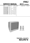
BX1S CHASSIS
PART NO. : 9-872-430-02
MODEL
KV-BM14M70
NO.
SUFFIX
DATE
SUPPL. / CORR
1
-01
2003/12
––
2
-02
2004/6
Supp-1
DESCRIPTION
1st. Issue
R827 Part Number Change (Page 63)
SERVICE MANUAL
MODEL
COMMANDER DEST.
KV-BM14M70
RM-W101 Ukraine
CHASSIS NO.
MODEL
BX1S CHASSIS
COMMANDER DEST.
CHASSIS NO.
SCC-V14C-A
RM-W101
TRINITRON ® COLOR TV
KV-BM14M70
RM-W101
TABLE OF CONTENTS
Section
Title
Page
Section
SELF DIAGNOSTIC FUNCTION .............................. 3
1. DISASSEMBLY
1-1. Rear Cover Removal ................................................. 6
1-2. Speaker Removal ...................................................... 6
1-3. Chassis Assy Removal .............................................. 6
1-4. Service Position ........................................................ 6
1-5. Terminal Bracket Removal ....................................... 6
1-6. A Board Removal ...................................................... 6
1-7. Picture Tube Removal ............................................... 7
2. SET-UP ADJUSTMENTS
2-1. Beam Landing ........................................................... 8
2-2. Convergence .............................................................. 9
2-3. Focus Adjustment .................................................... 11
2-4. G2 (SCREEN) Adjustment ..................................... 11
2-5. White Balance Adjustment ..................................... 11
2-6. Sub Bright Adjustment ........................................... 11
Title
Page
4. DIAGRAMS
4-1. Block Diagram ........................................................ 31
4-2. Circuit Boards Location .......................................... 32
4-3. Schematic Diagram Information ............................ 32
4-3-1. A Board — Processor (Block A) ............... 33
4-3-2. A Board — Audio (Block B) ..................... 35
4-3-3. A Board — Power Supply (Block C) ........ 37
4-3-4. A Board — Deflection (Block D) .............. 39
4-3-5. A Board — Tuner (Block E) ...................... 41
4-3-6. A Board — Jack (Block F) ........................ 43
4-3-7. C Board Schematic Diagram ..................... 45
4-4. Voltage Measurement and Waveforms ................... 46
4-5. Printed Wiring Boards and Parts Location ............. 49
4-6. Semiconductors ....................................................... 52
5. EXPLODED VIEWS
5-1. Chassis ..................................................................... 54
6. ELECTRICAL PARTS LIST .................................... 55
3. CIRCUIT ADJUSTMENTS
3-1. Adjustment With Commander ................................ 12
3-2. Adjustment Method ................................................ 13
3-3. Picture Quality Adjustments ................................... 28
3-4. Deflection Adjustment ............................................ 28
3-5. Drive Adjustment .................................................... 29
3-6. Picture Distortion Adjustment ................................ 30
OPERATING INSTRUCTIONS
CAUTION
SAFETY-RELATED COMPONENT WARNING!!
SHORT CIRCUIT THE ANODE OF THE PICTURE TUBE AND
THE ANODE CAP TO THE METAL CHASSIS, CRT SHIELD,
OR CARBON PAINTED ON THE CRT, AFTER REMOVING THE
ANODE.
COMPONENTS IDENTIFIED BY SHADING AND MARK ! ON
THE SCHEMATIC DIAGRAMS, EXPLODED VIEWS AND IN
THE PARTS LIST ARE CRITICAL TO SAFE OPERATION.
REPLACE THESE COMPONENTS WITH SONY PARTS
WHOSE PART NUMBERS APPEAR AS SHOWN IN THIS
MANUAL OR IN SUPPLEMENTS PUBLISHED BY SONY.
–2–
KV-BM14M70
RM-W101
SELF DIAGNOSTIC FUNCTION
The units in this manual contain a self diagnostic function. If an error occurs, the STANDBY (1) indicator will
automatically begin to flash. A description of the self-diagnosis function is explained in the instruction manual. The
number of times the STANDBY (1) indicator flashes translates to a probable source of the problem. If an error
symptom cannot be reproduced, the remote commander can be used to review the failure occurrence data stored in
memory to reveal past problems and how often these problems occur.
1. DIAGNOSTIC TEST INDICATORS
When an errors occurs, the STANDBY (1) indicator will flash a set number of times to indicate the possible cause of
the problem. If there is more than one error, the indicator will identify the first of the problem areas.
Result for all of the following diagnosis items are displayed on screen. No error has occured if the screen displays a
"0".
Diagnosis
Item
Description
No. of timer
STANDBY (1)
indicator flashes
Self-Diagnostic
display/
Diagnosis result
Probable Cause
Location
Detected
Symptoms
Power does
not turn on
Does not light
–
• Power cord is not plugged
in.
• Fuse is burned out (F600)
A board.
• Power does not turn on.
• No power is supplied on
TV.
• AC Power supply is faulty.
+B overcurrent
(OCP)*
2 times
2:0
or
2:1 ~ 255
• H OUT (Q805) is shorted.
(A board)
• IC751 is shorted. (C board)
• Power does not turn on.
• Load on power line is
shorted.
V-Protect
4 times
4:0
or
4:1 ~ 255
• +13V is not supplied.
(A board)
• IC804 is faulty. (A board)
• Has entered standby state
after horizontal raster.
• Vertical deflection pulse is
stopped.
• Power line is shorted or
power supply is shorted.
IK (AKB)
5 times
5:0
or
5:1 ~ 255
• Video OUT (IC1545) is
faulty. (A board)
• IC001 is faulty. (A board)
• Screen (G2) is improperly
adjusted.**
• No raster is generated.
• CRT Cathode current
detection reference pulse
output is small.
Power supply
NG (+5V) for
Video Processor
8 times
8:0
or
8:1 ~ 255
• IC604 faulty.
• IC602 faulty.
• No power supply to CRT
ANODE.
• No RASTER is generated.
If a +B overcurrent is detected, stoppage of the vertical deflection is detected simultaneously. The symptom that is
diagnosed first by the micro controller is displayed on the screen.
** Refer to Screen (G2) Adjustment in this manual.
*
–3–
KV-BM14M70
RM-W101
2. DISPLAY OF STANDBY (1) INDICATOR
FLASH COUNT
2 times
4 times
5 times
Diagnostic Item
Flash Count*
+B overcurrent
V-Protect
IK (AKB)
Power Supply NG (+5V)
for Video processor
2 times
4 times
5 times
8 times
8 times
* One flash count is not used for self-diagnosis.
Lamp ON 300ms
Lamp OFF 3 sec.
Lamp OFF 300ms
STANDBY (1) indicator
3. STOPPING THE STANDBY (1) INDICATOR FLASH
Turn off the power switch on the TV main unit or unplug the power cord from the outlet to stop the STANDBY (1)
indicator from flashing.
4. SELF-DIAGNOSTIC SCREEN DISPLAY
For errors with symptoms such as "power sometimes shuts off" or "screen sometimes goes off" that cannot be
confirmed, it is possible to bring up past occurrences of failure on the screen for confirmation.
[To Bring Up Screen Test]
In standby mode, press buttons on the remote commander sequentially in rapid succession as shown below:
Display
/ Channel 5 / Volume
/ Power
/ TV
˘
Note that this differs from entering the service mode (volume [+]).
The following screen will be displayed indicating the error count.
SELF DIAGNOSTIC
2:
3:
4:
5:
8:
0
N/A
0
1
0
101 :
N/A
Numeral "0" means that no fault was detected.
Numeral "1" means the number of a fault occurrence (1 ~ 255).
–4–
KV-BM14M70
RM-W101
5. HANDLING OF SELF-DIAGNOSTIC SCREEN DISPLAY
Since the diagnostic results displayed on the screen are not automatically cleared, always check the self-diagnostic
screen during repairs. When you have completed the repairs, clear the result display to "0".
Unless the result display is cleared to "0", the self-diagnosis function will not be able to detect subsequent faults after
completion of the repairs.
[Clearing the result display]
To clear the result display to "0", press buttons on the remote commander subsequent as shown below when the
self-diagnostic screen is being displayed.
8,[Quitting Self-diagnostic screen]
To quit the entire self-diagnostic screen, turn off the power switch on the remote commander or the main unit.
6. SELF-DIAGNOSTIC CIRCUIT
A BOARD
IC001
Y/CHROMA JUNGLE
FROM
C BOARD
IC751 PIN 5
A BOARD
FROM
Q816
COLLECTOR
A BOARD
IC804
V.OUT
A BOARD
IC001
SYSTEM
A BOARD
IC003
MEMORY
SDA1
84 IK
F.B-PLS
3
99
13
5 SDA
V.GUARD
RED LED 122
32 EHTO
DISPLAY
[+B overcurrent $OCP%]
Occurs when an overcurrent on the +B(135V) line is detected by pin 32 of IC001 (A board).
If the voltage of pin 32 of IC001 (A board) is more than 4V, the unit will automatically go
to standby.
[V-PROTECT]
Occurs when an absence of the vertical deflection pulse is detected by pin 13 of IC001
(A board).
[IK $AKB%]
If the RGB levels* do not balance within 15 sec after the power is turned on, this error will
be detected by IC001 (A board). TV will stay on, but there will be 5 times LED blinking.
POWER SUPPLY NG (+5V)
for VIDEO PROCESSOR
Occurs when IC001 internal HV protect detects an abnormal H-Pulse (frequency) due to
improper power supply to IC001. TV cuts off high voltage power of anode CRT. No picture
will be detected. eg: IC602, IC604 go faulty.
* (Refers to the RGB levels of the AKB detection Ref pulse that detects IK.)
–5–
KV-BM14M70
RM-W101
SECTION 1
DISASSEMBLY
1-1. REAR COVER REMOVAL
1-2. SPEAKER REMOVAL
1 Rear cover
1 Two screw
(+BVTP 3 × 12)
2 Six screws
(+BVTP 4 × 16)
1-3. CHASSIS ASSY REMOVAL
1-4. SERVICE POSITION
1-5. TERMINAL BRACKET REMOVAL
1-6. A BOARD REMOVAL
2 One screw
(+BVTP 3 × 16)
1 Terminal
bracket
3 Two screw
(+BVTP 4 × 16)
1 A board
–6–
KV-BM14M70
RM-W101
1-7. PICTURE TUBE REMOVAL
Note:
• Please make sure the TV set is not in standing position before removing necessary CRT support located on bottom
right and left.
1) Place the TV set with the CRT face down on a cushion jig.
2) Remove the rear cover.
3) Unplug all inder connecting leads from the Deflection Yoke, Degaussing Coil and CRT grounding strap.
qf Top switch Block
4 Anode Cap Removal
!£ Nut, Special, CRT (4)
7 Loosen the Neck Assembly
fixing screw and removal
qs Degaussing Coil
6 Spring Tension Removal
5 Earth Coating Assy
8 C Board Removal
0 Support, CRT(2) Removal
9 Chassis Assy Removal
qa Loosen the Deflection Yoke
fixing screw and remove
• REMOVAL OF ANODE-CAP
Note:
• After removing the anode, short circuit the anode of the picture tube and the anode cap to the metal chassis, CRT
shield or carbon paint on the CRT.
•
c
REMOVING PROCEDURES
a
anode button
a
turning up the rubber cap and pulling it up in the
direction of the arrow C.
•
1 Turn up one side of the rubber cap in the direction
indicated by the arrow A.
HOW TO HANDLE AN ANODE-CAP
1 Do not damage the surface of anode-caps with
sharp shaped objects.
2 Do not press the rubber too hard so as not to
damage the inside of anode-cap.
A metal fitting called the shatter-hook terminal is
built into the rubber.
3 Do not turn the foot of rubber over too hard.
The shatter-hook terminal will stick out or damage
the rubber.
b
b
2 Using a thumb pull up the rubber cap firmly in the direction indicated by the arrow B.
3 When one side of the rubber cap is separated from
the anode button, the anode-cap can be removed by
–7–
KV-BM14M70
RM-W101
SECTION 2
SET-UP ADJUSTMENTS
•
The following adjustments should be made when a
complete realignment is required or a new picture
tube is installed.
Set the controls as follows unless otherwise noted:
VIDEO model ..................................................... Standard
PICTURE control .................................................. normal
BRIGHTNESS control .......................................... normal
Perform the adjustments in the following order :
1. Beam Landing
2. Convergence
3. Focus
4. Screen(G2)
5. White Balance
Note : Test Equipment Required.
1. Pattern Generator
2. Degausser
3. DC Power Supply
4. Digital Multimeter
5. Oscilloscope
......................................................................................................................................................................................................................
Preparation :
• In order to reduce the influence of geomagnetism on
the set's picture tube, face it east or west.
• Switch on the set's power and degauss with the
degausser.
2-1.
Purity control
BEAM LANDING
Picture Mode: DYNAMIC
1. Input a white signal with the pattern generator.
Contrast
normal
Brightness
2. Set the pattern generator raster signal to a green
raster.
3. Move the deflection yoke to the rear and adjust with
purity control so that the green is at the center and
the blue and the red take up equally sized areas on
each side. (See Figures 2-1 through 2-4.)
4. Move the deflection yoke forward and adjust so that
the entire screen is green. (See Figure 2-1.)
5. Switch the raster signal to blue then to red and verify
the condition.
6. When the position of the deflection yoke has been
decided fasten the deflection yoke with the screws
and DY spacers.
7. If the beam does not land correctly in all the corners,
use a magnet to adjust it. (See Figure 2-4.)
Fig. 2-2
}
Blue
Red
Green
Fig. 2-3
Purity control
corrects this area.
b
a
c
d
Disk magnets or rotatable
disk magnets correct these
areas (a-d).
Deflection yoke positioning
corrects these areas.
b
c
a
d
Fig. 2-1
Fig. 2-4
–8–
KV-BM14M70
RM-W101
2-2.
•
•
•
CONVERGENCE
Before starting this adjustment, adjust the focus,
horizontal size and vertical size.
Receive dot/hatch signal.
Pic mode: Soft.
Operation of V.STAT magnet
If the V.Stat magnet is moved in the “A” and “B” arrows,
the red, green and blue dots moves as shown below.
A
B
(1) Horizontal and Vertical Static Convergence
Center dot
A
B
B
B
G
G
R
R
R
G
B
R
G
B
Moved RV750 H.STAT.
the red, green and blue dots move as shown below.
V. STAT
Magnet
H. STAT VR
A
R
RV750
H. STAT
B
B
G
R
4. BMC (Hexapole) Magnet.
If the red, green and blue dots are not balanced or
aligned, then use the BMC magnet to adjust in the
manner described below.
C Board
1. (Moving vertically), adjust the V.STAT magnet so that
the red, green and blue dots are on top of each other
at the center of the screen.
2. (Moving horizontally), adjust the H.STAT control so
that the red, green and blue dots are on top of each
other at the center of the screen.
3. If the H.STAT variable resistor cannot bring the red,
green and blue dots together at the center of the
screen, adjust the horizontal convergence with the
H.STAT variable resistor and the V.STAT magnet in
the manner given below.
(In this case, the H.STAT variable resistor and the
V.STAT magnet influence each other, so be sure to
perform adjustments while tracking.)
Purity
G
B
R G
B
R
B
G
R
G
B
R
G
B
R
G
R
BMC
BMC (Hexapole)
Purity
DY pocket
V.STAT
V.STAT
–9–
G B
B
KV-BM14M70
RM-W101
(2) Convergence Rough Adjustment
Preparation:
• Before starting this adjustment, adjust the horizontal
static convergence and the vertical static
convergence
RB
B
R
TLH
TLV
RB
R
B
XCV
YCH
TLH
Insert
TLH
Correction Plate to DY Pocket
YCH Insert
YCH
VOL on DY
ON DY:
(Left or Right)
TLV
Rotate TLV
VOL on DY
XCV
Rotate XCV
Adj core on DY
TLV
YCH
DY pocket
TLH Plate
(3) Screen corner Convergence
TLV
XCV
1. Affix a Piece A (90), conv. correct corresponding to
the misconverged areas.
XCV
DY pocket
b
b
a
a-d : screen-corner
misconvergence
a
c
d
d
Piece A (90), conv. correct
– 10 –
c
KV-BM14M70
RM-W101
2-3.
FOCUS ADJUSTMENT
2-5.
FOCUS adjustment should be completed before the W/B
adjustment:
1. Receive digital monoscope pattern.
2. Set picture mode: DYNAMIC.
3. Adjust focus VR to obtain a just focus at the center of
the screen.
4. Change receiving signal to white pattern and blue
back.
5. Confirm MAGENTA RING is not noticeable. Incase
magenta ring is obvious, then adjust FOCUS VR to
balance magenta ring and FOCUS.
2-6.
SUB BRIGHT ADJUSTMENT
1. Set to service mode.
2. Brightness set to 50%, Picture....Minimum
3. Select WHBL SBRT (10) with 1 and 4 and adjust
SBRT (10) data with 3 and 6 so that the third
stripe from right dimly lit.
4. Write into the memory by pressing [MUTING] then -.
5. GA models C/O: 20 IRE
S/G: 30 IRE
FOCUS
SCREEN
FLYBACK TRANSFORMER (T802-14")
FLYBACK TRANSFORMER (T801-21")
2-4.
WHITE BALANCE ADJUSTMENT
1. Set to Service Mode (Refer Section 3-1:
ADJUSTMENTS WITH COMMANDER)
2. Input white raster signal.
3. Set Picture to <DYNAMIC mode>
4. Select RDRV (02) with 1 and 4 and fixed the value
to 25 with 3 and 6
5. Adjust WHBL GDRV (03) and BDRV (04) with 1 and
4 and adjust the data with 3 and 6 for best white
balance in Highlight condition.
6. Write into the memory by pressing [MUTING] then -.
7. Adjust WHBL BKOR (00) and BKOG (01) with 1 and
4 and adjust the level with 3 and 6 for best white
balance cut-off condition.
8. Write into memory by pressing [MUTING] then -.
9. US model need to apply only for colour temperature
in Neutral.
G2 (SCREEN) ADJUSTMENT
1. Set the PICTURE & BRIGHTNESS to STANDARD.
2. Put the Video input mode signal.
3. Connect R,G,B of the C board cathode to
oscilloscope.
4. Adjust Brightness to obtain the cathode value to
value below.
5. Adjust G2 (screen) on the FBT until picture shows
the point before cut off.
165 ± 2VDC
– 11 –
KV-BM14M70
RM-W101
SECTION 3
CIRCUIT ADJUSTMENTS
3-1.
ADJUSTMENT WITH COMMANDER
Service adjustments to this model can be performed using the supplied remote commander RM-W101.
a. ENTERING SERVICE MODE
With the unit on standby
t [DISPLAY] t 5 t [VOL $+% ] t [POWER]
This operation sequence puts the unit into service mode.
This screen display is:
item no.
in decimal
item name
service data
in decimal
NVM
NG
service command
field
frequency
channel no./
video input name
GEOM
006
HSIZ
031
x
SERVICE
60
S VIDEO 1
release ID
software
version
service data
in binary
reserved
for factory
color system
power on time
(decimal?)
0.69U
0001 1111
FF FF
NTSC3
65535
category
SUS01
Flash DCXO
111 11 11 1 7 11
FG
xy 111
Status Byte
#1 SSD
Status Byte
#2 SSD
000000
000000
VDSP_C Flag
CO_LOCKED
VDSP
Detected Stereo Type (Direct Value from CZ_ Stereo_Mode)
S : for Sony
A : Aiwa
U S : US/Latin/Taiwan
E U : Europe
G A : General Area
J P : Japan
0 1 : serial no. of the M/P release
for each destination
111
Needed for Nicam DCXO aligment Purpose
xy
Value of x = 0 - Unknown, 1 - BTSC, 2 - A2, 3 - NICAM,
4 - KOREAN, 5 - Japan, 6 - AV Stereo
Value of y = 0 - Mono, 1 - Stereo, 2 - Bilingual, 4 - SAP/Single
b. METHOD OF CANCELLATION FROM SERVICE MODE
Set the standby condition (Press [POWER] button on the commander), then press [POWER] button again, hereupon it
becomes TV mode.
c.
1.
2.
3.
4.
5.
METHOD OF WRITE INTO MEMORY
Set to Service Mode.
Press 1 (UP) and 4 (DOWN), to select the adjustment item.
Change item by pressing 3, 6.
Press [MUTING] button to indicate WRITE on the screen.
Press - button to write into memory.
1, 4
r
3, 6
r
[MUTING]
r
-
d.
1.
2.
3.
Select the adjustment item.
Raise/lower the data value.
Writes.
Executes the writing.
MEMORY WRITE CONFIRMATION METHOD
After adjustment, pull out the plug from AC outlet, and then plug into AC outlet again.
Turn the power switch ON and set to Service Mode.
Call the adjusted items again to confirm adjustments were made.
– 12 –
KV-BM14M70
RM-W101
e. OTHER FUNCTION VIA REMOTE COMMANDER
7, All the data becomes the values in memory.
8, All user control goes to the standard state.
Display, - Service data initialization (Be sure not to use usually.)
2, 5
Select Device or Category
3-2.
ADJUSTMENT METHOD
Item Number 000 HPOS
This explanation uses H POSITION as an example.
1. Select "000 HPOS" with the 1 and 4 buttons, or 2 and 5.
2. Raise/lower the data with the 3 and 6 buttons.
3. Select the optimum state. (The standard is IF for PAL reception.)
4. Write with the [MUTING] button. (The display changes to WRITE.)
5. Execute the writing with the - button. (The WRITE display will be changed to red color while excuting, and back to
SERVICE.)
Example on screen display :GREEN
GEOM
000
HPOS
039
SERVICE
50 VIDEO 1
Adjusted with [3] and [6] buttons.
GREEN
GEOM
000
HPOS
039
WRITE
50
VIDEO
1
50
VIDEO
1
write with [MUTING].
RED
GEOM
000
HPOS
039
WRITE
The WRITE display
then returns to green
SERVICE
Write executed with [0].
Use the same method for all Items. Use 1 and 4 to select the adjustment item, use 3 and 6 to adjust, write with
[MUTING], then execute the write with -.
Note : 1. In [WRITE], the data for all items are written into memory together.
2. For adjustment items that have different standard data between 50Hz or 60Hz, be sure to use the respective
input signal after adjustment.
– 13 –
Category
GEOM
Functionality
Init.
Range
DATA
Function
Table & Note
Device Name
NVM Address / Initial Value (Detailed)
– 14 –
No.
Name
Dec
Dec
000
HPOS
031
063
ADJUST
Horizontal Shift (HS)
001
HPAR
031
063
ADJUST
Horizontal Parallelogram
002
HBOW
031
063
ADJUST
Horizontal Bow
50/60/w50/w60
31
31
31
31
003
VLIN
031
063
ADJUST
Vertical Linearity
50/60/w50/w60
31
31
31
31
004
VSCR
031
063
ADJUST
Vertical Scroll
50/60/w50/w60
31
31
31
31
005
HSIZ
031
063
ADJUST
EW Width (EW)
50/60/w50/w60
25
25
25
25
006
EWPW
031
063
ADJUST
EW Parabola/Width (PW)
50/60/w50/w60 (+JPN RGB)
31
31
31
31
007
UCOP
017
063
ADJUST
EW Upper Corner Parabola
50/60/w50/w60
31
31
31
31
008
LCOP
017
063
ADJUST
EW Lower Corner Parabola
50/60/w50/w60
31
31
31
31
009
EWTZ
031
063
ADJUST
EW Trapezium
50/60/w50/w60
31
31
31
31
010
VSLP
031
063
ADJUST
Vertical Slope (VS)
50/60/w50/w60
31
31
31
31
011
VSIZ
015
063
ADJUST
Vertical Amplitude
50/60/w50/w60
15
15
15
15
012
SCOR
014
063
ADJUST
S-Correction (SC)
50/60/w50/w60
25
25
25
25
013
VPOS
031
063
ADJUST
Vertical Shift (VSH)
50/60/w50/w60
31
31
31
31
014
HBL
000
001
FIX
RGB Blanking Mode
50/60/w50/w60
01
01
01
01
(Slave Address)
Common
50
60
w50
w60
50/60/w50/w60 (+JPN RGB)
TV-Processor
42
42
42
42
50/60/w50/w60
(8Ah)
31
31
31
31
015
WBF
007
015
FIX
Timing of Wide Blanking (WBF)
50/60/w50/w60
07
07
07
07
016
WB R
007
015
FIX
Timing of Wide Blanking (WBR)
50/60/w50/w60
10
10
10
10
017
SBL
000
001
FIX
Service Blanking
none
00
018
COPY
000
001
FIX
Copy the GEO data to all 50/60Hz NVM area
none
00
RM-W101
TVJ
KV-BM14M70
Adjustment Item Table
TVJ
Functionality
Init.
Range
Category
No.
Name
Dec
Dec
WHBL
000
BKOR
031
063
ADJUST Black Level Offset R
col temp (HIGH/LOW/Normal)*(UV/RGB/Others)
001
BKOG
031
063
ADJUST Black Level Offset G
col temp (HIGH/LOW/Normal)*(UV/RGB/Others)
002
RDRV
037
063
White Point R
col temp (HIGH/LOW/Normal)*(UV/RGB/Others)
003
GDRV
037
063
ADJUST White Point G
col temp (HIGH/LOW/Normal)*(UV/RGB/Others)
004
BDRV
037
063
ADJUST White Point B
col temp (HIGH/LOW/Normal)*(UV/RGB/Others)
DATA
Function
Table & Note
Device Name
(Slave Address)
FIX
NVM Address / Initial Value (Detailed)
Common
Col Temp
(HIGH other)
Col Temp
(LOW other)
Col Temp
(NORM other)
TV-Processor
31
31
(8Ah)
31
31
TV-Pro (8AH)
37
31
31
005
LPG
000
001
FIX
RGB Gain Preset
none
01
006
PGR
031
127
FIX
Preset Gain R (PGR)
none
**
007
PGG
031
127
FIX
Preset Gain G (PGG)
none
**
008
PGB
031
127
FIX
Preset Gain B (PGB)
none
**
FIX
Preset Gain Offset
009
GNOF
000
015
010
SBRT
031
063
011
SBRO
000
003
none
ADJUST Sub-Brightness
FIX
Sub-Brightness Offset (Intelligent Pic)
CCC loop
Col Temp
(HIGH YUV)
Col Temp
(LOW YUV)
Col Temp
(NORMAL YUV)
Col Temp
(HIGH RGB)
31
31
31
31
31
31
31
31
31
31
31
31
31
31
37
37
37
37
37
37
37
37
31
31
31
31
31
31
31
31
31
31
31
31
31
31
31
31
Col Temp
(LOW RGB)
Col Temp
(NORM RGB)
Others
RGB
YUV
31
31
31
Pic mode
0
Pic mode
1
Pic mode
2
Pic mode
3
00
01
02
01
15
Others/RGB/YUV
none
01
012
EGL
000
001
FIX
Enable Gain Loop in CCC System
none
00
013
SGL
000
003
FIX
Selection of High Current in CCC System
none
00
014
AKB
000
001
FIX
Black Current Stabilization
none
00
015
CBS
000
001
FIX
Control Sequence of Beam Current Limiting
none
00
016
RGBB
000
003
FIX
RGB Blanking
none
00
017
BLBG
000
001
FIX
Blanking of Blue & Green Output
none
00
018
OFB
000
001
FIX
Black Level Offset Blue
none
01
019
NSBR
000
015
FIX
Non Standard Brightness Offset
none
05
020
WBP
000
003
FIX
Color Temp Setting (0:High, 1:Normal, 2,3:Low)
021
OUV
000
Picture Mode
Offset Control on UV Input Signals
00
00
– 15 –
Item remarks ** please refer to page 23 and 24
TVJ
Functionality
Init. Range
DATA
Function
Table & Note
Device Name
NVM Address / Initial Value (Detailed)
(Slave Address) Common YUV 50pal 50pal 50secam 50secam 60TV 60Video 50YUV 60YUV 50RGB 60RGB Pic mode Pic mode Pic mode Pic mode Dynamic*Eco
(TV) (Video) (TV) (Video)
0
1
2
3
std (Jpn)
Category
No.
Name Dec
Dec
SADJ
000
PMAX 063
063
ADJUST Picture Maximum
001
SHUE 007
015
ADJUST Sub-Hue
002
SSHP 015
063
FIX
Sub-Sharpness
003
SSHO 000
003
FIX
Sub-Sharpness Offset (Intelligent Pic)
004
SCOL
031
063
005
SCOO 000
ADJUST Sub-Color
(TV / Video)*(Normal / Wide) / <Normal / Wide> (+JPN RGB)
TV-Processor
TV / Video
**
TV / Video / YUV (+JPN RGB)
none
31
31
31
31
31
31
31
31
31
37
07
07
**
**
37
37
00
00
31
FIX
Sub-Color Offset (Intelligent Pic)
PIC
031
127
FIX
Picture Control [GA:0-100(valid), >100(invalid);
Others:0-63(valid); ignore bit 6(invalid)]
Picture Model(GA: Personal = User Reset Data)
02
100
80
65
100
007
COL
031
127
FIX
Color Control [GA:0-100(valid), >100(invalid);
Others:0-63(valid); ignore bit 6(invalid)]
Picture Model(GA: Personal = User Reset Data)
56
50
40
50
008
BRT
031
127
FIX
Brightness Control [GA:0-100(valid),
>100(invalid); Others:0-63(valid); ignore bit
6(invalid)]
Picture Model(GA: Personal = User Reset Data)
50
50
60
50
009
HUE
031
127
FIX
Hue Control [GA:0-100(valid), >100(invalid);
Others:0-63(valid); ignore bit 6(invalid)]
Picture Model(GA: Personal = User Reset Data)
50
50
50
50
010
SHP
031
127
FIX
Sharpness Control [GA:0-100(valid),
>100(invalid); Others:0-63(valid); ignore bit
6(invalid)]
Picture Model(GA: Personal = User Reset Data)
60
50
50
50
RM-W101
KV-BM14M70
003
006
Item remarks ** please refer to page 23 and 24
37
02
50pal(tv)/50pal(video)/50secam(tv)/50secam(video)/
60TV/60video/50YUV/60YUV/50RGB/60RGB
none
Dynamic*Eco Standard*Eco Standard*Eco Eco std Eco much TV Video TV Video AVM AV Wide
much (Jpn)
std (Jpn)
much (Jpn)
(Jpn)
(Jpn)
Wide Wide (Jpn) (Jpn)
Init.
Name
Dec
Dec
YC
000
PFRQ
000
003
001
RPA
####
003
FIX
Ratio Pre & Over Shoot
TV/other
02
02
002
RPO
0 02
003
FIX
Ratio of Positive & Negative Peaks
TV/other
02
02
003
YDLY
012
015
FIX
Y-Delay
004
CMAT
000
003
FIX
PAL-SECAM or NTSC (Japan/USA) Matrix
Range DATA
Function
Table & Note
Device Name
NVM Address / Initial Value (Detailed)
(Slave Address) Common Others
FIX
Peaking Center Frequency and Delay
TV-Processor
RGB
005
ACL
001
001
FIX
Automatic Color Limiting
CB
000
001
FIX
Chroma Bandpass Center Frequency
007
SBO
001
003
FIX
SECAM Black Offset
PAL(TV) NTSC(TV) SECAM(TV) PAL(Video) NTSC(Video) SECAM(Video) S-INPUT SECAM NTSC TV
**
**
(PAL/NTSC/SECAM)*(TV/VIDEO)+YUV/S-INPUT
006
YUV
(JPN RGB)
00
valid only with TV (*Video:0 fix)
01
**
**
**
**
**
**
**
00
01
00
008
CHSE
001
003
FIX
PAL/NTSC Ident Sensitivity
02
009
CLO
000
001
FIX
Center Frequency of Cloche(Bell) Filter
00
010
CTRP
000
001
FIX
Chroma Trap Mode
SECAM/others
011
BPS
000
001
FIX
Bypass of Chroma Base-band Delay Line
012
FCO
000
001
FIX
Forced Color On
013
TINT
031
063
FIX
Base-Band Tint Control
014
TUV
000
001
FIX
Tint Control on UV Signals
00
01
**
NTSC/others
**
00
YUV/others
31
31
00
– 16 –
Item remarks ** please refer to page 23 and 24
TVJ
Category
SYNC
Functionality
Init.
Range
No.
Name
Dec
Dec
000
SYS
000
001
FIX
Synchronization on YSYNC Input
001
FO
000
003
FIX
Phase 1 Time Constant
002
VID
000
001
F IX
Video Ident Mode
DATA
Function
Table & Note
Device Name
(Slave Address)
NVM Address / Initial Value (Detailed)
Common
60
00
00
00
00
others
YUV
TV
Video
Teletext
TV-ip
No signal
03
03
01
00
00
00
TV IP ON/TV IP OFF/Video/Teletext/Auto Tuning or No signal(RF)
50/60
003
FSL
000
001
FIX
Forced Slicing Level for Vertical Sync
004
SSL
000
001
FIX
Slicing Level Sync Separator
005
SVID
001
007
FIX
Source Selection for Video Identification
006
FORF
000
003
FIX
Forced Field Frequency
03
00
50/60
YUV/Others
00
007
MVK
000
001
FIX
Macro Vision Keying
01
008
AFCT
000
003
FIX
AFC Timing Switch Control
(GA, US:pin 116, EURO, JPN:pin 128)
#
#Note : AFCT For ES5.2D, data is 00
For ES7.2D, data is 03
50
07
RM-W101
Functionality
No.
KV-BM14M70
TVJ
Category
TVJ
Category
PICT
Functionality
Init.
Range
DATA
Function
Table & Note
Device Name
(Slave Address)
NVM Address / Initial Value (Detailed)
Common Others
No.
Name
Dec
Dec
000
CADL
007
015
FIX
Cathode Drive Level
001
CFA
000
003
FIX
Comb Filter Mode
002
SOC
002
003
FIX
Soft Clipping Level
003
PWL
001
001
FIX
Peak White Limiting Switch
004
WHTL
006
015
FIX
Peak White Limiting
**
005
GAM
001
001
FIX
Gamma
00
006
WTS
001
003
FIX
Gamma Control and White Stretch
007
TFR
000
001
FIX
008
COR
003
003
FIX
009
CORO
000
001
FIX
Coring Offset (Intelligent Pic)
010
BKS
003
003
FIX
Black Stretch
011
AAS
001
001
FIX
Black Area to Switch off the Black Stretch
##
012
DSK
000
001
FIX
Dynamic Skin Control
00
RGB
Live
TV
TV
Video Video ColorTemp ColorTemp
Color
Color Temp
(Dyn) (Others) (Dyn) (Others) (HIGH)
(Others) Temp(LOW) (NORMAL)
00
**
(8Ah)
00
01
Live/Others
#
DC Transfer Ratio of Luminance Signal
Live/Others (+JPN RGB)
01
Coring
(TV/Video)*(Dyna/others)
– 17 –
013
BLS
000
001
FIX
Blue Stretch
NBLS
000
001
FIX
Operation Blue Stretch Circuit
015
NRR
000
001
FIX
Non Red Reduction
00
01
00
00
00
00
00
RGB/others
014
#
02
02
col temp (HIGH/OTHERS)
00
00
00
col temp (HIGH/LOW/NORMAL)
01
01
01
Item remarks ** please refer to page 23 and 24
# for WTS :Data is 01 (ES5.2D)
:Data is 02 (ES7.2D)
## for AAS:Data is 00 (ES5.2D)
:Data is 01 (ES7.2D)
TVJ
Category
SW
Range
No.
Name
Dec
Dec
000
CV2
000
001
FIX
CVBS2 Input Signal Selection
001
SVO
001
003
FIX
Function of IFVO/SVO/CVBSI Pin @ 48
002
DFL
000
001
FIX
Flash Protection
DATA
Function
Table & Note
Device Name
(Slave Address)
NVM Address / Initial Value (Detailed)
Common
YUV
TV
Video
02
01
01
00
TV/Video/YUV
01
RM-W101
Init.
KV-BM14M70
Functionality
V IF
Init.
Range
No.
Name
Dec
Dec
000
OIFD
036
063
FIX
Offset IF Demodulator
001
AGCT
031
063
FIX
AGC Take-over
002
STM
000
001
FIX
Search Tuning Mode
01
003
GD
000
001
FIX
Group Delay on CVBS1 Signal
00
004
AGCS
001
003
FIX
IF AGC Speed
01
005
FFI
000
001
FIX
Fast Filter IF PLL
00
006
OAMP
003
003
FIX
Video Output Signal Amplitude (only L & L'System)
03
007
VAI
000
001
FIX
System I Output Signal Amplitude Correction (only L & L'System)
00
DATA
Function
Table & Note
Device Name
Common
(Slave Address)
TV-Processor
36
(8Ah)
31
– 18 –
TVJ
Functionality
Init.
Range
Category
No.
Name
Dec
Dec
VM
000
RGBD
003
007
FIX
Delayof RGB Output to VM Output
001
VMA
003
003
FIX
Amplitude of VM Output
002
VMAP
002
003
FIX
VM setting (0:High, 1:Low, 2,3:OFF)
003
VMMO
003
003
FIX
VM Mode
DATA
Item remarks ** please refer to page 23 and 24
# for RGBD : Data is 02 (ES5.2D)
: Data is 04 (ES7.2D)
Function
Table & Note
Device Name
NVM Address / Initial Value (Detailed)
(Slave Address)
Common
none
TV-Processor
#
none
(8Ah)
**
Picture Mode
01
Pic mode
0
Pic mode
1
Piv mode
2
Pic mode
3
00
01
02
00
RM-W101
Category
Functionality
KV-BM14M70
TVJ
TVJ
Category
SDEM
Functionality
Init.
Range
No.
Name
Dec
Dec
000
FMWS
000
003
FIX
Window Selection for FM Demodulator
001
QSS
001
001
FIX
Quasi Split Sound (QSS) Amplifier Mode (except GA Model)
002
BPB
000
001
FIX
Bypass of Sound Bandpass Filter
00
003
AMLO
000
001
FIX
Audio Output Signal for AM Sound
00
004
HPVC
000
001
FIX
Head Phone Volume Control
00
DATA
Function
Table & Note
Device Name
Common
(Slave Address)
TV-Processor
02
(8Ah)
**
Item remarks ** please refer to page 23 and 24
– 19 –
TVJ
Category
TXT
Functionality
Init.
Range
No.
Name
Dec
Dec
000
TXV
039
063
FIX
Teletext Vertical Position for Philips
001
THD
005
127
FIX
Teletext H-sunc Active Edge Shift
05
002
TBR
004
015
FIX
Teletext RGB Brightness
11
003
LCB
000
001
FIX
Teletext LCB 0 : disable 1: enable (setting for FASTEX)
00
DATA
Function
Table & Note
Device Name
Common
(Slave Address)
Text Decoder
39
RM-W101
KV-BM14M70
Init.
Range
Name
Dec
Dec
SDSP
000
AVM
002
007
DATA
FIX
Function
Table & Note
Device Name
(Slave Address)
NVM Address / Initial Value (Detailed)
Common
AVL Mode
SSD
02
(B0h)
09
001
AVV
005
015
FIX
AVL Reference Level
002
BBL
000
015
FIX
BBE Contour
**
003
BBH
000
015
FIX
BBE Process
**
004
BBLW
000
015
FIX
BBE Contour Offset
005
SVOF
000
015
FIX
Surround /Effect Mode Volume Offset
006
IVOF
000
007
FIX
Master Volume Positive Offset
06
007
EVOF
000
007
FIX
Master Volume Negative Offset
06
008
LAD
000
031
FIX
Decoder Level Adjust
05
009
LAM
000
031
FIX
Mono Level Adjust
05
010
LAN
000
031
FIX
Nicam Level Adjust
22
011
LAS
000
031
FIX
SAP Level Adjust
08
012
LAA
000
031
FIX
ADC Level Adjust
TV
Video
Off
SRS/WOW
Trusurround
Istereo
Imono
**
**
**
**
**
05
03
**
Off(SRS/WOW)/Trusurround/Istereo/Imono
Tv/Video(Non Euro)I TV-L/TV-non L/Video
00
– 20 –
013
SEF
003
007
FIX
Incredible Mono/Stereo Effect
014
A1L
000
255
FIX
AUX1 Volume Left
00
015
A1R
000
255
FIX
AUX1 Volume Right
00
016
BAS
008
015
FIX
Main Bass Offset
**
017
TRE
008
015
FIX
Main Treble Offset
**
018
EQ1
008
015
FIX
Equalizer Main Channel Band (100 Hz) Offset
**
019
EQ2
008
015
FIX
Equalizer Main Channel Band (300 Hz) Offset
**
Istereo/Imono
020
EQ3
008
015
FIX
Equalizer Main Channel Band (1000 Hz) Offset
**
021
EQ4
008
015
FIX
Equalizer Main Channel Band (3000 Hz) Offset
**
022
EQ5
008
015
FIX
Equalizer Main Channel Band (8000 Hz) Offset
**
023
BFCT
005
007
FIX
DBE, DUB and BBE Control
**
024
SCEN
001
015
FIX
SRS3D Center Control
04
025
SSPA
000
015
FIX
SRS3D Space Control
01
026
BBHW
000
015
FIX
BBE process offset in WOW mode
**
027
STRE
002
007
FIX
Treble Offset for surround mode
**
028
BBHT
000
015
FIX
BBE Offset in TV mode
00
029
DWA
000
000
FIX
DWA???
00
030
TTRE
002
007
FIX
Treble Offset in TV Mode
02
Item remarks ** please refer to page 23 and 24
TV-L(Euro)
00
00
RM-W101
Functionality
No.
KV-BM14M70
TVJ
Category
TVJ
Category
SDEC
Functionality
Init.
Range
No.
Name
Dec
Dec
000
MPTU
003
015
DATA
FIX
Function
Table & Note
Device Name
(Slave Address)
Common
Upper Threshold for MPX pilot detection (BTSC)
SSD
02
(B0h)
001
MPTL
009
015
FIX
Lower Threshold for MPX pilot detection (BTSC)
002
SPTU
003
015
FIX
Upper Threshold for SAP carrier detection
08
003
SPTL
006
015
FIX
Lower Threshold for SAP carrier detection
15
05
004
C1TH
000
031
FIX
Normal Threshold for detection of SC1
00
005
C1AP
000
031
FIX
Auto Program Threshold for detection of SC1
00
006
SPTH
000
031
FIX
Noise Threshold for automute of SAP
00
007
SPHY
004
015
FIX
Hysteresis size for automute of SAP
03
008
FMTH
000
031
FIX
Noise Threshold for automute of SC2 in FM A2 standard
18
009
FMHY
004
015
FIX
Hysteresis size for automute of SC2 in FM A2 standard
07
010
BTTH
000
031
FIX
Noise Threshold for automute of BTSC stereo carrier
00
011
BTHY
004
015
FIX
Hysteresis size for automute of BTSC stereo
03
012
EJTH
000
031
FIX
Noise Threshold for automute of EIAJ FM subcarrier
00
013
EJHY
004
015
FIX
Hysteresis size for automute of EIAJ FM subcarrier
04
– 21 –
014
ONLY
000
001
FIX
Reproduce only related NICAM on DEC output
00
015
EXAM
000
001
FIX
Fall back source in case of automute in standard L (DDEP)
00
016
NIMT
000
001
FIX
NICAM auto mute function depend on bit error rate (DDEP)
00
017
NILE
100
255
FIX
NICAM lower error limit (DDEP)
50
018
NIUE
200
255
FIX
NICAM upper error limit (DDEP)
200
019
EPMD
001
003
FIX
DEMDEC Easy Programming (DDEP)
02
020
STDS
019
031
FIX
Bits multiplexed for ASD and SSS modes
31
021
OVMA
001
001
FIX
FM overmodulation adaption
00
022
FLBW
000
003
FIX
FM/AM demodulator filter bandwidth
03
023
IDMD
000
003
FIX
FM ident speed in SSS mode
00
024
FPAL
000
001
FIX
Line fequency for BTSC decoding
00
025
OVMT
001
002
FIX
Overmodulation level threshold relative to nominal
03
026
DCXI
000
001
FIX
NICAM DCXO Scaling Control Inverter
**
027
DCXG
000
007
FIX
NICAM DCXO Scaling Control Gain
**
028
DCLL
011
015
FIX
NICAM DCXO Scaling Control Limit (L)
00
DCLH
000
031
FIX
NICAM DCXO Scaling Control Limit (H)
**
IDEU
001
003
FIX
IDMOD setting for European A2 STD
00
031
IDKR
001
003
FIX
IDMOD setting for Korean M STD
00
032
IDJP
001
003
FIX
IDMOD setting for EIAJ STD
01
RM-W101
Item remarks ** please refer to page 23 and 24
KV-BM14M70
029
030
OPTM
Init.
Range
No.
Name
Dec
Dec
000
ASHT
006
007
DATA
FIX
Function
Table & Note
Device Name
(Slave Address)
Auto shut off timer (data * 5 min)
NVM Address / Initial Value (Detailed)
Common
50
60
63
31
00
001
OSDB
000
015
FIX
OSD brightness
MMR/Micro 60h
05
002
OSDH
005
015
FIX
OSD Horizontal Position
MMR/Micro 60h
05
003
OSDV
037
063
FIX
OSD Vertical Position
004
MUTE
000
001
FIX
No Signal Mute Switch (1=enabled)
00
50 / 60
MMR/Micro 60h
005
RFUL
015
015
FIX
RF Signal Change Counter after Unlocked (Disable when 0fh)
04
006
RFLK
015
015
FIX
RF Signal Change Counter after Locked (Disable when 0fh)
00
007
AVUL
015
015
FIX
AV Signal Change Counter after Unlocked (Disable when 0Fh)
04
008
AVLK
015
015
FIX
AV Signal Change Counter after Locked (Disable when 0Fh)
00
009
LANG
000
003
FIX
OSD language shipping condition
010
HTXT
000
001
FIX
Sync seperator sw
011
CMSS
000
001
FIX
Sync sw
012
DCXO
060
295
FIX
DCXO Value
00
TV-Processor(8A)
00
TV-Processor(8A)
01
SFR/Micro 60h/DSP
59
– 22 –
013
EXBL
000
015
FIX
Extended Blanking Timer to Eliminate White Noise
014
TSYS
000
003
FIX
Memorize TV Sys in NVM at Test Reset [0:B/G, 1:I, 2:M, 3:D/K] (GA Model)
**
015
TV0U
001
001
FIX
TV Out mute condition 0:Always mute off, 1:mute without signal
00
016
LBL
001
001
FIX
Brightness Reduction At No Signal Condition
00
07
Item remarks ** please refer to page 23 and 24
TVJ
Category
OPTB
Functionality
Init.
Range
No.
Name
Dec
Dec
000
IALL
000
001
FIX
Standard Write Switch (not memorized in NVM)
001
OPB1
000
255
FIX
Option 1 (System related)
****
002
OPB2
000
255
FIX
Option 2 (Video Signal related)
****
003
OPB3
000
255
FIX
Option 3 (Stereo Decoding related)
****
004
OPB4
000
255
FIX
Option 4 (Miscellaneous)
****
005
OPB5
000
255
FIX
Option 5 (Miscellaneous)
****
006
OPB6
000
255
FIX
Option 6 (OSD Language related)
****
DATA
Function
Table & Note
Device Name
(Slave Address)
Common
Note
00
For remark ****
Please refer to option
bit for all models on
page 25 to page 27.
NOTE
• Standard data listed on the Adjustment Item Table are reference values, therefore it may be different for each model and for each mode.
• Note for Different Data Those are the standard data values written on the microprocessor. Therefore, the data values of the modes and stored respectively in the memory.
In case of a device replacement, adjustment by rewriting the data value is necessary for some items.
RM-W101
Category
Functionality
KV-BM14M70
TVJ
KV-BM14M70
RM-W101
Data variant depend on models
Category
No
Name
Model
WHBL
006
PGR
007
PGG
008
PGB
With VM
Without VM
With VM
Without VM
With VM
Without VM
Category
No
Name
Model
Data
VM
001
VMA
With VM
Without VM
03
00
Category
YC
Category
No Name
003 YDLY
No
Data (ES5.2D)
69
61
69
61
69
61
Table
Comb Model
Non-Comb Model
Name
PAL
(TV)
NTSC
(TV)
SECAM
(TV)
08
02
08
02
08
10
SECAM
(VIDEO)
YUV
S-Input
09
2
11
2
09
09
09
09
11
2
Table
Video
YUV
35
38
35
35
21" Comb models
21"Non-Comb models &
All 14" models
35
35
Category
No
Name
Model
Data
PICT
001
CFA
Comb models
Non-Comb models
00
01
Category
No
Name
Model
YC
000
PFRQ
Comb models
Non-Comb models
Category
No
Name
Model
Comb models
Non-Comb models
NTSC
(VIDEO)
TV
SSHP
BPS
PAL
(VIDEO)
Model
002
011
50
45
50
45
50
45
Model
SADJ
YC
Data (ES5.2~)
Data (ES5.2D) Data (ES7.2D)
01
00
00
00
Table
NTSC
Others
01
00
00
00
– 23 –
KV-BM14M70
RM-W101
Data variant depend on models
Category
No
Name
AR21
series
01
05
06
13
14
12
04
10
09
10
05
00
01
BT21
(AV Stereo)
00
00
06
14
14
09
10
09
10
11
00
00
01
HW21
3D
00
00
06
11
12
00
00
00
11
12
00
00
01
AR14
series
01
04
06
00
13
07
00
00
10
00
05
00
01
SDSP
002
003
004
016
017
018
019
020
021
022
023
026
027
BBL
BBH
BBLW
BAS
TRE
EQ1
EQ2
EQ3
EQ4
EQ5
BFCT
BBHW
STRE
Category
No
Name
Stereo models
Non-stereo models
SDEC
026
027
029
DCXI
DCXG
DCLH
01
03
06
00
00
00
Category
No
Name
14" models
21" models
PICT
004
WHTL
09
00
Category
No
Name
Mono & AV Stereo models
Stereo, China & India
SDEM
001
QSS
00
01
Category
No
Name
Other Country
OPTM
014
TSYS
00
Category No Name
SDSP
Model
005 SVOF BM14/21 & BT21 mono
HW21
non-3D
00
00
06
13
14
11
00
00
00
12
00
00
01
BM14/21
& BT21
00
00
06
0
00
00
00
00
00
00
00
00
01
Table
Off
SRS/WOW
Trusurround
Istereo
Imono
00
07
00
02
00
– 24 –
KV-BM14M70
RM-W101
ITEM INFORMATION
No. OPB1
Item
KV-BM14M70
Speed Search
1
0
M/N(US)
L’
M
B/G
I
D/K
DEC
0
0
1
1
1
1
79
SPEED SEARCH (Time of speed search)
TV System Selection
00 = disabled (original cycle speed)
01 = 4 time speed from the original
10 = 6 time speed from the original
11 = 8 time speed from the original
0 = disabled, 1 = enabled
No. OPB2
Item
KV-BM14M70
D1(JPN) AV Multi/ Component Composite (SCART)
PAM(GA)
0
0
0
1
0
D1
AV Multi/
PAM
Component
Composite
(D1 Terminal)
(AV Multi Terminal) - JP
Portable Audio Mode - GA
(Component [YCbCr] Terminals)
(No. of Composite Terminals)
(SCART)
(No. of SCART Terminals)
SECAM
Color decoding
(SECAM Color System)
(Color Crystal Selection)
SECAM
1
Color Decording
0
DEC
0
20
0 = not available, 1 = available
0 = not available, 1 = available
0 = not available, 1 = available
0 = not available, 1 = available
00 = no composite terminal
(Euro:no Scart) BX1L:No Video
01 = 1 composite terminal
(Euro:1 Scart) BX1L:2 Video in
10 = 2 composite terminals
(Euro:2 Scart) BX1L:3 Video in
11 = 3 composite terminals
(Euro:no terminal) BX1L:4 Video in
0 = not available, 1 = available
00 = PAL/NTSC/SECAM (Multi)
01 = NTSC (3.58MHz)
10 = PAL/NTSC/SECAM (4.43MHz)
11 = PAL/NTSC (Tri-Norma)
No. OPB3
Item
KV-BM14M70
HDEV
0
NICAM ST NICAM BI A2 ST Thai Bilingual JP/US ST Korean ST MONO
0
0
0
0
0
0
1
HDEV
NICAM ST
NICAM BI
A2 ST/BI
Thai Bilingual
JP/US ST
Korean ST
MONO
(High Deviation Mode)
(NICAM Stereo)
(NICAM Stereo)
(A2 [West German]
Stereo/Bilingual)
(A2 [Thai] Bilingual)
or Force SAP if JP/US ST is act
(JP/US Stereo)
(Korean Stereo)
(Monaural Model)
– 25 –
0 = disabled, 1 = enabled
0 = disabled, 1 = enabled
0 = disabled, 1 = enabled
0 = disabled, 1 = enabled
0 = disabled, 1 = enabled
0 = disabled, 1 = enabled
0 = disabled, 1 = enabled
0 = Stereo (SSD) Model
1 = Monuaral Model
DEC
01
KV-BM14M70
RM-W101
No. OPB4
Item
Firmware/
SMAT
1 spk
Models
VM
0
1
0
KV-BM14M70
Equalizer Surround
0
Firmware
SMAT
1 spk Models
(SSD Firmware Downloading)
Surround Matrix
1 Speaker Models
VM
Equalizer
Surround
(Velocity Modulation)
(5-band Equalizer Model)
(US/GA Surround Selection)
V-Chip
(V-Chip Model)
TOP
TEXT
(Forced TOP)
(Teletext Model)
0
V-Chip
Top
Text
DEC
0
0
0
64
0 = disabled, 1 = enabled
0 = Active, 1 = Passive
0 = 2 or 3 Speaker Models,
1 = 1 speaker Models
0 = disabled, 1 = enabled
0 = Bass/Treble Model, 1 = Equalizer Model
0 = Off/Simulated/Surround
1 = Off/Simulated/WOW/TruSurround (US)
1 = Off/Simulated/SRS (3D) Surround (GA)
0 = Channel Block Model (no rating)
1 = Parental Control Model (rating)
0 = Auto Mode (TOP/FLOF), 1 = Forced TOP
0 = Non-Teletext Model, 1 = Teletext Model
No. OPB5
Item
KV-BM14M70
Full
No
Forced 60
Surround Surround
0
1
0
ASD
Tilt
IP Plus
IP
Wide
DEC
0
0
1
1
0
70
Full Surround
(Full Surround option)
No Surround
Forced 60
ASD
Tilt
IP Plus
IP
Wide
(No Surround Model)
(Forced 60Hz in no signal)
(Automatic Standard Detection)
(Tilt Correction/PIC Rotation)
(Intelligent Picture Plus)
(Intelligent Picture)
(Wide Mode/V-Compressed)
– 26 –
0 = Normal Surround Model
1 = Full Surround Model
(Off/simulated/surround/
SRS/WOW/TruSurround)
0 = Surround Model, 1 = Non-Surround Model
0 = 50Hz, 1 = 60Hz
0 = disabled, 1 = enabled
0 = disabled, 1 = enabled
0 = disabled, 1 = enabled
0 = disabled, 1 = enabled
0 = disabled, 1 = enabled
KV-BM14M70
RM-W101
No. OPB6
Item
GA US
Latin
1
0
KV-BM14M70
Feature 2 Feature 1
0
0
OSD Language Selection
1
GA US
(US Model Destination)
Latin
(US Model Latin Destination)
Feature 2
(Temporary for BX1L)
Feature 1
(Temporary for BX1L)
OSD Language Selection
(English always available except JP)
0
0
136
0 = US/CANADA/Latin
1 = Taiwan/Korea/Philippine
(Wake-up timer enable)
(GA Surround Spec:OFF,
SIMULATED, SRS)
0 = US/CANADA (No Volume Figure Display)
1 = Latin (Volume Figure Display)
0 = Comb Not available
1 = Comb available
0 = PiP Not Available
1 = PiP available
US
01xx = French
0x1x = Spanish
0xx1 = Portuguese
US
(GA NTSC)
1x1x = Complicated Chinese
1xx1 = Korean
GA
EU
– 27 –
0
DEC
1xxx = Simplified Chinese
x1xx = Arabic
xx1x = Thai
xxx1 = Vietnamese
0000 = Destination ADE
0001 = Destination BL
0010 = Destination KR
0011 = Destination U
KV-BM14M70
RM-W101
3-3.
PICTURE QUALITY ADJUSTMENTS
SUB HUE ADJUSTMENT
PMX/CONTRAST ADJUSTMENT
1.
2.
3.
4.
Select Video Mode.
Input PAL CB to TV set.
Set PICT 03 "PWL" to 00h and WHBL 21 "BLBG" to 01h.
Set the following condition:
PICTURE 100%, COLOR 0%, BRIGHTNESS 50%.
5. Connect an oscilloscope to pin 4 (R output) of CN004.
6. Set to Service Mode "PWL" to 00h, “BLBG” to 01h.
7. Select SADJ00 "PMX" with 1 and 4 of the
commander then adjust VR within spec with 3 and 6.
1. Select Video.
2. Input a NTSC 3.58 Color Bar to TV set.
3. Set the following condition:
PICTURE 100%, COLOR 50%, BRIGHTNESS 50%
4. Connect an oscilloscope to pin 2 (B output) of CN004.
5. Set to Service and adjust SADJ01 "SHUE" with 1
and 4 of commander then adjust to VB1 = VB2 =
VB3 = VB4 with 3 and 6.
6. Then press [MUTING] t - to write the data.
VB1
VB2
VR
Black
The highest level of VB1, VB2, VB3, VB4 must be
aligned at the same time.
The ideal difference between VB2 and VB3 is within
±110mV.
1.46 ± 0.03 Vp-p = without VM models
1.65 ± 0.03 Vp-p = with VM models
8. Then press [MUTING] t - to write the data
9. Set "PWL" and "BLBG" back to initial data repectively.
(PWL: 01h and BLGG: 00h)
Select Video and set Picture mode.
Input PAL 100% CB to TV set.
Set PICT 06 "WTS" to 00h.
Set the following condition:
PICTURE 100%, COLOR 50%, BRIGHTNESS 50%.
5. Connect an oscilloscope to pin 2 (B output) of CN004.
6. Select to Service Mode and adjust SADJ04 "SCOL"
with 1 and 4 of commander then adjust to
VB2 = VB3 = VB4 with 3 and 6.
VB1
For single system with NTSC 4.43 select TV channel
with NTSC 4.43 and repeat 4 t 6.
3-4.
SUB COLOR ADJUSTMENT
1.
2.
3.
4.
VB3 VB4
DEFLECTION ADJUSTMENT
H-TRAPEZOID ADJUSTMENT
1. Receive cross hatch/dotsignal.
2. Adjust on to make H-Trapezoid distortion best.
NORMAL MODE (50Hz)
1. Set to Service Mode.
2. Input SPCB Signal (Select Video Mode for USA).
3. Using the 1 and 4 button select GEO (Service
Mode).
4. Rasie/lower data using the 3 and 6 buttons adjust
the following items:-
VB2 VB3 VB4
GEOM :
VB2 = VB3 = VB4
(Difference is within 70mV)
7. Then press [MUTING] t - to write the data.
8. Set "WTS" back to original data.
000
001
002
003
004
005
006
007
008
009
010
011
012
013
014
015
016
017
018
HPOS
HPAR
HBOW
VLIN
VSCR
HSIZ
EWPW
UCOP
LCOP
EWTZ
VSLP
VSIZ
SCOR
VPOS
HBL
WBF
WBR
SBL
COPY
Horizontal Shift (HS)
Horizontal Parallelogram
Horizontal Bow
Vertical Linearity
Vertical Scroll
EW Width (EW)
EW Parabola/Width (PW)
EW Upper Corner Parabola
EW Lower Corner Parabola
EW Trapezium
Vertical Slope (VS)
Vertical Amplitude
S-Correction (SC)
Vertical Shift (VSH)
RGB Blanking Mode
Timing of Wide Blanking (WBF)
Timing of Wide Blanking (WBR)
Service Blanking
Copy the GEO data to all
50/60Hz NVM area
5. Write into memory by pressing [MUTING] then - on
the remote commander.
– 28 –
KV-BM14M70
RM-W101
WIDE MODE (50Hz)
WIDE MODE (60Hz)
(V-Compression Adjustment)
1. Input SPCB signal.
2. Adjust condition change to WIDE MODE : ON
3. Copy (Item from normal mode 50Hz) all Normal
Mode adjusted data.
(V-Compression Adjustment)
1. Input mono scope signal.
2. Adjust condition change to WIDE MODE : ON
3. "COPY" is set to 1, then [MUTE] + -
3-5.
NORMAL MODE (60Hz)
1. Input signal
1. Input 525/60Hz signal.
2. They can copy 50Hz first.
("COPY" under GEOM is set to 1, then [MUTE] + -)
3. Using the 1 and 4 button, select category GEO
(Service Mode).
4. Raise/lower data using the 3 and 6 buttons to
obtain optimum image.
GEOM :
000
001
002
003
004
005
006
007
008
009
010
011
012
013
014
015
016
017
018
HPOS
HPAR
HBOW
VLIN
VSCR
HSIZ
EWPW
UCOP
LCOP
EWTZ
VSLP
VSIZ
SCOR
VPOS
HBL
WBF
WBR
SBL
COPY
DRIVE ADJUSTMENT
Horizontal Shift (HS)
Horizontal Parallelogram
Horizontal Bow
Vertical Linearity
Vertical Scroll
EW Width (EW)
EW Parabola/Width (PW)
EW Upper Corner Parabola
EW Lower Corner Parabola
EW Trapezium
Vertical Slope (VS)
Vertical Amplitude
S-Correction (SC)
Vertical Shift (VSH)
RGB Blanking Mode
Timing of Wide Blanking (WBF)
Timing of Wide Blanking (WBR)
Service Blanking
Copy the GEO data to all
50/60Hz NVM area
2.
3.
4.
5.
70% Color Bar (USA)
100% Color Bar (Other)
Make sure only red is active.
Set following condition :PICTURE 100%, COLOR 0%, Other 50%
Select SADJ00 "PMAX" with 1 and 4 then adjust
until voltage in R out X gain [recorded] = SPEC
Then press [MUTING] t - to write data.
X±2VDC (R Cathode on C or CV board)
Model
14”
21”
GA
83.0
88.0 - Non VM Models
99.0 - VM Models
6. Set VIDP 36 BLBG back to 00.
– 29 –
KV-BM14M70
RM-W101
3-6. PICTURE DISTORTION ADJUSTMENT
H. CENTER ADJUSTMENT (HPOS)
1. Input Monoscope signal.
2. Activate the Service Adjustment Mode.
3. Select the HPOS item with 1 and 4.
4. Adjust the value of HPOS with 3 and 6 for the best
vertical center.
5. Press [MUTING] then - to save into the memory.
V. LINEARITY (VLIN), V. CORRECTION (SCOR), PIN
AMP (EWPW), AND HORIZONTAL TRAPEZOID
(EWTZ) ADJUSTMENTS
1. Input Monoscope signal.
2. Activate the Service Adjustment Mode.
3. Select VLIN, SCOR, EWPW, and EWTZ with 1 and
4.
4. Adjust with 3 and 6 for the best horizontal size.
5. Press [MUTING] then - to save into the memory.
V LINEARITY (VLIN)
H. SIZE ADJUSTMENT (HSIZ)
1. Inpu Monoscope signal.
2. Activate the Service Adjustment Mode.
3. Select HSIZ with 1 and 4.
4. Adjust with 3 and 6 for the best horizontal size.
5. Press [MUTING] then - to save into the memory.
V CORRECTION (SCOR)
PIN AMP (EWPW)
HORIZONTAL TRAPEZOID (EWTZ)
V. SIZE ADJUSTMENT (VSIZ)
1.
2.
3.
4.
Input Monoscope signal.
Activate the Service Adjustment Mode.
Select the VSIZ item with 1 and 4.
Adjust value of VPOS with 3 and 6 for the best
vertical center.
5. Press [MUTING] then - to save into the memory.
V. ANGLE (HPAR), H. BOW (HBOW), UPPER PIN
(UCOP) AND LOW PIN (LCOP) ADJUSTMENTS
1. Input Monoscope signal.
2. Activate the Service Adjustment Mode.
3. Select HPAR, HBOW, UCOP, and LCOP with 1 and
4.
4. Adjust with 3 and 6 for the best picture.
5. Press [MUTING] then - to save into the memory.
V. CENTER ADJUSTMENT (VPOS)
V ANGLE (HPAR)
1.
2.
3.
4.
Input Monoscope signal.
Activate the Service Adjustment Mode.
Select the VPOS item with 1 and 4.
Adjust value of VPOS with 3 and 6 for the best
vertical center.
5. Press [MUTING] then - to save into the memory.
V BOW (HBOW)
UPPER PIN (UCOP)
LOW PIN (LCOP)
– 30 –
MAIN
Power
Supply
IF
30V
+B line
VIF&SIF SAW
FSS TUNER
3.3/5V
8V
AUDIO VCC
AGCin
STBY
3.3V
12C
5V
3.3V
5V
4-1. BLOCK DIAGRAM
CISPR/
PFC
AC in ~
110-220V
8V
Relay
30V
DGC
24-5.VIF1~2
115.P3.0
VIF & SIF
31.AGCout
Video
L(Mono)
Mon
out
Video
L(Mono)
AV1
in
CV/YC
L(Mono)
AV1
AV2
in
CV/YC
L(Mono)
AV2
Audio Amp
Mon Out
43.IFVO/IF_MON_OUT
62.SCARTHPL
48.SV0MON_OUT
36.OutL
Color
Decoder
56.InL1
55.CVBS3
Ik
65.SVM
VM
+B
HV
V-out
V+, V-
112.ROT CTRL
113.ROT SW
ONE CHIP
Rot. cct
On/Off
Micro
Text
CC & V-chip
I/O Port
DVD/RGB
Fbl(RGBin)
51.CVBS2/Y2
52.C2
49.InL2
Jungle
PLL
11.Xtalout
Pin out
H-drive
H-out
EHT, ABL
+/-15V
Hout
FBT
feedback
Audio Amp
I/O Port
70-72.VUY IN
74~76.YUVout
24.576MHz
EW, Hd
Hp
32.EHTO
83.ABL
77.Fbl3
10.Xtalin
21.EWD
67.Hout
66.AFC
78~80.R-Y/R,
Y/G,
B/Y/B IN
34.InL5
102.B-INT
122~123 RED-GREEN LED
AV3
97.SIRCS
98, 99.SCL1,SDA1
108, 109.SCL0,SDA0
G/Y
B/PB
R/PR
L
RGB
23. V+
22. V-
119.KEY
RGB/
DVD
in
CV/YC
L(Mono)
RGB
58.CVB51/Y1
59.C1
53.InL3
AV3
in
YUV
Processor
85~87
RGBout
84.lk
SECTION 4
DIAGRAMS
– 31 –
TV
out
RGB Amp
POWER
60.LSL
FM MONO Dem
Volume control
L
3W
Mono
R
3W
1/2ch
mute
106.AUDIO MUTE
105.AUDIO STANDBY
stdby
LED
HP
B-INT
Key buttons
SIRCS
L
ATT
L,R
VAR
12C
RM-W101
NVM
KV-BM14M70
Device 12C
KV-BM14M70
RM-W101
4-2.
CIRCUIT BOARDS LOCATION
C Board
A Board
4-3.
SCHEMATIC DIAGRAM INFORMATION
Note:
• All capacitors are in µF unless otherwise noted.
• All electrolytic capacitors are rated at 50V unless otherwise
noted.
• All resistors are in ohms.
kΩ = 1000Ω, MΩ = 1000kΩ
• Indication of resistance which does not have rating
electrical power is as follows.
Reference information
RESISTOR
: RN
: RC
: FPRD
: FUSE
: RS
: RB
: RW
Pitch: 5 mm
Rating electrical power 1/4W (CHIP: 1/10W)
•
•
•
•
•
•
•
•
•
•
•
•
•
•
•
: nonflammable resistor.
: fusible resistor.
¢
: internal component.
: panel designation or adjustment for repair.
All variable and adjustable resistors have characteristic
curve B unless otherwise noted.
Readings are taken with a color-bar signal input.
no mark
: Common
(
)
: PAL
[
]
: NTSC 3.58
Readings are taken with a 10 MΩ digital multimeter.
Voltage are dc with respect to ground unless otherwise
noted.
Voltage variations may be noted due to normal
production tolerances.
All voltage are in Volt.
✽
: Cannot be measured.
Circled numbers are waveform references.
: B +bus.
: B –bus.
k : signal path.
COIL
CAPACITOR
Note: The reference number which starts with Wxxx
(eg: W003) indicates a wire to wire connection.
Note: Components marked as XX are not fitted on this
model.
– 32 –
Note:
:✽
: LF-8L
: TA
: PS
: PP
: PT
: MPS
: MPP
: ALB
: ALT
: ALR
METAL FILM
SOLID
NONFLAMMABLE CARBON
NONFLAMMABLE FUSIBLE
NONFLAMMABLE METAL
OXIDE
NONFLAMMABLE CEMENT
NONFLAMMABLE
WIREWOUND
ADJUSTMENT RESISTOR
MICRO INDUCTOR
TANTALUM
STYROL
POLYPROPYLENE
MYLAR
METALIZED POLYESTER
METALIZED POLYPROPYLENE
BIPOLAR
HIGH TEMPERATURE
HIGH RIPPLE
The component identified by shading and
mark ! are critical for safety. Replace only
with part number specified.
Note: “A” board schematic diagram is divided into 6 blocks.
Each block is named by its function and block
“alphabet”. eg: Processor (Block A)
Joint connection between boards can be identified
using the block alphabet followed by sequence
numbering.
eg: -<HOUT-DEFL (A10) To D11
Meaning: Block A joint A10 is connected to Block D
joint D11
KV-BM14M70
KV-BM14M70
RM-W101
RM-W101
4-3-1. A Board — Processor (Block A)
D066
GP08D
Y IN / G
GND
U IN / B
V IN / R
GND
1
2
3
4
5
CN003
XX
WHT
TO C BOARD
CN711
14
R377
XX
CHIP
V IN
Y IN
13
HOUT-DEFL (A10) To D11
AFC-DEFL (A11) To D2
LSR-AUDIO (A12) To B3
LSL-AUDIO (A13) To B2
Y OUT
GND
U OUT / FB
GND
V OUT
1
2
3
4
5
U IN
12
+B (A9) To C11,D15,E11
+B
NC
GND
VM OUT
GND
B OUT
G OUT
R OUT
GND
IK
9V
CN004
XX
WHT
TO C BOARD
CN701
CN009
XX
YEL
1
2
3
4
5
6
7
D1_JP/MODE2_
EU/MONSW-MONO
(A8) To F24
CN007
XX
WHT
TO A BOARD
(JACK)
CN905
9V
R
G
B
U IN
C004
100
16V
V IN
5V
R394
4.7k
CHIP
L003
10uH
U OUT
3.3V
11
Y OUT
B
10
C005
100
16V
C006
100
16V
PROCESSOR
(BLOCK A)
9
V OUT
A
8
1
2
3
4
7
PWR-OFF-MUTE
(A1) To B6
A
6
MOMUTE-AUDIO
(A7) To B8
5
SDA-0 (A5) To E14
SCL-0 (A6) To E15
4
5V (A4) To C9,D12,E16,F1
3
3.3V (A3) To C1,D18
2
9V (A2) To B4,B14,C8,
D14,E13,F6
1
1.8V AUDIO
R014
100
CHIP
R097 220 CHIP
AUDIO-STDBY
To B7 (A61)
R340
10k
CHIP
3.3V
R336
4.7k
CHIP
3.3V
R338
4.7k
CHIP
R015
R322
C020
1.5k
4.7k
0.1
CHIP
CHIP
16V
D068
B:CHIP
UDZSTE-175.6B
R392
C308
R380
0.01 25V
100
10K
CHIP CHIP
B:CHIP
R030
100
CHIP
C091
100p
CHIP
R320
4.7k
CHIP
1.8V MAIN
R029
100
CHIP
L009 C011
C090
10uH XX
16V B 100p
C311
CHIP
2.2
D070
R319
XX
XX
CHIP
Q013
MSD601-RT1
R098
220
CHIP
L012
10uH
C314
470
10V
F
Q006
UN2216
G LED SW
Q007
UN2216
R LED SW
97 SIRSC
R020
98 SCL1
100 CHIP
L011
99 SDA1
10uH
C021
100p CHIP 100 VDDC2
C012
101 VSSC2
0.22
16V
102 B INT
C313 B:CHIPR012 2.2k CHIP
103 D1_JP/MODE2_EU/MONSW-MONO
1000p
B:CHIP
104 MOMUTE-AUDIO
R337 470 CHIP
105 AUDIO STDBY
R339 100 CHIP
106 AUDIO MUTE
R341 100 CHIP
107 HD SW
R018 100 CHIP 108
10
11
111 S1/VC(GA)
D069
XX
C014
0.22
16V
B:CHIP
112 ROT CTRL
113 ROT SW
(
114 STBY_SW
R023 1.5K CHIP
115 DGC RELAY
R024 100 CHIP
116 D1_JP/MODE1_EU
JR1011
117 VDDC1(1.8V)
0
118 DECV1V8
CHIP
C013
119 KEY
100 16V
120 S2
R026
121 VSSC1/P
100
CHIP
122 RED LED
R025
100
CHIP
R356
0 CHIP
L007 10uH
C094
D005
0.1
C038
XX
16V B C095
0.1
0.1
16VC302R386PROTECTION
16V
C301 B 2.2 100
C053
B
470p CHIP 16VCHIP
0.022
F
CH
25V B
R385 R384
C092 C093
100 100
0.1 0.1
C096
CHIP CHIP
16V 16V
0.1
B
B
16V B
9
8
125 VSSC3
126 AGC-MUTE
W004
CVBSO (A15) To F23
SCARTHPR (A16) To F22
SCARTHPL (A17) To B1,F21
64
63
62
IC001
TDA11010H/N1B000PN
SYSTEM CONTROLLER
- VIDEO PROCESSOR
- AUDIO PROCESSOR
INL2
MON-OUT
VP2
AGC2SIF
VCC8V
)
IFVO/IF_MON_OUT
SIFAGC/SCART
PLLIF
GND2
MONO_OUTL
DECSDEM
OUTR
OUTL
D1 RIN
D1 LIN
AVL/2SIF
1
2
3
4
5V
C1 (A18) To F8
CVBS1/Y1 (A19) To F10
INR1 (A20) To F12
INL1 (A21) To F11
CVBS3 (A22) To F13
INR3 (A23) To F15
INL3 (A24) To F14
59
58
57
56
55
54
53
52
49
5
48
47
L033
10uH
1.8V AUDIO
H
L004
47uH
C303
100
16V
45
R314
6.8k
CHIP
R316
XX
CHIP
3.3V
R315
6.8k
CHIP
C319
47p
CHIP
43
CVBS2/Y2 (A25) To F20
INR2 (A26) To F18
INL2 (A27) To F19
MON-OUT (A28) To F5
W033
C069
0.1
16V
B:CHIP
42
40
37
36
MONO_OUTL (A30) To E19,F2
C063
0.1
16V B
35
C316
0.47
10V
B:CHIP
34
TV-R
TV-L
W032
33
W010
C065
3.3
C309
W030
XX
W031
C064 R379 25V
B
2.2
68k
CHIP
D074
MMDL914T1
OUTR (A31) To F4
OUTL (A32) To F3
5V
D063
MMDL914T1
OCP
3.3V
W008
1.8V AUDIO
R310 R311
100 47k
R309 CHIP CHIP
1M
CHIP
D061
C079
MMDL914T1
XX
Q009
R326
XX
XX
ABL-BUFFER
RN-CP
C084
XX R327
B
XX
RN-CP W009
D060
UDZSTE-175.6B
ABL
I
W011
D062
UDZSTE-175.6B
SLICER
1.8V AUDIO
1.8V MAIN
FB001
1.1uH
– 33 –
B-BX1S12153-UKR-A..PROCESSOR-BM14M70
To E3 (A35) 2SIF
To D8 (A38) OVP-DEFL
To E10 (A36) TUAGC-IF
To D10 (A37) OCP-PROTECT
To E2 (A40) SIFIN1-IF
To E1 (A39) SIFIN2-IF
To D1 (A45) EWD-DEFL
To D7 (A44) VD--DEFL
To D5 (A43) VD+-DEFL
To E8 (A42) VIFIN1-IF
To E7 (A41) VIFIN2-IF
To D4 (A47) ABL
To D3 (A46) VGUARD-DEFL
To E20 (A67) VDDC4_CAP
To D19 (A66) PH2LF
To C2 (A49) 1.8V_MAIN
1.8V_AUDIO
To B13,C10 (A50)
To E12 ( A51) AGC-MUTE
To E21 (A68) VDDC3_CAP
To F9 (A53) S1/VC
D1_JP/MODE1_EU
To F25 (A52)
To F17 (A54) S2
To C13 (A58) STBY_SW
To C15 (A57) DGC-RELAY
To E6 (A56) SECAM-L-L
To E9 (A55) M-SYS-IF
(A59) RESET
To B9 (A60) AUDIO-MUTE
J
– 34 –
5
5
5
JW1089
XX
JW1090
XX
JW1091
XX
5
JW1092
XX
IFVO/IF_MON_OUT (A29) To E5
PLL1F (A65) To E18
39
38
5
W034
C320
47p
CHIP
41
R312
C048
C089
0.22 C052
1000p
1M
R060
16V 1000p
R051
B
CHIP
100
B
B
CHIP
39k
CHIPCHIP
CHIP
CHIP
C046
C300
R044 6800p
R048 C055
R313
0.22
0.15
R011
12k 25V B
100
16V
150k
250V
C323
C034 1K B:CHIP CHIP CHIP
C058
R046CHIP PP
CHIP
XX CHIP
0.001 1000p
100
CH
B:CHIP
CHIP
C041
B:CHIP
C049 C050
10
4700p C044
0.022
2.2
B:CHIP 16V
25V B
W022
3.3V
C321
F:CHIPCHIP
C081
0.01
C317
1000p
25V
220 16V B:CHIP
B
C042
C080
0.22
5V
1000p
16V
B:CHIP
B:CHIP
C322
0.001
B :CHIP
L032
10uH
C072
0.01
25V
B:CHIP
46
C304
100
16V
C029 22
L036
10uH
C031
XX
L037
XX
C032 XX CH
C022 C024
0.22 22
16V
B:CHIP
3.3V
JW1088
XX
61
60
13 14 15 16 17 18 19 20 21 22 23 24 25 26 27 28 29 30 31 32
L010 10uH
1.8V MAIN
W003
R395
100k TP04
CHIP
CVBS2/Y2 51
INR2 50
124 VDDC3(1.8V)
TP02
6
SCARTFBL/A16 (A14) To F16
R317
3.3k
CHIP
INTC0-IF 44
127 SECAM L-L
C325
0.022
25V
CHIP
7
CVBS0
SCARTHPR
SCARTHPL
LSR
LSL
C1
CVBS1/Y1
INR1
INL1
CVBS3
INR3
INL3
C2
123 GREEN LED
G
R
D914
SPB-25MVWF
LED
C036
100 16V
C056
100
16V
L005
10uH
C054
0.1
16V
B R058
100
R056 CHIP R059
XX
100
CHIP
CHIP
110 VDDP(3.3V)
ROT_CTRL
To D16 (A33)
ROT_SW
To D17 (A34)
128 M-SYS-IF
G
D006
XX
D008
PROTECTION
XX
PROTECTION
SCL0
C018
0.22
16V
B:CHIP
L013
10uH
R364
1k
CHIP
109 SDA0
D071
MMDL914T1
D072
MMDL914T1
D007
D009
XX
XX
PROTECTION PROTECTION
VP3
GND3
B-Y/BIN
Y/GIN
R-Y/RIN
SCARTFBL
3 4
R324
2.2k
CHIP
R038
100
CHIP
5V
96 95 94 93 92 91 90 89 88 87 86 85 84 83 82 81 80 79 78 77 76 75 74 73 72 71 70 69 68 67 66 65
C312
1000p
B:CHIP
F
R087
220
CHIP
C028
0.1
16V B:CHIP
C030
0.22
16V
B
CHIP
C051
XX
16V
F
VREF_POS_HPR
XTALIN
XTALOUT
X001 VSSA1
24.576MHz
VGUARD
L008
DECDIG
10uH
VP1
PH2LF
PH1LF
GND1
SECPLL
DECBG
R045
EWD
100 CHIP
VDVD+
D065
UDZSTE-175.6B
VIFIN1
D064 PROTECTION
UDZSTE-175.6B
VIFIN2
PROTECTION
VSC
IREF
GNDIF
SIFIN1
SIFIN2
AGCOUT
EHT0
B_DAT
C328
0.01 25V
R323
100
CHIP
R096
220 CHIP
To F29 (A63) B_INT
L031
10uH
C023
2.2
TP03 16V
B:CHIP
VDDADC(1.8)
VSSADC
VDDA2
VDDA(1.8)
Q016
UN2211
C026
47
35V
Q010
XX
C071
XX
16V
F
C073 2.2
C025
0.22 16V
B:CHIP
R039 100 CHIP
R041 100 CHIP
R042 2.2k CHIP
3.3V
R010
10k
CHIP
R001
4.7k
CHIP
R003
4.7k
CHIP
R099
220
CHIP
R362 R363 C009
XX
0
XX
CHIP CHIP B
L006
10uH
D023
UDZSTE-179.1B
PROTECTION
L035
10uH
VSSP2
VSSC4
VDDC4(1.8V)
VDDA3(3.3V)
VREF_POS_LSL
VREF_NEG_LSL+LSR
VREF_POS_LSR+HPL
vREF_NEG_HPL+HPR
R361
XX
CHIP
VCC OUT
GND
C010
470p
CHIP
D003
MMDL914T1
C008
47
35V
IC002
RPM7240-H5
IC RECEIVER
2 1
D002
MMDL914T1
R360
0
CHIP
R331
100
CHIP
D054
UDZSTE-175.6B
PROTECTION
D056
MMDL914T1
PROTECTION
D055
UDZSTE-175.6B
PROTECTION
B_INT
JR1010
XX
CHIP
To F27 (A64) B_CLK
D025
UDZSTE-179.1B
PROTECTION
2
IC003
B:CHIP
CAT24WC16J1-TE13
NVM
R393 C002
470
100
3.3V
CHIP 16V
GND 1
NC 2
KEY 3
To F28 (A62) B_DAT
C015
XX
D067
XX
1
D
E
C003
100p
CHIP
C001
100p CHIP
R002
R006
100
XX
CHIP
CHIP
C318
0.1
16V
5V
CN005
3P
WHT
TO TOP CONTROL
PANEL
R004
100
CHIP
PROTECTION
C098
XX
16V C068
XX
F
16V
F
C097
XX
16V
F
D004
XX
PROTECTION
5V
D075 UDZSTE-179.1B
C037 4.7
D059
MMDL914T1
B-MUTE
D024
UDZSTE-179.1B
3.3V
3.3V
C099
XX
16V
F
VOUT
UOUT
YOUT
YSYNC
YIN
UIN
VIN
VDDCOMB
VSSCOMB
HOUT
AFC
VM
5V
GNDA
VREFAD
VREFAD_PO
VREFAD_NE
VDDA(3.3V)
B OUT
G OUT
R OUT
IK
ABL
C
Q001
UN2211
RGB-MUTE
(SPOT)
Y IN
5V
D057
MMDL914T1
R-MUTE
D058
MMDL914T1
G-MUTE
3.3V
KV-BM14M70
KV-BM14M70
RM-W101
RM-W101
4-3-2. A Board — Audio (Block B)
SP
GND
GND
12
CN202
3P
WHT
1
2
3
4
SP L
GND
GND
SP R
1
2
3
2
CN200
XX
WHT
11
A
AUDIO
C225
XX
R225
XX
CHIP
IN L
IN C/NC
OUTL
MUTE
PW_GND
VCC
STBY
OUTR/NC
S_GND
8
9
10
11
12
C213
R213 C212
0.1
15k 1000
B
25V
CHIP
CHIP
D210
XX
Q200
UN2211
C224 C211
XX 4.7
C229
R230
XX
XX
CHIP
R215
10k
CHIP
R216
10k CHIP
R212
0
CHIP
R224
XX
CHIP
D207
XX
R236
10K
CHIP
Q206
UN2211
H
R242
2.2k
CHIP
D214
MMDL914T1
FB2607
XX
PS2601
5A
To A61 (B7) AUDIO-STDBY
To A1 (B6) PWR-OFF-MUTE
To A7 (B8) MOMUTE-AUDIO
To A60 (B9) AUDIO-MUTE
To C6 (B10) AUDIO_GND
To C4 (B12) AUDIO_1
To C5 (B11) AUDIO_2
I
To A50,C10 (B13) 1.8V_AUDIO
D206
XX
R221
1k
CHIP
9V
R220
0
CHIP
C221
XX
25V
D204
MMDL914T1
D211
1PS226-115
9V
R2646
1
FPRD
To A2,B4,C8,D14,E13,F6 (B14) 9V
D203
MMDL914T1
C219
220
16V
R218
0
CHIP
D212
MMDL914T1
FB2602
1.1UH
– 35 –
Q201
MSB709-RT1
9V
Q202
MS