1
MODIFICATION
HISTORY
# No.
DATA
#1
2002.3
Correction of exploded views. (P.4-2)
#2
2002.9
Addition of Chinese model. (P.4-2, 4-3)
Addition of Block Diagram and Schematic diagrams/Printed Wiring Boards.
(P.3-1, 3-3~3-11)
MODEL NAME : SDM-S51
#3
2004.9
Addition of the LCD panels. (P.1)
Addition and change of 4-1. CHASSIS PART No. (P.4-2)
SERVICE MANUAL
PARTS No. : 9-978-721-04
* Blue characters are linking.
CONTENTS
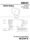
SDM-S51
US Model
Canadian Model
AEP Model
Chinese Model
SERVICE MANUAL
The SDM-S51 has two
varieties of the LCD panels.
Please make sure to determine
the service parts of the LCD
module, I/F board and main
harness assy.
SPEC.
MODEL NAME
SDM-S51/WQ UC
SDM-S51/WQ1 UC
SDM-S51/BQ UC
SDM-S51/BQ1 UC
SDM-S51/WQ EK
SDM-S51/WQ1 EK
SDM-S51/WQ2 EK
SDM-S51/BQ EK
SDM-S51/BQ1 EK
SDM-S51/WQ AZ1
SDM-S51/WQ CAN
OLD PANEL
COLOR DEST.
Gray
UC
Gray
UC
Black UC
Black UC
Gray AEP
Gray AEP
Gray AEP
Black AEP
Black AEP
Gray
SH
Gray
CH
SER. No.
No. 4,000,001 ~
No. 4,047,389 ~
No. 4,250,001 ~
No. 4,263,963 ~
No. 4,500,001 ~
No. 4,535,257 ~
No. 4,545,849 ~
No. 4,750,001 ~
No. 4,755,009 ~
No. 5,500,001 ~
No. 5,600,001 ~
NEW PANEL
MODEL NAME COLOR DEST.
SDM-S51/WQ2 UC7
Gray UC
SER. No.
No. 4,150.00 ~
SDM-S51/BQ2 UC7
Black
UC
No. 4,300,00 ~
SDM-S51/WQ3 EKZ
Gray
AEP
No. 4,650,00 ~
SDM-S51/BQ2 EKZ
Black
AEP
No. 4,800,00 ~
SDM-S51/WQ1 AZ1
SDM-S51/WQ1 CAN
Gray
Gray
SH
CH
No. 5,510,00 ~
No. 5,610,00 ~
SPECIFICATIONS
LCD panel
Input signal format
Resolution
Input signal levels
Power requirements
DC input
Power consumption
Operating temperature
Panel type: a-Si TFT Active Matrix
Picture size: 15.0 inch
RGB operating frequency*
Horizontal: 28 - 60 kHz
Vertical: 48 - 75 Hz
Horizontal: Max.1024 dots
Vertical: Max.768 lines
RGB video signal
0.7 Vp-p, 75Ω , positive
SYNC signal
TTL level, 2.2 kΩ,
positive or negative
(Separate horizontal and vertical,
or composite sync)
0.3 Vp-p, 75Ω, negative
(Sync on green)
100 - 240 V, 50 - 60 Hz,
Max. 0.56 A (U/C, AEP)
Max. 0.8 A (CH)
DC 12 V (supplied AC adapter)
Max. 25 W
5 - 35 °C
Dimensions (width/height/depth)
Display (upright):
Approx. 387 × 330 × 175 mm
(15 1/4 × 13 × 7 inches)
(with stand)
Approx. 387 × 281 × 48 mm
(15 1/4 × 11 1/8 × 1 15 /16 inches)
(without stand)
Mass
Approx. 3.7 kg ( 8 lb 3 oz) (with
stand)
Approx. 2.9 kg (6 lb 5 oz)
(without stand)
Plug & Play
DDC2B
Accessories
See page 7.
* Recommended horizontal and vertical timing condition
Horizontal sync width duty should be more than 4.8% of total
horizontal time or 0.8 µs, whichever is larger.
Horizontal blanking width should be more than 2.5 µsec.
Vertical blanking width should be more than 450 µsec.
Design and specifications are subject to change without notice.
TFT LCD Color Computer DISPLAY
SAFETY CHECK-OUT
After correcting the original service problem, perform the following safety
checks before releasing the set to the customer:
1. Check the area of your repair for unsoldered or poorly-soldered
connections. Check the entire board surface for solder splashes and
bridges.
2. Check the interboard wiring to ensure that no wires are “pinched” or
contact high-wattage resistors.
3. Check that all control knobs, shields, covers, ground straps, and
mounting hardware have been replaced. Be absolutely certain that you
have replaced all the insulators.
4. Look for unauthorized replacement parts, particularly transistors, that
were installed during a previous repair. Point them out to the customer
and recommend their replacement.
5. Look for parts which, though functioning, show obvious signs of
deterioration. Point them out to the customer and recommend their
replacement.
6. Check the line cords for cracks and abrasion. Recommend the
replacement of any such line cord to the customer.
7. Check the B+ and HV to see if they are specified values. Make sure your
instruments are accurate; be suspicious of your HV meter if sets always
have low HV.
8. Check the antenna terminals, metal trim, “metallized” knobs, screws, and
all other exposed metal parts for AC Leakage. Check leakage as
described right.
LEAKAGE TEST
The AC leakage from any exposed metal part to earth ground and from all
exposed metal parts to any exposed metal part having a return to chassis,
must not exceed 0.5 mA (500 microamperes).
Leakage current can be measured by any one of three methods.
1. A commercial leakage tester, such as the Simpson 229 or RCA WT540A. Follow the manufacturers’ instructions to use these instruments.
2. A battery-operated AC milliammeter. The Data Precision 245 digital
multimeter is suitable for this job.
3. Measuring the voltage drop across a resistor by means of a VOM or
battery-operated AC voltmeter. The “limit” indication is 0.75 V, so
analog meters must have an accurate low-voltage scale. The Simpson 250
and Sanwa SH-63Trd are examples of a passive VOMs that are suitable.
Nearly all battery operated digital multimeters that have a 2 V AC range
are suitable. (See Fig. A)
To Exposed Metal
Parts on Set
0.15 µF
1.5 kΩ
AC
Voltmeter
(0.75 V)
Earth Ground
Fig. A. Using an AC voltmeter to check AC leakage.
SDM-S51(E)
2
WARNING!!
NEVER TURN ON THE POWER IN A CONDITION IN WHICH THE
DEGAUSS COIL HAS BEEN REMOVED.
AVERTISSEMENT!!
NE JAMAIS METTRE SOUS TENSION QUAND LA BOBINE DE
DEMAGNETISATION EST ENLEVÉE.
SAFETY-RELATED COMPONENT WARNING!!
COMPONENTS IDENTIFIED BY SHADING AND MARK ! ON THE
SCHEMATIC DIAGRAMS, EXPLODED VIEWS AND IN THE
PARTS LIST ARE CRITICAL FOR SAFE OPERATION. REPLACE
THESE COMPONENTS WITH SONY PARTS WHOSE PART
NUMBERS APPEAR AS SHOWN IN THIS MANUAL OR IN
SUPPLEMENTS PUBLISHED BY SONY. CIRCUIT ADJUSTMENTS THAT ARE CRITICAL FOR SAFE OPERATION ARE
IDENTIFIED IN THIS MANUAL. FOLLOW THESE PROCEDURES
WHENEVER CRITICAL COMPONENTS ARE REPLACED OR IMPROPER OPERATION IS SUSPECTED.
ATTENTION AUX COMPOSANTS RELATIFS À LA SÉCURITÉ!!
LES COMPOSANTS IDENTIFIÉS PAR UNE TRAME ET UNE
MARQUE ! SONT CRITIQUES POUR LA SÉCURITÉ. NE LES
REMPLACER QUE PAR UNE PIÈCE PORTANT LE NUMÉRO
SPECIFIÉ. LES RÉGLAGES DE CIRCUIT DONT L’IMPORTANCE EST
CRITIQUE POUR LA SÉCURITÉ DU FONCTIONNEMENT SONT
IDENTIFIÉS DANS LE PRÉSENT MANUEL. SUIVRE CES
PROCÉDURES LORS DE CHAQUE REMPLACEMENT DE
COMPOSANTS CRITIQUES, OU LORSQU’UN MAUVAIS
FONCTIONNEMENT EST SUSPECTÉ.
SDM-S51(E)
3
POWER SAVING FUNCTION
This monitor meets the power-saving guidelines set by VESA,
ENERGY STAR, and NUTEK. If the monitor is connected to a
computer or video graphics board that is DPMS (Display Power
Management Signaling) compliant, the monitor will automatically
reduce power consumption as shown below.
SDM-S51
Power mode Power consumption
1 (power)
indicator
normal
operation
25 W (max.)
green
active off*
(deep sleep)**
3 W (max.)
orange
power off
3 W (max.)
off
*
When your computer enters the active off mode, the input signal is
cut and NO INPUT SIGNAL appears on the screen. After 20 seconds,
the monitor enters the power saving mode.
** deep sleep is the power saving mode defined by the Environmental
Protection Agency.
SDM-S51(E)
4
AUTOMATIC PICTURE QUALITY ADJUSTMENT FUNCTION
When the monitor receives an input signal, it automatically
matches the signal to one of the factory preset modes stored in the
monitor,s memory to provide a high quality picture at the center
of the screen. (See Appendix for a list of the factory preset
modes.)
For input signals that do not match one of the factory preset
modes, the automatic picture quality adjustment function of this
monitor automatically adjusts the picture position, phase, and
pitch, and ensures that a clear picture appears on the screen for
any timing within the monitor,s frequency range (horizontal: 28 60 kHz , vertical: 48 - 75 Hz ).
Consequently, the first time the monitor receives input signals
that do not match one of the factory preset modes, the monitor
may take a longer time than normal for displaying the picture on
the screen. This adjustment data is automatically stored in
memory so that next time, the monitor will function in the same
way as when the monitor receives the signals that match one of
the factory preset modes.
In all modes as above, if the picture is adjusted, the adjustment
data is stored as a user mode and automatically recalled whenever
the same input signal is received.
Note
While the automatic picture quality adjustment function is activated, only
the (power) switch will operate.
SDM-S51(E)
5
TABLE OF CONTENTS
Section
Title
Page
1. DISASSEMBLY
1-1.
1-2.
1-3.
1-4.
1-5.
Back Cabinet and TFT Panel Removal ................
Keyboard Mount Removal ...................................
Inverter Mount Removal ......................................
I/F Board Removal ...............................................
TFT Panel Removal ..............................................
Section
Title
Page
4. EXPLODED VIEWS
1-1
1-2
1-3
1-4
1-5
4-1. Chassis .................................................................
4-2. Packing Materials .................................................
4-2
4-3
5. ELECTRICAL PARTS LIST ...............................
5-1
2. ADJUSTMENTS
2-1.
2-2.
2-3.
2-4.
2-5.
Functional Alignment (1) .....................................
Functional Alignment (2) .....................................
Table 1&2 ............................................................
Timing Specification ............................................
W/B Alignment Procedure ....................................
2-1
2-2
2-3
2-4
2-5
3. DIAGRAMS
3-1. Circuit Boards Location ........................................
3-1
SDM-S51(E)
6
SECTION 1
DISASSEMBLY
1-1. BACK CABINET AND TFT PANEL REMOVAL
1 Four screws
(+PVTP 4x12)
2 Back cabinet
3 TFT panel
SDM-S51(E)
1-1
1-2. KEYBOARD MOUNT REMOVAL
1 Screw
(+PWH 3x4)
2 Four screws
(+PVTP 3x10)
3 Keyboard mount
SDM-S51(E)
1-2
1-3. INVERTER MOUNT REMOVAL
1 Two screws
(+PWH 3x4)
2 Inverter cover
3 Two screws
(+PWH 3x4)
4 Inverter shield
5 Inverter mount
6 CN2
6 CN1
6 CY2
SDM-S51(E)
1-3
1-4. I/F BOARD REMOVAL
1 Three screws
(+PWH 3x4)
2 I/F cover
3 Two screws
(+PWH 3x4)
3 Three screws
(+PWH 3x4)
5 CN501
6 I/F board mount
5 CN201
5 CN302A
4 Two connector screws
SDM-S51(E)
1-4
1-5. TFT PANEL REMOVAL
2 TFT panel
1 Four screws
(+PVTP 4x12)
SDM-S51(E)
1-5
SECTION 2
ADJUSTMENTS
2-1. FUNCTIONAL ALIGNMENT (1)
•Procedures of how to go to service mode.
1. Hold “C” and “B” key power on, SDM-S51 goes into service mode.
2. Press “MENU” key-----ODS display → contigulation → RGB Reset → ΟΚ → contigulation → Color Temp.
3. Press “-” key to go to second page’s late icon.
4. Press “OK” key-----service menu display.
5. Select one of features.
6. Press “MENU” key to exit OSD.
7. Power OFF then ON again, monitor go to normal mode.
If you would like to enter service mode again, performing the above procedures cycle.
ANALOG
9300K
6500K
5000K
CONFIGUR ATION
(N/A)
OK
2
G
EXIT
CLEAR ETI TIME
SYNC SLICE
1
(N/A)
EXIT
R
COLO R TEMP
INITIAL EE PROM
CHIPS
SUB-BRIGHTNESS
B
SUB-CONTRAST
RGB RESET
R
EEPROM TEST
INITIAL EE PRM
EXIT
G
B
PERFORM
EXIT
On
Off
Note
1. N/A means “Not applied”.
2. This service menu only provides both Configuration & Sync slice functions.
This other were used for design engineering. There is no guarantee of using those N/A functions.
SDM-S51(E)
2-1
2-2. FUNCTIONAL ALIGNMENT (2)
This paper documents the functional alignment (Used
Color meter) procedure of Sony LCD monitor
SDM-S51.
• Equipm ent
Computer:
PC workstation with Windows 95
Installed PS/2 mouse is required
Software:
KSi Engineering alignment software tool
Color meter:
Option
Signal generator: Option
Cable:
Special RS232 interface cable
• Setup
1. Copy ECS software <ALIGN.EXE> into a new PC
directory.
2. Prepare timing & pattern data for signal generator
according to Sony’s timing specifications.
3. Prepare timing files for <ALIGN.EXE>.
4. Connect monitor interface cable between flat panel
monitor and PC com port.
5. Connect monitor video cable to signal generator.
6. Put Topcon 50cm from the monitor; Point it
perpendicularly at the center of the display; Achieve
the best focus through the eyepiece.
7. Enclose the monitor and Topcon in a light-shield
chamber.
8. Set up [SERVICE MODE] of the monitor.
• Download
In order to enhance productivity, a software utility is
provided to download default data to LCD monitor. The
default data includes color balance data and geometry
timing data.
• Operation
1. Execute software <ALIGN.EXE>.
2. Click on ‘Setup’ menu.
3. Select ‘Monitor’ type as ‘Sony SDM-S81 ’.
4. Select ‘COM PORT’ according to hardware connection.
5. Click <OK> to save the new setup configuration.
6. Quit this application and Re-enter to make the new
settings effective.
d. Click ‘Refresh’.
Refer to table 1 for default data for color
adjustment.
e. Adjust ‘sub_brt_B’ to achieve color temperature.
Refer to table 2 for specification.
f. Click ‘Save this color’ for a 9300K color save.
2. 5000K color adjustment
a. Click ‘Color Temperature’ as ‘5000’.
b. Repeat alignment procedure as 9300 steps b-f.
• On Screen Adj ustment
1. Click on the ‘Monitor’ icon; an virtual monitor panel
would show up.
2. On entry, the software tries to establish a communication
link with the monitor. The monitor internal DACs
are read and shown on screen sliders. A ‘CONNECT’
icon would show up on the lower left corner of the
dialog screen.
3. An error message would pop up should communication
fail. A ‘BREAK’ icon would show up on the dialog
screen. If this happens, check the hardware setup,
communication cable, and the connection.
• Warm up time
Allow 30 minutes warm up time before doing any adjustment.
3. 6500K color adjustment
a. Click ‘Color Temperature’ as ‘6500’.
b. Repeat alignment procedure as 9300 steps b-f.
• Geometry Adjus tment
1. Connect the personal computer which has alignment
data.
2. Click ‘Refresh’ (inside Geometry Register Box).
3. Adjust ‘Pitch’ for optimum screen performance.
4. Adjust ‘Phase’ for optimum screen performance.
5. Adjust ‘H position’ to make the screen center
horizontally.
6. Adjust ‘V position’ to make the screen center vertically.
7. Repeat steps 3-6 for best picture performance.
8. Click ‘Save Geometry’ to perform a user timing mode
save.
9. Repeat step 1-7 for each of the user present timings.
• Color Adjustm ent
1. 9300K color adjustment
--Center adjustment-a. Click ‘Color Temperature’ as ‘9300’.
b. Apply 40% IRE white video field, primary mode.
c. Make sure ‘backlight’ register data is 0 (100%).
SDM-S51(E)
2-2
2-3. TABLE1 & 2
Table 1: Default data for analog color adjustment
Color
Brightness (G)
Contrast (G)
Sub-Brt-R
Sub-Brt-G
Sub-Brt-B
Sub-Cont-R
Sub-Cont-G
Sub-Cont-B
9300K
50
70
30
32
26
128
128
128
6500K
30
70
33
32
18
128
128
128
5000K
50
70
37
32
12
128
128
128
y
Y (35% IRE)
Table 2: Specifications for color adjustment
Color
x
9300
0.2838
0.2981
10 nit
6500
0.3132
0.3297
10 nit
5000
0.3450
0.3580
10 nit
Tole
± 0.003
± 0.003
± 0.7
Y: Luminance measurements are in cd/m 2
SDM-S51(E)
2-3
2-4. TIMING SPECIFICATION
PRESET MODE
MODE 1
MODE 3
MODE 4
MODE 5
MODE 6
MODE 7
MODE 8
SIGNAL MODE
VESA 60Hz
RESOLUTION
640 X 480
640 X 480
VESA 75Hz
VESA 85Hz
VESA 70Hz
VESA 60Hz
VESA 75Hz
VESA 85Hz
640 X 480
640 X 480
720 X 400
800 X 600
800 X 600
DOT CLOCK
25.175 MHz
800 X 600
30.240 MHz
31.500 MHz
36.000 MHz
28.350 MHz
40.000 MHz
49.500 MHz
56.250 MHz
usec
usec
usec
usec
usec
usec
usec
usec
H. TOATL
31.778
28.571
26.667
23.111
31.746
26.400
21.333
18.631
H. SYNC
3.813
2.116
2.032
1.556
2.540
3.200
1.616
1.138
H. BP
1.907
3.175
3.810
2.222
3.175
2.200
3.232
2.702
H. ACTIV
25.422
21.164
20.317
17.778
25.397
20.000
16.162
14.222
HORIZONTAL
MODE 2
MAC 13”
VERTICAL
msec
msec
msec
msec
msec
msec
msec
msec
V. TOTAL
16.683
15.000
13.333
11.764
14.254
16.579
13.333
11.756
V. SYNC
0.064
0.086
0.080
0.069
0.095
0.106
0.064
0.056
V. BP
1.049
1.114
0.427
0.578
1.079
0.607
0.448
0.503
V. ACTIV
15.253
13.714
12.800
11.093
12.698
15.840
12.800
11.179
N/N
N/N
N/N
N/N
N/P
P/P
P/P
P/P
MODE 13
MODE 14
MODE 15
MODE 16
H/V POLARITY
PRESET MODE
MODE 9
MODE 10
MODE 11
MODE 12
SIGNAL MODE
PMAC 16”
VESA 60Hz
VESA 70Hz
VESA 75Hz
RESOLUTION
832 X 624
1024 X 768
1024 X 768
1024 X 768
1024 X 768
DOT CLOCK
57.285 MHz
65.000 MHz
75.000 MHz
78.750 MHz
usec
usec
usec
usec
H. TOATL
20.110
20.677
17.707
H. SYNC
1.117
2.092
1.813
HORIZONTAL
MAC
WS
1024 X 768
1152 X 870
1152 X 900
94.500 MHz
80.000 MHz
100.000 MHz
92.940 MHz
usec
usec
usec
usec
16.660
14.561
16.600
14.560
16.182
1.219
1.016
1.200
1.280
1.377
VESA 75Hz
PMAC 19”
H. BP
3.910
2.462
1.920
2.235
2.201
2.200
1.440
2.087
H. ACTIV
14.524
15.754
13.653
13.003
10.836
12.800
11.520
12.395
VERTICAL
msec
msec
msec
msec
msec
msec
msec
msec
V. TOTAL
13.413
16.666
14.272
13.328
11.765
13.346
13.322
15.163
V. SYNC
0.060
0.124
0.106
0.050
0.044
0.050
0.048
0.065
V. BP
0.744
0.600
0.513
0.466
0.524
0.498
0.568
0.502
V. ACTIV
12.549
15.880
13.599
12.795
11.183
12.749
12.667
14.564
N/N
N/N
N/N
P/P
P/P
N/N
N/N
N/N
H/V POLARITY
SDM-S51(E)
2-4
PRESET MODE
MODE 17
MODE 18
MODE 19
MODE 20
SIGNAL MODE
WS
VESA 60Hz
VESA 85Hz
VESA 60Hz
RESOLUTION
1152X 900
1280 X 960
1280 X 960
1280 X 1024
DOT CLOCK
105.590 MHz
108.000 MHz
148.500 MHz
108.000 MHz
135.000 MHz
157.500 MHz
usec
usec
usec
usec
usec
usec
H. TOATL
13.941
16.667
22.636
15.630
12.504
10.971
H. SYNC
0.909
1.037
1.077
1.037
1.067
1.016
H. BP
1.970
2.889
1.508
2.296
1.837
1.422
H. ACTIV
10.910
11.852
8. 620
11.852
9.481
8.127
HORIZONTAL
MODE 21
VESA 75Hz
1280 X 1024
MODE 22
VESA 85Hz
1280 X 1024
VERTICAL
msec
msec
msec
msec
msec
msec
V. TOTAL
13.146
16.667
11.764
16.661
13.329
11.761
V. SYNC
0.112
0.050
0.035
0.047
0.038
0.033
V. BP
0.460
0.600
0.547
0.594
0.475
0.483
V. ACTIV
12.547
16.000
11.171
16.005
12.804
11.235
N/N
P/P
P/P
P/P
P/P
P/P
H/V POLARITY
SDM-S51(E)
2-5
2-5. W/B ALIGNMENT PROCEDURE
A. Measurement Condition:
- Measurement point: Center of screen
- Measurement distance: 50 cm
- Measurement Angle: 90Åã
B. Measurement equipment:
- Color Analyzer: Minolta CS-1000 or equivalent
- Signal Generator: VG-828D or equivalent
C. Alignment Procedure:
Alignment Procedure
Parameter Setting & Specification
1. Aging: more than 30 minutes
Burn-in mode: press "BRT"+"OK" then "Power ON"
2. Enter to "Service Mode"
Service mode: press " "+"
3. RGB reset
MaintainConfigurationRGB Reset
4. Initial Data Setting:
S51:
S81:
a. Brightness: 50
a. Brightness: 50
b. Contrast: 70
b. Contrast: 70
c. Sub-BRT (R/G/B): 128
c. Sub-BRT (R/G/B): 26
d. Sub-CONT (R/G/B): 50
d. Sub-CONT (R/G/B): 128
35 IRE (1024*768, 60K/75Hz)
30 IRE (1280*1024, 80K/75Hz)
5. Input gray raster pattern
6. Adjust White Balance (9300K, 6500K & 5000K) and Luminance
(10 nits @ SONY CS-1000) by Sub-BRT
Remark: In normally, adjust G for Luminance (Y), adjust R for x and adjust
B for y.
7. All mode recall
9300K
" then "Power ON"
6500K
5000K
Tolerance
x
0.2838
0.3132
0.3450 }0.003
y
0.2981
0.3297
0.3580 }0.003
Y
Select OSD
"ALL
RESET"
function
10
10
10 }0.7
All mode recall:
press"CONTRA
ST"+"OK" then
"Power ON"
SDM-S51(E)
2-6
SECTION 3
DIAGRAMS
#2
3-1. BLOCK DIAGRAM
ON/OFF
IC304
24LC21
CN303
DDC
INVERTER
IC401
T0911
ANALOG GRAPHICS
SIGNAL I/P
SCALER
ZURAC2
IC601
AD9883A
15"LCD TFT
ADC
IC301
T8570D
OSD
IC302
W78E62B
MCU
IC303
24C16
CN304
EEPROM
RS-232
KEY-MATRIX
CN202
DC JACK
12V
IC202
5V/3A
POWER
SWITCH
AC 90-264
3.3V
IC201,IC203
LDO
()*
2.5V
DC
I/P
ADAPTER
5V
12V/0.2A
12V
INTERFACE BOARD (MCU, OSD, POWER SW, INPUT TERMINAL)
H BOARD (KER BOARD)
SDM-S51 (E)
3-1
3-2. CIRCUIT BOARDS LOCATION
H (Keyboard) mount
I/F mount
Inverter mount
SDM-S51 (E)
3-2
#2
3-3. SCHEMATIC DIAGRAMS AND PRINTED WIRING BOARDS
Note:
• All capacitors are in µF unless otherwise noted. (pF: µµF)
Capacitors without voltage indication are all 50 V.
• Indication of resistance, which does not have one for rating electrical power, is as follows.
Pitch: 5 mm
Rating electrical power 1/4 W (CHIP : 1/10 W)
•
•
•
•
•
•
•
•
•
•
•
•
•
•
•
•
•
All resistors are in ohms.
: nonflammable resistor.
: fusible resistor.
T
:internal component.
: panel designation, and adjustment for repair.
All variable and adjustable resistors have characteristic curve B, unless otherwise noted.
: earth-ground.
: earth-chassis.
When replacing the part in below table, be sure to perform the related adjustment.
All voltages are in V.
Readings are taken with a 10 M digital multimeter.
Readings are taken with a color-bar signal input.
Voltage variations may be noted due to normal production tolerances.
* : Can not be measured.
Circled numbers are waveform references.
: B + bus.
: B – bus.
Terminal name of semiconductors in silk screen
printed circuit ( )
Device
1
*
Printed symbol
Transistor
Base
2
3
Circuit
Terminal name
Collector
Transistor
Base
Diode
Emitter
Collector
Emitter
Cathode
Anode
Cathode
4
Diode
Anode
(NC)
Cathode
5
Diode
Anode
(NC)
Common
6
7
Diode
Anode
Diode
Cathode
Common
Anode
Cathode
Common
8
Diode
Anode
Anode
Common
9
Diode
Anode
Anode
Common
Note: The components identified by shading and
mark ! are critical for safety. Replace only
with part number specified.
Note: Les composants identifiés par un tramé et
une marque ! sont critiques pour la
sécurité. Ne les remplacer que par une pièce
portant le numéro spécifié.
0
each having the code INTERFACE-a to INTERFACE-e. For example, the destination
Cathode
qa
Diode
qs
Diode
qd
Transistor
(FET)
Anode
Anode
Cathode
Drain
Cathode
Cathode
Anode
Anode
Source
Gate
D
Source
Gate
qf
Transistor
(FET)
qg
Transistor
(FET)
Source
Drain
Gate
Transistor
Emitter
Collector
Base
qh
–
Ref. No.
Cathode
D
G
ab1 on the code INTERFACE-a sheet is connected to ab1 on the INTERFACE-b sheet.
a b 1
Cathode
Common
• Divided circuit diagram
One sheet of INTERFACE board circuit diagram is divided into five sheets,
Diode
Drain
G
S
S
D
D
G
G
S
S
Discrete semiconductot
(Chip semiconductors that are not actually used are included.)
Ver.1.6
Circuit diagram division code
SDM-S51 (E)
3-3
(1) Schematic Diagram of H (KEY) Board
1
3
2
4
5
6
7
8
9
A
CN302B
D904
5V1
D903
5V1
CON11
D905
5V1
D902
5V1
D906
5V1
D908
5V1
D907
5V1
2
C
1
2
3
4
5
6
7
8
9
10
11
1
B
TO
INTERFACE (C) BOARD
CN302A
3
D901
D
S905
UP
S907
OK
S906
DOWN
S902
MENU
S903
CONTRAST
S904
BRIGHT
S901
POWER
H BOARD
(KEY)
B-SS3615<J..> - H..
E
SDM-S51 (E)
3-4
(2) Schematic Diagram of INTERFACE (a, b, c, d, e) Board
1
3
2
4
5
6
7
8
10
9
11
12
14
13
A
+3.3V
+2.5V
PRA1
PRA0
PGA7
PGA6
PGA5
PRA7
PRA6
PRA5
PRA4
PRA3
PRA2
+2V5 +3V3
+3V3
+2V5
C405
100n
PRA 0~7
a d 15
PGA 0~7
a d 16
PBA 0~7
a d 17
C406
100n
PCRA7
PCRA6
PCRA5
PCRA4
PCRA3
PCRA2
PCRA1
PCRA0
8
6
4
2
8
6
4
2
C
7
5
3
1
7
5
3
1
IRA7
IRA6
IRA5
IRA4
IRA3
IRA2
IRA1
IRA0
+2.5V
R419
47R
ab4
RP402
100X4
ab2
PCGA 0~7
D
8
6
4
2
8
6
4
2
7
5
3
1
7
5
3
1
CKADCA
abc5
COAST
ab6
RGHS
abe7
RP403
100X4
PCGA7
PCGA6
PCGA5
PCGA4
PCGA3
PCGA2
PCGA1
PCGA0
SVSYNC
IAHS
ab8
IGA7
IGA6
IGA5
IGA4
IGA3
IGA2
IGA1
IGA0
C325
33P
R418
47R
IRA7
IRA6
IRA5
IRA4
IRA3
IRA2
IRA1
IRA0
R416
47R
IGA7
IGA6
IGA5
IGA4
IGA3
IGA2
IGA1
IGA0
RP404
100X4
E
ab3
PCBA 0~7
F
RP405
100X4
PCBA7
PCBA6
PCBA5
PCBA4
PCBA3
PCBA2
PCBA1
PCBA0
8
6
4
2
8
6
4
2
7
5
3
1
7
5
3
1
IBA7
IBA6
IBA5
IBA4
IBA7
IBA6
IBA5
IBA4
IBA3
IBA2
IBA1
IBA0
G
a b c 12
C402
100n
C403
100n
SHSYNC
R415
47R
TTic-INTn
TTfc-RSTn
ASICPDP
a c 14
CSIN
C404
100n
GND
IABLU1
IABLU0
IACLK
IBCLK(YUVLLC)
GND
COAST
VDD2
RGHS
GND
IAVSYNC
IAHSYNC
IBRED7(YIN7/YUV7)
IBRED6(YIN6/YUV6)
IBRED5(YIN5/YUV5)
IBRED4(YIN4/YUV4)
IBRED3(YIN3/YUV3)
IBRED2(YIN2/YUV2)
IBRED1(YIN1/YUV1)
IBRED0(YIN0/YUV0)
VDD2
IBGRN7(YUVPLLC2)
IBGRN6(YUVVS)
IBGRN5(YUVHS)
IBGRN4
IBGRN3
IBGRN2(YUVVREF)
IBGRN1(YUVHREF)
IBGRN0(YUVCREF)
CLAMP
IBGRN7(YUVPLLC2)
IBGRN6(YUVVS)
IBGRN5(YUVHS)
IBGRN4
VDD3
IBBLU3(UVIN3)
IBBLU2(UVIN2)
IBBLU1(UVIN1)
IBBLU0(UVIN0)
GND
C407
100n
GND
PAGRN4
PAGRN3
PAGRN2
PAGRN1
PAGRN0
VDD2
PABLU7
PABLU6
PABLU5
PABLU4
PABLU3
PABLU2
PABLU1
PABLU0
GND
PHSYNC
VDD3
PDE
PVSYNC
VDD2
PBRED7
PBRED6
PBRED5
PBRED4
GND
PACLK
VDDPP/PBCLK
VDDAP
VSSAP
XSSPP
XO
X1
VDD3
PBRED3
PBRED2
PBRED1
PBRED0
PBGRN7
GND
IC401
PQFP160
Zurac2/3t0911
PQFP160
SCALER
80
79
78
77
76
75
74
73
72
71
70
69
68
67
66
65
64
63
62
61
60
59
58
57
56
55
54
53
52
51
50
49
48
47
46
45
44
43
42
41
PGA4
PGA3
PGA2
PGA1
PGA0
PBA7
PBA6
PBA5
PBA4
PBA3
PBA2
PBA1
PBA0
PHSYNC
R404
0
LMCOUNT
+3V3
C418
100n
PCLK
+2V5
C410
100n
+2.5V
R301
1k
C301
*
0603
R220
100R
R219
100R
I
+5V
VCC
VSS 16
VSS
R 15
XIN
G 14
NC
B 13
VDD IC301
12
T8570D
FB 11
HS
OSD
INT 10
SSB
VS
SDA
9
VDD
SCLK
R303
R304
R305
R306
C413
100n
R410
1M
FB401
BRED / 120u
C414
47u / 6.3V
CHIP
X401
14.318MHz
+3.3V
C409
33p
a d 20
a d 21
+3V3
+2.5V
D201
SIB
+2V5
+2.5V
+3.3V
C201
100n
ZPWN
1
2
3
4
OVHS 5
6
7
8
a d 22
C415
15p
0603
+2V5
+2V5
R302
100
H
C421
#
PBCLK
PVSYNC
R417 47
C419
100n
C411
100n
C412
100n
+3V3
R403
#
a c19
R409
47
PDE
C416 C417
100n 100n
a d 18
R408
#
+3.3V
C408
33p
R401 100
R402 100
SDA
SCL
3.4 SDA
3.4SCL
a c 13
;y
IBA3
IBA2
IBA1
IBA0
RP406
100X4
abe9
a c 10
a c 11
+3.3V
GND
IABLU2
IABLU3
IABLU4
IABLU5
IABLU6
IABLU7
VDD3
IAGRN0
IAGRN1
IAGRN2
IAGRN3
GND
IAGRN4
IAGRN5
IAGRN6
IAGRN7
IARED0
IARED1
IARED2
VDD2
IARED3
IARED4
IARED5
IARED6
IARED7
GND
PARED7
PARED6
PARED5
PARED4
PARED3
PARED2
VDD3
PARED1
PARED0
PAGRN7
PAGRN6
PAGRN5
GND
PCRA 0~7
C401
100n
121
122
123
124
125
126
127
128
129
130
131
132
133
134
135
136
137
138
139
140
141
142
143
144
145
146
147
148
149
150
151
152
153
154
155
156
157
158
159
160
ab1
RP401
100X4
120
119
118
117
116
115
114
113
112
111
110
109
108
107
106
105
104
103
102
101
100
99
98
97
96
95
94
93
92
91
90
89
88
87
86
85
84
83
82
81
+2V5
B
C202
100u/6.3V
+
a c 23
22R
22R
22R
22R
R219
100R
INTERFACE-a
(SCALER, OSD)
B-SS3615<J..> - INTERFACE-P1
• Divided circuit diagram
One sheet of INTERFACE board circuit diagram is divided into five sheets,
each having the code INTERFACE-a to INTERFACE-e. For example, the destination
ab1 on the code INTERFACE-a sheet is connected to ab1 on the INTERFACE-b sheet.
a b 1
Ref. No.
Circuit diagram division code
SDM-S51 (E)
3-5
1
3
2
4
5
6
7
8
10
9
11
12
13
14
A
IC2
TOREX/XC62FP3302PR/SOT89
B
+5V
VCC
3.3V REG
2
VI
VO
3
3.3VCC3
GND
+3.3V
VOP
VD
FB602
BEAD/120U
+
C203
100n
VPLL
FB601
BEAD/120U
+3.3V
+3.3V
FB603
BEAD/120U
+3.3V
+3V3
C215
100U/6.3V
1
+3.3V
+
C622
100n
C623
100n
+
C611
100n
C612
100n
D
RIN
R601
*
abe9
ab6
BIN
RGHS
R601
22
C601
*
R604
22
SVSYNC
R603
*
VD
VD
VD
VD
VD
VD
VD
VD
VD
VD
C605
47n
54
C606
47n
48
C607
47n
be24
SHSYNC
E
abe7
abc5
GIN
26
27
39
42
45
46
51
52
59
62
C624
100UF
6.3V
CHIP
r607
220
43
c608
1n
VGAG
49
38
30
31
COAST
R605
#
C602
22p
F
29
R606
2.2
r608
0
58
V REFADC
C630
3.9n
+3.3V
VPLL
C603
100u
6.3V
+
C604
39n
R611
3.3
SDA
SCL
R609
100
R610
100
C609
100n
57
56
55
C610
100n
70
71
72
73
74
75
76
77
PCRA7
PCRA6
PCRA5
PCRA4
PCRA3
PCRA2
PCRA1
PCRA0
G7
G6
G5
G4
G3
G2
G1
GO
2
3
4
5
6
7
8
9
PCGA7
PCGA6
PCGA5
PCGA4
PCGA3
PCGA2
PCGA1
PCGA0
B7
B6
B5
B4
B3
B2
B1
B0
13
13
14
15
16
17
18
19
PCBA7
PCBA6
PCBA5
PCBA4
PCBA3
PCBA2
PCBA1
PCBA0
DATACLK
HSOUT
VSOUT
SOGOUT
67
66
64
65
GAIN
BAIN
SOGIN
VSYNC
IC601
SLAVE ADDRESS : 98
AD9883KST-110
LQFP80
COAST
A/D CONVERTER
HSYNC
REF
MIDSCV
FILT
SDA
SCL
AO
C615
100n
R7
R6
R5
R4
R3
R2
R1
R0
RAIN
CLAMP
C614
100n
C677
100n
C618
100n
C619
100n
C616
100UF
6.3V
CHIP
PCRA 0-7
ab1
PCGA 0-7
ab2
PCBA 0-7
ab3
ab4
CKADCA
IAHS
ab8
CSIN
ab9
1
10
20
21
24
25
28
32
36
40
41
44
47
50
53
60
61
63
68
80
G
abc12
37
33
FILT
C613
100n
11
22
23
69
78
79
C620
100n
VDD
VDD
VDD
VDD
VDD
VDD
C629
100n
34
35
C628
100n
PVD
PVD
C
C626
100n
GND
GND
GND
GND
GND
GND
GND
GND
GND
GND
GND
GND
GND
GND
GND
GND
GND
GND
GND
GND
C627
100n
H
INTERFACE-b
(A/D CONVERTER)
I
B-SS3615<J..> - INTERFACE-P2
• Divided circuit diagram
One sheet of INTERFACE board circuit diagram is divided into five sheets,
each having the code INTERFACE-a to INTERFACE-e. For example, the destination
ab1 on the code INTERFACE-a sheet is connected to ab1 on the INTERFACE-b sheet.
a b 1
Ref. No.
Circuit diagram division code
SDM-S51 (E)
3-6
1
3
2
4
5
6
A
VCC
C304 C305 C306100n
22p 22p
20
2
3
10
X2
RESET
ac10
abc5
ce25
TTfc-INTn
COAST
SHSYNC-UC
ac19
LMCOUNT
14
15
16
VOL-ADJ 17
abc12
R321
100
ac11
P3.2/INT0
P3.3/INT1
P3.4/T0
P3.5/T1
2
3
4
5
6
7
8
9
R320
100
SCL
SDA
TTfc-RSTn
P1.0/T2
T1.1/T2EX
P1.2
P1.3
P1.4
P1.5
P1.6
P1.7
24
25
26
27
28
29
30
31
P2.0
P2.1
P2.2
P2.3
P2.4
P2.5
P2.6
P2.7
1
ce26
12
14
13
VCC
R311
4.7
R310
4.7
R312
4.7
P-12V
FB201
BEAD/120U/1206
ce27
PANEL PWR
FB202
BEAD/120U/1206
ce28
VGA-DET
+12V
VCC
LED 2
+5V
C205
470U 16V
VOL-MUTE
ac13
ASICPDP
R314 100
Q201
BC848
SOT-23
R204
4.7
R315 100
R348
100
DDC SDA
11
R360
100
22 23 24
D
10
9
PANEL PWR
BACKLITn
19
18
32
33
13
11
P3.7/RD
P3.6/WR
PSEN
ALE/P
P3.1/TXD
P3.0/WR
VSS
P4.0
P4.1
C
R307
4.7
1
35 EA/VP
21
X1
IC305
MCP810
RESET
R309
1M
C303
100n
B
44
8
IC302
W78E62B/PLCC44
MCU
12
43
P0.0
42
P0.1
41
P0.2
40
P0.3
39
P0.4
38
P0.5
37
P0.6
36
P0.7
+5V
X301
12mHz
7
R349
100
R205
4.7
+
1
2
3
4
5
6
7
R206
10K
I ON/OFF
R207
82K
CN201
C206
10UF 25V
CHIP
TO
INVERTER
BOARD
VCC
1
2
3
4
PRE
E1
E2
VSS
VCC
/WC
SCL
SDA
8
7
6
5
IC303
C307
MN24C16-MN6T/SO8
100n
EEPROM
E
R208
0/1206
R318
100
R319
100
R306
4.7
R308
4.7
R317
4.7
9
10
11
12
13
14
15
16
R351Å@Å@100
R329Å@*
R331Å@*
R332Å@*
+5V
R341
SC
SB
SA
Y0A
Y1A
ZA
ZB
VCC
IC306
4053B
OPTION
VSS
VEE
E
Y0C
ZC
Y1C
Y0B
Y1B
8
7
6
5
4
3
2
1
R202
100
1206
FB203
BRED/120U/1206
ce29
DDCSCL
be23
R326
R201
2.2K
Q202
BC848
SOT-23
ZPWM
*
*
C309
R313
*
*
R203
4.7
R218
4.7
C204
1UF/0805
X7R/50V
K+-10%
R350
100
2
2
F
VCC
D611
BAV99
3
1
1
3
D610
BAV99
G
+5V
Q302
BC848
SOT-23
R335
470
Q301
BC848
SOT-23
R340 4.7K
R339 4.7K
R338 4.7K
R337 4.7K
R346 4.7K
R347 4.7K
R342 4.7K
R336
470
CN302A
1
2
3
4
5
6
7
8
9
10
R334 220
R333 220
R325 470
R324 470
R323 470
R322 470
R344 470
R343470
R345 470
TO
H BOARD
CN302B
H
CN304
HEADER4-100mil
FOR RS232C
MINI DIN
5
2
1
3
8
7
4
6
C310
C316
*
*
C311
*
I
INTERFACE-C
C313 C314 C315
C312
*
*
*
*
(MCU, EEPROM)
B-SS3615<J..> - INTERFACE-P3
• Divided circuit diagram
One sheet of INTERFACE board circuit diagram is divided into five sheets,
each having the code INTERFACE-a to INTERFACE-e. For example, the destination
ab1 on the code INTERFACE-a sheet is connected to ab1 on the INTERFACE-b sheet.
a b 1
Ref. No.
Circuit diagram division code
SDM-S51 (E)
3-7
1
3
2
4
5
6
7
8
10
9
11
12
13
14
A
ad15
PRA 0-7
PRA2
PRA3
PRA4
PRA5
PRA6
PRA7
B
FB503 120U
FB504 120U
FB505 120U
FB506 120U
FB507 120U
FB507 120U
RA2
RA3
RA4
RA5
RA6
RA7
C503
15p
C507
15p
C505
C506
15p
15p
C504
15p
CN501
C508
15p
VSYNC
C
RA2
RA4
RA5
RA7
ad16
GA2
GA4
GA5
GA7
PGA 0-7
D
PGA2
PGA3
PGA4
PGA5
PGA6
PGA7
C511
15p
C517
15p
C513
15p
RA3
RA6
GA3
GA6
BA3
BA6
Vpn 16
PBA 0-7
PBA2
PBA3
PBA4
PBA5
PBA6
PBA7
FB519 120U
FB520 120U
FB521 120U
FB522 120U
FB523 120U
FB524 120U
BA2
BA3
BA4
BA5
BA6
BA7
G
C519
15p
C519
15p
C519
15p
C519
15p
H
C519
15p
V-SYNC
H-SYNC
C519
15p
CLK
ad21
PVSYNC
ad18
PHSYNC
ad20
PDE
ad22
PCLK
R501
0
R502
0
DE-UN
P-CLK
ad17
CLKJIA
H-SYNC
HEADR-20X2
C530
0.1U
25V
F
2
4
6
8
10
12
14
16
18
20
22
24
26
28
30
32
34
36
38
40
TO
LCD
TFT
C518
15p
C516
15p
C514
15p
E
BA2
BA4
BA5
BA7
PODE
GA2
GA3
GA4
GA5
GA6
GA7
FB511 120U
FB512 120U
FB513 120U
FB514 120U
FB515 120U
FB516 120U
1
3
5
7
9
11
13
15
17
19
21
23
25
27
29
31
33
35
37
39
41
FB525
0
C525 C526
15p
#
C527
#
C528
#
R503
0
R504
0
INTERFACE-d
(MCU, EEPROM)
I
B-SS3615<J..> - INTERFACE-P4
• Divided circuit diagram
One sheet of INTERFACE board circuit diagram is divided into five sheets,
each having the code INTERFACE-a to INTERFACE-e. For example, the destination
ab1 on the code INTERFACE-a sheet is connected to ab1 on the INTERFACE-b sheet.
a b 1
Ref. No.
Circuit diagram division code
SDM-S51 (E)
3-8
1
3
2
4
5
6
7
8
10
9
11
12
14
13
IC202
S18050SD/LM25965S/DIP5
POWER SW
A
P-12V
FEEDBACK
C209
470U
16V
SMD
D202
SS36/DO-201
+5V
Å{
Å{
VCC
C210
100n
R630
2.2K
1
2
3
4
C216
470U
16V
SMD
NC
NC
NC
GND
8
7
6
5
VCC
VCLK
SCL
SDA
C308
100n
IC304
ST24LC21BM6TR/S08
EEPROM
C
D
+
C211
47UF/16V
CHIP
VIN
VOUT
2
9
14
8
10
11
SVSYNC
abc7
SHSYNC
abc9
IC602E
74HC14D
7
D604 100
BAS16
SOT-23
IC602B
R631
100
3
4
5
6
IC602C
C632
*
R626
22
+3.3V
2
1
R209
200F
1206
ADJ
C631
100n
ce29
+3V3
1
3
+5V
R328
VSYNC-A
DDCSCL
DDCSDA
ce26
IC602D
R632
100
D607
BAS16LT1
SOT-23
+ C212
220UF/10V
+5V
VCC
R628
4.7
2
R625
4.7
R627
4.7
3
3
D612
BAV99
SOT-23
3
3
D605
5.6V
SOT-23
D606
5.6V
SOT-23
1
E
ce25
+5V
C639
100n
R210
332F
1206
SHSYNC-U04
IC602A
74HCT14D
2
IC203
1RU1050CP/TO252
LDO
VCC
R629
2.2K
R327
100
FB604
BEAD/120
D602
BAV99
SOT-23
D601
BAV99
SOT-23
D603
BAV99
SOT-23
1
C207
470UF
10V
D301
BAS16
SOT-23
2
ON/OFF
3
2
5
GND
C208
100n
OUTPUT
VCC
L201
100UH
CHOKE
EOR13X8X6LC
1
2
VIN
250VAC
T5AH
B
4
1
1
2
+12V
F201
1
3
2
1
CN202
DC+12V
PANEL POWER SELECTOR
VCC
FB605
BEAD/120
+3V3
LINE WIDTH
F
FB204
NC/BAED
60R1206
C636
1n
FB205
NC/BAED
60R1206
+5V
R214
2.2
R303
470
+3.3V
R213
2.2
R211
1K
H
ce27
PANELPWR
Q203
BC848
SOT-23
R623
100
SYNC GND
DDCSC 15
Q205
2SA1359-Y
TO-126
Q204
BC848
SOT-23
VCLK
Vpn 15
R217
510
C213
100
I
C214
10U/6.3V
CHIP
C638
100
R624
100
R216
10K
R215
100/1206
ce28
VCC
G
R212
10K
VGA-DET
+5V
VCC
+5V
C637
47p
D609
BAV99
SOT-23
D608
BAV99
SOT-23
5
14
4
HSYNC 13
3
DDCSDA 12
2
11
1
R617
47
BGND
BIN
GGND
GIN
RGND
REN
VGAG
R618
47
GIN
b c 24
RIN
C633
22p
CN303
ANALOG
DSUB 15P
BIN
R620
75
C635
22p
C634
22p
R621
75
R619
47
R622
75
INTERFACE-e
(POWER SW, LDO)
• Divided circuit diagram
B-SS3615<J..> - INTERFACE-P5
One sheet of INTERFACE board circuit diagram is divided into five sheets,
each having the code INTERFACE-a to INTERFACE-e. For example, the destination
ab1 on the code INTERFACE-a sheet is connected to ab1 on the INTERFACE-b sheet.
a b 1
Ref. No.
Circuit diagram division code
SDM-S51 (E)
3-9
SECTION 4
EXPLODED VIEWS
• Items with no part number and no
description are not stocked because they
are seldom required for routine service.
• The construction parts of an assembled
part are indicated with a collation number
in the remark column.
• Items marked " * " are not stocked since
they are seldom required for routine
service. Some delay should be anticipated
when ordering these items.
The components identified ! marked are
critical for safety.
Replace only with the part number specified.
Les composants identifiés par la marque !
sont critiques pour la sécurité.
Ne les remplacer que par une pièce portant
le numéro spécifié.
SDM-S51(E)
4-1
REF.NO. PART NO.
4-1. CHASSIS
1
PWH3 x 4
3
PWH
3x4
PWH3 x 4
2
PWH
3x4
#1 #3
2
#2 #3
3
PWH
3x6
PVTP
3 x 10
4
5
6
5
7
B2.6 x 5
6
REMARK
4-087-927-01
4-087-930-01
1-804-691-11
1-805-236-11
1-761-556-12
1-761-556-21
1-761-554-11
BEZEL ASSY(WHITE)(U/C, AEP, CH)
BEZEL ASSY(BLACK)(U/C, AEP)
LCD PANEL(LPL OLD F3)
LCD PANEL(LPL NEW A3)
I/F BOARD MOUNT(LPL OLD F3)
I/F BOARD MOUNT(LPL NEW A3)
KEYBOARD MOUNT
1-761-549-11
4-087-928-01
4-087-931-01
4-087-919-01
4-087-920-01
INVERTER MOUNT
STAND ASSY(WHITE)(U/C, AEP, CH)
STAND ASSY(BLACK)(U/C, AEP)
COVER, REAR(WHITE)(U/C, AEP, CH)
COVER, REAR(BLACK)(U/C, AEP)
PWH
3x4
4
PVTP4 x 12
DESCRIPTION
PSW4 x 10
8
7
1
#2
8
9
4-087-926-01 CABINET ASSY(WHITE)(U/C, AEP, CH)
4-087-929-01 CABINET ASSY(BLACK)(U/C, AEP)
4-087-354-01 LABEL, INFORMATION(WHITE)
(U/C,AEP)
4-087-354-04 LABEL, INFORMATION(WHITE)(CH)
4-087-354-21 LABEL, INFORMATION(BLACK)
(U/C, AEP)
K3 x 8
#3
#3
1-910-003-94 MAIN HARNESS ASSY(LPL OLD F3)
1-910-003-19 MAIN HARNESS ASSY(LPL NEW A3)
9
PTP3 x 8 P4 x 10
SDM-S51(E)
4-2
REF.NO. PART NO.
4-2. PACKING MATERIALS
REMARK
51
52
53
54
55
4-087-213-01
4-087-768-01
4-087-767-01
4-087-766-01
1-477-228-11
1-477-231-11
INDIVIDUAL CARTON
CUSHION (LEFT)
CUSHION (RIGHT)
CUSHION (BOTTOM)
ADPTOR, AC(WHITE)
ADPTOR, AC(BLACK)
56
1-765-719-11
1-765-719-21
1-765-720-11
1-765-720-21
1-757-371-11
1-757-371-21
CORD SET, POWER(BLACK)(AEP)
CORD SET, POWER(WHITE)(AEP)
CORD SET, POWER(BLACK)(U/C)
CORD SET, POWER(WHITE)(U/C)
CABLE ASSY(HD15X2)(WHITE)
CABLE ASSY(HD15X2)(BLACK)
55 56 57 58 59
52
53
57
54
DESCRIPTION
58
59
1-772-979-21 DISC, INFORMATION(CD-ROM)
4-087-260-11 MANUAL, INSTRUCTION
51
SDM-S51(E)
4-3
SECTION 5
ELECTRICAL PARTS LIST
NOTE:
The components identified ! marked are
critical for safety.
Replace only with the part number specified.
Les composants identifiés par la marque !
sont critiques pour la sécurité.
Ne les remplacer que par une pièce portant
le numéro spécifié.
• Items marked " * " are not stocked since
they are seldom required for routine
service. Some delay should be anticipated
when ordering these items.
RESISTORS
• All resistors are in ohms
• F : nonflammable
When indicating parts by reference
number, please include the board name.
The components identified by [ in this
manual have been carefully factory-selected
for each set in order to satisfy regulations
regardin X-ray radiation.Should replacement
be required, replace only with the value
originally used.
• All variable and adjustable resistors have
characteristic curve B, unless otherwise
noted.
SDM-S51(E)
5-1
*:INVERTER BOARD
No.
1
2
#
Board
A*
B**
Type
FUSE
IC
! /*
Ref.No.
F201
IC302
Part No.
1-576-633-11
6-801-646-01
Descrption
Remarks-1
Remarks-2
**:I/F MOUNT
Difference
W78E62B-40
SDM-S51(E)
5-2
Sony EMCS Corporation
9-978-721-04
Ichinomiya Tec
English
2004IL08-Data
Made in Japan
2004. 9
SDM-S51(E)
22