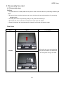
1
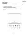
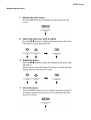
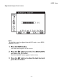
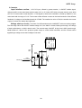
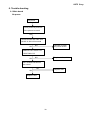
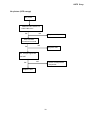
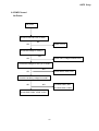
HS75 Sony
Service
Manual
TFT LCD COLOR COMPUTER DISPLAY
SONY
1
HS75 Sony
Table of contents
Table of contents -------------------------------------------------------------------------- 02
1. Precaution ------------------------------------------------------------------------------------------ 03
2.Specification -----------------------------------------------------------05
2.1 Product character-----------------------------------------------------------05
2.2 Interface description-----------------------------------------------------------------06
2.3 Factory preset mode
3.OSD operation
------------------------------------------------------------07
--------------------------------------------------------------------------------08
3.1 Generalization
3.2 Key control
------------------------------------------------------------------------------08
-------------------------------------------------------------------------08
3.3 Common adjustment
--------------------------------------------------------------------- 09
4.Disassembly flow chart -------------------------------------------------------------------------22
4.1 Disassembly steps---------------------------------------------------------------------------22
5. Circuit principle analysis --------------------------------------------------------------------26
5.1 Main board
-------------------------------------------------------------------------------26
5.1.1 Block diagram
------------------------------------------------------------------26
5.1.2 Introduction of IC -------------------------------------------------------27
5.1.3 Introduction of important function -------------------------------------------------27
5.2 PWPC board
-------------------------------------------------------------------------30
5.2.1 Block diagram------------------------------------------------------------------------30
5.2.2 Introduction of IC------------------------------------------------------------------31
5.2.3 Introduction of important function-------------------------------------------------32
6.Trouble shooting ---------------------------------------------------------------------38
6.1 Main board -----------------------------------------------------------------------------38
6.2 PWPC board ----------------------------------------------------------------------------41
7. BOM ---------------------------------------------------------------------------------------43
8. Schematic ------------------------------------------------------------------------------------------59
2
HS75 Sony
1. Precaution
Warning on power connections
Installation
3
HS75 Sony
Handing the LCD screen
Maintenance
Transportation
4
HS75 Sony
2. Specification
2.1 Product character
LCD Panel
Input signals
Power consumption
Power supply
Operating condition
Driving system
TFT LCD
Size
17.0"
Type
CLAA170EA
Pixel pitch
0.264mm(H) x 0.264mm(V)
Viewing angle
140(H) 130(V) (CR>10)
Luminance
300 cd/㎡ (typ)
Contrast Ratio
500:1 (typ)
Response time
12ms (typ)
Display colors
16.2 million Colors
Max dimension
Horizontal: 337.920mm
Vertical: 270.336mm
R G B Analog
0.7Vp-p
H/V separate
TTL level
Horizontal frequency
28kHz–80kHz (Aalog)
Vertical rate
48-75Hz (Aalog)
Recommend resolution
1280 x 1024@60HZ
Normal operation
≤45W
Active off (deep sleep)
≤1W
Power off
≤1W
AC voltage
100~240VAC,50~60Hz
Temperature
5-35°C
Humidity
10-80%
5
HS75 Sony
2.2 Interface description
Analog connectors
NO.
Description
NO.
Description
1.
Red Video
9.
+5V
2.
Green Video
10.
Detect Cable
3.
Blue Video
11.
NC
4.
GND
12.
SDA
5.
Sensor for PC
13.
Horizontal Sync
6.
Red GND
14.
Vertical Sync
7.
Green GND
15.
SCL
8.
Blue GND
VGA Connector layout
1
5
6
10
11
15
6
HS75 Sony
2.3 Factory preset mode
Resolution
Frequency (KHz)
Vertical (Hz)
Clock (MHZ)
720 × 400
31.469
70.087
28.322
640 × 480
31.469
59.940
25.175
640 × 480
35.000
66.667
30.240
640 × 480
37.500
75.000
31.500
720 × 480
35.200
60.000
31.505
800 × 600
35.156
56.250
36.000
800 × 600
37.879
60.317
40.000
800 × 600
48.077
72.188
50.000
800 × 600
46.875
75.000
49.500
800 × 600
49.725
74.551
57.283
1024 × 768
48.363
60.004
65.000
1024 × 768
56.476
70.069
75.000
1024 × 768
60.023
75.029
78.750
1024 × 768
60.2
75
80.000
1152 × 864
67.5
75
108.000
1152 × 870
68.9
75
100.000
1152 × 900
61.8
66
92.940
1152 × 900
71.7
76
105.590
1170 × 584
31.2
50
46.200
1280 × 960
60.0
60
108.000
1280 × 1024
63.981
60.020
108.00
1280 × 1024
79.976
75.025
135.00
7
HS75 Sony
3.OSD operation
3.1 Generalization
Press the power button to turn the monitor on or off. The other control buttons are located
at front panel of the monitor. By changing these settings, the picture can be adjusted to
your personal preferences.
-
The power cord should be connected.
-
Connect the video cable from the monitor to the video card.
-
Press the power button to turn on the monitor, the power indicator will light up.
3.2 Key control
Key control:
8
HS75 Sony
Power Switch: To turn the display on or off, press the Power Switch upward.
The power indicator lights up in green when the display is turned on, and lights up in
orange when the monitor is in power saving mode.
Menu Button: This button displays or close the main menu.
(Arrow) Button: These buttons are used to select the menu items make adjustments.
OK Button: This button selects the item or executes the settings in the menu.
Button: This button is used to change the brightness of the screen.
3.3 Common adjustment
NO
Tag
Description
1
Backlight
Adjust the brightness of the backlight
2
Contrast
Adjust the picture contrast
3
Brightness
Adjust the picture brightness (black level)
Screen
Adjust the picture’s sharpness or its centering
Color
Adjust the color temperature of the picture
Gamma
Change the picture’s color shade settings
7
Sharpness
Adjust to sharpen the edge of images
8
Menu position
Change the on screen menu position
9
Language
Chance the language used on menus or messages
10
Reset
Reset the adjustments to the default settings
11
Menu lock
4
Icon
A
5
6
γ
Lock the control of buttons to prevent accidental adjustments or
resetting
9
HS75 Sony
Navigating the menu
10
HS75 Sony
Adjustment steps of each menu
11
HS75 Sony
12
HS75 Sony
13
HS75 Sony
14
HS75 Sony
15
HS75 Sony
16
HS75 Sony
17
HS75 Sony
18
HS75 Sony
19
HS75 Sony
20
HS75 Sony
21
HS75 Sony
4. Disassembly flow chart
4.1 Disassembly steps
Notices
1. Lay the monitor on a steady table with a piece of clean cloth mat under it for preventing scratching the
panel.
2. Be careful when open the bezel and rear cover with the tool that mentioned above for preventing
mangling them.
3. Put away the screws for preventing rolling on the panel and scratching it.
4. Be careful and don’t scratch the connection line when open the shield.
5. Press the interface with a hand and pull or insert the connection line with the other.
Flow Chart
Step1
Figure
Description
Pull out the rear cover and signal line,
then put the monitor on a clean soft
Prepare
cloth with panel facing to the table.
22
HS75 Sony
Step2
Figure
Description
1.Wring the two screws marked with red
2.Take stand away
1.Wring the nine screws marked with red.
2.Take away as blue arrow direction
Discharge the
Tool: a big screwdriver
back cabinet
Step: 1,Wring the four screws in the
bracket marked with blue.
2, Take the screw and stand away
23
HS75 Sony
Step2
Figure
Description
Step: 1, insert a hard plastic chip in the gap
between bezel and rear cover at
up-left corner
2, Hold the monitor with a hand and
press the hard plastic chip with the
other, then move it in the forward
hour hand.
Discharge
3, Pay attention to some hooks, then
the shield
open it with little force till the bezel
and rear cover separated.
4, The position marked with arrows
exists some hooks.
5, After bezel and rear cover
separated, the bezel is shown in
the figure down-left.
Discharge
Step: Wring down the two screws marked
the Bezel
with red in the key board.
24
HS75 Sony
Discharge
1.Wring down all screws in the power board
the power
and main board directly.
board and
2. Take all connectors in the power board
the main
and main board away.
board
25
HS75 Sony
5. Circuit principle analysis
The LCD Monitor contains a main board, an inverter/power board, key board which house the flat panel
control logic, brightness control logic and DDC.
Backlight and Panel
PWPC board
Main board
Key board
Video signal and DDC
HOST computer
5.1 Main board
5.1.1 Block diagram
The main board contains panel control logic, brightness control logic, DDC and DC convert DC circuit
and so on.
PWPC board
R
G
B
H
V
SDA
SCL
GM5321
Backlight and Panel
OSC
EPROM
Key board
EPROM
26
HS75 Sony
5.1.2 Introduction of IC
GM5321: integrate ADC, OSD, SCALER, TCON, LVDS, RSDS convert analog RGB into digital and
zoom and shrink scaling output to LCD panel.
AIC1084-33M: DC power convert, used to 5v convert 3.3v.
AIC1084-18CE: DC power convert, used to 5v convert 1.8v.
5.1.3 Introduction of important function
DC TO DC: The required power supply are different for each chip, and the voltage of 12v, 5v offered by
PWPC can’t reach the requirement, so we deal with this problem by means of two pieces
of DC TO DC chips (AIC1084-18CM, AIC1084-33CM). The circuit diagrams are as follows:
+3.3V
VCC5V+
+3.3V
TO-263
U302
3
1
C308
VIN
VOUT
2
ADJ
AIC1084-33M
0.1uF
+ C309
C310
47uF/25V
0.1uF
VCC5V+
TO-263
+1.8V
+1.8V
3
2
1
D311
SMAL240LVXRO
U301
AIC1084-18CM
VIN
VOUT(TAB)
ADJ(GND)
D310
SMAL240LVXRO
C305
C306
0.1uF
47uF/25V
27
+
C307
0.1uF
HS75 Sony
Panel Control Circuit:
The high level output from PIN67 of U201 makes Q402 break through, Q203 break through and offer
5V to panel when work well. The output is low level when it’s saving energy state and Q402 break off, Q203
break off, so the panel doesn’t work.
Vcc+12V
+5V
+3.3V
R401
0 1/10W
R402
NC
R403
100K 1/16W
C405
0.068uF
2
R404
1
Q203
100K 1/16W
1
PPWR
10K 1/16W
Q402
PMBS3904
C403
C404
2
(3)
VDDD
3
3
R405
AO3401
0.1uF
0.1uF
GND
GND
28
HS75 Sony
On/Off /Brightness control circuit:
ON/OFF control: When it works well, the high level output form PIN 68 of U201, and low in saving energy
state.
Brightness control: When it works well, the output PWM pulse from PIN98 of U201 adjusts the brightness,
the bigger the duty, the higher the brightness.
CN301
R316
GND
GND
VCC12V
GND
+5V
GND
1
3
5
7
9
11
2
4
6
8
10
12
ON_OFF
DIM
PBIAS
VCC12V
Vcc+12V
GND
+5V
GND
VCC5V+
+5V
C304
0.1uF
CONN
+5V
UDZS5.6B
D316
SMAL240LVXRO
D309
C302
C303
+
100uF/25V
R301
0.1uF
1K 1/16W
R302
PWM0
1K 1/16W
Brightness
C301
1uF/25V
C328
1uF/25V
CN301
UDZS5.6B
GND
GND
VCC12V
GND
+5V
GND
D316
(3)
4.7K 1/16W
1
3
5
7
9
11
2
4
6
8
10
12
ON_OFF
DIM
VCC12V
GND
+5V
GND
CONN
Interface of main board and PWPC board
29
Vcc+12V
HS75 Sony
5.2 PWPC board
5.2.1 Block diagram
PWPC board combines to adapter and inverter, this design has the merits in predigesting
constructions, reducing cost and improving product’s capability.
Adapter which commonly consists of bridge rectifier and filter, start circuit, PWM control circuit
(TOP247Y), protection circuits and convert to 12V, 5V DC voltage by input 90V-240V AC voltage that provide
power supply for each chips in the main board and inverter.
Inverter is DC TO AC circuit. It changes the 12v DC of power supply to about 600-800v AC that drives
the backlight. It mostly consists of starting circuit, PWM controller, output circuit and protection circuit etc.
AC input
Bridge
Rectifier
and Filter
EMI filter
Start Circuit
R906、R907
Transformer
Rectifier
CMOS
MOSFET
Q903
CN902
Voltage
Feedback
Circuit
PWM
Control IC
5V
Over
Voltage
Protect
12V
ON/OFF
Royer –type L,C Resonance
Lamp
PWM convert &DC
Current Circuit
circuit & Boost circuit
Feedback
Circuit
PWM
Control IC
ON/OFF
Control
BL ADJ
30
HS75 Sony
5.2.2 Introduction of IC
TOP247Y: It cost effectively integrating the high voltage power MOSFET, PWM control, fault protection
and other control circuitry onto a single CMOS chip. The function of each pin and the inside circuit diagram
are as follows:
Pin
Symbol
Functional Description
1
C
Control Pin, Error amplifier and feedback current input pin for duty cycle control
2
L
3
X
4
S
Source Pin, Output MOSFET source connection for high voltage power return
5
F
Frequency Pin, Input pin for selecting switching frequency
7
D
Drain Pin, High voltage power MOSFET drain output
Line-Sense Pin, Input pin for OV, UV, line feed forward with DCMAX reduction,
remote ON/OFF and synchronization
External Current Limit Pin, Input pin for external current limit adjustment, remote
ON/OFF and synchronization
31
HS75 Sony
OZ9RRB: OZ9RRB operates at a constant operating frequency. The operating frequency can be
synchronized with an external signal that eliminates any undesired interference between the controller and
LCD panel. The controller provides a wide dimming range control with a low-frequency Pulse Width Modulation
(LPWM) dimming function. The control logic provides a regulated ignition voltage and appropriate protection for
over-voltage or over-current conditions. The function of each pin is as follows:
PIN
NAME
Description
1
ENA_SST_CMP
2
CT
3
GNDA
Ground
4
DRV2
N MOSFET Drive Output
5
DRV1
N MOSFET Drive Output
6
VDDA
Supply Voltage
7
VSEN_DIM
8
ISEN
Enable, Soft Start Time and Compensation
Timing Capacitor to Set Striking, Operating and LPWM Frequency
Voltage Sense_Dimming Voltage
Current-Sense Feedback
5.2.3 Introduction of important function
a. Adapter
EMI filter circuit: It is common used to get rid of the disturbance existing in the electric net or
coming from outside. L901 is used to reduce the symmetry disturbance and filter the high frequency noise;
C901, C902 can restrain the symmetry and filter the low frequency noise; R918, R919, R920 is used for
discharging the capacitance when cut off the power. NR901 is used to prevent the impulse of surge current
when start the machine, which possesses minus temperature modulus.
Rectifier and filter circuit: The AC input is changed to a high DC voltage, that magnitude is the
product of 1.414 to AC after it is commuted by bridge rectifier (BD901) and filtered by the capacitance
(C905).
32
HS75 Sony
Start-up circuit: After being commuted and filtered, the high DC voltage falls down through R (R904,
R908, and R911 series), the start-up carries out when the lowered voltage is supplied to L Pin of IC901
(TOP247Y). The output pulse makes T901 work. The voltage produced at the two terminals of T901 is
offered to C Pin of IC901 after being commuted by D905 and filtered by C914, and then the whole start-up
process is end.
33
HS75 Sony
Over-voltage Protection circuit: 1. ZD903 can be broken down when12V DC voltage increases,
which leads to the current increase through IC902, and voltage increase of C Pin of IC901, and then it cuts off
the pulse output.
C Pin of IC901
2. ZD901, ZD902 can be broken down when12V and 5V DC voltage increase, which lead to SCR901 breaks
through, then 12 connected to ground and realizes over-voltage protection.
34
HS75 Sony
Commute and filter output circuit: When D Pin of IC901 has pulse output, which makes T901
work, while being given a low level, and there is a current in the primary coil of T901 with a voltage up
terminal positive and down negative, so the secondary coil produces a reverse electromotive force. It is the
stage of storing energy in the coil because D902, D904 are closed. But while being given a high level, The
primary coil produces a EMF with its down terminal positive and up negative, and the secondary coil
appears a reverse EMF at the same time, then D902, D904 get through accompanied with a voltage output
of 12V and 5V through C904, C909 which are used to filter. R901, C918 contained in the RC circuit is used
to absorb the surge voltage produced by D902, while R909, C907 is use to absorb the surge voltage
produced by D904.
35
HS75 Sony
b. Inverter
Input interface section: 1.12V DC input, offered by power section; 2. ON/OFF enable signal,
offered by MCU in the main board with its value of 0V or 5V. When OFF=0V,the inverter doesn’t work, while
OFF=5V, it works under normal situation. 3. DIM signal for luminance modulation, offered by GM5321 in the
main board with its range of 0~5V. The Inverter offers different currents to the loads because of the different
feedback of voltage to the feedback-terminal of PWM. The smaller the value of DIM, the smaller the current
output of Inverter, the darker the brightness.
Voltage start-up circuit: It consists of a NPN transistor and a NMOSFET with two working stages.
The first stage: When the ON/OFF enable voltage is 0V, the Q807 is closed, Q806 gets through, the voltage
of drain pulled down, so U801 doesn’t work. The second stage :ON/OFF is high level, Q807 gets through,
Q806 breaks off, Hence U201 produces pulse output to control switch transistor, and the Inverter which
R821
82K
36
0.1uF
C840
C817
ON/OFF
Q807
DTC144WKA
R827
1M
NC
Q806
RK7002
OZ9RRB
5
DRV1
DRV2
4
6
VDDA
GNDA
3
7
VSEN_DIM
CT
2
1
+5VDD
ENA_SST ISEN
U801
8
applied high voltage across the backlight works well.
HS75 Sony
Feedback circuit:
Alternating voltage exists at the two terminals of R842 when the loads are working. After being commuted
and filtered, it changed to a DC sampling voltage. Apply the voltage to PIN8 of U801, and it is used to control
the duty of pulse output. The whole process acts as steadying the output voltage.
CN802
PIN8 of U801
1
ISEN
R808
2K 1/16W
R809
220 1/16W
2
D802
R842
2
1
390 1/16W
R811
C810
0.047uF/25V
3
1K 1/10W
BAV99
37
CONN
HS75 Sony
6. Trouble shooting
6.1 Main board
No power
No power
Press power key and look
if the picture is normal
NG
Please reinsert and make sure
the AC of 100-240 is normal
OK
Reinsert or check
the power section
NG
Measure U301 PIN2=1.8V
U302 PIN2=3.3V
OK
NG
Replace U301, U302
X201 oscillate waveforms
are normal
OK
NG
Replace X201
Replace U201
38
HS75 Sony
No picture (LED orange)
No picture
Measure U301 PIN2=1.8
U302 PIN2=3.3V
OK
NG
Replace U301, U302
X201 oscillate
waveform is normal
OK
NG
Replace X201
Hs, Vs input signal are
normal?
OK
NG
Check Correspondent
component.
Replace U201
39
HS75 Sony
White screen
White screen
Measure Q402
base is high level?
OK
Measure U301 PIN2=1.8
U302 PIN2=3.3V
NG
OK
Check Q402/Q203 are
broken or CN401 solder?
Check Correspondent
component.
NG
Replace U301, U302
X201 oscillate
waveform is normal?
NG
NG
OK
OK
Replace PANEL
Replace U201
40
Replace X201
HS75 Sony
6.2 PWPC board
No Power
No power
Check AC line volt 110V or 220V
NG
Check AC line
OK
Check the voltage of C905(+)
NG
OK
Check F901, bridge rectified circuit
Check start voltage for the L pin of IC901
NG
Check R904, R908, R911
OK
Check the auxiliary voltage is normal?
OK
NG
1) Check IC901,T901
2) Check D905, IC902
Check D902, D904, IC902, IC903
41
HS75 Sony
No Backlight
Check CN902 Pin12 =12V
OK
NG
Check adapter
Check ON/OFF signal
NG
OK
Check Interface board
Check IC801 PIN8 voltage is normal?
OK
NG
Check Q807,Q806 circuit
Check U801 PIN2 triangular wave is
normal
OK
NG
Check C819, C820
Check U801 PIN4, 5
NG
OK
Check U801,Q801, Q802
Check D802, D803, D807, D809
42
HS75 Sony
7. BOM
T 782KCDNK24SNP
Symbol
Part No for TPV
Description
M1G1730 6128 GP
SCREW
CBPC780KCD2SP
CONVERSION BOARD
PWPC1742CPS8P
POWER BOARD
11G6040 1
GP
TWIST LOCK
11G6048 1
GP
CLAMP-S
11G6054 1
GP
LOCK WASHER
12G 425 1
GP
RUBBER FOOT(FRONT)
15G8137 2
GP
MAIN FRAME
20G 022 1 QC GP
STAND
23G3178834 6A GP
LOGO
33G4816 QC L GP
HINGE COVER
34G1491AQB L GP
BACK CABINET
34G1492 PY L GP
REAR COVER
37G 521 1
HINGE ASS'Y
GP
40G 190834 1
ID LABEL
40G 457834 4A GP
S/N LABEL FOR ID
40G 457834 9A GP
CARTON LABEL
40G 58162435A GP
LABEL FOR PE BAG
44GP705 1
GP
PULP MOLD
44GP705 2
GP
PULP MOLD
44GP705624 1A GP
CARTON
45G 88607SY1 GP
EPE BAG FOR MONITOR
50G 600 2
GP
HANDLE1
50G 600 3
GP
HANDLE2
52G
1186
GP
SMALL TAPE
52G
1208 A GP
AL TAPE
52G6019 5
GP
TAPE
52G6022 22
GP
TAPE STAND
52G6025 12104 GP
MYLAR
52G6025 12107 GP
MYLAR
85G 688 1
GP
MAIN SHIELD
43
HS75 Sony
89G1738LAA 17 GP
SIGNAL CABLE
89G402A18N IS GP
POWER CORD
95G8014 12 30 GP
HARNESS 12P-12P 210MM
95G8018 30 64 GP
LVDS CABLE
M1G 130 5120 GP
SCREW
M1G 330 4128 GP
SCREW M3X4
M1G1140 6128 GP
SCREW 4X6
M1G1430 8 47 GP
SCREW
Q1G 130 5120 GP
SCREW
Q1G 130 10128 GP
SCREW
Q1G 330 10120 GP
SCREW
Q1G 330 14120 GP
SCREW
Q1G1030 6 47 GP
SCREW
705G780KB34 01
COVER ASS'Y
750GLC70A07
GP
KEPC780KS6P
20G 021 1
CPT 17" 030 PANEL
KEY BOARD
GP
BEZEL HOLDER
33G4812 QA L GP
FUNTION BUTTON
33G4814 1 C GP
POWER LENS
34G1493APZ L GP
DECO PANEL
34G1494 QB 1L GP
BOTTOM-VENT-COVER
Q1G 130 5120 GP
SCREW
B34G1490APY L GP
FRONT PANEL
AM1G1740 10128 GP
SCREW
44
HS75 Sony
CBPC780KCD2SP
Symbol
Part No for TPV
Description
AIC780KCD2SP
MAIN BOARD
40G 457624 1B GP
CPU LABEL
40G 45762420A GP
CBPC LABEL 25X6mm
M1G1730 6128 GP
SCREW
705G780KC87 05
AC BKT ASS'Y
C201
67G305V100 7N GP
KME50VB10M-CC3 5*11
C209
67G305V100 7N GP
KME50VB10M-CC3 5*11
C215
67G305V100 7N GP
KME50VB10M-CC3 5*11
C220
67G305V100 7N GP
KME50VB10M-CC3 5*11
C221
67G305V100 7N GP
KME50VB10M-CC3 5*11
C231
67G305V100 7N GP
KME50VB10M-CC3 5*11
C232
67G305V100 7N GP
KME50VB10M-CC3 5*11
C236
67G305V100 7N GP
KME50VB10M-CC3 5*11
C238
67G305V100 7N GP
KME50VB10M-CC3 5*11
C302
67G215L101 4N GP
KY25VB100M-L(6.3*11)
C306
67G215L470 4N GP
KY25VB47M-L 5*11
C309
67G215L470 4N GP
KY25VB47M-L 5*11
C401
67G215L470 4N GP
KY25VB47M-L 5*11
CN102
88G 35315FHSW GP
D-SUB
CN301
33G8027 12
GP
WAFER
CN302
33G8027 14
GP
WAFER OR PLAG
CN401
33G8027 24 H GP
U201
X201
90G 372 1
GP
WAFER
HEAT SINK
93G 22 53
CRYSTAL 14.318MHzHC-49U
715G1370 1A S GP
MAIN BOARD
C103
65G0603473 32 GP
CHIP 0.047UF 50V X7R
C104
65G0603473 32 GP
CHIP 0.047UF 50V X7R
C106
65G0603473 32 GP
CHIP 0.047UF 50V X7R
C107
65G0603473 32 GP
CHIP 0.047UF 50V X7R
C108
65G0603104 32 GP
CHIP 0.1UF 50V X7R
C109
65G0603473 32 GP
CHIP 0.047UF 50V X7R
C110
65G0603473 32 GP
CHIP 0.047UF 50V X7R
C113
65G0603104 32 GP
CHIP 0.1UF 50V X7R
45
HS75 Sony
C122
65G0603104 32 GP
CHIP 0.1UF 50V X7R
C123
65G0603104 32 GP
CHIP 0.1UF 50V X7R
C124
65G0603104 32 GP
CHIP 0.1UF 50V X7R
C126
65G0603104 32 GP
CHIP 0.1UF 50V X7R
C202
65G0603104 32 GP
CHIP 0.1UF 50V X7R
C203
65G0603104 32 GP
CHIP 0.1UF 50V X7R
C204
65G0603104 32 GP
CHIP 0.1UF 50V X7R
C205
65G0603104 32 GP
CHIP 0.1UF 50V X7R
C206
65G0603104 32 GP
CHIP 0.1UF 50V X7R
C207
65G0603104 32 GP
CHIP 0.1UF 50V X7R
C208
65G0603104 32 GP
CHIP 0.1UF 50V X7R
C210
65G0603104 32 GP
CHIP 0.1UF 50V X7R
C211
65G0603104 32 GP
CHIP 0.1UF 50V X7R
C212
65G0603104 32 GP
CHIP 0.1UF 50V X7R
C213
65G0603104 32 GP
CHIP 0.1UF 50V X7R
C214
65G0603104 32 GP
CHIP 0.1UF 50V X7R
C216
65G0603104 32 GP
CHIP 0.1UF 50V X7R
C217
65G0603104 32 GP
CHIP 0.1UF 50V X7R
C218
65G0603104 32 GP
CHIP 0.1UF 50V X7R
C219
65G0603104 32 GP
CHIP 0.1UF 50V X7R
C222
65G0603104 32 GP
CHIP 0.1UF 50V X7R
C223
65G0603104 32 GP
CHIP 0.1UF 50V X7R
C224
65G0603104 32 GP
CHIP 0.1UF 50V X7R
C225
65G0603104 32 GP
CHIP 0.1UF 50V X7R
C226
65G0603104 32 GP
CHIP 0.1UF 50V X7R
C227
65G0603104 32 GP
CHIP 0.1UF 50V X7R
C228
65G0603104 32 GP
CHIP 0.1UF 50V X7R
C229
65G0603104 32 GP
CHIP 0.1UF 50V X7R
C230
65G0603104 32 GP
CHIP 0.1UF 50V X7R
C233
65G0603104 32 GP
CHIP 0.1UF 50V X7R
C234
65G0603104 32 GP
CHIP 0.1UF 50V X7R
C235
65G0603104 32 GP
CHIP 0.1UF 50V X7R
C237
65G0603104 32 GP
CHIP 0.1UF 50V X7R
C239
65G0603104 32 GP
CHIP 0.1UF 50V X7R
C240
65G0603104 32 GP
CHIP 0.1UF 50V X7R
C241
65G0603104 32 GP
CHIP 0.1UF 50V X7R
46
HS75 Sony
C242
65G0603104 32 GP
CHIP 0.1UF 50V X7R
C243
65G0603104 32 GP
CHIP 0.1UF 50V X7R
C244
65G0603330 31 GP
33PF+-5% 50V NPO
C245
65G0603330 31 GP
33PF+-5% 50V NPO
C246
65G0603103 32 GP
CHIP 0.01UF 50V X7R
C248
65G0805105 22 GP
CHIP 1UF 25V X7R 0805
C250
65G0805105 22 GP
CHIP 1UF 25V X7R 0805
C251
65G0603104 32 GP
CHIP 0.1UF 50V X7R
C301
65G0805105 22 GP
CHIP 1UF 25V X7R 0805
C303
65G0603104 32 GP
CHIP 0.1UF 50V X7R
C304
65G0603104 32 GP
CHIP 0.1UF 50V X7R
C305
65G0603104 32 GP
CHIP 0.1UF 50V X7R
C307
65G0603104 32 GP
CHIP 0.1UF 50V X7R
C308
65G0603104 32 GP
CHIP 0.1UF 50V X7R
C310
65G0603104 32 GP
CHIP 0.1UF 50V X7R
C313
65G0603104 32 GP
CHIP 0.1UF 50V X7R
C314
65G0603104 32 GP
CHIP 0.1UF 50V X7R
C315
65G0603104 32 GP
CHIP 0.1UF 50V X7R
C316
65G0603104 32 GP
CHIP 0.1UF 50V X7R
C317
65G0603104 32 GP
CHIP 0.1UF 50V X7R
C318
65G0603104 32 GP
CHIP 0.1UF 50V X7R
C319
65G0603104 32 GP
CHIP 0.1UF 50V X7R
C320
65G0603104 32 GP
CHIP 0.1UF 50V X7R
C322
65G0603104 32 GP
CHIP 0.1UF 50V X7R
C323
65G0603104 32 GP
CHIP 0.1UF 50V X7R
C325
65G0603102 32 GP
1000PF +-10% 50V X7R
C326
65G0603221 31 GP
CAP:CER 220PF 5% 50V SM
C327
65G0603221 31 GP
CAP:CER 220PF 5% 50V SM
C328
65G0805105 22 GP
CHIP 1UF 25V X7R 0805
C402
65G0603103 32 GP
CHIP 0.01UF 50V X7R
C403
65G0603104 32 GP
CHIP 0.1UF 50V X7R
C404
65G0603104 32 GP
CHIP 0.1UF 50V X7R
C405
65G0603683 32 GP
CHIP 0.068UF 50V X7R
D102
93G 64 33
BAV99
D103
93G 64 33
BAV99
D104
93G 64 33
BAV99
47
HS75 Sony
D105
93G 64 42 PP
BAV70 SOT-23
D301
93G 39S 34 T
UDZS5.6B
D302
93G 39S 34 T
UDZS5.6B
D303
93G 39S 34 T
UDZS5.6B
D304
93G 39S 34 T
UDZS5.6B
D305
93G 39S 34 T
UDZS5.6B
D306
93G 39S 34 T
UDZS5.6B
D307
93G 39S 34 T
UDZS5.6B
D308
93G 39S 34 T
UDZS5.6B
D309
93G2004 2A
SM240A DO-214AC
D310
93G2004 2A
SM240A DO-214AC
D311
93G2004 2A
SM240A DO-214AC
D312
93G 39S 34 T
UDZS5.6B
D313
93G 39S 34 T
UDZS5.6B
D314
93G 39S 34 T
UDZS5.6B
D315
93G 39S 34 T
UDZS5.6B
D316
93G 39S 34 T
UDZS5.6B
FB101
71G 56K121 M GP
120 OHM 6A
FB102
71G 59C800
GP
CHIP BEAD
FB103
71G 59C800
GP
CHIP BEAD
FB104
71G 59C800
GP
CHIP BEAD
FB201
71G 56K121 M GP
120 OHM 6A
FB202
71G 56K121 M GP
120 OHM 6A
FB203
71G 56K121 M GP
120 OHM 6A
FB204
71G 56K121 M GP
120 OHM 6A
FB205
71G 56K121 M GP
120 OHM 6A
FB206
71G 56K121 M GP
120 OHM 6A
FB207
71G 56K121 M GP
120 OHM 6A
FB208
71G 56K121 M GP
120 OHM 6A
FB209
71G 56K121 M GP
120 OHM 6A
Q101
57G 417 4
PMBS3904/PHILIPS-SMT(04
Q102
57G 759 2
RK7002
Q103
57G 759 2
RK7002
Q203
57G 763 1
A03401 SOT23 BY AOS(A1)
Q301
57G 417 6
PMBS3906/PHILIPS-SMT(06
Q302
57G 417 6
PMBS3906/PHILIPS-SMT(06
48
HS75 Sony
Q402
57G 417 4
PMBS3904/PHILIPS-SMT(04
R106
61L0603181
GP
CHIPR 180 OHM +5% 1/16W
R107
61L0603101
GP
CHIPR 100 OHM +-5% 1/10
R108
61L0603181
GP
CHIPR 180 OHM +5% 1/16W
R109
61L0603101
GP
CHIPR 100 OHM +-5% 1/10
R110
61L0603101
GP
CHIPR 100 OHM +-5% 1/10
R111
61L0603472
GP
CHIPR 4.7K OHM +-5% 1/1
R112
61L0603472
GP
CHIPR 4.7K OHM +-5% 1/1
R114
61L0603181
GP
CHIPR 180 OHM +5% 1/16W
R115
61L0603101
GP
CHIPR 100 OHM +-5% 1/10
R116
61L0603101
GP
CHIPR 100 OHM +-5% 1/10
R118
61L0603750
GP
CHIPR 75 OHM+-5% 1/10W
R119
61L0603750
GP
CHIPR 75 OHM+-5% 1/10W
R120
61L0603750
GP
CHIPR 75 OHM+-5% 1/10W
R121
61L0603103
GP
CHIPR 10K OHM +-5% 1/10
R122
61L0603472
GP
CHIPR 4.7K OHM +-5% 1/1
R125
61L0603220
GP
CHIPR 22 OHM+-5% 1/10W
R126
61L0603220
GP
CHIPR 22 OHM+-5% 1/10W
R127
61L0603222
GP
CHIPR 2.2K OHM+-5% 1/10
R128
61L0603222
GP
CHIPR 2.2K OHM+-5% 1/10
R131
61L0603472
GP
CHIPR 4.7K OHM +-5% 1/1
R134
61L0603103
GP
CHIPR 10K OHM +-5% 1/10
R135
61L0603103
GP
CHIPR 10K OHM +-5% 1/10
R145
61L0603472
GP
CHIPR 4.7K OHM +-5% 1/1
R150
61L0603101
GP
CHIPR 100 OHM +-5% 1/10
R151
61L0603101
GP
CHIPR 100 OHM +-5% 1/10
R152
61L0603330 1F GP
CHIPR 3.3K OHM +-1% 1/1
R153
61L0603100 2F GP
CHIPR 10K OHM +-1% 1/10
R201
61L0603472
GP
CHIPR 4.7K OHM +-5% 1/1
R202
61L0603472
GP
CHIPR 4.7K OHM +-5% 1/1
R205
61L0603255 0F GP
R215
61L0603103
GP
CHIPR 10K OHM +-5% 1/10
R218
61L0603103
GP
CHIPR 10K OHM +-5% 1/10
R233
61L0603103
GP
CHIPR 10K OHM +-5% 1/10
R234
61L0603222
GP
CHIPR 2.2K OHM+-5% 1/10
R235
61L0603222
GP
CHIPR 2.2K OHM+-5% 1/10
CHIP 255 OHM 1/16W
49
HS75 Sony
R236
61L0603101
GP
CHIPR 100 OHM +-5% 1/10
R237
61L0603101
GP
CHIPR 100 OHM +-5% 1/10
R238
61L0603103
GP
CHIPR 10K OHM +-5% 1/10
R239
61L0603103
GP
CHIPR 10K OHM +-5% 1/10
R241
61L0603000
GP
CHIPR 0OHM +-5% 1/10W
R242
61L0603103
GP
CHIPR 10K OHM +-5% 1/10
R243
61L0603103
GP
CHIPR 10K OHM +-5% 1/10
R244
61L0603101
GP
CHIPR 100 OHM +-5% 1/10
R245
61L0603103
GP
CHIPR 10K OHM +-5% 1/10
R249
61L0603472
GP
CHIPR 4.7K OHM +-5% 1/1
R251
61L0603203
GP
CHIPR 20K OHM+-5% 1/10W
R252
61L0603473
GP
CHIP 47K OHM 1/10W
R253
61L0603000
GP
CHIPR 0OHM +-5% 1/10W
R301
61L0603102
GP
CHIPR 1K OHM +-5% 1/10W
R302
61L0603102
GP
CHIPR 1K OHM +-5% 1/10W
R306
61L0603223
GP
CHIP 22KOHM 1/16W
R307
61L0603303
GP
CHIP 30K OHM 5% 1/10W
R308
61L0603473
GP
CHIP 47K OHM 1/10W
R309
61L0603223
GP
CHIP 22KOHM 1/16W
R310
61L0603303
GP
CHIP 30K OHM 5% 1/10W
R311
61L0603103
GP
CHIPR 10K OHM +-5% 1/10
R314
61L0603103
GP
CHIPR 10K OHM +-5% 1/10
R315
61L0603103
GP
CHIPR 10K OHM +-5% 1/10
R316
61L0603472
GP
CHIPR 4.7K OHM +-5% 1/1
R317
61L0603472
GP
CHIPR 4.7K OHM +-5% 1/1
R318
61L0603473
GP
CHIP 47K OHM 1/10W
R319
61L0603000
GP
CHIPR 0OHM +-5% 1/10W
R320
61L0603472
GP
CHIPR 4.7K OHM +-5% 1/1
R321
61L0603102
GP
CHIPR 1K OHM +-5% 1/10W
R322
61L0603000
GP
CHIPR 0OHM +-5% 1/10W
R323
61L0603472
GP
CHIPR 4.7K OHM +-5% 1/1
R324
61L0603102
GP
CHIPR 1K OHM +-5% 1/10W
R401
61L0805000
GP
CHIP O OHM 1/8W
R403
61L0603104
GP
CHIPR 100K OHM +-5% 1/1
R404
61L0603104
GP
CHIPR 100K OHM +-5% 1/1
R405
61L0603103
GP
CHIPR 10K OHM +-5% 1/10
50
HS75 Sony
R408
61L1206331
GP
CHIP 330 OHM 5%
R409
61L0603470
GP
CHIPR 47 OHM +-5% 1/10W
R410
61L0603470
GP
CHIPR 47 OHM +-5% 1/10W
R415
61L0603000
GP
CHIPR 0OHM +-5% 1/10W
R416
61L0603000
GP
CHIPR 0OHM +-5% 1/10W
U102
56G113334A
24LC02B/SNG SOIC-8PIN
U104
56G4LVC 14 P
74LVC14ADT
U201
56L 562 71
GM2321 PQFP-208
U202
56G 643 11
ASM809SEVRF-T SOT-23
U203
56G1133 63CS1
PMC25LV010
U205
56G113356A
24LC16B/SNG SOIC-8PIN
U301
56G 563 34
AIC 1084-18PM TO-263
U302
56G 563 7
AIC1084-33PM
ZD104
93G 39S 34 T
UDZS5.6B
ZD105
93G 39S 34 T
UDZS5.6B
ZD106
93G 39S 34 T
UDZS5.6B
ZD107
93G 39S 34 T
UDZS5.6B
ZD109
93G 39S 34 T
UDZS5.6B
ZD110
93G 39S 34 T
UDZS5.6B
ZD114
93G 39S 34 T
UDZS5.6B
15G8138 1
GP
AC BKT
M1G 130 6 47 GP
SCREW
705G 780 87 05
AC SOCKET ASS'Y
87G 501 7 RF GP
AC SOCKET
95G 900578
GP
WIRE HARNESS
95G8021 2512 GP
WIRE HARNESS
96G 29 8
GP
TUBE
51
HS75 Sony
PWPC1742CPS8P
Symbol
Part No for TPV
Description
PW1742CPS8SMTP
POWER BOARD
40G 45762420A GP
CBPC LABEL 25X6mm
51G 100510500 GP
1-2577
55G 23524500 GP
ISOPARE
705G 780 56 01
IC901 ASS'Y
705G 780 93 S6
D902/D904 ASS'Y
C801
67G215V471 4N GP
KY25VB470M-CC3 10*16
C803
65L 3J2206ET GP
22PF 5% 3KV TDK
C805
65L 3J2206ET GP
22PF 5% 3KV TDK
C806
65L 3J5096ET GP
CERAMIC CAP
C809
65L 3J5096ET GP
CERAMIC CAP
C816
65L 3J2206ET GP
22PF 5% 3KV TDK
C822
65L 3J2206ET GP
22PF 5% 3KV TDK
C823
65L 3J5096ET GP
CERAMIC CAP
C824
67G215V471 4N GP
KY25VB470M-CC3 10*16
C825
65L 3J5096ET GP
CERAMIC CAP
C901
65G306M1022BM GP
Y1.CAP.001UF 250VAC MUR
C902
65G306M1022BM GP
Y1.CAP.001UF 250VAC MUR
C903
63G 10722410S GP
0.22UF/250V X1 ARCO
C905
67G215S10115N GP
EC CAP 450V/100
C909
67G215V102 3N GP
KY10VB1000M-CC3 10*16
C910
67G215V471 3N GP
KY16VB470M-CC3 10*12.5
C912
65G306M1022BM GP
Y1.CAP.001UF 250VAC MUR
C923
67G215V471 4N GP
KY25VB470M-CC3 10*16
CN801
33G8021 2D U GP
WAFER
CN802
33G8021 2D U GP
WAFER
CN803
33G8021 2D U GP
WAFER
CN804
33G8021 2D U GP
WAFER
CN901
33G8029 3A H GP
WAFER
CN902
33G8027 12
GP
WAFER
CN903
95G 90 23
GP
TIN COATED
D901
93G 6026T52T
RECTIFIER DIODE FR107
DB901
93L 50460 16
U4KB80R
52
HS75 Sony
L901
73L 174 40LSG GP
LINE FILTER
L902
73G 253 91 LS GP
CHOKE BY LI SHIN
L903
73G 253 91 LS GP
CHOKE BY LI SHIN
NR901
61G 58050 WT GP
5 OHM /5A NTCR
R905
61G152M10458F GP
100K OHM 5% 2W
T801
80GL19T 8 DN GP
TRANSFORMER
T802
80GL19T 8 DN GP
TRANSFORMER
T901
80LL17T 20LSG GP
POWER X'FMR
U902
56G 139 3A
PC123Y22
VAR901
61G 46 6
GP
TNR 10V471K
VAR902
61G 46 6
GP
TNR 10V471K
PW1742CPS8AIP
POWER BOARD FOR AI
C802
65L0805222 32
2200PF/50V/0805/X7R
C804
65L0805222 32
2200PF/50V/0805/X7R
C808
65G1206225 17 GP
CHIP 2.2UF 16V Y5V 1206
C810
65G0603473 22 GP
0.047UF/25V
C811
65G0603103 32 GP
CHIP 0.01UF 50V X7R
C813
65G0603332 32 GP
3300PF X7R 50V
C814
65G0603333 22 GP
0.0033UF/25V
C815
65L0805222 32
2200PF/50V/0805/X7R
C818
65G0603473 22 GP
0.047UF/25V
C819
65G0603331 31 GP
330PF NPO 50V
C820
65G0603390 31 GP
39PF NPO 50V
C821
65L0805222 32
2200PF/50V/0805/X7R
C826
65G0603333 22 GP
0.0033UF/25V
C827
65G0603333 22 GP
0.0033UF/25V
C829
65G0603332 32 GP
3300PF X7R 50V
C830
65G0603104 22 GP
0.1UF/25V
C831
65G0603333 22 GP
0.0033UF/25V
C836
65G0603104 22 GP
0.1UF/25V
C837
65G0603104 22 GP
0.1UF/25V
C838
65G0603104 22 GP
0.1UF/25V
C839
65G0805104 22 GP
0.1UF +-10% 25V X7R 080
C840
65G0603473 32 GP
CHIP 0.047UF 50V X7R
C906
65G0805104 22 GP
0.1UF +-10% 25V X7R 080
C911
65G0805104 22 GP
0.1UF +-10% 25V X7R 080
53
HS75 Sony
C913
65G0805103 22 GP
CHIP 0.01UF 25V X7R 080
C916
65G0805104 22 GP
0.1UF +-10% 25V X7R 080
C917
65G0805104 22 GP
0.1UF +-10% 25V X7R 080
C922
65G0805104 22 GP
0.1UF +-10% 25V X7R 080
C924
65G0805105 22 GP
CHIP 1UF 25V X7R 0805
D802
93G 64 33
BAV99
D803
93L 6432V
LL4148-GS08
D804
93G 64 33
BAV99
D805
93L 6432V
LL4148-GS08
D806
93G 64 33
BAV99
D807
93G 64 33
BAV99
D809
93L 6432V
LL4148-GS08
D810
93L 6432V
LL4148-GS08
D811
93G 64 33
BAV99
D812
93G 64 33
BAV99
D813
93L 6432V
LL4148-GS08
D814
93L 6432V
LL4148-GS08
D903
93L 6432V
LL4148-GS08
D906
93L 6432V
LL4148-GS08
D907
93L 6432V
LL4148-GS08
Q801
57G 600 55
P5506 HVG SO-8
Q802
57G 417 4
PMBS3904/PHILIPS-SMT(04
Q803
57G 759 2
RK7002
Q804
57G 417 6
PMBS3906/PHILIPS-SMT(06
Q805
57G 600 55
P5506 HVG SO-8
Q806
57G 759 2
RK7002
Q807
57G 760 5
DTC144WKA BY ROHM SMT
Q808
57G 417 6
PMBS3906/PHILIPS-SMT(06
Q809
57G 759 2
RK7002
Q810
57G 417 6
PMBS3906/PHILIPS-SMT(06
Q811
57G 417 6
PMBS3906/PHILIPS-SMT(06
R802
61L1206100
GP
CHIPR 10 OHM+-5% 1/4W
R803
61L0805102
GP
CHIPR 1K OHM +-5% 1/8W
R804
61L1206471
GP
CHIP 470 OHM 1/8W
R806
61L0603000
GP
CHIPR 0OHM +-5% 1/10W
R807
61L1206100
GP
CHIPR 10 OHM+-5% 1/4W
54
HS75 Sony
R808
61L0603202
GP
CHIP 2KOHM 1/16W
R809
61L0603221
GP
CHIP 220 OHM 1/16W
R810
61L0603160 2F GP
16KOHM 1/16W
R811
61L0603431
430 OHM 1/16W
R812
61L0603100 3F GP
R814
61L0603105
R815
61L0603180 3F GP
180KOHM 1/16W
R816
61L0603431
GP
430 OHM 1/16W
R817
61L0603104
GP
CHIPR 100K OHM +-5% 1/1
R818
61L0603240 3F GP
R819
61L0603105
GP
1MOHM 1/16W
R820
61L0603105
GP
1MOHM 1/16W
R821
61L0603104
GP
CHIPR 100K OHM +-5% 1/1
R822
61L1206100
GP
CHIPR 10 OHM+-5% 1/4W
R823
61L0603202
GP
CHIP 2KOHM 1/16W
R824
61L0603221
GP
CHIP 220 OHM 1/16W
R826
61L0603431
GP
430 OHM 1/16W
R827
61L0603105
GP
1MOHM 1/16W
R828
61L1206100
GP
CHIPR 10 OHM+-5% 1/4W
R829
61L0603102
GP
CHIPR 1K OHM +-5% 1/10W
R830
61L0603104
GP
CHIPR 100K OHM +-5% 1/1
R831
61L0603105
GP
1MOHM 1/16W
R832
61L0603431
GP
430 OHM 1/16W
R833
61L0603160 2F GP
16KOHM 1/16W
R835
61L0603431
GP
430 OHM 1/16W
R836
61L0603105
GP
1MOHM 1/16W
R837
61L0603102
GP
CHIPR 1K OHM +-5% 1/10W
R838
61L0603105
GP
1MOHM 1/16W
R839
61L0603431
GP
430 OHM 1/16W
R840
61L0603105
GP
1MOHM 1/16W
R841
61L0603200 2F GP
20KOHM 1/10W
R842
61L0805102
GP
CHIPR 1K OHM +-5% 1/8W
R843
61L0805102
GP
CHIPR 1K OHM +-5% 1/8W
R844
61L0805103
GP
CHIPR 10K OHM +-5% 1/8W
R845
61L0805000
GP
CHIP O OHM 1/8W
R901
61L1206201
GP
200 OHM 1/4W
GP
100K OHM 1/16W
GP
1MOHM 1/16W
240KOHM 1/16W
55
HS75 Sony
R902
61L1206220
GP
22 OHM/1206
R903
61L1206335
GP
3.3MOHM 1/4W
R904
61L1206665 3F GP
R906
61L1206335
GP
3.3MOHM 1/4W
R907
61L1206220
GP
22 OHM/1206
R908
61L1206665 3F GP
R909
61L1206201
GP
200 OHM 1/4W
R910
61L1206205
GP
CHIP 2M OHM % 1/4W
R911
61L1206665 3F GP
R912
61L0805102
GP
CHIPR 1K OHM +-5% 1/8W
R913
61L0805471
GP
CHIPR 470 OHM 1/8W
R914
61L0805102
GP
CHIPR 1K OHM +-5% 1/8W
R915
61L0805150 3F GP
R916
61L0805103
R917
61L0805133 2F GP
R918
61L1206684
GP
CHIPR 680K OHM+-5% 1/4W
R919
61L1206684
GP
CHIPR 680K OHM+-5% 1/4W
R920
61L1206684
GP
CHIPR 680K OHM+-5% 1/4W
R921
61L0805201
GP
CHIP 200 OHM 1/8W
R922
61L0805472
GP
CHIRP 4.7K OHM +-5% 1/8
R923
61L0805689
GP
CHIP 6.8 OHM 1/8W 5%
R924
61L0805143 2F GP
14.3KOHM 1/8W
R925
61L0805100 2F GP
10KOHM F 1/10W
R926
61L0805102
GP
CHIPR 1K OHM +-5% 1/8W
R927
61L1206201
GP
200 OHM 1/4W
R928
61L1206201
GP
200 OHM 1/4W
R929
61L1206201
GP
200 OHM 1/4W
R930
61L1206201
GP
200 OHM 1/4W
CHIPR 665KOHM +-1% 1/4W
CHIPR 665KOHM +-1% 1/4W
CHIPR 665KOHM +-1% 1/4W
150KOHM F 1/8W
GP
CHIPR 10K OHM +-5% 1/8W
13.3KOHM F 1/8W
U801
56G 608 9
OZ9RRBGN SOIC-8
ZD801
93G 39S 24 T
RLZ 5.6B LLDS
ZD901
93G 39S 17 T
RLZ12B LLDS
ZD902
93G 39S 25 T
RLZ5.1B LLDS
ZD903
93G 39S 19 T
PTZ7.5B
ZD904
93G 39S 10 T
RLZ6.8B LLDS
ZD905
93G 39S 10 T
RLZ6.8B LLDS
ZD906
93G 39S 10 T
RLZ6.8B LLDS
56
HS75 Sony
715G1447 1
GP
PCB BOARD
C832
65G601G101 1T GP
100pf +-2% 50v
C833
65G601G101 1T GP
100pf +-2% 50v
C834
65G601G101 1T GP
100pf +-2% 50v
C835
65G601G101 1T GP
100pf +-2% 50v
C905
6G 31502
GP
1.5MM RIVET
C907
65G517K471 2T GP
470PF/500V
C908
65G 2K152 1T GP
CERAMIC CAP
C914
67G 2152207NT GP
LOW ESR 22UF+-20% 50V B
C918
65G517K471 2T GP
470PF/500V
C919
65G517K471 2T GP
470PF/500V
C920
67G 2154707NT GP
KY 50VB 47M-L 6.3*11
C921
67G 2151007NT GP
KY50VB10M-TP5(5*11)
CN901
6G 31500
GP
EYELET
CN903
6G 31500
GP
EYELET
D905
93G 6038T52T
FR103
F901
84G 55 5
GP
FUSE 2.5A 250V WICKMANN
L901
6G 31502
GP
1.5MM RIVET
NR901
6G 31502
GP
1.5MM RIVET
R805
61L212Y625 KT GP
MATEL GLAZE 6.2M OHM 3K
R825
61L212Y625 KT GP
MATEL GLAZE 6.2M OHM 3K
SCR901
57L 566 4
MCR100-6 SCR
T801
6G 31502
GP
1.5MM RIVET
T802
6G 31502
GP
1.5MM RIVET
T901
6G 31502
GP
1.5MM RIVET
U903
56G 158 10 T
AZ431AZ-AE1
VR903
62L 10 18 LS GP
SPARK GAP 200V +-20% LI
90G6107 2
IC901
GP
HEAT SINK
AM1G1730 8128 GP
SCREW M3*8
56G 379 41
TOP247Y T0220-7C
90G6108 1
GP
HEAT SINK
AM1G1730 8128 GP
SCREW M3*8
D902
93L 60249
FCH10U15 TO-220
D904
93G 60251
FCQ10U06G
57
HS75 Sony
KEPC780KS6P
Symbol
Part No for TPV
Description
AIK780KS6SMTP
KEY BOARD FOR SMT
95G 900 66
GP
GND WIRE
DP101
11G6065 1
GP
LED HOLDER
DP101
81G 41B OG 1 GP
LED
JP101
95G8014 14 22 GP
HARNESS 14P-13P 285MM
SW101
77G 602 1 CJ GP
TACT SW1TCH
SW102
77G 602 1 CJ GP
TACT SW1TCH
SW103
77G 602 1 CJ GP
TACT SW1TCH
SW104
77G 602 1 CJ GP
TACT SW1TCH
SW105
77G 602 1 CJ GP
TACT SW1TCH
SW106
77G 602 1 CJ GP
TACT SW1TCH
715G1442 1
GP
PCB BOARD
R101
61L0603101
GP
CHIPR 100 OHM +-5% 1/10
R102
61L0603101
GP
CHIPR 100 OHM +-5% 1/10
ZD101
93G 39S 34 T
UDZS5.6B
ZD102
93G 39S 34 T
UDZS5.6B
ZD103
93G 39S 34 T
UDZS5.6B
ZD104
93G 39S 34 T
UDZS5.6B
ZD105
93G 39S 34 T
UDZS5.6B
ZD106
93G 39S 34 T
UDZS5.6B
ZD107
93G 39S 34 T
UDZS5.6B
ZD108
93G 39S 34 T
UDZS5.6B
ZD109
93G 39S 34 T
UDZS5.6B
ZD110
93G 39S 34 T
UDZS5.6B
ZD111
93G 39S 34 T
UDZS5.6B
ZD112
93G 39S 34 T
UDZS5.6B
58
HS75P Sony
8.Schematic
8.1 Main board
CN101
Q104
2N7002E
GND
25
D_Gate
SCL_IN
SDA_IN
R147
33 1/16W
3
D107
BAV99
D108
BAV99
C115
1000pF
D109
BAV99
C116
1000pF
D110
BAV99
C117
1000pF
C118
1000pF
D111
BAV99
C119
1000pF
D112
BAV99
C120
1000pF
R142
R143
22 1/16W
22 1/16W
RX0RX0+
(3)
(3)
RXC+
RXC-
(3)
(3)
D113
BAV99
1
2
1
2
1
2
1
2
1
2
1
2
1
2
2
10/25 ADD
C121
1000pF
R129
10K 1/16W
GND GND
NC
Changed ZD102,ZD103 to
UDZ5.6V
GND
R130
GND
DVI_HPD
DVI_HPD
1K 1/16W
C125
0.1uF
(3)
ZD108
UDZS5.6B
GND
GND
GND
GND
+5V
1
2
1
2
C124
0.1uF
1
C123
0.1uF
0.1uF
C122
GND
10K 1/16W
10/25 ADD
GND
R145
4.7K 1/16W
ZD104
ZD105
10K 1/16W
A_Gate
R152
3.3K 1/16W
R153
ZD115
NC
UDZS5.6B
A_DDC_5V
C108
0.1uF
14
15
Q103
2N7002E
24LC02BT
13
VS_IN
R151
100 1/16W
8
7
6
5
GND
HS_in
UDZS5.6B
4.7K 1/16W
4.7K 1/16W
A0
VCC
A1
WP
A2
SCL
GND SDA
12
A_GATE
(3) DDC_SCL_VGA
U102
1
2
3
4
3
0.047uF
C106
100 1/16W
C107
R114
180 1/16W
C109
R115
100 1/16W
C110
80 OHM
Bin
R116
47 1/16W
(3)
RED-
(3)
SOG_MCSS
(3)
GREEN+
(3)
GREEN-
(3)
BLUE+
(3)
BLUE-
(3)
0.047uF
0.047uF
0.047uF
0.047uF
GPIO5/UART_DO (3)
R118
75 1/16W
R119
75 1/16W
R120
75 1/16W
+5V
AGND
GND
ZD114
R121
10K 1/16W
R135
GND GND
AGND
UDZS5.6B UDZS5.6B
R122
4.7K 1/16W
10K 1/16W
VGA_PLUG
VGA_CONN
GND
GND
180 1/16W
R109
FB104
Gin
GND
GND
75-ohm terminating resistor
very close to the VGA
conn.
Pins 6/7/8 are R/G/B
return lines resp.
GND GND
R108
RED+
0.047uF
NC
Rin
ZD110
C126
0.1uF
C104
80 OHM
DB15
1
6
2
7
3
8
4
9
5
10
11
R150
100 1/16W Q102
2N7002E
FB103
CN102
GND
(3) GPIO4/UART_DI
(3) DDC_SDA_VGA
C103
100 1/16W
C105
17
R110
47 1/16W
180 1/16W
R107
VGA_5V
16
A_DDC_5V
ZD109
UDZS5.6B
11/17 R150,
R151 33 OHM
-> 100 OHM
10/23 DEL
R113,R117
10/23 ADD
Q101,Q102
R106
80 OHM
R134
BAV70
R111
(10 mil, ┰キ︽絬)
FB102
D105
R112
10/29 change value
D104
BAV99
3
2
D103
BAV99
3
+5V
1
D102
BAV99
VGA_5V
3
EDID-WP
DVI_EDID_WP (3)
R132
22 1/16W
22 1/16W
(3)
(3)
+5V
C114
1000pF
ZD103
UDZS5.6B
R149
10K 1/16W
ZD116
NC
R131
Q101
PMBS3904
D106
BAV99
JACK
D_Gate
R148
3.3K 1/16W
4.7K 1/16W
1
R140
R141
RX1RX1+
+5V
ZD102
UDZS5.6B
D_DDC_5V
RXC+IN
RXC-IN
GND
DDC_SDA_DVI
(3)
GND
C1
C2
C3
C4
C5
Q105
2N7002E
24LC02BT
GND
22 1/16W
22 1/16W
(3)
(3)
UDZS5.6B
RX0-IN
RX0+IN
2
8
7
6
5
HOT_PLUG
17
18
19
20
21
22
23
24
3
A_RED
A_GREEN
A_BLUE
A_HSYNC
A_GND
A_GND
R146
33 1/16W
(3) DDC_SCL_DVI
R138
R139
RX2RX2+
ZD101
3
R105
4.7K 1/16W
4.7K 1/16W
A0
VCC
A1
WP
A2
SCL
GND SDA
4.7K 1/16W
U101
1
2
3
4
R133
2
R104
1uF/25V
R103 10K 1/16W
3
C101
22 1/16W
22 1/16W
DVI_5V
3
T0T0+
SGND
T5T5+
SGND
TC+
TC-
D_DDC_5V
RX1-IN
RX1+IN
9
10
11
12
13
14
15
16
1
3
D101
BAV70
R136
R137
SCL_IN
SDA_IN
3
T1T1+
SGND
T3T3+
+5V
GND
HPD
2
1
DVI_5V +5V
RX2-IN
RX2+IN
1
2
3
4
5
6
7
8
3
T2T2+
SGND
T4T4+
DDCCLK
DDCDAT
A_VSYNC
3
A_GND
3
26
R125
22 1/16W
R126
22 1/16W
U104A
74LVC14ADT
1
2
(3)
C113
0.1uF
U104F
74LVC14ADT
13
U104B
74LVC14ADT
(8 mil)
VGA_PG
12
FB101
120OHM
+3.3V
VCC
VS
GND
(3)
U104E
74LVC14ADT
EDID-WP
3
1
2
9/23 R137
Rename
R145
ZD106
UDZS5.6B
ZD107
UDZS5.6B
R127
2.2K 1/16W
R128
2.2K 1/16W
3
C111
C112
NC
NC
4
11
10
HS
(3)
GND
GND
715L1370-D-S
Title
ANALOG&DIGITAL INPUT
59
Size
D
Document Number
gm5221H/gm2321
Date:
Thursday, December 09, 2004
Rev
A
Sheet
2
of
5
HS75P Sony
DVI=250mA
D-SUB=250mA
1.8V_CVDD
Close to respective power Pins
0.1uF
C204
0.1uF
C205
0.1uF
0.1uF
C206
C207
0.1uF
0.1uF
D-SUB=11mA
DVI=14mA
C208
0.1uF
1.8V_AVDD
C216
0.1uF
C218
0.1uF
0.1uF
+3.3V
GND
FB205
120OHM
C231
10uF/50V
1.8V_AVDD
C213
C214
0.1uF
0.1uF
0.1uF
+
0.1uF
0.1uF
U201
FB206
120OHM
C232
10uF/50V
C233
+
+3.3V_RGB
C220
10uF/50V
FB204
120OHM
+
C221
10uF/50V
C234
+
0.1uF
0.1uF
C222
+
0.1uF
GND
GND
0.1uF
+3.3V
GND
D-SUB=21mA
DVI=21mA
C223
C224
0.1uF
C225
C226
0.1uF
FB207
120OHM
0.1uF
C238
10uF/50V
C239
C240
C228
0.1uF
0.1uF
C229
0.1uF
+3.3V
3.3V_LVDS
0.1uF
0.52mA
C236
10uF/50V
C241
C242
C243
0.1uF
0.1uF
0.1uF
FB208
120OHM
+
C237
DVI=62mA
D-SUB=62mA
115
117
122
127
131
136
144
149
153
156
163
165
168
177
0.1uF
8.2mA
GND
0.1uF
0.1uF
C235
+
0.1uF
113
120
125
130
134
141
145
150
154
172
171
C230
GND
GND
FB209
120OHM
C227
GND
GND
AGND
C244
33pF
C245
33pF
1.8V_CVDD
3.3V_LVDS
3.3V_A
AGND_IMB
AGND_RX2
AGND_RX1
AGND_RX0
AGND_RXC
GND_RXPLL
AGND_BLUE
AGND_GREEN
AGND_RED
AGND_ADC
GND_ADC
GND_RPLL
AGND_RPLL
LBADC_GND
RESERVED
CH3P_LV_E
CH3N_LV_E
CLKP_LV_E
CLKN_LV_E
CH2P_LV_E
CH2N_LV_E
CH1P_LV_E
CH1N_LV_E
CH0P_LV_E
CH0N_LV_E
CH3P_LV_O
CH3N_LV_O
CLKP_LV_O
CLKN_LV_O
CH2P_LV_O
CH2N_LV_O
CH1P_LV_O
CH1N_LV_O
CH0P_LV_O
CH0N_LV_O
AGND
10
13
14
15
16
17
18
19
20
21
22
LV_E9
LV_E8
LV_E7
LV_E6
LV_E5
LV_E4
LV_E3
LV_E2
LV_E1
LV_E0
29
30
31
32
33
34
35
36
37
38
LV_O9
LV_O8
LV_O7
LV_O6
LV_O5
LV_O4
LV_O3
LV_O2
LV_O1
LV_O0
LV_E[0..9]
(5)
LV_O[0..9]
(5)
43
44
45
46
RESERVED
RESERVED
RESERVED
RESERVED
1
+5V
GND
AVDD_IMB_3.3
AVDD_RX2_3.3
AVDD_RX1_3.3
AVDD_RX0_3.3
AVDD_RXC_3.3
AVDD_BLUE_3.3
AVDD_GREEN_3.3
AVDD_RED_3.3
AVDD_ADC_3.3
LBADC_VDD_3.3
AVDD_RPLL_3.3
1.8V_PLL
116
121
126
137
164
166
C212
1.8V_PLL
+1.8V
D-SUB=24mA
DVI=0mA
+3.3V
C209
10uF/50V
D-SUB=103mA
DVI=64mA
C219
0.1uF
C211
GND
D-SUB=3mA
DVI=16mA
+1.8V
C217
+
C210
VDD_RX2_1.8
VDD_RX1_1.8
VDD_RX0_1.8
VDD_RXPLL_1.8
VDD_ADC_1.8
VDD_RPLL_1.8
FB203
120OHM
C215
10uF/50V
FB202
120OHM
RVDD_3.3
RVDD_3.3
RVDD_3.3
RVDD_3.3
RVDD_3.3
+1.8V
+3.3V
1.8V_DVI
50
73
95
190
205
1.8V_DVI
GND
24
11
26
27
40
C203
AVDD_LV_E_3.3
AVDD_LV_E_3.3
AVDD_LV_3.3
AVDD_LV_O_3.3
AVDD_LV_O_3.3
C202
+
86
9
41
75
96
139
179
FB201
120OHM
C201
10uF/50V
CVDD_1.8
CVDD_1.8
CVDD_1.8
CVDD_1.8
CVDD_1.8
CVDD_1.8
CVDD_1.8
+1.8V
U203
R243
8
7
6
5
ROM_HOLD#
ROM_SCLK
ROM_SDI
SST25VF020-20-4C-SAE
GND
GND
11/04 WP#
pull low
changed from +5V to
+3.3V
+3.3V
GPIO8/IRQout
RMADDR17
RMADDR16
C248
1uF/25V
R242
10K 1/16W
GND
10K 1/16W
12/09 close to U203
pin 8
+3.3V_RGB
R205
10K 1/16W
R215
R217 NC
R218
10K 1/16W
R222
NC
138
255 1/16W
114
RMADDR17
RMADDR16
RMADDR15
183
184
185
186
187
188
189
192
193
194
195
196
197
198
199
200
201
202
Cancel R249
RMADDR13
RMADDR12
Cancel R250
R222 Change to NC
changed R215,R218 from 20K to 10K
203
204
207
208
1
2
3
4
R249
Serial ROM >>0
Parallel
ROM>>NC
5
6
7
ROMCE#
BOOTSTRAP SIGNALS
ADDRESS
NAME
SET R
x
DESCRIPTION
To specify the device address for serial host
interface
ROM_ADDR(6:0)
DEV_ADDR(6:0)
ROM_ADDR(8:7)
FORCEI/EROM
x
00=Check for signature in external ROM and if
present jump to external ROM
ROM_ADDR9
OCM_USES_TCLK
x
0=OCM_CLK=FCLK
x
00=for TCLK=14.3MHz
ROM_ADDR(11:10) TCLKSEL
1
1=DDC2Bi=DDC_SCL_VGA/DDC_SCL_VGA
ROM_ADDR(14:13) OP_MODE
x
00=UART
ROM_ADDR15
SPI_EN
1
0=Parallel,1=SPI
ROM_ADDR16
OCM_ROM
x
ROM_ADDR17
OSC_SEL
x
ROM_ADDR12
DDCHANSEL
x
BLUE+
BLUESOG_MCSS
GREEN+
GREENRED+
REDHSYNC/CSYNC
VSYNC
RESERVED
GPIO0
GPIO1
GPIO2
GPIO3
GPIO4
GPIO5
GPIO6
GPIO7
GPIO8
GPIO9/NVRAM_SCL
GPIO10/NVRAM_SDA
GPIO11/PWM0
GPIO12/PWM1
GPIO13/PWM2
GPIO14/PWM3
CLKOUT
REXT
ROM_ADDR17
ROM_ADDR16
ROM_ADDR15
ROM_ADDR14
ROM_ADDR13
ROM_ADDR12
ROM_ADDR11
ROM_ADDR10
ROM_ADDR9
ROM_ADDR8
ROM_ADDR7
ROM_ADDR6
ROM_ADDR5
ROM_ADDR4
ROM_ADDR3
ROM_ADDR2
ROM_ADDR1
ROM_ADDR0
4.7K 1/16W
81
82
83
84
85
88
89
90
91
92
93
GPIO7/IRQin
GPIO8/IRQout
SCL
SDA
98
99
100
101
SMBCLK-GM
WP
SMBDAT-GM
GPIO15
0 1/16W
PPWR
PBIAS
(5)
(4)
R201
R202
R254
4.7K 1/16W
4.7K 1/16W
NC
POWER_ON
LED_GRN
LED_RED
(4)
(4)
(4)
DVI_HPD
(2)
DVI_EDID_WP (2)
PWM0
VGA_PG
SMBCLK
+5V
70
206
191
180
140
97
94
76
74
51
42
8
87
+5V
R411
NC
R412
NC
SMBCLK-GM
R413
NC
SMBDAT-GM
R414
NC
SCL
R415
0 1/16W
R416
0 1/16W
SDA
SMBCLK
(4)
SMBDAT
(4)
GND
+3.3V
ROM_OEn
ROM_WEn
ROM_CSn
173
174
175
176
LBADC_IN1
LBADC_IN2
LBADC_IN3
LBADC_RETURN
LBADC1
LBADC2
+5V
(4)
(4)
R241
R240
0 1/16W
NC
GND
R245
10K 1/16W
10K 1/16W
+3.3V
R234
R235
4.7K 1/16W
4.7K 1/16W
R251
GND
WP
SCL
SDA
+5V
R252
8
7
6
5
100 1/16W
100 1/16W
100 1/16W
R244
R236
R237
C250
1uF/25V
U205
20K 1/16W
GND
(4)
(2)
167
135
RESERVED
CRVSS
CRVSS
CRVSS
CRVSS
CRVSS
CRVSS
CRVSS
CRVSS
CRVSS
CRVSS
CRVSS
CRVSS
R233
VCC
WP
SCK
SI
A0
A1
A2
VSS
1
2
3
4
47K 1/16W
R248
R251 Dual >>20K
Analog-only>>NC
0=Internal ROM on at top of 1M in X86
address space(normal operation)
R238
R239
10K 1/16W 10K 1/16W
NC
CN201
GND
M24C16-WMN6T
NC
GND
(2) GPIO5/UART_DO
(2) GPIO4/UART_DI
1
2
3
4
GPIO5/UART_DO
GPIO4/UART_DI
GND
715L1370-D-S
Title
1=Internal ROM off
0=TCLK source using external
crystal
R253
9/20 Add SM BUS
69
RESERVED
RESERVED
ROM_DATA7
ROM_DATA6
ROM_DATA5
ROM_DATA4
ROM_DATA3
ROM_DATA2
ROM_DATA1
ROM_DATA0
R249
67
68
PPWR
PBIAS
RX2+
RX2RX1+
RX1RX0+
RX0RXC+
RXC-
GM5221H
PQFP-208
47
48
49
55
RESERVED
RESERVED
RESERVED
RESERVED
NC
NC
NC
NC
NC
NC
NC
NC
NC
NC
NC
+3.3V
118
119
123
124
128
129
132
133
4.7K Ohm
+3.3V
52
53
54
104
105
157
158
159
160
161
162
RX2+
RX2RX1+
RX1RX0+
RX0RXC+
RXC-
Add R249
RESETn
AVSS_LV_E
AVSS_LV_E
AVSS_LV
AVSS_LV_O
AVSS_LV_O
(2)
(2)
(2)
(2)
(2)
(2)
(2)
(2)
142
143
146
147
148
151
152
181
182
155
HOST_SCL/UART_DI
HOST_SDA/UART_DO
DDC_SCL_VGA
DDC_SDA_VGA
DDC_SCL_DVI
DDC_SDA_DVI
12
23
25
28
39
BLUE+
BLUESOG_MCSS
GREEN+
GREENRED+
REDHS
VS
56
57
58
59
60
61
62
63
64
65
66
JTAG_RESET
RESERVED
RESERVED
RESERVED
RESERVED
RESERVED
RESERVED
RESERVED
JTAG_TDO
RESERVED
JTAG_TDI
TCLK
XTAL
102
103
106
107
108
109
110
111
112
GND
CE# VDD
SO HOLD#
WP# SCK
VSS
SI
71
72
77
78
79
80
178
(2)
(2)
0.01uF (2)
(2)
(2)
(2)
(2)
(2)
(2)
C246
ROM_SCSn
1
ROM_SDO 2
3
ROM_WP#
4
170
169
GPIO4/UART_DI
GPIO5/UART_DO
(2) GPIO4/UART_DI
R250
(2) GPIO5/UART_DO
NC (2) DDC_SCL_VGA
(2) DDC_SDA_VGA
(2) DDC_SCL_DVI
(2) DDC_SDA_DVI
GND
GND
ROMCE#
RMADDR15
GPIO7/IRQin
AGND
TCLK
XTAL
2
3
VDD
RESET(RESET)
GND
EM6353BX2SP3B
0.1uF
2
1
C251
GPIO16
GPIO17
GPIO18
GPIO19
GPIO20
GPIO21
GPIO22
GPIO23
NC
X201
14.318MHz
+3.3V
U202
GND
9/16 Cancel R246,R247,trace ddc_scl,sda_vga
60
RS232
Size
C
Document Number
gm5321
Date:
Thursday, December 09, 2004
Rev
A
Sheet
3
of
5
(4)
HS75P Sony
VCC5V+
TO-263
D310
SMAL240LVXRO
CN301
R316
1
3
5
7
9
11
2
4
6
8
10
12
PBIAS
D311
SMAL240LVXRO
C304
VCC5V+
+5V
12/9 d310,d311 change to
SMAL240LVXR0
0.1uF
UDZS5.6B
CONN
+5V
C305
C306
0.1uF
47uF/25V
+1.8V
(3)
+3.3V
(2,3,5)
C307
+
0.1uF
C302
12/9 add D316 ,
close to pin9
C303
+
+3.3V
R301
0.1uF
100uF/25V
Brightness 1K 1/16W
VCC5V+
TO-263
R302
(3)
PWM0
U302
1K 1/16W
3
C301
1uF/25V
C328
1uF/25V
+3.3V
VIN
1
VOUT
2
ADJ
C308
AIC1084-33M
0.1uF
+ C309
C310
47uF/25V
0.1uF
+3.3V
9/20 ADD
R322
2
0 1/16W
Q301
PMBS3906
1
R323
LED_GRN
LED_GRN
(3)
Q302
PMBS3906
1
R320
4.7K 1/16W
LED_RED
LED_RED
LED_RED#
Changed D301-D308 From Bav99 to UDZ5.6B
Changed C322,D301,D307,D308, NC
Cancel C314,C321
Add D309,C314
Changed CN302 from 10 pin to 14pin
3
4.7K 1/16W
LED_GRN#
9/16
9/16
9/16
9/17
(3)
9/17
R319
0 1/16W
2
+1.8V
3
2
1
SMAL240LVXRO
D309
D316
(3)
Vcc+12V
VCC12V
GND
+5V
GND
U301
AIC1084-18CM
4.7K 1/16W
ON_OFF
DIM
VIN
VOUT(TAB)
ADJ(GND)
GND
GND
VCC12V
GND
+5V
GND
3
R321
1K 1/16W
R324
1K 1/16W
+3.3V
+3.3V
CN302
Add R409, 47 ohm
R314
10K 1/16W
0.1uF
10K 1/16W
GND
KEY_ECO
LED_RED#
KEY_MENU
KEY_UP
+5V
R410
47 1/16W
+5V
C323
1000pF
GND
C315
1000pF
GND
C316
1000pF
GND
C317
1000pF
GND
SMBCLK
GND
ORANGE
MENU
UP
ON/OFF
(3)
Add R410, 47 ohm
SMBDAT
1000pF
(3)
CONN
C327
1000pF
GND
C318
C319
C320
1000pF
1000pF
1000pF
4.7K 1/16W
C322
LCD_ON/OFF
C325
1000pF
GND
GND
C326
1000pF
1000pF
GND
GND
GND
GND
9/20 ADD D312 C327
GND
9/20 rename R309 ,
R315
61
9/20 ADD D313 C324
9/20 ADD D314 C326
D308
UDZS5.6B
D307
UDZS5.6B
D306
UDZS5.6B
D305
UDZS5.6B
D313
UDZS5.6B
D312
D315
UDZS5.6B
D304
UDZS5.6B
D303
GND
UDZS5.6B
LBADC2 KEY_MENU-->2.25V
KEY_UP-->2.46V
KEY_MENU+KEY_UP-->1.83V
LBADC1
KEY_DOWN-->2.71V
KEY_OK-->2.46V
D314
(3) POWER_ON
UDZS5.6B
R317
2
4
6
8
10
12
14
C314
D302
LBADC2
9/17 Add R318
R409
47 1/16W
KEY_ECO
KEY_MENU
KEY_UP
KEY_OK
KEY_DOWN
KEY_INPUT
UDZS5.6B
(3)
LBADC1
22K 1/16W
30K 1/16W
47K 1/16W
22K 1/16W
30K 1/16W
47K 1/16W
D301
(3)
R306
R307
R308
R309
R310
R318
UDZS5.6B
HP :Changed
R315,R306 NC
1
3
5
7
9
11
13
LED_GRN#
KEY_OK
KEY_DOWN
LCD_ON/OFF
KEY_INPUT
C313
R311
UDZS5.6B
R315
10K 1/16W
GREEN
AUTO
DOWN
GND
HS75P Sony
CN401
RXO0RXO0+
RXO1RXO1+
RXO2RXO2+
LV_O6
LV_O7
LV_O8
LV_O9
LV_E0
LV_E1
RXOCRXOC+
RXO3RXO3+
RXE0RXE0+
LV_E2
LV_E3
RXE1RXE1+
LV_E4
LV_E5
LV_E6
LV_E7
LV_E8
LV_E9
RXE2RXE2+
RXECRXEC+
RXE3RXE3+
1
3
5
7
9
11
13
15
17
19
21
23
CONN
RXO0+
RXO1+
RXO2+
RXOC+
RXO3+
RXE0+
RXE1+
RXE2+
RXEC+
RXE3+
2
4
6
8
10
12
14
16
18
20
22
24
VDDD
C402
R408
330 1/8W
C401
+
0.01uF
47uF/25V
GND
9/13 Changed C402 from 0.1uF to 0.01uF
11/17 Changed from 0603 to
0805 +5V
+3.3V
Vcc+12V
9/13 Changed from +5V to +12V
R401
0 1/10W
R403
100K 1/16W
R402
NC
SOURCE
40mil
C405
0.068uF
9/13 Cancel R407
R404
2
1
Q203
100K 1/16W
R405
(3)
1
PPWR
10K 1/16W
Q402
PMBS3904
C403
AO3401
VDDD
3
DRAIN
LV_E[0..9]
LV_O0
LV_O1
LV_O2
LV_O3
LV_O4
LV_O5
RXO0RXO1RXO2RXOCRXO3RXE0RXE1RXE2RXECRXE3-
3
(3)
LV_O[0..9]
C404
2
(3)
0.1uF
0.1uF
GND
62
GND
HS75P Sony
8.2 PWPC board
R901 200 1206
4
R928 200 1206
R927 200 1206
22 /1206
R904
665K/1206
C905
6 T901
O
9-10
100uF/450V
R906
3.3M 1/8W
2
R905
100K 2W
R907
22 /1206
R908
665K/1206
L902
C904
R930 200 1206 680uF/25V +
C907
R929 200 1206 470PF/500V
-
+
C919
1000PF/500V
D902 10A/150V
1
2
3
+
+12V
C915
680uF/25V
+
C923
470uF/25V
O 11
R909 200 1206
1
R910
2M 1/8W
VAR902
C908
1500P/2KV
4
L903
12
2
R911
665K/1206
+5V
+
C909
1000uF/16V
7-8
ZD902
C911
RLZ5.1B
0.1uF/0805
+
C910
470uF/16V
1O
D901
FR107
C906
0.1uF/0805
2
3
D904
10A/60V
varistor
ZD903
R902
R903
3.3M 1/8W
3
SML4737A/1
+
DB901
2KBP06M
1
C918
1000PF/500V
ZD901
RLZ12B
3
2
PS
D905
PS102R
1000PF/250V
L901
73L174-40-LS
VR903
varistor
D906
LL4148
D907
LL4148
R913
470 1/10W
C912
SCR901
4
ZD904
0.22uF/250V
R917
13.3K F 1/10W
R915
150K F 1/10W
2N5060
+
C914
22uF/50V
RLZ6.2B
C922
104/0805
R919
680K/1206
4
R918
C903
680K/1206
C913
0.01uF/0805
C
1uF/0805
R914
1k 1/10W
1
1
R912
1k 1/10W
3
R926
1K 1/10W
R916
10K 1/10W
2
IC902
PC123FY82 4P
680K/1206
R920
NR901
L
D
PS
IC901
CN902
33L8027-12
61L58-050-WT
R921
C
VAR901
TOP247Y
R923
6.8 1/10W
ON/OFF
200 /1206
C916
DIM
LL4148
F
X
S
varistor
HS
D903
0.1uF/0805
ZD905
RLZ6.2B
C917
0.1uF/0805
C902
1000pF/250V
C920
47uF/50V
R922
4.7K 1/10W
+
+
C901
1000pF/250V
R924
14.3K F 1/10W
C921
10uF/25V
F901
2A/250V
3
2
ZD906
RLZ6.2B
1
1
2
3
CN901
CN903
S/W
63
IC903
AZ431
R925
10K F 1/10W
2
4
6
8
10
12
1
3
5
7
9
11
+12V
+5V
HS75P Sony
R801
+12V
CN801
T801
3
2
R803
1K 1/16W
1
C832
100pF
R808
2K 1/16W
C806
5pF/3KV
D803
LL4148-GS08
R811
390 1/16W
R816
430 1/10W
C814
0.033uF/25V
1
2
R819
1M 1/16W
5
CN803
D1
C815
0.0022uF
C816
22pF/3KV
7
R828
10 1/8W
3
C821
0.0022uF
R841
20K 1/16W
C822
22pF/3KV
5
1
R843
1K 1/10W
2
CONN
CN804
7
C820
FB2
3
R825
6.2M 1/2W
8
2
R839
390 1/16W
D1
S1
R822
10 1/8W
6
D807 BAV99
D809
LL4148-GS08
G1
5
R824
220 1/16W
R826
430 1/10W
D2
1
OZ9RR_TRANS
C823
5pF/3KV
+5VDD
2
C824
470uF/25V
C828
NC
C829
0.0033uF
1
2
OVP
D814 LL4148-GS08
R840
1M 1/16W
C830
0.1uF/25V
D813 LL4148-GS08 FB2
64
3
D811
BAV99
Q810
PMBS3906
1
D812
BAV99
R834
NC
R830
100K 1/16W
CONN
C827
0.033uF/25V
R831
1M 1/16W
Q809
RK7002
R836
1M 1/16W
C825
5pF/3KV
D810 LL4148-GS08 FB1
R835
430 1/16W
+
2
C834
100pF
R833
16K 1/16W
39pF
1
D2
S2
1
R823
2K 1/16W
C818
0.047uF/25V
Q805
G2
10
.
6
VDDA
GNDA
DRV2
DRV1
OZ9RRB
330pF
BAV99
BAV99
SI9945
C819
CONN
1K 1/10W
T802
1
4
3
8
U801
1
7
0.1uF
Q804
PMBS3906
2
C838
0.1uF/25V
R838
1M 1/16W
R817
100K 1/16W
1
2
C840
NC
R842
+5VDD
D806
3
C817
2
D802
2
1
BAV99
3
ISEN
C831
0.033uF/25V
C810
0.047uF/25V
3
R810
16K 1/16W
R813
NC
C813
0.0033uF
D804
Q803
RK7002
C835
100pF
R837
1K 1/16W
R809
220 1/16W
3
ISEN
Q811
PMBS3906
CONN
CN802
7
ISEN
ISEN
C836
0.1uF/25V
5
.
R827
1M
C805
22pF/3KV
C809
5pF/3KV
4
C826
0.033uF/25V
C804
0.0022uF
8
R844
10 K 0805
Q806
RK7002
R829
1K 1/16W
R807
10 1/8W
R805
6.2M 1/2W
ISEN
R821
82K
Q808
PMBS3906
7
2
3
OVP
R818
240K 1/16W
Q807
DTC144WKA
FB1
C803
22pF/3KV
C812
NC
+5VDD
ON/OFF
D1
C802
0.0022uF
C811
0.01uF
D805
LL4148-GS08
R820
1M 1/16W
D1
S1
R802
10 1/8W
6
OZ9RR_TRANS
VSEN_DIM
R815
180K 1/16W
G1
5
C833
100pF
CT
DIM
D2
SI9945
C808
2.2uF/16V(1206)
C807
NC
R812
100K 1/16W
R814
1M 1/16W
D2
S2
R806
0 1/10W
ENA_SST
ZD801
RLZTE-115.6B
+5VDD
Q802
PMBS3904
2
1
2
3
C839
104
1
G2
1
R832
390 1/16W
R804
470 1/8W
.
Q801
4
NC
10
.
Q813
NC
1
3
R845
0 1/10W
ON/OFF
C837
0.1uF/25V
.
C801
470uF/25V
+
Q812
.
0 1/8W