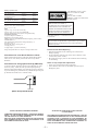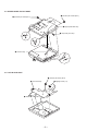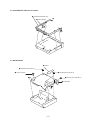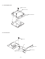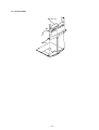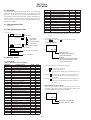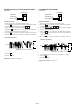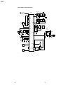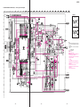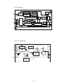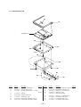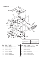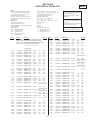
1
MZ-R55
SERVICE MANUAL
US Model
Canadian Model
AEP Model
UK Model
E Model
Australian Model
Tourist Model
Ver 1.5 2001. 01
With SUPPLEMENT-1
(9-924-964-85)
US and foreign patents licensed from Dolby Laboratories
Licensing Corporation.
Model Name Using Similar Mechanism
NEW
MD Mechanism Type
MT-MZR55-161
Optical Pick-up Type
KMS-280A
SPECIFICATIONS
System
Audio playing system
MiniDisc digital audio system
Laser diode properties
Material: GaAlAs
Wavelength: λ = 780 nm
Emission duration: continuous
Laser output: less than 44.6 µW
(This output is the value measured at a
distance of 200 mm from the lens surface on
the optical pick-up block with 7 mm
aperture.)
Recording and playback time
Maximum 74 minutes (MDW-74, stereo
recording)
Maximum 148 minutes (MDW-74, monaural
recording)
Revolutions
400 rpm to 900 rpm (CLV)
Error correction
Advanced Cross Interleave Reed Solomon
Code (ACIRC)
Sampling frequency
44.1 kHz
Sampling rate converter
Input: 32 kHz / 44.1 kHz / 48 kHz
Coding
Adaptive TRansform Acoustic Coding (ATRAC)
Modulation system
EFM (Eight to Fourteen Modulation)
Number of channels
2 stereo channels
1 monaural channel
Frequency response
20 to 20,000 Hz ± 3 dB
Wow and Flutter
Below measurable limit
Inputs
Microphone: stereo mini-jack, 0.22-0.78 mV
Line in: stereo mini-jack, 69-194 mV
Optical (Digital) in: optical (digital) mini-jack
Outputs
Headphones: stereo mini-jack, maximum
output level 5 mW+ 5 mW, load impedance
16 ohm
Line out: stereo mini-jack, 194 mV, load
impedance 10 kilohm
General
Power requirements
Sony AC Power Adaptor (supplied)
connected at the DC IN 3V jack:
120 V AC, 60 Hz (US model)
220-240 V AC, 50/60 Hz (Hong Kong model)
100-240 V AC, 50/60 Hz (Tourist model)
Nickel metal hydride rechargeable battery NH-14WM (supplied)
Two LR6 (size AA) alkaline batteries (not supplied)
– Continued on next page –
PORTABLE MINIDISC RECORDER
MICROFILM
–1–
Battery operation time
Batteries
NH-14WM nickel
metal hydride
rechargeable battery
Two LR6 (SG)
Sony alkaline dry batteries
NH-14WM + Two LR6 (SG)
Recording
Approx.
2.5 hours
Playback
Approx.
4 hours
Approx.
5 hours
Approx.
9.5 hours
Approx.
10 hours
Approx.
16 hours
This MiniDisc player is classified as a CLASS 1 LASER
product.
The CLASS 1 LASER
PRODUCT label is located on the
bottom exterior.
IN NO EVENT SHALL SELLER BE
LIABLE FOR ANY DIRECT,
INCIDENTAL OR CONSEQUENTIAL
DAMAGES OF ANY NATURE, OR
LOSSES OR EXPENSES RESULTING
FROM ANY DEFECTIVE PRODUCT
OR THE USE OF ANY PRODUCT.
Dimensions
Approx. 78.9 × 18.9 × 84 mm (w/h/d)
(3 1/8 × 3/4 × 3 3/8 in.)
Mass
Approx. 147 g (5.2 oz) the recorder only
Approx. 190 g (6.7 oz) incl. a recordable MD,
and NH-14WM nickel metal hydride rechargeable battery
Supplied accessories
AC power adaptor AC-MZR55 (1)
Headphones with a remote control
MDR-A34SP (US model)/MDR-E838SP (Hong Kong, Tourist model)
and RM-MZR55 (1)
NH-14WM nickel metal hydride rechargeable battery (1)
Dry battery case (1)
Rechargeable battery carrying case (1)
Carrying pouch (1)
AC plug adaptor (1) (Tourist model only)
“MD WALKMAN” is a trademark of Sony
Corporation.
CAUTION
Use of controls or adjustments or performance of procedures
other than those specified herein may result in hazardous
radiation exposure.
Flexible Circuit Board Repairing
• Keep the temperature of the soldering iron around 270°C
during repairing.
• Do not touch the soldering iron on the same conductor of the
circuit board (within 3 times).
• Be careful not to apply force on the conductor when soldering
or unsoldering.
Design and specifications are subject to change without notice.
Precautions for Laser Diode Emission Check
When checking the emission of the laser diode during adjustments, never view directly downwards as this may lead to
blindness.
Precautions for Using Optical Pick-up (KMS-280A)
As the laser diode inside the optical pick-up damages by static
electricity easily, solder the laser tap of the Optical pick-up
flexible board when handling. Also take the necessary measures
to prevent damages by static electricity. Handle the Optical pickup flexible board with care as it breaks easily.
Notes on chip component replacement
• Never reuse a disconnected chip component.
• Notice that the minus side of a tantalum capacitor may be
damaged by heat.
Laser tap
Optical Pick-up flexible board
ATTENTION AU COMPOSANT AYANT RAPPORT
À LA SÉCURITÉ!!
SAFETY-RELATED COMPONENT WARNING!!
COMPONENTS IDENTIFIED BY MARK ! OR DOTTED LINE WITH
MARK ! ON THE SCHEMATIC DIAGRAMS AND IN THE PARTS
LIST ARE CRITICAL TO SAFE OPERATION.
REPLACE THESE COMPONENTS WITH SONY PARTS WHOSE
PART NUMBERS APPEAR AS SHOWN IN THIS MANUAL OR IN
SUPPLEMENTS PUBLISHED BY SONY.
LES COMPOSANTS IDENTIFIÉS PAR UNE MARQUE ! SUR LES
DIAGRAMMES SCHÉMATIQUES ET LA LISTE DES PIÈCES SONT
CRITIQUES POUR LA SÉCURITÉ DE FONCTIONNEMENT. NE
REMPLACER CES COMPOSANTS QUE PAR DES PIÈCES SONY
DONT LES NUMÉROS SONT DONNÉS DANS CE MANUEL OU
DANS LES SUPPLÉMENTS PUBLIÉS PAR SONY.
–2–
TABLE OF CONTENTS
4. TEST MODE
1. GENERAL ....................................................................... 4
4-1.
4-2.
4-3.
4-4.
4-5.
4-6.
2. SELF-DIAGNOSTIC
2-1.
2-2.
2-3.
2-4.
2-5.
2-6.
General .....................................................................
Test Mode Setting .....................................................
Operation in Test Mode Setting ................................
Releasing the Test Mode ...........................................
Self-Diagnostic Mode ...............................................
Clearing the Error Indication Code
and Total Recording Time ........................................
5
5
5
5
5
General ...................................................................
Test Mode Setting ...................................................
Test Mode Structure ...............................................
Manual Mode .........................................................
Overall Adjustment Mode ......................................
Hybrid Mode, Key Check Mode ............................
12
12
12
12
15
16
5. ELECTRICAL ADJUSTMENTS ........................... 17
6
6. DIAGRAMS
3. DISASSEMBLY
3-1.
3-2.
3-3.
3-4.
3-5.
3-6.
3-7.
3-8.
3-9.
6-1. IC Pin Descriptions ................................................
6-2. Block Diagram – Servo Section – ..........................
6-3. Block Diagram – Audio Section – ..........................
6-4. Block Diagram – System Control Section – ...........
6-5. Printed Wiring Board (-11) .....................................
6-6. Printed Wiring Board (-12) .....................................
6-7. Printed Wiring Board (-13) .....................................
6-8. Schematic Diagram – Main Section (1/3) – ...........
6-9. Schematic Diagram – Main Section (2/3) – ...........
6-10. Schematic Diagram – Main Section (3/3) – ...........
Bottom Panel Assy ................................................... 7
Connector ................................................................. 7
Upper Panel Block Assy ........................................... 8
LCD Block Assy ....................................................... 8
Ornamental Belt Block Assy .................................... 9
Main Board ............................................................... 9
Chassis (Main) Assy ............................................... 10
OP Block Assy ........................................................ 10
Holder Assy ............................................................ 11
21
25
27
29
31
34
37
40
43
46
7. EXPLODED VIEWS
7-1. Panel Section .......................................................... 54
7-2. Chassis Section ....................................................... 55
7-3. Mechanism Deck Section ....................................... 56
8. ELECTRICAL PARTS LIST ................................... 57
SERVICING NOTE
1) When repairing this device with the power on, if you remove
the main board or open the upper panel assy, this device stops
working.
In this case, you can work without the device stopping by
fastening the hook of the DOOR OPEN switch (S801) with tape.
upper panel assy
MAIN board
tape
S801
2) This set is designed to perform automatic adjustment for each
adjustment and write its value to EEPROM. Therefore, when
EEPROM (IC801) has been replaced in service, be sure to perform automatic adjustment and write resultant values to the new
EEPROM.
Refer to page 12 for details.
–3–
SECTION 1
GENERAL
–4–
This section is extracted from
instruction manual.
SECTION 2
SELF-DIAGNOSTIC
2-1. GENERAL
2) Remote controller LCD
This set uses the self-diagnostic system in which if an error occurs
in playback/recording mode, the error is detected by the model
control and power control blocks of the microprocessor and information on the cause is stored as history in EEPROM.
By viewing this history in test mode, it helps you to analyze a fault
and determine its location.
888
ı
All ON
2-2. TEST MODE SETTING
All OFF
There are two different methods to set the test mode:
1 Short BP801 (TEST) on the main board with a solder bridge
(connect pin @§ of IC801 to the ground). Then, turn on the
power.
Ver ‚.8‚
Microprocessor
version
display
– main board (side B) –
• Holding down P allows the current display to be maintained
while it being depressed.
IC503
2-4. RELEASING THE TEST MODE
IC802
For test mode set with the method 1:
Turn off the power and open the solder bridge on BP801 on the
main board.
For test mode set with the method 2:
Turn off the power.
BP801
IC509
2-5. SELF-DIAGNOSTIC MODE
R818
1. Go into the test mode.
2. With the unit LCD indicators all flashing, press DISPLAY key
to go into the self-diagnostic mode.
C309
History code
Error indication code
2 In the normal mode, use the keys on the unit to perform the
following operations:
Press and hold down ( and press the keys below in this turn:
+ n + n =n = n + n = n + n
=nPnP
2-3. OPERATION IN TEST MODE SETTING
When the test mode is set, the LCD shows repeated cycles of the
following display:
1st
‚
‚‚
3. Then, each time ) key is pressed, the reference information
display changes as given below.
1) Unit LCD
ı
All ON
188 : 88
1st
‚
XX
N-1
‚
XX
1st
1
‚‚
N-1
1
‚‚
1st
2
‚‚
N-1
2
‚‚
N
‚
XX
N-2
‚
XX
N
1
‚‚
N-2
1
‚‚
N
2
‚‚
N-2
2
‚‚
All OFF
REC
Ver
‚‚.8‚
Microprocessor
version
display
1st
XXXX
‚
XX
• Press = key to go back to the previous display.
–5–
(return)
• Description of History Codes
History code number
1st 0
1st 1
1st 2
N
0
N
1
N
2
N-1 0
N-1 1
N-1 2
N-2 0
N-2 1
N-2 2
REC
Description
The first error
00 indicated
The last error
00 indicated
*1) Total recording time
Total recording time is recorded in minutes as an index for load to
the OP. It is recorded in hexadecimal format and up to 65,535 min.
(about 886 discs of 74-minute disc) can be counted. It returns to
“0000h” when recorder goes beyond this limit.
Example : REC 000A n Approx. 10 min.
REC 00A0 n Approx. 160 min.
REC 0A00 n Approx. 2560 min.
One error before the last.
00 indicated
Two errors before the last.
00 indicated
Total recording time *1)
• Description of Error Indication Codes
Problem
No error
Abnormal stop
during recording
Indication code
00
01
Servo error
02
03
ADIP read error
Shock detected during write
Shock detected during
laser down
No focus applied
CRC error
FG error
Lower voltage due to overload
Momentary interruption
Lower power voltage in motor
system
Low power voltage in DSP
04
Abnormal stop
during playback
Abnormal stop of
recording/playback
caused by power
system
Meaning of code
11
12
15
21
22
23
24
2-6. CLEARING THE ERROR INDICATION CODE
AND TOTAL RECORDING TIME
After repair, reset the error indication code.
Reset the total recording time when you have replaced the OP.
1. Go into the self-diagnostic mode. (See page 5.)
2. To reset the error indication code, slide REC c key when
the code is displayed.
(All data including 1st, N , N-1 and N-2 are reset.)
3. To reset the total recording time, slide REC c key when the
time is displayed.
–6–
Description
Abnormal disc RPM.
Focus out of alignment.
Attempt to access an abnormal address.
Unable to read the ADIP address.
Jumped by 1.5 tracks or more due to shock during write.
Shock detected when laser was moving down.
Focus could not be applied.
Unable to read the address.
Abnormal rotation of disc.
Power voltage reduced due to overload.
Momentary interruption detected.
Power voltage for motor continuously reduced to less than
1V.
SECTION 3
DISASSEMBLY
Note : This set can be disassemble according to the following sequence.
Connector
Main Board
Bottom
Panel
Upper Panel
LCD Block assy
assy
Block assy
Ornametal Belt
Main
Block assy
Board
Chassis (Main)
assy
OP Block
assy
Note : Follow the disassembly procedure in the numerical order given.
3-1. BOTTOM PANEL ASSY
Note) When installing, fit the each positions knobs with switches.
4 bottom panel assy
2 precision pan screws (M1.4)
knobs
3 precision pan screw (M1.4)
1 precision pan screws (M1.4)
switches
3-2. CONNECTOR
3 CN502
1 CN601
–7–
2 CN801
Holder
assy
3-3. UPPER PANEL BLOCK ASSY
3 precision pan screws (M1.4)
2 precision pan screw (M1.4)
7 upper panel block assy
4 step screw (click arm)
5
6
8
0 click arm assy
9
1
3-4. LCD BLOCK ASSY
1 precision pan screw (M1.4)
4 LCD block assy
2 tapping screws (1.7)
3 claws
–8–
3-5. ORNAMENTAL BELT BLOCK ASSY
5 ornamental belt block assy
1
6 button (OPEN)
2
4
3
3-6. MAIN BOARD
7 CN501
3 toothed lock screw (M1.4)
4 toothed lock screws (M1.4)
2 step screw (HP)
6
1 precision pan screw (M1.4)
8 MAIN board
5
–9–
3-7. CHASSIS (MAIN) ASSY
1 step screw (MD)
2 step screw (MD)
4 chassis (MAIN) assy
3
3-8. OP BLOCK ASSY
1 M1.4x3.0
lens
2 main shaft
over head block assy
3 flexible board
– 10 –
4 OP block assy
3-9. HOLDER ASSY
4 holder assy
2
3
1 claw
– 11 –
SECTION 4
TEST MODE
4-1. GENERAL
This set provides the Overall adjustment mode (Assy mode) that
allows CD and MO disk to be automatically adjusted when in the
test mode. In this Assy mode, the system discriminates between
CD and MO disk and then automatically perform adjustments for
them in sequence. If a fault is found, the system displays its location. Also, the Servo mode allows each individual adjustment to be
automatically adjusted.
4-2. TEST MODE SETTING
See page 5.
4-3. TEST MODE STRUCTURE
Test Description
Low reflection CD focus bias
CD test adjustment
CD focus search adjustment
CD FE balance adjustment
CD ABCD level adjustment
Laser CD read
CD focus gain
CD tracking gain
CD focus bias
Recording test
32 cluster full recording
Recording shock
32 cluster full playback
+ or VOLUME + key
Manual Mode
Servo Mode
Audio Mode
Mechanism Mode
Power Mode
®
® (10)
® (15)
® (08)
® (30)
® (30)
® (00)
Unit LCD display
SERVO
XX XX
Adjustment value
(the data can be changed/
written when flashing.)
EDIT/ENTER key
Key Check Mode
Mode No.
(The lower two digits are indicated.
Three digits are indicated on the
remote controller LCD.)
4-4. MANUAL MODE
(1) Servo Mode
• How to Transfer in the Servo Mode:
Test Description
Servo mode
Offset correction value indication
VC offset correction
Focus bias correction
FE offset correction
ABCD offset correction
All servo ON
Temperature indication
Laser power adjustment
Laser CD/MO read adjustment
Laser MO write adjustment
Sled normal
Sled intermittent
Sled access
MO test adjustment
MO focus search adjustment
MO read FE balance adjustment
MO read ABCD level
MO write FE balance adjustment
MO write ABCD level
Laser MO read adjustment
MO focus gain
MO tracking gain
MO focus bias
Low reflection CD test adjustment
Low reflection CD focus search adjustment
Low reflection CD FE balance adjustment
Low reflection CD ABCD level
Laser low reflection CD read
Low reflection CD focus gain
Low reflection CD tracking gain
Write
® (00)
1. Go into the test mode.
2. Press + or VOLUME + key to set the servo mode.
= or VOLUME – key
Overall Adjustment Mode
(Assy Mode)
MODE key
Hybrid Mode (ALL Mode)
Mode No.
000
010
011
012
013
014
015
016
020
021
022
023
024
025
030
031
032
033
034
035
036
037
038
039
040
041
042
043
044
045
046
Check
®
Check : Mode to display error rate and cluster.
Write : Mode to permit adjustment (Default value given in paren
theses).
Test mode
VOLUME + key
Mode No.
047
050
051
052
053
054
055
056
057
060
061
062
063
Check
Write
® (08)
® (4C)
® (45)
® (65)
® (30)
®
3. Press the keys below to change the mode No.
( : Increases the one place.
p : Sets the one place to 0.
This key brings the ten place to 0 if the one place is
0.
VOLUME + : Increases the ten place by 10 if the one place is 0.
Increases the adjustment value if the one place
is non-zero.
VOLUME – : Decreases the ten place by 10 if the one place is 0.
Decreases the adjustment value if the one place is
non-zero.
• How to Adjust in Servo Mode:
1. When the servo mode is set to the appropriate mode for each
adjustment, the lower tow digits of the mode No. and the value
stored in EEPROM are displayed and flashing.
® (0F)
® (07)
® (10)
® (18)
® (08)
® (30)
® (30)
® (06)
SERVO
XX XX
Adjustment value (flashing)
Mode No. (lower two digits)
® (10)
® (06)
® (08)
® (30)
® (30)
– 12 –
2. To perform automatic adjustment for an adjustment item with
the mode number 030 to 047, press P key.
If the result of adjustment is OK, the adjustment value changes
from flashing to steady on and it is automatically written to
EEPROM.
(2) Audio Mode
• How to Transfer in the Audio Mode
Mode No.
Test Description
3. To perform manual adjustment, change the adjustment value with
VOLUME + or – key, and press P key to write it to
EEPROM.
100
110
111
112
113
114
120
121
*1)
122
*1)
123
*1)
Note) Normally, automatic adjustment should be performed. Do
not execute manual adjustment.
124
*1)
• System Gain Mode
1. This mode allows the system gain to be freely adjusted. Press
DISPLAY key to enter this mode.
130
131
132
133
134
135
136
137
138
139
140
141
142
143
144
145
146
147
148
149
150
151
152
153
154
155
156
157
158
159
Audio mode
Audio playback
L/R=1 kHz 0 dB
L=1 kHz 0 dB
R=1 kHz 0 dB
L/R – ∞ dB
Audio recording test
LINE manual recording
MIC manual recording
DEMP LINE manual recording
DEMP MIC manual recording
LINE automatic recording
OPT automatic recording
MIC automatic recording
DEMP LINE automatic recording
DEMP OPT automatic recording
DEMP MIC automatic recording
DIGITAL AGC ADJ1
MIC UP SR
MIC DOWN SR
MIC THD0
MIC GAIN
MIC ATTACK
MIC RECOVER
MIC THD2
MIC GAIN2
MIC RTIME
DIGITAL AGC ADJ2
LINE UP SR
LINE DOWN SR
LINE THD0
LINE GAIN
LINE ATTACK
LINE RECOVER
LINE THD2
LINE GAIN2
LINE RTIME
DIGITAL AGC ADJ3
MAN UP SR
MAN DOWN SR
AUTO THD3
AUTO LMT UP SR
AUTO LMT DOWN SR
MAN THD3
MANU LMT UP SR
MANU LMT DOWN SR
THD1
AUTO ADJ
32 OF
Adjustment value
(flashing to steady on)
SYS_GAIN
32 OF
Adjustment value (flashing)
2. Increase or decrease the adjustment value with VOLUME + or
– key.
3. Press DISPLAY or p key to return to the normal mode.
4. For the error rate display enabled:
Normal Mode
Error rate display
Press DISPLAY key
System gain Mode
Cluster value
AT error rate
BLOCK error rate
000
4F
Write
Change
Description
Playback VOL
Playback VOL
Playback VOL
Playback VOL
HP output
HP output
HP output
HP output
Recording VOL HP output
Recording VOL HP output
HP VOL
HP output
HP VOL
HP output
® (30)
® (FA)
® (D0)
® (00)
® (A0)
® (F8)
® (F0)
® (D0)
® (01)
® (17)
® (FF)
® (D0)
® (0C)
® (33)
® (F8)
® (E4)
® (5F)
® (04)
® (C0)
® (40)
® (51)
® (FF)
® (E0)
® (51)
® (FF)
® (A0)
® (1A)
*1) The port is detected and the input is automatically selected.
Contents changed : Contents to be changed when VOLUME
+ or – key is pressed.
Write
: Mode to permit adjustment
(Default value given in parentheses)
FF
39 OA
Adjustment value (flashing)
Mode No. (lower two digits)
1. Go into the test mode.
2. Press + key or VOLUME + key and VOLUME + key in
this turn to set the audio mode.
Note) In normal service, do not adjust the system gain mode.
– 13 –
Unit LCD display
(3) Mechanism Mode
• How to Transfer the Mode in the Mechanism Mode:
Mode No. Test Description
Operation
200
FUNCTION
Stepper control
210
MECHA test
Initial position return
211
HEAD adjustment Operation variation changing (19)
212
REC position
Recording head descent
220
CLOCK
Clock
221
CLOCK check
Clock check/initialization
( ) : Default value
AUDIO
XX XX
Adjustment value
(the data can be changed/
written when flashing.)
Mode No.
(The lower two digits are indicated.
Three digits are indicated on the
remote controller LCD.)
1. Go into the test mode.
2. Press + or VOLUME + and VOLUME + and VOLUME
+ in this turn to set the mechanism mode.
3. Press the keys below to change the mode number.
( : Increases the one place.
p : Sets the one place to 0.
This key brings the ten place to 0 if the one place
is 0.
VOLUME + : Increases the ten place by 10 if the one place is 0.
Increases the adjustment value if the one place is
non-zero.
VOLUME – : Decreases the ten place by 10 if the one place is 0.
Decreases the adjustment value if the one place is
non-zero.
• How to Adjust in the Audio Mode
1. When the audio mode is set to the appropriate mode for each
adjustment, the lower tow digits of the mode No. and the value
stored in EEPROM are displayed and flashing.
2. Change the adjustment value with VOLUME + or – key and
press P key to write the new value to EEPROM.
• How to Check in the Audio Mode
The audio mode allows the checks below to be performed:
1. For the mode numbers of 100 and 110 to 114, pressing P key
will activate a beep. (No beep sounds when c HOLD switch
is put on.)
2. For the mode numbers of 121 to 124, pressing DIGITAL MEGA
BASS key will display the DBB mode for the adjustment value.
1 : Mode 1
2 : Mode 2
13 : OFF
(This will not be accepted when the LINE OUT jack is plugged.
The display will be 13 : OFF when LINE OUT jack is plugged
in Modes 1 and 2.)
3. For the mode numbers of 120 to 124, REC LED goes on.
(The LED does not go on when SYNCHRO REC switch is put
on.)
Unit LCD display
MECHA
XX XX
Adjustment value
Mode No.
(Lower two digits are displayed.)
3. Press the keys below to change the mode No.
( : Increases the one place.
p : Sets the one place to 0.
This key brings the ten place to 0 if the one place is
0.
VOLUME + : Increases the ten place by 10 if the one place is 0.
Increases the adjustment value if the one place
is non-zero.
VOLUME – : Decreases the ten place by 10 if the one place is 0.
Decreases the adjustment value if the one place is
non-zero.
• How to Check in the Mechanism Mode
The mechanism mode allows the checks below to be performed:
1. For the mode numbers of 200, 210 to 212, 220 and 221, pressing
= key will move the optical pickup to the inner radius.
Pressing + key will move the pickup to the outer radius.
2. For the mode numbers of 211 and 212, pressing P key will
start aging. Pressing p key will stop aging.
• Mode No. 211 ... Sled aging with stepper at playback position.
• Mode No. 212 ... Sled aging with stepper at recording position.
3. With the mode number 210 selected, pressing P key will start
aging with steeper at between home and recording positions.
p key will stop aging.
– 14 –
• Clock Operation Check
1. For the mode No. of 221, operation check is performed.
It is determined as OK if at 11 years, 11 months, 11 days, 11
hours, 11 minutes and 11 seconds or not the default value.
2. For the mode No. of 221, pressing P key will clear the resume
data stored in EEPROM and initialize the clock data.
4-5. OVERALL ADJUSTMENT MODE (ASSY MODE)
• How to Adjust in Assy Mode
1. Go into the test mode.
2. Press = or VOLUME – key.
Assy Mode
Note) The clock should be set when the overall adjustment mode
is completed as OK. The write data is to be at 11 years,
November 11 days, 11 hours, 11 minutes and 11 seconds.
(4) Power Mode
Mode No. Test Description
300
POWER test
310
POWER SUPPLY
311
DC IN
312
DC IN + Ni-Cd
313
Ni or AM3
314
AM3
320
CHG TEST
321
Charging start
Indication value Remark
40 XX
3. Insert the test CD (TDYS-1) or an available SONY CD.
4. Press ( key. The system discriminates between CD and MO
and performs automatic adjustment for CD.
+B voltage value
+B voltage value
+B voltage value
+B voltage value
CD RUN
51
Mode No. under adjustment
1. Go into the test mode.
2. Press + key or VOLUME + and VOLUME + and VOLUME + and VOLUME + in this turn to set the power mode.
POWER
XX XX
Adjustment value
Mode No.
(Lower two digits are displayed.)
• CD Automatic Adjustment
Mode No.
Adjustment Description
052
CD FE balance adjustment
053
CD ABCD level adjustment
055
CD focus gain
056
CD tracking gain
057
CD focus bias
5. If the result of automatic adjustment is OK, the following display appears:
CDmode
3. Press the keys below to change the mode No.
( : Increases the one place.
p : Sets the one place to 0.
This key brings the ten place to 0 if the one place is
0.
VOLUME + : Increases the ten place by 10 if the one place is 0.
Increases the adjustment value if the one place
is non-zero.
VOLUME – : Decreases the ten place by 10 if the one place is 0.
Decreases the adjustment value if the one place is
non-zero.
OK
00
6. If the result of automatic adjustment is NG, the following display appears:
Note) With the mode number 310 selected, pressing ( key will
transfer to the mode number (311 to 314) for the currently
operating power.
With the mode number 300 selected, pressing P key will
set the sleep mode. Pressing p key will release it.
• How to Check in the Power Mode
1. For the mode numbers of 311 to 314, the voltage of the currently
operating power is displayed.
– 15 –
CDmode
NG
55 7F
Result of adjustment
NG mode No. (lower two digits)
* For the mode numbers of 039 and 057, if the focus bias value is
NG, the following display is repeated:
CDmode
10. If the result of automatic adjustment is OK, the following display appears:
NG
MOmode
55 30
OK
00
Focus bias value
Mode No.
11. If the result of automatic adjustment is NG, the following display appears:
While P key is being depressed
MOmode
CDmode
NG
NG
82 00
77 01
Result of adjustment
NG mode No. (low two digits)
Error code (01 to 04)
Meaning of focus bias
* For the mode numbers of 039 and 061, if the At error rate is NG,
the following display is repeated:
12. If NG, set the servo mode. Perform automatic adjustment for
the items not accepted (see the servo mode).
4-6. HYBRID MODE, KEY CHECK MODE
CDmode
These modes are not used in normal service.
NG
39 03
At error value
Mode No. (lower two digits)
7. If NG, set the servo mode. Perform automatic adjustment for
the items not accepted (see the servo mode).
8. Insert a MO disk.
9. Press ( key. The system discriminates between CD and MO
and performs automatic adjustment for the MO disk.
MO RUN
61
Mode No. (lower two digits)
• MO Automatic Adjustment
Mode No.
Adjustment Description
032
MO read FE balance adjustment
033
MO read ABCD level
034
MO write FE balance adjustment
035
MO write ABCD level
037
MO focus gain
038
MO tracking gain
061
32 cluster full recording
062
Recording shock
063
32 cluster full playback
039
MO focus bias
042
Low refrection CD FE balance adjustment
043
Low refrection CD ABCD level
044
Laser low reflection CD read
046
Low refrection CD tracking gain
– 16 –
Ver 1.5 2001. 01
SECTION 5
ELECTRICAL ADJUSTMENTS
PRECAUTIONS FOR ADJUSTMENT
MO TRAVERSE ADJUSTMENT
1) Perform all adjustments in the order given in the test mode.
After adjusting, exit the test mode.
2) Use the following tools and measuring instruments.
• Test CD
TDYS-1
(Part No. : 4-963-646-01)
• SONY MO disc available on the market
• Laser power meter LPM-8001
(Part No. : J-2501-046-A)
• Oscilloscope (Frequency band above 40 MHz. Perform the
calibration of probe first before measuring.)
• Digital voltmeter
3) Unless specified othewise, supply DC 3V from the DC IN 3V
jack.
4) Swtich, knob positions
HOLD switch .............. OFF
AVLS switch ................ NORM
Connection :
LASER POWER CHECK
Connection :
laser
power meter
Optical pick-up
objective lens
oscilloscope
MAIN board
TP5980 (TE)
AP5430 (VC)
Adjustment Method :
1. Set the servo mode of the test mode (Mode : 000).
2. Press the ( key, and set the MO test adjustment mode (Mode
: 030) using the VOLUME + or – key.
3. Press the = or + key and move the optical pick-up to
the center circumference.
4. Insert any MO disk available on the market.
5. When the ( key is pressed, the MO read FE balance adjustment mode (Mode : 032) will be set after MO focus search
adjustment mode (Mode : 031).
6. Press the P key to perform automatic adjustment, and check
that the traverse waveform is symmetrical at the top and bottom.
7. Slide the REC key and set the MO write FE balance adjust
ment mode (Mode : 034).
8. Press the P key to perform automatic adjustment, and check
that the traverse waveform is symmetrical at the top and bottom.
(Traverse waveform)
digital voltmeter
A
MAIN board
0V
C
AP5117 (VCC)
AP574 (LDI0)
B
Adjustment Method :
1. Set the servo mode of the test mode (Mode : 000).
2. Press the ( key, and set the laser power adjustment mode
(Mode : 020) using the VOLUME + or – key.
3. Press the = key and move the optical pick-up to the inner
most circumference.
4. Open the cover and set the laser power meter on the objective
lens of the optical pick-up.
5. Press the ( key, and set the laser CD/MO read adjustment
mode (Mode : 021).
6. Check that the laser power meter reading is 0.85 ± 0.085 mW.
7. Check that the voltage between AP5117 (VCC) and AP574
(LDI0) at this time is below 44 mV.
8. Press the ( key, and set the laser MO write adjustment
mode (Mode : 022).
9. Check that the laser power meter reading is 6.8 ± 0.68 mW.
10. Press the P key to finalize the adjustment data.
11. Check that the voltage between AP5117 (VCC) and AP574
(LDI0) at this time is below 80 mV.
12. Press the p key.
13. Exit the test mode.
Specification : A = B, C >
= 1.0 Vp-p
9. Check that the traverse level at this time is above 1.0 Vp-p.
10. Press the p key.
11. Exit the test mode.
Note) Using a recorded disk in this adjustment will erase the data.
Adjustment Location : See page 19.
Adjustment Location : See page 19.
– 17 –
LOW REFLECTION CD TRAVERSE ADJUSTMENT
CD TRAVERSE ADJUSTMENT
Connection :
Connection :
oscilloscope
oscilloscope
MAIN board
MAIN board
TP5980 (TE)
AP5430 (VC)
TP5980 (TE)
AP5430 (VC)
Adjustment Method :
1. Set the servo mode of the test mode (Mode : 000).
2. Press the ( key, and set the low reflection CD test adjustment
mode (Mode : 040) using the VOLUME + or – key.
3. Insert any MO disk available on the market.
4. When the ( key is pressed, the low reflection CD FE balance
adjustment mode (Mode : 042) will be set after low reflection
CD focus search adjustment mode (Mode : 041).
5. Press the P key to perform automatic adjustment, and check
that the traverse waveform is symmetrical at the top and bottom.
(Traverse waveform)
Adjustment Method :
1. Set the servo mode of the test mode (Mode : 000).
2. Press the ( key, and set the CD test adjustment mode (Mode
: 050) using the VOLUME + or – key.
3. Press the = or + key and move the optical pick-up to the
center circumference.
4. Insert a test CD (TDYS-1).
5. When the ( key is pressed, the CD FE balance adjustment
mode (Mode : 052) will be set after CD focus search adjustment
mode (Mode : 051).
6. Press the P key to perform automatic adjustment, and check
that the traverse waveform is symmetrical at the top and bottom.
(Traverse waveform)
A
0V
A
C
0V
B
C
B
Specification : A = B, C >
= 0.9 Vp-p
Specification : A = B, C >
= 1.0 Vp-p
6. Check that the traverse level at this time is above 0.9 Vp-p.
7. Press the p key.
8. Exit the test mode.
Adjustment Location : See page 19.
7. Check that the traverse level at this time is above 1.0 Vp-p.
8. Press the p key.
9. Exit the test mode.
Adjustment Location : See page 19.
– 18 –
CD RF LEVEL CHECK
Adjustment Location :
Connection :
– main board (side B) –
oscilloscope
MAIN board
AP5500 (RF)
AP5430 (VC)
digital voltmeter
IC509
MAIN board
IC503
IC501
CN501
AP574
(LDI0)
AP5117 (VCC)
AP574 (LDI0)
Adjustment Method :
1. Set the servo mode of the test mode (Mode : 000).
2. Press the ( key, and set the CD test adjustment mode
(Mode : 050) using the VOLUME + or – key.
3. Press the = or + key and move the optical pick-up to
the center circumference.
4. Insert a test CD (TDYS-1).
5. When the ( key is pressed, the CD FE balance adjustment
mode (Mode : 052) will be set after CD focus search adjustment mode (Mode : 051).
6. When the ( key is pressed, the CD ABCD level adjustment
mode (Mode : 053) is set.
7. Press the P key to perform automatic adjustment, and check
that the RF level is 1.1 ± 0.3 Vp-p.
(RF waveform)
1.0 ± 0.3 Vp-p
8. Check that the voltage between AP5117 (VCC) and AP574
(LDI0) and at this time is below 40 mV.
9. Press the p key.
10. Exit the test mode.
– 19 –
BP801
(TEST)
AP5500
(RF)
AP5430 AP5117
(VCC)
(VC)
– main board (side B) –
TP5980
(TE)
2.65V ADJUSTMENT
Connection :
digital voltmeter
MAIN board
AP908 (2.65V)
AP906 (GND)
Adjustment Method :
1. Playback the test CD (TDYS-1).
2. Adjust RV901 so that the voltage between AP908 (2.65V) and
AP906 (GND) is at 2.65 ± 0.03 Vdc.
Adjustment Location :
– main board (side B) –
IC802
AP908
(2.65V)
AP906
(GND)
RV901
2.65V ADJUSTMENT
CN801
– 20 –
SECTION 6
DIAGRAMS
6-1. IC PIN DESCRIPTIONS
• IC503 CXD2652AR (DIGITAL SERVO, ATRAC)
Pin No.
1
Pin name
MNT 0
I/O
O
Pin Description
Traverse count signal output.
2
MNT 1
O
Track jump detect output.
3
MNT 2
—
Not used (Open).
4
MNT 3
—
Focus OK signal output.
5
SWDT
I
Inputs write data signal from system controller (IC802).
6
SCLK
I
Inputs serial clock signal from system controller (IC802).
7
XLAT
I
Inputs serial latch signal from system controller (IC802).
8
SRDT
O
Outputs write data signal to system controller (IC802).
9
SENS
O
Outputs internal status (SENS) to system controller (IC802).
10
XRST
I
Inputs reset signal from system controller (IC802). L : Reset
11
SQSY
O
Output subcode Q sync (SCOR) to system controller (IC802).
Outputs “L” every 13.3 msec. Outputs “H” at all most mostly.
12
DQSY
O
Outputs digital-in U-bit CD format subcode Q sync (SCOR) to system controller (IC802).
Outputs “L” every 13.3 msec. Outputs “H” at all most mostly.
13
WRPWR
I
14
NC
—
15
TX
I
Inputs laser power switching signal from system controller (IC801).
Not used (Open).
Input of write data taransmission timing from system controller (IC801).
Also used as magnetic field head ON/OFF output.
16
OSC1
O
Clock output (22.5 MHz).
17
OSC0
I
Clock input (22.5 MHz).
18
XTSL
—
Not used (Fixed at “L”)
19
NC
—
Not used (Connect to ground).
20
RVSS
—
21
DIN
I
22
NC
—
23
ADDT
I
Audio data input from A/D converter (IC301).
24
DATA
O
Monitor/decode audio data output to A/D converter (IC301).
25
ALRCK
O
L/R clock output to D/A converter (IC301).
26
ABCK
O
Bit clock signal output to A/D, D/A converter (IC301).
27
FS256
O
11.2896 MHz clock output (MCLK).
Connect to ground.
Digital audio signal input pin (For optical input).
Not used (Open).
28
DVDD
—
Power supply (+2.8 V) for digital.
29 – 39
A00 – A08, A10, A11
O
Address signal output to DRAM (IC509).
40
DVSS
—
Ground terminal.
41
XOE
O
Output enable contol signal output to DRAM (IC509).
42
XCAS
O
Column address strobe singal output to DRAM (IC509).
43
A09
O
Address signal output to DRAM (IC509).
44
XRAS
O
Row address strobe signal output to DRAM (IC509).
45
XWE
O
Read/write control signal output to DRAM (IC509).
46 – 49
D0 – D3
I
Data signal input from DRAM (IC509).
50
MVCI
—
51
ASYO
O
Playback EFM full-swing output (L : VSS, H : VDD).
52
ASYI
I
Playback EFM asymmetry comparate voltage input.
53
AVDD
—
54
BIAS
I
Playback EFM asymmetry circuit constant current input.
55
RFI
I
Inputs playback EFM RF signal from RF amplifier (IC501).
Not used (Connect to ground).
Power supply (+2.8 V) for analog.
– 21 –
Pin No.
56
Pin name
AVSS
I/O
—
Pin Description
Ground terminal.
57
PDO
—
Not used (Open).
58
PCO
O
Decoder PLL master clock PLL phase comparison output.
59
FILI
I
Decoder PLL master clock PLL filter input.
60
FILO
O
Decoder PLL master clock PLL filter output.
61
CLTV
I
Decoder PLL master clock PLL VCO control voltage input.
62
PEAK
I
Inputs peak hold signal for light amount signal from RF amplifier (IC501).
63
BOTM
I
Inputs bottom hold signal for light amount signal from RF amplifier (IC501).
64
ABCD
I
Light amount signal from RF amplifier (IC501).
65
FE
I
Input focus error signal from RF amplifier (IC501).
66
AUX1
I
Input of auxiliary signal from RF amplifier (IC501).
67
VC
I
68
ADIO
—
Not used (Open).
Input of middle point voltage (+1.4 V) from RF amplifier (IC501).
69
AVDD
—
Power supply (+2.8 V) for analog.
70
ADRT
—
Not used (Connect to +2.8 V).
71
ADRB
—
Not used (Connect to ground).
72
AVSS
—
Ground terminal.
73
SE
I
Input of sled error signal from RF amplifier (IC501).
74
TE
I
Input of tracking error signal from RF amplifier (IC501).
75
AUX2
—
Not used (Connect to +2.8 V).
76
DCHG
—
Not used (Connect to +2.8 V).
77
APC
—
78
ADFG
I
79
FO CONT
O
Not used (Connect to +2.8 V).
Input of ADIP dual FM signal from RF amplifier (IC501) (22.05 kHz ± 1 kHz).
(TTL Schmit input)
Focus control output to RF amplifier (IC501).
80
XLRF
I
Latch signal input from RF amplifier (IC501).
81
CKRF
O
RFCK clock (7.35 kHz) signal output.
82
DTRF
I
Serial data input from system controller (IC802).
83
APCREF
I
Laser power setting signal input.
84
LDDR
—
Not used (Open).
85
TRDR
O
Tracking servo drive signal output (–).
86
TFDR
O
Tracking servo drive signal output (+).
87
DVDD
—
Power supply (+2.8 V) for digital.
88
FFDR
O
Focus servo drive signal output (+).
89
FRDR
O
Focus servo drive signal output (–).
90
FS4
O
Not used (Open). (176.4 kHz clock signal output (MCLK).)
91
SRDR
O
Sled servo drive signal output (–).
92
SFDR
O
Sled servo drive signal output (+).
93
SPRD
O
Spindle servo drive signal output (–).
94
SPFD
O
Spindle servo drive signal output (+).
95
FGIN
I
FG signal input from spindle motor driver (IC701).
96
TEST1
—
Not used (Connect to ground).
97
TEST2
—
Not used (Connect to ground).
98
TEST3
—
Not used (Connect to ground).
99
DVSS
—
Ground terminal.
100
EFMO
O
EFM recording signal output.
– 22 –
• IC802 CXP740010 (SYSTEM CONTROL)
Pin No.
1
Pin name
CLKCS
I/O
O
Pin Description
Chip select output to real time clock (IC805).
Pin No.
51
52
Pin name
AVREF
I/O
I
Pin Description
A/D converter reference voltage input.
AVDD
—
A/D converter power supply terminal.
2
XRST
O
Reset output. L : Reset
53
NC
—
3
WRPWR
O
Laser power switching signal output.
54
TEMP
I
Temp meter (IC803) input.
4
TX
O
Write data transfer timing output.
55
KEY3
I
Key input.
5
SDI2
I
Serial data input.
56
KEY4
I
Key input.
6
SDO2
O
Serial data output.
57
KEY1
I
Key input.
7
SCK2
O
Serial clock output.
58
XINT REC SW
I
Recording head position detect input.
8
XRF-STBY
O
Power control output to RF amplifier (IC501).
59
UNREG MNT
I
2.8 V voltage monitor input.
9
SSB
I/O
SSB data signal input and output.
60
2V MNT
I
Voltage monitor for lithium battery. Motor power voltage monitor input.
10
SSB SCK
I/O
SSB clock signal input and output. (Not used (Open).)
61
FG IN
I
FG input from motor driver (IC503).
11
DTCK
I/O
Remote control data signal input/output.
62
NC
—
12
SPCK
—
Not used (Open).
63
FOK
I
13
WP
I
Wake-up signal input from remote control key and this unit key.
64
––––
—
14
OPEN
I
Detecting switch for opening and closing of the upper cover. L : Close
65
––––
—
15
CLOCK
I
CLOCK SET switch input.
66
XJACKDET
I
16
NC
—
Not used (Open).
67
OPT DET
I
LINE IN (OPTICAL) optical detection input.
17
NC
—
Not used (Open).
68
XMIC DET
I
MIC (PLUG IN) jack detection.
18
T.MARK
I
T MARK (Track mark) switch input.
69
––––
—
Not used (Open).
19
REC
I
REC switch input.
70
––––
—
Not used (Open).
20
PROTECT
I
Disc write protect switch. H : Protect
71
SPOFF
O
21
HOLD
I
HOLD switch input (This unit). L : HOLD
72
RSI
O
22
SYNC REC
I
SYNCHRO REC switch input.
73
CHG CONT
O
Constant current chage control signal output.
23
D. B. B
I
DIGITAL MEGA BASS slide switch input.
74
––––
—
Not used (Open).
24
XLINEDET
I
LINE IN (OPTICAL) detection input. L : LINE IN
75
DQSY
I
Subcode Q sync (SCOR) of digital in U-bit CD format from IC503.
25
AVLS
I
AVLS switch input. L : LIMIT
76
T COUNT
I
Traverse count signal input.
26
XTEST
I
Test mode terminal. L : Test mode
77
SDI1
I
Serial data input.
27
XDCIN
I
Not used (Open). (DC input detect. L : DC IN)
78
SDO1
O
Serial data output.
Not used (Open).
Not used (Open).
Focus OK signal input.
Not used (Open).
Not used (Open).
LINE IN (OPTICAL) jack detection input.
REC head motor control signal output.
28
KANA SE L
I
Model input. (L : J model, H : Tourist, Hong Kong model)
79
SCK1
O
Serial clock output.
29
XPHOTO SW
O
ON/OFF control signal output of PHOTO circuit.
80
SQSY
I
SUB-Q/ADIP SYNC input.
30
XP CONT
O
Power control output. L : ON
81
BEEP
O
BEEP sound output control.
31
X2VCONT
O
Outputs H while operating with a lithium battery. 2V power control signal output. L : ON
82
XLAT
O
Latch output.
32
XREC LED
O
REC LED control. L : ON
83
NC
—
Not used (Open).
33
MODE2
O
84
TEX
—
Not used (Fixed at “L”).
34
MODE1
O
85
XT
—
Not used (Fixed at “L”).
35
XNIMH CHG
O
Battery charger control signal output. L : Charge
86
VSS
—
Ground.
36
XLCD ON
O
LCD ON/OFF control. L : ON
87
VDD
—
Power supply pin (+2.8V).
37
––––
—
Not used (Open).
88
NC
—
Not used (Fixed at “H”).
38
MRST
I
Microprocessor reset input.
89
XCS ADA
O
A/D, D/A converter chip select output.
39
VSS
—
Ground.
90
XPD ADA
O
A/D, D/A converter power down signal output. H : Power down
40
XTAL
—
System clock (12 MHz).
91
KEYON
O
SLEEP : L, action : H.
41
EXTAL
—
System clock (12 MHz).
92
XNIMH DET
I
Battery detect switch input.
42
LCD STBY
O
LCD communication strobe signal output to LCD driver.
93
A MUTE
O
Analog mute control. H : Mute
43
NC
—
Not used.
94
OPT CTL
O
Power supply control output for an optical input.
44
LCD DATA
O
LCD data output.
95
XCE REG
—
Not used (Open).
45
LCD SCK
O
Serial clock output.
96
XCE NV
O
EEPROM chip select output.
46
CHG MNT
I
Battery charge voltage minitor input.
97
SENS
I
SENS input.
47
INLS
I
Detecting switch for internal circuit of sleding. L : Internal circuit
98
LDON
O
“H” : APC circuit ON, “L” : APC circuit OFF
48
HIDC MNT
I
Voltage monitor DC input.
99
SHOCK
I
Track jump detection input from IC503.
49
KEYR
I
Remote control key input.
100
GND SW
O
Ground switch output.
50
AVSS
—
REC drive (IC602) control signal output.
Ground terminal for A/D converter.
– 23 –
– 24 –
MZ-R55
6-2. BLOCK DIAGRAM — SERVO SECTION —
REC DRIVE
IC602
DIGITAL SERVO
ATRAC
IC503
MODE1 17
MODE2 16
OVER WRITE
HEAD DRIVE
Q601, 602
OVER
WRITE
HEAD
10
EFM
LOGIC
11
14
100
1
2
I
J
VC
A
B
C
D
RF
AGC/
EQ
RF
AMP
RF
AUX
SW
3 VC
AUX
PEAK
BTM
PEAK/
BOTTOM
ABCD
AMP
4
5
6
7
ABCD
FOCUS
ERROR
AMP
I-V
CONV.
FE
AI
AMP
E
F
8
9
PP
10
ADFG
AUTO POWER
CONTROL
Q502
55
33
66 AUX1
37
36
62 PEAK
63 BOTM
35
64 ABCD
34
65 FE
32
78 ADFG
82
81
80
83
79
4
5
21
22
46
|
49
2
•
3
• D0-D3
22
•
23
D0-D3
SHOCK
PROOF
MEMORY
CONTROL
29
A0 |
| 39
A11 •
43
XWE
XRAS
XCAS
XOE
6 A0
•
11
•
14
|
19 A11
DADT
24
ADDT
23
SDTI
SDTO
ALRCK 25
ABCK 26
FS256 27
LRCK
BCK
MCLK
(Page 27)
74 TE
73 SE
26
28
45
44
42
41
RFI
38
SWDT 16
SCLK 17
XLAT 18
APCREF
12
FO CONT 20
APC
VCC
TE
SE
TRACKING
ERROR
AMP
I-V
CONV.
11
WE
XRAS
XCAS
XOE
EFM/
ACIRC
ENCODER/
DECODER
RF AMP
IC501
OPTICAL
PICK-UP
FEMO
DRAM
IC509
DIGITAL
AUDIO
IN
DTRF
CDRF
XLRF
APCREF
FO CONT
DIN
21
DIN
XRST
A
AUDIO
SECTION
DC/DC CONVERTER
IC601
2.7V
L602
XSTB
19
Q503
(1/2)
Q503
(2/2)
X501
22.5MHz
2.7V
PWM
COMP
16 OSCI
17 OSCO
8V
5
D602
1
2
2.7V
LDON
FOCUS/TRACKING COIL
SLED/SPINDLE MOTOR DRIVE
IC505
TRACKING
COIL
29
27
DRIVE
20
19
86 TFDR
85 TRDR
8
10
DRIVE
16
17
88 FFDR
89 FRDR
SYSTEM CONTROL
IC802 (1/3)
FOCUS COIL
MNT 0
MNT 1
MNT 3
SWDT
SCLK
XLAT
SRDT
SENS
XRST
SQSY
DQSY
TX
WRPWR
FGIN
PSB 34
SLED SD+
MOTOR SD–
12
14
DRIVE
18
19
AOUT
AOUTB
PROTECT
XINTREC SW
INLS
4
6
DRIVE
35
3
25
DRIVE
22
SPINDLE
MOTOR
COM
W
V
U
2.7V
SPINDLE MOTOR DRIVE
IC701
6
19
20
1
92 SFDR
91 SRDR
SPOFF
RSI
94 SPFD
1
2
4
5
6
7
8
9
10
11
12
15
13
95
76
99
63
78
79
82
77
97
2
80
75
4
3
61
T COUNT
MODE 1 34
SHOCK
MODE 2 33
FOK
SDO 1
SCK 1
XLAT
SDI 1
XRFSTBY 8
SENSE
RSI 72
XRST
SPOFF 71
SQSY
XPHOTOSW 29
DQSY
INLS 47
TX
XINTRECSW 58
WRPWR
PROTECT 20
FGIN
LDON 98
93 SPRD
12
VM
17
DRIVE STBY
14
FG
11
Signal path
: PLAY(DIGITAL)
: REC(DIGITAL)
XRFSTBY
POWER
SWITCH
Q701
2.7V
HIGH
3 VCC DET
IC510
4
2.7V
R-ch : same as L-ch.
MD MECHANISM
04
– 25 –
XPHOTO SW
– 26 –
MZ-R55
6-3. BLOCK DIAGRAM — AUDIO SECTION —
OPT
CONTROL
Q302
2.7V
DIN
RCH
ADC
A
4
2
3
5
MCLK
XRST
1
46
41
AUDIO
I/F
CONTROL
44
7
RCH
MIC AMP
IC302
DAC
5
6
MIC 2.5V
25
MIC
ATT
Q301
26
29
CDTI
CDTO
CLOCK
KCS
PD
SERVO
SECTION
(Page 26)
SDTO
LRCK
BCK
SDTI
J301
LINE IN
(OPTICAL)
A/D, D/A
CONVERTER
IC301
HIGH
R-CH
LOW
S301
MIC
SENS
15 14 13 12 47
MIC2.5V
3
5
MIC AMP
IC304
2
2.7V
R-CH
SYSTEM CONTROL
IC802
90
89
7
5
6
NV RAM
IC801
CS
DO
DI
SCK
9
X802
32kHz
8
REAL
TIME
CLOCK
IC805
XPD ADA
XCS ADA
SCK 2
SDI2
SDO2
96 XCSNV
1
3
4
2
1 CLK CS
7
4
3
2
17
B
J303
MIC
(PLUG IN POWER)
9
J302
LINE OUT
LINE/HP AMP
IC303
R-CH
16
BEEP 81
AMUTE 93
OPT CONT
XJACK DET
OPT DET
XMIC DET
XLINE DET
KEY ON
DTCK
KEY RMC
21
23 MUTE
4
VCOM 6
94
66
67
68
24
91
11
49
SYSCON
SECTION
(Page 29)
J304
/REMOTE
RVCC
(+2.8V)
Q804
KEYRMC
04
Signal path
: PLAY(DIGITAL)
: REC(DIGITAL)
: PLAY(ANALOG)
: REC(ANALOG)
R-ch : same as L-ch.
– 27 –
– 28 –
MZ-R55
6-4. BLOCK DIAGRAM — SYSTEM CONTROL SECTION —
B
AUDIO
SECTION
(Page 27)
SYSTEM CONTROL
IC802 (3/3)
KEYRMC
LCD
MODULE
WITH
SWITCH
UNIT
RVCC
(+2.8V)
POWER
SWITCH
Q801
13
45
44
42
WP
LCD SCK
LCD DATA
LCD STB
57 KEY1
56 KEY2
55 KEY3
3V
DC/DC CONVERTER
IC903
RVCC
(+2.8V)
XPCONT1 30
PWM
COMP
3
4
ON/OFF
DRIVE
Q904 (1/2)
5
2.7V REG
Q908, 909
RV901
2.65V
1
3V
DC/DC CONVERTER
IC902
PWM
COMP
3
X2V CONT 31
2.7V
4
ON/OFF
DRIVE
Q904 (2/2)
5
2V REG
Q907, 909
2V
1
32 XREC LED
DC/DC CONVERTER
IC806
3V
36 XLCD ON
PWM
COMP
ON/OFF
DRIVE
Q802
3V
D802
S807
SYNCHRO
REC
S806
HOLD
S809
DIGITAL
MEGA BASS
S808
AVLS
OFF
OFF
NORM
HOLD
ON
LIMIT
S802
OPEN
HOLD
SYNC REC
DBB
AVLS
3
2.8V REG
2
IC807
RVCC
(+2.8V)
RECHAGEABLE
BATTERY
NH-14WM
1.2V 1400mAh
3
3V
(CHARGE)
S901
(BATTERY IN)
XNIMH DET 92
Q906
FILTER
LF901
GND SW 100
S803
CLOCK
SET
RVCC
(+2.8V)
21
22
23
25
2
S801
DOOR
OPEN
S804
T MARK
S805
REC
14
15
18
19
OPEN
CLOCK
TMARK
REC
Q903
3V
Q901
NIMH CHG 35
RESET
3
IC804
38 MRST
X801
12MHz
TEMP
METER 4
IC803
41 EXTAL
CHG CONT 73
5
CHG MNT 46
1
40 XTAL
CHARGE
CONTROL
IC901
7
CHARGE
CONTROL
Q902
2
54 TEMP
04
– 29 –
– 30 –
J901
DC IN 3V
MZ-R55
6-8. SCHEMATIC DIAGRAM — MAIN SECTION (1/3) — • Refer to page 49 for IC Block Diagrams.
• Waveforms
1
VOLT/DIV : 0.5V AC
TIME/DIV : 1µsec
1.0±0.3Vp-p
IC501
2
#•
VOLT/DIV : 0.1V AC
TIME/DIV : 0.1msec
Approx. 0.5Vp-p
IC501
3
@ª
VOLT/DIV : 1V AC
TIME/DIV : 5msec
2.4Vp-p
13.4msec
IC503
4
!¡
VOLT/DIV : 1V AC
TIME/DIV : 20nsec
2.4Vp-p
22.5MHz
IC503
!¶
(Page 47)
(Page 43)
Note:
• All capacitors are in µF unless otherwise noted. pF: µµF
50 WV or less are not indicated except for electrolytics
and tantalums.
• All resistors are in Ω and 1/4 W or less unless otherwise
specified.
•
%
: indicates tolerance.
Note:
The components identified by mark ! or dotted
line with mark ! are critical for safety.
Replace only with part
number specified.
(Page 45)
(Page 48)
(Page 47)
Note:
Les composants identifiés par
une marque ! sont critiques
pour la sécurité.
Ne les remplacer que par une
piéce portant le numéro
spécifié.
• A : B+ Line.
• Power voltage is dc 3 V and fed with regulated dc power
supply from external power voltage jack.
• Voltage and waveforms are dc with respect to ground
under no-signal conditions.
no mark : PB
(
) : REC
: Impossible to measure
∗
• Voltages are taken with a VOM (Input impedance 10 MΩ).
Voltage variations may be noted due to normal production tolerances.
• Waveforms are taken with a oscilloscope.
Voltage variations may be noted due to normal production tolerances.
• Circled numbers refer to waveforms.
• Signal path.
J : PB (digital)
c : REC (digital)
• Abbreviation
HK
: Hong Kong model.
JE
: Tourist model.
(Page 43)
(Page 43)
(Page 45)
– 40 –
– 41 –
– 42 –
MZ-R55
6-9. SCHEMATIC DIAGRAM — MAIN SECTION (2/3) — • Refer to page 49 for IC Block Diagrams.
• Waveforms
(Page 42)
5
(Page 42)
VOLT/DIV : 1V AC
TIME/DIV : 20nsec
2.3Vp-p
12kHz
(Page 48)
IC802
6
$º
VOLT/DIV : 0.1V AC
TIME/DIV : 10µsec
(Page 42)
1.4Vp-p
32kHz
IC805
8
Note:
• All capacitors are in µF unless otherwise noted. pF: µµF
50 WV or less are not indicated except for electrolytics
and tantalums.
• All resistors are in Ω and 1/4 W or less unless otherwise
specified.
•
%
: indicates tolerance.
• C : panel designation.
• A : B+ Line.
• H : adjustment for repair.
• Power voltage is dc 3 V and fed with regulated dc power
supply from external power voltage jack.
• Voltage and waveforms are dc with respect to ground
under no-signal conditions.
no mark : PB
(
) : REC
• Voltages are taken with a VOM (Input impedance 10 MΩ).
Voltage variations may be noted due to normal production tolerances.
• Waveforms are taken with a oscilloscope.
Voltage variations may be noted due to normal production tolerances.
• Circled numbers refer to waveforms.
(Page 48)
(Page 42)
(Page 42)
(Page 47)
– 43 –
– 44 –
– 45 –
MZ-R55
6-10. SCHEMATIC DIAGRAM — MAIN SECTION (3/3) — • Refer to page 49 for IC Block Diagrams.
Note:
• All capacitors are in µF unless otherwise noted. pF: µµF
50 WV or less are not indicated except for electrolytics
and tantalums.
• All resistors are in Ω and 1/4 W or less unless otherwise
specified.
•
%
: indicates tolerance.
• C : panel designation.
• A : B+ Line.
• Power voltage is dc 3 V and fed with regulated dc power
supply from external power voltage jack.
• Voltage is dc with respect to ground under no-signal
condition.
no mark : PB
(
) : REC
– 46 –
• Voltages are taken with a VOM (Input impedance 10 MΩ).
Voltage variations may be noted due to normal production tolerances.
• Signal path.
F : PB (analog)
L : REC (analog)
J : PB (digital)
c : REC (digital)
• Abbreviation
HK
: Hong Kong model.
JE
: Tourist model.
(Page 42)
(Page 42)
(Page 45)
(Page 43)
– 47 –
(Page 45)
(Page 42)
– 48 –
• IC Block Diagrams
PD
RST
SSB
LIN1
RIN1
TST1
LIN2
RIN2
TST2
LIN3
RIN3
48
47 46 45 44 43 42 41 40 39 38 37
36 IPGAL
CLOCK
DIVIDER
MCLK 1
LRCK
BCLK
SDTO
SDTI
DIFO
DIFI
CMODE
IC301 AK4517-VQ-L
2
3
4
5
6
7
AUDIO
I/F
CONTROLLER
ADO
HPF
DPGA
DBB
DAC
35
34
33
32
ADCL
VCMC
VCMR
ADCR
31 IPGAR
30 VRAD
TST3 8
29 LOUT2
DCODE0 9
DCODE1 10
DCODE2 11
CS(SCK) 12
CONTROL
REGISTER
I/F
28
27
26
25
DGND
VD
VB
VA
AGND
VCOM
DZF
OPGAR
ROUT1
16 17 18 19 20 21 22 23 24
CCLK(SSI)
CDTO
CDTI(SSO)
13 14 15
ROUT2
VRDA
OPGAL
LOUT1
MUTE TC
MUTE
VREF
BEEP IN
GAIN CONTROL
PRE GND
LINE NF1
LINE IN1
IN1
IN2
LINE IN2
LINE NF2
IC303 AN7535SA-E1
24
23
22
21
20
19
18
17
16
15
14
13
MUTE
VCC
DET.
BEEP
VREF
VREF
VCC
VREF
1
2
3
4
5
6
7
8
9
10
11
12
VCC 1
RIPPLE
VCC
OUT 1
NC
CENTER OUT
GND
OUT 2
LINE OUT1
LINE VCC
LINE OUT2
NC
RIPPLE
IC302 TLV23621PW
IC601 XC6383E401MR
5 LX
VLX LIMIT
VOUT 1
VREF
BUFFER
4 VSS
VDD 2
2 STEP PFM CONTROL
OSC 100/180kHz
NC 3
– 49 –
V OUT 1
IN–1 2
IN+1 3
VSS 4
8 VDD
7 OUT2
6 IN–2
5 IN+2
–
+
RF AGC
RF
PEAK
44
43 42
41
40
39
38
37
USROP
RF AGC
+
–
EQ
USRC
EQ
DET
+
–
RFA1
AGCI
45
COMPO
OPN
46
COMPP
RFO
47
ADDC
MORFI
48
OPO
MORFO
IC501 CXA2523AR
BPF3T
RFA2
I
J
1
–1
–
–2
–
2
RFA3
HLPT
–1
CVB
IVR
WBL
TEMP
PEAK
–2
BOTTOM
PBSW
GRVA
WBL
35 ABCD
34 FE
–
–
–
–
AA
36 BOTM
PBH
–1
GRV
+
–
4
3T
PTGR
–
1
–
–2
–
+
A
3
P-P
–2
OFST
VC
AUX
SW
PEAK3T
3T
33 AUX
BPFC
ABCDA
32 ADFG
B
+
–
5
IVR
C
31 ADAGC
BB
+
–
6
IVR
+
+
–
–
30 ADIN
FEA
CC
DET
BPF22
D
–
–
+
+
+
–
7
IVR
ADIP
AGC
WBL
ATA
DD
WBL
E
+
–
8
IVR
29 ADFM
+
–
EE
–1
PTGR
–
+
–
+
EE'
TG
–2
27 CSLED
EFB
–1
TESW
EBAL
TG
–2
+
–
9
IVR
FF
IV
+
–
WBL
FF'
3T
AUXSW
PD 10
+
25 WBLADJ
VI CONV
EQ
FBAL
GSW
BGR
COMMAND
–
+ –
VREF
SCRI - PARA
DECODE
APC 11
TEMPI
TEMPR
SWDT
SCLK
XLAT
IC803 S-8110ANP-DSB-T2
19
20
21
22 23
24
VCC
18
3TADJ
17
EQADJ
16
VREF
15
F0CNT
14
XSTBY
13
GND
APCREF 12
IC901 NJU7015M
1 VDD
TEMPERATURE
SENSOR
26 TE
TEA
ESW
F
28 SE
SEA
V OUT 1
IN–1 2
IN+1 3
VSS 4
2 VOUT
3 NC
4 VSS
– 50 –
8 VDD
7 OUT2
6 IN–2
5 IN+2
VG
SPOFF
PSB
LGND
B OUT
B OUT B
PGND35
F03
VM3
R03
PGND34
FM0
VM4
VC
FM1
RI3
FI3
RI2
IC505 MPC17A58DTBEL
36
35
34
33
32 31 30
29 28 27 26 25
24 23 22 21
20
19
VC
VG
CONTROL
PRE-DRIVER
PRE-DRIVER
STEP
MOTOR
DRIVER
CONTROL
CONTROL
PRE-DRIVER
PRE-DRIVER
CONTROL
PRE-DRIVER
PRE-DRIVER
HALF
BLIDGE
DRIVER
H BLIDGE
DRIVER
CH2
AOUT B
PGND15
F01
VM1
R01
11
12 13 14 15
16 17 18
IC509 MN41X17400CTT
24 VSS
CLOCK
GENERATOR
CLOCK GENERATOR
VDD
1
DQ0
DQ1
2
WE
RAS
4
5
NC
5
CBR REFRESH
COUNTER
3
A10 7
A01 8
A02 9
A03 10
A04 11
ROW
ADDRESS
BUFFER
ROW
DECODER
WORD
DRIVER
SENSE
AMP
COLUMN
ADDRESS
BUFFER
COLUMN
DECODER
VDD 12
ON CHIP
VSS
GENERATOR
– 51 –
23 DQ3
22 DQ2
21 CAS
DATA
INPUT
BUFFER
MEMORY
CELL
I/O
SELECTOR
DATA
OUTPUT
BUFFER
20 OE
19
18
17
16
15
14
H BLIDGE
DRIVER
CH1
FI1
RI1
FI2
8 9 10
PGND2
7
F02
6
VM2
R02
5
VM5
1 2 3
PGND12
4
A OUT
H BLIDGE
DRIVER
CH3
PGND5
FS1
RS1
CONTROL
A10
A09
A08
A07
A06
A05
RF
SS
DTC
NC
PGNDLG
VB
VIN
VIH
VGH
CIL
VCC
CK
COSC
MODE 1
MODE 2
IC602 MPC18A20VMEL
30
29
28
27
26
25
24
23
22
21
20
19
18
17
16
CLK
SAW
CONTROL
LOGIC
CHARGE PUMP
PRE DRIVER
OSC
EN
ENB
SAW
COMP
+
SAW
COMP
VREF
PRE
DRIVER
EFM
LOGIC
BIAS
OP
6
7
8
9
10
ERRID
ERRIV
GND
VSET
VG
VGL
PGNDG
PGNDB
HA
11
12
13
14
15
VERF
5
EFM
4
GND
3
PGNDA
2
HB
1
INM
VREF
IC701 BA6966FV
U OUT 1
RF 2
20 V OUT
U IN 3
TIMING
SELECTER
V IN 4
W IN 5
COM 6
CST 7
DRIVE
SIGNAL
MIX
LOGIC
OPERATION
CONTROL
LOGIC
GND 10
19 W OUT
PRE
DRIVE
18 NC
17 VM
EX-OR
16 VCC
15 RIB
PHASE
CONTROL
CSL 1 8
CSL 2 9
HIGH/
LOW
SEPARATOR
TSD
STANDBY
13 BRK+
12 BRK–
11 FG
SCOPE
WAVEFORM
MIX
IC806 XC6383B331MR
IC804 PST9325UL
2 STEP PFM CONTROL
OSC 100/180kHz
BUFFER
2
1
VSS EXT
14 STBY
VREF
3
VOUT
– 52 –
NC 1
VCC/
VOLTAGE
DET
4 VCC
GND 2
RESET
SIGNAL
OUTPUT
3 VOUT
IC805 RS5C348A
32K OUT
1
32KHz
OUTPUT
CONTROL
10 VDD
ALARM-W REGISTER
(WEEK,MIN,HOUR)
COMPARATOR-W
ALARM-D REGISTER
(MIN,HOUR)
COMPARATOR-D
VOLTAGE
DETECT
9 OSC IN
TIME COUNTER
(SEC,MIN,HOUR,WEEK,DAY,MONTH,YEAR)
SCLK
DIVIDER
CORRECTION
OSC
8 OSC OUT
2
SO
3
SI
4
ADDRESS
DECORDER
ADDRESS
REGISTER
I/O
CONTROL
7 CE
OSC
DETECT
6 /INTR
INTERRUPT CONTROL
SHIFT REGISTER
VSS
DIV
5
IC902, 903 MB3800-M03
-IN 1
ERROR
AMP
FB
7
OSC
6
GND
5
OUT
0.1V
_
+
VCC 3
8
1.25V
±
SCP 2
SAW-WAVE
GENERATOR
REFERENCE
VOLTAGE
36K
±
0.5V
500
DTC 0.6V
OUTPUT
DRIVE
CONTROL
CIRCUIT
30K
0.3V
BR/CTL 4
SOFT START
S.C.P.
– 53 –
SECTION 7
EXPLODED VIEWS
• -XX and -X mean standardized parts, so
they may have some difference from the
original one.
• Color Indication of Appearance Parts
Example :
KNOB, BALANCE (WHITE) ... (RED)
N
N
NOTE:
• The mechanical parts with no reference
number in the exploded views are not supplied.
• Items marked “*” are not stocked since
they are seldom required for routine service.
Some delay should be anticipated
when ordering these items.
• Abbreviation
AUS : Australian model
CND : Canadian model
FR : French model
HK : Hong Kong model
JE : Tourist model
Parts Color Cabinet’s Color
• Accessories and packing materials are
given in the last of this parts list.
The components identified by
mark ! or dotted line with mark.
! are critical for safety.
Replace only with part number
specified.
Les composants identifiés par une
marque ! sont critiques pour
la sécurité.
Ne les remplacer que par une piéce
portant le numéro spécifié.
7-1. PANEL SECTION
1
1
11
9
LCD1
2
7
6
3
1
4
8
1
10
1
1
5
Ref. No.
Part No.
Description
1
2
3
4
5
4-963-883-21
4-212-847-01
1-803-307-11
4-212-856-01
4-984-017-01
SCREW (M1.4), PRECISION PAN
SCREW (CLICK ARM), STEP
SWITCH MODULE
BRACKET (LCD)
SCREW (1.7), TAPPING
6
6
6
7
8
X-4950-399-1
X-4950-400-1
X-4950-401-1
4-213-809-01
3-010-287-01
PANEL (N) ASSY, BOTTOM (GOLD)
PANEL (L) ASSY, BOTTOM (BLUE)
PANEL (Y) ASSY, BOTTOM (YELLOW)
SHEET (MIC)
COLLAR (DC IN)
Remark
Ref. No.
9
10
Part No.
Description
Remark
10
11
11
X-4950-406-1 ARM ASSY, CLICK
3-938-805-72 KNOB (DOLBY) (SILVER) ... (for GOLD,
YELLOW)
3-938-805-81 KNOB (DOLBY) (PURPLE) ... (for BLUE)
X-4950-559-1 SERVICE ASSY, UPPER PANEL (N) (GOLD)
X-4950-560-1 SERVICE ASSY, UPPER PANEL (L) (BLUE)
11
LCD1
X-4950-561-1 SERVICE ASSY, UPPER PANEL (Y) (YELLOW)
1-803-308-11 LCD MODULE
– 54 –
7-2. CHASSIS SECTION
52
51
MT-MZR55-161
53
54
55
53
55
56
59
60
62
61
62
Ref. No.
51
52
52
Part No.
Description
Remark
53
54
X-4950-398-1 BELT ASSY, ORNAMENTAL
4-212-844-01 BUTTON (OPEN) (GOLD)
4-212-844-11 BUTTON (OPEN) (SILVER) ... (for BLUE,
YELLOW)
4-212-820-01 DAMPER
X-4950-396-3 CHASSIS (MAIN) ASSY
55
56
56
4-212-821-01 SCREW (MD), STEP
A-3323-076-A MAIN BOARD, COMPLETE (E,HK,JE)
A-3323-130-A MAIN BOARD, COMPLETE (US,CND)
Ref. No.
63
Part No.
Description
56
56
59
60
61
A-3323-131-A
A-3323-132-A
3-335-797-91
4-995-436-01
X-4950-397-3
MAIN BOARD, COMPLETE (AEP,UK,AUS)
MAIN BOARD, COMPLETE (FR)
SCREW (M1.4), TOOTHED LOCK
SCREW (HP), STEP
CASE ASSY, BATTERY
62
63
63
63
4-963-883-21
4-212-824-02
4-212-824-12
4-212-824-22
SCREW (M1.4), PRECISION PAN
LID, BATTERY CASE (GOLD)
LID, BATTERY CASE (BLUE)
LID, BATTERY CASE (YELLOW)
– 55 –
Remark
7-3. MECHANISM DECK SECTION
(MT-MZR55-161)
101
104
103
107
106
105
M1
119
108
110
110
108
120
117
118
112
115
111
122
114
M2
109
113
107
107
107
102
107
116
121
102
M3
The components identified by
mark ! or dotted line with mark.
! are critical for safety.
Replace only with part number
specified.
Ref. No.
Part No.
Description
101
102
103
104
105
X-4950-391-1
3-704-197-31
4-212-312-01
X-4950-390-1
4-995-585-01
HOLDER ASSY
SCREW (M1.4X3.0), LOCKING
SHAFT, MAIN
CHASSIS ASSY
SPRING (LIMITER), TORSION
106
107
108
109
110
1-418-079-11
4-963-883-41
4-963-883-01
4-212-308-01
3-338-645-31
PR UNIT
SCREW (M1.4), PRECISION PAN
SCREW (M1.4), PRECISION PAN
GEAR, WORM
WASHER (0.8-2.5)
111
112
113
4-212-310-01 GEAR (RACK)
4-212-309-01 GEAR (WORM WHEEL)
X-4950-392-1 CHASSIS ASSY, GEAR
Remark
Ref. No.
Les composants identifiés par une
marque ! sont critiques pour la
sécurité.
Ne les remplacer que par une piéce
portant le numéro spécifié.
Part No.
Description
114
115
116
117
118
4-212-862-01
1-671-605-11
3-015-033-01
4-995-586-01
4-900-615-01
SCREW (M1X1.3), PRECISION
MD FLEXIBLE BOARD
SCREW (DIA. 1.4X4), PRECISION
GEAR (SD)
SCREW, LEAD
119
120
121
! 122
M1
4-995-578-01
X-4949-131-1
4-995-571-01
X-4950-546-1
1-763-011-11
GEAR (SC)
BRACKET (S) ASSY
SPRING, THRUST
SERVICE ASSY, OP
MOTOR (SPINDLE) (INCLUDING TURNTABLE)
M2
M3
– 56 –
1-763-174-11 MOTOR, DC (LOADING)
A-3311-972-A MOTOR BLOCK ASSY, SLED
Remark
SECTION 8
ELECTRICAL PARTS LIST
NOTE:
• Due to standardization, replacements in
the parts list may be different from the
parts specified in the diagrams or the
components used on the set.
• -XX and -X mean standardized parts, so
they may have some difference from the
original one.
• RESISTORS
All resistors are in ohms.
METAL:Metal-film resistor.
METAL OXIDE: Metal oxide-film resistor.
F:nonflammable
• Abbreviation
AUS : Australian model
CND : Canadian model
FR : French model
HK : Hong Kong model
JE : Tourist model
Ref. No.
• Items marked “*” are not stocked since
they are seldom required for routine service.
Some delay should be anticipated
when ordering these items.
• SEMICONDUCTORS
In each case, u : µ, for example:
uA.. : µA.. uPA.. : µPA..
uPB.. : µPB.. uPC.. : µPC.. uPD.. : µPD..
• CAPACITORS
uF : µF
• COILS
uH : µH
• Board part number suffix
-11 : Number suffix is -11
-12 : Number suffix is -12
-13 : Number suffix is -13
Part No.
Description
Remark
A-3323-076-A
A-3323-130-A
A-3323-131-A
A-3323-132-A
MAIN BOARD, COMPLETE (E,HK,JE)
MAIN BOARD, COMPLETE (US,CND)
MAIN BOARD, COMPLETE (AEP,UK,AUS)
MAIN BOARD, COMPLETE (FR)
*********************
< CAPACITOR >
C101
C102
C103
C104
C105
1-164-935-11
1-107-820-11
1-125-926-11
1-125-837-11
1-125-837-11
CERAMIC CHIP
CERAMIC CHIP
TANTAL. CHIP
CERAMIC CHIP
CERAMIC CHIP
470PF
0.1uF
4.7uF
1uF
1uF
10%
20%
10%
10%
16V
16V
6.3V
6.3V
6.3V
C106
C107
C108
C109
C110
1-117-919-11
1-117-919-11
1-113-619-11
1-164-937-11
1-125-926-11
TANTAL. CHIP
TANTAL. CHIP
CERAMIC CHIP
CERAMIC CHIP
TANTAL. CHIP
10uF
10uF
0.47uF
0.001uF
4.7uF
20%
20%
10%
10%
20%
6.3V
6.3V
6.3V
16V
6.3V
C111
C112
C113
C114
C115
1-164-874-11
1-117-919-11
1-119-749-11
1-164-878-11
1-117-919-11
CERAMIC CHIP
TANTAL. CHIP
TANTAL. CHIP
CERAMIC CHIP
TANTAL. CHIP
100PF
10uF
33uF
150PF
10uF
5%
20%
20%
5%
20%
16V
6.3V
4V
16V
6.3V
C116
C117
C118
C119
C120
1-164-937-11
1-125-985-11
1-164-939-11
1-125-926-11
1-164-939-11
CERAMIC CHIP
CERAMIC CHIP
CERAMIC CHIP
TANTAL. CHIP
CERAMIC CHIP
0.001uF
0.47uF
0.0022uF
4.7uF
0.0022uF
10%
16V
10%
25V
10%
16V
20%
6.3V
10%
16V
(US,CND,E,HK,JE)
C120
1-164-937-11 CERAMIC CHIP
C121
1-164-939-11 CERAMIC CHIP
C121
1-164-937-11 CERAMIC CHIP
C123
1-164-939-11 CERAMIC CHIP
C201
1-164-935-11 CERAMIC CHIP
10%
16V
(AEP,UK,FR,AUS)
0.0022uF 10%
16V
(US,CND,E,HK,JE)
0.001uF 10%
16V
(AEP,UK,FR,AUS)
0.0022uF 10%
16V
(-13)
470PF
10%
16V
C202
C203
C204
C205
C206
1-107-820-11
1-125-926-11
1-125-837-11
1-125-837-11
1-117-919-11
CERAMIC CHIP
TANTAL. CHIP
CERAMIC CHIP
CERAMIC CHIP
TANTAL. CHIP
0.1uF
4.7uF
1uF
1uF
10uF
20%
10%
10%
20%
16V
6.3V
6.3V
6.3V
6.3V
C207
C208
C209
C210
1-117-919-11
1-113-619-11
1-164-937-11
1-125-926-11
TANTAL. CHIP
CERAMIC CHIP
CERAMIC CHIP
TANTAL. CHIP
10uF
0.47uF
0.001uF
4.7uF
20%
10%
10%
20%
6.3V
6.3V
16V
6.3V
0.001uF
Ref. No.
MAIN
The components identified by
mark ! or dotted line with mark.
! are critical for safety.
Replace only with part number
specified.
Les composants identifiés par une
marque ! sont critiques pour
la sécurité.
Ne les remplacer que par une piéce
portant le numéro spécifié.
When indicating parts by reference
number, please include the board.
Part No.
Description
C211
C212
C213
C214
C215
1-164-874-11
1-117-919-11
1-119-749-11
1-164-878-11
1-117-919-11
CERAMIC CHIP
TANTAL. CHIP
TANTAL. CHIP
CERAMIC CHIP
TANTAL. CHIP
100PF
10uF
33uF
150PF
10uF
5%
20%
20%
5%
20%
C216
C217
C218
C219
C220
1-164-937-11
1-125-985-11
1-164-939-11
1-125-926-11
1-164-939-11
CERAMIC CHIP
CERAMIC CHIP
CERAMIC CHIP
TANTAL. CHIP
CERAMIC CHIP
0.001uF
0.47uF
0.0022uF
4.7uF
0.0022uF
10%
16V
10%
25V
10%
16V
20%
6.3V
10%
16V
(US,CND,E,HK,JE)
C220
1-164-937-11 CERAMIC CHIP
C221
1-164-939-11 CERAMIC CHIP
C221
1-164-937-11 CERAMIC CHIP
C223
1-164-939-11 CERAMIC CHIP
C301
1-107-820-11 CERAMIC CHIP
10%
16V
(AEP,UK,FR,AUS)
0.0022uF 10%
16V
(US,CND,E,HK,JE)
0.001uF 10%
16V
(AEP,UK,FR,AUS)
0.0022uF 10%
16V
(-13)
0.1uF
16V
C303
C304
C306
C307
C308
1-107-820-11
1-117-919-11
1-117-919-11
1-104-908-11
1-107-820-11
CERAMIC CHIP
TANTAL. CHIP
TANTAL. CHIP
TANTAL. CHIP
CERAMIC CHIP
0.1uF
10uF
10uF
47uF
0.1uF
C310
C311
C312
C313
C314
1-117-919-11
1-135-337-11
1-164-949-11
1-164-937-11
1-117-919-11
TANTAL. CHIP
TANTAL. CHIP
CERAMIC CHIP
CERAMIC CHIP
TANTAL. CHIP
10uF
1uF
0.047uF
0.001uF
10uF
10%
20%
6.3V
6.3V
16V
16V
6.3V
C315
C316
C317
C318
C319
1-125-984-21
1-125-984-21
1-117-919-11
1-135-337-11
1-164-943-11
TANTAL. CHIP
TANTAL. CHIP
TANTAL. CHIP
TANTAL. CHIP
CERAMIC CHIP
22uF
22uF
10uF
1uF
0.01uF
20%
20%
20%
20%
10%
4V
4V
6.3V
6.3V
16V
C320
C321
C322
C323
C324
1-117-919-11
1-113-619-11
1-104-908-11
1-117-919-11
1-164-937-11
TANTAL. CHIP
CERAMIC CHIP
TANTAL. CHIP
TANTAL. CHIP
CERAMIC CHIP
10uF
0.47uF
47uF
10uF
0.001uF
20%
10%
20%
20%
10%
6.3V
6.3V
4V
6.3V
16V
C328
C329
C330
C331
C332
1-164-937-11
1-164-937-11
1-125-777-11
1-164-937-11
1-164-943-11
CERAMIC CHIP
CERAMIC CHIP
CERAMIC CHIP
CERAMIC CHIP
CERAMIC CHIP
0.001uF
0.001uF
0.1uF
0.001uF
0.01uF
10%
10%
10%
10%
10%
16V
16V
10V
16V
16V
– 57 –
Remark
16V
6.3V
4V
16V
6.3V
0.001uF
20%
20%
20%
20%
20%
16V
6.3V
6.3V
4V
16V
MAIN
Ref. No.
Part No.
Description
C333
C335
C501
C504
C505
1-164-937-11
1-107-820-11
1-115-169-11
1-117-919-11
1-117-919-11
CERAMIC CHIP
CERAMIC CHIP
TANTALUM
TANTAL. CHIP
TANTAL. CHIP
0.001uF
0.1uF
10uF
10uF
10uF
10%
Remark
Ref. No.
Part No.
Description
20%
20%
20%
16V
16V
6.3V
6.3V
6.3V
C707
* C709
C710
C711
C712
1-164-939-11
1-119-923-81
1-125-837-11
1-125-777-11
1-164-943-11
CERAMIC CHIP
CERAMIC CHIP
CERAMIC CHIP
CERAMIC CHIP
CERAMIC CHIP
0.0022uF
0.047uF
1uF
0.1uF
0.01uF
10%
10%
10%
10%
10%
16V
10V
6.3V
10V
16V
C506
C507
C508
C509
C510
1-164-938-11
1-125-777-11
1-164-942-11
1-115-467-11
1-164-941-11
CERAMIC CHIP
CERAMIC CHIP
CERAMIC CHIP
CERAMIC CHIP
CERAMIC CHIP
C511
C512
C513
C514
C515
1-164-939-11
1-164-943-11
1-164-943-11
1-164-943-11
1-119-749-11
C517
C518
C519
C521
C522
0.0015uF
0.1uF
0.0068uF
0.22uF
0.0047uF
10%
10%
10%
10%
10%
16V
10V
16V
10V
16V
C801
C803
C804
C805
C806
1-107-820-11
1-164-874-11
1-164-874-11
1-164-874-11
1-164-874-11
CERAMIC CHIP
CERAMIC CHIP
CERAMIC CHIP
CERAMIC CHIP
CERAMIC CHIP
0.1uF
100PF
100PF
100PF
100PF
5%
5%
5%
5%
16V
16V
16V
16V
16V
CERAMIC CHIP
CERAMIC CHIP
CERAMIC CHIP
CERAMIC CHIP
TANTAL. CHIP
0.0022uF
0.01uF
0.01uF
0.01uF
33uF
10%
10%
10%
10%
20%
16V
16V
16V
16V
4V
C807
C808
C809
C810
C811
1-107-820-11
1-125-837-11
1-107-820-11
1-119-750-11
1-164-943-11
CERAMIC CHIP
CERAMIC CHIP
CERAMIC CHIP
TANTAL. CHIP
CERAMIC CHIP
0.1uF
1uF
0.1uF
22uF
0.01uF
1-125-777-11
1-164-943-11
1-125-837-11
1-164-943-11
1-164-943-11
CERAMIC CHIP
CERAMIC CHIP
CERAMIC CHIP
CERAMIC CHIP
CERAMIC CHIP
0.1uF
0.01uF
1uF
0.01uF
0.01uF
10%
10%
10%
10%
10%
10V
16V
6.3V
16V
16V
C812
C813
C814
C815
C816
1-164-940-11
1-164-943-11
1-125-837-11
1-164-943-11
1-119-749-11
CERAMIC CHIP
CERAMIC CHIP
CERAMIC CHIP
CERAMIC CHIP
TANTAL. CHIP
C524
C525
C526
C529
C530
1-107-820-11
1-125-984-21
1-164-943-11
1-164-943-11
1-113-619-11
CERAMIC CHIP
TANTAL. CHIP
CERAMIC CHIP
CERAMIC CHIP
CERAMIC CHIP
0.1uF
22uF
0.01uF
0.01uF
0.47uF
20%
10%
10%
10%
16V
4V
16V
16V
6.3V
C816
C817
C818
C822
C902
1-127-569-11
1-164-943-11
1-127-569-11
1-164-939-11
1-107-820-11
C531
C532
C533
C534
C536
1-164-874-11
1-164-940-11
1-125-777-11
1-125-777-11
1-107-820-11
CERAMIC CHIP
CERAMIC CHIP
CERAMIC CHIP
CERAMIC CHIP
CERAMIC CHIP
100PF
0.0033uF
0.1uF
0.1uF
0.1uF
5%
10%
10%
10%
16V
16V
10V
10V
16V
C903
C904
C905
C906
C907
C537
C538
C541
C542
C544
1-104-908-11
1-125-777-11
1-164-849-11
1-164-849-11
1-107-820-11
TANTAL. CHIP
CERAMIC CHIP
CERAMIC CHIP
CERAMIC CHIP
CERAMIC CHIP
47uF
0.1uF
9PF
9PF
0.1uF
20%
10%
0.5PF
0.5PF
4V
10V
16V
16V
16V
C545
C547
C548
C549
C550
1-125-984-21
1-127-578-11
1-127-578-11
1-119-749-11
1-119-749-11
TANTAL. CHIP
TANTAL. CHIP
TANTAL. CHIP
TANTAL. CHIP
TANTAL. CHIP
22uF
3.3uF
3.3uF
33uF
33uF
20%
20%
20%
20%
20%
C551
C552
C553
C574
C600
1-127-578-11
1-127-578-11
1-119-749-11
1-164-943-11
1-125-777-11
TANTAL. CHIP
TANTAL. CHIP
TANTAL. CHIP
CERAMIC CHIP
CERAMIC CHIP
3.3uF
3.3uF
33uF
0.01uF
0.1uF
C601
C602
C603
C604
C607
1-119-749-11
1-109-813-11
1-107-686-11
1-164-943-11
1-119-749-11
TANTAL. CHIP
CAP,CHIP
TANTAL. CHIP
CERAMIC CHIP
TANTAL. CHIP
C609
C701
* C703
C704
C705
1-164-874-11
1-115-467-11
1-119-923-81
1-125-837-11
1-164-939-11
CERAMIC CHIP
CERAMIC CHIP
CERAMIC CHIP
CERAMIC CHIP
CERAMIC CHIP
C706
1-164-939-11 CERAMIC CHIP
Remark
20%
10%
16V
6.3V
16V
6.3V
16V
0.0033uF
0.01uF
1uF
0.01uF
33uF
10%
10%
10%
10%
20%
16V
16V
6.3V
16V
4V (-11)
TANTAL. CHIP
CERAMIC CHIP
TANTAL. CHIP
CERAMIC CHIP
CERAMIC CHIP
100uF
0.01uF
100uF
0.0022uF
0.1uF
20%
10%
20%
10%
4V (-12)
16V
4V
16V (-13)
16V
1-127-578-11
1-125-777-11
1-164-943-11
1-164-943-11
1-125-777-11
TANTAL. CHIP
CERAMIC CHIP
CERAMIC CHIP
CERAMIC CHIP
CERAMIC CHIP
3.3uF
0.1uF
0.01uF
0.01uF
0.1uF
20%
10%
10%
10%
10%
6.3V
10V
16V
16V
10V
C908
C909
C910
C912
C913
1-164-943-11
1-164-943-11
1-111-253-11
1-164-943-11
1-117-919-11
CERAMIC CHIP
CERAMIC CHIP
TANTAL. CHIP
CERAMIC CHIP
TANTAL. CHIP
0.01uF
0.01uF
100uF
0.01uF
10uF
10%
10%
20%
10%
20%
16V
16V
6.3V
16V
6.3V
4V
6.3V
6.3V
4V
4V
C914
C915
C918
C919
C920
1-117-919-11
1-117-569-11
1-117-720-11
1-117-720-11
1-115-169-11
TANTAL. CHIP
TANTAL. CHIP
CERAMIC CHIP
CERAMIC CHIP
TANTALUM
10uF
100uF
4.7uF
4.7uF
10uF
20%
20%
20%
6.3V
4V
10V
10V
6.3V
20%
20%
20%
10%
10%
6.3V
6.3V
4V
16V
10V
C921
C922
C923
C924
C925
1-115-169-11
1-164-943-11
1-164-943-11
1-164-874-11
1-164-874-11
TANTALUM
CERAMIC CHIP
CERAMIC CHIP
CERAMIC CHIP
CERAMIC CHIP
10uF
0.01uF
0.01uF
100PF
100PF
20%
10%
10%
5%
5%
6.3V
16V
16V
16V
16V
33uF
100PF
4.7uF
0.01uF
33uF
20%
5%
20%
10%
20%
4V
100V
16V
16V
4V
C926
C927
C930
C931
C932
1-125-837-11
1-125-837-11
1-164-938-11
1-164-938-11
1-164-935-11
CERAMIC CHIP
CERAMIC CHIP
CERAMIC CHIP
CERAMIC CHIP
CERAMIC CHIP
1uF
1uF
0.0015uF
0.0015uF
470PF
10%
10%
10%
10%
10%
6.3V
6.3V
16V
16V
16V
100PF
0.22uF
0.047uF
1uF
0.0022uF
5%
10%
10%
10%
10%
16V
10V
10V
6.3V
16V
C933
C934
C935
C936
C937
1-164-936-11
1-164-943-11
1-164-943-11
1-107-819-11
1-107-819-11
CERAMIC CHIP
CERAMIC CHIP
CERAMIC CHIP
CERAMIC CHIP
CERAMIC CHIP
680PF
0.01uF
0.01uF
0.022uF
0.022uF
10%
10%
10%
10%
10%
16V
16V
16V
16V
16V
0.0022uF 10%
16V
C938
1-125-777-11 CERAMIC CHIP
0.1uF
10%
10V
– 58 –
10%
MAIN
Ref. No.
Part No.
Description
Part No.
Description
C939
C940
C941
C942
C943
1-125-777-11
1-164-943-11
1-164-943-11
1-164-937-11
1-111-253-11
CERAMIC CHIP
CERAMIC CHIP
CERAMIC CHIP
CERAMIC CHIP
TANTAL. CHIP
0.1uF
0.01uF
0.01uF
0.001uF
100uF
10%
10%
10%
10%
20%
Remark
10V
16V
16V
16V
6.3V
Ref. No.
IC510
IC601
IC602
IC701
IC801
8-759-487-20
8-759-559-94
8-759-329-43
8-759-559-62
8-759-468-72
IC
IC
IC
IC
IC
PST9330UL
XC6383E401MR
MPC18A20VM
BA6966FV-E2
AK6420AM-E2
Remark
C944
C946
C948
1-164-937-11 CERAMIC CHIP
1-164-935-11 CERAMIC CHIP
1-107-826-91 CERAMIC CHIP
0.001uF
470PF
0.1uF
10%
10%
16V
16V
16V
(-11)
IC802
IC803
IC804
IC805
IC806
8-752-904-97
8-759-559-93
8-759-559-95
8-759-560-17
8-759-530-10
IC
IC
IC
IC
IC
CXP740010-015R
S-8110ANP-DSB-T2
PST9325UL
RS5C348A-E2
XC6383B331MR
IC807
IC901
IC902
IC903
J301
8-759-569-24
8-759-559-89
8-759-427-21
8-759-427-21
8-749-015-08
IC
IC
IC
IC
IC
XC62FP2802MR
NJU7015R-TE2
MB3800PFV-G-BND-EF
MB3800PFV-G-BND-EF
SJ7000 (LINE IN (OPTICAL))
< CONNECTOR >
* CN501
CN502
CN601
CN801
1-764-504-21
1-778-164-21
1-778-711-11
1-778-160-11
CONNECTOR, FPC (ZIF) 22P
CONNECTOR, FFC/FPC (ZIF) 16P
CONNECTOR, FFC/FPC (ZIF) 5P
CONNECTOR, FFC/FPC (ZIF) 12P
< JACK >
< DIODE >
D301
D302
D600
D601
D602
8-719-066-17
8-719-066-17
8-719-072-10
8-719-072-10
8-719-421-27
DIODE
DIODE
DIODE
DIODE
DIODE
FTZ6.8E-T148
FTZ6.8E-T148
FS05J10-TP
FS05J10-TP
MA728
D801
D802
D803
D902
D903
8-719-421-27
8-719-072-27
8-719-421-27
8-719-072-26
8-719-072-26
DIODE
DIODE
DIODE
DIODE
DIODE
MA728
MA2Z748001S0
MA728
FS1J3-TP
FS1J3-TP
D904
D905
8-719-988-62 DIODE 1SS355
8-719-988-62 DIODE 1SS355
J302
J303
J304
J901
< COIL >
L301
L302
L303
L501
L502
1-414-754-11
1-414-754-11
1-414-754-11
1-414-398-41
1-414-398-41
INDUCTOR
INDUCTOR
INDUCTOR
INDUCTOR
INDUCTOR
10uH
10uH
10uH
10uH
10uH
L504
L506
L507
L508
L509
1-414-398-41
1-410-389-31
1-410-389-31
1-410-389-31
1-410-389-31
INDUCTOR
INDUCTOR CHIP
INDUCTOR CHIP
INDUCTOR CHIP
INDUCTOR CHIP
10uH
47uH
47uH
47uH
47uH
1/16W
(-11,-12)
1/16W
(-11,-12)
1/16W
(E,HK,JE)
L510
L511
L601
L602
L603
1-414-398-41
1-410-389-31
1-414-404-41
1-412-330-41
1-414-398-41
INDUCTOR
INDUCTOR CHIP
INDUCTOR
INDUCTOR
INDUCTOR
10uH
47uH
100uH
330uH
10uH
L801
L901
L902
L903
L904
1-414-398-41
1-414-398-41
1-414-398-41
1-414-398-41
1-424-673-41
INDUCTOR
INDUCTOR
INDUCTOR
INDUCTOR
COIL, CHOKE
10uH
10uH
10uH
10uH
4.7uH
L905
1-424-673-41 COIL, CHOKE
4.7uH
FB301
FB302
FB500
1-500-444-11 INDUCTOR, FERRITE BEAD
1-500-444-11 INDUCTOR, FERRITE BEAD
1-216-864-11 METAL CHIP
0
5%
FB501
1-216-864-11 METAL CHIP
0
5%
FB502
1-216-864-11 METAL CHIP
0
5%
FB502
1-500-444-11 INDUCTOR, FERRITE BEAD
(US,CND,AEP,UK,FR,AUS)
1-216-864-11 METAL CHIP
0
5%
1/16W
(E,HK,JE)
1-500-444-11 INDUCTOR, FERRITE BEAD
(US,CND,AEP,UK,FR,AUS)
FB503
< IC >
IC301
IC302
IC303
IC304
IC501
8-759-559-61
8-759-536-71
8-759-559-58
8-759-559-91
8-752-080-95
IC
IC
IC
IC
IC
AK4517-VQ-L
TLV23621PWR
AN7535SA-E1
RN5RZ25AA-TR
CXA2523AR
IC503
IC505
IC509
8-752-384-47 IC CXD2652AR
8-759-559-60 IC MPC17A58DTBEL
8-759-559-57 IC MN41X17400CTT-10T1
JACK (LINE OUT)
JACK (MIC)
JACK (2/REMOTE)
JACK, DC (POLARITY UNIFIED TYPE)
(DC IN 3V)
< JUMPER RESISTOR >
FB503
1-779-881-11
1-779-881-21
1-778-179-11
1-785-383-11
< EMI FILTER >
LF901
1-416-405-21 FILTER, CHIP EMI (COMMON MODE)
< TRANSISTOR >
Q301
Q302
Q502
– 59 –
8-729-012-88 TRANSISTOR XP1504-(TX)
8-729-046-49 TRANSISTOR FDV304P
8-729-046-46 TRANSISTOR XN04407001SO
MAIN
Ref. No.
Part No.
Description
Q503
Q601
Q602
Q701
Q801
8-729-930-13
8-729-046-43
8-729-046-42
8-729-028-91
8-729-028-91
TRANSISTOR
TRANSISTOR
TRANSISTOR
TRANSISTOR
TRANSISTOR
UMH2
HAT2051T-EL
HAT2050T-EL
DTA144EUA-T106
DTA144EUA-T106
Remark
R201
1-218-851-11 RES, CHIP
1.5K
R201
1-218-855-11 RES, CHIP
2.2K
R202
1-218-871-11 RES, CHIP
10K
Q802
Q803
Q804
Q901
Q902
8-729-041-51
8-729-905-35
8-729-046-48
8-729-046-49
8-729-905-35
TRANSISTOR
TRANSISTOR
TRANSISTOR
TRANSISTOR
TRANSISTOR
FMMT617TA
2SC4081-R
FDV303N
FDV304P
2SC4081-R
R202
1-218-863-11 RES, CHIP
4.7K
R203
1-218-855-11 RES, CHIP
2.2K
R204
1-218-851-11 RES, CHIP
1.5K
Q903
Q904
Q906
Q907
Q908
8-729-047-10
8-729-046-50
8-729-046-45
8-729-822-62
8-729-822-62
TRANSISTOR
TRANSISTOR
TRANSISTOR
TRANSISTOR
TRANSISTOR
FZT688BTC
NDH8303N
SI2302DS-T1
2SB1302-T
2SB1302-T
R204
1-218-855-11 RES, CHIP
2.2K
R205
R206
R207
1-218-863-11 RES, CHIP
1-218-871-11 RES, CHIP
1-218-871-11 RES, CHIP
4.7K
10K
10K
Q909
Q910
8-729-905-35 TRANSISTOR 2SC4081-R
8-729-905-35 TRANSISTOR 2SC4081-R
R208
R209
1-218-446-11 METAL CHIP
1-216-864-11 METAL CHIP
1
0
R209
1-216-791-11 METAL CHIP
3.3
R210
1-216-864-11 METAL CHIP
0
R211
1-218-891-11 RES, CHIP
68K
R212
R213
1-218-887-11 RES, CHIP
1-216-864-11 METAL CHIP
47K
0
R214
R215
R216
1-216-837-11 METAL CHIP
1-218-867-11 RES, CHIP
1-218-843-11 RES, CHIP
22K
6.8K
680
0.50% 1/16W
5%
1/16W
(-11,-12)
5%
1/16W
0.50% 1/16W
0.50% 1/16W
R217
R218
R219
R220
R221
1-218-883-11
1-218-867-11
1-218-891-11
1-218-887-11
1-218-887-11
RES, CHIP
RES, CHIP
RES, CHIP
RES, CHIP
RES, CHIP
33K
6.8K
68K
47K
47K
0.50%
0.50%
0.50%
0.50%
0.50%
1/16W
1/16W
1/16W
1/16W
1/16W
R301
R302
R303
R307
R308
1-216-797-11
1-216-821-11
1-216-849-11
1-216-809-11
1-216-864-11
METAL CHIP
METAL CHIP
METAL CHIP
METAL CHIP
METAL CHIP
10
1K
220K
100
0
5%
5%
5%
5%
5%
1/16W
1/16W
1/16W
1/16W
1/16W
(-11,-12)
R309
R310
R312
R313
1-216-809-11
1-218-446-11
1-216-864-11
1-216-864-11
METAL CHIP
METAL CHIP
METAL CHIP
METAL CHIP
100
1
0
0
5%
5%
5%
5%
R314
1-216-864-11 METAL CHIP
0
5%
1/16W
1/16W
1/16W
1/16W
(-11,-12)
1/16W
(-11,-12)
R315
R316
R317
R318
R319
1-216-809-11
1-216-809-11
1-216-809-11
1-216-809-11
1-216-809-11
100
100
100
100
100
5%
5%
5%
5%
5%
1/16W
1/16W
1/16W
1/16W
1/16W
R320
R321
R322
1-500-444-11 INDUCTOR, FERRITE BEAD
1-500-444-11 INDUCTOR, FERRITE BEAD
1-216-864-11 METAL CHIP
0
5%
1/16W
< RESISTOR >
R101
1-218-851-11 RES, CHIP
1.5K
R101
1-218-855-11 RES, CHIP
2.2K
R102
1-218-871-11 METAL CHIP
10K
R102
1-218-863-11 RES, CHIP
4.7K
R103
1-218-855-11 RES, CHIP
2.2K
R104
1-218-851-11 RES, CHIP
1.5K
R104
1-218-855-11 RES, CHIP
2.2K
R105
R106
R107
1-218-863-11 RES, CHIP
1-218-871-11 RES, CHIP
1-218-871-11 RES, CHIP
4.7K
10K
10K
R108
R109
1-218-446-11 METAL CHIP
1-216-864-11 METAL CHIP
1
0
R109
1-216-791-11 METAL CHIP
3.3
R110
1-216-864-11 METAL CHIP
0
R111
1-218-891-11 RES, CHIP
68K
R112
R113
1-218-887-11 RES, CHIP
1-216-864-11 METAL CHIP
47K
0
R114
R115
R116
1-216-837-11 METAL CHIP
1-218-867-11 RES, CHIP
1-218-843-11 RES, CHIP
22K
6.8K
680
0.50% 1/16W
5%
1/16W
(-11,-12)
5%
1/16W
0.50% 1/16W
0.50% 1/16W
R117
R118
R119
R120
R121
1-218-883-11
1-218-867-11
1-218-891-11
1-218-887-11
1-218-887-11
33K
6.8K
68K
47K
47K
0.50%
0.50%
0.50%
0.50%
0.50%
RES, CHIP
RES, CHIP
RES, CHIP
RES, CHIP
RES, CHIP
0.50% 1/16W
(US,CND,E,HK,JE)
0.5% 1/16W
(AEP,UK,FR,AUS)
0.50% 1/16W
(US,CND,E,HK,JE)
0.5% 1/16W
(AEP,UK,FR,AUS)
0.50% 1/16W
0.50% 1/16W
(US,CND,E,HK,JE)
0.5% 1/16W
(AEP,UK,FR,AUS)
0.50% 1/16W
0.50% 1/16W
0.50% 1/16W
5%
1/16W
5%
1/16W
(US,CND,E,HK,JE)
5%
1/16W
(AEP,UK,FR,AUS)
5%
1/16W
(-11,-12)
0.50% 1/16W
1/16W
1/16W
1/16W
1/16W
1/16W
Ref. No.
– 60 –
Part No.
Description
METAL CHIP
METAL CHIP
METAL CHIP
METAL CHIP
METAL CHIP
Remark
0.50% 1/16W
(US,CND,E,HK,JE)
0.5% 1/16W
(AEP,UK,FR,AUS)
0.50% 1/16W
(US,CND,E,HK,JE)
0.5% 1/16W
(AEP,UK,FR,AUS)
0.50% 1/16W
0.50% 1/16W
(US,CND,E,HK,JE)
0.5% 1/16W
(AEP,UK,FR,AUS)
0.50% 1/16W
0.50% 1/16W
0.50% 1/16W
5%
1/16W
5%
1/16W
(US,CND,E,HK,JE)
5%
1/16W
(AEP,UK,FR,AUS)
5%
1/16W
(-11,-12)
0.50% 1/16W
MAIN
Ref. No.
Part No.
Description
Remark
5%
Part No.
Description
Remark
1-216-864-11 METAL CHIP
1/16W
(E,HK,JE)
R804
1-216-864-11 METAL CHIP
0
5%
R500
R501
R502
R503
1-500-444-11 INDUCTOR, FERRITE BEAD
(US,CND,AEP,UK,FR,AUS)
1-216-835-11 METAL CHIP
15K
5%
1/16W
1-216-835-11 METAL CHIP
15K
5%
1/16W
1-216-831-11 METAL CHIP
6.8K
5%
1/16W
R805
R806
R807
R808
1-216-857-11
1-216-845-11
1-216-833-11
1-216-833-11
1M
100K
10K
10K
5%
5%
5%
5%
R809
1-216-864-11 METAL CHIP
0
5%
R504
R505
R506
R507
R508
1-216-859-11
1-218-446-11
1-216-811-11
1-216-833-11
1-216-817-11
RES, CHIP
METAL CHIP
METAL CHIP
METAL CHIP
METAL CHIP
1.5M
1
150
10K
470
5%
5%
5%
5%
5%
1/16W
1/16W
1/16W
1/16W
1/16W
R810
1-216-845-11 METAL CHIP
100K
R810
1-216-833-11 METAL CHIP
10K
R509
R510
R512
1-216-853-11 METAL CHIP
1-216-833-11 METAL CHIP
1-216-864-11 METAL CHIP
470K
10K
0
5%
5%
5%
R811
R812
1-218-887-11 RES, CHIP
1-218-887-11 RES, CHIP
47K
47K
R513
R514
1-216-843-11 METAL CHIP
1-216-864-11 METAL CHIP
68K
0
5%
5%
1/16W
1/16W
1/16W
(-12)
1/16W
1/16W
1/16W
(-11,-12)
5%
1/16W
(-11)
5%
1/16W
(-12)
0.50% 1/16W
0.50% 1/16W
R813
R815
R816
R817
R818
1-218-887-11
1-216-845-11
1-216-851-11
1-216-851-11
1-216-864-11
RES, CHIP
METAL CHIP
METAL CHIP
METAL CHIP
METAL CHIP
47K
100K
330K
330K
0
0.50%
5%
5%
5%
5%
1/16W
1/16W
1/16W
1/16W
1/16W
R515
R516
R517
R519
1-216-864-11
1-216-821-11
1-216-803-11
1-216-864-11
0
1K
33
0
5%
5%
5%
5%
R520
1-216-841-11 METAL CHIP
47K
5%
R819
R820
R821
R822
R823
1-216-809-11
1-216-821-11
1-216-851-11
1-218-871-11
1-218-887-11
METAL CHIP
METAL CHIP
METAL CHIP
RES, CHIP
RES, CHIP
100
1K
330K
10K
47K
5%
5%
5%
0.50%
0.50%
1/16W
1/16W
1/16W
1/16W
1/16W
R521
1-216-864-11 METAL CHIP
0
5%
R522
R523
1-216-864-11 METAL CHIP
1-216-817-11 METAL CHIP
R824
R825
R826
R827
R901
1-216-857-11
1-216-857-11
1-216-845-11
1-216-857-11
1-216-864-11
METAL CHIP
METAL CHIP
METAL CHIP
METAL CHIP
METAL CHIP
1M
1M
100K
1M
0
5%
5%
5%
5%
5%
R523
1-216-864-11 METAL CHIP
1/16W
1/16W
1/16W
1/16W
1/16W
(-11,-12)
R524
1-216-833-11 METAL CHIP
1/16W
(-11,-12)
0
5%
1/16W
470
5%
1/16W
(US,CND,AEP,UK,FR,AUS)
0
5%
1/16W
(E,HK,JE)
10K
5%
1/16W
R902
1-216-864-11 METAL CHIP
0
5%
R525
R526
R528
R529
R530
1-216-845-11
1-216-853-11
1-216-821-11
1-216-821-11
1-216-827-11
METAL CHIP
METAL CHIP
METAL CHIP
METAL CHIP
METAL CHIP
100K
470K
1K
1K
3.3K
5%
5%
5%
5%
5%
1/16W
1/16W
1/16W
1/16W
1/16W
R903
R904
R905
R906
1-216-833-11
1-218-899-11
1-218-899-11
1-218-891-11
METAL CHIP
RES, CHIP
RES, CHIP
RES, CHIP
10K
150K
150K
68K
1/16W
(-11,-12)
5%
1/16W
0.50% 1/16W
0.50% 1/16W
0.50% 1/16W
R545
R546
R549
R554
R559
1-216-845-11
1-216-841-11
1-216-845-11
1-216-821-11
1-216-811-11
METAL CHIP
METAL CHIP
METAL CHIP
METAL CHIP
METAL CHIP
100K
47K
100K
1K
150
5%
5%
5%
5%
5%
1/16W
1/16W
1/16W
1/16W
1/16W
R907
R908
R909
R910
R911
1-218-903-11
1-216-845-11
1-218-915-11
1-218-915-11
1-218-907-11
RES, CHIP
METAL CHIP
RES, CHIP
RES, CHIP
RES, CHIP
220K
100K
680K
680K
330K
0.50%
5%
0.50%
0.50%
0.50%
1/16W
1/16W
1/16W
1/16W
1/16W
R563
R564
R565
R602
R603
1-216-839-11
1-216-843-11
1-216-849-11
1-218-895-11
1-218-895-11
METAL CHIP
METAL CHIP
METAL CHIP
RES, CHIP
RES, CHIP
33K
68K
220K
100K
100K
5%
5%
5%
0.50%
0.50%
1/16W
1/16W
1/16W
1/16W
1/16W
R912
R913
R914
R915
R916
1-216-821-11
1-218-903-11
1-218-887-11
1-219-724-11
1-219-724-11
METAL CHIP
RES, CHIP
RES, CHIP
METAL CHIP
METAL CHIP
1K
220K
47K
1
1
5%
0.50%
0.50%
1%
1%
1/16W
1/16W
1/16W
1/4W
1/4W
R701
R702
R703
R704
R705
1-216-833-11
1-216-833-11
1-216-815-11
1-216-833-11
1-219-724-11
METAL CHIP
METAL CHIP
METAL CHIP
METAL CHIP
METAL CHIP
10K
10K
330
10K
1
5%
5%
5%
5%
1%
1/16W
1/16W
1/16W
1/16W
1/4W
R918
R919
R921
R922
R923
1-218-903-11
1-218-895-11
1-218-871-11
1-218-859-11
1-218-871-11
RES, CHIP
RES, CHIP
RES, CHIP
RES, CHIP
RES, CHIP
220K
100K
10K
3.3K
10K
0.50%
0.50%
0.50%
0.50%
0.50%
1/16W
1/16W
1/16W
1/16W
1/16W
R706
R710
R801
R802
1-216-835-11
1-216-864-11
1-216-857-11
1-216-857-11
METAL CHIP
METAL CHIP
METAL CHIP
METAL CHIP
15K
0
1M
1M
5%
5%
5%
5%
1/16W
1/16W
1/16W
1/16W
R924
R927
R928
R929
R930
1-218-855-11
1-216-801-11
1-216-801-11
1-216-821-11
1-216-825-11
RES, CHIP
METAL CHIP
METAL CHIP
METAL CHIP
METAL CHIP
2.2K
22
22
1K
2.2K
0.50%
5%
5%
5%
5%
1/16W
1/16W
1/16W
1/16W
1/16W
METAL CHIP
METAL CHIP
METAL CHIP
METAL CHIP
0
Ref. No.
R500
1/16W
1/16W
1/16W
1/16W
(-11,-12)
1/16W
– 61 –
METAL CHIP
METAL CHIP
METAL CHIP
METAL CHIP
1/16W
(-11,-12)
1/16W
1/16W
1/16W
1/16W
MZ-R55
Ref. No.
Ver 1.4 1999. 09
Part No.
Description
R931
R933
R934
R935
R936
1-216-833-11
1-216-789-11
1-216-789-11
1-216-827-11
1-216-827-11
METAL CHIP
METAL CHIP
METAL CHIP
METAL CHIP
METAL CHIP
10K
2.2
2.2
3.3K
3.3K
5%
5%
5%
5%
5%
1/16W
1/16W
1/16W
1/16W
1/16W
Remark
R937
R938
R939
R940
R941
1-216-827-11
1-216-827-11
1-216-837-11
1-216-837-11
1-216-817-11
METAL CHIP
METAL CHIP
METAL CHIP
METAL CHIP
METAL CHIP
3.3K
3.3K
22K
22K
470
5%
5%
5%
5%
5%
1/16W
1/16W
1/16W
1/16W
1/16W
R942
R943
1-216-817-11 METAL CHIP
1-216-857-11 METAL CHIP
470
1M
5%
5%
1/16W
1/16W
Ref. No.
3
106
115
! 122
LCD1
Remark
1-803-307-11
1-418-079-11
1-671-605-11
X-4950-546-1
1-803-308-11
SWITCH MODULE
PR UNIT
MD FLEXIBLE BOARD
SERVICE ASSY, OP
LCD MODULE
M1
1-763-011-11 MOTOR (SPINDLE) (INCLUDING TURNTABLE)
M2
1-763-174-11 MOTOR, DC (LOADING)
M3
A-3311-972-A MOTOR BLOCK ASSY, SLED
*************************************************************
ACCESSORIES & PACKING MATERIALS
********************************
1-233-971-11 RES, NETWORK (CHIP TYPE) 47K
1-233-965-11 RES, NETWORK (CHIP TYPE) 4.7K
1-233-963-21 RES, NETWORK (CHIP TYPE) 2.2K
!
!
!
1-418-002-11
1-418-028-11
1-418-049-12
1-418-275-11
1-418-276-11
REMOTE CONTROL UNIT (RM-MZR55)
ADAPTOR, AC (AC-MZR55) (E,JE)
ADAPTOR, AC (AC-MZR55) (UK,HK)
ADAPTOR, AC (AC-MZR55) (US,CND)
ADAPTOR, AC (AC-MZR55) (AEP,FR)
!
1-418-277-11
1-528-842-11
1-569-007-11
1-759-693-11
1-779-504-11
ADAPTOR, AC (AC-MZR55) (AUS)
BATTERY, NICKEL HYDROGEN (NH-14WM)
ADAPTOR, CONVERSION 2P (E,JE)
CASE, BATTERY
CONNECTOR, OPTICAL
< VARIABLE RESISTOR >
RV901
Description
MISCELLANEOUS
***************
< NETWORK RESISTOR >
RB301
RB302
RB501
Part No.
1-223-991-21 RES, CARBON ADJ 1K
< SWITCH >
S301
S801
S802
S803
S804
1-762-078-11
1-762-805-21
1-572-467-61
1-572-921-11
1-771-517-21
SWITCH, SLIDE (MIC SENS)
SWITCH, PUSH (1 KEY) (DOOR OPEN)
SWITCH, PUSH (1 KEY) (OPEN)
SWITCH, KEY BOARD (CLOCK SET)
SWITCH, TACTILE (EVQPUK02K) (T MARK)
S805
S806
S807
S808
S809
1-771-331-41
1-762-078-11
1-762-078-11
1-762-078-11
1-771-517-21
SWITCH, PUSH (1 KEY) (REC)
SWITCH, SLIDE (HOLD)
SWITCH, SLIDE (SYNCHRO REC)
SWITCH, SLIDE (AVLS)
SWITCH, TACTILE (EVQPUK02K) (DIGITAL
MEGA BASS)
S901
1-771-331-41 SWITCH, PUSH (1 KEY) (BATTERY IN)
3-008-521-01 CASE, BATTERY CHARGE
3-864-987-12 MANUAL, INSTRUCTION (GREEK,SPANISH,
PORTUGUESE,SWEDISH,FINNISH,RUSSIAN)
(AEP,E,JE)
3-864-987-21 MANUAL, INSTRUCTION (ENGLISH)
(US,UK,HK,AUS)
3-864-987-31 MANUAL, INSTRUCTION (ENGLISH,FRENCH,
GERMAN,DUTCH,ITALIAN) (CND,AEP,FR)
3-864-987-42 MANUAL, INSTRUCTION (CHINESE,KOREAN,
URDU) (E,HK,JE)
4-972-888-01
8-953-218-90
8-953-278-90
8-953-304-90
< THERMISTOR >
THP901 1-533-817-21 THERMISTOR
CASE, CARRYING
HEADPHONE MDR-E838SP//K SET (HK,JE)
HEADPHONE MDR-A34SP SET (US)
RECEIVER MDR-E805SP SET (CND,AEP,UK,
FR,E,AUS)
< BATTERY >
* U801
1-528-924-11 BATTERY
< VIBRATOR >
X501
1-767-498-11 OSCILLATOR, CRYSTAL (22.5MHz)
X801
1-767-179-31 VIBRATOR, CERAMIC (12MHz)
X802
1-579-886-11 VIBRATOR, CRYSTAL (32kHz)
*************************************************************
The components identified by
mark ! or dotted line with mark.
! are critical for safety.
Replace only with part number
specified.
Sony Corporation
9-924-964-13
Personal A&V Products Company
– 62 –
Les composants identifiés par une
marque ! sont critiques pour la
sécurité.
Ne les remplacer que par une piéce
portant le numéro spécifié.
99B0492-1
Printed in Japan C1999. 2
Published by Quality Engineering Dept.
(Shinagawa)
MZ-R55
US Model
Canadian Model
AEP Model
UK Model
E Model
Australian Model
Tourist Model
SERVICE MANUAL
Ver 1.3 1999. 05
SUPPLEMENT-1
File this supplement with the service manual.
Subject : Change the Electrical Parts
(ECN-DA800761)
The following parts should be replaced for these changes.
Part change should be made at the same time for the changes * 1 to 4.
When repairing the MZ-R55, check the type name and constant of the IC.
! : indicates changed portion.
Change * 1 (Change of system control IC)
Ref. No.
Former
New
IC802
8-752-903-61 IC CXP740010-012R
8-752-907-14
IC CXP740010-020R
C120, 220
1-164-939-11 CERAMIC CHIP
0.0022uF
10%
16V
1-164-936-11
CERAMIC CHIP
680PF
10%
16V
C121, 221
1-164-939-11 CERAMIC CHIP
0.0022uF
C122, 222
not used.
10%
16V
not used.
R101, 201
1-218-851-11 RES,CHIP
CERAMIC CHIP
1uF
10%
6.3V
1.5K
0.5%
1/16W
not used.
R102, 202
R104, 204
1-218-871-11 RES,CHIP
10K
0.5%
1/16W
1-218-875-11
RES,CHIP
15K
0.5%
1/16W
1-218-851-11 RES,CHIP
1.5K
0.5%
1/16W
1-218-871-11
RES,CHIP
10K
0.5%
1/16W
R109, 209
1-216-864-11 METAL CHIP
0
5%
1/16W
1-216-791-11
METAL CHIP
3.3
5%
1/16W
1-125-837-11
Note: Remove R101 and R201 for C122 and C222 respectively and install them to the lands.
Page
Former
New
R115
R116
R121
C323
IC302
C313
C221
C102
C316
C112
C122
C315
C222
C323
IC301
IC304
IC301
^
C314
C105
C205
C115
C105
%
C202
C215
C313
C221
C314
R117
C202
C114
R114
C315
R201
C119
R214
C205
C115
IC302
R117
(B-C, 11-12)
C112 R101
IC304
38
C102
C316
C215
R114
R216
C114
C119
R214
R121
R215
R216
L302
R215
L302
R115
R116
Change * 2 (Change of AD/DA converter IC)
Ref. No.
IC301
Former
New
8-759-559-61 IC AK4517-VQ-L
8-759-584-59
IC AK4517A-VQ-L
Note: To make change 2, it is needed to make change 1. Ensure that change 1 is made.
Change * 3 (Change of headphone amp IC)
Ref. No.
Former
New
IC303
8-759-559-58 IC AN7535SA-E1
8-759-584-58
IC AN7535NSA-E1
C1234, 2234
not used.
1-164-939-11
CERAMIC CHIP
0.0022uF 10%
16V
Note: The parts marked “ 4 ” correspond to the board with a suffix No. of -13 or later. Therefore, the board with a suffix No. of before -13
has no lands. If the repair chip part is hard to install, a little larger chip part should be installed and connected to ground of J301 with
a jumper wire.
C123, 223 CERAMIC 0.0022uF 10% 50V (1-162-966-11)
Former
New
C332
R110
R210
C214
R117
IC302
C215
$
IC302
C118
R217
C118
R217
C223
R114
R117
C113
C212
C214
C213
(B-C, 10-11)
R114
R116
R216
C113
R210
R313
R216
R313
38
J301
R116
R110
C213
J301
^
C123
C332
R314
C212
R314
C215
Page
C105
C105
Change * 4
Ref. No.
Former
C934
1-164-943-11 CERAMIC CHIP
C822p
not used.
New
0.01uF
10%
16V
1-107-819-11
CERAMIC CHIP
0.022uF
10%
16V
1-107-819-11
CERAMIC CHIP
0.022uF
10%
16V
Note: The parts marked “ p ” correspond to the board with a suffix No. of -13 or later. Therefore, the board with a suffix No. of before -13
has no lands. To install these parts to the board with a suffix No. of before -13, install them to the locations below:
C806
C106
L301
C308
R307
U801
BACK UP
BATTERY
R811
Q802
R812 R817
R813
U801
BACK UP
BATTERY
R811
Q802
R307
R810
C822
$
C806
R810
Sony Corporation
9-924-964-85
R814
R816
D802
L301
D802
C308
C805
C805
(D-E, 5-6)
C106
R814
R813
38
R812 R817
R816
New
R802
Former
R802
Page
Personal Audio Company
–2–
99E0492-1
Printed in Japan C1999. 5
Published by General Engineering Dept.