1
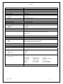
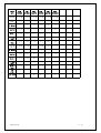
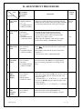
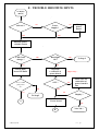
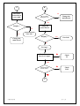
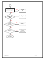
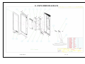
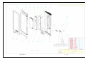
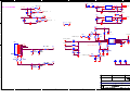
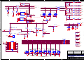
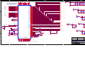
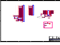
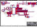
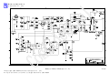
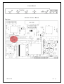
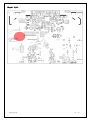
SP716
SP916
Service Manual
SP716/SP916
1 / 20
TABLE OF CONTENTS
WARNING--------------------------------------------------------------------------------------3
A. IMPORTANT SAFETY INSTRUCTION--------------------------------------3
B. SPECIFICATIONS ---------------------------------------------------------------------4
C. TIMING CHART------------------------------------------------------------------------6
D. ADJUSTMENT PROCEDURE-----------------------------------------------------8
E. TROUBLE SHOOTING HINTS---------------------------------------------------9
F. BLOCK DIAGRAM------------------------------------------------------------------- 13
G. EXPLODED DIAGRAM-------------------------------------------------------------14
H. SCHEMATIC DIAGRAM-----------------------------------------------------------16
I. PCB LAYOUT DIAGRAM----------------------------------------------------------17
SP716/SP916
2 / 20
WARNING
To prevent from fire or shock hazard,do not expose monitor to any rain or any form of water.High voltage is
inside the monitor so please do not remove the back cover of the cabinet if you are not a qualified monitor
engineer.Contact the local dealer or the nearest Proview branch office if you need help.
A. IMPORTANT SAFETY INSTRUCTION
Prior to using this service manual,please ensure that you have carefully followed all the procedures outlined in
the user's manual for this product.
1. Read all of these instructions.
2. Save these instructions.
3. Follow all warnings and instructions marked on the product.
4. Unplug this product from the wall outlet before cleaning.Do not use liquid cleaner or aerosol
cleaner, use a damp cloth for cleaning.
5. Do not use this product near water.
6. Do not place this product on an unstable cart,stand or table.The product may fall,causing serious
damage to the product.
7. Slots and openings in the cabinet and the back or bottom are provided for ventilation,to ensure
reliable operation of the product and to protect it from overheating.Those openings must not be
blocked or covered.The openings should never be blocked by placing the product on a bed,sofa, rug,
or other similar surface.This product should not be placed in a built-in installation,since proper
ventilation is provided.
8. This products should be operated with the type of power source indicated on the marked label.
If you are not sure of the type of power is available, consult with your dealer or local power company.
9. This product is equipped with a 3-wire grounding type plug,a plug having a third (grounding)
pin.This plug will only fit into a grounding-type power outlet.This is a safety feature.If you are
unable to insert the plug into the outlet,contact your electrician to replace your obsolete outlet.Do
not damage the purpose of the grounding-type plug.
10. Do not allow anything to rest on the power cord.Do not locate this product where persons will walk
on the cord.
11. Never push any kinds of objects into this product through cabinet slots as they may touch dangerous
voltage points or short out parts that could result in a risk of fire or electric shock.Never spill any kinds
of liquid on the product.
12. Do not attempt to service this product yourself,as opening or removing covers may expose you to
dangerous voltage points or other risk.Refer all servicing to service personnel.
13. Unplug this product from the wall outlet and refer servicing to qualified service personnel under the
following conditions.
a. When the power cord or plug is damaged or frayed.
b. If liquid has been spilled into the product.
c. If the product has been exposed to rain or water.
d. If the product does not operate normally,when the operating instructions are followed.Adjust
only those controls involved in the operating instructions ,since improper adjustment of
other controls may result in damage and will often require extra work by a qualified
technician to restore the product to normal operation.
e. If the product has been dropped or the cabinet has been damaged.
f. If the product exhibits a distinct change in performance,indicating a need for service.
SP716/SP916
3 / 20
B. SPECIFICATIONS
SP716
Panel General Specification
Screen Diagonal
Model Name
Active Display Area
Pixel Pitch
Number of Colors
View Angle
Horizontal
Vertical
Luminance of White
Contrast Ratio (Typical)
Maximum Resolution
Recommend Resolution
Synchronization Range
Horizontal
Vertical
Pixel Rate
User Control
OSD Function
Power Source
Power Consumption
Connection Type
Input Signal
Video
Sync.
Color Temperature
Dimension (WxHxD)
Monitor Weight
Base Operation
Tilt
Power Saving
ON
STAND BY
OFF
17” TFT
CMO M170E5-P01
337.92(H) × 270.34(V) mm
0.264(H) x 0.264(V) mm
16.2M colors
+/-70 degree
+/-60 degree Typical
250cd/m²(Min.)
450:1
1280 x 1024 @ 75Hz
1280 x 1024 @ 75Hz
30 – 80 KHz
60– 75 Hz
135 MHz
5 Key Switch
Auto, Brightness, Contrast, H-position, V-position, H-size,
Phase, Reset, Color selection (R, G, B, cool, warm), OSD ,
Language, Exit.
90 – 264 Vac 60 / 50 Hz
48 W (max.)
15 Pin D-Sub Type;
D-Sub: Analog R.G.B. , 0.7Vp-p / 75 Ohms
TTL level,positive or negative polarity
Cool / Warm / user mode
378.4x382x192 (mm)
3.8 kg
-5 / + 15 degree
< 48W
< 3W
< 3W
Signal Connector Pin Assignment
D-SUB Pin No.
1. Red Video
2.Green Video
3.Blue Video
4.GND
5.Self Test
Sound Output
SP716/SP916
6. Red Ground
7. Green Ground
8. Blue Ground
9. VGA +5V
10. Sync. GND
11. GND
12. SDA For DDC2B
13. H-sync.
14. V-sync-DDC1
15. SCL For DDC2B
No Audio
4 / 20
SP916
Panel General Specification
Panel Model
Screen Diagonal
Active Display Area
Pixel Pitch
Number of Colors
View Angle
Horizontal
Vertical
Luminance of White
Contrast Ratio (Typical)
Maximum Resolution
Recommend Resolution
Synchronization Range
Horizontal
Vertical
Pixel Rate
User Control
OSD Function
Power Source
Power Consumption
Connection Type
Input Signal
Video
Sync.
Color Temperature
Dimension (WxHxD)
Monitor Weight
Base Operation
Tilt
Power Saving
ON
STAND BY
OFF
Hannstar HSD190ME12-A00
19” TFT
376.32mm (H) x 301.056mm (V)
0.294(H) x 0.294(V) mm
16.2M colors
+/-70 degree
-60/+70 degree Typical
250cd/m²(Typical)
500:1
1280 x 1024 @ 75Hz
1280 x 1024 @ 75Hz
30 – 80 KHz
60– 75 Hz
135 MHz
5 Key Switch
Auto, Brightness, Contrast, H-position, V-position, H-size,
Phase, Reset, Color selection (R, G, B, cool, warm), OSD ,
Language, Exit.
90 – 264 Vac 60 / 50 Hz
50 W (max.)
15 Pin D-Sub Type;
D-Sub: Analog R.G.B. , 0.7Vp-p / 75 Ohms
TTL level,positive or negative polarity
Cool / Warm / user mode
426.4x 417x210 (mm)
4.6 kg
-5 / + 15 degree
< 50W
< 3W
< 3W
Signal Connector Pin Assignment
D-SUB Pin No.
1. Red Video
2.Green Video
3.Blue Video
4.GND
5.Self Test
Sound Output
SP716/SP916
6. Red Ground
7. Green Ground
8. Blue Ground
9. +5V from PC
10. Sync. GND
11. GND
12. SDA For DDC2B
13. H-sync.
14. V-sync-DDC1
15. SCL For DDC2B
No Audio
5 / 20
C . TIMING CHART
D
Video
B
E
Sync.
A
C
Preset
Modes
A: Period
B: Active
C: Sync Width
D: Back Porch
E: Front porch
VGA
640X400
VGA
640X480
VESA
640X480
Dot Rate
25.175MHz
25.175MHz
31.500MHz
F.H
31.469KHz
31.469KHz
37.861KHz
A-period
31.778us
31.778us
B-Active
25.422us
C-Syn
VGA
720X400
VESA
800X600
VESA
800X600
VESA
800X600
28.322MHz
36.000MHz
40.000MHz
50.000MHz
37.500KHz
31.469KHz
35.156KHz
37.879KHz
48.077KHz
26.413us
26.667us
31.777us
28.444us
26.400us
20.800us
25.422us
20.317us
20.317us
25.422us
22.222us
20.000us
16.000us
3.813us
3.813us
1.270us
2.032us
3.813us
2.000us
3.200us
2.400us
D-Back
Porch
1.907us
1.589us
3.810us
3.810us
1.907us
3.556us
2.200us
1.280us
E-Front
Porch
0.636us
0.954us
1.016us
0.508us
0.635us
0.666us
1us
1.12us
F . V
70.087Hz
59.941Hz
72.810Hz
75.000Hz
70.087Hz
56.250Hz
60.317Hz
72.188Hz
A-Period
14.268ms
16.683ms
13.734ms
13.333ms
14.268ms
17.778ms
16.579ms
13.853ms
B-Active
12.711ms
15.253ms
12.678ms
12.800ms
12.711ms
17.067ms
15.840ms
12.480ms
C-Syn
0.064ms
0.064ms
0.079ms
0.080ms
0.064ms
0.057ms
0.106ms
0.125ms
1.112ms
0.794ms
0.528ms
0.427ms
1.112ms
0.626ms
0.607ms
0.478ms
0.381ms
0.572ms
0.449ms
0.026ms
0.381ms
0.028ms
0.026ms
0.77ms
-
-
-
-
+
+
+
D-Back
Porch
E-Front
Porch
VESA
640X480
31.500MHz
H/V
SYNC
Interlaced
SP716/SP916
+
NON
-
NON
-
NON
-
NON
- +
NON
+
NON
+
NON
+
NON
6 / 20
Preset
Modes
VESA
800X600
VESA
1024X768
VESA
1024X768
VESA
VESA
VESA
1024X768 1280X1024 1280X1024
Dot Rate
49.500MHz 65.000MHz 75.000MHz 78.750MHz 108.00MHz 135.00MHz
F.H
46.875KHz 48.363KHz 56.476KHz 60.023KHz 63.98KHz 79.976KHz
A-period
21.333us
20.677us
17.707us
16.660us
15.630us
12.504us
B-Active
16.162us
15.754us
13.653us
13.003us
11.852us
9.481us
C-Syn
1.616us
2.092us
1.813us
1.219us
1.037us
1.067us
D-Back
Porch
3.232us
2.462us
1.920us
2.235us
2.296us
1.837us
E-Front
Porch
0.323us
0.369us
0.321us
0.203us
0.444us
0.119us
F . V
75.000Hz
60.004Hz
70.069Hz
75.029Hz
60.020Hz
75.025Hz
A-Period
13.333ms
16.666ms
14.272ms
13.328ms
16.661ms
13.329ms
B-Active
12.800ms
15.880ms
13.599ms
12.795ms
16.005ms
12.804ms
C-Syn
0.064ms
0.124ms
0.106ms
0.050ms
0.047ms
0.038ms
0.448ms
0.600ms
0.513ms
0.466ms
0.594ms
0.475ms
0.021ms
0.062ms
0.054ms
0.017ms
0.016ms
0.013ms
+
-
-
+
+
+
D-Back
Porch
E-Front
Porch
H/V
SYNC
Interlaced
+
NON
SP716/SP916
-
NON
-
NON
+
NON
+
NON
+
NON
7 / 20
D. ADJUSTMENT PROCEDURE
ITEM
Program Menu.
Power supply
Check
A
﹟Test Meter
﹡Test Point
﹫Pattern
﹟Digital Voltmeter
﹡CON 001
﹫Crosshatch Pattern
(1280x768, 60Hz)
Power Saving ﹟Wattmeter
Check
﹟PC or Pattern
generator
﹫Crosshatch Pattern
(1280x768, 60Hz)
B
Into Factory ﹟PC or Pattern
mode
generator
﹫Crosshatch Pattern
C
(1280x768, 60Hz)
Check
Value
Operation
220Vac
1. Plug power cable into the LCD monitor directly.
2. Make sure the voltage of the power plug (CON001) ±0.2V
on the Power Board to the value shown at right.
1. Unplug the signal cable into the monitor.
2. Turn the power switch of the monitor ON.
3. Check monitor power indicator light up blue
flashing every other second.
4. Make sure the wattmeter value shown at right.
5. OSD will be display “NO SIGNAL” Picture.
1. Hold Down key,then turn the power switch of the
monitor off.
2. Hold Up key,then turn the power switch of the
monitor on.
3. You can enter factory adjustment mode.
Auto mode
Check
﹟PC or Pattern
generator
﹫Crosshatch Pattern
(1280x768, 60Hz)
1.Press and release the Auto key to adjust display
mode to its utmost performance according to VGA
setting.
White
Balance
Adjust
﹟PC or Pattern
generator
﹫White Pattern
(1280x768, 60Hz)
1. Move the OSD to the COLOR mode (AUTO COLOR).
2. set color is Cool using the OSD,Check the value
shown at right.
Y = 200±20cd/m^2 x = 0.283±0.02 y = 0.297±0.02
3. set color is Warm using the OSD,Check the value
shown at right.
Y = 200±20cd/m^2 x = 0.313±0.02 y = 0.329±0.02
D
E
OSD
F Language
Setting
SP716/SP916
﹟PC or Pattern
generator
1. Move the OSD to the OSD setting mode
2. Move the OSD to the LANGUAGE mode.
3. You can choose one of the language you need.
8 / 20
‹ 3W
E . TROUBLE SHOOTING HINTS
No Display
( Black )
LED ON ?
NO
NO
Power
Supply ?
YES
Change
power
board
YES
Push the power
ON/OFF switch
LED Color
change ?
YES
Back light
ON?
NO
YES
To Step 2
NO
Check main
board U5/Pin24
Check the
CN1/Pin1,2 of
High Voltage !
power board
+12V ?
Hi / Lo under
push power
sw?
YES
YES
NO
NO
To Step 2
A
NO
Make sure the
connection of
power board is
fine
Display ?
Check
Power board
YES
B
SP716/SP916
Nice Job !
9 / 20
A
B
Check the
connection of
CON1 cable
NO
Change the
main board
Hi / Lo under
push power sw?
YES
Display ?
YES
NO
Change the
power board
Nice Job !
Display ?
YES
Change the
main board
Nice Job !
NO
To Step 2
Check the main
board 12V input?
NO
Check
F1
YES
NO
Check the main
board +5.0 V ?
Check
I1,I2
YES
C
SP716/SP916
10 / 20
C
Check the main
board 3.3V input ?
NO
Check
I2
YES
Check 2.5 V
Input
NO
Check
I1
YES
NO
Check
U3/Pin37,38
Check H/V
input Signal ?
YES
Display ?
NO
Change
Signal Cable
YES
Nice Job !
SP716/SP916
11 / 20
No display
(White)
Check the main
board 5V ?
NO
Check
I1,I2
NO
Check
I2
YES
+3.3V ?
YES
NO
Check
H/V Input
Signal ?
U3/Pin37,38
YES
Display ?
NO
Change
Signal Cable
YES
Nice Job !
SP716/SP916
12 / 20
F. BLOCK DIAGRAM
Right
Left
AUDIO IN(OPTION)
LCD Panel
R
G
G
B
B
Right
R
Left
A/D_BOARD
VGA IN
INTERFACE
SCL
SDA
CCFL
SDA
CONTROL BOARD
Power Board
5V
12V
CCFL
SDA
DATA&CLK&VCC
5V
Vsync
12V
Vsync
DATA&CLK&VCC
Bri control
Hsync
KEY
Right
Left
ON/OFF
Hsync
Bri control
KEY
ON/OFF
AUDIO OUT(OPTION)
220/110V
Left
SPEAKER
Right
SP716/SP916
13 / 20
G. EXPLODED DIAGRAM
SP716/SP916
14 / 20
SP716/SP916
15 / 20
H. SCHEMATIC DIAGRAM
SP716/SP916
16 / 20
5
4
3
2
1
D
D
TOP LEVEL
1. S1:THE FIRST VERSION OF THE COST DOWN MODEL,MSTAR SOLUTION
2.change note:audio schematic add D13﹜D2˙power schematic add R4˙C101 change TC5
C
C
3.DVI schmatic add R8,R12.power schmatic add R18.
B
B
APPROVE BY
CHECK
BY
PREPARE BY
李李李
A
A
200-100-M713I-E
Title
MSTAR COSTDWON(DVI_I PIGTAIL) LVDS&RSDS OUT
Size
Document Number
Custom
Date:
5
4
3
2
Rev
TOP LEVEL
Tuesday, June 28, 2005
Sheet
1
1
of
7
E
5
4
3
2
1
+5V
VCC2V5
D11
To Inverter
I1
33K VCC5V
R1
BL_CTRL
D12
C1
D4001
D4001
0.1uF
Changed in 2004.8.30
3
VIN
VOUT
2
1
ADJ
TAB
4
AIC1084-18CE
3
Q1
C3
0.1u
4.7K
BKLT_EN
C2
47uF/25V
0.1uF
4
6
D
VCC3V3_PANEL
2
D
1 R2
VCC2V5
TC1
R3
VCC3V3
MMBT3904
0
R39
R5
Q2
3
BRT_LEVEL
C5
1 R6
100K
BKLT_ADJ
0.1uF
4
MMBT3904
0R
I2
C4
2
1u
+5V
VCC5V
1K
Added by lotuschou 20041111
3
VIN
VOUT
2
1
ADJ
TAB
4
VCC3V3
TC2
AIC1084-33CM
+5V
L1
4,5,6
C6
47uF/25V
0.1uF
VCC5V
BEAD
+12V
R9
1
VCC3V3_PANEL
CN1
U1
FB1
1
TC4
220uF/25V
R13
22K
S3
1
+5V
+12V
8
7
6
5
C9
VLCD
0.1uF(NC)
C11
Si9933-SO8(9435)
R4
0.1uF
100
S4
2
2
MLB-201209-0220P-N2
C15
0.1uF
1
+ TC3
C0603
C12
R14
1K
C13
220uF/16V 0.1uF
R16
6
B
R15
0.1uF 100K(NC)
Q4
1
PANELVCC_EN
4K7
C14
F1
B
MMBT3904
0.1uF
1
1
1
2
1
1
FB3 1206
1
+12V
1
1
24V/5A
1
125V/5A
D1
D1
D2
D2
ADD R4 AND R18
1206
HEADER5X2
F1A
S1
G1
S2
G2
3
+
1
2
3
4
1
2
BL_CTRL
BRT_LEVEL
VLCD12V
Changed 2004.9.10
NP
2
10
9
8
7
6
5
4
3
2
1
VCC5V
R10
100
S2
2
0.1uF
C
R18
Q3
NP
2
NP
S1
2
R11
6 PANEL12V_EN
NP
3
C
C7
1
R7
NP
MLB-201209-0220P-N2
+
TC6
220uF/25V
C17
0.1uF
C0603
APPROVE BY
CHECK
BY
PREPARE BY
A
A
李李李
200-100-M713I-E
Title
MSTAR COSTDWON(DVI_I PIGTAIL) LVDS&RSDS OUT
Size
Document Number
Custom
Date:
5
4
3
2
Rev
POWER
Tuesday, June 28, 2005
Sheet
2
1
of
7
E
5
4
3
2
1
DDC5V
R20
10K
R19
SCL_D1
R26
SDA_D1
DDC_CLK
33
R27
DDC_CLK
DDC_DAT
33
R212
DDC_DAT
6
B
FB4
SBK160808T-300Y-S
G
FB5
SBK160808T-300Y-S
NC
SBK160808T-300Y-S
R32
C24
75_1%
NC
DDC5V
R21 10K
R8 NC
AT24C21
VCC
VCLK
SCL
SDA
2
C81
DCC5V
C82
0.1uF
0.1uF
R36
C30
75_1%
NC
VCC5V
DVI_5V
DDC_CLK
DDC_DAT
AT24C21
DDC5V
10K
R210
100
R12 NC
R30
47
C21
47nF
R31
20
C22
47nF
R33
470 C23
1000pF
R34
47
C25
47nF
R35
20
C26
47nF
R37
47
C31
47nF
D1
BAT54C
1
4
GNDB
4
GIN
4
SOG
4
GNDG
4
RIN
4
GNDR
4
2
DDC5V
DDC5V
C
C
DDC5V
HSYNC_IN
R213 100Ω
HPDET_D1
3.3K
R204
R207
2.2K
10K
R208 3.3K
33K
1
1
DDC_WP
R205
R
U_GND
L
3
2
1
10K
C
4
B-
4
G+
4
G-
4
R+
4
R-
4
CLK+
4
CLK-
4
G+
R223
B
100
GR214
10R
R215 10R
R216 10R
R217 10R
R218 10R
R219 10R
R220 10R
R221 10R
B+
BG+
GR+
RCLK+
CLK-
R224
100
RCLK+
R225
100
C70
0.1uF
C71
0.1uF
C72
0.1uF
C73
0.1uF
C74
0.1uF
D30
BAV99
3
3
3
D29
BAV99
APPROVE BY
C75
0.1uF
CHECK
BY
PREPARE BY
C76
0.1uF
李李李
1
2
VCC5V
1
VCC5V
2
1
2
VCC5V
1
1
3
3
VCC5V
VCC5V
D28
BAV99
1
2
D27
MMBD7000
2
VCC5V
D26
BAV99
1
VCC5V
D25
BAV99
2
D24
BAV99
2
D23
BAV99
VCC5V
3
CLK-
3
DATA2DATA2+
GND
DATA1DATA1+
GND
DATA0DATA0+
GND
CLKCLK+
GND
VSYNC_IN
HSYNC_IN
R+
DATA0+
DATA0DATA1+
DATA1DATA2+
DATA2CLK+
CLK-
2
A
PHD 2.0/90D
B+
B-
33K/NC
1
CN2
1
3
5
7
9
11
13
15
17
19
21
23
25
27
4
100
R209
2N3904
100K
3
2
4
6
8
HPDET_D1
10
SDA_D1 12
SCL_D1
14
GND
16
B
18
GND
20
G
22
GND
24
R
26
GND
28
VSYNC
2K2
B+
CN5
Rout
1 DVI_5V
R
1
L
U_GND
100
R222
E
Q202
B
E
6
2N3904
C
R203 10K
R22
4
R24
5.6V
VGA_DDC5V
VGA_DDC5V
Q203
B
R202
20u
R23
HSYNC
2N3906
C
C
R206
C83
100
Q204
B
DVI_DDC5V
5.6V
ESD
DVI_DDC5V
D4
D3
C84
20u
R17
E
E
R201
2N3906
B
33K/NC
VSYNC_IN
ST_DET1 6
D101
Q201
B
BIN
D
3
D9
BAV99
ADD R8 AND R12
8
7
6
5
47nF
3
NC
NC
NC
GND
DCC5V
0.1uF
DVI_DDC5V
U6
1
2
3
4
C80
DCC5V
DDC5V
100
D8
BAV99
2
D7
BAV99
3
8
7
6
5
VCC
VCLK
SCL
SDA
1
NC
NC
NC
GND
2
1
2
3
4
3
U2
6
6
D5
ESD
1
D6
ESD
DDC_CLK1
DDC_DAT1
FB6
VGA_DDC5V
33 33
C20
75_1%
C19
6
R
R211
R29
20
1
D
10K
R28
200-100-M713I-E
C77
0.1uF
Title
MSTAR COSTDWON(DVI_I PIGTAIL) LVDS&RSDS OUT
Size
Document Number
Custom
Date:
5
4
3
2
VGA IN(DVI_ PIGTAIL)
Tuesday, June 28, 2005
Sheet
1
Rev
3
of
7
E
A
5
4
C
R+
RG+
GB+
BCLK+
CLKR40
40
41
43
44
46
47
49
50
52
18
87
97
117
NC/BA2
NC/BA3
NC/BA4
NC/BA5
NC/BA6
NC/BA7
NC/GA2
NC/GA3
NC/GA4
NC/GA5
LVA3P/GA6
LVA3M/GA7
LVACKP/NC
LVACKM/NC
LVA2P/RA2
LVA2M/RA3
LVA1P/RA4
LVA1M/RA5
LVA0P/RA6
LVA0M/RA7
NC/BB2
NC/BB3
NC/BB4
NC/BB5
NC/BB6
NC/BB7
NC/GB2
NC/GB3
NC/GB4
NC/GB5
NC/GB6
NC/GB7
NC/RB2
NC/RB3
NC/RB4
NC/RB5
NC/RB6
NC/RB7
88
89
90
91
92
93
98
99
100
101
102
103
106
107
108
109
110
111
112
113
124
125
128
1
4
5
8
9
12
13
14
15
16
17
22
23
24
25
NC/GPO0
NC/GPO1
NC/GPO2
NC/GPO3
NC/GPO4
DDC1_DAT/GPO7
DDC1_CLK/GPO8
NC
NC/GPO9
NC/OCLK
NC/ECLK
83
82
81
80
79
28
29
118
119
120
121
R+
RG+
GB+
BCK+
CKREXT
0.1uF
6 HWRESET
6 INT
R42
10K
C48
10nF
7
2
R41
HWRESET
INT
BKLT_ADJ
VOLUME
REFP
67
REFM
HWRESETZ
INT
73
74
PWM0
PWM1
33
XIN
22pF
X1
14.318MHZ
BYPASS
AVSS_MPLL
OSP
ESP
76
75
BUS TYPE
AD0/GPO6
AD1
AD2
AD3/GPO5
RDZ / SCL
WRZ / SDA
ALE / CS
6
30
77
78
31
71
70
69
GNDP
GNDP
GNDP
GNDP
GNDP
GNDP
GNDP
10
20
85
95
105
115
127
AVSS
AVSS
AVSS
LVB2P
LVB2M
39
42
48
68
56
64
A
AVSS_PLL
3
2
AVSS_MPLL
0.1uF
XOUT
54
C56
34
36
22pF
AVSS
AVSS
AVSS
C52
LVACKP
LVACKM
5
5
RA2
RA3
RA4
RA5
5
5
5
5
RA6
RA7
GA2
GA3
5
5
5
5
GA4
GA5
GA6
GA7
5
5
5
5
BA2
BA3
BA4
BA5
5
5
5
5
BA6
BA7
RB2
RB3
5
5
5
5
RB4
RB5
RB6
RB7
5
5
5
5
GB2
GB3
GB4
GB5
5
5
5
5
GB6
GB7
BB2
BB3
5
5
5
5
BB4
BB5
BB6
BB7
5
5
5
5
47R
32
72
BKLT_ADJ
C49
66
1
VDD2V5
VDDC
VDDC
VDDC
VDDC
53
11
21
84
94
104
114
126
VDDP
VDDP
VDDP
VDDP
VDDP
VDDP
VDDP
35
45
51
AVDD
AVDD
VPO
390_1%
C45
B
RIN0
RIN0M
GIN0
GIN0M
SOGIN0
BIN0
BIN0M
HSYNC0
VSYNC0
2
VCC3V3
GNDC
GNDC
GNDC
GNDC
R+
RG+
GB+
BCLK+
CLK- VDVI
63
62
60
59
61
58
57
37
38
3
122
123
R43
LVB3P
R44
R45
R46
47
R51 52 62 63
CHANGE TO
RN16
5
47
47
ESP
47
VCC3V3
6
R47
6
10K
6
6 R25 47R
RDZ
R38 47R
WRZ
R48
C87 47R
ALE
47PF
5
AD0
AD1
AD2
AD3
C85
47PF
C86
47PF
POL
LOAD
STV1
CPV
OE
5
5
5
5
5
STV2
OCLK
ECLK
5
5
5
STH
5
VPO
FB7
PBY160808T-600Y-S
TC7
C32
C33
C34
C35
C36
C37
C38
10uF/16V
0.1uF
0.1uF
0.1uF
0.1uF
0.1uF
0.1uF
0.1uF
D
VDD2V5
VCC2V5
FB8
PBY160808T-600Y-S
VCC3V3
TC8
C39
C40
C41
C42
10uF/16V
0.1uF
0.1uF
0.1uF
0.1uF
TC9
C43
C44
10uF/16V
0.1uF
0.1uF
VAD
FB9
PBY160808T-600Y-S
VCC3V3
VCC3V3
VDPLL
FB11
C
VPLL
FB10
PBY160808T-600Y-S
PBY160808T-600Y-S
TC11
C47
10uF/16V
0.1uF
TC10
C46
10uF/16V
0.1uF
B
C50
C51
47P
47P
VCC3V3
VDVI
FB12
PBY160808T-600Y-S
TC12
C53
C54
10uF/16V
0.1uF
0.1uF
6
6
6
LVB2M LVB2P
5
5
APPROVE BY
CHECK
BY
PREPARE BY
A
19
86
96
116
3
3
3
3
3
3
3
3
RIN
GNDR
GIN
GNDG
SOG
BIN
GNDB
HSYNC
VSYNC
RIN
GNDR
GIN
GNDG
SOG
BIN
GNDB
HSYNC
VSYNC
VDPLL
AVDD_PLL
3
3
3
3
3
3
3
3
3
AVDD
AVDD
D
U3
AVDD_MPLL
MST TSU16AK/TSU56AK
55
65
VAD
VPLL
VDVI
李李李
200-100-M713I-E
Title
Pin 6:LOW- SERIAL BUS
Pin 6:HIGH- DIRECT BUS
MSTAR COSTDWON(DVI_I PIGTAIL) LVDS&RSDS OUT
Size
Document Number
Custom
Date:
5
4
3
2
Rev
MST SCALER
Sheet
Tuesday, June 28, 2005
1
4
of
7
E
5
4
3
2
CN3
D
4
4
BA7
BA6
4
4
BA5
BA4
4
4
BA3
BA2
4
4
GA7
GA6
4
4
GA5
GA4
4
4
GA3
GA2
4
4
STH
4
ESP
C
STV2
4
LVB3P
4
4
RA7
RA6
4
4
RA5
RA4
4
4
RA3
RA2
BA7
BA6
FB0N
FB0P
BA5
BA4
FB1N
FB1P
BA3
BA2
FB2N
FB2P
GA7
GA6
FG0N
FG0P
GA5
GA4
FG1N
FG1P
GA3
GA2
FG2N
FG2P
STV2-A
DHS_TTL
FCLKN
FCLKP
RA7
RA6
FR0N
FR0P
RA5
RA4
FR1N
FR1P
RA3
RA2
FR2N
FR2P
LOAD-A
POL-A
STH
LP
POL
HMS
STH-A
4
4
ESP
C60
4
4
4
LOAD
POL
C61
CPV-A
STV1-A
OE-A
CPV
STV1
OE
CLKV
STV
OE
10pF(NC) 10pF(NC)
VLCD
VLCD12V
R51
R52
R53
R54
R55
R56
R57
0(NC)
0(NC)
0(NC)
0(NC)
0(NC)
0(NC)
0(NC)
1
2
3
4
5
6
7
8
9
10
11
12
13
14
15
16
17
18
19
20
21
22
23
24
25
26
27
28
29
30
31
32
33
34
35
36
37
38
39
40
41
42
43
44
45
46
47
48
49
50
1
CN4
4
4
BB7
BB6
4
4
BB5
BB4
4
4
BB3
BB2
4
4
GB7
GB6
4
4
GB5
GB4
4
4
GB3
GB2
4
4
ECLK
OCLK
4
4
RB7
RB6
4
4
RB5
RB4
4
4
RB3
RB2
BB7
BB6
B0N
B0P
BB5
BB4
B1N
B1P
BB3
BB2
B2N
B2P
GB7
GB6
BG0N
BG0P
GB5
GB4
BG1N
BG1P
GB3
GB2
BG2N
BG2P
1
2
3
4
5
6
7
8
9
10
11
12
13
14
15
16
17
18
19
20
21
22
23
24
25
26
27
28
29
30
DEN_TTL BCLKN
DCLK_TTL BCLKP
RB7
RB6
BR0N
BR0P
RB5
RB4
BR1N
BR1P
RB3
RB2
BR2N
BR2P
D
JP1
4
4
RB4
RB2
LVB2P
OCLK
LVB3P
BA6
BA4
BA2
LVACKP
GA6
VCC_TEST
LVB2P
VLCD
LVACKP
RXO0+
RXO1+
RXO2+
RXOC+
RXO3+
RXE0+
RXE1+
RXE2+
RXEC+
RXE3+
C59
0.1uF
1
3
5
7
9
11
13
15
17
19
21
23
25
RB5
RB3
LVB2M
ECLK
STV2
BA7
BA5
BA3
LVACKM
GA7
2
4
6
8
10
12
14
16
18
20
22
24
26
RXO0RXO1RXO2RXOCRXO3RXE0RXE1RXE2RXECRXE3-
LVB2M
4
LVACKM
4
HEADER 12X2
NC
C
FOR RSDS INTERFACE
6
3/31 modify
MCU_OD_EN
MCU_OD_EN
DHS_TTL
LVB3P
4
(NC)6702-50-50P-R
VCC3V3
FOR RSDS INTERFACE
VCC3V3
VCC3V3
2,4,6
R49
10K (NC)
VCC_TEST
FOR 19" FSC PANEL
B
B
R50
0(NC)
A
A
APPROVE BY
CHECK
BY
PREPARE BY
李李李
200-100-M713I-E
Title
MSTAR COSTDWON(DVI_I PIGTAIL) LVDS&RSDS OUT
Size
Document Number
Custom
Date:
5
4
3
2
PANEL INTERFACE
Sheet
Tuesday, June 28, 2005
1
Rev
5
of
7
E
5
4
MCU
3
2
VCC5V
MCU
R64 R65
R62
C64
VCC5V
R67
R68
SCL1
SDA1
10K
1
MCU
VCC3V3
1K 1
LEDG R70
1K
Q6
MMBT3904
Q7
MMBT3904
1
MCU
MCU
S10
2
R69
LEDO
3
100
100
3
10K 10K
R66
POWER
LED_O
LED_G
DOWN
UP
MENU
AUTO
1
R72
C65
CON1
1
8
2
7
3
6
22
RN11
4
5
1
8
2
7
3
6
4
5
1
2
3
4
5
6
7
8
D
2
24C16
S9
2
VCC
WP
SCL
SDA
RN10 22
330
MCU
2
D
A0
A1
A2
GND
8
7
6
5
4
3
2
1
4
3
2
1
1
2
3
4
R63
330
U4
.1u
1
VCC5V
RN12
RN13
10K
10K
D35
ESD
D34
D33 ESD
D32
ESD
D31
ESD
ESD
to KEY PAD
.1u
XTAL1
20
XTAL2
10
RESET
10u/16V
C68
22pF
C
D10
8.2K
1N41484
14
15
16
17
INT
SCL1
SDA1
2
3
4
5
6
7
8
9
2 PANEL12V_EN
2 PANELVCC_EN
3/31 modify 5 MCU_OD_EN
2
BKLT_EN
7
MUTE
3
DDC_WP
3
DDC_CLK1
3
DDC_DAT1
INT0/P3.2
INT1/P3.3
T0/P3.4
T1/P3.5
P1.0
P1.1
P1.2
P1.3
P1.4
P1.5
P1.6
P1.7
10K
5
6
7
8
MCU
P2.0
P2.1
P2.2
P2.3
P2.4
P2.5
P2.6
P2.7
NC
P3.7/RD
P3.6/WR
PSEN
ALE/P
P3.1/TXD
P3.0/RXD
24
25
26
27
28
29
30
31
12
19
18
32
33
13
11
HWRESET
ALE
RDZ
WRZ
AD0
AD1
AD2
AD3
4
4
4
4
4
4
4
4
C8
20050428
0.1uF
C
POWER
DOWN
UP
MENU
AUTO
LEDO
ST_DET1
RN14
LEDG
10K
4
RN15
10K
MCU
4
3
2
1
RN6
DDC_DAT
DDC_CLK
3
3
VCC5V
10K
5
6
7
8
RN5
4
3
2
1
8051-PLCC
VSS
.1u(NC)
R74
43
42
41
40
39
38
37
36
22
C69
P0.0
P0.1
P0.2
P0.3
P0.4
P0.5
P0.6
P0.7
4
3
2
1
EA/VP
21
5
6
7
8
35
4
3
2
1
Y1
5
6
7
8
11.0592MHZ
TC14
44
U5
VCC
MCU
22pF
5
6
7
8
5
6
7
8
10K
C66
MCU
CON2
B
1
2
3
4
B
RS232 debug
NC
APPROVE BY
CHECK
BY
PREPARE BY
A
A
李李李
200-100-M713I-E
Title
MSTAR COSTDWON(DVI_I PIGTAIL) LVDS&RSDS OUT
Size
Custom
Date:
5
4
3
2
Document Number
MCU(SYNC&MYSON 512&MX)
Tuesday, June 28, 2005
6
Sheet
1
of
Rev
7
E
聯昌電子企業股份有限公司
LC Electronic Co., Ltd.
MODEL:AI-0088FAI-0088AF(Spec No.:01)
*Copy-right LIEN CHANG Electronic Enterprise Co., Ltd.
No copy & disclosure is Allowed. All Right Reserved by LIEN CHANG.
29/239
3
1
4
4
2
2
3
1
聯昌電子企業股份有限公司
LC Electronic Co., Ltd.
7
1
1
2
2
8
8
4
4
6
7
6
3 3
5
5
MODEL:AI-0088FAI-0088AF(Spec No.:01)
*Copy-right LIEN CHANG Electronic Enterprise Co., Ltd.
No copy & disclosure is Allowed. All Right Reserved by LIEN CHANG.
30/239
I. PCB LAYOUT DIAGRAM
Main Board
SP716/SP916
17 / 20
Control Board
Inverter + Power Board
Top layer
SP716/SP916
18 / 20
Bottom layer
SP716/SP916
19 / 20
MEMO
SP716/SP916
20 / 20