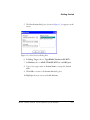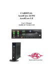
1
ADSP-TS201S EZ-KIT Lite®
Evaluation System Manual
Revision 1.0, March 2004
Part Number
82-000770-01
Analog Devices, Inc.
One Technology Way
Norwood, Mass. 02062-9106
a
Copyright Information
© 2004 Analog Devices, Inc., ALL RIGHTS RESERVED. This document may not be reproduced in any form without prior, express written
consent from Analog Devices, Inc.
Printed in the USA.
Limited Warranty
The EZ-KIT Lite evaluation system is warranted against defects in materials and workmanship for a period of one year from the date of purchase
from Analog Devices or from an authorized dealer.
Disclaimer
Analog Devices, Inc. reserves the right to change this product without
prior notice. Information furnished by Analog Devices is believed to be
accurate and reliable. However, no responsibility is assumed by Analog
Devices for its use; nor for any infringement of patents or other rights of
third parties which may result from its use. No license is granted by implication or otherwise under the patent rights of Analog Devices, Inc.
Trademark and Service Mark Notice
The Analog Devices logo, TigerSHARC, TigerSHARC logo, VisualDSP++, the VisualDSP++ logo, CROSSCORE, the CROSSCORE logo,
and EZ-KIT Lite are registered trademarks of Analog Devices, Inc.
All other brand and product names are trademarks or service marks of
their respective owners.
Regulatory Compliance
The ADSP-TS201S EZ-KIT Lite evaluation system has been certified to
comply with the essential requirements of the European EMC directive
89/336/EEC (inclusive 93/68/EEC) and, therefore, carries the “CE”
mark.
The ADSP-TS201S EZ-KIT Lite evaluation system had been appended to
the Technical Construction File referenced “DSPTOOLS1” dated
December 21, 1997 and was awarded CE Certification by an appointed
European Competent Body as listed below.
Technical Certificate No: Z600ANA1.019
Issued by:
Technology International (Europe) Limited
41 Shrivenham Hundred Business Park
Shrivenham, Swindon, SN6 8TZ, UK
The EZ-KIT Lite evaluation system contains ESD
(electrostatic discharge) sensitive devices. Electrostatic charges readily accumulate on the human
body and equipment and can discharge without
detection. Permanent damage may occur on devices
subjected to high-energy discharges. Proper ESD
precautions are recommended to avoid performance
degradation or loss of functionality. Store unused
EZ-KIT Lite boards in the protective shipping
package.
iv
ADSP-TS201S EZ-KIT Lite Evaluation System Manual
CONTENTS
PREFACE
Purpose of This Manual .................................................................. xi
Intended Audience ......................................................................... xii
Manual Contents .......................................................................... xiii
What’s New in This Manual .......................................................... xiii
Technical or Customer Support ...................................................... xiv
Supported Processors ...................................................................... xiv
Product Information ....................................................................... xv
MyAnalog.com .......................................................................... xv
Embedded Processor Product Information .................................. xv
Related Documents .................................................................. xvi
Online Documentation ........................................................... xvii
Printed Manuals ..................................................................... xviii
VisualDSP++ Documentation Set ....................................... xviii
Hardware Manuals ............................................................. xviii
Data Sheets ........................................................................ xviii
Contacting DSP Publications .................................................... xix
Notation Conventions .................................................................... xix
ADSP-TS201S EZ-KIT Lite Evaluation System Manual
v
CONTENTS
GETTING STARTED
Contents of EZ-KIT Lite Package ................................................. 1-1
PC Configuration ......................................................................... 1-3
Installation Tasks .......................................................................... 1-3
Installing VisualDSP++ and EZ-KIT Lite Software .................. 1-4
Installing and Registering VisualDSP++ and EZ-KIT Lite License 1-5
Setting Up EZ-KIT Lite Hardware .......................................... 1-5
Installing EZ-KIT Lite USB Driver ......................................... 1-7
Windows 98 USB Driver .................................................... 1-8
Windows 2000 USB Driver .............................................. 1-12
Windows XP USB Driver ................................................. 1-13
Verifying Driver Installation .................................................. 1-15
Starting VisualDSP++ ........................................................... 1-16
USING EZ-KIT LITE
EZ-KIT Lite License Restrictions .................................................. 2-2
Memory Map ............................................................................... 2-2
Using SDRAM Interface ............................................................... 2-4
Using Flash Memory ..................................................................... 2-4
Using Programmable FLAG Pins ................................................... 2-5
Using Interrupt Pins ..................................................................... 2-6
Using Audio Interface ................................................................... 2-7
Using Processor Link Ports ............................................................ 2-8
Example Programs ........................................................................ 2-9
vi
ADSP-TS201S EZ-KIT Lite Evaluation System Manual
CONTENTS
Using Flash Programmer Utility .................................................... 2-9
EZ-KIT LITE HARDWARE REFERENCE
System Architecture ...................................................................... 3-2
External Port ........................................................................... 3-3
Expansion Interface ................................................................. 3-3
JTAG Emulation Port .............................................................. 3-4
Switch Settings .............................................................................. 3-5
Audio Amplification Selection (SW1) ...................................... 3-6
Processor Mode Selections (SW2) ............................................ 3-6
Processor Boot Strap Settings .............................................. 3-7
SYSCON/SDRCON Mode Settings .................................... 3-7
Interrupt Enable Settings .................................................... 3-8
Link Port Width Settings .................................................... 3-8
FLAGs and IRQs Switch Settings (SW10) ................................ 3-9
Configuration Resistors ............................................................... 3-10
Processor ID Settings ............................................................. 3-10
Clock Mode Settings ............................................................. 3-12
Control Impedance Selection ................................................. 3-14
Drive Strength Selection ........................................................ 3-15
LEDs and Push Buttons .............................................................. 3-16
Power LED (LED1) ............................................................... 3-16
Reset LEDs (LED2 and LED8) .............................................. 3-17
FLAG LEDs (LED3–6) ......................................................... 3-17
USB Monitor LED (LED9) ................................................... 3-17
ADSP-TS201S EZ-KIT Lite Evaluation System Manual
vii
CONTENTS
Programmable FLAG Push Buttons (SW6–9) ........................ 3-18
Interrupt Push Buttons (SW4 and SW5) ................................ 3-18
Reset Push Button (SW3) ...................................................... 3-19
Connectors ................................................................................. 3-19
Audio (P1–2) ........................................................................ 3-20
Power (P3) ............................................................................ 3-20
JTAG (P4) ............................................................................ 3-21
USB (P5) .............................................................................. 3-21
Expansion Interface (J1–3) .................................................... 3-21
Link Ports (J4–7) .................................................................. 3-22
Specifications ............................................................................. 3-22
Power Supply ........................................................................ 3-22
BILL OF MATERIALS
INDEX
viii
ADSP-TS201S EZ-KIT Lite Evaluation System Manual
PREFACE
Thank you for purchasing the ADSP-TS201S EZ-KIT Lite®, Analog
Devices (ADI) evaluation system for TigerSHARC® floating-point
embedded processors.
The TigerSHARC processor is a Static Super Scalar (SSS) architecture targeted at software-defined radio applications. In these wireless
infrastructure applications, the TigerSHARC processor is replacing
field-programmable gate arrays (FPGAs) in the Chip Rate processing
applications for third generation cellular. The performance, flexibility,
multiprocessing and IO capabilities of the TigerSHARC processor makes
it superior to FPGA implementations.
The evaluation board is designed to be used in conjunction with the VisualDSP++® development environment to test the capabilities of the
ADSP-TS201S TigerSHARC processor. The VisualDSP++ development
environment gives you the ability to perform advanced application code
development and debug, such as:
• Create, compile, assemble, and link application programs written
in C++, C, and ADSP-TS201S assembly
• Load, run, step-in, step-out, step-over, halt, and set breakpoints in
application program
• Read and write data and program memory
• Read and write core and peripheral registers
• Plot memory
ADSP-TS201S EZ-KIT Lite Evaluation System Manual
ix
Access to the ADSP-TS201S processor from a personal computer (PC) is
achieved through a USB port or an optional JTAG emulator. The USB
interface gives unrestricted access to the ADSP-TS201S processor and the
evaluation board peripherals. Analog Devices JTAG emulators offer faster
communication between the host PC and target hardware. Analog Devices
carries a wide range of in-circuit emulation products. To learn more about
Analog Devices emulators and processor development tools, go to
http://www.analog.com/processors/tools/.
The ADSP-TS201S EZ-KIT Lite provides example programs to demonstrate the capabilities of the evaluation board.
VisualDSP++ license provided with this EZ-KIT Lite evaluaL The
tion system limits the size of a user program’s code to 128K words.
The board features:
• Two Analog Devices ADSP-TS201S processors
D
D
500 MHz Core Clock Speed
Configurable Core Clock Mode
• Analog Devices AD1871 96 kHz Analog-to-Digital Converter
D
Line-In 3.5 mm Stereo Jack
• Analog Devices AD1854 96 kHz Digital-to-Analog Converter
D
Line-Out 3.5 mm Stereo Jack
• SDRAM Memory
D
32 MB (4 Meg x 64)
• Flash Memory
D
512K Main Flash Memory
• USB Debugging Interface
x
ADSP-TS201S EZ-KIT Lite Evaluation System Manual
Preface
• Interface Connectors
D
D
D
14-Pin Emulator Connector for JTAG Interface
LVDS Link Ports via RJ-45 Connectors
Expansion Interface Connectors (not populated)
• General-Purpose IO
D
D
D
4 Push Button FLAGS (two for each processor)
2 Push Button Interrupts (one for each processor)
4 LED FLAG Outputs (two for each processor)
• Analog Devices ADP3331, ADP3336, and ADP3339 for Voltage
Regulation
The EZ-KIT Lite board contains two external memories: Flash memory
and SDRAM. The Flash memory can be used to store user-specific boot
code. By configuring the boot mode switch (SW2) and programming the
Flash memory, the board can run as a stand-alone unit. The SDRAM is
shared by both processors and can be used to store data external to the
processors. For more information, see “Memory Map” on page 2-2.
The EZ-KIT Lite board contains an audio interface, facilitating creation
of audio signal processing applications.
Additionally, the EZ-KIT Lite board provides expansion connectors,
allowing you to connect to the processor’s external port (EP).
Purpose of This Manual
The ADSP-TS201S EZ-KIT Lite Evaluation System Manual provides
instructions for using the hardware and installing the software on your
PC. The manual provides guidelines for running your own code on the
ADSP-TS201S EZ-KIT Lite. This manual also describes the operation
ADSP-TS201S EZ-KIT Lite Evaluation System Manual
xi
Intended Audience
and configuration of the components on the evaluation board. Finally, a
schematic and a bill of materials are provided as a reference for future
ADSP-TS201S board designs.
Intended Audience
This manual is a user’s guide and reference to the ADSP-TS201S EZ-KIT
Lite evaluation system. Programmers who are familiar with the Analog
Devices TigerSHARC processor architecture, operation, and programming are the primary audience for this manual.
Programmers who are unfamiliar with Analog Devices TigerSHARC processors can use this manual in conjunction with the ADSP-TS201
TigerSHARC Processor Hardware Reference and the ADSP-TS201 TigerSHARC Processor Programming Reference, which describe the processor
architecture and instruction set. Programmers who are unfamiliar with
VisualDSP++ should refer to the VisualDSP++ online Help and the VisualDSP++ user’s or getting started guides. For the locations of these
documents, refer to “Related Documents”.
xii
ADSP-TS201S EZ-KIT Lite Evaluation System Manual
Preface
Manual Contents
The manual consists of:
• Chapter 1, “Getting Started” on page 1-1
Provides software and hardware installation procedures, PC system
requirements, and basic board information.
• Chapter 2, “Using EZ-KIT Lite” on page 2-1
Provides information on the EZ-KIT Lite from a programmer’s
perspective and outlines the board’s memory map.
• Chapter 3, “EZ-KIT Lite Hardware Reference” on page 3-1
Provides information on the hardware aspects of the EZ-KIT Lite.
• Appendix A, “Bill Of Materials” on page A-1
Provides a list of components used to manufacture the EZ-KIT
Lite board.
• Appendix B, “Schematics” on page B-1
Provides the resources to allow making modifications to the
EZ-KIT Lite or to use as a reference design.
This appendix is not part of the online Help. The online Help
viewers should go the PDF version of the ADSP-TS201S EZ-KIT
Lite Evaluation System Manual located in the Docs\EZ-KIT Lite
Manuals folder on the installation CD to see the schematics.
What’s New in This Manual
This is the first edition of the ADSP-TS201S EZ-KIT Lite Evaluation System Manual. The manual documents the hardware tools support for
ADSP-TS201S TigerSHARC processors.
ADSP-TS201S EZ-KIT Lite Evaluation System Manual
xiii
Technical or Customer Support
Technical or Customer Support
You can reach DSP Tools Support in the following ways.
• Visit the DSP Development Tools website at
www.analog.com/technology/dsp/developmentTools/index.html
• Email questions to
[email protected]
• Phone questions to 1-800-ANALOGD
• Contact your ADI local sales office or authorized distributor
• Send questions by mail to
Analog Devices, Inc.
DSP Division
One Technology Way
P.O. Box 9106
Norwood, MA 02062-9106
USA
Supported Processors
The ADSP-TS201S EZ-KIT Lite evaluation system supports
ADSP-TS201S TigerSHARC Analog Devices embedded processors.
xiv
ADSP-TS201S EZ-KIT Lite Evaluation System Manual
Preface
Product Information
You can obtain product information from the Analog Devices website,
from the product CD-ROM, or from the printed publications (manuals).
Analog Devices is online at www.analog.com. Our website provides information about a broad range of products—analog integrated circuits,
amplifiers, converters, and embedded processors.
MyAnalog.com
MyAnalog.com is a free feature of the Analog Devices website that allows
customization of a webpage to display only the latest information on
products you are interested in. You can also choose to receive weekly email
notification containing updates to the webpages that meet your interests.
MyAnalog.com provides access to books, application notes, data sheets,
code examples, and more.
Registration:
Visit www.myanalog.com to sign up. Click Register to use MyAnalog.com.
Registration takes about five minutes and serves as means for you to select
the information you want to receive.
If you are already a registered user, just log on. Your user name is your
email address.
Embedded Processor Product Information
For information on embedded processors, visit our website at
www.analog.com/processors, which provides access to technical publications, data sheets, application notes, product overviews, and product
announcements.
ADSP-TS201S EZ-KIT Lite Evaluation System Manual
xv
Product Information
You may also obtain additional information about Analog Devices and its
products in any of the following ways.
• Email questions or requests for information to
[email protected]
• Fax questions or requests for information to 1-781-461-3010
(North America) or +49 (0) 89 76903-157 (Europe)
Related Documents
For information on product related development software, see the following publications.
Table 1. Related Processor Publications
Title
Description
ADSP-TS201S Embedded Processor Datasheet
General functional description, pinout, and
timing
ADSP-TS201 TigerSHARC Processor Hardware
Reference
Description of internal processor architecture
and all register functions
ADSP-TS201 TigerSHARC Processor Programming Reference
Description of all allowed processor assembly
instructions
Table 2. Related VisualDSP++ Publications
Title
Description
VisualDSP++ 3.5 User’s Guide for 32-Bit Proces- Detailed description of VisualDSP++ 3.5 feasors
tures and usage
xvi
VisualDSP++ 3.5 Assembler and Preprocessor
Manual for TigerSHARC Processors
Description of the assembler function and
commands for TigerSHARC processors
VisualDSP++ 3.5 C/C++ Complier and Library
Manual for TigerSHARC Processors
Description of the complier function and commands for TigerSHARC processors
ADSP-TS201S EZ-KIT Lite Evaluation System Manual
Preface
Table 2. Related VisualDSP++ Publications (Cont’d)
Title
Description
VisualDSP++ 3.5 Linker and Utilities Manual
for 32-Bit Processors
Description of the linker function and commands for the 32-bit processors
VisualDSP++ 3.5 Loader Manual for 32-Bit
Processors
Description of the loader function and commands for the 32-bit processors
The listed documents can be found through online Help or in the Docs
folder of your VisualDSP++ installation. Most documents are available in
printed form.
you plan to use the EZ-KIT Lite board in conjunction with a
L IfJTAG
emulator, refer to the documentation that accompanies the
emulator.
Online Documentation
Your software installation kit includes online Help as part of the Windows® interface. These help files provide information about VisualDSP++
and the ADSP-TS201S EZ-KIT Lite evaluation system.
To view VisualDSP++ Help, click on the Help menu item or go to the
Windows task bar, and select Start–>Programs–>Analog Devices–>VisualDSP++ 3.5 for 32-bit Processors–>VisualDSP++ Documentation.
To view ADSP-TS201S EZ-KIT Lite Help, which now is part of the VisualDSP++ Help system, go to the Contents tab of the Help window and
select Manuals–>ADSP-TS201S EZ-KIT Lite.
For more documentation, please go to
http://www.analog.com/processors/resources/technicalLibrary/.
ADSP-TS201S EZ-KIT Lite Evaluation System Manual
xvii
Product Information
Printed Manuals
For general questions regarding literature ordering, call the Literature
Center at 1-800-ANALOGD (1-800-262-5643) and follow the prompts.
VisualDSP++ Documentation Set
Printed copies of VisualDSP++ manuals may be purchased through Analog Devices Customer Service at 1-781-329-4700; ask for a Customer
Service representative. The manuals can be purchased only as a kit. For
additional information, call 1-603-883-2430.
If you do not have an account with Analog Devices, you will be referred to
Analog Devices distributors. To get information on our distributors, log
onto www.analog.com/salesdir/continent.asp.
Hardware Manuals
Printed copies of hardware reference and instruction set reference manuals
can be ordered through the Literature Center or downloaded from the
Analog Devices website. The phone number is 1-800-ANALOGD
(1-800-262-5643). The manuals can be ordered by a title or by product
number located on the back cover of each manual.
Data Sheets
All data sheets can be downloaded from the Analog Devices website. As a
general rule, printed copies of data sheets with a letter suffix (L, M, N, S)
can be obtained from the Literature Center at 1-800-ANALOGD
(1-800-262-5643) or downloaded from the website. Data sheets without
the suffix can be downloaded from the website only—no hard copies are
available. You can ask for the data sheet by part name or by product
number.
xviii
ADSP-TS201S EZ-KIT Lite Evaluation System Manual
Preface
If you want to have a data sheet faxed to you, the phone number for that
service is 1-800-446-6212. Follow the prompts and a list of data sheet
code numbers will be faxed to you. Call the Literature Center first to find
out if requested data sheets are available.
Contacting DSP Publications
Please send your comments and recommendations on how to improve our
manuals and online Help. You can contact us by emailing
[email protected].
Notation Conventions
The following table identifies and describes text conventions used in this
manual.
conventions, which apply only to specific chapters, may
L Additional
appear throughout this document.
Example
Description
Close command
(File menu) or OK
Text in bold style indicates the location of an item within the
VisualDSP++ environment’s and boards’ menu system and user interface
items.
{this | that}
Alternative required items in syntax descriptions appear within curly
brackets separated by vertical bars; read the example as this or that.
[this | that]
Optional items in syntax descriptions appear within brackets and separated by vertical bars; read the example as an optional this or that.
[this,…]
Optional item lists in syntax descriptions appear within brackets delimited by commas and terminated with an ellipsis; read the example as an
optional comma-separated list of this.
PF9–0
Registers, connectors, pins, commands, directives, keywords, code examples, and feature names are in text with letter gothic font.
filename
Non-keyword placeholders appear in text with italic style format.
ADSP-TS201S EZ-KIT Lite Evaluation System Manual
xix
Notation Conventions
Example
[
xx
Description
Note:
A note providing information of special interest or identifying a
related topic. In the online version of this book, the word Note appears
instead of the symbol.
Caution:
A caution providing information about critical design or programming
issues that influence operation of a product. In the online version of this
book, the word Caution appears instead of the symbol.
ADSP-TS201S EZ-KIT Lite Evaluation System Manual
1 GETTING STARTED
This chapter provides information you need to begin using
ADSP-TS201S EZ-KIT Lite evaluation system. For correct operation,
install the software and hardware in the order presented in “Installation
Tasks” on page 1-3.
The chapter includes the following sections.
• “Contents of EZ-KIT Lite Package” on page 1-1
Provides a list of the components shipped with the EZ-KIT Lite
evaluation system.
• “PC Configuration” on page 1-3
Describes the minimum requirements for the PC to work with the
EZ-KIT Lite evaluation system.
• “Installation Tasks” on page 1-3
Provides the step-by-step procedures for setting up the EZ-KIT
Lite hardware and software.
Contents of EZ-KIT Lite Package
Your ADSP-TS201S EZ-KIT Lite package contains the following items.
• ADSP-TS201S EZ-KIT Lite board
• EZ-KIT Lite Quick Start Guide
• VisualDSP++ 3.5 Installation Quick Reference Card
ADSP-TS201S EZ-KIT Lite Evaluation System Manual
1-1
Contents of EZ-KIT Lite Package
• ADSP-TS201S EZ-KIT Lite Evaluation System Manual (this
document)
• CD containing:
D
VisualDSP++ 3.5 for 32-bit processors with a limited
license
D
ADSP-TS201 EZ-KIT Lite debug software
D
USB driver files
D
Example programs
• Universal 7.5V DC power supply
• USB 2.0 type cable
• Registration card (please fill out and return)
If any item is missing, contact the vendor where you purchased your
EZ-KIT Lite or contact Analog Devices, Inc.
The EZ-KIT Lite evaluation system contains ESD
(electrostatic discharge) sensitive devices. Electrostatic charges readily accumulate on the human
body and equipment and can discharge without
detection. Permanent damage may occur on devices
subjected to high-energy discharges. Proper ESD
precautions are recommended to avoid performance
degradation or loss of functionality. Store unused
EZ-KIT Lite boards in the protective shipping
package.
1-2
ADSP-TS201S EZ-KIT Lite Evaluation System Manual
Getting Started
PC Configuration
For correct operation of the VisualDSP++ software and the EZ-KIT Lite,
your computer must have the minimum configuration:
Windows 98, Windows 2000, or Windows XP
Intel (or comparable) 166 MHz processor
VGA Monitor and color video card
2-button mouse
50 MB free on hard drive
32 MB RAM
Full-speed USB port
CD-ROM Drive
Lite does not run under Windows 95 or Windows NT
[ EZ-KIT
unless using a JTAG emulator.
Installation Tasks
The following task list is provided for the safe and effective installation of
the ADSP-TS201S EZ-KIT Lite. Follow these instructions in the presented order to ensure correct operation of your software and hardware.
1. VisualDSP++ and EZ-KIT Lite software installation
2. VisualDSP++ and EZ-KIT license installation and registration
3. EZ-KIT Lite hardware setup
4. EZ-KIT Lite USB driver installation
ADSP-TS201S EZ-KIT Lite Evaluation System Manual
1-3
Installation Tasks
5. USB driver installation verification
6. VisualDSP++ startup
Installing VisualDSP++ and EZ-KIT Lite Software
This EZ-KIT Lite comes with the latest version of VisualDSP++ 3.5 for
32-bit processors. VisualDSP++ installation includes EZ-KIT Lite
installations.
To install VisualDSP++ and EZ-KIT Lite software:
1. Insert the VisualDSP++ installation CD into the CD-ROM drive.
2. If Autoplay is enabled on your PC, you see the Install Shield Wizard Welcome screen. Otherwise, choose Run from the Start menu,
and enter D:\ADI_Setup.exe in the Open field, where D is the name
of your local CD-ROM drive.
3. Follow the on-screen instructions to continue installing the
software.
4. At the Custom Setup screen, select your EZ-KIT Lite from the list
of available systems and choose the installation directory.
Click an icon in the Feature Description field to see the selected
system’s description. When you have finished, click Next.
5. At the Ready to Install screen, click Back to change your install
options, click Install to install the software, or click Cancel to exit
the install.
6. When the EZ-KIT Lite installs, the Wizard Completed screen
appears. Click Finish.
1-4
ADSP-TS201S EZ-KIT Lite Evaluation System Manual
Getting Started
Installing and Registering VisualDSP++ and EZ-KIT
Lite License
VisualDSP++ and EZ-KIT Lites are licensed products. You may run only
one copy of the software for each license purchased. Once a new copy of
the VisualDSP++ or EZ-KIT Lite software is installed on your PC, you
must install, register, and validate your licence.
The VisualDSP++ 3.5 Installation Quick Reference Card included in your
package will guide you through the licence installation and registration
process (refer to Tasks 1, 2, and 3).
Setting Up EZ-KIT Lite Hardware
The EZ-KIT Lite evaluation system contains ESD
(electrostatic discharge) sensitive devices. Electrostatic
charges readily accumulate on the human body and
equipment and can discharge without detection. Permanent damage may occur on devices subjected to
high-energy discharges. Proper ESD precautions are
recommended to avoid performance degradation or
loss of functionality. Store unused EZ-KIT Lite
boards in the protective shipping package.
The ADSP-TS201S EZ-KIT Lite board is designed to run outside your
personal computer as a stand-alone unit. You do not have to open your
computer case.
To connect the EZ-KIT Lite board:
1. Remove the EZ-KIT Lite board from the package.
careful when handling the boards to avoid the discharge of static
[ Beelectricity,
which may damage some components.
Figure 1-1 shows the default jumper settings, DIP switches, connector locations, and LEDs used in installation.
ADSP-TS201S EZ-KIT Lite Evaluation System Manual
1-5
Installation Tasks
2. Confirm that your board is set up in the default configuration
(Figure 1-1) before going to step 3.
Figure 1-1. EZ-KIT Lite Hardware Setup
3. Plug the provided power supply into P3 on the EZ-KIT Lite board.
Verify that the green power LED (LED1) is on. Also verify that the
RESET (LED8) and USB RESET (LED2) LEDs go on quickly and
then go off.
1-6
ADSP-TS201S EZ-KIT Lite Evaluation System Manual
Getting Started
4. While the board is booting, the processor RESET LED (LED8) stays
lit. Once the LED turns off, connect the USB cable to an available
full-speed USB port and to P5 on the ADSP-TS201S EZ-KIT Lite
board.
5. Follow the USB driver installation instructions in “Installing
EZ-KIT Lite USB Driver”.
Installing EZ-KIT Lite USB Driver
The EZ-KIT Lite evaluation system requires one full-speed USB port. The
USB driver can be installed on the following platforms.
• Windows 98, as described on page 1-8.
• Windows 2000, as described on page 1-12.
• Windows XP, as described on page 1-13.
The USB driver used by the debug agent is not Microsoft certified because
it is intended for a development or laboratory environment, not a commercial environment.
ADSP-TS201S EZ-KIT Lite Evaluation System Manual
1-7
Installation Tasks
Windows 98 USB Driver
Before using the ADSP-TS201S EZ-KIT Lite for the first time, the Windows 98 USB driver must be installed.
To install the USB driver:
1. Insert the CD into the CD-ROM drive.
The connection of the ADSP-TS201S EZ-KIT Lite evaluation
board to the USB port activates the Windows 98 Add New Hardware Wizard shown in Figure 1-2.
Figure 1-2. Windows 98 – Add New Hardware Wizard
2. Click Next.
1-8
ADSP-TS201S EZ-KIT Lite Evaluation System Manual
Getting Started
3. Select Search for the best driver for your device, as shown in
Figure 1-3.
Figure 1-3. Windows 98 – Searching for Driver
4. Click Next.
5. Select CD-ROM drive, as shown in Figure 1-4.
Figure 1-4. Windows 98 – Searching for CD-ROM
ADSP-TS201S EZ-KIT Lite Evaluation System Manual
1-9
Installation Tasks
6. Click Next.
Windows 98 locates the WmUSBEz.inf file on the installation CD, as
shown in Figure 1-5.
Figure 1-5. Windows 98 – Locating Driver
7. Click Next. The Copying Files dialog box appears (Figure 1-6).
Figure 1-6. Windows 98 – Searching for .SYS File
1-10
ADSP-TS201S EZ-KIT Lite Evaluation System Manual
Getting Started
8. Click Browse. The Open dialog box, shown in Figure 1-7, appears
on the screen.
Figure 1-7. Windows 98 – Opening .SYS File
9. In Drives, select your CD-ROM drive.
10. Click OK. The Copying Files dialog box (Figure 1-8) appears.
Figure 1-8. Windows 98 – Copying .SYS File
ADSP-TS201S EZ-KIT Lite Evaluation System Manual
1-11
Installation Tasks
11. Click OK.
The driver installation is now complete, as shown in Figure 1-9.
Figure 1-9. Windows 98 – Completing Software Installation
12. Click Finish to exit the wizard.
Verify the installation by following the instructions in “Verifying Driver
Installation” on page 1-15.
Windows 2000 USB Driver
VisualDSP++ 3.5 installation software pre-installs the necessary drivers for
the selected EZ-KIT Lite. The install also upgrades an older driver if such
is detected in the system.
to running the VisualDSP++ 3.5 installer, ensure there are no
[ Prior
other Hardware Wizard windows running in the background. If
there are any wizard windows running, close them before starting
the installer.
1-12
ADSP-TS201S EZ-KIT Lite Evaluation System Manual
Getting Started
To install the USB driver:
1. If VisualDSP++ 3.5 is already installed on your system, go to
step 2. Otherwise, run VisualDSP++ 3.5 installation. Refer to the
VisualDSP++ 3.5 Installation Quick Reference Card for a detailed
installation description.
When installing VisualDSP++ 3.5 on Windows 2000, ensure the
appropriate EZ-KIT Lite component is selected for the installation.
2. Connect the EZ-KIT Lite device to your PC’s USB port.
Windows 2000 automatically detects an EZ-KIT device and automatically installs the appropriate driver for the selected device (see
step 1).
3. Verify the installation by following the instructions in “Verifying
Driver Installation” on page 1-15.
Windows XP USB Driver
VisualDSP++ 3.5 installation software pre-installs the necessary drivers for
the selected EZ-KIT Lite. The install also upgrades an older driver if such
is detected in the system.
to running the VisualDSP++ 3.5 installer, ensure there are no
[ Prior
other Hardware Wizard windows running in the background. If
there are any wizard windows running, close them before starting
the installer.
To install the USB driver:
1. If VisualDSP++ 3.5 is already installed on your system, go to
step 2. Otherwise, run VisualDSP++ 3.5 installation. Refer to the
VisualDSP++ 3.5 Installation Quick Reference Card for a detailed
installation description.
When installing VisualDSP++ 3.5 on Windows XP, ensure the
appropriate EZ-KIT Lite component is selected for the installation.
ADSP-TS201S EZ-KIT Lite Evaluation System Manual
1-13
Installation Tasks
2. Connect the EZ-KIT Lite device to your PC’s USB port.
By connecting the device to the USB port you activate the Windows XP Found New Hardware Wizard, shown in Figure 1-10.
Figure 1-10. Windows XP – Found New Hardware Wizard
3. Select Install the software automatically (Recommended) and
click Next. When Windows XP completes the driver installation
for the selected device (see step 1), a window shown in Figure 1-11
appears on the screen.
Figure 1-11. Windows XP – Completing Driver Installation
1-14
ADSP-TS201S EZ-KIT Lite Evaluation System Manual
Getting Started
4. Verify the installation by following the instructions in “Verifying
Driver Installation”.
Verifying Driver Installation
Before you use the EZ-KIT Lite evaluation system, verify that the USB
driver software is installed properly:
1. Remove power and unplug the USB cable, then apply power to the
evaluation board.
2. Verify that the RESET LED (LED8) stays lit for a few seconds and
then turns off.
3. Connect the USB cable to the evaluation board.
4. After the RESET (LED8) turns off, verify that the yellow USB monitor LED (LED9) is lit. This signifies that the board is
communicating properly with the host PC and is ready to run
VisualDSP++.
5. Verify that the USB driver software is installed properly.
Open Windows Device Manager and verify that ADSP-TS201S
EZ-KIT Lite shows under ADI Development Tools with no exclamation point, as in Figure 1-12.
Lite on Windows 98, disconnect the USB
[ Ifcableusingfroman theEZ-KIT
board before booting the PC. When Windows 98 is
booted and you are logged on, re-connect the USB cable to the
board. The operation should continue normally from this point.
ADSP-TS201S EZ-KIT Lite Evaluation System Manual
1-15
Installation Tasks
Figure 1-12. Device Manager Window
Starting VisualDSP++
To set up a session in VisualDSP++:
1. Verify that the yellow USB monitor LED (LED9, located near the
USB connector) is lit. This signifies that the board is communicating properly with the host PC and is ready to run VisualDSP++.
2. Press and hold down the keyboard Control (CTRL) key.
3. Select the Start button on the Windows taskbar, then choose Programs–>Analog Devices–>VisualDSP++ 3.5 for 32-bit
processors–>VisualDSP++ Environment.
If you are running VisualDSP++ for the first time, go to step 5. If
you already have existing sessions, the Session List dialog box
appears on the screen.
4. Click New Session.
1-16
ADSP-TS201S EZ-KIT Lite Evaluation System Manual
Getting Started
5. The New Session dialog box, shown in Figure 1-13, appears on the
screen.
Figure 1-13. New Session Dialog Box
6. In Debug Target, choose TigerSHARC Emulators/EZ-KITs.
7. In Platform, choose ADSP-TS201EZ-KIT Lite via DBG port.
8. Type a new target name in Session Name or accept the default
name.
9. Click OK to return to the Session List dialog box.
10.Highlight the new session and click Activate.
ADSP-TS201S EZ-KIT Lite Evaluation System Manual
1-17
Installation Tasks
1-18
ADSP-TS201S EZ-KIT Lite Evaluation System Manual
2 USING EZ-KIT LITE
This chapter provides specific information to assist you with developing
programs for the ADSP-TS201S EZ-KIT Lite evaluation board. The
information appears in the following sections.
• “EZ-KIT Lite License Restrictions” on page 2-2
Describes the restrictions of the VisualDSP++ license shipped with
the EZ-KIT Lite.
• “Memory Map” on page 2-2
Describes the ADSP-TS201S EZ-KIT Lite board’s memory map.
• “Using SDRAM Interface” on page 2-4
Defines the register values needed to configure the external memory for SDRAM access.
• “Using Flash Memory” on page 2-4
Describes how to program and use the Flash memory.
• “Using Programmable FLAG Pins” on page 2-5
Describes the function and use of the programmable FLAG pins on
the EZ-KIT Lite evaluation system.
• “Using Interrupt Pins” on page 2-6
Describes the function and use of the interrupt pins on the
EZ-KIT Lite evaluation system.
• “Using Audio Interface” on page 2-7
Describes how to use and configure the audio interface.
ADSP-TS201S EZ-KIT Lite Evaluation System Manual
2-1
EZ-KIT Lite License Restrictions
• “Using Processor Link Ports” on page 2-8
Describes how to use and configure the link ports.
• “Example Programs” on page 2-9
Provides information about the example programs included in the
ADSP-TS201S EZ-KIT Lite evaluation system.
• “Using Flash Programmer Utility” on page 2-9
Provides information on the Flash Programmer utility included
with VisualDSP++.
For detailed information about programming the ADSP-TS201S TigerSHARC processor, see the documents referred to as “Related
Documents”.
EZ-KIT Lite License Restrictions
The license shipped with the EZ-KIT Lite imposes the following
restrictions.
• The size of a user program is limited to program’s code to 128K
words.
• No connections to simulator or emulator sessions are allowed.
• The EZ-KIT Lite hardware must be connected and powered up in
order to use VisualDSP++ with a kit license.
Memory Map
The ADSP-TS201S processor has 24 Mbits of internal memory that can
be used for program storage or data storage. The configuration of internal
memory is detailed in the ADSP-TS201 TigerSHARC Processor Hardware
Reference.
2-2
ADSP-TS201S EZ-KIT Lite Evaluation System Manual
Using EZ-KIT Lite
The ADSP-TS201S EZ-KIT Lite board contains 512K x 8-bit of external
Flash memory. The memory is divided into eight uniform 64 Kb sections.
This memory connects to the processor’s ~BMS and ~MSO pins. The Flash
memory can be accessed in boot memory space as well as the external
memory bank zero space.
The board also contains 4M x 64-bit of external SDRAM memory. This
memory connects to the processor’s SDRAM interface.
Table 2-1. EZ-KIT Lite Evaluation Board Memory Map
Internal
Memory
External
Memory
Start Address
End Address
Content
0x0000 0000
0x 0001 FFFF
Internal Memory 0
0x0004 0000
0x0005 FFFF
Internal Memory 2
0x0008 0000
0x0009 FFFF
Internal Memory 4
0x000C 0000
0x000D FFFF
Internal Memory 6
0x0010 0000
0x0011 FFFF
Internal Memory 8
0x0014 0000
0x0015 FFFF
Internal Memory 10
0x001E 0000
0x001E 03FF
Internal Registers
0x001F 0000
0x001F 03FF
SOC Registers
0x0C00 0000
0x0FFF FFFF
Broadcast
0x1000 0000
0x13FF FFFF
Processor ID 0
0x1400 0000
0x17FF FFFF
Processor ID 1
0x3000 0000
0x37FF FFFF
External Memory Space Bank 0 (MS0);
MS0 includes Flash Memory which ends at
0x3007 FFFF.
0x3800 0000
0x39FF FFFF
External Memory Space Bank 1
0x4000 0000
0x43FF FFFF
External Memory Space (MSSD0);
MSSD0 includes SDRAM which ends at
0x407F FFFF.
0x8000 0000
0xFFFF FFFF
Host
ADSP-TS201S EZ-KIT Lite Evaluation System Manual
2-3
Using SDRAM Interface
Using SDRAM Interface
The SDRAM on the EZ-KIT Lite evaluation board is 32 MB. To access
SDRAM, the SYSCON and SDRCON registers must be configured properly.
The SDRAM default values are:
•
SYSCON
= 0x00189067
•
SDRCON
= 0x00005983
For the supplied memory, the
follows:
SDRCON
register should be configured as
• SDRAM enable, CAS latency of two cycles
• pipe depth of zero, page boundary of 256 words
• refresh rate of every 3700 cycles, precharge to RAS of two cycles
• RAS to precharge of five cycles
• init sequence is MRS cycle follows refresh
and
registers define bus control configuration.
[ The
They can be written once only after reset and cannot be changed
SYSCON
SDRCON
during system operation.
emulation space, the
and the
registers can be
L Inwritten
to as many times as needed. The USB debug monitor operSYSCON
SDRCON
ates in emulation space and allows “always writable” mode for these
registers.
Using Flash Memory
The AT49BV040 chip provides a total of 512K x 8-bits of external Flash
memory, arranged into eight uniform 64 Kb memory blocks. The block
addresses are shown in Table 2-2.
2-4
ADSP-TS201S EZ-KIT Lite Evaluation System Manual
Using EZ-KIT Lite
Table 2-2. Flash Memory Map
Start Address
End Address
Content
0x3000 0000
0x3000 FFFF
Uniform Block 0
0x3001 0000
0x3001 FFFF
Uniform Block 1
0x3002 0000
0x3002 FFFF
Uniform Block 2
0x3003 0000
0x3003 FFFF
Uniform Block 3
0x3004 0000
0x3004 FFFF
Uniform Block 4
0x3005 0000
0x3005 FFFF
Uniform Block 5
0x3006 0000
0x3006 FFFF
Uniform Block 6
0x3007 0000
0x3007 FFFF
Uniform Block 7
To program the Flash memory with your boot code, you must first create
a loader file from your processor code. You set up the loader in VisualDSP++ depending on how you plan to boot the Flash. For information
on creating a loader file, refer to VisualDSP++ online help and the VisualDSP++ 3.5 Loader Manual for TigerSHARC DSPs.
Next, the loader file must be programmed into the Flash memory. This
can be done using the VisualDSP++ Flash Programmer utility (see “Using
Flash Programmer Utility” on page 2-9).
Using Programmable FLAG Pins
Each ADSP-TS201S processor has four programmable FLAG pins. Two
FLAG pins from each processor (FLAG0 and FLAG1) allow interaction with
the running program through the use of a switch (SW6–9). The FLAG2 and
FLAG3 pins from each processor are connected to LEDs (LED3–6).
After the processor is reset, the programmable FLAGs are configured as
inputs. The direction of each programmable FLAG is configured in the
FLAGREG register. If the FLAG is configured for an output, the value to be
ADSP-TS201S EZ-KIT Lite Evaluation System Manual
2-5
Using Interrupt Pins
output is set in the FLAGREG register. If the FLAG is configured for an
input, the value on the FLAG pin is read from the SQSTAT register. Programmable FLAGs are summarized in Table 2-3. For more information
on how to configure the programmable FLAG pins, see the ADSP-TS201S
TigerSHARC Processor Hardware Reference.
Table 2-3. Programmable FLAG Pin Summary
FLAG
Connected To
Use
FLAG0_A
SW9
FLAG1_A
SW8
The FLAG0 and FLAG1 pins are connected to the push
buttons to supply feedback for program execution. For
instance, you can write user input to trigger a routine
when the push button is pressed.
FLAG0_B
SW6
FLAG1_B
SW7
FLAG2_A
LED4
FLAG3_A
LED6
FLAG2_B
LED5
FLAG3_B
LED3
The FLAG2 and FLAG3 pins are connected to the LEDs to
supply feedback during program execution.
Using Interrupt Pins
The ADSP-TS201S processor includes four interrupt pins (IRQ3–0) for
interaction with the running program. One external interrupt from each
processor is directly accessible through push button switches SW4 and SW5
on the EZ-KIT Lite board. Interrupts are summarized in Table 2-4. For
more information on configuring the interrupt pins, see the
ADSP-TS201S TigerSHARC Processor Hardware Reference.
2-6
ADSP-TS201S EZ-KIT Lite Evaluation System Manual
Using EZ-KIT Lite
Table 2-4. Interrupt Pin Summary
Interrupt
Connected To
Use
IRQ0_A
SW4
IRQ0_B
SW5
The IRQ0 interrupt is connected to push buttons to supply
feedback for program execution. For instance, you can write
your code to perform a different function when an interrupt is
detected.
Using Audio Interface
The audio interface of the EZ-KIT Lite board allows you to interface with
the board’s analog-to-digital converter (ADC) and digital-to-analog converter (DAC). The audio interface consists of two main ICs: AD1871 and
AD1854.
The AD1871 is a stereo audio ADC intended for digital audio applications requiring high-performance analog-to-digital conversion. The
AD1871 provides 97 dB THD+N and 107 dB dynamic range.
The AD1854 is a high-performance, single-chip stereo, audio DAC delivering 113 dB dynamic range and 112 dB SNR at a 48 kHz sample rate.
Because the ADSP-TS201S processor does not have any SPORTs, an Xilinx field-programmable gate array (FPGA) generates the audio interface
control signals between the processor and the audio circuit. Setting the
FLAG3 signal of DSP A “high” enables the audio interface inside of the
FPGA. Once the audio interface has been enabled, the audio data can be
transferred to and from the processor by generating a DMAR0 cycle. The
audio data interfaces with the processor via the lowest 24 bits of the data
bus (D23–0).
Refer to the audio example program included in the EZ-KIT Lite’s installation directory for more information on how to use the audio interface.
Refer to “Audio (P1–2)” on page 3-20 for information about the audio
connectors.
ADSP-TS201S EZ-KIT Lite Evaluation System Manual
2-7
Using Processor Link Ports
Using Processor Link Ports
The link ports on the ADSP-TS201S processor use LVDS signaling to
communicate with each another. Each processor has a TX (transmit) port
and RX (receive) port for each of its link ports. The RJ-45 connectors, J4
and J5, are the TX and RX for DSP A. Similarly, J6 and J7 are TX and
RX for DSP B. The TX and RX of one processor’s link ports should be
respectively connected to RX and TX of another processor’s link port. In
this manner, the TX of one processor connects to the RX of the other
processor.
The link ports should be connected using a standard CAT 5E networking
cable. The length of the cable may affect the maximum frequency at which
the data can be transferred. Refer to the ADSP-TS201S Embedded Processor Datasheet for more information.
There are four link ports on each of the processors on the EZ-KIT Lite.
of both processors connects to the field-programmable gate
array (FPGA) at U20. Link Port1 of both processors connects to J3 of the
expansion interface. Link Port2 of each of the processors connects to each
other. Finally, Link Port3 connects to the RJ-45 connectors (J4–J7).
Link Port0
The L0CLKIN_P of both DSP A and DSP B are pulled up internally in the
FPGA. Similarly, L0CLKININ_N of both DSP A and DSP B are pulled down
internally in the FPGA. Finally, R12 and R28 are not populated. All of this
is done to avoid noise affecting the EZ-KIT Lite operation.
To suppress noise from the expansion interface, a similar pull-up or
pull-down scheme has been used on Link Port1. The board’s R240 and
R239 are used to pull up L1CLKIN_P of both processors. Similarly, R242 and
R241 are used to pull down L1CLKIN_N of both processors. Finally, R14 and
R30 are not populated to avoid a short between 2.5V power and GND. The
link ports can be reactivated by removing the pull up and pull downs and
adding a 100 Ohm resistor on R14 and R30.
2-8
ADSP-TS201S EZ-KIT Lite Evaluation System Manual
Using EZ-KIT Lite
Example Programs
Example programs are provided with the ADSP-TS201S EZ-KIT Lite to
demonstrate various capabilities of the evaluation board. These programs
are installed with the EZ-KIT Lite software and can be found in
\…\VisualDSP 3.5 32-Bit\TS\EZ-KITs\ADSP-TS201\Examples. Please
refer to the readme file provided with each example program for more
information.
Using Flash Programmer Utility
The ADSP-TS201S EZ-KIT Lite evaluation system includes a Flash Programmer utility. The utility allows you to program the Flash memory on
the EZ-KIT Lite. The Flash Programmer is installed with VisualDSP++.
Once the utility is installed, it is accessible from the Tools pull-down
menu.
For more information on the Flash Programmer utility, select Start and
choose Programs–>Analog Devices–>VisualDSP++ for 32-bit Processors–>VisualDSP++ Documentation.
ADSP-TS201S EZ-KIT Lite Evaluation System Manual
2-9
Using Flash Programmer Utility
2-10
ADSP-TS201S EZ-KIT Lite Evaluation System Manual
3 EZ-KIT LITE HARDWARE
REFERENCE
This chapter describes the hardware design of the ADSP-TS201S EZ-KIT
Lite board. The following topics are covered.
• “System Architecture” on page 3-2
Describes the configuration of the ADSP-TS201S processor and
explains how the board components interface with the EZ-KIT
Lite.
• “Switch Settings” on page 3-5
Shows the location and describes the function of each configuration DIP switch.
• “Configuration Resistors” on page 3-10
Shows the location and describes the function of each configuration resistor.
• “LEDs and Push Buttons” on page 3-16
Shows the location and describes the function of the LEDs and
push buttons.
• “Connectors” on page 3-19
Shows the location of and gives the part number for all of the connectors on the board. In addition, provides the manufacturer and
part number information for the mating parts.
• “Specifications” on page 3-22
Describes the power connector.
ADSP-TS201S EZ-KIT Lite Evaluation System Manual
3-1
System Architecture
System Architecture
This section describes the processor’s configuration on the EZ-KIT Lite
board.
Figure 3-1. System Architecture
The EZ-KIT Lite has been designed to demonstrate the capabilities of the
ADSP-TS201S TigerSHARC processor. The processor is powered by
three separate regulators for the core, the internal DRAM, and the IO.
3-2
ADSP-TS201S EZ-KIT Lite Evaluation System Manual
EZ-KIT Lite Hardware Reference
The processor core voltage is set to 1.15V. The internal DRAM is powered by an external 1.5V regulator. Finally, the external interface (IO)
operates at 2.5V but can accept up to 3.3V levels.
A 20 MHz SMT oscillator in conjunction with a clock generator set to 5x
supply the input clock to the processors. The speed at which the core
operates is determined by pull-up and pull-down resistors on both the
clock generator (U1) and the SCLKRAT[2:0] bit of each of the processors.
For more information, see “Clock Mode Settings” on page 3-12. By
default, the processor core runs at 500 MHz (20 MHz x 5 (U1) x 5
(sclkrat) =500 MHz).
External Port
The external port (EP) connects to a 512K x 8-bit Flash memory. The
Flash memory connects to the boot memory select pin (~BMS) and memory
bank zero pin (~MS0), allowing the memory to be used to boot the processor as well as to store information during normal operation. Refer to
“Using Flash Memory” on page 2-4 for information about the Flash memory locations.
The EP also connects to a 4M x 64-bit SDRAM. Refer to “Using SDRAM
Interface” on page 2-4 for information on how to configure the SDRAM
registers.
Expansion Interface
The expansion interface consists of three connectors. The following table
shows the interfaces each connector provides. For the exact pinout of these
connectors, refer to Appendix B, “Schematics”.
ADSP-TS201S EZ-KIT Lite Evaluation System Manual
3-3
System Architecture
Table 3-1. Expansion Interface Connectors
Connector
Interfaces
J1
5V, GND, Address, Data
J2
2.5V, GND, SDRAM control signals, FLAGs, IRQs, TIMERs, Data
J3
GND, Reset, DMA, Memory Control, CLKOUT, Link Ports signals
When you use the expansion interface, limits to the current and to the
interface speed must be taken into consideration. The maximum current
limit depends on the capabilities of the regulator. Additional circuitry can
also add extra loading to signals, decreasing their maximum effective
speed.
Devices does not support and is not responsible for the
L Analog
effects of additional circuitry.
JTAG Emulation Port
The JTAG emulation port allows an emulator to access the processor’s
internal and external memory, as well as the special function registers
through a 14-pin header. See “JTAG (P4)” on page 3-21 for more information about the JTAG connector. To learn more about available
emulators, contact Analog Devices as described in “Embedded Processor
Product Information” on page -xv.
For more information about designing JTAG into a custom board or to
learn more about the JTAG interface, please refer to EE-68 found at Analog Devices website.
3-4
ADSP-TS201S EZ-KIT Lite Evaluation System Manual
EZ-KIT Lite Hardware Reference
Switch Settings
This section describes the function of the DIP switches SW1, SW2, and
SW10. The location of the switches and their respective default settings are
shown in Figure 3-2.
Figure 3-2. Switch Locations
ADSP-TS201S EZ-KIT Lite Evaluation System Manual
3-5
Switch Settings
Audio Amplification Selection (SW1)
The SW1 switch determines the amplification of right and left signals connected to the Line-IN connector P1. A non-powered electret microphone
can be used by simply varying the switch setting to the values shown in
Table 3-2. An amplification gain of a factor of 10 can be achieved by setting the switch into electret microphone use.
Table 3-2. Audio Amplification Selection (SW1)
Position 1
Position 2
Position 3
Position 4
Audio Amplification Mode
OFF1
OFF
ON
ON
No amplification
ON
ON
OFF
OFF
For electret microphone use
1
Default settings
Processor Mode Selections (SW2)
The SW2 switch configures several processor strap pins, which set the processor’s operating modes after power up or hard reset:
• “Processor Boot Strap Settings”
• “SYSCON/SDRCON Mode Settings”
• “Interrupt Enable Settings”
• “Link Port Width Settings”
The switch settings should not be changed while power is applied to the
board. Many of the strap pin settings may be re-configured in software
after the processor is powered up. Refer to the ADSP-TS201S Embedded
Processor Datasheet for more information.
3-6
ADSP-TS201S EZ-KIT Lite Evaluation System Manual
EZ-KIT Lite Hardware Reference
Processor Boot Strap Settings
Position 1 of the SW2 switch determines how the processor boots.
Table 3-3 shows the available boot mode settings. Refer to the
ADSP-TS201S Embedded Processor Datasheet for more information.
Table 3-3. Processor Boot Strap Settings (SW2 Position 1)
Position 1
Boot Mode
OFF1
EPROM Boot
ON
External Boot or Link Port Boot
1
Default settings
SYSCON/SDRCON Mode Settings
Position 2 of the SW2 switch determines how the processor handles writes
to the SYSCON and SDRCON registers. Table 3-4 shows the setting for the
type of write. Refer to the ADSP-TS201S Embedded Processor Datasheet for
more information.
Table 3-4. SYSCON/SRDCON Mode Settings (SW2 Position 2)
Position 2
SYSCON/SDRCON Mode
OFF1
SYSCON/SDRCON one-time writable
ON
SYSCON/SDRCON always writable
1
Default settings
space, the
and
registers can be written
L toIn asemulation
many times as needed. The USB debug monitor operates in
SYSCON
SDRCON
emulation space and allows “always writable” mode for these
registers.
ADSP-TS201S EZ-KIT Lite Evaluation System Manual
3-7
Switch Settings
Interrupt Enable Settings
Positions 3 and 5 of the SW2 switch determine how each of the processor
handles interrupts. Table 3-5 and Table 3-6 show the settings for the
interrupt modes. Refer to the ADSP-TS201S Embedded Processor Datasheet
for more information.
Table 3-5. Interrupt Enable Settings (SW2 Position 3)
Position 3
Interrupt Enable Mode for DSP A (U11)
OFF1
Disable interrupts, level-sensitive mode
ON
Enable interrupts, edge-sensitive mode
1
Default settings
Table 3-6. Interrupt Enable Settings (SW2 Position 5)
Position 5
Interrupt Enable Mode for DSP B (U12)
OFF1
Disable interrupts, level-sensitive mode
ON
Enable interrupts, edge-sensitive mode
1
Default settings
Link Port Width Settings
Positions 4 and 6 of the SW2 switch determine the link port data width.
Table 3-7 and Table 3-8 show the settings for the two types of link ports
data widths. Refer to the ADSP-TS201S Embedded Processor Datasheet for
more information.
Table 3-7. Link Port Width Settings (SW2 Position 4)
3-8
Position 4
Link Port Data Width for DSP A (U11)
OFF1
1-Bit link port data width
ON
4-Bit link port data width
ADSP-TS201S EZ-KIT Lite Evaluation System Manual
EZ-KIT Lite Hardware Reference
1
Default settings
Table 3-8. Link Port Width Settings (SW2 Position 6)
Position 6
Link Port Data Width for DSP B (U12)
OFF1
1-Bit link port data width
ON
4-Bit link port data width
1
Default settings
FLAGs and IRQs Switch Settings (SW10)
The SW10 switch determines the source of the FLAG and IRQ signals connected to each of the prospective DSPs. The source can be modified so
that the nets can be driven by either a push button switch or an external
source via the Expansion Header. Refer to “Programmable FLAG Push
Buttons (SW6–9)” and “Interrupt Push Buttons (SW4 and SW5)” on
page 3-18 for information on FLAGs, IRQs, and the associated push buttons. Table 3-9 shows the setting for the interrupt modes.
Table 3-9. FLAGs and IRQs Switch Settings (SW10)
DSP A
DSP B
DSP A
DSP B
Use With
Position 1 Position 2
(FLAG0) (FLAG1)
Position 3 Position 4 Position 5 Position 6
(FLAG0) (FLAG1) (IRQ0)
(IRQ0)
OFF
OFF
OFF
OFF
OFF
OFF
External source
ON1
ON
ON
ON
ON
ON
On-board push button
switch
1
Default settings
ADSP-TS201S EZ-KIT Lite Evaluation System Manual
3-9
Configuration Resistors
Configuration Resistors
This section describes the function of the two TigerSHARC processors’
configuration resistors. The location of the configuration resistors and
their respective default settings are shown in Figure 3-3.
Figure 3-3. Resistor Locations (Bottom View of Board)
Processor ID Settings
The two ADSP-TS201S processors on the EZ-KIT Lite are factory-configured to set the DSP A to an ID value of zero and DSP B to an ID value of
one. This means that in the cluster DSP A is the master. Although it is not
3-10
ADSP-TS201S EZ-KIT Lite Evaluation System Manual
EZ-KIT Lite Hardware Reference
recommended, the ID value of each processor can be varied by placing
500 Ohm resistors in the appropriate position. Table 3-10 and Table 3-11
show the available ID settings.
EZ-KIT Lite must have a processor with the processor ID set
L The
to zero ( ) on the board.
must be present in order to allow ini0
ID0
tialization of SDRAM external memory. Internal pull-up or
pull-downs on certain pins, such as memory interface and bus arbitration, are enabled only when the ID=(000). Refer to the
ADSP-TS201S TigerSHARC processor Hardware Reference for more
information.
Table 3-10. DSP A ID Pins Configuration
R115 (Net: ID2_A)
R117 (Net: ID1_A)
R120 (Net: ID0_A)
ID[2:0] Value
Not populated1
Not populated
Not populated
0
Not populated
Not populated
Populated
1
Not populated
Populated
Not populated
2
Not populated
Populated
Populated
3
Populated
Not populated
Not populated
4
Populated
Not populated
Populated
5
Populated
Populated
Not populated
6
Populated
Populated
Populated
7
1
Default settings
Table 3-11. DSP B ID Pins Configuration
R122 (Net: ID2_B)
R123 (Net: ID1_B)
R124 (Net: ID0_B)
ID[2:0] Value
Not populated
Not populated
Not populated
0
Not populated1
Not populated
Populated
1
Not populated
Populated
Not populated
2
ADSP-TS201S EZ-KIT Lite Evaluation System Manual
3-11
Configuration Resistors
Table 3-11. DSP B ID Pins Configuration (Cont’d)
R122 (Net: ID2_B)
R123 (Net: ID1_B)
R124 (Net: ID0_B)
ID[2:0] Value
Not populated
Populated
Populated
3
Populated
Not populated
Not populated
4
Populated
Not populated
Populated
5
Populated
Populated
Not populated
6
Populated
Populated
Populated
7
1
Default settings
Clock Mode Settings
The resistors on the clock generator (U1) and the resistors on the SCLKRAT
pins[2:0] of each of the processors determine the frequency at which the
two processor operate. The frequency supplied to CLKIN of the processor
may also be changed by replacing the 20 MHz oscillator (U18) shipped
with the board with a different oscillator. Ensure that the selected clock
mode and frequency do not exceed the minimum and maximum specifications of the ADSP-TS201S processor as noted in the datasheet.
The final frequency at which the DSPs operate is determined by the following equation:
(Freq of U18)*(Mult Factor of U1)*(Mult Factor of SCLKRAT pins) =
Final Oper Freq
The default frequency factory setting is 20
MHz*5*5 = 500 MHz.
Table 3-12 through Table 3-14 show the resistor settings for the clock
generator and the SCLKRAT pins. For more information on the clock
modes, see the ADSP-TS201S Embedded Processor Datasheet.
L The DSP A and DSP B SCLK ratios must be of the same value.
3-12
ADSP-TS201S EZ-KIT Lite Evaluation System Manual
EZ-KIT Lite Hardware Reference
Table 3-12. Clock Generator (U1) Settings
R215
R224
R3
R223
Multiplication Factor
Not populated
Populated
Not populated
Populated
2
Not populated
Populated
Populated
Populated
3
Not populated
Populated
Populated
Not populated
4
Populated
Populated
Not populated
Populated
4.25
Populated1
Populated
Populated
Populated
5
Populated
Populated
Populated
Not populated
6
Populated
Not populated
Not populated
Populated
6.25
Populated
Not populated
Populated
Populated
8
Populated
Not populated
Populated
Not populated
Reserved (Test mode)
1
Default settings
Table 3-13. SCLK Ratio Settings for DSP A
R128 (SCLKRAT2)
R127 (SCLKRAT1)
R133 (SCLKRAT0)
Multiplication Factor
Not populated
Not populated
Not populated
4
Not populated1
Not populated
Populated
5
Not populated
Populated
Not populated
6
Not populated
Populated
Populated
7
Populated
Not populated
Not populated
8
Populated
Not populated
Populated
10
Populated
Populated
Not populated
12
Populated
Populated
Populated
Reserved
1
Default settings
ADSP-TS201S EZ-KIT Lite Evaluation System Manual
3-13
Configuration Resistors
Table 3-14. SCLK Ratio Settings for DSP B
R126 (SCLKRAT2)
R125 (SCLKRAT1)
R45 (SCLKRAT0)
Multiplication Factor
Not populated
Not populated
Not populated
4
Not populated1
Not populated
Populated
5
Not populated
Populated
Not populated
6
Not populated
Populated
Populated
7
Populated
Not populated
Not populated
8
Populated
Not populated
Populated
10
Populated
Populated
Not populated
12
Populated
Populated
Populated
Reserved
1
Default settings
Control Impedance Selection
The CONTROLIMP1 and CONTROLIMP0 resistors set the impedance and driver
mode of the processors, as described in Table 3-15. The resistors are used
together with the drive strength pins to determine the actual impedance
and drive strength. Refer to the ADSP-TS201S Embedded Processor
Datasheet for more information.
Table 3-15. Control Impedance Selection
R143 (CONTROLIMP1)
R131 (CONTROLIMP0)
Driver Mode
Populated1
Not populated
Normal
Populated
Populated
Pulse mode
Not populated
Not populated
A/D mode
Not populated
Populated
Pulse mode, A/D mode
1
3-14
Default settings
ADSP-TS201S EZ-KIT Lite Evaluation System Manual
EZ-KIT Lite Hardware Reference
Drive Strength Selection
The DS[2:0] pins of each processor determine the digital drive strength, as
described in Table 3-16 and Table 3-17. Refer to the ADSP-TS201S
Embedded Processor Datasheet for more information.
Table 3-16. Drive Strength Setting for DSP A
R136 (DS2)
R132 (DS1)
R135 (DS0)
Drive Strength
Output
Impedance
Populated
Not populated
Populated
11.1%
26Ω
Populated
Not populated
Not populated
23.8%
32Ω
Populated
Populated
Populated
36.5%
40Ω
Populated
Populated
Not populated
49.2%
50Ω
Not populated
Not populated
Populated
61.9%
62Ω
Not populated
Not populated
74.6%
70Ω
Not populated
Populated
Populated
87.3%
96Ω
Not populated
Populated
Not populated
100%
120Ω
Not
1
populated1
Default settings
Table 3-17. Drive Strength Setting for DSP B
R138 (DS2)
R139 (DS1)
R137 (DS0)
Drive Strength
Output
Impedance
Populated
Not populated
Populated
11.1%
26Ω
Populated
Not populated
Not populated
23.8%
32Ω
Populated
Populated
Populated
36.5%
40Ω
Populated
Populated
Not populated
49.2%
52Ω
Not populated
Not populated
Populated
61.9%
62Ω
Not populated1
Not populated
Not populated
74.6%
70Ω
Not populated
Populated
Populated
87.3%
96Ω
Not populated
Populated
Not populated
100%
120Ω
1
Default settings
ADSP-TS201S EZ-KIT Lite Evaluation System Manual
3-15
LEDs and Push Buttons
LEDs and Push Buttons
This section describes the function of the LEDs and push buttons.
Figure 3-4 shows the locations of the LEDs and push buttons.
Figure 3-4. LED and Push Button Locations
Power LED (LED1)
The green LED, LED1, indicates that power is being properly supplied to
the board.
3-16
ADSP-TS201S EZ-KIT Lite Evaluation System Manual
EZ-KIT Lite Hardware Reference
Reset LEDs (LED2 and LED8)
When LED2 is lit, the USB interface is being reset. This interface is only
reset when it is not configured. Once it has been configured, you must
remove power to reset the USB interface.
When LED8 is lit, it indicates that the master reset of all the major ICs is
active.
FLAG LEDs (LED3–6)
The FLAG LEDs connect to the processor’s FLAG pins (FLAG2 and
FLAG3). These LEDs are active “high” and are lit by an output of “1” from
the processor. Refer to “Using Programmable FLAG Pins” on page 2-5 for
information on how to utilize the FLAGs when programming the processor. Table 3-18 shows the FLAG signals and the corresponding LEDs.
Table 3-18. FLAG LEDs
FLAG Pin
LED Reference Designator
FLAG2_A
LED4
FLAG3_A
LED6
FLAG2_B
LED5
FLAG3_B
LED3
USB Monitor LED (LED9)
The USB monitor LED indicates that USB communication has been initialized successfully, allowing you to connect to the processor using
VisualDSP++. If LED9 is not lit, try resetting the board and/or reinstalling
the USB driver (see “Installing EZ-KIT Lite USB Driver” on page 1-7).
ADSP-TS201S EZ-KIT Lite Evaluation System Manual
3-17
LEDs and Push Buttons
Programmable FLAG Push Buttons (SW6–9)
Four push buttons are provided for general-purpose user input. The SW6,
SW7, SW8, and SW9 push buttons connect to the processor’s programmable
FLAG pins. The push buttons are active “high” and when pressed, send a
high (1) to the processor. Refer to “Using Programmable FLAG Pins” on
page 2-5 for more information on how to use the FLAGs. Table 3-19
shows the FLAG signals and the corresponding switches.
Table 3-19. FLAG Push Buttons
FLAG Pin
Push Button Reference Designator
FLAG0_A
SW9
FLAG1_A
SW8
FLAG0_B
SW6
FLAG1_B
SW7
Interrupt Push Buttons (SW4–5)
Two push buttons, SW4 and SW5, are provided for user interrupts. The
push buttons connect to the processor’s interrupt pins. The push buttons
are active “low” and, when pressed, send a low (0) to the processor. Refer
to “Using Interrupt Pins” on page 2-6 for more information on how to
use the interrupts. Table 3-20 shows the interrupt signals and the corresponding switches.
Table 3-20. Interrupt Push Buttons
Interrupt Pin
Push Button Reference Designator
IRQ0_A
SW4
IRQ0_B
SW5
3-18
ADSP-TS201S EZ-KIT Lite Evaluation System Manual
EZ-KIT Lite Hardware Reference
Reset Push Button (SW3)
The RESET push button, SW3, resets all the ICs on the board, except the
USB interface after it has been configured.
Connectors
This section describes the connector functionality and provides information about mating connectors. The locations of the connectors are shown
in Figure 3-5.
Figure 3-5. Connector Locations
ADSP-TS201S EZ-KIT Lite Evaluation System Manual
3-19
Connectors
Audio (P1–2)
There are two 3.5 mm stereo audio jacks.
Part Description
Manufacturer
Part Number
3.5 mm stereo jack
Shogyo
SJ-0359AM-5
Mating Connector
3.5 mm stereo plug to 3.5 mm ste- Radio Shack
reo cable
L12-2397A
Power (P3)
The power connector provides all the power necessary to operate the
EZ-KIT Lite board.
Part Description
Manufacturer
Part Number
2.5 mm Power Jack (P3)
SWITCHCRAFT
RAPC712
Digi-Key
SC1152-ND
Mating Power Supply (shipped with the EZ-KIT Lite)
7.5V Power Supply
3-20
GlobTek
TR9CC2000LCP-Y
ADSP-TS201S EZ-KIT Lite Evaluation System Manual
EZ-KIT Lite Hardware Reference
JTAG (P4)
The JTAG header is the connecting point for a JTAG in-circuit emulator
pod. For more information about designing JTAG into a custom board or
to learn more about the JTAG interface, please refer to EE-68 found at
Analog Devices website.
3 is missing to provide keying. Pin 3 in the mating connector
L Pin
should have a plug. When an emulator is connected to the JTAG
header, the USB debug interface is disabled.
using an emulator with the EZ-KIT Lite board, follow the
[ When
connection instructions provided with the emulator.
USB (P5)
The USB connector is a standard Type B USB receptacle.
Part Description
Manufacturer
Part Number
Type B USB receptacle
Mill-Max
897-30-004-90-000
Digi-Key
ED90003-ND
Mating Connector
USB cable (provided with the kit)
Assman
AK672/2-3
Digi-Key
AE1302-ND
Expansion Interface (J1–3)
Three board-to-board connectors provide signals for most of the processor’s peripheral interfaces. The connectors are located at the bottom of the
board. For more information about the expansion interface, see “Expansion Interface” on page 3-3.
ADSP-TS201S EZ-KIT Lite Evaluation System Manual
3-21
Specifications
Part Description
Manufacturer
Part Number
90 Position 0.05" Spacing
Samtec
SFC-145-T2-F-D-A
Mating Connector
90 Position 0.05” Spacing
(Through Hole)
Samtec
TFM-145-x1 Series
90 Position 0.05” Spacing
(Surface Mount)
Samtec
TFM-145-x2 Series
90 Position 0.05” Spacing
(Low Cost)
Samtec
TFC-145 Series
Link Ports (J4–7)
There are four RJ-45 connectors on the EZ-KIT Lite. Two connectors are
used for Link Port 3 of DSP A and two are used for Link Port 3 of DSP B.
Part Description
Manufacturer
Part Number
8-Pin RJ-45 Connector
TYCO
1-1609214-1
Mating Cables
BLK CAT 5E Cable (1 Foot)
E-FILLIATE
119-5136
Gray CAT 5E Cable (1 Meter)
Digi-Key
AE1233-ND
Specifications
This section provides the requirements for powering the board.
Power Supply
The power connector supplies DC power to the EZ-KIT Lite board.
Table 3-21 shows the power connector pinout.
3-22
ADSP-TS201S EZ-KIT Lite Evaluation System Manual
EZ-KIT Lite Hardware Reference
Table 3-21. Power Connectors
Terminal
Connection
Center pin
+7.5 VDC@2amps
Outer Ring
GND
ADSP-TS201S EZ-KIT Lite Evaluation System Manual
3-23
Specifications
3-24
ADSP-TS201S EZ-KIT Lite Evaluation System Manual
2
U28
Part
Number
1 3.3V-OCTAL-BUFFER
Manufacturer
Quantity
1
Reference
Design
Reference
Description
A BILL OF MATERIALS
TI
SN74LVT244BDW
2 HEX-INVER-SCHMITT-TR U14, U30
IGGER
TI
74LVC14AD
3
1 3.3V-OCTAL-BUFFER
U13
IDT
IDT74FCT3244APY
4
1 ADJ 200MA REGULATOR
VR4
ANALOG
DEVICES
ADP3331ART
5
3 SINGLE-2-INPUT-NAND
U15, U31, U38
TI
SN74AHC1G00DBVR
6
1 12.288MHz SMT OSCILLA- U2
TOR
DIGIKEY
SG-8002CA-PCC-ND
7
2 ADJUSTABLE-3A-SWITCH-REG
VR1–2
LINEAR
TECH
LT1765ES8
8
1 P-CHANNEL-MOSFET
U35
FAIRCHILD
SEMI
FDS6375
9
1 ADJ-7A-SWITCH-REG-CN VR5
TRLR
LINEAR
TECH
LTC1773EMS
10
1 N-CHANNEL-MOSFET
U36
VISHAY
SI9804DY
11
2 4MX32-SDRAM-166MHZ
U24–25
MICRON
MT48LC4M32B2TG–7
ADSP-TS201S EZ-KIT Lite Evaluation System Manual
A-1
Manufacturer
U1
IDT
IDT5V928PGI
13
1 3.3V 1:5 CLK DRIVER
U37
IDT
IDT49FCT3805AQ
14
1 512K-X-8-BIT-FLASH-3.3V U10
ATMEL
AT49BV040-90JC
15
2 1000pF 50V 5%
C47–48
AVX
12065A102JAT2A
16
4 2200pF 50V 5%
C22, C24,
C56–57
AVX
12065A222JAT050
17
1 0.1uF 50V 20%
C5
AVX
12065E104MAT2A
18
1 VOLTAGE-SUPERVISOR
U5
ANALOG
DEVICES
ADM708SAR
19
1 3.3V 1.5A REGULATOR
VR3
ANALOG
DEVICES
ADP3339AKC-3.3-RL
20
4 DUAL AUDIO OP AMP
U6–8, U26
NATIONAL
LMV722M
21
1 STERO-DAC
U3
ANALOG
DEVICES
AD1854JRS
22
1 STERO-DAC
U9
ANALOG
DEVICES
AD1871YRS
23
1 ADJ 500MA REGULATOR
VR6
ANALOG
DEVICES
ADP3336ARM-REEL
24
2 TigerSHARC ADSP-TS201S U11–12
Processor
ANALOG
DEVICES
ADSP-TS201SABP-ENG
25
4 RUBBER FEET BLACK
MH1–2, MH4–5 MOUSER
Part
Number
1 3.3V CLK GENERATOR
A-2
Reference
Design
Quantity
Description
Reference
12
517-SJ-5018BK
ADSP-TS201S EZ-KIT Lite Evaluation System Manual
27
P3
Part
Number
1 PWR 2.5MM_JACK
Manufacturer
Quantity
26
Reference
Design
Reference
Description
Bill Of Materials
SWITCHCRAFT
SC1152-ND12
7 SPST-MOMENTARY 6MM SW3–9
PANASONIC
EVQ-PAD04M
28
3 0.05 45X2 SMT
J1–3
SAMTEC
SFC-145-T2-F-D-A
29
2 DIP6
SW2, SW10
DIGIKEY
CKN1364-ND
30
4 RJ45 8PIN RIGHT ANGLE
J4–7
TYCO
1-1609214-1
31
1 4 PIN SMT SWITCH
SW1
DIGIKEY
CKN1363-ND
32
12 0.00 1/8W 5%
R76, R91, R104, YAGEO
R107, R109–110,
R113, R118,
R178–179, R189,
R202
0.0ECT-ND
33
4 AMBER-SMT
LED3–6,
PANASONIC
LN1461C-TR
34
2 330pF 50V 5% NPO
C25, C30
AVX
08055A331JAT
35
4 0.01uF 100V 10% CERM
C1–2, C7–8
AVX
08051C103KAT2A
36
15 0.1uF 50V 10% CERM
C4, C51, C63,
AVX
C66, C142–143,
C145–149,
C247–249
08055C104KAT
37
4 0.001uF 50V 5% NPO
C10–11, C13–14 AVX
08055A102JAT2A
38
2 10uF 16V 10% TANT
CT22–23
293D106X9016C2T
SPRAGUE
ADSP-TS201S EZ-KIT Lite Evaluation System Manual
A-3
Part
Number
Manufacturer
Reference
Design
Description
Quantity
Reference
39
39 10K 100MW 5%
R3, R26,
AVX
R39–42, R77,
R86–87, R89,
R92, R94, R100,
R102, R108,
R112, R116,
R153, R158–160,
R182–183, R187,
R194, R195,
R203, R213–215,
R223–224,
R235–236,
R238–242
CR21-103J-T
40
4 4.7K 100MW 5%
R5, R93, R186,
R188
AVX
CR21-4701F-T
41
1 10.7K 1/8W 1%
R217
DALE
CRCW1206-1072FRT1
42
1 10.5K 1/8W 1%
R227
BECKMAN
BCR1/81052FT
43
6 2.00K 1/8W 1%
R37–38,R88,
DALE
R121, R156–157
CR32-2001F-T
44
2 49.9K 1/8W 1%
R60, R63
CR32-4992F-T
45
12 100pF 100V 5% NPO
C3, C6, C9, C12, AVX
C15, C20–21,
C23, C27, C31,
C52–53
12061A101JAT2A
46
3 10uF 16V 10% TANT
CT1–3
AVX
TAJB106K016R
47
1 3A SCHOT_RECT
D2
MICRO-SEMI HSM350J
48
6 100 100MW 5%
R78, R85, R95, AVX
R99, R101, R103
A-4
AVX
CR21-101J-T
ADSP-TS201S EZ-KIT Lite Evaluation System Manual
Manufacturer
49
3 220pf 50V 10% NPO
C28, C32, C62
AVX
12061A221JAT2A
50
1 2A SILICON RECTIFIER
D1
GENERAL
SEMI
S2A
51
5 600 100MHZ 500MA FERRITE BEAD
FER1–3, FER6–7 DIGIKEY
240-1019-1-ND
52
4 237 1/8W 1%
R46, R48, R50,
R52
AVX
CR32-2370F-T
53
2 750K 1/8W 1%
R47, R49
DALEVISHAY
CRCW12067503FRT1
54
8 5.76K 1/8W 1%
R44,R53–57,
R150, R152
PHYCOMP
9C12063A5761FKHFT
55
2 11.0K 1/8W 1%
R61–62
DALE
CRCW12061102FRT1
56
4 120PF 50V 5% NPO
C16–19
PHILLIPS
1206CG121J9B200
57
4 1UF 16V 10% X7R
C54, C70–72
MURATA
GRM40X7R105K016AL
58
1 47PF 100V 10%
C64
KEMET
C1206C470K1GACTU
60
1 340K 1/8W 1%
R192
DALE
CRCW0805-3403FT
61
1 698K 1/8W 1%
R201
DALE
CRCW0805-6983FT
62
2 680PF 50V 1% NPO
C26, C29
AVX
08055A681FAT2A
63
2 2.74K 1/8W 1%
R68, R73
DALE
CRCW12062741FRT1
64
4 5.49K 1/8W 1%
R64–65, R69–70 PANASONIC
ERJ-8ENF5491V
65
2 3.32K 1/8W 1%
R66, R71
CRCW12063321FRT1
DALE
ADSP-TS201S EZ-KIT Lite Evaluation System Manual
Part
Number
Quantity
Reference
Design
Reference
Description
Bill Of Materials
A-5
Manufacturer
R67, R72
PANASONIC
ERJ-8ENF1651V
67
2 10UF 16V 20% ELEC
CT4–5
DIG01
PCE3062TR-ND
68
2 68UF 25V 20% ELEC
CT6–7
PANASONIC
EEV-FC1E680P
69
2 2A SL22 SCHOTTKY
D4, D5
GENERAL
SEMI
SL22
70
1 332K 1/10W 1%
R234
PHILIPS
9C08052A3323FKRT/R
71
18 0.00 100MW 5%
R1–2, R7–10,
VISHAY
R130, R155,
R161, R181,
R184–185,
R208–212, R226
CRCW0805 0.0 RT1
72
1 190 100MHZ 5A FERRITE
BEAD
FER5
MURATA
DLW5BSN191SQ2
73
1 35.7K 1/10W 1%
R220
YAGEO
9C08052A3572FKHFT
74
2 10UH X 10%
L1–2
PANASONIC
ELJ-FC100KF
75
11 22 1/10W 5%
R4, R6, R11,
R24, R32,
R34–35,R129,
R205–207
VISHAY/DALE CRCW0805220JRT1
76
2 0.47UF 16V 10%
C73–74
AVX
0805YC474KAT2A
77
4 1UF 10V 10%
C37, C41, C44,
C46
AVX
0805ZC105KAT2A
78
6 1000PF 10V 20%
C38–40,
C42–43, C45
YAGEO
1206CG229C9B200
Part
Number
2 1.65K 1/8W 1%
A-6
Reference
Design
Quantity
Description
Reference
66
ADSP-TS201S EZ-KIT Lite Evaluation System Manual
Manufacturer
79
3 4.7UF 6.3V 10%
C61, C65, C76
AVX
08056D475KAT2A
80
53 0.1UF 10V 10%
C69, C75,
AVX
C79–84,
C155–162,
C108,C110–115,
C118,
C120–122,
C141, C144,
C165–166,
C182,C184–185,
C187,C197–201,
C221–225,
C228–231,
C237–239, C241
0402ZD104KAT2A
81
46 0.01UF 16V 10%
C68,C85–90,
AVX
C92–99,
C103–104,
C107, C109,
C129–140,
C167, C181,
C183,C202–205,
C216,C218–220,
C227, C232,
C240, C242
0402YC103KAT2A
82
2 4.7K 31MW 5%
RN3–4
746X101472J
83
16 499 1/10W 1%
R23, R25,R45,
VISHAY
R51,R111, R114,
R124, R133,
R140–146,R154
CRCW08054990FRT1
84
1 1UH 5.9MOHMS 30%
L6
DIGIKEY
919AS-1RON=P3-ND
85
2 1.5UH 45MOHM 20%
L4–5
TYCO
DS6630-1R5M
CTS
ADSP-TS201S EZ-KIT Lite Evaluation System Manual
Part
Number
Quantity
Reference
Design
Reference
Description
Bill Of Materials
A-7
Manufacturer
R219
IRC
LR2512-01-R010-F
87
1 2.55K 1/10W 1%
R105
VISHAY
CRCW08052251FRT1
88
1 30K 1/10W 5%
R218
VISHAY
CRCW0805303JRT1
89
1 80.6K 1/10W 1%
R221
VISHAY
CRCW08058062FRT1
90
2 SUPERMINI SCHOTTKY
D6–7
CENTRAL
SEMI
CMDSH-3
91
1 3A MBRS340T3
D3
ON SEMI
MBRS340T3
92
1 680uF 6.3V 10%
TANT-LOW-ESR
CT15
AVX
TPSE687K006R0045
93
2 0.18uF 25V 10% CERM
C55, C58
AVX
08053C184KAT2A
94
2 100uF 10V 10%
TANT-LOW-ESR
CT16–17
AVX
TPSC107K010R0075
95
1 150uF 10V 10%
TANT-LOW-ESR
CT14
KEMET
T494D157K010AS
96
2 2.2uF 10V 10% CERM
C59–60
AVX
0805ZD225KAT2A
97
44 1000PF 50V 5% CERM
C67, C168–180, AVX
C186,C188–196,
C206–215,
C217, C226,
C233–236,
C243–246
04025C102JAT2A
98
1 64.9K 1/10W 1%
R191
VISHAY
CRCW08056492FRT1
99
2 57.6K 1/4W 1%
R147–148
VISHAY
CRCW12065762FRT1
Part
Number
1 0.01 1.5W 5%
A-8
Reference
Design
Quantity
Description
Reference
86
ADSP-TS201S EZ-KIT Lite Evaluation System Manual
Part
Number
1 210K 1/4W 1%
Manufacturer
Quantity
100
Reference
Design
Reference
Description
Bill Of Materials
R190
VISHAY
CRCW08052103FRT1
101 22 100 1/10W 1%
R13, R15–22,
R27, R29, R31,
R33, R36, R43,
R83, R96,R98,
R230–233
VISHAY
CRCW08051000FRT1
102
3 100K 1/8W 5%
R58–59, R228
AVX
CR1206-1003FRT1
103
7 270 1/8W 5%
R79–82, R84,
R90, R151
AVX
CR32-271J-T
104
1 20MHZ 1/2
U18
ECLIPTEK
EC1100HS-20.000M
105
2 10.0K 1/8W 1%
R216, R222
DALE
CRCW1206-1002FRT1
106
1 13.0K 1/8W 1%
R225
PANASONIC
ERJ-8ENF1302V
107
2 RED-SMT GULL-WING
LED2,LED8
PANASONIC
LN1261C
108
1 GREEN-SMT GULL-WING LED1
PANASONIC
LN1361C
109
2 604 1/8W 1%
R74–75
DALE
CRCW12066040FRT1
110
6 1uF 25V 20% TANT
CT8–13
PANASONIC
ECS-T1EY105R
111
2 QUICKSWITCH-257
U22–23
ANALOG
DEVICES
ADG774ABRQ
112
1 IDC 7X2
P4
BERG
54102-T08-07
113
1 2.5A RESETABLE
F1
RAYCHEM
SMD250-2
114
2 3.5MM STEREO_JACK
P1–2
A/D ELEC.
ST-323-5
ADSP-TS201S EZ-KIT Lite Evaluation System Manual
A-9
C91, C100,
C154, C163,
C164
AVX
Part
Number
Manufacturer
5 10uF 6.3V 10% TANT
A-10
Reference
Design
Quantity
Description
Reference
115
08056D106KAT2A
ADSP-TS201S EZ-KIT Lite Evaluation System Manual
A
B
C
D
1
1
2
2
ADSP-TS201S EZ-KIT Lite
3
3
ANALOG
DEVICES
4
Approvals
Date
Title
20 Cotton Road
Nashua, NH 03063
4
PH: 1-800-ANALOGD
ADSP-TS201S EZ-KIT LITE - TITLE
Drawn
Checked
Engineering
A
B
C
Size
Board No.
C
Date
Rev
A0178-2002
1.1C
Sheet
3-1-2004_10:59
D
1
of
15
A
B
C
DSP A
U11
A[0:31]
1
A0
H24
A1
H23
A2
H22
A3
H21
A4
G24
A5
G23
A6
G22
A7
G21
A8
F24
A9
F23
A10
E24
A11
E23
ADDR1
DATA1
ADDR2
DATA2
ADDR5
ADDR6
ADDR7
F22
A13
F21
ADDR12
DATA12
ADDR13
ADDR16
DATA16
D23
A18
B24
ADDR17
ADDR18
ADDR20
DATA20
A22
A21
A23
B21
ADDR22
ADDR23
DATA21
DATA22
DATA23
A28
A20
DATA25
D19
ADDR25
A27
DATA24
C19
ADDR24
A26
ADDR26
DATA26
ADDR27
DATA27
ADDR28
A29
B20
A30
A19
A31
DATA18
DATA19
ADDR21
D20
DATA17
ADDR19
A23
A25
DATA14
DATA15
A17
C20
DATA13
ADDR15
D24
A24
DATA10
DATA11
E21
A21
DATA7
ADDR11
A15
C21
DATA6
DATA9
ADDR14
A20
DATA5
ADDR9
E22
D22
DATA4
DATA8
A14
A19
DATA3
ADDR8
ADDR10
A12
A16
2
DATA0
ADDR4
ADDR29
ADDR30
B19
ADDR31
DATA28
DATA29
DATA30
DATA31
DATA32
DATA33
AA15
NC1
DATA34
NC2
DATA35
NC3
DATA36
AB4
R21
DATA37
DATA38
DATA39
DATA40
DATA41
Y1
EMU
TCK_DSP_A
3
TCK
W3
TDI
TDI
W4
TDO_A
TDO
AC4
TMS
PLACE CLOSE TO DSP PINS
EMU
Y2
AD4
TMS
TRST
TRST
DATA42
DATA43
DATA44
DATA45
DATA46
DATA47
DATA48
SCLK_DSP_A
DATA49
R2
0.00
805
DATA50
R7
0.00
805
DATA51
DATA52
P1
SCLK1
R2
SCLK2
C33
10PF
805
DNP
DATA53
DATA54
DATA55
C34
10PF
805
DNP
DATA56
DATA57
DATA58
T1
DSP_RESET
RST_IN
DATA59
DATA60
U2
RST_OUT
R1
0.00
805
4
DATA61
DATA62
V3
POR_IN
LABEL "DSP A" near this DSP
D[0:63]
ADDR0
ADDR3
D
DATA63
D17
D0
A17
D1
B17
D2
C16
D3
D16
D4
A16
D5
B16
D6
C15
D7
D15
D8
A15
D9
B15
D10
A14
D11
KEEP THESE NETS THE SAME LENGTH
1
PLACE CLOSE TO IDT5v929 PINS
R4
22
805
SCLK_DSP_A
U11
3.3V
B14
D12
C14
D13
D14
D14
WRL
A13
D15
WRH
D16
ACK
C12
D17
BRST
D12
D18
B13
C18
RD
RD
A18
WRL
AC7
CPA
CPA
SCLK_DSP_B
AD7
DPA
DPA
D19
B12
D20
MS1
D21
MSH
D11
D22
BMS
A11
D23
C11
AA7
ACK
DMAR0
BRST
DMAR1
D18
B11
D24
A10
D25
B10
D26
C10
D27
D10
D28
A9
D29
B9
D30
C9
D32
A8
D33
D35
D8
D36
A7
D37
B7
D38
C7
D39
AB7
DMAR1_A
IOWR
IORD
IORD
CAS
B6
D42
A5
D43
AA6
IOEN
IOEN
L4
BR3
M1
D45
D6
D46
SDA10
C5
D47
SDCKE
D5
D48
SDWE
A4
D49
B4
D50
BR2
BR3
T3
BR5
M3
BR6
M4
BR7
R4
BR4
BR6
BR7
D55
D2
D56
E3
D57
E4
D58
F3
D59
F4
D60
E1
D61
E2
D62
F1
D63
10
Q2
R32
22
805
11
Q3
14
Q4
SDRAM_CLK1
15
R34
22
805
18
Q6
19
Q7
CLKOUT_EXP
R35
22
805
22
OE
N1
ID0
AD2
ID1
U3
ID2
GND1
R26
10K
805
ID1_A
ID2_A
1
OE
SCLKRAT0_A
SCLKRAT1_A
24
S0
23
S1
R11
22
805
U18
H4
SCLKRAT0
M2
SCLKRAT1
T2
SCLKRAT2
TP1
8
ID0_A
BR5
TP6
9
GND2
16
GND3
17
GND4
5
1
REF
OUT
20MHZ
OSC001
SCLKRAT2_A
2
21
GND5
IDT5V928PGI
TSSOP24
P4
BM
AC8
BOFF
AD8
BUSLOCK
AA8
HBR
AB8
HBG
W1
CONTROLIMP0
V4
CONTROLIMP1
CONTROLIMP0
CONTROLIMP1
MSSD[0:3]
T4
DS0
U4
DS1
V2
DS2
DS0_A
DS1_A
PLACE CLOSE TO EACH OTHER
DS2_A
J1
RAS
J2
W2
ENEDREG
K3
Y3
TMR0E
CAS
LDQM
ENEDREG_A
TMR0E_A
K4
3
HDQM
K1
SDA10
K2
SDCKE
L1
SDWE
MSSD0
U1
MSSD1
G1
MSSD2
V1
MSSD3
H3
MSSD0
MSSD1
D51
D1
R223
10K
805
BR1
BR4
HDQM
C6
D54
R224
10K
805
2
X1_I
3
X2_O
SDRAM_CLK0
7
Q1
Q5
3.3V
BR0
L3
LDQM
D44
D3
IOWR
AD5
L2
BR2
HBG
D41
D53
AC5
BMS
BR1
HBR
D40
B1
DMAR3_A
R3
10K
805
6
Q0
PLACE TEST POINTS NEXT TO EACH OTHER
A6
D52
DMAR3
MSH
G4
BUSLOCK
D7
C4
R215
10K
805
DMAR2_A
AD6
MS1
BOFF
RAS
A2
4
VDD
5
VDDQ1
12
VDDQ2
13
VDDQ3
20
VDDQ4
DMAR0
F2
H2
BM_A
D34
C8
B5
MS0
D31
D9
B8
G3
BR0
BR[0:7]
R24
22
805
WRH
AC6
A12
U1
B18
C17
DMAR2
MS0
R6
22
805
MSSD2
MSSD3
AC1
FLAG0
AA2
FLAG1
AA1
FLAG2
Y4
FLAG3
FLAG0_A
FLAG1_A
3.3V
FLAG3_A
IRQ0_A
AB6
IRQ1_A
AB5
IRQ2_A
AA3
IRQ3_A
IRQ1
IRQ2
IRQ3
3.3V
FLAG2_A
AA5
IRQ0
FLAG[3:0]_A
IRQ[3:0]_A
C108
0.1UF
402
C107
0.01UF
402
C103
0.01UF
402
C104
0.01UF
402
C141
0.1UF
402
ADSP-TS201S
BP576
IDT5V928PGI
ANALOG
DEVICES
ADSP-TS201S
BP576
Approvals
Date
Title
20MHz
20 Cotton Road
Nashua, NH 03063
4
PH: 1-800-ANALOGD
ADSP-TS201S EZ-KIT LITE - DSP A
Drawn
Checked
Engineering
A
B
C
Size
Board No.
C
Date
Rev
A0178-2002
1.1C
Sheet
3-1-2004_10:59
D
2
of
15
A
B
C
D
DSP B
U12
A[0:31]
1
A0
H24
A1
H23
A2
H22
A3
H21
A4
G24
A5
G23
A6
G22
A7
G21
A8
F24
A9
F23
A10
E24
A11
E23
A12
F22
A13
F21
A14
E22
A15
A16
2
ADDR0
DATA0
ADDR1
DATA1
ADDR2
DATA2
ADDR3
ADDR4
ADDR5
ADDR6
ADDR7
ADDR12
DATA12
ADDR13
D23
B24
A19
D22
A20
C21
A21
A23
A22
A21
A23
B21
ADDR16
A18
A27
ADDR17
ADDR18
ADDR19
ADDR20
ADDR21
ADDR22
ADDR23
ADDR24
DATA13
DATA14
DATA15
DATA16
DATA17
DATA18
DATA19
DATA20
DATA21
DATA22
DATA23
DATA24
DATA25
ADDR26
DATA26
ADDR27
DATA27
C19
ADDR25
D19
A28
A20
A29
B20
A30
A19
A31
DATA10
DATA11
A17
A26
DATA7
ADDR11
D24
D20
DATA6
DATA9
ADDR15
C20
DATA5
ADDR9
E21
A25
DATA4
DATA8
ADDR14
A24
DATA3
ADDR8
ADDR10
ADDR28
ADDR29
ADDR30
B19
ADDR31
DATA28
DATA29
DATA30
DATA31
DATA32
DATA33
AA15
NC1
DATA34
NC2
DATA35
NC3
DATA36
AB4
R21
DATA37
DATA38
DATA39
DATA40
DATA41
Y1
EMU
3
TCK_DSP_B
TCK
W3
TDI_B
TDI
W4
TDO_B
TDO
AC4
TMS
PLACE CLOSE TO DSP PINS
EMU
Y2
DATA42
DATA43
DATA44
DATA45
TMS
DATA46
TRST
DATA47
AD4
TRST
DATA48
SCLK_DSP_B
DATA49
R8
0.00
805
DATA50
R9
0.00
805
DATA51
DATA52
P1
SCLK1
R2
SCLK2
C36
10PF
805
DNP
DATA53
DATA54
DATA55
C35
10PF
805
DNP
DATA56
DATA57
DATA58
T1
DSP_RESET
RST_IN
DATA59
DATA60
U2
RST_OUT
R10
0.00
805
DATA61
DATA62
V3
POR_IN
LABEL "DSP B" near this DSP
D[0:63]
DATA63
D17
D0
A17
D1
B17
D2
C16
D3
D16
D4
A16
D5
B16
D6
C15
D7
D15
D8
A15
D9
B15
D10
A14
D11
B14
D12
C14
D13
RD
D14
D14
WRL
1
2.5V
R5
4.7K
805
BR0
R93
4.7K
805
HBR
U12
D15
WRH
D16
ACK
C12
D17
BRST
D12
D18
A12
D19
MS0
B12
D20
MS1
C11
D21
MSH
D11
D22
BMS
A11
D23
A13
B13
C18
RD
A18
WRL
AC7
CPA
AD7
DPA
DPA
B18
WRH
C17
ACK
D18
BRST
RN4
AA7
DMAR0
DMAR0
BR3
AB7
DMAR1
DMAR1_B
BR2
DMAR2
G3
MS0
F2
MS1
H2
MSH
G4
BMS
DMAR2_B
BR1
AD6
DMAR3
DMAR3_B
SDCKE
DMAR2_A
AC5
IOWR
IOWR
DMAR3_A
AD5
IORD
IORD
BOFF
AA6
D24
A10
D25
IOEN
BR0
BR[0:7]
BR1
BR2
B10
D26
BR3
C10
D27
BR4
D10
D28
A9
D29
B9
D30
BR5
BR6
BR7
C9
D9
D31
L2
BR0
L3
BR1
L4
BR2
M1
BR3
T3
BR4
M3
BR5
M4
BR6
R4
BR7
BM_B
B8
D34
BOFF
C8
D35
BUSLOCK
D8
D36
A7
D37
HBR
B7
D38
HBG
P4
BM
AC8
BOFF
AD8
BUSLOCK
AA8
HBR
AB8
HBG
IOEN
DMAR1_B
ID0
ID1
D7
D40
RAS
A6
D41
CAS
B6
D42
A5
D43
LDQM
B5
D44
HDQM
C6
D45
ID2
ID2_B
D6
D46
C5
D47
SDCKE
D48
A4
D49
B4
D50
A2
D51
C4
D52
K3
LDQM
K4
HDQM
K1
SDA10
K2
SDCKE
L1
SDWE
SDWE
MSSD[0:3]
MSSD0
U1
MSSD1
G1
MSSD2
MSSD3
B1
D53
D3
D54
D1
D55
D2
D56
E3
D57
E4
D58
F3
D59
F4
D60
E1
D61
E2
D62
F1
D63
MSSD0
MSSD1
V1
MSSD2
H3
MSSD3
DMAR0
DMAR1_A
H4
SCLKRAT0
M2
SCLKRAT1
T2
SCLKRAT0_B
DMAR3_B
SCLKRAT1_B
DMAR2_B
SCLKRAT2_B
BR5
BR6
W1
CONTROLIMP0
V4
CONTROLIMP1
T4
DS0
U4
ENEDREG
TMR0E
CONTROLIMP0
BR7
CONTROLIMP1
BR4
2
1
R1
2
R2
3
R3
4
R4
6
R5
7
R6
8
R7
9
R8
5
COM1
10
COM2
4.7K
RNET8
DS0_B
DS1
DS1_B
DS2_B
W2
ENEDREG_B
Y3
TMR0E_B
3
FLAG0
SDA10
D5
J1
RAS
J2
CAS
10
COM2
RN3
ID1_B
U3
DS2
D39
5
COM1
ID0_B
AD2
V2
C7
1
R1
2
R2
3
R3
4
R4
6
R5
7
R6
8
R7
9
R8
4.7K
RNET8
N1
SCLKRAT2
D32
D33
A8
2.5V
CPA
AC6
B11
2.5V
FLAG1
FLAG2
FLAG3
IRQ0
IRQ1
IRQ2
IRQ3
AC1
FLAG0_B
AA2
FLAG1_B
AA1
FLAG2_B
Y4
FLAG3_B
AA5
IRQ0_B
AB6
IRQ1_B
AB5
IRQ2_B
AA3
IRQ3_B
FLAG[3:0]_B
IRQ[3:0]_B
ADSP-TS201S
BP576
ANALOG
DEVICES
4
ADSP-TS201S
BP576
Approvals
Date
Title
20 Cotton Road
Nashua, NH 03063
4
PH: 1-800-ANALOGD
ADSP-TS201S EZ-KIT LITE - DSP B
Drawn
Checked
Engineering
A
B
C
Size
Board No.
C
Date
Rev
A0178-2002
1.1C
Sheet
3-1-2004_10:59
D
3
of
15
A
B
C
Link Port 0
Link Port 1
Link Port 2
Link Port 3
ALL NETS ON THIS PAGE EXCEPT L?ACK?_? and L?BCMP?_? ARE DIFFERETIAL PAIRS
THESE SIGNAL SHOULD BE ROUTING ACCORDING THE GUIDELINES SET IN EE-179
DSP A
FPGA
EXP INT
DSP B
RJ45
D
DSP B
FPGA
EXP INT
DSP A
RJ45
2_5V_DSP_A
2_5V_DSP_B
DSP A
1
DSP B
U11
PLACE CLOSE TO DSP A PINS (CRITICAL)
J24
L0DATI0_P_A
R27
100
805
L0DATI0_P
J23
L0DATI0_N_A
L0DATI0_N
K22
L0DATI1_P
L0DATI0_P_A
L0DATI0_N_A
K21
L0DATI1_N
R12
100
805
DNP
L24
L0DATI2_P
L23
L0DATI2_N
L0CLKIN_P_A
L22
L0CLKIN_N_A
L0DATI3_P
L21
L0DATI3_N
K24
L0CLKIN_P_A
L0CLKIN_P
K23
L0CLKIN_N_A
L0CLKIN_N
J21
L0ACKO_A
L0ACKO
J22
L0BCMPI_A
L0BCMPI
T22
L1DATI0_P_A
2_5V_DSP_A
2
L1DATI0_P
T21
L1DATI0_N_A
R13
100
805
L1DATI0_N
U24
L1DATI1_P
L1DATI0_P_A
U23
L1DATI0_N_A
L1DATI1_N
V24
L1DATI2_P
V23
L1DATI2_N
R240
10K
805
V22
L1DATI3_P
V21
L1DATI3_N
R14
100
805
DNP
U22
L1CLKIN_P_A
L1CLKIN_P
U21
L1CLKIN_N_A
L1CLKIN_P_A
L1CLKIN_N_A
L1CLKIN_N
T23
L1ACKO_A
L1ACKO
T24
L1BCMPI_A
R15
100
805
L1BCMPI
AD21
L2DATI0_P_A
L2DATI0_P_A
L2DATI0_N_A
R16
100
805
R242
10K
805
AC21
L2DATI0_N_A
AB20
L2DATI1_P_A
AA20
L2DATI1_N_A
L2DATI1_P_A
L2DATI1_N_A
AD20
L2DATI2_P_A
AC20
L2DATI2_N_A
R17
100
805
AD19
L2DATI3_P_A
L2DATI2_P_A
L2DATI2_N_A
AC19
L2DATI3_N_A
AB19
L2CLKIN_P_A
R18
100
805
AA19
L2CLKIN_N_A
L2DATI3_P_A
L2DATI3_N_A
3
AB21
L2ACKO_A
AD23
L2BCMPI_A
R19
100
805
L2CLKIN_P_A
L2CLKIN_N_A
AD14
L3DATI0_P_A
AC14
L3DATI0_N_A
AB14
AA14
AB13
AA13
R20
100
805
AD12
AC12
L3DATI0_P_A
L3DATI0_N_A
AD13
L3CLKIN_P_A
AC13
L3CLKIN_N_A
R21
100
805
AC15
L3ACKO_A
L3CLKIN_P_A
L3CLKIN_N_A
AD15
L3BCMPI_A
2_5V_DSP_A
4
R108
10K
805
R116
10K
805
R119
10K
805
DNP
L2DATI0_P
L2DATI0_N
L2DATI1_P
L2DATI1_N
L2DATI2_P
L2DATI2_N
L2DATI3_P
L2DATI3_N
L2CLKIN_P
L2CLKIN_N
L2ACKO
L2BCMPI
L3DATI0_P
L3DATI0_N
L3DATI1_P
L3DATI1_N
L3DATI2_P
L3DATI2_N
L3DATI3_P
L3DATI3_N
L3CLKIN_P
L3CLKIN_N
L3ACKO
L3BCMPI
U12
P24
L0DATO0_P
P23
L0DATO0_N
P22
L0DATO1_P
P21
L0DATO1_N
N22
L0DATO2_P
N21
L0DATO2_N
M24
L0DATO3_P
M23
L0DATO3_N
N24
L0CLKO_P
N23
L0CLKO_N
R24
L0ACKI
R23
L0BCMPO
PLACE CLOSE TO DSP B PINS (CRITICAL)
L0DATO0_P_A
L0DATO0_N_A
J24
L0DATI0_P_B
L0DATI0_N_B
L0DATI0_P_B
L0DATI0_N_B
R28
100
805
DNP
L0CLKIN_P_B
L0CLKIN_N_B
L0CLKOUT_P_A
L0CLKIN_P_B
L0CLKOUT_N_A
L0CLKIN_N_B
L0ACKI_A
L0ACKO_B
L0BCMPO_A
AA24
L1DATO0_P
AA23
L1DATO0_N
Y22
L1DATO1_P
Y21
L1DATO1_N
Y24
L1DATO2_P
Y23
L1DATO2_N
W24
L1DATO3_P
W23
L1DATO3_N
W22
L1CLKO_P
W21
L1CLKO_N
AC24
L1ACKI
AA22
L1BCMPO
AB16
L2DATO0_P
AA16
L2DATO0_N
AD17
L2DATO1_P
AC17
L2DATO1_N
AD18
L2DATO2_P
AC18
L2DATO2_N
AB18
L2DATO3_P
AA18
L2DATO3_N
AB17
L2CLKO_P
AA17
L2CLKO_N
AD16
L2ACKI
AC16
L2BCMPO
AD9
L3DATO0_P
AC9
L3DATO0_N
AB10
L3DATO1_P
AA10
L3DATO1_N
AD11
L3DATO2_P
AC11
L3DATO2_N
AB11
L3DATO3_P
AA11
L3DATO3_N
AD10
L3CLKO_P
AC10
L3CLKO_N
AB9
L3ACKI
AA9
L3BCMPO
L1DATO0_P_A
L0BCMPI_B
L1DATI0_P_B
2_5V_DSP_B
L1DATO0_N_A
L1DATI0_N_B
R29
100
805
L1DATI0_P_B
L1DATI0_N_B
R239
10K
805
R30
100
805
DNP
L1CLKOUT_P_A
L1CLKOUT_N_A
L1ACKI_A
L1CLKIN_P_B
L1CLKIN_N_B
L1CLKIN_P_B
L1CLKIN_N_B
L1BCMPO_A
L1ACKO_B
L1BCMPI_B
R36
100
805
L2DATO0_P_A
L2DATO0_N_A
L2DATO0_P_A
L2DATO0_P_A
L2DATO0_N_A
L2DATO1_P_A
R43
100
805
L2DATO1_N_A
L2DATO2_P_A
L2DATO1_N_A
L2DATO2_N_A
L2DATO3_N_A
L2DATO3_P_A
L2DATO2_P_A
L2DATO2_N_A
L2CLKOUT_P_A
L2ACKI_A
L2CLKOUT_N_A
L2DATO3_P_A
L2DATO3_N_A
L2BCMPO_A
L2ACKI_A
L2BCMPO_A
R98
100
805
L3DATO0_P_A
L2DATO3_N_A
L2CLKOUT_P_A
R96
100
805
L2CLKOUT_N_A
L2DATO2_P_A
L2DATO2_N_A
R83
100
805
L2DATO3_P_A
R241 L2DATO0_N_A
10K
L2DATO1_P_A
805
L2DATO1_N_A
L2DATO1_P_A
L2CLKOUT_P_A
L2CLKOUT_N_A
L3DATO0_N_A
L3DATI0_P_B
L3DATI0_N_B
R31
100
805
L3DATI0_P_B
L3DATI0_N_B
R33
100
805
L3CLKOUT_P_A
L3CLKIN_P_B
L3CLKIN_P_B
L3CLKIN_N_B
L3CLKOUT_N_A
L3CLKIN_N_B
L3ACKI_A
L3ACKO_B
L3BCMPO_A
L3BCMPI_B
ADSP-TS201S
BP576
2_5V_DSP_B
R235
10K
805
R153
10K
805
R236
10K
805
R237
10K
805
DNP
L1BCMPI_A
L3BCMPI_B
R238
10K
805
Approvals
AD21
L2DATI0_P
AC21
L2DATI0_N
AB20
L2DATI1_P
AA20
L2DATI1_N
AD20
L2DATI2_P
AC20
L2DATI2_N
AD19
L2DATI3_P
AC19
L2DATI3_N
AB19
L2CLKIN_P
AA19
L2CLKIN_N
AB21
L2ACKO
AD23
L2BCMPI
AB16
L2DATO0_P
AA16
L2DATO0_N
AD17
L2DATO1_P
AC17
L2DATO1_N
AD18
L2DATO2_P
AC18
L2DATO2_N
AB18
L2DATO3_P
AA18
L2DATO3_N
AB17
L2CLKO_P
AA17
L2CLKO_N
AD16
L2ACKI
AC16
L2BCMPO
AD14
L3DATI0_P
AC14
L3DATI0_N
AB14
L3DATI1_P
AA14
L3DATI1_N
AB13
L3DATI2_P
AA13
L3DATI2_N
AD12
L3DATI3_P
AC12
L3DATI3_N
AD13
L3CLKIN_P
AC13
L3CLKIN_N
AC15
L3ACKO
AD15
L3BCMPI
AD9
L3DATO0_P
AC9
L3DATO0_N
AB10
L3DATO1_P
AA10
L3DATO1_N
AD11
L3DATO2_P
AC11
L3DATO2_N
AB11
L3DATO3_P
AA11
L3DATO3_N
AD10
L3CLKO_P
AC10
L3CLKO_N
AB9
L3ACKI
AA9
L3BCMPO
L0DATO0_N_B
L0CLKOUT_P_B
L0CLKOUT_N_B
L0ACKI_B
L0BCMPO_B
L1DATO0_P_B
L1DATO0_N_B
2
L1CLKOUT_P_B
L1CLKOUT_N_B
L1ACKI_B
L1BCMPO_B
L2DATI0_P_A
L2DATI0_N_A
L2DATI1_P_A
L2DATI1_N_A
L2DATI2_P_A
L2DATI2_N_A
L2DATI3_P_A
L2DATI3_N_A
L2CLKIN_P_A
L2CLKIN_N_A
L2ACKO_A
3
L2BCMPI_A
L3DATO0_P_B
L3DATO0_N_B
L3CLKOUT_P_B
L3CLKOUT_N_B
L3ACKI_B
L3BCMPO_B
Date
Title
20 Cotton Road
Nashua, NH 03063
4
PH: 1-800-ANALOGD
ADSP-TS201S EZ-KIT LITE - DSP LINK PORTS
Drawn
Checked
L3BCMPI_A
Engineering
B
AA24
L1DATO0_P
AA23
L1DATO0_N
Y22
L1DATO1_P
Y21
L1DATO1_N
Y24
L1DATO2_P
Y23
L1DATO2_N
W24
L1DATO3_P
W23
L1DATO3_N
W22
L1CLKO_P
W21
L1CLKO_N
AC24
L1ACKI
AA22
L1BCMPO
ANALOG
DEVICES
L2BCMPO_A
L2BCMPI_A
T22
L1DATI0_P
T21
L1DATI0_N
U24
L1DATI1_P
U23
L1DATI1_N
V24
L1DATI2_P
V23
L1DATI2_N
V22
L1DATI3_P
V21
L1DATI3_N
U22
L1CLKIN_P
U21
L1CLKIN_N
T23
L1ACKO
T24
L1BCMPI
L0DATO0_P_B
ADSP-TS201S
BP576
L0BCMPI_A
L1BCMPI_B
L0DATI0_N
K22
L0DATI1_P
K21
L0DATI1_N
L24
L0DATI2_P
L23
L0DATI2_N
L22
L0DATI3_P
L21
L0DATI3_N
K24
L0CLKIN_P
K23
L0CLKIN_N
J21
L0ACKO
J22
L0BCMPI
P24
L0DATO0_P
P23
L0DATO0_N
P22
L0DATO1_P
P21
L0DATO1_N
N22
L0DATO2_P
N21
L0DATO2_N
M24
L0DATO3_P
M23
L0DATO3_N
N24
L0CLKO_P
N23
L0CLKO_N
R24
L0ACKI
R23
L0BCMPO
L0DATI0_P
J23
R22
100
805
L0BCMPI_B
A
1
C
Size
Board No.
C
Date
Rev
A0178-2002
1.1C
Sheet
3-1-2004_10:59
D
4
of
15
A
B
3.3V
C
D
2.5V
1V_DSP_A
R121
2.00K
1206
R38
2.00K
1206
1V_DSP_B
L1
10UH
1008
DSP_SCLK_VREF
L2
10UH
1008
DSP_VREF
A1V_DSP_A
A1V_DSP_B
1
R37
2.00K
1206
R88
2.00K
1206
C41
1UF
805
1
C37
1UF
805
C44
1UF
805
C46
1UF
805
PLACE CLOSE TOGETHER
USE at least 3 vias per connection
PLACE CLOSE TOGETHER
USE at least 3 vias per connection
1.0V
DSP A
1V_DSP_A
R76
0.00
1206
1V_DSP_B
1_5V_DSP_B
1.5V
R110
0.00
1206
U12
U11
2
P8
2
IDC2X1
2X1
DNP
3
A1V_DSP_A
DSP_SCLK_VREF
F10
F13VDD1
F14VDD2
F17VDD3
F18VDD4
F19VDD5
F6VDD6
F7VDD7
F8VDD8
F9VDD9
G10VDD10
G13VDD11
G14VDD12
G17VDD13
G18VDD14
G19VDD15
G6VDD16
G7VDD17
G8VDD18
G9VDD19
H18VDD20
H19VDD21
H6VDD22
H7VDD23
J18VDD24
J19VDD25
J6VDD26
J7VDD27
K6VDD28
K7VDD29
L6VDD30
L7VDD31
M18VDD32
M19VDD33
M6VDD34
M7VDD35
N18VDD36
N19VDD37
N6VDD38
N7VDD39
P6VDD40
P7VDD41
R6VDD42
R7VDD43
T18VDD44
T19VDD45
T6VDD46
T7VDD47
U10VDD48
U18VDD49
U19VDD50
U6VDD51
U7VDD52
V10VDD53
V13VDD54
V14VDD55
V17VDD56
V18VDD57
V19VDD58
V6VDD59
V7VDD60
V8VDD61
V9VDD62
W10VDD63
W13VDD64
W14VDD65
W17VDD66
W18VDD67
W19VDD68
W6VDD69
W7VDD70
W8VDD71
W9VDD72
VDD73
N3
N4VDD_A1
VDD_A2
P2
R3SCLK_VREF1
SCLK_VREF2
F11
VDD_DRAM1F12
VDD_DRAM2F15
VDD_DRAM3F16
VDD_DRAM4G11
VDD_DRAM5G12
VDD_DRAM6G15
VDD_DRAM7G16
VDD_DRAM8K18
VDD_DRAM9K19
VDD_DRAM10L18
VDD_DRAM11L19
VDD_DRAM12P18
VDD_DRAM13P19
VDD_DRAM14R18
VDD_DRAM15R19
VDD_DRAM16U11
VDD_DRAM17V11
VDD_DRAM18V12
VDD_DRAM19V15
VDD_DRAM20V16
VDD_DRAM21W11
VDD_DRAM22W12
VDD_DRAM23W15
VDD_DRAM24W16
VDD_DRAM25
R104
0.00
1206
P10
1
2
IDC2X1
2X1
DNP
2_5V_DSP_A
AB23
VDD_IO1AB24
VDD_IO2AC22
VDD_IO3AC3
VDD_IO4AD22
VDD_IO5AD3
VDD_IO6C23
VDD_IO7C24
VDD_IO8E10
VDD_IO9E11
VDD_IO10E12
VDD_IO11E13
VDD_IO12E14
VDD_IO13E15
VDD_IO14E17
VDD_IO15E19
VDD_IO16E6
VDD_IO17E8
VDD_IO18F20
VDD_IO19F5
VDD_IO20G20
VDD_IO21H20
VDD_IO22H5
VDD_IO23K20
VDD_IO24K5
VDD_IO25L20
VDD_IO26L5
VDD_IO27M20
VDD_IO28M5
VDD_IO29N20
VDD_IO30N5
VDD_IO31P20
VDD_IO32P5
VDD_IO33R20
VDD_IO34R5
VDD_IO35U20
VDD_IO36U5
VDD_IO37V20
VDD_IO38W20
VDD_IO39W5
VDD_IO40Y10
VDD_IO41Y11
VDD_IO42Y12
VDD_IO43Y13
VDD_IO44Y14
VDD_IO45Y15
VDD_IO46Y17
VDD_IO47Y19
VDD_IO48Y6
VDD_IO49Y8
VDD_IO50
J4
VREF
2.5V
R107
0.00
1206
P11
1
2
IDC2X1
2X1
DNP
DSP_VREF
A1
A22VSS1
A24VSS2
A3VSS3
AA12VSS4
AA21VSS5
AA4VSS6
AB1VSS7
AB12VSS8
AB15VSS9
AB2VSS10
AB22VSS11
AB3VSS12
AC2VSS13
AC23VSS14
AD1VSS15
AD24VSS16
B2VSS17
B22VSS18
B23VSS19
B3VSS20
C1VSS21
C13VSS22
C2VSS23
C22VSS24
C3VSS25
D13VSS26
D21VSS27
D4VSS28
E16VSS29
E18VSS30
E20VSS31
E5VSS32
E7VSS33
E9VSS34
G2VSS35
G5VSS36
H1VSS37
H10VSS38
H11VSS39
H12VSS40
H13VSS41
H14VSS42
H15VSS43
H16VSS44
H17VSS45
H8VSS46
H9VSS47
J10VSS48
J11VSS49
J12VSS50
J13VSS51
J14VSS52
J15VSS53
J16VSS54
J17VSS55
J20VSS56
J3VSS57
J5VSS58
J8VSS59
J9VSS60
K10VSS61
K11VSS62
K12VSS63
K13VSS64
K14VSS65
K15VSS66
K16VSS67
K17VSS68
K8VSS69
K9VSS70
L10VSS71
L11VSS72
L12VSS73
L13VSS74
L14VSS75
L15VSS76
VSS77
L16
VSS78L17
VSS79L8
VSS80L9
VSS81M10
VSS82M11
VSS83M12
VSS84M13
VSS85M14
VSS86M15
VSS87M16
VSS88M17
VSS89M21
VSS90M22
VSS91M8
VSS92M9
VSS93N10
VSS94N11
VSS95N12
VSS96N13
VSS97N14
VSS98N15
VSS99N16
VSS100N17
VSS101N2
VSS102N8
VSS103N9
VSS104P10
VSS105P11
VSS106P12
VSS107P13
VSS108P14
VSS109P15
VSS110P16
VSS111P17
VSS112P3
VSS113P8
VSS114P9
VSS115R1
VSS116R10
VSS117R11
VSS118R12
VSS119R13
VSS120R14
VSS121R15
VSS122R16
VSS123R17
VSS124R22
VSS125R8
VSS126R9
VSS127T10
VSS128T11
VSS129T12
VSS130T13
VSS131T14
VSS132T15
VSS133T16
VSS134T17
VSS135T20
VSS136T5
VSS137T8
VSS138T9
VSS139U12
VSS140U13
VSS141U14
VSS142U15
VSS143U16
VSS144U17
VSS145U8
VSS146U9
VSS147V5
VSS148Y16
VSS149Y18
VSS150Y20
VSS151Y5
VSS152Y7
VSS153Y9
VSS154
C42
1000PF
805
P9
2
IDC2X1
2X1
DNP
A1V_DSP_B
DSP_SCLK_VREF
F10
F13VDD1
F14VDD2
F17VDD3
F18VDD4
F19VDD5
F6VDD6
F7VDD7
F8VDD8
F9VDD9
G10VDD10
G13VDD11
G14VDD12
G17VDD13
G18VDD14
G19VDD15
G6VDD16
G7VDD17
G8VDD18
G9VDD19
H18VDD20
H19VDD21
H6VDD22
H7VDD23
J18VDD24
J19VDD25
J6VDD26
J7VDD27
K6VDD28
K7VDD29
L6VDD30
L7VDD31
M18VDD32
M19VDD33
M6VDD34
M7VDD35
N18VDD36
N19VDD37
N6VDD38
N7VDD39
P6VDD40
P7VDD41
R6VDD42
R7VDD43
T18VDD44
T19VDD45
T6VDD46
T7VDD47
U10VDD48
U18VDD49
U19VDD50
U6VDD51
U7VDD52
V10VDD53
V13VDD54
V14VDD55
V17VDD56
V18VDD57
V19VDD58
V6VDD59
V7VDD60
V8VDD61
V9VDD62
W10VDD63
W13VDD64
W14VDD65
W17VDD66
W18VDD67
W19VDD68
W6VDD69
W7VDD70
W8VDD71
W9VDD72
VDD73
N3
N4VDD_A1
VDD_A2
P2
R3SCLK_VREF1
SCLK_VREF2
F11
VDD_DRAM1F12
VDD_DRAM2F15
VDD_DRAM3F16
VDD_DRAM4G11
VDD_DRAM5G12
VDD_DRAM6G15
VDD_DRAM7G16
VDD_DRAM8K18
VDD_DRAM9K19
VDD_DRAM10L18
VDD_DRAM11L19
VDD_DRAM12P18
VDD_DRAM13P19
VDD_DRAM14R18
VDD_DRAM15R19
VDD_DRAM16U11
VDD_DRAM17V11
VDD_DRAM18V12
VDD_DRAM19V15
VDD_DRAM20V16
VDD_DRAM21W11
VDD_DRAM22W12
VDD_DRAM23W15
VDD_DRAM24W16
VDD_DRAM25
R113
0.00
1206
P12
1
2
IDC2X1
2X1
DNP
2_5V_DSP_B
AB23
VDD_IO1AB24
VDD_IO2AC22
VDD_IO3AC3
VDD_IO4AD22
VDD_IO5AD3
VDD_IO6C23
VDD_IO7C24
VDD_IO8E10
VDD_IO9E11
VDD_IO10E12
VDD_IO11E13
VDD_IO12E14
VDD_IO13E15
VDD_IO14E17
VDD_IO15E19
VDD_IO16E6
VDD_IO17E8
VDD_IO18F20
VDD_IO19F5
VDD_IO20G20
VDD_IO21H20
VDD_IO22H5
VDD_IO23K20
VDD_IO24K5
VDD_IO25L20
VDD_IO26L5
VDD_IO27M20
VDD_IO28M5
VDD_IO29N20
VDD_IO30N5
VDD_IO31P20
VDD_IO32P5
VDD_IO33R20
VDD_IO34R5
VDD_IO35U20
VDD_IO36U5
VDD_IO37V20
VDD_IO38W20
VDD_IO39W5
VDD_IO40Y10
VDD_IO41Y11
VDD_IO42Y12
VDD_IO43Y13
VDD_IO44Y14
VDD_IO45Y15
VDD_IO46Y17
VDD_IO47Y19
VDD_IO48Y6
VDD_IO49Y8
VDD_IO50
J4
VREF
2.5V
R118
0.00
1206
P13
1
2
IDC2X1
2X1
DNP
C45
1000PF
805
C39
1000PF
805
A1
A22VSS1
A24VSS2
A3VSS3
AA12VSS4
AA21VSS5
AA4VSS6
AB1VSS7
AB12VSS8
AB15VSS9
AB2VSS10
AB22VSS11
AB3VSS12
AC2VSS13
AC23VSS14
AD1VSS15
AD24VSS16
B2VSS17
B22VSS18
B23VSS19
B3VSS20
C1VSS21
C13VSS22
C2VSS23
C22VSS24
C3VSS25
D13VSS26
D21VSS27
D4VSS28
E16VSS29
E18VSS30
E20VSS31
E5VSS32
E7VSS33
E9VSS34
G2VSS35
G5VSS36
H1VSS37
H10VSS38
H11VSS39
H12VSS40
H13VSS41
H14VSS42
H15VSS43
H16VSS44
H17VSS45
H8VSS46
H9VSS47
J10VSS48
J11VSS49
J12VSS50
J13VSS51
J14VSS52
J15VSS53
J16VSS54
J17VSS55
J20VSS56
J3VSS57
J5VSS58
J8VSS59
J9VSS60
K10VSS61
K11VSS62
K12VSS63
K13VSS64
K14VSS65
K15VSS66
K16VSS67
K17VSS68
K8VSS69
K9VSS70
L10VSS71
L11VSS72
L12VSS73
L13VSS74
L14VSS75
L15VSS76
VSS77
L16
VSS78L17
VSS79L8
VSS80L9
VSS81M10
VSS82M11
VSS83M12
VSS84M13
VSS85M14
VSS86M15
VSS87M16
VSS88M17
VSS89M21
VSS90M22
VSS91M8
VSS92M9
VSS93N10
VSS94N11
VSS95N12
VSS96N13
VSS97N14
VSS98N15
VSS99N16
VSS100N17
VSS101N2
VSS102N8
VSS103N9
VSS104P10
VSS105P11
VSS106P12
VSS107P13
VSS108P14
VSS109P15
VSS110P16
VSS111P17
VSS112P3
VSS113P8
VSS114P9
VSS115R1
VSS116R10
VSS117R11
VSS118R12
VSS119R13
VSS120R14
VSS121R15
VSS122R16
VSS123R17
VSS124R22
VSS125R8
VSS126R9
VSS127T10
VSS128T11
VSS129T12
VSS130T13
VSS131T14
VSS132T15
VSS133T16
VSS134T17
VSS135T20
VSS136T5
VSS137T8
VSS138T9
VSS139U12
VSS140U13
VSS141U14
VSS142U15
VSS143U16
VSS144U17
VSS145U8
VSS146U9
VSS147V5
VSS148Y16
VSS149Y18
VSS150Y20
VSS151Y5
VSS152Y7
VSS153Y9
VSS154
2
3
DSP_VREF
ADSP-TS201S
BP576
ADSP-TS201S
BP576
ADSP-TS201S
BP576
ADSP-TS201S
BP576
C40
1000PF
805
R109
0.00
1206
1
1.5V
U12
U11
R91
0.00
1206
1
1_5V_DSP_A
1.0V
DSP B
C43
1000PF
805
C38
1000PF
805
ANALOG
DEVICES
PLACE CLOSE TO DSP B PINS
PLACE CLOSE TO DSP A PINS
4
Approvals
Date
Title
20 Cotton Road
Nashua, NH 03063
4
PH: 1-800-ANALOGD
ADSP-TS201S EZ-KIT LITE - DSP POWER
Drawn
Checked
Engineering
A
B
C
Size
Board No.
C
Date
Rev
A0178-2002
1.1C
Sheet
3-1-2004_10:59
D
5
of
15
A
B
2.5V
C
D
2.5V
ID[2-0] have internal 5Kohm pull-down resistors
R115
499
805
DNP
1
R117
499
805
DNP
R120
499
805
DNP
R122
499
805
DNP
ID2_A
ID2_B
ID1_A
ID1_B
ID0_A
ID0_B
DSP A
Default ID = 0
R123
499
805
DNP
DSP B
Default ID = 1
R124
499
805
Proc ID
0
1
2
3
4
5
6
7
2.5V
PLACE A LABEL "HIGH" NEAR SW2.12
PLACE A LABEL FOR THE SIGNAL NAME NEXT TO SW2 PINS 1-6
1
R140
499
805
THESE RESISTORS DO NOT NEED TO BE VERY CLOSE TO THE DSP
IF POSSIBLE I WOULD LIKE THEM ALL ON THE BOTTOM OF THE BOARD
ORGANIZED IN GROUPS SIMILAR TO SHOW HERE
DEPENDING ON HOW MUCH ROOM YOU CAN LEAVE NEAR THEM
I WOULD LIKE TO LABEL SOME OF THEM
BMS
BM_A
SCLKRAT2_A
SCLKRAT2_B
SCLKRAT1_A
SCLKRAT1_B
SCLKRAT0_A
SCLKRAT0_B
2
DSP A
Default PLL Ratio = 5X
CCLK = 500MHz
R125
499
805
DNP
R45
499
805
SCLKRAT(2-0)
000
001
010
011
100
101
110
111
4
9
5
8
6
7
6
SCLKRAT[2-0] have internal 5Kohm pull-down resistors
R126
499
805
DNP
10
5
TMR0E_B
R133
499
805
11
3
4
BM_B
R127
499
805
DNP
2
3
2.5V
ON 12
2
BUSLOCK
TMR0E_A
R128
499
805
DNP
R141
499
805
R142
499
805
R144
499
805
R145
499
805
R146
499
805
SW2
1
1
2.5V
ID(2-0)
000
001
010
011
100
101
110
111
SWT017
DIP6
All strap pins have internal 5Kohm pull-down resistors during DSP reset
Switch OFF (Signal Pulled Low)
Switch ON (Signal Pulled High)
BMS
* EPROM Boot
External or link port boot
BM
* Disable interupts, level sensitive
Enable interupts, edge sensitive
TMR0E
* 1-bit Link Port Data Width
4-bit Link Port Data Width
BUSLOCK * SYSCON/SDRCON one-time writable
SYSCON/SDRCON always writable
* indicates DEFAULT
PLL Ratio
4
5
6
7
8
10
12
RESERVED
2
DSP B
Default PLL Ratio = 5X
CCLK = 500MHz
KEEP STUB TO THE SIGNAL AS SMALL AS POSSIBLE
2.5V
L1BCMPO_A
L1BCMPO_B
REALLY (L1BCMP0_B)
L2BCMPO_A
R131
499
805
DNP
CONTROLIMP0
CONTROLIMP1
DEFAULT = NORMAL
CONTROLIMP0 has an internal 5Kohm pull-down resistor
CONTROLIMP1 has an internal 5Kohm pull-up resistor
CONTROLIMP(1:0)
00
01
10
11
L3BCMPO_A
L2BCMPI_A
L3BCMPO_B
Driver Mode
Normal
Pulse Mode
A/D Mode
Pulse Mode, A/D Mode
R134
499
805
DNP
R23
499
805
R51
499
805
R106
499
805
DNP
R111
499
805
R114
499
805
R143
499
805
3
3
ENEDREG_A
2.5V
ENEDREG_B
2.5V
R25
499
805
R132
499
805
DNP
R139
499
805
DNP
DS2_A
DS2_B
DS1_A
DS1_B
DS0_A
DS0_B
R135
499
805
DNP
R154
499
805
R136
499
805
DNP
DS1 has internal 5Kohm pull-down resistor
DS2 and DS0 have internal 5Kohm pull-up resistors
R137
499
805
DNP
DS(2-0)
000
001
010
011
100
101
110
111
R138
499
805
DNP
Drive Strength
11.1%
23.8%
36.5%
49.2%
61.9%
74.6%
87.3%
100%
OUTPUT IMP
26
32
40
50
62
70
96
120
DEFAULT
ANALOG
DEVICES
4
Approvals
Date
Title
20 Cotton Road
Nashua, NH 03063
4
PH: 1-800-ANALOGD
ADSP-TS201S EZ-KIT LITE - CONFIG
Drawn
Checked
Engineering
A
B
C
Size
Board No.
C
Date
Rev
A0178-2002
1.1C
Sheet
3-4-2004_10:58
D
6
of
15
A
B
C
D
SDRAM 256Mb
(32MB - 4M x 64bits)
FLASH (512Kbx8)
LABEL "SDRAM(LOW)"
1
LABEL "SDRAM(HIGH)"
D[0:63]
1
A[0:18]
U24
A1
25
A2
26
U25
A0
DQ0
A1
A3
27
A4
60
A5
61
DQ1
A2
DQ2
A3
DQ3
A4
A6
62
A7
63
DQ4
A5
DQ5
A6
A8
64
A9
65
A10
66
DQ6
A7
DQ7
A8
DQ8
A9
DQ9
24
SDA10
A10
A12
DQ10
21
A11
DQ11
DQ12
A13
22
A14
23
BA0
DQ13
BA1
DQ14
DQ15
2
20
SDRAM_CS
CS
DQ16
67
SDCKE
CKE
DQ17
68
SDRAM_CLK0
CLK
DQ18
DQ19
17
SDWE
WE
DQ20
18
CAS
CAS
DQ21
19
RAS
RAS
DQ22
DQ23
16
LDQM
DQM0
DQ24
71
DQM1
DQ25
28
DQM2
DQ26
59
DQM3
DQ27
DQ28
14
NC1
DQ29
30
NC2
DQ30
57
NC3
DQ31
2
D0
A1
25
4
D1
A2
26
A3
27
7
D3
A4
60
8
D4
A5
61
A3
A4
D5
A6
62
11
D6
A7
63
A5
A6
13
D7
A8
64
74
D8
A9
65
76
D9
A10
66
A7
A8
A9
77
D10
79
D11
80
D12
82
D13
A13
22
83
D14
A14
23
85
D15
31
D16
33
D17
D18
D19
24
SDA10
A10
A12
21
A11
BA0
BA1
20
SDRAM_CS
CS
67
SDCKE
CKE
68
SDRAM_CLK1
CLK
37
D20
17
39
D21
40
D22
42
D23
45
D24
47
D25
71
48
D26
28
50
D27
59
51
D28
53
D29
14
54
D30
30
56
D31
57
SDWE
WE
18
CAS
CAS
19
RAS
RAS
16
HDQM
DQM0
DQM1
DQM2
DQM3
NC1
NC2
NC3
3.3V
NC5
10
D34
A3
D35
A4
D36
A5
D37
A6
D38
A7
D39
A8
D40
A9
D41
A10
D42
A11
D43
A12
D44
A13
D45
A14
D46
A15
D47
A16
D48
A17
D49
A18
D50
D51
MS0
D52
BMS
1
U31
1
U38
4
4
2
SN74AHC1G00
SOT23-5
D53
A2
9
A3
8
A4
7
A5
6
A6
5
A7
27
A8
26
A9
23
A10
25
A11
4
A12
28
A13
29
A14
3
A15
2
A16
30
A17
1
A18
22
2
SN74AHC1G00
SOT23-5
24
RD
31
WRL
D1
15
D2
17
D3
18
D4
19
D5
20
D6
21
D7
D1
14
A1
D2
D3
D4
D5
D6
D7
2
CE
OE
WE
D54
AT49BV040
PLCC32RS
D55
D56
D57
D58
D59
D60
D61
D62
D63
NC5
73
NC6
1
VDD1
VSS1
15
VDD2
VSS2
29
VDD3
VSS3
43
VDD4
VSS4
3
VDDQ1
9
VDDQ2
35
VDDQ3
41
VDDQ4
49
VDDQ5
55
VDDQ6
75
VDDQ7
81
VDDQ8
VSSQ1
VSSQ2
VSSQ3
VSSQ4
VSSQ5
VSSQ6
VSSQ7
VSSQ8
44
1
58
15
72
29
86
43
VDD2
VDD3
VDD4
6
3
12
9
32
35
38
41
46
49
52
55
78
75
84
81
3.3V
VDDQ2
VDDQ3
VDDQ4
VDDQ5
VDDQ6
VDDQ7
VDDQ8
3.3V
3.3V
3
R155
0.00
805
6
VSSQ1
12
VSSQ2
32
VSSQ3
38
VSSQ4
46
VSSQ5
52
VSSQ6
78
VSSQ7
84
VSSQ8
VDDQ1
MSSD[0:1]
MSSD0
SDRAM_CS
C113
0.1UF
402
C112
0.1UF
402
C109
0.01UF
402
R149
0.00
805
MSSD1
DNP
PLACE CLOSE TO DSP (not so critical)
SN74AHC1G00
SN74AHC1G00
AT49BV040
MT48LC4M32B2
TSOP86
3.3V
C132
0.01UF
402
44
VSS1
58
VSS2
72
VSS3
86
VSS4
VDD1
MT48LC4M32B2
TSOP86
C130
0.01UF
402
11
A2
D33
D0
D0
13
A0
70
NC6
C129
0.01UF
402
A1
D32
NC4
70
73
4
12
69
NC4
3
A2
10
69
3.3V
A1
D2
36
2
DQ0
4
DQ1
5
DQ2
7
DQ3
8
DQ4
10
DQ5
11
DQ6
13
DQ7
74
DQ8
76
DQ9
77
DQ10
79
DQ11
80
DQ12
82
DQ13
83
DQ14
85
DQ15
31
DQ16
33
DQ17
34
DQ18
36
DQ19
37
DQ20
39
DQ21
40
DQ22
42
DQ23
45
DQ24
47
DQ25
48
DQ26
50
DQ27
51
DQ28
53
DQ29
54
DQ30
56
DQ31
A0
5
34
U10
A0
3.3V
C131
0.01UF
402
C136
0.01UF
402
C135
0.01UF
402
C133
0.01UF
402
C134
0.01UF
402
C140
0.01UF
402
C139
0.01UF
402
C137
0.01UF
402
ANALOG
DEVICES
C138
0.01UF
402
Approvals
Date
Title
20 Cotton Road
Nashua, NH 03063
4
PH: 1-800-ANALOGD
ADSP-TS201S EZ-KIT LITE - MEMORY
Drawn
SDRAM
SDRAM
Checked
Engineering
A
B
C
Size
Board No.
C
Date
Rev
A0178-2002
1.1C
Sheet
3-4-2004_11:06
D
7
of
15
A
B
C
D
KEEP ALL OF THESE COMPONENTS OVER THE AGND PLANE
PLACE NEAR CONNECTOR
CT5
10UF
CAP002
FER2
600
1206
1
R44
5.76K
1206
R148
57.6K
1206
1
TRY TO KEEP ALL TRACES AS SHORT AS POSSIBLE
INL-_AMPIN
R58
100K
1206
C16
120PF
1206
C20
100PF
1206
3.3V
R52
237
1206
U6
2
1
INL-_AMPOUT
INL-
AGND
3
LMV722M
SOIC8
LABEL "LINE IN"
R55
5.76K
1206
VREF_AUDIO
C14
0.001UF
805
R54
5.76K
1206
P1
C12
100PF
1206
ADC
ADC LEFT
R42
10K
805
C17
120PF
1206
1
5
AGND
AUDIO_IN_LEFT
4
R49
750K
1206
LOOPBACK_LEFT
3
2
U9
13
R50
237
1206
U6
6
LOOPBACK_RIGHT
AUDIO_IN_RIGHT
C11
0.001UF
805
12
7
CON001
STEREO_JACK
INL+
11
5
10
LMV722M
SOIC8
2
18
AGND
19
AGND
16
CT4
10UF
CAP002
FER1
600
1206
R53
5.76K
1206
R147
57.6K
1206
17
21
CASC
CAPLN
CAPLP
VINLP
VINLN
VINRP
C18
120PF
1206
C15
100PF
1206
24
RESET
2
VINRN
CAPRN
CAPRP
1
MCLK
MCLK
SLAVE MODE
MCLK IS 256 x Fs
48 kHZ SAMPLE RATE
I S I/F MODE
8
XCTRL
2
CCLK/{256~/512}
3
COUT/{DF0}
4
CIN/{DF1}
5
CLATCH/{M~/S}
INR-_AMPIN
R59
100K
1206
R39
10K
805
RESET
28
LRCLK
27
BCLK
26
DOUT
25
DIN
LRCLK
BCLK
DR
14
VREF
VREF_AUDIO
AD1871YRS
SSOP28
2
C4
0.1UF
805
R48
237
1206
U7
1
INR-_AMPOUT
CT2
10UF
B
INR-
AGND
3
LMV722M
SOIC8
PLACE NEAR CONNECTOR
R57
5.76K
1206
C13
0.001UF
805
C3
100PF
1206
R56
5.76K
1206
C9
100PF
1206
AGND
C8
0.01UF
805
ADC RIGHT
C19
120PF
1206
AGND
R47
750K
1206
3
C2
0.01UF
805
C1
0.01UF
805
C10
0.001UF
805
3
KEEP THESE CLOSE TO AD1871
7
U26
2
C7
0.01UF
805
R46
237
1206
U7
6
C6
100PF
1206
INR+
AGND
5
1
LMV722M
SOIC8
3
LMV722M
SOIC8
AGND
THE GND AND AGND PLANES SHOULD GO FROM PIN 8 to PIN 21 of U9
AGND
A5V
6
7
VREF_AUDIO
C147
0.1UF
805
WHEN USING AN ELECTRET MICROPHONE
PLACE SW1.1 AND SW1.2 IN ON POSITION
PLACE SW1.3 AND SW1.4 IN OFF POSITION
5
LMV722M
SOIC8
A5V
A5V
3.3V
R179
0.00
1206
5V
AGND
R157
2.00K
1206
U26
A5V
C146
0.1UF
805
C145
0.1UF
805
C148
0.1UF
805
C249
0.1UF
805
C149
0.1UF
805
PLACE RESISTOR BETWEEN AD1871 and AD1854
R156
2.00K
1206
ANALOG
DEVICES
SW1
3
6
4
5
4
R152
5.76K
1206
ON
7
3
INR-_AMPIN
8
2
2
R150
5.76K
1206
1
1
4
AUDIO_IN_RIGHT
AUDIO_IN_LEFT
INR-_AMPOUT
AGND
AGND
AGND
AGND
NEAR U6
NEAR U7
NEAR U26
AD1871
AD1871
SWT018
DIP4
4
PH: 1-800-ANALOGD
Date
Title
ADSP-TS201S EZ-KIT LITE - AUDIO IN
Drawn
Checked
INL-_AMPIN
Engineering
A
Nashua, NH 03063
AD1871
Approvals
INL-_AMPOUT
20 Cotton Road
B
C
Size
Board No.
C
Date
Rev
A0178-2002
1.1C
Sheet
3-4-2004_10:58
D
8
of
15
A
B
C
D
1
1
KEEP ALL OF THESE COMPONENTS OVER THE AGND PLANE
R65
5.49K
1206
R62
11.0K
1206
C27
100PF
1206
R66
3.32K
1206
THE GND AND AGND PLANES SHOULD GO FROM PIN 10 to PIN 20 of U3
DAC LEFT
C25
330PF
805
6
384/256~
R74
604
1206
1
3
U3
96/48~
CT7
68UF
CAP003
U8
C23
100PF
1206
DAC
10
2
16
OUTL-
17
OUTL+
13
OUTR-
12
OUTR+
OUTLOUTL+
R64
5.49K
1206
C26
680PF
805
LMV722M
SOIC8
R67
1.65K
1206
C24
2200PF
1206
R63
49.9K
1206
7
X2MCLK
2
MCLK
BCLK
LRCLK
DT
2
OUTR-
BCLK
OUTR+
26
MCLK
25
LRCLK
27
SDATA
C28
220PF
1206
LABEL "LINE OUT"
14
FILTR
FILTB
3.3V
2
R68
2.74K
1206
AGND
19
P2
1
VREF_AUDIO
4
CCLK
3
CLATCH
5
CDATA
ZEROL
ZEROR
22
CT3
10UF
B
8
C5
0.1UF
1206
5
CT1
10UF
B
AGND
LOOPBACK_LEFT
LOOPBACK_RIGHT
RESET
R40
10K
805
24
4
3
2
RESET
CON001
STEREO_JACK
R70
5.49K
1206
9
DEEMP
23
21
20
MUTE
R61
11.0K
1206
AGND
IDPM0
C31
100PF
1206
R71
3.32K
1206
IDPM1
AD1854JRS
SSOP28
C30
330PF
805
DAC RIGHT
6
CT6
68UF
CAP003
U8
C21
100PF
1206
R75
604
1206
7
5
3
R69
5.49K
1206
SLAVE MODE
MCLK IS 256 x Fs
48 kHZ SAMPLE RATE
I S I/F MODE
5V
A5V
C29
680PF
805
LMV722M
SOIC8
R72
1.65K
1206
3
C22
2200PF
1206
R60
49.9K
1206
A5V
R73
2.74K
1206
C32
220PF
1206
AGND
C142
0.1UF
805
C143
0.1UF
805
C153
0.1UF
805
AGND
AD1854
AGND
AGND
AD1854
NEAR U8
ANALOG
DEVICES
4
Approvals
Date
Title
20 Cotton Road
Nashua, NH 03063
4
PH: 1-800-ANALOGD
ADSP-TS201S EZ-KIT LITE - AUDIO OUT
Drawn
Checked
Engineering
A
B
C
Size
Board No.
C
Date
Rev
A0178-2002
1.1C
Sheet
3-1-2004_10:59
D
9
of
15
A
B
C
D
3.3V
3.3V
R89
10K
805
LABEL "IRQ_A"
LABEL "FLAG0_A"
3.3V
R94
10K
805
1
R99
100
805
U14
U30
1
R95
100
805
SW4
SWT013
SPST-MOMENTARY
U14
11
SW9
SWT013
SPST-MOMENTARY
10
2
1
74LVC14A
SOIC14
1
2
IRQ0_A_S
74LVC14A
SOIC14
CT9
1UF
A
74LVC14A
SOIC14
R92
10K
805
3.3V
CT8
1UF
A
USB_CONFIGURED
R86
10K
805
LABEL "RESET"
3.3V
U5
1
U15
4
3.3V
1
MR
4
PFI
SW3
SWT013
SPST-MOMENTARY
LABEL "FLAG1_A"
13
2
U14
3
U14
SW8
SWT013
SPST-MOMENTARY
12
SW5
SWT013
SPST-MOMENTARY
74LVC14A
SOIC14
SN74AHC1G00
SOT23-5
RESET
R130
0.00
805
DSP_RESET
R85
100
805
R78
100
805
U30
4
SOFT_RESET
3
74LVC14A
SOIC14
4
IRQ0_B_S
74LVC14A
SOIC14
2
CT10
1UF
A
CT13
1UF
A
USB_RESET
2
ADM708SAR
SOIC8
R100
10K
805
LABEL "IRQ_B"
R77
10K
805
8
RESET
7
RESET
5
PFO
3.3V
3.3V
LABEL "USB RESET"
USB RESET
LED2
RED-SMT
LED001
RESET
LED8
RED-SMT
LED001
LABEL "RESET"
3.3V
R112
10K
805
R160
10K
805
R158
10K
805
R84
270
1206
R159
10K
805
R87
10K
805
LABEL "FLAG0_B"
U13
U30
R103
100
805
5
USB_RESET
6
U14
5
SW6
SWT013
SPST-MOMENTARY
RESET
74LVC14A
SOIC14
6
74LVC14A
SOIC14
9
1A4
FLAG2_A
FLAG2_B
FLAG3_A
10
FLAG3_B
74LVC14A
SOIC14
13
2A1
13
2A2
15
17
2A3
2A4
9
2Y1
7
2Y2
5
2Y3
3
2Y4
OE1
ON 12
2
11
3
10
4
9
1
1
2
R101
100
805
8
IRQ0_A_S
6
6
IRQ0_B_S
5
5
74LVC14A
SOIC14
4
9
3
U14
SWT017
DIP6
8
7
3
FLAG3_B
LED3
AMBER-SMT
LED001
OE2
12
FLAG3_A/AUDIO
LED6
AMBER-SMT
LED001
FLAG2_B
LED5
AMBER-SMT
LED001
FLAG2_A
LED4
AMBER-SMT
LED001
POWER
LED1
GREEN-SMT
LED001
IDT74FCT3244APY
SSOP20
R79
270
1206
SW10
R102
10K
805
3.3V
1
74LVC14A
SOIC14
R80
270
1206
R81
270
1206
R82
270
1206
R151
270
1206
FLAG0_A
FLAG1_A
FLAG0_B
FLAG1_B
3.3V
3.3V
3.3V
3.3V
LABEL "POWER"
LABEL "FLAG3_B"
LABEL "FLAG2_B"
LABEL "FLAG3_A/AUDIO"
LABEL "FLAG2_A"
3.3V
IRQ0_A
IRQ0_B
Switch ON = Pushbutton will drive DSP net.
Switch OFF = DSP net can come from an external source
DEFAULT = All Switches ON
4
11
19
U30
CT11
1UF
A
1A2
18
1Y1
16
1Y2
14
1Y3
12
1Y4
8
11
SW7
SWT013
SPST-MOMENTARY
4
1A3
U30
LABEL "FLAG1_B"
1A1
8
74LVC14A
SOIC14
3.3V
2
6
U30
CT12
1UF
A
3
R90
270
1206
C114
0.1UF
402
C118
0.1UF
402
C111
0.1UF
402
C120
0.1UF
402
ANALOG
DEVICES
C144
0.1UF
402
Approvals
Date
Title
20 Cotton Road
Nashua, NH 03063
4
PH: 1-800-ANALOGD
ADSP-TS201S EZ-KIT LITE - RESET/PB/LED
Drawn
SN74AHC1G00 74LVC14
74LVC14 IDT74FCT3244APY ADM708
Checked
Engineering
A
B
C
Size
Board No.
C
Date
Rev
A0178-2002
1.1C
Sheet
3-1-2004_10:59
D
10
of
15
A
B
C
D
Expansion Interface (TYPE A)
PLACE LABEL "EXPANSION INTERFACE (TYPE A)" NEAR MIDDLE CONNECTOR
5V
1
2.5V
2.5V
5V
WARNING: WHEN CONNECTING TO ANOTHER BOARD
MAKE SURE TX CONNECTOR GOES TO A RX CONNECTOR
DO NOT USE CROSSOVER CABLE
3.3V
1
D[0:63]
A[0:31]
J4
J3
2
J1
2
1
J2
2
1
4
3
4
3
6
5
6
5
1
L3CLKOUT_P_A
4
3
L3CLKOUT_N_A
6
5
L3DATO0_P_A
8
7
1
LABEL "DSP A TX"
2
3
4
A1
2
3
A0
A3
8
7
A2
A5
10
9
A4
A7
12
11
A6
A9
14
13
A11
16
A13
A15
CLKOUT_EXP
8
7
10
9
12
11
A8
14
13
15
A10
16
15
18
17
A12
D49
18
17
20
19
A14
D51
20
19
A17
22
21
A16
D53
22
A19
24
23
A18
D55
24
A21
26
25
A20
D57
A23
28
27
A22
A25
30
29
A24
A27
32
31
A26
A29
34
33
A28
A31
36
35
A30
9
12
11
14
13
16
15
18
17
D48
20
19
D50
22
21
21
D52
24
23
23
D54
26
25
26
25
D56
28
27
D59
28
27
D58
30
29
D61
30
29
D60
32
31
D63
32
31
D62
34
33
34
33
36
35
36
35
38
37
38
37
40
39
40
39
42
41
SDCKE
HDQM
FLAG3_A
DPA
10
CAS
FLAG1_A
SDWE
SDA10
RAS
LDQM
MSSD0
DMAR3_B
IOWR
MSSD1
MSSD3
RESET
L1DATO0_N_A
L1CLKOUT_N_A
FLAG0_A
L1BCMPO_A
FLAG2_A
L1DATI0_N_A
FLAG0_B
L1CLKIN_N_A
38
37
D1
40
39
D0
D3
42
41
D2
42
41
44
43
D5
44
43
D4
44
43
46
45
D7
46
45
D6
46
45
48
47
50
49
52
51
54
53
56
55
FLAG1_B
FLAG3_B
FLAG2_B
L1BCMPI_A
L1DATO0_N_B
L1CLKOUT_N_B
D9
48
47
D8
48
47
D11
50
49
D10
50
49
D13
52
51
D12
52
51
D15
54
53
D14
54
53
D17
56
55
D16
56
55
58
57
D19
58
57
D18
58
57
60
59
D21
60
59
D20
60
59
62
61
D23
62
61
D22
62
61
64
63
D25
64
63
D24
64
63
66
65
D27
66
65
D26
66
65
68
67
D29
68
67
D28
68
67
70
69
D31
70
69
D30
70
69
72
71
D33
72
71
D32
72
71
74
73
D35
74
73
D34
74
73
76
75
D37
76
75
D36
76
75
78
77
D39
78
77
D38
78
77
80
79
D41
80
79
D40
80
79
82
81
D43
82
81
D42
82
81
84
83
D45
84
83
D44
84
83
86
85
IRQ1_A
IRQ3_A
IRQ1_B
IRQ3_B
L1BCMPO_B
L1DATI0_N_B
L1CLKIN_N_B
L1BCMPI_B
IOEN
TMR0E_A
BUSLOCK
HBG
IRQ0_A
BMS
IRQ2_A
MS0
IRQ0_B
MS1
IRQ2_B
ACK
DMAR0
L3ACKI_A
DMAR1_A
L3DATO0_N_A
DMAR2_B
L3BCMPO_A
MSH
DSP A TX
5
6
7
8
IORD
CON_RJ45
MSSD2
BM_B
J5
L3CLKIN_P_A
L1DATO0_P_A
L3CLKIN_N_A
L1CLKOUT_P_A
L3DATI0_P_A
1
2
LABEL "DSP A RX"
3
4
L1ACKI_A
L1DATI0_P_A
L3ACKO_A
L1CLKIN_P_A
L3DATI0_N_A
L1ACKO_A
L3BCMPI_A
DSP A RX
2
5
6
7
8
L1DATO0_P_B
CON_RJ45
L1CLKOUT_P_B
L1ACKI_B
L1DATI0_P_B
L1CLKIN_P_B
J6
L1ACKO_B
BOFF
L3CLKOUT_P_B
L3CLKOUT_N_B
L3DATO0_P_B
1
2
3
LABEL "DSP B TX"
4
L3ACKI_B
HBR
L3DATO0_N_B
L3BCMPO_B
DSP B TX
5
6
7
8
CPA
RD
CON_RJ45
3
WRL
WRH
J7
D47
86
85
88
87
90
89
45X2
CON019
D46
BM_A
BRST
86
85
88
87
L3CLKIN_P_B
88
87
90
89
L3CLKIN_N_B
90
89
L3DATI0_P_B
45X2
CON019
1
2
LABEL "DSP B RX"
3
DSP B RX
4
45X2
CON019
L3ACKO_B
L3DATI0_N_B
L3BCMPI_B
5
6
7
8
CON_RJ45
ANALOG
DEVICES
4
Approvals
Date
Title
20 Cotton Road
Nashua, NH 03063
4
PH: 1-800-ANALOGD
ADSP-TS201S EZ-KIT LITE - EXPANSION INT
Drawn
Checked
Engineering
A
B
C
Size
Board No.
C
Date
Rev
A0178-2002
1.1C
Sheet
3-1-2004_10:59
D
11
of
15
A
B
C
D
3.3V
PLACE CLOSE TO OSC
All USB interface circuitry is considered proprietary and has
been omitted from this schematic.
R41
10K
805
U2
1
OE
OUT
3.3V
When designing your JTAG interface please refer to the
Engineer to Engineer Note EE-68 which can be found at
http://www.analog.com
R129
22
805
3
AUDIOCLK
12.288MHZ
OSC003
1
1
R182
10K
805
R213
10K
805
R214
10K
805
R186
4.7K
805
PLACE CLOSE TO FPGA
R205
22
805
3.3V
MCLK
U22
2
MCLK_S
3
USB_TMS
R206
22
805
5
BCLK
BCLK_S
LRCLK
R203
10K
805
LRCLK_S
I1A
TMS
7
I0B
U28
YB
2
I1B
11
I0C
10
I1C
14
I0D
13
I1D
USB_TRST
R187
10K
805
YA
6
USB_TCK
R207
22
805
R181
0.00
805
4
I0A
USB_TDI
9
YC
4
1A2
6
1A3
12
YD
8
1A4
1
S
15
E
D[0:23]
M15
RD
AUDIO_RD
M16
WRL
AUDIO_WRL
D6
FLAG3_A
AUDIO_EN
E14
DMAR0
2
ADUIO_DMAR
N11
MS1
AUDIO_SELECT
L15
DT
AUDIO_DOUT
L14
DR
AUDIO_DIN
T5
BCLK_S
AUDIO_BCLK
C1
LRCLK_S
AUDIO_LRCLK
N14
MCLK_S
AUDIO_MCLK
T9
AUDIOCLK
AUDIO_CLK
R97
0.00
805
PLACE CLOSE TO FPGA PINS (CRITICAL)
H2
DSP_RESET
DSP_RESET
P6
AUDIO_D0
F2
AUDIO_D1
C6
AUDIO_D2
D8
AUDIO_D3
E16
AUDIO_D4
F15
AUDIO_D5
G12
AUDIO_D6
G13
AUDIO_D7
K13
AUDIO_D8
K14
AUDIO_D9
R4
AUDIO_D10
F1
AUDIO_D11
A3
AUDIO_D12
A6
AUDIO_D13
A7
AUDIO_D14
B3
AUDIO_D15
B5
AUDIO_D16
B7
AUDIO_D17
C4
AUDIO_D18
C5
AUDIO_D19
C15
AUDIO_D20
C16
AUDIO_D21
D2
AUDIO_D22
D7
AUDIO_D23
D0
R188
4.7K
805
EMU
2A2
15
2A3
2A4
ADG774A
QSOP16
D2
P4
1
R230
100
805
L0DATO0_P_A
L0DATO0_N_A
L0DATO0_P_A
L0DATO0_N_A
L0CLKOUT_P_A
R231
100
805
L0CLKOUT_N_A
L0ACKI_A
L0CLKOUT_P_A
L0CLKOUT_N_A
L0BCMPO_A
R233
100
805
L0DATO0_P_B
L0DATO0_N_B
L0DATO0_P_B
L0DATO0_N_B
L0CLKOUT_P_B
R232
100
805
L0CLKOUT_N_B
L0ACKI_B
L0CLKOUT_P_B
L0CLKOUT_N_B
L0BCMPO_B
R212
0.00
805
OE1
D3
19
3
4
OE2
5
6
SN74LVT244DW
SOIC20
7
8
9
10
11
12
13
14
2
D4
D5
U23
D6
2
D7
D8
3
USB_EMU
5
D9
IDC7X2
7X2
D10
YA
I1A
7
I0B
YB
I1B
11
I0C
10
I1C
14
I0D
13
I1D
D11
D12
D13
D14
DSP JTAG HEADER
D15
4
I0A
6
USB_TDO
U37
R184
0.00
805
9
YC
10
12
YD
2
OUT_A1
3
OUT_A2
4
OUT_A3
6
OUT_A4
7
OUT_A5
IN_A
3.3V
1
S
15
E
D16
9
OE_A
TCK_DSP_A
R185
0.00
805
TCK_DSP_B
D17
R183
10K
805
ADG774A
QSOP16
D18
11
19
OUT_B1
18
OUT_B2
17
OUT_B3
15
OUT_B4
14
OUT_B5
IN_B
D19
D20
D21
12
D22
OE_B
D23
13
MON
3
L4
L5
LA_DATI0_P
LA_DATI0_N
M1
LA_CLKIN_P
N1
LA_CLKIN_N
L3
LA_ACKO
M2
LA_BCOMPI
J2
LB_DATI0_P
J3
LB_DATI0_N
K2
LB_CLKIN_P
K3
LB_CLKIN_N
H1
LB_ACKO
J4
LB_BCOMPI
M3
LA_DATO0_P
M4
LA_DATO0_N
P1
LA_CLKO_P
P2
LA_CLKO_N
N2
LA_ACKI
N3
LA_BCOMPO
L0DATI0_P_A
IDT49FCT3805
QSOP20
L0DATI0_N_A
L0CLKIN_P_A
3.3V
3.3V
3.3V
3.3V
L0CLKIN_N_A
L0ACKO_A
L0BCMPI_A
K4
LB_DATO0_P
K5
LB_DATO0_N
L1
LB_CLKO_P
L2
LB_CLKO_N
J1
LB_ACKI
K1
LB_BCOMPO
L0DATI0_P_B
L0DATI0_N_B
R208
0.00
805
C115
0.1UF
402
C110
0.1UF
402
C121
0.1UF
402
C122
0.1UF
402
TDO_A
TDI_B
L0CLKIN_P_B
R180
0.00
805
DNP
L0CLKIN_N_B
L0ACKO_B
L0BCMPI_B
R209
0.00
805
TDO
12.288MHz
IDT74FCT3244
QS3257
TDO_B
QS3257
ANALOG
DEVICES
4
Approvals
XC2S150E
FT256
Date
Title
20 Cotton Road
Nashua, NH 03063
4
PH: 1-800-ANALOGD
ADSP-TS201S EZ-KIT LITE - JTAG/FPGA
Drawn
Checked
Engineering
A
R211
0.00
805
1
2
DNP
3
9
2Y1
7
2Y2
5
2Y3
3
2Y4
2A1
13
17
D1
TRST
R161
0.00
805
TDI
11
TDO
U20
R210
0.00
805
18
1Y1
16
1Y2
14
1Y3
12
1Y4
1A1
B
C
Size
Board No.
C
Date
Rev
A0178-2002
1.1C
Sheet
3-4-2004_11:17
D
12
of
15
A
B
F1
2.5A
FUS001
3
1
2
D
D2
SCHOT_RECT
3A
DO214AB
FER5
CHOKE_COIL
4
C
UNREG_IN
P3
1
C48
1000PF
1206
2
D1
S2A_RECT
2A
DO-214AA
3
7_5V_POWER
CON005
2.5MM_JACK
FER7
600
1206
MH1
TP2
TP3
TP4
MH2
MH3
MH4
TP5
1
1
FER6
600
1206
C47
1000PF
1206
SHGND
SHGND
SHGND
1.8V
5V
A5V
UNREG_IN
3.3V
R234
332K
805
R178
0.00
1206
VR6
7
IN1
OUT1
8
IN2
OUT2
OUT3
6
SD
2
FER3
600
1206
VR4
VR3
1
2
INPUT
6
SD
2
3
5
FB
GND
4 ADP3336ARM
MSOP8
R190
210K
805
C70
1UF
805
3.3V
C54
1UF
805
C72
1UF
805
C73
0.47UF
805
R202
0.00
1206
3
ERR
1
OUTPUT
5
FB
GND
4 ADP3331ART
SOT23-6
UNREG_IN
C74
0.47UF
805
C71
1UF
805
R228
100K
1206
R192
340K
805
3
INPUT
CT22
10UF
C
2
OUTPUT
GND
1
ADP3339AKC-33
SOT-223
C247
0.1UF
805
CT23
10UF
C
C248
0.1UF
805
2
R201
698K
805
R191
64.9K
805
AGND
2.5V
U35
UNREG_IN
UNREG_IN
D6
CMDSH-3
100MA
SOD-323
R227
10.5K
1206
R219
0.01
2512
VR2
2
VIN
3
5
SHDN
8
SYNC
C66
0.1UF
805
1.5V
R225
13.0K
1206
C60
2.2UF
805
4
GND
C58
0.18UF
805
1
BOOST
R105
2.55K
805
6
FB
7
C57
2200PF
1206
LT1765
SO-8
D4
SL22
2A
DO-214AA
CT16
100UF
C
R222
10.0K
1206
C61
4.7UF
805
C51
0.1UF
805
CT14
150UF
D
R218
30K
805
C63
0.1UF
805
3
SYNC/FCB
3
7
4
8
10
1.0V
L6
1UH
IND004
3
U36
SW
9
SENSE
1
5
2
6
TG
3
7
2
RUN/SS
6
BG
4
8
7
4
VFB
SI9804DY
SOIC8
LTC1773
MSOP10
C53
100PF
1206
D7
CMDSH-3
100MA
SOD-323
6
1
ITH
5
GND
UNREG_IN
2
VR5
8
VIN
C62
220PF
1206
5
FDS6375
SOIC8
C64
47PF
1206
3
SW
VC
L5
1.5UH
IND003
1
R221
80.6K
805
R220
35.7K
805
D3
MBRS340T3
3A
DIO002
CT15
680UF
E
C65
4.7UF
805
C52
100PF
1206
2.5V
VR1
2
VIN
R226
0.00
805
5
SHDN
8
SYNC
4
4
GND
C59
2.2UF
805
LT1765
SO-8
C55
0.18UF
805
1
BOOST
R189
0.00
1206
3
SW
R217
10.7K
1206
6
FB
VC
L4
1.5UH
IND003
7
C56
2200PF
1206
D5
SL22
2A
DO-214AA
R216
10.0K
1206
ANALOG
DEVICES
CT17
100UF
C
C76
4.7UF
805
Approvals
Date
Title
20 Cotton Road
Nashua, NH 03063
4
PH: 1-800-ANALOGD
ADSP-TS201S EZ-KIT LITE - POWER
Drawn
Checked
Engineering
A
B
C
Size
Board No.
C
Date
Rev
A0178-2002
1.1C
Sheet
3-1-2004_10:59
D
13
of
15
A
B
C
D
1V_DSP_A
VDD (1.0V) Bypass Caps (per DSP)
(8) 1nF
(4) 0.01uF
(5) 0.1uF
(1) 100uF
C173
1000PF
402
C174
1000PF
402
C175
1000PF
402
C176
1000PF
402
C177
1000PF
402
C178
1000PF
402
C179
1000PF
402
C180
1000PF
402
C219
0.01UF
402
C218
0.01UF
402
C216
0.01UF
402
C220
0.01UF
402
C221
0.1UF
402
C222
0.1UF
402
C223
0.1UF
402
C224
0.1UF
402
C225
0.1UF
402
1
1
1V_DSP_B
ALL BYPASS CAPS SHOULD BE PLACED AS CLOSE AS POSSIBLE TO THE CORISPONDING IC
TRACES FROM COMPONENT TO CAPACITOR AND FROM THE CAPACITOR TO GND SHOULD BE AS SHORT AS POSSIBLE
THE PRIORITY FOR THE PLACEMENT:
1V_DSP_X
1_5V_DSP_X
2_5V_DSP_X
C206
1000PF
402
C196
1000PF
402
C207
1000PF
402
C208
1000PF
402
C209
1000PF
402
C210
1000PF
402
C195
1000PF
402
C211
1000PF
402
C203
0.01UF
402
C204
0.01UF
402
C205
0.01UF
402
C202
0.01UF
402
C201
0.1UF
402
C200
0.1UF
402
C199
0.1UF
402
C198
0.1UF
402
C197
0.1UF
402
2
2
1_5V_DSP_A
1_5V_DSP_B
VDD_DRAM (1.5V) Bypass Caps (per DSP)
(6) 1nF
(2) 0.01uF
(4) 0.1uF
(1) 100uF
C67
1000PF
402
C168
1000PF
402
C169
1000PF
402
C170
1000PF
402
C171
1000PF
402
C172
1000PF
402
C68
0.01UF
402
C167
0.01UF
402
C165
0.1UF
402
C166
0.1UF
402
C75
0.1UF
402
C69
0.1UF
402
C212
1000PF
402
C226
1000PF
402
C217
1000PF
402
C215
1000PF
402
C214
1000PF
402
C213
1000PF
402
2_5V_DSP_A
C232
0.01UF
402
C227
0.01UF
402
C229
0.1UF
402
C228
0.1UF
402
C230
0.1UF
402
C231
0.1UF
402
2_5V_DSP_B
3
3
VDD_IO (2.5V) Bypass Caps (per DSP)
(8) 1nF
(2) 0.01uF
(4) 0.1uF
(1) 100uF
C194
1000PF
402
C193
1000PF
402
C192
1000PF
402
C191
1000PF
402
C190
1000PF
402
C189
1000PF
402
C188
1000PF
402
C186
1000PF
402
C181
0.01UF
402
C183
0.01UF
402
C182
0.1UF
402
C187
0.1UF
402
C185
0.1UF
402
C184
0.1UF
402
C234
1000PF
402
C246
1000PF
402
C236
1000PF
402
C245
1000PF
402
C233
1000PF
402
C244
1000PF
402
C243
1000PF
402
C235
1000PF
402
C242
0.01UF
402
C240
0.01UF
402
ANALOG
DEVICES
4
Approvals
Date
Title
C241
0.1UF
402
C237
0.1UF
402
C238
0.1UF
402
C239
0.1UF
402
20 Cotton Road
Nashua, NH 03063
4
PH: 1-800-ANALOGD
ADSP-TS201S EZ-KIT LITE - DSP BYPASS
Drawn
Checked
Engineering
A
B
C
Size
Board No.
C
Date
Rev
A0178-2002
1.1C
Sheet
3-1-2004_10:59
D
14
of
15
A
B
C
D
1
1
3.3V
3.3V
U20
R16
C155
0.1UF
402
C156
0.1UF
402
C157
0.1UF
402
C162
0.1UF
402
C158
0.1UF
402
C159
0.1UF
402
C160
0.1UF
402
C161
0.1UF
402
C154
10UF
805
C99
0.01UF
402
C92
0.01UF
402
C93
0.01UF
402
C94
0.01UF
402
C95
0.01UF
402
C91
10UF
805
R194
10K
805
C100
10UF
805
B16
PROGRAM_D0
E15
PROGRAM_D1
F14
PROGRAM_D2
G15
PROGRAM_D3
J14
PROGRAM_D4
L13
PROGRAM_D5
L16
PROGRAM_D6
P16
PROGRAM_D7
PROGRAM
A15
PROGRAM_CCLK
A14
PROGRAM_CS
A13
PROGRAM_WR
R195
10K
805
T2
FPGA_M0
R1
FPGA_M1
R3
FPGA_M2
SPARTANIIe FPGA
E8
3.3V
2
2.5V
1.8V
2.5V
C96
0.01UF
402
C97
0.01UF
402
C98
0.01UF
402
C85
0.01UF
402
C86
0.01UF
402
C87
0.01UF
402
C88
0.01UF
402
C89
0.01UF
402
C90
0.01UF
402
C164
10UF
805
C79
0.1UF
402
C80
0.1UF
402
C81
0.1UF
402
C82
0.1UF
402
C83
0.1UF
402
C84
0.1UF
402
C163
10UF
805
1.8V
VCCO1_B0
F7
VCCO2_B0
F8
VCCO3_B0
E9
VCCO4_B1
F9
VCCO5_B1
F10
VCCO6_B1
G11
VCCO7_B2
H11
VCCO8_B2
H12
VCCO9_B2
J11
VCCO10_B3
J12
VCCO11_B3
K11
VCCO12_B3
L9
VCCO13_B4
L10
VCCO14_B4
M9
VCCO15_B4
L7
VCCO16_B5
L8
VCCO17_B5
M8
VCCO18_B5
J5
VCCO19_B6
J6
VCCO20_B6
K6
VCCO21_B6
G6
VCCO22_B7
H5
VCCO23_B7
H6
VCCO24_B7
P15
PROGRAM_INIT
T15
PROGRAM_DONE
A2
FPGA_TCK
C13
FPGA_TDI
B14
FPGA_TDO
B1
FPGA_TMS
2
A1
GND1
A16
GND2
B15
GND3
B2
GND4
F11
GND5
F6
GND6
G10
GND7
G7
GND8
G8
GND9
G9
GND10
H10
GND11
H7
GND12
H8
GND13
H9
GND14
J10
GND15
J7
SPARTANIIe FPGA
GND16
SPARTANIIe FPGA
C3
J8
VCCINT1
GND17
C14
J9
VCCINT2
GND18
D4
K10
VCCINT3
GND19
D13
3
K7
VCCINT4
3
GND20
E5
K8
VCCINT5
E12
VCCINT6
M5
VCCINT7
M12
VCCINT8
N4
VCCINT9
N13
VCCINT10
P3
VCCINT11
P14
VCCINT12
GND21
K9
GND22
L11
GND23
L6
GND24
R15
GND25
R2
GND26
T1
GND27
T16
GND28
XC2S150E
FT256
ANALOG
DEVICES
4
Approvals
Date
Title
20 Cotton Road
Nashua, NH 03063
4
PH: 1-800-ANALOGD
ADSP-TS201S EZ-KIT LITE - CONTROLLER
Drawn
Checked
Engineering
A
B
C
Size
Board No.
C
Date
Rev
A0178-2002
1.1C
Sheet
3-1-2004_10:59
D
15
of
15
I
INDEX
Symbols
~BMS, boot memory select pin, 2-3,
3-3
~MS0, memory bank zero pin, 2-3, 3-3
A
AD1854, x, 2-7
AD1871, x, 2-7
Add New Hardware Wizard, Windows
98, 1-8
ADSP-TS201S processor
clock frequency, 3-12
core speed, 3-3
core voltage, 3-3
drive strength, 3-15
driver modes, 3-14
external Flash memory, 2-3
impedance selection, 3-14
input clock, 3-3
internal memory, 2-2
memory map, 2-2
pm memory restrictions, 2-2
SDRAM interface, 2-3
amplification, 3-6
analog-to-digital converters (ADCs),
2-7
audio
amplification, 3-6
connectors (P1, P2), 3-20
data transfer, 2-7
interface, xi, 2-7
see also AD1854
see also AD1871
B
bill of materials, A-1
board peripherals, x
boot
code, 2-5
memory select pin (~MS0), 3-3
memory space, 2-3
strap settings, 3-7
broadcast, 2-3
bus control configuration, 2-4
C
clock
frequency, 3-12
generator (U1), 3-3, 3-12
modes, 3-12
ratios, 3-12
configuration resistors, 3-10
connecting, EZ-KIT Lite board, 1-5
connectors, 1-5, 3-19
ADSP-TS201S EZ-KIT Lite Evaluation System Manual
I-1
INDEX
J1-J3 (expansion interface), 3-4, 3-21
J4-J7 (link ports), 3-22
P1 (audio), 3-6, 3-20
P2 (audio), 3-20
P3 (power), 1-6
P4 (JTAG), 3-4, 3-21
P5 (USB), 1-7, 3-21
contents, EZ-KIT Lite package, 1-1
control impedance, 3-14
CONTROLIMP resistors, 3-14
conventions, manual, -xix
core power regulator, 3-2
current limit, 3-4
customer support, -xiv
D
data
bus (D23-0), 2-7
memory, 2-2
transfer, 2-8
Device Manager window, 1-15
digital-to-analog converters (DACs),
2-7
DIP switches
see switches
DMAR0 cycle, 2-7
DRAM, 3-3
drive strength, 3-15
DSP A, 2-7, 2-8, 3-10, 3-15
DSP B, 2-8, 3-10, 3-15
E
electrostatic discharge, 1-2
emulation, 2-2, 2-4
I-2
port, 3-4
space, 3-7
EPROM boot, 3-7
example programs, 2-9
expansion
header, 3-9
interface, 3-3, 3-21
external
interface regulator, 3-3
interrupts, 2-6
memory, xi, 2-3, 3-4
ports, xi, 3-3
external regulator, 3-3
EZ-KIT Lite board
architecture, 3-2
features, x
F
features, EZ-KIT Lite board, x
field-programmable gate arrays
(FPGAs), ix, 2-7, 2-8
FLAG
LEDs (LED3-6), 3-17
pins, 2-5, 3-17, 3-18
push buttons (SW6-9), 3-18
source switch (SW10), 3-9
FLAG0 signal, 2-5, 2-6, 3-18
FLAG1 signal, 2-5, 2-6, 3-18
FLAG2 signal, 2-5, 2-6, 3-17
FLAG3 signal, 2-5, 2-6, 2-7, 3-17
FLAGREG register, 2-5
flash
memory, x, 2-4, 3-3
programmer utility, 2-9
ADSP-TS201S EZ-KIT Lite Evaluation System Manual
INDEX
Found New Hardware Wizard
Windows 2000, 1-14
G
general-purpose IO, xi
H
Help, online, xvii, 2-9
host, 2-3
I
installation, summary, 1-3
installing
EZ-KIT Lite USB driver, 1-7
VisualDSP++ and EZ-KIT Lite
license, 1-5
software, 1-4
interface connectors, xi
internal
DRAM power regulator, 3-2
memory, 2-2, 2-3, 3-4
interrupt
enable settings, 3-8
mode switch (SW10), 3-9
modes, 3-8
pins, 2-6, 3-18
push buttons (SW4, SW5), 3-18
IO, xi
power regulator, 3-2
push buttons, 3-18
IRQ0_A (SW4) interrupt pin, 2-7, 3-18
IRQ0_B (SW5) interrupt pin, 2-7, 3-18
J
JTAG
emulation port, 3-4
emulator, x
header, 3-21
jumper settings, 1-5
L
L0CLKIN pins, 2-8
LEDs, 1-5
LED1 (power), 1-6, 3-16
LED2 (USB reset), 1-6, 3-17
LED3 (FLAG3_B), 2-5, 2-6, 3-17
LED4 (FLAG2_A), 2-5, 2-6, 3-17
LED5 (FLAG2_B), 2-5, 2-6, 3-17
LED6 (FLAG3_A), 2-5, 2-6, 3-17
LED8 (processor reset), 1-6, 1-15,
3-17
LED9 (USB monitor), 1-15, 1-16,
3-17
license restrictions, 2-2
link ports, 2-8, 3-8
loader file, 2-5
LVDS signaling, 2-8
M
master processor, 3-10
memory
blocks, see flash memory
map, see ADSP-TS201S processor
microphone, 3-6
ADSP-TS201S EZ-KIT Lite Evaluation System Manual
I-3
INDEX
N
networking cable, 2-8
noise, 2-8
resistors, 3-10, 3-12, 3-14
locations of, 3-10
RJ-45 connectors, xi, 2-8, 3-22
O
oscillator (U18), 3-3, 3-12
S
SCLKRAT bit, 3-3, 3-12
SDRAM, x, xi, 2-4
default values, 2-4
memory, 2-3
registers, 3-3
SDRCON registers, 2-4, 3-7
setting EZ-KIT Lite hardware, 1-5
simulator session, 2-2
SOC registers, 2-3
specifications, power connector, 3-22
SQSTAT registers, 2-6
starting VisualDSP++, 1-16
switches, 3-5
SW1, 3-6
SW10, 3-9
SW2, xi, 3-7, 3-8
SW6-9, 2-5, 2-6
SYSCON registers, 2-4, 3-7
system
architecture, EZ-KIT Lite board, 3-2
requirements, PC, 1-3
P
package contents, 1-1
PC configuration, 1-3
peripheral interfaces, 3-21
power
connector (P3), 3-20
LED (LED1), 3-16
supply, 3-22
processor ID, 2-3, 3-10
program memory, 2-2
programmable FLAG pins
see FLAG pins
push buttons
SW3 (reset), 3-19
SW4 (interrupt), 2-6, 3-18
SW5 (interrupt), 2-6, 3-18
SW6 (FLAG0_B), 2-6, 3-18
SW7 (FLAG1_B), 2-6, 3-18
SW8 (FLAG1_A), 2-6, 3-18
SW9 (FLAG0_A), 2-6, 3-18
R
registering, this product, 1-2, 1-5
reset
LEDs (LED2, LED8), 3-17
push button (SW3), 3-19
I-4
U
USB
cable, 1-2, 1-7
connector (P7), 3-21
debug monitor, 2-4, 3-7
driver installation, Windows 2000,
1-12
ADSP-TS201S EZ-KIT Lite Evaluation System Manual
INDEX
driver installation, Windows 98, 1-8
driver installation, Windows XP, 1-13
interface, 3-17
monitor LED (LED9), 3-17
port, x
V
verifying USB driver installation, 1-15
VisualDSP++
documentation, xviii
Flash Programmer utility, 2-5
installation, 1-4
license, 1-5
online Help, xvii
requirements, 1-3
starting, 1-16
voltage regulators, xi
ADSP-TS201S EZ-KIT Lite Evaluation System Manual
I-5
INDEX
I-6
ADSP-TS201S EZ-KIT Lite Evaluation System Manual