1
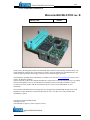
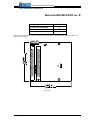
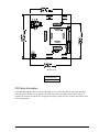
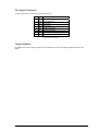
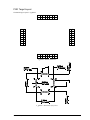
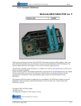
_ V1.1 POD Hardware Reference Motorola 68HC08LD POD rev. B Ordering code IC20187 Thank you for purchasing this product from iSYSTEM. This product has been carefully crafted to satisfy your needs. Should any questions arise, do not hesitate to contact your local distributor or iSYSTEM directly. Our technical support personnel will be happy to answer all your technical support questions. All information, including contact information, is available on our web site www.isystem.com. Feel free also to explore our alternative products. iSystem constantly yields for development and therefore certain pictures in this documentation may vary slightly from the actual product you received. The differences should be minor, but should you find more serious inconsistencies of the product with the documentation, please contact your local distributor for more information. This document and all documents accompanying it are copyrighted by iSYSTEM and all rights are reserved. Duplication of these documents is allowed for personal use. For every other case a written consent from iSYSTEM is required. Copyright 2004 iSYSTEM, GmbH. All rights reserved. All trademarks are property of their respective owners. www.isystem.com iSYSTEM, March 2004 1/12 _ POD Hardware Reference In-Circuit Emulation PODs The following elements of interest are located on all In-Circuit emulation PODs: • emulation CPU - acts on behalf of target's CPU. On some PODs you must use the same CPU on the POD as it is used on the target (see your POD reference page). In such cases, remove the CPU from the POD and insert the CPU that you use in the target system, in its place. • red LED (D3) - lit when CPU is running • green LED (D4) - lit when Emulator is ready for emulation • a connector, mostly marked ST3 - contains signal lines, some of which are hardware configuration lines (such as bank select signals), others you can use for signal generation (pattern generator outputs). Here are some common signals found on the signal connector, commonly marked as ST3: • GND Ground • BPE External breakpoint input. Active high. • RESO/RO Reset output. Connect to target to reset peripherals. • TRES/TR Target reset input. • AUXn AUX signal inputs (same as inputs on Emulator/trace) Note: On PODs that support synchronization between two or more Emulators (currently only the HC(S)12 Family, see the Synchronization section in the Hardware User's Guide for more information) AUX0 and AUX1 are cut short with Run/Stop synchronization line, and AUX2, AUX3 with RESET synchronization line. You should use these pins to connect to other PODs or target CPUs. • PAT0-2 Pattern generator output on 16-bit POD • OC4-6 Pattern generator output on 8-bit POD Note: The signal connector can also have other markings, like P1, U1, etc. Please refer to the POD-specific documentation for the signal connector name and signals present. iSYSTEM, March 2004 2/12 For every POD the following information is given: • Ordering code. If there are different speed versions of a POD the ordering code is modified by appending the speed in MHz (IC81020-16 for the 16 MHz 8031 POD) • information on available speed versions and required Emulator access time • POD size and position of PIN1 on the target adapter relative to bottom left corner. The memory range specifies the range of addresses that a POD can address. If this specification is omitted the default 1MB is assumed. Note: The In-Circuit Emulator can emulate a processor or a microcontroller. Beside the CPU, additional logic is integrated on the POD. The amount of additional logic depends on the emulated CPU and the type of emulation. A buffer on a data bus is always used (minimal logic) and when rebuilding ports on the POD, maximum logic is used. As soon as a POD is inserted in the target instead of the CPU, electrical and timing characteristics are changed. Different electrical and timing characteristics of used elements on the POD and prolonged lines from the target to the CPU on the POD contribute to different POD characteristics. Consequently, signal cross-talks and reflections occur, capacitance changes, etc. Beside that, pull-up and pull-down resistors are added to some signals. Pull-up/pull-down resistors are required to define the inactive state of signals like reset and interrupt inputs, while the POD is not connected to the target. Because of this, the POD can operate as standalone without the target. Final Target Application Test After the application is being more or less debugged and final application test is performed, it is recommended to remove all breakpoints and to close all debug windows (memory, SFR, watch...) to eliminate any possible influence of the emulator on the CPU execution. There were cases where the target application has been behaving differently with the target CPU inserted or the POD connected. If the debugger is configured to update some debug windows in real-time, the user may not be aware of that the CPU execution may be slightly disturbed. However, when the monitor access type is configured to update debug windows while the CPU is running, the CPU execution is disturbed significantly, depending on the necessary number of memory accesses to update opened debug windows. There are cases when internal peripheral device requires read access of the particular register during the device configuration. The user has had SFR window opened and the necessary read access was actually performed by the debugger and not by the application as it would be correct. Therefore, the application was working fine with the emulator, but a standalone application didn't work correctly, as the peripheral device was not configured properly. For Better Understanding of the Hardware Reference: PIN 1 locations There are several references to pin 1 in the manual and many jumper settings, CPU and pinout orientations rely on the correct location of pin 1. If sometimes the location of pin 1 is not clear, check the markings on the POD. If there are no markings, check the PCB board of the POD. Pin 1 is always marked on the PCB with a square pin (the other pins are round). The pin 1 location is also visible on the board in the hardware reference, if not any other way it can be identified by searching for the square pin. iSYSTEM, March 2004 3/12 _ POD Hardware Reference Motorola 68HC08LD POD rev. B Ordering code IC20187 Maximum CPU Clock (MHz) 6 Emulator Speed (ns) 65 Exchange CPU NO Before connecting the POD, make sure you have read the technical notes on Motorola 68HC08 Family in the Hardware User's Guide. Top board iSYSTEM, March 2004 4/12 Bottom board Emulated CPU 68HC908LD64 CPU Mask Information A standard 68HC908LD64 CPU is inserted in the POD. If you are confronted with an unexpected application behaviour, which could be due to a different CPU mask being used in the POD and in the target, feel free to exchange the inserted CPU with the one being used in the target. Contact the CPU vendor for more details on the CPU mask differences. iSYSTEM, March 2004 5/12 Electrical and Logical Differences In order to enable emulation, 1k Pull-up resistor is present on the Target Reset line. The original ports A and B are used for the emulation and are rebuilt by the port replacement unit on the POD; therefore electrical characteristics are changed. The IRQ line is also used to start the emulation mode of the CPU. During the execution of the user program a 220E resistor and an 100nF capacitor are present on the line, which causes RC delays on this pin. The Analog/Digital Converter The reference voltage for the ADC can be selected using jumpers J1 and J3 on the bottom board. J2: VREFL reference voltage The J2 jumper defines the VREFL source. Position VREFL connected to 1-2 (*) GND 2-3 Target VREFL Jumper J2 settings (* - factory default) If the Target VREFL is selected, the VREFL from the target must be connected. J5: VREFH reference voltage The J5 jumper defines the VREFH source. Position VREFH connected to 1-2 (*) CPU Power Supply 2-3 Target VREFH Jumper J5 settings (* - factory default) If the Target VREFH is selected, the VREFH from the target must be connected. Clock Settings Target clock source selection is done by jumpers J1 and J3. Both jumpers must be in the same position. Position Clock source 1-2 (*) Target 2-3 Rebuilt on POD Jumper J1 and J3 settings (* - factory default) The Clock can be rebuilt on the POD with the R1, Q1, C8 and C9 clock circuit. If internal clock is selected in the software, the jumper position is ignored. iSYSTEM, March 2004 6/12 Voltage settings J1 (on the top board) Jumper selector J1 on the top board determines the operational voltage. Position Vcc level Set (*) 5.0 V Removed 3.3 V Jumper J1 settings (* - factory default) This jumper must be set in any way regardless if the power supply is set to Emulator or to Target. Ports Original ports A and B are used for emulation and rebuilt by a port replacement unit. Therefore, electrical characteristics are changed. Because of different technology used in the original chip and the port replacement unit, the POD is not 100% electrically identical to the CPU. These (electrical) differences usually do not matter, until it is relied upon its limits (i.e. max. VIL, min. VIH, max. input current, input resistance, etc.). Ports A and B also feature alternate functions, i.e. ADC and Keyboard interrupts. The ADC convertor is original, just the ADC selection is done using analog switches. The Keyboard interrupt logic is emulated on the POD. The POD recognizes the KBSCR and KBIER register configuration and emulates it and generates interrupts to the CPU. A Port Replacement Unit (PRU) is used to emulate the rebuilt ports. The rebuilt port A has pull-up registers constructed on the POD for the ports that can also be used as keyboard interrupts. The pull-up resistor value is defined by the resistor network, inserted into the GR2 socket. The default value for the resistor network is 22k. The pull-ups must always be defined by setting the jumpers. Jumpers J4 through J11 set the Port A pull-ups (J4..J11 for PTA0..PTA7). Whenever operating close to electrical limits and having problems with rebuilt ports, please check pull-up and pull-down resistors on the problematical port. They should be neither too strong nor too weak. Check the voltage level. Try to withdraw from voltage limits. The jumpers P1_0 through P1_7 configure PORT A pull-up resistors GR2 (22k by default). Configuration: Jumper Set Removed J4 Pull-up enabled on PTA0 No Pull-up J5 Pull-up enabled on PTA1 No Pull-up J6 Pull-up enabled on PTA2 No Pull-up J7 Pull-up enabled on PTA3 No Pull-up J8 Pull-up enabled on PTA4 No Pull-up J9 Pull-up enabled on PTA5 No Pull-up J10 Pull-up enabled on PTA6 No Pull-up J11 Pull-up enabled on PTA7 No Pull-up Jumper P1_0 through P1_7 settings (* - factory default) iSYSTEM, March 2004 7/12 General HC08 Emulation Notes Internal RAM, Internal EEPROM Note that the internal RAM of the 68HC08 CPU on the POD is disabled during the emulation. Thereby, associated memory area must be mapped as emulator RAM by the user. If the CPU provides a capability to write to the internal RAM or EEPROM via memory window (no specific programming sequence required), the download file can be loaded to the internal RAM or EEPROM using the ‘Target Download’ option. The debugger downloads the code to the internal memory after reset via the CPU. If the CPU (e.g. 68HC08AZ60A) requires some registers to be configured before the CPU is able to write in the EEPROM area, the user must configure the necessary registers respectively, using the initialization dialog. Any sequence, added in the initialization dialog, is executed immediately after reset, before the download is performed. Note that some HC08 derivatives (e.g. 68HC908AB32) don't allow writing to the internal EEPROM area via memory window since a special programming sequence is required. Consequently, the download file cannot be loaded to the internal EEPROM by the debugger. Therefore, the programming algorithm must be implemented by the user in his application. Refer to the CPU datasheets for more details. Note that debugging is limited while executing the program in the internal EEPROM. At the HC08 family, the internal RAM is disabled during the emulation and the associated memory area overlaid by the in-circuit emulator (ICE). Thus, the debugging in the CPU internal RAM area has no limitations. While the CPU accesses internal memory resources, the (ICE) loses the control over the CPU since the external bus is not active. Therefore, breakpoints cannot be set and the user's program cannot be stopped or stepped when executing in the internal EEPROM. Additionally, debug windows cannot be updated as well. Normally, in the target application the CPU executes the program in the internal or external ROM. Using the ICE, ROM memory is overlaid by the emulation memory and consequently the program can be debugged without restrictions. But sometimes there is a need to execute some short routines in the CPU internal memory. Using the ICE, the user can run such a routine, but cannot debug it. Checksum When performing any kind of checksum in the emulated (code) area, note that all breakpoints must be removed before, otherwise the results are distorted. Note that the emulator forces "breakpoint" instruction on the data bus when executing the code at the address where breakpoint is set. COP Using any HC08 POD, the CPU's internal COP must be either disabled in the CONFIG-1 register (if the CPU has such an option) or serviced by the user's program, otherwise the emulation fails. While the user’s program is stopped, the debugger updates the COP counter. COP servicing by the user's program Writing any value to location 0xFFFF before overflow occurs clears the COP counter and prevents reset. A user must be careful since reset vector and COP register are located at the same address. COP update routine should be placed in the main program and not in an interrupt subroutine. Such an interrupt subroutine could keep the COP from generating a reset even while the main program is not working properly. Clock Clock source can be either used internal from the emulator or external from the target. It is recommended to use the internal clock when possible. When using the clock from the target, it may happen that the emulator cannot initialize any more. Internal CPU Flash Internal FLASH is overlaid by the emulation memory and disabled during the emulation and cannot be used in any way. iSYSTEM, March 2004 8/12 The Signal Connector A signal connector is present on this pod, marked as ST4. Pin Signal Description 1 GND 2 BPEXT External Breakpoint Ground 3 RESO Reset Output 4 TRES Target Reset 5 AUX0 Auxilliary Signal Input 6 AUX1 Auxilliary Signal Input 7 AUX2 Auxilliary Signal Input 8 AUX3 Auxilliary Signal Input ST4 Connector signals Target Adapters iSYSTEM offers various adapter solutions for this POD. Please refer to the adapter documentation for more details. iSYSTEM, March 2004 9/12 POD Target Layout The POD Target Layout is T_QFP64. 15 13 11 9 7 16 14 12 10 8 17 19 21 23 25 27 29 31 5 6 3 4 1 2 18 20 22 24 26 28 30 32 64 62 60 58 56 54 52 50 63 61 59 57 55 53 51 49 34 36 38 40 42 44 46 48 33 35 37 39 41 43 45 47 T_QFP64 – Bottom POD View T_QFP64 – Dimensions (Top View) iSYSTEM, March 2004 10/12 Notes: iSYSTEM, March 2004 11/12 Notes: iSYSTEM, March 2004 12/12


![[DRAFT] DEMO908JL16 User`s Manual](http://vs1.manualzilla.com/store/data/005639706_1-2a84cd2ce2f0b318fdb7aae7896f2a79-150x150.png)