1
Intel® 80219 General Purpose PCI
Processor
Specification Update
July 2004
Notice: The Intel® 80219 General Purpose PCI Processor (80219) may contain design defects or
errors known as errata that may cause the product to deviate from published specifications.
Current characterized errata are documented in this specification update.
Document Number: 274020-002
INFORMATION IN THIS DOCUMENT IS PROVIDED IN CONNECTION WITH INTEL® PRODUCTS. NO LICENSE, EXPRESS OR IMPLIED, BY
ESTOPPEL OR OTHERWISE, TO ANY INTELLECTUAL PROPERTY RIGHTS IS GRANTED BY THIS DOCUMENT. EXCEPT AS PROVIDED IN
INTEL'S TERMS AND CONDITIONS OF SALE FOR SUCH PRODUCTS, INTEL ASSUMES NO LIABILITY WHATSOEVER, AND INTEL DISCLAIMS
ANY EXPRESS OR IMPLIED WARRANTY, RELATING TO SALE AND/OR USE OF INTEL PRODUCTS INCLUDING LIABILITY OR WARRANTIES
RELATING TO FITNESS FOR A PARTICULAR PURPOSE, MERCHANTABILITY, OR INFRINGEMENT OF ANY PATENT, COPYRIGHT OR OTHER
INTELLECTUAL PROPERTY RIGHT.
Intel products are not intended for use in medical, life saving, life sustaining applications.
Intel may make changes to specifications and product descriptions at any time, without notice.
Designers must not rely on the absence or characteristics of any features or instructions marked “reserved” or “undefined.” Intel reserves these for
future definition and shall have no responsibility whatsoever for conflicts or incompatibilities arising from future changes to them.
Designers must not rely on the absence or characteristics of any features or instructions marked “reserved” or “undefined.” Intel reserves these for
future definition and shall have no responsibility whatsoever for conflicts or incompatibilities arising from future changes to them.
The Intel® 80219 General Purpose PCI Processor may contain design defects or errors known as errata which may cause the product to deviate from
published specifications. Current characterized errata are available on request.
Contact your local Intel sales office or your distributor to obtain the latest specifications and before placing your product order.
Copies of documents which have an ordering number and are referenced in this document, or other Intel literature may be obtained by calling
1-800-548-4725 or by visiting Intel's website at http://www.intel.com.
Copyright© Intel Corporation, 2004
AlertVIEW, i960, AnyPoint, AppChoice, BoardWatch, BunnyPeople, CablePort, Celeron, Chips, Commerce Cart, CT Connect, CT Media, Dialogic,
DM3, EtherExpress, ETOX, FlashFile, GatherRound, i386, i486, iCat, iCOMP, Insight960, InstantIP, Intel, Intel logo, Intel386, Intel486, Intel740,
IntelDX2, IntelDX4, IntelSX2, Intel ChatPad, Intel Create&Share, Intel Dot.Station, Intel GigaBlade, Intel InBusiness, Intel Inside, Intel Inside logo, Intel
NetBurst, Intel NetStructure, Intel Play, Intel Play logo, Intel Pocket Concert, Intel SingleDriver, Intel SpeedStep, Intel StrataFlash, Intel TeamStation,
Intel WebOutfitter, Intel Xeon, Intel XScale, Itanium, JobAnalyst, LANDesk, LanRover, MCS, MMX, MMX logo, NetPort, NetportExpress, Optimizer
logo, OverDrive, Paragon, PC Dads, PC Parents, Pentium, Pentium II Xeon, Pentium III Xeon, Performance at Your Command, ProShare,
RemoteExpress, Screamline, Shiva, SmartDie, Solutions960, Sound Mark, StorageExpress, The Computer Inside, The Journey Inside, This Way In,
TokenExpress, Trillium, Vivonic, and VTune are trademarks or registered trademarks of Intel Corporation or its subsidiaries in the United States and
other countries.
The ARM* and ARM Powered logo marks (the ARM marks) are trademarks of ARM, Ltd., and Intel uses these marks under license from ARM, Ltd.
*Other names and brands may be claimed as the property of others.
2
Specification Update
Intel® 80219 General Purpose PCI Processor
Contents
Revision History ......................................................................................... 5
Preface....................................................................................................... 6
Summary Table of Changes....................................................................... 7
Identification Information...........................................................................11
Core Errata .............................................................................................. 13
Non-Core Errata....................................................................................... 20
Specification Changes ............................................................................. 24
Specification Clarifications ....................................................................... 26
Documentation Changes ......................................................................... 29
Specification Update
3
Intel® 80219 General Purpose PCI Processor
This Page Left Intentionally Blank
4
Specification Update
Intel® 80219 General Purpose PCI Processor
Revision History
Revision History
Date
Version
July 2004
002
Added Specification Clarification 7.
November 2003
001
Initial Release.
Specification Update
Description
5
Intel® 80219 General Purpose PCI Processor
Preface
Preface
This document is an update to the specifications contained in the Affected Documents/Related
Documents table below. This document is a compilation of device and documentation errata,
specification clarifications and changes. It is intended for hardware system manufacturers and
software developers of applications, operating systems, or tools.
Information types defined in Nomenclature are consolidated into the specification update and are
no longer published in other documents.
This document may also contain information that was not previously published.
Affected Documents/Related Documents
Title
Order
Intel® 80219 General Purpose PCI Processor Developer’s Manual
274017
Intel® 80219 General Purpose PCI Processor Advance Information Datasheet
274018
Intel® 80219 General Purpose PCI Processor Design Guide
274019
Nomenclature
Errata are design defects or errors. These may cause the Intel® 80219 General Purpose PCI
Processor1 behavior to deviate from published specifications. Hardware and software designed to
be used with any given stepping must assume that all errata documented for that stepping are
present on all devices.
Specification Changes are modifications to the current published specifications. These changes
will be incorporated in any new release of the specification.
Specification Clarifications describe a specification in greater detail or further highlight a
specification’s impact to a complex design situation. These clarifications will be incorporated in
any new release of the specification.
Documentation Changes include typos, errors, or omissions from the current published
specifications. These will be incorporated in any new release of the specification.
Note:
1.
6
Errata remain in the specification update throughout the product life cycle, or until a particular
stepping is no longer commercially available. Under these circumstances, errata removed from the
specification update are archived and available upon request. Specification changes, specification
clarifications and documentation changes are removed from the specification update when the
appropriate changes are made to the appropriate product specification or user documentation
(datasheets, manuals, etc.).
ARM* architecture compliant.
Specification Update
Intel® 80219 General Purpose PCI Processor
Summary Table of Changes
Summary Table of Changes
The following table indicates the errata, specification changes, specification clarifications, or
documentation changes which apply to the Intel® 80219 General Purpose PCI Processor product.
Intel may fix some of the errata in a future stepping of the component, and account for the other
outstanding issues through documentation or specification changes as noted. This table uses the
following notations:
Codes Used in Summary Table
Stepping
X:
Errata exists in the stepping indicated. Specification Change or
Clarification that applies to this stepping.
(No mark)
or (Blank box):
This erratum is fixed in listed stepping or specification change does not
apply to listed stepping.
(Page):
Page location of item in this document.
Doc:
Document change or update will be implemented.
PlanFix:
This erratum may be fixed in a future stepping of the product.
Fixed:
This erratum has been previously fixed.
NoFix:
There are no plans to fix this erratum.
Page
Status
Row
Change bar to left of table row indicates this erratum is either new or
modified from the previous version of the document.
Specification Update
7
Intel® 80219 General Purpose PCI Processor
Summary Table of Changes
Core Errata
Steppings
No.
Page
Status
Errata
A-0
8
1
X
13
NoFix
Boundary Scan Is Not Fully Compliant to the IEEE 1149.1 Specification
2
X
13
NoFix
Drain Is Not Flushed Correctly when Stalled in the Pipeline
3
X
14
NoFix
Undefined Data Processing-‘like’ Instructions are Interpreted as an MSR Instruction
4
X
14
NoFix
Debug Unit Synchronization with the TXRXCTRL Register
5
X
14
NoFix
Extra Circuitry Is Not JTAG Boundary Scan Compliant
6
X
15
NoFix
Incorrect Decode of Unindexed Mode, Using Addressing Mode 5, Can Corrupt Protected
Registers
7
X
15
NoFix
Load Immediately Following a DMM Flush Entry is Also Flushed
8
X
15
NoFix
Trace Buffer Does Not Operate Below 1.3 V
9
X
15
NoFix
Data Cache Unit Can Stall for a Single Cycle
10
X
16
NoFix
Aborted Store that Hits the Data Cache May Mark Writeback Data As Dirty
11
X
17
NoFix
Performance Monitor Unit Event 0x1 Can Be Incremented Erroneously by Unrelated
Events
12
X
17
NoFix
In Special Debug State, Back-to-Back Memory Operations Where the First Instruction
Aborts May Cause a Hang
13
X
18
NoFix
Accesses to the CP15 ID register with opcode2 > 0b001 returns unpredictable values
14
X
18
NoFix
Disabling and re-enabling the MMU can hang the core or cause it to execute the wrong
code
15
X
19
NoFix
Updating the JTAG parallel register requires an extra TCK rising edge
Specification Update
Intel® 80219 General Purpose PCI Processor
Summary Table of Changes
Non-Core Errata
Steppings
No.
Page
Status
Errata
A-0
1
X
20
NoFix
The ATU Returns Invalid Data for the DWORD that Target Aborted from the MCU when
Using 32-Bit Memory, ECC Enabled and in PCI Mode
2
X
20
NoFix
PBI Issue When Using 16-bit PBI Transactions in PCI Mode
3
X
21
NoFix
MCU Pointers are Incorrect following a Restoration from a Power Fail
4
X
21
NoFix
PMU Does Not Account for when the Arbiter Deasserts GNT# One Cycle before
FRAME#
5
X
21
NoFix
Lost Data During Bursts of Large Number of Partials with 32-bit ECC Memory
6
X
22
NoFix
The MTTR1 (Core Multi-Transaction Timer) is not operating due to improper behavior of
the core internal bus request signal (REQ#)
7
X
22
NoFix
The MCU supports a page size of 2 Kbytes for 64-bit mode
8
X
23
NoFix
Vih Minimum Input High Voltage (Vih) level for the PCI pins
Specification Update
9
Intel® 80219 General Purpose PCI Processor
Summary Table of Changes
Specification Changes
Steppings
No.
Page
Specification Changes
A-0
1
X
24
Signal NC2 was renamed to P_BMI (AE23). New function added to signal P_BMI.
Specification Clarifications
Steppings
No.
Page
Status
Specification Clarifications
A-0
1
X
26
NoFix
The Intel® 80219 general purpose PCI processor is compliant with the PCI Local Bus
Specification, Revision 2.2 but it is not compliant with PCI Local Bus Specification,
Revision 2.3
2
X
26
NoFix
Modifications to the Hot-Debug procedure are necessary for the Intel® 80219 general
purpose PCI processor when flat memory mapping is not used (Virtual Address =
Physical Address)
3
X
27
Doc
BAR0 Configuration When Using the Messaging Unit (MU)
4
X
27
Doc
Reading Unpopulated SDRAM Memory Banks
5
X
27
Doc
32-bit Writes-to-Unaligned 64-bit Addresses, are Promoted to 64-bit Aligned Writes
6
X
28
Doc
In-order Delivery not guaranteed for data blocks described by a single DMA descriptor
7
X
28
Doc
Writing to reserved registers can cause unexpected behavior
Documentation Changes
No.
Document Revision
Page
Status
Documentation Changes
None for this revision of this specification update.
10
Specification Update
Intel® 80219 General Purpose PCI Processor
Identification Information
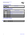
Identification Information
Markings
Figure 1.
Topside Markings
FW80219Mxxx
{FPO#}
SLxxx
INTEL © ‘2001
M
Intel® 80219 General Purpose PCI Processor
Specification Update
11
Intel® 80219 General Purpose PCI Processor
Identification Information
Die Details
Stepping
Part Number
QDF (Q)/
Specification Number (SL)
Voltage (V)
Intel® 80219 General
Purpose PCI Processor
Speed (MHz)
A-0
FW80219M400
Q690
3.3
400
Samples
A-0
FW80219M600
Q691
3.3
600
Samples
A-0
FW80219M400
SL7CL
3.3
400
Production Material
A-0
FW80219M600
SL7CM
3.3
600
Production Material
Notes
Device ID Registers
12
Device and Stepping
Processor Device ID
(CP15, Register0 - opcode_2=0)
ATU Device ID
(ATUDID)
ATU Revision ID
(ATURID)
JTAG Device ID
A-0 (400 MHz)
0x69052E20
0x031A
0x00
0x0927E013
A-0 (600 MHz)
0x69052E30
0x031B
0x00
0x0927F013
Specification Update
Intel® 80219 General Purpose PCI Processor
Core Errata
Core Errata
1.
Boundary Scan Is Not Fully Compliant to the IEEE 1149.1 Specification
Problem:
The IEEE Standard 1149.1 specifies the boundary scan logic to support two main goals:
1. To allow the interconnections between the various components to be tested, test data can be
shifted into all the boundary-scan register cells associated with component output pins and
loaded in parallel through the component interconnections, into those cells associated with
inputs pins; and
2. To allow the components on the board to be tested, the boundary-scan register can be used as a
means of isolating on-chip system logic from stimuli received from surrounding components,
while an internal self-test is performed. Alternatively, when the boundary-scan register is
suitably designed, it can permit a limited slow-speed static test of the on-chip system logic,
since it allows delivery of test data to the component and examination of the test results. (IEEE
std. 1149.1-1990, page 1-5)
The Intel Xscale® core does not support the second goal, because it does not support the optional
INTEST or RUBIST instructions. The Intel Xscale® core is not required to provide these
instructions, however, since it doesn't, this makes the following statement practically invalid.
The IEEE std. 1149.1 description of the SAMPLE/PRELOAD instruction states that, “When the
SAMPLE/PRELOAD instruction is selected, the state of all signals flowing through system pins
(input or output) shall be loaded into the boundary scan register on the rising edge of the TCK in
the Capture-DR controller state.” (Page 7-8).
The boundary scan cells of the Intel Xscale® core bi-directional pads, do not capture the data
driven from the on-chip system logic to the pins, when these pads are acting as outputs. This would
only be useful when trying to capture the data driven from the on-chip logic, during normal
operation of the assembled board. However, the Intel Xscale® core does not allow single stepping
of its clocks. Thus, even when the Intel Xscale® core did provide the compliant boundary scan cell,
it would be extremely difficult (or impossible) to synch the boundary scan logic with the state of
the on-chip logic. Therefore, this feature of the boundary scan cells is not useful. This has NO
effect on the ability to determine the integrity of the interconnections on boards, which is what the
Intel Xscale® core boundary scan logic was designed to support.
Workaround:
No workaround.
Status:
NoFix.
2.
Drain Is Not Flushed Correctly when Stalled in the Pipeline
Problem:
In a load followed by a drain scenario, the load table walks and then gets a precise data abort. The
core fetches the address for the abort handler, but in the same cycle does not flush the drain.
Implication:
Not a functional problem, but may effect performance.
Workaround:
No workaround.
Status:
NoFix.
Specification Update
13
Intel® 80219 General Purpose PCI Processor
Core Errata
3.
Undefined Data Processing-‘like’ Instructions are Interpreted as an MSR
Instruction
Problem:
The instruction decode allows undefined opcodes, which look similar to the MSR (Move to Status
register from an ARM register) instruction, to be interpreted as an MSR instruction. The
mis-decoded MSR instruction also adds a SUBNV PC,0x4 to the instruction flow.
Workaround:
Do not use undefined opcodes of this form:
31 30 29 28 27 26 25 24 23 22 21 20 19 18 17 16 15 14 13 12 11 10 9
8
7
6
5
4
3
2
1
0
-
-
-
-
0
0
0
1
0
-
1
0
-
-
-
-
-
-
-
-
-
-
-
-
0
0
1
0
-
-
-
-
-
-
-
-
0
0
0
1
0
-
1
0
-
-
-
-
-
-
-
-
-
-
-
-
0
1
0
0
-
-
-
-
-
-
-
-
0
0
0
1
0
-
1
0
-
-
-
-
-
-
-
-
-
-
-
-
0
1
1
0
-
-
-
-
Status:
NoFix.
4.
Debug Unit Synchronization with the TXRXCTRL Register
Problem:
The RX bit in the TXRXCTRL (TX/RX Control) register comes from the JTAG clock domain to
the core clock domain, and several cycles are needed for the register in the core clock domain to
update. During this time, a debugger, which is running a fast JTAG clock relative to the core clock,
may read the bit before it updates in the register, thus reading the old value.
Workaround:
The JTAG clock should be slower than the core clock.
Status:
NoFix.
5.
Extra Circuitry Is Not JTAG Boundary Scan Compliant
Problem:
The IEEE 1149.1 (JTAG) specification states that, “when the HIGHZ instruction is selected, all
system logic outputs.... shall immediately be placed in an inactive drive state”. The JTAG unit on
the core creates an internal ‘float’ signal, which is driven to the I/O pads. This signal is derived
from the HIGHZ instruction; however, the HIGHZ instruction gets flopped by a rising edge of
TCK first, before it is able to ‘float’ the pads. This is in violation of the JTAG specification, specifically the term “immediately”. It is possible for TCK to stop after the HIGHZ instruction is loaded
and thus the pads may never ‘float’.
Workaround:
Do not stop the JTAG clock (TCK).
Status:
NoFix.
14
Specification Update
Intel® 80219 General Purpose PCI Processor
Core Errata
6.
Incorrect Decode of Unindexed Mode, Using Addressing Mode 5, Can
Corrupt Protected Registers
Problem:
The instruction decoder incorrectly decodes the valid combination of P=0, U=1 and W=0, when
using unindexed mode in addressing mode 5 (load and store coprocessor). In this case, the LDC or
STC should produce consecutive address loads or stores, with no base update until the coprocessor
signals that it has received enough data. Instead, the instruction gets separated into an LDR/STR
and a CP access.
The LDR/STR gets decoded as a post-index address, updating the base register. Due to the
decoding as post-index, the ‘option’ bits, normally reserved for the coprocessor in unindexed
mode, become the 8-bit offset value used in the base register update calculation.
The implication is, that protected registers can be corrupted. This errata can cause the corruption of
FIQ registers, R13-R14, in user and system modes when the LDC instruction is executed using
unindexed addressing mode. It can also cause the corruption of FIQ registers, R8-R12, in any mode,
when the LDC instruction is executed using unindexed addressing. The R13 register in debug mode
may also be corrupted during an LDC in any mode. In the case of STC, only Rn is corrupted.
Unexpected memory accesses can also occur. In the case of an LDC, any memory location may be
accessed, since the FIQ registers may be improperly used as the base register. In the case of an
STC, the memory word located at Rn+4 is corrupted. This is the memory location immediately
following the locations which should be modified by STC unindexed.
Workaround:
Do not use unindexed addressing in addressing mode 5 – Load and Store Coprocessor.
Status:
NoFix.
7.
Load Immediately Following a DMM Flush Entry is Also Flushed
Problem:
A load that immediately follows a data memory management (DMM) flush entry command, that
also hits the data TLB, is also flushed. Therefore, the instruction immediately following the flush,
is also flushed from the data TLB.
Workaround:
All flush entry commands to the data TLB must be followed by two NOPs. The first ensures the
erratum is not encountered, and the second ensures the speed path is not hit.
Status:
NoFix.
8.
Trace Buffer Does Not Operate Below 1.3 V
Problem:
The trace buffer within the debug unit is not guaranteed to operate, due to voltage sensitivity, when
the core voltage supply is below 1.3 V.
Workaround:
Make sure the voltage is above 1.3 V during debug.
Status:
NoFix.
9.
Data Cache Unit Can Stall for a Single Cycle
Problem:
When the data cache unit retries an operation that is in the pending buffer, a single cycle stall
occurs.
Workaround:
No workaround. This is a performance issue only.
Status:
NoFix.
Specification Update
15
Intel® 80219 General Purpose PCI Processor
Core Errata
10.
Aborted Store that Hits the Data Cache May Mark Writeback Data As Dirty
Problem:
When there is an aborted store that hits clean data in the data cache (data in an aligned four word
range, that has not been modified from the core, since it was last loaded in from memory or
cleaned), the data in the array is not modified (the store is blocked), but the dirty bit is set.
When the line is then aged out of the data cache or explicitly cleaned, the data in that four word
range is evicted to external memory, even though it has never been changed. In normal operation,
this is nothing more than an extra store on the bus, that writes the same data to memory as is
already there.
Here is the boundary condition where this might be visible:
1. a cache line is loaded into the cache at address A
2. another master externally modifies address A
3. a core store instruction attempts to modify A, hits the cache, aborts because of MMU
permissions, and is backed out of the cache. That line should not be marked dirty, but because
of this errata is marked as dirty.
4. the cache line at A then ages out or is explicitly cleaned. The original data from location A is
evicted to external memory, overwriting the data written by the external master.
This only happens when software is allowing an external master to modify memory, that is,
writeback or write-allocate in the page tables, and depending on the fact that the data is not 'dirty' in
the cache, to preclude the cached version from overwriting the external memory version. When
there are any semaphores or any other handshaking to prevent collisions on shared memory, this
should not be a problem.
Workaround:
For this shared memory region, mark it as write-through memory in the page table. This prevents
the data from ever being written out as dirty.
Status:
NoFix.
16
Specification Update
Intel® 80219 General Purpose PCI Processor
Core Errata
11.
Performance Monitor Unit Event 0x1 Can Be Incremented Erroneously by
Unrelated Events
Problem:
Event 0x1 in the performance monitor unit (PMU) can be used to count cycles in which the
instruction cache cannot deliver an instruction. The only cycles counted should be those due to an
instruction cache miss or an instruction TLB miss. The following unrelated events in the core, also
causes the corresponding count to increment when event number 0x1 is being monitored:
1. Any architectural event (e.g. IRQ, data abort)
2. MSR instructions which alter the CPSR control bits
3. Some branch instructions, including indirect branches and those mispredicted by the BTB
4. CP15 mcr instructions to registers 7, 8, 9, or 10 which involve the instruction cache or the
instruction TLB.
Each of the items above may cause the performance monitoring count to increment several times.
The resulting performance monitoring count may be higher than expected when the above items
occur, but never lower.
Workaround:
There is no way to obtain the correct number of cycles stalled due to instruction cache misses and
instruction TLB misses. Extra counts due to branch instructions mispredicted by the BTB, may be
one component of the unwanted count that can be filtered out. The number of mispredicted
branches can also be monitored using performance monitoring event 0x6 during the same time
period as event 0x1. The mispredicted branch number can then be subtracted from the instruction
cache stall number generated by the performance monitor to get a value closer to the correct one.
Note that this only addresses counts contributed by branches that the BTB is able to predict. All the
items listed above still affect the count. Depending on the nature of the code being monitored, this
workaround may have limited value.
Status:
NoFix.
12.
In Special Debug State, Back-to-Back Memory Operations Where the First
Instruction Aborts May Cause a Hang
Problem:
When back-to-back memory operations occur in the Special Debug State (SDS, used by ICE and
Debug vendors) and the first memory operation gets a precise data abort, the first memory
operation is correctly cancelled and no abort occurs. However, depending on the timing, the second
memory operation may not work correctly. The data cache may internally cancel the second
operation, but the register file may have score-boarded registers for that second memory operation.
The effect is that the core may hang (due to a permanently score-boarded register) or that a store
operation may be incorrectly cancelled.
Workaround:
In Special Debug State, any memory operation that may cause a precise data abort should be
followed by a write-buffer drain operation. This precludes further memory operations from being
in the pipe when the abort occurs. Load Multiple/Store Multiple that may cause precise data aborts
should not be used.
Status:
NoFix.
Specification Update
17
Intel® 80219 General Purpose PCI Processor
Core Errata
13.
Accesses to the CP15 ID register with opcode2 > 0b001 returns
unpredictable values
Problem:
The ARM Architecture Reference Manual (ARM DDI 0100E) states the following in chapter B-2,
section 2.3:
“If an <opcode2> value corresponding to an unimplemented or reserved ID register is
encountered, the System Control processor returns the value of the main ID register.
ID registers other than the main ID register are defined so that when implemented, their value
cannot be equal to that of the main ID register. Software can therefore determine whether they
exist by reading both the main ID register and the desired register and comparing their values.
If the two values are not equal, the desired register exists.”
The Intel Xscale® core does not implement any CP15 ID code registers other than the Main ID
register (opcode2 = 0b000) and the Cache Type register (opcode2 = 0b001). When any of the
unimplemented registers are accessed by software (e.g., mrc p15, 0, r3, c15, c15, 2), the value of
the Main ID register should be returned. Instead, an unpredictable value is returned.
Workaround:
No workaround.
Status:
NoFix.
14.
Disabling and re-enabling the MMU can hang the core or cause it to execute
the wrong code
Problem:
When the MMU is disabled, via the CP15 control register (CP15, CR1, opcode_2 = 0, bit 0), after
being enabled, certain timing cases can cause the processor to hang. In addition to this, re-enabling
the MMU after disabling it can cause the processor to fetch and execute code from the wrong
physical address. To avoid these issues, the code sequence below needs to be used whenever
disabling the MMU or re-enabling it afterwards.
Workaround:
The following code sequence can be used to disable and/or re-enable the MMU safely. The
alignment of the mcr instruction that disables or re-enables the MMU needs to be controlled
carefully, so that it resides in the first word of an instruction cache line.
@ The following code sequence takes r0 as a parameter. The value of r0 is written
@ to the CP15 control register to either enable or disable the MMU.
mcr
p15, 0, r0, c10, c4, 1@ unlock I-TLB
mcr
p15, 0, r0, c8, c5, 0@ invalidate I-TLB
mrc p15, 0, r0, c2, c0, 0@ CPWAIT
mov r0, r0
sub pc, pc, #4
b
1f
@ branch to aligned code
.align 5
1:
mcr
p15, 0, r0, c1, c0, 0@ enable/disable MMU, caches
mrc p15, 0, r0, c2, c0, 0@ CPWAIT
mov r0, r0
sub pc, pc, #4
Status:
18
NoFix.
Specification Update
Intel® 80219 General Purpose PCI Processor
Core Errata
15.
Updating the JTAG parallel register requires an extra TCK rising edge
Problem:
IEEE 1149.1 states that the effects of updating all parallel JTAG registers should be seen on the
falling edge of TCK in the Update-DR state. The Intel Xscale® core parallel JTAG registers
incorrectly require an extra TCK rising edge to make the update visible. Therefore, operations like
hold-reset, JTAG break, and vector traps require either an extra TCK cycle by going to
Run-Test-Idle or by cycling through the state machine again in order to trigger the expected
hardware behavior.
Workaround:
When the JTAG interface is polled continuously, this erratum has no effect. When not, an extra
TCK cycle can be caused by going to Run-Test-Idle after writing a parallel JTAG register.
Status:
NoFix.
Specification Update
19
Intel® 80219 General Purpose PCI Processor
Non-Core Errata
Non-Core Errata
1.
The ATU Returns Invalid Data for the DWORD that Target Aborted from the
MCU when Using 32-Bit Memory, ECC Enabled and in PCI Mode
The external PCI bus requests a read through the ATU to the MCU, starting at the high DWORD.
Remember the MCU is in 32-bit mode. The ATU requests multiple DWORDs since it pre-fetches, but
starts at the high DWORD address. The MCU issues two DWORDs. First the high, followed by the
low and then a Target Abort, so the DWORD count is two. When the ATU returns the data to the
external PCI agent (in PCI Mode ONLY), the logic ONLY disconnects on 64-byte QWORD
boundaries. Recall the ATU DWORD count is at two. When the external PCI device returns to get
data, the ATU returns the first DWORD and SHOULD disconnect, because it does not have enough
data to get to the next QWORD boundary. It does not do this. Instead, it returns invalid data in the
high DWORD of the second QWORD (data from a previous fetch) and the transaction is corrupted.
This issue occurs when all of the following conditions exist in the MCU:
1. 32-bit memory
2. ECC is enabled
3. The PCI bus is in PCI mode
Workaround:
Use 64-bit Memory, PCI-X Mode or ECC disabled.
Status:
NoFix.
2.
PBI Issue When Using 16-bit PBI Transactions in PCI Mode
Problem:
Under certain conditions, in bound burst and non-burst reads and writes from the PCI bus to the
PBI would appear as two writes on the PBI. However, the byte enables are not asserted for the
second write.
This happens when:
1. 80219 is in PCI mode.
2. Another PCI master is attempting to access the PBI behind the 80219.
3. 16-bit mode on PBI.
Workaround:
The BE# signals can be used in combination with the PCE#. The BE# prevents the second CE#
from being recognized by the Flash. See the Intel® IQ80219 evaluation platform board (IQ80219)
schematic for a circuit design to correct this issue.
Status:
NoFix.
20
Specification Update
Intel® 80219 General Purpose PCI Processor
Non-Core Errata
3.
MCU Pointers are Incorrect following a Restoration from a Power Fail
Problem:
This issue occurs when:
1. There is a power failure (not during power management or normal shutdown).
2. When power is restored, the internal MCU pointers to the SDRAM may not be correct.
3. When a read from SDRAM (prior to doing a write to SDRAM) is the first MCU operation
done after the power is restored, the MCU pointers may be incorrect and can be reading the
wrong data.
4. However, when a write to SDRAM is the first MCU operation done after the power is restored,
then the pointers are correct and everything works properly.
Workaround:
Following restoration of power after a power failure, ensure that the first MCU operation done is a
write to SDRAM.
Status:
NoFix.
4.
PMU Does Not Account for when the Arbiter Deasserts GNT# One Cycle
before FRAME#
Problem:
One of the countable PMU events is bus acquisition latency for the ATU. There is a condition
where the acquire counter is not stopped even though the ATU starts a transaction. When the arbiter
deasserts GNT# in PCI-X mode, the requestor can still start a transaction for one cycle (due to
allowed pipelining). In this situation, the PMU does not properly detect the FRAME# as the ATU
and continues running the counter.
Workaround:
No workaround.
Status:
NoFix.
5.
Lost Data During Bursts of Large Number of Partials with 32-bit ECC Memory
Problem:
When the MCU operates in 32-bit mode only and it is hit by enough partials to cause the input
posted write buffer to fill (in 32-bit mode it holds 512 bytes), the MCU has conditions where it
does NOT disconnect on the IB (internal bus) before overrunning.
When the buffer overruns, the MCU momentarily thinks it is empty, allowing the refresh to occur,
but also causing all data to be lost for the rest of the burst. The ATU continues to throw data at the
MCU, but this data is lost.
This is strictly a 32-bit memory ECC on mode issue, as this is the only way to fill the entire buffer
since all buffers on the IB are 1 K in size (except the MCU when operating in 32-bit DDR mode).
The DMA, AAU, and core cannot cause the situation in 32-bit mode because they only issue up to
two partials in their burst before disconnecting. In these situations, the MCU will drain enough data
to prevent buffer overrun.
Workaround:
Use 64-bit memory or ECC disabled.
Status:
NoFix.
Specification Update
21
Intel® 80219 General Purpose PCI Processor
Non-Core Errata
6.
The MTTR1 (Core Multi-Transaction Timer) is not operating due to improper
behavior of the core internal bus request signal (REQ#)
Problem:
The MTTR1 (Core Multi-Transaction Timer) is not operating due to improper behavior of the core
internal bus request signal (REQ#). All agents on the bus, except the core, maintain their assertion
on REQ# signals upon receiving a retry. When the MCU is busy this means that the core must wait
for other agents to complete their transactions before the core gains access to memory. Due to the
fact that internal bus agents initiate larger transactions than the core, this issue results in an
unbalanced access to the internal bus biased to these other agents (DMA, ATU, etc.). When operational, the MTTR1 is intended to correct this balance. See Section 11.2.2 of the Intel® 80219
General Purpose PCI Processor Developer’s Manual for more information on the MTTR1
function.
Implication:
In the case of the MCU internal bus target, this problem is compounded by the many internal bus
retries that are issued by the MCU when under heavily loaded conditions. The result is that the
internal bus arbiter removes the core access to the bus when the core deasserts REQ#. This
condition may result in the core being locked out of accessing the MCU until other internal bus
agents have completed their transaction(s) (i.e., when the DMA is in the process of a large block
transfer of data, the core may have to wait until the DMA transaction is completed before it would
have access to the internal bus to initiate its transaction).
Workaround:
No workaround.
Status:
NoFix.
7.
The MCU supports a page size of 2 Kbytes for 64-bit mode
Problem:
The Intel® 80219 General Purpose PCI Processor Developer’s Manual (Section 6.1.1 and Section
6.2.2.3) states that the MCU supports a page size of 4 Kbytes for 64-bit mode and 2 Kbytes for
32-bit mode. This is in error.
Implication:
The MCU supports a page size of 2 Kbytes for 64-bit mode and for 32-bit mode.
Workaround:
No workaround.
Status:
NoFix.
22
Specification Update
Intel® 80219 General Purpose PCI Processor
Non-Core Errata
8.
Vih Minimum Input High Voltage (Vih) level for the PCI pins
Problem:
The Vih Minimum Input High Voltage (Vih) level for the PCI pins is being tested at 100 mV higher
than the minimum Vih level specified in Table 4-3 (DC Specifications for 3.3 V Signaling) of the
PCI Local Bus Specification, Revision 2.2. This Vih test limit only applies to cold temperature
testing specified to be 0°C.
The PCI Local Bus Specification, Revision 2.2 specifies the minimum Vih level to be 0.5 Vcc. The
Vcc specification is 3.3 V +/- 10% with the minimum Vcc specification (or minimum power level)
being tested at 3.0 V. The minimum Vih level per the PCI Specification should therefore be
0.5(3.0 V) or 1.5 V. The 80219 is unable to meet this minimum Vih level at cold temperature
testing specified to be 0°C.
Implication:
During cold temperature manufacturing testing, 80219 silicon is subjected to a 0°C environment
for an extended period of time. During this time the Vih test is implemented and the junction
temperature is at or near the test temperature of 0°C. This junction temperature is considered to be
far less than the temperature the 80219 silicon would be subjected to in a customer application
under operating conditions.
Below is an example calculation showing the expected junction temperature for a customer
application operating in an ambient temperature of 0°C:
Tj = junctions temperature, Ta = ambient temperature, qja = junction to ambient thermal
resistance of the package, P = power at minimum Vcc
Tj = Ta + (qja * P) where Ta = 0C, qja = 13.94 C/W assuming 200lfm airflow (see Table 11 of
the Intel® 80219 General Purpose PCI Processor Datasheet), P = 3.0 W
Tj = 0 + (13.94 C/W * 3.0 C)
Tj = 41.82 C
Workaround:
The minimum Vih level for the PCI pins will be tested at the PCI Local Bus Specification,
Revision 2.2 specification (0.5 Vcc) plus an additional 100 mV that equates to 1.6 V during cold
temperature manufacturing testing.
Status:
NoFix.
Specification Update
23
Intel® 80219 General Purpose PCI Processor
Specification Changes
Specification Changes
1.
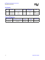
Signal NC2 was renamed to P_BMI (AE23). New function added to signal
P_BMI.
The P_BMI (AE23) signal has been added to the Intel® 80219 general purpose PCI processor. This
signal replaces, using an external GPIO pin for Initialization Device Select (IDSEL) control of an
I/O device during host configuration cycles.
Issue:
I/O Device IDSEL control using the new P_BMI signal:
When the system boots after reset, the host BIOS initiates a PCI bus scan to find all the PCI
components installed in the system. The system uses the IDSEL signal to address the I/O device when
assigning the necessary resources. Without special control over the IDSEL signal during configuration
cycles, the host and the 80219 may both attempt to configure the same I/O device. By taking control of
IDSEL, the 80219 can execute configuration cycles to the slave I/O device (SCSI) and properly hide
the slave I/O device from the host and operating system initiated configuration cycles.
The 80219 has eight integrated General Purpose Input Output (GPIO) pins, referred to as GPIO[7:0].
These pins, along with the new PCI-X Bus Master Indicator (P_BMI) signal, can be used to control the
IDSEL to the I/O device. External circuitry is no longer required other than a simple switch. The output
function of the P_BMI signal is controlled by the GPIO Output Data Register (GPOD), Bit 0 as shown
in Table 1. The P_BMI signal is always driven and defaults to driving low at power up.
Table 1.
GPIO Output Data Register (address = FFFF E7CCh)
Bit
Default
0
0
Description
This bit value is driven on the P_BMI signal when the 80219 has been given control
of the bus (granted GNT#) by the bus arbiter.
The IDSEL signal is used as a chip select during configuration cycles initiated by the BIOS, operating
system or 80219. The GPOD[0] can be driven low in firmware, thereby disabling the P_BMI signal
and hiding the host I/O device from the system, by turning off its IDSEL. When the 80219 intends to
perform configuration cycles in the PCI bus segment of the I/O device, the P_BMI signal should be
asserted high by driving the GPOD[0] high. The affect of these two operations is, that the I/O device
is initialized and controlled by the 80219. More care must be taken with the gate chosen to control
IDSEL, since most host bridge controllers do not use PCI address stepping. With IDSEL being a
synchronous signal, with respect to CLK, the switch used must be a sub nanosecond propagation
delay device (e.g., Pericom PI5C3303). In Figure 2, the P_BMI signal is used to control a
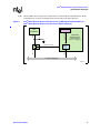
MUX/DeMUX switch that is used to enable/disable IDSEL to the I/O device.
24
Specification Update
Intel® 80219 General Purpose PCI Processor
Specification Changes
Note:
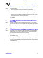
Figure 2.
The host BIOS does not require any modifications to accommodate this implementation. All the
responsibility for I/O device configuration and resource falls to the 80219 firmware.
Intel® 80219 General Purpose PCI Processor P_BMI Signal Implementation for
Intel® 80219 General Purpose PCI Processor B-0/B-1 Stepping
GPOD Register
Bit 0
Enable P_BMI
IDSEL
I/O
Controller
R1
P_BMI
Control
Logic
GNT#
AD[11+x]
P_BMI Signal (AE23)
Intel® 80219
General Purpose
PCI Processor
(B-0 / B-1 Stepping)
PCI-X Bus AD[64:0]
B2845-01
Specification Update
25
Intel® 80219 General Purpose PCI Processor
Specification Clarifications
Specification Clarifications
1.
The Intel® 80219 general purpose PCI processor is compliant with the PCI
Local Bus Specification, Revision 2.2 but it is not compliant with PCI Local
Bus Specification, Revision 2.3
Issue:
The Intel® 80219 general purpose PCI processor was designed to be compliant with the PCI-X
Addendum to the PCI Local Bus Specification, Revision 1.0a, that calls out compliance with the
PCI Local Bus Specification, Revision 2.2. Since the release of the 80219, the PCI Special Interest
Group has released a new specification revision, PCI Local Bus Specification, Revision 2.3.
Status:
NoFix. The current stepping of the 80219 is not compliant with PCI Local Bus Specification,
Revision 2.3 and there are no plans to make it compliant with the PCI Local Bus Specification,
Revision 2.3 in future steppings.
2.
Modifications to the Hot-Debug procedure are necessary for the Intel®
80219 general purpose PCI processor when flat memory mapping is not
used (Virtual Address = Physical Address)
Issue:
The Intel® 80219 general purpose PCI processor can implement Hot Debug as stated in the
application note “Hot-Debug for Intel® Xscale™ Core Debug:
“http://developer.intel.com/design/iio/applnots/273539.htm”.
However, there can be a conflict for resources when flat memory mapping is not used (Virtual
Address = Physical Address).
This is primarily due to the debug implementation within the core that causes the Instruction
Memory Management Unit to be disabled when in this Special Debug State.
Status:
NoFix. The following are suggested steps to overcome this conflict within a debug environment.
1. Instrument the application code to add an infinite loop before any memory is remapped
(physically or virtually).
2. Hook up the JTAG Debugger that supports Hot Debug.
3. Set PC to address passed the loop.
4. The code can now run without the need to reset the application environment.
Note:
26
Once a debug session has ended, you must follow the above steps over again in order to regain
debug control.
Specification Update
Intel® 80219 General Purpose PCI Processor
Specification Clarifications
3.
BAR0 Configuration When Using the Messaging Unit (MU)
Issue:
When the BAR0 is configured as a prefetchable register by default and a burst request crosses into
or through the range of offsets 40h to 4Ch (i.e., this includes the Circular Queues), the transaction
is signaled a Target Abort immediately on the PCI/PCI-X bus, which may be read as an NMI by the
host BIOS.
Status:
Doc. Do not configure the BAR0 as prefetchable when using BAR0 and the non-prefetchable MU
registers (i.e., range of offsets 40h to 4Ch). Configure the BAR0 as non-prefetchable, IABAR0[3],
when accessing these non-prefetchable MU registers. Since non-prefetchable memory windows
cannot be placed above the 4 Gbyte address boundary, when the Prefetchable Indicator bit,
IABAR0[3], is cleared prior to host configuration, also clear the Type Indicator bits, IABAR0[2:1]
for 32-bit addressability. When the non-prefetchable MU registers are in use, those memory
accesses that require prefetchable operations, use the BAR2 configured as prefetchable.
4.
Reading Unpopulated SDRAM Memory Banks
Issue:
A hang condition can occur with the 80219 when firmware does a read to unpopulated SDRAM
memory and DQS0 is sampled low. In this scenario, putting a load (i.e., scope probe), on the DQS0
signal could trigger DQS0 to be sampled low, which the MCU interprets as the pre-amble and waits
for DQS0 to go high. Since the read is to unpopulated memory, nothing drives the DQS0 signal
high, therefore the 80219 appears to hang.
Status:
Doc. Do not attempt to read from non-existent memory. In some applications, firmware performs a
memory scan, typically during boot-up, to determine the total amount o SDRAM installed. Instead,
either use the Serial Presence Detect (SPD) mechanism or have it hard coded in firmware. SPD is
used to read, via I2C, from a non-volatile storage device. This device contains data programmed by
the DIMM manufacturer, that identifies the module type, various SDRAM organizations and
timing parameters. Using SPD or hard coded firmware eliminates the need to do SDRAM sizing in
the firmware.
5.
32-bit Writes-to-Unaligned 64-bit Addresses, are Promoted to 64-bit Aligned
Writes
Issue:
In 80219-based applications that run the PCI bus segment in 32-bit PCI Mode or 64-bit PCI Mode
with 32-bit targets, write transactions that are on unaligned 64-bit addresses are promoted to 64-bit
aligned writes. The first half of the 64-bit write is on a 64-bit aligned address and has the BE#
signals disabled. Therefore, the write is invalid. The second half on the 64-bit write is a valid write
with the BE# enabled and the write is to the intended 32-bit address.
Per the PCI Local Bus Specification, Revision 2.2, the PCI compliant devices should ignore the
first half of the 64-bit write due to the BE# signals being disabled.
Status:
For devices that support using the I/O memory window, the 64-bit write does not occur when using
the 80219 ATU I/O Window and the only expected 32-bit write occurs. See section 3.2.2.2 of the
Intel® 80219 General Purpose PCI Processor Developer’s Manual for details.
For memory mapped devices, the only option is to run in PCI-X mode, where the byte count and
starting address are consistent with the actual number of bytes to be written (i.e., 4). This is so
because, when a 64-bit PCI-X request gets downshifted, the requester can use the starting
address/byte count to recognize that the write request does not cross a DWORD address boundary
and only perform a single 32-bit wide data cycle.
Specification Update
27
Intel® 80219 General Purpose PCI Processor
Specification Clarifications
6.
In-order Delivery not guaranteed for data blocks described by a single DMA
descriptor
Issue:
In-order delivery is not guaranteed for data blocks described by a single DMA descriptor that
crosses a 1 KB boundary. This may result in out of order execution of the DMA transfer. When
multiple DMA descriptors are used the ordering is maintained with respect to the blocks described
by each descriptor. When ordering is important, the ordering needs to be maintained by splitting
the relevant pieces of data into multiple DMA descriptors.
Example
A 100 byte DMA transfer described by a single descriptor with a source address of
0x3ff8. Since each DMA channel has two 1 KB buffers, the DMA unit breaks this
transaction at the 1 KB boundary. Therefore, the first buffer might fetch the 8 bytes
from 0x3ff8-0x3fff and the second buffer might fetch the remaining 92 byes from
0x4000-0x405C. Both buffers have the ability to access the internal bus, without
preference (i.e., either buffer may gain access first). Therefore, it is possible the
92 bytes of data after the 1 KB boundary could be transferred to the destination
before the first 8 bytes. However, the transaction is completed and all data has been
copied to the correct address when the descriptor completes (i.e., descriptors are
not completed out of order).
Status:
When a data delivery sequence is required, descriptors should be used to ensure sequenced arrival
(e.g., in the example above), break the data into blocks then use multiple descriptors linked in the
correct order to ensure sequential data delivery.
7.
Writing to reserved registers can cause unexpected behavior
Issue:
The Intel® 80219 General Purpose PCI Processor contains several reserved registers. The Intel®
80219 General Purpose PCI Processor Developer’s Manual (Section 15.5 Table 273) states that
memory map register locations FFFFE800H - FFFFE8FFH are reserved. Writing to these can cause
the processor to enter an undesired state.
Status:
NoFix.
28
Specification Update
Intel® 80219 General Purpose PCI Processor
Documentation Changes
Documentation Changes
None for this revision of this specification update.
Specification Update
29
Intel® 80219 General Purpose PCI Processor
Documentation Changes
This Page Left Intentionally Blank
30
Specification Update