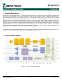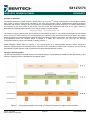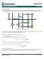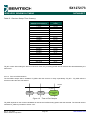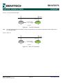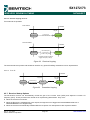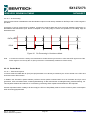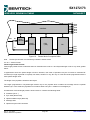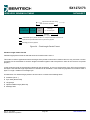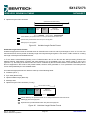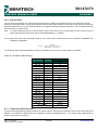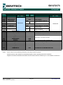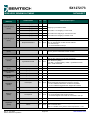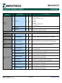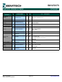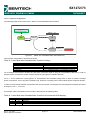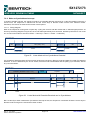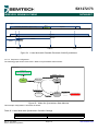
1
SX1272/73 WIRELESS, SENSING & TIMING DATASHEET SX1272/73 - 860 MHz to 1020 MHz Low Power Long Range Transceiver GENERAL DESCRIPTION KEY PRODUCT FEATURES The SX1272/73 transceivers feature the LoRaTM long range modem that provides ultra-long range spread spectrum communication and high interference immunity whilst minimising current consumption. Using Semtech’s patented LoRaTM modulation technique SX1272/73 can achieve a sensitivity of over -137 dBm using a low cost crystal and bill of materials. The high sensitivity combined with the integrated +20 dBm power amplifier yields industry leading link budget making it optimal for any application requiring range or robustness. LoRaTM also provides significant advantages in both blocking and selectivity over conventional modulation techniques, solving the traditional design compromise between range, interference immunity and energy consumption. These devices also support high performance (G)FSK modes for systems including WMBus, IEEE802.15.4g. The SX1272/73 deliver exceptional phase noise, selectivity, receiver linearity and IIP3 for significantly lower current consumption than competing devices. ORDERING INFORMATION Part Number Delivery MOQ / Multiple SX1272IMLTRT T&R 3000 pieces SX1273IMLTRT T&R 3000 pieces QFN 28 Package - Operating Range from -40 to +85°C Pb-free, Halogen free, RoHS/WEEE compliant product Rev. 2 - July 2014 ©2014 Semtech Corporation LoRaTM Modem 157 dB maximum link budget +20 dBm at 100 mW constant RF output vs. V supply +14 dBm high efficiency PA Programmable bit rate up to 300 kbps High sensitivity: down to -137 dBm Bullet-proof front end: IIP3 = -12.5 dBm 89 dB blocking immunity Low RX current of 10 mA, 100 nA register retention Fully integrated synthesizer with a resolution of 61 Hz FSK, GFSK, MSK, GMSK, LoRaTM and OOK modulation Built-in bit synchronizer for clock recovery Preamble detection 127 dB Dynamic Range RSSI Automatic RF Sense and CAD with ultra-fast AFC Packet engine up to 256 bytes with CRC Built-in temperature sensor and low battery indicator APPLICATIONS Page 1 Automated Meter Reading Home and Building Automation Wireless Alarm and Security Systems Industrial Monitoring and Control Long range Irrigation Systems www.semtech.com SX1272/73 WIRELESS, SENSING & TIMING DATASHEET Table of contents Section Page 1. General Description ............................................................................................................................................... 10 1.1. Simplified Block Diagram ............................................................................................................................... 10 1.2. Product Versions ............................................................................................................................................11 1.3. Pin Diagram ................................................................................................................................................... 11 1.4. Pin Description ...............................................................................................................................................12 1.5. Package Marking ...........................................................................................................................................13 2. Electrical Characteristics ....................................................................................................................................... 14 2.1. ESD Notice .................................................................................................................................................... 14 2.2. Absolute Maximum Ratings ........................................................................................................................... 14 2.3. Operating Range............................................................................................................................................ 14 2.4. Thermal Properties ........................................................................................................................................ 14 2.5. Chip Specification ..........................................................................................................................................15 2.5.1. Power Consumption .................................................................................................................................. 15 2.5.2. Frequency Synthesis................................................................................................................................. 15 2.5.3. FSK/OOK Mode Receiver ......................................................................................................................... 16 2.5.4. FSK/OOK Mode Transmitter ..................................................................................................................... 17 2.5.5. Electrical specification for LoRaTM modulation ........................................................................................ 18 2.5.6. Digital Specification ................................................................................................................................... 20 3. SX1272/73 Features.............................................................................................................................................. 21 3.1. LoRaTM Modem ............................................................................................................................................ 22 3.2. FSK/OOK Modem .......................................................................................................................................... 22 4. SX1272/73 Digital Electronics ............................................................................................................................... 23 4.1. The LoRaTM Modem ..................................................................................................................................... 23 4.1.1. Link Design Using the LoRaTM Modem ....................................................................................................24 4.1.1.1. Overview ........................................................................................................................................... 24 4.1.1.2. Spreading Factor............................................................................................................................... 25 4.1.1.3. Coding Rate ...................................................................................................................................... 25 4.1.1.4. Signal Bandwidth .............................................................................................................................. 26 4.1.1.5. LoRaTM Transmission Parameter Relationship ............................................................................... 26 4.1.1.6. LoRaTM Packet Structure .................................................................................................................27 4.1.1.7. Time on air ........................................................................................................................................ 29 4.1.1.8. Frequency Hopping with LoRaTM..................................................................................................... 29 4.1.2. LoRaTM Digital Interface ...........................................................................................................................31 4.1.2.1. LoRaTM Configuration Registers ...................................................................................................... 31 4.1.2.2. Status Registers................................................................................................................................ 31 4.1.2.3. LoRaTM Mode FIFO Data Buffer ...................................................................................................... 31 4.1.2.4. Interrupts in LoRa Mode.................................................................................................................... 32 4.1.3. Operation of the LoRaTM Modem............................................................................................................. 33 4.1.3.1. Operating Mode Control .................................................................................................................... 33 4.1.4. Frequency Settings ...................................................................................................................................34 4.1.5. Frequency Error Indication ........................................................................................................................ 34 4.1.6. LoRaTM Modem State Machine Sequences .............................................................................................35 Rev. 2 - July 2014 ©2014 Semtech Corporation Page 2 www.semtech.com SX1272/73 WIRELESS, SENSING & TIMING DATASHEET Table of contents Section Page 4.1.6.1. Digital IO Pin Mapping ...................................................................................................................... 42 4.2. FSK/OOK Modem .......................................................................................................................................... 43 4.2.1. Bit Rate Setting ......................................................................................................................................... 43 4.2.2. FSK/OOK Transmission ............................................................................................................................ 44 4.2.2.1. FSK Modulation................................................................................................................................. 44 4.2.2.2. OOK Modulation................................................................................................................................ 44 4.2.2.3. Modulation Shaping .......................................................................................................................... 44 4.2.3. FSK/OOK Reception ................................................................................................................................. 45 4.2.3.1. FSK Demodulator.............................................................................................................................. 45 4.2.3.2. OOK Demodulator............................................................................................................................. 45 4.2.3.3. Bit Synchronizer ................................................................................................................................ 47 4.2.3.4. Frequency Error Indicator .................................................................................................................48 4.2.3.5. AFC ................................................................................................................................................... 48 4.2.3.6. Preamble Detector ............................................................................................................................49 4.2.3.7. Image Rejection Mixer ...................................................................................................................... 49 4.2.3.8. Image and RSSI Calibration.............................................................................................................. 49 4.2.3.9. Timeout Function .............................................................................................................................. 50 4.2.4. Operating Modes in FSK/OOK Mode ........................................................................................................ 50 4.2.5. General Overview...................................................................................................................................... 50 4.2.6. Startup Times ............................................................................................................................................51 4.2.6.1. Transmitter Startup Time .................................................................................................................. 51 4.2.6.2. Receiver Startup Time ...................................................................................................................... 51 4.2.6.3. Time to RSSI Evaluation ................................................................................................................... 52 4.2.6.4. Tx to Rx Turnaround Time ................................................................................................................ 53 4.2.6.5. Rx to Tx............................................................................................................................................. 53 4.2.6.6. Receiver Hopping, Rx to Rx ..............................................................................................................54 4.2.6.7. Tx to Tx ............................................................................................................................................. 54 4.2.7. Receiver Startup Options .......................................................................................................................... 54 4.2.8. Receiver Restart Methods......................................................................................................................... 55 4.2.8.1. Restart Upon User Request .............................................................................................................. 55 4.2.8.2. Automatic Restart after valid Packet Reception ................................................................................ 55 4.2.8.3. Automatic Restart when Packet Collision is Detected ......................................................................56 4.2.9. Top Level Sequencer ................................................................................................................................ 56 4.2.9.1. Sequencer States.............................................................................................................................. 56 4.2.9.2. Sequencer Transitions ...................................................................................................................... 57 4.2.9.3. Timers ............................................................................................................................................... 58 4.2.9.4. Sequencer State Machine .................................................................................................................60 4.2.10. Data Processing in FSK/OOK Mode ....................................................................................................... 61 4.2.10.1. Block Diagram ................................................................................................................................. 61 4.2.10.2. Data Operation Modes .................................................................................................................... 61 4.2.11. FIFO ........................................................................................................................................................62 4.2.11.1. Sync Word Recognition................................................................................................................... 63 Rev. 2 - July 2014 ©2014 Semtech Corporation Page 3 www.semtech.com SX1272/73 WIRELESS, SENSING & TIMING DATASHEET Table of contents Section Page 4.2.12. Digital IO Pins Mapping ...........................................................................................................................65 4.2.13. Continuous Mode ....................................................................................................................................66 4.2.13.1. General Description ........................................................................................................................ 66 4.2.13.2. Tx Processing ................................................................................................................................. 66 4.2.13.3. Rx Processing ................................................................................................................................. 67 4.2.14. Packet Mode ........................................................................................................................................... 67 4.2.14.1. General Description ........................................................................................................................ 67 4.2.14.2. Packet Format ................................................................................................................................. 68 4.2.14.3. Tx Processing ................................................................................................................................. 71 4.2.14.4. Rx Processing ................................................................................................................................. 71 4.2.14.5. Handling Large Packets .................................................................................................................. 72 4.2.14.6. Packet Filtering ............................................................................................................................... 72 4.2.14.7. DC-Free Data Mechanisms............................................................................................................. 74 4.2.14.8. Beacon Tx Mode ............................................................................................................................. 75 4.2.15. io-homecontrol® Compatibility Mode ...................................................................................................... 75 4.3. SPI Interface ..................................................................................................................................................76 5. SX1272/73 Analog & RF Frontend Electronics...................................................................................................... 78 5.1. Power Supply Strategy .................................................................................................................................. 78 5.2. Low Battery Detector ..................................................................................................................................... 78 5.3. Frequency Synthesis ..................................................................................................................................... 78 5.3.1. Crystal Oscillator ....................................................................................................................................... 78 5.3.2. CLKOUT Output ........................................................................................................................................ 79 5.3.3. PLL ............................................................................................................................................................ 79 5.3.4. RC Oscillator ............................................................................................................................................. 81 5.4. Transmitter Description ..................................................................................................................................82 5.4.1. Architecture Description ............................................................................................................................ 82 5.4.2. RF Power Amplifiers.................................................................................................................................. 82 5.4.3. High Power +20 dBm Operation ............................................................................................................... 83 5.4.4. Over Current Protection ............................................................................................................................84 5.5. Receiver Description...................................................................................................................................... 84 5.5.1. Overview ................................................................................................................................................... 84 5.5.2. Receiver Enabled and Receiver Active States.......................................................................................... 84 5.5.3. Automatic Gain Control In FSK/OOK Mode .............................................................................................. 85 5.5.4. RSSI in FSK/OOK Mode ........................................................................................................................... 86 5.5.5. RSSI and SNR in LoRaTM Mode.............................................................................................................. 87 5.5.6. Channel Filter ............................................................................................................................................ 88 5.5.7. Temperature Measurement....................................................................................................................... 88 6. Description of the Registers................................................................................................................................... 90 6.1. Register Table Summary ............................................................................................................................... 90 6.2. FSK/OOK Mode Register Map .......................................................................................................................93 6.3. LoRaTM Mode Register Map....................................................................................................................... 107 7. Application Information ........................................................................................................................................ 114 Rev. 2 - July 2014 ©2014 Semtech Corporation Page 4 www.semtech.com SX1272/73 WIRELESS, SENSING & TIMING DATASHEET Table of contents Section Page 7.1. Crystal Resonator Specification................................................................................................................... 114 7.2. Reset of the Chip ......................................................................................................................................... 114 7.2.1. POR......................................................................................................................................................... 114 7.2.2. Manual Reset ..........................................................................................................................................115 7.3. Top Sequencer: Listen Mode Examples ...................................................................................................... 115 7.3.1. Wake on Preamble Interrupt ................................................................................................................... 115 7.3.1.1. Timing Diagram ............................................................................................................................... 116 7.3.1.2. Sequencer Configuration ................................................................................................................117 7.3.2. Wake on SyncAddress Interrupt ..............................................................................................................118 7.3.2.1. Timing Diagram ............................................................................................................................... 118 7.3.2.2. Sequencer Configuration ................................................................................................................ 119 7.4. Top Sequencer: Beacon Mode ....................................................................................................................121 7.4.1. Timing diagram........................................................................................................................................ 121 7.4.2. Sequencer Configuration......................................................................................................................... 121 7.5. Example CRC Calculation ...........................................................................................................................123 7.6. Example Temperature Reading ...................................................................................................................124 8. Packaging Information ......................................................................................................................................... 125 8.1. Package Outline Drawing ............................................................................................................................ 125 8.2. Recommended Land Pattern ....................................................................................................................... 126 8.3. Tape and Reel Information ..........................................................................................................................127 9. Revision History................................................................................................................................................... 128 Rev. 2 - July 2014 ©2014 Semtech Corporation Page 5 www.semtech.com SX1272/73 WIRELESS, SENSING & TIMING DATASHEET Table of contents Section Page Table 1. SX1272/73 Device Variants and Key Parameters ...........................................................................................11 Table 2. Pin Description ................................................................................................................................................12 Table 3. Absolute Maximum Ratings .............................................................................................................................14 Table 4. Operating Range .............................................................................................................................................14 Table 5. Operating Range .............................................................................................................................................14 Table 6. Power Consumption Specification ...................................................................................................................15 Table 7. Frequency Synthesizer Specification ..............................................................................................................15 Table 8. Receiver Specification .....................................................................................................................................16 Table 9. Transmitter Specification .................................................................................................................................17 Table 10. Electrical specifications: LoraTM mode .........................................................................................................18 Table 11. Digital Specification .......................................................................................................................................20 Table 12. Example LoRaTM Modem Performances .....................................................................................................23 Table 13. Range of Spreading Factors ..........................................................................................................................25 Table 14. Cyclic Coding Overhead ................................................................................................................................25 Table 15. LoRaTM Operating Mode Functionality .........................................................................................................33 Table 16. LoRa CAD Consumption Figures ..................................................................................................................42 Table 17. DIO Mapping LoRaTM Mode .........................................................................................................................42 Table 18. Bit Rate Examples .........................................................................................................................................43 Table 19. Preamble Detector Settings ...........................................................................................................................49 Table 20. RxTrigger Settings to Enable Timeout Interrupts ..........................................................................................50 Table 21. Basic Transceiver Modes ..............................................................................................................................50 Table 22. Receiver Startup Time Summary ..................................................................................................................52 Table 23. Receiver Startup Options ..............................................................................................................................55 Table 24. Sequencer States ..........................................................................................................................................56 Table 25. Sequencer Transition Options .......................................................................................................................57 Table 26. Sequencer Timer Settings .............................................................................................................................59 Table 27. Status of FIFO when Switching Between Different Modes of the Chip .........................................................63 Table 28. DIO Mapping, Continuous Mode ...................................................................................................................65 Table 29. DIO Mapping, Packet Mode ..........................................................................................................................65 Table 30. CRC Description ...........................................................................................................................................73 Table 31. Power Amplifier Mode Selection Truth Table ................................................................................................82 Table 32. High Power Settings ......................................................................................................................................83 Table 33. Operating Range, +20 dBm Operation ..........................................................................................................83 Table 34. Operating Range, +20 dBm Operation ..........................................................................................................83 Table 35. Trimming of the OCP Current ........................................................................................................................84 Table 36. LNA Gain Control and Performances ............................................................................................................85 Table 37. RssiSmoothing Options .................................................................................................................................87 Table 38. Available RxBw Settings ................................................................................................................................88 Table 39. Registers Summary .......................................................................................................................................90 Rev. 2 - July 2014 ©2014 Semtech Corporation Page 6 www.semtech.com SX1272/73 WIRELESS, SENSING & TIMING DATASHEET Table of contents Section Page Table 40. Register Map .................................................................................................................................................93 Table 41. Register Map, LoRa Mode ...........................................................................................................................107 Table 42. Crystal Specification ....................................................................................................................................114 Table 43. Listen Mode with PreambleDetect Condition Settings .................................................................................117 Table 44. Listen Mode with PreambleDetect Condition Recommended DIO Mapping ...............................................117 Table 45. Listen Mode with SyncAddress Condition Settings .....................................................................................119 Table 46. Listen Mode with PreambleDetect Condition Recommended DIO Mapping ...............................................120 Table 47. Beacon Mode Settings ................................................................................................................................122 Table 48. Revision History ...........................................................................................................................................128 Rev. 2 - July 2014 ©2014 Semtech Corporation Page 7 www.semtech.com SX1272/73 WIRELESS, SENSING & TIMING DATASHEET Table of contents Section Page Figure 1. SX1272/73 Block Diagram ............................................................................................................................10 Figure 2. Pin Diagram ...................................................................................................................................................11 Figure 3. Package Marking ...........................................................................................................................................13 Figure 4. Simplified SX1272 Block Schematic Diagram ...............................................................................................21 Figure 5. LoRaTM Modem Connectivity .......................................................................................................................24 Figure 6. LoRaTM Packet Structure .............................................................................................................................27 Figure 7. Interrupts generated in the case of successful frequency hopping communication. .....................................30 Figure 8. LoRaTM data buffer ......................................................................................................................................31 Figure 9. Applied versus measured frequency offset and influence on PER. ..............................................................34 Figure 10. LoRaTM modulation transmission sequence. .............................................................................................35 Figure 11. LoRaTM receive sequence. ........................................................................................................................36 Figure 12. LoRaTM CAD flow .......................................................................................................................................40 Figure 13. Channel activity detection (CAD) time as a function of spreading factor. ...................................................41 Figure 14. Consumption Profile of the LoRa CAD Process ..........................................................................................42 Figure 15. OOK Peak Demodulator Description ...........................................................................................................45 Figure 16. Floor Threshold Optimization ......................................................................................................................46 Figure 17. Bit Synchronizer Description .......................................................................................................................47 Figure 18. Startup Process ...........................................................................................................................................51 Figure 19. Time to Rssi Sample ...................................................................................................................................52 Figure 20. Tx to Rx Turnaround ...................................................................................................................................53 Figure 21. Rx to Tx Turnaround ...................................................................................................................................53 Figure 22. Receiver Hopping ........................................................................................................................................54 Figure 23. Transmitter Hopping ....................................................................................................................................54 Figure 24. Timer1 and Timer2 Mechanism ...................................................................................................................58 Figure 25. Sequencer State Machine ...........................................................................................................................60 Figure 26. SX1272/73 Data Processing Conceptual View ...........................................................................................61 Figure 27. FIFO and Shift Register (SR) ......................................................................................................................62 Figure 28. FifoLevel IRQ Source Behavior ...................................................................................................................63 Figure 29. Sync Word Recognition ...............................................................................................................................64 Figure 30. Continuous Mode Conceptual View ............................................................................................................66 Figure 31. Tx Processing in Continuous Mode .............................................................................................................66 Figure 32. Rx Processing in Continuous Mode ............................................................................................................67 Figure 33. Packet Mode Conceptual View ...................................................................................................................68 Figure 34. Fixed Length Packet Format .......................................................................................................................69 Figure 35. Variable Length Packet Format ...................................................................................................................70 Figure 36. Unlimited Length Packet Format .................................................................................................................70 Figure 37. Manchester Encoding/Decoding .................................................................................................................74 Figure 38. Data Whitening Polynomial .........................................................................................................................75 Figure 39. SPI Timing Diagram (single access) ...........................................................................................................76 Rev. 2 - July 2014 ©2014 Semtech Corporation Page 8 www.semtech.com SX1272/73 WIRELESS, SENSING & TIMING DATASHEET Table of contents Section Page Figure 40. TCXO Connection .......................................................................................................................................78 Figure 41. Typical Phase Noise Performances of the Low Consumption and Low Phase Noise PLLs. ......................80 Figure 42. RF Front-end Architecture Shows the Internal PA Configuration. ...............................................................82 Figure 43. Receiver Block Diagram ..............................................................................................................................85 Figure 44. AGC Steps Definition ..................................................................................................................................86 Figure 45. Temperature Sensor Response ..................................................................................................................89 Figure 46. POR Timing Diagram ................................................................................................................................114 Figure 47. Manual Reset Timing Diagram ..................................................................................................................115 Figure 48. Listen Mode: Principle ...............................................................................................................................115 Figure 49. Listen Mode with No Preamble Received .................................................................................................116 Figure 50. Listen Mode with Preamble Received .......................................................................................................116 Figure 51. Wake On PreambleDetect State Machine .................................................................................................117 Figure 52. Listen Mode with no SyncAddress Detected .............................................................................................118 Figure 53. Listen Mode with Preamble Received and no SyncAddress .....................................................................118 Figure 54. Listen Mode with Preamble Received & Valid SyncAddress ....................................................................119 Figure 55. Wake On SyncAddress State Machine .....................................................................................................119 Figure 56. Beacon Mode Timing Diagram ..................................................................................................................121 Figure 57. Beacon Mode State Machine ....................................................................................................................121 Figure 58. Example CRC Code ..................................................................................................................................123 Figure 59. Example Temperature Reading ................................................................................................................124 Figure 60. Package Outline Drawing ..........................................................................................................................125 Figure 61. Recommended Land Pattern ....................................................................................................................126 Figure 62. Tape and Reel Information ........................................................................................................................127 Rev. 2 - July 2014 ©2014 Semtech Corporation Page 9 www.semtech.com SX1272/73 WIRELESS, SENSING & TIMING DATASHEET 1. General Description The SX1272/73 incorporates the LoRaTM spread spectrum modem which is capable of achieving significantly longer range than existing systems based on FSK or OOK modulation. With this new modulation scheme sensitivities 8 dB better than equivalent data rate FSK can be achieved with a low-cost, low-tolerance crystal reference. This increase in link budget provides much longer range and robustness without the need for a TCXO or external amplification. LoRaTM Also provides significant advances in selectivity and blocking performance, further improving communication reliability. For maximum flexibility the user may decide on the spread spectrum modulation bandwidth (BW), spreading factor (SF) and error correction rate (CR). Another benefit of the spread modulation is that each spreading factor is orthogonal - thus multiple transmitted signals can occupy the same channel without interfering. This also permits simple coexistence with existing FSK based systems. Standard GFSK, FSK, OOK, and GMSK modulation is also provided to allow compatibility with existing systems or standards such as wireless MBUS and IEEE 802.15.4g. The SX1272 offers three bandwidth options of 125 kHz, 250 kHz, and 500 kHz with spreading factors ranging from 6 to 12. The SX1273 offers the same bandwidth options with spreading factors from 6 to 9. 1.1. Simplified Block Diagram Figure 1. SX1272/73 Block Diagram Rev. 2 - July 2014 ©2014 Semtech Corporation Page 10 www.semtech.com SX1272/73 WIRELESS, SENSING & TIMING DATASHEET 1.2. Product Versions The features of the two product variants SX1272 and SX1273 are detailed in the following table. Table 1 SX1272/73 Device Variants and Key Parameters Part Number Frequency Range SX1272 SX1273 LoRaTM Parameters Spreading Factor Bandwidth Effective Bitrate Sensitivity 860 - 1020 MHz 6 - 12 125 - 500 kHz 0.24 - 37.5 kbps -117 to -137 dBm 860 - 1020 MHz 6-9 125 - 500 kHz 1.7 - 37.5 kbps -117 to -130 dBm 1.3. Pin Diagram The following diagram shows the pin arrangement of the QFN package, top view. Figure 2. Pin Diagram Rev. 2 - July 2014 ©2014 Semtech Corporation Page 11 www.semtech.com SX1272/73 WIRELESS, SENSING & TIMING DATASHEET 1.4. Pin Description Table 2 Pin Description Number Name Type 0 GROUND - Exposed ground pad 1 VBAT1 - Supply voltage 2 VR_ANA - Regulated supply voltage for analogue circuitry 3 VR_DIG - Regulated supply voltage for digital blocks 4 XTA I/O XTAL connection or TCXO input 5 XTB I/O XTAL connection 6 RESET I/O Reset trigger input 7 NC - Can be connected to Ground 8 NC - Can be connected to Ground 9 DIO0 I/O Digital I/O, software configured 10 DIO1/DCLK I/O Digital I/O, software configured 11 DIO2/DATA I/O Digital I/O, software configured 12 DIO3 I/O Digital I/O, software configured 13 DIO4 I/O Digital I/O, software configured 14 DIO5 I/O Digital I/O, software configured 15 VBAT2 - Supply voltage 16 GND - Ground 17 SCK I SPI Clock input 18 MISO O SPI Data output 19 MOSI I SPI Data input 20 NSS I SPI Chip select input 21 RF_MOD O NC 22 GND O Ground 23 RXTX O Rx/Tx switch control: high in Tx 24 RFO O RF output 25 RFI I RF input 26 GND O Ground 27 PA_BOOST O Optional high-power PA output 28 VR_PA O Regulated supply for the PA Rev. 2 - July 2014 ©2014 Semtech Corporation Description Page 12 www.semtech.com SX1272/73 WIRELESS, SENSING & TIMING DATASHEET 1.5. Package Marking Figure 3. Package Marking Rev. 2 - July 2014 ©2014 Semtech Corporation Page 13 www.semtech.com SX1272/73 WIRELESS, SENSING & TIMING DATASHEET 2. Electrical Characteristics 2.1. ESD Notice The SX1272/73 is a high performance radio frequency device. It satisfies: Class II of the JEDEC standard JESD22-A114-B (Human Body Model) on all pins. Class III of the JEDEC standard JESD22-C101C (Charged Device Model) on all pins It should thus be handled with all the necessary ESD precautions to avoid any permanent damage. 2.2. Absolute Maximum Ratings Stresses above the values listed below may cause permanent device failure. Exposure to absolute maximum ratings for extended periods may affect device reliability. Table 3 Absolute Maximum Ratings Symbol Description Min Max Unit VDDmr Supply Voltage -0.5 3.9 Tmr Temperature -55 +115 °C Tj Junction temperature - +125 °C Pmr RF Input Level - +10 dBm Min Max Note V Specific ratings apply to +20 dBm operation (see Section 5.4.3). 2.3. Operating Range Table 4 Operating Range Symbol Description Unit VDDop Supply voltage 1.8 3.7 V Top Operational temperature range -40 +85 °C Clop Load capacitance on digital ports - 25 pF ML RF Input Level - +10 dBm Note A specific supply voltage range applies to +20 dBm operation (see Section 5.4.3). 2.4. Thermal Properties Table 5 Operating Range Symbol Description Min Typ Max Unit THETA_JA Package θja (Junction to ambient) - 22.185 - °C/W THETA_JC Package θjc (Junction to case ground paddle) - 0.757 - °C/W Rev. 2 - July 2014 ©2014 Semtech Corporation Page 14 www.semtech.com SX1272/73 WIRELESS, SENSING & TIMING DATASHEET 2.5. Chip Specification The tables below give the electrical specifications of the transceiver under the following conditions: Supply voltage VBAT1 = VBAT2 = VDD = 3.3 V, temperature = 25 °C, FXOSC = 32 MHz, FRF = 915 MHz, Pout = +13 dBm, 2 level FSK modulation without pre-filtering, FDA = 5 kHz, Bit Rate = 4.8 kbps and terminated in a matched 50 Ohm impedance, unless otherwise specified. Shared Rx and Tx path matching. Note Unless otherwise specified, the performance in the 868 MHz band is identical or better. 2.5.1. Power Consumption Table 6 Power Consumption Specification Symbol Description Conditions Min Typ Max Unit - 0.1 1 uA IDDSL Supply current in Sleep mode IDDIDLE Supply current in Idle mode RC oscillator enabled - 1.5 - uA IDDST Supply current in Standby mode Crystal oscillator enabled - 1.4 1.6 mA IDDFS Supply current in Synthesizer mode FSRx - 4.5 - mA IDDR Supply current in Receive mode LnaBoost Off LnaBoost On - 10.5 11.2 - mA IDDT Supply current in Transmit mode with impedance matching RFOP = +20 dBm on PA_BOOST RFOP = +17 dBm on PA_BOOST RFOP = +13 dBm on RFO pin RFOP = + 7 dBm on RFO pin - 125 90 28 18 - mA mA mA mA 2.5.2. Frequency Synthesis Table 7 Frequency Synthesizer Specification Symbol Description Conditions Programmable Min Typ Max Unit 860 - 1020 MHz FRF Synthesizer frequency range FXOSC Crystal oscillator frequency - 32 - MHz TS_OSC Crystal oscillator wake-up time - 250 - us TS_FS Frequency synthesizer wake-up time to PllLock signal - 60 - us - 20 20 50 50 50 50 50 - us us us us us us us From Standby mode 200 kHz step 1 MHz step 5 MHz step 7 MHz step 12 MHz step 20 MHz step 25 MHz step TS_HOP Frequency synthesizer hop time at most 10 kHz away from the target frequency FSTEP Frequency synthesizer step FSTEP = FXOSC/219 - 61.0 - Hz FRC RC Oscillator frequency After calibration - 62.5 - kHz Rev. 2 - July 2014 ©2014 Semtech Corporation Page 15 www.semtech.com SX1272/73 WIRELESS, SENSING & TIMING DATASHEET BRF Bit rate, FSK Programmable values (1) 1.2 - 300 kbps BRO Bit rate, OOK Programmable 1.2 - 32.768 kbps BRA Bit Rate Accuracy ABS(wanted BR - available BR) - - 250 ppm FDA Frequency deviation, FSK (1) Programmable FDA + BRF/2 =< 250 kHz 0.6 - 200 kHz Note For Maximum Bit Rate the maximum modulation index is 0.5. 2.5.3. FSK/OOK Mode Receiver All receiver tests are performed with RxBw = 10 kHz (Single Side Bandwidth) as programmed in RegRxBw, receiving a PN15 sequence. Sensitivities are reported for a 0.1% BER (with Bit Synchronizer enabled), unless otherwise specified. Blocking tests are performed with an unmodulated interferer. The wanted signal power for the Blocking Immunity, ACR, IIP2, IIP3 and AMR tests is set 3 dB above the receiver sensitivity level. Table 8 Receiver Specification Symbol Description Conditions Min Typ Max Unit Direct tie of RFI and RFO pins, shared Rx, Tx paths FSK sensitivity, highest LNA gain. FDA = 5 kHz, BR = 1.2 kbps FDA = 5 kHz, BR = 4.8 kbps FDA = 40 kHz, BR = 38.4 kbps* FDA = 20 kHz, BR = 38.4 kbps** FDA = 62.5 kHz, BR = 250 kbps*** - -119 -115 -105 -106 -92 - dBm dBm dBm dBm dBm Split RF paths, LnaBoost is turned on, the RF switch insertion loss is not accounted for. FDA = 5 kHz, BR = 1.2 kbps FDA = 5 kHz, BR = 4.8 kbps FDA = 40 kHz, BR = 38.4 kbps* FDA = 20 kHz, BR = 38.4 kbps** FDA = 62.5 kHz, BR = 250 kbps*** - -123 -119 -110 -110 -97 - dBm dBm dBm dBm dBm RFS_O OOK sensitivity, highest LNA gain shared Rx, Tx paths BR = 4.8 kbps BR = 32 kbps - -117 -108 - dBm dBm CCR Co-Channel Rejection - -9 - dB FDA = 2 kHz, BR = 1.2 kbps, RxBw = 5.2 kHz Offset = +/- 25 kHz - 54 - dB FDA = 5 kHz, BR=4.8kbps Offset = +/- 25 kHz Offset = +/- 50 kHz - 50 50 - dB dB RFS_F ACR Adjacent Channel Rejection BI Blocking Immunity Offset = +/- 1 MHz Offset = +/- 2 MHz Offset = +/- 10 MHz - 73 78 87 - dB dB dB AMR AM Rejection, AM modulated interferer with 100% modulation depth, fm = 1 kHz, square Offset = +/- 1 MHz Offset = +/- 2 MHz Offset = +/- 10 MHz - 73 78 87 - dB dB dB Rev. 2 - July 2014 ©2014 Semtech Corporation Page 16 www.semtech.com SX1272/73 WIRELESS, SENSING & TIMING DATASHEET IIP2 2nd Order input intercept point unwanted tones are 20 MHz above the LO IIP3 3rd Order input intercept point unwanted tones are 1 MHz and 1.995 MHz above the LO BW_SSB Single Side channel filter BW Programmable IMR Image Rejection Wanted signal power sensitivity +3 dB BER = 0.1% IMA Image Attenuation DR_RSSI RSSI Dynamic Range Highest LNA gain - +57 - dBm Highest LNA gain G1 LNA gain G2, 4dB sensitivity reduction. - -12.5 -8.5 - dBm dBm 2.7 - 250 kHz - 48 - dB - 57 - dB - -127 0 - dBm dBm AGC enabled * RxBw = 83 kHz (Single Side Bandwidth) ** RxBw = 50 kHz (Single Side Bandwidth) *** RxBw = 250 kHz (Single Side Bandwidth) Min Max 2.5.4. FSK/OOK Mode Transmitter Table 9 Transmitter Specification Symbol RF_OP ΔRF_ OP_V Description RF output power in 50 ohms on RFO pin (High efficiency PA). Min Typ Max RF output power in 50 ohms, on PA_BOOST pin (Regulated PA) RF_OPH_ MAX Max RF output power, on PA_BOOST pin ΔRF_ OPH_V RF output power stability on PA_BOOST pin versus voltage supply. ΔRF_T RF output power stability versus temperature on both RF pins. Transmitter Phase Noise Rev. 2 - July 2014 ©2014 Semtech Corporation Unit +11 - +14 -1 - dBm dBm - 3 8 - dB dB - +17 +2 - dBm dBm - +20 - dBm - +/-1 - dB From T = -40 °C to +85 °C - +/-1 - dB Low Consumption PLL, 915 MHz 50 kHz offset 400 kHz offset 1 MHz offset - -102 -114 -120 - dBc/ Hz Low Phase Noise PLL, 915 MHz 50 kHz offset 400 kHz offset 1 MHz offset - -106 -117 -122 - dBc/ Hz Programmable with steps Max Min RF output power stability on RFO pin versus voltage supply RF_OPH PHN Conditions VDD = 2.5 V to 3.3 V VDD = 1.8 V to 3.7 V Programmable with 1dB steps Max Min High power mode VDD = 2.4 V to 3.7 V Page 17 www.semtech.com SX1272/73 WIRELESS, SENSING & TIMING DATASHEET ACP Transmitter adjacent channel power (measured at 25 kHz offset) BT = 1. Measurement conditions as defined by EN 300 220-1 V2.3.1 - - -37 TS_TR Transmitter wake up time, to the first rising edge of DCLK Frequency Synthesizer enabled, PaRamp = 10 us, BR = 4.8 kbps - 120 - dBm us 2.5.5. Electrical specification for LoRaTM modulation The table below gives the electrical specifications for the transceiver operating with LoraTM modulation. Following conditions apply unless otherwise specified: Supply voltage = 3.3 V. Temperature = 25° C. fXOSC = 32 MHz. Band: fRF = 915 MHz. bandwidth (BW) = 125 kHz. Spreading Factor (SF) = 12. Error Correction Code (EC) = 4/6. Packet Error Rate (PER)= 1% CRC on payload enabled. Output power = 13 dBm in transmission. Payload length = 10 bytes. Preamble Length = 12 symbols (programmed register PreambleLength=8) With matched impedances Symbol IDDR_L IDDT_L IDDT_H_L Description Supply current in receiver LoRaTM mode Supply current in transmitter mode Supply current in transmitter mode with an external impedance transformation Conditions Min. Typ Max Unit LnaBoost Off, BW = 125 kHz LnaBoost Off, BW = 250 kHz LnaBoost Off, BW = 500 kHz - 9.7 10.5 12 - mA mA mA LnaBoost On, BW = 125 kHz LnaBoost On, BW = 250 kHz LnaBoost On, BW = 500 kHz - 10.8 11.6 13 - mA mA mA RFOP = 13 dBm RFOP = 7 dBm - 28 18 - mA mA Using PA_BOOST pin RFOP = 17 dBm - 90 - mA BI_L Blocking immunity, FRF=868 MHz CW interferer offset = +/- 1 MHz offset = +/- 2 MHz offset = +/- 10 MHz - 82.5 86.5 89 IIP3_L 3rd order input intercept point, highest LNA gain, FRF=868 MHz, CW interferer F1 = FRF + 1 MHz F2 = FRF + 1.995 MHz - -12.5 dB dB dB - dBm Table 10 Electrical specifications: LoraTM mode Rev. 2 - July 2014 ©2014 Semtech Corporation Page 18 www.semtech.com SX1272/73 WIRELESS, SENSING & TIMING Symbol DATASHEET Description Conditions Min. Typ Max Unit - 57 - dBm 0.24 - 37.5 2nd order input intercept point, highest LNA gain, FRF = 868 MHz, CW interferer. F1 = FRF + 20 MHz F2 = FRF+ 20 MHz + Δf Bit rate, Long-Range Mode From SF6, CR = 4/5, BW = 500 kHz to SF12, CR = 4/8, BW = 125 kHz RF sensitivity, Long-Range Mode, highest LNA gain, LNA boost, 125 kHz bandwidth using split Rx/Tx path SF = 6 SF = 7 SF = 8 SF = 9 SF = 10 SF = 11 SF = 12 - -121 -124 -127 -130 -133 -135 -137 - dBm dBm dBm dBm dBm dBm dBm RF sensitivity, Long-Range Mode, highest LNA gain, LNA boost, 250 kHz bandwidth using split Rx/Tx path SF = 6 SF = 7 SF = 8 SF = 9 SF = 10 SF = 11 SF = 12 - -118 -122 -125 -128 -130 -132 -135 - dBm dBm dBm dBm dBm dBm dBm RF sensitivity, Long-Range Mode, highest LNA gain, LNA boost, 500 kHz bandwidth using split Rx/Tx path SF = 6 SF = 7 SF = 8 SF = 9 SF = 10 SF = 11 SF = 12 - -111 -116 -119 -122 -125 -128 -129 - dBm dBm dBm dBm dBm dBm dBm CCR_LCW Co-channel rejection Single CW tone = Sens +6 dB 1% PER SF = 7 SF = 8 SF = 9 SF = 10 SF = 11 SF = 12 - 5 9.5 12 14.4 17 19.5 - dB dB dB dB dB dB CCR_LL Co-channel rejection Interferer is a LoRaTM signal using same BW and same SF. Pw = Sensitivity +3 dB IIP2_L BR_L RFS_L125 RFS_L250 RFS_L500 ACR_LCW IMR_LCW FERR_L Adjacent channel rejection FRF = 868 MHz -6 kbps dB Interferer is 1.5*BW_L from the wanted signal center frequency 1% PER, Single CW tone = Sensitivity + 3 dB SF = 7 SF = 12 - 60 72 - dB dB Image rejection after calibration 1% PER, Single CW tone = Sens +3 dB - 66 - dB Maximum tolerated frequency offset between transmitter and receiver, no sensitivity degradation BW_L = 125 kHz BW_L = 250 kHz BW_L = 500 kHz -30 -60 -120 - 30 60 120 kHz kHz kHz Table 10 Electrical specifications: LoraTM mode Rev. 2 - July 2014 ©2014 Semtech Corporation Page 19 www.semtech.com SX1272/73 WIRELESS, SENSING & TIMING DATASHEET 2.5.6. Digital Specification Conditions: Temp = 25° C, VDD = 3.3 V, FXOSC = 32 MHz, unless otherwise specified. Table 11 Digital Specification Symbol Description Conditions Min Typ Max Unit VIH Digital input level high 0.8 - - VDD VIL Digital input level low - - 0.2 VDD VOH Digital output level high Imax = 1 mA 0.9 - - VDD VOL Digital output level low Imax = -1 mA - - 0.1 VDD FSCK SCK frequency - - 10 MHz tch SCK high time 50 - - ns tcl SCK low time 50 - - ns trise SCK rise time - 5 - ns tfall SCK fall time - 5 - ns tsetup MOSI setup time From MOSI change to SCK rising edge 30 - - ns thold MOSI hold time From SCK rising edge to MOSI change 20 - - ns tnsetup NSS setup time From NSS falling edge to SCK rising edge 30 - - ns tnhold NSS hold time From SCK falling edge to NSS rising edge, normal mode 100 - - ns tnhigh NSS high time between SPI accesses 20 - - ns T_DATA DATA hold and setup time 250 - - ns Rev. 2 - July 2014 ©2014 Semtech Corporation Page 20 www.semtech.com SX1272/73 WIRELESS, SENSING & TIMING DATASHEET 3. SX1272/73 Features This section gives a high-level overview of the functionality of the SX1272/73 low-power, highly integrated transceiver. The following figure shows a simplified block diagram of the SX1272/73. Figure 4. Simplified SX1272 Block Schematic Diagram SX1272/73 Is a half-duplex, low-IF transceiver. Here the received RF signal is first amplified by the LNA. The LNA input is single ended to minimize the external BoM and for ease of design. Following the LNA output, the conversion to differential is made to improve the second order linearity and harmonic rejection. The signal is then down-converted to in-phase and quadrature (I&Q) components at the intermediate frequency (IF) by the mixer stage. A pair of sigma delta ADCs then perform data conversion, with all subsequent signal processing and demodulation performed in the digital domain. The digital state machine also controls the automatic frequency correction (AFC), received signal strength indicator (RSSI) and automatic gain control (AGC). It also features the higher-level packet and protocol level functionality of the top level sequencer (TLS). The frequency synthesizer generates the local oscillator (LO) frequency for both receiver and transmitter. The PLL is optimized for user-transparent low lock time and fast auto-calibrating operation. In transmission, frequency modulation is performed digitally within the PLL bandwidth. The PLL also features optional prefiltering of the bit stream to improve spectral purity. SX1272/73 feature a pair of RF power amplifiers. The first, connected to RFO, can deliver up to +14 dBm, is unregulated for high power efficiency and can be connected directly to the RF receiver input via a pair of passive components to form a single antenna port high efficiency transceiver. The second PA, connected to the PA_BOOST pin, can deliver up to +20 dBm via a dedicated matching network. SX1272/73 also includes two timing references, an RC oscillator and a 32 MHz crystal oscillator. All major parameters of the RF front end and digital state machine are fully configurable via an SPI interface which gives access to SX1272/73’s configuration registers. This includes a mode auto sequencer that oversees the transition and calibration of the SX1272/73 between intermediate modes of operation in the fastest time possible. Rev. 2 - July 2014 ©2014 Semtech Corporation Page 21 www.semtech.com SX1272/73 WIRELESS, SENSING & TIMING DATASHEET The SX1272/73 are equipped with both standard FSK and long range spread spectrum (LoRaTM) modems. Depending upon the mode selected either conventional OOK or FSK modulation may be employed or the LoRaTM spread spectrum modem. 3.1. LoRaTM Modem The LoRaTM modem uses a proprietary spread spectrum modulation technique. This modulation, in contrast to legacy modulation techniques, permits an increase in link budget and increased immunity to in-band interference. At the same time the frequency tolerance requirement of the crystal reference oscillator is relaxed - allowing a performance increase for a reduction in system cost. For a fuller description of the design trade-offs and operation of the SX1272/73 please consult Section 4.1 of the datasheet. 3.2. FSK/OOK Modem In FSK/OOK mode the SX1272/73 supports standard modulation techniques including OOK, FSK, GFSK, MSK and GMSK. The SX1272/73 is especially suited to narrow band communication thanks the low-IF architecture employed and the built-in AFC functionality. For full information on the FSK/OOK modem please consult Section 4.2 of this document. Rev. 2 - July 2014 ©2014 Semtech Corporation Page 22 www.semtech.com SX1272/73 WIRELESS, SENSING & TIMING DATASHEET 4. SX1272/73 Digital Electronics 4.1. The LoRaTM Modem The LoRaTM modem uses spread spectrum modulation and forward error correction techniques to increase the range and robustness of radio communication links compared to traditional FSK or OOK based modulation. Examples of the performance improvement possible for several settings are summarised in the table below. The spreading factor and error correction rate are design variables that allow the designer to optimise the trade-off between occupied bandwidth, data rate, link budget improvement and immunity to interference. In the table below a coding rate of 4/5 is used. Table 12 Example LoRaTM Modem Performances Bandwidth (kHz) Spreading Factor Nominal Rb (bps) Sensitivity (dBm) 125 125 250 250 500 500 6 12 6 12 6 12 9380 293 18750 586 3750 1172 -122 -137 -119 -134 -116 -131 Typically such performance gains require high stability frequency references, with LoRaTM this is not the case. Low crystal tolerances are easily accommodated reducing the overall BoM cost for a given increase in link budget. For European operation the range of crystal tolerances acceptable for each sub-band (of the ERC 70-03) is given in the specifications table. For US based operation a frequency hopping mode is available that automates both the LoRaTM spread spectrum and frequency hopping spread spectrum processes. Another important facet of the LoRaTM modem is its increased immunity to interference. The LoRaTM modem is capable of co-channel GMSK rejection of up to 25 dB. This immunity to interference permits the simple coexistence of LoRaTM modulated systems either in bands of heavy spectral usage or in hybrid communication networks that use LoRaTM to extend range when legacy modulation schemes fail. Rev. 2 - July 2014 ©2014 Semtech Corporation Page 23 www.semtech.com SX1272/73 WIRELESS, SENSING & TIMING DATASHEET 4.1.1. Link Design Using the LoRaTM Modem 4.1.1.1. Overview The LoRaTM modem is setup as shown in the following figure. This configuration permits the simple replacement of the FSK modem with the LoRaTM modem via the configuration register setting RegOpMode. This change can be performed on the fly (in Sleep operating mode) thus permitting the use of both standard FSK or OOK in conjunction with the long range capability. The LoRaTM modulation and demodulation process is proprietary, it uses a form of spread spectrum modulation combined with cyclic error correction coding. The combined influence of these two factors is an increase in link budget and enhanced immunity to interference. Figure 5. LoRaTM Modem Connectivity A simplified outline of the transmit and receive processes is also shown above. Here we see that the LoRaTM modem has an independent dual port data buffer FIFO that is accessed through an SPI interface common to all modes. Upon selection of LoRaTM mode, the configuration register mapping of the SX1272/73 changes. For full details of this change please consult the register description of Section 6. So that it is possible to optimise the LoRaTM modulation for a given application, access is given to the designer to three critical design parameters. Each one permitting a trade off between link budget, immunity to interference, spectral occupancy and nominal data rate. These parameters are spreading factor, modulation bandwidth and error coding rate. Rev. 2 - July 2014 ©2014 Semtech Corporation Page 24 www.semtech.com SX1272/73 WIRELESS, SENSING & TIMING DATASHEET 4.1.1.2. Spreading Factor The spread spectrum LoRaTM modulation is performed by representing each bit of payload information by multiple chips of information. The rate at which the spread information is sent is referred to as the symbol rate (Rs), the ratio between the nominal symbol rate and chip rate is the spreading factor and represents the number of symbols sent per bit of information. The range of values accessible with the LoRaTM modem are shown in the following table. Table 13 Range of Spreading Factors SpreadingFactor (RegModemConfig2) Spreading Factor (Chips / symbol) LoRa Demodulator SNR 6 7 8 9 10 11 12 64 128 256 512 1024 2048 4096 -5 dB -7.5 dB -10 dB -12.5 dB -15 dB -17.5 dB -20 dB Note that the spreading factor, SpreadingFactor, must be known in advance on both transmit and receive sides of the link as different spreading factors are orthogonal to each other. Note also the resulting signal to noise ratio (SNR) required at the receiver input. It is the capability to receive signals with negative SNR that increases the sensitivity, so link budget and range, of the LoRa receiver. Spreading Factor 6 SF = 6 Is a special use case for the highest data rate transmission possible with the LoRa modem. To this end several settings must be activated in the SX1272/73 registers when it is in use. These settings are only valid for SF6 and should be set back to their default values for other spreading factors: Set SpreadingFactor = 6 in RegModemConfig2 The header must be set to Implicit mode. Set the bit field DetectionOptimize of register RegLoRaDetectOptimize to value "0b101". Write 0x0C in the register RegDetectionThreshold. 4.1.1.3. Coding Rate To further improve the robustness of the link the LoRaTM modem employs cyclic error coding to perform forward error detection and correction. Such error coding incurs a transmission overhead - the resultant additional data overhead per transmission is shown in the table below. Table 14 Cyclic Coding Overhead Rev. 2 - July 2014 ©2014 Semtech Corporation CodingRate (RegModemConfig1) Cyclic Coding Rate Overhead Ratio 1 2 3 4 4/5 4/6 4/7 4/8 1.25 1.5 1.75 2 Page 25 www.semtech.com SX1272/73 WIRELESS, SENSING & TIMING DATASHEET Forward error correction is particularly efficient in improving the reliability of the link in the presence of interference. So that the coding rate (and so robustness to interference) can be changed in response to channel conditions - the coding rate can optionally be included in the packet header for use by the receiver. Please consult Section 4.1.1.6 for more information on the LoRaTM packet and header. 4.1.1.4. Signal Bandwidth An increase in signal bandwidth permits the use of a higher effective data rate, thus reducing transmission time at the expense of reduced sensitivity improvement. There are of course regulatory constraints in most countries on the permissible occupied bandwidth. Contrary to the FSK modem, which is described in terms of the single sideband bandwidth, the LoRaTM modem bandwidth refers to the double sideband bandwidth (or total channel bandwidth). The range of bandwidths relevant to most regulatory situations is given in the LoRaTM modem specifications table (see Section 2.5.5). 4.1.1.5. Bandwidth (kHz) Spreading Factor Coding rate Nominal Rb (bps) Sensitivity (dBm) 125 250 500 12 12 12 4/5 4/5 4/5 293 586 1172 -136 -133 -130 LoRaTM Transmission Parameter Relationship With a knowledge of the key parameters that can be controlled by the user we define the LoRaTM symbol rate as: BWRs = -------2 SF where BW is the programmed bandwidth and SF is the spreading factor. The transmitted signal is a constant envelope signal. Equivalently, one chip is sent per second per Hz of bandwidth. Rev. 2 - July 2014 ©2014 Semtech Corporation Page 26 www.semtech.com SX1272/73 WIRELESS, SENSING & TIMING DATASHEET 4.1.1.6. LoRaTM Packet Structure The LoRaTM modem employs two types of packet format, explicit and implicit. The explicit packet includes a short header that contains information about the number of bytes, coding rate and whether a CRC is used in the packet. The packet format is shown in the following figure. The LoRaTM packet comprises three elements: A preamble. An optional header. The data payload. Figure 6. LoRaTM Packet Structure Preamble The preamble is used to synchronize receiver with the incoming data flow. By default the packet is configured with a 12 symbol long sequence. This is a programmable variable so the preamble length may be extended, for example in the interest of reducing to receiver duty cycle in receive intensive applications. The transmitted preamble length may be changed by setting the registers RegPreambleMsb and RegPreambleLsb from 6 to 65535, yielding total preamble lengths of 6 + 4 to 65535 + 4 symbols, once the fixed overhead of the preamble data is considered. This permits the transmission of near arbitrarily long preamble sequences. The receiver undertakes a preamble detection process that periodically restarts. For this reason the preamble length should be configured identical to the transmitter preamble length. Where the preamble length is not known, or can vary, the maximum preamble length should be programmed on the receiver side. Header Depending upon the chosen mode of operation two types of header are available. The header type is selected by the ImplictHeaderModeOn bit found within the RegModemConfig1 register. Explicit Header Mode This is the default mode of operation. Here the header provides information on the payload, namely: The payload length in bytes. The forward error correction code rate The presence of an optional 16-bits CRC for the payload. Rev. 2 - July 2014 ©2014 Semtech Corporation Page 27 www.semtech.com SX1272/73 WIRELESS, SENSING & TIMING DATASHEET The header is transmitted with maximum error correction code (4/8). It also has its own CRC to allow the receiver to discard invalid headers. In Explicit Header Mode the presence of the payload CRC selected on the transmit side through the use of the bit RxPayloadCrcOn locatind in the register RegModemConfig1. The corresponding bit (RxPayloadCrcOn) is hence unused on the receive side. Instead, upon reception of the payload, may consult the bit CrcOnPayload in the register RegHopChannel. If the bit CrcOnPayload is at ‘1’ then the user should then check the Irq Flag PayloadCrcError to ensure that the CRC is valid. If the bit CrcOnPayload is at ‘0’, it means there was no CRC on the payload and thus the IRQ Flag PayloadCrcError will not be trigged in the event of payload errors. Explicit Header Value of the bit RxPayloadCrcOn Transmitter Receiver CRC Status 0 0 CRC is not checked 0 1 CRC is not checked 1 0 CRC is checked 1 1 CRC is checked Implicit Header Mode In certain scenarios, where the payload, coding rate and CRC presence are fixed or known in advance, it may be advantageous to reduce transmission time by invoking implicit header mode. In this mode the header is removed from the packet. In this case the payload length, error coding rate and presence of the payload CRC must be manually configured on both sides of the radio link. Note that with SF = 6 selected implicit header mode is the only mode of operation possible. To avail of the payload CRC in Implicit Header Mode, it is necessary to set the bit RxPayloadCrcOn in the register RegModemConfig1 on both sides (TX and RX). Implicit Header Value of the bit RxPayloadCrcOn Transmitter Receiver CRC Status 0 0 CRC is not checked 0 1 CRC is always wrong 1 0 CRC is not checked 1 1 CRC is checked Low Data Rate Optimization Given the potentially long duration of the packet at high spreading factors the option is given to improve the robustness of the transmission to variations in frequency over the duration of the packet transmission and reception. The bit LowDataRateOptimize increases the robustness of the LoRa link at these low effective data rates, its use is mandated with spreading factors of 11 and 12 at 125 kHz bandwidth. Rev. 2 - July 2014 ©2014 Semtech Corporation Page 28 www.semtech.com SX1272/73 WIRELESS, SENSING & TIMING DATASHEET Payload The packet payload is a variable-length field that contains the actual data coded at the error rate either as specified in the header in explicit mode or in the register settings in implicit mode. An optional CRC may be appended. For more information on the payload and how it is loaded from the data buffer FIFO please see Section 4.1.2.3. 4.1.1.7. Time on air For a given combination of spreading factor (SF), coding rate (CR) and signal bandwidth (BW) the total on-the-air transmission time of a LoRaTM packet can be calculated as follows. From the definition of the symbol rate it is convenient to define the symbol period: 1 Ts = -----Rs The LoRa packet duration is the sum of the duration of the preamble and the transmitted packet. The preamble length is calculated as follows: T preamble = ( n preamble + 4.25 )T sym where npreamble is the programmed preamble length, taken from the registers RegPreambleMsb and RegPreambleLsb. The payload duration depends upon the header mode that is enabled. The following formula gives the number of payload symbols. ( 8PL – 4SF + 28 + 16CRC – 20IH ) n payload = 8 + max ceil ---------------------------------------------------------------------------------------- ( CR + 4 ), 0 4 ( SF – 2DE ) Where PL is the number of bytes of payload, SF is the spreading factor, IH = 1 when implicit header mode is enabled and IH = 0 when explicit header mode is used. DE set to 1 indicates the use of the low data rate optimization, 0 when disabled. CRC indicates the presence of the payload CRC = 1 when on 0 when off. CR is the programmed coding rate from 1 to 4. The ceil function indicates that the portion of the equation in square brackets should be rounded up to the next integer value. The max function compares the evaluated ceil function result and returns 0 or the result - whichever is higher. T payload = n payload × T s Addition of the preamble and payload durations gives the total packet time on air. T packet = T preamble + T payload 4.1.1.8. Frequency Hopping with LoRaTM Frequency hopping spread spectrum (FHSS) is typically employed when the duration of a single packet could exceed regulatory requirements relating to the maximum permissible channel dwell time. This is most notably the case in US operation where the 902 to 928 MHz ISM band which makes provision for frequency hopping operation. To ease the implementation of FHSS systems the frequency hopping mode of the LoRaTM modem can be enabled by setting FreqHoppingPeriod to a non-zero value in register RegHopPeriod. Rev. 2 - July 2014 ©2014 Semtech Corporation Page 29 www.semtech.com SX1272/73 WIRELESS, SENSING & TIMING DATASHEET Principle of Operation The principle behind the FHSS scheme is that a portion of each LoRaTM packet is transmitted on each hopping channel from a look up table of frequencies managed by the host microcontroller. After a predetermined hopping period the transmitter and receiver change to the next channel in a predefined list of hopping frequencies to continue transmission and reception of the next portion of the packet. The time which the transmission will dwell in any given channel is determined by FreqHoppingPeriod which is an integer multiple of symbol periods: HoppingPeriod [ s ] = Ts × FreqHoppingPeriod The frequency hopping transmission and reception process starts at channel 0. The preamble and header are transmitted first on channel 0. At the beginning of each transmission the channel counter FhssPresentChannel (located in the register RegHopChannel) is incremented and the interrupt signal FhssChangeChannel is generated. The new frequency must then be programmed within the hopping period to ensure it is taken into account for the next hop, the interrupt ChangeChannelFhss is then to be cleared by writing a logical ‘1’. FHSS Reception always starts on channel 0. The receiver waits for a valid preamble detection before starting the frequency hopping process as described above. Note that in the eventuality of header CRC corruption, the receiver will automatically request channel 0 and recommence the valid preamble detection process. Timing of Channel Updates The interrupt requesting the channel change, FhssChannelChange, is generated upon transition to the new frequency. The frequency hopping process is illustrated in the diagram below: Figure 7. Interrupts generated in the case of successful frequency hopping communication. Rev. 2 - July 2014 ©2014 Semtech Corporation Page 30 www.semtech.com SX1272/73 WIRELESS, SENSING & TIMING DATASHEET 4.1.2. LoRaTM Digital Interface The LoRaTM modem comprises three types of digital interface, static configuration registers, status registers and a FIFO data buffer. All are accessed through the SX1272/73’s SPI interface - full details of each type of register are given below. Full listings of the register addresses used for SPI access are given in Section 6.3. 4.1.2.1. LoRaTM Configuration Registers Configuration registers are accessed through the SPI interface. Registers are readable in all device mode including Sleep. However, they should be written only in Sleep and Stand-by modes. Please note that the automatic top level sequencer (TLS modes) are not available in LoRaTM mode and the configuration register mapping changes as shown in Table 39. The content of the LoRaTM configuration registers is retained in FSK/OOK mode. For the functionality of mode registers common to both FSK/OOK and LoRaTM mode, please consult the Analog and RF Front End section of this document (Section 5). 4.1.2.2. Status Registers Status registers provide status information during receiver operation. 4.1.2.3. LoRaTM Mode FIFO Data Buffer Overview The SX1272/73 is equipped with a 256 byte RAM data buffer which is uniquely accessible in LoRa mode. This RAM area, herein referred to as the FIFO Data buffer, is fully customizable by the user and allows access to the received, or to be transmitted, data. All access to the LoRaTM FIFO data buffer is done via the SPI interface. A diagram of the user defined memory mapping of the FIFO data buffer is shown below. These FIFO data buffer can be read in all operating modes except sleep and store data related to the last receive operation performed. It is automatically cleared of old content upon each new transition to receive mode. Figure 8. LoRaTM data buffer Rev. 2 - July 2014 ©2014 Semtech Corporation Page 31 www.semtech.com SX1272/73 WIRELESS, SENSING & TIMING DATASHEET Principle of Operation Thanks to its dual port configuration, it is possible to simultaneously store both transmit and receive information in the FIFO data buffer. The register RegFifoTxBaseAddr specifies the point in memory where the transmit information is stored. Similarly, for receiver operation, the register RegFifoRxBaseAddr indicates the point in the data buffer where information will be written to in event of a receive operation. By default, the device is configured at power up so that half of the available memory is dedicated to Rx (RegFifoRxBaseAddr initialized at address 0x00) and the other half is dedicated for Tx (RegFifoTxBaseAddr initialized at address 0x80). However, due to the contiguous nature of the FIFO data buffer, the base addresses for Tx and Rx are fully configurable across the 256 byte memory area. Each pointer can be set independently anywhere within the FIFO. To exploit the maximum FIFO data buffer size in transmit or receive mode, the whole FIFO data buffer can be used in each mode by setting the base addresses RegFifoTxBaseAddr and RegFifoRxBaseAddr at the bottom of the memory (0x00). The FIFO data buffer is cleared when the device is put in SLEEP mode, consequently no access to the FIFO data buffer is possible in sleep mode. However, the data in the FIFO data buffer are retained when switching across the other LoRaTM modes of operation, so that a received packet can be retransmitted with minimum data handling on the controller side. The FIFO data buffer is not self-clearing (unless if the device is put in sleep mode) and the data will only be “erased” when a new set of data is written into the occupied memory location. The FIFO data buffer location to be read from, or written to, via the SPI interface is defined by the address pointer RegFifoAddrPtr. Before any read or write operation it is hence necessary to initialize this pointer to the corresponding base value. Upon reading or writing to the FIFO data buffer (RegFifo) the address pointer will then increment automatically. The register RegRxNbBytes defines the size of the memory location to be written in the event of a successful receive operation. The register RegPayloadLength indicates the size of the memory location to be transmitted. In implicit header mode, the register RegRxNbBytes is not used as the number of payload bytes is known. Otherwise, in explicit header mode, the initial size of the receive buffer is set to the packet length in the received header. The register RegFifoRxCurrentAddr indicates the location of the last packet received in the FIFO so that the last packet received can be easily read by pointing the register RegFifoAddrPtr to this register. It is important to note that all the received data will be written to the FIFO data buffer even if the CRC is invalid, permitting user defined post processing of corrupted data. It is also important to note that when receiving, if the packet size exceeds the buffer memory allocated for the Rx, it will overwrite the transmit portion of the data buffer. 4.1.2.4. Interrupts in LoRa Mode Two registers are used to control the interrupt signals (IRQ) available in LoRa mode: the register RegIrqFlags contains the state of the interrupts themselves and the register RegIrqFlagsMask which can be used to mask the interrupts. The interrupt mask RegIrqFlagsMask, allows the user to mask individual interrupts, in this case setting a bit to ‘1’ will mask - so deactivate the interrupt at the same position in the RegIrqFlags register. By default all the interrupts are unmasked, so available. In the register RegIrqFlags, a ‘1’ indicates a given IRQ has been trigged and then the IRQ must be clear by writing a ‘1’. Rev. 2 - July 2014 ©2014 Semtech Corporation Page 32 www.semtech.com SX1272/73 WIRELESS, SENSING & TIMING DATASHEET 4.1.3. Operation of the LoRaTM Modem 4.1.3.1. Operating Mode Control The operating modes of the LoRaTM modem are accessed by enabling LoRaTM mode (setting the LongRangeMode bit of RegOpMode). Depending upon the operating mode selected the range of functionality and register access is given by the following table: Table 15 LoRaTM Operating Mode Functionality Operating Mode Description SLEEP Low-power mode. In this mode only SPI and configuration registers are accessible. Lora FIFO is not accessible. Note that this is the only mode permissible to switch between FSK/OOK mode and LoRa mode. STAND-BY Both crystal oscillator and LoRa baseband blocks are turned on. RF front-end and PLLs are disabled FSTX This is a frequency synthesis mode for transmission. The PLL selected for transmission is locked and active at the transmit frequency. The RF front-end is off. FSRX This is a frequency synthesis mode for reception. The PLL selected for reception is locked and active at the receive frequency. The RF front-end is off. TX When activated the SX1272/73 powers all remaining blocks required for transmit, ramps the PA, transmits the packet and returns to Stand-by mode. RXCONTINUOUS When activated the SX1272/73 powers all remaining blocks required for reception, processing all received data until a new user request is made to change operating mode. RXSINGLE When activated the SX1272/73 powers all remaining blocks required for reception, remains in this state until a valid packet has been received and then returns to Stand-by mode. CAD When in CAD mode, the device will check a given channel to detect LoRa preamble signal It is possible to access any mode from any other mode by changing the value in the RegOpMode register. Rev. 2 - July 2014 ©2014 Semtech Corporation Page 33 www.semtech.com SX1272/73 WIRELESS, SENSING & TIMING DATASHEET 4.1.4. Frequency Settings Recalling that the frequency step is given by: F XOSC F STEP = --------------19 2 In order to set LO frequency values following registers are available. Frf is a 24-bit register which defines carrier frequency. The carrier frequency relates to the register contents by following formula: F RF = F STEP × Frf (23,0) 4.1.5. Frequency Error Indication The SX1272 derives its RF centre frequency from a crystal reference oscillator which has a finite frequency precision. Errors in reference frequency will manifest themselves as errors of the same proportion from the RF centre frequency. In LoRa receive mode the SX1272 is capable of measuring the frequency offset between the receiver centre frequency and that of an incoming LoRa signal. The image below shows the estimated frequency offset and corresponding PER for various coding rates as a function of frequency offset. Here we can see that the modem is intolerant of frequency offsets in the region of +/- 20% of the bandwidth and will accurately report the error over this same range. Figure 9. Applied versus measured frequency offset and influence on PER. The error is read by reading the three RegFei registers. The contents of which are a signed 20 bit two's compliment word, FreqError. The frequency error is determined from the register contents by: 24 FreqError × 2 F Error = -----------------------------------------F xtal Where Fxtal is the crystal frequency. Please note that the measured FEI should not be applied to the RF centre frequency to perform AFC. The FEI measurement is provided for information only. Rev. 2 - July 2014 ©2014 Semtech Corporation Page 34 www.semtech.com SX1272/73 WIRELESS, SENSING & TIMING DATASHEET 4.1.6. LoRaTM Modem State Machine Sequences The sequence for transmission and reception of data to and from the LoRaTM modem, together with flow charts of typical sequences of operation, are detailed below. Data Transmission Sequence In transmit mode power consumption is optimized by enabling RF, PLL and PA blocks only when packet data needs to be transmitted. Figure 10 shows a typical LoRaTM transmit sequence. Figure 10. LoRaTM modulation transmission sequence. Static configuration registers can only be accessed in Sleep mode, Stand-by mode or FSTX mode. The LoRaTM FIFO should only be filled in Stand-by mode and cannot be filled in Sleep mode. Data transmission is initiated by sending TX mode request. Upon completion the TxDone interrupt is issued and the radio returns to Stand-by mode. Following transmission the radio can be manually placed in Sleep mode or the FIFO refilled for a subsequent Tx operation. Rev. 2 - July 2014 ©2014 Semtech Corporation Page 35 www.semtech.com SX1272/73 WIRELESS, SENSING & TIMING DATASHEET LoRaTM Transmit Data FIFO Filling In order to write packet data into FIFO user should: 1 Set FifoAddrPtr to FifoTxBaseAddrs. 2 Write PayloadLength bytes to the FIFO (RegFifo) Data Reception Sequence Figure 11 shows typical LoRaTM receive sequences for both single and continuous receiver modes of operation. Figure 11. LoRaTM receive sequence. Rev. 2 - July 2014 ©2014 Semtech Corporation Page 36 www.semtech.com SX1272/73 WIRELESS, SENSING & TIMING DATASHEET The LoRaTM modem can work in two distinct reception modes: 1. Single receive mode 2. Continuous receive mode Single Reception Operating Mode In this mode, the modem searches for a preamble during a given time window. If a preamble hasn’t been found at the end of the time window, the chip generates the RxTimeout interrupt and goes back to stand-by mode. The length of the window (in symbols) is defined by the RegSymbTimeout register and should be in the range of 4 (minimum time for the modem to acquire lock on a preamble) up to 1023 symbols. (The default value being 5). If no preamble is detected during this window the RxTimeout interrupt is generated and the radio goes back to stand-by mode. At the end of the payload, the RxDone interrupt is generated together with the interrupt PayloadCrcError if the payload CRC is not valid. However, even when the CRC is not valid, the data are written in the FIFO data buffer for post processing. Following the RxDone interrupt the radio goes to stand-by mode. The modem will also automatically return in stand-by mode when the interrupts RxDone or RxTimeout are generated. Therefore, this mode should only be used when the time window of arrival of the packet is known . In other cases, the RX continuous mode should be used. In Rx single mode low-power is achieved by turning off PLL and RF blocks as soon as a packet has been received. The flow is as follows: 1 Set FifoAddrPtr to FifoRxBaseAddr. 2 Static configuration register device can be written in either Sleep mode, Stand-by mode or FSRX mode. 3 A single packet receive operation is initiated by selecting the operating mode RXSINGLE. 4 The receiver will then await the reception of a valid preamble. Once received, the gain of the receive chain is set. Following the ensuing reception of a valid header, indicated by the ValidHeader interrupt in explicit mode. The packet reception process commences. Once the reception process is complete the RxDone interrupt is set. The radio then returns automatically to Stand-by mode to reduce power consumption. 5 The receiver status register PayloadCrcError should be checked for packet payload integrity. 6 If a valid packet payload has been received then the FIFO should be read (See Payload Data Extraction below). Should a subsequent single packet reception need to be triggered, then the RXSINGLE operating mode must be re-selected to launch the receive process again - taking care to reset the SPI pointer (FifoAddrPtr) to the base location in memory (FifoRxBaseAddr). Continuous Reception Operating Mode In continuous receive mode the modem scans the channel continuously for a preamble. Each time a preamble is detected the modem detects and tracks it until the packet is received and then carries on waiting for the next preamble. If the preamble length exceeds the anticipated value set by the registers RegPreambleMsb and RegPreambleLsb (measured in symbol periods) the preamble will be dropped and the search for a preamble restarted. However, this scenario will not be flagged by an interrupt. In continuous RX mode, opposite to the single RX mode, when a timeout interrupt is generated, the device will not go in standby mode. In this case, the user must simply clear the interrupt while the device carry on waiting for a valid preamble. It is also important to note that the demodulated bytes are written in the data buffer memory in the order received. Meaning, the first byte of a new packet is written just after the last byte of the preceding packet. The RX modem address pointer is never reset as long as this mode is enabled. It is therefore necessary for the companion microcontroller controller to handle the address pointer to make sure the FIFO data buffer is never full. Rev. 2 - July 2014 ©2014 Semtech Corporation Page 37 www.semtech.com SX1272/73 WIRELESS, SENSING & TIMING DATASHEET In continuous mode the received packet processing sequence is given below. 1 Whilst in Sleep or Stand-by mode select RXCONT mode. 2 Upon reception of a valid header CRC the RxDone interrupt is set. The radio remains in RXCONT mode waiting for the next RX LoRaTM packet. 3 The PayloadCrcError flag should be checked for packet integrity. 4 If packet has been correctly received the FIFO data buffer can be read (see below). 5 The reception process (steps 2 - 4) can be repeated or receiver operating mode exited as desired. In continuous mode status information are available only for the last packet received, i.e. the corresponding registers should be read before the next RxDone arrives. Payload Data Extraction from FIFO In order to retrieve received data from FIFO the user must ensure that ValidHeader, PayloadCrcError, RxDone and RxTimeout interrupts in the status register RegIrqFlags are not asserted to ensure that packet reception has terminated successfully (i.e. no flags should be set). In case of errors the steps below should be skipped and the packet discarded. In order to retrieve valid received data from the FIFO the user must: RegRxNbBytes Indicates the number of bytes that have been received thus far. Set RegFifoAddrPtr to RegFifoRxCurrentAddr. This sets the FIFO pointer to the location of the last packet received in the FIFO. The payload can then be extracted by reading the register RegFifo, RegRxNbBytes times. RegFifoAddrPtr is a dynamic pointer that indicates precisely where the Lora modem received data has been written up to. Alternatively, it is possible to manually point to the location of the last packet received, from the start of the current packet, by setting RegFifoAddrPtr to RegFifoRxByteAddr minus RegRxNbBytes. The payload bytes can then be read from the FIFO by reading the RegFifo address RegRxNbBytes times. Packet Filtering based on Preamble Start The LoRaTM modem does not automatically filter received packets based upon an address. However, the SX1272/73 permits software filtering of the received packets based on the contents of the first few bytes of payload. A brief example is given below for a 4 byte address, however, the address length can be selected by the designer. The objective of the packet filtering process is to determine the presence, or otherwise, of a valid packet designed for the receiver. If the packet is not for the receiver then the radio returns to sleep mode in order to improve battery life. Rev. 2 - July 2014 ©2014 Semtech Corporation Page 38 www.semtech.com SX1272/73 WIRELESS, SENSING & TIMING DATASHEET The software packet filtering process follows the steps below: Each time the RxDone interrupt is received, latch the RegFifoRxByteAddr[7:0] register content in a variable, this variable will be called start_address. The RegFifoRxByteAddr[7:0] register of the SX1272 gives in real time the address of the last byte written in the data buffer + 1 (or the address at which the next byte will be written by the receive LoRaTM modem). So by doing this, we make sure that the variable start_address always contains the start address of the next packet. Upon reception of the interrupt ValidHeader, start polling the RegFifoRxByteAddr[7:0] register until it begins to increment. The speed at which this register will increment depends on the spreading factor, the error correction code and the modulation bandwidth. (Note that this interrupt is still generated in implicit mode). As soon as RegFifoRxByteAddr[7:0] >= start address + 4, the first 4 bytes (address) are stored in the FIFO data buffer. These can be read and tested to see if the packet is destined for the radio and either remaining in Rx mode to receive the packet or returning to sleep mode if not. Receiver Timeout Operation In either single or continuous LoRaTM reception modes, a receiver timeout functionality is available that permits the receiver to listen for a predetermined period of time before generating an interrupt signal to indicate that no valid packets have been received. The timer is absolute and commences as soon as the radio is placed in either single or continuous receive mode. The interrupt itself, RxTimeout, can be found in the interrupt register RegIrqFlags. In Rx Single mode, the device will return to Standby mode as soon as the interrupt occurs and the interrupt needs to be cleared before returning to Rx Single mode. In Rx Continuous mode, the interrupt will simply be raised but the device will stay in Rx Continuous mode. It is therefore the responsibility on the companion microcontroller to clear the interrupt while still in Rx Continuous mode. The programmed timeout value is expressed as a multiple of the symbol period and is given by: TimeOut = LoraRxTimeout ⋅ Ts Rev. 2 - July 2014 ©2014 Semtech Corporation Page 39 www.semtech.com SX1272/73 WIRELESS, SENSING & TIMING DATASHEET Channel activity detection The use of a spread spectrum modulation technique presents challenges in determining whether the channel is already in use by a signal that may be below the noise floor of the receiver. The use of the RSSI in this situation would clearly be impracticable. To this end the channel activity detector is used to detect the presence of other LoRaTM signals. Figure 12 shows the channel activity detection (CAD) process: Figure 12. LoRaTM CAD flow Rev. 2 - July 2014 ©2014 Semtech Corporation Page 40 www.semtech.com SX1272/73 WIRELESS, SENSING & TIMING DATASHEET Principle of Operation The channel activity detection mode is designed to detect a LoRa preamble on the radio channel with the best possible power efficiency. Once in CAD mode, the SX1272/73 will perform a very quick scan of the band to detect a LoRaTM packet preamble. During a CAD the following operations take place: The PLL locks The radio receiver captures LoRaTM preamble symbol of data from the channel. The radio current consumption during that phase is approximately 10 mA. The radio receiver and the PLL turn off and the modem digital processing starts. Once the calculation is finished the modem generates the CadDone interrupt. If the correlation was successful, the CadDetected is generated simultaneously. The chip goes back to stand-by mode. The modem searches for a correlation between the radio captured samples and the ideal preamble waveform. This correlation process takes a little bit less than a symbol period to perform. The radio current consumption during that phase is greatly reduced. If a preamble was detected, clear the interrupt, then initiate the reception by putting the radio in RX single mode or RX continuous mode. The time taken for the channel activity detection is dependent upon the LoRaTM modulation settings used. For a given configuration the typical CAD detection time is shown in the graph below, expressed as a multiple of the LoRaTM symbol period. Of this period the radio is in receiver mode for (2SF + 32) / BW seconds. For the remainder of the CAD cycle the radio is in a reduced consumption state. Figure 13. Channel activity detection (CAD) time as a function of spreading factor. Rev. 2 - July 2014 ©2014 Semtech Corporation Page 41 www.semtech.com SX1272/73 WIRELESS, SENSING & TIMING DATASHEET To illustrate this process and the respective consumption in each mode, the CAD process follows the sequence of events outlined below: Figure 14. Consumption Profile of the LoRa CAD Process The receiver is then in full receiver mode for just over half of the activity detection, followed by a reduced consumption processing phase where the consumption varies with the LoRa bandwidth as shown in the table below. Table 16 LoRa CAD Consumption Figures Bandwidth (kHz) Full Rx, IDDR_L (mA) Processing, IDDC_L (mA) 125 250 500 10.8 11.6 13 5.6 6.5 8 4.1.6.1. Digital IO Pin Mapping Six of SX1272/73’s general purpose IO pins are available used in LoRaTM mode. Their mapping is shown below and depends upon the configuration of registers RegDioMapping1 and RegDioMapping2. Table 17 DIO Mapping LoRaTM Mode Operating Mode ALL DIOx Mapping 00 01 10 11 Rev. 2 - July 2014 ©2014 Semtech Corporation DIO5 DIO4 DIO3 DIO2 ModeReady ClkOut DIO1 DIO0 CadDetected CadDone PllLock ValidHeader FhssChangeChannel RxTimeout RxDone FhssChangeChannel FhssChangeChannel TxDone ClkOut PllLock - - PayloadCrcError FhssChangeChannel CadDetected CadDone - - - - Page 42 www.semtech.com SX1272/73 WIRELESS, SENSING & TIMING DATASHEET 4.2. FSK/OOK Modem 4.2.1. Bit Rate Setting The bit rate setting is referenced to the crystal oscillator and provides a precise means of setting the bit rate (or equivalently chip) rate of the radio. In continuous transmit mode (Section 4.2.13) the data stream to be transmitted can be input directly to the modulator via pin 9 (DIO2/DATA) asynchronously, unless Gaussian filtering is used, in which case the DCLK signal on pin 10 (DIO1/DCLK) is used to clock-in the data stream. See section 4.2.2.3 for details of the Gaussian filter. In Packet mode or in Continuous mode with Gaussian filtering enabled, the Bit Rate (BR) is controlled by bits BitRate in RegBitrateMsb and RegBitrateLsb FXOSC BitRate = ------------------------------------------------------------------------BitrateFrac BitRate (15,0) + ------------------------------16 Note: BitrateFrac bits have no effect (i.e may be considered equal to 0) in OOK modulation mode. The quantity BitrateFrac is hence designed to allow very high precision (max. 250 ppm programing resolution) for any bitrate in the programmable range. Table 18 below shows a range of standard bitrates and the accuracy to within which they may be attained. Table 18 Bit Rate Examples Type Classical modem baud rates (multiples of 1.2 kbps) Classical modem baud rates (multiples of 0.9 kbps) Rev. 2 - July 2014 ©2014 Semtech Corporation BitRate (15:8) BitRate (7:0) (G)FSK (G)MSK OOK Actual BR (b/s) 0x68 0x2B 1.2 kbps 1.2 kbps 1200.015 0x34 0x15 2.4 kbps 2.4 kbps 2400.060 0x1A 0x0B 4.8 kbps 4.8 kbps 4799.760 0x0D 0x05 9.6 kbps 9.6 kbps 9600.960 0x06 0x83 19.2 kbps 19.2 kbps 19196.16 0x03 0x41 38.4 kbps 38415.36 0x01 0xA1 76.8 kbps 76738.60 0x00 0xD0 153.6 kbps 153846.1 0x02 0x2C 57.6 kbps 57553.95 0x01 0x16 115.2 kbps 115107.9 Page 43 www.semtech.com SX1272/73 WIRELESS, SENSING & TIMING Type Round bit rates (multiples of 12.5, 25 and 50 kbps) Watch Xtal frequency DATASHEET BitRate (15:8) BitRate (7:0) (G)FSK (G)MSK OOK Actual BR (b/s) 0x0A 0x00 12.5 kbps 12.5 kbps 12500.00 0x05 0x00 25 kbps 25 kbps 25000.00 0x80 0x00 50 kbps 50000.00 0x01 0x40 100 kbps 100000.0 0x00 0xD5 150 kbps 150234.7 0x00 0xA0 200 kbps 200000.0 0x00 0x80 250 kbps 250000.0 0x00 0x6B 300 kbps 299065.4 0x03 0xD1 32.768 kbps 32.768 kbps 32753.32 4.2.2. FSK/OOK Transmission 4.2.2.1. FSK Modulation FSK modulation is performed inside the PLL bandwidth by changing the fractional divider ratio in the feedback loop of the PLL. The high resolution of the sigma-delta modulator allows for very narrow frequency deviation. The frequency deviation FDEV is given by: F DEV = F STEP × Fdev (13,0) To ensure correct modulation the following limit applies: BR F DEV + ------- ≤ ( 250 )kHz 2 Note No constraint applies to the modulation index of the transmitter, but the frequency deviation must be set between 600 Hz and 200 kHz. 4.2.2.2. OOK Modulation OOK modulation is applied by switching on and off the power amplifier. Digital control and ramping are available to improve the transient power response of the OOK transmitter. 4.2.2.3. Modulation Shaping Modulation shaping can be applied in both OOK and FSK modulation modes to improve the narrowband response of the transmitter. Both shaping features are controlled with PaRamp bits in RegPaRamp. In FSK mode, a Gaussian filter with BT = 0.5 or 1 can be used to filter the modulation stream, at the input of the sigmadelta modulator. If the Gaussian filter is enabled when the SX1272/73 is in Continuous mode, DCLK signal on pin 10 (DIO1/DCLK) will trigger an interrupt on the uC each time a new bit has to be transmitted. Please refer to section 4.2.13.2 for details. When OOK modulation is used the PA bias voltages are ramped up and down smoothly when the PA is turned on and off to reduce spectral splatter. Rev. 2 - July 2014 ©2014 Semtech Corporation Page 44 www.semtech.com SX1272/73 WIRELESS, SENSING & TIMING DATASHEET Note The transmitter must be restarted if the ModulationShaping setting is changed in order to recalibrate the built-in filter. 4.2.3. FSK/OOK Reception 4.2.3.1. FSK Demodulator The FSK demodulator of the SX1272/73 is designed to demodulate FSK, GFSK, MSK and GMSK modulated signals. It is most efficient when the modulation index (β) of the signal is greater than 0.5 and below 10: 2 × F DEV 0.5 ≤ β = ---------------------- ≤ 10 BR The output of the FSK demodulator can be fed to the Bit Synchronizer to provide the companion processor with a synchronous data stream in Continuous mode. 4.2.3.2. OOK Demodulator The OOK demodulator performs a comparison of the RSSI output and a threshold value. Three different threshold modes are available, configured through bits OokThreshType in RegOokPeak. The recommended mode of operation is the “Peak” threshold mode, illustrated in Figure 15: RSSI [dBm] ‘’Peak -6dB’’ Threshold ‘’Floor’’ threshold defined by OokFixedThresh Noise floor of receiver Time Zoom Zoom Decay in dB as defined in OokPeakThreshStep Fixed 6dB difference Period as defined in OokPeakThreshDec Figure 15. OOK Peak Demodulator Description In peak threshold mode the comparison threshold level is the peak value of the RSSI reduced by 6 dB. In the absence of an input signal, or during the reception of a logical ‘0’, the acquired peak value is decremented by one OokPeakThreshStep every OokPeakThreshDec period. When the RSSI output is null for a long time (for instance after a long string of “0” received or if no transmitter is present) the peak threshold level will continue falling until it reaches the “Floor Threshold” programmed in OokFixedThresh. Rev. 2 - July 2014 ©2014 Semtech Corporation Page 45 www.semtech.com SX1272/73 WIRELESS, SENSING & TIMING DATASHEET The default settings of the OOK demodulator lead to the performance stated in the electrical specification. However, in applications in which sudden received signal power reduction is possible, the three parameters should be optimized accordingly. Optimizing the Floor Threshold OokFixedThresh determines the sensitivity of the OOK receiver, as it sets the comparison threshold for weak input signals (i.e. those close to the noise floor). Significant sensitivity improvements can be generated if configured correctly. Note that the noise floor of the receiver at the demodulator input depends on: The noise figure of the receiver. The gain of the receive chain from antenna to base band. The matching - including SAW filter if any. The bandwidth of the channel filters. It is therefore important to note that the setting of OokFixedThresh will be application dependant. The following procedure is recommended to optimize OokFixedThresh. Set SX1272/3 in OOK Rx mode Adjust Bit Rate, Channel filter BW Default OokFixedThresh setting No input signal Continuous Mode Monitor DIO2/DATA pin Increment OokFixedThresh Glitch activity on DATA ? Optimization complete Figure 16. Floor Threshold Optimization The new floor threshold value found during this test should be used for OOK reception with those receiver settings. Optimizing OOK Demodulator for Fast Fading Signals A sudden drop in signal strength can cause the bit error rate to increase. For applications where the expected signal drop can be estimated, the following OOK demodulator parameters OokPeakThreshStep and OokPeakThreshDec can be optimized as described below for a given number of threshold decrements per bit. Refer to RegOokPeak to access those settings. Rev. 2 - July 2014 ©2014 Semtech Corporation Page 46 www.semtech.com SX1272/73 WIRELESS, SENSING & TIMING DATASHEET Alternative OOK Demodulator Threshold Modes In addition to the Peak OOK threshold mode, the user can alternatively select two other types of threshold detectors: Fixed Threshold: The value is selected through OokFixedThresh Average Threshold: Data supplied by the RSSI block is averaged (this operation mode should only be used with DCfree encoded data). 4.2.3.3. Bit Synchronizer The bit synchronizer provides a clean and synchronized digital output based upon timing recovery information gleaned from the received data edge transitions. Its output is made available on pin DIO1/DCLK in Continuous mode and can be disabled through register settings. However, for optimum receiver performance, especially in Continuous receive mode, its use is strongly advised. The Bit Synchronizer is automatically activated in Packet mode. Its bit rate is controlled by BitRateMsb and BitRateLsb in RegBitrate. Raw demodulator output (FSK or OOK) DATA BitSync Output To pin DATA and DCLK in continuous mode DCLK Figure 17. Bit Synchronizer Description To ensure correct operation of the Bit Synchronizer the following conditions have to be satisfied: A preamble (0x55 or 0xAA) of at least 12 bits is required for synchronization, the longer the synchronization phase is the better the ensuing packet detection rate will be. The subsequent payload bit stream must have at least one edge transition (either rising or falling) every 16 bits during data transmission. The absolute error between transmitted and received bit rate must not exceed 6.5%. Rev. 2 - July 2014 ©2014 Semtech Corporation Page 47 www.semtech.com SX1272/73 WIRELESS, SENSING & TIMING DATASHEET 4.2.3.4. Frequency Error Indicator This frequency error indicator measures the frequency error between the programmed RF centre frequency and the carrier frequency of the modulated input signal to the receiver. When the FEI is performed the frequency error is measured and the signed result is loaded in FeiValue in RegFei in 2’s complement format. The time required for an FEI evaluation is 4 bit periods. To ensure correct operation of the FEI: The measurement must be launched during the reception of preamble. The sum of the frequency offset and the 20 dB signal bandwidth must be lower than the base band filter bandwidth. i.e. The whole modulated spectrum must be received. The 20 dB bandwidth of the signal can be evaluated as follows (double-side bandwidth): BR BW 20 dB = 2 × F DEV + ------- 2 The frequency error, in Hz, can be calculated with the following formula: FEI = F STEP × FeiValue The FEI is enabled automatically upon the transition to receive mode and automatically updated every 4 bits. 4.2.3.5. AFC The AFC is based on the FEI measurement therefore the same input signal and receiver setting conditions apply. When the AFC procedure is performed the AfcValue is directly subtracted from the register that defines the frequency of operation of the chip, FRF. The AFC is executed each time the receiver is enabled, if AfcAutoOn = 1. When the AFC is enabled (AfcAutoOn = 1) the user has the option to: Clear the former AFC correction value if AfcAutoClearOn = 1. Allowing the next frequency correction to be performed from the initial centre frequency. Start the AFC evaluation from the previously corrected frequency. This may be useful in systems in which the centre frequency experiences cumulative drift - such as the ageing of a crystal reference. The SX1272/73 offers an alternate receiver bandwidth setting during the AFC phase allowing the accommodation of larger frequency errors. The setting RegAfcBw sets the receive bandwidth during the AFC process. In a typical receiver application, once the AFC is performed, the radio will revert to the receiver communication or channel bandwidth (RegRxBw) for the ensuing communication phase. Note that the FEI measurement is valid only during the reception of preamble. The provision of the PreambleDetect flag can hence be used to detect this condition and allow a reliable AFC or FEI operation to be triggered. This process can be performed automatically by using the appropriate options in StartDemodOnPreamble found in the RegRxConfig register. A detailed description of the receiver setup to enable the AFC is provided in section 4.2.7. Rev. 2 - July 2014 ©2014 Semtech Corporation Page 48 www.semtech.com SX1272/73 WIRELESS, SENSING & TIMING DATASHEET 4.2.3.6. Preamble Detector The Preamble Detector indicates the reception of a carrier modulated with a 0101...sequence. It is insensitive to the frequency offset, as long as the receiver bandwidth is large enough. The size of detection can be programmed from 1 to 3 bytes with PreambleDetectorSize in RegPreambleDetect as defined in the next table. Table 19 Preamble Detector Settings PreambleDetectorSize # of Bytes 00 1 01 2 (recommended) 10 3 11 reserved For normal operation, PreambleDetectTol should be set to be set to 10 (0x0A) with a qualifying preamble size of 2 bytes. The PreambleDetect interrupt (either in RegIrqFlags1 or mapped to a specific DIO) then goes high every time a valid preamble is detected assuming PreambleDetectorOn=1. The preamble detector can also be used as a gate to ensure that AFC and AGC are performed on valid preamble. See section 4.2.7. for details. 4.2.3.7. Image Rejection Mixer The SX1272/73 employs an image rejection mixer (IRM) which, uncalibrated, gives 35 dB image rejection. The low phase noise PLL is used to perform calibration of the receiver chain. Which increases the typical image rejection to 48 dB. This process is fully automated in FSK/OOK mode and radio power-up. 4.2.3.8. Image and RSSI Calibration An automatic calibration process is used to calibrate the phase and gain of both I and Q receive paths. This calibration allows enhanced image frequency rejection and improves the RSSI precision. This calibration process is launched under the following circumstances: Automatically at Power On Reset or after a Manual Reset of the chip (refer to section 7.2). For applications where the temperature remains stable, or if the Image Rejection is not a major concern, this single calibration will suffice. Automatically when a pre-defined temperature change is observed. Upon User request, by setting bit ImageCalStart in RegImageCal, when the device is in Standby mode. Note that in LoRaTM mode the calibration command is inaccessible. To perform the calibration the radio must be returned temporarily to FSK/OOK mode. A selectable temperature change, set with TempThreshold (5, 10, 15 or 20°C), is detected and reported in TempChange if the temperature monitoring is turned On with TempMonitorOff = 0. This interrupt flag can be used by the application to launch a new image calibration at a convenient time if AutoImageCalOn=0, or immediately when this temperature variation is detected, if AutoImageCalOn=1. Rev. 2 - July 2014 ©2014 Semtech Corporation Page 49 www.semtech.com SX1272/73 WIRELESS, SENSING & TIMING DATASHEET The calibration process takes approximately 10 ms. 4.2.3.9. Timeout Function The SX1272/73 includes a Timeout function, which allows the automation of a duty-cycled recceive oprtation where the radio periodically wakes from sleep mode into receiver mode. Timeout interrupt is generated TimeoutRxRssi x 16 x Tbit after switching to Rx mode if the Rssi flag does not raise within this time frame (RssiValue > RssiThreshold). Timeout interrupt is generated TimeoutRxPreamble x 16 x Tbit after switching to Rx mode if the PreambleDetect flag does not raise within this time frame. Timeout interrupt is generated TimeoutSignalSync x 16 x Tbit after switching to Rx mode if the SyncAddress flag does not raise within this time frame. This timeout interrupt can be used to warn the companion processor to shut down the receiver and return to a lower power mode. To become active, these timeouts must also be enabled by setting the correct RxTrigger parameters in RegRxConfig: Table 20 RxTrigger Settings to Enable Timeout Interrupts Receiver Triggering Event None Rssi Interrupt PreambleDetect Rssi Interrupt & PreambleDetect RxTrigger (2:0) 000 001 110 111 Timeout on Rssi Off Active Off Active Timeout on Preamble Off Off Active Active Timeout on SyncAddress Active 4.2.4. Operating Modes in FSK/OOK Mode 4.2.5. General Overview The SX1272/73 has several working modes, manually programmed in RegOpMode. Fully automated mode selection, packet transmission and reception is also possible using the Top Level Sequencer described in Section 4.2.9. Table 21 Basic Transceiver Modes Mode Selected mode Symbol Enabled blocks 000 Sleep mode Sleep None 001 Standby mode Stdby Top regulator and crystal oscillator 010 Frequency synthesiser to Tx frequency FSTx Frequency synthesizer at Tx frequency (Frf) 011 Transmit mode Tx Frequency synthesizer and transmitter 100 Frequency synthesiser to Rx frequency FSRx Frequency synthesizer at frequency for reception (Frf-IF) 101 Receive mode Rx Frequency synthesizer and receiver When switching from a mode to another the sub-blocks are woken up according to a pre-defined optimized sequence. Rev. 2 - July 2014 ©2014 Semtech Corporation Page 50 www.semtech.com SX1272/73 WIRELESS, SENSING & TIMING DATASHEET 4.2.6. Startup Times The startup time of the transmitter or the receiver is dependent upon which mode the transceiver was in at the beginning. For a complete description, Figure 18 below shows a complete startup process, from the lower power mode “Sleep”. Current Drain IDDR (Rx) or IDDT (Tx) IDDFS IDDST IDDSL 0 Timeline TS_OSC TS_OSC +TS_FS TS_OSC +TS_FS +TS_TR FSTx Sleep mode TS_OSC +TS_FS +TS_RE Transmit Stdby mode FSRx Receive Figure 18. Startup Process TS_OSC is the startup time of the crystal oscillator which depends on the electrical characteristics of the crystal. TS_FS is the startup time of the PLL including systematic calibration of the VCO. Typical values of TS_OSC and TS_FS are given in Section 2.5.2. 4.2.6.1. Transmitter Startup Time The transmitter startup time, TS_TR, is calculated as follows in FSK mode: 1 TS _ TR = 5μs + 1.25 × PaRamp + × Tbit 2 , where PaRamp is the ramp-up time programmed in RegPaRamp and Tbit is the bit time. In OOK mode, this equation can be simplified to the following: 1 TS _ TR = 5μs + × Tbit 2 4.2.6.2. Receiver Startup Time The receiver startup time, TS_RE, only depends upon the receiver bandwidth effective at the time of startup. When AFC is enabled (AfcAutoOn=1) the AfcBw should be used instead of RxBw to extract the receiver startup time: Rev. 2 - July 2014 ©2014 Semtech Corporation Page 51 www.semtech.com SX1272/73 WIRELESS, SENSING & TIMING DATASHEET Table 22 Receiver Startup Time Summary RxBw if AfcAutoOn=0 RxBwAfc if AfcAutoOn=1 2.6 kHz 3.1 kHz 3.9 kHz 5.2 kHz 6.3 kHz 7.8 kHz 10.4 kHz 12.5 kHz 15.6 kHz 20.8 kHz 25.0 kHz 31.3 kHz 41.7 kHz 50.0 kHz 62.5 kHz 83.3 kHz 100.0 kHz 125.0 kHz 166.7 kHz 200.0 kHz 250.0 kHz TS_RE (+/-5%) 2.33 ms 1.94 ms 1.56 ms 1.18 ms 984 us 791 us 601 us 504 us 407 us 313 us 264 us 215 us 169 us 144 us 119 us 97 us 84 us 71 us 85 us 74 us 63 us TS_RE or later after setting the device in Receive mode, any incoming packet will be detected and demodulated by the transceiver. 4.2.6.3. Time to RSSI Evaluation The first RSSI sample will be available TS_RSSI after the receiver is ready: equivalently TS_RE + TS_RSSI after the receive mode instruction was issued. Timeline 0 FSRx TS_RE TS_RE +TS_RSSI Rssi IRQ Rssi sample ready Rx Figure 19. Time to Rssi Sample TS_RSSI depends on the receiver bandwidth as well as the RssiSmoothing option that was selected. The formula used to calculate TS_RSSI is provided in section 5.5.4. Rev. 2 - July 2014 ©2014 Semtech Corporation Page 52 www.semtech.com SX1272/73 WIRELESS, SENSING & TIMING DATASHEET 4.2.6.4. Tx to Rx Turnaround Time Timeline 0 TS_HOP +TS_RE Tx Mode 1. set new Frf (*) 2. set Rx mode Rx Mode (*) Optional Figure 20. Tx to Rx Turnaround Note The SPI instruction times are omitted, as they can generally be very small as compared to other timings (up to 10 MHz SPI clock). 4.2.6.5. Rx to Tx Timeline 0 TS_HOP +TS_TR Rx Mode 1. set new Frf (*) 2. set Tx mode Tx Mode (*) Optional Figure 21. Rx to Tx Turnaround Rev. 2 - July 2014 ©2014 Semtech Corporation Page 53 www.semtech.com SX1272/73 WIRELESS, SENSING & TIMING DATASHEET 4.2.6.6. Receiver Hopping, Rx to Rx Two methods are possible: First method Timeline 0 TS_HOP +TS_RE Rx Mode, Channel A Rx Mode, Channel B 1. set new Frf 2. set RestartRxWithPllLock Second method Timeline 0 ~TS_HOP Rx Mode, Channel A 1. set FastHopOn=1 2. set new Frf (*) 3. wait for TS_HOP Rx Mode, Channel B (*) RegFrfLsb must be written to trigger a frequency change Figure 22. Receiver Hopping The second method is quicker and should be used if a very quick RF sniffing mechanism is to be implemented. 4.2.6.7. Tx to Tx Timeline ~PaRamp +TS_HOP 0 Tx Mode, Channel A 1. set new Frf (*) 2. set FSTx mode ~PaRamp +TS_HOP +TS_TR FSTx Set Tx mode Tx Mode, Channel B Figure 23. Transmitter Hopping 4.2.7. Receiver Startup Options The SX1272/73 receiver can automatically control the gain of the receive chain (AGC) and adjust the receiver LO frequency (AFC). Those processes are carried out on a packet-by-packet basis. They occur: When the receiver is turned On. When the receiver is automatically restarted after the reception of a valid packet or after a packet collision. When the Receiver is restarted upon user request, through the use of trigger bits RestartRxWithoutPllLock or RestartRxWithPllLock in RegRxConfig. Rev. 2 - July 2014 ©2014 Semtech Corporation Page 54 www.semtech.com SX1272/73 WIRELESS, SENSING & TIMING DATASHEET Automatic restart capabilities are detailed in Section 4.2.8. The receiver startup options available in SX1272/73 are described in Table 23. Table 23 Receiver Startup Options Triggering Event Realized Function None Rssi Interrupt PreambleDetect Rssi Interrupt & PreambleDetect AgcAutoOn AfcAutoOn None AGC AGC & AFC AGC AGC & AFC AGC 0 1 1 1 1 1 0 0 1 0 1 0 RxTrigger (2:0) 000 001 001 110 110 111 AGC & AFC 1 1 111 When AgcAutoOn=0, the LNA gain is manually selected by choosing LnaGain bits in RegLna. 4.2.8. Receiver Restart Methods The options for restart of the receiver are covered below. This is typically of use to prepare for the reception of a new signal whose strength or carrier frequency is different from the preceding packet to allow the AGC or AFC to be re-evaluated. 4.2.8.1. Restart Upon User Request In Receive mode the user can request a receiver restart - this can be useful in conjunction with the use of a Timeout interrupt following a period of inactivity in the channel of interest. Two options are available: No change in the Local Oscillator upon restart: the AFC is disabled, and the Frf register has not been changed through SPI before the restart instruction: set bit RestartRxWithoutPllLock in RegRxConfig to 1. Local Oscillator change upon restart: if AFC is enabled (AfcAutoOn=1), and/or the Frf register had been changed during the last Rx period: set bit RestartRxWithPllLock in RegRxConfig to 1. Note ModeReady must be at logic level 1 for a new RestartRx command to be taken into account. 4.2.8.2. Automatic Restart after valid Packet Reception The bits AutoRestartRxMode in RegSyncConfig control the automatic restart feature of the SX1272/73 receiver, when a valid packet has been received: If AutoRestartRxMode = 00, the function is off, and the user should manually restart the receiver upon valid packet reception (see section 4.2.8.1). If AutoRestartRxMode = 01, after the user has emptied the FIFO following a PayloadReady interrupt, the receiver will automatically restart itself after a delay of InterPacketRxDelay, allowing for the distant transmitter to ramp down, hence avoiding a false RSSI detection on the ‘tail’ of the previous packet. If AutoRestartRxMode = 10 should be used if the next reception is expected on a new frequency, i.e. Frf is changed after the reception of the previous packet. An additional delay is systematically added, in order for the PLL to lock at a new frequency. Rev. 2 - July 2014 ©2014 Semtech Corporation Page 55 www.semtech.com SX1272/73 WIRELESS, SENSING & TIMING DATASHEET 4.2.8.3. Automatic Restart when Packet Collision is Detected In receive mode the SX1272/73 is able to detect packet collision and restart the receiver. Collisions are detected by a sudden rise in received signal strength, detected by the RSSI. This functionality can be useful in network configurations where many asynchronous slaves attempt periodic communication with a single a master node. The collision detector is enabled by setting bit RestartRxOnCollision to 1. The decision to restart the receiver is based on the detection of RSSI change. The sensitivity of the system can be adjusted in 1 dB steps by using register RssiCollisionThreshold in RegRxConfig. 4.2.9. Top Level Sequencer Depending on the application it may be desirable to be able to change the mode of the circuit according to a predefined sequence without access to the serial interface. In order to define different sequences or scenarios a user-programmable state machine called the Top Level Sequencer (herein reffered to as the Sequencer) can automatically control the chip modes. NOTE THAT THIS FUNCTIONALITY IS ONLY AVAILABLE IN FSK/OOK MODE. The Sequencer is activated by setting the SequencerStart bit in RegSeqConfig1 to 1 in Sleep or Standby mode (called initial mode). It is also possible to force the Sequencer off by setting the Stop bit in RegSeqConfig1 to 1 at any time. Note SequencerStart and Stop bit must never be set at the same time. 4.2.9.1. Sequencer States As shown in the table below, with the aid of a pair of interrupt timers (T1 and T2), the sequencer can take control of the chip operation in all modes. Table 24 Sequencer States Sequencer State SequencerOff State Description The Sequencer is not activated. Sending a SequencerStart command will launch it. When coming from LowPowerSelection state, the Sequencer will be Off, whilst the chip will return to its initial mode (either Sleep or Standby mode). Idle State The chip is in low-power mode, either Standby or Sleep, as defined by IdleMode in RegSeqConfig1. The Sequencer waits only for the T1 interrupt. Transmit State The transmitter in on. Receive State The receiver in on. PacketReceived The receiver is on and a packet has been received. It is stored in the FIFO. LowPowerSelection Selects low power state (SequencerOff or Idle State) Rev. 2 - July 2014 ©2014 Semtech Corporation Page 56 www.semtech.com SX1272/73 WIRELESS, SENSING & TIMING RxTimeout DATASHEET Defines the action to be taken on a RxTimeout interrupt. RxTimeout interrupt can be a TimeoutRxRssi, TimeoutRxPreamble or TimeoutSignalSync interrupt. 4.2.9.2. Sequencer Transitions The transitions between sequencer states are listed in the forthcoming table. Table 25 Sequencer Transition Options Variable Transition IdleMode Selects the chip mode during Idle state: 0: Standby mode 1: Sleep mode FromStart Controls the Sequencer transition when the SequencerStart bit is set to 1 in Sleep or Standby mode: 00: to LowPowerSelection 01: to Receive state 10: to Transmit state 11: to Transmit state on a FifoThreshold interrupt LowPowerSelection Selects Sequencer LowPower state after a to LowPowerSelection transition 0: SequencerOff state with chip on Initial mode 1: Idle state with chip on Standby or Sleep mode depending on IdleMode Note: Initial mode is the chip LowPower mode at Sequencer start. FromIdle Controls the Sequencer transition from the Idle state on a T1 interrupt: 0: to Transmit state 1: to Receive state FromTransmit Controls the Sequencer transition from the Transmit state: 0: to LowPowerSelection on a PacketSent interrupt 1: to Receive state on a PacketSent interrupt FromReceive Controls the Sequencer transition from the Receive state: 000 and 111: unused 001: to PacketReceived state on a PayloadReady interrupt 010: to LowPowerSelection on a PayloadReady interrupt 011: to PacketReceived state on a CrcOk interrupt. If CRC is wrong (corrupted packet, with CRC on but CrcAutoClearOn is off), the PayloadReady interrupt will drive the sequencer to RxTimeout state. 100: to SequencerOff state on a Rssi interrupt 101: to SequencerOff state on a SyncAddress interrupt 110: to SequencerOff state on a PreambleDetect interrupt Irrespective of this setting, transition to LowPowerSelection on a T2 interrupt FromRxTimeout Controls the state-machine transition from the Receive state on a RxTimeout interrupt (and on PayloadReady if FromReceive = 011): 00: to Receive state via ReceiveRestart 01: to Transmit state 10: to LowPowerSelection 11: to SequencerOff state Note: RxTimeout interrupt is a TimeoutRxRssi, TimeoutRxPreamble or TimeoutSignalSync interrupt. Rev. 2 - July 2014 ©2014 Semtech Corporation Page 57 www.semtech.com SX1272/73 WIRELESS, SENSING & TIMING FromPacketReceived DATASHEET Controls the state-machine transition from the PacketReceived state: 000: to SequencerOff state 001: to Transmit on a FifoEmpty interrupt 010: to LowPowerSelection 011: to Receive via FS mode, if frequency was changed 100: to Receive state (no frequency change) 4.2.9.3. Timers Two timers (Timer1 and Timer2) are also available in order to define periodic sequences. These timers are used to generate interrupts, which can trigger transitions of the Sequencer. T1 interrupt is generated (Timer1Resolution * Timer1Coefficient) after T2 interrupt or SequencerStart. command. T2 interrupt is generated (Timer2Resolution * Timer2Coefficient) after T1 interrupt. The timer mechanism is summarized on the following diagram. Sequencer Start T2 interrupt Timer1 Timer2 T1 interrupt Figure 24. Timer1 and Timer2 Mechanism Note The timer sequence is completed independently of the actual Sequencer state. Thus, both timers need to be on to achieve periodic cycling. Rev. 2 - July 2014 ©2014 Semtech Corporation Page 58 www.semtech.com SX1272/73 WIRELESS, SENSING & TIMING DATASHEET Table 26 Sequencer Timer Settings Variable Description Timer1Resolution Resolution of Timer1 00: disabled 01: 64 us 10: 4.1 ms 11: 262 ms Timer2Resolution Resolution of Timer2 00: disabled 01: 64 us 10: 4.1 ms 11: 262 ms Timer1Coefficient Multiplying coefficient for Timer1 Timer2Coefficient Multiplying coefficient for Timer2 Rev. 2 - July 2014 ©2014 Semtech Corporation Page 59 www.semtech.com SX1272/73 WIRELESS, SENSING & TIMING DATASHEET 4.2.9.4. Sequencer State Machine The following graphs summarize every possible transition between each Sequencer state. The Sequencer states are highlighted in grey. The transitions are represented by arrows. The condition activating them is described over the transition arrow. For better readability, the start transitions are separated from the rest of the graph. Transitory states are highlighted in light grey, and exit states are represented in red. It is also possible to force the Sequencer off by setting the Stop bit in RegSeqConfig1 to 1 at any time. Sequencer: Start transitions Sequencer Off & Initial mode = Sleep or Standby On SequencerStart bit rising edge Start On FifoThreshold if FromStart = 11 If FromStart = 00 If FromStart = 01 If FromStart = 10 LowPower Selection Receive Transmit Sequencer: State machine Standby if IdleMode = 0 Sleep if IdleMode = 1 If LowPowerSelection = 1 LowPower Selection If LowPowerSelection = 0 ( Mode Initial mode ) Sequencer Off Idle On T1 if FromIdle = 0 If FromPacketReceived = 000 On T1 if FromIdle = 1 If FromPacketReceived = 010 Packet Received On PayloadReady if FromReceive = 010 On T2 On PayloadReady if FromReceive = 011 (CRC failed and CrcAutoClearOn=0) On RxTimeout If FromRxTimeout = 10 RxTimeout If FromPacketReceived = 100 Via FS mode if FromPacketReceived = 011 On PayloadReady if FromReceive = 001 On CrcOk if FromReceive = 011 Receive On Rssi if FromReceive = 100 On SyncAdress if FromReceive = 101 On Preamble if FromReceive = 110 On PacketSent if FromTransmit = 1 Via ReceiveRestart if FromRxTimeout = 00 If FromRxTimeout = 11 Transmit On PacketSent if FromTransmit = 0 Sequencer Off If FromRxTimeout = 01 Figure 25. Sequencer State Machine Rev. 2 - July 2014 ©2014 Semtech Corporation Page 60 www.semtech.com SX1272/73 WIRELESS, SENSING & TIMING DATASHEET 4.2.10. Data Processing in FSK/OOK Mode 4.2.10.1. Block Diagram Figure below illustrates the SX1272/73 data processing circuit. Its role is to interface the data to/from the modulator/ demodulator and the uC access points (SPI and DIO pins). It also controls all the configuration registers. The circuit contains several control blocks which are described in the following paragraphs. DIO0 DIO1 DIO2 DIO3 DIO4 DIO5 Tx/Rx CONTROL Data Rx SYNC RECOG. PACKET HANDLER FIFO (+SR) SPI NSS SCK MOSI MISO Tx Potential datapaths (data operation mode dependant) Figure 26. SX1272/73 Data Processing Conceptual View The SX1272/73 implements several data operation modes each with their own data path through the data processing section. Depending on the data operation mode selected some control blocks are active whilst others remain disabled. 4.2.10.2. Data Operation Modes The SX1272/73 has two different data operation modes selectable by the user: Continuous mode: each bit transmitted or received is accessed in real time at the DIO2/DATA pin. This mode may be used if adequate external signal processing is available. Packet mode (recommended): user only provides/retrieves payload bytes to/from the FIFO. The packet is automatically built with preamble, Sync word, and optional CRC and DC-free encoding schemes The reverse operation is performed in reception. The uC processing overhead is hence significantly reduced compared to Continuous mode. Depending on the optional features activated (CRC, etc) the maximum payload length is limited to 255, 2047 bytes or unlimited. Each of these data operation modes is fully described in the following sections. Rev. 2 - July 2014 ©2014 Semtech Corporation Page 61 www.semtech.com SX1272/73 WIRELESS, SENSING & TIMING DATASHEET 4.2.11. FIFO Overview and Shift Register (SR) In packet mode of operation both data to be transmitted and that has been received are stored in a configurable FIFO (First In First Out). It is accessed via the SPI interface and provides several interrupts for transfer management. The FIFO is 1 byte wide hence it only performs byte (parallel) operations, whereas the demodulator functions serially. A shift register is therefore employed to interface the two devices. In transmit mode it takes bytes from the FIFO and outputs them serially (MSB first) at the programmed bit rate to the modulator. Similarly, in Rx the shift register gets bit by bit data from the demodulator and writes them byte by byte to the FIFO. This is illustrated in figure below. FIFO byte1 byte0 8 Data Tx/Rx SR (8bits) 1 MSB LSB Figure 27. FIFO and Shift Register (SR) Note When switching to Sleep mode, the FIFO can only be used once the ModeReady flag is set (immediately from all modes except from Tx) The FIFO size is fixed to 64 bytes. Interrupt Sources and Flags FifoEmpty: FifoEmpty interrupt source is high when byte 0, i.e. whole FIFO, is empty. Otherwise it is low. Note that when retrieving data from the FIFO, FifoEmpty is updated on NSS falling edge, i.e. when FifoEmpty is updated to low state the currently started read operation must be completed. In other words, FifoEmpty state must be checked after each read operation for a decision on the next one (FifoEmpty = 0: more byte(s) to read; FifoEmpty = 1: no more byte to read). FifoFull: FifoFull interrupt source is high when the last FIFO byte, i.e. the whole FIFO, is full. Otherwise it is low. FifoOverrunFlag: FifoOverrunFlag is set when a new byte is written by the user (in Tx or Standby modes) or the SR (in Rx mode) while the FIFO is already full. Data is lost and the flag should be cleared by writing a 1, note that the FIFO will also be cleared. PacketSent: PacketSent interrupt source goes high when the SR's last bit has been sent. FifoLevel: Threshold can be programmed by FifoThreshold in RegFifoThresh. Its behavior is illustrated in figure below. Rev. 2 - July 2014 ©2014 Semtech Corporation Page 62 www.semtech.com SX1272/73 WIRELESS, SENSING & TIMING DATASHEET FifoLevel 1 0 B B+1 # of bytes in FIFO Figure 28. FifoLevel IRQ Source Behavior Notes - FifoLevel interrupt is updated only after a read or write operation on the FIFO. Thus the interrupt cannot be dynamically updated by only changing the FifoThreshold parameter - FifoLevel interrupt is valid as long as FifoFull does not occur. An empty FIFO will restore its normal operation FIFO Clearing Table below summarizes the status of the FIFO when switching between different modes Table 27 Status of FIFO when Switching Between Different Modes of the Chip From Stdby Sleep Stdby/Sleep Stdby/Sleep Rx Rx Tx To Sleep Stdby Tx Rx Tx Stdby/Sleep Any FIFO status Not cleared Not cleared Not cleared Cleared Cleared Not cleared Cleared Comments To allow the user to write the FIFO in Stdby/Sleep before Tx To allow the user to read FIFO in Stdby/Sleep mode after Rx 4.2.11.1. Sync Word Recognition Overview Sync word recognition (also called Pattern recognition) is activated by setting SyncOn in RegSyncConfig. The bit synchronizer must also be activated in Continuous mode (automatically done in Packet mode). The block behaves like a shift register as it continuously compares the incoming data with its internally programmed Sync word and sets SyncAddressMatch when a match is detected. This is illustrated in Figure 29 below. Rev. 2 - July 2014 ©2014 Semtech Corporation Page 63 www.semtech.com SX1272/73 WIRELESS, SENSING & TIMING Rx DATA Bit N-x = (NRZ) Sync_value[x] DATASHEET Bit N-1 = Bit N = Sync_value[1] Sync_value[0] DCLK SyncAddressMatch Figure 29. Sync Word Recognition During the comparison of the demodulated data, the first bit received is compared with bit 7 (MSB) of RegSyncValue1 and the last bit received is compared with bit 0 (LSB) of the last byte whose address is determined by the length of the Sync word. When the programmed Sync word is detected the user can assume that this incoming packet is for the node and can be processed accordingly. SyncAddressMatch is cleared when leaving Rx or FIFO is emptied. Configuration Size: Sync word size can be set from 1 to 8 bytes (i.e. 8 to 64 bits) via SyncSize in RegSyncConfig. In Packet mode this field is also used for Sync word generation in Tx mode. Value: The Sync word value is configured in SyncValue(63:0). In Packet mode this field is also used for Sync word generation in Tx mode. Note SyncValue choices containing 0x00 bytes are not allowed Packet Handler The packet handler is the block used in Packet mode. Its functionality is fully described in section 4.2.14. Control The control block configures and controls the full chip's behavior according to the settings programmed in the configuration registers. Rev. 2 - July 2014 ©2014 Semtech Corporation Page 64 www.semtech.com SX1272/73 WIRELESS, SENSING & TIMING DATASHEET 4.2.12. Digital IO Pins Mapping Six general purpose IO pins are available on the SX1272/73 and their configuration in Continuous or Packet mode is controlled through RegDioMapping1 and RegDioMapping2. Table 28 DIO Mapping, Continuous Mode DIOx Mapping DIO0 DIO1 DIO2 DIO3 DIO4 DIO5 00 01 10 11 00 01 10 11 00 01 10 11 00 01 10 11 00 01 10 11 00 01 10 11 Sleep Standby FSRx/Tx - Rx Tx SyncAddress Rssi / PreambleDetect RxReady TxReady TxReady - Dclk Rssi / PreambleDetect - - Data Data Data Data Timeout Rssi / PreambleDetect - TempChange / LowBat - ModeReady ClkOut ClkOut if RC - ModeReady TempChange / LowBat TempChange / LowBat PllLock TimeOut ModeReady ClkOut PllLock Rssi / PreambleDetect ModeReady Table 29 DIO Mapping, Packet Mode DIOx Mapping 00 DIO0 DIO1 DIO2 DIO3 DIO4 DIO5 01 10 11 00 01 10 11 00 01 10 11 00 01 10 11 00 01 10 11 00 01 10 11 Rev. 2 - July 2014 ©2014 Semtech Corporation Sleep Standby FSRx/Tx TempChange / LowBat FifoLevel FifoEmpty FifoFull FifoFull FifoLevel FifoEmpty FifoFull FifoFull FifoFull FifoFull FifoEmpty FifoEmpty FifoEmpty TempChange / LowBat - ClkOut ClkOut if RC - Tx PacketSent - TempChange / LowBat FifoLevel FifoEmpty FifoFull FifoFull RxReady TimeOut SyncAddress FifoEmpty FifoEmpty FifoEmpty Rx PayloadReady CrcOk ModeReady Page 65 FifoFull FifoFull FifoEmpty TxReady FifoEmpty FifoEmpty TempChange / LowBat PllLock TimeOut Rssi / PreambleDetect ClkOut PllLock Data ModeReady www.semtech.com SX1272/73 WIRELESS, SENSING & TIMING DATASHEET 4.2.13. Continuous Mode 4.2.13.1. General Description As illustrated in Figure 30 in Continuous mode the NRZ data to (from) the (de)modulator is directly accessed by the uC on the bidirectional DIO2/DATA pin. The FIFO and packet handler are thus inactive. DIO0 DIO1/DCLK DIO2/DATA DIO3 DIO4 DIO5 Tx/Rx CONTROL Data Rx SYNC RECOG. SPI NSS SCK MOSI MISO Figure 30. Continuous Mode Conceptual View 4.2.13.2. Tx Processing In Tx mode a synchronous data clock for an external uC is provided on DIO1/DCLK pin. Clock timing with respect to the data is illustrated in Figure 31. DATA is internally sampled on the rising edge of DCLK so the uC can change logic state anytime outside the grayed out setup/hold zone. T_DATA T_DATA DATA (NRZ) DCLK Figure 31. Tx Processing in Continuous Mode Note the use of DCLK is required when the modulation shaping is enabled (see section 4.2.13.2). Rev. 2 - July 2014 ©2014 Semtech Corporation Page 66 www.semtech.com SX1272/73 WIRELESS, SENSING & TIMING DATASHEET 4.2.13.3. Rx Processing If the bit synchronizer is disabled the raw demodulator output is made directly available on DATA pin and no DCLK signal is provided. Conversely, if the bit synchronizer is enabled, synchronous cleaned data and clock are made available respectively on DIO2/DATA and DIO1/DCLK pins. DATA Is sampled on the rising edge of DCLK and updated on the falling edge as illustrated below. DATA (NRZ) DCLK Figure 32. Rx Processing in Continuous Mode Note In Continuous mode it is always recommended to enable the bit synchronizer to clean the DATA signal even if the DCLK signal is not used by the uC (bit synchronizer is automatically enabled in Packet mode). 4.2.14. Packet Mode 4.2.14.1. General Description In Packet mode the NRZ data to (from) the (de)modulator is not directly accessed by the uC but stored in the FIFO and accessed via the SPI interface. In addition the SX1272/73 packet handler performs several packet oriented tasks such as Preamble and Sync word generation, CRC calculation/check, whitening/dewhitening of data, Manchester encoding/decoding, address filtering, etc. This simplifies software and reduces uC overhead by performing these repetitive tasks within the RF chip itself. Another important feature is ability to fill and empty the FIFO in Sleep/Stdby mode to ensure minimum power consumption when accessing payload data. Rev. 2 - July 2014 ©2014 Semtech Corporation Page 67 www.semtech.com SX1272/73 WIRELESS, SENSING & TIMING DATASHEET DIO0 DIO1 DIO2 DIO3 DIO4 DIO5 CONTROL Data Rx SYNC RECOG. PACKET HANDLER FIFO (+SR) SPI NSS SCK MOSI MISO Tx Figure 33. Packet Mode Conceptual View Note The Bit Synchronizer is automatically enabled in Packet mode. 4.2.14.2. Packet Format Fixed Length Packet Format Fixed length packet format is selected when bit PacketFormat is set to 0 and PayloadLength is set to any value greater than 0. In applications where the packet length is fixed in advance, this mode of operation may be of interest to minimize RF overhead (no length byte field is required). All nodes, whether Tx only, Rx only or Tx/Rx should be programmed with the same packet length value. The length of the payload is limited to 2047 bytes. The length programmed in PayloadLength relates only to the payload which includes the message and the optional address byte. In this mode the payload must contain at least one byte i.e. address or message byte. An illustration of a fixed length packet is shown below. It contains the following fields: Preamble (1010...) Sync word (Network ID) Optional Address byte (Node ID) Message data Optional 2-bytes CRC checksum Rev. 2 - July 2014 ©2014 Semtech Corporation Page 68 www.semtech.com SX1272/73 WIRELESS, SENSING & TIMING DATASHEET Optional DC free data coding CRC checksum calculation Preamble Sync Word 0 to 65536 bytes 0 to 8 bytes Address byte Message Up to 2047 bytes CRC 2-bytes Payload (min 1 byte) Fields added by the packet handler in Tx and processed and removed in Rx Optional User provided fields which are part of the payload Message part of the payload Figure 34. Fixed Length Packet Format Variable Length Packet Format Variable length packet format is selected when bit PacketFormat is set to 1. This mode is useful in applications where the length of the packet is not known in advance and can vary over time. It is then necessary for the transmitter to send the length information together with each packet in order for the receiver to operate properly. In this mode the length of the payload, indicated by the length byte, is given by the first byte of the FIFO and is limited to 255 bytes. Note that the length byte itself is not included in its calculation. In this mode the payload must contain at least 2 bytes i.e. length + address or message byte. An illustration of a variable length packet is shown below. It contains the following fields: Preamble (1010...) Sync word (Network ID) Length byte Optional Address byte (Node ID) Message data Rev. 2 - July 2014 ©2014 Semtech Corporation Page 69 www.semtech.com SX1272/73 WIRELESS, SENSING & TIMING DATASHEET Optional 2-bytes CRC checksum Optional DC free data coding CRC checksum calculation Preamble Sync Word 0 to 65536 bytes 0 to 8 bytes Length byte Address byte Message Up to 255 bytes CRC 2-bytes Payload (min 2 bytes) Fields added by the packet handler in Tx and processed and removed in Rx Optional User provided fields which are part of the payload Message part of the payload Figure 35. Variable Length Packet Format Unlimited Length Packet Format Unlimited length packet format is selected when bit PacketFormat is set to 0 and PayloadLength is set to 0. The user can then transmit and receive packet of arbitrary length and PayloadLength register is not used in Tx/Rx modes for counting the length of the bytes transmitted/received. In Tx the data is transmitted depending on the TxStartCondition bit. On the Rx side the data processing features like Address filtering, Manchester encoding and data whitening are not available if the sync pattern length is set to zero (SyncOn = 0). The filling of the FIFO in this case can be controlled by the bit FifoFillCondition. The CRC detection in Rx is also not supported in this mode of the packet handler, however CRC generation in Tx is operational. The interrupts like CrcOk & PayloadReady are not available either. An unlimited length packet shown below is made up of the following fields: Preamble (1010...). Sync word (Network ID). Optional Address byte (Node ID). Message data Optional 2-bytes CRC checksum (Tx only) DC free Data encoding Preamble 0 to 65535 bytes Sync Word 0 to 8 bytes Address byte Message unlimited length Payload Fields added by the packet handler in Tx and processed and removed in Rx Message part of the payload Optional User provided fields which are part of the payload Figure 36. Unlimited Length Packet Format Rev. 2 - July 2014 ©2014 Semtech Corporation Page 70 www.semtech.com SX1272/73 WIRELESS, SENSING & TIMING DATASHEET 4.2.14.3. Tx Processing In Tx mode the packet handler dynamically builds the packet by performing the following operations on the payload available in the FIFO: Add a programmable number of preamble bytes. Optional DC-free encoding of the data (Manchester or whitening). Add a programmable Sync word. Optionally calculating CRC over complete payload field (optional length byte + optional address byte + message) and appending the 2 bytes checksum. Only the payload (including optional address and length fields) is required to be provided by the user in the FIFO. The transmission of packet data is initiated by the Packet Handler only if the chip is in Tx mode and the transmission condition defined by TxStartCondition is fulfilled. If transmission condition is not fulfilled then the packet handler transmits a preamble sequence until the condition is met. This happens only if the preamble length /= 0, otherwise it transmits a zero or one until the condition is met to transmit the packet data. The transmission condition itself is defined as: if TxStartCondition = 1, the packet handler waits until the first byte is written into the FIFO, then it starts sending the preamble followed by the sync word and user payload If TxStartCondition = 0, the packet handler waits until the number of bytes written in the FIFO is equal to the number defined in RegFifoThresh + 1 If the condition for transmission was already fulfilled i.e. the FIFO was filled in Sleep/Stdby then the transmission of packet starts immediately on enabling Tx 4.2.14.4. Rx Processing In Rx mode the packet handler extracts the user payload to the FIFO by performing the following operations: Receiving the preamble and stripping it off. Detecting the Sync word and stripping it off. Optional DC-free decoding of data. Optionally checking the address byte. Optionally checking CRC and reflecting the result on CrcOk.. Only the payload (including optional address and length fields) is made available in the FIFO. When the Rx mode is enabled the demodulator receives the preamble followed by the detection of sync word. If fixed length packet format is enabled then the number of bytes received as the payload is given by the PayloadLength parameter. In variable length mode the first byte received after the sync word is interpreted as the length of the received packet. The internal length counter is initialized to this received length. The PayloadLength register is set to a value which is greater than the maximum expected length of the received packet. If the received length is greater than the maximum length stored in PayloadLength register the packet is discarded otherwise the complete packet is received. If the address check is enabled then the second byte received in case of variable length and first byte in case of fixed length is the address byte. If the address matches to the one in the NodeAddress field reception of the data continues otherwise it's stopped. The CRC check is performed if CrcOn = 1 and the result is available in CrcOk indicating that the Rev. 2 - July 2014 ©2014 Semtech Corporation Page 71 www.semtech.com SX1272/73 WIRELESS, SENSING & TIMING DATASHEET CRC was successful. An interrupt (PayloadReady) is also generated on DIO0 as soon as the payload is available in the FIFO. The payload available in the FIFO can also be read in Sleep/Standby mode. If the CRC fails the PayloadReady interrupt is not generated and the FIFO is cleared. This function can be overridden by setting CrcAutoClearOff = 1, forcing the availability of PayloadReady interrupt and the payload in the FIFO even if the CRC fails. 4.2.14.5. Handling Large Packets When PayloadLength exceeds FIFO size (64 bytes) whether in fixed, variable or unlimited length packet format, in addition to PacketSent in Tx and PayloadReady or CrcOk in Rx, the FIFO interrupts/flags can be used as described below: For Tx: FIFO can be prefilled in Sleep/Standby but must be refilled “on-the-fly” during Tx with the rest of the payload. 1) Pre-fill FIFO (in Sleep/Standby first or directly in Tx mode) until FifoThreshold or FifoFull is set 2) In Tx, wait for FifoThreshold or FifoEmpty to be set (i.e. FIFO is nearly empty) 3) Write bytes into the FIFO until FifoThreshold or FifoFull is set. 4) Continue to step 2 until the entire message has been written to the FIFO (PacketSent will fire when the last bit of the packet has been sent). For Rx: FIFO must be emptied “on-the-fly” during Rx to prevent FIFO overrun. 1) Start reading bytes from the FIFO when FifoEmpty is cleared or FifoThreshold becomes set. 2) Suspend reading from the FIFO if FifoEmpty fires before all bytes of the message have been read 3) Continue to step 1 until PayloadReady or CrcOk fires 4) Read all remaining bytes from the FIFO either in Rx or Sleep/Standby mode 4.2.14.6. Packet Filtering The SX1272/73 packet handler offers several mechanisms for packet filtering, ensuring that only useful packets are made available to the uC, significantly reducing system power consumption and software complexity. Sync Word Based Sync word filtering/recognition is used for identifying the start of the payload and also for network identification. As previously described, the Sync word recognition block is configured (size, value) in RegSyncConfig and RegSyncValue(i) registers. This information is used both for appending Sync word in Tx and filtering packets in Rx. Every received packet which does not start with this locally configured Sync word is automatically discarded and no interrupt is generated. When the Sync word is detected payload reception automatically starts and SyncAddressMatch is asserted. Note Sync Word values containing 0x00 are forbidden. Rev. 2 - July 2014 ©2014 Semtech Corporation Page 72 www.semtech.com SX1272/73 WIRELESS, SENSING & TIMING DATASHEET Address Based Address filtering can be enabled via the AddressFiltering bits. It adds another level of filtering above Sync word (i.e. Sync must match first) and is typically useful in a multi-node networks where a network ID is shared between all nodes (Sync word) and each node has its own ID (address). Two address based filtering options are available: AddressFiltering = 01: Received address field is compared with internal register NodeAddress. If they match then the packet is accepted and processed, otherwise it is discarded. AddressFiltering = 10: Received address field is compared with internal registers NodeAddress and BroadcastAddress. If either is a match, the received packet is accepted and processed, otherwise it is discarded. This additional check with a constant is useful for implementing broadcast in a multi-node networks Please note that the received address byte, as part of the payload, is not stripped off the packet and is made available in the FIFO. In addition, NodeAddress and AddressFiltering only apply to Rx. On Tx side, if address filtering is expected, the address byte should simply be put into the FIFO like any other byte of the payload. As address filtering requires a Sync word match hence both features share the same interrupt flag SyncAddressMatch. Length Based In variable length Packet mode, PayloadLength must be programmed with the maximum payload length permitted. If received length byte is smaller than this maximum then the packet is accepted and processed, otherwise it is discarded. Please note that the received length byte, as part of the payload, is not stripped off the packet and is made available in the FIFO. To disable this function the user should set the value of the PayloadLength to 2047. CRC Based The CRC check is enabled by setting bit CrcOn in RegPacketConfig1. It is used for checking the integrity of the message. On Tx side a two byte CRC checksum is calculated on the payload part of the packet and appended to the end of the message On Rx side the checksum is calculated on the received payload and compared with the two checksum bytes received. The result of the comparison is stored in bit CrcOk. By default, if the CRC check fails then the FIFO is automatically cleared and no interrupt is generated. This filtering function can be disabled via CrcAutoClearOff bit and in this case, even if CRC fails, the FIFO is not cleared and only PayloadReady interrupt goes high. Please note that in both cases, the two CRC checksum bytes are stripped off by the packet handler and only the payload is made available in the FIFO. Two CRC implementations are selected with bit CrcWhiteningType. Table 30 CRC Description Crc Type CCITT CrcWhiteningType 0 (default) IBM 1 Polynomial 16 X 16 X + X12 + X15 + X5 + X2 +1 Seed Value 0x1D0F Complemented Yes +1 0xFFFF No A C code implementation of each CRC type is proposed in Application Section 7. Rev. 2 - July 2014 ©2014 Semtech Corporation Page 73 www.semtech.com SX1272/73 WIRELESS, SENSING & TIMING DATASHEET 4.2.14.7. DC-Free Data Mechanisms The payload to be transmitted may contain long sequences of 1's and 0's, which introduces a DC bias in the transmitted signal. The radio signal thus produced has a non uniform power distribution over the occupied channel bandwidth. It also introduces data dependencies in the normal operation of the demodulator. Thus it is useful if the transmitted data is random and DC free. For such purposes, two techniques are made available in the packet handler: Manchester encoding and data whitening. Note Only one of the two methods can be enabled at a time. Manchester Encoding Manchester encoding/decoding is enabled if DcFree = 01 and can only be used in Packet mode. The NRZ data is converted to Manchester code by coding '1' as “10” and '0' as “01”. In this case, the maximum chip rate is the maximum bit rate given in the specifications section and the actual bit rate is half the chip rate. Manchester encoding and decoding is only applied to the payload and CRC checksum while preamble and Sync word are kept NRZ. However, the chip rate from preamble to CRC is the same and defined by BitRate in RegBitRate (Chip Rate = Bit Rate NRZ = 2 x Bit Rate Manchester). Manchester encoding/decoding is thus transparent with NRZ transferred between FIFO and MCU. 1/BR ...Sync RF chips @ BR User/NRZ bits Manchester OFF User/NRZ bits Manchester ON 1/BR ... 1 1 1 0 1 0 0 1 0 0 1 Payload... 0 1 1 0 1 0 ... ... 1 1 1 0 1 0 0 1 0 0 1 0 0 1 0 ... ... 1 1 1 0 1 0 0 1 0 1 0 1 1 1 t ... Figure 37. Manchester Encoding/Decoding Data Whitening Another technique called whitening or scrambling is widely used for randomizing the user data before radio transmission. The data is whitened using a random sequence on the Tx side and de-whitened on the Rx side using the same sequence. Compared to Manchester coding, whitening has the added advantage that the NRZ data rate is retained i.e. the effective actual bit rate is not halved. The whitening/de-whitening process is enabled if DcFree = 10. A 9-bit LFSR is used to generate a random sequence. The payload and 2-byte CRC checksum is then XORed with this random sequence as shown below. The data is de-whitened on the receiver side by XORing with the same random sequence. Payload whitening/de-whitening is thus made transparent to the user who still provides/retrieves NRZ data to/from the FIFO. Rev. 2 - July 2014 ©2014 Semtech Corporation Page 74 www.semtech.com SX1272/73 WIRELESS, SENSING & TIMING DATASHEET L F S R P o ly n o m ia l = X 9 + X 5 + 1 X8 X7 X6 X5 X4 X3 T ran sm it d ata X2 X1 X0 W hite ne d d ata Figure 38. Data Whitening Polynomial 4.2.14.8. Beacon Tx Mode In some short range wireless network topologies a repetitive message, also known as beacon, is transmitted periodically by a transmitter. The Beacon Tx mode allows for the re-transmission of the same packet without having to fill the FIFO multiple times with the same data. When BeaconOn in RegPacketConfig2 is set to 1 the FIFO can be filled only once in Sleep or Stdby mode with the required payload. After a first transmission, FifoEmpty will go high as usual, but the FIFO content will be restored when the chip exits Transmit mode. FifoEmpty, FifoFull and FifoLevel flags are also restored. This feature is only available in Fixed packet format with the Payload Length smaller than the FIFO size. The control of the chip modes (Tx-Sleep-Tx....) can either be undertaken by the microcontroller, or be automated in the Top Sequencer. See example in section 4.2.14.8. The Beacon Tx mode is exited by setting BeaconOn to 0 and clearing the FIFO by setting FifoOverrun to 1. 4.2.15. io-homecontrol® Compatibility Mode The SX1272/73 features a io-homecontrol® compatibility mode. Please contact your local Semtech representative for details on its implementation. Rev. 2 - July 2014 ©2014 Semtech Corporation Page 75 www.semtech.com SX1272/73 WIRELESS, SENSING & TIMING DATASHEET 4.3. SPI Interface The SPI interface gives access to the configuration register via a synchronous full-duplex protocol corresponding to CPOL = 0 and CPHA = 0 in Motorola/Freescale nomenclature. Only the slave side is implemented. Three access modes to the registers are provided: SINGLE access: an address byte followed by a data byte is sent for a write access whereas an address byte is sent and a read byte is received for the read access. The NSS pin goes low at the beginning of the frame and goes high after the data byte. BURST access: the address byte is followed by several data bytes. The address is automatically incremented internally between each data byte. This mode is available for both read and write accesses. The NSS pin goes low at the beginning of the frame and stay low between each byte. It goes high only after the last byte transfer. FIFO access: if the address byte corresponds to the address of the FIFO, then succeeding data byte will address the FIFO. The address is not automatically incremented but is memorized and does not need to be sent between each data byte. The NSS pin goes low at the beginning of the frame and stay low between each byte. It goes high only after the last byte transfer. The figure below shows a typical SPI single access to a register. Figure 39. SPI Timing Diagram (single access) MOSI is generated by the master on the falling edge of SCK and is sampled by the slave (i.e. this SPI interface) on the rising edge of SCK. MISO is generated by the slave on the falling edge of SCK. A transfer is always started by the NSS pin going low. MISO is high impedance when NSS is high. The first byte is the address byte. It is comprises: A wnr bit, which is 1 for write access and 0 for read access. Then 7 bits of address, MSB first. The second byte is a data byte, either sent on MOSI by the master in case of a write access or received by the master on MISO in case of read access. The data byte is transmitted MSB first. Proceeding bytes may be sent on MOSI (for write access) or received on MISO (for read access) without a rising NSS edge and re-sending the address. In FIFO mode, if the address was the FIFO address then the bytes will be written / read at the FIFO address. In Burst mode, if the address was not the FIFO address, then it is automatically incremented for each new byte received. Rev. 2 - July 2014 ©2014 Semtech Corporation Page 76 www.semtech.com SX1272/73 WIRELESS, SENSING & TIMING DATASHEET The frame ends when NSS goes high. The next frame must start with an address byte. The SINGLE access mode is therefore a special case of FIFO / BURST mode with only 1 data byte transferred. During the write access the byte transferred from the slave to the master on the MISO line is the value of the written register before the write operation. Rev. 2 - July 2014 ©2014 Semtech Corporation Page 77 www.semtech.com SX1272/73 WIRELESS, SENSING & TIMING DATASHEET 5. SX1272/73 Analog & RF Frontend Electronics 5.1. Power Supply Strategy The SX1272/73 employs an internal voltage regulation scheme which provides stable operating voltage, and hence device characteristics, over the full industrial temperature and operating voltage range. This includes up to +17 dBm of RF output power which is maintained from 1.8 V to 3.7 V and +20 dBm from 2.4 V to 3.7 V. The SX1272/73 can be powered from any low-noise voltage source via pins VBAT1 and VBAT2. Decoupling capacitors should be connected, as suggested in the reference design of the applications section of this document, on VR_PA, VR_DIG and VR_ANA pins to ensure correct operation of the built-in voltage regulators. 5.2. Low Battery Detector A low battery detector is also included allowing the generation of an interrupt signal in response to the supply voltage dropping below a programmable threshold that is adjustable through the register RegLowBat. The interrupt signal can be mapped to any of the DIO pins by programming RegDioMapping. 5.3. Frequency Synthesis 5.3.1. Crystal Oscillator The crystal oscillator is the main timing reference of the SX1272/73. It is used as the reference for the PLL’s frequency synthesis and as the clock signal for all digital processing. The crystal oscillator startup time, TS_OSC, depends on the electrical characteristics of the crystal reference used, for more information on the electrical specification of the crystal see section 7.1. The crystal connects to the Pierce oscillator of pins XTA and XTB. The SX1272/73 optimizes the startup time and automatically triggers the PLL when the oscillator signal is stable. Optionally, an external clock can be used to replace the crystal oscillator. This typically takes the form of a tight tolerance temperature compensated crystal oscillator (TCXO). When using an external clock source the bit TcxoInputOn of register RegTcxo should be set to 1 and the external clock has to be provided on XTA (pin 4). XTB (pin 5) should be left open. The peak-peak amplitude of the input signal must never exceed 1.8 V. Please consult your TCXO supplier for an appropriate value of decoupling capacitor, CD. XTA XTB NC TCXO 32 MHz OP Vcc GND Vcc CD Figure 40. TCXO Connection Rev. 2 - July 2014 ©2014 Semtech Corporation Page 78 www.semtech.com SX1272/73 WIRELESS, SENSING & TIMING DATASHEET 5.3.2. CLKOUT Output The reference frequency, or a fraction of it, can be provided on DIO5 (pin 12) by modifying bits ClkOut in RegDioMapping2. Two typical applications of the CLKOUT output include: To provide a clock output for a companion processor, thus saving the cost of an additional oscillator. CLKOUT can be made available in any operation mode except Sleep mode and is automatically enabled at power on reset. To provide an oscillator reference output. Measurement of the CLKOUT signal enables simple software trimming of the initial crystal tolerance. Note To minimize the current consumption of the SX1272/73, please ensure that the CLKOUT signal is disabled when not required. 5.3.3. PLL The local oscillator of the SX1272/73 is derived from a fractional-N PLL that is referenced to the crystal oscillator circuit. Two PLLs are available for transmit mode operation - either low phase noise or low current consumption to maximize either transmit power consumption or transmit spectral purity respectively. Both PLLs feature a programmable bandwidth setting where one of four discrete preset bandwidths may be accessed. For reference the relative performance of both low consumption and low phase noise PLLs, for each programmable bandwidth setting, is shown in the following figure. Rev. 2 - July 2014 ©2014 Semtech Corporation Page 79 www.semtech.com SX1272/73 WIRELESS, SENSING & TIMING DATASHEET Figure 41. Typical Phase Noise Performances of the Low Consumption and Low Phase Noise PLLs. Note In receive mode only the low consumption PLL is available. The SX1272/73 PLL uses a 19-bit sigma-delta modulator whose frequency resolution, constant over the whole frequency range, is given by: F XOSC F STEP = --------------19 2 Rev. 2 - July 2014 ©2014 Semtech Corporation Page 80 www.semtech.com SX1272/73 WIRELESS, SENSING & TIMING DATASHEET The carrier frequency is programmed through RegFrf, split across addresses 0x06 to 0x08: F RF = F STEP × Frf (23,0) Note The Frf setting is split across 3 bytes. A change in the center frequency will only be taken into account when the least significant byte FrfLsb in RegFrfLsb is written. This allows the potential for user generation of m-ary FSK at very low bit rates. This is possible where frequency modulation is achieved by direct programming of the programmed RF centre frequency. To enable this functionality set the FastHopOn bit of register RegPllHop. 5.3.4. RC Oscillator All timing operations in the low-power Sleep state of the Top Level Sequencer rely on the accuracy of the internal lowpower RC oscillator. This oscillator is automatically calibrated at the device power-up not requiring any user input. Rev. 2 - July 2014 ©2014 Semtech Corporation Page 81 www.semtech.com SX1272/73 WIRELESS, SENSING & TIMING DATASHEET 5.4. Transmitter Description The transmitter of SX1272/73 comprises the frequency synthesizer, modulator (both LoRaTM and FSK/OOK) and power amplifier blocks, together with the DC biasing and ramping functionality that is provided through the VR_PA block. 5.4.1. Architecture Description The architecture of the RF front end is shown in the following diagram. Here we see that the unregulated PA0 is connected to the RFO pin features a single low power amplifier device. The PA_BOOST pin is connected to the internally regulated PA1 and PA2 circuits. Here PA2 is a high power amplifier that permits continuous operation up to +17 dBm and duty cycled operation up to +20 dBm. For full details of operation at +20 dBm please consult Section 5.4.3. LNA Rec eiv er Chain RFI PA0 RFO Loc al Os c illator PA1 PA _BOOST PA2 Figure 42. RF Front-end Architecture Shows the Internal PA Configuration. 5.4.2. RF Power Amplifiers Three power amplifier blocks, PA0 - PA2, are available in the SX1272/73. PA0 is a high efficiency amplifier capable of yielding RF power programmable in 1 dB steps from -1 dBm to +14 dBm directly into a 50 ohm load with low current consumption. PA0 is connected to pin RFO (pin 24). PA1 and PA2 are both connected to pin PA_BOOST (pin 27). There are two potential configurations of these power amplifiers, fixed or programmable. In the fixed configuration they can deliver up to +20 dBm. In programmable configuration they can provide from +17 dBm to +2 dBm in 1 dB programmable steps. Naturally, low impedance matching and harmonic filtering is required to ensure RF power delivery and regulatory compliance. (See the applications section of this document for more details). Table 31 Power Amplifier Mode Selection Truth Table Mode PaSelect Power Range Pout Formula 0 PA0 output on pin RFO -1 to +14 dBm -1 dBm + OutputPower 1 PA1 and PA2 combined on pin PA_BOOST +2 to +17 dBm +2 dBm + OutputPower 1 PA1+PA2 on PA_BOOST with high output power +20 dBm settings (see 5.4.3) +5 to +20 dBm +5 dBm + OutputPower Rev. 2 - July 2014 ©2014 Semtech Corporation Page 82 www.semtech.com SX1272/73 WIRELESS, SENSING & TIMING DATASHEET Notes - For +20 dBm restrictions on operation please consult the following section. - To ensure correct operation at the highest power levels ensure that the current limiter OcpTrim is adjusted to permit delivery of the requisite supply current. - If the PA_BOOST pin is not used it may be left floating. 5.4.3. High Power +20 dBm Operation The SX1272/73 has a high power +20 dBm capability on PA_BOOST pin, with the following settings: Table 32 High Power Settings Register Address Value for High Power Default value PA0 or +17dBm RegPaDac 0x5A 0x87 0x84 Description High power PA control Notes - High Power settings must be turned off when using PA0 - The Over Current Protection limit should be adapted to the actual power level, in RegOcp Specific Absolute Maximum Ratings and Operating Range restrictions apply to the +20 dBm operation. They are listed in Table 33 and Table 34. Table 33 Operating Range, +20 dBm Operation Symbol Description Min Max Unit DC_20dBm Duty Cycle of transmission at +20 dBm output - 1 % VSWR_20dBm Maximum VSWR at antenna port, +20 dBm output - 3:1 - Min Max Unit 2.4 3.7 V Table 34 Operating Range, +20 dBm Operation Symbol VDDop_20dBm Description Supply voltage, +20 dBm output The duty cycle of transmission at +20 dBm is limited to 1%, with a maximum VSWR of 3:1 at antenna port, over the standard operating range (-40 to +85 °C). For any other operating conditions, contact your Semtech representative. Rev. 2 - July 2014 ©2014 Semtech Corporation Page 83 www.semtech.com SX1272/73 WIRELESS, SENSING & TIMING DATASHEET 5.4.4. Over Current Protection The power amplifiers of SX1272/73 are protected against current over supply in adverse RF load conditions by the over current protection block. This has the added benefit of protecting battery chemistries with limited peak current capability and minimising worst case PA consumption in battery life calculations. The current limiter value is controlled by the OcpTrim bits in RegOcp and is calculated according to the following formulas: Table 35 Trimming of the OCP Current OcpTrim IMAX Imax Formula 0 to 15 45 to 120 mA 45 + 5*OcpTrim [mA] 16 to 27 130 to 240 mA -30 + 10*OcpTrim [mA] 27+ 240 mA 240 [mA] Note Imax sets a limit on the current drain of the Power Amplifier only, hence the maximum current drain of the SX1272/ 73 is equal to Imax + IFS. 5.5. Receiver Description 5.5.1. Overview The SX1272/73 features a digital receiver with the analog to digital conversion process performed directly following the LNA-Mixer block. In addition to the LoRaTM modulation scheme the low-IF receiver is able to demodulate ASK, OOK, (G)FSK and (G)MSK modulation. All filtering, demodulation, gain control, synchronization and packet handling is performed digitally allowing a high degree of programmable flexibility. The receiver also has automatic gain calibration, this improves the precision of RSSI measurement and enhances image rejection. 5.5.2. Receiver Enabled and Receiver Active States In the receiver operating mode two states of functionality are defined. Upon initial transition to receiver operating mode the receiver is in the ‘receiver-enabled’ state. In this state the receiver awaits for either the user defined valid preamble or RSSI detection criterion to be fulfilled. Once met the receiver enters ‘receiver-active’ state. In this second state the received signal is processed by the packet engine and top level sequencer. For a complete description of the digital functions of the SX1272/73 receiver please see Section 5.5 of the datasheet. Rev. 2 - July 2014 ©2014 Semtech Corporation Page 84 www.semtech.com SX1272/73 WIRELESS, SENSING & TIMING DATASHEET Figure 43. Receiver Block Diagram 5.5.3. Automatic Gain Control In FSK/OOK Mode The AGC feature allows receiver to handle a wide Rx input dynamic range from the sensitivity level up to maximum input level of 0 dBm or more, whilst optimizing the system linearity. The following table shows typical NF and IIP3 performances for the SX1272/73 LNA gains available. Table 36 LNA Gain Control and Performances Gain Setting LnaGain Relative LNA Gain [dB] NF [dB] IIP3 [dBm] Pin <= AgcThresh1 G1 ‘001’ 0 dB 7 -12 AgcThresh1 < Pin <= AgcThresh2 G2 ‘010’ -6 dB 11 -8 AgcThresh2 < Pin <= AgcThresh3 G3 ‘011’ -12 dB 16 -5 AgcThresh3 < Pin <= AgcThresh4 G4 ‘100’ -24 dB 26 5 AgcThresh4 < Pin <= AgcThresh5 G5 ‘110’ -26 dB 34 10 AgcThresh5 < Pin G6 ‘111’ -48 dB 44 10 RX input level (Pin) Rev. 2 - July 2014 ©2014 Semtech Corporation Page 85 www.semtech.com SX1272/73 DATASHEET G1 G2 AgcStep3 Ag c AgcStep4 AgcStep5 G4 G5 G3 Th re sh 5 hr es Ag cT AgcStep2 h4 h3 Ag cT cT h Ag Ag AgcStep1 hr es h2 re s h1 re s cT h C AG Towards -125 dBm Re fe re nc e WIRELESS, SENSING & TIMING Higher Sensitivity Lower Linearity Lower Noise Figure Pin [dBm] G6 Lower Sensitivity Higher Linearity Higher Noise Figure Figure 44. AGC Steps Definition The AGC reference power level is determined as follows: AGC Reference [dBm]=-174 dBm + 10 * log(2 * RxBw) + SNR + AgcReferenceLevel with SNR = 8 dB (considered a fixed value). A detailed description of the receiver setup to enable the AGC is provided in section 4.2.7. 5.5.4. RSSI in FSK/OOK Mode The RSSI provides a measure of the incoming signal power at RF input port measured within the receiver bandwidth. The signal power is available in RssiValue. This value is absolute in units of dBm and with a resolution of 0.5 dB. The formula below relates the register value to the absolute input signal level at the RF input port: RssiValue = −2 ⋅ RF level [dBm] + RssiOffset [dB ] The RSSI value can be compensated to take into account the loss in the matching network or even the gain of an additional LNA by using RssiOffset. The offset can be chosen in 1 dB steps from -16 to +15 dB. When compensation is applied the effective signal strength is read as follows: RSSI [dBm] = − RssiValue 2 The RSSI value is smoothed on a user defined number of measured RSSI samples. The precision of the RSSI value is related to the number of RSSI samples used. RssiSmoothing selects the number of RSSI samples from a minimum of 2 samples up to 256 samples in increments of power of 2. Table 37 gives the estimation of the RSSI accuracy for a 10 dB SNR and response time versus the number of RSSI samples programmed in RssiSmoothing. Rev. 2 - July 2014 ©2014 Semtech Corporation Page 86 www.semtech.com SX1272/73 WIRELESS, SENSING & TIMING DATASHEET Table 37 RssiSmoothing Options RssiSmoothing ‘000’ ‘001’ ‘010’ ‘011’ ‘100’ ‘101’ ‘110’ ‘111’ Number of Samples 2 4 8 16 32 64 128 256 Estimated Accuracy ± 6 dB ± 5 dB ± 4 dB ± 3 dB ± 2 dB ± 1.5 dB ± 1.2 dB ± 1.1 dB Response Time 2 (RssiSmoothing +1) [ms] 4 ⋅ RxBw[kHz ] The RSSI is calibrated when the image and RSSI calibration process is launched. Please see Section Table 4.2.3.8 for details. 5.5.5. RSSI and SNR in LoRaTM Mode The RSSI values reported by the LoRaTM modem differ from those expressed by the FSK/OOK modem. The following formula shows the method used to interpret the LoRaTM RSSI values: RSSI (dBm) = -139 + Rssi, (when LnaBoost=1) The same formula can be re-used to evaluate the signal strength of the received packet: Packet Strength (dBm) = -139 + PacketRssi, (when LnaBoost=1 and SNR >= 0) Due to the nature of the LoRa modulation, it is possible to receive packets below the noise floor. In this situation, the SNR is used in conjunction of the PacketRssi to compute the signal strength of the received packet: Packet Strength (dBm) = -139 + PacketRssi + PacketSnr (when LnaBoost=1 and SNR < 0) Note: 1. PacketRssi (in RegPktRssiValue), is an averaged version of Rssi (in RegRssiValue). Rssi can be read at any time (during packet reception or not), and should be averaged to give more precise results. 2. The constants, -139, may vary with the front-end setup of the SX1272 (LnaBoost =1 or 0, presence of an external LNA, mismatch at the LNA input…). It is recommended to adjust these values with a single-point calibration procedure to increase RSSI accuracy. 3. As signal strength increases (RSSI>-100dBm), the linearity of PacketRssi is not guaranteed and results will diverge from the ideal 1dB/dB curve. When very good RSSI precision is required over the whole dynamic range of the receiver, two options are proposed: - Rssi in RegRssiValue offers better linearity. Rssi can be sampled during the reception of the payload (between ValidHeader and RxDone IRQ), and used to extract a more high-signal RSSI measurement. Rssi is updated every 1/BW (i.e. 8us in 125kHz mode, 4us in 250kHz, etc…) - When SNR>=0, the standard formula can be adjusted to correct the slope: RSSI = -139+16/15 * PacketRssi Rev. 2 - July 2014 ©2014 Semtech Corporation Page 87 www.semtech.com SX1272/73 WIRELESS, SENSING & TIMING DATASHEET 5.5.6. Channel Filter The role of the channel filter is to reject noise and interference outside of the wanted channel. The SX1272/73 channel filtering is implemented with a 16-tap finite impulse response (FIR) filter. Rejection of the filter is high enough that the filter stop-band performance is not the dominant influence on adjacent channel rejection performance. This is instead limited by the SX1272/73 PLL phase noise. Note To respect sampling criterion in the decimation chain of the receiver, the communication bit rate cannot be set at a higher than twice the single side receiver bandwidth (BitRate < 2 x RxBw) The programmed single side bandwidth RxBw of the channel filter is determined by the parameters RxBwMant and RxBwExp in RegRxBw: FXOSC RxBw = ----------------------------------------------------------------RxBwExp + 2 RxBwMant × 2 The following channel filter bandwidths are hence accessible in the case of a 32 MHz reference oscillator. Table 38 Available RxBw Settings RxBwMant (binary/value) RxBwExp (decimal) 10b / 24 01b / 20 00b / 16 10b / 24 01b / 20 00b / 16 10b / 24 01b / 20 00b / 16 10b / 24 01b / 20 00b / 16 10b / 24 01b / 20 00b / 16 10b / 24 01b / 20 00b / 16 10b / 24 01b / 20 00b / 16 Other settings 7 7 7 6 6 6 5 5 5 4 4 4 3 3 3 2 2 2 1 1 1 RxBw (kHz) FSK / OOK 2.6 3.1 3.9 5.2 6.3 7.8 10.4 12.5 15.6 20.8 25.0 31.3 41.7 50.0 62.5 83.3 100.0 125.0 166.7 200.0 250.0 reserved 5.5.7. Temperature Measurement A stand alone temperature measurement block is used in order to measure the temperature in all mode except Sleep and Standby. It is enabled by default and can be stopped by setting TempMonitorOff to 1. The result of the measurement is stored in TempValue in RegTemp. Rev. 2 - July 2014 ©2014 Semtech Corporation Page 88 www.semtech.com SX1272/73 WIRELESS, SENSING & TIMING DATASHEET Due to process variations the absolute accuracy of the result is +/- 10 °C. Higher precision requires a calibration procedure at a known temperature. The figure below shows the influence of just such a calibration process. For more information, including source code, please consult the applications section of this document. Figure 45. Temperature Sensor Response Rev. 2 - July 2014 ©2014 Semtech Corporation Page 89 www.semtech.com SX1272/73 WIRELESS, SENSING & TIMING DATASHEET 6. Description of the Registers The register mapping depends upon whether FSK/OOK or LoRaTM mode has been selected. The following table summarises the location and function of each register and gives an overview of the changes in register mapping between both modes of operation. 6.1. Register Table Summary Table 39 Registers Summary Address Register Name FSK/OOK Mode LoRaTM Mode Reset (POR) Description Default (FSK) FSK Mode LoRaTM Mode 0x00 RegFifo 0x00 FIFO read/write access 0x01 RegOpMode 0x01 Operating mode & LoRaTM / FSK selection Bit Rate setting, Most Significant Bits Bit Rate setting, Least Significant Bits Frequency Deviation setting, Most Significant Bits Frequency Deviation setting, Least Significant Bits RF Carrier Frequency, Most Significant Bits RF Carrier Frequency, Intermediate Bits RF Carrier Frequency, Least Significant Bits PA selection and Output Power control Control of PA ramp time, low phase noise PLL Over Current Protection control LNA settings 0x02 0x03 0x04 0x05 0x06 0x07 0x08 0x09 0x0A 0x0B 0x0C RegBitrateMsb RegBitrateLsb Unused RegFdevMsb RegFdevLsb RegFrfMsb RegFrfMid RegFrfLsb RegPaConfig RegPaRamp RegOcp RegLna 0x0D RegRxConfig AFC, AGC, ctrl FIFO SPI pointer 0x0E RegRssiConfig 0x02 RSSI Start Tx data 0x0F RegRssiCollision 0x0A RSSI Collision detector Start Rx data 0x10 RegRssiThresh FifoRxCurrentAddr 0xFF RSSI Threshold control Start address of last packet received 0x11 0x12 0x13 RegRssiValue RegRxBw RegAfcBw RegIrqFlagsMask RegIrqFlags RegRxNbBytes 0x15 0x0B RSSI value in dBm Channel Filter BW Control AFC Channel Filter BW Optional IRQ flag mask IRQ flags Number of received bytes 0x14 RegOokPeak RegRxHeaderCnt ValueMsb 0x28 OOK demodulator 0x15 RegOokFix RegRxHeaderCnt ValueLsb 0x0C Threshold of the OOK demod 0x16 RegOokAvg RegRxPacketCnt ValueMsb 0x12 Average of the OOK demod 0x17 Reserved17 RegRxPacketCnt ValueLsb 0x47 - 0x18 Reserved18 RegModemStat 0x32 - 0x19 Reserved19 RegPktSnrValue 0x3E - 0x1A RegAfcFei RegPktRssiValue Rev. 2 - July 2014 ©2014 Semtech Corporation RegFifoAddrPtr 0x1A 0x0B 0x00 0x52 0xE4 0xC0 0x00 0x0F 0x19 0x2B 0x20 0x08 RegFifoTxBaseAddr RegFifoRxBaseAddr 0x1E n/a 0x00 n/a n/a Page 90 AFC and FEI control Number of valid headers received Number of valid packets received Live LoRaTM modem status Espimation of last packet SNR RSSI of last packet www.semtech.com SX1272/73 WIRELESS, SENSING & TIMING Address 0x1B 0x1C 0x1D Register Name FSK/OOK Mode LoRaTM Mode RegAfcMsb RegAfcLsb RegFeiMsb RegRssiValue RegHopChannel RegModemConfig 1 DATASHEET Reset (POR) Default (FSK) 0x00 0x00 0x00 n/a n/a RegFeiLsb RegModemConfig 2 0x00 n/a 0x1F RegPreambleDetect 0x40 0xAA 0x20 0x21 RegRxTimeout1 RegRxTimeout2 RegSymbTimeout Lsb RegPreambleMsb RegPreambleLsb 0x22 RegRxTimeout3 RegPayloadLength 0x00 0x23 RegRxDelay 0x00 0x24 RegOsc RegMaxPayloadL ength RegHopPeriod 0x25 RegPreambleMsb 0x26 RegPreambleLsb 0x00 0x00 Size of preamble LoRaTM payload length Address of last byte written in FIFO 0x03 Preamble length, LSB LoRaTM rx data pointer 0x93 Sync Word Recognition control RegFeiMsb 0x55 0x01 0x29 RegSyncValue2 RegFeiMib 0x55 0x01 0x2A RegSyncValue3 RegFeiLsb 0x55 0x01 0x2B0x2F 0x2C RegSyncValue4 0x55 0x01 0x55 0x01 0x2D2F 0x30 0x31 RegSyncValue6-8 0x55 0x01 RegPacketConfig1 RegPacketConfig2 0x32 0x33 RegPayloadLength RegNodeAdrs 0x34 0x35 RegBroadcastAdrs RegFifoThresh 0x36 0x37 RegSeqConfig1 RegSeqConfig2 RESERVED Rev. 2 - July 2014 ©2014 Semtech Corporation Receiver timeout value Preamble length, MSB RegSyncValue1 Sync Word bytes, 1 through 8 RESERVED 0x40 0x00 Payload length setting Packet mode settings Node address 0x8F 0x00 0x00 Page 91 RESERVED Wideband RSSI measurement Packet mode settings 0x0F RESERVED Estimated frequency error 0x90 0x40 0x00 RegDetectionThreshold Modem PHY config 2 FHSS Hop period 0x28 RESERVED Modem PHY config 1 RC Oscillators Settings, CLKOUT frequency 0x07 0x00 RegDetectOptimize RESERVED RegInvertIQ Settings of the Preamble Detector Current RSSI FHSS start channel LoRaTM maximum payload length RegSyncConfig RegSyncValue5 Value of the calculated frequency error Timeout Rx request and RSSI Timeout RSSI and PayloadReady Timeout RSSI and SyncAddress 0x27 RESERVED RegRssiWideband Frequency correction value of the AFC LoRaTM Mode Delay between Rx cycles 0x05 RESERVED FSK Mode n/a 0x1E RegFifoRxByteAd dr Description LoRa detection Optimize for SF6 RESERVED Invert LoRa I and Q signals Broadcast address Fifo threshold, Tx start condition Top level Sequencer settings RESERVED Top level Sequencer settings Change the LoRa Detection threshold for SF6 www.semtech.com SX1272/73 WIRELESS, SENSING & TIMING Address Register Name FSK/OOK Mode 0x38 0x39 0x3A 0x3B RegTimerResol RegTimer1Coef RegTimer2Coef RegImageCal 0x3C 0x3D 0x3E RegTemp RegLowBat RegIrqFlags1 0x3F RegIrqFlags2 0x40 0x41 0x42 0x43 0x44 0x45 0x46 0x4B 0x58 0x5A 0x5C 0x5E 0x6C 0x70 LoRaTM Mode DATASHEET Reset (POR) Default (FSK) 0x00 0xF5 0x20 0x82 RESERVED RegDioMapping1 RegDioMapping2 RegVersion RegAgcRef RegAgcThresh1 RegAgcThresh2 RegAgcThresh3 RegPllHop RegTcxo RegPaDac RegPll RegPllLowPn RegFormerTemp RegBitRateFrac 0x02 0x02 0x80 n/a 0x40 n/a 0x00 0x00 0x22 0x13 0x0E 0x5B 0xDB 0x2E 0x09 0x84 0xD0 0xD0 0x00 Description FSK Mode LoRaTM Mode Timer 1 and 2 resolution control Timer 1 setting Timer 2 setting Image calibration engine control RESERVED Temperature Sensor value Low Battery Indicator Settings Status register: PLL Lock state, Timeout, RSSI Status register: FIFO handling flags, Low Battery Mapping of pins DIO0 to DIO3 Mapping of pins DIO4 and DIO5, ClkOut frequency Semtech ID relating the silicon revision Adjustment of the AGC thresholds Control the fast frequency hopping mode TCXO or XTAL input setting Higher power settings of the PA Control of the PLL bandwidth Control of the Low Phase Noise PLL bandwidth Stored temperature during the former IQ Calibration Fractional part in the Bit Rate division ratio Notes - Reset values are automatically refreshed in the chip at Power On Reset - Default values are the Semtech recommended register values, optimizing the device operation - Registers for which the Default value differs from the Reset value are denoted by an * in the tables of section 6.2 Rev. 2 - July 2014 ©2014 Semtech Corporation Page 92 www.semtech.com SX1272/73 WIRELESS, SENSING & TIMING DATASHEET 6.2. FSK/OOK Mode Register Map This section details the SX1272/73 register mapping and the precise contents of each register in FSK/OOK mode. Convention: r: read, w: write, t:trigger, c: clear Table 40 Register Map Name (Address) Bits Variable Name Mode Default value RegFifo (0x00) 7-0 Fifo rw 0x00 FSK/OOK Description FIFO data input/output Registers for Common settings 0 FSK/OOK Mode 7 6-5 RegOpMode (0x01) RegBitrateMsb (0x02) RegBitrateLsb (0x03) 4-3 LongRangeMode ModulationType ModulationShaping r rw rw 0x00 1 LoRaTM Mode This bit can be modified only in Sleep mode. A write operation on other device modes is ignored. 0x00 Modulation scheme: 00 FSK 01 OOK 10 -11 reserved 0x00 Data shaping: In FSK: 00 no shaping 01 Gaussian filter BT = 1.0 10 Gaussian filter BT = 0.5 11 Gaussian filter BT = 0.3 In OOK: 00 no shaping 01 filtering with fcutoff = bit_rate 10 filtering with fcutoff = 2*bit_rate (for bit_rate < 125 kbps) 11 reserved 2-0 Mode rw 0x01 Transceiver modes 000 Sleep mode 001 Stdby mode 010 FS mode TX (FSTx) 011 Transmitter mode (Tx) 100 FS mode RX (FSRx) 101 Receiver mode (Rx) 110 reserved 111 reserved 7-0 BitRate(15:8) rw 0x1A MSB of Bit Rate (chip rate if Manchester encoding is enabled) 7-0 BitRate(7:0) rw 0x0B LSB of bit rate (chip rate if Manchester encoding is enabled) FXOSC BitRate = ------------------------------------------------------------------------BitrateFrac BitRate (15,0) + ------------------------------16 Default value: 4.8 kbps Rev. 2 - July 2014 ©2014 Semtech Corporation Page 93 www.semtech.com SX1272/73 WIRELESS, SENSING & TIMING Name (Address) RegFdevMsb (0x04) DATASHEET Bits Variable Name Mode Default value 7-6 unused r 0x00 unused 5-0 Fdev(13:8) rw 0x00 MSB of the frequency deviation FSK/OOK Description LSB of the frequency deviation RegFdevLsb (0x05) 7-0 Fdev(7:0) rw 0x52 Fdev = Fstep × Fdev (15,0) Default value: 5 kHz RegFrfMsb (0x06) 7-0 Frf(23:16) rw 0xE4 MSB of the RF carrier frequency RegFrfMid (0x07) 7-0 Frf(15:8) rw 0xC0 MSB of the RF carrier frequency LSB of RF carrier frequency Frf = Fstep × Frf ( 23 ;0 ) RegFrfLsb (0x08) 7-0 Frf(7:0) rw 0x00 Default value: 915.000 MHz The RF frequency is taken into account internally only when: - entering FSRX/FSTX modes - re-starting the receiver Registers for the Transmitter RegPaConfig (0x09) 7 PaSelect rw 0x00 Selects PA output pin 0 RFO pin. Maximum power of +13 dBm 1 PA_BOOST pin. Maximum power of +20 dBm 6-4 unused r 0x00 unused 3-0 OutputPower rw 0x0F Output power setting, with 1dB steps Pout = 2 + OutputPower [dBm], on PA_BOOST pin Pout = -1 + OutputPower [dBm], on RFO pin 7-5 unused r - 4 LowPnTxPllOff rw 0x01 Select a higher power, lower phase noise PLL only when the transmitter is used: 0 Standard PLL used in Rx mode, Lower PN PLL in Tx 1 Standard PLL used in both Tx and Rx modes 0x09 Rise/Fall time of ramp up/down in FSK 0000 3.4 ms 0001 2 ms 0010 1 ms 0011 500 us 0100 250 us 0101 125 us 0110 100 us 0111 62 us 1000 50 us 1001 40 us (d) 1010 31 us 1011 25 us 1100 20 us 1101 15 us 1110 12 us 1111 10 us RegPaRamp (0x0A) 3-0 Rev. 2 - July 2014 ©2014 Semtech Corporation PaRamp rw unused Page 94 www.semtech.com SX1272/73 WIRELESS, SENSING & TIMING Name (Address) DATASHEET Bits Variable Name Mode Default value 7-6 unused r 0x00 unused 5 OcpOn rw 0x01 Enables overload current protection (OCP) for the PA: 0 OCP disabled 1 OCP enabled 0x0B Trimming of OCP current: Imax = 45+5*OcpTrim [mA] if OcpTrim <= 15 (120 mA) / Imax = -30+10*OcpTrim [mA] if 15 < OcpTrim <= 27 (130 to 240 mA) Imax = 240mA for higher settings Default Imax = 100mA RegOcp (0x0B) 4-0 OcpTrim rw FSK/OOK Description Registers for the Receiver 7-5 LnaGain rw 0x01 LNA gain setting: 000 reserved 001 G1 = highest gain 010 G2 = highest gain – 6 dB 011 G3 = highest gain – 12 dB 100 G4 = highest gain – 24 dB 101 G5 = highest gain – 36 dB 110 G6 = highest gain – 48 dB 111 reserved Note: Reading this address always returns the current LNA gain (which may be different from what had been previously selected if AGC is enabled. 4-2 - r 0x00 unused 0x00 Improves the system Noise Figure at the expense of Rx current consumption: 00 Default setting, meeting the specification 11 Improved sensitivity RegLna (0x0C) 1-0 RegRxConfig (0x0D) LnaBoost rw 7 RestartRxOnCollision rw 0x00 Turns on the mechanism restarting the receiver automatically if it gets saturated or a packet collision is detected 0 No automatic Restart 1 Automatic restart On 6 RestartRxWithoutPllLock wt 0x00 Triggers a manual Restart of the Receiver chain when set to 1. Use this bit when there is no frequency change, RestartRxWithPllLock otherwise. 5 RestartRxWithPllLock wt 0x00 Triggers a manual Restart of the Receiver chain when set to 1. Use this bit when there is a frequency change, requiring some time for the PLL to re-lock. 4 AfcAutoOn rw 0x00 0 No AFC performed at receiver startup 1 AFC is performed at each receiver startup 3 AgcAutoOn rw 0x01 0 LNA gain forced by the LnaGain Setting 1 LNA gain is controlled by the AGC 2-0 RxTrigger rw 0x06 * Selects the event triggering AGC and/or AFC at receiver startup. See Table Table 23 for a description. Rev. 2 - July 2014 ©2014 Semtech Corporation Page 95 www.semtech.com SX1272/73 WIRELESS, SENSING & TIMING Name (Address) DATASHEET Bits Variable Name Mode Default value 7-3 RssiOffset rw 0x00 Signed RSSI offset, to compensate for the possible losses/gains in the front-end (LNA, SAW filter...) 1dB / LSB, 2’s complement format FSK/OOK Description 2-0 RssiSmoothing rw 0x02 Defines the number of samples taken to average the RSSI result: 000 2 samples used 001 4 samples used 010 8 samples used 011 16 samples used 100 32 samples used 101 64 samples used 110 128 samples used 111 256 samples used RegRssiCollision (0x0F) 7-0 RssiCollisionThreshold rw 0x0A Sets the threshold used to consider that an interferer is detected, witnessing a packet collision. 1dB/LSB (only RSSI increase) Default: 10dB RegRssiThresh (0x10) 7-0 RssiThreshold rw 0xFF RSSI trigger level for the Rssi interrupt: - RssiThreshold / 2 [dBm] RegRssiValue (0x11) 7-0 RssiValue r - Absolute value of the RSSI in dBm, 0.5dB steps. RSSI = - RssiValue/2 [dBm] 7 unused r - unused 6-5 reserved rw 0x00 reserved 4-3 RxBwMant rw 0x02 Channel filter bandwidth control: 00 RxBwMant = 16 10 RxBwMant = 24 01 RxBwMant = 20 11 reserved RegRssiConfig (0x0E) RegRxBw (0x12) RegAfcBw (0x13) RegOokPeak (0x14) 2-0 RxBwExp rw 0x05 Channel filter bandwidth control: FSK Mode: FXOSC RxBw = ----------------------------------------------------------------RxBwExp + 2 RxBwMant × 2 7-5 reserved rw 0x00 reserved 4-3 RxBwMantAfc rw 0x01 RxBwMant parameter used during the AFC 2-0 RxBwExpAfc rw 0x03 RxBwExp parameter used during the AFC 7-6 reserved rw 0x00 reserved 5 BitSyncOn rw 0x01 Enables the Bit Synchronizer. 0 Bit Sync disabled (not possible in Packet mode) 1 Bit Sync enabled 4-3 OokThreshType rw 0x01 Selects the type of threshold in the OOK data slicer: 00 fixed threshold 10 average mode 01 peak mode (default) 11 reserved 0x00 Size of each decrement of the RSSI threshold in the OOK demodulator: 000 0.5 dB 001 1.0 dB 010 1.5 dB 011 2.0 dB 100 3.0 dB 101 4.0 dB 110 5.0 dB 111 6.0 dB 2-0 Rev. 2 - July 2014 ©2014 Semtech Corporation OokPeakTheshStep rw Page 96 www.semtech.com SX1272/73 WIRELESS, SENSING & TIMING DATASHEET Name (Address) Bits Variable Name Mode Default value RegOokFix (0x15) 7-0 OokFixedThreshold rw 0x0C Fixed threshold for the Data Slicer in OOK mode Floor threshold for the Data Slicer in OOK when Peak mode is used RegOokAvg (0x16) RegRes17 to RegRes19 RegAfcFei (0x1A) FSK/OOK Description 7-5 OokPeakThreshDec rw 0x00 Period of decrement of the RSSI threshold in the OOK demodulator: 000 once per chip 001 once every 2 chips 010 once every 4 chips 011 once every 8 chips 100 twice in each chip 101 4 times in each chip 110 8 times in each chip 111 16 times in each chip 4 reserved rw 0x01 reserved 3-2 OokAverageOffset rw 0x00 Static offset added to the threshold in average mode in order to reduce glitching activity (OOK only): 00 0.0 dB 10 4.0 dB 11 6.0 dB 01 2.0 dB 1-0 OokAverageThreshFilt rw 0x02 Filter coefficients in average mode of the OOK demodulator: 00 fC ≈ chip rate / 32.π 01 fC ≈ chip rate / 8.π 10 fC ≈ chip rate / 4.π 11 fC ≈ chip rate / 2.π 7-0 reserved rw 0x47 0x32 0x3E reserved. Keep the Reset values. 7-5 unused r - 4 AgcStart wt 0x00 Triggers an AGC sequence when set to 1. 3 reserved rw 0x00 reserved 2 unused - - 1 AfcClear wc 0x00 Clear AFC register set in Rx mode. Always reads 0. unused unused 0 AfcAutoClearOn rw 0x00 Only valid if AfcAutoOn is set 0 AFC register is not cleared at the beginning of the automatic AFC phase 1 AFC register is cleared at the beginning of the automatic AFC phase RegAfcMsb (0x1B) 7-0 AfcValue(15:8) rw 0x00 MSB of the AfcValue, 2’s complement format. Can be used to overwrite the current AFC value RegAfcLsb (0x1C) 7-0 AfcValue(7:0) rw 0x00 LSB of the AfcValue, 2’s complement format. Can be used to overwrite the current AFC value RegFeiMsb (0x1D) 7-0 FeiValue(15:8) rw - MSB of the measured frequency offset, 2’s complement. Must be read before RegFeiLsb. RegFeiLsb (0x1E) 7-0 FeiValue(7:0) rw - LSB of the measured frequency offset, 2’s complement Frequency error = FeiValue x Fstep Rev. 2 - July 2014 ©2014 Semtech Corporation Page 97 www.semtech.com SX1272/73 WIRELESS, SENSING & TIMING Name (Address) RegPreambleDetect (0x1F) Bits Variable Name DATASHEET Mode Default value Enables Preamble detector when set to 1. The AGC settings supersede this bit during the startup / AGC phase. 0 Turned off 1 Turned on FSK/OOK Description 7 PreambleDetectorOn rw 0x01 * 6-5 PreambleDetectorSize rw 0x01 * Number of Preamble bytes to detect to trigger an interrupt 00 1 byte 10 3 bytes 01 2 bytes 11 Reserved 4-0 PreambleDetectorTol rw 0x0A * Number or chip errors tolerated over PreambleDetectorSize. 4 chips per bit. RegRxTimeout1 (0x20) 7-0 TimeoutRxRssi rw 0x00 Timeout interrupt is generated TimeoutRxRssi*16*Tbit after switching to Rx mode if Rssi interrupt doesn’t occur (i.e. RssiValue > RssiThreshold) 0x00: TimeoutRxRssi is disabled RegRxTimeout2 (0x21) 7-0 TimeoutRxPreamble rw 0x00 Timeout interrupt is generated TimeoutRxPreamble*16*Tbit after switching to Rx mode if Preamble interrupt doesn’t occur 0x00: TimeoutRxPreamble is disabled RegRxTimeout3 (0x22) 7-0 TimeoutSignalSync rw 0x00 Timeout interrupt is generated TimeoutSignalSync*16*Tbit after the Rx mode is programmed, if SyncAddress doesn’t occur 0x00: TimeoutSignalSync is disabled RegRxDelay (0x23) 7-0 InterPacketRxDelay rw 0x00 Additional delay before an automatic receiver restart is launched: Delay = InterPacketRxDelay*4*Tbit RC Oscillator registers 7-4 unused r - 3 RcCalStart wt 0x00 Triggers the calibration of the RC oscillator when set. Always reads 0. RC calibration must be triggered in Standby mode. 0x07 * Selects CLKOUT frequency: 000 FXOSC 001 FXOSC / 2 010 FXOSC / 4 011 FXOSC / 8 100 FXOSC / 16 101 FXOSC / 32 110 RC (automatically enabled) 111 OFF RegOsc (0x24) 2-0 ClkOut rw unused Packet Handling registers RegPreambleMsb (0x25) 7-0 PreambleSize(15:8) rw 0x00 Size of the preamble to be sent (from TxStartCondition fulfilled). (MSB byte) RegPreambleLsb (0x26) 7-0 PreambleSize(7:0) rw 0x03 Size of the preamble to be sent (from TxStartCondition fulfilled). (LSB byte) Rev. 2 - July 2014 ©2014 Semtech Corporation Page 98 www.semtech.com SX1272/73 WIRELESS, SENSING & TIMING Name (Address) Bits Variable Name DATASHEET Mode Default value FSK/OOK Description 7-6 AutoRestartRxMode rw 0x02 Controls the automatic restart of the receiver after the reception of a valid packet (PayloadReady or CrcOk): 00 Off 01 On, without waiting for the PLL to re-lock 10 On, wait for the PLL to lock (frequency changed) 11 reserved 5 PreamblePolarity rw 0x00 Sets the polarity of the Preamble 0 0xAA (default) 1 0x55 4 SyncOn rw 0x01 Enables the Sync word generation and detection: 0 Off 1 On 3 FifoFillCondition rw 0x00 FIFO filling condition: 0 if SyncAddress interrupt occurs 1 as long as FifoFillCondition is set 2-0 SyncSize rw 0x03 Size of the Sync word: (SyncSize + 1) bytes, (SyncSize) bytes if ioHomeOn=1 RegSyncValue1 (0x28) 7-0 SyncValue(63:56) rw 0x01 * 1st byte of Sync word. (MSB byte) Used if SyncOn is set. RegSyncValue2 (0x29) 7-0 SyncValue(55:48) rw 0x01 * 2nd byte of Sync word Used if SyncOn is set and (SyncSize +1) >= 2. RegSyncValue3 (0x2A) 7-0 SyncValue(47:40) rw 0x01 * 3rd byte of Sync word. Used if SyncOn is set and (SyncSize +1) >= 3. RegSyncValue4 (0x2B) 7-0 SyncValue(39:32) rw 0x01 * 4th byte of Sync word. Used if SyncOn is set and (SyncSize +1) >= 4. RegSyncValue5 (0x2C) 7-0 SyncValue(31:24) rw 0x01 * 5th byte of Sync word. Used if SyncOn is set and (SyncSize +1) >= 5. RegSyncValue6 (0x2D) 7-0 SyncValue(23:16) rw 0x01 * 6th byte of Sync word. Used if SyncOn is set and (SyncSize +1) >= 6. RegSyncValue7 (0x2E) 7-0 SyncValue(15:8) rw 0x01 * 7th byte of Sync word. Used if SyncOn is set and (SyncSize +1) >= 7. RegSyncValue8 (0x2F) 7-0 SyncValue(7:0) rw 0x01 * 8th byte of Sync word. Used if SyncOn is set and (SyncSize +1) = 8. RegSyncConfig (0x27) Rev. 2 - July 2014 ©2014 Semtech Corporation Page 99 www.semtech.com SX1272/73 WIRELESS, SENSING & TIMING Name (Address) DATASHEET Bits Variable Name Mode Default value 7 PacketFormat rw 0x01 Defines the packet format used: 0 Fixed length 1 Variable length FSK/OOK Description 6-5 DcFree rw 0x00 Defines DC-free encoding/decoding performed: 00 None (Off) 01 Manchester 10 Whitening 11 reserved 4 CrcOn rw 0x01 Enables CRC calculation/check (Tx/Rx): 0 Off 1 On 0x00 Defines the behavior of the packet handler when CRC check fails: 0 Clear FIFO and restart new packet reception. No PayloadReady interrupt issued. 1 Do not clear FIFO. PayloadReady interrupt issued. RegPacketConfig1 (0x30) 3 CrcAutoClearOff rw 2-1 AddressFiltering rw 0x00 Defines address based filtering in Rx: 00 None (Off) 01 Address field must match NodeAddress 10 Address field must match NodeAddress or BroadcastAddress 11 reserved 0 CrcWhiteningType rw 0x00 Selects the CRC and whitening algorithms: 0 CCITT CRC implementation with standard whitening 1 IBM CRC implementation with alternate whitening 7 unused r - 6 DataMode rw 0x01 Data processing mode: 0 Continuous mode 1 Packet mode 5 IoHomeOn rw 0x00 Enables the io-homecontrol® compatibility mode 0 Disabled 1 Enabled 4 IoHomePowerFrame rw 0x00 reserved - Linked to io-homecontrol® compatibility mode 3 BeaconOn rw 0x00 Enables the Beacon mode in Fixed packet format 2-0 PayloadLength(10:8) rw 0x00 Packet Length Most significant bits RegPayloadLength (0x32) 7-0 PayloadLength(7:0) rw 0x40 If PacketFormat = 0 (fixed), payload length. If PacketFormat = 1 (variable), max length in Rx, not used in Tx. RegNodeAdrs (0x33) 7-0 NodeAddress rw 0x00 RegBroadcastAdrs (0x34) 7-0 BroadcastAddress rw 0x00 RegPacketConfig2 (0x31) Rev. 2 - July 2014 ©2014 Semtech Corporation unused Node address used in address filtering. Broadcast address used in address filtering. Page 100 www.semtech.com SX1272/73 WIRELESS, SENSING & TIMING Name (Address) RegFifoThresh (0x35) Variable Name Bits DATASHEET Mode Default value 7 TxStartCondition rw 0x01 * 6 unused r - 5-0 FifoThreshold rw 0x0f FSK/OOK Description Defines the condition to start packet transmission: 0 FifoLevel (i.e. the number of bytes in the FIFO exceeds FifoThreshold) 1 FifoEmpty goes low(i.e. at least one byte in the FIFO) unused Used to trigger FifoLevel interrupt, when: number of bytes in FIFO >= FifoThreshold + 1 Sequencer registers 7 SequencerStart wt 0x00 Controls the top level Sequencer When set to ‘1’, executes the “Start” transition. The sequencer can only be enabled when the chip is in Sleep or Standby mode. 6 SequencerStop wt 0x00 Forces the Sequencer Off. Always reads ‘0’ 5 IdleMode rw 0x00 Selects chip mode during the state: 0: Standby mode 1: Sleep mode 0x00 Controls the Sequencer transition when SequencerStart is set to 1 in Sleep or Standby mode: 00: to LowPowerSelection 01: to Receive state 10: to Transmit state 11: to Transmit state on a FifoLevel interrupt 4-3 FromStart rw RegSeqConfig1 (0x36) 2 LowPowerSelection rw 0x00 Selects the Sequencer LowPower state after a to LowPowerSelection transition: 0: SequencerOff state with chip on Initial mode 1: Idle state with chip on Standby or Sleep mode depending on IdleMode Note: Initial mode is the chip LowPower mode at Sequencer Start. 1 FromIdle rw 0x00 Controls the Sequencer transition from the Idle state on a T1 interrupt: 0: to Transmit state 1: to Receive state 0 FromTransmit rw 0x00 Controls the Sequencer transition from the Transmit state: 0: to LowPowerSelection on a PacketSent interrupt 1: to Receive state on a PacketSent interrupt Rev. 2 - July 2014 ©2014 Semtech Corporation Page 101 www.semtech.com SX1272/73 WIRELESS, SENSING & TIMING Name (Address) Variable Name Bits 7-5 FromReceive DATASHEET Mode rw Default value 0x00 FSK/OOK Description Controls the Sequencer transition from the Receive state 000 and 111: unused 001: to PacketReceived state on a PayloadReady interrupt 010: to LowPowerSelection on a PayloadReady interrupt 011: to PacketReceived state on a CrcOk interrupt (1) 100: to SequencerOff state on a Rssi interrupt 101: to SequencerOff state on a SyncAddress interrupt 110: to SequencerOff state on a PreambleDetect interrupt Irrespective of this setting, transition to LowPowerSelection on a T2 interrupt (1) If the CRC is wrong (corrupted packet, with CRC on but CrcAutoClearOn=0), the PayloadReady interrupt will drive the sequencer to RxTimeout state. RegSeqConfig2 (0x37) 4-3 FromRxTimeout rw 0x00 Controls the state-machine transition from the Receive state on a RxTimeout interrupt (and on PayloadReady if FromReceive = 011): 00: to Receive State, via ReceiveRestart 01: to Transmit state 10: to LowPowerSelection 11: to SequencerOff state Note: RxTimeout interrupt is a TimeoutRxRssi, TimeoutRxPreamble or TimeoutSignalSync interrupt 2-0 FromPacketReceived rw 0x00 Controls the state-machine transition from the PacketReceived state: 000: to SequencerOff state 001: to Transmit state on a FifoEmpty interrupt 010: to LowPowerSelection 011: to Receive via FS mode, if frequency was changed 100: to Receive state (no frequency change) 7-4 unused r - unused 0x00 Resolution of Timer 1 00: Timer1 disabled 01: 64 us 10: 4.1 ms 11: 262 ms 3-2 Timer1Resolution rw RegTimerResol (0x38) 1-0 Timer2Resolution rw 0x00 Resolution of Timer 2 00: Timer2 disabled 01: 64 us 10: 4.1 ms 11: 262 ms RegTimer1Coef (0x39) 7-0 Timer1Coefficient rw 0xF5 Multiplying coefficient for Timer 1 RegTimer2Coef (0x3A) 7-0 Timer2Coefficient rw 0x20 Rev. 2 - July 2014 ©2014 Semtech Corporation Multiplying coefficient for Timer 2 Page 102 www.semtech.com SX1272/73 WIRELESS, SENSING & TIMING Name (Address) Bits Variable Name DATASHEET Mode Default value FSK/OOK Description Service registers RegImageCal (0x3B) 7 AutoImageCalOn rw 0x00 * Controls the Image calibration mechanism 0 Calibration of the receiver depending on the temperature is disabled 1 Calibration of the receiver depending on the temperature enabled. 6 ImageCalStart wt - Triggers the IQ and RSSI calibration when set in Standby mode. 5 ImageCalRunning r 0x00 4 unused r - 3 2-1 RegTemp (0x3C) TempChange TempThreshold r rw Set to 1 while the Image and RSSI calibration are running. Toggles back to 0 when the process is completed unused 0x00 IRQ flag witnessing a temperature change exceeding TempThreshold since the last Image and RSSI calibration: 0 Temperature change lower than TempThreshold 1 Temperature change greater than TempThreshold 0x01 Temperature change threshold to trigger a new I/Q calibration 00 5 °C 01 10 °C 10 15 °C 11 20 °C Controls the temperature monitor operation: 0 Temperature monitoring done in all modes except Sleep and Standby 1 Temperature monitoring stopped. 0 TempMonitorOff rw 0x00 7-0 TempValue r - Measured temperature -1°C per Lsb Needs calibration for absolute accuracy 7-4 unused r - unused 3 LowBatOn rw 0x00 Low Battery detector enable signal 0 LowBat detector disabled 1 LowBat detector enabled 0x02 Trimming of the LowBat threshold: 000 1.695 V 001 1.764 V 010 1.835 V (d) 011 1.905 V 100 1.976 V 101 2.045 V 110 2.116 V 111 2.185 V RegLowBat (0x3D) 2-0 LowBatTrim rw Status registers Rev. 2 - July 2014 ©2014 Semtech Corporation Page 103 www.semtech.com SX1272/73 WIRELESS, SENSING & TIMING Name (Address) RegIrqFlags1 (0x3E) RegIrqFlags2 (0x3F) Bits Variable Name DATASHEET Mode Default value FSK/OOK Description 7 ModeReady r - Set when the operation mode requested in Mode, is ready - Sleep: Entering Sleep mode - Standby: XO is running - FS: PLL is locked - Rx: RSSI sampling starts - Tx: PA ramp-up completed Cleared when changing the operating mode. 6 RxReady r - Set in Rx mode, after RSSI, AGC and AFC. Cleared when leaving Rx. 5 TxReady r - Set in Tx mode, after PA ramp-up. Cleared when leaving Tx. 4 PllLock r - Set (in FS, Rx or Tx) when the PLL is locked. Cleared when it is not. 3 Rssi rwc - Set in Rx when the RssiValue exceeds RssiThreshold. Cleared when leaving Rx or setting this bit to 1. 2 Timeout r - Set when a timeout occurs Cleared when leaving Rx or FIFO is emptied. 1 PreambleDetect rwc - Set when the Preamble Detector has found valid Preamble. bit clear when set to 1 0 SyncAddressMatch rwc - Set when Sync and Address (if enabled) are detected. Cleared when leaving Rx or FIFO is emptied. This bit is read only in Packet mode, rwc in Continuous mode 7 FifoFull r - Set when FIFO is full (i.e. contains 66 bytes), else cleared. 6 FifoEmpty r - Set when FIFO is empty, and cleared when there is at least 1 byte in the FIFO. 5 FifoLevel r - Set when the number of bytes in the FIFO strictly exceeds FifoThreshold, else cleared. 4 FifoOverrun rwc - Set when FIFO overrun occurs. (except in Sleep mode) Flag(s) and FIFO are cleared when this bit is set. The FIFO then becomes immediately available for the next transmission / reception. 3 PacketSent r - Set in Tx when the complete packet has been sent. Cleared when exiting Tx 2 PayloadReady r - Set in Rx when the payload is ready (i.e. last byte received and CRC, if enabled and CrcAutoClearOff is cleared, is Ok). Cleared when FIFO is empty. 1 CrcOk r - Set in Rx when the CRC of the payload is Ok. Cleared when FIFO is empty. 0 LowBat rwc - Set when the battery voltage drops below the Low Battery threshold. Cleared only when set to 1 by the user. IO control registers Rev. 2 - July 2014 ©2014 Semtech Corporation Page 104 www.semtech.com SX1272/73 WIRELESS, SENSING & TIMING Name (Address) RegDioMapping1 (0x40) RegDioMapping2 (0x41) DATASHEET Bits Variable Name Mode Default value 7-6 Dio0Mapping rw 0x00 5-4 Dio1Mapping rw 0x00 3-2 Dio2Mapping rw 0x00 1-0 Dio3Mapping rw 0x00 See Table 17 for mapping in LoRa mode 7-6 Dio4Mapping rw 0x00 5-4 Dio5Mapping rw 0x00 See Table 28 for mapping in Continuous mode See Table 29 for mapping in Packet mode 3-1 reserved rw 0x00 reserved. Retain default value 0x00 Allows the mapping of either Rssi Or PreambleDetect to the DIO pins, as summarized on Table 28 and Table 29 0 Rssi interrupt 1 PreambleDetect interrupt 0 MapPreambleDetect rw FSK/OOK Description Mapping of pins DIO0 to DIO5 Version register RegVersion (0x42) 7-0 Version r 0x22 Version code of the chip. Bits 7-4 give the full revision number; bits 3-0 give the metal mask revision number. Additional registers 7-6 RegAgcRef (0x43) unused r - unused Sets the floor reference for all AGC thresholds: AGC Reference [dBm] = -174 dBm + 10*log(2*RxBw) + SNR + AgcReferenceLevel SNR = 8 dB, fixed value 5-0 AgcReferenceLevel rw 0x13 RegAgcThresh1 (0x44) 7-5 unused r - 4-0 AgcStep1 rw 0x0E Defines the 1st AGC Threshold RegAgcThresh2 (0x45) 7-4 AgcStep2 rw 0x05 Defines the 2nd AGC Threshold: 3-0 AgcStep3 rw 0x0B Defines the 3rd AGC Threshold: RegAgcThresh3 (0x46) 7-4 AgcStep4 rw 0x0D Defines the 4th AGC Threshold: 3-0 AgcStep5 rw 0x0B Defines the 5th AGC Threshold: RegPllHop (0x4b) RegTcxo (0x58) RegPaDac (0x5A) unused 7 FastHopOn rw 0x00 Bypasses the main state machine for a quick frequency hop. Writing RegFrfLsb will trigger the frequency change. 0 Frf is validated when FSTx or FSRx is requested 1 Frf is validated triggered when RegFrfLsb is written 6-0 reserved rw 0x2E reserved 7-5 reserved rw 0x00 reserved. Retain default value 4 TcxoInputOn rw 0x00 Controls the crystal oscillator 0 Crystal Oscillator with external Crystal 1 External clipped sine TCXO AC-connected to XTA pin 3-0 reserved rw 0x09 Reserved. Retain default value. 7-3 reserved rw 0x10 reserved. Retain default value 2-0 PaDac rw 0x04 Enables the +20 dBm option on PA_BOOST pin 0x04 Default value 0x07 +20 dBm on PA_BOOST when OutputPower = 1111 Rev. 2 - July 2014 ©2014 Semtech Corporation Page 105 www.semtech.com SX1272/73 WIRELESS, SENSING & TIMING Name (Address) RegPll (0x5C) RegPllLowPn (0x5E) RegFormerTemp (0x6C) RegBitrateFrac (0x70) DATASHEET Bits Variable Name Mode Default value 7-6 PllBandwidth rw 0x03 Controls the PLL bandwidth: 00 75 kHz 10 225 kHz 11 300 kHz 01 150 kHz 5-0 reserved rw 0x10 reserved. Retain default value 7-6 PllBandwidth rw 0x03 Controls the Low Phase Noise PLL bandwidth: 00 75 kHz 10 225 kHz 01 150 kHz 11 300 kHz 5-0 reserved rw 0x10 reserved. Retain default value 7-0 FormerTemp rw - 7-4 unused r 0x00 FSK/OOK Description Temperature saved during the latest IQ (RSSI and Image) calibrated. Same format as TempValue in RegTemp. unused Fractional part of the bit rate divider (Only valid for FSK) If BitRateFrac> 0 then: 3-0 Rev. 2 - July 2014 ©2014 Semtech Corporation BitRateFrac rw 0x00 Page 106 FXOSC BitRate = ------------------------------------------------------------------------BitrateFrac BitRate (15,0) + ------------------------------16 www.semtech.com SX1272/73 WIRELESS, SENSING & TIMING DATASHEET 6.3. LoRaTM Mode Register Map This section details the SX1272/73 register mapping and the precise contents of each register in LoRaTM mode. It is essential to understand that the LoRa modem is controlled independently of the FSK modem. Therefore, care should be taken when accessing the registers, especially as some register may have the same name in LoRa or FSK mode. The LoRa registers are only accessible when the device is set in Lora mode (and, in the same way, the FSK register are only accessible in FSK mode). However, in some cases, it may be necessary to access some of the FSK register while in LoRa mode. To this aim, the AccesSharedReg bit was created in the RegOpMode register. This bit, when set to ‘1’, will grant access to the FSK register 0x0D up to the register 0x3F. Once the setup has been done, it is strongly recommended to clear this bit so that LoRa register can be access normally. Convention: r: read, w: write, c: set to clear and t: trigger Table 41 Register Map, LoRa Mode Name (Address) RegFifo (0x00) Variable Name Bits 7-0 Fifo Mode Reset rw 0x00 LoRaTM Description LoRaTM base-band FIFO data input/output. FIFO is cleared an not accessible when device is in SLEEP mode Common Register Settings 0 FSK/OOK Mode 7 RegOpMode (0x01) LongRangeMode rw 0x0 6 AccesSharedReg rw 0x0 5-3 unused r 0x00 1 LoRaTM Mode This bit can be modified only in Sleep mode. A write operation on other device modes is ignored. This bit operates when device is in Lora mode; if set it allows access to FSK registers page located in address space (0x0D:0x3F) while in LoRa mode 0 Access LoRa registers page 0x0D: 0x3F 1 Access FSK registers page (in mode LoRa) 0x0D: 0x3F 2-0 Mode rwt 0x01 Device modes 000 SLEEP 001 STDBY 010 Frequency synthesis TX (FSTX) 011 Transmit (TX) 100 Frequency synthesis RX (FSRX) 101 Receive continuous (RXCONTINUOUS) 110 receive single (RXSINGLE) 111 Channel activity detection (CAD) (0x02) 7-0 reserved r 0x00 - (0x03) 7-0 reserved r 0x00 - (0x04) 7-0 reserved r 0x00 - (0x05) 7-0 reserved r 0x00 - RegFrMsb (0x06) 7-0 Frf(23:16) rw 0xE4 MSB of RF carrier frequency RegFrMib (0x07) 7-0 Frf(15:8) rw 0xC0 MIB of RF carrier frequency Rev. 2 - July 2014 ©2014 Semtech Corporation Page 107 www.semtech.com SX1272/73 WIRELESS, SENSING & TIMING Name (Address) Bits Variable Name DATASHEET Mode LoRaTM Description Reset LSB of RF carrier frequency RegFrLsb (0x08) 7-0 Frf(7:0) rwt F(XOSC) ⋅ Frff RF = ----------------------------------19 2 0x00 Resolution is 61.035 Hz if F(XOSC) = 32 MHz. Default value is 0xe4c000 = 915 MHz. Register values must be modified only when device is in SLEEP or STAND-BY mode. register for RF RegPaConfig (0x09) 7 PaSelect rw 0x00 Selects PA output pin 0 RFIO pin. Output power is limited to 13 dBm. 1 PA_BOOST pin. Output power is limited to 20 dBm 6-4 unused r - unused 3-0 OutputPower rw 0x0F power amplifier max output power: Pout = 2 + OutputPower(3:0) on PA_BOOST. Pout = -1 + OutputPower(3:0) on RFIO. 7-5 unused r - unused 4 LowPnTxPllOff rw 0x01 1 Low consumption PLL is used in receive and transmit mode 0 Low consumption PLL in receive mode, low phase noise PLL in transmit mode. 3-0 PaRamp(3:0) rw 0x09 Rise/Fall time of ramp up/down in FSK 0000 3.4 ms 0001 2 ms 0010 1 ms 0011 500 us 0100 250 us 0101 125 us 0110 100 us 0111 62 us 1000 50 us 1001 40 us 1010 31 us 1011 25 us 1100 20 us 1101 15 us 1110 12 us 1111 10 us 7-6 unused r 0x00 unused 5 OcpOn rw 0x01 Enables overload current protection (OCP) for PA: 0 OCP disabled 1 OCP enabled 0x0B Trimming of OCP current: Imax = 45+5*OcpTrim [mA] if OcpTrim <= 15 (120 mA) / Imax = -30+10*OcpTrim [mA] if 15 < OcpTrim <= 27 (130 to 240 mA) Imax = 240mA for higher settings Default Imax = 100mA RegPaRamp (0x0A) RegOcp (0x0B) 4-0 Rev. 2 - July 2014 ©2014 Semtech Corporation OcpTrim rw Page 108 www.semtech.com SX1272/73 WIRELESS, SENSING & TIMING Name (Address) Bits Variable Name DATASHEET Mode LoRaTM Description Reset LNA gain setting: 000 not used 001 G1 = maximum gain 010 G2 0x01 011 G3 100 G4 101 G5 110 G6 = minimum gain 111 not used 7-5 LnaGain rwx 4-2 reserved r 0x00 - 1-0 LnaBoost rw 0x00 00 Default LNA current 11 Boost on, 150% LNA current. RegLna (0x0C) Lora page registers RegFifoAddrPtr (0x0D) RegFifoTxBaseAd dr (0x0E) RegFifoRxBaseAd dr (0x0F) RegFifoRxCurrent Addr (0x10) RegIrqFlagsMask (0x11) 7-0 FifoAddrPtr rw 0x00 SPI interface address pointer in FIFO data buffer. FifoTxBaseAddr rw 0x80 write base address in FIFO data buffer for TX modulator FifoRxBaseAddr rw 0x00 read base address in FIFO data buffer for RX demodulator 7-0 FifoRxCurrentAddr r n/a Start address (in data buffer) of last packet received 7 RxTimeoutMask rw 0x00 Timeout interrupt mask: setting this bit masks the corresponding IRQ in RegIrqFlags 6 RxDoneMask rw 0x00 Packet reception complete interrupt mask: setting this bit masks the corresponding IRQ in RegIrqFlags 5 PayloadCrcErrorMask rw 0x00 Payload CRC error interrupt mask: setting this bit masks the corresponding IRQ in RegIrqFlags 4 ValidHeaderMask rw 0x00 Valid header received in Rx mask: setting this bit masks the corresponding IRQ in RegIrqFlags 3 TxDoneMask rw 0x00 FIFO Payload transmission complete interrupt mask: setting this bit masks the corresponding IRQ in RegIrqFlags 2 CadDoneMask rw 0x00 CAD complete interrupt mask: setting this bit masks the corresponding IRQ in RegIrqFlags 1 FhssChangeChannelM ask rw 0x00 FHSS change channel interrupt mask: setting this bit masks the corresponding IRQ in RegIrqFlags 0 CadDetectedMask rw 0x00 Cad Detected Interrupt Mask: setting this bit masks the corresponding IRQ in RegIrqFlags 7-0 7-0 Rev. 2 - July 2014 ©2014 Semtech Corporation Page 109 www.semtech.com SX1272/73 WIRELESS, SENSING & TIMING Name (Address) Bits Variable Name DATASHEET Mode Reset LoRaTM Description Timeout interrupt: writing a 1 clears the IRQ 7 RxTimeout rc 0x00 6 RxDone rc 0x00 5 PayloadCrcError rc 0x00 4 ValidHeader rc 0x00 3 TxDone rc 0x00 2 CadDone rc 0x00 1 FhssChangeChannel rc 0x00 0 CadDetected rc 0x00 Valid Lora signal detected during CAD operation: writing a 1 clears the IRQ 7-0 FifoRxBytesNb r n/a Number of payload bytes of latest packet received RegRxHeaderCnt ValueMsb (0x14) 7-0 ValidHeaderCntMsb(15: 8) r n/a Number of valid headers received since last transition into Rx mode, MSB(15:8). Header and packet counters are reseted in Sleep mode. RegRxHeaderCnt ValueLsb (0x15) 7-0 ValidHeaderCntLsb(7:0) r n/a Number of valid headers received since last transition into Rx mode, LSB(7:0). Header and packet counters are reseted in Sleep mode. RegRxPacketCntV alueMsb (0x16) 7-0 ValidPacketCntMsb(15: 8) rc n/a Number of valid packets received since last transition into Rx mode, MSB(15:8). Header and packet counters are reseted in Sleep mode. RegRxPacketCntV alueLsb (0x17) 7-0 ValidPacketCntLsb(7:0) r n/a Number of valid packets received since last transition into Rx mode, LSB(7:0). Header and packet counters are reseted in Sleep mode. 7-5 RxCodingRate r n/a Coding rate of last header received 4 r ‘1’ Modem clear 3 r ‘0’ Header info valid r ‘0’ RX on-going 1 r ‘0’ Signal synchronized 0 r ‘0’ Signal detected RegIrqFlags (0x12) RegRxNbBytes (0x13) RegModemStat (0x18) 2 ModemStatus Packet reception complete interrupt: writing a 1 clears the IRQ Payload CRC error interrupt: writing a 1 clears the IRQ Valid header received in Rx: writing a 1 clears the IRQ FIFO Payload transmission complete interrupt: writing a 1 clears the IRQ CAD complete: write to clear: writing a 1 clears the IRQ FHSS change channel interrupt: writing a 1 clears the IRQ Estimation of SNR on last packet received.In two’s compliment format mutiplied by 4. RegPktSnrValue (0x19) 7-0 Rev. 2 - July 2014 ©2014 Semtech Corporation PacketSnr r n/a Page 110 PacketSnr [ two s complement ] SNR [ dB ] = ----------------------------------------------------------------------------------4 www.semtech.com SX1272/73 WIRELESS, SENSING & TIMING Name (Address) Variable Name Bits DATASHEET Mode LoRaTM Description Reset RSSI of the latest packet received (dBm) RegPktRssiValue (0x1A) 7-0 PacketRssi r n/a RSSI[dBm] = - 139 + PacketRssi (when SNR >= 0) or RSSI[dBm] = - 139 + PacketRssi + PacketSnr (when SNR < 0) Current RSSI value (dBm) RegRssiValue (0x1B) RegHopChannel (0x1C) 7-0 Rssi r n/a RSSI[dBm] = - 139 + Rssi n/a PLL failed to lock while attempting a TX/RX/CAD operation 1 PLL did not lock 0 PLL did lock 7 PllTimeout r 6 CrcOnPayload r n/a CRC Information extracted from the received packet header 0 Header indicates CRC off 1 Header indicates CRC on 5-0 FhssPresentChannel r n/a Current value of frequency hopping channel in use. 0x0 Signal bandwidth: 00 125 kHz 01 250 kHz 10 500 kHz 11 reserved 7-6 Bw rw 5-3 CodingRate rw ‘001’ Error coding rate 001 4/5 010 4/6 011 4/7 100 4/8 All other values reserved In implicit header mode should be set on receiver to determine expected coding rate. See Section 4.1.1.3. 2 ImplicitHeaderModeOn rw 0x0 0 Explicit Header mode 1 Implicit Header mode RegModemConfig 1 (0x1D) 1 RxPayloadCrcOn rw 0x0 Enable CRC generation on payload, in implicit header mode this it determines if receiver should expect a payload CRC. 0 CRC disable 1 CRC enable N/A in Receiver mode with Implicit Header mode 0 LowDataRateOptimize rw 0x0 0 Disabled 1 Enabled; mandated for SF11 and SF12 with BW = 125 kHz Rev. 2 - July 2014 ©2014 Semtech Corporation Page 111 www.semtech.com SX1272/73 WIRELESS, SENSING & TIMING Name (Address) Bits Variable Name DATASHEET Mode LoRaTM Description Reset 7-4 SpreadingFactor rw 0x7 SF rate (expressed as a base-2 logarithm) 6 64 chips / symbol 7 128 chips / symbol 8 256 chips / symbol 9 512 chips / symbol 10 1024 chips / symbol 11 2048 chips / symbol 12 4096 chips / symbol other values reserved. 3 TxContinuousMode rw 0 0 normal mode, a single packet is sent 1 continuous mode, send multiple packets across the FIFO (used for spectral analysis) 2 AgcAutoOn rw 0x01 0 LNA gain set by register LnaGain 1 LNA gain set by the internal AGC loop 1-0 SymbTimeout(9:8) rw 0x00 RX Time-Out MSB RegModemConfig 2 (0x1E) RX Time-Out LSB RX operation time-out value expressed as number of symbols: RegSymbTimeoutL sb 7-0 (0x1F) SymbTimeout(7:0) RegPreambleMsb (0x20) 7-0 PreambleLength(15:8) rw 0x0 Preamble length MSB, = PreambleLength + 4.25 Symbols See Section 4.1.1.6 for more details. RegPreambleLsb (0x21) 7-0 PreambleLength(7:0) rw 0x8 Preamble Length LSB rw 0x1 Payload length in bytes. The register needs to be set in implicit header mode for the expected packet length. A 0 value is not permitted rw 0xFF Maximum payload length; if header payload length exceeds value a header CRC error is generated. Allows filtering of packet with a bad size. rw 0x0 Symbol periods between frequency hops. (0 = disabled). 1st hop always happen after the 1st header symbol RegPayloadLength 7-0 (0x22) RegMaxPayloadLe 7-0 ngth (0x23) RegHopPeriod (0x24) 7-0 rw 0x64 TimeOut = SymbTimeout ⋅ Ts PayloadLength(7:0) PayloadMaxLength(7:0) FreqHoppingPeriod(7:0) RegFifoRxByteAdd 7-0 r (0x25) FifoRxByteAddrPtr r n/a Current value of RX databuffer pointer (address of last byte written by Lora receiver) (0x26) - (0x27) - Reserved r n/a Reserved 7-4 Reserved r n/a Reserved RegFeiMsb (0x28) (RegFeiMid (0x29) Estimated frequency error from modem in 2’s compliment format. MSB of RF Frequency error 3-0 FreqError(19:16) r 0x0 7-0 FreqError(15:8) r 0x0 Rev. 2 - July 2014 ©2014 Semtech Corporation 24 FreqError × 2 F Error = -----------------------------------------F xtal Middle byte of RF Frequency Error Page 112 www.semtech.com SX1272/73 WIRELESS, SENSING & TIMING Name (Address) Bits Variable Name DATASHEET Mode Reset LoRaTM Description RegFeiLsb (0x2A) 7-0 FreqError(7:0) r 0x0 LSB of RF Frequency Error (0x2B) - Reserved r n/a Reserved RegRssiWideband (0x2C) 7-0 RssiWideband(7:0) r n/a Wideband RSSI measurement used to locally generate a random number (0x2D) - (0x30) - Reserved r n/a Reserved 7-3 Reserved r 0xC0 Reserved 2-0 DetectionOptimize rw 0x03 LoRa detection Optimize 0x03 SF7 to SF12 0x05 SF6 - Reserved r n/a Reserved 7 Reserved rw 0x0 6 InvertIQ rw 0x0 5-0 Reserved rw 0x27 (0x34) - (0x36) 7-0 Reserved r n/a Reserved RegDetectionThre shold (0x37) 7-0 DetectionThreshold rw 0x0A LoRa detection threshold 0x0A SF7 to SF12 0x0C SF6 - Reserved r n/a Reserved RegDetectOptimiz e (0x31) (0x32) RegInvertIQ (0x33) (0x38) - (0x3F) Rev. 2 - July 2014 ©2014 Semtech Corporation Reserved Invert the LoRa I and Q signals 0 normal mode 1 I and Q signals are inverted Reserved Page 113 www.semtech.com SX1272/73 WIRELESS, SENSING & TIMING DATASHEET 7. Application Information 7.1. Crystal Resonator Specification Table 42 shows the crystal resonator specification for the crystal reference oscillator circuit of the SX1272/73. This specification covers the full range of operation of the SX1272/73 and is employed in the reference design. Table 42 Crystal Specification Symbol Description FXOSC Conditions Min Typ Max XTAL Frequency - 32 - RS XTAL Serial Resistance - 15 40 Ohms C0 XTAL Shunt Capacitance - 1.5 3 pF CFOOT External Foot Capacitance 8 15 22 pF CLOAD Crystal Load Capacitance 6 - 12 pF On each pin XTA and XTB Unit MHz Notes - the initial frequency tolerance, temperature stability and aging performance should be chosen in accordance with the target operating temperature range and the receiver bandwidth selected. - the loading capacitance should be applied externally, and adapted to the actual Cload specification of the XTAL. 7.2. Reset of the Chip A power-on reset of the SX1272/73 is triggered at power up. Additionally, a manual reset can be issued by controlling pin 6. 7.2.1. POR If the application requires the disconnection of VDD from the SX1272/73, despite of the extremely low Sleep Mode current, the user should wait for 10 ms from of the end of the POR cycle before commencing communications over the SPI bus. Pin 6 (Reset) should be left floating during the POR sequence. VDD Pin 6 (output) Undefined Wait for 10 ms Chip is ready from this point on Figure 46. POR Timing Diagram Please note that any CLKOUT activity can also be used to detect that the chip is ready. Rev. 2 - July 2014 ©2014 Semtech Corporation Page 114 www.semtech.com SX1272/73 WIRELESS, SENSING & TIMING DATASHEET 7.2.2. Manual Reset A manual reset of the SX1272/73 is possible even for applications in which VDD cannot be physically disconnected. Pin 6 should be pulled high for a hundred microseconds and then released. The user should then wait for 5 ms before using the chip. VDD Pin 6 (input) > 100 us Wait for 5 ms ’’1’’ High-Z High-Z Chip is ready from this point on Figure 47. Manual Reset Timing Diagram Note Whilst pin 6 is driven high an over current consumption of up to ten milliampere can be seen on VDD. 7.3. Top Sequencer: Listen Mode Examples In this scenario the circuit spends most of the time in Idle mode during which only the RC oscillator is on. Periodically the receiver wakes up and looks for incoming signal. If a wanted signal is detected the receiver is kept on and data are analyzed. Otherwise, if there was no wanted signal for a defined period of time, the receiver is switched off until the next receive period. During Listen mode the Radio stays most of the time in a Low Power mode resulting in very low average power consumption. The general timing diagram of this scenario is given in Figure 48. Listen mode : principle Receive Idle ( Sleep + RC ) Receive Idle Figure 48. Listen Mode: Principle An interrupt request is generated on a packet reception. The user can then take appropriate action. Depending on the application and environment, there are several ways to implement Listen mode: Wake on a PreambleDetect interrupt. Wake on a SyncAddress interrupt. Wake on a PayloadReady interrupt. 7.3.1. Wake on Preamble Interrupt In one possible scenario, the sequencer polls for a Preamble detection. If a preamble signal is detected, the sequencer is switched off and the circuit stays in Receive mode until the user switches modes. Otherwise, the receiver is switched off until the next Rx period. Rev. 2 - July 2014 ©2014 Semtech Corporation Page 115 www.semtech.com SX1272/73 WIRELESS, SENSING & TIMING DATASHEET 7.3.1.1. Timing Diagram When no signal is received, the circuit wakes every Timer1 + Timer2 and switches to Receive mode for a time defined by Timer2, as shown on the following diagram. If no Preamble is detected, it then switches back to Idle mode, i.e. Sleep mode with RC oscillator on. No received signal Receive Idle ( Sleep + RC ) Receive Timer2 Idle Timer2 Timer1 Timer1 Timer1 Figure 49. Listen Mode with No Preamble Received If a Preamble signal is detected the Sequencer is switched off. The PreambleDetect signal can be mapped to DIO4 in order to request the user's attention. Received signal Preamble ( As long as T1 + 2 * T2 ) Idle ( Sleep + RC ) Timer1 Sync Word Timer2 Payload Crc Receive Timer2 Preamble Detect Figure 50. Listen Mode with Preamble Received Rev. 2 - July 2014 ©2014 Semtech Corporation Page 116 www.semtech.com SX1272/73 WIRELESS, SENSING & TIMING DATASHEET 7.3.1.2. Sequencer Configuration The following graph shows Listen mode - Wake on PreambleDetect state machine: State Machine Sequencer Off & Initial mode = Sleep or Standby IdleMode = 1 : Sleep Start bit set Start FromStart = 00 LowPower Selection LowPowerSelection = 1 Idle On T1 FromIdle = 1 On T2 Receive On PreambleDetect FromReceive = 110 Sequencer Off Figure 51. Wake On PreambleDetect State Machine This example configuration is achieved as follows: Table 43 Listen Mode with PreambleDetect Condition Settings Variable IdleMode FromStart LowPowerSelection FromIdle FromReceive Effect 1: Sleep mode 00: To LowPowerSelection 1: To Idle state 1: To Receive state on T1 interrupt 110: To Sequencer Off on PreambleDetect interrupt TTimer2 defines the maximum duration the chip stays in Receive mode as long as no Preamble is detected. In order to optimize power consumption Timer2 must be set just long enough for Preamble detection. TTimer1 + TTimer2 defines the cycling period, i.e. time between two Preamble polling starts. In order to optimize average power consumption, Timer1 should be relatively long. However, increasing Timer1 also extends packet reception duration. In order to insure packet detection and optimize the receiver's power consumption the received packet Preamble should be as long as TTimer1 + 2 x TTimer2. An example of DIO configuration for this mode is described in the following table: Table 44 Listen Mode with PreambleDetect Condition Recommended DIO Mapping DIO 0 1 3 4 Value 01 00 00 11 Rev. 2 - July 2014 ©2014 Semtech Corporation Description CrcOk FifoLevel FifoEmpty PreambleDetect – Note: MapPreambleDetect bit should be set. Page 117 www.semtech.com SX1272/73 WIRELESS, SENSING & TIMING DATASHEET 7.3.2. Wake on SyncAddress Interrupt In another possible scenario, the sequencer polls for a Preamble detection and then for a valid SyncAddress interrupt. If events occur, the sequencer is switched off and the circuit stays in Receive mode until the user switches modes. Otherwise, the receiver is switched off until the next Rx period. 7.3.2.1. Timing Diagram Most of the sequencer running time is spent duty cycling the receiver and idle modes with no wanted signal present. As shown by the timing diagram in Figure 52, the circuit wakes periodically for a short time, defined by RxTimeout. The circuit is in a Low Power mode for the rest of Timer1 + Timer2 (i.e. Timer1 + Timer2 - TrxTimeout) No wanted signal Idle Receive Idle ( Sleep + RC ) Receive Idle Timer2 Timer2 Timer1 Timer1 RxTimeout Timer1 RxTimeout Figure 52. Listen Mode with no SyncAddress Detected If a preamble is detected before RxTimeout timer ends the circuit stays in Receive mode and waits for a valid SyncAddress detection. If none is detected by the end of Timer2, Receive mode is deactivated and the polling cycle resumes, without any user intervention. Unwanted Signal Preamble ( Preamble + Sync = T2 ) Idle Wrong Word Receive Payload Idle Receive Timer2 Timer1 Crc Idle Timer2 RxTimeout Timer1 Timer1 RxTimeout Preamble Detect Figure 53. Listen Mode with Preamble Received and no SyncAddress But if a valid Sync Word is detected a SyncAddress interrupt is fired, the Sequencer is switched off and the circuit stays in Receive mode as long as the user doesn't switch modes. Rev. 2 - July 2014 ©2014 Semtech Corporation Page 118 www.semtech.com SX1272/73 WIRELESS, SENSING & TIMING DATASHEET Wanted Signal Preamble ( Preamble + Sync = T2 ) Idle Sync Word Payload Crc Receive Timer2 Timer1 RxTimeout Preamble Detect Sync Address Fifo Level Figure 54. Listen Mode with Preamble Received & Valid SyncAddress 7.3.2.2. Sequencer Configuration The following graph shows Listen mode - Wake on SyncAddress state machine: State Machine Sequencer Off & Initial mode = Sleep or Standby IdleMode = 1 : Sleep Start bit set Start FromStart = 00 LowPower Selection LowPowerSelection = 1 Idle On T1 FromIdle = 1 FromRxTimeout = 10 RxTimeout On T2 Receive On SyncAdress FromReceive = 101 Sequencer Off On RxTimeout Figure 55. Wake On SyncAddress State Machine This example configuration is achieved as follows: Table 45 Listen Mode with SyncAddress Condition Settings Variable IdleMode FromStart Rev. 2 - July 2014 ©2014 Semtech Corporation Effect 1: Sleep mode 00: To LowPowerSelection Page 119 www.semtech.com SX1272/73 WIRELESS, SENSING & TIMING DATASHEET LowPowerSelection FromIdle FromReceive FromRxTimeout 1: To Idle state 1: To Receive state on T1 interrupt 101: To Sequencer off on SyncAddress interrupt 10: To LowPowerSelection TTimeoutRxPreamble should be set to the expected transmit preamble duration (depends on PreambleDetectSize and BitRate). TTimer1 should be set to 64 µs (shortest possible duration). TTimer2 is set so that TTimer1 + TTimer2 defines the time between two start of reception. In order to ensure packet detection and optimize the receiver power consumption the received packet Preamble should be defined so that TPreamble = TTimer2 - TSyncAddress with TSyncAddress = (SyncSize + 1)*8/BitRate. An example of DIO configuration for this mode is described in the following table: Table 46 Listen Mode with PreambleDetect Condition Recommended DIO Mapping DIO 0 1 2 3 4 Value 01 00 11 00 11 Rev. 2 - July 2014 ©2014 Semtech Corporation Description CrcOk FifoLevel SyncAddress FifoEmpty PreambleDetect – Note: MapPreambleDetect bit should be set. Page 120 www.semtech.com SX1272/73 WIRELESS, SENSING & TIMING DATASHEET 7.4. Top Sequencer: Beacon Mode In this mode, a single message is periodically re-transmitted. If the Payload being sent is always identical and PayloadLength is smaller than the FIFO size, the use of the BeaconOn bit in RegPacketConfig2 together with the Sequencer permit to achieve periodic beacon without any user intervention. 7.4.1. Timing diagram In this mode, the Radio is switched to Transmit mode every TTimer1 + TTimer2 and back to Idle mode after PacketSent, as shown in the diagram below. The Sequencer insures minimal time is spent in Transmit mode and therefore power consumption is optimized. Beacon mode Idle Transmit Idle ( Sleep + RC ) Transmit Timer2 Idle Timer2 Timer1 Timer1 Timer1 Packet Sent Packet Sent Figure 56. Beacon Mode Timing Diagram 7.4.2. Sequencer Configuration The Beacon mode state machine is presented in the following graph. It should be noted that the sequencer enters an infinite loop and can only be stopped by setting SequencerStop bit in RegSeqConfig1. State Machine Sequencer Off & Initial mode = Sleep or Standby IdleMode = 1 : Sleep Start bit set Start FromStart = 00 LowPower Selection LowPowerSelection = 1 Idle On T1 FromIdle = 0 On PacketSent FromTransmit = 0 Transmit Figure 57. Beacon Mode State Machine Rev. 2 - July 2014 ©2014 Semtech Corporation Page 121 www.semtech.com SX1272/73 WIRELESS, SENSING & TIMING DATASHEET This example is achieved by programming the Sequencer as follows: Table 47 Beacon Mode Settings Variable IdleMode FromStart LowPowerSelection FromIdle FromTransmit Effect 1: Sleep mode 00: To LowPowerSelection 1: To Idle state 0: To Transmit state on T1 interrupt 0: To LowPowerSelection on PacketSent interrupt TTimer1 + TTimer2 define the time between the start of two transmissions. Rev. 2 - July 2014 ©2014 Semtech Corporation Page 122 www.semtech.com SX1272/73 WIRELESS, SENSING & TIMING DATASHEET 7.5. Example CRC Calculation The following routine may be implemented to mimic the CRC calculation of the SX1272/73: Figure 58. Example CRC Code Rev. 2 - July 2014 ©2014 Semtech Corporation Page 123 www.semtech.com SX1272/73 WIRELESS, SENSING & TIMING DATASHEET 7.6. Example Temperature Reading The following routine may be implemented to read the temperature and calibrate the sensor: Figure 59. Example Temperature Reading Rev. 2 - July 2014 ©2014 Semtech Corporation Page 124 www.semtech.com SX1272/73 WIRELESS, SENSING & TIMING DATASHEET 8. Packaging Information 8.1. Package Outline Drawing The SX1272/73 is available in a 28-lead QFN package as shown in Figure 60. Figure 60. Package Outline Drawing Rev. 2 - July 2014 ©2014 Semtech Corporation Page 125 www.semtech.com SX1272/73 WIRELESS, SENSING & TIMING DATASHEET 8.2. Recommended Land Pattern Figure 61. Recommended Land Pattern Rev. 2 - July 2014 ©2014 Semtech Corporation Page 126 www.semtech.com SX1272/73 WIRELESS, SENSING & TIMING DATASHEET 8.3. Tape and Reel Information Figure 62. Tape and Reel Information Rev. 2 - July 2014 ©2014 Semtech Corporation Page 127 www.semtech.com SX1272/73 WIRELESS, SENSING & TIMING DATASHEET 9. Revision History Table 48 Revision History Revision 1 Date June 2013 2 July 2014 Rev. 2 - July 2014 ©2014 Semtech Corporation Comment First release. Inclusion of FEI Correction of ToA formula Improve description in the RSSI and IQ calibration mechanism Correction of default value in FSK Added undocumented register Page 128 www.semtech.com SX1272/73 WIRELESS, SENSING & TIMING DATASHEET © Semtech 2014 All rights reserved. Reproduction in whole or in part is prohibited without the prior written consent of the copyright owner. The information presented in this document does not form part of any quotation or contract, is believed to be accurate and reliable and may be changed without notice. No liability will be accepted by the publisher for any consequence of its use. Publication thereof does not convey nor imply any license under patent or other industrial or intellectual property rights. Semtech assumes no responsibility or liability whatsoever for any failure or unexpected operation resulting from misuse, neglect improper installation, repair or improper handling or unusual physical or electrical stress including, but not limited to, exposure to parameters beyond the specified maximum ratings or operation outside the specified range. SEMTECH PRODUCTS ARE NOT DESIGNED, INTENDED, AUTHORIZED OR WARRANTED TO BE SUITABLE FOR USE IN LIFE-SUPPORT APPLICATIONS, DEVICES OR SYSTEMS OR OTHER CRITICAL APPLICATIONS. INCLUSION OF SEMTECH PRODUCTS IN SUCH APPLICATIONS IS UNDERSTOOD TO BE UNDERTAKEN SOLELY AT THE CUSTOMER’S OWN RISK. Should a customer purchase or use Semtech products for any such unauthorized application, the customer shall indemnify and hold Semtech and its officers, employees, subsidiaries, affiliates, and distributors harmless against all claims, costs damages and attorney fees which could arise. Contact information Semtech Corporation Wireless, Sensing & Timing Products Division 200 Flynn Road, Camarillo, CA 93012 Phone: (805) 498-2111 Fax: (805) 498-3804 E-mail: [email protected] [email protected] Internet: http://www.semtech.com Rev. 2 - July 2014 ©2014 Semtech Corporation Page 129 www.semtech.com