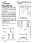
Download Seagate ST1.2 - Series 8 GB Removable Hard Drive Specifications
Transcript
ST1 Series ST650211CF ST650211FX ST625211CF ST625211FX ST1 Series ST650211CF ST650211FX ST625211CF ST625211FX Rev. A ©2004, Seagate Technology LLC All rights reserved Publication number: 100325578, Rev. A June 2004 Seagate and Seagate Technology are registered trademarks of Seagate Technology LLC. SeaTools, SeaFONE, SeaBOARD, SeaTDD, and the Wave logo are either registered trademarks or trademarks of Seagate Technology LLC. Other product names are registered trademarks or trademarks of their owners. Seagate reserves the right to change, without notice, product offerings or specifications. No part of this publication may be reproduced in any form without written permission of Seagate Technology LLC. Revision status summary sheet Revision Rev. A Date 06/30/04 Sheets Affected All. Contents 1.0 Introduction. . . . . . . . . . . . . . . . . . . . . . . . . . . . . . . . . . . . . . . . . . . . . . . . . . . . . . . . . . . . . . . . . . . 1.1 Disclaimer . . . . . . . . . . . . . . . . . . . . . . . . . . . . . . . . . . . . . . . . . . . . . . . . . . . . . . . . . . . . . . 1.2 Drive care . . . . . . . . . . . . . . . . . . . . . . . . . . . . . . . . . . . . . . . . . . . . . . . . . . . . . . . . . . . . . . 1.3 Handling precautions . . . . . . . . . . . . . . . . . . . . . . . . . . . . . . . . . . . . . . . . . . . . . . . . . . . . . . 2.0 Drive specifications . . . . . . . . . . . . . . . . . . . . . . . . . . . . . . . . . . . . . . . . . . . . . . . . . . . . . . . . . . . . 3 2.1 Power, access times and acoustics. . . . . . . . . . . . . . . . . . . . . . . . . . . . . . . . . . . . . . . . . . . 3 2.2 Formatted capacity . . . . . . . . . . . . . . . . . . . . . . . . . . . . . . . . . . . . . . . . . . . . . . . . . . . . . . . 5 2.3 Default logical geometry . . . . . . . . . . . . . . . . . . . . . . . . . . . . . . . . . . . . . . . . . . . . . . . . . . . 5 2.4 Physical organization . . . . . . . . . . . . . . . . . . . . . . . . . . . . . . . . . . . . . . . . . . . . . . . . . . . . . 5 2.5 Recording and interface technology . . . . . . . . . . . . . . . . . . . . . . . . . . . . . . . . . . . . . . . . . . 6 2.6 Physical characteristics . . . . . . . . . . . . . . . . . . . . . . . . . . . . . . . . . . . . . . . . . . . . . . . . . . . 6 2.7 Seek time. . . . . . . . . . . . . . . . . . . . . . . . . . . . . . . . . . . . . . . . . . . . . . . . . . . . . . . . . . . . . . . 7 2.8 Time to ready. . . . . . . . . . . . . . . . . . . . . . . . . . . . . . . . . . . . . . . . . . . . . . . . . . . . . . . . . . . . 7 2.9 Power specifications . . . . . . . . . . . . . . . . . . . . . . . . . . . . . . . . . . . . . . . . . . . . . . . . . . . . . . 8 2.9.1 Power consumption . . . . . . . . . . . . . . . . . . . . . . . . . . . . . . . . . . . . . . . . . . . . . . . 8 2.9.2 Conducted noise . . . . . . . . . . . . . . . . . . . . . . . . . . . . . . . . . . . . . . . . . . . . . . . . 10 2.9.3 Voltage tolerance . . . . . . . . . . . . . . . . . . . . . . . . . . . . . . . . . . . . . . . . . . . . . . . . 10 2.9.4 Power-management modes . . . . . . . . . . . . . . . . . . . . . . . . . . . . . . . . . . . . . . . . 11 2.10 Environmental specifications . . . . . . . . . . . . . . . . . . . . . . . . . . . . . . . . . . . . . . . . . . . . . . . 12 2.10.1 Ambient temperature . . . . . . . . . . . . . . . . . . . . . . . . . . . . . . . . . . . . . . . . . . . . . 12 2.10.2 Temperature gradient. . . . . . . . . . . . . . . . . . . . . . . . . . . . . . . . . . . . . . . . . . . . . 12 2.10.3 Humidity . . . . . . . . . . . . . . . . . . . . . . . . . . . . . . . . . . . . . . . . . . . . . . . . . . . . . . . 12 2.10.4 Altitude . . . . . . . . . . . . . . . . . . . . . . . . . . . . . . . . . . . . . . . . . . . . . . . . . . . . . . . . 12 2.10.5 Shock . . . . . . . . . . . . . . . . . . . . . . . . . . . . . . . . . . . . . . . . . . . . . . . . . . . . . . . . . 13 2.10.6 Vibration . . . . . . . . . . . . . . . . . . . . . . . . . . . . . . . . . . . . . . . . . . . . . . . . . . . . . . . 14 2.11 Acoustics . . . . . . . . . . . . . . . . . . . . . . . . . . . . . . . . . . . . . . . . . . . . . . . . . . . . . . . . . . . . . . 16 2.12 Electromagnetic immunity . . . . . . . . . . . . . . . . . . . . . . . . . . . . . . . . . . . . . . . . . . . . . . . . . 16 2.13 Reliability . . . . . . . . . . . . . . . . . . . . . . . . . . . . . . . . . . . . . . . . . . . . . . . . . . . . . . . . . . . . . . 17 2.14 Agency certification . . . . . . . . . . . . . . . . . . . . . . . . . . . . . . . . . . . . . . . . . . . . . . . . . . . . . . 18 2.14.1 Safety certification . . . . . . . . . . . . . . . . . . . . . . . . . . . . . . . . . . . . . . . . . . . . . . . 18 2.14.2 Electromagnetic compatibility. . . . . . . . . . . . . . . . . . . . . . . . . . . . . . . . . . . . . . . 18 2.14.3 FCC verification . . . . . . . . . . . . . . . . . . . . . . . . . . . . . . . . . . . . . . . . . . . . . . . . . 18 3.0 Configuring and mounting the drive . . . . . . . . . . . . . . . . . . . . . . . . . . . . . . . . . . . . . . . . . . . . . 21 3.1 Handling and static discharge precautions . . . . . . . . . . . . . . . . . . . . . . . . . . . . . . . . . . . . 21 3.2 Drive installation . . . . . . . . . . . . . . . . . . . . . . . . . . . . . . . . . . . . . . . . . . . . . . . . . . . . . . . . 21 4.0 interface description . . . . . . . . . . . . . . . . . . . . . . . . . . . . . . . . . . . . . . . . . . . . . . . . . . . . . . . . . . 4.1 Connector interface signals and connector pins . . . . . . . . . . . . . . . . . . . . . . . . . . . . . . . . 4.1.1 Flex Interface Connector Signals . . . . . . . . . . . . . . . . . . . . . . . . . . . . . . . . . . . . 4.1.2 Supported ATA commands . . . . . . . . . . . . . . . . . . . . . . . . . . . . . . . . . . . . . . . . 4.1.3 Identify Device command. . . . . . . . . . . . . . . . . . . . . . . . . . . . . . . . . . . . . . . . . . 4.1.4 Set Features command . . . . . . . . . . . . . . . . . . . . . . . . . . . . . . . . . . . . . . . . . . . 4.1.5 Card Information Structure (CIS) Information for CF . . . . . . . . . . . . . . . . . . . . . 5.0 Seagate Technology support services . . . . . . . . . . . . . . . . . . . . . . . . . . . . . . . . . . . . . . . . . . . . 49 ST1 Series Product Manual, Rev. A 1 2 2 2 25 25 27 29 31 35 37 v vi ST1 Series Product Manual, Rev. A List of Figures Figure 1. Figure 2. Figure 3. Figure 4. Figure 5. Figure 6. Figure 7. ST1 Series CompactFlash+ disc drive . . . . . . . . . . . . . . . . . . . . . . . . . . . . . . . . . . . . . . . . . . . 1 ST1 Series Flex (IDE interface) disc drive . . . . . . . . . . . . . . . . . . . . . . . . . . . . . . . . . . . . . . . . 1 Typical 3.3V startup and operation current profile . . . . . . . . . . . . . . . . . . . . . . . . . . . . . . . . . . 9 Location where tri-axial accelerometer will be placed on S1 drive. . . . . . . . . . . . . . . . . . . . . 13 Drive axis definition for S1 drives. . . . . . . . . . . . . . . . . . . . . . . . . . . . . . . . . . . . . . . . . . . . . . 13 CF model mechanical dimensions—top, side and end view . . . . . . . . . . . . . . . . . . . . . . . . . 22 FX Model mechanical dimensions—top, side and end view. . . . . . . . . . . . . . . . . . . . . . . . . . 23 ST1 Series Product Manual, Rev. A vii viii ST1 Series Product Manual, Rev. A 1.0 Introduction This manual describes the functional, mechanical and interface specifications for the following Seagate® ST1® Series drives: • ST650211CF and ST625211CF CompactFlash+ Type II disc drives. • ST650211FX and ST625211FX Flex (IDE interface) disc drives. These drives provide the following key features: • 3,600-RPM spindle speed and 2-Mbyte buffer combine for superior performance. • Quiet operation. Fluid Dynamic Bearing (FDB) motor. • Giant magnetoresistive (GMR) recording heads and EPRML technology, which provide the drives with increased areal density. • State-of-the-art cache and on-the-fly error-correction algorithms. • 1.5K Gs nonoperating shock, and 200 Gs operating shock. • SeaTools™ diagnostic software performs a drive self-test that eliminates unnecessary drive returns. • The 3D Defense System™, which includes Drive Defense, Data Defense, and Diagnostic Defense, offers the industry’s most comprehensive protection for disc drives. Figure 1. ST1 Series CompactFlash+ disc drive Figure 2. ST1 Series Flex (IDE interface) disc drive ST1 Series Product Manual, Rev. A 1 1.1 Disclaimer Seagate Technology LLC makes no warranties whatsoever, including any warranty of merchantability, non infringement, fitness for any particular purpose, or any warranty otherwise arising out of any proposal, specification or sample. Seagate may not be held liable for any direct, indirect, incidental, special, exemplary, or consequential damages (including, but not limited to, loss of use, data, or profits; procurement of substitute goods or services; or business interruptions) however caused and on any theory of liability, whether in contract, strict liability, or tort (including negligence or otherwise) arising in any way from the use of this kit, even if advised of the possibility of such damage. 1.2 Drive care Do not use the ST1 Series disc drives outside of the ranges of environmental conditions found in Section 2.10, "Environmental specifications." Doing so may void the warranty of the ST1 Series disc drive. 1.3 Handling precautions • Do not cover or seal the breather hole! Covering or sealing the breather hole may result in loss of data. • Do not press on the drive! Do not apply any force to the drive during handling or installation. • Always handle the drive with care to prevent damage from shock, vibration, or electrostatic discharge (ESD). • Handle the drive carefully by the edges. Do not touch any exposed printed circuit board or the top cover. • Do not write on the label or remove it. Do not apply additional labels. • Always carry the drive in its plastic case. • Do not drop the drive. • Do not expose the drive to wet conditions. • Do not place the drive near a strong magnetic field. • Do not expose the drive to extreme temperatures. • Do not use the drive in CF+TM Type II slots without an ejection mechanism. • The drive may become hot during operation. Be careful when removing the drive from the host device immediately after operation. 2 ST1 Series Product Manual, Rev. A 2.0 Drive specifications Unless otherwise noted, all specifications are measured under ambient conditions, at 25°C, and nominal power. For convenience, the phrases the drive and this drive are used throughout this manual to indicate ST650211CF, ST650211FX, ST625211FX, and ST625211CF model drives. 2.1 Power, access times and acoustics The specifications listed in this table are for quick reference. For details on specification measurement or definition, see the appropriate section of this manual. Table 1: Specifications Drive specification ST650211CF ST650211FX ST625211CF ST625211FX Formatted Gbytes (512 bytes/sector) 5.0 2.5 Guaranteed sectors 9,767,520 4,883,760 Bytes per sector 512 Physical read/write heads 2 1 Discs 1 1 Cache (Mbytes) 2 Recording density, BPI (bits/inch max) 651,000 Track density. TPI (tracks/inch max) 105,000 Areal density (Gbits/inch2 max) 68.3 Spindle speed (RPM) 3,600 Internal data transfer rate OD (Mbytes/sec max) 9.67 Sustained data transfer rate OD (Mbytes/sec) 7.0 I/O data-transfer rate (Mbytes/sec max) 33.3MB/s (UDMA 2) ATA data-transfer modes supported PIO modes 0–4; Multiword DMA modes 0-2; Ultra DMA modes 0–2 Height 5.0 max (0.1968 inches max) Width 42.80 +/-0.101 mm (1.685 +/-0.004 inches) Length 36.40 +/-0.15 mm (1.433 +/-0.006 inches) Weight (typical) 19 grams (0.041 lb.) Average latency (msec) 8.3 Power-on to ready (sec typical / max) 2.0 / 2.5 Standby to ready (sec typical / max) 2.0 / 2.5 Startup current 5V (peak) (maximum RMS in 10ms window) 300 mA Track-to-track average seek time (msec typical, read) 2.0 Average seek time (msec typical, read) 2.0 ST1 Series Product Manual, Rev. A 3 Table 1: Specifications Drive specification ST650211CF ST650211FX Average seek, read (msec typical/max) 16.0/17.0 Full-stroke seek (msec typical/max) 26.0/27.0 Seek power (typical 3.3V) 226 mA Read/write power (typical 3.3V) 300/310 mA Performance idle mode (typical 3.3V) 200 mA Low power idle mode (typical 3.3V) 90 mA ST625211CF ST625211FX Standby/Sleep mode (typical) 30 mA Voltage tolerance (including noise) 3.3V ± 5% 5V ± 10% Ambient temperature 0° to 70°C (operating) –40° to 70°C (nonoperating) Temperature gradient (°C per hour max) 20°C (operating) 30°C (nonoperating) Relative humidity (noncondensing) 5% to 90% (operating) 5% to 95% (nonoperating) Relative humidity gradient 30% per hour max Wet bulb temperature (°C max) 33°C (operating) 40°C (nonoperating) Altitude, operating –60.98 m to 3,048 m (–200 ft to 10,000+ ft) Altitude, nonoperating (below mean sea level, max) –60.98 m to 12,192 m (–200 ft to 40,000+ ft) Shock, operating (Gs max at1 msec) Read 200 Shock, operating (Gs max at 2 msec) Write 175 Shock, operating (Gs max at 2 msec) Write 175 Shock, nonoperating (Gs max at 1 msec) 1500 Shock, nonoperating (Gs max at 0.5 msec) 1500 Vibration, operating (max displacement may apply below 10 hz) 1.0 Gs (0 to peak, 5–500 Hz) @ 2 oct/min sweep rate Vibration, nonoperating (max displacement may apply below 22 hz) 5.0 Gs (0 to peak, 5–500 Hz) @ 0.5 oct/min sweep rate (70°C case temperature) Drive acoustics, sound power (bels) Idle (typical / max) 2.1/ 2.4 Operational (typical / max) 2.2 / 2.5 Nonrecoverable read errors 1 per 1014 bits read Mean time between failures (power-on hours) 100,000 at 40°C Max case temperature: 70°C Load/Unload (LUL) cycles 25°C, 50% relative humidity 300,000 software-controlled power on/off cycles 20,000 hard power on/off cycles 32°C, 80% relative humidity 5°C, 80% relative humidity 5°C, 10% relative humidity 55°C, 16% relative humidity 200,000 software-controlled power on/off cycles 20,000 hard power on/off cycles Warranty Per agreement 4 ST1 Series Product Manual, Rev. A 2.2 Formatted capacity Model Formatted capacity Guaranteed sectors Bytes per sector ST650211CF ST650211FX 5 Gbytes 9,767,520 512 ST625211CF ST625211FX 2.5 Gbytes 4,883,760 512 2.3 Default logical geometry Model Cylinders Read/write heads Sectors per track ST650211CF ST650211FX 9690 16 63 ST625211CF ST625211FX 4845 16 63 LBA mode When addressing these drives in LBA mode, all blocks (sectors) are consecutively numbered from 0 to n–1, where n is the number of guaranteed sectors as defined above. 2.4 Physical organization Model Read/write heads Number of discs ST650211CF ST650211FX 2 1 ST625211CF ST625211FX 1 1 ST1 Series Product Manual, Rev. A 5 2.5 Recording and interface technology Technology Specification Interface CompactFlash 2.0 (CF+ 2.0) Recording method RLL 0,20 Recording density BPI (bits/inch max) 651,000 Track density TPI (tracks/inch max) 105,000 Areal density (Gbits/inch2 max) 68.3 Spindle speed (RPM) (± 0.2%) 3,600 Internal data-transfer rate OD (Mbits/sec max) 9.67 Sustained data transfer rate OD (Mbytes/sec max) 7.0 I/O data-transfer rate (Mbytes/sec max) 33.3MB/s (UDMA 2) Interleave 1:1 Cache buffer ST650211CF, ST650211FX, ST625211CF and ST625211FX 2.6 Physical characteristics Height (mm) (inches) 5.0 +/-0.1 mm 0.1968 +/-0.004 inches Width (mm) (inches) 42.80 +/-0.101 1.685 +/-0.004 Length (mm) (inches) 36.40 +/-0.15 1.433 +/-0.006 Typical weight (grams) (pounds) 19 0.041 Interface Connector ST650211CF, ST625211CF ST650211FX, ST625211FX 6 2 Mbytes (2,048 kbytes) CompactFlash Type II Connector (50-pin) Seagate Flex Connector (45-way) ST1 Series Product Manual, Rev. A 2.7 Seek time Seek measurements are taken with nominal power at 25°C ambient temperature. All times are measured using drive diagnostics. The specifications below are defined as follows: • Track-to-track seek time is an average of all possible single-track seeks in both directions. • Average seek time is a true statistical random average of at least 5,000 measurements of seeks between random tracks, less overhead. *Seek times (msec) Read Write Typical Max Typical Max Track-to-track 2.0 2.5 3.0 3.5 Average 16.0 17.0 19.0 22.0 Full-stroke 26.0 27.0 29.0 32.0 Average latency 8.3 *Measured in performance mode Note. These drives are designed to consistently meet the seek times represented in this manual. Physical seeks, regardless of mode (such as track-to-track and average), are expected to meet or exceed the noted values. However, due to the manner in which these drives are formatted, benchmark tests that include command overhead or measure logical seeks may produce results that vary from these specifications. 2.8 Time to ready Time to ready Typical Max Power-on to Ready (sec) 2.0 2.5 Standby to Ready (sec) 2.0 2.5 ST1 Series Product Manual, Rev. A 7 2.9 Power specifications The drive receives DC power (+3.3V or +5V) through the CompactFlash interface connector for ST650211CF and ST625211CF models, and (+3.3V only) through the Flex interface connector for ST650211FX and ST625211FX models. 2.9.1 Power consumption Power requirements for the drives are listed in the table on page 9. Typical power measurements are based on an average of drives tested, under nominal conditions, using +3.3V and +5.0V input voltage at 25°C ambient temperature. • Spinup power Spinup power is measured from the time of power-on to the time that the drive spindle reaches operating speed. • Seek mode During seek mode, the read/write actuator arm moves toward a specific position on the disc surface and does not execute a read or write operation. Servo electronics are active. Seek mode power is measured based on three random seek operations every 100 msecs. This mode is not typical. • Read/write power and current Read/write power is measured with the heads on track, at the moment while the head is writing/reading from/to disc. It is performed with 100% duty cycle of write/read operation. • Idle mode power, low Spindle motor is working normally with actuator unloaded to the parked position. • Standby mode / Sleep mode During Standby mode, the drive accepts commands, but the drive is not spinning, and the servo and read/ write electronics are in power-down mode. 8 ST1 Series Product Manual, Rev. A Table 2: DC power ST1 Power Consumption (W) Max current the average of the peak value in 10ms window Average 3.3V Max 3.3V Average 5.0V Max 5.0V Current 330 330 Spinup 300 300 Load/Unload current 300 300 Write 310 330 310 330 Read 310 330 320 340 Seek 226 300 226 300 Performance idle 200 205 Low power idle 90 92 Standby/Sleep 30 33 *During periods of drive idle, some offline activity may occur according to the S.M.A.R.T. specification, which may increase acoustic and power to operational levels. 2.9.1.1 Typical current profile Figure 3. Typical 3.3V startup and operation current profile ST1 Series Product Manual, Rev. A 9 2.9.2 Conducted noise Input noise ripple is measured at the host system power supply across an equivalent 15-ohm resistive load on the +5 volt line. Using 5-volt power, the drive is expected to operate with a maximum of 100 mV peak-to-peak square-wave injected noise at up to 20 MHz. Using 3.3-volt power, the drive is expected to operate with a maximum of 70 mV peak-to-peak square-wave injected noise at up to 20 MHz. Note. Equivalent resistance is calculated by dividing the nominal voltage by the typical RMS read/write current. 2.9.3 Voltage tolerance Voltage tolerance (including noise): 5.0V ± 10% 3.3V ± 5% 10 ST1 Series Product Manual, Rev. A 2.9.4 Power-management modes The drive provides programmable power management to provide greater energy efficiency. The drive features the following power-management modes: Table 3: Power management modes Power modes Heads Spindle Buffer Active (operating) Tracking Rotating Enabled Idle, low power Parked Rotating Disabled Standby/Sleep Parked Stopped Disabled • Active mode The drive is in Active mode during the read/write and seek operations. • Low power idle mode Drive enters Low Power Idle mode from Active Idle mode when the Advanced Power Management Level is set above 80h and the Idle timer is reached at 2 seconds. Disc is spinning and head is parked and drive accepts all commands and returns to Active mode any time disc access is necessary. • Performance idle mode The buffer remains enabled, and the drive accepts all commands and returns to Active mode any time disc access is necessary. • Standby/Sleep mode The drive enters Standby mode when the host sends a Standby Immediate command. If the host has set the standby timer, the drive can also enter Standby mode automatically after the drive has been inactive for a specifiable length of time. The standby timer delay is established using a Standby or Idle command. In Standby mode, the drive buffer is enabled, the heads are parked and the spindle is at rest. The drive accepts all commands and returns to Active mode any time disc access is necessary. • Standby timers Each time the drive performs an Active function (such as read, write or seek), the standby timer is reinitialized and begins counting down from its specified delay times to zero. If the standby timer reaches zero before any drive activity is required, the drive makes a transition to Standby mode. In both Idle and Standby mode, the drive accepts all commands and returns to Active mode when disc access is necessary. ST1 Series Product Manual, Rev. A 11 2.10 Environmental specifications 2.10.1 Ambient temperature Ambient temperature is defined as the temperature of the environment immediately surrounding the drive. Actual drive case temperature should not exceed 70°C (158°F) within the operating ambient conditions. Above 1,000 feet (305 meters), the maximum temperature is derated linearly by 1°C every 1000 feet. Operating Nonoperating 2.10.2 0° to 70°C (41° to 158°F) (70°C @ case temperature) –40° to 70°C (–40° to 153°F) Temperature gradient Operating 20°C per hour (68°F per hour max), without condensation Nonoperating 30°C per hour (86°F per hour max), without condensation 2.10.3 Humidity 2.10.3.1 Relative humidity Operating 5% to 90% noncondensing (30% per hour max) Nonoperating 5% to 95% noncondensing (30% per hour max) 2.10.3.2 Wet bulb temperature Operating 33°C (91.4°F max) [1] Nonoperating 40°C (104°F max) [2] [1] [2] Operating Wet bulb temperature is calculated by the operating Temperature and the Relative Humidity levels. Non-operating Wet bulb temperature is calculated by the non-operating Temperature and the Relative Humidity levels. 2.10.4 Altitude Operating Nonoperating 12 –60.98 m to 3,048 m (–200 ft to 10,000+ ft) –60.98 to 12,192 m (–200 ft to 40,000+ ft) ST1 Series Product Manual, Rev. A 2.10.5 Shock All shock measurements in this section are carried out at drive level. For all linear shock test, Operating or Non-Operating, the input shock level shall be measured at the frame of the disk drive at the specific location indicated by the red ellipse in Figure 4 below for the CF and interface drives. Finger Grip Area S1 CF drive S1 interface drive Figure 4. Location where tri-axial accelerometer will be placed on S1 drive. All shock test will cover all the 6 directions, +/- x, y and z axes. The drive axis definition in shown in Figure 5 below. Figure 5. Drive axis definition for S1 drives. 2.10.5.1 Operating shock The drive will be subjected to 10 shocks for each direction. During the shocks, there must be a minimum delay of 3 seconds between shock pulses. Soft errors and automatic retries are allowed during the test. No data loss or permanent damage occurs during a half sine shock pulse of: 200Gs, 1ms (on-track read at OD) 200Gs, 2ms (on-track read at OD) 175Gs, 1ms (random write) 175Gs, 2ms (random write) 2.10.5.2 Nonoperating shock The Non-Operating Shock level that the drive can experience without incurring any physical damage when subsequently put into operation is 750Gs based on a non-repetitive half sine shock pulse of 2ms duration. The same applies for shock levels of 1500Gs, 1ms pulse duration and 1500Gs, 0.5ms pulse duration on fresh drives for each level. ST1 Series Product Manual, Rev. A 13 2.10.6 Vibration All vibration specifications assume that the drive is mounted securely in a fixture that do not have fixture resonances in the frequency test range. The input vibration is applied through the disk drive guide rails of the device under test. Testing is carried out in the x, y and z axes. 2.10.6.1 Operating Sweep Sine Vibration The following lists the maximum Operating Sweep Sine Vibration levels that the drive may experience while meeting the performance standards specified. It will consist of a forward and backward sweep from 5Hz to 500Hz to 5Hz. The drive will operate without a hard error while being subjected to the following vibration levels. 5Hz to 500Hz @ 2 oct/min 2.10.6.2 1.0Gs (0 to pk). Maximum displacement may apply below 10Hz. Operating Random Vibration The test consists of 30 minutes of random vibration using the power spectral density (PSD) levels specified in the table below. The vibration test level is 0.67Gs RMS. The drive will operate without a hard error while being subjected to the following vibration levels. Table 4: 2.10.6.3 Operating Random Vibration profile. Frequency (Hz) G2/Hz 17 1.1 x E-03 45 1.1 x E-03 48 8.0 x E-03 62 8.0 x E-03 65 1.0 x E-03 150 1.0 x E-03 200 5.0 x E-04 500 5.0 x E-04 Non-Operating Sweep Sine Vibration The following table lists the maximum Non-Operating Sweep Sine vibration levels that the drive may experience while meeting the performance standards specified. It will consist of a forward and backward sweep from 5Hz to 500Hz to 5Hz. The drive will not incur any physical damage when subsequently put into operation. 5Hz to 500Hz @ 0.5 oct/min 14 5.0Gs (0 to pk). Maximum displacement may apply below 22Hz. ST1 Series Product Manual, Rev. A 2.10.6.4 Operating Random Vibration The test consists of 15 minutes of random vibration using the power spectral density (PSD) levels specified in the table below. The vibration test level is 3.01Gs RMS. The drive will not incur any physical damage when subsequently put into operation. Table 5: Non-Operating Random Vibration profile. Frequency (Hz) G2/Hz 2.5 1.0 x E-03 5 3.0 x E-02 40 1.8 x E-02 500 1.8 x E-02 ST1 Series Product Manual, Rev. A 15 2.11 Acoustics Drive acoustics are measured as overall A-weighted acoustic sound power levels (no pure tones). Discrete tone penalties are added to the A-weighted sound power (LW) with the following formula only when determining compliance: LWt(spec) == LW + 0.1Pt + 0.3 < 4.0 (Bels) where LW = A-weighted sound power level pt == Value of discrete tone penalty [==dLt-6.0 (dBA)] dLt = Tone-to-noise ratio taken in accordance with ISO 7779. All measurements are consistent with ISO document 7779. Sound power measurements are taken under essentially free-field conditions over a reflecting plane. For all tests, the drive is oriented with the cover facing upward. Note. For seek mode tests, the drive is placed in seek mode only. The number of seeks per second is defined by the following equation: (Number of seeks per second = 0.4 / (average latency + average access time) Table 6: Drive level acoustics Acoustic mode Idle Operational 2.1 bels (typ) 2.4 bels (max) 2.2 bels (typ) 2.5 bels (max) 2.12 Electromagnetic immunity When properly installed in a representative host system, the drive operates without errors or degradation in performance when subjected to the radio frequency (RF) environments defined in the following table: Table 7: Electromagnetic immunity Performance level Reference standard 80 to 1,000 MHz, 3 V/m, 80% AM with 1 kHz sine 900 MHz, 3 V/m, 50% pulse modulation @ 200 Hz A EN 61000-4-3: 96 ENV 50204: 95 Electrical fast transient ± 1 kV on AC mains, ± 0.5 kV on external I/O B EN 61000-4-4: 95 Surge immunity ± 1 kV differential, ± 2 kV common, AC mains B EN 61000-4-5: 95 Conducted RF immunity 150 kHz to 80 MHz, 3 Vrms, 80% AM with 1 kHz sine A EN 61000-4-6: 97 Voltage dips, interrupts 0% open, 5 seconds 0% short, 5 seconds 40%, 0.10 seconds 70%, 0.01 seconds C C C B EN 61000-4-11: 94 Test Description Radiated RF immunity 16 ST1 Series Product Manual, Rev. A 2.13 Reliability Measurement type Specification Nonrecoverable read errors 1 per 1014 bits read, max. Mean time between failures 100,000 power-on hours At nominal power, 40°C ambient temperature. Max case temperature: 60°C at the case measurement location shown in Figure 6 and 7. Load/Unload (LUL) 25°C, 50% relative humidity 300,000 software-controlled power on/off cycles 20,000 hard power on/off cycles 32°C, 80% relative humidity 5°C, 80% relative humidity 5°C, 10% relative humidity 55°C, 16% relative humidity 200,000 software-controlled power on/off cycles 20,000 hard power on/off cycles Warranty Per agreement ST1 Series Product Manual, Rev. A 17 2.14 Agency certification 2.14.1 Safety certification The drives are recognized in accordance with UL60950 Third edition, CAN/CSA-C22.2 No. 60950-00 Third edition, EN 60950-2000 Third edition, and IEC 60950 Third edition as tested by TUV North America.. 2.14.2 Electromagnetic compatibility Hard drives that display the CE mark comply with the European Union (EU) requirements specified in the Electromagnetic Compatibility Directive (89/336/EEC). Testing is performed to the levels specified by the product standards for Information Technology Equipment (ITE). Emission levels are defined by EN 55022, Class B and the immunity levels are defined by EN 55024. Seagate uses an independent laboratory to confirm compliance with the EC directives specified in the previous paragraph. Drives are tested in representative end-user systems. Although CE-marked Seagate drives comply with the directives when used in the test systems, we cannot guarantee that all systems will comply with the directives. The drive is designed for operation inside a properly designed enclosure, with properly shielded I/O cable (if necessary) and terminators on all unused I/O ports. Computer manufacturers and system integrators should confirm EMC compliance and provide CE marking for their products. Korean RRL If these drives have the Korea Ministry of Information and Communication (MIC) logo, they comply with paragraph 1 of Article 11 of the Electromagnetic Compatibility control Regulation and meet the Electromagnetic Compatibility (EMC) Framework requirements of the Radio Research Laboratory (RRL) Ministry of Information and Communication Republic of Korea. These drives have been tested and comply with the Electromagnetic Interference/Electromagnetic Susceptibility (EMI/EMS) for Class B products. Drives are tested in a representative, end-user system by a Korean-recognized lab. • EUT name (model numbers): ST650211CF. ST650211FX, ST625211CF and ST625211FX • Certificate numbers: ST650211CF ST650211FX ST625211CF ST625211FX E-H011-04-xxxx(B) E-H011-04-xxxx(B) E-H011-04-xxxx(B) E-H011-04-xxxx(B) model pending certification model pending certification model pending certification model pending certification • Trade name or applicant: Seagate Technology • Manufacturing date: Aug. 2004 • Manufacturer/nationality: USA, Singapore and China Australian C-Tick (N176) If these models have the C-Tick marking, they comply with the Australia/New Zealand Standard AS/NZS3548 1995 and meet the Electromagnetic Compatibility (EMC) Framework requirements of the Australian Communication Authority (ACA). 2.14.3 FCC verification These drives are intended to be contained solely within a personal computer or similar enclosure (not attached as an external device). As such, each drive is considered to be a subassembly even when it is individually marketed to the customer. As a subassembly, no Federal Communications Commission verification or certification of the device is required. 18 ST1 Series Product Manual, Rev. A Seagate Technology LLC has tested this device in enclosures as described above to ensure that the total assembly (enclosure, disc drive, motherboard, power supply, etc.) does comply with the limits for a Class B computing device, pursuant to Subpart J, Part 15 of the FCC rules. Operation with noncertified assemblies is likely to result in interference to radio and television reception. Radio and television interference. This equipment generates and uses radio frequency energy and if not installed and used in strict accordance with the manufacturer’s instructions, may cause interference to radio and television reception. This equipment is designed to provide reasonable protection against such interference in a residential installation. However, there is no guarantee that interference will not occur in a particular installation. If this equipment does cause interference to radio or television, which can be determined by turning the equipment on and off, you are encouraged to try one or more of the following corrective measures: • Reorient the receiving antenna. • Move the device to one side or the other of the radio or TV. • Move the device farther away from the radio or TV. • Plug the computer into a different outlet so that the receiver and computer are on different branch outlets. If necessary, you should consult your dealer or an experienced radio/television technician for additional suggestions. You may find helpful the following booklet prepared by the Federal Communications Commission: How to Identify and Resolve Radio-Television Interference Problems. This booklet is available from the Superintendent of Documents, U.S. Government Printing Office, Washington, DC 20402. Refer to publication number 004-000-00345-4. ST1 Series Product Manual, Rev. A 19 20 ST1 Series Product Manual, Rev. A 3.0 Configuring and mounting the drive This section contains the specifications and instructions for configuring and mounting the drive. 3.1 Handling and static discharge precautions After unpacking, and before installation, the drive may be exposed to potential handling and electrostatic discharge (ESD) hazards. Observe the following standard handling and static-discharge precautions: Caution: • Keep the drive in the electrostatic discharge (ESD) bag until you are ready for installation to limit the drive’s exposure to ESD. • Before handling the FX interface model drives (ST650211FX and ST625211FX), put on a grounded wrist strap, or ground yourself frequently by touching the metal chassis of a computer that is plugged into a grounded outlet. Wear a grounded wrist strap throughout the entire installation procedure. • Handle the drive only by its edges or frame. • The drive is fragile—handle it with care. Do not press down on the drive top cover or attempt to use a pen to write on the drive’s label. • Always rest the FX interface model drives (ST650211FX and ST625211FX) on a padded, antistatic surface until you mount it in the system. • Do not remove the factory-installed labels from the drive or cover them with additional labels. Removal voids the warranty. Some factory-installed labels contain information needed to service the drive. Other labels are used to seal out dirt and contamination. • Store drive in the provided protective casing when not in use. (CF interface) • For the FX interface model drives (ST650211FX and ST625211FX), turn the power off before installing or removing the drive. • Do not cover the breather hole with any type of label, sticker, or impede the flow of air at any time. 3.2 Drive installation See Figure 6 and 7 for drive mechanical dimensions. Follow these installation precautions when inserting the drive: • Follow instructions for the installation of data storage devices, provided with your device’s user manual. • Do not obstruct the breather hole on the drive. (See figure 4.) • Handle the drive only by its edges or frame or designated finger grip region during mounting. (See figure 4.). ST1 Series Product Manual, Rev. A 21 FINGER GRIP G F Breather Hole Do not cover E B D C A N J K H L M Pin 50 Pin 1 A B C D E F G H J K L M N Dimension Table Inches Millimeters 0.197 max 5.00 max 1.433 ± .006 36.40 ± .15 1.685 ± .004 42.80 ± .10 1.015 ± .003 2x 25.78 ± .07 1.152 ± .010 29.25 ± .25 0.299 ± .010 7.61 ± .25 0.394 min 10.00 min 0.063 ± .002 1.60 ± .05 0.040 ± .003 2x 1.01 ± .07 0.039 ± .002 1.00 ± .05 0.039 ± .004 2x 1.00 min 0.065 ± .004 1.65 ± .10 0.243 ± .004 2x 6.16 ± .10 Figure 6. CF model mechanical dimensions—top, side and end view 22 ST1 Series Product Manual, Rev. A FINGER GRIP G A F Breather Hole Do not cover E B D R S P C H T J K L M A B C D E F G H J K L M P R S T Dimension Table Inches Millimeters 0.197 max 5.00 max 1.433 ± .006 36.40 ± .15 1.685 ± .004 42.80 ± .10 1.015 ± .003 2x 25.78 ± .07 1.152 ± .010 29.25 ± .25 0.299 ± .010 7.61 ± .25 0.394 min 10.00 min 0.063 ± .002 1.60 ± .05 0.040 ± .003 2x 1.01 ± .07 0.039 ± .002 1.00 ± .05 0.039 ± .004 2x 1.00 min 0.065 ± .004 1.65 ± .10 0.906 ± .003 23.00 ± .07 0.669 ± .020 17.00 ± .50 0.414 ± .020 10.51 ± .50 0.130 ± .004 2X 3.30 ± .10 Figure 7. FX Model mechanical dimensions—top, side and end view ST1 Series Product Manual, Rev. A 23 24 ST1 Series Product Manual, Rev. A 4.0 interface description These drives use the industry-standard ATA task file interface that supports 16-bit data transfers. It supports ATA programmed input/output (PIO) modes 0–4; multiword DMA modes 0–2, and Ultra DMA modes 0–2. The drive also supports the use of the IORDY signal to provide reliable high-speed data transfers. For detailed information about the CompactFlash interface, refer to CF+ and CompactFlash Spec Rev 2.0. 4.1 Connector interface signals and connector pins The following table summarizes the signals on the CompactFlash interface connector. For a detailed description of these signals, refer to CF+ and CompactFlash Spec Rev 2.0. Table 8: CompactFlash+ interface connector signals PC Card Memory Mode Pin Num Signal Name 1 GND 2 True IDE Mode[4] PC Card I/O Mode Pin Type In, Out Type Pin Num Signal Name Pin Type In, Out Type Pin Num Signal Name Ground 1 GND D03 I/O I1Z, OZ3 2 3 D04 I/O I1Z, OZ3 4 D05 I/O I1Z, OZ3 5 D06 I/O 6 D07 I/O 7 -CE1 8 A10 9 10 Pin Type In, Out Type Ground 1 GND D03 I/O I1Z, OZ3 2 D03 I/O I1Z, OZ3 3 D04 I/O I1Z, OZ3 4 D05 I/O I1Z, OZ3 3 D04 I/O I1Z, OZ3 4 D05 I/O I1Z, OZ3 I1Z, OZ3 5 D06 I/O I1Z, OZ3 6 D07 I/O I1Z, OZ3 5 D06 I/O I1Z, OZ3 I1Z, OZ3 6 D07 I/O I1Z, OZ3 I I3U 7 -CE1 I I3U I I1Z 8 A10 I I1Z 7 -CS0 I I3U 8 A10[2] I I1Z -OE I I3U 9 -OE I I3U A09 I I1Z 10 A09 I I1Z 9 -ATA SEL I I3U 10 A09[2] I I1Z [2] I I1Z I I1Z Ground 11 A08 I I1Z 11 A08 I I1Z 11 A08 12 A07 I I1Z 12 A07 I I1Z 12 A07[2] 13 VCC Power 13 VCC Power 13 VCC 14 A06 I1Z 14 A06 I1Z 14 A06[2] I I1Z [2] I I1Z I I1Z I I 15 A05 I I1Z 15 A05 I I1Z 15 A05 16 A04 I I1Z 16 A04 I I1Z 16 A04[2] [2] Power 17 A03 I I1Z 17 A03 I I1Z 17 I I1Z 18 A02 I I1Z 18 A02 I I1Z 18 A02 I I1Z 19 A01 I I1Z 19 A01 I I1Z 19 A01 I I1Z 20 A00 I I1Z 20 A00 I I1Z 20 A00 I I1Z 21 D00 I/O I1Z, OZ3 21 D00 I/O I1Z, OZ3 21 D00 I/O I1Z, OZ3 22 D01 I/O I1Z, OZ3 22 D01 I/O I1Z, OZ3 22 D01 I/O I1Z, OZ3 23 D02 I/O I1Z, OZ3 23 D02 I/O I1Z, OZ3 23 D02 I/O I1Z, OZ3 ST1 Series Product Manual, Rev. A A03 25 Table 8: CompactFlash+ interface connector signals PC Card Memory Mode True IDE Mode[4] PC Card I/O Mode 24 WP O OT3 24 -IOIS16 O OT3 24 -IOIS16 O ON3 25 -CD2 O Ground 25 -CD2 O Ground 25 -CD2 O Ground 26 -CD1 O Ground 26 -CD1 O Ground 26 -CD1 O Ground 27 D11 [1] I/O I1Z, OZ3 27 D11 [1] I/O I1Z, OZ3 27 [1] D11 I/O I1Z, OZ3 28 D12[1] I/O I1Z, OZ3 28 D12[1] I/O I1Z, OZ3 28 D12[1] I/O I1Z, OZ3 29 D13 [1] I/O I1Z, OZ3 29 D13 [1] I/O I1Z, OZ3 29 [1] D13 I/O I1Z, OZ3 30 D14[1] I/O I1Z, OZ3 30 D14[1] I/O I1Z, OZ3 30 D14[1] I/O I1Z, OZ3 31 D15 [1] I/O I1Z, OZ3 31 D15 [1] I/O I1Z, OZ3 31 [1] D15 I/O I1Z, OZ3 32 -CE2[1] I I3U 32 -CE2[1] I I3U 32 -CS1[1] I I3Z 33 -VS1 O Ground 33 -VS1 O Ground 33 -VS1 O Ground 34 -IORD I I3U 34 -IORD I I3U 34 -IORD I I3Z 35 -IORW I I3U 35 -IORW I I3U 35 -IORW I I3Z 36 -WE I I3U 36 -WE I I3U 36 -WE[3] I I3U 37 READY O O OT1 37 INTRQ O 38 VCC Power 38 VCC 39 -CSEL[5] 40 -VS2 41 RESET I 42 -WAIT O 43 -INPACK O 44 -REG I 45 BVD2 46 BVD1 47 D08 [1] I/O 48 D09[1] I/O 49 D10 [1] 50 GND Note. [1] [2] [3] [4] [5] [6] 26 OT1 37 -IREQ Power 38 VCC I I2Z 39 -CSEL[5] I I2Z 39 -CSEL I I2U O OPEN 40 -VS2 O OPEN 40 -VS2 O OPEN I2Z 41 RESET I I2Z 41 -RESET I I2Z OT1 42 -WAIT O OT1 42 IORDY O ON1 OT1 43 -INPACK O OT1 43 DMARC O OZ1 I3U 44 -REG I I3U 44 -DMACK[6] I I3U O OT1 45 -SPKR O OT1 45 -DASP I/O I1U, ON1 O OT1 46 -STSCHG O OT1 46 -PDIAG I/O I1U, ON1 I1Z, OZ3 47 D08[1] I/O I1Z, OZ3 47 D08[1] I/O I1Z, OZ3 I1Z, OZ3 48 D09[1] I/O I1Z, OZ3 48 D09[1] I/O I1Z, OZ3 I1Z, OZ3 49 D10 [1] I1Z, OZ3 49 [1] D10 I/O I1Z, OZ3 Ground 50 GND Ground 50 GND I/O I/O OZ1 Power Ground RFU is Reserved for Future Use These signals are required only for 16 bit accesses and not required when installed in 8 bit systems. Devices should allow for 3-state signals not to consume current. The signal should be grounded by the host. The signal should be tied to VCC by the host. The mode is optional for CF+ Cards, but required for CompactFlash Storage Cards. The -CSEL signal is ignored by the card in PC Card modes. However, because it is not pulled up on the card in these modes, it should not be left floating by the host in PC Card modes. In these modes, the pin should be connected by the host to PC Card A25 or grounded by the host. If DMA operations are not used, the signal should be held high or tied to VCC by the host. For proper operation in older hosts: while DMA operations are not active, the card shall ignore this signal, including a floating condition. ST1 Series Product Manual, Rev. A 4.1.1 Flex Interface Connector Signals The following table summarizes the signal on the Seagate Flex interface connector. For a detailed description of these signals, refer to ATA-7 Specifications Revision 7.0. Table 9: Flex interface connector signals Pin Signal Description 1 Ground Ground 2 DD11 Data bus bit 11 3 DD10 Data bus bit 10 4 DD8 Data bus bit 8 5 RESET- Reset 6 DD14 Data bus bit 7 DD15 Data bus bit 8 IORDY- I/O Ready DMA ready during Ultra DMA data-in bursts Data strobe during Ultra DMA data-out bursts 9 INTRQ Interrupt request 10 DA1 Device address bit 1 11 GROUND Ground 12 DA2 Device address bit 2 13 DA0 Device address bit 0 14 DIOW- I/O Write Stop during Ultra DMA data bursts 15 GROUND Ground 16 DIOR- I/O Read DMA ready during Ultra DMA data-in bursts Data strobe during Ultra DMA data-out bursts 17 GROUND Ground 18 PDIAG- Passed diagnostics 19 GROUND Ground 20 DASP- Device active or slave present 21 GROUND Ground 22 CS1- Chip select 0 23 GROUND Ground ST1 Series Product Manual, Rev. A 27 Table 9: Flex interface connector signals 24 DD9 Data bus bit 9 25 GROUND Ground 26 DD13 Data bus bit 13 27 CSEL Cable select 28 DD12 Data bus bit 12 29 DD7 Data bus bit 7 30 DD6 Data bus bit 6 31 DD5 Data bus bit 5 32 DD4 Data bus bit 4 33 DD3 Data bus bit 3 34 DD2 Data bus bit 2 35 GROUND Ground 36 DD1 Data bus bit 1 37 DD0 Data bus bit 0 38 DMARQ DMA request 39 DMACK- DMA Acknowledge 40 IOCS16- Data transfer size is one word per transfer cycle 41 CS0 Chip select 0 42 Reserved 1 Reserved for device use only 43 Reserved 2 Reserved for device use only 44 VCC +3.3V 3.3V Voltage supply to device 45 VCC +3.3V 3.3V Voltage supply to device 28 ST1 Series Product Manual, Rev. A 4.1.2 Supported ATA commands The following table lists ATA-standard commands that the drive supports. For a detailed description of the CF commands, refer to CF+ and CompactFlash Spec Rev 2.0. Table 10: Supported commands Command name Command code (in hex) Does command cause drive to transition to active mode? [1] ATA-standard commands Check Power Mode 98H, E5H Download Microcode 92H (for FX models only) X Erase Sector C0H X Execute Device Diagnostics 90H Flush Cache E7H Format Track (Legacy) 50H Identify Device ECH Idle 97H, E3H X Idle Immediate 95H, E1H X NOP 00h X Read Buffer E4H X Read Multiple C4H X Read Native Max Address F8h X Read Sectors 20H, 21H X Read Verify Sectors 40H, 41H X Recalibrate 10H X Request Sense 03H X Seek 7XH X Set Drive Parameters 91H X Set Features EFH X Set Max Address F9h X Set Multiple Mode C6H X [2] Sleep 99H, E6H Smart B0h X Standby 96H, E2H X Standby Immediate 94H, E0H X Translate Sector 87H X Wear Level F5H X Write Buffer E8H X Write DMA CAH, CBH X ST1 Series Product Manual, Rev. A X 29 Table 10: Supported commands Does command cause drive to transition to active mode? [1] Command name Command code (in hex) Write Multiple C5H X Write Multiple w/o Erase CDH X Write Sectors 30H, 31H X Write Sector w/o Erase 38H X Write Verify 3CH X ATA-standard power-management commands Check Power Mode 98H or E5H Idle 97H or E3H X Idle Immediate 95H or E1H X Sleep 99H or E6H Standby 96H or E2H Standby Immediate 94H or E0H [1] [2] ‘X’ indicates: If the drive is in Standby mode, it will cause the drive to spin up to Active mode in order to execute the command. Except 0Ah, 8Ah and DFh. 30 ST1 Series Product Manual, Rev. A 4.1.3 Identify Device command The Identify Device command (command code ECH) transfers information about the drive to the host following power up. The data is organized as a single 512-byte block of data, whose contents are shown in the table on page 31. All reserved bits or words should be set to zero. Parameters listed with an “x” are drive-specific or vary with the state of the drive. See Section 2.0 on page 3 for default parameter settings. The following commands contain drive-specific features that may not be included in the Draft ATA-7 Standard. Word ATA specification CF specification Value Value Value CF Mem/IO CF TruIDE FX (Flex) 0 Configuration information: • Bit 15: 0 = ATA; 1 = ATAPI • Bit 7: removable media • Bit 6: removable controller • Bit 0: reserved General Config 848AH 848AH 0C5AH 1 Obsolete Default number of cylinders 16,383 16,383 16,383 2 Special Config Reserved 0000H 0000H 0000H 3 Obsolete Default number of heads 16 16 16 4 Retired Number of unformatted bytes/track (Obsolete) 0000H 0000H 0000H 5 Retired Number of unformatted bytes/sector (Obsolete) 0000H 0000H 0000H 6 Obsolete Default number of sectors/track 003FH 003FH 003FH 7 Reserved for CF Spec Number of sectors per card (MSW) xxxx xxxxH xxxx xxxxH xxxx xxxxH 8 Reserved for CF Spec Number of sectors per card (LSW) 9 Retired Obsolete 0000H 0000H 0000H 10–19 Serial number: (20 ASCII characters, 0000H = none) Serial number: (Right justified) ASCII ASCII ASCII 20 Retired Obsolete 0000H 0000H 0000H 21 Retired Obsolete 0000H 0000H 0000H 22 Obsolete Number of ECC bytes 0004H 0004H 0004H 23–26 Firmware revision (8 ASCII character string, padded with blanks to end of string) Firmware revision x.xx x.xx x.xx 27–46 Drive model number: (40 ASCII characters, padded with blanks to end of string) Drive model number (left justified) big endian byte order in word ST650211CF ST625211CF ST650211CF ST625211CF ST650211FX ST625211FX ST1 Series Product Manual, Rev. A 31 Word ATA specification CF specification Value Value Value 47 (Bits 7–0) Maximum sectors per interrupt on Read multiple and Write multiple (16) Maximum number of sectors on Read/Write Multiple command 8010H 8010H 8010H 48 Reserved Reserved 0000H 0000H 0000H 49 Capabilities Capabilities 0A00H 0B00H 0B00H 50 Reserved Reserved 0000H 0000H 0000H 51 Obsolete PIO data transfer cycle timing mode 0200H 0200H 0200H 52 Obsolete Obsolete 0000H 0000H 0000H 53 Words 64–70 and 88 valid Field validity 0003H 0003H 0003H 54 Obsolete Current number of cylinders xxxxH xxxxH xxxxH 55 Obsolete Current number of heads xxxxH xxxxH xxxxH 56 Obsolete Current number of tracks xxxxH xxxxH xxxxH 57 Obsolete Current capacity in sectors (LBA) LSW capacity xxxxH capacity xxxxH capacity xxxxH 58 Obsolete Current capacity in sectors (LBA) MSW capacity xxxxH capacity xxxxH capacity xxxxH 59 Multiple sector setting Multiple sector setting 0100H 0100H 0100H 60–61 Total number of useraddressable LBA sectors available (see Section 2.2 for related information) Total number of useraddressable LBA sectors available (see Section 2.2 for related information) capacity xxxxH capacity xxxxH capacity xxxxH 62 Obsolete Reserved 63 Retired Reserved 0000H 0407H 0407H 64 Advanced PIO modes supported (modes 3 and 4 supported) Advanced PIO modes supported (modes 3 and 4 supported) 0003H 0003H 0003H 65 Reserved Reserved 0000H 0078H 0078H 66 Reserved Reserved 0000H 0078H 0078H 67 Minimum PIO cycle time without IORDY flow control (120 nsec) Minimum PIO cycle time without IORDY flow control (120 nsec) 0078H 0078H 0078H 68 Minimum PIO cycle time with IORDY flow control (120 nsec) Minimum PIO cycle time with IORDY flow control (120 nsec) 0078H 0078H 0078H 69–79 Reserved 0000H 0000H 0000H 80-81 Reserved 0000H 0000H 0000H 82 Features/Command sets supported Features/Command sets supported 7068H 7068H 7068H 83 Features/Command sets supported Features/Command sets supported 500CH 500CH 500DH 32 ST1 Series Product Manual, Rev. A Word ATA specification CF specification Value Value Value 84 Features/Command sets supported Features/Command sets supported 4000H 4000H 4000H 85 Features/Command sets enabled Features/Command sets enabled 7068H 7068H 7068H 86 Features/Command sets enabled Features/Command sets enabled 100CH 100CH 100DH 87 Features/Command sets enabled Features/Command sets enabled 4000H 4000H 4000H 88 Ultra DMA support and current mode (see note following this table) Reserved 0000H 0007H 0007H 89 Time required for security erase complete Time required for security erase complete 0000H 0000H 0000H 90 Time required for enhanced security erase complete Time required for enhanced security erase complete 0000H 0000H 0000H 91 Advanced power management value Advanced power management value 4040H 4040H 4040H Reserved 0000H 0000H 0000H 92-127 128 Security status Security status 0000H 0000H 0000H 129–159 Seagate-reserved Seagate-reserved 0000H 0000H 0000H 160 CFA power mode 1 Power Level Description 814AH 814AH 814AH 161 Reserved for assignment by the CFA 0000H 0000H 0000H 162 Key management schemes supported 0000H 0000H 0000H 163–175 ATA-reserved Reserved for assignment by the CFA 0000H 0000H 0000H 176-255 Reserved Reserved 0000H 0000H 0000H ST1 Series Product Manual, Rev. A 33 Note. See the bit descriptions below for words 63, 88, 93 and 94 of the Identify Drive data: Description (if bit is set to 1) 34 Bit Word 63 0 Multiword DMA mode 0 is supported. 1 Multiword DMA mode 1 is supported. 2 Multiword DMA mode 2 is supported. 8 Multiword DMA mode 0 is currently active. 9 Multiword DMA mode 1 is currently active. 10 Multiword DMA mode 2 is currently active. Bit Word 88 0 Ultra DMA mode 0 is supported. 1 Ultra DMA mode 1 is supported. 2 Ultra DMA mode 2 is supported. 8 Ultra DMA mode 0 is currently active. 9 Ultra DMA mode 1 is currently active. 10 Ultra DMA mode 2 is currently active. ST1 Series Product Manual, Rev. A 4.1.4 Set Features command This command controls the implementation of various features that the drive supports. When the drive receives this command, it sets BSY, checks the contents of the Features register, clears BSY and generates an interrupt. If the value in the register does not represent a feature that the drive supports, the command is aborted. Power-on default has the read look-ahead feature enabled and write caching feature disabled. The acceptable values for the Features register are defined as follows: Table 11: Features register values Feature Description Availability in Interface Mode CF Memory or I/O TrueIDE or IDE 01H Enable 8-bit data transfer; Only in True IDE mode. Yes No 02H Enable Write Cache. Yes Yes Yes Yes 03H Used for Set transfer mode Command. Sector Count register values: 00H Set PIO mode to default (PIO mode 2). Yes Yes 01H Set PIO mode to default and disable IORDY (PIO mode 2). Yes Yes 08H PIO mode 0 Yes Yes 09H PIO mode 1 Yes Yes 0AH PIO mode 2 Yes Yes 0BH PIO mode 3 Yes Yes 0CH PIO mode 4 (default) Yes Yes 20H Multiword DMA mode 0 No Yes 21H Multiword DMA mode 1 No Yes 22H Multiword DMA mode 2 No Yes 40H Ultra DMA mode 0 No Yes 41H Ultra DMA mode 1 No Yes 42H Ultra DMA mode 2 No Yes 05H Enable advanced power management Yes Yes 0AH Enable Power Level 1 commands Yes Yes 44H Product Specific ECC bytes (XX bytes) apply on Read/Write Long Command Yes Yes 55H Disable read look-ahead (read cache) feature. Yes Yes 66H Disable Power On Reset (POR) establishment of defaults at Soft Reset. Yes Yes ST1 Series Product Manual, Rev. A 35 Table 11: Features register values 69H NOP- Accepted for backward compatibility Yes Yes 81H Disable 8 bit transfer; Only in True IDE mode Yes Yes 82H Disable write cache. (default) Yes Yes 85H Disable Advanced Power Management Yes Yes 8AH Disable Power Level 1 Commands Yes Yes 96H NOP- Accepted for backward compatibility Yes Yes 97H Accepted for backward compatibility Yes Yes 9AH It's NOP for backward compatibility Yes Yes AAH Enable read look-ahead (read cache) feature (default). Yes Yes BBH 4 Bytes of ECC apply on Read/Write Long Command Yes Yes CCH Enable Power On Reset (POR) establishment of defaults at soft reset Yes Yes D0H Seagate Unique; Disable Reassignment Yes Yes D1H Seagate Unique; Enable Reassignment Yes Yes Note. 36 At power-on, or after a hardware or software reset, the default values of the features are as indicated above. ST1 Series Product Manual, Rev. A 4.1.5 Card Information Structure (CIS) Information for CF CIS information for the CF card is as follows: Address Data Description of data Common Memory Device Information in 5V Operation 000H 01H CISTPL_DEVICE 002H 04H TPL_LINK = 04 bytes 004H DFH CISTPL_DEVICE: Device ID Device type (bit 4...7 = D (DTYPE_FUNCSPEC) WPS (write protect switch) (bit 3) = 1 (non WP) Device Speed (bit 0...2) = 7 (DSPEED_EXT) 006H 12H CISTPL_DEVICE: EXT (bit 7) = 0 Mantissa (bit 3...6) = 2 (1.2) --> 120ns Exponent (bit 0...2) = 2 (100) 008H 01H CISTPL_DEVICE: Device size = 1 (2K bytes) 00AH FFH CISTPL_DEVICE: End Marker Other Operating Conditions Device Information for Common Memory 00CH 1CH CISTPL_DEVICE_OC 00EH 05H TPL_LINK = 05 bytes 03H CISTPL_DEVICE_OC: Other conditions Information EXT (bit 7) = 0 Reserved (bit 3...6) = 0 Vcc used (bit 1,2) = 1 (3.3V) MWAIT (bit 0) = 1 012H DFH CISTPL_DEVICE_OC: Device ID Information Device Type (bit 4...7) = D (DTYPE_FUNCSPEC) WPS (write protect switch) (bit 3) = 1 (non WP) Device Speed (bit 0...2) = 7 (DSPEED_EXT) 014H 12H CISTPL_DEVICE_OC: EXT (bit 7) = 0 Mantissa (bit 3...6) = 2 (1.2) --> 120ns Exponent (bit 0...2) = 2 (100) 016H 01H CISTPL_DEVICE_OC: Device size = 1 (2K bytes) 018H FFH CISTPL_DEVICE_OC: End Marker 010H JEDEC Programming Information for Common Memory 01AH 18H CISTPL_JEDEC_C 01CH 02H TPL_LINK = 02 bytes 01EH DFH CISPTL_JEDEC_C: PCMCIA JEDEC Code 020H 01H ST1 Series Product Manual, Rev. A 37 Manufacturer Identification String 022H 20H CISTPL_MANFID 024H 04H TPL_LINK = 04 bytes 026H 11H TPL_MANF: Manufacturer’s ID code (Low byte) = 11 for SEAGATE 028H 01H TPL_MANF: Manufacturer’s ID code (High byte) = 01 for SEAGATE 02AH 00H TPLMID_CARD: Product code (Low byte) (Manufacturer Info) 02CH 00H TPLMID_CARD: Product code (High byte) (Manufacturer Info) 02EH 15H CISTPL_VERS_1 030H 0EH TPL_LINK = 0Eh bytes 032H 04H TPLLV1_MAJOR: Major Version Number (JEIDA 4.2/PCMCIA 2.1) 034H 01H TPLLV1_MINOR : Minor Version Number = 1 036H 53H TPLLV1_INFO: ‘ S ’ (Vender Specific Strings) 038H 45H TPLLV1_INFO: ‘ E ’ (Vender Specific Strings) 03AH 41H TPLLV1_INFO: ‘ A ’ (Vender Specific Strings) 03CH 47H TPLLV1_INFO: ‘ G ’ (Vender Specific Strings) 03EH 41H TPLLV1_INFO: ‘ A ’ (Vender Specific Strings) 040H 54H TPLLV1_INFO: ‘ T ’ (Vender Specific Strings) 042H 45H TPLLV1_INFO: ‘ E ’ (Vender Specific Strings) 044H 00H TPLLV1_INFO: Null terminator (End of Name) 046H 53H TPLLV1_INFO: ‘ S ’ (Vender Specific Strings) 048H 54H TPLLV1_INFO: ‘ T ’ (Vender Specific Strings) 04AH 51H TPLLV1_INFO: ‘ 1 ’ (Vender Specific Strings) 04CH 00H TPLLV1_INFO: Null terminator (End of Name) 04EH FFH CISTPL_VERS_1: End marker 050H 21H CISTPL_FUNCID 052H 02H TPL_LINK = 02 bytes 054H 04H TPLFID_FUNCTION: (IC Card Function Code) = 04 (Fixed Disk) 056H 01H TPLFD_SYSINT: (System Initialization bit mask) POST (bit 0) =1 ROM (bit 1) =0 058H 22H CISTPL_FUNCE :(Function Extension Tuple) 05AH 02H TPL_LINK = 02 bytes 05CH 01H TUPLE_TYPE: (Extension Type) = 01 (Disk Device Interface) 05EH 01H TUPLE_DATA: (Interface Type) = 01 (PC Card ATA Interface) 38 ST1 Series Product Manual, Rev. A 060H 22H CISTPL_FUNCE: (Function Extension Tuple) 062H 03H TPL_LINK =3 bytes 064H 02H TUPLE_TYPE: (Extension Type) = 02 (Basic PC Card ATA Interface) 08H TPLFE_DATA V : Vpp[2::1] (bit0,1) = 00 (Vpp not required) S : Silicon (bit2) = 0 (Rotating Device) U : Inique (bit3) = 0 (Single Drive) D : Dual Drive (bit4) = 0 (Single Drive) 068H 0FH TPLFE_DATA P0 : Sleep (bit0) = 1 (Support Sleep mode) P1 : Standby (bit1) = 1 (Support Standby mode) P2 : Idle (bit2) = 1 (Support Idle mode) P3 : Auto (bit 3) = 1 (Support Automatic Power Control) N : 3F7/377 (bit4) = 0 (Include 3F7h/377h for I/O Address) E : Index Emulate (bit5) = 0 (Index Emulation is not supported) I : IOIS16 (bit6) =0 06AH 1AH CISTPL_CONFIG (Configuration Tuple) 06CH 05H TPL_LINK = 5 bytes 06EH 01H TPCC_SZ :(Size of Field Byte) TPCC_RASZ (Size of TPCC_RADR) (bit0,1) = 1 (2 bytes) TPCC_RMSZ (Size of TPCC_RMSK) (bit 2..5) = 0 (1 byte) 070H 07H TPCC_LAST: (Last Entry Index) =07 072H 00H TPCC_RADR: (Low byte) (Base address of Configuration Register = 00h) 074H 02H TPCC_RADR: (High byte) (Base address of Configuration Register = 02h) 076H 0FH TPCC_RMSK: (Register Presence Mask) = 00001111b (200, 202, 204, 206) 066H Configuration For PC Card Memory Mode in 5V Operation (Default) 078H 1BH CISTPL_CFTABLE_ENTRY: (16 Bit PCCard Configuration Table Entry Tuple) 07AH 0CH TPCE_LINK = 0C bytes C0H TPCE_INDX: ( Configuration Table Entry Tuple) Config Entry Number (bit0..5) = 00 (Memory Mode) Default (bit6) = 1 Interface (bit7) = 1 (Interface Field Exist) C0H TPCE_IF: (Interface Description Field) Interface Type (bit0..3) = 00 (Memory) BVDS active (bit4) = 0 WP active (bit5) = 0 READY active (bit6) = 1 MWAIT required (bit7) = 1 07CH 07EH ST1 Series Product Manual, Rev. A 39 A1H TPCE_FS: (Feature Selection Byte) Power (bit0,1) = 01 (Vcc Only) Timing (bit2) = 0 I/O (bit3) = 0 Interrupt (bit4) = 0 Memory (bit5,6) = 01 Misc (bit7) = 1 TPCE_PD (Power Description Structure) 082H 27H TPCE_PS: Parameter Selection Byte NomV (bit0) =1 MinV (bit1) = 1 MaxV (bit2) =1 PeakI (bit5) =1 084H 55H TPCE_PD: Power Parameter Definition (NomV) Exponent (bit 0..2) = 5 (1V) -->5.0V Mantissa (bit3..6) = A (5.0) 086H 4DH TPCE_PD: Power Parameter Definition (MinV) Exponent (bit 0..2) = 5 (1V) -->4.5V Mantissa (bit3..6) = 9 (4.5) 088H 5DH TPCE_PD: Power Paramter Definition (MaxV) Exponent (bit 0..2) = 5 (1V) -->5.5V Mantissa (bit3..6) = C (5.5) 08AH B6H TPCE_PD: Power Parameter Defintion (PeakI) Exponent (bit 0..2) = 6 (100mA) - -+-->330mA Mantissa (bit3..6) = 6 (3) + Extension (bit7) = 1 (Extension Byte Exists) + 08CH 1EH TPCE_PD: Extension = 1Eh = +30 - -+ TPCE_MS: (Memory Space Description Structure) 08EH 08H TPCE_MS: Memory Space Descriptor Space # of Windows (-1) (bit0..2) = 0 (# of window =1) Length Size (bit3..4) =1 (Length Field Size =1 byte) Card Address Size (bit5..6) = 0 (no card addr field) Host Addr (bit7) = 0 (arbitrary host addr) 090H 00H TPCE_MS: Window Descriptor Length of the window = 0 20H TPCE_MI: (Miscellaneous Features Field) Max Twin Card (bit0..2) = 0 Audio (bit3) =0 Read Only (bit4) =0 Power Down (bit5) =1 (Support Power Down Mode) 080H 092H Configuration For PC Card Memory I/O Mode in 3.3V Operation (Alternative) 094H 1BH CISTPL_CFTABLE_ENTRY: (16 bit PCCard Configuration Table Entry Tuple) 096H 07H TPCE_LINK = 07h bytes 40 ST1 Series Product Manual, Rev. A 00H TPCE_INDX: (Configuration Table Index Byte) Config Entry Number (bit0..5) = 00 (Memory Mode) Default (bit6) = 0 Interface (bit7) = 0 (Interface Field Exist) 01H TPCE_FS Power (bit0,1) = 01 (Vcc Only) Timing (bit2) = 0 I/O (bit3) = 0 Interrupt (bit4) = 0 Memory (bit5,6) = 00 Misc (bit7) = 0 21H TPCE_PD: Paramter Selection Byte NomV (bit0) =1 MinV (bit1) = 0 MaxV (bit2) =0 PeakI (bit5) =1 09EH B5H TPCE_PD: Power Parameter Defintion (NomV) Exponent (bit0..2) = 5 (1V) - -+ -->3.3V Mantissa (bit3..6) =6 (3.0) + Extension (bit7) =1 (Extension Exists) + 0A0H 1EH TPCE_PD: Extension 0A2H B6H TPCE_PD: Power Parameter Defintion (PeakI) Exponent (bit0..2) = 6 (100mA) -->330mA Mantissa (bit3..6) = 6 (3) Extension (bit7) =1 (Extension Exists) + 0A4H 1EH TPCE_PD: Extension 098H 09AH 09CH = 1Eh =+0.30 = 1Eh =+30 --+ --+ For PC Card ATA I/O in Contiguous Memory Mode in 5V Operation (Default) 0A6H 1BH CISTPL_CFTABLE_ENTRY: (16 Bit PCCard Configuration Table Entry Tuple) 0A8H 0EH TPCE_LINK = 0E bytes C1H TPCE_INDX: ( Configuration Table Entry Tuple) Config Entry Number (bit0..5) = 01 (I/O and Memory Mode) Default (bit6) = 1 Interface (bit7) = 1 (Interface Field Exist) 41H TPCE_IF: (Interface Description Field) Interface Type (bit0..3) = 01 (I/O and Memory) BVDS active (bit4) = 0 WP active (bit5) = 0 READY active (bit6) = 1 MWAIT required (bit7) = 0 0AAH 0ACH ST1 Series Product Manual, Rev. A 41 99H TPCE_FS: (Feature Selection Byte) Power (bit0,1) = 01 (Vcc Only) Timing (bit2) = 0 I/O (bit3) = 0 Interrupt (bit4) = 0 Memory (bit5,6) = 01 Misc (bit7) = 1 TPCE_PD (Power Description Structure) 0B0H 27H TPCE_PD: Parameter Selection Byte NomV (bit0) =1 MinV (bit1) = 1 MaxV (bit2) =1 PeakI (bit5) =1 0B2H 55H TPCE_PD: Power Parameter Definition (NomV) Exponent (bit 0..2) = 5 (1V) -->5.0V Mantissa (bit3..6) = A (5.0) 0B4H 4DH TPCE_PD: Power Parameter Definition (MinV) Exponent (bit 0..2) = 5 (1V) -->4.5V Mantissa (bit3..6) = 9 (4.5) 0B6H 5DH TPCE_PD: Power Paramter Definition (MaxV) Exponent (bit 0..2) = 5 (1V) -->5.5V Mantissa (bit3..6) = C (5.5) 0B8H B6H TPCE_PD: Power Parameter Defintion (PeakI) Exponent (bit 0..2) = 6 (100mA) --+-->330mA Mantissa (bit3..6) = 6 (3) + Extension (bit7) = 1 (Extension Byte Exists) + 0BAH 1EH TPCE_PD: Extension = 1Eh = +30 --+ TPCE_MS: (Memory Space Description Structure) 64H TPCE_IO: (I/O Space Address required for this configuration) I/O Address Lines (bit0..4) =4 (16 byte boundary) Bus 16/8 (bit5,6) = 3 (Support 16/8 bit access) Range (bit7) = 0 TPCE_IR (Interrupt Request Description Structure) 0BEH F0H TPCE_IR: IRQ Line 0..15 (bit0..3) =0 MASK (bit4) = 1 Level (bit5) = 1 Pulse (bit6) = 1 Share (bit7) = 1 0C0H FFH TPCE_IR+1: IRQ0..IRQ7 0C2H FFH TPCE_IR+2: IRQ8..IRQ15 = All Supported 20H TPCE_MI :(Miscellaneous Features Field ) Max Twin Card (bit0..2) = 0 Audio (bit3) = 0 Read Only (bit4) = 0 Power Down (bit5) = 1 (Support Power Down Mode) 0AEH 0BCH 0C4H 42 = All Supported ST1 Series Product Manual, Rev. A For PC Card ATA I/O in Contiguous Memory Mode in 3.3V Operation (Default) 0C6H 1BH CISTPL_CFTABLE_ENTRY: (16 Bit PCCard Configuration Table Entry Tuple) 0C8H 07H TPCE_LINK = 07h bytes 01H TPCE_INDX :(Configuration Table Index Byte) Config Entry Number (bit0..5) = 01 (I/O and Memory Mode) Default (bit6) = 0 Interface (bit7) = 0 (Interface Field Exist) 01H TPCE_FS Power (bit0,1) = 01 (Vcc Only) Timing (bit2) = 0 I/O (bit3) = 0 Interrupt (bit4) = 0 Memory (bit5,6) = 00 Misc (bit7) = 0 21H TPCE_PD: Paramter Selection Byte NomV (bit0) =1 MinV (bit1) = 0 MaxV (bit2) =0 PeakI (bit5) =1 0D0H B5H TPCE_PD: Power Parameter Defintion (NomV) Exponent (bit0..2) = 5 (1V) - -+ -->3.3V Mantissa (bit3..6) =6 (3.0) + Extension (bit7) =1 (Extension Exists) + 0D2H 1EH TPCE_PD: Extension 0D4H B6H TPCE_PD: Power Parameter Defintion (PeakI) Exponent (bit0..2) = 6 (100mA) -->330mA Mantissa (bit3..6) = 6 (3) Extension (bit7) =1 (Extension Exists) + 0D6H 1EH TPCE_PD: Extension 0CAH 0CCH 0CEH = 1Eh =+0.30 = 1Eh =+30 --+ --+ For PC Card ATA I/O Primary Mode (1F0-1F7, 3F6, 3F7) in 5V Operation (Default) 0D8H 1BH CISTPL_CFTABLE_ENTRY: (16 Bit PC Card Configuration Table Entry Tuple) 0DAH 13H TPCE_LINK = 13h bytes C2H TPCE_INDX :( Configuration Table Entry Tuple) Config Entry Number (bit0..5) = 02 (Primary I/O Mode) Default (bit6) = 1 Interface (bit7) = 1 (Interface Field Exist) 41H TPCE_IF: (Interface Description Field) Interface Type (bit0..3) = 01 (I/O and Memory) BVDS active (bit4) = 0 WP active (bit5) = 0 READY active (bit6) = 1 MWAIT required (bit7) = 0 0DCH 0DEH ST1 Series Product Manual, Rev. A 43 99H TPCE_FS: (Feature Selection Byte) Power (bit0,1) = 01 (Vcc Only) Timing (bit2) = 0 I/O (bit3) = 0 Interrupt (bit4) = 0 Memory (bit5,6) = 01 Misc (bit7) = 1 TPCE_PD (Power Description Structure) 0E2H 27H TPCE_PD: Parameter Selection Byte NomV (bit0) =1 MinV (bit1) = 1 MaxV (bit2) =1 PeakI (bit5) =1 0E4H 55H TPCE_PD: Power Parameter Definition (NomV) Exponent (bit 0..2) = 5 (1V) -->5.0V Mantissa (bit3..6) = A (5.0) 0E6H 4DH TPCE_PD: Power Parameter Definition (MinV) Exponent (bit 0..2) = 5 (1V) -->4.5V Mantissa (bit3..6) = 9 (4.5) 0E8H 5DH TPCE_PD: Power Paramter Definition (MaxV) Exponent (bit 0..2) = 5 (1V) -->5.5V Mantissa (bit3..6) = C (5.5) 0EAH B6H TPCE_PD: Power Parameter Defintion (PeakI) Exponent (bit 0..2) = 6 (100mA) --+-->330mA Mantissa (bit3..6) = 6 (3) + Extension (bit7) = 1 (Extension Byte Exists) + 0ECH 1EH TPCE_PD: Extension = 1Eh = +30 --+ EAH TPCE_IO: (I/O Space Address required for this configuration) I/O Address Lines (bit0..4) =A (1K byte boundary) Bus 16/8 (bit5,6) = 3 (Support 16/8 bit access) Range (bit7) = 1 (See I/O Range Description Byte) 0F0H 61H TPCE_IO: I/O Range Description Byte # of address range - 1 (bit0..3) = 1 (#of field = 2) Size Of Address (bit4,5) = 2 (2 byte address) Size Of Length (bit6,7) = 1 (1 byte length) 0F2H F0H TPCE_IO: I/O Address Range Description Field #1 Address = 1F0 0F4H 01H 0F6H 07H TPCE_IO: I/O Address Block Length = 8 0F8H F6H TPCE_IO: I/O Address Range Description Field #2 Address = 3F6 0FAH 03H 0FCH 01H 0E0H 0EEH 44 TPCE_IO: I/O Address Block Length = 2 ST1 Series Product Manual, Rev. A 0FEH 100H EEH TPCE_IR: (Interrupt Request Description Structure) IRQ Line 0..15 (bit0..3) = E MASK (bit4) = 0 Level (bit5) = 1 Pulse (bit6) = 1 Share (bit7) = 1 20H TPCE_MI: (Miscellaneous Features Field ) Max Twin Card (bit0..2) = 0 Audio (bit3) = 0 Read Only (bit4) = 0 Power Down (bit5) = 1 (Support Power Down Mode) For PC Card ATA I/O Primary Mode (1F0-1F7, 3F6, 3F7) in 3.3V Operation (Alternative) 102H 1BH CISTPL_CFTABLE_ENTRY: (16 Bit PC Card Configuration Table Entry Tuple) 104H 07H TPCE_LINK = 07 bytes 02H TPCE_INDX: (Configuration Table Index Byte) Config Entry Number (bit0..5) = 02 (Primary I/O Mode) Default (bit6) = 0 Interface (bit7) = 0 (Interface Field Exist) 01H TPCE_FS Power (bit0,1) = 01 (Vcc Only) Timing (bit2) = 0 I/O (bit3) = 0 Interrupt (bit4) = 0 Memory (bit5,6) = 00 Misc (bit7) = 0 21H TPCE_PD: Paramter Selection Byte NomV (bit0) =1 MinV (bit1) = 0 MaxV (bit2) =0 PeakI (bit5) =1 10CH B5H TPCE_PD: Power Parameter Defintion (NomV) Exponent (bit0..2) = 5 (1V) - -+ -->3.3V Mantissa (bit3..6) =6 (3.0) + Extension (bit7) =1 (Extension Exists) + 10EH 1EH TPCE_PD: Extension 110H B6H TPCE_PD: Power Parameter Defintion (PeakI) Exponent (bit0..2) = 6 (100mA) -->330mA Mantissa (bit3..6) = 6 (3) Extension (bit7) =1 (Extension Exists) + 112H 1EH TPCE_PD: Extension 106H 108H 10AH = 1Eh =+0.30 = 1Eh =+30 --+ --+ For PC Card ATA I/O Secondary Mode (170-177, 377, 377) in 5V Operation (Default) 114H 1BH CISTPL_CFTABLE_ENTRY (16 Bit PC Card Configuration Table Entry Tuple) 116H 13H TPCE_LINK = 13h bytes ST1 Series Product Manual, Rev. A 45 C3H TPCE_INDX :( Configuration Table Entry Tuple) Config Entry Number (bit0..5) = 03 (Secondary I/O Mode) Default (bit6) = 1 Interface (bit7) = 1 (Interface Field Exist) 41H TPCE_IF: (Interface Description Field) Interface Type (bit0..3) = 01 (I/O and Memory) BVDS active (bit4) = 0 WP active (bit5) = 0 READY active (bit6) = 1 MWAIT required (bit7) = 0 99H TPCE_FS: (Feature Selection Byte) Power (bit0,1) = 01 (Vcc Only) Timing (bit2) = 0 I/O (bit3) = 0 Interrupt (bit4) = 0 Memory (bit5,6) = 01 Misc (bit7) = 1 TPCE_PD (Power Description Structure) 11EH 27H TPCE_PD: Parameter Selection Byte NomV (bit0) =1 MinV (bit1) = 1 MaxV (bit2) =1 PeakI (bit5) =1 120H 55H TPCE_PD: Power Parameter Definition (NomV) Exponent (bit 0..2) = 5 (1V) -->5.0V Mantissa (bit3..6) = A (5.0) 122H 4DH TPCE_PD: Power Parameter Definition (MinV) Exponent (bit 0..2) = 5 (1V) -->4.5V Mantissa (bit3..6) = 9 (4.5) 124H 5DH TPCE_PD: Power Paramter Definition (MaxV) Exponent (bit 0..2) = 5 (1V) -->5.5V Mantissa (bit3..6) = C (5.5) 126H B6H TPCE_PD: Power Parameter Defintion (PeakI) Exponent (bit 0..2) = 6 (100mA) --+-->330mA Mantissa (bit3..6) = 6 (3) + Extension (bit7) = 1 (Extension Byte Exists) + 128H 1EH TPCE_PD: Extension = 1Eh = +0.30 --+ EAH TPCE_IO: (I/O Space Address required for this configuration) I/O Address Lines (bit0..4) =A (1K byte boundary) Bus 16/8 (bit5,6) = 3 (Support 16/8 bit access) Range (bit7) = 1 (See I/O Range Description Byte) 12CH 61H TPCE_IO: I/O Range Description Byte # of address range - 1 (bit0..3) = 1 (#of field = 2) Size Of Address (bit4,5) = 2 (2 byte address) Size Of Length (bit6,7) = 1 (1 byte length) 12EH 70H TPCE_IO: I/O Address Range Description Field #1 Address = 170 118H 11AH 11CH 12AH 46 ST1 Series Product Manual, Rev. A 130H 01H 132H 07H TPCE_IO: I/O Address Block Length = 8 134H 76H TPCE_IO: I/O Address Range Description Field #2 Address = 376 136H 03H 138H 01H TPCE_IO: I/O Address Block Length = 2 EEH TPCE_IR: (Interrupt Request Description Structure) IRQ Line 0..15 (bit0..3) = E MASK (bit4) = 0 Level (bit5) = 1 Pulse (bit6) = 1 Share (bit7) = 1 20H TPCE_MI: (Miscellaneous Features Field ) Max Twin Card (bit0..2) = 0 Audio (bit3) = 0 Read Only (bit4) = 0 Power Down (bit5) = 1 (Support Power Down Mode) 13AH 13CH For PC Card ATA I/O Secondary Mode (170-177, 377, 377) in 3.3V Operation (Default) 13EH 1BH CISTPL_CFTABLE_ENTRY (16 Bit PC Card Configuration Table Entry Tuple) 140H 06H TPCE_LINK = 07h bytes 03H TPCE_INDX: (Configuration Table Index Byte) Config Entry Number (bit0..5) = 03 (Secondary I/O Mode) Default (bit6) = 0 Interface (bit7) = 0 (Interface Field Exist) 01H TPCE_FS Power (bit0,1) = 01 (Vcc Only) Timing (bit2) = 0 I/O (bit3) = 0 Interrupt (bit4) = 0 Memory (bit5,6) = 00 Misc (bit7) = 0 21H TPCE_PD: Paramter Selection Byte NomV (bit0) =1 MinV (bit1) = 0 MaxV (bit2) =0 PeakI (bit5) =1 148H B5H TPCE_PD: Power Parameter Defintion (NomV) Exponent (bit0..2) = 5 (1V) - -+ -->3.3V Mantissa (bit3..6) =6 (3.0) + Extension (bit7) =1 (Extension Exists) + 14AH 1EH TPCE_PD: Extension B6H TPCE_PD: Power Parameter Defintion (PeakI) Exponent (bit 0..2) = 6 (100mA) --+-->330mA Mantissa (bit3..6) = 6 (3) + Extension (bit7) = 1 (Extension Byte Exists) + 142H 144H 146H 14CH ST1 Series Product Manual, Rev. A = 1Eh =+0.30 --+ 47 14EH 1EH TPCE_PD: Extension = 1Eh = +30 --+ 150H 14H CISTPL_NO_LINK 152H 00H TPCE_LINK 154H FFH CISTPL_END 48 ST1 Series Product Manual, Rev. A 5.0 Seagate Technology support services Online Services Internet www.seagate.com for information about Seagate products and services. Worldwide support is available 24 hours daily by e-mail for your questions. Presales Support: www.seagate.com/support/email/email_presales.html or [email protected] Technical Support: www.seagate.com/support/email/email_disc_support.html or [email protected] mySeagate my.seagate.com is the industry’s first Web portal designed specifically for OEMs and distributors. It provides self-service access to critical applications, personalized content and the tools that allow our partners to manage their Seagate account functions. Submit pricing requests, orders and returns through a single, passwordprotected Web interface—anytime, anywhere in the world. reseller.seagate.com reseller.seagate.com supports Seagate resellers with product information, program benefits and sales tools. You may register for customized communications that are not available on the web. These communications contain product launch, EOL, pricing, promotions and other channel-related information. To learn more about the benefits or to register, go to reseller.seagate.com, any time, from anywhere in the world. Automated Phone Services SeaFONE® (1-800-SEAGATE) is the Seagate toll-free number (1-800-732-4283) to access our automated self-help and directory assistance for Seagate support services. Using a touch-tone phone, you can find service and support phone numbers for disc drives 24 hours daily. International callers can reach this service by dialing +1-405-324-4770. Presales, Technical Support and Warranty Service Presales Support Our Presales Support staff can help you determine which Seagate products are best suited for your specific application or computer system. Technical Support If you need help installing your drive, consult your system's documentation or contact the dealer's support services department for assistance specific to your system. Seagate technical support is also available to assist you online at support.seagate.com or through one of our call centers. Have your system configuration information and your drive’s “ST” model number available. SeaTDD™ (+1-405-324-3655) is a telecommunications device for the deaf (TDD). You can send questions or comments 24 hours daily and exchange messages with a technical support specialist during normal business hours for the call center in your region. ST1 Series Product Manual, Rev. A 49 Warranty Service Seagate offers worldwide customer support for Seagate drives. Seagate distributors, OEMs and other direct customers should contact their Seagate service center representative for warranty-related issues. Resellers or end users of drive products should contact their place of purchase or one of the Seagate warranty service centers for assistance. Have your drive’s “ST” model number and serial number available. Authorized Service Centers In some locations outside the US, you can contact an Authorized Service Center for service. 50 ST1 Series Product Manual, Rev. A USA/Canada/Latin America Support Services Presales Support Call Center Americas Toll-free 1-877-271-32851 Direct dial +1-405-324-47301 FAX +1-405-324-4704 Toll-free 1-800-SEAGATE2 Direct dial +1-405-324-47003 FAX +1-405-324-4702 Toll-free 1-800-468-34724 Direct dial +1-405-324-47204 FAX / Internet +1-405-324-4722 1-800-636-6349 +1-905-660-4936 +1-905-660-4951 www.memofix.com — +55-21-2509-7267 +55-21-2507-6672 www.mainformatica.com.br/produtos.htm Technical Support Call Center Americas Warranty Service Call Center USA, Mexico and Latin America Canada Memofix5 Brazil MA Centro de Serviços5 1Hours of operation are 8:00 A.M. to 11:45 A.M. and 1:00 P.M. to 6:00 P.M., Monday through Friday (Central time) product-specific phone number 3Hours of operation are 8:00 A.M. to 8:00 P.M., Monday through Friday (Central time) 4Hours of operation are 8:30 A.M. to 12:15 P.M. and 1:30 P.M. to 5:30 P.M., Monday through Friday (Central time) 5Authorized Service Center 2For ST1 Series Product Manual, Rev. A 51 European Support Services For presales and technical support in Europe, dial the toll-free number for your specific location. If your location is not listed here, dial our presales and technical support call center at +1-405-324-4714 from 8:00 A.M. to 11:45 A.M. and 1:00 P.M. to 5:00 P.M. (Central Europe time) Monday through Friday. The presales and technical support call center is located in Oklahoma City, USA. For European warranty service, dial the toll-free number for your specific location. If your location is not listed here, dial our European warranty service center at +31-20-316-7222 from 8:30 A.M. to 5:00 P.M. (Central Europe time) Monday through Friday. The warranty service center is located in Amsterdam, The Netherlands. Toll-Free Support Numbers Call Center Austria Belgium Denmark France Germany Ireland Italy Netherlands Norway Poland Spain Sweden Switzerland Turkey United Kingdom Presales and Technical Support 0 800-20 12 90 00 800-47324283 (00 800-4SEAGATE) 00 800-47324283 00 800-47324283 00 800-47324283 00 800-47324283 00 800-47324283 00 800-47324283 00 800-47324283 00 800-311 12 38 00 800-47324283 00 800-47324283 00 800-47324283 00 800-31 92 91 40 00 800-47324283 Warranty Service 0 800-20 12 90 00 800-47324289 00 800-47324289 00 800-47324289 00 800-47324289 00 800-47324289 00 800-47324289 00 800-47324289 00 800-47324289 00 800-311 12 38 00 800-47324289 00 800-47324289 00 800-47324289 00 800-31 92 91 40 00 800-47324289 FAX Services—All Europe (toll call) Technical Support Warranty Service +1-405-324-4702 +31-20-653-3513 Africa/Middle East Support Services For presales and technical support in Africa and the Middle East, dial our presales and technical support call center at +1-405-324-4714 from 8:00 A.M. to 11:45 A.M. and 1:00 P.M. to 5:00 P.M. (Central Europe time) Monday through Friday. The presales and technical support call center is located in Oklahoma City, USA. For warranty service in Africa and the Middle East, dial our European warranty service center at +31-20-3167222 from 8:30 A.M. to 5:00 P.M. (Central Europe time) Monday through Friday, or send a FAX to +31-20-6533513. The warranty service center is located in Amsterdam, The Netherlands. 52 ST1 Series Product Manual, Rev. A Asia/Pacific Support Services For Asia/Pacific presales and technical support, dial the toll-free number for your specific location. The Asia/ Pacific toll-free numbers are available from 6:00 A.M. to 10:45 A.M. and 12:00 P.M. to 6:00 P.M. (Australian Eastern time) Monday through Friday, except as noted. If your location is not listed here, direct dial one of our technical support locations. Warranty service is available from 9:00 A.M. to 6:00 P.M. April through October, and 10:00 P.M. to 7:00 P.M. November through March (Australian Eastern time) Monday through Friday. Call Center Australia China (Mandarin)1, 4 Hong Kong Hong Kong (Cantonese)1, 4 India2, 4 Indonesia Japan3, 4 Malaysia New Zealand Singapore Taiwan (Mandarin)1, 4 Thailand Toll-free 1800-14-7201 800-810-9668 800-90-0474 001-800-0830-1730 1-600-33-1104 001-803-1-003-2165 0034 800 400 554 1-800-80-2335 0800-443988 800-1101-150 00-800-0830-1730 001-800-11-0032165 Direct dial — +86-10-6225-5336 — — — — — — — — — — FAX — — — — — — — — — +65-6488-7525 — — Toll-free — 1800-12-9277 — Direct dial +65-6485-3595 — +91-44-821-6164 FAX +65-6485-4860 — +91-44-827-2461 Warranty Service Call Center Asia/Pacific Australia India4 1Hours of operation are 8:30 A.M. to 5:30 P.M., Monday through Friday (Australian Western time). of operation are 9:00 A.M. to 6:00 P.M., Monday through Saturday. 3Hours of operation are 9:30 A.M. to 6:30 P.M., Monday through Friday (Japan time). 4Authorized Service Center 2Hours ST1 Series Product Manual, Rev. A 53 54 ST1 Series Product Manual, Rev. A Index Numerics 3D Defense System 1 A acoustics 16 Active mode 11 agency certification (regulatory) 18 altitude 12 ambient conditions 3 ambient temperature 7, 12 areal density 1, 6 ATA-standard commands 29 Australian C-Tick 18 average seek time 7 B BPI 6 buffer 1, 6 C cache 1, 6 card information structure 37 case temperature 12 CE mark 18 certification 18 CF+ interface connector signals 25 Check Power Mode 30 CIS 37 commands 29 compliance 18 conducted noise 10 conducted RF immunity 16 configuring the drive 21 connector pins 25 consumption 9 CSA C22.2 (950) 18 C-Tick 18 current profile 9 cycles 17 D Data Defense 1 DC power 8, 9 density 6 Diagnostic Defense 1 diagnostic software 1 disclaimer 2 discs 5 Download Microcode 29 drive care 2 ST1 Series Product Manual, Rev. A Drive Defense 1 drive diagnostics 7 drive self-test 1 E electrical fast transient 16 electromagnetic compatibility 18 Electromagnetic Compatibility Directive 18 electromagnetic immunity 16 EMC compliance 18 EN 60950 18 enclosures 19 environmental specifications 12 EPRML 1 error-correction algorithms 1 errors 17 European Union 18 Execute Device Diagnostics 29 F FCC verification 18 Features register 35 Flush Cache 29 formatted capacity 5 frequency 16 FX interface connector signals 27 G GMR 1 guaranteed sectors 5 H handling 21 heads 1, 5 height 6 humidity 12 I I/O data-transfer rate 6 Identify Device 29 Identify Device command 31 Idle 30 Idle Immediate 30 Idle mode power, low 8 IEC950 18 Information Technology Equipment 18 interface 6 interface signals 25 interface technology 25 interference 19 interleave 6 internal data-transfer rate OD 6 ISO document 7779 16 55 K LBA mode 5 length 6 Load/Unload 17 Load/Unload curren 9 logical geometry 5 low power idle 9 read/write heads 5 read/write power and current 8 recording and interface technology 6 recording density 6 recording heads 1 recording method 6 register 35 relative humidity 12 reliability 17 resistance 10 RF 16 M S maximum temperature 12 Mean time between failures (MTBF) 17 modes 25 mounting the drive 21 safety certification 18 SeaTools 1 sectors 5 Seek 29 seek mode 8 seek time 7 Seeking 9 Set Features 29 Set Features command 35 Set Multiple Mode 29 shock 13 signals 25 single-track seeks 7 Sleep 30 sleep mode 8 sound 16 specifications 3 spindle speed 6 Spinup 9 spinup power 8 Standby 30 Standby Immediate 30 standby mode 8 Standby timers 11 Standby to Ready 7 Standby/Sleep 9 Standby/Sleep mode 11 static-discharge precautions 21 subassembly 18 support services 49 surge immunity 16 sustained data transfer rate 6 Korean RRL 18 L N noise 10 nominal power 3 nonoperating shock 13 nonrecoverable read errors 17 O operating shock 13 P performance idle 9 Performance idle mode 11 physical characteristics 6 physical organization 5 pins 25 PIO 25 power consumption 8, 9 power management 11 power on/off cycles 17 power specifications 8 power-management commands 30 power-management modes 11 Power-on to Ready 7 precautions 21 programmable power management 11 R radiated RF immunity 16 radio and television interference 19 radio frequency (RF) 16 Read Buffer 29 read errors 17 Read Multiple 29 Read Sectors 29 Read Verify Sectors 29 56 T technical support services 49 temperature 12 temperature gradient 12 theory of liability 2 time to ready 7 timers 11 tort 2 ST1 Series Product Manual, Rev. A track density 6 track-to-track seek time 7 TUV North America 18 U UL 1950 18 V voltage 10 voltage dips, interrupts 16 voltage tolerance 10 W Warranty 17 warranty 2 weight 6 wet bulb temperature 12 width 6 Write Buffer 29 Write DMA 29 Write Multiple 30 Write Sectors 30 ST1 Series Product Manual, Rev. A 57 58 ST1 Series Product Manual, Rev. A Seagate Technology LLC 920 Disc Drive, Scotts Valley, California 95066-4544, USA Publication Number: 100325578, Rev. A, Printed in USA