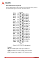
1
NuDAQ® 723X Series
32 Channels Isolated
Digital I/O Card
User’s Manual
Manual Rev.
4.03
Revision Date:
January 12, 2006
Part No:
50-11103-2040
Advance Technologies; Automate the World.
Copyright 2006 ADLINK TECHNOLOGY INC.
All Rights Reserved.
The information in this document is subject to change without prior
notice in order to improve reliability, design, and function and does
not represent a commitment on the part of the manufacturer.
In no event will the manufacturer be liable for direct, indirect, special, incidental, or consequential damages arising out of the use or
inability to use the product or documentation, even if advised of
the possibility of such damages.
This document contains proprietary information protected by copyright. All rights are reserved. No part of this manual may be reproduced by any mechanical, electronic, or other means in any form
without prior written permission of the manufacturer.
Trademarks
NuDAQ, NuIPC, DAQBench are registered trademarks of ADLINK
TECHNOLOGY INC.
Product names mentioned herein are used for identification purposes only and may be trademarks and/or registered trademarks
of their respective companies.
Getting Service from ADLINK
Customer Satisfaction is top priority for ADLINK Technology Inc.
Please contact us should you require any service or assistance.
ADLINK TECHNOLOGY INC.
Web Site:
http://www.adlinktech.com
Sales & Service:
[email protected]
TEL:
+886-2-82265877
FAX:
+886-2-82265717
Address:
9F, No. 166, Jian Yi Road, Chungho City,
Taipei, 235 Taiwan
Please email or FAX this completed service form for prompt and
satisfactory service.
Company Information
Company/Organization
Contact Person
E-mail Address
Address
Country
TEL
FAX:
Web Site
Product Information
Product Model
Environment
OS:
M/B:
Chipset:
CPU:
BIOS:
Please give a detailed description of the problem(s):
Table of Contents
Table of Contents..................................................................... i
List of Tables.......................................................................... iii
List of Figures ........................................................................ iv
1 Introduction ........................................................................ 1
1.1
1.2
1.3
1.4
1.5
Features............................................................................... 2
PCI-7230, cPCI-7230, and LPCI-7230 Features ............ 2
PCI-7233/H and Features ............................................... 2
PCI-7234/7234P Features .............................................. 3
Specifications of PCI-7230/cPCI-7230/LPCI-7230 .............. 4
Isolated Digital I/O (DIO) ................................................. 4
General Specifications .................................................... 5
Specifications of PCI-7233/PCI-7233H................................ 5
Isolated Digital Input ....................................................... 5
General Specifications .................................................... 6
Specifications of PCI-7234/7234P ....................................... 7
Isolated Digital Output .................................................... 7
General Specifications .................................................... 7
Software Supporting ............................................................ 8
Programming Library ...................................................... 8
DAQ-LVIEW PnP: LabVIEW® Driver ............................. 9
PCIS-VEE: HP-VEE Driver ............................................. 9
PCIS-OCX: ActiveX Controls .......................................... 9
DASYLab™ PRO .......................................................... 10
PCIS-DDE: DDE Server and InTouch™ ...................... 10
PCIS-ISG: ISaGRAF™ driver ....................................... 10
PCIS-ICL: InControl™ Driver ........................................ 10
PCIS-OPC: OPC Server ............................................... 10
2 Installation ........................................................................ 11
2.1
2.2
2.3
2.4
What You Have.................................................................. 11
Unpacking.......................................................................... 11
Hardware Installation Outline............................................. 12
PCI configuration .......................................................... 12
PCI slot selection .......................................................... 12
Device Installation for Windows Systems .......................... 13
Table of Contents
i
2.5
2.6
Connector Pin Assignment ................................................ 14
PCI-7230 Pin Assignment ............................................. 14
cPCI-7230 Pin Assignment ........................................... 16
LPCI-7230 Pin Assignment ........................................... 18
PCI-7233 Pin Assignment ............................................. 20
PCI-7234 Pin Assignment ............................................. 22
PCI-7234P Pin Assignment .......................................... 24
Termination Board Connection .......................................... 25
3 Registers Format .............................................................. 27
3.1
3.2
3.3
3.4
PCI PnP Registers .............................................................
I/O Registers Format..........................................................
Digital Input Register..........................................................
Digital Output Register.......................................................
27
28
29
29
4 Operation Theorem........................................................... 31
4.1
4.2
4.3
Isolated Digital Input Circuits ............................................. 31
Isolated Digital Output Circuits........................................... 32
Change of State Detection................................................. 36
What is COS? ............................................................... 36
Structure of COS detection and Dual Interrupt System 36
COS Detection .............................................................. 38
Warranty Policy ..................................................................... 39
ii
Table of Contents
List of Tables
Table 3-1: I/O Address Map of
PCI-7230/cPCI-7230/LPCI-7230 ............................
Table 3-2: I/O Address Map of PCI-7233/PCI-7233H ..............
Table 3-3: I/O Address Map of PCI-7234/7234P .....................
Table 3-4: Digital Input Register ..............................................
Table 3-5: Digital Output Register ...........................................
List of Tables
28
28
28
29
30
iii
List of Figures
Figure 2-1: PCI-7230 Pin Assignment........................................
Figure 2-2: PCI-7230 Onboard Power and Ground terminal......
Figure 2-3: cPCI-7230 Pin Assignment......................................
Figure 2-4: LPCI-7230 Pin Assignment......................................
Figure 2-5: PCI-7233 Pin Assignment........................................
Figure 2-6: PCI-7233 Onboard Power and Ground terminal......
Figure 2-7: PCI-7234 Pin Assignment........................................
Figure 2-8: PCI-7234 Onboard Power and Ground terminal......
Figure 2-9: PCI-7234P Pin Assignment .....................................
Figure 2-10: PCI-7234P Onboard Power and Ground terminal ...
Figure 4-1: Input circuits of 7230 and 7233 series .....................
Figure 4-2: Differential Input circuits of cPCI-7230 ....................
Figure 4-3: Isolate output circuits of PCI-7234 (sink current).....
Figure 4-4: Isolate output circuits of PCI-7234P
(source current) .......................................................
Figure 4-5: Isolation Output to TTL Input connection.................
Figure 4-6: Isolation Output to Isolation Input connection..........
Figure 4-7: Dual Interrupt System of PCI-7233..........................
Figure 4-8: Example of COS detection ......................................
iv
14
15
16
18
20
21
22
23
24
25
31
32
33
33
34
35
37
38
List of Figures
1
Introduction
This manual lists and describes the components of the PCI-723X
family products, which includes:
X
PCI-7230: Isolated 16-CH DI and 16-CH DO Card
X
PCI-7233: Isolated 32-CH DI Card with COS detection
X
PCI-7233H: Isolated High-speed 32-CH DI Card with COS
X
PCI-7234: Isolated 32-CH DO Card
X
PCI-7234P: Isolated 32-CH DO Card (source current)
X
cPCI-7230: Isolated 16-CH DI and 16-CH DO Module for
3U CompactPCI
X
LPCI-7230: Isolated 16-CH DI and 16-CH DO Module for
low profile PCI
These products have high isolation voltage with either 32 DI or 32
DO channels. The high isolation voltage protects the user’s computer against damage caused by accidental contact with high
external voltage and eliminates troublesome ground loops.
The PCI-7230/cPCI-7230//LPCI-7230 provides 16 isolated inputs
and 16 isolated outputs. The PCI-7230/cPCI-7230 isolated I/O
channels are isolated to 5000 Vrms, and LPCI-7230 isolated I/O
channels are isolated to 2500 Vrms (excluding cables).
The PCI-7233 provides 32 isolated digital input channels with
COS (change-of-state detection). The high speed version PCI7233H provides 32-CH isolated digital input. The isolation voltage
of PCI-7233H is high up to 2,500 Vrms (excluding cables).
The PCI-7234/7234P provides 32 isolated digital output (Darlington transistor) channels. The isolation voltage is high up to 5,000
Vrms (excluding cables), both channel-to-channel and channel-tocomputer. (PCI-7234 is sink current DO card, PCI-7234P is source
current DO card).
The PCI-7230/7233/7234 use ASIC PCI controller to interface the
board to the PCI bus. The ASIC fully implement the PCI local bus
specification Rev 2.1. All bus relative configurations, such as base
memory address and interrupt assignment, are automatically controlled by BIOS software. It does not need any user interaction and
pre-study for the configurations. This removes the burden of
Introduction
1
searching for a conflict-free configuration, which can be very timeconsuming and difficult with some other bus standards.
1.1 Features
PCI-7230, cPCI-7230, and LPCI-7230 Features
X
16 isolated Digital Input Channels
X
16 isolated Digital Output Channels
X
High output driving capability
X
5000 Vrms high voltage isolation (for PCI-7230 and cPCI7230), 2500 Vrms high voltage isolation (for LPCI-7230)
X
Interrupt is controlled from external signal
X
Dual interrupt trigger
X
500mA max@ 100% duty, for one of the eight transistor
devices ON
X
Up to 24V voltage protection for isolated input
X
37-pin D-type connector (for PCI-7230)
X
50-pin SCSI-II type connector (or cPCI-7230 and LPCI7230)
PCI-7233/H and Features
2
X
32 Isolated Digital Input Channels
X
5000Vrms high voltage isolation (PCI-7233)
X
Up to 24V voltage protection for isolated input
X
Interrupt is generated by COS (change-of-state) detection
X
Dual interrupt trigger
X
High-speed isolator (1ms) version PCI-7233H available with
2500Vrms isolation voltage
X
37-pin D-type connector
Introduction
PCI-7234/7234P Features
X
32 Isolated Digital Output Channels
X
High output driving capability
X
500mA max@ 100% duty, for one of the eight transistor
devices ON (PCI-7234: sink current, PCI-7234P: source
current)
X
5,000Vrms high voltage isolation
X
37-pin D-type connector
Introduction
3
1.2 Specifications of PCI-7230/cPCI-7230/LPCI-7230
Isolated Digital I/O (DIO)
X
Optical Isolated Input Channel
X
Numbers of Channel: 16 digital inputs
X
Input Voltage: up to 24Vdc
Z
Logic “L”: 0 to 1V
Z
Logic “H”: 3 to 24V
X
Input resistance:1.2KΩ @ 0.5W
X
Isolated voltage: 5000Vrms (for PCI-7230 and cPCI-7230),
2500Vrms (for LPCI-7230)
X
Throughput:10KHz
X
Optical Isolated Output channel:
X
Z
Numbers of Channel: 16 digital outputs
Z
Output type: Darlington transistors
Z
Output Voltage: open collector 5V (min.), up to 35VDC
(max.)
Sink Current:
Z
500mA max @ 100% duty, for one of the eight transistor
devices ON
Z
370 mA @ duty 10% for all transistors devices ON
Z
140 mA @ duty 50% for all transistors devices ON
(Note: the pulse width is 25ms for one duty cycle.)
4
X
Throughput: 10KHz
X
Interrupt sources: Channel 0 and channel 1 of digital input
channels
Introduction
General Specifications
X
Connector:
Z
37-pin D-type connector for PCI-7230
Z
50-pin SCSI-II type connector for cPCI-7230 and LPCI7230
X
Operating Temperature: 0 to 60°C
X
Storage Temperature: -20 to 80°C
X
Humidity: 5 to 95%, non-condensing
X
Power Consumption:
Z
PCI-7230: +5V @ 150mA (typical)
(Note: Requires external power)
Z
X
cPCI-7230: +5V @ 270mA (typical)
Dimension: Compact size
Z
PCI-7230 153mm(L) X 107mm(H)
Z
cPCI-7230 Standard 3U ComapctPCI form factor
Z
LPCI-7230 Standard Low-Profile MD1 form factor
1.3 Specifications of PCI-7233/PCI-7233H
Isolated Digital Input
Optical Isolated Input Channel (PCI-7233)
X
Numbers of Channel: 32 digital inputs
X
Input Voltage: up to 24Vdc
Z
Logic “L”: 0 to 1.5V
Z
Logic “H”: 5 to 24V
X
Input resistance:1.2 KΩ @ 0.5W
X
Isolated voltage: 5000Vrms
X
Throughput: 10KHz
Introduction
5
Optical Isolated Input Channel (PCI-7233H)
X
Numbers of Channel: 32 digital inputs
X
Input Voltage: up to 24Vdc
Z
Logic “L”: 0 to 1.5V
Z
Logic “H”: 5 to 24V
X
Input resistance:1.2KΩ @ 0.5W
X
Isolated voltage: 2500Vrms
X
Throughput: High speed 500KHz
X
Dual-interrupt sources:
Z
Change-of-state (COS) on any 16 DI lines of LSB
Z
Change-of-state (COS) on any 16 DI lines of MSB
General Specifications
X
Connector: 37-pin D-type connector
X
Operating Temperature: 0°C to 60°C
X
Storage Temperature: -20°C to 80°C
X
Humidity: 5 to 95%, non-condensing
X
Power Consumption:
X
6
Z
+5V @ 300 mA for PCI-7233
Z
+5V @ 550 mA for PCI-7233H
Dimension: Compact size only 158 mm x 107 mm
Introduction
1.4 Specifications of PCI-7234/7234P
Isolated Digital Output
X
Optical isolated Output channel
X
Numbers of Channel: 32 digital output
X
Z
Output type: Darlington transistors
Z
Output Voltage: open collector 5V (min.), up to 35VDC
(max.)
Sink Current: (PCI-7234)
Z
500mA max @ 100% duty, for one of the eight transistors ON
Z
370mA @ duty 10% for all transistors devices ON
Z
140mA @ duty 50% for all transistors devices ON
(Note: the pulse width is 25ms for one duty cycle)
X
Source Current:(PCI-7234P)
Z
500mA max @ 100% duty, for one of the eight transistors ON
Z
260mA @ duty 10% for all transistors devices ON
Z
59mA @ duty 50% for all transistors devices ON
(Note: the pulse width is 25ms for one duty cycle)
X
Isolated voltage:
Z
X
5000Vrms
Throughput:
Z
10KHz
General Specifications
X
Connector: 37-pin D-type connector
X
Operating Temperature: 0 to 60°C
X
Storage Temperature: -20 to 80°C
X
Humidity: 5 to 95%, non-condensing
X
Power Consumption: +5V @ 180mA (typical)
X
Dimension: Compact size only 175mm(H) x 107mm(L)
Introduction
7
1.5 Software Supporting
ADLINK provides versatile software drivers and packages for different users’ approach to building up a system. We not only provide a programming library such as DLL for various Windows
systems, but also provide drivers for many software packages
such as LabVIEW®, HP VEETM, DASYLabTM, InTouchTM,
InControlTM, ISaGRAFTM.
All software options are included on the ADLINK CD. Software
drivers that require a fee are protected with a serial licensed code.
Without the software serial number, the drivers can still be
installed, with the demo version used for demonstration purposes
for two hours. Please contact your dealer to purchase the formal
license serial code.
Programming Library
For customers who are writing their own programs, we provide
function libraries for many different operating systems, including:
DOS Library:
Borland C/C++ and Microsoft C++, the functions descriptions
are included in this user’s guide.
Windows 95 DLL:
For VB, VC++, Delphi, BC5, the functions descriptions are
included in this user’s guide.
PCIS-DASK:
Includes device drivers and DLL for Windows 98/NT/2000/XP.
DLL is binary compatible across Windows 98/NT/2000/XP.
That means all applications developed with PCIS-DASK are
compatible across Windows 98, Windows NT, and Windows
2000. The developing environment can be VB, VC++, Delphi,
BC5, or any Windows programming language that allows calls
to a DLL. The user’s guide and function reference manual of
PCIS-DASK are in the CD. Please refer to the PDF manual
files under the following directory: \\Manual\Software Package\PCIS-DASK.
8
Introduction
PCIS-DASK/X:
Includes device drivers and shared library for Linux. The developing environment can be Gnu C/C++ or any programming language that allows linking to a shared library. The user's guide
and function reference manual of PCIS-DASK/X are in the CD.
(\\Manual\Software Package\PCIS-DASK-X.)
The above software drivers are shipped with the board. Please
refer to the “Software Installation Guide” to install these drivers.
DAQ-LVIEW PnP: LabVIEW® Driver
DAQ-LVIEW PnP contains the VIs, which are used to interface
with NI’s LabVIEW® software package. The DAQ-LVIEW PnPW
supports Windows 98/NT/2000/XP. The LabVIEW® drivers are
shipped free of charge with the board. These can be installed and
used without license. For further detailed information about DAQLVIEW PnP, please refer to the user’s guide in the CD.
(\\Manual\Software Package\DAQ-LVIEW PnP)
PCIS-VEE: HP-VEE Driver
The PCIS-VEE includes user objects, which are used to interface
with HP VEE software package. PCIS-VEE supports Windows 95/
98/NT. The HP-VEE drivers are free, shipped with the board.
These can be installed and used without license. For further information about PCIS-VEE, please refer to the user’s guide in the
CD.
(\\Manual\Software Package\PCIS-VEE)
PCIS-OCX: ActiveX Controls
It is recommended that customers who are familiar with ActiveX
controls and VB/VC++ programming to use the PCIS-OCX
ActiveX Control components library for developing applications.
The PCIS-OCX is designed under Windows 98/NT/2000/XP. For
further information on PCIS-OCX, please refer to the user’s guide
in the CD.
(\\Manual\Software Package\PCIS-OCX)
Introduction
9
DASYLab™ PRO
DASYLab is an easy-to-use software package, which provides
easy-setup instrument functions such as FFT analysis. Please
contact ADLINK for DASYLab PRO, which includes DASYLab and
ADLINK hardware drivers.
PCIS-DDE: DDE Server and InTouch™
DDE is an acronym for Dynamic Data Exchange specifications.
The PCIS-DDE includes the PCI cards’ DDE server. The PCISDDE server is included in the ADLINK CD, and requires a license.
The DDE server can be used in conjunction with any DDE client
under Windows NT.
PCIS-ISG: ISaGRAF™ driver
The ISaGRAF WorkBench is an IEC1131-3 SoftPLC control program development environment. The PCIS-ISG includes ADLINK
products’ target drivers for ISaGRAF under Windows NT environment. The PCIS-ISG is included in the ADLINK CD and also
requires a license.
PCIS-ICL: InControl™ Driver
PCIS-ICL is the InControl driver which supports the Windows NT.
The PCIS-ICL is included in the ADLINK CD, requiring a license.
PCIS-OPC: OPC Server
PCIS-OPC is an OPC Server, which can be linked with OPC clients. Many software packages now provide OPC clients. The
PCIS-OPC supports Windows NT and requires a license.
10
Introduction
2
Installation
This chapter describes the configurations of 723X series. The
723X series is Plug and Play and can easily be installed onto any
PC system with PCI slots.
2.1 What You Have
X
This User’s Manual
X
723X family Isolated Digital I/O Card
X
ADLINK CD
X
Software Installation Guide
If any of these items are missing or damaged, please contact the
dealer from whom the product was purchased. Save the shipping
materials and carton for future storage or shipping purposes.
2.2 Unpacking
Your 723X series card contains sensitive electronic components
that can be easily damaged by static electricity.
The card should be placed on a grounded anti-static mat. The
operator should wear an anti-static wristband, grounded at the
same point as the anti-static mat. Inspect the card module carton
for obvious damage. Shipping and handling may cause damage to
the module. Ensure that there are no shipping and handing damages on the module before processing.
After opening the card module carton, extract the system module
and place it only on a grounded anti-static surface component side
up.
Again, inspect the module for damage. Press down on all socketed ICs to make sure they are properly seated. Do this only with
the module placed on a firm flat surface.
Note:
Installation
Do not apply power to the card if it has been damaged.
11
2.3 Hardware Installation Outline
PCI configuration
The PCI cards (or CompactPCI cards) are equipped with a Plug
and Play PCI controller, it can request base addresses and interrupt in accordance with the PCI standard. The system BIOS will
install the system resource based on the PCI cards’ configuration
registers and system parameters (which are set by system BIOS).
Interrupt assignment and memory usage (I/O port locations) of the
PCI cards can be assigned by system BIOS only. These system
resource assignments are done on a board-by-board basis. It is
not recommended that the system resource be assigned by any
other method.
PCI slot selection
The PCI card can be inserted into any PCI slot without any configuration for system resource.
Installation Procedures
1. Turn off the computer.
2. Turn off all accessories (printer, modem, monitor, etc.)
connected to your computer.
3. Remove the computer cover.
4. Select a 32-bit PCI slot. PCI slots are shorter than ISA or
EISA slots, and usually white or ivory in color.
5. Before handling the PCI cards, discharge any static
buildup on your body by touching the metal case of the
computer. Hold the edge and do not touch the components.
6. Position the board into the selected PCI slot.
7. Secure the card in place at the rear panel of the system.
12
Installation
2.4 Device Installation for Windows Systems
Once Windows 98/2000/XP has started, the Plug and Play function of Windows system will find the new NuDAQ/NuIPC cards. If
this is the first time installing NuDAQ/NuIPC cards on your Windows system, you will be prompted to enter the device information
source. Please refer to the “Software Installation Guide” for
instructions on installing the device.
Installation
13
2.5 Connector Pin Assignment
PCI-7230 Pin Assignment
The pin assignment of the 37 pins D-type connector CN2, which is
an isolated DIO signal connector, shown below:
IDI_0
(1)
IDI_2
(2)
IDI_4
(3)
IDI_6
(4)
IDI_8
(5)
IDI_10
(6)
IDI_12
(7)
IDI_14
(8)
EICOM (9)
EOGND(10)
IDO_0 (11)
IDO_2 (12)
IDO_4 (13)
IDO_6 (14)
IDO_8 (15)
IDO_10 (16)
IDO_12 (17)
IDO_14 (18)
VDD
(19)
(20) IDI_1
(21) IDI_3
(22) IDI_5
(23) IDI_7
(24) IDI_9
(25) IDI_11
(26) IDI_13
(27) IDI_15
(28) EOGND
(29) EOGND
(30) IDO_1
(31) IDO_3
(32) IDO_5
(33) IDO_7
(34) IDO_9
(35) IDO_11
(36) IDO_13
(37) IDO_15
Figure 2-1: PCI-7230 Pin Assignment
14
Installation
Legend:
IDI_n: Isolated digital input channel #n.
IDO_n: Isolated digital output channel #n.
EICOM: Common Ground or Common power of isolated input
channels.
EOGND: Ground return path of isolated output channels.
VDD: Power supply of isolated output channels.
The VDD must be supplied by an external power supply of 5 to 35VDC.
Note:
EOGND 1
2 EOGND
Figure 2-2: PCI-7230 Onboard Power and Ground terminal
Installation
15
cPCI-7230 Pin Assignment
The pin assignment of the cPCI-7230’s 50 pins SCSI-II type connector CN1 is shown in the following diagram.
VDD
(1)
EOGND (2)
EOGND (3)
EOGND (4)
IDO_7 (5)
IDO_6 (6)
IDO_5 (7)
IDO_4 (8)
IDO_3 (9)
IDO_2 (10)
IDO_1 (11)
IDO_0 (12)
IDI_3H (13)
IDI_3L (14)
IDI_2H (15)
IDI_2L (16)
IDI_1H (17)
IDI_1L (18)
IDI_0H (19)
IDI_0L (20)
IDI_11 (21)
IDI_10 (22)
IDI_9 (23)
IDI_8 (24)
EICOM (25)
(26)
(27)
(28)
(29)
(30)
(31)
(32)
(33)
(34)
(35)
(36)
(37)
(38)
(39)
(40)
(41)
(42)
(43)
(44)
(45)
(46)
(47)
(48)
(49)
(50)
VDD
EOGND
EOGND
EOGND
IDO_14
IDO_15
IDO_12
IDO_13
IDO_10
IDO_11
IDO_8
IDO_9
IDI_7L
IDI_7H
IDI_6L
IDI_6H
IDI_5L
IDI_5H
IDI_4L
IDI_4H
IDI_15
IDI_14
IDI_13
IDI_12
EICOM
Figure 2-3: cPCI-7230 Pin Assignment
Legend:
IDI_n: Isolated digital input channel #n.
IDO_n: Isolated digital output channel #n.
16
Installation
EICOM: Common ground or common power of isolated input
channels #8 to 15.
IDI_nH: High input of isolated differential DI channel #n.
IDI_nL: Low input of isolated differential DI channel #n.
EOGND: Ground return path of isolated output channels.
VDD: Power input signal for fly-wheel diode of DO channels.
Installation
17
LPCI-7230 Pin Assignment
The pin assignment of the LPCI-7230’s 50 pins SCSI-II type connector CN1 is shown in the following diagram.
VDD
VDD
(1)
(1)
(2)
EIGND
EICOM
EOGND (2)
EICOM
EOGND (3)
EIGND
(3)
EICOM
EOGND (4)
EIGND
(4)
IDO_7
IDO_7 (5)
(5)
IDO_6
IDO_6 (6)
(6)
IDO_5
IDO_5 (7)
(7)
IDO_4
IDO_4 (8)
(8)
IDO_3
IDO_3 (9)
(9)
IDO_2
IDO_2 (10)
(10)
IDO_1
IDO_1 (11)
(11)
IDO_0
IDO_0 (12)
(12)
IDI_3H
(13)
IDI_3H (13)
IDI_3L (14)
IDI_3L
(14)
IDI_2H (15)
IDI_2H
(15)
IDI_2L (16)
IDI_2L
(16)
IDI_1H (17)
IDI_1H
(17)
(18)
IDI_1L (18)
IDI_1L
(19)
IDI_0H (19)
IDI_0H
(20)
IDI_0L (20)
IDI_0L
(21)
IDI_11
IDI_11 (21)
(22)
IDI_10
IDI_10 (22)
(23)
IDI_9
IDI_9 (23)
(24)
IDI_8
IDI_8 (24)
EICOM (25)
EOGND
(25)
EOGND
VDD
(26)
(26) VDD
ISO5V
(27)
(27) ISO5V
EIGND
EICOM
(28)
(28) EOGND
EIGND
EICOM
(29)
(29) EOGND
(30)
(30) IDO_14
IDO_14
(31)
(31) IDO_15
IDO_15
(32)
(32) IDO_12
IDO_12
(33)
(33) IDO_13
IDO_13
(34)
(34) IDO_10
IDO_10
(35)
(35) IDO_11
IDO_11
(36)
(36) IDO_8
IDO_8
(37)
(37) IDO_9
IDO_9
(38)
(38) IDI_7L
IDI_7L
(39)
(39) IDI_7H
IDI_7H
(40)
(40) IDI_6L
IDI_6L
(41)
(41) IDI_6H
IDI_6H
(42)
(42) IDI_5L
IDI_5L
(43)
(43) IDI_5H
IDI_5H
(44)
(44) IDI_4L
IDI_4L
(45)
(45) IDI_4H
IDI_4H
(46)
(46) IDI_15
IDI_15
(47)
(47) IDI_14
IDI_14
(48)
(48) IDI_13
IDI_13
(49)
(49) IDI_12
IDI_12
(50)
(50) EICOM
EOGND
Figure 2-4: LPCI-7230 Pin Assignment
Legend:
IDI_n: Isolated digital input channel #n.
IDO_n: Isolated digital output channel #n.
18
Installation
EICOM: Common ground or common power of isolated input
channels #8 to 15.
IDI_nH: High input of isolated differential DI channel #n.
IDI_nL: Low input of isolated differential DI channel #n.
EOGND: Ground return path of isolated output channels.
VDD: Power input signal for fly-wheel diode of DO channels.
ISO5V: Isolatied power output 5V.
Installation
19
PCI-7233 Pin Assignment
The pin assignment of the 37 pins D-type connector CN1 is illustrated below:
IDI_0
(1)
IDI_2
(2)
IDI_4
(3)
IDI_6
(4)
I.GND (5)
IDI_9 (6)
IDI_11 (7)
IDI_13 (8)
IDI_15 (9)
IDI_16 (10)
IDI_18 (11)
IDI_20 (12)
IDI_22 (13)
I.GND (14)
IDI_25 (15)
IDI_27 (16)
IDI_29 (17)
IDI_31 (18)
I.GND (19)
(20) IDI_1
(21) IDI_3
(22) IDI_5
(23) IDI_7
(24) IDI_8
(25) IDI_10
(26) IDI_12
(27) IDI_14
(28) I.GND
(29) IDI_17
(30) IDI_19
(31) IDI_21
(32) IDI_23
(33) IDI_24
(34) IDI_26
(35) IDI_28
(36) IDI_30
(37) I.GND
Figure 2-5: PCI-7233 Pin Assignment
Legend:
IDI_n: Isolated digital input channel n.
I.GND: Isolated common ground.
20
Installation
I.GND
1
2
CN2
VDD
3
4
CN3
Figure 2-6: PCI-7233 Onboard Power and Ground terminal
Installation
21
PCI-7234 Pin Assignment
The pin assignment of the 37 pins D-type connector CN1, which is
an isolated DIO signal connector, is shown below.
IDO_0
(1)
IDO_2
(2)
IDO_4
(3)
IDO_6
(4)
I.GND
(5)
IDO_9 (6)
IDO_11 (7)
IDO_13 (8)
IDO_15 (9)
IDO_16 (10)
IDO_18 (11)
IDO_20 (12)
IDO_22 (13)
I.GND (14)
IDO_25 (15)
IDO_27 (16)
IDO_29 (17)
IDO_31 (18)
VDD (19)
(20) IDO_1
(21) IDO_3
(22) IDO_5
(23) IDO_7
(24) IDO_8
(25) IDO_10
(26) IDO_12
(27) IDO_14
(28) I.GND
(29) IDO_17
(30) IDO_19
(31) IDO_21
(32) IDO_23
(33) IDO_24
(34) IDO_26
(35) IDO_28
(36) IDO_30
(37) I.GND
Figure 2-7: PCI-7234 Pin Assignment
Legend:
IDO_n: Isolated digital output signal channel n.
I.GND: Isolated Ground for all isolated output channels.
VDD: Power input signal for fly-wheel diode of DO channels.
22
Installation
V
D
DVDD
I.GND
I
.
G
N
1
1
3
2
C
N
2 C
N
3
CN2
3
4
CN3
Figure 2-8: PCI-7234 Onboard Power and Ground terminal
Installation
23
PCI-7234P Pin Assignment
The pin assignment of the 37 pins D-type connector CN1, which is
an isolated DIO signal connector, as shown below:
IDO_0
(1)
IDO_2
(2)
IDO-4
(3)
IDO_6
(4)
VDD
(5)
IDO_9
(6)
IDO_11 (7)
IDO_13 (8)
IDO_15 (9)
IDO_16 (10)
IDO_18 (11)
IDO_20 (12)
IDO_22 (13)
VDD
(14)
IDO_25 (15)
IDO_27 (16)
IDO_29 (17)
IDO_31 (18)
I.GND
(19)
(20) IDO_1
(21) IDO_3
(22) IDO_5
(23) IDO_7
(24) IDO_8
(25) IDO_10
(26) IDO_12
(27) IDO_14
(28) VDD
(29) IDO_17
(30) IDO_19
(31) IDO_21
(32) IDO_23
(33) IDO_24
(34) IDO_26
(35) IDO_28
(36) IDO_30
(37) VDD
Figure 2-9: PCI-7234P Pin Assignment
Legend:
IDO_n: Isolated digital output signal channel n.
I.GND: Isolated ground for isolated output channels.
VDD: External power supply for IDO source drivers.
24
Installation
I
.
G
N
D
V
D
D
VDD
I.GND
12
1
34
2
C
N
2 C
N
3
CN2
3
4
CN3
Figure 2-10: PCI-7234P Onboard Power and Ground terminal
2.6 Termination Board Connection
The 723X boards are equipped with a DB-37 or a 50-pin SCSI-II
female connector. Available termination boards include:
ACLD-9137:
General-Purpose termination board with a 37-pin D-sub male connector.
ACLD-9188:
General-Purpose termination board with one 37-pin D-sub connector and two 20-pin ribbon connectors.
DIN-37D:
Termination board with a 37-pin D-sub connector and DIN-Rail
mounting (including one 1-meter ACL-10137 cable).
DIN-50S:
Termination board with a 50-pin SCSI-II connector and DIN-Rail
mounting (including one 1-meter ACL-10250 cable)
Installation
25
26
Installation
3
Registers Format
The registers format is described in this chapter. This information
is quite useful for programmers who wish to handle the card by
low-level programming. However, it is recommended that the user
has a deeper understanding of the PCI interface before starting
any low-level programming. This chapter can also assist users in
using the software driver to manipulate this card.
3.1 PCI PnP Registers
This PCI card functions as a 32-bit PCI target device to any master on the PCI bus. There are three types of registers: PCI Configuration Registers (PCR), Local Configuration Registers (LCR),
and PCI-723X registers.
The PCR, which is compliant with the PCI-bus specifications, is
initialized and controlled by the Plug and Play PCI BIOS. Users
can study the PCI BIOS specification to understand the operation
of the PCR. Please contact the PCISIG for specifications of the
PCI interface.
The PCI bus controller PCI 9052 is provided by PLX technology
Inc. (www.plxtech.com). For further detail on the LCR, please visit
PLX technology’s website to download the relative information.
Users are not required to understand the details of the LCR if
using the software library. The PCI PnP BIOS assigns the base
address of the LCR to offset 14h of PCR.
The PCI-723X registers are shown in the next section. The base
address, which is also assigned by the PCI PnP BIOS, is located
at offset 18h of PCR. Therefore, users can read the 18h of PCR to
find the base address by using the BIOS function call.
Do not try to modify the base address and interrupt assigned by
the PCI PnP BIOS as it may cause resource conflict within your
system.
Registers Format
27
3.2 I/O Registers Format
The PCI-7230/cPCI-7230/LPCI-7230 requires one 32-bit address
in the PC I/O address space. Table 3.1 shows the I/O address of
each register with respect to the base address.
Address
Write
Read
Base (0 - 1 )
Isolated DO
Isolated DI
Table 3-1: I/O Address Map of PCI-7230/cPCI-7230/LPCI-7230
The PCI-7233 requires one 32-bit address in the PC I/O address
space. Table 3.2 shows the address.
Address
Write
Read
Base (0 - 3 )
--
Isolated DI
Table 3-2: I/O Address Map of PCI-7233/PCI-7233H
The PCI-7234/7234P requires one 32-bit address in the PC I/O
address space. Table 3.3 shows the address.
Address
Write
Read
Base (0 - 3 )
Isolated DO
--
Table 3-3: I/O Address Map of PCI-7234/7234P
CAUTION:
All the I/O ports above are 32-bit width.
8-bit or 16-bit I/O access is NOT allowed.
28
Registers Format
3.3 Digital Input Register
There is a total of 16 and 32 digital input channels on the PCI7230/cPCI-7230/LPCI-7230 and PCI-7233/7233H respectively.
Each bit corresponds to a signal on the digital input channel.
IDI_16 to IDI_31 are only available on PCI-7233/7233H.
Address: BASE + 0 to BASE + 3
Attribute: read only
Data Format:
Bit
7
6
5
4
3
2
1
0
Base + 0
IDI_7
IDI_6
IDI_5
IDI_4
IDI_3
IDI_2
IDI_1
IDI_0
Base + 1 IDI_15 IDI_14 IDI_13 IDI_12 IDI_11 IDI_10
IDI_9
IDI_8
Base + 2 IDI_23 IDI_22 IDI_21 IDI_20 IDI_19 IDI_18 IDI_17 IDI_16
Base + 3 IDI_31 IDI_30 IDI_29 IDI_28 IDI_27 IDI_26 IDI_25 IDI_24
Table 3-4: Digital Input Register
Legend:
IDI_n: Isolated Digital Input CH n.
3.4 Digital Output Register
There is a total of 16 and 32 digital output channels on the PCI7230/cPCI-7230/LPCI-7230 and PCI-7234/7234P respectively.
Each bit corresponds to a signal on the digital output channel.
IDO_16 to IDO_31 are only available on PCI-7234/7234P.
Address: BASE + 0 to BASE + 3
Attribute: write only
Data Format:
Registers Format
29
Bit
7
6
5
4
3
2
1
0
Base + 0
IDO_7
IDO_6
IDO_5
IDO_4
IDO_3
IDO_2
IDO_1
IDO_0
Base + 1 IDO_15 IDO_14 IDO_13 IDO_12 IDO_11 IDO_10
IDO_9
IDO_8
Base + 2 IDO_23 IDO_22 IDO_21 IDO_20 IDO_19 IDO_18 IDO_17 IDO_16
Base + 3 IDO_31 IDO_30 IDO_29 IDO_28 IDO_27 IDO_26 IDO_28 IDO_24
Table 3-5: Digital Output Register
Legend:
IDO_n: Isolated Digital Output CH n.
30
Registers Format
4
Operation Theorem
4.1 Isolated Digital Input Circuits
The isolated digital output is an open collector transistor output.
The input can accept voltages of up to 24V. The input resisters on
PCI-7230/7233/7233H, cPCI-7230 and LPCI-7230 are 1.2KΩ. The
connection between outside signal and PCI-7230/7233/7233H,
cPCI-7230 and LPCI-7230 are shown below.
Isolated Input
1.2K Ohm
EICOM
GND
Isolated Input
1.2K Ohm
EICOM
GND
Figure 4-1: Input circuits of 7230 and 7233 series
Operation Theorem
31
DI_nH
1.2K Ohm
DI_nL
Figure 4-2: Differential Input circuits of cPCI-7230
4.2 Isolated Digital Output Circuits
On the 7230/7234 series, an external voltage source, minimum
5V, maximum 35 VDC, is necessary to power the internal isolated
circuits. It is connected with the VDD pin, When the isolated digital
output goes to high, the sink current will be from VDD.
On the 7230/7234 series, the VDD pin is used as a “fly-wheel”
diode, which can protect the driver if the loading is inductance
loading such as relay, motor, or solenoid.
The VDD must connect to the external power to form a fly-wheel
current loop.
32
Operation Theorem
V5V
VDD
Load
DC (5-35V)
IDOn
+
I.GND
PC 817
Darlington
Sink Driver
Figure 4-3: Isolate output circuits of PCI-7234 (sink current)
V5V
VDD
IDOn
DC (5-35V)
+
Load
I.GND
PC 817
Darlington
Source Current
Figure 4-4: Isolate output circuits of PCI-7234P (source current)
Operation Theorem
33
Figure 4-5: Isolation Output to TTL Input connection
34
Operation Theorem
Figure 4-6: Isolation Output to Isolation Input connection
Operation Theorem
35
4.3 Change of State Detection
What is COS?
The COS (Change of State) occurs when the input state (logic
level) is changed from low to high or from high to low. The COS
detection circuit is used to detect the edge of level change. In the
PCI-7233 card, the COS detection circuit is applied to all 32 channels input channels. If any channel is changed, the COS detection
circuit generates an interrupt request signal.
Structure of COS detection and Dual Interrupt System
The dual interrupt system is used in PCI-7233. Dual interrupt
occurs when the hardware can generate two interrupt request signals at the same time and the software can service these two
requests with ISR. Note that dual interrupt does not mean the card
occupies two IRQ levels. The two interrupt request signals (INT1
and INT2) come from COS detection output signal #1 and #2. The
INT1 is inserted when any channel from 0 to 15 is changed. The
INT2 is inserted when any channel between 16 to 31 is changed.
The interrupt system is illustrated below.
36
Operation Theorem
DI_0~
DI_15
DI_0~
DI_31
INT1
PLD1
32
Channel
Isolated
Input
PCI
Bridge
Clear
IRQ
DI_16~
DI_31
INT2
PLD2
PCI Bus
Figure 4-7: Dual Interrupt System of PCI-7233
Operation Theorem
37
COS Detection
The following timing is an example of the COS detection. Every DI
signal’s edge change can be detected. All the DI channels edge
will be ‘OR’ together to generate the INT1 or INT2 IRQ signals.
If INT1 or INT2 irq Signals generate, the signal will be latch its
state. The user can use the “_7233_CLR_IRQ” function to clear,
INT1, or INT2 IRQ signal state.
DI_0
DI_1
DI_0 COS
DI_1 COS
INT1
Clear_IRQ
Clear_IRQ
Clear_IRQ
Figure 4-8: Example of COS detection
38
Operation Theorem
Warranty Policy
Thank you for choosing ADLINK. To understand your rights and
enjoy all the after-sales services we offer, please read the following carefully.
1. Before using ADLINK’s products please read the user
manual and follow the instructions exactly. When sending in damaged products for repair, please attach an
RMA application form which can be downloaded from:
http://rma.adlinktech.com/policy/.
2. All ADLINK products come with a two-year guarantee:
X
The warranty period starts from the product’s shipment date
from ADLINK’s factory.
X
Peripherals and third-party products not manufactured by
ADLINK will be covered by the original manufacturers' warranty.
X
For products containing storage devices (hard drives, flash
cards, etc.), please back up your data before sending them
for repair. ADLINK is not responsible for loss of data.
X
Please ensure the use of properly licensed software with
our systems. ADLINK does not condone the use of pirated
software and will not service systems using such software.
ADLINK will not be held legally responsible for products
shipped with unlicensed software installed by the user.
X
For general repairs, please do not include peripheral accessories. If peripherals need to be included, be certain to
specify which items you sent on the RMA Request & Confirmation Form. ADLINK is not responsible for items not listed
on the RMA Request & Confirmation Form.
Warranty Policy
39
3. Our repair service is not covered by ADLINK's two-year
guarantee in the following situations:
X
Damage caused by not following instructions in the user's
manual.
X
Damage caused by carelessness on the user's part during
product transportation.
X
Damage caused by fire, earthquakes, floods, lightening,
pollution, other acts of God, and/or incorrect usage of voltage transformers.
X
Damage caused by unsuitable storage environments (i.e.
high temperatures, high humidity, or volatile chemicals).
X
Damage caused by leakage of battery fluid during or after
change of batteries by customer/user.
X
Damage from improper repair by unauthorized technicians.
X
Products with altered and/or damaged serial numbers are
not entitled to our service.
X
Other categories not protected under our warranty.
4. Customers are responsible for shipping costs to transport damaged products to our company or sales office.
5. To ensure the speed and quality of product repair, please
download an RMA application form from our company
website: http://rma.adlinktech.com/policy. Damaged
products with attached RMA forms receive priority.
If you have any further questions, please email our FAE staff:
[email protected].
40
Warranty Policy