1
ADS7865
www.ti.com
SBAS441C – OCTOBER 2008 – REVISED APRIL 2012
Dual, 12-Bit, 3+3 or 2+2 Channel, Simultaneous Sampling
Analog-to-Digital Converter
Check for Samples: ADS7865
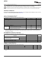
FEATURES
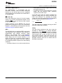
DESCRIPTION
•
•
•
•
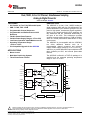
The ADS7865 is a dual, 12-bit, 2MSPS analog-todigital converter (ADC) with four fully differential or six
pseudo-differential input channels grouped into two
pairs for high-speed, simultaneous signal acquisition.
Inputs to the sample-and-hold (S/H) amplifiers are
fully differential and are maintained differentially to
the input of the ADC. This architecture provides
excellent common-mode rejection of 72dB at 100kHz,
which is a critical performance characteristic in noisy
environments.
1
2
•
•
•
•
•
Six Pseudo- or Four Fully Differential Inputs
SNR: 71.7dB, THD: –87dB
Programmable Channel Sequencer
Programmable and Buffered Internal 2.5V
Reference
Flexible Power-Down Features
Variable Power-Supply Ranges: 2.7V to 5.5V
Low-Power Operation: 44mW Maximum at 5V
Operating Temperature Range:
–40°C to +125°C
Pin-Compatible Upgrade for the ADS7862
The ADS7865 is pin-compatible with the ADS7862,
but offers additional features such as a
programmable channel sequencer and reference
output, flexible supply voltage (2.7V to 5.5V for AVDD
and BVDD), a pseudo-differential input multiplexer with
three channels per ADC, and several power-down
features.
APPLICATIONS
•
•
•
Motor Control
Multi-Axis Positioning Systems
Three-Phase Power Control
The ADS7865 is offered in a TQFP-32 package. It is
specified over the extended operating temperature
range of –40°C to +125°C.
SAR
BVDD
AVDD
CHA0+
CHA1+
Input
MUX
DB[11:0]
S/H
CDAC
CHA1-
Comparator
CHB0+
CHB0CHB1+
Input
MUX
S/H
CDAC
CHB1-
CS
CLOCK
WR
RD
Comparator
BUSY
CONVST
REFIN
SAR
REFOUT
Parallel Interface
CHA0-
10-Bit DAC
BGND
2.5V Reference
AGND
1
2
Please be aware that an important notice concerning availability, standard warranty, and use in critical applications of
Texas Instruments semiconductor products and disclaimers thereto appears at the end of this data sheet.
All trademarks are the property of their respective owners.
PRODUCTION DATA information is current as of publication date.
Products conform to specifications per the terms of the Texas
Instruments standard warranty. Production processing does not
necessarily include testing of all parameters.
Copyright © 2008–2012, Texas Instruments Incorporated
ADS7865
SBAS441C – OCTOBER 2008 – REVISED APRIL 2012
www.ti.com
This integrated circuit can be damaged by ESD. Texas Instruments recommends that all integrated circuits be handled with
appropriate precautions. Failure to observe proper handling and installation procedures can cause damage.
ESD damage can range from subtle performance degradation to complete device failure. Precision integrated circuits may be more
susceptible to damage because very small parametric changes could cause the device not to meet its published specifications.
ORDERING INFORMATION
For the most current package and ordering information, see the Package Option Addendum at the end of this
document, or visit the device product folder at www.ti.com.
ABSOLUTE MAXIMUM RATINGS (1)
Over operating free-air temperature range, unless otherwise noted.
ADS7865
UNIT
Supply voltage, AVDD to AGND
–0.3 to +6
V
Supply voltage, BVDD to BGND
–0.3 to +6
V
Supply voltage, BVDD to AVDD
1.5 × AVDD
V
Analog and reference input voltage with respect to AGND
AGND – 0.3 to AVDD + 0.3
V
Digital input voltage with respect to BGND
BGND – 0.3 to BVDD + 0.3
V
Ground voltage difference |AGND – BGND|
0.3
V
–10 to +10
mA
Input current to all pins except power-supply pins
Maximum virtual junction temperature, TJ
ESD ratings
(1)
+150
°C
Human body model (HBM),
JEDEC standard 22, test method A114-C.01, all pins
±4000
V
Charged device model (CDM),
JEDEC standard 22, test method C101, all pins
±1500
V
Stresses above these ratings may cause permanent damage. Exposure to absolute maximum conditions for extended periods may
degrade device reliability. These are stress ratings only, and functional operation of the device at these or any other conditions beyond
those specified is not implied.
RECOMMENDED OPERATING CONDITIONS
Over operating free-air temperature range, unless otherwise noted.
ADS7865
PARAMETER
Supply voltage, AVDD to AGND
Supply voltage, BVDD to BGND
MIN
NOM
MAX
2.7
5.0
5.5
UNIT
V
3.6
V
Low voltage levels
2.7
5V logic levels
4.5
5.0
5.5
V
0.5
2.5
2.525
V
Reference input voltage on REFIN
Analog differential input voltage (CHXX+) – (CHXX–)
Operating ambient temperature range, TA
–VREF
+VREF
V
–40
+125
°C
THERMAL CHARACTERISTICS (1)
Over operating free-air temperature range, unless otherwise noted.
PARAMETER
θJA
Junction-to-air thermal resistance
θJC
Junction-to-case thermal resistance
PD
Device power dissipation at AVDD = 5V and BVDD = 3.3V
(1)
2
ADS7865
High-K thermal resistance
UNIT
56.4
°C/W
20.8
°C/W
44
mW
Tested in accordance with the High-K thermal metric definitions of EIA/JESD51-3 for leaded surface-mount packages with a 3×3 via
array.
Copyright © 2008–2012, Texas Instruments Incorporated
ADS7865
www.ti.com
SBAS441C – OCTOBER 2008 – REVISED APRIL 2012
ELECTRICAL CHARACTERISTICS
At TA = –40°C to +125°C; over entire power-supply voltage range, VREF = 2.5V (internal), fCLK = 32MHz, and fDATA = 2MSPS,
unless otherwise noted.
ADS7865
PARAMETER
TEST CONDITIONS
RESOLUTION
MIN
TYP (1)
MAX
12
UNIT
Bits
ANALOG INPUT
FSR
Full-scale differential input range
VIN
Absolute input voltage
CHxx+ or CHxx– to AGND
(CHxx+) – (CHxx–)
CIN
Input capacitance
CHxx+ or CHxx– to AGND
CID
Differential input capacitance
IIL
Input leakage current
CMRR
Common-mode rejection ratio
–VREF
+VREF
V
–0.1
AVDD + 0.1
V
2
pF
4
–50
Both ADCs, dc to 100kHz
pF
50
72
nA
dB
DC ACCURACY
–40°C < TA < +125°C
–1.25
±0.6
+1.25
LSB
–40°C < TA < +85°C
–1
±0.5
+1
LSB
–1
±0.4
+1
LSB
Input offset error
–3
±0.5
+3
LSB
Match
–3
±0.5
+3
LSB
Gain error
–0.6
0.15
+0.6
%
Match
–0.6
±0.1
+0.6
%
INL
Integral nonlinearity
DNL
Differential nonlinearity
VOS
dVOS/dT
GERR
Input offset thermal drift
GERR/dT
Gain error thermal drift
PSRR
Power-supply rejection ratio
μV/°C
±2
AVDD = 5V
±2
ppm/°C
70
dB
dB
AC ACCURACY
SINAD
Signal-to-noise + distortion
VIN = 5VPP at 100kHz
69
71.3
SNR
Signal-to-noise ratio
VIN = 5VPP at 100kHz
70
71.7
THD
Total harmonic distortion
VIN = 5VPP at 100kHz
SFDR
Spurious-free dynamic range
VIN = 5VPP at 100kHz
–87
74
dB
–74
88
dB
dB
SAMPLING DYNAMICS
tCONV
Conversion time per ADC
tACQ
Acquisition time
fDATA
Data rate
tA
13
Clocks
62.5
1MHz < fCLK ≤ 32MHz
ns
62.5
2000
Aperture delay
6
Match
tAJIT
Aperture jitter
fCLK
Clock frequency on CLOCK
(1)
1MHz < fCLK ≤ 32MHz
50
ns
ps
50
1
kSPS
ps
32
MHz
All values at TA = +25°C.
Copyright © 2008–2012, Texas Instruments Incorporated
3
ADS7865
SBAS441C – OCTOBER 2008 – REVISED APRIL 2012
www.ti.com
ELECTRICAL CHARACTERISTICS (continued)
At TA = –40°C to +125°C; over entire power-supply voltage range, VREF = 2.5V (internal), fCLK = 32MHz, and fDATA = 2MSPS,
unless otherwise noted.
ADS7865
PARAMETER
TEST CONDITIONS
MIN
TYP (1)
MAX
UNIT
INTERNAL VOLTAGE REFERENCE
Resolution
Reference output DAC resolution
10
Over 20% to 100% DAC range
0.496
DAC = 0x3FF,
–40°C < TA < +125°C
2.485
DAC = 0x3FF at +25°C
2.495
Bits
2.515
V
2.500
2.515
V
2.500
2.505
VREFOUT
Reference output voltage
dVREFOUT/dT
Reference voltage drift
DNLDAC
DAC differential linearity error
–4
±1
4
LSB
INLDAC
DAC integral linearity error
–4
±0.5
4
LSB
VOSDAC
DAC offset error
–4
±1
4
LSB
PSRR
Power-supply rejection ratio
IREFOUT
Reference output dc current
+2
mA
IREFSC
Reference output short-circuit
current
50
mA
tREFON
Reference output settling time
0.5
ms
±10
VREFOUT = 0.5V
73
–2
V
ppm/°C
dB
VOLTAGE REFERENCE INPUT
VREF
Reference input voltage range
0.5
2.525
V
IREF
Reference input current
50
μA
CREF
Reference input capacitance
10
pF
DIGITAL INPUTS
Logic family
CMOS
VIH
High-level input voltage
0.7 × BVDD
BVDD + 0.3
VIL
Low-level input voltage
–0.3
0.3 × BVDD
V
IIN
Input current
–50
+50
nA
CI
Input capacitance
VI = BVDD to BGND
5
V
pF
DIGITAL OUTPUTS
Logic family
CMOS
VOH
High-level output voltage
IOH = –100μA
VOL
Low-level output voltage
IOH = 100μA
IOZ
High-impedance-state output
current
CO
Output capacitance
CL
Load capacitance
4
VI = BVDD to BGND
BVDD – 0.2
V
–50
0.2
V
+50
nA
5
pF
30
pF
Copyright © 2008–2012, Texas Instruments Incorporated
ADS7865
www.ti.com
SBAS441C – OCTOBER 2008 – REVISED APRIL 2012
ELECTRICAL CHARACTERISTICS (continued)
At TA = –40°C to +125°C; over entire power-supply voltage range, VREF = 2.5V (internal), fCLK = 32MHz, and fDATA = 2MSPS,
unless otherwise noted.
ADS7865
PARAMETER
TEST CONDITIONS
MIN
TYP (1)
MAX
UNIT
POWER SUPPLY
AVDD
Analog supply voltage
AVDD to AGND
2.7
5.0
5.5
BVDD
Buffer I/O supply current
BVDD to BGND
2.7
3.0
5.5
V
AVDD = 2.7V
4.1
6.0
mA
AIDD
BIDD
PD
Analog supply current
AVDD = 5V
5.6
7.5
mA
AVDD = 2.7V, NAP power-down
0.9
1.6
mA
AVDD = 5V, NAP power-down
1.1
1.8
mA
AVDD = 2.7V, deep power-down
0.001
mA
AVDD = 5V, deep power-down
0.001
mA
0.6
1.7
mA
BVDD = 3.3V, CLOAD = 10pF
0.8
1.9
mA
AVDD = 2.7V, BVDD = 2.7V
12.7
21
mA
AVDD = 5.0V, BVDD = 3.0V
30.6
44
mW
BVDD = 2.7V, CLOAD = 10pF
Buffer I/O supply current
Power dissipation
V
EQUIVALENT INPUT CIRCUIT
RSER = 200W
RSW = 50W
CHXX+
CPAR = 5pF
CS = 2pF
CPAR = 5pF
CS = 2pF
CHXXRSER = 200W
Copyright © 2008–2012, Texas Instruments Incorporated
RSW = 50W
5
ADS7865
SBAS441C – OCTOBER 2008 – REVISED APRIL 2012
www.ti.com
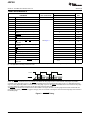
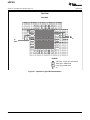
DEVICE INFORMATION
CHA0+
CHA0-
CHA1+
CHA1-
CHB0-
CHB0+
CHB1-
CHB1+
PBS PACKAGE
TQFP-32
(TOP VIEW)
32
31
30
29
28
27
26
25
BGND
AGND
3
22
WR
AVDD
4
21
RD
DB11
5
20
CS
DB10
6
19
CLOCK
DB9
7
18
CONVST
DB8
8
17
BUSY
DB7
9
10
11
12
13
14
15
16
DB0
23
DB1
2
DB2
REFOUT
DB3
BVDD
DB4
24
DB5
1
DB6
REFIN
TERMINAL FUNCTIONS
PIN NUMBER
6
NAME
DESCRIPTION
1
REFIN
2
REFOUT
Reference voltage input. A ceramic capacitor of 470nF (min) is required at this terminal.
3
AGND
Analog ground. Connect to analog ground plane.
4
AVDD
Analog power supply, 2.7V to 5.5V. Decouple to AGND with a 1μF ceramic capacitor.
5
DB11
Data bit 11, MSB
6
DB10
Data bit 10
7
DB9
Data bit 9
8
DB8
Data bit 8
9
DB7
Data bit 7
10
DB6
Data bit 6
11
DB5
Data bit 5
12
DB4
Data bit 4
13
DB3
Data bit 3
14
DB2
Data bit 2
15
DB1
Data bit 1
16
DB0
Data bit 0
17
BUSY
ADC busy indicator. BUSY goes high when the inputs are in hold mode and returns to low after the
conversion has been finished.
18
CONVST
Conversion start. The ADC switches from the sample into the hold mode on the falling edge of
CONVST, independent of the status of the CLOCK. The conversion itself starts with the next rising
edge of CLOCK.
19
CLOCK
20
CS
Chip select. When low, the parallel interface of the device is active; when high, input signals are
ignored and output signals are 3-state.
21
RD
Read data. Falling edge active synchronization pulse for the parallel data outputs. RD only triggers,
when CS is low.
22
WR
Write data. Rising edge latches in the parallel data inputs. WR only triggers, when CS is low.
Reference voltage output. The programmable internal voltage reference output is available on this pin.
External clock input.
Copyright © 2008–2012, Texas Instruments Incorporated
ADS7865
www.ti.com
SBAS441C – OCTOBER 2008 – REVISED APRIL 2012
TERMINAL FUNCTIONS (continued)
PIN NUMBER
NAME
23
BGND
Buffer I/O ground. Connect to digital ground plane.
DESCRIPTION
24
BVDD
Buffer I/O power supply, 2.7V to 5.5V. Decouple to BGND with a 1μF ceramic capacitor.
25
CHB1+
Noninverting analog input channel B1
26
CHB1–
Inverting analog input channel B1
27
CHB0+
Noninverting analog input channel B0
28
CHB0–
Inverting analog input channel B0
29
CHA1–
Inverting analog input channel A1
30
CHA1+
Noninverting analog input channel A1
31
CHA0–
Inverting analog input channel A0
32
CHA0+
Noninverting analog input channel A0
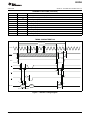
TIMING CHARACTERISTICS
Conversion Cycle
tCONV
1
14
16
CLOCK
tCLK
tCLKH
t1
tACQ
tCLKL
CONVST
t3
t2
BUSY
t4
t5
CS
t6
t8
t7
t7
t6
WR
t9
t14
RD
t12
t10
t11
DB[11:0]
CHAx
Output
t13
CHBx
Output
Input
Data
Previous Conversion Results
Figure 1. Interface Timing Diagram
Copyright © 2008–2012, Texas Instruments Incorporated
7
ADS7865
SBAS441C – OCTOBER 2008 – REVISED APRIL 2012
www.ti.com
TIMING REQUIREMENTS (1)
ADS7865
PARAMETER
TEST CONDITIONS
MIN
fCLOCK = 32MHz
TYP
MAX
13
UNIT
tCONV
Conversion time
tACQ
Acquisition time
tCLK
fCLK
CLOCK frequency
tCLK
CLOCK period
tCLKL
CLOCK low time
9.4
ns
tCLKH
CLOCK high time
9.4
ns
t1
CONVST low time
20
ns
t2
CONVST falling edge to BUSY high
delay (2)
3
ns
t3
CONVST high time
t4
RD falling edge to BUSY high setup time
t5
14th CLOCK rising edge to BUSY low delay
62.5
ns
1
32
31.25
1000
MHz
ns
20
ns
1
tCLK
3
ns
0
ns
0
ns
ns
See Figure 1
t6
CS falling edge to RD or WR falling edge
setup time
t7
CS rising edge to RD or WR rising edge
hold time
t8
WR low time
10
t9
RD high time between two read accesses
10
t10
RD falling edge to output data valid delay
t11
Output data hold time
5
ns
t12
Input data setup time
10
ns
t13
Input data hold time
5
ns
t14
Input data still valid to CONVST falling edge
setup time
31.25
ns
(1)
(2)
ns
20
ns
All input signals are specified with tR = tF = 1.5ns (10% to 90% of BVDD) and timed from a voltage level of (VIL + VIH)/2.
Not applicable in auto-Nap power-down mode.
CLOCK
Cycle 1
Cycle 2
10ns
10ns
5ns
CONVST
A
B
5ns
C
NOTE: All CONVST commands that occur more than 10ns before the rising edge of cycle '1' of the external clock (Region 'A') initiate a
conversion on the rising edge of cycle '1'. All CONVST commands that occur 5ns after the rising edge of cycle '1' or 10ns before the rising
edge of cycle '2' (Region 'B') initiate a conversion on the rising edge of cycle '2'. All CONVST commands that occur 5ns after the rising edge
of cycle '2' (Region 'C') initiate a conversion on the rising edge of the next clock period.
The CONVST pin should never be switched from LOW to HIGH in the region 10ns before the rising edge of the CLOCK and 5ns after the
rising edge (gray areas). If CONVST is toggled in this gray area, the conversion could begin on either the same rising edge of the CLOCK or
the following edge.
Figure 2. CONVST Timing
8
Copyright © 2008–2012, Texas Instruments Incorporated
ADS7865
www.ti.com
SBAS441C – OCTOBER 2008 – REVISED APRIL 2012
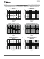
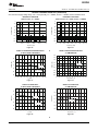
TYPICAL CHARACTERISTICS
Over the entire supply voltage range; VREF = 2.5V (internal), fCLK = 32MHz, and fDATA = 2MSPS, unless otherwise noted.
INTEGRAL NONLINEARITY vs
DATA RATE
INTEGRAL NONLINEARITY vs
TEMPERATURE
1.00
1.00
0.75
0.75
0.50
0.50
Positive
0.25
INL (LSB)
INL (LSB)
Positive
0
-0.25
0.25
0
-0.25
Negative
Negative
-0.50
-0.50
-0.75
-0.75
-1.00
0.50
0.75
1.00
1.25
1.50
1.75
-1.00
-40 -25 -10
2.00
5
Data Rate (MSPS)
Figure 3.
95
110 125
DIFFERENTIAL NONLINEARITY vs CODE
1.0
1.0
0.8
0.8
0.6
0.6
0.4
0.4
DNL (LSB)
INL (LSB)
80
Figure 4.
INTEGRAL NONLINEARITY vs CODE
0.2
0
-0.2
0.2
0
-0.2
-0.4
-0.4
-0.6
-0.6
-0.8
-0.8
-1.0
-1.0
0
512
1024
1536
2048
2560
3072
3584
4096
0
512
1024
Code
2048
2560
3072
3584
Figure 5.
Figure 6.
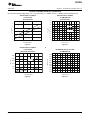
DIFFERENTIAL NONLINEARITY vs
DATA RATE
DIFFERENTIAL NONLINEARITY vs
TEMPERATURE
1.00
1.00
0.75
0.75
0.50
0.50
0.25
0.25
Positive
0
-0.25
Negative
0
-0.50
-0.75
-0.75
0.75
1.00
1.25
4096
1.50
Data Rate (MSPS)
Figure 7.
Copyright © 2008–2012, Texas Instruments Incorporated
1.75
2.00
Positive
-0.25
-0.50
-1.00
0.50
1536
Code
DNL (LSB)
DNL (LSB)
20 35 50 65
Temperature (°C)
-1.00
-40 -25 -10
Negative
5
20 35 50 65
Temperature (°C)
80
95
110 125
Figure 8.
9
ADS7865
SBAS441C – OCTOBER 2008 – REVISED APRIL 2012
www.ti.com
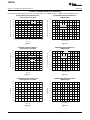
TYPICAL CHARACTERISTICS (continued)
Over the entire supply voltage range; VREF = 2.5V (internal), fCLK = 32MHz, and fDATA = 2MSPS, unless otherwise noted.
OFFSET ERROR AND OFFSET MATCH vs
ANALOG SUPPLY VOLTAGE
OFFSET ERROR AND OFFSET MATCH vs
TEMPERATURE
2.0
0.8
Offset Error and Offset Match (LSB)
Offset Error and Offset Match (LSB)
1.0
Offset Match
0.6
0.4
Offset Error
0.2
0
-0.2
-0.4
-0.6
-0.8
3.0
3.3
3.6
3.9
4.2
4.5
4.8
5.1
1.0
Offset Match
0.5
Offset Error
0
-0.5
-1.0
-1.5
-2.0
-40 -25 -10
-1.0
2.7
1.5
5.4
5
95
GAIN ERROR AND GAIN MATCH vs
ANALOG SUPPLY VOLTAGE
GAIN ERROR AND GAIN MATCH vs
TEMPERATURE
0.5
0.20
0.4
0.15
110 125
Gain Error
0.3
Gain Error
0.2
0.1
Gain Match
0
-0.1
-0.2
-0.3
2.7
3.0
3.3
3.6
3.9
4.2
4.5
4.8
5.1
0.10
Gain Match
0.05
0
-0.05
-0.10
-0.15
-0.20
-40 -25 -10
-0.5
5.4
5
AVDD (V)
80
95
110 125
Figure 12.
COMMON-MODE REJECTION RATIO vs
ANALOG SUPPLY VOLTAGE
COMMON-MODE REJECTION RATIO vs
TEMPERATURE
74.0
74.0
73.5
73.5
73.0
73.0
72.5
72.5
72.0
71.5
72.0
71.5
71.0
71.0
70.5
70.5
70.0
2.7
20 35 50 65
Temperature (°C)
Figure 11.
CMRR (dB)
CMRR (dB)
80
Figure 10.
-0.4
3.0
3.3
3.6
3.9
4.2
AVDD (V)
Figure 13.
10
20 35 50 65
Temperature (°C)
Figure 9.
Gain Error and Gain Match (%)
Gain Error and Gain Match (%)
AVDD (V)
4.5
4.8
5.1
5.4
70.0
-40 -25 -10
5
20 35 50 65
Temperature (°C)
80
95
110 125
Figure 14.
Copyright © 2008–2012, Texas Instruments Incorporated
ADS7865
www.ti.com
SBAS441C – OCTOBER 2008 – REVISED APRIL 2012
TYPICAL CHARACTERISTICS (continued)
Over the entire supply voltage range; VREF = 2.5V (internal), fCLK = 32MHz, and fDATA = 2MSPS, unless otherwise noted.
FREQUENCY SPECTRUM
(4096 Point FFT; fIN = 100kHz, fSAMPLE = 1.5MSPS)
0
0
-20
-20
-40
-40
Amplitude (dB)
Amplitude (dB)
FREQUENCY SPECTRUM
(4096 Point FFT; fIN = 100kHz)
-60
-80
-60
-80
-100
-100
-120
-120
-140
-140
0
200k
400k
600k
800k
1M
0
100
200
Frequency (Hz)
300
400
500
600
700 750
Frequency (kHz)
Figure 15.
Figure 16.
SIGNAL-TO-NOISE RATIO AND DISTORTION
vs INPUT SIGNAL FREQUENCY
SIGNAL-TO-RATIO AND DISTORTION
vs TEMPERATURE
74
73.0
72.5
73
71
AVDD = 5V
70
SINAD (dB)
SINAD (dB)
72.0
72
71.5
AVDD = 5V
71.0
70.5
AVDD = 2.7V
70.0
AVDD = 2.7V
69
69.5
68
10
30
40
70
90
110
130
150
170
69.0
-40 -25 -10
190 200
5
fIN (kHz)
80
Figure 17.
Figure 18.
SIGNAL-TO-NOISE RATIO
vs INPUT SIGNAL FREQUENCY
SIGNAL-TO-NOISE RATIO
vs TEMPERATURE
74
73.0
73
72.5
72
95
110 125
72.0
AVDD = 5V
SNR (dB)
SNR (dB)
20 35 50 65
Temperature (°C)
71
70
AVDD = 5V
71.5
AVDD = 2.7V
71.0
AVDD = 2.7V
69
70.5
68
10
30
50
70
90
110
130
150
fIN (kHz)
Figure 19.
Copyright © 2008–2012, Texas Instruments Incorporated
170
190 200
70.0
-40 -25 -10
5
20 35 50 65
Temperature (°C)
80
95
110 125
Figure 20.
11
ADS7865
SBAS441C – OCTOBER 2008 – REVISED APRIL 2012
www.ti.com
TYPICAL CHARACTERISTICS (continued)
Over the entire supply voltage range; VREF = 2.5V (internal), fCLK = 32MHz, and fDATA = 2MSPS, unless otherwise noted.
TOTAL HARMONIC DISTORTION
vs INPUT SIGNAL FREQUENCY
TOTAL HARMONIC DISTORTION
vs TEMPERATURE
-78
-76
-78
-80
-80
THD (dB)
THD (dB)
-82
-82
AVDD = 5V
-84
-86
-84
AVDD = 5V
-86
AVDD = 2.7V
-88
-88
AVDD = 2.7V
-90
-90
-40 -25 -10
-92
10
30
40
70
90
110
130
150
170
190 200
5
fIN (kHz)
20 35 50 65
Temperature (°C)
80
95
Figure 21.
Figure 22.
SPURIOUS-FREE DYNAMIC RANGE
vs INPUT SIGNAL FREQUENCY
SPURIOUS-FREE DYNAMIC RANGE
vs TEMPERATURE
110 125
92
94
92
AVDD = 5V
90
88
SFDR (dB)
SFDR (dB)
90
AVDD = 2.7V
86
84
82
AVDD = 5V
88
AVDD = 2.7V
86
84
80
82
-40 -25 -10
78
10
30
fIN (kHz)
20 35 50 65
Temperature (°C)
Figure 23.
Figure 24.
ANALOG SUPPLY CURRENT
vs TEMPERATURE
DIGITAL SUPPLY CURRENT
vs TEMPERATURE
40
70
90
110
130
150
170
190 200
8
95
110 125
95
110 125
1.8
AVDD = 5V
1.6
6
1.4
5
IBVDD (mA)
AVDD (mA)
80
2.0
7
4
5
AVDD = 2.7V
3
1.2
BVDD = 3.3V
1.0
0.8
BVDD = 2.7V
0.6
2
0.4
1
0.2
0
0
-40 -25 -10
5
20 35 50 65
Temperature (°C)
Figure 25.
12
80
95
110 125
-40 -25 -10
5
20 35 50 65
Temperature (°C)
80
Figure 26.
Copyright © 2008–2012, Texas Instruments Incorporated
ADS7865
www.ti.com
SBAS441C – OCTOBER 2008 – REVISED APRIL 2012
TYPICAL CHARACTERISTICS (continued)
Over the entire supply voltage range; VREF = 2.5V (internal), fCLK = 32MHz, and fDATA = 2MSPS, unless otherwise noted.
ANALOG SUPPLY CURRENT
vs DATA RATE
(Auto-NAP Mode)
ANALOG SUPPLY CURRENT
vs TEMPERATURE
(Auto-NAP Mode)
6
1.8
1.6
5
1.4
AVDD (mA)
AVDD (mA)
4
Reference ON
3
2
AVDD = 5V
1.2
1.0
AVDD = 2.7V
0.8
0.6
Reference OFF
0.4
1
0.2
0
0
0
500
1000
1500
-40 -25 -10
5
20 35 50 65
Temperature (°C)
Data Rate (kSPS)
80
95
Figure 27.
Figure 28.
ANALOG SUPPLY CURRENT
vs DATA RATE
(Deep Power-Down Mode)
REFERENCE OUTPUT VOLTAGE
vs TEMPERATURE
3500
110 125
2.505
2.504
3000
2.503
2.502
Clock ON
VREFOUT (V)
AVDD (mA)
2500
2000
1500
2.501
2.500
2.499
2.498
1000
2.497
500
2.496
Clock OFF
0
2.495
0
10
20
30
40
50
Data Rate (kSPS)
Figure 29.
Copyright © 2008–2012, Texas Instruments Incorporated
60
70
-40 -25 -10
5
20 35 50 65
Temperature (°C)
80
95
110 125
Figure 30.
13
ADS7865
SBAS441C – OCTOBER 2008 – REVISED APRIL 2012
www.ti.com
APPLICATION INFORMATION
GENERAL DESCRIPTION
The ADS7865 includes two 12-bit analog-to-digital
converters (ADCs) that operate based on the
successive-approximation register (SAR) principle.
The ADCs sample and convert simultaneously.
Conversion time can be as low as 406.25ns. Adding
the acquisition time of 62.5ns and an additional clock
cycle for setup/hold time requirements and skew
results in a maximum conversion rate of 2MSPS.
Each ADC has a fully differential 2:1 multiplexer frontend. In many common applications, all negative input
signals remain at the same constant voltage (for
example, 2.5V). In this type of application, the
multiplexer can be used in a pseudo-differential 3:1
mode, where CHx0– functions as a common-mode
input and the remaining three inputs (CHx0+, CHx1–,
and CHx1+) operate as separate inputs referred to
the common-mode input.
The ADS7865 also includes a 2.5V internal reference.
The reference drives a 10-bit digital-to-analog
converter (DAC), allowing the voltage at the REFOUT
pin to be adjusted via the internal DAC register in
2.44mV steps. A low-noise operational amplifier with
unity-gain buffers the DAC output voltage and drives
the REFOUT pin.
The ADS7865 offers a parallel interface that is pincompatible with the ADS7862. However, instead of
the A0 pin of the ADS7862 that controls channel
selection, the ADS7865 offers a write data input (WR)
pin that supports additional functions described in the
Digital section of this data sheet (see also the
ADS7862 Compatibility section).
ANALOG
This section discusses the analog input circuit, the
ADCs, and the reference design of the device.
Analog Inputs
Each ADC is fed by an input multiplexer, as shown in
Figure 31. Each multiplexer is either used in a fullydifferential 2:1 configuration (as described in Table 1)
or a pseudo-differential 3:1 configuration (as shown in
Table 2). The channel selection is performed using
bits C1 and C0 in the configuration register (see also
the Configuration Register section).
14
CHx1+
CHx1-
Input
MUX
CHx0+
ADC+
ADC-
CHx0-
Figure 31. Input Multiplexer Configuration
Table 1. Fully Differential 2:1 Multiplexer
Configuration
C1
C0
ADC+
ADC–
0
0
CHx0+
CHx0–
1
1
CHx1+
CHx1–
Table 2. Pseudo-Differential 3:1 Multiplexer
Configuration
C1
C0
ADC+
ADC–
0
0
CHx0+
CHx0–
0
1
CHx1–
CHx0–
1
0
CHx1+
CHx0–
The input path for the converter is fully differential
and provides a common-mode rejection of 72dB at
100kHz. The high CMRR also helps suppress noise
in harsh industrial environments.
Each of the 2pF sample-and-hold capacitors (shown
as CS in the Equivalent Input Circuit ) is connected
via switches to the multiplexer output. Opening the
switches holds the sampled data during the
conversion process. After finishing the conversion,
both capacitors are pre-charged for the duration of
one clock cycle to the voltage present at the REFIN
pin. After the pre-charging, the multiplexer outputs
are connected to the sampling capacitors again. The
voltage at the analog input pin is usually different
from the reference voltage; therefore, the sample
capacitors must be charged to within one-half LSB for
12-bit accuracy during the acquisition time tACQ (see
the Timing Characteristics).
Acquisition time is indicated with the BUSY signal
being held low. It starts by closing the input switches
(after finishing the previous conversion and precharging) and finishes with the rising edge of the
CONVST signal. If the ADS7865 operates at full
speed, the acquisition time is typically 62.5ns.
Copyright © 2008–2012, Texas Instruments Incorporated
ADS7865
www.ti.com
The minimum –3dB bandwidth of the driving
operational amplifier can be calculated as shown in
Equation 1, with n = 12 being the resolution of the
ADS7865:
ln(2) ´ (n + 1)
f-3dB =
2p ´ tACQ
(1)
With tACQ = 62.5ns, the minimum bandwidth of the
driving amplifier is 23MHz. The required bandwidth
can be lower if the application allows a longer
acquisition time.
A gain error occurs if a given application does not
fulfill the settling requirement shown in Equation 1. As
a result of pre-charging the capacitors, linearity and
THD are not directly affected, however.
The
OPA365
from
Texas
Instruments
is
recommended as a driver; in addition to offering the
required bandwidth, it provides a low offset and also
offers excellent THD performance.
The phase margin of the driving operational amplifier
is usually reduced by the ADC sampling capacitor. A
resistor placed between the capacitor and the
amplifier limits this effect; therefore, an internal 200Ω
resistor (RSER) is placed in series with the switch. The
switch resistance (RSW) is typically 50Ω (see the
Equivalent Input Circuit ).
The differential input voltage range of the ADC is
±VREF, the voltage at the REFIN pin.
It is important to keep the voltage to all inputs within
the 0.1V limit below AGND and above AVDD while not
allowing dc current to flow through the inputs. Current
is only necessary to recharge the sample-and-hold
capacitors.
Copyright © 2008–2012, Texas Instruments Incorporated
SBAS441C – OCTOBER 2008 – REVISED APRIL 2012
Analog-to-Digital Converter (ADC)
The ADS7865 includes two SAR-type, 2MSPS, 12-bit
ADCs (shown in the Functional Block Diagram on the
front page of this data sheet).
CONVST
The analog inputs are held with the falling edge of the
CONVST (conversion start) signal. The setup time of
CONVST referred to the next rising edge of CLOCK
(system clock) is 10ns (minimum). The conversion
automatically starts with the rising CLOCK edge.
CONVST should not be issued during a conversion,
that is, when BUSY is high.
CLOCK
The ADC uses an external clock in the range of
1MHz to 32MHz. 12 clock cycles are needed for a
complete conversion; the following clock cycle is used
for pre-charging the sample capacitors and a
minimum of two clock cycles are required for the
sampling. With a minimum of 16 clocks used for the
entire process, one clock cycle is left for the required
setup and hold times along with some margin for
delay caused by layout. The clock input can remain
low between conversions (after applying the 16th
falling edge to complete a running conversion). It can
also remain low after applying the 14th falling edge
during a DAC register write access if the device is not
required to perform a conversion (for example, during
an initiation phase after power-up).
The CLOCK duty cycle should be 50%. However, the
ADS7865 functions properly with a duty cycle
between 30% and 70%.
15
ADS7865
SBAS441C – OCTOBER 2008 – REVISED APRIL 2012
RESET
www.ti.com
REFIN
reference stable (see the previous discussion of
REFIN). For applications that use an external
reference source, the internal reference can be
disabled using bit RP in the SDI Register (see the
Digital section). The settling time of the REFOUT pin is
500μs (max) with the reference capacitor connected.
The default value of the REFOUT pin after power-up is
2.5V.
The reference input is not buffered and is directly
connected to the ADC. The converter generates
spikes on the reference input voltage because of
internal switching. Therefore, an external capacitor to
the analog ground (AGND) should be used to
stabilize the reference input voltage. This capacitor
should be at least 470nF. Ceramic capacitors (X5R
type) with values up to 1μF are commonly available
as SMD in 0402 size.
For operation with a 2.7V analog supply and a 2.5V
reference, the internal reference buffer requires a railto-rail input and output. Such buffers typically contain
two input stages; when the input voltage passes the
mid-range area, a transition occurs at the output
because of switching between the two input stages.
In this voltage range, rail-to-rail amplifiers generally
show a very poor power-supply rejection.
The ADS7865 features an internal power-on-reset
(POR) function. When the device is powered up, the
POR sets the device to default mode when AVDD
reaches 1.8V.
REFOUT
The ADS7865 includes a low-drift, 2.5V internal
reference source. This source feeds a 10-bit string
DAC that is controlled via the DAC register. As a
result of this architecture, the voltage at the REFOUT
pin is programmable in 2.44mV steps and can be
adjusted to specific application requirements without
the use of additional external components.
However, the DAC output voltage should not be
programmed below 0.5V to ensure the correct
functionality of the reference output buffer. This buffer
is connected between the DAC and the REFOUT pin,
and is capable of driving the capacitor at the REFIN
pin. A minimum of 470nF is required to keep the
16
As a result of this poor performance, the ADS7865
buffer has a fixed transition at DAC code 509
(0x1FD). At this code, the DAC may show a jump of
up to 10mV in its transfer function.
Table 3 lists some examples of internal reference
DAC settings.
Table 3. Reference DAC Setting Examples
VREFOUT
DECIMAL
CODE
BINARY CODE
HEXADECIMAL
CODE
0.500V
205
00 1100 1101
CD
1.241V
508
01 1111 1100
1FC
1.240V
509
01 1111 1101
1FD
2.500V
1023
11 1111 1111
3FF
Copyright © 2008–2012, Texas Instruments Incorporated
ADS7865
www.ti.com
SBAS441C – OCTOBER 2008 – REVISED APRIL 2012
DIGITAL
This section reviews the timing and control of the
ADS7865 parallel interface.
Configuration Register
The configuration register can be set by issuing a
write access on the parallel interface. The data
present on DB[11:0] are latched with the rising edge
of WR. The data word width of the configuration
register is 12 bits; its structure is shown in Table 4.
The default value of this register after power-up is
0x000.
11
N: Nap power-down enable
('1' = device in nap power-down mode)
AN: AutoNap power-down enable
('1' = device in autonap power-down mode)
RP: Reference power-down
('1' = reference is turned off)
Table 7. A2, A1, and A0: DAC, Sequencer, and
SW-Reset Control
Table 4. Configuration Register Map
A2
A1
A0
CONFIGURATION REGISTER BIT
0
0
0
Configuration register
update only
0
0
1
Write to reference DAC
register with next access
0
1
0
Configuration register
update only
0
1
1
Read from reference
DAC register with next
access
1
0
0
Write to sequencer
register
1
0
1
Device SW-reset
1
1
0
Read from sequencer
register
1
1
1
Configuration register
update only
10
C1
DP: Deep power-down enable
('1' = device in deep power-down mode)
C0
9
8
R1
R0
7
6
DP
N
5
AN
4
RP
3
(1)
X
2
1
0
A2
A1
A0
(1) X = Don't care.
Table 5. C1 and C0: Channel Selection
ADC A/B
C1
C0
POSITIVE INPUT
NEGATIVE INPUT
0
0
CHA0+/CHB0+
CHA0–/CHB0–
0
1
CHA1–/CHB1–
CHA0–/CHB0–
1
0
CHA1+/CHB1+
CHA0–/CHB0–
1
1
CHA1+/CHB1+
CHA1–/CHB1–
Table 6. R1 and R0: Register Update Enable
R1
R0
FUNCTION
0
0
Register update disabled
0
1
Register update enabled
1
0
Reserved for factory test (don’t
use)
1
1
Register update disabled
Copyright © 2008–2012, Texas Instruments Incorporated
FUNCTION
All enabled power-down features are activated by the
rising edge of the WR pulse immediately after writing
to the configuration register.
Because two write accesses are required to program
the reference DAC and the sequencer registers,
these settings are updated with the rising edge of WR
after the second write access. For more details, see
the Sequencer Register and Programming the
Reference DAC sections.
17
ADS7865
SBAS441C – OCTOBER 2008 – REVISED APRIL 2012
www.ti.com
Figure 32 shows a complete timing diagram
consisting of a write access to set up the proper input
channel, followed by an initiation of a conversion and
the read access of both conversion results.
The digital output code format of the ADS7865 is in
binary twos complement, as shown in Table 8.
Conversion results can be read out only once. A
second read access (without issuing a new
conversion) results in 000h as the output value.
The input multiplexer updates with the rising edge of
the WR input. The following falling edge of CONVST
triggers the conversion of the previously selected
channel. The data output register then updates with
the falling edge of BUSY and can be read thereafter.
14
1
14
16
CLOCK
CONVST
WR
CS
RD
DB[11:0]
BUSY
10 0h
Previous Conversion
of Both CHxx
Output
C H Ax
Output
CHBx
Output
CHA0
D 00 h
Conversion of
Both Differential CHx0
Output
CHB0
Conversion of
Both Differential CHx1
Figure 32. Channel Selection Timing Diagram
Table 8. ADS7865 Output Data Format
DESCRIPTION
DIFFERENTIAL INPUT VOLTAGE
(CHXX+) – (CHXX–)
INPUT VOLTAGE AT CHXX+
(CHXX– = VREF = 2.5V)
BINARY CODE
HEXADECIMAL
CODE
Positive full-scale
Midscale
VREF
5V
0111 1111 1111
7FF
0V
2.5V
0000 0000 0000
000
Midscale – 1LSB
–VREF/4096
2.49878V
1111 1111 1111
FFF
Negative fullscale
–VREF
0V
1000 0000 0000
800
18
Copyright © 2008–2012, Texas Instruments Incorporated
ADS7865
www.ti.com
SBAS441C – OCTOBER 2008 – REVISED APRIL 2012
Sequencer Register
The ADS7865 features a programmable sequencer
that controls the switching of the ADC input
multiplexer. To set up the sequencer, two write
accesses to the ADC are required. During the first
write access, the programming of the sequencer must
be enabled by setting R[1:0] = '01' and A[2:0] = '100'
in the Configuration Register. The data applied to the
data bus on the second write access contain the
updated Sequencer Register content.
The structure of the Sequencer Register is shown in
Table 9. The default value of this register after powerup is 0x000.
Detailed timing diagrams of the different sequencer
modes are shown in Figure 33.
If the output data are read after the entire sequence
has been converted, the output data are presented in
LIFO manner (last in, first out); that is, the conversion
results of ADC A is followed by ADC B data of the
last channel in the sequence, followed by the ADC
A/B data of the second-last channel in the sequence,
and so on. Trying to read out more results (2, 4, or 6)
than the actual sequence length results in 000h at the
output of the converter. Older conversion results are
overwritten if all data of a completed sequence have
not been read out before issuing a new conversion
start. Figure 34 shows an example where the
sequencer is set to scan through the pseudodifferential inputs of the ADS7865 beginning with
CHx1+, followed by CHx1– and CHx0+, while using a
single CONVST and BUSY for the entire sequence.
The internal LIFO pointer is reset with every BUSY
signal rising edge. Therefore, to ensure proper data
retrieval, the sequence results should either be read
after completion of the entire sequence conversion or
between two consecutive conversions within the
sequence as indicated in Figure 34. Other read
options may deliver incorrect results.
Table 9. Sequencer Register Map
SEQUENCER REGISTER BIT
11
10
9
8
7
6
5
4
3
2
1
0
S1
S0
SL1
SL0
CH1
CM1
CH2
CM2
CH3
CM3
SP1
SP0
Table 10. S1 and S0: Sequencer Mode
S1
S0
0
X
Individual CONVST and BUSY for each conversion
FUNCTION
1
0
Single CONVST for entire sequence and individual BUSY for each
conversion
1
1
Single CONVST and BUSY for entire sequence
Table 11. SL1 and SL0: Sequence Length
SL1
SL0
0
0
Length = 0: Sequencer disabled
FUNCTION
0
1
Length = 1: Cx1 (bits 6/7) enabled
1
0
Length = 2: Cx1 (bits 6/7) and Cx2 (bits 4/5) enabled
1
1
Length = 3: Cx1 (bits 6/7), Cx2 (bits 4/5), and Cx3 (bits 2/3) enabled
CH1: Signal input of the first channel in sequence; refer to Table 12 for details.
CM1: Common-mode input of the first channel in sequence; refer to Table 12 for details.
CH2: Signal input of the second channel in sequence; refer to Table 12 for details.
CM2: Common-mode input of the second channel in sequence; refer to Table 12 for details.
CH3: Signal input of the third channel in sequence; refer to Table 12 for details.
CM3: Common-mode input of the third channel in sequence; refer to Table 12 for details.
Copyright © 2008–2012, Texas Instruments Incorporated
19
ADS7865
SBAS441C – OCTOBER 2008 – REVISED APRIL 2012
www.ti.com
Table 12. Channel Selection
Table 13. SP1 and SP0: Sequence Position (ReadOnly)
ADC A/B
CHx
CMx
SIGNAL INPUT
COMMON-MODE
INPUT
0
0
CHA0+/CHB0+
CHA0–/CHB0–
0
1
CHA1–/CHB1–
CHA0–/CHB0–
1
0
CHA1+/CHB1+
CHA0–/CHB0–
1
1
CHA1+/CHB1+
CHA1–/CHB1–
SP1
SP0
FUNCTION
0
0
Sequencer disabled
0
1
CH1/CM1 (bits 6/7) to be converted at
next falling edge of CONVST
1
0
CH2/CM2 (bits 4/5) to be converted at
next falling edge of CONVST
1
1
CH3/CM3 (bits 2/3) to be converted at
next falling edge of CONVST
Mode 0 (One-shot conversion start, one BUSY for whole sequence)
CONVST
BUSY
Conv A
Conv B
Conv C
Mode 1 (One-shot conversion start, one BUSY for each conversion)
CONVST
BUSY
Conv A
Conv B
Conv C
Mode 2 (One conversion start and one BUSY for each conversion)
CONVST
BUSY
Conv A
Conv B
Conv C
5.5 tCLK
Figure 33. Sequencer Modes (Example: SL = '11')
14
1
35
21
41
CLOCK
CONVST
WR
CS
RD
DB[11:0]
BUSY
Output
CHA1+
0x104 0xF90
Conversion of
Both CH1+
Output
CHB1+
Output
CHA1-
Conversion of
Both CH1-
Output
CHB1-
Conv. of
Both CH0+
Figure 34. Sequencer Programming Example
20
Copyright © 2008–2012, Texas Instruments Incorporated
ADS7865
www.ti.com
SBAS441C – OCTOBER 2008 – REVISED APRIL 2012
Programming the Reference DAC
The internal reference DAC can be set by issuing a
WR pulse while providing a control word with R[1:0] =
'01' and A[2:0] = '001' (see Table 4). Thereafter, a
second WR pulse must be generated with the data
bus bits DB[11:10] = '00' and DB[9:0] containing the
actual 10-bit DAC value, with DB9 being the MSB
(see Figure 35).
To verify the current DAC setting, a WR pulse must
be generated while providing a control word
containing R[1:0] = '01' and A[2:0] = '011' to initialize
the DAC read access. Thereafter, triggering the RD
line causes the data bus to provide the 10-bit DAC
value on DB[9:0].
Table 14 shows the content of this register; the
default value after power-up is 0x3FF (see also
Table 3).
Table 14. DAC Register Contents
DAC REGISTER CONTENT
11
10
9
8
7
6
5
4
3
2
1
0
0
0
MSB
Bit 8
Bit 7
Bit 6
Bit 5
Bit 4
Bit 3
Bit 2
Bit 1
Bit 0
WR
CS
RD
DB[11:0]
b01xxxxx001
DAC Value
b01xxxxx011
DAC Value
Figure 35. DAC Write and Read Access Timing Diagram
Copyright © 2008–2012, Texas Instruments Incorporated
21
ADS7865
SBAS441C – OCTOBER 2008 – REVISED APRIL 2012
www.ti.com
Power-Down Modes and Reset
The ADS7865 has a comprehensive built-in powerdown feature. There are three power-down modes:
deep power-down, nap power-down, and auto-nap
power-down. All three power-down modes are
activated with the rising WR edge after having been
activated by asserting the corresponding bit in the
Configuration Register (DP = '1', N = '1', or AN = '1').
All modes are deactivated by de-asserting the
respective bit in the Configuration Register. The
contents of the Configuration Register are not
affected by any of the power-down modes. Any
ongoing conversion aborts when deep or nap powerdown is initiated. Table 15 lists the differences among
the three power-down modes.
In deep power-down mode, all functional blocks
except the digital interface are disabled. The analog
block has its bias currents turned off. In this mode,
the power dissipation reduces to 1μA within 2μs. The
wake-up time from deep power-down mode is 1μs.
In nap power-down mode, the ADS7865 turns off
the biasing of the comparator and the mid-voltage
buffer within 200ns. The device goes into nap powerdown mode regardless of the conversion state.
The auto-nap power-down mode is very similar to
the nap mode. The only differences are the methods
of powering down and waking up the device. The
Configuration Register bit AN is only used to
enable/disable this feature. If the auto-nap mode is
enabled, the ADS7865 turns off the biasing
automatically after finishing a conversion; thus, the
end of conversion actually activates the auto-nap
power-down. The device powers down within 200ns
in this mode, as well. Triggering a new conversion by
applying a CONVST pulse returns the device to
normal operation and automatically starts a new
conversion six CLOCK cycles later. Therefore, a
complete conversion cycle takes 22 CLOCK cycles;
thus, the maximum throughput rate in auto-nap
power-down mode is reduced to 1.45MSPS.
To issue a device reset, a write access to the
Configuration Register must be generated to set
A[2:0] = '101'. With the rising edge of the WR input,
the entire device is forced into reset. After
approximately 20ns, the parallel interface becomes
active again.
Table 15. Power-Down Modes
POWER-DOWN
TYPE
ENABLED
BY
ACTIVATED BY
ACTIVATION
TIME
RESUMED
BY
REACTIVATION TIME
DISABLED
BY
Deep
DP = '1'
Rising WR edge
2μs
DP = '0'
1μs
DP = '0'
Nap
N = '1'
Rising WR edge
200ns
N = '0'
6 clocks
N = '0'
Each end of
conversion
200ns
CONVST pulse
6 clocks
AN = '0'
Auto-nap
22
AN = '1'
Copyright © 2008–2012, Texas Instruments Incorporated
ADS7865
www.ti.com
SBAS441C – OCTOBER 2008 – REVISED APRIL 2012
ADS7862 COMPATIBILITY
The ADS7865IPBS is pin-compatible with the
ADS7862Y. However, there are some differences
between the two devices that must be considered
when migrating from the ADS7862 to the ADS7865 in
an existing design.
WR versus A0
One of the differences is that pin 22, which triggers
writing to the internal Configuration Register of the
ADS7865 (WR), is used to select the input channel
on the ADS7862 (A0).
Channel selection on the ADS7865 can only be
performed by setting bits C[1:0] in the Configuration
Register or, automatically, by the sequencer (see the
Sequencer Register section for details).
REFIN
The ADS7865 offers an unbuffered REFIN input with a
code-dependent input impedance while featuring a
programmable and buffered reference output
(REFOUT). The ADS7862 offers a high-impedance
(buffered) reference input. If an existing ADS7862based design uses the internal reference of the
device and relies on an external resistor divider to
adjust the input voltage range of the ADC, migration
to the ADS7865 platform requires one of the following
conditions:
• A software change to set up the internal reference
Copyright © 2008–2012, Texas Instruments Incorporated
•
DAC properly via the DAC register while removing
the external resistors; or
An additional external buffer between the resistor
divider and the required 470nF (minimum)
capacitor on the REFIN input.
In the latter case, while the capacitor stabilizes the
reference voltage during the entire conversion, the
buffer must recharge it by providing an average
current only; thus, the required minimum bandwidth of
the buffer can be calculated using Equation 2:
ln(2) ´ 2
f-3dB =
2p ´ 16 ´ tCLK
(2)
The buffer must also be capable of driving the 470nF
load while maintaining its stability.
Timing
The only timing requirement that may cause the
ADS7865 to malfunction in an existing ADS7862based design is the CONVST low time (t1) which is
specified to be 20ns minimum, while the ADS7862
works properly with a pulse as short as 15ns. All
other required minimum setup and hold times are
specified to be either the same as or lower than the
ADS7865; therefore, there are no conflicts with the
ADS7862 requirements.
23
ADS7865
SBAS441C – OCTOBER 2008 – REVISED APRIL 2012
www.ti.com
APPLICATION INFORMATION
fFILTER =
ln(2) ´ (n + 1)
2´p´2´R´C
(3)
The absolute minimum configuration of the ADS7865
in an application is shown in Figure 36. In this case,
the ADS7865 is used in dual-channel mode only, with
the default settings of the device after power up.
It is recommended to use a capacitor value of at least
20pF.
The input signal for the amplifiers must fulfill the
common-mode voltage requirements of the ADS7865
in this configuration. The actual values of the
resistors and capacitors depend on the bandwidth
and performance requirements of the application.
Keep the acquisition time in mind; the resistor value
can be calculated as shown in Equation 4 for each of
the series resistors (with n = 12, the resolution of the
ADS7865).
tACQ
R=
ln(2) ´ (n + 1) ´ 2 ´ C
(4)
Those values can be calculated using Equation 3,
with n = 12 being the resolution of the ADS7865.
BVDD
1mF
0.1mF
ADS7865
AVDD
BGND
BGND
OPA2365
AGND
OPA2365
AGND
AGND
AVDD
470nF
(min)
BVDD
CHB1+
DB[11:0]
CHB1-
BUSY
CHB0+
CLOCK
CHB0-
WR
CHA1+
RD
CHA1-
CONVST
CHA0+
CS
CHA0-
SDI
BGND
REFIN
M0
BVDD
REFOUT
M1
Controller
Device
AVDD
AGND
OPA2365
0.1mF (min)
1 mF
AGND
OPA2365
AGND
Figure 36. Minimum ADS7865 Configuration
24
Copyright © 2008–2012, Texas Instruments Incorporated
ADS7865
www.ti.com
LAYOUT
For optimum performance, care should be taken with
the physical layout of the ADS7865 circuitry. This
caution is particularly true if the CLOCK input
approaches the maximum throughput rate. In this
case, it is recommended to have a fixed phase
relationship between CLOCK and CONVST.
Additionally, the basic SAR architecture is quite
sensitive to glitches or sudden changes on the power
supply, reference, ground connections, and digital
inputs that occur just before latching the output of the
analog comparator. Therefore, when driving any
single conversion for an n-bit SAR converter, there
are n windows in which large external transient
voltages can affect the conversion result. Such
glitches might originate from switching power
supplies, nearby digital logic, or high-power devices.
The degree of error in the digital output depends on
the reference voltage, layout, and the exact timing of
the external event. These errors can change if the
external event also changes in time with respect to
the CLOCK input.
With this possibility in mind, power to the ADS7865
should be clean and well-bypassed. A 0.1μF ceramic
bypass capacitor should be placed as close to the
device as possible. In addition, a 1μF to 10μF
capacitor is recommended. If needed, an even larger
capacitor and a 5Ω or 10Ω series resistor may be
used to low-pass filter a noisy supply.
If the reference voltage is external and originates
from an operational amplifier, be sure that it can drive
the reference capacitor without oscillation. The
connection between the output of the external
reference driver and REFIN should be of low
resistance (10Ω max) to minimize any codedependent voltage drop on this path.
Grounding
All ground (AGND and BGND) pins should be
connected to a clean ground reference. These
connections should be kept as short as possible to
minimize the inductance of these paths. It is
recommended to use vias connecting the pads
directly to the ground plane. In designs without
ground planes, the ground trace should be kept as
wide as possible. Avoid connections that are too near
the grounding point of a microcontroller or digital
signal processor.
Copyright © 2008–2012, Texas Instruments Incorporated
SBAS441C – OCTOBER 2008 – REVISED APRIL 2012
Depending on the circuit density of the board,
placement of the analog and digital components, and
the related current loops, a single solid ground plane
for the entire printed circuit board (PCB) or a
dedicated analog ground area may be used. In an
instance of a separated analog ground area, ensure a
low-impedance connection between the analog and
digital ground of the ADC by placing a bridge
underneath (or next to) the ADC. Otherwise, even
short undershoots on the digital interface with a value
lower than –300mV may lead to conduction of ESD
diodes, causing current flow through the substrate
and degrading the analog performance.
During the PCB layout process, care should also be
taken to avoid any return currents crossing any
sensitive analog areas or signals. No signal must
exceed the limit of –300mV with regard to the
respective ground plane. Figure 37 illustrates the
recommended layout of the ground and power-supply
connections.
Supply
The ADS7865 has two separate supplies: the BVDD
pin for the digital interface and the AVDD pin for all
remaining circuits.
BVDD can range from 2.7V to 5.5V, allowing the
ADS7865 to easily interface with processors and
controllers. To limit the injection of noise energy from
external digital circuitry, BVDD should be filtered
properly. Bypass capacitors of 0.1μF and 10μF
should be placed between the BVDD pin and the
ground plane.
AVDD supplies the internal analog circuitry. For
optimum performance, a linear regulator (for
example, the UA7805 family) is recommended to
generate the analog supply voltage in the range of
2.7V to 5.5V for the ADS7865 and the necessary
analog front-end circuitry.
Bypass capacitors should be connected to the ground
plane such that the current is allowed to flow through
the pad of the capacitor (that is, the vias should be
placed on the opposite side of the connection
between the capacitor and the power-supply pin of
the ADC).
Digital Interface
To further optimize device performance, a series
resistor of 10Ω to 100Ω can be used on each digital
pin of the ADS7865. In this way, the slew rates of the
input and output signals are reduced, limiting the
noise injection from the digital interface.
25
ADS7865
SBAS441C – OCTOBER 2008 – REVISED APRIL 2012
www.ti.com
Top View
ADS7865I
32
470
nF
1.0
mF
to
AV DD
0.1
mF
31
30
29
28
27
26
25
REFIN
BVDD
REFOUT
BGND
AGND
22
AV DD
21
5
20
6
19
7
18
8
17
9
10
11
12
13
14
15
0.1
mF
1
mF
to
BVDD
16
LEGEND
TOP layer; copper pour and traces
lower layer; AGND area
lower layer; BGND area
via
Figure 37. Optimized Layout Recommendation
26
Copyright © 2008–2012, Texas Instruments Incorporated
ADS7865
www.ti.com
SBAS441C – OCTOBER 2008 – REVISED APRIL 2012
REVISION HISTORY
NOTE: Page numbers for previous revisions may differ from page numbers in the current version.
Changes from Revision B (May 2010) to Revision C
•
Page
Deleted Ordering Information table ....................................................................................................................................... 2
Changes from Revision A (June 2009) to Revision B
Page
•
Deleted footnote 2 from Electrical Characteristics table ....................................................................................................... 3
•
Changed RESET section of Applications Information ........................................................................................................ 16
•
Added last sentence in final paragraph of the Configuration Register section ................................................................... 18
•
Changed last paragraph of Sequencer Register section .................................................................................................... 19
•
Updated Figure 33 .............................................................................................................................................................. 20
•
Updated Figure 34 .............................................................................................................................................................. 20
Copyright © 2008–2012, Texas Instruments Incorporated
27
PACKAGE OPTION ADDENDUM
www.ti.com
10-Jun-2014
PACKAGING INFORMATION
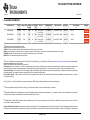
Orderable Device
Status
(1)
Package Type Package Pins Package
Drawing
Qty
Eco Plan
Lead/Ball Finish
MSL Peak Temp
(2)
(6)
(3)
Op Temp (°C)
Device Marking
(4/5)
ADS7865IPBS
ACTIVE
TQFP
PBS
32
250
Green (RoHS
& no Sb/Br)
CU NIPDAU
Level-2-260C-1 YEAR
-40 to 125
7865I A
ADS7865IPBSG4
ACTIVE
TQFP
PBS
32
250
Green (RoHS
& no Sb/Br)
CU NIPDAU
Level-2-260C-1 YEAR
-40 to 125
7865I A
ADS7865IPBSR
ACTIVE
TQFP
PBS
32
1000
Green (RoHS
& no Sb/Br)
CU NIPDAU
Level-2-260C-1 YEAR
-40 to 125
7865I A
(1)
The marketing status values are defined as follows:
ACTIVE: Product device recommended for new designs.
LIFEBUY: TI has announced that the device will be discontinued, and a lifetime-buy period is in effect.
NRND: Not recommended for new designs. Device is in production to support existing customers, but TI does not recommend using this part in a new design.
PREVIEW: Device has been announced but is not in production. Samples may or may not be available.
OBSOLETE: TI has discontinued the production of the device.
(2)
Eco Plan - The planned eco-friendly classification: Pb-Free (RoHS), Pb-Free (RoHS Exempt), or Green (RoHS & no Sb/Br) - please check http://www.ti.com/productcontent for the latest availability
information and additional product content details.
TBD: The Pb-Free/Green conversion plan has not been defined.
Pb-Free (RoHS): TI's terms "Lead-Free" or "Pb-Free" mean semiconductor products that are compatible with the current RoHS requirements for all 6 substances, including the requirement that
lead not exceed 0.1% by weight in homogeneous materials. Where designed to be soldered at high temperatures, TI Pb-Free products are suitable for use in specified lead-free processes.
Pb-Free (RoHS Exempt): This component has a RoHS exemption for either 1) lead-based flip-chip solder bumps used between the die and package, or 2) lead-based die adhesive used between
the die and leadframe. The component is otherwise considered Pb-Free (RoHS compatible) as defined above.
Green (RoHS & no Sb/Br): TI defines "Green" to mean Pb-Free (RoHS compatible), and free of Bromine (Br) and Antimony (Sb) based flame retardants (Br or Sb do not exceed 0.1% by weight
in homogeneous material)
(3)
MSL, Peak Temp. - The Moisture Sensitivity Level rating according to the JEDEC industry standard classifications, and peak solder temperature.
(4)
There may be additional marking, which relates to the logo, the lot trace code information, or the environmental category on the device.
(5)
Multiple Device Markings will be inside parentheses. Only one Device Marking contained in parentheses and separated by a "~" will appear on a device. If a line is indented then it is a continuation
of the previous line and the two combined represent the entire Device Marking for that device.
(6)
Lead/Ball Finish - Orderable Devices may have multiple material finish options. Finish options are separated by a vertical ruled line. Lead/Ball Finish values may wrap to two lines if the finish
value exceeds the maximum column width.
Important Information and Disclaimer:The information provided on this page represents TI's knowledge and belief as of the date that it is provided. TI bases its knowledge and belief on information
provided by third parties, and makes no representation or warranty as to the accuracy of such information. Efforts are underway to better integrate information from third parties. TI has taken and
Addendum-Page 1
Samples
PACKAGE OPTION ADDENDUM
www.ti.com
10-Jun-2014
continues to take reasonable steps to provide representative and accurate information but may not have conducted destructive testing or chemical analysis on incoming materials and chemicals.
TI and TI suppliers consider certain information to be proprietary, and thus CAS numbers and other limited information may not be available for release.
In no event shall TI's liability arising out of such information exceed the total purchase price of the TI part(s) at issue in this document sold by TI to Customer on an annual basis.
Addendum-Page 2
PACKAGE MATERIALS INFORMATION
www.ti.com
14-Jul-2012
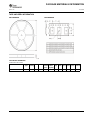
TAPE AND REEL INFORMATION
*All dimensions are nominal
Device
ADS7865IPBSR
Package Package Pins
Type Drawing
TQFP
PBS
32
SPQ
Reel
Reel
A0
Diameter Width (mm)
(mm) W1 (mm)
1000
330.0
16.4
Pack Materials-Page 1
7.2
B0
(mm)
K0
(mm)
P1
(mm)
W
Pin1
(mm) Quadrant
7.2
1.5
12.0
16.0
Q2
PACKAGE MATERIALS INFORMATION
www.ti.com
14-Jul-2012
*All dimensions are nominal
Device
Package Type
Package Drawing
Pins
SPQ
Length (mm)
Width (mm)
Height (mm)
ADS7865IPBSR
TQFP
PBS
32
1000
367.0
367.0
38.0
Pack Materials-Page 2
IMPORTANT NOTICE
Texas Instruments Incorporated and its subsidiaries (TI) reserve the right to make corrections, enhancements, improvements and other
changes to its semiconductor products and services per JESD46, latest issue, and to discontinue any product or service per JESD48, latest
issue. Buyers should obtain the latest relevant information before placing orders and should verify that such information is current and
complete. All semiconductor products (also referred to herein as “components”) are sold subject to TI’s terms and conditions of sale
supplied at the time of order acknowledgment.
TI warrants performance of its components to the specifications applicable at the time of sale, in accordance with the warranty in TI’s terms
and conditions of sale of semiconductor products. Testing and other quality control techniques are used to the extent TI deems necessary
to support this warranty. Except where mandated by applicable law, testing of all parameters of each component is not necessarily
performed.
TI assumes no liability for applications assistance or the design of Buyers’ products. Buyers are responsible for their products and
applications using TI components. To minimize the risks associated with Buyers’ products and applications, Buyers should provide
adequate design and operating safeguards.
TI does not warrant or represent that any license, either express or implied, is granted under any patent right, copyright, mask work right, or
other intellectual property right relating to any combination, machine, or process in which TI components or services are used. Information
published by TI regarding third-party products or services does not constitute a license to use such products or services or a warranty or
endorsement thereof. Use of such information may require a license from a third party under the patents or other intellectual property of the
third party, or a license from TI under the patents or other intellectual property of TI.
Reproduction of significant portions of TI information in TI data books or data sheets is permissible only if reproduction is without alteration
and is accompanied by all associated warranties, conditions, limitations, and notices. TI is not responsible or liable for such altered
documentation. Information of third parties may be subject to additional restrictions.
Resale of TI components or services with statements different from or beyond the parameters stated by TI for that component or service
voids all express and any implied warranties for the associated TI component or service and is an unfair and deceptive business practice.
TI is not responsible or liable for any such statements.
Buyer acknowledges and agrees that it is solely responsible for compliance with all legal, regulatory and safety-related requirements
concerning its products, and any use of TI components in its applications, notwithstanding any applications-related information or support
that may be provided by TI. Buyer represents and agrees that it has all the necessary expertise to create and implement safeguards which
anticipate dangerous consequences of failures, monitor failures and their consequences, lessen the likelihood of failures that might cause
harm and take appropriate remedial actions. Buyer will fully indemnify TI and its representatives against any damages arising out of the use
of any TI components in safety-critical applications.
In some cases, TI components may be promoted specifically to facilitate safety-related applications. With such components, TI’s goal is to
help enable customers to design and create their own end-product solutions that meet applicable functional safety standards and
requirements. Nonetheless, such components are subject to these terms.
No TI components are authorized for use in FDA Class III (or similar life-critical medical equipment) unless authorized officers of the parties
have executed a special agreement specifically governing such use.
Only those TI components which TI has specifically designated as military grade or “enhanced plastic” are designed and intended for use in
military/aerospace applications or environments. Buyer acknowledges and agrees that any military or aerospace use of TI components
which have not been so designated is solely at the Buyer's risk, and that Buyer is solely responsible for compliance with all legal and
regulatory requirements in connection with such use.
TI has specifically designated certain components as meeting ISO/TS16949 requirements, mainly for automotive use. In any case of use of
non-designated products, TI will not be responsible for any failure to meet ISO/TS16949.
Products
Applications
Audio
www.ti.com/audio
Automotive and Transportation
www.ti.com/automotive
Amplifiers
amplifier.ti.com
Communications and Telecom
www.ti.com/communications
Data Converters
dataconverter.ti.com
Computers and Peripherals
www.ti.com/computers
DLP® Products
www.dlp.com
Consumer Electronics
www.ti.com/consumer-apps
DSP
dsp.ti.com
Energy and Lighting
www.ti.com/energy
Clocks and Timers
www.ti.com/clocks
Industrial
www.ti.com/industrial
Interface
interface.ti.com
Medical
www.ti.com/medical
Logic
logic.ti.com
Security
www.ti.com/security
Power Mgmt
power.ti.com
Space, Avionics and Defense
www.ti.com/space-avionics-defense
Microcontrollers
microcontroller.ti.com
Video and Imaging
www.ti.com/video
RFID
www.ti-rfid.com
OMAP Applications Processors
www.ti.com/omap
TI E2E Community
e2e.ti.com
Wireless Connectivity
www.ti.com/wirelessconnectivity
Mailing Address: Texas Instruments, Post Office Box 655303, Dallas, Texas 75265
Copyright © 2014, Texas Instruments Incorporated