1
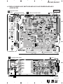
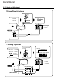
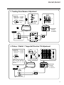
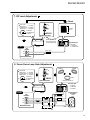
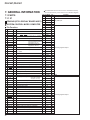
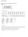
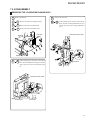
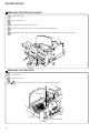
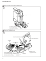
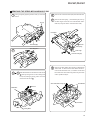
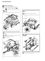
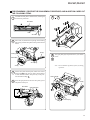
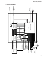
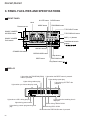
42-5064
MODEL CD-8400
FILE-TYPE CD PLAYER
Catalog Number: 42-5064
¶ The service manual for this product includes Pioneer's RRV1898 PD-F907/KU service manual. The
pages preceding that manual list additional specifications, all service changes between Pioneer's
RRV1898 PD-F907/KU and the 42-5064 CD8400, and any RadioShack part numbers that are different
from the Pioneer part numbers.
¶ The specifications on Page 51 of the RRV1898 service manual for Pioneer's model PD-F907/KU are
like the specifications listed in the owner's manual for the 42-5064 CD-8400. Additional specs are
given on the page inside the back cover.
© 1998 Tandy Corporation.
All Rights Reserved.
Optimus and Radio Shack are registered trademarks used by Tandy Corporation.
PART NUMBER DIFFERENCES BETWEEN 42-5064 CD-8400 AND
PD-F907/KU
NOTES : ÷ Parts marked by “ NSP ” are generally unavailable .
indicates safety critical components. Be sure to replace only with specified parts.
÷
÷ Ref. No. : Numbers following P and hyphen(–) indicate the page(s) and location number(s) in the RRV1898 service manual,
respectively.
42-5064 CD-8400 and PD-F907/KU are constructed the same except for the following:
Parts No.
Ref.No. Mark
P3 - 3
P3 - 3
P3 - 4
P3 - 5
P3 - 6
P3 - 11
P3 - 13
P6 - 18
P6 - 44
P6 - 45
P6 - 46
P6 - 47
P6 - 52
P6 - 50
2
NSP
NSP
Symbol and Description
PD-907/KU
42-5064
CD-8400
PWW1132
Not used
AZA7204
ARY1044
PRB1263
Not used
PYY1262
PZN1105
Not used
PRB1272
Packing Case
Battery (R6P, AA)
PHG2285
VEM-013
PHG2325
Not used
EXTERIOR SECTION
Rear Base
Control Button
Power Button
Name Plate
Display Window
PNA2389
PAC1822
PAC1833
VAM1073
PAM1725
PNA2431
PAC1899
PAC1900
AAM7001
PAM1765
PNW2732
PNW2773
PNW2824
PNW2825
PACKING
Remote Control Unit (CU-PD080)
Remote Control Unit
Battery Cover
Warranty Card
Operating Instructions (English)
Hood
Operation Panel
Remarks
Service
Manual
D
FILE–TYPE
COMPACT DISC PLAYER
DISC
TRACK
MIN
SEC
PD-F905
Î
ACSESS
PLAY
MODE
HI-LITE
CLEAR
PROGRAM
TITLE
INPUT
TITLE
DISPLAY
SINGLE
LOADER
UNLOAD
BEST
PREVIOUS
DISC
FILE –TYME CD MECHANISM
ORDER NO.
OPEN/
CLOSE
RRV1898
FILE-TYPE CD PLAYER
PD-F957
PD-F907
THIS MANUAL IS APPLICABLE TO THE FOLLOWING MODEL(S) AND TYPE(S).
Model
Type
Power Requirement
PD-F957
PD-F907
KU
–
O
AC120V
KC
–
O
AC120V
KU/CA
O
–
AC120V
Remarks
CONTENTS
1. SAFETY INFORMATION .................................... 2
2. EXPLODED VIEWS AND PARTS LIST ............. 3
3. SCHEMATIC DIAGRAM ................................... 11
4. PCB CONNECTION DIAGRAM ....................... 19
5. PCB PARTS LIST ............................................. 24
6. ADJUSTMENT .................................................. 28
7.GENERAL INFORMATION ............................... 36
7.1 PARTS ........................................................ 36
7.1.1 IC .......................................................... 36
7.1.2 DISPLAY ............................................... 37
7.2 DIAGNOSIS ................................................ 39
7.2.1 ERROR CORD DISPLAY ................. 39
7.2.2 ERROR HISTORY AND DISPLAY ... 39
7.2.3 ERROR HISTORY DISPLAY ............ 40
7.2.4 DISASSEMBLY ................................. 41
7.3 BLOCK DIAGRAM ...................................... 49
8. PANEL FACILITIES AND SPECIFICATIONS
................................................................... 50
PIONEER ELECTRONIC CORPORATION
4-1, Meguro 1-Chome, Meguro-ku, Tokyo 153, Japan
PIONEER ELECTRONICS SERVICE, INC. P.O. Box 1760, Long Beach, CA 90801-1760, U.S.A.
PIONEER ELECTRONIC (EUROPE) N.V . Haven 1087, Keetberglaan 1, 9120 Melsele, Belgium
PIONEER ELECTRONICS ASIACENTRE PTE. LTD. 501 Orchard Road, #10-00 Lane Crawford Place, Singapore 0923
C PIONEER ELECTRONIC CORPORATION 1997
T–ZZY DEC. 1997 Printed in Japan
PD-F957,PD-F907
1. SAFETY INFORMATION
This service manual is intended for qualified service technicians; it is not meant for the casual
do-it-yourselfer. Qualified technicians have the necessary test equipment and tools, and have been
trained to properly and safely repair complex products such as those covered by this manual.
Improperly performed repairs can adversely affect the safety and reliability of the product and may
void the warranty. If you are not qualified to perform the repair of this product properly and safely, you
should not risk trying to do so and refer the repair to a qualified service technician.
WARNING
Lead in solder used in this product is listed by the California Health and Welfare agency as a known reproductive toxicant which
may cause birth defects or other reproductive harm (California Health & Safety Code, Section 25249.5).
When servicing or handling circuit boards and other components which contain lead in solder, avoid unprotected skin contact with
the solder. Also, when soldering do not inhale any smoke or fumes produced.
NOTICE
(FOR CANADIAN MODEL ONLY)
Fuse symbols
(fast operating fuse) and/or
(slow operating fuse) on PCB indicate that replacement parts
must be of identical designation.
REMARQUE
(POUR MODÈLE CANADIEN SEULEMENT)
Les symboles de fusible
(fusible de type rapide) et/ou
(fusible de type lent) sur CCI indiquent que les
pièces de remplacement doivent avoir la même désignation.
(FOR USA MODEL ONLY)
1. SAFETY PRECAUTIONS
The following check should be performed for the
continued protection of the customer and service
technician.
LEAKAGE CURRENT CHECK
Measure leakage current to a known earth ground
(water pipe, conduit, etc.) by connecting a leakage
current tester such as Simpson Model 229-2 or
equivalent between the earth ground and all exposed
metal parts of the appliance (input/output terminals,
screwheads, metal overlays, control shaft, etc.). Plug
the AC line cord of the appliance directly into a 120V
AC 60 Hz outlet and turn the AC power switch on. Any
current measured must not exceed 3.5 mA.
Leakage
current
tester
Device
under
test
Reading should
not be above
3.5 mA
Test all exposed
metal surfaces
Also test with plug
reversed
(Using AC adapter
plug as required)
Earth ground
AC Leakage Test
2
ANY MEASUREMENTS NOT WITHIN THE LIMITS
OUTLINED ABOVE ARE INDICATIVE OF A POTENTIAL SHOCK HAZARD AND MUST BE CORRECTED BEFORE RETURNING THE APPLIANCE
TO THE CUSTOMER.
2. PRODUCT SAFETY NOTICE
Many electrical and mechanical parts in the appliance have special safety related characteristics. These
are often not evident from visual inspection nor the
protection afforded by them necessarily can be obtained by using replacement components rated for
voltage, wattage , etc. Replacement parts which have
these special safety characteristics are identified in
this Service Manual.
Electrical components having such features are
identified by marking with a
on the schematics and
on the parts list in this Service Manual.
The use of a substitute replacement component which
does not have the same safety characteristics as the
PIONEER recommended replacement one, shown in
the parts list in this Service Manual, may create shock,
fire, or other hazards.
Product Safety is continuously under review and
new instructions are issued from time to time. For
the latest information, always consult the current
PIONEER Service Manual. A subscription to, or additional copies of, PIONEER Service Manual may be
obtained at a nominal charge from PIONEER.
PD-F957,PD-F907
2. EXPLODED VIEWS AND PARTS LIST
NOTES : ÷ Parts marked by “ NSP ” are generally unavailable because they are not in our Master Spare Parts List.
÷ The mark found on some component parts indicates the importance of the safety factor of the part.
Therefore, when replacing, be sure to use parts of identical designation.
÷ Screw adjacent to ∞ mark on the product are used for disassembly.
2.1 PACKING
13
3
8
4
5
(1) PARTS LIST
6
Mark No. Description
2 1
7
NSP
1
2
3
4
5
NSP
6
7
8
9
10
11
12
13
12
PD-F907/KC only
10(2/2)
10(1/2)
9(2/2)
Front
9(1/2)
Parts No.
Control Cable (L=1.0m)
Output Cable (L=1.0m)
Remote Control Unit
Battery Cover
Warranty Card
PDE1247
PDE1248
Operating Instructions (English)
Operating Instructions (French))
Polyethlene Bag
Styrol Protector F
Styrol Protector R
Packing Case
Mirror Mat
Battery (R6P, AA)
See Contrast table (2)
See Contrast table (2)
See Contrast table (2)
AZN7204
See Contrast table (2)
Z21 - 038
PHA1307
PHA1308
See Contrast table (2)
Z23 - 0204
VEM - 013
11
(2) CONTRAST TABLE
PD-F907/KU,KC and PD-F957/KU/CA have the same construction except for the following:
Part No.
Mark No.
NSP
Symbol & Description
3
Remote Control Unit
5
6
7
11
Warranty Card
Operating Instructions (English)
Operating Instructions (French)
Packing Case
PD-F957/
KU/CA
PD-F907/
KU
PD-F907
KC
PWW1130
(CU-PD088)
ARY1044
PRB1264
Not used
PHG2304
PWW1132
(CU-PD080)
ARY1044
PRB1263
Not used
PHG2285
PWW1132
(CU-PD080)
ARY1039
PRB1263
PRD1023
PHG2286
Remarks
3
PD-F957,PD-F907
2.2 EXTERIOR
56
61
62
51
55
KU/CA,KU type only
62
53
68
4
54
50
3
68
63
A
45
11
46
44
13
61
63
PD-F907 only
47
13
PD-F907 only
4
68
PD-F957,PD-F907
D
27
24
65 6
67
61
61
61
32(4/4)
Note1
16
Refer to
''2.3 LOADING
MECHANISM
ASSY''
31
32(3/4)
18
J
61
F
19
32(2/4)
57
21(1/2)
63
61
41
35
32(1/4)
64
E
33
40
43
38
69
42
37
8
63
15
63
H
15
42
2
39
G
15
E J
15
12
36
10
34
59
25
F
1
52
C
Note2
26(2/2)
15
30
28
29
D
G
B C
A
64
63
Note1
21 (2/2)
7
H
69
21(1/2)
23
63
15
14
26(1/2)
17
25
34
59
Note2 cutting position
No.26(Hood Base)
26(2/2)
cutting
5
63
22
20
Note1 cutting position
cutting No.21(Back Fence)
21(2/2)
cutting
B
26(1/2)
60
PD-F957 Only
21(1/2)
5
PD-F957,PD-F907
(1) EXTERIOR PARTS LIST
Mark No.
NSP
NSP
NSP
NSP
NSP
NSP
Description
Parts No.
Mark No.
Description
Parts No.
Main Board Assy
Power Board Assy
Display Board Assy
Switch Board Assy
Door Board Assy
See Contrast table(2)
See Contrast table(2)
See Contrast table(2)
See Contrast table(2)
See Contrast table(2)
36
37
38
39
40
6
7
8
9
10
Center LED Board Assy
Select Motor Board Assy
Sensor Board Assy
.............
Cord Stopper
See Contrast table(2)
41
42
43
44
45
Mecha Stopper
Roller
Gear Pulley
Control Button
Power Button
PNW2646
PNW2647
VNL1662
PAC1822
PAC1833
11
12
13
14
15
F.F.C/30V
AC Power Cord
Rubber Sheet
Foot Assy
Screw C
46
47
48
49
50
Name Plate
Display Window
.............
.............
Operation Panel
VAM1073
16
17
18
19
20
Screw
Under Base
Rear Base
Stopper Angle
Insulator
PBA1108
PNA2255
Bonnet Case
Hood
Side Fence
Sensor Acryl
65 Label
PYY1191
PNW2732
PNW2674
VNK1566
See Contrast table(2)
51
52
53
54
55
21
22
23
24
25
Back Fence
Locking Card Spacer
Belt
Cover
Motor Assy
PNW2671
VEC1596
PEB1288
PNM1294
PEA1333
56
57
58
59
60
Label
Label
.............
Slider Motor
Screw
PRW1428
PRW1429
VXM1033
IBZ30P080FZK
26
27
28
29
30
Hood Base
Center Pole
Gear
Gear
Gear Pulley
PNW2633
PNW2634
PNW2641
PNW2642
VNL1662
61
62
63
64
65
Screw
Screw
Screw
Screw
Screw
BBZ30P080FZK
FBT40P080FZK
IBZ30P060FMC
IPZ20P080FMC
IPZ30P080FCU
31
32
33
34
35
Loading Mechanism Assy
Rack Label
Belt
Motor Pulley
Disc Rack
PXA1589
PAM1732
PEB1288
PNW1634
PNW2632
66
67
68
69
.............
Screw
Screw
Binder
PPZ30P050FMC
PPZ30P100FMC
Z09 - 056
1
2
3
4
5
PWZ3324
PWZ3327
CM - 22C
See Contrast table(2)
PDG1015
See Contrast table(2)
See Contrast table(2)
PBA1106
See Contrast table(2)
PNB1559
Mecha Base
Gear
Gear
Slider
Lock Lever
PNW2639
PNW2641
PNW2642
PNW2643
PNW2644
See Contrast table(2)
See Contrast table(2)
See Contrast table (2)
(2) CONTRAST TABLE
PD-F907/KU,KC and PD-F957/KU/CA have the same construction except for the following:
Part No.
Mark No.
NSP
NSP
NSP
6
Symbol & Description
PD-F957/
KU/CA
PD-F907/
KU
PD-F907/
KC
1
2
3
4
5
Main Board Assy
Power Board Assy
Display Board Assy
Switch Board Assy
Door Board Assy
PWZ3663
PWZ3668
PWZ3672
PWZ3675
PWZ3681
PWZ3400
PWZ3414
PWZ3426
PWZ3432
PWZ3441
PWZ3400
PWZ3414
PWZ3426
PWZ3432
PWZ3441
6
11
Center LED Board Assy
F.F.C/30V
13
14
Rubber Sheet
Foot Assy
PWZ3683
PDD1186
(40P F.F.C)
Not Used
REC1263
PWZ3443
PDD1167
(32P F.F.C)
AEB1111
AEC1531
PWZ3443
PDD1167
(32P F.F.C)
AEB1111
AEC1531
18
20
47
50
55
Rear Base
Insulator
Display Window
Operation panel
65 Label
PNA2405
PNW2766
PAM1752
PNW2786
ORW1069
PNA2389
Not Used
PAM1725
PNW2773
ORW1069
PNA2389
Not Used
PAM1725
PNW2773
Not used
Remarks
PD-F957,PD-F907
2.3 LOADING MECHANISM ASSY
7
PD-F957,PD-F907
LOADING MECHANISM ASSY PARTS LIST
Mark No. Description
NSP
NSP
NSP
NSP
8
1
2
3
4
5
…………
…………
Loading Motor Board Assy
Load SW Board Assy
Arm A Spring2
Parts No.
PWZ3337
PWZ3334
ABH7124
6
7
8
9
10
Gear Plate Spring
Clamp Spring
…………
…………
Loading Belt
ABH7051
ABH7107
11
12
13
14
15
…………
…………
…………
Servo Stopper S
Loading Base
ANB7047
ANW7086
16
17
18
19
20
Cam Cover
Motor Holder
Sensor Holder
Float Base 96
Clamper Holder
ANW7052
ANW7053
ANW7119
PNW2700
ANW7117
21
22
23
24
25
Arm (A)
Arm (B)
Drive Plate
Arm Plate
Gear Plate
ANW7057
ANW7058
ANW7059
ANW7060
ANW7111
26
27
28
29
30
Gear Pulley (B)
Gear A
Drive Gear
…………
…………
ANW7062
ANW7063
ANW7064
31
32
33
34
35
…………
…………
…………
Roller B
Motor Pulley
ANW7075
PNW1634
36
37
38
39
40
Clamper
Float Spring
Connector Assy (4P)
Float Rubber
Servo Mechanism Assy GM
PNW2743
ABH7049
RDE1043
AEB7028
PXA1591
41
42
43
44
45
Screw
…………
…………
Motor Assy
Loading Motor
IPZ20P080FMC
AEA7006
VXM1034
46
16P FFC/30V
PDD1180
Froil (for Service)
Ha Narl (for Service)
GYA1001
GEM1016
AEB7029
PD-F957,PD-F907
2.4 SERVO MECHANISM ASSY GM
How to Install the Disc Table
1 Use nipper or other tool to cut the three sections marked
A in figure 1 . Then remove the spacer
2 While supporting the spindle motor shaft with the
stopper, put spacer on top of the yoke M, and stick the
disc table on top (takes about 9kg pressure). Detach the
spacer.
1
2
A
Spacer
(Pressure of about 9 kg)
Spacer
Disc Table
6.9mm
Float Base
Yoke M
Spacer Setting
Position
Carriage Base
0.9mm
±0.05mm
1.2mm
Spindle Motor
Stopper
9
PD-F957,PD-F907
SERVO MECHANISM ASSY GM PARTS LIST
Mark No. Description
1
2
3
4
5
NSP
NSP
10
Parts No.
Gear 1
Gear 2
Gear 3
Carriage Base
Pickup Assy - S
PNW2052
PNW2053
PNW2054
PNW2699
PEA1335
6
7
8
9
10
D.C. Motor Assy (SPINDLE)
Carriage DC Motor Assy
Pinion Gear
Carriage DC Motor/0.3W
Disc Table Assy
PEA1235
PEA1246
PNW2055
PXM1027
PEA1314
11
12
13
14
15
Mechanism Board Assy
Guide Bar
…………
Screw
Screw
PWX1192
PLA1094
16
17
18
19
20
Washer
Clamp Magnet
Yoke M
Disc Table
Float Angle
WT12D032D025
PMF1014
PNB1312
PNW2410
ANB7020
21
22
23
24
25
Gear Stopper
Screw
Screw
PU Rack Spring
Rack Holder
PNB1303
BPZ20P060FMC
BPZ26P100FMC
ABH7077
PNW2056
JFZ17P025FZK
JFZ20P040FMC
1
2
3
4
PD-F957,PD-F907
3. SCHEMATIC DIAGRAM
Note: When ordering service parts, be sure to refer to "EXPLODED VIEW AND PARTS LIST" or "PCB PARTS LIST".
CN610
3.1 MECHANISM BOARD ASSY,SENSOR BOARD ASSY,LOAD SW BOARD ASSY,SELECT
MOTOR BOARD ASSY,LOADING MOTOR BOARD ASSY,CENTER LED BOARD ASSY,
DOOR BOARD ASSY AND PICKUP ASSY
A
SERVO MECHANISM ASSY GM
(PXA1591)
SPINDLE
MOTOR
ASSY
PEA1235
CARRIAGE
MOTOR
ASSY
PEA1246
A
A
MECHANISM
BOARD ASSY
(PWX1192)
PICK UP ASSY
(PEA1335)
B
B
LOAD SW BOARD
B ASSY (PWZ3334 )
C
LOADING MECHA
BOARDASSY
(PWX1474)
C
LOADING MOTOR
BOARD ASSY
(PWZ3337)
C
SENSOR BOARD
ASSY
(PWZ3327)
D
E
SELECT MOTOR
BOARD ASSY
(PWZ3324)
D
CENTER LED BOARD ASSY
PD-F957/KU/CA:(PWZ3683)
PD-F907/KU,KC:(PWZ3443)
E
D
F
DOOR BOARD ASSY
PD-F957/KU/CA:(PWZ3681)
PD-F907/KU,KC:(PWZ3441)
F
G
1
2
A B C D E F G
3
4
11
1
2
3
4
PD-F957,PD-F907
3.2 MAIN BOARD ASSY AND POWER BOARD ASSY (FOR PD-F957)
2 23
3
A
4
1.8V
7
33
-O.7V
1.8V
1.6V
A
5
53
OV
1.6V
1.6V
6
16
OV
1.6V
18
B
B
1.7V
19
8
0.2V
(F)
(F)
(F)
(F)
(T)
(T)
1.7V
0V
0V
0V
C
0V
(SEL)
3.4V
23
0V
(SEL)
C
0V
D
(D)
5.0V
(SEL)
0V
(D)
0V
(D)
0V
SIGNAL ROUTE
: AUDIO SIGNAL
: EFM SIGNAL
: FOCUS SERVO LOOP
: TRACKING SERVO LOOP
: CARRIAGE SERVO LOOP
(S)
: SPINDLE DRIVE
: LOADING DRIVE
(D)
: DOOR DRIVE
E
D
F
12
H
1
L
M
2
3
DISPLAY BOARD ASSY
(PWZ3672)
SWITCH BOARD ASSY
(PWZ3675)
4
5
6
7
8
PD-F957,PD-F907
IC301(CXD2529Q) :PLAY MODE
PIN No.
Voltage(V)
1
5
2
0
3-4
0
7
4.7
8
9
1.2-1.3 1.2-1.4
PIN No.
Voltage(V)
26
5
27
2.6-2.7
38
2.5
39
3.1
40
2.5
PIN No.
Voltage(V)
61
5
71
2.5
75
0
78
0
79
5
10
4.4
11
5
12
4.7
13
4.7
14
0.05
16
5
17
4.7
23
5
24
5
25
0
41
0
42
3.1
43
5
44
2.5
45
0.9
46
2.5
47
2.5
48
5
50-55
2.5
56
0
57
5
82
0
83
5
84-86
2.5
87
0
88
5
96
5
97
0
100
5
0V
89-90 91-92 93-95
2.5
0
2.5
A
0V
1.6V
LINE OUT
JACK
-9.2
0V
-9.2
1.6V
10
0V
0V
B
C
H
MAIN BOARD ASSY
(PWZ3663)
AC120V
60Hz
AC POWER CORD
:PDG1015
I
POWER BOARD ASSY
(PWZ3668)
D
P0WER TRANSFORMER
5
6
7
H I
8
13
1
2
3
4
PD-F957,PD-F907
3.3 MAIN BOARD ASSY AND POWER BOARD ASSY (FOR PD-F907)
J
2 23
3
A
4
MAIN BOARD ASSY
(PWZ3400)
1.8V
7
33
-O.7V
1.8V
1.6V
A
5
53
OV
1.6V
1.6V
6
16
OV
1.6V
18
B
B
1.7V
19
8
0.2V
(F)
(F)
(F)
(F)
(T)
(T)
1.7V
0V
0V
0V
C
0V
(SEL)
3.4V
23
0V
(SEL)
C
0V
D
(D)
5.0V
(SEL)
0V
(D)
0V
(D)
0V
SIGNAL ROUTE
: AUDIO SIGNAL
: EFM SIGNAL
: FOCUS SERVO LOOP
: TRACKING SERVO LOOP
: CARRIAGE SERVO LOOP
(S)
: SPINDLE DRIVE
: LOADING DRIVE
(D)
: DOOR DRIVE
E
D
F
N
14
J
1
2
DISPLAY BOARD ASSY
(PWZ3426)
SWITCH BOARD ASSY
O
3
(PWZ3432)
4
5
6
7
8
PD-F957,PD-F907
IC301(CXD2519Q) :PLAY MODE
PIN No.
Voltage(V)
1
5
2
0
3-4
0
7
4.7
8
9
1.2-1.3 1.2-1.4
PIN No.
Voltage(V)
26
5
27
2.6-2.7
38
2.5
39
3.1
40
2.5
PIN No.
Voltage(V)
61
5
71
2.5
75
0
78
0
79
5
10
4.4
11
5
12
4.7
13
4.7
14
0.05
16
5
17
4.7
23
5
24
5
25
0
41
0
42
3.1
43
5
44
2.5
45
0.9
46
2.5
47
2.5
48
5
50-55
2.5
56
0
57
5
82
0
83
5
84-86
2.5
87
0
88
5
96
5
97
0
100
5
0V
89-90 91-92 93-95
2.5
0
2.5
A
0V
1.6V
LINE OUT
JACK
-9.2
0V
-9.2
1.6V
10
0V
0V
B
(BACK UP)
C
AC 120V
60 Hz
K
POWER BOARD ASSY
(PWZ3414)
AC POWER CORD
POWER TRANSFORMER
D
5
6
7
J K
8
15
1
2
3
4
PD-F957,PD-F907
3.4 DISPLAY BOARD ASSY AND SWITCH BOARD ASSY
L
A
DISPLAY BOARD ASSY
PD-F957/KU/CA:(PWZ3672)
PD4934B
B
M
O
SWITCH BOARD ASSY
PD-F957/KU/CA:(PWZ3675)
H
PD-F907/KU,KC:(PWZ3432)
CN351
SWITCHES
SWITCH BOARD ASSY
S751 : SL ACCESS
S752 : SL PLAY
S753 : POWER STAND/ON
C
DISPLAY BOARD ASSY
S703
S704
S707
S708
S709
S710
S711
S712
S713
S714
: MODE
: UNLOAD
: 6
: OPEN/CLOSE
: HI-LITE
: 7
: 4 1
: ¡ ¢
: BEST
: PREVIOUS
S715
S716
S717
S718
S719
: DISC –
: DISC +
: CLEAR
: PGM
: TITLE INPUT (PD-F957)
: RANDOM (PD-F907)
S720 : TITLE DISPLAY (PD-F957)
: REPEAT (PD-F907)
J
N
CN351
DISPLAY BOARD ASSY
PD-F907/KU,KC:(PWZ3426)
D
16
L M N O
1
2
3
4
PD-F957,PD-F907
∗1 50T-JUMP: After switching to the pause mode, press
the manual search key.
∗2 FOCUS-IN: Press the play key without loading a disc.
Waveforms
Note: The encircled numbers denote measuring point in the schematic diagram.
2
4'
TP1-Pin 1: PLAY MODE (RF)
500mV/div 500nsec/div
– VC
2
TP1-Pin 1: TRACK SEARCH MODE
(RF)
500 mV/div 200 µsec/div
TP1-Pin 6: PLAY MODE (FOER)
100mV/div 10msec/div
5
TP1-Pin 2: PLAY MODE (TRER)
200mV/div 1msec/div
– VC
IC202-Pin 3: FOCUS-IN (*2) MODE
(FODR)
1V/div 200msec/div
5
IC202-Pin 3: PLAY MODE (FODR)
1V/div 1msec/div
7
IC202-Pin 4: PLAY MODE (TRDR)
500mV/div 1msec/div
– GND
IC203-Pin 3: PLAY MODE (SPDR)
1V/div 50msec/div
– GND
7
IC203-Pin 3: TRACK SEARCH MODE
(SPDR)
2V/div 50msec/div
– GND
– GND
6
IC202-Pin 4: 50T - JUMP (*1) MODE
(TRDR)
500mV/div 1msec/div
– GND
– GND
– VC
4
6'
– VC
– VC
3
TP1-Pin 2: 50T - JUMP (*1) MODE
(TRER)
200mV/div 1msec/div
8
IC202-Pin 9: PLAY MODE (CADR)
0.2V/div 2sec/div
– GND
17
PD-F957,PD-F907
Waveforms
8
IC202-Pin 9: TRACK SEARCH MODE
(CADR)
2V/div 200msec/div
16
– GND
IC301-Pin 54 : PLAY MODE (1kHz)
(BCK)
2V/div 500nsec/div
– GND
18
IC301-Pin 50 : PLAY MODE (1kHz)
(LRCK)
2V/div 10 µsec/div
33
IC301-Pin 27 : PLAY MODE (MDP)
2V/div 2 µsec/div
– GND
10
IC301-Pin 86 : PLAY MODE (1kHz)
(LOUT 1)
1V/div 200msec/div
19
IC301-Pin 52 : PLAY MODE (1kHz)
(PCMD)
2V/div 500nsec/div
– GND
– GND
23
TRACK SEARCH MODE
Upper : TP1-Pin 1 (RF) 1V/div
Lower : IC151-Pin 23 (C.OUT)
2V/div 50 µsec/div
– GND
– GND
18
– GND
53
IC301-Pin 38 : PLAY MODE
(PCO)
2V/div 10 µsec/div
– GND
1
2
3
4
PD-F957,PD-F907
4. PCB CONNECTION DIAGRAM
4.1 MECHANISM BOARD ASSY,SENSOR BOARD ASSY,LOAD SW BOARD ASSY,SELECT
MOTOR BOARD ASSY,LOADING MOTOR BOARD ASSY,CENTER LED BOARD ASSY
AND DOOR BOARD ASSY
2
4
J656
5 J657
J6
56
PNP1443-A
1
J
CN207 CN203
M
SPINDLE
MOTOR
INSIDE
J
S652
M
(PD-F957)
Symbol in PCB
Diagrams
PWZ3337PWZ3338PWZ3339-
1
(PD-F907)
For PD-F957
Symbol in Schematic
Diagrams
B
E B
C
Part Name
E
Transistor
B
3. The parts mounted on this PCB include all necessary
parts for several destination.
For further information for respective destinations,
be sure to check with the schematic diagram.
1. Part numbers in PCB diagrams match those in the
schematic diagrams.
2. A comparison between the main parts of PCB and
schematic diagrams is shown below.
Connector
E B
C
E
Transistor
with resistor
D
G
S D
G
S
Field effect
transistor
D G S
Capacitor
C
B C E
4. Viewpoint of PCB diagrams
F
C
B C E
NOTE FOR PCB DIAGRAMS:
PNP1239-B
1
3
CN207 CN203
PWZ3334PWZ3335PWZ3336-
S651
H
A
LOAD SW BOARD ASSY
2
4
H
B
1
3
C
CARRIAGE
MOTOR
A
LOADING MOTOR BOARD ASSY
MECHANISM BOARD ASSY
B
SIDE A
CENTER LED BOARD ASSY
Resistor
array
P. C. Board
H
Chip Part
3-terminal
regulator
SIDE B
CN208
G
PNP1443–A
DOOR BOARD ASSY
H
CN205
SIDE A
For PD-F907
C
J
CN205
F
CENTER LED BOARD ASSY
G
DOOR BOARD ASSY
PNP1421–C
J
SELECT MECHA BOARD ASSY
CN208
E
D SENSOR BOARD ASSY
SELECT MOTOR
BOARD ASSY
H
D
CN204
(PD-F957)
J
CN204
(PD-F907)
1
2
PNP1409–A
A B C D E F G
3
4
19
D
G
20
Q381
J1601
IC201
Q322
Q153
IC301
IC203 IC202
Q321
Q341
B
J657
C
VR153
Q391
4.2 MAIN BOARD ASSY (FOR PD-F957)
H
1
2
3
To PICKUP ASSY
CN610
A
J11
I
J631
CN701
L
PNP1443–A
3
4
IC151
Q152 Q151
Q452
Q405 Q406 Q404
IC405 Q451 Q454 IC406 Q403 Q453
H
2
IC71
IC401
VR152
VR156
VR151 VR155 VR154
1
4
PD-F957,PD-F907
MAIN BOARD ASSY
SIDE A
A
C
J601
E
F
1
2
3
4
PD-F957,PD-F907
4.3 DISPLAY BOARD ASSY,SWITCH BOARD ASSY AND POWER BOARD ASSY
(FOR PD-F957)
BOARD
M SWITCH
ASSY
SIDE A
L
A
H CN351
DISPLAY BOARD ASSY
B
C
IC702
I
Q702
IC701
Q701
H CN11
POWER BOARD ASSY
D
IC21 IC41
IC31 IC32
AC IN
PNP1443–A
1
2
3
I L M
4
21
D
J631
G
22
Q381
Q371 Q372
J1601
F
IC351
Q322
IC201
IC301
IC202
Q321
J
1
A
Q391
MAIN BOARD ASSY
2
To PICKUP ASSY
CN610
J11
K
J657
C
CN701
N
PNP1421–C
3
4
IC71 IC371
IC401
A
VR153
4.4 MAIN BOARD ASSY(FOR PD-F907)
3
IC151
Q152 Q151
Q452
Q405 Q404
IC405 Q451 Q454 IC406 Q403 Q453
J
2
J601
E
Q341
IC203
B
VR152
VR156
VR151 VR155 VR154
1
4
PD-F957,PD-F907
SIDEA
C
1
2
3
4
PD-F957,PD-F907
4.5 DISPLAY BOARD ASSY,SWITCH BOARD ASSY AND POWER BOARD ASSY
(FOR PD-F907)
BOARD
O SWITCH
ASSY
SIDE A
N
J
DISPLAY BOARD ASSY
A
CN351
B
C
Q711
K
J
POWER BOARD ASSY
CN11
D
IC31 IC21
AC IN
IC33
IC32
IC23
PNP1421–C
1
2
3
K N O
4
23
PD-F957,PD-F907
5. PCB PARTS LIST
NOTES : ÷ Parts marked by “ NSP ” are generally unavailable because they are not in our Master Spare Parts List.
÷ The
mark found on some component parts indicates the importance of the safety factor of the part.
Therefore, when replacing, be sure to use parts of identical designation.
÷ When ordering resistors, first convert resistance values into code form as shown in the following examples.
Ex. 1
When there are 2 effective digits (any digit apart from 0), such as 560 ohm and 47k ohm (tolerance is shown by
J = 5%, and K = 10%).
560 Ω = 56 × 10 1 = 561 ................................................... RD1/4PU 5 6 1 J
47k Ω = 47 × 10 3 = 473 .................................................. RD1/4PU 4 7 3 J
0.5 Ω = R50 ...................................................................... RN2H Â 5 0 K
1 Ω = 1R0 ......................................................................... RS1P 1 Â 0 K
Ex. 2
When there are 3 effective digits (such as in high precision metal film resistors).
5.62k Ω = 562 × 10 1 = 5621 ........................................... RN1/4PC 5 6 2 1 F
LIST OF WHOLE PCB ASSEMBLIES
Part No.
Mark
Symbol and Description
PD-F957/
KU/CA
PD-F907/
KU
NSP
NSP
NSP
MOTHER BOARD ASSY
MAIN BOARD ASSY
POWER BOARD ASSY
DISPLAY BOARD ASSY
SWITCH BOARD ASSY
DOOR BOARD ASSY
CENTER LED ASSY
PWM2130
PWZ3663
PWZ3668
PWZ3672
PWZ3675
PWZ3681
PWZ3683
PWM2119
PWZ3400
PWZ3414
PWZ3426
PWZ3432
PWZ3441
PWZ3443
PWM2119
PWZ3400
PWZ3414
PWZ3426
PWZ3432
PWZ3441
PWZ3443
NSP
NSP
NSP
SELECT MECHA BOARD ASSY
SELECT MOTOR BOARD ASSY
SENSOR BOARD ASSY
PWX1465
PWZ3324
PWZ3327
PWX1465
PWZ3324
PWZ3327
PWX1465
PWZ3324
PWZ3327
NSP
NSP
NSP
NSP
LOADING MECHANISM ASSY
LOADING MECHA BOARD ASSY
LOAD SW BOARD ASSY
LOADING MOTOR BOARD ASSY
SERVO MECHANISM ASSY GM
MECHANISM BOARD ASSY
PXA1589
PWX1474
PWZ3334
PWZ3337
PXA1591
PWX1192
PXA1589
PWX1474
PWZ3334
PWZ3337
PXA1591
PWX1192
PXA1589
PWX1474
PWZ3334
PWZ3337
PXA1591
PWX1192
NSP
PD-F907
KC
Remarks
CONTRAST OF PCB ASSEMBLIES
DOOR BOARD Assy
PWZ3681 and PWZ3441 are constructed the same except for the following:
Part No.
Mark
NSP
Symbol and Description
CONNECTOR
J631
Remarks
PWZ3681
PWZ3441
51048-0400
D20PDY0425E
Not used
D20PWY0425E
CENTER LED BOARD Assy
PWZ3683 and PWZ3443 are constructed the same except for the following:
Part No.
Mark
NSP
Remarks
Symbol and Description
CONNECTOR
J1601
PWZ3683
PWZ3443
51048-0300
D20PDY0340G
Not used
D20PWY0340G
SWITCH BOARD Assy
Although PWZ3675 and PWZ3432 are different in part number, they consist of the same components.
24
PD-F957,PD-F907
PARTS LIST FOR PD-F957/KU/CA
Mark No.
H
Description
Parts No.
Mark No.
MAIN BOARD ASSY (PWZ3663)
Description
Other Resistors
IC151
IC301
IC203
IC201,IC202
IC302
CXA1782CQ
CXD2529Q
LA6517
LA6520
LC89170M
IC405
Q151
Q381,Q391
Q403,Q404
Q341
NJM4558DX
2SA854S
2SC1740S
2SD2144S
2SK246
Q152,Q406
Q153,Q321,Q405
D1301-D1309,D1312-D1314,D321
D341,D391-D397
D218
DTA124ES
DTC124ES
1SS254
1SS254
MTZJ6.2B
CN207
CN208
CN205
CN203
CN204
MT 4P CONNECTOR
3P JUMPER CONNECTOR
4P JUMPER CONNECTOR
5P JUMPER CONNECTOR
7P JUMPER CONNECTOR
173981-4
52147-0310
52147-0410
52147-0510
52147-0710
CN11
JA394
JA321
CN351
JA401
12P JUMPER CONNECTOR
I/O INTERFACE JACK
OPTICAL LINK OUT
CONNECTOR
JACK
52147-1210
DKN1035
GP1F32T
HLEM40S-1
PKB1032
JA393
JACK
X341
X TAL.RES.(16.9344MHz)
JA391,JA392 JACK
CN201
CONNECTOR 6P
CN202
CONNECTOR
SCREW PLATE
COILS AND FILTERS
LAU1R0J
CAPACITORS
C181
C341,C342
C372,C373,C384,C385,C397
C315
C481,C482
CCCCH100D50
CCCCH120J50
CCCSL101J50
CCCSL221J50
CCCSL390J50
C356
C171,C175,C301,C302
C311-C314,C316,C322,C380
C433,C434
C131-C133,C211,C212
CEAT100M50
CEAT101M10
CEAT101M10
CEAT220M25
CEAT330M16
C169,C170
C309
C153-C155,C158,C172,C230
C250,C321
C157
CEAT4R7M50
CEATR47M50
CFTLA104J50
CFTLA104J50
CFTLA823J50
C156,C161,C164,C168,C218
C160
C152,C307
C163
C176,C306,C441,C442
CGCYX103K25
CGCYX333K25
CGCYX473K25
CKCYB102K50
CKCYB152K50
C305
C162
C167
C151
C159,C185,C205,C210,C215
CKCYB222K50
CKCYB332K50
CKCYB472K50
CKCYB682K50
CKCYF103Z50
C219,C304,C318,C323,C351
C355,C366,C371,C375
C381,C382,C387,C394,C398
CKCYF103Z50
CKCYF103Z50
CKCYF103Z50
I
RD1/4VM163J
RD1/4VM274J
RCP1045
RCP1046
RCP1049
PKN1005
PSS1008
RKN1004
RKP-533
SLW16S-1C7
VNE1948
POWER BOARD ASSY (PWZ3668)
SEMICONDUCTORS
IC31,IC32
IC21
D54
D11-D14,D52
ICP-N10
PQ05RR12
MTZJ24B
S5688G
CAPACITORS
C27
C52
C26
C11,C13,C15,C16
C25
(6800 µF/16V)
CEAT101M10
CEAT101M35
CEAT222M16
CKCYF103Z50
VCH1060
RESISTORS
Other Resistors
RD1/4PU&&&J
OTHERS
J11
L
CONNECTOR
JUMPER WIRE
POWER TRANSFORMER
TERMINAL
51048-1200
D20PDY1235E
PTT1342
RKC-061
DISPLAY BOARD ASSY (PWZ3672)
SEMICONDUCTORS
IC701
IC702
Q701
D701-D705
PD4934B
S-24C16ADP
DTC124ES
1SS254
COILS AND FILTERS
L701
RESISTORS
R189
R157
VR153,VR155
(10k Ω)
VR151,VR152,VR154 (22k Ω)
VR156 (220k Ω)
RD1/4PU&&&J
OTHERS
SEMICONDUCTORS
L391,L395,L396
Parts No.
LAU101J
SWITCHES AND RELAYS
S703,S704,S707-S720
PSG1006
25
PD-F957,PD-F907
Mark No.
Description
Parts No.
CAPACITORS
C712
C705,C709
C711
C708
C701,C704,C706,C707
CEAT100M50
CEAT101M10
CEAT4R7M50
CKCYF103Z50
CKPUYY103M16
RESISTORS
RD1/4PU&&&J
OTHERS
51048-0600
51048-0800
HLEM40R-1
PEL1095
VSS1028
SWITCH BOARD ASSY
SWITCHES AND RELAYS
S751-S753
PSG1006
CAPACITORS
C752
CKCYF103Z50
OTHERS
REMOTE RECEIVER UNIT
GP1U27X
DOOR BOARD ASSY
OTHERS
CONNECTOR
REAF SWITCH
F
51048-0400
VSK1011
CENTER LED BOARD ASSY
SEMICONDUCTORS
D1601-D1603
SLR-342YCT31
RESISTORS
Other Resistors
RD1/4PU&&&J
OTHERS
CONNECTOR
J1601
E
51048-0300
D20PDY0340G
SELECT MOTOR BOARD ASSY
SELECT MOTOR BOARD assembly has no service part.
D
SENSOR BOARD ASSY
SEMICONDUCTORS
Q601,Q602
D601,D602
DTC124ES
GP1S53V
RESISTORS
B
Other Resistors
RD1/4PU&&&J
LOAD SW BOARD ASSY
SWITCHES AND RELAYS
S651,S652
VSG1006
OTHERS
J656
26
Parts No.
LOADING MOTOR BOARD ASSY
LOADING MOTOR BOARD assembly has no service part.
A
MECHANISM BOARD ASSY
S610
DSG1016
OTHERS
CONNECTOR
CONNECTOR
CN701
CONNECTOR
V701
FL INDICATOR TUBE
X701
CERAMIC RES.(4.19MHz)
G
C
Description
SWITCHES AND RELAYS
Other Resistors
M
Mark No.
3P JUMPER WIRE
D20PWW0310E
CN610
MT 4P CONNECTOR
173979-4
PD-F957,PD-F907
PARTS LIST FOR PD-F907/KU/KC
Mark No.
J
Description
Parts No.
MAIN BOARD ASSY(PWZ3400)
Mark No.
Parts No.
RESISTORS
SEMICONDUCTORS
IC151
IC301
IC203
IC201,IC202
IC371
Description
CXA1782CQ
CXD2519Q
LA6517
LA6520
NJM2930L05
R189
R157
VR153,VR155
(10k Ω)
VR151,VR152,VR154 (22k Ω)
VR156 (220k Ω)
RD1/4VM163J
RD1/4VM274J
RCP1045
RCP1046
RCP1049
Other Resistors
RD1/4PU&&&J
OTHERS
IC405
IC71
IC351
Q151
Q381,Q391
NJM4558DX
NJM79L05A
PD4817A
2SA854S
2SC1740S
CN207
CN208
CN205
CN203
CN204
MT 4P CONNECTOR
3P JUMPER CONNECTOR
4P JUMPER CONNECTOR
5P JUMPER CONNECTOR
7P JUMPER CONNECTOR
173981-4
52147-0310
52147-0410
52147-0510
52147-0710
Q403,Q404
Q341
Q152,
Q321,Q371,Q372,Q405
D218,D321,D341,D372,D373
2SD2144S
2SK246
DTA124ES
DTC124ES
1SS254
CN11
JA321
CN351
JA401
JA393
12P JUMPER CONNECTOR
OPTICAL LINK OUT
CONNECTOR
JACK
JACK
52147-1210
GP1F32T
HLEM32S-1
PKB1032
PKN1005
D391-D397,
D374
1SS254
MTZJ3.3B
X341
X TAL.RES.(16.9344MHz)
JA391,JA392 JACK
CN201
CONNECTOR 6P
CN202
CONNECTOR
COILS AND FILTERS
L391,L395,L396,L393
LAU1R0J
CAPACITORS
C181
C341,C342
C373 (0.047F)
C315
C481,C482
CCCCH100D50
CCCCH120J50
ACH1246
CCCSL221J50
CCCSL390J50
C171,C175,C301,C302
C311-C314,C316,C322,C374
C73
C371
C433,C434
CEAS101M10
CEAS101M10
CEAS101M10
CEAS1R0M50
CEAS220M25
C131-C133,C211,C212
C376
C351
C169,C170,C356
C309
CEAS330M16
CEAS470M10
CEAS471M6R3
CEAS4R7M50
CEASR47M50
C153-C155,C158,C230
C250,C321
C157
C156,C161,C164,C168,C218
C160
CFTXA104J50
CFTXA104J50
CFTXA823J50
CGCYX103K25
CGCYX333K25
C152,C307
C397
C163
C176,C306,C441,C442
C305
CGCYX473K25
CKCYB101K50
CKCYB102K50
CKCYB152K50
CKCYB222K50
C162
C167
C151
C159,C185,C205,C210,C215
C219,C304,C318,C323,366,C353
CKCYB332K50
CKCYB472K50
CKCYB682K50
CKCYF103Z50
CKCYF103Z50
C354,C358,C362,C366
C375,C399,C81
CKCYF103Z50
CKCYF103Z50
X351
K
SCREW PLATE
CERAMIC RES.(4.19MHz)
PSS1008
RKN1004
RKP-533
SLW16S-1C7
VNE1948
VSS1028
POWER BOARD ASSY (PWZ3414)
SEMICONDUCTORS
IC21
D54
D11-D14,D31,D32,D52
PQ05RR12
MTZJ18B/C
S5688G
CAPACITORS
C27
C52
C26
C31
C11,C13,C15,C16
C25
(6800 µF/16V)
CEAS101M10
CEAS101M35
CEAS222M16
CEAS330M16
CKCYF103Z50
VCH1060
RESISTORS
Other Resistors
RD1/4PU&&&J
OTHERS
J11
POWER TRANSFORMER
TERMINAL
N
D20PWY1235E
PTT1318
RKC-061
DISPLAY BOARD ASSY (PWZ3426)
SEMICONDUCTORS
D701-D705
1SS254
SWITCHES AND RELAYS
S703,S704,S707-S720
PSG1006
OTHERS
CN701
V701
CONNECTOR
FL INDICATOR TUBE
HLEM32R-1
PEL1089
27
PD-F957,PD-F907
6. ADJUSTMENT
6.1 PREPARATIONS
6.1.1 Jigs and Measuring Instruments
8 Cm DISC
(With at last about 20
minutes recording)
CD TEST DISC
(YEDS-7)
screwdriver
(small)
screwdriver
(medium)
screwdriver
(large)
39 kΩ
0.001µF
Precise
screwdriver
Ball point hexagon wrench
(size: 1.5mm)
GGK1002
Low-frequency
oscillator
Dual-trace
oscilloscope
(10 : 1 probe)
56 kΩ
6.1.2 Necessary Adjustment Points
When
Exchange
PICKUP
Exchange
MAIN BOARD ASSY
Exchange
SERVO MECH ASSY
Exchange
SPINDLE MOTOR
28
Low pass filter 1
(39 kΩ + 0.001µF)
Adjustment points
1.2.3.4.5.6.7.
= Page 30 - 35
8.9.10.11.12
1.3.5.6.7.8.
9.10.11.12
= Page 30 - 35
1.2.3.4.5.6.7.
= Page 30 - 35
8.9.10.11.12
ADJ = Page 9
0.001µF
Low pass filter 2
(56 kΩ + 0.001µF)
PD-F957,PD-F907
6.2 ADJUSTMENT
6.2.1 How to Start/Cancel Test Mode
TEST MODE : ON
PD-F957 MODEL
PD-F957 MODEL
W115
W102
W115
W102
Short Point
Short Point
MAIN BOARD ASSY
MAIN BOARD ASSY
PD-F907 MODEL
PD-F907 MODEL
W184
W188
W184
W188
Short Point
Short Point
MAIN BOARD ASSY
MAIN BOARD ASSY
TEST MODE : PLAY
TEST DISC : YEDS-7
4 /1
inwards
MODE
¡ / ¢
CLOSE
outwards
Focus servo : CLOSE
Pickup Move
No.1 SLOT
6
6
Spindle motor : START
Spindle servo : CLOSE
6
OPEN
Tracking servo :
TEST MODE : STOP = CANCEL
7
6.2.2 Adjustment Location
Upper
PICKUP ASSY
Adjustment screw
(Tangential tilt direction)
Adjustment screw
(Radial tilt direction)
VR151
TR. GAIN
VR154
VR155 FO. OFS
TR. BAL
STOP all operations.
6 CN201
VR152 1
FO. GAIN ......
VR153
VR156
RF LEVEL
FO.BEST
PD-F957 MODEL
W115 W102
Grating adjustment
MAIN BOARD ASSY
W184
VR151
TR. GAIN
VR154
VR155 FO. OFS
TR. BAL
CN201 TP1
6
6.FE
5
5.FI
4
4.VC
3
3.TI
2
2.TE
1
1.RF
6 CN201
VR152 1
FO. GAIN ......
VR153
VR156
RF LEVEL
FO.BEST
PD-F907 MODEL
W188
MAIN BOARD ASSY
FRONT
29
PD-F957,PD-F907
6.2.3 Check and Adjustment
1. Focus Offset Adjustment
Test mode
DC voltage
0±50mV
VR154
None disc
MAIN BOARD ASSY
Oscilloscope
DC Mode
V: 5mV/div
H: 10mSec/div
Player
START
TP1
(CN201)
FE
VC
Prove (10:1)
6
4
GND
MAIN BOARD ASSY
2. Grating Adjustment
Turn counterclockwise
from null.
Locate null.
Test mode
SPDL servo = CLOSE
FOCUS servo = CLOSE
TRKG servo = OPEN
Counterclockwise, Maximum amplitude.
TEST DISC
PLAY
Innermost
circumference
(1 TRK)
PICKUP
Oscilloscope
Player
TP1
(CN201)
TE
VC
2
4
MAIN BOARD ASSY
Low pass filter 1
Prove (10:1)
39kΩ
0.001µF
GND
START
30
DC Mode
V: 10mV/div
H: 5mSec/div
PD-F957,PD-F907
3. Tracking Error Barance Adjustment
A=B
Test mode
SPDL servo = CLOSE
FOCUS servo = CLOSE
TRKG servo = OPEN
TEST DISC
PLAY
A
VC
Innermost
circumference
(1 TRK)
B
VR155
MAIN BOARD ASSY
Oscilloscope
DC Mode
V: 10mV/div
H: 5mSec/div
Player
START
Low pass filter 1
TP1
(CN201)
Probe (10:1)
2
4
VC
39kΩ
GND
TE
0.001µF
MAIN BOARD ASSY
4. Pickup 1Radial/ 2Tangential Direction Tilt Adjustment
Test mode
SPDL servo = CLOSE
FOCUS servo = CLOSE
TRKG servo = CLOSE
NG
2
1
2
1
TEST DISC
TEST DISC
PLAY
Position where the screw is
visible through the adjustment
hole of the float base after
moving toward the outer
peripheral.
Eye pattern
Remove lock tight.
OK (Smooth)
Oscilloscope
Player
START
TP1
(CN201)
RF
VC
1
4
AC Mode
V: 20mV/div
H: 200nSec/div
Probe (10:1)
GND
MAIN BOARD ASSY
31
PD-F957,PD-F907
5. RF Level Adjustment
Test mode
SPDL servo = CLOSE
FOCUS servo = CLOSE
TRKG servo = CLOSE
TEST DISC
PLAY
1.2VP-P
±0.1V
Innermost
circumference
(1 TRK)
VR153
MAIN BOARD ASSY
Oscilloscope
START
AC Mode
V: 50mV/div
H: 10mSec/div
Player
TP1
(CN201)
RF
VC
Prove (10:1)
1
4
GND
MAIN BOARD ASSY
6. Focus Best Adjustment
Test mode
SPDL servo = CLOSE
FOCUS servo = CLOSE
TRKG servo = CLOSE
TEST DISC
PLAY
MAX
Innermost
circumference
(1 TRK)
VR156
Adjust the RF level to maximum, with the
focus error voltage within ±150mV.
MAIN BOARD ASSY
Oscilloscope
FE
RF
VC
6
1
4
MAIN BOARD ASSY
32
Player
Prove(10:1)
GND
TP1
(CN201)
GND
START
DC Mode
CH1: 5mV/div
CH2: 20mV/div
H: 200ns/div
Prove(10:1)
PD-F957,PD-F907
7. RF Level Adjustment
Check
Test mode
SPDL servo = CLOSE
FOCUS servo = CLOSE
TRKG servo = CLOSE
1.2VP-P
±0.1V
Innermost
circumference
PLAY (1 TRK)
TEST DISC
VR153
MAIN BOARD ASSY
Make adjustment if
the value exceeds
the specified range.
Oscilloscope
AC Mode
V: 50mV/div
H: 10mSec/div
Player
START
TP1
(CN201)
RF
VC
Prove (10:1)
1
4
GND
MAIN BOARD ASSY
8. Focus Servo Loop Gain Adjustment
UPPER
UNDER
Test mode
SPDL servo = CLOSE
FOCUS servo = CLOSE
TRKG servo = CLOSE
Innermost
circumference
PLAY (1 TRK)
TEST DISC
JUST
VR152
Lissajous Waveform
MAIN BOARD ASSY
Oscilloscope
X-Y Mode
X: 20mV/div
Y: 5mV/div
START
Player
VC
1.2kHz
1Vp-p
Prove (10:1)
56kΩ
100kΩ
0.001µF
MAIN BOARD ASSY
GND
FI
6
5
4
GND
TP1
(CN201)
FE
Low-frequency
oscillator
Prove (10:1)
GND
Low pass filter 2
33
PD-F957,PD-F907
9. Focus Best Adjustment
Test mode
SPDL servo = CLOSE
FOCUS servo = CLOSE
TRKG servo = CLOSE
Innermost
circumference
PLAY (1 TRK)
MAX
TEST DISC
VR156
Adjust the RF level to maximum, with
the focus error voltage within ±150mV.
MAIN BOARD ASSY
Oscilloscope
FE
RF
VC
Player
Prove (10:1)
6
1
4
GND
TP1
(CN201)
GND
START
DC Mode
CH1: 5mV/div
CH2: 20mV/div
H: 200ns/div
Prove (10:1)
MAIN BOARD ASSY
10. Focus Servo Loop Gain Adjustment
Check
UNDER
UPPER
Test mode
SPDL servo = CLOSE
FOCUS servo = CLOSE
TRKG servo = CLOSE
Innermost
circumference
PLAY (1 TRK)
TEST DISC
JUST
VR152
Lissajous Waveform
MAIN BOARD ASSY
Oscilloscope
X-Y Mode
X: 20mV/div
Y: 5mV/div
Readjust if
adjustment
is incorrect.
Player
FI
VC
6
5
4
GND
TP1
(CN201)
FE
1.2kHz
1Vp-p
Prove (10:1)
56kΩ
100kΩ
0.001µF
MAIN BOARD ASSY
GND
Low pass filter 2
34
Low-frequency
oscillator
Prove (10:1)
GND
START
PD-F957,PD-F907
11. Focus Best Adjustment
Adjust this point only if adjustment was made in item 10.
Test mode
SPDL servo = CLOSE
FOCUS servo = CLOSE
TRKG servo = CLOSE
Innermost
circumference
PLAY (1 TRK)
MAX
TEST DISC
VR156
Adjust the RF level to maximum, with
the focus error voltage within ±150mV.
MAIN BOARD ASSY
Oscilloscope
FE
RF
VC
Player
Prove (10:1)
6
1
4
GND
TP1
(CN201)
GND
START
DC Mode
CH1: 5mV/div
CH2: 20mV/div
H: 200ns/div
Prove (10:1)
MAIN BOARD ASSY
12. Tracking Servo Loop Gain Adjustment
UPPER
UNDER
Test mode
SPDL servo = CLOSE
FOCUS servo = CLOSE
TRKG servo = CLOSE
Innermost
circumference
PLAY (1 TRK)
TEST DISC
JUST
VR151
Lissajous Waveform
MAIN BOARD ASSY
Oscilloscope
X-Y Mode
X: 20mV/div
Y: 10mV/div
Player
TE
TI
VC
2
3
4
MAIN BOARD ASSY
GND
TP1
(CN201)
100kΩ
Low-frequency
oscillator
Prove (10:1)
1.2kHz
1Vp-p
Prove (10:1)
GND
START
GND
35
PD-F957,PD-F907
7. GENERAL INFORMATION
7.1 PARTS
The information shown in the list is basic information and may
not correspond exactly to that shown in the schematic diagrams.
No. Pin Name I/O
Function
47
STBL
O
Standby - led /osce.
48
KD3
I
49
KD2
I
Key data input.
PD4934B (IC701:DISPLAY BOARD ASSY) 50 KD1
I
51
KD0
I
SYSTEM CONTROL MICRO COMPUTER
52
S36
O
Pin Function
53
S35
O
54
S34
O
No. Pin Name I/O
Function
55
S33
O
1
VDD
+5V +5V
56
S32
O
2
CLS
I
Hood open/close SW input.
S31
O
3
OPEN
I
Open (CLS:H ,OPEN:L),Close (CLS :L,OPEN:H) 57
58
S30
O
4
DCNT
I
Disc count pulse input.
59
S29
O
5
DPOS
I
Disc position detection pulse input.
Count up(DSRT:L,DSLT:H)
60
S28
O
6
DSLT
O
Selecter output.
Count down(DSRT:H,DSLT:L)
61
S27
O
Stop(DSRT:L,DSLT:L)
7
DSRT
O
62
S26
O
8
MCLS
O
Hood motor output. Open(MOPN:H,MCLS:L)
Close(MOPN:L,MCLS:H)
63
S25
O
Stop(MOPN:L,MCLS:L)
9
MOPN
O
64
S24
O
FL driving segment output.
10 RESET
I
CPU Reset.(L: RESET )
65
S23
O
11
X2
–
Crystal connection for system clock oscillation
66
S22
O
12
X1
–
:4.19MHz.
67
S21
O
13
IC
GND GND
68
S20
O
14
XT2
–
NC (OPEN)
69
S19
O
15
GND
I
GND
70
S18
O
16
VDD
+5V +5V
71
S17
O
17 CLOK
O
Serial clock.
72
S16
O
18 MDAT
O
LSI control data.
73
S15
O
19 SQSO
I
Serial input.(Q data/fcok/gfs/sens/clmp/eject/insd )
74
S14
O
20
XLAT
O
LSI control data latch pulse output.
75
S13
O
21 XRST
O
Reset input fof each LSI.
76
S12
O
22 SCLK
O
CD TEXT timing data clock output.
77
S11
O
23
O
L: output.
78
S10
O
24 SRDT
I
CD TEXT data input.
79 VLOAD -26V -26V
25 AVSS
–
GND
IN(LIN:H,LOUT:L)
80
S9
O
26
O
Lauding motor output.
LIN
OUT(LIN:L,LOUT:H)
81
S8
O
27 LOUT
O
Stop(LIN:L,LOUT:L)
82
S7
O
28 CLED/TEST I/O Center LED control (ON:H , OFF:input)
83
S6
O
29 DQSY
I
CD TEXT data input.
84
S5
O
30 MUTB
O
Muting output (L:MUTE)
85
S4
O
31 SYC3
O
Synchronous output.
86
S3
O
32 SYC1
I
Synchronous input.
87
S2
O
33
DLAT
O
DAC control data latch pulse output.
88
S1
O
34 AVDD
+5V +5V
89
G12
O
35 AVREF GND GND
90
G11
O
FL driving segment output.
36
CNIN
I
C.OUT input.
91
G10
O
37 TRST
O
CD TEXT decooder reset output. (L: reset)
92
G9
O
38 SCOR
I
Subcode sync SO+S1 input.
93
G8
O
39 RMDT
I
Remote control data input.
94
G7
O
40
GND GND
VSS
95
G6
O
41 QSEL
O
Signal output for Q DATA expansion
96
G5
O
42 MUTE
O
Muting output for expansion. (MUTE:H)
97
G4
O
43 TRCH
O
Data serial output for expansion.
98
G3
O
44
SCL
O
EEPROM clock output
99
G2
O
45
SDA
I/O EEPROM data IN/OUTPUT
100
G1
O
46
VDD
+5V +5V
7.1.1 IC
36
PD-F957,PD-F907
7.1.2 DISPLAY
PEL1095(V701: DISPLAY BOARD ASSY) :FOR PD-F957
¶ Pin Assignment
43
84
CUSTOM
1
RDM PGM BEST REPEAT 1
ALL
SINGLE PREVIOUS DISC SCAN ADLC
CDTEXT
REMAIN
42
¶ Anode Grid Assignment
¶ Pin Connection
37
PD-F957,PD-F907
PEL1089(V701: DISPLAY BOARD ASSY) :FOR PD-F907
¶ Pin Assignment
¶ Anode Grid Assignment
¶ Pin Connection
38
PD-F957,PD-F907
7.2 DIAGNOSIS
7.2.1 ERROR CODE DISPLAY
If a failure occurs in the Loading mechanism, the error symbol is automatically displayed on the fluorescent display screen of the front panel.
7.2.2 ERROR HISTORY AND DISPLAY
Error history display in test mode
The previously generated errors (NG processing) can be confirmed in the test mode. Since the has a backup function, the error history is
memorized even if the power is turned off. (Memory holding time : About two days)
TEST MODE: ON
PD-F957 MODEL
PD-F957 MODEL
W115
W102
W115
W102
Short Point
Short Point
MAIN BOARD ASSY
MAIN BOARD ASSY
PD-F907 MODEL
PD-F907 MODEL
W184
W188
W184
W188
TEST MODE: STOP
Short Point
Short Point
MAIN BOARD ASSY
MAIN BOARD ASSY
CANCEL
7
STOP all operations.
Press the "BEST" button of the keys on the main body.
MODE
Focus servo : CLOSE
An error appears on the fluorescent indicator display by the above operation.
A
B
C
A0
01
36 : 15
A: Disc No.
B: Track No.
C: Minute:second No.
: Error code
: Error sequence
: Error generation mode
(Only 10’s digit is valid.)
The previously generated 16 error codes (maximum) can be memorized. These error codes are displayed one at a time in the ascending order
by pressing the "BEST" button again.
Note : A product performs fail safe operation when an error occurs. At that time, an error code is memorized by the fail safe operation
after the error is eliminated.
39
PD-F957,PD-F907
7.2.3 ERROR HISTORY DISPLAY
(1) Disc No. A : Detail of error code at portion
<Note> The user display appears only when the normal operation cannot be returned even if the fail safe operation is executed after each
error occurs.
User display
None
A0
None
A1
A3
Description
• A disc couldn’t be detected for playback after loading because;
No disc existed.
A disc was turned upside down.
A disc was dirty.
A disc was loaded incompletely.
• The focus got out of place during playback due to the crack
and stain on the disc.
• The servo mechanism couldn’t move to the desired tune
position within a fixed time during selection of a tune from
playback or during playback.
• A disc couldn’t be loaded within a fixed time.
(A disc couldn’t be carried from the rack block.)
U1
A4
• A disc couldn’t be unloaded within a fixed time. (A disc couldn’t
be returned to the rack block.)
A2
• The LOADING mechanism couldn’t move to the desired disc
position within a fixed time during selection of a disc from
playback or during playback start from stop.
User display
None
A7
None
A8
None
A9
None
AA
Description
• Mechanism position just before the LOADING mechanism
shifts to the disc selection operation when the DCNT pin is
low. (The DCNT pin is usually high when the LOADING
mechanism is in the stop state. The mechanism position is
thus judged to have been shifted for some reason. The shifted
mechanism position may cause a failure.)
• Discrepancy has occurred between the detected disc position
and the current disc position during movement of the loading
mechanism. (The system may incorrectly counted the
waveforms of the DCNT and DPOS terminals. If counting is
incorrect, the position of the disc No. displayed does not match
the disc position counted.)
• Mechanism position during disc loading when the DCNT pin
is low. (The DCNT pin is usually high when the LOADING
mechanism is in the stop state. The mechanism position is
thus judged to have been shifted for some reason. The shifted
mechanism position may cause a failure.)
• The pickup block cannot return to the innermost circumference
when the playback is completed or another disc is shifted.
U2
A5
None
A6
• The LOADING mechanism couldn’t be forcibly returned to
the home position (left position when viewed from the front)
within a fixed time after it is initialized or becomes NG.
• A disc couldn’t be normally rotated for playback after loading
because;
A disc was turned upside down.
A disc was dirty
A disc was loaded incompletely.
• A disc couldn’t be normally rotated during playback due to the
crack and stain on the disc.
Hood section
User
display
Description
U3
P0
The hood did not open within the specified time. The switch of
the hood was malfunctioning.
P1
The hood did not close within the specified time. The switch of
the hood was malfunctioning.
P2
The hood was attempted to be opened with force when it was
completely closed. The switch of the hood was malfunctioning.
(2) Track No. B : Error sequence in portion
The display of 1 to 16 appears. The low number indicates the recently generated error. The error whose number is “1” was generated most
recently.
(3) Minute : Second No. C : Detail of error generation mode in portion
Indicates the internal mode in which the displayed error is generated. The upper digit in “minute : second” has the meaning.
Digit of minute
Display Contents
0*
Spindle stop operation
1*
Disc return operation
2*
Disc selection operation
3*
Setup operation
4*
CD-R setup operation
5*
TOC read
6*
Track search operation
7*
Play
8*
Pause
9*
Manual search
40
Digit of second
Display Contents
0*
1*
During closing of the hood
and when the hood is completely close
During opening of the hood
and when the hood is completely open
PD-F957,PD-F907
7.2.4 DISASSEMBLY
REMOVING THE LOADING MECHANISM ASSY
1
2
4
6
Remove the Bonnet.
3
5
7
Remove the Screws and Stopper Angle.
11 Remove the each wire.
holding down the hook of the Mecha
12 14 While
Base, slide the Loading Mechanism Assy to
pull up and remove the Loading Mechanism
Assy.
Remove the Screws and Rear Base.
Remove the Screws and Back Fence.
7
6
Loading Mechanism ASSY
Rear Base
2
Back Fence
5
3
14
4
2
4
4
Stopper Angle
11
4
Push
11
4
4
4
12 Push
11
8
10
While holding down the hook of the Mecha
Base, slide the Mechanism Stopper toward the
right to pull up and remove the Mecha Stopper.
Mecha Base
13
Loading Mechanism ASSY
10 Push
9
8
Push
Hook
Mecha Stopper
Mecha Base
41
PD-F957,PD-F907
REMOVING THE OPERATION PANEL
1
2
3
4
5
Remove the Bonnet.
Remove the Screws.
Cut the Binder securing the wire material.
Remove the Center Pole. (Refer to the “REMOVING THE DISC RACK”)
Shift the Front Panel slightly toward you while paying attention to the back side hooks on the Chassis.
2
3
5
5
Hook
section
2
2
REMOVING THE DISC RACK
1
2
3
Open the Hood.
Remove the Screws.
4
Press the 4 hooks to remove the Center Pole from the Operation Panel.
2
4
Center Pole
3
3
3
3
OPEN
1
Hood
Disc Rack
Operation Panel
42
PD-F957,PD-F907
REMOVE THE HOOD AND HOOD BASE
1
2
3
4
5
8
9
Remove the Bonnet.
Remove the Operation Panel. (Refer to the “REMOVING THE OPERATION PANEL”)
Remove the Screws.
Remove the Back Fence.
7
Press the hook of the Stopper of the Hood Base to remove the Stopper. Slide the Hood toward the left to remove the Hood.
Remove the Screws.
Remove the Hood Base.
Back Fence
8
8
Hood
3
4
8
7
Turning
9
Push
5
Hook
section
Stopper
Hood Base
6
43
PD-F957,PD-F907
INSTALLING THE LOADING MECHANISM ASSY
1
Loading Mechanism Assy
Slider
The projection of the Drive Plate
should be engaged with the
corresponding part of the slider
INSTALLING THE DISC RACK
1
The hook of the Mecha Base should
should be on the top of the Disc Rack
Loading Mechanism Assy
Disc Rack
Gear
Place the Disc Rack below
the hook of the Mecha Base,
then let the center hole of the Disc
Rack pass through the Center Boss.
44
The Gear should be
engaged with Disc Rack
Mecha Base
Center Boss of the
Mecha Base
PD-F957,PD-F907
REMOVING THE SERVO MECHANISM ASSY GM
1
Turn gear pulley (B) and position Arm (A) as shown
below.
6
Remove the connector ASSY (4P) from the float base.
7
Remove the float spring. (To install this part, line up
the float angle side of the Servo Mechanism ASSY
GM first, and press down on the float base side.)
Arm(A)
45
Float Base
1 Turn
7 Remove
Gear Pulley(B)
Float Spring
Servo Stopper S
2
2
Float Angle
6
Connector Assy(4P)
2
8
3
5
Slide the float base in the direction of the arrow
4 while pressing down on the loading base
hook, and, lifting it gently, pull it out in the
direction of the arrow 5 .
Remove the float rubber from the Servo Mechanism
ASSY GM. At this time the float rubber should remain on the float base side. (To install it on the float
base when it has been removed, push it into place with
a thin cylindrical object.
Servo Mechanism Assy Gm
Float Rubber
5 Remove
Flloat Base
4 Move
Float Base
3
Push
Hook
Loading Base
45
PD-F957,PD-F907
REMOVING THE ARM (A)
Remove the float base together with the Servo
Mechanism ASSY GM. (Refer to Steps 1 5 for
“ Removing the Servo Mechanism ASSY GM” .)
1
3
2
8
Turn gear pulley (B) and position Arm (A) as shown
below.
9
Remove the Arm A spring2 from its hook.
Remove the clamp spring and remove the clamper holder.
Clamper Holder
Note: Do not hold the tip (blade) of arm (A) during
operation.
3 Remove
Gear Pulley(B)
Clamp Spring
2
8
Arm(A)
9
Hook
4
Turn gear pulley (B) and position Arm (A ) as shown
Arm A Spring2
below.
5
7
6
Remove Arm (B) while pressing the hook in
10 12
the direction of the arrow.
Cam Cover
Remove screw 7.
10
Remove
Gear Pulley(B)
10
12
Lift
11
Screw 7
10
Arm(B)
4
Hook
5
Push
6
Arm(A)
46
Arm(B)
13
Remove drive plate, Arm plate, Arm A spring2 and Arm
(A). (Refer to Steps 3-4 on page 47.)
PD-F957,PD-F907
FOR REASSEMBLY, REVERSE THE DISASSEMBLY PROCEDURE, AND IN ADDITION CARRY OUT
THE FOLLOWING ITEMS.
1
Assemble the arm plate as shown below, watching out
for the drive plate hook.
5
7
Drive Plate
7
7
6
Hook
Arm Plate
2
Place Arm (A) and the Arm A spring2 on the loading
base, being careful to keep them in the position shown
below.
5
Arm(A)
Loading Base
8
9
Set Position
Turn gear pulley (B) and position Arm (A) as shown
below.
Arm Spring2
Arm(A)
3
4
Note : Do not hold the tip (blade) of arm (A) during
operation.
Set the drive plate and arm plate, which were assembled in Step 1 , on the Arm (A) side as shown below.
At this time be careful to keep Arm (A) in the position described in Step 2 .
Gear Pulley(B)
Insert the gear plate boss into the drive plate groove
and pull it toward you.
Drive Plate
Arm(A)
Gear Plate Boss
8
Tun
4
Arm Plate
3
Arm(A)
Hook 9
ArmA Spring
47
PD-F957,PD-F907
12
10
Gear Pulley(B)
12
Arm(A)
10 Turn
Arm(B)
11
Install
Arm(A)
Arm(B)
Gear Plate
15
13
Clamper Holder
Gear Pulley(B)
13
45°
15
Clamp Spring
48
14
FUNCTION KEY
FLOURESCENT
DISPLAY
EJECT SW
CLAMP SW
DISC-COUNT
DISC-POSITION
IN-SIDE SW
M
LED
18,19
56
28
26,27,37,36
25
LD-ON
21,22,
23,24,
12,13
IN-SIDE SW
(IC201,
IC202)
LA6520
(IC203)
LA6517
AMP
23
44
COUT
DATA
FOK
25
RESET
MOTOR DRIVE
22
(IC151)
CXA1782CQ
SERVO
CONTROLLER
6,
13,
16
DOOR SW
33
LD
FOCUS DRIVE
TRACKING DRIVE
34
MD
SPINDLE DRIVE
CARRIAGE DRIVE
LOADING DRIVE
DISC SELECT DRIVE
DOOR DRIVE
PICK-UP
ASSEMBLY
34
8
CPU
11
100 12, 11
10
47
42,43
53
86,93
75
40 9, 39 46
10
PD-F957:PD4934B (IC351)
PD-F907:PD4817A (IC701)
35
90
DECODER+DAC
89
(IC301)
PD-F957: CXD2529Q
PD-F907:CXD2519Q
SQSO
SENS
FCOK
X351
14
26,27
23
71
RESET
44
CLOCK, DATA
RF
LATCH
31
SCOR
A-F
MOTOR
DRIVE
X341
MUTE
AUDIO
SR
DECK
SYNCHRO
AUDIO
OUTPUT
OPTICAL
OUT
PD-F957,PD-F907
7.3 BLOCK DIAGRAM
49
PD-F957,PD-F907
8. PANEL FACILITIES AND SPECIFICATIONS
FRONT PANEL
HI-LITE button CLEAR button
Hood
MODE button
Remote sensor
PROGRAM button
TITLE INPUT button
SINGLE LOADER
ACCESS button
D
FILE–TYPE
COMPACT DISC PLAYER
DISC
TRACK
MIN
TITLE DISPLAY button
SEC
PD-F905
Î
ACSESS
PLAY
MODE
HI-LITE
CLEAR
TITLE
INPUT
PROGRAM
TITLE
DISPLAY
DISC (–/+) buttons
SINGLE
LOADER
SINGLE LOADER
PLAY button
UNLOAD
BEST
PREVIOUS
DISC
FILE –TYME CD MECHANISM
Track/Manual search
buttons
(
)
OPEN/
CLOSE
UNLOAD button
STANDBY/ON switch
OPEN/CLOSE button
Stop button (
BEST button
)
PREVIOUS button
Play/Pause button (
)
DISPLAY
Lights when the PROGRAM (PGM)
button is pressed.
Lights when the BEST button is pressed.
Lights during repeat play.
Lights during random play.
Lights during CD TEXT disc
playback.
Lights when you choose the play mode.
DISC
CUSTOM
Lights when a CD is being played.
TRACK
MIN
ALL
RDM
SINGLE
PREVIOUS
PGM
BEST
DISC
REPEAT
SCAN
SEC
1
CD TEXT
REMAIN
Lights when the remaining time is
displayed.
Lights during pause mode.
Blinks during TRACK SCAN.
Lights during custom programming and
play.
Blinks during DISC SCAN.
Blinks when the PREVIOUS button is pressed.
50
PD-F957,PD-F907
SPECIFICATION
1. General
3. Output terminal
Type ........................................... Compact disc digital audio system
Power requirements
U.S. and Canadian models ............................... AC 120V, 60 Hz
U.K. model ............................................ AC 220-240V, 50/60 Hz
European model .................................... AC 220-240V, 50/60 Hz
Multi-voltage model ................................. AC 110-127/220-240V
(switchable) 50/60Hz
Power consumption
U.S. and Canadian models .................................................. 12W
U.K. model ........................................................................... 14W
European model ................................................................... 14W
Multi-voltage model .............................................................. 14W
Operating temperature ................................................ +5°C - +35°C
(+41°F - +95°F)
Weight ( without package ) ................................ 6.5 kg (14 lb 3 oz.)
External dimensions ........................ 420(W) X 402(D) X 193(H) mm
16-9/16(W) X 15-13/16(D) X 7-10/16(H) in.
Audio line output
Control input jack (Except for U.K. model)
Control output jack (Except for European and U.K. models)
CD-DECK SYNCHRO jack
Optical digital output jack
I/O interface (Except for U.K. and Multi-voltage models)
Head phone jack with volume control
(Except for U.S. and Canadian models)
2. Audio section
Note.
Specifications and design subject to possible modification without notice,
due to improvements.
Frequency response .................................................. 2 Hz - 20 kHz
S/N ratio ......................................................... 98 dB or more (EIAJ)
Dynamic range ............................................... 96 dB or more (EIAJ)
Channel separation ........................................ 96 dB or more (EIAJ)
Harmonic distortion ...................................... 0.003 % or less (EIAJ)
Level difference between channels ................. 1.0 dB or less (EIAJ)
Output voltage ............................................................ 2 Vrms (EIAJ)
Wow and flutter ................................ less than ±0.001 % (W.PEAK)
( below measurable level ) (EIAJ)
Channels ........................................................... 2-channel ( stereo )
4. Accessories
÷
÷
÷
÷
÷
÷
÷
Remote control unit ................................................................... 1
Size AA/R6P dry cell batteries .................................................. 2
Output cable .............................................................................. 1
Control cable (Except for European and U.K. models) ............. 1
CD liner notes file (Except for U.S. and Canadian models) ...... 1
Index label sheet (Except for U.S. and Canadian models) ....... 1
Operating instructions ............................................................... 1
51
AUDIO SPECIFICATIONS
Frequency response ................................................ 2Hz to 20 kHz
Signal to noise ratio ............................................. More than 98 dB
Dynamic range ..................................................... More than 96 dB
THD ........................................................ 1kHz: 0.003% maximum
Output voltage .................................................................... 2 Vrms
Channel balance .................................................. 1.0 dB maximum
1
RadioShack
A Division of Tandy Corporation
Fort Worth, Texas 76102
RRV1971M ZZY
6A8
Printed in Japan