1
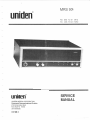
MRS 904
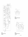
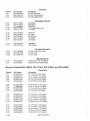
uniden®
0
.c:
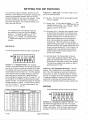
RX: 896 TO 901 MHZ
TX : 935 TO 941 MHZ
vawwa
•
..
saun
.
cw
.•
.
n
.•
{
. . .
IUSY
ACO
JIIOW£ft
. •.
~r
-
<OC.U.
..... - -
~ on
C.
uniden®
UNIDEN AMERICA CORPORATION
Commercial Communications Division
4700 Amon Carter Blvd.
Fort Worth, TX 76155
(817) 858·3300
CC SM 43
SERVICE
MANUAL
First Edition (January, 1990)
Uniden America Corporation reserves the right to make improvements and/or changes in the
product(s) and/or component(s) described in this publication at any time. This publication could
include technical inaccuracies or printing errors.
SAFETY INFORMATION
Through the provisions of the Occupational Safety and Health Act (OSHA) of 1970, the United
States Department of Labor has established an electromagnetic safety standard which applies to
the use of two-way radio equipment. The proper use of this transceiver will result in exposure
below the OSHA limit.
The following precautions shall be observed.:
WARNING
DO NOT operate the transmitter of any radio equipment with the antenna touching, or close to the
eyes, face, or exposed body parts.
DO NOT operate the transmitter of any radio equipment unless all the Radio Frequency (RF)
connectors are secure and any open connectors are properly terminated.
DO NOT operate the transmitter of any radio equipment near electrical blasting caps or in an
explosive atmosphere.
DO NOT let children operate any transmitter-equipped radio equipment.
Have your radio equipment installed and serviced by a qualified technician.
® 1990, Uniden America Corporation
All Rights Reserved
Printed in the United States of America
MRS 904
CONTENTS
ifc
3
4
7
7
8
10
13
13
13
14
14
14
14
15
15
15
15
15
15
16
17
18
19
20
21
22
22
23
24
24
25
26
29
29
29
31
33
35
36
38
37
48
49
50
51
52
52
52
53
53
53
53
Safety Information
Specifications
Introduction
Installation
Recommended Trunking System Layouts for Five and Ten Channels With Combiner
Repeater Network Data Link (RNDL) Bus
Cabling Instructions
Operation
Operating Controls and Indicators
Connectors
Repeater Operation
Local Control Operation
Local Control Operation (MRS 904S Conventional)
Theory of Operation
Basic Theory of Repeater Trunking
Design Concept
Trunking System Operation
Servicing Information
Disassembly
Suggested Test Equipment
MRS 904 Block Diagram
MRS 904T Trunking Mechanical Exploded View (Desk Top Version)
MRS 904S Conventional Mechanical Exploded View (Desk Top Version)
MRS 904TX Trunking Mechanical Exploded View (Slide Rack Mount Version)
MRS 904SXConventional Mechanical Exploded View (Slide Rack Mount Version)
Mechanical Exploded View (Internal)
Mechanical Exploded View (Receiver Module)
Mechanical Exploded View (Local Oscillator)
System Troubleshooting Flow Chart
Transmitter Troubleshooting Flow Chart
Receiver Troubleshooting Flow Chart
Logic Troubleshooting Flow Chart
Mechanical Parts List
Alignment Procedures
External DC Power Supply Adjustment
Local Audio and Squelch Adjustments
Transmitter Alignment Procedure
Trunking Logic Board (ARX 800A) Alignment Procedure
Conventional Control Board (PD-200AB) Alignment Procedure
Setting the DIP Switches
Repeater Test Mode
Frequency Setting
Schematic Diagrams
Modifications to the ARX 800A Trunking Logic Controller
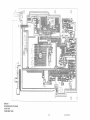
Motherboard (PD-388AB)
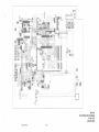
Receiver Module (PD-438AA)
Local Oscillator Module (PD-439AA)
RX PLL Module (PD-440AA)
Crystal Filter PCB (PD-458AA)
Second Mixer PCB (PD-377 AA)
Switch PCB
Relay PCB
IF AMP PCB (PD-378AA)
LED PCB
Page 1 MRS 904
1/1/90
54
55
56
57
58
59
60
61
62
63
64
65
66
67
67
67
67
68
68
68
68
69
69
69
69
70
71
72
91
Cable Harness Schematic
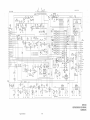
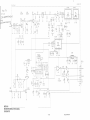
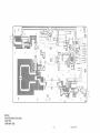
ARX 800A (MRS 904T Only) Logic Board (L-BOARD-1) Schematic (Page 1 of 2)
ARX 800A (MRS 904T Only) Logic Board (L-BOARD-1) Schematic (Page 2 of 2)
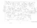
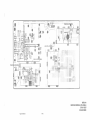
ARX 720 (MRS 904S Only) Conventional Logic Board (PD-200AB) Schematic
Board Views
Local Oscillator Module (PD-439AA) X-Ray View, Component Side
Local Oscillator Module (PD-439AA) X-Ray View, Solder Side
Receiver Module (PD-438AA) X-Ray View, Component Side
Receiver Module (PD-438AA) X-Ray View, Solder Side
Motherboard (PD-388AB) X-Ray View , Component Side
Motherboard (PD-388AB) X-Ray View, Solder Side
ARX 720 (MRS 904S Only) Conventional Logic Board (PD-200AB) X-Ray View, Component Side
RX PLL Module (PD-440AA) X-Ray View, Component Side
RX PLL Module (PD-440AA) X-Ray View, Solder Side
Relay PCB X-Ray View, Component Side
Relay PCB X-Ray View, Solder Side
Crystal Filter PCB (PD-458AA) X-Ray View, Component Side
Crystal Filter PCB (PD-458AA) X-Ray View, Solder Side
LED PCB X-Ray View, Component Side
LED PCB X-Ray View, Solder Side
Second Mixer PCB (PD-377AA) X-Ray View, Component Side
Second Mixer PCB (PD-377AA) X-Ray View, Solder Side
Switch PCB X-Ray View, Component Side
Switch PCB X-Ray View, Solder Side
IF AMP PCB (PD-378AA) X-Ray View , Component Side
IF AMP PCB (PD-378AA) X-Ray View, Solder Side
ARX 800A (MRS 904T Only) Logic Board (L-BOARD-1) X-Ray View , Component Side
Cable Harness Mechanical View
Electrical Parts List
Installing the ARX 2940 Single High Stability Oscillator
1/1/90
Page 2 MRS 904
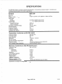
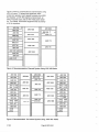
SPECIFICATIONS
The MRS 904 meets or exceeds the following specifications (Conventional versions include 1 CTCSS tone and
Trunking versions include the ARX 800A Logic Board):
General
MRS 904
Channels
Size
Weight 20 lbs. (9.25kg)
Input Power
Primary
Secondary
Current Drain
Transmit (Full Power)
Receive (Standby)
Operating Temperature Range
Channel Spacing
Frequency Control
Frequency Resolution
Canadian DOC Approval
one
14.875" x 5.375"x 12.75" (380mm x 138mm x327 mm
13.6 VDC (negative ground only)
13.6 VDC (negative ground only)
1000 mA
600 mA
-30°C to +60°C
12.5 kHz
PLL
12.5 kHz
Pending
Transmitter- Conforms to EIA RS-152-8
Frequency Range
RF Power Output
Audio Distortion
Modulation
FM Hum & Noise
Spurious & Harmonic Suppression
Frequency Stability
FCC Transmitter Type Acceptance
935-941 MHz
400 mW
3%
11 KOF3E, 11 KOF9E
-40dB
-40 dB
.05 ppm per Reference Input (ARX 2950)
Part 90 (AMW95P-89001)
Receiver- Conforms to EIA RS-204-8 and C
Frequency Range
Sensitivity
12 dB SINAD
20 dB Quieting
Selectivity
lntermodulation Rejection
Spurious Rejection
Image Rejection
Modulation Acceptance
Audio Output (@ 5% THO)
Frequency Stability
896 - 901 MHz
0.30 1-LV
0.40 j.LV
70 dB
70 dB
80 dB
70 dB
±3.75 kHz
2.5W
.05 ppm per Reference Input (ARX 2950)
Specifications are subject to change without notice.
Page 3 MRS 904
1/1/90
INTRODUCTION
Scope of Manual
This service manual is intended for use by experienced
technicians familiar with similar types of radios. It contains all service information required for the repeater
described and is current as of the printing date. Changes
which occur after the printing date are incorporated by
Service Manual Revisions and/or Technical Service
Bulletins These Revision/Service Bulletins are added to
the service manual as engineering changes are incorporated into the equipment.
Technical Support
Technical assistance and information is available from
the Commercial Communications Technical Support
Group during normal work days between the hours of
8:00am to 5:00pm Central Time. The Commercial
Communications Technical Support Group can be
reached at:
Replacement Parts and Additional
Manuals
Replacement parts are available through the Parts
Department located in Fort Worth, Texas. When ordering
replacement parts, please use the complete identification
number of the part. If the identification number is not
known, the order should contain the Part Symbol Number, Unit Model Number and a description of the part so
that the part can be properly identified. Parts orders may
be placed by writing to:
Uniden America Corporation
Commercial Communications Division
Parts Department
4700 Amon Carter Blvd.
Fort Worth, TX 76155
Phone:
FAX:
Telex:
1-817-858-3600
1-817-858-3523
27-2296
Uniden America Corporation
Commercial Communications Division
Technical Support Group
4700 Amon Carter Blvd.
Ft. Worth, Texas 76155
Additional copies of this manual are available through the
Sales Department located in Fort Worth, Texas. When
ordering please include the Part Symbol Number and the
Unit Model Number. Mail service manual orders to :
Phone :
Uniden America Corporation
Commercial Communications Division
FAX:
1-800-231-2868 (Outside of Texas)
1-800-621-8527(1nside Texas)
1-817-858-3300
1-817-858-3528
To return a unit for repair, send to:
Uniden America Corporation
Commercial Communications Division
Repair Department
4700 Amon Carter Blvd.
Fort Worth, TX 76155
Phone :
FAX:
1-817-858-3638
1-817-858-3523
Sales Department
4700 Amon Carter Blvd.
Fort Worth, Texas 76155
Phone:
FAX:
1-800-521-9627(0utside of Texas)
1-800-621-8527 (Inside Texas)
1-817-838-3568
1-817-858-3523
In Canada:
UNIDEN Canada Inc.
11 Plateau Street
Pointe Claire (Montreal), Quebec
Canada H9R 9Z7
Phone:
FAX:
1/1/90
Page 4 MRS 904
1-514-697-6920
1-514-697-7700
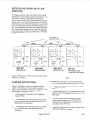
FAST ACCESS SYSTEM TRUNKING
•
The MRS 904T is a stand-alone, 400 mW, 900 MHz
Trunking Repeater that supports the LTR signalling
format . Fast Access System Trunking (FAST) is the
latest advance in trunking system technology from
Uniden. The FAST System delivers almost instantaneous transmission of voice communications as well as
data, without the slow response and frequent busy
signals associated with older trunking systems. A FAST
System may have up to 20 individual channels. Each
channel consists of an MRS 904T repeater, a linear
amplifier, and a switching power supply. Figure 1 is a
logic diagram of the FAST system.
A complete FAST System consists of the following
elements:
• Antenna and antenna mounting system. You may
mount the antenna on a tower or on a building using a
bracket . Uniden does not supply antennas and antenna
mounting systems.
• ARX 176 Post Combiner Filter.
In addition to the preceding elements you may add the
following optional equ ipment:
ARX 19X
Transmitter Combiner, Receiver Multicouplers or Duplexer cable kits.
ARX 780
Repeater Interconnect Controller (phone
patch)
ARX 800
Trunked Logic Controller (for overlay applications); an individual panel
ARX 820
10 Validator
ARX 850
Air Time Billing Package
There are three models of MRS 904 repeaters . Each
model has a 400 mW output and is available in rack
mount and desk top versions. The MRS 904S is a
conventional repeater, the MRS 904T is a FAST Tru nking
Repeater, and the MRS 904A is an AmeriCom® compatible repeater. If the model number ends with an 'X' (MRS
904SX/MRS 904TX). it is the slide rack mount version.
The slide rack mount version supplies easy access to all
adjustments.
The ARX 800 is a separate panel that contains an AR X
800A PCB . The ARX BOOA PCB also has a "L-BOAR D01" designation visible on the printed circu it board ,
however, the Part Number is ARX 800A.
• ARX 173 Transmitter Combiner.
• ARX 175 Receiver Multicoupler.
• MRS 904 Repeater.
This service manual contains basic data on the MRS 904
Repeater. A separate manual is provided for each option
delivered with your FAST System.
• ARX 1600 Power Amplifier .
• ARX 310 Power Supply.
• ARX 2950 Master Oscillator
• Enclosed cabinets or open relay racks (ARX 430 or
ARX 440).
Page 5 MRS 904
1/1/90
----......
<D
0
"'T1
<C"
c....
(!)
:-"
"'T1
Q)
(/)
)>
0
0
'\]/
(!)
(/)
(/)
en
-
'<
(/)
Remote Site
Dial-Up Voice
Grade Phone Line
Repeater Site
( !)
3
....
TX
-i
c
::J
~
RS-232C Cable
:;
(0
b
(0
0
c
"1J iii"
Ill (0
(0
ro Ql
0>
s::
3
MSDOS
Compatible
Computer
JJ
(f)
<D
256K RAM
0
.j:>.
360 K Flopp
System
Invoice
Softwar
ARX 176
Post Combiner Filter
110 VAC
RX
Communications
Software with
Capture and
Emulation
Routines
ARX173
5 Channel
Combiner
20 Meg
Hard Disk
Phone Line-----...,---1
ARX175
Receiver
Multicouple
ARX 310
Power Supply
Phone Lin~----~
:
ARX1600
Trunking Repeaters
ARX 310
I
Power Suppl
:
-------------------------------------------~
n
10 Channel To
Repeater
Receiver Inputs
To Repeater
Power Amplifier
Outputs
ARX178
Duplexer
(Optional)
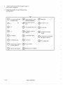
INSTALLATION
The MRS 904T is available in a desk top or a slide rack
mount version . You can place the deskmount version on
any flat surface , such as a desk or a table. You can
place the slide rack mount version in an ARX 430
cabinet (see figure 2) or an ARX 440 rack (see figure 3) .
/
/
•
:n
'- Co
ci
C\J
1:'?
I/
16"
_1
l:=
j
~9. 75"
19"
--
21 .75"
Figure 2. ARX 430 Cabinet
,.,,
1 able 1. C:qu IPment HelQhtS
Device
Description
l-ive Ghannel Gomb1ner
AHX 113
ARX 175
Ten Channel RX Multicoupler
ARX176
Post Combiner Filter
ARX 178
High power Duplexer
ARX310
Power Supply
ARX 780
Telephone Interconnect
ARX 800
Trunked Logic Controller
ARX 820
Validator
ARX 850
Air Time Billing
Power Amplifier
ARX 1600
MRS 904
900 MHz Repeater
ARX 2950
Master Oscillator/Power
Supply
Size
10.5"
3.5"
3.5"
3.5"
5.25"
3.5
3.5"
3.5"
3.5"
10.5"
5.25"
3.5/
5.25"
RECOMMENDED TRUNKING SYSTEM
LAYOUTS FOR FIVE AND TEN
CHANNELS WITH COMBINER
Each channel in a trunking system is assigned a seperate repeater . Each repeater in the recommended layouts
consists of the following equipment:
·~
• MRS 904T Trunking Repeater
• ARX 780 Telephone Interconnect
~
• N
:\j-..
'-
f--171/2"-
• ARX 1600 Power Amplifier
~
c.o
c.o
• ARX 310 Power Supply.
I~
/
l--2o 5/16"
~
~
..);
/~
/
__..j
Figure 3. ARX 440 Rack
Table1 shows the vertical height of some of the equipment that is typically placed in these cabinets.
Each repeater is assigned a unique repeater number
between 1 and 20. You select the repeater number by
setting DIP switch S1 on the ARX 800A Logic PCB . See
"Setting DIP Switches" for more information on how to set
the repeater number. Space repeater numbers evenly
and assign the highest repeater number to the lowest
frequency.
Figure 4 shows a recommended five channel layout
using ARX 440 racks. The lefthand and middle racks
contain five repeaters. Each repeater consists of an MRS
904 repeater, an ARX 780 telephone interconnect, an
ARX 310 power supply, and an ARX 1600 power amplifier. The righthand rack contains equipment that is used
by all of the repeaters .
Page 7 MRS 904
1/1/90
Figure 5 shows a recommended ten channel layout using
ARX 440 racks. The lefthand and righthand racks
contain ten repeaters . Each repeater consists of an MRS
904 repeater, an ARX 780 telephone interconnect, an
ARX 31 0 power supply, and an ARX 1600 power amplifier. The middle rack contains equipment that is used by
all of the repeaters.
ARX 780
MRS 904
ARX 2950
ARX 1600
AMX 350 I
ARX 780
MRS 904
I
ARX 1600
ARX 175
ARX 3101 ARX 310
ARX 780
ARX 1600
ARX 173
MRS 904
ARX 780
ARX 1600
ARX 176
MRS 904
ARX 31 ol ARX 31 o
ARX 1600
ARX 780
MRS 904
ARX 310
I
Figure 5. Recommended Ten Channel System Using ARX 440 Racks
ARX 2950
ARX 780
MRS 904
ARX 1600
ARXI ARX
310
310
ARX 780
ARX 780
ARX 1600
ARX 175
ARX 780
MRS 904
AMX 3501
ARX 1600
ARX 780
ARX 1600
ARX 173
ARX 1600
ARX 176
ARX 1600
MRS 904
ARXI
310
ARX
310
ARX 780
MRS 904
MRS 904
ARX 780
MRS 904
ARX 1600
ARX 173
ARX 1600
MRS 904
ARX 780
MRS 904
ARX 176
ARX 780
ARXl ARX
310
310
ARX 780
MRS904
MRS 904
ARXI
310
ARX
310
ARX 1600
ARX 850
ARX 1600
ARXl
310
ARXI
310
Figure 5. Recommended Ten Channel System Using ARX 440 Racks
1/1/90
Page 8 MRS 904
REPEATER NETWORK DATA LINK
(RNDL) BUS
The Repeater Network Data Link (RNDL) bus connects
the repeaters in the trunking system to each other and to
the ARX 820 Validator or ARX 850 Air Time Billing
option. Each end of the RNDL should contain a 100 ohm
pull-up resistor. The 100 ohm pull-up resistor is built into
the ARX 820 and the ARX 850. Therefore, if use an ARX
820 or ARX 850 , place it at one end of the RNDL bus . If
you have an MRS 904T at one or both ends of the RNDL
bus, Install a jumper between CN2-1 and CN2-4 on the
Logic Board. Figure 6 shows an example of a RNDL bus
for a three channel system with an ARX 820 or ARX 850 .
TYPE BNC 'T'
CONNEC~
!t-il
RNDL
"J
~f
Orange
Jumper
Omoge
Jumper,
In
+5
v
Out
----------.....
RNDL
CN2
100 n
+5
Orange
Jumper
Out
v
+5
v
+5
v
MRS 904T
MRS904T
MRS 904T
ARX 850
REPEATER#1
REPEATER#5
REPEATER #9
AIR TIME BILLING
or ARX 820 VALIDA TOR
Figure 6. RNDL Bus for a Three Channel System with an
ARX 820 or ARX 850
NOTE
CABLING INSTRUCTIONS
If the MRS 904 is the first or last device on the RNDL
bus, you must install a jumper form CN2-1 to CN2-4.
Figure 7 describes the cabling for a typical trunking
system. For information on how to cable a specific
device , see the manual for that device. Cable each MRS
904 repeater in the trunking system as follows:
4.
Install the receiver input cable in the "RX" receptacle.
5.
Install a cable from the "TX" receptacle on the MRS
904 to the "RF IN"receptacle on the ARX 900 or the
ARX 1500.
6.
If you are using an ARX 780 Telephone lnterconect, install a cable from the "ACCESSORY"
receptacle on the MRS 904 to the "REPEATER "
receptacle on the ARX 780.
7.
Install the cable from the 12V battery backup in the
"BATTERY BACKUP" receptacle .
1.
Install a type "N" T -connector in the receptacle
marked "RNDL".
2.
If the MRS 904 is not the first device on the RNDL
bus, connect the cable from the last device on the
RNDL bus to the T-connector.
3.
If the MRS 904 is not the last device on the RNDL
bus, connect a cable to the other side of the Tconnector.
Page 9 MRS 904
1/ 1/90
9.
Install tne cable from the ARX 310 power supply in
the "DC INPUT" receptacle.
10. Repeat this procedure for each MRS 904 in the
trunking system.
KEY
G)
To J3 or J4 of ARX 780
via adapter cable
G)
To MRS 904 RNDL
G)
J3
G
G
@
@
Daisy Chained to Each
MRS 904 Repeater
ARX 1600 1.3.8 VDC
Input
@
MRS 90413.8 VDC Input
@ To ARX 780 (15)
@ To Combiner (ARX 173) @ ToARX2950
J4
@
To Telephone
@
To Modem , Printer, or
Terminal
@
To MRS 904 (18pin)
@ To MRS 904 and ARX1600
To MRS 904 Transmit
Output
DC Inputs (17 and 10)
@ To Telephone Line
@
G
@ Power ON/OFF
(V
1/1/90
Transmit Output Type"N"
To ARX 1600 RF IN
Receiver Input Type"N"
@
110 VAC In
Backup Input 12V Battery
Page 10 MRS 904
@
DC Voltage Adjust
Rear Panel ARX 85
Airtime Billing
•
Q}: :t:@) <8
RIIC
Rear Panel ARX 780
Telephone Interconnect
_o
Fuse
-
REPEATER
t
ARX 1600 Rear Panel
Power Amplifier
DC
POWER
RFOUT
RF IN
t~~~~7Y~r
Figure 7. Cabling a Repeater
Page 11 MRS 904
1/1/90
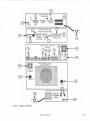
Figure 8. Front Panel Of MRS 904 Desk Top Version
Figure 9. Front Panel Of MRS 904 Rack Mount Version
Figure 10. Rear Panel Of MRS 904
1/ 1/90
Page 12 MRS 904
OPERATION
~
OPERATING CONTROLS AND
INDICATORS
All of the operating controls and indicators, except the
power switch, are located on the front panel (see figures
8 and 9).
Power Switch - The power switch is located on the rear
panel. This switch turns the MRS 904 repeater on or off.
POWER Light- The POWER light glows steadily when
the 13.6 VDC primary power is applied to the MRS 904
radio through the DC INPUT connector. This light
flashes on and off when the backup 12.0 VDC power is
applied through the BATIERY connector.
SQUELCH CONTROL- The SQUELCH control adjusts
the Local Audio Amplifier opening sensitivity. Use the
following procedure to adjust the squelch:
1. Rotate the SQUELCH control fully counterclockwise.
2. Rotate the SQUELCH control clockwise until the noise
just disappears.
3. For the best results, leave the SQUELCH control in
this position. Rotating the control further diminishes
sensitivity.
NOTE
The SQUELCH control has no effect on repeater
operation.
VOLUME Control- Rotate the VOLUME control clockwise to increase the Local Speaker volume and counterclockwise to decrease the volume.
REPEAT/LOCAL Switch- When the switch is in the
REPEAT position (depressed), the MRS 904 repeater
action is automatic. Another station as well as the local
microphone can access its transmitter. When the switch
is in the LOCAL position (released) , only the local microphone can access the transmitter of the MRS 904
repeater .
RCD Light - The yellow RCD (Received Data) Light
comes on when the MRS 904T repeater properly decodes the subaudible trunking data that the mobile/
portable radio generates. The microprocessor on the
ARX 800A trunking logic controller board controls the
RCD light. The RCD light must be On for the repeater to
transmit, however it is normal for the RCD Light to
"flicker'' at times during marginal signal reception and
multipath fading. This will not affect voice communications due to the two second repeater hang time .
TX Light - The TX (Transmit) light comes on when the
MRS 904 transmitter is keyed.
CALL Light (MRS 904S Conventional)- If you use the
MRS 904S repeater as a local control repeater/base
station, the CALL light comes on and remain on when the
repeater receives the correct CTCSS tone. The repeater
must be equipped with the CTCSS option, the microphone must be in a properly grounded hang up bracket,
and the MON/TONE SO Switch must be in the TONE SO
position. To reset the CALL Light, remove the microphone from the hang up bracket or momentarily depress
and release the MON/TONE SO Switch.
BUSY Light -The BUSY light (LED) comes on to alert
the user that the channel is busy when a carrier is
present on the receive frequency.
OPTION ON/OFF Switch · When this switch is in the
OPTION ON position (depressed), it has no effect on
MRS 904 repeater operation. When this switch is in the
OPTION OFF position (released) , the MRS 904 repeater
is keyed up for testing and alignment purposes.
MON/TONE SQ Switch (MRS 904S Conventional):
When the switch is in the MON (monitor} position (depressed) , the user can monitor or receive all calls transmitted on the channel. When the switch is in the TONE
SO (tone squelch) position (released). the user can
receive only the transmissions intended for the user's
group. The MRS 904S repeater must be equipped with
the CTCSS option and the microphone must be hung up
in a properly grounded hang up bracket.
CONNECTORS
All of the connectors, except the microphone connector,
are located on the rear panel (see figure 10).
DC INPUT Connector- Primary 13.6 VDC power input
connector.
BATTERY Connector- Backup 12.0 VDC power input
connector. The POWER Light flashes and warning tones
are transmitted to alert the user when the MRS 904 is
operating on backup power.
ACCESSORYConnector- The ACCESSORY Connector
(Female 'D Subminiature' 15 Pin) is used to add the ARX
780 Telephone Interconnect with the MRS 904T (Trunking Version) . It is also used to interface to AmeriCom®
Network Switch in MRS 904A (AmeriCom® Version} .
Page 13 MRS 904
1/ 1/90
RNDL Connector - Connects the repeater to the Repeater Network Data Link (RNDL) Bus. See page 63 for
recommended RNDL Bus connection
MIC Jack: The MIC (Microphone) jack connects the
ARX 100A microphone to the MRS 904 repeater.
TX Jack- The TX (Transmitter) jack is aType N Connector (400 mW) that connects the transmitter of the MRS
904 repeater to the antenna.
RX Jack- The RX (Receiver) jack is a Type N Connector
that connects the antenna to the receiver of the MRS 904
repeater.
Reference Input- The reference input jack connects
the TX and RX synthesizer of the repeater to the external reference oscillator (ARX 2950) .
REPEATER OPERATION
1.
Set the POWER switch to on. Make sure that the
green POWER Light glows steadily.
2.
Rotate the SQUELCH contro l fully counterclockwise .
3.
Rotate VOLUME control clockwise or counterclockwise to obtain the desired volume level.
4.
Rotate the SQUELCH Control clockwise until the
noise just disappears.
5.
Place the REPEAT/LOCAL switch in the REPEAT
(depressed) position.
LOCAL CONTROL OPERATION
1.
Perform steps 1 thru 4 of "Repeater Operation
above.
2.
Place the REPEAT/LOCAL switch in the LOCAL
(released) position .
3. * Monitor channel to insure that it is not busy. Verify
that the BUSY light is not on .
4.
5.
To transmit, depress and hold the Push-To-Talk
(PTT) switch on the side of the microphone . Release
the PTT Switch to end transmission .
Hang up the microphone.
*MRS 904S Conventional only.
LOCAL CONTROL OPERATION (MRS
9048 Conventional)
1. Perform steps 1 thru 5 of "Local Control Operation"
above .
2.
You may use the MON/TONE SO switch as follows :
a. With the switch in the MON position (depressed),
the user can monitor or receive all calls transmitted on the channel.
b. With switch in TONE SO position (released), the
user can rece ive only the transmissions intended
for the user's group. The MRS 904S repeater
must be equipped with the CTCSS option and the
microphone must be hung up in a properly
grounded hang up bracket. The CALL Light will
come on when you receive a call. To reset and
turn off the CALL light , remove the microphone
from the hang up bracket or momentarily depress
and release the MON/TONE SO switch.
THEORY OF OPERATION
The MRS 904T Trunking Repeater is a full featured
commercial grade trunking repeater. The standard
model contains such features as CW Identifier, coded
access , and provisions for automatic emergency power
operation (battery) . The MRS 904T attaches to the
ARX 780 Telephone Interconnect for fully programmable interconnect. The MRS 904T also attaches to the
the ARX 850 Air Time Billing Package and the ARX 820
Validator.
1/1/90
The MRS 904T has a continuous duty rated output of
400 mW. It may be operated as a stand -alone repeater,
but it is usually used with a Power Amplif ier (ARX 1600)
that boosts the power output to 150 W. This higher power
output and the use of favorable installation sites permits
very low power mobiles or portables to communicate
over a greatly extended range . Combiners are available
that allow a multi-channel repeater system to share a
common antenna.
Page 14 MRS 904
BASIC THEORY OF REPEATER
TRUNKING
Repeater trunking was designed to permit multiple users
to equally and automatically share all channels. If a
repeater is busy and the system has two or more repeaters, the incoming signal may be "handed off" to another
repeater. This provides more rapid communication than
with single repeater systems, where each call must be
completed before another can be handled. Trunking
systems are more convenient for the mobile/portable
user who is no longer required to monitor the channel or
adjust squelch. The user simply depresses the radio
PTT switch to access a channel. Since the user cannot
monitor a channel, trunking systems permit higher
security in business communications.
The MRS series repeaters are completely compatible
with all Uniden trunking radios. In these radios, each
"system" setting is normally a different repeater site. This
provides a wide area of coverage. The repeater retransmits the Group (digital) I. D. codes that trunking radios
generate to provide private conversation.
DESIGN CONCEPT
The design of the MRS 904T repeater system employs
the module concept. The following table describes the
modules and their location as a part of the system:
Module
Receiver
Local
Oscillator
Mother board
Logic
Board
DC relay
Descriotion
Full Shield~d
Plug-in
Full Shielded
Plug-in
PCB Sub
Chassis
PCB
PCB
Location
Plugs into Motherboard
TRUNKING SYSTEM OPERATION
SERVICING INFORMATION
Mobile/portable radios are programmed to monitor one
specific "home" channel in the trunking system. They
monitor this channel at all times in the idle state . The
mobile/portable radio receives subaudible data from the
"home" channel. this subaudible data tells the radio that a
call is coming in and steers the radio to the correct
channel to receive the call. The mobile/portable radio
also completes a "handshake" with the "home" channel
every time the user depresses the radio PTT switch. If
the "home" channel is not busy handling another call, the
mobile/portable radio repeats on the "home" channel. If
the "home" channel was busy when the user depressed
the PTT switch, the mobile/portable radio "handshakes"
with the next available repeater in the system.
All mobiles in the same group must be "homed" on the
same channel. There are 250 (001-250) group !.D.'s per
channel and up to 20 (01-20) channels per system.
Therefore a 20 channel system has the capability of,SOOO
unique !.D .'s.
Each repeater uses the Repeater Network Data Link
(RNDL) bus to communicate with the other repeaters in
the system. The RNDL bus is a high speed serial data
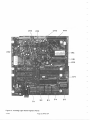
bus that communicates information regarding the repeater state (idle, busy) and the mobile I. D. A block
diagram of the RNDL bus is included on page xx. A 100
Ohm pull-up resistor must be located at the first and last
device on the RNDL. To provide these pull-up resistors in
an MRS 904 repeater, install a jumper from CN2-1 to
CN2-4. The pull-up resistor is already installed in the
ARX 850 Air Time Billing Unit and ARX 820 Validator.
Plugs into Motherboard
Mounts horizontally
over Logic Board . You
may raise Motherboard
to vertical on hinged
mounting for ease of
service.
Mounted in cabinet
base under Motherboard
Mounted on back inside
panel
The MRS 904T repeater uses broad band technology to
cover the following frequency ranges without retuning:
• Transmit- 935 to 941 MHz
• Receive - 896 to 901 MHz
There are 400 channels available to the repeater.These
channels are spaced 12.5 kHz apart .
DISASSEMBLY
1. Place the MRS 904 unit on a flat static-free work surface.
2. Remove the eight screws that secure the top cover. There are two on each side, two on the top, and two on the
rear.
3. Loosen the two captive slotted screws on the sub-chassis. You can now lift the sub-chassis on hinges to a
verticle position. This allows access to the Logic/Controller Board and the Mother Board.
4. To acheive bottom access, remove the eight screws on the bottom panel. Secure the sub-chassis before you
turn the unit over to access the bottom panel.
SUGGESTED TEST EQUIPMENT
Table 3 shows the test equipment needed to repair this unit. A service monitor will replace many of the individual
items .
1a01e 3. ~uaaestea 1 est E IUioment
TEST INSTRUMENT
REQUIRED SPECIFICATIONS
DC Power Supply
Voltage: 13.6 VDC
I
Current: 8 Amoeres Continuous
i RF Wattmeter
Frequency: 935-941 MHz
Power: 0-1 Watts
RF Dummy Load
Impedance: 50 Ohms
Power: 50 Watts
DC Voltmeter
Range: 0-20 VDC
DC Resistance: 10 Meg Ohm
AC Voltmeter
Ranae: 3 mV-20V AC
Audio Generator
Frequency: 10Hz-10kHz
Level: 0-1V
Deviation Meter
Ranae: 0-5 kHz
Distortion Meter
Range: 30Hz-10kHz
or
Level: 1 mV-300 V
Sinadder
lnout Level: 1-5 VAC
RF Frequency Counter
Range: 1.3 GHz
Accuracy: +.001 ppm/vr.
Oscilloscope
Bandwidth: 50-100 MHz
Triggered Sweep
RF Signal Generator
Attenuator
FM Linear Detector
Service Monitor
-
Page 15 MRS 904
1/1/90
-----
-
-
Range: 800-910 MHz
Level: 0.1-1000 uV
Modulation: lnt/Ext
Deviation: 0-5 kHz
Attenuation: 20 dB
Power: 50 Watts Minimum
SUGGESTED TYPE or Eauivalent
Ratelco PS-9
12 VDC Batterv
Bird Model 43 with
50E Element
Bird Model 8085
Bird Model8135
Simpson 260
Fluke D802 or D804
Leader LMV 181 A
Leader LGA 120 A
Marconi TF 2304
Leader LDM 170
Heloer's Sinadder 3
HP-5325B OPT 010, 030
Tektronix 2213
Tektronix 465B
Hameo HM705
HP 8640
HP 8642
Bird 8341-200
Bird 8343-200
Cushman CE-50 or
Cushman CE-4000
IFR 1200S or IFR 1500
Motorola RS2001
Wavetek 3000
--
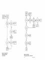
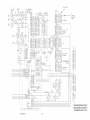
r-----MOTHERBOARD
455KHZ
896-902 MHZ
59.9375 MHZ
~
~~~
SP
I
I
I
X101
59.4875 MHZ
RSSI
RX IN
RECEIVER
MODULE
RXDATA
I_
MIG
f)_~_J~---->•·J
v
-~~
I
LOCAL
MODULE
~~
TX +9V
PTT
~~----------~
+5V
RX +8V
TX +8V
LOGIC PCB
UNLOCK
sss-lw1 MHZ
I
I
TXKEY
TX DATA
TXDAT
VR103DATAADJ
AMP
IC101
TX +BV
212
TXAUD19
I
FROM RIC
- - -------- ,
OCXO IN
MRS 904
BLOCK DIAGRAM
1/1/90
Page 16 MRS 904
~
~
25'
r
32
XEROX 80 10 IMPORT
Page 17 MRS 904
1/1/90
MRS 904T TRUNKING
MECHANICAL EXPLODED VIEW
(DESK TOP VERSION)
25
r
iI
MRS 904S CONVENTIONAL
MECHANICAL EXPLODED VIEW
(DESK TOP VERSION)
30
1/1/90
Page 18 MRS 904
SECTION A-A
SCALE:
1: 1
1 PLACE AS SHOWN
1 PLACE OPPOSITE HAND
I
2
PL
l
Z
1
I
l
Page 19 MRS 904
1/1/90
~
PL~z
REOD
MRS 904TX TRUNKING
MECHANICAL EXPLODED VIEW
(SLIDE RACK MOUNT VERSION)
REF
REF
SECTION A-A
SCALE: 1: 1
1 PLACE AS SHOWN
1 PLACE OPPOSITE HAND
------------- --------------- -------___;---------
I
I
l
MRS 904SX CONVENTIONAL
MECHANICAL EXPLODED VIEW
(SLIDE RACK MOUNT VERSION)
1/1/90
~
Page 20 MRS 904
I II"">-..
-r-!1-i
I
•
I
II,
I
II
~Q)
I
I'
Lt::JC)
-n.J
_.
I
rCO. i
I
I
I
I I .- ' o !.' I
!1 --
I'
-,I--·
1'--;=.,.
I
I
II
I
2 REOn!JllL Pci --- - L:--.._____., ••
0
2slJ' , __~ - --_-n,-n ,....___
--"
0
. __,_____----.----~~----~"9 .U-- --"----t.-vn.-·- . .c -- e o o o 0
-J-~-II
:::-.-- --· -
-
I
--
r
1
-
--- -
•
•
--
----11
-- ------
--
-.
~-•
-
--"
------
-~----
·--- .
-
. - -.
-+-- L--
;
!t
-
-- --
j;:::::.-@
" ___ --~-~ 28
!
~--•
~ I! I
•
--
.
I ---
----ii
I
1---.
-
~
fl
1
-
0
i
I
I
I
i
I
I
I
I
1I
I
e
I
11
j
I
ii
I
I
I I
_...--iiL--oO
I
•
I
_... ... - r
I
___ ..J
... a
--~
---·
....-;.--...--
MRS 904
MECHANICAL EXPLODED VI EW
(INTERNAL)
Page 21 MRS 904
1/1/90
0
0
MRS 904
RECEIVER MODULE
MECHANICAL EXPLODED VIEW
oo
MRS 904
LOCAL OSCILLATOR MODULE
MECHANICAL EXPLODED VIEW
1/1/90
Page 22 MRS 904
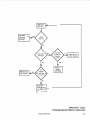
With MRS 904T
off, verify all DIP
switch settings
Connect all
RNDL ports of
each MRS 904T
Turn MRS 904T on
Transmit on each
channel of system
with test radio
'"0
PJ
(Q
CD
1\)
w
s:
::.0
Suspect bad
receiver or
mlsprogrammed
test radio
(/)
<0
0
~
Check ARX BOOA
Suspect bad
ARX BOOA or LED
circuit
sa and data
recovery
adjustments
--......
(0
0
Suspect bad
ARX BOOA or
cable harness
Check transmitter
Key up home
channel using
LOCAL OPTION
switch, key test
radio
Suspect bad
ARX BOOA
Align L.O. modulel
Suspect RNDL
cables, connector
DIP switch (SYNC)
and orange jumpe
wires
-t
Handshake
Is okay
~
Suspect bad L.O
module
<
Suspect bad
ARX BOOA
board
Reset power on
MRS 904T
::0
Os:
C:o
Yes
.,~en
r-mc.o
Repeat the trunkln
:e::x:~
testfor each
channel In system
ocno
no en
::x:O~
)>~-t
:ozm
-tG'>S:
1~~------------------------------------------------~
Inject RX signal
on frequency.
(-47dBm)with
LOCAL SQ.
Key transmitter
(Place OPTION
switch in the
OUT position)
Read frequency
and power on
test equipment
Reset DIP switches
on frequency.
Toggle MRS 904T
power on
Suspect bad
RX module
Reset switches
and retest
or speaker
Refer to
ARX 2950
Service Manual
M
......_.__"'
VR101 correct
~0
rl_s_u_s-pe_c_t_b_a_d_L-.o..,J
module or coax
cable
Receiver is
functioning
correctly
functioning
correctly
MRS 904 TRANSMITTER
TROUBLESHOOTING
FLOWCHART
MRS 904 RECEIVER
TROUBLESHOOTING FLOWCHART
1/1/90
Page 24 MRS 904
Switch on
MRS 904T
ARX BOCA
microprocessor
is running
I 'IIIII(
correctly
t
>
~I Check fuse or
power supply
Repair or
replace
Battery backup
PWR indicator
ARX BOCA
I*·
t
Reset DIP
switches and
turn MRS 904T
off
MRS 904T LOGIC
TROUBLESHOOTING FLOWCHART
Page 25 MRS 904
1/1/90
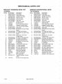
MECHANICAL PARTS LIST
MRS 904T TRUNKING DESK TOP
VERSION
MRS904S CONVENTIONAL DESK
TOP VERSION
Pan Number
Description
1
2
3
4
5
6
7
8
9
10
11
12
13
GCMF180751A
GCMZ414434Z
GNBP480760Z
GNBY 408150Z
HCHF254024Z
HCMT204085Z
TSTD001 0004
11000717
17000838
17000533
TSTD01911 00
ECMB154033Z
SSCW31 04068
14
15
SSCW530035N
SSCW31 0406B
16
SSCW311 008B
17
18
19
20
21
22
23
24
25
26
27
28
29
30
31
32
SSCW320404Z
SSCW530035N
11000779
11000704
UL026Z
UL027Z
BWZY0758001
BWZY0759001
BWZY0760001
BWZY0839001
JDPA450044Z
HZ033
ARX800A
11001052
F015
JDPA450117Z
33
11001734
Front Panel
Plastic Slide Piece
ARU251 Push Knob
ARU 251 Knob
Desk Top Bezel
Top Cover
RubberFootABS
#4-40 Hex Nut
Front Insert Clamp Bracket
Repeater Function Label
4.25" Pre-cut Nylon Edging
Base Plate
#4-40X3/8 Pan Head Phillips
Screw
D3.5 Split Lock Washer
#4-40X3/8 Pan Head Phillips
Screw
#1 0-24x1/2" Pan Head
Phillips Screw
#4-40X1/4 Flat Head Screw
D3 .5 Split Lock Washer
#6 Split Lock Washer Zinc
#6-32X3/4 Pan Head Screw
RX Module
Local Module
X-Connection Cable Assy
TX Cable Assembly
RX Cable Assembly
Ref. Osc. Cable Assembly
Serial Number Label
Main Case Assembly
Trunking Logic Board
BNC ''T" Connector
BNC Data Cable
Trunking Repeater Function
Label
#4-40X1/4 Pan Head Screw
Ret.No.
1/1/90
Pan Number
Description
1
2
3
4
5
6
7
8
9
10
11
12
13
GCMF180751A
GCMZ414434Z
GNBP480760Z
GNBY408150Z
HCHF254024Z
HCMT204085Z
TSTD001 0004
11000717
17000838
17000533
TSTD01911 00
ECMB154033Z
SSCW31 0406B
14
15
SSCW530035N
SSCW310406B
16
SSCW311 008B
17
18
19
20
21
22
23
24
25
26
27
28
29
30
31
SSCW320404Z
SSCW530035N
11000779
11000704
UL026Z
UL027Z
BWZY0758001
BWZY0759001
BWZY0760001
BWZY0839001
JDPA450044Z
HZ033
ARX720
17000212
11001734
Front Panel
Plastic Slide Piece
ARU251 Push Knob
ARU 251 Knob
Desk Top Bezel
Top Cover
Rubber Foot ABS
#4-40 Hex Nut
Front Insert Clamp Bracket
Repeater Function Label
4.25" Pre-cut Nylon Edging
Base Plate
#4-40X3/8 Pan Head Phillips
Screw
D3.5 Split Lock Washer
#4-40X3/8 Pan Head Phillips
Screw
#10-24x1/2" Pan Head
Phillips Screw
#4-40X1/4 Flat Head Screw
D3.5 Split Lock Washer
#6 Split Lock Washer Zinc
#6-32X3/4 Pan Head Screw
RX Module
Local Module
X-Connection Cable Assy
TX Cable Assembly
RX Cable Assembly
Ref. Osc. Cable Assembly
Serial Number Label
Main Case Assembly
Conventional Logic Board
Repeater Tone Label
#4-40X1/4 Pan Head Screw
Ref. No.
Page 26 MRS 904
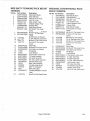
MRS 904TX TRUNKING RACK MOUNT
VERSION
MRS 904SX CONVENTIONAL RACK
MOUNT VERSION
Ref.No.
1
2
3
4
5
6
7
8
9
Ret. No.
1
2
3
4
5
6
7
8
9
Part Number
ECM F154025Z
ECMY154026Z
GNBP480760Z
GNBY408150Z
HCSZ32112Z
HCSZ32113Z
HHNS350028Z
MHNH32111Z
SSCW3111 06Z
10
11
SSCW320604B
SSCW321 008B
12
13
14
15
11000798
11001709
11001778
11001779
16
17
18
19
20
21
22
23
24
25
26
27
28
29
30
ECMB154033Z
SSCW310406B
SSCW530035N
UL026Z
UL027Z
BWZY0758001
BWZY0759001
BWZY0760001
BWZY0839001
JDPA450044Z
HZ033
ARX800A
11001052
F015
JDPA450117Z
• 31
11001734
Description
Rack Mount Bezel
Rack Slide Box
ARU 251 Push Knob
ARU 251 Knob
Slide Adaptor Plate
Chassis Adaptor Plate
Chassis Slide
Rack Mount Handle
#1 0-32x3/8" Pan Head
Screw
#6-32x1/4" Flat Head Screw
#1 0-24x1/2" Flat Head
Screw
#8 External Lock Washer
22 GA Stainless Steel Shim
#8-32x1/4" Pan Head Screw
#12-24x1/2" Pan Head
Screw
Base Plate
#4-40x3/8" Pan Head Screw
03.5 Split Lock Washer
RX Module
Local Module
X-Connection Cable Assy
TX Cable Assembly
RX Cable Assembly
Ref. Osc. Cable Assembly
Serial Number Label
Main Case Assembly
Trunking Logic Board
BNC "T" Connector
BNC Data Cable
Trunking Repeater Function
Label
#4-40X1/4 Pan Head Screw
Page 27 MRS 904
Part Number
ECMF154025Z
ECMY154026Z
GNBP480760Z
GNBY408150Z
HCSZ32112Z
HCSZ32113Z
HHNS350028Z
MHNH32111Z
SSCW3111 06Z
10
11
SSCW320604B
SSCW321 008B
12
13
14
15
11000798
11001709
11001778
11001779
16
17
18
19
20
21
22
23
24
25
26
27
28
29
ECMB154033Z
SSCW31 0406B
SSCW530035N
UL026Z
UL027Z
BWZY0758001
BWZY0759001
BWZY0760001
BWZY0839001
JDPA450044Z
HZ033
ARX720A
17000212
11001734
Description
Rack Mount Bezel
Rack Slide Box
ARU 251 Push Knob
ARU 251 Knob
Slide Adaptor Plate
Chassis Adaptor Plate
Chassis Slide
Rack Mount Handle
#1 0-32x3/8" Pan Head
Screw
#6-32x1 /4" Flat Head Screw
#1 0-24x1/2" Flat Head
Screw
#8 External Lock Washer
22 GA Stainless Steel Shim
#8-32x1 /4" Pan Head Screw
#12-24x1 /2" Pan Head
Screw
Base Plate
#4-40x3/8" Pan Head Screw
03 .5 Split Lock Washer
RX Module
Local Module
X-Connection Cable Assly
TX Cable Assembly
RX Cable Assembly
Ref. Osc. Cable Assembly
Serial Number Label
Main Case Assembly
Conventional Logic Board
Repeater Tone Label
#4-40X1 /4 Pan Head Screw
1/1 /90
INTERNAL PARTS
Ref. No.
1
2
3
4
5
6
7
8
9
10
11
12
13
14
15
16
Part Number
HCMZ154029Z
HCMF154027Z
HCMZ154028Z
ECSV154032Z
HCMZ352114Z
UL006Z
UL007Z
UL005Z
30000082
17
BRVY0239001
18
BRVY0324001
19
20
21
22
23
24
25
26
27
28
29
30
31
32
33
34
35
36
37
38
39
40
41
BJKY0207001
BSPY0014001
11000826
(2683DP-750)
11000825
(2073SB-625)
GNBP480760Z
JDPA451174Z
JDPA454031Z
11001046
BWZY0225001
22000426
42
43
44
45
46
47
48
49
50
11001772
11000799
1/1/90
34000025
11000116
11000134
11000784
(205817-4)
(9X15M0506)
BRPB616824Z
11001734
11001750
SSCW31 0406B
11000779
99160000
99160002
99240003
RECEIVER MODULE
Description
Chassis
Front Panel
Rear Panel
Sub-Chassis
Hinge Bracket
Receiver Module
Local Oscillator Module
Motherboard
LED PCB Assembly
Switch PCB Assembly
Relay PCB Assembly
Wiring Harness Assembly
RX Cable Assembly
TX Cable Assembly
X-Connection Cable Assly
AC Power Switch
XRM-21 ON-00
Volume Control
10KA RV-239
Squelch Control
10KB RV-324
Microphone Jack JK-207
Speaker SP-014
7/ 16" Hole Plug DP-437
3/4" Hole Plug
15/32" Grommet
518" Grommet
Push Button
Serial Number Label
Rear Escutcheon
Connector Bulkhead
DC Power Cord WZ-225
Ferrite Bead (ATL1100) PA
Coax Cable Retainer
Cable Clamp
Molex Pin
Shield Ground Lug
Locking Terminal Lug
DB15 Standoff Kit
M5.8x6 mm Shoulder Screw
6.8K 1/6W J Resistor
#4-40X1 /4 Pan Head Screw
#4-40x3/8" Pan Head Screw
#4-40X3/8 Pan Head Phillips
Screw
#4-40X1 /2 Pan Head Screw
#6-32X1/4 Pan Head Screw
#4 Flat Washer
#4 Split Lock Washer
#6 Split Lock Washer
16 AWG Black Wire
16 AWG Red Wire
Heatsink Compound
24 AWG Black Wire
Ref.No.
1
2A
2B
3
4
5
6
7
8
9
10
11
12
13
14
15
16
17
18
19
20
21
22
Part Number
HSDC382918Z
HSDC482976Z
HSDC482976Z
HSDC482986Z
HSDP282925Z
HSDP282927Z
HSDP483276Z
HSDP482979Z
HSDP482980Z
HSDP482981Z
LRNG481895Z
PLBS415685Z
PLBZ482572Z
RZEB483092Z
SSCW1 02606N
SSCW1 0261 ON
SSCW1 03025N
SSCW430026N
SSCW51 0026N
SSCW530026N
TSTD0453045
HETC483285Z
HSDP483822Z
Description
Chassis Assembly
Shield Case SPCD
Shield Case SPCD
Shield Case SPCC Nl-3
Cover (A) SUS 304
Cover (B) SUS 304
Shield Plate (A) SPTE 0 .3T
Shield Plate (C) SPTE 0.3T
Shield Plate (D) SPTE 0.3T
Shield Plate (E) SPTE 0.3T
0-Ring NBR D1 8*2.0
Serial Number Label
Caution Label
Insulation Plate
M2.6x6 Pan Head Screw
M2 .6x1 0 Pan Head Screw
M3x25 Pan Head Screw
M2.6 Hex Nut
D2.6 Spring Washer
D2.6 Lock Washer
Nylon Rivet
Toucher (B) SPTE 0.3T
Shield Plate (E) SPTE 0.3T
LOCAL OSCILLATOR MODULE
Ref.No.
1
2
3
4
5
6
7
8
9
10
Part Number
HSDC382919Z
HSDC483278Z
HSDP282926Z
HSDP282967Z
LRNG481895Z
PLBS415685Z
SSCW1 02606N
SSCW1 0261 ON
-
SSCW,1Q~025N
HPSP482820Z
11
12
13
14
15
SSCW430026N
TSTD0453045
HSDP482982Z
HHDE482821Z
HSDP483812Z
16
HSDP483813Z
17
18
19
20
SSCW51 0026N
SSCW530026N
SSCW192008N
HETC483285Z
Page 28 MRS 904
Description
Chassis Assembly
Shield Case SPTE 0.3T
Cover (D) SUS 304
Cover (C) SUS 304
0-Ring NBR D1 8*2 .0
Serial Number Label
M2.6x6 Pan Head Screw
M2 .6x1 0 Pan Head Screw
M3x25 Esan HeaQ Screw.,
Earth Plate C5210 , 0.1T,
MBNI3
M2.6 Hex Nut
Nylon Rivet
Shield Plate SPTE 0.3T
IC Holder
Shield Plate (B) C521 OP ,
0.3T
Shield Plate (C) C5210P ,
0.3T
D2.6 Spring Washer
D2.6 Lock Washer
M2x8 Bind Head Screw
Toucher (B) SPTE 0.3T
ALIGNMENT PROCEDURES
The MRS 904 alignment procedures require the following test equipment:
•
•
•
•
•
•
•
•
•
•
DC Power Supply (13.6V)
Oscilloscope
RF Wattmeter
AF Signal Generator
RF Dummy Load, 50 Ohms
RF Signal Generator
DC Voltmeter
Deviation Meter
Distortion Meter
Frequency Counter
Motherboard
Set up this test equipment as shown in figure 11 .
R F SIGNAL
GENERATOR
ANTENNA
RX
TX
'-----
RF
WATIMETER
MRS 904
RADIO
DC POWER
SUPPLY
(13.6 V)
•
PIN
4
1
DC
VOLTMETER
RF DUMMY
LOAD (SOQ)
FREQUENCY
COUNTER
MIC
PIN
3
'---
AF SIGNAL
GENERATOR
AUDIO
~GROUND
DEVIATION
METER
l
DISTORTION
METER
OSCILLOSCOPE
Logic Board
EXTERNAL DC POWER SUPPLY
ADJUSTMENT
Figure 11. Test Equipment Setup
NOTES
There are no receiver adjustments/alignments.
1. Turn the external power supply on.
1. Before you begin this procedure, make sure
that J1 05 on the Motherboard is in the "900"
position.
2. Connect a DC voltmeter to the output of the exte rn al
power supply.
2.
If you are using the Trunking Version (MRS
904T), Make sure that J101 is in the "T" position. If you are using the Conventional
Version (MRS 904S), Make sure that J1 01 is
in the "C" position.
3 . Adjust the voltage contro l on the external pow er
supply to an output between 13.6 and 13.8 VDC.
LOCAL AUDIO AND SQUELCH
ADJUSTMENTS
Relay Board
1. Set the VOLUME control to its physical midpoint and
rotate the SQUELCH control fully counterclockwise.
2. Input a strong RF signal (-47dBm) into the repeater.
Modulate this signal with a 1000 Hz tone at 1.5 kHz
deviation.
Page 29 MRS 904
1/1/90
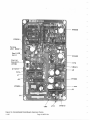
Figure 12. MRS 904 Open View
~
;
VR101
5102
5103
5101
J105
VR104
VR102
VR101
J101
L112
VR103
5103
Figure 14. Receiver Module and Local Oscillator Module Alignment Points
Figure 13. Motherboard Alignment Points
1/1/90
Page 30 MRS 904
3. Adjust VR1 02 on the motherboard for the desired
local audio level.
10. Set VR4 on the Trunking Logic Board(L-BOARD-01 )
to its physical midpoint.
4.
11. Set positions 1 through 8 of switch S1 to OFF .
Rotate the SQUELCH control tully clockwise.
5. Input a 1.0
~V
RF signal into the repeater.
12. Set position 1 of switch S2 to ON and set positions 2
through 8 to OFF.
6. Adjust VR 103 on the motherboard until the squelch
just opens .
13. Turn the repeater power switch off, then on.
TRANSMITTER ALIGNMENT
PROCEDURE
14. Input a strong (-47 dBm) RF signal into the repeater
through the RX jack. Modulate this signal with 1000
Hz at 1.5 kHz deviation.
1. Set DIP switches S1 02 and S1 03 on the Motherboard
(see figure 13) to the desired frequency using the
procedure described in "Frequency Setting".
15. Depress microphone PTT. Adjust VR 105 on the
Local Oscillator PCB for 2.4 kHz deviation.
2. Connect an RF Wattmeter and a 50 Ohm dummy
load to the TX antenna jack.
16. Return the Trunking Logic Board DIP switches to
their original position.
17. Turn the repeater power switch off, then on.
3. Depress the microphone PTT switch and adjust
VR1 01 on the Local Oscillator PCB (see figure 14)
for desired power output (between 200 and 400 mW).
NOTE
Steps 19 through 23 (Repeater Deviation)
pertain to MRS 904S Conventional Version
only.
4. Rotate VR101 on the Motherboard and VR104 and
VR 105 on the Local Oscillator PCB tully counterclockwise.
5. For MRS 904T Trunking Version, depress the microphone PTT switch and adjust VR1 03 for 900 Hz.
Proceed to step 9 .
6. For MRS 904S Conventional Version, perform steps 8
through 11 of "Conventional Control Board Alignment Procedure".
7. For MRS 904S Conventional Version , depress the
microphone PTT switch and adjust VR 103 for 500700 Hz deviation.
18. Set VR604 on the Conventional Logic PCB (PD200AB) to its physical midpoint.
19. Set SW600 to CARRIER SQUELCH position and
verify that the red LED (D611) is lit.
20. Set the REPEAT/LOCAL switch to REPEAT position .
21. Input a strong ( -47 dBm) signal into the repeater
using the RX jack. Modulate this signal with 1000 Hz
at 1.5 kHz deviation.
8. Input a 100 mV peak-to-peak (70.7 mV RMS) 1000Hz
tone into the microphone input jack at pin 4.
22. Depress the microphone PTT switch and adjust
VR1 05 on the Local Oscillator PCB for 1.5 kHz
deviation. Set SW600 to the CTCSS position and
verify that the red LED (D611) is off.
9. Depress the microphone PTT switch and adjust
V R 104 on the Local Oscillator PCB tor ±2.4 kHz total
system deviation.
23. Input a 50 mV peak-to-peak (35.4 mV RMS) 1000 Hz
tone into the microphone input jack at pin 4.
24. Depress the microphone PTT switch and adjust
VR101 on Motherboard for 2.4 kHz local deviation .
NOTES
1. Steps 11 through 18 (Repeater Deviation)
pertain to MRS 904T Trunking Version only.
2. Before you preset DIP switches S1 and S2
on the Trunking Logic Board(L-BOARD-01),
record the original ON/OFF positions 1 thru
8.
Page 31 MRS 904
1/1/90
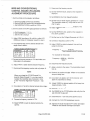
VRS
VR6
VR3
VR1
VR2
~!'!,;il
S2
S1
S3
Figure 15. Trunki ng Log ic Board Alignment Points
1/1 /90
Page 32 MRS 904
TP7
TRUNKING LOGIC CONTROLLER
(PN ARX SODA)
ALIGNMENT PROCEDURE
8. Attach the local microphone and depress the PTT
switch. Adjust VR3 for ±1.5 kHz peak system deviation.
9. Turn the repeater POWER switch off and disconnect
the backup (BATTERY) power supply.
1. Turn the repeater POWER switch off.
2. Set DIP Switches S1 through S5 (see figure 15) using
the procedure described in "Setting the DIP Switches".
3. Turn the repeater POWER switch on.
4. Inject a 1 mV RF signal with a 900 Hz deviation of 100
Hz square wave into the RX jack. Adjust VR1 to obtain
a 1.4 V to 2.0V peak-to-peak output at TP5.
5. Adjust VR2 so that the squelch just opens with a
0.15~-LV input to the RX jack. (TP7 shows 3.6 VDC
with the squelch open and ±0.6 VDC with the squelch
closed).
10. Connect the primary power and turn the repeater
POWER switch on.
11. Inject a 1 mV RF signal with a ±1.5 kHz deviation of
1000 Hz tone into the RX jack and adjust VR4 for
1.5 kHz total system deviation.
10. Adjust VR5 to its physical midpoint.
11. Adjust VR6 to its physical midpoint.
6. Turn off the primary power supply and apply backup
power ( 12 VDC) to the repeater using the BATTERY
connection.
7. Turn the repeater POWER switch on.
Page 33 MRS 904
NOTE
You must cut the orange jumper from CN 2-1 to
CN 2-4 on all repeaters except the first and last
repeater in the RNDL chain. If an ARX 850/820
is used in the system , place it at the end of the
RNDL bus. Cut the orange jumper between
CN2-1 and CN2-4 in the repeater that is adjacent to the ARX 850/820.
1/1/90
' - - - VRSOO
Yellow
LED 0609
u~--~-,
.
~~
j
I
Carrier
Squelch-(CSQ)
,
"'
.
; --..:. "· - /;':;>., ' ' .. --~·. '· __ --i.r
- "h
\.-1 E1
... '
·:; : . .
..
-
~-
--
.
•
VR602
."'1
•
TP2
HJ::t
cress
-
~v..ft'f
VR601
rn;~
-~
JS
~=----VR603
~-
~
VR604
-----J9
TP4
Figure 16. Conventional Control Board Alignment Points
1/ 1/90
Page 34 MRS 904
VR610
MRS 9045 CONVENTIONAL
CONTROL BOARD (PD-200AB)
ALIGNMENT PROCEDURE
1. Set the controls on the repeater as follows:
a. Set the VOLUME control fully clockwise.
b. Set the SQUELCH control fully counterclockwise
c. Set the REPEAT/LOCAL switch to LOCAL.
2. Set the controls on the RF signal generator as follows :
a. Set the frequency to 1 kHz .
b. Set the deviation to 1.5 kHz.
c. Set the level to 0.25 J..LV
4. Cut jumpers J9 and J1 0 for desired decode tone
range shown in table 4.
I--·- ----.-.- . . . . . ---·
-I---s I I-
13. Set SW600 to the Carrier Squelch position .
14. Set the level on the RF signal generator to 1.0 mV .
The transmitter should key. Verify that the red LED
(D611) lights .
15. Adjust VR604 to obtain a 1.5 kHz deviation of the
transmitter.
17. Set the level on the RF Signal Generator to 0.25 J..LV.
18. Connect a frequency counter to TP2 .
19. Adjust VR602 to obtain the desired time-out time
using the formula:
-- ncy
J9
J10
IN
IN
IN
CUT
CUT
12. Set the REPEAT/LOCAL switch on the repeater to
REPEAT.
16. Set the REPEAT/LOCAL switch on the repeater to
the LOCAL position .
3. Adjust VR600 (see figure 16) until the yellow LED
(D609) just comes on . (Repeater squelch is open).
Frequency
160 to 300Hz
125 to 165Hz
60 to 135Hz
11 . Disconnect the frequency counter.
Frequency =
8192Hz
Time in seconds minus 2 seconds
For example (2 minute total):
CUT
Frequency= 8192Hz = 69.42 Hz
120-2
5. Connect a frequency counter to TP4 and make sure
that jumper J4 is connected.
6. Adjust VR61 0 to obtain desired decode frequency .
7. Disconnect the frequency counter and cut jumper J4.
NOTE
When you change the CTCSS Encode Frequency (Steps 8 through 11) , you may need to
readjust the transmitter data modulation . Refer
to the "Transmitter Alignment Procedure" , step
8.
8. Cut jumpers J7 and J8 for desired encode tone range :
20. Disconnect the frequency counter.
21. Apply a carrier to the receiver. The transmitter should
key up.
22 . Remove the carrier and adjust VR601 for the desired
drop-out delay time.
23 . Cut jumper J6, apply a carrier to the rece iver, and
allow the transmitter to time out.
24. Adjust VR603 for desired deviation of the beep tone
(Approximately 1 kHz) .
25 . Reconnect jumper J6.
Table 5. Encoder CTCSS Frequency
Freauencv
J7
J8
180 to 340Hz
IN
IN
140 to 190Hz
CUT
IN
60 to 150Hz
CUT
CUT
26. Set SW600 to the CTCSS position and verify that the
red LED (D611) goes off.
27. Disconnect the 13.6 VDC primary power source.
9. Connect a frequency counter to TP3.
28. Connect the 12.0 VDC backup power source.
10. Adjust VR605 to obtain the desired encode frequency.
29. Depress the local microphone PTT switch and adjust
VR606 for the desired warning tone deviation.
Page 35 MRS 904
1/1/90
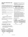
SETTING THE DIP SWITCHES
Position 6·7 =RNDL Mode- The RNDL mode is set to
You must set the Logic PC Board (L-BOARD-01) DIP
one of the following values :
switches for each repeater in the system. Connect each
repeater to the Repeater Network Data Line (RNDL)
using the RNDL port on the rear of the repeater. These
ports are bi-directional, and a BNC T connector is included with the repeater. This connector allows you to
daisy chain the RNDL bus.
00
The microprocessor in the repeater reads the
dip switches only when you turn the repeater's
power on. To change the settings, turn off the
repeater, make the necessary changes, and
then turn on the repeater. The microprocessor
reads the new settings when you turn on the
repeater.
10 = Secondary sync. A secondary sync repeater backs
up the primary sync repeater. If the primary sync
repeater stops sending sync, the secondary sync
repeater provides sync. If the primary sync repeater stops sending sync for a short period of
time, the secondary sync repeater will begin
sending sync. When the primary sync repeater
begins sending sync again, there will be dual sync
until the secondary sync repeater detects both sync
pulses and stop sending sync. For this reason it is
suggested not to use secondary sync except in
critical situations which require a backup for the
primary sync repeater.
SWITCH S1
The following illustration shows the factory set defaults :
11 = Sync loss reset. This mode enables a time-out
routine which resets the repeater if RNDL sync
data is not received within 4.5 seconds. This reset
is equivalent to the power up reset to the repeater.
This feature is enabled if you set either or both of
positions 6 and 7 to ON.
~~~~~~~~
1
2
4
3
5
6
1 8
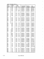
Position 1·5 =Repeater Number. The repeater
number is a number between 1 and 20 that the repeater
uses as an ID when it transmits or receives RNDL data.
The repeater also uses the repeater number to identify
mobile radios that are homed in on it. The RIC attached
to the repeater uses the repeater number to check for
data errors and for airtime billing. Table6 shows the
switch settings for repeater numbers 1 through 20. No
two repeaters on the RNDL bus should have the same
repeater number. You should evenly space the repeater
numbers between 1 and 20. For a five channel system
use 1,5,9,13, and 17. For a ten channel system use
1,3,5,7,9,11,13,15,17, and 19.
T~hl1=1l
Rotr #
1
2
3
4
5
6
7
8
9
10
1/1/90
~~=~ttinn
1
1
0
1
0
1
0
1
0
1
0
th1=1 n.
Position
2 3 4
0 0 0
1 0 0
1 0 0
0 1 0
0 1 0
1 1 0
1 1 0
0 0 1
0 0 1
1 0 1
Position 8 = RIC (Repeater Interconnect) - Set this
position ON to enable the RIC for telephone interconnect. If the RIC classifies an incoming ID code as an
interconnect ID code, the repeate r allows the interconnect call to progress. If the RIC classifies the Incoming
ID code as a dispatch ID code or if the RIC does not
classify the ID code (the RIC is disconnected or not
turned on) , the repeater treats the call as a dispatch call.
SWITCH52
•r N11n 1h1=1r
5
0
0
0
0
0
0
0
0
0
0
Rot r# 1
11
1
12
0
13
1
14
0
15
1
16
0
17
1
18
0
19
1
20
0
Position
2 3 4
1 0 1
0 1 1
0 1 1
1 1 1
1 1 1
0 0 0
0 0 0
1 0 0
1 0 0
0 1 0
This is the mode for all repeaters except
the sync repeater.
01 = Primary sync. This is usually the highest frequency
repeater (lowest number). You should set only one
repeater in a system as the sync repeater. Set all
other repeaters to 00 (no sync).
NOTE
ON
= No sync.
!
The following illustration shows the factory set defaults :
I
s
0
0
0
0
0
1
1
1
1
1
I
ONI
~~~~~~~~
1
2
3
4
5
6
1
8
Position 1-8 = ID Code for Local PTT/Test ID- This is
the repeater ID code and you can set it to a value
between 1 and 255 in binary. It is set to a default value
of 254 in the factory. If this ID is set to equal a mobile/
portable ID, the FCC ID is transmitted upon mobile
Page 36 MRS 904
dekey. Always set this switch to 254 for normal operation.
SWITCH 54
The following illustration shows the factory set defaults:
NOTES
1. No mobile in the system should have the
same ID code as the local PTI and test
message ID code in normal repeat operation.
~~~~~~~~
ONI
1
2
3
4
5
6
7
8
Position 1-6 =Data Lost Hang Time. These switches
control the amount of time the repeater hangs, or continues to transmit after it loses data decode. This is necessary to keep communications from chattering or dropping
out due to fading and weak signal conditions. The
factory default is 2 seconds.
2. The idle message ID code is 255.
SWITCH S3
The following illustration shows the factory set defaults:
ONI
~~~~~~~~
1
2
3
4
5
6
7
8
Position 1-5 =Priority Free Repeater Number. If a call
comes in for the repeater and the repeater is busy, the
call is normally trunked to the first available repeater on
the RNDL bus. If you set these positions to a valid
repeater number, the call is trunked to this repeater
number, if it is available. Use the procedure for setting
positions 1 through 5 of switch S1 to set these positions.
If you set all of these positions OFF, the call is trunked to
the first available repeater.
Position 6
=Reserved.
Position 7 = Area. The Area switch is normally set to
OFF. Use this switch when two systems operate on the
same frequencies and due to geographic location they
interfere with one another. If one system is set to Area 1
(Area switch is ON) then mobile/portable radios with Area
programmed to 0 are not allowed to access the system.
Likewise, you need to program Area= 1 for all mobile/
portable radios on the system with the Area set ON.
=
Position 8 Alert Tone for Loss of Data. The repeater
sends a tone to alert the user that data is no longer being
decoded. If the hang time is set long enough, a user
may be able to relocate to a position and re-establish
proper data decoding before communications cease.
SWITCH 55
Position 7 = Transmit Data Invert. This position is
usually set OFF to allow for normal subaudible transmit
data. This position is set ON to allow for inverted subaudible transmit data. This position is provided to allow you
to interface the ARX-800 with non-Uniden equipment.
The following illustration shows the factory set defaults:
ON
·.:·:
:::;:
1 2
=
Position 8 Receive Data Invert. This position is
usually set OFF to allow for normal subaudible receive
data. This position is set ON to allow for inverted subaudible receive data. This position is provided to allow you
to interface the ARX-800 with non-Uniden equipment.
~~ ~~·· ~~~~,.
..:.:
..
3
4
:···:
:::;:
·::::
.::~
5
6
7
8
Position 1-6 = Idle Message Cycle Time. This time is
factory set to 10 seconds. It is programmable in one
second intervals between 1 and 64 seconds. The idle
message lets mobile/portable units know that the home
channel is free and within range .
Position 7 = Continuous IDLE Message Enabled.
Factory set is OFF.
Position 8 = FCC Station ID Enable. Should be set ON,
on the lowest frequency repeater only (highest number
repeater). Will transmit FCC ID every 30 minutes.
NOTE
FCC Station ID should be enabled in lowest
frequency repeater only.
Page 37 MRS 904
1/ 1/90
MRS 904T REPEATER TEST
MODE
If you turn the power to the repeater on with all positions
on DIP switch S1 set to OFF (S1-1 thru S1-8) , the
repeater goes into an audio path test mode . The setting
of DIP switch S2 controls the audio path that is active.
Each switch position 1 through 4 of switch S2 controls an
audio path as follows :
2. There are 400 channels that you can program in the
900 MHz band .
3. To place the repeater in a TEST MODE set position T
of switch S1 03 on 0. In TEST MODE , the repeater
operates on the frequencies shown in table 7.
1
2
3
• Postion 1 set ON tests the repeater audio path (IC20
pins 1 0 and 11)
The TEST MODE frequencies change each time you
press S1 01 on the Motherboard.
• Position 2 set ON tests the RIC to repeater audio path
(IC20 pins 3 and 4)
4. To return the repeater to normal operating mode set
position T of switch S1 03 on 1.
• Position 3 set ON tests the repeater to RIC audio path
(IC20 pins 8 and 9)
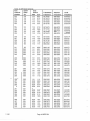
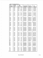
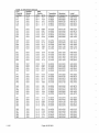
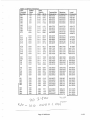
5. Select the desired channel frequency from the
frequencies listed in Table 8. Set the SYSTEM
(S102) and CH DATA (S103) DIP switches according
to the table. For example , if you want to set the
repeater to channel 384, look for this channel in the
table. The receive frequency for channel 384 is
900.8000 MHz, the transmit frequency is 939.8000
MHz and the local frequency is 840.8625 MHz.
Table 8 shows the following settings for the SYSTEM
and CH DATA switches :
• Position 4 set ON tests the beep tone (IC20 pins 1
and 2)
NOTE
You can set DIP switches S2-1 through S2-4 to
ON and OFF without turning the power to the
repeater off.
When you press the LOCAL PTT in the test mode, the
repeater keys up the transmitter without data for any
audio path controlled by S2.
• SYSTEM Switch = 1001
•CHDATASwitch=01111111
ON
SYSTEM
0 nP~!IIn jP~nnnnnnnl
~uu~ -u~IJIJ~~~J~?J
NOTE
SO (TP7) must be HIGH to repeat the received
audio when S2-1 is in the ON position and the
LOCAL PTT is pressed.
T
2
1
S103
FREQUENCY SETTING
1.
ON
T
2
1
S103
1/1/90
CH DATA
0
7
6
5
4
3
0
-
I
o-
-
5
-
4
2
1
0
S102
Page 38 MRS 904
3
S102
(Note: 'T' is in position 1 for normal mode .)
Use DIP switches S1 02 and S1 03 on the Motherboard to set the frequency . These Switches are
lab led SYSTEM and CH DATA on the Motheboard as
shown in the following figure .
SYSTEM
CH DATA
2
1
0
QJoooou -•--•'-
-·
-··
"'WWILVII
...,VLLIII
~'1'
.;;,
FCC
Channel
Number
001
002
003
004
005
System
Switch
T210
1000
1000
1000
1000
1000
Data
Switch
7654 3210
0000 0000
0000 0001
0000 0010
0000 0011
0000 0100
Transmitter
Freauencv
935 .0125
935 .0250
935 .0375
935.0500
935.0625
Receiver
Freauencv
896.0125
896.0250
896.0375
896.0500
896.0625
Local
Freauencv
836 .0750
836 .0875
836.1000
836.1125
836.1250
006
007
008
009
010
1000
1000
1000
1000
1000
0000
0000
0000
0000
0000
0101
0110
0111
1000
1001
935.0750
935.0875
935 .1000
935 .1125
935.1250
896.0750
896.0875
896.1000
896.1125
896.1250
836.1375
836.1500
836 .1625
836.1750
836.1875
011
012
013
014
015
1000
1000
1000
1000
1000
0000
0000
0000
0000
0000
1010
1011
1100
1101
1110
935.1375
935.1500
935 .1625
935 .1750
935.1875
896.1375
896.1500
896.1625
896.1750
896.1875
836.2000
836 .2125
836 .2250
836.2375
836.2500
016
017
018
019
020
1000
1000
1000
1000
1000
0000
0001
0001
0001
0001
1111
0000
0001
0010
0011
935 .2000
935.2 125
935.2250
935 .2375
935 .2500
896.2000
896.2125
896.2250
896.2375
896.2500
836.2625
836.2750
836.2875
836.3000
836.3125
021
022
023
024
025
1000
1000
1000
1000
1000
0001
0001
0001
0001
0001
0100
0101
0110
0111
1000
935 .2625
935 .2750
935.2875
935.3000
935 .3125
896.2625
896.2750
896.2875
896.3000
896.3125
836.3250
836.3375
836.3500
836.3625
836.3750
026
027
028
029
030
1000
1000
1000
1000
1000
0001
0001
0001
0001
0001
1001
1010
1011
1100
1101
935.3250
935.3375
935.3500
935.3625
935.3750
896.3250
896.3375
896.3500
896.3625
896.3750
836.3875
836.4000
836.4125
836.4250
836.4375
031
032
033
034
035
1000
1000
1000
1000
1000
0001
0001
0010
0010
0010
1110
1111
0000
0001
0010
935 .3875
935.4000
935.4125
935.4250
935.4375
896.3875
896.4000
896.4125
896.4250
896.4375
836.4500
836.4625
836.4750
836.4875
836.5000
036
037
038
039
040
1000
1000
1000
1000
1000
0010
0010
0010
0010
0010
0011
0100
0101
0110
0111
935.4500
935.4625
935.4750
935.4875
935.5000
896.4500
896.4625
896.4750
896.4875
896.5000
836.5125
836.5250
836.5375
836.5500
836.5625
041
042
043
044
045
1000
1000
1000
1000
1000
0010
0010
0010
0010
0010
1000
1001
1010
1011
1100
935.5125
935.5250
935.5375
935.5500
935.5625
896.5125
896.5250
896.5375
896.5500
896.5625
836.5750
836.5875
836.6000
836.6125
836.6250
Page 39 MRS 904
1/ 1/90
S ett nas
·--·- -·- IP Switch
System
Data
1/1/90
FCC
Channel
Number
046
047
048
049
050
Switch
T210
1000
1000
1000
1000
1000
051
052
053
054
055
Switch
3210
0010
1101
0010
1110
1111
0010
00 11 0000
00 11 0001
Transmitter
Freauencv
935 .5750
935 .5875
935 .6000
935 .6125
935.6250
Receiver
Freauencv
896.5750
896.5875
896.6000
896.6125
896.6250
Local
Freauencv
836.6375
836.6500
836.6625
836.6750
836.6875
1000
1000
1000
1000
1000
0011
0011
0011
0011
0011
0010
0011
0100
0101
0110
935 .6375
935 .6500
935 .6625
935.6750
935 .6875
896.6375
896.6500
896.6625
896.6750
896.6875
836.7000
836.7125
836.7250
836.7375
836.7500
056
057
058
059
060
1000
1000
1000
1000
1000
0011
0011
0011
0011
0011
0111
1000
1001
1010
1011
935.7000
935.7125
935 .7250
935 .7375
935.7500
896.7000
896.7125
896.7250
896.7375
896.7500
836.7625
836 .7750
836.7875
836.8000
836.8125
061
062
063
064
065
1000
1000
1000
1000
1000
00 11
0011
00 11
0011
0100
1100
1101
1110
1111
0000
935.7625
935 .7750
935.7875
935.8000
935.8125
896.7625
896.7750
896.7875
896.8000
896.8125
836.8250
836.8375
836.8500
836.8625
836.8750
066
067
068
069
070
1000
1000
1000
1000
1000
0100
0100
0100
0100
0100
0001
0010
0011
0100
0101
935.8250
935 .8375
935 .8500
935 .8625
935 .8750
896.8250
896.8375
896.8500
896.8625
896.8750
836.8875
836.9000
836.9125
836.9250
836.9375
071
072
073
074
075
1000
1000
1000
1000
1000
0100
0100
0100
0100
0100
0110
0111
1000
1001
1010
935.8875
935.9000
935.9 125
935 .9250
935 .9375
896.8875
896.9000
896.9125
896.9250
896.9375
836.9500
836.9625
836.9750
836.9875
837.0000
076
077
078
079
080
1000
1000
1000
1000
1000
0100
0100
0100
0100
0100
1011
1100
1101
1110
1111
935.9500
935 .9625
935 .9750
935 .9875
936.0000
896.9500
896.9625
896.9750
896.9875
897.0000
837.0125
837.0250
837.0375
837.0500
837.0625
081
082
083
084
085
1000
1000
1000
1000
1000
0101
0101
0101
0101
0101
0000
0001
0010
0011
0100
936.0125
936.0250
936.0375
936.0500
936.0625
897.0125
897.0250
897.0375
897.0500
897.0625
837.0750
837.0875
837.1000
837.1125
837.1250
086
087
088
089
090
1000
1000
1000
1000
1000
0101
0101
0101
0101
0101
0101
0110
0111
1000
1001
936.0750
936.0875
936.1000
936.1125
936.1250
897.0750
897.0875
897.1000
897.1125
897.1250
837.1375
837.1500
837.1625
837.1750
837.1875
7654
Page 40 MRS 904
l
Table R nr o
~witch
FCC
Channel
Number
091
092
093
094
095
System
Switch
T210
1000
1000
1000
1000
1000
Data
Switch
7654 3210
0101
1010
0101
1011
0101
1100
0101
1101
0101
1110
Transmitter
Freauencv
936.1375
936.1500
936.1625
936.1750
936.1875
Receiver
Freauencv
897.1375
897.1500
897.1625
897.1750
897.1875
Local
Freauencv
837.2000
837.2125
837.2250
837.2375
837.2500
096
097
098
099
100
1000
1000
1000
1000
1000
0101
0110
0110
0110
0110
1111
0000
0001
0010
0011
936.2000
936.2125
936.2250
936.2375
936.2500
897.2000
897.2125
897.2250
897.2375
897.2500
837.2625
837.2750
837.2875
837.3000
837.3125
101
102
103
104
105
1000
1000
1000
1000
1000
0110
0110
0110
0110
0110
0100
0101
0110
0111
1000
936.2625
936.2750
936.2875
936.3000
936.3125
897.2625
897.2750
897.2875
897.3000
897.3125
837.3250
837.3375
837.3500
837.3625
837.3750
106
107
108
109
110
1000
1000
1000
1000
1000
0110
0110
0110
0110
0110
1001
1010
1011
1100
1101
936.3250
936.3375
936 .3500
936.3625
936.3750
897.3250
897.3375
897.3500
897.3625
897.3750
837.3875
837.4000
837.4125
837.4250
837.4375
111
112
113
114
115
1000
1000
1000
1000
1000
0110
0110
0111
0111
0111
1110
1111
0000
0001
0010
936.3875
936.4000
936.4125
936.4250
936.4375
897.3875
897.4000
897 .4125
897.4250
897.4375
837.4500
837.4625
837.4750
837.4875
837.5000
116
117
118
119
120
1000
1000
1000
1000
1000
0111
0111
0111
0111
0111
0011
0100
0101
0110
0111
936.4500
936.4625
936.4750
936.4875
936.5000
897.4500
897.4625
897.4750
897.4875
897.5000
837.5125
837.5250
837.5375
837.5500
837.5625
121
122
123
124
125
1000
1000
1000
1000
1000
0111
0111
0111
0111
0111
1000
1001
1010
1011
1100
936.5125
936.5250
936.5375
936.5500
936 .5625
897.5125
897.5250
897.5375
897.5500
897.5625
837.5750
837.5875
837.6000
837.6125
837.6250
126
127
128
129
130
1000
1000
1000
1000
1000
0111
0111
0111
1000
1000
1101
1110
1111
0000
0001
936.5750
936.5875
936.6000
936.6125
936.6250
897.5750
897.5875
897.6000
897.6125
897.6250
837.6375
837.6500
837.6625
837 .6750
837.6875
131
132
133
134
135
1000
1000
1000
1000
1000
1000
1000
1000
1000
1000
0010
0011
0100
0101
0110
936.6375
936.6500
936.6625
936.6750
936.6875
897.6375
897.6500
897.6625
897.6750
897.6875
837.7000
837.7125
837.7250
837.7375
837.7500
SP-tt"nos
Page 41 MRS 904
1/ 1/90
1/1/90
Table 8. DIP Switch S _...... FCC
System
Data
Channel
Switch
Switch
Number
T210
7654 3210
Transmitter
Freauencv
Receiver
Freauencv
Local
Freauencv
136
137
138
139
140
1000
1000
1000
1000
1000
1000
1000
1000
1000
1000
0111
1000
1001
1010
1011
936.7000
936.7125
936.7250
936.7375
936.7500
897.7000
897.7125
897.7250
897.7375
897.7500
837.7625
837.7750
837.7875
837.8000
837 .8125
141
142
143
144
145
1000
1000
1000
1000
1000
1000
1000
1000
1000
1001
1100
1101
1110
1111
0000
936.7625
936.7750
936.7875
936.8000
936.8125
897.7625
897.7750
897.7875
897.8000
897.8125
837.8250
837.8375
837.8500
837.8625
837.8750
146
147
148
149
150
1000
1000
1000
1000
1000
1001
1001
1001
1001
1001
0001
0010
0011
0100
0101
936.8250
936.8375
936.8500
936.8625
936.8750
897.8250
897.8375
897.8500
897.8625
897.8750
837.8875
837.9000
837.9125
837.9250
837.9375
151
152
153
154
155
1000
1000
1000
1000
1000
1001
1001
1001
1001
1001
0110
0111
1000
1001
1010
936.8875
936.9000
936.9125
936.9250
936.9375
897.8875
897.9000
897.9125
897.9250
897.9375
837.9500
837.9625
837.9750
837.9875
838.0000
156
157
158
159
160
1000
1000
1000
1000
1000
1001
1001
1001
1001
1001
1011
1100
1101
1110
1111
936.9500
936.9625
936.9750
936.9875
937.0000
897.9500
897.9625
897.9750
897.9875
898 .0000
838.0125
838.0250
838.0375
838.0500
838.0625
161
162
163
164
165
1000
1000
1000
1000
1000
1010
1010
1010
1010
1010
0000
0001
0010
0011
0100
937.0125
937.0250
937.0375
937.0500
937.0625
898.0125
898 .0250
898.0375
898 .0500
898 .0625
838 .0750
838.0875
838.1000
838.1125
838.1250
166
167
168
169
170
1000
1000
1000
1000
1000
1010
1010
1010
1010
1010
0101
0110
0111
1000
1001
937.0750
937.0875
937.1000
937.1125
937.1250
898 .0750
898.0875
898.1000
898.1125
898 .1250
838 .1375
838.1500
838 .1625
838.1750
838.1875
171
172
173
174
175
1000
1000
1000
1000
1000
1010
1010
1010
1010
1010
1010
1011
1100
1101
1110
937.1375
937.1500
937.1625
937.1750
937.1875
898.1375
898 .1500
898.1625
898 .1750
898 .1875
838 .2000
838 .2125
838.2250
838 .2375
838.2500
176
177
178
179
180
1000
1000
1000
1000
1000
1010
1011
1011
1011
1011
1111
0000
0001
0010
0011
937.2000
937.2125
937.2250
937.2375
937.2500
898 .2000
898.2125
898 .2250
898.2375
898.2500
838.2625
838 .2750
838.2875
838.3000
838.3125
Page 42 MRS 904
T~hlo
s:l n1 ) C::\Atitr-h C::ott"1nnc;,
FCC
Channel
Number
181
182
183
184
185
System
Switch
T210
1000
1000
1000
1000
1000
Data
Switch
7654 3210
1011
0100
1011
0101
1011
0110
1011
0111
1011
1000
Transmitter
Freauencv
937.2625
937.2750
937.2875
937.3000
937.3125
Receiver
Freauency
898.2625
898 .2750
898 .2875
898 .3000
898.3125
Local
Freauencv
838 .3250
838 .3375
838.3500
838 .3625
838 .3750
186
187
188
189
190
1000
1000
1000
1000
1000
1011
1011
1011
1011
1011
1001
1010
1011
1100
1101
937.3250
937.3375
937.3500
937.3625
937.3750
898 .3250
898 .3375
898 .3500
898 .3625
898.3750
838 .3875
838.4000
838.4125
838.4250
838.4375
191
192
193
194
195
1000
1000
1000
1000
1000
1011
1011
1100
1100
1100
1110
1111
0000
0001
0010
937.3875
937.4000
937.4125
937.4250
937.4375
898.3875
898.4000
898.4125
898.4250
898.4375
838.4500
838.4625
838.4750
838.4875
838 .5000
196
197
198
199
200
1000
1000
1000
1000
1000
11 00
1100
1100
11 00
1100
0011
0100
0101
0110
0111
937.4500
937.4625
937.4750
937.4875
937.5000
898 .4500
898.4625
898.4750
898.4875
898 .5000
838 .5125
838.5250
838.5375
838 .5500
838 .5625
201
202
203
204
205
1000
1000
1000
1000
1000
1100
1100
1100
1100
1100
1000
1001
1010
1011
1100
937.5125
937.5250
937.5375
937.5500
937.5625
898 .5125
898 .5250
898 .5375
898.5500
898.5625
838.5750
838.5875
838.6000
838.6125
838.6250
206
207
208
209
210
1000
1000
1000
1000
1000
1100
1100
1100
1101
1101
1101
1110
1111
0000
0001
937.5750
937.5875
937.6000
937.6125
937 .6250
898.5750
898 .5875
898 .6000
898.6125
898 .6250
838 .6375
838 .6500
838.6625
838 .6750
838 .6875
211
212
213
214
215
1000
1000
1000
1000
1000
1101
1101
1101
1101
1101
0010
0011
0100
0101
0110
937.6375
937.6500
937.6625
937.6750
937.6875
898 .6375
898 .6500
898 .6625
898 .6750
898 .6875
838.7000
838 .7125
838.7250
838.7375
838.7500
216
217
218
219
220
1000
1000
1000
1000
1000
1101
1101
1101
1101
1101
0111
1000
1001
1010
1011
937.7000
937.7125
937.7250
937.7375
937.7500
898.7000
898.7125
898 .7250
898.7375
898.7500
838.7625
838 .7750
838.7875
838 .8000
838 .8125
221
222
223
224
225
1000
1000
1000
1000
1000
1101
1101
1101
1101
1110
1100
1101
1110
1111
0000
937.7625
937.7750
937.7875
937.8000
937.8125
898 .7625
898 .7750
898 .7875
898 .8000
898 .8125
838 .8250
838 .8375
838 .8500
838 .8625
838 .8750
-- · -
Page 43 MRS 904
1/1/90
I U...,IY
Vo
...,II
"'-'WW I'VII "'-'V,\11 I
~
FCC
Channel
Number
226
227
228
229
230
System
Switch
T210
1000
1000
1000
1000
1000
Data
Switch
7654 3210
1110 0001
1110 0010
1110 0011
1110 0100
1110 0101
Transmitter
Freauencv
937.8250
937.8375
937.8500
937.8625
937.8750
Receiver
Frequency
898.8250
898.8375
898.8500
898.8625
898.8750
838.8875
838.9000
838.9125
838.9250
838.9375
231
232
233
234
235
1000
1000
1000
1000
1000
1110
1110
1110
1110
1110
0110
0111
1000
1001
1010
937.8875
937.9000
937.9125
937.9250
937.9375
898.8875
898.9000
898.9125
898.9250
898.9375
838.9500
838.9625
838.9750
838.9875
839.0000
236
237
238
239
240
1000
1000
1000
1000
1000
1110
1110
1110
1110
1110
1011
1100
1101
1110
1111
937.9500
937.9625
937.9750
937.9875
938.0000
898.9500
898.9625
898.9750
898.9875
899.0000
839.0125
839.0250
839.0375
839.0500
839.0625
241
242
243
244
245
1000
1000
1000
1000
1000
1111
1111
1111
1111
1111
0000
0001
0010
0011
0100
938.0125
938.0250
938.0375
938.0500
938.0625
899.0125
899.0250
899.0375
899.0500
899.0625
839.0750
839.0875
839.1000
839.1125
839.1250
246
247
248
249
250
1000
1000
1000
1000
1000
1111
11 11
1111
1111
1111
0101
0110
0111
1000
1001
938.0750
938.0875
938.1000
938.1125
938.1250
899.0750
899.0875
899.1000
899.1125
899.1250
839.1375
839.1500
839.1625
839.1750
839.1875
251
252
253
254
255
1000
1000
1000
1000
1000
1111
1111
1111
1111
1111
1010
1011
1100
1101
1110
938.1375
938.1500
938.1625
938.1750
938.1875
899.1375
899.1500
899.1625
899.1750
899 .1875
839.2000
839.2125
839.2250
839.2375
839.2500
25o
257
258
259
260
1000
1001
1001
1001
1001
1111
0000
0000
0000
0000
1111
0000
0001
0010
0011
938.2000
938.2125
938 .2250
938.2375
938.2500
899.2000
899.2125
899 .2250
899.2375
899.2500
839.2625
839.2750
839.2875
839.3000
839.3125
261
262
263
264
265
1001
1001
1001
1001
1001
0000
0000
0000
0000
0000
0100
0101
0110
0111
1000
938.2625
938.2750
938.2875
938.3000
938.3125
899.2625
899.2750
899.2875
899.3000
899.3125
839.3250
839.3375
839.3500
839.3625
839.3750
266
267
268
269
270
1001
1001
1001
1001
1001
0000
0000
0000
0000
0000
1001
1010
1011
1100
1101
938.3250
938.3375
938.3500
938.3625
938.3750
899.3250
899.3375
899.3500
899.3625
899.3750
839.3875
839.4000
839.4125
839.4250
839.4375
---
1/1/90
Page 44 MRS 904
Local
Fr~quency
I
...
...,,y "'•
LJ'II
...., .... " " ' '
.,;JCU.IIIU;:,
FCC
Channel
Number
271
272
273
274
275
System
Switch
T210
1001
1001
1001
1001
1001
Data
Switch
7654 3210
0000 1110
0000 1111
0001
0000
0001
0001
0001
0010
Transmitter
Freauencv
938.3875
938.4000
938.4125
938.4250
938.4375
Receiver
Freauencv
899.3875
899.4000
899.4125
899.4250
899.4375
Local
Freauencv
839.4500
839.4625
839.4750
839.4875
839.5000
276
277
278
279
280
1001
1001
1001
1001
1001
0001
0001
0001
0001
0001
0011
0100
0101
0110
0111
938.4500
938.4625
938.4750
938.4875
938.5000
899.4500
899.4625
899.4750
899.4875
899.5000
839.5125
839.5250
839.5375
839.5500
839.5625
281
282
283
284
285
1001
1001
1001
1001
1001
0001
0001
0001
0001
0001
1000
1001
1010
1011
1100
938.5125
938.5250
938.5375
938.5500
938.5625
899.5125
899.5250
899.5375
899.5500
899.5625
839.5750
839.5875
839 .6000
839.6125
839.6250
286
287
288
289
290
1001
1001
1001
1001
1001
0001
0001
0001
0010
0010
1101
1110
1111
0000
0001
938.5750
938.5875
938.6000
938.6125
938.6250
899.5750
899.5875
899.6000
899.6125
899.6250
839.6375
839.6500
839.6625
839.6750
839.6875
291
292
293
294
295
1001
1001
1001
1001
1001
0010
0010
0010
0010
0010
0010
0011
0100
0101
0110
938.6375
938.6500
938.6625
938.6750
938.6875
899.6375
899.6500
899.6625
899.6750
899.6875
839.7000
839.7125
839.7250
839.7375
839.7500
296
297
298
299
300
1001
1001
1001
1001
1001
0010
0010
0010
0010
0010
0111
1000
1001
1010
1011
938.7000
938.7125
938.7250
938.7375
938.7500
899.7000
899.7125
899.7250
899.7375
899.7500
839 .7625
839.7750
839.7875
839.8000
839.81 25
301
302
303
304
305
1001
1001
1001
1001
1001
0010
0010
0010
0010
0011
1100
1101
1110
1111
0000
938.7625
938.7750
938.7875
938.8000
938.8125
899.7625
899.7750
899.7875
899.8000
899.8125
839.8250
839.8375
839.8500
839.8625
839.8750
306
307
308
309
310
1001
1001
1001
1001
1001
0011
0011
0011
0011
0011
0001
0010
0011
0100
0101
938.8250
938.8375
938.8500
938.8625
938.8750
899.8250
899.8375
899.8500
899.8625
899.8750
839.8875
839.9000
839.9125
839.9250
839.9375
311
312
313
314
315
1001
1001
1001
1001
1001
0011
0011
0011
0011
0011
0110
0111
1000
1001
1010
938.8875
938.9000
938.91 25
938.9250
938.9375
899.8875
899.9000
899.9125
899.9250
899.9375
839.9500
839.9625
839.9750
839.9875
840.0000
------
Page 45 MRS 904
1/ 1/90
·--·- -· .. -····-·· --·····
1/1/90
FCC
Channel
Number
316
317
318
319
320
System
Switch
T210
1001
1001
1001
1001
1001
321
322
323
324
325
-Data
Switch
3210
0011
1011
0011
1100
0011
1101
0011
1110
0011
1111
Transmitter
Freauencv
938.9500
938.9625
938.9750
938.9875
939.0000
Receiver
Freauencv
899 .9500
899.9625
899 .9750
899.9875
900.0000
Local
Freauencv
840.0125
840.0250
840.0375
840.0500
840.0625
1001
1001
1001
1001
1001
0100
0100
0100
0100
0100
0000
0001
0010
0011
0100
939.0125
939.0250
939.0375
939.0500
939.0625
900 .0125
900.0250
900.0375
900.0500
900 .0625
840.0750
840.0875
840 .1000
840 .1125
840 .1250
326
327
328
329
330
1001
1001
1001
1001
1001
0100
0100
0100
0100
0100
0101
0110
0111
1000
1001
939.0750
939.0875
939.1000
939 .1125
939.1250
900.0750
900.0875
900.1000
900.1125
900.1250
840 .1375
840 .1500
840.1625
840.1750
840.1875
331
332
333
334
335
1001
1001
1001
1001
1001
0100
0100
0100
0100
0100
1010
1011
1100
1101
1110
939.1375
939 .1500
939 .1625
939 .1750
939 .1875
900 .1375
900 .1500
900 .1625
900 .1750
900 .1875
840.2000
840 .2125
840.2250
840.2375
840.2500
336
337
338
339
340
1001
1001
1001
1001
1001
0100
0101
0101
0101
0101
1111
0000
0001
0010
0011
939.2000
939.2125
939.2250
939.2375
939.2500
900.2000
900 .2125
900.2250
900.2375
900.2500
840.2625
840.2750
840.2875
840 .3000
840.3125
341
342
343
344
345
1001
1001
1001
1001
1001
0101
0101
0101
0101
0101
0100
0101
0110
0111
1000
939 .2625
939 .2750
939.2875
939.3000
939.3125
900.2625
900 .2750
900 .2875
900.3000
900 .3125
840 .3250
840.3375
840 .3500
840.3625
840.3750
346
347
348
349
350
1001
1001
1001
1001
1001
0101
0101
0101
0101
0101
1001
1010
1011
1100
1101
939 .3250
939 .3375
939.3500
939.3625
939 .3750
900.3250
900 .3375
900.3500
900 .3625
900.3750
840.3875
840.4000
840.4125
840.4250
840 .4375
351
352
353
354
355
1001
1001
1001
1001
1001
0101
0101
0110
0110
0110
1110
1111
0000
0001
0010
939 .3875
939.4000
939.4125
939.4250
939.4375
900.3875
900.4000
900.4125
900.4250
900 .4375
840.4500
840.4625
840.4750
840.4875
840.5000
356
357
358
359
360
1001
1001
1001
1001
1001
0110
0110
0110
0110
0110
0011
0100
0101
0110
0111
939.4500
939.4625
939.4750
939.4875
939.5000
900.4500
900.4625
900.4750
900.4875
900 .5000
840 .5125
840.5250
840 .5375
840.5500
840 .5625
7654
Page 46 MRS 904
---·-
.
-·
FCC
Channel
Number
361
362
363
364
365
.. -····-·· --·····
....,
System
Switch
T210
1001
1001
1001
1001
1001
Data
Switch
7654 3210
0110
1000
0110
1001
0110
1010
0110
1011
0110
1100
Transmitter
Freauencv
939.5125
939 .5250
939.5375
939.5500
939.5625
Receiver
Freauencv
900.5125
900.5250
900.5375
900.5500
900 .5625
Local
Freauencv
840.5750
840 .5875
840.6000
840.6125
840.6250
366
367
368
369
370
1001
1001
1001
1001
1001
0110
0110
0110
0111
0111
1101
1110
1111
0000
0001
939 .5750
939.5875
939 .6000
939 .6125
939 .6250
900 .5750
900 .5875
900.6000
900 .6125
900.6250
840 .6375
840 .6500
840 .6625
840 .6750
840 .6875
371
372
373
374
375
1001
1001
1001
1001
1001
0111
0111
0111
0111
0111
0010
0011
0100
0101
0110
939.6375
939 .6500
939 .6625
939 .6750
939 .6875
900 .6375
900.6500
900 .6625
900 .6750
900 .6875
840 .7000
840.7125
840.7250
840 .7375
840.7500
376
377
378
379
380
1001
1001
1001
1001
1001
0111
0111
0111
0111
0111
0111
1000
1001
1010
1011
939 .7000
939 .71 25
939 .7250
939 .7375
939 .7500
900.7000
900 .7125
900.7250
900.7375
900.7500
840 .7625
840 .7750
840 .78 75
840 .8000
840 .8125
381
382
383
384
385
1001
1001
1001
1001
1001
0111
0111
0111
0111
1000
1100
1101
1110
1111
0000
939 .7625
939 .7750
939.7875
939 .8000
939 .8125
900.7625
900.7750
900.7875
900 .8000
900 .8125
840 .8250
840.8375
840 .8500
840 .8625
840 .8750
386
387
388
389
390
1001
1001
1001
1001
1001
1000
1000
1000
1000
1000
0001
0010
0011
0100
0101
939 .8250
939.8405
939.8500
939 .8625
939 .8750
900 .8250
900 .8405
900 .8500
900.8625
900 .8750
840 .8875
840 .9000
840.9125
840 .9250
840.9375
391
392
393
394
395
1001
1001
1001
1001
1001
1000
1000
1000
1000
1000
0110
0111
1000
1001
1010
939 .8875
939 .9000
939.9125
939.9250
939.9375
900.8875
900.9000
900.9125
900 .9250
900.8985
840.9500
840.9625
840.9750
840.9875
841 .0000
396
397
398
399
1001
1001
1001
1001
1000
1000
1000
1000
1011
1100
1101
1110
939 .9500
939 .9625
939 .9750
939 .9875
900.9500
900 .9625
900.9750
900.9875
841 .0125
841.0250
841 .0375
841 .0500
90
i{Jz;- /010
~ ~ ;oo
~oi, 55°
qO),ooO
oooo -l Ooo
Page 47 MRS 904
1/1/90
MODIFICATIONS TO THE ARX 800A TRUNKING LOGIC
CONTROLLER
All ARX 800A Trunking Logic Controllers produced as of 7/6/89 include an additional high pass
filter (HPF). This hybrid HPF (part# BDEY0334001) corrects a low speed data noise problem that
occurs when the ARX 800A is used with the ARX 780 Telephone Interconnect. The schematics
and board view of the ARX SODA in this manual DO NOT show this modification.
If you are using an ARX 800A Trunking Logic Controller that was produced before 7/6/89, modify
it as follows:
1. Carefully remove IC19 (UC11 05) from the PCB.
2. Solder an insulate wire to pin 7 of IC19.
3. Solder an insulated wire into the hole in the PCB that pin 7 of IC19 went into.
4. Carefully replace IC19 in the PCB. Have IC19 rise slightly off the PCB to avoid shorting the two
wires.
5. Connect the wire from the PCB to pin 4 of the hybrid HPF.
6. Connect the wire coming from pin 7 of IC19 to pin 2 of the hybrid HPF.
7. Connect an insulated wire from pin 1 of the hybrid HPF to pin 8 of IC25 (+Vee).
8. Connect an insulated wire from pin 3 of the hybrid HPF to pin 4 of IC25 (Gnd).
Make sure to check the ARX 780 Telephone Interconnect for proper deviation and interfacing to
the telephone lines. Refer to the ARX 780 service manual for the alignment procedure.
1/1/90
Page 48 MRS 904
""<
~
I-
0
0
z0
PCIOI PD-388
.,
I
I
I
I
I
I
I
I
I
o1 os
2501048X6
~
1ft
.
21,
IN)
-;+;:
'-'
~
~ I LOCI.L
0
...
-
u
'
.
-
.,
-
~ ICTCSS
13.8Y
~
I RPT
~P\01
~
AIA:llO
"
~~l _c~
......
II
0
~
>a:«>
-~
o.,
~~
P1JC KA.NC UP
BY
I
Pn
Q101
2501 048X6
;r,..
TX LED
t
r ., .
'-'.,;
R167
6.0«
Rl27
IDK
M
tooK
,.
1
8
+ ~
1~::::
CIJI
."
+
TDA1905
::: ~1~
;:;.,;
a::
~
~
:;:::::r_
...,.
.
I
/c ~ 5
J+-I
<..>
SU!
0
-ro
-
o ::
<->
.,+;:T
.,;
c ; K c
'
t -,;;:::::742
I
2. 211:
~l.
~
R\39
2.21(
I
3
I
.--..
R\41
2. 21(
I
4
"( 39
R142
2.2K
f.O"'C:
R\43
2.2K
_l
R\44
2.2K
I
llt4S
2.2K
I
11146
2.2K
l
~
~
r-.r
~
u
~
IV" u
'---
~147
2.2K
~144
2.2K
R14t
2.2K
R151
2.2K
2
I
TEST
KA.~
QX~·~
22K
~
'
J~C~
:g
""
e
~
I
I
TIT-
Q102
..
~
2.2K
"'·i'jji"Rt!5.3
2.2K
:
I
~
I-=-
~
~
Ee
~
l
IE
RESET
<->
•·•
1"1
1115"
, l
13
U 30 ~
"
Q104
2501048X6
29 1
-
28n-SP ON
II
I
17
261jDUT
1
18
~ 25
19
24
I Pn
-rl ~ ij
tt
20
LJ.J
0
21
R156
~
CLOCK
n::
L.r...
DATA
-f8
..r..
IIC
tiC
17.21
8
2
61
3
·
~
7
,e """''.
~«~
SOYID
0
6
::::
~
~
2
10
..
.. +
3
...
J!E
'"
T'r
7:'r
..., ...,
"'
T'r
"'
~
RIS3
ISK
-«>
I
'"'"'
~~I
Vi~
~
7
..:..
;:
4
u
D'.:A
~"""::~
14.01
<
;
TIT-
+II
·..
~~
13
oz:-
,-;r:-_ .~ :; ~ : ';:
~
!
:!!:!:~ ]~
"'*"
I
;;!; ..
~~
C13'
35VD.221TI
;
..
0
:g
..;l~o~
"'
IL.DI
D: I c105
9
.~h
TC4066BP
14
~6
D
~
a:
7:'r
. 7:'r
·
'T1Ir
18.01
7:'r
~l
~
;; -:
;_~~~rr
....
"'
Rl35
\OK
Q 107
2501048X6
~
<>
"'
<..>
Tlr
JC111
I yPC
b
[2;j]
TX DATA
IO I
r.1
TX
.,uu
Rt-1061
•
23
22
IOK
7sosHJ
.,.,..
~
~[ r
....
::::
;
0
~
-rlT
.,1,-
2°s1~13048X6
:
l·
r-t
"'
'-'
7:....
TX 9Y
ts
1
I
I
1
I
I
s~~:: '~T-'Jr
+
"'
Tlr
I
IC112
NJM
-:
::::
I
II
19.11
r: ~
~ll7so9A r ;f+;;
~
+
KET
6.411
1
"'
13.8V
QND
I
113.81
I
GNO
TLE
---:J;
;:•
lH..OCK
foiNC
;c
113.81
C119
!SY0.221TI
RLE
TX AIA:l!O
OUT
IC108
(M519511
I BHL I
1u1
u:
=r..;...
0
J1D2
JK488 ISP
101
SK082
§ ;
..,
~F.
...
16.51
IOK
CALLED
27
r
"'
1115~
1116\
Itt~.
~3tlirr
=
~~iOi- -
22K
I
3P
I
::r:: :!3
I
32 it
II
---'
I
I
I
I
I
II
§j~~
-oz: -"' i-oz:
CD
10
-. .
I I~
0
R\76.W,IK
j
3.4
16
I
R128
~
J~~;.,
I
I
I
I
I
0
1; 1; 1; 1
11&0011
I
Q1 06
2501 04BX6
"'
12;;:
!:1
.•"'~
3
JC106-r+r
11
7 =36
twfJAL IN! IS
R152
~I:!::
'-'
'~I==~
-'
0 on;;,_
-'"~
"'
"'-T
- Tlr
0 .,1,-
>
THB
277A
· -~~
+
-
7
sL:J
2501048X6
!lo"'
:::.1.>~
1
··:-
<..>
o
~
a ~ ssl:
..
""
;
I I.Qt-J
":" 37
12
CTCSS IN'
o
(£
-
~
JNI
.. .1
II
90011 P\0095
~ 381 i f t'j Tfr
6
9
l
z
...
...-""...
I
' 1
I 5
r
~
~
:
n-- :
I'
:;: I 2
40 rr::::-:::--.PI0
me
• I:'-T
u---
'~
6 ~l~
~f I ~
14.41 7
7
1
'"
I}J-11
16V4i
~
~
Tlr
Y......
=
~
-
.
JC107
:
~
2
IC103
NJM2 904 D ~*
'T1Ir
JK3931
..,;;
"'<>
l c:;~:;: ~;c.;>.;!r~
I "'
~ ...c:; ...
I
--....
13.8
Rl24
lOOK
;;;
IDDK
c:
EJ ~
<..>
R121
4
;;;
I
I
I
7
I.e)
1/'
5
-
~ ~
:
6~
Rt23
r
"'
"'
..,
680K
.
Rll9
~
51ti.J"\
.......... Sli!>N
R118
~ 7 KB
-
2.211:
1113'7
~
lf1S!021
~
-()""(:
18.11
'
.,.
:::
c "'
I
VIII03
RT507
••.
......
1
1
.,
-o
I
I
-
H
co
....
"'
JH
50POT
I
"'*" "'*" "'*"
A: JC1 01 NJH45580
B: JC1 02 NJM45580
I
-
.---->
~
"' ~ - o rt"T o-
...
SPK
~
I
I
<..>
oz:
22K
I
I
w+~r"'0
...>
--
::
~
....
~~
SET
~~
S~7
...
~-
~
-
K
14.81
oz:~.
~
-
-><
!! ~ ><
I
I
I'
I
I
I
•
•
: : : : :
14.41
..._..,
_,.
.,_
.....
~;;l _.,
<..>co
BUSY LED
...,_-..,
~·~o-
14.41
II
4. 7K
,... 1RX DATA
I
.n
H528 IOlB
~~
R105
C\03
0. 0022/B
2.2K
TPIOI
¥11112
~
l2067
0.56,H
PG095
SQ COif! CENT
1
...
CUI-'
::!~
YOL CONT
~
Itt II
3.31(
.I!
L102
CALL LED
roL COHT
IC113
"'*"
-v
'-"
-.,1,-
J\01 I JKS38 Y
-v
lev
B
t . IOI/1
"'*"
OCT
'-'
~
.,
..
IS tl C\!5.3
HI C
'-'
~
c:;-:T
Ill"
11~2
->
(.)0
~!
.Jr. ~~r
~
. . r:f+
.
"'
!31:
C\11
~~
-
~
~1811
UL025::27:2
.,
!3
17. 11
;: .
--~:;;- w--..r- ..
'i.~
JU4
JK4a9
R1D8
IOI 50:10 1" '
.,1,-
S6l(
11
~
-v
~~T~~·
c:;5T
~ 168
ctot
0. 04 711
C\12
>
i "' ..f'i
)I(
""
¢ ¢ ¢ ¢ ¢ ¢ ¢ 69
J113
JK438 UP
...
Rt07
><
I<
0
tgtl :
:;;
7:'r
I
I
I
0
Tlr
I
I
I
L------------------------------------------------------------------------------------------------MRS 904
MOTHERBOARD (PD-388AB)
SCHEMATIC
Page 49 MRS 904
1/1/90
ULD25: :27:2
PC1C1 PD -L3 8
RX MIT
~..,.,..I
..,.,..I
..,.,..I
k132
R\33
33t
L7
I
I
I
__ j
I C1 03
JlO:l
J~491
:::!~- ':}_~;c
"oT ur~
"TiT
Rl\2
i
J \02
ji(L.J.!2
i
I
I
~J/
:t
~I
~~
co !
~I
:t
u l
-1
sJ
..,.,..
;:;..,.,..I
0 1
-rfi
..L
=-
...,...
"''-'
..L
~T
i~
LOC~L
..,.,..
~I
-r1T
I
~I
~I
I
..,
"' .1.. , _!
v
..,
"'
0
"'
0
=-"'
14
13
l
~;I
'-':;';
\\
10
9
RX •UO!O
I
.
13.51
I C1 02
R551
NJML.550M
'
! == i ::b;~
I '-'"'
J..
13.8V
I
i
'"
I
.,.-;-
•li
I
~
\L
< !
T UT' "'I .., I
l S!
!
MRF58\
~T..,.,..
~
I
I•;
:=
C"1
1.5T
IS
JCIOI SA60"D
12345
E18
11
100
..;>,I
16
I OF
~~l
<>:T
..,.,..
i
N
~
u~
'
.
I
0 =::
~N
•
~l '"'
m
""1 I
"-0
-0
«-
I
I
r.r
I
L1 05
j ! :.5:
•
- i
~
~..,..
'-'
..,.,.. ..,.,..
0
' I I '·-r--------------------------------~
LZDH
1- - - - - - - - - - - - - - - - - - - - - - - - - - - - - - - - - - - - - - - J
loH
§t
'"
I
I
I
I
I
I
I
I
MRS 904
L- - - - - - - - - - - - - - - - - RECEIVER MODULE (PD-438AA)
SCHEMATIC
1/1/90
Page 50 MRS 904
I
I
I
"U
0
(J.)
_.
----
.j>.
0
(J.)
(/)
JJ
s:
01
_.
co
<0
OJ
0
('") .._ +;:.
-;t>O
~:g(O
:S:wcn
m~:c
:COS:
en(")"'C
r
m
c
c
0
:s:
0
::0
~
r
r
('")
-
CJ)
r
0
:t>
('")
r
CD
CJ
V1
V1
'--
z
3:
,.._
-,.._
~
n
CJ
00
V1
en
3:
,...._
'--
z
(}
CD
CD
CJ
V1
V1
z
'-3:
,.._
N
-
~
~·
"
,._
...
.
~
~
ft:oVIO
-l
~
I:
N -·
_, V1
CD
con
I
~ :;
·<-
-<·-<.
SO VI 0
Rl3~
- - - - -IA~
-- G- - - -
l c165
t--11
IOGP/SL
CI~L
'1---11- -
Cl63
IOOP/Sl
~~Ir~--
0
"''
'--
~
0
J
'0
r·
,_,
~~~~
--- - V/v·
- --T- -
C
-
·~
:1----l ,,,
,,__ ,
~· 14.31. Rl36
I§
,.~
V' -·
.. ,.,
12P /CO
1--- 11---
CI1A
l]r/CG
~l-- 11--
CIAO
-~
~v.
. {; ~:
I
I
I
I
I
I
I
I
I
I
I
I
I
I
I
I
I
L - - - - - - - - - - - - ---------------,
I
I
I
I
I
I
I
I
I
I
I
I
I
I
I
I
I
I
I
I
I
I
I
I
I
I
I
I
I
I
I
I
I
I
I
I
I
\ '---·
CIGI
C\14
-~
~~
::0
;>';;
N
..• w
,.._o
r-v --
no
U>
N
(7 /B
em
H~:t-1
12P /CO
0. 0
"'
"'
.,
"'
~
;:!
,..
~~
I9 I
12P/CG
l - 11-
c1~9
l £~
0.001/B
o.ou;e J
~- 11 --
1-11---
I~P/CG I Cl30
:1-11-,
cns
:: l -11
- 1/P/CO
...---~------
c183
- ··' ,.
V1
00
-..]
-.1
3:
n
---
)
~
r
g;,;
,.. ....
l
6"
?
-v
cl9s
...,
o,.o
_,
0.001/R
l - ----H-
X
g~
~~
~
I I
I I
I I
I I
I I
"'I
"' . -(~-6I"'"'
CIIB
35VIITI
I
l-It-+
~
0
w
;<-1
...
0
f ----"'
_,.,
.,_
m
r
J
§
i=-v
"'
0
r
,.~
~
-,_-
~~~
"
~
CIOI
17P/CO
~I
12P /CO
~-- 16¥41
~~
1--1
1
:.::::._, __·. ...)
- - - - - _j
I
I
I
I
I
I
I
I
I
I
I
I
I
I
I
I
I
I
I
I
I
I
I
I
I
I
I
I
I
I
I
I
I
I
I
I
I
I
I
I
I
I
I
I
I
I
I
I
I
I
I
I
I
I
I
I
I
I
I
I
I
I
I
I
I
I
I
I
I
I
I
I
I
I
I
I
I
I
I
I
;;I
r::l
oo
'"
,._'
0
'"
n
,
'"
rq
tn
·-.)
-- )
"-'
"'·-'
,
~)
__
c
r -
D
-"',....,
0
C214
,"'
C215 ..
~
C216
0.1/B
100P/SL
10¥47
(")
"'
-,...., "'
:><:
.t--
::1
...,n
- ::"' ~
I
'I
.,
I
C2~~
...!"- ......
680
'
"'
n
IV'
17 . 91~
1DV'47
...
.. +
::1
C218 "
IOV221TI
~
1:
C220
u
ii
..,::-"
~
.,
::1
"'
"+
;:;
,
R2C2
I,
-
-
lOOK
,.,
9
HB1501PF
~----------------.,
I
I
I
I
I
I
I
......, ......,
... ...)"!
"" Ui
0
I
I
I
R211
I
10
I
I
C205
100P/SL
I
......,n... t---11--I
.,..
!
,., I
...... t---1~------<
...,
C206
;::::
.., I
0.1/B
FT201
FLL0'7
I
J201
JK317
2P
CD
"'
8
~
C>
~
PC201 PD-1.58
I
~
33P /SL
IC201
I
I
I
"'
MRS 904
CRYSTAL FILTER PCB (PD-458AA)
SCHEMATIC
121 . R2C9
.+
..
10V4. 71TI
K
5.6K-G
C223
35VO . IITI
M
"+
,.,
. ...,
... _
.....
~
K
PC40 1 PD-377
r-------------------------l
n
.,
0
...
rn
I
01
::1
l
~
C204
II
u.~
...
~~
~
33P /SL
n
_,.,
,.........
C224
i
I
I
......,
== ......
...
0.01/B .
C221
35V0.331TI K
C222
~
C203
)
~
~
33P/SL
~
II
"+
I
16
..,
C219
IOV4 . 71TI
C2C2
::1
~
,.,...,
,"'
1-c
I~
1:;
,
"+
R2D7
Ul
:::0
I
~
-
Ul
c
n
-,....,
(D
n
,....,
0
,....,
C401
47P/RH
,
::1
R204
=
3
...
0
C2 12
::~l
3P /CG
:
J40(
.ii\t.SV
3P
I
I
I
I
I
::;~T
U·
0
L402
LZDSI
l lI
I
I
5
'--f---t--+<..)-1 4
I
I
I
I
L--------------------------~
MRS 904
RX PLL MODULE (PD-440AA)
SCHEMATIC
MRS 904
SECOND MIXER PCB (PD-377 AA)
SCHEMATIC
1/1/90
'~
~·
~--------~-----H~ 6
I
~
J402
JK490
~----~--~-----K~ 1
I
I
~~-9
~I
g
I
~
L_______
_ __________________ II
II
IC401
SA602D
2
Ul
~CD I
100
I
Page 52 MRS 904
i----------------------------------------------------------------------------------------------~-·
''
''
1:
J1
''
''
:
KE~
I
~
i
GN
RPTR p
PTTCNTR
-
I
LOCAL PTTl-0
I
•
LOCAL PT1}-o
I
I
I
TRUNKING
POSITION
JU1
..__1+-0
l
i
i
:
:
:
:
I
4
2~
~
s:
R302
8.2K
OPTION/MONITOR
SW 2
~---------!
Ue>
a:N
2SC3356-R22
l
:
I
I
'TT7"
-
shown with coil
energized.
I
GND~
1°
1
''
'''
''
''
''
'
'''
'
''
'''
''
'
~---- -- --- ----- ---------------- ------ -------------------- ----- --------------- - - -- --------------- -- ---------------~
MRS 904
RELAY PCB
SCHEMATIC
1/1/90
JK490
3P
MRS 904
IF AMP PCB (PD378AA)
SCHEMATIC
.----------------------------------------------------------------------------------------------------------------,
''
'
''
'
I
+13.8
'
'''
''
''
''
''
'''
''
''
'''
'''
7TT"
J302
-------------------------------'
1
Page 53 MRS 904
I
I
I
I
I
I
I
I
I
I
I
I
I
I
I
1Me:
Or-
(').
-----------------------------------------------------------------------------------------------------------------i·
J1 1
' " ""
DC Backup
l
+13.8VDCf-o I
,
------~·--,1, Note : Relay i
KEY 1--o-+--K
J:C2
3
JK490
2P
MRS 904
SWITCH PCB
SCHEMATIC
!C1
4
r--'1"1'---1
J301
i
''
1
C307
0-
2
L ................. .. .......... ....... ................... ..............................................................................................................................................t,.
RELAY SENSE 1--<J I
5
L303
.,.,~
-><
I
w~
Too
.,f.,.
[l.,;
!
12i
''
To
P103
~
:i
-
Q30 1
i
}---~:
~
~
-
I
: 3 10--+X
-
'''
''
'
---------------,
\
.. . . . . . . . . . . . . . . . . . . . ,
1
''
I
I
MONITOR~MONITOR
:
'''
'''
'
REPEAT/LOCAL
SW1
T
.
PTT CNTRLto
0
'
-~---:__ !~+---,
I
I
-
4
I
I
I
I
I
I
I
I
I
I
'''
--3----b+
I
1
GNct-o.
To
P1 01
~---------------
l
8.0VDCI~
RPTR MOD DISABLEr
PC301 P0-378
:
v
i
N/C ~
+ 13.8
To
P1 01
J
+8.0 V IN
02
~
+8.0 V OUT
1--<J
TEXT CONTROL
0
1
BUSY CONTROL
RCVD CONTROL
POWER CONTROL
L.-
\0
~<
2
2
TX LED
1 1~ Red
~
N~
0
BUSY LED
1 '\'- Yellow
''
''
''
<
<
2
+8.0 V OUT
<
j
i
v
''
'
'''
''
8~
2
RCVD LED
o 11~Yellow
o~
~
''
'
POWER LED
o 1 ~ Green
~
i:
l
''
'
'''
''
'
'''
''
''
''
'''
''
'.. - - - - - - - - - - - - - - - - - - - - - - - - - - - - - - - - - - - - - - - - - - - - - - - - - - - - - - - - - - - - - - - - - - - - - - - - - - - - - - - - - - - - - - - - - - - - - - - - - - - - - - - - - - - - - - - - .l
MRS 904
LED PCB
SCHEMATIC
J504
CNl
r-
RRN-? r--"'1
1
RFn-1
2
JlliT-2 3
YFI -?
4
W'H" /RJ K5
VTO-?
6
BLK-5
7
ORG-?
8
9
10
BLK-8
11
Rl ll-?
12
NL(: 13
r.RN_::':i
IW'HT -1
RX AUDIO
1
2
3 -et;LR, ''-1
4 PNK
·n5
W'HT/RI t'-~
6
7 WHT/VIO
YF 8
RFO-?
9
Rl t'10
KEY
LOCAL PTT
TX AUDIO
TX DATA
TX CONTROL
RPTR MOD DISABLED
RCVD LED CTL
8. 0 VDC
GND
POWER FAIL SENSE
POWER LED
13. 8 VDC INPUT
11
GR~~
lRRN-~
IW'HT /ORG
12
IW'H' 'RFI
13
'--
r-"lnRr.
1 l!iLC
2 fi:RY--?
3
4
JI
KEY
RPTR MOD DISABLED
GNO
GNO
RPTR PTT
PTT CNTL
PTT CNTL
LOCAL PTT
LOCAL PTT
MONITOR
MONITOR
-
BLK-1
13.8 VDC
KEY
RELAY SENSE
GNO
13. 8 VDC
A
1
c:~123
YF \JW/RFO fRI
RFOPNK
W'H~'/flRG 'RI k
r.RN-?
Rl
ORG-1
Rl K-?
Rl t'-~
GRYW'HT-1
W'HT/RRN/RI KRFn-?
IIH' 'YF
WHT/BRN
WHT /Rl K-1
IIH' 'GRN
IRF0-3
,we
i./Hr /VT n
IRLK-3
IRI K-4
\JH"/RI t'-~
IJHT /RRN
I
iiiHT/~-2
IWHT /BI U-1
1\IH''/RI -?
iWHT /RRN/RI t'11
IWHT /BRN/_BU: -21_
12
-
~
6
~
9
10
GND
LOCAL MIC AU D
FUNCTION AA
13.6 VDC OUT
8. 0 VDC OUT
RPT AUD
CALL/RCVD LE D
BUSY LED
VOLU~1E POT
11 SQUELCH CNTL SET
12 GNO
13 GND
14 VOLUME CNTL SET
15 RX DATA
16 l.tiC HANG-UP
17 8. 0 VDC OUT
18 SPKR HIGH
19 PTT IN
20 TX LED CNTL
21 SQUELCH POT HIGH
'--
UHT /RFO /RI k
~c
VT0- 1 TX DATA IN
iliHT /R£0
IRFn-1
IRF0-::1
iRFOIJHT /RI t'IGRN-2
'lJHT /ORG/RI
:WH"/ORG
rnAY
1
I
RFO-!
Rl t'-
..____.
U~T /RI
_f'.fifl}i
MRS 904
CABLE HARNESS
SCHEMATIC
RING TERMINAL
(ITEM #91
~
-
1
2
3
4
S
6
7
8
9
10
1
2
3
4
11': AUr.l RF0--1 Iii
pJ.j2
13. 8 VDC IN
KEY
13. 8 VDC OUT
8. 0 VDC IN
8. 0 VDC OUT
8. 0 VDC OUT
TX CONTROL
BUSY CONTROL
RCVD/CALL CNTL
POWER CNTL LED
-
RF0- 1 ?
NL..C.
RRN- 1
Rl t'-!l
ISH::E
5 lr.flA)(
A
6
IRJ -?
7
8 IYEL-2
9 IIIHT-2
10 IVT 0-?
IGRN-3
11 W'HT/RI t'-3
12
13 IORG-?
IRRN-?
14
1
2
3
4
5
6
7
8
9
10
15
P~3
P)JH
8. 0 VDC IN
14
MHT /BLK-
CN2
FUNCTION A
KEY
FUNCTION B
FUNCTION C
FUNCTION D
FUNCTION E
FUNCTION F
FUNCTION G
FUNCTION H
FUNCTION J
FUNCTION K
FUNCTION L
FUNCTION M
FUNCTION N
FUNCTION P
FUNCTION R
FUNCTION S
FUNCTION T
FUNCTION AB
FUNCTION U
CHASSIS GND
FUNCTION V
OPEN
FUNCTION II
GND
FUNCTION X
OPEN
FUNCTION Y
FUNCTION l
FUN C TRU~N;
PULL UP
A
!;NO
B
c RNDL
0
RNDL CNO
E RNDL
F
Rl CL CNO
c RICL
H >NO
J
4WR•
K 4WRL 4WT•
4WTII
N N/C
p N/C
3 8 VDC
FUNC JRUNJ:[NC
s !;NO
T RICL
u 4WR•
v 4WTw CND
X RICL CND
y
4WR4Wt.
l
Aft DATA DECODE
fiB NOT USEO
__,c.
2
1
1
~-~
WHT/BRN/BLK-2
IIUL T PLE FUNCTJ ON TA!LE
ER C II
N/C
TX DATA
N/C
N/C
NIC
N/C
PTT
13. 8 VDC
SQ DET
N/C
N/C
TX AUDIO
RX AUDIO
RX AUDI 0
N/C
ll-2_
RNDL
lfliiERICON
!3. 8
voc
PTT
SQ DET
TX AUDIO
ITX DATA
NIC
N/C
N/C
CTCSS DETECT
NOT USED
CONVENl ONAL
( 16 AWGl RED-1
1
P104
WH6~g~SQUELCH
POT HIGH
SQUELCH CNTL SET
Rl K-? GND
GRY-1
BLU- 1 VOLUME CNTL SET
VOLUME POT
PTT
WHT/YEl SPKR HIGH
1/1/90
Page 54 MRS 904
RIC ON/O FF
1CI2
S}J7)/38
{)I- {l!
IS2o1 ~1
t4 O.l...
45
JPI
!--'='----""'-< T,AD
R><tll
__
sc.
AIS
~'--.:=...j ~1SD
R140L
.A.J>=------'-'"i
sc.
AK
~ 11
>--'-"----'"-1 ;.cr'-----4 --iq f{lA I
Al4 (f"(.!-'1)
2 6 AI3
~~~
~I
oc
0
CQ
-
!VIA 1 N
CD
"<j-
'-0
Q
·::r:
su~
I
AI
c.._
.._
-..o
!:0
I
-1
-~ ~ u
Dl
"I OD
.X1C.I
7
t:-
N
-..o
2:
J::.
on
.}:
:r:
)<1(2.
I 1
22
(E
TOT
-..[)
N
.,., jOE
l-D No
10 Code for
Local PTI
:r::
t:...
~D2
1E.ST I-'ll
-...o
.._
'11£!1 ~
·il Db N
"II os
g3
1st SYNC
10 2nd SYNC
11 TEST
01
RPTR #
RS f-lo
-
._j
:::r:
-~
l
~
~~w,>•l s 2.
~~---<)~
~~
{) ~
J-.L
,.___ 6
"'
A 'l
Ao
10
..
67
)MoDE
~~ttiL
~ AS
6 A~
7 A:
B A2
q AI
0
~ .
~
z I 1\ 10 1 ( 2.
24 A~
1-------<-:--=+---:-z,::l A s
Q
~ ~===:j
{)2
2
~
/
~~
rb3
i...bT}n
L --· 3
31
~~
Y(t
1-----'~r--c2::-:~:1 A II
J C1
S(r
:2.
g
~~
06
•
1----'-r.=..~---:-':'1 A 12
P"------.-< D-"----'-~B_, ~~A I
RlC L
ri!;·• 1
:
l------'A'-'-1"-~4
R, A0
~
JP2
I
21
A/5'
g~
Af4
wR
AI~
"Hang· Time for
loss of data.
All.
~II
CE'
I
AID
1\ 'f
A r,
A 'l
A 6
A IS
A 'I
11.3
20
llooo~
iHl- {)4o
D1"2"'~ .S S
Li>.l
AO
~;
1~----o~
~~
8
~JH
l~~
'{)4;::
fl'
AI
~---
~~
B
~A---<>
,..__,
~
AI
{)0
t.LJ:Q.;
FCC Station 10
ON/OFF
A2
IDLE Message
Cycle Time
Ill
AD
-{)1
RR~
.Pl.
{)5
~1K
.l{) {)+
I {)3 31
CL {)2 .l2
<(
-{)I
~ {) 0 ..---''-"' J
N
ooTI5
w~
12 loE.
Jl/~
~
!l.o
HC32
j Rs
RESEl t;.,
c.b
O.IJ<
--
l'lo
~ IOK
:::::r
W.O.T
~:::.,
WR.
ME.
jOE
1m2.
lJ"·
0
\6,~
~0
p<o
ARX 800A (MRS 904T ONLY)
LOGIC BOARD (L-BOARD-01)
SCHEMATIC (PAGE 1 OF 2)
pli
c;.NE>
Page 55 MRS 904
G:~~---r----~
~'"
~
R<t
flO
1/1/90
Cl..l1
CO IV!
13. Bv
-tSV
TPIO
~1-J.f)
2
N.C
0
N.C
f\I.C.
oq
0
l·x DATA
At;
<;.~£>
-I!;V
'?
Cl,
KAI1SOSP
lC2'l
TP2
5
0
R1 1
Rl4
/01<.
RL4
r ·:I
~; 2 JP4
Sot
rJi 3
~------~~----------------------------------------~0
MAIN
f;:t2
lOOt\
TP3
SUB
Rl~
I
l2 ::JF.:l
, o,~--~~----------------------------,
R:o: AUDIO
221(
e.2K
,,
'---'
10K
R3S
R.-Da..ta.
(Poo)
10/<:.
T.t. AUill 0
TP7
2
4'N R.
SQ
ON/ oFF ( PDI)
(-)
300
R~l
u.
QJ2
124'1J 1"
(+)
0
Beep 'Tone .sw (Plo)
- Jo ~ bd8rn
RlC. t>wt-.J PATH Slil (Pl3)
4w"T
(-)
13
f-~:_:~~:__r-------t-----------
0
. Re pea..t.e~
PATH Sw (P2. 1)
HAI'J SS8
Cl-ll
T~. ( 01-JTRb L
rdl
0
LED
0
~
t:U\ '(
o~
12
P owEP, LED
RCD
-{)TCIHES
~-----~-----------------------------~~r------------------------{)T(I2.q.ts
T
~-------------------------------------------------------------R~ ~s~~A-~~r---------------------------------------------------------
8
v~"
Z~oKQll {)1( 1~'\ES
_,..- _
JX
,.. 11 -rD ,'"': J
'-N f f'\VL..
1,. 1 c.. -./
POIVER. L EP sw (P25 J
ACD
lf'
I O")A '\
L ED
sw (P 2 b)
Rb~
\11<.
l<6o
BTT
I A C.
LocAL
LOcAL PT1
( PO ~ )
PTT oNfoFF (P0 2 )
ARX 800A (MRS 904T ONLY)
LOGIC BOARD (L-BOARD-01)
SCHEMATIC (PAGE 2 OF 2)
1/ 1/90
Page 56 MRS 904
""\
> :.
-----------
PC006 PD-200
r - -RG:-CGI!t
IC 600-3/4
I~
IOK
I
I
I
I
RX AUDIO
+
RPT. SW.
35VO.I
(T)
REPEAT AUDIO
I
CTCSS ENCODER
I
tf5
~
~
I
I
I
I
~~~f1.,~
~
I
IOK
I
I!
:"
PTT
I I
...
II
ill I·I
R648
470
~
l J+J II
., ••
i JiB::~""'"""
10
I
(-)BND
RELAY
POWER LED
I~
I
I
I
I
+13.8V
-------------------PHONE PATCH INTERFACE
_J
OPTION INTERFACE
. .;
.. !
L~s~z~B~ ~w::_
ARX 720 (MRS 904S ONLY)
CONVENTIONAL LOGIC BOARD (PD-200AB)
SCHEMATIC
Page 57 MRS 904
1/1 /90
PCIOl
P0439AA
(TOP VIEW)
C191
J103
C153
~ -¥
~
0
I CIll
0
·C10B
RX PLL MODULE
,
•
..•
2-
___
-
,
~
0 - ~ _ -,- - - lD v_
::;;:r - -~
'
0
~
---~~
I - ..J
.•
-e
J102
-
-
=
u
0
+
c 112
MRS 904
LOCAL OSCILLATOR MODULE (PD-439AA)
X-RAY VIEW
COMPONENT SIDE
1/1/90
Page 58 MRS 904
06HH
1706 St:llfll 6S e5ed
301S 1:13010S
M31A A'VI:I-X
<vvs£v-ad} 3lnaow I:IOl'Vlll:lSO l'V:lOl
voa s~:~w
C:86Z:8-7',.1
3l'fld Ol3IHS
r
("")
;::;n
cnU
j~,;
'
'
-o-.s9n
-c::J
("")
()'!
0
'
>
0 -
-)
":to.
0
8
Jl02
BLOCK A
(IF AHP l
(X 'TAL FI LTERl
,
1
-
-
n
-
-~
-
-
l5
10 ~ ~ ~.
[ } -
L
l
__
__
-_ I
0
L1 0 4
n....
n
L1"
Ll
FT 102
[}
0
J 101
-11
r:r 0
MRS 904
RECEIVER MODULE (PD-438AA)
X-RAY VIEW
COMPONENT SIDE
1/1/90
Page 60 MRS 904
v06 St1V'J ~ 9 a6ed
3GIS H3010S
.M31A A'VH-X
('V'VS£v-ad) 31naow H3AI3::>3H
v06 SHW
t
01 3 IHS
'1 I.J.J
OJ s 11-:>~-.
~"-..........
.
.,__• •.¥·
31 Vld Ol3IHS
j:::J_9-l!=,J -.
~. --
...
~OB6iB-7 Wl 31Vld Ol3 IHS
C"'l
::1:1
n
3
"-l
-·
L II:>
D
:co
=
- nEJ
§oor
:>
;.:j_
' o-><D
Q)
~=>- G_ .,
D
LZ I__,
..
3
n
£0
llHL310N J I
..... - l\
·-~ -
~0
*
0
0
0
N
u
0
*
0
I C113
0
C\37
MRS 904
MOTHERBOARD (PD-388AB)
X-RAY VIEW
COMPONENT SIDE
1/1/90
Page 62 MRS 904
0
06/ ~ / ~
v06 Stiii'J £9 a6Bd
3GIS 1:13GlOS
M31J\ AVI:I-X
(8VBB&-Od) GI:IV081:13H.lOLI\I
1706 Sl:lll\l
/ -(
D
(
} _
- -,... -- .,-,.._ --_!,. . -,. . .
: ~
c:
.
IC' l,ij"" [:=J.
~
Z-" H [:=J
.~
~10.1 0
~ --
- o:o~~ ~-o=o
sm:d
;·9E ilfC:::::L
. md
~
(
£
~
0
:
0
)
01~
ARX 720 (MRS 904S ONLY)
CONVENTIONAL LOGIC BOARD (PD-200AB)
X-RAY VIEW
COMPONENT SIDE
1/1/90
Page 64 MRS 904
061 ~ 1 ~
t06 St:lii'J 59 e6Bd
301S 1N3NOdWO:>
M31J\ AVH-X
(VVOPP-ad) 3lnaOW lld XH
P06 SHW
IIZ:::l
v06 StJV'J 99 e6ed
06/ ~ / ~
301S H3010S
M31A AVH-X
('\fVO~~-ad) 3lnOOU\Illd XH
SHU\1
~06
z;
I
z:o r
50Z:!l
D~D
D
c.D
C>
N
a:
Z:IZ:::l
DD
o·
L.t')
N
N
u
Q)
N
u
EZZ::l
Ill
+
Osoz::>
'--------'1
D
SO:Z!l -
D
OIZ:!l
0 I Z: ::l
ZIZ:!l
D
Ill
Ill:.;
LOZ::l
D
0
-
D
D
~
a:
C)
N
u
......
Q)
C)
N
u
90Z:::l
EOZ:::l
'JOZ::l
D
D
II
I
~
.._
F-'
zo :>
OZ::l
zo
'11
!l
r
It
6
MRS 904
RELAY PCB
X-RAY VIEW
COMPONENT SIDE
MRS 904
RELAY PCB
X-RAY VIEW
SOLDER SIDE
~ 2,1)
MRS 904
CRYSTAL FILTER PCB (PD-458AA)
X-RAY VIEW
COMPONENT SIDE
Page 67 MRS 904
MRS 904
CRYSTAL FILTER PCB (PD-458AA)
X-RAY VIEW
SOLDER SIDE
1/1/90
.._
a:~,....,
o_
......_
c.>o::-
b
o< o
- ( ) ""z
0
LIJ
a:::
LO
0
ffi~
C)
p(
~~~
-
PI
::a
'1-
....J
"'()0
~
d
o
L
>-
Q~
::;
Ill
0
-
::a
~():3
....J
"'
0
""
>-
~Q ~
g()o
"'
""
0
a::
MRS 904
LED PCB
X-RAY VIEW
COMPONENT SIDE
MRS 904
SECOND MIXER PCB (PD-377 AA)
X-RAY VIEW
COMPONENT SIDE
1/1/90
MRS 904
LED PCB
X-RAY VIEW
SOLDER SIDE
MRS 904
SECOND MIXER PCB (PD-377 AA)
X-RAY VIEW
SOLDER SIDE
Page 68 MRS 904
[?;2-
MRS 904
SWITCH PCB
X-RAY VIEW
SOLDER SIDE
MRS 904
SWITCH PCB
X-RAY VIEW
COMPONENT SIDE
MRS 904
IF AMP PCB (PD-378AA)
X-RAY VIEW
SOLDER SIDE
MRS 904
IF AMP PCB (PD-378AA)
X-RAY VIEW
COMPONENT SIDE
Page 69 MRS 904
1/ 1/90
ARX 800A (MRS 904T ONLY)
LOGIC BOARD (L-BOARD-01)
X-RAY VIEW
COMPONENT SIDE
1/1/90
Page 70 MRS 904
AR (SEE NOTE IJ
20 REQO
P103
16 AWG
"U
0>
<0
CD
1.
-...1
......
9.
s:
6.
:.:IJ
(/)
2.
tO
0
~
I.
I.
2.
2.
:5:
mn
("))>
:::Cto
l>r-
I
n:::c
)>)>:J:
I
zm
r-:o:o
......
..._
......
..._
tO
0
<Zen
-m<.O
mcno
::Ecn+:-
I
l--1. 60 --l
4. 00
l - - - 4. 50
ELECTRICAL PARTS LIST
Capacitors
AS= AI Solid
CC = Chip Capacitor
CD = Ceramic Disk
MF =Mylar Film
CT =Trimmer
TI =Tantalum
FT = Feed Thru
TC =Tantalum Chip
CG = Ceramic Gimmick
EL = Electrolytic
SO = Semi-Conductor
The first code indicates the tolerance of the capacitor:
C = ±0.25 PF
D = ± 0.5 PF
F = ± 1 PF
G=±2%
J =±5%
K = ± 10%
M = ± 20%
z = +80% -20%
The second code Indicates the variation of capacitance with temperature:
YA
YB
YD
YE
=± 5%
=± 10%
= +20% -30%
= +20% -50%
YF = +30% -38% (-25°C to +85 °C}
ZF = +30% -80% (1
to 70°C)
CH = ±60 ppm/°C
RH = -220 ppm/°C
CJ = ±120 ppm/° C
TH = -4 70 ppm/°C ±60 ppm/°C
UJ = -750 ppm/°C ±120 ppmJOC
SL = +350 ppmJOC to -1 000 ppmJOC
RC = Chip Resistor
RT =Trimmer Resistor
RM = Micro Resistor
RV = Variable Resistor
ooc
Resistors
CF = Carbon Film
MF =Metal Film
The last code Indicates the tolerance of the resistor:
F = 1%
K = 10%
J=5%
Motherboard (PD-388AB)
Capacitors
Symbol
C101
C102
C103
C104
C105
Part Number
BCXS814735Z
BCXS811025Z
BCXS812225Z
BCXS811025Z
BCEL811000Z
Description
CC 0.047 ~F 50V K B Taping
CC 0.001 ~F 50V K B Taping
CC 0.0022 ~F 50V K B Taping
CC 0.001 ~F 50V K B Taping
EL 10 ~F 50V
C106
C107
C108
C109
C111
BCEL811000Z
BCXS811 035Z
BCEL314700Z
BCEL811 OOOZ
BCXD811014Z
EL 10 ~F 50V
CC 0.01 ~F 50V K B Taping
EL 47 ~F 16V
EL 10 ~F 50V
CC 100 PF 50V J CG Taping
C112
C113
C114
C115
C116
BCEL811000Z
BCXS811025Z
BCXS811025Z
BCXD811 015Z
BCOM121044Z
EL 10 ~F 50V
CC 0.001 ~F 50V K B Taping
CC 0.001 ~F 50V K B Taping
CC 100 PF SOV K CG Taping
MF 0.1 ~F 100V J
C117
C119
C120
C121
C122
BCEL811000Z
BCSB662285Z
BCEL811000Z
BCEL314700Z
BCEL512210Z
EL
TI
EL
EL
EL
1/1/90
10 ~F 50V
0.22 J.lF 35V K C-089
10 ~F SOV
47 ~F 16V
220 ~F 25V
Page 72 MRS 904
Symbol
C123
C124
C125
C126
C127
Part Number
BCXS811 045Z
BCEL512210Z
BCXS811 025Z
BCX0813304Z
BCX0813304Z
Description
CC 0.1 IJ.F 50V K B Taping
EL 220 IJ.F 25V
CC 0.001 IJ.F 50V K B Taping
CC 33 PF 50V J CG(CH) Taping
CC 33 PF 50V J CG(CH) Taping
C128
C129
C130
C131
C132
BCXS811 045Z
BCXS811 025Z
BCEL812200Z
BCXS811 045Z
BCEL811 090Z
CC 0.1 IJ.F 50V K B Taping
CC 0.001 IJ.F 50V K B Taping
EL 221J.F 50V
CC 0.1 IJ.F 50V K B Taping
EL 1 IJ.F 50V
C133
C134
C135
C136
C137
BCXS811035Z
BCSB662285Z
BCEL514700Z
BCXS811045Z
BC EL812200Z
CC 0.01 IJ.F 50V K B Taping
TI 0.22 IJ.F 35V K C-089
EL 471-!F 25V
CC 0.1 IJ.F 50V K B Taping
EL 221J.F 50V
C138
C139
C141
C142
C143
BCXS811 045Z
BCEL812200Z
BCXS811 045Z
BCEL814790Z
BCXS811 035Z
CC 0.1 IJ.F 50V K B Taping
EL 221J.F 50V
CC 0.1 IJ.F 50V K B Taping
EL 4.7 IJ.F 50V
CC 0.01 IJ.F 50V K B Taping
C144
C145
C146
C147
C148
BCEL812200Z
BC XS811 045Z
BCEL811 090Z
BCXS811 045Z
BCEL514710Z
EL 221J.F 50V
CC 0.1 IJ.F 50V K B Taping
EL 1 IJ.F 50V
CC 0.1 1-1F 50V K B Taping
EL 470 IJ.F 25V
C149
C151
C152
C153
C154
BCXS811025Z
BCXS811 025Z
BCXS811025Z
BCXS811 025Z
BCEL814790Z
CC 0.001 IJ.F 50V
CC 0.001 IJ.F 50V
CC 0.001 IJ.F 50V
CC 0.001 IJ.F 50V
EL 4.7 IJ.F 50V
C155
C156
BCEL811000Z
BCEL811 OOOZ
EL 10 IJ.F 50V
EL 10 IJ.F 50V
K B Taping
K B Taping
K B Taping
K B Taping
Diodes
0101
0102
0103
BOAY0181001
BOAY0339001
BOAY0245001
181555
OLS1585 TPH11
1N5401
J101
J102
J103
J104
J105
BJKY0338003
BJKY0488015
BJKY048801 0
BJKY0489021
BJKY0338003
JK-338 68907-003 3P
JK-488
15P
JK-488
10P
JK-489
21P
JK-338 68907-003 3P
J106
P101
P102
SK101
TP101
BJKY0537001
BPGY0095001
BPGY0095001
BSKY0082042
BJKY0393001
JK-537
PG-095 68905-001
PG-095 68905-001
SK-082 42P
JK-393
Connectors
,
Page 73 MRS 904
1/ 1/90
Coils
Symbol
U01
L102
Part Number
8LZY0067568
8LZY0067568
Description
LZ-067 0.56 11H Taping
LZ-067 0.561J.H Taping
0101
0102
0103
0104
0105
80801048661
80801048661
80801048661
80801048661
80801048661
08-435
08-435
08-435
08-435
08-435
2S01 048-X6
2S01 048-X6
2S01 048-X6
2801 048-X6
2801 048-X6
Taping
Tapin~
Taping'
Taping
Taping
0106
0107
80801048661
80801048661
08-435 2801 048-X6
08-435 2801 048-X6
Taping
Taping
R101
R102
R103
R104
R105
8RFC181524Z
8RFC182234Z
8RFC182224Z
8RFC182224Z
8RFC184724Z
RC
RC
RC
RC
RC
1.5K 1/8W J
22K 1/8W J
2.2K 1/8W J
2.2K 1/8W J
4.7K 1/8W J
Taping
Taping
Taping
Taping
Taping
R106
R107
R108
R109
R111
8RFC181834Z
8RFC186814Z
8RFC183334Z
8RFC183324Z
8RFC181024Z
RC
RC
RC
RC
RC
18K 1/8W J
680 1/8W J
33K 1/8W J
3.3K 1/8W J
1K 1/8W J
Taping
Taping
Taping
Taping
Taping
R112
R113
R114
R115
R116
8RFC181834Z
8RFC181534Z
8RFC184724Z
8RFC184724Z
8RFC182224Z
RC
RC
RC
RC
RC
18K 1/8W J
15K 1/8W J
4.7K 1/8W J
4.7K 1/8W J
2.2K 1/8W J
Taping
Taping
Taping
Taping
Taping
R117
R118
R119
R121
R122
8RFC181534Z
8RFC186844Z
8RFC181044Z
8RFC181 044Z
8RFC181834Z
RC
RC
RC
RC
RC
15K 1/8W J
680K 1/8W J
100K 1/8W J
1OOK 1/8W J
18K 1/8W J
Taping
Taping
Taping
Taping
Taping
R123
R124
R125
R126
R127
8RFC181044Z
8RFC182234Z
8RFC181534Z
8RFC181034Z
8RFC181034Z
RC
RC
RC
RC
RC
1OOK 1/8W J
22K 1/8W J
15K 1/8W J
1OK 1/8W J
10K 1/8W J
Taping
Taping
Taping
Taping
Taping
R128
R129
R131
R132
R133
8RFC182234Z
8RFC181034Z
8RFC181034Z
8RFC181014Z
BRFC181534Z
RC
RC
RC
RC
RC
22K 1/8W J
10K 1/8W J
1OK 1/8W J
100 1/8W J
15K 1/BW J
Taping
Taping
Taping
Taping
Taping
R134
R135
R136
R137
R138
8RFC181034Z
8RFC181034Z
8RFC184794Z
8RFC182224Z
8RFC182224Z
RC
RC
RC
RC
RC
10K 1/SW J
10K 1/SW J
4.7 1/8W J
2.2K 1/8W J
2.2K 1/8W J
Taping
Taping
Taping
Taping
Taping
Transistors
Resistors
1/1/90
Page 74 MRS 904
Symbol
R139
R141
R142
R143
R144
Part Number
BRFC182224Z
BRFC182224Z
BRFC182224Z
BRFC182224Z
BRFC182224Z
Description
RC 2.2K 1/BW J
RC 2.2K 1/BW J
RC 2.2K 1/BW J
RC 2.2K 1/BW J
RC 2.2K 1/BW J
Taping
Taping
Taping
Taping
Taping
R145
R146
R147
R148
R149
BRFC182224Z
BRFC182224Z
BRFC182224Z
BRFC182224Z
BRFC182224Z
RC
RC
RC
RC
RC
2.2K
2.2K
2.2K
2.2K
2.2K
1/BW J
1/BW J
1/8W J
1/BW J
1/8W J
Taping
Taping
Taping
Taping
Taping
R151
R152
R153
R154
R155
BRFC182224Z
BRFC182224Z
BRFC182224Z
BRFC181 034Z
BRFC181 034Z
RC
RC
RC
RC
RC
2.2K 1/8W J
2.2K 1/8W J
2.2K 1/BW J
10K 1/8W J
1OK 1/8W J
Taping
Taping
Taping
Taping
Taping
R156
R157
R158
R159
R161
BRFC181 034Z
BRFC181 024Z
BRFC181 024Z
BRFC181 024Z
BRFC181 024Z
RC
RC
RC
RC
RC
1OK 1/8W J
1K 1/8W J
1K 1/BW J
1K 1/8W J
1K 1/8W J
Taping
Taping
Taping
Taping
Taping
R162
R163
R164
R165
R166
BRFC181 024Z
BRFC181 004Z
BRFC186844Z
BRFC181044Z
BRFC181 034Z
RC
RC
RC
RC
RC
1K 1/8W J Taping
10 1/8W J Taping
680K 1/8W J Taping
1OOK 1/BW J Taping
1OK 1/BW J Taping
R167
R168
R169
R171
R172
BRFC186824Z
BRFC185634Z
BRFC185634Z
BRFC181044Z
BRFC181 044Z
RC
RC
RC
RC
RC
6.8K 1/BW J
56K 1/8W J
56K 1/8W J
1OOK 1/BW J
1OOK 1/BW J
Taping
Taping
Taping
Taping
Taping
R173
R174
R175
R176
R177
BRFC181 044Z
BRFC181 044Z
BRFC181 044Z
BRFC181034Z
BRFC181 034Z
RC
RC
RC
RC
RC
1OOK 1/8W J
100K 1/BW J
100K 1/BW J
10K 1/8W J
10K 1/8W J
Taping
Taping
Taping
Taping
Taping
R178
R179
R181
R182
R183
BRFC181034Z
BRFC181 034Z
BRFC181 034Z
BRFC181 034Z
BRFC185644Z
RC 1OK 1/8W J
RC10K1/8WJ
RC 1OK 1/8W J
RC 1OK 1/8W J
RC 560K 1/BW J
R184
R185
R186
R187
R188
BRFC185644Z
BRFC181 044Z
BRFC181044Z
BRFC182224Z
BRFC183304Z
RC 560K 1/BW J Taping
RC 100K 1/BW J Taping
RC .100K 1/BW J Taping
RC 2.2K 1/8W J Taping
RC 331 /BW J Taping
R189
R191
BRSJ1 01894Z
BRFC181004Z
MF 1.8 1W J
RC 10 1/BW J
Taping
Taping
Taping
Taping
Taping
Taping
Page 75 MRS 904
1/ 1/90
Switches
Symbol
8101
8102
8103
Part Number
B8WY0588001
B8WY0547001
B8WY0546001
Description
8W-588 R66-3816
8W-547 8SGM48002A
8W-546 S8GM44003A
IC101
IC102
IC103
IC104
BDEY0145001
BDEY0145001
BDEY0580001
BDEY1446001
NJM4558D
NJM4558D
NJM2904D
MB88P505H-505P-5129
IC105
BDEY0411001
TC4066BP
IC106
IC107
IC108
IC109
IC111
BDEY1409001
BDEY0603001
BDEY0850001
BDEY1452001
BDEY0401 001
THB277A
TDA1905
M51951BML
TC4528BP
UPC7808H
IC112
IC113
BDEY6154001
BDEY0767001
NJM7809A
UPC78M05H
VR101
VR102
VR103
BRTY0528682
BRTY05281 03
BRTY0507473
RT-528 H0651A012-6.8KB
RT-528 10KB
RT-507 47KB
PC101
X101
BPDY0388AAZ
BOXY0279001
Motherboard PCB PD-388AB
Crystal OX-279 3.579545 MHz
Integrated Circuits
Variable Resistors
Miscellaneous
Receiver Module (PD-438AA, PD-377AA, PD-378AA, and PD-458AA)
Capacitors
Symbol
C101
C102
C103
C104
C105
Part Number
BCXG815091Z
BCXG814091Z
BCXG814704Z
BCXG815092Z
BCXG815092Z
Description
CC 5 PF 50V C CG Taping
CC 4 PF 50V C CG Taping
CC 47 PF 50V J CG Taping
CC 5 PF 50V D CG Taping
CC 5 PF 50V D CG Taping
C106
C107
C108
C109
C111
BCXG818204Z
BCXG814704Z
BCXT811 035Z
BCXG813092Z
BCXG81 3092Z
CC
CC
CC
CC
CC
82 PF 50V J CG Taping
47 PF SOV J CG Taping
0.01 11F 50V K B Taping
3 PF 50V J CG Taping
3 PF 50V J CG Tapi ng
C112
C113
C114
C115
C116
BCXG816092Z
BCXG814091Z
BCXG812704Z
BCXG812704Z
BCXG818214Z
CC
CC
CC
CC
CC
6 PF SOV D CG Taping
4 PF 50V C CG Taping
27 PF SOV J CG Taping
27 PF SOV J CG Taping
820 PF SOV J CG Taping
C117
C118
C119
C121
C122
BCXG814091Z
BCXG817092Z
BCXG813904Z
BCXT811 035Z
BCXG813904Z
CC 4 PF 50V C CG Taping
CC 7 PF 50V D CG Taping
CC 39 PF 50V J CG Taping
CC 0.01 IJ.F 50V K B Taping
CC 39 PF 50V J CG Taping
1/1/90
Page 76 MRS 904
Symbol
C125
C126
C127
C128
C129
Part Number
BCXG815092Z
BCXG819092Z
BCXG814091Z
BCXG814091Z
BCXG814091Z
Description
CC 5 PF 50V
CC 9 PF 50V
CC 4 PF 50V
CC 4 PF 50V
CC 4 PF 50V
C131
C132
C133
C134
C135
BCXG815614Z
BCXG814704Z
BCXT811 035Z
BCXT811 025Z
BCEL814790Z
CC 560 PF 50V J CG Taping
CC 47 PF 50V J CG Taping
CC 0.01 11-F 50V K B Taping
CC 0.001 11-F 50V K B Taping
EL 4.7 11-F 50V
C136
C137
C138
C139
C140
BCXT811 035Z
BCXT811 025Z
BCEL814790Z
BCXG811504Z
BCXT811 035Z
CC 0.01 11-F 50V K B Taping
CC 0.001 11-F 50V K B Taping
EL 4 .7 11-F 50V
CC 15 PF 50V J CG Taping
CC 0.01 11-F 50V K B Taping
C141
C142
C143
C144
C145
BCXT811 025Z
BCXG812204Z
BCXS811 045Z
BCXS811045Z
BCXS811 045Z
CC
CC
CC
CC
CC
0.001 11-F 50V K B Taping
22 PF 50V J CG Taping
0.1 11-F 50V K B Taping
0.111-F 50V K B Taping
0.1 11-F 50V K B Taping
C146
C147
C148
C149
C151
BCXS811 045Z
BCXG811 002Z
BCXG811814Z
BCXT813335Z
BCXT811 025Z
CC
CC
CC
CC
CC
0.1 11-F 50V K B Taping
10 PF 50V D CG Taping
180 PF 50V J CG Taping
0.033 11-F 50V K B Taping
0.001 11-F 50V K B Taping
C152
C153
C154
C155
C156
BCEL814790Z
BCXT813335Z
BCSC662286Z
BCXT811525Z
BCXT811525Z
EL 4.7 11-F 50V
CC 0.033 11-F 50V K B Taping
TC 0.2211-F 35V M C-182 Taping
CC 0.001511-F 50V K B Taping
CC 0.001511-F 50V K B Taping
C157
C158
C159
C161
C162
BCXT811 035Z
BCEL814790Z
BCXG815604Z
BCEL814790Z
BCXT813335Z
CC 0.01 11-F 50V K B Taping
EL 4.711-F 50V
CC 56 PF 50V J CG Taping
EL 4.7 11-F 50V
CC 0.033 11-F 50V K B Taping
C163
C165
C166
C174
C175
BCXT813335Z
BCXT811525Z
BCXT811525Z
BCXT811525Z
BCXT811525Z
CC
CC
CC
CC
CC
C176
C177
C178
C179
C181
BCEL814790Z
BCEL814790Z
BCXS811045Z
BCXT811 035Z
BCXS811045Z
EL 4.711-F 50V
EL 4 .7 11-F 50V
CC 0.1 11-F 50V K B Taping
CC 0.01 11-F 50V K B Taping
CC 0.1 11-F 50V K B Taping
C201
C202
C301
C302
C303
BCXG811 002Z
BCXG811 002Z
BCXT811 035Z
BCXT811 035Z
BCXG817092Z
CC
CC
CC
CC
CC
D CG
D CG
C CG
C CG
C CG
Taping
Taping
Taping
Taping
Taping
0.033 11-F 50V K B Taping
0.001511-F 50V K B Taping
0.001511-F 50V K B Taping
0.001511-F 50V K B Taping
0.001511-F 50V K B Taping
10 PF 50V D CG
10 PF 50V D CG
0.01 11-F 50V K B Taping
0.01 11-F 50V K B Taping
7 PF 50V D CG Taping
Page 77 MRS 904
1/1/90
Symbol
C304
C305
C306
C307
C401
Part Number
BCXT811 035Z
BCXT811 035Z
BCXT811 035Z
BCXT811 035Z
BCXM814704Z
Description
CC 0.01 J.lF 50V K B Taping
CC 0.01 J.lF 50V K B Taping
CC 0.01 J.lF 50V K B Taping
CC 0.01 J.lF 50V K B Taping
CC 47 PF 50V J RH Taping
C402
C403
C404
C405
BCXG812214Z
BCXT811 035Z
BCXT811 035Z
BCXT811 035Z
CC
CC
CC
CC
0101
0102
BDAY0381001
BDAY0381001
MA707 TX
MA707 TX
J1 01
J102
J103
J201
J202
BJKY0449001
BJKY0449001
BJKY0491010
BJKY0317002
BJKY0317002
JK-449
JK-449
JK-491
JK-317
JK-317
J301
J302
J401
J402
BJKY0490002
BJKY0490003
BJKY0490003
BJKY0490004
JK-490
JK-490
JK-490
JK-490
L101
L102
L103
L104
L105
BLEY0244001
BLEY0052228
BLZY0052688
BLFY0152001
BLZY0074102
LE-244
LZ-052
LZ-052
LF-152
LZ-074
L106
L107
L201
L202
L301
BLZY0074102
BLZY0074102
BLFY0203001
BLFY0204001
BLZY0051229
LZ-0741 MH
LZ-074 1 MH
LF-203
LF-204
LZ-051 SP0305-2R2M 2.2J.!H
L302
L303
L401
L402
BLZY0067278
BLZY0067477
BLFY0193001
BLZY0051229
LZ-067
LZ-067
LF-193
LZ-051
220 PF 50V J CG Taping
0.01 J.lF 50V K B Taping
0.01 J.lF 50V K B Taping
0.01 J.lF 50V K B Taping
Diodes
Connectors
C05-R1 04-02
C05-R1 04-02
1OP
68907-102 2P
68907-102 2P
2P
3P
3P
4P
Coils
03.0 5 1/2T
SP0305-R22K 0.22J.!H
SP0305-R68K 0.68 J.lH
5PNR-T1021Z
1 MH
0.27 J.lH Taping
0.047 J.lH Taping
341LNS-1356Z
SP0305-2R2M 2.2J.!H
Transistors
0101
0102
0103
0301
BDBC3357000
BOBC3357000
BDBZ0614001
BOBC3356644
DB-754
OB-754
DB-614
OB-711
R101
R102
R103
R104
R105
BRFC015624Z
BRFC011224Z
BRFC011814Z
BRFC018214Z
BRFC011014Z
RC
RC
RC
RC
RC
2SC3357 T1
2SC3357 T1
MRF581
2SC3356-R22 T1 B
Resistors
1/1/90
5.6K 1/1 OW J Taping
1.2K 1/10W J Taping
180 1/10W J Taping
820 1/10W J Taping
100 1/1 OW J Taping
Page 78 MRS 904
Symbol
R106
R107
R109
R111
R112
Part Number
BRFC011 014Z
BRFC013904Z
BRFC013314Z
BRFC011524Z
BRFC011 014Z
Description
RC 100 1/ 1OW J Taping
RC 39 1/1 OW J Taping
RC 330 1/ 1OW J Taping
RC 1.5K 1/ 1OW J Taping
RC100 1/ 10W J Taping
R113
R117
R118
R119
R121
BRFC015604Z
BRFC011014Z
BRFC011 004Z
BRFC011 004Z
BRFC011 024Z
RC 561 /10W J
RC1 00 1/ 1OW J
RC10 1/10W J
RC10 1/10W J
RC1 K 1/1 OW J
R122
R123
R124
R125
R126
BRFC011 034Z
BRFC011004Z
BRFC014714Z
BRFC014734Z
BRFC011 044Z
RC10K 1/10W J Taping
RC101 /10WJ Taping
RC 470 1/ 10W J Taping
RC 47K 1/10W J Taping
RC 1OOK 1/1 OW J Taping
R129
R131
R132
R133
R301
BRFC015614Z
BRFC015614Z
BRFC014704Z
BRFC013314Z
BRFC012724Z
RC
RC
RC
RC
RC
560 1/1OW J Taping
560 1/1OW J Taping
47 1/1OW J Taping
330 1/1OW J Taping
2.7K 1/ 10W J Taping
R302
R303
R304
R305
B R FCO 18224Z
BRFC011014Z
BRFC015604Z
BRFC011014Z
RC
RC
RC
RC
8.2K 1/ 10W J Taping
100 1/ 10W J Taping
56 1/1OW J Taping
100 1/10W J Taping
FT101
FT102
FT103
FT104
FT105
BFL Y0297001
BFL Y0406001
BFL Y0408001
BFL Y0405001
BFL Y0416001
FL-297
FL-406
FL-408
FL-405
FL-416
FT106
FT201
BFL Y0409001
BFL Y0407001
FL-409 SFH455F
FL-407 59.9375 MHz
IC101
IC102
IC103
IC401
BDEY1479001
BDEY1451001
BDEY0401 001
BDEY1163001
SA604AD
NJM4560M
UPC7808H
SA602D
PC101
PC201
PC301
PC401
X101
BPDY0438AAZ
BPDY0458AAZ
BPDY0378AAZ
BPDY0377 AAZ
BOXY0339001
RX Module (PD-438AA) Blank PCB
Crystal Filter (PD-458AA) Blank PCB
IF (PD-378AA) Blank PCB
2ND Mixer (PD-377 AA) Blank PCB
Crystal OX-339 59.4825 MHz
Taping
Taping
Taping
Taping
Taping
Filters
DFC2R899P006BTD
DFC5R902P025BTD
59.9375 MHz
DFC3R836P025BTD
CFK455F4
Integrated Circuits
Miscellaneous
Page 79 MRS 904
1/1/90
Local Oscillator Module (PD-439AA and PD-440AA)
Capacitors
Symbol
Part Number
Description
C101
C102
C103
C104
C105
BCXG811204Z
BCXG811204Z
BCXG811204Z
BCXG811204Z
BCEL314700Z
CC 12 PF 50V
CC 12 PF 50V
CC 12 PF 50V
CC 12 PF 50V
EL 47 JlF 16V
J
J
J
J
C106
C107
C108
C109
C110
BCXS811 045Z
BCXS811 045Z
BCEL314700Z
BCXS811 045Z
BC XS811 045Z
CC 0.1 JlF 50V
CC 0.1 JlF 50V
EL 47 JlF 16V
CC 0.1 JlF 50V
CC 0.1 JlF 50V
K B Taping
K B Taping
C111
C112
C113
C114
C115
BCXS811 045Z
BCEL314700Z
BCXS811 045Z
BCSE314796Z
BCXS811 045Z
CC 0.1 JlF 50V K B Taping
EL 47 Jlf 16V
CC 0.1 JlF 50V K B Taping
TI 4.7 JlF 16V M
CC 0.1 JlF 50V K B Taping
C116
C117
C118
C119
C120
BCEL811 OOOZ
BC XS811 045Z
BCSC661 096Z
BCXH811 014Z
BCXG811204Z
EL 10 JlF 50V
CC 0.1 JlF 50V K B Taping
TC 1 JlF 35V M C-182 Taping
CC 100 PF 50V J SL Taping
CC 12 PF 50V J CG Taping
C121
C122
C123
C124
C125
BCXG811204Z
BCXT811 025Z
BCXS814735Z
BC XT811 025Z
BCXG811204Z
CC
CC
CC
CC
CC
12 PF 50V J CG Taping
0.001 JlF 50V K B Taping
0.047 JlF 50V K B Taping
0.001 JlF 50V K B Taping
12 PF 50V J CG Taping
C126
C127
C128
C129
C130
BCXG813304Z
BCXG812204Z
BCXT811 025Z
BCXS814735Z
BCXT811 025Z
CC
CC
CC
CC
CC
33 PF 50V J CG Taping
22 PF 50V J CGTaping
0.001 JlF 50V K B
0.047 JlF 50V K B
0.001 JlF 50V K B
C131
C132
C133
C134
C135
BCXG811204Z
BCXG811204Z
BCXS814735Z
BCXT811 025Z
BCXG811204Z
CC
CC
CC
CC
CC
12 PF 50V J CG Taping
12 PF 50V J CG Taping
0.047 JlF 50V K B Taping
0.001 JlF 50V K B Taping
12 PF SOV J CG Taping
C136
C137
C138
C139
C140
BCSE111 006Z
BCXS814735Z
BCXG811204Z
BCXG811204Z
BCXT811 025Z
TI
CC
CC
CC
CC
10 JlF 10V M
0.047 JlF SOV K B Taping
12 PF 50V J CG Taping
12 PF SOV J CG Taping
0.001 JlF 50V K B Taping
C141
C142
C143
C144
C145
BCXS811 045Z
BCXS811 045Z
BCEL811 OOOZ
BCXG813304Z
BCXG812204Z
CC 0.1 JlF SOV K B Taping
CC 0.1 Jlf SOV K B Taping
EL10JlF SOV
CC 33 PF 50V J CG Taping
CC 22 PF 50V J CGTaping
1/1/90
CG
CG
CG
CG
Taping
Taping
Taping
Taping
K B Taping
K B Taping
Page 80 MRS 904
Symbol
C146
C147
C148
C149
C150
Part Number
BCSE661 096Z
BCXT811 025Z
BCXG811204Z
BCXT811 025Z
BCXG814091Z
Description
TI 1 J..LF 35V M
CC 0.001 J..LF 50V K B Taping
CC 12 PF 50V J CG Taping
CC 0.001 J..LF 50V K B Taping
CC 4 PF 50V C CG Taping
C151
C152
C153
C154
C155
BCXG811204Z
BCSE661 096Z
BCSE114706Z
BCXG811204Z
BCXG811204Z
CC 12 PF 50V J CG Taping
TI 1 J.l.F 35V M
TI47J.l.F16VM
CC 12 PF 50V J CG Taping
CC 12 PF 50V J CG Taping
C156
C157
C158
C159
C160
BCXG811204Z
BCEL 111010Z
BCXH811 014Z
BCXG811204Z
BCXG814091Z
CC 12 PF 50V J CG Taping
EL 100 J.l.F 10V
CC 100 PF 50V J SL Taping
CC 12 PF 50V J CG Taping
CC 4 PF 50V C CG Taping
C161
C162
C163
C164
C165
BCXS814735Z
BCSC311 096Z
BCXH811 014Z
BCXH811 014Z
BCEL811 OOOZ
CC 0.047 J..LF 50V K B Taping
TC 1 J..LF 16V M C-182
CC 100 PF 50V J SL Taping
CC 100 PF 50V J SL Taping
EL 10 J.l.F 50V
C166
C167
C168
C169
C171
BCEL811 OOOZ
BCXG811204Z
BCXG813304Z
BCXG813304Z
BCXG811204Z
EL 10 J.l.F 50V
CC 12 PF 50V J
CC 33 PF 50V J
CC 33 PF 50V J
CC 12 PF 50V J
C172
C173
C174
C175
C176
BCXG811204Z
BCSC311 096Z
BCXG811204Z
BCXG811204Z
BCXG811204Z
CC
TC
CC
CC
CC
12 PF 50V J CG Taping
1 J..LF 16V M C-182
12 PF 50V J CG Taping
12 PF 50V J CG Taping
12 PF 50V J CG Taping
C177
C178
C179
C180
C181
BCXG811204Z
BCXG811204Z
BCXG811204Z
BCXG811204Z
BCXG811204Z
CC
CC
CC
CC
CC
12
12
12
12
12
PF 50V J
PF 50V J
PF 50V J
PF 50V J
PF 50V J
CG
CG
CG
CG
CG
Taping
Taping
Taping
Taping
Taping
C182
C183
C184
C185
C186
BC XT811 035Z
BCXG811204Z
BCXG811204Z
BCXG811204Z
BCXG811204Z
CC
CC
CC
CC
CC
0.01 J..LF 50V
12 PF 50V J
12 PF 50V J
12 PF 50V J
12 PF 50V J
KB
CG
CG
CG
CG
Taping
Taping
Taping
Taping
C187
C188
C189
C191
C192
BCXG811204Z
BCXG813304Z
BCXG811204Z
BCEL314700Z
BCEL314700Z
CC 12 PF 50V J CG Taping
CC 33 PF 50V J CG Taping
CC 12 PF 50V J CG Taping
EL 47 J.l.F 16V
EL 47 J.l.F 16V
C193
C194
C195
C196
C201
BDSE112206Z
BCXT811 025Z
BCXT811 025Z
BCXG813304Z
BCXT811 025Z
TI22J..LF 10VM
CC 0.001 J..LF 50V K B Taping
CC 0.001 J..LF 50V K B Taping
CC 33 PF 50V J CG Taping
CC 0.001 J..LF 50V K B Taping
CG Taping
CG Taping
CG Taping
CG Taping
Page 81 MRS 904
1/ 1/90
Symbol
C202
C203
C204
C205
C206
Part Number
BCXH813304Z
BCXH813304Z
BCXH813304Z
BCXH811014Z
BC XS811 045Z
Description
CC 33 PF SOV J SL Taping
CC 33 PF SOV J SL Taping
CC 33 PF SOV J SL Taping
CC 100 PF SOV J SL Taping
CC 0.1 Jl.F SOV K B Taping
C207
C208
C209
C210
C211
BCXT811 025Z
BCXT812235Z
BCXT811 025Z
BCXS811 045Z
BCXT811 025Z
CC
CC
CC
CC
CC
C212
C213
C214
C215
C216
BCXG813091Z
BCXG811 002Z
BCXH811014Z
BCAT114 706Z
BC XS811 045Z
CC 3 PF SOV C CG (CH) Taping
CC 10 PF SOV D CG Taping
CC 100 PF SOV J SL Taping
EL 47 Jl.F 10V M C-136
CC 0.1 J.lF SOV K B taping
C217
C218
C219
C220
C221
BCAT114706Z
BCST112206Z
BCSC114796Z
BCXT811 035Z
BCSC663385Z
EL 47 J.lF 10V M C-136
TC 22 Jl.F 1OV M C C-222 Taping
TC 4.7 J.lF 10V M C-182 Taping
CC 0.01 J.lF SOV K B Taping
TC 0.33 J.lF 35V K C-182 Taping
C222
C223
C224
C225
BCSC114795Z
BCSC661 085Z
BCXT811 035Z
· BCXG813091Z
0101
0102
0201
BOAY0339001
BOAY0574001
BOAY0339001
0.001 Jl.F SOV K B Taping
0.022 J.lF SOV K B Taping
0.001 J.lF SOV K B Taping
0.1 J.lF SOV K B Taping
0.001 J.lF SOV K B Taping
TC 4.7 Jl.F 10V K C-182 Taping
TC 0.1 J.lF 35V K C-182 Taping
CC 0.01 J.lF SOV K B Taping
CC 3 PF SOV C CG (CH) Taping
Diodes
OLS1585 TPH11
MI808-T11
DLS1585 TPH11
Connectors
J101
J102
J103
J201
J202
BJKY0491015
BJKY0449001
BJKY0449001
BJKY0492009
BJKY0492002
JK-491
15P
JK-449 C05-R104-02
JK-449 C05-R1 04-02
JK-492 9P
JK-492 2P
L101
L102
L103
L104
L105
BLOY0077001
BLOY0077001
BLOY0077001
BLOY0077001
BLOY0077001
L0-077
L0-077
L0-077
LD-077
LD-077
L106
L107
L108
L110
L111
BLZY0067478
BLZY00511 01
BLZY0067478
BLOY0077001
BLOY0077001
LZ-067 0.47U TAPE
LZ-051 SP0305-101K 100 Jl.H
LZ-067 0.47U TAPE
L0-077 BF03-1.8*5*0.7
LD-077 BF03-1.8*5*0.7
Coils
1/1/90
BF03-1.8*5*0.7
BF03-1.8*5*0. 7
BF03-1.8*5*0.7
BF03-1.8*5*0.7
BF03-1.8*5*0.7
Page 82 MRS 904
Symbol
L112
L113
l114
L115
L116
Part Number
8LOY0077001
8LOY0077001
8LZY00511 01
8LOY0077001
8LZY0067687
Description
L0-077 8F03-1.8*5*0.7
L0-077 8F03-1.8*5*0.7
LZ-051 SP0305-101K 100 J..LH
L0-077 8F03-1.8*5*0.7
LZ-067 0.068 J..LH Taping
L117
8LZY0067687
LZ-067 0.068 J.lH Taping
0101
0102
0103
0104
0201
80881121119
80801048661
808C2412547
808C2412547
80BC2412547
OB-137
OB-435
08-396
08-396
08-396
R101
R102
R103
R104
R105
8RFC012214Z
8RFC011 034Z
8RFC011 034Z
8RFC011 034Z
BRFC011814Z
RC
RC
RC
RC
RC
R106
R107
R108
R109
R110
8RFC013314Z
8RFC013314Z
8RFC011804Z
8RFC013314Z
8RFC011 014Z
RC 330 1/1OW J Taping
RC 330 1/1OW J Taping
RC181 /10WJ Taping
RC 330 1/1OW J Taping
RC 100 1/10W J Taping
R111
R112
R113
R114
R115
BRFC011804Z
8RFC013314Z
8RFC011 024Z
8RFC011804Z
8RFC011 024Z
RC 18 1/10W J
RC 330 1/1OW J
RC 1K 1/10W J
RC181 /10WJ
RC 1K 1/10W J
R116
R117
R118
R119
R121
8RFC011 034Z
8RFC101814Z
8RFC0 11004Z
8RFC011214Z
8RFC015104Z
RC
RC
RC
RC
RC
10K 1/10W J Taping
180 1W J
10 1/1 0W J Taping
120 1/10W J Taping
51 1/10W J Taping
R122
R123
R124
R125
R126
8RFC011214Z
8RFC011814Z
8RFC013304Z
8RFC011814Z
8RFC012224Z
RC
RC
RC
RC
RC
120 1/10W J Taping
180 1/10W J Taping
33 1/10W J Taping
180 1/10W J Taping
2.2K 1/ 1OW J Taping
R127
R128
R129
R130
R131
8RFC012224Z
8RFC012234Z
8RFC014734Z
8RFC012734Z
8RFC018214Z
RC 2.2K 1/1OW J Taping
RC 22K 1/ 10W J Taping
RC 47K 1/1OW J Taping
RC 27K 1/1OW J Taping
RC 820 1/1OW J Taping
R132
R133
R134
R135
R136
8RFC011534Z
8RFC012734Z
8RFC012224Z
8RFC011537Z
8RFC011837Z
RC
RC
RC
RC
RC
Transistors
2881121-T Taping
2801 048-X6 Taping
2SC2412K-R T96
2SC2412K-R T96
2SC2412K-R T96
Resistors
220 1/1OW J Taping
10K 1/10W J Taping
1OK 111 OW J Taping
1OK 1/1OW J Taping
180 1/1OW J Taping
Taping
Taping
Taping
Taping
Taping
15K 1/10W J Taping
27K 1/10W J Taping
2.2K 1/1 OW J Taping
15K 1/10W G Taping
18K 1/10W G Taping
Page 83 MRS 904
1/1/90
Symbol
R137
R138
R139
R140
R141
Part Number
BRFC012234Z
BRFC011 034Z
BRFC015614Z
BRFC011 044Z
BRFC011 044Z
Description
RC 22K 1/1OW J Taping
RC 10K 1/10W J Taping
RC 560 1/1OW J Taping
RC 100K 1/10W J Taping
RC 100K 1/10W J Taping
R142
R143
R191
R201
R202
BRFC013324Z
BRFC015104Z
BRFC016814Z
BRFC011 034Z
BRFC011 044Z
RC
RC
RC
RC
RC
3.3K 1/10W J Taping
51 1/10W J Taping
680 1/ 10W J Taping
10K 1/ 10W J Taping
100K 1/1 OW J Taping
R203
R204
R205
R206
R207
BRFC011204Z
BRFC011 014Z
BRFC017504Z
BRFCO 11 014Z
BRFC016814Z
RC
RC
RC
RC
RC
12 1/10W J Taping
100 1/ 1OW J Taping
75 1/1OW J Taping
100 1/ 10W J Taping
680 1/1 OW J Taping
R208
R209
R210
R211
R212
BRFC011527Z
BRFC015627Z
BRFC014724Z
BRFC011 004Z
BRFC011804Z
RC
RC
RC
RC
RC
1.5K 1/10W G Taping
5.6K 1/10W G Taping
4.7K 1/10W J Taping
10 1/1OW J Taping
18 1/10W J Taping
IC101
IC102
IC103
IC104
IC105
BDEY0767001
BDEY0827001
BDEY0768001
BDEY0773001
BDEY1653001
UPC78M05H
UPC78L08J
UPC78L05J
UPC317H
UPC1678G
IC106
IC108
IC109
IC111
IC112
BDEY1444001
BDEY0827001
BDEY1653001
BDEY1652001
BDEY0145001
TC40107BP
UPC78L08J
UPC1678G
M57781
NJM4558D
IC113
IC114
IC115
IC201
IC202
BDEY0145001
BDEY0145001
BDEY1246001
BDEY1443001
BDEY1651 001
NJM4558D
NJM4558D
THB127B
MB1501 PF
VCO UC1295
IC203
BDEY1190001
UPC1675G-T1
VR101
VR103
VR104
VR105
BRTY05071 02
BRTY05071 03
BRTY0507103
BRTY0507223
RT-507 1KB
RT-50710KB
RT-50710KB
RT-507 22KB
W101
Y101
PC101
PC201
BWZY0838001
BYYY0906001
BPDY0439AAZ
BPDY0440AAZ
Coaxial Cable WZ-838
PLL Module (TX) YY-906
Local Oscillator (PD-439AA) Blank PCB
RX PLL (PD-440AA) Blank PCB
Integrated Circuits
Variable Resistors
Miscellaneous
1/1/90
Page 84 MRS 904
ARX SODA Logic Controller Board
Capacitors
Symbol
Part Number
Description
C1
C2
C3
C4
C5
BCCC812204Z
BCCC812204Z
BCKC811 040Z
BCKC811 040Z
BCKC811 040Z
CD
CD
CD
CD
CD
C6
C7
C8
C9
C10
BCKC811 040Z
BCOM811024Z
BCSE511096Z
BCSE511 096Z
BCOM812224Z
CD 0.111-F 16V DO 307F 104Z16
MF 0.00111-F 50V AMZ 102J
TT 111-F 25V DNIE 010 MIS
TT 111-F 25V DNIE 010 MIS
MF 0.002211-F 50V AMZ 222J
C11
C14
C15
C16
C17
BCSE511 096Z
BCER511 006Z
BCER511 006Z
BCER811 040Z
BCOM811234Z
TT 111-F 25V DNIE 010 MIS
EL 1011-F 25V SME 25 VB-10
EL 1011-F 25V SME 25 VB-1 0
EL 4 .711-F 50V SME 50 VB-4.7
MF 0.01211-F 50V AMZ 123J
C18
C19
C20
C21
C23
BCQM811 034Z
BCQM8127 45Z
BCQM811234Z
BCER511 016Z
BCKC512240Z
MF 0.0111-F 50V AMZ 103J
MF 0.2711-F 50V AMZ 273J
MF 0.01211-F 50V AMZ 123J
EL 10011-F 25V SM E 25 VB-1 0
CD 0.211-F 16V DO 307F 104Z16
C24
C25
C26
C27
C28
BCSB312206Z
BCKC811 040Z
BCOM813334Z
BCSE514786Z
BCKC811 040Z
TT 2211-F 16V DNIC 220M IS
CD 0.111-F 16V DO 307F 104Z16
MF 0.03311-F 50V AMZ 333J
TT 0.4711-F 20V DSB1D 474 M 1M
CD 0.111-F 16V DD 307F 104Z16
C29
C30
C31
C32
C33
BCER811 096Z
BCQM811524Z
BCER811 096Z
BCQM814724Z
BCQM814724Z
EL 111-F 50V SME SOVB-1
MF 0.001511-F 50V AMZ 152J
EL 111-F 50V SME SOVB-1
MF 0.004711-F 50V AMZ 412J
MF 0.004711-F 50V AMZ 412J
C34
C35
C36
C37
C38
BCER811 096Z
BCER511 016Z
BCER511 006Z
BCER511 006Z
BCER511006Z
EL
EL
EL
EL
EL
111-F 50V SME SOVB-1
10011-F 25V SME 25 VB-10
1011-F 25V SME 25 VB-1 0
1011-F 25V SME 25 VB-10
1011-F 25V SME 25 VB-10
C39
C40
C41
C42
C43
BCER511 006Z
BCER511 006Z
BCER511006Z
BCER511006Z
BCER511 006Z
EL
EL
EL
EL
EL
1011-F 25V
1011-F 25V
1011-F 25V
1011-F 25V
1011-F 25V
C44
C45
C46
C47
C48
BCKC811 040Z
BCKC811040Z
BCKC811 040Z
BCKC811040Z
BCKC811 040Z
CD
CD
CD
CD
CD
0.111-F 16V
0.111-F 16V
0.111-F 16V
0.111-F 16V
0.111-F 16V
22PF 50V 00014 CH220 J-50
22PF 50V 00014 CH220 J-50
0.111-F 16V DO 307F 104Z16
0.111-F 16V DO 307F 104Z16
0.111-F 16V DO 307F 104Z16
SME
SME
SME
SME
SME
25
25
25
25
25
VB-1 0
VB-1 0
VB-10
VB-10
VB-10
DO 307F 104Z16
DO 307F 104Z16
DD 307F 104Z 16
DO 307F 104Z16
DO 307F 104Z16
Page 85 MRS 904
1/ 1/90
Symbol
C49
C50
C51
C52
C53
Part Number
BCKC811 040Z
BCKC811040Z
BCKC811040Z
BCKC811 040Z
BCKC811040Z
Description
CD 0.1f..l.F 16V
CD 0.1f..l.F 16V
CD 0.1f..l.F 16V
CD 0.1f..l.F 16V
CD 0.1f..l.F 16V
DD 307F
DD 307F
DD 307F
DD 307F
DD 307F
104Z16
104Z16
104Z16
104Z16
104Z16
C54
C55
C56
C57
C58
BCKC811 040Z
BCKC811 040Z
BCKC811040Z
BCKC811 040Z
BCKC811 040Z
CD
CD
CD
CD
CD
0.1f..l.F
0.1f..l.F
0.1f..l.F
0.1f..l.F
0.1f..l.F
DD 307F
DD 307F
DD 307F
DD 307F
DD 307F
104Z16
104Z16
104Z16
104Z16
104Z16
C59
C60
C61
C62
C63
BCKC811040Z
BCKC811 040Z
BCKC811 040Z
BCKC811 040Z
BCOM814734Z
CD
CD
CD
CD
MF
0.1f..l.F 16V DD 307F 104Z16
0.1f..l.F 16V DD 307F 104Z16
0.1f..l.F 16V DD 307F 104Z16
0.1f..l.F 16V DD 307F 104Z16
0.047f..l.F 50V AMZ 473J
C66
C70
BCKC814730Z
BCCC814714Z
CD 0.047f..l.F50V Z ZF
CD 470PF 50V DD104B 471K
D1
D2
D3
D4
D5
BDAY0131001
BDAY0131001
BDAY0131001
BDAY0131001
BDAY0131001
1S2076
182076
182076
182076
182076
D6
D7
D8
D9
D10
BDAY0131001
BDAY0131001
BDAY0131001
BDAY0131001
BDAY0131001
182076
182076
1S2076
182076
182076
D11
D12
D13
D14
D15
BDAY0131001
BDAY0131001
BDAY0131001
BDAY0131001
BDAY0131001
182076
182076
182076
182076
182076
D1 6
D17
D18
D19
D20
BDAY0131 001
BDAY0131001
BDAY0131001
BDAY0131001
BDAY0131001
182076
182076
182076
182076
182076
D21
D22
D23
024
D25
BDAY0131001
BDAY0131001
BDAY0131001
BDAY0131001
BDAY0131001
182076
182076
182076
182076
182076
D26
D27
D28
0 29
D30
BDAY0131001
BDAY0131001
BDAY0131001
BDAY0131001
BDAY0131 001
182076
182076
182076
182076
182076
16V
16V
16V
16V
16V
Diodes
1/1/90
Page 86 MRS 904
Symbol
031
032
033
034
035
Part Number
BOAY0131 001
BDAY0131001
BDAY0131001
BDAY0131001
BDAY0131001
Description
1S2076
1S2076
1S2076
1S2076
1S2076
036
037
038
039
040
BDAY0131001
BDAY0131001
BDAY0131001
BDAY0131001
BDAY0131001
1S2076
152076
1S2076
1S2076
1S2076
041
042
BDAY0131001
BDAY0131001
1S2076
152076
IC1
IC2
IC3
IC4
IC5
N.A.
BDEY0950001
BDEY0779001
BDEY0473001
N.A.
HD64B180ROP (CPU)
M5L27356K (ROM-250ns)
HM6264LP-1 5 (RAM -150ns)
M5L8255AP-5 (PIO)
HD74HC240P
IC6
IC7
IC8
IC9
IC10
BDEY6079001
BDEY6078001
BDEY0272001
BDEY0912001
BDEY0898001
HD74HC138P
HD74HC32P
HD74HC04FP
HD14538BP
M51953B
IC12
IC13
IC15
IC16
IC17
N.A.
BDEY0973001
BDEY0774001
BDEY0973001
BDEY0799001
SN75238N
HD74HC74FP
HD14020BP
HD74HC74FP
UC-1102
IC18
IC19
IC20
IC21
IC22
BDEY0882001
BDEY0802001
BDEY0411001
BDEY0560001
BDEY0560001
UC-1119
UC-11 05
HD14066BP
M5218P
M5218P
IC23
IC24
IC25
IC26
BDEY0560001
BDEY0560001
BDEY0560001
BDEY0709001
M5218P
M5218P
M5218P
M5278L08P
IC27
BDEY0586001
M5F7805P
Integrated Circuits
Coils
L1
L2
N.A.
N.A.
SN-5-400 Choke Coil 48 llH
LAL03NA471 K 470 j.lH
01
02
03
04
05
N.A.
N.A.
N.A.
N.A.
N.A.
DTC1 24ES
DTC124ES
DTC124ES
DTC124ES
DTC1 24ES
06
07
N.A.
N.A.
DTC124ES
DTC124ES
Transistors
Page 87 MRS 904
1/ 1/90
Symbol
08
09
010
011
012
Part Number
N.A.
N.A.
N.A.
N.A.
N.A.
R1
R2
R3
R4
R5
BRUB141044Z
BRUB141044Z
BRUB141544Z
BRUB141044Z
BRUB141034Z
CF
CF
CF
CF
CF
100K 1/4W J
100K 1/4W J
150K 1/4W J
100K 1/4W J
10K 1/4W J
R6
R?
R8
R9
R10
BRUB144734Z
BRUB141014Z
BRUB141014Z
BRUB144734Z
BRUB144734Z
CF
CF
CF
CF
CF
47K 1/4W J
100 1/4W J
100 1/4W J
47K 1/4W J
47K 1/4W J
R11
R12
R13
R14
R15
BRUB142234Z
BRUB141044Z
BRUB148224Z
BRUB141034Z
BRUB142744Z
CF
CF
CF
CF
CF
22K 1/4W J
100K 1/4W J
8.2K 1/4W J
10K 1/4W J
270K 1/4W J
R16
R17
R18
R19
R20
BRUB143344Z
BRUB148234Z
BRUB148234Z
BRUB148234Z
BRUB148234Z
CF
CF
CF
CF
CF
330K 1/4W J
82K 1/4W J
82K 1/4W J
82K 1/4W J
82K 1/4W J
R21
R23
R24
R25
R26
BRUB142044Z
BRUB141044Z
BRUB144724Z
BRUB144724Z
BRUB142244Z
CF
CF
CF
CF
CF
200K 1/4W J
1OOK 1/4W J
4.7K 1/4W J
4.7K 1/4W J
220K 1/4W J
R27
R28
R29
R30
R31
BRUB143324Z
BRUB146824Z
BRUB141034Z
BRUB142734Z
BRUB145634Z
CF
CF
CF
CF
CF
3.3K 1/4W J
6.8K 1/4W J
10K 1/4W J
27K 1/4W J
56K 1/4W J
R32
R33
R34
R35
R36
BRUB143934Z
BRUB143934Z
BRUB141034Z
BRUB141034Z
BRUB141034Z
CF
CF
CF
CF
CF
39K
39K
10K
10K
10K
R37
R38
R39
R40
R41
BRUB143334Z
BRUB141044Z
BRUB141034Z
BRUB141044Z
BRUB143014Z
CF
CF
CF
CF
CF
33K 1/4W J
100K 1/4W J
10K 1/4W J
1OOK 1/4W J
300 1/4W J
R42
R43
R44
R45
R46
1/ 1/90
BRUB143014Z
BRUB141034Z
BRUB143934Z
BRUB141034Z
BRUB143934Z
CF
CF
CF
CF
CF
300 1/4W J
10K 1/4W J
39K 1/4W J
10K 1/4W J
39K 1/4W J
Page 88 MRS 904
Description
DTC124ES
DTC124ES
DTC124ES
DTC124ES
DTC124ES
Resistors
1/4W J
1/4W J
1/4W J
1/4W J
1/4W J
- .
Symbol
R47
R48
R49 I
R50
R51
Part Number
BRUB141 034Z
BRUB141034Z
BRUB141034Z
BRUB141034Z
BRUB141 034Z
Description
CF 10K 1/4W J
CF 10K 1/4W J
CF 10K 1/4W J
CF 10K 1/4W J
CF 10K 1/4W J
R52
R53
R54
R56
R58
BRUB144734Z
BRUB144734Z
BRUB144734Z
BRUB144734Z
BRUB145614Z
CF
CF
CF
CF
CF
47K 1/4W J
47K 1/4W J
47K 1/4W J
47K 1/4W J
560 1/4W J
R59
R60
R61
R62
R63
BRUB145614Z
BRUB142714Z
BRUB144734Z
BRUB144734Z
BRUB141024Z
CF
CF
CF
CF
CF
560 1/4W J
270 1/4W J
47K 1/4W J
47K 1/4W J
1K 1/4W J
R64
R65
R66
R68
R69
BRUB145634Z
BRUB141 034Z
BRUB143934Z
BRUB141244Z
BRUB 144734Z
CF
CF
CF
CF
CF
56K 1/4W J
10K 1/4W J
39K 1/4W J
120K 1/4W J
47K 1/4W J
R?O
BRUB142234Z
CF 22K 1/4W J
R71
BRUB144734Z
CF 47K 1/4W J
RR1
RR2
RR3
RR4
RR5
N.A.
N.A.
N.A.
N.A.
N.A.
RR
RR
RR
RR
RR
RR6
RR7
N.A.
N.A.
RR 47K 1/8W C09X J (X8)
RR 47K 1/8W C05X J (X8)
VR1
VR2
VR3
VR4
VR5
BRTY0528474
BRTY05281 03
BRTY05281 03
BRTY0528223
BRTY0528473
VR6
BRTY05281 04
Resistor Arrays
47K
47K
47K
47K
1OK
1/8W C09X J
1/8W C09X J
1/8W C09X J
1/8W C05X J
1/8W C09X J
(X8)
(X8)
(X8)
(X8)
(X8)
Variable Resistors
RT
RT
RT
RT
RT
470K 1/4W RH0651 CS J
10K 1/4W RH0651CS J
10K 1/4W RH0651CS J
22K 1/4W RH0651CS J
47K 1/4W RH0651 CS J
RT 1OOK 1/4W RH0651 CS J
Switches
S1
S2
S3
S4
S5
BSWY0388001
BSWY0388001
BSWY0388001
BSWY0388001
BSWY0388001
N1
CN2
CN3
SK1
SK-2
N.A.
N.A.
N.A.
BSKY0047064
BSKY0041 028
SSGM48002A
SSGM48002A
SSGM48002A
SSGM48002A
SSGM48002A
Miscellaneous
3094-13A
3094-13A
PS-50PE-D4TI-PN1
DICS-64CS (64-pin IC socket)
DICF-28AS-E (28-pin IC socket)
Page 89 MRS 904
1/1/90
Symbol
TH1
TP1
TP2
TP3
TP4
Part Number
BFDY0014002
N.A.
N.A.
N.A.
N.A.
Description
TD5-C31 OD2H thermistor
ST-4-2
ST-4-2
ST-4-2
ST-4-2
TP5
TP6
TP7
TP8
TP9
N.A.
N.A.
N.A.
N.A.
N.A.
ST-4-2
ST-4-2
ST-4-2
ST-4-2
ST-4-2
TP10
X1
N.A.
BQXY0180001
ST-4-2
Crystal12.150 MHz
1/1/90
Page 90 MRS 904
INSTALLING THE ARX 2940 SINGLE HIGH STABILITY
OSCILLATOR
ADJUSTMENT OF THE ARX 2940 WITHOUT THE PROPER EQUIPMENT MAY CAUSE AN
INCORRECT FREQUENCY SETTING. THIS IS DUE TO THE EXTREMELY TIGHT FREQUIENCY TOLERANCE THAT THE FCC HAS PLACED ON 900 MHZ SYSTGEMS.
THE ADJUSTMENT SCREW IS FACTORY SEALED. THE WARRANTY OF THIS UNIT WILL
VOID IF THE SEAL IS BROKEN. THE WARRANTY OF THIS UNIT MAY BECOME VOID IF
THE UNIT IS MISHANDLED. CONTACT UNIDEN SUPPORT SERVICES BEFORE ATTEMPTING ANY ADJUSTMENT.
The ARX 2940 is a single high-stability oscillator that
supplies the frequency reference for one MRS 904.
Unlike the ARX 2950, the ARX 2940 is not fully redundant. The ARX 2940 mounts inside of an MRS 904
repeater and obtains its power from the MRS 904. If
your installation has four or more channels or if you plan
to expand to four or more channels , Uniden recommends
that you use an ARX 2950 Master Oscillator instead of
the ARX 2940.
1.
Place the MRS 904 unit on a flat static-free work
surface.
2.
Remove the eight screws that secure the top cover.
There are two on each side, two on the top , and two
on the rear.
3.
Insert the 4" red/white wire into one of the+ 13.8VDC
power holes at JU2 in the Relay Board and carefully
solder it into place. See Figure 17.
4.
Insert the 4" black/white wire into to one of the
ground holes at JU2 in the DC Relay Assembly and
carefully solder it into place . Check both solder
connections and make sure that neither connection
is shorted to ground.
5. Loosen the two captive slotted screws on the hinged
chassis assembly that holds the receiver and transmitter modules . You can now lift the hinged chassis
to a vertical position. This allows access to the Motherboard.
6.
Plug the SMB connector into the reference SMB
socket on the Motherboard.
7.
Tighten the two captive slotted screws on the hinged
chassis assembly.
8. Turn the MRS-904 over and remove the eight screws
on the bottom panel.
9. The ARX 2940 mounts in front of the Relay Board.
Locate the two pre-drilled holes under the bottom
panel.
10. Insert the #4-40x1 /4" screws thorough the pre-drilled
holes and screw them into the threaded holes on the
ARX 2940 mounting bracket.
11. Replace the bottom panel and and the top cover.
After you install the ARX 2940 in the MRS 904, allow the
MRS 904 to warm up tor 24 hours before you operate it .
Parts List
Part
Number
Description
Quantity
l
: GaDie Harness Assemory
1
BDEY1720001 6.4 MHz Ovenized Oscillator
1
HHDZ250086Z Mounting Bracket
1
JDPA450087Z Warning Label
2
#4-40x1 /4" Pan Head Screw
11001734
t-LU<::/
Page 91 MRS 904
1/1/90
ARX
' ~:
To Motherboard
Relay Board _______
~~
Hinged Chassis
Figure 17. Installing the ARX 2940
SHIELD WIRE PII'>J
~
COAX PI NS, 1&2 1
BLK /WHT PIN 3, S,-8
RED / WHT
Figure 18. ARX 2940 Harness Assembly
1/1/90
Page 92 MRS 904
Plr~
4
0
\
UNIDEN AMERICA CORPORATION
COMMERCIAL COMMUNICATIONS
TWO YEAR LIMITED WARRANTY
WARRANTOR: Uniden America Corporation ("Uniden" or "Warrantor")
ELEMENTS OF WARRANTY: Uniden warrants to the purchaser that all new Commercial Radio equipment
of Uniden's manufacture (the Product) shall be free of defects in material and workmanship . Equipment and
accessory items not manufactured by Uniden carry the warranty. if any, of the manufacturer thereof .
WARRANTY DURATION: The warranty period shall commence upon installation of the equ ipment or two
(2) months from date of shipment from the factory , whichever occurs first. This Warranty shall terminate and
be of no further effect two (2) years from commencement of the warranty period or at the time the Product is
(a) damaged or not maintained as reasonable ; (b) modified ; (c) improperly installed; (d) is repaired by
someone other than Warrantor or Authorized Warranty Repair Station for a defect or malfunction covered by
this warranty ; or (e) used in a manner or purpose for which the Product was not intended or in an environmental condition for which the Product was not intended.
STATEMENT OF REMEDY: In the event that the Product does not conform to this Warranty at any time
while this Warranty is in effect, Warrantor will repair the defect and return the Product without charge for
parts , service or any other cost incurred by Warrantor or its representatives in connection with the periormance of this Warranty. This Warranty does not cover or provide for reimbursement of payment of
incidental or consequential damages. Any and all implied warranties, including, but not limited to,
warranties of merchantability and/or fitness for any particular use, are expressly disclaimed. Some
states do not allow the exclusion or limitation of incidental or consequential damages so such limitation or
exclusion may not apply to you.
WARRANTY REGISTRATION CARD: In order to facilitate the service under this Warranty, the Customer
should return the Warranty Registration Card to Warrantor. However, return of the Warranty Regist ration Card
is not a precondition of this Warranty . This Warranty will be observed by Warrantor whether or not the Warranty Registration Card is returned , on the condition that other evidence , satisfactory to Uniden, of the date of
the original installation or purchase is provided.
PROCEDURE FOR OBTAINING PERFORMANCE OF WARRANTY: To obtain warranty repair, the Customer must return the Product properly packed, freight prepaid, to Warrantor or any Authorized Warranty
Repair Station. It will be returned freight prepaid.
oenn
v06 SHW