1
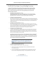
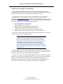
SFF8639 Test Adapter User Manual (Preliminary) SFF‐8639 Test Adapter User Manual P a g e | 1 ©2014 Wilder Technologies, LLC Document No. 910‐0034‐000 Rev. A (Preliminary) SFF8639 Test Adapter User Manual (Preliminary) Table of Contents Introduction ..................................................................................................................................... 3 Product Inspection .......................................................................................................................... 5 The SFF‐8639 Test Adapter Care and Handling Precautions ........................................................... 6 General Test Adapter, Cable, and Connector .................................................................................. 8 Handling and Storage .................................................................................................................. 8 Visual Inspection.......................................................................................................................... 8 Cleaning ....................................................................................................................................... 8 Making Connections .................................................................................................................... 8 Electrostatic Discharge Information ................................................................................................ 9 User Model .................................................................................................................................... 10 Calibration Through De‐Embedding .............................................................................................. 12 Mechanical and Environmental Specifications.............................................................................. 13 8639 Configuration Board ............................................................................................................. 23 Electrical Specifications ................................................................................................................. 24 8639‐TPA Receptacle Accessories ................................................................................................. 34 Wilder Technologies, LLC – Limited Warranty .............................................................................. 35 Wilder Technologies, LLC – Terms & Conditions of Sale ............................................................... 36 Compliance with Environmental Legislation ................................................................................. 37 WEEE Compliance Statement .................................................................................................... 37 Glossary of Terms .......................................................................................................................... 38 Addendum A – Specific Configuration Test Adapters ................................................................... 39 PCI Express Specific Configuration Test Adapters ..................................................................... 39 SATA Express Specific Configuration Test Adapters .................................................................. 41 SAS MultiLink Specific Configuration Test Adapters ................................................................. 43 Addendum B – 8639 Configuration Board Reference Information ............................................... 51 8639 Configuration Board Jumper Positions ............................................................................. 51 8639 Configuration Board Block Diagram ................................................................................. 52 Index .............................................................................................................................................. 53 P a g e | 2 ©2014 Wilder Technologies, LLC Document No. 910‐0034‐000 Rev. A (Preliminary) SFF8639 Test Adapter User Manual (Preliminary) Introduction This user’s manual documents the SFF‐8639 Plug and Receptacle Test Adapters (8639‐TPA‐P and 8639‐TPA‐R). The two test adapter types, shown in Figures 1 and 2, test 8639 interface cables, hosts and devices against the SFF‐8639 Specification. NOTE: The test adapters referred to and illustrated in this “General” section of the User Manual, reflect the “Universal” SFF‐ 8639 Test Adapters. Addendum “A”, at the end of this document, presents reference information and details for specific types of SFF‐8639 test adapters offered by Wilder Technologies. The TPA‐P and TPA‐R test adapter assemblies allow easy access, via SMA connections, to measure or inject data signals. The Receptacle test adapter also provides access to +5V, +12V, and their respective GNDs, via a 4‐position Molex power connector. Additionally, the user can access +3.3V, its respective GND, Resets, Wake, Activity, Dual Link Enable, SM Clock, SM Data, and others via an alternate 16‐position connector. A mating 16‐position connector housing and contacts are provided to connect these 16 signals to a wiring assembly provided by the user. NOTE: To avoid damaging the cables, use the handling techniques described in the Care and Handling section before making any connections or configuring a test setup. Always use a static‐safe workstation when performing tests, as explained in the “Electrostatic Discharge Information” section. Low‐Speed Connector (10‐Position) 28 Female SMAs for High‐Speed Testing Housing
8639 Plug (68‐Position) Figure 1. The 8639 Test Adapter (Host Plug). Universal SFF-8639 Host Test Fixture Shown.
P a g e | 3 ©2014 Wilder Technologies, LLC Document No. 910‐0034‐000 Rev. A (Preliminary) SFF8639 Test Adapter User Manual (Preliminary) 22 Female SMAs for High‐
Speed Testing 4‐Position +5V and +12V Power Connector 8639 Receptacle (68‐Position) Low‐Speed Connector (16‐position) Housing
6 Female SMAs for High‐Speed Testing Figure 2. The 8639 Test Adapter (Device Receptacle). Universal SFF-8639 Device Test Fixture Shown.
The 4‐position power connector is Molex part number 53109‐0410 (Mating connector not provided). The 16‐position keyed/latching mating connector part number is 43045‐1602. The mating receptacle connector housing and contact pins for 26‐30awg wire are provided with each 8639‐TPA‐R assembly (Molex part numbers 43025‐1600 for the 16‐position receptacle housing and 43030‐0011 for the 26‐30awg receptacle contacts). Replacement receptacle parts can be purchased through Molex distributors. P a g e | 4 ©2014 Wilder Technologies, LLC Document No. 910‐0034‐000 Rev. A (Preliminary) SFF8639 Test Adapter User Manual (Preliminary) Product Inspection Upon receiving the 8639‐TPA from Wilder Technologies, perform the following product inspection:
Inspect the outer shipping container, foam‐lined instrument case, and product for damage. Retain the outer cardboard shipping container until the contents of the shipment have been inspected for completeness and the product has been checked mechanically and electrically. Use the foam‐lined instrument‐case for secure storage of the Wilder Technologies SFF‐8639 Test Adapter when not in use. Locate the shipping list and verify that all items ordered were received. In the unlikely event that the product is defective or incomplete, the “Limited Warranty” section discusses how to contact Wilder Technologies for technical assistance and/or how to package the product for return. P a g e | 5 ©2014 Wilder Technologies, LLC Document No. 910‐0034‐000 Rev. A (Preliminary) SFF8639 Test Adapter User Manual (Preliminary) The SFF‐8639 Test Adapter Care and Handling Precautions The SFF‐8639 Test Adapter requires careful handling to avoid damage. Improper handling techniques, or using too small a cable bend radius, can damage the coaxial cable connections within the adapter housing or the cables themselves. This can occur at any point along the cable. To achieve optimum performance and to prolong the 8639‐TPA’s life, observe the following handling precautions:
CAUTION 1: Avoid Torque Forces (Twisting) While individual coaxial cables within the test adapter have some rotational freedom, twisting the 8639‐TPA as a unit, with one end held stationary, may damage or severely degrade performance. Adherence to Caution 5 (below) helps to avoid twisting. CAUTION 2: Avoid Sharp Cable Bends Never bend coaxial cables into a radius of 26 mm (1‐inch) or less. Never bend cables greater than 90°. Single or multiple cable bends must be kept within this limit. Bending the 8639‐TPA cables less than a 26mm (1‐Inch) radius will permanently damage or severely degrade test adapter performance. CAUTION 3: Avoid Cable Tension (Pull Forces) Never apply tension (pull forces) to an individual coaxial cable that is greater than 2.3 kg (5 lbs.). To avoid applying tension, always place accessories and equipment on a surface that allows adjustment to eliminate tension on the 8639‐TPA and cables. Use adjustable elevation stands or apparatus to accurately place and support the 8639‐TPA. CAUTION 4: Connect the 8639‐TPA First To prevent twisting, bending, or applying tension to the coaxial cables when connecting a 8639‐TPA, always attach the 8639‐TPA to the device under test (DUT) or cable under test before attaching any SMA connectors. Carefully align the 8639 connectors and then gently push the connectors together until fully seated. If the 8639‐TPA must be turned or twisted to make connection to the DUT, avoid using the 8639‐TPA housing alone to make this occur. Try to distribute the torque forces along the length of the test setup and cabling. If this is not possible, it is recommended to first loosen or disconnect the SMA connections at the 8639‐TPA, make the connection to the DUT and then re‐tighten or attach the test equipment leads. NOTE: Only grip the test adapter housing when inserting or extracting the 8639‐TPA to or from the DUT. Pulling directly on the 8639‐TPA cables or using them to insert the 8639‐TPA may cause damage.
CAUTION 5: Carefully Make SMA Connections To connect the 8639‐TPA SMA connectors, follow these steps: 1.
Hold the cable stationary by grasping the cable at the black heat‐shrink section near the SMA connector. 2.
Insert the mating SMA barrel and hand‐tighten the free‐spinning SMA nut onto the connector while avoiding pulling, bending, or twisting the 8639‐TPA coaxial cable. P a g e | 6 ©2014 Wilder Technologies, LLC Document No. 910‐0034‐000 Rev. A (Preliminary) SFF8639 Test Adapter User Manual (Preliminary) 3.
The 8639‐TPA SMA connectors have flats that accept an open‐end 1/4‐inch or 6.5mm wrench. When attaching instrument cables to the 8639‐TPA, it is recom‐
mended that the 8639‐TPA SMA connectors be mechanically held and the test leads be tightened to the equipment manufacturer’s torque recommendations, normally 5 in‐lbs, using a 5/16‐inch open‐end wrench. If the test set‐up requires repositioning, first loosen or disconnect the SMA connections to avoid twisting, bending, or tension. NOTE: A drop in signal amplitude by half or 6db during the testing of a channel may indicate that a cable has been mechanically pulled free of coaxial cable connections internal to the assembly. This could be determined by checking if the cable has any lateral play relative to the TPA. This would only occur when the TPA has exceeded the pull force as specified within the mechanical specification. If the cable cannot be re‐seated, the test adapter will need to be sent back to the factory for service.
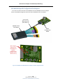
CAUTION 6: Independently Support Instrument Cables or Accessories Excessive weight from instrument cables and/or accessories connected to the 8639‐TPA can cause damage or affect the test adapter performance. Be sure to provide appropriate means to support and stabilize all test set‐up components. NOTE: The 8639‐TPA‐R (Device TPA) is supplied with Device Support Adapter materials that allow the user to properly support and stabilize a 2.5‐inch or 3.5‐inch form‐factor device while under test. Figure 16, later within this document, illustrates the installation and a typical application of the Device Support Adapter materials. P a g e | 7 ©2014 Wilder Technologies, LLC Document No. 910‐0034‐000 Rev. A (Preliminary) SFF8639 Test Adapter User Manual (Preliminary) General Test Adapter, Cable, and Connector Observing simple precautions can ensure accurate and reliable measurements. Handling and Storage Before each use of the 8639‐TPA, ensure that all connectors are clean. Handle all cables carefully and store the 8639‐TPA in the foam‐lined instrument case when not in use, if possible. Do not set connectors contact end down. Install the SMA protective end caps when the 8639‐TPA is not in use. Visual Inspection Be sure to inspect all cables carefully before making a connection. Inspect all cables for metal particles, scratches, deformed threads, dents, or bent, broken, or misaligned center conductors. Do not use damaged cables. Cleaning If necessary, clean the connectors using low‐pressure (less than 60 PSI) compressed air or nitrogen with an effective oil‐vapor filter and condensation trap. Clean the cable threads, if necessary, using a lint‐free swab or cleaning cloth moistened with isopropyl alcohol. Always completely dry a connector before use. Do not use abrasives to clean the connectors. Re‐
inspect connectors, making sure no particles or residue remains. Making Connections Before making any connections, review the “Care and Handling Precautions” section. Follow these guidelines when making connections:
Align cables carefully Make preliminary connection lightly To tighten, turn connector nut only Do not apply bending force to cable Do not over‐tighten preliminary connections Do not twist or screw‐in cables Use an appropriately sized torque wrench (depends on SMA gender), and do not tighten past the “break” point of the torque wrench (normally set to 5 in‐lbs) P a g e | 8 ©2014 Wilder Technologies, LLC Document No. 910‐0034‐000 Rev. A (Preliminary) SFF8639 Test Adapter User Manual (Preliminary) Electrostatic Discharge Information Protection against electrostatic discharge (ESD) is essential while connecting, inspecting, or cleaning the 8639‐TPA test adapter and connectors attached to a static‐sensitive circuit (such as those found in test sets). Electrostatic discharge can damage or destroy electronic components. Be sure to perform all work on electronic assemblies at a static‐safe work station, using two types of ESD protection:
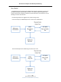
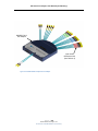
Conductive table‐mat and wrist‐strap combination Conductive floor‐mat and heel‐strap combination When used together, both of these types provide a significant level of ESD protection. Used alone, the table‐mat and wrist‐strap combination provide adequate ESD protection. To ensure user safety, the static‐safe accessories must provide at least 1 MΩ of isolation from ground. Acceptable ESD accessories may be purchased from a local supplier. WARNING: These techniques for a static‐safe work station should not be used when working on circuitry with a voltage potential greater than 500 volts. P a g e | 9 ©2014 Wilder Technologies, LLC Document No. 910‐0034‐000 Rev. A (Preliminary) SFF8639 Test Adapter User Manual (Preliminary) User Model The 8639‐TPA supports all testing of SFF‐8639 related interface specifications such as PCIe SFF‐8639, SATA Express, MultiLink SAS, and others. It is capable of performing beyond the scope of measurements required, limited only by the specifications, environmental, care and handling as stated in this document. The following examples are suggestions for possible testing setups. In this first example, an 8639 Receptacle TPA is used to test an 8639 device: Physical Links Under Test
Reference Transmitter
8639
Receptacle TPA
SFF‐8639 Device Under Test
Reference Receiver
The second example shows an 8639 Plug TPA used to test a host: Physical Links Under Test
Reference Transmitter
8639
Plug TPA
SFF‐8639 Host Under Test
Reference Receiver
P a g e | 10 ©2014 Wilder Technologies, LLC Document No. 910‐0034‐000 Rev. A (Preliminary) SFF8639 Test Adapter User Manual (Preliminary) The third example shows one 8639 Plug TPA and one 8639 Receptacle TPA used for testing a 8639 extension cable: Physical Links Under Test
Mated Connectors
8639 Plug TPA
SFF‐8639 Extension
Cable
Reference Transceiver
8639 Receptacle TPA
Mated Connectors
Physical Links Under Test
P a g e | 11 ©2014 Wilder Technologies, LLC Document No. 910‐0034‐000 Rev. A (Preliminary) SFF8639 Test Adapter User Manual (Preliminary) Calibration Through De‐Embedding The SFF‐8639 Host and Device Test Adapters are fully passive components. Therefore, calibration compensating for the losses must occur within the test instrumentation that drives the SFF‐8639 receiver or looks at the response of the SFF‐8639 transmitter. The 8639‐TPAs have Touchstone S4P files for de‐embedding the electrical length and losses within the TPA up to the SFF‐8639 connector interface pads. (Contact Wilder Technologies, support@wilder‐tech.com, to obtain a copy of the S4P files.) The Touchstone S4P files enable the test engineer to compensate for the last four of the following six repeatable, systematic errors that occur when moving the reference plane:
Signal leakage effects: Directivity errors Signal leakage effects: Crosstalk errors Reflection effects: Source Impedance Mismatching errors Reflection effects: Load Impedance Mismatching errors Bandwidth effects: Receiver Transmission in Test Equipment errors Bandwidth effects: Receiver Reflection‐tracking in Test Equipment errors These errors are corrected on each port. Refer to the Instrument Manual for instructions on the instrument’s specific de‐embedding process. NOTE: The reference plane is the boundary, both physically and electrically, between the calibrated and un‐calibrated portions of the circuit. Everything outside the reference plane is considered part of the DUT. Any instrument that does not use calibration or de‐
embedding of the test fixture defines the DUT as the total of externally connected components. If the de‐embedding file is not used, all of the 8639‐TPA and associated coaxial cables, as well as cables connecting the TPA assembly to the test instrument, would be a part of the DUT. Non‐repeatable errors, such as drift or random errors, can be reduced but not corrected. Drift errors aggregate over time or with environmental changes such as temperature shift. To eliminate drift errors, perform an instrumentation‐level calibration. A random error cannot be corrected through calibration since the error occurred randomly. Random errors are typically associated with either test instrument noise or test repeatability problems. Reduce test instrument noise by increasing source power, lowering the IF bandwidth, or averaging results over multiple sweeps. Reduce test repeatability problems through the use of a torque wrench or, again, by averaging over multiple sweeps. P a g e | 12 ©2014 Wilder Technologies, LLC Document No. 910‐0034‐000 Rev. A (Preliminary) SFF8639 Test Adapter User Manual (Preliminary) Mechanical and Environmental Specifications NOTE: All specifications in this manual are subject to change. Table 1. General Specifications
ITEM DESCRIPTION Usage Environment Controlled indoor environment Plug Test Adapter Length (w/standard cables) 246 mm +/‐ 2 mm (9.70 inches +/‐ .08 inches) (Characteristic) Receptacle Test Adapter Length (w/std. cables) 381 mm +/‐ 2 mm (15.00 inches +/‐ .08 inches) (Characteristic) Operating Temperature 0°C to +55°C (32°F to +131°F) (Characteristic) Storage Temperature ‐40°C to +70°C (‐40°F to +158°F) (Characteristic) 8639‐TPA‐R Cable Pinout The 8639‐TPA‐R cables provide 28 SMA connectors (access up to six lanes of differential TX and RX, and up to two differential reference clocks), one 4‐position power connector, and one 16‐position alternate connector. Labels clearly mark each cable or connector. The following figure refers to pin‐description tables for each of the three connector types. Note: The power supplies each have 22 µF in parallel with a 0.01 µF capacitor, with the exception of the +3.3V, which does not have the 22 µF cap. The precharge signals each have a series 2 ohm resistor to their respective power supplies. Color ID for Differential Pairs (See Table 4) SMA Connectors (See Table 4) 4‐Position Power Connector “J2” (See Table 2) Receptacle Connector (See Table 4) 16‐Position Connector “J3” (See Table 3) White Band Indicates Transmitter Signals SMA Connectors (See Table 4) Color ID’s for
Data Line Polarity (See Table 4) Figure 3. Cable Connectors (“Universal” 8639-TPA-R shown)
P a g e | 13 ©2014 Wilder Technologies, LLC Document No. 910‐0034‐000 Rev. A (Preliminary) SFF8639 Test Adapter User Manual (Preliminary) Table 2. 8639-TPA-R 4-Position Power Connector “J2”
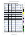
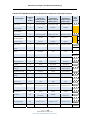
LABEL PIN NO. DESCRIPTION +12V Pin 1 +12 Volts GND Pin 2 Power Ground GND Pin 3 Power Ground +5V Pin 4 +5 Volts Table 3. 8639-TPA-R 16-Position Alternate Connector “J3” (“Universal” 8639-TPA-R Described)
LABEL PIN NO. DESCRIPTION GND Pin 1 Power Ground PERST Pin 2 PCI Express Reset (Port A) WAKE# Pin 3 Wake (required only if the device/system supports wake‐up and/or the OBFF mechanism) PIN P2 Pin 4 Access to SFF‐8639 Connector Pin P2 (description is interface type dependent) CLKREQ# Pin 5 PCI Express Reference Clock Request PRSNT# Pin 6 Device Present (PCI Express SFF‐8639 module presence detect pin) ACTIVY# Pin 7 PCI Express Activity (indicates read or write activity of the SFF‐8639 module) DLEN# Pin 8 PCI Express Dual Link Enable +3.3V Pin 9 +3.3 Volts PERSTB Pin 10 PCI Express Reset (Port B) RES E6 Pin 11 Access to “Reserved” SFF‐8639 Connector Pin E6 (description is interface type dependent) RES E16 Pin 12 Access to “Reserved” SFF‐8639 Connector Pin E16 (description is interface type dependent) RES S15 Pin 13 Access to “Reserved” SFF‐8639 Connector Pin S15 (description is interface type dependent) IFDET# Pin 14 Interface Type Detect (PCI Express SFF‐8639 module presence detect pin) SMCLK Pin 15 SMBus (System Management Bus) Clock SMDAT Pin 16 SMBus (System Management Bus) Data P a g e | 14 ©2014 Wilder Technologies, LLC Document No. 910‐0034‐000 Rev. A (Preliminary) SFF8639 Test Adapter User Manual (Preliminary) Table 4. 8639 Receptacle Pin Assignments on notched side of connector
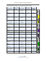
Connector Pin Number Destination Name Color ID for Data Line Polarity Color ID for Differential Pair (Receptacle) Signal Ground S1 Signal Ground, GND N/A N/A Device SAS/SATA 0 Receiver Positive S2 DEV S0R+ Red Orange Device SAS/SATA 0 Receiver Negative S3 DEV S0R ‐ Black Orange Signal Ground S4 Signal Ground, GND N/A N/A Device SAS/SATA 0 Transmitter Negative S5 DEV S0T‐ Black Orange/Wht Band Device SAS/SATA 0 Transmitter Positive S6 DEV S0T+ Red Orange/Wht Band Signal Ground S7 Signal Ground, GND N/A N/A PCIe Ref Clock for Port B Positive E1 DEV RCLKB+ Red White PCIe Ref Clock for Port B Negative E2 DEV RCLKB‐ Black White +3.3 Volts for SM Bus E3 +3.3V Black N/A PCIe reset for Port B E4 PERSTB N/A N/A PCIe reset for Port A E5 PERST N/A N/A Reserved E6 RES E6 N/A N/A Device/System Specific Wake‐Up P1 WAKE# N/A N/A PIN P2 P2 PIN P2 N/A N/A PCIe Reference Clock Request P3 CLKREQ# N/A N/A Interface Type Detect P4 IFDET# N/A N/A P5, P6 GND N/A N/A P7 2 Ohm Resistor to +5V N/A N/A P8, P9 +5V N/A N/A Device Present P10 PRSNT# N/A N/A PCIe Activity P11 ACTIVY# N/A N/A Power Ground P12 GND N/A N/A +12 Volts precharge P13 2 Ohm Resistor to +12V N/A N/A P14, P15 +12V N/A N/A Pin Description Power Ground +5 Volts precharge +5 Volts +12 Volts P a g e | 15 ©2014 Wilder Technologies, LLC Document No. 910‐0034‐000 Rev. A (Preliminary) SFF8639 Test Adapter User Manual (Preliminary) Table 4. 8639 Receptacle Pin Assignments on side opposed to notch side of connector
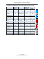
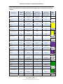
Pin Description Connector Pin Number Destination Name Color ID for Data Line Polarity Color ID for Differential Pair (Plug) PCIe Ref Clock for Port A Positive E7 DEV RCLKA+ Red White PCIe Ref Clock for Port A Negative E8 DEV RCLKB‐ Black White Signal Ground E9 Signal Ground, GND N/A N/A Device PCIe 0 Receiver Positive E10 DEV PER0+ Red Yellow Device PCIe 0 Receiver Negative E11 DEV PER0‐ Black Yellow Signal Ground E12 Signal Ground, GND N/A N/A Device PCIe 0 Transmitter Negative E13 DEV PET0‐ Black Yellow/Wht Band Device PCIe 0 Transmitter Positive E14 DEV PET0+ Red Yellow/Wht Band Signal Ground E15 Signal Ground, GND N/A N/A Reserved E16 RES E16 N/A N/A Signal Ground S8 Signal Ground, GND N/A N/A Device SAS 1 Receiver Positive S9 DEV S1R+ Red Violet Device SAS 1 Receiver Negative S10 DEV S1R ‐ Black Violet Signal Ground S11 Signal Ground, GND N/A N/A Device SAS 1 Transmitter Negative S12 DEV S1T‐ Black Violet/Wht Band Device SAS 1 Transmitter Positive S13 DEV S1T+ Red Violet/Wht Band Signal Ground S14 Signal Ground, GND N/A N/A Reserved S15 RES S15 N/A N/A Signal Ground S16 Signal Ground, GND N/A N/A Device PCIe 1 Receiver Positive S17 DEV PER1+ Red Green Device PCIe 1 Receiver Negative S18 DEV PER1‐ Black Green Signal Ground S19 Signal Ground, GND N/A N/A Device PCIe 1 Transmitter Negative S20 DEV PET1‐ Black Green/Wht Band Device PCIe 1 Transmitter Positive S21 DEV PET1+ Red Green/Wht Band Signal Ground S22 Signal Ground, GND N/A N/A P a g e | 16 ©2014 Wilder Technologies, LLC Document No. 910‐0034‐000 Rev. A (Preliminary) SFF8639 Test Adapter User Manual (Preliminary) Table 4. 8639 Receptacle Pin Assignments on side opposed to notch side of connector (continued)
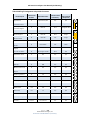
Connector Pin Number Destination Name Color ID for Data Line Polarity Color ID for Differential Pair (Plug) Device PCIe 2 Receiver Positive S23 DEV PER2+ Red Blue Device PCIe 2 Receiver Negative S24 DEV PER2‐ Black Blue Signal Ground S25 Signal Ground, GND N/A N/A Device PCIe 2 Transmitter Negative S26 DEV PET2‐ Black Blue/Wht Band Device PCIe 2 Transmitter Positive S27 DEV PET2+ Red Blue/Wht Band Signal Ground S28 Signal Ground, GND N/A N/A Device PCIe 3 Receiver Positive E17 DEV PER3+ Red Red Device PCIe 3 Receiver Negative E18 DEV PER3‐ Black Red Signal Ground E19 Signal Ground, GND N/A N/A Device PCIe 3 Transmitter Negative E20 DEV PET3‐ Black Red/Wht Band Device PCIe 3 Transmitter Positive E21 DEV PET3+ Red Red/Wht Band Signal Ground E22 Signal Ground, GND N/A N/A SM‐Bus Clock E23 SMCLK N/A N/A SM‐Bus Data E24 SMDAT N/A N/A PCIe Dual Link Enable E25 DLEN# N/A N/A Pin Description P a g e | 17 ©2014 Wilder Technologies, LLC Document No. 910‐0034‐000 Rev. A (Preliminary) SFF8639 Test Adapter User Manual (Preliminary) 8639‐TPA‐P Cable Pin‐out The 8639‐TPA‐P cables provide 28 SMA connectors (access up to six lanes of PCIe differential TX and RX, and up to two differential reference clocks) and one 10‐Position low‐speed connector. Labels clearly mark each cable or connector. The following figure refers to the pin‐
description table for the plug connector. Low‐Speed
Signal Connector (See Table 5) SMA Connectors (See Table 6) Color ID for Differential Pair (See Table 6) Housing Plug Connector (See Table 6) White Band Indicates Transmitter Signals Color ID for Data Line Polarity (See Table 6)
Figure 4. Cable Connectors (“Universal” 8639-TPA-P shown)
P a g e | 18 ©2014 Wilder Technologies, LLC Document No. 910‐0034‐000 Rev. A (Preliminary) SFF8639 Test Adapter User Manual (Preliminary) Table 5. 8639-TPA-P 10-Position Low-Speed Connector “J3”
LABEL PIN NO. DESCRIPTION GND Pin 1 Power Ground BRS Pin 2 PCI Express Reset (Port B) ARS Pin 3 PCI Express Reset (Port A) DRS Pin 4 Access to 8639 Connector P2 (Device Reset) WK# Pin 5 Device/System Specific Wake‐Up ID# Pin 6 PCI Express Interface Type Detect PR# Pin 7 PCI Express Device Present AS Pin 8 PCI Express Activity SMC Pin 9 SMBus (System Management Bus) Clock SMD Pin 10 SMBus (System Management Bus) Data P a g e | 19 ©2014 Wilder Technologies, LLC Document No. 910‐0034‐000 Rev. A (Preliminary) SFF8639 Test Adapter User Manual (Preliminary) Table 6. 8639 Plug Pin Assignments on keyed side of connector
Connector Pin Number Destination Name Color ID for Data Line Polarity Color ID for Differential Pair (Receptacle) Signal Ground S1 Signal Ground, GND N/A N/A Host SAS/SATA 0 Transmitter Positive S2 HOST S0T+ Red Orange/Wht Band Host SAS/SATA 0 Transmitter Negative S3 HOST S0T ‐ Black Orange/Wht Band Signal Ground S4 Signal Ground, GND N/A N/A Host SAS/SATA 0 Receiver Negative S5 HOST S0R‐ Black Orange Host SAS/SATA 0 Receiver Positive S6 HOST S0R+ Red Orange Signal Ground S7 Signal Ground, GND N/A N/A PCIe Ref Clock for Port B Positive E1 HOST RCLKB+ Red White PCIe Ref Clock for Port B Negative E2 HOST RCLKB‐ Black White +3.3 Volts for SM Bus E3 0.01 uF bypass to GND Black N/A PCIe Reset for Port B E4 BRS N/A N/A PCIe Reset for Port A E5 ARS N/A N/A Reserved E6 No connection N/A N/A Device/System Specific Wake‐Up P1 WK# N/A N/A 8639 Connector Pin P2 P2 DRS N/A N/A PCIe Reference Clock Request P3 No connection N/A N/A Interface Type Detect P4 ID# N/A N/A P5, P6 GND N/A N/A P7 No connection N/A N/A P8, P9 No connection N/A N/A Device Present P10 PR# N/A N/A PCIe Activity P11 AS N/A N/A Power Ground P12 GND N/A N/A +12 Volts precharge P13 No connection N/A N/A P14, P15 No connection N/A N/A Pin Description Power Ground +5 Volts precharge +5 Volts +12 Volts P a g e | 20 ©2014 Wilder Technologies, LLC Document No. 910‐0034‐000 Rev. A (Preliminary) SFF8639 Test Adapter User Manual (Preliminary) Table 6. 8639 Plug Pin Assignments on side opposed to keyed side of connector
Pin Description Connector Pin Number Destination Name Color ID for Data Line Polarity Color ID for Differential Pair (Plug) PCIe Ref Clock for Port A Positive E7 HOST RCLKA+ Red White PCIe Ref Clock for Port A Negative E8 HOST RCLKA‐ Black White Signal Ground E9 Signal Ground, GND N/A N/A Host PCIe 0 Transmitter Positive E10 HOST PET0+ Red Yellow/Wht Band Host PCIe 0 Transmitter Negative E11 HOST PET0‐ Black Yellow/Wht Band Signal Ground E12 Signal Ground, GND N/A N/A Host PCIe 0 Receiver Negative E13 HOST PER0‐ Black Yellow Host PCIe 0 Receiver Positive E14 HOST PER0+ Red Yellow Signal Ground E15 Signal Ground, GND N/A N/A Reserved E16 No connection N/A N/A Signal Ground S8 Signal Ground, GND N/A N/A Host SAS 1 Transmitter Positive S9 HOST S1T+ Red Violet/Wht Band Host SAS 1 Transmitter Negative S10 HOST S1T ‐ Black Violet/Wht Band Signal Ground S11 Signal Ground, GND N/A N/A Host SAS 1 Receiver Negative S12 HOST S1R‐ Black Violet Host SAS 1 Receiver Positive S13 HOST S1R+ Red Violet Signal Ground S14 Signal Ground, GND N/A N/A Reserved S15 No connection N/A N/A Signal Ground S16 Signal Ground, GND N/A N/A Host PCIe 1 Transmitter Positive S17 HOST PET1+ Red Green/Wht Band Host PCIe 1 Transmitter Negative S18 HOST PET1‐ Black Green/Wht Band Signal Ground S19 Signal Ground, GND N/A N/A Host PCIe 1 Receiver Negative S20 HOST PER1‐ Black Green Host PCIe 1 Receiver Positive S21 HOST PER1+ Red Green Signal Ground S22 Signal Ground, GND N/A N/A P a g e | 21 ©2014 Wilder Technologies, LLC Document No. 910‐0034‐000 Rev. A (Preliminary) SFF8639 Test Adapter User Manual (Preliminary) Table 6. 8639 Plug Pin Assignments on side opposed to keyed side of connector (continued)
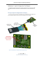
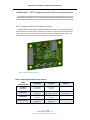
Pin Description Connector Pin Number Destination Name Color ID for Data Line Polarity Color ID for Differential Pair (Plug) Host PCIe 2 Transmitter Positive S23 HOST PET2+ Red Blue/Wht Band Host PCIe 2 Transmitter Negative S24 HOST PET2‐ Black Blue/Wht Band Signal Ground S25 Signal Ground, GND N/A N/A Host PCIe 2 Receiver Negative S26 HOST PER2‐ Black Blue Host PCIe 2 Receiver Positive S27 HOST PER2+ Red Blue Signal Ground S28 Signal Ground, GND N/A N/A Host PCIe 3 Transmitter Positive E17 HOST PET3+ Red Red/Wht Band Host PCIe 3 Transmitter Negative E18 HOST PET3‐ Black Red/Wht Band Signal Ground E19 Signal Ground, GND N/A N/A Host PCIe 3 Receiver Negative E20 HOST PER3‐ Black Red Host PCIe 3 Receiver Positive E21 HOST PER3+ Red Red Signal Ground E22 Signal Ground, GND N/A N/A SM‐Bus Clock E23 SMC N/A N/A SM‐Bus Data E24 SMD N/A N/A PCIe Dual Link Enable E25 No connection N/A N/A P a g e | 22 ©2014 Wilder Technologies, LLC Document No. 910‐0034‐000 Rev. A (Preliminary) SFF8639 Test Adapter User Manual (Preliminary) 8639 Configuration Board When used with the 8639‐TPA‐P (Host Test Adapter), the 8639 Configuration Board provides access to IFDET# (P4) and PRSNT# (P10) signals. The use of the combined signals provides the ability to set and detect the appropriate device type (configuration). Jumper configurations are referenced and clearly marked on the board. The 8639 Configuration Board also provides access to other low‐speed signals as well as jumper access for the WAKE# signal. Momentary switches allow the user to reset each of the three “RESET” signal functions. Specific features and usage models are presented within Addendum A and B of this document. Figure 5. 8639 Configuration Board Figure 6. 8639 Configuration Board mated to a 8639‐TPA‐P (Plug) Test Adapter P a g e | 23 ©2014 Wilder Technologies, LLC Document No. 910‐0034‐000 Rev. A (Preliminary) SFF8639 Test Adapter User Manual (Preliminary) Electrical Specifications NOTE: All specifications in this manual are subject to change. Table 7. Electrical Specifications
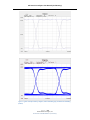
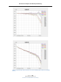
SPECIFICATION MINIMUM TYPICAL MAXIMUM Differential Impedance (ohms), 70 ps Rise Time, 20 – 80 percent 94 106 All Differential Pairs, Receptacle and Plug, excluding 8639 connector. Differential Impedance (ohms), 70 ps Rise Time, 20 – 80 percent TBD TBD All Differential Pairs, Receptacle and Plug, including 8639 connector. Impedance (ohms), 70ps Rise Time, 20 – 80 percent 47 53 All Differential Pairs, Receptacle and Plug, excluding 8639 connector. Intra‐pair Skew (ps) ‐6 6 All Differential Pairs, Receptacle and Plug. Inter‐pair Skew (ps) ‐6 6 All Differential Pairs, Receptacle and Plug. ‐40 All differential pairs, single aggressor, without 8639 connector, with six‐inch cables and terminations. Current Carrying (A) Per Pin 1.5 +5V, and +12V Power. Current Carrying (mA) 100 +3.3V Power. NEXT (db), at TBD GHz NOTES P a g e | 24 ©2014 Wilder Technologies, LLC Document No. 910‐0034‐000 Rev. A (Preliminary) SFF8639 Test Adapter User Manual (Preliminary) Figure 7. Typical mated pair 6 Gb/s eye diagram, with de-embedding (top) and without de-embedding
(bottom)
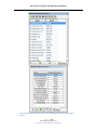
P a g e | 25 ©2014 Wilder Technologies, LLC Document No. 910‐0034‐000 Rev. A (Preliminary) SFF8639 Test Adapter User Manual (Preliminary) Figure 8. Typical mated pair 6 Gb/s eye data, with de-embedding (top) and without de-embedding
(bottom)
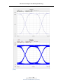
P a g e | 26 ©2014 Wilder Technologies, LLC Document No. 910‐0034‐000 Rev. A (Preliminary) SFF8639 Test Adapter User Manual (Preliminary) Figure 9. Typical mated pair 12 Gb/s eye diagram, with de-embedding (top) and without de-embedding
(bottom)
P a g e | 27 ©2014 Wilder Technologies, LLC Document No. 910‐0034‐000 Rev. A (Preliminary) SFF8639 Test Adapter User Manual (Preliminary) Figure 10. Typical mated pair 12 Gb/s eye data, with de-embedding (top) and without de-embedding
(bottom)
P a g e | 28 ©2014 Wilder Technologies, LLC Document No. 910‐0034‐000 Rev. A (Preliminary) SFF8639 Test Adapter User Manual (Preliminary) Figure 11. Typical mated pair balanced insertion loss, with de-embedding (top) and without de-embedding
(bottom)
P a g e | 29 ©2014 Wilder Technologies, LLC Document No. 910‐0034‐000 Rev. A (Preliminary) SFF8639 Test Adapter User Manual (Preliminary) Figure 12. Typical mated pair balanced return loss, with de-embedding (top) and without de-embedding
(bottom)
P a g e | 30 ©2014 Wilder Technologies, LLC Document No. 910‐0034‐000 Rev. A (Preliminary) SFF8639 Test Adapter User Manual (Preliminary) Figure 13. Typical TPA balanced return loss, differential termination replacing 8639 connector
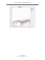
P a g e | 31 ©2014 Wilder Technologies, LLC Document No. 910‐0034‐000 Rev. A (Preliminary) SFF8639 Test Adapter User Manual (Preliminary) Figure 14. Typical differential TDP of TPA-P connected to TPA-R at 100 ps Rise Time, All differential pairs.
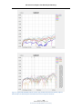
P a g e | 32 ©2014 Wilder Technologies, LLC Document No. 910‐0034‐000 Rev. A (Preliminary) SFF8639 Test Adapter User Manual (Preliminary) Figure 15. Typical Differential NEXT, without connector (top) and with mated connectors (bottom), adjacent
differential pairs, all differential pairs terminated at both ends. Into receptacle TPA shown.
P a g e | 33 ©2014 Wilder Technologies, LLC Document No. 910‐0034‐000 Rev. A (Preliminary) SFF8639 Test Adapter User Manual (Preliminary) 8639‐TPA Receptacle Accessories 8639‐TPA‐R Accessories The 8639‐TPA‐R (Device TPA) is supplied with Disk Support Adapter materials that allow the user to properly support and stabilize a 2.5 or 3.5‐inch form‐factor disk drive while under test. The figure, below, illustrates the installation and a typical application of the Disk Support Adapter materials. Disk Drive Under Test Thumb‐Screws and Disc Support Brackets Provided. Left side bracket can be repositioned for 3.5‐inch disk drive form‐factor. 4‐Each M3x0.5x6 Long Shoulder Screws provided to secure the disk drive 4‐Each 4‐40 x .25 Long Button Head Socket Machine Screws Provided. 1/16” socket wrench required (Lightly Tool‐Tighten Only) 16 position Molex Micro‐Fit receptacle and contact pins are provided for customer interface customization. Figure 16. 8639-TPA-R Device Support Adapter (Shown without High Speed Cables for Clarity)
P a g e | 34 ©2014 Wilder Technologies, LLC Document No. 910‐0034‐000 Rev. A (Preliminary) SFF8639 Test Adapter User Manual (Preliminary) Wilder Technologies, LLC – Limited Warranty Wilder Technologies, LLC warrants that each Test Adapter, 1) is free from defects in materials and workmanship and, 2) conforms to Wilder Technologies specifications for a period of 12 months. See Consumable and Fragile Material Warranty for exceptions to the 12 month warranty The warranty period for a Test Adapter is a specified, fixed period commencing on the date of ship from Wilder Technologies, LLC. If you did not purchase your Test Adapter directly from Wilder Technologies, LLC, the serial number and a valid proof of purchase will be required to establish your purchase date. If you do not have a valid proof of purchase, the warranty period will be measured from the date of ship from Wilder Technologies, LLC. If, during the warranty period, the Test Adapter is not in good working order, Wilder Technologies, LLC will, at its option, repair or replace it at no additional charge, except as is set forth below. In some cases, the replacement Test Adapter may not be new and may have been previously installed. Regardless of the Test Adapter’s production status, Wilder Technologies, LLC appropriate warranty terms apply. Consumable and Fragile Material Warranty Wilder Technologies, LLC warrants that consumable materials and all fragile materials supplied by Wilder Technologies, LLC either as part of an instrument or system, or supplied separately, will be free from defects in material and workmanship at the time of shipment. Extent of Warranty The warranty does not cover the repair or exchange of a Test Adapter resulting from misuse, accident, modification, unsuitable physical or operating environment, improper maintenance by you, or failure caused by a product for which Wilder Technologies, LLC is not responsible. The warranty is voided by removal or alteration of Test Adapter or parts identification labels. The initial three months are unconditional; the remaining months excludes plugs, receptacles and SMA connectors. Connectors are wear items and excluded from the warranty after the initial three months. These warranties are your exclusive warranties and replace all other warranties or conditions, express or implied, including but not limited to, the implied warranties or conditions or merchantability and fitness for a particular purpose. These warranties give you specific legal rights and you may also have other rights which vary from jurisdiction to jurisdiction. Some jurisdictions do not allow the exclusion or limitation of express or implied warranties, so the above exclusion or limitation may not apply to you. In that event, such warranties are limited in duration to the warranty period. No warranties apply after that period. Items Not Covered by Warranty
Wilder Technologies, LLC does not warrant uninterrupted or error–free operation of a Test Adapter. Any technical or other support provided for a Test Adapter under warranty, such as assistance via telephone with "how–to" questions and those regarding Test Adapter set‐up and installation, will be provided WITHOUT WARRANTIES OF ANY KIND. Warranty Service Warranty service may be obtained from Wilder Technologies, LLC by returning a Wilder Technologies, LLC Returns Material Authorization and the Test Adapter to Wilder Technologies, LLC during the warranty period. To obtain RMA number, contact support@wilder‐tech.com. You may be required to present proof of purchase or other similar proof of warranty entitlement. You are responsible for any associated transportation charges, duties and insurance between you and Wilder Technologies, LLC. In all instances, you must ship Test Adapters in Wilder Technologies, LLC approved packaging. Information on packaging guidelines can be found at: www.wilder‐tech.com. Wilder Technologies, LLC will ship repaired or replacement Test Adapter Delivery Duty Prepaid (DDP) and will pay for return shipment. You will receive title to the repaired or replacement Test Adapter and you will be the importer of record. P a g e | 35 ©2014 Wilder Technologies, LLC Document No. 910‐0034‐000 Rev. A (Preliminary) SFF8639 Test Adapter User Manual (Preliminary) Wilder Technologies, LLC – Terms & Conditions of Sale 1.
2.
3.
4.
5.
6.
Other Documents: This Agreement may NOT be altered, supplemented, or amended by the use of any other document(s) unless otherwise agreed to in a written agreement signed by both you and Wilder Technologies, LLC. If you do not receive an invoice or acknowledgement in the mail, via e‐mail, or with your Product, information about your purchase may be obtained at support@wilder‐tech.com or by contacting your sales representative. Payment Terms, Orders, Quotes, Interest: Terms of payment are within Wilder Technologies, LLC's sole discretion, and unless otherwise agreed to by Wilder Technologies, LLC, payment must be received by Wilder Technologies, LLC prior to Wilder Technologies, LLC's acceptance of an order. Payment for the products will be made by credit card, wire transfer, or some other prearranged payment method unless credit terms have been agreed to by Wilder Technologies, LLC. Invoices are due and payable within the time period noted on your invoice, measured from the date of the invoice. Wilder Technologies, LLC may invoice parts of an order separately. Your order is subject to cancellation by Wilder Technologies, LLC, in Wilder Technologies, LLC's sole discretion. Unless you and Wilder Technologies, LLC have agreed to a different discount, Wilder Technologies, LLC's standard pricing policy for Wilder Technologies, LLC‐branded systems, which includes hardware, software and services in one discounted price, allocates the discount off list price applicable to the service portion of the system to be equal to the overall calculated percentage discount off list price on the entire system. Wilder Technologies, LLC is not responsible for pricing, typographical, or other errors in any offer by Wilder Technologies, LLC and reserves the right to cancel any orders resulting from such errors. Shipping Charges; Taxes; Title; Risk of Loss: Shipping, handling, duties and tariffs are additional unless otherwise expressly indicated at the time of sale. Title to products passes from Wilder Technologies, LLC to Customer on shipment from Wilder Technologies, LLC's facility. Loss or damage that occurs during shipping by a carrier selected by Wilder Technologies, LLC is Wilder Technologies, LLC's responsibility. Loss or damage that occurs during shipping by a carrier selected by you is your responsibility. You must notify Wilder Technologies, LLC within 7 days of the date of your invoice or acknowledgement if you believe any part of your purchase is missing, wrong or damaged. Unless you provide Wilder Technologies, LLC with a valid and correct tax exemption certificate applicable to your purchase of Product and the Product ship‐to location, you are responsible for sales and other taxes associated with the order. Shipping dates are estimates only. WARRANTY: WILDER TECHNOLOGIES, LLC, warrants that the item(s) manufactured under the Buyer's contract shall be free from defects in materials and workmanship furnished by WILDER TECHNOLOGIES, LLC, and shall conform to the applicable drawings and specifications. WILDER TECHNOLOGIES, LLC’S liability herein, for breach of warranty, contract or negligence in manufacturing, shall be limited to repair or replacement. Repair or replacement of defective items will be applicable only if the Buyer notifies WILDER TECHNOLOGIES, LLC, by written notice within 30‐days of delivery. All claims shall be addressed to: support@wilder‐tech.com or WILDER TECHNOLOGIES, LLC, 6101A East 18th Street, Vancouver, Washington 98661 U.S.A.; ATTENTION: Customer Service Manager. WILDER TECHNOLOGIES, LLC, reserves the right to inspect at the Buyer's plant all items claimed to be defective or nonconforming prior to authorizing their return. WILDER TECHNOLOGIES, LLC, assumes no liability for the results of the use of its components in conjunction with other electric, electronic or mechanical components, circuits and/or systems. The foregoing constitutes the sole and exclusive remedy of the Buyer and the exclusive liability of WILDER TECHNOLOGIES, LLC, and is IN LIEU OF ANY AND ALL OTHER WARRANTIES, STATUTORY, IMPLIED OR EXPRESSED AS TO MERCHANTABILITY, FITNESS FOR THE PURPOSE SOLD, DESCRIPTION, QUALITY, and PRODUCTIVENESS OR ANY OTHER MATTER. Without limiting the foregoing, in no event shall WILDER TECHNOLOGIES, LLC, be liable for loss of use, profit or other collateral, or for special and/or consequential damages. RETURNED GOODS: WILDER TECHNOLOGIES, LLC, will accept only those goods for return that have been authorized for return. All goods authorized for return shall be assigned a Returned Material Authorization (RMA) Number. The RMA Number shall be clearly marked on the shipping container(s) and all documentation accompanying the goods authorized for return. The RMA Number shall be assigned by WILDER TECHNOLOGIES, LLC pursuant to the conditions set forth in Paragraph 4, WARRANTY. UNITED STATES GOVERNMENT CONTRACTS: In the event this offer is accepted under Government contract, WILDER TECHNOLOGIES, LLC, agrees to accept clauses required by Government regulations and to waive WILDER TECHNOLOGIES, LLC conditions inconsistent therewith. WILDER TECHNOLOGIES, LLC, certifies that it is a regular manufacturer or dealer of the goods and/or services offered herein and that the prices offered do not exceed those charged to any customer for like quantities, services or materials under the same conditions. P a g e | 36 ©2014 Wilder Technologies, LLC Document No. 910‐0034‐000 Rev. A (Preliminary) SFF8639 Test Adapter User Manual (Preliminary) Compliance with Environmental Legislation Wilder Technologies, LLC, is dedicated to complying with the requirements of all applicable environmental legislation and regulations, including appropriate recycling and/or disposal of our products. WEEE Compliance Statement The European Union adopted Directive 2002/96/EC on Waste Electrical and Electronic Equipment (WEEE), with requirements that went into effect August 13, 2005. WEEE is intended to reduce the disposal of waste from electrical and electronic equipment by establishing guidelines for prevention, reuse, recycling and recovery. Wilder Technologies has practices and processes in place to conform to the requirements in this important Directive. In support of our environmental goals, effective January 1st, 2009 Wilder Technologies, LLC has partnered with EG Metals Inc. – Metal and Electronics Recycling of Hillsboro, Oregon, www.egmetalrecycling.com, to recycle our obsolete and electronic waste in accordance with the European Union Directive 2002/96/EC on waste electrical and electronic equipment ("WEEE Directive"). As a service to our customers, Wilder Technologies is also available for managing the proper recycling and/or disposal of all Wilder Technologies products that have reached the end of their useful life. For further information and return instructions, contact support@wilder‐tech.com. P a g e | 37 ©2014 Wilder Technologies, LLC Document No. 910‐0034‐000 Rev. A (Preliminary) SFF8639 Test Adapter User Manual (Preliminary) Glossary of Terms TERMINOLOGY DEFINITION Aggressor A signal imposed on a system (i.e., cable assembly) to measure response on
other signal carriers. Decibel (dB) Ten times the common logarithm (i.e. log10) of the ratio of relative powers.
Informative The designation of a test that is not required for compliance but is considered
important from a characterization standpoint. It is provided for informational purposes only. Insertion loss The ratio, expressed in dB, of incident power to delivered power. Internal cable A cable that is used to connect a 8639 Initiator Device to a 8639 Target Device within a mainframe. Near‐end crosstalk Crosstalk that is propagated in a disturbed channel in the opposite direction as the propagation of a signal in the aggressor channel. The terminals of the aggressor channel and the victim channel are usually close to each other. Normative The designation of a test that is required for compliance. Physical link Two differential signal pairs, one pair in each direction, that connect two physical phys (see the current 8639 specification.) Return Loss The ratio, expressed in dB, of incident power to reflected power. 8639 Initiator Device A device containing SSP, STP, and /or SMP initiating ports in a 8639 domain.
8639 Target Device A device containing SSP, STP, and /or SMP target ports in a 8639 domain.
8639‐TPA 8639 Test Point Access. A specialized assembly that interfaces to a 8639
receptacle or plug and enables access of signals for measurement or stimulation. Serial ATA (SATA) The protocol defined by SATA (see ATA8‐AAM)
Serial Attached SCSI (8639) The set of protocols defined in SPL and the interconnect defined by the 8639
specification. Victim A signal carrier on a system that has a response imposed on it by other signals in the system. P a g e | 38 ©2014 Wilder Technologies, LLC Document No. 910‐0034‐000 Rev. A (Preliminary) SFF8639 Test Adapter User Manual (Preliminary) Addendum A – Specific Configuration Test Adapters This addendum provides documentation of specific configuration (non‐Universal) SFF‐8639 test adapters (PCI Express, SATA Express, and SAS MultiLink) as to content and operation of each. PCI Express Specific Configuration Test Adapters This section contains illustrations of the 8639PE‐TPA‐P and 8639PE‐TPA‐R test adapters and the related 8639 Configuration Board used with the 8639PE‐TPA‐P test adapter. 8639PE‐TPA‐P Test Adapter Color ID for Differential Pair (See Table A‐1) 8639 Configuration Board Note Jumper Positions for PCIe Specific Configuration (JP2 Pin 2 to Side, JP3 Pin 2 to 3) Figure A‐1. 8639PE-TPA-P Test Adapter and 8639 Configuration Board
P a g e | 39 ©2014 Wilder Technologies, LLC Document No. 910‐0034‐000 Rev. A (Preliminary) SFF8639 Test Adapter User Manual (Preliminary) 8639PE‐TPA‐R Test Adapter Color ID for Differential Pair (See Table A‐2) Figure A‐2. 8639PE-TPA-R PCIe Specific Test Adapter
P a g e | 40 ©2014 Wilder Technologies, LLC Document No. 910‐0034‐000 Rev. A (Preliminary) SFF8639 Test Adapter User Manual (Preliminary) SATA Express Specific Configuration Test Adapters This section contains illustrations of the 8639SA‐TPA‐P and 8639SA‐TPA‐R test adapters and the related 8639 Configuration Board used with the 8639SA‐TPA‐P test adapter. USB Type A to Type B Cable
(Provided with Universal TPA‐P and SATA Express TPA‐P). Required to Supply 1.8Vdc Pull‐up on IFDET# for SATA Express Configurations Only Color ID for Differential Pair (See Table A‐1) 8639SA‐TPA‐P Test Adapter 8639 Configuration Board USB Type A to Type B Cable
(Partially Shown) Note Jumper Positions for SATA Express Specific Configuration (JP2 Pin 1 to 2, JP3 Pin 1 to 2) Figure A‐3. 8639SA-TPA-P SATA Express Test Adapter and 8639 Configuration Board
P a g e | 41 ©2014 Wilder Technologies, LLC Document No. 910‐0034‐000 Rev. A (Preliminary) SFF8639 Test Adapter User Manual (Preliminary) Color ID for Differential Pair (See Table A‐2) 8639PE‐TPA‐R Test Adapter Figure A‐4. 8639SA-TPA-R SATA Express Specific Test Adapter
P a g e | 42 ©2014 Wilder Technologies, LLC Document No. 910‐0034‐000 Rev. A (Preliminary) SFF8639 Test Adapter User Manual (Preliminary) SAS MultiLink Specific Configuration Test Adapters This section contains illustrations of the 8639SX4‐TPA‐P and 8639SX4‐TPA‐R test adapters and the related 8639 Configuration Board used with the 8639SX4‐TPA‐P test adapter. Color ID for Differential Pair (See Table A‐1) 8639SX4‐TPA‐P Test Adapter 8639 Configuration Board Note Jumper Positions for SAS MultiLink Specific Configuration (JP2 Pin 1 to 2, JP3 Pin 2 to 3) Figure A‐5. 8639SX4-TPA-P SAS MultiLink Test Adapter and 8639 Configuration Board
P a g e | 43 ©2014 Wilder Technologies, LLC Document No. 910‐0034‐000 Rev. A (Preliminary) SFF8639 Test Adapter User Manual (Preliminary) 8639SX4‐TPA‐R Test Adapter Color ID for Differential Pair (See Table A‐2) Figure A‐6. 8639SX4-TPA-R SAS MultiLink Specific Test Adapter
P a g e | 44 ©2014 Wilder Technologies, LLC Document No. 910‐0034‐000 Rev. A (Preliminary) SFF8639 Test Adapter User Manual (Preliminary) Table A-1. TPA-P (8639 Specific Configuration Plug) Pin Assignments on keyed side of connector
Connector Pin Number PCI Express 8639. Identification Marker, if Present (Name in Spec.) SATA Express. Identification Marker, if Present (Name in Spec.) SAS MultiLink. Identification Marker, if Present (Name in Spec.) Signal Ground S1 Signal Ground, GND Signal Ground, GND Signal Ground, GND Host SAS/SATA 0 Transmitter Positive S2 HOST S0T+ HOST S0T+ HOST S0T+ Host SAS/SATA 0 Transmitter Negative S3 HOST S0T ‐ HOST S0T ‐ HOST S0T ‐ Signal Ground S4 Signal Ground, GND Signal Ground, GND Signal Ground, GND Host SAS/SATA 0 Receiver Negative S5 HOST S0R‐ HOST S0R‐ HOST S0R‐ Host SAS/SATA 0 Receiver Positive S6 HOST S0R+ HOST S0R+ HOST S0R+ Signal Ground S7 Signal Ground, GND Signal Ground, GND Signal Ground, GND PCIe Ref Clock for Port B Positive E1 HOST RCLKB+ N/A N/A PCIe Ref Clock for Port B Negative E2 HOST RCLKB‐ N/A N/A +3.3 Volts for SM Bus E3 0.01 µF bypass to GND 0.01 µF bypass to GND 0.01 µF bypass to GND PCIe Reset for Port B E4 BRS N/A N/A PCIe Reset for Port A E5 ARS N/A N/A Reserved E6 No Connection N/A, No Connection N/A, No Connection Device/System Specific Wake‐Up P1 WK# (WAKE#) WK# (Reserved) WK# (Pin P1) 8639 Connector Pin P2 P2 DRS (Pin P2) DRS (PERST#) DRS (Pin P2) PCIe Reference Clock Request P3 No Connection No Connection No Connection Interface Type Detect P4 ID# (IFDET#) ID# (IFDET#) ID# (IFDET#) P5, P6 GND GND GND P7 N/A, No Connection No Connection No Connection P8, P9 N/A, No Connection No Connection No Connection Device Present P10 PR# (PRSNT#) PR# (PRSNT#) PR# (PRSNT#) PCIe Activity P11 AS (ACTIVITY#) AS (DAS/DSS) AS (READY LED) Power Ground P12 GND GND GND +12 Volts precharge P13 No Connection No Connection No Connection P14, P15 No Connection No Connection No Connection Pin Description Power Ground +5 Volts precharge +5 Volts +12 Volts P a g e | 45 ©2014 Wilder Technologies, LLC Document No. 910‐0034‐000 Rev. A (Preliminary) Color Bands (if used) SFF8639 Test Adapter User Manual (Preliminary) Table A-1. TPA-P (8639 Specific Configuration Plug) Pin Assignments on side opposed to keyed side of
connector
Pin Description Connector Pin Number PCI Express 8639. Identification Marker, if Present (Name in Spec.) SATA Express. Identification Marker, if Present (Name in Spec.) SAS MultiLink. Identification Marker, if Present (Name in Spec.) PCIe Ref Clock for Port A Positive E7 HOST RCLKA+ HOST RCLKA+ N/A PCIe Ref Clock for Port A Negative E8 HOST RCLKA‐ HOST RCLKA‐ N/A Signal Ground E9 Signal Ground, GND Signal Ground, GND (Doesn’t support SRIS) N/A Host PCIe 0 Transmitter Positive E10 HOST PET0+ N/A N/A Host PCIe 0 Transmitter Negative E11 HOST PET0‐ N/A N/A Signal Ground E12 Signal Ground, GND N/A N/A Host PCIe 0 Receiver Negative E13 HOST PER0‐ N/A N/A Host PCIe 0 Receiver Positive E14 HOST PER0+ N/A N/A Signal Ground E15 Signal Ground, GND N/A N/A Reserved E16 No Connection N/A N/A Signal Ground S8 Signal Ground, GND Signal Ground, GND Signal Ground, GND Host SAS 1 Transmitter Positive S9 HOST S1T+ HOST S1T+ HOST S1T+ Host SAS 1 Transmitter Negative S10 HOST S1T‐ HOST S1T‐ HOST S1T‐ Signal Ground S11 Signal Ground, GND Signal Ground, GND Signal Ground, GND Host SAS 1 Receiver Negative S12 HOST S1R‐ HOST S1R‐ HOST S1R‐ Host SAS 1 Receiver Positive S13 HOST S1R+ HOST S1R+ HOST S1R+ Signal Ground S14 Signal Ground, GND Signal Ground, GND Signal Ground, GND Reserved S15 No Connection N/A, No Connection No Connection Signal Ground S16 Signal Ground, GND N/A Signal Ground, GND Host PCIe 1 Transmitter Positive S17 HOST PET1+ N/A HOST S2T+ Host PCIe 1 Transmitter Negative S18 HOST PET1‐ N/A HOST S2T‐ Signal Ground S19 Signal Ground, GND N/A Signal Ground, GND Host PCIe 1 Receiver Negative S20 HOST PER1‐ N/A HOST S2R+ Host PCIe 1 Receiver Positive S21 HOST PER1+ N/A HOST S2R+ Signal Ground S22 Signal Ground, GND N/A Signal Ground, GND P a g e | 46 ©2014 Wilder Technologies, LLC Document No. 910‐0034‐000 Rev. A (Preliminary) Color Bands (if used) SFF8639 Test Adapter User Manual (Preliminary) Table A-1. TPA-P (8639 Specific Configuration Plug) Pin Assignments on side opposed to keyed side of
connector (continued)
Connector Pin Number PCI Express 8639. Identification Marker, if Present (Name in Spec.) SATA Express. Identification Marker, if Present (Name in Spec.) SAS MultiLink. Identification Marker, if Present (Name in Spec.) Host PCIe 2 Transmitter Positive S23 HOST PET2+ N/A HOST S3T+ Host PCIe 2 Transmitter Negative S24 HOST PET2‐ N/A HOST S3T‐ Signal Ground S25 Signal Ground, GND N/A Signal Ground, GND Host PCIe 2 Receiver Negative S26 HOST PER2‐ N/A HOST S3R+ Host PCIe 2 Receiver Positive S27 HOST PER2+ N/A HOST S3R‐ Signal Ground S28 Signal Ground, GND N/A Signal Ground, GND Host PCIe 3 Transmitter Positive E17 HOST PET3+ N/A N/A Host PCIe 3 Transmitter Negative E18 HOST PET3‐ N/A N/A Signal Ground E19 Signal Ground, GND N/A N/A Host PCIe 3 Receiver Negative E20 HOST PER3‐ N/A N/A Host PCIe 3 Receiver Positive E21 HOST PER3+ N/A N/A Signal Ground E22 Signal Ground, GND N/A N/A SM‐Bus Clock E23 SMC (SMCLK) N/A N/A SM‐Bus Data E24 SMD (SMDAT) N/A N/A PCIe Dual Link Enable E25 No connection
(DualLinkEn#) N/A N/A Pin Description P a g e | 47 ©2014 Wilder Technologies, LLC Document No. 910‐0034‐000 Rev. A (Preliminary) Color Bands (if used) SFF8639 Test Adapter User Manual (Preliminary) Table A-2. TPA-R (8639 Specific Configuration Receptacle) Pin Assignments on keyed side of connector
Connector Pin Number PCI Express 8639. Identification Marker, if Present (Name in Spec.) SATA Express. Identification Marker, if Present (Name in Spec.) SAS MultiLink. Identification Marker, if Present (Name in Spec.) Signal Ground S1 Signal Ground, GND Signal Ground, GND Signal Ground, GND Device SAS/SATA 0 Receiver Positive S2 DEV S0R+ DEV S0R+ DEV S0R+ Device SAS/SATA 0 Receiver Negative S3 DEV S0R ‐ DEV S0R ‐ DEV S0R ‐ Signal Ground S4 Signal Ground, GND Signal Ground, GND Signal Ground, GND Device SAS/SATA 0 Transmitter Negative S5 DEV S0T‐ DEV S0T‐ DEV S0T‐ Device SAS/SATA 0 Tranmitter Positive S6 DEV S0T+ DEV S0R+ DEV S0T+ Signal Ground S7 Signal Ground, GND Signal Ground, GND Signal Ground, GND PCIe Ref Clock for Port B Positive E1 DEV RCLKB+ N/A N/A PCIe Ref Clock for Port B Negative E2 DEV RCLKB‐ N/A N/A +3.3 Volts for SM Bus E3 +3.3V N/A, +3.3V N/A, +3.3V PCIe Reset for Port B E4 PERSTB N/A, PIN E4 N/A, PIN E4 PCIe Reset for Port A E5 PERST N/A, PIN E5 N/A, PIN E5 Reserved E6 RES E6 N/A, PIN E6 N/A, PIN E6 Device/System Specific Wake‐Up P1 WAKE# RES P1
(Reserved)
PIN P1 (Vendor Specific) 8639 Connector Pin P2 P2 N/A, PIN P2 PERST# PIN P2 (Vendor Specific) PCIe Reference Clock Request P3 CLKREQ# DEVSLP PWRDIS Interface Type Detect P4 IFDET# IFDET# IFDET# P5, P6 GND GND GND P7 N/A, +5V
2 Ohm Resistor to +5V +5V
2 Ohm Resistor to +5V
+5V 2 Ohm Resistor to +5V P8, P9 N/A, +5V +5V +5V Device Present P10 PRSNT# PRSNT# PRSNT# PCIe Activity P11 ACTIVTY#
(ACTIVITY#) DAS/DSS RDYLED (Ready LED) Power Ground P12 GND GND GND +12 Volts precharge P13 +12V, 2 Ohm
Resistor to +12V +12V, 2 Ohm
Resistor to +12V
+12V, 2 Ohm Resistor to +12V P14, P15 +12V +12V +12V Pin Description Power Ground +5 Volts precharge +5 Volts +12 Volts P a g e | 48 ©2014 Wilder Technologies, LLC Document No. 910‐0034‐000 Rev. A (Preliminary) Color Bands (if used) SFF8639 Test Adapter User Manual (Preliminary) Table A-2. TPA-R (8639 Specific Configuration Receptacle) Pin Assignments on side opposed to keyed side of
connector
Pin Description Connector Pin Number PCI Express 8639. Identification Marker, if Present (Name in Spec.) SATA Express. Identification Marker, if Present (Name in Spec.) SAS MultiLink. Identification Marker, if Present (Name in Spec.) PCIe Ref Clock for Port A Positive E7 DEV RCLKA+ DEV RCLKA+ N/A PCIe Ref Clock for Port A Negative E8 DEV RCLKA‐ DEV RCLKA‐ N/A Signal Ground E9 Signal Ground, GND Signal Ground, GND (Doesn’t support SRIS) N/A Device PCIe 0 Receiver Positive E10 DEV PER0+ N/A N/A Device PCIe 0 Receiver Negative E11 DEV PER0‐ N/A N/A Signal Ground E12 Signal Ground, GND N/A N/A Device PCIe 0 Transmitter Negative E13 DEV PET0‐ N/A N/A Device PCIe 0 Transmitter Positive E14 DEV PET0+ N/A N/A Signal Ground E15 Signal Ground, GND N/A N/A Reserved E16 PIN E16
(Reserved) N/A, PIN E16 N/A, PIN E16 Signal Ground S8 Signal Ground, GND Signal Ground, GND Signal Ground, GND Device SAS 1 Receiver Positive S9 DEV S1R+ DEV S1R+ DEV S1R+ Device SAS 1 Receiver Negative S10 DEV S1R‐ DEV S1R‐ DEV S1R‐ Signal Ground S11 Signal Ground, GND Signal Ground, GND Signal Ground, GND Device SAS 1 Transmitter Negative S12 DEV S1T‐ DEV S1T‐ DEV S1T‐ Device SAS 1 Transmitter Positive S13 DEV S1T+ DEV S1T+ DEV S1T+ Signal Ground S14 Signal Ground, GND Signal Ground, GND Signal Ground, GND Reserved S15 PIN S15
(Reserved) N/A, PIN S15 PIN S15 (Reserved) Signal Ground S16 Signal Ground, GND N/A Signal Ground, GND Device PCIe 1 Receiver Positive S17 DEV PER1+ N/A DEV S2R+ Device PCIe 1 Receiver Negative S18 DEV PER1‐ N/A DEV S2R‐ Signal Ground S19 Signal Ground, GND N/A Signal Ground, GND Device PCIe 1 Transmitter Negative S20 DEV PET1‐ N/A DEV S2T+ Device PCIe 1 Transmitter Positive S21 DEV PET1+ N/A DEV S2T+ Signal Ground S22 Signal Ground, GND N/A Signal Ground, GND P a g e | 49 ©2014 Wilder Technologies, LLC Document No. 910‐0034‐000 Rev. A (Preliminary) Color Bands (if used) SFF8639 Test Adapter User Manual (Preliminary) Table A-2. TPA-R (8639 Specific Configuration Receptacle) Pin Assignments on side opposed to keyed side of
connector (continued)
Connector Pin Number PCI Express 8639. Identification Marker, if Present (Name in Spec.) SATA Express. Identification Marker, if Present (Name in Spec.) SAS MultiLink. Identification Marker, if Present (Name in Spec.) Device PCIe 2 Receiver Positive S23 DEV PER2+ N/A DEV S3R+ Device PCIe 2 Receiver Negative S24 DEV PER2‐ N/A DEV S3R‐ Signal Ground S25 Signal Ground, GND N/A Signal Ground, GND Device PCIe 2 Transmitter Negative S26 DEV PET2‐ N/A DEV S3T+ Device PCIe 2 Transmitter Positive S27 DEV PET2+ N/A DEV S3T‐ Signal Ground S28 Signal Ground, GND N/A Signal Ground, GND Device PCIe 3 Receiver Positive E17 DEV PER3+ N/A N/A Device PCIe 3 Receiver Negative E18 DEV PER3‐ N/A N/A Signal Ground E19 Signal Ground, GND N/A N/A Device PCIe 3 Transmitter Negative E20 DEV PET3‐ N/A N/A Device PCIe 3 Transmitter Positive E21 DEV PET3+ N/A N/A Signal Ground E22 Signal Ground, GND N/A N/A SM‐Bus Clock E23 SMC (SMCLK) N/A, PIN E23 N/A, PIN E23 SM‐Bus Data E24 SMD (SMDAT) N/A, PIN E24 N/A, PIN E24 PCIe Dual Link Enable E25 No connection (DualLinkEn#) N/A, PIN E25 N/A, PIN E25 Pin Description P a g e | 50 ©2014 Wilder Technologies, LLC Document No. 910‐0034‐000 Rev. A (Preliminary) Color Bands (if used) SFF8639 Test Adapter User Manual (Preliminary) Addendum B – 8639 Configuration Board Reference Information This addendum provides reference information for the 8639 Configuration Board with regard to the specific configuration (non‐Universal) SFF‐8639 test adapters (PCI Express, SATA Express, and SAS MultiLink). Additional details of the 8639 Configuration Board itself are also presented. 8639 Configuration Board Jumper Positions The following illustration depicts the 8639 Configuration Board in the “as delivered” product, with all jumpers positioned to the “Neutral/Park” positions. The table that follows depicts the jumper positions for each of the specific interface types (PCI Express 8639, SATA Express, and SAS MultiLink) that are required to have the device recognized by the system. Figure B‐1. 8639 Configuration Board Table B-1. 8639 Configuration Board Jumper Positions
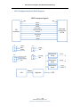
JUMPER CONFIGURATIONS JP2 (PRSNT#) JP3 (IFDET#) COMMENT PCIe 8639 (Enterprise) Pin 2 to Side (Open/Park) Pin 2 to Pin 3 (Ground) SATA Express Pin 1 to Pin 2 (Ground) Pin 1 to Pin 2 (Pulled‐up to 1.8 Vdc) Requires USB Cable and Connection SAS MultiLink Pin 1 to Pin 2 (Ground) Pin 2 to Pin 3 (Ground) No Device Present Pin 2 to Side (Open/Park) Pin 2 to Side (Open/Park) P a g e | 51 ©2014 Wilder Technologies, LLC Document No. 910‐0034‐000 Rev. A (Preliminary) SFF8639 Test Adapter User Manual (Preliminary) 8639 Configuration Board Block Diagram 8639 low speed signals
1
GND
GND
1
B Reset
A Reset
Wake#
Device Reset
Interface Detect#
Present#
TPA connector
Mirrored connections of TPA
Activity/Spin
SMCLK
SMDAT
J3
1
JP1
SMCLK
GND
SMDAT
1
Wake#
GND
JP2
JP3
1
1 5k ohms to 1.8V
Interface Detect#
GND
Present#
GND
Momentary Reset B Reset
Momentary Reset A Reset
Momentary Reset Power
USB
Regulator
+3.3V
P a g e | 52 ©2014 Wilder Technologies, LLC Document No. 910‐0034‐000 Rev. A (Preliminary) Device
Reset
SFF8639 Test Adapter User Manual (Preliminary) Index +12V, 3 +3.3V, 3 +5V, 3 1.8Vdc Pull‐up on IFDET#, 41 10‐Position Low‐Speed Connector, 18 16‐Position Alternate Connector, 3, 4, 13 4‐Position Power Connector, 3, 4, 13 8639 Configuration Board, 23, 39 8639 Configuration Board Block Diagram, 52 8639 Configuration Board Jumper Positions, 51 8639 Plug & Receptacle TPA Testing a 8639 Cable, 11 8639 Plug TPA Testing a Host, 10 8639 Receptacle TPA Testing a 8639 Device, 10 8639‐TPA‐P Cable Pinout, 18 8639‐TPA‐R Accessories, 34 8639‐TPA‐R Cable Pinout, 13 Addendum A – Specific Configuration TPAs, 39 Addendum B – 8639 Configuration Board Reference Information, 51 Cable Bend Limits, 6 Cable Tension (Pull Forces), 6 Cable Twisting (Torque), 6 Calibration Through De‐Embedding, 12 Care and Handling, 6 Cleaning, 8 Compliance WEEE, 37 Connections 8639‐TPA to DUT, 6 SMA, 6, 7 Crosstalk Errors, 12 Directivity Errors, 12 Disk Support Adapter, 34 Drift Errors, 12 DUT, 12 Electrical Specifications, 24 Electrostatic Discharge Information (ESD), 9 Environmental Changes, 12 Errors Crosstalk, 12 Directivity, 12 Drift, 12 Load Impedance Mismatching, 12 Random, 12 Receiver Reflection‐tracking in Test Equipment, 12 Receiver Transmission in Test Equipment, 12 Source Impedance Mismatching, 12 ESD protection, 9 Figures 8639 Configuration Board, 23, 51 8639PE‐TPA‐P Test Adapter and 8639 Configuration Board, 39 8639PE‐TPA‐R PCIe Specific Test Adapter, 40 8639SA‐TPA‐P Test Adapter and 8639 Configuration Board, 41 8639SA‐TPA‐R SATA Express Specific TPA, 42 8639SX4‐TPA‐P Test Adapter and 8639 Configuration Board, 43 8639SX4‐TPA‐R SAS MultiLink Specific TPA, 44 Cable Connectors, 13, 18 Disk Support Adapter, 34 The 8639 Test Adapter (Plug), 3 The 8639 Test Adapter (Receptacle), 4 Glossary, 38 GND, 3 Handling and Storage, 8 Jumper Positions, 8639 Config. Board, 39, 41, 43 Load Impedance Mismatching Errors, 12 Making Connections, 8 Mechanical and Environmental Specifications, 13 Molex Part Numbers, 4 Product Inspection, 5 Product Return, 5 Pull Force, 6, 7 Random Errors, 12 Receiver Reflection‐Tracking in Test Equip. Errors, 12 Receiver Transmission in Test Equipment Errors, 12 Receptacle Accessories, 34 Secure Storage, 5 SFF‐8639 Specification, 3, 10 SMA cables, 13, 18 Source Impedance Mismatching Errors, 12 Specific Configuration TPAs, PCI Express, 39 Specific Configuration TPAs, SAS MultiLink, 43 Specific Configuration TPAs, SATA Express, 41 Support, 12, 36 Supporting Instrument Cables or Accessories, 7 Tables 8639 Configuration Board Jumper Positions, 51 8639 Plug Pin Assignments, 20, 21, 22 8639 Receptacle Pin Assignments, 15, 16, 17 8639‐TPA‐R 10‐Position Low‐Speed Connector, 19 8639‐TPA‐R 16‐Position Alternate Connector, 14 8639‐TPA‐R 4‐Position Power Connector, 14 Electrical Specifications, 24 General Specifications, 13 TPA‐P Specific Config. Pin Assignments, 45, 46, 47 TPA‐R Specific Config. Pin Assignments, 48, 49, 50 Terms and Conditions of Sale, 36 Test Instrument Noise, 12 Test Repeatability Problems, 12 USB Type A to Type B Cable, 41 User Model Examples, 10, 11 Visual Inspection, 8 Warranty, 35 Web Sites support@wilder‐tech.com, 35, 36 www.egmetalrecycling.com, 37 www.wilder‐tech.com, 35 WEEE, 37 P a g e | 53 ©2014 Wilder Technologies, LLC Document No. 910‐0034‐000 Rev. A (Preliminary) Visit our website at www.wilder‐tech.com Wilder Technologies, LLC 6101A East 18th Street Vancouver, WA 98661 Phone: 360‐859‐3041 Fax: 360‐859‐3105 www.wilder‐tech.com ©2014 Wilder Technologies, LLC Document No. 910‐0034‐000 Rev. A (Preliminary) Created: 4/25/2014 Updated: 8/13/2014