1
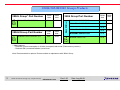
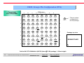
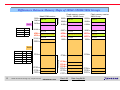
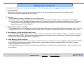
8 -bit MICROCOMPUTER 38000 Series - Differences Between The 3804L Group/3804H Group/3804 Group - ©2008. Renesas Technology Corp., All rights reserved. REJ99B2001-0100 3804L/3804H/3804Groups GroupsProducts Products 3804L/3804H/3804 60 K 2048 3804H Group Part Number ROM size RAM size 60 K 2048 M38049FFHSP/FP/HP/KP (Note) ROM size RAM size M38044M4-XXXSP/FP/HP 16 K 640 M38047M6-XXXSP/FP/HP 24 K 1024 M38047M8-XXXSP/FP/HP 32 K M38049MC-XXXSP/FP/HP 48 K M38049MF-XXXSP/FP/HP 60 K M38049FFSP/FP/HP (Note) 60 K 3804 Group Part Number Mask ROM ver. RAM size Flash Memory ver. M38049FFLSP/HP/KP/WG ROM size Flash Memory ver. Flash Memory ver. 3804L Group* Part Number * 3804L features - Reduced current consumption in 32 kHz (low-speed) wait mode (Flash memory version) - Reduced EMI (unwanted radiation) noise level Note: Recommended to replace. Please consider a replacement with 3804L Group. 2 ©2008. Renesas Technology Corp., All rights reserved. REJ99B2001-0100 Rev.1.00 Date: Aug.04.08 2048 3804L/3804H/3804Groups GroupsPin PinConfiguration Configuration(SP) (SP) 3804L/3804H/3804 Completely Completely PinCompatible Compatible Pin 1 2 3 4 5 6 7 8 9 10 11 12 13 14 15 16 17 18 19 20 21 22 23 24 25 26 27 28 29 30 31 32 M3804XMX-XXXSP M38049FFHSP M38049FFLSP M38049FFSP VCC VREF AVSS P6 7 /AN7 P6 6 /AN6 P6 5 /AN5 P6 4 /AN4 P6 3 /AN3 P6 2 /AN2 P6 1 /AN1 P6 0 /AN0 P5 7 /INT 3 P5 6 /PWM P5 5 /CNTR 1 P5 4 /CNTR 0 P5 3 /S RDY2 P5 2 /S CLK2 P5 1 /S OUT2 P5 0 /S IN2 P4 7 /S RDY1 /CNTR 2 P4 6 /S CLK1 P4 5 /TX D 1 P4 4 /R X D 1 P4 3 /INT 2 P4 2 /INT 1 VPP CNV SS RESET P4 1 /INT 00 /X CIN P4 0 /INT 40 /X COUT XIN XOUT VSS 64 63 62 61 60 59 58 57 56 55 54 53 52 51 50 49 48 47 46 45 44 43 42 41 40 39 38 37 36 35 34 33 P3 0 /DA1 P3 1 /DA2 P32/SDA P33/SCL P3 4 /R X D 3 P3 5 /TX D3 P3 6 /SCLK3 P3 7 /SRDY3 P0 0 /AN8 P0 1 /AN9 P0 2 /AN10 P0 3 /AN11 P0 4 /AN12 P0 5 /AN13 P0 6 /AN14 P0 7 /AN15 P1 0 /INT 41 P1 1 /INT 01 P1 2 P1 3 P1 4 P1 5 P1 6 P1 7 P2 0 (LED 0 ) P2 1 (LED 1 ) P2 2 (LED 2 ) P2 3 (LED 3 ) P2 4 (LED 4 ) P2 5 (LED 5 ) P2 6 (LED 6 ) P2 7 (LED 7 ) Outline SP: PRDP0064BA-A (64P4B) (1.78mm pitch) 3 ©2008. Renesas Technology Corp., All rights reserved. REJ99B2001-0100 Rev.1.00 Date: Aug.04.08 33 34 35 36 37 39 38 40 42 41 43 44 45 Note: KP for 3804H/3804L Groups only. FP for 3804/3804H Groups only. 32 31 49 50 51 52 53 54 55 56 30 29 28 27 26 25 24 23 22 21 M3804XMX-XXXFP/HP M38049FFHFP/HP/KP M38049FFLHP/KP M38049FFFP/HP 57 58 59 60 61 62 63 64 16 14 15 13 12 11 9 10 8 7 P20(LED0) P21(LED1) P22(LED2) P23(LED3) P24(LED4) P25(LED5) P26(LED6) P27(LED7) VSS XOUT XIN P40/INT40/XCOUT P41/INT00/XCIN RESET CNVSS VPP P42/INT1 P54/CNTR0 P53/SRDY2 P52/SCLK2 P51/SOUT2 P50/SIN2 P47/SRDY1/CNTR2 P46/SCLK1 P45/TXD1 P44/RXD1 P42/INT2 6 5 4 3 P62/AN2 P61/AN1 P60/AN0 P57/INT3 P56/PWM P55/CNTR1 2 20 19 18 17 1 P37/SRDY3 P36/SCLK3 P35/TXD3 P34/RXD3 SCL/P33 SDA/P32 P31/DA2 P30/DA1 VCC VREF AVSS P67/AN7 P66/AN6 P65/AN5 P64/AN4 P63/AN3 47 48 Completely Completely PinCompatible Compatible Pin 46 P00/AN8 P01/AN9 P02/AN10 P03/AN11 P04/AN12 P05/AN13 P06/AN14 P07/AN15 P10/INT41 P11/INT01 P12 P13 P14 P15 P16 P17 3804L/3804H/3804Groups GroupsPin PinConfiguration Configuration(FP/HP/KP) (FP/HP/KP) 3804L/3804H/3804 Outline KP :PLQP0064GA-A (64P6U-A) (0.8mm pitch, 14mm square, 1.7mm mounting height) FP : PRQP0064GA-A (64P6N-A) (0.8mm pitch, 14mm square, 3.05mm mounting height) HP : PLQP0064KB-A (64P6Q-A) (0.5mm pitch, 10mm square, 1.7mm mounting height) 4 ©2008. Renesas Technology Corp., All rights reserved. REJ99B2001-0100 Rev.1.00 Date: Aug.04.08 3804LGroups GroupsPin PinConfiguration Configuration(WG) (WG) 3804L Completely Completely PinCompatible Compatible Pin (TOP view) A 8 50 P36/SCLK3 7 51 P35/TxD3 6 5 4 3 46 44 D E 41 P02/AN10 P04/AN12 P07/AN15 F G H 40 32 31 30 P10/INT41 P25(LED0) P21(LED1) P22(LED2) 47 45 42 39 27 29 28 P01/AN9 P03/AN11 P06/AN14 P11/INT01 P25(LED5) P23(LED3) P24(LED4) 53 52 48 43 38 37 26 25 P34/RxD3 P00/AN8 P05/AN13 P12 P13 P26(LED6) P27(LED7) 56 55 54 49 33 36 35 34 P30/DA1 P31/DA2 P32/SDA P37/SRDY3 P17 P14 P15 P16 1 64 58 59 57 24 22 23 P62/AN2 P63/AN3 VREF AVss VCC VSS XIN 4 7 12 14 21 60 62 P65/AN5 1 C P33/SCL P67/AN7 2 B 2 P61/AN1 A 61 P66/AN6 P57/INT3 P54/CNTR0 63 5 P64/AN4 8 10 6 9 P60/AN0 P55/CNTR1 P52/SCLK2 C D 30 7 P22(LED2) 6 5 4 XOUT 20 ©2008. Renesas Technology Corp., All rights reserved. REJ99B2001-0100 Package top view 3 P41/INT40/XCIN 13 17 19 P42/INT1 RESET 11 15 16 18 P50/SIN2 P44/RxD1 P43/INT2 CNVSS E F G 2 1 H Outline WG: PTLG0064JA-A (64F0G) (6mm FLGA package, 1.05mm height) 5 The pin number corresponds to the flat package. P40/INT40/XCOUT P56/PWM P53/SRDY2 P51/SOUT2 P46/SCLK1 3 B P47/SRDY1/CNTR2 P45/TxD1 8 Rev.1.00 Date: Aug.04.08 M38049FFLWG DifferencesBetween Between3804L/3804H/3804 3804L/3804H/3804Groups Groups Differences 3804L Group 3804H Group 3804 Group Flash Memory ver. Flash Memory ver. Mask ROM ver. Flash Memory ver. Program Memory Flash memory Flash memory Mask ROM Flash memory Program Memory/RAM size 60K/2K 60K/2K 16K/640, 24K/1K, 32K/1K, 48K/2K, 60K/2K 60K/2K Package SP, HP, KP, WG SP, FP, HP, KP SP, FP, HP SP, FP, HP Operating Power Source Voltage 2.7 to 5.5 V 2.7 to 5.5V 2.7 to 5.5 V 4.0 to 5.5V Flash Memory ID Code Addresses FFD4 to FFDAh Addresses FFD4 to FFDAh – – Flash Memory ROM Code Protect Address FFDBh Address FFDBh – – Flash Memory Control Register Flash Memory control registers 0 to 2 Addresses 0FE0h to 0FE2h Flash Memory control registers 0 to 2 Addresses 0FE0h to 0FE2h – Flash Memory control register Address 0FFEh Flash command register Address 0FFFh Program/Erase Power Source Single power source (Vcc = 2.7 to 5.5 V) Single power source (Vcc = 2.7 to 5.5 V) – Dual power source (Vcc = 5 V ± 0.5 V, Vpp = 11.7 to 12.6 V) Program/Erase Mode CPU Rewrite Mode Parallel I/O Mode Standard serial I/O Mode CPU Rewrite Mode Parallel I/O Mode Standard serial I/O Mode – CPU Rewrite Mode Parallel I/O Mode Standard serial I/O Mode Time until Flash Memory can Operate after Returning from Stop Mode Needed: 100 μsec Needed: 100 μsec Not needed Not needed Needed Not needed Not needed Power Source Circuit Characteristics Needed Internal Power Source Stable Time at Power-on : td (P-R) Electrical Characteristics Recommended Operating Conditions 6 The power source current of the Flash memory version differs between the Groups. Also, the operating conditions differs according to different operating voltages. For details, refer to the corresponding datasheet. ©2008. Renesas Technology Corp., All rights reserved. REJ99B2001-0100 Rev.1.00 Date: Aug.04.08 Improvementin in3804L(H)/3804 3804L(H)/3804Groups GroupsOperating OperatingFrequency FrequencyCharacteristics Characteristics Improvement Flash memory version Mask version f(Xin) f(Xin) High-speed mode High-speed mode 16.8 MHz 16.8 MHz 12.5 MHz 12.5 MHz 8.4 MHz 8.4 MHz 3804 Group 2.7 V f(Xin) 4.0 V 4.5 V 5.5 V Middle-speed mode f(Xin) 16.8 MHz 12.5 MHz 12.5 MHz 3804 Group 7 ©2008. Renesas Technology Corp., All rights reserved. REJ99B2001-0100 Vcc Middle-speed mode Vcc Rev.1.00 3804 Group 4.0 V 4.5 V 5.5 V 3804L Group 3804H Group 8.4 MHz 4.0 V 4.5 V 5.5 V 2.7 V Vcc 16.8 MHz 2.7 V 3804L Group 3804H Group 2.7 V Date: Aug.04.08 3804 Group 4.0 V 4.5 V 5.5 V Vcc DifferencesBetween BetweenMemory MemoryMaps Mapsof of3804L/3804H/3804 3804L/3804H/3804Groups Groups Differences Flash memory version 3804L, 3804H Group SFR area 004016 RAM RAM size XXXX 640 02BF 1024 043F 2048 083F 010016 Zero page Mask ROM version 000016 XXXX16 0FE016 SFR (incl. Reservation) 0FF616 ZZZZ16 000016 SFR area 004016 010016 010016 Not used Reserved ROM area 083F16 Not used 0FE016 SFR (incl. Reservation) 0FF616 0FF016 SFR area 0FFF16 100016 100016 ZZZZ16 ZZZZ16 FF0016 FF0016 Not used Not used YYYY16 000016 SFR area 004016 083F16 Not used Flash memory version 3804 Group Not used ROM ROM size YYYY ZZZZ C000 C080 24576 A000 A080 32768 8000 8080 49152 4000 4080 61440 1000 1080 FF0016 FFD416 FFDA16 FFDB16 FFDC16 Interrupt vector area FFFE16 Reserved ROM area FFFF16 8 ©2008. Renesas Technology Corp., All rights reserved. REJ99B2001-0100 Special page 16384 FFD416 FFD416 ID code FFDA16 FFDB16 Protect address FFDC16 Interrupt vector area FFFE16 Reserved ROM area FFFF16 Rev.1.00 FFDA16 FFDB16 FFDC16 Interrupt vector area FFFE16 Reserved ROM area FFFF16 Date: Aug.04.08 ReplacementNotes Notes(1) (1) Replacement According to the differences in the specifications shown in P.6, the following notes are suggested. Please also refer to P.6. 1. Program Memory Depending on the memory type, program/erase specifications as well as applicable programmers and adaptors differ. Confirm the programmer applicable for your product. 2. Packages - The WG-package product is available only in the 3804L Group. - In the 3804L Group, the FP package product is not available, but the thin KP package product is available for 0.8 mm-pitch. As a 0.8 mm-pitch, the KP package has better excellence in thinness, heat radiation, and stress characteristics than FP package. Confirm the mounting pad design standards of FP package and KP package on Renesas Surface Mount Package User's Manual (Document No.: REJ11K0001) 3. Operating Power Source Voltage - The operating power source voltage for the 3804 Group Mask ROM version and the 3804H/3804L Groups ranges from 2.7 to 5.5V. It ranges from 4.0 to 5.5 V for 3804 Group Flash memory version. Confirm the operating power source voltage for your product. 4. Flash Memory ID Code and ROM Code Protect In the 3804H/3804L Groups Flash memory version, ID codes are assigned to addresses FFD4 to FFDA16, and ROM code protect is assigned to address FFDB16. Please note that these addresses are included in the user ROM area. The data of these addresses must be set to programming data before programming. 5. Flash Memory Control Registers - In the 3804H/3804L Group Flash memory version, Flash Memory control registers 0 to 2 are assigned to addresses 0FE0 to 0FE216. - In the 3804 Group Flash memory version, Flash Memory control register is assigned to address 0FFE16 and Flash command register is assigned to address 0FFF16. - In the Mask ROM versions, nothing is allocated to these addresses, so writing can be performed to them. When read, their values are undefined. 9 ©2008. Renesas Technology Corp., All rights reserved. REJ99B2001-0100 Rev.1.00 Date: Aug.04.08 ReplacementNotes Notes(2) (2) Replacement 6. Program/Erase Power Source, Program/Erase Mode The program/erase power source voltage as well as the absolute maximum ratings of the pins differ between 3804 Group Flash memory version and 3804H/3804L Groups. Further more, the program specification (pin used, program algorithm, etc) differs, too. Make sure to connect the specified programmer with your product to prevent a voltage that exceeds the ratings from being applied to the pins. 7. Stop Mode In the 3804H and 3804 L Groups, waiting time (more than 100 μsec) until Flash memory can operate after returning from stop mode is necessary. Use oscillation stabilization time setting function after the STP instruction is released to set it. 8. Internal Power Source Stable Time at Power-on In the 3804H and 3804 L Groups, internal power source stable time at power-on (td (P-R): max. 2msec) is necessary. Set Vcc to more than 2.7 V and reset input “L” to td(P-R) + XIN16 cycles or more. 9. Oscillation Circuit Constants The oscillation circuit structure differs between the 3804, 3804H, and 3804L Groups. The XIN-XOUT and XCIN-XCOUT oscillation circuit constants differ from product to product. Contact the oscillator manufacturer to select an appropriate oscillator and oscillation circuit constants so that the product used for mass production will obtain an stable operating clock with your system and conditions. Additional consideration is required when the voltage range or the temperature range is wide. Also, we recommend considering the wiring patterns of the feedback resistors, the damping resistors, and the load capacity beforehand when designing circuits. 10. Differences between Mask ROM and Flash Memory Versions The Flash memory and Mask ROM versions differ in their manufacturing processes and mask patterns because of the different ROM types used. Because of these differences, characteristics values, operation margins, noise immunity, noise radiation, and oscillation circuit constants may vary. When developing application products, perform careful system evaluations for each product. Additional care is required when replacing products (for example, replacing a Mask ROM version with a Flash memory version). Careful system evaluations should be performed with replacement products before the mass production phase of application products. 10 ©2008. Renesas Technology Corp., All rights reserved. REJ99B2001-0100 Rev.1.00 Date: Aug.04.08 Programchange changeatatreplacing replacing Program Details about a program are described as follows regarding whether the same program can be used without change when replacing between standards, Spec. H and Spec. L of the 3804 Group. Please make sure to check there are some differences of memory size in every product. Refer to the datasheets and technical updates of the 3804 Group for detailed specifications of products. Confirm the operation using replaced product. Note: Program checksum When calculating the checksum of ROM area by a program, make sure to check the difference of areas for calculation. When the unused area and reserved ROM area are included in target areas of replaced products, the read values are undefined and calculated values of the checksum are also undefined. (1) Standard flash memory version Æ Spec. L flash memory version 1. When using the addresses FFD4h to FFDAh, check the followings: The codes written in these addresses are the ID codes of the Spec. L flash memory version when using a serial programmer. To input this code is necessary as the ID code for flash memory reprogramming by a serial programmer. Check the above only when using a serial programmer because the addresses can be executed as an instruction. 2. The bits 7 to 2 of the address FFDBh are the protect set bits of the Spec. L flash memory version when using a parallel programmer. When the set condition is not unexpected, to change a program is necessary. Since the protect set bits do not affect when using a serial programmer, there is no problem. This address can be executed as an instruction same as the addresses FFD4h to FFDAh. 3. When accessing the addresses 0FE0h to 0FEFh, to change a program not to access these addresses is necessary. 4. Nothing is assigned on the addresses 0FFEh and 0FFFh of Spec. L flash memory version. To change a program is not necessary even if programming in standard flash memory version is performed. 5. To change a program is necessary when the oscillation stabilization time after the STP instruction is released is less than 100 μ sec in stop mode. Set 100 μ sec or more by the oscillation stabilization time setting function after the STP instruction which uses timer 1 is released. 6. When using CPU rewrite mode, to change general processes regarding CPU rewrite mode is necessary. (2) Spec. H flash memory version Æ Spec. L flash memory version To change a program is not necessary. 11 ©2008. Renesas Technology Corp., All rights reserved. REJ99B2001-0100 Rev.1.00 Date: Aug.04.08 Reference:M38049FF M38049FFand and M38049FFH M38049FFH(L) (L)Serial SerialRewriting RewritingCircuit Circuit Reference: whenUsing UsingaaSuisei SuiseiElectronics ElectronicsSystem SystemSerial SerialUnit Unit when The pin number indicates the flat package version. M38049FF (Standard serial I/O Mode 1) (Standard serial I/O Mode) T_VDD T_TXD *1 T_RXD T_SCLK T_PGM/OE/MD T_BUSY *3 57 15 13 49 12 N.C. 14 T_VPP M38049FFH M38049FFL Differences Note: 18 Vcc T_VDD SDA (P44/RXD1) T_TXD SCLK (P46/SCLK1) T_SCLK OE (P37/SRDY3) *2 T_BUSY BUSY (P47/SRDY1 /CNTR2) T_RXD TXD (P45/TXD1) VPP (CNVSS) T_PGM/OE/MD 57 15 13 12 Vcc RXD (P44/RXD1) SCLK (P46/SCLK1) BUSY (P47/SRDY1/CNTR2) 14 TXD (P45/TXD1) 18 CNVSS Note: T_VPP is not needed. T_RESET 19 USER RST 24 GND T_RESET RESET(RESET) Vss USER RST GND XIN XOUT Perform the same pin processing as in single chip mode. 19 24 RESET(RESET) Vss XIN XOUT Perform the same pin processing as in single chip mode. z As programming specifications differ for each product, specify the part number before programming. z As the MCU programming pins are common, writing can be performed on the same board in the QzROM/Flash memory versions. *1: For the standard version, connect both the serial unit’s T_TXD and T_RXD to SDA (RxD pin), and leave TxD pin open. *2: Supply the power source voltage (Vcc) from the user so that it will meet the Vcc of the output buffer used on the programmer. *3: The VDD power source is supplied from the programmer. When the user power consumption is high (20 mA or more for other than the MCU), supply the VDD from the user. 12 ©2008. Renesas Technology Corp., All rights reserved. REJ99B2001-0100 Rev.1.00 Date: Aug.04.08 Renesas Renesas 3804L/3804H/3804Groups GroupsDevelopment DevelopmentSupport SupportTools Tools 3804L/3804H/3804 Except programmers and on-chip debugging emulators, development support tools are common to the Groups. Development Support Tool Part Number Assembler package M3T-SRA74 (Simulator debugger incl. Integrated Development Environment with HEW) M3T-ICC740 (Simulator debugger incl. Integrated Development Environment with HEW) Compiler Package Simulator Debugger M3T-SRA74, M3T-ICC740 or M3T-PD38SIM accessory (discontinued) On-chip Debugging Emulator (3804L Group) E8a (incl. HEW, 740 E8a emulator debugger, M3T-SRA74 free evaluation version, M3T-ICC740 free evaluation version, FDT free evaluation version, and more) M38000T2-CPE (incl. 740 Compact emulator debugger, M3T-ICC740 (with HEW), and M3T-SRA74 (with HEW) ) Compact Emulator System Compact Emulator Emulator MCU PC4701 Emulator System (Discontinued Product) Accessory M38049RLSS Emulator Debugger 740 PC4701 emulator debugger or M3T-PD38 (discontinued) Emulator PC4701U (emulator debugger license bundled) Emulation Pod M38000TL2-FPD (low voltage operation supported) (discontinued) Emulator MCU M38049RLSS Package Converter (Refer to the next page) Pin processing board 13 ©2008. Renesas Technology Corp., All rights reserved. REJ99B2001-0100 M38007T-ADS (pin processing board for Emulator MCU) Rev.1.00 Date: Aug.04.08 ConnectingEmulator Emulatorand andTarget TargetSystem System Connecting Compact emulator system PC4701 System (discontinued) Emulation Pod M38000TL2-FPD (discontinued) Compact emulator M38000T-CPE *Emulator Pod Probe type 30-pin narrow pitch connector x 1 M3T-28DP-WS *1 *1. This converter is included in Emulator Pod Package. *2. These 3 parts are as one set. *3. These 4 parts are as one set. *4. Available from Tokyo Eletech Corporation. * The z mark indicates the location of No.1 pin. M3T-28DP-WT RSS type emulator MCU M38049RLSS FP/KP package boardmounted evaluation M38007T-PRB M3T-64LCC-QSD YQSOCKET064SDF2 64-pin SDIP socket (SP package) (Sold Separately) *4 YQPACK064SD (Sold Separately) HP package sample Board-mounted evaluation ©2008. Renesas Technology Corp., All rights reserved. FP package : HQPACK064SA (Sold Separately) *4 KP package : HQPACK064SA160 (Sold Separately) *4 HQPACK064SD (Sold Separately) *4 *2 *3 HP package version *4 M3T-64LCC-QSD 64-pin 0.5 mm pitch QFP NQPACK064SD-ND (Sold Separately) *4 (HP package) 64-pin 0.5 mm pitch QFP (HP package) 14 M3T-64DIP-DMS REJ99B2001-0100 FP/KP package version M3T-DUMMY64 M3T-FLX-64NSA 64-pin 0.8 mm pitch QFP 64pin (FP package) 0.8 mm pitch QFP/LQFP (FP/KP package) Rev.1.00 Date: Aug.04.08 3804H/3804LGroups Groups 3804H/3804L SuiseiElectronics ElectronicsSystem SystemFlash FlashMemory MemoryProgrammers Programmers Suisei Main unit Serial/Parallel Unit On-board reprogramming Off-board reprogramming M38049FFH M38049FFL Flash memory version (Serial programming) EFP-S2V EFP-S2 in common M38049FFH M38049FFL Flash memory version (Parallel programming) EF1SRP-01US2 EF1CNT-96P + Parallel unit EF3803F-64H (for HP) EF3803F-64F (for FP) EF3803F-64U (for KP) EF3803F-64S (for SP) EF3803F-64FL (for WG) EF1CNT-96P + EF1SRP-01U EFP-I EF1SRP-01U Parallel unit EF3803F-64H (for HP) EF3803F-64F (for FP) EF3803F-64U (for KP) EF3803F-64S (for SP) EF3803F-64FL (for WG) EF1CNT-96P: Connector converter unit Each unit for EFP-I can be connected to EFP-S2 or EFP-S2V by EF1CNT-96P. As a Renesas Flash memory/QzROM programmer, the Flash Development Toolkit (FDT) and the E8 can be used together for on-board programming. (IC socket boards are required for the QzROM on-board programming.) 15 ©2008. Renesas Technology Corp., All rights reserved. REJ99B2001-0100 Rev.1.00 Date: Aug.04.08 3804Group GroupProgrammers Programmers 3804 Tools 3804 Group Products RENESAS Programming Adapter PCA4738HF-64 (for 0.5 mm-pitch LQFP package) PCA4738FF-64 (for 0.8 mm-pitch QFP package) PCA4738SF-64 (for 1.778 mm-pitch SDIP package) EFP-I for Serial Interface Available from Suisei Electronics System Co., Ltd. R4945, R4945A for Parallel Interface Available from ADVANTEST Corp. (RENESAS Programming Adapter required) AF9709, AF9708, AF9723 for Standard Parallel Interface Available from Flash Support Group, Inc. (RENESAS Programming Adapter required) Flash Memory Programmer 16 ©2008. Renesas Technology Corp., All rights reserved. REJ99B2001-0100 Rev.1.00 Date: Aug.04.08 REVISION HISTORY 17 Rev. Date 1.00 Aug. 04, 2008 Page ©2008. Renesas Technology Corp., All rights reserved. Summary First edition issued REJ99B2001-0100 Rev.1.00 Date: Aug.04.08 ©2008. Renesas Technology Corp., All rights reserved. To our customers, Old Company Name in Catalogs and Other Documents On April 1st, 2010, NEC Electronics Corporation merged with Renesas Technology Corporation, and Renesas Electronics Corporation took over all the business of both companies. Therefore, although the old company name remains in this document, it is a valid Renesas Electronics document. We appreciate your understanding. Renesas Electronics website: http://www.renesas.com April 1st, 2010 Renesas Electronics Corporation Issued by: Renesas Electronics Corporation (http://www.renesas.com) Send any inquiries to http://www.renesas.com/inquiry. Notice 1. 2. 3. 4. 5. 6. 7. All information included in this document is current as of the date this document is issued. Such information, however, is subject to change without any prior notice. Before purchasing or using any Renesas Electronics products listed herein, please confirm the latest product information with a Renesas Electronics sales office. Also, please pay regular and careful attention to additional and different information to be disclosed by Renesas Electronics such as that disclosed through our website. Renesas Electronics does not assume any liability for infringement of patents, copyrights, or other intellectual property rights of third parties by or arising from the use of Renesas Electronics products or technical information described in this document. No license, express, implied or otherwise, is granted hereby under any patents, copyrights or other intellectual property rights of Renesas Electronics or others. You should not alter, modify, copy, or otherwise misappropriate any Renesas Electronics product, whether in whole or in part. Descriptions of circuits, software and other related information in this document are provided only to illustrate the operation of semiconductor products and application examples. You are fully responsible for the incorporation of these circuits, software, and information in the design of your equipment. Renesas Electronics assumes no responsibility for any losses incurred by you or third parties arising from the use of these circuits, software, or information. When exporting the products or technology described in this document, you should comply with the applicable export control laws and regulations and follow the procedures required by such laws and regulations. You should not use Renesas Electronics products or the technology described in this document for any purpose relating to military applications or use by the military, including but not limited to the development of weapons of mass destruction. Renesas Electronics products and technology may not be used for or incorporated into any products or systems whose manufacture, use, or sale is prohibited under any applicable domestic or foreign laws or regulations. Renesas Electronics has used reasonable care in preparing the information included in this document, but Renesas Electronics does not warrant that such information is error free. Renesas Electronics assumes no liability whatsoever for any damages incurred by you resulting from errors in or omissions from the information included herein. Renesas Electronics products are classified according to the following three quality grades: “Standard”, “High Quality”, and “Specific”. The recommended applications for each Renesas Electronics product depends on the product’s quality grade, as indicated below. You must check the quality grade of each Renesas Electronics product before using it in a particular application. You may not use any Renesas Electronics product for any application categorized as “Specific” without the prior written consent of Renesas Electronics. Further, you may not use any Renesas Electronics product for any application for which it is not intended without the prior written consent of Renesas Electronics. Renesas Electronics shall not be in any way liable for any damages or losses incurred by you or third parties arising from the use of any Renesas Electronics product for an application categorized as “Specific” or for which the product is not intended where you have failed to obtain the prior written consent of Renesas Electronics. The quality grade of each Renesas Electronics product is “Standard” unless otherwise expressly specified in a Renesas Electronics data sheets or data books, etc. “Standard”: 8. 9. 10. 11. 12. Computers; office equipment; communications equipment; test and measurement equipment; audio and visual equipment; home electronic appliances; machine tools; personal electronic equipment; and industrial robots. “High Quality”: Transportation equipment (automobiles, trains, ships, etc.); traffic control systems; anti-disaster systems; anticrime systems; safety equipment; and medical equipment not specifically designed for life support. “Specific”: Aircraft; aerospace equipment; submersible repeaters; nuclear reactor control systems; medical equipment or systems for life support (e.g. artificial life support devices or systems), surgical implantations, or healthcare intervention (e.g. excision, etc.), and any other applications or purposes that pose a direct threat to human life. You should use the Renesas Electronics products described in this document within the range specified by Renesas Electronics, especially with respect to the maximum rating, operating supply voltage range, movement power voltage range, heat radiation characteristics, installation and other product characteristics. Renesas Electronics shall have no liability for malfunctions or damages arising out of the use of Renesas Electronics products beyond such specified ranges. Although Renesas Electronics endeavors to improve the quality and reliability of its products, semiconductor products have specific characteristics such as the occurrence of failure at a certain rate and malfunctions under certain use conditions. Further, Renesas Electronics products are not subject to radiation resistance design. Please be sure to implement safety measures to guard them against the possibility of physical injury, and injury or damage caused by fire in the event of the failure of a Renesas Electronics product, such as safety design for hardware and software including but not limited to redundancy, fire control and malfunction prevention, appropriate treatment for aging degradation or any other appropriate measures. Because the evaluation of microcomputer software alone is very difficult, please evaluate the safety of the final products or system manufactured by you. Please contact a Renesas Electronics sales office for details as to environmental matters such as the environmental compatibility of each Renesas Electronics product. Please use Renesas Electronics products in compliance with all applicable laws and regulations that regulate the inclusion or use of controlled substances, including without limitation, the EU RoHS Directive. Renesas Electronics assumes no liability for damages or losses occurring as a result of your noncompliance with applicable laws and regulations. This document may not be reproduced or duplicated, in any form, in whole or in part, without prior written consent of Renesas Electronics. Please contact a Renesas Electronics sales office if you have any questions regarding the information contained in this document or Renesas Electronics products, or if you have any other inquiries. (Note 1) “Renesas Electronics” as used in this document means Renesas Electronics Corporation and also includes its majorityowned subsidiaries. (Note 2) “Renesas Electronics product(s)” means any product developed or manufactured by or for Renesas Electronics.