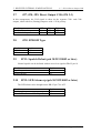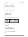
1
Eclipse Series
RF Technology
[email protected]
May, 2005
R70/R71 and R150 Receiver
Operation and Maintenance Manual
This manual is produced by RF Technology Pty Ltd.,
10/8 Leighton Place, Hornsby, 2077, Australia
Copyright © 1997 RF Technology
CONTENTS
CONTENTS
Contents
1
Operating Instructions
1.1 Front Panel Controls and Indicators
1.1.1
Mon. Volume
1.1.2
Mon. Sq.
1.1.3
N. SQ
1.1.4
C. SQ
1.1.5
Line
1.1.6
PWR LED
1.1.7
SQ LED
1.1.8
Alarm LED
4
4
4
4
5
5
5
5
5
6
2
Receiver Internal Jumper Options
2.1 JP1: 240Hz Notch Filter
2.2 JP2: Audio Response
2.3 JP3: Audio Filter In/Out
2.4 JP4: 600Ω Line dc Loop COS
2.5 JP6: COS Polarity
2.6 JP7/8/9: dc Loop COS Configuration
2.7 JP7, JP8, JP9: Direct Output COS
2.8 JP11 EPROM Type
2.9 JP13: Squelch Defeat (pcb 30/9132/0002 or later)
2.10 JP19: LED Alarm output (pcb 30/9132/0002 or later)
6
6
7
7
7
7
7
8
8
9
9
3
Receiver I/O Connections
3.1 25 Pin Connector
10
10
4
Channel and Tone Frequency Programming
11
5
Circuit Description
5.1 RF Section
5.2 IF Section
5.3 VCO Section
5.4 PLL Section
5.5 Audio Signal Processing
5.6 Noise Filter, Amplifier and Detector
5.7 Subtone Filter and CTCSS
5.8 External Squelch
5.9 Microprocessor Controller
5.10 Carrier Operated Switch
5.11 Voltage Regulator
11
11
11
12
12
13
13
13
14
14
14
15
6
Alignment Procedure
6.1 Standard Input Signal
6.2 RF Alignment
6.3 IF Alignment
6.4 Line Level Adjustment
6.5 Reference Oscillator Calibration
15
15
16
17
17
17
Page 2
RF Technology R350/R500
CONTENTS
7
B
CONTENTS
Specifications
7.1 General Description
7.1.1
Channel Capacity
7.1.2
CTCSS
7.1.3
Channel Programming
7.1.4
Channel Selection
7.1.5
Micropressor
17
17
17
17
17
18
18
7.2
Physical Configuration
18
7.3
Front Panel Controls, Indicators and Test Points
7.3.1
Controls
7.3.2
Indicators
7.3.3
Test Points
18
18
18
19
7.4
Electrical Specifications
7.4.1
Power Requirements
7.4.2
Frequency Range and Channel Spacing
7.4.3
Frequency Synthesizer Step Size
7.4.4
Frequency Stability
7.4.5
Nominal Antenna Impedance
7.4.6
IF Frequencies
7.4.7
Sensitivity
7.4.8
Selectivity
7.4.9
Spurious and Image Rejection
7.4.10
Inter-modulation
7.4.11
Modulation Acceptance BW
7.4.12
Noise Squelch
7.4.13
Carrier Level Squelch
7.4.14
Receiver Frequency Spread
7.4.15
Receiver Conducted Spurious Emissions
7.4.16
Audio Frequency Response
7.4.17
Audio Output Level
7.4.18
Audio Distortion
7.4.19
Channel Select Input/Output
7.4.20
Carrier Operated Switch Output
7.4.21
CTCSS
7.4.22
External Squelch Input
19
19
19
19
19
19
20
20
20
20
20
20
20
21
21
21
21
21
21
22
22
22
24
7.5
Connectors
7.5.1
Antenna Connector
7.5.2
Power and I/O Connector
7.5.3
Test Connector
24
24
24
24
Parts List
RF Technology R70/R71 and R150
27
Page 3
1
OPERATING INSTRUCTIONS
WARNING
Changes or modifications not expressly approved
by RF Technology could void your authority to
operate this equipment. Specifications may vary
from those given in this document in accordance
with requirements of local authorities. RF
Technology equipment is subject to continual
improvement and RF Technology reserves the right
to change performance and specification without
further notice.
1
Operating Instructions
1.1
Front Panel Controls and Indicators
1.1.1
Mon. Volume
The Mon. Volume control is used to adjust the volume of the internal loudspeaker
and any external speaker connected to the test socket. It does not effect the level of
the 600Ω line or direct audio output.
1.1.2
Mon. SQ.
The Mon. SQ. switch allows all squelch functions controlling the monitor output to
be disabled. When the switch is in the Mon. SQ. position the audio at the monitor
speaker is controlled by the noise detector. The CTCSS, carrier and external squelch
functions are disabled. This can be useful when you are trying to trace the source of
on-channel interference or when setting the noise squelch threshold. The audio from
the 600Ω line and direct outputs is not effected by the switch position.
1.1.3
N.SQ
The N.SQ trimpot is used to set the noise squelch sensitivity.
procedure to set the noise squelch to maximum sensitivity.
1.
Use the following
Set the toggle switch to the Mon. Sq. position and set the Mon. Volume control
to 9 o’clock.
Page 4
RF Technology R350/R500
1.1 OPERATING INSTRUCTIONS
1.1
Front Panel Controls and Indicators
2.
Turn the N. SQ. adjustment counter clockwise until the squelch opens and
noise is heard from the speaker. Adjust the VOLUME to a comfortable
listening level.
3.
In the absence of any on channel signal, turn the N.SQ. screw clockwise until
the noise in the speaker is muted. Then turn the screw two additional turns in
the clockwise direction.
1.1.4
C.SQ
The C.SQ trimpot is used to set the carrier squelch sensitivity. Carrier squelch is
useful at higher signal levels than those at which noise squelch and can be used
typically from 1-200µ V input.
It is provided mainly for use in fixed link applications where a high minimum signal
to noise ratio is required or where very fast squelch operation is required for data
transmission. The carrier squelch will open and close in less than 2 mSec.
In most base station applications carrier squelch is disabled by turning the adjustment
counter clockwise until the screw clicks.
The carrier squelch may be set to a predetermined level with the Techelp/Service
Monitor 2000 software or by using the following procedure:
1.
First turn the adjustment fully counter-clockwise.
squelch as above.
2.
Connect a source of an on channel signal with the desired threshold level to
the receiver's RF input.
3.
Turn the screw clockwise until the SQ LED goes OFF. Then turn the screw
back until the LED just comes ON.
1.1.5
Then set the noise
LINE
The LINE trimpot is used to set the line and direct audio output level. It is normally
set to give 0dBm (775mV) to line with a standard input signal equal to 60% of
maximum deviation at 1 KHz. The level can be measured between test socket pins 6
and 1 and set as desired.
1.1.6
PWR LED
The PWR LED shows that the dc supply is connected to the receiver.
1.1.7
SQ LED
The SQ LED comes on when the audio to the line and direct outputs is un-squelched.
RF Technology R70/R71 and R150
Page 5
2
RECEIVER INTERNAL JUMPER OPTIONS
The LED and squelch function are controlled by noise, carrier and tone squelch
circuits.
1.1.8
ALARM LED
The ALARM LED can indicate the detection of several different fault conditions by
the self test circuits. The alarm indicator shows the highest priority fault present.
Receivers using software issue 5 and higher use the cadence of the LED flash
sequence to indicate the alarm condition. Refer to table 1.
LED Flash Cadence
5 flashes, pause
4 flashes, pause
3 flashes, pause
1 flash, pause
LED ON continuously
Fault Condition
Synthesizer unlocked
Tuning voltage outside limits
Signal level below preset threshold (fixed link)
dc supply voltage low or high
External squelch is active
Table 1: Interpretations of LED flash cadence
Receivers using software issue 4 and lower use the LED flash rate to indicate the
alarm condition. Refer to table 2.
Indication
Flashing, 8 per second
Flashing, 4 per second
Flashing, 2 per second
Continuous
Fault condition
Synthesizer unlocked
Tuning voltage outside 2-7 Vdc
Signal level below preset threshold (fixed links)
dc supply voltage low or high
Table 2: Interpretations of LED flash speed, for early models.
2
Receiver Internal Jumper Options
In the following subsections an asterisk (*) signifies the standard (Ex-Factory)
configuration of a jumper.
2.1
JP1: 240 Hz Notch Filter
JP1 allows the 240Hz notch filter in the normal audio path to be bypassed.
Condition
Notch Filter In
Notch Filter Out
Page 6
Position
1-2 *
2-3
RF Technology R350/R500
2.2
2.2
JP2: Audio Response
Condition
750 uSec. de-emphasis
Flat response
2.3
2 RECEIVER INTERNAL JUMPER OPTIONS
JP2: Audio Response
Position
1-2 *
2-3
JP3: Audio Filter In/Out
JP3 bypasses the 300Hz high-pass filter and 240Hz notch filter if necessary.
Condition
Hi-pass, Notch In
Flat response
2.4
Position
2-3 *
1-2
JP4: 600Ω Line dc Loop COS
JP4 allows the dc return path through the output audio transformer to be broken, to
permit dc signaling via the audio pair or wires.
Condition
dc Loop Configured by JP7, JP8, JP9
dc Loop Not used
2.5
JP6: COS Polarity
Condition
Active on Signal
Active on No Signal
2.6
Position
1-2 *
2-3
Position
2-3 *
1-2
JP7,JP8,JP9: dc Loop COS Configuration (JP4 1-2)
These settings are relevant when the Carrier Operated Switch (COS) signal is to be
used across the same wires as the audio. Refer to setting of JP4, in section 2.4. They
control the levels and connection into the audio balanced line circuitry.
Condition
Source +12 Vdc Loop
Free Switch Output
JP7
2-3
1-2
RF Technology R70/R71 and R150
JP8
ON
ON
JP9
1-2 *
2-3
Page 7
2 RECEIVER INTERNAL JUMPER OPTIONS
2.7
2.7 JP7/8/9 Direct Output COS
JP7, JP8, JP9: Direct Output COS (JP4 2-3)
In this arrangement, the COS signal is taken via the separate COS+ and COSoutputs, either with free (floating) output or with +12Vdc pull-up.
Condition
+12 Vdc Direct Output
Free Switch Output
2.8
JP7
2-3
1-2
JP8
OFF
OFF
JP9
OFF
OFF
JP11 EPROM Type
Condition
27C256
27C64
2.9
Position
2-3 *
1-2
JP13: Squelch Defeat (pcb 30/9132/0002 or later)
Normal squelch can be defeated with an active low signal at DB-25 pin 19.
Condition
Squelch operation normal
Squelch Defeat
2.10
Position
1-2 *
2-3
JP19: LED Alarm o/p (pcb 30/9132/0002 or later)
The LED alarm can be brought out to DB-25 pin 7 for ATI
Condition
No Alarm Output
Alarm LED connect to DB-25 pin 7
Page 8
Position
1-2 *
2-3
RF Technology R350/R500
RECEIVER INTERNAL JUMPER OPTIONS
2
RX PCB
TX PCB
The Receiver and Transmitter modules plug into the back plane DB25/F connectors
Miniature spade connectors (2.1 x 0.6 x 7mm) are captive/ soldered at the labelled points.
To configure: Solder wire connections between appropriate points.
Receiver
DB25/F
RX
PCB
DESCRIPTION
TX
PCB
Transmitter
DB25/F
1, 14
+12V
+12V DC SUPPLY
+12V
1, 14
2
TXD
TX Data
TXD
2
15
RXD
RX Data
RXD
15
3
COR+
Carrier Operate Sw+
PressToTalk input
PTT
3
16
COR-
Carrier Operate Sw-
Tx/Rx output
T/R
16
4
TONE
Subtone output
Hi Z audio input+
AUD+
4
17
AUDIO
Audio output
Hi Z audio input-
AUD-
17
5
AGND
Audio Ground
Ext tone input+
TONE+
5
18
DISC
Discriminator output
Ext tone input-
TONE-
18
6
LINE+
Line output+
Line input+
LINE+
6
20
LINE-
Line output-
Line input-
LINE-
20
ALC
8
8
EXT SQ Ext Squelch input
Auto Level Control
13, 25
GND
Ground, 0V
GND
13, 25
21
BCD 1
Channel select 1’s digit
BCD 1
21
9
BCD 2
Channel select 1’s digit
BCD 2
9
22
BCD 4
Channel select 1’s digit
BCD 4
22
10
BCD 8
Channel select 1’s digit
BCD 8
10
23
BCD 10
Channel select 10’s digit
BCD 10
23
11
BCD 20
Channel select 10’s digit
BCD 20
11
24
BCD 40
Channel select 10’s digit
BCD 40
24
12
BCD 80
Channel select 10’s digit
BCD 80
12
RF Technology R70/R71 and R150
Page 9
3
RECEIVER I/O CONNECTIONS
3.1 25 Pin Connector
3
Receiver I/O Connections
3.1
25 Pin Connector
The D-shell 25 pin connector is the main interface to the receiver. The pin
connections are described in table 3.
Function
DC Power
Channel Select
RS232 Data
600Ω Line
Signal
+12 Vdc
0 Vdc
1
2
4
8
10
20
40
80
In
Out
In
Out
150Ω / Hybrid
Discriminator
Direct Audio Output
Audio Ground
Sub-Audible Audio
Out
Carrier Operated Sw
Carrier Operated Sw
External Squelch
COS [+]
COS [-]
Input
Pins
1, 14
13, 25
21
9
22
10
23
11
24
12
15
2
20
6
7
19
18
17
5
4
Specification
+11.4 to 16 Vdc
Ground
BCD Coded
0 = Open Circuit
or 0 Vdc
3
16
8
Opto-coupled Transistor Switch
(10mA 30V max)
<1 Vdc to Squelch
>2 Vdc or open ckt to
unsquelch
1 = +5 to +16 Vdc
Test and Programming use 9600,
8 data 2 stop bits
Transformer Isolated Balanced
0dBm Output
AC coupled, unsquelched
Direct AC Coupled Audio
Direct Audio Ground
Unsquelched, 1-250 Hz
Table 3: Pin connections and explanations for the main, 25-pin,
D-shell Connector
Page 10
RF Technology R350/R500
4 FREQUENCY PROGRAMMING
4
Frequency Programming
Channel and tone frequency programming is most easily acomplished with RF
Technology TecHelp/Service Monitor 2000 software. This software can be run on
an IBMcompatible/Windows PC and provides a number of additional useful
facillities.
TecHelp/Service Monitor 2000 allows setting of the adaptive noise squelch
threshold, provides a simple means of calibrating the signal strength output and
minimum signal alarm.
TecHelp/Service Monitor 2000 can be supplied by your dealer, distributor or by
contacting RF Technology direct.
5
Circuit Description
The following descriptions should be read as an aid to understanding the block and
schematic diagrams at the rear of this manual.
5.1
RF Section
A two pole voltage tuned filter (D13, D14, L35-39) is used to limit the RF band
width prior to the RF amplifier transistor Q1. The tuning voltage is supplied by the
frequency synthesizer through voltage follower U28D. The circuit values are chosen
so that the centre frequency tracks the VCO frequency.
RF amplifier transistor Q1 is followed by a second two pole voltage tuned filter
(D15, D16, L28-32) which provides additional image and spurious frequency
rejection. The filter output is connected to the RF input port of the mixer MX1.
MX1 is a high level double balanced diode ring mixer with excellent intermodulation performance. It has a conversion loss of approximately 6 dB. The gain
between the receiver input and the mixer input is approximately 10 dB so that the
total gain between the antenna input and the IF input 3-4dB.
Monolithic amplifiers MA1, MA2 and transistor Q5 amplify the VCO output to the
necessary LO level for MX1 approximately +13dBm.
The network C8, C9 L1-3 and R6 passes the IF frequency of 45 MHz and terminates
the RF and LO components.
5.2
IF Section
The first IF amplifier uses two parallel connected JFET transistors Q2 and Q3 to
obtain 8-10 dB gain. The two transistors provide improved dynamic range and input
matching over a single transistor.
RF Technology R70/R71 and R150
Page 11
5 CIRCUIT DESCRIPTION
5.2 IF Section
A two pole 45 MHz crystal filter XF1 is used between the first and second IF
amplifiers. The second IF amplifier Q4 provides additional gain of 6-10dB. A two
pole crystal filter is used between Q4 and the 2nd oscillator mixer. These two crystal
filters provide some adjacent channel rejection and all of the second IF image
frequency rejection.
U1 is a monolithic oscillator and mixer IC. It converts the 45 MHz IF signal down to
455 KHz. The second oscillator frequency or 45.455 MHz is controlled by crystal
Y1. The 455 KHz output of the second mixer is fed through a ceramic filter CF1 to
the second IF amplifier transistor Q27. Q27 provides an additional 15 dB gain ahead
of the limiter and discriminator IC U3.
CF1 provides additional adjacent channel selectivity for 25KHz versions and all of
the adjacent channel selectivity for 12.5 KHz versions. CF1 and termination
resistors R15 and R24 are the only component differences between the 12.5 and 25
KHz versions
The limiter/discriminator IC U3 further amplifies the signal and passes it through
CF2. CF2 does not contribute to the adjacent channel rejection but is used to reduce
the wide band noise input to the limiter section of U3.
The limiter section of U3 drives the quadrature detector discriminator. C31 and IF
tuned circuit L10 comprise the discriminator phase shift network.
U3 also has a received signal strength indicator output (RSSI). The RSSI voltage
connects to the test socket for alignment use. The RSSI voltage is also used by the
microprocessor for the adaptive noise squelch, carrier squelch and low signal alarm
functions.
Dual op-amp U2 is used to amplify and buffer the discriminator audio and RSSI
outputs.
5.3
VCO Section
The Voltage Controlled Oscillator uses a junction FET Q6 which oscillates at the
required mixer injection frequency. Varactor diode D4 is used by the PLL circuit to
keep the oscillator on the desired frequency. Transistor Q7 is used as a filter to
reduce the noise on the oscillator supply voltage.
5.4
PLL Section
The synthesizer frequency reference is supplied by either a conventional crystal
oscillator (Q25, Y4) or a temperature compensated crystal oscillator (XO1). The
frequency stability of the conventional oscillator is 5 ppm and the temperature
compensated oscillator is better than 1 ppm.
The 12.8 MHz output of Q25 or XO1 is amplified by Q8 to drive the reference input
of the PLL synthesizer IC U4. This IC is a single chip synthesizer which includes a
Page 12
RF Technology R350/R500
5.5 Audio Signal Processing
5 CIRCUIT DESCRIPTION
1.1 GHz pre-scaler, programmable divider, reference divider and phase/frequency
detector. The frequency data is entered by a serial data link from the microprocessor.
The phase detector output signals of U4 are used to control two switched current
sources. The output of the positive and negative sources' Q10 and Q16, produce the
tuning voltage which is smoothed by the loop filter components to bias the VCO
varactor diode D4.
5.5
Audio Signal Processing
A 4 KHz low pass filter (U27b) is used to remove high frequency noise from the
signal. A 300 Hz high pass filter (U26a,b) then removes the sub-audible tones. A 240
Hz notch filter (U26c,d) is used to improve the rejection of tones above 200 Hz. The
high pass and notch filters can be bypassed by internal jumpers JP1 and JP3.
The audio frequent response can be set for either 750 uS de-emphasis or a flat
characteristic by JP2. JP2 selects the feedback network of amplifier U27c.
After de-emphasis and filtering, the audio signal is applied to the inputs of two
analog switches (U17a,b). These switches are controlled by the micro-controller and
squelch or mute the audio to the line and monitor output circuits. The monitor output
can be set for noise squelch only operation by S1.
The audio from U17a is adjusted by the volume control before connecting to the
monitor output amplifier U5. U5 drives the internal speaker and can also supply 3-5
watts to an external loudspeaker.
The audio from U17b is adjusted by RV3 before connecting to the line output IC
(U22a,b). U22 is a dual amplifier connected in a bridge configuration to drive the
600Ω line output transformer T1.
5.6
Noise Filter, Amplifier and Detector
The unfiltered audio from the discriminator is fed to trimpot RV4 which is used to
set the noise squelch threshold. From RV4 the audio goes to the noise filter (U27a).
This is a 10 KHz high pass filter and is used to eliminate voice frequency
components.
The noise signal is then amplified by U27d and fed to the noise detector. The noise
detector consists of D6, Q17 and U26c. D6 and Q17 are a charge pump detector and
pull the input to U26c low as the noise increases. U26c has positive feedback and
acts like a schmidt trigger. The output of U26c goes high when noise is detected. It
connects to the micro-controller and to analog switch U17d. U17d varies the gain of
the noise amplifier to provide approximately 2dB hysteressis.
5.7
Sub-Tone Filter and CTCSS
The discriminator audio is fed through cascaded low pass filters U28a
and U28b to filter out the voice frequency components. The filtered
sub-tone audio is supplied to the CTCSS hybrid and the rear panel
RF Technology R70/R71 and R150
Page 13
5 CIRCUIT DESCRIPTION
5.8 External Squelch
system connector. The filtered output can be used for re-transmission of CTCSS or
DCS.
The CTCSS decoder module is a micro-controller base hybrid module. Under control
of the main microprocessor U15 it can decode all 38 EIA tones and 12 additional
commonly used tones. The decode bandwidth is set to 1% but may be changed to 2%
by a jumper on the printed circuit board.
5.8
External Squelch
The audio output can be muted through pin 8 of the receiver system connector P1.
When pin 8 is pulled to less than 1 volt above ground, the micro-controller U15 will
mute the audio output.
This facility can be used to mute the audio during transmission, as is required in
single frequency systems, by simply connecting pin 8 of the receiver to the
transmitter T/R relay driver output (pin 16 on Eclipse transmitters).
5.9
Microprocessor Controller
The microprocessor controller circuit uses an advanced eight bit processor and
several support chips. The processor U15 includes EE memory for channel
frequencies, tones, and other information. It also has an asynchronous serial port and
an analog to digital converter.
The program is stored in U12, a CMOS EPROM. U13 is an address latch for the low
order address bits. U11 is used to read the channel select lines onto the data bus. U7
is an address decoder for U11 and U12. U14 is a supervisory chip which keeps the
processor reset unless the +5 Volt supply is within operating limits. U16 translates
the asynchronous serial port data to standard RS232 levels.
The analog to digital converter is used to measure the received signal strength, tuning
voltage, dc supply voltage and the carrier squelch setting.
5.10
Carrier Operated Switch
The carrier operated switch is an opto-coupled (ISO1) output. Internal jumpers
(JP4,7,8,9) can be connected to provide loop source, loop switch, free switch and
various other configurations.
The COS can be set to be active (switch closed) on carrier or active in the absence of
carrier.
The generic term ``Carrier Operated Switch'' may be misleading in this case. SINCE,
if a sub-audible tone has been programmed for the channel in use, the COS is
controlled by carrier and tone detection.
Page 14
RF Technology R350/R500
5.11 Voltage Regulator
5.11
5 CIRCUIT DESCRIPTION
Voltage Regulator
The dc input voltage is regulated down to 9.4 Vdc by a discrete regulator circuit. The
series pass transistor Q20 is driven by error amplifiers Q21 and Q22. Q23 is used to
start up the regulator and once the circuit turns on, it plays no further part in the
operation.
This circuit is short circuit and overload protected. It provides much better line
isolation and lower dropout voltage than can be obtained with current integrated
circuit regulators.
6
Alignment Procedure
The following procedures may be used to align the receiver for optimum
performance. Normally only RF alignment will be required when changing
frequencies. IF alignment should only be necessary after repairs on that part of the
circuit.
Reference oscillator or TCXO calibration may be required periodically due to crystal
aging. The aging should be less than 1 ppm/year.
6.1
Standard Input Signal
RF Signal Generator
50Ω output impedance
Frequency range 66 - 174 MHz
FM modulation at 1KHz
1.5KHz peak for 12.5KHz channel spacing
3.0KHz peak for 25KHz channel spacing.
6.2
RF Alignment
Alignment Frequency
66-84 MHz range
76.000 MHz
70-88 MHz range
80.000 MHz
136-156 MHz range
146.000 MHz
148-168 MHz range
158.000 MHz
154-174 MHz range
164.000 MHz
RF Technology R70/R71 and R150
Page 15
6
ALIGNMENT PROCEDURE
Step
1
2
3
6.3
Step
1
2
3
4
5
6
7
Page 16
Input
Select alignment
frequency channel
Signal generator on
centre frequency
channel to J1.
Modulation off.
As Above
6.3 IF Alignment
Measure
dc Volts on test socket
pin 9 to pin 1
dc Volts on test socket
pin 7 to pin 1
Adjust
L34 to read 4.00Vdc
As Above
L29, L31, L36, L38
for maximum reading.
Reduce generator
output to keep below
2 Vdc
Input
Signal generator on
center frequency
channel to J1.
Modulation OFF
As Above
Measure
dc Volts in test socket
pin 7 to pin 1
Adjust
Generator level to
read 1 - 2 Vdc
As Above
Set generator level to
10 µV
Set generator level to
1 millivolt.
Modulation ON.
As Above
As Above
Frequency U3 pin 9
L5, L6, L7, L8 for
maximum reading.
Reduce generator
output to keep below
2 Vdc
L9 to read 455 KHz
+/- 10Hz
Line level (RV3) to
obtain approx.1Vrms
Generator level to
read 1 - 2 Vdc
IF Alignment
Set generator level to
approx. 25µV
Audio level test socket
pin 6 to pin 1
As Above
Audio level P1 pin 18
to pin 5
SINAD on test socket
pin 6 to pin 1
L10 for maximum
RV1 for 0.5 Vrms
Reduce generator
level to obtain 12 Db
SINAD. Carefully
adjust L5, L6, L7, L8
to obtain the best
SINAD. Reduce
generator output to
maintain 12 dB
SINAD
RF Technology R350/R500
6.4
Step
1
6.5
Step
1
Line Level Adjustment
Input
Signal generator on
centre frequency
channel to J1.
Modulation ON.
Level 1 millivolt
Measure
Audio level test socket
pin 6 to pin 1
Adjust
RV3 for 390 mV rms
Reference Oscillator Calibration
Input
None required
Measure
Frequency junction of
R69 and R26 on the
top of the PCB. (LO
input to the mixer)
7
Specifications
7.1
General Description
Adjust
C181 or XO1 for L.O.
+/-100 Hz
L.O. = Fc+45 MHz
The receiver is a high performance, frequency synthesized, narrow band FM unit
which can be used in conjunction with transmitter and power supply modules as a
base station or as a stand alone receiver. All necessary control and 600Ω line
interface circuitry is included.
7.1.1
Channel Capacity
Although most applications are single channel, it can be programmed for up to 100
channels numbered 0-99. This is to provide the capability of programming all
channels into all of the receivers used at a given site.
7.1.2
CTCSS
The CTCSS tone or no tone can also be programmed for each channel. So that each
channel number can represent unique RF and tone frequency combination.
7.1.3
Channel Programming
The channel information is stored in a non-volatile memory chip and can be
programmed via the front panel test connector using a PC and RF Technology
supplied TecHelp/Service Monitor 2000 software.
RF Technology R70/R71 and R150
Page 17
7
SPECIFICATIONS
7.1.4
7.1.4 Channel Selection
Channel Selection
Channel selection is by eight channel select lines. These are available through the
rear panel connector.
A BCD active high code applied to the lines selects the required channel. This can be
supplied by pre-wiring the rack connector so that each rack position is dedicated to a
fixed channel.
BCD switches inside the receiver can be used to pre-set any desired channel. These
eliminate the need to externally select the channel.
7.1.5
Microprocessor
A microprocessor is used to control the synthesizer and squelch functions and
facilitate the channel frequency programming. With the standard software it also can
provide fault monitoring and reporting.
7.2
Physical Configuration
The receiver is designed to fit in a 19 inch rack mounted frame. The installed height
is 4 RU (178 mm) and the depth 350 mm. The receiver is 63.5 mm or two Eclipse
modules wide.
7.3
Front Panel Controls, Indicators and Test Points
7.3.1
Controls
Mute defeat switch - toggle (Overrides CTCSS, noise and carrier squelch at the
monitor output)
Monitor Speaker Volume - Knob
Line Output Level - screwdriver adjust multiturn pot
Noise Squelch Setting - screwdriver adjust multiturn pot
Carrier Squelch Setting - screwdriver adjust multiturn pot
7.3.2
Indicators
Power ON - Green LED
Squelch Open - Yellow LED
Fault Indicator - Flashing Red LED
Page 18
RF Technology R350/R500
7 SPECIFICATIONS
7.3.3 Test Points
7.3.3
Test Points (DB9 Connector)
Line Output Level
Pin 6 + Gnd (pin 1)
Receive Signal Strength Pin 7 + Gnd (pin 1)
Tuning Voltage
Pin 9 + Gnd (pin 1)
Serial Data (RS232)
Pins 2/3 + Gnd (pin 1)
7.4
Electrical Specifications
7.4.1
Power Requirements
Operating Voltage - 10.5 to 16 Vdc
Current Drain - 250mA Max.
Polarity - Negative Ground
7.4.2
Frequency Range and Channel Spacing
Frequency
66 - 84 MHz
70 - 88 MHz
136 - 156 MHz
148 - 168 MHz
154 - 174 MHz
7.4.3
25 KHz
R70A/R71A
R70A/R71A
R150A
R150B
R150B
12.5 KHz
R70AN/R71AN
R70AN/R71AN
R150AN
R150BN
R150BN
Frequency Synthesizer Step Size
5.0 or 6.25 KHz
7.4.4
Frequency Stability
+/- 5 ppm, 0 to +60 C, Standard for 25 KHz
+/- 1 ppm, 0 to +60 C, Standard for 12.5 KHz, Optional for 25 KHz
7.4.5
Nominal Antenna Impedance
50Ω
RF Technology R70/R71 and R150
Page 19
7 SPECIFICATIONS
7.4.6
7.4.6 IF Frequencies
IF Frequencies
First IF frequency 45 MHz
Second IF frequency 455 KHz
7.4.7
Sensitivity
-119 dBm Max. for 12 dB SINAD
-116 dBm Max. for 20 dB Quieting
7.4.8
Selectivity
25 KHz spacing - 80dB per RS204C
12 KHz spacing - 70dB per ECR-235
7.4.9
Spurious and Image Rejection
90dB
7.4.10
Inter-modulation
80dB
7.4.11
Modulation Acceptance BW
25 KHz spacing - 7.5 KHz per RS204C
12.5 KHz spacing - 3.75 KHz per RS204C
7.4.12
Noise Squelch
Adjustment Range:
6 - 26dB SINAD, 25KHz versions
6 - 18 dB SINAD, 12.5 KHz versions
Attack Time:
20 mSec. above 20dB Quieting
Release Time:
150 mSec. at 20dB Quieting decreasing to 20ms above 2µV
preset threshold
Hysteresis:
Hysteresis is equal to approximately 2dB change in noise
quieting
Page 20
RF Technology R350/R500
7.4.13 Carrier Level Squelch
7.4.13
7 SPECIFICATIONS
Carrier Level Squelch
Carrier level squelch can be used when it is necessary to set the opening point above
26dB SINAD as may be required in link applications. The minimum adjustment
range is 1 to 200µV.
7.4.14
Receiver Frequency Spread
Less than 1 dB change in sensitivity over the band
7.4.15
Receiver Conducted Spurious Emissions
Less than -57dBm from 1 to 2900 MHz
7.4.16
Audio Frequency Response
600ΩLine and Direct Output:
+1/-3dB 300-3000 Hz relative to either a flat response or 750µs de-emphasis with the
high pass and notch filters bypassed.
+1/-6 dB with the filters in circuit.
Sub-Audio Output:
+1/-3dB 67-250 Hz
7.4.17
Audio Output Level
600ΩLine:
Adjustable -10 to +10dBm
Monitor Loudspeaker:
5 Watts with external speaker, 0.3 Watt with internal speaker
Discriminator and Sub-Audio:
Nominally equal to 1 volt peak at rated system deviation
7.4.18
Audio Distortion
750µs De-Emphasis:
Less than 3% at 1 KHz and 60% of rated system deviation
Flat Response:
Less than 5% at 1 KHz and 60% of rated system deviation
RF Technology R70/R71 and R150
Page 21
7
SPECIFICATIONS
7.4.19
7.4.20 Carrier Operated Switch Output
Channel Select Input/Output
Coding:
8 lines BCD coded 00-99
Logic Input Levels:
0 = <0.4 Volts
1 = >3.5 Volts
Internal 10K pull down resistors selects Channel 00 when all inputs are O/C.
7.4.20
Carrier Operated Switch Output
Floating Opto-Coupler Output:
The carrier operated switch output is via an opto-coupler. Collector and emitter
connections are available to allow connection for source or sink.
The opto-coupler can be linked inside the receiver to be ON when a carrier is
detected or to be ON in the absence of carrier.
Connection to Remote Switch via 600Ω Line:
Internal connections are provided so that the opto-coupler can be connected to the
600Ω line for use over a single pair. This permits remote switching with no extra
connections.
Current Source/Sink, Collector Voltage:
The COS output is implemented with an optocoupler whose ratings are:
Ic = 10mA
Vc = 30 Volts
7.4.21
or 20mA Maximum
15 V Maximum
CTCSS
The CTCSS decoding is provided by a hybrid module. This provides programmable
decoding of all 38 EIA and 12 other common tones. Refer to table 4.
Page 22
RF Technology R350/R500
7 SPECIFICATIONS
7.4.21 CTCSS
Frequency
No Tone
EIA Number
67.0
69.4
71.9
74.4
77.0
79.7
82.5
85.4
88.5
91.5
94.8
97.4
100.0
103.5
107.2
110.9
114.8
118.8
123.0
127.3
131.8
136.5
141.3
146.2
151.4
156.7
159.8
162.2
165.5
167.9
171.3
173.8
177.3
179.9
183.5
186.2
189.9
192.8
196.6
199.5
203.5
206.5
210.7
218.1
225.7
229.1
233.6
241.8
250.3
254.1
A1
B1
C1
A2
C2
B2
C3
A3
C4
B3
A4
B4
A5
B5
A6
B6
A7
B7
A8
B8
A9
B9
A10
B10
A11
B11
A12
B12
A13
B13
A14
B14
A15
B15
A16
B16
A17
Table 4: Tone Squelch Frequencies
RF Technology R70/R71 and R150
Page 23
7
SPECIFICATIONS
7.4.22
7.4.22 External Squelch Input
External Squelch Input
An external input is provided to squelch or mute the receiver audio output. This may
be used in conjunction with an external decoder or to mute the receiver during
transmissions.
External Squelch Input can be connected to the T/R Relay pin on Eclipse transmitters
to mute the receiver during transmission.
7.5
Connectors
7.5.1
Antenna Connector
Type N Female Mounted on the module rear panel
7.5.2
Power & I/O Connector
25-pin “D” Male Mounted on the rear panel
7.5.3
Test Connector
9-pin “D” Female mounted on the front panel
Page 24
RF Technology R350/R500
IN
OUT
+12 Vdc Direct Output
Free Switch Output
JP7, JP8, JP9 - Direct Output COS (JP4 2-3)
Source +l2Vdc Loop
Free Switch Output
JP7, JP8, JP9 - dc Loop COS Configuration (JP4 1-2)
Active on Signal
Active on No Signal
JP6 - COS Polarity
dc Loop Configured
by JP7, JP8, JP9
dc Loop Not Used
JP4 - 600 Ohm Line dc Loop COS
Hi-pass & Notch In
Flat Response
JP3 - Audio Filter in/Out
750 uSec. de-emphasis
Flat response
JP2 - Audio Response
Notch Filter
JP1 - 240 Hz Notch Filter
JP7
2-3
1-2
JP7
2-3
1-2
RECEIVER Jumper Options
JP8
OFF
OFF
JP8
ON
ON
Position
2-3 *
1-2
1-2 *
2-3
Position
Position
2-3 *
1-2
Position
1-2 *
2-3
Position
1-2 *
2-3
JP9
OFF
OFF
JP9
1-2 *
2-3
* = Standard Factory Configuration
No alarm output
Alarm LED signal output brought to DB25 pin 7
JP19 – LED Alarm output
Squelch operation normal
Squelch Defeat on active low input at DB25 pin 19
JP13 – Squelch Defeat
THE FOLLOWING JUMPERS ARE VALID ON
RX PCB VERSION 30/9132/0002 OR LATER
27C256
27C64
JP11 EPROM Type
Position
1-2 *
2-3
Position
1-2 *
2-3
Position
2-3 *
1-2