1
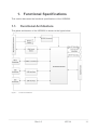
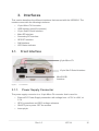
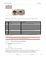
Courier M2M 3G Cellular Modem USR3500 Reference Guide Reference Guide Important Notice Due to the nature of wireless communications, transmission and reception of data can never be guaranteed. Data may be delayed, corrupted (i.e., have errors) or be totally lost. Although significant delays or losses of data are rare when wireless devices are used in a normal manner with a well-constructed network, the modem should not be used in situations where failure to transmit or receive data could result in damage of any kind to the user or any other party, including but not limited to personal injury, death, or loss of property. Neither Sierra Wireless nor USRobotics accepts any responsibility for damages of any kind resulting from delays or errors in data transmitted or received using the modem, or for failure of the modem to transmit or receive such data. Safety and Hazards Do not operate the modem in areas where cellular modems are not advised without proper device certifications. These areas include environments where cellular radio can interfere such as explosive atmospheres, medical equipment, or any other equipment which may be susceptible to any form of radio interference. The modem can transmit signals that could interfere with this equipment. Do not operate the modem in any aircraft, whether the aircraft is on the ground or in flight. In aircraft, the modem MUST BE POWERED OFF. When operating, the modem can transmit signals that could interfere with various onboard systems. Note: Some airlines may permit the use of cellular phones while the aircraft is on the ground and the door is open. Modems may be used at this time. The driver or operator of any vehicle should not operate the modem while in control of a vehicle. Doing so will detract from the driver or operator’s control and operation of that vehicle. In some states and provinces, operating such communications devices while in control of a vehicle may be an offence. Limitations of Liability This manual is provided “as is”. Neither Sierra Wireless nor USRobotics makes any warranties of any kind, either expressed or implied, including any implied warranties of merchantability, fitness for a particular purpose, or noninfringement. The recipient of the manual shall endorse all risks arising from its use. The information in this manual is subject to change without notice and does not represent a commitment on the part of Sierra Wireless or USRobotics. EACH OF SIERRA WIRELESS AND USROBOTICS AND THEIR RESPECTIVE AFFILIATES SPECIFICALLY DISCLAIM LIABILITY FOR ANY AND ALL DIRECT, INDIRECT, SPECIAL, GENERAL, INCIDENTAL, CONSEQUENTIAL, PUNITIVE OR EXEMPLARY DAMAGES INCLUDING, BUT NOT LIMITED TO, LOSS OF PROFITS OR REVENUE OR ANTICIPATED PROFITS OR REVENUE ARISING OUT OF THE USE OR INABILITY TO USE ANY SIERRA WIRELESS PRODUCT, EVEN IF Rev 1.0 1/27/14 2 2 Reference Guide SIERRA WIRELESS AND/OR USROBOTICS AND/OR THEIR RESPECTIVE AFFILIATES HAVE BEEN ADVISED OF THE POSSIBILITY OF SUCH DAMAGES OR THEY ARE FORESEEABLE OR FOR CLAIMS BY ANY THIRD PARTY. Notwithstanding the foregoing, in no event shall Sierra Wireless or USRobotics and/or their respective affiliates aggregate liability arising under or in connection with the Sierra Wireless/ USRobotic product, regardless of the number of events, occurrences, or claims giving rise to liability, be in excess of the price paid by the purchaser for the Sierra Wireless /USRobotics product. Customer understands that neither Sierra Wireless nor USRobotics is providing cellular or GPS (including A-GPS) services. These services are provided by a third party and should be purchased directly by the Customer. Rev 1.0 1/27/14 3 3 Reference Guide SPECIFIC DISCLAIMERS OF LIABILITY: CUSTOMER RECOGNIZES AND ACKNOWLEDGES SIERRA WIRELESS IS NOT RESPONSIBLE FOR AND SHALL NOT BE HELD LIABLE FOR ANY DEFECT OR DEFICIENCY OF ANY KIND OF CELLULAR OR GPS (INCLUDING A-GPS) SERVICES. Patents This product may contain technology developed by or for Sierra Wireless, Inc. This product includes technology licensed from QUALCOMM®. This product is manufactured or sold by Sierra Wireless, Inc. or its affiliates under one or more patents licensed from InterDigital Group and MMP Portfolio Licensing. Copyright © 2014 USRobotics. All rights reserved. Trademarks USRobotics®, CourierTM and the USRobotics logo are registered trademarks of USRobotics. Sierra Wireless®, AirPrime®, AirLink®, AirVantage® and the Sierra Wireless logo are registered trademarks of Sierra Wireless. Windows® is a registered trademark of Microsoft Corporation. QUALCOMM® is a registered trademark of QUALCOMM Incorporated. Used under license. Other trademarks are the property of their respective owners. Contact Information http://www.usr.com/support Web: Consult our website for up-to-date product descriptions, documentation, application notes, firmware upgrades, and troubleshooting tips: http://www.usr.com/support/3500 Rev 1.0 1/27/14 4 4 Reference Guide Document History Version 1.0 Date Updates Initial release Rev 1.0 1/27/14 5 5 Contents CONTENTS ................................................................................................................ 6 LIST OF FIGURES ..................................................................................................... 8 LIST OF TABLES....................................................................................................... 9 1. FUNCTIONAL SPECIFICATIONS ...................................................................... 11 1.1. Functional Architecture .............................................................................. 11 1.2. RF Functionalities ...................................................................................... 12 1.3. Operating System ...................................................................................... 12 2. TECHNICAL SPECIFICATIONS ........................................................................ 13 2.1. Power Supply ............................................................................................ 13 2.2. Mechanical Specifications ......................................................................... 14 3. INTERFACES ..................................................................................................... 15 3.1. Front Interface ........................................................................................... 15 3.1.1. Power Supply Connector .................................................................. 15 3.1.2. Serial Interface .................................................................................. 21 3.1.3. USB Interface .................................................................................... 29 3.2. Back Interface ............................................................................................ 30 3.2.1. SIM Interface ..................................................................................... 30 3.2.2. RF Interface....................................................................................... 31 4. SIGNALS AND INDICATORS ............................................................................ 37 4.1. Alarm Mode ............................................................................................... 37 4.2. RESET Signal Connection ........................................................................ 37 4.2.1. Reset Sequence ................................................................................ 39 4.3. LED Status Indicator .................................................................................. 39 4.4. Real Time Clock (RTC).............................................................................. 40 4.5. Interrupt ..................................................................................................... 40 5. EXPANSION ....................................................................................................... 41 5.1. Expansion Compartment ........................................................................... 41 6. POWER CONSUMPTION ................................................................................... 42 6.1. Various Operating Modes .......................................................................... 42 6.2. Working Mode Features ............................................................................ 43 6.3. Connected Mode Power Consumption ...................................................... 44 6.4. Non-Connected Mode Power Consumption .............................................. 46 Rev 1.0 1/27/14 6 Reference Guide 7. RECOMMENDATIONS WHEN USING THE USR3500 ON TRUCKS ............... 48 7.1. Recommended Power Supply Connection on Trucks ............................... 48 7.2. Technical Constraints on Trucks ............................................................... 49 8. RELIABILITY COMPLIANCE AND RECOMMENDED STANDARDS............... 50 8.1. Reliability Compliance ............................................................................... 50 8.2. Applicable Standards Listing ..................................................................... 50 8.3. Environmental Specifications .................................................................... 51 8.3.1. Function Status Classification ........................................................... 52 9. CERTIFICATION COMPLIANCE AND RECOMMENDED STANDARDS ......... 53 9.1. Certification Compliance ............................................................................ 53 9.2. Applicable Standards Listing ..................................................................... 54 10. SAFETY RECOMMENDATIONS........................................................................ 55 10.1. General Safety ......................................................................................... 55 10.2. RF Safety ................................................................................................. 57 10.2.1. General ........................................................................................... 57 10.2.2. Exposure to RF Energy ................................................................... 57 10.2.3. Efficient Modem Operation .............................................................. 57 10.3. Vehicle Safety .......................................................................................... 57 10.4. Care and Maintenance ............................................................................ 58 10.5. Your Responsibility .................................................................................. 58 11. REFERENCE DOCUMENTS .............................................................................. 59 11.1. Firmware Documentation ........................................................................ 59 11.2. Expansion Card Documentation .............................................................. 59 12. LIST OF ABBREVIATIONS ................................................................................ 60 Rev 1.0 1/27/14 7 7 List of Figures Figure 1. Functional Architecture ............................................................................11 Figure 2. RF Architecture ........................................................................................12 Figure 3. USR3500 Mechanical Drawing ................................................................14 Figure 4. Front Interface .........................................................................................15 Figure 5. Power Supply Connector .........................................................................16 Figure 6. Equivalent Circuit of VIL, Vref = 2.8V .......................................................17 Figure 7. Equivalent Circuit of VIH, Vref = 2.8V.......................................................18 Figure 8. Equivalent Circuit of VOL, Vref = 2.8V ......................................................18 Figure 9. Equivalent Circuit of VOH, Vref = 2.8V .....................................................18 Figure 10. Equivalent Circuit of VIL, Vref > 2.8V .......................................................19 Figure 11. Equivalent circuit of VIH, Vref > 2.8V .......................................................19 Figure 12. Equivalent circuit of VOL, Vref > 2.8V ......................................................19 Figure 13. Equivalent circuit of VOH, Vref > 2.8V ......................................................19 Figure 14. 15-Pin Serial Connector ..........................................................................21 Figure 15. RS232 Serial Link Signals .......................................................................23 Figure 16. V24 Serial Link Implementation for a 5-wire UART .................................24 Figure 17. V24 Serial Link Implementation for a 4-wire UART .................................24 Figure 18. V24 Serial Link Implementation for a 2-wire UART .................................25 Figure 19. Equivalent Circuit of CSPK ......................................................................28 Figure 20. Mini-B USB Connector.............................................................................29 Figure 21. USR3500 Back Interface .........................................................................30 Figure 22. Main RF Connector..................................................................................31 Figure 23. Secondary RF Connector for USR3500 ..................................................32 Figure 24. GPS RF Connector for USR3500 ............................................................32 Figure 25. Reset Sequence Diagram .......................................................................39 Figure 26. USR3500 expansion compartment ..........................................................41 Figure 27. Recommended Power Supply Connection on Trucks .............................48 Figure 28. Example of an Electrical Connection That May Damage the modem .....49 Rev 1.0 1/27/14 8 List of Tables Table 1. Power Supply Electrical Characteristics ...................................................13 Table 2. Power Supply Connector Pin Description .................................................16 Table 3. GPIO Pin Description ................................................................................17 Table 4. GPIO Pin Operating Conditions when Vref is at 2.8V ...............................17 Table 5. GPIO Pin Operating Conditions when Vref > 2.8V ...................................18 Table 6. ON/OFF Pin Operation .............................................................................21 Table 7. ON/OFF Pin Description ...........................................................................21 Table 8. Serial Connector Pin Description ..............................................................22 Table 9. Microphone Pin Description for USR3500 ................................................26 Table 10. Equivalent Circuits of CMIC .....................................................................26 Table 11. Electrical Characteristics of CMIC for USR3500 .....................................26 Table 12. Recommended Microphone Characteristics ............................................27 Table 13. Speaker Outputs Pin Description for USR3500 .......................................27 Table 14. Electrical Characteristics of CSPK for USR3500 .....................................28 Table 15. Recommended Speaker Characteristics .................................................28 Table 16. Mini-B USB Pin Description .....................................................................29 Table 17. USB Electrical Characteristics for USR3500 ...........................................29 Table 18. SIM Socket Pin Description .....................................................................31 Table 19. Available RF Interfaces ...........................................................................31 Table 20. Main Receiver Parameters for USR3500 ................................................32 Table 21. Main Transmitter Parameters for USR3500 ............................................32 Table 22. Antenna Specifications for USR3500 ......................................................33 Table 23. GPS Antenna Specifications for USR3500 ..............................................34 Table 24. Alarm Mode (Low Power Mode) ..............................................................37 Table 25. USR3500 Reset Status ...........................................................................38 Table 26. Reset Electrical Characteristics for USR3500 .........................................38 Table 27. Reset Operating Conditions ....................................................................38 Table 28. USR3500 LED Status ..............................................................................39 Table 29. Real Time Clock Specifications ...............................................................40 Table 30. Available Interrupt Pins on the USR3500 ................................................40 Table 31. Initial Power Consumption (Typical) ........................................................42 Table 32. USR3500 Operating Modes ....................................................................42 Rev 1.0 1/27/14 9 Reference Guide Functional Specifications Table 33. USR3500 Operating Modes Feature Availability .....................................43 Table 34. Power Consumption of USR3500 in Connected Mode with Serial Port OFF, Flash LED OFF and USB ON (typical values) ..................................................44 Table 35. Power Consumption of USR3500 in Non-Connected Mode with UART ON, FLASH LED OFF and USB OFF (typical values) ...............................................47 Table 36. Standards Conformity for the modem ......................................................50 Table 37. Applicable Standards and Requirements for the modem ........................50 Table 38. Operating Class Temperature Range ......................................................51 Table 39. ISO Failure Mode Severity Classification ................................................52 Table 40. Standards Conformity for USR3500 ........................................................53 Table 41. Applicable Standards and Requirements for USR3500 ..........................54 Rev 1.0 1/27/14 10 10 1. Functional Specifications This section discusses the functional specifications of the USR3500. 1.1. Functional Architecture The global architecture of the USR3500 is shown in the figure below. Figure 1. Functional Architecture Rev 1.0 1/27/14 11 Reference Guide 1.2. Figure 2. 1.3. Functional Specifications RF Functionalities RF Architecture Operating System The modem is Open AT Application Framework compliant. With the Courier M2M Open AT application loaded, the modem becomes a solution for many specific market needs. The operating system of the modem is responsible for the following functions: • • AT Command processing Real Time Clock (RTC) with calendar Rev 1.0 1/27/14 12 12 2. Technical Specifications 2.1. Power Supply The modem is supplied by an external DC voltage, DC-IN, with a voltage range of +4.75V to +32V. The main regulation is made with an internal DC/DC converter in order to supply all the internal functions with a DC voltage. The correct operation of the modem in Communication mode is not guaranteed if the input voltage falls below 4.75V. Refer to the following table for the modem’s operating voltage range and maximum current. Table 1. Power Supply Electrical Characteristics Operating Voltage Range • 4.75V to 32V DC, nominal at 13.2V Maximum Current (Typical) • 850mA, average at 4.75V; 3.7A Peak at 4.75V The modem is permanently powered once the power supply is connected. In the case of Alarm mode (Low Power mode), the user can set the modem “Turn-on” time. Refer to section 4.1 Alarm Mode for more information. Caution: The minimum input voltage specified here is the modem input. Be mindful of the input voltage decrease caused by the power cable. When using the optional 6-wire cable accessory, this input drop is at around 800mV at 4.75V and 220mV at 32V (EDGE 4TX). The modem is designed for use with the original power cable, and the fuse that came with the original cable is a 2A/250V Slow Break fuse 5.2mm*20mm. Rev 1.0 1/27/14 13 Reference Guide 2.2. Figure 3. Technical Specifications Mechanical Specifications USR3500 Mechanical Drawing Rev 1.0 1/27/14 14 14 3. Interfaces This section describes the different interfaces that connect with the USR3500. The modem comes with the following interfaces: • • • • • • • • 10-pin Micro-Fit Connector USB Interface (mini-B connector) 15-pin Sub-D Serial Interface Main RF Interface Secondary RF Interface GPS RF Interface SIM Interface LED Status Indicator 3.1. Front Interface 10-pin Micro-Fit Connector 15-pin Sub-D Serial Interface Mini-B USB Interface Figure 4. Front Interface 3.1.1. Power Supply Connector The power supply connector is a 10-pin Micro-Fit connector that is used for: • • • • External DC Power Supply connection with voltage from +4.75V to +32V, at 3.7A GPIO connections and GPIO voltage reference ON/OFF pin to power OFF the modem Interrupt pin Rev 1.0 1/27/14 15 Reference Guide Figure 5. Interfaces Power Supply Connector Refer to the following table for the pin description of the power supply connector. Table 2. Power Supply Connector Pin Description Pin # Signal Description 1 GPIO25/INT1 General purpose input/output or Interrupt 2 GPIO35 General purpose input/output 3 Vref Voltage reference for the GPIOs 4 Reserved Reserved 5 Reserved Reserved 6 GND Ground 7 DC-IN Input Supply for the modem (4.75V to 32V) 8 ON/OFF Control pin to power OFF the modem 9 Reserved Reserved 10 Reserved Reserved The input voltage range (DC-IN) is from 4.75V to 32V, with a typical operating voltage of 13.2V. Caution: Pins 1, 2, 3, 4, 5, 8, 9 and 10 are low voltage interfaces. It is strictly prohibited to connect these pins to any power supply as there is a risk of damaging the modem. 3.1.1.1. General Purpose Input/Output The modem has two external GPIO ports: • GPIO35 and • GPIO25; as well as a voltage reference line, Vref. Vref sets the reference voltage of the input or output of the two GPIOs. Leaving it unconnected sets the GPIO level at 2.3V – 2.6V by default. It is strongly recommended to connect to the required GPIOs’ output voltage (2.8V ~ 15V). Rev 1.0 1/27/14 16 16 Reference Guide Interfaces Refer to the following table for the pin description of the GPIOs. Table 3. GPIO Pin Description Pin # Signal I/O I/O Voltage Description 1 GPIO25/INT 1 I/O Vref General purpose input/output or Interrupt 2 GPIO35 I/O Vref General purpose input/output 3 Vref I 2.8V ~ 15V Voltage reference for the GPIOs Note: It is recommended to use a 6-wire cable accessory for easy access to these three lines. Please refer to the Getting Started Guide at http://www.usr.com/support/3500 for more information about the 6-wire cable accessory. When the voltage reference, Vref, is not connected, if one of the GPIO output is in High state while the other is in Low state, the GPIO in high level voltage will be at 2.3V.To avoid this voltage drop, it is recommended to use Vref to the desired output voltage. With Vref connected to 2.8V, both GPIO35 and GPIO25 may be interfaced with a component that complies with the following levels. Table 4. GPIO Pin Operating Conditions when Vref is at 2.8V Parameter Mininum Typical VIL VIH Maximum Condition 0.84V Please refer to Figure 6. 1.96V Please refer to Figure 7. VOL 0.4* VOH modem Zout = 100K Pull-up to Vref, please refer to Figure 9. 2.8* * Figure 6. Please refer to Figure 8. Value without external load. Equivalent Circuit of VIL, Vref = 2.8V Rev 1.0 1/27/14 17 17 Reference Guide Interfaces Figure 7. Equivalent Circuit of VIH, Vref = 2.8V Figure 8. Equivalent Circuit of VOL, Vref = 2.8V Figure 9. Equivalent Circuit of VOH, Vref = 2.8V With Vref > 2.8V, both GPIO35 and GPIO25 may be interfaced with a component that complies with the following levels. Table 5. GPIO Pin Operating Conditions when Vref > 2.8V Parameter Min VIL VIH Max Condition 0.84V Please refer to Figure 10. 1.96V Please refer to Figure 11. Vref + 0.058* 110 VOL VOH Typ Please refer to Figure 12. modem Zout = 100K Pull-up to Vref, please refer to Figure 13. Vref* Rev 1.0 1/27/14 18 18 Reference Guide * Interfaces Value without external load. Figure 10. Equivalent Circuit of VIL, Vref > 2.8V Figure 11. Equivalent circuit of VIH, Vref > 2.8V Figure 12. Equivalent circuit of VOL, Vref > 2.8V Figure 13. Equivalent circuit of VOH, Vref > 2.8V The GPIO pin is mainly used to: • Act as a switch for a transistor when the GPIO is configured as output. Rev 1.0 1/27/14 19 19 Reference Guide • Interfaces Act as a status reading when the GPIO is configured as input. The GPIOs may be controlled with the following AT commands: • • AT+WIOW an output AT+WIOR as an input for write access to the GPIO value, when the GPIO is used as for read access to the GPIO value, when the GPIO is used [1] By default, and when the modem has been reset, both GPIOs are configured as inputs. The AT command AT+WIOM must be used to change this configuration. Refer to documents [3] AT Commands Interface Guide [2] Customer Release Notes for Firmware 7.52 A1 for more information regarding this AT command. 3.1.1.1.1. Setting the GPIO as an Output Refer to the following example for how to configure the GPIO as an output. • Enter the following commands: § AT+WIOM=1,“GPIO21”,1,0 à this command activates GPIO21 as an output and sets it at a low level. § AT+WIOW=“GPIO21”,1 à this command sets the output level of GPIO21 to HIGH. 3.1.1.1.2. Setting the GPIO as an Input Refer to the following example for how to configure the GPIO as an input. • • Enter the following commands: § AT+WIOM=1,“GPIO21”,0 à this command activates GPIO21 as an input. § AT+WIOR=“GPIO21” à this command reads the GPIO21 level and returns the value “1” which represents a HIGH level. Pull the GPIO21 pin to GND, and read again. The return value should now be “0” which represents a LOW level. Refer to the AT Commands Interface Guide at http://www.usr.com/support/3500 for more information regarding AT commands. Note: The AT+WIOW and AT+WIOR commands will automatically set the GPIO to the desired mode. For example, AT+WIOW=42,1 will set GPIO42 to output mode and in High state. Rev 1.0 1/27/14 20 20 Reference Guide 3.1.1.2. Interfaces ON/OFF Pin The modem has an external ON/OFF pin which is used to turn the device ON or OFF. The following table describes the operation of this pin. Table 6. ON/OFF Pin Operation Condition State Power Supply Operation 1 Open When 4.75V to 32V supply is applied. The modem is turned ON. 2 Pulled to GND When 4.75V to 32V supply is applied. The modem remains OFF. 3 Left open when turning ON the modem, then pulled to GND 4.75V to 32V supply is initially applied. The modem remains ON and will remain ON until AT+CPOF is sent to turn the device OFF. To enable the low power mode, the user may simply pull the ON/OFF pin to GND and send AT+CPOF to the modem using a communication software such as a HyperTerminal. Table 7. ON/OFF Pin Description Pin # Signal I/O I/O Voltage Description 8 ON/OFF I 4V Pin to turn the modem ON/OFF. Refer to the power consumption tables in section 6 Power Consumption for the power consumption values when the modem is in Alarm mode (Low Power mode). 3.1.2. Serial Interface A SUB-D 15-pin connector is available as a serial interface to directly communicate with the modem. This serial interface is used for: • • • RS232 serial link connection Audio lines connection (microphone and speaker) RESET signal connection Figure 14. 15-Pin Serial Connector Rev 1.0 1/27/14 21 21 Reference Guide Interfaces Refer to the following table for the pin description of the 15-pin serial connector. Table 8. Serial Connector Pin Description Pin # Signal I/O I/O Type Reset State Description 1 CT109/DCD O +/- 5.5V Undefined Data Carrier Detect 2 CT103/TXD I +/- 5.5V Z Transmit Serial Data 3 Reserved 4 CMIC2P I Analog Microphone positive input 5 CMIC2N I Analog Microphone negative input 6 CT104/RXD O +/- 5.5V 1 Receive Serial Data 7 CT107/DSR O +/- 5.5V Z Data Set Ready 8 CT108-2/DTR I +/- 5.5V Z Data Terminal Ready 9 GND GND Ground 10 CSPK2P O Analog Speaker positive input 11 CT106/CTS O +/- 5.5V Z Clear To Send 12 CT105/RTS I +/- 5.5V Z Request To Send 13 CT125/RI O +/- 5.5V Undefined Ring Indicator 14 RESET I/O 1V8 Modem Reset 15 CSPK2N O Analog Speaker negative input 3.1.2.1. Do not connect RS232 Serial Link Connection Also known as the main serial link, the RS232 interface performs the voltage level adaptation (V24/CMOS ⇔ V24/V28) between the internal modem (DCE) and external applications (DTE). The signals available on the RS232 serial link are as follows: • • • • • • • • TX data (CT103/TXD) RX data (CT104/RXD) Request To Send (CT105/RTS) Clear To Send (CT106/CTS) Data Terminal Ready (CT108-2/DTR) Data Set Ready (CT107/DSR) Data Carrier Detect (CT109/DCD) Ring Indicator (CT125/RI) Rev 1.0 1/27/14 22 22 Reference Guide Figure 15. Interfaces RS232 Serial Link Signals The RS232 interface has been designed to allow flexibility in the use of the serial interface signals. However, the use of TXD, RXD, CTS and RTS signals are mandatory; while the use of DTR, DSR, DCD and RI signals are optional. Tip: The modem is designed to operate using all serial interface signals and it is recommended to use CT105/RTS and CT106/CTS for hardware flow control in order to avoid data corruption during transmission. The USR3500 also implements the Serial Port Auto Shut Down feature with the DTR signal. It is recommended to use the CT108-2/DTR signal to benefit from the current consumption improvement performed by this feature. 3.1.2.2. RS232 Implementation The following subsections describe how the RS232 serial link can be implemented to suit different designs. 3.1.2.2.1. 5-wire Serial Interface RS232 Implementation The signals used in this interface are as follows: • • • • • Note: CT103/TXD CT104/RXD CT105/RTS CT106/CTS CT108-2/DTR The CT108-2/DTR signal must be managed following the V24 protocol signaling if the Sleep Idle Mode and Serial Port Auto Shut Down feature are to be used. Rev 1.0 1/27/14 23 23 Reference Guide Figure 16. Interfaces V24 Serial Link Implementation for a 5-wire UART 3.1.2.2.2. 4-wire Serial Interface RS232 Implementation The signals used in this interface are as follows: • • • • CT103/TXD CT104/RXD CT105/RTS CT106/CTS Figure 17. V24 Serial Link Implementation for a 4-wire UART 3.1.2.2.3. 2-wire Serial Interface RS232 Implementation The signals used in this interface are as follows: • • Note: CT103/TXD CT104/RXD Although this case is possible, it is not recommended. The flow control mechanism must be managed from the customer end. Rev 1.0 1/27/14 24 24 Reference Guide Figure 18. Interfaces V24 Serial Link Implementation for a 2-wire UART The CT105/RTS and the CT106/CTS signals are not used in this configuration. Configure the AT command AT+IFC=0,0 to disable the flow control function. Refer to the AT Commands Interface Guide at http://www.usr.com/support/3500 for more information regarding AT Commands. For more information on how to use the RS232 serial link to communicate with the modem, refer to section 3.1.2.1 RS232 Serial Link Connection. 3.1.2.3. Autobauding Mode The autobauding mode allows the modem to detect the baud rate used by the DTE connected to the RS232 serial link. The autobauding mode is controlled by AT commands. Refer to the AT Commands Interface Guide at http://www.usr.com/support/3500 for more information. 3.1.2.4. Serial Port Auto Shut Down Feature The RS232 serial link can be shut down when there is no activity between the DTE and the modem. This can help improve the power consumption performance. The Serial Port Auto Shut Down feature is controlled by the AT command AT+WASR. Enter: • • AT+WASR=1 to enter the serial port auto shut down mode AT+WASR=0 to exit the serial port auto shut down mode Refer to the AT Commands Interface Guide at http://www.usr.com/support/3500 for more information on AT commands. Caution: GPIO24 is reserved for serial port auto shut down feature. It is prohibited for customer use. Improper access to GPIO24 by customers may lead to unexpected behavior on serial port performance. It is prohibited to use the serial port auto shut down feature when the CT108-2/DTR is not used in the application. Otherwise, there will be data lost from the DTE side to the modem. Rev 1.0 1/27/14 25 25 Reference Guide 3.1.2.5. Interfaces Audio Lines Connection The modem supports one microphone input and one speaker output. 3.1.2.5.1. Microphone The microphone inputs are connected in differential mode to reject common mode noise and TDMA noise. The microphone inputs have already included biasing for an electret microphone (0.5mA and 2V) and are ESD protected. An electret microphone may be directly connected to these inputs allowing an easy connection to a headset. The microphone gain can be adjusted by AT+VGT and the transmit digital gain can be adjusted by AT+WDGT. Refer to documents the AT Commands Interface Guide at http://www.usr.com/support/3500 for more information about these AT commands. The following table shows the pin assignments of the microphone input. Table 9. Microphone Pin Description for USR3500 (Sub D 15-pin) Pin # Signal I/O I/O Type Description 4 CMIC1P I Analog Microphone positive input 5 CMIC1N I Analog Microphone negative input Table 10. Equivalent Circuits of CMIC DC Equivalent Circuit Table 11. AC Equivalent Circuit Electrical Characteristics of CMIC for USR3500 Parameters Min DC Characteristics AC Characteristics 200 Hz<F<4 kHz Working voltage (CMICxP-CMICxN) Maximum rating voltage (CMICxP or CMICxN) Typ Max N/A Z 70 120 AT+VGT*=3500dB 13.8 AT+VGT*=2000dB 77.5 AT+VGT*=700dB 346 Positive Negative Rev 1.0 Unit V 160 kΩ mVrms +7.35** -0.9 1/27/14 V 26 26 Reference Guide Interfaces * The input voltage depends of the input micro gain set by AT command. Refer to the AT Commands Interface Guide at http://www.usr.com/support/3500. ** Because CMICxP is internally biased, it is necessary to use a coupling capacitor to connect an audio signal provided by an active generator. Only a passive microphone can be directly connected to the CMICxP and CMICxN inputs. Refer to the following table for the list of recommended microphone characteristics. Table 12. Recommended Microphone Characteristics Feature Values Type Electret 2V/0.5 mA Impedance Z = 2kΩ Sensitivity -40dB to -50dB SNR > 50dB Frequency response Compatible with GSM specifications 3.1.2.5.2. Speaker The speaker outputs are connected in differential mode to reject common mode noise and TDMA noise. Speaker outputs are connected to internal push-pull amplifiers and may be loaded down with components between 32 – 150Ω and up to 1nF. These outputs may be directly connected to a speaker. The output power may be adjusted by 2dB steps. The gain of the speaker outputs is internally adjusted and may be tuned using the AT+VGR command. Furthermore, the digital gain can be adjusted using AT+WDGR. Refer to the AT Commands Interface Guide at http://www.usr.com/support/3500 for more information about these AT commands. The following table shows the pin assignments of the speaker output. Table 13. Speaker Outputs Pin Description for USR3500 (Sub D 15-pin) Pin # Signal I/O I/O Type Description 10 CSPK1P O Analog Speaker positive output 15 CSPK1N O Analog Speaker negative output Rev 1.0 1/27/14 27 27 Reference Guide Interfaces Figure 19. Equivalent Circuit of CSPK Table 14. Electrical Characteristics of CSPK for USR3500 Parameters Min Typ Max Unit 1.5 mV Biasing voltage CSPKxP and CSPKxN -1.5 Output swing voltage RL=16Ω: AT+VGR=-1600*; single-ended - 1.7 RL=32Ω: AT+VGR=-1600*; single-ended - 1.9 2.75 Vpp RL Load resistance 14.5 32 - Ω Output current; peak value; RL=16Ω - 40 85 mA Output current; peak value; RL=32Ω - 22 - mA RL=16Ω; AT+VGR=-1600* - 25 - mW RL=32Ω; AT+VGR=-1600* - 16 27 mW Output pull-down resistance at power-down 28 40 52 kΩ IOUT POUT RPD Vpp * The output voltage depends of the output speaker gain set by AT command. Refer to the AT Commands Interface Guide at http://www.usr.com/support/3500. This value is given in dB, but it’s possible to toggle this to index value. Refer to the following table for the list of recommended speaker characteristics. Table 15. Recommended Speaker Characteristics Feature Values Type 10mW, electro-magnetic Impedance Z = 30 to 50Ω Sensitivity 110dB SPL min. (0dB = 20µPa) Frequency response Compatible with GSM specifications Rev 1.0 1/27/14 28 28 Reference Guide 3.1.3. Interfaces USB Interface Aside from the serial interface, the Mini-B USB interface (USB slave) may also be used to directly communicate with the modem. Figure 20. Mini-B USB Connector Refer to the following table for the pin description of the mini-B USB connector. Table 16. Mini-B USB Pin Description Pin # Signal Description 1 VBUS +5V Power supply 2 D- Differential data interface negative 3 D+ Differential data interface positive 4 ID Not connected 5 GND Ground The USR3500 USB slave interface complies with USB 2.0 protocol signaling and with USB 2.0 electrical interface. The USB interface features: • • • • • Table 17. 480Mbit/s high-speed transfer rate 3.3V type compatible USB Soft-connect feature USB Download feature CDC 1.1 – ACM compliant USB Electrical Characteristics for USR3500 Parameter I/O Min Typ VBUS Input 4.75 5 Input High 2.00 3.30 Input Low 0 Output High 2.80 D-, D+ (Low / Full speed) Output Low D-, D+ (High speed) Input High Rev 1.0 0.30 3.30 Max Unit V 3.60 V 0.80 V 3.60 V 0.30 V 0.44 V 1/27/14 29 29 Reference Guide Interfaces Parameter I/O Min Input Low 0 Output High 0.36 Output Low 0 Typ 0.38 Max Unit 0.01 V 0.44 V 0.01 V The USB feature can be activated by using the AT+WMFM=0,1,3 AT command. Refer to the AT Commands Interface Guide at http://www.usr.com/support/3500 for more information regarding this AT command. 3.2. Back Interface Expansion Compartment SIM Interface LED Status Indicator GPS RF Interface Main RF Interface Secondary RF Interface Figure 21. 3.2.1. USR3500 Back Interface SIM Interface A SIM card can be directly connected to the USR3500 through the embedded SIM socket. This interface controls 3V / 1V8 SIM cards and it is fully compliant with GSM 11.11 recommendations concerning SIM functions. The SIM interface of the USR3500 is ESD protected. Transient overvoltage protections in ESD are internally added on the signals connected to the SIM interface in order to prevent any damage from electrostatic discharge. The SIM interface uses 5 SIM signals, namely: • • • • • SIM-VCC: SIM Power supply ~SIM-RST: Reset SIM-CLK: Clock SIM-IO: I/O Port SIMPRES: SIM card detection Rev 1.0 1/27/14 30 30 Reference Guide 3.2.1.1. Interfaces SIM Socket Pin Description Refer to the following table for the pin description of the SIM socket. Table 18. SIM Socket Pin Description Pin # Signal I/O I/O Type 1 SIMVCC O 2V9 / 1V8 2 SIMRST O 2V9 / 1V8 O SIM RESET 3 SIMCLK O 2V9 / 1V8 O SIM Clock 7 SIMDATA I/O 2V9 / 1V8 Pull up* SIM DATA 8 SIMPRES I 1V8 Pull low** SIM Card Detect * SIM-IO pull up is about 10KΩ. ** SIMPRES pull low is about 100KΩ. 3.2.2. Reset State Description SIM Power Supply RF Interface The USR3500 has three RF interfaces. Refer to the following table for the list of available RF interfaces. Table 19. Available RF Interfaces Main RF Interface Secondary RF Interface GPS RF Interface ü ü ü The main antenna connector allows the transmission of radio frequency (RF) signals from the device to an external customer supplied antenna. This interface is an SMA type connector and its nominal impedance is 50Ω. Figure 22. Main RF Connector The secondary RF interface is used in USR3500 for 3G diversity antenna connection. It is an SMA type connector and its nominal impedance is 50Ω. Rev 1.0 1/27/14 31 31 Reference Guide Figure 23. Interfaces Secondary RF Connector for USR3500 The GPS RF interface is used for GPS antenna connection. It is an MMCX type connector and its nominal impedance is 50Ω. It also provides bias for active antenna. For more details, refer to section 3.2.2.3.6 Active GPS Antenna Bias. Figure 24. GPS RF Connector for USR3500 3.2.2.1. RF Performances RF performances are compliant with ETSI recommendation GSM 05.05. Refer to the tables below for the main parameters used for both the Receiver and the Transmitter. Table 20. Main Receiver Parameters for USR3500 Parameters Typical Values GSM850 Reference Sensitivity -108dBm E-GSM900 Reference Sensitivity -109dBm DCS1800 Reference Sensitivity -107dBm PCS1900 Reference Sensitivity -107dBm 3G Band I 2100 Reference Sensitivity -108dBm 3G Band II 1900 Reference Sensitivity -107dBm 3G Band V 850 Reference Sensitivity -110dBm 3G Band VI 800 Reference Sensitivity -110dBm 3G Band VIII 900 Reference Sensitivity -108dBm Selectivity @ 200 kHz > +9dBc Selectivity @ 400 kHz > +41dBc Linear dynamic range 63dB Co-channel rejection >= 9dBc Table 21. Main Transmitter Parameters for USR3500 Parameters Typical Values Output power at PCL5 (EGSM & GSM850) 32dBm Output power at PCL0 (GSM1800 & PCS1900) 29dBm Rev 1.0 1/27/14 32 32 Reference Guide Interfaces Parameters Typical Values Output power at PCL19 (EGSM & GSM850) 5dBm Output power at PCL15 (GSM1800 & PCS1900) 0dBm Output power Class 3 (3G all band) 23dBm 3.2.2.2. Antenna Specifications The main/secondary antenna must meet the requirements specified in the table below. The optimum operating frequency depends on the application. A dual-band or quadband antenna should operate in these frequency bands and have the following characteristics. Antennas used with the USR3500 must have a maximum antenna gain of 1 dBi for Bands 900 and 1800, and 2.5 dBi for Band 2100. Table 22. Antenna Specifications for USR3500 Characteristics GSM850 and WCDMA Band V WCDMA Band VI EGSM 900 and WCDMA Band VIII TX Frequency 824 to 849 MHz 830 to 840 MHz RX Frequency 869 to 894 MHz 875 to 885 MHz Impedance 50Ω VSWR Rx max 1.5:1 Tx max 1.5:1 Typical radiated gain DCS 1800 PCS 1900 and WCDMA Band II WCDMA Band I 880 to 915 MHz 1710 to 1785 MHz 1850 to 1910 MHz 1920 to 1980 MHz 925 to 960 MHz 1805 to 1880 MHz 1930 to 1990 MHz 2110 to 2170 MHz 0dBi in one direction at least Rev 1.0 1/27/14 33 33 Reference Guide Interfaces The USR3500 GPS antenna must meet the requirements specified in the table below. Table 23. GPS Antenna Specifications for USR3500 Characteristic GPS L1 RX Frequency 1575.42 MHz RF Impedance 50Ω VSWR 1.5:1 Rx max LNA Bias Voltage 5V LNA Current Consumption 40mA MAX Polarization Linear, vertical Typical radiated gain 0dBi in one direction at least 3.2.2.3. Note: GPS Specifications for USR3500 These specifications are preliminary targets that are subject to change without notice. Actual GPS functionality depends on the firmware version and module configuration. The USR3500 provides the GPS features listed in the following sub-sections. This GPS feature can be used through AT commands provided by the Extended Open AT application (which is pre-loaded at the factory) or from a custom Open AT application using Location Library. 3.2.2.3.1. • • • • • • • Standalone GPS Leading standalone/autonomous GPS performance -145 dBm cold start sensitivity -153 dBm hot start sensitivity -155 dBm tracking sensitivity < 45 second average cold start TTFF (Time To First Fix) in open air < 3 second average super hot TTFF in open sky < 10 m accuracy in open sky Note: For optimum performance, the modem should be registered on the GSM/UMTS network, but does not need to be on an active data or voice call. 3.2.2.3.2. gpsOneXTRATM • Enables enhanced standalone GPS operation by downloading < 40 kB file from a server on the Internet • Performance closer to UE-based operation than traditional standalone GPS operation Rev 1.0 1/27/14 34 34 Reference Guide • Interfaces Best if downloaded once every 1–2 days, but valid for up to 7 days with some accuracy degradation Rev 1.0 1/27/14 35 35 Reference Guide 3.2.2.3.3. • Interfaces A-GPS Features Leading A-GPS performance Exceeds 3GPP RAN 4 AGPS performance specification • • • • • • • -153 dBm cold start sensitivity -155 dBm tracking sensitivity < 5 second average cold start TTFF in open sky (UE-based) < 3 second average super hot TTFF in open sky < 2 m accuracy in open sky 1 Hz tracking with CEP-50 UMTS Control Plane (CP) – UE-assisted and UE-based GSM Control Plane (CP) – UE-assisted and UE-based 3.2.2.3.4. • • • Enhanced Navigation 2.0 Feature Provides leading performance in car and walking navigation modes as well as accuracy while stationary Airline/Game/Offline mode GPS capability is available while phone is offline 3.2.2.3.5. NMEA Supported sentences: GGA, GSA, GSV, RMC, VTG 3.2.2.3.6. Active GPS Antenna Bias The USR3500 provides bias for active antenna, which can be enabled or disabled using GPIO44. Note that GPIO44 needs to be at high level for antenna bias to be activated. Rev 1.0 1/27/14 36 36 4. Signals and Indicators 4.1. Alarm Mode The USR3500 can be turned on using the Alarm mode when power supply is applied. The USR3500 will remain in Low Power mode until the alarm is triggered to start the USR3500 up. Note: Table 24. Refer to section 3.1.1.2 ON/OFF Pin for more information on how to turn the USR3500 ON or OFF using the ON/OFF pin. Alarm Mode (Low Power Mode) Steps State Power Supply Operation 1 AT+CALA=“YY/MM/DD,H H:MM” 4.75V to 32V supply is applied. The alarm is set. The USR3500 remains ON. 2 Pulled ON/OFF PIN to GND 4.75V to 32V supply is applied. The USR3500 remains ON. 3 AT+CPOF 4.75V to 32V supply is applied. (The ON/OFF signal remains at GND.) The USR3500 turns OFF and will remain OFF until the Alarm mode is activated to turn the device ON. Note: The USR3500’ clock must be set before Alarm mode is activated. To set the clock, refer to the AT+CCLK command in the AT Commands Interface Guide at http://www.usr.com/support/3500. 4.2. RESET Signal Connection This signal is used to force a reset procedure by providing the USR3500 with a LOW level that lasts at least 200µs (when the power supply is already stabilized). It is activated by either an external Reset signal or by an internal signal (from the Reset generator); and is automatically driven by an internal hardware during the power ON sequence. Note: The USR3500 remains in Reset mode for as long as the Reset signal is held LOW. A software reset is always preferred to a hardware reset. Refer to document documents the AT Commands Interface Guide at http://www.usr.com/support/3500 for more information regarding software resets. This signal may also be used to provide a reset to an external device when the pin is configured as an output. If no external reset is necessary, this input may be left open. When used (as an emergency reset), it has to be driven by either an open collector or an open drain output. Caution: This signal is for emergency resets only. Rev 1.0 1/27/14 37 Reference Guide Table 25. Signals and Indicators USR3500 Reset Status (Serial Port) Pin # Signal I/O I/O Type Voltage Description 14 Reset I/O Open drain 1V8 USR3500 Reset Table 26. Reset Electrical Characteristics for USR3500 Parameter Minimum Typical Maximum Unit Input Impedance (R)* 10 kΩ Input Impedance (C) 20 nF * Table 27. Internal pull-up Reset Operating Conditions Parameter Minimum ~Reset time (Rt) 1 200 2 20 ~Reset time (Rt) (at power up only) Cancellation time (Ct) Typical Maximum Unit µs 40 100 ms 34 V H* 0.57 VIL 0 VIH 1.33 ms V 0.57 V V * VH = Hysterisis Voltage 1: This reset time is the minimum to be carried out on the ~Reset signal when the power supply is stabilized. 2: This reset time is internally carried out by the embedded module power supply supervisor only when the embedded module power supplies are powered ON. Rev 1.0 1/27/14 38 38 Reference Guide 4.2.1. Signals and Indicators Reset Sequence To activate the Reset sequence, the Reset signal has to be set to LOW for a minimum of 200µs. As soon as the reset is done, the application can send the command AT8 and the AT interface will send an “OK” back to the application. If the application manages hardware flow control, the AT command may be sent during the initialization phase. Figure 25. Reset Sequence Diagram Another solution is to use the AT+WIND command to get an unsolicited status from the USR3500. Refer to the AT Commands Interface Guide at http://www.usr.com/support/3500 for more information regarding AT commands. 4.3. LED Status Indicator The USR3500 has a red LED that indicates the current operational status of the device. Table 28. USR3500 LED Status USR3500 State LED Status USR3500 Status Permanently lighted The modem is switched ON, but not registered in the network. Flashing slowly LED is ON for 200ms, OFF for 2s ON Flashing rapidly LED is ON for 200ms, OFF for 600ms Very quick flash LED is ON for 100ms, OFF for 200ms OFF The modem is switched ON and is registered in a network (Idle mode). OFF Rev 1.0 The modem is switched ON and is registered in a network (Connected mode). The modem is switched on, and the software downloaded is either corrupted or non-compatible (“BAD SOFTWARE”). The modem is either switched OFF, or the Flash LED has been disabled by the user*. 1/27/14 39 39 Reference Guide Signals and Indicators * The Flash LED can be disabled by the user when in Sleep mode in order to save power consumption. Refer to the AT Commands Interface Guide at http://www.usr.com/support/3500 for more information on how to disable the Flash LED using an AT command. 4.4. Real Time Clock (RTC) The USR3500 has implemented Real Time Clock for saving date and time when the USR3500 is unplugged from the DC power supply through the DC power cable. Table 29. Real Time Clock Specifications Item Minimum Charging Time start from fully discharged to fully charged RTC Time Period* Typical Maximum 15 Hours Guaranteed 30 Hours Not guaranteed 60 Hours * This RTC time period is measured when the RTC battery is fully charged before the modem is unplugged from the DC power source. * This RTC time period is for temperature from -20°C to +60°C. Once the operating/storage temperature is beyond this range, this time period is not guaranteed. Caution: When the modem is shipped out, the charging voltage of the RTC battery is not guaranteed. Once the modem is on power, the RTC battery will start charging and the RTC feature can then be resumed. 4.5. Interrupt An interrupt pin, INT1, is multiplexed with GPIO25 on pin 1 of the Microfit connector. Additional interrupt pins are also available via the expansion card connector. Refer to the following table for the list of available interrupt pins in the modem. Table 30. Available Interrupt Pins on the USR3500 Interface Location Pin Number Signal Name Multiplex Microfit connector 1 INT1 GPIO25 Expansion connector 32 INT0 GPIO3 Rev 1.0 Notes 1/27/14 40 40 5. Expansion 5.1. Expansion Compartment The expansion compartment allows users to easily expand the USR3500’s features (Ethernet, for example) for their own applications. Figure 26. USR3500 expansion compartment Refer to the Ethernet Expansion Card User Guide at http://www.usr.com/support/3500 for more information regarding this feature. Rev 1.0 1/27/14 41 6. Power Consumption The following sub-sections details out the power consumption values of the USR3500 for various modes and RF bands. These consumption values were obtained by performing measurements on USR3500 samples at a temperature of 25°C using a 3V SIM card. Note: For power consumption, the software version used is R7.50 A1. Refer to the Courier M2M Application guide at http://www.usr.com/support/3500 for details on how to upgrade modem firmware. The table below gives the average power consumption of the USR3500 for the first 10s when power supply (DC-IN, supplied by Agilent 66321D in this example) is initially applied to it with no serial port, LED ON or SIM card at ambient temperature. Table 31. Initial Power Consumption (Typical) Configuration USR3500 Average Power Consumption with FW R7.50 A1 DC-IN @ 13.2V 18mA 6.1. Various Operating Modes The power consumption levels of the USR3500 vary depending on the operating mode used. Refer to the table below for the different kinds of operating modes available. Refer to Appendix 3.1 of the AT Commands Interface Guide at http://www.usr.com/support/3500 for the working mode description. Table 32. USR3500 Operating Modes Operating Mode Description GSM Connected Mode The modem is connected to a live GSM network, during circuit switch voice or data call. Transfer Mode The modem has GPRS data transfer connection with a live network, during packet data transmission. Active mode with GSM stack in Idle When the RF function is active and the modem is synchronized with the network, but there is currently no communication. Sleep mode with GSM stack in Idle When the RF function is disabled but is regularly activated to remain synchronized with the network. This mode only works when the DTE sends an AT command to shut the serial link down (DTE turns DTR to inactive state). Active Mode When the RF function is disabled and there is no synchronization with the network but the UART is available. Sleep Mode When the RF function is disabled, and there is no synchronization with the network and the UART is not available. Rev 1.0 1/27/14 42 Reference Guide Power Consumption Operating Mode Description Low power consumption mode, the only feature which is available in this mode is the alarm wake up. When the alarm clock is set for the modem with ALL of the following conditions: Alarm Mode • before the alarm time is up • with the ON/OFF signal pulled to GND • with AT+CPOF entered from a computer that is connected to the modem Serial Port Auto Shut Down Feature The serial link can be shut down when there is no activity between the DTE and the modem. This auto shut down feature can be enabled by AT command. Refer to section 3.1.2.4 Serial Port Auto Shut Down Feature for more information on this feature. FLASH LED Activated/Deactivated The modem Flash LED can be enabled or disabled by AT command. Refer to section for more information on this feature. 6.2. Working Mode Features The table below sums up the feature availability in each mode. Table 33. USR3500 Operating Modes Feature Availability Alarm Mode ACTIVE Mode with GSM Stack in Idle SLEEP Mode with GSM Stack in Idle ACTIVE Mode SLEEP Mode Connected Mode Transfer Mode Alarm √ √ √ √ √ √ √ Wake-up Open AT Application Framework on timer events - √ √ √ √ √ √ GSM/GPRS paging (alert from the network for incoming call, incoming SMS or incoming GPRS data) - √ √ - - √ √ SIM - √ - - - √ √ UARTs - √ - √ - √ √ USB - √ - √ - √ √ SPIs - √ - √ - √ √ IC - √ - √ - √ √ GPIO - √ - √ - √ √ ADCs - √ - √ - √ √ Buzzer - √ - √ - √ √ Keypad - √ √ √ √ √ √ External IT - √ √ √ √ √ √ Flash LED - √ √ √ √ √ √ Features 2 Rev 1.0 1/27/14 43 43 Reference Guide 6.3. Table 34. Power Consumption Connected Mode Power Consumption Power Consumption of USR3500 in Connected Mode with Serial Port OFF, Flash LED OFF and USB ON (typical values) I average Mode Parameters DC-IN =13.2V DC-IN =32V DC-IN =4.75V DC-IN =13.2V PCL5 (TX power 33dBm) 420 107 46 3625 703 mA PCL19 (TX power 5dBm) 97 34 15 682 249 mA PCL5 (TX power 33dBm) 428 109 47 3782 710 mA PCL19 (TX power 5dBm) 99 35 15 698 215 mA PCL0 (TX power 30dBm) 299 91 39 2374 536 mA PCL15 (TX power 0dBm) 101 35 16 728 226 mA PCL0 (TX power 30dBm) 269 86 37 2169 497 mA PCL15 (TX power 0dBm) 102 36 16 813 255 mA 850 MHz PCL5 (gamma 3) 363 102 45 3478 702 mA 900 MHz PCL5 (gamma 3) 384 107 42 3600 720 mA 1800 MHz PCL0 (gamma 3) 291 84 38 2413 538 mA 1900 MHz PCL0 (gamma 3) 253 83 36 2008 486 mA 850 MHz PCL5 (gamma 3) 654 174 76 3503 880 mA 900 MHz PCL5 (gamma 3) 698 185 78 3489 1001 mA 1800 MHz PCL0 (gamma 3) 476 143 61 2348 910 mA 1900 MHz PCL0 (gamma 3) 459 129 58 2201 833 mA 850 MHz PCL5 (gamma 3) 467 147 72 1414 749 mA 900 MHz PCL5 (gamma 3) 519 180 75 1510 787 mA 1800 MHz PCL0 (gamma 3) 553 184 78 1587 794 mA 1900 MHz PCL0 (gamma 3) 570 183 76 1598 801 mA 850 MHz PCL8 (gamma 6) 197 67 58 1508 401 mA 900 MHz PCL8 (gamma 6) 203 66 29 1464 406 mA 1800 MHz PCL2 (gamma 5) 192 68 29 1404 497 mA 1900 MHz PCL2 (gamma 5) 193 64 28 1357 387 mA 850 MHz PCL8 (gamma 6) 312 100 42 1453 740 mA 900 MHz PCL8 (gamma 6) 301 95 43 1470 772 mA 1800 MHz PCL2 (gamma 5) 313 108 49 1521 775 mA 1900 MHz PCL2 (gamma 5) 293 97 43 1454 785 mA 850 MHz PCL8 (gamma 6) 437 150 66 1441 718 mA 900 MHz PCL8 (gamma 6) 459 164 70 1460 804 mA 1800 MHz PCL2 (gamma 5) 567 185 78 1557 811 mA 1900 MHz PCL2 (gamma 5) 507 174 72 1494 765 mA 900 MHz GSM 1800 MHz 1900 MHz GPRS class 10 (2TX, 3RX) GPRS class 12 (4TX, 1 RX) EGPRS class 8 (1TX, 4RX) EGPRS class 10 (2TX, 3RX) EGPRS class 12 (4TX, 1RX) Unit DC-IN =4.75V 850 MHz GPRS class 8 (1TX, 4RX) I peak Rev 1.0 1/27/14 44 44 Reference Guide Power Consumption I average Mode Parameters Band I Band II UMTS (Voice) Band V Band VI Band VIII Band I UMTS (Data Transfer 2) 384 kbit/s Band II Band V Band VI Band VIII Band I HSDPA Data Transfer 2 Cat.10 14.4 Mbit/s Band II Band V Band VI Band VIII Band I HSUPA Data Transfer 2 Cat.5 2 Mbit/s Band II Band V Band VI Band VIII I peak Unit DC-IN =4.75V DC-IN =13.2V DC-IN =32V DC-IN =4.75V DC-IN =13.2V +22 dBm 637 222 94 1090 767 mA +10 dBm 227 81 34 1057 442 mA +22 dBm 616 210 88 1074 830 mA +10 dBm 232 80 35 1062 423 mA +22 dBm 606 204 89 1042 898 mA +10 dBm 204 70 31 842 417 mA +22 dBm 609 204 88 1036 858 mA +10 dBm 200 71 30 978 404 mA +22 dBm 582 200 87 1050 895 mA +10 dBm 328 114 51 804 646 mA +22 dBm 694 225 97 585 781 mA +10 dBm 243 85 42 987 457 mA +22 dBm 798 226 107 1306 899 mA +10 dBm 250 89 38 1121 481 mA +22 dBm 628 208 90 1095 961 mA +10 dBm 206 73 33 1117 430 mA +22 dBm 669 221 92 1133 827 mA +10 dBm 216 76 32 1170 406 mA +22 dBm 594 201 87 1045 1003 mA +10 dBm 330 118 52 810 708 mA +22 dBm 736 243 103 1155 754 mA +10 dBm 314 109 48 747 592 mA +22 dBm 636 213 96 1032 724 mA +10 dBm 322 107 46 703 585 mA +22 dBm 664 225 96 1024 863 mA +10 dBm 278 98 42 774 509 mA +22 dBm 705 227 95 885 928 mA +10 dBm 269 92 42 668 415 mA +22 dBm 668 219 91 988 656 mA +10 dBm 386 133 61 820 749 mA +22 dBm 697 238 91 960 509 mA +10 dBm 377 130 58 659 519 mA +22 dBm 635 217 85 899 498 mA +10 dBm 483 132 58 786 534 mA +22 dBm 660 226 87 951 499 mA +10 dBm 347 120 54 625 514 mA +22 dBm 657 224 88 922 549 mA +10 dBm 335 117 52 618 506 mA +22 dBm 638 220 85 946 557 mA +10 dBm 401 140 54 715 558 mA Rev 1.0 1/27/14 45 45 Reference Guide Power Consumption 6.4. Non-Connected Mode Power Consumption Note: The USB port must be deactivated to enter Sleep Mode. Rev 1.0 1/27/14 46 46 Reference Guide Table 35. Power Consumption Power Consumption of USR3500 in Non-Connected Mode with UART ON, FLASH LED OFF and USB OFF (typical values) Mode Active Idle Mode, HSPA Sleep Idle Mode, HSPA Active Idle Mode, 2G page 9 Sleep Idle Mode, 2G page 9 Active Idle Mode, 2G page 2 Sleep Idle Mode, 2G page 2 Alarm Mode Serial Port Status I average Unit DC-IN=4.75V DC-IN=13.2V DC-IN=32V ON 45.82 16.56 7.6 mA OFF 15.48 5.96 2.81 mA ON 32.66 11.89 5.8 mA OFF 3.09 1.39 0.78 mA ON 46.01 16.47 7.5 mA OFF 16.43 6.01 2.96 mA ON 31.91 11.51 5.65 mA OFF 2.7 1.12 0.81 mA ON 47.11 16.82 7.75 mA OFF 17.54 6.4 3.15 mA ON 33.51 12.07 5.65 mA OFF 4.3 1.64 1.14 mA OFF 2.7 1.23 0.91 mA Rev 1.0 1/27/14 47 47 7. Recommendations when Using the USR3500 on Trucks Caution: The power supply connection of the modem must never be directly connected to the truck battery. 7.1. Recommended Power Supply Connection on Trucks All trucks have a circuit breaker on the exterior of the cabin. The circuit breaker is used for safety reasons: if a fire blazes in the trucks, (for example, on the wiring trunk) the driver may cut the current source to avoid any damage (explosion). The circuit breaker is connected to the truck ground, most often associated with the fuse box. Most truck circuit breakers do not cut the Positive Supply line of the battery, but cut the ground line of the latter. Figure 27. Recommended Power Supply Connection on Trucks The figure above shows the recommended power supply connection where the ground connection of the modem is not directly connected to the battery but is connected after the Circuit Breaker (on the truck ground or the fuse box). Rev 1.0 1/27/14 48 Recommendations when Using the USR3500 on Trucks Reference Guide 7.2. Technical Constraints on Trucks It is highly recommended to directly connect the power supply on the circuit breaker rather than on the battery. The modem may be damaged when starting the truck if the circuit breaker is switched OFF (in this case, the truck ground and the battery ground will be connected through the modem as shown in the following figure). Figure 28. Example of an Electrical Connection That May Damage the modem The figure above gives an example of an electrical connection which may dramatically damage the modem when its ground connection is directly connected to the battery ground. In this example, when the circuit breaker is switched OFF, the current flows through the modem and powers the electrical circuit of the truck (for example, the dashboard). Furthermore, when the Starter Engine command is used, it will destroy the cables or the modem. Since the internal tracks of the modem are not designed to support high currents (up to 60A when starting the truck), they will be destroyed. Rev 1.0 1/27/14 49 49 8. Reliability Compliance and Recommended Standards 8.1. Reliability Compliance The USR3500 is compliant with the following requirements. Table 36. Standards Conformity for the modem Abbreviation Definition IEC International Electro technical Commission ISO International Organization for Standardization 8.2. Applicable Standards Listing The table hereafter gives the basic list of standards applicable to the USR3500. Note: Table 37. References to any features can be found from these standards. Applicable Standards and Requirements for the modem Document Current Version Title IEC6006826 7.0 Environmental testing - Part 2.6: Test FC: Sinusoidal Vibration. IEC60068234 73 Basic environmental testing procedures part 2: Test FD: random vibration wide band - general requirements. Cancelled and replaced by IEC60068-2-64. For reference only. IEC60068264 2.0 Environmental testing - part 2-64: Test FH: vibration, broadband random and guidance. IEC60068232 2.0 Basic environmental testing procedures - part 2: Test ED: (procedure 1) Withdrawn & replaced by IEC60068-2-31. For reference only. IEC60068231 2.0 Environmental testing part 2-31: Test EC: rough handling shocks, primarily for equipment-type specimens. IEC60068229 2.0 Basic environmental testing procedures - part 2: Test EB and guidance: bump. Withdrawn and replaced by IEC60068-2-27. For reference only. IEC60068227 4.0 Environmental testing - part 2-27: Test EA and guidance: shock. IEC60068214 6.0 Environmental testing - part 2-14: Test N: change of temperature. IEC6006822 5.0 Environmental testing - part 2-2: Test B: dry heat. IEC6006821 6.0 Environmental testing - part 2-1: Test A: cold. IEC60068230 3.0 Environmental testing - part 2-30: Test DB: damp heat, cyclic (12 h + 12 h cycle). IEC6006823 69 w/A1 Basic environmental testing procedures part 2: Test CA: damp heat, steady State. Withdrawn and replaced by IEC60068-2-78. For reference only. IEC60068278 1.0 Environmental testing part 2-78: Test CAB: damp heat, steady state. Rev 1.0 1/27/14 50 Reliability Compliance and Recommended Standards Reference Guide Document Current Version Title IEC60068238 2.0 Environmental testing - part 2-38: Test Z/AD: composite temperature/humidity cyclic test. IEC60068240 1.0 w/A1 Basic environmental testing procedures - part 2: Test Z/AM combined cold/low air pressure tests. ISO167501 2ND Road vehicles - environmental conditions and testing for electrical and electronic equipment - part 1: general. ISO167502 2ND Road vehicles - environmental conditions and testing for electrical and electronic equipment - part 2: electrical loads. ISO167503 2ND Road vehicles - environmental conditions and testing for electrical and electronic equipment - part 3: mechanical loads. ISO167504 2ND Road vehicles - environmental conditions and testing for electrical and electronic equipment - part 4: climatic loads. IEC60529 2.1 w/COR2 Degrees of protection provided by enclosures (IP code). IEC60068217 4.0 Basic environmental testing procedures - part 2: Test Q: sealing. IEC60068218 2.0 Environmental testing - part 2-18: Tests - R and guidance: water. IEC60068270 1.0 Environmental testing - part 2: tests - test XB: abrasion of markings and letterings caused by rubbing of fingers and hands. IEC60068268 1.0 Environmental testing - part 2: tests - test l: dust and sand. IEC60068211 3.0 Basic environmental testing procedures, part 2: test KA: salt mist. IEC60068260 2.0 Environmental testing - part 2: Test KE: flowing mixed gas corrosion test. IEC60068252 2.0 w/COR Environmental testing - part 2: Test KB: salt mist, cyclic (sodium chloride solution). 8.3. Environmental Specifications The USR3500 is compliant with the operating classes listed below. The ideal temperature range of the environment for each operating class is also specified. Table 38. Operating Class Temperature Range Conditions Temperature Range Operating / Class A -20 °C to +55°C Operating / Class B* -30 °C to +75°C Operating / Class C* -30 °C to +85°C Storage* -40 °C to +85°C * Refer to the Footnotes of Table 29 Real Time Clock Specifications for RTC battery related issues. Rev 1.0 1/27/14 51 51 Reliability Compliance and Recommended Standards Reference Guide 8.3.1. Function Status Classification The classes reported below comply with the Annex “ISO Failure Mode Severity Classification”, ISO Standard 7637, and Section 1. Note: Table 39. Class The word “function” used here only concerns the function performed by the modem. ISO Failure Mode Severity Classification Definition All equipment/system functions are fulfilled normally (100% functional) during and after the constraint. CLASS A CLASS B The modem shall exhibit normal function during and after environmental exposure. The modem performance shall meet the minimum requirements of 3GPP or appropriate wireless standards. All equipment/system functions are fulfilled normally during application of the constraint; however, one or several of them may be out of the specified tolerances. After application of the constraint, all functions automatically return within standard limits. The memories shall remain in compliance with Class A. The modem shall exhibit the possibility at all times to establish a voice, SMS or DATA call. Unless otherwise stated, full performance should return to normal after the external influence has been removed. CLASS C No functional requirement will be fulfilled during the application of the constraint; however, full functionality will automatically be returned after the constraint has been removed. Rev 1.0 1/27/14 52 52 9. Certification Compliance and Recommended Standards 9.1. Certification Compliance Refer to the following tables for the requirements compliance of the USR3500. Table 40. Standards Conformity for USR3500 Domain Applicable Standard Safety & Health IEC 60950:2005+A1:2009 EN 60950:2006+A11:2009+A1:2010+A12:2011 EN 62311: 2008 Efficient use of the radio frequency spectrum EN 301 440-1, v1.6.1 EN 301 440-2 v1.4.1 EN 301 511, v9.0.2 EN 301 908-1, v4.2.1 EN 301 908-2, v5.2.1 EMC EN 301 489-1, v1.9.2 EN 301 489-3, v1.4.1 EN 301 489-7, v1.3.1 EN 301 489-24, v1.5.1 FCC FCC Part 22, 24 IC RSS-132 Issue 2 RSS-133 Issue 5 International Standard for Battery IEC 61951-2 Rev 1.0 1/27/14 53 Certification Compliance and Recommended Standards Reference Guide 9.2. Applicable Standards Listing The table hereafter gives the basic list of standards applicable for 2G and 3G (HSPA). Note: Table 41. References to any features can be found from these standards. Applicable Standards and Requirements for USR3500 Document Current Version Title GCF-CC 3.46.0 GSM Certification Forum-Certification Criteria NAPRD.03 5.11 Overview of PCS Type certification review board (PTCRB) Mobile Equipment Type Certification and IMEI control TS 51.010-1 10.1.0 3rd Generation Partnership Project; Technical Specification Group GSM/EDGE Radio Access Network; Digital cellular telecommunications system (Phase 2+); Mobile Station (MS) conformance specification; Part 1: Conformance specification TS 51.010-2 10.1.0 3rd Generation Partnership Project; Technical Specification Group GSM/EDGE Radio Access Network; Mobile Station (MS) conformance specification; Part 2: Protocol Implementation Conformance Statement (PICS) proforma specification TS 51.010-4 4.23.0 3rd Generation Partnership Project; Technical Specification Group GSM/EDGE Radio Access Network; Digital cellular telecommunications system (Phase 2+); Mobile Station (MS) conformance specification; Part 4: SIM Application Toolkit Conformance specification EN 301 511 9.0.2 Global System for Mobile Communications (GSM); Harmonized standard for mobile stations in the GSM 900 and DCS 1800 bands covering essential requirements under article 3.2 of the R&TTE directive (1999/5/EC) EN 301 908-2 5.2.1 Global System for Mobile Communications (GSM); Harmonized standard for mobile stations in the GSM 900 and DCS 1800 bands covering essential requirements under article 3.2 of the R&TTE directive (1999/5/EC) Rev 1.0 1/27/14 54 54 10. Safety Recommendations 10.1. General Safety For the efficient and safe operation of your programmable modem, please read the following information carefully. It is important to follow any special regulations regarding the use of radio equipment due in particular to the possibility of radio frequency (RF) interference. Carefully follow the safety advice given. Switch OFF your programmable modem: • • • • When in an aircraft. The use of cellular telephones in an aircraft may endanger the operation of the aircraft, disrupt the cellular network and is illegal. Failure to observe this instruction may lead to suspension or denial of cellular telephone services to the offender, or legal action or both, When at a refueling point, When in any area with a potentially explosive atmosphere which could cause an explosion or fire, In hospitals and any other place where medical equipment may be in use. Respect restrictions on the use of radio equipment in: • • • • • Fuel depots, Chemical plants, Places where blasting operations are in progress, Any area where the use of a cellular telephone is forbidden or dangerous. Any other area where you would normally be advised to turn off your vehicle engine. Turn your modem OFF when in any area with a potentially explosive atmosphere. It is rare, but your modem or its accessories could generate sparks. Sparks in such areas could cause an explosion or fire resulting in bodily injuries or even death. Areas with a potentially explosive atmosphere are often, but not always, clearly marked. They include below decks on boats and areas where the air contains chemicals or particles, such as grain, dust, or metal powders. Do not transport or store flammable gas, liquid, or explosives, in the compartment of your vehicle which contains your modem or accessories. Before using your modem in a vehicle powered by liquefied petroleum gas (such as propane or butane) ensure that the vehicle complies with the relevant fire and safety regulations of the country in which the vehicle is to be used. Rev 1.0 1/27/14 55 Reference Guide Safety Recommendations There may be a hazard associated with the operation of your USR3500 close to inadequately protected personal medical devices such as hearing aids and pacemakers. Consult the manufacturers of the medical device to determine if it is adequately protected. Operation of your USR3500 close to other electronic equipment may also cause interference if the equipment is inadequately protected. Observe any warning signs and manufacturers’ recommendations. The USR3500 is designed for and intended to be used in "fixed" and "mobile" applications: "Fixed" means that the device is physically secured at one location and is not able to be easily moved to another location. "Mobile" means that the device is designed to be used in other than fixed locations and generally in such a way that a separation distance of at least 20 cm (8 inches) is normally maintained between the transmitter’s antenna and the body of the user or nearby persons. The USR3500 is not designed for nor intended to be used in portable applications (within 20 cm or 8 inches of the body of the user) and such uses are strictly prohibited. Rev 1.0 1/27/14 56 56 Reference Guide Safety Recommendations 10.2. RF Safety 10.2.1. General Your GSM modem is based on the GSM standard for cellular technology. The GSM standard is spread all over the world. It covers Europe, Asia and some parts of America and Africa. This is the most used telecommunication standard. Your GSM modem is actually a low power radio transmitter and receiver. It sends out and receives radio frequency energy. When you use your GSM application, the cellular system which handles your calls controls both the radio frequency and the power level of your cellular modem. 10.2.2. Exposure to RF Energy There has been some public concern about possible health effects of using GSM modems. Although research on health effects from RF energy has focused on the current RF technology for many years, scientists have begun research regarding newer radio technologies, such as GSM. After existing research had been reviewed, and after compliance to all applicable safety standards had been tested, it has been concluded that the product was acceptable for use. If you are concerned about exposure to RF energy there are things you can do to minimize exposure. Obviously, limiting the duration of your calls will reduce your exposure to RF energy. In addition, you can reduce RF exposure by operating your cellular modem efficiently by following the below guidelines. 10.2.3. Efficient Modem Operation For your GSM modem to operate at the lowest power level, consistent with satisfactory connection quality: Do not hold the antenna when the modem is « IN USE ». Holding the antenna affects connection quality and may cause the modem to operate at a higher power level than needed. 10.3. Vehicle Safety Do not use your USR3500 while driving, unless equipped with a correctly installed vehicle kit allowing ‘Hands-Free’ Operation. Respect national regulations on the use of cellular telephones in vehicles. Road safety always comes first. If incorrectly installed in a vehicle, the operation of the USR3500 could interfere with the correct functioning of vehicle electronics. To avoid such problems, make sure Rev 1.0 1/27/14 57 57 Reference Guide Safety Recommendations that the installation has been performed by qualified personnel. Verification of the protection of vehicle electronics should form part of the installation. The use of an alert device to operate a vehicle’s lights or horn on public roads is not permitted. 10.4. Care and Maintenance Your USR3500 is the product of advanced engineering, design and craftsmanship and should be treated with care. The suggestion below will help you to enjoy this product for many years. Do not expose the USR3500 to any extreme environment where the temperature or humidity is high. Do not use or store the USR3500 in dusty or dirty areas. Its moving parts can be damaged. Do not attempt to disassemble the modem. There are no user serviceable parts inside. Do not expose the USR3500 to water, rain or beverages. It is not waterproof. Do not abuse your USR3500 by dropping, knocking, or violently shaking it. Rough handling can damage it. Do not place the USR3500 alongside computer discs, credit or travel cards or other magnetic media. The information contained on discs or cards may be affected by the embedded module. The use of third party equipment or accessories not authorized by USRobotics may invalidate the warranty of the modem. Contact USRobotics in the unlikely event of a modem failure. 10.5. Your Responsibility This USR3500 is under your responsibility. Please treat it with care, respecting all local regulations. It is not a toy. Therefore, keep it in a safe place at all times and out of the reach of children. Remember your Unlock and PIN codes. Become familiar with and use the security features to block unauthorized use and theft. Rev 1.0 1/27/14 58 58 11. Reference Documents For more details, several reference documents can be consulted. The documents referenced herein are provided by USRobotics. Visit the USRobotics website at http://www.usr.com/ for the latest documentation available. 11.1. Firmware Documentation [3] AT Commands Interface Guide [4] Customer Release Notes for Firmware 7.52 A1 11.2. Expansion Card Documentation [5] Ethernet Expansion Card User Guide Rev 1.0 1/27/14 59 12. List of Abbreviations Abbreviation Definition AC Alternating Current ACM Accumulated Call Meter AMR Adaptive Multi-Rate AT ATtention (prefix for Wireless CPU commands) CLK CLocK CMOS Complementary Metal Oxide Semiconductor CS Coding Scheme CTS Clear To Send dB Decibel dBc Decibel relative to the Carrier power dBi Decibel relative to an Isotropic radiator dBm Decibel relative to one milliwatt DC Direct Current DCD Data Carrier Detect DCE Data Communication Equipment DCS Digital Cellular System DSR Data Set Ready DTE Data Terminal Equipment DTMF Dual Tone Multi-Frequency DTR Data Terminal Ready EEPROM Electrically Erasable Programmable Read-Only Memory EFR Enhanced Full Rate E-GSM Extended GSM EMC ElectroMagnetic Compatibility EMI ElectroMagnetic Interference ESD ElectroStatic Discharges ETSI European Telecommunications Standards Institute FIT Series of connectors (micro-FIT) FR Full Rate FTA Full Type Approval GCF Global Certification Forum GND GrouND GPIO General Purpose Input Output GPRS General Packet Radio Service GSM Global System for Mobile communications HR Half Rate HSDPA High Speed Downlink Packet Access HSPA High Speed Packet Access HSUPA High Speed Uplink Packet Access I Input ® Rev 1.0 1/27/14 60 Reference Guide List of Abbreviations Abbreviation Definition IEC International Electrotechnical Commission IES Internal Expansion Socket IESM Internal Expansion Socket Module IMEI International Mobile Equipment Identification I/O Input / Output LED Light Emitting Diode MAX MAXimum ME Mobile Equipment MIC MICrophone Micro-Fit Family of connectors from Molex MIN MINimum MNP Microcom Networking Protocol MO Mobile Originated MS Mobile Station MT Mobile Terminated NOM NOMinal O Output Pa Pascal (for speaker sound pressure measurements) PBCCH Packet Broadcast Control Channel PC Personal Computer PCL Power Control Level PDP Packet Data Protocol PIN Personal Identity Number PLMN Public Land Mobile Network PUK Personal Unblocking Key RF Radio Frequency RFI Radio Frequency Interference RI Ring Indicator RMS Root Mean Square RTS Request To Send RX Receive SIM Subscriber Identification Module SMA SubMiniature version A RF connector SMS Short Message Service SNR Signal-to-Noise Ratio SPL Sound Pressure Level SPK SpeaKer SRAM Static RAM TCP/IP Transmission Control Protocol / Internet Protocol TDMA Time Division Multiple Access TU Typical Urban fading profile TUHigh Typical Urban, High speed fading profile TX Transmit Rev 1.0 1/27/14 61 61 Reference Guide List of Abbreviations Abbreviation Definition TYP TYPical UMTS Universal Mobile Telecommunications System VSWR Voltage Standing Wave Ratio Rev 1.0 1/27/14 62 62 Rev 1.0 1/27/14 63