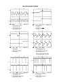
1
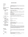
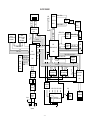
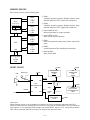
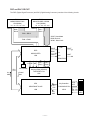
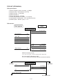
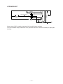
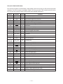
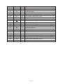
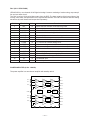
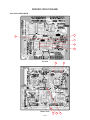
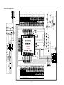
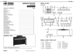
CTK-811EX
JUL.1998
,,,,,,,,,,,,,,,,,,,,,,,,,,,,,,,,
,,,,,,,,,,,,,,,,,,,,,,,,,,,,,,,,
,,,,,,,,,,,,,,,,,,,,,,,,,,,,,,,,
,,,,,,,,,,,,,,,,,,,,,,,,,,,,,,,,
,,,,,,,,,,,,,,,,,,,,,,,,,,,,,,,,
,,,,,,,,,,,,,,,,,,,,,,,,,,,,,,,,
,,,,,,,,,,,,,,,,,,,,,,,,,,,,,,,,
,,,,,,,,,,,,,,,,,,,,,,,,,,,,,,,,
,,,,,,,,,,,,,,,,,,,,,,,,,,,,,,,,
,,,,,,,,,,,,,,,,,,,,,,,,,,,,,,,,
,,,,,,,,,,,,,,,,,,,,,,,,,,,,,,,,
,,,,,,,,,,,,,,,,,,,,,,,,,,,,,,,,
,,,,,,,,,,,,,,,,,,,,,,,,,,,,,,,,
,,,,,,,,,,,,,,,,,,,,,,,,,,,,,,,,
,,,,,,,,,,,,,,,,,,,,,,,,,,,,,,,,
,,,,,,,,,,,,,,,,,,,,,,,,,,,,,,,,
,,,,,,,,,,,,,,,,,,,,,,,,,,,,,,,,
,,,,,,,,,,,,,,,,,,,,,,,,,,,,,,,,
,,,,,,,,,,,,,,,,,,,,,,,,,,,,,,,,
,,,,,,,,,,,,,,,,,,,,,,,,,,,,,,,,
,,,,,,,,,,,,,,,,,,,,,,,,,,,,,,,,
,,,,,,,,,,,,,,,,,,,,,,,,,,,,,,,,
,,,,,,,,,,,,,,,,,,,,,,,,,,,,,,,,
,,,,,,,,,,,,,,,,,,,,,,,,,,,,,,,,
,,,,,,,,,,,,,,,,,,,,,,,,,,,,,,,,
,,,,,,,,,,,,,,,,,,,,,,,,,,,,,,,,
USER RHYTHM
100 ‘109
2-WAY
BASS REFLEX SPEAKER
110 RHYTHMS
232 TONES
10DSP
DSP
DEMO
TONE
7
8
9
4
5
6
ENVELOPE
SYNTH
MODE
VOLUME
FULL RANGE
CHORD
FREE
SESSION
MAX
AMP
ENVELOPE
00 FLAT
DECAY
01-17 VIBRATO
SUSTAIN
TRANSPOSE/
TUNE/MIDI
LAYER/
AUTO HARMONIZE
FINGERED
1
CASIO CHORD
PITCH
ENVELOPE
RHYTHM
CONTRAST
POWER
ONE TOUCH
PRESET
SPLIT
2
3
TOUCH
RESPONSE
18-45 OTHERS
/NO
MIN
/YES
DISK
0
SEQUENCER
16 CHANNEL MIXER
EXTERNAL
CH2
CH3
CH4
CH5
CH6
CH7
CH8
CH9
CH10
CH11
CH12
CH13
CH14
CH15
CH16
DELETE
CURSOR
RECORD
SONG
PATTERN
INTERNAL
MIXER SELECT
INTRO
CH1
NORMAL/
FILL-IN
VARIATION/
FILL-IN
SYNCHRO/
ENDING
START/
STOP
UPPER1 UPPER2 LOWER1 LOWER2 ACC VOL. CHORD1 CHORD2 CHORD3
TONE EXPANDER
ACCOMP
BASS
RHYTHN
TR1
TR2
TR3
TR4
TR5
SEQUENCER TRACK
TR6
MAIN MENU/
CHANNEL VOLUME :
SUB MENU/
CHANNEL SELECT :
REGISTRATION
TEMPO
BANK
A
B
C
D
E
STORE
,,,,,,,,,,,,,,,,,,,,,,,,,,,,,,,
,,,,,,,,,,,,,,,,,,,,,,,,,,,,,,,
,,,,,,,,,,,,,,,,,,,,,,,,,,,,,,,
,,,,,,,,,,,,,,,,,,,,,,,,,,,,,,,
,,,,,,,,,,,,,,,,,,,,,,,,,,,,,,,
,,,,,,,,,,,,,,,,,,,,,,,,,,,,,,,
,,,,,,,,,,,,,,,,,,,,,,,,,,,,,,,
,,,,,,,,,,,,,,,,,,,,,,,,,,,,,,,
,,,,,,,,,,,,,,,,,,,,,,,,,,,,,,,
,,,,,,,,,,,,,,,,,,,,,,,,,,,,,,,
,,,,,,,,,,,,,,,,,,,,,,,,,,,,,,,
,,,,,,,,,,,,,,,,,,,,,,,,,,,,,,,
,,,,,,,,,,,,,,,,,,,,,,,,,,,,,,,
,,,,,,,,,,,,,,,,,,,,,,,,,,,,,,,
,,,,,,,,,,,,,,,,,,,,,,,,,,,,,,,
,,,,,,,,,,,,,,,,,,,,,,,,,,,,,,,
,,,,,,,,,,,,,,,,,,,,,,,,,,,,,,,
,,,,,,,,,,,,,,,,,,,,,,,,,,,,,,,
,,,,,,,,,,,,,,,,,,,,,,,,,,,,,,,
,,,,,,,,,,,,,,,,,,,,,,,,,,,,,,,
,,,,,,,,,,,,,,,,,,,,,,,,,,,,,,,
,,,,,,,,,,,,,,,,,,,,,,,,,,,,,,,
,,,,,,,,,,,,,,,,,,,,,,,,,,,,,,,
,,,,,,,,,,,,,,,,,,,,,,,,,,,,,,,
,,,,,,,,,,,,,,,,,,,,,,,,,,,,,,,
,,,,,,,,,,,,,,,,,,,,,,,,,,,,,,,
ENTER
PARAMETER RESET
ENTER
2-WAY
BASS REFLEX SPEAKER
LATION
MODU
PITCH
BEND
CTK-811
INDEX
GM SOUND KEYBOARD
CONTENTS
Safety Notice ----------------------------------------------------------------------------------------------- 2
Specifications ---------------------------------------------------------------------------------------------- 3
Important Operation ------------------------------------------------------------------------------------- 5
Block Diagram --------------------------------------------------------------------------------------------- 6
Circuit Description --------------------------------------------------------------------------------------- 7
Diagnostic Program ------------------------------------------------------------------------------------ 22
Major Waveformes -------------------------------------------------------------------------------------- 28
Printed Circuit Board ---------------------------------------------------------------------------------- 29
Exploded View ------------------------------------------------------------------------------------------- 31
Parts List --------------------------------------------------------------------------------------------------- 32
Schematic Diagrams ----------------------------------------------------------------------------------- 35
—1—
SAFETY NOTICE
CAUTION!
Danger of explosion if battery is incorrectly replaced. Replace
only with the same or equivalent type.
DENMARK:
ADVARSE!
Lithiumbatteri. Eksplosionsfare ved fejlagtig handtering.
Udskiftning ma kun ske med batteri af samme fabrikat og type.
Lever det brugte batteri tilbage tili leverandoren.
FINLAND:
VAROITUS
Paristo voiäjähtää, jos se on virheellisesti asennettu. Vaihda
paristo ainoastaan valmistajan suosittelemaan tyyppiin. Hävitä
käytetty paristo valmistajan ohjeiden mukaisesti.
SWEDEN:
VARNING
Felaktigt batteribyte kan medf fara för explosion. Använd därför endast samma typ eller likvärdig typ enligt apparattillverkarens rekommendation.
Kassera förbrukade batterier enligt tillverkarens anvisning.
—2—
SPECIFICATIONS
GENERAL
Keyboard:
Tones:
Rhythm instrument tones:
Polyphony:
Digital effects:
Auto accompaniment
Rhythm patterns:
Tempo:
Chords:
Rhythm controller:
Accomp volume:
One touch presets:
Auto harmonize:
Free session
Number of patterns:
Song sequencer
Songs:
Recording tracks:
Recording method:
Memory capacity
(total for two songs):
Punch in:
Pattern sequencer
Number of patterns:
Memory capacity:
Elements:
Parts:
Recording method:
Registration memory
Number of setups:
Memory contents:
Demo tunes:
Synthesizer
Parameters:
61 standard-size keys, 5 octaves (with touch response on/off; ExLight/
Light/Normal/Heavy touch)
232 (128 General MIDI, 64 variation, 8 drum, 32 user); with layer and
split
53
32 notes maximum (16 for certain tones)
10 (REVERB 1, 2, 3; CHORUS; TREMOLO; PHASE SHIFTER; ORGAN SPEAKER; ENHANCER; FLANGER; EQ LOUDNESS)
110 (100 + 10 user rhythms)
Variable (226 steps, = 30 to 255)
3 fingering methods (CASIO CHORD, FINGERED, FULL RANGE
CHORD)
Start/Stop, Intro, Normal/Normal Fill-In, Variation/Variation Fill-In,
Synchro/Ending
0 to 127 (128 steps)
Recalls settings for tone, tempo, layer, and Auto Harmonize in accordance with rhythm.
Automatic addition of notes that harmonize with melody note in accordance with specified Auto Accompaniment chords.
100 (Auto Accompaniment function based on preset chord progressions.)
2
6 (2 through 6 are melody tracks)
Real-time
Approximately 4,900 notes
Supported
10 (Rhythm numbers 100 to 109)
Approximately 7,000 notes
Intro, Normal, Variation, Normal Fill-In, Variation Fill-In, Ending
Chord 1, 2, 3; Bass; Rhythm
Real-time
20 (5 setups × 4 banks)
Tone, Rhythm, Tempo, Split on/off, Split point, Layer on/off, Auto Harmonize on/off, Mixer settings, Keyboard channel on/off, DSP (digital
effect) on/off, DSP (digital effect) settings, Accompaniment mode,
Touch Response settings, Assignable jack setting, Transpose, Tuning, Pitch Bend range, Sound range shift on/off
2
PCM set, amp envelope set, attack rate, release rate, pitch envelope
set, pitch, level, touch sensitivity, pan, filter sensitivity, filter level, transpose
Mixer
Channels:
Modes:
Parameters:
MIDI:
16
Internal, External, External/Solo, External/Play
Program change number, volume, expression, pan, coarse tuning,
fine tuning, Effect Send
16-channel multi-timbre receive, General MIDI Level 1
—3—
Other functions
Pitch bend range:
Modulation:
Transpose:
Tuning:
Terminals
MIDI terminal:
Sustain/Assignable jack:
Headphones/Output:
Floppy disk drive
Type:
Formats:
Functions:
Power supply:
Batteries
Battery life
AC adapter:
Auto power off:
Speaker output:
Power consumption:
Dimensions:
Weight (without batteries):
Standard accessories:
Adjustable (12 semitones upwards and downwards)
Equipped
25 steps (–12 semitones to +12 semitones)
Adjustable (A4 = approximately 440Hz ± 50 cents)
IN, OUT
Standard jack (sustain, sostenuto, soft, rhythm start/stop)
Stereo standard jack
Output Impedance: 250 Ω
Output Voltage: 5 V (RMS) MAX
12 V DC
3.5" FDD
2DD (720KB MS-DOS format)
2HD (1.44MB MS-DOS format)
Save and load of user tones, user rhythms, sequencer, and registration
data; playback of SMF; disk formatting; file delete; accompaniment pattern style conversion
Dual power supply system
Six D-size batteries
Approximately 3 hours continuous operation on alkaline batteries
AD-12
Turns power off approximately six minutes after last key operation. Enabled under battery power only, can be disabled manually.
5W+5W
12 V 18 W
109.2 × 42.7 × 15.7 cm (43 1/16 × 16 13/16 × 6 3/16 inch)
Approximately 9.2 kg (20.3 lbs)
Music Stand; Pattern Conversion Disk; Data Disk; Disk User’s Guide;
Keyboard User’s Guide
ELECTRICAL
Current drain with 12 V DC:
No sound output
Maximum volume
with 10 keys from C3 to E4 pressed in whistle tone
Volume: MAX., Velocity: MAX.
DSP0: Reverb1, FDD: Replay
Phone output level (Vrms with 8 Ω load each channel):
with tone Synth-Bass 4 tone
Volume: MAX., Velocity: MAX.
DSP0: Reverb1
Speaker output level (Vrms with 8 Ω load each channel):
with tone Synth-Bass 4 tone
Volume: MAX., Velocity: MAX.
DSP0: Reverb1
Output level (Vrms with 47 kΩ load each channel):
with tone Synth-Bass 4 tone
Volume: MAX., Velocity: MAX.
DSP0: Reverb1
Minimum operating voltage:
—4—
440 mA ± 20 %
2000 mA ± 20 %
L-ch (Key C4)
R-ch (Key F3)
100 mV ± 20 %
92 mV ± 20 %
L-ch (Key D3)
R-ch (Key F3)
7.1 mV ± 20 %
6.2 mV ± 20 %
L-ch (Key C4)
R-ch (Key F3)
3200 mV ± 20 %
3100 mV ± 20 %
6.1 V
IMPORTANT OPERATION
Full Initialization
Use this procedure to return all keyboard settings to what they were when you purchased it. Note that this
procedure clears all data from memory.
• While holding down the ENTER button, turn on keyboard power.
R e s e t?
• Press YES to initialize the keyboard or NO to turn on power without changing any settings.
Parameter Initialization
Use this procedure to return all keyboard settings to what they were when you purchased it. Note that this
procedure does not affect user tones, user rhythms, registration memory contents, and display contrast
settings.
• While keyboard power is on, press the [+], [–], and ENTER buttons at the same time.
Adjusting Display Contrast
• Display contrast can be adjust to one of 100 levels for easy viewing.
• Adjusting display contrast helps to make figures easier to read from any viewing angle.
• Within five seconds after pressing the CONTRAST button, press [+] to increase the contrast value (making the display darker) or [–] to decrease it (making the display lighter).
• After you release CONTRAST, the message “Contrast” remains on the display for a few moments, during
which you can change the contrast setting further using [+] and [–] or by inputting a contrast value with the
number keys.
The contrast can be set to a value from 0 to 99. The initial default setting is 50.
GM (General MIDI):
General MIDI standardizes MIDI data to play music with same nuance between different MIDI instruments.
Among GM conformed MIDI instruments, or commercially available musical data, music can be played with
similar tones.
SMF (Standard MIDI File):
SMF is a standard file format for MIDI instruments and computer music software. SMF formatted data can
be played and transported easily among SMF complied instruments or musical data of different manufacturers.
—5—
BLOCK DIAGRAM
Key Board
MIDI
IN OUT
SED1278F2A
SI0 ~
SI7
FI0 ~
FI7
KC0
~
KC7
LSI501
RD, HWR,
LWR
Key Controller
TC190C020AF-001
LSI10
ROM2
MSM23C3210MC
-12CA89
LSI3 (32Mbit)
LCD
Back Light
Back Light Driver
COM1 ~ COM16
NT-07
Q501, Q502
DB4
~DB7
LEDCK, LEDCL
CONT,
LRS,
LR/W
LE
RESB
A1 ~ A4
S-Register
TC74HC164
IC301
LEDs
LEDA ~ LEDF
D0 ~ D15
Buttons
RA0 ~ RA20
CPU
LSDT
HD6473042F16-465
SWCK
PBO
RESB
A0 ~ A3
S-Register
TC74HC164
IC302
VDD
KC0 ~ KC8
KI0 ~ KI7
DSP
RD0 ~ RD15
Working
RAM
RESET
RD,
HWR
LSI4
ECEB, EOEB
EWEB
D0 ~ D15
D0
LPF
(L)
(L)
FDD Controller
HWR
RD
VC
VDD
VCC
RESET
CVDD FVDD DVDD AVDD
Power Supply Circuit
Q205,
Q206
(R)
Speakers
—6—
HD63266F
LSI6
Reset IC
RN5VD40A
IC3
Power Amp.
LA4620
IC201
Out put
RAM2
TC551001BFL-70L
LSI8 (1Mbit)
S1
HWR, RD
D15
IC1
LPF
(R)
Main
Volume
D8
VBR
D15
~
~
RAM1
TC551001BFL-70L
LSI7 (1Mbit)
S1
LWR, RD
D/A Converter
µPD6376GS
LSI1
D8
VBR
D7
~
WOK1
SOLP
BOK
LSI5
(256Kbit)
NMI
TEND, DREQ, CS2, CS3, B1-5
1RD, 1HWR, 1LWR
Chip Selector
TC74HC08
A0 ~ A15
IC4
HG51B155FD
EA0 ~ EA14
ED0 ~ ED8
TC55257
GFL-70L
D8 ~ D15
LSI9
RD, HWR,
LWR
ROM1
MSM27C802CZ-465
LSI2 (8Mbit)
SEG1 ~ SEG40
LCD Driver
IC204, Q203
Q204, Q208, Q210 APO
VBR
VDD
Back up
Power
CR2032
3.5" FDD Unit
DF354HO64A
CIRCUIT DESCRIPTION
KEY MATRIX
KC0
KC1
KC2
KC3
KC4
KC5
KC6
KC7
FI0
C2 1
C#2 1
D2 1
D#2 1
E2 1
F2 1
F#2 1
G2 1
SI0
C2 2
C#2 2
D2 2
D#2 2
E2 2
F2 2
F#2 2
G2 2
FI1
G#2 1
A2 1
A#2 1
B2 1
C3 1
C#3 1
D3 1
D#3 1
SI1
G#2 2
A2 2
A#2 2
B2 2
C3 2
C#3 2
D3 2
D#3 2
FI2
E3 1
F3 1
F#3 1
G3 1
G#3 1
A3 1
A#3 1
B3 1
SI2
E3 2
F3 2
F#3 2
G3 2
G#3 2
A3 2
A#3 2
B3 2
FI3
C4 1
C#4 1
D4 1
D#4 1
E4 1
F4 1
F#4 1
G4 1
SI3
C4 2
C#4 2
D4 2
D#4 2
E4 2
F4 2
F#4 2
G4 2
FI4
G#4 1
A4 1
A#4 1
B4 1
C5 1
C#5 1
D5 1
D#5 1
SI4
G#4 2
A4 2
A#4 2
B4 2
C5 2
C#5 2
D5 2
D#5 2
FI5
E5 1
F5 1
F#5 1
G5 1
G#5 1
A5 1
A#5 1
B5 1
SI5
E5 2
F5 2
F#5 2
G5 2
G#5 2
A5 2
A#5 2
B5 2
FI6
C6 1
C#6 1
D6 1
D#6 1
E6 1
F6 1
F#6 1
G6 1
SI6
C6 2
C#6 2
D6 2
D#6 2
E6 2
F6 2
F#6 2
G6 2
FI7
G#6 1
A6 1
A#6 1
B6 1
C7 1
SI7
G#6 2
A6 2
A#6 2
B6 2
C7 2
Note: Each key has two contacts, the first conatct 1 and second contact 2.
Key
FI
First contact 1
Second contact 2
KC
SI
NOMENCLATURE OF KEYS
C#2 D#2
C2
D2
E2
F#2 G#2 A#2
F2
G2
A2
B2
C#3 D#3
C3
D3
E3
F#3 G#3 A#3
F3
G3
A3
B3
C#4 D#4
C4
D4
E4
F#4 G#4 A#4
F4
G4
—7—
A4
B4
C#5 D#5
C5
D5
E5
F#5 G#5 A#5
F5
G5
A5
B5
C#6 D#6
C6
D6
E6
F#6 G#6 A#6
F6
G6
A6
B6 C7
BUTTON MATRIX
KC0
KC1
KC2
KC3
KI0
KI1
KI2
KI3
KI4
KI5
KI6
KI7
MODE
INTRO
MIXER
SELECT
CH8
A
CH16
SPLIT
H/NO
—
RECORD NORMAL/
FILL-IN
CH1
CH9
B
E
LAYER/
AUTO HARMO
2
VARIATION/
FILL-IN
CH2
CH10
C
H
RHYTHM
5
PATTERN SYNCHRO/
ENDING
CH3
CH11
D
ENTER
TONE
8
SONG
KC4
DSP
START/
STOP
CH4
CH12
E
DISK
0
G/YES
+
KC5
CONTRAST
TEMPO
G
CH5
CH13
STORE
TOUCH
RESPONSE
1
3
KC6
FREE
SESSION
TEMPO
H
CH6
CH14
G
TRANSPOSE
4
6
KC7
ONE TOUCH
PRESET
BANK
CH7
CH15
F
SYNTH
7
9
DMSW
DEMO
LED MATRIX
LED-A
LED-B
LED-C
LED-D
LED-E
LED-F
FULL RANGE
CHORD
FINGERD
CASIO CHORD
FREE
SESSION
SYNTH
DISK
—8—
MEMORY DEVICES
Each memory device has the following data.
1 RAM1 :
S-RAM for operation program, Register, Pattern, Song
and SMF data from FDD. (Lower part of data bus)
RAM1
1
1 Mbit
LSI7
CPU
2 RAM2 :
S-RAM for operation program, Register, Pattern, Song
and SMF data from FDD. (Upper part of data bus)
Internal Memory
3 ROM 512 kbit
RAM2
2
1 Mbit
LSI8
4 RAM 16 kbit
LSI9
3 Internal ROM of CPU :
Main program data for system operation
4 Internal RAM of CPU :
Work area for system operation
ROM1
5
8 Mbit
LSI2
DSP
5 ROM1 :
Demo, Accompaniment data, Song, Pattern, Synth, Disk
mode
ROM2
6
32 Mbit
LSI3
LSI4
6 ROM2 :
Sound Waveforms/Tone data Digital sound effect
7 Working RAM :
Work area for DSP
Working RAM
7
256 kbit
LSI5
RESET CIRCUIT
VDD
DVDD
RESET
FDD Controller
HD63266F
LSI6
RESET
VDD
Battery set
RES
PB0
DVDD
DSP
HG51B155FD
LSI4
RESB
RESET
PW/SW ON
RESET
CPU
HD6473042F16-465
LSI9
PWSW
NMI
PA7
APO
APO
From power switch
DVDD
(5V)
Power Supply
Circuit
DVDD
RESB
Key Controller
TC190C020AF-001
LSI10
DVDD
Initial reset
When batteries are set or an AC adapter is connected, the reset IC provides a low pulse to the CPU.
When the power switch is pressed, the CPU receives a low pulse of POWER signal. The CPU first raises
APO signal to +5 V to generate DVDD voltage, then raises RESET signal to +5 V. During this period the
DSP, the key controller and FDD controller LSIs initialize their internal circuits.
—9—
POWER SUPPLY CIRCUIT
The power supply circuit provides various voltages as shown below.
The voltage VDD (+5 V) is provided as long as batteries or AC adaptor is set.
Other voltages are controlled by APO (Auto Power Off) signal from CPU.
PW/ON
NMI
APO
APO
CPU
HD6473042F16-465
PA7
LSI9
NMI
From
+9V ~ +12 V
Batteries or
AC Adaptor
PW/SW
(To back light)
Switching
Transistors
(To LCD)
LC Filter
(To FDD)
(To digital)
(To analog)
LC Filter
Regulator IC
The regulator IC BA9700A generates square waveform from pin 5 as PWM (Pulse Wide Modulation).
The LC filter makes stable output voltage (+5 V) for each circuit as shown above.
— 10 —
DSP and DAC CIRCUIT
The DSP (Digital Signal Processor) and DAC (Digital Analog Converter) consists of the following circuits.
ROM1
MSM27CB02CZ-465
LSI2 (8Mbit)
CE
RA23
ROM2
MX23C3210MC-12CA89
LSI3 (32Mbit)
A0 ~ A18 Q0 ~ Q15
CE
RA22
RA0 ~
RA18
A0 ~ A20 Q0 ~ Q15
RA0 ~
RA20
RD0 ~ RD15
SOLP: Sound data
BOK: Bit clock
WOK1: Word clock
RA0 ~ RA20
SOLP
DSP
HG51B155FD
LSI4
DAC
SI
BOK
CLK
WOK1
LRCK
ROUT
LOUT
UPD6376GS
CS OE WE
PG
D8 ~
D15
key
data
24.576 MHz
Control
data
ED0 ~
ED15
EA0 ~
EA14
D0 ~ D15
A0 ~ A14
Working RAM (256K-bit)
TC55257DFL-70L
LSI5
CPU
Key Controller
D0 ~
D15
HD6473042F16-465
LSI9
TC190C020AF-001
LSI10
key
data
— 11 —
KC0 ~
KC7
SI0 ~ SI7
FI0 ~ FI7 Key
board
FDD UNIT (DF354H064A)
FDD Specifications:
1
2
3
4
5
6
7
8
Memory Capacity (under un-format) : 1.6 MByte
Density of track : 5.33 track/mm (135 TPI)
Number of track : 77 track/side
Number of head : 2
Rate of data transfer : 500 kbps
Access time (between two tracks) : 3 m seconds
Compensation of writing data : 125 n second (all tracks)
Rotation speed : 360 Min-1 (rpm) ± 1.5 %
FDD Interface:
Host system
Drive
CN2 connector
4
8
Drive Select 1
12
Motor ON
Direction
Step
Write Data
Write Gate
16
18
20
22
24
Side 1 Select
Density Select
Index
26
28
30
Track 00
Write Protect
Read Data
34
Disk Change
32
GND Pin Numbers of CN2:
1, 5, 7, 9, 11, 13, 15, 17, 19, 21, 23, 25, 27, 29, 31, 33
Non connected Pin Numbers of CN2:
2, 6, 10, 14 (Pin #3 is removed to prevent erroneous insertion)
CN1 connector
DC.GND
+5 V
2
3
N.C
Signal GND
1
+5 V Return
+5 V Return
4
0Ω
System Frame GND.
Drive Frame GND.
— 12 —
LCD BACKLIGHT
1
2
4.7K
Q502
LHL08TB101K
1
2
L501
CVDD
2
R501
1
T501
1
3
5
(Bottom View)
2SD965R
5
C516
4
7
DG
CP14
C104FA
1
2
C502
3
2SD965R C104M
CFL1
2
8
C501
HMBV26BG1W63N/AZG
DE0405-979SL180J2K
2
1
3
2
1
2
9
1
Q501 1
NT-07
10
When voltage CVDD is supplied, transistors Q501 and Q502 start oscillation.
From the oscillation voltage, transformer T501 generates about 600 V which is necessary for lighting the
backlight.
— 13 —
CPU (LSI9: HD6473042F16-465)
The 16 bit CPU contains a 512K-bit ROM, a 16K-bit RAM, eleven 8-bit I/O ports, an A/D converter and serial
interfaces. The CPU accesses to the RAM1, RAM2, DSP, Key controller, FDD controller and LCD driver
LSI. The CPU also controls buttons, LEDs, bender input and MIDI input/output.
Pin No.
1
Terminal
VCC
In/Out
In
2~5
6
7
8
9
PB0 ~ PB3
PB4
PB5
DREQ0
PB7
Out
Out
Out
—
Out
Data bus for LCD driver.
Chip enable signal for LCD driver.
Read/write signal for LCD driver.
DMA (Direct Memory Access) request.
Register selection signal for LCD driver.
In
In
Out
In
In
Not used.
Ground terminal (0 V).
MIDI signal output.
Key input signal from buttons.
MIDI signal input.
10
RES0
11
VSS
12
TXD0
13, 15 ~ 17 P91, P93~P95
14
RXD0
18 ~ 21
23 ~ 34
22
35
36 ~ 43,
45 ~ 56
Function
VCC (5 V) source.
D0 ~ D15
In/Out
VSS
VCC
In
In
A0 ~ A19
Out
Address bus.
In
In
—
Out
—
Ground terminal (0 V).
Key input signal from buttons.
Not used.
Clock signal (16 MHz).
Not used.
44, 57
VSS
55, 59, 60 P52, P61, P62
58
WAIT
61
CLKOUT
62
STBY
63
64
65
66, 67
68
RES
NMI
VSS
EXTAL, XTAL
VCC
In
In
In
In
In
69
70
71
72
73 ~ 75
AS
RD
HWR
LWR
MD0 ~ MD2
—
Out
Out
Out
In
76, 77
78
79
AVCC, VREF
AN0
AN1
In
In
In
Data bus.
Ground terminal (0 V).
Vcc (5 V) source.
Reset signal at VDD (5 V) supplied.
Power ON signal input.
Ground terminal (0 V).
Clock (16 MHz) input.
Vcc (5 V) source.
Not used.
Read signal.
Write signal for upper data bus.
Write signal for lower data bus.
Mode selection terminals.
Power source and reference voltage for internal A/D, D/A.
Battery voltage detection (Not used).
Pitch bender voltage detection.
— 14 —
Pin No.
80
Terminal
P72
In/Out
In
Function
AC adaptor detection terminal.
81
82
83
84
85
P73
P74
P75
P76
DA1
In
In
In
In
Out
Modulation signal input.
Pedal signal input.
FD sheet type (2HD, 2DD) signal input.
Key input signal from buttons.
LCD contrast control voltage output.
86
87
88
89
90
AVSS
PB0
CS3
CS2
CS1
In
Out
Out
Out
Out
Ground terminal (0 V).
Reset signal for DSP, Key controller, FDD controller.
Chip select signal for FDD.
Acknowledge signal FDD DMA function.
Chip select signal for Key controller.
91
92
93
94
95
CS0
VSS
TEND
PA1
PA2
Out
In
Out
Out
Out
Chip select signal for DSP.
Ground terminal (0 V).
End signal for data transfer of FDD.
Change signal for data transfer speed of FDD.
Key input signal for DEMO button.
96
97
98
99
100
PA3
PA4
PA5
PA6
PA7
Out
Out
Out
Out
Out
Clock signal for shift register of KC signal.
Clear signal for shift register of LED.
Control signal for KC signal and LED.
Clock signal for shift register of LED.
APO (Auto Power Off) signal.
— 15 —
DIGITAL SIGNAL PROCESSOR (LSI4:HG51A115A01FD)
Upon receipt of note numbers and their velocities, the DSP (Digital Signal Processor) reads sound and
velocity data from the sound source ROM in accordance with the selected tone; the DSP can read rhythm
data simultaneously when a rythm pattern is selected. Then it provides 16-bit serial signals containing data
of the melody, chord, bass, and percussion to the DAC. The DSP also adds the selected effect to the sound
data using a 256k-bit RAM.
The following table shows the pin functions of the DSP.
Pin No.
1~8
Terminal
CD0 ~ CD7
In/Out
In/Out
Function
Data bus
9, 10
11
12
13
14
GND7
CK16
VCC6
CK0
15
16
17
18, 19
20
TCKB
VCC1
GND1
XT0, XT1
SGL
In
In
In/Out
In
21
22 ~ 25
26
27
CCSB
CA0 ~ CA3
CE0
CWRB
In
In
In
In
Chip select signal input
Address bus
Not used. Connected to ground.
Write enable signal
28
29 ~ 32
33
34
35 ~ 39
CRDB
In
RESB
TESB
In
In
Read enable signal
Not used.
Reset signal input
Not used. Connected to +5 V
Not used.
RD0 ~ RD15
In
RA23
RA22
RA21
Out
Out
Out
Chip select signal for the ROM1
Chip select signal for the ROM2
Not used.
RA0 ~ RA20
Out
Address bus for the ROM1 and ROM2
74
83
84
85
86
GND5
WOK2
VCC3
GND3
WOK1
In
Out
In
In
Out
Ground (0 V) source
Word clock output. Not used.
+5 V source
Ground (0 V) source
Word clock for the DAC
87
88
89
SOLM
SOLP
BOK
Out
Out
Out
Serial data output. Not used.
Serial data output for the DAC
Bit clock output for the DAC
40 ~ 49
52 ~ 57
58
59
60
61 ~ 73
75 ~ 82
In
Out
In
In
Not used.
Ground (0 V) source
24.576 MHz clock output
+5 V source
Clock input. Connected to terminal CK16.
Not used.
+5 V source
Ground (0 V) source
24.576 MHz clock input/output. Connected to a crystal oscillator.
System control terminal. Single chip system: Open
Data bus for the ROM1 and ROM2
— 16 —
Pin No.
90 ~ 92
93
94, 95
97 ~ 105
107, 109
110, 112
96
106
108
111
113 ~ 117
118
119
120 ~ 122
123 ~ 130
131
132 ~ 134
135, 136
Terminal
In/Out
Function
Not used.
+5 V source
VCC
In
EA0 ~ EA14
Out
Address bus for the working RAM
EWEB
EOEB
VCC7
ECEB
Out
Out
In
Out
Write enable signal output for the working RAM
Read enable signal output for the working RAM
+5 V source
Chip select signal output for the working RAM
VCC4
GND4
In
In
ED0 ~ ED7
In/Out
GND5
In
Not used.
+5 V source
Ground (0 V) source
Not used.
Data bus for the working RAM
Ground (0 V) source
Not used. Connected to ground.
Not used.
FDD CONTROLLER (LSI6:HD63266F)
The FDD (Floppy Disk Drive) controller can control the FDD unit.
The controller contains not only analog VFO (Variable Frequency Oscillator) circuit but also driver/receiver,
input/output port and oscillation circuit internally.
Pin No.
1
2
Terminal
8/ - 5
XTALSEL
In/Out
In
—
3
4
5
6
7
RESET
E, -RD
R/-W, -WR
CS
DACK
In
In
In
In
In
8, 9
10, 11
12 ~ 19
20
21
RS0, RS1
VSS1, VSS2
D0 ~ D7
DREQ
IRQ
In
In
In/Out
In
—
22
23
24
25
DEND
VSS3
1/2 EX1
VCC1
NUM1, NUM2
IFS
In
In
—
In
26, 27, 28
29
SFORM
—
In
Function
Change of data transfer speed.
Not used. Connected to ground (0 V).
Reset signal input.
Read signal.
Write signal.
Chip select signal.
Acknowledge signal of DMA (Direct Memory Access).
Register selection for read/write.
Ground terminal (0 V).
Data bus.
Request signalof DMA.
Not used.
End signal for data transfer.
Ground terminal (0 V).
Not used.
DVDD (5 V) source.
Not used. Connected to ground (0 V).
Selection signal for formatting.
— 17 —
Pin No.
Terminal
In/Out
30
INP
In
Disk detection signal.
31
READY
In
Ready signal from FDD. (Connected to ground (0V).)
32
33
WPRT
TRKO
In
In
Write protect signal from FDD.
Track0 signal from FDD.
34
INDEX
In
Index signal from FDD.
35
RDATA
In
Read data signal from FDD.
36, 37, 38 XTAL2, EXTAL2
39
NC, XTAL1
—
Function
Not used.
40
EXTAL1
In
Clock signal input from CPU (16 MHz).
41, 42
43
VSS4, VSS5
NC
In
—
Ground terminal (0 V).
Not used.
44 ~ 46
VCC2, VCC3,
VCC4
In
47
WGATE
Out
48
WDATA
Out
49
VSS6
In
50
51
STEP
HDIR
Out
Out
Step signal for FDD head.
Head direction signal for FDD.
52
HLOAD
Out
Not used.
53
HSEL
Out
Head selection signal for FDD.
54
VSS7
In
Ground terminal (0 V).
55
DS0
Out
Drive selection signal.
—
In
Not used.
Ground terminal (0 V).
56, 57, 58 DS1, DS2, DS3
59
VSS8
60
MON0
Out
61, 62, 63
MON1, MON2,
MON3
—
64
VSS9
In
DVDD (5 V) source.
Write gate signal to FDD.
Write data signal to FDD.
Ground terminal (0 V).
Motor ON signal for FDD.
Not used.
Ground terminal (0 V).
— 18 —
KEY TOUCH LSI (LSI10: TC190C020AF-001)
By counting the time between first-key input signal FI and second-key SI from the keyboard unit, the key
touch LSI detects key velocity of 256-step. Then the LSI sends the CPU the note number and its velocity
data.
Pin No.
Terminal
In/Out
1
WRB
In
2 ~ 11, 13,
14, 16 ~ 19
D0 ~ D15
In/Out
12
15
VSS
VDD
In
In
Ground terminal (0 V).
VDD (5 V) source.
20 ~ 23
CA0 ~ CA3
In
Address bus.
24
VSS
In
Ground terminal (0 V).
25 ~ 32,
34, 35
FI0 ~ FI4,
SI0 ~ SI4
In
Key input signal.
33
VDD
In
VDD (5 V) source.
KC0 ~ KC7
Out
VSS
In
Ground terminal (0 V).
45
VDD
In
VDD (5 V) source.
46 ~ 51
FI5 ~ FI7
SI5 ~ SI7
In
Key input signal.
VSS
In
Ground terminal (0 V).
In
Key input signal (Not used).
In
VDD (5 V) source.
—
Not used.
36 ~ 38,
40 ~ 44
39
52
59
FI8 ~ FI10
SI8 ~ SI10
KI0 ~ KI2
VDD
63, 64
MODE0, MODE1
53 ~ 58,
60 ~ 62
Function
Write signal from CPU.
Data bus.
Key scan signal.
65
VSS
In
Ground terminal (0 V).
66
KCKI
In
Clock signal for key common/input.
—
Not used.
67 ~ 72,
74 ~ 77
73
VDD
In
VDD (5 V) source.
78
RESB
In
Reset signal from CPU.
79
CSB
In
Chip selection signal.
80
RDB
In
Read signal from CPU.
— 19 —
LCD DRIVER (LSI501: SED1278F2A)
The LCD driver can drive a dot matrix LCD having 40 segment and 16 common lines. The LSI contains 240
graphic symbols in the built-in character generator ROM, and stores 80 characters in the built-in display
data RAM. In accordance with command from the CPU, the LSI is capable of displaying up to 16 characters
simultaneously. The following table shows the pin functions of LSI 501.
Pin No.
Terminal
In/Out
Function
1 ~ 22,
63 ~ 80
SEG1 ~ SEG40
Out
23
VSS
—
24, 25
OSC1, OSC2
In/Out
26 ~ 30
V1 ~ V5
In
LCD drive voltage input.
Those voltages are used for generating the stepped pulse of the
LCD drive signals.
31, 32
LP, XSCL
—
Not used
33
VDD
In
LVDD (+5 V) source
34, 35
FR, DO
—
Not used
36
37
RS
R/W
In
In
Data/command determination terminal.High: data, Low: command
Read/write terminal. High: read, Low: write
38
E
In
Chip enable signal.
High: enable, the writing is done at fall edge.
Low: disenable
39 ~ 42
DB0 ~ DB3
—
Not used. Connected to GND (0 V)
43 ~ 46
DB4 ~ DB7
In/Out
47 ~ 62
COM1 ~ COM16
Out
Segment signal output
GND (0 V) source
Terminals for the built-in clock pulse generator. The external resistor connected determines the oscillation frequency.
Data bus
Common signal/output
REGULATOR IC (IC204: BA9700A)
The regulator IC controls the output voltage by PWM (Pulse Wide Modulation) with outer switching transistors and LC filters (integration circuit).
NON
INVERT
INP
1/2Vret
INVERT
INP
Vret
POWER
SW
NC
VCC
14
13
12
11
10
9
8
+
Voltage
Regulator
–
30k
Error
Amp
30k
Vret
PWM
Comparator
Triangle
Oscillator
1
2
3
4
5
6
7
D-TIME
CONT
RT
CT
FEED
BACK
OUT
NC
GND
— 20 —
DAC (LSI1: UPD6376GS)
UPD6376GS is a two-channel 16-bit Digital to Analog Convertor consisting of resistor string, output amplifier and zero offset circuit.
The DAC receives 16-bit serial data output from the DSP. The data contains digital sound data of the
melody, chord, bass, and percussion for the right and left channels. The DAC converts the data into analog
waveforms by each channel and output them separately.
Pin No.
1
Terminal
SEL
In/Out
In
2
D.GND
In
3
NC
Function
Mode selection terminal. Connected to ground.
Ground (0 V) source for internal digital circuit
Not used.
4
DVDD
In
+5 V source for internal digital circuit
5
A.GND
In
Ground (0 V) source for internal analog circuit
6
7
R.OUT
A.VDD
Out
In
8
A.VDD
In
+5 V source for internal analog circuit
9
R.REF
In
Reference voltage terminal. Connected to a capacitor.
10
L.REF
In
Reference voltage terminal. Connected to a capacitor.
11
L.OUT
Out
12
13
A.GND
LRCK
In
In
Ground (0 V) source for internal analog circuit
Word clock (L/R separation signal) input.
14
LRSEL
In
Not used. Connected to ground.
15
SI
In
Sound data input
16
CLK
In
Bit clock input
Sound waveform output
+5 V source for internal analog circuit
Left channel sound waveform output
POWER AMPLIFIER (IC301: LA4620)
The power amplifier is a two-channel amplifier with standby switch.
19
Boot11
20
OUT11
21
PoGND1
22
OUT12
23
Boot12
1
VCC1
18
Boot21
17
OUT21
15
PoGND2
14
OUT22
12
Boot22
+
IN11+
3
IN11–
5
–
IN12–
4
–
+
Input
Amp.
Pre-drive
Amp.
RL Short
Protector
Input
Amp.
Pre-drive
Amp.
Terminal
Protection
Circuit
PriGND
6
IN21+
9
+
IN21–
7
–
IN22–
8
–
+
Power
Amp.
Input
Amp.
Power
Amp.
Pop Noise
Prevention
Circuit
Ripple
Filter
Pre-drive
Amp.
Power
Amp.
RL Short
Protector
Input
Amp.
Pre-drive
Amp.
Power
Amp.
16
2
10
11
13
NC
DC
MUTE
VCC2
ADJ
— 21 —
DIAGNOSTIC PROGRAM
■ To enter diagnostic mode
1. While pressing down “0” and “ACCOMP CHORD MODE” buttons, press “POWER” button for turning
on.
2. The instrument is set in diagnostic mode and display indicates “Test”.
■ Button check
1. Press “0” button.
2. Display indicates “Console”.
3. Press buttons in the following order
)
1
2
3
4
5
6
7
8
9
0
A
B
C
D
MODE button
RECORD button
SONG button
PATTERN button
INTRO button
NORMAL/FILL-IN
button
VARIATION/FILL-IN
button
SYNCHRO/ENDING
button
START/STOP button
TEMPO button down
TEMPO button up
BANK button
REGISTRATION
buttons A
REGISTRATION
buttons B
REGISTRATION
buttons C
E REGISTRATION
buttons D
F REGISTRATION
buttons E
G STORE button
H DSP (digital effect)
button
I CONTRAST button
J FREE SESSION
button
K ONE TOUCH
PRESET button
L MIXER SELECT
button
M CHANNEL button
CH1
N CH2
O CH3
P CH4
Q CH5
R
S
T
U
V
W
X
Y
Z
[
\
]
_
g
h
i
j
k
l
m
n
o
p
q
r
s
t
u
CH6
CH7
CH8
CH9
CH10
CH11
CH12
CH13
CH14
CH15
CH16
SPLIT button
LAYER/AUTO
HARMONIZE button
RHYTHM button
TONE button
Number key 7
Number key 4
Number key 1
Number key 0
a
b
c
d
e
f
Number key –
Number key 2
Number key 5
Number key 8
Number key 9
Number key 6
Number key 3
Number key +
Cursor key Up
Cursor key Left
Cursor key Down
Cursor key Right
ENTER button
DISK button
TOUCH RESPONSE
button
v TRANSPOSE/
TUNING/MIDI button
w SYNTH button
x DEMO button
DSP
TONE
H
b
DEMO
x
w
7
8
9
c
j
k
SYNTH
RHYTHM
CONTRAST
POWER
MODE
VOLUME
FULL RANGE
CHORD
MAX
I
a
FREE
SESSION
LAYER/
AUTO HARMONIZE
J
FINGERED
CASIO CHORD
_
ONE TOUCH
PRESET
]
SEQUENCER
EXTERNAL
SONG
PATTERN
1
2
3
INTRO
NORMAL/
FILL-IN
4
5
VARIATION/
FILL-IN
6
v
/NO
0
f
16 CHANNEL MIXER
RECORD
SYNCHRO/
ENDING
7
CH1
CH2
CH3
CH4
CH5
CH6
CH7
CH8
CH9
START/
STOP
8
UPPER1 UPPER2 LOWER1 LOWER2 ACC VOL. CHORD1 CHORD2 CHORD3
TONE EXPANDER
ACCOMP
CH10
RHYTHN
CH11
CH12
TR1
TR2
CH13
CH14
CH15
TR3
TR4
TR5
SEQUENCER TRACK
CH16
BANK
A
A
B
B
C
D
C D E
E
STORE
F
G
u
/YES
DISK
g n
t
CURSOR
TR6
o
REGISTRATION
TEMPO
9 0
BASS
TOUCH
RESPONSE
DELETE
L MNOPQRSTUV WXYZ[\
INTERNAL
MIXER SELECT
TRANSPOSE/
TUNE/MIDI
1
2
3
e
h
m
SPLIT
K
MIN
)
4
5
6
d
i
l
p
r
q
ENTER
s
Display shows the button number to be pressed. When the pressed button functions properly, the instrument emits a verification signal and indicates next button number.
If the button malfunctions, an error alarm sounds and display indicates “Cons ER”.
When wrong button is pressed, the alarm sound is also emitted. In that case, re-press the correct button.
— 22 —
■ Bender check
1. While pitch bender is left untouched, press “–” button.
2. Display indicates “Bender”.
3. If the bender’s center point is adjusted correctly, the instrument emits verification sound. If the center
point is improper, an error alarm sounds and display indicates “Bend ER” and the instrument exits
from the diagnostic program.
4. Rotate the bender all the way to the upper position.
When the program detects upper most position, it emits verification sound. If wrong direction (toward
lower position ) of bender rotation is detected, the instrument exits from the diagnostic program after
emitting an alarm sound and displaying “Bend ER”.
5. Reset the bender on the center position.
A verification tone sounds.
6. Rotate the bender all the way to the lower position.
When the program detects lower most position, it emits verification sound.
If wrong direction (toward upper position) is detected, the instrument exits from the diagnostic program after emitting an alarm sound and displaying “Bender ER”.
7. Reset the bender on the center position.
The instrument exits from diagnostic program after emitting a verification sound and displaying “Bend
OK”. (During and after the check, display indicates bender values until another button is pressed.)
■ AC adaptor detection check.
1. Press “+” button.
2. When the instrument detects that an AC adaptor is plugged in, it indicates “Jack OK” on the display.
If it judges that no AC adaptor is inserted (powered by batteries), it indicates “Jack ER” on the display.
■ Keyboard, Sustain pedal, and Modulation switch check
1. Press “1” button.
2. Display indicates “TouchSus”.
In accordance with key, sustain pedal, or module switch depressions, display indicates velocity value
(hexadecimal values 01 to 7F), “SUS”, or “Mod”.
■ ROM check
1. Press “2” button.
2. The diagnostic program counts check sums of 8Mbit and 16Mbit ROMs.
3. In accordance with ROMs functions, display indicates;
“ROM OKOK” -------------- Both ROMs function normally
“ROM OKER” -------------- 8Mbit ROM OK, 16Mbit ROM NG
“ROM EROK” -------------- 8Mbit ROM NG, 16Mbit ROM OK
“ROM ERER” -------------- Both ROMs are NG
— 23 —
■ RAM check
1. Press “3” button.
2. The program executes write/read test in all the RAM area.
3. When the RAM is proper, display indicates “RAM OK”.
If the RAM malfunctions, “RAM NG” is shown on the display.
4. When the RAM check is executed, other tests become unavailable.
5. Pressing any key performs “Bender reset” transaction described below.
■ Small sound output
1. Press “4” button.
2. The instrument emits a sound in small volume and indicates “MIN” on the display.
■ Medium sound output
1. Press “5” button.
2. The instrument emits a medium volume sound and indicates “MID” on the display.
■ Large sound output
1. Press “6” button.
2. The instrument emits a large volume sound and indicates “MAX” on the display.
■ Large sound left channel output
1. Press “7” button.
2. The instrument emits a large volume sound from the left speaker and indicates “L” on the display.
■ Large sound right channel output
1. Press “8” button.
2. The instrument emits a large volume sound from the right channel and indicates “R” on the display.
■ MIDI IN/OUT test
1. Connect MIDI IN and MIDI OUT terminals with a MIDI cable.
2. Press “9” button.
3. When the MIDI circuit is normal, display indicates “MIDI OK” whereas “MIDI ER” will be shown if the
MIDI circuit is abnormal.
— 24 —
■ LCD test
1. Press “CURSOR ←” button.
2. Display indicates “LCD OK”.
3. Each pressing of “CURSOR ←” button, displays following patterns in the following order with verification sound.
a.
b.
c.
d.
e.
f.
g.
Checker on 8 character block : pattern A
Checker on 8 character block : pattern B
Checker on pixel block : pattern A
Checker on pixel block : pattern B
All dots indication
Displays each pixel (or dot) block in turn + all dots indication
Displays each dot in turn + all dots indication
■ LED test
1. Press “CURSOR →” button.
2. Display indicates “LED Test” and LEDs illuminate in the following order with verification sound.
a.
b.
c.
d.
e.
f.
g.
h.
FULL RANGE CHORD
FINGERED
CASIO CHORD
SONG
PATTERN
FREE SESSION
SYNTH
DISK
■ FDD test
1. Press “DISK” button.
2. Display indicates “Disk0-9E” (which means numeral key 0 to 9 and ENTER button.)
This test executes floppy disk’s write/read test and entering a number selects sectors to be tested.
Larger the number, narrower the check area namely, entering 0 checks all the sectors of the disk.
3. Press “ENTER” button to clean the FDD with cleaning disk. Wet type cleaning disk is recommended.
■ To exit from the diagnostic program
Pressing “CURSOR ↓” button sets the instrument in Reset power off state.
If you wish to use the instrument continually after this diagnostic program, perform “System reset” described below.
— 25 —
<Other utilities>
■ Bender reset
Sets bender’s center point in initial value.
1. While pressing down “ENTER” and “ACCOMP CHORD MODE” buttons, turn the power on.
2. Display shows “BndReset” indicating that pitch bender’s center point is initialized.
3. Perform the “System reset” described below.
■ System reset
1. While pressing down “ENTER” button, turn power on.
2. Display indicates “Reset?”.
3. Pressing “+” button initializes the instrument.
Pressing “–” button invalidates system reset.
4. The instrument turns on automatically.
■ Touch off max
1. While pressing down “RHYTHM” and “ACCOMP CHORD MODE” buttons, turn the power on.
2. Display indicates “TouchMax”.
3. The instrument is set in touch off max mode.
In this state, sound volume in touch response off mode becomes maximum.
— 26 —
FDD ERROR MESSAGE
Error Message
Reason of Error
R e a dO n l y
The file being written to is read-only.
F o rm a t
The disk format is not one supported by this keyboard.
D is k R /W
Error occurred during reading from the disk.
D is k F u l l
Disk is full.
M em F u l l
Not enough memory to perform the process.
No memory is available to load data.
N o tS SM F 0
An attempt was made to play data that is not SMF
FORMAT 0.
N o D is k
An attempt was made to access a disk while no disk
is loaded in the drive.
N o F i le
There is no file that corresponds to the file that was
specified.
P ro te c t
A save or delete operation was attempted with a
disk that is write protected.
C onve rt
The attempted file conversion was not successful.
W ro n g D a t
Something is wrong with the data you are trying to
load.
— 27 —
MAJOR WAVEFORMES
1
3
4
2
1 Clock signal for CPU
Check point CP1
2 Clock signal for DSP
Check point CP2
3 Voltage VDD
IC3 pin 2
4 Reset signal RES
IC3 pin 1
7
5
6
8
5 NMI signal
LSI9 pin 64
6 Reset signal RESB
LSI9 pin 87
7 Sound signal L-OUT
JC connector pin 10
8 Sound signal L-VOL0OUT
JG connector pin 5
Tone: Clarinet, Volume: Max.
Touch speed: Max., Key: A4
A
9
0
B
9 Key common signal KC0
JB connector pin 1
0 Key common signal KC1
JB connector pin 2
A Read signal for RAM1
LSI7 pin 24
B Write signal for RAM1
LSI7 pin 29
— 28 —
PRINTED CIRCUIT BOARD
Main PCB JCM465-MA1M
4
3
1
12
11
Top View
Bottom View
— 29 —
6
9
10
5
2
Sub PCB JCM465-MA2M
7
Top View
8
— 30 —
EXPLODED VIEW
41
R-1
R-3
38
37
36
29
30
31
35
40
39
22
10
32
34
21
33
40
27
19
23
24
20
7
3
12
11
23
5
28
14
4
6
— 31 —
22
13
8
BT1
1
9
43
2
R-2
15
16
18
26
R-4
46
44
42
25
17
45
48
48
47
47
PARTS LIST
Item
1
LSI1
LSI2
(LSI2)
LSI3
LSI4
LSI5
LSI6
LSI7/LSI8
LSI9
(LSI9)
LSI10
IC1
IC2
IC3
IC4
Q1,Q3,Q4
Q2
D1,D3,D4
D2
X1
X2
BT1
2
IC201
IC204
IC202,205
IC203
Q205
Q204,206,209
Q208
Q203,210
D201,204~207,
210
D208
D202,203,209
J201
J202
J203
J204
L201,203,204,
208
L202,205
L206
3
4
5
6
7
LSI501
Q501/502
Q503
Code No.
Parts Name
Specification
Q
R
1
1
1
(1)
1
1
1
1
2
1
(1)
1
1
1
1
1
1
1
3
1
1
1
1
A
A
A
(A)
A
A
A
A
A
A
(A)
A
B
B
B
B
B
B
C
C
C
C
A
MA1M PCB
6926 8930
2114 4221
2012 6135
(2012 6062)
2012 6064
2011 7434
2012 5572
2010 9990
2012 5947
2012 6132
(2012 6060)
2012 5987
2105 1561
2105 6355
2012 1883
2105 4935
2252 1169
2250 1169
2390 1820
2360 3057
2590 2748
2590 2107
3815 0707
MA2M PCB
6926 8990
2114 1883
2113 0084
2114 1799
2114 1421
2251 0672
2252 0154
2252 1253
2250 0133
2390 1344
PCB/ASSY (MA1M)
LSI
LSI
(LSI)
LSI
LSI
LSI
LSI
LSI
LSI
(LSI)
LSI
IC/CMOS
IC/CMOS
IC/MOS
IC/CMOS
TRANSISTOR/CHIP
TRANSISTOR/CHIP
DIODE/CHIP
DIODE/ZENER/CHIP
OSCILLATOR/CERAMIC
OSCILLATOR/CRYSTAL
BATTERY/LITHIUM
M240837*1
UPD6376GS-E1
MX23C8100MC-12CA99
(MSM27C802CZ-465)
MX23C3210MC-12CA89
HG51B155FD
TC55257DFL-70L(EL)
HD63266F
TC551001BFL-70L(EL)
HD6433042SB51F
(HD6473042F16-465)
TC190C020AF-001
TC7S04F(TE85R)
TC7S00F(TE85R)
RN5VD40AA-TR
TC74VHC08F(TP1)
2SC4081-T106S
2SA1576A-T106S
1SS355TE-17
UDZTE-173.3B
CSA16.00-MXZ243
HC-49S24A
CR2032-1HM
PCB/ASSY (MA2M)
IC/MONOLITHIC
IC/MONOLITHIC
IC/MONOLITHIC
IC/PHOTO COUPLER
TRANSISTOR
TRANSISTOR
TRANSISTOR
TRANSISTOR
DIODE
M140750*1
LA4620
BA9700A
M5218APR
PC900V
2SB1548-P.CS
2SC1740SS-TP-T
2SB1566F
2SA933SS-TP-T
1SS133T-77-T
1
1
1
2
1
1
3
1
2
6
B
B
B
B
B
B
B
B
B
C
2360 1085
2390 1463
3501 5012
3612 0665
3612 0789
3501 4816
3841 2154
DIODE/ZENER
DIODE/SHOTTKY
JACK/DC
JACK
JACK
JACK/DIN
COIL/COMMON MODE
HZS6B1LTD-T
SB20-03B
HEC2305-01-920
YKB21-5006
YKB21-5010
YKF51-5051
SH-432
1
3
1
1
1
1
4
C
C
C
C
C
C
C
3841 2175
3841 2177
BL ass'y
6926 9030
6926 9050
3122 3558
5861 3522
6925 9490
2012 6018
2253 0710
2250 0133
Notes: Q
R
COIL/COMMON MODE
COIL
SH-S132
OH-022Z
2
1
C
C
BL/ASSY
PCB/ASSY (LD1M)
CFL
HOLDER/CFL
PLATE/BL
LSI
TRANSISTOR
TRANSISTOR
– Quantity per unit
– Rank
M240682*2
M240838*1
HMBV26BG1W63N/AZG
HRB-0256
M340602-1
SED1278F2A
2SD965-R(TA)
2SA933SS-TP-T
1
1
1
2
1
1
2
1
A
A
A
C
C
A
B
B
— 32 —
Item
Code No.
Q504
D501
D502
L501
T501
2252 0154
2360 3056
2390 1344
3841 1197
3012 1470
CN1 ~ CN3
6926 9070
6926 9080
6926 9090
2105 1239
2370 1383
2370 1403
2765 2178
Keyboard
6922 2720
6922 2730
6906 8482
6906 8592
6926 2500
6926 2510
6926 9130
6926 9140
Bender
2765 1141
6926 9450
6926 9460
Panel
3831 1081
3831 1082
3335 6728
3502 2446
3502 2447
6926 2540
6921 5030
6926 9280
6926 9290
6926 9300
6926 9310
6926 9320
6926 9330
6926 9340
6926 9350
6926 9360
6926 9370
6925 9380
6925 9410
6926 9240
6918 1630
3502 2318
1015 1399
6926 9400
6926 9410
6926 9420
6926 9431
8
9
10
IC301,302
LED301
LED302~309
VR301
11
12
13
14
15
16
17
18
19
20
21
22
23
24
25
26
27
28
29
30
31
32
33
34
35
36
37
38
39
40
41
42
43
44
45
46
47
48
Notes:
Part Name
Specification
Q
R
TRANSISTOR
DIODE/ZENER
DIODE
COIL
INVERTER TRANS
PCBs
PCB/ASSY (CN1M)
PCB/ASSY (CN2M)
PCB/ASSY (CN3M)
IC/CMOS
LED
LED
VOLUME/SLIDE
2SC1740SS-TP-T
HZS6A2LTD-T
1SS133T-77-T
LHL08TB101K
NT-07
1
1
1
1
1
B
C
C
C
B
M140751*1
M340815*1
M340816*1
TC74HC164AP
TLR124(TPJ56,KT)
TLG124A(TPJ56)
EWASC2C95B23
1
1
1
2
1
8
1
B
B
B
A
C
C
B
KEY SET/LT WHITE
KEY SET/LT WHITE
KEY SET/LS BLACK
KEY SET/LS BLACK
RUBBER/KEY
RUBBER/KEY
PCB/ASSY (KY1M)
PCB/ASSY (KY2M)
M312118*1
M312118*2
M140369B-3
M140369B-4
M240699-2
M240700-2
M140687*2
M140688*2
4
1
2
1
4
1
1
1
A
A
A
A
B
B
B
B
VOLUME
KNOB/BENDER
SPRING/BENDER
RK1631110-50KB
M340796-1
M440654-1
1
1
1
B
B
C
SPEAKER
SPEAKER
LCD
CONNECTOR/24P
CONNECTOR/2P
CONNECTOR/FOR LCD
KNOB/SLIDE
RUBBER/BUTTON
RUBBER/BUTTON
RUBBER/BUTTON
RUBBER/BUTTON
RUBBER/BUTTON
RUBBER/BUTTON
RUBBER/BUTTON
RUBBER/BUTTON
RUBBER/BUTTON
RUBBER/BUTTON
RUBBER/BUTTON
RUBBER/BUTTON
PLATE/DISPLAY
COVER/BATTERY
CONNECTOR/LITHIUM BATT.
FDD UNIT
PLATE/FDD
PLATE/FDD
RUBBER/DAMPER
SPACER
S12J85A
S05JH39A
LD-B10294E
RA-34P-900-M465
AMP-2P-720-M465
M440459-2
M311859-1
M240800-1
M240801-1
M240802-1
M240803-1
M240804-1
M240805-1
M140720-1
M240807-1
M240808-1
M340788-1
M240641-1
M240640-1
M240813-1
M311164*1
MLES-A60-T
DF354H064A
M340792-1
M340793-1
M440598-2
M440597A-1
2
2
1
1
1
2
2
1
1
1
1
1
2
1
1
1
1
1
1
1
1
1
1
1
1
4
4
B
B
A
X
X
C
B
B
B
B
B
B
B
B
B
B
B
B
B
C
B
C
A
X
X
X
X
Q – Quantity per unit
R – Rank
— 33 —
Item
Code No.
Accessory
6926 9540
6926 9210
6926 9220
6926 9230
Notes:
Part Name
STAND/MUSIC
DISK/FLOPPY
DISK/FLOPPY (Others)
DISK/FLOPPY (USA,CANADA only)
Q – Quantity per unit
R – Rank
— 34 —
Specification
M140744-1
811FD-PRG
811FD-SMP-1
811FD-SMP-2
Q
R
1
1
1
1
C
X
X
X
SCHEMATIC DIAGRAMS
MainPCB JCM465-MA1M
10
9
ROM1
ROM2
Working
RAM
DSP
Key Controller
D/A Converter
2
4
3
To FDD Unit
Reset IC
1
Backup
Power
5
12
FDD Controller
6
11
CPU
RAM1
RAM2
— 35 —
SubPCB JCM465-MA2M
Power Amp.
7
LPF (R)
Power Supply
LPF (L)
8
Regulator IC
— 36 —
Console PCBs JCM465-CN1M/CN2M/CN3M
S-Register
S-Register
— 37 —
LCD Driver PCB JCM465-LCD1M
Voltage
Regulator
Back Light Circuit
CAUTION
High Voltage
LCD Driver
— 38 —
Keyboard PCBs JCM618T-KY1M/KY2M
— 39 —
CASIO TECHNO CO.,LTD.
Overseas Service Division
8-11-10, Nishi-Shinjuku
Shinjuku-ku, Tokyo 160-0023, Japan