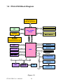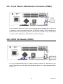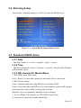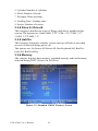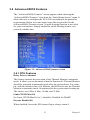
1
PCA-6190
LGA775 Pentium® 4/Celeron® D Processor Card with
VGA/Dual Gigabit LAN/HISA/
DVI (800 MHz FSB)
User’s Manual
Copyright Notice
This document is copyrighted, 2005, by Advantech Co., Ltd. All rights
are reserved. Advantech Co., Ltd. reserves the right to make improvements to the products described in this manual at any time without notice.
No part of this manual may be reproduced, copied, translated or transmitted in any form or by any means without the prior written permission of
Advantech Co., Ltd. Information provided in this manual is intended to
be accurate and reliable. However, Advantech Co., Ltd. assumes no
responsibility for its use, nor for any infringements upon the rights of
third parties which may result from its use.
Acknowledgements
•AWARD is a trademark of Phoenix Technologies Ltd.
•IBM and PC are trademarks of International Business Machines Corporation.
•Intel®, Pentium® 4, and Celeron® are trademarks of Intel Corporation.
•WinBond is a trademark of Winbond Corporation.
All other product names or trademarks are the properties of their respective owners.
Part No. 2002619000
Printed in Taiwan
PCA-6190 User’s Manual
ii
1st Edition
September 2005
1.0.1 A Message to the Customer
Advantech customer services
Each and every Advantech product is built to the most exacting specifications to ensure reliable performance in the harsh and
demanding conditions typical of industrial environments. Whether your
new Advantech equipment is destined for the laboratory or the factory
floor, you can be assured that your product will provide the reliability and
ease of operation for which the name Advantech has come to be known.
Your satisfaction is our primary concern. Here is a guide to
Advantech’s customer services. To ensure you get the full benefit of our
services, please follow the instructions below carefully.
Technical support
We want you to get the maximum performance from your products. So if
you run into technical difficulties, we are here to help. For the most frequently asked questions, you can easily find answers in your product documentation. These answers are normally a lot more detailed than the ones
we can give over the phone.
So please consult this manual first. If you still cannot find the answer,
gather all the information or questions that apply to your problem, and
with the product close at hand, call your dealer. Our dealers are well
trained and ready to give you the support you need to get the most from
your Advantech products. In fact, most problems reported are minor and
are able to be easily solved over the phone.
In addition, free technical support is available from Advantech engineers
every business day. We are always ready to give advice on application
requirements or specific information on the installation and operation of
any of our products.
iii
Table 1.1: Table 1.1: PCA-6190 Comparison Table
Model
PCA-6190VG00A1
PCA-6190G200A1
PCA-6190G2D0A1
VGA: Intel 915 GV integrated
VGA controller onboard
yes
yes
yes
USB 2.0 port
8
8
8
LAN 1: Broadcom BCM5721
10/100/1000Base-T
no
yes
yes
LAN 2: Broadcom BCM5721
10/100/1000Base-T
yes
yes
yes
DVI function
no
no
yes
PCI B-to-B daughter board
connector
no
no
yes
Note:
PCA-6190VG-00A1 uses onboard LAN2 controller
PCA-6190 User’s Manual
iv
Table 1.2: PCA-6190 DDR memory compatibility table
Brand
Size
Speed
Type
ECC
Part
Number
Advantech PN
Memory
Apacer
1 GB
DDR2 533
DDR2
N
78.01066.
330
NA
HYB18T5
12
800AF37
FSS35249
0434
1 GB
DDR2 533
DDR2
N
78.01066.
400
NA
SAMSUNG
K4T51083
QB-ZKD5
512 MB
DDR2 400
DDR2
N
UG64T64
00K8DU4AM
NA
4WB42
D9CHL
1 GB
DDR2 400
DDR2
N
UG12T64
00L8DU4AM
NA
EPPIDA
E5108AB5C-E
256 MB
DDR2 533
DDR2
N
NA
NA
SAMSUNG 443
K4T56083
QF-GC05
1 GB
DDR2 533
DDR2
N
NA
NA
ELPIDA
E5108AB5C-E
512 MB
DDR2 533
DDR2
N
NA
NA
HYB18T5
12
800AF37
FSS43331
0440
1 GB
DDR2 400
DDR2
N
NA
NA
HYB18T5
12A
800AF37
FSS43331
0440
UG
Transcend
DSL
v
1.0.1 Product warranty
Advantech warrants to you, the original purchaser, that each of its products will be free from defects in materials and workmanship for two years
from the date of purchase.
This warranty does not apply to any products which have been repaired or
altered by persons other than repair personnel authorized by Advantech,
or which have been subject to misuse, abuse, accident or improper installation. Advantech assumes no liability under the terms of this warranty as
a consequence of such events.
If an Advantech product is defective, it will be repaired or replaced at no
charge during the warranty period. For out-of-warranty repairs, you will
be billed according to the cost of replacement materials, service time and
freight. Please consult your dealer for more details.
If you think you have a defective product, follow these steps:
Step 1. Collect all the information about the problem encountered. (For
example, type of PC, CPU speed, Advantech products used,
other hardware and software used, etc.) Note anything abnormal
and list any on-screen messages you get when the problem
occurs.
Step 2. Call your dealer and describe the problem. Please have your manual, product, and any helpful information readily available.
Step 3. If your product is diagnosed as defective, obtain an RMA (return
material authorization) number from your dealer. This allows us
to process your return more quickly.
Step 4. Carefully pack the defective product, a fully-completed Repair
and Replacement Order Card and a photocopy proof of purchase
date (such as your sales receipt) in a shippable container. A product returned without proof of the purchase date is not eligible for
warranty service.
Step 5. Write the RMA number visibly on the outside of the package and
ship it prepaid to your dealer.
PCA-6190 User’s Manual
vi
1.0.2 Initial Inspection
Before you begin installing your single board computer, please make sure
that the following materials have been shipped:
1 PCA-6190 Pentium 4/Celeron Dprocessor-based single board computer
1 PCA-6190 Startup Manual
1 CD with driver utility and manual (in PDF format)
1 FDD cable
P/N: 1700340640
1 Ultra ATA 66/100 HDD cables
P/N: 1701400452
4 Serial ATA HDD data cable
P/N: 1700071000
4 Serial ATA HDD power cable
P/N: 1703150102
1 ATX 12V power converter cable
P/N: 170304015K
1 Printer (parallel) port & COM port cable kit
P/N: 1700060305
1 Dual COM port cable kit (certain models)
P/N: 1701092300
1 Y cable for PS/2 keyboard and PS/2 mouse
P/N: 1700060202
2 Four-USB port cables
P/N:1700000719
Jumper pack
P/N:9689000068
DVI cable (PCA-6190G2-D0A1 only)
P/N: 1700000821
Warranty card
If any of these items are missing or damaged, contact your distributor or
sales representative immediately.
We have carefully inspected the PCA-6190 mechanically and electrically
before shipment. It should be free of marks and scratches and in perfect
working order upon receipt.
As you unpack the PCA-6190, check it for signs of shipping damage.
(For example, damaged box, scratches, dents, etc.) If it is damaged or it
fails to meet the specifications, notify our service department or your
local sales representative immediately. Also notify the carrier. Retain the
shipping carton and packing material for inspection by the carrier. After
inspection, we will make arrangements to repair or replace the unit.
1.0.3 Release Note
Date
Revision
Description
September 2005
1st Edition
Initial Release
vii
Important Safety Information
SAFETY INSTRUCTIONS
This device complies with the requirements in part 15 of the FCC
rules: Operation is subject to the following two conditions:
1.
This device may not cause harmful interference, and
2.
This device must accept any interference received, including interference
that may cause undesired operation
This equipment has been tested and found to comply with the limits for a Class A digital
device, pursuant to Part 15 of the FCC Rules. These limits are designed to provide reasonable protection against harmful interference when the equipment is operated in a
commercial environment. This equipment generates, uses, and can radiate radio frequency energy and, if not installed and used in accordance with the instruction manual,
may cause harmful interference to radio communications. Operation of this device in a
residential area is likely to cause harmful interference in which case the user will be
required to correct the interference at his/her own expense. The user is advised that any
equipment changes or modifications not expressly approved by the party responsible for
compliance would void the compliance to FCC regulations and therefore, the user's
authority to operate the equipment.
CAUTION!!
There is a danger of a new battery exploding if it is incorrectly installed. Do not
attempt to recharge, force open, or heat the battery. Replace the battery only with
the same or equivalent type recommended by the manufacturer. Discard used batteries according to the manufacturer’s instructions.
PCA-6190 User’s Manual
viii
Contents
Chapter
1 Hardware Configuration .................................2
1.1
1.2
1.3
Introduction ....................................................................... 2
Features ............................................................................. 3
Specifications .................................................................... 4
1.3.1
1.3.2
1.3.3
1.3.4
1.3.5
1.3.6
1.3.7
1.4
System............................................................................. 4
Memory........................................................................... 4
Input/Output.................................................................... 4
VGA interface................................................................. 5
Ethernet LAN.................................................................. 5
Industrial features ........................................................... 5
Mechanical and environmental specifications................ 5
Jumpers and Connectors.................................................... 6
Table 1.1:Jumpers........................................................... 6
Table 1.2:Connectors ...................................................... 6
1.5
Board Layout: Jumper and Connector Locations.............. 9
1.6
PCA-6190 Block Diagram ............................................. 10
1.7
1.8
Safety Precautions .......................................................... 11
Jumper Settings ............................................................... 12
Figure 1.1:Jumper and Connector locations ................... 9
Figure 1.2: ................................................................... 10
1.8.1
1.8.2
1.8.3
1.9
System Memory .............................................................. 13
1.9.1
1.9.2
1.10
1.11
Chapter
How to set jumpers ....................................................... 12
CMOS clear (J1) ........................................................... 12
Table 1.3:CMOS (J1).................................................... 12
Watchdog timer output (J2) .......................................... 13
Table 1.4:Watchdog timer output (J2).......................... 13
CPU FSB and memory speed ....................................... 14
Dual channel configuration........................................... 14
Memory Installation Procedures ..................................... 14
Processor Installation ...................................................... 15
2 Connecting Peripherals .................................18
2.1
2.2
2.3
2.4
2.5
2.6
2.7
Introduction ..................................................................... 18
1st (CN1) IDE Connectors .............................................. 18
Floppy Drive Connector (CN3)....................................... 19
Parallel Port (CN4).......................................................... 19
USB Ports (CN6,CN63,CN66,CN67) ............................. 20
VGA Connector CN7 ...................................................... 20
DVI Connector VCN1 (optional).................................... 21
ix
2.8
2.9
2.10
2.11
2.12
2.13
Ethernet Connector (CN24) ............................................ 21
Serial Ports (COM1: CN9/CN91; COM2: CN10 ) ......... 22
PS/2 Keyboard/Mouse Connector (CN11)...................... 22
External Keyboard Connector (CN12)............................ 23
CPU Fan Connector (CN68) ........................................... 23
Front Panel Connectors (CN16, 17, 18, 19, 21&29)....... 24
2.13.1
2.13.2
2.13.3
2.13.4
2.13.5
2.13.6
2.14
2.15
2.16
2.17
2.18
2.19
2.20
2.21
2.22
Chapter
Power LED (CN16) ...................................................... 24
External speaker (CN17) .............................................. 24
Reset (CN18) ................................................................ 25
HDD LED (CN19)........................................................ 25
ATX soft power switch (CN21).................................... 25
SM Bus Connector (CN29)........................................... 25
ATX Feature Connector (CN20)..................................... 26
AC-97 Audio Interface (CN43)....................................... 26
Serial ATA Interface (SA0,SA1,SA2, and SA3) ............ 26
Connecting to SNMP-1000 Remote Manager ................ 27
Auxiliary 4-pin Power Connector (ATX1) ..................... 27
SCSI Daughterboard Extension Connector (CN30)........ 28
Case Open Connector (CN64)......................................... 28
Front Panel LAN Indicator Connector (CN65)............... 29
GPIO Pin Header (CN93) ............................................... 29
3 Award BIOS Setup.........................................32
3.1
Introduction ..................................................................... 32
3.1.1
CMOS RAM Auto-backup and Restore ....................... 32
3.2
Entering Setup ................................................................. 33
3.3
Standard CMOS Setup .................................................... 33
Figure 3.1:Award BIOS Setup initial screen ................ 33
3.3.1
3.3.2
3.3.3
3.3.4
3.3.5
3.3.6
3.4
Date............................................................................... 33
Time .............................................................................. 33
IDE channel 0/1 Master/Slave ...................................... 33
Drive A / Drive B.......................................................... 34
Halt On.......................................................................... 34
Memory......................................................................... 34
Figure 3.2:Standard CMOS Features Screen................ 34
Advanced BIOS Features ................................................ 35
3.4.1
3.4.2
3.4.3
3.4.4
3.4.5
3.4.6
3.4.7
PCA-6190 User’s Manual
Figure 3.3:Advanced BIOS features screen.................. 35
CPU Features ................................................................ 35
Hard Disk Boot Priority................................................ 35
Virus Warning............................................................... 36
CPU L1 & L2 Cache..................................................... 36
Hyper-Threading Technology....................................... 36
Quick Power On Self Test ............................................ 36
First/Second/Third Boot Device ................................... 36
x
3.4.8
3.4.9
3.4.10
3.4.11
3.4.12
3.4.13
3.4.14
3.4.15
3.4.16
3.4.17
3.4.18
3.5
Advanced Chipset Features............................................. 38
3.5.1
3.5.2
3.5.3
3.5.4
3.5.5
3.5.6
3.5.7
3.5.8
3.5.9
3.5.10
3.5.11
3.5.12
3.5.13
3.5.14
3.5.15
3.6
Boot Other Device ........................................................ 36
Swap Floppy Drive ....................................................... 36
Boot Up Floppy Seek.................................................... 36
Boot Up NumLock Status............................................. 36
Gate A20 Option........................................................... 36
Typematic Rate Setting................................................. 36
Typematic Rate (Chars/Sec) ......................................... 37
Typematic Delay (msec)............................................... 37
Security Option ............................................................. 37
APIC Mode ................................................................... 37
MPS Version Control For OS....................................... 37
Figure 3.4:Advanced chipset features screen ............... 38
DRAM Timing Selectable ............................................ 38
CAS Latency Time ....................................................... 38
DRAM RAS# to CAS# Delay ...................................... 39
DRAM RAS# Precharge............................................... 39
Precharge Delay (t RAS) .............................................. 39
System Memory Frequency .......................................... 39
System BIOS Cacheable............................................... 39
Video BIOS Cacheable................................................. 39
Memory Hole At 15M-16M ......................................... 39
PCI-Express Root Port Func......................................... 40
On-Chip Video Memory Size ....................................... 40
On-Chip Frame Buffer Size.......................................... 40
FIXED Memory Size .................................................... 40
DVMT Memory Size .................................................... 40
Init Display First ........................................................... 40
Integrated Peripherals...................................................... 41
3.6.1
3.6.2
3.6.3
3.6.4
3.6.5
3.6.6
3.6.7
3.6.8
3.6.9
3.6.10
3.6.11
3.6.12
3.6.13
Figure 3.5:Integrated peripherals.................................. 41
Figure 3.6:On-Chip IDE Device................................... 41
IDE HDD Block Mode ................................................. 41
IDE DMA Transfer Access........................................... 41
On-Chip IDE Device .................................................... 42
SATA Mode.................................................................. 42
On-Chip Serial ATA..................................................... 42
PATA IDE Mode .......................................................... 42
SATA Port .................................................................... 42
Figure 3.7:Onboard Device........................................... 43
USB Controller ............................................................. 43
USB 2.0 Controller ....................................................... 43
USB Keyboard/Mouse Support .................................... 43
AC97 Audio.................................................................. 43
Onboard LAN1 Control ................................................ 43
Onboard LAN2 Control ................................................ 43
xi
3.6.14 GPIO Function.............................................................. 44
Figure 3.8:Super I/O Device......................................... 44
3.6.15 KBC Input Clock .......................................................... 44
3.6.16 Onboard FDC Controller .............................................. 44
3.6.17 Onboard Serial Port 1 ................................................... 44
3.6.18 Onboard Serial Port 2 ................................................... 45
3.6.19 UART Mode Select ...................................................... 45
3.6.20 RxD, TxD Active.......................................................... 45
3.6.21 IR Transmission Delay ................................................. 45
3.6.22 UR2 Duplex Mode........................................................ 45
3.6.23 Use IR Pins ................................................................... 45
3.6.24 Onboard Parallel Port.................................................... 45
3.6.25 Parallel Port Mode ........................................................ 45
3.6.26 EPP Mode Select .......................................................... 45
3.6.27 ECP Mode Use DMA ................................................... 45
3.7
Power Management Setup............................................... 46
3.7.1
3.7.2
3.7.3
3.7.4
3.7.5
3.7.6
3.7.7
3.7.8
3.7.9
3.7.10
3.7.11
3.7.12
3.7.13
3.7.14
3.7.15
3.7.16
3.7.17
3.8
PnP/PCI Configurations .................................................. 48
3.8.1
3.8.2
3.8.3
3.8.4
3.9
Figure 3.9:Power management setup screen (1)........... 46
Power Supply Type....................................................... 46
ACPI Function .............................................................. 46
Power Management ...................................................... 46
Video Off Method......................................................... 47
Video Off In Suspend ................................................... 47
Suspend Type................................................................ 47
Modem Use IRQ........................................................... 47
Suspend Mode............................................................... 47
Soft-Off by PWR-BTTN .............................................. 47
CPU THRM-Throttling................................................. 47
PowerOn by Modem..................................................... 47
PowerOn by LAN ......................................................... 47
PowerOn by Alarm ....................................................... 48
Primary IDE 0 (1) and Secondary IDE 0 (1) ................ 48
FDD, COM, LPT PORT ............................................... 48
PCI PIRQ [A-D]# ........................................................ 48
PWRON After PWR-Fail ............................................. 48
Figure 3.10:PnP/PCI configurations screen.................. 48
Reset Configuration Data.............................................. 49
Resources Controlled By .............................................. 49
PCI/VGA Palette Snoop ............................................... 49
Maximum Payload Size ................................................ 49
PC Health Status.............................................................. 49
3.9.1
3.9.2
3.9.3
PCA-6190 User’s Manual
Figure 3.11:PC Health Status Screen............................ 49
Case Open Warning ...................................................... 49
CPU Warning Temperature .......................................... 50
Current System Temperature ........................................ 50
xii
3.9.4
3.9.5
3.9.6
3.9.7
3.9.8
3.10
Current CPU Temperature ............................................ 50
CPU FAN Speed........................................................... 50
System FAN Speed....................................................... 50
VCORE and Other Voltages......................................... 50
Shutdown Temperature................................................. 50
Frequency / Voltage Control ........................................... 50
Figure 3.12:Spread Spectrum Control screen ............... 50
3.10.1 CPU Clock Ratio .......................................................... 51
3.10.2 Spread Spectrum ........................................................... 51
3.11
3.12
3.13
Chapter
4 Chipset Software Install Utility.....................54
4.1
4.2
4.3
Chapter
Introduction ..................................................................... 66
Features ........................................................................... 66
Installation....................................................................... 66
Win XP Driver Setup (Broadcom BCM5721) ................ 67
7 USB 2.0 Configuration...................................72
7.1
7.2
7.3
Chapter
Introduction ..................................................................... 60
Windows XP Driver Setup.............................................. 61
6 LAN Configuration ........................................66
6.1
6.2
6.3
6.4
Chapter
Before you begin ............................................................. 54
Introduction ..................................................................... 54
Windows XP Driver Setup.............................................. 55
5 VGA Setup ......................................................60
5.1
5.2
Chapter
Password Setting ............................................................. 51
Save & Exit Setup ........................................................... 51
Exit Without Saving ........................................................ 52
Introduction ..................................................................... 72
Features ........................................................................... 72
Installation....................................................................... 72
8 Onboard Security Setup ................................74
8.1
8.2
8.3
Introduction ..................................................................... 74
Windows XP Driver Setup.............................................. 75
Using the OBS Hardware Doctor Utility ........................ 78
Appendix A
Programming the watchdog .........................82
A.1
Programming the Watchdog Timer................................. 82
A.1.1
A.1.2
A.1.3
A.1.4
Watchdog timer overview............................................. 82
Reset/ Interrupt selection .............................................. 82
Programming the Watchdog Timer .............................. 82
Example Program ......................................................... 85
Appendix B
Programming the GPIO ...............................92
B.1
Sample Code ................................................................... 92
xiii
Appendix C
Pin Assignments ............................................98
C.1
IDE Hard Drive Connector (CN1) .................................. 98
C.2
Floppy Drive Connector (CN3)....................................... 99
C.3
Parallel Port Connector (CN4) ...................................... 100
C.4
USB Connector (CN6, CN63, CN66, CN67)................ 101
C.5
VGA Connector (CN7) ................................................. 101
C.6
VCN1 DVI connector.................................................... 102
C.7
COM1/COM2 RS-232 Serial Port (CN9/CN91/CN10) 102
C.8
Keyboard and Mouse Connnector (CN11).................... 103
C.9
External Keyboard Connector (CN68).......................... 104
C.10
CPU Fan Power Connector (CN14) .............................. 104
C.11
Power LED (CN16)....................................................... 105
C.12
External Speaker Connector (CN17)............................. 105
C.13
Reset Connector (CN18) ............................................... 106
C.14
HDD LED Connector (CN19)....................................... 106
C.15
ATX Feature Connector (CN20)................................... 106
C.16
ATX Soft Power Switch (CN21)) ................................. 107
C.17
H/W Monitor Alarm (CN22)......................................... 108
C.18
C.19
AC-97 Audio Interface (CN43).................................... 109
SM Bus Connector (CN29) ........................................... 109
C.20
Case Open Connector (CN64)....................................... 110
C.21
Front Panel LAN Indicator connector (CN65).............. 110
Table C.1:IDE hard drive connector (CN1, CN2) ........ 98
Table C.2:Floppy drive connector (CN3) ..................... 99
Table C.3:Parallel port connector (CN4).................... 100
Table C.4:USB1/USB2 connector (CN6)................... 101
Table C.5:VGA connector (CN7)............................... 101
Table C.6:VCN5 DVI connector ................................ 102
Table C.7:COM1/2 Serial Port (CN9/CN91/CN10)... 102
Table C.8:Keyboard and mouse connector (CN11).... 103
Table C.9:External keyboard connector (CN12) ........ 104
Table C.10:CPU Fan Power Connector (CN68)......... 104
Table C.11: Power LED and keylock conn (CN16) ... 105
Table C.12:External Speaker Connector (CN17) ....... 105
Table C.13:Reset connector (CN18)........................... 106
Table C.14:HDD LED connector (CN19) .................. 106
Table C.15:ATX feature connector (CN20) ............... 107
Table C.16:ATX soft power switch (CN21)............... 107
Table C.17:H/W monitor alarm (CN22)..................... 108
Table C.19:SM Bus Connector (CN 29)..................... 109
Table C.20:Case Open Connector (CN64) ................. 110
Table C.21:Front Panel LAN Indicator connector (CN65)
110
PCA-6190 User’s Manual
xiv
C.22
GPIO Pin Header (SMD pitch=2.0mm) (CN93)........... 111
C.23
System I/O Ports............................................................ 111
C.24
DMA Channel Assignments.......................................... 112
C.25
Interrupt Assignments ................................................... 112
C.26
1st MB Memory Map.................................................... 113
C.27
PCI Bus Map ................................................................. 113
Table C.22:GPIO pin header (CN93) ......................... 111
Table C.23:System I/O ports ...................................... 111
Table C.24:DMA channel assignments ...................... 112
Table C.25:Interrupt assignments ............................... 112
Table C.26:1st MB memory map ............................... 113
Table C.27:PCI bus map............................................. 113
xv
PCA-6190 User’s Manual
xvi
CHAPTER
1
General Information
1
Chapter 1 Hardware Configuration
1.1 Introduction
The PCA-6190 is designed with the Intel 915GV chipset and ICH6 (I/O
controller) to support 800 MHz Front side Bus, Intel Pentium 4/Celeron
D processor, high speed/high capacity dual channel DDRII 400/533
memory, and high performance I/O functions such as dual Gigabit Ethernet ports, Serial/Parallel ATA ports, and PCI-Express host interface for
LAN. In compliance with PICMG 1.0 specification, PCA-6190 can be
used with a wide choice of existing PCI/ISA backplanes to meet versatile
requirements of industrial applications.
The PCA-6190 is designed to deliver high performance for industrial
applications. It uses Intel’s long-life 915GV and ICH6 chipset, capable
of running the fastest Pentium 4 and Celeron D processor. It has 4 DIMM
sockets in two separated memory channels. It accepts up to 4GB DDRII
400/533 SDRAM memory, enough for most of applications. The PCA6190 features single/dual Gigabit Ethernet network interface(s) .With the
Broadcom BCM5721 GbE controller designed-in, PCA-6190 implements
the PCI Express host interface (PCI-E X1) in LAN connection with the
maximum throughput of 2Gbps for heavy-duty industrial network application. The Intel 915GV integrated VGA provides superior 3D performance with unique Intel Graphics Media Accelerator 900. Four Serial
ATA ports (up to 150MB/s) allows the use of thin and long SATA cables
for storage devices, eliminating cabling issues inside industrial-grade
chassis. In addition, the PCA-6190 also provides most of the popular I/O
interfaces such as eight USB 2.0 ports, AC-97 audio interface, 2 RS-232
ports, one enhanced parallel port and floppy disk interface.
The PCA-6190 is designed with reliability considerations to suit industrial environments. To prevent CPU damage from overheating, the PCA6190 features a thermal protection circuit that enables the processor to
automatically shut down when the cooling system fails. In addition,
PCA-6190 provides a 14-pin General Purpose I/O interface as the port80
function used in detecting hardware bugs or as the programmable 8-bit I/
O. A remote management port allows users to monitor the system health
status and control the system remotely through standard SNMP/HTTP
protocol when used with Advantech's SNMP-1000 Intelligent System
Manager.
PCA-6190 User’s Manual
2
1.2 Features
1.
Supports 4 Serial-ATA devices
2.
Supports Dual Channel DDRII 400/533 SDRAM up to 4GB
3.
Features a thermal protection circuit which will enable the processor to automatically shut down when the cooling system fails.
4.
Supports DVI interface (optional)
5.
Provides a 14-pin General Purpose I/O interface as the port80 function used in detecting hardware bugs or as the programmable 8-bit
I/O.
6.
Supports 10/100/1000Base-T Ethernet
7.
8 USB 2.0 ports
8.
CMOS automatic backup and restore to prevent accidental data loss
of BIOS setup data
9.
Remote management with SNMP-1000-B1
3
1.3 Specifications
1.3.1 System
• CPU: Intel LGA 775 Celeron D up to 3.06GHz, Pentium 4 up to 3.8
GHz, FSB 533/800 MHz. Advantech also certifies several high-performance CPU coolers as optional parts for customers who use highspeed CPUs in 2U chassis or high temperature environments.
• L2 Cache: CPU built-in 256KB and 1 MB/2 MB full-speed L2 cache
BIOS: Award Flash BIOS (4Mb Flash Memory)
• System Chipset: Intel 915GV with ICH6
• SATA/EIDE hard disk drive interface: Four on-board serial ATA
connectors with data transmission rate up to 150 MB/Sec and supporting Advanced Host controller interface (AHCI) technology. One IDE
hard disk drives or two enhanced IDE devices. Supports PIO mode 4
(16.67MB/s data transfer rate) and ATA 33/66/100 (33/66/100MB/s
data transfer rate.) BIOS enabled/disabled.
• Floppy disk drive interface: Supports one floppy disk drive, 5¼" (360
KB and 1.2 MB) or 3½" (720 KB, 1.44 MB). BIOS enabled/disabled
1.3.2 Memory
• RAM: Up to 4GB in four 240-pin DIMM sockets. Supports dual
channel DDRII 400/533 SDRAM.
Note:
Due to the physical limitation of PC architecture,
the system can NOT fully detect 4 GB RAM
capacity when 4 GB RAM is installed.
1.3.3 Input/Output
• Bus interface: PICMG 1.0 compliant PCI/ISA bus interface
• Enhanced parallel port: Configurable to LPT1, LPT2, LPT3, or disabled. Standard DB-25 female connector provided. Supports EPP/SPP/
ECP
• Serial ports: Two RS-232 ports with 16C550 UARTs (or compatible)
with 16-byte FIFO buffer. Supports speeds up to 115.2 Kbps. Ports can
be individually configured to COM1, COM2 or disabled
• Keyboard and PS/2 mouse connector: One 6-pin mini-DIN connector
is located on the mounting bracket for easy connection to a keyboard or
PS/2 mouse. An onboard keyboard pin header connector is available.
PCA-6190 User’s Manual
4
• ISA bus: Supports ISA without DMA. PCI-to-ISA bridge: ITE IT8888
• AC-97 Audio: PCA-6190 can provide audio function with the optional
audio extension module PCA-AUDIO-00A1
• USB port: Supports up to eight USB 2.0 ports with the two USB 2.0
cable kits included, and supports transmission rates up to 480 Mbps;
available through two 4-USB port cable kits, P/N: 1700000719
1.3.4 VGA interface
• Controller: Chipset integrated VGA controller
• Display memory: Dynamically shared system memory up to 128 MB.
• Resolution: Up to 2048x1536@ 85 Hz refresh
1.3.5 Ethernet LAN
• Supports single/dual 10/100/1000Base-T Ethernet port(s) via PCI
Express x1 bus which provides 500 MB/s data transmission rate.
• Controller:
• Single 10/100/1000Base-T: Broadcom BCM5721
• Dual 10/100/1000Base-T: Broadcom BCM5721 X 2
Note:
The Speed & Duplex mode default setting is full
duplex mode and can NOT be changed
1.3.6 Industrial features
• Watchdog timer: Can generate a system reset or IRQ11. The watchdog
timer is programmable, with each unit equal to one second or one
minute (255 levels). You can find programming detail in Appendix A
1.3.7 Mechanical and environmental specifications
• Operating temperature: 0°~60° C (32° ~ 140° F, Depending on CPU)
• Storage temperature: -20°~ 70° C (-4° ~ 158° F)
• Humidity: 20 ~ 95% non-condensing
• Power supply voltage: +5 V, ±12 V
• Power consumption: Maximum: +5V:6.64A, +12V:12.59A (Intel
Pentium4 3.4GHz with 800MHz FSB, 2 X256 MB, 2 X512 MB
DDRII 533 SDRAM)
• Board size: 338 x 122 mm (13.3" x 4.8")
• Board weight: 0.5 kg (1.2 lb)
5
1.4 Jumpers and Connectors
Connectors on the PCA-6190 single board computer link it to external
devices such as hard disk drives and a keyboard. In addition, the board has a
number of jumpers used to configure your system for your application.
The tables below list the function of each of the board jumpers and connectors. Later sections in this chapter give instructions on setting jumpers. Chapter 2 gives instructions for connecting external devices to your
single board computer.
Table 1.1: Jumpers
Label
Function
J1
CMOS Clear
J2
Watchdog timer output selection
Table 1.2: Connectors
Label
Function
CN1
Primary IDE connector
CN3
FDD connector, Supports 360K/1.2M/720K/1.44M
FDD x 2
CN4
Parallel port, Parallel port x 1, supports SPP/EPP/
ECP mode
CN6
USB port 0,1
CN7
VGA connector
CN8
Ethernet connector 1
CN9
Serial port: COM1; RS232 (D-sub 9-pin connector)
CN10
Serial port: COM2; RS232 (9-pin connector)
CN11
PS/2 keyboard and mouse connector
Cable length: 20 meters
CN12
External keyboard connector
CN13
Reserved
PCA-6190 User’s Manual
6
Table 1.2: Connectors
CN16
(keyboard lock
and power LED)
Power LED
Suspend: flash flash (ATX/AT)
System On: ON (ATX/AT)
System Off: OFF (AT)
System OffL Slow flash (ATX)
CN17
External speaker
CN18
Reset connector
CN19
HDD LED connector
CN20
ATX feature connector
CN21
ATX soft power switch (PS_ON)
CN22
HW Monitor Alarm
Close: Enable OBS Alarm
Open: Disable OBS Alarm
CN29
SM BUS Connector
CN24
2 LAN Ports
CN30
SCSI daughter board extension connector 1 (PCI
interface)
CN43
AC97 Link connector
CN63
USB port 3,4
CN64
Case Open
CN65
Front Panel LAN Indicator connector
CN66
USB port 5,6
CN67
USB port 7,8
CN68
CPU FAN connector (4-pin)
CN91
Serial Port: COM1; RS232 (9-pin connector)
CN93
GPIO pin header (SMD pitch=2.0 mm)
SA0
Serial ATA0
SA1
Serial ATA1
SA2
Serial ATA2
SA3
Serial ATA3
ATX1
ATX 12V Auxillary power connector
VCN1
DVI connector (DF13-20DP-1.25mm TMDS)
7
Notice:
The 4-pin ATX 12V power connector "ATX1"
must be connected to the power supply to provide adequate power to the CPU card. Otherwise, the system may become unstable.
PCA-6190 User’s Manual
8
CN19
CN17
CN16
ATX1
B
CN68
CN21CN18 CN29
9
8
7
6
5
CN93
DDRII 4
DDRII 3
DDRII 2
DDRII 1
4
3
2
1
VCN1
CN67
CN65
CN91
CN9
CN10
CN12
CN6 CN63 CN66
CN4
CN24
CN20
J2
CN64
CN7
CN13 J1
CN22
CN30
CN43
CN11
CN1
SA0 SA1 CN3 SA2 SA3 SA3
1.5 Board Layout: Jumper and Connector Locations
Figure 1.1: Jumper and Connector locations
1.6 PCA-6190 Block Diagram
533/800 MHz FSB
Intel Pentium 4
LGA 775 Processor
DDR II 400/533
Channel A
CRT
VG A
Intel 915GV
GMCH
CH7307C
1 ATA 100
ports
DMA 33/66/100
4 SATA ports
150MB/s
8 USB Ports
USB 2.0/1.1
Audio Codec
2G B/s ban dwi dt h
DVI TMDS
connector
(PCA-6190G2-D0A1 only)
DDR II 400/533
PCI-Express x1
G-LAN1 : Broadcom
BCM5721
PCI-Express x1
G-LAN2 : Broadcom
BCM5721
ICH6
PCI-Express x1
PCI-E x1
B to B Connector
(optional)
AC'97
PCI B to B connector
for daughtor board
(PCA-6190G2-D0A1only)
PCIBus
LPC Bus
BIOS
DDR II 400/533
Channel B
D ir ec t Med ia
In te r fac e
SD V O
DDR II 400/533
Super IO
Winbond
W83627HF
GPIO
Figure 1.2:
PCA-6190 User’s Manual
10
PCI to ISA Bridge
ITE8888
Back Plane
(PICMG 1.0)
1.7 Safety Precautions
Warning!
Always completely disconnect the power cord
from your chassis whenever you work with the
hardware. Do not make connections while the
power is on. Sensitive electronic components
can be damaged by sudden power surges. Only
experienced electronics personnel should open
the PC chassis.
Caution!
Always ground yourself to remove any static
charge before touching the single board computer. Modern electronic devices are very sensitive to static electric charges. As a safety
precaution, use a grounding wrist strap at all
times. Place all electronic components on a
static-dissipative surface or in a static-shielded
bag when they are not in the chassis.
Caution!
The computer is provided with a battery-powered Real-time Clock circuit. There is a danger
of explosion if battery is incorrectly replaced.
Replace only with same or equivalent type recommended by the manufacturer. Discard used
batteries according to manufacturer's instructions.
Notice:
Before install your PCA-6190 into a chassis,
make sure that all components on both sides of
the CPU card do not touch any metal parts,
especially the chassis wall and add-on card at
the adjacent slot.
11
1.8 Jumper Settings
This section provides instructions on how to configure your single board
computer by setting the jumpers. It also includes the single board computer's default settings and your options for each jumper.
1.8.1 How to set jumpers
You can configure your single board computer to match the needs of your
application by setting the jumpers. A jumper is a metal bridge that closes
an electrical circuit. It consists of two metal pins and a small metal clip
(often protected by a plastic cover) that slides over the pins to connect
them. To “close” (or turn ON) a jumper, you connect the pins with the
clip. To “open” (or turn OFF) a jumper, you remove the clip. Sometimes
a jumper consists of a set of three pins, labeled 1, 2, and 3. In this case
you connect either pins 1 and 2, or 2 and 3. A pair of needle-nose pliers
may be useful when setting jumpers.
1.8.2 CMOS clear (J1)
The PCA-6190 single board computer contains a jumper that can erase
CMOS data and reset the system BIOS information. You can clear
CMOS by shorting 2-3 pin while the system is off. Then return to 1-2 pin
position. Avoid clearing the CMOS while the system is on; it will damage
the mainboard.
Table 1.3: CMOS (J1)
Function
Jumper Setting
* Keep CMOS data
1-2 closed
Clear CMOS data
2-3 short
* default setting
PCA-6190 User’s Manual
12
1.8.3 Watchdog timer output (J2)
The PCA-6190 contains a watchdog timer that will reset the CPU or send
a signal to IRQ11 in the event the CPU stops processing. This feature
means the PCA-6190 will recover from a software failure or an EMI
problem. The J2 jumper settings control the outcome of what the computer will do in the event the watchdog timer is tripped.
Table 1.4: Watchdog timer output (J2)
Function
Jumper Setting
IRQ11
1
1-2 closed
* Reset
1
2-3 closed
* default setting
Note:
The interrupt output of the watchdog timer is a
low level signal. It will be held low until the
watchdog timer is reset.
1.9 System Memory
The PCA-6190 has four sockets for 240-pin dual inline memory modules
(DIMMs) in two separated memory channels. It can operate with single
channel or dual channel modules. We recommend to use dual channel
mode to provide optimized performance.
All these sockets use 1.8 V unbuffered double data rate synchronous
DRAMs (DDRII SDRAM). They are available in capacities of 256, 512
and 1024 MB. The sockets can be filled in any combination with DIMMs
of any size, giving a total memory size between 256 MB and 4 GB.
13
Note:
System resources such as PCI require physical
memory address locations that reduce available
memory addresses above 3GB. This may result
in less than 4GB of memory being available to
the operating system and applications.
1.9.1 CPU FSB and memory speed
The PCA-6190 can accept DDRII SDRAM memory chips without parity.
Also note: The PCA-6190 accepts DDRII 400MHz SDRAM and DDRII
533MHz SDRAM, depending on the CPU front side bus frequency
(FSB). Please refer below table for the relationship between the CPU FSB
and memory speed.
1.9.2 Dual channel configuration
The four DIMM sockets are arranged in two channels: DIMM1 &
DIMM2 in channel A; DIMM3 & DIMM4 in channel B. To enable dual
channel operation, please install a matched pair of DIMMs in DIMM1 &
DIMM3 (green sockets). If additional memory is to be used, another
matched pair of DIMMs have to be installed in DIMM2 & DIMM4 (purple sockets).
"Matched pair of DIMMs" means: same in speed (DDR266, DDR333,
DDR400), same in size (128MB, 256MB, 512MB or 1GB), same in chip
density (128 Mb, 256Mb or 512Mb and same in CSA latency. Any other
memory configuration will result in single channel memory operation.
1.10 Memory Installation Procedures
To install DIMMs, first make sure the two handles of the DIMM socket
are in the "open" position. i.e. The handles lean outward. Slowly slide the
DIMM module along the plastic guides on both ends of the socket. Then
press the DIMM module right down into the socket, until you hear a
click. This is when the two handles have automatically locked the memory module into the correct position of the DIMM socket. To remove the
memory module, just push both handles outward, and the memory module will be ejected by the mechanism in the socket.
PCA-6190 User’s Manual
14
1.11 Processor Installation
The CPU on the board must have a fan or heat sink attached, to prevent
overheating.
Warning:
Without a fan or heat sink, the CPU will over-heat
and cause damage to both the CPU and the single
board computer. To install a CPU, first turn off
your system and remove its cover. Locate the processor LGA775.
1.
The CPU has a plastic cap on it to protect the contact from damage.
Before you install the CPU, always cover it to protect the socket
pin. First, remove the cap from lever hinge side and the pins of
socket reveal.
2.
Open the load lever. Then,lift the load lever up and open the load
plate.After confirming the CPU direction for correct mating,gently
put down the CPU in the socket housing frame.Be sure to grap on
the edge of the CPU base. Note that the alignment keys are
matched.
3.
Cover the load plate onto the package. Press down the load lever
lightly onto the load plate, and then secure the lever with the hook
under retention tab. Confirm if your CPU cooler is firmly installed
before turning on your system.
15
PCA-6190 User’s Manual
16
CHAPTER
2
Connecting Peripherals
17
Chapter 2
Chapter 2 Connecting Peripherals
2.1 Introduction
You can access most of the connectors from the top of the board while it
is installed in the chassis. If you have a number of cards installed or have
a packed chassis, you may need to partially remove the card to make all
the connections.
2.2 1st (CN1) IDE Connectors
You can attach up to two IDE (Integrated Drive Electronics) drives to the
PCA-6190’s built-in controller. The primary (CN1) connector can
accommodate two drives.
Wire number 1 on the cable is red or blue and the other wires are gray.
Connect one end to connector CN1 on the single board computer. Make
sure that the red/blue wire corresponds to pin 1 on the connector (in the
upper right hand corner). See Chapter 1 for help finding the connector.
Unlike floppy drives, IDE hard drives can connect in either position on
the cable. If you install two drives to a single connector, you will need to
set one as the master and the other as the slave. You do this by setting the
jumpers on the drives.
Connect the first hard drive to the other end of the cable. Wire 1 on the
cable should also connect to pin 1 on the hard drive connector, which is
labeled on the drive circuit board. Check the documentation that came
with the drive for more information.
PCA-6190 User’s Manual
18
2.3 Floppy Drive Connector (CN3)
You can attach up to two floppy disk drives to the PCA-6190's on board
controller. You can use 3.5" (720 KB, 1.44 MB) drives.
The single board computer comes with a 34-pin daisy-chain drive connector cable. On one end of the cable is a 34-pin flat-cable connector. On
the other end are two sets of 34-pin flat-cable connector (usually used for
3.5" drives). The set on the end (after the twist in the cable) connects to
the A: floppy drive. The set in the middle connects to the B: floppy drive.
2.4 Parallel Port (CN4)
The parallel port is normally used to connect the single board computer to
a printer. The PCA-6190 includes an onboard parallel port, accessed
through a 26-pin flat-cable connector, CN4. The card comes with an
adapter cable which lets you use a traditional DB-25 connector. The cable
has a 26-pin connector on one end and a DB-25 connector on the other,
mounted on a retaining bracket. The bracket installs at the end of an
empty slot in your chassis, giving you access to the connector.
19
Chapter 2
The parallel port is designated as LPT1, and can be disabled or changed
to LPT2 or LPT3 in the system BIOS setup.
To install the bracket, find an empty slot in your chassis. Unscrew the
plate that covers the end of the slot. Screw in the bracket in place of the
plate. Next, attach the flat-cable connector to CN4 on the CPU card. Wire
1 of the cable is red or blue, and the other wires are gray. Make sure that
wire 1 corresponds to pin 1 of CN4. Pin 1 is on the upper right side of
CN4.
2.5 USB Ports (CN6,CN63,CN66,CN67)
The PCA-6190 provides up to eight ports of USB (Universal Serial
Bus)interface.The USB interface complies with USB Specification Rev.
2.0 support transmission rate up to 480 Mbps and is fuse-protected. The
USB interface can be disabled in the system BIOS setup. To install the
USB cable (p/n:1700000719) bracket, find an empty slot in your chassis
and . Unscrew the plate that covers the end of the slot. Screw in the
bracket in place of the plate. Next, attach the USB connector to CN6,
CN63, CN66, or CN67.
2.6 VGA Connector CN7
PCA-6190 User’s Manual
20
The PCA-6190 includes a VGA interface that can drive conventional
CRT displays. CN7 is a standard 15-pin D-SUB connector commonly
used for VGA. Pin assignments for CRT connector CN7 are detailed in
Appendix B.
2.7 DVI Connector VCN1 (optional)
The PCA-6190 provides an optional DVI interface that supports DVI display. The user can choose 26-pin to 20-pin DVI cable (p/n: 1700000821)
for providing DVI connector. Pin assignments for DVI connector VCN1
are detailed in Appendix B.
2.8 Ethernet Connector (CN24)
The PCA-6190 is equipped with single/dual high performance 1000
Base-T Ethernet interface. The Gigabit Ethernet ports uses the Broadcom
BCM 5721 controller connected to the PCI-Express x1 of the ICH6 I/O
controller. The PCA-6190 is fully compliant with IEEE 802.3ab
1000Base-T standards. It is supported by all major network operating systems and is 100% Novell NE-2000 compatible. An onboard RJ-45 jack
provides convenient 10/100/1000Base-T RJ-45 operation.
21
Chapter 2
2.9 Serial Ports (COM1: CN9/CN91; COM2: CN10 )
The PCA-6190 offers two serial ports, CN9/CN91 as COM1 (CN9 for
PCA-6190G2; CN91 for PCA-6190VG) and CN10 as COM2. These
ports can connect to serial devices, such as a mouse or a printer, or to a
communications network.
The IRQ and address ranges for both ports are fixed. However, if you
want to disable the port or change these parameters later, you can do this
in the system BIOS setup.
Different devices implement the RS-232 standard in different ways. If
you are having problems with a serial device, be sure to check the pin
assignments for the connector.
2.10 PS/2 Keyboard/Mouse Connector (CN11)
One 6-pin mini-DIN connectors (CN11) on the card mounting bracket
provide connection to a PS/2 keyboard or a PS/2 mouse, respectively.
CN11 can also be connected to an adapter cable (P/N: 1700060202, available from Advantech) for connecting to both a PS/2 keyboard and a PS/2
mouse.
PCA-6190 User’s Manual
22
2.11 External Keyboard Connector (CN12)
In addition to the PS/2 mouse/keyboard connector on the PCA-6190's
rear plate, there is also an extra onboard external keyboard connector.
This gives system integrators greater flexibility in designing their systems.
2.12 CPU Fan Connector (CN68)
The PCA-6190 provides 4 pin CPU fan connector.
23
Chapter 2
2.13 Front Panel Connectors (CN16, 17, 18, 19, 21&29)
There are several external switches to monitor and control the PCA-6190
2.13.1 Power LED (CN16)
CN16 is a 5-pin connector for the power on LED. Refer to Appendix B
for detailed information on the pin assignments. If a PS/2 or ATX power
supply is used, the system's power LED status will be as indicated below:
Table 2.1: PS/2 or ATX power supply LED status
Power mode
LED (PS/2 power)
LED (ATX power)
System On
On
On
System Suspend
Fast flashes
Fast flashes
System Off
Off
Slow flashes
2.13.2 External speaker (CN17)
CN17 is a 4-pin connector for an external speaker. If there is no external
speaker, the PCA-6190 provides an onboard buzzer as an alternative. To
enable the buzzer, set pins 3-4 as closed.
PCA-6190 User’s Manual
24
2.13.3 Reset (CN18)
Many computer cases offer the convenience of a reset button. Connect the
wire for the reset button.
1
2.13.4 HDD LED (CN19)
You can connect an LED to connector CN19 to indicate when the HDD is
active.
1
2.13.5 ATX soft power switch (CN21)
If your computer case is equipped with an ATX power supply, you should
connect the power on/off button on your computer case to CN21. This
connection enables you to turn your computer on and off.
2.13.6 SM Bus Connector (CN29)
This connector is reserved for Advantech's SNMP-1000 HTTP/SNMP
Remote System Manager. The SNMP-1000 allows users to monitor the
internal voltages, temperature and fans from a remote computer through
an Ethernet network.
CN29 can be connected to CN19 of SNMP-1000. Please be careful about
the pin assignments, pin 1 must be connected to pin 1 and pin 2 to pin 2
on both ends of cable.
25
Chapter 2
2.14 ATX Feature Connector (CN20)
Connect to the CN1 on the Advantech backplane to enable the ATX function, 5V stand-by.
2.15 AC-97 Audio Interface (CN43)
The PCA-6190 provides AC-97 audio through PCA-AUDIO-00A1
module from Advantech.
2.16 Serial ATA Interface (SA0,SA1,SA2, and SA3)
PCA-6190 User’s Manual
26
In addition to the one EIDE interfaces (up to two devices), the PCA-6190
provides four high performance serial ATA interfaces (up to 150MB/s)
which eases cabling to hard drives with thin and long cables.
2.17 Connecting to SNMP-1000 Remote Manager
Use the 6-pin to 8-pin cable to connect the single board computer to
SNMP-1000. This cable comes with the SNMP-1000.
CN21
CN18
CN19
CN29
CN19
PIN 1
PIN 1
SNMP-1000
CPU Card
2.18 Auxiliary 4-pin Power Connector (ATX1)
To ensure the sufficiency of power supply for Pentium® 4 single board
computer, one auxiliary 4-pin power connector is available on PCA6190. This connector must be connected to the power supply, otherwise
the system may become unstable.
27
Chapter 2
2.19 SCSI Daughterboard Extension Connector (CN30)
The PCA-6190 is equipped with an Adaptec AIC-7899 single-chip PCIto-SCSI host adapter which provides a dual channel Ultra 160 multitasking interface between your computer’s PCI bus and SCSI devices (disk
drives, CD-ROM drives, scanners, tape backups, removable media
drives, etc.). Ultra 160 is a new generation of SCSI technology that
expands SCSI performance from 80 MBytes/s to 160 MBytes/s. Up to a
total of 15 SCSI devices can be connected to each of the SCSI connectors.
2.20 Case Open Connector (CN64)
The signal is connected to the limit switch sensor of the chassis to detect
the case open or closed.
PCA-6190 User’s Manual
28
2.21 Front Panel LAN Indicator Connector (CN65)
If you want to observe your LAN operating status through the front LED
of system, you can connect the front LAN LED to the CN65 connector to
indicate the LAN operating status. The indication of the front LAN LED
is same as the indication of the RJ45 on the rear plate.
2.22 GPIO Pin Header (CN93)
PCA-6190 particularly has a 14-pin General Purpose I/O interface as the
port80 function used in detecting hardware bugs or as the programmable
8-bit I/O.
29
Chapter 2
PCA-6190 User’s Manual
30
CHAPTER
3
Award BIOS Setup
31
Chapter 3
Chapter 3 Award BIOS Setup
3.1 Introduction
Award’s BIOS ROM has a built-in setup program that allows users to
modify the basic system configuration. This type of information is stored
in battery backed-up memory (CMOS RAM) so that it retains the setup
information when the power is turned off.
3.1.1 CMOS RAM Auto-backup and Restore
The CMOS RAM is powered by an onboard button cell battery. When
you finish BIOS setup, the data in CMOS RAM will be automatically
backed up to Flash ROM. If operation in harsh industrial environments
causes a soft error, BIOS will recheck the data in CMOS RAM and automatically restore the original data in Flash ROM to CMOS RAM for
booting.
Note:
If you intend to change the CMOS setting without restoring the previous backup, you have to
click on "DEL" within two seconds of the
"CMOS checksum error..." display screen message appearing. Then enter the "Setup" screen
to modify the data. If the "CMOS checksum
error..."message appears again and again,
please check to see if you need to replace the
battery in your system.
PCA-6190 User’s Manual
32
3.2 Entering Setup
Turn on the computer and press <Del> to enter the BIOS setup.
Figure 3.1: Award BIOS Setup initial screen
3.3 Standard CMOS Setup
3.3.1 Date
The date format is <week>, <month>, <day>, <year>.
3.3.2 Time
The times format in <hour> <minute> <second>, based on the 24-hour
military time clock.
3.3.3 IDE channel 0/1 Master/Slave
1. IDE HDD Auto-Detection:
Press "Enter" to select this option for automatic device detection.
2. IDE Device Setup.
Auto: Automatically detecting IDE devices during POST
None: Select this when no IDE device is used and the system will skip the
auto-detection step to make system start up faster.
Manual: User can manually input the correct settings.
3. Access Mode: The options are CHS/LBA/Large/Auto
4. Capacity of currently installed hard disk.
33
Chapter 3
5. Cylinder Number of cylinders
6. Head: Number of heads
7. Precomp: Write precomp
8. Landing Zone: Landing zone
9. Sector: Number of sectors
3.3.4 Drive A / Drive B
This category identifies the types of floppy disk drives installed in the
system. The options are: None/360K, 5.25"/1.2M, 5.25"/720K, 3.5"/
1.44M, 3.5"/2.88M, 3.5".
3.3.5 Halt On
This category determines whether system start-up will halt or not when
an error is detected during power up.
The options are: No Errors/All Errors/All, But Keyboard/All, But Diskette/All, But Disk/Key
3.3.6 Memory
The category displays base memory, extended memory and total memory
detected during POST (Power On Self Test).
Figure 3.2: Standard CMOS Features Screen
PCA-6190 User’s Manual
34
3.4 Advanced BIOS Features
The “Advanced BIOS Features” screen appears when choosing the
“Advanced BIOS Features” item from the “Initial Setup Screen” menu. It
allows the user to configure the PCA-6190 according to his particular
requirements. Below are some major items that are provided in the
Advanced BIOS Features screen. A quick booting function is provided
for your convenience. Simply enable the Quick Booting item to save
yourself valuable time.
Figure 3.3: Advanced BIOS features screen
3.4.1 CPU Features
Delay Prior to thermal
This feature controls the activation of the Thermal Monitor's automatic
mode. It allows you to determine when the Pentium 4's Thermal Monitor
should be activated in automatic mode after the system boots. For example, with the default value of 16 Minutes, the BIOS activates the Thermal
Monitor in automatic mode 16 minutes after the system starts booting up.
The choices are 4 Min, 8 Min, 16 Min, and 32 Min.
Limit CPUID MaxVal
Set Limit CPUID MaxVa1 to 3, should be Disabled for WinXP.
Execute Disable Bit
When disabled, forces the XD feature flag to always return 0.
35
Chapter 3
3.4.2 Hard Disk Boot Priority
Set hard disk boot device priority.
3.4.3 Virus Warning
Enable virus warning, the commands are "Enabled" or "Disabled".
3.4.4 CPU L1 & L2 Cache
Enabling this feature speeds up memory access. The commands are
“Enabled” or “Disabled.”
3.4.5 Hyper-Threading Technology
While using CPU with Hyper-Threading technology, you can select
"Enabled" to enable Hyper Threading Technology in OS which supports
Hyper-Threading Technology or select "Disabled" for other OSs which
do not support HT technology.
3.4.6 Quick Power On Self Test
It allows the system to skip certain tests to speed up boot-up procedure.
3.4.7 First/Second/Third Boot Device
The BIOS tries to load the OS from the devices in the sequence set here.
The options are: "Floppy", "LS120", "HDD-0", "SCSI", "CDROM",
"HDD-1", "HDD-2", "HDD-3", "ZIP100", "USB-FDD", "USB-ZIP",
"USBCDROM","USB-HDD", "LAN", "Disabled".
3.4.8 Boot Other Device
To boot another device, the options are "Enabled" and "Disabled".
3.4.9 Swap Floppy Drive
If the system has two floppy drives, choose "Enabled" to assign physical
drive B to logical drive A and vice-versa. The commands are “Enabled”
or “Disabled.”
3.4.10 Boot Up Floppy Seek
Selection of the command “Disabled” will speed the boot up. Selection of
“Enabled” searches disk drives during boot up.
3.4.11 Boot Up NumLock Status
Set the boot up status Num Lock, the options are "On" and "Off".
3.4.12 Gate A20 Option
"Normal": A pin in the keyboard controller controls GateA20. Fast"
(Default): Lets chipset control GateA20.
PCA-6190 User’s Manual
36
3.4.13 Typematic Rate Setting
The typematic rate is the rate key strokes repeat as determined by the keyboard controller. The commands are “Enabled” or “Disabled.” Enabling
allows the typematic rate and delay to be selected.
3.4.14 Typematic Rate (Chars/Sec)
BIOS accepts the following input values (characters/second) for typematic rate: 6, 8, 10, 12, 15, 20, 24, 30.
3.4.15 Typematic Delay (msec)
Typematic delay is the time interval between the appearances of two consecutive characters, when the key is continuously depressed. The input
values for this category are: 250, 500, 750, and 1000 (ms).
3.4.16 Security Option
This category determines whether the password is required when the system boots up or only when entering setup. The options are:
"System" The system will not boot, and access to Setup will be also
denied unless the correct password is entered at the prompt.
"Setup" The system will boot, but access to Setup will be denied unless
the correct password is entered at the prompt.
Note:
To disable security, select PASSWORD SETTING in the main menu. Then, you will be asked
to enter a password. Simply press <Enter> to
disable security. When security is disabled, the
system will boot and you can enter Setup freely.
3.4.17 APIC Mode
This setting allows you to enable the APIC mode, the choice is “Disabled” or “Enabled.”
3.4.18 MPS Version Control For OS
The selections are "1.1" or "1.4" MPS 1.1 is the original specification.
MPS version 1.4 adds extended configuration tables for improved support
of multiple PCI bus configurations and greater expandability in the
future. In addition, MPS 1.4 introduces support for a secondary PCI bus
without requiring a PCI bridge .
37
Chapter 3
3.5 Advanced Chipset Features
By choosing the “Advanced Chipset Features” option from the “Initial
Setup Screen” menu, the screen below will be displayed. This sample
screen contains the manufacturer’s default values for the PCA-6190, as
shown in Figure 3-4:
Figure 3.4: Advanced chipset features screen
Note:
DRAM default timings have been carefully chosen and should ONLY be changed if data is
being lost. Please first contact technical support.
3.5.1 DRAM Timing Selectable
This item allows you to control the DRAM speed. The selections are
"Manual" or "By SPD".
3.5.2 CAS Latency Time
When the DRAM Timing Selectable is set to [Manual], this field is
adjustable. The category controls the CAS latency, which determines the
time interval between SDRAM starting a read command and receiving it.
Setting options: [3T], [4T], [5T], [Auto].
PCA-6190 User’s Manual
38
3.5.3 DRAM RAS# to CAS# Delay
When the DRAM Timing selectable is set to [Manual], this field is adjustable. When DRAM is refreshed, the rows and columns are addressed separately. This setup item allows user to determine the timing of the
transition from RAS (row address strobe) to CAS (column address
strobe). The less the clock cycles are, the faster the DRAM speed is. Setting options: [2T] to [5T], [Auto].
3.5.4 DRAM RAS# Precharge
When the DRAM Timing Selectable is set to [Manual], this field is
adjustable. This setting controls the number of cycles for Row Address
Strobe (RAS) to be allowed to precharge. If no sufficient time is allowed
for the RAS to accumulate its charge before DRAM refresh, refreshing
may be incomplete and DRAM may fail to retain data. This item applies
only when synchronous DRAM is installed in the system. Setting options:
[2T] to [5T], [Auto].
3.5.5 Precharge Delay (t RAS)
This item allows you to select the value in this field, depending on
whether the board has paged DRAMs or EDO (extended data output)
DRAMs. The choices are: "4" to "15" and "Auto.”
3.5.6 System Memory Frequency
To adjust the frequency of memory. The choices are: "333MHz,”
"400MHz," "533MHz" and "Auto."
3.5.7 System BIOS Cacheable
Selecting “Enabled” allows caching of the system BIOS ROM at F0000hFFFFFh, resulting in better system performance. However, if any program writes data to this memory area, a system error may occur. The
Choices: "Enabled," "Disabled."
3.5.8 Video BIOS Cacheable
Selecting “Enabled” allows caching of the video BIOS, resulting in better
system performance. However, if any program writes to this memory
area, a system error may occur. The Choices: "Enabled," "Disabled."
3.5.9 Memory Hole At 15M-16M
Enabling this feature reserves 15 MB to 16 MB memory address space
for ISA expansion cards that specifically require this setting. This makes
memory from 15 MB and up unavailable to the system. Expansion cards
can only access memory up to 16 MB. The default setting is “Disabled.”
39
Chapter 3
3.5.10 PCI-Express Root Port Func
PCI Express Port 1/2/3/4
The default setting is “Auto.” The choices are “Enabled,” “Disabled,” and
“Auto.”
PCI-E Compliancy Mode
It allows user to select the PCI-E compliant mode. Setting options: [v1.0],
[v1.0a].
3.5.11 On-Chip Video Memory Size
Use this field to select On-Chip Frame Buffer Size, Fixed Memory Size
and DVMT Memory Size. Total Graphics Memory can be set as 64 MB,
128 MB or 224 MB.
3.5.12 On-Chip Frame Buffer Size
The On-Chip Frame Buffer Size can be set us 1 MB or 8 MB. This memory is shared with the system memory.
3.5.13 FIXED Memory Size
Specify the size of system memory to allocate for video memory.
3.5.14 DVMT Memory Size
Specify the size of DVMT memory to allocate for video memory.
3.5.15 Init Display First
Choose the first display interface to initiate while booting. The choice is
"PCI Slot" or "Onboard."
PCA-6190 User’s Manual
40
3.6 Integrated Peripherals
Figure 3.5: Integrated peripherals
Figure 3.6: On-Chip IDE Device
3.6.1 IDE HDD Block Mode
If your IDE hard drive supports block mode select Enabled for automatic
detection of the optimal number of block read/writes per sector the drive
can support.
3.6.2 IDE DMA Transfer Access
Use this field to enable or disable IDE DMA transfer access.
41
Chapter 3
3.6.3 On-Chip IDE Device
IDE Primary Master/Slave PIO/UDMA Mode (Auto). The channel has
both a master and a slave, making four IDE devices possible. Because
two IDE devices may have a different Mode timing (0, 1, 2, 3, 4), it is
necessary for these to be independent. The default setting “Auto” will
allow auto detection to ensure optimal performance.
3.6.4 SATA Mode
The setting choices for the SATA Mode are IDE, RAID and AHCI Mode.
Select [IDE] if you want to have SATA function as IDE. Select [AHCI]
for Advanced Host Controller Interface (AHCI) feature, with improved
SATA performance with native command queuing. Select [RAID] to use
SATA as RAID function. RAID function is supported on the board if it
uses ICH6R. Otherwise, it is not supported.
3.6.5 On-Chip Serial ATA
Choose the status of serial ATA, the default setting is "Auto" which let
system to arrange all parallel and serial ATA resource automatically. The
"Disabled" will disable SATA controller. The "Combined Mode" will
combine PATA and SATA, and max of 2 IDE drives in each channel.
The "Enhanced Mode" will enable both SATA and PATA, and maxes of
6 IDE drives are supported. The "SATA Only" means SATA is operating
in legacy mode.
3.6.6 PATA IDE Mode
This item allows you to select the parallel ATA channel. Setting options
are Primary and Secondary.
3.6.7 SATA Port
This feature allows users to view the SATA port as primary or secondary
channel. If PATA IDE Mode is set to “Primary,” it will display “P1, P3
Secondary” which means that SATA2 and SATA4 are secondary. If
PATA IDE Mode is set to “Secondary,” it will display “P0, P2 Secondary” which means that SATA1 and SATA3 are secondary.
PCA-6190 User’s Manual
42
Figure 3.7: Onboard Device
3.6.8 USB Controller
Select Enabled if your system contains a Universal Serial Bus (USB) controller and you have USB peripherals. The choices: "Enabled," "Disabled."
3.6.9 USB 2.0 Controller
This entry is to disable/enable the USB 2.0 controller only. The BIOS
itself may/may not have high-speed USB support. If the BIOS has high
speed USB support built in, the support will automatically turn on when a
high speed device is attached. The choices are : "Enabled" or "Disabled."
3.6.10 USB Keyboard/Mouse Support
Select Enabled if user plans to use an USB keyboard. The choices are:
"Enabled", "Disabled."
3.6.11 AC97 Audio
Select Disable if you do not want to use AC-97 audio. Option is "Auto",
"Disabled."
3.6.12 Onboard LAN1 Control
Options are "Enabled" and "Disabled" Select Disable if user does not
want to use onboard LAN controller1.
3.6.13 Onboard LAN2 Control
Options are "Enabled" and "Disabled." Select Disabled if you don’t want
to use the onboard LAN controller2.
43
Chapter 3
Note:
PCA-6190VG-00A1 uses onboard LAN2 controller
3.6.14 GPIO Function
Options are "Enabled" and "Disabled." Select Disabled if you don’t want
to use GPIO function.
.
Figure 3.8: Super I/O Device
3.6.15 KBC Input Clock
This BIOS feature allows you to adjust the keyboard interface clock for a
better response or to fix a keyboard problem. It is recommended that you
select the 16MHz option for a better keyboard response. But if the keyboard performs erratically or fails to initialize, try a lower clock speed.
3.6.16 Onboard FDC Controller
When enabled, this field allows you to connect your floppy disk drives to
the onboard floppy disk drive connector instead of a separate controller
card. If you want to use a different controller card to connect the floppy
disk drives, set this field to Disabled.
3.6.17 Onboard Serial Port 1
The settings are "3F8/IRQ4," "2F8/IRQ3," "3E8/IRQ4," "2E8/ IRQ3,"
and "Disabled" for the on-board serial connector.
PCA-6190 User’s Manual
44
3.6.18 Onboard Serial Port 2
The settings are "3F8/IRQ4", "2F8/IRQ3", "3E8/IRQ4", "2E8/ IRQ3"
and "Disabled" for the on-board serial connector.
3.6.19 UART Mode Select
This item allows you to select UART mode. The choices: "IrDA",
"ASKIR", "Normal".
3.6.20 RxD, TxD Active
This item allows you to determine the active of RxD, TxD. The Choices:
“Hi, Hi,” “Lo, Lo,” “Lo, Hi,” “Hi, Lo.”
3.6.21 IR Transmission Delay
This item allows you to enable/disable IR transmission delay. The
choices: "Enabled", "Disabled".
3.6.22 UR2 Duplex Mode
This item allows you to select the IR half/full duplex function. The
choices: "Half", "Full.”
3.6.23 Use IR Pins
The Choice : "RxD2, TxD2", "IR-Rx2Tx2".
3.6.24 Onboard Parallel Port
This field sets the address of the on-board parallel port connector. You
can select either "378/IRQ7", "278/IRQ5", "3BC/IRQ7", or "Disabled". If
you install an I/O card with a parallel port, make sure there is no conflict
in the address assignments. The single board computer can support up to
three parallel ports, as long as there are no conflicts for each port.
3.6.25 Parallel Port Mode
This field allows you to set the operation mode of the parallel port. The
setting “Normal” allows normal speed operation, but in one direction
only. “EPP” allows bidirectional parallel port operation at maximum
speed. “ECP” allows the parallel port to operate in bi-directional mode
and at a speed faster than the maximum data transfer rate. “ECP + EPP”
allows normal speed operation in a two-way mode.
3.6.26 EPP Mode Select
This field allows you to select EPP port type 1.7 or 1.9. The choices:
"EPP1.9", "EPP1.7".
3.6.27 ECP Mode Use DMA
This selection is available only if you select “ECP” or “ECP + EPP” in
the Parallel Port Mode field. In ECP Mode, you can select DMA channel
1 or DMA channel 3. Leave this field on the default setting.
45
Chapter 3
3.7 Power Management Setup
The power management setup controls the single board computer's
“green” features to save power. The following screen shows the manufacturer’s defaults.
Figure 3.9: Power management setup screen (1)
3.7.1 Power Supply Type
PCA-6190 can support both "ATX" and "AT" power supply. Customers
can choose the PSU type through this selection. The choices are:
"ATX","AT". While selecting "AT", the ACPI function will disable automatically.
3.7.2 ACPI Function
The choices are: "Enabled", "Disabled".
3.7.3 Power Management
This category allows you to select the type (or degree) of power saving
and is directly related to the following modes:
1. HDD Power Down
2. Suspend Mode
There are three selections for Power Management, and they have fixed
mode settings.
PCA-6190 User’s Manual
46
Min Saving
Minimum power management., Suspend Mode = 1 hr.,
and HDD Power Down = 15 min.
Max Saving
Maximum power management., Suspend Mode = 1 min.,
and HDD Power Down = 1 min.
User Defined
(Default)
Allows you to set each mode individually. When not disabled, each of the ranges are from 1 min. to 1 hr. except
for HDD Power Down which ranges from 1 min. to 15
min, and disabled.
3.7.4 Video Off Method
Use this to select the method to turn off the video. The choices are :
"Blank Screen", "V/H SYNC+ Blank", "DPMS".
3.7.5 Video Off In Suspend
When the system is in suspend mode, the video will turn off. The choices
are "No" and "Yes".
3.7.6 Suspend Type
The choices are : "Stop Grant", "PwrOn Suspend".
3.7.7 Modem Use IRQ
This determines the IRQ that the MODEM can use.The choices are: "3",
"4", "5", "7", "9", "10", "11", "NA".
3.7.8 Suspend Mode
Please refer to 3.7.3
3.7.9 Soft-Off by PWR-BTTN
If you choose “Instant-Off”, then pushing the ATX soft power switch button once will switch the system to “system off” power mode. You can
choose “Delay 4 sec.” If you do, then pushing the button for more than 4
seconds will turn off the system, whereas pushing the button momentarily
(for less than 4 seconds) will switch the system to “suspend” mode.
3.7.10 CPU THRM-Throttling
This field allows you to select the CPU THRM-Throttling rate. The
choices: "75.0%", "50.0%", and "25.0%".
3.7.11 PowerOn by Modem
To enabled or disable the function to power on the system via Modem
from the remotehost. The Choice : "Enabled", "Disabled".
3.7.12 PowerOn by LAN
This item allows you to power on the system by LAN. The choices:
"Enabled," "Disabled."
47
Chapter 3
3.7.13 PowerOn by Alarm
The Choice : "Enabled", "Disabled".
3.7.14 Primary IDE 0 (1) and Secondary IDE 0 (1)
When Enabled, the system will resume from suspend mode if Primary
IDE 0 (1) or Secondary IDE 0 (1) is active. The choice: "Enabled", "Disabled".
3.7.15 FDD, COM, LPT PORT
When Enabled, the system will resume from suspend mode if FDD, COM
port, or LPT port is active. The choice: "Enabled", "Disabled".
3.7.16 PCI PIRQ [A-D]#
When Enabled, the system will resume from suspend mode if interrupt
occurs. The choice: "Enabled", "Disabled".
3.7.17 PWRON After PWR-Fail
Use this to set up the system after power failure. The "Off" will keep the
system powered off after power failure, the "On" will boot up the system
after failure, and the "Former-Sts" will return the system to the status
before power failure.
3.8 PnP/PCI Configurations
Figure 3.10: PnP/PCI configurations screen
PCA-6190 User’s Manual
48
3.8.1 Reset Configuration Data
Default is Disabled. Select Enable to reset Extended System Configuration Data (ESCD) if you have installed a new add-on, and system configuration has caused such a conflict that OS cannot boot.
3.8.2 Resources Controlled By
The commands here are "Auto(ESCD)" or “Manual.” Choosing “Manual” requires you to choose resources from each following sub-menu.
"Auto(ESCD)" automatically configures all of the boot and Plug and Play
devices, but you must be using Windows 95 or above.
3.8.3 PCI/VGA Palette Snoop
This is set to “Disabled” by default.
3.8.4 Maximum Payload Size
It allows you to set the maximum TLP payload size for the PCI Express
devices. Setting options: [128 bytes], [256 bytes], [512 bytes], [1024
bytes], [2048 bytes], [4096 bytes].
3.9 PC Health Status
Figure 3.11: PC Health Status Screen
3.9.1 Case Open Warning
It allows the limit switch sensor of the chassis to detect if the case is open
or closed.
49
Chapter 3
3.9.2 CPU Warning Temperature
This item will prevent the CPU from overheating. The choices are: "Disabled,""60C/140F," "63C/145F," "66C/151F," "70C/158F," "75C/167F,"
"80C/176F," "85C/185F," "90C/194F," and "95C/205F."
3.9.3 Current System Temperature
This shows you the current temperature of system.
3.9.4 Current CPU Temperature
This shows you the current CPU temperature.
3.9.5 CPU FAN Speed
This shows you the current CPU FAN operating speed.
3.9.6 System FAN Speed
This shows you the current System FAN operating speed.
3.9.7 VCORE and Other Voltages
This shows you the voltage of VCORE, +1.5V, VCC3, +5V, +12V, -12V,
-5V, VBAT(V), and 5VSB(V).
3.9.8 Shutdown Temperature
The system will shut down automatically when the CPU temperature is
over the selected setting. This function can prevent CPU damage caused
by overheating.
3.10 Frequency / Voltage Control
Figure 3.12: Spread Spectrum Control screen
PCA-6190 User’s Manual
50
3.10.1 CPU Clock Ratio
Key in a DEC number to set up the CPU Clock Ratio (Min=14; Max=17).
This item only shows up in special situations.
3.10.2 Spread Spectrum
This setting allows you to reduce the EMI by modulating the signals the
CPU generates so that the spikes are reduced to flatter curves. It achieves
this by varying the frequency slightly so that the signal does not use any
particular frequency for more than a moment. The choices are: "Disabled," and “Enabled.”
3.11 Password Setting
To change the password:
1.
Choose the “Set Password” option from the “Initial Setup Screen”
menu and press <Enter>.
The screen will display the following message:
Please Enter Your Password
Press <Enter>.
2.
If the CMOS is good or if this option has been used to change the
default password, the user is asked for the password stored in the CMOS.
The screen will display the following message:
Please Confirm Your Password
Enter the current password and press <Enter>.
3.
After pressing <Enter> (ROM password) or the current password
(user-defined), you can change the password stored in the CMOS. The
password must be no longer than eight (8) characters.
Remember, to enable the password setting feature, you must first select
either “Setup” or “System” from the “Advanced BIOS Features” menu.
51
Chapter 3
3.12 Save & Exit Setup
If you select this and press <Enter>, the values entered in the setup utilities will be recorded in the CMOS memory of the chipset. The microprocessor will check this every time you turn your system on and compare
this to what it finds as it checks the system. This record is required for the
system to operate.
3.13 Exit Without Saving
Selecting this option and pressing <Enter> lets you exit the setup program
without recording any new values or changing old ones.
PCA-6190 User’s Manual
52
CHAPTER
4
Chipset Software
Installation Utility
53
Chapter 4
Chapter 4 Chipset Software Install Utility
4.1 Before you begin
To facilitate the installation of the enhanced display device drivers and
utility software, you should read the instructions in this chapter carefully
before you attempt installation. The device drivers for the PCA-6190
board are located on the software installation CD. The auto-run function
of the driver CD will guide and link you to the utilities and device drivers
under a Windows system. The Intel® Chipset Software Installation Utility is not required on any systems running Windows NT 4.0. Updates are
provided via Service Packs from Microsoft*.
Note:
The files on the software installation CD are
compressed. Do not attempt to install the drivers by copying the files manually. You must use
the supplied SETUP program to install the drivers.
Before you begin, it is important to note that most display drivers need to
have the relevant software application already installed in the system
prior to installing the enhanced display drivers. In addition, many of the
installation procedures assume that you are familiar with both the relevant software applications and operating system commands. Review the
relevant operating system commands and the pertinent sections of your
application software’s user’s manual before performing the installation.
4.2 Introduction
The Intel® Chipset Software Installation (CSI) utility installs to the target
system the Windows INF files that outline to the operating system how
the chipset components will be configured. This is needed for the proper
functioning of the following features:
• Core PCI and ISA PnP services.
• AGP support.
• IDE Ultra ATA 100/66/33 and Serial ATA interface support.
• USB 1.1/2.0 support (USB 2.0 driver needs to be installed separately
for Win98)
PCA-6190 User’s Manual
54
• Identification of Intel® chipset components in the Device Manager.
• Integrates superior video features. These include filtered sealing of
720 pixel DVD content, and MPEG-2 motion compensation for software DVD
Note:
This utility is used for the following versions of
Windows system, and it has to be installed
before installing all the other drivers:
Windows 98SE
Windows 2000
Windows Me
Windows XP
4.3 Windows XP Driver Setup
1.
Insert the driver CD into your system's CD-ROM drive. In a few
seconds, the software installation main menu appears. Move the
mouse cursor over the "Auto" button under the "CSI UTILITY"
heading, a message pops up telling you to install the CSI utility
before other device drivers, as shown in the following figure. Click
on this button. Taking Windows XP as example.
55
Chapter 4
2.
Click "Next" when you see the following message.
3.
Click "Yes" when you see the following message.
PCA-6190 User’s Manual
56
4.
Click "Next" when you see the following message.
5.
When the following message appears, click "Finish" to complete
the installation and restart Windows.
57
Chapter 4
PCA-6190 User’s Manual
58
CHAPTER
5
VGA Setup
59
Chapter 5
Chapter 5 VGA Setup
5.1 Introduction
The Intel 915GV integrated graphics controller provides an analog display port and DVI interface through SDVO ports. You need to install the
VGA driver to enable the function.
The features include:
• Intel Graphics Media Accelerator 900: Incorporating the latest
Microsoft* DirectX*9 support capabilities, it allows software developers to create real-life environments and characters. Dual independent
display, enhanced display modes for widescreen flat panels, and optimized 3D support deliver an intense and realistic visual experience
without requiring a separate graphics card.
• Intel Serial Digital Video Output (SDVO): The PCA-6190 provides
DVI interface through SDVO ports. It supports CRTs via a VGA connector with a maximum pixel lock of 400 MHz (up to 2048x1536 resolution @ 85 Hz refresh rate)
PCA-6188 User’s Manual
60
5.2 Windows XP Driver Setup
Note:
Before installing this driver, make sure the CSI
utility has been installed in your system. See
Chapter 4 for information on installing the CSI
utility
Insert the driver CD into your system's CD-ROM drive. In a few seconds,
the software installation main menu appears, as shown in the following
figure.
The following installation procedure is for Windows XP. For other operating systems, please do a manual installation.
61
Chapter 5
1.
Please click on "Next" to continue the installation
2.
You will see a welcome window. Please chick on "Yes" to continue
the installation.
.
PCA-6188 User’s Manual
62
3.
Click "Finish" to complete the installation and restart the computer
now or later.
63
Chapter 5
PCA-6188 User’s Manual
64
CHAPTER
6
LAN Configuration
65
Chapter 6
Chapter 6 LAN Configuration
6.1 Introduction
The PCA-6190 features single/dual Gigabit Ethernet network interface.
With the Broadcom BCM5721 GbE controller designed-in, PCA-6190
implements the PCI Express host interface (PCI-E X1) in LAN connection with the maximum throughput of 2Gbps for heavy-duty industrial
network application.
6.2 Features
Integrated 10/100/100 BASE-T transceiver
1. 10/100/1000 BASE-T triple-speed MAC
2. High-speed RISC core with 24-KB cache
3. On-chip voltage regulation
4. Supporting Wake-on-LAN (WOL) function
5. PCI Express X1 host interface
6.3 Installation
Note:
Before installing the LAN drivers, make sure the
CSI utility has been installed on your system.
See Chapter 4 for information on installing the
CSI utility.
The PCA-6190's Broadcom BCM5721 Gigabit integrated controller supports all major network operating systems. However, the installation procedure varies with different operating systems. In the following sections,
refer to the one that provides driver setup procedure for the operating system you are using.
PCA-6190 User’s Manual
66
6.4 Win XP Driver Setup (Broadcom BCM5721)
1.
Insert the driver CD into your system's CD-ROM drive. In a few
seconds, the software installation main menu appears, as shown in
the following figure. Under the "LAN Drivers" heading, click on
the "Manual" to open file manager, then click "SETUP.EXE" to
run the installation procedure.
2.
Please click on "Next" to continue the installation
67
Chapter 6
3.
You will see the license agreement. Please click on "next" to continue the installation.
4.
Click "Install" to continue.
PCA-6190 User’s Manual
68
5.
Click "Finish" to complete the installation.
69
Chapter 6
PCA-6190 User’s Manual
70
CHAPTER
7
USB 2.0 Configuration
71
Chapter 7
Chapter 7 USB 2.0 Configuration
7.1 Introduction
The PCA-6190 is designed with Intel ICH6 which supports both USB1.1
and USB 2.0 high-speed transmission. It remains compatible with today's
USB device. High-speed USB 2.0 provides data transfer up to 480Mb/s
which is 40 times faster than USB 1.1. It is ideal for today's speeddemanding I/O peripherals.
7.2 Features
• Provides data transmission rate up to 480Mb/s
• Offer 40X greater bandwidth than USB 1.1
• Offers complete compatibility with current USB device
7.3 Installation
Note:
Before installing this driver, make sure the CSI utility
has been installed in your system. See Chapter 4 for
information on installing the CSI utility.
Note:
USB 2.0 driver is not available for Windows 98SE/ME
from PCA-6190 driver CD. Under these operating systems, the USB device will operate at USB 1.1 speeds.
Note:
Install service pack 4 under Windows 2000 to enable
USB 2.0.
Note:
Install service pack 1 under Windows XP to enable
USB 2.0.
PCA-6188 User’s Manual
72
CHAPTER
8
Onboard Security Setup
73
Chapter 8
Chapter 8 Onboard Security Setup
8.1 Introduction
The PCA-6190's hardware monitor is designed with Winbond
W83627HF. Onboard security (OBS) functions monitor key hardware.
They help you maintain your system's stability and durability. The PCA6190 can monitor 5 sets of system positive voltages, 2 sets of system negative voltages, CPU cooling fan speed, and CPU temperature. The positive system voltage sets which can be monitored include:
• CPU core voltage: 1.3 V ~ 3.3 V, according to Intel specifications.
• Transmission voltage from CPU to chipset: typically 1.8 V.
• Chipset voltage: typically 3.3 V.
• Main voltage: +5 V, +12 V.
The negative system voltage sets which can be monitored include:
• Main voltage: -5 V, -12 V.
PCA-6190 User’s Manual
74
8.2 Windows XP Driver Setup
1.
Insert the driver CD into your system's CD-ROM drive. In a few
seconds, the software installation main menu appears, as shown in
the following figure. Click on the "Install" button under the "OBS
DRIVERS" heading.
2.
Click "Next" when you see the following message.
75
Chapter 8
3.
Click "Next" when you see the following message.
4.
Click "Next" when you see the following message.
PCA-6190 User’s Manual
76
5.
Click "Finish" to complete the installation
6.
Click "Finish" when you see the following message.
77
Chapter 8
8.3 Using the OBS Hardware Doctor Utility
After completing the setup, all the OBS functions are permanently
enabled. When a monitored reading exceeds safe limits, a warning message will be displayed and an error beep tone will activate to attract your
attention.
OBS Hardware Doctor will show an icon on the right side of the bottom
window bar. This icon is the "Terminate and Stay Resident" (TSR) icon.
It will permanently remain in the bottom window bar, and will activate
warning signals when triggered by the onboard security
system.
You can view or change values for various OBS settings by running this
utility:
1.
From the desktop of Windows, click on "Start" and select "Program,” select "Winbond HWDoctor" and click "HWDOCTOR."
2.
It is recommended that you load the default values for all the OBS
settings. However, if desired, you can establish new conditions for
voltage, fan speed, and temperature.
PCA-6190 User’s Manual
78
79
Chapter 8
PCA-6190 User’s Manual
80
Appendix
A
Programming the
Watchdog Timer
81
Appendix A
Appendix A Programming the watchdog
A.1 Programming the Watchdog Timer
The PCA-6190's watchdog timer can be used to monitor system software
operation and take corrective action if the software fails to function after
the programmed period. This section describes the operation of the
watchdog timer and how to program it.
A.1.1 Watchdog timer overview
The watchdog timer is built into the super I/O controller W83627HF. It
provides the following functions for user programming:
• Can be enabled and disabled by user's program.
• Timer can be set from 1 to 255 seconds or 1 to 255 minutes.
• Generates an interrupt or resets signal if the software fails to reset the
timer after time-out.
A.1.2 Reset/ Interrupt selection
The J2 jumper is used to select reset or interrupt (IRQ 11) in the event the
watchdog timer is tripped. See Chapter 1 for detailed jumper settings.
Note:
The interrupt output of the watchdog timer is a low
level signal. It will be held low until the watchdog timer
is reset.
A.1.3 Programming the Watchdog Timer
The I/O port address of the watchdog timer is 2E(hex) and 2F(hex).
2E (hex) is the address port. 2F(hex) is the data port.
You must first assign the address of register by writing address value
into address port 2E(hex), then write/read data to/from the assigned
register through data port 2F (hex).
PCA-6190 User’s Manual
82
Unlock W83627H
Select register of
watchdog timer
Enable the function of
the watchdog timer
Use the function of
the watchdog timer
Lock W83627HF
83
Appendix A
Watchdog Timer Registers
Address of register (2E)
Attribute
Read/Write
Value (2F) and
description
87 (hex)
-----
Write this address to I/O
address port 2E (hex) twice
to unlock theW83627HF
07 (hex)
write
Write 08 (hex) to select register of watchdog timer.
30 (hex)
write
Write 01 (hex) to enable
the function of the watchdog timer. Disabled is set
as default.
F5 (hex)
write
Set seconds or minutes as
units for the timer.
write
0: stop timer [default]
01~FF (hex): The amount
of the count, in seconds or
minutes, depends on the
value set in register F5
(hex). This number decides
how long the watchdog
timer waits for strobe
before generating an interrupt or reset signal. Writing
a new value to this register
can reset the timer to count
with the new value.
Write 0 to bit 3: set second as counting unit.
[default]
Write 1 to bit 3: set
minute as counting unit
F6 (hex)
PCA-6190 User’s Manual
84
F7 (hex)
read/write
Bit 6: Write 1 to enable keyboard to reset the timer, 0
to disable.[default]
Bit 5: Write 1 to generate a
timeout signal immediately
and automatically return to
0. [default=0]
Bit 4: Read status of watchdog timer, 1 means timer is
""time out""."
AA (hex)
-----
Write this address to I/O
port 2E (hex) to lock the
watchdog timer.2
Table A.1: Watchdog timer registers
A.1.4 Example Program
1.
Enable watchdog timer and set 10 sec. as timeout interval
;----------------------------------------------------------Mov dx,2eh
; Unlock W83627HF
Mov al,87h
Out dx,al
Out dx,al
;----------------------------------------------------------Mov al,07h
; Select registers of watchdog timer
Out dx,al
Inc
dx
Mov al,08h
Out dx,al
;----------------------------------------------------------Dec dx
; Enable the function of watchdog timer
Mov al,30h
Out dx,al
Inc
dx
Mov al,01h
Out dx,al
85
Appendix A
;----------------------------------------------------------Dec dx
; Set second as counting unit
Mov al,0f5h
Out dx,al
Inc
dx
In
al,dx
And al,not 08h
Out dx,al
;----------------------------------------------------------Dec dx
; Set timeout interval as 10 seconds and start counting
Mov al,0f6h
Out dx,al
Inc
dx
Mov al,10
Out dx,al
;----------------------------------------------------------Dec dx
; lock W83627HF
Mov al,0aah
Out dx,al
2.
Enable watchdog timer and set 5 minutes as timeout interval
;----------------------------------------------------------Mov dx,2eh
; unlock W83627H
Mov al,87h
Out dx,al
Out dx,al
;----------------------------------------------------------Mov al,07h
; Select registers of watchdog timer
Out dx,al
Inc
dx
Mov al,08h
Out dx,al
PCA-6190 User’s Manual
86
;----------------------------------------------------------Dec dx
; Enable the function of watchdog timer
Mov al,30h
Out dx,al
Inc
dx
Mov al,01h
Out dx,al
;----------------------------------------------------------Dec dx
; Set minute as counting unit
Mov al,0f5h
Out dx,al
Inc
dx
In
al,dx
Or al,08h
Out dx,al
;----------------------------------------------------------Dec dx
; Set timeout interval as 5 minutes and start counting
Mov al,0f6h
Out dx,al
Inc
dx
Mov al,5
Out dx,al
;----------------------------------------------------------Dec dx
; lock W83627HF
Mov al,0aah
Out dx,al
3.
Enable watchdog timer to be reset by mouse
;----------------------------------------------------------Mov dx,2eh
; unlock W83627H
Mov al,87h
Out dx,al
87
Appendix A
Out dx,al
;----------------------------------------------------------Mov al,07h
; Select registers of watchdog timer
Out dx,al
Inc
dx
Mov al,08h
Out dx,al
;----------------------------------------------------------Dec dx
; Enable the function of watchdog timer
Mov al,30h
Out dx,al
Inc
dx
Mov al,01h
Out dx,al
;----------------------------------------------------------Dec dx
; Enable watchdog timer to be reset by mouse
Mov al,0f7h
Out dx,al
Inc
dx
In
al,dx
Or al,80h
Out dx,al
;----------------------------------------------------------Dec dx
; lock W83627HF
Mov al,0aah
Out dx,al
4.
Enable watchdog timer to be reset by keyboard
;----------------------------------------------------------Mov dx,2eh
; unlock W83627H
Mov al,87h
Out dx,al
PCA-6190 User’s Manual
88
Out dx,al
;----------------------------------------------------------Mov al,07h
; Select registers of watchdog timer
Out dx,al
Inc
dx
Mov al,08h
Out dx,al
;----------------------------------------------------------Dec dx
; Enable the function of watchdog timer
Mov al,30h
Out dx,al
Inc
dx
Mov al,01h
Out dx,al
;----------------------------------------------------------Dec dx
; Enable watchdog timer to be strobed reset by keyboard
Mov al,0f7h
Out dx,al
Inc
dx
In
al,dx
Or al,40h
Out dx,al
;----------------------------------------------------------Dec dx
; lock W83627HF
Mov al,0aah
Out dx,al
5.
Generate a time-out signal without timer counting
;----------------------------------------------------------Mov dx,2eh
; unlock W83627H
Mov al,87h
Out dx,al
89
Appendix A
Out dx,al
;----------------------------------------------------------Mov al,07h
; Select registers of watchdog timer
Out dx,al
Inc
dx
Mov al,08h
Out dx,al
;----------------------------------------------------------Dec dx
; Enable the function of watchdog timer
Mov al,30h
Out dx,al
Inc
dx
Mov al,01h
Out dx,al
;----------------------------------------------------------Dec dx
; Generate a time-out signal
Mov al,0f7h
Out dx,al
Inc
dx
In
al,dx
;Write 1 to bit 5 of F7 register
Or al,20h
Out dx,al
;----------------------------------------------------------Dec dx
; lock W83627HF
Mov al,0aah
Out dx,al
PCA-6190 User’s Manual
90
Appendix
B
Programming the
GPIO
91
Appendix B
Appendix B Programming the GPIO
B.1 Sample Code
;-----------------------------------------------------------; MTEST1 _M_HL=05 GP10-13=GPO GP14-17=GPI
;
_M_HL=50 GP10-13=GPI GP14-17=GPO
;-----------------------------------------------------------MTEST1 MACRO _M_HL
LOCAL _M_Begin,_M_END,_M_LOP1
_M_Begin:
MOV
DX,2Eh
; 2E/2F=F1/05 (CR-F1)
MOV
AL,0F1h
;
OUT
DX,AL
;-Index
MOV
DX,2Fh
;
MOV
al,_M_HL
OUT
DX,AL
;-Data
MOV
DX,2Fh
;
IN
jz
;AL<--05/50
AL,DX
cmp
al,55h
;-Data
;
_M_LOP1
jmp
=F1/50 (CR-F1)
;
_M_Begin
;
MOV
DX,2Fh
;
MOV
AL,_M_HL
_M_LOP1:
;AL<-05/50
SHL
AL,1
OUT
DX,AL
;-Data
MOV
DX,2Fh
;
IN
cmp
jz
jmp
AL,DX
;05/50 -->0A/A0
;-Data
al,0AAh
;
_M_END
;
_M_Begin
PCA-6190 User’s Manual
;
92
_M_END:
ENDM
;-----------------------------------------------------------; Logic_Dev_Sel
;-----------------------------------------------------------Logic_Dev_Sel MACRO Log_Dev
MOV
DX,2Eh
;
MOV
AL,07h
; Point To Logical Device Number Reg.
OUT
DX,AL
;
MOV
DX,2Fh
;
MOV
AL,Log_Dev
OUT
DX,AL
ENDM
; Select Logical Device Number 7
; (GAME/MIDI/GPIO Port)
;
;-----------------------------------------------------------;-----------------------------------------------------------AnyKey MACRO
MOV
INT
;
AH,01H
21H
ENDM
;
;
;
;-----------------------------------------------------------;-----------------------------------------------------------PRINT MACRO String
mov
dx,offset string
MOV
INT
AH,09H
21H
ENDM
;-----------------------------------------------------------.MODEL SMALL
93
Appendix B
.386
.DATA
MSG_1 db
0ah,0dh,"GP10-13 Output/GP14-17 Input .....$ "
MSG_2 db
0ah,0dh,"GP10-13 Input /GP14-17 Output .....$ "
MSG_3 db
"Test OK! $ ",0ah,0dh
.CODE
BEGIN: MOV
AX,@DATA
MOV
DS,AX
MOV
DX,2Eh
; Enter the Extended Function
MOV
AL,87h
; Mode, Interruptible Double-Write
OUT
DX,AL
;
OUT
DX,AL
;
MOV
AL,2Ah
; Set Configuration Regsister
MOV
DX,2Eh
;
OUT
DX,AL
;-Index
MOV
DX,2Fh
;
IN
OR
AL,DX
;;Read CR-2A, Set Bit[7:2]=1
AL,0FCh
;;Write Back CR-2A
MOV
DX,2Fh
;;
OUT
DX,AL
;;-Data
Logic_Dev_Sel 7
mov
dx,2eh
;Logic Device 7 CR-F0(GPIO 10-17)
mov
al,0f0h
;
out
dx,al
;-Index (F0)
mov
dx,2fh
;
mov
al,0f0h
; 1=GPI/0=GPO GPIO[7:4]=GPI
out
dx,al
;-Data(F0)
GPIO[3:0]=GPO
Print MSG_1
MTEST1 05h
;05h=0101B
Print MSG_3
AnyKey
PCA-6190 User’s Manual
94
mov
dx,2eh
;Logic Device 7 CR-F0(GPIO 10-17)
mov
al,0f0h
;
out
dx,al
;-Index (F0)
mov
dx,2fh
;
mov
al,0fh
; 1=GPI/0=GPO GPIO[7:4]=GPO
out
dx,al
;-Data(0F)
GPIO[3:0]=GPI
Print MSG_2
MTEST1 50h
;50h=0101b
Print MSG_3
;-----------------------------------------------------------MOV
INT
END
AH,4CH
21H
BEGIN
END
95
Appendix B
PCA-6190 User’s Manual
96
Appendix
C
I/O Pin Assignments
97
Appendix C
Appendix C Pin Assignments
C.1 IDE Hard Drive Connector (CN1)
Table C.1: IDE hard drive connector (CN1, CN2)
Pin
Signal
Pin Signal
1
IDE RESET*
2
GND
3
DATA 7
4
DATA 8
5
DATA 6
6
DATA 9
7
DATA 5
8
DATA 10
9
DATA 4
10
DATA 11
11
DATA 3
12
DATA 12
13
DATA 2
14
DATA 13
15
DATA 1
16
DATA 14
17
DATA 0
18
DATA 15
19
SIGNAL GND
20
N/C
21
DISK DMA REQUEST
22
GND
23
IO WRITE
24
GND
25
IO READ
26
GND
27
IO CHANNEL READY
28
CSEL
29
HDACKO*
30
GND
31
IRQ14
32
IDSC1633
ADDR 1
34
PDIAG
35
ADDR 0
36
ADDR 2
37
HARD DISK SELECT 0* 38
HARD DISK SELECT 1*
39
IDE ACTIVE*
40
GND
* low active
PCA-6188 User’s Manual
98
C.2 Floppy Drive Connector (CN3)
33 31
3 1
34 32
4 2
Table C.2: Floppy drive connector (CN3)
Pin
Signal
Pin
1
GND
2
3
GND
4
5
N/C
6
7
GND
8
9
GND
10
11
GND
12
13
GND
14
15
GND
16
17
GND
18
19
GND
20
21
GND
22
23
GND
24
25
GND
26
27
GND
28
29
GND
30
31
GND
32
33
GND
34
* low active
99
Signal
FDHDIN*
N/C
FDEDIN*
INDEX*
MOTOR 0*
DRIVE SELECT 1*
DRIVE SELECT 0*
MOTOR 1*
DIRECTION*
STEP*
WRITE DATA*
WRITE GATE*
TRACK 0*
WRITE PROTECT*
READ DATA*
HEAD SELECT*
DISK CHANGE*
Appendix C
C.3 Parallel Port Connector (CN4)
13 12
2 1
26 25
15 14
Table C.3: Parallel port connector (CN4)
Pin
Signal
Pin
1
STROBE*
14
2
D0
15
3
D1
16
4
D2
17
5
D3
18
6
D4
19
7
D5
20
8
D6
21
9
D7
22
10
ACK*
23
11
BUSY
24
12
PE
25
13
SLCT
26
* low active
PCA-6188 User’s Manual
100
Signal
AUTOFD*
ERR
INIT*
SLCTINI*
GND
GND
GND
GND
GND
GND
GND
GND
N/C
C.4 USB Connector (CN6, CN63, CN66, CN67)
1
2
3
4
5
6
7
8
9
10
Table C.4: USB1/USB2 connector (CN6)
Pin
USB1 Signal
Pin
1
+5 V
6
2
UV7
3
UV+
8
4
GND
9
5
Chassis GND
10
USB2 Signal
+5 V
UVUV+
GND
N/CA
C.5 VGA Connector (CN7)
5
1
10
6
15
11
Table C.5: VGA connector (CN7)
Pin
Signal
1
RED
2
GREEN
3
BLUE
4
N/C
5
GND
6
GND
7
GND
101
Pin
9
10
11
12
13
14
15
Signal
VCC
GND
N/C
SDT
H-SYNC
V-SYNC
SCK
Appendix C
C.6 VCN1 DVI connector
Table C.6: VCN5 DVI connector
Pin
Signal
1
#TMDS1_0
2
AGP_5V_TMDS2
3
TMDS1_0
4
GND
5
GND
6
TMDS1_CK
7
#TMDS1_1
8
GND
9
#TMDS1_1
10
DDC3_SCLOUT
Pin
11
12
13
14
15
16
17
18
19
20
Signal
GND
DDC3_SDAOUT
#TMDS1_2
#TMDS1_2
TMDS1_2
ATI_12C_DAT
AGP_5V_TMDS2
ATI_12C_CLK
CPIS_ENA_BL
CPIS_VDD_VCL
C.7 COM1/COM2 RS-232 Serial Port (CN9/CN91/CN10)
Table C.7: COM1/2 Serial Port (CN9/CN91/CN10)
Pin
Signal
1
DCD
2
RXD
3
TXD
4
DTR
PCA-6188 User’s Manual
102
5
6
7
8
9
GND
DSR
RTS
CTS
RI
C.8 Keyboard and Mouse Connnector (CN11)
Table C.8: Keyboard and mouse connector (CN11)
Pin
Signal
1
KB DATA
2
MS DATA
3
GND
4
VCC
5
KB CLOCK
6
MS CLOCK
103
Appendix C
C.9 External Keyboard Connector (CN68)
Table C.9: External keyboard connector (CN12)
Pin
Signal
1
CLK
2
DATA
3
NC
4
GND
5
VCC
C.10 CPU Fan Power Connector (CN14)
Table C.10: CPU Fan Power Connector (CN68)
Pin
Signal
1
GND
2
+12V
3
FANIO
4
FAMPWM
PCA-6188 User’s Manual
104
C.11 Power LED (CN16)
You can use an LED to indicate when the single board computer is on.
Pin 1 of CN16 supplies the LED's power, and Pin 3 is the ground.
Table C.11: Power LED and keylock conn (CN16)
Pin
Function
1
LED power (+5 V)
2
NC
3
GND
4
NC
5
GND
C.12 External Speaker Connector (CN17)
The single board computer has its own buzzer. You can also connect it to
the external speaker on your computer chassis.
Table C.12: External Speaker Connector (CN17)
Pin
Function
1
Internal buzzer
2
NC
3
Internal buzzer
4
Speaker out
105
Appendix C
C.13 Reset Connector (CN18)
1
Table C.13: Reset connector (CN18)
Pin
Signal
1
RESET
2
GND
C.14 HDD LED Connector (CN19)
1
Table C.14: HDD LED connector (CN19)
Pin
Signal
1
VCC (LED+)
2
IDE LED (LED-)
C.15 ATX Feature Connector (CN20)
1
PCA-6188 User’s Manual
106
Table C.15: ATX feature connector (CN20)
Pin
Signal
1
PS-ON
2
VCC
3
VCCSB
C.16 ATX Soft Power Switch (CN21))
1
Table C.16: ATX soft power switch (CN21)
Pin
Signal
1
5VSB
2
PWR-BTN
107
Appendix C
C.17 H/W Monitor Alarm (CN22)
Table C.17: H/W monitor alarm (CN22)
Pin
Signal
1
Enable OBS alarm
2
Disable OBS alarm
1
PCA-6188 User’s Manual
108
C.18 AC-97 Audio Interface (CN43)
Table C.18: AC-97 Audio Interface (CN43)
1 VCC
2 GND
3 SYNC
4 BITCLK
5 SDOUT
6 SDIN0
7 SDIN1
8 AC-RST
9 +12V
10 GND
11 GND
12 N/C
C.19 SM Bus Connector (CN29)
1
Table C.19: SM Bus Connector (CN 29)
Pin
Signal
1
2
SMB_DATA
SMB_CLK
109
Appendix C
C.20 Case Open Connector (CN64)
Table C.20: Case Open Connector (CN64)
Pin
Signal
1
2
CASEOP#
GND
C.21 Front Panel LAN Indicator connector (CN65)
Table C.21: Front Panel LAN Indicator connector (CN65)
Pin
Signal
Pin
Signal
1
2
3
4
5
LAN1_LINK N/C
LAN2_LINK N/C
LAN1_ACT
LAN2_ACT
LAN1_LINK1000
6
7
8
9
LAN2_LINK1000
LAN1_LINK100
LAN2_LINK100
3VDUAL
PCA-6188 User’s Manual
110
C.22 GPIO Pin Header (SMD pitch=2.0mm) (CN93)
Table C.22: GPIO pin header (CN93)
Pin
Signal
Pin
Signal
1
2
3
4
5
6
7
GPIO_PORT80_1
GPIO_PORT80_5
VCC_GPIO
GND
GPIO_PORT80_2
GPIO_PORT80_6
GND
8
9
10
11
12
13
14
GND
GPIO_PORT80_3
GPIO_PORT80_7
GND
GND
GPIO_PORT80_4
GPIO_PORT80_8
C.23 System I/O Ports
Table C.23: System I/O ports
Addr. range (Hex) Device
000-01F
DMA controller
020-021
Interrupt controller 1, master
022-023
Chipset address
040-05F
8254 timer
060-06F
8042 (keyboard controller)
070-07F
Real-time clock, non-maskable interrupt (NMI)
mask
080-09F
DMA page register
0A0-0BF
Interrupt controller 2
0C0-0DF
DMA controller
0F0
Clear math co-processor
0F1
Reset math co-processor
0F8-0FF
Math co-processor
1F0-1F8
Fixed disk
111
Appendix C
200-207
278-27F
290-297
2F8-2FF
300-31F
360-36F
378-37F
380-38F
3A0-3AF
3B0-3BF
3C0-3CF
3D0-3DF
3F0-3F7
3F8-3FF
Game I/O
Parallel printer port 2 (LPT3)
On-board hardware monitor
Serial port 2
Prototype card
Reserved
Parallel printer port 1 (LPT2)
SDLC, bisynchronous 2
Bisynchronous 1
Monochrome display and printer adapter (LPT1)
Reserved
Color/graphics monitor adapter
Diskette controller
Serial port 1
C.24 DMA Channel Assignments
Table C.24: DMA channel assignments
Channel
Function
0
Available
1
Available
2
Floppy disk (8-bit transfer)
3
Available
4
Cascade for DMA controller 1
5
Available
6
Available
7
Available
C.25 Interrupt Assignments
Table C.25: Interrupt assignments
Priority
Interrupt#
Interrupt source
1
NMI
Parity error detected
2
IRQ0
Interval timer
3
IRQ1
Keyboard
IRQ2
Interrupt from controller 2 (cascade)
4
IRQ8
Real-time clock
PCA-6188 User’s Manual
112
5
6
7
8
9
10
11
12
13
14
15
16
IRQ9
IRQ10
IRQ11
IRQ12
IRQ13
IRQ14
IRQ15
IRQ3
IRQ4
IRQ5
IRQ6
IRQ7
Cascaded to INT 0A (IRQ 2)
Available
Available
PS/2 mouse
INT from co-processor
Primary IDE Channel
Secondary IDE Channel
Serial communication port 2
Serial communication port 1
Parallel port 2
Diskette controller (FDC)
Parallel port 1 (print port)
C.26 1st MB Memory Map
Table C.26: 1st MB memory map
Addr. range (Hex)
E0000h - FFFFFh
CC000h - DFFFFh
C0000h - CBFFFh
A0000h - BFFFFh
00000h - 9FFFFh
Device
BIOS
Unused
VGA BIOS
Video Memory
Base memory
C.27 PCI Bus Map
Table C.27: PCI bus map
Function Signals Device ID
Onboard LAN1
Onboard LAN2
AD21
SCSI
AD19
Bridge
AD22
PCI slot 1
AD31
PCI slot 2
AD30
PCI slot 3
AD29
PCI slot 4
AD28
INT# pin
INT E
INT H
INT F, G
INT B, C, D, A
INT C, D, A, B
INT D, A, B, C
INT A, B, C, D
113
GNT
REQ
GNT F
GNT A
GNT E
GNT A
GNT B
GNT C
GNT D
REQ F
REQ A
REQ E
REQ A
REQ B
REQ C
REQ D
Appendix C
PCA-6188 User’s Manual
114