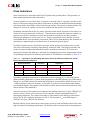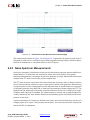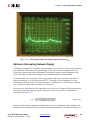
1
Zynq-7000
All Programmable SoC
PCB Design Guide
UG933 (v1.8) November 7, 2014
Revision History
The following table shows the revision history for this document.
Date
Version
Revision
06/04/2012
1.0
Initial Xilinx release.
06/06/2012
1.1
Corrected format issue.
08/29/2012
1.2
Updated Table 3-1 and Table 3-2 for additional devices/packages. Added 680 µF
capacitor specification to Table 3-3.
10/11/2012
1.2.1
Corrected document number (changed UG993 to UG933).
11/05/2012
1.2.2
Corrected sizing problem in PDF (no content change).
02/12/2013
1.3
Added Note (2) to Table 3-2. Added suggested part numbers to Table 3-3. Modified
paragraph under VCCPAUX – PS Auxiliary Logic Supply. Modified paragraph under
VCCPLL – PS PLL Supply. Added Figure 5-3. Modified second to last sentence and
added last sentence under PS_DDR_VREF0, PS_DDR_VREF1 – PS DDR Reference
Voltage. Modified CAUTION! under Configuring the VCCO_MIO0, VCCO_MIO1 Voltage
Mode and Note under DDR Supply Voltages. Changed Cke connection from a
pull-down resistor to a pull-up resistor in Figure 5-5 through Figure 5-7. Updated
entire MIO/EMIO IP Layout Guidelines section.
04/01/2013
1.4
Added XC7Z100 devices to Table 3-1 and Table 3-2. Updated ESR range values in
Table 3-3. Changed “0805 Ceramic Capacitor” section heading to Mid and High
Frequency Capacitors and modified first paragraph. Removed dimensions, changed
“0805” to “0402” in Figure 3-1 and deleted “0402 Ceramic Capacitor” subsection.
Deleted last sentence under , Modes and Attributes. Changed “minimum” to
“maximum” in third sentence of second paragraph under VCCPLL – PS PLL Supply.
Added second to last sentence under PS_DDR_VREF0, PS_DDR_VREF1 – PS DDR
Reference Voltage. Changed “Rup” to “Rterm” in Figure 5-5 and Figure 5-6. Deleted
Drst_b from Figure 5-6 and Figure 5-7. Changed Rup pull-up resistor to Rdown
pull-down resistor in Figure 5-7. Changed LPDDR2 setting in last row of Table 5-6 to
N/A. Updated values in first row of Table 5-9. Changed “Three” different topologies
to “two” under DDR Routing Topology. Removed Fly-by topology from Figure 5-8 and
Table 5-12. Deleted “NAND (ONFI),” “NOR/Flash/SRAM,” “SPI Master,” “SWDT (System
Watch Dog Timer),” and “TTC (Triple Time Counter” subsections from MIO/EMIO IP
Layout Guidelines and modified remaining subsections. Changed “EN208” to “EN247”
and “DS821” to “PG054” under Additional Resources and Legal Notices in Appendix A.
09/26/2013
1.5
Added XC7Z010, XC7Z015, and XC7Z030 packages/devices to Table 3-1 and Table 3-2.
Changed suggested part number for the 4.7 µF capacitor in Table 3-3. Added DDR ECC
unused pins to Table 5-5. Modified Figure 5-6 (Cke pins are now applied to GND via
resistor Rdown instead of VTT via Rterm). Expanded first paragraph under DDR
Termination. Clarified DDR Termination paragraph. Added fly-by routing to DDR
Routing Topology section. Deleted SD/SDIO Peripheral Controller section. Added last
sentence under sections IIC and SDIO and second sentence under QSPI. Added
Chapter 6, Migration from XC7Z030-SBG485 to XC7Z015-CLG485 Devices.
Zynq-7000 PCB Design Guide
UG933 (v1.8) November 7, 2014
www.xilinx.com
Send Feedback
2
Date
Version
Revision
12/04/2013
1.6
Changed “DDR3” to “DDR3/3L” throughout document. Updated capacitor quantities
and packages in Table 3-1 and Table 3-2. Updated capacitor specifications in
Table 3-3. Updated descriptions for VCCPINT – PS Internal Logic Supply and VCCPAUX –
PS Auxiliary Logic Supply. Deleted “Capacitor Consolidation Rules” section. Modified
next-to-last sentence under PS_DDR_VREF0, PS_DDR_VREF1 – PS DDR Reference
Voltage. Added paragraph preceding Table 5-5 and updated Table 5-5. Updated Addr,
Command, Contrl output name in Figure 5-7. Deleted last sentence under DDR Trace
Length.
08/01/2014
1.7
Removed “and Pin Planning Guide” from title. Added recommendation to
Recommended PCB Capacitors per Device. Changed VCCO per Bank sub-heading from
“100 µF” to 47 µF” in Table 3-1. Removed values for VCCPLL and replaced with
reference (Note 3) in Table 3-2. Changed “Terminal” type to “Terminal Tantalum” and
added “X7U” to 100 µF capacitor in Table 3-3. Modified first paragraph under Noise
Limits by removing specifications and adding a reference to the data sheet. Updated
second paragraph under Unconnected VCCO Pins. Changed Murata part number from
“GRM155R60J475ME47D” to “GRM155R60J474KE19” under Unconnected VCCO Pins.
Updated first paragraph under PS_DDR_VRN, PS_DDR_VRP – PS DDR Termination
Voltage. Updated Unused DDR Memory. Deleted last two sentences under PS_POR_B
– Power on Reset and last sentence under PS_SRST_B – External System Reset.
Changed “Boot Mode Pins” section (pins MIO[2] to MIO[8] to Boot Mode Pin MIO[8].
Modified Figure 5-5 (CKE resistor layout). Modified Figure 5-6 (changed clk signal to
differential signals CLK_P/CLK_N and added pull-down resistor to ODT). Added
separate column for DDR3L to Table 5-6 and modified values. Clarified DDR Trace
Length and DDR Trace Impedance sections. Clarified byte swapping under DDR
Routing Topology. Added last paragraph under Ethernet GEM. Deleted “Lower
Operating Frequencies (without Feedback Mode)” section from Chapter 6.
08/05/2014
1.7.1
11/07/2014
1.8
Updated document to latest user guide template.
Added XC7Z035 device to Table 3-1 and Table 3-2. Added 10 µF capacitor to Table 3-3.
Updated Table 5-5.
Zynq-7000 PCB Design Guide
UG933 (v1.8) November 7, 2014
www.xilinx.com
Send Feedback
3
Table of Contents
Revision History . . . . . . . . . . . . . . . . . . . . . . . . . . . . . . . . . . . . . . . . . . . . . . . . . . . . . . . . . . . . . . . . . . . . 2
Chapter 1: Introduction
About This Guide . . . . . . . . . . . . . . . . . . . . . . . . . . . . . . . . . . . . . . . . . . . . . . . . . . . . . . . . . . . . . . . . . . 6
Additional Support Resources. . . . . . . . . . . . . . . . . . . . . . . . . . . . . . . . . . . . . . . . . . . . . . . . . . . . . . . . 6
Chapter 2: PCB Technology Basics
Introduction . . . . . . . . . . . . . . . . . . . . . . . . . . . . . . . . . . . . . . . . . . . . . . . . . . . . . . . . . . . . . . . . . . . . . . 7
PCB Structures . . . . . . . . . . . . . . . . . . . . . . . . . . . . . . . . . . . . . . . . . . . . . . . . . . . . . . . . . . . . . . . . . . . . 7
Transmission Lines . . . . . . . . . . . . . . . . . . . . . . . . . . . . . . . . . . . . . . . . . . . . . . . . . . . . . . . . . . . . . . . . 10
Return Currents . . . . . . . . . . . . . . . . . . . . . . . . . . . . . . . . . . . . . . . . . . . . . . . . . . . . . . . . . . . . . . . . . . 11
Chapter 3: Power Distribution System
Introduction . . . . . . . . . . . . . . . . . . . . . . . . . . . . . . . . . . . . . . . . . . . . . . . . . . . . . . . . . . . . . . . . . . . . .
PCB Decoupling Capacitors . . . . . . . . . . . . . . . . . . . . . . . . . . . . . . . . . . . . . . . . . . . . . . . . . . . . . . . . .
Basic PDS Principles . . . . . . . . . . . . . . . . . . . . . . . . . . . . . . . . . . . . . . . . . . . . . . . . . . . . . . . . . . . . . . .
Simulation Methods . . . . . . . . . . . . . . . . . . . . . . . . . . . . . . . . . . . . . . . . . . . . . . . . . . . . . . . . . . . . . .
PDS Measurements . . . . . . . . . . . . . . . . . . . . . . . . . . . . . . . . . . . . . . . . . . . . . . . . . . . . . . . . . . . . . . .
Troubleshooting . . . . . . . . . . . . . . . . . . . . . . . . . . . . . . . . . . . . . . . . . . . . . . . . . . . . . . . . . . . . . . . . . .
12
12
17
31
32
37
Chapter 4: SelectIO Signaling
Introduction . . . . . . . . . . . . . . . . . . . . . . . . . . . . . . . . . . . . . . . . . . . . . . . . . . . . . . . . . . . . . . . . . . . . . 39
Interface Types. . . . . . . . . . . . . . . . . . . . . . . . . . . . . . . . . . . . . . . . . . . . . . . . . . . . . . . . . . . . . . . . . . . 39
Single-Ended Signaling. . . . . . . . . . . . . . . . . . . . . . . . . . . . . . . . . . . . . . . . . . . . . . . . . . . . . . . . . . . . . 40
Chapter 5: Processing System (PS) Power and Signaling
Power . . . . . . . . . . . . . . . . . . . . . . . . . . . . . . . . . . . . . . . . . . . . . . . . . . . . . . . . . . . . . . . . . . . . . . . . . .
PS Clock and Reset . . . . . . . . . . . . . . . . . . . . . . . . . . . . . . . . . . . . . . . . . . . . . . . . . . . . . . . . . . . . . . . .
Boot Mode Pin MIO[8] . . . . . . . . . . . . . . . . . . . . . . . . . . . . . . . . . . . . . . . . . . . . . . . . . . . . . . . . . . . .
Dynamic Memory. . . . . . . . . . . . . . . . . . . . . . . . . . . . . . . . . . . . . . . . . . . . . . . . . . . . . . . . . . . . . . . . .
MIO/EMIO IP Layout Guidelines . . . . . . . . . . . . . . . . . . . . . . . . . . . . . . . . . . . . . . . . . . . . . . . . . . . . .
Zynq-7000 PCB Design Guide
UG933 (v1.8) November 7, 2014
www.xilinx.com
Send Feedback
51
56
56
57
65
4
Chapter 6: Migration from XC7Z030-SBG485 to XC7Z015-CLG485 Devices
Introduction . . . . . . . . . . . . . . . . . . . . . . . . . . . . . . . . . . . . . . . . . . . . . . . . . . . . . . . . . . . . . . . . . . . . . 69
Differences between XC7Z030-SBG485 and XC7Z015-CLG485 Devices . . . . . . . . . . . . . . . . . . . . . . 69
Appendix A: Additional Resources and Legal Notices
Xilinx Resources . . . . . . . . . . . . . . . . . . . . . . . . . . . . . . . . . . . . . . . . . . . . . . . . . . . . . . . . . . . . . . . . . .
Solution Centers. . . . . . . . . . . . . . . . . . . . . . . . . . . . . . . . . . . . . . . . . . . . . . . . . . . . . . . . . . . . . . . . . .
References . . . . . . . . . . . . . . . . . . . . . . . . . . . . . . . . . . . . . . . . . . . . . . . . . . . . . . . . . . . . . . . . . . . . . .
Please Read: Important Legal Notices . . . . . . . . . . . . . . . . . . . . . . . . . . . . . . . . . . . . . . . . . . . . . . . .
Zynq-7000 PCB Design Guide
UG933 (v1.8) November 7, 2014
www.xilinx.com
Send Feedback
72
73
73
76
5
Chapter 1
Introduction
About This Guide
This guide provides information on PCB design for the Zynq®-7000 All Programmable SoC
(AP SoC), with a focus on strategies for making design decisions at the PCB and interface
level.
This Zynq-7000 All Programmable SoC PCB Design Guide, part of an overall set of
documentation on the Zynq-7000 AP SoC, is available on the Xilinx website at
www.xilinx.com/zynq.
Additional Support Resources
For additional information regarding PCB materials, traces, and design techniques for high
speed signals, refer to chapters four and five of UG483, 7 Series FPGAs PCB Guide. A
comprehensive list of all additional resources is provided in Appendix A, Additional
Resources and Legal Notices.
Zynq-7000 PCB Design Guide
UG933 (v1.8) November 7, 2014
www.xilinx.com
Send Feedback
6
Chapter 2
PCB Technology Basics
Introduction
Printed circuit boards (PCBs) are electrical systems, with electrical properties as complicated
as the discrete components and devices mounted to them. The PCB designer has complete
control over many aspects of the PCB; however, current technology places constraints and
limits on the geometries and resulting electrical properties. The following information is
provided as a guide to the freedoms, limitations, and techniques for PCB designs using
Zynq-7000 AP SoC devices.
This chapter contains the following sections:
•
PCB Structures
•
Transmission Lines
•
Return Currents
PCB Structures
PCB technology has not changed significantly in the last few decades. An insulator
substrate material (usually FR4, an epoxy/glass composite) with copper plating on both
sides has portions of copper etched away to form conductive paths. Layers of plated and
etched substrates are glued together in a stack with additional insulator substrates between
the etched substrates. Holes are drilled through the stack. Conductive plating is applied to
these holes, selectively forming conductive connections between the etched copper of
different layers.
While there are advancements in PCB technology, such as material properties, the number
of stacked layers used, geometries, and drilling techniques (allowing holes that penetrate
only a portion of the stackup), the basic structures of PCBs have not changed. The
structures formed through the PCB technology are abstracted to a set of physical/electrical
structures: traces, planes (or planelets), vias, and pads.
Zynq-7000 PCB Design Guide
UG933 (v1.8) November 7, 2014
www.xilinx.com
Send Feedback
7
Chapter 2: PCB Technology Basics
Traces
A trace is a physical strip of metal (usually copper) making an electrical connection between
two or more points on an X-Y coordinate of a PCB. The trace carries signals between these
points.
Planes
A plane is an uninterrupted area of metal covering the entire PCB layer. A planelet, a
variation of a plane, is an uninterrupted area of metal covering only a portion of a PCB layer.
Typically, a number of planelets exist in one PCB layer. Planes and planelets distribute power
to a number of points on a PCB. They are very important in the transmission of signals along
traces because they are the return current transmission medium.
Vias
A via is a piece of metal making an electrical connection between two or more points in the
Z space of a PCB. Vias carry signals or power between layers of a PCB. In current
plated-through-hole (PTH) technology, a via is formed by plating the inner surface of a hole
drilled through the PCB. In current microvia technology (also known as High Density
Interconnect or HDI), a via is formed with a laser by ablating the substrate material and
deforming the conductive plating. These microvias cannot penetrate more than one or two
layers, however, they can be stacked or stair-stepped to form vias traversing the full board
thickness.
Pads and Antipads
Because PTH vias are conductive over the whole length of the via, a method is needed to
selectively make electrical connections to traces, planes, and planelets of the various layers
of a PCB. This is the function of pads and antipads. Pads are small areas of copper in
prescribed shapes. Antipads are small areas in prescribed shapes where copper is removed.
Pads are used both with vias and as exposed outer-layer copper for mounting of
surface-mount components. Antipads are used mainly with vias. For traces, pads are used to
make the electrical connection between the via and the trace or plane shape on a given
layer. For a via to make a solid connection to a trace on a PCB layer, a pad must be present
for mechanical stability. The size of the pad must meet drill tolerance/registration
restrictions. Antipads are used in planes. Because plane and planelet copper is otherwise
uninterrupted, any via traveling through the copper makes an electrical connection to it.
Where vias are not intended to make an electrical connection to the planes or planelets
passed through, an antipad removes copper in the area of the layer where the via
penetrates.
Zynq-7000 PCB Design Guide
UG933 (v1.8) November 7, 2014
www.xilinx.com
Send Feedback
8
Chapter 2: PCB Technology Basics
Lands
For the purposes of soldering surface mount components, pads on outer layers are typically
referred to as lands or solder lands. Making electrical connections to these lands usually
requires vias. Due to manufacturing constraints of PTH technology, it is rarely possible to
place a via inside the area of the land. Instead, this technology uses a short section of trace
connecting to a surface pad. The minimum length of the connecting trace is determined by
minimum dimension specifications from the PCB manufacturer. Microvia technology is not
constrained, and vias can be placed directly in the area of a solder land.
Dimensions
The major factors defining the dimensions of the PCB are PCB manufacturing limits, AP SoC
package geometries, and system compliance. Other factors such as Design For
Manufacturing (DFM) and reliability impose further limits, but because these are
application specific, they are not documented in this user guide.
The dimensions of the AP SoC package, in combination with PCB manufacturing limits,
define most of the geometric aspects of the PCB structures described in this section, both
directly and indirectly. This significantly constrains the PCB designer. The package ball pitch
(1.0 mm for FF packages) defines the land pad layout. The minimum surface feature sizes of
current PCB technology define the via arrangement in the area under the device. Minimum
via diameters and keep-out areas around those vias are defined by the PCB manufacturer.
These diameters limit the amount of space available in-between vias for routing of signals
in and out of the via array underneath the device. These diameters define the maximum
trace width in these breakout traces. PCB manufacturing limits constrain the minimum trace
width and minimum spacing.
The total number of PCB layers necessary to accommodate an AP SoC is defined by the
number of signal layers and the number of plane layers.
•
The number of signal layers is defined by the number of I/O signal traces routed in and
out of an AP SoC package (usually following the total User I/O count of the package).
•
The number of plane layers is defined by the number of power and ground plane layers
necessary to bring power to the AP SoC and to provide references and isolation for
signal layers.
Most PCBs for large AP SoCs range from 12 to 22 layers.
System compliance often defines the total thickness of the board. Along with the number of
board layers, this defines the maximum layer thickness, and therefore, the spacing in the Z
direction of signal and plane layers to other signal and plane layers. Z-direction spacing of
signal trace layers to other signal trace layers affects crosstalk. Z-direction spacing of signal
trace layers to reference plane layers affects signal trace impedance. Z-direction spacing of
plane layers to other plane layers affects power system parasitic inductance.
Zynq-7000 PCB Design Guide
UG933 (v1.8) November 7, 2014
www.xilinx.com
Send Feedback
9
Chapter 2: PCB Technology Basics
Z-direction spacing of signal trace layers to reference plane layers (defined by total board
thickness and number of board layers) is a defining factor in trace impedance.Trace width
(defined by AP SoC package ball pitch and PCB via manufacturing constraints) is another
factor in trace impedance. A designer often has little control over trace impedance in area
of the via array beneath the AP SoC. When traces escape the via array, their width can
change to the width of the target impedance (usually 50Ω single-ended).
Decoupling capacitor placement and discrete termination resistor placement are other
areas of trade-off optimization. DFM constraints often define a keep-out area around the
perimeter of the AP SoC (device footprint) where no discrete components can be placed.
The purpose of the keep-out area is to allow room for assembly and rework where
necessary. For this reason, the area just outside the keep-out area is one where components
compete for placement. It is up to the PCB designer to determine the high priority
components. Decoupling capacitor placement constraints are described in Chapter 3,
Power Distribution System. Termination resistor placement constraints must be determined
through signal integrity simulation, using IBIS or SPICE models.
Transmission Lines
The combination of a signal trace and a reference plane forms a transmission line. All I/O
signals in a PCB system travel through transmission lines. For single-ended I/O interfaces,
both the signal trace and the reference plane are necessary to transmit a signal from one
place to another on the PCB. For differential I/O interfaces, the transmission line is formed
by the combination of two traces and a reference plane.
While the presence of a reference plane is not strictly necessary in the case of differential
signals, it is necessary for practical implementation of differential traces in PCBs. Good
signal integrity in a PCB system is dependent on having transmission lines with controlled
impedance. Impedance is determined by the geometry of the traces and the signal trace
and the reference plane.
The dielectric constant of the material in the vicinity of the trace and reference plane is a
property of the PCB laminate materials, and in the case of surface traces, a property of the
air or fluid surrounding the board. PCB laminate is typically a variant of FR4, though it can
also be an exotic material.
While the dielectric constant of the laminate varies from board to board, it is fairly constant
within one board. Therefore, the relative impedance of transmission lines in a PCB is defined
most strongly by the trace geometries and tolerances. Impedance variance can occur based
on the presence or absence of glass in a local portion of the laminate weave, but this rarely
poses issues except in high-speed (>6 Gb/s) interfaces.
Zynq-7000 PCB Design Guide
UG933 (v1.8) November 7, 2014
www.xilinx.com
Send Feedback
10
Chapter 2: PCB Technology Basics
Return Currents
An often neglected aspect of transmission lines and their signal integrity is return current.
It is incorrect to assume that a signal trace by itself forms a transmission line. Currents
flowing in a signal trace have an equal and opposite complimentary current flowing in the
reference plane beneath them. The relationship of the trace voltage and trace current to
reference plane voltage and reference plane current defines the characteristic impedance of
the transmission line formed by the trace and reference plane. While interruption of
reference plane continuity beneath a trace is not as dramatic in effect as severing the signal
trace, the performance of the transmission line and any devices sharing the reference plane
is affected.
It is important to pay attention to reference plane continuity and return current paths.
Interruptions of reference plane continuity, such as holes, slots, or isolation splits, cause
significant impedance discontinuities in the signal traces. They can also be a significant
source of crosstalk and contributor to Power Distribution System (PDS) noise. The
importance of return current paths cannot be underestimated.
Zynq-7000 PCB Design Guide
UG933 (v1.8) November 7, 2014
www.xilinx.com
Send Feedback
11
Chapter 3
Power Distribution System
Introduction
This chapter documents the power distribution system (PDS) for Zynq-7000 AP SoC devices,
including decoupling capacitor selection, placement, and PCB geometries. A simple
decoupling method is provided for each device. Basic PDS design principles are covered, as
well as simulation and analysis methods. This chapter contains the following sections:
•
PCB Decoupling Capacitors
•
Basic PDS Principles
•
Simulation Methods
•
PDS Measurements
•
Troubleshooting
PCB Decoupling Capacitors
Recommended PCB Capacitors per Device
A simple PCB-decoupling network for the Zynq-7000 AP SoC devices is listed in Table 3-1
and Table 3-2. The optimized quantities of PCB decoupling capacitors assumes that the
voltage regulators have stable output voltages and meet the regulator manufacturer's
minimum output capacitance requirement.
Decoupling methods other than those presented in these tables can be used, but the
decoupling network should be designed to meet or exceed the performance of the simple
decoupling networks presented here. The impedance of the alternate network must be less
than or equal to that of the recommended network across frequencies from 100 KHz to
100 MHz.
Because device capacitance requirements vary with CLB and I/O utilization, PCB decoupling
guidelines are provided on a per-device basis. VCCINT, VCCAUX , VCCAUX_IO, VCCBRAM, and PS
supply capacitors are listed as the quantity per device, while VCCO capacitors are listed as
Zynq-7000 PCB Design Guide
UG933 (v1.8) November 7, 2014
www.xilinx.com
Send Feedback
12
Chapter 3: Power Distribution System
the quantity per I/O bank. Device performance at full utilization is equivalent across all
devices when using these recommended networks.
Table 3-1 and Table 3-2 do not provide the decoupling networks required for the GTX and
GTP transceiver power supplies. For this information, refer to UG476, 7 Series FPGAs
GTX/GTH Transceivers User Guide and UG482, 7 Series FPGAs GTP Transceivers User Guide.
RECOMMENDED: Refer to XMP277, 7 Series Schematic Review Recommendations, for a comprehensive
checklist for schematic review which complements this document.
Required PCB Capacitor Quantities
Table 3-1 lists the PCB decoupling capacitor guidelines per VCC supply rail for Zynq-7000 AP
SoC devices.
Table 3-1:
Required PCB Capacitor Quantities per Device (PL)
VCCBRAM
VCCINT
Package
Device
CLG225
Z-7010
0
0
1
1
2
CLG400
Z-7010
0
0
1
1
CLG485
Z-7015
0
1
0
CLG400
Z-7020
0
1
CLG484
Z-7020
0
SBG485
Z-7030
FBG484/
RB484
VCCAUX
VCCO per Bank(3)(4) Bank 0
VCCAUX_IO
47
µF
4.7
µF
0.47
µF
47 µF
or
100 µF
4.7
µF
0.47
µF
47
µF
1
NA
NA
NA
1
2
4
1
1
1
NA
NA
NA
1
2
4
1
1
1
2
NA
NA
NA
1
2
4
1
1
1
1
1
NA
NA
NA
1
2
4
1
1
1
1
1
2
NA
NA
NA
1
2
4
1
0
1
2
1
0
0
NA
NA
NA
1
0
0
1
1
0
1
2
1
0
0
NA
NA
NA
1
0
0
1
0
1
0
1
2
1
0
0
1
0
0
1
0
0
1
1
0
1
0
1
2
1
0
0
1
0
0
1
0
0
1
0
2
1
0
2
4
1
0
0
1
0
0
1
0
0
1
1
0
0
2
1
0
2
4
1
0
0
1
0
0
1
0
0
1
1
2
0
0
1
1
0
2
4
1
0
0
1
0
0
1
0
0
1
1
Z-7045
2
0
0
2
0
1
0
2
4
1
0
0
1
0
0
1
0
0
1
FFG676/
RF676
Z-7045
2
0
0
2
0
1
0
2
4
1
0
0
1
0
0
1
0
0
1
FFG900/
RF900
Z-7045
2
0
0
1
0
1
0
2
4
1
0
0
1
0
0
1
0
0
1
FFG900
Z-7100
3
0
0
2
0
2
0
4
8
1
0
0
1
0
0
1
0
0
1
680 330 100
µF
µF
µF
4.7 0.47 100
µF
µF
µF
47
µF
4.7
µF
0.47
µF
47
µF
NA
NA
NA
NA
1
1
2
0
1
1
1
1
2
4
1
0
1
1
0
2
4
1
0
1
1
0
2
4
1
0
0
1
0
1
0
1
Z-7030
0
1
0
1
0
FBG676
Z-7030
0
1
0
1
FFG676/
RF676
Z-7030
0
1
0
FBG676
Z-7035
2
0
FFG676/
RF676
Z-7035
2
FFG900/
RF900
Z-7035
FBG676
Zynq-7000 PCB Design Guide
UG933 (v1.8) November 7, 2014
www.xilinx.com
4.7 0.47
µF
µF
Send Feedback
13
Chapter 3: Power Distribution System
Table 3-1:
Required PCB Capacitor Quantities per Device (PL)
VCCBRAM
VCCINT
Package
Device
FFG1156
Z-7100
680 330 100
µF
µF
µF
3
0
4.7 0.47 100
µF
µF
µF
0
2
0
2
VCCAUX
47
µF
4.7
µF
0.47
µF
47
µF
0
4
8
1
4.7 0.47
µF
µF
0
VCCO per Bank(3)(4) Bank 0
VCCAUX_IO
0
47
µF
4.7
µF
0.47
µF
47 µF
or
100 µF
4.7
µF
0.47
µF
47
µF
1
0
0
1
0
0
1
Notes:
1. PCB Capacitor specifications are listed in Table 3-3.
2. Total includes all capacitors for all supplies, except for the MGT supplies MGTAVCC and MGTAVTT, which are covered in
UG476, 7 Series FPGAs GTX/GTH Transceivers User Guide and UG482, 7 Series FPGAs GTP Transceivers User Guide.
3. HRIO 47 µF capacitors can be consolidated at one 47 µF per four banks.
4. HPIO 47 µF capacitors can be consolidated at one 47 µF per four banks.
5. Decoupling capacitors cover down to approximately 100 Hz.
Table 3-2 lists the decoupling requirements for the Processing System (PS).
Table 3-2:
Required PCB Capacitor Quantities per Device (PS)
VCCPAUX(1)
VCCPINT
Package Device 100 4.7 0.47 100
VCCO_DDR
VCCO_MIO0
VCCPLL(2)(3)
VCCO_MIO1
µF
µF
µF
µF
4.7
µF
0.47
µF
100
µF
4.7
µF
0.47
µF
100
µF
4.7
µF
0.47
µF
100
µF
4.7
µF
0.47
µF
CLG225
Z-7 010
1
1
3
1
1
1
1
1
4
1
1
1
1
1
1
CLG400
Z-7 010
1
1
3
1
1
1
1
1
4
1
1
1
1
1
1
CLG485
Z-7015
1
1
3
1
1
1
1
1
4
1
1
1
1
1
1
CLG400
Z-7020
1
1
3
1
1
1
1
1
4
1
1
1
1
1
1
CLG484
Z-7020
1
1
3
1
1
1
1
1
4
1
1
1
1
1
1
SBG485
Z-7030
1
0
0
1
1
1
1
0
0
1
1
1
1
1
1
FBG484/
RB484
Z-7030
1
0
0
1
1
1
1
0
0
1
1
1
1
1
1
FBG676
Z-7 030
1
0
0
1
1
1
1
0
0
1
1
1
1
1
1
FFG676/
RF676
Z-7030
1
0
0
1
1
1
1
0
0
1
1
1
1
1
1
FBG676
Z-7035
1
0
0
1
1
1
1
0
0
1
1
1
1
1
1
FFG676/
RF676
Z-7035
1
0
0
1
1
1
1
0
0
1
1
1
1
1
1
FFG900/
RF900
Z-7035
1
0
0
1
1
1
1
0
0
1
1
1
1
1
1
FBG676
Z-7045
1
0
0
1
1
1
1
0
0
1
1
1
1
1
1
FFG676/
RF676
Z-7045
1
0
0
1
1
1
1
0
0
1
1
1
1
1
1
FFG900/
RF900
Z-7045
1
0
0
1
1
1
1
0
0
1
1
1
1
1
1
FFG900
Z-7100
1
0
0
1
1
1
1
0
0
1
1
1
1
1
1
Zynq-7000 PCB Design Guide
UG933 (v1.8) November 7, 2014
www.xilinx.com
Send Feedback
14
Chapter 3: Power Distribution System
Table 3-2:
Required PCB Capacitor Quantities per Device (PS) (Cont’d)
VCCPAUX(1)
VCCPINT
Package Device 100 4.7 0.47 100
FFG1156
Z-7100
VCCO_DDR
VCCO_MIO0
VCCPLL(2)(3)
VCCO_MIO1
µF
µF
µF
µF
4.7
µF
0.47
µF
100
µF
4.7
µF
0.47
µF
100
µF
4.7
µF
0.47
µF
100
µF
4.7
µF
0.47
µF
1
0
0
1
1
1
1
0
0
1
1
1
1
1
1
Notes:
1. See VCCPAUX – PS Auxiliary Logic Supply, page 51 for layout guidelines.
2. VCCPLL can be derived from VCCPAUX using a ferrite bead filter (see Figure 5-2, page 52).
3. See VCCPLL – PS PLL Supply, page 52 for layout guidelines.
Capacitor Specifications
The electrical characteristics of the capacitors in Table 3-1 and Table 3-2 are specified in
Table 3-3, and are followed by guidelines on acceptable substitutions. The equivalent series
resistance (ESR) ranges specified for these capacitors can be over-ridden. However, this
requires analysis of the resulting power distribution system impedance to ensure that no
resonant impedance spikes result.
Table 3-3:
PCB Capacitor Specifications
Ideal
Value
Value
Range(1)
Body
Size(2)
ESL
Maximum
ESR Range(3)
Voltage
Rating(4)
Suggested
Part Number
680 µF
C > 680 µF
2917/D
/7343
2-Terminal
Tantalum
2.1 nH
5 mΩ < ESR < 40 mΩ
2.5V
T530X687M006ATE018
330 µF
C > 330 µF
2917/D
/7343
2-Terminal
Tantalum
2.0 nH
5 mΩ < ESR < 40 mΩ
2.5V
T525D337M006ATE025
330 µF
C > 330 µF
2917/D
/7343
2-Terminal
Niobium
Oxide
2.0 nH
5 mΩ < ESR < 40 mΩ
2.5V
NOSD337M002#0035
100 µF
C > 100 µF
1210
2-Terminal
Tantalum,
Ceramic
X7R, X7U, or
X5R
1 nH
1 mΩ < ESR < 40 mΩ
2.5V
GRM32EE70G107ME19
47 µF
C > 47 µF
1210
2-Terminal
Ceramic X7R
or X5R
1 nH
1 mΩ < ESR < 40 mΩ
6.3V
GRM32ER70J476ME20L
10 µF
C = 10 µF
0603
2-Terminal
Ceramic X7R
or X5R
0.25 nH
5 mΩ
4.0V
GRM188R60G106ME47
4.7 µF
C > 4.7 µF
0805
2-Terminal
Ceramic X7R
or X5R
0.5 nH
1 mΩ < ESR < 20 mΩ
6.3V
GRM21BR71A475KA73
Type
Zynq-7000 PCB Design Guide
UG933 (v1.8) November 7, 2014
www.xilinx.com
Send Feedback
15
Chapter 3: Power Distribution System
Table 3-3:
PCB Capacitor Specifications (Cont’d)
Ideal
Value
Value
Range(1)
Body
Size(2)
0.47 µF
C > 0.47 µF
0603
Type
2-Terminal
Ceramic X7R
or X5R
ESL
Maximum
ESR Range(3)
Voltage
Rating(4)
Suggested
Part Number
0.5 nH
1 mΩ < ESR < 20 mΩ
6.3V
GRM188R70J474KA01
Notes:
1. Values can be larger than specified.
2. Body size can be smaller than specified.
3. ESR must be within the specified range.
4. Voltage rating can be higher than specified.
PCB Bulk Capacitors
The purpose of the bulk capacitors is to cover the low-frequency range between where the
voltage regulator stops working and where the on-package ceramic capacitors start
working. As specified in Table 3-1 and Table 3-2, all AP SoC supplies require bulk capacitors.
The tantalum and niobium oxide capacitors specified in Table 3-3 were selected for their
values and controlled ESR values. They are also ROHS compliant. If another manufacturer's
tantalum, niobium oxide, or ceramic capacitors are used, ensure they meet the
specifications of Table 3-3 and are properly evaluated via simulation, s-parameter
extraction, or bench testing.
PCB High-Frequency Capacitors
Table 3-3 shows the requirements for the 0.47 µF and 4.7 µF capacitors in the 0402 package.
Substitutions can be made for some characteristics, but not others. For details, refer to the
notes in Table 3-3.
PCB Capacitor Placement and Mounting Techniques
PCB Bulk Capacitors
Bulk capacitors can be large and sometimes are difficult to place very close to the AP SoC.
Fortunately, this is not a problem because the low-frequency energy covered by bulk
capacitors is not sensitive to capacitor location. Bulk capacitors can be placed almost
anywhere on the PCB, but the best placement is as close as possible to the AP SoC.
Capacitor mounting should follow normal PCB layout practices, tending toward short and
wide shapes connecting to power planes with multiple vias.
Mid and High Frequency Capacitors
The 4.7 µF capacitor covers the middle frequency range, while the 0.47 µF capacitor covers
the high frequency range. Placement has some impact on performance. The 4.7 µF
capacitors should be placed as close as possible to the AP SoC. Any placement within two
Zynq-7000 PCB Design Guide
UG933 (v1.8) November 7, 2014
www.xilinx.com
Send Feedback
16
Chapter 3: Power Distribution System
inches of the device’s outer edge is acceptable. The 0.47 µF capacitors should be placed as
close to the AP SoC as possible, within 0.5 inches of the outer edge.
The capacitor mounting (solder lands, traces, and vias) should be optimized for low
inductance. Vias should be butted directly against the pads. Vias can be located at the ends
of the pads (see Figure 3-1B), but are more optimally located at the sides of the pads (see
Figure 3-1C). Via placement at the sides of the pads decreases the mounting’s overall
parasitic inductance by increasing the mutual inductive coupling of one via to the other.
Dual vias can be placed on both sides of the pads (see Figure 3-1D) for even lower parasitic
inductance, but with diminishing returns.
X-Ref Target - Figure 3-1
Land Pattern
End Vias
Long Traces
Not Recommended.
Connecting Trace is Too Long
Land Pattern
End Vias
Land Pattern
Side Vias
Land Pattern
Double Side Vias
(C)
(A)
(D)
(B)
UG933_c3_01_102413
Figure 3-1:
Example Capacitor Land and Mounting Geometries
Basic PDS Principles
The purpose of the PDS and the properties of its components are discussed in this section.
The important aspects of capacitor placement, capacitor mounting, PCB geometry, and PCB
stackup recommendations are also described.
Noise Limits
In the same way that devices in a system have a requirement for the amount of current
consumed by the power system, there is also a requirement for the cleanliness of the power.
This cleanliness requirement specifies a maximum amount of noise present on the power
Zynq-7000 PCB Design Guide
UG933 (v1.8) November 7, 2014
www.xilinx.com
Send Feedback
17
Chapter 3: Power Distribution System
supply, often referred to as ripple voltage. Most digital devices, including all Zynq-7000 AP
SoC devices, require that VCC supplies not fluctuate more than the specifications
documented in the device data sheet.
The power consumed by a digital device varies over time and this variance occurs on all
frequency scales, creating a need for a wide-band PDS to maintain voltage stability.
•
Low-frequency variance of power consumption is usually the result of devices or large
portions of devices being enabled or disabled. This variance occurs in time frames from
milliseconds to days.
•
High-frequency variance of power consumption is the result of individual switching
events inside a device. This occurs on the scale of the clock frequency and the first few
harmonics of the clock frequency up to about 5 GHz.
Because the voltage level of VCC for a device is fixed, changing power demands are
manifested as changing current demand. The PDS must accommodate these variances of
current draw with as little change as possible in the power-supply voltage.
When the current draw in a device changes, the PDS cannot respond to that change
instantaneously. As a consequence, the voltage at the device changes for a brief period
before the PDS responds. Two main causes for this PDS lag correspond to the two major
PDS components: the voltage regulator and decoupling capacitors.
The first major component of the PDS is the voltage regulator. The voltage regulator
observes its output voltage and adjusts the amount of current it is supplying to keep the
output voltage constant. Most common voltage regulators make this adjustment in
milliseconds to microseconds. Voltage regulators effectively maintain the output voltage
for events at all frequencies from DC to a few hundred kHz, depending on the regulator
(some are effective at regulating in the low MHz). For transient events that occur at
frequencies above this range, there is a time lag before the voltage regulator responds to
the new current demand level.
For example, if the device’s current demand increases in a few hundred picoseconds, the
voltage at the device sags by some amount until the voltage regulator can adjust to the
new, higher level of required current. This lag can last from microseconds to milliseconds. A
second component is needed to substitute for the regulator during this time, preventing
the voltage from sagging.
This second major PDS component is the decoupling capacitor (also known as a bypass
capacitor). The decoupling capacitor works as the device’s local energy storage. The
capacitor cannot provide DC power because it stores only a small amount of energy
(voltage regulator provides DC power). This local energy storage should respond very
quickly to changing current demands. The capacitors effectively maintain power-supply
voltage at frequencies from hundreds of kHz to hundreds of MHz (in the milliseconds to
nanoseconds range). Discrete decoupling capacitors are not useful for events occurring
above or below this range.
Zynq-7000 PCB Design Guide
UG933 (v1.8) November 7, 2014
www.xilinx.com
Send Feedback
18
Chapter 3: Power Distribution System
For example, if current demand in the device increases in a few picoseconds, the voltage at
the device sags by some amount until the capacitors can supply extra charge to the device.
If current demand in the device maintains this new level for many milliseconds, the
voltage-regulator circuit, operating in parallel with the decoupling capacitors, replaces the
capacitors by changing its output to supply this new level of current.
Figure 3-2 shows the major PDS components: the voltage regulator, the decoupling
capacitors, and the active device being powered (AP SoC).
X-Ref Target - Figure 3-2
LREGULATOR
LDECOUPLING
+
Voltage
Regulator
V
CDECOUPLING
AP SoC
UG933_c3_02_081312
Figure 3-2:
Simplified PDS Circuit
Figure 3-3 shows a simplified PDS circuit with all reactive components represented by a
frequency-dependent resistor.
X-Ref Target - Figure 3-3
ltransient
+
ZP(f)
V
+
VRIPPLE
-
AP SoC
UG933_c2_03_081312
Figure 3-3:
Further Simplified PDS Circuit
Role of Inductance
Inductance is the property of the capacitors and the PCB current paths that slows down
changes in current flow. Inductance is the reason why capacitors cannot respond
instantaneously to transient currents or to changes that occur at frequencies higher than
their effective range.
Inductance can be thought of as the momentum of charge. Charge moving through a
conductor represents some amount of current. If the level of current changes, the charge
Zynq-7000 PCB Design Guide
UG933 (v1.8) November 7, 2014
www.xilinx.com
Send Feedback
19
Chapter 3: Power Distribution System
moves at a different rate. Because momentum (stored magnetic-field energy) is associated
with this charge, some amount of time and energy is required to slow down or speed up the
charge flow. The greater the inductance, the greater the resistance to change, and the
longer the time required for the current level to change. A voltage develops across the
inductance as this change occurs.
The PDS, made up of a regulator and multiple stages of decoupling capacitors,
accommodates the device current demand and responds to current transients as quickly as
necessary to maintain the voltage within the specified limits. When these current demands
are not met, the voltage across the device's power supply changes. This is observed as
noise. Inductance in the current path of the capacitors should be minimized, because it
retards the ability of decoupling capacitors to quickly respond to changing current
demands.
Inductances occur between the AP SoC device and capacitors and between the capacitors
and the voltage regulator (see Figure 3-2). These inductances occur as parasitics in the
capacitors and in all PCB current paths. It is important that each of these parasitics be
minimized.
Capacitor Parasitic Inductance
The capacitance value is often considered to be a capacitors’s most important
characteristic. In power system applications, the parasitic inductance (ESL) has the same or
greater importance. Capacitor package dimensions (body size) determine the amount of
parasitic inductance. Physically small capacitors usually have lower parasitic inductance
than physically large capacitors.
Requirements for choosing decoupling capacitors:
•
For a specific capacitance value, choose the smallest package available.
- or -
•
For a specific package size (essentially a fixed inductance value), choose the highest
capacitance value available in that package.
Surface-mount chip capacitors are the smallest capacitors available and are a good choice
for discrete decoupling capacitors:
•
For values from 100 µF to very small values such as 0.01 µF, ceramic X7R or X5R type
capacitors are usually used. These capacitors have a low parasitic inductance and a low
ESR, with an acceptable temperature characteristic.
•
For larger values, such as 47 µF to 1000 µF, tantalum capacitors are usually used. These
capacitors have a low parasitic inductance and a medium ESR, giving them a low Q
factor and consequently a very wide range of effective frequencies.
Zynq-7000 PCB Design Guide
UG933 (v1.8) November 7, 2014
www.xilinx.com
Send Feedback
20
Chapter 3: Power Distribution System
If tantalum capacitors are not available or cannot be used, low-ESR, low-inductance
electrolytic capacitors can be used, provided they have comparable ESR and ESL values.
Other new technologies with similar characteristics are also available (Os-Con, POSCAP, and
Polymer-Electrolytic SMT).
A real capacitor of any type then not only has capacitance characteristics but also
inductance and resistance characteristics. Figure 3-4 shows the parasitic model of a real
capacitor. A real capacitor should be treated as an RLC circuit (a circuit consisting of a
resistor (R), an inductor (L), and a capacitor (C), connected in series).
X-Ref Target - Figure 3-4
ESR
ESL
C
UG933_c3_04_032811
Figure 3-4:
Parasitics of a Real, Non-Ideal Capacitor
Figure 3-5 shows a real capacitor’s impedance characteristic. Overlaid on this plot are
curves corresponding to the capacitor’s capacitance and parasitic inductance (ESL). These
two curves combine to form the RLC circuit’s total impedance characteristic, softened or
sharpened by the capacitor’s ESR.
X-Ref Target - Figure 3-5
Total Impedance Characteristic
Impedance
Inductive
Contribution (ESL)
Capacitive
Contribution (C)
Frequency
Figure 3-5:
UG933_c3_05_032811
Contribution of Parasitics to Total Impedance Characteristics
As capacitive value is increased, the capacitive curve moves down and left. As parasitic
inductance is decreased, the inductive curve moves down and right. Because parasitic
inductance for capacitors in a specific package is fixed, the inductance curve for capacitors
in a specific package remains fixed.
Zynq-7000 PCB Design Guide
UG933 (v1.8) November 7, 2014
www.xilinx.com
Send Feedback
21
Chapter 3: Power Distribution System
As different capacitor values are selected in the same package, the capacitive curve moves
up and down against the fixed inductance curve, as shown in Figure 3-6.
X-Ref Target - Figure 3-6
Z Value at F2 is Equal
0805
0.47 μF
Inductance (Z)
0805
4.7 μF
Inductive
Portion
F2
Frequency
UG933_c3_06_060211
Figure 3-6:
Effective Frequency Example
The low-frequency capacitor impedance can be reduced by increasing the value of the
capacitor; the high-frequency impedance can be reduced by decreasing the inductance of
the capacitor. While it might be possible to specify a higher capacitance value in the fixed
package, it is not possible to lower the inductance of the capacitor (in the fixed package)
without putting more capacitors in parallel. Using multiple capacitors in parallel divides the
parasitic inductance, and at the same time, multiplies the capacitance value. This lowers
both the high and low frequency impedance at the same time.
PCB Current Path Inductance
The parasitic inductance of current paths in the PCB have three distinct sources:
•
Capacitor mounting
•
PCB power and ground planes
•
AP SoC mounting
Capacitor Mounting Inductance
Capacitor mounting refers to the capacitor's solder lands on the PCB, the trace (if any)
between the land and via, and the via.
The vias, traces, and capacitor mounting pads of a 2-terminal capacitor contribute
inductance between 300 pH to 4 nH depending on the specific geometry.
Because the current path’s inductance is proportional to the loop area the current traverses,
it is important to minimize this loop size. The loop consists of the path through one power
Zynq-7000 PCB Design Guide
UG933 (v1.8) November 7, 2014
www.xilinx.com
Send Feedback
22
Chapter 3: Power Distribution System
plane, up through one via, through the connecting trace to the land, through the capacitor,
through the other land and connecting trace, down through the other via, and into the
other plane, as shown in Figure 3-7.
X-Ref Target - Figure 3-7
0402 Capacitor Body
Surface Trace
Via
Solderable End Terminal
Capacitor Solder Land
Power and
Ground Planes
GND
VCC
PCB
Mounted Capacitor Current Loop
UG933_c3_07_032811
Figure 3-7:
Example Cutaway View of PCB with Capacitor Mounting
A connecting trace length has a large impact on the mounting’s parasitic inductance and if
used, should be as short and wide as possible. When possible, a connecting trace should
not be used and the via should butt up against the land. Placing vias to the side of the
capacitor lands or doubling the number of vias, further reduces the mounting’s parasitic
inductance.
Some PCB manufacturing processes allow via-in-pad geometries, an option for reducing
parasitic inductance. Using multiple vias per land is important with ultra-low inductance
capacitors, such as reverse aspect ratio capacitors that place wide terminals on the sides of
the capacitor body instead of the ends.
PCB layout engineers often try to squeeze more parts into a small area by sharing vias
among multiple capacitors. This technique should not be used under any circumstances.
PDS improvement is very small when a second capacitor is connected to an existing
capacitor’s vias. For a larger improvement, reduce the total number of capacitors and
maintain a one-to-one ratio of lands to vias.
The capacitor mounting (lands, traces, and vias) typically contributes about the same
amount or more inductance than the capacitor's own parasitic self-inductance.
Zynq-7000 PCB Design Guide
UG933 (v1.8) November 7, 2014
www.xilinx.com
Send Feedback
23
Chapter 3: Power Distribution System
Plane Inductance
Some inductance is associated with the PCB power and ground planes. The geometry of
these planes determines their inductance.
Current spreads out as it flows from one point to another (due to a property similar to skin
effect) in the power and ground planes. Inductance in planes can be described as spreading
inductance and is specified in units of henries per square. The square is dimensionless; the
shape of a section of a plane, not the size, determines the amount of inductance.
Spreading inductance acts like any other inductance and resists changes to the amount of
current in a power plane (the conductor). The inductance retards the capacitor’s ability to
respond to a device’s transient currents and should be reduced as much as possible.
Because the designer’s control over the X-Y shape of the plane can be limited, the only
controllable factor is the spreading inductance value. This is determined by the thickness of
the dielectric separating a power plane from its associated ground plane.
For high-frequency power distribution systems, power and ground planes work in pairs,
with their inductances coexisting dependently with each other. The spacing between the
power and ground planes determines the pair’s spreading inductance. The closer the
spacing (the thinner the dielectric), the lower the spreading inductance. Approximate values
of spreading inductance for different thicknesses of FR4 dielectric are shown in Table 3-4.
Table 3-4: Capacitance and Spreading Inductance Values for Different Thicknesses of FR4
Power-Ground Plane Sandwiches
Dielectric Thickness
Inductance
Capacitance
(micron)
(mil)
(pH/square)
(pF/in2)
(pF/cm2)
102
4
130
225
35
51
2
65
450
70
25
1
32
900
140
Decreased spreading inductance corresponds to closer spacing of VCC and GND planes.
When possible, place the VCC planes directly adjacent to the GND planes in the PCB stackup.
Facing VCC and GND planes are sometimes referred to as sandwiches. While the use of VCC
– GND sandwiches was not necessary in the past for previous technologies (lead frames,
wire bond packages), the speeds involved and the sheer amount of power required for fast,
dense devices often demand it.
However, because of the presence of substrate decoupling capacitors in Zynq-7000 AP SoC
devices, there is a limit to the amount of fast transient current demanded from PCB
decoupling capacitors. This means that there is little benefit from dielectric thicknesses
below 50µ (2 mil). Dielectric thickness of 50µ or 75µ between VCC and GND layers is
sufficient for Zynq-7000 AP SoC devices.
Besides offering a low-inductance current path, power-ground sandwiches also offer some
high-frequency decoupling capacitance. As the plane area increases and as the separation
Zynq-7000 PCB Design Guide
UG933 (v1.8) November 7, 2014
www.xilinx.com
Send Feedback
24
Chapter 3: Power Distribution System
between power and ground planes decreases, the value of this capacitance increases.
Capacitance per square inch is shown in Table 3-4. However, the amount of capacitance
arising from these PCB power-ground plane pairs is generally inconsequential, given the
substrate decoupling capacitors present in Zynq-7000 AP SoC devices.
AP SoC Mounting Inductance
The PCB solder lands and vias that connect the AP SoC power pins (VCC and GND)
contribute an amount of parasitic inductance to the overall power circuit. For existing PCB
technology, the solder land geometry and the dogbone geometry are mostly fixed, and
parasitic inductance of these geometries does not vary. Via parasitic inductance is a
function of the via length and the proximity of the opposing current paths to one another.
The relevant via length is the portion of the via that carries transient current between the AP
SoC solder land and the associated VCC or GND plane. Any remaining via (between the
power plane and the PCB backside) does not affect the parasitic inductance of the via (the
shorter the via between the solder lands and the power plane, the smaller the parasitic
inductance). Parasitic via inductance in the AP SoC mounting is reduced by keeping the
relevant VCC and GND planes as close to the AP SoC as possible (close to the top of the PCB
stackup).
Device pinout arrangement determines the proximity of opposing current paths to one
another. Inductance is associated with any two opposing currents (for example, current
flowing in a VCC and GND via pair). A high degree of mutual inductive coupling between the
two opposing paths reduces the loop’s total inductance. Therefore, when given a choice,
VCC and GND vias should be as close together as possible.
The via field under an AP SoC has many VCC and GND vias, and the total inductance is a
function of the proximity of one via to another:
•
For core VCC supplies (VCCINT and VCCAUX), opposing current is between the VCC and
GND pins.
•
For I/O VCC supplies (VCCO), opposing current is between any I/O and its return current
path, whether carried by a VCCO or GND pin.
To reduce parasitic inductance:
•
Core VCC pins such as VCCINT and VCCAUX are placed in a checkerboard arrangement in
the pinout.
•
VCCO and GND pins are distributed among the I/O pins.
Every I/O pin in the Zynq-7000 AP SoC device pinout is adjacent to a return-current pin.
AP SoC pinout arrangement determines the PCB via arrangement. The PCB designer cannot
control the proximity of opposing current paths but has control over the trade-offs between
the capacitor’s mounting inductance and AP SoC’s mounting inductance:
Zynq-7000 PCB Design Guide
UG933 (v1.8) November 7, 2014
www.xilinx.com
Send Feedback
25
Chapter 3: Power Distribution System
•
Both mounting inductances are reduced by placing power planes close to the PCB
stackup’s top half and placing the capacitors on the top surface (reducing the
capacitor’s via length).
•
If power planes are placed in the PCB stackup’s bottom half, the capacitors must be
mounted on the PCB backside. In this case, AP SoC mounting vias are already long, and
making the capacitor vias long (by coming down from the top surface) is a bad
practice. A better practice is to take advantage of the short distance between the
underside of the PCB and the power plane of interest, mounting capacitors on the
underside.
PCB Stackup and Layer Order
VCC and ground plane placement in the PCB stackup (the layer order) has a significant
impact on the parasitic inductances of power current paths. Layer order must be considered
early in the design process:
•
High-priority supplies should be placed closer to the AP SoC (in the PCB stackup’s top
half)
•
Low-priority supplies should be placed farther from the AP SoC (in the PCB stackup’s
bottom half)
Power supplies with high transient current should have the associated VCC planes close to
the top surface (AP SoC side) of the PCB stackup. This decreases the vertical distance (VCC
and GND via length) that currents travel before reaching the associated VCC and GND
planes. To reduce spreading inductance, every VCC plane should have an adjacent GND
plane in the PCB stackup. The skin effect causes high-frequency currents to couple tightly,
and the GND plane adjacent to a specific VCC plane tends to carry the majority of the
current complementary to that in the VCC plane. Thus, adjacent VCC and GND planes are
treated as a pair.
Not all VCC and GND plane pairs reside in the PCB stackup’s top half because manufacturing
constraints typically require a symmetrical PCB stackup around the center (with respect to
dielectric thicknesses and etched copper areas). The PCB designer chooses the priority of
the VCC and GND plane pairs: high priority pairs carry high transient currents and are placed
high in the stackup, while low priority pairs carry lower transient currents (or can tolerate
more noise) and are placed in the lower part of the stackup.
Capacitor Effective Frequency
Every capacitor has a narrow frequency band where it is most effective as a decoupling
capacitor. This band is centered at the capacitor’s self-resonant frequency F RSELF . The
effective frequency bands of some capacitors are wider than others. A capacitor’s ESR
determines the capacitor’s quality (Q) factor, and the Q factor can determine the width of
the effective frequency band:
•
Tantalum capacitors generally have a very wide effective band.
Zynq-7000 PCB Design Guide
UG933 (v1.8) November 7, 2014
www.xilinx.com
Send Feedback
26
Chapter 3: Power Distribution System
•
Ceramic chip capacitors with a lower ESR, generally have a very narrow effective
frequency band.
An ideal capacitor only has a capacitive characteristic, whereas real non-ideal capacitors
also have a parasitic inductance (ESL) and a parasitic resistance (ESR). These parasitics work
in series to form an RLC circuit (Figure 3-4). The RLC circuit’s resonant frequency is the
capacitor’s self-resonant frequency.
To determine the RLC circuit’s resonant frequency, use Equation 3-1:
1
F = ------------------2π LC
Equation 3-1
Another method of determining the self-resonant frequency is to find the minimum point in
the impedance curve of the equivalent RLC circuit. The impedance curve can be computed
or generated in SPICE using a frequency sweep. See the Simulation Methods section for
other ways to compute an impedance curve.
It is important to distinguish between the capacitor's self-resonant frequency and the
mounted capacitor’s effective resonant frequency when the capacitor is part of the system,
F RIS . This corresponds to the resonant frequency of the capacitor with its parasitic
inductance, plus the inductance of the vias, planes, and connecting traces between the
capacitor and the AP SoC.
The capacitor’s self-resonant frequency, F RSELF , (capacitor data sheet value) is much higher
than its effective mounted resonant frequency in the system, F RIS . Because the mounted
capacitor's performance is most important, the mounted resonant frequency is used when
evaluating a capacitor as part of the greater PDS.
Mounted parasitic inductance is a combination of the capacitor's own parasitic inductance
and the inductance of: PCB lands, connecting traces, vias, and power planes. Vias traverse a
full PCB stackup to the device when capacitors are mounted on the PCB backside. For a
board with a finished thickness of 1.524 mm (60 mils), these vias contribute approximately
300 pH to 1,500 pH, (the capacitor’s mounting parasitic inductance, L MOUNT) depending on
the spacing between vias. Wider-spaced vias and vias in thicker boards have higher
inductance.
To determine the capacitor’s total parasitic inductance in the system, L IS , the capacitor's
parasitic inductance, L SELF, is added to the mounting’s parasitic inductance, L MOUNT :
L IS = L SELF + L MOUNT
Equation 3-2
For example, using X7R Ceramic Chip capacitor in 0402 body size:
C = 0.01 μF (selected by user)
L SELF = 0.9 nH (capacitor data sheet parameter)
F RSELF = 53 MHz (capacitor data sheet parameter)
Zynq-7000 PCB Design Guide
UG933 (v1.8) November 7, 2014
www.xilinx.com
Send Feedback
27
Chapter 3: Power Distribution System
L MOUNT = 0.8 nH (based on PCB mounting geometry)
To determine the effective in-system parasitic inductance (L IS), add the via parasitics:
L IS = L SELF + L MOUNT = 0.9 nH + 0.8 nH
L IS = 1.7 nH
Equation 3-3
The values from the example are used to determine the mounted capacitor resonant
frequency (FRIS). Using Equation 3-1:
1
F RIS = ------------------------2π L IS C
6
1
F RIS = ------------------------------------------------------------------------------------- = 38 ×10 Hz
–9
–6
2π ( 1.7 ×10 H ) ⋅ ( 0.01 ×10 F )
Equation 3-4
Equation 3-5
F RSELF is 53 MHz, but F RIS is lower at 38 MHz. The addition of mounting inductances shifts
the effective-frequency band down.
A decoupling capacitor is most effective at the narrow-frequency band around its resonant
frequency, and thus, the resonant frequency must be reviewed when choosing a capacitor
collection to build up a decoupling network. This being said, capacitors can be effective at
frequencies considerably higher and lower than their resonant frequency. Recall that
capacitors of differing values in the same package share the same inductance curve. As
shown in Figure 3-6, for any given frequency along the inductive portion of the curve, the
capacitors are equally effective.
Capacitor Anti-Resonance
One problem associated with combinations of capacitors in a PDS of an AP SoC is
anti-resonant spikes in the PDS aggregate impedance. The cause for these spikes is a bad
combination of energy storage elements in the PDS (intrinsic capacitances, discrete
capacitors, parasitic inductances, and power and ground planes).
Anti-resonance can arise between any two consecutive stages of a power distribution
system, such as between the high-frequency PCB capacitors and the PCB plane capacitance.
The inter-plane capacitance of the power and ground planes generally has a high-Q factor.
If the high-frequency PCB capacitors also are high-Q, the crossover point between the
high-frequency discrete capacitors and the plane capacitance might exhibit a
high-impedance anti-resonance peak. If the AP SoC has a high transient current demand at
this frequency (as a stimulus), a large noise voltage can occur.
To correct this type of problem, the characteristics of the high-frequency discrete capacitors
or the characteristics of the VCC and ground planes must be changed, or AP SoC activity
shifted to a different frequency away from the resonance.
Zynq-7000 PCB Design Guide
UG933 (v1.8) November 7, 2014
www.xilinx.com
Send Feedback
28
Chapter 3: Power Distribution System
Capacitor Placement Background
To perform the decoupling function, capacitors should be close to the device being
decoupled.
Increased spacing between the AP SoC and decoupling capacitor increases the current flow
distance in the power and ground planes, and it often increases the current path’s
inductance between the device and the capacitor.
The inductance of this current path (the loop followed by current as it travels from the VCC
side of the capacitor to the VCC pin[s] of the AP SoC, and from the GND pin[s] of the AP SoC
to the GND side of the capacitor[s]), is proportional to the loop area. Inductance is
decreased by decreasing the loop area.
Shortening the distance between the device and the decoupling capacitor reduces the
inductance, resulting in a less impeded transient current flow. Because of typical PCB
dimensions, this lateral plane travel tends to be less important than the phase relationship
between the AP SoC noise source and the mounted capacitor.
The phase relationship between the AP SoC’s noise source and the mounted capacitor
determines the capacitor’s effectiveness. For a capacitor to be effective in providing
transient current at a certain frequency (for example, the capacitor’s resonant frequency),
the phase relationship, based on the distance travelled by the current from the AP SoC to
the capacitor, must be within a fraction of the corresponding period.
The capacitor’s placement determines the length of the transmission line interconnect (in
this case, the power and ground plane pair) between the capacitor and AP SoC. The
propagation delay of this interconnect is the key factor.
AP SoC noise falls into certain frequency bands, and different sizes of decoupling capacitors
take care of different frequency bands. Thus, capacitor placement requirements are
determined by each capacitor’s effective frequency.
When the AP SoC initiates a current demand change, it causes a small local disturbance in
the PDS voltage (a point in the power and ground planes). Before it can counteract this, the
decoupling capacitor must first sense a voltage difference.
A finite time delay (Equation 3-6) occurs between the start of the disturbance at the AP SoC
power pins and the point when the capacitor senses the disturbance.
Distance from the AP SoC power pins to the capacitor
Time Delay = -----------------------------------------------------------------------------------------------------------------Signal propagation speed through FR4 dielectric
Equation 3-6
The dielectric is the substrate of the PCB where the power planes are embedded.
Zynq-7000 PCB Design Guide
UG933 (v1.8) November 7, 2014
www.xilinx.com
Send Feedback
29
Chapter 3: Power Distribution System
Another delay of the same duration occurs when the compensation current from the
capacitor flows to the AP SoC. For any transient current demand in the AP SoC, a round-trip
delay occurs before any relief is seen at the AP SoC.
•
Negligible energy is transferred to the AP SoC with placement distances greater than
one quarter of a demand frequency’s wavelength.
•
Energy transferred to the AP SoC increases from 0% at one-quarter of a wavelength to
100% at zero distance.
•
Energy is transferred efficiently from the capacitor to the AP SoC when capacitor
placement is at a fraction of a quarter wavelength of the AP SoC power pins. This
fraction should be small because the capacitor is also effective at some frequencies
(shorter wavelengths) above its resonant frequency.
One-tenth of a quarter wavelength is a good target for most practical applications and
leads to placing a capacitor within one-fortieth of a wavelength of the power pins it is
decoupling. The wavelength corresponds to the capacitor's mounted resonant frequency,
F RIS .
When using large numbers of external termination resistors or passive power filtering for
transceivers, priority should be given to these over the decoupling capacitors. Moving away
from the device in concentric rings, the termination resistors and transceiver supply
filtering should be closest to the device, followed by the smallest-value decoupling
capacitors, then the larger-value decoupling capacitors.
VREF Stabilization Capacitors
In V REF supply stabilization, one capacitor per pin is placed as close as possible to the VREF
pin. The capacitors used are in the 0.01 µF – 0.47 µF range. The V REF capacitor’s primary
function is to reduce the VREF node impedance, which in turn reduces crosstalk coupling.
Since no low-frequency energy is needed, larger capacitors are not necessary.
This only applies when Internal VREF is not used. Internal VREF is a feature in the Zynq-7000
AP SoC device wherein the reference voltage rail is generated internally, which in turn
allows the V REF pins to be used as regular I/O pins. See UG471, 7 Series FPGAs SelectIO User
Guide for more details on Internal V REF.
Power Supply Consolidation
Powering 1.8V VCCO and VCCAUX from a common PCB plane is allowed in Zynq-7000 AP SoC
designs. However, careful consideration must be given to power supply noise—in particular,
any noise on the VCCO rail should not violate the recommended operating condition range
for the VCCAUX supply. See DS187, Zynq-7000 All Programmable SoC (Z-7010, Z-7015, and
Z-7020): DC and AC Switching Characteristics and DS191, Zynq-7000 All Programmable SoC
(Z-7030, Z-7045, and Z-7100): DC and AC Switching Characteristics.
Zynq-7000 PCB Design Guide
UG933 (v1.8) November 7, 2014
www.xilinx.com
Send Feedback
30
Chapter 3: Power Distribution System
Unconnected VCCO Pins
In some cases, one or more I/O banks in an AP SoC are not used (for example, when an AP
SoC has far more I/O pins than the design requires). In these cases, it might be desirable to
leave the bank’s associated VCCO pins unconnected, as it can free up some PCB layout
constraints (less voiding of power and ground planes from via antipads, less obstacles to
signals entering and exiting the pinout array, more copper area available for other planelets
in the otherwise used plane layer).
Leaving the VCCO pins of unused I/O banks floating reduces the level of ESD protection on
these pins and the I/O pins in the bank. For maximum ESD protection in an unused bank, all
VCCO and I/O pins in that bank should be connected together to the same potential,
whether that be ground, a valid VCCO voltage, or a floating plane.
Simulation Methods
Simulation methods, ranging from very simple to very complex, exist to predict the PDS
characteristics. An accurate simulation result is difficult to achieve without using a fairly
sophisticated simulator and taking a significant amount of time.
Basic lumped RLC simulation is one of the simplest simulation methods. Though it does not
account for the distributed behavior of a PDS, it is a useful tool for selecting and verifying
that combinations of decoupling capacitor values will not lead to large anti-resonances.
Lumped RLC simulation is a good method for establishing equivalence of decoupling
networks, such as evaluating an alternative to the capacitors of Table 3-3.
Lumped RLC simulation is performed either in a version of SPICE or other circuit simulator,
or by using a mathematical tool like MathCAD or Microsoft Excel. Istvan Novak publishes a
free Excel spreadsheet for lumped RLC simulation (among other useful tools for PDS
simulation) on his website under Tool Download:
http://www.electrical-integrity.com
Table 3-5 also lists a few EDA tool vendors for PDS design and simulation. These tools span
a wide range of sophistication levels.
Table 3-5:
EDA Tools for PDS Design and Simulation
Tool
Vendor
Website URL
ADS
Agilent
http://www.agilent.com
SIwave, HFSS
Ansoft
http://www.ansoft.com
Specctraquest Power Integrity
Cadence
Speed 2000, PowerSI, PowerDC
Sigrity
http://www.sigrity.com
Hyperlynx PI
Mentor
http://www.mentor.com
Zynq-7000 PCB Design Guide
UG933 (v1.8) November 7, 2014
www.xilinx.com
http://www.cadence.com
Send Feedback
31
Chapter 3: Power Distribution System
PDS Measurements
Measurements can be used to determine whether a PDS is adequate. PDS noise
measurements are a unique task, and many specialized techniques have been developed.
This section describes the noise magnitude and noise spectrum measurements.
Noise Magnitude Measurement
Noise measurement must be performed with a high-bandwidth oscilloscope (minimum
3 GHz oscilloscope and 1.5 GHz probe or direct coaxial connection) on a design running
realistic test patterns. The measurement is taken at the device’s power pins or at an unused
I/O driven High or Low (referred to as a spyhole measurement).
VCCINT and VCCAUX can only be measured at the PCB backside vias. VCCO can also be
measured this way, but more accurate results are obtained by measuring static (fixed logic
level) signals at unused I/Os in the bank of interest.
When making the noise measurement on the PCB backside, the via parasitics in the path
between the measuring point and AP SoC must be considered. Any voltage drop occurring
in this path is not accounted for in the oscilloscope measurement.
PCB backside via measurements also have a potential problem: decoupling capacitors are
often mounted directly underneath the device, meaning the capacitor lands connect
directly to the VCC and GND vias with surface traces. These capacitors confuse the
measurement by acting like a short circuit for the high-frequency AC current. To make sure
the measurements are not shorted by the capacitors, remove the capacitor at the
measurement site (keep all others to reflect the real system behavior).
When measuring VCCO noise, the measurement can be taken at an I/O pin configured as a
driver to logic 1 or logic 0. In most cases, the same I/O standard should be used for this
“spyhole” as for the other signals in the bank. Measuring a static logic 0 shows the crosstalk
(via field, PCB routing, package routing) induced on the victim. Measuring a static logic 1
shows all the same crosstalk components as well as the noise present on the VCCO net for
the I/O bank. By subtracting (coherently in time) the noise measured on static logic 0 from
the noise measured on static logic 1, the noise on VCCO at the die can be viewed. For an
accurate result, the static logic 0 and static logic 1 noise must be measured at the same I/O
location. This means storing the time-domain waveform information from both logic states
and performing the subtraction operation on the two waveforms in a post-process math
computation tool such as MATLAB or Excel.
Oscilloscope Measurement Methods
There are two basic ways of using the oscilloscope to view power system noise, each for a
different purpose. The first surveys all possible noise events, while the second is useful for
focusing on individual noise sources.
Zynq-7000 PCB Design Guide
UG933 (v1.8) November 7, 2014
www.xilinx.com
Send Feedback
32
Chapter 3: Power Distribution System
•
Place the oscilloscope in infinite persistence mode to acquire all noise over a long time
period (many seconds or minutes). If the design operates in many different modes,
using different resources in different amounts, these various conditions and modes
should be in operation while the oscilloscope is acquiring the noise measurement.
•
Place the oscilloscope in averaging mode and trigger on a known aggressor event. This
can show the amount of noise correlated with the aggressor event (any events
asynchronous to the aggressor are removed through averaging).
Power system noise measurements should be made at a few different AP SoC locations to
ensure that any local noise phenomena are captured.
Figure 3-8 shows an averaged noise measurement taken at the VCCO pins of a sample
design. In this case, the trigger was the clock for an I/O bus interface sending a 1-0-1-0
pattern at 250 Mb/s.
X-Ref Target - Figure 3-8
UG933_c3_08_032811
Figure 3-8:
Averaged Measurement of VCCO Supply with Multiple I/O Sending Patterns at 250 Mb/s
Figure 3-9 shows an infinite persistence noise measurement of the same design with a
wider variety of I/O activity. Because the infinite persistence measurement catches all noise
events over a long period, both correlated and non-correlated with the primary aggressor,
all power system excursions are shown.
Zynq-7000 PCB Design Guide
UG933 (v1.8) November 7, 2014
www.xilinx.com
Send Feedback
33
Chapter 3: Power Distribution System
X-Ref Target - Figure 3-9
UG933_c3_09_032811
Figure 3-9:
Infinite Persistence Measurement of Same Supply
The measurement shown in Figure 3-8 and Figure 3-9 represents the peak-to-peak noise. If
the peak-to-peak noise is outside the specified acceptable voltage range, the decoupling
network is inadequate or a problem exists in the PCB layout.
3.0.1 Noise Spectrum Measurements
Having the necessary information to improve the decoupling network requires additional
measurements. To determine the frequencies where the noise resides, noise power
spectrum measurement is necessary. A spectrum analyzer or a high-bandwidth oscilloscope
coupled with FFT math functionality can accomplish this.
The FFT math function can be built into the oscilloscope, however, many of these functions
do not have resolution sufficient to give a clear picture of the noise spectrum. Alternatively,
a long sequence of time-domain data can be captured from an oscilloscope and converted
to frequency domain using MATLAB or other post-processing software supporting FFT. This
method has the advantage of showing as much resolution as the user is willing to process.
If neither math capacity is available, the noise frequency content can be approximated by
visually examining the time-domain waveform and estimating the individual periodicities
present in the noise.
A spectrum analyzer is a frequency-domain instrument, showing the frequency content of a
voltage signal at its inputs. Using a spectrum analyzer, the user sees the exact frequencies
where the PDS is inadequate.
Zynq-7000 PCB Design Guide
UG933 (v1.8) November 7, 2014
www.xilinx.com
Send Feedback
34
Chapter 3: Power Distribution System
Excessive noise at a certain frequency indicates a frequency where the PDS impedance is
too high for the device’s transient current demands. Using this information, the designer
can modify the PDS to accommodate the transient current at the specific frequency. This is
accomplished by either adding capacitors with effective frequencies close to the noise
frequency or otherwise lowering the PDS impedance at the critical frequency.
The noise spectrum measurement should be taken in the same manner as the peak-to-peak
noise measurement, directly underneath the device, or at a static I/O driven High or Low. A
spectrum analyzer takes its measurements using a 50Ω cable instead of an active probe.
•
A good method attaches the measurement cable through a coaxial connector tapped
into the power and ground planes close to the device. This is not available in most
cases.
•
Another method attaches the measurement cable at the lands of a decoupling
capacitor in the vicinity of the device that has been removed. The cable’s center
conductor and shield are soldered directly to the capacitor lands. Alternatively, a probe
station with 50Ω RF probes can be used to touch the decoupling capacitor lands.
To protect the spectrum analyzer’s sensitive front-end circuitry, add a DC blocking capacitor
or attenuator in line. This isolates the spectrum analyzer from the device supply voltage.
Figure 3-10 is an example of a noise spectrum measurement of the VCCO power-supply
noise, with multiple I/O sending patterns at 100 MHz.
Zynq-7000 PCB Design Guide
UG933 (v1.8) November 7, 2014
www.xilinx.com
Send Feedback
35
Chapter 3: Power Distribution System
X-Ref Target - Figure 3-10
UG933_c3_10_032811
Figure 3-10:
Screenshot of Spectrum Analyzer Measurement of VCCO
Optimum Decoupling Network Design
If a highly optimized PDS is needed, measurements and simulations of a prototype system
can inform the PDS design. Using knowledge of the noise spectrum generated by the
prototype system along with knowledge of the system’s power system impedance, the
unique transient current of the design can be determined and accommodated.
To measure the noise spectrum of the design under operating conditions, use either a
spectrum analyzer or an oscilloscope with FFT. The power system impedance can be
determined either through direct measurement or simulation, or a combination of these
two as there are often many variables and unknowns.
Both the noise spectrum and the impedance are functions of frequency. By examining the
quotient of these per frequency point, transient current as a function of frequency is
computed (Equation 3-7):
V ( f ) From Spectrum Analyzer
I ( f ) = ------------------------------------------------------------------------------------Z ( f ) From Network Analyzer
Equation 3-7
Using the data sheet’s maximum voltage ripple value, the impedance value needed at all
frequencies can be determined. This yields a target impedance as a function of frequency. A
Zynq-7000 PCB Design Guide
UG933 (v1.8) November 7, 2014
www.xilinx.com
Send Feedback
36
Chapter 3: Power Distribution System
specially designed capacitor network can accommodate the specific design’s transient
current.
Troubleshooting
In some cases the proper design work is done up-front, but noise problems still exist. This
next section describes possible issues and suggested resolution methods.
Possibility 1: Excessive Noise from Other Devices on the PCB
Sometimes ground and/or power planes are shared among many devices, and noise from
an inadequately decoupled device affects the PDS at other devices. Common causes of this
noise are:
•
RAM interfaces with inherently high-transient current demands resulting either from
temporary periodic contention or high-current drivers
•
Large ASICs
When unacceptable amounts of noise are measured locally at these devices, the local PDS
and the component decoupling networks should be analyzed.
Possibility 2: Parasitic Inductance of Planes, Vias, or Connecting Traces
Sometimes the decoupling network capacitance is adequate, but there is too much
inductance in the path from the capacitors to the AP SoC.
Possible causes are:
•
Wrong decoupling capacitor connecting-trace geometry or solder-land geometry
•
The path from the capacitors to the AP SoC is too long
- and/or •
A current path in the power vias traverses an exceptionally thick PCB stackup
For inadequate connecting trace geometry and capacitor land geometry, review the loop
inductance of the current path. If the vias for a decoupling capacitor are spaced a few
millimeters from the capacitor solder lands on the board, the current loop area is greater
than necessary.
To reduce the current loop area, vias should be placed directly against capacitor solder
lands. Never connect vias to the lands with a section of trace.
Zynq-7000 PCB Design Guide
UG933 (v1.8) November 7, 2014
www.xilinx.com
Send Feedback
37
Chapter 3: Power Distribution System
Other improvements of geometry are via-in-pad (via under the solder land), not shown, and
via-beside-pad (vias straddle the lands instead of being placed at the ends of the lands).
Double vias also improve connecting trace geometry and capacitor land geometry.
Exceptionally thick boards (> 3.2 mm or 127 mils) have vias with higher parasitic
inductance.
To reduce the parasitic inductance, move critical VCC /GND plane sandwiches close to the
top surface where the AP SoC is located, and place the capacitors on the top surface where
the AP SoC is located.
Possibility 3: I/O Signals in PCB are Stronger Than Necessary
If noise in the VCCO PDS is still too high after refining the PDS, the I/O interface slew rate
and/or drive strength can be reduced. This applies to both outputs from the AP SoC and
inputs to the AP SoC. In severe cases, excessive overshoot on inputs to the AP SoC can
reverse-bias the IOB clamp diodes, injecting current into the VCCO PDS.
If large amounts of noise are present on VCCO , the drive strength of these interfaces should
be decreased, or different termination should be used (on input or output paths).
Possibility 4: I/O Signal Return Current Traveling in Sub-Optimal Paths
I/O signal return currents can also cause excessive noise in the PDS. For every signal
transmitted by a device into the PCB (and eventually into another device), there is an equal
and opposite current flowing from the PCB into the device's power/ground system. If a
low-impedance return current path is not available, a less optimal, higher impedance path
is used. When I/O signal return currents flow over a less optimal path, voltage changes are
induced in the PDS, and the signal can be corrupted by crosstalk. This can be improved by
ensuring every signal has a closely spaced and fully intact return path.
Methods to correct a sub-optimal return current path:
•
Restrict signals to fewer routing layers with verified continuous return current paths.
•
Provide low-impedance paths for AC currents to travel between reference planes
(high-frequency decoupling capacitors at PCB locations where layer transitions occur).
Zynq-7000 PCB Design Guide
UG933 (v1.8) November 7, 2014
www.xilinx.com
Send Feedback
38
Chapter 4
SelectIO Signaling
Introduction
The Zynq-7000 AP SoC SelectIO resources are the general-purpose I/O and its various
settings. With numerous I/O standards and hundreds of variants within these standards,
these SelectIO resources offer a flexible array of choices for designing I/O interfaces.
This chapter provides some strategies for choosing I/O standard, topography, and
termination, and offers guidance on simulation and measurement for more detailed
decision making and verification. In many cases, higher-level aspects of the system (other
device choices or standards support) define the I/O interfaces to be used. In cases where
such constraints are not defined, it is up to the system designer to choose I/O interface
standards and optimize them according to the purpose of the system.
This chapter contains the following sections:
•
Interface Types
•
Single-Ended Signaling
Interface Types
To better address the specifics of the various interface types, it is necessary to first break
interfaces into categories. Two relevant divisions are made:
•
Single-Ended interfaces versus Differential interfaces
•
Single Data Rate (SDR) interfaces versus Double Data Rate (DDR) interfaces
Single-Ended versus Differential Interfaces
Traditional digital logic uses single-ended signaling – a convention that transmits a signal
and assumes a GND common to the driver and receiver. In single-ended interfaces, a
signal’s assertion (whether it is High or Low) is based on its voltage level relative to a fixed
voltage threshold that is referenced to GND. When the voltage of the signal is higher than
the V IH threshold, the state is considered High. When the voltage of the signal is lower than
Zynq-7000 PCB Design Guide
UG933 (v1.8) November 7, 2014
www.xilinx.com
Send Feedback
39
Chapter 4: SelectIO Signaling
the V IL threshold, the state is considered Low. TTL is one common example of a
single-ended I/O standard.
To reach higher interface speeds and increase noise margin, some single-ended I/O
standards rely on a precise dedicated local reference voltage other than GND. HSTL and
SSTL are examples of I/O standards that rely on a VREF to resolve logic levels. V REF can be
thought of as a fixed comparator input.
Higher-performance interfaces typically make use of differential signaling – a convention
that transmits two complementary signals referenced to one another. In differential
interfaces, a signal’s assertion (whether it is High or Low) is based on the relative voltage
levels of the two complementary signals. When the voltage of the P signal is higher than the
voltage of the N signal, the state is considered High. When the voltage of the N signal is
higher than the voltage of the P signal, the state is considered Low. Typically the P and N
signals have similar swing, and have a common-mode voltage above GND (although this is
not always the case). LVDS is one common example of a differential I/O standard.
SDR versus DDR Interfaces
The difference between Single Data Rate (SDR) and Double Data Rate (DDR) interfaces has
to do with the relationship of the data signals of a bus to the clock signal of that bus. In SDR
systems, data is only registered at the input flip-flops of a receiving device on either the
rising or the falling edge of the clock. One full clock period is equivalent to one bit time. In
DDR systems, data is registered at the input flip-flops of a receiving device on both the
rising and falling edges of the clock. One full clock period is equivalent to two bit times. The
distinction of SDR and DDR has nothing to do with whether the I/O standard carrying the
signals is single-ended or differential. A single-ended interface can be SDR or DDR, and a
differential interface can also be SDR or DDR.
Single-Ended Signaling
A variety of single-ended I/O standards are available in the Zynq-7000 AP SoC I/O. For a
complete list of supported I/O standards and detailed information about each one, refer to
the “SelectIO Resources” chapter of UG471, 7 Series FPGAs SelectIO Resources User Guide.
Tables at the end of this chapter summarize for each supported I/O standard which ones
support DRIVE and SLEW attributes, bidirectional buffers, and the DCI options. It also
describes which I/O standards are supported in the high-performance (HP) and high-range
(HR) I/O banks.
Modes and Attributes
Some I/O standards can be used only in unidirectional mode, while some can be used in
bidirectional mode or unidirectional mode.
Zynq-7000 PCB Design Guide
UG933 (v1.8) November 7, 2014
www.xilinx.com
Send Feedback
40
Chapter 4: SelectIO Signaling
Some I/O standards have attributes to control drive strength and slew rate, as well as the
presence of weak pull-up or pull-down and weak-keeper circuits (not intended for use as
parallel termination). Drive strength and slew rate can be used to tune an interface for
adequate speed while not overdriving the signals. Weak pull-ups, weak pull-downs, and
weak keepers can be used to ensure a known or steady level on a floating or 3-stated signal.
The “SelectIO Resources” chapter of UG471, 7 Series FPGAs SelectIO Resources User Guide
describes which standards support these attributes. Refer to this user guide for more
information.
LVCMOS, when set to 6 mA DRIVE and FAST slew, has an approximate output impedance
close to 50Ω , allowing it to be used as a crude approximation of a controlled-impedance
driver. The impedance match of the weak driver to the transmission line is only approximate
and varies with voltage and temperature.
Input Thresholds
The input circuitry of the single-ended standards fall into two categories: those with fixed
input thresholds and those with input thresholds set by the VREF voltage. The use of VREF
has three advantages:
•
It allows for tighter control of input threshold levels
•
It removes dependence on die GND for the threshold reference
•
It allows for input thresholds to be closer together, which reduces the need for a large
voltage swing of the signal at the input receiver
Two 1.8V I/O standards that illustrate this are LVCMOS18 and SSTL18 Class 1. The
thresholds for 1.8V LVCMOS are set at 0.63V and 1.17V (necessitating that the signal at the
receiver swing a full 540 mV at minimum to make a logic transition). The thresholds for
SSTL18 Class 1 are set at VREF – 0.125V and VREF + 0.125V, or for a nominal VREF of 0.9V, set
at 0.775V and 1.025V (necessitating that the signal at the receiver only swing 250 mV at
minimum to make a logic transition). This smaller required swing allows for higher
frequency of operation in the overall link. A smaller swing at the driver means reduced DC
power is required with less transient current. A historical drawback to the use of VREFwas
that the semi-dedicated VREF pins of the bank could not be used as I/Os whenever an I/O
standard was used in a bank that required the VREF supply. However, with the 7 series
devices, the reference voltage can either be provided using the semi-dedicated VREF pins, or
optionally generated internally using the Internal V REF feature. See UG471, 7 Series FPGAs
SelectIO User Guide for more details on Internal V REF. For more information on V REF
decoupling and decoupling of all other supplies, see Chapter 3, Power Distribution System.
Topographies and Termination
Topography generally refers to the arrangement of drivers, receivers, interconnect and
terminations in an interface. The techniques used in unidirectional topographies are
different from those used in bidirectional topographies, so these are treated separately.
Zynq-7000 PCB Design Guide
UG933 (v1.8) November 7, 2014
www.xilinx.com
Send Feedback
41
Chapter 4: SelectIO Signaling
The SelectIO standards can be used in countless topographies depending on the
requirements of the system. SelectIO drivers and receivers adhering to a standard (SSTL,
LVCMOS, etc.) either can be used according to the letter of the standard (published by a
standards body such as EIA/TIA or JEDEC) or they can be mixed and matched with drivers or
receivers from another standard or hybrid I/O. An I/O standard specification might define
something as limited as the VIL and VIH of the receiver, or it might define every aspect of the
interface, including driver impedance and slew rate, PCB trace length and topography, value
and position of passive termination, the maximum input capacitance of a receiving device,
and even the maximum number of receivers.
It is up to the designer to apply the standard in question to the system in which it is
working. There are many decisions to make with respect to topographies and termination,
which determine the signal integrity of the interface. It is of utmost importance that the
signal integrity of each interface be verified through both simulation and measurement.
Termination generally refers to impedance-matching or impedance-compensating devices
that are used to maintain signal integrity in an interface. While many types of elements can
be used as terminators (such as, resistors, capacitors, diodes), this discussion is limited to
resistive termination. In general, capacitor and diode termination techniques are more
complicated.
Unidirectional Topographies and Termination
The two basic subsets of unidirectional topographies are point-to-point and multi-drop. A
point-to-point topography has one driver and one receiver, while a multi-drop topography
has one driver and many receivers. Whether or not a topography is point-to-point or
multi-drop defines important aspects of the interface that determine which termination
strategies are appropriate and which are not.
Unidirectional Point-to-Point Topographies
The simplest unidirectional topography is point-to-point. That is, there is one driver and
one receiver. Termination, if present, can consist of parallel termination at the receiver
(Figure 4-1), series termination at the driver (Figure 4-2), or a controlled-impedance driver
(Figure 4-3 and Figure 4-4). Always use IBIS simulation to determine the optimal resistor
values, V TT voltage level, and VRN/VRP reference resistors for these terminations.
X-Ref Target - Figure 4-1
VTT
RP = Z0 = 50Ω
RO = 25Ω
Z0 = 50Ω
UG933_c4_01_031711
Figure 4-1:
Parallel-Terminated Unidirectional, Point-to-Point Topography
Zynq-7000 PCB Design Guide
UG933 (v1.8) November 7, 2014
www.xilinx.com
Send Feedback
42
Chapter 4: SelectIO Signaling
X-Ref Target - Figure 4-2
RO = 25Ω
RS = Z0 – R0 = 25Ω
Z0 = 50Ω
UG933_c4_02_031711
Figure 4-2:
Series-Terminated Unidirectional, Point-to-Point Topography
X-Ref Target - Figure 4-3
LVDCI
RO = RVRN = RVRP > Z0 = 50Ω
Z0 = 50Ω
UG933_c4_03_031711
Figure 4-3:
DCI-Controlled Impedance Driver Unidirectional, Point-to-Point
Topography
X-Ref Target - Figure 4-4
LVCMOS (DRIVE = 6, SLEW = FAST)
RO ≈ Z0 ~ 50Ω
Z0 = 50Ω
UG933_c4_04_031711
Figure 4-4:
“Weak Driver” Unidirectional, Point-to-Point Topography
In general, parallel resistive termination (RP) has a value equal to the characteristic
impedance (Z 0) of the transmission line it is terminating. Series resistive terminations (RS)
have a value equal to the characteristic impedance of the transmission line (Z0) minus the
output impedance of the driver (RO) to which they are connected. Controlled-impedance
drivers are tuned such that the driver output impedance (RO) is equal to the characteristic
impedance (Z 0) of the transmission line it is terminating.
Assuming transmission lines with 50Ω characteristic impedance and a driver output
impedance (RO) of 25Ω , a 25Ω series termination (Figure 4-2) or a 50Ω parallel termination
(Figure 4-1) is appropriate. Controlled-impedance drivers, whether implemented with DCI
or with weak LVCMOS drivers, should be sized to have an output impedance (RO) of 50Ω .
This corresponds to VRN and VRP resistors equal to 50Ω for DCI. Weak LVCMOS drivers of
6 mA to 8 mA drive strength have an output impedance approximately equal to
50Ω (Figure 4-3).
Typically, parallel terminations have best performance when V TT (the voltage source
connected to the parallel termination resistor) is equal to half of the signaling voltage. For
2.5V signals (VCCO = 2.5V), V TT is ideally 1.25V. In cases where this voltage is not available,
it is possible to use a Thevenin parallel termination. Thevenin parallel termination consists
of a voltage divider with a parallel equivalent resistance (RPEQ) equal to the characteristic
impedance of the transmission line (50Ω in most cases). The divided voltage point is
designed to be at V TT. Figure 4-5 illustrates a Thevenin parallel termination powered from
2.5V VCCO, made up of two 100Ω resistors, resulting in a V TT of 1.25V and a parallel
equivalent resistance (R PEQ) of 50Ω .
Zynq-7000 PCB Design Guide
UG933 (v1.8) November 7, 2014
www.xilinx.com
Send Feedback
43
Chapter 4: SelectIO Signaling
Parallel termination can be less desirable than series termination or controlled-impedance
drivers because it dissipates more power. This trade-off must be weighed against other
trade-offs to determine the optimum termination topography for an interface.
X-Ref Target - Figure 4-5
VCCO = 2.5V
RPT = 2 x Z0 = 100Ω
RO = 25Ω
Z0 = 50Ω
VTTEQ = 1.25V
Parallel Equivalent Resistance
RPT = 2 x Z0 = 100Ω
RPEQ = (
1 )–1 = 50Ω
1
+
100Ω
100Ω
UG933_c4_05_031711
Figure 4-5:
Thevenin Parallel Termination
Table 4-1 lists example I/O interface types that can be used with the unidirectional
point-to-point topography.
Table 4-1:
Example I/O Interface Type for Unidirectional Point-to-Point Topographies
LVTTL
LVCMOS
LVDCI
SSTL Class I
HSTL Class I
LVTTL and LVCMOS do not specify any canonical termination method. Series termination at
the driver or parallel termination at the receiver are both appropriate considerations.
LVDCI implicitly uses controlled-impedance driver termination. No form of termination is
needed at the receiver.
Every I/O standard can have different requirements for termination techniques. In some
cases the specification for the I/O standard can rigidly define the termination topology.
Other standards might not have any hard requirements, but rather might simply provide
examples of termination topologies. An example of a standard with specific termination
requirements is HSTL. HSTL Class I is a unidirectional I/O standard that recommends a
parallel termination at the receiver. In the case of HSTL Class I, the termination voltage V TT
is defined as half of the supply voltage VCC. The designer can ultimately elect either not to
use termination at all or to use a different termination, such as series termination at the
driver. There are a number of reasons why this selection might be advantageous in a given
system. It is up to the designer to verify through simulation and measurement that the
signal integrity at the receiver is adequate.
Zynq-7000 PCB Design Guide
UG933 (v1.8) November 7, 2014
www.xilinx.com
Send Feedback
44
Chapter 4: SelectIO Signaling
The SSTL standards tend to not have rigid requirements for termination topology. Rather, the JEDEC
specifications provide example termination techniques that tend to be the commonly used
topographies. The “SelectIO Resources” chapter of UG471, 7 Series FPGAs SelectIO Resources User
Guide provides example termination techniques for each of the I/O standards, including the SSTL
standards, for the purpose of providing a good starting point for consideration. Similar to HSTL, it is
ultimately up to the designer to verify through simulation and measurement that the signal integrity
at the receiver is adequate.
Unidirectional Multi-Drop Topographies
In more complex topographies, a single driver can drive multiple receivers. The receivers
represent loads that must be fed by individual transmission line stubs. From a signal
integrity standpoint, the best topography to use in this case is a single long transmission
line with the driver at one end and parallel termination at the other, with receivers
connected to the main trace by short stubs in between. This type of topography is often
referred to as a flyby multi-drop topography.
There are two critical aspects of this topography. The first is the presence of a single parallel
termination at the far end of the transmission line. Series termination at the driver or a
controlled impedance driver must never be used. Parallel termination is the only applicable
termination type for this topography. The second critical aspect is the length of the
connecting stubs at each receiver. These must remain short: no more than a fraction of a
signal rise time in length. With a typical signal rise time of 600 ps, a stub no longer than
700 ps/4 = 150 ps, or 0.9 inches (22.86 mm) should be used. As the stubs become longer,
they present a larger impedance discontinuity to the signal travelling down the
transmission line, and can support significant reflections. These impedance discontinuities
corrupt the signal. With increasing numbers of loads and increasing length of stubs, the
signal is corrupted to the point where it is no longer usable.
Star topographies are not recommended. The constraints involved in designing a star
topography with good signal integrity are beyond the scope of this document.
As stated in Unidirectional Point-to-Point Topographies, ideal parallel resistive termination
has a value equal to the characteristic impedance of the transmission line it is terminating.
The best performance is achieved when V TT is equal to half of the signaling voltage, and
when this voltage is not available, a Thevenin parallel termination is recommended, as
defined in the previous section.
Figure 4-6 illustrates a Thevenin parallel termination powered from VCCO, made up of two
100Ω resistors, resulting in a V TT of VCCO/2 and a parallel equivalent resistance of 50Ω . This
figure shows a topography with one driver (an LVCMOS driver) and four receivers. The
driver is on the left side, the receivers are spaced at interim points across the 50Ω
transmission line, and the Thevenin parallel termination of two 100Ω resistors is on the
right side.
Zynq-7000 PCB Design Guide
UG933 (v1.8) November 7, 2014
www.xilinx.com
Send Feedback
45
Chapter 4: SelectIO Signaling
X-Ref Target - Figure 4-6
Input 4
Output
Main Transmission Line
Z0 = 50Ω
Z0 = 50Ω
Z0 = 50Ω
Z0 = 50Ω
Z0 = 50Ω
Z0 = 50Ω
length < 8mm
Z0 = 50Ω
length < 8mm
Z0 = 50Ω
length < 8mm
VCCO
2 x Z0 = 100Ω
Input 1
Input 2
Input 3
2 x Z0 = 100Ω
UG933_c4_06_031711
Figure 4-6:
Basic Multi-Drop Topography
The main transmission line should be kept as short as possible. Lengths up to 20 inches or
more are practical for most I/O standards as long as precise trace impedance is maintained
and crosstalk sources are avoided. The lengths of interim segments of the main
transmission line need not be equal. Their relative lengths can be arbitrary. Receivers at
different points along the main transmission line receive the signal with varying amounts of
delay, but all signal rise times are similar.
Stubs stretching from the main transmission line to the individual receivers must be kept as
short as possible. The longer these stubs become, the more corrupted the received
waveforms are. Simulation and measurement are required to assess signal integrity at the
individual receivers.
Table 4-2 lists example I/O interface types that can be used with the unidirectional
multi-drop topography.
Table 4-2:
Example I/O Interface Types for Unidirectional Multi-Drop I/O Topographies
LVTTL
LVCMOS
HSTL
SSTL
LVTTL and LVCMOS do not specify any canonical termination method. Parallel termination
at the end of the long t-line is an appropriate termination method.
Bidirectional Topography and Termination
The two basic subsets of bidirectional topographies are point-to-point and multi-point. A
point-to-point topography has two transceivers (driver and receiver sharing one device
pin), while a multi-point topography can have many transceivers. Whether or not a
Zynq-7000 PCB Design Guide
UG933 (v1.8) November 7, 2014
www.xilinx.com
Send Feedback
46
Chapter 4: SelectIO Signaling
topography is point-to-point or multi-point defines important aspects of the interface that
determine which termination strategies are appropriate and which are not.
Bidirectional Point-to-Point Topographies
The simplest bidirectional topography is point to point. That is, there are two transceivers
connected by a transmission line. Because bidirectional interfaces need to operate equally
well in both directions, symmetry of the topography is desirable. While asymmetrical
topographies can be designed with reasonably good signal integrity, the easiest way to
ensure good signal integrity is to keep the topography symmetrical. Thus any termination
used on one side of the link should also be used on the other side of the link. Series
termination (Figure 4-8) is rarely appropriate for bidirectional interfaces as incoming
signals are attenuated by the series resistor of the receiving transceiver. Parallel termination
(Figure 4-7) almost always achieves better signal levels at both receivers.
Controlled-impedance drivers, whether crudely controlled in the form of a weak LVCMOS
driver or adaptively controlled in the form LVDCI or HSLVDCI, also can have good results as
shown in Figure 4-9, Figure 4-10, and Figure 4-11 (implemented with a low-drive strength
LVCMOS driver). Always use IBIS simulation to determine the optimal termination resistor
value, V TT voltage level and VRN/VRP reference resistor values for these terminations.
X-Ref Target - Figure 4-7
VTT
VTT
RP = Z0 = 50Ω
RP = Z0 = 50Ω
RO = 25Ω
Z0 = 50Ω
RO = 25Ω
UG933_c4_07_031711
Figure 4-7:
Parallel Terminated Bidirectional Point-to-Point Topography
X-Ref Target - Figure 4-8
RO = 25Ω
RS = Z0 – R0 = 25Ω
Z0 = 50Ω
RS = Z0 – R0 = 25Ω
RO = 25Ω
UG933_c4_08_031711
Figure 4-8:
Series Terminated Bidirectional Point-to-Point Topography: Not
Recommended
Zynq-7000 PCB Design Guide
UG933 (v1.8) November 7, 2014
www.xilinx.com
Send Feedback
47
Chapter 4: SelectIO Signaling
X-Ref Target - Figure 4-9
RO = RVRN = RVRP ≈ Z0 = 50Ω
LVDCI_15
Z0 = 50Ω
RO = RVRN = RVRP ≈ Z0 = 50Ω
LVDCI_15
UG933_c4_09_032411
Figure 4-9:
DCI Controlled Impedance Bidirectional Point-to-Point Topography
X-Ref Target - Figure 4-10
RO = 0.5 x RVRN = 0.5 x RVRP ≈ Z0 = 50Ω
LVDCI_DIV2_15
Z0 = 50Ω
VREF
RO = 0.5 x RVRN = 0.5 x RVRP ≈ Z0 = 50Ω
LVDCI_DIV2_15
VREF
UG933_c4_10_032411
Figure 4-10:
HSLVDCI Controlled Impedance Driver Bidirectional Point-to-Point
Topography
X-Ref Target - Figure 4-11
RO ≈ Z0 = 50Ω
LVCMOS (DRIVE = 6, SLEW = FAST)
Z0 = 50Ω
RO ≈ Z0 = 50Ω
LVCMOS_6F
UG933_c4_11_031711
Figure 4-11:
“Weak Driver” Bidirectional Point-to-Point Topography
In general, parallel resistive termination (RP) has a value equal to the characteristic
impedance Z 0 of the transmission line it is terminating. Some interfaces, such as DDR2
memory interfaces, use 75Ω termination resistors instead of 50Ω in an effort to open the
data eye. In this case, the trade-off is eye height against a small amount of signal reflection
from the impedance discontinuity. Controlled-impedance drivers are typically tuned such
that the driver output impedance (RO) is equal to the characteristic impedance (Z 0) of the
transmission line it is terminating.
Assuming transmission lines with 50Ω characteristic impedance and a driver output
impedance of 25Ω , 50Ω parallel terminations are appropriate (Figure 4-7).
Controlled-impedance drivers, whether implemented with DCI or with weak LVCMOS
drivers, should be sized to have an output impedance (RO) of 50Ω . An example of the use
of a controlled-impedance driver would be the LVDCI_15 I/O standard. By using 50Ω
Zynq-7000 PCB Design Guide
UG933 (v1.8) November 7, 2014
www.xilinx.com
Send Feedback
48
Chapter 4: SelectIO Signaling
external precision resistors placed on the VRN and VRP pins for that bank, the resulting
controlled output impedance for that bank would be 50Ω. If 100Ω resistors were already
required on the VRN and VRP pins (for the purpose of creating a Thevenin-equivalent split
termination circuit equal to 50Ω), and a 50Ω controlled impedance driver was required in
the same bank, this could be accomplished by using the “DIV2” versions of the drivers, such
as LVDCI_DIV2_15 (Figure 4-9 and Figure 4-10). Weak LVCMOS drivers of 6 mA to 8 mA
drive strength have an output impedance approximately equal to 50Ω (Figure 4-11).
Parallel terminations have the best performance when V TT (the voltage source connected to
the parallel termination resistor) is equal to half of the signaling voltage, since this is
typically the center voltage of the data eye. For 2.5V signals (VCCO = 2.5V), V TT is ideally
1.25V. In cases where this voltage is not available, it is advisable to use a Thevenin parallel
termination. Thevenin parallel termination consists of a voltage divider with a parallel
resistance equal to the characteristic impedance of the transmission line (50Ω in most
cases). The divided voltage point is designed to be at V TT. Figure 4-12 illustrates a Thevenin
parallel termination powered from 2.5V VCCO, made up of two 100Ω resistors, resulting in a
V TT of 1.25V and a parallel equivalent resistance (RPEQ) of 50Ω .
Parallel termination can be less desirable than series termination or controlled-impedance
drivers because it dissipates more power. This trade-off must be weighed against other
trade-offs to determine the optimum termination topography for an interface.
X-Ref Target - Figure 4-12
VCCO = 2.5V
VCCO = 2.5V
RPT = 2 x Z0 = 100Ω
RPT = 2 x Z0 = 100Ω
RO = 25Ω
Z0 = 50Ω
RPT = 2 x Z0 = 100Ω
RPT = 2 x Z0 = 100Ω
RO = 25Ω
VTTEQ = 1.25V
UG933_c4_12_031711
Figure 4-12:
Thevenin Parallel Termination (Bidirectional Point-to-Point Topography)
Table 4-3 lists example I/O interface types that can be used with the bidirectional
point-to-point topography.
Table 4-3:
Example I/O Interface Types for Bidirectional Point-to-Point I/O Topographies
LVTTL
LVCMOS
LVDCI
HSLVDCI
SSTL15
Zynq-7000 PCB Design Guide
UG933 (v1.8) November 7, 2014
www.xilinx.com
Send Feedback
49
Chapter 4: SelectIO Signaling
Table 4-3:
Example I/O Interface Types for Bidirectional Point-to-Point I/O Topographies
SSTL15 DCI
SSTL18 CLASS II
SSTL18 CLASS II DCI
HSTL CLASS II
HSTL CLASS II DCI
LVTTL and LVCMOS do not specify any canonical termination method. Series termination is
not recommended for bidirectional interfaces. Parallel termination and weak drivers,
however, are both appropriate.
LVDCI and HSLVDCI both implicitly use controlled-impedance driver termination.
HSTL Class II specifies parallel termination at both transceivers. The termination voltage V TT
is defined as half of the supply voltage VCCO. The designer can elect either not to use
termination at all or to use a different termination. It is up to the designer to verify through
simulation and measurement that the signal integrity at the receiver is adequate.
The JEDEC specifications for SSTL provide examples of both series termination and parallel
termination. The termination voltage V TT is defined as half of the supply voltage VCCO.
While the specification document provides examples depicting series termination at the
drivers, it is important to note that the purpose of this is to attempt to match the
impedance of the driver with that of the transmission line. Because the Zynq-7000 AP SoC
SSTL drivers target to have output impedances close to 40–50Ω, better signal integrity can
be achieved without any external source-series termination. When possible, it is a better
starting point to consider the use of the 3-state DCI I/O standards (“T_DCI”), which provide
internal parallel termination resistors that are only present when the output buffer is in
3-state. It is up to the designer to carefully choose the I/O standard(s) at the 7 series device,
drive strengths, and on-die termination (ODT) options at the other device(s) in the interface
(usually DRAM ICs) and termination topography though careful simulation and
measurement. See UG471, 7 Series FPGAs SelectIO User Guide for more details on the
available I/O standards and options.
Bidirectional Multi-Point Topographies
In more complex topographies, any transceiver in a multi-point bus can transmit to all other
transceivers. Usually these topographies can only run at very slow clock rates because they
only support very slow signal rise times (10 ns to 50 ns). While useful in some situations, the
drawbacks usually outweigh the benefits. The constraints involved in designing these
topographies with good signal integrity are beyond the scope of this document.
Zynq-7000 PCB Design Guide
UG933 (v1.8) November 7, 2014
www.xilinx.com
Send Feedback
50
Chapter 5
Processing System (PS) Power and
Signaling
Power
Zynq-7000 AP SoC devices are divided into several power domains. Figure 5-1 shows an
overview of those domains.
X-Ref Target - Figure 5-1
Processing System (PS)
Programmable Logic (PL)
VCCPINT
VCCINT
VCCPAUX
VCCAUX
VCCPLL
VCCO_MIO0
VCCO_DDR
VCCO_MIO1
VCCO0
VCCO1
VCCOn
UG933_c5_01_051212
Figure 5-1:
Power Domains
Main Power Supplies
VCCPINT – PS Internal Logic Supply
VCCPINT is a 1.0V nominal supply that powers all of the PS internal logic circuits. This supply
can be combined with VCCINT if the system does not require the PL supply to be powered
down independent of the PS.
VCCPAUX – PS Auxiliary Logic Supply
VCCPAUX is a 1.8V nominal supply that powers all of the PS auxiliary circuits. One of the
0.47 µF capacitors must have less than a 200 mil (5.1 mm) total PCB trace length from the
Zynq-7000 PCB Design Guide
UG933 (v1.8) November 7, 2014
www.xilinx.com
Send Feedback
51
Chapter 5: Processing System (PS) Power and Signaling
capacitor to the adjacent VCCPAUX and GND BGA vias. This supply can be combined with
VCCAUX if the system does not require the PL supply to be powered down independent of
the PS.
VCCPLL – PS PLL Supply
VCCPLL is a 1.8V nominal supply that provides power to the three PS PLLs and additional
analog circuits. It can be powered separately or derived from the VCCPAUX supply. If powered
by VCCPAUX , VCCPLL must be filtered through a 120Ω @ 100 MHz, size 0603 ferrite bead and
a 10 µF or larger, size 0603 decoupling capacitor. In both cases a 0.47 µF to 4.7 µF 0402
capacitor must be placed near the VCCPLL BGA via.
The PCB construction of the VCCPLL power supply must be carefully managed. The
recommended connection between the 10 µF 0603 capacitor and the VCCPLL BGA ball is a
planelet with a minimum width of 80 mil (2 mm) and a length of less than 3,000 mil
(76 mm). If a planelet cannot be used then a trace with a maximum impedance of 40Ω and
a length of less than 2,000 mil (50.8mm) must be used. The 0.47 µF to 4.7 µF 0402 or 0201
capacitor must have a less than a 200 mil (5.1 mm) total PCB trace length from the capacitor
to the adjacent VCCPLL and GND BGA vias.
Figure 5-2 shows an example of the filtering and local capacitor circuit used when VCCPLL is
derived from VCCPAUX . Figure 5-3 shows an example of the layout of the same filtering
circuit for the CLG484 package.
The recommended components are:
•
Ferrite bead – Murata BLM18SG121TN1
•
10 µF capacitor – Murata GRM188R60G106ME47
•
0.47µF-4.7µF capacitor – Murata GRM155R60J474KE19
X-Ref Target - Figure 5-2
VCCPAUX
FERRITE-120
VCCPLL
0.47-4.7 µF
10 µF
GND
GND
UG933_c5_02_020813
Figure 5-2:
Zynq-7000 PCB Design Guide
UG933 (v1.8) November 7, 2014
Connecting VCCPLL
www.xilinx.com
Send Feedback
52
Chapter 5: Processing System (PS) Power and Signaling
X-Ref Target - Figure 5-3
UG933_c5_10_020713
Figure 5-3:
Filtering Circuit Layout
PS DDR Power Supplies
VCCO_DDR – PS DDR I/O Supply
VCCO_DDR is a 1.2V–1.8V nominal supply that supplies the DDR I/O bank input and output
drivers. This supply sources the DDR output drivers, input receivers and termination
circuitry. Its requirements are defined by the type of interface (DDR2, DDR3/3L or LPDDR2),
memory speed, and the data bus width. Table 5-1 shows the supply voltages for the
different memory types.
Table 5-1:
PS DDR Interface I/O Supply
DDR interface
DDR2
DDR3/3L
LPDDR2
Voltage
1.8V
1.5V/1.35V
1.2V
PS_DDR_VREF0, PS_DDR_VREF1 – PS DDR Reference Voltage
PS_DDR_VREF0 and PS_DDR_VREF1 provide a voltage reference for the PS_DDR_DQ and
PS_DDR_DQS input receivers. They need to be tied to a termination voltage (Vtt) equal to
VCCO_DDR/2. For example, for DDR3, VCCO_DDR is set to 1.5V, then VREF shall be set to 0.75V.
A resistor divider can be used to generate PS_DDR_VREF0 and PS_DDR_VREF1. A 0.01 µF –
0.47 µF capacitor shall be added for decoupling. The PS DDR reference voltage can also be
generated internally. For LPDDR2, PS_DDR_VREF0/1 shall be set to VDDq/2 in accordance
with the HSUL_12 I/O standard. See section 2.5.7 (MIO Pin Electrical Parameters) in UG585,
Zynq-7000 All Programmable SoC Technical Reference Manual.
Zynq-7000 PCB Design Guide
UG933 (v1.8) November 7, 2014
www.xilinx.com
Send Feedback
53
Chapter 5: Processing System (PS) Power and Signaling
PS_DDR_VRN, PS_DDR_VRP – PS DDR Termination Voltage
PS_DDR_VRN and PS_DDR_VRP provide a reference for digitally controlled impedance (DCI)
calibration. For memory types that require termination (DDR2, DDR3) VRP must be pulled
Low to GND and VRN needs to be pulled High to VCCO_DDR. For DDR2/3, the resistor value
on VRP and VRN should be twice the memory's trace and termination impedance. For
example, for a DDR3 memory with a 40Ω termination and board impedance, an 80Ω resistor
must be used to pull-up/down VRP and VRN. For LPDDR2, the DCI tunes the output
impedance of the driver and therefore the resistor value on VRP and VRN should be equal
to the transmission line impedance, typically set to 40Ω.
Table 5-2 shows the required values for the DCI VRN/VRP pull-down/pull-up resistors.
Table 5-2:
DCI VRP and VRN Values
VRP/VRN
LPDDR2
DDR2
DDR3/3L
40Ω
100Ω
80Ω
(type I DCI trace
impedance 40Ω )
(type III DCI trace
impedance 50Ω)
(type III DCI trace
impedance 40Ω)
Unused DDR Memory
When no PS DDR memory is used, VCCO_DDR should be tied to VCCPAUX . PS_DDR_VREF0/1
and PS_DDR_VRN/P should be left floating.
PS MIO Power Supplies
VCCO_MIO0 – PS MIO Bank 0 I/O Supply
VCCO_MIO0 is a 1.8–3.3 volt supply. It powers I/O Bank 500 which contains PS_MIO[15:0],
PS_CLK, and PS_POR_B I/Os.
VCCO_MIO1 – PS MIO Bank 1 I/O Supply
VCCO_MIO1 is a 1.8-3.3 volt supply. It powers I/O Bank 501 which contains PS_MIO[53:16],
PS_VREF_MIO, and PS_SRST_B I/Os.
Configuring the VCCO_MIO0, VCCO_MIO1 Voltage Mode
The PS I/O banks can operate in two different voltage modes, low (1.8V) mode and high
(2.5V – 3.3V) mode. Before powering on, the banks must be configured for the correct mode
otherwise, damage might occur. The I/O bank voltage is set by pulling pins MIO[7] and
MIO[8] either High or Low. Table 5-3 shows the voltage mode configuration (VMODE) for
MIO Bank 0 and Bank 1.
Zynq-7000 PCB Design Guide
UG933 (v1.8) November 7, 2014
www.xilinx.com
Send Feedback
54
Chapter 5: Processing System (PS) Power and Signaling
MIO[7] and MIO[8] are dual use pins that are shared with the high-speed
QSPI/NAND/SRAM interface signals. Special care needs to be taken to avoid signal integrity
issues.
CAUTION! If the MIO bank voltage is incorrectly set, the I/O behaves unpredictably and damage might
occur. For example, avoid setting the MIO voltage to 3.3V while using HSTL18. Any pull-up resistors
should only connect to V CCO_MIO0 .
Table 5-3:
Voltage Mode Configuration
I/O Bank
I/O Supply Name
Programming Pin
1.8V Mode
2.5V, 3.3V Modes
MIO Bank 0
VCCO_MIO0
MIO[7]
20 KΩ resistor to
VCCO_MIO0
20 KΩ resistor to
ground
MIO Bank 1
VCCO_MIO1
MIO[8]
20 KΩ resistor to
VCCO_MIO0
20 KΩ resistor to
ground
PS_MIO_VREF – RGMII Reference Voltage
PS_MIO_VREF provides a reference voltage for the RGMII input receivers. If RGMII is being
used, this pin should be tied to a voltage equal to one half VCCO_MIO1. For example, when
using a HSTL18 RGMII interface, VCCO_MIO1 is set to 1.8V then PS_MIO_VREF shall be set to
be 0.9V. A resistor divider can be used to generate PS_MIO_REF. A 0.01 µF capacitor shall be
added for decoupling. If RGMII is not being used, PS_MIO_VREF is safe to float.
Power Sequencing
Refer to DS187, Zynq-7000 All Programmable SoC (Z-7010, Z-7015, and Z-7020): DC and AC
Switching Characteristics and DS191, Zynq-7000 All Programmable SoC (Z-7030, Z-7045,
and Z-7100): DC and AC Switching Characteristics for power supply sequencing
requirements.
Power Supply Ramp Requirements
Refer to DS187, Zynq-7000 All Programmable SoC (Z-7010, Z-7015, and Z-7020): DC and AC
Switching Characteristics and DS191, Zynq-7000 All Programmable SoC (Z-7030, Z-7045,
and Z-7100): DC and AC Switching Characteristics for power supply ramp requirements.
PCB Decoupling Capacitors
Decoupling guidelines for the PS supplies can be found in Table 3-2, page 14.
Zynq-7000 PCB Design Guide
UG933 (v1.8) November 7, 2014
www.xilinx.com
Send Feedback
55
Chapter 5: Processing System (PS) Power and Signaling
PS Clock and Reset
PS_CLK – Processor Clock
PS_CLK shall be connected to a clock generator providing a 30-60 MHz clock. The clock
must be a single-ended LVCMOS signal, using the same voltage level as the VCCO_MIO0 I/O
voltage for bank MIO0. Refer to DS187, Zynq-7000 All Programmable SoC (Z-7010, Z-7015,
and Z-7020): DC and AC Switching Characteristics and DS191, Zynq-7000 All Programmable
SoC (Z-7030, Z-7045, and Z-7100): DC and AC Switching Characteristics for further PS_CLK
requirements.
PS_POR_B – Power on Reset
The PS power-on reset (PS_POR_B) is an active-Low signal used to hold the PS in reset until
all PS power supplies are stable and at their required voltage levels. It is suggested to
generate this signal from the power supply power-good signal or a voltage supervisor chip.
PS_SRST_B – External System Reset
The PS system reset (PS_SRST_B) is an active-Low signal that is mostly used for debugging proposes.
PS_SRST_B must be High to begin the boot process. If PS_SRST_B is not used it can be pulled High to
VCCO_MIO1.
Boot Mode Pin MIO[8]
MIO[8] is used to configure the boot mode, PLL bypass, and MIO voltage. All designs must
include a 20 KΩ pull-up or pull-down resistor on this pin to set the required setting.
MIO[8] is a dual use pin that is shared with the high-speed QSPI/NAND/SRAM interface
signals. Special care needs to be taken to avoid signal integrity issues. To avoid signal
integrity issues, limit the stub length to the pull-up or pull-down resistor to < 10 mm.
When system design requires the modes to be changeable, it is recommended to not use a
resistor tree to set the mode but instead connect one pull-up/down resistor to the mode
pin and place a jumper on the other side of the resistor to select between pull-up or
pull-down. See Figure 5-4 for an example.
Note: PROGRAM_B, INIT_B, and DONE should not be left floating. Refer to UG470, 7 Series FPGAs
Configuration User Guide for more information on how to treat these pins.
Note: The PL system JTAG interface, PL_JTAG, should have its signals TDI, TMS, and TCK pulled-up.
Zynq-7000 PCB Design Guide
UG933 (v1.8) November 7, 2014
www.xilinx.com
Send Feedback
56
Chapter 5: Processing System (PS) Power and Signaling
X-Ref Target - Figure 5-4
VCCO_MIO0
1
2
MIO
20 KΩ
3
GND
UG585_c30_03_020713
Figure 5-4:
Setting Mode Pins
Dynamic Memory
Zynq-7000 AP SoC devices support DDR2, DDR3/3L, and LPDDR2 (mobile DDR) dynamic
memory. The memory is connected to dedicated pins in I/O Bank 502. This bank has
dedicated I/O, termination, and reference voltage supplies.
DDR runs at very high speeds and special care need to be taken in board layout to ensure
signal integrity. The following sections show the recommendations for DDR memory
designs for Zynq-7000 AP SoC devices.
DDR Interface Signal Pins
Table 5-4 lists all dynamic memory interface signals in Bank 502.
Table 5-4:
DDR Interface Signal Pins
Pin Name
Direction
Description
DDR_CK_P
O
Differential clock output positive
DDR_CK_N
O
Differential clock output negative
DDR_CKE
O
Clock enable
DDR_CS_B
O
Clock select
DDR_RAS_B
O
RAS row address select
DDR_CAS_B
O
CAS column address select
DDR_WE_B
O
Write enable
DDR_BA[2:0]
O
Bank address
DDR_A[14:0]
O
Address
DDR_ODT
O
Output dynamic termination
DDR_DRST_B
O
Reset
Zynq-7000 PCB Design Guide
UG933 (v1.8) November 7, 2014
www.xilinx.com
Send Feedback
57
Chapter 5: Processing System (PS) Power and Signaling
Table 5-4:
DDR Interface Signal Pins (Cont’d)
Pin Name
Direction
DDR_DQ[31:0]
I/O
DDR_DM[3:0]
O
Description
Data
Data mask
DDR_DQS_P[3:0]
I/O
Differential data strobe positive
DDR_DQS_N[3:0]
I/O
Differential data strobe negative
DDR_VRP
I/O
Used to calibrate input termination
DDR_VRN
I/O
Used to calibrate input termination
DDR_VREF[1:0]
I/O
Reference voltage
Unused DDR pins should be connected as shown in Table 5-5.
For designs utilizing single-ended DQS, connect the DQS signal to DQS_P. DQS_N can either
be connected to the DQS_B I/O of the SDRAM, or via resistor divider to VCCO/2.
Table 5-5:
DDR Unused Pins
Unconnected Pins
Comments
DDR Unused Pins, x16 non-ECC
O
Unconnected
DQ/DQS IO
Unconnected, internal pull-up by software
IO
Unconnected, internal pull-up by software
DDR Unused Pins, x16 ECC
O
DQ/DQS IO
Other IO
Unconnected
Connect to SDRAM
Unconnected, internal pull-up by software
Dynamic Memory Implementation
Figure 5-5, Figure 5-6 and Figure 5-7 show examples of implementing DDR memory on
typical boards.
Zynq-7000 PCB Design Guide
UG933 (v1.8) November 7, 2014
www.xilinx.com
Send Feedback
58
Chapter 5: Processing System (PS) Power and Signaling
X-Ref Target - Figure 5-5
VREF
VDDQ
VREF
VREF
VDDQ
Addr, Command, Contrl
(Addr, we_b,
ras_b, cas_b,
odt, cs_b)
ZYNQ
CLK_P
CLK_N
CKE
DRST_B
Data Group 0
(dq, dqs, dm)
Rdown
VDDQ
VREF
VDDQ
VREF
VDDQ
Addr, Command,
Contrl
(Addr, we_b,
ras_b, cas_b,
clk odt, cs_b)
VREF
VDDQ
Addr, Command,
Contrl
(Addr, we_b,
ras_b, cas_b,
clk odt, cs_b)
Cke
Cke
rset_b
rset_b
DDR3
Data Group
(dq, dqs, dm)
VREF
VDDQ
VREF
VDDQ VTT
Addr, Command,
Rterm
Contrl
(Addr, we_b,
ras_b, cas_b,
clk odt, cs_b)
Rclk
Cke
rset_b
VTT
Cke
rset_b
DDR3
DDR3
ZQ
Rzq
Data Group
(dq, dqs, dm)
Data Group 2
(dq, dqs, dm)
Data Group 3
(dq, dqs, dm)
ZQ
Rzq
Data Group
(dq, dqs, dm)
Rvrnp
VRN
VRP
Rvrnp
VDDQ
Rterm
Rzq
Data Group
(dq, dqs, dm)
Data Group 1
(dq, dqs, dm)
VREF
VREF
VDDQ
Addr, Command,
Contrl
(Addr, we_b,
ras_b, cas_b,
clk odt, cs_b)
DDR3
ZQ
VDDQ
DDR
Termination
Regulator
VDDQ
VREF
VTT
ZQ
Rzq
VREF
VTT
UG585_c30_04_022814
Figure 5-5:
Zynq-7000 PCB Design Guide
UG933 (v1.8) November 7, 2014
DDR3/3L Board Implementation
www.xilinx.com
Send Feedback
59
Chapter 5: Processing System (PS) Power and Signaling
X-Ref Target - Figure 5-6
VREF
VREF
VDDQ
VDDQ
Data Group 0
(dq, dqs, dm)
VREF
VDDQ
VREF
VDDQ
VREF
Data Group
(dq, dqs, dm)
VDDQ
Data Group
VREF
(dq, dqs, dm)
VDDQ
DDR2
DDR2
CLK Addr, Command, Contrl (Addr,
cke _P_N we_b, ras_b, cas_b, odt, cs_b)
Data Group 1
(dq, dqs, dm)
cke
CLK Addr, Command, Contrl (Addr,
_P_N we_b, ras_b, cas_b, odt, cs_b)
Rdown
ZYNQ
Cke
CLK_P
CLK_N
Rclk
VTT
Rterm
Addr, Command, Contrl
(Addr, we_b, ras_b,
cas_b, cs_b)
ODT
cke
Rdown
Data Group 2
(dq, dqs, dm)
CLK Addr, Command, Contrl (Addr,
_P_N we_b, ras_b, cas_b, odt, cs_b)
Data Group
(dq, dqs, dm)
cke
DDR2
Data Group 3
(dq, dqs, dm)
VREF
VDDQ
VREF
VDDQ
CLK Addr, Command, Contrl (Addr,
_P_N we_b, ras_b, cas_b, odt, cs_b)
Data Group
(dq, dqs, dm)
DDR2
VREF
VDDQ
VREF
VDDQ
VDDQ
Rvrnp
VRN
VRP
VDDQ
Rvrnp
DDR
Termination
Regulator
VDDQ
VREF
VREF
VTT
VTT
UG933_c5_05_020614
Figure 5-6:
Zynq-7000 PCB Design Guide
UG933 (v1.8) November 7, 2014
DDR2 Board Implementation
www.xilinx.com
Send Feedback
60
Chapter 5: Processing System (PS) Power and Signaling
X-Ref Target - Figure 5-7
VREF
VREF
VDDQ
VDDQ
Data Group 0
(dq, dqs, dm)
Data Group 0
(dq, dqs, dm)
Data Group 1
(dq, dqs, dm)
Data Group 1
(dq, dqs, dm)
cke
VREF
VDDQ
VREF
VDDQ
LPDDR2
zq
Addr, Command, Contrl
(CA, cs_b)
clk
Rzq
Cke
ZYNQ
Rdown
clk
Addr, Command, Contrl
(Addr, cs_b)
cke
clk
Addr, Command, Contrl
(CA, cs_b)
Data Group 2
(dq, dqs, dm)
Data Group 0
(dq, dqs, dm)
Data Group 3
(dq, dqs, dm)
Data Group 1
(dq, dqs, dm)
VDDQ
Rvrnp
LPDDR2
VREF
zq
VDDQ
VREF
VDDQ
Rzq
VRN
VRP
Rvrnp
UG933_c5_06_102413
Figure 5-7:
LPDDR2 Board Implementation
DDR Supply Voltages
Table 5-6 lists the different supply, reference and termination voltages required for
LPDDR2/DDR2/DDR3 memory. These voltages are also required to power the DDR I/O bank,
reference, and termination voltages.
Note: VREF should track the midpoint of the VDD supplied to the DRAM and ground via
low-impedance paths. This can be done with a resistive divider or by a regulator that tracks this
midpoint. If resistive dividers are used, a separate divider and high-frequency decoupling capacitor
is recommended for each IC. If a regulator is used, a low impedance plane or planelet is
recommended for distribution.
Table 5-6:
Voltage
VCCO_DDR
VDDQ
DDR Voltage
LPDDR2
DDR2
DDR3
DDR3L
Comments
1.2V
1.8V
1.5V
1.35V
LPDDR2 devices also require VDD1 (1.8V) and
VDD2 (1.2V)
Zynq-7000 PCB Design Guide
UG933 (v1.8) November 7, 2014
www.xilinx.com
Send Feedback
61
Chapter 5: Processing System (PS) Power and Signaling
Table 5-6:
DDR Voltage (Cont’d)
Voltage
LPDDR2
DDR2
DDR3
DDR3L
Comments
V TT
V DDQ /2
V DDQ /2
VDDQ /2
VDDQ /2
PS_DDR_VREF0
PD_DDR_V REF1
VREF
V DDQ /2
V DDQ /2
VDDQ /2
VDDQ /2
Use a DDR termination regulator or a
resistor voltage divider to generate V TT and
VREF
DDR Termination
For better signal integrity, DDR2 and DDR3 clock, address, command and control signals
need to be terminated. For DDR2, ODT and CKE are not terminated and should be pulled
down during memory initialization with a 4.7 kΩ resistor to GND. For DDR3, the DRST_B
signal is not terminated and should be pulled down during memory initialization with a
4.7 kΩ resistor to GND.
LPDDR2 does not require termination.
Table 5-7 shows the DDR termination requirements.
Table 5-7:
DDR Termination
Termination
LPDDR2
DDR2
DDR3/3L
Rterm
N/A
50Ω
40Ω
Rclk
N/A
100Ω
80Ω
Rdown
4.7 KΩ
4.7 KΩ
4.7 KΩ
Comments
There is no DDR_DRST_B in LPDDR2/DDR2 device
side
Note: DDR3 memory also supports terminated DQS signals through the TDQS_P and TDQS_N pins.
This feature is not supported on Zynq-7000 AP SoC devices and those pins should be left floating.
DDR Trace Length
All DDR memory devices should be placed as closely to the Zynq-7000 AP SoC device as
possible. Table 5-8 shows the maximum recommended trace lengths for DDR signals.
Table 5-8:
DDR Max Trace Length
Signal Group
LPDDR2
Data Group
1.5”
Address, Command, Control
1.5”
DDR2
DDR3/3L
Comments
2”
2”
Without guard-band
5”
5”
With guard-band(1)
3”
3”
Without guard-band
5”
5”
With guard-band(1)
Notes:
1. A guard-band is a ring of copper driven by a low-impedance source to the same voltage as the high impedance node. It is
used to protect against surface leakage currents.
Zynq-7000 PCB Design Guide
UG933 (v1.8) November 7, 2014
www.xilinx.com
Send Feedback
62
Chapter 5: Processing System (PS) Power and Signaling
In addition, DDR signals also require matched trace delays, which include package delays.
Table 5-9 shows the recommended delay matching for DDR. Differential traces should be
delay matched such that the signal crossing point occurs in the linear region of the rising
and falling edges.
The skew limits can be increased if the memory interface is not operated at the maximum
frequency, and/or if a faster memory device is utilized. If running a DDR2 interface at
800 MHz, using a 1,066 MHz memory relaxes the skew from 20 pS to 82 pS. If running a
DDR3 interface at 1,066 MHz, using a 1,333 MHz memory device relaxes the skew from
10 pS to 45 pS.
Table 5-9:
DDR Delay Match
Signal Group
LPDDR2
DDR2
DDR3/3L
DQ/DM to DQS_P/N in data group
±10 ps
±20 ps
±10 ps
Address/Control to CK_P/N
±10 ps
±25 ps
±10 ps
Comments
To ensure proper write leveling for DQS to clock delays, route the CK trace to be equal to or
longer than the DQS trace per byte lane.
DDR Trace Impedance
All DDR signals except DDR_DRST_B require controlled impedance. DDR_CKE also requires
controlled impedance in DDR3/3L. Table 5-10 shows the required trace impedance for DDR
signals.
Table 5-10:
DDR Trace Impedance
Signal Group
LPDDR2
DDR2
DDR3/3L
Comments
Single-ended
40Ω
50Ω
40Ω
±10% tolerance
Differential
80Ω
100Ω
80Ω
±10% tolerance
DDR3 and LPDDR2 memory also require an additional resistor connected to the ZQ pin to
calibrate the device's output impedance. Table 5-11 shows the required RZQ values.
Ω
Table 5-11:
DDR ZQ
ZQ
LPDDR2
DDR2
DDR3/3L
Rzq
240Ω
N/A
240Ω
DDR Routing Topology
Based on the chosen memory type, the number of memory devices and layout
requirements, different routing topologies can be used for DDR memory. Figure 5-8 shows
two different topologies.
Zynq-7000 PCB Design Guide
UG933 (v1.8) November 7, 2014
www.xilinx.com
Send Feedback
63
Chapter 5: Processing System (PS) Power and Signaling
Note: For PS_DDR_DQxx, ensure that byte lines are kept together. PS_DDR_ADDR0 should always be
used. If bits must be omitted for chip select or other functionality, omit upper bit (PS_ADDR14)
instead.
X-Ref Target - Figure 5-8
TL2
DDR
TL1
VTT
VTT
DDR
Rterm
ZYNQ
DDR
TL0
Rterm
Tsub
Tsub
DDR
DDR
Point-to-point
Balanced T-branch
VTT
TL0 DDR TL1 DDR TL1 DDR TL1 DDR TL2
Rterm
Fly-by
UG585_c30_07_091913
Figure 5-8:
DDR Routing Topologies
In a balanced T-branch configuration, trace lengths TL1, TL2 and Tsub shall be kept as short
as possible; Rterm shall be close to and balanced among the loads.
In a point-to-point configuration, Rterm shall be placed behind and close to the last load.
In the fly-by topology, TL0 should be kept from 0-64 mm, with TL1 14 mm ±0.1 mm, and
TL2 from 6-20 mm.
Table 5-12 shows the recommended routing topologies. Byte and bit swapping is allowed
to facilitate PCB routing, except for LPDDR2, which specifically forbids swapping. When
swapping bits, keep all bits within the same byte group.
Table 5-12:
DDR Routing Topology
Number of DDR
Devices
Signal Group
LPDDR2
DDR2
DDR3/3L
Data
Point-to-point
Point-to-point
Point-to-point
Point-to-point
Point-to-point
Point-to-point
1
T-branch
T-branch
Fly-by
2
N/A
T-branch
Fly-by
4
Point-to-point
Point-to-point
Point-to-point
1
T-branch
T-branch
Fly-by/T-branch
2
N/A
T-branch
Fly-by/T-branch
4
Clock
Address,
Command,
Control
Zynq-7000 PCB Design Guide
UG933 (v1.8) November 7, 2014
www.xilinx.com
Send Feedback
64
Chapter 5: Processing System (PS) Power and Signaling
MIO/EMIO IP Layout Guidelines
This section lists MIO/EMIO interface-specific layout guidelines.
CAN (Controller Area Network)
A level shifter must be implemented if using a CAN PHY that operates at 5.0V.
Ethernet GEM
Depending which RGMII specification the external PHY supports, the TX/RX clocks might
need to be delayed on the PCB relative to their respective data and control lines:
•
•
•
PHYs that support RGMII v1.3
°
Requires clock to be delayed using longer PCB routes by 1.5 ns – 2.0 ns with respect
to average delay of DATA[3:0] and CTL
°
Delay skew for DATA[3:0] and CTL should be less than 100 ps including package
time
PHYs that support RGMII v2.0 without internal delays
°
Requires clock to be delayed using longer PCB routes by 1.5 ns – 2.0 ns with respect
to average delay of DATA[3:0] and CTL
°
Delay skew for DATA[3:0] and CTL should be less than 100 ps including package
time
PHYs that support RGMII v2.0 with internal delays (RGMII-ID)
°
Delay skew for DATA[3:0] and CTL to clock delay should be less than ±50 ps
including package time
When using EMIO to connect to the PL, ensure that all clocks (TX and RX) route using
clock-capable I/Os.
IIC
A 4.7 kΩ pull-up resistor shall be placed at the far end of the SCL and SDA lines, furthest
from the Zynq-7000 AP SoC device. A level-shifter/repeater might be required depending
on the particular multiplexers used. PCB and package delay skew for IIC_SDA to IIC_SCL
should be less than ±500 ps.
SDIO
A 40Ω–60Ω series resistor should be placed on the CLK line, as close to the MIO pin as
possible. A level-shifter might be required depending on the particular voltages used on
Zynq-7000 PCB Design Guide
UG933 (v1.8) November 7, 2014
www.xilinx.com
Send Feedback
65
Chapter 5: Processing System (PS) Power and Signaling
the Zynq-7000 AP SoC device and SD chip. PCB and package delay skew for SD_DAT[0:3]
and SD_CMD relative to SD_CLK should be less than ±50 ps. Asynchronous signals SD_CDn
and SD_WPn have no timing relationship to SD_CLK.
The Cdn and WPn lines should both be pulled up with their own 50 kΩ resistors to the MIO
I/O voltage.
RECOMMENDED: It is highly recommended to perform a signal integrity analysis on the CLK line at the
near (close to Zynq-7000 AP SoC device) and far ends.
Temperature Sensing Diodes
Note: If unused, the DXP and DXN pins for the temperature sensing interface should be tied
to ground.
Trace Port Interface Unit (TPIU)
When operating the TPIU in MIO mode, the trace clock output should be delayed by
approximately one half clock period. This can be done on the PCB, or by the debugging
device (ARM_DSTREAM, Lauterbach, Agilent, etc).
UART
For MIO pins 14 and 15, keep trace delays below 1.75 nS. Match TX line to +/-50 pS, and RX
line to +/-50 pS.
Trace B
Tx Path: The clock to data skew should be targeted to 2.6 ns to center align the clock to the
data for all voltages. This shift must be provided either on the board or by the trace
debugger tools. ARM DSTREAM, Lauterbach & Agilent Trace debugger tools support
individually adjustable trace clk/data signals.
USB ULPI
PCB and package delay should be kept to 2.0 ns or shorter to meet the 60 MHz operating
target. PCB and package delay skew for DATA[7:0], DIR, NXT, and STP should be less than
±100 ps.
RECOMMENDED: It is recommended that the clock trace should always be shorter than the data and
control signals to improve hold time.
Zynq-7000 PCB Design Guide
UG933 (v1.8) November 7, 2014
www.xilinx.com
Send Feedback
66
Chapter 5: Processing System (PS) Power and Signaling
QSPI
The clock, data, and SS lines are recommended to have matched lengths to facilitate
meeting setup and hold times. PCB and package delay skew for QSPI_IO[0:3] and QSPI_SS
lines relative to QSPI_SCLK should be less than ±50 ps. Keeping the clock and data lines
equal provides greater immunity to undesirable setup and hold time effects. It is highly
recommended to perform a signal integrity analysis on the clock line at the near (close to
Zynq-7000 AP SoC device) and far ends.
The overall trace delays of the clock and data lines affect the maximum frequency at which
the QSPI interface can run.
IMPORTANT: An important rule that must be followed is that the clock-to-out time of the flash device
(tckoflash) plus twice the maximum PCB trace length delay (Tpd) must be greater than the maximum
hold time requirement of the Zynq-7000 AP SoC device. In other words:
TQSPICKD < Tckominflash + 2 * Tpd (requirement)
For example, with a Zynq-7000 AP SoC hold time requirement of 1.3 ns, and a flash
clock-to-out of 1.0 ns, the propagation delay of the clock and data lines must be at least
0.15 ns. With a higher hold time requirement, the PCB trace delays will need to increase.
The following table shows minimum trace delays depending on various timing scenarios:
TQSPICKD
(ns)
1.3
1.3
3.0
3.0
Tckominflash
(ns)
0.0
1.0
0
1.0
Minimum Tpd
(ns)
0.65
0.15
1.50
1.0
Maximum Operating Frequency (Feedback Mode Enabled)
Note: To operate QSPI at the highest possible frequency, feedback mode must be enabled.
To enable this mode, MIO pin 8 must be programmed as the feedback output clock and
must only be connected to a pull-up/pull-down resistor on the PCB for boot strapping (see
Boot Mode Pin MIO[8], page 56).
As long as the clock and data lines are matched and at least their minimum length per the
rule above, the maximum frequency for the QSPI interface is the lesser of:
1
Fmax1 = ----------------------------------------------------------------------2 × ( TQSPICKOMAX + Tsu flash )
Equation 5-1
1
Fmax2 = ---------------------------------------------------------------------------Tcko flash + TQSPIDCK + ( 2 × Tpd )
Equation 5-2
Zynq-7000 PCB Design Guide
UG933 (v1.8) November 7, 2014
www.xilinx.com
Send Feedback
67
Chapter 5: Processing System (PS) Power and Signaling
1
Fmax3 = -------------------------------------------------------------------------2 × ( Thold flash – TQSPICKOMIN )
Equation 5-3
For Fmax1, TQSPICKOMAX and TQSPIDCK are the respective clock-to-out and setup times of
the Zynq-7000 AP SoC device. For Fmax2, Tckoflash and Tsuflash are the respective
clock-to-out and setup times of the flash device, and Tpd is the maximum PCB propagation
delay which includes Zynq device package propagation delay along with the flash package
propagation delay. (Zynq device propagation delays are available in the Vivado tools. See
flash vendor documentation for flash propagation delays). For Fmax3, Tholdflash is the
input hold time of the flash device, and TQSPICKOMIN is the minimum clock-to-out time of
the Zynq-7000 device.
Using data from DS191 and a popular flash vendor’s data sheet, the effect of trace delay on
the maximum frequency can be illustrated:
TQSPICKO TQSPICKO TQSPIDCK Tckoflash Tsuflash Tholdflash
Fmax1
Tpd (ns) (MHz)
min (ns)
max (ns)
(ns)
(ns)
(ns)
(ns)
0.0
0.0
0.0
0.0
0.0
0.0
3.4
3.4
3.4
3.4
3.4
3.4
2.0
2.0
2.0
2.0
2.0
2.0
7.0
7.0
7.0
7.0
7.0
7.0
2.0
2.0
2.0
2.0
2.0
2.0
3.0
3.0
3.0
3.0
3.0
3.0
0.175
0.35
0.525
0.70
0.875
1.75
100
100
100
100
100
100
Fmax2
(MHz)
Fmax3
(Mhz)
Fmax
(MHz)
107
103
99
96
93
80
166
166
166
166
166
166
100
100
99
96
93
80
As can be seen from the table, Fmax3 is not dependent on trace delay as long as the clock
and data delays are equal. Fmax3 is only of concern with an unusually high hold time
requirement for the flash device. It is recommended to avoid flash devices with hold times
greater than 4.0 ns.
Zynq-7000 PCB Design Guide
UG933 (v1.8) November 7, 2014
www.xilinx.com
Send Feedback
68
Chapter 6
Migration from XC7Z030-SBG485 to
XC7Z015-CLG485 Devices
Introduction
Package migration across a device family is a common feature among Xilinx devices. The
pinout remains consistent, with the biggest difference being more available I/Os in bigger
packages. However, a unique case arises when migrating from an XC7Z030-SBG485 device
to an XC7Z015-CLG485 device, as there are more significant differences between the
devices other than pinout. The designer wishing to migrate between these two devices
needs to be aware of these differences.
Differences between XC7Z030-SBG485 and
XC7Z015-CLG485 Devices
When migrating from an XC7Z030-SBG485 device to an XC7Z015-CLG485 device, some key
differences should be noted in regards to functionality, performance, packaging,
transceivers, PCB layout, and software (see Table 6-1).
Table 6-1:
Key Differences Between XC7Z030-SBG485 and XC7Z015-CLG485 Devices
XC7Z030-SBG485
XC7Z015-CLG485
Die/Fabric
Kintex-7
Artix-7
Package Type
Bare/Flip Chip
Wirebond
Processor Speed
1 GHz
800 MHz
Power Supply Tolerance
3%
5%
Bank 34, pins H8/R8
VRP/VRN (for DCI)
No DCI
Bank 35, pins H5/H6
VRP/VRN (for DCI)
No DCI
Bank 34
HP I/Os
HR I/Os
Bank 35
HP I/Os
HR I/Os
Bank 112 (MGT)
GTX
GTP
Bank 112, pin V7
MGTAVTTRCAL
Not connected
Zynq-7000 PCB Design Guide
UG933 (v1.8) November 7, 2014
www.xilinx.com
Send Feedback
69
Chapter 6: Migration from XC7Z030-SBG485 to XC7Z015-CLG485 Devices
Table 6-1:
Key Differences Between XC7Z030-SBG485 and XC7Z015-CLG485 Devices (Cont’d)
XC7Z030-SBG485
XC7Z015-CLG485
Bank 112, pin W3
MGTVCCAUX
Not Connected
Xilinx Design Software
Vivado and ISE
Vivado Only
Functional and Performance Differences
The main functional and performance-related difference between the two devices is the
programmable logic upon which each is based. The XC7Z030-SBG485 device utilizes
Kintex®-7 logic, the XC7Z015-CLG485 device utilizes Artix®-7 logic. Kintex-7 device
performance characteristics are higher than Artix-7 device performance characteristics, as
Artix-7 devices are generally geared for lower-cost applications. There will be timing
differences as a result, so careful timing analysis will need to be performed. For a general
overview of Zynq-7000 devices as they pertain to Kintex-7 and Artix-7 device architectures,
refer to the Zynq-7000 All Programmable SoC Overview (DS190). For more specific
information regarding Kintex-7 and Artix-7 device architectures, refer to the Kintex-7 FPGAs
Data Sheet (DS182), and the Artix-7 FPGAs Data Sheet (DS181).
Package Differences
The second-most important difference is in regards to packaging. The different package
types (bare/flip chip versus wirebond) results in flight time differences between same I/Os.
For designs targeting maximum performance, PCB and system simulations are crucial to
determine if system-wide timing can be met.
There are also a number of pinout differences between the two packages, as noted in
Table 6-1. Full package details, including links to the respective package files, can be found
in the Zynq-7000 All Programmable SoC Packaging and Pinout Product Specification
(UG865).
Transceiver Differences
The XC7Z030-SBG485 device utilizes the higher-performance GTX transceivers, the
XC7Z015-CLG485 device utilizes high performance GTP transceivers. GTX and GTP
transceivers share many of the same features, but some notable differences are in regards
to power supply tolerances, as well as different transceiver software wizards. For more
information about GTX and GTP transceivers, please refer to the 7 Series FPGAs GTX/GTH
Transceivers User Guide (UG476), as well as the 7 Series FPGAs GTP Transceivers User Guide
(UG482).
PCB Layout Considerations
The key items to note from a PCB layout perspective are that banks 34 and 35 are high
performance I/O banks in the XC7Z030-SBG485 device, so care must be made not to exceed
valid voltage levels on those banks. In addition, bank 112 contains two pins that are not
Zynq-7000 PCB Design Guide
UG933 (v1.8) November 7, 2014
www.xilinx.com
Send Feedback
70
Chapter 6: Migration from XC7Z030-SBG485 to XC7Z015-CLG485 Devices
connected on the XC7Z015-CLG485 device, but that are connected on the XC7Z030-SBG485
device.
Software Considerations
The Zynq-7000 XC7Z015 device is not supported in the ISE Design Suite and you should not
use the Zynq-7000 XC7Z030 device in the SBG485 package in an attempt to migrate to a
Zynq-7000 XC7Z015 device in the ISE Design Suite. You must use the Vivado Design Suite to
migrate from the Zynq-7000 XC7Z030 device in the SBG485 package to the Zynq-7000
XC7Z015 device.
Zynq-7000 PCB Design Guide
UG933 (v1.8) November 7, 2014
www.xilinx.com
Send Feedback
71
Appendix A
Additional Resources and Legal Notices
Xilinx Resources
Product Support and Documentation
•
For support resources such as Answers, Documentation, Downloads, and Forums, see
Xilinx Support.
•
For continual updates, add the Answer Record to your myAlerts..
Device User Guides
http://Zynq-7000 AP SoC Product Page
http://www.xilinx.com/products/silicon-devices/soc/zynq-7000/index.htm
Xilinx Design Tools: Release Notes, Installation, and Licensing
http://www.xilinx.com/support/index.html/content/xilinx/en/supportNav/design_tools.
html
Xilinx Forums and Wiki Links
°
http://forums.xilinx.com
°
http://wiki.xilinx.com
°
http://wiki.xilinx.com/zynq-linux
°
http://wiki.xilinx.com/zynq-uboot
Xilinx git Websites
https://github.com/xilinx
Zynq-7000 PCB Design Guide
UG933 (v1.8) November 7, 2014
www.xilinx.com
Send Feedback
72
Appendix A: Additional Resources and Legal Notices
Solution Centers
See the Xilinx Solution Centers for support on devices, software tools, and intellectual
property at all stages of the design cycle. Topics include design assistance, advisories, and
troubleshooting tips.
References
Zynq-7000 AP SoC Documents
Refer to the following Zynq-7000 AP SoC documents for further reference:
°
DS190, Zynq-7000 All Programmable SoC Product Overview
°
DS187, Zynq-7000 All Programmable SoC (Z-7010, Z-7015, and Z-7020): AC and DC
Switching Characteristics Data Sheet
°
DS191, Zynq-7000 All Programmable SoC (Z-7030, Z-7035, Z-7045, and Z-7100): AC
and DC Switching Characteristics Data Sheet
°
UG865, Zynq-7000 All Programmable SoC Packaging and Pinout Specifications
°
UG821, Zynq-7000 All Programmable SoC Software Developers Guide
°
UG585, Zynq-7000 All Programmable SoC Technical Reference Manual
These user guides and additional relevant information can be found on the Xilinx Zynq-7000
AP SoC product page:
http://www.xilinx.com/support/index.html/content/xilinx/en/supportNav/silicon_device
s/soc/zynq-7000.html
PL Documents – Device and Boards
To learn more about the PL resources, refer to the following 7 Series FPGA User Guides:
°
UG471, Xilinx 7 Series FPGAs SelectIO Resources User Guide
°
UG472, Xilinx 7 Series FPGAs Clocking Resources User Guide
°
UG473, Xilinx 7 Series FPGAs Memory Resources User Guide
°
UG474, Xilinx 7 Series FPGAs Configurable Logic Block User Guide
°
UG476, Xilinx 7 Series FPGAs GTX/GTH Transceivers User Guide
°
UG482, Xilinx 7 Series FPGAs GTP Transceivers User Guide
Zynq-7000 PCB Design Guide
UG933 (v1.8) November 7, 2014
www.xilinx.com
Send Feedback
73
Appendix A: Additional Resources and Legal Notices
°
UG479, Xilinx 7 Series FPGAs DSP48E1 Slice User Guide
°
UG480, Xilinx 7 Series FPGAs and Zynq-7000 All Programmable SoC XADC Dual
12-Bit 1 MSPS Analog-to-Digital Converter User Guide
°
UG483, Xilinx 7 Series FPGAs PCB Guide
These user guides and additional relevant information can be found on the Xilinx 7 Series
product page:
http://www.xilinx.com/support/index.html/content/xilinx/en/supportNav/silicon_devices/f
pga/num-7-series.html
Advanced eXtensible Interface (AXI) Documents
Refer to UG761, AXI Reference Guide for further reference on the AXI protocol.
Software Documents
UG821, Zynq-7000 All Programmable SoC Software Developers Guide
UG873, Zynq-7000 All Programmable SoC: Concepts, Tools, and Techniques (CTT)
The source drivers for stand alone and FSBL are provided as part of the Xilinx IDE Design
Suite Embedded Edition. The Linux drivers are provided via the Xilinx Open Source Wiki at:
http://wiki.xilinx.com
Xilinx Alliance Program partners provide system software solutions for IP, middleware,
operation sys tems, etc. For the latest information refer to the Zynq-7000 landing page at:
http://www.xilinx.com/products/silicon-devices/soc/zynq-7000
git Information
°
http://git-scm.com
°
http://git-scm.com/documentation
°
http://git-scm.com/download
Design Tool Documents
Xilinx Vivado Design Suite
http://www.xilinx.com/support/index.html/content/xilinx/en/supportNav/design_tools.
html
Zynq-7000 PCB Design Guide
UG933 (v1.8) November 7, 2014
www.xilinx.com
Send Feedback
74
Appendix A: Additional Resources and Legal Notices
Xilinx ISE Design Suite
http://www.xilinx.com/support/index.html/content/xilinx/en/supportNav/design_tools/i
se_design_suite.html
Xilinx Embedded Development Kit (EDK)
http://www.xilinx.com/support/index.html/content/xilinx/en/supportNav/design_tools/
embedded_development_kit__edk.html
ChipScope Pro Documentation
http://www.xilinx.com/support/index.html/content/xilinx/en/supportNav/design_tools/
chipscope_pro.html
Xilinx Problem Solvers
http://www.xilinx.com/support/troubleshoot.htm
Third-Party IP and Standards Documents
To learn about functional details related to vendor IP cores contained in Zynq-7000 devices
or related international interface standards, refer the following documents:
Note: ARM documents can be found at: http://infocenter.arm.com/help/index.jsp
°
ARM AMBA Level 2 Cache Controller (L2C-310) TRM (also called PL310)
°
ARM AMBA Specification Revision 2.0, 1999 (IHI 0011A)
°
ARM Architecture Reference Manual (Need to register with ARM)
°
ARM Cortex-A Series Programmer's Guide
°
ARM Cortex-A9 Technical Reference Manual, Revision r3p0
°
ARM Cortex-A9 MPCore Technical Reference Manual, Revision r3p0 (DDI0407F) –
includes descriptions for accelerator coherency port (ACP), CPU private timers and
watchdog timers (AWDT), event bus, general interrupt controller (GIC), and snoop
control unit (SCU)
°
ARM Cortex-A9 NEON Media Processing Engine Technical Reference Manual, Revision
r3p0
°
ARM Cortex-A9 Floating-Point Unit Technical Reference Manual, Revision r3p0
°
ARM CoreSight v1.0 Architecture Specification – includes descriptions for ATB Bus,
and Authentication
°
ARM CoreSight Program Flow Trace Architecture Specification
Zynq-7000 PCB Design Guide
UG933 (v1.8) November 7, 2014
www.xilinx.com
Send Feedback
75
Appendix A: Additional Resources and Legal Notices
°
ARM Debug Interface v5.1 Architecture Specification
°
ARM Debug Interface v5.1 Architecture Specification Supplement
°
ARM CoreSight Components TRM – includes descriptions for embedded cross trigger
(ECT), embedded trace buffer (ETB), instrumentation trace macrocell (ITM), debug
access port (DAP), and trace port interface unit (TPIU)
°
ARM CoreSight PTM-A9 TRM
°
ARM CoreSight Trace Memory Controller Technical Reference Manual
°
ARM Generic Interrupt Controller v1.0 Architecture Specification (IHI 0048B)
°
ARM Generic Interrupt Controller PL390 Technical Reference Manual (DDI0416B)
°
ARM PrimeCell DMA Controller (PL330) Technical Reference Manual
°
ARM Application Note 239: Example programs for CoreLink DMA Controller DMA-330
°
ARM PrimeCell Static Memory Controller (PL350 series) Technical Reference Manual,
Revision r2p1, 12 October 2007 (ARM DDI 0380G)
•
BOSCH, CAN Specification Version 2.0 PART A and PART B, 1991
•
Cadence, Watchdog Timer (SWDT) Specification
•
IEEE 802.3-2008 - IEEE Standard for Information technology-Specific requirements - Part
3: Carrier Sense Multiple Access with Collision Detection (CSMA/CD) Access Method and
Physical Layer Specifications, 2008
•
Universal Serial Bus (USB) Specification, Revision 2.0
•
UTMI+ Low Pin Interface (ULPI) Specification, Revision 1.1
•
Enhanced Host Controller Interface (EHCI) Specification for USB, Revision 1.0
•
SD Association, Part A2 SD Host Controller Standard Specification Ver2.00 Final 070130
•
SD Association, Part E1 SDIO Specification Ver2.00 Final 070130
•
SD Group, Part 1 Physical Layer Specification Ver2.00 Final 060509
Please Read: Important Legal Notices
The information disclosed to you hereunder (the “Materials”) is provided solely for the selection and use of Xilinx products. To the
maximum extent permitted by applicable law: (1) Materials are made available "AS IS" and with all faults, Xilinx hereby DISCLAIMS
ALL WARRANTIES AND CONDITIONS, EXPRESS, IMPLIED, OR STATUTORY, INCLUDING BUT NOT LIMITED TO WARRANTIES OF
MERCHANTABILITY, NON-INFRINGEMENT, OR FITNESS FOR ANY PARTICULAR PURPOSE; and (2) Xilinx shall not be liable (whether
in contract or tort, including negligence, or under any other theory of liability) for any loss or damage of any kind or nature related
to, arising under, or in connection with, the Materials (including your use of the Materials), including for any direct, indirect, special,
incidental, or consequential loss or damage (including loss of data, profits, goodwill, or any type of loss or damage suffered as a
result of any action brought by a third party) even if such damage or loss was reasonably foreseeable or Xilinx had been advised
of the possibility of the same. Xilinx assumes no obligation to correct any errors contained in the Materials or to notify you of
updates to the Materials or to product specifications. You may not reproduce, modify, distribute, or publicly display the Materials
without prior written consent. Certain products are subject to the terms and conditions of Xilinx’s limited warranty, please refer to
Xilinx’s Terms of Sale which can be viewed at http://www.xilinx.com/legal.htm#tos; IP cores may be subject to warranty and support
Zynq-7000 PCB Design Guide
UG933 (v1.8) November 7, 2014
www.xilinx.com
Send Feedback
76
Appendix A: Additional Resources and Legal Notices
terms contained in a license issued to you by Xilinx. Xilinx products are not designed or intended to be fail-safe or for use in any
application requiring fail-safe performance; you assume sole risk and liability for use of Xilinx products in such critical applications,
please refer to Xilinx’s Terms of Sale which can be viewed at http://www.xilinx.com/legal.htm#tos.
© Copyright 2012–2014 Xilinx, Inc. Xilinx, the Xilinx logo, Artix, ISE, Kintex, Spartan, Virtex, Vivado, Zynq, and other designated
brands included herein are trademarks of Xilinx in the United States and other countries. All other trademarks are the property of
their respective owners.
Zynq-7000 PCB Design Guide
UG933 (v1.8) November 7, 2014
www.xilinx.com
Send Feedback
77