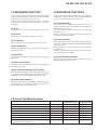
1
SERVICE GUIDE
ORDER NO.
RRV1896
DVD PLAYER
DV-505
DV-S9
DVD LD PLAYER
DVL-909
CONTENTS
1. CIRCUIT DESCRIPTION ...................................... 2
2. CIRCUIT DESCRIPTIONS
FOR DV-S9 AND DV-09 ............................... 10
3. TEST MODE ....................................................... 13
4. IC INFORMATION .............................................. 22
5. FL INFORMATION .............................................. 47
PIONEER ELECTRONIC CORPORATION
4-1, Meguro 1-Chome, Meguro-ku, Tokyo 153-8654, Japan
PIONEER ELECTRONICS SERVICE, INC. P.O. Box 1760, Long Beach, CA 90801-1760, U.S.A.
PIONEER ELECTRONIC (EUROPE) N.V. Haven 1087, Keetberglaan 1, 9120 Melsele, Belgium
PIONEER ELECTRONICS ASIACENTRE PTE. LTD. 501 Orchard Road, #10-00 Lane Crawford Place, Singapore 0923
c PIONEER ELECTRONIC CORPORATION 1998
T - IZM APR. 1998 Printed in Japan
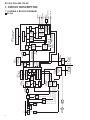
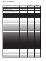
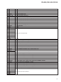
2
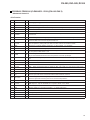
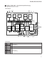
TA
FA
Slider
TE
GEN
HA
OEIC
A/D
Servo
DSP
EFM
Decoder
DMA
CPU
I/F
Mechanism
sense SW
Mechanism
Control
CPU
IC501
PD4889A
CD Digital Out
CD PCM
Sub-code Buffer
CD-ROM Sync gen.
ECC &
ID Reg.
DRAM I/F
(bus arbitor)
IC101
PD4890A
Key-SW
& Display
Display
CPU
CD D. OUT
SREO
XSACK
CD PCM
XSACK
SREO
Program Stream
RAM
IC604
TC551001BFL-85
MPEG2
Video
Decoder
DAC
GUI
S/PDIF
AC3/MPEG1
Audio Decoder
NTSC Copy
/PAL Guard DAC
encode
DAC
MIX
Subpicture
Decoder
(MPEG2 Decoder)
IC801
MB86371
DVD/V-CD
AV Decoder
AV Sync
controller
SYSTEM
Decoder
(DMUX)
CPU
I/F
Memory Controller
CODE Buffer
(Video, Audio, Sub-picture,GUI)
D/A
AC3 D-Out
Lt
Rt
PCM D-Out
Comp.
C
Video Out
Y
DV-505
IC201
LC78650NE
CD DSP
Sub-CPU
I/F
Spindle
control
Sync
Demod
IC603
VYW1536
FLASH
ROM
System CPU
(32 bit RISC)
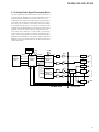
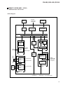
1.1 OVERALL BLOCK DIAGRAM
Loading
Motor
Spindle
Motor
IC301
TLC5540INS
LSI-11
IC701
PD4833A
IC702
HM514800CJ-7
4M bit DRAM
VBR Buffer
IC601
PD3381A
IC802
MB811171622A-100FN
16M bit SDRAM
DV-505, DVL-909, DV-S9
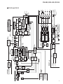
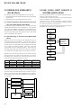
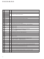
1. CIRCUIT DESCRIPTION
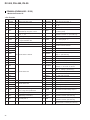
TA
FA
Slider
Mechanism
sense SW
Loading
Motor
Spindle
Motor
Key-SW
& Display
DIRB
DV-S9 Only
A/D
(COAXIAL)
Digital In
(OPTICAL)
TE
GEN
HA
OEIC
IC301
TLC5540INS
Display
CPU
IC101
PD4890A
Servo
DSP
DMA
CPU
I/F
DIGITAL
INTERFACE
RECEIVER
SREO
XSACK
DRAM
8
DNR
IC811
8
IC901
PD0259A
DATA
SELECTOR
8
10
AC IN
HIBIT
LEGATO S
FILTER
FILTER
FILTER
FILTER
AUDIO
POWER SUPPLY
96/24 DAC
AMP.
AMP.
AMP.
AMP.
GUI
AUDIO
DRIVER
VIDEO OUT
S/PDIF
AC3/MPEG1
Audio Decoder
MIX
Subpicture
Decoder
(MPEG2 Decoder)
96/24 DAC
DAC
DAC
DAC
DAC
AUDIO
TRANSFORMER
IC951
M65677FP
VIDEO
ENCODER,
10
COPY GUARD
10
VIDEO
ENCODER,
10
COPY GUARD
MPEG2
Video
Decoder
Memory Controller
DVD/V-CD
Decoder
AV Sync
controller
SYSTEM
Decoder
(DMUX)
CPU
I/F
AV
IC801
MB86371
XSACK
SREO
Program Stream
IC952
M65677FP
16M bit SDRAM
CODE Buffer
(Video, Audio, Sub-picture,GUI)
IC802
MB811171622A-100FN
IC601
PD3381A
IC602
IC603
PDK026A IC604
VYW1536
TC551001BFL-85
GUI
ROM
RAM
ROM
Mechanism IC501
PD4889A
Control
CPU
CD Digital Out
CD PCM
Sub-code Buffer
CD-ROM Sync gen.
ECC &
ID Reg.
DRAM I/F
(bus arbitor)
IC861
CD0015AF
EFM
Decoder
IC201
LC78650NE
CD DSP
Sub-CPU
I/F
Spindle
control
Sync
Demod
LSI-11
IC701
PD4833A
IC702
HM514800CJ-7
4M bit DRAM
VBR Buffer
System CPU
(32 bit RISC)
(COAXIAL)
(OPTICAL)
R ch (Analog)
L ch (Analog)
R ch (Analog)
L ch (Analog)
Y
Component
Video Out
Cr
Cb
S-Video
Audio Out
DRIVER
DRIVER
DRIVER
DRIVER
DRIVER
Composite
Digital
Out
DRIVER
8
DV-505, DVL-909, DV-S9
DV-S9 and DV-09
3
DV-505, DVL-909, DV-S9
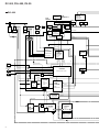
DVL-909
4Mbit DRAM
VBR Buffer
IC701
PD4833A
LSI-11
SPDL
Motor
TA
FA
TA
FA
Slider
Slider
For CLD
HA
OEIC
System CPU
(32bit RISC)
DRAM I/F
(Bus Arbiter)
Sync
Demod
A/D
IC601
PD3381A
IC702
HM514800CJ-7
IC603
IC602
IC604
FLASH
ROM
GUI
ROM
RAM
CPU
I/F
ECC & ID Reg.
Program Stream
TE
GEN
DMA
CD-ROM
Sync gene
Sub-code Buffer
Spindle
Control
For DVD
Sub-CPU
I/F
16M
16M
27M
CD PCM
CD Digital out
CD PCM
CD DSP
27M
CD Digital Out
IC 813
CY2081SL
-611
IC 501
PD4889A
EFM Decoder
16M
4
SI, SO, SCK,
SHAKE
SLD POS
Servo DSP
XRESET
Mechanism
Control
CPU
DVD TILT ERR
Mecha.
SW
SLD DRV
LOAD/TILT
MOTOR
IC101
PD0260A2
SLD ERR
IC205
TC7S02F
LOAD/TILT DRV
M
LD Mechanism Control
TURN DRV
M
LD TILT ERR
TURN
MOTOR
TRKG
FOCS
X312
384 × 48k
(18M)
TILT ERR
Sel
VCXO ERR
IC901
LA9430M
Servo
Control IC
(ASP)
IC801
LA9425
PSP
IC908
LC78625E
DSP
EFM Decode
LD DATA
56
Sel
25
4
IC352
CA0002AM
15
14
Analog L
Analog R
Analog Audio
ACOM
Phillips Code
27
10
IC400
LA7134M
VDEM
37
IC101
PD3212A
IC500
PD6159B
A/D
Dual DVP
SPDL
Cont
14-21
14M VCXO
65-72
Memory
Cont.
(with DNR)
IC102, IC103
MB81C1501PF
Field Memory
VCXO ERR
4
44-51
36M
18M
IC 201
LC78650E-P
DV-505, DVL-909, DV-S9
IC802
MB811171622A
-100FN
DVD Y
(IC815 1 )
16Mbit SDRAM
CODE Buffer
(Video, Audio, Sub-picture,GUI)
(from MECHA. CONT. 41 )
D-EXT ON/OFF
LD Y SIGNAL
(from MYCB)
AMP
D-Extention
Circuit
Pedestal
Clamp
Sync Tip
Clamp
H
Y OUT
LD Y
Sync Tip
Clamp
L
C OUT
to
MYCB
TRAP
IC 801
MB86371
Memory Controller
BLANKING PLUSE
(from AV-1 48 )
BURST FLAG
(from AV-1 47 )
CPU
I/F
System
Decoder
(DMUX)
IC620
MPEG 2
Video
Decoder
LD C SIGNAL
(from MYCB)
DVD C
(IC815 7 )
Sub
Picture
Decoder
GUI
L
IC620
H
KEY
Front Section
MIX
Copy Gurd
FL TUBE
NTSC
/PAL
Encode
AV Sync
Controller
DAC
A.B.
DAC
REMOTE
SENSOR
Key
DAC
AC3/MPEG1
Audio Decoder
36M
DVD/V-CD
AV Decoder
X311
384 × 44.1k
(16M)
IR
SEL IR
AC-3/PCM Digital
DVD Y.
DVD C.
PCM Digital
Hi-Bit
DATA
S/PDIF
PD
Key
2
3
VCXO
Sel
4
SR IN
IC203
TC74HC157AF
SR OUT
CLK
8
14
9
25
Hi-Bit
L
D/A
5
R
6
L OUT
Sel
10
IC202
PD0236AM
R OUT
Sel
JCKB ASSY
IC201
PD2029AM (L)
16M
(COAXIAL)
(TOSLINK)
AC-3
/PCM
Digital
OUT
PCM
Digital OUT
AC-3 RF
C (DVD)
AC-3 RF OUT
Y (DVD)
27M
FL
Cont.
3
4
IC301
CXD2046Q
D/A
33
Y (LD)
1
Y/C SEP.
1-8
D/A
36
C (LD)
5
15
2
Y OUT
IC620
IC620
TC74HC4053AF
C OUT
Comp. OUT
MYCB ASSY
CLDM ASSY
5
DV-505, DVL-909, DV-S9
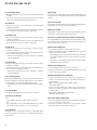
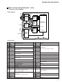
1.2 EXPLANATION OF EACH MOVEMENT
1.2.1 Sequence Up to Playback
DVD SETUP
MIRR Modulation
Measurement
RF AGC ON
T Servo ON
SLDR Servo ON
LD ON
Sweep UP → Down
F Gain Adj.
T Gain Adj.
Focus Lock
AFB Adj.
(Auto Focus Bias)
Yes
SPDL ACCEL
Layer Det.
ATB ON
Lead-in Search
PLAY
1.2.2 Focus Servo
FE generated in the RF IC is sent to the
Digital servo IC.
For a DVD, the servo is turned on during
the transition from “Up” to “Down” of
the first-order sine wave. For a CD, it
turns on during the transition from
“Down” to “Up” of the first-order sine
wave.
When the servo is turned on, the level of
PH (the envelope of the bright side of RF)
increases, and DRF becomes H. The
kick-brake pulses, such as those for
FOCUS jump, are also output from pin
49 of IC201.
• FOCUS SERVO
OEIC GAIN
PICKUP
RF
OEIC
3
B1
B2
B3
B4
58
5
IC101
RFIC
6
31
7
PH
FE
54
32
35
IC201
DIGITAL
SERVO IC
LASER
8
13
11 12
54
22
LD
MD
27
SGC
44
49
1
IC151
4
2 DRIVER
FOCUS
COIL
IC501
ADDRESS
MECH.
&
CONTROL
BUS
26
DRF
FDO
• FOCUS LOCK TIMING
CD
DVD
LDON
UP
FDO
FE
DRF
(FOK)
6
UP
DV-505, DVL-909, DV-S9
1.2.3 Tracking / Slider Servo
ATB: The tracking balance compensation is • TRACKING / SLIDER SERVO
achieved by outputting the offset from
the TBAL output at pin 46 of the digital PICKUP
servo IC, and by biasing the charge pump
TE RF
4
resistor for phase-difference error of
B1
5
IC101
RFIC.
B2
6
RFIC
OEIC
The difference is detected by processing
B3
7
TE at pin 34 of IC 201 with an internal
B4
8
digital equalizer.
TDO: In addition to the servo output, the lowband components, such as the kick-brake
for jump, are added for TDO output.
TE
26
34
TBAL
28
IC201
DIGITAL ADDRESS
&
SERVO IC
BUS
46
CP
50
26
TRKG
COIL
SLDO: The low-band components of TE are
processed by the internal digital
equalizer, and deadband is added for
SLDO output. The offset voltage for
pickup movement is also included in the
SLDO output.
27
16
IC501
MECH.
CONTROL
24
IC151
DRIVER
19
47
TDO
SLDO
17
M
SLDR
1.2.4 SPINDLE SERVO
• SPDL SERVO
OEIC
RF
3
ATC
IC101
RFIC
50
179
RFO
CLK
(27M)
32
RF
IC301
A/D
3
|
10
200
|
207
8 bit
12
IC701
LSI II
176
APC
AFC
IC302
(1/2)
41
FG
57
VCO
IC201
DIGITAL
SERVO
SPDL
M
SPDL -
IC161
DRV 25
177
159
95
FPWM
VPWM
PPWM
RPWM
IC271
(2/2)
DUTY50
SPDO
12
180
161 163 166 167
31
48
SPDL +
ASC
178
V165
SPDO
(Compatible)
IC271
(1/2)
13
(Base)
FG
For a CD, the RF signal output from pin 32 of the RF IC is converted
to binary in IC201. By comparing the binary value with the reference
CLK (clock), the SPDL ERR signal is output from pin 48.
For a DVD, the SPDL ERR signal is generated from the PWM signal
output from LSI-ΙΙ. Upon receiving this signal via pin 31, IC201
also outputs it from pin 48, switching from the CD SPDL ERR
signal.
7
DV-505, DVL-909, DV-S9
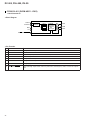
1.2.5 Disc Determination
Determination is achieved by checking the sine wave by sweeping
the lens with the OE IC gain at L and the FSC error amplifier (SGC)
at the default setting. If no sine wave is detected, checking is retried
after switching the OE IC gain to H and increasing the gain of the
FSC error amplifier (SGC). If no sine wave is detected again, it is
regarded as the NO DISC condition.
If one half of the sine wave detected at the first lens sweep is of a
value less than 0.5 V, the OE IC gain is set to H and the peak-topeak value of the sine wave is roughly adjusted to 1.8 Vp-p.
By sweeping the lens around the height where the sine wave has
been detected, disc determination is performed, and the sine wave
is finely adjusted to 1.8 Vp-p.
Offset compensation
Lens sweep
Checking
the sine wave
Yes
None
Level check
OEIC gain = H
FCS AMP gain up
Less than 0.5V
More than 0.5V
Lens sweep
Checking
the sine wave
None
OEIC gain = H
Yes
Roughly adjust to
1.8Vp-p sine wave
NO DISC
Disc determination
Finely adjust to 1.8Vp-p
sine wave
END
8
DV-505, DVL-909, DV-S9
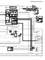
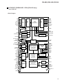
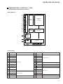
1.2.6 System Control (DVL-909)
DVD MAIN
16
SI1,SO1
SCK1,XRDY
13
IC101
PD4890A
Mode Control
22
(FL Cont.)
102,107,108,111
FLPB, KEYB
IC601
PD3381A
IC604
Work
RAM
System
Cont.
IC603
FLASH
ROM
IC602
GUI
4M ROM
21
IC801
MB86371
AV-Dec.
MAD0–MAD7
Mech. Cont.
(DVD)
77
POWER SUPPLY
ASSY
8
72
26
IC501
PD4889A
65
LSI-11
19
IC701
PD4833A
142 151
Remote
Sensor
XRESET
KEY
POWER ON
DATA,ADDRESS
MAIN BUS
39
19
Loading
Position
SW
SW1–3
9
21
56
Mech. Cont.
(CLD)
55
35
24
IC803
Tilt /
Loading M
Motor
DVDP PK
IC101
PD0260A2
33
SLDPOS
Digital
Servo
10
SO1,SI1
SCK1
Slider
Position
SW
IC201
LC78650E-P
54
XLPO
XTurn A
XTurn B
LD/DVD
Carriage
Out position SW
Turn
A/B SW
25
IC171
Tilt / Loading
Drive
Turn
Drive
M
CLD MAIN
1) Interface between Mode Cont. and System Cont.
IC101
PD4890A
13
46
Mode Control 14
(FL Cont.)
15
16
XRDY
LT1
SCK1
SO1
SI1
102
65
111
107
108
IC601
PD3381A
System
Cont.
XRDY
LT1
SCK
SI
DATA
SO
Timing Chart
If there is no communication for 2 sec.,
Mode Cont. turn off the power and reset.
9
DV-505, DVL-909, DV-S9
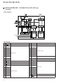
2. CIRCUIT DESCRIPTIONS FOR DV-S9 AND DV-09
2.1 VIDEO SIGNAL PROCESSING BLOCK
2.1.1 PD0259A Block
(3) Y/C-timing Adjustment
The major purposes of the PD0259A block are;
(1) Frame-correlative cyclic digital noise reduction
(2) Horizontal and vertical contour compensation
(3) Y/C timing adjustment
(4) Frame freezing
This function changes the output phase of the Y signal with respect
to the Cb and Cr signals in units of the 13.5-MHz clock cycle (approx.
74 ns).
(1) Frame-Correlative Cyclic Digital Noise Reduction
For eight-bit digital video data input to the PD0259A, noise reduction
is performed through subtraction between the data and those of the
corresponding points 1 frame before, delayed for the subtraction
via a 4-bit DRAM by 1 frame.
The noise signal detected as a result is sent to a non-linear circuit. If
the difference is larger than a specific value, it is regarded as “a
change in picture,” and no canceling calculation is made.
This function is the same as that which has been performed in
conventional laser-disc players. The only difference is that the input
video signal here is a DVD digital component signal (4:2:2), while
it is an LD digital composite signal in conventional laser-disc players.
DATA
Non-linear
circuit
For data after digital noise reduction, horizontal and vertical contour
compensations are made only for the Y-signal.
Horizontal compensation is performed by detecting edge components
from the information of the reference picture elements and those
that horizontally proceed and succeed by several pixels, and then
generating edge-emphasizing components through non-linear
processing of the detected components.
Vertical compensation is performed by detecting edge components
from information on the reference picture elements and those which
vertically proceed and succeed by one line, and then generating edgeemphasizing components through non-linear processing of the
detected components.
These edge-emphasizing components are added to the main-line
digital data to achieve contour compensations.
Vertical edge generation
HPF
Non-linear
circuit
BPF
Non-linear
circuit
Horizontal edge generation
10
The M65677FP block functions as an NTSC encoder that converts
digital component signals to analog Y, C, Cb and Cr signals. While
our popular models other than the DV-S9 use the built-in encoder in
the MB86371 block, an external NTSC encoder is added to the DVS9, as it performs digital processing in the PD0259A block.
Setup of –7.5 IRE is added to the Y signal. D.EXT(DV-S9)/BLACK
LVL(DV-09) processing using analog signals in conventional laser
disc players is achieved by using digital signals.
(2) Horizontal and Vertical Contour Compensations
Delay
2.1.2 M65677FP Block
(1) D.EXT(DV-S9)/BLACK LVL(DV-09)
1-frame delay
1H
Delay
In response to a command sent from the system control computer
by serial transmission, data for one frame are frozen, and the frozen
picture is output.
This function is specific to the DV-S9 and is used only for pictureby-picture reversing by jog/shuttle operation or “Slow 1” playback
operation.
In addition to NTSC encoding, the M65677FP also performs:
(1) D.EXT(DV-S9)/BLACK LVL(DV-09)
(2) C.LEVEL adjustment
ON/OFF
SW
1H
Delay
(4) Frame Freezing
(2) C.LEVEL Adjustments
The burst level of the C signal can be varied centering around 40
IRE.
Therefore, it is performed for the S-connector and CVBS-connector
outputs, but not for the color-difference output.
This function is also not available if the connected TV receiver has
no AGC circuit.
DV-505, DVL-909, DV-S9
2.1.3 Analog Video Signal Processing Block
The video signals output from the built-in 10-bit DA converter of
the M65677FP pass through a low-pass filter and amplifier, and are
output from the DVD MAIN Assy and sent to the VOUT Assy.
In the VOUT Assy, analog noise-reduction processing having three
levels (OFF, low, and high) is initially applied only to the Y signal.
This analog noise reduction is the same as that performed by
conventional laser-disc players. The register port output in serial
communication that the PD0259A receives from the system-control
computer is used as the control signal for analog noise reduction.
After analog noise reduction, a CVBS signal is generated by
composing the Y and C signals (no clamping is performed for the C
signal). The timing pulse BF to be used for pedestal clamping is
supplied from the PD0259A. This signal is adjusted within the
PD0259A so that it provides the timing for the burst portions of the
output video signals.
4M DRAM
×2
µ-COM
µ-COM
Amp.
V
FLD
IC901
PD0259A
(DNR)
V DATA
H
V
Cb
IC951
M65677FP
NTSC
ENCODER
ANR2
LPF
Amp.
Cr
CLK
ANR1
CLK
BF
IC801
MB86371
(AV1)
V DATA
H
CLAMP
Cb
CLAMP
Cr
CLAMP
Y
CLAMP
Y
LPF
Amp.
IC952
M65677FP
NTSC
ENCODER
Y
Analog
NR
LPF
Amp.
C
LPF
C
CLAMP
DVD MAIN ASSY
CVBS
V OUT ASSY
11
DV-505, DVL-909, DV-S9
2.2 DIRB BLOCK (DIRB ASSY)
(DV-S9 ONLY)
2.3 96K, 24-Bit, HIBIT LEGATO S
SYSTEM (AUDIO ASSY)
The two major purposes of the DIRB block are the following:
(1) Switching between data reproduced from a disc and a data signal
in DAC mode
(2) Data decoding in external input mode (DAC mode)
All 16-bit and 20-bit sources are converted to 24-bit data by IC101,
which lets a 24-bit data pass through.
As PCM1702P is a 20-bit D/A converter, processing of the upper
20 bits is assigned to it by the shift register.
The lower 4 bits are converted from serial to parallel, then the
significance of each bit is converted digital to analog, functioning
as a 4-bit D/A converter for the lower 4 bits.
By adding the lower 4 bits to the upper 20 bits in the low-pass &
ADD block, D/A conversion is achieved for 24 bits.
(1) Switching Between Data Reproduced from a
Disc and a Data Signal in DAC Mode
The signal switching is performed at IC811, sending 3-line data
(LRCK, BCK and DATA) to the AUDIO Assy. The switching
control line (DAC MODE) is supplied from the DVD MAIN Assy.
The master clock (MCK) is generated by a crystal on the AUDIO
Assy when reproducing a disc, and by IC861 in DAC mode. MCK
is sent to the AUDIO Assy via RXP.
(2) Data Decoding in External Input Mode (DAC
Mode)
When the user selects DAC mode, the DAC MODE port is set to H
and VCO in IC861 starts oscillating. (VCO does not oscillate in
any other modes than DAC mode.) When there is a toss link of an
external input or a coaxial digital input, the digital input signal is
sent to IC861 from RXP of CN801, generating 3-line data
corresponding to the input sampling frequency. At the same time,
the master clock (MCK) to be used in DAC mode is also generated.
For a 96kHz input, the MCK frequency is divided by 2 by IC831.
When the user selects the internal clock as the system clock, the
clock generated by the crystal on the AUDIO Assy is sent to the
DVD MAIN Assy. When the user selects an external sync as the
system clock, the following parameters are used.
FS(kHz)
32
44.1
48
96
16M clock in
the AUDIO Assy
18M clock in
the AUDIO Assy
16M clock sent to
the DVD MAIN Assy
18M clock sent to
the DVD MAIN Assy
Oscillates
Oscillates
Crystal 16M clock
Stops oscillating
Oscillates
DIR 16M clock
Oscillates
Stops oscillating Crystal 16M clock
Oscillates
Stops oscillating Crystal 16M clock
Crystal 18M clock
Crystal 18M clock
DIR 18M clock
DIR 18M clock
If there is no external input or locking onto the input digital signal
cannot be achieved, the ERR signal at pin 43 of IC861 is set to H,
and the crystal in the AUDIO Assy immediately starts oscillating.
In such cases, the clock sent to the DVD MAIN Assy will always be
a crystal clock.
IC901 16M Selector
IC902 18M Selector
IC811 Data Selector
IC831
Clock Selector
IC861
DIR
CN801
12
IC835
1/2 Divider
CN811
Hi Bit
IC101
Legato S
IC111
Shift Register
TC74HC164AF
D/A Converter
PCM1702P
Low-pass
& ADD
Analog Output
Serial to Parallel
and Significance
Conversion
TC74HC163AF
DV-505, DVL-909, DV-S9
3. TEST MODE
3.1 HOW TO ENTER THE TEST MODE
(5) Pause
There is the three following methods in an enters of the test mode.
1. Short-circuit the terminals (TP6006 and TP6007) for test mode
entry at the side of the system control IC (IC601) of DVDM ASSY,
and turn the power on.
2. Input [ESC] key and [TEST/RANDOM] key of the test mode
remote control unit in order under the power on condition.
3. Connect a personal computer with the RS232C terminal (CN106),
and input entry command (TE) of test mode from the personal
computer.
Note: FL indication and LED come all to light until key operation
is done when entering the test mode.
1. It becomes pause condition by pressing [CX] (0E) key of the
remote control unit in the play.
2. Pause ON/OFF changes alternately by pressing [PAUSE] (18)
key in the play.
3.2 RELEASE THE TEST MODE
There is the three following methods in a release of the test mode.
1. Turn the power off.
2. Press [ESC] key of the remote control unit. At this time, reset it
for a while except for during the LD and CDV set.
3. Connect a personal computer with the RS232C terminal (CN106),
and input normal mode entry command (NE) from the personal
computer.
3.3 THE EXPLANATION OF EACH
FUNCTION
The function that can be operated in the test mode is as the following.
Use a LD remote control unit in the test mode.
(1) Door Open/Close
1. Press [REPEAT A-B] (48) key of the remote control unit.
2. Press [OPEN/CLOSE] key of the player from the stop condition.
(2) Stop
1. Press [REPEAT] (44) key of the remote control unit.
2. Press [STOP] key of the remote control unit or the player from
the stop condition.
(3) Play 1 (Demultiplex exist which it tries to output
the playback screen)
1. Press [PLAY] (17) key of the remote control unit.
• CLD rise up at the tracking open condition. However, it becomes
tracking close when entering the test mode during the play.
• DVD rise up at the tracking close. Playback screen may not
appear because the NAVI information isn't read in the test mode.
(6) Search Address Input Entry
It becomes the address input mode when [+10] key (1F) is pressed.
(indication for the most significant digit : > )
Indicate the last address as the initial condition in this time.
Only in case of DVD, addition search (indication for the most
significant digit : + ) and subtraction search (indication for the most
significant digit : – ) are able to select in order by pressing [+10]
key continuously.
The address where input value was added to the present address is
make to search with addition search.
The address where input value was subtracted to the present address
is make to search with subtraction search.
In case of CD is only absolute time search.
Also address clear and release from the address input mode are able
to perform by 2 steps by pressing [CLEAR] (45) key.
(7) Search Address Input
Press [0] to [9] keys of the remote control unit.
Set up the address by the hexadecimal number with DVD.
When [PROGRAM] (4C) key is pressed in the address input mode,
input mode changes to hexadecimal number input (Indicates "∗"
mark), and [1] to [6] keys are input as [A] to [F].
At this time, [7], [8], [9] and [0] keys are not accepted.
Also the hexadecimal number input and the decimal number input
can be changed with toggle.
(8) Search Practice
1. Press [CHP/TIM] (13) key of the remote control unit.
Practice the on screen no playback (Doesn't demultiplex) after
the search with DVD.
2. Press [PLAY] (17) key of the remote control unit.
Practice the on screen playback (demultiplex exists) after the
search with DVD.
(9) Side Change
This function becomes effective when a set disk is LD.
1. Change a side on the side A from the side B when pressing [SIDE
A] (4D) key of the remote control unit.
2. Change a side on the side B from the side A when pressing [SIDE
B] (4E) key of the remote control unit
(4) Play 2 (Demultiplex is absent which performing
trace only)
(10) Tracking Open
1. Press [TV/LDP] (0F) key of the remote control unit.
• It is equal to the play 1 with CLD.
• Perform only tracing with DVD, and there are no video and
audio output.
1. Press [STEP FWD] (54) key of the remote control unit in the play
condition.
2. Switch the open/close by pressing [PLAY] key of the remote
control unit or the player during the play (CD only).
13
DV-505, DVL-909, DV-S9
(11) Tracking Close
(20) Tilt Up
1. Press [STEP RVS] (50) key of the remote control unit in the play
condition.
2. Switch the open/close by pressing [PLAY] key of the remote
control unit or the player during the play (CD only).
A manual moves in the going up direction when [SKIP FWD] (52)
key of the remote control unit is pressed during the play at the time
of tilt off.
(21) Focus Jump +
(12) Slider In
1. Press [SCAN RVS] (11) key of the remote control unit in the
tracking off condition.
2. Turn the shuttle of the remote control unit in the REV direction
(2C to 2F) in the tracking off condition. (DVD only)
Focus jumps in 1 layer from 0 layer when [MULTI FWD] (58) key
of the remote control unit is pressed. (DVD only)
(22) Focus Jump –
Focus jumps in 0 layer from 1 layer when [MULTI REV] (55) key
of the remote control unit is pressed. (DVD only)
(13) Slider Out
1. Press [SCAN FWD] (10) key of the remote control unit in the
tracking off condition.
2. Turn the shuttle of the remote control unit in the FWD direction
(28 to 2A) in the tracking off condition. (DVD only)
(23) The First And The Second Screen Switching
(14) Scan In
(24) Screen Display On
1. Press [SCAN RVS] (11) key of the remote control unit in the
tracking on condition.
2. Turn the shuttle of the remote control unit in the REV direction
(2C to 2F) in the tracking on condition.
• DVD can be scanned only in the case of the play 2 (playback
without demultiplex).
1. Press [DISPLAY] (43) key of the remote control unit.
2. Display on/off switches every time [PROGRAM] (4C) key of the
remote control unit is pressed.
• When [DISPLAY] key is pressed in the display on, change the
part number indication of the microprocessor and revision
indication.
• Initial state is screen display on and it becomes the part number
indication of the microprocessor.
(15) Scan Out
1. Press [SCAN FWD] (10) key of the remote control unit in the
tracking on condition.
2. Turn the shuttle of the remote control unit in the FWD direction
(28 to 2A) in the tracking on condition.
• DVD can be scanned only in the case of the play 2 (playback
without demultiplex).
(16) Loading In/Out
When pressing [SKIP REV] (53) key of the remote control unit in
the open condition, it loads in the clamp direction. Then it loads in
the open direction when pressing [SKIP FWD] (52) key.
• This function can practice only when it is indicated with "OPEN"
in FL.
(17) Tilt Neutral
Press [SPEED DOWN] (46) key of the remote control unit.
Every time [DISPLAY] (43) key of the remote control unit is pressed,
the contents of the version indication part (the bottom right of the
screen) change. (Refer to page 17.)
(25) Screen Display Off
1. Press [AUDIO] (1E) key of the remote control unit.
2. Display on/off switches every time [PROGRAM] (4C) key of the
remote control unit is pressed.
(26) Background Color Switching
1. Change the background color (eight colors) prepared for in
advance every time [2/R] (49) key of the remote control unit is
pressed in order.
[Blue→Green→Light blue→Red→Purple→Yellow→
Gray→Black→Blue ....]
2. Change the background color (eight colors) prepared for in
advance every time [1/L] (4B) key of the remote control unit is
pressed in order.
[Blue→Black→Gray→Yellow→Purple→Red→
Light blue→Green→Blue ....]
(18) Tilt Servo On/Off
a. On
Press [SPEED UP] (47) key of the remote control unit.
b. Off
Press [SKIP REV] (53) key and [SKIP FWD] (52) key of the
remote control unit at the tilt servo on or the tilt neutral.
(19) Tilt Down
A manual moves in the going down direction when [SKIP REV]
(53) key of the remote control unit is pressed during the play at the
time of tilt off.
14
(27) Video Output Switching
1. It becomes component output when pressing [DIGITAL EFFECT]
(5C) key of the remote control unit.
2. It becomes composite output when pressing [STILL WITH
SOUND] (5B) key of the remote control unit.
DV-505, DVL-909, DV-S9
3.4 EXPANSION FUNCTION 1
3.5 EXPANSION FUNCTION 2
Set the reception mode of expansion function by pressing [TEST]
(5E) key of the test mode remote control unit, then expansion function
is able to execute by pressing the key of [0] to [9].
Indication for the most significant digit becomes "T" during the
reception mode of expansion function. (This mode can on and off
with toggle.)
Set the reception mode of expansion function 2 by pressing [HILITE/
INTRO] (55) key of the remote control unit, then expansion function
2 is able to execute by pressing the key of [0] to [9].
(1) Forced DVD Setting
Focus locks by pressing [TEST] and [2] keys in order.
In the checker mode, set up the condition that DVD is attached
forcibly except for the result of disc distinction by pressing [HILITE/
INTRO] and [1] keys in order.
In the no checker mode (normal test mode), once execute the setting
but abandan it soon.
Therefore, perform the disc distinction again for the safety when
rising up the player in this condition.
(3) Focus Sweep
(2) Forced CD Setting
Repeat focus sweep by pressing [TEST] and [3] keys in order.
In the checker mode, set up the condition that CD is attached forcibly
except for the result of disc distinction by pressing [HILITE/INTRO]
and [3] keys in order.
In the no checker mode (normal test mode), once execute the setting
but abandan it soon.
Therefore, perform the disc distinction again for the safety when
rising up the player in this condition.
(1) LD On
Turn the laser diode to on by pressing [TEST] and [1] keys in order.
(2) Focus On
(4) Spindle FG Servo
Rising up the spindle and FG servo becomes on by pressing [TEST]
and [5] keys in order.
(5) AGC On/Off
Switch the AGC on and off with toggle by pressing [TEST] and [7]
keys in order.
(3) Execute The Disk Distinction
In the checker mode, execute the disc distinction result by pressing
[HILITE/INTRO] and [0] keys in order.
(6) Jitter Value Indication.
It becomes the jitter-value indication mode by pressing [TEST] and
[DIG/ANA] keys in order.
(7) DSP coefficient indication of FTS system.
Set up the address (four digits) of the coefficient that it wants to see
by the point of search address input, then real time indicates the
coefficient in OSD by pressing [TEST] and [9] keys in order.
(8) CD Error Rate Indication
Indicate the value in OSD after measuring is completed by pressing
[TEST] and [0] keys in order after set up the measuring time (1 to 8
seconds) by the point of search address input.
3.6 List of Test Mode Function
Open
STOP
Key Name of
Remote Control Unit
REPEAT A
Close
OPEN
REPEAT A
A8-48
Stop
PLAY
REPEAT B
A8-44
Play (DVD is only tracing.)
STOP
TV/LDP
A8-0F
Play (DVD is with decode.)
STOP
PLAY
A8-17
Pause on
PLAY
CX
A8-0E
PLAY/PAUSE
PAUSE
Contents of Command
Pause on/off
Search address input (0 to 9)
Condition
0 to 9
Mode of
Remote Control Unit
A8-48
A8-18
A8-00 to 09
∗Use for other numerical value input
15
DV-505, DVL-909, DV-S9
Contents of Command
Search address input (A to F)
Search address clear
Escape the search input mode
During address input
Key Name of
Remote Control Unit
PGM+1 to 6
During address input
CLEAR
A8-45
+10
A8-1F
Condition
Mode of
Remote Control Unit
Address = 0
Change the search address input mode
(Off→absolute address→addition→subtraction→Off)
∗Use for other numerical value input.
Search execution (ignore the wrong address)
CHAP/TIME
A8-13
Side change (side B→side A)
LD
SIDE A
A8-4D
Side change (side A→side B)
LD
SIDE B
A8-4E
Tracking open
PLAY
STEP FWD
A8-54
Tracking close
PLAY
STEP REV
A8-50
Slider in
TR : Off
SCAN REV
A8-11
Shuttle REV
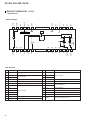
A8-2C to 2F
Low speed scan REV
TR : On
SCAN REV
A8-11
Scan REV (Jump number is variable)
TR : On
Shuttle REV
A8-2C to 2F
Slider out
TR : Off
SCAN FWD
A8-10
Shuttle FWD
A8-28 to 2B
Low speed scan FWD
TR : On
SCAN FWD
A8-10
Scan FWD (Jump number is variable)
TR : On
Shuttle FWD
A8-28 to 2B
Loading in
STOP
SKIP REV
A8-53
Loading out
STOP
SKIP FWD
A8-52
Tilt neutral
Tilt servo on
Tilt servo off
Tilt : On/N
SPEED DOWN
A8-46
SPEED UP
A8-47
SKIP REV
A8-53
SKIP FWD
A8-52
Tilt up
PLAY
SKIP FWD
A8-52
Tilt down
PLAY
SKIP REV
A8-53
LD on
TEST + 1
A8-5E + A8-01
Focus on
TEST + 2
A8-5E + A8-02
Focus sweep
TEST + 3
Focus jump +
MULTI FWD
A8-58
Focus jump –
MULTI REV
A8-55
Spindle FG on
TEST + 5
AGC on/off
Indication of the FTS coefficient
CD error rate indication
Screen indication off
AGC : Off/On
TEST + 7
A8-5E + A8-07
TEST + 9
A8-5E + A8-09
PLAY
TEST + 0
A8-5E + A8-00
TEST + DIG/ANA
A8-5E + A8-0C
OSD Off/On
DISPLAY
OSD : On
AUDIO
A8-1E
PROGRAM
A8-4C
DIG/ANA
A8-0C
HILITE/INTRO
A8-5A
Screen indication on/off
Switching of ID display methods (decimal/hexadecimal)
DISC type designation
A8-5E + A8-05
After the address four-digit input
Jitter indication
Screen indication on/Switching of the first screen and second screen
A8-5E + A8-03
STOP
A8-43
• Forced designation to DVD
+1
+A8-01
• Forced designation to CD
+3
+A8-03
• Request for Disk sensing
+0
+A8-00
Tray close of disk sense inhibition
Background color (eight colors) switching
Background color (eight colors) switching (reverse toggle)
Checker mode
REPEAT A
A8-48
2/R
A8-49
1/L
A8-4B
Video : component output
DIGITAL EFFECT
A8-5C
Video : composite output
STILL WITH SOUND
A8-5B
16
DV-505, DVL-909, DV-S9
Special Mention Item
(1) Indications for the spindle status are as follows:
A/B : Spindle accelerator and brake
FG : FG servo
SRV : Rough, velocity/phase servo
O_S : Offset addition, rough, velocity/phase servo
(2) The movement of loading in/out starts from the tray open status.
After that, this function is executed unless a play and close
operation are done.
(3) There are three methods for entering a search address:
Absolute address designation
→ Searching for the address entered (indication for the most
significant digit :>)
Additional input
→ Searching for the address with the current ID number plus
an entered number
(indication for the most significant digit :+)
Subtractive input
→ Searching for the address with the current ID number minus
an entered number(indication for the most significant digit :–)
The above modes can be changed by pressing [10] key.
Note : A number for addition or subtraction must be entered in
hexadecimal.
(4) If you turn the power on while short-circuiting the short-circuit
terminal at the side of the system controller, the player will
forcibly enter the test mode. If the FL controller is set to Checker
mode, disc sensing will not be started, even if a disc is loaded.
Disc sensing will also not be performed if the tray is opend/
closed by your pressing [REPEAT A] key while in Checker
mode.
However, disc sensing will be started if the [OPEN/CLOSE]
key on the player or on the remote control unit is pressed.
(5) If disc-type designation is forcibly executed during a mode other
than Checker mode, the system controller will abandon disctype designation after setting the mechanism controller.
Therefore, after startup of the player, disc sensing will be
performed again for safety.
If disc-type designation is forcibly executed during Checker
mode, as disc-type designation is not abandoned, playback will
be immediately started.
(6) A background color change in order of blue → green → light
blue → red → purple → yellow → gray → black → with the [2/
R] key.
It changes in order of gray → yellow → purple → red → light
blue → green → blue → black → in the case of the [1/L] key.
(7) In case of PD0260A∗, tilt servo on function may not move with
DVD.
3.7 Test Mode Screen Display (The Second Generation)
Consecutive double-OSD display is supported during test mode. The screen is composed 10 lines with a maximum of 32 characters per line.
It can't be used with the debugging display mode together.
• Screen Composition
Character in bold : Item name
: Information display
Address
Key code
Mechanical position value
Tilt error value, Tilt servo status
Slider position
Tracking status
Spindle status
Output video system
AV1 classification and
Flash ROM size
FL controller version
AGC setting
FTS servo IC information
Region setting for the player
C1 error value of CD and DVD
Internal operation mode of
the mechanism control
Disc judgment
Pickup
Flash ROM version
System controller revision
DVD mechanism controller revision
AV-1 chip version
First screen display
Caution :
The first screen and second screen switch by
pressing [DISPLAY] key of the remote control
unit.
It is only a version display part on the lower
right of the screen those contents of display
change.
ATB : ON/OFF information display and AGC
manual establishment display deleted with the
second generation.
Remote control code
CLD mechanism controller revision
FL controller version
GUI-ROM number
Part No. of flash ROM and system controller
Part No. of DVD mechanism controller
Part No. of CLD mechanism controller
Second screen display (at lower right portion of the screen)
17
DV-505, DVL-909, DV-S9
• Description of Each Item on the Display
(1) Address indication
The address being traced is displayed in number.
DVD
: ID indication (hexadecimal number, 8 digits)
[∗∗∗∗∗∗∗∗]
∗∗∗∗]
CD/LD (CLV) : A-TIME (min. sec.)
[
∗∗∗∗∗]
LD (CAV)
: FRAME
[
(Note : For DVDs, decimal-number indication is possible.)
(2) Code indication of the remote control unit [R-∗∗∗∗]
The code for the key pressed on the remote control unit, which is
received by the FL controller, is displayed while the key is pressed.
In the case of the double code, the second code will be displayed.
(3) Key code indication for the main unit [K-∗∗]
The code for the key pressed on the main unit, which is received by
the system controller, is displayed while the key is pressed.
(4) Tilt error value, Tilt servo status [TILT-∗:∗∗∗]
Tilt error value :
Tilt servo status :
Tilt neutral
Tilt servo on
Tilt servo off
[0] to [F]
[N]
[ON]
[OFF]
(5) Tracking status [TRKG-∗∗∗]
Tracking on
Tracking off
[ON]
[OFF]
18
[ER-C1 ∗∗∗∗ ]
[ER-∗∗∗∗ ∗∗∗∗]
(13) Internal operation mode of mechanism controller
[MM-∗∗:∗∗]
Internal mechanism mode (2 digits) and internal mechanism step (2
digits) of the mechanism controller
Note : For details, see the specifications of the mechanism controller.
(14) Disk sensing [DSC-∗∗∗]
The type of discs loaded is displayed.
[DVD], [CD ], [CDV], [LD ], [VCD], [ ]
(15) Pickup [PU-∗∗∗]
The pickup being operating is displayed.
DVD
CLD
[DVD]
[CLD]
[0] to [8]
[IN ]
[CD ]
[CDV ]
[LD ]
[B IN]
(17) Region setting of the player [REG:∗]
Setting value [1] to [6]
(18) Version of the flash ROM [V:∗.∗∗]
(19) Revision of the system controller [S:∗.∗∗∗/∗.∗∗]
[ON]
[OFF]
(10) Output video system [V-∗∗∗∗]
NTSC system
PAL system
Auto-setting
C1 error value of CD
C1 error value of DVD
Three characters that follow represent the destination code.
J : /J, K: /KU, /KC, /KU/KC, RAM: /RAM (China)
RL : /RL, WY: /WY, RD: /RD.
∗ Furthermore DVL-91/KU/CA indicates as L91/K.
(9) AGC setting [AGC-∗∗]
AGC on
AGC off
(12) Error rate indication
Three characters in front represent the type of model:
505: DV-505, S9: DV-S9
606 : DV-606D, EDU: for education
909: DVL-909, K88: DVL-K88.
(8) Slider position [S-∗∗∗∗]
CD TOC area
CD active area
CDV video area
LD active area
Side B inside
Jitter value indication
[JT-[
]∗∗∗∗]
Displays the jitter value (four digits) with [TEST] and [DIG/
ANA] keys.
[A/B]
[FG]
[SRV]
[O_S]
(7) Mechanism position value [M-∗]
Position code
Indications for the following two types of information can be
switched:
DSP coefficient indication
[KS-[∗∗∗∗] ∗∗∗∗]
Displays the address (four digits) of the specified coefficient
and the setting value (four digits) with [TEST] and [9] keys.
(16) Destination setting of the FL controller
[F:∗∗∗/∗∗∗]
(6) Spindle status [SPDL-∗∗∗]
Spindle accelerator and brake
FG servo
Rough, velocity phase servo
Offset addition, rough, velocity phase servo
(11) FTS servo IC information
[NTSC]
[PAL ]
[AUTO]
Revision number of the external ROM part (flash ROM) of the
system controller
<Front>
Revision of the internal ROM part of the system controller
<Rear>
DV-505, DVL-909, DV-S9
(20) Revision of the DVD mechanism controller
[M:∗.∗∗∗/∗.∗∗∗]
Revision number of the external ROM part (flash ROM) of the
DVD mechanism controller
<Front>
Revision of the internal ROM (core part) of the DVD mechanism
controller
<Rear>
(21) Revision of the CLD mechanism controller
[L:∗.∗∗∗]
Using the Function in Test Mode (The Remote
Control Keys to be Used are Indicated in Brackets)
(1) Set the CD to trace (playback) state.
(2) Set the player to Number input mode by pressing [+10] and
enter the measurement time in a range of 1 to 5 (sec.).
(3) Start measurement by pressing [TEST] + [0]. The SubQ counter
stops during measurement, but this is not a malfunction. When
the specified measurement time has elapsed, the result is
indicated to the right of “ER C1 –” on the screen.
If you skip step 2, the measurement time is set to 5 (sec).
3.8.2 Jitter Value
(22) Version of the AV-1 chip [AV:∗.∗]
Overview
(23) Version of the FL controller [F:∗.∗]
(24) Control number of the GUI-ROM [GUI:∗∗∗]
(25) The part number of the flash ROM and system
controller [S : ∗∗∗∗∗∗/∗∗∗∗∗∗∗]
Part number of the flash ROM
(Example) VYW1536-A → W1536A
(Example) PD626A9 → 6256A9
<Front>
Part number of the system controller
(Example) PD3381T1 → 3381T1
<Rear>
(26) Part number of the DVD mechanism controller
(Example) PD4889A0 → 4889A0
(27) Part number of the CLD mechanism controller
(Example) PD0260A2 → 0260A2
(28) AV1 classification [AV1 : ∗∗∗]
The jitter values of DVDs and CDs can be displayed on basic models,
such as the DV-505, and those of DVDs can be displayed on DVD/
LD-compatible models, such as the DVL-909.
V.
The displayed value shows a voltage in three-digit decimal as .
For example, the indication “0278” means 2.78 V. The larger the
value, the worse the jitter. The worst value is 3.25 V. When playing
a DVD or a video CD with which the jitter value is extremely high,
mosaics may be seen. As with the error rate, the jitter depends on
the disc and pickup. The jitter value to be displayed has no close
correlation with a jitter measuring device, and is to be regarded just
for reference.
Reference : When the jitter value is 2.9 V or more with a DVD, or
3.0 V or more with a CD (or a video CD), it may cause
a problem (mosaic, audio distortion, etc.) in playback.
Using the Function in Test Mode (The Remote
Control Keys to be Used are Indicated in Brackets)
(1) Set the DVD or CD to trace (playback) state with AGC OFF.
(2) Press [TEST] and [DIGITAL/ANALOG].
The current jitter value appears to the right of “JT:
” on
the display. The jitter value keeps changing unless any additional
key operation is made.
RAM, E/A, S/C
(29) Flash ROM size [FLSH : ∗∗]
8M : 8M bit, 4M : 4M bit
3.8 DESCRIPTIONS OF NEW FUNCTIONS IN TEST MODE
Note : Although a value may be displayed on the screen even with
AGC ON, this is NOT a jitter value.
The jitter value with AFB ON cannot be displayed (see the
next section). The jitter value with AFB ON can be obtained
only by directly measuring the voltage at the JV connector
(pin 94) of the servo DSP (LC78650).
3.8.1 Error Rate
Overview
The error rate of CDs can be measured on basic models, such as the
DV-505, and that of CDs as well as LDs with sub-Q codes can be
measured on DVD/LD-compatible models, such as the DVL-909.
The value is displayed in decimal and indicates the number of C1
errors (including the corrected ones) counted during the specified
measurement time.
An indeterminate measurement result may be caused by a dirty disc,
decentering, surface deflection, birefringence (double reflection),
or a pickup problem (dirty lens, etc.), misadjustments of the pickup,
improper automatic adjustment, or incomplete adjustments. On the
manufacturing line, the value is used for yes/no decision of pickups.
Normally, for a measurement for 5 seconds, the value may be less
than 10 with a clean disc and less than 100 with a disc with some
damage.
19
DV-505, DVL-909, DV-S9
Using the Function in Test Mode
3.8.3 Startup Sequence
The basic flow is shown below. The parentheses indicate a limitation:
“base” represents base models, such as the DV-505 and DV-S9,
and “compatibles” represents DVD-LD compatible models, such as
the DVL-909.
(1) Closes the tray.
(2) Runs the tilt servo for 1.5 seconds (compatibles).
(3) Detects the peak.
(4) Distinguishes the disc.
(5) SGC
(6) Turns on the focus servo.
(7) Turns on the tilt servo (compatibles).
(8) Starts the spindle rotation.
(9) ATB
(10) Measures the MIRR modulation degree.
(11) Turns on the tracking servo.
(12) Turns on the slider servo.
(13) Turns on the spindle servo.
(14) Focus AGC
(15) Tracking AGC
(16) AFB
(17) Plays AGC (base for CDs)
(18) Plays back.
∗ For a 2-layer DVD, steps (9) through (16) are repeated for each
layer.
∗ When starting up with [TV/LDP] in Test mode, all the steps (1)
to (18) are performed for a DVD, and steps (1) to (10) are
performed for a CD.
This function is not assigned to any remote control keys. Only an
open/close operation can trigger the function.
3.8.6 SGC
Overview
This is a new function to maintain the sine wave related to focus
errors to a certain size so that the sine wave shows 1.8 V for the Pto-P value.
This operation is performed each time after judging disc presence
and distinction in the normal startup process and in Test mode, as
well. The operation is achieved by switching the FE gain inside the
RF IC (LA9700) by using the voltage at the SGC connector (pin 22)
of the RF IC.
Using the Function in Test Mode
This function is not assigned to any remote control keys. Only an
open/close operation can trigger the function.
3.8.7 Measurement of MIRR Modulation
Degree
Overview
The slice voltage of the RF signal is measured and used in the
calculation to generate the MIRR signal. This operation is made in
synchronization with ATB ON/OFF in normal startup and in Test
mode, as well.
3.8.8 AFB (Auto Focus Bias) Function
Overview
3.8.4 Peak Detection
Overview
This is a new function to measure the size and location of the sine
wave related to focus errors at the beginning. The measurement is
performed in the normal startup process and in Test mode, as well.
If the sine wave is small, the OE IC gain is switched. Only the
judgment for NO DISC is accomplished at this time. The operation
is in effect as for judgment for DISC .
Using the Function in Test Mode
This function is not assigned to any remote control keys. Only an
open/close operation can trigger the function.
3.8.5 Disc Distinction
Overview
This function is almost the same as that with the first-generation
models. The only difference is as follows: If an error occurs in the
startup sequence and playback cannot be started, startup is retried
after forcibly switching the disc distinction from DVD to CD or
vice verse by a backup process. If startup fails again, it is canceled,
and an error is generated. The types of error that triggers the backup
process for disc distinction are discussed in the next section.
20
Among the first-generation models, this function supports only CDs
with the basic models, such as the DV-7. Among the new models,
this function supports DVDs with all models, but CDs only with the
basic models. The operation is executed only once (once for each
layer for a 2-layer DVD) after the focus and tracking AGC at startup.
The operation is accomplished not by centering the focus servo to
Vref (2.5 V), but by gradually changing the center value for the
optimum jitter value. Thus, performance with an improper or dirty
disc (by fingerprints, etc.), or the temperature characteristics (at 0°C,
35°C, etc.) will be improved.
OverviewUsing the Function in Test mode
(the Remote Control Keys to be Used are
Indicated in Brackets)
As the function is to be synchronized with AGC, turn on and off
AFB by pressing [TEST] + [7]. The jitter value measurement cannot
be made with AFB ON.
DV-505, DVL-909, DV-S9
3.8.9 PLAY AGC
Overview
The SGC voltage is adjusted during playback according to the RF
signal level. (For details on SGC, see section 3.8.6.)
Only for CDs in basic models, such as the DV-505 (including the
DV-S9), this adjustment is made only once immediately after AFB
during startup. In Test mode, it synchronizes with AGC ON/OFF.
The operation is achieved through adjustment in the Servo DSP
(LC78650), and the SGC voltage is output via AUX0 (pin 44).
Using the Function in Test Mode
(the Remote Control Keys to be Used are Indicated
in Brackets)
As the function is to be synchronized with AGC, turn on and off
AFB by pressing [TEST] + [7].
(5) Automatic Sequence Errors (Errors 51 to 55)
If any automatic sequence (auto execution command) of the servo
DSP is not completed, these errors are generated. The causes differ
among error numbers. They may be caused by abnormalities in the
communication line between the mechanism-control computer
(PD4889A) and the servo DSP or instability of the XABUSY
connector (pin 38) of the mechanism-control computer.
(6) DSP Communication Errors (Errors a1 to a6)
These errors will be generated if the mechanism-control computer
cannot properly communicate with the servo DSP. They may be
caused by instability of the XCBUSY connector (pin 8) of the
mechanism-control computer, instability of the communication line
between the mechanism-control computer and the servo DSP, or a
defect in the servo DSP.
(7) DVD Block Noise, etc.
3.9 Additional Descriptions of Error
Generation
This section describes the major errors of the mechanism-control
computer.
(1) DISC Distinction Error (Error 38)
The most common error. The tracking overcurrent error (Error c3),
Defocus error (Error 33), spindle errors (Errors 41 to 4b), auto
sequence errors (Errors 51 to 55) and code misread errors (71 to 74)
often lead to this error.
(2) Search Errors (Errors 11, 12, 19)
Almost all cases where playback suddenly stops may involve these
errors. They may be generated because of defects on the disc, or if
the pickup goes too far over the inner periphery with DVD/LDcompatible models. As with the code misread errors below, they
can also be generated by a dirty disc or bad jitters.
Block noise and momentary picture freeze (∗) with a DVD are not
regarded as errors, but the causes of these symptoms in the Servo
system may be:
(1) A search takes a long time (leading to a search error if it worsens).
(2) Codes cannot be read clearly (leading to a code misread error if
it worsens).
If the value to the right in the “ER: : e–” indication displayed
on the screen by pressing the ESC and DISP keys of the remote
control in Test mode is greater than 5, the cause may be (1). If
the value is less then 3, the cause may be (2).
(∗) With a specific 2-layer disc with which playback continues from
layer 1 to 2 or vice versa, the picture may be seen momentarily
stop. This may be attributed to the performance of the player.
Players of other manufacturers have the same symptoms to
varying degrees.
(3) Code Misread Errors (Errors 71 to 74)
Almost all cases where the inserted disc does not start or immediately
stops playing may involve these errors. They may be generated
because of a dirty disc or bad jitters. A bad jitter may be caused by
a dirty disc, decentering, surface deflection, birefringence (double
reflection), or a pickup problem (dirty lens, etc.), misadjustments of
the pickup, improper automatic adjustment, or incomplete
adjustments.
(4) Spindle Errors (Errors 48, 49)
An FG transition timeout (Error 48) may be generated because of
instability of the FG signal or unavailability of spindle drive voltage.
A PLL transition timeout (Error 49) can be generated with a dirty
disc.
21
DV-505, DVL-909, DV-S9
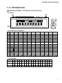
4. IC INFORMATION
• The information shown in the list is basic information and may not correspond exactly to that shown in the schematic diagrams.
• List of IC
PD4890A, PD0260A2, PD0261A2, LA9700M, BA6195FP, LC78650E-P, PD4889A, SRM2B256SLMX70, VYW1536, PD3381A,
MB86371, MB811171622A-100FN, CY2081SL-611, PD2058A
PD4890A (FLKB ASSY : IC101)
• Mode Control IC
• Block Diagram
47
TO0/P30
TI0/INTP0/P00
43
TO1/P31
TI1/P33
42
TO2/P32
TI2/P34
41
47
44
16-bit TIMER/
EVENT COUNTER
PORT0
46
31
40
39
8-bit TIMER/
EVENT COUNTER 1
PORT1
8-bit TIMER/
EVENT COUNTER 2
PORT2
WATCHDOG TIMER
PORT3
WATCH TIMER
PORT7
CI0/INTP3/P03
44
6-bit UP/DOWN
COUNTER
SI0/SB0/P25
SO0/SB1/P26
SCK0/P27
11
SI1/P20
SO1/P21
SCK1/P22
STB/P23
BUSY/P24
16
ANI0/P10ANI7/P17
AVDD
AVSS
AVREF
21
INTP0/TI0/P00INTP3/CI0/P03
44
47
INTERRUPT
CONTROL
BUZ/P36
37
BUZZER OUTPUT
10
9
15
14
SERIAL
INTERFACE 0
PORT8
78K/0
CPU CORE
ROM
29
22
P30-P37
18,19
49-51
7
6
P70-P74
P80
P81
69,70
72-77
P100-P107
61
68
53
60
P110-P117
P120-P127
A/D CONVERTER
20
FIP
CONTROLLER/
DRIVER
30
38
43
P20-P27
PORT10
1-7,
53-70
72-80
VLOAD
17
RESET
X1
X2
XT1/P04
XT2
35
31
CLOCK OUTPUT
CONTROL
32
8,52
33
48
VDD
VSS
IC
FIP0-FIP33
71
34
SYSTEM
CONTROL
PCL/P35
36
P10-P17
P90-P97
PORT12
RAM
28
9
16
P04
1-5
78-80
PORT11
12
28
P01-P03
PORT9
SERIAL
INTERFACE 1
13
21
P00
DV-505, DVL-909, DV-S9
• Pin Function
No.
Mark
Pin Name
1
P94
G7
2
P93
G6
3
P92
G5
4
P91
G4
5
P90
G3
6
P81
G2
7
P80
G1
8
VDD
VCC
9
P27
(NC)
I/O
O
FL timing output
−
Power supply pin
O
Not used
DVD lamp ON/OFF
H : ON
Communication handshake line with the system controller
L :Permit the communication
Communication clock output with the system controller
10
P26
(NC)
11
P25
(NC)
12
P24
LAMP
O
13
P23
XREADY
O
14
P22
SCK
I/O
15
P21
SO
I/O
16
P20
SI
I
17
RESET
18
P74
Function
H : ON
Communication data output with the system controller
Communication data input with the system controller
RESET IN
I
Reset input
(NC) (DV-505)
O
Not used
L : reset
SIDE A LED (DVL-909)
O
SIDE A LED ON/OFF
(NC) (DV-505)
O
Not used
L : ON
19
P73
SIDE B LED (DVL-909)
O
SIDE B LED ON/OFF
20
AVss
Vss
−
GND pin
21
P17
POWER ON
O
SW 5V ON/OFF
O
System reset output
O
Not used
I
Key input
I
Destination judgement input
22
P16
RESET OUT
23
P15
(NC)
24
P14
(NC)
25
P13
KIN1
26
P12
KIN0
27
P11
MS1
28
P10
MS0
29
AVDD
AVDD
−
Power supply pin
30
AVREF
AVREF
−
Reference voltage
31
P04
P04
I
Not used
32
XT2
(NC)
−
Not used
GND pin
33
VSS
VSS
−
34
X1
X1
I
35
X2
X2
−
36
P37
(NC)
37
P36
(NC)
(NC)
38
P35
39
P34
P34
40
P33
P33
L : ON
H : ON
L : reset
Connect a microprocessor clock
O
Not used
I
Not used
23
DV-505, DVL-909, DV-S9
No.
Mark
Pin Name
41
P32
P32
42
P31
P31
I/O
I
Function
Not used
43
P30
(NC)
I
Not used
44
P03
P03
I
Not used
45
P02
ON POWER
I
46
P01
LT
I
Switch the STBY/POWER ON at rising edge the FL controller
Communication handshake line with the system controller
H : Permit the communication
Remote control signal input
47
P00
SEL IR
I
48
IC
IC
−
−−−−
49
P72
(NC)
O
Not used
50
P71
51
P70
52
VDD
FL OFF LED (DV-505)
O
FL OFF LED ON/OFF
(NC) (DVL-909)
O
Not used
(NC)
O
Not used
VDD
−
Power supply pin
(NC) (DV-505)
O
Not used
FL OFF LED (DVL-909)
O
FL OFF LED ON/OFF
O
Not used
O
FL segment output
−
– 27V input
O
FL segment output
O
FL timing output
53
P127
54
P126
(NC)
55
P125
(NC)
56
P124
(NC)
57
P123
(NC)
58
P122
(NC)
59
P121
(NC)
60
P120
(NC)
61
P117
P15
62
P116
P14
63
P115
P13
64
P114
P12
65
P113
P11
66
P112
P10
67
P111
P9
68
P110
P8
P7
69
P107
70
P106
P6
71
VLOAD
-27V
72
P105
P5
P4
73
P104
74
P103
P3
75
P102
P2
76
P101
P1
77
P100
G11
78
P97
G10
79
P96
G9
80
P95
G8
24
L : ON
H : ON
H : ON
H : ON
H : ON
H : ON
L : STBY
DV-505, DVL-909, DV-S9
PD0260A2, PD0261A2 (CLDM ASSY : IC101)(DVL-909 ONLY)
• Mechanism Control IC
• Pin Function
No.
Pin Name
I/O
Function
1
VCC
I
Power supply pin Apply 5V ± 10%
2
RWC
O
DSP read/write command signal output "L"= Read "H"= Write
3
XPLAY
O
Signal output during spindle servo "L"= During servo "H"= During acceleration, brake and stop
4
CLK:SCK3/CQCK
O
DVP/DSP clock switch "H"= DVP "L"= DSP
5
XCD
O
LD/CD switch signal output "L= CD "H"= LD
6
TILT ERR
I
A/D • This signal is A/D converted as the tilt servo control input. Control the tilt motor so that this signal
becomes 2.5V.
7
TRK BAL ERR
I
A/D • Tracking balance error signal input This signal is A/D converted as the tracking offset control input.
8
SLD ERR
I
A/D • This signal is A/D converted as the slider servo control input.
Control the slider motor so that this signal becomes 2.5V.
9
SLD POS
I
A/D • Pickup position detection switch input
Detect the position by reading A/D input value which each switches are resistance divided.
10
FSEQ
I
Subcode sync. confirmity detection signal input "L"= Not confirmity "H"= Confirmity
11
C DETECT
I
Spindle over-current detection signal input "L" = Over current "H"= Normal
12
TRK BAL DRV
O
PWM • Output the tracking offset signal to PWM output, then use for auto tracking offset.
910 µsec period, tri-state control H, L, Z
13
SHAKE
I/O
Handshake signal for data communication with the DVD mechanism control IC
This pin is the bilateral data line and each microprocessor control the Input/Output.
14
RF CORRECTION
O
RF correction switch signal output "H"= Gain UP CD, CDV-A:Low, CAV inner circuit gain up, others are
High.
15
SQOUT
I
Command data input from DSP Read out SUBQ
16
SO3/COIN
O
Command data output to DVP/DSP
17
SCK3/CQCK
O
DVP/DSP read/write command clock output
Read-in at rising edge
18
SLD OUT
O
PWM • Slider control signal output 5V= FWD, 0V= REV, 2.5V= STOP 910 µsec period, tri-state control
19
SI1
I
Data input from the DVD mechanism control IC
20
SO1
O
Serial data output to the DVD mechanism control IC
I/O
Clock for serial communication with the DVD mechanism control IC
Becomes input mode without communicate with the DVD mechanism control IC
21
SCK
22
TRK 0 CRS
I
23
SBSY
I
24
INT • Tracking error zero cross signal input
Monitor this signal when searching track count in the miss clamp detection
Subcode block sync. input
LOAD/TILT control output
PWM output 0V : Tray IN / Tilt DOWN, 5V : Tray OUT / Tilt UP, 2.5V : STOP
TILT OUT
I/O
25
TURN OUT
O
Turn drive signal output
26
XPBV
I
Playback vertical sync. signal input of LD/CDV "L"= During vertical sync.
27
CNVSS
I
Ground for A/D conversion
28
XRESET
I
Reset signal input
"L"= Reset "H"= Release reset
29
XIN
I
9MHz clock oscillation input
30
XOUT
O
9MHz clock oscillation output
Control with the DVD mechanism control IC.
25
DV-505, DVL-909, DV-S9
No.
31
Pin Name
I/O
Function
PHAI
O
Not used
32
GND
I
Ground
33
SW1
I
Switch input for Loading/Tilt position detection
34
SW3
35
SW2
36
TBCLOCK
I
Spindle lock signal input "L"= Unlock "H"= Lock
37
FG
I
Spindle motor FG signal input
16 outputs per rotation Used after dividing by 2 in the microprocessor
38
DATA
I
Input for Phillips code decoder with built-in mechanism controller
39
XPBH
I
Playback H-SYNC input for Phillips code decoder
40
XPBV
I
Playback V-SYNC input for Phillips code decoder
41
DEXT
O
Control signal output of video dynamic range extension "H"= ON "L"= OFF
42
WFM/VLOCK
I
Field discrimination signal from DVP "H"= ODD "L"= EVEN (with memory)
VLOCK signal at clear scan (with no memory)
43
LATMEM
O
Serial control latch output of memory control IC PD3212A
Latches at falling edge.
44
XPFR
O
PD0260A2 : 17MHz PLL control signal output
PD0261A2 : Not used
H : Phase comparison
L : Free-run
45
XP/N2
O
PD0260A2 : NTSC/XPAL circuit switching signal output excepting VDEM
PD0261A2 : Not used
46
HQ
O
PD0260A2 : Control signal output of the High Quality circuit (analog NR)
H : Through the HQ circuit L : Not through
PD0261A2 : Not used
47
THLD
I
Track jump accelerating / decelerating signal input "L"= Others "H"= During accelerating / decelerating
48
LATDVP
O
PD6159B serial latch signal output Latches at falling edge.
H : NTSC
49
SELTZC
O
TZC switch signal output "H"= at normal "L"= at CD/DVD disc discrimination
50
DOCINH
O
Control the clamp pulse and clamp killer circuit by tri-state value
51
XP/N1
O
PD0260A2 : NTSC/XPAL circuit switching signal output for VDEM
PD0261A2 : Not used
52
NROFF
O
Noise reduction control output by VDEM "L"= Normal "H"= Not NR
53
DSCDET
I
Disc present/absent detecting signal input by the tilt sum in the DVD P.U. mode
"H"= Absent "L"= Present
DEFECT input at LD P.U.
54
XTURNB
I
Turn switch input
"H"= Side A / turn "L"= Side B
"H"= Side B / turn "L"= Side A
H : NTSC
L : PAL
L : PAL
55
XTURNA
I
Turn switch input
56
XLPO
I
LD P.U. out position detecting switch input "H"= LD P.U. active "L"= LD P.U. out position
57
VDET
I
Use for power abnormal signal input port
58
XFOK
I
Focus servo lock signal input "L"= Lock "H"= Unlock Use for lock detection of focus servo
I
Subcode Q reading OK signal input "L"= NG "H"= OK
This pin will be H when subcode Q data passed by CRC check.
59
WRQ
"L"= Normal "H"= Abnormal
60
AC3MUTE
O
Mute control signal output for AC3
61
SQ1
O
Analog audio switching signal output 1/L "L"= Squelch OFF "H"= Squelch ON
Release MUTE during playback.
"L"= Release MUTE "H"= MUTE
62
SQ2
O
Analog audio switching signal output 2/R "L"= Squelch OFF "H"= Squelch ON
63
XCX
O
Analog audio CX noise reduction switching signal output "L"= CX ON "H"= CX OFF
64
XANA
O
Digital / Analog audio switching signal output "L"= Analog "H"= Digital
26
DV-505, DVL-909, DV-S9
LA9700M (DVDM ASSY : IC101)
• RF IC
RFOUT
PHC
BHC
PHI
BHI
PH
BH
GND
TC
DEPC
DLPC
DEF
DEFI
RFO
EQI
64
63
62
61
60
59
58
57
56
55
54
53
52
51
50
49
Scratch Detection
REF
48 BPI1
VCC
PH
50k
BH
PH
–
+
50k
REFI 2
REF
BH
VCC
47 VCC
+
–
26p
80k
80k
RFI 3
REF
46 BPO1
45k
80k
80k
LIM
PD1 5
LIM
PD
PD2 6
LIM
PD
PD3 7
LIM
45 EQB
1k
PDRF 4
–
+
3k
PDRF– 1
50k
REF
• Block Diagram
REF
3k
+
–
44 BPO2
40k
40k
–
+
PD
40k
40k
PD4 8
LIM
43 N/C
60k
+
–
CP
26p
42 BPI2
60k
41 N/C
PD
PD6 10
+
–
10p
80k
60k
–
+
15k
10p
80k
40 DLAY1
3k
39 DLAY2
38 MIXO1
REF
APC
VCC
37 VCC
+
–
LDS 12
REF
60k
REF
LDD 11
15k
3k
+
–
+
–
PD5 9
1k
26p
36 MIXI1
AGOF 14
35 MIXI2
+
–
10k
20k
LDON 13
REF
+
–
33 MIXO2
17
18
19
20
21
22
23
24
25
26
27
28
29
30
31
32
QPH/BH
DVD/CD
DPD/TE
CPOF
TEBAL
SGC
TES
TESI
RREC
TE
TLP
CP
TEO
TE–
FE
EFMO
REF
10k
QAGC 16
34 GND
+
–
PH/RR 15
27
DV-505, DVL-909, DV-S9
BA6195FP (DVDM ASSY : IC161)
• Spindle Driver
18
17
16
15
14
NC
GND
Driver mute
NC
19
NC
20
NC
21
NC
VCC
22
NC
NC
MUTE
23
GND
NC
24
GND
OPIN+
25
NC
OPIN–
• Block Diagram
TSD
GND
NC
NC
NC
VCC
IN Level shift
10K
10K
10K
10K
7
8
9
10
11
12
13
DROUT+
BIAS
NC
DROUT–
NC
6
NC
NC
NC
5
NC
NC
4
NC
NC
3
NC
NC
2
10K
NC
1
DRIN
NC
DRIN'
NC
OPOUT
10K
• Pin Function
No.
Pin Name
1
OPOUT
2
N.C.
3
N.C.
4
BIAS
Function
OP amp. output pin
Non Connection
Bias pin
No.
Pin Name
15 N.C.
16 N.C.
Power supply pin
Non Connection
5
DRIN'
Driver gain adjustment pin
18 N.C.
DRIN
Driver gain input pin
19 GND
7
N.C.
20 GND
8
N.C.
21 N.C.
9
N.C.
Non Connection
11 N.C.
12 DROUT –
Driver negative output pin (for input)
13 DROUT +
Driver positive output pin (for input)
28
Non Connection
17 VCC
6
10 N.C.
Function
14 N.C.
Sub-strait GND pin
Non Connection
22 MUTE
Mute pin
23 N.C.
Non Connection
24 OPIN +
OP amp. non-inverting input pin
25 OPIN –
OP amp. inverting input pin
DV-505, DVL-909, DV-S9
LC78650E-P (DVDM ASSY : IC201)(DVL-909 only)
• Servo DSP LSI
• Block Diagram
FE 35
49 FDO
50 TDO
TE 34
TILTE 31
MPX
RF_PH 32
8bit
A/D
Servo
Processor
(16×16+32→32)
47 SLDO
8bit
D/A
48 SPDO
46 TBAL
RF_BH 33
45 TILTDO
44 AUXO
JITT 30
HFL 63
61 VREF
CMP
26 DRF
TES 28
Track Counter
55 DVD_CDB
1 PP5/SYNC
PP7/EVNT 58
Event Counter
LCD Driver
PP6/FG 57
SLCIST1,2 36,37
EFMIN 41
SLCO1,2 38,39
EFMOUT 3
PCKIST1,2 89,90
CDFR 93
DVDFR 92
PD01-3 85-87
JV 94
LEFM 2
PCK 95
VRPFR
VCOC
VPDO
XIN
XOUT
XTALOUT
SLC
25 V_PB
83
16
24 FAST
CLV
79 WRQ
CD-PLL
DVD-PLL
Frame Synchronous
Detection, Protection,
Insertion EFM
Demodulation
Sub Code
Decode
CRC
76 SQOUT
77 CQCKB
78 RWC
19 EMPH
14 PW
12 SBCK
20 SBSY
13 SFSY
81
82
56 LCDCNTL
FG Counter
Clock
Generator
Error Detect
Correction
C1-Twofold,
C2-Fourfold
For De-Interleave
16k SRAM
11 FSX
4 C2F
22 EFLG
17
10
CSB 60
WRB 62
RDB 61
P0-7 65-72
BUSYB 75
LASER 54
PP0-4 96-100
Command
Interface
Supplement/Mute
D Attenuate
Deemphasis Filter
DOUT
21 DOUT
7 LRSY
Serial Out
6 ROMCK
5 ROMXA
27,29
40,52
TEST1-4
RESB 59
29
DV-505, DVL-909, DV-S9
• Pin Function
No.
1
Pin Name
PP5/SYNC
I/O
Function
I/O General-purpose port input/output / DVD sync. signal input
2
LEFM
O
Output the state that cut and out a signal which was binary-stated value EFM/EFM + with PCK.
3
EFMOUT
O
Output the state that was binary-stated value EFM/EFM + .
4
C2F
O
C2 flag output
5
ROMXA
O
ROMXA data output
6
ROMCK
O
Shift clock output for ROMXA data output
7
LRSY
O
L/R clock output for ROMXA data output
8
DVDD2
−
5V power supply
9
VSS
−
GND
10 XTALOUT
O
External system clock output
11 FSX
O
CD 1 frame sync. signal output
12 SBCK
I
Subcode reading out clock input
13 SFSY
O
Frame sync. signal output of subcode
14 PW
O
Subcode P, Q, R, S, T, U, V and W output
15 VSS
−
GND for oscillation circuit
16 XIN
I
Connect a crystal resonator (16.9344MHz)
17 XOUT
O
Connect a crystal resonator
18 DVDD1
−
3.3V power supply of the oscillation circuit
19 EMPH
O
Monitor the deemphasis
20 SBSY
O
Sync. signal output of the subcode block
21 DOUT
O
Output for the digital audio I/F
22 EFLG
O
Error correction state monitor of the error correction C1 and C2
23 FSEQ
O
Detection monitor of the CD/DVD frame sync. signal
24 FAST
O
Playback speed monitor
25 V_PB
O
Monitor output of the rough servo/CLV control
26 DRF
O
In focus monitor
27 TEST3
I
Test input 3
28 TES
I
Tracking error signal input
29 TEST2
I
Test input 2
30 JITT
I
Jitter quantity detecting signal input of EFM/EFM + PLL
31 TILTE
I
Tilt error signal input
32 RF_PH
I
RF peak hold signal input
33 RF_BH
I
RF bottom hold signal input
34 TE
I
Tracking error signal input
35 FE
I
Focus error signal input
36 SLCIST1
−
Current setting pin 1 of the constant current charge pump for SLC
37 SLCIST2
−
Current setting pin 2 of the constant current charge pump for SLC
38 SLCO1
−
Control output 1 for SLC
39 SLCO2
−
Control output 2 for SLC
40 TEST1
I
Test input 1
41 EFMIN
I
EFM/EFM + input
42 AVDD
−
5V power supply of A/D and D/A for servo
43 AVSS
−
GND of A/D and D/A for servo
44 AUXO
O
DA auxiliary output
45 TILTDO
O
Tilt control signal output
46 TBAL
O
Tracking balance control signal output
47 SLDO
O
Sled control signal output
48 SPDO
O
Spindle control signal output
49 FDO
O
Focus control signal output
50 TDO
O
Tracking control signal output
30
DV-505, DVL-909, DV-S9
No.
Pin Name
I/O
Function
51 VREF
−
Reference level of A/D and D/A for servo
52 TEST4
I
Test input 4
Track detection signal output
53 HFL
O
54 LASER
O
For laser ON/OFF control
55 DVD_CDB
O
Disc discrimination result output
Pickup liquid shutter control signal output
56 LCDCNTL
O
57 PP6/FG
I/O General-purpose port input/output / FG signal input
58 PP7/EVNT
I/O General-purpose port input/output / Event counter input
59 RESB
I
60 CSB
I
Reset input
Chip select input
61 RDB
I
Internal state reading signal input
62 WRB
I
Command / data writing signal input
63 DVDD2
−
5V power supply
64 VSS
−
GND
65 P0
66 P1
67 P2
68 P3
69 P4
I/O Command / data input/output
70 P5
71 P6
72 P7
73 VSS
−
GND
74 DVDD1
−
3.3V power supply for internal logic
75 BUSYB
O
Busy signal output of command process
76 SQOUT
O
Serial output of subcode Q
77 CQCKB
I
Data read-out shift clock input of subcode Q
78 RWC
I
Serial output update permission input of subcode Q
79 WRQ
O
Read out ready monitor of subcode Q
80 VSS
−
PLL GND for internal system clock
81 VRPFR
−
VCO oscillation range setting of PLL for internal system clock
−
Connect a PLL filter for internal system clock
82 VCOC
83 VPDO
84 DVDD2
−
PLL 5V power supply for internal system clock
85 PDO1
−
PLL filter connection pin 1 for EFM/EFM + playback
86 PDO2
−
PLL filter connection pin 2 for EFM/EFM + playback
87 PDO3
−
PLL filter connection pin 3 for EFM/EFM + playback
88 VSS
−
PLL GND for EFM/EFM + playback
89 PCKIST1
−
Current setting 1 of PLL constant current charge pump for EFM/EFM + playback
90 PCKIST2
−
Current setting 2 of PLL constant current charge pump for EFM/EFM + playback
91 DVDD2
−
PLL 5V power supply for EFM/EFM + playback
92 DVDFR
−
VCO oscillation range setting of PLL for EFM + playback
93 CDFR
−
VCO oscillation range setting of PLL for EFM playback
94 JV
O
Jitter monitor of PLL clock for EFM/EFM + playback
95 PCK
O
Bit clock output for EFM/EFM + playback
96 PP0
97 PP1
98 PP2
I/O General-purpose port input/output
99 PP3
100 PP4
31
DV-505, DVL-909, DV-S9
PD4889A (DVDM ASSY : IC501)
• Mechanism Control IC
• Pin Function
No. Pin Name
No. Pin Name
I/O
1
LODDRV
I/O Loading motor drive output
I/O
Function
33 XDSPRST
−
Reset pulse for servo DSP "L"
2
DVD/XCD
O
34 ASTB
O
Address strobe of multiplexed address/data
bus "H"
3
AGOFF
O
Turn AGC of RF IC to OFF for "H"
35 XRST
I
CPU reset input "L"
36 SBSY
Subcode frame sync. input
INT
(H : S0+S1 period)
Clock switch
H : DVD , L : CD
Function
4
EFLG
I
Count data input of error rate
Measureable by using timer 1 and 2.
5
FS X
I
Error rate count area input (EFM frame sync.)
H : C1 , L : C2
37 SHAKE
INT
6
P35/PCL
−
Not used (pull down)
38 XABUSY
INT DSP auto sequence busy input "L"
7
XTOFF
High impedance (input) at DEFECT ON
"L" output at DEFECT OFF
39 XIRQ2
INT LSI-11 interrupt input "L"
I/O
Communication handshake of CLD
mechanism controller "L" (DVL-909 only)
8
XCBUSY
I
DVD command reception is possible "L"
40 VDD
−
9
VSS
−
GND
41 X2
−
10 MAD0
42 X1
−
11 MAD1
43 IC (Vpp)
−
12 MAD2
44 XT2
−
Not used
45 DVDPPK
I
Park position detection of compatible DVD
pickup "L" (DVL-909 only)
13 MAD3
I/O External address / data bus
Power supply pin
Connect a ceramic resonator
GND
14 MAD4
46 AVss
−
GND
15 MAD5
47 LODPOS
I
Loading and clamp position SW input
16 MAD6
48 SLDPOS
I
Slider position SW input
17 MAD7
49 DORPOS
I
Panel position SW input (DV-S9 only)
18 MA8
50 XCURDET
I
Acutuator over-current detection input (former
TRDLMT) "L" Servo OFF for 300 ms.
19 MA9
51 DR/XLD
O
Panel and loading switch of PWM output
Panel : H , loading : L (DV-S9 only)
52 MON
O
Spindle motor ON output "H"
20 MA10
O
External address bus
21 MA11
53 XCD2X
O
Not used
22 MA12
54 OEICG
O
"H" : OEIC gain up to 6dB
23 MA13
55 AVDD
−
Power supply pin
24 VSS
25 MA14
−
GND
56 AVREF
−
Reference power supply pin
57 P_ERR
O
Not used
O
External address bus
58 P21/SO1
−
Not used (pull down)
27 DRF
I
(FOK) Focus OK input
59 P22/XSK1
−
Not used (pull down)
28 V_PB
I
(LOCK) EFM servo lock signal
"H"/"L"= rough servo / phase servo
60 XCSB
O
DSP parallel command setting output "L"
29 P62
−
Not used (pull down)
61 CLD
O
CLD circuit block switch (DVL-909 only)
30 WRQ
I
Readable flag of subcode Q
62 LDSO
I
Inputs serial communication output of CLD
mechanism controller (DVL-909 only)
31 XRD
O
CPU read pulse "L"
63 LDSI
O
Outputs serial communication input of CLD
mechanism controller (DVL-909 only)
32 XWR
O
CPU write pulse "L"
64 LDSCK
I
Inputs serial communication clock output of
CLD mechanism controller (DVL-909 only)
26 MA15
32
DV-505, DVL-909, DV-S9
SRM2B256SLMX70 (DVDM ASSY : IC502)
• 256 K SRAM (For Mechanism Control IC)
• Block Diagram
A0
A1
A2
A3
A4
A5
A6
A7
A8
A9
A10
A11
A12
A13
A14
10
CS
20
Control
Logic
OE
22
OE, WE
WE
27
Control
Logic
9
8
7
9
5
4
3
25
24
Address Buffer
6
Line
Decoder
512
Memory-Cell
Array
512×64×8
64×8
21
23
2
6
26
Row
Decoder
64
Row Gate
1
CS
8
14 18
11 12 13 15 16 17 18 19
Vss
VDD
I/O1
I/O2
I/O3
I/O4
I/O5
I/O6
I/O7
I/O8
I/O Buffer
• Pin Function
No.
Pin Name
Function
No.
Pin Name
1
A14
15 I/O4
2
A12
16 I/O5
3
A7
17 I/O6
4
A6
18 I/O7
5
A5
Function
Data input/output
19 I/O8
Address input
6
A4
20 CS
Chip select
7
A3
21 A10
Address input
8
A2
22 OE
Output enable
9
A1
23 A11
10 A0
24 A9
11 I/O1
25 A8
Address input
12 I/O2
Data input/output
13 I/O3
14 VSS
GND (0V)
26 A13
27 WE
Write enable
28 VDD
Power supply (2.7 to 5.5V)
33
DV-505, DVL-909, DV-S9
VYW1536 (DVDM ASSY : IC603)(DV-505 and DVL-909 only)
• Flash ROM
• Block Diagram
DQ0-DQ15
RY/BY
15-22,
24-31
1
RY/BY
BUFFER
RY/BY
ERASE
CIRCUIT
WE
BYTE
RESET
INPUT/OUTPUT
BUFFER
43
33
CONTROL
CIRCUIT
44
WRITE
CIRCUIT
CHIP ENABLE
STB
OUTPUT ENABLE
CIRCUIT
12
14
LOW VCC
DET. CIRCUIT
STB
WRITE/ERASE
PULSE TIMER
2-11,
A0-A18 34-42
A-1
31
ADDRESS LATCH
CE
OE
DATA LATCH
Y DECODER
X DECODER
Y GATE
8,388,608
CELL
MATRIX
• Pin Function
No.
Pin Name
Function
Ready / Busy output
No.
Pin Name
Function
Power supply (+5.0V ± 10% or ± 5%)
1
RY/BY
23
VCC
2
A18
24
DQ4
3
A17
25
DQ12
4
A7
26
DQ5
5
A6
27
DQ13
6
A5
28
DQ6
7
A4
29
DQ14
8
A3
30
DQ7
9
A2
31
DQ15/A-1
10
A1
32
VSS
Ground
11
A0
33
BYTE
Switch the 8 bit and 16 bit modes
12
CE
Chip enable
34
A16
13
VSS
Ground
35
A15
14
OE
Output enable
36
A14
Address input
Data input / output
Data input/output / address input
15
DQ0
37
A13
16
DQ8
38
A12
17
DQ1
39
A11
18
DQ9
40
A10
19
DQ2
41
A9
20
DQ10
42
A8
21
DQ3
43
WE
Write enable
22
DQ11
44
RESET
Hardware reset
34
Data input/output
Address input
DV-505, DVL-909, DV-S9
PD3381A (DVDM ASSY : IC601)
A16
A17
A18
A19
A20
A21
CS0
CS1/CASH
CS2
CS3/CASL
PA0/CS4/TIOCA0
PA1/CS5/RA5/RAS
PA2/CS6/TIOCB0
PA3/CS7/WAIT
PA4/WRL(WR)
PA5/WRH(LBS)
PA6/RD
PA7/BACK
PA8/BREQ
PA9/AH/IRQOUT/ADTRG
PA10/DPL/TIOCA1
PA11/DPH/TIOCB1
PA12/IRQ0/DACK0/TCLKA
PA14/IRQ2/DACK1
PA15/IRQ3/DREQ1
• Block Diagram
PA13/IRQ1/DREQ0/TCLKB
• System Control CPU
69 68 67 66 65 64 63 62 60 59 58 57 56 55 54 53
51 50 49 48 47 46 45 44 42 41
PORT A
ADDRESS
RES 79
39 A15
WDTOVF 78
38 A14
MD2 82
37 A13
MD1 81
36 A12
35 A11
MD0 80
64k PROM / MASK ROM
NMI 76
XTAL 74
33 A9
ADDRESS
EXTAL 73
34 A10
OSCILLATOR
CK 71
4kB RAM1
32 A8
30 A7
29 A6
28 A5
Vpp 77
Vcc 15
27 A4
DIRECT
MEMORY
ACCESS
CONTROLLER
CPU
Vcc 43
26 A3
25 A2
Vcc 70
24 A1
Vcc 75
INTERRUPT
CONTROLLER
Vcc 83
USER BREAK
CONTROLLER
23 A0(HBS)
BUS STATE
CONTROLLER
Vcc 84
21 AD15
Vcc 99
20 AD14
Vss 3
19 AD13
Vss 22
Vss 31
18 AD12
SERIAL
COMMUNICATION
INTERFACE
(×2CHANNEL)
16BIT
INTEGRATED
TIMER PULSE UNIT
PROGRAMABLE
TIMING
PATTERN
CONTROLLER
WATCHDOG
A/D
TIMER
CONVERTER
17 AD11
DATA/ADDRESS
Vss 12
Vss 40
Vss 52
Vss 61
Vss 72
16 AD10
14 AD9
13 AD8
11 AD7
10 AD6
Vss 96
9 AD5
Vss 106
8 AD4
7 AD3
6 AD2
AVref 86
5 AD1
AVcc 85
PORT C
PORT B
PB0/TP0/TIOCA2
PB1/TP1/TIOCB2
PB2/TP2/TIOCA3
PB3/TP3/TIOCB3
PB4/TP4/TIOCA4
PB5/TP5/TIOCB4
PB6/TP6/TOCXA4/TCLKC
PB9/TP9/TxD0
PB8/TP8/RxD0
PB10/TP10/RxD1
PB11/TP11/TxD1
PB12/TP12/IREQ4/SCK0
PB13/TP13/IREQ5/SCK1
PB7/TP7/TOCXB4/TCLKC
Periphery data bus(16 bit)
PC0/AN0
PB14/TP14/IREQ6
Periphery address bus(24 bit)
PC1/AN1
PC2/AN2
PC3/AN3
PC4/AN4
1 112 111 110 109 108 107 105 104 103 102 101 100 98 97
PC5/AN5
2
PC6/AN6
95 94 93 92 90 89 88 87
PB15/TP15/IRQ7
4 AD0
PC7/AN7
AVss 91
Internal address bus(24 bit)
Internal upper data(16 bit)
Internal lower data(16 bit)
35
DV-505, DVL-909, DV-S9
• Pin Function
No.
Pin Name
1
PB14/TP14/IRQ6
2
PB15/TP15/IRQ7
3
VSS
4
AD0
5
AD1
6
AD2
7
AD3
8
AD4
9
AD5
10
AD6
11
AD7
12
VSS
13
AD8
14
AD9
15
VCC
16
AD10
17
AD11
18
AD12
19
AD13
20
AD14
21
AD15
I/O
I/O
I
I/O
I
I/O
I
I/O
Function
16 bit input/output (port B) / Timing pattern output / Interruption request
Ground
16 bit bilateral data bus
Ground
16 bit bilateral data bus
Power supply
16 bit bilateral data bus
22
VSS
I
Ground
23
A0 (HBS)
O
Address bus output (upper byte strobe signal)
O
Address bus output
I
Ground
O
Address bus output
I
Ground
O
Address bus output
I
Power supply
24
A1
25
A2
26
A3
27
A4
28
A5
29
A6
30
A7
31
VSS
32
A8
33
A9
34
A10
35
A11
36
A12
37
A13
38
A14
39
A15
40
VSS
41
A16
42
A17
43
VCC
36
DV-505, DVL-909, DV-S9
No.
Pin Name
44
A18
45
A19
46
A20
47
A21
I/O
O
Function
Address bus output
48
CS0
O
Chip select signal
49
CS1/CASH
O
Chip select signal / Column address strobe timing signal on the upper side of DRAM
50
CS2
O
Chip select signal
51
CS3/CASL
O
Chip select signal / Column address strobe timing signal on the lower side of DRAM
52
VSS
I
Ground
16 bit input/output (port A) / Chip select signal /
ITU input capture input/ITU output compare output (channel 0)
53
PA0/CS4/TIOCA0
I/O
54
PA1/CS5/RAS
I/O
16 bit input/output (port A) / Chip select signal / Low address strobe timing signal of DRAM
I/O
16 bit input/output (port A) / Chip select signal /
ITU input capture input/ITU output compare output (channel 0)
55
PA2/CS6/TIOCB0
56
PA3/CS7/WAIT
I/O
16 bit input/output (port A) / Chip select signal / Wait input for bus cycle
57
PA4/WRL (WR)
I/O
16 bit input/output (port A) / External lower 8 bit writing (output at writing)
58
PA5/WRH (LBS)
I/O
16 bit input/output (port A) / External upperr 8 bit writing (lower byte strobe signal)
59
PA6/RD
I/O
16 bit input/output (port A) / External reading out
60
PA7/BACK
I/O
16 bit input/output (port A) / Bus claim request acknowledge
61
VSS
62
PA8/BREQ
I
Ground
I/O
16 bit input/output (port A) / Bus claim request
63
PA9/AH/IRQOUT/ADTRG
I/O
16 bit input/output (port A) / Address hold timing signal / Interruption request output at slave /
A/D conversion trigger input
64
PA10/DPL/TIOCA1
I/O
16 bit input/output (port A) / Data bus parity on the lower side /
ITU input capture input/ITU output compare output (channel 1)
65
PA11/DPH/TIOCB1
I/O
16 bit input/output (port A) / Data bus parity on the upper side /
ITU input capture input/ITU output compare output (channel 1)
66
PA12/IRQ0/DACK0/TCLKA
I/O
16 bit input/output (port A) / Interruption request / DMA transfer request reception (channel 0) /
ITU timer clock input
I/O
16 bit input/output (port A) / Interruption request / DMA transfer request (channel 0) /
ITU timer clock input
67
PA13/IRQ1/DREQ0/TCLKB
68
PA14/IRQ2/DACK1
I/O
16 bit input/output (port A) / Interruption request / DMA transfer request reception (channel 1)
69
PA15/IRQ3/DREQ1
I/O
16 bit input/output (port A) / Interruption request / DMA transfer request (channel 1)
70
VCC
I
Power supply
71
CK
O
System clock output
72
VSS
I
Ground
73
EXTAL
I
Crystal oscillator input
External clock input
74
XTAL
I
Crystal oscillator input
75
VCC
I
Power supply
76
NMI
I
Non-maskable interruption input
77
VPP
I
Power supply of PROM program
78
WDTOVF
O
Watchdog timer over-flow output
I
Reset input
I
Mode setting pins
I
Power supply
79
RES
80
MD0
81
MD1
82
MD2
83
VCC
84
VCC
37
DV-505, DVL-909, DV-S9
No.
Pin Name
I/O
Function
85
AVCC
I
Analog power supply
86
AVREF
I
Analog reference power supply
I
8 bit input (port C) / Analog signal input
I
Analog Ground
I
8 bit input (port C) / Analog signal input
I
Ground
87
PC0/AN0
88
PC1/AN1
89
PC2/AN2
90
PC3/AN3
91
AVSS
92
PC4/AN4
93
PC5/AN5
94
PC6/AN6
95
PC7/AN7
96
VSS
97
PB0/TP0/TIOCA2
98
PB1/TP1/TIOCB2
99
VCC
100 PB2/TP2/TIOCA3
101 PB3/TP3/TIOCB3
102 PB4/TP4/TIOCA4
103 PB5/TP5/TIOCB4
104 PB6/TP6/TOCXA4/TCLKC
105 PB7/TP7/TOCXB4/TCLKD
106 VSS
I/O
I
16 bit input/output (port B) / Timing pattern output / ITU input capture input/ITU output compare
output (channel 2)
Power supply
I/O
16 bit input/output (port B) / Timing pattern output / ITU input capture input/ITU output compare
output (channel 3)
I/O
16 bit input/output (port B) / Timing pattern output / ITU input capture input/ITU output compare
output (channel 4)
I/O
16 bit input/output (port B) / Timing pattern output / ITU output compare output (channel 4) /
ITU timer clock input
I
Ground
107 PB8/TP8/RXD0
I/O
16 bit input/output (port B) / Timing pattern output / Receive data input (channel 0)
108 PB9/TP9/TXD0
I/O
16 bit input/output (port B) / Timing pattern output / Transmission data output (channel 0)
109 PB10/TP10/RXD1
I/O
16 bit input/output (port B) / Timing pattern output / Receive data input (channel 1)
110 PB11/TP11/TXD1
I/O
16 bit input/output (port B) / Timing pattern output / Transmission data output (channel 1)
111 PB12/TP12/IRQ4/SCK0
I/O
16 bit input/output (port B) / Timing pattern output / Interruption request /
Serial clock input/output (channel 0)
112 PB13/TP13/IRQ5/SCK1
I/O
16 bit input/output (port B) / Timing pattern output / Interruption request /
Serial clock input/output (channel 1)
38
DV-505, DVL-909, DV-S9
MB86371 (DVDM ASSY : IC801)
• MPEG2 Decoder LSI For DVD
• Block Diagram
Exclusive
Parallel port
Input Signal
CPU
CPU
Interface
System
Decoder Block
16Mbit
SDRAM
Memory
Controller Block
Internal
Bus
Video
Decoder
Block
Sync.
Control
Block
Reset
Signal
Control
Block
27MHz
LPF
VCO
System
Clock
Generation
Block
Subpicture
MIX
Starting
Signal
Picture
Block
Reset Signal
Whole Control
Block
Clock
Signal
OSD
Audio
Decoder
Block
NTSC/PAL
Video Encoder
Digital
Signal Output
(Component/
Composite)
System Clock
Clock for video
DAC
Audio
Clock
Generation
Block
Video Output
Block
Clock for audio
Clock
Generation
Block
Audio Output
Video Output
(Y,C,Comp/Y,Cb,Cr)
39
DV-505, DVL-909, DV-S9
• Pin Function
No.
Pin Name
I/O
Function
No.
Pin Name
1
CLKSEL
I
ON/OFF signal of PLL ("H" : ON, "L" : OFF)
27 VDD
2
DIGCPN7
O
Digital component signal output (MSB)
Digital Y signal output (9-bit) (MSB)
28 DIGCOMP4
3
VSS
−
GND
29 DIGCOMP3
4
DIGCPN6
30 DIGCOMP2
5
DIGCPN5
31 DIGCOMP1
6
DIGCPN4
7
DIGCPN3
8
9
O
Digital component signal output
Digital Y signal output (9-bit)
I/O
−
O
Function
3.3V power supply
Digital composite signal output
Digital C signal output
Digital composite signal output (LSB)
Digital C signal output (LSB)
32 DIGCOMP0
33 DACK
O
27 MHz clock output
DIGCPN2
34 N.C.
−
Non connection
DIGCPN1
35 VSSA3
−
GND (D/A converter)
36 ANAC
O
Analog color (C) output signal
−
3.3V power supply
11 DIGCPN0
O
Digital component signal output (LSB)
Digital Y signal output (9-bit) (LSB)
37 VDDA3
−
3.3V power supply (for built-in D/A converter
only)
12 RBSEL
O
Cb and Cr discrimination signal at the digital
component signal output.
LSB at the digital Y signal output.
38 VSSA2
−
GND (D/A converter)
13 XHS
O
Horizontal sync. output signal
39 ANAY
O
Analog luminance (Y) output signal
−
3.3V power supply (for built-in D/A converter
only)
10 VDD
14 XVS
O
Vertical sync. output signal
40 VDDA2
15 VSS
−
GND
41 VREF
I
Reference voltage for D/A converter
16 XRESET
I
LSI reset signal
42 VRO
O
Internal current setting pin of D/A converter
17 XLDCSYNC
I
External sync. signal input (LD mode)
43 N.C.
−
Non connection
18 KEY
O
KEY signal for LD and OSD overlay
(LD mode)
44 VSSA1
−
GND (D/A converter)
19 PD
O
Phase comparison result output signal of
horizontal sync. (LD mode)
45 ANACOMP
O
Analog composite output signal
20 VFLD
O
Field discrimination signal at the digital signal
46 VDDA1
output
H : even field L : odd field
−
3.3V power supply (for built-in D/A converter
only)
Digital composite signal output (MSB)
Digital C signal output (MSB)
47 BF
O
Burst flag signal
48 XBLK
O
H/V composite blanking signal
Digital composite signal output
Digital C signal output
49 N.C.
−
Non connection
50 VSS
−
GND
51 TEST0
−
Normally, set to "open".
GND
52 TEST1
−
"L" status normally
21 DIGCOMP9
22 DIGCOMP8
23 DIGCOMP7
O
24 DIGCOMP6
25 DIGCOMP5
26 VSS
40
−
DV-505, DVL-909, DV-S9
No.
Pin Name
53 DAIIN
I/O
Function
No.
Pin Name
I
Digital data input of external input (SPDIF)
92 HADRS10
54 CDDATA
I
Audio data input of external input
(correspond to CD)
93 HADRS9
55 CDLR
I
Data channel clock input of external input
(correspond to CD)
94 HADRS8
56 CDBCK
I
Data clock input of external input
(correspond to CD)
95 HADRS7
57 AODATA3
58 AODATA2
I/O
Function
I
CPU address bus signal (MSB)
I
CPU address bus signal
96 VSS
−
GND
−
3.3V power supply
O
Audio decode data
97 VDD
60 VSS
−
GND
99 HADRS5
61 VDD
−
3.3V power supply
100 HADRS4
62 AODATA0
O
Audio decode data
101 HADRS3
63 AOPCM
O
Digital audio interface output
(compression data)
102 HADRS2
CPU address bus signal (LSB)
64 AODAI
O
Digital audio interface output (decode data)
103 HDATA15
CPU data bus signal (MSB)
59 AODATA1
98 HADRS6
65 LRCK
O
Data channel clock for D/A and digital filter
104 HDATA14
66 AOMCK
O
Master clock for D/A and digital filter
105 HDATA13
67 BCK
O
Bit clock for D/A and digital filter
68 ICED1
69 ICED0
70 ICEBRK
Pin for emulator
Normally, set to "open".
71 XDSPRST
−
GND
111 HDATA8
73 N.C.
−
Non connection
112 HDATA7
76 TEST4
−
Normally, set to "open".
114 VDD
I
Parallel data input
117 HDATA3
79 VDD
−
3.3V power supply
118 HDATA2
80 SD6
119 VSS
81 SD5
120 HDATA1
I
Parallel data input
83 SD3
87 SD0
88 XERR
121 HDATA0
122 BUSSEL
84 SD2
86 SD1
I/O CPU data bus signal
−
GND
I
Parallel data input
I
Error input signal
−
3.3V power supply
115 HDATA5
116 HDATA4
78 SD7
85 VSS
GND
113 HDATA6
77 TEST5
82 SD4
−
108 HDATA11
110 HDATA9
74 TEST2
CPU data bus signal
109 HDATA10
72 VSS
75 TEST3
I/O
106 HDATA12
107 VSS
−
CPU address bus signal
I
I/O CPU data bus signal
−
I/O
I
GND
CPU data bus signal
CPU data bus signal (LSB)
Bus width selection signal
(0 : 8-bit bus, 1 : 16-bit bus)
123 XOSDACK
I
OSD data acknowledge signal
124 XOSDREQ
O
OSD data request signal
I
CPU selection signal (00 :SPARC,
01 :86 system, 10 :68 system, 11 :Reserve)
O
Interrupt request signal to the CPU
−
GND
125 HCPUSEL1
126 HCPUSEL0
127 XINT3
89 XSACK
I
Acknowledge signal
128 XINT2
90 XTEST
I
Set to "H" at normal use
129 XINT1
91 SREQ
O
Data request signal
130 VSS
41
DV-505, DVL-909, DV-S9
Pin Name
I/O
131 VDD
No.
Pin Name
I/O
−
3.3V power supply
170 XMDRCAS
O
CAS signal for SDRAM
132 XINT0
O
Interrupt request signal to CPU
171 XMDRDQM1
O
Input mask / output enable signal for
SDRAM
133 XEXTRDY
O
SPARC, 68 system : Ready signal to CPU
86 system : Acknowledge (ACK) signal to
CPU
172 VSS
−
GND
134 HRW
I
CPU read / write signal
173 XMDRWE
O
Write enable signal for SDRAM
Input mask / output enable signal for
SDRAM
135 HCLKIN
I
136 XHCS
137 XHAS
Function
No.
Host clock input
174 XMDRDQM0
O
I
LSI chip select signal
175 MDRDAT8
I/O Data bus signal for SDRAM
I
SPARC, 68 system : CPU address strobe
86 system : CPU address status
176 VSS
138 XHBE3
177 MDRDAT7
139 XHBE2
178 MDRDAT9
140 XHBE1
I
CPU byte enable signal
141 XHBE0
142 VSS
145 MDRADR5
179 MDRDAT6
−
GND
O
Address signal for SDRAM
146 MDRADR2
−
GND
183 VDD
−
3.3V power supply
184 MDRDAT11
185 MDRDAT4
−
3.3V power supply
186 MDRDAT12
−
GND
187 MDRDAT3
Address signal for SDRAM
189 VSS
Address signal for SDRAM (LSB)
191 MDRDAT14
149 MDRADR6
153 MDRADR8
−
Address signal for SDRAM
192 MDRDAT1
GND
193 MDRDAT15
155 TEST6
194 MDRDAT0
−
−
GND
190 MDRDAT2
O
152 MDRADR0
156 TEST7
I/O Data bus signal for SDRAM
188 MDRDAT13
150 MDRADR1
157 TEST8
I/O Data bus signal for SDRAM
181 MDRDAT5
147 VDD
154 VSS
GND
182 VSS
148 VSS
151 MDRADR7
−
180 MDRDAT10
143 MDRADR4
144 MDRADR3
Function
"L" status normally
I/O
Data bus signal for SDRAM
Data bus signal for SDRAM (MSB)
I/O Data bus signal for SDRAM (LSB)
195 VSS
−
GND
196 N.C.
−
Non connection
158 TEST9
197 ICK27M
I
System clock input
159 MDRADR10
198 VSS
−
GND
199 OCK27M
O
System clock output
200 VSSA(VCO)
−
GND (for VCO only)
160 MDRADR9
O
161 MDRADR11
Address signal for SDRAM
Address signal for SDRAM (MSB)
162 XMDRCS
O
Chip select signal for SDRAM
201 VDDA(VCO)
−
3.3V power supply (for VCO only)
163 MDRCKE
O
Clock enable signal for SDRAM
202 ILPF
O
PLL block inverter output for audio
164 VSS
−
GND
203 MLPF
I
PLL block inverter input for audio
165 VDD
−
3.3V power supply
204 OLPF
O
Phase detector output for audio
166 XMDRRAS
O
RAS signal for SDRAM
205 OVCO
I
VCO input for audio clock
167 MDRCLK
O
Clock output signal for SDRAM
206 VSS
−
GND
168 VSS
−
GND
207 XPLLRST
I
PLL section reset signal
169 MDRCLKIN
I
Clock input signal for SDRAM
208 XSYNCRST
I
SYNC reset signal
42
DV-505, DVL-909, DV-S9
MB811171622A-100FN (DVDM ASSY : IC802)
• Code Buffer (16M bit SDRAM)
• Block Diagram
A0-A11,
AP
DQ0-DQ15
Clock
Buffer
34
To
Blocks
Bank 1
17
16
Command
Decoder
Control
Signal
Latch
CAS
WE
15
Address
Buffer/
Register
&
Bank
Select
1
Pin Name
VCC
2
DQ0
3
DQ1
4
VSSQ
5
DQ2
6
DQ3
7
VCCQ
8
DQ4
DRAM Core
(2,048×256×16)
Mode
Register
Row Address
Column
Address
Counter
14
36
Column Address
I/O
I/O Data
Buffer/
Register
1,7,13,25,38,44
4,10,26,41,47,50
VCC/VCCQ
VSS/VSSQ
• Pin Function
No.
Bank 0
RAS
18
2,3,5,6,8,9,11,12,39,
40,42,43,45,46,48,49
DQML
DQMU
35
21-24, 27-32, 20, 19
CLK
CKE
CS
RAS
CAS
WE
Function
Power supply (+ 3.3V)
Data input/output
Ground
Data input/output
Power supply (+ 3.3V)
Data input/output
No.
26
Pin Name
VSS
27
A4
28
A5
29
A6
30
A7
Function
Ground
Address input
Row : A0 to A10 , Column : A0 to A7
31
A8
32
A9
33
DU
Don't use (use for open)
34
CKE
Clock enable
35
CLK
Clock input
36
DQMU
Input mask / Output enable
9
DQ5
10
VSSQ
11
DQ6
12
DQ7
37
DU
Don't use (use for open)
13
VCCQ
Power supply (+ 3.3V)
38
VCCQ
Power supply (+ 3.3V)
14
DQML
Input mask / Output enable
39
DQ8
15
WE
Write enable
40
DQ9
Ground
Data input/output
16
CAS
Column address strobe
41
VSSQ
17
RAS
Row address strobe
42
DQ10
18
Chip select
43
DQ11
19
CS
A11 (BA)
44
VCCQ
20
A10/AP
Bank select
Address input
Row : A0 to A10 , Column : A0 to A7
/ Auto pre-charge enable
45
DQ12
21
A0
46
DQ13
22
A1
47
VSSQ
23
A2
48
DQ14
24
A3
49
DQ15
25
VCC
50
VSS
Address input
Row : A0 to A10 , Column : A0 to A7
Power supply (+ 3.3V)
Data input/output
Ground
Data input/output
Power supply (+ 3.3V)
Data input/output
Ground
Data input/output
Ground
43
DV-505, DVL-909, DV-S9
CY2081SL-611 (DVDM ASSY : IC813)
• Clock Generate IC
• Block Diagram
XTALIN
XTALOUT
3
GND
VDD
2
OE/PD/FS/SUSPEND
8
4
Refference
Oscillator
PLL1
PLL2
7
PLL3
EPROMConfigurable
Multiplexer
and
Drive Logic
1
CLKA
5
CLKB
6
CLKC
• Pin Function
No.
Pin Name
Function
1
CLKA
Configurable clock output
2
GND
Ground
3
XTALIN
Reference crystal input or external reference clock input
4
XTALOUT
Reference crystal feedback
5
CLKB
Configurable clock output
6
CLKC
Configurable clock output
7
VDD
Voltage supply
8
OE/PD/FS/SUSPEND
Output control pin
Either active-High output enable, active-Low power down, CLKA frequency select, or active-Low suspend
input
44
DV-505, DVL-909, DV-S9
PD2058A ( DVDM ASSY : IC901 )(DV-505 and DVL-909 only)
• Digital Signal Processor For Audio
4,31
5,14,34,52
Offset RAM
64w×16b
Coefficient
ROM
256w×16b
Coefficient
RAM
320w×16b
Data RAM
128w×24b
VSS
13 12
VDD
1–3,6–11,
53–60
VSSR
VDDR
42–44
TPS16
45
TPS0
TES0
TES2
RST
• Block Diagram
Delay RAM
4096w×16b
Delay RAM
Address
Generating
Circuit
Interface bus
Data bus
Work register
bus
24b
Program
Counter
Logical
Arithmetic
Unit(LU)
Program
ROM
1024w×32b
16b
36 PLOFF
32 XI
33 XO
Temporary
Register
Multiply
and add
Culculator
24b×16b+43b
35 CKSL
30 SYNC
Serial Data
Input/Output
Circuit
Input (2 port)
Output (3 port)
Interface
Circuit
Work
Register
Timing
Generation
Circuit
28,29 ELRI1,ELRI0
25,26 EBCI1,EBCI0
27 ELRO
24 EBCO
20 LR
21 WCK
SDO0
VDDA
22 FS32
23 FS64
VSSA
SDI1
SDI0
AMPO
41 37 40 39 38
PD
17–15
AMPI
18,19
SDO2
49 51
ACK
IFDI
IFCK
IFCD
CS
46 47 50 48
IFDO
VCO Oscillation
Circuit
• Pin Function
No. Pin Name
1 TP8
I/O
Function
O
Test data output pin
Normally, use with open.
VDD
−
Power supply pin
VSS
−
Ground pin
O
Test data output pin
Normally, use with open.
2
TP7
3
TP6
4
5
6
TP5
7
TP4
8
TP3
9
TP2
10 TP1
11 TP0
45
DV-505, DVL-909, DV-S9
No. Pin Name
12 VSSR
I/O
Function
−
Ground pin for internal delay RAM (DLRAM)
13 VDDR
−
Power supply pin for internal delay RAM (DLRAM)
14 VSS
−
Ground pin
O
Serial data output pin
Output data length is able to select the 24-bit or 16-bit by controlling the microprocessor.
I
Serial data input pin
Input data length is able to select the 24-bit or 16-bit by controlling the microprocessor.
15 SDO2
16 SDO1
17 SDO0
18 SDI1
19 SDI0
20 LR
O LR clock output pin (1 fs)
21 WCK
O Word clock output pin (2 fs)
22 FS32
O Bit clock output pin (32 fs)
23 FS64
O Bit clock output pin (64 fs)
24 EBC0
I
Bit clock input pin Inputs shift clock for SDO0/1/2 data output.
I
Bit clock input pin
Inputs shift clock for SDI0/1 data input.
25 EBCI1
26 EBCI0
27 ELRO
For SDI1 data input
For SDI0 data input
I
LR clock input pin
I
LR clock input pin
Inputs LR clock for SDI0/1 data input.
30 SYNC
I
Sync. signal input pin
Turn the program counter into "0" forcibly by the edge of SYNC signal.
Moreover, set the polarity by controlling the microprocessor.
31 VDD
32 XI
−
I
33 XO
O Crystal oscillator connection pin
34 VSS
35 CKSL
−
I
Oscillation clock switch pin
36 PLOFF
I
X'tal oscillation mode / VCO oscillation mode switch pin
37 PD
O Phase comparison data output pin
38 VSSA
− Analog ground pin
O Amp. output pin for low-pass filter
28 ELRI1
29 ELRI0
39 AMPO
Inputs LR clock for SDO0/1/2 data output.
For SDI1 data input
For SDI0 data input
Power supply pin
Crystal oscillator connection pin / external clock input pin
Ground pin
L : correspond to 384 fs
H : correspond to 512 fs
L :built-in VCO oscillation mode H :X'tal oscillation mode
40 AMPI
I
Amp. input pin for low-pass filter
41 VDDA
−
Analog power supply pin
I
Test pin
Normally, use for "H" or open.
45 RST
I
Reset signal input pin
46 CS
I
Chip select signal input pin
47 IFCD
I
Command or data input mode selection pin from the microprocessor
Recognize the command for "H" period and the data for "L" period.
Microprocessor data input pin Receive the command and data by LSB first.
42 TES0
43 TES1
44 TES2
When CS is L active, data is able to transfer from the microprocessor.
48 IFDI
I
49 IFDO
O Data output pin of data bus (DBUS) Transmit the data of data bus to the microprocessor by LSB first.
50 IFCK
I
51 ACK
Acknowledge signal output pin for microprocessor
O
When parity of command and data is OK, outputs the acknowledge signal.
52 VSS
−
Ground pin
O
Test data output pin
Normally, use with open.
Shift clock input pin for microprocessor data
53 TP16
54 TP15
55 TP14
56 TP13
57 TP12
58 TP11
59 TP10
60 TP9
46
DV-505, DVL-909, DV-S9
5. FL INFORMATION
VAW1046 (FLKB ASSY : V101)(DV-505 and DVL-909 only)
• FL DISPLAY
1
34
GUI
96kHz
P1
TITLE
PB
P4
G1
ANGLE LAST MEMO CONDITION DOLBY
P6
CHP / TRK
REMAIN TOTAL DIGITAL
P9
P6
P7
P3
G2
G3
G4
G5
G6
G7
G8
G9
G10
G11
P8
P10
P13
P2
P1
P5
P11
P12
P14
• ANODE AND GRID ASSIGNMENT
G1
G2
G3
G4
G5
G6
G7
G8
G9
G10
G11
P1
P1
P1
P1
P1
P1
P1
P1
P1
P1
P1
P1
P2
ANGLE
P2
P2
P2
P2
P2
P2
P2
P2
P2
P2
P3
TITLE
P3
P3
P3
P3
P3
P3
P3
P3
P3
P3
P4
LAST MEMO
P4
P4
P4
P4
P4
P4
P4
P4
P4
P4
P5
CONDITION
P5
P5
P5
P5
P5
P5
P5
P5
P5
P5
P6
P6
P6
P6
P6
P6
P6
P6
P6
P6
P6
P6
P7
CHP/TRK
P7
P7
P7
P7
P7
P7
P7
P7
P7
P7
P8
P8
P8
P8
P8
P8
P8
P8
P8
P8
P8
P8
P9
REMAIN
P9
P9
P9
P9
P9
P9
P9
P9
P9
P9
P10
DOLBY
DIGITAL
P10
P10
P10
P10
P10
P10
P10
P10
P10
P10
P11
GUI
P11
P11
P11
P11
P11
P11
P11
P11
P11
P11
P12
96kHz
P12
P12
P12
P12
P12
P12
P12
P12
P12
P12
P13
P13
P13
P13
P13
P13
P13
P13
P13
P13
P13
P14
P14
P14
P14
P14
P14
P14
P14
P14
P14
P14
P15
TOTAL
• PIN ASSIGNMENT
Pin No.
1
2
3
4
5
6
7
8
9
10
11
12
13
14
15
16
17
Assignment
F1
F1
NP
P15
P14
P13
P12
P11
P10
P9
P8
P7
P6
P5
P4
P3
P2
19
20
Pin No.
18
Assignment
P1
F1, F2 : Filament
G11 G10
21
22
23
24
25
26
27
28
29
30
31
32
33
34
G9
G8
NL
NL
G7
G6
G5
G4
G3
G2
G1
NP
F2
F2
G1~G11 : Grid
P1~P15 : Anode
NP : No Pin
NL : No Lead
47