1
SLM R12+ Performer
Service Manual
R9010170
R9010171
R5976820/00
08/03/2005
Barco nv Events
Noordlaan 5, B-8520 Kuurne
Phone: +32 56.36.89.70
Fax: +32 56.36.88.24
E-mail: [email protected]
Visit us at the web: www.barco.com
Printed in Belgium
Table of contents
TABLE OF CONTENTS
1. Safety . . . . . . . . . . . . . . . . . . . . . . . . . . . . . . . . . . . . . . . . . . . . . . . . . . . . . . . . . . . . . . . . . . . . . . . . . . . . . . . . . . . . . . . . . . . . . . . . . . . . . . . . . . . . . . . . . . 7
1.1
Safety Instructions . . . . . . . . . . . . . . . . . . . . . . . . . . . . . . . . . . . . . . . . . . . . . . . . . . . . . . . . . . . . . . . . . . . . . . . . . . . . . . . . . . . . . . . . . . . . . . . . . . . . . . . . . . . . . . . . . . . . 7
2. General Info SLM R12+ P . . . . . . . . . . . . . . . . . . . . . . . . . . . . . . . . . . . . . . . . . . . . . . . . . . . . . . . . . . . . . . . . . . . . . . . . . . . . . . . . . . . . . . . . . 11
2.1
2.2
Performances . . . . . . . . . . . . . . . . . . . . . . . . . . . . . . . . . . . . . . . . . . . . . . . . . . . . . . . . . . . . . . . . . . . . . . . . . . . . . . . . . . . . . . . . . . . . . . . . . . . . . . . . . . . . . . . . . . . . . . . . 11
Specifications. . . . . . . . . . . . . . . . . . . . . . . . . . . . . . . . . . . . . . . . . . . . . . . . . . . . . . . . . . . . . . . . . . . . . . . . . . . . . . . . . . . . . . . . . . . . . . . . . . . . . . . . . . . . . . . . . . . . . . . . . 12
3. SLM R12+ P - Parts. . . . . . . . . . . . . . . . . . . . . . . . . . . . . . . . . . . . . . . . . . . . . . . . . . . . . . . . . . . . . . . . . . . . . . . . . . . . . . . . . . . . . . . . . . . . . . . . . 13
3.1
3.2
3.3
SLM R12+ P - List of Modules . . . . . . . . . . . . . . . . . . . . . . . . . . . . . . . . . . . . . . . . . . . . . . . . . . . . . . . . . . . . . . . . . . . . . . . . . . . . . . . . . . . . . . . . . . . . . . . . . . . . . . . 13
SLM R12+ P - List of Kits . . . . . . . . . . . . . . . . . . . . . . . . . . . . . . . . . . . . . . . . . . . . . . . . . . . . . . . . . . . . . . . . . . . . . . . . . . . . . . . . . . . . . . . . . . . . . . . . . . . . . . . . . . . . 15
SLM R12+ P - List of Lenses . . . . . . . . . . . . . . . . . . . . . . . . . . . . . . . . . . . . . . . . . . . . . . . . . . . . . . . . . . . . . . . . . . . . . . . . . . . . . . . . . . . . . . . . . . . . . . . . . . . . . . . . 15
4. SLM R12+ P - Location of the modules. . . . . . . . . . . . . . . . . . . . . . . . . . . . . . . . . . . . . . . . . . . . . . . . . . . . . . . . . . . . . . . . . . . . . . . . . 17
4.1
4.2
4.3
4.4
Projector side - Left . . . . . . . . . . . . . . . . . . . . . . . . . . . . . . . . . . . . . . . . . . . . . . . . . . . . . . . . . . . . . . . . . . . . . . . . . . . . . . . . . . . . . . . . . . . . . . . . . . . . . . . . . . . . . . . . . . 17
Projector side - Right . . . . . . . . . . . . . . . . . . . . . . . . . . . . . . . . . . . . . . . . . . . . . . . . . . . . . . . . . . . . . . . . . . . . . . . . . . . . . . . . . . . . . . . . . . . . . . . . . . . . . . . . . . . . . . . . . 18
Projector - Electronic Box . . . . . . . . . . . . . . . . . . . . . . . . . . . . . . . . . . . . . . . . . . . . . . . . . . . . . . . . . . . . . . . . . . . . . . . . . . . . . . . . . . . . . . . . . . . . . . . . . . . . . . . . . . . . 19
Projector - Accessories . . . . . . . . . . . . . . . . . . . . . . . . . . . . . . . . . . . . . . . . . . . . . . . . . . . . . . . . . . . . . . . . . . . . . . . . . . . . . . . . . . . . . . . . . . . . . . . . . . . . . . . . . . . . . . 27
5. SLM R12+ P - Location of the Fans . . . . . . . . . . . . . . . . . . . . . . . . . . . . . . . . . . . . . . . . . . . . . . . . . . . . . . . . . . . . . . . . . . . . . . . . . . . . . 29
5.1
5.2
5.3
5.4
5.5
5.6
Fans - Mounted on Air Outlet . . . . . . . . . . . . . . . . . . . . . . . . . . . . . . . . . . . . . . . . . . . . . . . . . . . . . . . . . . . . . . . . . . . . . . . . . . . . . . . . . . . . . . . . . . . . . . . . . . . . . . . . 29
Fans - Mounted on Projector Frame. . . . . . . . . . . . . . . . . . . . . . . . . . . . . . . . . . . . . . . . . . . . . . . . . . . . . . . . . . . . . . . . . . . . . . . . . . . . . . . . . . . . . . . . . . . . . . . . . 29
Fans - Mounted on the Electronic Box . . . . . . . . . . . . . . . . . . . . . . . . . . . . . . . . . . . . . . . . . . . . . . . . . . . . . . . . . . . . . . . . . . . . . . . . . . . . . . . . . . . . . . . . . . . . . . 31
Fans - Mounted on Optical Base . . . . . . . . . . . . . . . . . . . . . . . . . . . . . . . . . . . . . . . . . . . . . . . . . . . . . . . . . . . . . . . . . . . . . . . . . . . . . . . . . . . . . . . . . . . . . . . . . . . . 31
Fans - Mounted on Light Engine. . . . . . . . . . . . . . . . . . . . . . . . . . . . . . . . . . . . . . . . . . . . . . . . . . . . . . . . . . . . . . . . . . . . . . . . . . . . . . . . . . . . . . . . . . . . . . . . . . . . . 32
Fans - Mounted on the Lamp Power Supply . . . . . . . . . . . . . . . . . . . . . . . . . . . . . . . . . . . . . . . . . . . . . . . . . . . . . . . . . . . . . . . . . . . . . . . . . . . . . . . . . . . . . . . . 33
6. Interconnection diagram . . . . . . . . . . . . . . . . . . . . . . . . . . . . . . . . . . . . . . . . . . . . . . . . . . . . . . . . . . . . . . . . . . . . . . . . . . . . . . . . . . . . . . . . . . 35
6.1
Interconnection diagram . . . . . . . . . . . . . . . . . . . . . . . . . . . . . . . . . . . . . . . . . . . . . . . . . . . . . . . . . . . . . . . . . . . . . . . . . . . . . . . . . . . . . . . . . . . . . . . . . . . . . . . . . . . . . 35
7. IR Transmitter RC-5 Coded R763569. . . . . . . . . . . . . . . . . . . . . . . . . . . . . . . . . . . . . . . . . . . . . . . . . . . . . . . . . . . . . . . . . . . . . . . . . . . . 37
7.1
7.2
7.3
7.4
7.5
General Info . . . . . . . . . . . . . . . . . . . . . . . . . . . . . . . . . . . . . . . . . . . . . . . . . . . . . . . . . . . . . . . . . . . . . . . . . . . . . . . . . . . . . . . . . . . . . . . . . . . . . . . . . . . . . . . . . . . . . . . . . . 37
Access to the IR Transmitter Board . . . . . . . . . . . . . . . . . . . . . . . . . . . . . . . . . . . . . . . . . . . . . . . . . . . . . . . . . . . . . . . . . . . . . . . . . . . . . . . . . . . . . . . . . . . . . . . . . 38
Battery Plug in . . . . . . . . . . . . . . . . . . . . . . . . . . . . . . . . . . . . . . . . . . . . . . . . . . . . . . . . . . . . . . . . . . . . . . . . . . . . . . . . . . . . . . . . . . . . . . . . . . . . . . . . . . . . . . . . . . . . . . . . 38
Technical Info . . . . . . . . . . . . . . . . . . . . . . . . . . . . . . . . . . . . . . . . . . . . . . . . . . . . . . . . . . . . . . . . . . . . . . . . . . . . . . . . . . . . . . . . . . . . . . . . . . . . . . . . . . . . . . . . . . . . . . . . . 40
Technical Description . . . . . . . . . . . . . . . . . . . . . . . . . . . . . . . . . . . . . . . . . . . . . . . . . . . . . . . . . . . . . . . . . . . . . . . . . . . . . . . . . . . . . . . . . . . . . . . . . . . . . . . . . . . . . . . . 41
8. Local Keypad & LCD Display. . . . . . . . . . . . . . . . . . . . . . . . . . . . . . . . . . . . . . . . . . . . . . . . . . . . . . . . . . . . . . . . . . . . . . . . . . . . . . . . . . . . . 43
8.1
8.2
8.3
8.4
General Info . . . . . . . . . . . . . . . . . . . . . . . . . . . . . . . . . . . . . . . . . . . . . . . . . . . . . . . . . . . . . . . . . . . . . . . . . . . . . . . . . . . . . . . . . . . . . . . . . . . . . . . . . . . . . . . . . . . . . . . . . . 43
Module replacement . . . . . . . . . . . . . . . . . . . . . . . . . . . . . . . . . . . . . . . . . . . . . . . . . . . . . . . . . . . . . . . . . . . . . . . . . . . . . . . . . . . . . . . . . . . . . . . . . . . . . . . . . . . . . . . . . 43
Technical Description . . . . . . . . . . . . . . . . . . . . . . . . . . . . . . . . . . . . . . . . . . . . . . . . . . . . . . . . . . . . . . . . . . . . . . . . . . . . . . . . . . . . . . . . . . . . . . . . . . . . . . . . . . . . . . . . 44
Status Conditions & Fault Analysis . . . . . . . . . . . . . . . . . . . . . . . . . . . . . . . . . . . . . . . . . . . . . . . . . . . . . . . . . . . . . . . . . . . . . . . . . . . . . . . . . . . . . . . . . . . . . . . . . . 46
8.4.1 Error List on LCD and INFO display . . . . . . . . . . . . . . . . . . . . . . . . . . . . . . . . . . . . . . . . . . . . . . . . . . . . . . . . . . . . . . . . . . . . . . . . . . . . . . . . . . . . . . . . . . 46
8.4.2 Error List on INFO display Only . . . . . . . . . . . . . . . . . . . . . . . . . . . . . . . . . . . . . . . . . . . . . . . . . . . . . . . . . . . . . . . . . . . . . . . . . . . . . . . . . . . . . . . . . . . . . . . 52
9. Communication Module R763768 . . . . . . . . . . . . . . . . . . . . . . . . . . . . . . . . . . . . . . . . . . . . . . . . . . . . . . . . . . . . . . . . . . . . . . . . . . . . . . . 55
9.1
9.2
9.3
9.4
9.5
General Info . . . . . . . . . . . . . . . . . . . . . . . . . . . . . . . . . . . . . . . . . . . . . . . . . . . . . . . . . . . . . . . . . . . . . . . . . . . . . . . . . . . . . . . . . . . . . . . . . . . . . . . . . . . . . . . . . . . . . . . . . . 55
Interconnection with CPU . . . . . . . . . . . . . . . . . . . . . . . . . . . . . . . . . . . . . . . . . . . . . . . . . . . . . . . . . . . . . . . . . . . . . . . . . . . . . . . . . . . . . . . . . . . . . . . . . . . . . . . . . . . . 56
Technical description . . . . . . . . . . . . . . . . . . . . . . . . . . . . . . . . . . . . . . . . . . . . . . . . . . . . . . . . . . . . . . . . . . . . . . . . . . . . . . . . . . . . . . . . . . . . . . . . . . . . . . . . . . . . . . . . . 57
On board connector pin assignment. . . . . . . . . . . . . . . . . . . . . . . . . . . . . . . . . . . . . . . . . . . . . . . . . . . . . . . . . . . . . . . . . . . . . . . . . . . . . . . . . . . . . . . . . . . . . . . . . 59
On board Information Display. . . . . . . . . . . . . . . . . . . . . . . . . . . . . . . . . . . . . . . . . . . . . . . . . . . . . . . . . . . . . . . . . . . . . . . . . . . . . . . . . . . . . . . . . . . . . . . . . . . . . . . . 64
9.5.1 View of the board . . . . . . . . . . . . . . . . . . . . . . . . . . . . . . . . . . . . . . . . . . . . . . . . . . . . . . . . . . . . . . . . . . . . . . . . . . . . . . . . . . . . . . . . . . . . . . . . . . . . . . . . . . . . . . 64
9.5.2 Technical Info . . . . . . . . . . . . . . . . . . . . . . . . . . . . . . . . . . . . . . . . . . . . . . . . . . . . . . . . . . . . . . . . . . . . . . . . . . . . . . . . . . . . . . . . . . . . . . . . . . . . . . . . . . . . . . . . . . 64
9.5.3 Error List on INFO display Only . . . . . . . . . . . . . . . . . . . . . . . . . . . . . . . . . . . . . . . . . . . . . . . . . . . . . . . . . . . . . . . . . . . . . . . . . . . . . . . . . . . . . . . . . . . . . . . 65
10.Serial Digital Input Module R7632485. . . . . . . . . . . . . . . . . . . . . . . . . . . . . . . . . . . . . . . . . . . . . . . . . . . . . . . . . . . . . . . . . . . . . . . . . . . 67
10.1 General Info . . . . . . . . . . . . . . . . . . . . . . . . . . . . . . . . . . . . . . . . . . . . . . . . . . . . . . . . . . . . . . . . . . . . . . . . . . . . . . . . . . . . . . . . . . . . . . . . . . . . . . . . . . . . . . . . . . . . . . . . . . 67
10.2 Technical Info . . . . . . . . . . . . . . . . . . . . . . . . . . . . . . . . . . . . . . . . . . . . . . . . . . . . . . . . . . . . . . . . . . . . . . . . . . . . . . . . . . . . . . . . . . . . . . . . . . . . . . . . . . . . . . . . . . . . . . . . . 67
11.Signal Input Selection R763850 & R763851. . . . . . . . . . . . . . . . . . . . . . . . . . . . . . . . . . . . . . . . . . . . . . . . . . . . . . . . . . . . . . . . . . . . 69
11.1 General Info . . . . . . . . . . . . . . . . . . . . . . . . . . . . . . . . . . . . . . . . . . . . . . . . . . . . . . . . . . . . . . . . . . . . . . . . . . . . . . . . . . . . . . . . . . . . . . . . . . . . . . . . . . . . . . . . . . . . . . . . . . 69
11.2 Block Diagram Signal Input Selection 1 & 2. . . . . . . . . . . . . . . . . . . . . . . . . . . . . . . . . . . . . . . . . . . . . . . . . . . . . . . . . . . . . . . . . . . . . . . . . . . . . . . . . . . . . . . . . 70
11.3 Technical Description Input Selector 1 & 2 . . . . . . . . . . . . . . . . . . . . . . . . . . . . . . . . . . . . . . . . . . . . . . . . . . . . . . . . . . . . . . . . . . . . . . . . . . . . . . . . . . . . . . . . . . 71
11.3.1 Technical Description Input Selector 1 . . . . . . . . . . . . . . . . . . . . . . . . . . . . . . . . . . . . . . . . . . . . . . . . . . . . . . . . . . . . . . . . . . . . . . . . . . . . . . . . . . . . . . . . 71
11.3.1.1 General Description . . . . . . . . . . . . . . . . . . . . . . . . . . . . . . . . . . . . . . . . . . . . . . . . . . . . . . . . . . . . . . . . . . . . . . . . . . . . . . . . . . . . . . . . . . . . . . . . . . . . . 71
11.3.1.2 Detailed description (see schematics sheet 1/11 to 11/11 . . . . . . . . . . . . . . . . . . . . . . . . . . . . . . . . . . . . . . . . . . . . . . . . . . . . . . . . . . . . . 71
11.3.1.2.1 Analog Input and sync processing.. . . . . . . . . . . . . . . . . . . . . . . . . . . . . . . . . . . . . . . . . . . . . . . . . . . . . . . . . . . . . . . . . . . . . . . . . . . . . . . 71
11.3.1.2.2 DVI input (sheet 3/11). . . . . . . . . . . . . . . . . . . . . . . . . . . . . . . . . . . . . . . . . . . . . . . . . . . . . . . . . . . . . . . . . . . . . . . . . . . . . . . . . . . . . . . . . . . . . 72
11.3.1.2.3 Analog to digital converter I4 (AD9888KS). . . . . . . . . . . . . . . . . . . . . . . . . . . . . . . . . . . . . . . . . . . . . . . . . . . . . . . . . . . . . . . . . . . . . . . 72
11.3.1.2.4 DVI Output (see sheet 3/11). . . . . . . . . . . . . . . . . . . . . . . . . . . . . . . . . . . . . . . . . . . . . . . . . . . . . . . . . . . . . . . . . . . . . . . . . . . . . . . . . . . . . . 73
11.3.1.2.5 Data multiplexing (see sheet 7- 8/11) . . . . . . . . . . . . . . . . . . . . . . . . . . . . . . . . . . . . . . . . . . . . . . . . . . . . . . . . . . . . . . . . . . . . . . . . . . . . 73
11.3.1.2.6 Sync switching and control, I25 (sheet 9/11). . . . . . . . . . . . . . . . . . . . . . . . . . . . . . . . . . . . . . . . . . . . . . . . . . . . . . . . . . . . . . . . . . . . . 73
11.3.1.2.7 Power section. . . . . . . . . . . . . . . . . . . . . . . . . . . . . . . . . . . . . . . . . . . . . . . . . . . . . . . . . . . . . . . . . . . . . . . . . . . . . . . . . . . . . . . . . . . . . . . . . . . . . 74
11.3.2 Technical Description Input Selector 2 . . . . . . . . . . . . . . . . . . . . . . . . . . . . . . . . . . . . . . . . . . . . . . . . . . . . . . . . . . . . . . . . . . . . . . . . . . . . . . . . . . . . . . . . 74
11.3.2.1 General Description . . . . . . . . . . . . . . . . . . . . . . . . . . . . . . . . . . . . . . . . . . . . . . . . . . . . . . . . . . . . . . . . . . . . . . . . . . . . . . . . . . . . . . . . . . . . . . . . . . . . . 74
R5976820 SLM R12+ PERFORMER 08/03/2005
1
Table of contents
11.3.2.2 Analog input and sync processing. . . . . . . . . . . . . . . . . . . . . . . . . . . . . . . . . . . . . . . . . . . . . . . . . . . . . . . . . . . . . . . . . . . . . . . . . . . . . . . . . . . . . . 74
11.3.2.3 DVI Input . . . . . . . . . . . . . . . . . . . . . . . . . . . . . . . . . . . . . . . . . . . . . . . . . . . . . . . . . . . . . . . . . . . . . . . . . . . . . . . . . . . . . . . . . . . . . . . . . . . . . . . . . . . . . . . . 74
11.4 Power Supply . . . . . . . . . . . . . . . . . . . . . . . . . . . . . . . . . . . . . . . . . . . . . . . . . . . . . . . . . . . . . . . . . . . . . . . . . . . . . . . . . . . . . . . . . . . . . . . . . . . . . . . . . . . . . . . . . . . . . . . . 75
11.4.1 Power Diagram for Input Selection module 1. . . . . . . . . . . . . . . . . . . . . . . . . . . . . . . . . . . . . . . . . . . . . . . . . . . . . . . . . . . . . . . . . . . . . . . . . . . . . . . . . 75
11.4.2 Power Diagram for Input Selection module 2. . . . . . . . . . . . . . . . . . . . . . . . . . . . . . . . . . . . . . . . . . . . . . . . . . . . . . . . . . . . . . . . . . . . . . . . . . . . . . . . . 78
12.Digital Decoder R763826 . . . . . . . . . . . . . . . . . . . . . . . . . . . . . . . . . . . . . . . . . . . . . . . . . . . . . . . . . . . . . . . . . . . . . . . . . . . . . . . . . . . . . . . . . . 81
12.1 General Info . . . . . . . . . . . . . . . . . . . . . . . . . . . . . . . . . . . . . . . . . . . . . . . . . . . . . . . . . . . . . . . . . . . . . . . . . . . . . . . . . . . . . . . . . . . . . . . . . . . . . . . . . . . . . . . . . . . . . . . . . . 81
12.2 Block Diagram Digital Decoder . . . . . . . . . . . . . . . . . . . . . . . . . . . . . . . . . . . . . . . . . . . . . . . . . . . . . . . . . . . . . . . . . . . . . . . . . . . . . . . . . . . . . . . . . . . . . . . . . . . . . . 82
12.3 Technical Description . . . . . . . . . . . . . . . . . . . . . . . . . . . . . . . . . . . . . . . . . . . . . . . . . . . . . . . . . . . . . . . . . . . . . . . . . . . . . . . . . . . . . . . . . . . . . . . . . . . . . . . . . . . . . . . . 83
12.3.1 General . . . . . . . . . . . . . . . . . . . . . . . . . . . . . . . . . . . . . . . . . . . . . . . . . . . . . . . . . . . . . . . . . . . . . . . . . . . . . . . . . . . . . . . . . . . . . . . . . . . . . . . . . . . . . . . . . . . . . . . . 83
12.3.2 Functional Description . . . . . . . . . . . . . . . . . . . . . . . . . . . . . . . . . . . . . . . . . . . . . . . . . . . . . . . . . . . . . . . . . . . . . . . . . . . . . . . . . . . . . . . . . . . . . . . . . . . . . . . . . 83
12.3.3 Power Supply . . . . . . . . . . . . . . . . . . . . . . . . . . . . . . . . . . . . . . . . . . . . . . . . . . . . . . . . . . . . . . . . . . . . . . . . . . . . . . . . . . . . . . . . . . . . . . . . . . . . . . . . . . . . . . . . . . 84
13.Digital Inputs Backplane R763378. . . . . . . . . . . . . . . . . . . . . . . . . . . . . . . . . . . . . . . . . . . . . . . . . . . . . . . . . . . . . . . . . . . . . . . . . . . . . . . 85
13.1 General Info . . . . . . . . . . . . . . . . . . . . . . . . . . . . . . . . . . . . . . . . . . . . . . . . . . . . . . . . . . . . . . . . . . . . . . . . . . . . . . . . . . . . . . . . . . . . . . . . . . . . . . . . . . . . . . . . . . . . . . . . . . 85
13.2 Power Supply Monitoring . . . . . . . . . . . . . . . . . . . . . . . . . . . . . . . . . . . . . . . . . . . . . . . . . . . . . . . . . . . . . . . . . . . . . . . . . . . . . . . . . . . . . . . . . . . . . . . . . . . . . . . . . . . . 85
13.3 Interconnection with Communication Interface. . . . . . . . . . . . . . . . . . . . . . . . . . . . . . . . . . . . . . . . . . . . . . . . . . . . . . . . . . . . . . . . . . . . . . . . . . . . . . . . . . . . . . 87
14.Power Distribution Backplane R764239 . . . . . . . . . . . . . . . . . . . . . . . . . . . . . . . . . . . . . . . . . . . . . . . . . . . . . . . . . . . . . . . . . . . . . . . . 89
14.1 General Info . . . . . . . . . . . . . . . . . . . . . . . . . . . . . . . . . . . . . . . . . . . . . . . . . . . . . . . . . . . . . . . . . . . . . . . . . . . . . . . . . . . . . . . . . . . . . . . . . . . . . . . . . . . . . . . . . . . . . . . . . . 89
14.2 Pin Assignment Connectors on Board. . . . . . . . . . . . . . . . . . . . . . . . . . . . . . . . . . . . . . . . . . . . . . . . . . . . . . . . . . . . . . . . . . . . . . . . . . . . . . . . . . . . . . . . . . . . . . . 90
14.2.1 Euro-Connectors. . . . . . . . . . . . . . . . . . . . . . . . . . . . . . . . . . . . . . . . . . . . . . . . . . . . . . . . . . . . . . . . . . . . . . . . . . . . . . . . . . . . . . . . . . . . . . . . . . . . . . . . . . . . . . . 90
14.2.2 Wire-Connections. . . . . . . . . . . . . . . . . . . . . . . . . . . . . . . . . . . . . . . . . . . . . . . . . . . . . . . . . . . . . . . . . . . . . . . . . . . . . . . . . . . . . . . . . . . . . . . . . . . . . . . . . . . . . . 91
14.2.2.1 Wire-connections to FANs . . . . . . . . . . . . . . . . . . . . . . . . . . . . . . . . . . . . . . . . . . . . . . . . . . . . . . . . . . . . . . . . . . . . . . . . . . . . . . . . . . . . . . . . . . . . . . 91
14.2.2.2 Wire-connections to Modules. . . . . . . . . . . . . . . . . . . . . . . . . . . . . . . . . . . . . . . . . . . . . . . . . . . . . . . . . . . . . . . . . . . . . . . . . . . . . . . . . . . . . . . . . . . 96
15.Lamp Power Supply R7633705. . . . . . . . . . . . . . . . . . . . . . . . . . . . . . . . . . . . . . . . . . . . . . . . . . . . . . . . . . . . . . . . . . . . . . . . . . . . . . . . . 101
15.1 General Info . . . . . . . . . . . . . . . . . . . . . . . . . . . . . . . . . . . . . . . . . . . . . . . . . . . . . . . . . . . . . . . . . . . . . . . . . . . . . . . . . . . . . . . . . . . . . . . . . . . . . . . . . . . . . . . . . . . . . . . . .101
15.2 Technical Info . . . . . . . . . . . . . . . . . . . . . . . . . . . . . . . . . . . . . . . . . . . . . . . . . . . . . . . . . . . . . . . . . . . . . . . . . . . . . . . . . . . . . . . . . . . . . . . . . . . . . . . . . . . . . . . . . . . . . . . .102
15.3 Interconnection Diagrams. . . . . . . . . . . . . . . . . . . . . . . . . . . . . . . . . . . . . . . . . . . . . . . . . . . . . . . . . . . . . . . . . . . . . . . . . . . . . . . . . . . . . . . . . . . . . . . . . . . . . . . . . . .105
15.4 Controls on Board . . . . . . . . . . . . . . . . . . . . . . . . . . . . . . . . . . . . . . . . . . . . . . . . . . . . . . . . . . . . . . . . . . . . . . . . . . . . . . . . . . . . . . . . . . . . . . . . . . . . . . . . . . . . . . . . . . .107
15.5 Technical Description LPS-X In/Out R7632113 . . . . . . . . . . . . . . . . . . . . . . . . . . . . . . . . . . . . . . . . . . . . . . . . . . . . . . . . . . . . . . . . . . . . . . . . . . . . . . . . . . . . 111
15.5.1 General . . . . . . . . . . . . . . . . . . . . . . . . . . . . . . . . . . . . . . . . . . . . . . . . . . . . . . . . . . . . . . . . . . . . . . . . . . . . . . . . . . . . . . . . . . . . . . . . . . . . . . . . . . . . . . . . . . . . . . . 111
15.5.2 Functions on the module: . . . . . . . . . . . . . . . . . . . . . . . . . . . . . . . . . . . . . . . . . . . . . . . . . . . . . . . . . . . . . . . . . . . . . . . . . . . . . . . . . . . . . . . . . . . . . . . . . . . . 111
15.5.3 EMC Filter - Rush-in Current Limit - Mains Rectifier. . . . . . . . . . . . . . . . . . . . . . . . . . . . . . . . . . . . . . . . . . . . . . . . . . . . . . . . . . . . . . . . . . . . . . . . . 112
15.5.4 On-board SMPS. . . . . . . . . . . . . . . . . . . . . . . . . . . . . . . . . . . . . . . . . . . . . . . . . . . . . . . . . . . . . . . . . . . . . . . . . . . . . . . . . . . . . . . . . . . . . . . . . . . . . . . . . . . . . . 112
15.5.5 Secondary circuit of the LPS. . . . . . . . . . . . . . . . . . . . . . . . . . . . . . . . . . . . . . . . . . . . . . . . . . . . . . . . . . . . . . . . . . . . . . . . . . . . . . . . . . . . . . . . . . . . . . . . . 113
15.5.6 Measurement of the lamp voltage. . . . . . . . . . . . . . . . . . . . . . . . . . . . . . . . . . . . . . . . . . . . . . . . . . . . . . . . . . . . . . . . . . . . . . . . . . . . . . . . . . . . . . . . . . . . 113
15.5.7 Lamp Current Measurement.. . . . . . . . . . . . . . . . . . . . . . . . . . . . . . . . . . . . . . . . . . . . . . . . . . . . . . . . . . . . . . . . . . . . . . . . . . . . . . . . . . . . . . . . . . . . . . . . . 113
15.5.8 Boost up circuit.. . . . . . . . . . . . . . . . . . . . . . . . . . . . . . . . . . . . . . . . . . . . . . . . . . . . . . . . . . . . . . . . . . . . . . . . . . . . . . . . . . . . . . . . . . . . . . . . . . . . . . . . . . . . . . . 114
15.5.9 Fan drive . . . . . . . . . . . . . . . . . . . . . . . . . . . . . . . . . . . . . . . . . . . . . . . . . . . . . . . . . . . . . . . . . . . . . . . . . . . . . . . . . . . . . . . . . . . . . . . . . . . . . . . . . . . . . . . . . . . . . . 114
15.5.10LAMP_ON green LED indication. . . . . . . . . . . . . . . . . . . . . . . . . . . . . . . . . . . . . . . . . . . . . . . . . . . . . . . . . . . . . . . . . . . . . . . . . . . . . . . . . . . . . . . . . . . . . 114
15.6 Technical Description LPS-X Processing R7632105. . . . . . . . . . . . . . . . . . . . . . . . . . . . . . . . . . . . . . . . . . . . . . . . . . . . . . . . . . . . . . . . . . . . . . . . . . . . . . . 114
15.6.1 General . . . . . . . . . . . . . . . . . . . . . . . . . . . . . . . . . . . . . . . . . . . . . . . . . . . . . . . . . . . . . . . . . . . . . . . . . . . . . . . . . . . . . . . . . . . . . . . . . . . . . . . . . . . . . . . . . . . . . . . 114
15.6.2 Controller circuits and controller interface circuits: . . . . . . . . . . . . . . . . . . . . . . . . . . . . . . . . . . . . . . . . . . . . . . . . . . . . . . . . . . . . . . . . . . . . . . . . . . 114
15.6.3 Power Factor Corrector (sheet 4/5) . . . . . . . . . . . . . . . . . . . . . . . . . . . . . . . . . . . . . . . . . . . . . . . . . . . . . . . . . . . . . . . . . . . . . . . . . . . . . . . . . . . . . . . . . . 116
15.6.4 Primary LPS . . . . . . . . . . . . . . . . . . . . . . . . . . . . . . . . . . . . . . . . . . . . . . . . . . . . . . . . . . . . . . . . . . . . . . . . . . . . . . . . . . . . . . . . . . . . . . . . . . . . . . . . . . . . . . . . . . 118
15.7 Pin Assignment Connectors on Board. . . . . . . . . . . . . . . . . . . . . . . . . . . . . . . . . . . . . . . . . . . . . . . . . . . . . . . . . . . . . . . . . . . . . . . . . . . . . . . . . . . . . . . . . . . . . .120
15.8 Adjustments on Board . . . . . . . . . . . . . . . . . . . . . . . . . . . . . . . . . . . . . . . . . . . . . . . . . . . . . . . . . . . . . . . . . . . . . . . . . . . . . . . . . . . . . . . . . . . . . . . . . . . . . . . . . . . . . .123
16.Start Pulse Generator (SPG) R763512 . . . . . . . . . . . . . . . . . . . . . . . . . . . . . . . . . . . . . . . . . . . . . . . . . . . . . . . . . . . . . . . . . . . . . . . . 125
16.1 General Info . . . . . . . . . . . . . . . . . . . . . . . . . . . . . . . . . . . . . . . . . . . . . . . . . . . . . . . . . . . . . . . . . . . . . . . . . . . . . . . . . . . . . . . . . . . . . . . . . . . . . . . . . . . . . . . . . . . . . . . . .125
16.2 Technical Info . . . . . . . . . . . . . . . . . . . . . . . . . . . . . . . . . . . . . . . . . . . . . . . . . . . . . . . . . . . . . . . . . . . . . . . . . . . . . . . . . . . . . . . . . . . . . . . . . . . . . . . . . . . . . . . . . . . . . . . .126
17.Switch Mode Power Supply (SMPS) R764349 . . . . . . . . . . . . . . . . . . . . . . . . . . . . . . . . . . . . . . . . . . . . . . . . . . . . . . . . . . . . . . . 129
17.1
17.2
17.3
17.4
17.5
Introduction . . . . . . . . . . . . . . . . . . . . . . . . . . . . . . . . . . . . . . . . . . . . . . . . . . . . . . . . . . . . . . . . . . . . . . . . . . . . . . . . . . . . . . . . . . . . . . . . . . . . . . . . . . . . . . . . . . . . . . . . . .129
Technical Description . . . . . . . . . . . . . . . . . . . . . . . . . . . . . . . . . . . . . . . . . . . . . . . . . . . . . . . . . . . . . . . . . . . . . . . . . . . . . . . . . . . . . . . . . . . . . . . . . . . . . . . . . . . . . . .130
Block Diagrams. . . . . . . . . . . . . . . . . . . . . . . . . . . . . . . . . . . . . . . . . . . . . . . . . . . . . . . . . . . . . . . . . . . . . . . . . . . . . . . . . . . . . . . . . . . . . . . . . . . . . . . . . . . . . . . . . . . . . .132
Pin Assignment Connectors on Board. . . . . . . . . . . . . . . . . . . . . . . . . . . . . . . . . . . . . . . . . . . . . . . . . . . . . . . . . . . . . . . . . . . . . . . . . . . . . . . . . . . . . . . . . . . . . .135
Status Conditions/Fault Analysis . . . . . . . . . . . . . . . . . . . . . . . . . . . . . . . . . . . . . . . . . . . . . . . . . . . . . . . . . . . . . . . . . . . . . . . . . . . . . . . . . . . . . . . . . . . . . . . . . . .137
18.Temperature & Motor Control Module R764203. . . . . . . . . . . . . . . . . . . . . . . . . . . . . . . . . . . . . . . . . . . . . . . . . . . . . . . . . . . . . 139
18.1 Introduction . . . . . . . . . . . . . . . . . . . . . . . . . . . . . . . . . . . . . . . . . . . . . . . . . . . . . . . . . . . . . . . . . . . . . . . . . . . . . . . . . . . . . . . . . . . . . . . . . . . . . . . . . . . . . . . . . . . . . . . . . .139
18.2 Technical Description . . . . . . . . . . . . . . . . . . . . . . . . . . . . . . . . . . . . . . . . . . . . . . . . . . . . . . . . . . . . . . . . . . . . . . . . . . . . . . . . . . . . . . . . . . . . . . . . . . . . . . . . . . . . . . .139
18.3 Pin Assignment Connectors on Board. . . . . . . . . . . . . . . . . . . . . . . . . . . . . . . . . . . . . . . . . . . . . . . . . . . . . . . . . . . . . . . . . . . . . . . . . . . . . . . . . . . . . . . . . . . . . .144
19.Formatter Interface Board (FIB) R764346 . . . . . . . . . . . . . . . . . . . . . . . . . . . . . . . . . . . . . . . . . . . . . . . . . . . . . . . . . . . . . . . . . . . . 147
19.1 Introduction . . . . . . . . . . . . . . . . . . . . . . . . . . . . . . . . . . . . . . . . . . . . . . . . . . . . . . . . . . . . . . . . . . . . . . . . . . . . . . . . . . . . . . . . . . . . . . . . . . . . . . . . . . . . . . . . . . . . . . . . . .147
19.2 Power Supply. . . . . . . . . . . . . . . . . . . . . . . . . . . . . . . . . . . . . . . . . . . . . . . . . . . . . . . . . . . . . . . . . . . . . . . . . . . . . . . . . . . . . . . . . . . . . . . . . . . . . . . . . . . . . . . . . . . . . . . .148
19.3 Light Engine Connection . . . . . . . . . . . . . . . . . . . . . . . . . . . . . . . . . . . . . . . . . . . . . . . . . . . . . . . . . . . . . . . . . . . . . . . . . . . . . . . . . . . . . . . . . . . . . . . . . . . . . . . . . . . .150
20.CPU Module R7638858 . . . . . . . . . . . . . . . . . . . . . . . . . . . . . . . . . . . . . . . . . . . . . . . . . . . . . . . . . . . . . . . . . . . . . . . . . . . . . . . . . . . . . . . . . . 153
20.1
20.2
20.3
20.4
2
Introduction . . . . . . . . . . . . . . . . . . . . . . . . . . . . . . . . . . . . . . . . . . . . . . . . . . . . . . . . . . . . . . . . . . . . . . . . . . . . . . . . . . . . . . . . . . . . . . . . . . . . . . . . . . . . . . . . . . . . . . . . . .153
Block Diagram CPU . . . . . . . . . . . . . . . . . . . . . . . . . . . . . . . . . . . . . . . . . . . . . . . . . . . . . . . . . . . . . . . . . . . . . . . . . . . . . . . . . . . . . . . . . . . . . . . . . . . . . . . . . . . . . . . . .154
Power Supply on Board . . . . . . . . . . . . . . . . . . . . . . . . . . . . . . . . . . . . . . . . . . . . . . . . . . . . . . . . . . . . . . . . . . . . . . . . . . . . . . . . . . . . . . . . . . . . . . . . . . . . . . . . . . . . .155
Functions on Board . . . . . . . . . . . . . . . . . . . . . . . . . . . . . . . . . . . . . . . . . . . . . . . . . . . . . . . . . . . . . . . . . . . . . . . . . . . . . . . . . . . . . . . . . . . . . . . . . . . . . . . . . . . . . . . . .155
R5976820 SLM R12+ PERFORMER 08/03/2005
Table of contents
20.5 Interconnection Diagram . . . . . . . . . . . . . . . . . . . . . . . . . . . . . . . . . . . . . . . . . . . . . . . . . . . . . . . . . . . . . . . . . . . . . . . . . . . . . . . . . . . . . . . . . . . . . . . . . . . . . . . . . . . .156
21.Pixel Map Processor Module R764115. . . . . . . . . . . . . . . . . . . . . . . . . . . . . . . . . . . . . . . . . . . . . . . . . . . . . . . . . . . . . . . . . . . . . . . . 157
21.1
21.2
21.3
21.4
21.5
View of the PMP Module . . . . . . . . . . . . . . . . . . . . . . . . . . . . . . . . . . . . . . . . . . . . . . . . . . . . . . . . . . . . . . . . . . . . . . . . . . . . . . . . . . . . . . . . . . . . . . . . . . . . . . . . . . . .157
Block Diagram PMP. . . . . . . . . . . . . . . . . . . . . . . . . . . . . . . . . . . . . . . . . . . . . . . . . . . . . . . . . . . . . . . . . . . . . . . . . . . . . . . . . . . . . . . . . . . . . . . . . . . . . . . . . . . . . . . . .158
Short Technical Description . . . . . . . . . . . . . . . . . . . . . . . . . . . . . . . . . . . . . . . . . . . . . . . . . . . . . . . . . . . . . . . . . . . . . . . . . . . . . . . . . . . . . . . . . . . . . . . . . . . . . . . . .159
Power Supply. . . . . . . . . . . . . . . . . . . . . . . . . . . . . . . . . . . . . . . . . . . . . . . . . . . . . . . . . . . . . . . . . . . . . . . . . . . . . . . . . . . . . . . . . . . . . . . . . . . . . . . . . . . . . . . . . . . . . . . .159
Status Conditions / Fault Analysis . . . . . . . . . . . . . . . . . . . . . . . . . . . . . . . . . . . . . . . . . . . . . . . . . . . . . . . . . . . . . . . . . . . . . . . . . . . . . . . . . . . . . . . . . . . . . . . . . .161
22.Infra Red Receiver Module R763261 . . . . . . . . . . . . . . . . . . . . . . . . . . . . . . . . . . . . . . . . . . . . . . . . . . . . . . . . . . . . . . . . . . . . . . . . . . 163
22.1 View of the Infra Red Receiver . . . . . . . . . . . . . . . . . . . . . . . . . . . . . . . . . . . . . . . . . . . . . . . . . . . . . . . . . . . . . . . . . . . . . . . . . . . . . . . . . . . . . . . . . . . . . . . . . . . . .163
22.2 Block Diagram IR Receiver . . . . . . . . . . . . . . . . . . . . . . . . . . . . . . . . . . . . . . . . . . . . . . . . . . . . . . . . . . . . . . . . . . . . . . . . . . . . . . . . . . . . . . . . . . . . . . . . . . . . . . . . .163
22.3 Interconnection Diagram . . . . . . . . . . . . . . . . . . . . . . . . . . . . . . . . . . . . . . . . . . . . . . . . . . . . . . . . . . . . . . . . . . . . . . . . . . . . . . . . . . . . . . . . . . . . . . . . . . . . . . . . . . . .164
23.Ambient Temperature Sensor R762790 . . . . . . . . . . . . . . . . . . . . . . . . . . . . . . . . . . . . . . . . . . . . . . . . . . . . . . . . . . . . . . . . . . . . . . 167
23.1 View of the Ambient Temperature Sensor. . . . . . . . . . . . . . . . . . . . . . . . . . . . . . . . . . . . . . . . . . . . . . . . . . . . . . . . . . . . . . . . . . . . . . . . . . . . . . . . . . . . . . . . . .167
23.2 Interconnection Diagram . . . . . . . . . . . . . . . . . . . . . . . . . . . . . . . . . . . . . . . . . . . . . . . . . . . . . . . . . . . . . . . . . . . . . . . . . . . . . . . . . . . . . . . . . . . . . . . . . . . . . . . . . . . .168
24.Projector Tilt Switch R764240. . . . . . . . . . . . . . . . . . . . . . . . . . . . . . . . . . . . . . . . . . . . . . . . . . . . . . . . . . . . . . . . . . . . . . . . . . . . . . . . . . 169
24.1 View of the projector Tilt Switch . . . . . . . . . . . . . . . . . . . . . . . . . . . . . . . . . . . . . . . . . . . . . . . . . . . . . . . . . . . . . . . . . . . . . . . . . . . . . . . . . . . . . . . . . . . . . . . . . . . .169
24.2 Projector Tilting Protection . . . . . . . . . . . . . . . . . . . . . . . . . . . . . . . . . . . . . . . . . . . . . . . . . . . . . . . . . . . . . . . . . . . . . . . . . . . . . . . . . . . . . . . . . . . . . . . . . . . . . . . . . .169
24.3 Interconnection Diagram . . . . . . . . . . . . . . . . . . . . . . . . . . . . . . . . . . . . . . . . . . . . . . . . . . . . . . . . . . . . . . . . . . . . . . . . . . . . . . . . . . . . . . . . . . . . . . . . . . . . . . . . . . . .171
25.Light Output Sensor R763294. . . . . . . . . . . . . . . . . . . . . . . . . . . . . . . . . . . . . . . . . . . . . . . . . . . . . . . . . . . . . . . . . . . . . . . . . . . . . . . . . . 173
25.1 View of the Light Output Sensor . . . . . . . . . . . . . . . . . . . . . . . . . . . . . . . . . . . . . . . . . . . . . . . . . . . . . . . . . . . . . . . . . . . . . . . . . . . . . . . . . . . . . . . . . . . . . . . . . . . .173
25.2 Technical Info . . . . . . . . . . . . . . . . . . . . . . . . . . . . . . . . . . . . . . . . . . . . . . . . . . . . . . . . . . . . . . . . . . . . . . . . . . . . . . . . . . . . . . . . . . . . . . . . . . . . . . . . . . . . . . . . . . . . . . . .173
25.3 Interconnection with CPU . . . . . . . . . . . . . . . . . . . . . . . . . . . . . . . . . . . . . . . . . . . . . . . . . . . . . . . . . . . . . . . . . . . . . . . . . . . . . . . . . . . . . . . . . . . . . . . . . . . . . . . . . . .175
26.Lamp Info Module R763295. . . . . . . . . . . . . . . . . . . . . . . . . . . . . . . . . . . . . . . . . . . . . . . . . . . . . . . . . . . . . . . . . . . . . . . . . . . . . . . . . . . . . 177
26.1 View of the Lamp Info . . . . . . . . . . . . . . . . . . . . . . . . . . . . . . . . . . . . . . . . . . . . . . . . . . . . . . . . . . . . . . . . . . . . . . . . . . . . . . . . . . . . . . . . . . . . . . . . . . . . . . . . . . . . . . .177
26.2 Interconnection Diagram . . . . . . . . . . . . . . . . . . . . . . . . . . . . . . . . . . . . . . . . . . . . . . . . . . . . . . . . . . . . . . . . . . . . . . . . . . . . . . . . . . . . . . . . . . . . . . . . . . . . . . . . . . . .178
26.3 Technical Info . . . . . . . . . . . . . . . . . . . . . . . . . . . . . . . . . . . . . . . . . . . . . . . . . . . . . . . . . . . . . . . . . . . . . . . . . . . . . . . . . . . . . . . . . . . . . . . . . . . . . . . . . . . . . . . . . . . . . . . .179
27.Maintenance. . . . . . . . . . . . . . . . . . . . . . . . . . . . . . . . . . . . . . . . . . . . . . . . . . . . . . . . . . . . . . . . . . . . . . . . . . . . . . . . . . . . . . . . . . . . . . . . . . . . . . . 181
27.1 Lens Block . . . . . . . . . . . . . . . . . . . . . . . . . . . . . . . . . . . . . . . . . . . . . . . . . . . . . . . . . . . . . . . . . . . . . . . . . . . . . . . . . . . . . . . . . . . . . . . . . . . . . . . . . . . . . . . . . . . . . . . . . .181
27.1.1 Overview of Micro Switches and Motors. . . . . . . . . . . . . . . . . . . . . . . . . . . . . . . . . . . . . . . . . . . . . . . . . . . . . . . . . . . . . . . . . . . . . . . . . . . . . . . . . . . . .181
27.1.2 Disassembling the Lens Block . . . . . . . . . . . . . . . . . . . . . . . . . . . . . . . . . . . . . . . . . . . . . . . . . . . . . . . . . . . . . . . . . . . . . . . . . . . . . . . . . . . . . . . . . . . . . . .181
27.1.3 Disassembling a Motor Unit . . . . . . . . . . . . . . . . . . . . . . . . . . . . . . . . . . . . . . . . . . . . . . . . . . . . . . . . . . . . . . . . . . . . . . . . . . . . . . . . . . . . . . . . . . . . . . . . . .183
27.2 Cleaning/Replacement of the Dust Filters. . . . . . . . . . . . . . . . . . . . . . . . . . . . . . . . . . . . . . . . . . . . . . . . . . . . . . . . . . . . . . . . . . . . . . . . . . . . . . . . . . . . . . . . . .186
27.2.1 Location of the Dust Filters . . . . . . . . . . . . . . . . . . . . . . . . . . . . . . . . . . . . . . . . . . . . . . . . . . . . . . . . . . . . . . . . . . . . . . . . . . . . . . . . . . . . . . . . . . . . . . . . . . .187
27.2.2 Cleaning/Replacement of the Dust Filters . . . . . . . . . . . . . . . . . . . . . . . . . . . . . . . . . . . . . . . . . . . . . . . . . . . . . . . . . . . . . . . . . . . . . . . . . . . . . . . . . . .187
27.2.2.1 Dust filter on the front side of the projector . . . . . . . . . . . . . . . . . . . . . . . . . . . . . . . . . . . . . . . . . . . . . . . . . . . . . . . . . . . . . . . . . . . . . . . . . . .187
27.2.2.2 Dust filters on the rear side of the projector . . . . . . . . . . . . . . . . . . . . . . . . . . . . . . . . . . . . . . . . . . . . . . . . . . . . . . . . . . . . . . . . . . . . . . . . . . .188
27.3 Lamp Replacement . . . . . . . . . . . . . . . . . . . . . . . . . . . . . . . . . . . . . . . . . . . . . . . . . . . . . . . . . . . . . . . . . . . . . . . . . . . . . . . . . . . . . . . . . . . . . . . . . . . . . . . . . . . . . . . . .191
27.3.1 Safety Warnings . . . . . . . . . . . . . . . . . . . . . . . . . . . . . . . . . . . . . . . . . . . . . . . . . . . . . . . . . . . . . . . . . . . . . . . . . . . . . . . . . . . . . . . . . . . . . . . . . . . . . . . . . . . . . .191
27.3.1.1 Safety warnings during installation . . . . . . . . . . . . . . . . . . . . . . . . . . . . . . . . . . . . . . . . . . . . . . . . . . . . . . . . . . . . . . . . . . . . . . . . . . . . . . . . . . . .191
27.3.1.2 Product care. . . . . . . . . . . . . . . . . . . . . . . . . . . . . . . . . . . . . . . . . . . . . . . . . . . . . . . . . . . . . . . . . . . . . . . . . . . . . . . . . . . . . . . . . . . . . . . . . . . . . . . . . . . .191
27.3.2 Introduction . . . . . . . . . . . . . . . . . . . . . . . . . . . . . . . . . . . . . . . . . . . . . . . . . . . . . . . . . . . . . . . . . . . . . . . . . . . . . . . . . . . . . . . . . . . . . . . . . . . . . . . . . . . . . . . . . . .192
27.3.2.1 Content of the kit . . . . . . . . . . . . . . . . . . . . . . . . . . . . . . . . . . . . . . . . . . . . . . . . . . . . . . . . . . . . . . . . . . . . . . . . . . . . . . . . . . . . . . . . . . . . . . . . . . . . . . .192
27.3.3 Removing the old lamp . . . . . . . . . . . . . . . . . . . . . . . . . . . . . . . . . . . . . . . . . . . . . . . . . . . . . . . . . . . . . . . . . . . . . . . . . . . . . . . . . . . . . . . . . . . . . . . . . . . . . . .192
27.3.3.1 Access to the Lamp Unit. . . . . . . . . . . . . . . . . . . . . . . . . . . . . . . . . . . . . . . . . . . . . . . . . . . . . . . . . . . . . . . . . . . . . . . . . . . . . . . . . . . . . . . . . . . . . . .192
27.3.3.2 Removing the Lamp Unit.. . . . . . . . . . . . . . . . . . . . . . . . . . . . . . . . . . . . . . . . . . . . . . . . . . . . . . . . . . . . . . . . . . . . . . . . . . . . . . . . . . . . . . . . . . . . . .193
27.3.4 Inserting the new lamp Unit . . . . . . . . . . . . . . . . . . . . . . . . . . . . . . . . . . . . . . . . . . . . . . . . . . . . . . . . . . . . . . . . . . . . . . . . . . . . . . . . . . . . . . . . . . . . . . . . . .194
27.3.4.1 Installation of the new Lamp Unit. . . . . . . . . . . . . . . . . . . . . . . . . . . . . . . . . . . . . . . . . . . . . . . . . . . . . . . . . . . . . . . . . . . . . . . . . . . . . . . . . . . . . .194
27.3.4.2 Optical Alignment of the lamp . . . . . . . . . . . . . . . . . . . . . . . . . . . . . . . . . . . . . . . . . . . . . . . . . . . . . . . . . . . . . . . . . . . . . . . . . . . . . . . . . . . . . . . . .196
27.3.4.3 Reinstalling the Side Panel . . . . . . . . . . . . . . . . . . . . . . . . . . . . . . . . . . . . . . . . . . . . . . . . . . . . . . . . . . . . . . . . . . . . . . . . . . . . . . . . . . . . . . . . . . . .197
27.4 Re-convergence. . . . . . . . . . . . . . . . . . . . . . . . . . . . . . . . . . . . . . . . . . . . . . . . . . . . . . . . . . . . . . . . . . . . . . . . . . . . . . . . . . . . . . . . . . . . . . . . . . . . . . . . . . . . . . . . . . . . .198
27.4.1 Re-Convergence Kit . . . . . . . . . . . . . . . . . . . . . . . . . . . . . . . . . . . . . . . . . . . . . . . . . . . . . . . . . . . . . . . . . . . . . . . . . . . . . . . . . . . . . . . . . . . . . . . . . . . . . . . . . .198
27.4.1.1 Purpose of the kit . . . . . . . . . . . . . . . . . . . . . . . . . . . . . . . . . . . . . . . . . . . . . . . . . . . . . . . . . . . . . . . . . . . . . . . . . . . . . . . . . . . . . . . . . . . . . . . . . . . . . .198
27.4.1.2 Contents of the Kit . . . . . . . . . . . . . . . . . . . . . . . . . . . . . . . . . . . . . . . . . . . . . . . . . . . . . . . . . . . . . . . . . . . . . . . . . . . . . . . . . . . . . . . . . . . . . . . . . . . . .198
27.4.1.3 Relevant Test Pattern . . . . . . . . . . . . . . . . . . . . . . . . . . . . . . . . . . . . . . . . . . . . . . . . . . . . . . . . . . . . . . . . . . . . . . . . . . . . . . . . . . . . . . . . . . . . . . . . . .199
27.4.2 Preparation Projector for Re-Convergence . . . . . . . . . . . . . . . . . . . . . . . . . . . . . . . . . . . . . . . . . . . . . . . . . . . . . . . . . . . . . . . . . . . . . . . . . . . . . . . . . .199
27.4.2.1 Access to Light Engine . . . . . . . . . . . . . . . . . . . . . . . . . . . . . . . . . . . . . . . . . . . . . . . . . . . . . . . . . . . . . . . . . . . . . . . . . . . . . . . . . . . . . . . . . . . . . . . .200
27.4.2.1.1 Removing the Input Assembly. . . . . . . . . . . . . . . . . . . . . . . . . . . . . . . . . . . . . . . . . . . . . . . . . . . . . . . . . . . . . . . . . . . . . . . . . . . . . . . . . . .200
27.4.2.1.2 Removing the Back Cover. . . . . . . . . . . . . . . . . . . . . . . . . . . . . . . . . . . . . . . . . . . . . . . . . . . . . . . . . . . . . . . . . . . . . . . . . . . . . . . . . . . . . . .200
27.4.2.1.3 Removing the top cover . . . . . . . . . . . . . . . . . . . . . . . . . . . . . . . . . . . . . . . . . . . . . . . . . . . . . . . . . . . . . . . . . . . . . . . . . . . . . . . . . . . . . . . . .201
27.4.2.2 Disconnection Fans on Light Engine . . . . . . . . . . . . . . . . . . . . . . . . . . . . . . . . . . . . . . . . . . . . . . . . . . . . . . . . . . . . . . . . . . . . . . . . . . . . . . . . . .202
27.4.2.2.1 Removing the Prism Cooling Fan . . . . . . . . . . . . . . . . . . . . . . . . . . . . . . . . . . . . . . . . . . . . . . . . . . . . . . . . . . . . . . . . . . . . . . . . . . . . . . .202
27.4.2.2.2 Removing the Engine Cooling Fan. . . . . . . . . . . . . . . . . . . . . . . . . . . . . . . . . . . . . . . . . . . . . . . . . . . . . . . . . . . . . . . . . . . . . . . . . . . . . .203
27.4.2.2.3 Electrical disconnection of the Fans . . . . . . . . . . . . . . . . . . . . . . . . . . . . . . . . . . . . . . . . . . . . . . . . . . . . . . . . . . . . . . . . . . . . . . . . . . . .203
27.4.2.3 Temporarily Replacement of the Air Channel . . . . . . . . . . . . . . . . . . . . . . . . . . . . . . . . . . . . . . . . . . . . . . . . . . . . . . . . . . . . . . . . . . . . . . . . .204
27.4.2.3.1 Removal of the Air Channel . . . . . . . . . . . . . . . . . . . . . . . . . . . . . . . . . . . . . . . . . . . . . . . . . . . . . . . . . . . . . . . . . . . . . . . . . . . . . . . . . . . . .205
27.4.2.3.2 Installation of the Service Air Channel (Part of the kit) . . . . . . . . . . . . . . . . . . . . . . . . . . . . . . . . . . . . . . . . . . . . . . . . . . . . . . . . .206
27.4.3 Re-convergence the Light Engine . . . . . . . . . . . . . . . . . . . . . . . . . . . . . . . . . . . . . . . . . . . . . . . . . . . . . . . . . . . . . . . . . . . . . . . . . . . . . . . . . . . . . . . . . . .207
27.4.3.1 Action of the convergence controls. . . . . . . . . . . . . . . . . . . . . . . . . . . . . . . . . . . . . . . . . . . . . . . . . . . . . . . . . . . . . . . . . . . . . . . . . . . . . . . . . . . .207
27.4.3.2 Re-convergence GREEN on RED. . . . . . . . . . . . . . . . . . . . . . . . . . . . . . . . . . . . . . . . . . . . . . . . . . . . . . . . . . . . . . . . . . . . . . . . . . . . . . . . . . . . .209
27.4.3.2.1 Location of controls . . . . . . . . . . . . . . . . . . . . . . . . . . . . . . . . . . . . . . . . . . . . . . . . . . . . . . . . . . . . . . . . . . . . . . . . . . . . . . . . . . . . . . . . . . . . . .209
R5976820 SLM R12+ PERFORMER 08/03/2005
3
Table of contents
27.4.3.2.2 Re-converging Green DMD . . . . . . . . . . . . . . . . . . . . . . . . . . . . . . . . . . . . . . . . . . . . . . . . . . . . . . . . . . . . . . . . . . . . . . . . . . . . . . . . . . . . .210
27.4.3.2.3 Readjustment of the plungers . . . . . . . . . . . . . . . . . . . . . . . . . . . . . . . . . . . . . . . . . . . . . . . . . . . . . . . . . . . . . . . . . . . . . . . . . . . . . . . . . . . 211
27.4.3.3 Re-convergence BLUE on RED . . . . . . . . . . . . . . . . . . . . . . . . . . . . . . . . . . . . . . . . . . . . . . . . . . . . . . . . . . . . . . . . . . . . . . . . . . . . . . . . . . . . . . .213
27.4.3.3.1 Location of controls . . . . . . . . . . . . . . . . . . . . . . . . . . . . . . . . . . . . . . . . . . . . . . . . . . . . . . . . . . . . . . . . . . . . . . . . . . . . . . . . . . . . . . . . . . . . . .213
27.4.3.3.2 Re-converging Blue DMD . . . . . . . . . . . . . . . . . . . . . . . . . . . . . . . . . . . . . . . . . . . . . . . . . . . . . . . . . . . . . . . . . . . . . . . . . . . . . . . . . . . . . . .214
27.4.3.3.3 Readjustment of the plungers . . . . . . . . . . . . . . . . . . . . . . . . . . . . . . . . . . . . . . . . . . . . . . . . . . . . . . . . . . . . . . . . . . . . . . . . . . . . . . . . . . .216
27.5 Engine Replacement . . . . . . . . . . . . . . . . . . . . . . . . . . . . . . . . . . . . . . . . . . . . . . . . . . . . . . . . . . . . . . . . . . . . . . . . . . . . . . . . . . . . . . . . . . . . . . . . . . . . . . . . . . . . . . . .217
27.5.1 Safety Instructions . . . . . . . . . . . . . . . . . . . . . . . . . . . . . . . . . . . . . . . . . . . . . . . . . . . . . . . . . . . . . . . . . . . . . . . . . . . . . . . . . . . . . . . . . . . . . . . . . . . . . . . . . . . .217
27.5.1.1 General . . . . . . . . . . . . . . . . . . . . . . . . . . . . . . . . . . . . . . . . . . . . . . . . . . . . . . . . . . . . . . . . . . . . . . . . . . . . . . . . . . . . . . . . . . . . . . . . . . . . . . . . . . . . . . . . .217
27.5.2 Access to Image Processor Unit . . . . . . . . . . . . . . . . . . . . . . . . . . . . . . . . . . . . . . . . . . . . . . . . . . . . . . . . . . . . . . . . . . . . . . . . . . . . . . . . . . . . . . . . . . . . .218
27.5.2.1 Removal of the Input Assembly . . . . . . . . . . . . . . . . . . . . . . . . . . . . . . . . . . . . . . . . . . . . . . . . . . . . . . . . . . . . . . . . . . . . . . . . . . . . . . . . . . . . . . .218
27.5.2.2 Removing the side panel . . . . . . . . . . . . . . . . . . . . . . . . . . . . . . . . . . . . . . . . . . . . . . . . . . . . . . . . . . . . . . . . . . . . . . . . . . . . . . . . . . . . . . . . . . . . . .218
27.5.2.3 Removal of the Back Cover . . . . . . . . . . . . . . . . . . . . . . . . . . . . . . . . . . . . . . . . . . . . . . . . . . . . . . . . . . . . . . . . . . . . . . . . . . . . . . . . . . . . . . . . . . .219
27.5.2.4 Removing the Lens . . . . . . . . . . . . . . . . . . . . . . . . . . . . . . . . . . . . . . . . . . . . . . . . . . . . . . . . . . . . . . . . . . . . . . . . . . . . . . . . . . . . . . . . . . . . . . . . . . . .219
27.5.2.5 Removal of the Top Cover . . . . . . . . . . . . . . . . . . . . . . . . . . . . . . . . . . . . . . . . . . . . . . . . . . . . . . . . . . . . . . . . . . . . . . . . . . . . . . . . . . . . . . . . . . . . .220
27.5.2.6 Removal of the lamp unit . . . . . . . . . . . . . . . . . . . . . . . . . . . . . . . . . . . . . . . . . . . . . . . . . . . . . . . . . . . . . . . . . . . . . . . . . . . . . . . . . . . . . . . . . . . . . .220
27.5.2.7 Removing the SM Power Supply Module . . . . . . . . . . . . . . . . . . . . . . . . . . . . . . . . . . . . . . . . . . . . . . . . . . . . . . . . . . . . . . . . . . . . . . . . . . . . .220
27.5.2.8 Removal of the Air Channel . . . . . . . . . . . . . . . . . . . . . . . . . . . . . . . . . . . . . . . . . . . . . . . . . . . . . . . . . . . . . . . . . . . . . . . . . . . . . . . . . . . . . . . . . . .222
27.5.3 Removing the Engine. . . . . . . . . . . . . . . . . . . . . . . . . . . . . . . . . . . . . . . . . . . . . . . . . . . . . . . . . . . . . . . . . . . . . . . . . . . . . . . . . . . . . . . . . . . . . . . . . . . . . . . . .222
27.5.3.1 Overview connections behind input box. . . . . . . . . . . . . . . . . . . . . . . . . . . . . . . . . . . . . . . . . . . . . . . . . . . . . . . . . . . . . . . . . . . . . . . . . . . . . . .222
27.5.3.2 Disconnecting the formatter and DMD connections . . . . . . . . . . . . . . . . . . . . . . . . . . . . . . . . . . . . . . . . . . . . . . . . . . . . . . . . . . . . . . . . . .223
27.5.3.3 Removing the disconnected cables . . . . . . . . . . . . . . . . . . . . . . . . . . . . . . . . . . . . . . . . . . . . . . . . . . . . . . . . . . . . . . . . . . . . . . . . . . . . . . . . . . .225
27.5.3.4 Disconnect the lens sensor cable . . . . . . . . . . . . . . . . . . . . . . . . . . . . . . . . . . . . . . . . . . . . . . . . . . . . . . . . . . . . . . . . . . . . . . . . . . . . . . . . . . . . .226
27.5.3.5 Disconnect the shutter . . . . . . . . . . . . . . . . . . . . . . . . . . . . . . . . . . . . . . . . . . . . . . . . . . . . . . . . . . . . . . . . . . . . . . . . . . . . . . . . . . . . . . . . . . . . . . . . .226
27.5.3.6 Disconnect the lens holder ground leads . . . . . . . . . . . . . . . . . . . . . . . . . . . . . . . . . . . . . . . . . . . . . . . . . . . . . . . . . . . . . . . . . . . . . . . . . . . . .227
27.5.3.7 Disconnecting the engine fans . . . . . . . . . . . . . . . . . . . . . . . . . . . . . . . . . . . . . . . . . . . . . . . . . . . . . . . . . . . . . . . . . . . . . . . . . . . . . . . . . . . . . . . .227
27.5.3.8 Removing the engine . . . . . . . . . . . . . . . . . . . . . . . . . . . . . . . . . . . . . . . . . . . . . . . . . . . . . . . . . . . . . . . . . . . . . . . . . . . . . . . . . . . . . . . . . . . . . . . . . .228
27.5.4 Installing a new engine . . . . . . . . . . . . . . . . . . . . . . . . . . . . . . . . . . . . . . . . . . . . . . . . . . . . . . . . . . . . . . . . . . . . . . . . . . . . . . . . . . . . . . . . . . . . . . . . . . . . . . .230
27.5.4.1 Mounting the engine . . . . . . . . . . . . . . . . . . . . . . . . . . . . . . . . . . . . . . . . . . . . . . . . . . . . . . . . . . . . . . . . . . . . . . . . . . . . . . . . . . . . . . . . . . . . . . . . . . .230
27.5.4.2 Guiding the cables . . . . . . . . . . . . . . . . . . . . . . . . . . . . . . . . . . . . . . . . . . . . . . . . . . . . . . . . . . . . . . . . . . . . . . . . . . . . . . . . . . . . . . . . . . . . . . . . . . . . .232
27.5.4.3 Connecting the engine fans . . . . . . . . . . . . . . . . . . . . . . . . . . . . . . . . . . . . . . . . . . . . . . . . . . . . . . . . . . . . . . . . . . . . . . . . . . . . . . . . . . . . . . . . . . .233
27.5.4.4 Mounting the lens holder ground leads . . . . . . . . . . . . . . . . . . . . . . . . . . . . . . . . . . . . . . . . . . . . . . . . . . . . . . . . . . . . . . . . . . . . . . . . . . . . . . .236
27.5.4.5 Connecting the shutter. . . . . . . . . . . . . . . . . . . . . . . . . . . . . . . . . . . . . . . . . . . . . . . . . . . . . . . . . . . . . . . . . . . . . . . . . . . . . . . . . . . . . . . . . . . . . . . . .237
27.5.4.6 Connecting the lens sensor. . . . . . . . . . . . . . . . . . . . . . . . . . . . . . . . . . . . . . . . . . . . . . . . . . . . . . . . . . . . . . . . . . . . . . . . . . . . . . . . . . . . . . . . . . . .237
27.5.5 Re-assembling the projector . . . . . . . . . . . . . . . . . . . . . . . . . . . . . . . . . . . . . . . . . . . . . . . . . . . . . . . . . . . . . . . . . . . . . . . . . . . . . . . . . . . . . . . . . . . . . . . . .238
27.5.5.1 Mounting the Air channel . . . . . . . . . . . . . . . . . . . . . . . . . . . . . . . . . . . . . . . . . . . . . . . . . . . . . . . . . . . . . . . . . . . . . . . . . . . . . . . . . . . . . . . . . . . . . .238
27.5.5.2 Removing the SM Power Supply Module . . . . . . . . . . . . . . . . . . . . . . . . . . . . . . . . . . . . . . . . . . . . . . . . . . . . . . . . . . . . . . . . . . . . . . . . . . . . .239
27.5.5.3 Installation of the Lamp Unit. . . . . . . . . . . . . . . . . . . . . . . . . . . . . . . . . . . . . . . . . . . . . . . . . . . . . . . . . . . . . . . . . . . . . . . . . . . . . . . . . . . . . . . . . . .241
27.5.5.4 Mounting the top cover . . . . . . . . . . . . . . . . . . . . . . . . . . . . . . . . . . . . . . . . . . . . . . . . . . . . . . . . . . . . . . . . . . . . . . . . . . . . . . . . . . . . . . . . . . . . . . . .242
27.5.5.5 Reinstalling the Side Panel . . . . . . . . . . . . . . . . . . . . . . . . . . . . . . . . . . . . . . . . . . . . . . . . . . . . . . . . . . . . . . . . . . . . . . . . . . . . . . . . . . . . . . . . . . . .243
27.5.5.6 Lens Installation . . . . . . . . . . . . . . . . . . . . . . . . . . . . . . . . . . . . . . . . . . . . . . . . . . . . . . . . . . . . . . . . . . . . . . . . . . . . . . . . . . . . . . . . . . . . . . . . . . . . . . . .244
27.5.5.7 Mounting the back cover. . . . . . . . . . . . . . . . . . . . . . . . . . . . . . . . . . . . . . . . . . . . . . . . . . . . . . . . . . . . . . . . . . . . . . . . . . . . . . . . . . . . . . . . . . . . . . .245
27.5.5.8 Inserting the Input panel . . . . . . . . . . . . . . . . . . . . . . . . . . . . . . . . . . . . . . . . . . . . . . . . . . . . . . . . . . . . . . . . . . . . . . . . . . . . . . . . . . . . . . . . . . . . . . .245
27.6 Replacement of the Light Integration Rod. . . . . . . . . . . . . . . . . . . . . . . . . . . . . . . . . . . . . . . . . . . . . . . . . . . . . . . . . . . . . . . . . . . . . . . . . . . . . . . . . . . . . . . . . .246
27.6.1 General Info. . . . . . . . . . . . . . . . . . . . . . . . . . . . . . . . . . . . . . . . . . . . . . . . . . . . . . . . . . . . . . . . . . . . . . . . . . . . . . . . . . . . . . . . . . . . . . . . . . . . . . . . . . . . . . . . . . .246
27.6.2 Replacement procedure . . . . . . . . . . . . . . . . . . . . . . . . . . . . . . . . . . . . . . . . . . . . . . . . . . . . . . . . . . . . . . . . . . . . . . . . . . . . . . . . . . . . . . . . . . . . . . . . . . . . . .247
27.6.2.1 Removing the air channel unit . . . . . . . . . . . . . . . . . . . . . . . . . . . . . . . . . . . . . . . . . . . . . . . . . . . . . . . . . . . . . . . . . . . . . . . . . . . . . . . . . . . . . . . . .247
27.6.2.2 Removing the start pulse generator . . . . . . . . . . . . . . . . . . . . . . . . . . . . . . . . . . . . . . . . . . . . . . . . . . . . . . . . . . . . . . . . . . . . . . . . . . . . . . . . . . .249
27.6.2.3 Removal of the Light Integration Rod . . . . . . . . . . . . . . . . . . . . . . . . . . . . . . . . . . . . . . . . . . . . . . . . . . . . . . . . . . . . . . . . . . . . . . . . . . . . . . . . .250
27.6.2.4 Installation of the Light Integration Rod . . . . . . . . . . . . . . . . . . . . . . . . . . . . . . . . . . . . . . . . . . . . . . . . . . . . . . . . . . . . . . . . . . . . . . . . . . . . . . .251
27.6.3 Alignment of the Light Integration Rod. . . . . . . . . . . . . . . . . . . . . . . . . . . . . . . . . . . . . . . . . . . . . . . . . . . . . . . . . . . . . . . . . . . . . . . . . . . . . . . . . . . . . . .252
27.6.3.1 Select internal black purity pattern . . . . . . . . . . . . . . . . . . . . . . . . . . . . . . . . . . . . . . . . . . . . . . . . . . . . . . . . . . . . . . . . . . . . . . . . . . . . . . . . . . . .253
27.6.3.2 Access to the controls for the alignment . . . . . . . . . . . . . . . . . . . . . . . . . . . . . . . . . . . . . . . . . . . . . . . . . . . . . . . . . . . . . . . . . . . . . . . . . . . . . .254
27.6.3.3 Focusing the Light Spot. . . . . . . . . . . . . . . . . . . . . . . . . . . . . . . . . . . . . . . . . . . . . . . . . . . . . . . . . . . . . . . . . . . . . . . . . . . . . . . . . . . . . . . . . . . . . . . .254
27.6.3.4 Matching the Light Spot to the DMD TM outline. . . . . . . . . . . . . . . . . . . . . . . . . . . . . . . . . . . . . . . . . . . . . . . . . . . . . . . . . . . . . . . . . . . . . . . .255
28.Upgrade with Air Filters . . . . . . . . . . . . . . . . . . . . . . . . . . . . . . . . . . . . . . . . . . . . . . . . . . . . . . . . . . . . . . . . . . . . . . . . . . . . . . . . . . . . . . . . . 257
28.1 Air Filter Upgrade Kit for SLM R12+ . . . . . . . . . . . . . . . . . . . . . . . . . . . . . . . . . . . . . . . . . . . . . . . . . . . . . . . . . . . . . . . . . . . . . . . . . . . . . . . . . . . . . . . . . . . . . . . .257
28.1.1 Location of the Dust Filters . . . . . . . . . . . . . . . . . . . . . . . . . . . . . . . . . . . . . . . . . . . . . . . . . . . . . . . . . . . . . . . . . . . . . . . . . . . . . . . . . . . . . . . . . . . . . . . . . . .257
28.1.2 Contents of the Kit . . . . . . . . . . . . . . . . . . . . . . . . . . . . . . . . . . . . . . . . . . . . . . . . . . . . . . . . . . . . . . . . . . . . . . . . . . . . . . . . . . . . . . . . . . . . . . . . . . . . . . . . . . . .257
28.2 Disassembling the projector for Cover replacement . . . . . . . . . . . . . . . . . . . . . . . . . . . . . . . . . . . . . . . . . . . . . . . . . . . . . . . . . . . . . . . . . . . . . . . . . . . . . . .258
28.2.1 Step by step actions . . . . . . . . . . . . . . . . . . . . . . . . . . . . . . . . . . . . . . . . . . . . . . . . . . . . . . . . . . . . . . . . . . . . . . . . . . . . . . . . . . . . . . . . . . . . . . . . . . . . . . . . . .258
28.2.2 Disassembling Steps . . . . . . . . . . . . . . . . . . . . . . . . . . . . . . . . . . . . . . . . . . . . . . . . . . . . . . . . . . . . . . . . . . . . . . . . . . . . . . . . . . . . . . . . . . . . . . . . . . . . . . . . .258
28.2.2.1 Removing the lamp cover. . . . . . . . . . . . . . . . . . . . . . . . . . . . . . . . . . . . . . . . . . . . . . . . . . . . . . . . . . . . . . . . . . . . . . . . . . . . . . . . . . . . . . . . . . . . . .258
28.2.2.2 Removing the Input Assembly. . . . . . . . . . . . . . . . . . . . . . . . . . . . . . . . . . . . . . . . . . . . . . . . . . . . . . . . . . . . . . . . . . . . . . . . . . . . . . . . . . . . . . . . .259
28.2.2.3 Removing the Rear Cover . . . . . . . . . . . . . . . . . . . . . . . . . . . . . . . . . . . . . . . . . . . . . . . . . . . . . . . . . . . . . . . . . . . . . . . . . . . . . . . . . . . . . . . . . . . . .259
28.2.2.4 Removing the Top Cover . . . . . . . . . . . . . . . . . . . . . . . . . . . . . . . . . . . . . . . . . . . . . . . . . . . . . . . . . . . . . . . . . . . . . . . . . . . . . . . . . . . . . . . . . . . . . .260
28.2.2.5 Removal of the Carrying Handle . . . . . . . . . . . . . . . . . . . . . . . . . . . . . . . . . . . . . . . . . . . . . . . . . . . . . . . . . . . . . . . . . . . . . . . . . . . . . . . . . . . . . .262
28.2.2.6 Removal of the Bottom Cover . . . . . . . . . . . . . . . . . . . . . . . . . . . . . . . . . . . . . . . . . . . . . . . . . . . . . . . . . . . . . . . . . . . . . . . . . . . . . . . . . . . . . . . . .263
28.3 Reassembling the projector with kit parts . . . . . . . . . . . . . . . . . . . . . . . . . . . . . . . . . . . . . . . . . . . . . . . . . . . . . . . . . . . . . . . . . . . . . . . . . . . . . . . . . . . . . . . . . .264
28.3.1 Step by step actions . . . . . . . . . . . . . . . . . . . . . . . . . . . . . . . . . . . . . . . . . . . . . . . . . . . . . . . . . . . . . . . . . . . . . . . . . . . . . . . . . . . . . . . . . . . . . . . . . . . . . . . . . .264
28.3.2 Reassembling Steps. . . . . . . . . . . . . . . . . . . . . . . . . . . . . . . . . . . . . . . . . . . . . . . . . . . . . . . . . . . . . . . . . . . . . . . . . . . . . . . . . . . . . . . . . . . . . . . . . . . . . . . . . .264
28.3.2.1 Adaptation of the Safety cable tightening unit . . . . . . . . . . . . . . . . . . . . . . . . . . . . . . . . . . . . . . . . . . . . . . . . . . . . . . . . . . . . . . . . . . . . . . . .264
28.3.2.2 Mounting the Bottom Cover with Air Filters . . . . . . . . . . . . . . . . . . . . . . . . . . . . . . . . . . . . . . . . . . . . . . . . . . . . . . . . . . . . . . . . . . . . . . . . . . .266
28.3.2.3 Mounting the Carrying handle fixation studs . . . . . . . . . . . . . . . . . . . . . . . . . . . . . . . . . . . . . . . . . . . . . . . . . . . . . . . . . . . . . . . . . . . . . . . . . .266
28.3.2.4 Mounting the Carrying Handle. . . . . . . . . . . . . . . . . . . . . . . . . . . . . . . . . . . . . . . . . . . . . . . . . . . . . . . . . . . . . . . . . . . . . . . . . . . . . . . . . . . . . . . . .267
4
R5976820 SLM R12+ PERFORMER 08/03/2005
Table of contents
28.3.2.5 Mounting the removed Stacking interlocks. . . . . . . . . . . . . . . . . . . . . . . . . . . . . . . . . . . . . . . . . . . . . . . . . . . . . . . . . . . . . . . . . . . . . . . . . . . .267
28.3.2.6 Mounting the IR Receiver Unit. . . . . . . . . . . . . . . . . . . . . . . . . . . . . . . . . . . . . . . . . . . . . . . . . . . . . . . . . . . . . . . . . . . . . . . . . . . . . . . . . . . . . . . . .268
28.3.2.7 Mounting the Bottom Cover with Air Filters . . . . . . . . . . . . . . . . . . . . . . . . . . . . . . . . . . . . . . . . . . . . . . . . . . . . . . . . . . . . . . . . . . . . . . . . . . .270
29.Overview of the Electrical Diagrams. . . . . . . . . . . . . . . . . . . . . . . . . . . . . . . . . . . . . . . . . . . . . . . . . . . . . . . . . . . . . . . . . . . . . . . . . . 271
29.1 Electrical Diagrams. . . . . . . . . . . . . . . . . . . . . . . . . . . . . . . . . . . . . . . . . . . . . . . . . . . . . . . . . . . . . . . . . . . . . . . . . . . . . . . . . . . . . . . . . . . . . . . . . . . . . . . . . . . . . . . . . .271
A. Specifications . . . . . . . . . . . . . . . . . . . . . . . . . . . . . . . . . . . . . . . . . . . . . . . . . . . . . . . . . . . . . . . . . . . . . . . . . . . . . . . . . . . . . . . . . . . . . . . . . . . . . 273
A.1
SLM R12+ P Specifications . . . . . . . . . . . . . . . . . . . . . . . . . . . . . . . . . . . . . . . . . . . . . . . . . . . . . . . . . . . . . . . . . . . . . . . . . . . . . . . . . . . . . . . . . . . . . . . . . . . . . . . . .273
Index. . . . . . . . . . . . . . . . . . . . . . . . . . . . . . . . . . . . . . . . . . . . . . . . . . . . . . . . . . . . . . . . . . . . . . . . . . . . . . . . . . . . . . . . . . . . . . . . . . . . . . . . . . . . . . . . . . . . 275
R5976820 SLM R12+ PERFORMER 08/03/2005
5
Table of contents
6
R5976820 SLM R12+ PERFORMER 08/03/2005
1. Safety
1. SAFETY
1.1 Safety Instructions
WARNING:
Before Removing/Replacing any projector components, turn off the Main Power Switch and unplug the Main AC power cable.
R5976820 SLM R12+ PERFORMER 08/03/2005
7
1. Safety
Safety Instructions
1.
Before returning an instrument to the customer, always make a safety check of the entire instrument, including, but not limited
to, the following items:
a) Be sure that no built-in protective devices are defective and/or have been defeated during servicing. (1) Protective shields
are provided on this chassis to protect both the technician and the customer. Correctly replace all missing protective shields,
including any removed for servicing convenience. (2) When reinstalling the chassis and/or other assembly in the cabinet,
be sure to put back in place all protective devices, including, but not limited to, insulating materials, barriers, covers/shields,
and isolation resistor/capacitor networks. Do not operate this instrument or permit it to be operated without all protective
devices correctly installed and functioning. Servicers who defeat safety features or fail to perform safety checks may be
liable for any resulting damage.
b) Be sure that there are no cabinet openings through which an adult or child might be able to insert their fingers and contact a
hazardous voltage. Such openings include, but are not limited to, (1) excessively wide cabinet ventilation slots, and (2) an
improperly fitted and/or incorrectly secured cover panels.
c) Leakage Current Hot Check. With the instrument completely reassembled, plug the AC line cord directly into a 220 V AC
outlet (Do not use an isolation transformer during this test). Use a leakage current tester or a metering system that complies
with American National Standards Institute (ANSI) C101.0 Leakage Current for Appliances and Underwriters Laboratories
(UL) 1410, (50.7). With the instrument AC switch first in the on position and then in the off position, measure from a known
earth ground (metal waterpipe, conduit, etc.) to all exposed metal parts of the instrument (antennas, handle bracket, metal
cabinet, screwheads, metallic overlays, control shafts, etc.). especially any exposed metal parts that offer an electrical
return path to the chassis. Any current measured must not exceed 1.5 mA. Reverse the instrument power cord plug in the
outlet and repeat test. ANY MEASUREMENTS NOT WITHIN THE LIMITS SPECIFIED HEREIN INDICATE A POTENTIAL
SHOCK HAZARD THAT MUST BE ELIMINATED BEFORE RETURNING THE INSTRUMENT TO THE CUSTOMER OR
BEFORE CONNECTING ACCESSORIES.
AC Leakage Test
Leakage Current Tester
Reading should
not be above
1.5 mA
Device Under Test
+
-
Test all exposed metal surfaces
2-Wired cord
Also test with plug reversed
(Using AC Adapter plug as required)
Earth
Ground
Image 1-1
AC Leakage Test
d) Ultraviolet Radiation exposure - Warning: This lamp can cause serious skin burn and eye inflammation from shortwave
ultraviolet radiation if not operated in enclosed fixtures. DO NOT operate this lamp in a fixture with a missing or broken lens
cover.
e) Ozone: Operating lamp generates ozone gas which is harmful to the respiratory system. Therefore the lamp should be
operated in adequately ventilated equipment.
8
2.
Read and comply with all caution and safety-related notes on or inside the projector cabinet or on the projector chassis, or on
the picture tube.
3.
Design Alteration Warning - Do not alter or add to the mechanical or electrical design of this apparatus. Design alterations and
additions, including, but not limited to, circuit modifications and the addition of items such as auxiliary audio and/or video output
connections, might alter the safety characteristics of this apparatus and create a hazard to the user. Any design alterations
or additions may void the manufacturer’s warranty and may make you, the servicer responsible for personal injury or property
damage resulting therefrom.
4.
Lamp explosion Protection Warning – The lamp in this projector operates with a high internal pressure and there is a slight risk
that the lamp may explode, particularly if it is used beyond its rated life of 1000 hours. Do not remove, install, or otherwise
handle the lamp in any manner without first putting on shatterproof goggles equipped with side shields. People not so equipped
must be kept safely away while lamps are handled. Keep the lamp away from your body. For continued explosion protection,
replace the lamp only with one of the same type number. Always replace the lamp before the rated life time.
R5976820 SLM R12+ PERFORMER 08/03/2005
1. Safety
5.
Hot Chassis Warning - This projector chassis has two ground systems: the primary ground system is formed by the negative
voltage of the rectified mains (power) and is only used as a reference in primary circuits; the secondary ground system is
connected to earth ground via the earth conductor in the mains (power) lead. Separation between primary and secondary
circuits is performed by the safety isolation transformers. Components bridging this transformers are also safety components
and must never be defeated or altercated. All user-accessible conductive parts must be connected to earth ground, or are kept
at SELV (Safety Extra Low Voltage).
6.
Observe original lead dress. Always inspect in all areas for pinched, out-of-face, or frayed wiring. Do not change spacing
between components, and between components and the printed-circuit board. Check AC power cord for damage. Take extra
care to assure correct lead dress in the following areas:
a) near sharp edges
b) near thermally hot parts - be sure that leads and components do not touch thermally hot parts
c) the AC supply
d) high voltage
7.
Components, parts, and/or wiring that appear to have overheated or are otherwise damaged should be replaced with components, parts, or wiring that meet original specifications. Additionally, determine the cause of overheating and/or damage and, if
necessary, take corrective action to remove any potential safety hazard.
8.
PRODUCT SAFETY NOTICE - Many electrical and mechanical parts have special safety-related characteristics some of which
are often not evident from visual inspection, nor can the protection they give necessarily be obtained by replacing them with
components rated for higher voltage, wattage, etc. Use of a substitute replacement that does not have the same safety characteristics as the recommended replacement part in BARCO service data parts list might create shock, fire, and/or other hazards.
Product Safety is under review continuously and new instructions are issued whenever appropriate. For the latest information,
always consult the appropriate current BARCO service literature.
9.
Do not spray chemical on or near this instrument or any of its assemblies.
10. Electrostatically Sensitive (ES) Devices Some semiconductor (solid state) devices can be damaged easily by static electricity.
Such components commonly are called Electrostatically Sensitive (ES) Devices. Examples of typical ES devices are integrated
circuits and some field-effect transistors and semiconductor "chip" components. The following techniques should be used to
help reduce the incidence of component damage caused by static electricity:
a) Immediately before handling any semiconductor-equipped assembly, drain off any electrostatic charge on your body by
touching a known earth ground. Wear a commercially available high impedance discharging wrist strap device.
b) After removing an electrical assembly equipped with ES devices, place the assembly on a static dissipative surface such as
a 3M No 8210 table mat, to prevent electrostatic charge buildup or exposure of the assembly.
c) Do not use freon-propelled chemicals. These can generate electrical charges sufficient to damage ES devices.
d) Do not remove a replacement ES device from its protective package until immediately before you are ready to install it
(Most replacement ES devices are packaged with leads electrically shorted together by conductive foam, aluminium foil or
comparable conductive material).
e) Immediately before removing the protective material from the leads of a replacement ES device, touch the protective material
to the chassis or circuit assembly into which the device will be installed. CAUTION: Be sure no power is applied to the chassis
or circuit, and observe all other safety precautions.
f) Minimize bodily motions when handling unpacked replacement ES devices (Otherwise harmless motion such as the brushing together of your clothes fabric or the lifting of your foot from a carpeted floor can generate static electricity sufficient to
damage an ES device).
R5976820 SLM R12+ PERFORMER 08/03/2005
9
1. Safety
10
R5976820 SLM R12+ PERFORMER 08/03/2005
2. General Info SLM R12+ P
2. GENERAL INFO SLM R12+ P
2.1 Performances
Overview
Image 2-1
Performances
R5976820 SLM R12+ PERFORMER 08/03/2005
11
2. General Info SLM R12+ P
2.2 Specifications
Overview
Image 2-2
Specifications
12
R5976820 SLM R12+ PERFORMER 08/03/2005
3. SLM R12+ P - Parts
3. SLM R12+ P - PARTS
Spare abbreviation
Abbreviation
Definition
NR
Non repairable
CO
Consumable
FR
Factory Repairable
LR
Locally repairable
3.1 SLM R12+ P - List of Modules
Control Panel - Overview modules
Art. Number
Description
Order Number
Spare abbreviation
NR
R763223
CO
FR
LR
Local keypad + LCD Display
R763279
LCD Display
R763768
Communication Unit
R763090
Communication Display
R763766
Communication Interface
Signal Input - Overview Modules
Art. Number
Order Number
Description
Spare abbreviation
NR
R7632485
R9840110
CO
FR
LR
SDI Input (standard)
R763850
Input Selection 1/2 (standard)
R763851
Input Selection 2/2 (standard)
R763291
R9840450
HDTV-SDI Input (optional)
R763790
R9841170
(S)-Video Input +Decoder ( (optional)
Signal Processing - Overview Modules
Art. Number
Order Number
Description
Spare abbreviation
NR
R763261
Infra Red Receiver (Front & Rear)
R763826
Digital Decoder
R764115
Pixel Map Processor (PMP)
R7638858
CPU
R764346
Formatter Interface board (FIB)
R5976820 SLM R12+ PERFORMER 08/03/2005
CO
FR
LR
13
3. SLM R12+ P - Parts
Light Engine - Overview Modules
Art. Number
Order Number
Description
Spare abbreviation
NR
R840527
R840527k
R764423
CO
FR
LR
Light Engine Complete
DLP 3CH SXGA+ Unit Blue
R764596
Formatter FTP* Blue
R764422
DLP 3CH SXGA+ Unit Green
R764595
Formatter FTP* Green
R7644221
DLP 3CH SXGA+ Unit Red
R7645951
Formatter FTP* Red
R764346
Formatter Interface board (FIB)
* Fast track Pixel
Power Supply - Overview Modules
Art. Number
Order Number
Description
Spare abbreviation
NR
R764349
Switch Mode Power Supply
R763512
Start Pulse Generator
R7632245S
CO
FR
LR
Start Pulse Generator Sub/2
R7633705
Lamp Power Supply-Xenon Mech/5
R7632113
Lamp Power Supply-Xenon In/Out/3
R7632105
Lamp Power Supply-Xenon Proc/5
Misceleneous
Art. Number
Description
R762790
Temperature Sensor
R763604
Remote Control Complete (RC5)
R763569
14
Order Number
Spare abbreviation
Remote Control board
R763294
Ambient Light Sensor
R763295
Lamp Info board
R764240
Tilt switch
R764239
Backplane Electronic box
R763378
Backplane Electronic box (Inputs)
R5976820 SLM R12+ PERFORMER 08/03/2005
3. SLM R12+ P - Parts
3.2 SLM R12+ P - List of Kits
Overview
Order Number
Description
R840527K
Light Engine Complete
R5976786
R8454096K*
Framed Air Filter (6 pack)
xxxxxxx
R84540924k*
Framed Air Filter (24 pack)
R9841812
Lamp unit replacement
R5976754
R9841170
Digital Video Input
R5976226
R9840450
HDTV-SDI Input
R5976226
R9841200
Network
R5976325
R9841180
Toolkit
R5976290
R9841080
Ceiling Mount 100 adapter plate
R5976313
R9841010
Ceiling Mount 100 with Pulley
R5976359
R9841011
Ceiling Mount 100 without Pulley
R5976359
R9840840
Multi-funtional Frame
R5976259
R9898215
Stackable Frame
R5976400
R847196K
Re-convergence Toolkit
R5976814
R9840170
Rugged Remote Control
R5976251
R9840172
Wireless Receiver
R5976348
R9840171
Wireless Rugged Remote Control
R5976251
Publication Reference
* For the SLM R9+ only
3.3 SLM R12+ P - List of Lenses
Overview TLD High Brightness Lenses
Lens Reference
Metric formulas (meter)
Inch formulas (inch)
TLD HB(0.8:1)
PD=0.77xSW+0.05
PD=0.77SW+1.97
TLD HB(1.2:1)
PD=1.11xSW-0.01
PD=1.11xSW-0.39
TLD HB(1.6–2.0:1)
PD min=1.47xSW-0.09
PD min=1.47xSW-3.54
PD max=1.85xSW-0.13
PD max=1.85xSW-5.12
PD min=1.85xSW-0.17
PD min=1.85xSW-6.69
PD max=2.62xSW-0.24
PD max=2.62xSW-9.45
PD min=2.58xSW-0.16
PD min=2.58xSW-6.30
PD max=4.71xSW-0.38
PD max=4.71xSW-14.96
PD min=4.52xSW-0.01
PD min=4.52xSW-0.39
PD max=7.53xSW-0.29
PD max=7.53xSW-11.42
TLD HB(2.0–2.8:1)
TLD HB(2.8–5.0:1)
TLD HB(5.0–8.0:1)
R5976820 SLM R12+ PERFORMER 08/03/2005
15
3. SLM R12+ P - Parts
Overview TLD Lenses
Lens Reference
Metric formulas (meter)
Inch formulas (inch)
TLD(0.8:1)
PD=0.77xSW+0.05
PD=0.77SW+1.97
TLD(1.2:1)
PD=1.11xSW-0.01
PD=1.11xSW-0.39
TLD(1.6–2.0:1)
PD min=1.47xSW-0.09
PD min=1.47xSW-3.54
PD max=1.85xSW-0.13
PD max=1.85xSW-5.12
PD min=1.85xSW-0.17
PD min=1.85xSW-6.69
PD max=2.62xSW-0.24
PD max=2.62xSW-9.45
PD min=2.58xSW-0.16
PD min=2.58xSW-6.30
PD max=4.71xSW-0.38
PD max=4.71xSW-14.96
PD min=4.52xSW-0.01
PD min=4.52xSW-0.39
PD max=7.53xSW-0.29
PD max=7.53xSW-11.42
TLD(2.0–2.8:1)
TLD(2.8–5.0:1)
TLD(5.0–8.0:1)
16
R5976820 SLM R12+ PERFORMER 08/03/2005
4. SLM R12+ P - Location of the modules
4. SLM R12+ P - LOCATION OF THE MODULES
Convention - Projector Orientation
left
rear
right
front
Image 4-1
Projector orientation
4.1 Projector side - Left
Identification
1
2
3
4
5
8
7
6
Image 4-2
Module identification - left side
Art. No
Identification
1
R763223
Local Key Panel +LCD Display
2
R763768
Communication Interface & Display
3
R813245
Dummy plate
4
R763850
Input Selector 1/2
5
R763851
Input Selector 2/2
6
R7632485
SDI Input
7
R9841812
Lamp Unit 2200W
8
R822478
Power Input & Power Switch Complete
Picture Ref.
R5976820 SLM R12+ PERFORMER 08/03/2005
Manual Page
17
4. SLM R12+ P - Location of the modules
4.2 Projector side - Right
Identification
1
3
2
Image 4-3
Module identification - right side
Art. No
Identification
1
R7633705*
Lamp Power Supply
2
R763512
Start pulse Generator
3
R764349
Switch Mode Power Supply
Picture Ref.
Manual page
* Unit article number exclusive modules
18
R5976820 SLM R12+ PERFORMER 08/03/2005
4. SLM R12+ P - Location of the modules
4.3 Projector - Electronic Box
Local Keypad & LCD Display
1
2
Image 4-4
Local Keypad & LCD Panel
Art. No
Identification
1
R763223
Local key pad
2
R763279
LCD Display
Picture Ref.
R5976820 SLM R12+ PERFORMER 08/03/2005
Manual page
19
4. SLM R12+ P - Location of the modules
Communication Interface
1
2
Image 4-5
Communication Interface
Art. No
Identification
1
R763090
Communication Display
2
R763766
Communication Interface
Picture Ref.
Manual page
SDI Input
1
Image 4-6
SDI Input
20
R5976820 SLM R12+ PERFORMER 08/03/2005
4. SLM R12+ P - Location of the modules
Picture Ref.
1
Art. No
Identification
R7632485
SDI Input
Manual page
Input Selector 1/2 & Digital Decoder
1
2
Image 4-7
Input selector 1/2
Art. No
Identification
1
R763826
Digital Decoder
2
R763850
Input Selector 1/2
Picturer Ref.
Manual page
Input Selector 2/2 & Digital Decoder
1
2
Image 4-8
Input selector 2/2
Art. No
Identification
1
R763826
Digital Decoder
2
R763851
Input Selector 2/2
Picture Ref.
R5976820 SLM R12+ PERFORMER 08/03/2005
Manual page
21
4. SLM R12+ P - Location of the modules
CPU & Backplane Digital Inputs
1
2
Image 4-9
CPU & Digital backplane
Art. No
Identification
1
R763378
Digital Backplane
2
R7638857
CPU
Picture Ref.
22
Manual page
R5976820 SLM R12+ PERFORMER 08/03/2005
4. SLM R12+ P - Location of the modules
Pixel Map Processor (PMP)
1
2
Image 4-10
Pixel Map Processor
Art. No
Identification
1
R763348
Pixel Map Processor (PMP)
2
R763850
Input Selector 1/2
Picture Ref.
R5976820 SLM R12+ PERFORMER 08/03/2005
Manual page
23
4. SLM R12+ P - Location of the modules
FIB - Temp & Motor Control - Power Backplane
1
2
3
Image 4-11
FIB - Temp & Motor Control - Power Backplane
Art. No
Identification
1
R764346
Formatter Interface board
2
R764203
Temp. & Motor Control board
3
R764239
Power Backplane
Picture Ref.
24
Manual page
R5976820 SLM R12+ PERFORMER 08/03/2005
4. SLM R12+ P - Location of the modules
IR Receivers & Temperature Sensor
1
2
3
Image 4-12
IR receiver Front & Rear - Temp. Sensor
Art. No
Identification
1
R762790
Ambient Temperature Sensor
2
R763261
IR Receiver ’Front’
3
R763261
IR Receiver ’Rear’
Picture Ref.
Manual page
Start Pulse Generator - Light Sensor
1
2
3
Image 4-13
Start Pulse Generator & Light sensor
Picture Ref.
1
Art. No
Identification
R763294
Light Sensor
R5976820 SLM R12+ PERFORMER 08/03/2005
Manual page
25
4. SLM R12+ P - Location of the modules
Art. No
Identification
2
R763512
Start Pulse Generator Complete
3
R7632245s
Start Pulse Generator Sub/2
Picture Ref.
Manual page
Switch Mode Power Supply
1
Image 4-14
Switch Mode Power Supply
Picture Ref.
1
26
Art. No
Identification
R764349
Switch Mode Power Supply
Manual page
R5976820 SLM R12+ PERFORMER 08/03/2005
4. SLM R12+ P - Location of the modules
Tilt Switch & Lamp Info
1
2
Image 4-15
Tilt switch & Lamp Info
Art. No
Identification
1
R764240
Tilt Switch
2
R763295
Lamp Info
Picture Ref.
Manual page
4.4 Projector - Accessories
IR Remote Control (RCU RC5)
1
Image 4-16
IR Remote Control (RC5)
R5976820 SLM R12+ PERFORMER 08/03/2005
27
4. SLM R12+ P - Location of the modules
Projector Ref.
1
28
Art. No
Identification
R763604
IR Remote Control (RC5)
Manual Ref.
R5976820 SLM R12+ PERFORMER 08/03/2005
5. SLM R12+ P - Location of the Fans
5. SLM R12+ P - LOCATION OF THE FANS
5.1 Fans - Mounted on Air Outlet
Identification
1
2
Image 5-1
Fan on Air Outlet
Art. No
Identification
1
B3245651D
Fan Air Outlet
2
B3245571D
Fan cooling DMD Green
Projector Ref.
Manual Ref.
5.2 Fans - Mounted on Projector Frame
Identification
SMP Supply board
removed
1
Image 5-2
Lamp Anode Fan
Projector Ref.
1
Art. No
Identification
B3245621D
Fan cooling Lamp Anode
R5976820 SLM R12+ PERFORMER 08/03/2005
Manual Ref.
29
5. SLM R12+ P - Location of the Fans
Identification
Image 5-3
Cold mirror Fan
Projector Ref.
1
Art. No
Identification
B3245911D
Fan cooling Cold mirror
Manual Ref.
Identification
1
2
Image 5-4
Fans on front projector
Art. No
Identification
1
B3245311D
Fan cooling SMPS
2
B3245311D
Fan cooling SMPS
Projector Ref.
30
Manual Ref.
R5976820 SLM R12+ PERFORMER 08/03/2005
5. SLM R12+ P - Location of the Fans
5.3 Fans - Mounted on the Electronic Box
Identification
1
2
Image 5-5
Fan on Elca Box
Art. No
Identification
1
B3245963D
Fan cooling PMP & Lamp Cathode
2
B3245571D
Fan cooling DMD Red
Projector Ref.
Manual Ref.
5.4 Fans - Mounted on Optical Base
Identification
1
Image 5-6
Fan-Cooling Red & Green DMD
Projector Ref.
1
Art. No
Identification
B324646D
Fan cooling Red DMD
R5976820 SLM R12+ PERFORMER 08/03/2005
Manual Ref.
31
5. SLM R12+ P - Location of the Fans
Identification
1
Image 5-7
Fans-Light Engine outlet
Projector Ref.
1
Art. No
Identification
B3246261
Light Engine air exhaust
Manual Ref.
5.5 Fans - Mounted on Light Engine
Identification
1
2
Image 5-8
Fans-Light engine
32
R5976820 SLM R12+ PERFORMER 08/03/2005
5. SLM R12+ P - Location of the Fans
Art. No
Identification
1
B3246261D
Fan cooling light engine top (Prism)
2
B324557D
Fan cooling DMD Blue
Projector Ref.
Manual Ref.
5.6 Fans - Mounted on the Lamp Power Supply
Identification
1
2
Image 5-9
Fans-LPS mounted
Art. No
Identification
1
B3245962D
Fan cooling LPS
2
B3245962D
Fan cooling LPS
Projector Ref.
R5976820 SLM R12+ PERFORMER 08/03/2005
Manual Ref.
33
5. SLM R12+ P - Location of the Fans
34
R5976820 SLM R12+ PERFORMER 08/03/2005
Communication
Interface
PIXEL MAP
PROCESSOR
PROCESSOR
Formatter
INTERFACE
FORMATTER DMD
G
OPTICAL
ENGINE
DMD
FORMATTER
B
Display
Input
Selection
+
Decoder
Input Backplane
Light
Sense
Lamp
Info
Front IR
Receiver
Rear IR
Receiver
Power Backplane
Mains Input
(85 - 264V AC)
EMC
Filter
Lamp
Module
Formatter
Power
Fan & Motor
Control
Switch Mode
Power
Supply
Lamp Power
Supply
Focus
Right/Left
Shutter
Up/Down
DMD
Zoom
MOTOR
DRIVER
FORMATTER
R
PROJECTION
LENS
6. INTERCONNECTION DIAGRAM
KEYPAD
LCD panel
6.1 Interconnection diagram
Block diagram
Image 6-1
Block diagram
R5976820 SLM R12+ PERFORMER 08/03/2005
Block diagram SLM R12+ Performer
Power
Switch
6. Interconnection diagram
35
12
1
J301
R-Formatter
1
12
1
J101
R-Formatter
J103
B-Formatter
30
J102
G-Formatter
30
Formatter Interface
Board (FIB)
J303
B-Formatter
12
30
1
08-10-2004
R9010170
ADJ
SLM R12+ INTERCONNECTION
1
1
36
J302
G-Formatter
6. Interconnection diagram
Interconnection diagram
Image 6-2
Interconnection diagram
R5976820 SLM R12+ PERFORMER 08/03/2005
7. IR Transmitter RC-5 Coded R763569
7. IR TRANSMITTER RC-5 CODED R763569
7.1 General Info
View of the Remote Control
1
Image 7-1
1
IR Remote Control RC5 coded
View of the RCU Board
Top view
3
4
5
Bottom view
1
2
Image 7-2
RCU board
Picture Ref.
Article No
Description
1
R763569
RCU module complete
2
R32875801
EPROM-Based Micro Controller
3
R1316666
D O TSUS5202 T IR
4
V306895
XT1 RSN CE 0M864 P 2
5
B338800
J PHN FBS D 3,5MON P
R5976820 SLM R12+ PERFORMER 08/03/2005
37
7. IR Transmitter RC-5 Coded R763569
7.2 Access to the IR Transmitter Board
Handle as follows:
1. Remove the screw (1) , using a Torx Screwdriver (T10), holding top and bottom housing together.
1
3
2
Image 7-3
Access to IR transmitter board
2. Remove the battery cover (2&3) and disconnect the battery.
3. Separate the top from bottom housing as follows:
Important: The top housing clicks onto the bottom housing onto 4 points on both long sides. To remove the top housing, release
the 4 click points (A..D) on one side of the remote control.
-
Insert a flat screwdriver in the groove near to the click point.
2
D
1
C
B
A
Image 7-4
Access to IR transmitter board
-
Push a little pressure (1) on the screwdriver (to unlock) and lift up (2) the top housing on that specific click point.
-
Repeat the same action on the four click points of the same side.
4. Remove the bottom housing.
7.3 Battery Plug in
Place of the battery on delivery
The battery for the RCU is not yet installed on delivery, to save the battery life time, and is placed in the upper compartment (B)
(image 7-5) inside the RCU.
How to plug in!
1. Press the battery cover (A) lock (1) inwards and simultaneously lift up the cover (2) for removal.
38
R5976820 SLM R12+ PERFORMER 08/03/2005
7. IR Transmitter RC-5 Coded R763569
2
1
A
B
Image 7-5
Battery cover removal
2. Plug in the battery (9 V battery - type E-block or equivalent) onto the battery contact plate (A).
A
B
Image 7-6
Battery connection
3. Place the battery into the lower compartment (B) (.image 7-6)
4. Insert the pins of the battery cover (A) into the slots on the bottom of battery back cover and close the cover by pushing downwards
(B) until it clicks.
B
A
Image 7-7
Battery cover mount
R5976820 SLM R12+ PERFORMER 08/03/2005
39
7. IR Transmitter RC-5 Coded R763569
7.4 Technical Info
Pin Assignment Micro Contoller
Row 7
10 RB 0
Row 6 11
12
Row 5
13
Row 4
14
Row 3
15
Row 2
3
VDD
Pin functions:
+5V
RB 1
VDD
: Power Supply
RB 2
VSS
: Ground connection
RB 3
RB 4
1
Keyboard
TOCK1
Scan Outputs
(active=L) MCLR/Vpp
RB 5
Row 1 16 RB 6
Row 0 17 RB 7
Oscillator (osc1, Osc2
): Use of a 864 kHz Ceramic resonator
with 2 load capacitors of 82pF.
MCLR Reset Input
: to be activated in 2 cases:
- Power On: all memory locations are initialised.
- Awake from sleep: option jumpers are scanned and
memorised, keyboard matrix is scanned, key entries are
processed, and the device goes back to sleep.
RA0/RA1:
RC5 modulated/unmodulated driver outputs:
28
Osc.1 /CLK In
27
Osc.1 /CLK Out
26
active=H
Pulse sequence: RC5; with/without 36 kHz Carrier Frequency
respectively.
RA2 : Backlight Sense Input/Driver Output: active=high
Turns on for 5sec when a key is hit. This period is retriggered
when another key is hit. During this period, the PIC doesn't
enter the sleep mode.
If this pin is tied high (through a resistor) before it is driven high
internally, the program assumes that the Remote Control is
connected to a projector by means of the jack connector. In this
case, the modulated RC5 driver output is disabled internally.
RA3 : Laser Driver Output active=high
RB0..RB7
: Keyboard Scan Outputs active=low
RC0..RC7
: Keyboard Sense Inputs (External pull up resistors)
PIC
16C55
Col 7 18 RC 0
Col 6 19 RC 1
Col 5 20 RC 2
Col 4 21 RC 3
Keyboard
Sense Inputs
(active=L)
Col 3 22 RC 4
Col 2 23 RC 5
Col 1 24 RC 6
RAO
6 RC5 modulated Out
RA1
7 RC5 unmodulated Out
RA2
8 Backlight Out/Jack sense In
RA3
9 Laser driver Out
VSS
4 GND
active=low
Col 0 25 RC 7
Image 7-8
Pin assignment micro controller
RC5 Sequences
RC5
s e
qu
e n c e s
Command String
Command String
24,9 ms
Command String is repeated every 114 ms
114 ms
The RC-5 Code
Command String
1
0
1
2 x S tart
B it
0
T og gle
B it
9.26u s
The Burst
F
0
1
0
1
0
1
0
5 x A ddress
B its
r e
qu
e n c
y is 3 6 k H
0
1
0
6 x C om m and
B its
z
,
w
ith
a
3 3 % d u ty
c
y c le
In the RC-5 standard a bi-phase coding (Coding: a
rising edge within a time window is equivalent to a "1",
a falling edge represents a "0") is applied. The carrier
frequency is fixed at 36 kHz.
The transmission of a word begins with two start bits,
followed by a toggle bit. The toggle bit changes its
value at each key operation. With this change an
interruption of the transmission link can be
distinguished from a multiple key pressing. The 5
address bits address the device to be controlled, the
command bits contain the information to be transmitted.
Each bit in a data word consists of a burst of 32 pulses
with a repetition rate of 36 kHz. The equivalent times
are shown on the puls diagram.
27.8u s
Image 7-9
RC5 sequences
40
R5976820 SLM R12+ PERFORMER 08/03/2005
7. IR Transmitter RC-5 Coded R763569
Enhancements
Enhancements:
Jumper W1 'Address Mode' Installed?
- Yes: command send with free address
- No: command send with fixed address
Jumper W2 'Address Entry' Installed?
W4
W3
W2
W1
- Yes: entering address with 2 digits (0..31)
- No: entering address with 1 digit (0..9)
Jumper W3 'Extend' Installed?
- Yes: extended
- No: Standard RC5 protocol
Jumper W4 : further expansion
Image 7-10
Remote control enhancements
7.5 Technical Description
Introduction
The Infra Red Remote control is built around an EPROM-Based 8-Bit CMOS Microcontroller with hardware selectable enhancements.
Operation
During the idle time of the RCU, the IC PIC is in the sleep mode and all scan outputs are low. Any key action will discharge the
RESET timing capacitor C3 through the involved sense input pull up resistor (R1..R8). When the C3 voltage drops to 0.15VDD, the
PIC resets and puts the scan outputs in the Hi_Z state. The capacitor C3 recharges through the resistor R9 and when the 0.15VDD
is reached, the PIC starts running. Since this is a reset from sleep, a ’warm reset’ procedure is started, which reads "IN" the option
jumpers. Pin RB7 is put high to bias the pull up resistor R12. One after another, pins RB0...RB6 generate 1, 2, 4, 8,...64 pulses
respectively, which are counted by the PIC. The totalled counts reveal which option jumpers are installed. After that, a delay loop is
initiated to obtain a total key debounce of 20 ms. Next, the keyboard matrix is scanned: one after another the rows are forced to low
through the scan pins RB0..RB7, and each time, the column pattern is read through the sense inputs RC0..RC7. The whole matrix
is always scanned to detect simultaneously key activations, in which case the scan results are ignored. The scan pulses only last
20 oscillator periods, short enough to have no influence on the reset pin voltage.
Depending on which key was pressed, the following actions can be taken:
1. Address key (S43): The ’ADDR’ command is transmitted along with the ’always listen’ address value (address ’0’). A 5 seconds
countdown starts, during which 1 or 2 numeric key entries are expected. Each numeric key entry is followed by a 260 ms holdoff
and restarts the countdown, but now for 2 seconds. If the initial time window elapses without a numeric key entry, or if an invalid
address (e.g. >31) is entered, the RCU address is reset to the ’always listen’ value.
2. Laser key (S41): If the option, pin RB6, is activated (RCU type is executive) the RA3 pin is switched high and no code is transmitted.
3. Other keys: The corresponding command is transmitted along with the address last entered. The command bits are NOT related
to the matrix co-ordinates: the key number, which is =row*8+column, is used to select the appropriate command from a look up
table. (e.g. Button S41 pressed - Key number=2(row)x8+7(colomn)=23)
After transmitting, the keyboard is scanned once more to detect if a key is still pressed. This keeps the repetition rate controllable
at exactly 115 ms, because the reset timing is offside now.
Power supply
The IC1 needs to run from the +3V Nominal type (2 x 1.5V cells).
IR LED drive
The transistors Q1 and Q2 drive the IR LED’s in a constant current figuration. An emitter-follower Q5, which is following the pulse
output of IC1, provides the drive current for the bases of the 2 transistors. The base signal of Q5 is stabilized in amplitude. The
capacitor C5 acts as a reservoir for supplying the high current pulses (up to 400 mA in total) that could not be drawn from the 3V
battery on its own, due to the internal resistance.
R5976820 SLM R12+ PERFORMER 08/03/2005
41
7. IR Transmitter RC-5 Coded R763569
Backlight LED Drive
The transistor Q8 drives the 12 LED’s via their ballast resistors R30..R41. The On/Off status is imposed through R22 by IC1, output
RA2, which handles the switch-on criteria. When the Jack cable connection is installed, the transistor Q8 is driven by the saturated
transistor Q10 through R25, causing the backlight to be lit continuously.
Indicator LED driving
The transistor Q6 drives the LED D22 via the resistor R28. The latter needs to have a rather small value because the driving pulses
are very short. The transistor Q6 is connected to the unmodulated RC5 drive output, pin RA1 of IC1, and drives the LED D5 via the
resistor R13.
Jack cable connection
The IC1 also senses the backlight driving pin RA2 whether it is high already before it decides to switch on the backlight; if this is the
case, the address is reset to 0 and the modulated IR Output RA0 is blocked.
3.5mm Jack cable connection
The Zenerdiode Z1 and the diode D8 provide the necessary voltage drop from 9V to 3V (Projector supply voltage for the cable
connected Remote Control is 9V). The Zenerdiode Z3 limits this internal 3V to 5V maximum. The voltage drop across the zenerdiode
Z1 drives the transistor Q8 through the transistors Q11/Q10. The RC5 in formation is injected into the cable as current pulses driven
by the transistor Q9. The resistor R20 determines the amplitude of these current pulses that are drawn from the 9V, supply voltage
from the projector, where they are detected by a series resistor and further processed. The diode D8 takes care that the transistor
doesn’t discharge the decoupling capacitors C4 and C5.
42
R5976820 SLM R12+ PERFORMER 08/03/2005
8. Local Keypad & LCD Display
8. LOCAL KEYPAD & LCD DISPLAY
8.1 General Info
View of the local keypad & LCD display
Image 8-1
Front view Local Keypad & LCD display
View of the modules
1
2
3
Image 8-2
Art. No
Identification
1
R763223
Control Switch board
2
R722864
key pad foil
3
R763279
LCD Display
Picture Ref.
8.2 Module replacement
Removal LCD Display
1. Disconnect the flat cable plug (1) and wired plug (2) from control switch module.
R5976820 SLM R12+ PERFORMER 08/03/2005
43
8. Local Keypad & LCD Display
A
2
3
1
B
C
Image 8-3
Board removal
2. Remove the 3 screws (C) holding the board onto the front end.
3. Replace the LCD display module.
Removal Control Switch module
1. Disconnect the flat cable plug (1) and wired plug (2) from control switch module (image 8-3).
2. Release the flat cable locks on both sides of the flat cable connector (3) and remove the key pad flat cable out of connector.
3. Remove the 2 screws (A) holding control switch board onto key pad metal support.
4. Replace the control switch module.
Removal Key pad foil
1. First, remove the control switch module (See preceding procedure).
2. Remove the 4 screws (B) holding key pad metal support onto front end (image 8-3).
3. Replace the key pad foil.
8.3 Technical Description
Introduction
The local control panel is built around a PIC16C55, an EPROM-Based 8-Bit CMOS Microcontroller with hardware selectable enhancements. The difference between I1 and I3 is that the first is a classic through component and the second is a SMD PIC processor
version.
The local keypad is the integrated control device of the projector.
Depending on the key that is pressed, an RC5 code is generated. This code is sent to the CPU-board, which converts the code to
projector commands.
A character based LCD display (24 characters by 2 lines) can be connected to the unit. This LCD is used for displaying menu’s and
error messages. The CPU-board can control the display through an I²C I/O expander.
44
R5976820 SLM R12+ PERFORMER 08/03/2005
8. Local Keypad & LCD Display
PIC16C55 Pin functions:
+
VDD
Pin functions:
Reset In
MCLR/VPP
VDD: Power Supply
Vss: Ground connection
Oscillator : Use of a 400kHz Ceramic resonator with 2
load capacitors of 82pF.
MCLR Reset Input : to be activated in 2 cases:
- Power On: all memory locations are initialised.
- Awake from sleep: keyboard matrix is scanned,
key entries are processed, and the device goes
back to sleep.
RB0
RB1
RB2
RB3
K
e
ybo
a r
d
Osc. In
sense
inputs
RB4
RB5
RB6
Osc. Out
RB7
PI C
16C55
RA0: Output to Controller : active=H
RC0
RC1
RB0..RB7 : Keyboard Sense Inputs
RC0..RC7 : Keyboard Scan Outputs
active=low
RA0
RC5 code
RA1
Not used
RA2
Not used
RA3
Jumper scan out
(active=L)
RC2
K
RC3
RC4
e
ybo
a r
d
scan outputs
(active=L)
RC5
RC6
RC7
VSS
Image 8-4
Pic16C55 pin fuctions
RC5 Sequences Extended
RC5
s e
qu
e n c e s
Command String
Command String
24,9 ms
Command String is repeated every 114 ms
114 ms
The RC-5 Code
Command String
1
0
1
2 x S tart
B it
0
T og gle
B it
F
1
0
1
0
1
0
5 x A ddress
B its
r e
qu
e n c
y is 3 6 k H
9.26u s
The Burst
0
0
1
0
6 x C om m and
B its
z
,
w
ith
a
3 3 % d u ty
c
y c le
In the RC-5 standard a bi-phase coding (Coding: a
rising edge within a time window is equivalent to a "1",
a falling edge represents a "0") is applied. The carrier
frequency is fixed at 36 kHz.
The transmission of a word begins with two start bits,
followed by a toggle bit. The toggle bit changes its
value at each key operation. With this change an
interruption of the transmission link can be
distinguished from a multiple key pressing. The 5
address bits address the device to be controlled, the
command bits contain the information to be transmitted.
Each bit in a data word consists of a burst of 32 pulses
with a repetition rate of 36 kHz. The equivalent times
are shown on the puls diagram.
27.8u s
Image 8-5
RC5 sequences
During the idle time of the local control panel, the IC PIC is in the sleep mode and all scan outputs are low.
Any key action will discharge the RESET timing capacitor C1 through the involved sense input pull up resistor (R1..R8). When the
C1 voltage drops to 0.15VDD, the PIC resets and puts the scan outputs in the Hi_Z state. The capacitor C1 recharges through the
resistor R9 and when the 0.15VDD is reached, the PIC starts running.
Since this is a reset from sleep, a ’warm reset’ procedure is started, the scan pin is put to low momentarily, during which time the 8
sense inputs are read and stored in the memory. After that, key debounce is done by a 20ms delay loop.
Next, the keyboard matrix is scanned: one after another the columns are forced to low through the scan pins RC0..RC7, and each
time, the bit pattern of the column is read through the sense inputs RB0..RB7.
Q1 is the output buffer and ensures the output is inverted on its route to the output connector J1, D1 is a protection diode for the
output logic, and D2 protects I2 from inverse voltage.
The whole matrix is always scanned to detect simultaneously pressed keys, in which case the scan results are ignored. The scan
pulses only last 20 oscillator periods, short enough to have no influence on the reset pin voltage.
Depending on which key was pressed, the following actions can be taken:
R5976820 SLM R12+ PERFORMER 08/03/2005
45
8. Local Keypad & LCD Display
1. Address key: The ’ADDR’ command is activated along with the ’always listen’ address value (address ’10’). A 5 seconds
countdown starts, during which 1 or 2 numeric key entries are expected. Each numeric key entry is followed by a 260 ms hold off
and restarts the countdown, but now for 2 seconds. If the initial time window elapses without a numeric key entry, or if an invalid
address (e.g. >16) is entered, the local control panel address is reset to the ’always listen’ value.
2. Other keys: The corresponding command is activated along with the address last entered. The command bits are related to the
matrix coordinates as follows:
Matrix
command = (<row> x 8 ) + <column>
e.g. ’PAUSE’ button pressed
command = ( 1 x 8 ) + 7 = 15
After activating, the keyboard is scanned once more to detect if a key is still pressed. This keeps the repetition rate controllable at
exactly 130ms, because the reset timing is offside now.
This unit was designed for the ELM series which has a character 24x2 character LCD display.
The functionality of all previous local controls are combined in this unit, therefore the unit can be used in all non-CRT projectors.
The display can be controlled by the CPU-board through an I²C I/O expander (I20) and a latch (I21). I²C adresss of the I/O expander
is 0x7F. The display needs an 8 bit databus, a clock signal and a register select (selects if incoming data is command or data). The
output of the I/O expander provides the clock and register select and the upper nibble of the databus (D4..D7), the latch control and
a control signal for the backlight of the display. The latch is used to create an 8-bit databus.
The contrast voltage of the display must be independent of the supply voltage, hence a voltage reference (Z101) is needed.
8.4 Status Conditions & Fault Analysis
8.4.1
Error List on LCD and INFO display
Error List
The first column of this table represents the two characters displayed on the information display and the second column the fault
description displayed in the LCD display.
ERROR(-101)
I C ERROR(SDA)
2
C
Image 8-6
Display fault analysis
Info Display
- C
LCD Display
Error Description
ERROR(-101)
The I 2C SCL line doesn’t react (held down), so no I 2C communication
is possible.
I 2C ERROR(SCL)
- d
ERROR(-102)
I 2C ERROR(SDA)
- L
ERROR(-1000)
WRONG LAMP PARAMETER(S)
- L
ERROR(-1001)
The I 2C SDA line doesn’t react (held down), so no I 2C communication
is possible.
No I 2C communication with the lamp module EEPROM or Lamp
parameter “article number” unknown or corrupt.
Lamp parameter "maximum current" corrupt or not within range.
WRONG LAMP PARAMETER(S)
46
R5976820 SLM R12+ PERFORMER 08/03/2005
8. Local Keypad & LCD Display
Info Display
- L
LCD Display
Error Description
ERROR(-1002)
Lamp parameter "maximum power" corrupt or not within range.
WRONG LAMP PARAMETER(S)
- L
ERROR(-1003)
Lamp parameter "minimum power" corrupt or not within range.
WRONG LAMP PARAMETER(S)
- L
ERROR(-1004)
WRONG LAMP PARAMETER(S)
- L
ERROR(-1005)
Lamp parameter "minimum power" greater than lamp parameter
"maximum power".
Lamp parameter "power" corrupt or not within range.
WRONG LAMP PARAMETER(S)
- L
ERROR(-1006)
Lamp parameter "nominal power" corrupt or not within range.
WRONG LAMP PARAMETER(S)
- L
ERROR(-1007)
WRONG LAMP PARAMETER(S)
- L
ERROR(-1008)
WRONG LAMP PARAMETER(S)
- L
ERROR(-1009)
Lamp parameter "nominal power" less than lamp parameter "minimum
power".
Lamp parameter "nominal power" greater than lamp parameter
"maximum power".
Lamp parameter "maximum run time" corrupt or not within range.
WRONG LAMP PARAMETER(S)
- L
ERROR(-1010)
Lamp parameter "run time" corrupt or not within range.
WRONG LAMP PARAMETER(S)
- L
ERROR(-1011)
Lamp parameter "run time message" corrupt .
WRONG LAMP PARAMETER(S)
- L
ERROR(-1012)
Lamp parameter "run time warning" corrupt .
WRONG LAMP PARAMETER(S)
- L
ERROR(-1013)
Lamp parameter "run time auto-shutdown" corrupt.
WRONG LAMP PARAMETER(S)
- L
ERROR(-1014)
Lamp parameter "start-up power" corrupt or not within range.
WRONG LAMP PARAMETER(S)
- L
ERROR(-1015)
WRONG LAMP PARAMETER(S)
- L
ERROR(-1016)
WRONG LAMP PARAMETER(S)
- L
ERROR(-1017)
Lamp parameter "start-up power" less than lamp parameter "minimum
power".
Lamp parameter "start-up power" greater than lamp parameter
"maximum power".
Lamp parameter "run time" not within range
WRONG LAMP PARAMETER(S)
- L
ERROR(-1100)
The temperature of the lamp is too high.
LAMP OVERTEMP
- L
ERROR(-1101)
The lamp sensor is not connected.
LAMP SENSOR NOT
CONNECTED
- L
ERROR(-1102)
The lamp is not inserted well.
LAMP NOT INSERTED WELL
- L
ERROR(-2000)
No I 2C communication with the LPS modules.
NO LPS DETECTED
R5976820 SLM R12+ PERFORMER 08/03/2005
47
8. Local Keypad & LCD Display
Info Display
- L
LCD Display
Error Description
ERROR(-2001)
Mains voltage lower than minimum specified mains voltage.
MAINS VOLTAGE TOO LOW
- L
ERROR(-2002)
Unable to start the lamp.
LAMP START FAILED
- L
ERROR(-2003)
Mains voltage higher than maximum specified mains voltage.
MAINS VOLTAGE TOO HIGH
- L
ERROR(-2004)
Lamp shut down, unknown error
LAMP GONE OUT
- L
ERROR(-2040)
There is no mains supply from LPS to SMPS
MAINS ERROR FROM LPS
- L
ERROR(-2101)
LPS with I 2C slave address 0x20: Fuse F100 is blown.
LAMP POWER SUPPLY
- L
ERROR(-2104)
LAMP POWER SUPPLY
- L
ERROR(-2124)
LPS with I 2C slave address 0x20: Mains voltage too low; must be
>180Vrms.
LPS with I 2C slave address 0x20: Error in LPS power circuits.
LAMP POWER SUPPLY
- L
ERROR(-21xx)
LPS with I 2C slave address 0x20: Unknown LPS error
LAMP POWER SUPPLY
- L
ERROR(-2201)
LPS with I 2C slave address 0x20: Start-up of the PFC module failed.
START PC NOT OK
- L
ERROR(-2202)
LPS with I 2C slave address 0x20: Start-up of the LPS module failed.
START LPS NOT OK
- L
ERROR(-2203)
LPS with I 2C slave address 0x20: Start-up of the BOOST module failed.
START BOOST NOT OK
- L
ERROR(-2206)
LPS with I 2C slave address 0x20: Ignition of the lamp failed.
LAMP IGNITION FAILED
- L
ERROR(-2207)
LPS with I 2C slave address 0x20: The voltage at the lamp is too high.
LAMP VOLTAGE OUT RANGE
- L
ERROR(-2208)
LPS with I 2C slave address 0x20: The power at the lamp is too high.
LAMP POWER OUT RANGE
- L
ERROR(-2209)
LPS with I 2C slave address 0x20: Temperature in LPS is too high.
OVERTEMP IN LPS
- L
ERROR(-2210)
HTSNK OVERTEMP LPS
- L
ERROR(-2211)
AMBIENT OVERTEMP LPS
- L
ERROR(-2212)
LPS with I 2C slave address 0x20: Heatsink temperature in LPS is too
high.
LPS with I 2C slave address 0x20: Ambient Temperature in LPS is too
high.
LPS with I 2C slave address 0x20: Fan error.
FAN ERROR LPS
- L
ERROR(-2401)
LPS with I 2C slave address 0x22: Fuse F100 has blown up.
LAMP POWER SUPPLY
48
R5976820 SLM R12+ PERFORMER 08/03/2005
8. Local Keypad & LCD Display
Info Display
- L
LCD Display
Error Description
ERROR(-2404)
LPS with I 2C slave address 0x22: Mains voltage too low; must be
>180Vrms.
LAMP POWER SUPPLY
- L
ERROR(-2424)
LPS with I 2C slave address 0x22: Error in LPS power circuits.
LAMP POWER SUPPLY
- L
ERROR(-24xx)
LPS with I 2C slave address 0x22: Unknown LPS error.
LAMP POWER SUPPLY
- L
ERROR(-2501)
LPS with I 2C slave address 0x22: Start-up of the PFC module failed.
START PFC NOT OK
- L
ERROR(-2502)
LPS with I 2C slave address 0x22: Start-up of the LPS module failed.
START LPS NOT OK
- L
ERROR(-2503)
LPS with I 2C slave address 0x22: Start-up of the BOOST module failed.
START BOOST NOT OK
- L
ERROR(-2506)
LPS with I 2C slave address 0x22: Ignition of the lamp failed.
LAMP IGNITION FAILED
- L
ERROR(-2507)
LPS with I 2C slave address 0x22: The voltage at the lamp is too high.
LAMP VOLTAGE OUT RANGE
- L
ERROR(-2508)
LPS with I 2C slave address 0x22: The power at the lamp is too high.
LAMP POWER OUT RANGE
- L
ERROR(-2509)
LPS with I 2C slave address 0x22: Temperature in LPS is too high.
OVERTEMP IN LPS
- L
ERROR(-2510)
HTSNK OVERTEMP LPS
- L
ERROR(-2511)
AMBIENT OVERTEMP LPS
- L
ERROR(-2512)
LPS with I 2C slave address 0x22: Heatsink temperature in LPS is too
high.
LPS with I 2C slave address 0x22: Ambient temperature in LPS is too
high.
LPS with I 2C slave address 0x22: Fan error.
FAN ERROR LPS
- L
ERROR(-2701)
LPS with I 2C slave address 0x28: Fuse F100 has blown up.
LAMP POWER SUPPLY
- L
ERROR(-2704)
LAMP POWER SUPPLY
- L
ERROR(-2723)
LPS with I 2C slave address 0x28: Mains voltage too low; must be
>180Vrms.
LPS with I 2C slave address 0x28: Error in LPS low voltage circuits.
LAMP POWER SUPPLY
- L
ERROR(-2724)
LPS with I 2C slave address 0x28: Error in LPS power circuits.
LAMP POWER SUPPLY
- L
ERROR(-2725)
LAMP POWER SUPPLY
- L
ERROR(-2726)
LPS with I 2C slave address 0x28: Lamp has gone out and LPS still
running.
LPS with I 2C slave address 0x28: Lamp output short-circuited.
LAMP POWER SUPPLY
- L
ERROR(-2727)
LPS with I 2C slave address 0x28: Output power out of range.
LAMP POWER SUPPLY
R5976820 SLM R12+ PERFORMER 08/03/2005
49
8. Local Keypad & LCD Display
Info Display
- L
LCD Display
Error Description
ERROR(-2740)
LPS with I 2C slave address 0x28: "Error mains" signal from SMPS
module has shut down the LPS module.
LAMP POWER SUPPLY
- L
ERROR(-2750)
LAMP POWER SUPPLY
- L
ERROR(-2751)
LAMP POWER SUPPLY
- L
ERROR(-2752)
LPS with I 2C slave address 0x28: Over-temperature on heatsink mains
rectifier.
LPS with I 2C slave address 0x28: Over-temperature on heatsink PFC
and LPS primary.
LPS with I 2C slave address 0x28: Over-temperature in transformer LPS.
LAMP POWER SUPPLY
- L
ERROR(-2753)
LAMP POWER SUPPLY
- L
ERROR(-2801)
LPS with I 2C slave address 0x28: Over-temperature on heatsink LPS
secondary diode.
LPS with I 2C slave address 0x28: Start-up of the PFC module failed.
START PFC NOT OK
- L
ERROR(-2802)
LPS with I 2C slave address 0x28: Start-up of the LPS module failed.
START LPS NOT OK
- L
ERROR(-2803)
LPS with I 2C slave address 0x28: Start-up of the BOOST module failed.
START BOOST NOT OK
- L
ERROR(-2806)
LPS with I 2C slave address 0x28: Ignition of the lamp failed.
LAMP IGNITION FAILED
- L
ERROR(-2807)
LPS with I 2C slave address 0x28: The voltage at the lamp is too high.
LAMP VOLTAGE OUT RANGE
- L
ERROR(-2808)
LPS with I 2C slave address 0x28: The power at the lamp is too high.
LAMP POWER OUT RANGE
- L
ERROR(-2809)
LPS with I 2C slave address 0x28: Temperature in LPS is too high.
OVERTEMP IN LPS
- L
ERROR(-2810)
HTSNK OVERTEMP LPS
- L
ERROR(-2811)
AMBIENT OVERTEMP LPS
- L
ERROR(-2812)
LPS with I 2C slave address 0x28: Heatsink temperature in LPS is too
high..
LPS with I2C slave address 0x28: Ambient Temperature in LPS is too
high.
LPS with I 2C slave address 0x28 :Fan error
FAN ERROR LPS
- P
ERROR(-3001)
The SMPS has unexpectedly shut down.
SMPS FAILED
- P
ERROR(-3002)
Unable to start the SMPS.
SMPS START FAILED
- P
ERROR(-3003)
The output of the SMPS is shorted.
SMPS OUTPUT SHORTED
- P
ERROR(-3004)
The Fan on top of the lamp is not working.
TOP FAN ERROR
- P
ERROR(-3005)
The Fan at the anode of the lamp is not working.
ANODE FAN ERROR
50
R5976820 SLM R12+ PERFORMER 08/03/2005
8. Local Keypad & LCD Display
Info Display
- P
LCD Display
Error Description
ERROR(-3006)
The Fan at the cathode of the lamp is not working.
CATHODE FAN ERROR
- P
ERROR(-3007)
The SMPS is in the “In System Programming” mode.
SMPS IN ISP MODE
- H
ERROR(-4000)
Incompatible hardware was found.
INCOMPATIBLE HARDWARE
- H
ERROR(-4001)
PLD CONFIGURE
- H
ERROR(-4002)
Unable to configure one or more PLD’s. (PLD = Programmable Logic
Device)
Incompatible hardware was found: Backplane
INCOMPATIBLE HARDWARE
- H
ERROR(-4003)
Incompatible hardware was found: Identification
INCOMPATIBLE HARDWARE
- H
ERROR(-4004)
Data in SMPS EEPROM is corrupt
SMPS EEPROM CORRUPT
- H
ERROR(-4005)
The SMPS is not compatible with this projector
WRONG SMPS VERSION
- H
ERROR(-4006)
An input module is not compatible with this projector
OLD INPUT
- H
ERROR(-4100)
Voltage FAN 1 is too high
VOLTAGE ERROR
- H
ERROR(-4101)
Voltage FAN 2 is too high
VOLTAGE ERROR
- H
ERROR(-4102)
Voltage FAN 3 is too high
VOLTAGE ERROR
- H
ERROR(-4103)
Voltage +15V is too high
VOLTAGE ERROR
- H
ERROR(-4104)
Voltage +30V is too high
VOLTAGE ERROR
- H
ERROR(-4105)
Voltage +12V is too high
VOLTAGE ERROR
- H
ERROR(-4106)
Voltage +12V is too high
VOLTAGE ERROR
- H
ERROR(-4107)
Voltage +3V3 is too high
VOLTAGE ERROR
- H
ERROR(-4108)
Voltage FAN 1 is too low
VOLTAGE ERROR
- H
ERROR(-4109)
Voltage FAN 2 is too low
VOLTAGE ERROR
- H
ERROR(-4110)
Voltage FAN 3 is too low
VOLTAGE ERROR
R5976820 SLM R12+ PERFORMER 08/03/2005
51
8. Local Keypad & LCD Display
Info Display
- H
LCD Display
Error Description
ERROR(-4111)
Voltage +15V is too low
VOLTAGE ERROR
- H
ERROR(-4112)
Voltage +30V is too low
VOLTAGE ERROR
- H
ERROR(-4113)
Voltage +12V is too low
VOLTAGE ERROR
- H
ERROR(-4114)
Voltage +5V is too low
VOLTAGE ERROR
- H
ERROR(-4115)
Voltage +3V3 is too low
VOLTAGE ERROR
- t
ERROR(-5001)
The temperature of one or more DMD’s is out of range.
DMD TEMPERATURE
- t
ERROR(-5002)
The ambient temperature is too high.
AMBIENT OVERTEMP
- t
ERROR(-6000)
The projector is not correctly positioned.
TILT ERROR
8.4.2
Error List on INFO display Only
Error List
The first column of this table represents the two characters displayed on the information display and the second column the fault
description which is NOT displayed in the LCD display.
C
Image 8-7
Display fault analysis
Error
Error Description
- c
I 2C ERROR SCL Line
The I 2C SCL line doesn’t react (held down), so no I 2C communication
is possible.
- d
I 2C ERROR SDA Line
The I 2C SDL line doesn’t react (held down), so no I 2C communication
is possible.
- H
"Hardware" ERROR
Indicates an error concerning the hardware. This can be:
Info
Display
52
•
incompatible hardware found
•
hardware failure
R5976820 SLM R12+ PERFORMER 08/03/2005
8. Local Keypad & LCD Display
Info
Display
- L
Error
Error Description
"Lamp" ERROR
Indicates an error concerning the lamp. This can be:
•
an error concerning the LPS
•
an error on the lamp info module
If it concerns an error on the lamp info module, "Wrong Lamp
Parameter(s) is displayed on the LCD display.
- P
SMPS ERROR
Indicates an error concerning the SMPS.
- t
Temperature ERROR
Projector has been shut down due to temperature reasons. This can
be:
•
E 1
Formatter ERROR
DMD temperature is out of range.
Indicates an error concerning the formatter. This can be:
•
No I2C communication (no acknowledge) with the formatter board
•
Formatter error (see menu "SERVICE/DIAGNOSIS/FORMATTER")
E 2
I 2C Panellink Out
No I 2C communication (no acknowledge) with Panellink Out EEPROM.
E 3
I 2C AD9887
No I 2C communication (no acknowledge) with device AD9887 on input
selector slot 1 and 2.
E 4
I 2C Video Input
No I 2C communication (no acknowledge) with video input on slot 3
and 4.
E 5
I 2C Decoder
No I 2C communication (no acknowledge) with decoder.
E c
I 2C SCL Line
The I 2C SCL line doesn’t react (held low), so no I 2C communication
is possible.
E d
I 2C SDA Line
The I 2C SDA line doesn’t react (held low), so no I2C communication
is possible.
E L
LPS down, reduced power
At least one LPS gone down. The projector continues with reduced
power.
F 2
I 2C Motor Driver
No I 2C communication (no acknowledge) with motor driver.
F 4
CPU Flash read
F 5
CPU Flash write
F 6
CPU Flash clear
F 7
CPU Flash format
F 8
CPU Flash command busy
F 9
CPU Flash command time out
H 0
COMM PORT TX Busy
The TX-Line of the COMM PORT is still busy when a new transmission
has to take place.
H 1
COMM PORT RX Timeout
The slave device connected to the COMM PORT didn’t respond after
a request sent by the projector.
H 2
COMM PORT RX Data
The slave device connected to the COMM PORT sent an unknown
answer after a request sent by the projector.
H 3
COMM PORT RX Error
The slave device connected to the COMM PORT answered with the
"RX error byte" after a request sent by the projector.
H 4
COMM PORT Source Number
The projector tries to send a wrong source selection request to the
slave device connected to the COMM PORT.
H 5
COMM PORT TX Timeout
The projector is unable to send a command to the slave device
connected to the COMM PORT (transmission failure).
R5976820 SLM R12+ PERFORMER 08/03/2005
53
8. Local Keypad & LCD Display
54
R5976820 SLM R12+ PERFORMER 08/03/2005
9. Communication Module R763768
9. COMMUNICATION MODULE R763768
9.1 General Info
View of the Communication module
Image 9-1
Front view Communication module
View of the modules
1
2
3
Image 9-2
View of the assembly
Article No
Identification
1
R763768
Communication Interface complete ( + Display)
2
R763766
Communication main module
3
R763090
Communication display
Picture Ref.
R5976820 SLM R12+ PERFORMER 08/03/2005
55
9. Communication Module R763768
9.2 Interconnection with CPU
Interconnection diagram
Communication
Interface
Network
Interface
IC6/IC8/
IC9/T1
IC1/IC2
IC10/T2
ISA
XLR
Interface
External
IR Front
IR/RC5
Interface
DIMM-PC
RS232/422
Interface
IR Disable
Q6/Q5/Q11
IC5
Q3/Q4
S1/S2
Loop through
(Power Off)
External
IR Rear
S3
Q10
RS422
Termination
IR Disable
Q7/Q8
RESET_SBC
SBC_PRESENT
RTS_SBC
CTS_SBC
RXD_SBC
TXD_SBC
SCL_COMM
IRQ_IR
RDY_IN_RCVDS
SDA_COMM
RX_RCVDS
TX_RCVDS
TX_PC
RX_PS
N_LB
IR_DISF
IR_DISR
IRQ_RC5
RMT_DIR
RMT_DATA
++5V
To Controller J700
Image 9-3
Interconnection with CPU
56
R5976820 SLM R12+ PERFORMER 08/03/2005
9. Communication Module R763768
9.3 Technical description
Introduction
This unit makes it possible to communicate with the projector. You can interface with the projector in several ways:
•
Communication port : communication with Barco equipment (RCVDS, … )
•
RS232 and RS422 port with active and passive loop through
•
Infrared (IR) receivers at the front and rear side of the projector
•
Local keypad with LCD display
•
Wired remote control via jack or XLR plug
•
Rugged wired remote with local keypad and LCD display
•
Error display
•
Optional Network Interface
RCVDS Communication
•
If the RCVDS is present, the RDY line is pulled high. This switches the TX_RCVDS signal to pin 3 of the comm. port connector.
If an external information display is connected, the RDY line is pulled low thereby switching the SDA_COMM line to pin 3.
•
The PPM or RC5 signal on pin 1 is AC coupled by C1 and clamped between 0V and 3.3V by D10 and D9-Z4. This is done to
get good communication across long cables.
•
All inputs and outputs are protected by series resistors and diodes. The ++24V is short circuit protected by PT2. The ++9V
also has short circuit protection in I7.
RS232/422 Communication
•
The RS232 and RS422 signal levels are converted into TTL levels and visa versa by means of I5. It can by switched between
the two RS modes by means of the RS422_SEL line. The signals also have an active loop-through between J2 and J3.
•
With the N_LB line the RS drivers in I5 can be tested. The TX_PC signal is looped back to the RX_PC line through the internal
drivers without changing the external RS signals.
•
With power off, the TXD and RXD lines are looped through between J2 and J3 by means of relays S1 and S2. The outputs of
I5 are in high impedance mode at that time.
•
The RS422 inputs can be terminated with a 120 Ohm resistor through relay S3. It can be selected with the RS422_TERM line
only in the RS422 mode.
•
All inputs are protected by series resistors and diodes.
IR Reception
•
All RC5 signals are added onto the IRQ_RC5 line coming from the local keypad and going to the controller. It is pulled high by
R9 and made glitch-free by means of C3.
•
The RC5 signal coming from the jack or XLR wired remote is detected via the current sense resistors R10 and R11. The signal
is then AC coupled by C2 , clamped with D33 and drives the transistor Q3. On the base of Q4 the RC5 signals of Q3 and the
IR receivers are combined.
•
The signals IR_FRONT and IR_REAR can come from the connectors J7 and J6 or from the flexfoil connector J700. For direct
connection with a processor board the 0 Ohm resistors R61 and R62 have to be removed.
•
The IR receivers can be switched off only if a wired remote control is connected. Only then are Q6 and Q8 in the off state. This
is why, in case of the XLR connection, pin 3 has to be externally connected to ground. The rear receiver can be disabled with
the IR_DISR line, the front and display receivers can be disabled with the IR_DISF line. The transistors Q7, Q5 and Q11 take
care of that.
ERROR display connection
•
The two 7 segment displays are controlled by the I2C lines SDA_ERROR and SCL_ERROR coming from the processor board.
•
The red IR-received led is activated by a mmv of I4 triggered on the RC5 or PPM signal.
•
The green IR-accepted led is also activated by a second mmv of I4 triggered on the IR_OK line coming from the processor.
•
The yellow sync-present led is directly controlled by the L_YEL line.
•
The two-colored standby led is controlled by the /PMP_PE line. It also drives the RI signal on the RS232 port (pin 9) and the
TRIGGER OUTPUT port.
R5976820 SLM R12+ PERFORMER 08/03/2005
57
9. Communication Module R763768
Remote XLR connection
•
The direction of communication is determined by the RMT_DIR line. A low puts the interface in receiving mode, a high in
transmitting mode. All data is put on the RMT_DATA line.
•
The TTL level of the data is translated into a differential voltage by I6 and is then superimposed onto the ++24V supply by
transformer T1. Capacitors C14, C15 and C16 block the DC current in order not to saturate the transformer.
•
Because of the transformer it is also necessary to hold the DC level of the signal constant. That is why a zero bit is transmitted
as half the bit-time a low level and half the bit-time a high level. This is achieved with a mmv of I8 (pin 1-7). In receiving mode
a zero bit is stretched to the full bit-time by the second mmv of I8.
•
Because of the fixed delays of I8 the communication baudrate is also fixed to 57600 baud.
Power Supply
•
The main power supply is the ++5V coming from the SMPS. It is protected against overvoltage by the transorb Z3.
•
The ++24V from the SMPS is used for supplying power to the comm port and the remote XLR port. They are separately
protected against short circuit by the PTC fuses PT1 and PT2.
•
The ++9V for the comm port and IR wired remote is taken from the ++24V. It is stabilized and short circuit protected by I7.
Ethernet LAN controller for PC card
An Ethernet LAN controller, IC10 CS8900A, is provided on board. This offers a 10-base T input connection to connect the projector
to the corporate network (LAN). Thanks to the optional network interface, the SLM projector becomes an IP-addressable device.
The CS8900A includes on-chip RAM, 10BASE-T transmit and receive filters, and a direct ISA-Bus interface with 24 mA Drivers.
Communication Interface R763766
Xtal
20MHz
LED Green
CS8900A
Controller
Serial Port
DIMM-PC/520
ISA Bus
Lithium cell
Ethernet
Controlle r
T2
RJ-45
LED Yellow
Image 9-4
DIMM-PC interconnection
Block diagram info:
58
•
Green LED: detection of the presence of a valid link.
Yellow LED: detection of network activity
•
Galvanic separation with transormer T2
•
Serial port with the Controller: RXD_SBC, TXD_SBC........
•
Module detection with Q12 & Q13: when SYSCLK is presence, the transistor Q12 is saturated whereas SBC_PRESENT is
high.
•
A lithium cell ensure real-time clock for the DIMM-PC.
R5976820 SLM R12+ PERFORMER 08/03/2005
9. Communication Module R763768
9.4 On board connector pin assignment
Input Connectors
J5
J9
J4
J2
J3
J1
J11
Image 9-5
On board connector pin assignment
Input Connector J1 - CommunicatioGroundn Port
Pin Name
Pin No
In/out
Definition
Signal
N_PPM/RC5
1
In
PPM or RC5 from RCVDS
TTL
TXD
2
In
Transmit data from RCVDS
TTL
RXD/SDA
3
Out
Receive data or I 2C SDA to RCVDS
TTL
++9V
4
Out
Power supply
+9V - 0.1 A max.
GND
5
SCL
6
In
I 2C SCL to RCVDS
TTL
RDY
7
Out
Selection I 2C or serial
TTL
++24V
8
Power supply
+24V- 0.17A max.
GND
9
Ground
Ground
Input Connector J2 - RS232/422 In
Pin Name
Pin No
In/out
Definition
Signal
DCD
1
Out
Data Carrier Detect
RS232
RXD-
2
Out
Receive Data (inverted)
RS422/232
TXD-
3
In
Transmit Data (inverted)
RS422/232
TXD+/DTR
4
In
Transmit Data+/ Data Terminal Ready
RS422/232
GND
5
RXD+/DSR
6
Out
Receive data+ / Data Set Ready
RTS
7
In
Not connected
CTS
8
Out
Clear To Send
RS232
RI
9
Out
Ring Indicator (+9V with power on)
RS232
Ground
RS422/232
Input Connector J3 - RS232/422 Out
Pin Name
Pin No
In/out
Definition
Signal
RXD-
2
In
Receive Data (inverted)
RS422/232
TXD-
3
Out
Transmit Data (inverted)
RS422/232
TXD+/DTR
4
Out
Transmit Data+/ Data Terminal Ready
RS422/232
R5976820 SLM R12+ PERFORMER 08/03/2005
59
9. Communication Module R763768
Input Connector J3 - RS232/422 Out
GND
5
RXD+/DSR
6
NC
1,7-9
Ground
In
Receive data+ / Data Set Ready
RS422/232
Not connected
Input Connector J4 - IR Jack
Pin Name
Pin No
In/out
Definition
N_RC5
1
In
RC5 input (current driver)
INFO_JACK
2
Out
Info on jack present
GND
4
Signal
0/+9V
Ground
Input Connector J5 -Remote XLR
Pin Name
Pin No
GND
1
R/TXD+
2
In/Out
Receive/Transmit Data (non-inverted)
AC+24VDC
R/TXD-
3
In/Out
Receive/Transmit Data (inverted)
AC+24VDC
In/out
Definition
Signal
In/out
Definition
Signal
Ground
Input Connector J9 - IR XLR
Pin Name
Pin No
GND
1
N_RC5
2
In
RC5 input (current driver)
INFO_XLR
3
In
Info on XLR present
0/+9V
Definition
Signal
Transmit Data
(non-inverted)
Grounf
Input Connector J11 -10(/100) BASE-T
60
Pin Name
Pin No
TXD+
1
TXD-
2
In
Transmit Data
(inverted)
RXD+
3
In
Receive Data
(non-inverted)
RXD-
6
Receive Data
(inverted)
GND
13
Ground
In/out
R5976820 SLM R12+ PERFORMER 08/03/2005
9. Communication Module R763768
Interconnection with CPU & Local Keypad
Local Keypad
J101
CPU
J6
J101
J7
J700
J409
J300
J700
Communication Interface
Image 9-6
Interconnection with CPU & Local Keypad
Connector J101 - from Local Keypad
Pin Name
Pin No
GND
1
AMB_LIGHT
2
In
Ambient light info from local keypad
TTL
IRQ_RC5
3
In
RC5 signal from local keypad
TTL
++5V
4
Out
Power supply
+5V
SDA_ERROR
5
Out
I2C SDA signal to lcd display
TTL
SCL_ERROR
6
Out
I2C SCL signal to lcd display
TTL
In/out
Definition
Signal
Ground
Connector J700 - Interconnection CPU/Local Keypad
Pin Name
Pin No
GND
1-2
TX_RCVDS
3
In
Ambient light info from local keypad
TTL
RX_RCVDS
4
Out
RC5 signal from local keypad
TTL
RDY_IN_RCVDS
5
Out
Power supply
+5V
TX_PC
6
In
I2C SDA signal to lcd display
TTL
RX_PC
7
Out
I2C SCL signal to lcd display
TTL
In/out
Definition
Signal
Ground
R5976820 SLM R12+ PERFORMER 08/03/2005
61
9. Communication Module R763768
Connector J700 - Interconnection CPU/Local Keypad
GND
8
SDA_ERROR
9
In
I2C SDA signal to display
TTL
SCL_ERROR
10
In
I2C SCL signal to display
TTL
SCL_COMM
11
In
I2C SCL signal to comm port
TTL
SDA_COMM
12
In
I2C SDA signal to comm port
TTL
IR_DISF
13
In
Disable front IR receiver
TTL
/PMP_PE
14
In
Power on signal
TTL
IR_OK
15
In
Signal to green led (IR accepted)
TTL
IRQ_IR
16
Out
PPM or RC5 from RCVDS
TTL
IR_DISR
17
In
Disable rear IR receiver
TTL
IRQ_RC5
18
Out
RC5 from IR receivers and local keypad
TTL
IR_FRONT
19
In
RC5 from front IR receiver
TTL
IR_REAR
20
In
RC5 from rear IR receiver
TTL
AMB_LIGHT
21
Out
Ambient light info from local keypad
TTL
L_YEL
22
In
Signal for yellow led (sync present)
TTL
RS422_SEL
23
In
Selection of RS422 or RS232
TTL
RS422_TERM
24
In
Selection of RS422 termination on/off
TTL
N_LB
25
In
Not_Loop Back – Selection of the self test function of RS
driver
TTL
RMT_DIR
26
In
Selection of wired remote transmit or receive
TTL
RMT_DATA
27
In/Out
Serial data from and to wired remote
TTL
GND
62
28-38
Future expansion
39,40
Ground
R5976820 SLM R12+ PERFORMER 08/03/2005
9. Communication Module R763768
Interconnection with Input Backplane
J6
J7
J409
Input Backplane
J6
J7
J101
J700
J409
J300
Communication Interface
Image 9-7
Interconnection with Input Backplane
Connector J6 - IR Receiver Rear
Pin Name
Pin No
In/out
Definition
Signal
++5V
1
In
Power supply
+5V
IR_REAR
2
In
RC5 signal from rear IR receiver
TTL
GND
3
Ground
Connector J6 - IR Receiver Front
Pin Name
Pin No
In/out
Definition
Signal
++5V
1
In
Power supply
+5V
IR_REAR
2
In
RC5 signal from front IR receiver
TTL
GND
3
Ground
Connector J300 - to Display
Pin Name
Pin No
In/out
Definition
Signal
L_YEL
1
Out
Signal for yellow led (sync present)
TTL
GND
2
Out
Ground
L_IR_OK
3
Out
Signal for green led (IR accepted)
TTL
L_IR_REC
4
Out
Signal for red led (IR received)
TTL
R5976820 SLM R12+ PERFORMER 08/03/2005
63
9. Communication Module R763768
Connector J300 - to Display
L_PWR_ON
5
Out
Signal for standby led (power on/off)
TTL
SCL_ERROR
6
Out
I2C SCL signal to error display
TTL
SDA_ERROR
7
Out
I2C SDA signal to error display
TTL
IR_DISPLAY
8
In
RC5 signal from IR receiver on display unit
TTL
++5V
9
Out
Power supply
+5V
Connector J409 - Power Connection
Pin Name
Pin No
In/out
Definition
Signal
++5V
1
In
Standby 5V power supply
+5V
0.2A max.(exc display,..)
0.6A max.(inc display,..)
NC
2
In
Not connected
++24V
3
In
Standby 24V power supply
GND
4
+24V – 0.32A max
Ground
9.5 On board Information Display
9.5.1
View of the board
Top view Board
Image 9-8
Top view Information Display board
9.5.2
Technical Info
Functionality on board
A
B
C
D
E
F
Image 9-9
Functions on Display board
64
R5976820 SLM R12+ PERFORMER 08/03/2005
9. Communication Module R763768
This unit contains two seven segment led display (E), four normal LEDs (A..D) and an IR receiver (F). The display is used to show
the status of the projector for instance the selected input number, error codes, ….
The four normal leds each have a specific function:
•
IR received (red) (C): Infrared signal or local keypad signal is detected (any address)
•
IR accepted (green) (B): Infrared signal is accepted (own address)
•
Sync detected (yellow) (A): There is a stable sync present on the selected input
•
Power (red/green) (D): red is projector standby, green is projector active
The IR receiver can accept RC5 code. It is positioned next to the display in order to receive the IR signal through the same red glass
as the display.
On board connector pin assignment
Connector J300 - to Communication Interface
9.5.3
Pin Name
Pin No
In/out
Definition
Signal
L_YEL
1
Out
Signal for yellow led (sync present)
TTL
GND
2
Out
Ground
L_IR_OK
3
Out
Signal for green led (IR accepted)
TTL
L_IR_REC
4
Out
Signal for red led (IR received)
TTL
L_PWR_ON
5
Out
Signal for standby led (power on/off)
TTL
SCL_ERROR
6
Out
I2C SCL signal to error display
TTL
SDA_ERROR
7
Out
I2C SDA signal to error display
TTL
IR_DISPLAY
8
In
RC5 signal from IR receiver on display unit
TTL
++5V
9
Out
Power supply
+5V
Error List on INFO display Only
Overview
The following error codes are shown on the two seven segment led display:
Error
Error Description
- c
I 2C ERROR SCL Line
The I 2C SCL line doesn’t react (held down), so no I 2C communication
is possible.
- d
I 2C ERROR SDA Line
The I 2C SDL line doesn’t react (held down), so no I 2C communication
is possible.
- H
"Hardware" ERROR
Indicates an error concerning the hardware. This can be:
Info
Display
- L
"Lamp" ERROR
•
incompatible hardware found
•
hardware failure
Indicates an error concerning the lamp. This can be:
•
an error concerning the LPS
•
an error on the lamp info module
If it concerns an error on the lamp info module, "Wrong Lamp
Parameter(s) is displayed on the LCD display.
- P
SMPS ERROR
Indicates an error concerning the SMPS.
- t
Temperature ERROR
Projector has been shut down due to temperature reasons. This can
be:
•
R5976820 SLM R12+ PERFORMER 08/03/2005
DMD temperature is out of range.
65
9. Communication Module R763768
Info
Display
E 1
66
Error
Error Description
Formatter ERROR
Indicates an error concerning the formatter. This can be:
•
No I2C communication (no acknowledge) with the formatter board
•
Formatter error (see menu "SERVICE/DIAGNOSIS/FORMATTER")
E 2
I 2C Panellink Out
No I 2C communication (no acknowledge) with Panellink Out EEPROM.
E 3
I 2C AD9887
No I 2C communication (no acknowledge) with device AD9887 on input
selector slot 1 and 2.
E 4
I 2C Video Input
No I 2C communication (no acknowledge) with video input on slot 3
and 4.
E 5
I 2C Decoder
No I 2C communication (no acknowledge) with decoder.
E c
I 2C SCL Line
The I 2C SCL line doesn’t react (held low), so no I 2C communication
is possible.
E d
I 2C SDA Line
The I 2C SDA line doesn’t react (held low), so no I2C communication
is possible.
E L
LPS down, reduced power
At least one LPS gone down. The projector continues with reduced
power.
F 2
I 2C Motor Driver
No I 2C communication (no acknowledge) with motor driver.
F 4
CPU Flash read
F 5
CPU Flash write
F 6
CPU Flash clear
F 7
CPU Flash format
F 8
CPU Flash command busy
F 9
CPU Flash command time out
H 0
COMM PORT TX Busy
The TX-Line of the COMM PORT is still busy when a new transmission
has to take place.
H 1
COMM PORT RX Timeout
The slave device connected to the COMM PORT didn’t respond after
a request sent by the projector.
H 2
COMM PORT RX Data
The slave device connected to the COMM PORT sent an unknown
answer after a request sent by the projector.
H 3
COMM PORT RX Error
The slave device connected to the COMM PORT answered with the
"RX error byte" after a request sent by the projector.
H 4
COMM PORT Source Number
The projector tries to send a wrong source selection request to the
slave device connected to the COMM PORT.
H 5
COMM PORT TX Timeout
The projector is unable to send a command to the slave device
connected to the COMM PORT (transmission failure).
R5976820 SLM R12+ PERFORMER 08/03/2005
10. Serial Digital Input Module R7632485
10. SERIAL DIGITAL INPUT MODULE R7632485
10.1 General Info
View of the SDI Input module
Front view
Rear view
Image 10-1
View SDI input module
10.2 Technical Info
Technical description
This interface is made for serial digital video (4:2:2) according to SMPTE259 (270Mbit/s).
The input signal is amplified (with equalizer) and sampled with a regenerated clock. A copy of the regenerated input signal is buffered
to a BNC-output. The serial bitstream is transformed into a parallel 10-bit YCbCr stream. Horizontal, vertical sync and field signal
are derived from the 10-bit stream. The YCbCr stream is decoded into RGB signals which connect to the PMP through an Euro
connector. Contrast, saturation and brightness adjustment are possible.
Horizontal and vertical sync are both active high during blanking. The field signal is high during field 1 and low during field 2.
LEDs on board
B
A
Image 10-2
LEDs on board
On this PCB, 2 red LEDs are present.
•
SMD LED (D300) (A) which indicates whether the FPGA is configured or not. When the LED is “on”, the FPGA is NOT configured.
•
Discrete LED (D301) (B), visible from the outside via an aperture in the front plate, indicates whether the SDI module is selected
or not. When the LED is “on”, the module is selected.
R5976820 SLM R12+ PERFORMER 08/03/2005
67
10. Serial Digital Input Module R7632485
Power Supply
Image 10-3
SDI input Power supply
The SDI input module receives its power supply via the on board Euro connector which is plugged in onto the Euro connector J1 on
the input backplane
Connector J1 on Input Backplane
68
Pin C17
+5V
Pin C18–C19–C20
+3V3
R5976820 SLM R12+ PERFORMER 08/03/2005
11. Signal Input Selection R763850 & R763851
11. SIGNAL INPUT SELECTION R763850 & R763851
11.1 General Info
Introduction
The full input section comprises two 5-cable fixed BNC inputs and two digital slots to insert (optional) digital modules like the SDI /
H-SDI or another digital decoder. On the input selection module 1 & 2 there is also a DVI IN available and only on the input selection
module 1 a DVI OUT. A digital decoder R763826 is connected to each of the input boards. Video or S-video signals are processed
in this digital decoder board to re-enter this input board where they are buffered in order to add them to the digital RGB_ ANA.
View of the Signal Input modules
Input Backplane R763378
Input selection module 2 R763851
Input selection module 1 R763850
Image 11-1
Overview Signal Input modules
R5976820 SLM R12+ PERFORMER 08/03/2005
69
70
75 Ω
75 Ω
75 Ω
75 Ω
Dipslay Data
Channel
I7/I8
VS/C
R/R-Y
DVI
Receiver
I5
HS/CS/
CV
BLUE_DEC1
RGB_PL2_O/E[0..7]
HS/CS/
CV
BLUE_DEC1
75 Ω
G/G-Y
RGB_PL1_O/E[0..7]
75 Ω
G/G-Y
RGB_PL1_O/E[0..7]
75 Ω
DVI
Transmitter
I10
B/B-Y
RED_DEC1
DVI
Receiver
I8
Sync Signal
restoration I2
75 Ω
DVI Output
B/B-Y
RED_DEC1
Chroma
Input Panel 2
DVI Input
Dipslay Data
Channel
I6/I7
VS/C
R/R-Y
Input Panel 1
RGB_PL2_O/E[0..7]
Sync Signal
restoration I2
PL2_ENABLE
HS/CS_1_SEL
YS_1_SEL
GREEN_DEC1
PL_RGB_OUT[0..7]
PL_OUT_ENABLE
RGB_PL1_O/E[0..7]
Sync Signal
restoration I2
HS/CS_1_SEL
YS_1_SEL
GREEN_DEC1
Sync Signal
restoration I2
DVI Input
Buffer
I9..I15
75 Ω
DVI Buffer
from PMP
I15/I18
DVI
Resyncer
I12/I13
75 Ω
From
PMP
FILT_EN_2
FILT_EN_1
VS_IN2
HS/CS_IN2
CKINV_ANA_2
COAST_ANA2
SOG_IN2
GREEN_IN2
BLUE_IN2
RED_IN2
VS_IN1
HS/CS_IN1
CKINV_ANA_1
COAST_ANA1
SOG_IN1
GREEN_IN1
BLUE_IN1
RED_IN1
2:1
MUX
2:1
MUX
2:1
MUX
2:1
MUX
2:1
MUX
2:1
MUX
2:1
MUX
2:1
MUX
2:1
MUX
2:1
MUX
2:1
MUX
2:1
MUX
ADC 1
8
8
8
A/D
A/D
A/D
8
8
8
RGB_PL2_O/E[0..7]
Chroma
SYNC_DEC2
DEC_OUT[0..7]
DEC2_ENABLE
DE_DEC2
CLK_DEC2
Digital Decoder 2
SOG_OUT_ANA2
VS_ANA2
HS_OUT_2
CLK_ANA2
8 B OUTB
8 BOUTA
8 G OUTB
8 G OUTA
8 R OUTB
8 R OUTA
SOG_OUT_ANA1
VS_ANA1
HS_OUT_1
CLK_ANA1
8 BOUTB
8 B OUTA
8 G OUTB
8 G OUTA
8 R OUTB
CLK_DEC1
DE_DEC1
DEC1_ENABLE
DEC_OUT[0..7]
Digital Decoder 1
8 R OUTA
RED_DEC2
GREEN_DEC2
BLUE_DEC2
8-Bit Analog
Interface
AD9888KS
SERIAL REGISTER
AND
POWER MANAGEMENT
SYNC
PROCESSING
AND
CLOCK
GENERATION
CLAMP
CLAMP
CLAMP
ADC 2
A/D
A/D
A/D
Chroma
SYNC_DEC1
8-Bit Analog
Interface
AD9888KS
SERIAL REGISTER
AND
POWER MANAGEMENT
SYNC
PROCESSING
AND
CLOCK
GENERATION
CLAMP
CLAMP
CLAMP
RED_DEC1
GREEN_DEC1
BLUE_DEC1
Y-Cr-Cb
4-2-2
DEC1_OUT[0..7]
Decoder
Buffer
I19
Decoder
Buffer
I18
Decoder
Buffer
I32
Y-Cr-Cb
4-2-2
DEC2_OUT[0..7]
CLK_ANA2
HS_OUT_2
HS_ANA2
RGBANA2_0/E[0..7]
CKINV_ANA_2
COAST_ANA2
CKINV_ANA_1
COAST_ANA1
HS_ANA1
HS_OUT_1
CLK_ANA1
RGBANA1_0/E[0..7]
Decoder
Buffer
I31
I25 FPGA
Sync &
Control Signals
RGBANA1_E[0..7]
RGBANA2_E[0..7]
CLK_ANA2
HS_OUT_2
VS_ANA2
FILT_EN_2
HS_ANA2
HS_ANA1
FILT_EN_1
VS_ANA1
HS_OUT_1
CLK_ANA1
RGBANA1_0[0..7]
RGBANA2_0[0..7]
I24 FPGA
Multiplexing
Even Pixels
XI2_HS
XI2_VS
XI2_DE/FIELD/HS
XI2_COAST
XI2_CK_INV
XI1_HS
XI1_VS
XI1_DE/FIELD/HS
XI1_COAST
XI1_CK_INV
I23 FPGA
Multiplexing
Odd Pixels
XI2_RGB_IN[0..15]
XI2_CLK_IN
Pixel Map
Processor
XI1_RGB_IN[0..15]
XI1_CLK_IN
11. Signal Input Selection R763850 & R763851
11.2 Block Diagram Signal Input Selection 1 & 2
Block diagram
Image 11-2
Block diagram Signal Input selection 1& 2
R5976820 SLM R12+ PERFORMER 08/03/2005
11. Signal Input Selection R763850 & R763851
11.3 Technical Description Input Selector 1 & 2
11.3.1 Technical Description Input Selector 1
11.3.1.1 General Description
General description
The full input section comprises two (-cable fixed BNC inputs and two digital slots to insert (optional) digital modules like the SDI /
H-SDI or another digital decoder. On input 1 there is also a DVI / OUT available and input 2 has a DVI IN only. A digital decoder
R763826 is connected to each of the input boards. Video or S-video signals are processed in this digital decoder board to re-enter
this input board where they are buffered in order to add them to the digital RGB_ ANA1 bus.
The RGB computer input signals are converted into a 48-bit (3x2x8) digital RGB format. They are then multiplexed together with
three other 48 digital RGB channels onto two 48-bit digital RGB outputs for the Pixel Map Processor.
Besides signal processing, the board also handles the sync processing and multiplexing (=selection) of the sync for the AMDS
(source identification) on the PMP.
The 5-cable input can handle all possible analog input signals: RGBHV, RGBCS, RGBCV, RGsB, YUVCS, YsUV, video and S-video.
The RGB and YUV signals are sent to an ADC (Analog to Digital Converter).
The PanelLink*1 or DVI input allows a direct digital interfacing with a DVI output of a PC card or other devices equipped with DVI
outputs, such as scalers.
The PanelLink* signals are also processed by a DVI receiver chip set. An FPGA is then programmed for re-syncing and deliver an
output to the RGB ANA1 digital bus and to the transmitter DVI chipset for loop through purposes. The same transmitter chip set also
can receive the DVI signal from the PMP board via a buffer.
In case of a PanelLink input, the resolution of the projector’s display device must match the resolution of the graphics card of the
PC. This means that the native resolution of the DMD panel of the projector must be communicated to the graphics card (or scaler)
through the DVI connector. This information is stored and is available in an E²PROM on the Input Selector 1. The DVI source can
access and read this info via a kind of I²C bus. This communication link is called Display Data Channel (DDC).
This bus can also be switched to the controller I²C bus of the FPGA on the input selector 1 for programming or updating later.
The DVI output has mainly as task to loop through two or three projectors. This DVI output signal can be either the looped DVI input
signal, or the processed RGB input signal (processed already by the PMP).
This PannelLink output is a signal that has already been processed and does in theory not need further processing in the PMP of
the slaved projector, except for the OSD information.
This means that ALL resolution image processing like edge or contrast enhancement, PIP, etc.., are present in the output signal.
However, due to tolerances in the looped projectors some small corrections on black level and gain may be required.
11.3.1.2 Detailed description (see schematics sheet 1/11 to 11/11
11.3.1.2.1 Analog Input and sync processing.
1. Signal selection (sheet 1/11).
The "INTERCONNECTION DIAGRAM" shows a "Power Backplane" (R763426) and an "Input Backplane " (R763378).
The "Power Backplane" is a power interface module for distributing the power from the SMPS to different boards.
The "Input Backplane" is an interface for the signals, receiving the two input selector 1 and 2 signals, the communication Interface
and the CPU (I²C bus).
The RGB inputs are correctly terminated with 75 Ohm and the R/G/B_IN1 signals proceed to the ADC Analog to Digital Converter I4
via clamping capacitors. The RED_DEC1, BLUE_DEC1, CHROM_DEC1 and Y/CVBS_DEC1 signals proceed to the digital decoder
via connector J3.
2. Sync selection
Sync pulses embedded in video signals can either be applied to the G input (Sync on Green) or to the HS/CS/CV input (composite video with RGB signals at standard 15kHz). The selection happens based upon the lines YS_1_SEL for sync on green and
HS/CS_1_SEL for a composite video sync. The user in the installation menu must do this selection. Disturbing video frequencies
are filtered out with C3 by switching on Q1.
SOG_IN1 goes to the ADC whereas SYNC_DEC proceeds to the digital decoder for 15kHz component inputs.
1. (*)PanelLink is a trademark of Silicon Image. PanelLink provides a high-speed serial interface that is consistent from VGA through UXGA panel technologies is highly skew and jitter
tolerant and can be AC coupled. The standardization of the data mapping according to Digital Visual Interface (DVI) standard makes the interface even more powerful since it allows
displays and systems from different manufacturers to inter-operate with each other seamlessly.
R5976820 SLM R12+ PERFORMER 08/03/2005
71
11. Signal Input Selection R763850 & R763851
3. Sync clamping-restoration (sheet 1/12).
HS/CS and VS sync processing
Most of the sync processing, like HS / VS separation is done inside the ADC chip. Hence, the sync signals just need a little restoration
prior to enter them into the AD9888. The negative peak level of the HS and VS pulses are clamped at approximately ground level
with one OPAMP in I2 and then put at the right level and amplitude with another OPAMP in I2. As such they can be applied to the
AD9888 analog-digital converter.
COAST signal (see sheet 2/11, input pin 53 of I4).
In most computer signals, H sync pulses are provided continuously on a separate wire (separate HS). The sequence of the sync
pulses is not interrupted. In some systems however, H sync is disturbed during the V sync period (equalization pulses, Macrovision
pulses, …). In other cases they disappear. To avoid upsetting the clock generator it is important to ignore these distortions. The
COAST signal, generated on the PMP (AMDS section) is an asynchronous input that disables the PLL input and allows the clock to
free-run at its current frequency. The PLL can run several lines without significant drift.
11.3.1.2.2 DVI input (sheet 3/11).
1. Signal flow
The eight RX* signals are routed straight to the SIL161 receiver chip which delivers 3x8x2 bit (three colors, 8-bit and split odd/even
pixels). This is the BUS_RX destined for the DVI Re-syncer I12 (see sheet 4/11). This FPGA must deliver the BUS_TX for the DVI
OUT and the BUS_TO_INPUT for the multiplexer. This signal is in fact put on the same bus of the RGB_ANA1 output of the ADC
(see sheet 5/11). The BUS_TX is converted to the DVI standard with a SIL160.
2. Display resolution info. (DDC lines and Hot Plug detection)
The DVI graphics card in the image generator must generate the DVI signals at the correct native resolution of the display (the
projector in this case). The info required by the DVI source is programmed in the I²C controlled E²PROM I7. The moment the source
is connected the Hot plug detect line activate the switchers Q3-Q4 such that the DDC Clock and DDC DATA lines are connected to
the E³PROM . The DVI source now can read the requested data from this memory. In case of an upgrade of the info, the E²PROM
lines can be connected to the CPU I²C bus SCL_PL and SDA_PL with the PL1_WE line.
The E²PROM receives its power supply from the projector or from the DVI source in case the projector is in stand-by or switched
OFF.
11.3.1.2.3 Analog to digital converter I4 (AD9888KS).
Description
The pixel clock output frequencies of the AD9888 range from 10 to 205MHz and is compatible with the UXGA resolution
(1600x1200@75hz). The ADC generates its own clock based on the HSYNC_1 input or accepts an external clock. RGB or YUV
signals are converted into 48 bits (3 colors, 8-bit depth and odd/even split).
The digital decoder outputs are connected in parallel to the ADC outputs. Therefore, when the ADC is active, the decoder outputs
must be switched to a three-state level. If the decoder is active, the ADC outputs must be three-state.
Finally, the power supply is delivered by an external regulator I20, taking its input from the +5V power line.
72
R5976820 SLM R12+ PERFORMER 08/03/2005
11. Signal Input Selection R763850 & R763851
Image 11-3
Block diagram AD9888
Output of the ADC is an RGB 48 bit digital signal. Each color is 2x8bit (odd and even). The split in odd and even is done to lower
the clock (clock is half by the odd/even split).
11.3.1.2.4 DVI Output (see sheet 3/11).
Description
The SIL 160 uses Panellink technology to support displays ranging from VGA to UXGA (25 to 165MHz). The BUS_TX signal can be
either the DVI IN signal that has been re-synced, or, the processed analog input ([Active Image] in the Input Slot Selection menu).
Note that an analog RGB signal, that has been processed by the PMP has undergone some delay. The DVI OUT signal is not
synchronized with the input signal and with the image shown on the projector. It is advised then to install a minimum delay in the"
advanced settings" in the "installation menu" (see owner’s manual).
11.3.1.2.5 Data multiplexing (see sheet 7- 8/11)
Description
We have four 48-bit digital signals:
•
48 bit from the fixed input selector 1
•
48 bit from the fixed input selector 2
•
48 bit from the optional digital input 1
•
48 bit from the optional digital input 2
The multiplexing of the four 48 bit RGB signals is done by two FPGA’s: I23 for the odd pixels and I24 for the even pixels.
The two FPGA’s have almost the same programming done by a third FPGA I25.
One of the four input channels is clocked to the output channel 1(XI1) depending on the level of the signals SLOTSEL0_XI1 and
SLOTSEL1_XI1. The same story goes for the second output channel XI2 depending on SLOTSEL0_XI2 and SLOTSEL1_XI2.
For Picture in Picture (PIP) applications, there are two full outputs to the PMP. The latter is also designed to accept and process
simultaneously two signals
11.3.1.2.6 Sync switching and control, I25 (sheet 9/11)
Description
The input boards are controlled by the third FPGA (I25). The FPGA is programmed by the projector’s microcontroller at start up.
The FPGA controller I25 performs following tasks:
R5976820 SLM R12+ PERFORMER 08/03/2005
73
11. Signal Input Selection R763850 & R763851
•
It converts the parallel programming data from the controller into a serial bit stream for the two multiplexing FPGA’s I23/I24.
•
It allows the controller to set the control signals of the modules Input Selector 1 and Input Selector 2 by writing to certain
registers. Also the control lines that determine which input goes to which output channel is set by this controller FPGA according
to the controller’s data.
•
It allows the controller to read the status of the detection signals of input selector 1 and 2.
•
It multiplexes the sync signals from the four inputs to the two output channels. It also multiplexes the two COAST and CKINV
signals from the PMP channels to the four inputs.
•
It buffers the data- and address bus and the control signals that go to the two digital inputs.
•
It has an I²C interface that converts the 8 bit parallel data into an I²C bitstream in order to (re)program the E²PROM on the DVI
inputs.
11.3.1.2.7 Power section.
Description
Following voltages are generated locally from the +15V on the Input board itself:
•
a +12V with I27
•
a -12V with the switcher regulator I28
•
a +5V with the power converter step down regulator I30
The heavily loaded +3.3V supply rail is sensed on the board and the present voltage sent to the SMPS in order to be sure that the
+3.3V supply does not drop too low
11.3.2 Technical Description Input Selector 2
11.3.2.1 General Description
General Description
The input selector II is very similar to the Input Selector I except that this one has a DVI Input but no DVI output.
This input also has a 5-cable configurable input and one DVI (PanelLink*) input.
The input signals are converted into a 48-bit (3x2x8) digital RGB format which go to Input Selector I for multiplexing to the input
channels of the PMP.
Besides signal processing, the board also handles the sync processing and multiplexing (=selection) of the sync for the AMDS
(source identification) on the PMP.
The 5-cable input can handle all possible analog input signals: RGBHV, RGBCS, RGBCV, RGsB, YUVCS, YsUV, video and S-video.
The RGB and YUV signals are applied to an Analog Digital Converter, same type as on Input 1.
The video and S-video signals are routed to a digital decoder and its output is added in parallel to the RGB digital bus (three-state
technology).
The PanelLink* or DVI input allows a direct digital interfacing with a DVI output of a PC or other devices equipped with DVI outputs,
such as scalers.
The PanelLink* (1)signals are also processed by a SIL 161
The I8 contains all information required by the DVI source to adapt the resolution.
11.3.2.2 Analog input and sync processing
Description
This section is almost identical to the Input Selection 1 and we refer to this paragraph for a detailed explanation.
11.3.2.3 DVI Input
Description
The DVI input is identical to the DVI Input as described for the Input Selection board 1and is also based upon the SIL161 from Silicon
Image.
74
R5976820 SLM R12+ PERFORMER 08/03/2005
11. Signal Input Selection R763850 & R763851
11.4 Power Supply
11.4.1 Power Diagram for Input Selection module 1
Schematic
Image 11-4
Power diagram (part 1)
R5976820 SLM R12+ PERFORMER 08/03/2005
75
11. Signal Input Selection R763850 & R763851
Image 11-5
Power diagram (part 2)
76
R5976820 SLM R12+ PERFORMER 08/03/2005
11. Signal Input Selection R763850 & R763851
Location Components on board
J207 J206 J205 J204
J207
J206
A1 +30V
D1 ++5V
D2 ++30V
D1 +5VD
D2 +15V
A
B
C
D
2
1
2
1
2
1
2
Q37
1
J205
A1 GND
A2 GND
B1 GND
B2 GND
C1 GND
C2 GND
D1 GND
D2 GND
J204
A1 +3.3VD
A2 +3.3VD
B1 +3.3VD
B2 +3.3VD
C1 +3.3VD
C2 +3.3VD
D1 +3.3VD
D2 +3V3 Sense
M203
(-12V)
M202
(+12V)
J204 J205 J206 J207
Z1
L3
Z9
IC28
M205
(+5V)
IC27
Q41
Z10
M103
(-12V)
M102
(+12V)
M105
(+5V)
L6
IC30
Image 11-6
Power supply (location components)
R5976820 SLM R12+ PERFORMER 08/03/2005
77
11. Signal Input Selection R763850 & R763851
11.4.2 Power Diagram for Input Selection module 2
Schematic
Image 11-7
Power diagram
78
R5976820 SLM R12+ PERFORMER 08/03/2005
11. Signal Input Selection R763850 & R763851
Location Components on board
F
E
D
C
B
A
Z
J200
4
5
6
20
21
22 23 24
25
(F1 to F25: GND)
GND +3.3VD +3.3VD +3.3VD +3.3VD +5V GND -12V +12V
(C1 to C25: GND)
J200
Image 11-8
Power supply (location components)
R5976820 SLM R12+ PERFORMER 08/03/2005
79
11. Signal Input Selection R763850 & R763851
80
R5976820 SLM R12+ PERFORMER 08/03/2005
12. Digital Decoder R763826
12. DIGITAL DECODER R763826
12.1 General Info
Introduction
This decoder board is connected to the Input Selection 1 and 2 boards and accepts video (CVBS), S-video (Y/C) and component
signals. These signals are entered via the programmable 5-cable BNC inputs. It is obvious that either a computer RGB signal or a
video signal can be selected. The SAA7118E is a multi-standard video decoder chip with additional component processing providing
an optionally scaled video output. The circuit is fully I²C-bus controlled.
View of the Digital Decoder
Input Selection 1 R763850
Digital Decoder R763826
Input Selection 2 R763851
Image 12-1
Digital decoder
R5976820 SLM R12+ PERFORMER 08/03/2005
81
Y
CR
CHROM_DEC
BLUE_DEC
ANALOG 2
and
ADC 2
ANALOG 3
and
ADC 3
ANALOG INPUT CONTROL
B
Y/CVBS_DEC
C
S
ANALOG 4
and
ADC 4
CHROMINANCE
PROCESSING
CB
CR
COMB FILTER
Y
RED_DEC
CB
LUMINANCE
PROCESSING
SYNCHRONISATION
Y
DIGITAL
PROCESSING
Y-CB -CR
OUTPUT FORMATTER PORT
COMPONENT
PROCESSING
DECODER OUTPUT CONTROL
R
G
VS_DEC
HS_DEC
DEC_OUT (0-7)
Y:U:V
4:2:2
CLK_DEC
Y
S
R5976820 SLM R12+ PERFORMER 08/03/2005
CRYSTAL
BLOCKDIAGRAM DIGITAL DECODER R763826
12. Digital Decoder R763826
Block diagram
Image 12-2
Block diagram Digital decoder
ANALOG 1
and
ADC 1
12.2 Block Diagram Digital Decoder
82
SYNC_DEC
Y/CVBS_DEC
12. Digital Decoder R763826
12.3 Technical Description
12.3.1 General
Introduction
This decoder board is connected to the Input Selection 1 and 2 boards and accepts video (CVBS), S-video (Y/C) and component
signals. These signals are entered via the programmable 5-cable BNC inputs. It is obvious that either a computer RGB signal or a
video signal can be selected. The SAA7118E is a multi-standard video decoder chip with additional component processing providing
an optionally scaled video output. The circuit is fully I²C-bus controlled.
12.3.2 Functional Description
Analog input section
The SAA7118E has sixteen analog inputs, four analog main channels with source switching, a clamp circuit, an analog amplifier,
alias-filter and finally a 9-bit CMOS Analog to Digital Converter.
The clamp control circuit controls the clamping to the correct levels for the ADC’s. The coupling capacitor is used to store and filter
the clamping voltage.
The gain control circuit receives the static gain levels via I²C or the gain is adjusted via a built-in AGC. The AGC active time is the
sync bottom of the video signal.
Components are manually adjusted. Signal peal control limits the gain at signal overshoots.
During the vertical blanking period, gain and clamping controls are frozen to avoid influences of digital data and anti-copy encoded
signals.
The alias filter has a roll-off starting at about 6 MHz and -30dB at 12Mhz.
Chrominance path.
The 9-bit CVBS or Chrominance input is supplied to the input of a quadrature demodulator. Two time multiplexed (0° and 90° phase
relationship to the demodulator axis) are therefor generated by the SUBCARRIER GENERATION 1 block. The (time multiplexed)
output signals are then passing a low pass filter to achieve the desired bandwidth.
The filtered signals are now fed to an Adaptive Comb Filter where the chrominance signals are separated from the luminance. This
block is bypassed for Secam and during the Vertical Blanking Interval (VBI). A second low pass filter allows to shape the bandwidth
of the chrominance without affecting the luminance.
SECAM signals are processed by the SECAM PROCESSING block and it is bypassed for quadrature modulated signals.
Next is a “Chroma gain control” section amplifying or attenuating the signals according to the detected burst amplitude in the “Burst
Processing” block. This block achieves following tasks:
•
burst gating
•
color identification and color killing
•
comparison nominal / actual burst amplitude
•
loop filter chrominance gain control
•
loop filter chrominance PLL
•
PAL/SECAM sequence detection, generation of H/2 signal
The output of this block is used to generate a stable phase-locked sine signal under all conditions.
The PAL DELAY LINE block eliminates crosstalk between the chrominance channels. The embedded line delay is also used for
Secam recombination with the help of the fH/2 switch signal.
The CB-CR signals are now fed to the last decoder output control block, the “brightness / contrast / saturation control” block.
Luminance path.
The rejection of the chrominance components within the 9-bit CVBS is achieved by subtracting the re-modulated chrominance from
the CVBS input.
The comb filtered CR-CB are interpolated (upsampled) and then multiplied by two time multiplexed subcarrier signals. Because
the component at the adaptive comb filter output are delayed, these time multiplexed oscillator signals must also be delayed with a
time dependent on the color system and the comb filter setting. The re-modulated CR and CB signals are then added to build the
re-modulated chrominance (CHR) signal, ready for substraction.
In the last block, the separated luminance can be modified by applying a peaking or resolution enhancement . This peaking can be
fixed value or user controllable.
Matrix - Down Formatter - Multiplexing.
A matrix converts the RGB signals from the analog-to-digital converters to the Y-CB-CR format. Component input signals are bypassed after delay compensation.
R5976820 SLM R12+ PERFORMER 08/03/2005
83
12. Digital Decoder R763826
The colour difference signals are first passing a low-pass filter, and then mutliplexed according the ITU standard. The Y, on the other
hand, passes a high pass filter and then a delay compensation.
In a last stage, a multiplexer “selects” the decoder output or the R/R-Y, G/Y or B/B-Y matrixed signals.
Digital processing - Scaling.
The digital processing consists of an acquisition control, pre-scaler for horizontal down-scaling, line buffer with asynchronous read
and write for vertical up-scaling, a vertical scaling section and output formatter.
The video scaler receives its input from the video decoder or from the expansion port (X-port, and not used here).It gets 16-bit
Y-CR-CB 4:2:2 input data at a continuous rate of 13.5MHz. It is sorted into a luminance path and time multiplexed chrominance
path. If it is a 4 : 1 : 1 format it is converted to 4:2:2 first.
The 8-bit Y-CR-CB output from the decoder, real time and unscaled ,is available at the bi-directional expansion port (X-port) from
where it is sent to the PMP board via the connector J3.
12.3.3 Power Supply
Power diagram for Digital decoder
LED D17
J3
30 60
1
31
Image 12-3
Power Supply for Digital decoder
GREEN LED D17: illuminates when the decoder is locked (Vertical & Horizontal lock and Colour detected)
Power Supply test points
Image 12-4
Power supply measurement points
84
R5976820 SLM R12+ PERFORMER 08/03/2005
13. Digital Inputs Backplane R763378
13. DIGITAL INPUTS BACKPLANE R763378
13.1 General Info
Introduction
This module connects Input Selector 2 (R763851) and the two Digital Input slots with Input Selector 1 (R763850). It also gives power
to the Controller (R7638858) and the Communication Interface (R763766). It receives the standby I²C signals from the Controller
and routes them through Input Selector 1 to the Power Backplane (R764239). These signals are used by the Switched Mode Power
Supply (R764349). The IR signals from the front and rear IR receivers are routed from the Power Backplane, through Input Selector
1 to the Communication Interface. The power supply voltages can also be monitored on this board through led’s D5 to D11.
View of the Digital Inputs Backplane
Input Backplane R763378
Input Backplane R763378
Input selection module 2 R763851
Input selection module 1 R763850
Image 13-1
View Digital Input Backplane
13.2 Power Supply Monitoring
Power supply voltages monitoring
The available generated power voltages are monitored by a specific Green LED on the digital input backplane. To view the LEDs,
remove the SDI input module.
R5976820 SLM R12+ PERFORMER 08/03/2005
85
13. Digital Inputs Backplane R763378
SDI Input Module Removed
Image 13-2
Power Supply Voltage monitoring
86
R5976820 SLM R12+ PERFORMER 08/03/2005
13. Digital Inputs Backplane R763378
13.3 Interconnection with Communication Interface
Interconnection diagram
Communication Interface R763766
+ +
9V
CPU R7638857
CPU R7638856
CPU R7638858
IR Detection
from Jack or XLR
R10/R11/Q3
IR_JACK
J700
18 IRQ_RC5
17 IR_DISR
IRQ_RC5
13 IR_DISF
IR drive
Q4
IR XLR
J709
Jack
or
XLR
select
IR Rear
Input Select
Q7/Q8
IR_DISR
Input Select
Q11
IR Front
Input Select
Q5/Q6
IR_DISF
J6
IR Rear
J7
IR Front
IR_DISPLAY
J300
J101
J409
from Display
from keypad
not connected
J709
J809
J806
to Analog Decoder
J6
J7
J709
IR Rear
IR Front
to CPU
J409
to Com.
Interface
1
2
3
4
++5V
GND
SCL_STBY
SDA_STBY
J409
1 ++5V
23 ++30V
4 GND
Digital Input Backplane R763378
J201
J202
J203
Image 13-3
Interconnection diagram with Communication Interface
R5976820 SLM R12+ PERFORMER 08/03/2005
87
13. Digital Inputs Backplane R763378
88
R5976820 SLM R12+ PERFORMER 08/03/2005
14. Power Distribution Backplane R764239
14. POWER DISTRIBUTION BACKPLANE R764239
14.1 General Info
View of the Power Distribution Backplane
Power Distribution Backplane R764239
Rear view
Front view
Image 14-1
View of the Power distribution backplane
Short description
The Power distribution backplane routes through the different logical signals and provides power to the respective modules ( Mounted
in the Electronic Box). The Power distribution backplane is on one side connected to the SMPS via a 8-pins and a 48-pins Euro
connector and on the other side connected to the Electronic Box via four 8-pins Euro connectors.
Via wire units, plugged in on the rear of the backplane, power is supplied to the temperature & motor control module and the different
FANs in the projector.
A quad bi-directional translating switch, controlled via the I2C -bus, ensure correct data communication to Lamp Info module, Temp.
& Motor control and Tilt switch.
R5976820 SLM R12+ PERFORMER 08/03/2005
89
14. Power Distribution Backplane R764239
14.2 Pin Assignment Connectors on Board
14.2.1 Euro-Connectors
Euro-Connector Rear Side Backplane
SMP Supply R764349
J601
to Backplane
1
4
5
8
D
C
B
A
1
16
J601
C
B
A
J602
J602
to Backplane
J602
to Backplane
FAN_4_CTRL
++5V
TILT_SW
3V3_SENSE
FAN_3_CTRL
NTC_LAMP
+12V
+15V
+30V
++30V
T_AMB_IN
SDA_STBY
++30V
J602
to Backplane
SCL_STBY
FAN_1
FAN_2
MICR_SW
FAN_5_CTRL
RES_IN
PWR_GOOD
J620
Control to LPS
Address from LPS
TEC
FAN_4
J619
FAN_5
FAN_3
J609
MAINS In from LPS
Image 14-2
Interconnection with SMPS
90
R5976820 SLM R12+ PERFORMER 08/03/2005
14. Power Distribution Backplane R764239
Euro-Connector Front Side Backplane
D
C
B
A
1
2
J204
Input Selection 1 R763850
1
2
J205
1
2
1
2
D
C
B
A
J206 J207
Image 14-3
Interconnection with Input selection 1/2
14.2.2 Wire-Connections
Not used wire-connections
J52
not connected
J1
not connected
J411-412-413
not connected
J415
not connected
J5
not connected
Image 14-4
Not used wire-connections
14.2.2.1 Wire-connections to FANs
Interconnection FAN Group_1
Color of the wires of the connection cable is Red/Black
R5976820 SLM R12+ PERFORMER 08/03/2005
91
14. Power Distribution Backplane R764239
Power backplane R764239
J10
J11
J12
J13
from
SMPS
Image 14-5
Interconnection FAN Group 1
Interconnection FAN Group_2
Color of the wires of the connection cable is Violet/Black
92
R5976820 SLM R12+ PERFORMER 08/03/2005
14. Power Distribution Backplane R764239
Power backplane R764239
J20
J21
to & from
SMPS
Image 14-6
Interconnection FAN Group_2
Interconnection FAN Group_3
Color of the wires of the connection cable is Orange/Black
R5976820 SLM R12+ PERFORMER 08/03/2005
93
14. Power Distribution Backplane R764239
to & from
SMPS
Not connected
Power backplane R764239
J30 J31
J32
Image 14-7
Interconnection FAN Group_3
Interconnection FAN Group_4
Color of the wires of the connection cable is Red.
to & from
SMPS
FAN_4_CTRL
Power backplane R764239
J40
Image 14-8
Interconnection FAN Group_4
94
R5976820 SLM R12+ PERFORMER 08/03/2005
14. Power Distribution Backplane R764239
Interconnection FAN Group_5
Color of the wires of the connection cable is Blue.
NC
J50
Power backplane R764239
J51
TO FAN_5
TO FAN_5
FAN_5
to & from
SMPS
Image 14-9
Interconnection FAN Group_5
R5976820 SLM R12+ PERFORMER 08/03/2005
95
14. Power Distribution Backplane R764239
14.2.2.2 Wire-connections to Modules
Interconnection with Temperature & Motor Control module
Temperature & Motor Control R764203
From Backplane (SMPS)
From Backplane
J504
J520
Power backplane R764239
J920
J904
Image 14-10
Interconnection with Temperature and Motor Control module
96
R5976820 SLM R12+ PERFORMER 08/03/2005
14. Power Distribution Backplane R764239
Interconnection with Formatter Interface module (FIB)
J520
Formatter Interface Module R764346
Power backplane R764239
J507
Image 14-11
Interconnection with Formatter Interface module
R5976820 SLM R12+ PERFORMER 08/03/2005
97
14. Power Distribution Backplane R764239
Interconnection with IR Receivers & Ambient Temp Sensor
IR Receiver Rear
Ambient Temperature Sensor
IR Receiver Front
Power backplane R764239
J888
J99
J887
Image 14-12
Interconnection with IR Receivers & Ambient Temp Sensor
98
R5976820 SLM R12+ PERFORMER 08/03/2005
14. Power Distribution Backplane R764239
Interconnection with Tilt Switch & Lamp Info
Lamp Info
Tilt Switch
Power backplane R764239
J6
J4
Image 14-13
Interconnection with Tilt Switch & Lamp Info
R5976820 SLM R12+ PERFORMER 08/03/2005
99
14. Power Distribution Backplane R764239
Interconnection with Micro switch, Light Sensor & Lamp Temp NTC
Micro Switch
Linght Sensor
Lamp NTC
Power backplane R764239
J416
J2
J3
Image 14-14
Interconnection with Micro switch, Light Sensor & Lamp Temp NTC
100
R5976820 SLM R12+ PERFORMER 08/03/2005
15. Lamp Power Supply R7633705
15. LAMP POWER SUPPLY R7633705
Attention!
WARNING
THIS CIRCUIT BOARD IS HOT TO AC. THIS POWER
SUPPLY, DOES NOT USE A LINE ISOLATION
TRANSFORMER, MEANING A PORTION OF THE
CIRCUITRY IS
HOT-TO-LINE AND SHOULD BE TREATED WITH CAUTION.
Also When the mains is switched off, a period of at least 2
minutes must pass before unplugging the module for
servicing
Image 15-1
15.1 General Info
View of the LPS
Lamp Power Supply
Image 15-2
View of the Lamp Power Supply
Modules of the LPS
The Lamp Power Supply includes the following modules:
LPS assembly ref.
Part No
Description
1
R7633705
Lamp Power Supply Xenon casing /5
2
R7632113
Lamp Power Supply Xenon In/Out /3
3
R7632105
Lamp Power Supply Processor /5
R5976820 SLM R12+ PERFORMER 08/03/2005
101
15. Lamp Power Supply R7633705
Lamp Power Supply
1
Lamp Power Supply Complete
3
2
Lamp Power Supply disassembled
Mechanical parts removed
Image 15-3
Modules of the LPS
Order Number for the LPS
Item
Order No
Lamp Power Supply (Complete)
R7633705K
15.2 Technical Info
General
This module behaves like an electronic ballast for the lamp of the projector.
The Mains input voltage is either 90 to 264 V AC or 200 to 264V AC and the power delivered to the lamp is adjustable via the I²C
bus. The maximum power however is limited to 2500 W and the maximum current, although also adjustable via I²C, is limited to 105
A maximum.
Specifications
Input (two ranges):
Universal range
90V AC to 264 V AC
230V Range only
200 V AC to 264 V AC
Outputs:
Output voltage
11V to 65V at starting up max. 105V.
Output current
100A maximal at starting up 180A maximal
Output power
Output frequency
•
adjustable up to 2600 W in 230 V AC range
•
adjustable up to 1400 W in universal range
DC
Protections
Input current
fused with
T20AH
Input voltage
internal SMPS starts at
Vac > 80 V AC
LPS
starts at
Vac > 165Vac
LPS
switches off at
Vac < 160Vac
Output voltage
Vdc
min = 11V
Vdc
max = 65V
ambient
up to 70°C
Max. Temperature
102
R5976820 SLM R12+ PERFORMER 08/03/2005
15. Lamp Power Supply R7633705
General composition
The R7633705 is the part number of the complete unit. This unit contains all necessary electronic circuits to work as an independent
power supply unit for the Xenon lamp. This includes its own low voltage SMPS for the internal circuits. On exception: the built in
microprocessor gets its supply via connector J619 from the external projector SMPS module.
It is composed of two boards:
Functionality on board
R7632105 LPS-X Processor
•
Power Factor Correction (PFC)
•
Primary circuits of the LPS
•
Feedback circuits
•
I²C Interface circuits.
•
µ-processor control of the PFC and LPS and its protections.
Functionality on board
R7632113 LPS-X In/Out
•
EMC filter with inrush limiter and bridge rectifier.
•
Internal Stand-By power supply
•
Secondary circuits of the LPS.
•
Lamp_voltage_sense.
•
Lamp_current_sense.
•
Boost voltage generator.
•
Fan Control
Visual indications LEDs
LAMP_ON
(Green LED)
comes ON when the LPS provides power to the lamp.
LVPS_OK
(Yellow LED)
On
Mains volage above 85 Vac and internal low power supply is OK. The module is ready for
lamp start up.
Off
•
Mains voltage not present or,
•
Fuse F100 in LPS module has blown up or,
•
internal low power supply is NOK
PFC_OK
(Green LED)
is ON when the PFC is switches On and functions correctly.
LPS_OK
(Green LED)
is on when the LPS is switched On and functions correctly.
ERROR (Red
LED)
in case of an error detection, this LED comes On.
Note: if the Red LED is ON, then the PFC nor the LPS can be started up.
R5976820 SLM R12+ PERFORMER 08/03/2005
103
15. Lamp Power Supply R7633705
Red LED: Error
Green LED: PFC OK
Green LED: LPS OK
Green LED: Lamp On
Yellow LED: LVPS OK
Image 15-4
View operation LEDs LPS
Mains Input
Switch
Filter
F100
Bridge
Rectifier
PFC
StdBy Power Supply
F200
Rectifier
Low Voltage
Supply
primary
secondary
Fuse F100
B370043 F 6x32T 20A H
Fuse F200
B314156 F 5X20T 1A H UL
Image 15-5
Fuses on board
104
R5976820 SLM R12+ PERFORMER 08/03/2005
15. Lamp Power Supply R7633705
Connectors Primary side
J609
Through this connector the module is connected with the SMPS of the projector. The SMPS is supplied with
the +380VM output of the PFC.
+380VM
In standby mode: Rectified mains volatge
When PFC is active: +380V DC or +280V DC nominal
The output is fused with F340 (1.25A) on the R7632103. The maximum
power that can be taken from that line is 250W in standby and 450W in the
operational mode.
J20/J21
V-SIN
When the mains voltage disappears, this V_SIN also disappears but very
quickly, in fact, much faster than any other supply line. The SMPS gets from
this V_SIN a kind of warning that the mains supply is switched off and the
processor on the SMPS can take all necessary measures to switch off the
projector modules in the correct sequence. The DMD engine also requires a
signal that informs the formatter board on the abrupt disappearance of the
mains supply (short or relative short power supply interruptions).
MAINS _1/2
Mains_1 is the mains line input fused by a 20A (F100) located in the
connector. Mains_2 is the return (Max. is 274V AC.).
Connectors Secondary side
J620
As this is a looped connector, this connector has the same pin layout as the CONTROL_IN connector (J619).
NOT_ERROR MAINS
This is an open collector output from the SMPS module. In the event of a fault
condition detected on the projector SMPS, this line is dropped to a low level,
hereby stopping the PFC and LPS.
J23
+LAMP_OUT
Positive output (95Vdc max) for the lamp.
J24
- LAMP_OUT
Negative output (return) for the lamp (approx. 0V)
15.3 Interconnection Diagrams
Mains (Power) Circuit
MAINS Filter
Power Switch+
Magnetic circuit breaker
MAINS Input
J21
J20
Image 15-6
Mains power circuit
R5976820 SLM R12+ PERFORMER 08/03/2005
105
15. Lamp Power Supply R7633705
Interconnection LPS & SMPS
Lamp Power Supply R7633705
Switch Mode Power Supply R764349
J618
J619
nc
J620
J609
J619
J620
J609
+380VM
Image 15-7
Lamp Power Supply Control
106
R5976820 SLM R12+ PERFORMER 08/03/2005
15. Lamp Power Supply R7633705
Boards interconnection
LPS-X Processing/5 R7632105
LPS-X In/Out/3
R7632113
J603
J603
J608
J604
secondary
J605
J608
J605
J604
primary
Power Mosfet
Switchers
J605 J605
Q550/551
J604 J604
Q560/561
Image 15-8
Boards interconnection
15.4 Controls on Board
Lamp Power Supply FAN Control
Block diagram
R5976820 SLM R12+ PERFORMER 08/03/2005
107
15. Lamp Power Supply R7633705
LPS Processor Module R7632105
IC212
8-Channel
Analogue
Multiplexer/
Demultiplexer
XT1
8MHz
E
A0
A1
IC214
Z
XTAL2
XTAL1
8-BIT MICRO
CONTROLLER
P1.0/TXD
A2
0
1
J603
2
P1.1/RXD
FAN_OK
3
P1.2/SCL/TO
9
4
P1.3/SDA/INTO
5
P1.4/INT1
6
P1.5/RST
P1.6/PWM1
P1.7/PWM2
7
FAN_SPD*
PWM/CMP2P0.0
PWM0/CIN2B/P0.1
CIN2AP0.2
AD0/CIN1BP0.3
AD1/CIN1AP0.4
AD2/CCMPREFP0.5
AD3/CMP1P0.6
T1/P0.7
2
* This PWM (Pulse Width Modulated) signal drives the FANs via a PWM converter on the R7632113 module.
LPS IN/OUT Module R7632113
J603
FAN Drive
I330
Q383/384/381
FAN_1
J380
FAN_SPD
2
++5VREF
FAN_1
FAN_OK
D382
Q382
FAN_2
9
J381
FAN_2
Image 15-9
FAN connection to Board
108
R5976820 SLM R12+ PERFORMER 08/03/2005
15. Lamp Power Supply R7633705
Fan 1 J380
Fan 2 J381
Image 15-10
FAN Connection to board
Temperature Sensing on Board
Block Diagram
R5976820 SLM R12+ PERFORMER 08/03/2005
109
15. Lamp Power Supply R7633705
LPS Processor Module R7632105
XT1
8MHz
IC213
IC214
Primary
Secondary
8-Channel
Analogue
Multiplexer/
Demultiplexer
XTAL1 XTAL2
8-BIT MICRO CONTROLLER
P1.0/TXD
P1.1/RXD
P1.2/SCL/TO
P1.3/SDA/INTO
P1.4/INT1
P1.5/RST
P1.6/PWM1
P1.7/PWM2
E
Z
0
1
2
3
4
5
6
7
PWM/CMP2/P0.0
PWM0/CIN2B/P0.1
CIN2A/P0.2
AD0/CIN1B/P0.3
AD1/CIN1A/P0.4
AD2/CCMPREF/P0.5
AD3/CMP1/P0.6
T1/P0.7
++5VM
Linear Analog
Optocoupler
IC320
Heatsink PFC
TEMP_HTSNK_PFC
TEMP_TRAFO
TEMP_HTSNK_LPS
TEMP_RECT_SEC
J603
Temp. Sense
Heatsink adjust
IC313
Integrator
IC314
A0
A1
A2
TEMP_HTSNK_PFC
R326
TEMP_RECT_SEC
Linear Analog
Optocoupler
IC330
Heatsink LPS
P320
Temp. Sense
Heatsink adjust
IC311
Integrator
IC312
TEMP_TRAFO
4
5
TEMP_HTSNK_LPS
R336
P330
* This PWM (Pulse Width Modulated) signal drives the FANs via a PWM converter on the R7632113 module.
LPS IN/OUT Module R7632113
Secondary
Heatsink D302
R355
Primary
FAN_1
J603
++15V
TEMP_RECT_SEC
FAN_2
TEMP_TRAFO
4
5
NTC
T300
Image 15-11
Temperature Sensing on Board
Temperature Sensors location on board
110
R5976820 SLM R12+ PERFORMER 08/03/2005
15. Lamp Power Supply R7633705
Image 15-12
Temperature Sensors location on board
15.5 Technical Description LPS-X In/Out R7632113
15.5.1 General
Preview
Module R7632113 is part of the complete lamp power supply . Together with the R7632105 (LPS-X PROCESSOR) it delivers the
necessary power for the Xenon lamp.
15.5.2 Functions on the module:
Mains Input circuit: EMC filter with inrush current limiter and mains rectifier.
The output of this rectifier is connected to the other board R7632103 where we find the Power Factor Corrector circuit.
R5976820 SLM R12+ PERFORMER 08/03/2005
111
15. Lamp Power Supply R7633705
Low Voltage Power Supply.
This power supply (SMPS) generates the stand-by (remains active in the operational mode) voltages for the low power circuits on
this module, the boost voltage circuits, and the fans.
Lamp Power Supply Secondary.
This board contains the transformer T300 of the HF DC/DC CONVERTER. This transforms the HF square wave input voltage (at
200kHz) to a lower value, at the secondary side, where D301 and D302 rectify the pulses to obtain the lamp voltage at the output.
Lamp_voltage_sense information.
The I330 sense the lamp voltage (signal VS is 0.1V for 1V on the lamp).
Lamp_current_sense information.
Isolating OPAMP and DC current to voltage converter of the lamp_current_sense information.
With these two information lines, the lamp voltage and current are measured and used by the controller IC to regulate the power of
the lamp.
Boost voltage Generator.
The lamp needs an arcing or ignition voltage to start up. This is an AC voltage that can reach 40kV with a frequency of 3MHz.
The SPG (Start Pulse Generator) employs the lamp voltage as supply voltage (see SPG). This lamp voltage is boosted up during
the start to 92V with a “boost circuit”.
From the moment the lamp is ignited, the boost circuit is switched off by the microprocessor.
Temperature Sensors
The temperature of the heatsinks of the secondary output diode (D302) is measured with an NTC resistor and the info is handled by
the microprocessor on the R7632103.
Furthermore, a temperature sensor is incorporated in the T300 transformer as a protection element against overheating of the latter.
Led indications
The status of the smps is shown by the yellow LED (LVPS OK).
The status of the LPS is shown by the green LED (LAMP ON), This led is ON when the DC/DC converter delivers power to the lamp.
Important Note:
The secondary outputs are separated from the mains by base isolation. It is strongly forbidden to connect the device or a module
to the mains without secure grounding.
15.5.3 EMC Filter - Rush-in Current Limit - Mains Rectifier.
Description
The mains input is connected via the connectors J20 and J21.
Fuse F100 is designed to blow as a result of over current brought about by a possible defect in the module. Thereby the projector
can also operate on a lower power with other lamp supply modules (redundancy).
The mains voltage passes first a double EMC filter C100/L100 and C101/L101. Resistors R102 to R104 limit the inrush current
loading the big smoothening capacitors on the other board.
To avoid unnecessary heating, these resistors are shorted with RL1 which is supplied from the ++15VM generated by the standby
SMPS on this board. The diode bridge D103 rectifies the AC voltage.
A relative small smoothening capacitor of 1µF (on the other board) is sufficient at this stage, because a PFC circuit follows.
By means of two diodes D101 and D102, the shape of the AC waveform is checked and used by the PFC controller IC on the other
board R7632105 to modulate the current.
15.5.4 On-board SMPS.
Description
This “flyback SMPS” is built around I200, TOP223Y, performing all necessary functions for driving the primary of the transformer
T200 and the stabilization of the output voltages.
The input voltage is the +380VM via the connector J608, pin 8, from the other PFC board R7632105. The fuse F200 interrupts this
connection in case of a fault (short) in the SMPS.
The transformer delivers one primary and three secondary voltages :
112
R5976820 SLM R12+ PERFORMER 08/03/2005
15. Lamp Power Supply R7633705
Primary
Voltages
Secondary
voltages
++15VM
•
used as feedback information for stabilization of all output voltages.
•
used in circuits with ”hot ground” on this board and via connector J603 on
the other board R7632103.
++24V
mainly used for supplying the two fans.
++15V
used on sheet 2/2 for several circuits, and also stabilized down to a stable
++5Vref.
++110V
a floating voltage used to charge up the boostup capacitors (for the start up of
the lamp)
The SMPS starts up from 80Vac onwards. When the SMPS is in operation, the +380VM must drop first to 50V before the SMPS is
switched off. This accelerates the discharge of the electrolytic capacitors at the PFC output on the module R7632105.
15.5.5 Secondary circuit of the LPS.
Description
The separation / isolation between primary and secondary is realized with transformer T300. The relay RL2 , supplied from the line
TRAFO_RANGE, can change the ratio Nprim / Nsec from LOW to HIGH. The ratio changes from 22/3 to 17/3.
Inside the transformer, a temperature sensing NTC resistor T300 provides an increasing voltage with temperature at the
TEMP_TRAFO line.
This information is handled by the microprocessor and the projector is shut down when the transformer reaches a predefined overtemperature value, a value stored in eeprom on the R7632105.
The reverse voltage across the rectifier diodes may be maximum 300V. The most critical is the switching off time of the diodes.
Heavy ringing at turning off the diodes should be avoided.
A snubber 100E/1nF clamps too high ringing voltages.
The 100A coils L300 and L301 filter the HF components of the rectified current.
The capacitors C308 in parallel with a capacitor of 3000µF (C309+C310) (when the relay contacts are closed) filter the DC lamp
voltage.
At starting up, the lamp voltage is boosted up by the boost circuit around Q363 up to 105V and this high lamp voltage switches on
Q364. The relay RL3 opens its contacts and puts hereby a 1 Ohm in series with the electrolytic capacitors. From the moment the
lamp starts, the capacitors discharge through this 1 Ohm. The lamp voltage drops and the relay goes in rest position, shortening
the resistors. The electrolytic capacitors are now in parallel on the lamp electrodes.
15.5.6 Measurement of the lamp voltage.
Description
The lamp voltage at the secondary side must be measured and sent to the controller IC on the module R7632103.
The I330 buffers the voltage from the divider R334, R335.
The output VS (Voltage Sense) is led out to the other board via pin 6 of the CONTROL connector J603.
The voltage division is such that we obtain a ratio of 10 or, VS = 0.1V for 1V on the lamp.
Because the controller module on the R7632103 only can handle voltages up to 5V, the maximum lamp voltage that can be
measured is 50V.
15.5.7 Lamp Current Measurement.
Description
The lamp current is relatively high and is a DC current.
A trace on the pcb (printed circuit board) board serves as current sense resistor (R340). The sensed voltage is amplified with I340
and I341, and the output voltage IS is adjusted with P340 to be equal at 0.04V for 1A in the output.
The NTC R346 compensates resistance variations in the pcb trace when the temperature varies.
The maximum lamp current that can be measured is 125A.
R5976820 SLM R12+ PERFORMER 08/03/2005
113
15. Lamp Power Supply R7633705
15.5.8 Boost up circuit.
Description
The ++110V , ++110RET voltage is a floating supply delivered by the on-board SMPS. When the opto-coupler is switched ON by
the processor (BOOST_ON) The ++110V voltage charges up the capacitors C309 /C310 via the current source Q363. This current
is determined by the zener voltage of Z360, the threshold of Q363 and the source resistors R373+R374.
As soon the zeners Z361 to Z363 start conducting, the transistor Q361 which drives Q362 reduces the current of the current source.
A stable situation is reached until the processor turns off the opto-coupler and consequently also the MOSFET.
During that stable situation, the voltage across the lamp is roughly the sum of the three zeners Z361+Z362+Z363, this is 93V.
15.5.9 Fan drive
Description
Because the fans only can start when the boost circuit is switched off and have to continue cooling after the LPS is turned off, the
drive is done by the processor with the FAN_SPD line.
The two fans are connected in parallel and pulse width modulated with Q381. Because the SMPS cannot supply the fans and the
boost circuit simultaneously (this would require too much power from it), the fans only are started when the boost circuit is turned off.
The time the fans keep blowing after switching off, is programmable.
The signal FAN_OK goes low when either of the fans does not rotate.
15.5.10LAMP_ON green LED indication.
Description
The secondary transformer outputs SEC1 and SEC2 of T300 are rectified with D330 and D331, and applied to the base of Q330.
The LED turns on from a lamp voltage of 12V onwards.
15.6 Technical Description LPS-X Processing R7632105
15.6.1 General
Preview
This module is part of the complete LPS and performs following functions :
•
A microcontroller with I2C interface an peripheral circuits for controlling and monitoring the LPS module
•
PFC Power factor Corrector.
•
Primary of the LPS and a part of the feedback circuits.
15.6.2 Controller circuits and controller interface circuits:
On sheet 1/5
The connector J619 (CONTROL IN) realizes the connection with the SMPS and carries the I²C bus lines SDA and SCL.
J620 is the CONTROL OUT connector (in parallel or ‘looped through’) to the second or third LPS unit, if present.
The ++5V supply voltage for the secondary circuits (with cold chassis ground) comes from the SMPS via J619.
A local ++15V and -13V are generated with the circuit around I150.
The SCL and SDA lines, and the two address lines from J619 are directly connected to the controller I214 on sheet 2/5.3
On sheet 2/5 and sheet 3/5
The controller I214 has following inputs & outputs:
8 Digital Inputs
114
NOT_EXT_ERROR
This is an input from the SMPS module in the projector; a low level indicates an
error, and shuts down LPS and PFC.
ADR_0
First address line from J619/J620.
ADR_1
Second address line from J619/J620.
R5976820 SLM R12+ PERFORMER 08/03/2005
15. Lamp Power Supply R7633705
8 Digital Inputs
FAN_OK
From the fan drivers on the R7632113 module. Is high when the fans are switched
on and will become low when either of the internal fans fails.
MAINS_HIGH
Is high when the mains input is in the 230V range.
PFC_OK
Is high when the PFC is switched on and shows no malfunction.
LPS_OK
Is high when the LPS is switched on and shows no malfunction.
SMPS_OK
Is high when the internal LV SMPS on the R7632113 shows no malfunction.
8 Digital Outputs
ERROR_OUT
Drives the red LED D121 (ERROR) via Q122 (on sheet 1/5).
LPS_ON
A high level switches on the LPS via optocoupler I300 on sheet 3/5.
PFC_ON
A high level switches on the PFC via optocoupler I300 on sheet 3/5.
TRAFO_RANGE
A high level modifies the step down ratio of the LPS trafo on the R7632113 for
the high lamp voltage range.
MAINS_RANGE
A high level switches the module to the 220V-only 3kW range a low level switches
the module to the 110/220V 1.5kW range.
PFC_LED
Drives the green LED D231 (PFC_OK).
LPS_LED
Drives the green LED D230 (LPS_OK).
BOOST_ON
A high level switches the boost voltage generator on the R7632113 module on.
8 Analog Inputs
IS
Sense signal from the R7632113 module, sensitivity: 0.04V for 1A lamp current.
VS
Sense signal from the R7632113 module, sensitivity: 0.1V for 1V lamp voltage.
TEMP_HTSNK_PFC
Analog voltage that represents the temperature on the PFC heatsink. Analog optocoupler I320
on sheet 3/5 couples this analog voltage from the primary to the secondary.
TEMP_TRAFO
Analog voltage that represents the temperature on the LPS trafo on the R7632113 module.
TEMP_HTSNK_LPS
Analog voltage that represents the temperature on the LPS heatsink. Analog optocoupler I330
on sheet 3/5 couples this analog voltage from the primary to the secondary.
PFC_OUT_S
Sense signal from the PFC output, sensitivity 0.01V/V. Analog optocoupler I310 on sheet 3/5
couples this analog voltage from the primary to the secondary.
TEMP_RECT_SEC
Analog voltage that represents the temperature on the sec rectifier heatsink on the R7632113
module.
BOOST_OUT_S
Sense signal from the R7632113 module, sensitivity: 0.025V for 1V lamp voltage (see voltage
divider on sheet 1/5).
3 PWM (pulse width modulated) outputs
DIM
the PWM signal is integrated with R257 and C253 to an analog signal (1 to 5V). This voltage controls
linearly the dimming of the LPS output. With DIM = 0V the output power is at maximum (1.5kW or 3kW,
depending on the level of Mains_Range.
With DIM = 5V the output power is reduced to zero.
R5976820 SLM R12+ PERFORMER 08/03/2005
115
15. Lamp Power Supply R7633705
3 PWM (pulse width modulated) outputs
VL_MIN
The PWM signal is integrated with R253 and C251 to an analog signal (1 to 5V).
This voltage controls the maximum output current of the LPS.
With VL_MIN = at low values (depending on the adjusted power) the maximum output current is kept
below 110A (hardware current limit in the LPS).
With VL_MIN = 2V the maximum output current is kept below the value <adjusted power level in Watts>
divided by 20V.
With VL_MIN = 5V the maximum output current is kept below the value <adjusted power level in Watts>
divided by 50V.
FAN_SPD
This PWM signal drives the fans via a PWM converter on the R7632113 module.
EEPROM I210
This EEPROM contains values that control protection levels (temperature and voltage levels), lamp voltage ranges, look up tables
for temperature measurements conversion, and module serial number).
AMBIENT TEMP SENSOR I215
This I2C controlled circuit measures the module internal ambient temperature.
FEEDBACK CIRCUITS ON SHEET 2/5
The signals VS and IS coming from module R7632113 via connector J603 are representative of the module output levels:
•
VS is a measure of the module output voltage, sensitivity: 0.1V for 1V at the output.
•
IS is a measure of the module output current, sensitivity: 0.04V for 1A at the output.
Both are multiplied in the analog multiplier I251, where also an offset voltage equal to the signal DIM is added.
The resultant output voltage POUT_S is via an analog optocoupler I270 coupled to the primary LPS controller (on sheet 5/5).
The LPS controller regulates the LPS output such that POUT_S is kep constant.
As a result the product VS x IS is also constant, so the module is keeping its output power level at a constant level, depending on
the value of the signal DIM.
(The clamp circuit in I250, output pin 8 is not used, as diode D251 is not mounted).
SIGNAL VIN_RMS on sheet 3/5
This analog voltage is a measure of the ac input mains voltage, sensitivity 0.02Vdc for 1Vrms at the input. Its level controls:
•
the output voltage of the PFC: 380Vdc for mains voltages above 180Vrms, 280Vdc for mains voltages below 175Vrms (circuit
around I370 and Q370, and signal PFC_OUT_LEVEL that modifies the feedback in the PFC controller on sheet 4/5).
•
the undervoltage protection that prevents the PFC startup for too low mains voltages. See next paragraph.
MAINS_RANGE SELECT on sheet 3/5
With the signal MAINS_RANGE SELECT, several circuits are adjusted to different values depending on the input mains range. The
module has two ranges, depending on the level of MAINS_RANGE SELECT.
230Vac only range
Signal MAINS_RANGE SELECT is low, and Q360/361 are conducting:
•
The level at pin 7 of I370 is increased and prevents startup of the PFC for input voltages below 190Vac.
•
The 5V level on POWER_LIMIT_RANGE programs the PFC controller I420 on sheet 4/5 for 3kW max.
120/230Vac universal range
Signal MAINS_RANGE SELECT is high, and Q360/361 are blocked
•
The lower level at pin 7 of I370 prevents startup of the PFC for input voltages below 85Vac.
•
The low level on POWER_LIMIT_RANGE programs the PFC controller I420 on sheet 4/5 for 1.5kW max.
15.6.3 Power Factor Corrector (sheet 4/5)
Introduction
The PFC must take current from the mains line in phase with the voltage which is understood to have a sinus shape. This function
can be combined with a stabilization of the output by adjusting the amplitude of the current using a boost converter circuit. All this
is controlled by the L4981A (I420).
116
R5976820 SLM R12+ PERFORMER 08/03/2005
15. Lamp Power Supply R7633705
The rectifier bloc on the other board R7632113 is terminated with a small capacitor C400/C401 just to remove the HF components
(130khz) generated by the DC / DC converter.
The 50 or 60Hz of the mains voltage is not removed by these capacitors and the rectified sinus waveform is presented to the input
of the DC/DC converter. The amplitude is the peak value of the sinus (eg. +325V for a 230Vrms).
This input voltage is boosted up by the DC/DC converter to +380V independent of the mains input voltage.
The boost converter power stage
This power stage consists of
•
switcher Q400-Q401
•
Coil L400
•
rectifying diode D404
•
smoothening capacitors C410-C414.
The switching frequency is approximately 130kHz and the duty cycle is regulated by the controller I420.
Controller I420
I420 (L4981A) is an average current mode controller designed for power factor correction. The oscillator is tuned at 130kHz ( R432
/ C429).
The power supply voltage is ++15VM to pin 19. This supply voltage is monitored with the P-UVLO input pin 15. When this pin is
below 13.5V the drive to the Mosfets is stopped. If the PFC does not work, the LPS cannot work neither. Thus, this is a protection
for a too low 15V on the LPS circuit as well.
In standby position the pin is low via D421, because the PFC_ON_M line is at a low level.
The capacitor C433 is the soft start capacitor. The voltage across this capacitor determines the status of the controller.
If too low, the drive is interrupted. This will happen when the mains voltage drops below 160V.
The VAC is applied on pin 6 of the comparator I370 with the divider R350/R351/R352/R354/R353. Pin 7 of I370 can discharge C433
as soon the mains voltage drops below 160V. From 170V onwards the controller starts up again, with a soft start, by charging up
C433.
The current in the switcher Q400-Q401 is measured with the sense resistors R400/R401/R402. When a maximum is got, the mosfets
are turned off. This maximum amplitude changes in step with the measured voltage. The controller knows the mains voltage via the
IAC pin 4 through R424/R425/R426. Hereby is guaranteed that we have a sinus shaped current in phase with the sinus voltage.
Besides correction of the power factor, we need to make sure that this maximum current is sufficient to feed the output load. A
voltage feedback loop R7447/R448/R449/R450/R451P420/R452 supplies the VFEED pin 14 with this information.
C432/R438 is a compensation for possible oscillations in this feedback circuit.
The voltage divider R442 - R446 feeds the overvoltage pin (OVP, pin 3). The threshold is hereby set at 420V maximum.
The controller starts up again without a soft start from the moment the voltage drops below 420V.
The filter R420/R421/C420/C421/R422/R423/C422/C423 feeds an RMS (Root Mean Square) information to the VRMS pin 7. With
this information, the PFC circuit will show a saturation or limitation of the delivered power independent of the RMS value.
Auxiliary circuit for zero loss (zero volt) switching
This auxiliary circuit eliminates the switching losses of Q400-Q401 during switching on and switching off. The same circuit equally
minimizes the switching power in the diodes and the auxiliary switcher itself Q403.
Hereafter we”ll discuss in detail the switching on and off phenomenons.
Timing Diagram
Controller
PWM Out
(M460)
t3
0
Q403
DRIVE_AUX
0
t2
Q400 - Q401
DRIVE_IN
t1
t3
Image 15-13
Timing diagram
R5976820 SLM R12+ PERFORMER 08/03/2005
117
15. Lamp Power Supply R7633705
Switching on of Q400-Q401.
A short while before Q400-Q401 are driven into conduction, Q403 stops conducting (see timing diagram). Just before
Q403 stops conduction, there flows a current in L401/Q403/C404. This current is modulated on the input current
flowing through L400/L401/D404 towards the output.
The above current charges up the D-S capacitor of the MOSFETS and this means that Q403 can switch off with a
minimum of losses.
Even when the mosfet Q403 fully stops conducting the coil L401 tries to maintain the current . This current now flows
in the following circuit : D404/C408,C409/GNDM /D-S cap. of MOSFETS and the parallel capacitors C402, C403.
The above current discharges C402/C403 from 380V to 0V. As soon these capacitors are discharged the inverse
diodes in the Mosfets Q401/Q402 start conducting and this is the moment to drive the mosfets in conduction (see
timing diagram t1).
The input current, flowing in L400 via D404 to the output, gradually is taken over by the drain current of Q401-Q402.
The di/dt decrease of the diode current is slow due to the L401, hence its dissipation is low. There flows however
an inverse recovery diode in D404. This current finds its way through C404 D-S cap. of Q403. The drain-source
capacity is discharged from 380V to 0V and the inverse diode of Q403 starts conduction. This is the moment to
drive the mosfet on (t2).
When Q403 is conducting, the current in L401/C404/Q403 reverses and becomes a forward current in Q403 (from
drain to source). This is the current mentioned in the start....
Switching on of Q400-Q401.
The switching off time of the main switchers happens when the PWM output of the controllers goes low. Q403 remains
in conduction to maintain the current in the mentioned circuit (see “switching on”).
Elimination of the switching losses happens by adding the capacitors C402/C403 in parallel with the drains of the
mosfets.
At switching off, the drain current must now charge up first these capacitors. The drain voltage increases slowly
and, hence, the drain current decreases equally slowly.
Above only is possible on condition these capacitors are discharged by the above-mentioned diode reverse recovery
current (see switching on).
Short voltage peaks are removed by D403/C405. The physical position of these components is such that they are very
close to the drains in order to limit the peaks to 500V. R413 provides a discharge path for the capacitor to the output.
Drive of the power Mosfets
The timing diagram of the drive of the main switchers Q400-Q401 and the auxiliary switcher Q403 can be as seen (see timing
diagram).
•
Floating drive Q403 (OUT A of I470).
The off time of Q403 must be constant and start coincident with the rising edge of the PWM output. This time (0-t2) is programmed with monostable I460 to input A of driver I470.
Since we require a floating drive between -30V and +380V, a pulse transformer is used.
•
Drive of the main switchers.
The delay between the rising edge of the PWM output and the switching on time of the main Mosfets is programmed with the
monostable I460 to input B of driver I470.
I470 is a non-inverting mosfet power driver generating drive pulses having 15V amplitude.
For the main (powerful) switchers a buffer is necessary to drive power FETs with a high input capacitance at a high frequency.
Temperature protection
An NTC resistor, mounted on the heatsink of the converter, is part of a resistive divider (R326 TEMP_HTSNK_PFC and R336
TEMP_HTSNK_LPS). The output of this divider is checked by the microprocessor which calculates the heatsink temperature from
the non-linear input (NTC is a non-linear device).
As soon a programmable threshold is reached , both, the PFC and the LPS are switched inactive.
15.6.4 Primary LPS
Feedback (see sheet 2/5).
The feedback informations IS and VS enter via J603 from module R7632113 and need to be multiplied in the analog multiplier I231
(74HC4051) on sheet 2/5.
IS is proportional with the lamp current and related as 0.04V / A lamp.
VS is proportional with the lamp voltage and relates as 0.1V / V lamp.
The output voltage W (PS) (pin 5) is function of the feedback voltage returned to Z or pin 4 of I251.
118
R5976820 SLM R12+ PERFORMER 08/03/2005
15. Lamp Power Supply R7633705
Since X2 = Y2 = 0 the output voltage is:
PS=
(R261+R262+R260
VS + IS
+DIM
x
(R261+R262)
10
PS=
VS x IS
+DIM
2.4
The feedback circuit starts regulating from 2.5V onwards (internal reference level of the controller I500). The PS output pin 5 of the
analog multiplier must therefore reach 4V (taken into account the divider R263 / P260 / R264).
Dimming
•
DIM = 0 V (max. power)
If DIM=0V and the PS output should be 5V, then VS x IS = 10V
Vlamp x Ilamp =
Taken into account the ratio’s between Vlamp / VS and Ilamp / IS we can calculate that:
•
8
=200W
0.1 x 0.04
DIM = 2
If we apply the above formula, we see that VS x IS should be 8V now. The output power for the lamp will consequently be
reduced to 1000W .
The DIM voltage is generated by the microprocessor I214 and added to the offset of the analog multiplier.
Current limiting
When the regulating circuit stabilises the lamp power, the current will increase heavily when the lamp voltage drops. However, there
are limits for the circuit and for the lamp itself. This limitation is realised with the voltage clamper built around I250. Let us illustrate
this with an example.
Assume we like to limit at 80A. This corresponds with a lamp voltage of 25V when the power is stabilised at 2000W.
In this case the controller will install a VL_MIN = 0.1 x min. voltage, or, 2.5V.
D250 remains reverse biased as long the VL_MIN voltage is higher than this limit. But, when VS would like to drop below the pin 5
level, the diode is forward biased and clamps pin 1 of the analog multiplier at 2.5V.
This means that the output current, irrelevant the lamp voltage being lower than 25V , will be limited at 2000W/25V = 80A.
VL_MIN =
In general, the VL_MIN is calculated by the processor in function of the lamp power as follows:
Plamp
10 x I max (in A)
A second clamper implements a 2V at the comparator input pin 5. This is a second protection of the maximum current on a higher
level.
In the unlikely event that the microprocessor would fail to generate the VL_MIN voltage.
At a 2000W installed power, the 2V level means a current limitation at 100A.
Controller I500
I500 is a controller IC from Unitrode generating the four drive outputs for a phase shift modulated full bridge (4 power Mosfet switchers).
The oscillator frequency is tuned at 200 kHz (C800-C809), the transformer works at 100kHz and thus the converter again at 200kHz
(full phase rectifier).
The controller can be stopped and turned on via the Soft Start (SS) pin 19. The dead time between the A/B and the C/D outputs is
installed with the resistors R508 and R509 and the voltage at pin 11 (ADS) .
With an increase of the primary current, the dead time is shortened since the output capacitance of the FETs are much faster charged
up and discharged when the current goes up.
The analog multiplier output is adjusted with P260. The adjusted voltage on P260 is sensed by the isolation amplifier I270. A
differential output volatge is created on the other side of the I270 optical isolation barier. This differential voltage is converted to a
single-ended signal PENSE_M by I312 and feeds pin 1 inpuT of the controller I500.
The internal reference in the controller IC is 2.5V. This means that the feedback circuit will adjust the power until the voltage at pin
1 is 2.5V. To reach this 2.5V, the lamp voltage and lamp current are constantly adapted. By adding an offset to the Z-input of the
multiplier we can “mislead” the controller and this is used for dimming purposes.
This regulation circuit is relatively slow, a fast (dynamic) current limitation is necessary. A current transformer 1 : 100 feeds a current
proportional voltage to pin 12 at low impedance. This pin has a two-level detector.
From the 2V level onwards, the drive of the FETs is momentarily stopped. If however a 2.5V is applied, the controller completely
stops and re-starts with a soft start.
Drive of the full bridge mosfets
The respective outputs are directly supplying, via a 10 Ohm, the High (HIN) and Low (LIN) inputs of the FET drivers IR2110.
To speed up the discharge of the gate-source capacitors a discharge-transistor (Q552, Q553, Q562, Q563) is added in the gate
drive.
R5976820 SLM R12+ PERFORMER 08/03/2005
119
15. Lamp Power Supply R7633705
The four FETs form a full bridge. The primary of the transformer (on the other board) is connected at the J605/J604 in series with
the blocking capacitors C570, a primary coil L570 and the current transformer.
Ringing is limited with the clamper D570/D571.
15.7 Pin Assignment Connectors on Board
Overview connectors on Board
LPS-X Processing/5 R7632105
LPS-X In/Out/3 R7632113
J24
J23
J609
J620 J619
J618
J603
J603
J608
J604
J608
J605
J605
J604
Image 15-14
Overview connectors on Board
Connectors on LPS Processor Board R7632105
Connector: J609 AUX POWER OUT (!! Mains Connected !!)
Pin Name
Pin No
In/Out
Description
Signal
+380VM
1
O
380 V Output to SMPS
380V dc
0-15V max
2
V_SIN
3
O
Full wave rectified mains supply, limited on 15V by a zener (Mains
voltage monitoring)
GND
4
O
Primary ground
Connector: J604 LPS Primary OUT1 to R7632113 (!! Mains Connected !!)
Pin Name
Pin No
In/Out
Description
Signal
P_t_A Pulses
1
I
Passive to Active LPS Output
380V
Connector: J605 LPS Primary OUT2 to R7632113 (!! Mains Connected !!)
120
Pin Name
Pin No
In/Out
Description
Signal
PRIM_2 Pulses
1
I
Lamp Supply Primary Output 2
380V
R5976820 SLM R12+ PERFORMER 08/03/2005
15. Lamp Power Supply R7633705
Connector: J603 Controls
Pin Name
Pin No
In/Out
Description
Signal
TRAFO_RANGE
1
I
Lamp Voltage Range Select
0-5V
FAN_SPD
2
I
Fan Speed control
0-5V
BOOST_ON
3
I
Boost Enable Voltage
0-5V
TEMP_RECT_SEC
4
O
Temp Sense Heatsink Sec Rectifier
0-5V
TEMP_TRAFO
5
O
Temp Sense LPS Trafo
0-5V
VS
6
O
Lamp- Voltage Sense Voltage
0-5V
IS
7
O
Lamp-Current Sense Voltage
0-5V
SMPS_OK
8
O
HIGH IF LV SMPS IS OK
0-5V
FAN_OK
9
O
HIGH IF FANS OK
0-5V
++15V
10
O
Rectified Voltage
0-5V
GND
11
-
Secondary Ground
GND
12
-
Secondary Ground
Connector: J618 Address Select
Pin Name
Pin No
In/Out
Description
Signal
ADR 0
1
I
Adres select bit nr 0
5V dc
ADR 0
2
I
Adres select bit nr 0
5V dc
ADR 1
3
I
Adres select bit nr 0
5V dc
ADR 1
4
I
Adres select bit nr 0
5V dc
GND
5
O
Secondary ground
0
GND
6
O
Secondary ground
0
Connector: J619 Control In
Pin Name
Pin No
In/Out
Description
Signal
++5V
1
I
++5V secondary supply voltage
5V dc
GND
2
I
Secondary ground
0V
SCL_STANDBY
3
I/O
I 2C CLOCK SIGNAL
5V PULSES
SDA_STANDBY
4
I/O
I 2C DATA SIGNAL
5V PULSES
NOT_ERROR_M
5
I
Error signal from SMPS
0 or 5V
6
Connector: J620 Control Out
Pin Name
Pin No
In/Out
Description
Signal
++5V
1
I
++5V secondary supply voltage
5V dc
GND
2
I
Secondary ground
0V
SCL_STANDBY
3
I/O
I 2C CLOCK SIGNAL
5V PULSES
SDA_STANDBY
4
I/O
I 2C DATA SIGNAL
5V PULSES
R5976820 SLM R12+ PERFORMER 08/03/2005
121
15. Lamp Power Supply R7633705
Connector: J620 Control Out
Pin Name
Pin No
In/Out
Description
Signal
NOT_ERROR_M
5
I
Error signal from SMPS
0 or 5V
6
Connectors on LPS In/Out Board R76321113
Connector: J20 Mains 1 (!! Mains Connected !!)
Pin Name
Pin No
In/Out
Description
Signal
MAINS_1
1
I
Mains Line Input
Max 264Vac
Connector: J21 Mains 2 (!! Mains Connected !!)
Pin Name
Pin No
In/Out
Description
Signal
MAINS_2
1
I
Mains Return
Max 264Vac
Connector: J608 Rectified Mains Output (!! Mains Connected !!) to R7632105
Pin Name
Pin No
In/Out
Description
Signal
MAINS_IN
1
O
Mains Input Voltage
0-360V
MAINS_IN
2
O
Mains Input Voltage
0-360V
MAINS_IN
3
O
Mains Input Voltage
0-360V
MAINS_RET
4
O
Mains Input Return
-0.2 to 0V
MAINS_RET
5
O
Mains Input Return
-0.2 to 0V
MAINS_RET
6
O
Mains Input Return
-0.2 to 0V
Vac
7
O
Rectified Mains Voltage
0-360V
+380V
8
I
+380 V (to SMPS on R7632113)
+380V
GND
9
Primary Ground
-
GND
10
Primary Ground
-
++15VM
11
Rectified Voltage
++15VM
O
Connector: J603 Controls
122
Pin Name
Pin No
In/Out
Description
Signal
TRAFO_RANGE
1
I
Lamp Voltage Range Select
0-5V
FAN_SPD
2
I
Fan Speed control
0-5V
BOOST_ON
3
I
Boost Enable Voltage
0-5V
TEMP_RECT_SEC
4
O
Temp Sense Heatsink Sec Rectifier
0-5V
TEMP_TRAFO
5
O
Temp Sense LPS Trafo
0-5V
VS
6
O
Lamp- Voltage Sense Voltage
0-5V
IS
7
O
Lamp-Current Sense Voltage
0-5V
SMPS_OK
8
O
HIGH IF LV SMPS IS OK
0-5V
FAN_OK
9
O
HIGH IF FANS OK
0-5V
++15V
10
O
Rectified Voltage
0-5V
R5976820 SLM R12+ PERFORMER 08/03/2005
15. Lamp Power Supply R7633705
Connector: J603 Controls
Pin Name
Pin No
In/Out
Description
GND
11
-
Secondary Ground
GND
12
-
Secondary Ground
Signal
15.8 Adjustments on Board
Location of the Adjustment Controls
LPS-X Processing/5 R7632105
LPS-X In/Out/3 R7632113
Lamp Current Sense Adj.
P340
PFC Out Sense Adj.
P310
Heatsink PFC Temp Sense adj.
P320
Power Adj.
P260
+380VM Adj. P420
Heatsink LPS Temp Sense Adj.
P330
Image 15-15
Adjustment controls on LPS
WARNING
Special Equipment is required for the alignment of the different adjustment controls on the Lamp Power
Supply. For that reason, NEVER attempt to re-adjust the different adjustment controls in order to maintain the
factory-preset performances and to prevent damage to other connected electrical circuits.
R5976820 SLM R12+ PERFORMER 08/03/2005
123
15. Lamp Power Supply R7633705
124
R5976820 SLM R12+ PERFORMER 08/03/2005
16. Start Pulse Generator (SPG) R763512
16. START PULSE GENERATOR (SPG) R763512
16.1 General Info
View of the SPG
Start Pulse Generator Complete R763512
Start Pulse Generator Driver R7632245S
Image 16-1
View of the SPG
Purpose of the SPG
The purpose of the Start Pulse Generator (SPG) is to ignite the lamp with a burst of high voltage peaks. The SPG superimposes
high voltage peaks onto the normal dc start-up voltage of the lamp supplied by the Lamp Power Supply. Once the lamp is started
up and burning the high voltage is removed and the lamp voltage drops to the arc voltage.
The high voltage peaks are added to the lamp voltage by a superimposing transformer which is in series with the positive connection
from the LPS to the lamp. The negative connection from LPS to lamp is direct and is connected to the chassis at the lamp side. The
full lamp current passes through the secondary of the superimposing transformer.
R5976820 SLM R12+ PERFORMER 08/03/2005
125
16. Start Pulse Generator (SPG) R763512
16.2 Technical Info
Block Diagram
Lamp Power Supply
230VAC
mains
Block diagram Start Pulse Generator
-
Xenon Arc Lamp
2.2kW
Max. 100Vdc output voltage
Secondary side
Superimposing
transformer
+
Spark gap
C
Capacitor loading circuit
(active during lamp startup)
Image 16-2
Block diagram SPG
Technical Description
The transformer is triggered at the primary by a periodical discharge of a few high voltage capacitors (C5, C6, C7) through two spark
gaps (SA1, SA2). This generates an energy pulse of a few megahertz. The voltage at the secondary is several times higher than
the voltage on the primary.
The high voltage capacitors itself are charged by a Switched Mode Power Supply. All active components of the SMPS are on the
subunit of the SPG.
At the beginning of a switching cycle the Mosfet Q1 it turned on. The current through Q1 and the primary of T1 ramps up, putting
energy into T1. The HV diodes on the secondary are at that time off. The current is measured by resistors R5 and R6. When it
reaches about 5 A the control IC I1 switches Q1 off. The energy stored in T1 is now charging C5, C6 and C7 via a current through
D3.
The capacitor C4 and the diode D2 form a clamping circuit for the high voltage peaks on the secondary of T1. The capacitor C4 is
charged through D2 at the beginning of the on period of Q1. To limit the peak current at that time, L1 is added. Because L1 would
generate a high voltage when Q1 is switched off, a snubber network formed around D1, R1 and C3 is also added.
The IC1 is a low power current mode PWM IC (Pulse Width Modulation). It is activated when the lamp voltage reaches about 85V.
This is the minimum dc lamp voltage for igniting the lamp. The moment the lamp voltage drops below this voltage, it means the lamp
is ignited and the IC is disactivated.
Detection of the lamp voltage is done by Q2 and Z1. When the voltage across R10 becomes higher than the zener voltage, Q2
begins to conduct and delivers power to IC1.
A turn-on delay of about one second is added by the network C4, R2 and D1 to make sure the dc lamp voltage is stabilized.
The switching frequency is determined by R1 and C5 and is set at about 12.5kHz. D2 and D3 protect the circuit against reversed
polarity.
126
R5976820 SLM R12+ PERFORMER 08/03/2005
16. Start Pulse Generator (SPG) R763512
Pin assignment connector
-
+
J24
from LPS
J23
J1
Image 16-3
Pin assignment connector J1
Connector: Lamp Power Cables
Pin Name
Pin No
In/Out
Description
Signal
LMP_OUT_POS
23
I
Positive lamp voltage from LPS
Red wire
LMP_OUT_NEG
24
I
Negative lamp voltage from LPS
Black wire
Signal
Connector: J1 SPG Driver
Pin Name
Pin No
In/Out
Description
LMP_OUT_POS
1
I
Positive lamp voltage from LPS
2
LMP_OUT_NEG
3
Negative lamp voltage from LPS
4
5
SPG_DRV
6
R5976820 SLM R12+ PERFORMER 08/03/2005
Connection to switching Mosfet
127
16. Start Pulse Generator (SPG) R763512
128
R5976820 SLM R12+ PERFORMER 08/03/2005
17. Switch Mode Power Supply (SMPS) R764349
17. SWITCH MODE POWER SUPPLY (SMPS) R764349
Attention
WARNING
THIS CIRCUIT BOARD IS HOT TO AC. THIS POWER
SUPPLY, DOES NOT USE A LINE ISOLATION
TRANSFORMER, MEANING A PORTION OF THE
CIRCUITRY IS
HOT-TO-LINE AND SHOULD BE TREATED WITH CAUTION.
Also When the mains is switched off, a period of at least 2
minutes must pass before unplugging the module for
servicing
Image 17-1
17.1 Introduction
View of the SMPS
Image 17-2
View of the SMPS
R5976820 SLM R12+ PERFORMER 08/03/2005
129
17. Switch Mode Power Supply (SMPS) R764349
17.2 Technical Description
General
The following functions are performed by this unit :
•
Generation of the standby voltages for the controller and the interfacing.
•
Generation of the “operational voltages” to the rest of the circuits (PMP, Formatter, etc...)
•
Supply voltages and regulation of the speed of the fans and the TEC’s (Thermo Electric Cooler).
•
Processing of a number of controls (like temperature sensors) and driving on and off the appropriated circuits by the use of a
microprocessor.
Standby power supply
This is a separate Flyback Converter built around the I100 TOP249 and the transformer T100, running at approximately 132KHz.
The +380VM, arriving at J609 from the LPS board, is further smoothed by L100/ D100 / C102 .
The ++5V , from the Flyback Converter, is used in the controller, LPS interface and to generate the 3V3 for the controller on board.
The ++30V ,from the Flyback Converter, is used in the interfacing circuits, motor control and Fan 1-2-3.
The status of this SMPS is shown with the green LED diode D107. By using the +5V as feedback, there is no further need to stabilise
this ++5V on the CPU.
The drain in the TOP249 is protected by the snubber network D101/D102/C104/R107.
This Standby SMPS is active as soon the mains switch is turned on. The maximum power of this converter is 120W.
Power supply for the electronic circuits
This SMPS, built around the I150 TOP249 and the transformer T150, delivers one unique voltage +15V with a maximum power of
100W. This voltage is then further down converted by DC / DC converters to various other voltages.
The Flyback Converter is switched On and Off via the opto-coupler I151, on its turn driven by the SHDN_SMPS (SHut DowN) line
from the microprocessor I2 (port P1.7, pin 4).
This +15V power supply is utilised by the operational modules in the projector.
Following down converted voltages are obtained by DC/DC converters:
The+3.3V- PMP and Formatter board (driver of the DMD units, between PMP and DMD).
The IC I200 (LT1339) drives the two parallel power FETs Q202/Q203 in the bottom (BG output) and Q204 is driven by the TG (Top
Gate) output of the IC. The total required current by the PMP and formatter is approximately 24A.
The current sensing resistors R211/R212/R213 limit the output current in the event of a short or very heavy load.
The Voltage feedback happens through R214, R215/R216 and R217 to pin 9 I200.
The power voltage+30V and the power voltage +5V
If the +15V is existing, the ++30V is switched through by Q230 and acts further as the +30V power voltage. The maximum output
current totals 0.5A.
The same voltage switches also the ++5V via Q233/Q232 and acts further as the +5V power voltage. The maximum output current
totals 7A.
The +12V- Formatter, Motor drive PMP.
The +15V is also applied to the stabilizer IC I230, supplying a stable +12V power voltage. The maximum output current totals 1A.
Voltage monitoring
The mains voltage is constantly monitored in order to have an immediate reaction and to put the mirrors in their parking position as
soon the mains voltage would disappear.
The V_SIN (half wave rectified mains input voltage) , taken from the mains input, is coupled by an opto-coupler I190 to the voltage
comparator I240. As long the pulses can switch on the opto-coupler, the voltage at pin 10 remains below the threshold installed by
the zener Z240.
The output "PWR_GOOD line (active low= Error)” can equally be pulled low by the output of two other voltage comparators (+3V3
and +5V). These two level detectors are constantly checking whether these voltages still are present or at least not too low.
The status of the PWR_GOOD line is shown by the YELLOW LED D240 This LED is on when all voltages are OK.
The local uProcessor with flash memory and I²C interface on board performed the following functions:
130
R5976820 SLM R12+ PERFORMER 08/03/2005
17. Switch Mode Power Supply (SMPS) R764349
•
Measurement of the ambient temperature T_AMB and the lamp house temperature NTC_LAMP.
•
Switching on and off of the fans and variation of their speed in function of the measured temperature via the different SHDN_xx
and VDAC_xx connections.
•
Speed control of the FANs around lamp cathode and light engine via FAN_4_CTRL, FAN_2_CTRLand FAN_5_CTRL.
•
Control of some protections, including:
-
lamp house fully plugged in via MICR_SW. (Micro switch : switch that senses the position of the lamp house block. It must
be fully pushed in the holes before you can start up.)
-
tilt of the projector, (in fact, position of the xenon lamp) via TILT_SW. (Tilt switch : The xenon lamp must be in a well defined
position for maximum lifetime. Because the position of the lamp is determined by the position of the projector a “tilt unit “
mounted on the metal frame below the lamp house is checking the position of the projector. If the projector is installed in
the wrong position, the SMPS cannot start up.
-
absence of mains voltage via V_SIN.
-
T° sensors plugged in ?
•
Adjustment of the voltages for the Peltif the DMD’s.
•
Switching on and off of the operational SMPS (+15V).
•
Enabling and disabling the protections.
•
Loading the LUT’s (conversion of the measured temperature to the speed of the fans).
•
Voltages Fan 1,2 & 3 – +30V, +15V, +12V, +5V & +3V3 (multiplexed by I9).
•
Fan speed of Fan 4,5 and 2 (multiplexed by I8)
The lamp temperature related voltage is buffered with I1(3-2-1) , converted in the AD Converter I7 to a digital information and then
further processed using LUT’s by theprocessor. In case of a too high temperature the processor switches off the SMPS. In order to
switch off the LPS as well, the ERROR line is pulled low via Q3.
As a safety measure, in the unlikely event the µP fails, the lamp temperature information is applied straight forward to a level detector
I1(5-6-7) . Q2 takes over in this case to pull the ERROR line to an active low state.
Outputs of the local processor:
•
SHDN_0 ... 3 lines : switching on and off the four fan groups.
•
SHDN_TEC : switching on and off the SMPS for the Peltier cooling.
•
SHDN_SMP : switching on and off the operational SMPS (+15V).
•
I²C bus for communication with the main processor (pins 7 -8).
•
•
local I²C bus for the E²PROM (I5) and AD Converter (I8).
data and clock for the local DAC.
The VDAC outputs are controlled by the processor in function of the measured temperature.
The Peltier voltage is programmable. The processor can switch this voltage on and off only. The temperature of the DMD ‘s is
sensed and the voltage is applied to the TEC’s from 40°C onwards. It switches back off at 30°C.
Power Voltage for the Fans
In total 5 adjustable Fan outputs are available:
•
2 Flyback converters (built around T300/I300, and T340/I340) supply each of them a power of minimum 40W by an input voltage
of +380V. The output voltage is adjustable between 12V and 28V. These outputs drive the FAN_LAMP and FAN_MIRR.
•
1 Flyback converter (built around T320/I320) supplies a power of minimum 90W by an input voltage of +380V. The output
voltage is adjustable between 7V and 15V. This output drive the TEC (Thermo electric cooling).
•
3 DC/DC converters (built around I360, I370 and I380) supply each of them a power of approximately 30W by an input voltage
of +30V. The output voltage is adjustable between 12V and 28V. These outputs drive the FAN_1, FAN_2 and FAN_3.
R5976820 SLM R12+ PERFORMER 08/03/2005
131
17. Switch Mode Power Supply (SMPS) R764349
17.3 Block Diagrams
SMPS Power diagram
Secondary
Primary
Supply for 2 FANs cooling the SMPs
+
++5V
StandBy
SMPS
I100/T100
+380VM F100
DC/DC
Converter
I360/Q361/
Q362/Q360
+5V
+5V
Switch
Q233/Q232
+5V
+30V
Switch
Q233/Q232
+30V
FAN_1
VDAC_FAN_1
++30V
D107
Axial FAN cooling Elca box and Lamp Cathode
I101
Opto
coupler
DC/DC
Converter
I370/Q372/
Q371Q360
P100
adj. ++5V
FAN_2
VDAC_FAN_2
+12V
Regulator
I230
+12V
FANs in DMD engine box
Main
SMPS
I150/T150
F100
+15V
DC/DC
Converter
I380/D381/
Q382/Q360
+15V
Overvoltage Protection +3V3
D155
SHDN
I151
Opto
coupler
DC/DC
Converter
I200
Q202..204
I151
Opto
coupler
SHDN_SMPS
I190
Opto
coupler
V_SIN
Shut Down
Q207/Q206
D210/Z202
FAN_3
VDAC_FAN_3
PMP
J505
+3V3
+3V3_SENSE
from LPS PROCESSOR
J608
from LPS IN-OUT
Mains
Input
400_MAINS-OUT
VAC
J609
PFC
+380VM
V_SIN
F600
+380VM
V_SIN
Block Diagram SMPS R764349:
Standby SMPS
Main SMPS
FAN 1,2 & 3 Drive/Control
Image 17-3
Power diagram
132
R5976820 SLM R12+ PERFORMER 08/03/2005
17. Switch Mode Power Supply (SMPS) R764349
Primary Secondary
Block Diagram SMPS R764349:
FAN 4 & 5 + TEC Drive/Control
FAN located in air outlet channel
from LPS PROCESSOR
J608
from LPS IN-OUT
J609
400_MAINS-OUT
Mains
Input
+380VM
PFC
VAC
F300
F600
+380VM
V_SIN
V_SIN
Flyback
Converter
I300/T300
I301
Opto
coupler
I301
Opto
coupler
FAN_4
VDAC_FAN_4
SHDW_FAN_4
FAN cooling Lamp Anode and Cold Mirror
J602
to backplane
++30V
12V
++5V
+12V
+15V
+30V
++30V
++12V
++5V
++5V
FAN_1
FAN_2
FAN_3
FAN_2_CTRL
FAN_4
FAN_5
TEC
TEC
-C1
-C2
-C3
-C4
-C5
-C6
-C7
-C8
-C9
-C10
-C11
-C12
-C13
-C14
-C15
-C16
FAN_4_CTRL
TILT_SW
3V3_SENSE
FAN_3_CTRL
NTC_LAMP
T_AMB_IN
SDA_STDBY
SCL_STDBY
MICR_SW
FAN_5_CTRL
RES_IN
PWR_GOOD
F340
-B1
-B2
-B3
-B4
-B5
-B6
-B7
-B8
-B9
-B10
-B11
-B12
B13
B14
B15
B16
J601
to backplane
>+3.3V 1
>+3.3V 2
>+3.3V 3
>+5V 4
5>
6>
7>
8>
A1
A2
A3
A4
A5
A6
A7
A8
A9
A10
A11
A12
A13
A14
A15
A16
Flyback
Converter
I340/T340
I341
Opto
coupler
I341
Opto
coupler
RET_FAN
FAN_5
VDAC_FAN_5
SHDW_FAN_5
TEC power supply foor cooling the DMD's
F320
Flyback
Converter
I320/T320
I321
Opto
coupler
I321
Opto
coupler
TEC
VDAC_TEC
SHDW_TEC
Image 17-4
Power diagram-FAN drive
R5976820 SLM R12+ PERFORMER 08/03/2005
133
17. Switch Mode Power Supply (SMPS) R764349
SMPS Control diagram
8 Ch
-
A
M
D
n a
u
a n n e
lo g
l ti p l e
e m u
l
Switch
Q1
u e
x e r
l ti p l e
ERROR
/
+5VA
x e r
Comparator
I1
8 -Bit A/D &
E
N TC
A0
_
D/A converter
Voltage
follower
I1
L A M P
A1
A0
A2
A1
_1
F A N _2
F A N _3
1
+15V
3
+30V
4
+12V
5
+5V
6
+3.3V
7
FAN
0
T
V_ADC
Z
_
A M B
_
A2
IN
0
1
2
V_DAC
2
3
local_SDA
local_SCL
8-Channel
Analogue
Multiplexer/
Demultiplexer
8 B IT
-
M IC R O
C O N T R O L L ER
P1.5
P0.6
P1.6
P0.7
P1.7
C
o m
p
a r a
to
P2.1
A0
A1
A2
SDA_STBY
FAN_CTRL
P3.1
P1.4
P0.5
P3.0
P1.3
P0.4
P2.6
G O O D
P1.2
P0.3
P2.7
_
P0.2
P2.5
R
P1.1
P2.0
PW
P1.0
P0.1
P2.4
MICR_SW
TILT_SW
P0.0
P2.3
Q1
N
P2.2
V_ SI
E
SCL_STBY
Z
0
1
2
3
4
5
6
7
FAN_4_CTRL
FAN_5_CTRL
FAN_2_CTRL
FAN_3_CTRL
RES_IN
EEPROM
I5
r
A 0
V_ SI
N
SD A
A 1
SC L
A 2
W P
+
3 3V
+
5V
.
PW
R
G O O D
_
+
D240
Q240
+ +
30V
SMPS R764349
MicroProcessor Control Diagram/1
Image 17-5
SMPS control diagram-Inputs
134
R5976820 SLM R12+ PERFORMER 08/03/2005
17. Switch Mode Power Supply (SMPS) R764349
ERROR
SMPS R764349
MicroProcessor Control Diagram/2
Q3
++
J 621
8-BIT
MICRO
CONTROLLER
ISP_Program
1
2
High Speed
RS-232
line driver/receiver
3
4
5
ERROR
Q4
6
7
SH D N
D9
_TEC
P0.0
P1.0
P0.1
P1.1
P0.2
P1.2
SC L
P0.3
P1.3
SD A
P0.4
P1.4
P0.5
P1.5
P0.6
P1.6
P0.7
P1.7
ST B Y
_
ST B Y
_
J 619
to L P S
++5V
1
2
3
SH D N
_
SM PS
4
5
SH D N
_FAN_5
SH D N
_FAN_4
P3.1
P3.0
P2.7
P2.6
P2.5
P2.4
P2.3
P2.2
P2.1
P2.0
6
SH D N
Forced
EEPROM
I5
A0
SDA
A1
SCL
A2
_FAN_123
ISP
WP
J620
to L P S
8 B it
-
D /A C
w
Op
e r a
O
u
ti
o n v e r
o n a
1
r
2
3
l A
tp u t B
CLK
te
i th
u
m
ffe
p l i fi
4
e r
5
r s
6
DAC
Output
DATA IN
Load
++30V
+5VA
A01
VD A C
A02
VD A C
A03
VD A C
A04
VD A C
A05
VD A C
A06
Voltage
follower
I1
VDD
_
_
_
_
_
FA N
FA N
FA N
FA N
FA N
VD A C
_
_
_
_
_
_
1
4
5
2
3
T EC
A07
A08
++5V
VCC
DATA OUT
++3.3V
Voltage
Regulator
I1
++5V
Image 17-6
SMPS Control diagram-Outputs
17.4 Pin Assignment Connectors on Board
Pin Assignment
Connector : J609 – to Lamp Power Supply (primary)
Pin Name
Pin No
In/Out
Description
Signal
+380V
1
I
+380VM from PFC on LPS
+380V nom.
2
VSIN
3
GNDM
4
not used
I
R5976820 SLM R12+ PERFORMER 08/03/2005
Full wave rectified mains supply, limited on 15V
by a zener.
Earth (primary) of LPS
135
17. Switch Mode Power Supply (SMPS) R764349
Connector : J619 – to Lamp Power Supply (secondary)
Pin Name
Pin No
In/Out
Description
Signal
++5V
1
O
+5V Power Supply StandBy
+5VDC
GND
2
SCL
3
I/O
Serial Clock line
0/5VDC
SDA
4
I/O
Serial Data line
0/5VDC
/ERROR
5
O
Drops to low level when the NTC sensor in Open
collector drain the Lamp house exceeds predefined
temperature range
Open collector drain
Earth (secondary)
6
not used
Connector : J601 – to Backplane (secondary)
136
Pin Name
Pin No
In/Out
Description
Signal
++3.3V
1,2,3
O
+3.3V Power Supply
+3.3VDC
+5V
4
O
+5V Power Supply
+5VDC
GND
5,6,7,8
Earth (secondary)
GND
a..a10
Earth (secondary)
RET_FAN
a11..a16
I
Tacho input Fan FAN_LAMP
FAN_LAMP_CTRLb1
I
Tacho input Fan FAN_LAMP
0/5VDC
TILT_SW
b2
I
Tilt Switch
0/5VDC
3V3_SENSE
b3/b4
I
Remote sense 3.3V
3.3VDC
NTC_LAMP
b5
I
NTC sensor input
0..5VDC
T_AMB
b6
I
Analog Voltage, measure for ambiant 0.1V/°C
temperature
0.1V/°C
SDA_STBY
b7
I/O
Serial Data line
0/5V
SCL_STBY
b8
I/O
Serial Clock line
0/5V
MICRO_SW
b9
I
Microswitch
0/5V
FANMIRR_CTRL
b10
I
Tacho input Fan FAN_MIRROR
0/5VDC
RES_IN
b11
I
Spare input
0/5VDC
PWR_GOOD
b12
O
Signal that indicates the presence of the mains
voltage and that the power voltages+3.3V and +5V
are within predefined range.
FAN_LAMP
b13
O
Current output to FAN Lamp
16...28VDC
FAN_MIRR
b14
O
Current output to FAN Mirror
16...28VDC
TEC
b15,b16
O
Current output to Thermo electric cooling
+9...+16VDC
++5V
c1
O
5V StandBy output
+5VDC
+12V
c2
O
12V output
+12VDC
+15V
c3
O
15V output
+15VDC
+30V
c4
O
30V output
+30VDC
+12V AMB
c5
O
12V output to Ambiant Temp. Sensor
+12VDC
R5976820 SLM R12+ PERFORMER 08/03/2005
17. Switch Mode Power Supply (SMPS) R764349
Connector : J601 – to Backplane (secondary)
Pin Name
Pin No
In/Out
Description
Signal
++30V
C6
O
30V Standby output
+30VDC
SHDN_RES
c7/c8
O
Spare output On/Off
0/5VDC
FAN_1
c9
O
Current output to FAN 1
12...28VDC
FAN_2
c10
O
Current output to FAN 2
12...28VDC
FAN_3
c11/c12
O
Current output to FAN 3
12...28VDC
FAN_LAMP
c13
O
Current output to FAN Lamp
12...28VDC
FAN_MIRR
c14
O
Current output to FAN Mirror
12...28VDC
TEC
c15/c16
O
Current output to Thermo electric cooling
+9...+16VDC
Connector : J620 – Address from Lamp Power Supply (J618) (secondary)
Pin Name
Pin No
Description
Signal
1-3-6
Interconnected
—
2-4-5
Interconnected
—
In/Out
17.5 Status Conditions/Fault Analysis
LEDs and Fuses on Board
Overview Fuse
F100 R314156 F 5X20 T 1A H UL
F100 P247301 F#ACC HLDR T 5X20 OPEN
F150 R314156 F 5X20 T 1A H UL
F150 P247301 F#ACC HLDR T 5X20 OPEN
F300 R314156 F 5X20 T 1A H UL
F300 P247301 F#ACC HLDR T 5X20 OPEN
F340 R314156 F 5X20 T 1A H UL
F340 P247301 F#ACC HLDR T 5X20 OPEN
F320 R314156 F 5X20 T 1A H UL
F320 P247301 F#ACC HLDR T 5X20 OPEN
F320
F340
F300
F150
F100
D240
<Yellow >
Power Good
D9
<Red>
Error
D107
D155
<Green > <Green >
++30V
+15V
Image 17-7
Status LEDs and FUSES on board
R5976820 SLM R12+ PERFORMER 08/03/2005
137
17. Switch Mode Power Supply (SMPS) R764349
LED
Explanation
Green LED D107
Illuminating: indicates the presence of the ++30V
Green LED D155
Illuminating: indicates the presence of the +15V
Yellow LED D240
Illuminating: indicates the presence of the mains voltage and that the power voltages
+3.3V and +5V are within predefined range.
Red LED D9
Illuminating: indicates an ERROR condition, e.g.
•
138
Overheating detection in lamp house.
•
FAN Lamp or FAN Mirror failure
•
Lamp unit not connected
•
Tilting error of the projector
•
Failing of secondary power voltages SMPS
R5976820 SLM R12+ PERFORMER 08/03/2005
18. Temperature & Motor Control Module R764203
18. TEMPERATURE & MOTOR CONTROL MODULE
R764203
18.1 Introduction
View of the Temperature & Motor Control Module
Electronic Box removed
Image 18-1
View of the Temperature & Motor Control Module
18.2 Technical Description
General
This board performs two different functions:
•
Temperature control of the DMD devices.
•
Drive of the motors.
The command and control lines are software controlled and a local micro-controller communicates, via the I²C bus, with the main
CPU. An NTC resistor measures the temperature of the DMD and an active Pelletier-cooling element is switched on when a certain
temperature is reached. The active cooling status of each Pelletier device is visualized with yellow Leds.
The zoom and focus motors have an encoder so that their position can be precisely adjusted. This can be necessary to get an exact
position of the zoom and focus lenses per source. The other motors have a simple left/right or up/down control with an end of range
detection. They are driven with a dual power OPAMP.
Micro-Controller Section
The board has two wired connections with the Power Backplane, J520 for the connection with the CPU (I²C bus and an IRQ_DMD)
and J504 with a number of supply voltages.
The +TEC voltage is generated and adjusted on the SMPS and is applied via a MOSFET power switcher to the Pelletier active
elements.
R5976820 SLM R12+ PERFORMER 08/03/2005
139
18. Temperature & Motor Control Module R764203
An 8-bit micro-controller P87LPC768P is slaved to the CPU via an SDAI and SCLI bus. In the event of a cooling problem with heavy
risk of damaging the DMD’s, an IRQ_DMD line informs directly the CPU to shut down the projector.
Some data are programmable, like start and stop conditions of the DMD cooling, and this data is programmed via the micro-controller
into the E²PROM I402 using its own local I²C bus SCL0/SDA0.
The temperature of each DMD is measured with an NTC resistor and the analog informations NTC1/2/3 are converted into a digital
value in the controller. The result is compared in a LUT (Look Up Table) with a pre-installed and programmed value. The Pelletier
elements are switched on from some threshold level onwards and switch off again as soon a working temperature is obtained.
The DMD’s are also permanently cooled by fans running at a constant speed (J12, J15, J18).
As the micro-controller does not have sufficient I/O pins, an 8-bit addressable latch 74HC259 (IC401) is used. As the RESET or
CLEAR pin is permanently high level, the IC only can work in the “Memory” and “Addressable Latch” modes. Three address bits
A0/A1/A2 select one of the eight latches and the DATA IN information is then transferred to the addresses latch in the “addressable
latch” mode when the ENABLE_259 is low.
Three latched TEC1/2 and /3 outputs turn Q100, Q101 and Q103 on when needed. A yellow LED visualizes the active status of the
cooling element. The amplitude of the +TEC voltage is programmed on the SMPS board where this voltage is generated.
Three other outputs MUX0/MUX1/MUX2 are used for the 1 of 8 data multiplexers I104, I105 and I107.
Multiplexers I104 and I105 are an extension of the micro-controller. The encoder data of the zoom and focus motors are taken in by
the controller via the Schmitt trigger-inverter I103 and the multiplexers I104/I105.
PRISM protection
The projection lens might be turned in by the zoom motor so far that the lens body could touch the DMD prism. Lens or Prism can
be then be damaged. A sensor, connected to J20, detects this extreme position of the lens and the micro-controller stops the motor
and even reverses the rotation to push it a little back, away from the prism.
Note that there is room for more encoder motors, but CHA2/CHB2 and CHA3/CHB3 are not used (see bloc schematics).
Motor Drive - Control
There is a common circuit for generation of the required motor current PWR_DRV. The current flows through Q204/Q205 as long
Q202 remains blocked.
This circuit is initialized at power start up by C200/R201/Q200/Q201. These transistors are switched on a short time until C200 has
charged up.
The RST_LOG is passing a Schmitt trigger-inverter of I102 and enables the de-multiplexer I107.
The power circuit of each motor is identical. A series transistor in the power rail is turned on to supply a dual power OPAMP L2726.
A voltage, fixed by R215/R218, installs a level at the “+” or the” -” input. The FWD and REV lines allow thereby a current flow in the
motors in two directions.
Overload:
The motor current is flowing in R203/R204 and in the event of an overload, the voltage drop across these resistors reaches the
0.5V threshold and Q202 turns on. The collector current of Q202 charges C203, Q205 gets opposite biased due to the voltage drop
across R210 and finally Q203 turns on.
The OVL line goes low, but this line is not used (anymore) as the micro-controller always gives a “Reset Overload” by pulling low
the OVL_RST line, prior to start a motor (even when there is no overload). The OVL_RST line is a latched output of I401.
Shutter2
The SHUTTER2 motor is related to the Contrast Enhancement in the menu. A mechanical shutter (Iris) is inserted in the relay optics
between the integrator rod and the folding mirror to improve the contrast. However, the light output decreases as a consequence.
DMD Temperature Control
A TEC (Thermo-Electric Cooler) is a solid state heat pump that utilises the Peltier effect. During operation, a DC current flows
through it, causing heat to be transferred from one side of the TEC to the other, creating a cold and a hot side.
140
R5976820 SLM R12+ PERFORMER 08/03/2005
18. Temperature & Motor Control Module R764203
FAN
TEC
ON
HEATSINK
OFF
TEC
30
40
DMD
T° SENSOR
TEC: Thermo-Electric Cooler
Image 18-2
DMD temperature control
Each DMD is mounted on a metal stud on which there is a TEC , a heatsink and a fan. An NTC-resistor in a voltage-divider circuit
gives the temperature on the stud.
When this temperature rises above a threshold, the TEC is turned on. This way the heat of the DMD is transferred to the heatsink.
When the temperature on the stud has dropped enough, the TEC is turned off again. An LED reflects the activity of the TEC.
A fan continuously blows air through the heatsink to cool it.
Image 18-3
TEC drive
Lens motorisation
Each motor is driven with a separate power stage, supplied however by a common current limiting circuit. One stage at a time is
selected with the appropriate signal from a multiplexer.
R5976820 SLM R12+ PERFORMER 08/03/2005
141
18. Temperature & Motor Control Module R764203
OVL
PWR
DRIVE
MTR_SEL
M
A
B
DIR
SPD
Image 18-4
Motor drive
Two controlling signals are formed out of a direction signal and a speed signal. The latter is a PWM-signal that can reduce the
velocity of the motor by decreasing the duty-cycle. A switch at each end of the run will break the circuit and stop the motor but a
diode still enables the reverse direction. The current limiting circuit prevents the motor from overheating during an overload situation.
If this persists for more than three seconds then the current supply will be removed. This status can only be reset by selecting the
other direction or a different motor.
Motors with encoder issue two phase-shifted signals, which can be used to increment or decrement a counter, thus keeping track
of the relative position.
CHA2
CHB2
Image 18-5
Motor drive
PWM = Pulse Width Modulation: fixed frequency, varying duty-cycle (high/low ratio)
Controller
The voltages from the temperature-sensing circuits are converted with 8-bit ADC’s. These values are then used to turn on/off the
proper TEC-signals, and can be read out by the processor. When a DMD goes out of its operating temperature range for more than
two seconds, an interrupt request will be sent out to the processor in order to take actions to prevent damage of the DMD.
When receiving a motor command, the motor-selection and direction-signals are set and the duty-cycle of the speed-signal leaves
its zero-state. If the motor-command differs from the previous one then the overload-circuit will first be reset. An overload-signal
indicates the current-limiting status. The motor-selection-signals are also used to control the multiplexers for the encoder-signals,
so that only the position of the selected motor is considered
142
R5976820 SLM R12+ PERFORMER 08/03/2005
18. Temperature & Motor Control Module R764203
+TEC
8-bit Micro-controller
Mosfet
Switcher
Mosfet
Switcher
Mosfet
Switcher
XT2
I2C Bus
SDA0
I2C interface
for
microcontroller
SCL0
IC402
EEPROM
ZOOM
FOUS
L/R
U/D
SHUTTER
BRIDGE
FOCUS2
TEC R
DeMultiPlexer
TEC G
TEC B
LED is ON when cooling is active
T° DMD Red
Module Info (Factory loaded)
T° DMD Green
Programmable
level
detectors
ADC
T° DMD Blue
I401
8-Bit Addressable
Latch
A0
A1
1-of-8
A2 Decoder
IRQ_DMD
8
Latches
CHA
CHB
UP/Down
counter
PWM
SPD
Enable_259
+5VA
PRISM
MUX
A0
A1
A2
MUX
Enable
Reset
Data In
Q0
MUX2
Q1
MUX1
Q2
MUX0
Q3
OVL_RST
Q4
TEC1
Q5
TEC2
Q6
TEC3
Q7
DIR
Logic
Gate
FWD
REV
Image 18-6
Temperature/Motor Control
R5976820 SLM R12+ PERFORMER 08/03/2005
143
18. Temperature & Motor Control Module R764203
18.3 Pin Assignment Connectors on Board
Indication Connectors on Board
J21
J28
J40
J16
J13
J10
J12
J20
J15
J18
J17
J14
J11
J26
J24
J504
J25
J27
J28
J520
Image 18-7
Connectors on board
Connectors J25 and J27 are not used.
Pin Assignment
Connector : J504 From Power distribution backplane
144
Pin Name
Pin No
In/Out
Description
Signal
+TEC
1
I
Voltage for the TEC’s
max. 7A & 12V
+12V
2
I
Voltage for analog circuits & motors
400 mA max.
+5VD
3
I
Voltage for digital circuits
100 mA
GND
4
++5V
5
I
Standby voltage digital
not used
++24V
6
I
Standby voltage analog
5 mA
Ground
R5976820 SLM R12+ PERFORMER 08/03/2005
18. Temperature & Motor Control Module R764203
Connector : J520 From Bckpln
Pin Name
Pin No
In/Out
Description
Signal
IRQ_DMD
1
O
Interrupt request
max. 7A & 12V
SDA
2
I
I²C Data
400 mA max.
SCL
3
I
I²C Clock
100 mA
GND
4
Ground
Connector : J10, J13, J16 NTC DMD Red, Green, Blue
Pin Name
Pin No
In/Out
Description
NTC
1
I
pin 1 ntc resistor
GND
2
Signal
Ground
Connector : J11, J14, J17 TEC Red, Green, Blue
Pin Name
Pin No
In/Out
Description
TEC+
1
O
+ terminal TEC
TEC-
2
O
- terminal TEC
Signal
Connector : J12, J15, J18 Fan Red, Green, Blue
Pin Name
Pin No
In/Out
Description
+12V
1
O
FAN Voltage
GND
2
O
Ground
Signal
Connector : J20 Prism contact
Pin Name
Pin No
In/Out
Description
P1.5
1
O
Membrane contact 1
GND
2
O
Membrane contact 2 direction + diode
Signal
Connector : J21 Zoom
Pin Name
Pin No
In/Out
Description
Mtr Fw
1
O
Fwd motor terminal
+5VD
2
O
Encoder voltage
CHA0
3
I
Encoder Channel 0
CHB0
4
I
Encoder Channel 0
GND
5
Mtr Rev
6
Signal
Ground
O
Rev motor terminal
Connector : J23 Focus
Pin Name
Pin No
In/Out
Description
Mtr Fw
1
O
Fwd motor terminal
+5VD
2
O
Encoder voltage
CHA1
3
I
Encoder Channel 1
R5976820 SLM R12+ PERFORMER 08/03/2005
Signal
145
18. Temperature & Motor Control Module R764203
Connector : J23 Focus
Pin Name
Pin No
In/Out
Description
CHB1
4
I
Encoder Channel 1
GND
5
Mtr Rev
6
Signal
Ground
O
Rev motor terminal
Connector : J24 Shift Up/Down Shift
Pin Name
Pin No
In/Out
Description
Signal
DRev
1
O
Endstop switch reverse direction + diode
Normally Closed
Rev
2
O
Endstop switch reverse direction
Fwd
3
O
Endstop switch forward direction
DFwd
4
O
Endstop switch forward direction + diode
Normally Closed
Connector : J26 Shift Left/Right Shift
Pin Name
Pin No
In/Out
Description
Signal
DRev
1
O
Endstop switch reverse direction + diode
Normally Closed
Rev
2
O
Endstop switch reverse direction
Fwd
3
O
Endstop switch forward direction
DFwd
4
O
Endstop switch forward direction + diode
Normally Closed
Connector : J28 Shutter
Pin Name
Pin No
In/Out
Description
Signal
DRev
1
O
Endstop switch reverse direction + diode
Normally Closed
Rev
2
O
Endstop switch reverse direction
Normally Closed
Fwd
3
O
Endstop switch forward direction
Normally Closed
DFwd
4
O
Endstop switch forward direction + diode
Normally Closed
Connector : J40 Contrast (on light pipe)
146
Pin Name
Pin No
In/Out
Description
Signal
DRev
1
O
Endstop switch reverse direction + diode
Normally Closed
Rev
2
O
Endstop switch reverse direction
Normally Closed
Fwd
3
O
Endstop switch forward direction
Normally Closed
DFwd
4
O
Endstop switch forward direction + diode
Normally Closed
R5976820 SLM R12+ PERFORMER 08/03/2005
19. Formatter Interface Board (FIB) R764346
19. FORMATTER INTERFACE BOARD (FIB) R764346
19.1 Introduction
View of the Formatter Interface Board
Electronic Box removed
Formatter Interface Board R764346
Image 19-1
View of the Formatter Interface Board
R5976820 SLM R12+ PERFORMER 08/03/2005
147
19. Formatter Interface Board (FIB) R764346
19.2 Power Supply
From SMPS via Power Distribution Backplane (+5V)
J520
Formatter Interface Module R764346
Power backplane R764239
J507
Image 19-2
+5V Power Supply
148
R5976820 SLM R12+ PERFORMER 08/03/2005
19. Formatter Interface Board (FIB) R764346
From SMPS via Pixel Map Processor (+3.3V)
Image 19-3
3.3V Power Supply
R5976820 SLM R12+ PERFORMER 08/03/2005
149
19. Formatter Interface Board (FIB) R764346
19.3 Light Engine Connection
Power Supply to DMD Formatters
G
R
B
to Blue Formatter
to GREEN Formatter
to Red Formatter
J301
J303
J302
Image 19-4
Power Supply to DMD Formatters
Power Voltage generated on Board
On board, 3 LT®1580 7A low dropout regulators are provided to generate the +2.5V for the 3 DMD formatters. The dropout voltage
of this device is 100mV at light loads rising to just 540mV at 7A. To achieve this dropout, a second low current input voltage 1V
greater than the output voltage, is required. The device can also be used as a single supply device where dropout is comparable
to an LT1584. A remote SENSE pin is brought out. This feature virtually eliminates output voltage variations due to load changes.
Typical load regulation, measured at the SENSE pin, for a load current step of 100mA to 7A is less than 1mV. The LT1580 has fast
transient response, equal to the LT1584. On fixed voltage devices, the ADJ pin is brought out. A small capacitor on the ADJ pin
further improves transient response.
150
R5976820 SLM R12+ PERFORMER 08/03/2005
19. Formatter Interface Board (FIB) R764346
I14
I12
M44
I13
M43
+2.5V GREEN
LED D7
Rear view FIB
Image 19-5
Power Voltage generated on Board
R5976820 SLM R12+ PERFORMER 08/03/2005
M45
+2.5V BLUE
LED D6
+2.5V RED
LED D8
Front view FIB
151
19. Formatter Interface Board (FIB) R764346
Signals to DMD Formatters
J102
J103
to GREEN Formatter
J101
to Red Formatter
to Blue Formatter
G
R
B
LED indications
LED D4 (Green): illuminates as soon as the FPGA I6 is configured.
LED D3 (Green): illuminates as soon as the Pixel Clock to the Formatters
is OK (=stable).
Image 19-6
Signals to DMD Formatters
152
R5976820 SLM R12+ PERFORMER 08/03/2005
20. CPU Module R7638858
20. CPU MODULE R7638858
20.1 Introduction
View of the module
Image 20-1
View of the module
R5976820 SLM R12+ PERFORMER 08/03/2005
153
CPU Control Logic
Clock
32MHz
7032AE
Altera
16MHz/3.3V
DIP
Switches
ISP Program
Connector
1
Address Bus 24 Bits
Dog
Watch
DATA BUS
CPU
ADDRESS BUS
154
68000
2-4
++5V
from SMPS
Control Logic
Software
2.5V
3.3V
Stabilization
All Settings
Software +
Projector
2MB
FLASH 2
PMP Altera
2MB
FLASH 1
Data Bus 16 Bits
5V
2.5V
3.3V
RCVDS
IR Code
RS232
Interface Module
to
Interface
Logic
Altera
20K100
SRAM
32KX16
8 Bit
Control
Memory
Buffer
SDRAM
2MB
12 Bit
Data 16 Bit
Address 24
16 Bit
Control
Control
Buffer
74LVT16245
Buffer
74LVT16244
to
PMP
20. CPU Module R7638858
20.2 Block Diagram CPU
Block Diagram
Image 20-2
R5976820 SLM R12+ PERFORMER 08/03/2005
6024A Program
ISP Program
20. CPU Module R7638858
20.3 Power Supply on Board
Power Supply
IC20
++3.3V
SCL
SCL_STBY
R66
FET Bus
Switches
J719
I2C SMPS
SDA_STBY
CONF_DONE
from IC15
4
not
c o n n e c te d
D14
Red LED
Configuration Software
loaded
SDA
R18
3
Q1
2
P M P
R19
1
_
P E
++5V
J709
SMPS
4
fro m
P ow er
S u p p ly
IC14
3
2
++5V
1
5/6
R31
R 30
23/24
++2.5V
Dual-Output
Low-Dropout
Voltage
Regulator 17/18
++3.3V
C17 C18
C21
C20
D9
J709
D8
Green LED
Power ON
Image 20-3
Power Supply on Board
20.4 Functions on Board
Explanation functions on board
Correct loaded Altera
Illumination of the RED LED indicates a correct loading of the Altera IC15
GND
The ++5V Power Voltage Check
Illumination of the GREEN LED indicates
the presence ofthe ++5V
J709
The ++5V canbe measured on pin 1
of the connector J709
Switch
Position Switch
OFF
ON
1
2
3
4
Boot Repair* (Software Download)
Password Protection enabled
no function
Baudrate 9600 (if Switch 1 is ON)
no action (if switch 1 is OFF)
Normal operation
disabled
no function
Baudrate 115000
no action
Watch-Dog Operation
Oscillator Operation
On pin 3 of the XT1 an
oscillator frequency
at 32 MHz has to be measured
Reset of the Processor does not occur
as long triggerpulses arrive
at pin 6 of the Watch-Dog IC10
(approx. every 50ms).
Image 20-4
Functions on Board
R5976820 SLM R12+ PERFORMER 08/03/2005
155
20. CPU Module R7638858
20.5 Interconnection Diagram
Diagram
J702
J703
J702
J703
J709
J700
CPU R7638858
Pixel Map Processor R764115
J700
J7
J409
J6
Communication Interface R763766
J6
J6
J7
1 ++5V
2 IR_Rear
3 GND
J709 J409
Digital Input Backplane R763378
J7
1 ++5V
2 IR_Front
3 GND
J409
1 ++5V
23 ++30V
4 GND
J709
1 ++5V
2 GND
3 SCL_STBY
4 SDA_STBY
Image 20-5
Interconnection Diagram
156
R5976820 SLM R12+ PERFORMER 08/03/2005
21. Pixel Map Processor Module R764115
21. PIXEL MAP PROCESSOR MODULE R764115
21.1 View of the PMP Module
Location of the PMP
Rear Electronic Box
Image 21-1
Location of the PMP Module
R5976820 SLM R12+ PERFORMER 08/03/2005
157
60
60
3 x SDRAM
XILINX2 (I305)
FRC
AMDS
HORZ. CONV.
XILINX1 (I205)
FRC
AMDS
HORZ. CONV.
60
60
30
4
24
Switch
Mode
x
Switch
Mode
2
S D R A M
XILINX (I400)
FRC
PANELLINK OUT
+1.8V
J504
+2.5V
S D R A M
3 0
PANELLINK OUT
FROM INPUT SELECTOR
x
Vert. Conv.
Deinterlacing
Seamless Switch.
PIP
Gamma 1
ALTERA (I100)
4
GENESIS
+3.3V
J505
FROM INPUT SELECTOR
J505
J504
4 x FLASH
OSD
NOISE REDUCTION
IMAGE GRABBING
AUTO IMAGE
CONTROL SIGNALS
FROM CPU
30
MEM 1/2
MEM OSD
ALTERA2 (I500)
ADDRESSBUS
TO INPUT SLECTOR
DATABUS
J702
J703
CONTROL SIGNALS
158
30
30
J502
TO FORMATTER
3 x SDRAM
21. Pixel Map Processor Module R764115
21.2 Block Diagram PMP
Block diagram
Image 21-2
Block diagram PMP
R5976820 SLM R12+ PERFORMER 08/03/2005
21. Pixel Map Processor Module R764115
21.3 Short Technical Description
Data Path
Digital RGB data coming form input selector 1 enters the PMP where the data is stored in an SDRAM frame memory. Therefore an
SDRAM controller is needed and this controller is implemented in a Xilinx programmable component. Also, the horizontal conversion
to the native resolution is done in this component.
Data is vertically converted to the native resolution in an Altera that also contains the deinterlacer.
Then the data is processed for video enhancements in a second Altera. Also the On Screen Display is inserted in this second Altera.
After conversion and video processing, the data is sent to the formatter board.
Controlling the board
In order to do the pixel mapping properly, there is need of some control functions. Some important functions are:
AMDS
The Automatic Mode Detection and Synchronization circuit detects the source applied to the projector.
OSD
A character flash and a SDRAM device are connected to the controller. The flash contains the shapes of each possible character,
while the SDRAM contains the codes of the characters that needs to be shown on the screen. The controller sends the result to
Altera’s for insertion.
Processor Interface
A processor interface is implemented in order to be able to communicate with the main processor board. The main processor sends
its data through the processor interface to the different components on the board or to internal control registers.
Clock Circuit
The main clock circuit consists of crystal oscillators and some clock buffers and multipliers.
Power Supply
3.3V is supplied directly to the board, which eliminates a 3.3V power supply. Two switch modes convert the 3.3V in to 1.8V and 2.5V.
Software Adjustments
•
Geometry parameters: All geometry settings are done on the Pixel Map Processor:
•
Noise reduction: Signals are motion adaptive temporarily filtered dependent on a non-linear transform of their spectral energy
distribution.
21.4 Power Supply
Introduction
The PMP module receives the +3.3V power voltage from the SM Power supply. For the low voltage logic on board, two low power
voltages, a +1.8V and a 2.5V, are generated using each a step-down switching regulator controller (see schematics: sheet 9).
The +2.5V is applied to the Xilinx I400 whereas the +1.8V is applied to the Altera’s I500, I100 and the Xilinx’s I205, I305.
PMP R763348
SM Power Supply
R763418
+3.3V
3.3V Input High
Power Step-Down
Switching Regulator
Controller
IC600
Alterea I500
+1.8V
Alterea I100
Xilinx I205
Xilinx I305
3.3V Input High
Power Step-Down
Switching Regulator
Controller
IC650
+2.5V
Xilinx I400
Image 21-3
Power Supply
R5976820 SLM R12+ PERFORMER 08/03/2005
159
21. Pixel Map Processor Module R764115
Diagram Power Supply
Image 21-4
Diagram Power Supply
Component location on board
L650
L600
+2.5V
+1.8V
L650
Image 21-5
Component location on board/1
160
R5976820 SLM R12+ PERFORMER 08/03/2005
21. Pixel Map Processor Module R764115
D652
Q650
Q652
IC650
D602
Q602
Q603
Status Condition PMP
Q600
Q601
Image 21-6
Component location on board/2
21.5 Status Conditions / Fault Analysis
Introduction
The load condition of the programmable logic’s is indicated by means of a Red LED, linked to the respective logic IC. Non lightning
of a LED indicates correct loaded IC. These LED’s, mounted on the rear of the PMP module, become visible when the dummy plate,
covering the second SDI Input, or the mounted second SDI module itself is removed.
Location of the LEDs
D200
D100
D300
D400
D500
D10
Image 21-7
Location of the LEDs
LED Ref.
IC Ref.
Descriprion
D10
Logics on Input Selector
LED On: logics on input selector configured
D100
Altera IC100
LED On: Altera configured
D200
Xilinx IC205
LED On: Xilinx configured
R5976820 SLM R12+ PERFORMER 08/03/2005
161
21. Pixel Map Processor Module R764115
162
LED Ref.
IC Ref.
Descriprion
D300
Xilinx IC305
LED On: Xilinx configured
D400
XilinxIC400
LED On: Xilinx configured
D500
Altera IC500
LED On: Altera configured
R5976820 SLM R12+ PERFORMER 08/03/2005
22. Infra Red Receiver Module R763261
22. INFRA RED RECEIVER MODULE R763261
22.1 View of the Infra Red Receiver
Location of the module
Projector Rear View
Projector Front View
Image 22-1
Location of the IR Receiver module
22.2 Block Diagram IR Receiver
Block Diagram
IR Receiver
IR Transmitter
Vs
Control
Circuit
Input
Out
AGC
Band
Pass
Demodulator
5VSB_REC
Invertor
Q3
Pos. Pulses
GND
GND
Image 22-2
Block diagram IR Receiver
Technical Info
The TSOP1836 (Carrier frequency at 36 kHz) is an miniaturized receivers for infrared remote control systems. PIN diode and preamplifier are assembled on lead frame, the epoxy package is designed as IR filter. The demodulated output signal can directly
be decoded by a microprocessor. The main benefit is the reliable function even in disturbed ambient and the protection against
uncontrolled output pulses.
Features TSOP1386
•
Photo detector and preamplifier
•
Internal filter for PCM frequency
•
TTL and CMOS compatibility
•
Output active low
•
Improved shielding against electrical field disturbance
•
Enhanced immunity against all kinds of disturbance light
•
No occurrence of disturbance pulses at the output
•
Short settling time after power on (<200µs)
R5976820 SLM R12+ PERFORMER 08/03/2005
163
22. Infra Red Receiver Module R763261
22.3 Interconnection Diagram
J889
IR Receiver
Rear
J889
IR module connection to Power Backplane
IR Receiver
Front
Power Backplane R764239
J888
IR Rear
J887
IR Front
J207
J204
J205
J206
J207
B2 IR_FRONT
C2 IR_REAR
J204
Input Selector/1 R763850
J205
J206
J207
J207
B2 IR_FRONT
C2 IR_REAR
J203
J202
J201
J203
B2 IR_FRONT
B3 IR_REAR
to Communication Interface R763766
J6
J7
IR Rear
IR Front
Digital Input Backplane R763378
J203
B2 IR_FRONT
B3 IR_REAR
J201
J202
J203
Image 22-3
IR module connection to Power Backplane
164
R5976820 SLM R12+ PERFORMER 08/03/2005
22. Infra Red Receiver Module R763261
IR signal flow to CPU
Communication Interface R763766
+ +
9V
CPU R7638857
CPU R7638856
CPU R7638858
IR Detection
from Jack or XLR
R10/R11/Q3
IR_JACK
J700
18 IRQ_RC5
17 IR_DISR
IRQ_RC5
13 IR_DISF
IR drive
Q4
IR XLR
J709
Jack
or
XLR
select
IR Rear
Input Select
Q7/Q8
IR_DISR
Input Select
Q11
IR Front
Input Select
Q5/Q6
IR_DISF
J6
IR Rear
J7
IR Front
IR_DISPLAY
J300
J409
from Display
J101
from keypad
not connected
J809
J806
to Analog Decoder
J6
J7
J709
IR Rear
IR Front
to CPU
J409
to Com.
Interface
Digital Input Backplane R763378
J203
J201
J202
J203
B2 IR_FRONT
B3 IR_REAR
From Input Selector/1 R763850
Image 22-4
IR signal flow to CPU
R5976820 SLM R12+ PERFORMER 08/03/2005
165
22. Infra Red Receiver Module R763261
166
R5976820 SLM R12+ PERFORMER 08/03/2005
23. Ambient Temperature Sensor R762790
23. AMBIENT TEMPERATURE SENSOR R762790
23.1 View of the Ambient Temperature Sensor
Location of the module
Image 23-1
Location of the module
R5976820 SLM R12+ PERFORMER 08/03/2005
167
23. Ambient Temperature Sensor R762790
23.2 Interconnection Diagram
Interconnection with SMPS
Temperature Sensor R767290
Temp. Sensor
LM45
Non-inverting
Amplifier
I1
J1
J1
1 ++12V
2 T_AMB_IN
3 GND
1
Power Backplane R764239
J99
16
a
b
c
1
J602
J204
J205
J206
J207
J602
C5 ++12V
B6 T_AMB_IN
16
1
a
b
J602
c
NTC_LAMP
8-Bit A/D &
D/A converter
Voltage
follower
I1
T_AMB_IN
V_DAC
0
1
2
3
A0
A1
A2
local_SDA
local_SCL
SM Power Supply R764349
Image 23-2
Interconnection with SMPS
168
R5976820 SLM R12+ PERFORMER 08/03/2005
24. Projector Tilt Switch R764240
24. PROJECTOR TILT SWITCH R764240
24.1 View of the projector Tilt Switch
Location of the module
View inside lamp house
Image 24-1
Location of the tilt switch module
24.2 Projector Tilting Protection
Explanatory Drawing
In a projector mounting configuration where tilting of the projector is required, pay attention to the followings mountings rules to
maintain maximum performances of the Xenon lamp:
•
Tilting the projector according the projection axis has no restrictions.
•
Tilting the projector according the lamp axis is limited. As a rule of thumb, the cathode of the Xenon lamp in the mounting
configuration may not be positioned 15° (maximum) higher than the anode.
R5976820 SLM R12+ PERFORMER 08/03/2005
169
24. Projector Tilt Switch R764240
Point of Gravity
Projection
Axis
Projection Axis
100
°
Lamp Axis
15 °
FRONT VIEW
15°
Lamp Axis
195°
195 °
Image 24-2
Projector tilting range
170
R5976820 SLM R12+ PERFORMER 08/03/2005
24. Projector Tilt Switch R764240
24.3 Interconnection Diagram
Interconnection with SMPS
Tilt Switch R764240
EEPROM
J1
1 TILT_SW
2 ++5V
3 SCL_TILT
4 SDA_TILT
5 GND
J1
Power Backplane R764239
J6
J6
1 TILT_SW
2 ++5V
3 SCL_TILT
4 SDA_TILT
5 GND
4-Channel
I2C Switch
SDA_TILT
SCL_TILT
16
a
b
c
1
SDA_STBY
SCL_STBY
J602
J205
J204
J206
J207
J602
B2 TILT_SW
B7 SDA_STBY
B8 SCL_STBY
16
a
b
c
1
J602
8-BIT
MICRO
CONTROLLER
P1.6
P0.7
P1.7
SCL_STBY
SDA_STBY
P3.1
P1.5
P0.6
P3.0
P1.4
P0.5
P2.7
P1.3
P0.4
P2.6
P1.2
P0.3
P2.5
P0.2
P2.4
P1.1
P2.3
P1.0
P0.1
P2.0
TILT_SW
P0.0
P2.2
MICR_SW
Q1
P2.1
V_SIN
EEPROM
I5
A0
SDA
A1
SCL
A2
WP
SM Power Supply R764349
Image 24-3
Interconnection with SMPS
R5976820 SLM R12+ PERFORMER 08/03/2005
171
24. Projector Tilt Switch R764240
172
R5976820 SLM R12+ PERFORMER 08/03/2005
25. Light Output Sensor R763294
25. LIGHT OUTPUT SENSOR R763294
25.1 View of the Light Output Sensor
Location of the module
Light Sensor
Upper side
Under side
Image 25-1
Location of the module
25.2 Technical Info
Block diagram Light Sensor
Light Sensor R763294
Microcontroller
Progr. Light-to-Frequency converter
I3
Light
Photodiode
Current-tofrequency
converter
I1
TXD/P1.0
RXD/P1.1
T1/P0.7
SCL/TO/P1.2
SDA/INTO/P1.3
CM2/P0.0
SENS
EEPROM
I2
S0
A0
S1
A1
S2
A2
S3 WP
CIN2A/P0.2
CM1/P0.6
X1
FREQ.
J1
Light Sense
J1
1 ++5V
2 SDA_STBY
3 SCL_STBY
4 GND
Image 25-2
Block diagram Light Sensor
Short description
The intensity of light is measured with the help of sensor I3, which is a programmable Light-to-Frequency converter.
The output frequency of the light-to-frequency converter is directly proportional to the intensity of light falling on the sensor.
R5976820 SLM R12+ PERFORMER 08/03/2005
173
25. Light Output Sensor R763294
The microcontroller IC I1 execute a frequency measurement and will spread it out over a longer period.
On the basis of reference measurement, stored in de EEPROM IC2, the number of corresponding centrum-lumens are calculated.
174
R5976820 SLM R12+ PERFORMER 08/03/2005
25. Light Output Sensor R763294
25.3 Interconnection with CPU
Interconnection diagram
Light Sensor R763294
Microcontroller
Progr. Light-to-Frequency converter
I3
Light
I1
Current-tofrequency
converter
Photodiode
TXD/P1.0
RXD/P1.1
T1/P0.7
SCL/TO/P1.2
SDA/INTO/P1.3
CM2/P0.0
EEPROM
I2
S0
A0
S1
A1
S2
A2
S3 WP
SENS
CIN2A/P0.2
CM1/P0.6
X1
FREQ.
Light Sense
Po
B
w e r
a c
k p la
n e
J1
1 ++5V
2 SDA_STBY
3 SCL_STBY
4 GND
J1
R 7 64239
J4 1 6
L ig h t S
J2 04
e n s e
J2 05
J2 0 6
J2 07
J
D 1
+ +
207
5V
A 1 S D A
In p
t S
u
le
e
c
to
r
J2 04
1 R 7 63850
J2 05
J2 06
ST BY
_
J2 0 7
J
D 1
+ +
207
5V
A 1 S D A
A 2 S C L
J2 02
J2 0 1
STB Y
_
A 2 S C L
J2 03
J
STB Y
_
ST BY
_
203
C1 SD A
B 2 S C L
T
o
C PU
e a r
t
to C
ro n
7 09
J7 09
J 8 87
IR F
o n
tr
o
ll e
r
1
+ +
5V
2 G N D
3 SC L
4 SD A
J
_
STBY
B 2 IR
D i g i ta l I n p
J2 02
203
STB Y
_
B 3 IR
J2 01
STB Y
ST BY
R 7 6 38858
J
J888
IR R
_
_
u
t B
a c
k p la
n e
_
_
FR O N T
R E A R
R 763378
J2 0 3
Image 25-3
Interconnection diagram with CPU
R5976820 SLM R12+ PERFORMER 08/03/2005
175
25. Light Output Sensor R763294
176
R5976820 SLM R12+ PERFORMER 08/03/2005
26. Lamp Info Module R763295
26. LAMP INFO MODULE R763295
26.1 View of the Lamp Info
Location of the module
View inside lamp house
Image 26-1
Location of the module
R5976820 SLM R12+ PERFORMER 08/03/2005
177
26. Lamp Info Module R763295
26.2 Interconnection Diagram
Diagram
Lamp Info R763295
EEPROM
I1
Vcc
A0
A1
A2
J1
5
1
1 ++5V
2 GND
3 SCL_LIM
4 SDA_LIM
8 WP
J1
WP
SCL
SDA
Vss
Power Backplane R764239
Lamp Info
J4
SDA_LIM
SDA_TILT
SDA_MTR
SDA_SPARE
SCL_LIM
SCL_TILT
SCL_MTR
SCL_SPARE
++5V
SCL_STBY
SDA_STBY
++5V
Switch Control Logic
J207
SCL_STBY
SDA_STBY
2
C Bus
SCL
I
SDA
Control
A0
++5V
A1
++5V
J204
J205
J206
J207
J204
J205
J206
J207
D1 ++5V
A1 SDA_STBY
A2 SCL_STBY
J207
Input Selector 1 R763850
D1 ++5V
A1 SDA_STBY
A2 SCL_STBY
J
J201
J202
203
J203
C1 SD A
B 2 S C L
_
_
STB Y
ST BY
To CPU R7638858
J709
J888
J887
IR Rear
IR Front
J709
to Controller
1 ++5V
2 GND
3 SCL_STBY
4 SDA_STBY
J203
B2 IR_Front
B3 IR_Rear
D i g i ta l I n p
J201
J202
u
t B
a c
k p la
n e
R 763378
J203
Image 26-2
Interconnection Diagram
178
R5976820 SLM R12+ PERFORMER 08/03/2005
26. Lamp Info Module R763295
26.3 Technical Info
Description EEPROM X24C16A
The EEPROM provides 16384 bits of serial electrically erasable and programmable read-only memory (EEPROM) organized as
2048 words of 8 bits each.
Pin Configurations
Pin
Pin Name
Function
Pin Description
1-3
A0 - A2
Address Inputs
The X24C16A does not use the device address pins. The A0, A1 and
A2 pins are no-connects.
4
GND
Ground
5
SDA
Serial Data
The SDA pin is bidirectional for serial data transfer. This pin is
open-drain driven and may be wired-ORed with any number of other
open-drain or open collector devices.
6
SCL
Serial Clock Input
The SCL input is used to positive edge clock data into each EEPROM
device and negative edge clock data out of each device.
7
WP
Write protect
The X24C16A has a WP pin that provides hardware data protection.
The WP pin allows normal read/write operations when connected
to ground (GND). When the WP pin is connected to Vcc, the write
protection feature is enabled.
8
Vcc
Power voltage
++5V
R5976820 SLM R12+ PERFORMER 08/03/2005
179
26. Lamp Info Module R763295
180
R5976820 SLM R12+ PERFORMER 08/03/2005
27. Maintenance
27. MAINTENANCE
27.1 Lens Block
27.1.1 Overview of Micro Switches and Motors
Overview
End course Switch Left
(B372218)
Motor
Up/Down control
(R3221102D)
Motor
Shutter
(B4400011D)
End course Switch Top
(B372218)
End course Switch Down
(B372218)
Motor
Left/Right control
(R3221101D)
End course Switch Right
(B372218)
Image 27-1
Overview Micro Switches and Motors on Lens Block
27.1.2 Disassembling the Lens Block
Removing the Lens Holder Front Plate
1. Remove the 4 nuts (C) holding the lens holder front plate (B) onto the lens holder X-Y plate (E).
R5976820 SLM R12+ PERFORMER 08/03/2005
181
27. Maintenance
A
B
C
D
E
Image 27-2
Removal front plate lens block
2. Remove the lens holder front plate from the fixation bolts.
3. Remove the 4 springs (A) and the 3 washers (D) from the fixation bolts (to be reused when reassembling)
Tilting the Lens block X-Y Plate
1. Loosen the 2 hexagon socket screws (A) securing the hinge (B) into place.
B
A
Image 27-3
Hinge removal
2. Pull out the hinge.
3. Remove the 2 screws (C) fixing motor axle block (D) onto lens block X-Y plate.
182
R5976820 SLM R12+ PERFORMER 08/03/2005
27. Maintenance
D
C
Image 27-4
Loosening motor axle block
4. Lift up the lens block X-Y plate (E) to access the motor units Left/Right (F) and the end course micro switches Left/Right (G).
E
G
F
Image 27-5
Opening lens block
27.1.3 Disassembling a Motor Unit
Motor Unit Up/Down
1. Loosen the hexagon socket screw (A) fixing the motor axle onto the worm gear.
R5976820 SLM R12+ PERFORMER 08/03/2005
183
27. Maintenance
A
Image 27-6
Removal motor Up/Down shift
2. Remove the screw (B), accessible through a hole (C) on top of the mechanical frame, fastening the copper motor support (C)
onto the lens block.
184
R5976820 SLM R12+ PERFORMER 08/03/2005
27. Maintenance
3. Remove the motor unit for replacement.
Caution: When fixating the copper motor support onto a new motor, be careful not to turn the 2 fixation screws deeper than
the thickness of the motor reduction unit.
A
B
C
Image 27-7
Mounting motor copper support
Motor Unit Left/Right
1. Loosen the hexagon socket screw (A) fixing the motor axle onto the worm gear.
R5976820 SLM R12+ PERFORMER 08/03/2005
185
27. Maintenance
A
C
B
Image 27-8
Removal motor Left/Right shift
2. Remove the 2 screws (B) fastening the copper motor support (C) onto the lens block (D).
3. Remove the motor for replacement.
Caution: When fixating the copper motor support onto a new motor, be careful not to turn the 2 fixation screws deeper than
the thickness of the motor reduction unit (Illustration: see Motor unit Up/Down).
27.2 Cleaning/Replacement of the Dust Filters
CAUTION: Always turn off the projector before proceeding to dust filter cleaning or replacement.
To avoid contaminating the projector with its removed dust filters, clean the dust filters far away from the
projector or by preference clean the filters in another room.
Cleaning frequency
The cleaning frequency of the dust filters depends on the environment conditions. In any case, the dust filters must be cleaned
whenever you replace the lamp. In case the projector operates in a dusty or dirty environment, step up the cleaning frequency of all
dust filters, e.g. every 2 months. A clogged filter reduces air flow, and can lead to overheating and failure of the projector.
To guarantee maximum operating performances of the projector, ALWAYS replace damaged filters and too contaminated filters.
Overview
186
•
Location of the Dust Filters
•
Cleaning/Replacement of the Dust Filters
R5976820 SLM R12+ PERFORMER 08/03/2005
27. Maintenance
27.2.1 Location of the Dust Filters
Where mounted?
To protect the projector against internal contamination due to forced air cooling, dust filters are mounted at the air inlet of the projector.
Therefore 2 casings are mounted on the projector, one on the front (a) and the other on the rear (B), containing an air filter.
B
A
Image 27-9
Location of the dust filters
A
B
Dust filter at the front side of the projector
Dust filter at the rear side of the projector
Order number Air filters
Order No
Description
R8454096k
Air filter – 6 pack
R84540924K
Air filter – 24 pack
27.2.2 Cleaning/Replacement of the Dust Filters
27.2.2.1 Dust filter on the front side of the projector
Necessary tools
Philips screwdriver P1 or Flat blade screwdriver of 5 mm.
How to Remove!
1. For a table mounted projector, put one hand (A) under the filter casing (Dust filter will drops when the captive screws are loosened).
B
A
Image 27-10
Release dust filter at front side
2. Loosen the 4 captive screws (B) securing filter casing to projector front.
R5976820 SLM R12+ PERFORMER 08/03/2005
187
27. Maintenance
The dust filter is released and can be removed (C) for cleaning or replacement.
C
Image 27-11
Removing dust filter from its casing
How to clean!
1. Put the dirty air filter far away from the projector or preferable in another room.
2. Brush most of the dust off with a soft brush and/or blow dust away with compresses air.
Tip:
Always replace damaged and/or too dirty air filters by a new one.
How to reinstall the cleaned or new air filter
1. Slide the air filter (A) in its casing and hold it in place with one hand (B).
C
A
B
Image 27-12
2. Secure the position of the air filter in its casing by tightening the 4 captive screws (C).
27.2.2.2 Dust filters on the rear side of the projector
Access to the air filters
To access the air filters on the rear of the projector, first the projector rear cover has to be removed.
Necessary tools
Allen key of 3 mm
Removal of the projector rear cover
1. Turn the 3 captive screws, securing rear cover to projector frame, half a turn counterclockwise.
188
R5976820 SLM R12+ PERFORMER 08/03/2005
27. Maintenance
A
Image 27-13
Projector rear cover removal
2. Remove the rear cover from projector.
Removal of the Air filters
1. Loosen the 6 hexagon socket screws (B) , securing metal fixation plate (A) to rear cover.
B
A
Image 27-14
Removal metal fixation plate
2. Slide the metal fixation plate to the right until the screw head matches the free gap in the plate.
3. Remove metal fixation plate from rear cover.
4. Loosen the 3 hexagon socket screws (C) , securing metal fixation bar (D) to rear cover.
C
D
E
E
Image 27-15
Removal metal fixation bar
5. Slide the metal fixation bar to the right until the screw head matches the free gap in the plate.
R5976820 SLM R12+ PERFORMER 08/03/2005
189
27. Maintenance
6. Remove metal fixation bar from rear cover.
Both air filters (E) can be removed for cleaning or replacement.
E
C
E
Image 27-16
Air filter removal
How to clean!
1. Put the dirty air filter far away from the projector or preferable in another room.
2. Brush most of the dust off with a soft brush and/or blow dust away with compresses air.
Tip:
Always replace damaged and/or too dirty air filters by a new one.
How to reinstall the cleaned or new air filter
1. Place the air filters (A) on their place in the projector rear cover.
C
B
A
A
Image 27-17
Mounting the fixation bar
2. Place the metal fixation bar (B) on its place, slide it to the left and secure by tightening the 3 socket screws (C).
3. Place the metal fixation plate (D) on its place, slide it to the left and secure by tightening the 6 socket screws (E).
D
E
Image 27-18
Mounting the fixation plate
4. Reinstall the rear cover onto the projector and secure by turning the captive screws (A) half a turn clockwise.
190
R5976820 SLM R12+ PERFORMER 08/03/2005
27. Maintenance
A
Image 27-19
Mounting the projector rear cover
27.3 Lamp Replacement
27.3.1 Safety Warnings
27.3.1.1 Safety warnings during installation
Who may install
The installation must be performed by authorized technical personnel only.
Authorized technical personnel: persons having appropriate technical training and experience necessary to be aware of hazards to
which they are exposed in performing a task and of measures to minimize the danger to themselves or other persons.
Caution risk of electric shock
Before attempting to remove any of the projector’s covers, the projector has to be turned off and disconnected from the wall outlet
to minimize the risk of electric shock.
Caution on head
Before starting with the replacement of the lamp unit, always let cool down the projector after operation in order to reduce the heat
on parts in the light path and to avoid burns.
Warning eye damage
Eye damage may result from direct viewing the light produced by the lamp used in this equipment. Always turn off lamp before
opening cover.
27.3.1.2 Product care
Installation Kit
The universal lamp replacement Kit R9841810 is designed for use ONLY with the BARCO SLM G8/R8, G10/R10, R9+ and R12+
series projectors.
Replacement parts
When replacement parts are required, be sure the service technician has used original Barco replacement parts or authorized replacement parts which have the same characteristics as the Barco original part.
Unauthorized substitutions may result in degraded performance and reliability, fire, electric shock or other hazards. Unauthorized
substitutions may void warranty.
Repairable
Under no circumstances are Barco parts repairable by anyone other than Barco.
R5976820 SLM R12+ PERFORMER 08/03/2005
191
27. Maintenance
27.3.2 Introduction
27.3.2.1 Content of the kit
Content of the kit
The lamp kit consists in a lamp housing, Xenon lamp included. That means that the lamp position is factory calibrated following the
X- ,Y- and Z-axis. When observing a decrease in light output during the run time of the lamp, ONLY a realignment following the
Z-axis can solve the light output decrease.
A
B
Image 27-20
Spacers lock nut removal
Only for transport purposes, the 3 lamp housing fixation spacers (A) are fixed to the lamp casing frame by a
lock nut M5 (B). Always remove the lock nuts before inserting the lamp housing into the projector
27.3.3 Removing the old lamp
27.3.3.1 Access to the Lamp Unit.
What has to be done
To access the lamp casing, a side panel has to be removed.
Necessary tools
A flatblade screwdriver of 5 mm
Removing the side panel
1. Turn with a screwdriver the side panel lock screw (A) a quarter turn counter clockwise.
192
R5976820 SLM R12+ PERFORMER 08/03/2005
27. Maintenance
A
Image 27-21
Unlocking the side cover
2. Pull the right side of the panel towards you and next to the right to remove.
A
B
Image 27-22
Lamp cover removal
27.3.3.2 Removing the Lamp Unit.
What has to be done
The lamp unit has to be slid out of the projector frame.
Necessary tools
Flatblade screwdriver of 5mm or Nutdriver of 8mm.
Sliding out the lamp unit
1. Loosen the 3 spacer screws (A) on the lamp house.
R5976820 SLM R12+ PERFORMER 08/03/2005
193
27. Maintenance
A
A
A
B
Image 27-23
Loosening the spacer screws
2. Using the provided handle (B), pull the lamp unit out of the projector frame.
B
Image 27-24
Sliding out the lamp housing
Caution:
Be careful not to drop the lamp unit (see safety instructions in front of instruction manual)
27.3.4 Inserting the new lamp Unit
27.3.4.1 Installation of the new Lamp Unit.
What has to be done
First remove the lock nut on each spacer screw and next slide the lamp unit into the projector frame.
Necessary tools
Flatblade screwdriver of 5mm or Nut driver 8mm
Installing the lamp unit
1. Remove the lock nut (B) on the 3 spacer screws (A).
194
R5976820 SLM R12+ PERFORMER 08/03/2005
27. Maintenance
A
B
Image 27-25
2. Line up the lamp unit guides (A) with the guides on the projector base (B) and push the unit into the frame until it fits.
A
B
Image 27-26
Lamp unit mounting
3. Secure the position of the lamp unit with the 3 spacer screws.
R5976820 SLM R12+ PERFORMER 08/03/2005
195
27. Maintenance
A
A
A
Image 27-27
Lamp unit fixation
27.3.4.2 Optical Alignment of the lamp
What may be adjusted!!
The adjustments to the Y-axis and X-axis (balancing the light intensity) are FACTORY PREADJUSTED. Consequently, both adjustable screws are anchored by a lock screw and sealed with a warranty label (Destroying the label void the warranty).
ONLY the Optical readjustment to the Z-axis may be done and is recommended after the lamp has operated for many run times. An
optical realignment of the lamp to the z-axis could compensate the decrease in light output.
Y
Z
X
Factory Preadjusted
Image 27-28
Optical alignments scews
Necessary tools
•
Allen Key 3mm
•
nut driver 10mm
How to adjust
Optical alignment of the lamp to the z-axis, follow the next procedure:
1. Put a lightmeter in the center of the screen.
2. Enter the ‘RANDOM ACCESS ADJUSTMENT MODE’, select consecutively ‘Picture Tuning’ and ‘Colour Temperature’. Finally
set Colour Temperature on ‘PROJECTOR WHITE’.
3. Enter the ‘INSTALLATION MODE’ and select ‘Internal Patterns’. Finally set Internal patterns on ‘PURITY’.
196
R5976820 SLM R12+ PERFORMER 08/03/2005
27. Maintenance
4. Enter the ‘SERVICE MODE’ and select ‘Add-Ins’. Finally set CLO on ‘INACTIVE’.
5. Loosen the lock nut (A), securing the adjustable screw (B) for the optical Z-axis adjustment.
A
B
Image 27-29
Optical alignment Z-axis
6. Carefully adjust the adjustable screw (B), using an Allen key of 3mm, for maximum light fall on the screen.
7. Lock the adjustable screw by fastening the lock nut (A).
8. Cancel the above modified projector settings (Step 2 to 4).
27.3.4.3 Reinstalling the Side Panel
What has to be done
After the new lamp unit has been installed, the side panel has to be remounted.
Necessary tools
A flatblade screwdriver of 5 mm
Reinstalling the side panel
1. Move the cover guides under the back cover and push the front of the cover against the projector frame lining up the cover lock
screw with the speed nut (A) on the frame.
Image 27-30
Mounting the side cover
Image 27-31
Closing the side cover
2. Turn with a screwdriver the side panel lock screw (B) a quarter turn clockwise to lock.
R5976820 SLM R12+ PERFORMER 08/03/2005
197
27. Maintenance
B
Image 27-32
Locking side panel
27.4 Re-convergence
27.4.1 Re-Convergence Kit
Overview
•
Purpose of the kit
•
Contents of the Kit
•
Relevant Test Pattern
27.4.1.1 Purpose of the kit
Objective
To limit the return of light engines for small convergence drifts, a kit has been developed for the qualified technician to allow re-convergence the light engine.
As the Red DMD on the light engine is not accessible in the projector, re-convergence Green and Blue DMD has to be performed
with the Red convergence pattern as reference.
27.4.1.2 Contents of the Kit
Contents
The pre-convergence kit contains the following tools:
198
•
R847196 - Air outlet (to allow access to the Red DMD).
•
R821751 - Screen for Fan (not to be used if the Fan has been disconnected).
•
R847204 - 2x Steel screwdriver with 1/16” ended hex blade (.
•
R847203 - 1x Steel screwdriver with 0.05” ended hex blade.
•
R847205 - 1x Square drive socket with soldered hexagon key of 2.5 mm.
R5976820 SLM R12+ PERFORMER 08/03/2005
27. Maintenance
R847196
R821751
2x R847204
R847203
R847205
Image 27-33
Contents of the kit
27.4.1.3 Relevant Test Pattern
Display test pattern
1. Press the “*” button on the Remote Control to enter the ’Lens adjustment Zoom/Focus’ mode.
The lens focus test pattern is displayed with on screen the lens adjustment Zoom/Focus menu. More test patterns are available.
2. Next, press again the “*” button on the Remote Control to select one after the other the available convergence test patterns in
the ’Lens adjustment Zoom/Focus’ mode.
The following 2 test patterns are relevant to re-convergence Green and Blue DMD on the Red DMD (=reference)
B
R
Image 27-34
Convergence test pattern Blue/Red
R
G
Image 27-35
Convergence test pattern Red/Green
27.4.2 Preparation Projector for Re-Convergence
Overview
•
Access to Light Engine
•
Disconnection Fans on Light Engine
•
Temporarily Replacement of the Air Channel
R5976820 SLM R12+ PERFORMER 08/03/2005
199
27. Maintenance
27.4.2.1 Access to Light Engine
What to do to access the Light Engine
•
Removal of the Input Panel box (4 screws to loosen).
•
Removal of the back cover (2 spring screws to loosen).
•
Removal of the top cover (4 spring screws to loosen and to disconnect the lens dust cloth).
Overview
•
Removing the Input Assembly
•
Removing the Back Cover
•
Removing the top cover
27.4.2.1.1 Removing the Input Assembly
Necessary tools
A flatblade screwdriver of 5 mm
How to remove the Input Assembly
1. Loosen the 4 captive screws (A), holding Input Panel Box to projector main frame.
A
B
Image 27-36
Removal Input Panel Box
2. Take the input panel by the 2 handles (B) and pull it out the projector.
27.4.2.1.2 Removing the Back Cover
How to remove the Back Cover
1. Loosen the 3 spring screws (A), holding the back cover to projector main frame.
A
Image 27-37
Removal of the back cover
2. Slide backwards the back cover to remove.
200
R5976820 SLM R12+ PERFORMER 08/03/2005
27. Maintenance
27.4.2.1.3 Removing the top cover
Removal of the stacking points
1. Loosen the fixation bolt of the 3 stacking points on top of the projector, using an Allen key of 8 mm.
Image 27-38
Removal of the stacking points
2. Remove the 3 stacking points upwards.
Loosening the top cover fixation spring screws
1. Loosen 2 spring screws (3 & 4), holding front of top cover to projector main frame.
1
3
2
4
Image 27-39
Top cover fixation spring screws loosening
2. Loosen 1 spring screws (1), holding upper side of top cover to projector main frame.
3. Loosen 1 spring screws (2), holding side of top cover to projector main frame.
Disconnection of the dust protection cloth
1. Hold the lens with one hand and move the lens lock clockwise (picture A).
R5976820 SLM R12+ PERFORMER 08/03/2005
201
27. Maintenance
1
2
3
5
to Open
to Lock
4
A
B
Image 27-40
Removal Lens and dust cloth
The lens lock is unlocked and the lens can be removed from lens block.
2. Disconnect the dust protection cloth ring from lens block by pulling the ring backwards (picture B).
Removal of the top cover
1. Lift up the top cover to remove.
Image 27-41
Top cover removal
2. Put back the Input Panel box (see "Removing the Input Assembly", page 200).
27.4.2.2 Disconnection Fans on Light Engine
Overview
•
Removing the Prism Cooling Fan
•
Removing the Engine Cooling Fan
•
Electrical disconnection of the Fans
27.4.2.2.1 Removing the Prism Cooling Fan
Removal
To access the adjustable screws of the Green and the Blue DMD panel, the prism cooling fan has to be removed.
1. Remove the 3 screws holding the Fan to light engine frame.
202
R5976820 SLM R12+ PERFORMER 08/03/2005
27. Maintenance
Image 27-42
Removal of the Prism cooling fan
2. Take away the Fan from light engine.
27.4.2.2.2 Removing the Engine Cooling Fan
Removal
To access the adjustable screws of the Green and the Blue DMD panel, the engine cooling fan has to be removed
1. Remove the 3 screws holding the Fan assembly to light engine frame.
Image 27-43
Removal of the Engine cooling fan
2. Take away the Fan assembly from light engine.
27.4.2.2.3 Electrical disconnection of the Fans
Disconnection
1. Loosen the 4 fixation screws (A), holding Input panel to projector frame.
R5976820 SLM R12+ PERFORMER 08/03/2005
203
27. Maintenance
A
Image 27-44
Removal input panel
2. Keep the input panel by the provided handles and pull it backwards to remove.
Now, the backplane (board at he bottom) is accessible on which the cable plug of the mentioned Fans are plugged in.
3. Pull the two plugs J30 & J31 out their respective socket.
J30
J31
Image 27-45
Fan disconnection
The cooling Fan for the blue DMD and the Prism are switched off.
4. Reinstall the Input panel and tighten the fixation screws.
27.4.2.3 Temporarily Replacement of the Air Channel
Overview
•
Removal of the Air Channel
•
Installation of the Service Air Channel (Part of the kit)
Why to replace the air channel
Between the Green DMD and the air channel there is lack of space to allow loosening the Green DMD support. Installing the service
air channel, part of the kit, provides the necessary space.
204
R5976820 SLM R12+ PERFORMER 08/03/2005
27. Maintenance
27.4.2.3.1 Removal of the Air Channel
Necessary tools
•
Flat blade screwdriver of 5 mm
•
Torx® driver TX10
•
Crosshead screwdriver (medium)
How to remove the air channel
1. Remove the ten Torx® TX10 screws (A) on top of the air channel unit.
B (x2)
A (x10)
Image 27-46
Disconnection air channel
2. Remove the two bolts (B) fixating the air channel unit to the lamp power supply house (image 27-46).
3. Remove the small L shape metal support plate, fixating air channel to frame, by removing three Torx® TX10 screws.
1
2
3
Image 27-47
4. Disconnect onto the air channel the 3 engine ground leads by removing the respective fixation screw (image 27-48).
-
(1) Ground connection top air channel
-
(2) Ground connection top air channel
-
(2) Ground connection side air channel
5. Disconnect the 2 fan cables on top of the unit by pulling the plug out its socket.
-
(3) Exhaust Fan
-
(4) Cooling Fan DMD Green
R5976820 SLM R12+ PERFORMER 08/03/2005
205
27. Maintenance
1
2
3
4
5
Image 27-48
Disconnection Fans and GND
6. Remove the two Torx® screws (1&2) fixating air channel unit to starter unit and remove the bolt (3) fixating air channel unit to the
optical base.
1
2
3
Image 27-49
Disconnection air channel
7. Remove the air channel unit by gently lifting it up.
27.4.2.3.2 Installation of the Service Air Channel (Part of the kit)
Necessary tools
No tools.
How to install the service air channel unit
1. Place the service air channel, part of the kit, on its place in the projector without fixating it.
206
R5976820 SLM R12+ PERFORMER 08/03/2005
27. Maintenance
1
Image 27-50
Installation service air channel
2. Reconnect (1) the air channel Fan (image 27-50).
27.4.3 Re-convergence the Light Engine
27.4.3.1 Action of the convergence controls
Influence of the controls on the convergences
The DMD assemblies are provided with 3 adjustable screws. The assembly itself is kept in place by a plunger near the adjustable
screw. These plungers may not be re-adjusted (indicated in the drawing with the prohibition sign).
R5976820 SLM R12+ PERFORMER 08/03/2005
207
27. Maintenance
1
2
2
+
3
DMD
1
+
3
1
or
3
Image 27-51
Influence of the controls on the convergences
Adjusting the control(s):
•
208
(2): Move the respective convergence pattern up or downwards 45° diagonally (Top-Left/Bottom-Right).
•
(1) & (2) simultaneously: Move the respective convergence pattern up or downwards -45° diagonally (Top-Right/Bottom-Left).
•
(1) or (3) separately: rotate the convergence pattern respectively +X° or -X°.
R5976820 SLM R12+ PERFORMER 08/03/2005
27. Maintenance
27.4.3.2 Re-convergence GREEN on RED
27.4.3.2.1 Location of controls
Location of the lock-down screws
G1
G2
G3
G4
Image 27-52
Location of the lock-down screws for the green DMD assembly
Location of the convergence adjustable screws
Ba2
Bb2
Ba1
Bb1
G
B
R
Lens
Lens
Ba3
Bb3
Image 27-53
Location of the convergence adjustable screws
R5976820 SLM R12+ PERFORMER 08/03/2005
209
27. Maintenance
27.4.3.2.2 Re-converging Green DMD
CAUTION: Be cautious when adjusting the convergence controls, because a small turn causes already many
pixel shift.
Needed tools
R847204
R847204
R847205
R847203
Image 27-54
Needed tools for r-convergence
For older versions of the light engine, the screwdriver R847204 is used as well for the convergence adjustable
screws as well for the plungers.
How to re-convergence
1. Put the square drive socket (A), with soldered hexagon key, onto a ratchet (B).
A
B
Image 27-55
Ratchet
2. Carefully release the 4 lock-down screws, holding the DMD unit onto Prism frame (image 27-52).
Tip:
Release the lock-down screws in a way the DMD assembly becomes just movable. Keep in mind that at the end of the
re-convergence, tightening the DMD unit can cause some small convergence drift.
3. Start the re-convergence in the center of the image as follows (using tool R847204):
210
-
Adjust the control Gb1 until the crossing of the center Green convergence pattern coincide with the Top left/Bottom right
diagonal line of the center Red convergence pattern.
-
Adjust the control Gb2 & Gb3 simultaneously until the crossing of the center Green convergence pattern coincide with the Top
right/Bottom left diagonal line of the center Red convergence pattern.
R5976820 SLM R12+ PERFORMER 08/03/2005
27. Maintenance
Gb1 adjustment
Gb2+Gb2 adjustment
Gb2 or Gb2 adjustment
Gb3: top image
Gb2: bottom image
R
B
Ga2
Gb2
G
a1
G
b1
G
Ga3
Gb3
Image 27-56
Green convergence adjustment
4. Continue with re-convergence in center at the Top and the Bottom of the image as follows (using tool R847204):
-
Adjust the control Gb3 for coincidence of the diagonal Green line of the Green convergence pattern with the Red line of the
Red convergence pattern in the center at the top of the image.
-
Adjust the control Gb2 for coincidence of the diagonal Green line of the Green convergence pattern with the Red line of the
Red convergence pattern in the center at the bottom of the image
5. Because the different adjustments interact, step 3 and 4 have to be repeated until full coincidence of both convergence pattern
is obtained.
6. Carefully secure the position of the DMD assembly by tightening the 4 lock-down screws.
27.4.3.2.3 Readjustment of the plungers
CAUTION: Do NOT adjust the plungers on the DMD assembly, if small convergence drifts have to be corrected
only.
For extreme convergence adjustments, possible in case after the replacement of a DMD assembly, a readjustment of the plungers can be necessary.
Convergence screw is end of course
1. Turn the plunger (A) a few turns counterclockwise.
R5976820 SLM R12+ PERFORMER 08/03/2005
211
27. Maintenance
A
B
Image 27-57
Readjustment plunger
2. Continue with the fine convergence adjustment
Convergence screw sense no resistance
1. Turn the plunger clockwise until resistance is sensed again.
A
B
Image 27-58
Readjustment plunger
2. Continue with the fine convergence adjustment
212
R5976820 SLM R12+ PERFORMER 08/03/2005
27. Maintenance
27.4.3.3 Re-convergence BLUE on RED
27.4.3.3.1 Location of controls
Location of the lock-down screws
B1
B2
B3
B4
Image 27-59
Location of the lock-down screws for the blue DMD assembly
R5976820 SLM R12+ PERFORMER 08/03/2005
213
27. Maintenance
Location of the convergence adjustable screws
G
B
R
Ba1
Bb1
Ba2
Lens
Ba3
Bb2
Bb3
Lens
Lens
Image 27-60
Location of the convergence adjustable screws
27.4.3.3.2 Re-converging Blue DMD
CAUTION: Be cautious when adjusting the convergence controls, because a small turn causes already many
pixel shift.
Needed tools
R847204
R847204
R847205
R847203
Image 27-61
214
R5976820 SLM R12+ PERFORMER 08/03/2005
27. Maintenance
For older versions of the light engine, the screwdriver R847204 is used as well for the convergence adjustable
screws as well for the plungers.
How to re-convergence
1. Put the square drive socket (A), with soldered hexagon key, onto a ratchet (B).
A
B
Image 27-62
2. Carefully release the 4 lock-down screws, holding the DMD unit onto Prism frame (image 27-59).
Tip:
Release the lock-down screws in a way the DMD assembly becomes just movable. Keep in mind that at the end of the
re-convergence, tightening the DMD unit can cause some small convergence drift.
3. Start the re-convergence in the center of the image as follows (using tool R847204):
-
Adjust the control Bb1 until the crossing of the center Blue convergence pattern coincide with the Top left/Bottom right diagonal
line of the center Red convergence pattern.
-
Adjust the control Bb2 & Bb3 simultaneously until the crossing of the center Blue convergence pattern coincide with the Top
right/Bottom left diagonal line of the center Red convergence pattern.
R5976820 SLM R12+ PERFORMER 08/03/2005
215
27. Maintenance
Bb1 adjustment
Bb2+Bb3 adjustment
Ba2
Bb2
Ba1
Bb1
Bb2 or Bb3 adjustment
Bb3: top image
Bb2: bottom image
Ba3
Bb3
R
B
G
Image 27-63
Blue convergence adjustment
4. Continue with re-converging the center at the Top and the Bottom of the image as follows (using tool R847204):
-
Adjust the control Bb3 for coincidence of the diagonal Blue line of the Blue convergence pattern with the Red line of the Red
convergence pattern in the center at the top of the image.
-
Adjust the control Bb2 for coincidence of the diagonal Blue line of the Blue convergence pattern with the Red line of the Red
convergence pattern in the center at the bottom of the image
5. Because the different adjustments interact, step 3 and 4 have to be repeated until full coincidence of both convergence pattern
is obtained.
6. Carefully secure the position of the DMD assembly by tightening the 4 lock-down screws.
27.4.3.3.3 Readjustment of the plungers
CAUTION: Do NOT adjust the plungers on the DMD assembly, if small convergence drifts have to be corrected
only.
For extreme convergence adjustments, possible in case after the replacement of a DMD assembly, a readjustment of the plungers can be necessary.
216
R5976820 SLM R12+ PERFORMER 08/03/2005
27. Maintenance
Convergence screw is end of course
1. Convergence screw is end of course
A
B
Image 27-64
Readjustment plunger
2. Continue with the fine convergence adjustment
Convergence screw sense no resistance
1. Turn the plunger clockwise until resistance is sensed again.
A
B
Image 27-65
Readjustment plunger
2. Continue with the fine convergence adjustment
27.5 Engine Replacement
27.5.1 Safety Instructions
27.5.1.1 General
Who may perform the installation ?
This installation must be performed by authorized technical personnel only.
Authorized technical personnel : persons having appropriate technical training and experience necessary to be aware of hazards to
which they are exposed in performing a task and of measures to minimize the danger to themselves or other persons.
Cautions
Before attempting to remove any to the projector’s covers, the projector has to be turned off and disconnected from the wall outlet
to minimize the risk of electric shock.
Before starting with the Replacement of the Engine, always let cool down the projector after operation in order to reduce the heat
on parts in the light path and to avoid burns.
Eye warning
Eye damage may result from direct viewing the light produced by the lamp used in this equipment. Always turn off the lamp before
opening cover.
R5976820 SLM R12+ PERFORMER 08/03/2005
217
27. Maintenance
Product care
Installation kit. The kit R840527K is designed for use ONLY with the Barco SLM 12+ and 9+ series projectors.
Replacement parts. When replacement parts are required, be sure the service technician has used original Barco replacement parts
or authorized replacement parts which have the same characteristics as the Barco original part. Unauthorized substitutions may
result in degraded performance and reliability, fire, electric shock or other hazards. Unauthorized substitutions may void warranty.
Under no circumstances are Barco parts repairable by anyone other than Barco.
Electrostatic protection
The projector uses components which can be damaged by static charges. Most semiconductors can suffer serious degradation as a result of static charges, ever though complete failure may not occur. All necessary precautions when handling static-sensitive devices should be observed.
27.5.2 Access to Image Processor Unit
27.5.2.1 Removal of the Input Assembly
How to remove
1. See "Removing the Input Assembly", page 200
27.5.2.2 Removing the side panel
Necessary tools
A flatblade screwdriver of 5 mm
How to remove
1. Turn with a screwdriver the side panel lock screw a quarter turn counter clockwise.
Image 27-66
Unlocking the side cover
2. Pull the right side of the panel towards you and further to the right to remove.
218
R5976820 SLM R12+ PERFORMER 08/03/2005
27. Maintenance
Image 27-67
Pull and remove the side cover
27.5.2.3 Removal of the Back Cover
How to remove
1. See "Removing the Back Cover", page 200
27.5.2.4 Removing the Lens
When to perform this procedure?
The lens needs to be removed when removing the covers from the projector.
How to remove the Lens?
1. Support the lens with one hand.
2. Move the Lens Handle (A) to the right to unlock the lens.
Image 27-68
Lens installation
3. Slide out the lens, this will disconnect the Lens Block Connector (B).
R5976820 SLM R12+ PERFORMER 08/03/2005
219
27. Maintenance
27.5.2.5 Removal of the Top Cover
How to remove
1. See "Removing the top cover", page 201
27.5.2.6 Removal of the lamp unit
How to remove
1. See "Removing the Lamp Unit.", page 193
27.5.2.7 Removing the SM Power Supply Module
What has to be done ?
The cover doors must be removed first. Then unplug the cables and module can be removed completely.
Necessary tools
Flatblade screwdriver of 5mm
Access to the SMPS
1. Turn out the screw (A) of the plastic cover door.
A
Image 27-69
SMPS cover door screw
2. Move the side panel downwards to remove.
Image 27-70
Remove cover door
3. Unlock the metal cover lock screw (B) by turning it half a turn counter clockwise.
220
R5976820 SLM R12+ PERFORMER 08/03/2005
27. Maintenance
B
Image 27-71
Unlock lock screw
4. Turn the metal cover door to the right and remove.
Image 27-72
Remove metal cover door
Removing the SMPS module
1. Pull the 3 plugs (A, B and C) out of their respective socket.
R5976820 SLM R12+ PERFORMER 08/03/2005
221
27. Maintenance
A
B
C
Image 27-73
2. Unlock the 2 module locks
3. Slide the module out the projector frame.
27.5.2.8 Removal of the Air Channel
How to remove
1. See "Removal of the Air Channel", page 205
27.5.3 Removing the Engine
27.5.3.1 Overview connections behind input box
Overview
C
A
D
B
Image 27-74
Overview connections
Overview connections
1. Formatter power disconnection (A)
2. Formatter signal disconnection (B)
3. Temperature sensors (C)
4. Peltier connections (D)
222
R5976820 SLM R12+ PERFORMER 08/03/2005
27. Maintenance
27.5.3.2 Disconnecting the formatter and DMD connections
Necessary tools
•
Torx® driver TX10
•
Pair of wire-cutters
Disconnect the formatter power connections
1. Turn out both screws (1) fixing the ground leads of the formatter supply cables to the formatter interface board.
1
2
3
1
4
Image 27-75
Formatter supply connections
2. Pull out the formatter power connectors (2, 3 and 4).
2
green formatter power connector
3
blue formatter power connector
4
red formatter power connector
3. Cut the white wire tires.
Disconnect the formatter signal connections
1. Turn out both screws (5) fixing the ground leads of the formatter signal cables to the formatter interface board.
5
6
7
8
5
Image 27-76
Formatter signal connections
2. Pull out the formatter signal connectors (7, 8 and 9)
R5976820 SLM R12+ PERFORMER 08/03/2005
223
27. Maintenance
7
green formatter signal connector
8
blue formatter signal connector
9
red formatter signal connector
3. Pull the wires through the opening on top of the formatter board.
Temperature sensor and Peltier elements disconnection
1. Pull out the temperature connectors 1, 2 and 3.
1 3
2
4
5
6
Image 27-77
Temperature and Peltier connection
1
blue temperature sensor connector
2
green temperature sensor connector
3
red temperature sensor connector
2. Pull out the Peltier elements connectors 4, 5 and 6.
4
blue Peltier element connector
5
green Peltier element connector
6
red Peltier element connector
3. Remove the core tube around the cable bundle. Left up both clips and pull the tube open.
224
R5976820 SLM R12+ PERFORMER 08/03/2005
27. Maintenance
Image 27-78
Core tube removal
4. Turn out the screw holding the cable support to the right lower corner of the temperature and motor control board.
Image 27-79
Cable support removal
27.5.3.3 Removing the disconnected cables
How to remove ?
1. Push and pull cable by cable through the hole in the metal side plate. Be careful with the connectors.
R5976820 SLM R12+ PERFORMER 08/03/2005
225
27. Maintenance
Image 27-80
Cable pass through
27.5.3.4 Disconnect the lens sensor cable
How to disconnect ?
1. Disconnect the lens sensor cable through the lens holder gap.
Image 27-81
Lens sensor cable disconnection
27.5.3.5 Disconnect the shutter
How to disconnect ?
1. Disconnect the shutter cable on top of the shutter.
226
R5976820 SLM R12+ PERFORMER 08/03/2005
27. Maintenance
Image 27-82
Shutter cable disconnection
27.5.3.6 Disconnect the lens holder ground leads
Necessary tools
Torx® driver TX10
How to disconnect ?
1. Turn out the screw on top of the lens holder mechanism.
Image 27-83
Lens holder ground leads disconnection
The 3 ground leads are now free.
27.5.3.7 Disconnecting the engine fans
How to disconnect the red DMD fan ?
1. Cut the white wire tire.
R5976820 SLM R12+ PERFORMER 08/03/2005
227
27. Maintenance
Image 27-84
Red DMD fan dicsonnection
2. Unplug the black connector.
The supply wires are black and orange.
How to disconnect the prism fan ?
1. Cut the white wire tire.
Image 27-85
Prism fan disconnection
2. Disconnect the black connector.
The supply wires are black and purple.
27.5.3.8 Removing the engine
Necessary tools
Hex ball head screwdriver 3mm
How to remove ?
1. Turn out both bolts, fixing the engine to the optical base.
228
R5976820 SLM R12+ PERFORMER 08/03/2005
27. Maintenance
Image 27-86
Upper fixation bolts engine
Image 27-87
Upper fixation bolts engine, bottom view
2. Turn out the lower fixation bolt through the hole in the upper side of the SMPS cabinet. The bolt is mounted under approximately
45 degrees.
R5976820 SLM R12+ PERFORMER 08/03/2005
229
27. Maintenance
Image 27-88
Lower fixation bolt engine
3. Lift out the engine.
Image 27-89
Lifting up the engine
27.5.4 Installing a new engine
27.5.4.1 Mounting the engine
Necessary tools
Hex ball head screwdriver 3mm
How to mount ?
1. Carefully inset the engine into the projector in such a way that the pins (A) on the optical base matches the center holes (B) in
the positioning plate of the engine.
Note: Be careful with the cables. Ensure that those cables are not blocked between the mechanical parts.
230
R5976820 SLM R12+ PERFORMER 08/03/2005
27. Maintenance
A
Image 27-90
Positioning pins on optical base
B
Image 27-91
Positioning holes on engine
2. Turn in both upper fixation bolts.
R5976820 SLM R12+ PERFORMER 08/03/2005
231
27. Maintenance
Image 27-92
Upper fixation bolts
3. Insert the lower fixation bolt through the gap in the upper plate of the SMPS cabinet.
Image 27-93
27.5.4.2 Guiding the cables
How to guide the wires ?
1. Push the small colored wires for temperature sensing and Peltier cooling through the gap.
232
R5976820 SLM R12+ PERFORMER 08/03/2005
27. Maintenance
Image 27-94
Cable gap in optical base
2. Push the long black wires (power supply wires) of engine through the same gap.
3. Pull the wires through gap A and push them one for one through the pass-through (B) in the side plate of the input panel.
A
B
Image 27-95
27.5.4.3 Connecting the engine fans
Necessary tools
Torx® driver TX10
Engine signal connection
1. Push the short black cables through the gap between the formatter interface board and metal plate.
2. Plug in the connectors in the respective sockets. The cables are labelled with a colored wire tire.
R5976820 SLM R12+ PERFORMER 08/03/2005
233
27. Maintenance
5
6
7
8
5
Image 27-96
Formatter signal connection
6
green formatter signal connector
7
blue formatter signal connector
8
red formatter signal connector
3. Take the eyes of the green and the blue ground lead together, insert a Torx® screw and fixate it to the left fixation hole (left 5).
4. Take the eye of the red ground lead, insert a Torx® screw and fixate to the right fixation hole (right 5)
Temperature and Peltier connection
1. Plug in the temperature sensor connectors 1, 2 and 3.
1 3
2
4
5
6
Image 27-97
Temperature sensor and Peltier element connection
1
blue temperature sensor connector
2
green temperature sensor connector
3
red temperature sensor connector
2. Plug in the Peltier element connectors 4, 5 and 6 (image 27-97).
234
4
blue Peltier element connector
5
green Peltier element connector
6
red Peltier element connector
R5976820 SLM R12+ PERFORMER 08/03/2005
27. Maintenance
3. Pull all wires of the Peltier elements and the temperature sensor into the black cable holder. Insert a Torx® screw and fixate to
the right lower fixation point of the temperature and motor control board.
Image 27-98
Cable fixation
Mounting the core tube
1. Pull all wires of the temperature sensors and Peltier elements into the core tube.
A
A
B
B
Image 27-99
Core tube mounting
2. Close the tube and push together until a click is heard (A).
3. Take the cables together and bind a wire tire around them (B).
Mounting the formatter power cables
1. Plug the plugs of the black power cables into the respective connectors (2, 3 and 4). The cables are labelled with a colored wire
tire.
R5976820 SLM R12+ PERFORMER 08/03/2005
235
27. Maintenance
1
2
3
4
1
Image 27-100
Formatter power cables
2
green formatter power connector
3
blue formatter power connector
4
red formatter power connector
2. Take the green ground lead, insert a Torx® screw and fixate into left fixation hole of the formatter interface board (1 left).
3. Take the red and blue ground lead together, insert a Torx® screw and fixate into the right fixation hole of the formatter interface
board (1 right).
4. Tie the cables and wires together as shown in image 27-100.
27.5.4.4 Mounting the lens holder ground leads
Necessary tools
Torx® driver TX10
How to mount ?
1. Check first if the metal fixation plate is mounted on the engine. If not, turn out the screw on the removed engine to take off the
plate and mount this plate on the new inserted engine.
B
A
Image 27-101
Fixation plate engine-lensholder
2. Take the 3 ground leads together, plus the fixation plate and fixate with a Torx® screw.
236
R5976820 SLM R12+ PERFORMER 08/03/2005
27. Maintenance
Image 27-102
Lens holder ground leads
27.5.4.5 Connecting the shutter
How to connect ?
1. Take the shutter cable (orange - yellow wires) on top of the shutter and connect with the shutter extension cable.
Image 27-103
Shutter cable connection
27.5.4.6 Connecting the lens sensor
How to connect ?
1. Connect the lens sensor cable through the lens holder gap (blue connectors).
R5976820 SLM R12+ PERFORMER 08/03/2005
237
27. Maintenance
Image 27-104
Lens sensor cable
27.5.5 Re-assembling the projector
27.5.5.1 Mounting the Air channel
How to mount ?
1. Place the air channel in the projector with the fan to the engine.
2. Insert the two Torx® screws (1&2) fixating air channel unit to starter unit and turn in the bolt (3) fixating air channel unit to the
optical base.
1
2
3
Image 27-105
Assembling the air channel
3. Mount the small L shape metal support plate, fixating air channel to frame, by turning in the three Torx® TX10 screws.
1
2
3
Image 27-106
4. Turn in the ten Torx® TX10 screws (A) on top of the air channel unit.
238
R5976820 SLM R12+ PERFORMER 08/03/2005
27. Maintenance
B (x2)
A (x10)
Image 27-107
Assemble air channel
5. Insert the two bolts (B) fixating the air channel unit to the lamp power supply house (image 27-107).
6. Connect onto the air channel the 3 engine ground leads by turning in the respective fixation screw (image 27-108).
-
(1) Ground connection top air channel
-
(2) Ground connection top air channel
-
(2) Ground connection side air channel
7. Connect the 2 fan cables on top of the unit by pushing the plug into its socket.
-
(3) Exhaust Fan
-
(4) Cooling Fan DMD Green
1
2
3
4
5
Image 27-108
Disconnection Fans and GND
27.5.5.2 Removing the SM Power Supply Module
Necessary tools
Flatblade screwdriver of 5mm
Inserting the SMPS module
1. Slide the module into the grooves of the projector frame.
2. Push the 3 plugs (A, B and C) on to their respective socket.
R5976820 SLM R12+ PERFORMER 08/03/2005
239
27. Maintenance
A
B
C
Image 27-109
Mounting the SMPS module
3. Push the module completely in and close the locks.
Closing the SMPS cover
1. Hook the metal cover door on the right side (A) and turn in to the projector (B).
A
B
Image 27-110
Mounting the metal cover
2. Lock the metal cover lock screw (B) by turning it half a turn clockwise.
240
R5976820 SLM R12+ PERFORMER 08/03/2005
27. Maintenance
B
Image 27-111
Unlock lock screw
3. Place the side panel on its place.
4. Turn in the screw (A) of the plastic cover door.
A
Image 27-112
SMPS cover door screw
27.5.5.3 Installation of the Lamp Unit.
Necessary tools
Flatblade screwdriver of 5mm or Nut driver 8mm
Installing the lamp unit
1. Line up the lamp unit guides with the guides on the projector frame (B) and push the unit into the frame until it fits.
R5976820 SLM R12+ PERFORMER 08/03/2005
241
27. Maintenance
Image 27-113
Inserting the lamp
2. Secure the position of the lamp unit with the 3 spacer screws.
Image 27-114
Securing the lamp
27.5.5.4 Mounting the top cover
Mounting the top cover
1. Place the top cover on the projector.
Close the top cover fixation spring screws
1. Fasten 1 spring screws (1), holding upper side of top cover to projector main frame.
242
R5976820 SLM R12+ PERFORMER 08/03/2005
27. Maintenance
1
3
2
4
Image 27-115
Top cover fixation spring screws loosening
2. Fasten 1 spring screws (2), holding side of top cover to projector main frame.
3. Fasten 2 spring screws (3 & 4), holding front of top cover to projector main frame.
Mounting the stacking points
1. Insert the 3 stacking points on to the top cover.
2. Tighten the fixation bolt of the 3 stacking points, using an Allen key of 8 mm or a hex ball driver.
Connection of the dust protection cloth
1. Attach the dust protection cloth to the lens frame by inserting the 5 push fasteners..
Image 27-116
Fastening dust cloth lens
27.5.5.5 Reinstalling the Side Panel
Necessary tools
A flatblade screwdriver of 5 mm
R5976820 SLM R12+ PERFORMER 08/03/2005
243
27. Maintenance
Reinstalling the side panel
1. Move the cover guides under the back cover and push the front of the cover against the projector frame lining up the cover lock
screw with the speed nut (A) on the frame.
Image 27-117
Mounting the side cover
2. Turn with a screwdriver the side panel lock screw (B) a quarter turn clockwise to lock.
27.5.5.6 Lens Installation
How to install ?
Follow the next procedure:
1. Move the handle (A) of the lens anchor system to the right.
Image 27-118
Lens installation
2. Push the lens, motors at the top, in the lens block gap horizontally, lining up the motor connector on the lens with the connector
on the lens block (B), until the lens clicks in the lens anchor system.
244
R5976820 SLM R12+ PERFORMER 08/03/2005
27. Maintenance
Image 27-119
Mounted Lens
27.5.5.7 Mounting the back cover
How to mount ?
1. Slide the back cover over the rear of the projector.
A
A
A
Image 27-120
2. Turn with a screwdriver the 3 quarter turn fasteners a quarter turn clockwise (A).
27.5.5.8 Inserting the Input panel
How to mount ?
1. Take the input panel by the 2 handles (A) and push into the projector.
R5976820 SLM R12+ PERFORMER 08/03/2005
245
27. Maintenance
B
A
B
Image 27-121
2. Secure the 4 spring screws (B), holding Input Panel Box to projector main frame.
27.6 Replacement of the Light Integration Rod
Overview
•
General Info
•
Replacement procedure
•
Alignment of the Light Integration Rod
27.6.1 General Info
View of the Light Integration Rod
B
A
Image 27-122
View of the Light Integration Rod
Order Info
246
Image Ref.
Order No.
Description
A
R849700
DLP TM Light Integration Rod
B
R840546
DLP TM Light Unit Complete
R5976820 SLM R12+ PERFORMER 08/03/2005
27. Maintenance
27.6.2 Replacement procedure
Overview
•
Removing the air channel unit
•
Removing the start pulse generator
•
Removal of the Light Integration Rod
•
Installation of the Light Integration Rod
27.6.2.1 Removing the air channel unit
WARNING:
The projector has to be turned off and disconnected from the wall outlet to minimize the risk of
electric shock.
WARNING: Always let the projector cool down after operation in order to reduce the heat on parts in the light
path and to avoid burns.
Necessary tools
•
Flat blade screwdriver of 5 mm
•
Torx® driver TX10
•
Nut driver of 5,5 mm
•
Nut driver of 7 mm
How to remove the air channel unit
1. Remove the small L shape metal support plate, fixating air channel to frame, by releasing three Torx® TX10 screws.
Image 27-123
2. Disconnect the two fan cables on top of the unit and the three engine ground leads.
R5976820 SLM R12+ PERFORMER 08/03/2005
247
27. Maintenance
Image 27-124
3. Remove the two Torx® screws fixating air channel unit to starter unit and remove the bolt fixating air channel unit to the optical
base.
Image 27-125
4. Remove the two bolts fixating the air channel unit to the lamp power supply house.
Image 27-126
5. Remove the ten Torx® TX10 screws on top of the air channel unit.
248
R5976820 SLM R12+ PERFORMER 08/03/2005
27. Maintenance
Image 27-127
6. Remove the air channel unit by gently lifting it up.
Image 27-128
27.6.2.2 Removing the start pulse generator
Necessary tools
Nut driver of 7 mm
How to remove the start pulse generator
1. Remove the four bolts, fixating the start pulse generator to the main frame
R5976820 SLM R12+ PERFORMER 08/03/2005
249
27. Maintenance
Image 27-129
2. Displace the start pulse generator.
Image 27-130
27.6.2.3 Removal of the Light Integration Rod
CAUTION: The light integration rod cannot be slit out the light pipe for reason of not enough space behind
(hits the cold mirror). For that reason, always detach the light pipe from the folding mirror assembly for the
replacement of the light integration rod.
Necessary tools
•
Small cross head screwdriver
•
Ballpoint Allen key 1,5 mm and 2 mm
How to remove
1. Remove the 3 screws (A), using an Allen key of 2 mm, securing the light pipe assembly onto the folding mirror assembly.
250
R5976820 SLM R12+ PERFORMER 08/03/2005
27. Maintenance
A
A
A
Image 27-131
Light pipe assembly removal
2. Carefully place the light pipe assembly onto the projector frame border.
All screws for the light integration rod removal are accessible.
3. Loosen the 2 hexagon socket screws (A) , using an 1.5 mm ballpoint Allen key, clamping the rod inside the light pipe.
Image 27-132
Light integration rod removal
4. Remove the cross head screw (B), using the small cross head screwdriver, securing the light integration rod onto the light pipe.
5. Slide the light integration rod out the light pipe.
27.6.2.4 Installation of the Light Integration Rod
Necessary tools
•
Small cross head screwdriver
•
Ballpoint Allen key 1,5 mm and 2 mm
R5976820 SLM R12+ PERFORMER 08/03/2005
251
27. Maintenance
How to install the light integration rod
1. Slide the integration rod assembly, lens facing light pipe entry and worm wheel facing bottom projector, inside the light pipe.
Note: Ensure the worm wheel is standing halfway the gear wheel before mounting the light integration rod in the light pipe.
Image 27-133
Position of the worm wheel
Image 27-134
Mounting the light integration rod
2. Rotate the rod until the hole in the fixation ring matches the threaded hole in the light pipe and secure the position of the rod with
the cross head screw (A).
3. Next, consecutively proceed to the reinstallation of:
-
the light pipe onto the folding mirror assembly (see "Removal of the Light Integration Rod", page 250.)
-
the start pulse generator (see "Removing the start pulse generator", page 249)
-
the air channel (see "Removing the air channel unit", page 247)
4. Finally, proceed to the adjustment of the light integration rod (Focus and light spot on the DMD’s).
27.6.3 Alignment of the Light Integration Rod
WARNING:
Never start up the projector without light integration rod installed.
About the alignment
The position of the light integration rod into the light pipe has to be aligned for 2 reasons:
•
Focusing of the light spot
•
Framing the DMD’s on the light spot
For the alignment, a purity pattern is required. A suchlike pattern is available in the projector installation menu, sub item “Internal
patterns”.
252
R5976820 SLM R12+ PERFORMER 08/03/2005
27. Maintenance
27.6.3.1 Select internal black purity pattern
How to select the internal black purity pattern ?
1. Start the projector and enters the adjustment mode (see installation manual of the projector).
2. Consecutively selects menu items INSTALLATION, INTERNAL PATTERN and finally PURITY.
ADJUSTMENT MODE
INSTALLATION
INTERNAL PATTERNS
Select a path from below :
INPUT SLOTS
800 PERIPHERAL
SOURCE SWITCHING
NO SIGNAL
CONTRAST ENHANCEMENT
CONVERGENCE
CONFIGURATION
LENS
QUICK ACCESS KEYS
OSD
INTERNAL PATTERNS
OUTLINE
HATCH
COLOR BARS
MULTIBURST
CHECKER BOARD
PURITY
PAGE CHAR
ALPHA_NUMERIC CHARS
RANDOM ACCESS
INSTALLATION
SERVICE
Select with ↑ or ↓
then <ENTER>
<EXIT> to return
Menu 27-1
Select with ↑ or ↓
then <ENTER>
<EXIT> to return
Menu 27-2
Select with ↑ or ↓
then <ENTER>
<EXIT> to return.
Menu 27-3
3. Press ENTER to display the purity pattern.
4. Push the cursor key ↑ to select ’<<RGB>>’
RGB
R
G
B
255
255
255
Image 27-135
5. Push the cursor key < to select the left arrow of ’<<RGB>>’
6. Press ENTER to switch to full black image.
RGB
R
G
B
0
0
0
Image 27-136
R5976820 SLM R12+ PERFORMER 08/03/2005
253
27. Maintenance
27.6.3.2 Access to the controls for the alignment
How to reach
C
A
C
A
B
D
D
B
Air channel & Start Pulse Generator removed
Image 27-137
Access to the controls for the alignment
Image Ref.
Explanation
A
2 hexagon socket screws, blocking the light pipe holder in the light tube. These screws are accessible through
2 holes in the base frame.
B
Hexagon socket screw for adjusting the worm wheel. This screw is accessible through a hole in the base frame.
C
Light pipe adjustable screw. This alignment is FACTORY PRESET.
D
1 hexagon socket screw, blocking the light pipe in its holder. This screw is accessible through a hole in
the base frame.
27.6.3.3 Focusing the Light Spot
Necessary tools
Ballpoint Allen key of 1.5 mm and 2.5 mm.
How to focus
1. Loosen (Allen key of 1.5 mm) the 2 hexagon socket screws (A), securing light pipe support in the light tube.
Note: Ensure the hexagon socket screw (D) is still tightened.
D
A
B
Image 27-138
Focusing the light pipe
254
R5976820 SLM R12+ PERFORMER 08/03/2005
27. Maintenance
2. Rotate clockwise the worm wheel (B) (Allen key of 2.5 mm) until the borders of the light spot are outlined in the corner of the
screen.
3. Sightly tighten one of the hexagon socket screws (A) (light pipe must be able to move horizontally in the light tube).
4. Loosen (Allen key of 1.5 mm) the hexagon socket screws (D), securing light pipe in its support.
5. Rotate the worm wheel (B) (Allen key of 2.5 mm) until the outline of the light spot borders are as sharp as possible.
6. Secure the position of the light pipe in its support by tightening the hexagon socket screw (D).
7. Next, proceed to the matching of the light spot with the DMD TM outline (DMD=Digital Micro-Mirror Device).
27.6.3.4 Matching the Light Spot to the DMD TM outline
Necessary tools
Ballpoint Allen key of 1.5 mm and 2.5 mm.
How to align
1. Loosen (Allen key of 1.5 mm) the 2 hexagon socket screws (A), securing light pipe support in the light tube.
A
B
Image 27-139
Matching the light spot to the DMD outline
2. Rotate the worm wheel (B) (Allen key of 2.5 mm) until the light spot matches the outline of the DMD.
3. Secure the position of the light pipe support in the light pipe tube by tightening the 2 hexagon socket screw (A).
R5976820 SLM R12+ PERFORMER 08/03/2005
255
27. Maintenance
256
R5976820 SLM R12+ PERFORMER 08/03/2005
28. Upgrade with Air Filters
28. UPGRADE WITH AIR FILTERS
28.1 Air Filter Upgrade Kit for SLM R12+
28.1.1 Location of the Dust Filters
Where mounted
See "Location of the Dust Filters", page 187
28.1.2 Contents of the Kit
Parts listing Kit
Image 28-1
Image 28-2
Part Number
Description
R847318
FRM R12SLM+ FLTR BACK
R846661
HSGC SLM R9+ BTM
R846525
SPR L4 D15 D9 AL
R846524
FRM R9SLM+ HDL FIX PLT
B362902
NUT FLAT HEAD M 6 STNI
B361242
SCR $7380 M 6 X 8 STZN
R847506
FRMC R12SLM+ IR RX MNT
R763261
UN G10ELM RCU RX IR RC5
R847964
SPR L 2,5 D10,2D14 AL
R5976820 SLM R12+ PERFORMER 08/03/2005
257
28. Upgrade with Air Filters
28.2 Disassembling the projector for Cover replacement
Overview
•
Step by step actions
•
Disassembling Steps
28.2.1 Step by step actions
Disassembling the projector
1. Remove the lamp cover.
2. Remove the Input assembly.
3. Remove the rear cover.
4. Remove the top cover.
5. Remove 2 stacking points
6. Remove the carrying handle.
7. Remove the bottom cover
28.2.2 Disassembling Steps
28.2.2.1 Removing the lamp cover
Necessary tools
A flatblade screwdriver of 5 mm
How to remove
1. Turn with a screwdriver the side panel captive screw (A) a quarter turn counter clockwise.
A
Image 28-3
Unlocking the side cover
2. Pull the right side of the panel towards you and next to the right to remove.
258
R5976820 SLM R12+ PERFORMER 08/03/2005
28. Upgrade with Air Filters
A
B
Image 28-4
Lamp cover removal
28.2.2.2 Removing the Input Assembly
Necessary tools
A flat blade screwdriver of 5 mm
How to remove the Input Assembly
1. Loosen the 4 captive screws (A), holding Input Panel Box to projector main frame.
A
B
Image 28-5
Removal Input Panel Box
2. Take the input panel by the 2 handles (B) and pull it out the projector.
28.2.2.3 Removing the Rear Cover
How to remove the Rear Cover
1. Loosen the 3 spring screws (A), holding the back cover to projector main frame.
R5976820 SLM R12+ PERFORMER 08/03/2005
259
28. Upgrade with Air Filters
A
Image 28-6
Rear cover removal
2. Slide backwards the rear cover to remove.
28.2.2.4 Removing the Top Cover
Necessary tools
Allen key of 8 mm
Removal of the stacking points
1. Loosen the fixation bolt of the 3 stacking points on top of the projector, using an Allen key of 8 mm.
Image 28-7
2. Remove the 3 stacking points upwards.
Loosening the top cover fixation captive screws
1. Loosen 2 captive screws (3 & 4), holding front of top cover to projector main frame.
260
R5976820 SLM R12+ PERFORMER 08/03/2005
28. Upgrade with Air Filters
1
3
4
2
Image 28-8
Loosening the cover fixation captive screws
Disconnection of the dust protection cloth
1. Hold the lens with one hand and move the lens lock clockwise (picture A).
1
2
3
5
to Open
to Lock
A
4
B
Image 28-9
Removal Lens and dust cloth
The lens lock is unlocked and the lens can be removed from lens block.
2. Disconnect the dust protection cloth ring from lens block by pulling the ring backwards (picture B).
Removal of the top cover
1. Lift up the top cover to remove (A).
R5976820 SLM R12+ PERFORMER 08/03/2005
261
28. Upgrade with Air Filters
2
B
A
1
3
Image 28-10
Turning the projector upside down
2. Reinstall the stacking point on top of the projector (B).
3. Turn the projector upside down.
28.2.2.5 Removal of the Carrying Handle
Necessary tools
•
Allen Key of 2.5 mm and 8 mm .
•
Small flat blade screwdriver.
How to remove
Before attempting to remove the bottom cover, 2 bottom stacking interlocks have to be disassembled (see illustration for location of
the stacking interlocks to be removed).
1. Remove 2 bottom stacking point as follows: (procedure is the same for both).
262
-
Remove hexagon socket screw (A), using an Allen key of 2.5 mm .
-
Slide the metal tube (B) upwards from stacking interlock.
-
Turn the stacking interlock top counterclockwise to remove.
R5976820 SLM R12+ PERFORMER 08/03/2005
28. Upgrade with Air Filters
A
B
C
Image 28-11
Removal bottom stacking interlock
2. Remove the 3 hexagon socket screws (A), securing carrying handle to frame, using Allen key of 8 mm .
2
1
A
3
Image 28-12
Removal of the carrying handle
3. Remove the carrying handle.
28.2.2.6 Removal of the Bottom Cover
How to remove
1. Remove the 3 fixation studs (A) for the carrying handle.
R5976820 SLM R12+ PERFORMER 08/03/2005
263
28. Upgrade with Air Filters
A
B
Image 28-13
Removal of the bottom cover
2. Remove the 4 screws (B), securing the bottom cover to projector base.
3. Remove the bottom cover.
28.3 Reassembling the projector with kit parts
28.3.1 Step by step actions
Replacement of the bottom and rear cover provided with air filters
1. Mount the bottom cover provided with air filters.
2. Mount the new spring fixation plate for the safety cable (side input assembly).
3. Mount the 3 carrying handle fixation studs, inserting a plain washer.
4. Mount the carrying handle.
5. Mount the 2 removed stacking points
6. Successively, mount back top, rear and lamp cover and last one the input assembly.
28.3.2 Reassembling Steps
28.3.2.1 Adaptation of the Safety cable tightening unit
Necessary tools
Allen key of 6 mm and 2.5 mm.
How to adapt
When attempting to reinstall the carrying handle, the safety cable tightening unit (side air channel) will collide with the added air
channel on the new bottom cover. For that reason, the safety cable tightening unit on the carrying handle has to be adapted.
1. Disassemble the safety cable tightening unit as follows:
-
Remove the 2 screws (A) holding spring support (B) to U-bracket (C).
-
Remove the bolt (D) securing the safety cable tightening assembly.
Note: only the wheel of the assembly will be reused.
264
R5976820 SLM R12+ PERFORMER 08/03/2005
28. Upgrade with Air Filters
D
C
B
A
Image 28-14
Disassembling the spring fixation unit.
2. Reassemble the safety cable tightening, using the part added to the kit, as follows:
-
Fix the spring support plate (A) onto the wheel using the parts added to the kit.
A
B
Image 28-15
-
Clips the spring eye (B) into the notches on the top of the spring support plate.
R5976820 SLM R12+ PERFORMER 08/03/2005
265
28. Upgrade with Air Filters
A
B
Image 28-16
Disassembling the spring fixation unit.
28.3.2.2 Mounting the Bottom Cover with Air Filters
How to assemble
1. Place the bottom cover (A), with air filter, onto the projector underside.
B
Image 28-17
Bottom cover mounting
2. Secure the bottom cover onto projector frame with 4 screws (B).
28.3.2.3 Mounting the Carrying handle fixation studs
How to mount
1. Place a spacer (B), added to the kit, on each stud fixation hole.
266
R5976820 SLM R12+ PERFORMER 08/03/2005
28. Upgrade with Air Filters
A
B
Image 28-18
Remount of carrying handle studs
2. Screw in the 3 fixation studs.
28.3.2.4 Mounting the Carrying Handle
Necessary tools
Allen Key of 8 mm .
How to mount
1. Place the carrying handle on the fixation studs, lining up the fixation holes (B) with the respective studs
B
B
B
A
B
Image 28-19
Remount the carrying handle
2. Fix the carrying handle onto the studs with 3 screws (A).
28.3.2.5 Mounting the removed Stacking interlocks
How to mount
1. Fully screw the 2 stacking interlocks (A) in the projector base.
R5976820 SLM R12+ PERFORMER 08/03/2005
267
28. Upgrade with Air Filters
C
B
C
B
A
A2
A1
Image 28-20
Mounting the stacking interlocks
2. Slide the metallic tube (B) over the stacking rod, the longest tube on the front (A1) and the shortest on the side (A2) mounted
stacking interlock.
3. Secure the tube from siding off when adjusting the stacking interlock by insertion of the screw (C) on top of the interlock rod.
28.3.2.6 Mounting the IR Receiver Unit
Why a new IR Receiver module
The air filters in the projector rear cover disables the built-in IR receiver. For that reason a new IR Receiver, revited on a metal plate,
has to be mounted (added to the kit).
Necessary tools
•
Open ended spanner 10 mm
•
Torx T10
•
Flat blade screwdriver 5 mm
Access for mounting
1. Disconnect the Lamp Power supply.
268
R5976820 SLM R12+ PERFORMER 08/03/2005
28. Upgrade with Air Filters
4
5
1
2
3
6
7
Image 28-21
Disconnecting the lamp power supply
2. Loosen, turning counterclockwise, the 2 rod screws on top (A) and the 2 rod screws at the bottom (B), securing the lamp power
supply to its casing.
A
B
Image 28-22
Removing the lamp power supply from casing
3. Slide the lamp power supply out its casing.
Mounting the IR Receiver unit
1. Disconnect the built-in IR Receiver (B1).
R5976820 SLM R12+ PERFORMER 08/03/2005
269
28. Upgrade with Air Filters
B2
B1
B
A
Image 28-23
IR Receiver mount
2. Mount the IR Receiver unit onto the power input screening, using 2 screws (A) of the screening fixation.
3. Connect the IR Receiver (B2).
4. Reinstall the lamp power supply.
28.3.2.7 Mounting the Bottom Cover with Air Filters
To be mounted previously
The following parts have to be mounted before proceeding to the installation of the rear cover with air filters.
•
Top cover ("Removing the Top Cover", page 260)
•
Lamp cover ("Removing the lamp cover", page 258)
•
Input assembly ("Removing the Input Assembly", page 259)
How to mount
1. Place the rear cover with air filters (A) onto the back of the projector.
A
B
Image 28-24
Mounting the rear cover with air filters
2. Secure the cover on the projector frame by turning the 3 captive screws (B) a quarter turn clockwise.
270
R5976820 SLM R12+ PERFORMER 08/03/2005
29. Overview of the Electrical Diagrams
29. OVERVIEW OF THE ELECTRICAL DIAGRAMS
29.1 Electrical Diagrams
Overview
The electrical diagrams are added to the manual in the order mentioned in the table below.
Article Number
Module description
R763569_00
IR Transmitter
Link
R763223_00
Local Keypad+Display
Link
R763766_01
Communication Interface
Link
R763090_00
Communication Display
Link
R7632485_00
SDI Input
Link
R763850_05
Input Selection 1/2
Link
R763851_02
Input Selection 2/2
Link
R763826_00
Digital Decoder
Link
R763378_01
Backplane Digital Inputs
Link
R764239_02
Backplane Power Distribution
Link
R7632105_00
Lamp Power Supply-Xenon Processor /5
Link
R7632113_06
Lamp Power Supply-Xenon In/Out /3
Link
R763512_05
Start Pulse Generator
Link
R7632245S_04
Start Pulse Generator Drive
Link
R764349_01
Switch Mode Power Supply
Link
R764203_01
Temperature and Motor Control
Link
R764346_01
Formatter Interface
Link
R7638858_00
CPU
Link
R763261_02
IR Receiver Front/Rear
Link
R762790_00
Temperature Sensor
Link
R763294_00
Light Sensor
Link
R763295_00
Lamp Info
Link
R5976820 SLM R12+ PERFORMER 08/03/2005
271
29. Overview of the Electrical Diagrams
272
R5976820 SLM R12+ PERFORMER 08/03/2005
A. Specifications
A. SPECIFICATIONS
A.1 SLM R12+ P Specifications
Overview
Light Output
11500 ANSI lumens
Input source compatibility
1600 x 1200 (max. input)
Contrast ratio
1250 : 1 (full field)
Brightness uniformity
> 85%
Lamp
2.2 kW Xenon
max. lifetime: 1200 hrs
typ. lifetime: 800 hrs
min. lifetime: 500 hrs
Seamless Switching
Standard (wipes, fades, ...)
ScenergiX
Standard horizontal and vertical electronic edge blending
Sealed DLP™ core
not available
Network connection
Optional (10 base-T)
Fixed Inputs
•
2x configurable 5 cable (BNC) (incl. 2 video decoders)
•
2x DVI
Mains Voltage
200-240 V
Power consumption
2750 W
Weight
56 kg (124 lbs)
Dimensions (WxLxH)
585 x 876 x 429 mm
High contrast mode
1700 : 1 (full field)
Linked Constant Light Output
Standard
Light shutter
Standard
Picture-in-picture
2 sources simultaneous
Transition effects
Standard
Resolution
1400 x 1050 (native)
Noise level (@ 20°C - 68°F)
< 61.5 dBa
Noise level (@ 40°C - 104°F)
< 60 dBa
Ambient temperature
Max 35°C (95°F)
Lens encoders
On zoom and focus (with TLD lenses)
Modular inputs
Standard:
1x SDI (+ loop through)
Optional:
1x HDSDI (+ loop through)
R5976820 SLM R12+ PERFORMER 08/03/2005
273
A. Specifications
Control
•
1 x RS-232 / 422 IN
•
1 x RS-232 / 422 OUT
•
1 x XLR male (1 way)
•
1 x XLR female (2 way)
•
build-in RF remote transceiver (optional)
•
com 800
•
10base-T (optional)
Fixed focal lenses
Lens Throw ratio TLD HB 0.8 0.75 TLD HB 1.2 1.1
Zoom lenses
Lens Throw ratio TLD HB 1.6 - 2.0 1.45 - 1.85 TLD HB 2.0 - 2.8 1.85 - 2.55 TLD HB
2.8 - 5.0 2.55 - 4.55 TLD HB 5.0 - 8.0 4.55 - 7.3
Order Information
Projector: R9010310
Spare lamp: R9841810
6-pack dust filters: R8454096K
24-pack dust filters: R84540924K
274
Dust filters
Dense, high quality microfilters available as spare kit, in a 6-pack & 24-pack
Noise level (@ ECO)
54,5 dBa
R5976820 SLM R12+ PERFORMER 08/03/2005
Index
INDEX
A
Access 38
IR Transmitter Board 38
Adjustments on Board 123
Air channel 204–205
Removal 205
Replacement 204
Air Channel 222
Removal 222
Ambient Temperature Sensor
Front side 187
Dust filters 188
Rear side 188
Dust Filters 186–187, 257
Cleaning 187
Cleaning/Replacement 186
Location 187, 257
167
B
Back cover 200, 245
Mounting 245
Removal 200
Back Cover 219
Removal 219
Battery Plug in 38
Block Diagram CPU 154
Block Diagram IR Receiver 163
Block Diagram PMP 158
Block Diagrams 132
Blue DMD 214
Re-converge 214
Blue on Red 213
Board connector 59
Pin assignment 59
Board view 64
Boost up circuit. 114
Bottom Cover 263
Removal 263
Bottom Cover with Air Filters 266, 270
Mounting 266, 270
E
Electrical Diagrams 271
Overview 271
EMC Filter 112
Engine 217, 222–223, 225, 227–228, 230, 232–233
Connect 232
Guide cables 232
Connection 233
Connections 222
Overview 222
Disconnected cables 225
Remove 225
DMD 223
Disconnect 223
Fans 227
Disconnect 227
Formatter 223
Disconnect 223
Install 230
Mount 230
Remove 222, 228
Replacement 217
Error list 46, 52, 65
On INFO display 46
On LCD display 46
Euro-Connectors 90
Pin assignment 90
C
Carrying Handle 262, 267
Mounting 267
Removal 262
Carrying handle fixation studs 266
Mounting 266
Communication Interface 56–57
Interconnection with CPU 56
Technical description 57
Communication module 55
General info 55
Controller circuits 114
Controller interface circuits: 114
Controls for the alignment 254
Access 254
Controls on Board 107
Convergence controls 207
Action 207
CPU Module R7638858 153
D
Digital decoder 81–84
Block diagram 82
Power supply 84
Technical description 83
Functional Description 83
Introduction 83
Digital Inputs backplane 85
General info 85
Disassembling 258
Steps 258
Disconnection 202
Fans 202
Dust filter 187
R5976820 SLM R12+ PERFORMER 08/03/2005
F
Fan drive 114
Fans 29, 31–33, 203
Electrical disconnection 203
Light engine mounted 32
LPS mounted 33
Mounted on Air Outlet 29
Mounted on optical base 31
Mounted on projector frame 29
Mounted on the electronic box 31
Fault analysis 46
Formatter Interface Board 147
Functions on Board 155
G
General 111
General info 11, 37, 43
IR transmitter 37
LCD display 43
Local keypad 43
SLM R12+ P 11
General Info 125, 246
Green DMD 210
Re-convergence 210
I
Image Processor Unit 218
Access 218
Infra Red Receiver Module 163
Input assembly 200
Removal 200
275
Index
Input Assembly 218, 259
Removal 218, 259
Input panel 245
Insert 245
Input selection 71–75
Analog input & Sync processing 71
Analog input and sync processing 74
Analog to digital converter 72
Data multiplexing 73
Detailed description 71
DVI input 72
DVI Input 74
DVI output 73
Power section. 74
Power supply 75
Sync switching and control, I25 73
Technical description 71
Input selection 1 71, 75
Power diagram 75
Technical description 71
Input selection 1 & 2 71
General description 71
Input selection 2 74, 78
General description 74
Power diagram 78
Technical description 74
Installation 206
Kit air channel 206
Interconnection 87
Communication interface 87
Interconnection diagram 35
Interconnection Diagram 156, 164, 168, 171, 178
Interconnection Diagrams 105
Interconnection with CPU 175
Introduction 129, 139, 147, 153, 192
IR Receiver Unit 268
Mounting 268
IR Remote control 40
Technical Info 40
IR Transmitter 37, 41
Technical description 41
K
Kit 192, 257
Content 192
Contents 257
L
Lamp 191
Replacement 191
Lamp cover 258
Removal 258
Lamp Info Module 177
Lamp power supply 101
Lamp unit 192–194, 196, 220, 241
Access 192
Insert 194
Installation 194, 241
Optical Alignment 196
Removal 220
Remove 193
LAMP_ON green LED indication. 114
Lens Block 181
Disassembling 181
Lens holder 227, 236
Ground leads 227, 236
Connect 236
Disconnect 227
Lens sensor 226, 237
Connection 237
Disconnect 226
Lenses 244
installation 244
276
Light engine 200
Access 200
Light Engine Connection 150
Light Integration Rod 250–252
Alignment 252
Installation 251
Removal 250
Light Integrator 246
Replacement 246
Light Output Sensor 173
Light Spot 254–255
Focusing 254
Matching 255
List of kits 15
List of lenses 15
List of modules 13
Local keypad 43–44
Module replacement 43
Technical description 44
Local Keypad & LCD Display 43
location of controls 213
Location of controls 209
Location of Fans 29
Location of modules 17
LPS 101–102
General Info 101
Technical info 102
LPS-X In/Out R7632113 111
Functions on the module 111
Technical Description 111
LPS-X Processing R7632105 114
General 114
Technical Description 114
M
Mains Rectifier. 112
Maintenance 181
Measurement 113
Lamp voltage. 113
Measurement. 113
Lamp Current 113
Module identification 17–19
Module view 81
Motor Unit 183
Disassembling 183
O
On board display 64
On-board SMPS. 112
Overview 181
Micro Switches and Motors
181
P
Parts 13
Pin assignment 90
Connectors 90
Pin Assignment 120
Connectors on Board 120
Pin Assignment Connectors on Board
PMP 157
Power distribution backplane 89
Power Distribution Backplane 89
General info 89
Power Factor Corrector 116
Power supply 85
Power Supply 148, 159
Power Supply on Board 155
Pre-convergence kit 198
Contents 198
Pre-Convergence kit 198
Purpose 198
Primary LPS 118
135, 144
R5976820 SLM R12+ PERFORMER 08/03/2005
Index
Projector 27, 238, 258, 264
Accessories 27
Air channel 238
Mounting 238
Assembling 238
Disassembling 258
Reassembling 264
Projector Tilt Switch 169
Projector Tilting Protection 169
Purity pattern 253
R
Re-convergence 198–199, 207, 209
Green on Red 209
Light engine 207
Projector preparation 199
Re-convergence kit 198
Readjustment 211, 216
Plungers 211, 216
Rear Cover 259
Removal 259
Reassembling 264
Steps 264
Removal 202–203
Engine cooling Fan 203
Prism cooling Fan 202
Remove air channel 247
Remove start pulse generator 249
Removing 192, 219
Lens 219
Old lamp 192
Replacement procedure 247
Rush-in Current Limit 112
S
safety 7
Safety 7, 217
General 217
Instructions 7
Safety cable tightening unit 264
Adaptation 264
Safety warnings 191
installation 191
Product care 191
Safety Warnings 191
SDI Input 67
General Info 67
Technical info 67
Secondary circuit of the LPS. 113
Short Technical Description 159
Shutter 226, 237
Connect 237
Disconnect 226
Side panel 197, 218, 243
Installation 197, 243
Remove 218
R5976820 SLM R12+ PERFORMER 08/03/2005
Signal Input 69
General info 69
Signal Input 1 & 2 70
Block diagram 70
Signal input selection 69
SLM R12+ 257
Air Filter Upgrade Kit 257
SLM R12+ P 11–12
General info 11
Performances 11
Specifications 12
SMPS 220, 239
Remove 220, 239
Specifications 273
SLM R12+ P 273
Stacking interlocks 267
Mount 267
Start Pulse Generator 125
Status conditions 46
Status Conditions / Fault Analysis 161
Status Conditions/Fault Analysis 137
Step by step actions 258, 264
Switch Mode Power Supply 129
T
Technical Description 130, 139
Technical info 64
Information display 64
Technical Info 126, 173, 179
Temperature & Motor Control Module
Test pattern 199
Top cover 201, 242
Mounting 242
Removal 201
Top Cover 220, 260
Removal 220, 260
139
U
Upgrade 257
Air Filters 257
V
View
View
View
View
View
View
of the Ambient Temperature Sensor
of the Infra Red Receiver 163
of the Lamp Info 177
of the Light Output Sensor 173
of the PMP 157
of the projector Tilt Switch 169
167
W
Wire-connection to FANs 91
Wire-connections 91
Wire-connections to Modules 96
277
Index
278
R5976820 SLM R12+ PERFORMER 08/03/2005
Revision Sheet
To:
Barco nv Events/Documentation
Noordlaan 5, B-8520 Kuurne
Phone: +32 56.36.89.70, Fax: +32 56.36.88.24
E-mail: [email protected], Web: www.barco.com
From:
Date:
Please correct the following points in this documentation (R5976820/00):
page
R5976820
wrong
SLM R12+ PERFORMER
correct
08/03/2005


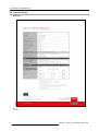


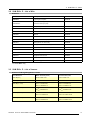


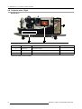


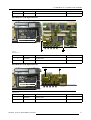
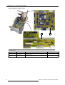


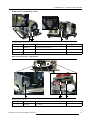
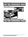
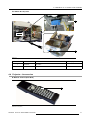


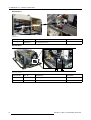


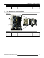

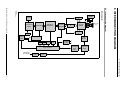
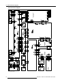
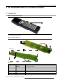


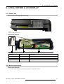

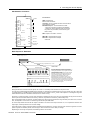

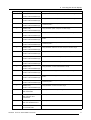

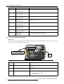
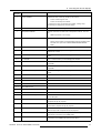

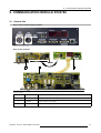
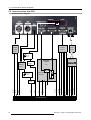


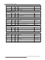


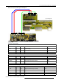
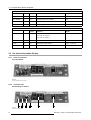
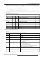
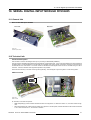
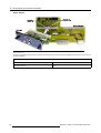
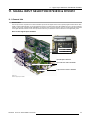
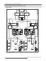


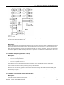
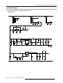
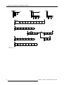

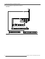
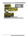


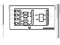


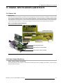


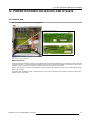
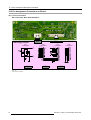
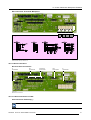
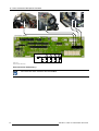

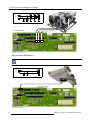
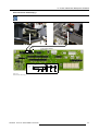
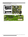

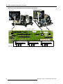
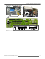

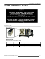

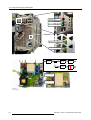
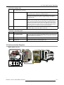
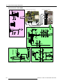
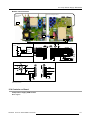

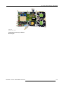
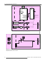
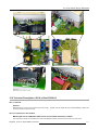

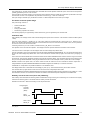


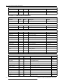
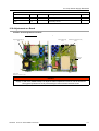

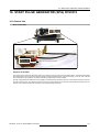
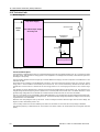
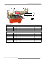

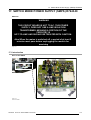

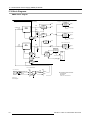


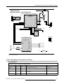
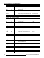

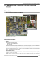


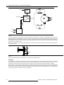
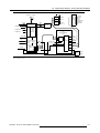
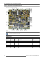


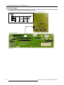

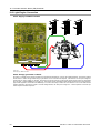


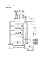
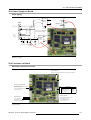

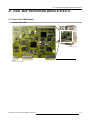
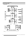
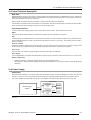
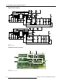
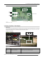


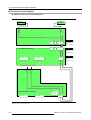
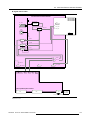


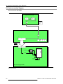
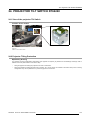
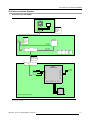

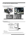
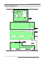


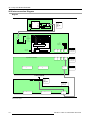


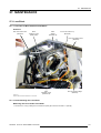

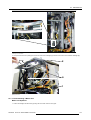

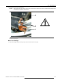

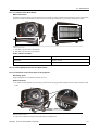
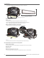
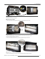
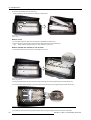
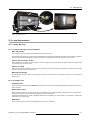
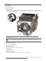
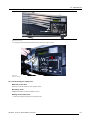
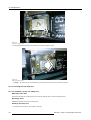

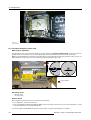

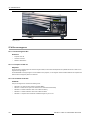
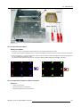
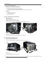

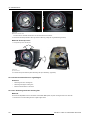
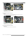
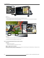

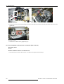

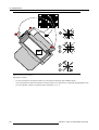
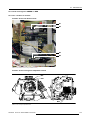
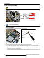
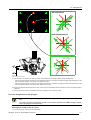
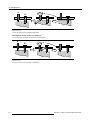

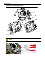
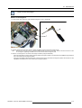
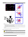
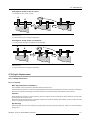
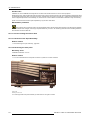
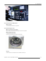

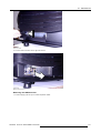
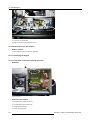

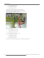

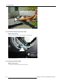
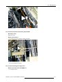
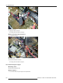
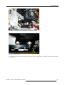

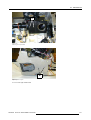

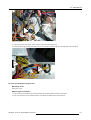
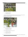


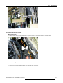


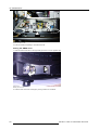
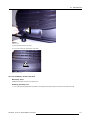


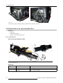
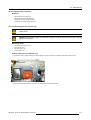
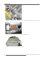

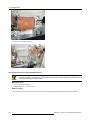

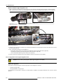
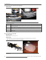
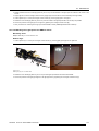


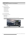
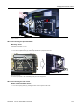
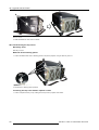
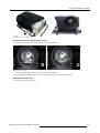

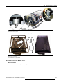

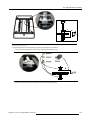

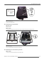
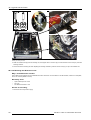
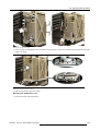

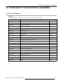


![SLM R12+ Performer [v05]](http://vs1.manualzilla.com/store/data/006296879_1-50504fc86d9979ae79ec928acfe3e08c-150x150.png)