1
APPLICATION NOTE
SAA4848/SAA4849 digital
deflection controller plus
microcontroller for CRT monitor
AN10281_1
Philips Semiconductors
TP97035.3/W97
TRAD
Philips Semiconductors
SAA4848/SAA4849 digital deflection controller
plus microcontroller for CRT monitor
Application Note
AN10281 1
Abstract
This application note describes the functioning of the Philips autosync SAA4848PS/SAA4849PS deflection controller plus
microcontroller. This application note also includes a pin-by-pin description of the device. Furthermore you will find some layout and
application proposals and also a functional comparison with the successful analog TDA4856.
Purchase of Philips I2C components conveys a
license under the I2C patent to use the
components in the I2C system, provided the
system conforms to the I2C specifications defined
by Philips.
© KONINKLIJKE PHILIPS ELECTRONICS N.V. 2004
All rights are reserved. Reproduction in whole or in part is prohibited without the prior written consent of the copyright owner.
The information presented in this document does not form part of any quotation or contract, is believed to be
accurate and reliable and may be changed without notice. No liability will be accepted by the publisher for any
consequence of its use. Publication thereof does not convey nor imply any license under patent- or other industrial or
intellectual property rights.
2
Philips Semiconductors
SAA4848/SAA4849 digital deflection controller
plus microcontroller for CRT monitor
Application Note
AN10281 1
APPLICATION NOTE
SAA4848/SAA4849 digital
deflection controller plus
microcontroller for CRT monitor
AN10281_1
Author(s):
Frank van Rens, Vedran Kovacevic
Philips Semiconductors
Competence Center Display Solutions
Eindhoven, The Netherlands
Keywords
autosync monitor
geometry control
CRT monitor
I2C-bus control
Deflection controller & Microcontroller
Number of pages: 88
Date: 2004-01-08
3
Philips Semiconductors
SAA4848/SAA4849 digital deflection controller
plus microcontroller for CRT monitor
Application Note
AN10281 1
Summary
In this application note the autosync CMOS deflection controller SAA4848PS/SAA4849PS is described. The
SAA4848/49 is intended for 17” to 19” CRT monitors. It provides a cost effective solution with integrated
microcontroller. The SAA4848/49 covers all the TDA4856 functionality except horizontal focus. Some new
geometry corrections are added:
• Horizontal s-wave
• Top and bottom corner balance
• Top bending
• Rotation balance
• Four 8-bit low interference DACs
Some additional features are added:
• Integrated soft start mechanism of the B+ voltage controller during startup and during mode changing
ensuring safe operation of the various deflections transistors and diodes.
• Integrated I2C -bus controller B+ voltage adjustment
• Under voltage detection
• I2C -bus controlled setting for separate horizontal EHT compensation and vertical EHT compensation for
combined deflection/EHT monitors.
The microcontroller features are:
• Standard 80c51 CPU core, 6-clock instruction cycle running at fixed 12MHz
• DDC2B, DDC2Bi, DDC2B+, DDC2AB protocol support
• 1x 8-bit PWM
• Three input 8-bit ADC
• 10mA sink port for LED application
• Power saving mode
• RAM 1024 byte
• SAA4848 embedded ROM 48k byte
• SAA4849 stacked FLASH 28k byte (in-system programming or parallel programming)
4
Philips Semiconductors
SAA4848/SAA4849 digital deflection controller
plus microcontroller for CRT monitor
Application Note
AN10281 1
CONTENTS
1
INTRODUCTION ...................................................................................................................9
1.1
Block diagram deflection controller .........................................................................................................................10
1.2
Block diagram microcontroller..................................................................................................................................10
1.3
On-chip interconnect of deflection controller and microcontroller ...................................................................11
1.4
Pin multiplexer block diagram...................................................................................................................................12
1.5
SAA4848/49 – TDA4856 comparison....................................................................................................................13
1.6
Geometry controls ......................................................................................................................................................14
2
FUNCTION DESCRIPTION AND APPLICATION .......................................................... 17
2.1
Deflection controller...................................................................................................................................................17
2.2
Microcontroller ............................................................................................................................................................19
2.3
Component placing and ground map.......................................................................................................................25
3
PIN APPLICATION...............................................................................................................26
3.1
Pin 1: P1.0.....................................................................................................................................................................26
3.2
Pin 2: P1.3/ I2C -SCL .................................................................................................................................................26
3.3
Pin 3: P1.4/ I2C -SDA ................................................................................................................................................26
3.4
Pin 4: P1.2/nINT0 ......................................................................................................................................................27
3.5
Pin 5: P2.6/DAC4/HSOUT .....................................................................................................................................28
3.6
Pin 6: P2.3/DAC3.......................................................................................................................................................29
3.7
Pin 7: HUNLOCK......................................................................................................................................................30
3.8
Pin 8: CLBL/VSOUT ................................................................................................................................................32
3.9
Pin 9: P0.3.....................................................................................................................................................................33
3.10
Pin 10: P0.2.......................................................................................................................................................33
3.11
Pin 11: P0.1.......................................................................................................................................................33
3.12
Pin 12: P0.0.......................................................................................................................................................34
3.13
Pin 13: P0.7.......................................................................................................................................................34
3.14
Pin 14: VSSE ....................................................................................................................................................34
3.15
Pin 15: VDDD .................................................................................................................................................35
3.16
Pin 16: V5V ......................................................................................................................................................35
3.17
Pin 17: VSSD – the star point ground..........................................................................................................35
3.18
Pin 18: BDRV ..................................................................................................................................................36
5
Philips Semiconductors
SAA4848/SAA4849 digital deflection controller
plus microcontroller for CRT monitor
Application Note
AN10281 1
3.19
Pin 19: HBGND..............................................................................................................................................36
3.20
Pin 20: HDRV..................................................................................................................................................37
3.21
Pin 21: HFB......................................................................................................................................................38
3.22
Pin 22: XRAY...................................................................................................................................................39
3.23
Pin 23: RST.......................................................................................................................................................39
3.24
Pin 24: VFOCUS .............................................................................................................................................40
3.25
Pin 25: P0.4.......................................................................................................................................................41
3.26
Pin 26: P2.1/DAC1.........................................................................................................................................42
3.27
Pin 27: P2.5/ADC2.........................................................................................................................................42
3.28
Pin 28: P2.0/ADC1.........................................................................................................................................43
3.29
Pin 29: P2.7/LED ...........................................................................................................................................43
3.30
Pin 30: UVOLT ...............................................................................................................................................44
3.31
Pin 31: P2.2/DAC2.........................................................................................................................................45
3.32
Pin 32: EHT .....................................................................................................................................................46
3.33
Pin 33: VOUT1................................................................................................................................................50
3.34
Pin 34: VOUT2................................................................................................................................................51
3.35
Pin 35: EWDRV ..............................................................................................................................................52
3.36
Pin 36: IREF.....................................................................................................................................................54
3.37
Pin 37: VREF ...................................................................................................................................................54
3.38
Pin 38: AGND .................................................................................................................................................54
3.39
Pin 39: BSENS .................................................................................................................................................55
3.40
Pin 40: BIN.......................................................................................................................................................57
3.41
Pin 41: BOP......................................................................................................................................................57
3.42
Pin 42: VSSA ....................................................................................................................................................58
3.43
Pin 43: VDDA .................................................................................................................................................58
3.44
Pin 44: MODE.................................................................................................................................................58
3.45
Pin 45: XTAL1.................................................................................................................................................59
3.46
Pin 46: XTAL2.................................................................................................................................................59
3.47
Pin 47: ROT .....................................................................................................................................................60
3.48
Pin 48: P2.4/ADC0.........................................................................................................................................61
3.49
Pin 49: P1.5/T1/PWM/VSOUT..................................................................................................................61
3.50
Pin 50: P0.5/HSOUT .....................................................................................................................................62
3.51
Pin 51: P0.6.......................................................................................................................................................62
3.52
Pin 52: HSYNC................................................................................................................................................63
6
Philips Semiconductors
SAA4848/SAA4849 digital deflection controller
plus microcontroller for CRT monitor
Application Note
AN10281 1
3.53
Pin 53: VSYNC ................................................................................................................................................63
3.54
Pin 54: P1.6/DDC-CLK ................................................................................................................................64
3.55
Pin 55: P1.7/DDC-SDA ................................................................................................................................64
3.56
Pin 56: P1.1/T0................................................................................................................................................64
4
ALIGNMENT.........................................................................................................................65
4.1
Vertical geometry.........................................................................................................................................................65
4.2
Horizontal geometry ...................................................................................................................................................66
4.3
Software limits for geometry controls......................................................................................................................68
I2C -BUS CONTROL ..............................................................................................................69
5
5.1
I2C register types..........................................................................................................................................................69
5.2
WOR register example values....................................................................................................................................69
6
DEVELOPMENT TOOLS ....................................................................................................75
6.1
Programming tool ISP................................................................................................................................................75
6.2
DEMIC I2C & SFR control software.......................................................................................................................77
6.3
I2C tools program ........................................................................................................................................................81
6.4
Emulator for SW debugging......................................................................................................................................83
7
LIST OF ABBREVIATIONS .................................................................................................84
8
LIST OF FIGURES.................................................................................................................85
9
REFERENCES .......................................................................................................................87
9.1
Datasheets.....................................................................................................................................................................87
9.2
Application notes.........................................................................................................................................................87
9.3
Web references.............................................................................................................................................................87
9.4
Software for PC ...........................................................................................................................................................87
7
Philips Semiconductors
SAA4848/SAA4849 digital deflection controller
plus microcontroller for CRT monitor
8
Application Note
AN10281 1
Philips Semiconductors
SAA4848/SAA4849 digital deflection controller
plus microcontroller for CRT monitor
1
Application Note
AN10281 1
INTRODUCTION
The SAA4848 (ROM version) and the SAA4849 (FLASH version) are very cost effective CMOS deflection
controllers with integrated 80c51 CPU and extra port functionality like DDC, timers, ADC, PWM. The deflection
controller and microcontroller are combined into one SDIP56 package.
Performance improvements:
• DAC instead of PWM to reduce noise
Cost effective implementation:
• I2C register readout in period versus frequency is cheaper because divider function of CPU can be used to
generate frequency.
• Horizontal focus is not implemented because most CRT monitor manufacturers use horizontal focus
transformer instead of dynamic focus amplifier.
• In case of combined deflection/EHT the HV adjustment can be done via I2C register h20.
• Three ADC inputs that are multiplexed to only one ADC.
• LED driver output saving 1 external transistor.
The SAA4848/49 microcontroller contains 49 special function registers.
The SAA4848/49 deflection controller contains 94 I2C registers.
9
Philips Semiconductors
SAA4848/SAA4849 digital deflection controller
plus microcontroller for CRT monitor
1.1
Application Note
AN10281 1
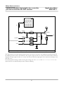
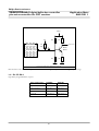
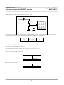
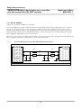
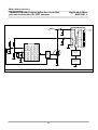
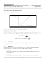
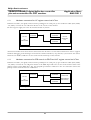
Block diagram deflection controller
DAC1
HSYNC/CSYNC
Sync
Watch
VSYNC
Four 8 bit DACs
DAC2
DAC3
DAC4
ROTATION
Sync
Processor
HSOUT
EWDRIVE
VOUT1,VOUT2
VSOUT
Geometrics
VFOCUS
EHT
VBLANK
48MHz
Osc
VDDA
Analog supply
regulator
HDRIVE
VSSA
Horizontal PLL
VDDD
HUNLOCK
CLAMP300ns,CLAMP700ns
HFLB
Digital supply
regulator
V5V
BDRIVE
VSSD
VREF
IREF
BOP
B+
Control
Bias
BIN
I2C
AGND
XRAY
BSENS
State
Control
UVOLT
I2C-CLK
I2C-Bus
Tranceiver
I2C-SDA
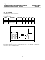
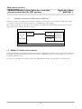
Figure 1 Block diagram deflection
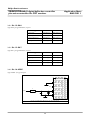
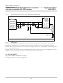
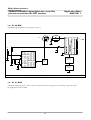
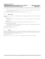
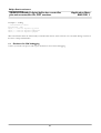
1.2
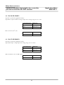
Block diagram microcontroller
Interrupt
Control
48k x 8
ROM
1024 x 8
RAM
Timer 1
Timer 0
Three channel
8 bit ADC
Internal microcontroller bus
CPU
80c51
12MHz/750kHz
DDC
SERIAL I/O
Three 8 bit I/O Ports
P0
P1
P2
DDC
CLK
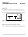
Figure 2 Block diagram microcontroller
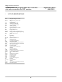
10
DDC
SDA
PWM
PWM
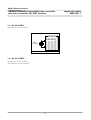
DEFLECTION
CONTROLLER
Reset from
pin 23
CPU
80c51
12MHz/750kHz
Reset
algorithm
Reset from
deflection
controller
Watch dog timer
11
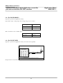
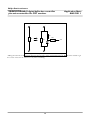
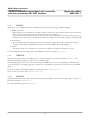
Figure 3 On-chip interconnect between deflection and microcontroller
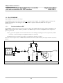
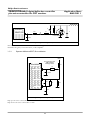
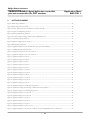
State
Control
I2C
power save
VBLANK
wakeup
interrupt
I2C-Bus
Tranceiver
B+
Control
Horizontal PLL
Geometrics
Four 8 bit DACs
DDC
interrupt
Timer 0
Timer 1
DDC
I2C-CLK I2C-SDA
Port 1
SAA4848/SAA4849 digital deflection controller
plus microcontroller for CRT monitor
Bias
Digital supply
regulator
Analog supply
regulator
Osc
Sync
Processor
Sync
Watch
Mode change
interrupt
Interrupt
Control
1.3
MICRO
CONTROLLER
Philips Semiconductors
Application Note
AN10281 1
On-chip interconnect of deflection controller and microcontroller
Philips Semiconductors
SAA4848/SAA4849 digital deflection controller
plus microcontroller for CRT monitor
1.4
Application Note
AN10281 1
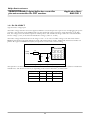
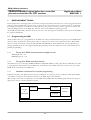
Pin multiplexer block diagram
HSOUT
P2.6
P1.5/T1
Pin 5
SFR hAE[6:7]
PWM
DAC4
P2.5
ADC2
VSOUT
Pin 27
SFR hAE[5]
P0.5
HSOUT
P2.4
ADC0
Pin 49
SFR h9E[1:0]
Pin 50
SFR h8E[0]
Pin 48
SFR hAE[4]
CLAMP300ns
P2.3
DAC4
CLAMP700ns
Pin 6
SFR hAE[3]
VBLANK
PROTECTIONBLANK
P2.2
DAC2
P2.1
DAC1
Pin 31
SFR hAE[2]
HUNLOCK(for blanking)
VSOUT
Clamp level = 5.0V
Blank level = 1.8V
Pin 26
SFR hAE[1]
PROTECTIONBLANK
P2.0
ADC1
Pin 8
“CLBL/VSOUT”
I2C-REG h0C
HUNLOCK
Pin 28
SFR hAE[0]
VBLANK
Pin 7
“HUNLOCK”
I2C-REG h0D
Different from TDA-type,
blanking level is 5V
Figure 4 All port 2.X multiplexing functions
Figure 5 Remaining multiplexing functions
12
Philips Semiconductors
SAA4848/SAA4849 digital deflection controller
plus microcontroller for CRT monitor
1.5
Application Note
AN10281 1
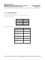
SAA4848/49 – TDA4856 comparison
Function
Geometry
Focus
BDRV control
HDRV control
Rotation
Other
TDA4856
SAA4848
S-wave
No
Yes
S-wave balance
No
Yes
Top corner balance
No
Yes
Bottom corner balance
No
Yes
ASCOR
Yes
No
Vertical focus
Yes
Yes
Horizontal focus
Yes
No
Reduced B+ during horizontal unlock
External
Automatic
Reference voltage of positive OTA input
Fixed: 2.5V
I2C: 2.32~2.5V
BDRV polarity
Fixed
I2C: pos/neg
Soft start
No/Exteral
I2C: internal
BDRV triggered by HDRV edge
Fixed
I2C: pos/neg
Minimum frequency
15kHz
25kHz
Maximum frequency
130kHz
140kHz
Frequency setting
Resistors+capacitos
I2C /Crystal
Slewing speed
Fixed
I2C
HDRV start up duty cycle
Fixed
I2C
HDRV duty cycle as function of frequency
Fixed
I2C
Rotation
No
I2C: current DAC
NS trapezium
No
I2C: current DAC
Free running frequency
Lowest/minimum
I2C
Supply voltage
12V
5V
Horizontal unlock indication
Interrupt
I2C/Interrupt
Sync on green
Yes
No
Moiré range
Fixed
I 2C
Hardware mode detector
No
Yes
Maximum vertical frequency
160Hz
200Hz
Vertical current outputs configuration
Sink
I2C: Sink or source
EHT regulation gain
Fixed
I2C
TV/VCR mode
Yes
No
Interlaced mode supported
No
No
13
Philips Semiconductors
SAA4848/SAA4849 digital deflection controller
plus microcontroller for CRT monitor
1.6
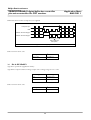
Geometry controls
Description
On screen effect
Vertical linearity
Vertical linearity balance
Horizontal trapezium
Horizontal parallelogram
Horizontal pincushion
Horizontal pincushion balance
14
Application Note
AN10281 1
Philips Semiconductors
SAA4848/SAA4849 digital deflection controller
plus microcontroller for CRT monitor
Horizontal s-wave
Horizontal s-wave balance
Horizontal corner top
Horizontal corner top balance
Horizontal corner bottom
Horizontal corner bottom balance
15
Application Note
AN10281 1
Philips Semiconductors
SAA4848/SAA4849 digital deflection controller
plus microcontroller for CRT monitor
Rotation
Rotation balance (NS trapezium)
16
Application Note
AN10281 1
Philips Semiconductors
SAA4848/SAA4849 digital deflection controller
plus microcontroller for CRT monitor
2
Application Note
AN10281 1
FUNCTION DESCRIPTION AND APPLICATION
This chapter describes the general functions and the system application. The more specific pin application is
described in chapter 3. First the deflection controller part is described and secondly the microcontroller part is
described.
2.1
Deflection controller
The CMOS75 shrink process technology is used for the SAA484x. There are some changes to the bipolar TDA4856
deflection controller. The changes are:
SAA
TDA
Supply voltage
5V
12V
Horizontal & vertical oscillator
locking
Digital, no external components
Analog, external components
Waveform generation
Digital plus current output DACs
Analog
Mode change
Deflection controller wait for slew command of
microcontroller
Deflection controller give mode change interrupt
and slews immediately
Startup timing
Timing via I2C
Fixed by external components
The supply voltage reduction has effect on the HDRV and BDRV outputs since the TDA application uses a pull up
resistor to the +12V supply. The SAA needs an extra external buffer transistor to generate the 12V output swing.
Furthermore there are current outputs used for the vertical drive, vertical focus and the east-west drive output. The
EHT input is in the SAA a current input with a fixed voltage of 2.5 volts.
The digital implementations of the HPLL and vertical oscillator do not require external components. This saves
quite some resistors and capacitors that where connected to the TDA4856 pins: HPLL1, HBUF, HREF, HCAP, HPLL2,
VREF, VCAP, VAGC. But it is not correct to count VREF and VAGC since the SAA needs this resistor and capacitor for
reference on the pins IREF and VREF.
The waveform generation is more flexible in the SAA because it is implemented digitally and more controls are
implemented. For example, the polarity of most waveforms can be selected by I2C.
The new HPLL implementation ensures a safer mode change. After a HSYNC frequency change, the SAA HDRV
output frequency does not change before the microcontroller allows the SAA to slew. This new control allows the
microcontroller to always switch the linearity capacitors to safe and then perform a slew operation. Furthermore, the
deflection voltage is reduced during the slewing.
The start up timing of the BDRV duty cycle can be set by I2C. The TDA application mostly used a big capacitor to
the BOP that was switched “on” during start up and after start up the microcontroller switched the capacitor to
“floating” to get a fast B+ control loop. With the SAA, no additional big external capacitor is needed and also no
switching transistor circuit.
17
Philips Semiconductors
SAA4848/SAA4849 digital deflection controller
plus microcontroller for CRT monitor
2.1.1
Application Note
AN10281 1
Deflection start-up and shutdown procedure
This paragraph describes the start up behaviour of the GEO, HPLL and BPLUS block. For the embedded software
this is not of any interest because the start up controlled internally by hardware. The reason why it is described in
this application note is because this part is not included in the datasheet. The GEO block generates the vertical
output current, the HPLL block generates the HDRV output and the BPLUS block generates the BDRV output.
When sending the I2C command, request output signals to all blocks (H8C,HE2,H13) the blocks are not switch on
immediately. First, only when the reference voltage (VREF) is stable, the GEO block will start. When the GEO block
output signals are stable the output signal stable (OSS) bit of the GEO block is set. You can think of this as an
athletics relay race where the runners handle over their stick to the next runner. When the GEO OSS bit is set the
HPLL block start up. The HDRV duty cycle will ramp up from the programmed starting value. When the duty
reaches the specified duty cycle for the actual frequency, the OSS bit of the HPLL block is set. This will start the
BPLUS block to start. The BDRV duty cycle ramps up according the specified (as programmed by I2C) start up
time. At end of the start up time, the BPLUS control loop is closed and the OSS bit of the BPLUS block is set. The
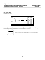
timing is shown in Figure 6 Start up & shutdown timing of GEO, HPLL and BPLUS block.
Vref
oss
oss
geo
ose
oss
hpll
bplus
ose
osr
hE2[0]
ose
osr
hE2[1]
osr
hE2[2]
osr_geo
osr_geo
osr_hpll
osr_hpll
osr_bplus
osr_bplus
ose_geo
oss_bplus
oss_geo
ose_bplus
ose_hpll
oss_hpll
oss_hpll
ose_hpll
ose_bplus
oss_geo
oss_bplus
ose_geo
start up procedure
shut down procedure
Figure 6 Start up & shutdown timing of GEO, HPLL and BPLUS block.
osr = output signal request (command, request block to switch on)
ose = output signal enabled (status, output signals present)
oss = output signal stable (status, output signals present and stable)
In case of shut down, the output signal enabled (OSE) bit is used allow the next block to switch off.
18
Philips Semiconductors
SAA4848/SAA4849 digital deflection controller
plus microcontroller for CRT monitor
Application Note
AN10281 1
Microcontroller
2.2
The basic microcontroller features are:
• Standard 80c51 CPU core (refer to IC20 80C51-Based 8-Bit Microcontrollers), 6-clock instruction cycle
running at fixed 12MHz
• DDC protocol support
• Watch-dog timer
• 24 I/O ports with alternative functions
• 1x 8-bit PWM
• Three input 8-bit ADC
• An external and six dedicated internal interrupts
• 10mA sink port for LED application
• Power saving modes
• RAM 1024 bytes
• SAA4848 embedded ROM 48k byte
• SAA4849 stacked FLASH 48k byte
NOTE: In all following examples, the written code is in C and according Keil’s compiler.
2.2.1
RESET
There are three different reset conditions:
• Power On Reset (POR) circuit;
• Reset signal generated by deflection in case of reset of the deflection part (only uC part);
• Watchdog reset (only uC part).
The POR and watchdog reset are standard C51 resets (refer to IC20 80C51-Based 8-Bit Microcontrollers) and the
reset generated by deflection part is specific for this IC. Its function is to synchronise the uC and deflection part of
the IC.
2.2.2
DDC
The DDC interface is fully based on the standard Philips I2C module with an additional second slave address. There
are various application notes on how to use this module in the book: “Application Notes and Development Tools
for 80C51”.
To get just a short intro in this matter, you can look at the skeleton of the following interrupt routine written in C
(used Keil compiler). It is fully based on the status register S1STA (SFR register at D9h), which tells us what was the
cause of the active interrupt:
19
Philips Semiconductors
SAA4848/SAA4849 digital deflection controller
plus microcontroller for CRT monitor
Application Note
AN10281 1
//SR-Slave Receiver; ST-Slave Transmitter
void DDC_Interrupt(void) interrupt DDC_INT_NO using 1
{
switch (S1STA)
{
//application code for slave receiver mode, e.g.
case SR_ADDR_ACK:
// SR_ADDR_ACK=0x60: Slave Address has been received with ACK
counter=0;
address=S1DAT;
break;
case SR_DATA_ACK:
// SR_DATA_ACK =0x80: DATA has been received,
// ACK returned application code, e.g.
buffer[counter++]=S1DAT;
break;
case SR_STOP_RECEIVE: // SR_STOP_RECEIVE =0xA0:
// STOP or repeated START condition received application code;
break;
//application code for slave transmitter mode, e.g.
case ST_ADDR_ACK:
// ST_ADDR_ACK=0xA8: Slave Address has been received with ACK
counter=0;
S1DAT=buffer[counter++];
break;
case ST_DATA_ACK:
// ST_DATA_ACK =0xB8: Data has been transmitted with ACK
S1DAT=buffer[counter++];
break;
case ST_DATA_NOACK:
counter=0;
break;
}
AA=1;
// ST_DATA_NOACK=0xC0: Data has been transmitted with NO ACK received
//set flag of S1CON1 register (SFR at 0xD8) to enable the generating of an acknowledge
}
2.2.3
RAM memory
The internal data memory is divided into three physically separated parts:
• 256 standard C51 RAM location (0-255);
• 128 bytes Special function registers (SFRs, 127-255);
• 768 of AUX-RAM locations (0-765).
These registers could be addressed in different ways:
• RAM 0 to 127 can be addressed directly (“data” type in Keil C compiler syntax) and indirectly (“idata” type in
Keil C compiler syntax) as in the standard C51. Address pointers are R0 and R1 of the selected register
bank;
• RAM 128 to 255 can be addressed indirectly (“idata” type in Keil C compiler syntax) as in the standard C51.
Address pointers are R0 and R1 of the selected register bank;
• SFR can be addressed directly (“SFR” type in Keil C compiler syntax);
• AUX-RAM is indirectly addressable via page register (XRAMP) and MOVX-Ri instruction. XRAMP page
register contains higher byte of the address and Ri register lower byte of the address. This way of addressing
20
Philips Semiconductors
SAA4848/SAA4849 digital deflection controller
plus microcontroller for CRT monitor
Application Note
AN10281 1
is well known as a paging (“pdata” type in Keil C compiler syntax). It should be mentioned that the first
version of the emulator doesn’t support the paging, while it works in the IC.
• AUX-RAM is indirectly addressable via MOVX-DPTR instruction, as well (“xdata” type in Keil C compiler
syntax).
2.2.4
Power save modes
There are 2 modes of CPU core, which are meant for the saving of power. The first one is the standard C51 IDLE
mode, which can be enabled by setting of the flag IDLE of the PCON register (0x87). This will stop CPU
execution, while all peripherals will remain active. Any activated interrupt will resume activity of the CPU.
The other mode is the Power Save mode of the deflection part. In this mode, the CPU speed is reduced from
12MHz to 750kHz, which dramatically reduce the power consumption. Before entering this state, it is necessary to
configure the waking up conditions. After waking up, there are two possibilities to detect that the IC is not in the
Power Save mode. The first is by using of the waking-up interrupt and the other one is by polling in the main
routine weather the deflection is back in the IDLE state. The following code is an example of the waking up
implementation by the polling:
WAKEUPCONF (I2C address 0xE0)=0x50;//interrupt not enabled, waking up conditions
//VSYNC>10Hz, HSYNC>10KHz
POWERCTRL (I2C address 0xE1)=0x5A;//DDC perform wake up, IC to power save mode.
After this initialisation, the IC is in the Power Save mode, and now it should be performed polling to figure out the
moment when the IC is back woken up:
void main()
{
…
if (SY_STATUS==IDLE_STATE){ … the IC is woken up … }
…
}
2.2.5
Pin configuration
The pin configuration is simple and straightforward.
In case of port 0 (P0, SFR register at 0x80) there is only alternative function on the pin P0.5. With SFR register
P0SEL (0x8E) is possible to configure this pin as a simple I/O or as horizontal sync output. Furthermore, it is
possible to select different I/O pins configurations by P0CFGA (SFR at 0x84) and P0CFGB (SFR at 0x85)
registers. In case if it’s kept the reset value (“0”), the P0 is configured as an open drain port. Noticed that P0 pins, in
case of the emulator, are controlled by other registers, which are EPORT0 (0xB0), EP0CFGA (0xB4) and
EP0CFGB (0xB5). For easier developing of the code, it is necessary to have the conditional compiling which will
distinguish those 2 cases (IC and emulator), like following:
/********* port 0 ***********/
SFR P0_C=0x80;
SFR P0CFGA_C=0x84;
SFR P0CFGB_C=0x85;
/***********
SFR
SFR
SFR
/********** port 0 bits *********/
sbit P0_7_C =0x87;
sbit P0_6_C= 0x86;
sbit P0_5_C= 0x85;
sbit P0_4_C=0x84;
sbit P0_3_C=0x83;
/********* emulator port 0 bits *********/
sbit EP0_7_C=0xB7;
sbit EP0_6_C= 0xB6;
sbit EP0_5_C= 0xB5;
sbit EP0_4_C=0xB4;
sbit EP0_3_C=0xB3;
21
emulator port 0 ***********/
EP0_C=0xB0;
EP0CFGA_C=0xB4;
EP0CFGB_C =0xB5;
Philips Semiconductors
SAA4848/SAA4849 digital deflection controller
plus microcontroller for CRT monitor
sbit
sbit
sbit
P0_2_C=0x82;
P0_1_C=0x81;
P0_0_C=0x80;
#ifdef EMULATOR
#define
#define
#define
#define
#define
#define
#define
#define
#define
#define
#define
#else
#define
#define
#define
#define
#define
#define
#define
#define
#define
#define
#define
#endif
Application Note
AN10281 1
sbit EP0_2_C=0xB2;
sbit EP0_1_C=0xB1;
sbit EP0_0_C=0xB0;
P0
P0_7
P0_6
P0_5
P0_4
P0_3
P0_2
P0_1
P0_0
P0CFGA
P0CFGB
EP0_C
EP0_7_C
EP0_6_C
EP0_5_C
EP0_4_C
EP0_3_C
EP0_2_C
EP0_1_C
EP0_0_C
EP0CFGA_C
EP0CFGB_C
P0
P0_7
P0_6
P0_5
P0_4
P0_3
P0_2
P0_1
P0_0
P0CFGA
P0CFGB
P0_C
P0_7_C
P0_6_C
P0_5_C
P0_4_C
P0_3_C
P0_2_C
P0_1_C
P0_0_C
P0CFGA_C
P0CFGB_C
The port 1 (P1, 0x90) has also the alternative functions on pin P1.5, which are: PWM and vertical sync output
(VSOUT). This is configurable by register P1SEL (0x9E). Some pins have the standard alternative functions derived
directly from the C51 core (timer inputs, external interrupt).
And the last port of this IC is port 2 (P2, at 0xA0). To be able to properly work with this port, it is necessary to set
P2CTRL register (0xAF) to “1”. Additionally, as all pins of this port have some alternative functions, it is must to
make a selection of those functions by configuring the SFR register P2SEL (0xAE).
ADC
2.2.6
A typical use of the ADC is as a keypad. In order to perform an ADC conversion it should be done the following,
respectively:
1.
Wait until the previous conversion is finished;
2.
Select a channel;
3.
Start the conversion;
4.
Wait until the conversion is finished (busy flag “0”);
5.
Read the result from the associated register to the selected channel;
Here is an example code of a general ADC conversion routine written in C, which has as an input parameter the
channel to select and as a return parameter the result of the conversion:
BYTE ReadADC(BYTE bChannelNO)
{
ADCCON = bChannelNO;
//select a channel
Wait10uS;
//wait that the voltage level is stable on the ADC input (after mux)
ADCCON |=0x01;
//start conversion
22
Philips Semiconductors
SAA4848/SAA4849 digital deflection controller
plus microcontroller for CRT monitor
while(ADCCON&0x02){}
switch(bChannelNO)
{
case ADC_0:
return ADATA0;
case ADC_1:
return ADATA1;
case ADC_2:
return ADATA2;
case ADC_VREFH:
return AVREFH;
case ADC_VREFL:
return AVREFL;
}
Application Note
AN10281 1
//wait busy flag
//return the result of the conversion
}
2.2.7
Mode change interrupt
Since the HWMD is based in the deflection part and like that only accessible by the I2C bus, the mode change
procedure was possible only by polling of I2C bus registers. In order to speed up the mode change detection, the
mode change interrupt has been introduced. The source code could look as following:
void pMOD_initModeChangeInterrupt()
{
ReadDeflection I2C address(V_MODE_CHANGE(=0x82)); //it should be done in order to delete the
ReadDeflection I2C address(H_MODE_CHANGE(=0x4A));//interrupt request which is always set after
//the POR of the IC
//In case we omit the above lines, this can be the mode change interrupt for the start-up procedure
EMC=TRUE; // enable mode change interrupt
EA=TRUE;
// general enable of interrupts
}
void pMOD_ModeChangeInterrupt(void) interrupt 6 using 1
{
dMOD_SetSafeSCapacitor();
//set S-caps to safe state
PROTECTION_BLANK=TRUE;
//mute the screen
EMC=FALSE;
// disable mode change interrupt, till the source is not cleared
tsk_signal(pMOD_ModeChangeMonitoringTask); //signalisation of the task which should continue with the
//mode change procedure (I2C communication, …)
}
void pMOD_ModeChangeMonitoringTask(void) // task triggered
{
ReadDeflection I2C address(V_MODE_CHANGE(=0x82)); //clear
ReadDeflection I2C address(H_MODE_CHANGE(=0x4A)); //clear
//the POR
EMC=TRUE;
// enable
}
by the mode change interrupt
the source of the interrupt
the source of the interrupt
of the IC
mode change interrupt again
NOTE: It should be taken care of the fact that the switching from the locking to the free-running mode and vice-verse of the vertical part
generates the interrupt as well.
2.2.8
Flash (re-) programming
In order to perform (re)-programming of the flash memory by ISP (In-System Programming), it is necessary to
enter the BOOT ROM mode. This mode can be entered by the fixed voltage combination on the pins MODE
(=5V) and HBGND (=2V) during The Power-On Reset (POR) or directly from the application mode by setting the
FLCTRL register (0xC0) to the value 0x03. In case this is performed directly from the application, the application
itself must switch the IC to the IDLE mode and than switch to the BOOT ROM mode, since during this switching
23
Philips Semiconductors
SAA4848/SAA4849 digital deflection controller
plus microcontroller for CRT monitor
Application Note
AN10281 1
the reset is performed. The routine in the application for this switching to the BOOT MODE can be activated by
DDC command.
In this mode, the CPU fetches instructions from the special memory, where are stored routines for the FLASH (re-)
programming by DDC (I2C) bus. The PC application called “ISP—DEMIC-Customer” should be used to perform
this programming. Once programming is finished, the IC must switch back to application mode. This can be done
again in two ways: by fixed voltage combination during the POR on pins MODE (=GND) and HBGND (=GND)
or by using the button in the PC application to switch back to the application mode (button called “Cancel boot
mode”).
24
Philips Semiconductors
SAA4848/SAA4849 digital deflection controller
plus microcontroller for CRT monitor
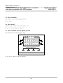
2.3
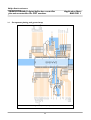
Component placing and ground map
Figure 7 Components placing and layout.
25
Application Note
AN10281 1
Philips Semiconductors
SAA4848/SAA4849 digital deflection controller
plus microcontroller for CRT monitor
3
PIN APPLICATION
3.1
Pin 1: P1.0
Application Note
AN10281 1
Type P1.0: open drain (application mode) with internal pull up resistor
3.2
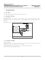
Pin 2: P1.3/ I2C -SCL
Type P1.3: open drain
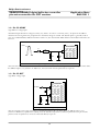
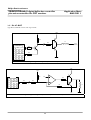
This pin must be used as I2C -SCL since it is on chip connected to the I2C -SCL line of the deflection controller. A
pull-up resistor needed to +5V, value must be 2.2k ~ 4.7k Ohm, depending on I2C specification of all devices on
the I2C -bus.
ESD/EMC protection needed: 100-ohm series resistor and 100pF filter cap from pin to ground.
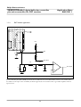
+5V
2.2k
SAA4848
2.2k
100
I2C_SCL = pin 2
I2C_SCL
100
I2C_SDA = pin 3
I2C_SDA
2x 100pF
I/O GND
Figure 8 Application diagram of pin 2 & pin 3
3.3
Pin 3: P1.4/ I2C -SDA
Type P1.4: open drain
This pin must be used as I2C -SDA since it is on chip connected to the I2C -SDA line of the deflection controller. A
pull-up resistor needed to +5V, value must be 2.2k ~ 4.7k Ohm.
Kind of ESD/EMC protection: 100-ohm series resistor and filter cap from pin to ground.
See Pin 2: P1.3/ I2C -SCL for application diagram.
26
Philips Semiconductors
SAA4848/SAA4849 digital deflection controller
plus microcontroller for CRT monitor
3.4
Pin 4: P1.2/nINT0
Type P1.2: open drain (application mode)
This pin can be used as input for an external interrupt signal.
27
Application Note
AN10281 1
Philips Semiconductors
SAA4848/SAA4849 digital deflection controller
plus microcontroller for CRT monitor
3.5
Pin 5: P2.6/DAC4/HSOUT
Type P2.6: open drain (application mode)
Type DAC4 output: buffered voltage output with a voltage range of 0 to 5 volts.
Type HSOUT: push pull output
Pin Configuration
SFR setting
P2.6
SFR hAE[7:6]=00
DAC4
SFR hAE[7:6]=01
HSOUT
SFR hAE[7:6]=10
HSOUT
SFR hAE[7:6]=11
HSOUT synchronisation behaviour for different HSYNC situations
Configuration
HSOUT locked to
HPLL not free running
25kHz<HSYNC<140kHz
HSYNC
HPLL not free running
No HSYNC input
No signal
HPLL not free running
HSYNC<25kHz
HSYNC>140kHz
HSYNC
HPLL Free running mode
25kHz<HSYNC<140kHz
HFB
HPLL Free running mode
No HSYNC input
HFB
HPLL Free running mode
HSYNC<25kHz
HSYNC>140kHz
HFB
28
Application Note
AN10281 1
Philips Semiconductors
SAA4848/SAA4849 digital deflection controller
plus microcontroller for CRT monitor
HSOUT behaviour when composite sync supplied
Composite sync
HFB
HSOUT with I2C h0F[3]=0
HSOUT with I2C h0F[3]=1
Gap is filled with
HFB pulses
Figure 9 HSVSOUT[3] explanation
DAC4 control via I2C -bus
3.6
Description
I2C address
DAC4 value
I2C hEB[7:0]
Pin 6: P2.3/DAC3
Type P2.3: open drain (application mode)
Type DAC3 output: buffered voltage output with a voltage range of 0 to 5 volts.
Pin Configuration
SFR setting
P2.3
SFR hAE[3]=0
DAC3
SFR hAE[3]=1
Description
I2C address
DAC3 value
I2C hEA
DAC3 control via I2C -bus
29
Application Note
AN10281 1
Philips Semiconductors
SAA4848/SAA4849 digital deflection controller
plus microcontroller for CRT monitor
3.7
Application Note
AN10281 1
Pin 7: HUNLOCK
Type HUNLOCK: push pull
The 1-volt blanking signal referenced to ground that was implemented in the TDA type deflection controllers is not
present in the SAA4848/49. SAA only has the 5 volt TTL levels available on the HUNLOCK pin.
Pin Configuration
WOR I2C setting
Vertical blanking as 5V pulse
WOR h0D[3]
HPLL unlock
WOR h0D[2:1]=10
HPLL unlock with overrule control
WOR h0D[2:1]=01
No HPLL unlock
WOR h0D[2:1]=00
Not allowed
WOR h0D[2:1]=11
Protection blank
WOR h0D[0]
30
Philips Semiconductors
SAA4848/SAA4849 digital deflection controller
plus microcontroller for CRT monitor
Application Note
AN10281 1
SAA4848
HUNLOCK = pin 7
100
GND
1n4148
10k
MPSA92
+
10uF
Vg1
1n4148
Vg1Blank
GND
10k
1.8M
82k
1n4148
10k
byd33g
100
VerticalDeflectionAbsent
-185V
47uF
+
GND
Figure 10 Application diagram of pin HUNLOCK for grid 1 protection blanking
The 10µF capacitor provides blanking during switch-off/switch-on situations. The blanking with HUNLOCK has
fast blanking and slow release characteristics. The negative supply (in this case–185V) must remain until the HV has
dropped; the 47µF capacitor takes care of that. No electrons will hit the phosphor in the CRT and no damage to the
CRT will occur.
In normal operation during vertical scan the grid1 voltage is 0 volts. Vg1Blank and VerticalDeflectionAbsent are
optional because the HUNLOCK provides sufficient blanking.
31
Philips Semiconductors
SAA4848/SAA4849 digital deflection controller
plus microcontroller for CRT monitor
3.8
Application Note
AN10281 1
Pin 8: CLBL/VSOUT
Type CLBL/VSOUT: push pull
Pin Configuration
WOR I2C setting
CL300ns
WOR h0C[6:5]=10
CL700ns
WOR h0C[6:5]=01
Not allowed
WOR h0C[6:5]=11
No clamping
WOR h0C[6:5]=00
VSOUT as 5V pulse
WOR h0C[4]
Vertical blanking as 1.8V pulse
WOR h0C[3]
HPLL unlock
WOR h0C[2:1]=10
HPLL unlock with overrule control
WOR h0C[2:1]=01
No HPLL unlock
WOR h0C[2:1]=00
Not allowed
WOR h0C[2:1]=11
Protection blank
WOR h0C[0]
The signal VSOUT is configured with I2C register VSHSOUTCONF. This configuration is valid for both VSOUT
pins (pin 8 and pin 49). The polarity can be set with VSHSOUTCONF[1], this polarity setting is also valid when
VBLANK is set with VSHSOUTCONF[2].
I2C register VSHSOUTCONF address is h0F.
VSYNC
Mux
I2C h0F[2]
Polarity
I2C h0F[1]
VBLANK
VSYNC
VBLANK
VBLSTART
I2C h84
VBLDUR
I2C hA6
Figure 11 VSHSOUTCONF[2:1] explanation
32
VSOUT
Philips Semiconductors
SAA4848/SAA4849 digital deflection controller
plus microcontroller for CRT monitor
Application Note
AN10281 1
Note:
The clamping signal should only be used for clamping of the video signal. The clamping signal cannot be used to
synchronise the OSD generator or to synchronise the SMPS in case of “sync out of range” OSD message (freerunning and vertical and/or horizontal sync out of range). During “sync out of range” condition the clamping is not
locked with the horizontal flyback pulse.
3.9
Pin 9: P0.3
Type P0.3: programmable I/O port
P0.3 Configuration
P0CFGA
P0CFGB
Open drain
SFR h84[3]=0
SFR h85[3]=0
High impedance
SFR h84[3]=0
SFR h85[3]=1
Quasi b-directional
SFR h84[3]=1
SFR h85[3]=0
Push pull
SFR h84[3]=1
SFR h85[3]=1
P0.2 Configuration
P0CFGA
P0CFGB
Open drain
SFR h84[2]=0
SFR h85[2]=0
High impedance
SFR h84[2]=0
SFR h85[2]=1
Quasi b-directional
SFR h84[2]=1
SFR h85[2]=0
Push pull
SFR h84[2]=1
SFR h85[2]=1
P0.1 Configuration
P0CFGA
P0CFGB
Open drain
SFR h84[1]=0
SFR h85[1]=0
High impedance
SFR h84[1]=0
SFR h85[1]=1
Quasi b-directional
SFR h84[1]=1
SFR h85[1]=0
Push pull
SFR h84[1]=1
SFR h85[1]=1
3.10 Pin 10: P0.2
Type P0.2: programmable I/O port
3.11 Pin 11: P0.1
Type P0.1: programmable I/O port
33
Philips Semiconductors
SAA4848/SAA4849 digital deflection controller
plus microcontroller for CRT monitor
Application Note
AN10281 1
3.12 Pin 12: P0.0
Type P0.0: programmable I/O port
P0.0 Configuration
P0CFGA
P0CFGB
Open drain
SFR h84[0]=0
SFR h85[0]=0
High impedance
SFR h84[0]=0
SFR h85[0]=1
Quasi b-directional
SFR h84[0]=1
SFR h85[0]=0
Push pull
SFR h84[0]=1
SFR h85[0]=1
P0.7 Configuration
P0CFGA
P0CFGB
Open drain
SFR h84[7]=0
SFR h85[7]=0
High impedance
SFR h84[7]=0
SFR h85[7]=1
Quasi b-directional
SFR h84[7]=1
SFR h85[7]=0
Push pull
SFR h84[7]=1
SFR h85[7]=1
3.13 Pin 13: P0.7
Type P0.7: programmable I/O port
3.14 Pin 14: VSSE
Type VSSE: I/O ground pin
SAA4848
VSSE = pin 14
I/O GND
n.c.
VDDD = pin 15
1
+5V
100uF +
100nF
V5V = pin 16
VSSD = pin 17
GND
Figure 12 Application diagram of pin 14,15,16 and 17
34
Philips Semiconductors
SAA4848/SAA4849 digital deflection controller
plus microcontroller for CRT monitor
Application Note
AN10281 1
3.15 Pin 15: VDDD
Type VDDD: output of digital supply regulator
Do not connect.
3.16 Pin 16: V5V
Type V5V: input voltage for IC power supply (+5V)
See Pin 14: VSSE for application diagram.
3.17 Pin 17: VSSD – the star point ground
Type VSSD: ground of digital supply voltage
SAA4848
AGND
AGND = pin 38
HBGND = pin 19
VSSD = pin 17
VSSE = pin 14
GND
HBGND
I/O GND
Star point at VSSD, pin 17
AGND
HBGND
(system)
GND
I/O GND
Figure 13 Application diagram of pin 14,17,19 and 38
See also Pin 14: VSSE for application diagram.
35
Philips Semiconductors
SAA4848/SAA4849 digital deflection controller
plus microcontroller for CRT monitor
Application Note
AN10281 1
3.18 Pin 18: BDRV
Type BDRV: CMOS push pull current output
Additional specification BDRV:
VV5V=5.0V;Tamb=25°C
SYMBOL
PARAMETER
CONDITIONS
MIN.
TYP.
MAX.
UNIT
IBDRV(high)
high level output current
Vout=0 to 2 V
-3.8
-3.3
-3.0
mA
IBDRV(low)
low level output current
Vout = 0.4 V
8
10
12
mA
TC(IBDRV(high))
temperature coefficient
-
+5
-
µA/K
TC(IBDRV(low))
temperature coefficient
-
-20
-
µA/K
+12V
+5V
R1
R3
SAA4848
BDRV
100
BDRV = pin 18
HBGND = pin 19
R2
HBGND
HBGND
HBGND
Figure 14 Application diagram of pin 18
The 100-Ohm resistor is inserted to block the HF interference currents (EMC) that could enter the pin BDRV
when the NPN buffer transistor is switched on. Resistor R1 defines the transistor when the BDRV output is in tristate. Resistor R2 makes the switch-off delay shorter. The switch-off is faster because the transistor will not be put
into deep saturation, because excessive base current is removed from the base.
Ensure that the BDRV will always start-up over the temperature range of –20°C and +100°C by calculating the
correct resistor values for the applied transistor.
3.19 Pin 19: HBGND
Type HBGND: HDRV and BDRV power ground (application mode)
See Pin 17: VSSD for application diagram.
36
Philips Semiconductors
SAA4848/SAA4849 digital deflection controller
plus microcontroller for CRT monitor
Application Note
AN10281 1
3.20 Pin 20: HDRV
Type HDRV: CMOS push pull current output
Additional specification HDRV:
VV5V=5.0V;Tamb=25°C
SYMBOL
PARAMETER
CONDITIONS
MIN.
TYP.
MAX.
UNIT
IHDRV(high)
high level output current
Vout=0 to 2 V
-3.8
-3.3
-3.0
mA
IHDRV(low)
low level output current
Vout = 0.4 V
8
10
12
mA
TC(IHDRV(high))
temperature coefficient
-
+5
-
µA/K
TC(IHDRV(low))
temperature coefficient
-
-20
-
µA/K
+12V
R1
SAA4848
HDRV
100
HDRV = pin 20
HBGND = pin 19
R2
HBGND
HBGND
HBGND
Figure 15 Application diagram of pin 20
See also Pin 18: BDRV application.
Ensure that the HDRV will always start-up over the temperature range of –20°C and +100°C by calculating the
correct resistor values for the applied transistor.
37
Philips Semiconductors
SAA4848/SAA4849 digital deflection controller
plus microcontroller for CRT monitor
Application Note
AN10281 1
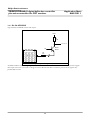
3.21 Pin 21: HFB
Type HFB: voltage input
Vmax
SAA4848
R
HFB = pin 21
Vmin
Figure 16 Application diagram of pin 21
The HFB input has a slicing level of 1.35 Volts and is only triggered by the rising edge. For the best performance,
the rising edge must be fast and free of any disturbance. The resistor value is calculated with the typical input
currents of [email protected] and –[email protected]. The resistor must be placed close to pin 7.
V max − 3.5V
5mA
V min − 0.2V
R=
− 1mA
R=
Choose the highest value of both results for the correct resistor value.
38
Philips Semiconductors
SAA4848/SAA4849 digital deflection controller
plus microcontroller for CRT monitor
Application Note
AN10281 1
3.22 Pin 22: XRAY
Type XRAY: voltage input
The XRAY input detection voltage level may vary from 1.20 volts to 1.30 volts (±4%). As input for the XRAY
detection circuit a signal that is proportional to the EHT voltage is needed. The flyback pulse is generally used in
case of a combined EHT/deflection monitor. However, also the internal EHT divider of the EHT transformer can
be used.
Vmax
SAA4848
D
R1
XRAY = pin 22
+
R2
GND
C
GND
Figure 17 Application diagram of pin 22
The activation level is set by the resistor divider R1 and R2. Resistor R1 and capacitor C set the response time. Since
the XRAY input is very sensitive to ESD tests, the resistor R1 must be placed close to pin 22.
3.23 Pin 23: RST
Type RST: voltage input
SAA4848
To other
V5V = pin 16
+
C1
RST = pin 23
R
GND
C2
GND
Figure 18 Application diagram of pin 23
The reset signal is active high. Capacitor C1 is 22µF and resistor R is 1k ohm. Since the XRAY input is very
sensitive to ESD tests, capacitor C2 (100nF) must be included. Capacitor C2 must be placed close to pin 23. The
positive node of capacitor C1 must be connected directly to pin 16.
39
Philips Semiconductors
SAA4848/SAA4849 digital deflection controller
plus microcontroller for CRT monitor
Application Note
AN10281 1
3.24 Pin 24: VFOCUS
Type VFOCUS: NMOS current sink output
+240V
R1
270k
VFOCUS,OUT
+5V
SAA4848
BF420
BF422
R2
100
VFOCUS = pin 24
Figure 19 Application diagram 1 of pin 24
An NPN transistor cascode stage application can be used when the VFOCUS,OUT is derived from a positive supply.
The output current is converted to voltage in resistor R1. Resistor R2 is needed to protect the IC against any
possible HF currents.
40
Philips Semiconductors
SAA4848/SAA4849 digital deflection controller
plus microcontroller for CRT monitor
Application Note
AN10281 1
+240V
+5V
SAA4848
R2
R4
VFOCUS,OUT
R1
3.9k
C
BF420
BF422
+
VFOCUS = pin 24
R3
R5
GND
GND
Figure 20 Application diagram 2 of pin 24
The current is converted to voltage in resistor R1. The voltage is amplified by the voltage amplifier stage.
3.25 Pin 25: P0.4
Type P0.4: programmable I/O port
P0.4 Configuration
P0CFGA
P0CFGB
Open drain
SFR h84[4]=0
SFR h85[4]=0
High impedance
SFR h84[4]=0
SFR h85[4]=1
Quasi b-directional
SFR h84[4]=1
SFR h85[4]=0
Push pull
SFR h84[4]=1
SFR h85[4]=1
41
Philips Semiconductors
SAA4848/SAA4849 digital deflection controller
plus microcontroller for CRT monitor
3.26 Pin 26: P2.1/DAC1
Type P2.1: open drain (application mode)
Type DAC1 output: buffered voltage output with a voltage range of 0 to 5 volts.
Pin Configuration
SFR setting
P2.1
SFR hEA[1]=0
DAC1
SFR hEA[1]=1
Description
I2C address
DAC1 value
I2C hE8
DAC1 control via I2C -bus
3.27 Pin 27: P2.5/ADC2
Type P2.5: open drain (application mode)
Type ADC2 input: voltage input with voltage range of 0 to 5 Volts.
Pin Configuration
SFR setting
P2.5
SFR hEA[5]=0
ADC2
SFR hEA[5]=1
Description
SFR address
ADC2 value
SFR hEA
ADC2 read back value via SFR register
42
Application Note
AN10281 1
Philips Semiconductors
SAA4848/SAA4849 digital deflection controller
plus microcontroller for CRT monitor
Application Note
AN10281 1
3.28 Pin 28: P2.0/ADC1
Type P2.0: open drain (application mode)
Type ADC1 input: voltage input with voltage range of 0 to 5 Volts.
Pin Configuration
SFR setting
P2.0
SFR hAE[0]=0
ADC1
SFR hAE[0]=1
Description
SFR address
ADC1 value
SFR hE9
ADC1 read back value via SFR register
3.29 Pin 29: P2.7/LED
Type P2.7: open drain (application mode) with 10mA sink capability
+5V
SAA4848
R
LED = pin 29
Figure 21 Application diagram of pin 29
The placement of resistor R must be close to IC.
43
Philips Semiconductors
SAA4848/SAA4849 digital deflection controller
plus microcontroller for CRT monitor
Application Note
AN10281 1
3.30 Pin 30: UVOLT
Type UVOLT: voltage input
The under voltage detection is used to suppress blank the screen and prevent a spot in case of unplugging the power
cord. For a fast detection of the SMPS switch-off, the monitored voltage must have a high load. Due to the high
load, the voltage across the buffer capacitors will drop faster. The monitored voltage can be the vertical deflection
booster voltage (+12V) or the horizontal deflection voltage (+50V or +185V).
The under voltage threshold level is in the range of 2.25 ~ 2.75 volts. An under voltage event will switch off the
BDRV signal and the horizontal deflection circuit will remain without supply. Additionally the microcontroller can
poll the I2C register UNDERVOLT (hE5) and perform a restart with a correct timing.
SAA4848
SMPS
voltage
R1
UVOLT = pin 30
R2
C
GND
GND
Figure 22 Application diagram 1 of pin 30
The capacitor C is advised to be 10nF and is needed to make the under voltage detection less sensitive to ESD tests
and HF noise. The detection accuracy is depending on the resistor tolerances, see table below.
Supply voltage
R1
R2
Voltage drop
50V
120k 5%
7.5k 5%
15V
50V
100k 1%
6.2k 1%
13V
180V
390k 1%
6.2k 1%
45V
44
Philips Semiconductors
SAA4848/SAA4849 digital deflection controller
plus microcontroller for CRT monitor
Application Note
AN10281 1
A faster detection can be realised with an extra zener diode.
SMPS
voltage
SAA4848
R1
UVOLT = pin 30
R2
C
GND
GND
Figure 23 Application diagram 2 of pin 30
When using a zener diode with a zener voltage of 39V, the under voltage detection detects already a drop of 3V
when using resistors with 5% tolerance. Still the signal has to be filtered with capacitor C.
Supply voltage
R1
R2
Voltage drop
50V
10k 5%
3.9k 5%
3V
3.31 Pin 31: P2.2/DAC2
Type P2.2: open drain (application mode)
Type DAC2: buffered voltage output with a voltage range of 0.2 to 4.5 volts.
This DAC2 is intended for HV adjust function because the reference voltage of DAC2 is tracking with OTA
reference voltage of the B+ controller.
Pin Configuration
SFR setting
P2.2
SFR hEA[2]=0
DAC2
SFR hEA[2]=1
Description
I2C address
DAC2 value
I2C hE9
DAC2 control via I2C -bus
45
Philips Semiconductors
SAA4848/SAA4849 digital deflection controller
plus microcontroller for CRT monitor
Application Note
AN10281 1
3.32 Pin 32: EHT
Type EHT: current input
For combined EHT/deflection monitors this input must be used to compensate the picture width increase in
vertical and horizontal direction due to the EHT voltage drop. The input current is sampled and fed to the size
controls for vertical and horizontal deflection. Both vertical and horizontal size controls can be adjusted with the
I2C registers VEHTGAIN (h94) and HEHTGAIN (h95).
The EHT input is a current input fixed at 2.5 volts and requires a capacitor of 2.2nF to AGND for stable operation.
A low pass filter (f-3dB=1~5kHz) must be used to filter out the line frequent signals because they cause disturbance
on the screen. The low pass filter consists of resistor R1 and capacitor C1.
SAA4848
R1
EHT
signal
EHT = pin 32
C1
2.2nF
GND
AGND
Figure 24 Application diagram of pin 32
The “EHT signal” as show in Figure 24 Application diagram of pin 32 can be derived from a) the beam current or
b) the EHT bleeder of the EHT transformer. Most monitors use the beam current to generate the “EHT signal”.
Both applications are discussed below.
3.32.1
Beam current
The beam current is partly flowing through the high voltage capacitor CEHT and partly through the secondary
winding of the transformer. The beam current is a representation of the high voltage drop.
The maximum beam current must not exceed the EHT transformer specification. Therefore the beam current signal
is always needed to limit the beam current by reducing the contrast in the video processor IC. The signal that
connects to the video processor is called “ABL”. The maximum beam current can be adjusted with the signal “ABL
adjust” that connect to the microcontroller DAC output.
46
Philips Semiconductors
SAA4848/SAA4849 digital deflection controller
plus microcontroller for CRT monitor
Application Note
AN10281 1
FBT
EHT
+12V
CEHT
R2
ABL
R3
TR
GND
ABL adjust
R4
R1
EHT signal
C1
GND
Figure 25 Application diagram 1 of EHT signal generation
Capacitor C1 filters out the high frequency video current; the value of C1 is 10~100nF.
The relation between ∆EHT and ∆Ibeam is non-linear due to the load dependent impedance of the EHT
transformer. For beam current variations from black to 50% (0µA to 500µA) the high voltage drops is more then
when the beam current varies from 50% to 100% (500µA to 1mA). Resistor R4 converts the beam current linear to
a voltage. For most applications this solution with resistor R4 is sufficient. When the EHT regulation needs to be
improved for scenes with reduces contrast (0µA < Ibeam <300µA) a non-linear conversion network has to be used.
This non-linear conversion network is shown in Figure 26 Application example compensation of EHT transformer
impedance.
47
Philips Semiconductors
SAA4848/SAA4849 digital deflection controller
plus microcontroller for CRT monitor
Application Note
AN10281 1
R4b
R4
R4c
R4a
-10V
Figure 26 Application example compensation of EHT transformer impedance
Adding more diodes to the network increases the accuracy of the compensation circuit. But the time needed to get
the correct values for the resistors is very time consuming.
48
Philips Semiconductors
SAA4848/SAA4849 digital deflection controller
plus microcontroller for CRT monitor
3.32.2
Application Note
AN10281 1
EHT bleeder application
FBT
EHT
CEHT
+12V
R1
ABL
C1
R2
GND
ABL adjust
R4
R4
C4
C3
C4
EHT signal
R3
GND
GND
GND
Figure 27 Application diagram 2 of EHT signal generation
The RC time constant of C3 and R3 must be the same as CEHT and the bleeder resistance. The roll-off frequency of
the 2nd order low pass filter (R4&C4) must be about 1kHz. Because the EHT bleeder current is too small to drive
the EHT current input of the SAA4848, the EHT signal needs to be buffered with a good DC amplifier with low
input current.
49
Philips Semiconductors
SAA4848/SAA4849 digital deflection controller
plus microcontroller for CRT monitor
Application Note
AN10281 1
3.33 Pin 33: VOUT1
Type VOUT1: NMOS or PMOS current output
The vertical deflection outputs VOUT1 & VOUT2 are differential current outputs, superimposed on a common
bias current source. The output can be configured as NMOS (current sink) or PMOS current source to fit the
desired vertical deflection booster. The differential outputs can be directly coupled to vertical deflection boosters
with (differential) current inputs (TDA4866/TDA4867). Vertical deflection boosters with a (differential) voltage
input (TDA4861/TDA4863) need a resistor interface.
Since the current outputs are 12MHz bitstream DAC’s the output currents need to be filtered. In both diagrams the
filter is implemented with the 6.8nF capacitor and the 470-ohm resistor.
3.33.1
Vertical deflection booster with differential current inputs
SAA4848
470
100
470
100
TDA4866
TDA4867
VOUT2 = pin 34
INP
VOUT1 = pin 33
NMOS outputs
VOUTCONF[0]=0
INN
2x 6.8nF
GND
2x 100pF
AGND AGND
GND
GND
Figure 28 Application diagram 1 of pin 33,34
50
GND
Philips Semiconductors
SAA4848/SAA4849 digital deflection controller
plus microcontroller for CRT monitor
3.33.2
Application Note
AN10281 1
Vertical deflection booster with differential voltage inputs
Vi+
TDA4861
TDA4863
TDA8778
KA2142
Vi-
OUT
SAA4848
470
100
470
100
VOUT2 = pin 34
VOUT1 = pin 33
2x 100pF
2x 6.8nF
PMOS outputs
VOUTCONF[0]=1
2x 2.7k
AGND AGND
GND
GND
Lyoke
GND
1.0 Ohm: +/-1.5A
1.5 Ohm: +/- 1.0A
2.2 Ohm: +/- 0.7A
GND
Figure 29 Application diagram 2 of pin 33,34
3.33.3
PCB layout
The loop area, formed by the tracks with the VOUT1 and VOUT2 signal must be small. These tracks must be
routed next to each other. In case the tracks are longer then 10 cm, the input of the vertical deflection booster
should be filtered to prevent any noise on screen cause by high frequencies (e.g. cellular phone) and switching spikes
(1 ~ 3 ns) entering the booster.
The filter components (470 ohm resistor and 6.8nF capacitor) must be placed close to the SAA4848 pins. The filter
components of the vertical deflection booster must be placed close to the booster IC.
3.34 Pin 34: VOUT2
Type VOUT2: NMOS or PMOS current output
See chapter 3.33 Pin 33: VOUT1 for application.
51
Philips Semiconductors
SAA4848/SAA4849 digital deflection controller
plus microcontroller for CRT monitor
Application Note
AN10281 1
3.35 Pin 35: EWDRV
Type EWDRV: NMOS current output
The EWDRV pin provides all the horizontal size related geometric signals. The EWDRV signal is tracking with
VSIZE and VPOS but the tracking can also be disabled for separate deflection/EHT with I2C register
FHMULT[7]=1.
3.35.1
Combined deflection/EHT
The EWDRV output current must be converted to voltage and amplified before driving the diode modulator. The
NMOS output current source makes it possible to use different types of east-west amplifiers. In the chapter two
types are presented:
• The “good old” amplifier with two PNP transistors and 1 darlington (darlington can be replaced by 2 NPN
transistor) as shown in Figure 30 Application diagram 1 of pin 35;
• NMOS transistor circuit shown in Figure 31 Application diagram 2 of pin 35.
Since the current output is also a 12MHz bitstream DAC’s like VOUT1 & VOUT2; the output currents need to be
filtered.
+12V
R1
R2
+5V
SAA4848
1.8k
100
EWDRV = pin 35
C
L
R5
+
C1
2.2nF
C2
AGND
R3
R4
GND
GND
GND
Figure 30 Application diagram 1 of pin 35
52
GND
GND
Philips Semiconductors
SAA4848/SAA4849 digital deflection controller
plus microcontroller for CRT monitor
Application Note
AN10281 1
L
Z
SAA4848
220
R
10
C
EWDRV = pin 35
PHP3055E
GND
1.0nF
GND
AGND
Figure 31 Application diagram 2 of pin 35
The zener diode ensures that the maximum drain voltage of the NMOS transistor is not exceeded. Resistor R
determines the gain (conversion factor) of the amplifier.
3.35.2
Separate deflection/EHT, B+ modulation
+50V or
+185V
SAA4848
RC (1k&180nF) filter
-3dB @ 800Hz
-80dB @ 12MHz
R1
1k
EWDRV = pin 35
180nF
AGND
BIN = pin 40
C1
R3
R2
BOP = pin 41
AGND
C2
AGND
Figure 32 Application diagram 3 of pin 35
Step-up converter: connect R1 to 50V
Step-down converter: connect R1 to 185V
53
Philips Semiconductors
SAA4848/SAA4849 digital deflection controller
plus microcontroller for CRT monitor
3.36 Pin 36: IREF
Type IREF: reference current
SAA4848
IREF = pin 36
VREF = pin 37
680nF
3.9k
1%
AGND = pin 38
AGND
Figure 33 Application diagram of pin 36, 37, 38
3.37 Pin 37: VREF
Type VREF: voltage reference
See application of Pin 36: IREF.
3.38 Pin 38: AGND
Type AGND: ground pin for the analog references and current outputs
See application of Pin 36: IREF.
54
Application Note
AN10281 1
Philips Semiconductors
SAA4848/SAA4849 digital deflection controller
plus microcontroller for CRT monitor
Application Note
AN10281 1
3.39 Pin 39: BSENS
Type BSENS: high impedance comparator saw tooth input with 6mA discharge sink current
FBT
50V
EHT
GND
CEHT
50V
SAA4848
GND
BSENSE = pin 39
GND
BIN = pin 40
BDRV = pin 18
AGND
Horizontal
deflection
BDRV
buffer
stage
BOP = pin 41
GND
AGND
East west
modulator
AGND
GND
Figure 34 Application diagram 1 of pin 39, 40, 41: Boost converter and BSENSE without current sense
55
Philips Semiconductors
SAA4848/SAA4849 digital deflection controller
plus microcontroller for CRT monitor
Application Note
AN10281 1
FBT
50V
EHT
GND
CEHT
50V
SAA4848
GND
BSENSE = pin 39
GND
BIN = pin 40
BDRV = pin 18
AGND
Horizontal
deflection
BDRV
buffer
stage
BOP = pin 41
AGND
East west
modulator
AGND
GND
GND
Figure 35 Application diagram 2 of pin 39, 40, 41: Boost converter and BSENSE with current sense
56
Philips Semiconductors
SAA4848/SAA4849 digital deflection controller
plus microcontroller for CRT monitor
Application Note
AN10281 1
3.40 Pin 40: BIN
Type BIN: high impedance inverting input of OTA
FBT
185V
EHT
GND
CEHT
50V
SAA4848
GND
BSENSE = pin 39
GND
BIN = pin 40
BDRV = pin 18
AGND
BDRV
buffer
stage
Horizontal
deflection
BOP = pin 41
AGND
East west
modulator
AGND
GND
Figure 36 Application diagram 3 of pin 39, 40, 41: Buck converter
3.41 Pin 41: BOP
Type BOP: high impedance current output of OTA & reference voltage for non-inverting comparator input
See application of Pin 40: BIN.
57
Philips Semiconductors
SAA4848/SAA4849 digital deflection controller
plus microcontroller for CRT monitor
3.42 Pin 42: VSSA
Type VSSA: analog supply ground
SAA4848
VDDA = pin 43
+
10uF
VSSA = pin 42
Figure 37 Application diagram of pin 42, 43
3.43 Pin 43: VDDA
Type VDDA: regulated analog supply
See application of Pin 42: VSSA.
3.44 Pin 44: MODE
Type MODE: high impedance voltage input
SAA4848
MODE = pin 44
GND
Figure 38 Application diagram of pin 44: Application mode
58
Application Note
AN10281 1
Philips Semiconductors
SAA4848/SAA4849 digital deflection controller
plus microcontroller for CRT monitor
3.45 Pin 45: XTAL1
Type XTAL1: crystal oscillator 1
SAA4848
XTAL2 = pin 46
48MHz
3rd overtone
XTAL1 = pin 45
Figure 39 Application diagram of pin 45, 46
3.46 Pin 46: XTAL2
Type XTAL2: crystal oscillator 1
See application of Pin 45: XTAL1
59
Application Note
AN10281 1
Philips Semiconductors
SAA4848/SAA4849 digital deflection controller
plus microcontroller for CRT monitor
Application Note
AN10281 1
3.47 Pin 47: ROT
Type ROT: NMOS current sink output DAC
+10V
+10V
6.8k
Ls
100
SAA4848
+6.1V
(heater)
100
VDDA = pin 43
3.3V
100
ROT= pin 47
GND
Figure 40 Application diagram 1 of pin 47: rotation amplifier
+10V
+10V
5.6k
SAA4848
+5V
100
100
100
ROT= pin 47
Ls
15k
-10V
Figure 41 Application diagram 2 of pin 47: NS trapezium and rotation amplifier
60
GND
Philips Semiconductors
SAA4848/SAA4849 digital deflection controller
plus microcontroller for CRT monitor
3.48 Pin 48: P2.4/ADC0
Type P2.4: open drain (application mode)
Type ADC0: high impedance voltage input, input voltage range 0 ~ 3.3 volts
Pin Configuration
SFR setting
P2.4
SFR hAE[4]=0
ADC0
SFR hAE[4]=1
Description
SFR address
ADC0 value
SFR hEB
ADC1 read back value via SFR register
3.49 Pin 49: P1.5/T1/PWM/VSOUT
Type P1.5/T1: open drain (application mode) with internal pull up resistor
Type PWM: push pull
Type VSOUT: push pull
Pin Configuration
SFR setting
P1.5/T1
SFR h9E[1:0]=00
PWM
SFR h9E[1:0]=01
VSOUT
SFR h9E[1:0]=10
VSOUT
SFR h9E[1:0]=11
61
Application Note
AN10281 1
Philips Semiconductors
SAA4848/SAA4849 digital deflection controller
plus microcontroller for CRT monitor
3.50 Pin 50: P0.5/HSOUT
Type P0.5: programmable I/O port
Type HSOUT: push pull output
P0.5 Configuration
P0CFGA
P0CFGB
Open drain
SFR h84[5]=0
SFR h85[5]=0
High impedance
SFR h84[5]=0
SFR h85[5]=1
Quasi b-directional
SFR h84[5]=1
SFR h85[5]=0
Push pull
SFR h84[5]=1
SFR h85[5]=1
Pin Configuration
SFR setting
P0.5
SFR h8E[0]=0
HSOUT
SFR h8E[0]=1
See pin 6 for more HSOUT information.
3.51 Pin 51: P0.6
Type P0.6: programmable I/O port
P0.6 Configuration
P0CFGA
P0CFGB
Open drain
SFR h84[6]=0
SFR h85[6]=0
High impedance
SFR h84[6]=0
SFR h85[6]=1
Quasi b-directional
SFR h84[6]=1
SFR h85[6]=0
Push pull
SFR h84[6]=1
SFR h85[6]=1
62
Application Note
AN10281 1
Philips Semiconductors
SAA4848/SAA4849 digital deflection controller
plus microcontroller for CRT monitor
3.52 Pin 52: HSYNC
Type: high impedance voltage input
SAA4848
100
HSYNC = pin 53
HSYNC
100
VSYNC = pin 52
VSYNC
100pF
470pF
I/O GND
Figure 42 Application diagram of pin 52,53: HSYNC and VSYNC
3.53 Pin 53: VSYNC
Type: high impedance voltage input
See pin 52 for application diagram.
63
Application Note
AN10281 1
Philips Semiconductors
SAA4848/SAA4849 digital deflection controller
plus microcontroller for CRT monitor
3.54 Pin 54: P1.6/DDC-CLK
Type P1.6: open drain
+5V
2.2k
2.2k
SAA4848
DDC_SCL
DDC_SDA
100
DDC_SCL = pin 54
100
DDC_SDA = pin 55
2x 100pF
I/O GND
Figure 43 Application diagram of pin 54,55: DDC_SCL and DDC_SDA
3.55 Pin 55: P1.7/DDC-SDA
Type P1.6: open drain
See pin 54 for application.
3.56 Pin 56: P1.1/T0
Type P1.1: open drain (application mode)
64
Application Note
AN10281 1
Philips Semiconductors
SAA4848/SAA4849 digital deflection controller
plus microcontroller for CRT monitor
4
ALIGNMENT
4.1
Vertical geometry
Application Note
AN10281 1
The registers VSHIFT and VGAIN are intended for factory alignment. They look very similar to VPOS and
VSIZE, which are for interaction free user control. Possible confusion is avoided by following the step described
below.
4.1.1
4.1.2
Step 1. Set the vertical deflection registers to their initial value.
Parameter
I2C address
Initial value
Remarks
VSHIFT
9A
80
50% of range
VGAIN
9B
30
Typical circuit & tube
VPOS
A8
80
50% of the user control range
VSIZE
A7
C0
75% of the user control range
Step 2. VSHIFT and VGAIN
Adjust for edge-to-edge raster scanning
• The raster is the area scanned by the deflection and is visible at high settings of brightness.
• This step compensates for gain variations of the vertical deflection booster and sensitivity of the
deflection yoke.
• After this alignment, some offset of the video mode may still be present.
4.1.3
Step 3. VLIN and VLINBAL
Only needed when poor reset values have
been loaded. Adjust for equal height of all
blocks of a crosshatch. Repeat step 2.
65
Philips Semiconductors
SAA4848/SAA4849 digital deflection controller
plus microcontroller for CRT monitor
4.1.4
Application Note
AN10281 1
Step 4. VPOS and VSIZE
Adjust the vertical position and the height
of the picture.
Horizontal geometry
4.2
The value of the register HSUBR and HSR must a fixed value for all monitors with the same chassis. The register
HGAIN is intended for factory alignment. HGAIN looks very similar to HSIZE, which is for interaction free user
control. Possible confusion is avoided by following the step described below.
4.2.1
Step 1. Any external adjustment
If other (external) adjustments are present in the horizontal deflection, they should be aligned at this point.
• Coarse pre-adjust of HPOS and HSIZE
• Adjust the horizontal shift transformer (HSHIFT) until the raster is centred horizontally
• Adjust the horizontal linearity coil (HLINBAL) and the linearity-correction capacitors (HLIN) until the
crosshatch block have equal width.
4.2.2
Step 2. Set the horizontal deflection registers to their initial value.
Parameter
I2C address
Set to value
Remarks
HGAIN
97h,
98h
97h=04h
98h=00h
50% of range
Default value
HSR
99h
80h
50% of range
Default value
HPIN
Adh
FFh
100% of the user control range
HSIZE
A9h
AAh
A9h=00h
Aah=00h
0% of range
Maximum picture width
HTRAP
Afh
80h
50% of the user control range
HCTOP
B1h
C0h
100% of the user control range
HCBOT
B2h
C0h
100% of the user control range
HSWAVE
B5h
80h
50% of the user control range
HSUBR
9Ch
08h
100% of range
66
Philips Semiconductors
SAA4848/SAA4849 digital deflection controller
plus microcontroller for CRT monitor
4.2.3
Application Note
AN10281 1
Step 3. HSUBR for optimal picture width
Alignment is only needed in monitor systems with east-west amplifier (combined deflection & EHT).
Reduce the east-west offset value until
there is no visible distortion (clipping to
the lower output voltage of the east-west
amplifier) on left and right vertical
borders.
4.2.4
Step 4. HSR and HGAIN
The HSR (horizontal size ratio) register can control the ratio between the HSIZE alignment range and HPIN
alignment range. Unlike HSR, the HGAIN register can control the gain setting of ALL the east-west geometry
controls like HPIN and HSIZE etc…
The default value for this register is 80h.
When the HPIN alignment range is not enough, increase the HSR register.
When the HPIN alignment range is too much, decrease the HSR register.
The default value for HGAIN is HGAINH=FFh, HGAINL=C0h.
In case the HPIN alignment range is still not enough, increase HGAIN register.
In case the HPIN alignment range still too much, decrease HGAIN register.
4.2.5
Step 5. HPOS and HSIZE
Adjust the centre of the left and right
vertical borders closely to the edges of
the CRT with the horizontal position and
width control.
4.2.6
Step 6. HTRAP and HPARAL
First, course align HPIN.
Adjust the trapezium and parallelogram
until the middle sections of the vertical
borders are vertical.
67
Philips Semiconductors
SAA4848/SAA4849 digital deflection controller
plus microcontroller for CRT monitor
4.2.7
Application Note
AN10281 1
Step 7. HPIN and HPINBAL
Adjust the pincushion and the pinbalans
until the centre sections of the left and
right vertical borders become straight.
4.2.8
Step 8. HCTOP and HCTOPBAL
Adjust the top corners and top corner
balance until the upper parts of the
vertical borders become straight.
4.2.9
Step 9. HCBOT and HCBOTBAL
Adjust the top corners and top corner
balance until the lower parts of the
vertical borders become straight.
4.2.10
Step 10. HSWAVE and HSWAVEBAL
If any remaining s-wave is present adjust
s-wave and s-wave balance until it is gone
4.3
Software limits for geometry controls
The provided control ranges of most settings are quite large and may cause unwanted geometry distortion. Extreme
HTRAP settings can cause ringing op top of screen due to the resonance property of the horizontal deflection stage.
Extreme HSIZE setting (small and large picture width) can cause the east-west amplifier to run out of operating
voltage. If these effects are difficult to solve in hardware, then it is advised to limit those ranges by software.
68
Philips Semiconductors
SAA4848/SAA4849 digital deflection controller
plus microcontroller for CRT monitor
5
I2C -BUS CONTROL
5.1
I2C register types
Application Note
AN10281 1
System initialisation
MOIRERANGE, HSR, HSUBR, HPMAXH, HPMAXL, HPMINH, HPMINL, HSLEW, HDUTYBASL, HDUTYSTST, HDUTYCUTOFF,
BPLUSCTRL1, BPLUSCTRL2, FHMULT, UCXRAY, CLBLCTRL, HUNCTRL, VOUTCONF, VSHSOUTCONF, CRC1, CRC2, CRC3,
CRC4, WAKEUPCONF, HPFREE, FVPER, VBLSTART, VHOLDOFF, CONTROL3, VBLDUR, DACI1, DACI2, DACI3, DACI4,
ONEMINP, EHTCUR, VEHTSHIFT, VEHTOFF, VEHTGAIN, EHTVALH, EHTVALL
System control
POWERCTRL, SYSONCTRL, HCONTROL, CONTROL1
System control information
SY_STATUS, BL_STATUS, HPSYNCH, HPSYNCL, HPDRVH, HPDRVL, HPLLSYNC_STAT, HPLLSTAT, CONTROL2, VPERHIGH,
VPERLOW, VPLR, HPLRH, HPLRL, SYNCPRES, UNDERVOLT, DDCEDGE, VSYNCCOMP, HMODECHANGE, VMODECHANGE,
OVERFLOW
Factory alignment
VSHIFT, VGAIN, MOIRERANGE, HGAINH, HGAINL
User alignment (probably not all registers are really needed)
VPOS, VSIZE, VLINBAL, VLIN, VFOCUS, VMOIRE, HMOIRE, HSIZEH, HSIZEL, HTRAP, HPIN, HSWAVE, HCTOP, HCBOT,
HPOSH, HPOSL, HPARAL, HPINBAL, HSWAVE, HSWAVEBAL, HCTOPBAL, HCBOTBAL, ROT, ROTBAL
5.2
WOR register example values
HPMAX and HPMIN
5.2.1
These double byte registers determine the maximum and minimum horizontal period of HDRV signal. To ensure an
operation range from 30kHz to 70kHz the HPLL needs a range that is just a little larger. A monitor that is designed
for 30kHz to 70kHz needs an HPLL range from 28kHz to 72kHz.
HPmax =
HPmin =
1
f min
1
f max
⋅
1
1
1
=
⋅
= 1428(decimal ) = 0594(hex)
25ns 28000 25ns
⋅
1
1
1
=
⋅
= 556(decimal ) = 02CC (hex)
25ns 72000 25ns
The register settings are:
HPMAXH
HPMAXL
HPMINH
HPMINL
5.2.2
=
=
=
=
h05
h94
h02
hCC
HSLEW
Slewing is the behaviour when the HDRV signal is changing it frequency. The slewing speed is programmable. The
slewing time is depending on the actual HDRV frequency and the target HDRV frequency. In the datasheet is
69
Philips Semiconductors
SAA4848/SAA4849 digital deflection controller
plus microcontroller for CRT monitor
Application Note
AN10281 1
described what the slewing speed is for settings for HSLEW from h40 to hFF. Example, for slewing from 80kHz to
40kHz and HSLEW is h60 the slewing time is 60ms.
The correct setting of the slewing speed depends on the horizontal deflection circuit. During a mode change the
output voltage of the B+ converter changes with a certain time constant, the slewing speed must be in the same
order or slower.
An extreme safe setting for HSLEW is hFF; better is to use a setting of h60. With HSLEW = h60 the maximum slewing
time occurs when slewing from 140kHz to 25kHz or from 25kHz to 140kHz. For a 30kHz ~ 70kHz monitor the
maximum slewing time is 50ms (HSLEW = h60).
5.2.3
Horizontal duty cycle versus frequency settings
The SAA484x has the possibility to tune the HDRV duty cycle for optimum line output transistor switching. These
registers are included in the write-once-registers.
HDUTYBASL
This register has two functions 1) set the horizontal duty cycle at low frequencies, this function is called
“HDUTYBASE”; 2) sets the amount of duty cycle change with respect to the frequency change, this is called
“HDUTYSLOPE”.
• BASE
The BASE sets the minimum duty cycle. This minimum duty cycle is always valid for frequencies smaller
then 34kHz (see also register HDUTYCUTOFF). The horizontal duty cycle polarity is specified like this:
HDUTY =
TOFF
H PER
TOFF = off time of line output transistor + storage time of line output transistor
HPER = actual horizontal period
• SLOPE
The duty cycle increases with frequency as specified with register SLOPE. When SLOPE is set to h0 the duty
cycle is for all frequencies equal to the minimum frequency. With SLOPE set to hF the duty cycle increases
rapidly with frequency, starting at a cut-off frequency specified by register HDUTYCUTOFF.
The minimum duty cycle is internally limited by hardware to 37.5% and the maximum duty cycle is limited to 62.5%.
HDUTYCUTOFF
The cut-off frequency determines the frequency, which the duty cycle starts to increase. Below the cut-off frequency
the duty cycle is fixed, above the cut-off frequency the duty cycle will increase according the SLOPE setting.
70
Philips Semiconductors
SAA4848/SAA4849 digital deflection controller
plus microcontroller for CRT monitor
Application Note
AN10281 1
Advised setting for HDUTYBASL & HDUTYCUTOFF
The TDA4856 duty cycle behaviour can be described like this: 1) minimum duty cycle is 45% for frequencies <
31kHz; 2) at 31kHz the duty cycle increases from 45% @ 31kHz to 48.5% @ 58kHz and 52% @ 110kHz.
Figure 44 TDA4856 HDRV duty cycle vs frequency plot.
In order to get the same behaviour for the SAA4848, the settings must be:
HDUTYBASL = h25 (BASE=h5, SLOPE=h2)
HDUTYCUTOFF=hFF (lowest frequency)
The HDUTYBASL and HDUTYCUTOFF settings can be calculated in the “DEMIC I2C menu control” software. Be aware
that the duty cycle mentioned in the “DEMIC I2C menu control” is defined different from the datasheet.
Datasheet: HDUTY =
TOFF
H PER
DEMIC I2C menu control: HDUTY =
5.2.4
TOn
H PER
HDUTYSTST
The register HDUTYSTST sets the initial HDRV duty cycle during start up. The HDRV duty cycle will grow from the
starting value to the value that is determined by the actual HPLL frequency.
5.2.5
BPLUSCTRL1
This register is used to set the start up and shutdown behaviour of the BPLUS control block. BPLUSCTRL
provides two functions: 1) setting the softstart timing; 2) enable/disable fast shutdown.
• Softstart timing
In case of the TDA4856 the start up timing was controlled externally by application. With the SAA484x the
softstart timing is set internally and can vary between 0ms and 540ms. A good starting value for the
softstart timing = h9.
• Fast shutdown
In case of XRAY occurrence or undervoltage the deflection voltage the B+ converter must stop
71
Philips Semiconductors
SAA4848/SAA4849 digital deflection controller
plus microcontroller for CRT monitor
Application Note
AN10281 1
immediately while the line output transistor remains active to discharge the deflection circuit. The fast off
option must be enabled BPLUSCTRL1[4]=1.
The setting for this register, with the softstart timing as specified above is BPLUSCTRL1=h19.
5.2.6
BPLUSCTRL2
This register has three functions: 1) set BDRV polarity; 2) select trigger edge of HDRV; 3) set mode change voltage
reduction.
• BDRV polarity
A step up converter (boost) needs the polarity to be set to 1. For a step down converter (buck) the polarity
must be set to 0.
• Trigger edge
The best setting for this register is rising edge like the TDA4856. This means that BPLUSCTRL2[3]=1.
• Mode change voltage reduction
This setting defines how much the B+ converter output voltage will decrease during mode change. A good
value to choose is 1.5 Volts on the BOP pin.
For a step up converter BPLUSCTRL2=h1C.
For a step down converter BPLUSCTRL2=h0C.
5.2.7
FHMULT
This register enables tracking of the east-west modulation with frequency. Tracking is needed for monitor systems
with combined deflection, EHT and diode modulator. Monitor systems with separate deflection and EHT need a
fixed value. This fixed value can be stored into FHMULT[6:0].
Combined systems: FHMULT=h00.
Separate systems: FHMULT=b1xxx.xxxx (where xxx.xxxx determines the amount of east west modulation)
72
Philips Semiconductors
SAA4848/SAA4849 digital deflection controller
plus microcontroller for CRT monitor
5.2.8
Application Note
AN10281 1
UCXRAY
This register serves multiple functions: 1) HDRV protection; 2) Undervoltage; 3) XRAY handling.
• HDRV protection
When this bit is set the deflection controller will not switch on the line output transistor when the flyback
pulse is present. This provides the line output transistor to be damaged.
Be aware that this protection prevents the system from starting when the flyback input voltage at pin 21 is
HIGH. If this is the case, an extra pull down resistor is needed to lower the input voltage at the flyback pin.
• Undervoltage
This bit enables the undervoltage detection as it is detection via pin 30 (UVOLT). When the UVOLT
voltage level is LOW the BPLUS block switches off and the BDRV signal will disappear.
• XRAY
This bit should be set to 0. When set to 0 the power supply be switched off manually to restart.
For normal application with undervoltage and HDRV protection the setting is UCXRAY=h03.
5.2.9
CLBLCTRL
This pin set the functions for the CLBL pin. It is adviced to enable the protection blanking CLBLCTRL[0]. The
protection blanking is blanking the video in case of undervoltage.
The clamping signal cannot be used for synchronising the SMPS circuitry. In case of displaying an OSD message
“sync out of range” the clamping signal is synchronous to the HSYNC input and not synchronous to the HDRV
signal.
In case of clamping and blanking sandcastle output pulse select CLBLCTRL=bxxx0.1101.
In case of 5V sync output select CLBLCTRL=bxxx1.0000.
5.2.10
HUNCTRL
The HUNLOCK pin can be used for protection blanking (blanking the screen by lowering the grid 2 voltage). For
protection blanking, set HUNCTRL=h05.
For vertical blanking output, set HUNCTRL=h08.
73
Philips Semiconductors
SAA4848/SAA4849 digital deflection controller
plus microcontroller for CRT monitor
5.2.11
Application Note
AN10281 1
VOUTCONF
This register has multiple functions: 1) East-west polarity; 2) reduced EWDRV; 3) Vertical booster power save
mode; 4) NMOS or PMOS current outputs.
• East-west polarity VOUTCONF[4]
The NMOS transistor application and differential amplifier with pnp transistors requires this bit to be set to
0.
• Reduced EWDRV VOUTCONF[3]
This function should not be used and therefore this bit must be set to 0.
• Vertical booster power down VOUTCONF[2:1]
Set these bits to 1 when using the Philips vertical deflection booster TDA4867j to save power when
deflection is switched off. For all other vertical boosters this bits must be set to 0.
• NMOS or PMOS current outputs VOUTCONF[0]
Select the type of current outputs. Select PMOS outputs for a vertical booster with voltage inputs. Select
NMOS outputs when using a vertical booster with current inputs.
TDA4866j, TDA4867j : VOUTCONF[0]=0
TDA4863j, TDA4861, KA2142 : VOUTCONF[0]=1
5.2.12
VSHSOUTCONF
The VSOUT signal can be multiplexed to pin 8 (CLBL) and pin 49 (P1.5), the HSOUT signal can be multiplexed to
pin 5 (P2.6) and pin 50 (P0.5). This register defines:
1) HFB pulses are used for HSOUT when no HSYNC is present;
2) Vertical blanking pulse is used for VSOUT or the VSYNC is used for VSOUT;
3) VSOUT polarity;
4) HSOUT polarity.
Normal application (HSOUT signal instead of clamping out):
Bit VSHSOUTCONF[3] must be set to generate HSOUT signals when no HSYNC is present;
74
Philips Semiconductors
SAA4848/SAA4849 digital deflection controller
plus microcontroller for CRT monitor
6
Application Note
AN10281 1
DEVELOPMENT TOOLS
In this chapter three useful programs for monitor control are described. The first one is used to program the flash
memory of the SAA4849. The second tool is a generic I2C tool that can be used to read and write I2C commands,
the reading and writing is controlled in a script. The last tool is used to control 1) the I2C registers via the I2C bus
and 2) the SFR registers via the DDC bus. All tools work on the Windows operating systems
95/98/ME/NT/XP/2000. The tools need one I2C driver. Do not forget to install these drivers that are included in
the software distribution.
6.1
Programming tool ISP
The SAA4849 can be (re-) programmed via the DDC bus. First the SAA4849 must be put into “boot ROM mode”.
There are three situations for entering boot mode: 1) empty device always starts with boot mode; 2) Boot ROM
mode is forced externally by voltage on pins MODE and HBGND; 3) Boot ROM mode is forced by firmware.
The programming tool does not support parallel programming. Check the datasheet for more information about
parallel programming.
6.1.1
Forcing boot ROM mode by external voltages on pins.
MODE (pin 44) = 5 V
HBGND (pin 19) = 2V
6.1.2
Forcing boot ROM mode by firmware:
The firmware has to set the flags FOBR and BFLN of SFR FLCTRL by writing value h03 into SFR hC0. In order
to reprogram the flash memory via the DDC bus, the firmware must include a function to detect the “force boot
ROM mode” command on the DDC bus.
6.1.3
Hardware connection for in-system programming
Hardware needed: 1) I2C PCB, connected to the parallel port or serial port; 2) four conductor cable (SCL, GND,
+5V, SDA). Connect the I2C cable from the PC to the DDC input of the monitor.
When using a VGA cable it is possible to use the DDC-CLK, DDC-SDA and GND signals. But do not forget to
supply 5V to the I2C interface board of your PC.
I2C interface
connection
DDC interface
connection
PC with
I2C
SOFTWARE
I2C interface
connection
monitor with
SAA4849
Figure 45 I2C bus connections for (re-) programming the flash memory.
75
Philips Semiconductors
SAA4848/SAA4849 digital deflection controller
plus microcontroller for CRT monitor
Application Note
AN10281 1
Figure 46 Screenshot of in-system programming tool.
6.1.4
SFR access program for HW debugging
With the ISP software a firmware version that controls the SFR registers is included. When this firmware is
programmed into the flash memory it is possible to control the SFR registers via the DDC bus.
The filename of the hex file is “SFR2.HEX” and is default located in the folder “C:\I2C\DEMIC\”.
Writing a value to a SFR register:
H60,H0F,SFR,VALUE
Reading a value(s) from a SFR register consists of two commands, the first command sets the pointer to the SFR
and the second commands read the value of the pointer. When reading more than one byte the pointer is
automatically increased:
H60,H0F,SFR
H61,H0F,NUMBEROFBYTES
Examples:
Putting the microcontroller with the SFR2 program into boot mode: H60,H0F,HC0,H03
Read back port 0 values: H60,H0F,HE8,H61,H01
76
Philips Semiconductors
SAA4848/SAA4849 digital deflection controller
plus microcontroller for CRT monitor
6.1.5
Application Note
AN10281 1
Hardware connection for SFR control via DDC bus
Hardware needed: 1) I2C PCB, connected to the parallel port or serial port; 2) four conductor cable (SCL, GND,
+5V, SDA). Connect the I2C cable from the PC to the DDC input of the monitor.
When using a VGA cable it is possible to use the DDC-CLK, DDC-SDA and GND signals. But do not forget to
supply 5V to the I2C interface board of your PC.
I2C interface
connection
DDC interface
connection
monitor with
PC with
I2C
SOFTWARE
I2C interface
connection
SFR2.HEX into
flash memory
Figure 47 I2C bus connections for SFR control via DDC bus.
6.2
DEMIC I2C & SFR control software
This program is primary intended to control the SAA4848/49 deflection controller. It also supports I2C control for
the Philips TDA484x and TDA485x deflection processors, EEPROM read/write and video processor control for
the Philips TDA488x types.
In order to use the SFR control in this software the SFR2.HEX file needs to be loaded into the flash memory.
77
Philips Semiconductors
SAA4848/SAA4849 digital deflection controller
plus microcontroller for CRT monitor
Figure 48 Screenshot of DEMIC I2C control tab “global”.
78
Application Note
AN10281 1
Philips Semiconductors
SAA4848/SAA4849 digital deflection controller
plus microcontroller for CRT monitor
Figure 49 Screenshot of DEMIC SFR control tab “SFR1/2”.
79
Application Note
AN10281 1
Philips Semiconductors
SAA4848/SAA4849 digital deflection controller
plus microcontroller for CRT monitor
6.2.1
Application Note
AN10281 1
Hardware connection for I2C register control via I2C bus
Hardware needed: 1) I2C PCB, connected to the parallel port or serial port; 2) four conductor cable (SCL, GND,
+5V, SDA). Connect the I2C cable from the PC to the I2C bus of the monitor.
Do not forget to supply 5V to the I2C interface board of your PC.
I2C interface
connection
DDC interface
connection
monitor
PC with
I2C
SOFTWARE
uC must
release I2C
bus
I2C interface
connection
Figure 50 I2C bus connections for SFR control via DDC bus.
The microcontroller must release the I2C bus because the PC takes over I2C master function. In order to support
hardware debugging, in the firmware two functions could be included: 1) stop I2C bus; 2) activate I2C bus. These
functions can disable/enable the I2C bus control in the main loop of the software.
6.2.2
Hardware connection for SFR control via DDC bus & I2C register control via I2C bus
Hardware needed: 1) I2C PCB, connected to the parallel port or serial port; 2) four conductor cable (SCL, GND,
+5V, SDA). Connect the I2C cable from the PC to the DDC input and to the I2C bus of the monitor. Due to the
pull-up resistors on the DDC & I2C bus, the total pull-up resistance could be too low. It is advised to remove the
pull-up resistors from the I2C bus or DDC bus.
I2C interface
connection
DDC interface
connection
PC with
I2C
SOFTWARE
I2C interface
connection
monitor with
SFR2.HEX into
flash memory
Figure 51 I2C bus connections for SFR control via DDC bus & I2C bus control.
80
Philips Semiconductors
SAA4848/SAA4849 digital deflection controller
plus microcontroller for CRT monitor
6.3
Application Note
AN10281 1
I2C tools program
This generic I2C program is very useful for controlling any I2C device including the SAA4848/49. It uses text-based
scripts to control the write and read commands on the I2C bus. The scripts are easy to copy-paste. For example, a
large series of commands can be generated by MSOffice applications like Excel. Next this file can be saved as a textfile with comma delimiter. Then a text editor can open this file and the copy-paste function can insert a script into
the tools program. Also read values from the I2C Tools program can be put into a text editor by copy-paste.
In case of SAA4849, the I2C tools program can include 1) a script to initialise control the complete monitor; 2) a
script to perform a mode change; 3) a script to display OSD message; 4) a script to read the ADC; 5) a script to
shutdown the deflection; 6) a script to enter power save mode; 7) etc, etc.
Figure 52 Screenshot of I2C Tools program.
81
Philips Semiconductors
SAA4848/SAA4849 digital deflection controller
plus microcontroller for CRT monitor
Example 1 – writing to I2C register:
// Shutdown DemicDemo
#ValueFormat = HEX
// blank video
60,0f,90,fe // Vblank @ Port1.2
88,00,06 // disable video & osd
// limit beam current
8c,e8,00 // abl_adj
// lower EHT voltage
8c,e9,ff // eht_adj @ dac2
// OSR=L & force blanking
8c,e2,10
// request IDLE
8c,e1,33
Example 2 – writing to SFR register:
// uC port config
#ValueFormat = HEX //HEX or COMBINED
60,0f,80,41 // set port 0
60,0f,90,ff // set port 1
60,0f,84,bf // set port 0 - cfga
60,0f,85,bf // set port 0 - cfgb
60,0f,8e,01 // HSout @ P0.5
60,0f,9e,03 // VSout @ P1.5
60,0f,af,01 // p2ctrl
60,0f,ae,ff // set port 2 special functions
60,0f,a0,00 // set port 2
82
Application Note
AN10281 1
Philips Semiconductors
SAA4848/SAA4849 digital deflection controller
plus microcontroller for CRT monitor
Application Note
AN10281 1
Example 3 – reading:
// Read deflection status
#ValueFormat = HEX
8d,e4,1 // read i2c register sy_status
8d,e0,1 // read i2c register wakeupconf
8d,e3,1 // read i2c register syncpres
More information about the functionality is included with the I2C Tools software. It is accessible during run-time in
the menu “Script-Commands?”
6.4
Emulator for SW debugging
Contact your local sales person and request emulator kit for software debugging.
83
Philips Semiconductors
SAA4848/SAA4849 digital deflection controller
plus microcontroller for CRT monitor
7
LIST OF ABBREVIATIONS
AC
ADC
B
CMOS
CPU
CPU
CRC
CRT
CT
DAC
DC
DDC
DEMIC
DPMS
EHT
G
H
HV
HWMD
I2C
IC
ISP
LED
NMOS
NPN
NVM
OSD
OTA
PC
PCB
PMOS
PWM
R
RAM
ROM
SCL
SDA
SFR
SW
uC or µC
V
VESA
WOR
alternating current
analogue to digital converter
blue
complementary metal-oxide
semiconductor
central processing unit
central processing unit
cyclic redundancy check
cathode ray tube
colour temperature
digital to analogue converter
direct current
display data channel
deflection and microcontroller IC
display power management signalling
extreme high tension
green
horizontal
high voltage
hardware mode detector
inter IC connect
integrated circuit
in-system programming
light emitting diode
n-channel metal oxide semiconductor
negative-positive-negative (transistor)
non-volatile memory
on screen display
operational transconductance
amplifier
personal computer
printed circuit board
p-channel metal oxide semiconductor
pulse width modulation
red
random access memory
read only memory
serial clock line
serial data line
special function register
software
microcontroller
vertical
video electronics standard association
write once register
84
Application Note
AN10281 1
Philips Semiconductors
SAA4848/SAA4849 digital deflection controller
plus microcontroller for CRT monitor
8
Application Note
AN10281 1
LIST OF FIGURES
Figure 1 Block diagram deflection ------------------------------------------------------------------------------------------------------------ 10
Figure 2 Block diagram microcontroller ----------------------------------------------------------------------------------------------------- 10
Figure 3 On-chip interconnect between deflection and microcontroller--------------------------------------------------------------- 11
Figure 4 All port 2.X multiplexing functions ----------------------------------------------------------------------------------------------- 12
Figure 5 Remaining multiplexing functions ------------------------------------------------------------------------------------------------- 12
Figure 6 Start up & shutdown timing of GEO, HPLL and BPLUS block.------------------------------------------------------------ 18
Figure 7 Components placing and layout. --------------------------------------------------------------------------------------------------- 25
Figure 8 Application diagram of pin 2 & pin 3 --------------------------------------------------------------------------------------------- 26
Figure 9 HSVSOUT[3] explanation ---------------------------------------------------------------------------------------------------------- 29
Figure 10 Application diagram of pin HUNLOCK for grid 1 protection blanking -------------------------------------------------- 31
Figure 11 VSHSOUTCONF[2:1] explanation---------------------------------------------------------------------------------------------- 32
Figure 12 Application diagram of pin 14,15,16 and 17------------------------------------------------------------------------------------ 34
Figure 13 Application diagram of pin 14,17,19 and 38------------------------------------------------------------------------------------ 35
Figure 14 Application diagram of pin 18 ---------------------------------------------------------------------------------------------------- 36
Figure 15 Application diagram of pin 20 ---------------------------------------------------------------------------------------------------- 37
Figure 16 Application diagram of pin 21 ---------------------------------------------------------------------------------------------------- 38
Figure 17 Application diagram of pin 22 ---------------------------------------------------------------------------------------------------- 39
Figure 18 Application diagram of pin 23 ---------------------------------------------------------------------------------------------------- 39
Figure 19 Application diagram 1 of pin 24 -------------------------------------------------------------------------------------------------- 40
Figure 20 Application diagram 2 of pin 24 -------------------------------------------------------------------------------------------------- 41
Figure 21 Application diagram of pin 29 ---------------------------------------------------------------------------------------------------- 43
Figure 22 Application diagram 1 of pin 30 -------------------------------------------------------------------------------------------------- 44
Figure 23 Application diagram 2 of pin 30 -------------------------------------------------------------------------------------------------- 45
Figure 24 Application diagram of pin 32 ---------------------------------------------------------------------------------------------------- 46
Figure 25 Application diagram 1 of EHT signal generation------------------------------------------------------------------------------ 47
Figure 26 Application example compensation of EHT transformer impedance ----------------------------------------------------- 48
Figure 27 Application diagram 2 of EHT signal generation------------------------------------------------------------------------------ 49
Figure 28 Application diagram 1 of pin 33,34 ---------------------------------------------------------------------------------------------- 50
Figure 29 Application diagram 2 of pin 33,34 ---------------------------------------------------------------------------------------------- 51
Figure 30 Application diagram 1 of pin 35 -------------------------------------------------------------------------------------------------- 52
Figure 31 Application diagram 2 of pin 35 -------------------------------------------------------------------------------------------------- 53
Figure 32 Application diagram 3 of pin 35 -------------------------------------------------------------------------------------------------- 53
Figure 33 Application diagram of pin 36, 37, 38 ------------------------------------------------------------------------------------------- 54
Figure 34 Application diagram 1 of pin 39, 40, 41: Boost converter and BSENSE without current sense ---------------------- 55
85
Philips Semiconductors
SAA4848/SAA4849 digital deflection controller
plus microcontroller for CRT monitor
Application Note
AN10281 1
Figure 35 Application diagram 2 of pin 39, 40, 41: Boost converter and BSENSE with current sense--------------------------- 56
Figure 36 Application diagram 3 of pin 39, 40, 41: Buck converter--------------------------------------------------------------------- 57
Figure 37 Application diagram of pin 42, 43------------------------------------------------------------------------------------------------ 58
Figure 38 Application diagram of pin 44: Application mode----------------------------------------------------------------------------- 58
Figure 39 Application diagram of pin 45, 46------------------------------------------------------------------------------------------------ 59
Figure 40 Application diagram 1 of pin 47: rotation amplifier --------------------------------------------------------------------------- 60
Figure 41 Application diagram 2 of pin 47: NS trapezium and rotation amplifier---------------------------------------------------- 60
Figure 42 Application diagram of pin 52,53: HSYNC and VSYNC --------------------------------------------------------------------63
Figure 43 Application diagram of pin 54,55: DDC_SCL and DDC_SDA ------------------------------------------------------------ 64
Figure 44 TDA4856 HDRV duty cycle vs frequency plot. ------------------------------------------------------------------------------- 71
Figure 45 I2C bus connections for (re-) programming the flash memory. ------------------------------------------------------------- 75
Figure 46 Screenshot of in-system programming tool. ------------------------------------------------------------------------------------ 76
Figure 47 I2C bus connections for SFR control via DDC bus. -------------------------------------------------------------------------- 77
Figure 48 Screenshot of DEMIC I2C control tab “global”. ------------------------------------------------------------------------------ 78
Figure 49 Screenshot of DEMIC SFR control tab “SFR1/2”. -------------------------------------------------------------------------- 79
Figure 50 I2C bus connections for SFR control via DDC bus. -------------------------------------------------------------------------- 80
Figure 51 I2C bus connections for SFR control via DDC bus & I2C bus control. --------------------------------------------------- 80
Figure 52 Screenshot of I2C Tools program. ----------------------------------------------------------------------------------------------- 81
86
Philips Semiconductors
SAA4848/SAA4849 digital deflection controller
plus microcontroller for CRT monitor
9
REFERENCES
9.1
Datasheets
Application Note
AN10281 1
Device
Description
Date
SAA4848PS/SAA4849PS/
SAA4847PS
I2C -bus autosync CMOS deflection controller and microcontroller for CRT monitors
sep-2003
TDA4856PS
I2C -bus controlled autosync deflection controller for PC monitors
13-jul-2003
TDA4841PS
I2C
21-jun-1999
TDA4867J
Full bridge current driven vertical deflection booster
9.2
-bus controller autosync deflection controller for PC monitors
29-aug-2000
Application notes
Number
Description
AN10280
17 inch 70kHz CRT monitor demo set featuring SAA4848/SAA4849
5-jan-2004
AN00033
CCM433 autosync monitor – 85kHz separate deflection/EHT
17-may-2000
AN00040
Vertical deflection booster TDA4863AJ/TDA4863J
AN00042
Failure mechanisms of the line output transistor
AN00057
ECO monitor – 70kHz combined deflection/EHT
9.3
Version
Date
8-nov-2000
Web references
Description
URL
I2C general
http://www.semiconductors.philips.com/buses/i2c/index.html
I2C FAQ
ftp://ftp.uni.paderborn.de/elrad/020/ or http://www.ping.be/~ping0751/i2c.htm
Philips Semiconductors datasheets
http://www.semiconductors.com
9.4
Software for PC
Ask your local sales person for the required software.
87
Philips Semiconductors
SAA4848/SAA4849 digital deflection controller
plus microcontroller for CRT monitor
APPENDIX 1
Application Note
AN10281 1
Source code for the CRC calculation
For the safe transfer of the Write Once Registers (WOR) a 4 byte CRC is used. The following is the code example
for the calculation of the CRC:
#define CRC_POLYNOMINAL 0x04C11DB7
#define HIGHEST_BIT
0x80000000
unsigned long Calculate_CRC( BYTE *StrPtr, BYTE length )
{
BYTE index, bit_nr, byte_to_check;
unsigned long crc;
crc = 0xFFFFFFFF;
// initial reminder
for ( index = 0; index < length; index++)
{
byte_to_check = *StrPtr++;
crc ^= (unsigned long)byte_to_check << 24;
for ( bit_nr = 0; bit_nr < 8; bit_nr++ )
{
if ( crc & HIGHEST_BIT )
{
crc <<= 1;
crc ^= CRC_POLYNOMINAL;
} else
{
crc <<= 1;
}
}
}
return crc;
}
The application part can look something like this:
…
Calculate_CRC(WOR_REG_DEFINITION, WOR_BYTES_NUMBER);
crc[0]=(BYTE)((result>>24) & 0x000000FF);
crc[1]=(BYTE)((result>>16) & 0x000000FF);
crc[2]=(BYTE)((result>>8) & 0x000000FF);
crc[3]=(BYTE)(result & 0x000000FF);
dIIC_SendData_Directly(DEFLECTION_SLAVE_ADDRESS, WOR_BYTES_NUMBER, WOR_REG_LIST_DEFINITION);
//fixed part of WOR
dIIC_SendData_Directly(DEFLECTION_SLAVE_ADDRESS, WOR_BYTES_NUMBER, crc); //CRC part
…
88