1
F28M35H52C, F28M35H22C, F28M35M52C,
F28M35M22C, F28M35M20B, F28M35E20B
Concerto MCUs
Silicon Errata
Literature Number: SPRZ357J
August 2011 – Revised July 2014
Contents
1
2
3
4
Introduction .........................................................................................................................
Device and Development Support Tool Nomenclature ..............................................................
Device Markings ..................................................................................................................
Usage Notes and Known Design Exceptions to Functional Specifications ..................................
4.1
4.2
4
4
5
6
Usage Notes .............................................................................................................. 6
4.1.1
PIE: Spurious Nested Interrupt After Back-to-Back PIEACK Write and Manual CPU Interrupt Mask
Clear Usage Note ............................................................................................ 6
4.1.2
EPI: New Feature Addition to EPI Module Usage Note ................................................. 7
4.1.3
EPI: ALE Signal Polarity Usage Note ...................................................................... 7
4.1.4
EPI: CS0/CS1 Swap Usage Note .......................................................................... 7
4.1.5
Major Device Revision Usage Note ........................................................................ 8
Known Design Exceptions to Functional Specifications
............................................................
9
5
6
Documentation Support ...................................................................................................... 37
Revision History ................................................................................................................. 38
2
Table of Contents
SPRZ357J – August 2011 – Revised July 2014
Submit Documentation Feedback
Copyright © 2011–2014, Texas Instruments Incorporated
www.ti.com
List of Figures
1
Example of Device Markings ............................................................................................... 5
2
Example of Device Nomenclature ......................................................................................... 5
List of Tables
1
2
3
4
5
6
................................................................... 5
List of Usage Notes.......................................................................................................... 6
CS0/CS1 Swap .............................................................................................................. 7
Table of Contents for Advisories ........................................................................................... 9
List of Advisories ........................................................................................................... 11
Crystal Equivalent Series Resistance (ESR) Requirements .......................................................... 18
Determining Silicon Revision From Lot Trace Code
SPRZ357J – August 2011 – Revised July 2014
Submit Documentation Feedback
List of Figures
Copyright © 2011–2014, Texas Instruments Incorporated
3
Silicon Errata
SPRZ357J – August 2011 – Revised July 2014
F28M35x Concerto™ MCU Silicon Errata
1
Introduction
This document describes the silicon updates to the functional specifications for the F28M35x
microcontrollers (MCUs).
The updates are applicable to:
• 144-pin PowerPAD™ Thermally Enhanced Thin Quad Flatpack, RFP Suffix
2
Device and Development Support Tool Nomenclature
To designate the stages in the product development cycle, TI assigns prefixes to the part numbers of all
Concerto MCU devices and support tools. Each Concerto MCU commercial family member has one of
three prefixes: x, p, or no prefix (for example, xF28M35H52C1RFPT). Texas Instruments recommends
two of three possible prefix designators for its support tools: TMDX and TMDS. These prefixes represent
evolutionary stages of product development from engineering prototypes (with prefix x for devices and
TMDX for tools) through fully qualified production devices and tools (with no prefix for devices and TMDS
for tools).
xF28M35...
pF28M35...
F28M35...
Experimental device that is not necessarily representative of the final device's
electrical specifications
Final silicon die that conforms to the device's electrical specifications but has
not completed quality and reliability verification
Fully qualified production device
Support tool development evolutionary flow:
TMDX Development-support product that has not yet completed Texas Instruments internal
qualification testing
TMDS Fully qualified development-support product
Devices with prefix x or p and TMDX development-support tools are shipped against the following
disclaimer:
"Developmental product is intended for internal evaluation purposes."
Production devices and TMDS development-support tools have been characterized fully, and the quality
and reliability of the device have been demonstrated fully. TI's standard warranty applies.
Predictions show that prototype devices with prefix of x or p have a greater failure rate than the standard
production devices. Texas Instruments recommends that these devices not be used in any production
system because their expected end-use failure rate still is undefined. Only qualified production devices are
to be used.
TI device nomenclature also includes a suffix with the device family name. This suffix indicates the
package type (for example, RFP) and temperature range (for example, T).
Concerto, PowerPAD, Code Composer Studio are trademarks of Texas Instruments.
StellarisWare is a registered trademark of Texas Instruments.
ARM, Cortex are registered trademarks of ARM Limited (or its subsidiaries) in the EU and/or elsewhere. All rights reserved.
Philips is a registered trademark of Koninklijke Philips Electronics N.V.
All other trademarks are the property of their respective owners.
4
F28M35x Concerto™ MCU Silicon Errata
Copyright © 2011–2014, Texas Instruments Incorporated
SPRZ357J – August 2011 – Revised July 2014
Submit Documentation Feedback
Device Markings
www.ti.com
3
Device Markings
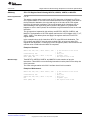
Figure 1 provides an example of the Concerto device markings and defines each of the markings. The
device revision can be determined by the symbols marked on the top of the package as shown in
Figure 1. Some prototype devices may have markings different from those illustrated. Figure 2 shows an
example of the device nomenclature.
YMLLLLS = Lot Trace Code
x
980
YM
LLLL
S
$$
#
980
F28M35H52C1RFPT
$$#-YMLLLLS
=
=
=
=
=
=
2-Digit Year/Month Code
Assembly Lot
Assembly Site Code
Wafer Fab Code as applicable
Package Marking Code
TI EIA Code
G4
G4 = Green (Low Halogen and RoHS-compliant)
Package
Pin 1
Figure 1. Example of Device Markings
Table 1. Determining Silicon Revision From Lot Trace Code
(1)
PACKAGE
MARKING CODE
SILICON
REVISION
Blank
REVISION ID ADDRESS
REVISION ID (1)
0
ARM® Cortex®-M3: 0x400F E000
C28x: 0x0883
0x0000
Available as an experimental
device.
Blank
A
Cortex-M3: 0x400F E000
C28x: 0x0883
0x0001
Available as an experimental
device.
B
B
Cortex-M3: 0x400F E000
C28x: 0x0883
0x0001
Available as an experimental
device and as a qualified
production device.
COMMENTS
For Cortex-M3, the REVID field (bits 15:0) is embedded in the DID0 register.
5
F28M3
x
H
5
2
C
1
RFP
T
PREFIX
TEMPERATURE RANGE
T = −40°C to 105°C
S = −40°C to 125°C
Q = −40°C to 125°C
(Q refers to Q100 qualification
for automotive applications.)
= experimental device
x
= prototype device
p
no prefix = qualified device
DEVICE FAMILY
F28M3 = Concerto
PACKAGE TYPE
144-Pin RFP PowerPAD
Thermally Enhanced Thin Quad Flatpack (HTQFP)
SERIES NUMBER
PINS
1 = 144 pins
PERFORMANCE
(C28x Speed / Cortex-M3 Speed)
H = 150/100 MHz
M = 75/75 MHz
E = 60/60 MHz
PERIPHERALS
C = Connectivity
B = Base
FLASH
2 = 256KB each core
5 = 512KB each core
RAM
0 = 72KB
2 = additional 64KB of masterable RAM
Figure 2. Example of Device Nomenclature
SPRZ357J – August 2011 – Revised July 2014
Submit Documentation Feedback
F28M35x Concerto™ MCU Silicon Errata
Copyright © 2011–2014, Texas Instruments Incorporated
5
Usage Notes and Known Design Exceptions to Functional Specifications
4
www.ti.com
Usage Notes and Known Design Exceptions to Functional Specifications
NOTE: For errata relating to the Cortex-M3 r2p0 core, see the ARM Core Cortex-M3 / Cortex-M3
with ETM (AT420/AT425) Errata Notice at the ARM Ltd. website.
4.1
Usage Notes
Usage notes highlight and describe particular situations where the device's behavior may not match
presumed or documented behavior. This may include behaviors that affect device performance or
functional correctness. These usage notes will be incorporated into future documentation updates for the
device (such as the device-specific data sheet), and the behaviors they describe will not be altered in
future silicon revisions.
Table 2 shows which silicon revision(s) are affected by each usage note.
Table 2. List of Usage Notes
SILICON REVISION(S)
AFFECTED
TITLE
0
A
B
Yes
Yes
Yes
EPI: New Feature Addition to EPI Module
Yes
Yes
EPI: ALE Signal Polarity
Yes
Yes
EPI: CS0/CS1 Swap
Yes
Yes
PIE: Spurious Nested Interrupt After Back-to-Back PIEACK Write and Manual CPU Interrupt
Mask Clear
Major Device Revision
4.1.1
Yes
PIE: Spurious Nested Interrupt After Back-to-Back PIEACK Write and Manual CPU Interrupt
Mask Clear Usage Note
Revision(s) Affected: 0, A, B
Certain code sequences used for nested interrupts allow the CPU and PIE to enter an inconsistent state
that can trigger an unwanted interrupt. The conditions required to enter this state are:
1. A PIEACK clear is followed immediately by a global interrupt enable (EINT or asm(" CLRC INTM")).
2. A nested interrupt clears one or more PIEIER bits for its group.
Whether the unwanted interrupt is triggered depends on the configuration and timing of the other
interrupts in the system. This is expected to be a rare or nonexistent event in most applications. If it
happens, the unwanted interrupt will be the first one in the nested interrupt's PIE group, and will be
triggered after the nested interrupt re-enables CPU interrupts (EINT or asm(" CLRC INTM")).
Workaround: Add a NOP between the PIEACK write and the CPU interrupt enable. Example code is
shown below.
6
//Bad interrupt nesting code
PieCtrlRegs.PIEACK.all = 0xFFFF;
EINT;
//Enable nesting in the PIE
//Enable nesting in the CPU
//Good interrupt nesting code
PieCtrlRegs.PIEACK.all = 0xFFFF;
asm(" NOP");
EINT;
//Enable nesting in the PIE
//Wait for PIEACK to exit the pipeline
//Enable nesting in the CPU
F28M35x Concerto™ MCU Silicon Errata
Copyright © 2011–2014, Texas Instruments Incorporated
SPRZ357J – August 2011 – Revised July 2014
Submit Documentation Feedback
Usage Notes and Known Design Exceptions to Functional Specifications
www.ti.com
4.1.2
EPI: New Feature Addition to EPI Module Usage Note
Revision(s) Affected: A, B
In the EPI module, many new features have been added on silicon revisions A and onwards. New
configuration registers have been added to enable new features. However, in some cases, new
configuration bits (which were “Reserved” on the revision 0 silicon) have been added to existing registers,
without breaking the compatibility with the revision 0 silicon. Users should refer to the "External Peripheral
Interface (EPI)" chapter in the Concerto F28M35x Technical Reference Manual (SPRUH22) to make sure
their existing EPI code (which works on the revision 0 silicon) is not changing the default value of the new
configuration bits. Otherwise, the old code may not work on the new silicon.
4.1.3
EPI: ALE Signal Polarity Usage Note
Revision(s) Affected: A, B
On the revision 0 silicon, the polarity of the ALE (address latch enable) signal was active HIGH and it was
not configurable. On new silicon revisions, a configuration bit (ALEHIGH) has been added in existing host
bus configuration registers so that the user can configure the polarity of the ALE signal as per system
requirement. Reset value of this bit is set to “1” to have the default polarity of ALE as active HIGH so that
it is compatible with the revision 0 silicon (‘0’ will make it active LOW). Since this configuration field was
reserved in the revision 0 silicon, if the application writes ‘0’ to this field (while configuring other bit fields in
this register), there would be no issue for the revision 0 silicon, but the same code will not work on the
revision A silicon. This is because ‘0’ means active LOW polarity for ALE on revision A silicon. This bit
needs to be set to ‘1’ to make it work on the revision A silicon.
4.1.4
EPI: CS0/CS1 Swap Usage Note
Revision(s) Affected: A, B
On revision A silicon onwards, if the following conditions are true:
• both EPADR and ERADR are not 0x0
• the ECADR field is 0x0
• the EPI is configured for dual-chip selects
then,
• CS0 is asserted for either address range defined by ERADR
• CS1 is asserted for either address range defined by EPADR
This has been changed from revision 0 silicon, where, in the same configuration,
• CS0 is asserted for either address range defined by EPADR
• CS1 is asserted for either address range defined by ERADR.
Table 3. CS0/CS1 Swap
SILICON
REVISION
CHIP SELECT
MODE
ERADR
EPADR
ECADR
CS0
CS1
0
Dual-chip select
0x1 or 0x2
0x1 or 0x2
0x0
EPADR defined
address range
(0xA000.0000 or
0xC000.0000)
ERADR defined
address range
(0x6000.0000 or
0x8000.0000)
A and onwards
Dual-chip select
0x1 or 0x2
0x1 or 0x2
0x0
ERADR defined
address range
(0x6000.0000 or
0x8000.0000)
EPADR defined
address range
(0xA000.0000 or
0xC000.0000)
SPRZ357J – August 2011 – Revised July 2014
Submit Documentation Feedback
F28M35x Concerto™ MCU Silicon Errata
Copyright © 2011–2014, Texas Instruments Incorporated
7
Usage Notes and Known Design Exceptions to Functional Specifications
4.1.5
www.ti.com
Major Device Revision Usage Note
Revision(s) Affected: 0
There were significant changes to the device functionality between Revision 0 and Revision A.
Code developed on the revision 0 device may not operate as expected on later revisions. The Concerto
F28M35x Technical Reference Manual (SPRUH22) and the F28M35H52C, F28M35H22C, F28M35M52C,
F28M35M22C, F28M35M20B, F28M35E20B Concerto Microcontrollers Data Manual (SPRS742) are
updated to reflect the functionality present on revision A and later device revisions. Some specific areas of
change are:
• GPIO configuration
• EPI additional functionality
• USB emulation:
– From revision A onwards, "extended ICEPick router support" in the target configuration has to be
enabled for the USB emulators to halt the Cortex-M3 core.
• Flash programming:
– From revision A onwards, the latest Flash API should be used without modifying the
Fapi_setupBankSectorEnable(void) function in the Fapi_UserDefinedFunctions.c file.
– Code Composer Studio™ and UniFlash should be checked for the latest updates for installing the
XMLs required for the Flash plugin to work with revision A and revision B devices.
8
F28M35x Concerto™ MCU Silicon Errata
Copyright © 2011–2014, Texas Instruments Incorporated
SPRZ357J – August 2011 – Revised July 2014
Submit Documentation Feedback
Usage Notes and Known Design Exceptions to Functional Specifications
www.ti.com
4.2
Known Design Exceptions to Functional Specifications
Table 4. Table of Contents for Advisories
Title
......................................................................................................................................
Advisory — Analog Subsystem: Analog Subsystem Function InitAnalogSystemClock() is Incomplete .....................
Advisory — Analog Subsystem: Potential Race Condition after Executing Analog Subsystem Functions
AnalogClockEnable() or AnalogClockDisable() ............................................................................
Advisory — ADC: Initial Conversion ..................................................................................................
Advisory — ADC: ADC Result Conversion When Sampling Ends on 14th Cycle of Previous Conversion, ACQPS = 6
or 7 ...............................................................................................................................
Advisory — ADC: Offset Self-Recalibration Requirement ........................................................................
Advisory — UART: RTRIS Bit in the UARTRIS Register is Only Set When the Interrupt is Enabled .......................
Advisory — VREG: VREG 'Warn Lo/High' Feature Does Not Work as Intended...............................................
Advisory — System Control: Clock Configuration Should Not be Changed When There are Pending or On-going
Accesses to Shared RAM (Cx and Sx) or to Analog Subsystem ........................................................
Advisory — ePWM: ePWM7 is Clocked by CPUCLK and Will Stop During IDLE ..............................................
Advisory — HWBIST: C28x HWBIST Should Not be Used .......................................................................
Advisory — Crystal: Maximum Equivalent Series Resistance (ESR) Values are Reduced ...................................
Advisory — Cortex-M3 Flash: C28x Reset While C28x Holding Pump Ownership Can Cause Erroneous Cortex-M3
Flash Reads ....................................................................................................................
Advisory — SSI: SSI Microwire Frame Format is Not Supported on This Device ..............................................
Advisory — USB/GPIO38: GPIO38/VBUS Cannot be Used as an Output .....................................................
Advisory — USB: VBUS Pin May Clamp to 3.3-V Supply, Preventing Proper OTG Mode Operation .......................
Advisory — USB: Host Mode — Cannot Communicate With Low-Speed Device Through a Hub ...........................
Advisory — RAM Controller: Cortex-M3 Correctable Error Address Register Always has Value 0x0 .......................
Advisory — RAM Controller: C28x Correctable Error Address Register Always has Value 0x0 ............................
Advisory — RAM Controller: Cortex-M3 Accesses to Shared RAM (Cx and Sx) and to MSG RAM Do Not Work When
Any Other Master (µDMA/C28x/DMA) Simultaneously Accesses the Same Memory ................................
Advisory — RAM Controller: µDMA Accesses to Shared RAM (Cx and Sx) and to MSG RAM Do Not Work When
Any Other Master (Cortex-M3/C28x/DMA) Simultaneously Accesses the Same Memory ...........................
Advisory — eQEP: eQEP Inputs in GPIO Asynchronous Mode ..................................................................
Advisory — eQEP: Missed First Index Event........................................................................................
Advisory — GPIO: GPIO38 and GPIO46 Shunt to VSS Due to Fast Transient Sensitivity at High Temperature ...........
Advisory — GPIO: Pins GPIO38 and GPIO46 Cannot be Used for Functions Other Than USB ............................
Advisory — GPIO: GPIOs on Port C Do Not Toggle Correctly When Using the GPCTOGGLE Register...................
Advisory — GPIO: Cortex-M3/C28x Reads GPIO State as ‘0’ When the GPIO is Mapped to the Other Core.............
Advisory — FPU: FPU Register Read Following MPYF32, ADDF32, SUBF32, or MACF32 .................................
Advisory — FPU: FPU Register Write Followed by F32TOUI32, FRACF32, UI16TOF32, or F32TOUI32..................
Advisory — FPU32 and VCU Back-to-Back Memory Accesses ..................................................................
Advisory — Control Subsystem I2C: FIFO Interrupt Trigger Levels Capped at 7 ...............................................
Advisory — Control Subsystem: Reset Value (/8) of CCLKCTL.CLKDIV Bit Field Violates the MIN Requirement
Mandated by the Data Manual for ACIBCLK, When the Input Clock to the Divider is Less Than 40 MHz ........
Advisory — Debug: Cross-Trigger Functionality is Limited When Using Breakpoints on the C28x Core ...................
Advisory — Debug: Global Run of Cortex-M3 and TMS320C28x is not Operational ..........................................
Advisory — Debug: Control Subsystem Boot ROM M0 RAM-INIT Does Not Wait for RAM-INIT to Complete ............
Advisory — NMI: Writing a "0" to Any of the CNMIFRC or MNMIFRC Register Bits Clears the Corresponding Flag Bit
in CNMIFLG or MNMIFLG ....................................................................................................
Advisory — PLL: Setting SYSPLLMULT or UPLLMULT to 0x0000 causes "/0" Condition in PLL Logic ....................
Advisory — Master Subsystem: MNMIFLG.NMIINT Bit Will Not be Set in Some Cases When an NMI is Still Pending..
Advisory — Master Subsystem I2C: Data Hold Time Violates Philips® I2C Specification ......................................
Advisory — Master Subsystem MPU: Memory Protection Unit is Disabled .....................................................
Advisory — Master Subsystem Boot ROM: NMI Handler Can Return Before Clearing All the Pending NMIs, if There
SPRZ357J – August 2011 – Revised July 2014
Submit Documentation Feedback
F28M35x Concerto™ MCU Silicon Errata
Copyright © 2011–2014, Texas Instruments Incorporated
Page
13
14
15
15
16
17
17
17
17
18
18
19
19
20
20
20
21
21
21
21
22
22
23
24
24
24
25
26
27
28
28
29
29
29
30
30
31
31
31
9
Usage Notes and Known Design Exceptions to Functional Specifications
www.ti.com
Table 4. Table of Contents for Advisories (continued)
is a Nested NMI ................................................................................................................
Advisory — Master Boot ROM: NMI Handler Not Executed if NMI Occurs at Power Up or Immediately After a Reset ..
Advisory — Master Boot ROM: Parallel Boot Mode Will Not Work as Intended ................................................
Advisory — C28x Flash: Code Executing From the C28x Subsystem Flash May be Subject to Unnecessary 1-Cycle
Delays ...........................................................................................................................
Advisory — C28x Flash: The SBF and BF Instructions Will Not Execute From Flash .........................................
Advisory — C28x Clocking: EALLOW Protection of C28x Clocking Registers Prevents Read of Registers ...............
Advisory — µDMA: No Transfer Completion Interrupt From SW Channels, Other Than Channel 30 .......................
Advisory — VCU: First CRC Calculation May Not be Correct ....................................................................
Advisory — Flash ECC: When Program/Data Cache is Enabled, ECC Errors are Captured Only on a Single 64-Bit
Slice and Not on the Full 128-Bit Flash Bank Data Width ...............................................................
Advisory — Flash ECC: C28x 'Flash Uncorrectable' Error Generated When Executing F021 Flash API Functions
With Flash ECC Enabled .....................................................................................................
Advisory — Temperature Sensor: getTempSlope() and getTempOffset() Functions are not Available on TMX Silicon ..
Advisory — EMAC: Resetting EMAC Controller Using SRCR2 Register Does Not Automatically Reset the Ethernet
PHY Via MII_PHYRST Signal ................................................................................................
Advisory — Read of Clock Control Registers on C28x Memory Map is EALLOW-Protected ................................
Advisory — CPU Self Test (HWBIST) is not Supported on Revision 0 Devices ...............................................
Advisory — EPI: C28x Access to the EPI Bus on the Device .....................................................................
Advisory — PBIST: DCAN0 Memory Cannot be Tested in Stand-alone Configuration .......................................
10
F28M35x Concerto™ MCU Silicon Errata
Copyright © 2011–2014, Texas Instruments Incorporated
32
32
32
33
33
33
34
34
35
35
35
35
36
36
36
36
SPRZ357J – August 2011 – Revised July 2014
Submit Documentation Feedback
Usage Notes and Known Design Exceptions to Functional Specifications
www.ti.com
Table 5 shows which silicon revision(s) are affected by each advisory.
Table 5. List of Advisories
SILICON REVISION(S)
AFFECTED
TITLE
0
A
B
Analog Subsystem: Analog Subsystem Function InitAnalogSystemClock() is Incomplete
Yes
Yes
Yes
Analog Subsystem: Potential Race Condition after Executing Analog Subsystem Functions
AnalogClockEnable() or AnalogClockDisable()
Yes
Yes
Yes
ADC: Initial Conversion
Yes
Yes
Yes
ADC: ADC Result Conversion When Sampling Ends on 14th Cycle of Previous Conversion,
ACQPS = 6 or 7
Yes
Yes
Yes
ADC: Offset Self-Recalibration Requirement
Yes
Yes
Yes
UART: RTRIS Bit in the UARTRIS Register is Only Set When the Interrupt is Enabled
Yes
Yes
Yes
VREG: VREG 'Warn Lo/High' Feature Does Not Work as Intended
Yes
Yes
Yes
System Control: Clock Configuration Should Not be Changed When There are Pending or Ongoing Accesses to Shared RAM (Cx and Sx) or to Analog Subsystem
Yes
Yes
Yes
ePWM: ePWM7 is Clocked by CPUCLK and Will Stop During IDLE
Yes
Yes
Yes
HWBIST: C28x HWBIST Should Not be Used
Yes
Yes
Yes
Crystal: Maximum Equivalent Series Resistance (ESR) Values are Reduced
Yes
Yes
Yes
Cortex-M3 Flash: C28x Reset While C28x Holding Pump Ownership Can Cause Erroneous
Cortex-M3 Flash Reads
Yes
Yes
Yes
SSI: SSI Microwire Frame Format is Not Supported on This Device
Yes
Yes
Yes
USB/GPIO38: GPIO38/VBUS Cannot be Used as an Output
Yes
USB: VBUS Pin May Clamp to 3.3-V Supply, Preventing Proper OTG Mode Operation
Yes
USB: Host Mode — Cannot Communicate With Low-Speed Device Through a Hub
Yes
RAM Controller: Cortex-M3 Correctable Error Address Register Always has Value 0x0
Yes
RAM Controller: C28x Correctable Error Address Register Always has Value 0x0
Yes
RAM Controller: Cortex-M3 Accesses to Shared RAM (Cx and Sx) and to MSG RAM Do Not
Work When Any Other Master (μDMA/C28x/DMA) Simultaneously Accesses the Same Memory
Yes
RAM Controller: μDMA Accesses to Shared RAM (Cx and Sx) and to MSG RAM Do Not Work
When Any Other Master (Cortex-M3/C28x/DMA) Simultaneously Accesses the Same Memory
Yes
eQEP: eQEP Inputs in GPIO Asynchronous Mode
Yes
eQEP: Missed First Index Event
Yes
GPIO: GPIO38 and GPIO46 Shunt to VSS Due to Fast Transient Sensitivity at High
Temperature
Yes
GPIO: Pins GPIO38 and GPIO46 Cannot be Used for Functions Other Than USB
Yes
GPIO: GPIOs on Port C Do Not Toggle Correctly When Using the GPCTOGGLE Register
Yes
GPIO: Cortex-M3/C28x Reads GPIO State as ‘0’ When the GPIO is Mapped to the Other Core
Yes
FPU: FPU Register Read Following MPYF32, ADDF32, SUBF32, or MACF32
Yes
FPU: FPU Register Write Followed by F32TOUI32, FRACF32, UI16TOF32, or F32TOUI32
Yes
FPU32 and VCU Back-to-Back Memory Accesses
Yes
Control Subsystem I2C: FIFO Interrupt Trigger Levels Capped at 7
Yes
Control Subsystem: Reset Value (/8) of CCLKCTL.CLKDIV Bit Field Violates the MIN
Requirement Mandated by the Data Manual for ACIBCLK, When the Input Clock to the Divider
is Less Than 40 MHz
Yes
Debug: Cross-Trigger Functionality is Limited When Using Breakpoints on the C28x Core
Yes
Debug: Global Run of Cortex-M3 and TMS320C28x is not Operational
Yes
Debug: Control Subsystem Boot ROM M0 RAM-INIT Does Not Wait for RAM-INIT to Complete
Yes
NMI: Writing a "0" to Any of the CNMIFRC or MNMIFRC Register Bits Clears the
Corresponding Flag Bit in CNMIFLG or MNMIFLG
Yes
PLL: Setting SYSPLLMULT or UPLLMULT to 0x0000 causes "/0" Condition in PLL Logic
Yes
Master Subsystem: MNMIFLG.NMIINT Bit Will Not be Set in Some Cases When an NMI is Still
Pending
Yes
SPRZ357J – August 2011 – Revised July 2014
Submit Documentation Feedback
Yes
Yes
Yes
Yes
Yes
Yes
Yes
Yes
Yes
Yes
F28M35x Concerto™ MCU Silicon Errata
Copyright © 2011–2014, Texas Instruments Incorporated
11
Usage Notes and Known Design Exceptions to Functional Specifications
www.ti.com
Table 5. List of Advisories (continued)
SILICON REVISION(S)
AFFECTED
TITLE
0
12
Master Subsystem I2C: Data Hold Time Violates Philips® I2C Specification
Yes
Master Subsystem MPU: Memory Protection Unit is Disabled
Yes
Master Subsystem Boot ROM: NMI Handler Can Return Before Clearing All the Pending NMIs,
if There is a Nested NMI
Yes
Master Boot ROM: NMI Handler Not Executed if NMI Occurs at Power Up or Immediately After
a Reset
Yes
Master Boot ROM: Parallel Boot Mode Will Not Work as Intended
Yes
C28x Flash: Code Executing From the C28x Subsystem Flash May be Subject to Unnecessary
1-Cycle Delays
Yes
C28x Flash: The SBF and BF Instructions Will Not Execute From Flash
Yes
C28x Clocking: EALLOW Protection of C28x Clocking Registers Prevents Read of Registers
Yes
μDMA: No Transfer Completion Interrupt From SW Channels, Other Than Channel 30
Yes
VCU: First CRC Calculation May Not be Correct
Yes
Flash ECC: When Program/Data Cache is Enabled, ECC Errors are Captured Only on a Single
64-Bit Slice and Not on the Full 128-Bit Flash Bank Data Width
Yes
Flash ECC: C28x 'Flash Uncorrectable' Error Generated When Executing F021 Flash API
Functions With Flash ECC Enabled
Yes
Temperature Sensor: getTempSlope() and getTempOffset() Functions are not Available on
TMX Silicon
Yes
EMAC: Resetting EMAC Controller Using SRCR2 Register Does Not Automatically Reset the
Ethernet PHY Via MII_PHYRST Signal
Yes
Read of Clock Control Registers on C28x Memory Map is EALLOW-Protected
Yes
CPU Self Test (HWBIST) is not Supported on Revision 0 Devices
Yes
EPI: C28x Access to the EPI Bus on the Device
Yes
PBIST: DCAN0 Memory Cannot be Tested in Stand-alone Configuration
Yes
F28M35x Concerto™ MCU Silicon Errata
Copyright © 2011–2014, Texas Instruments Incorporated
A
B
SPRZ357J – August 2011 – Revised July 2014
Submit Documentation Feedback
Usage Notes and Known Design Exceptions to Functional Specifications
www.ti.com
Advisory
Analog Subsystem: Analog Subsystem Function InitAnalogSystemClock() is
Incomplete
Revision(s) Affected
0, A, B
Details
The factory function InitAnalogSystemClock() is provided for the purpose of configuring
the clock ratio used by the Analog Subsystem and returning its status. A successful,
properly configured device will return the success code 0xA005.
For affected devices, InitAnalogSystemClock() is missing one step, which may
misconfigure the Analog Subsystem clocking scheme and return a code not equal to
0xA005.
A misconfigured Analog Subsystem clocking scheme may lead to random ACIB faults.
Under such error conditions, all of the following symptoms are exhibited:
1. Reads from the Analog Subsystem return unexpected values. In the vast majority of
cases, the reads return the value of 0x0000.
2. Writes to the Analog Subsystem appear to have no effect.
3. The ACIBERR bit in the NMIFLG registers are set.
4. The CIBSTATUS registers show no error:
• CIBSTATUS[15:8] increments freely
• CIBSTATUS[7:0] = 0x01
5. ACIB activity can be recovered by an ACIB reset initiated by the Master Subsystem.
Workaround(s)
Manually complete the clock initialization sequence with an additional step in the user
software immediately prior to calling the InitAnalogSystemClock() function from the
Control Subsystem. This extra step is required for every instance where
InitAnalogSystemClock() is called by user software.
The additional step will assign the value of 7 to the C28x memory space at address
0x4E58. The following code is an example of how the workaround can be implemented
for a device where the desired clock ratio between the Control Subsystem and Analog
Subsystem is 4-to-1:
*(unsigned int*)0x4E58 = 7;
(**InitAnalogSystemClock)(ACLKDIV4);
Once the workaround is in place, InitAnalogSystemClock() should be expected to return
the success code of 0xA005 and no further actions will be necessary for proper ACIB
behavior.
SPRZ357J – August 2011 – Revised July 2014
Submit Documentation Feedback
F28M35x Concerto™ MCU Silicon Errata
Copyright © 2011–2014, Texas Instruments Incorporated
13
Usage Notes and Known Design Exceptions to Functional Specifications
www.ti.com
Advisory
Analog Subsystem: Potential Race Condition after Executing Analog Subsystem
Functions AnalogClockEnable() or AnalogClockDisable()
Revision(s) Affected
0, A, B
Details
The factory functions AnalogClockEnable() and AnalogClockDisable() are provided for
the purpose of configuring the peripheral clocks of the analog modules. When an analog
clock configuration attempt succeeds, the function returns the value of 0.
Due to configuration latencies between the Control Subsystem and Analog Subsystem,
the desired clock configuration will not be effective immediately after the function returns.
A race condition may be encountered if user software attempts to use a module before
the clock configuration is complete.
Further, the factory function InitAnalogSystemClock() expects that the analog clock
configurations are static during execution. If AnalogClockEnable() or
AnalogClockDisable() is executed immediately before InitAnalogSystemClock(), the
initialization sequence may be corrupted because the analog clock configuration is not
static during execution. For such a scenario, the return value of InitAnalogSystemClock()
will not be 0xA005 as expected. If the initialization sequence is corrupted, the device
may require a reset to recover from the error condition.
The AnalogClockEnable() and AnalogClockDisable() functions support back-to-back
executions so a race condition between calls is not possible when these analog clock
configuration functions are executed immediately after each other.
Workaround(s)
After executing one or more calls to AnalogClockEnable() or AnalogClockDisable(), flush
the analog clock configuration sequence by executing the factory function
ReadAnalogClockStatus().
The read operation of ReadAnalogClockStatus() is automatically queued behind pending
analog clock configuration updates so its return from execution can be used to
definitively verify that the desired clock configuration sequence has completed.
For example, the following code will enable the ADC module clocks with
AnalogClockEnable() calls, and it will flush the clock configuration operations with
ReadAnalogClockStatus() before resetting the ADC modules:
while((**AnalogClockEnable)(AnalogConfig1,ADC1_ENABLE));
while((**AnalogClockEnable)(AnalogConfig2,ADC2_ENABLE));
(**ReadAnalogClockStatus)(AnalogConfig2);
Adc1Regs.ADCCTL1.bit.RESET = 1;
Adc2Regs.ADCCTL1.bit.RESET = 1;
14
F28M35x Concerto™ MCU Silicon Errata
Copyright © 2011–2014, Texas Instruments Incorporated
SPRZ357J – August 2011 – Revised July 2014
Submit Documentation Feedback
Usage Notes and Known Design Exceptions to Functional Specifications
www.ti.com
Advisory
ADC: Initial Conversion
Revision(s) Affected
0, A, B
Details
When the ADC conversions are initiated by any source of trigger in either sequential or
simultaneous sampling mode, the first sample may not be the correct conversion result.
Workaround(s)
For sequential mode, discard the first sample at the beginning of every series of
conversions. For instance, if the application calls for a given series of conversions,
SOC0→SOC1→SOC2, to initiate periodically, then set up the series instead as
SOC0→SOC1→SOC2→SOC3 and only use the last three conversions, ADCRESULT1,
ADCRESULT2, ADCRESULT3, thereby discarding ADCRESULT0.
For simultaneous sample mode, discard the first sample of both the A and B channels at
the beginning of every series of conversions.
User application should validate if this workaround is acceptable in their application.
This issue is fixed completely by writing a 1 to the ADCNONOVERLAP bit in the
ADCTRL2 register, which only allows the sampling of ADC channels when the ADC is
finished with any pending conversion.
Advisory
ADC: ADC Result Conversion When Sampling Ends on 14th Cycle of Previous
Conversion, ACQPS = 6 or 7
Revision(s) Affected
0, A, B
Details
Each on-chip ADC takes 13 ADC clock cycles to complete a conversion after the
sampling phase has ended. The result is then presented to the bus controller on the 14th
cycle post-sampling and latched on the 15th cycle into the ADC result registers. If the
next conversion's sampling phase terminates on this 14th cycle, the results latched by
the bus controller into the result register are not assured to be valid across all operating
conditions.
Workaround(s)
Some workarounds are as follows:
• Due to the nature of the sampling and conversion phases of the ADC, there are only
two values of ACQPS (which controls the sampling window) that would result in the
above condition occurring—ACQPS = 6 or 7. One solution is to avoid using these
values in ACQPS.
• When the ADCNONOVERLAP feature (bit 1 in ADCTRL2 register) is used, the above
condition will never be met; so the user is free to use any value of ACQPS desired.
• Depending on the frequency of ADC sampling used in the system, the user can
determine if their system will hit the above condition if the system requires the use of
ACQPS = 6 or 7. For instance, if the converter is continuously converting with
ACQPS = 6, the above condition will never be met because the end of the sampling
phase will always fall on the 13th cycle of the current conversion in progress.
SPRZ357J – August 2011 – Revised July 2014
Submit Documentation Feedback
F28M35x Concerto™ MCU Silicon Errata
Copyright © 2011–2014, Texas Instruments Incorporated
15
Usage Notes and Known Design Exceptions to Functional Specifications
www.ti.com
Advisory
ADC: Offset Self-Recalibration Requirement
Revision(s) Affected
0, A, B
Details
The factory offset calibration from Device_cal() may not ensure that each ADC's offset
remains within specifications under all operating conditions in the customer's system.
Workaround(s)
•
•
To ensure that the offset remains within the data sheet's “single recalibration”
specifications, perform the AdcxOffsetSelfCal() function after Device_cal() has
completed and the ADC has been configured.
To ensure that the offset remains within the data sheet's “periodic recalibration”
specifications, perform the AdcxOffsetSelfCal() function periodically with respect to
temperature drift.
For more details on AdcxOffsetSelfCal(), refer to the “ADC Zero Offset Calibration”
section in the Analog Subsystem chapter of the Concerto F28M35x Technical Reference
Manual (SPRUH22).
16
F28M35x Concerto™ MCU Silicon Errata
Copyright © 2011–2014, Texas Instruments Incorporated
SPRZ357J – August 2011 – Revised July 2014
Submit Documentation Feedback
Usage Notes and Known Design Exceptions to Functional Specifications
www.ti.com
Advisory
UART: RTRIS Bit in the UARTRIS Register is Only Set When the Interrupt is
Enabled
Revision(s) Affected
0, A, B
Details
The RTRIS (UART Receive Time-Out Raw Interrupt Status) bit in the UART Raw
Interrupt Status (UARTRIS) register should be set when a receive time-out occurs,
regardless of the state of the RTIM enable bit in the UART Interrupt Mask (UARTIM)
register. However, currently the RTIM bit must be set in order for the RTRIS bit to be set
when a receive time-out occurs.
Workaround(s)
For applications that require polled operation, the RTIM bit can be set while the UART
interrupt is disabled in the NVIC using the IntDisable(n) function in the StellarisWare®
Peripheral Driver Library, where n is 21, 22, or 49, depending on whether UART0,
UART1, or UART2 is used. With this configuration, software can poll the RTRIS bit, but
the interrupt is not reported to the NVIC.
Advisory
VREG: VREG 'Warn Lo/High' Feature Does Not Work as Intended
Revision(s) Affected
0, A, B
Details
The VREG "Warn Lo/High" feature should not be used or enabled in the device. Do not
set the VREGWARNE bit in the MNMICFG register as it could negatively affect the
VREG output voltage.
Workaround(s)
None
Advisory
System Control: Clock Configuration Should Not be Changed When There are
Pending or On-going Accesses to Shared RAM (Cx and Sx) or to Analog
Subsystem
Revision(s) Affected
0, A, B
Details
If the clock configuration is being changed (for example, changing the clock divider for
Cortex-M3) when there is a pending or on-going access to Shared RAM (Cx/Sx) or to
the Analog Subsystem, the access could generate an error.
Workaround(s)
Software should ensure that there is no pending or on-going access to Shared RAM or
to the Analog Subsystem when the clock configuration is being changed.
Advisory
ePWM: ePWM7 is Clocked by CPUCLK and Will Stop During IDLE
Revision(s) Affected
0, A, B
Details
The ePWM7 is clocked by C28x CPUCLK. When the CPUCLK stops, ePWM7 will also
stop. The C28x (and ePWM7) will stop during:
• C28x low-power IDLE mode
• C28x debugger halt
Other ePWM modules are clocked by SYSCLK, which does not stop during IDLE or
debugger halt.
Workaround(s)
None. Use other ePWM modules if the IDLE mode is used or ePWM must remain active
during debugger HALT.
SPRZ357J – August 2011 – Revised July 2014
Submit Documentation Feedback
F28M35x Concerto™ MCU Silicon Errata
Copyright © 2011–2014, Texas Instruments Incorporated
17
Usage Notes and Known Design Exceptions to Functional Specifications
www.ti.com
Advisory
HWBIST: C28x HWBIST Should Not be Used
Revision(s) Affected
0, A, B
Details
Using the HWBIST feature on the C28x CPU can cause unpredictable behavior in the
C28x subsystem.
The HWBIST feature on Cortex-M3 is supported with no issues.
Workaround(s)
None. The C28x HWBIST should not be used on the revisions affected.
Advisory
Crystal: Maximum Equivalent Series Resistance (ESR) Values are Reduced
Revision(s) Affected
0, A, B
Details
The maximum ESR values are reduced. For the revisions affected, the data in Table 6
supersedes the data given in the "Crystal Equivalent Series Resistance (ESR)
Requirements" table in the F28M35H52C, F28M35H22C, F28M35M52C, F28M35M22C,
F28M35M20B, F28M35E20B Concerto Microcontrollers Data Manual (SPRS742). The
differences between the two tables are highlighted in Table 6.
Table 6. Crystal Equivalent Series Resistance (ESR) Requirements (1)
(1)
Workaround(s)
18
CRYSTAL FREQUENCY (MHz)
MAXIMUM ESR (Ω)
(CL1/2 = 12 pF)
MAXIMUM ESR (Ω)
(CL1/2 = 24 pF)
2
175
375
4
100
195
6
75
145
8
65
105
10
55
70
12
50
45
14
50
35
16
45
25
18
40
20
20
30
15
Crystal shunt capacitance (C0) should be less than or equal to 7 pF.
None
F28M35x Concerto™ MCU Silicon Errata
Copyright © 2011–2014, Texas Instruments Incorporated
SPRZ357J – August 2011 – Revised July 2014
Submit Documentation Feedback
Usage Notes and Known Design Exceptions to Functional Specifications
www.ti.com
Advisory
Cortex-M3 Flash: C28x Reset While C28x Holding Pump Ownership Can Cause
Erroneous Cortex-M3 Flash Reads
Revision(s) Affected
0, A, B
Details
If the C28x Subsystem is reset while it owns the flash pump semaphore, then the flash
pump itself will also reset. Since the flash pump is also used by the Cortex-M3
Subsystem, any instruction fetch or data read from flash by the Cortex-M3 will return
invalid data. This will result in a hard fault, incorrect program execution, Cortex-M3 core
hang condition, or an unspecified error in the application.
This erratum does not apply if the C28x Subsystem never writes to the
CPUMPREQUEST register to take ownership of the flash pump semaphore.
Workaround(s)
The Cortex-M3 must not access flash while the C28x holds the flash pump semaphore
ownership. The following steps describe how this can be achieved:
1. At application start-up, the C28x reads the CPUMPREQUEST semaphore register. If
it is the owner, the C28x relinquishes the flash pump semaphore.
2. When the C28x wants to own the flash pump semaphore, it must notify the CortexM3 and wait for an acknowledgement.
3. The Cortex-M3 application branches to RAM and notifies the C28x that it has done
so. Any data being accessed by the Cortex-M3 must also reside in RAM at this time.
4. The C28x takes ownership of the semaphore.
5. The Cortex-M3 will refrain from accessing the flash until the C28x releases ownership
of the flash pump semaphore.
Advisory
SSI: SSI Microwire Frame Format is Not Supported on This Device
Revision(s) Affected
0, A, B
Details
The Synchronous Serial Interface (SSI) module does not support the Microwire frame
format. SSI and SPI frame formats are not affected.
Workaround(s)
None
SPRZ357J – August 2011 – Revised July 2014
Submit Documentation Feedback
F28M35x Concerto™ MCU Silicon Errata
Copyright © 2011–2014, Texas Instruments Incorporated
19
Usage Notes and Known Design Exceptions to Functional Specifications
www.ti.com
Advisory
USB/GPIO38: GPIO38/VBUS Cannot be Used as an Output
Revision(s) Affected
A
Details
GPIO38 cannot be used as an output and may fail in the system if used as such at any
time.
Workaround(s)
Do not use the output function on this pin. This is fixed in Revision B silicon.
Advisory
USB: VBUS Pin May Clamp to 3.3-V Supply, Preventing Proper OTG Mode
Operation
Revision(s) Affected
0
Details
The VBUS pin may clamp to VDDIO, preventing the pulldown resistors from taking effect in
USB-OTG mode when attempting to end a session.
Workaround(s)
None. This is fixed in Revision A silicon.
Advisory
USB: Host Mode — Cannot Communicate With Low-Speed Device Through a Hub
Revision(s) Affected
0
Details
When the USB controller is operating as a Host and a low-speed packet is sent to a
device through a hub, the subsequent Start-of-Frame is corrupted. After a period of time,
this corruption causes the USB controller to lose synchronization with the hub, which
results in data corruption.
Workaround(s)
None. This is fixed in Revision A silicon.
20
F28M35x Concerto™ MCU Silicon Errata
Copyright © 2011–2014, Texas Instruments Incorporated
SPRZ357J – August 2011 – Revised July 2014
Submit Documentation Feedback
Usage Notes and Known Design Exceptions to Functional Specifications
www.ti.com
Advisory
RAM Controller: Cortex-M3 Correctable Error Address Register Always has Value
0x0
Revision(s) Affected
0, A, B
Details
The Correctable Error Address Register should capture the address for which the
correctable error (1-bit ECC error) occurred, but the Correctable Error Address Register
mapped to the Cortex-M3 core will always have value 0x0.
Workaround(s)
None. The original intent of this register is to aid in debugging. Note that correctable
errors do get corrected, so this erratum does not affect device functionality.
Advisory
RAM Controller: C28x Correctable Error Address Register Always has Value 0x0
Revision(s) Affected
0
Details
The Correctable Error Address Register should capture the address for which the
correctable error (1-bit ECC error) occurred, but the Correctable Error Address Register
mapped to the C28x core will always have value 0x0.
Workaround(s)
None. The original intent of this register is to aid in debugging. Note that correctable
errors do get corrected, so this erratum does not affect device functionality.
Advisory
RAM Controller: Cortex-M3 Accesses to Shared RAM (Cx and Sx) and to MSG
RAM Do Not Work When Any Other Master (µDMA/C28x/DMA) Simultaneously
Accesses the Same Memory
Revision(s) Affected
0
Details
If Cortex-M3 accesses Shared RAM (Cx and Sx) or MSG RAM when any other master
(µDMA/C28x/DMA) accesses the same memory, data and parity may get corrupted in
the memory.
Workaround(s)
When Cortex-M3 accesses Shared RAM or MSG RAM, no other master
(µDMA/C28x/DMA) should access the same memory at that time.
This is fixed in Revision A silicon.
Advisory
RAM Controller: µDMA Accesses to Shared RAM (Cx and Sx) and to MSG RAM Do
Not Work When Any Other Master (Cortex-M3/C28x/DMA) Simultaneously
Accesses the Same Memory
Revision(s) Affected
0
Details
If µDMA accesses Shared RAM (Cx and Sx) or MSG RAM when any other master
(Cortex-M3/C28x/DMA) accesses the same memory, data and parity may get corrupted
in the memory.
Workaround(s)
When µDMA accesses Shared RAM or MSG RAM, no other master (CortexM3/C28x/DMA) should access the same memory at that time.
This is fixed in Revision A silicon.
SPRZ357J – August 2011 – Revised July 2014
Submit Documentation Feedback
F28M35x Concerto™ MCU Silicon Errata
Copyright © 2011–2014, Texas Instruments Incorporated
21
Usage Notes and Known Design Exceptions to Functional Specifications
www.ti.com
Advisory
eQEP: eQEP Inputs in GPIO Asynchronous Mode
Revision(s) Affected
0, A, B
Details
If any of the eQEP input pins are configured for GPIO asynchronous input mode via the
GPxQSELn registers, the eQEP module may not operate properly. For example,
QPOSCNT may not reset or latch properly, and pulses on the input pins may be missed.
This is because the eQEP peripheral assumes the presence of external synchronization
to SYSCLKOUT on inputs to the module.
For proper operation of the eQEP module, input GPIO pins should be configured via the
GPxQSELn registers for synchronous input mode (with or without qualification). This is
the default state of the GPxQSEL registers at reset. All existing eQEP peripheral
examples supplied by TI also configure the GPIO inputs for synchronous input mode.
The asynchronous mode should not be used for eQEP module input pins.
Workaround(s)
Configure GPIO inputs configured as eQEP pins for non-asynchronous mode (any
GPxQSELn register option except “11b = Asynchronous”).
Advisory
eQEP: Missed First Index Event
Revision(s) Affected
0
Details
If the first index event edge at the QEPI input occurs at any time from one system clock
cycle before the corresponding QEPA/QEPB edge to two system clock cycles after the
corresponding QEPA/QEP edge, then the eQEP module may miss this index event. This
can result in the following behavior:
• QPOSCNT will not be reset on the first index event if QEPCTL[PCRM] = 00b or 10b
(position the counter reset on an index event or position the counter reset on the first
index event).
• The first index event marker flag (QEPSTS[FIMF]) will not be set.
Workaround(s)
Reliable operation is achieved by delaying the index signal such that the QEPI event
edge occurs at least two system clock cycles after the corresponding QEPA/QEPB
signal edge. For cases where the encoder may impart a negative delay (td) to the QEPI
signal with respect to the corresponding QEPA/QEPB signal (that is, QEPI edge occurs
before the corresponding QEPA/QEPB edge), the QEPI signal should be delayed by an
amount greater than "td + 2*SYSCLKOUT".
This is fixed in Revision A silicon.
22
F28M35x Concerto™ MCU Silicon Errata
Copyright © 2011–2014, Texas Instruments Incorporated
SPRZ357J – August 2011 – Revised July 2014
Submit Documentation Feedback
Usage Notes and Known Design Exceptions to Functional Specifications
www.ti.com
Advisory
GPIO: GPIO38 and GPIO46 Shunt to VSS Due to Fast Transient Sensitivity at High
Temperature
Revision(s) Affected
0, A, B
Details
There is a potential temporary internal shunt to VSS condition identified on pins GPIO38
and GPIO46. In this condition, an on-chip path to VSS is turned on, which can bring down
the logic level of these pins below VIL and VOL. The condition can occur when the pin is
in input or output mode and with any of the alternate functions muxed on to this pin.
The condition is more likely to occur at high temperatures and has not been observed
below 85°C under normal operating use cases. The triggering event is dependent on
board design and the speed of signals switching on these pins, with fast-switching
transients more likely to induce the condition. The condition has only been observed
when the signal at the device pin has a rise time or fall time faster than 2 ns (measured
10% to 90% of VDDIO).
The condition will resolve upon toggle of the IO at a lower temperature.
Workaround(s)
Try one of these two options:
• Option 1:
Avoid the use of these pins in the revisions affected.
• Option 2:
This condition is not seen on all products. Many PCB designs have enough
capacitance and slow enough edge rates that the condition does not occur. If the
application can be tested and functions correctly with the temperature margin above
the end-use temperature, then no action may be required. If the issue is seen or
additional margin is desired, then the following can be applied.
Place a capacitor of 56 pF or greater between each of these pins and ground, placed
as closely as possible to the device. This will slow down the fast transient seen by
the device and avoid triggering the condition. Larger capacitors will be more effective
at filtering the transient but must be balanced against the PCB level timing
requirements of these pins.
SPRZ357J – August 2011 – Revised July 2014
Submit Documentation Feedback
F28M35x Concerto™ MCU Silicon Errata
Copyright © 2011–2014, Texas Instruments Incorporated
23
Usage Notes and Known Design Exceptions to Functional Specifications
www.ti.com
Advisory
GPIO: Pins GPIO38 and GPIO46 Cannot be Used for Functions Other Than USB
Revision(s) Affected
0
Details
Pins GPIO38 and GPIO46 can only be used as USB0VBUS and USB0ID. GPIO and
other functions are not available.
Workaround(s)
None. This is fixed in Revision A silicon.
Advisory
GPIO: GPIOs on Port C Do Not Toggle Correctly When Using the GPCTOGGLE
Register
Revision(s) Affected
0
Details
GPIOs on Port C do not toggle correctly when using the GPCTOGGLE register because
of a dependency on the state of GPIOs on Port A.
Workaround(s)
Use GPCSET and GPCCLEAR registers or the GPCDAT register to toggle Port C
GPIOs.
This is fixed in Revision A silicon.
Advisory
GPIO: Cortex-M3/C28x Reads GPIO State as ‘0’ When the GPIO is Mapped to the
Other Core
Revision(s) Affected
0
Details
The Cortex-M3 core reads the GPIO state as ‘0’ when the GPIO is mapped to the C28x
core. Conversely, the C28x core reads the GPIO state as ‘0’ when the GPIO is mapped
to the Cortex-M3 core.
Workaround(s)
None. This is fixed in Revision A silicon.
24
F28M35x Concerto™ MCU Silicon Errata
Copyright © 2011–2014, Texas Instruments Incorporated
SPRZ357J – August 2011 – Revised July 2014
Submit Documentation Feedback
Usage Notes and Known Design Exceptions to Functional Specifications
www.ti.com
Advisory
FPU: FPU Register Read Following MPYF32, ADDF32, SUBF32, or MACF32
Revision(s) Affected
0, A, B
Details
This advisory applies when a multi-cycle (2p) FPU instruction is followed by a FPU-toCPU register transfer. If the FPU-to-CPU read instruction source register is the same as
the 2p instruction destination, then the read may be of the value of the FPU register
before the 2p instruction completes. This occurs because the 2p instructions rely on
data-forwarding of the result during the E2 phase of the pipeline. If a pipeline stall
happens to occur in the E3 phase, the result does not get forwarded in time for the read
instruction.
The 2p instructions impacted by this advisory are MPYF32, ADDF32, SUBF32, and
MACF32. The destination of the FPU register read must be a CPU register (ACC, P, XT,
XAR0…XAR7). This advisory does not apply if the register read is an FPU-to-FPU
register transfer.
In the example below, the 2p instruction, MPYF32, uses R6H as its destination. The
FPU register read, MOV32, uses the same register, R6H, as its source and a CPU
register as the destination. If a stall occurs in the E3 pipeline phase, then the MOV32 will
read the value of RH6 before the MPYF32 completes.
Example of Problem:
MPYF32 R6H, R5H, R0H || MOV32 *XAR7++, R4H
F32TOUI16R R3H, R4H
ADDF32 R2H, R2H, R0H || MOV32 *--SP, R2H
MOV32 @XAR3, R6H
Workaround(s)
;
;
;
;
;
2p FPU instruction that writes
to R6H
delay slot
alignment cycle
FPU register read of R6H
Treat MPYF32, ADDF32, SUBF32, and MACF32 in this scenario as 3p-cycle
instructions. Three NOPs or non-conflicting instructions must be placed in the delay slot
of the instruction.
The C28x code generation tools V6.0.5 and later check for this scenario.
Example of Workaround:
MPYF32 R6H, R5H, R0H || MOV32 *XAR7++, R4H
F32TOUI16R R3H, R4H
ADDF32 R2H, R2H, R0H || MOV32 *--SP, R2H
NOP
MOV32 @XAR3, R6H
SPRZ357J – August 2011 – Revised July 2014
Submit Documentation Feedback
;
;
;
;
;
;
3p FPU instruction that writes
to R6H
delay slot
delay slot
alignment cycle
FPU register read of R6H
F28M35x Concerto™ MCU Silicon Errata
Copyright © 2011–2014, Texas Instruments Incorporated
25
Usage Notes and Known Design Exceptions to Functional Specifications
www.ti.com
Advisory
FPU: FPU Register Write Followed by F32TOUI32, FRACF32, UI16TOF32, or
F32TOUI32
Revision(s) Affected
0
Details
This advisory applies when the execution phase of an FPU register write coincides with
the F32TOUI32, FRACF32, UI16TOF32, and F32TOUI32 instructions.
If the F32TOUI32 instruction and FPU register write operation occur in the same cycle,
the target register (of the write operation) gets written with the output of the F32TOUI32
instruction instead of the data present on the C28x data write bus. This scenario also
applies to the following instructions:
• F32TOUI32 RaH, RbH
• FRACF32 RaH , RbH
• UI16TOF32 RaH , mem16
• UI16TOF32 RaH , RbH
• F32TOUI32 RaH , RbH
Workaround(s)
An FPU register write must be followed by a gap of five NOPs or non-conflicting
instructions before F32TOUI32, FRACF32, UI16TOF32, or F32TOUI32 can be used.
Example of Problem:
SUBF32 R5H, R3H, R1H || MOV32 *--XAR4, R4H
EISQRTF32 R4H, R2H
UI16TOF32 R2H, R3H
MOV32 R0H, @XAR0
NOP
NOP
F32TOUI32 R1H, R1H
I16TOF32 R6H, R3H
; Write to R0H register
;
;
; R1H gets written to R0H
Example of Workaround:
SUBF32 R5H, R3H, R1H || MOV32 *--XAR4, R4H
EISQRTF32 R4H, R2H
UI16TOF32 R2H, R3H
MOV32 R0H, @XAR0
NOP
NOP
NOP
NOP
NOP
F32TOUI32 R1H, R1H
I16TOF32 R6H, R3H
; Write to R0H register
This is fixed in Revision A silicon.
26
F28M35x Concerto™ MCU Silicon Errata
Copyright © 2011–2014, Texas Instruments Incorporated
SPRZ357J – August 2011 – Revised July 2014
Submit Documentation Feedback
Usage Notes and Known Design Exceptions to Functional Specifications
www.ti.com
Advisory
FPU32 and VCU Back-to-Back Memory Accesses
Revision(s) Affected
0
Details
This advisory applies when a VCU memory access and an FPU memory access occur
back-to-back. There are three cases:
Case 1. Back-to-back memory reads: one read performed by a VCU instruction
(VMOV32) and one read performed by an FPU32 instruction (MOV32).
If an R1 pipeline phase stall occurs during the first read, then the second read will latch
the wrong data. If the first instruction is not stalled during the R1 pipeline phase, then the
second read will occur properly.
The order of the instructions—FPU followed by VCU or VCU followed by FPU—does not
matter. The address of the memory location accessed by either read does not matter.
Case 1 Workaround: Insert one instruction between the two back-to-back read
instructions. Any instruction, except a VCU or FPU memory read, can be used.
Case 1, Example 1:
VMOV32
NOP
MOV32
VR1,mem32
R0H,mem32
; VCU memory read
; Not a FPU/ VCU memory read
; FPU memory read
Case 1, Example 2:
VMOV32
VMOV32
MOV32
VR1,mem32
mem32, VR2
R0H,mem32
; VCU memory read
; VCU memory write
; FPU memory read
Case 2. Back-to-back memory writes: one write performed by a VCU instruction
(VMOV32) and one write performed by an FPU instruction (MOV32).
If a pipeline stall occurs during the first write, then the second write can corrupt the data.
If the first instruction is not stalled in the write phase, then no corruption will occur.
The order of the instructions—FPU followed by VCU or VCU followed by FPU—does not
matter. The address of the memory location accessed by either write does not matter.
Case 2 Workaround: Insert two instructions between the back-to-back VCU and FPU
writes. Any instructions, except VCU or FPU memory writes, can be used.
Case 2, Example 1:
VMOV32
NOP
NOP
MOV32
mem32,VR0
mem32,R3H
;
;
;
;
VCU
Not
Not
FPU
memory write
a FPU/VCU memory write
a FPU/VCU memory write
memory write
Case 2, Example 2:
VMOV32
VMOV32
NOP
MOV32
mem32,VR0
VR1, mem32
; VCU memory write
; VCU memory read
mem32,R3H
; FPU memory write
Case 3. Back-to-back memory writes followed by a read or a memory read followed by a
write. In this case, there is no interaction between the two instructions. No action is
required.
Workaround(s)
See Case 1 Workaround and Case 2 Workaround. This is fixed in Revision A silicon.
SPRZ357J – August 2011 – Revised July 2014
Submit Documentation Feedback
F28M35x Concerto™ MCU Silicon Errata
Copyright © 2011–2014, Texas Instruments Incorporated
27
Usage Notes and Known Design Exceptions to Functional Specifications
www.ti.com
Advisory
Control Subsystem I2C: FIFO Interrupt Trigger Levels Capped at 7
Revision(s) Affected
0, A, B
Details
The TXFFIL (Transmit FIFO Interrupt Level) bits in the I2C Transmit FIFO (I2CFFTX)
register and the RXFFIL (Receive FIFO Interrupt Level) bits in the I2C Receive FIFO
(I2CFFRX) register are capped to a maximum value of 7. Writes of values greater than 7
to these fields will be truncated to the lower 3 bits.
Workaround(s)
Applications can poll the TXFFST (Transmit FIFO Status) and RXFFST (Receive FIFO
Status) bits in the I2CFFTX and I2CFFRX registers, respectively, for an accurate count
of the number of items in the FIFOs. Applications wishing to use I2C FIFO interrupts
must set the interrupt levels to 7 or less.
Advisory
Control Subsystem: Reset Value (/8) of CCLKCTL.CLKDIV Bit Field Violates the
MIN Requirement Mandated by the Data Manual for ACIBCLK, When the Input
Clock to the Divider is Less Than 40 MHz
Revision(s) Affected
0
Details
On power up or after an external reset (XRS), PLL is bypassed and the Master Boot
ROM configures the default SYSCLK divider to "/1". This makes the input clock to the
divider the same as OSCCLK. If OSCCLK is less than 40 MHz, then upon power up or
an external reset, ACIBCLK would be less than 5 MHz. However, this is not an issue
because the Analog Subsystem needs not be functional during boot time.
Workaround(s)
An OTP function is provided in the Control Subsystem for users to call during their
application initialization process and before using Analog Subsystem peripherals on the
device. This function will configure the CCLKCTL divider as needed by the application.
This is fixed in Revision A silicon.
28
F28M35x Concerto™ MCU Silicon Errata
Copyright © 2011–2014, Texas Instruments Incorporated
SPRZ357J – August 2011 – Revised July 2014
Submit Documentation Feedback
Usage Notes and Known Design Exceptions to Functional Specifications
www.ti.com
Advisory
Debug: Cross-Trigger Functionality is Limited When Using Breakpoints on the
C28x Core
Revision(s) Affected
0
Details
When cross-triggering is enabled, halting at a breakpoint set for the C28x core does not
also halt the Cortex-M3 core.
Workaround(s)
None. This is fixed in Revision A silicon.
Advisory
Debug: Global Run of Cortex-M3 and TMS320C28x is not Operational
Revision(s) Affected
0
Details
Due to missing signals in the debug logic, global run of the Cortex-M3 and C28x cores is
not enabled.
Workaround(s)
None. This is fixed in Revision A silicon.
Advisory
Debug: Control Subsystem Boot ROM M0 RAM-INIT Does Not Wait for RAM-INIT to
Complete
Revision(s) Affected
0
Details
C-Boot-ROM sets the RAM-INIT bit to zero-initialize the entire M0 RAM every time it is
run after reset. However, it does not wait for the RAM-INIT to complete before accessing
M0 RAM for run-time stack. This does not cause any problem on stand-alone device
operation because this wait before RAM is accessed is inherently achieved by the wait
to access Flash. As Flash power-up time is more than the M0 RAM-INIT time and the
Boot ROM waits for Flash to power up completely before accessing RAM, by the time
C-Boot-ROM accesses M0 RAM for stack, it is initialized properly.
Workaround(s)
On stand-alone device operation, this is not a problem because every time the device is
reset, Flash has to be brought back to active state and this wait for Flash to come to
active state is more than the time required for M0 RAM-INIT to complete.
During debug or development, when the emulator is connected and the user wants to
RUN through Boot ROM, care must be taken to ensure that Flash is not accessed before
running through boot initialization or the user should carefully step through Boot ROM
code at least until RAM-INIT is done, before clicking the RUN button on CCS.
This is fixed in Revision A silicon.
SPRZ357J – August 2011 – Revised July 2014
Submit Documentation Feedback
F28M35x Concerto™ MCU Silicon Errata
Copyright © 2011–2014, Texas Instruments Incorporated
29
Usage Notes and Known Design Exceptions to Functional Specifications
www.ti.com
Advisory
NMI: Writing a "0" to Any of the CNMIFRC or MNMIFRC Register Bits Clears the
Corresponding Flag Bit in CNMIFLG or MNMIFLG
Revision(s) Affected
0
Details
Writing a "0" to any of the bits in the Control Subsystem CNMIFRC register clears the
corresponding bits in the CNMIFLG register. Likewise, writing a "0" to any of the bits in
the Master Subsystem MNMIFRC register clears the corresponding bits in the MNMIFLG
register.
Workaround(s)
Do not write "0" to any of the bits in the CNMIFRC register or MNMIFRC register. To
clear the CNMIFLG and MNMIFLG bits, write a "1" to the corresponding bits in the
respective CNMIFLGCLR and MNMIFLGCLR registers.
This is fixed in Revision A silicon.
Advisory
PLL: Setting SYSPLLMULT or UPLLMULT to 0x0000 causes "/0" Condition in PLL
Logic
Revision(s) Affected
0
Details
Setting the SYSPLLMULT register or UPLLMULT register to 0x0000 to bypass the PLL
causes a "/0" condition in the PLL logic and results in an unstable PLL output clock.
Workaround(s)
Do not write 0x0000 to the SYSPLLMULT register or UPLLMULT register to bypass
either PLLs. Instead, to bypass the system PLL, set SYSPLLCTL[SPLLCLKEN] = 0. To
bypass the USB PLL, set UPLLCTL[UPLLCLKEN] = 0.
This is fixed in Revision A silicon.
30
F28M35x Concerto™ MCU Silicon Errata
Copyright © 2011–2014, Texas Instruments Incorporated
SPRZ357J – August 2011 – Revised July 2014
Submit Documentation Feedback
Usage Notes and Known Design Exceptions to Functional Specifications
www.ti.com
Advisory
Master Subsystem: MNMIFLG.NMIINT Bit Will Not be Set in Some Cases When an
NMI is Still Pending
Revision(s) Affected
0
Details
On the Master Subsystem, if there is a nested NMI and if the user clears the
MNMIFLG.NMIINT bit before clearing all the other pending flags while returning from the
first NMI handler, then the MNMIFLG.NMIINT bit will not be set while the second NMI is
still pending. This pending NMI will keep the MNMIWD counter running and will reset the
device if the pending flag is not cleared on time.
If the second NMI among the nested NMI is a Missing-clock NMI, then immediately after
MNMIWD reset, there will be another NMI because of the MCLKSTS bit being set.
Workaround(s)
User NMI handler should not depend on the MNMIFLG.NMIINT bit to determine if there
is an active NMI pending and should instead check all the individual bits to determine if
an NMI is pending.
This is fixed in Revision A silicon.
Advisory
Master Subsystem I2C: Data Hold Time Violates Philips® I2C Specification
Revision(s) Affected
0
Details
The Master subsystem I2C module’s data hold time on F28M35x Concerto devices is a
minimum of 2 system clock cycles, which violates the Philips I2C specification
requirement of a minimum of 0 system clock cycle.
Workaround(s)
None. This is fixed in Revision A silicon.
Advisory
Master Subsystem MPU: Memory Protection Unit is Disabled
Revision(s) Affected
0
Details
The Cortex-M3 Memory Protection Unit (MPU) is disabled on the F28M35x Revision 0
silicon.
Workaround(s)
None. This is fixed in Revision A silicon.
SPRZ357J – August 2011 – Revised July 2014
Submit Documentation Feedback
F28M35x Concerto™ MCU Silicon Errata
Copyright © 2011–2014, Texas Instruments Incorporated
31
Usage Notes and Known Design Exceptions to Functional Specifications
www.ti.com
Advisory
Master Subsystem Boot ROM: NMI Handler Can Return Before Clearing All the
Pending NMIs, if There is a Nested NMI
Revision(s) Affected
0
Details
The Master Subsystem Boot ROM depends on the MNMIFLG.NMIINT bit to determine if
there is a pending NMI on the Master Subsystem. However, as mentioned in the
advisory titled "Master Subsystem: MNMIFLG.NMIINT Bit Will Not be Set in Some Cases
When an NMI is Still Pending", this bit might not be set. Therefore, the Master Boot
ROM NMI handler might return while there is an active NMI pending and MNMIWD
counter running. This will trigger MNMIWDRST and reset the entire device. The
probability of nested NMI happening during boot time is highly unlikely, unless there is a
critical issue elsewhere in the device.
Workaround(s)
None. This is fixed in Revision A silicon.
Advisory
Master Boot ROM: NMI Handler Not Executed if NMI Occurs at Power Up or
Immediately After a Reset
Revision(s) Affected
0
Details
If there is an NMI at power up or immediately after a reset, the master Boot ROM will
branch to the NMI handler. Since access to all memories is blocked upon reset, the NMI
handler will not be able to acknowledge the NMI, which will cause the MNMIWD counter
to eventually overflow and reset the device. If this NMI is a missing clock NMI, there will
be another NMI after the MNMIWD reset because the MCLKSTS bit is not cleared by an
external (or watchdog) reset. Therefore, if there is a missing clock condition upon power
up or immediately after an external reset, then the device will keep resetting over and
over again.
Workaround(s)
None. This is fixed in Revision A silicon.
Advisory
Master Boot ROM: Parallel Boot Mode Will Not Work as Intended
Revision(s) Affected
0
Details
Parallel boot mode does not transfer data into the device in the intended format.
Workaround(s)
Use ARM production programming solutions for Cortex-M3 programming.
This is fixed in Revision A silicon.
32
F28M35x Concerto™ MCU Silicon Errata
Copyright © 2011–2014, Texas Instruments Incorporated
SPRZ357J – August 2011 – Revised July 2014
Submit Documentation Feedback
Usage Notes and Known Design Exceptions to Functional Specifications
www.ti.com
Advisory
C28x Flash: Code Executing From the C28x Subsystem Flash May be Subject to
Unnecessary 1-Cycle Delays
Revision(s) Affected
0
Details
Code executing from the C28x Subsystem Flash may be subject to unnecessary 1-cycle
delays. This delay will not occur more often than once every 8 instructions for code that
is composed of linear 32-bit opcodes with no pipeline delays (worst case). In practice,
the unnecessary delay occurs rarely since the C28x uses both 16-bit opcodes and 32-bit
opcodes.
This delay can occur when Flash wait states are set to "3" and the prefetch mechanism
is enabled. This delay does not occur when the wait states are set to "2" or "1" with
prefetch enabled.
Workaround(s)
None. This is fixed in Revision A silicon.
Advisory
C28x Flash: The SBF and BF Instructions Will Not Execute From Flash
Revision(s) Affected
0
Details
When the flash prefetch is enabled, the SBF and BF instructions will not be correctly
fetched from the Flash.
Workaround(s)
Compile the application code with the –me option to avoid the SBF and BF instructions.
This is fixed in Revision A silicon.
Advisory
C28x Clocking: EALLOW Protection of C28x Clocking Registers Prevents Read of
Registers
Revision(s) Affected
0
Details
The EALLOW protection of the C28x clocking registers prevents reads to these registers
(reads return 0x0000) in addition to preventing writes to the registers (expected behavior
of EALLOW-protection) when EALLOW is not set.
Workaround(s)
Prior to reading C28x clocking registers, the application code must first execute the
“EALLOW” command.
This is fixed in Revision A silicon.
SPRZ357J – August 2011 – Revised July 2014
Submit Documentation Feedback
F28M35x Concerto™ MCU Silicon Errata
Copyright © 2011–2014, Texas Instruments Incorporated
33
Usage Notes and Known Design Exceptions to Functional Specifications
www.ti.com
Advisory
µDMA: No Transfer Completion Interrupt From SW Channels, Other Than
Channel 30
Revision(s) Affected
0
Details
On a Concerto device, if any SW channel, other than Channel 30, is used for data
transfer, then there will be no completion interrupt generated on the µDMA interrupt line
when data transfer is done.
Workaround(s)
The user must poll for the STATE field of the DMASTAT register of SW channel, used
for data transfer, to get set to “0x9” to detect completion of data transfer.
This is fixed in Revision A silicon.
Advisory
VCU: First CRC Calculation May Not be Correct
Revision(s) Affected
0
Details
Due to the internal power-up state of the VCU module, it is possible that the first CRC
result will be incorrect. This applies to the first result from each of the eight CRC
instructions. This condition can only occur after a power-on reset, but will not necessarily
occur on every power on. A warm reset will not cause this condition to reappear.
Workaround(s)
The application can reset the internal VCU CRC logic by performing a CRC calculation
of a single byte in the initialization routine. This routine only needs to perform one CRC
calculation and can use any of the CRC instructions. At the end of this routine, clear the
VCU CRC result register to discard the result. An example is shown below.
_VCUcrc_reset
MOVZ XAR7, #0
VCRC8L_1 *XAR7
VCRCCLR
LRETR
This is fixed in Revision A silicon.
34
F28M35x Concerto™ MCU Silicon Errata
Copyright © 2011–2014, Texas Instruments Incorporated
SPRZ357J – August 2011 – Revised July 2014
Submit Documentation Feedback
Usage Notes and Known Design Exceptions to Functional Specifications
www.ti.com
Advisory
Flash ECC: When Program/Data Cache is Enabled, ECC Errors are Captured Only
on a Single 64-Bit Slice and Not on the Full 128-Bit Flash Bank Data Width
Revision(s) Affected
0
Details
When the prefetch/cache is enabled using the RD_INTF_CTRL register, ECC is verified
only on the 64-bit slice that is requested by the CPU; the other 64-bit slice of the 128-bit
Flash bank data width is not verified for ECC errors, and instead, is just loaded into the
cache. This is applicable for both Cortex-M3 and C28x Flash memory modules.
Workaround(s)
None. This is fixed in Revision A silicon.
Advisory
Flash ECC: C28x 'Flash Uncorrectable' Error Generated When Executing F021
Flash API Functions With Flash ECC Enabled
Revision(s) Affected
0
Details
On the Control Subsystem, when Flash ECC is enabled (C28 ECC_ENABLE[ENABLE] =
0xA), execution of any F021 Flash API functions will generate a "Flash Uncorrectable"
error and an NMI. Flash ECC is enabled by default.
Workaround(s)
Disable C28x Flash ECC before calling F021 Flash API functions by setting
C28 ECC_ENABLE[ENABLE] equal to any value other than 0xA. Then, re-enable C28x
Flash ECC by setting C28 ECC_ENABLE[ENABLE] equal to 0xA, if desired, after F021
Flash API functions have finished executing.
This is fixed in Revision A silicon.
Advisory
Temperature Sensor: getTempSlope() and getTempOffset() Functions are not
Available on TMX Silicon
Revision(s) Affected
0
Details
The getTempSlope() and getTempOffset() functions are not available for use on TMX
silicon.
Workaround(s)
None. This is fixed in Revision A silicon.
Advisory
EMAC: Resetting EMAC Controller Using SRCR2 Register Does Not Automatically
Reset the Ethernet PHY Via MII_PHYRST Signal
Revision(s) Affected
0
Details
Resetting the EMAC controller by setting Bit 28 of the SRCR2 register does not
automatically reset the Ethernet PHY that is connected to the controller via the
MII_PHYRST function on the IO pin.
Workaround(s)
The microcontroller signal or pin connected to the Reset pin on the Ethernet PHY should
be configured as a GPIO instead of as an MII_PHYRST peripheral pin; and the GPIO
must be toggled before resetting the EMAC controller. Toggling the GPIO pin (HIGH →
LOW → HIGH) will reset the PHY, assuming the reset for your PHY is an active-low
signal.
This is fixed in Revision A silicon.
SPRZ357J – August 2011 – Revised July 2014
Submit Documentation Feedback
F28M35x Concerto™ MCU Silicon Errata
Copyright © 2011–2014, Texas Instruments Incorporated
35
Usage Notes and Known Design Exceptions to Functional Specifications
www.ti.com
Advisory
Read of Clock Control Registers on C28x Memory Map is EALLOW-Protected
Revision(s) Affected
0
Details
Clock Control Registers on the C28x memory map are read-protected by EALLOW.
Workaround(s)
Enable EALLOW before reading the Clock Control Registers on the C28x memory map.
This is fixed in Revision A silicon.
Advisory
CPU Self Test (HWBIST) is not Supported on Revision 0 Devices
Revision(s) Affected
0
Details
HWBIST is not supported on revision 0 devices.
Workaround(s)
None. This is fixed in Revision A silicon.
Advisory
EPI: C28x Access to the EPI Bus on the Device
Revision(s) Affected
0
Details
On Revision 0 silicon, the Control Subsystem (C28x core) cannot access the EPI. Only
the Master Subsystem (M3 core) can. Starting with Revision A silicon, the C28x has read
and write data access to the EPI peripheral. Note that C28x use of the EPI for program
execution is not supported in any silicon revision.
Workaround(s)
This is fixed in Revision A silicon.
Advisory
PBIST: DCAN0 Memory Cannot be Tested in Stand-alone Configuration
Revision(s) Affected
0
Details
If DCAN0 memory is run in stand-alone mode using the PBIST logic, it will generate a
false fail regardless of memory integrity.
Workaround(s)
DCAN0 memory must be tested in distributed compare mode only. This is fixed in
Revision A silicon.
36
F28M35x Concerto™ MCU Silicon Errata
Copyright © 2011–2014, Texas Instruments Incorporated
SPRZ357J – August 2011 – Revised July 2014
Submit Documentation Feedback
Documentation Support
www.ti.com
5
Documentation Support
For device-specific data sheets and related documentation, visit the TI web site at: http://www.ti.com.
For further information regarding the F28M35x Concerto devices, see the following documents:
• F28M35H52C, F28M35H22C, F28M35M52C, F28M35M22C, F28M35M20B, F28M35E20B Concerto
Microcontrollers Data Manual (SPRS742)
• Concerto F28M35x Technical Reference Manual (SPRUH22)
For errata relating to the Cortex-M3 r2p0 core, see the ARM Core Cortex-M3 / Cortex-M3 with ETM
(AT420/AT425) Errata Notice at the ARM Ltd. website.
SPRZ357J – August 2011 – Revised July 2014
Submit Documentation Feedback
F28M35x Concerto™ MCU Silicon Errata
Copyright © 2011–2014, Texas Instruments Incorporated
37
Revision History
6
www.ti.com
Revision History
This revision history highlights the technical changes made to the SPRZ357I errata document to make it
an SPRZ357J revision.
Scope: See the following table.
LOCATION
Section 4.1.5
Section 4.2
ADDITIONS, DELETIONS, AND MODIFICATIONS
Updated "Major Device Revision Usage Note"
Known Design Exceptions to Functional Specifications:
• "Crystal: Maximum Equivalent Series Resistance (ESR) Values are Reduced" advisory:
– Removed "This issue will be fixed in the next silicon revision" from Workaround(s)
• "Cortex-M3 Flash: C28x Reset While C28x Holding Pump Ownership Can Cause Erroneous Cortex-M3
Flash Reads" advisory:
–
Updated Details
– Removed "This issue will be fixed in the next silicon revision" from Workaround(s)
• Added "RAM Controller: Cortex-M3 Correctable Error Address Register Always has Value 0x0" advisory
• "RAM Controller: C28x Correctable Error Address Register Always has Value 0x0" advisory:
– Changed "Revision(s) Affected" from "0, A, B" to "0"
• "GPIO: GPIO38 and GPIO46 Shunt to VSS Due to Fast Transient Sensitivity at High Temperature"
advisory:
– Removed "This issue will be fixed in a future revision of the silicon" from Workaround(s)
• Added "Control Subsystem I2C: FIFO Interrupt Trigger Levels Capped at 7" advisory
38
F28M35x Concerto™ MCU Silicon Errata
Copyright © 2011–2014, Texas Instruments Incorporated
SPRZ357J – August 2011 – Revised July 2014
Submit Documentation Feedback
IMPORTANT NOTICE
Texas Instruments Incorporated and its subsidiaries (TI) reserve the right to make corrections, enhancements, improvements and other
changes to its semiconductor products and services per JESD46, latest issue, and to discontinue any product or service per JESD48, latest
issue. Buyers should obtain the latest relevant information before placing orders and should verify that such information is current and
complete. All semiconductor products (also referred to herein as “components”) are sold subject to TI’s terms and conditions of sale
supplied at the time of order acknowledgment.
TI warrants performance of its components to the specifications applicable at the time of sale, in accordance with the warranty in TI’s terms
and conditions of sale of semiconductor products. Testing and other quality control techniques are used to the extent TI deems necessary
to support this warranty. Except where mandated by applicable law, testing of all parameters of each component is not necessarily
performed.
TI assumes no liability for applications assistance or the design of Buyers’ products. Buyers are responsible for their products and
applications using TI components. To minimize the risks associated with Buyers’ products and applications, Buyers should provide
adequate design and operating safeguards.
TI does not warrant or represent that any license, either express or implied, is granted under any patent right, copyright, mask work right, or
other intellectual property right relating to any combination, machine, or process in which TI components or services are used. Information
published by TI regarding third-party products or services does not constitute a license to use such products or services or a warranty or
endorsement thereof. Use of such information may require a license from a third party under the patents or other intellectual property of the
third party, or a license from TI under the patents or other intellectual property of TI.
Reproduction of significant portions of TI information in TI data books or data sheets is permissible only if reproduction is without alteration
and is accompanied by all associated warranties, conditions, limitations, and notices. TI is not responsible or liable for such altered
documentation. Information of third parties may be subject to additional restrictions.
Resale of TI components or services with statements different from or beyond the parameters stated by TI for that component or service
voids all express and any implied warranties for the associated TI component or service and is an unfair and deceptive business practice.
TI is not responsible or liable for any such statements.
Buyer acknowledges and agrees that it is solely responsible for compliance with all legal, regulatory and safety-related requirements
concerning its products, and any use of TI components in its applications, notwithstanding any applications-related information or support
that may be provided by TI. Buyer represents and agrees that it has all the necessary expertise to create and implement safeguards which
anticipate dangerous consequences of failures, monitor failures and their consequences, lessen the likelihood of failures that might cause
harm and take appropriate remedial actions. Buyer will fully indemnify TI and its representatives against any damages arising out of the use
of any TI components in safety-critical applications.
In some cases, TI components may be promoted specifically to facilitate safety-related applications. With such components, TI’s goal is to
help enable customers to design and create their own end-product solutions that meet applicable functional safety standards and
requirements. Nonetheless, such components are subject to these terms.
No TI components are authorized for use in FDA Class III (or similar life-critical medical equipment) unless authorized officers of the parties
have executed a special agreement specifically governing such use.
Only those TI components which TI has specifically designated as military grade or “enhanced plastic” are designed and intended for use in
military/aerospace applications or environments. Buyer acknowledges and agrees that any military or aerospace use of TI components
which have not been so designated is solely at the Buyer's risk, and that Buyer is solely responsible for compliance with all legal and
regulatory requirements in connection with such use.
TI has specifically designated certain components as meeting ISO/TS16949 requirements, mainly for automotive use. In any case of use of
non-designated products, TI will not be responsible for any failure to meet ISO/TS16949.
Products
Applications
Audio
www.ti.com/audio
Automotive and Transportation
www.ti.com/automotive
Amplifiers
amplifier.ti.com
Communications and Telecom
www.ti.com/communications
Data Converters
dataconverter.ti.com
Computers and Peripherals
www.ti.com/computers
DLP® Products
www.dlp.com
Consumer Electronics
www.ti.com/consumer-apps
DSP
dsp.ti.com
Energy and Lighting
www.ti.com/energy
Clocks and Timers
www.ti.com/clocks
Industrial
www.ti.com/industrial
Interface
interface.ti.com
Medical
www.ti.com/medical
Logic
logic.ti.com
Security
www.ti.com/security
Power Mgmt
power.ti.com
Space, Avionics and Defense
www.ti.com/space-avionics-defense
Microcontrollers
microcontroller.ti.com
Video and Imaging
www.ti.com/video
RFID
www.ti-rfid.com
OMAP Applications Processors
www.ti.com/omap
TI E2E Community
e2e.ti.com
Wireless Connectivity
www.ti.com/wirelessconnectivity
Mailing Address: Texas Instruments, Post Office Box 655303, Dallas, Texas 75265
Copyright © 2014, Texas Instruments Incorporated