1
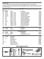
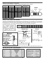
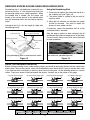
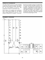
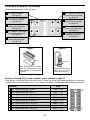
SOLDER PRACTICE KIT
MODEL SP-3B
Assembly and Instruction Manual
ELENCO
Copyright © 2012, 2001 by Elenco® Electronics, Inc. All rights reserved.
®
Revised 2012
REV-K
No part of this book shall be reproduced by any means; electronic, photocopying, or otherwise without written permission from the publisher.
753000
PARTS LIST
If you are a student, and any parts are missing or damaged, please see instructor or bookstore.
If you purchased this kit from a distributor, catalog, etc., please contact Elenco® (address/phone/e-mail is at the
back of this manual) for additional assistance, if needed. DO NOT contact your place of purchase as they will
not be able to help you.
RESISTORS
Note: Please refer to page 7 for the resistor reading exercise. This will familiarize you with the resistor color
band coding.
Qty. Symbol
Value
Color Code
Part #
r 2 R1, R7
100Ω 5% 1/4W
brown-black-brown-gold
131000
r 2 R2, R8
150Ω 5% 1/4W
brown-green-brown-gold
131500
r 2 R3, R9
200Ω 5% 1/4W
red-black-brown-gold
132000
r 2 R4, R10
220Ω 5% 1/4W
red-red-brown-gold
132200
r 2 R5, R11
330Ω 5% 1/4W
orange-orange-brown-gold
133300
r 1 R13
18kΩ 5% 1/4W
brown-gray-orange-gold
151800
r 1 R14
27kΩ 5% 1/4W
red-violet-orange-gold
152700
r 1 R15
39kΩ 5% 1/4W
orange-white-orange-gold
153900
r 1 R16
47kΩ 5% 1/4W
yellow-violet-orange-gold
154700
r 2 R6, R12
56kΩ 5% 1/4W
green-blue-orange-gold
155600
r 1 R17
100kΩ 5% 1/4W
brown-black-yellow-gold
161000
r 1 R18
120kΩ 5% 1/4W
brown-red-yellow-gold
161200
r 1 R19
470kΩ 5% 1/4W
yellow-violet-yellow-gold
164700
r 1 R20
680kΩ 5% 1/4W
blue-gray-yellow-gold
166800
CAPACITORS
Qty.
r2
Symbol
C1, C2
Value
10μF 16V
Description
Electrolytic
Part #
271015
SEMICONDUCTORS
Qty.
r2
r2
Symbol
Value
Q1, Q2
2N3904
LED1, LED2 Red
Description
Transistor NPN
LED (Light Emitting Diode)
Part #
323904
350002
MISCELLANEOUS
Qty. Symbol
r1
r 1 SW1
r1
r1
r 1 U1
r 36”
r1
r1
Description
PC board
Slide switch
Desoldering wick
Battery snap
16-pin IC socket
Wire 22AWG solid
Color code calculator
Lead-free solder tube
Part #
517042
541102
556000
590098
664016
834064
9CC100
9LF99
PARTS IDENTIFICATION
Resistor
Capacitor
Miscellaneous
Semiconductors
Battery Snap
Slide Switch
Solder Wick
Electrolytic
LED
Transistor
IC Socket 16-pin
-1-
Solder
IDENTIFYING RESISTOR VALUES
Use the following information as a guide in properly identifying the value of resistors.
BAND 1
1st Digit
Color
Black
Brown
Red
Orange
Yellow
Green
Blue
Violet
Gray
White
BAND 2
2nd Digit
Digit
0
1
2
3
4
5
6
7
8
9
Color
Black
Brown
Red
Orange
Yellow
Green
Blue
Violet
Gray
White
Multiplier
Digit
0
1
2
3
4
5
6
7
8
9
Color
Black
Brown
Red
Orange
Yellow
Green
Blue
Silver
Gold
Resistance
Tolerance
Multiplier
1
10
100
1,000
10,000
100,000
1,000,000
0.01
0.1
Color
Silver
Gold
Brown
Red
Orange
Green
Blue
Violet
Tolerance
±10%
±5%
±1%
±2%
±3%
±0.5%
±0.25%
±0.1%
BANDS
2
1
Multiplier
Tolerance
IDENTIFYING CAPACITOR VALUES
Capacitors will be identified by their capacitance value in pF (picofarads), nF (nanofarads), or μF (microfarads).
Most capacitors will have their actual value printed on them. Some capacitors may have their value printed in
the following manner. The maximum operating voltage may also be printed on the capacitor.
(–)
0
1
2
3
Multiply By
1
10
100
1k
CERAMIC DISC
Second digit
4
5
8
Tolerance*
Multiplier
First digit
50V
0.1
MYLAR
Multiplier
101K
9
10k 100k .01
Second digit
Tolerance*
First digit
If the capacitor is
connected with
incorrect polarity, it
may heat up and
either leak, or
cause the capacitor
to explode.
(+)
For the No.
100V
Warning:
Multiplier
2A222J
Electrolytic capacitors have a positive
and a negative electrode. The
negative lead is indicated on the
packaging by a stripe with minus
signs and possibly arrowheads. Also,
the negative lead of a radial
electrolytic is shorter than the positive
one.
Maximum working voltage
Polarity
marking
(–)
The value is 10 x 10 =
100pF, +10%, 50V
The value is 22 x 100 =
2,200pF or .0022μF, +5%, 100V
* The letter M indicates a tolerance of +20%
(+)
Radial
Axial
(may or may not appear
on the cap)
The letter K indicates a tolerance of +10%
The letter J indicates a tolerance of +5%
Note: The letter “R” may be used at times to signify a decimal point; as in 3R3 = 3.3
METRIC UNITS AND CONVERSIONS
Abbreviation
p
n
μ
m
–
k
M
Means
Pico
nano
micro
milli
unit
kilo
mega
Multiply Unit By
.000000000001
.000000001
.000001
.001
1
1,000
1,000,000
Or
10-12
10-9
10-6
10-3
100
103
106
-2-
1. 1,000 pico units
= 1 nano unit
2. 1,000 nano units
= 1 micro unit
3. 1,000 micro units = 1 milli unit
4. 1,000 milli units
= 1 unit
5. 1,000 units
= 1 kilo unit
6. 1,000 kilo units
= 1 mega unit
CONSTRUCTION
Introduction
Safety Procedures
The most important factor in assembling your SP-3B
Solder Practice Kit is good soldering techniques.
Using the proper soldering iron is of prime
importance. A small pencil type soldering iron of 25 40 watts is recommended. The tip of the iron must
be kept clean at all times and well tinned.
• Always wear safety glasses or safety
goggles to protect your eyes when
working with tools or soldering iron,
and during all phases of testing.
Solder
• Locate soldering iron in an area where you do not
have to go around it or reach over it. Keep it in a
safe area away from the reach of children.
'
• Be sure there is adequate ventilation when
soldering.
For many years leaded solder was the most common
type of solder used by the electronics industry, but it
is now being replaced by lead-free solder for health
reasons. This kit contains lead-free solder, which
contains 99.3% tin, 0.7% copper, and has a rosinflux core.
• Do not hold solder in your mouth. Solder is a
toxic substance. Wash hands thoroughly after
handling solder.
Lead-free solder is different from lead solder: It has a
higher melting point than lead solder, so you need
higher temperature for the solder to flow properly.
Recommended tip temperature is approximately
700OF; higher temperatures improve solder flow but
accelerate tip decay. An increase in soldering time
may be required to achieve good results. Soldering
iron tips wear out faster since lead-free solders are
more corrosive and the higher soldering
temperatures accelerate corrosion, so proper tip
care is important. The solder joint finish will look
slightly duller with lead-free solders.
Flux
Most solder contains flux in the hollow core of the
solder allowing it to be applied automatically when
you heat the solder. The flux will remove any oxide
film on the metals soldered creating a good metal-tometal contact. This is called “wetting the metal”.
There are three types of solder fluxes: chloride,
organic and rosin. In the electronics industry, only
the rosin type is used. Rosin flux comes in two types,
pure and active. The most reliable is the pure type,
since it doesn’t cause dendrites between tracks on
the PC board as the active type does. Due to the
highly
corrosive
and
moisture
attracting
characteristics of the chloride and organic type
fluxes, they should not be used in electronics.
Use these procedures to increase the life of your
soldering iron tip when using lead-free solder:
• Keep the iron tinned at all times.
• Use the correct tip size for best heat transfer. The
conical tip is the most commonly used.
Surface Preparation
In order for the solder to adhere to the connection, the
metals must be clean and free of nonmetallic materials.
Flux in the solder can remove oxides from metal but not
other materials like dirt or grease. To remove these, use
a small steel brush or fine emery cloth.
• Turn off iron when not in use or reduce
temperature setting when using a soldering
station.
• Tips should be cleaned frequently to remove
oxidation before it becomes impossible to remove.
Use Dry Tip Cleaner (Elenco® #SH-1025) or Tip
Cleaner (Elenco® #TTC1). If you use a sponge to
clean your tip, then use distilled water (tap water
has impurities that accelerate corrosion).
Mechanical Connection
When all the surfaces are clean, the metals should
have a solid mechanical connection. Wires should
be tightly wrapped around each other or to the
terminal. This will eliminate large gaps that create
weak solder joints. Solder should not be used as a
mechanical connection.
Solder
Terminal
Rosin Core
Wire
Figure 1
Figure 2
-3-
Solder
Types of Soldering Devices
Tip Cleaning
A number of different types of soldering devices:
irons, guns and stations are available today. Irons
are used for light to medium work and guns are for
medium to heavy-duty work. The station type can
range from light to heavy-duty For working on PC
boards, irons ranging from 15 to 40 watts are
suitable, or a station with a range of 15 to 40 watts.
If you use an iron with a higher wattage rating than
40 watt, you may damage the copper tracks on the
PC board. The higher wattage irons are best suited
for heavy-duty electrical jobs.
A good clean solder tip makes soldering much
easier. The tip should be tinned by lightly coating it
with solder to prevent it from oxidizing. The tip can
become pitted (black spots) from normal use. It is
important to clean the tip by wiping it with a wet
sponge or rag. For tips that need a good cleaning,
the tip tinner and cleaner (#TTC1) should be used.
Never use a file or abrasive material to clean the
tip. Using such methods will damage the plating and
ruin the tip. Do not remove the excess solder from
the tip before storing. The excess solder will prevent
oxidation.
Clean Connections
Soldering Iron
Soldering Gun
Proper solder adhesion requires that the metal
surface to be free of dirt and grease. The flux only
removes the oxides so a brush or rag can be used to
clean metal. There are contact cleaners in aerosol
cans and other solvents available.
Soldering Station
Solder Tips
The tip is the very important part of the iron. The
material that the tip is made from is an essential
factor. The soldering iron tip contains four different
metals as shown in Figure 3. The core consists of
copper. Since the copper is a soft material, it is
plated with iron. Chrome plating is used on the area
where no soldering takes place to prevent oxidation.
Then the tip is plated with tin, because it can be
easily cleaned.
Tin Plating
Chrome Plating
Iron Plating
Desoldering
Great care should be taken when repairing or
correcting a mistake on a PC board. The metal foil
can be easily pulled up or broken from excessive
heat. Use the least amount of heat as possible. You
can use a desoldering tool, bulb, wick or a station.
These tools will remove the solder enabling you to
correct the problem.
Copper
Desoldering Tool
Figure 3
Today, tips are manufactured in a variety of different
shapes (see figure below). The chisel shape is one
of the most common. Having a choice of tip styles
allows you to choose the one best suited for your
soldering needs. Due to the high heat, removable
tips can bond themselves to the heating element if
left in place for extended periods of time. Periodic
removal of the tip is therefore advisable.
1/32”
1/64”
1/16”
1/8”
Solder Wick
3/64”
Desoldering Station
-4-
Desoldering Bulb
SOLDER PRACTICE
Double Pads
Tack Soldering
Before we begin to assemble and solder
the components to the solder practice
PC board, we will start first by practice
soldering to the double pads on the
Figure 4
edge of the PC board (see Figure 4).
You will make 10 tack solder connections by
soldering five wires to the top row of pads.
1. Cut 5 one-inch wires and strip 1/8” insulation off
both ends.
2. Place the iron and the wire on top left pad as
shown in Figure 7. Allow the solder to flow around
the wire. Then, remove the iron and let the solder
cool. You may need to add some more solder.
The solder should be neat and smooth.
1. Apply a small amount of solder to the iron tip. This
allows the heat to leave the iron and onto the foil.
2. Place the iron on the top half of pad and then
apply the solder (see Figure 5). Allow the solder
to flow around the pad. Then, remove the solder
and the iron and let the solder cool. The solder
should be neat and smooth.
3. Pull the wire to make sure you have a good solder joint.
4. Bend the wire and solder it to the next pad, as
shown in Figure 7.
3. Repeat step 2 on the bottom half of the pad (see Fig. 5).
5. Now solder the remaining wires to the pads as
shown in Figure 7.
Soldering Iron
4. Practice again on the second large pad.
Soldering Iron
Solder
Solder
Figure 5
Figure 7
Single Pads
Jumper Wires
Now practice using the single pads. Start with the four
square pads and use the same soldering procedures
as the large pads. Note that the spacing between the
pads decrease as the pads get smaller. Be sure there
are no solder bridges between the pads.
In this section, you will solder 20 jumpers between
the two rows of holes.
1. Cut a one-inch wire and strip 1/8” insulation off
both ends.
2. Insert the wire between the top and bottom hole
(see Figure 8a).
3. Apply a small amount of solder to the tip.
Immediately apply solder to the opposite side of
the connection, away from the iron. Allow the
heated wire and circuit foil to melt the solder (see
Figure 8b).
Solder Bridge
Solder bridges occur when solder runs between
circuit paths and creates a short circuit. This is
usually caused by using too much solder. Try to
intentionally make a solder bridge on each section
(see Figure 6). Then, remove it by simply dragging
your soldering iron across the solder bridge as
shown. It is best to wipe the iron tip with a wet
sponge to remove the solder. You can also use
solder wick as described on page 7.
Figure 6
4. Cut off the excess leads.
5. Solder the remaining 19 jumper wires.
Soldering
Iron
Soldering Iron
PC Board
Jumper
Wires
Solder Bridges
Figure 8a
Drag Iron
-5-
Solder
Figure 8b
PC BOARD REPAIR
Hairline Cracks
Wide Gaps
The hairline cracks can develop in the copper foil if
the PC board is flexed. This can be easily repaired
by making a solder bridge across the two foils. The
solder should smoothly flow across the foil as shown
in Figure 9. If the solder does not adhere to the foil,
it will sit on the foil as a blob as shown if Figure 10.
Wide gaps in the copper foil can be bridged using a
small wire soldered across the gaps (see Figure 12).
Four wires will be soldered across the two rows of
small solder pads.
Board
Solder
Bare Wire
Solder
Foil
Foil
Figure 12
Figure 9
Figure 10
1. Place the iron on the top of a pad and then apply
the solder (see Figure 12). Allow the solder to
flow around and form a small pool.
1. Make five solder bridges using the second row of
single pads, starting from the left side (see Figure 11).
2. Repeat Step 1 on the adjacent pad.
3. Strip 1/2” of insulation off one end of the wire and
then tin it.
Solder Bridges
4. Position the wire on top of the solder pad and then
place the iron on the wire. As the solder melts,
the wire will be pressed down against the pad
(see Figure 12). Remove the iron while holding
the wire in place. Make sure the wire does not
move until the solder hardens.
Figure 11
5. Check for a good solder connection.
Reinforcing a Repair
6. Repeat step 4 on the adjacent pad.
A solder bridge repair can be reinforced using a solid
wire. Now add a wire to the five solder bridges you
just made.
7. Cut the wire off as close to the solder joint as
possible (see Figure 12).
1. Strip a 1/2” of insulation off one end of the wire
and then tin it.
8. You can hold the wire down with a screwdriver
and resolder if needed.
2. Hold the tinned wire on top of the solder bridge.
9. Practice this procedure three more times on the
remaining pads.
3. Place the iron on the wire until the solder melts.
4. Remove the iron while holding the wire in place
against the foil. Make sure the wire does not
move until the solder hardens.
5. Check for a good solder connection.
6. Cut the wire off as close to the solder joint as
possible.
7. Practice this procedure four more times.
-6-
REMOVING EXCESS SOLDER USING DESOLDERING WICK
Using the Desoldering Wick
Desoldering wick is a braided wire coated with noncorrosive rosin flux. It is the simplest and safest tool
for removing solder from a solder connection. When
the braided wire is heated, the flux cleans and
breaks up the surface tension so the melted solder
from the connection flows into the braid by capillary
action.
1. Place the wick against the solder with the tip of a
hot soldering iron (see Figure 13).
2. The molten solder is sucked up into the wick by
capillary action.
3. When the iron and wick are removed, the solder
should be removed. You need to repeat the
process if some solder remains.
Included in this kit is a six inch length of solder wick
(desoldering braid).
If necessary, repeat the procedure until all of the
unwanted solder is removed.
CAUTION: Wick gets HOT - use
long nose pliers to hold wick.
Soldering Iron Tip
After the excess solder has been removed, clip off
and discard the solder-saturated portion of the braid.
For best results, always use a fresh area of the braid
for each procedure.
Foil Side of PC board
Desoldering
Wick
Excess Solder
Using desoldering wick to remove excess solder.
A close-up view of the accumulation of solder onto
the solder wick (desoldering braid).
Figure 13
Figure 14
RESISTOR READING EXERCISE
Before starting assembly of your solder practice project, you should be thoroughly familiar with the 4-band color
code system. Many of the resistor values will be identified by color bands and it is easy to mistake their value
if you read the colors incorrectly or read the value from the wrong end. Do the following exercise in resistor
values. Place your answer in the box beneath the resistor. Answers are on the bottom of this page.
(1) brown-green-red-gold
(2) brown-black-orange-gold
(3) brown-black-yellow-gold
(4) red-red-orange-gold
(5) yellow-violet-brown-gold
(6) blue-gray-orange-gold
(7) yellow-violet-black-gold
(8) brown-blue-brown-gold
(9) orange-orange-red-gold
(10) green-brown-red-gold
(11) brown-black-green-gold
(12) brown-gray-orange-gold
Answers to Resistor Reading Exercise: 1) 1.5kΩ+5%; 2) 10kΩ+5%; 3) 100kΩ+5%; 4) 22kΩ+5%; 5) 470Ω+5%;
6) 68kΩ+5%; 7) 47Ω+5%; 8) 160Ω+5%; 9) 3.3kΩ+5%; 10) 5.1kΩ+5%; 11) 1MΩ+5%; 12) 18kΩ+5%
-7-
THEORY OF OPERATION
The solder practice kit consists of a circuit oscillating
at one hertz (one cycle per second). The oscillator
consists of two transistors Q1 and Q2, and resistors,
R1 - R11 and capacitors C1 and C2. This
configuration is known as a multivibrator circuit.
Q2 will start to conduct, causing Q1 to rapidly cutoff.
This process continues alternately causing Q1 or Q2
to conduct. The output will be a square wave. The
frequency is determined by the time constants of
resistor R6 and capacitor C1, also R12 and C2. Two
LED diodes are placed in the collectors of the
transistors and will light when current is passing
through them. Resistors R1 - R5, R7 -R11 determine
the current passing through the LEDs.
When voltage is first applied to this multivibrator
circuit, one transistor (possibly Q1) will conduct
faster, causing transistor Q2 to stay off. Q1 will
continue to conduct until it saturates. At this point,
SCHEMATIC DIAGRAM
-8-
SOLDERING COMPONENTS TO THE PC BOARD
A poorly soldered joint can greatly affect small current flow in circuits and can cause equipment failure. You can damage
a PC board or a component with too much heat or cause a cold solder joint with insufficient heat. Sloppy soldering can
cause bridges between two adjacent foils preventing the circuit from functioning.
Safety Procedures
•
•
•
•
Wear eye protection when soldering.
Locate soldering iron in an area where you do not have to go around it or reach over it.
Do not hold solder in your mouth. Wash your hands thoroughly after handling solder.
Be sure that there is adequate ventilation present.
What Good Soldering Looks Like
Types of Poor Soldering Connections
A good solder connection should be bright, shiny,
smooth, and uniformly flowed over all surfaces.
1. Insufficient heat - the solder will not flow onto the
lead as shown.
Soldering a PC board
1. Solder all components from the copper foil side only.
Push the soldering iron tip against both the lead and
the circuit board foil.
Rosin
Soldering Iron
Component Lead
Soldering iron positioned
incorrectly.
Foil
2. Insufficient solder - let the solder flow over the
connection until it is covered. Use just enough solder
to cover the connection.
Circuit Board
Solder
2. Apply a small amount of solder to the iron tip. This
allows the heat to leave the iron and onto the foil.
Immediately apply solder to the opposite side of the
connection, away from the iron. Allow the heated
component and the circuit foil to melt the solder.
Solder
Gap
Component Lead
3. Excessive solder - could make connections that you
did not intend to between adjacent foil areas or
terminals.
Soldering Iron
Foil
Solder
3. Allow the solder to flow around the connection. Then,
remove the solder and the iron and let the connection
cool. The solder should have flowed smoothly and not
lump around the wire lead.
Solder
Heat Sinking
Electronic components such as transistors, IC’s, and
diodes can be damaged by the heat during soldering. Heat
sinking is a way of reducing the heat on the components
while soldering. Dissipating the heat can be achieved by
using long nose pliers, an alligator clip, or a special heat
dissipating clip. The heat sink should be held on the
component lead between the part and the solder joint.
Soldering Iron
Foil
4. Here is what a good solder connection looks like.
Soldering Iron
Solder
PC Board
Heat Sink
(this can be ordered as part of Elenco’s
Solder Ease Kit Model SE-1).
-9-
Heat Sensitive
Component (Diode)
PC BOARD ASSEMBLY
Solder the following parts to the PC board.
J2 - Jumper Wire (see Fig. A)
J3 - Jumper Wire (see Fig. A)
J1 - Jumper Wire (see Fig. A)
J6 - Jumper Wire (see Fig. A)
J5 - Jumper Wire (see Fig. A)
J4 - Jumper Wire (see Fig. A)
R10 - 220Ω 5% ¼W Resistor
(red-red-brown-gold)
(see Figure B)
R1 - 100Ω 5% ¼W Resistor
(brown-black-brown-gold)
(see Figure B)
R9 - 200Ω 5% ¼W Resistor
(red-black-brown-gold)
(see Figure B)
R2 - 150Ω 5% ¼W Resistor
(brown-green-brown-gold)
(see Figure B)
R8 - 150Ω 5% ¼W Resistor
(brown-green-brown-gold)
(see Figure B)
R3 - 200Ω 5% ¼W Resistor
(red-black-brown-gold)
(see Figure B)
R7 - 100Ω 5% ¼W Resistor
(brown-black-brown-gold)
(see Figure B)
R4 - 220Ω 5% ¼W Resistor
(red-red-brown-gold)
(see Figure B)
Figure A
Figure B
Cut a 1” wire and strip 1/8” of
insulation off of both ends.
Mount the resistor flat against
the PC board as shown.
Resistance Testing #1 (If you do not have a meter, continue to page 11)
You will test the solder connections by measuring the resistance from the following points. If your readings are
different, double check your soldering connections.
Location
Point A (left side of J1) to point B (right side of J3)
Point A (left side of J1) to point C (top lead of R4)
Point D (left side of J4) to point E (right side of J6)
Point D (left side of J4) to point F (top lead of R10)
Value
Circuit
0.1 - 1Ω
670Ω +5%
(J1-J3)
(J1-J3, R1-R4)
0.1 - 1Ω +5%
670Ω +5%
B
A
D
C
-10-
F
E
(J4-J6)
(J4-J6, R7-R10)
PC BOARD ASSEMBLY (continued)
Solder the following parts to the PC board.
U1 - 16-pin IC Socket
(see Figure C)
R15 - 39kΩ 5% ¼W Resistor
(orange-white-orange-gold)
(see Figure D)
R14 - 27kΩ 5% ¼W Resistor
(red-violet-orange-gold)
(see Figure D)
R16 - 47kΩ 5% ¼W Resistor
(yellow-violet-orange-gold)
(see Figure D)
R13 - 18kΩ 5% ¼W Resistor
(brown-gray-orange-gold)
(see Figure D)
R19 - 470kΩ 5% ¼W Resistor
(yellow-violet-yellow-gold)
(see Figure D)
R17 - 100kΩ 5% ¼W Resistor
(brown-black-yellow-gold)
(see Figure D)
R20 - 680kΩ 5% ¼W Resistor
(blue-gray-yellow-gold)
(see Figure D)
R18 - 120kΩ 5% ¼W Resistor
(brown-red-yellow-gold)
(see Figure D)
Figure C
Figure D
Notch
White Circle
When mounting the IC socket,
make sure that the notch is in the
same direction as marked on the
PC board.
Stand resistor on end as
shown with the body
inside the white circle
Resistance Testing #2 (If you do not have a meter, continue to page 12)
Each resistor is connected across two pins of the IC socket. You will test the solder connections by measuring
the resistance from the following IC pins. If your readings are different, double check your soldering connections.
Location
Value
R14 - Measure from pin 1 to pin 2
27kΩ +/– 5%
R13 - Measure from pin 3 to pin 4
18kΩ +/– 5%
R17 - Measure from pin 5 to pin 6
100kΩ +/– 5%
R18 - Measure from pin 7 to pin 8
120kΩ +/– 5%
R19 - Measure from pin 9 to pin 10
470kΩ +/– 5%
R20 - Measure from pin 11 to pin 12
680kΩ +/– 5%
R16 - Measure from pin 13 to pin 14
47kΩ +/– 5%
R15 - Measure from pin 15 to pin 16
39kΩ +/– 5%
-11-
1
16
8
9
PC BOARD ASSEMBLY (continued)
Solder the following parts to the PC board.
R6 - 56kΩ 5% ¼W Resistor
(green-blue-orange-gold)
(see Figure B)
R12 - 56kΩ 5% ¼W Resistor
(green-blue-orange-gold)
(see Figure B)
R5 - 330Ω 5% ¼W Resistor
(orange-orange-brown-gold)
(see Figure B)
R11 - 330Ω 5% ¼W Resistor
(orange-orange-brown-gold)
(see Figure B)
C1 - 10μF 16V Electrolytic
(see Figure E)
C2 - 10μF 16V Electrolytic
(see Figure E)
Battery Snap (see Figure F)
LED2 - Red LED
(see Figure G)
SW1 - Switch SPST
Q2 - 2N3904 Transistor
(see Figure H)
LED1 - Red LED
(see Figure G)
J7 - Jumper Wire
(see Figure A)
Q1 - 2N3904 Transistor
(see Figure H)
Figure E
Figure F
Figure G
Electrolytic capacitors have
polarity. Be sure to mount them
with the negative (–) lead
(marked on side) in the correct
hole.
Thread the battery snap wires through the hole
in the PC board from the solder side as shown.
Solder the red wire to the (+) point and the
black wire to the (–) point on the PC board.
Mount the LED onto the PC board with
the flat side of the LED in the same
direction as marked on the PC board.
Red
Mount flush
with PC board
Black
Flat
Polarity
Mark
(–)
(+)
Figure H
Warning: If the capacitor is
connected
with
incorrect
polarity, it may heat up and
either leak or cause the
capacitor to explode.
Mount the IC with the flat side in the
same direction as marked on the PC
board. Solder and cut off the excess
leads.
Flat
OPERATION
Connect a 9 volt battery to the battery snap. Turn the ON/OFF switch to the ON position and the LEDs should
alternately light.
-12-
TROUBLESHOOTING
4. Pay close attention to the red and black wires of
the battery snap. The red wire should be installed
in the positive (+) hole and the black wire in the
negative (–) hole. Snap in a fresh 9-volt battery.
If you are a student, and any parts are missing or
damaged, please see instructor or bookstore. If you
purchased this solder practice kit from a distributor,
catalog, etc., please contact Elenco® Electronics
(address/phone/e-mail is at the back of this manual)
for additional assistance, if needed.
Problems
1. No LEDs Light
If you are experiencing a problem, first read the
theory of operation to familiarize yourself with the
operation.
• Check the solder connections for the battery
wires and switch.
• Check that all parts are in the correct way.
Component Check
1. Be sure that all components have been mounted
in their correct places.
2. LED1 Does Not Light
2. Make sure that C1 and C2, the electrolytic
capacitor is mounted correctly. The negative lead
should be in the hole as shown on the top legend.
3. LED2 Does Not Light
• Check C1, LED1 and Q1.
• Check C2, LED2 and Q2.
4. LED1 or LED2 is Always On
3. Have LEDs LED1 and LED2 been installed
correctly? The flat side of their bodies should be
in the same direction as marked on the top
legend. If the LEDs are in backwards, they will not
light.
• Check C1 and C2 for opens.
• Check Q1 and Q2 for shorts.
WORD GLOSSARY
Capacitor
An electrical component that can store electrical pressure (voltage) for periods of
time.
Cold Solder Joint
Occurs because insufficient heat was applied or the connection was moved before
the solder had set. Connection looks crystalline, crumbly, or dull.
Flux
A substance that is used to cleanse the surface of oxide before it is soldered. Always
used in electronics work. Most of the solder used in electronics has flux built right into it.
Heat Sinking
A process of keeping the component from becoming overheated during soldering.
Any metal object that can be clamped to the component lead will work as an effective
heat sink. An alligator clip or pliers work well.
Integrated Circuit (IC)
A type of circuit in which transistors, diodes, resistors, and capacitors are all
constructed on a semiconductor base.
Jumper Wire
A wire that is connected from one place to another on a PC board, thereby making a
connection between two pads.
LED
Common abbreviation for light emitting diode.
Light Emitting Diode
A diode made from gallium arsenide that has a turn-on energy so high that light is
generated when current flows through it.
Oxidation
Most metals, when exposed to air, form an oxide on their surface which prevents
solder from adhering to the metal.
Polarity
The division of two opposing forces or properties.
Printed Circuit Board
A board used for mounting electrical components.
Components are connected using metal traces “printed” on the board instead of
wires.
-13-
WORD GLOSSARY (continued)
Resistor
Component used to control the flow of electricity in a circuit. It is made of carbon.
Rosin Core Solder
The most common type of solder used in electronics generally referred to as 63/37
rosin core solder.
Solder
A tin/lead alloy that melts at a very low temperature, used to join other metals
together. It produces excellent electrical connections.
Solder Bridge
An unwanted solder connection between two points that are close together.
Solder Melting Point
The temperature at which a tin/lead alloy (solder) melts. The common solder used in
electronics (63% tin / 37% lead) has a melting point of 361OF.
Solder Wick
Braided wire coated with flux to effectively remove solder from a connection.
Soldering
The process of joining two or more metals by applying solder to them.
Tack Soldering
A connection where the lead or wire does not have any mechanical support.
Tinning the Tip
A process of coating the soldering iron tip with solder to minimize the formation of
oxide on the tip, which would reduce the amount of heat transfer.
Transistor
An electronic device that uses a small amount of current to control a large amount of
current.
Wire Gauge
Refers to the size of the wire. The bigger the number, the smaller the diameter of the
wire. 18 gauge to 24 gauge is generally used for hook-up in electronics.
QUIZ
1. The solder supplied is comprised of what two materials?
r
r
r
r
r
r
r
r
2. What type of flux should be used in electronics?
r
r
r
r
r
r
r
r
r
r
r
r
A. a jumper.
B. a blob.
C. a solder hole.
D. a solder bridge.
9. What ratio has the greatest amount of tin?
r
r
r
r
A. heating.
B. melting.
C. soldering.
D. oxidizing.
5. Proper solder adhesion requires that the metal surface
to be . . .
A. 20/60
B. 40/60
C. 50/50
D. 93/7
10. A good solder connection should be . . .
A. solder free.
B. clean.
C. greasy.
D. cold.
r
r
r
r
A. dull and rough.
B. shiny, bright and smooth.
C. lumped around the connection.
D. soldered on one side of the connection.
Answers: 1. B, 2. C, 3. A, 4. D, 5. B, 6. A, 7. C, 8. D, 9. D, 10. B
r
r
r
r
A. a solder bridge.
B. using 60/40 solder.
C. insufficient heat.
D. acid core solder.
8. When two adjacent solder joints accidentally touch, it is
called . . .
A. 15-40 watts
B. 50-100 watts
C. 1-10 watts
D. 100-200 watts
4. Tinning the soldering tip will prevent it from . . .
r
r
r
r
A. remove solder.
B. solder in small parts.
C. cleaning the soldering iron tip.
D. removing flux.
7. A cold solder joint is caused by . . .
A. Chloride
B. Organic
C. Rosin
D. Corrosive
3. When working on PC boards, what wattage range of iron
is ideal?
r
r
r
r
6. Solder wick is used to . . .
A. Gold and copper
B. Tin and copper
C. Zinc and copper
D. Lead and aluminum
-14-
ELENCO®
150 Carpenter Avenue
Wheeling, IL 60090
(847) 541-3800
Website: www.elenco.com
e-mail: [email protected]