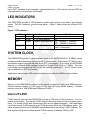
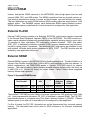
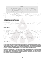
1
D O C - 0 5 1 5 - 0 1 0 , R E V A CMM-52259 Application Module for the Freescale MCF52259 Microcontroller USER GUIDE Email: www.axman.com Support: [email protected] C M M - 5 2 2 5 9 U S E R G U I D E J U N E 1 1 , 2 0 1 0 CONTENTS CAUTIONARY NOTES ..............................................................................................................4 TERMINOLOGY .........................................................................................................................4 FEATURES ................................................................................................................................5 REFERENCES ...........................................................................................................................6 GETTING STARTED ..................................................................................................................6 MCF52259 ..................................................................................................................................6 SOFTWARE DEVELOPMENT ...................................................................................................6 POWER ......................................................................................................................................7 LOW-POWER MODES ......................................................................................................... 7 RESET SWITCH ........................................................................................................................7 ABORT SWITCH ........................................................................................................................7 LED INDICATORS .....................................................................................................................8 SYSTEM CLOCK .......................................................................................................................8 MEMORY ...................................................................................................................................8 INTERNAL FLASH ................................................................................................................ 8 INTERNAL SRAM ................................................................................................................. 9 EXTERNAL FLASH ............................................................................................................... 9 EXTERNAL SRAM ................................................................................................................ 9 COMMUNICATIONS ................................................................................................................ 10 USB PORT .......................................................................................................................... 10 HOST MODE ................................................................................................................... 10 DEVICE MODE ............................................................................................................... 11 ON-THE-GO MODE ........................................................................................................ 11 ETHERNET ......................................................................................................................... 12 PHYSICAL PORT ............................................................................................................ 12 FAST ETHERNET CONTROLLER (FEC) ....................................................................... 13 UART ................................................................................................................................... 13 RS-232 ............................................................................................................................ 13 CAN ..................................................................................................................................... 13 I/O CONNECTORS .................................................................................................................. 14 2 C M M - 5 2 2 5 9 U S E R G U I D E J U N E 1 1 , 2 0 1 0 FIGURES Figure 1: LED Indicators .............................................................................................................8 Figure 2: Supported SRAM Devices ...........................................................................................9 Figure 3: USB Configuration ..................................................................................................... 11 Figure 4: Ethernet PHY Default Configuration .......................................................................... 12 Figure 5: Ethernet LED Indicators ............................................................................................ 12 Figure 6: UART0 Signal Connections ....................................................................................... 13 Figure 7: MCU_PORT IO Header ............................................................................................. 14 Figure 8: BUS_PORT IO Header .............................................................................................. 15 Figure 9: MISC_PORT IO Header ............................................................................................ 15 Figure 10: BDM_PORT IO Header ........................................................................................... 15 REVISION Date June 11, 2010 Rev A Comments Initial Release. 3 C M M - 5 2 2 5 9 U S E R G U I D E J U N E 1 1 , 2 0 1 0 CAUTIONARY NOTES 1) Electrostatic Discharge (ESD) prevention measures should be used when handling this product. ESD damage is not a warranty repair item. 2) Axiom Manufacturing does not assume any liability arising out of the application or use of any product or circuit described herein; neither does it convey any license under patent rights or the rights of others. 3) EMC Information on the CMM-52259 board: a) This product, as shipped from the factory with associated power supplies and cables, is designed to meet the requirements of CE and FCC as a CLASS A product. However, this product is not tested for compliance. b) This product is designed and intended for use as a development platform for hardware or software in an educational or professional laboratory. c) In a domestic environment, this product may cause radio interference in which case the user may be required to take adequate prevention measures. d) Attaching additional wiring to this product or modifying the product operation from the factory default as shipped may effect its performance and cause interference with other apparatus in the immediate vicinity. If such interference is detected, suitable mitigating measures should be taken. TERMINOLOGY This development board uses option selection jumpers and cut-traces. An option jumper is a plastic shunt that connects 2 terminals electrically. A cut-trace is a signal trace providing default connection between pads. Terminology for application of the option jumpers is as follows: Jumper on, in, or installed - jumper is installed such that 2 pins are connected together. Jumper off, out, or idle - jumper is installed on 1 pin only. It is recommended that jumpers be idled by installing on 1 pin so they will not be lost. Cut-Trace – a circuit trace connection between component pads. The circuit trace may be cut using a knife to break the default connection. To reconnect the circuit, simply install a suitably sized 0-ohm resistor or attach a wire across the pads. Signal names in this document that are followed by an asterisk (*) denotes active-low signals. 4 C M M - 5 2 2 5 9 U S E R G U I D E J U N E 1 1 , 2 0 1 0 FEATURES The CMM-52259 is full-featured, low-cost application module featuring the Freescale MCF52259 microcontroller. This module is available in 3 configurations; the CMM-52259OEM consists of the board only, the CMM-52259-DEV consists of the board and supporting cables, the CMM-52259-DEV-BDM consists of the board, supporting cables, and an AxBDM. In default configurations, the board is built with only the BDM_PORT header installed. Remaining IO headers are left unpopulated. This provides the end-user flexibility to mount additional headers on either side of the board. The board and BDM are fully compatible with Freescale CodeWarrior. The MQX RTOS is also freely available for application development. Embedded application development and debug is quick and easy using the CMM-52259-DEV-BDM, CodeWarrior, and MQX RTOS. Features: MCF52259 CPU, 144 LQFP V2 ColdFire Core w/ eMAC 80MHz internal bus 512 KB FLASH 64 KB SRAM 4ch, DMA Controller w/ Timers 10/100 Fast Ethernet Controller (FEC) USB Physical Layer Interface (PHY) Host/Device/OTG USB Modes Mini-FlexBus External Bus Interface Fast ATD Converter FlexCAN 2.0B Module I2C, UART(s), QSPI Real-Time Clock 48 MHz and 32.768 KHz Crystal Input 1Mb (128K x 8) Fast SRAM Memory 64Mb Serial Flash Memory 10-100 Ethernet PHY RJ-45 Connector w/ Magnetics HP Auto MDI/MDI-X Cable Detection SPD and LINK_ACT LEDs mini-AB USB Port Host/Device/OTG Modes Supported USB Mode Select Control Up to 500mA VBUS output Low- and Full-Speed USB Signaling Supported RS-232 Port w/ 2 x 5 Pin Header 1 Mbaud CAN PHY IO Header Access to MCU Signals RESET switch input w/ indicator ABORT switch input On-board voltage regulators provide all operating voltages Specifications: Board Size 2.2” x3.5” Power Input: +7 to +34 VDC, 9VDC typical 5 C M M - 5 2 2 5 9 U S E R G U I D E J U N E 1 1 , 2 0 1 0 REFERENCES Reference documents are provided on the support CD in Acrobat Reader format. CMM-52259_UG.pdf CMM-52259_SCH_A.pdf CMM-52259_Silk_A.pdf CFPRM.pdf CMM-52259-Test.zip CMM-52259 User Guide (this document) CMM-52259 Schematic CMM-52259 Top Silkscreen ColdFire Programmers Reference Manual CodeWarrior Project using MQX RTOS GETTING STARTED To get started quickly, please refer to the CMM-52259 Quick Start Guide. The quick start guide shows how to connect the board and execute the pre-programmed demonstration. MCF52259 The CMM-52259 features the Freescale MCF52259 microcontroller in a 144LQFP package. Details on use and configuration of internal modules may be found in the device Reference Manual. The device Datasheet contains information on the electrical requirements for use of the MCF52259. This document provides only brief descriptions of several internal MCU modules. Use and configuration of internal MCU modules requires further research using the Reference Manual and Datasheet. This additional research is left to the reader. Resources for the MCF52259, including Reference Manual and Datasheet may be downloaded directly from the Freescale web site at www.freescale.com. SOFTWARE DEVELOPMENT Software development for the CMM-52259 requires a ColdFire assembler or compiler, a host application development system, and a ColdFire compatible BDM cable. CodeWarrior Development Studio for ColdFire, v7.2 or later, fully supports application development and debug on the MCF52259. CodeWarrior is a fully integrated development environment (IDE) with debugger. The complimentary Freescale MQX real-time operation system (RTOS) is also available for application development. The MQX RTOS provides fully featured TPC/IP and USB software stacks ready for use. CodeWarrior and the MQX RTOS are both available for download from the Freescale web site at www.freescale.com. Application development and debug is fully supported using either the Axiom AxBDM-CF cable or the P&E ColdFire Multilink cable. 6 C M M - 5 2 2 5 9 U S E R G U I D E J U N E 1 1 , 2 0 1 0 NOTE: At this time, the MCF52259 unsecure function is supported using the P&E BDM only. The AxBDM can not be used to unsecure the MCU. When using the P&E unsecure function set the BUS frequency to 1333333 Hz. POWER Power to the CMM-52259 is applied at a 2.1mm, center-positive, barrel connect at J8. Input voltage is limited to the range of +7V to +34V. Insufficient or excessive input voltage may cause damage the board. The center tap from the barrel connector is connected to the MISC_PORT, pin 20 (J3-20). This provides flexibility in embedded applications. The CMM-52259 may be powered through the J3-20 input or may supply power to external circuitry through this connection. The CMM-52259 does not apply input transient, over-voltage, or reverse voltage protection at the input. Care should be used with applying power to the board; otherwise, damage to the board may occur. Low-Power Modes The MCF52259 supports several operating modes designed to reduce power consumption. Low-power modes include Wait, Doze, Stop, and Halt. Each low-power mode disables different MCU sub-systems. RESET SWITCH External reset is provided by a RESET push-button switch, or user connection to the RSTI* signal at the MCU_PORT (J1-5). The MCF52259 provides power-on reset (POR) and low voltage detector (LVD) functions internally. POR holds the device in reset until input voltage rises and stabilizes at a sufficient level. The LVD is user configurable to force a device reset or interrupt condition if the supply voltage falls below the LVD trip point. A red LED indicator is connected to the RSTO* output from the target device. If device reset is asserted, regardless of origin, RSTO* is also asserted causing the RESET LED to turn on. ABORT SWITCH The ABORT push-button switch is connected to the target device on IRQ7*/PNQ7. The input signal may be used as an interrupt input or as a general purpose input/output signal (GPIO). Interrupt level 7 (IRQ7*) is the highest input level to the MCU. When configured as an interrupt 7 C M M - 5 2 2 5 9 U S E R G U I D E J U N E 1 1 , 2 0 1 0 input, IRQ7* becomes a non-maskable, edge-sensitive input. If this input is used as GPIO the user application must configure functionality. LED INDICATORS The CMM-52259 provides 4 LED indicators; power supply status, reset status, and ethernet status. The LED indicators provide board status. Figure 1 below shows the different LED states. Figure 1: LED Indicators LED RESET +3.3V SPD Color Red Green Green LINK_ACT Green Function Default MCU in reset state OFF +3.3V power present ON Ethernet speed indicator ON – 100BASE-T operation OFF – 10BASE-T operation Ethernet link indicator ON – Ethernet link present Flash – Link activity SYSTEM CLOCK The CMM-52259 provides 2 crystal oscillator inputs to the MCF52259 MCU. A 48MHz crystal oscillator provides the primary input to the MCU clock module. A secondary, 32.768 kHz crystal oscillator supports internal real-time clock (RTC) functionality. Out of reset, the MCF52259 defaults to its internal 8MHz oscillator setting the System Clock (fSYS) to 1.33MHz. The user must enable and configure the MCU to use the external crystal input. The 32.768 kHz clock input is dedicated to RTC functionality. Applications which require USB communications must enable the 48MHz crystal oscillator. MEMORY Memory for the CMM-52259 consists of both internal and external FLASH and SRAM memory. Internal memory consists of 512K bytes FLASH and 64K bytes SRAM memory. External memory consists of 1Mb SRAM and 64Mb serial FLASH. Internal FLASH FLASH memory internal to the MCF52259 consists of 512K bytes of 32-bit memory. It is nonvolatile and bootable. The internal FLASH supports fast page erase and word program operations. It is divided into 4K byte logical pages that can be erased separately. User application can locate internal FLASH memory at any 512K boundary within the 4 GB address space. The value programmed into the FLASHBAR register determines the starting FLASH address. Default register configuration locates internal FLASH memory at address 0x0000_0000. 8 C M M - 5 2 2 5 9 U S E R G U I D E J U N E 1 1 , 2 0 1 0 Internal SRAM Internal, dual-ported, SRAM connects to the MCF52259’s internal high-speed local bus and supports DMA, FEC, and USB access. The SRAM is partitioned into two physical memory arrays allowing simultaneous access to arrays by the processor core and another bus master. The user application can locate SRAM memory 64k boundary within the target device’s 4 GB address space. The RAMBAR register value determines SRAM starting address location. SRAM address space is undefined out of reset and must be configured by user application. External FLASH External FLASH memory consists of a Spansion, S25FL064, serial memory device connected to the Queued Serial Peripheral Interface (QSPI) on the MCF52259. The QSPI module provides a serial peripheral interface with queued transfer capability allowing users to queue up to 16 transfers at once, eliminating CPU intervention between transfers. QSPI chip select, QSPI_CS0*, is dedicated to external, on-board, FLASH memory transfers and may be disconnected by option jumper if necessary. Two additional QSPI chip-selects are available for use with external, off-board serial devices connected to MCU_PORT. The QSPI module must be enabled by user application before use. External SRAM External SRAM connects to the MCF52259 Mini-FlexBus external bus. The Mini-FlexBus is a sub-set of the FlexBus found on other ColdFire MCU’s and interfaces to slave-only devices. In default configurations, the CMM-52259 applies a Cypress, CY62128E device for external memory. The external memory device footprint accepts memory devices within this family up to 4Mb (512k x 8). Contact the factory for custom orders. Figure 2 below shows supported memory devices and capacities. Figure 2: Supported SRAM Devices Device Part Number Size Addr bits Org CY62128EV30LL CY62138FV30LL CY62148ESL 1Mb 2Mb 4Mb A[16:0] A[17:0] A[18:0] 128k x 8 256k x 8 512k x 8 Start Address CSAR0 + 0x00000 0x00000 0x00000 End Address CSAR0 + 0x1FFFF 0x3FFFF 0x7FFFF The installed CY62128E provides 1Mbtye of storage organized as 128k words by 8 bits (128k x 8). User programmable chip select, FB_CS0* is dedicated to external SRAM. The FB_CS0* base address space is configured using Chip Select Address Register 0 (CSAR0). External address space is not valid out of reset and must be configured by user application. For Rev A boards, the FB_CS0* chip-select can not be disconnected from on-board external memory. This chip-select may not be used for GPIO functions or for off-board, multiplexed applications. 9 C M M - 5 2 2 5 9 U S E R G U I D E J U N E 1 1 , 2 0 1 0 NOTE: Do not use FB_CS0*/PQS3 in GPIO mode on Rev A boards. FB_CS0* is dedicated to on-board external SRAM and can not be disconnected. In GPIO mode, driving FB_CS0*/PQS3 low will cause contention on other external bus signals. Mini-FlexBus chip select, FB_CS1*, is available for use with off-board external memory and provides access to 1Mb (128k x 8) of storage space. FB_CS1* and associated address and data lines are accessible at the BUS_PORT header. Chip select FB_CS1* is not available for multiplexed operation. COMMUNICATIONS The CMM-52259 applies multiple communications ports for use in user application. Supported communications ports include; USB, Ethernet, RS-232, and CAN. The section below provides details on each port. USB Port The CMM-52259 applies a USB port supporting Host, Device, and OTG configurations. A mini-A/B USB connector is applied supporting the different configurations. USB mode is fully controllable by user application. The MCF52259 supports Full- and Low-Speed USB communications. The CMM-52259 is also capable of sourcing VBUS at 500 mA supporting buspowered USB devices. For details on use and configuration of the USB bus refer to the Universal Serial Bus Specification, Revision 2.0 along with the On-The-Go Supplement to the USB2.0 Specification, Revision 1.2. Both documents may be downloaded from the USB Implementer Forum at www.usb.org. Host Mode In Host Mode, the CMM-52259 is capable of sourcing VBUS supporting bus-powered devices. Output current on VBUS is limited to the USB standard 500mA. The output device supplying VBUS in host mode applications provide an over-current indicator output in the event of a fault on VBUS. This output signal is available at TP5 located behind the USB connector. Connecting a mini-A cable to the CMM-52259 signals the user application to configure as a USB HOST. In this configuration, VBUS output is enabled in hardware. The user application must disable VBUS output if required. Voltage levels on the DM and DP lines during the connect sequence determine connection speed. 10 C M M - 5 2 2 5 9 U S E R G U I D E J U N E 1 1 , 2 0 1 0 Device Mode The CMM-52259 may act as either a bus-powered or a self-powered device. As a buspowered device, the CMM-52259 will take input voltage and current through the USB connector. As a self-powered device, the CMM-52259 must be powered through the barrel connector. The VBUS input is designed to prevent back-driving VBUS if the board is powered externally. Connecting a mini-B cable to the CMM-52259 signals the user application to configure as a USB Device. In this configuration, VBUS output is disabled and the CMM-52259 may be powered from the USB bus. The user application must take care not to enable VBUS output to prevent damage to the CMM-52259 or USB HOST. As a USB Device, pull-ups on DM and DP determine USB communications speed. Enabling the DP pull-up selects full-speed mode while enabling the DM pull-up selects low-speed. On-The-Go Mode The On-The-Go supplement (OTG) to the USB2.0 specification enables dual role operation. An OTG appliance can take on HOST mode and DEVICE mode operations based on the type of cable attached. An OTG appliance can also switch modes during a USB session using the Host Negotiation Protocol (HNP) and Session Request Protocol (SRP) application programming interface (API). The CMM-52259 is designed to allow user applications to sense the ID pin voltage level when a USB cable is attached. Figure 3 below shows the control signals associated with HOST and DEVICE Mode. Figure 3: USB Configuration USB Signal DM DP DM Pull Down DP Pull Down DM PullUp DP PullUp VBUS / USB ID VBUS FAULT Function Control Signal USB_DM USB_DP USB_DM_PDOWN/PQS5 Host Mode DM DP Applied Device Mode DM DP NA USB data(-) signal USB data(+) signal DM pull-down control DP pull-down control USB_DP_PDOWN/PQS6 Applied NA DM pull-up control PUC2 NA DP pull-up control PUB3 Na Sense/Enable VBUS output Indicate VBUS fault USB_BVUSCHG/PUC3 Low Applied for low-speed Applied for high-speed High TP5 NA NA NOTE: The customer must apply a jumper wire between TP5 and an IO header signal to access the VBUS over-current indicator signal. 11 C M M - 5 2 2 5 9 U S E R G U I D E J U N E 1 1 , 2 0 1 0 NOTE: To conform to the USB standard, DM and DP pull-downs must be applied in Host Mode configuration. NOTE: For Device Mode applications, apply DP pull-up for Full-Speed applications or DM pullup for Low-Speed applications. Do not apply both DM pull-up and DP pull-up simultaneously. Ethernet The CMM-52259 applies a 10/100 Mbps Ethernet / IEEE 802.3 communications port. Physical Port Network connection is made using an RJ-45 connector in a tab-down configuration. The connector includes interface magnetics. The CMM-52259 applies a Micrel KSZ8041NL physical layer transceiver (PHY) to interface between the network cable and the MCF52259. Hardware strapping configures the PHY for default operation. Each of these setting is configurable in by user application. Figure 4 below shows the default configuration for the Ethernet PHY. Figure 4: Ethernet PHY Default Configuration Function Address Config Isolate Speed Duplex Auto-Negotiate Default Setting 0x01 MII Disable 100 Mbps Half-Duplex Enabled The PHY provides Auto MDI/MDI-X detection allowing the PHY to configure itself to the connected cable. This allows the use of straight-through and cross-over cables without error. The PHY also provide 2 output LED indicators used to indicate LINK, ACTIVITY and SPEED. Figure 5 below details the behavior of the output Ethernet LEDs. Figure 5: Ethernet LED Indicators LED SPD Color Green Function SPEED indicator LINK_ACT Green LINK / ACTIVITY indicator Default ON – 100BASE-T operation OFF – 10BASE-T operation ON – Ethernet link present Flash – Link activity OFF – No Ethernet link Refer to the Micrel, KSX8041NL datasheet for details on use and configuration of the Ethernet PHY. 12 C M M - 5 2 2 5 9 U S E R G U I D E J U N E 1 1 , 2 0 1 0 Fast Ethernet Controller (FEC) The MCF52259 internal Media Access Controller (MAC) supports 10/100 Mbps Ethernet / IEEE802.3 network connections. User application must configure the MAC for Media Independent Interface (MII) operation before use. The MAC supports both full- and half-duplex operation. UART The CMM-52259 applies 3 RS-232, UART channels. RS-232 A RS-232 physical layer transceiver (PHY) is applied on UART0 to support serial communications. UART1 and UART2 signals are available on the MCU_PORT connector for use with offboard PHY’s. A standard “Berg” style pin header and an IDC to DB-9 adapter cable complete the UART0 connections. The on-board PHY is enabled while power is applied to the board. Figure 6 below shows signal connections on UART0. Figure 6: UART0 Signal Connections MCU Port Signal PHY Signals UTXD0/PUA0 URXD0/PUA1 TXD RXD GND UCTS0*/PUA3 URTS0*/PUA2 CTS RTS NC NC COM CONECTOR J5-1 J5-3 J5-5 J5-7 J5-9 J5-2 J5-4 J5-6 J5-8 J5-10 COMMENTS 7, 2 pull-up 1, 2 1, 7 pull-down NOTE: The COM (J5) connector is placed too close to the BDM_PORT connector. To use both the COM cable and the BDM cable, first install the COM cable then install the BDM cable. CAN The CMM-52259 applies a high-speed controller area network (CAN) port. The Phillips, PCA82C250 physical layer transceiver (PHY) provides the interface between the MCF52259 CAN controller port and the physical CAN bus. The PHY connects to the differential CAN bus 13 C M M - 5 2 2 5 9 U S E R G U I D E J U N E 1 1 , 2 0 1 0 while supporting communications rates to 1 Mbaud. The PHY provides slope control reducing radio frequency interference (RFI) while providing a wide common-mode range input protecting against electro-magnetic interference (EMI). The PHY also provides short-circuit protection to battery and ground. Refer to the PCA82C250 data sheet for further details. The FlexCAN module in the MCF52259 provides support for the CAN protocol. The FlexCAN module supports standard and extended identifier (ID) message formats specified in the CAN protocol specification, revision 2.0, part B. The CAN module is disabled out of reset by default and must be configured by user application before use. I/O CONNECTORS The CMM-52259 applies several IO connectors arranged around the perimeter of the board providing access to most MCU signals. The BDM_PORT header is dedicated to development access. The figures below show signal assignment for each IO connector. With the exception of the BDM_PORT header at J4, the IO headers are not populated in default configurations. Figure 7: MCU_PORT IO Header MCU_PORT – J1 2 I2C_SDA0/URXD2/PAS1 I2C_SCL0/UTXD2/PAS0 1 4 TCLK/PSTCLK/CLKOUT/FB_CLK FEC_TXER/PTJ7 3 6 RSTO* RSTI* 5 8 UCTS2*/I2C_SCL1/USB_BUSCHG/PUC3 UCTS0*/USB_BUSE/PUA3 7 9 10 URTS0*/USB_VBUSD/PUA2 URTS2*/I2C_SDA1/USB_VBUSDIS/PUC2 NC 11 12 FB_AD19/PTG3 FB_AD18/PTG2 13 14 FB_AD17/PTG1 FB_AD16/PTG0 15 16 NC NC 17 18 NC DTIN3/DTOUT3/PWM6/PTC3 19 20 GPT3/ICOC3/PWM7/PTA3 DTIN2/DTOUT2/PWM4/PTC2 21 22 GPT2/ICOC2/PWM1/PTA2 DTIN1/DTOUT1/PWM2/PTC1 23 24 GPT1/ICOC1/PWM3/PTA1 DTIN0/DTOUT0/PWM0/PTC0 25 26 GPT0/ICOC0/PWM1/PTA0 UTXD1/I2C_SCL1/PUB0 27 28 URXD1/12C_SDA1/PUB1 UCTS1*/SYNCA/URSC2/PUB3 29 30 URTS1*/SYNCB/UTXD2/PUB2 UTXD0/PUA0 31 32 URXD0/PUA1 URXD2/CANRX/PUC1 33 34 UTXD2/CANTX/PUC0 QSPI_CS2/SYNCB/USB_DM_PDOWN/PQS5 35 36 QSPI_CS0/I2C_SDA0/UCTS1/PQS3 QSPI_CLK/I2C_SCL0/URTS1/PQS2 37 38 QSPI_DIN/I2C_SDA1/URXD1/PQS1 QSPI_DOUT/I2C_SCL1/UTXD1/PQS0 39 40 IRQ7*/PNQ7 QSPI_CS3/SYNCA/USB_DP_PDOWN/PQS6 41 42 IRQ5*/FEC_MDC/PNQ5 NC 43 44 IRQ3*/FEC_MDIO/PNQ3 NC 45 46 IRQ1*/USB_ALTCLK/PNQ1 GND 47 48 +3.3V CAN_HI 49 50 CAN_LO 14 C M M - 5 2 2 5 9 U S E R G U I D E J U N E Figure 8: BUS_PORT IO Header BUS_PORT CMM – J2 2 FB_D1/SYNCA/PTG6 FB_D0/SYNCB/PTG7 1 4 FB_D3/USB_VBUSD/PTH1 FB_D2/USB_VBUSE/PTH0 3 6 FB_D5/I2C_SDA/PTH3 FB_D4/I2C_SCL1/PTH2 5 7 8 FB_D7/CANRX/PTH5 FB_D6/CANRX/PTH4 FB_AD00/PTE0 9 10 FB_AD01/PTE1 FB_AD02/PTE2 11 12 FB_AD03/PTE3 FB_AD04/PTE4 13 14 FB_AD05/PTE5 FB_AD06/PTE6 15 16 FB_AD07/PTE7 FB_AD08/PTF0 17 18 FB_AD09/PTF1 FB_AD10/PTF2 19 20 FB_AD11/PTF3 FB_AD12/PTF4 21 22 FB_AD13/PTF5 FB_AD14/PTF6 23 24 FB_AD15/PTF7 FB_CS0*/PTG5 25 26 FB_ALE/FB_CS1*/PAS2 NC 27 28 FB_OE*/PTH6 NC 29 30 FB_RW*/PTH7 NC 31 32 NC +3.3V 33 34 GND Figure 9: MISC_PORT IO Header MISC_PORT – J3 2 GPT1/ICOC1/PWM3/PTA1 GPT0/ICOC0/PWM1/PTA0 1 4 GPT3/ICOC3/PWM7/PTA3 GPT2/ICOC2/PWM1/PTA2 3 5 6 GND +3.3V 8 AN1/PAN1 AN0/PAN0 7 AN2/PAN2 9 10 AN3/PAN3 AN4/PAN4 11 12 AN5/PAN5 AN6/PAN6 13 14 AN7/PAN7 NC 15 16 NC JTAG_EN 17 18 GND +3.3V 19 20 +VIN Figure 10: BDM_PORT IO Header BDM_PORT – J4 2 TMS/BKPT* RSTO* 1 4 TRST*/DSCLK GND 3 6 TCLK GND 5 7 8 TDI/DSI RSTI* +3.3V 9 10 TDO/DSO GND 11 12 PST3 PTS2 13 14 PST1 PTS0 15 16 DDATA3 DDATA2 17 18 DDATA1 DDATA0 19 20 GND NC 21 22 NC GND 23 24 TCLK 15 1 1 , 2 0 1 0 C M M - 5 2 2 5 9 U S E R G U I D E J U N E 16 1 1 , 2 0 1 0