1
LCD-Monitor
Chassis
Model
LS17PEA
732N
732NPLUS
932B
932BPLUS
932NPLUS
LS19PEB
LS19PEA
SERVICE
TFT-LCD Monitor
Manual
Fashion Feature
-Lustrous/Colorful Appearance (Design)
-Integrated UI applied
-Built-in Scaler Sync Separator
-Connectivity :
LS17PEA, LS19PEA - Analog (15p Dsub)
LS19PEB - Analog (15p Dsub),
Dual (24p DVI-D)
-Power Consumption : 17"(34W), 19"(38W)
-DPMS : under 1 W (230Vac)
Copyright
Trademarks
©2006 by Samsung Electronics Co., Ltd.
Samsung is the registered trademark of Samsung
Electronics Co., Ltd.
All rights reserved.
This manual may not, in whole or in part, be copied,
photocopied, reproduced, translated, or converted to
any electronic or machine readable form without prior
written permission of Samsung Electronics Co., Ltd.
LS17PEA/LS19PEA/LS19PEB Service Manual
First edition February 2006.
Printed in Korea.
ii
LS17PEA/LS19PEA/LS19PEB and MacMaster Cable
Adapter are trademarks of Samsung Electronics Co.,
Ltd.
Macintosh, Power Macintosh are trademarks of Apple
Computer, Inc.
All other trademarks are the property of their respective
owners.
Contents
1. Precautions ………………………………………………………………………………………………………………………………………1
1-1
1-1 Safety Precautions ……………………………………………………………………………………………………………………… 1-1
1-2 Servicing Precautions …………………………………………………………………………………………………………………… 1-2
1-3 Electrostatically Sensitive Devices (ESD) Precautions ……………………………………………………………………………… 1-2
1-4 Installation Precautions ………………………………………………………………………………………………………………… 1-3
2. Product specifications …………………………………………………………………………………………………………………………2
2-1
2-1 Fashion Feature…………………………………………………………………………………………………………………………… 2-1
2-2 LS17PEA Specifications ………………………………………………………………………………………………………………… 2-1
2-3 LS19PEB Specifications ………………………………………………………………………………………………………………… 2-2
2-3 LS19PEA Specifications ………………………………………………………………………………………………………………… 2-4
2-4 Spec Comparison ………………………………………………………………………………………………………………………… 2-5
2-5 Option Specification ……………………………………………………………………………………………………………………… 2-6
3. Alignments and Adjustments …………………………………………………………………………………………………………………3
3-1
3-1 Required Equipment
…………………………………………………………………………………………………………………… 3-1
3-2 Automatic Color Adjustment …………………………………………………………………………………………………………… 3-1
3-3 DDC EDID Data Input …………………………………………………………………………………………………………………… 3-1
3-4 OSD Adjustment When Replacing Panel ……………………………………………………………………………………………… 3-1
3-5 OSD Adjustment When Replacing Lamp Only ………………………………………………………………………………………… 3-1
3-6 Service Function Spec.
3-7 How to execute DDC
………………………………………………………………………………………………………………… 3-2
…………………………………………………………………………………………………………………… 3-4
3-8 How to execute MCU Code ……………………………………………………………………………………………………………… 3-5
4. Troubleshooting
4-1
………………………………………………………………………………………………………………………………4
4-1 No Power) …………………………………………………………………………………………………………………………………4-1
4-2 No Video (ANALOG) ……………………………………………………………………………………………………………………… 4-2
4-3 No Video (DIGITAL) ……………………………………………………………………………………………………………………… 4-4
5. Exploded View and Parts List
5-1
………………………………………………………………………………………………………………5
6. Electrical Parts List ……………………………………………………………………………………………………………………………6
6-1
Contents
7. Block Diagram …………………………………………………………………………………………………………………………………7
7-1
7-1 Power Tree ………………………………………………………………………………………………………………………………… 7-1
7-2 Main Board Part ( LS17PEA, LS19PEA) ……………………………………………………………………………………………… 7-2
7-3 Main Board Part ( LS19PEB) …………………………………………………………………………………………………………… 7-3
7-4 IP Board Part (SMPS Part) ……………………………………………………………………………………………………………… 7-4
7-5 IP Board Part (Inverter Part) …………………………………………………………………………………………………………… 7-5
8. Wiring Diagram …………………………………………………………………………………………………………………………………8
8-1
8-1 Wiring Diagram LS17PEA, LS19PEA ………………………………………………………………………………………………… 8-1
8-2 Wiring Diagram LS19PEB ……………………………………………………………………………………………………………… 8-2
9. Schematic Diagrams ……………………………………………………………………………………………………………………………9
9-1
9-1 Schematic Diagrams (LS17PEA, LS19PEA) ………………………………………………………………………………………… 9-1
9-2 Schematic Diagrams (LS19PEB) ……………………………………………………………………………………………………… 8-2
10. Operating Instructions and Installation
……………………………………………………………………………………………………10-1
10-1 Front …………………………………………………………………………………………………………………………………… 10-1
10-2 Rear……………………………………………………………………………………………………………………………………… 10-2
10-3 Connecting the monitor ……………………………………………………………………………………………………………… 10-3
11-1
11. Disassembly and Reassembly ………………………………………………………………………………………………………………1
11-1 Disassembly …………………………………………………………………………………………………………………………… 11-1
11-2 Reassembly …………………………………………………………………………………………………………………………… 11-6
12. PCB Diagram …………………………………………………………………………………………………………………………………1
12-1
12-1 Main PCB (LS17PEA, LS19PEA) …………………………………………………………………………………………………… 12-1
12-2 Main PCB (LS19PEB) ………………………………………………………………………………………………………………… 12-2
13. Circuit Descriptions ……………………………………………………………………………………………………………………………1
13-1
13-1 Overall Block Structure
……………………………………………………………………………………………………………… 13-1
13-2 Trouble Shooting ……………………………………………………………………………………………………………………… 13-5
13-3 IP BOARD(Power) Schematic Diagrams …………………………………………………………………………………………… 13-8
13-4 IP BOARD(Inverter) Schematic Diagrams ………………………………………………………………………………………… 13-9
14. Reference Infomation
14-1 Technical Terms ……………………………………………………………………………………………………………………… 14-1
14-2 Pin Assignments ……………………………………………………………………………………………………………………… 14-3
14-3 Timing Chart …………………………………………………………………………………………………………………………… 14-4
14-4 Preset Timing Modes ………………………………………………………………………………………………………………… 14-5
14-5 Panel Description ……………………………………………………………………………………………………………………… 14-6
-This Service Manual is a property of Samsung
Electronics Co., Ltd.
Any unauthorized use of Manual can be punished
under applicable International and/or domestic
law.
Samsung Electronics Co.,Ltd.
416, Maetan-3Dong, Yeongtong-Gu, Suwon City,
Gyeonggi-Do, Korea, 443-742
Printed in Korea
P/N : BN82-00138H-02
URL : http://itself.sec.samsung.co.kr/
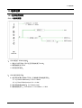
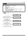
3 调整和调节
3 调整和调节
维修手册本章说明如何使用 DDC 管理工具。
该功能为更换 AD 板和程序存储器(IC110)所需。
3-1 所需的设备
以下设备为调整显示器所需。
-装有Windows 95、Windows 98、或Windows NT的计算机。
-MTI-2031 DDC管理工具
3-2 自动色彩调整
若要输入图像,使用 16 级灰度或任何使用黑色和白色的图形。
1. 为 OSD 语言选择英语。
2. 按“ (确定/来源)
”键 5 秒钟。
3-3 DDC EDID数据输入
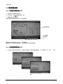
数据输入
1. 在更换 AD 印刷电路板时,输入 DDC EDID 数据。
2. 由 HQ 质量控制部门接收/下载适于该机型 DDC 文件。
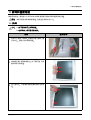
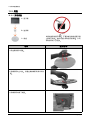
安装以下装置(图 1)并输入数据。
MTI-2031
DDC 管理器
并行连接器
(25 针电缆)
连接显示器
(信号电缆)
图1
3-4 更换显示屏时在屏显示调节
1. 调整亮度和对比度到 0。然后,按下 (确定/来源)键 5 秒。
维修功能 OSD 出现在屏幕上。
2. 按 + 键将光标置于显示屏上。按菜单键 5 秒。
3-5 仅更换灯时在屏显示调节
1. 调整亮度和对比度到 0。然后,按退出键 5 秒。
维修功能 OSD 出现在屏幕上。
2. 按 + 键。选择上灯并按菜单键 5 秒。
然后,选择下灯并按菜单键 5 秒。
-注意:如欲了解维修功能的详情,请务必阅读以下说明。
注意:
三星电子
3-1
3 调整和调节
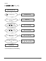
3-6 维修功能说明
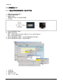
3-6-1 如何显示维修功能 OSD
1. 亮度和对比度值应变为零。
2. 在 5 秒内,按 (确定/来源)键。
3. 维修功能 OSD 将显示。
-如果您想取消维修功能 OSD,则必须断电。
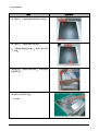
显示屏信息
软件版本
校验和
图 2. 维修功能 OSD 举例
维修功能 OSD 是基于 29 列×12 行的网格。
维修功能 OSD 包含显示屏信息、软件版本和 MICOM 检验和。
3-6-2 如何控制维修功能 OSD
1. 在 OSD 上选择了显示屏时,在您按下右键时,底色会改变成蓝色,从“显示屏”到“上灯”
,
“下灯”
。
图 3.
3-2
三星电子
3 调整和调节
3-6-3 如何控制维修功能 OSD
-在更换显示屏或灯后,必须重设维修功能
在更换显示屏或灯后,必须重设维修功能 OSD。
。
-更换显示屏的情况
更换显示屏的情况
在更换显示屏后,在 5 秒内按菜单键。
然后,显示屏频道数升高一级且显示屏时间信息被重设为零。
同时,其它信息被重设为零(上/下灯,显示屏循环)。
图 4.
3-6-4 如何控制维修功能
如何控制维修功能 OSD
-在更换上灯或下灯的情况下
在更换上灯或下灯的情况下
在更换上灯或下灯后,
1. 选择上灯或下灯。
2. 在 5 秒内按菜单键。
然后,频道数和时间会被重设为零(仅限于选定项)。
图 5、6
三星电子
3-3
3 调整和调节
3-7 如何执行DDC
如何执行
3-7-1 更换主印刷电路板组件后,
更换主印刷电路板组件后 确认以下项目
1. 检查PC颜色状态(自动色彩)
2. EDID输入(模拟和数字)
3. 检查MCU代码
(更换MCU代码后, 执行自动色彩调整)
4. 工厂预设
1) 运行DDC管理器MTI-2050
2) 选择DDC文件名称
程序: 三星电子有限公司WinDDC [版本:4.65.12V]---修改:20050425
DDC: 732N.ddc或932B.ddc
3) 插入DDC管理器端口1(模拟),并向旧式双重机型进行DDC输入。
4) 插入DDC管理器端口2(数字),并进行DDC输入。
1.
2.
3.
4.
3-4
打开文件。
选择端口#1。
选择 DDC 文件。
点击“下一步”按钮。
三星电子
3 调整和调节
5. 键入显示器系列号并按下“确定”
。
*在模拟输入后数字输入过程中,重复本步骤 2 至 5 次。
3-8如何执行
如何执行MCU代码
代码
如何执行
3-8-1程序设置
程序设置-配置设置
程序设置 配置设置
1. 点击配置设置
2. 在管脚分配上改变 SCL 信号
3. 将设备设置为并联。
三星电子
3-5
3 调整和调节
3-8-2 改变批文件路径和下载代码
4. 将代码路径改为电脑上的存储路径。
5. 保存批文件。
6. 键入“分批”指令
“批文件名称.txt”
7. 点击“执行”按钮
8. 如果指令“成功”
,强行开/关机直至 LED 指示灯熄灭
-如果指令“错误”
如果指令“错误”,
1. 强行关机
2. 键入指令“forcesa”
3. 点击“执行“按钮
4. 再次重复 7 至 9。
3-6
三星电子
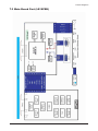
7 Block Diagrams
7 Block Diagram
7-1 Power Tree
7-1
7 Block Diagrams
7-2 Main Board Part (LS17PEA, LS19PEA)
7-2
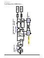
7 Block Diagrams
7-3 Main Board Part (LS19PEB)
7-3
7 Block Diagrams
7-4 IP Board Part (SMPS Part)
7-4
7 Block Diagrams
7-5 IP Board Part (Inverter Part)
7-5
7 Block Diagrams
Memo
7-6
!
"#$%&'( )*+,-./0
1,&' &'
2 34567859:
";#<85#2= >? @ 2=#
AB CD EFG H I
! J "#$"%&' K LM'CD
EFGN8 EK!OP'I
QRSJTU KVWXY' Z
()" 1, "#$"%&' #[ CD\] ' ^L_ * ! +
`a EbcHbd*3Ve`a9
:fg#hij k , lMI
mnhij op qr Kstuv -.
qrwI / ^J ^ &&*0 xyz{|}~
`k %,- ^ &&*0 ~`#
}IT
x %,- ^ ! * 4CT` :M#
* 4CTSJs v
\ kx <# *
7
7#
mn# F ¡ ¢£
¤¥# 22:\]¦ \]¦
\ xCDF§¨#© ª«¬
87&' $112$ 21, %3
W®LM 8®
8® &¯°± ^ #8² 8®
2³7
4´µ 5
¶®
¶®
¶® &¯·2FG¸ ¹FG5
£³724´µ 5
6 º»¼ E3 ½2 k¬ ¢
µ µ %
&'(
$
! "# )*
3
+ $,-
45
. + $,-
+ /012
)*
!" #$%&"'()*
)* +,-./012
+3
456
+./0789:; <=0&>?8
@:;0 ABCDEF12 GH IJ3&>0 K?LM N3
OFPQR" N3OS&TUFPQR
K?LM
" K?LM
N3OVWFXPQR"
K?LM N3OFPQR"
)*
YZ[\3O]^_8 `abcdef
3O GH IJgh>0
<FiO Ijklmno =iO[\
)*no
45pq
rstcpq
[\u
u
Fvw
xvw xvw
F xvw
[\yzy{
[\|}~o o |}~o o
p
)*
12
[\' YZ12=
0&>?[\ abcd N
ef =p12
<^GHvw=
IvwE0
=vwE>?78 GH12
Ip0PQhE3&
¡12¢£p&¤
=E0¥¦ § ¨©ªS&«
¬12 ®i 120S&R"
<E?¯S&R"
E°E±²³´'
«µ²¶· E?¯b
¸¹' + º'=
»Y§pih¼½¾¿q +./0789:;À/
>?78 <=¸h
<E0¥¦12
®iE°jÁGH12<ÂÃ12 IvwE0
<GHvwN=¶5
N12Fp
6 Electrical Parts List
6 Electrical Parts List
6-1 LS19PEBSWE/XSF Parts List
Level
Loc. No.
Code No.
Description & Specification
LS19PEBSWE/XSF
932B,SAB3/S19P0-LPE,19,LCD-MO,CHINA
Q'ty
SA/SNA Remark
0.1
M0001
BN90-01055K
ASSY COVER FRONT;LS19PE (932B),HSD,WHITE
1
S.N.A
..2
T0003
BN96-04142R
ASSY COVER P-FRONT;LS19PE (932B),HSD Pan
1
S.A
...3
M0081
6003-000282
SCREW-TAPTITE;BH,+,-,B,M3,L8,ZPC(BLK),SW
2
S.A
BN61-03222A
GUIDE-PANEL;LS17PEW,SECC,T 0.5
1
S.N.A
...3
...3
CCM1
BN63-02183D
COVER-SHEET;Rhcm,PE Vinyl,T0.05,680mm,20
0.45
S.N.A
...3
M0112
BN63-02878A
COVER-FRONT;PEBBLE,ABS HB,2.4,WH13,SF050
1
S.N.A
...3
T0022
BN64-00534A
KNOB CONTROL;PEBBLE,ABS,HB,WH13,SF-0500
1
S.N.A
...3
T0023
BN64-00597A
KNOB POWER;PEBBLE,ABS HB,WH13,H/GLOSSY
1
S.N.A
...3
M0130
BN67-00193A
LENS LED;PEBBLE,ABS HB,CLR
1
S.N.A
...3
M0145
BN96-04363A
ASSY BOARD P-FUCNTION;Pebble,SJ06-01-023
1
S.A
....4
M0014
BN94-01300M
ASSY PCB MAIN-SEDA,FUCHION PCB;PABBLE*
1
S.N.A
.....5
M2893
BN39-00774A
LEAD CONNECTOR;Pebble,UL1061#28,UL/CSA,3
1
S.A
.....5
M2893
BN39-00788A
LEAD CONNECTOR;Pebble,UL1061#28,4PIN,300
1
S.A
.....5
T0238
BN97-01597B
ASSY AUTO;PEBBLE*
1
S.N.A
......6
T0313
3404-000299
SWITCH-TACT;12V,50mA,120gf,6x6x4.3mm,SPS
5
S.A
......6
T0174
BN97-01589M
ASSY SMD;PABBLE
1
S.N.A
.......7
R110
2007-000122
R-CHIP;1.2Kohm,5%,1/10W,TP,1608
1
S.A
.......7
R110
2007-000122
R-CHIP;1.2Kohm,5%,1/10W,TP,1608
1
S.A
.......7
R110
2007-000123
R-CHIP;1.5Kohm,5%,1/10W,TP,1608
1
S.A
.......7
R110
2007-000123
R-CHIP;1.5Kohm,5%,1/10W,TP,1608
1
S.A
.......7
R110
2007-001157
R-CHIP;750ohm,5%,1/10W,TP,1608
4
S.A
.......7
R110
2007-001157
R-CHIP;750ohm,5%,1/10W,TP,1608
1
S.A
.......7
R110
2007-001157
R-CHIP;750ohm,5%,1/10W,TP,1608
1
S.A
.......7
R110
2007-001157
R-CHIP;750ohm,5%,1/10W,TP,1608
1
S.A
.......7
C120
2203-000189
C-CER,CHIP;100nF,+80-20%,25V,Y5V,1608
3
S.A
.......7
C120
2203-000189
C-CER,CHIP;100nF,+80-20%,25V,Y5V,1608
1
S.A
.......7
C120
2203-000189
C-CER,CHIP;100nF,+80-20%,25V,Y5V,1608
1
S.A
.......7
PCB
BN41-00793B
PCB SUB-FUNCTION;Pebble,FR-1,1,1.1,1.6,8
1
S.N.A
BN94-01310C
ASSY PCB MISC-SEDA,POWER,BN96-;PABBLE
1
S.N.A
.....5
L0405
0601-001896
LED;SMD,BLUE,1.6x0.8x0.4mm,470,1.6x0.8x0
1
S.A
.....5
L0405
0601-001896
LED;SMD,BLUE,1.6x0.8x0.4mm,470,1.6x0.8x0
1
S.A
.....5
L0405
0601-001896
LED;SMD,BLUE,1.6x0.8x0.4mm,470,1.6x0.8x0
1
S.A
.....5
L0405
0601-001896
LED;SMD,BLUE,1.6x0.8x0.4mm,470,1.6x0.8x0
1
S.A
.....5
T0313
3404-001207
SWITCH-TACT;12V,50mA,160gf,6.2X6.2,SPST
1
S.A
.....5
SUBPCB
BN41-00791A
PCB SUB-POWER;Pebble,FR-1,1,1.0,1.6,36*1
1
S.N.A
0.1
M0002
BN90-01423B
ASSY COVER REAR;LS19PEBSBE,WHITE_AUO
1
S.N.A
..2
M0013
BN96-06492B
ASSY COVER P-REAR;LS19PE(AUO),,ABS HB,,W
1
S.A
...3
M0081
6003-001003
SCREW-TAPTITE;BH,+,B,M4,L12,ZPC(BLK),SWR
4
S.N.A
...3
T0060
BN61-02830A
SPRING ETC;PEBBLE,SK5,1.0,LS19PEB,HRC 45
1
S.N.A
...3
CCM1
BN63-02183D
COVER-SHEET;Rhcm,PE Vinyl,T0.05,680mm,20
0.45
S.N.A
...3
M0014
BN63-02880A
COVER-STAND BAR;PEBBLE,ABS HB,T2.6,WH13,
1
S.N.A
BN63-02883A
COVER-HINGE;PEBBLE,ABS HB,T2.5,WH13,HF-0
1
S.N.A
....4
...3
...3
M0006
BN63-04083B
COVER-REAR;PEBBLE 19"(AUO),ABS,2.6,HB,WH
1
S.N.A
...3
T0102
BN73-00132A
RUBBER-CAP;PEBBLE,ELASTOMER,TPE,HB,IV16
1
S.N.A
0.1
M0112
BN91-01212A
ASSY SHIELD;LS19PEBSW/EDC
1
S.N.A
..2
BN63-02887A
SHIELD-LAMP;PEBBLE,SPTE,0.3,19INCH
1
S.N.A
0.1
BN91-01803G
ASSY LCD-ATZ;LS19PEB*
1
S.N.A
6-1
6 Electrical Parts List
Level
Loc. No.
Code No.
Description & Specification
Q'ty
SA/SNA Remark
..2
M0215
BN07-00474A
LCD-PANEL;M190EG02 V4,Haydn,6bit Hi-FRC,
1
S.A
0.1
M0019
BN92-02024R
ASSY LABEL;LS17PEASW/XSF
1
S.N.A
..2
LABEL
BN68-00761F
MANUAL-02,QSG;Protection Sheet,SyncMaste
1
S.N.A
0.1
M0113
BN92-02029B
ASSY P/MATERIAL;LS19PEB*,SAA4,PEBBLE
1
S.N.A
..2
T0524
6902-000241
BAG PE;NITRON/HDPE,T0.5/T0.012,W600,L600
1
S.N.A
..2
T0376
6902-000379
BAG AIR;LDPE,T0.2,W1000,L1800,TRP,-,--
0.001
S.N.A
..2
T0003
6902-000604
BAG WRAPPING;LDPE,T0.02,W500,L10000,TRP,
0.85
S.N.A
..2
M0081
6902-000609
BAG ROLL;LDPE,T0.05,W2400,L1000,TRP,-,-
0.018
S.N.A
0.1
M0003
BN92-02030Q
ASSY BOX;LS19PEBSBV/XSF
1
S.N.A
..2
BOX
BN69-01527D
BOX-07,SET;S/M932B(LS19PEB),CB,SY-01,A,Y
..2
T0081
BN96-02895A
ASSY MISC P-HANDLE PACKING;ALL MODEL,BN6
...3
M0102
BN66-00008A
LEVER-BOTTOM;ALL MODEL,LDPE,WHITE
1
S.N.A
...3
M0103
BN66-00007A
LEVER-TOP;ALL MODEL,LDPE,WHITE
1
S.N.A
0.1
M0045
BN92-02221V
ASSY ACCESSORY;LS19PEBSWV/XSF
1
S.N.A
..2
M0114
BN39-00244B
CBF SIGNAL;MO15PS,15P/15P,20276-N,1830mm
1
S.A
..2
M0125
BN39-00246F
CBF SIGNAL-DVI(D);1703FP,24P/24P,20276-D
1
S.A
..2
M0013
BN96-04150C
ASSY STAND P-BAR;-,PEBBLE17,-,ABS HB,WH1
1
S.A
...3
M0081
6003-000282
SCREW-TAPTITE;BH,+,-,B,M3,L8,ZPC(BLK),SW
2
S.A
...3
T0524
6902-000023
BAG PE;LDPE,T0.08,L120,W150,TRP,,,PE MAR
1
S.N.A
...3
BN61-02783C
STAND-BAR;PEBBLE,ABS HB,SI-212DG-U,WH13,
1
S.N.A
...3
BN61-02786A
BRACKET-PLATE;PEBBLE,SECC,1.0
1
S.N.A
S.A
1.01
S.N.A
1
S.N.A
..2
M0027
BN96-04154A
ASSY STAND P-BASE;-,PEBBLE19,-,ABS HB,WH
1
...3
M0081
6003-000282
SCREW-TAPTITE;BH,+,-,B,M3,L8,ZPC(BLK),SW
4
S.A
...3
CIS4
BN61-01717A
HOLDER-STAND;BIZET,NI PLT,CH,+,M4,L11(5)
1
S.A
BN61-02785A
BRACKET-STAND BODY;PEBBLE,SECC,0.8
1
S.N.A
...3
T0004
BN63-02882A
COVER-STAND BASE;PEBBLE,ABS HB,2.6,WH13,
1
S.N.A
...3
T0132
BN73-00077A
RUBBER FOOT;MATISSE,BUMPON,##13.5,T2.0,6
4
S.N.A
...3
T0524
6902-000389
BAG PE;HDPE/NITRON/HDPE,T0.015/T0.5/T0.0
1
S.N.A
...3
CCM1
BN63-02183C
COVER-SHEET;Rhcm,PE Vinyl,T0.05,200mm,20
0.3
S.N.A
BN68-01115A
MANUAL FLYER-QSG;COMM,SyncMaster,korean,
1
S.N.A
...3
...3
..2
M0045
BN96-04558B
ASSY ACCESSORY;LS17PEASW/XSF,-,-,-,-,-
1
S.A
...3
T0268
3903-000082
CBF-POWER CORD;DT,CN,IP3/YES(A),I(IEC C1
1
S.A
...3
T0524
6902-000110
BAG PE;LDPE,T0.05,W250,L400,TRP,28,2
1
S.N.A
...3
M0113
BH68-70455A
CARD-TESTED GOODS;ALL (CHINA),SAMAUNG,CH
1
S.N.A
...3
ACCESSORY
BH75-00146B
UNIT-10,WARRANTY;CHINA,-,ASS'Y-W/CARD,BH
1
S.N.A
....4
CIS
BH68-00297E
MANUAL FLYER-10,WARRANTY CARD;SAMSUNG BA
1
S.N.A
....4
CIS
BH68-00297F
MANUAL FLYER-10,WARRANTY CARD;ENVELOPE,S
1
S.N.A
...3
M0215
BN96-04304A
ASSY MANUAL P-IB+QSG;932B,732N,-,SyncMas
1
S.N.A
....4
QSG
BH68-00376L
MANUAL FLYER-06,QSG;LCDQUICK SETUP GUIDE
1
S.N.A
....4
IB
BN59-00585A
S/W DRIVER-03,IB;932B,732N,W/W,SyncMaste
1
S.N.A
...3
ACCESSORY
BN68-01237A
MANUAL FLYER-QSG;COMM,W/W(L12),Mojo 100g
1
S.N.A
...3
ACCESSORY
BN68-01118A
MANUAL-01,TCO99 CARD;COMM,W/W,Mojo 100g,
1
S.N.A
BN68-01115B
MANUAL FLYER-QSG;COMM,SyncMaster,korean,
1
S.N.A
..2
0.1
M0017
BN91-01890P
ASSY CHASSIS-ATZ,XSF;LS19PEBSB(W)*/XSF,9
1
S.A
..2
M0081
6003-000282
SCREW-TAPTITE;BH,+,-,B,M3,L8,ZPC(BLK),SW
1
S.A
..2
M0081
6003-000282
SCREW-TAPTITE;BH,+,-,B,M3,L8,ZPC(BLK),SW
3
S.A
..2
M0081
6003-001439
SCREW-TAPTITE;BH,+,-,S,M4,L8,ZPC(WHT),SW
1
S.N.A
..2
T0562
6046-001013
STAND OFF;M3,L5,Ni PLT,SUM24L,#4-40
4
S.N.A
..2
M0174
BN44-00124J
IP BOARD;IP-35155A(PV),Pebble,3.0 ~5.0mA
1
S.A
..2
T0514
BN61-02784A
BRACKET-SUPPORT;PEBBLE,SPTE,0.3
1
S.N.A
6-2
6 Electrical Parts List
Level
Loc. No.
..2
Code No.
Description & Specification
Q'ty
SA/SNA Remark
BN94-01559S
ASSY PCB MAIN-ATZ,XSF;LS19PEBSB(W)*/XSF
1
S.N.A
...3
T0245
0202-001492
SOLDER-WIRE FLUX;HSE-02 LFM48 SR-34 S,-,
0.003
S.N.A
...3
CN102
3701-001173
CONNECTOR-DVI;24P,3R,FEMALE,ANGLE,AUF
1
S.A
...3
CN101
3701-001219
CONNECTOR-DSUB;15P,3R,FEMALE,ANGLE,AUF
1
S.A
...3
T0174
BN97-01876Q
ASSY SMD;LLS19PEB*
....4
SUB05
0202-001477
SOLDER-CREAM;LST309-M,-,D20~45##,96.5Sn/
....4
D100
0401-001056
....4
D101
0401-001056
....4
D102
....4
1
S.N.A
0.673
S.N.A
DIODE-SWITCHING;MMBD4148SE,100V,200mA,SO
1
S.A
DIODE-SWITCHING;MMBD4148SE,100V,200mA,SO
1
S.A
0401-001056
DIODE-SWITCHING;MMBD4148SE,100V,200mA,SO
1
S.A
D103
0401-001056
DIODE-SWITCHING;MMBD4148SE,100V,200mA,SO
1
S.A
....4
D104
0401-001056
DIODE-SWITCHING;MMBD4148SE,100V,200mA,SO
1
S.A
....4
D105
0401-001056
DIODE-SWITCHING;MMBD4148SE,100V,200mA,SO
1
S.A
....4
D106
0401-001056
DIODE-SWITCHING;MMBD4148SE,100V,200mA,SO
1
S.A
....4
D107
0401-001056
DIODE-SWITCHING;MMBD4148SE,100V,200mA,SO
1
S.A
....4
D108
0401-001056
DIODE-SWITCHING;MMBD4148SE,100V,200mA,SO
1
S.A
....4
D110
0401-001056
DIODE-SWITCHING;MMBD4148SE,100V,200mA,SO
1
S.A
....4
D125
0401-001056
DIODE-SWITCHING;MMBD4148SE,100V,200mA,SO
1
S.A
....4
D126
0401-001056
DIODE-SWITCHING;MMBD4148SE,100V,200mA,SO
1
S.A
....4
D127
0401-001056
DIODE-SWITCHING;MMBD4148SE,100V,200mA,SO
1
S.A
....4
D109
0403-001411
DIODE-ZENER;-,5.49-5.73V,200mW,SOD-323,T
1
S.A
....4
D123
0403-001411
DIODE-ZENER;-,5.49-5.73V,200mW,SOD-323,T
1
S.A
....4
D124
0403-001411
DIODE-ZENER;-,5.49-5.73V,200mW,SOD-323,T
1
S.A
....4
D128
0403-001411
DIODE-ZENER;-,5.49-5.73V,200mW,SOD-323,T
1
S.A
....4
D129
0403-001411
DIODE-ZENER;-,5.49-5.73V,200mW,SOD-323,T
1
S.A
....4
D220
0403-001411
DIODE-ZENER;-,5.49-5.73V,200mW,SOD-323,T
1
S.A
....4
D230
0403-001411
DIODE-ZENER;-,5.49-5.73V,200mW,SOD-323,T
1
S.A
....4
D231
0403-001411
DIODE-ZENER;-,5.49-5.73V,200mW,SOD-323,T
1
S.A
....4
D221
0406-001061
DIODE-TVS;MMQA5V6T3,5.32/5.6/5.88V,24W,S
1
S.A
....4
D232
0406-001061
DIODE-TVS;MMQA5V6T3,5.32/5.6/5.88V,24W,S
1
S.A
....4
ZD200
0406-001061
DIODE-TVS;MMQA5V6T3,5.32/5.6/5.88V,24W,S
1
S.A
....4
Q201
0501-000445
TR-SMALL SIGNAL;KTC3875S-Y,NPN,150mW,SOT
1
S.A
....4
Q302
0501-002080
TR-SMALL SIGNAL;2SC2412K,NPN,200mW,SC-59
1
S.A
....4
Q409
0505-001957
FET-SILICON;NTR2101P,P,-8V,-3.7A,0.052oh
1
S.A
....4
IC112
1103-000129
IC-EEPROM;24C02,2Kbit,256x8Bit,SOP,8P,5x
1
S.A
....4
IC112
1103-000129
IC-EEPROM;24C02,2Kbit,256x8Bit,SOP,8P,5x
1
S.A
....4
IC112
1103-001023
IC-EEPROM;24C08,8Kbit,1Kx8Bit,SOP,8P,5x4
1
S.A
....4
IC303
1203-001212
IC-VOL. DETECTOR;7029,SOT-89,3P,-,PLASTI
1
S.A
....4
T0087
1203-003060
IC-POSI.FIXED REG.;AP1084,TO-263,3P,9.97
1
S.A
....4
T0087
1203-003696
IC-POSI.FIXED REG.;NCP1117DT18T5G,DPAK,3
1
S.A
....4
IC109
1205-002899
IC-LCD CONTROLLER;GM5726-LF-AA,PQFP,128P
1
S.A
....4
R110
2007-000070
R-CHIP;0ohm,5%,1/10W,TP,1608
1
S.A
....4
R110
2007-000071
R-CHIP;22ohm,5%,1/10W,TP,1608
1
S.A
....4
R110
2007-000071
R-CHIP;22ohm,5%,1/10W,TP,1608
1
S.A
....4
R110
2007-000071
R-CHIP;22ohm,5%,1/10W,TP,1608
1
S.A
....4
R110
2007-000071
R-CHIP;22ohm,5%,1/10W,TP,1608
1
S.A
....4
R110
2007-000071
R-CHIP;22ohm,5%,1/10W,TP,1608
1
S.A
....4
R110
2007-000071
R-CHIP;22ohm,5%,1/10W,TP,1608
1
S.A
....4
R110
2007-000071
R-CHIP;22ohm,5%,1/10W,TP,1608
1
S.A
....4
R110
2007-000071
R-CHIP;22ohm,5%,1/10W,TP,1608
1
S.A
....4
R110
2007-000071
R-CHIP;22ohm,5%,1/10W,TP,1608
1
S.A
....4
R110
2007-000071
R-CHIP;22ohm,5%,1/10W,TP,1608
1
S.A
....4
R110
2007-000071
R-CHIP;22ohm,5%,1/10W,TP,1608
1
S.A
....4
R110
2007-000071
R-CHIP;22ohm,5%,1/10W,TP,1608
1
S.A
....4
R110
2007-000074
R-CHIP;100ohm,5%,1/10W,TP,1608
1
S.A
....4
R110
2007-000074
R-CHIP;100ohm,5%,1/10W,TP,1608
1
S.A
6-3
6 Electrical Parts List
Level
Loc. No.
Code No.
Description & Specification
Q'ty
SA/SNA Remark
....4
R110
2007-000074
R-CHIP;100ohm,5%,1/10W,TP,1608
1
S.A
....4
R110
2007-000074
R-CHIP;100ohm,5%,1/10W,TP,1608
1
S.A
....4
R110
2007-000074
R-CHIP;100ohm,5%,1/10W,TP,1608
1
S.A
....4
R110
2007-000074
R-CHIP;100ohm,5%,1/10W,TP,1608
1
S.A
....4
R110
2007-000074
R-CHIP;100ohm,5%,1/10W,TP,1608
1
S.A
....4
R110
2007-000074
R-CHIP;100ohm,5%,1/10W,TP,1608
1
S.A
....4
R110
2007-000074
R-CHIP;100ohm,5%,1/10W,TP,1608
1
S.A
....4
R110
2007-000074
R-CHIP;100ohm,5%,1/10W,TP,1608
1
S.A
....4
R110
2007-000074
R-CHIP;100ohm,5%,1/10W,TP,1608
1
S.A
....4
R110
2007-000074
R-CHIP;100ohm,5%,1/10W,TP,1608
1
S.A
....4
R110
2007-000074
R-CHIP;100ohm,5%,1/10W,TP,1608
1
S.A
....4
R110
2007-000074
R-CHIP;100ohm,5%,1/10W,TP,1608
1
S.A
....4
R110
2007-000074
R-CHIP;100ohm,5%,1/10W,TP,1608
1
S.A
....4
R110
2007-000074
R-CHIP;100ohm,5%,1/10W,TP,1608
1
S.A
....4
R110
2007-000074
R-CHIP;100ohm,5%,1/10W,TP,1608
1
S.A
....4
R110
2007-000074
R-CHIP;100ohm,5%,1/10W,TP,1608
1
S.A
....4
R110
2007-000074
R-CHIP;100ohm,5%,1/10W,TP,1608
1
S.A
....4
R110
2007-000074
R-CHIP;100ohm,5%,1/10W,TP,1608
1
S.A
....4
R110
2007-000078
R-CHIP;1Kohm,5%,1/10W,TP,1608
1
S.A
....4
R110
2007-000078
R-CHIP;1Kohm,5%,1/10W,TP,1608
1
S.A
....4
R110
2007-000080
R-CHIP;2Kohm,5%,1/10W,TP,1608
1
S.A
....4
R110
2007-000080
R-CHIP;2Kohm,5%,1/10W,TP,1608
1
S.A
....4
R110
2007-000082
R-CHIP;3.3Kohm,5%,1/10W,TP,1608
1
S.A
....4
R110
2007-000082
R-CHIP;3.3Kohm,5%,1/10W,TP,1608
1
S.A
....4
R110
2007-000083
R-CHIP;3Kohm,5%,1/10W,TP,1608
1
S.A
....4
R110
2007-000083
R-CHIP;3Kohm,5%,1/10W,TP,1608
1
S.A
....4
R110
2007-000083
R-CHIP;3Kohm,5%,1/10W,TP,1608
1
S.A
....4
R110
2007-000084
R-CHIP;4.7Kohm,5%,1/10W,TP,1608
1
S.A
....4
R110
2007-000084
R-CHIP;4.7Kohm,5%,1/10W,TP,1608
1
S.A
....4
R110
2007-000084
R-CHIP;4.7Kohm,5%,1/10W,TP,1608
1
S.A
....4
R110
2007-000084
R-CHIP;4.7Kohm,5%,1/10W,TP,1608
1
S.A
....4
R110
2007-000084
R-CHIP;4.7Kohm,5%,1/10W,TP,1608
1
S.A
....4
R110
2007-000084
R-CHIP;4.7Kohm,5%,1/10W,TP,1608
1
S.A
....4
R110
2007-000084
R-CHIP;4.7Kohm,5%,1/10W,TP,1608
1
S.A
....4
R110
2007-000084
R-CHIP;4.7Kohm,5%,1/10W,TP,1608
1
S.A
....4
R110
2007-000084
R-CHIP;4.7Kohm,5%,1/10W,TP,1608
1
S.A
....4
R110
2007-000084
R-CHIP;4.7Kohm,5%,1/10W,TP,1608
1
S.A
....4
R110
2007-000090
R-CHIP;10Kohm,5%,1/10W,TP,1608
1
S.A
....4
R110
2007-000090
R-CHIP;10Kohm,5%,1/10W,TP,1608
1
S.A
....4
R110
2007-000090
R-CHIP;10Kohm,5%,1/10W,TP,1608
1
S.A
....4
R110
2007-000090
R-CHIP;10Kohm,5%,1/10W,TP,1608
1
S.A
....4
R110
2007-000090
R-CHIP;10Kohm,5%,1/10W,TP,1608
1
S.A
....4
R110
2007-000090
R-CHIP;10Kohm,5%,1/10W,TP,1608
1
S.A
....4
R110
2007-000090
R-CHIP;10Kohm,5%,1/10W,TP,1608
1
S.A
....4
R110
2007-000090
R-CHIP;10Kohm,5%,1/10W,TP,1608
1
S.A
....4
R110
2007-000090
R-CHIP;10Kohm,5%,1/10W,TP,1608
1
S.A
....4
R110
2007-000090
R-CHIP;10Kohm,5%,1/10W,TP,1608
1
S.A
....4
R110
2007-000090
R-CHIP;10Kohm,5%,1/10W,TP,1608
1
S.A
....4
R110
2007-000090
R-CHIP;10Kohm,5%,1/10W,TP,1608
1
S.A
....4
R110
2007-000090
R-CHIP;10Kohm,5%,1/10W,TP,1608
1
S.A
....4
R110
2007-000090
R-CHIP;10Kohm,5%,1/10W,TP,1608
1
S.A
....4
R110
2007-000092
R-CHIP;15Kohm,5%,1/10W,TP,1608
1
S.A
....4
R110
2007-000092
R-CHIP;15Kohm,5%,1/10W,TP,1608
1
S.A
....4
R110
2007-000092
R-CHIP;15Kohm,5%,1/10W,TP,1608
1
S.A
....4
R110
2007-000102
R-CHIP;100Kohm,5%,1/10W,TP,1608
1
S.A
6-4
6 Electrical Parts List
Level
Loc. No.
Code No.
Description & Specification
Q'ty
SA/SNA Remark
....4
R110
2007-000124
R-CHIP;2.2Kohm,5%,1/10W,TP,1608
1
S.A
....4
R110
2007-000608
R-CHIP;240ohm,5%,1/10W,TP,1608
1
S.A
....4
R110
2007-001002
R-CHIP;510ohm,5%,1/10W,TP,1608
1
S.A
....4
R110
2007-001164
R-CHIP;75ohm,1%,1/10W,TP,1608
1
S.A
....4
R110
2007-001164
R-CHIP;75ohm,1%,1/10W,TP,1608
1
S.A
....4
R110
2007-001164
R-CHIP;75ohm,1%,1/10W,TP,1608
1
S.A
....4
C120
2203-000041
C-CER,CHIP;0.01nF,0.25pF,50V,C0G,1608
1
S.A
....4
C120
2203-000041
C-CER,CHIP;0.01nF,0.25pF,50V,C0G,1608
1
S.A
....4
C120
2203-000189
C-CER,CHIP;100nF,+80-20%,25V,Y5V,1608
1
S.A
....4
C120
2203-000257
C-CER,CHIP;10nF,10%,50V,X7R,TP,1608
1
S.A
....4
C120
2203-000257
C-CER,CHIP;10nF,10%,50V,X7R,TP,1608
1
S.A
....4
C120
2203-000257
C-CER,CHIP;10nF,10%,50V,X7R,TP,1608
1
S.A
....4
C120
2203-000257
C-CER,CHIP;10nF,10%,50V,X7R,TP,1608
1
S.A
....4
C120
2203-000257
C-CER,CHIP;10nF,10%,50V,X7R,TP,1608
1
S.A
....4
C120
2203-000257
C-CER,CHIP;10nF,10%,50V,X7R,TP,1608
1
S.A
....4
C120
2203-000257
C-CER,CHIP;10nF,10%,50V,X7R,TP,1608
1
S.A
....4
C120
2203-000257
C-CER,CHIP;10nF,10%,50V,X7R,TP,1608
1
S.A
....4
C120
2203-000257
C-CER,CHIP;10nF,10%,50V,X7R,TP,1608
1
S.A
....4
C120
2203-000440
C-CER,CHIP;1nF,10%,50V,X7R,1608
1
S.A
....4
C120
2203-000872
C-CER,CHIP;0.0030nF,0.25pF,50V,C0G,1608
1
S.A
....4
C120
2203-000872
C-CER,CHIP;0.0030nF,0.25pF,50V,C0G,1608
1
S.A
....4
C120
2203-000872
C-CER,CHIP;0.0030nF,0.25pF,50V,C0G,1608
1
S.A
....4
C120
2203-001652
C-CER,CHIP;470nF,+80-20%,16V,Y5V,1608
1
S.A
....4
C120
2203-005005
C-CER,CHIP;100nF,10%,16V,X7R,1608
1
S.A
....4
C120
2203-005005
C-CER,CHIP;100nF,10%,16V,X7R,1608
1
S.A
....4
C120
2203-005005
C-CER,CHIP;100nF,10%,16V,X7R,1608
1
S.A
....4
C120
2203-005005
C-CER,CHIP;100nF,10%,16V,X7R,1608
1
S.A
....4
C120
2203-005005
C-CER,CHIP;100nF,10%,16V,X7R,1608
1
S.A
....4
C120
2203-005005
C-CER,CHIP;100nF,10%,16V,X7R,1608
1
S.A
....4
C120
2203-005005
C-CER,CHIP;100nF,10%,16V,X7R,1608
1
S.A
....4
C120
2203-005005
C-CER,CHIP;100nF,10%,16V,X7R,1608
1
S.A
....4
C120
2203-005005
C-CER,CHIP;100nF,10%,16V,X7R,1608
1
S.A
....4
C120
2203-005005
C-CER,CHIP;100nF,10%,16V,X7R,1608
1
S.A
....4
C120
2203-005005
C-CER,CHIP;100nF,10%,16V,X7R,1608
1
S.A
....4
C120
2203-005005
C-CER,CHIP;100nF,10%,16V,X7R,1608
1
S.A
....4
C120
2203-005005
C-CER,CHIP;100nF,10%,16V,X7R,1608
1
S.A
....4
C120
2203-005005
C-CER,CHIP;100nF,10%,16V,X7R,1608
1
S.A
....4
C120
2203-005005
C-CER,CHIP;100nF,10%,16V,X7R,1608
1
S.A
....4
C120
2203-005005
C-CER,CHIP;100nF,10%,16V,X7R,1608
1
S.A
....4
C120
2203-005005
C-CER,CHIP;100nF,10%,16V,X7R,1608
1
S.A
....4
C120
2203-005005
C-CER,CHIP;100nF,10%,16V,X7R,1608
1
S.A
....4
C120
2203-005005
C-CER,CHIP;100nF,10%,16V,X7R,1608
1
S.A
....4
C120
2203-005005
C-CER,CHIP;100nF,10%,16V,X7R,1608
1
S.A
....4
C120
2203-005005
C-CER,CHIP;100nF,10%,16V,X7R,1608
1
S.A
....4
C120
2203-005005
C-CER,CHIP;100nF,10%,16V,X7R,1608
1
S.A
....4
C120
2203-005005
C-CER,CHIP;100nF,10%,16V,X7R,1608
1
S.A
....4
C120
2203-005005
C-CER,CHIP;100nF,10%,16V,X7R,1608
1
S.A
....4
C120
2203-005005
C-CER,CHIP;100nF,10%,16V,X7R,1608
1
S.A
....4
C120
2203-005005
C-CER,CHIP;100nF,10%,16V,X7R,1608
1
S.A
....4
C120
2203-005005
C-CER,CHIP;100nF,10%,16V,X7R,1608
1
S.A
....4
C120
2203-005005
C-CER,CHIP;100nF,10%,16V,X7R,1608
1
S.A
....4
C120
2203-005005
C-CER,CHIP;100nF,10%,16V,X7R,1608
1
S.A
....4
C120
2203-005005
C-CER,CHIP;100nF,10%,16V,X7R,1608
1
S.A
....4
C120
2203-005005
C-CER,CHIP;100nF,10%,16V,X7R,1608
1
S.A
....4
C120
2203-005005
C-CER,CHIP;100nF,10%,16V,X7R,1608
1
S.A
6-5
6 Electrical Parts List
Level
Loc. No.
Code No.
Description & Specification
Q'ty
SA/SNA Remark
....4
C120
2203-005005
C-CER,CHIP;100nF,10%,16V,X7R,1608
1
S.A
....4
C120
2203-005005
C-CER,CHIP;100nF,10%,16V,X7R,1608
1
S.A
....4
C120
2203-005005
C-CER,CHIP;100nF,10%,16V,X7R,1608
1
S.A
....4
C120
2203-005005
C-CER,CHIP;100nF,10%,16V,X7R,1608
1
S.A
....4
C120
2203-005005
C-CER,CHIP;100nF,10%,16V,X7R,1608
1
S.A
....4
C120
2203-005005
C-CER,CHIP;100nF,10%,16V,X7R,1608
1
S.A
....4
C120
2203-005005
C-CER,CHIP;100nF,10%,16V,X7R,1608
1
S.A
....4
C120
2203-005005
C-CER,CHIP;100nF,10%,16V,X7R,1608
1
S.A
....4
C120
2203-005005
C-CER,CHIP;100nF,10%,16V,X7R,1608
1
S.A
....4
C120
2203-005005
C-CER,CHIP;100nF,10%,16V,X7R,1608
1
S.A
....4
C120
2203-005005
C-CER,CHIP;100nF,10%,16V,X7R,1608
1
S.A
....4
C120
2203-005005
C-CER,CHIP;100nF,10%,16V,X7R,1608
1
S.A
....4
C120
2203-005065
C-CER,CHIP;1000nF,+80-20%,10V,Y5V,1608
1
S.A
....4
C120
2203-005065
C-CER,CHIP;1000nF,+80-20%,10V,Y5V,1608
1
S.A
....4
C120
2203-005065
C-CER,CHIP;1000nF,+80-20%,10V,Y5V,1608
1
S.A
....4
C120
2203-005065
C-CER,CHIP;1000nF,+80-20%,10V,Y5V,1608
1
S.A
....4
C120
2203-005065
C-CER,CHIP;1000nF,+80-20%,10V,Y5V,1608
1
S.A
....4
C120
2203-005437
C-CER,CHIP;10000nF,+80-20%,10V,Y5V,3216
1
S.A
....4
C120
2203-005437
C-CER,CHIP;10000nF,+80-20%,10V,Y5V,3216
1
S.A
....4
C120
2203-005437
C-CER,CHIP;10000nF,+80-20%,10V,Y5V,3216
1
S.A
....4
C120
2203-005437
C-CER,CHIP;10000nF,+80-20%,10V,Y5V,3216
1
S.A
....4
C306
2402-001128
C-AL,SMD;100##F,20%,16V,-,TP,6.3X5.7mm
1
S.A
....4
C608
2402-001128
C-AL,SMD;100##F,20%,16V,-,TP,6.3X5.7mm
1
S.A
....4
C609
2402-001128
C-AL,SMD;100##F,20%,16V,-,TP,6.3X5.7mm
1
S.A
....4
C644
2402-001128
C-AL,SMD;100##F,20%,16V,-,TP,6.3X5.7mm
1
S.A
....4
X300
2801-003667
CRYSTAL-SMD;14.31818MHz,30ppm,28-AAN,16p
1
S.A
....4
T0568
3301-001145
BEAD-SMD;60ohm,4516,TP,70ohm/45MHz,82ohm
1
S.N.A
....4
T0568
3301-001145
BEAD-SMD;60ohm,4516,TP,70ohm/45MHz,82ohm
1
S.N.A
....4
T0568
3301-001145
BEAD-SMD;60ohm,4516,TP,70ohm/45MHz,82ohm
1
S.N.A
....4
T0568
3301-001145
BEAD-SMD;60ohm,4516,TP,70ohm/45MHz,82ohm
1
S.N.A
....4
T0568
3301-001145
BEAD-SMD;60ohm,4516,TP,70ohm/45MHz,82ohm
1
S.N.A
....4
T0568
3301-001145
BEAD-SMD;60ohm,4516,TP,70ohm/45MHz,82ohm
1
S.N.A
....4
T0568
3301-001145
BEAD-SMD;60ohm,4516,TP,70ohm/45MHz,82ohm
1
S.N.A
....4
T0568
3301-001145
BEAD-SMD;60ohm,4516,TP,70ohm/45MHz,82ohm
1
S.N.A
....4
T0568
3301-001145
BEAD-SMD;60ohm,4516,TP,70ohm/45MHz,82ohm
1
S.N.A
....4
CN400
3708-001150
CONNECTOR-FPC/FFC/PIC;30P,1mm,SMD-A,SN,Y
1
S.A
....4
CN330
3711-005503
HEADER-BOARD TO CABLE;BOX,9P,1R,2mm,SMD-
1
S.A
....4
CN330
3711-005509
HEADER-BOARD TO CABLE;BOX,4P,1R,1.25mm,S
1
S.A
....4
T0077
BN41-00792A
PCB MAIN;LS19PEB,Silver through,2,MP1.0,
1
S.N.A
....4
M0018
BN97-01891A
ASSY MICOM;Pebble,LPE19EB,MX25L1005,2007
1
S.N.A
.....5
IC115
1107-001614
IC-FLASH MEMORY;MX25L1005,1Mbit,1Mx1Bit,
1
S.N.A
..2
M0006
BN96-04145A
ASSY SHIELD P-COVER;PEBBLE19,SECC,T0.8
1
S.N.A
BN61-02429D
STUD-PEM;PNB,M2.8,D7,L20,ZPC(SIL),SUM24L
1
S.N.A
...3
...3
M0107
BN63-02886A
SHIELD-COVER;PEBBLE,SECC,0.8,19INCH
1
S.N.A
...3
M0114
BP61-01088A
HOLDER-WIRE;SVP-42L6,NYLON
1
S.N.A
...3
M0131
AA63-01240A
GASKET;FIRENZE,Conductive Fabric,3mm,12m
2
S.N.A
..2
M0524
BP39-00028A
CONNECT WIRE;BI17,19BS,UL1007#26,9P,80mm
1
S.A
..2
M0251
BN96-02854R
ASSY CABLE P;Pebble,FLAT CABLE,-,120mm,3
1
S.A
6-6
5 Exploded View & Parts List
5 Exploded View and Parts List
-You can search for updated part codes through ITSELF web site.
URL : http://itself. sec. samsung.co.kr
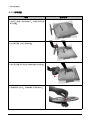
5-1 LS19PEBSWE/XSF Exploded View
M0174
M0013
T0003
M0215
T0514
M0006
M0013
5-1
5 Exploded View & Parts List
5-2 Parts List
Location
5-2
Code.No
Item & Specification
Q'ty
SA/SNA
T0003
BN96-04142R
ASSY COVER P-FRONT;LS19PE (932B),HSD Pan
1
S.A
M0215
BN07-00474A
LCD-PANEL;M190EG02 V4,Haydn,6bit Hi-FRC,
1
S.A
M0174
BN44-00124J
IP BOARD;IP-35155A(PV),Pebble,3.0 ~5.0mA
1
S.A
T0514
BN61-02784A
BRACKET-SUPPORT;PEBBLE,SPTE,0.3
S.N.A
M0006
BN96-04145A
ASSY SHIELD P-COVER;PEBBLE19,SECC,T0.8
1
M0013
BN96-06492B
ASSY COVER P-REAR;LS19PE(AUO),,ABS HB,,W
1
S.A
M0013
BN96-04150C
ASSY STAND P-BAR;-,PEBBLE17,-,ABS HB,WH1
1
S.A
1
S.N.A
Remark
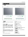
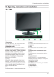
10 操作说明和安装
10 操作说明和安装
10-1 正面
1. 菜单按钮
打开 OSD 菜单。还用于退出 OSD 菜单或返回以
前的菜单。
2. MagicBright 按钮
MagicBright 是依据正在观看的图片内容提供最
佳观看环境的新功能。当前有六个不同的模式:
定制、文本、互联网、游戏、体育运动和电影。
各模式有自己的预先录制的亮度值。只需按下
MagicBright 控制按钮,即可轻松选择六个设置
之一。
1) 定制
尽管本公司的工程师仔细选择数值,但是预设值
可能让您的眼睛不舒适,取决于您的偏好。如果
出现这种情况,使用 OSD 菜单调节亮度和对比
度。
2) 文本
适用于涉及大量文字的文档或作品。
三星电子
3) 互联网
适用于文字和图形等组合图像。
4) 游戏
适用于观看游戏等动画。
5) 体育运动
适用于观看体育运动等动画。
6) 电影
适用于观看 DVD 或 VCD 等动画。
7)动态对比度
动态对比度将自动检测输入视频信号的分布情
况,并加以调整以创建最佳对比度。
3.亮度按钮
.亮度按钮
当屏幕上没有 OSD 时,按下该按钮调节亮度。
2,3.调节按钮
调节按钮
调节菜单中的项目。
4.确定按钮
.确定按钮(17”)
.确定按钮
启用反白显示的菜单项。
10-1
10 操作说明和安装
4.确定按钮
.确定按钮/来源按钮
.确定按钮 来源按钮(19”)
来源按钮
启用反白显示的菜单项。
按下“来源”,然后在 OSD 关闭时选择视频信号。
(当按下来源按钮改变输入模式时,显示当前模
式的屏幕的左上部显示信息-模拟或数字输入信
号。
)
5.自动按钮
自动按钮
使用该按钮,自动调节。
6.电源按钮
电源按钮
使用该按钮打开和关闭显示器。
电源指示灯
在正常运行过程中,本指示灯发出绿光,并且在
显示器存储调节内容时,闪烁发出绿光一次。
10-2 后部
(显示器背面的配置可能随产品而异。
)
1.
. 电源端口
将显示器的电源线接到显示器背面的电源端口上。
2.
. DVI 输入端口
输入端口
将 DVI 线接到显示器背面上的 DVI 端口上。
3. RGB 输入端口
将信号线接到显示器背面上的 15 针、D-sub 端口上。
4. Kensington 锁:
Kensington 锁是当在公共场所中使用时用于固定系统的装置。
10-2
三星电子
10 操作说明和安装
10-3 连接显示器(17”)
连接显示器
显示器后部
计算机后部
新式 Macintosh
旧式 Macintosh
1.
将显示器的电源线接到显示器背面的电源端口上。将显示器的电源线插入旁边的插口上。
2-1. 使用视频卡上的 D-sub(模拟)连接器。
把信号电缆接到显示器背面的 15 针、D-sub 连接器上。
2-2. 连接到 Macintosh 上。
使用 D-SUB 连接电缆将显示器接到 Macintosh 计算机上。
2-3. 如果是旧式 Macintosh,需要使用特殊 Mac 适配器连接显示器。
3.
打开计算机和显示器。如果显示器显示图像,则安装完成。
三星电子
10-3
10 操作说明和安装
10-3 连接显示器(19”)
连接显示器
显示器后部
计算机后部
新式 Macintosh
旧式 Macintosh
1.
将显示器的电源线接到显示器背面的电源端口上。将显示器的电源线插入旁边的插口上。
2-1. 使用视频卡上的 D-sub(模拟)连接器。
把信号电缆接到显示器背面的 15 针、D-sub 连接器上。
2-2. 使用视频卡上的 DVI(数字)连接器。
把 DVI 电缆接到显示器背面的 DVI 端口上。
2-3. 连接到 Macintosh 上。
使用 D-SUB 连接电缆将显示器接到 Macintosh 计算机上。
2-4. 如果是旧式 Macintosh,需要使用特殊 Mac 适配器连接显示器。
3.
10-4
打开计算机和显示器。如果显示器显示图像,则安装完成。
三星电子
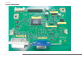
12 PCB Layout
12 PCB Diagram
12-1 Main PCB (LS17PEA, LS19PEA)
Regulator 3.3
Scaler
Regulator 1.8
Flash Memory
EEPROM - Analog
12-1
12 PCB Layout
12-2 Main PCB (LS19PEB)
Regulator 3.3
Scaler
Regulator 1.8
Flash Memory
EEPROM - Digital
EEPROM - Analog
12-2
1 Precautions
1 Precautions
Follow these safety, servicing and ESD precautions to prevent damage and to protect against potential hazards such as electrical shock.
1-1 Safety Precautions
1-1-1 Warnings
1.
For continued safety, do not attempt to modify the circuit
board.
2.
Disconnect the AC power and DC power jack before
servicing.
1-1-2 Servicing the LCD Monitor
1.
When servicing the LCD Monitor, Disconnect the AC
line cord from the AC outlet.
2.
It is essential that service technicians have an accurate
voltage meter available at all times. Check the
calibration of this meter periodically.
1-1-3 Fire and Shock Hazard
Before returning the monitor to the user, perform the
following safety checks:
1.
Inspect each lead dress to make certain that the leads are
not pinched or that hardware is not lodged between the
chassis and other metal parts in the monitor.
2.
Inspect all protective devices such as nonmetallic control
knobs, insulating materials, cabinet backs, adjustment
and compartment covers or shields, isolation resistorcapacitor networks, mechanical insulators, etc.
3.
Leakage Current Hot Check (Figure 1-1):
WARNING : Do not use an isolation
transformer during this test.
Use a leakage current tester or a metering system that
complies with American National Standards Institute
(ANSI C101.1, Leakage Current for Appliances), and
Underwriters Laboratories (UL Publication UL1410,
59.7).
Figure 1-1. Leakage Current Test Circuit
4.
With the unit completely reassembled, plug the AC line
cord directly into a 120V AC outlet. With the unit’s AC
switch first in the ON position and then OFF, measure
the current between a known earth ground (metal water
pipe, conduit, etc.) and all exposed metal parts,
including: metal cabinets, screwheads and control shafts.
The current measured should not exceed 0.5 milliamp.
Reverse the power-plug prongs in the AC outlet and
repeat the test.
1-1-4 Product Safety Notices
Some electrical and mechanical parts have special safetyrelated characteristics which are often not evident from visual
inspection. The protection they give may not be obtained by
replacing them with components rated for higher voltage,
wattage, etc. Parts that have special safety characteristics are
identified by
on schematics and parts lists. A substitute
replacement that does not have the same safety characteristics
as the recommended replacement part might create shock, fire
and/or other hazards. Product safety is under review
continuously and new instructions are issued whenever
appropriate.
1-1
1 Precautions
1-2 Servicing Precautions
WARNING:
An electrolytic capacitor installed with the wrong polarity might explode.
Caution:
Before servicing units covered by this service manual, read and follow the Safety Precautions section
of this manual.
Note:
If unforeseen circumstances create conflict between the following servicing precautions and any of the safety
precautions, always follow the safety precautions.
1-2-1 General Servicing
Precautions
1.
2.
3.
Always unplug the unit’s AC power cord from the AC
power source and disconnect the DC Power Jack before
attempting to:
(a) remove or reinstall any component or assembly, (b)
disconnect PCB plugs or connectors, (c) connect a test
component in parallel with an electrolytic capacitor.
Some components are raised above the printed circuit
board for safety. An insulation tube or tape is sometimes
used. The internal wiring is sometimes clamped to
prevent contact with thermally hot components. Reinstall
all such elements to their original position.
4.
Check the insulation between the blades of the AC plug
and accessible conductive parts (examples: metal panels,
input terminals and earphone jacks).
5.
Insulation Checking Procedure: Disconnect the power
cord from the AC source and turn the power switch ON.
Connect an insulation resistance meter (500 V) to the
blades of the AC plug.
The insulation resistance between each blade of the AC
plug and accessible conductive parts (see above) should
be greater than 1 megohm.
6.
After servicing, always check that the screws,
components and wiring have been correctly reinstalled.
Make sure that the area around the serviced part has not
been damaged.
Always connect a test instrument’s ground lead to the
instrument chassis ground before connecting the positive
lead; always remove the instrument’s ground lead last.
1-3 Electrostatically Sensitive Devices (ESD) Precautions
Some semiconductor (solid state) devices can be easily damaged by static electricity. Such components are commonly called
Electrostatically Sensitive Devices (ESD). Examples of typical ESD are integrated circuits and some field-effect transistors. The
following techniques will reduce the incidence of component damage caused by static electricity.
1.
Immediately before handling any semiconductor
components or assemblies, drain the electrostatic charge
from your body by touching a known earth ground.
Alternatively, wear a discharging wrist-strap device. To
avoid a shock hazard, be sure to remove the wrist strap
before applying power to the monitor.
2.
After removing an ESD-equipped assembly, place it on a
conductive surface such as aluminum foil to prevent
accumulation of an electrostatic charge.
3.
Do not use freon-propelled chemicals. These can
generate electrical charges sufficient to damage ESDs.
4.
Use only a grounded-tip soldering iron to solder or
desolder ESDs.
5.
Use only an anti-static solder removal device. Some
solder removal devices not classified as “anti-static” can
generate electrical charges sufficient to damage ESDs.
1-2
6.
Do not remove a replacement ESD from its protective
package until you are ready to install it. Most
replacement ESDs are packaged with leads that are
electrically shorted together by conductive foam,
aluminum foil or other conductive materials.
7.
Immediately before removing the protective material
from the leads of a replacement ESD, touch the
protective material to the chassis or circuit assembly into
which the device will be installed.
Caution: Be sure no power is applied to the
chassis or circuit and observe all
other safety precautions.
8.
Minimize body motions when handling unpackaged
replacement ESDs. Motions such as brushing clothes
together, or lifting your foot from a carpeted floor can
generate enough static electricity to damage an ESD.
1 Precautions
1-4 Installation Precautions
1. For safety reasons, more than two people are
required for carrying the product.
6. Keep the antenna far away from any high-voltage
cables and install it firmly. Contact with the highvoltage
cable or the antenna falling over may
2. Keep the power cord away from any heat emitting
cause fire or electric shock.
devices, as a melted covering may cause fire or
electric shock.
7. When installing the product, leave enough space
(10cm) between the product and the wall for
3. Do not place the product in areas with poor
ventilation such as a bookshelf or closet. The
ventilation purposes.
A rise in temperature within the product may cause fire.
increased internal temperature may cause fire.
4. Bend the external antenna cable when connecting
it to the product. This is a measure to protect it
from being exposed to moisture. Otherwise, it
may cause a fire or electric shock.
5. Make sure to turn the power off and unplug the
power cord from the outlet before repositioning
the product. Also check the antenna cable or the
external connectors if they are fully unplugged.
Damage to the cord may cause fire or electric
shock.
1-3
1 Precautions
Memo
1-4
2 Product Specifications
2 Product Specifications
2-1 Fashion Feature
-. Minimalism Design Something New
-. Boltless Model (Clean Cut & Soft Surface)
-. New Ball Hinge
-. Color Variation. White, Black
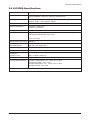
2-2 LS17PEA Specifications
Item
Description
LCD Panel
TFT-LCD panel, RGB vertical stripe, normally black transmissive,
17-Inch viewable, 0.264 (H) x 0.264 (V) mm pixel pitch
Scanning Frequency
Horizontal : 31 kHz ~ 81 kHz (Automatic)
Vertical : 56 Hz ~ 75 Hz (UXGA : 60 Hz)
Display Colors
16.7 Million colors
Maximum Resolution
Horizontal : 1280 Pixels
Vertical : 1024 Pixels
Input Signal
Analog
Input Sync Signal
Seperate H/V sync, Composite H/V, Sync-on-Green, Automatic synchroniza
tion whitout external swith of sync type
Level : TTL level
Maximum Pixel Clock rate
135 MHz
Active Display
Horizontal/Vertical
337(H) x 270(W) mm
AC power voltage & Frequency
AC 90 ~ 264 Volts, 60/50 Hz
Power Consumption
34W (Max)
Dimensions
Set (W x D x H)
376.0 x 177.0 x 380.0 mm
Weight (Set/Package)
3.2kg / 4.3kg
Environmental Considerations
Operating Temperature : 0˚F ~ 122˚F (0℃ ~ 50℃)
Operating Humidity : 20% ~ 90%
Storage temperature : -4˚F ~ 149˚F (-20℃ ~ 65℃)
Storage Humidity : 5% ~ 90%
- Designs and specifications are subject to change without prior notice.
2-1
2 Product Specifications
2-3 LS19PEB Specifications
Item
Description
LCD Panel
TFT-LCD panel, RGB vertical stripe, normally black transmissive,
19-Inch viewable, 0.294 (H) x 0.294 (V) mm pixel pitch
Scanning Frequency
Horizontal : 31 kHz ~ 81 kHz (Automatic)
Vertical : 56 Hz ~ 75 Hz (UXGA : 60 Hz)
Display Colors
16.7 Million colors
Maximum Resolution
Horizontal : 1280 Pixels
Vertical : 1024 Pixels
Input Signal
Analog / Digital
Input Sync Signal
Seperate H/V sync, Composite H/V, Sync-on-Green, Automatic synchroniza
tion whitout external swith of sync type
Level : TTL level
Maximum Pixel Clock rate
135 MHz
Active Display
Horizontal/Vertical
376.3(H) x 301.05(W) mm
AC power voltage & Frequency
AC 90 ~ 264 Volts, 60/50 Hz
Power Consumption
38W (Max)
Dimensions
Set (W x D x H)
418.0 x 199.0 x 418.0 mm
Weight (Set/Package)
4.0kg / 5.3kg
Environmental Considerations
Operating Temperature : 0˚F ~ 122˚F (0℃ ~ 50℃)
Operating Humidity : 20% ~ 90%
Storage temperature : -4˚F ~ 149˚F (-20℃ ~ 65℃)
Storage Humidity : 5% ~ 90%
- Designs and specifications are subject to change without prior notice.
2-2
2 Product Specifications
2-4 LS19PEA Specifications
Item
Description
LCD Panel
TFT-LCD panel, RGB vertical stripe, normally black transmissive,
19-Inch viewable, 0.294 (H) x 0.294 (V) mm pixel pitch
Scanning Frequency
Horizontal : 31 kHz ~ 81 kHz (Automatic)
Vertical : 56 Hz ~ 75 Hz (UXGA : 60 Hz)
Display Colors
16.7 Million colors
Maximum Resolution
Horizontal : 1280 Pixels
Vertical : 1024 Pixels
Input Signal
Analog
Input Sync Signal
Seperate H/V sync, Composite H/V, Sync-on-Green, Automatic synchroniza
tion whitout external swith of sync type
Level : TTL level
Maximum Pixel Clock rate
135 MHz
Active Display
Horizontal/Vertical
376.3(H) x 301.05(W) mm
AC power voltage & Frequency
AC 90 ~ 264 Volts, 60/50 Hz
Power Consumption
38W (Max)
Dimensions
Set (W x D x H)
418.0 x 199.0 x 418.0 mm
Weight (Set/Package)
4.0kg / 5.3kg
Environmental Considerations
Operating Temperature : 0˚F ~ 122˚F (0℃ ~ 50℃)
Operating Humidity : 20% ~ 90%
Storage temperature : -4˚F ~ 149˚F (-20℃ ~ 65℃)
Storage Humidity : 5% ~ 90%
- Designs and specifications are subject to change without prior notice.
2-3
2 Product Specifications
2-5 Spec Comparison
BI17BS / 19BS
LS17PEA / LS19PEA / LS19PEB
30 ~ 81 kHz
60 ~ 75 Hz
16,2M colors
30 ~ 81 kHz
60 ~ 75 Hz
16,7M colors
1280 x 1024 / 60 Hz
1280 x 1024 / 60 Hz
H/V Separate, TTL, P. or N.
0.7 Vp-p @ 75ohm
H/V Separate, TTL, P. or N.
0.7 Vp-p @ 75ohm
34W / 38W
< 1W
34W / 38W
< 1W
Response Time
8ms
17" : 5ms
19" : 5ms
Anion Option
None
None
Magic Color
Support
Support (Deleted Magic Zone)
Model
Design
Frequency
Horizontal
Vertical
Display Color
PC Resolution
Maximum mode
Input Signal
Sync Signal
Video Signal
Power
Consumption
Normal
Power Saving
2-4
2 Product Specifications
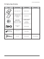
2-6 Option Specification
Item
Item Name
CODE.NO
Quick Setup Guide
BN68-01002C
Warranty Card
(Not available in all
locations)
AA68-00371C
User's Guide,
Monitor Driver,
Natural Color software,
MagicTune™ software
Remark
LS17PEA, LS19PEB:
BN59-00585A
LS19PEA:
BN59-00585L
D-Sub(15 Pin)
Cable
BN39-00244B
Power Cord
3903-000042
DVI Cable
BN39-00246F
Sold separately
2-5
2 Product Specifications
Memo
2-6
14 Reference Infomation
14 Reference Infomation
14-1 Technical Terms
-TFT-LCD
(Thin film Transistor Liquid Crystal Display)
ADC(Analog to Digital Converter)
This is a circuit that converts from analog signal to
digital signals.
-PLL(Phase Locked Loop)
During progressing ADC, Device makes clock synchronizing HSYNC with Video clock
-Inverter
Device that supplies Power to LCD panel lamp. This
device generates about 1,500~2,000V.
AC Adapter
Device that converts AC(90V~240V) to DC(+12V or
14V)
SMPS(Switching Mode Power Supply)
Switching Mode Power supply. This design technology is used to step up/down the input power by
switching on/off
-FRC(Frame Rate Controller)
Technology that changes the number of frames displayed on screen per second.
TFT-LCD panel requires 60 frames per second.
This technology is needed to convert input image to
60 frames per second regardless input frame quantity.
-Image Scaler
Technology that converts an input resolution to
another resolution.(ex. 640* 480 to 1024*768)
-Auto Configuration(Auto adjustment)
This is an algorithm to adjust monitor to optimum
condition by pushing one key.
-OSD(On Screen Display)
Customers can easily control the screen settings
using the OSD.
-FINE
The "Fine" adjustment is used to adjust visibility by
controlling phase difference.
-COARSE
This adjustment adjusts the display by tuning Video
clock and PLL clock.
-DVI (Digital Visual Interface)
This provides a high speed digital connection for
visual data types that is display technology independent. This interface is primarily forcused at providing a connection between a computer and
its display device.
-L.V.D.S.(Low Voltage Differential Signaling)
A kind of transmission method for Digital.It can be
used from Main PBA to Panel.
-T.M.D.S
(Transition minimized Differential Signaling)
a kind of transmission method for Digital.
It can be used from Video card to Main PBA.
-DDC(Display data channel)
It is a communication method between Host
Computer and related equipment.
It enables Plug and Play between PC and Monitor.
-EDID
Extended Display Identification Data PC can recognize monitor information such as Product data,
Product name,Display mode,Serial number and
Signal source, etc Data is recognised via DDC Line
linking PC and Monitor.
-Dot Pitch
The image on a monitor is composed of red, green
and blue dots. The closer the dots, the higher the
resolution. The distance between two dots of the
same color is called the 'Dot Pitch'. Unit: mm
-Vertical Frequency
The screen must be redrawn several times per second in order to create and display an image for the
14-1
14 Reference Infomation
user. The frequency of this repetition per second is
called Vertical Frequency or Refresh Rate. Unit: Hz
Example: If the same light repeats itself 60 times
per second, this is regarded as 60 Hz.
-Horizontal Frequency
The time to scan one line connecting the right edge
to the left edge of the screen horizontally is called
Horizontal Cycle. The inverse number of the
Horizontal Cycle is called Horizontal Frequency.
Unit: kHz
-Interlace and Non-Interlace Methods
Showing the horizontal lines of the screen from the
top to the bottom in order is called the Non-Interlace
method while showing odd lines and then even lines
in turn is called the Interlace method. The NonInterlace method is used for the majority of monitors
to ensure a clear image. The Interlace method is the
same as that used in TVs.
-Plug & Play
This is a function that provides the best quality
screen for the user by allowing the computer and
the monitor to exchange information automatically.
This monitor follows the international standard
VESA DDC for the Plug & Play function.
-Resolution
The number of horizontal and vertical dots used to
compose the screen image is called 'resolution'.
This number shows the accuracy of the display.
High resolution is good for performing multiple tasks
as more image information can be shown on the
screen.
Example: If the resolution is 1280 x 1024 , this
means the screen is composed of 1280 horizontal
dots (horizontal resolution) and 1024 vertical lines
(vertical resolution).
14-2
14 Reference Infomation
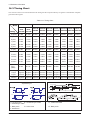
14-2 Pin Assignments
Sync
Type
Pin No.
1
2
3
4
5
6
7
8
9
10
11
12
13
14
15
15-Pin D-Sub Signal Cable Connector
Separate
Composite
Sync-on-green
Red
Green
Blue
GND
DDC Return (GND)
GND-R
GND-G
GND-B
DDC Power Input (+5V)
Self Raster
GND
Bi-Dr Data (SDA)
H-Sync.
V-Sync.
DDC Clock (SCL)
Red
Green
Blue
GND
DDC Return (GND)
GND-R
GND-G
GND-B
DDC Power Input (+5V)
Self Raster
GND
Bi-Dr Data (SDA)
H/V-Sync.
Not Used
DDC Clock (SCL)
Red
Green + H/V Sync.
Blue
GND
DDC Return (GND)
GND-R
GND-G
GND-B
DDC Power Input (+5V)
Self Raster
GND
Bi-Dr Data (SDA)
Not Used
Not Used
DDC Clock (SCL)
Sync
Type
Pin No.
24P DVI-D
1
Rx2-
13
No Connection
2
Rx2+
14
+5V_M
3
GND
15
Self Raster
4
No Connection
16
+5V_M
5
No Connection
17
Rx0-
6
DDC Clock (SCL)
18
Rx0+
7
DDC Data (SDA)
19
NC
8
NC
20
No Connection
9
Rx1-
21
No Connection
10
Rx1+
22
NC
11
NC
23
RxC+
12
No Connection
24
RxC-
14-3
14 Reference Infomation
14-3 Timing Chart
This section of the service manual describes the timing that the computer industry recognizes as standard for computergenerated video signals.
Table 14-1 Timing Chart
VESA
IBM
Mode
VGA2/
70 Hz
Timing
VGA3/
60 Hz
640/75 Hz 800/60 Hz 800/75 Hz 1024/60 Hz 1024/75 Hz 1280/60 Hz 1280/75 Hz
720 x 400 640 x 480
640x480
800x600
800x600
1024x768 1024x768 1280x1024 1280x1024
fH (kHz)
31.469
31.469
37.500
37.879
46.875
48.363
60.023
63.981
79.975
A μsec
31.777
31.778
26.667
26.400
21.333
20.677
16.660
11.852
12.504
B μsec
3.813
3.813
2.032
3.200
1.616
2.092
1.219
1.037
1.067
C μsec
1.589
1.589
3.810
2.200
3.232
2.462
2.235
2.296
1.837
D μsec
26.058
26.058
20.317
20.000
16.162
15.754
13.003
9.259
9.481
E μsec
0.318
0.318
0.508
0.000
0.323
0.369
0.203
0.000
0.119
fV (Hz)
70.087
59.940
75.000
60.317
75.000
60.004
75.029
60.020
75.025
O msec
14.268
16.683
13.333
16.579
13.333
16.666
13.328
16.005
13.329
P msec
0.064
0.064
0.080
0.106
0.064
0.124
0.050
0.047
0.038
Q msec
0.858
0.794
0.427
0.607
0.448
0.600
0.466
0.594
0.475
R msec
13.155
15.761
12.800
15.840
12.800
15.880
12.795
15.630
12.804
S msec
0.191
0.064
0.027
0.0261
0.021
0.062
0.017
0.016
0.013
28.322
26.175
31.500
40.000
49.500
75.000
78.750
108.000
Clock
Freq.
(MHz)
135.000
Polarity
H.Sync
Negative Negative Negative Positive
Positive Negative
Positive
Positive
Positive
V.Sync
Positive Negative Negative Positive
Positive Negative
Positive
Positive
Positive
Remark
Separate Separate Separate Separate Separate Separate Separate Separate Separate
H/V Composite Sync
Separate Sync
Video
Video
C
D
E
Q
R
S
Sync-on-Green
Sync
Sync
B
P
A
O
A : Line time total
B : Horizontal sync width
P : Vertical sync width
O : Frame time total
C : Back porch
R : Active time
Q : Back porch
14-4
D : Active time
14 Reference Infomation
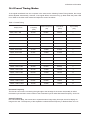
14-4 Preset Timing Modes
-If the signal transferred from the computer is the same as the following Preset Timing Modes, the screen
will be adjusted automatically. However, if the signal differs, the screen may go blank while the power LED
is on. Refer to the video card manual and adjust the screen as follows.
Table 1. Preset Timing
Display Mode
Horizontal
Frequency
(kHz)
Vertical Frequency
(Hz)
Pixel Clock
(MHz)
Sync Polarity
(H/V)
MAC, 640 x 480
35.000
66.667
30.240
-/-
MAC, 832 x 624
49.726
74.551
57.284
-/-
MAC,1152 x870
68.681
75.062
100.000
-/-
IBM, 640 x 350
31.469
70.086
25.175
+/-
IBM, 640 x 480
31.469
59.940
25.175
-/-
IBM, 720 x 400
31.469
70.087
28.322
-/+
VESA, 640 x 480
37.500
75.000
31.500
-/-
VESA, 640 x 480
37.861
72.809
31.500
-/-
VESA, 800 x 600
35.156
56.250
36.000
+,-/+,-
VESA, 800 x 600
37.879
60.317
40.000
+/+
VESA, 800 x 600
46.875
75.000
49.500
+/+
VESA, 800 x 600
48.077
72.188
50.000
+/+
VESA, 1024 x 768
48.363
60.004
65.000
-/-
VESA, 1024 x 768
56.476
70.069
75.000
-/-
VESA, 1024 x 768
60.023
75.029
78.750
+/+
VESA, 1152 x 864
67.500
75.000
108.00
+/+
VESA 1280 x 960
60.000
60.000
108.00
+/+
VESA, 1280 x 1024
63.981
60.020
108.00
+/+
VESA, 1280 x 1024
79.976
75.025
135.00
+/+
Horizontal Frequency
The time to scan one line connecting the right edge to the left edge of the screen horizontally is called
Horizontal Cycle and the inverse number of the Horizontal Cycle is called Horizontal Frequency. Unit: kHz
Vertical Frequency
Like a fluorescent lamp, the screen has to repeat the same image many times per second to display an
image to the user. The frequency of this repetition is called Vertical Frequency or Refresh Rate. Unit: Hz
14-5
14 Reference Infomation
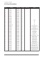
14-5 Panel Description
Maker
VENDOR P/N
PANEL_CODE
PANEL_ABB
STICKER_CODE
Remarks
BN68-00239H
-
SEC
LT140X1-002
BN07-00004A
SA
SEC
LT150XS-L01
BN07-00009A
SB
-
SEC
LT150XS-L01-B
BN07-00022A
SC
-
SEC
LTM150XS-L02
BN07-00005A
SD
-
SEC
LT181E2-132
BN07-00001A
SE
-
SEC
LT150XS-T01
BN07-00010A
SF
-
SEC
LTM181E3-132
BN07-00019A
SG
-
SEC
LT170E2-131
BN07-10001D
SH
-
SEC
LT181E2-131
BN07-10001E
SJ
-
SEC
LTM170E4-L01
BN07-00018A
SK
-
SEC
LTM240W1-L01
BN07-00015A
SL
-
SEC
LTM213U3-L01
BN07-00016A
SM
-
SEC
LTM150XH-L01
BN07-00026A
SN
-
SEC
LTM150XH-L03
BN07-00027A
SP
-
SEC
LTM150XS-L01
BN07-00032A
SQ
DELL(ZPD)
SEC
LTM181E4-L01
BN07-00034A
SR
PVA
SEC
LTM170EH-L01
BN07-00036A
SS
TN
SEC
LTM170E5-L01
BN07-00037A
SU
PVA
SEC
LTM150XH-L11
BN07-00041A
SV
-
SEC
LTM213U4-L01
BN07-00039A
SW
PVA
SEC
LTM150XH-L01(ZPD)
BN07-00045A
SX
ZPD
SEC
LTM150XH-L04
BN07-00046A
SY
"New panel with high brightness"
SEC
LTM170W1-L01
BN07-00047A
SZ
Panel for TV
SEC
LTM150XH-L06
BN07-00053A
EA
Panel for TV/ High luminance for 450cd _ SONY&EOS Team Panel for TV
SEC
LTM153W1-L01
BN07-00054A
EB
Use NIKE MODEL
SEC
LTM170EH-L05
BN07-00055A
EC
Panel EOS proj. for high brightness of 17" EH-L05
SEC
LTM170E5-L03
BN07-00056A
ED
Dell 1702FP pro. E4. EH mechanicalCompatible
SEC
LTM190E1-L01
BN07-00057A
EE
DELL 1900 FP
SEC
LTM181E5-L01
BN07-00061A
EF
18" narrow bezel GH18PS
SEC
LTM150XP-L01
BN07-00065A
EG
AMLCD PVA PANEL
SEC
LTM240W1-L02
BN07-00062A
EH
Panel for 15" Wide TV
SEC
LTM170EU-L01
BN07-00071A
EJ
Slim design, TN
SEC
LTM170E5-L04
BN07-00072A
EK
E5-L04 6 bits FRC... for IBM
SEC
LTA220W1-L01
BN07-00074A
EL
Panel for 22" TV
SEC
LTM170E6-L02
BN07-00075A
EM
AMLCD Narrow & slim design 17" PVAmode
SEC
LTM170W1-L01
BN07-00082A
EN
LTM170W1-L01 ZPD panel
SEC
LTM170EH-L01
BN07-00080A
EP
LTM170EH-L01 ZPD panel
SEC
LTM170E5-L01
BN07-00081A
EQ
LTM170E5-L01 ZPD panel
SEC
LTM170EH-L05
BN07-00083A
ER
LTM170EH-L05 ZPD panel
SEC
LTM170E5-L03
BN07-00084A
ES
LTM170E5-L03 ZPD panel
SEC
LTM170EU-L01
BN07-00085A
ET
LTM170EU-L01 ZPD panel
SEC
LTM170E5-L04
BN07-00086A
EU
LTM170E5-L04 ZPD panel
SEC
LTM170E6-L02
BN07-00087A
EV
LTM170E6-L02 ZPD panel
SEC
LTM150XH-L06
BN07-00091A
EW
"Color coordinates change for LCD TV"
SEC
LTM153W1-L01
BN07-00092A
EX
AMLCD WIDE 15",9/10
SEC
LTM170W1-L01
BN07-00100A
EY
"Color Coordinates change code management"
SEC
LTM170EH-L05
BN07-00097A
EZ
"LTM170E5-L05 Color Coordinates Change Panel Code"
SEC
LTA400W1-L01
BN07-00109A
S1
"PANEL of AMLCD 40"" TV"
SEC
LTM153W1-L01
BN07-00110A
S2
"Color coordinates change 0.280/0.290, 10000k & ZPD Panel"
SEC
LTM150XH-L06
BN07-00111A
S3
"Color coordinates change 0.280/0.290, 10000k & ZPD Panel"
SEC
LTM170W1-L01
BN07-00112A
S4
"Color coordinates change 0.280/0.290, 10000k & ZPD Panel"
SEC
LTM170EH-L05
BN07-00113A
S5
"Color coordinates change 0.280/0.290, 10000k & ZPD Panel"
SEC
LTM220W1-L01
BN07-00114A
S6
"ZPD Panel for AMLCD 22"" TV"
14-6
14 Reference Infomation
Maker
VENDOR P/N
PANEL_CODE
PANEL_ABB
STICKER_CODE
Remarks
SEC
LTM150XH-L06
BN07-00117A
S7
SEC
LTM153W1-L01
BN07-00118A
S8
"ZPD Panel code"
"ZPD Panel code"
SEC
LTM170WP-L01
BN07-00119A
S9
"PVA Panel for NIKE"
SEC
LTM213U4-L01
BN07-00039A
E1
21.3" NARROW
SEC
LTA260W1-L01
BN07-00121A
E2
VENUS
SEC
LTA220W1-L01
BN07-00074B
E3
"Panel B-level panel code for 22"" TV Panel "
SEC
LTA320W1-L01
BN07-00108A
E4
"Panel for AMLCD 32"" TV"
SEC
LTM213U4-L01
BN07-00124A
E5
NARROW BEZEL 21 " PANEL
SEC
LTM170E6-L04
BN07-00129A
E6
"HIGHLAND 17"" LOW PANEL (Panel only for TCO03)"
SEC
LTM190E1-L01
BN07-00088A
E7
LTM190E1-L01 ZPD panel
SEC
M150X4-L06
BN07-00137A
E8
15" Narrow & Slim panel
SEC
LTA170V1
BN07-00139A
E9
"17"" Panel for Muse 4:3 VGA TV"
SEC
LTM190E1-L02
BN07-00128A
E10
"New Panel from AMLCDl, Specification : 6bit Driver IC"
SEC
LTM170EX-L01
BN07-00143A
E11
"Development new Panel from AMLCD"
SEC
LTM170E8-L01
BN07-00144A
E12
"Development new Panel from AMLCD"
SEC
LTM170E6-L04
BN07-00129B
E13
"ZPD panel for AMLCD (Panel only for TCO03)"
SEC
LTA320W1-L02
BN07-00108B
E14
"Creat B-level Panel code for AMLCD 32"" TV"
SEC
LTM190E1-L03
BN07-00151A
E15
"Development new 19"" Panel form AMLCD (Panel only for TCO03)"
SEC
LTM240W1-L03
BN07-00134A
E16
"AMLCD 24"" panel development"
SEC
LTM190E1-L02
BN07-00128B
E17
"New Panel from AMLCD, Specification : 6bit Driver IC(ZPD)"
SEC
LTM190E4-L01
BN07-00145A
E18
"AMLCD 24"" new panel development"
SEC
LTM170E8-L01
BN07-00158A
E19
"ZPD code derivation"
SEC
LTM170EX-L01
BN07-00159A
E20
"ZPD code derivation"
SEC
LTM190E1-L03
BN07-00151B
E21
"Creat new panel code for AMLCD 19"" (Panel only for TCO03)"
SEC
LTA460H1-L01
BN07-00157A
E22
"creat panel code for AMLCD 46"" TV "
SEC
LTM170EU-L11
BN07-00160A
E23
"creat new panel code for AMLCD 17"" (Panel only for TCO03)"
SEC
LTM240W1-L03
BN07-00134B
E24
"24"" panel ZPD code derivation"
SEC
LTM190E4-L01
BN07-00145B
E25
"AMLCD 19"" ZPD Panel code derivation"
SEC
LTM240W1-L03
BN07-00134B
E26
24" panel ZPD code derivation
SEC
LTM150XO-L01
BN07-00164A
E27
AMLCD 15" XO-L01 new panel development
SEC
LTM150XO-L01
BN07-00164B
E28
AMLCD 15" XO-L01 ZPD code derivation
SEC
LTM170EU-L11
BN07-00160B
E29
AMLCD 17" NEW panel code derivation
SEC
LTA320W2-L01
BN07-00172A
SPZ
AMLCD 32" NEW panel
SEC
LTM213U4-L01
BN07-00124B
SPZ
21.3" Narrow PANEL ZPD Panel derivation
SEC
LTM170EU-L11
BN07-00189A
STH
AMLCD EU-L11 Pb free panel code derivtion
SEC
LTM170EU-L11
BN07-00189B
STZ
AMLCD EU-L11 Pb free panel ZPD code derivation
SEC
LTM240W1-L04
BN07-00188A
SPH
24" A-DCC new panel development
SEC
LTM190EX-L01
BN07-00191A
STH
AMLCD 19" TN new Panel
SEC
LTM190EX-L02
BN07-00191B
STZ
AMLCD 19" TN new Panel ZPD derivation
SEC
LTA230W1-L02
BN07-00184A
SPZ
AMLCD 23" 16:9 new Panel
SEC
LTA260W2-L01
BN07-00185A
SPZ
AMLCD 26" 16:9 new Panel
SEC
LTM240M1-L01
BN07-00195A
SPH
24" panel with high brightness deveiopment
SEC
LTA400W2-L01
BN07-00186A
SPZ
AMLCD 40" 16:9 new Panel
SEC
LTM150XO-L01
BN07-00197A
STH
AMLCD 15" XO-L01 Pb free panel code
SEC
LTM150XO-L01
BN07-00197B
STZ
AMLCD 15" XO-L01 Pb free panel ZPD code
SEC
LTM170EU-L21
BN07-00202A
STZ
AMLCD EU-L21 ZPD new code derivation
SEC
LTA460W2-L03
BN07-00187A
SPZ
BEETOVEN 46"ZPD new Panel
CPT
CLAA150XG09
BN07-00141A
PA
CPT 15" Monitor new panel development
CPT
CLAA170EA02
BN07-00148A
PB
17" CPT NEW development panel
CPT
CLAA170EA02
BN07-00148B
PC
17" CPT ZPD panel code derivation
CPT
CLAA150XG09
BN07-00141B
PTZ
"CPT 15"" panel ZPD code derivation (GOYA-PJT)"
CPT
CLAA150XP01
BN07-00173A
PTH
CPT 15" PSWG code derivation
CPT
CLAA150XP01
BN07-00173B
PTZ
CPT 15" PSWG panel ZPD code
14-7
14 Reference Infomation
Maker
VENDOR P/N
PANEL_CODE
PANEL_ABB
STICKER_CODE
Remarks
CPT
CLAA170EA07
BN07-00174A
PTH
"CPT 17"" PSWG panel code derivation?
CPT
CLAA170EA07
BN07-00174B
PTZ
CPT 17"""" PSWG type new Panel code"""
CPT
CLAA170EA07
BN07-00174B
PTZ
CPT 17" PSWG type new Panel code
TOSHIBA
LTM15C419(A)
BN07-00002A
TA
-
TOSHIBA
LTM15C423(B)
BN07-00006A
TB
-
TOSHIBA
LTM18C161
BN07-00008A
TC
-
TOSHIBA
LTM15C443
BN07-00031A
TD
-
TOSHIBA
LTM15C458
BN07-00043A
TE
-
TOSHIBA
LTM15C458S
BN07-00077A
TF
"TSB 15"" high brightness Panel"
TOSHIBA
LTM15C458
BN07-00078A
TG
Toshiba ZPD panel
TOSHIBA
LTM15C458S
BN07-00099A
TH
TSB LTM15C458S ( ZPD )
HANNSTAR
HSD150MX41A(A)
BN07-00020A
NA
"TTL type"
HANNSTAR
HSD150MX12
BN07-00030A
NB
"TTL type"
HANNSTAR
HSD170ME13
BN07-00180A
NTH
Hannstar 17" TN new panel development
HANNSTAR
HSD170ME13
BN07-00180B
NTZ
Hannstar 17" TN new panel development ZPD code derivation
TORISAN
TM150XG-22L03(A)
BN07-00021A
RA
-
TORISAN
TM150XG-26L06
BN07-00042A
RB
-
TORISAN
TM181SX-76N01
BN07-00048A
RC
-
TORISAN
TM150XG-26L06
BN07-00059A
RD
15" XGA TN MODE(ZPD)
TORISAN
TM290WX-71N31
BN07-00063A
RE
"RS24NS (TORISAN 29"" NEW PANEL)"
"RS24NS (TORISAN 40"" NEW PANEL)"
TORISAN
TM396WX-71N31
BN07-00064A
RF
TORISAN
TM150XG-26L09
BN07-00073A
RG
"Panel for 15"" TV"
TORISAN
TM150XG-26L10
BN07-00089A
RH
"L10(change except D/IC) ZPD"
TORISAN
TM150XG-26L10
BN07-00090A
RJ
L10 NORMAL
TORISAN
TM190SX-70N01
BN07-00098A
RK
Torisan 19" Panel
TORISAN
TM181SX-76N01
BN07-00106A
RL
ZPD Panel code
TORISAN
TM190SX-70N01
BN07-00107A
RM
ZPD Panel code
TORISAN
TM290WX-71N31
BN07-00115A
RN
"Color Coordinates change panel for TORISAN 29"" TV"
TORISAN
TM396WX-71N31
BN07-00116A
RP,Q
"Color Coordinates change panel for TORISAN 40"" TV"
TORISAN
TM22OWX-71N31
BN07-00125A
RR
"Development TORISAN 22"" TV PANEL (ZPD)"
TORISAN
TM22OWX-71N31
BN07-00127A
RS
"Development TORISAN 22"" TV PANEL (HPD)"
TORISAN
TM396WX-71N32A
BN07-00150A
RT
120V inverter Exclusive panel
TORISAN
TM190SX-70N02
BN07-00154A
RMH
Torisan 6bit panel code Derivation
TORISAN
TM190SX-70N02
BN07-00154B
RMZ
Torisan 6bit panel code Derivation
SHARP
LQ181E1DG11(A)
BN07-10001C
PA
-
SHARP
LQ150X1LW71
BN07-00067A
PB
SHARP 15" PVA PANEL
HITACHI
TX38D12VC0CAA(A)
BN07-00003A
HA
-
HITACHI
TX43DVCOCAB
BN07-00060A
HB
17" SXGA PVA MODE
HITACHI
TX43D15VC0CAB
BN07-00101A
HC
ZPD Panel
HITACHI
TX51D11VC0CAB
BN07-00122A
HD
20.1" NARROW
HITACHI
TX54D11VC0CAB
BN07-00123A
HE
21.3" NARROW
HITACHI
TX80D12VC0CAB
BN07-00169A
HIZ
"Development new panel for Hitachi 32"" TV (ZPD)"
HITACHI
TX54D11VC0CAB
BN07-00123B
HIZ
Hitachi 21.3"ZPD panel
IBM
ITSX94S
BN07-00017A
IA
-
UNIPAC
UM170E0
BN07-00028A
UA
Loaded by cisdba
HYUNDAI
HT15X13
BN07-00035A
DA
-
14-8
14 Reference Infomation
Maker
VENDOR P/N
PANEL_CODE
PANEL_ABB
STICKER_CODE
Remarks
HYUNDAI
HT17E11-200
BN07-00049A
DB
TN MODE
HYUNDAI
HT17E11-300
BN07-00093A
DC
HT17E11-300 ZPD panel
HYUNDAI
HT17E11-400
BN07-00094A
DD
HT17E11-400 normal panel
HYUNDAI
HT17E11-400
BN07-00095A
DE
HT17E11-400 ZPD panel code
HYUNDAI
HT17E12
BN07-00096A
DF
HT17E12 ( Narow & slim Design )
HYUNDAI
HT17E12
BN07-00105A
DG
ZPD Panel code
HYUNDAI
HT15X15-D00
BN07-00146A
DH
"Development for Ares 15"" Hydis TV"
HYUNDAI
HT15X15-D01
BN07-00146B
DJ
"Derivation panel HPD for Ares 15"" Hydis TV "
HYUNDAI
HT17E13-100
BN07-00167A
DTH
"PINEHURST-2(IBM) PJT 17"" HYDIS PANEL Derivation"
HYUNDAI
HT17E13-100
BN07-00167B
DTZ
"PINEHURST-2(IBM) Hydis 17"" ZPD code Derivation"
ACER
L170E3
BN07-00044A
AA
TN(ADT)
ACER
M170EN05
BN07-00076A
AB
AU 17" Panel (Narrow & slim design)
ACER
M170EN05
BN07-00102A
AC
ZPD Panel code
ACER
M190EN02
BN07-00170A
AMH
"AU Monitor 19"" new panel development (P19-1S)"
ACER
M190EN02
BN07-00170B
AMZ
"AU 19"" ZPD code derivation (ZPD)"
ACER
M170EN06
BN07-00171A
ATH
"AU Monitor 17"" New panel development"
ACER
T260XW01
BN07-00163A
AMZ
"AU 26"" new panel developm
(NF26EO)"
ACER
A201SN01
BN07-00177A
ATZ
"AU TV panel 20.1"" TN SVGA new panel development"
ACER
M170EN06
BN07-00171B
ATZ
"AU Monitor 17"" ZPD code Derivation
ACER
T315XW01
BN07-00194A
AMZ
AU 32" new
ACER
M170EG01
BN07-00192A
ATH
AU TN PSWG type new Panel code
ACER
M170EG01
BN07-00192B
ATZ
AU TN PSWG type NEW panel code derivation
CHIMEI
M170E3-LO1
BN07-00050A
CA
TN PANEL
CHIMEI
M150X3-L01
BN07-00051A
CB
COMPATIBLE
CHIMEI
M170E4-L01
BN07-00052A
CC
MVA PANEL
CHIMEI
M150X2-L01
BN07-00066A
CD
CHIME 15"I PVA PANEL
CHIMEI
M150X3-L01
BN07-00079A
CE
Chimei ZPD panel
CHIMEI
M170E3-L01
BN07-00103A
CF
ZPD Panel code
CHIMEI
M170E4-L01
BN07-00104A
CG
ZPD Panel code
CHIMEI
V296W1-L01
BN07-00120A
CH
MVA
CHIMEI
M170E6-L02
BN07-00126A
CJ
HIGHLAND 17" LOW PANEL
CHIMEI
M190E2-L01
BN07-00131A
CK
GH19AS,BS CHIMEI PANEL
CHIMEI
M150X4-L06
BN07-00137A
CL
15" Narrow & Slim panel
CHIMEI
M170E6-L01
BN07-00133A
CM
"2003-03-11 vendor change"
CHIMEI
M170E6-L01
BN07-00133B
CN
"ZPD derivation panel"
CHIMEI
V201V1-T01
BN07-00135A
CP
"CHIMEI 20.1"" panel development"
CHIMEI
M170E6-L02
BN07-00126B
CQ
"HIGHLAND 17"" LOW PANEL ZPD derivation panel"
CHIMEI
M170E6-L05
BN07-00152A
CR
"CMO 17"" new panel development code"
CHIMEI
M170E6-L05
BN07-00152B
CS
"CMO 17"" ZPD panel code derivation"
CHIMEI
M150X4-L06
BN07-00137B
CT
Chimei 15" Narrow & Slim panel ZPD derivation
CHIMEI
M170E5-L05
BN07-00165A
CTH
CMO 17" new panel development code (GOYA2-PJT)
CHIMEI
M170E5-L05
BN07-00165B
CTZ
CMO 17" ZPD panel(GOYA2-PJT)
14-9
14 Reference Infomation
Memo
14-10
9 Schematic Diagrams
9 Schematic Diagrams
9-1 Schematic Diagrams (LS17PEA, LS19PEA)
- This Document can not be used without Samsung s authorization.
9-1
9 Schematic Diagrams
9-2 Schematic Diagrams (LS19PEB)
9-2
y
y
y
!"#$ %&'%()*+,- ./0+1 y
23#$ 4567+189: ;67+189: 67+189:
y
<= > ?@ ;67+189:
y
<= 67+189:
A %BC, DEF G HIJKLMNOP QRST UVWX;67+189: !"# !"# )*/012 34
( %& 5,67 8967:; 5,67 8967:; %)* ( <=>?@ QRST UVWX;67+189: $!"# %&' ("# ("# !"# )*
+
, - +, )* - ., ., )*/012 34
( %& A
(:; A
%)* ( <=>?@ QRST UVWX;67+189: $!"# %&' %&'
("# )*
)* 8 Wiring Diagram
8 Wiring Diagram
8-1 Wiring Diagram (LS17PEA, LS19PEA)
(Connect to inverter Cable)
(Connect to LVDS Cable)
(Connect to Function Cable)
(Connect to D-sub Cable)
8-1
8 Wiring Diagram
8-2 Wiring Diagram (LS19PEB)
(Connect to inverter Cable)
(Connect to LVDS Cable)
(Connect to Function Cable)
(Connect to DVI-D Cable)
8-2
(Connect to D-sub Cable)
8 Wiring Diagram
8-3 Wiring Diagram (Code No.)
17" LVDS cable: BN96-02854J
19" LVDS cable: BN96-02854H
IP board - Main PBA Cable: BP39-00028A
8-3
8 Wiring Diagram
Memo
8-4