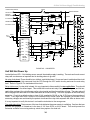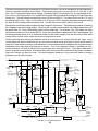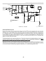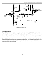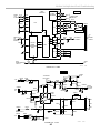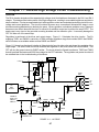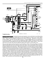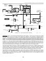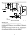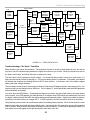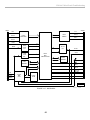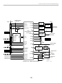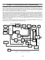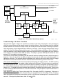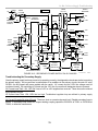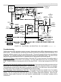
1
Training Manual
KDP-57XBR2
Projection Television
Troubleshooting
RA-3/3A, RA-4/4A, RA-5A, RA-6 Chassis
Practical Troubleshooting Tips
Course: TVP-14
Table of Contents
1. Introduction .......................................1
The RA-5A Chassis
The RA-3/3A Chassis
15. Troubleshooting
the RA-5A Chassis ...............................67
2. The RA-3/3A Chassis ........................2
3. Power Supply Troubleshooting ......3
The Main Power Supply ....................................... 6
4. Shutdown & Self-Diagnostics ........12
5. Deflection Circuits ...........................14
6. Video Process Troubleshooting:
T & S Models .........................................20
The RA-4/4A Chassis
7. Troubleshooting
the RA-4 Chassis ..................................29
Overview................................................................ 29
8. Power Supply Troubleshooting .....30
Overview................................................................ 30
Standby Power Supply Troubleshooting .......... 30
Unit will not Power Up ......................................... 34
Shorted Switching Transistors ........................... 35
Regulator Troubleshooting ................................. 35
9. Protect Circuit Troubleshooting ....37
Overview................................................................ 37
10. Deflection Circuit
Troubleshooting ...................................40
Overview................................................................ 40
Horizontal Deflection ........................................... 40
Vertical Deflection ................................................ 44
Vertical Deflection Troubleshooting .................. 46
11. High Voltage Circuit
Troubleshooting ...................................47
12. Video Circuit Troubleshooting .....54
13. Troubleshooting
the RA-4A Chassis ...............................63
Overview................................................................ 63
14. Video Circuit Troubleshooting .....64
Overview................................................................ 67
16. Power Supply Troubleshooting ...68
Overview................................................................ 68
Standby Power Supply ........................................ 68
Primary Power Supply ......................................... 68
Troubleshooting the Primary Power Supply .... 70
17. Protect Circuit Troubleshooting ..73
Overview................................................................ 73
Troubleshooting .................................................... 75
Shutdown - No Diagnostics Indication.............. 76
18. Deflection Circuit
Troubleshooting ...................................77
19. High Voltage Circuit
Troubleshooting ...................................80
20. Video Path Troubleshooting ........84
The RA-6 Chassis
21. Troubleshooting
the RA-6 Chassis ..................................87
Overview................................................................ 87
22. Power Supply Troubleshooting ...88
General Description............................................. 88
23. Protect Circuit Troubleshooting ..92
24. Deflection Circuit
Troubleshooting ...................................96
25. High Voltage Circuit
Troubleshooting ...................................99
26. Video Circuit Troubleshooting ... 103
General Description............................................ 103
27. Troubleshooting the
AKB Circuits ....................................... 109
Overview............................................................... 109
28. Auto Registration
Troubleshooting ................................. 113
Overview............................................................... 113
Flash Focus Errors ............................................. 115
Error Codes .......................................................... 119
29. Model-to-Chassis
Cross Reference ................................ 120
1. Features
Chapter 1 - Introduction
In the fall of 1996, Sony Electronics introduced a troubleshooting course (TVP-06) that covered troubleshooting
of the AP and RA-1 chassis, along with the prior EX and EXR model sets. The course provided some useful and
practical approaches to repairing failures that might occur in each of the circuits, and allowed the technician to
focus on troubleshooting more than theory of operation. Unfortunately, the RA-2 chassis was not included as
this product was just being released on the market. This chassis will not be covered in this course and since it
shares much of the same circuitry as the RA-3, you should be able to apply virtually all of the troubleshooting
techniques covered in this course. For information regarding theory of operation for this chassis, refer to the
training manual TVP-07 (P/N TVP070797).
Almost six years have passed, and six new chassis versions have been introduced. Some minor (and some
dramatic) changes in circuitry design have occurred. High Definition Television was finally getting underway and
the competition for producing better performing projection televisions introduced new features that had never
been seen before. In some cases, new troubleshooting approaches are needed to effectively deal with these
new circuit designs. Add replacement parts tracking and you have useful resources to document some practical
approaches to solving problems that might arise.
The course will be organized by chassis group with a brief description of what was introduced in that family.
Next, the major circuits with a brief description of each will be covered with some reasonable approaches to
isolating problems. If you need more detail on the theory of each circuit, the appropriate training manual that
applies will be mentioned.
NOTE: Much of the power supply troubleshooting techniques in this manual involve using a variac with either a
separate or integrated AC amp meter. If you do not have one, get one. You cannot perform speedy power supply
troubleshooting without one and risk the possibility of damaging newly installed components or causing the
failure of other parts along the way.
1
1. Features
Chapter 2 - The RA-3/3A Chassis
Overview
The RA-3 chassis introduced a major redesign in the convergence circuits that made it much easier for the
technician to converge the set with greater accuracy and speed. It is know as Flash Focus TM and allowed the
customer to perform more thorough convergence realignment should it drift out of range. The RA-4 was actually
the first unit to introduce this feature a year earlier, but it was confined to the more expensive XBR200 series
units. The RA-3 brought this feature to the more affordable models.
The power supply still utilized the dual transistor switching power supply that is found in previous sets, and
incorporated the two transistors into a single IC package. A separate standby supply still exists but uses a FET
transistor for switching instead of a bi-polar type. Self-diagnostics were also introduced to aid in troubleshooting.
The number of circuit boards was substantially reduced with most of the circuits residing on the A and G boards.
The G board now contained the deflection circuits, along with the usual power supply components rather than
utilizing a separate D board. Unlike previous sets, which had a separate horizontal scan and high voltage
sections, the horizontal/HV is handled with a single output and flyback to generate H scan and HV. This makes
deflection and HV problems easier to diagnose. The A board handles video processing, system control and the
Flash Focus TM circuit. Pincushion correction was simplified by substantially reducing the number of discrete
components.
The RA-3 also provided the customer with component video capability, which was previously found only on the
XBR series. The T and S series models provided a single component input at the rear in the video 4 slot while the
V series provided for two components inputs at video 4 and 5.
There are not any significant differences between the RA-3 and RA-3A worth mentioning. In fact, the circuits are
almost identical with some minor design changes. The RA-3A chassis was simply a carry-over into the next
model year, so the troubleshooting procedures remain the same for both. To keep things simple, only the RA-3
in the titles and text portions of this section will be mentioned.
2
3. RA-3/3A Power Supply Troubleshooting
Chapter 3 - RA-3/3A Power Supply Troubleshooting
he Standby Power Supply
The standby supply is a simple switched-mode type utilizing a single transistor, transformer and feedback circuitry
to generate approximately 7VDC provided to a 5-volt regulator IC. Regulation will be provided by changing the
oscillation frequency based on current demand. Notice that the regulated 5 volts not only provides standby
power for the microprocessor, but also powers the main relay. This is a deviation from previous designs. It is
important to remember this when the need arises to replace the relay and you are obtaining one from a scrap
board that came out of an earlier chassis. The relays in previous projection and direct-view sets were rated at 12
volts and will not function on this chassis.
Referring to Figure 3-1, the supply works by supplying unregulated B+ through the primary of T602 to the drain
of Q601, which will provide the needed ground path via R604 to provide current for the transformer. Q601 G will
need a kick-start and that will be provided by R609. The FET will now begin conducting and current will begin to
flow through the primary. The feedback winding at pin 4 of T602 will now start generating a positive voltage,
thereby charging C614, which will drive the FET harder. This increases current in the primary, which further
increases the feedback voltage, which further increases the conduction of the FET. This event will continue until
two things occur: Q601 reaches saturation and C614 charges. This is how the on time of Q601 is controlled to
change the frequency.
C616 will route the feedback voltage via R615 to Q602B. This voltage will be smoothed out by C610 and C609
to provide a rising sawtooth to control the on time of Q602. Q602 will now become part of the RC network of
C614, R608 and R616. If current demand on the secondary of T602 decreases, voltage levels in the transformer
will rise accordingly. This will cause a rise of the feedback voltage and will cause Q602 to conduct harder and
alter the RC time constant. C614 will now charge more rapidly and Q601 will turn off earlier. By shutting the FET
off earlier, the on time is decreased along with the duration of the field collapse in T602. Shorter conduction time
and field collapse equals faster switching cycles and, hence, higher frequency. The higher the frequency, the
lower the output voltages at the secondary.
Q602 will also provide protection against over-voltage or over-current situations. If the current rises dramatically,
a voltage drop will occur across R604. When it rises to 0.6V or more, Q602 will conduct to raise the frequency,
or, in severe cases, momentarily stop oscillation. This would cause the familiar “ticking” noise as the supply
keeps trying to re-start.
Should the regulator loop fail, zener diode D605 will monitor the voltage stored by C618, which is charged by
D610 during the field collapse periods. If this exceeds 6.2 volts, D605 will fire into Q602B and produce the same
reaction as an over-current condition.
3
3. RA-3/3A Power Supply Troubleshooting
FB621
D601
T602
SRT
R607
4.7 OHMS
1
FROM
T601/1
AC Hi
SIDE
D602
C617
R620
2
11
3
10
TO RY601
POWER RELAY
D623
R609
7.2VDC
D
D667
C614
4
S
CN605
I
9
R616
Q601
2SK2845
IC655
5V REG
BAO5T
G
C616
O
C650
D607
D604
MTZ-T-77
-15
10
STANDBY
+5V TO
A BOARD
CN681
C676
5
8
R615
R608
R622
C609
R638 D610
6
C608
Q602
PROT.
R605
D605
RD6.2ESB2
C613
C618
C610
G BOARD
R604
HOT
GROUND
FIGURE 3-1 - STANDBY SUPPLY
2TVP14
7/11/02
Troubleshooting
This supply should operate reliably since it only feeds a few circuits and the current demand is minimal.
Unfortunately, as this supply is always running so long as AC input is supplied, it will be susceptible to line
transients. The main supply will be protected as long as the main relay is not engaged and the transient is not
large enough to jump the open relay contacts (such as a heavy lightning strike). Failures that might occur would
be a dead supply or regulation problems.
If Q601 has shorted, there is a high probability that something else caused the failure. This is based upon a
reliable history of this component. We will start with a scenario of a shorted Q601 and then cover a “no run”
condition next since you are most like to end up with this after replacing Q601 due to current or transient causes.
The FET gate has very high impedance, which allows other components to suffer damage.
Dead standby supply - Q601 shorted
Upon replacement of the shorted FET, the main concern is what caused it to fail and to prevent it from failing
again when power is re-applied. The most valuable piece of test equipment in this situation, as mentioned in the
beginning of this manual, is a variac with an AC current meter, either separate or integrated with the voltage
meter. This will assist by indicating current conditions, and allow you to control that situation and prevent failure
of the newly installed FET.
4
3. RA-3/3A Power Supply Troubleshooting
Once the FET has been changed along with R607, you will need to disconnect the secondary voltage line by
lifting D667. This is very important since switch-mode supplies draw very small amounts of current while running
unloaded and the load from the 5-volt line must be kept from drawing any current. Many technicians are fearful
of running switch-mode supplies unloaded. Most are able to run unloaded, but this test is not going to supply
more than 40VAC. You will need to keep the AC low with the variac and watch for current draw. While turning up
the AC voltage, monitor the drain of the FET with an oscilloscope to ensure it is starting to oscillate. This will
need to be done because even if the oscillator starts running, you will probably not be able to detect any current
on most amp meters that come equipped with the variac. If you do not see any oscillation by the time 40 or
50VAC is reached, there is a problem.
Oscillator starts with very little AC current being drawn: Re-connect the load to the secondary and bring up the
supply with the variac while monitoring both AC current AND the voltage at D667. You want to ensure that
current draw continues to remain low and that the input voltage to IC655 does rise dramatically above 7 volts.
Rising current would indicate a short on the secondary or the output of IC655. A continuously rising voltage at
D667 indicates regulation problems. Regulation problems will be discussed later. If the supply runs with full AC
and minimal current, the repair has been completed
Oscillator starts with excessive current: This is an obvious indicator as to what caused Q601 to fail. This situation
is rare in this type of power supply in an unloaded condition but when it does occur, it is almost always caused by
a leaking or shorted feedback coupling capacitor (C614) or shorted winding(s) in T602. Ringing the transformer
or viewing the waveform at Q601D will expose problems in the windings. Listen for any ticking sounds and watch
the oscilloscope for bursts of oscillation, which would indicate the over-current and/or over-voltage stages are
doing their job.
Dead Standby Supply – Q601 not Shorted
Assuming very little AC current is being drawn and there are no chirping or ticking sounds, you are dealing with
a circuit that is not starting or is not able to sustain oscillation. Verify the presence of B+ at Q601. Next, read the
voltage on the gate of Q601. The same voltage present on the drain should appear at the gate
No voltage at gate: No voltage indicates either an open start resistor (R609) or the gate is loaded down. Read
the resistance at the gate of Q601 relative to hot ground. It should read infinity. If it does, lift one side of R609
and read its resistance. You must lift it since it is a 22MΩ. If resistance is read at the gate, you will need to find
the component(s) at fault. As mentioned earlier, due to the high impedance of the FET gate, many components
can be damaged by incoming transients. Even a small amount of leakage can overcome the pull up function of
R609. All you can do here is to “ohm out” parts or, more effectively, lift components to get the voltage back on the
gate. In the case of line transient damage, you may find several components loading the area down. Do not
forget about feedback capacitor C614 since it is connected to the feedback winding with a low resistance to
ground.
Voltage present at gate: This indicates the start resistor, R609, is OK and nothing is loading the gate. You now
have a narrow choice of components to check. Either the feedback path is open (C614, R616 or the feedback
winding itself), or the “tuned” portion of the oscillator has a problem. This leaves us with leaking or, most likely,
shorted C617 or D623 in the snubbing circuit or T602 itself.
Voltage Regulation Errors
This failure can be difficult at times due to the closed loop needed for this circuit to operate. It becomes even
more difficult when the problem is excessive B+ since components can be damaged. Listed below are some
troubleshooting techniques:
Low B+ This is easier to work on since you will not risk damaging components. Excessive current is not being drawn
since components are not smoking. It is safe to assume the regulation feedback loop is not open since this
would cause B+ to run too high. That leaves two possibilities: 1) The oscillator is incapable of producing adequate
B+ due to frequency shift or distorted oscillation; or 2) the regulation control components are not performing their
5
3. RA-3/3A Power Supply Troubleshooting
job properly. Since they are part of a loop, one affects the other. This is where many technicians run into
difficulties. It is similar to working on vertical deflection circuits. They are one of the more simple circuits in a
television but seem to be one of the more difficult to diagnose because of the reliance on feedback. The first task
is to isolate the failure in either the feedback loop or the oscillator. This can be done in a surprisingly simple way.
The regulator loop will be opened. It can be done safely so long as you have the variac. In this situation, you will
want to remove the connection from Q602-C to Q601-G. Slowly apply AC voltage with the variac while monitoring
the input to IC655. Proper B+ on the secondary line should appear at low AC. If it does, the problem is in the
regulation loop. The nice part of this method is that it divides the number of suspected components in half. Here
are the two possible outcomes:
B+ is still low even with full AC input: Assuming proper unregulated B+ is getting to Q601, either the
oscillator feedback line (not to be confused with the regulation feedback) is impeded or the oscillator
circuit is noisy or out of frequency. Suspect dry capacitor C614, resistance increase in R616 or loading of
the feedback line by shorted or leaking D604, D607 or C613. Q601 could even be the cause.
B+ reaches full level at low AC input: The problem is in the regulation loop and is usually caused by noise
in the line and open filters. C618 is a good suspect. If it opens, noise spikes will overcome the zener
diode D605 and will be amplified by Q602. Watch out for filters C609 and C610 opening or increasing in
value. Their job is to help produce a nice ramp-shaped signal at the base of Q602. This is especially true
for C610. The rise time of this ramp is critical in the timing of turning off Q601. A leaky C618, or even
Q602 itself, is another possibility.
Excessive B+
This problem requires caution since damage to components is a possibility. By far, the most likely component is
going to be Q602. Based on previous experience with this type of power supply, the B-E junction is common to
open. Leaking or shorted C610 comes in at a close second. Check for an increase in value, or open, at R615,
and a decrease in value or open at C618
The Main Power Supply
The main power supply is still a somewhat conventional style that has been used in Sony televisions for many
years. It is only active when the unit is powered up by energizing the main relay RY601. It has earned a dubious
reputation amongst technicians due to its insatiable appetite for several sets of switching transistors before the
technician finally got it repaired, and, rightfully so. When there are two transistors working together and one is
supposed to be off while the other is on, extreme care must be taken when replacing them. You are going to
learn some nice tricks that will virtually eliminate the immediate destruction of your newly installed switching
transistors. The regulation principle, although appearing complicated, is quite simple to troubleshoot since it
relies on pure DC voltages to function rather than ramp-rise timing used in simpler switching supplies.
Operation
Refer to Figure 3-2. The switching transistors are now conveniently packaged into a single IC. Oscillation is
begun by the upper transistor in IC601. Its collector is connected to the unregulated B+. R610, R611 and R619
bias the transistors near conduction in a classic AB-type amplifier design. The upper transistor will start current
flowing into the primary of T604 at pin 2. Pin 1 will continue the current flow to pin 5 of T605 and exit at pin 6
where C602 will provide the path to hot ground. This will cause pin 3 of T604 (the feedback winding) to spike the
base of the upper transistor through C620 and R619, which will now begin conducting. Current will increase in
the primaries of T604 and T605 and continue to charge C602 to the ground return. The feedback output at T604/
pin 3 will continue to increase and turn the upper transistor on harder. Meanwhile, the lower transistor is being
kept off since its base is connected to another feedback winding via R617 and C621. This other feedback source
is 180 degrees out-of-phase with the other so it is a negative voltage at this time.
6
3. RA-3/3A Power Supply Troubleshooting
Once C620 has charged, the upper transistor will lose its large B-E current and turn off. The impedance of the
primary in T604 will determine how fast C620 is charged and this will vary depending on the amount of current in
the control winding at pin 7 and 8 of T604. This is how this supply will regulate. The field will not collapse and all
induced voltages will reverse polarity. The feedback voltage at T604/pin 3 will now go negative and pin 4 will go
positive and turn on the lower transistor in IC601. IC601’s job is to pull pin 2 of T604 primary to ground potential.
The voltage stored in C602 will now have a path in which to discharge so that it is ready for the next cycle when
the upper transistor conducts again. The oscillator can continue this cycle indefinitely as long the components
remain stable and external power is available. All that needs to be done now is to alter the on-off time of the
switching transistors in order to regulate the secondary outputs.
The winding at pins 7 and 8 of T604 is what is known as a “cross winding”. The more current that flows through
this winding, the lower the net inductance of the windings in T604. It is similar to the effect that occurs when
adjusting the ferrite core in an adjustable coil or transformer. By lowering the inductance, the primary of T604 will
provide less resistance to current changes and will allow C602 to charge faster. If it charges faster, the field
collapse will also be shorter in duration and you now have a shorter charge/discharge rate and, hence, higher
oscillation frequency.
The current in the control winding is handled by IC654. It monitors the 135V B+ line. If the 135V line were to rise,
IC654 would act as an inverter. Pin 7 of T604 is fed by 18 volts from the secondary of T605. Since IC654 inverts,
it will pull down pin 8 of T604. Current through the control winding will increase, the impedance of T604 will
decrease and the oscillator frequency will rise. This will move the frequency further above the fixed resonant
point of T605, which will increase its impedance. The net effect will be a drop in secondary output voltages. The
opposite will occur should the 135V line decrease.
One more item to cover: The “soft start” circuit. This circuit is important to understand since its failure can cause
major problems for a technician. When the main power supply is first energized, a large current surge will occur
since the oscillator is starting from zero frequency and rising (which will cause it to cross the resonant point of
T605) and all of the filter capacitors on the secondary lines are waiting to be charged up. Consequently, it is
important that the oscillator be “forced” into high frequency as soon as possible. Q653 is allocated to this task.
There is a constant 12V source provided to the control winding by Q651. If it were not there, the control winding
would have no voltage at initial turn-on. As mentioned earlier, this would cause low frequency oscillation and,
hence, maximum output. This condition is undesirable while all of the filter capacitors are charging as it could
cause IC601 to fail.
Q653 is connected to the return side of the control winding through R669. Its base has a 1mf capacitor connected
to it. This capacitor provides approximately three seconds of charge time to keep Q653 on, which will provide
pull-down to the return side of the control winding. Extra current is now provided through the control winding to
keep the oscillator frequency high during the initial turn-on period. Once C673 has charged, the base of Q653
will go high and it will turn off and hand over control to IC654. Problems in this circuit can cause instant failure of
the switching transistors or may cause them to fail weeks later after the repair. A five second test can be done to
check this circuit and this will be covered in the troubleshooting section.
7
3. RA-3/3A Power Supply Troubleshooting
AUDIO
GND
AUDIO
B+
AUDIO
B-
T605
PIT
D665
+15V
C659
6
C658
5
-15V
+5V
IC653
D660
D659
R656
-5V
IC652
R652
R654
+135V
C662
A BOARD
R655
50V/DIV 5uS T/DIV
D658
C602
R619
R610 R611
D603
1/2W
C612
R602
0.82Ω
20W
HOT
GND
RY601
C612
2
IC601
MXO8
41AB-F
C622
C620
R612 0.1Ω
AC
C664
N
C624
R668
R680
N
7
R618
12V STBY
C621
8
C623
R679
D665
R676
C673
Q653
SOFT
START
R669
R617
Q651 BACK-UP
2
CN652 2
D666
TO R677
T604 PRT
PROT.
1
D668 LATCH
24V
R673
2
Q652
R683
RY
3
DRIVE
Q658
N
4
LIMIT
R681
R621
1
P
CN1601
18V
5
C611
12V
STBY
FROM IC001/62
D662
P
R666 C670 R670 C671
G BOARD
4
3
5
FIGURE 3-2 - SWITCHING POWER SUPPLY
8
2
1
IC654 DM-48
1TVP14 1448
7/17/02
3. RA-3/3A Power Supply Troubleshooting
Troubleshooting
Once a few standard procedures are followed, this power supply is not too difficult to repair. The greatest
obstacle is the precise timing required for the two transistors inside of IC601 to work together. They form a
classical AB-type amplifier design. This means the transistors need to be biased near the upper end of the cutoff
point and this is provided by resistors R610 and R611 for the upper half and R621 and R618 for the lower.
Anything upsetting the biasing of the feedback lines can cause an overlap. Once both transistors are on at the
same time, even for a brief moment, they will fail. Incoming transients from the AC line, excessive noise in the
feedback circuit or leakage of the coupling capacitors C620 or C621 can cause this to happen. The other cause
may be excessive current that exceeds the capacity of the transistors, such as shorts on the secondary line.
Problems in the feedback circuitry are the most difficult for the technician. In a typical situation, the technician
finds IC601 shorted and checks the secondary lines for shorts. He then fires the unit up and loses the newly
installed IC. This problem can be solved by using a proven method to actually run the supply with the original
cause still there, and yet not lose the switching IC. Also covered will be regulation problems, which are quite
easy to solve with a couple of simple tricks.
Since the most common failure is shorted switching transistors, that scenario will be covered first. Power supplies
that will not run is not very common, but will also be covered. Regulation troubleshooting will then follow.
Dead Power Supply, IC601 Shorted
The important rule to remember when this happens is to assume that something caused the failure. Occasionally,
IC601 will simply fail and will turn out to be an easy repair. However, you should be ready for the likelihood that
something else is still wrong. Rule number one is: Never fire up the set to see what happens. Always use a
variac to bring it up slowly. There is one problem to deal with before this is done. The main relay will not engage
until there is at least 60VAC coming into the set. This will supply enough unregulated B+ to the switching
transistors to generate full secondary voltages and they will be lost if a dynamic load (such as a defective flyback)
or a shorted line still exists that was missed during the performance of static resistance checks. It is going to
involve jumping the main relay while controlling things with the variac. This is a safe method so long as care is
taken and the current is monitored closely.
Some technicians like to use a light bulb in series with the AC input to protect against failures. This worked fine
on analog supplies, but all it did was sit there glaring at you to indicate a problem existed. It is not a good idea to
use this method on switching supplies. The light bulb will substantially reduce the incoming AC voltage and,
consequently, the unregulated B+. The power supply will now go into low frequency mode and try to get the
proper secondary voltages. This will produce greater “on” times for the transistors and they will soon overheat
and fail. Use a variac.
Once IC601 has been replaced (it is assumed that fuse resistor R612 will also need replacement), some other
checks are required before power is applied. A quick visual check of the components around the switching IC
should be done to look for signs of overheated parts. Watch the small capacitors for signs of cracking or
swelling. This is particularly important if lightning activity has occurred recently. Check all secondary voltage
lines for shorts and if all is OK, it is time to apply some power.
Plug into the variac and set the meter for AC current if it is an integrated type. Jump the relay RY601 and start
bringing up the AC voltage. Watch the current draw closely. At around 40VAC, about 750ma to 1 amp will should
appear. Continue to increase the voltage and allow up to 1.5 amps to appear, but no more. As you near 60 to
70VAC, the amperage should actually start decreasing as the voltage input rises. As the switching supply gets
more voltage, it will increase its frequency due to the transistors having a shorter on time. By the time you reach
full 120VAC, the amperage should have dropped to somewhere between 600 and 800ma. There is a good
chance you now have a repaired unit, but there is still one more check to perform. The soft start circuit could
have caused the IC failure and if this is so, IC601 will fail at turn-on. This may happen immediately or even
weeks later. Move forward to the section dealing with soft start. Unfortunately, it does not always go this easy
and a couple of different scenarios might occur from the ideal outcome above. Following are some suggestions
for resolving them:
9
3. RA-3/3A Power Supply Troubleshooting
No AC Current Is Read: You have a supply that will not start. This is not common, but can occur. Bring the AC
voltage up to 40 volts. It is recommended to not exceed this level just in case you accidentally cause the
oscillator to start while probing around with the scope and meter. The first important step is to measure the
voltage at the collector of the upper transistor. There should be a DC voltage present that is approximately twice
the AC voltage due to the doubling circuit. The next point to read is the collector of the lower transistor. Since
both transistors are biased slightly above cutoff, one half of the voltage level that is read on the upper transistor
should be here. Both transistors are identical and so are their bias resistors. Consequently, this comprises a
voltage divider. This is an excellent test to see if the bias resistors are good and both transistors are able to
conduct. If the voltage is significantly higher or lower at the mid point, possible causes are an open bias resistor,
shorted feedback coupling capacitors, shorted C612 (this would cause the same voltage to appear at both
collectors), or a defective IC.
If the DC voltage is being divided properly, there is likely a problem with the feedback circuits, an open winding
or solder connection problem at either transformer, or C602 could be open. It is possible that feedback capacitors
C620 and C621, or R617 and R619, are open since they handle significant current during their operation.
AC Current Rapidly Rises With Low AC input: This is where close attention will be required. The original cause
of the switching IC failure is still there and needs to be located. Since you have checked for static shorts on all
the lines, there is a possible dynamic load problem and the power supply needs to be running in order to locate
it. By keeping things under control and monitoring AC current, the failure of the switching IC can be prevented.
This test can be safely performed even if the horizontal output transistor is shorted.
The cause of the over-current problem needs to be located and it will be in one of two places: either the primary
side or the secondary side. Since problems in horizontal and high voltage circuits are the most common, a handy
trick is to disable the horizontal section by unsoldering the horizontal output transistor and re-applying AC voltage.
If the current problem is gone (the current will not go much higher that 250ma with the horizontal circuit
disconnected), the over-current source has been exposed and will be dealt with in the section on the deflection
circuits.
If excessive current still exists, its simply a matter of disconnecting secondary lines and trying to re-apply power.
If disconnecting secondary lines does not resolve the issue, the problem is in the primary circuits. The switching
transistors are either overlapping (conducting at the same time) or there could be a problem with T604 or T605.
In almost all cases, one of the feedback coupling capacitors (C620 or C621) is leaky. This is more likely to be
found in older units or ones that have incurred a large line transient. Watch the waveform at T604 pin 2. It should
be a relatively symmetrical square wave with a 50/50 duty cycle. Any evidence of ringing could indicate a shorted
winding in either of the transformers.
The Soft Start Circuit Check: As mentioned earlier, this circuit can cause switching transistor failures. Since the
supply was brought up slowly with the variac, the soft start has already been performed. The set has been
running for a while now and you are confident that everything is OK. The back cover is put back on and just to
check one more time, the set is plugged in and turned on and the power supply fails again. The set may turn on
just fine but be returned anywhere from a few days to even weeks later with the power supply gone again. While
other problems could be causing this, it is a wise idea to check the soft start circuit on any power supply in which
you have just changed shorted switching transistors to avoid that dreaded call-back from showing up. Here is a
very quick way to check the circuit:
Bring the unit up slowly to full AC with the variac. Set the meter to read AC current, if necessary. While leaving
the variac at full 120VAC, turn the unit off with the remote or front power button. Wait about two or three seconds
and turn it back on while closely watching the AC current. It does not matter what the current level is since this
will vary from model to model and the quality of your incoming line voltage. What you should see in about three
seconds is a rapid increase in current of about 200 to 300ma from the initial current reading. That was the soft
start circuit at work. If the current does not jump, find out why the circuit is not working. Suspect a dried-out
electrolytic capacitor C673, a shorted B-E junction or an open Q653 or shorted Q656.
10
3. RA-3/3A Power Supply Troubleshooting
B+ Regulator Troubleshooting
B+ Voltage Too High: This symptom can be a little troublesome to work with because the unit will be going into
shutdown protect and there is the possibility of damaging components (particularly the horizontal output transistor).
Once again, the main relay is going to be jumped, but this method works quite well if the proper steps are
carefully followed. Make sure that the unit is in the off mode. Turn on the set and let it go into shutdown. It is
important to follow this step. The main CPU must be kept in the “power on memory” mode. If it is not, the relay
on command will not go high and Q656 will hold the soft start circuit on and interfere with your diagnosis.
Jump the main relay RY601. Bring up AC voltage with the variac, while closely monitoring the 135V line. As soon
as 135 volts is reached, bring up the voltage to about 137V. It is OK to go this high since the protect circuit does
not even activate until 139V or more. The purpose of this procedure is to determine whether or not the regulator
stage recognizes the over-voltage condition. Read the voltage at T604/pin 7. There should be at least 12VDC
present. If not, the 18V line has failed coming from T605/pin 2. Failure of this line is rare so it should be there.
Next, read the voltage at T602, pin 8. It should be dramatically lower than pin 7. If it is not, the problem is being
caused by a lack of current through the control winding since IC654 is not pulling down on pin 7. Before you opt
for replacement of IC654, keep in mind that this IC is very reliable. Many have been changed needlessly. This
condition is usually caused by the B+ voltage sampling resistor(s) such as R668. It increases in value and the
regulator is fooled into thinking there is insufficient 135V.
If the voltage at T604/pin 8 is much lower than pin 7, either the control winding is open or IC654 is aware of the
153V being too high and is trying to correct the problem by inducing more current into the winding. Assuming the
winding is not open (extremely rare), all that is left is an oscillator section has drifted so far off frequency so as to
be “out-of-range” of the control circuit. This can be caused in older units by dried out capacitors. Any of the small
value capacitors in the primary oscillator can cause this, so it is recommended to replace all of them to get the
normal frequency back in range.
B+ voltage too low: This is a little easier to work with since the risk the damaging components is not present. We
know that excessive current is not causing the problem since the set is not going into shutdown. Simply read the
voltage at pins 7 and 8 of T604. If they are equal, IC654 is responding properly to the condition. Troubleshoot
the primary circuits for oscillator distortion or frequency shift. If pin 8 is lower than pin 7, and this will usually be
the case, suspect Q653 soft start is constantly on or shorted or IC654/pin 4 shorted.
NOTE: On a properly working power supply, it is sometimes normal to be unable to reach full B+ level with the
relay jumped. It depends on whether or not the microprocessor is in the “on” state. If it is not, the relay high
command will remain low and Q652 relay drive will be off. This causes Q656 to remain on, holding the base of
Q653 low. This keeps the unit in “soft start” all the time. The purpose of Q656 is to discharge C673 at turn-off so
that there is always a soft start when the unit is turned back on. If the unit happened to be in the “power on” state
when last running, the B+ level will rise to proper potential with the relay jumped. This is very important to
remember when troubleshooting OVP problems as the soft start may kick in and interfere with regulator checks.
11
4. RA-3/3A Shutdown and Self-Diagnostics
Chapter 4 - RA-3/3A Shutdown and Self-Diagnostics
Overview
Another new feature introduced in the RA-3 Chassis is self-diagnostics capability. By utilizing the timer LED on
the front panel, it can be flashed in sequences when a failure occurs to assist in troubleshooting. It works rather
well in most situations, but can also mislead the technician. The unit will also store these failure events into the
NVM IC for viewing and these can be called up by pressing “display” “5”, volume down” and “power”. This page
is only useful for troubleshooting intermittent problems since if cannot be displayed if the unit is going into
shutdown or video blanking. For a more detailed description of the shutdown circuitry, refer to training manual
TVP-10 (P/N TVP100100).
Below is a sample of the diagnostics page:
Self Check
2:
+B OCP
000
3:
+B OVP
000
4:
V Stop
000
5:
AKB
000
6:
H Stop
000
8:
Audio
000
101: WDT
000
The numbers on the left indicate how many times the timer LED flashed, which designates the probable cause of
the shutdown. The flashes on the LED will occur at one second intervals, followed by a three second separation
period and repeat again. The numbers at the extreme right indicate how many times the problem occurred up to
999 events. You can see why this is beneficial for intermittent troubleshooting. It is always a good idea to clear
the events before exiting and that can be done by pressing “8” and “enter” on the remote. This is not the same
as pressing these buttons in the service mode. It will only clear the events and not reset customer defaults.
Beware that the service manual instructs you to enter the service mode to clear these and that is a mistake. You
can do it right from this screen. Below is a description of each event:
+B OCP: Excessive current on the 135V line. This is usually caused by flyback problems or secondary loads on
the line. The circuit could also be tripping for no reason. This is why you should always monitor AC current while
the unit is shutting down. It will help to determine if the problem is actually an over-current condition and more
caution can be taken when servicing the unit.
+B OVP: The 135V line has exceeded 139 volts. Go back to the section on troubleshooting regulator problems.
V Stop: The vertical deflection circuit has stopped operating. This indication can also occur if the high voltage
circuit fails since it supplies the +15V and –15V supply rail to the vertical output. Loads on the I2C data and clock
bus can also be the source of this problem.
AKB: One or more CRT cathodes are unable to generate sufficient current to return a good feedback pulse. The
AKB detect circuit may also have failed. It is common to see multiple AKB events in the diagnostic page along
with registered HV failures. See the special section on AKB in Chapter 27 of this manual.
H Stop: The horizontal deflection has been turned off due to excessive high voltage. This will be covered in the
deflection section.
Audio: DC voltage has been detected on one or both of the audio out lines. The set is shut down to protect the
speakers. This is usually caused by shorted audio amp IC406.
WDT: A communications error has occurred. The main CPU is unable to communicate with the Y/C jungle IC.
The timer LED blinks continuously at one-second intervals and as soon as 101 of them occur, a failure is registered.
12
4. RA-3/3A Shutdown and Self-Diagnostics
Protection Circuits Not Covered By Self-Diagnostics
There are four protect circuits that are not monitored by diagnostics. Consequently, they will not be identified by
the timer LED or stored into the diagnostics page. Referring to Figure 4-1, the standby 5V regulator IC655 is
protected against over-voltage to its input and excessive current at the output. The 11V line on the secondary is
monitored for excessive current (or a complete loss of it). The 18V secondary line is also monitored for overvoltage. If the unit goes into shutdown with no diagnostic indicator, this is where you will want to look next. Here
are some quick methods to locate the source:
The Standby 5V Circuit: Monitor the anode of either D675 or D674 while applying AC power. An oscilloscope or
peak-hold DVM is preferred, but this can be done with a standard DVM. If anything higher that 600mv appears
at this point (you will see 10V or more if this circuit is firing), the input voltage to IC655 is exceeding 10V and firing
D675. Troubleshoot the standby supply regulator circuit described earlier in this manual. If D675 is not firing,
read the voltage across Q658 B-E. If it is 600mv, the OCP circuit is activating. Locate excessive load on standby
5V circuit. If Q658 B-E remains at less that .6V, monitor Q658 collector while re-applying AC. The voltage here
should be zero. Any rise indicates excessive 18V or loss of 11V.
18V and 11V Protect: Monitor the voltage at D669 cathode while applying AC power. If voltage peaks at 11VDC,
suspect 11V line failure or shorted D669. Normal voltage should be around 18V. If the voltage at Q657-E is
higher than 24VDC, the 18V line is too high. If both voltages check OK, look for leaking or shorted zener diodes
D669 or D668. Q657 may also be leaking or shorted.
STANDBY 5V
5
8
IC651
OVP/OCP
uPC393C
+
6
-
R663
R659
D672
+135V
R665
G BOARD
R664
CN605
OVP
7
R661
R660
8
TO CN681
A BOARD
2
-
3
+
OCP
1
C662
RELAY
7
4
R657
+135V
BRIDGE
NEG.
FROM
D652/A
AND D653/A
D661
4
R662
R675
C663
Q654
D663
PROTECTION
LATCH
R654
D675
MTZJ10B
D667
R691
9
PART
OF T602
STB
C676
8
C680
Q655
D674
I IC655
BAO5T O
5V REG.
G
D651
R686
RY DRIVE
FROM
Q652/C
TO
Q652/B
RELAY
DRIVE
D680
R687
C679
R667
R689
R690
R688
D676
MTZJ-3-9B
D664
MTZJ-2-7A
D668 C678
24V
STANDBY
5V
+18V
R684
+11V
Q658
R682
Q657
D669
13V
TO Q656/B LIMITER
R681
TO RY601 POWER RELAY
FIGURE 4-1 - POWER SUPPLY PROTECTION
13
4.1TVP14
7/11/02
5. RA-3/3A Deflection Circuits
Chapter 5 - RA-3/3A Deflection Circuits
Overview
Like the RA-2 chassis, the RA-3 utilizes a simple deflection circuit design much like those found in many of the
direct-view models. Figures 5-1A and 5-1B illustrate the simplicity of this design. High voltage and horizontal
sweep are accomplished with a single horizontal output transistor driving a flyback transformer and deflection
yokes. This helps to simplify CRT protection and the need for horizontal sweep loss protection is not required
since there will be no high voltage to burn the tubes. The vertical deflection circuit remains relatively the same as
those in previous years.
TO DYNAMIC
FOCUS BIAS
RECT. D517
G BOARD
T501
R508
+9V
TO PIN1
H+ ZR
C517
TO
T504/
PIN 1
R506
1
135V
4
R507
Q501
H DRIVE
40
XTAL
X203
HD
CN502
52
3
C501
N
CN801
IC206Y/C
JUNGLE
CXA2025AS
H
SYNC
IN
10 10
41
46
R502
R501
6
Q502
H OUT
C506
C510
FROM ABL
R529
+12V
C529
R528
HP
D501 5.1V
HP LIMIT
R550
R551
2
-
5
+
4
R556
+12V
C537
+135V
IC502 1/4
R530
D513
C538
D520
C515
R527
+12V
+12V
R542
+12V
R532
R526
14
Q503
PIN AMP.
+
-
R509
9
13
6
IC502 1/4
10
+
-
C527
R527
C514
11
IC502 1/4
R523
L503
C531
R563
R524
R543
C528
C521
C534
C502
R519
C516
D518
R509
43
TO H
WAVE GEN
IC802/1
C535
C508
E/W 37
HP
5
R525
R531
R535
C518
D517
C523
TO T502 PMT/PINS 3,4,7
FIGURE 5-1A - HORIZONTAL DEFLECTION (PART 1)
14
5.1ATVP14
7/17/02
5. RA-3/3A Deflection Circuits
CN506
FROM
Q502
H OUT
COLLECTOR
1 1
1
200V
T504 FBT
H+
TO HY
BLOCK
DYR
4
4 4
135V
2
TO
HEATERS
6
R584
R548
+
DYG
4 4
-12V
2
1
1 1
5
D522
CN502
CN505
TO
FOCUS
PACK
7
+12V
R545
H-
-
3
10
C536
R598
9
CN504
TO
ABL
1 1
+
8
D532
DYB
R594
R586
4 4
D528
IC502
TO A
BOARD
IC206
PIN 43
R536
-
6
+
7
1
R544 +4V
C550
C516
R511
R566
1
R522
L505
R532 C546
4
TO D518,
L503,
Q503,
PIN AMP.
C549
C543
C542
D507
D506
7.5V
C547
2
L504 HLC
135V
-4V
C541
R538
+
-
3
T502
PMT
5
6
G BOARD
1
C531
FIGURE 5-1B - HORIZONTAL DEFLECTION (PART 2)
5.1BTVP14 1451 7/17/02
High Voltage and Horizontal Deflection Troubleshooting
Three major issues usually arise when a failure occurs in this circuit. Either the horizontal output transistor fails,
the high voltage protect circuit engages or pincushion problems develop.
Horizontal Output Transistor Failure: Occasionally, you will be fortunate to have the output transistor fail and
nothing else is the cause. Many times, however, you end up losing the newly installed transistor. In the worst
case, this will cause the power supply switching transistors to fail. Always treat a shorted horizontal output as
though something else caused it to fail. The use of a variac and an oscilloscope will help insure this.
15
5. RA-3/3A Deflection Circuits
Once the new transistor has been installed, it is always a good idea to re-solder the connections on the horizontal
drive transformer. These transformers handle a lot of current to forward bias the B-E junction of the output
transistor. They get hot and run at high frequency, so it is common for solder connections to go bad. Solder the
connections very well. You want the solder to flow up into the internal pin connections at the windings. With that
done, it is time to apply power.
Jump the main power relay. Place your scope probe somewhere near the horizontal output transistor. Most
scope probes are not able to handle the direct spike level from the flyback so this is a safe method. Turn up the
gain a little on the scope and you will easily see the horizontal retrace pulse. Slowly apply AC power with the
variac and watch for the horizontal pulse (assuming it appears). If the flyback is defective, one of two waveforms
is likely to appear. The first may appear as a sinusoidal waveform with a distinct ringing appearance. This
definitely indicates flyback problems. The second phenomenon will be a horizontal retrace pulse with a second,
lower level, “phantom” pulse. It is sometimes normal for this “phantom” pulse to appear at low B+ input levels but
it should disappear quickly as you increase AC voltage. Monitor the AC current level closely while doing this. If
the phantom pulse remains and current starts to rise, it is time to replace the flyback.
One last situation that might occur is that the retrace pulse looks great but as you approach higher AC input, it
begins to jitter and dance on the scope screen. The current will also be higher than normal. Back off the AC
power quickly as this usually indicates excessive loading on the flyback secondary. Take resistance readings to
ground looking for shorts. Do not forget to read resistance across any + and – supply rails. The vertical output
IC is notorious for shorting the +15V and –15V rails together which would be missed by static resistance
measurements to ground
NOTE: Many technicians prefer to “ring” suspected transformers. This is OK and is a good method for detecting
shorts in the windings. However, it is not 100% accurate. Problems in transformers sometimes appear under full
voltage and current load so the above procedure is very effective, although it requires caution and close current
monitoring. For those of you fortunate enough to own the expensive test equipment to drive and test the flyback,
use the equipment in lieu of the above procedures.
High Voltage Shutdown: The only protection for the circuit in this chassis is excessive high voltage. This is
monitored by IC502 as illustrated in Figure 5-1B. Pin 7 is maintained at a constant 8.2V for reference. Pin 6 is
supplied with a divided-down sample of heater voltage. This sample voltage should remain slightly below the
reference at pin 7. If pin 6 rises above 8.2V, pin 1 will go low and ground pin 43 of the Y/C Jungle IC206. The
input at pin 43 has two purposes: one is to provide an H pulse sample from the horizontal output stage for
horizontal AFC centering, and the other is to monitor for an external pull-down which tells the IC206 to stop the
horizontal oscillator. The unit will not go into full shutdown. The horizontal and high voltage will cease, but the
rest of the unit will still be powered up and the timer LED will begin blinking six times.
Since the unit has protection for over-voltage on the 135V line, a failure there is unlikely although it would be a
good idea to check it anyway. The problem is likely caused by one of the tuning capacitors in the horizontal
output stage. Their job is to provide a current path to ground for the flyback transformer while the horizontal
output transistor is off. The impedance is critical to provide enough current to keep the kickback pulse voltage
level at the proper potential. Otherwise, the kickback pulse will rise dramatically and cause excessive high
voltage. The key to diagnosing this is to observe the H pulse width. It will be much narrower than the normal 11
to 12us duration and, although you will not be able to read it directly, the pulse amplitude level will be much higher
than normal.
Pincushion Correction
As seen in Figures 5-1A and 5-1B, this circuit is relatively simple in its operation (as there are a small number of
components). It still manages to give technicians a tough time based on the number of requests for technical
assistance. A lack of understanding is possibly the main reason. Here are some proven techniques to quickly
locate the possible cause:
The circuit requires two basic waveforms to operate. The E/W signal supplied by the Y/C Jungle IC301/pin37
provides the necessary modulation reference to gradually increase the scan width towards the center of the
screen edges. This waveform is applied to IC502/pin 9. This will be inverted and amplified by Q503 and applied
16
5. RA-3/3A Deflection Circuits
to the horizontal deflection yoke return. One more waveform is required, however. Vertical rate parabolic
correction cannot be injected directly into the horizontal circuit, which is tuned for 15.75KHZ. The parabolic
correction must be gated to provide horizontal-rate pulses that can be accepted by the horizontal deflection
circuit. These correction pulses will vary in amplitude based on where they occur during the vertical parabolic
level. Two different pincushion symptoms can occur and must be observed. Is the picture stretched with pin
distortion or is it pulled in with insufficient width (black hourglass shaped sides)? Paying attention to which
symptom is present provides excellent information on where to look.
Pincushion Distortion With Excessive Width: Several scenarios can cause this with the most obvious being a
shorted pincushion amp. As most technicians check this first, other possibilities will be discussed. As mentioned
earlier, it is very important that the parabolic correction waveform be gated at horizontal rate. Check for proper
H pulse level at IC502/pin11. It should continue onto pin 8. The final check is to see if the waveform at pin 14 is
somewhat parabolic in shape (it will not be a clean one), and that it also contains horizontal component. It is also
possible that IC502 has failed and is saturating Q503. This is the most common failure in this circuit design next
to a shorted pin amp.
Pincushion with Insufficient Width: Loss of vertical parabolic correction will cause this. Check for presence at
IC502/pin 9. Check for 10VDC at IC502/pin 14. If not present, change IC502. If present, suspect open Q503,
open pincushion modulation transformer, T502 or poor solder connections.
IMPORTANT NOTE: If you have checked and/or replaced everything in the pincushion circuit and you still have
the problem, there is one more component that can cause this: The EEPROM IC004 located on the A board.
This has been found to be the source of the problem in several cases where a technician has replaced most or
all of the components in the pincushion correction circuit.
Vertical Deflection
Not much has changed in the vertical deflection design over the last few years. Looking at Figure 5-2, the RA3 still utilizes the traditional vertical output IC utilizing negative feedback from the deflection yoke return to
maintain linear amplification of the drive signal. It is simple and works quite well. You rarely see vertical linearity
problems with this design. As with the pincushion circuit, the vertical circuit seems to cause problems in the field
and a significant number of calls come in on the tech support line about this.
The one major change in the design on this chassis is the addition of IC1501. It provides shading correction for
the light level changes due to the angle of the outer CRTs and, functions as a “zooming” control for the vertical.
This part of the IC monitors flyback current from the ABL circuit at IC1501/pins 7 and 14 and helps to minimize
vertical size fluctuations during rapid light to dark transitions of the programming. The addition of this circuit
does not change the troubleshooting approach much, other than to add an additional path for the vertical signal.
The Y/C Jungle IC206 will output vertical drive regardless of whether output and feedback are operating properly.
This makes troubleshooting much easier than it was on circuit designs from many years ago in which the entire
vertical circuit was dependent on feedback to even oscillate.
17
5. RA-3/3A Deflection Circuits
VS IN
+15V
A BD
51
ABL
IC206
3
28
Y/C
4
JUNGLE
CXA2025AS
SCL
SDP
R280 ABL CN1301
7
40
9V
SAW
OSC. V- V+
39
34
R1533
C277
FROM
CN506/7
R1584
C288
R1578
C1522
R300
N
D1501
5.6V
C1528
C1557
35
R1583
Q1505
V-SEP
C1525
R1586
R1528
L1502
VP
C1524
R1582
+15V
D1525
R1585
R1580
R299
2
14
-5V
X
13
C1511
C1513
X
6
IC1509
V OUT
STV9379
+
R1581
IC1501
7
6
7
12
3
5
1
8
R1579
R1521
IC1501
C1559
-
R1570
L1501
4
C1552
C1551
R1554
B-
R1550
-15V
R1559
R1560
BLUE
DY (V)
L1513
R1402
RED
DY (V)
R1552
TH1501
R1549
R1401
CN1461
3
1
3
3
3
V RET
R1462
1
3
V DEF
CN801 CN1508
V RET
ZG BD
2
R1461 R1431
1
1
R1432
CN1432
GREEN
DY (V)
1
V DEF
X IC1502 IS A MULTIPLIER
CN1401
ZR BD
FIGURE 5-2 - VERTICAL DEFLECTION
5.2TVP14 1449
6/17/02
Vertical Deflection Troubleshooting
No Vertical Deflection: The first instinct of the technician is to go after the vertical output IC1501 and understandably
so. It is a drive component with heavy current usage and heat dissipation, and it is usually the cause of the
failure. It is almost a given that F651 and/or F652 on the G board will also open. .
The first check that you should perform (and this applies to all Sony televisions of the last seven years) is to
check the voltage level of the clock and data lines on the I2C bus. They are conveniently labeled SCLK and
SDAT. The DC voltage should not be lower than 4.6 volts. If either of these lines is loaded down, the vertical
oscillator will not start. This is the number one cause of multiple component replacement for a simple vertical
problem. You should always check the clock and data level whenever you have a strange problem, particularly
if it appears that multiple symptoms are present. Although most television chassis’ will not produce vertical
deflection, some will generate other symptoms. As an example: The AA-2W used in Sony’s KV32/36XBR200
sets will display a magenta raster with no video and insufficient vertical height that can easily cause a technician
to look for separate failures and blame the y/C Jungle IC. Assuming the bus is okay, move onto the next
scenario:
18
5. RA-3/3A Deflection Circuits
Check for V drive out of pins 34 and 35 of the Y/C Jungle IC206. Since this unit shuts down during a vertical
failure, you will have to override by shorting the main relay. Unplug all three CRT sockets when doing this. It
is obvious why this unit shuts down during a vertical failure. If IC206 does not output vertical sawtooth signals
from the + and – drives at pins 34 and 35, it is likely at fault. If they are present, continue down the line and make
sure they are getting through the zoom IC1501 and into pins 1 and 7 of vertical output IC1509. Check the +15V
and –15V supply rails. If present, you are left with a bad driver IC, open yoke or open connection to the yoke.
Repeat Vertical Output IC Failure: If IC1509 fails immediately upon replacement or soon thereafter; it is usually
the fault of C1557. This is the boost capacitor. It charges to almost 30VDC during the lower half of the vertical
sweep to provide additional voltage to allow the beam to retrace to the top rapidly. When this filter dries out or
opens, the output IC will attempt to accomplish the retrace but the negative feedback line will resist the sudden
voltage kickback from the yoke and the –15V drive will cause the IC to draw excessive current. In smaller
televisions, a boost capacitor failure causes slight loss of vertical at the top with some fold-over.
Insufficient Vertical Height: The vertical output IC is receiving improper drive levels or it is unable amplify properly.
Due to the nature of the operational amp within IC1509, it is rare for this IC to be the cause. Operational
amplifiers have massive amounts of gain, which is why they need negative feedback to keep them under control.
Gain problems are most likely to be caused by improper supply voltage (very rare) or problems in the feedback
line. The feedback line should always be checked with an oscilloscope when height or linearity problems arise.
In this chassis, the best point is the top end of the ground return resistors (R1549 and 1552). What should
normally be here is approximately 1VPP of vertical rate sawtooth. If there is a problem here, you will observe one
of two things: A significantly larger sawtooth level or horizontal frequency contamination in the sawtooth. A large
sawtooth indicates one or more of the ground return resistors, or the thermal compensator TH1501, has opened.
The negative feedback of the op amp will respond by reducing gain. If there is a large amount of horizontal
component in the feedback, the amp will also reduce gain since the average DC level will be higher at this
frequency. The vertical deflection yoke windings are right next to the horizontal windings so it is very easy to
induce this into the vertical return. Suspect an open C1552 at this point.
Should the feedback line check OK, you now have a possible input problem. The YC/Jungle can cause this and
it is difficult to verify without replacing it. Before changing this expensive, multiple-pin IC, try one more thing. The
main NVM IC can cause this problem even though it is capable of changing the height in the service mode. Try
changing the NVM first. It is less expensive and only has eight legs.
19
6. RA-3/3A Video Process Troubleshooting: T & S Models
Chapter 6 - RA-3/3A Video Process Troubleshooting:
T & S Models
Overview
One of the more significant video features introduced in the RA-3 chassis was addition of component video input.
This was added to all models from the T series all the way up to the V line. Since DVD and satellite boxes were
offering this video format, it was a welcomed addition, which took advantage of its better picture quality capabilities.
The other new feature, only available on the V line models, was Twin View Picture and Picture. It allowed the
customer to watch simultaneous, live programming side-by-side. The video paths are slightly different between
the S and V lines so they will be covered separately.
What is the advantage of component video? “S” video eliminates chroma cross talk, so this issue is not relevant.
The luminance bandwidth of both composite and S video is the same as component, so what exactly is the
advantage? The most common answer would be “Less processing of the chroma”. While this may be true, it has
nothing to do with the one, distinct, advantage. Composite and S video utilize the 3.58 MHZ carrier. Component
does not. Although broadcast NTSC is limited to 4.2 MHZ of luminance bandwidth (because of transmission
bandwidth), recording and playback devices are not. VCRs are the exception, however, and their bandwidth is
restricted even further than broadcast because of the modulation required for tape recording. When it comes to
DVD and other high-end recording devices, the window opens up significantly.
The rule of thumb for resolution on a 4:3 display is 80 lines of horizontal resolution for every megahertz of
bandwidth. Since DVD is capable of over 6MHZ of luminance bandwidth, you can achieve 500+ lines of luminance
resolution. Since chrominance is modulating a 3.58MHZ carrier, the bandwidth must be restricted to 1MHZ (at
least on the I channel) to keep the sidebands from spilling over and covering the entire luminance territory. Even
though the chroma is interleaved between the luminance scan lines, cross talk still occurs as the luminance
frequency nears the chroma decoder “window”. Component video does not utilize the 3.58 encoding and,
therefore, is not restricted to the 1MHZ bandwidth on the chroma signal. Using the 80 lines of resolution per
MHZ, you see that a maximum of 80 lines of resolution is available for chroma.
Component video allows us to “open” the chroma bandwidth to 3MHZ, which gives much more vivid color detail,
especially at the edges of transitions. The better the display device, the more you will see this difference.
Circuit description and troubleshooting will begin with the lower-end T and S line models and then cover the V
line series. Since video processing tends to follow a predictable path from input to CRT, very basic block
diagrams will be used to isolate problems. Once the problem has been isolated to a certain area, more detailed
block diagrams will be illustrated. Even more detail, of course, can be found in the service literature.
Video problems can be divided into three distinct categories: 1) No video; 2) Improper Video Level; and 3) Video
Distortion.
S Model Video Troubleshooting
As illustrated in Figure 7-1, the main difference in this model series is the lack of a 3D comb filter, using a glass
type instead. It also utilizes a simple PIP circuit which overlays a second video source on top of the main picture.
This box can be moved around the screen and its size can be varied by the user. Since a 3D comb filter is not
used, the main video path will not be processed by a decoder circuit. Any S video sources will head directly to the
YC/Jungle IC206 after passing through some switches. The switches are necessary in order to toggle the
source of the main (or parent picture) and the sub (child picture) path. Since a component video source is
available at video 4 input, a YUV controller, IC1901, is utilized to switch the component source directly into the
YC/Jungle IC206.
The sub video path does not utilize any type of comb filtering but it does go through a decoding process by
IC1902. This is necessary since this path will enter the PIP processor, IC1905 and the 3.58MHZ carrier must be
removed. The block diagram in Figure 7-1 is rather crude but it serves its purpose well as you can get a good
20
6. RA-3/3A Video Process Troubleshooting: T & S Models
overall view of the video path. More detailed block diagrams will appear towards the end of this section. They
can also be found in the TVP-10 training manual. The goal at this point is to isolate the area in which the problem
exists and since there is a main and sub video path along with OSD, these features can be used to help locate
where it is occurring.
MONITOR OUT
PJED
CV
CV
C
INPUTS
UV
RGB
IC1702
COMB
FILTER
C
Y
IC1101
A/V
SWITCH
IC1601
RGB
MAIN
VCHIP
RGB
OSD
R
TO
C
BOARDS
G
C
MC
B
Y
MY
COMPONENT
Y
YUV SW
M H SYNC
SC
IC002
SYSCON
IC301 Y
Y SW
SY
IC206
YCJ
MY
SUB UV
YUV
YUV
YUV
YUV
SW
IC1903
IC1901
YUV
YUV CONTROLLER YUV
PIP
OR
COMP.
PIP
IC1905
SYNC TO
DEFLECTION
MAIN UV
IC1902
SUB DECODER
FIGURE 6-1 - S MODELS VIDEO BLOCK
6.1TVP14
6/26/02
No Video: Many possibilities can cause this condition. The presence of audio is usually a good diagnostic tool,
but the set may be in one of the external input modes so it might not be there for you to hear. You should look for
the initial “must haves” and use the following steps to isolate the cause:
The first check is for the presence of high voltage. You should be able to hear it come on. If it does, the next
concern is if it is staying on. You could be dealing with a HV shutdown. Fortunately, this chassis will indicate the
shutdown by blinking the timer LED blinking in sets of six. Looking for lit filaments in the CRT guns is another
way to verify high voltage. If high voltage is not being generated, refer to the Chapter 5 dealing with deflection
troubleshooting in this manual to work on the high voltage circuits.
The next step is to wait at least 15 seconds and observe if the timer LED begins to blink in sequences of five. If
it does, you have an AKB error. Go to Chapter 27 in this manual that specifically deals with AKB and troubleshoot
accordingly.
NOTE: The RA-3 chassis does not blank out the video during an AKB problem, which is unique when compared
to all the others that utilize this feature. There still can be a “no video” condition with an AKB error such as loss
of G2 or total RGB output failure from the YC/Jungle.
21
6. RA-3/3A Video Process Troubleshooting: T & S Models
With AKB and high voltage ruled out, the following tests can be performed:
The OSD feature is the first tool. Press the menu button on the remote. If you do not have a remote, press
channel up or down. The idea is to get the main CPU to generate OSD graphics. If no OSD appears, the Y/C
Jungle IC206 is suspect at this point since OSD has its own path directly into it and it is highly unlikely that both
the OSD and IC206 have simultaneously failed. Anything is possible, so several more checks are necessary
before making the decision to change IC206. If OSD is present, the next test will be even more important.
Using the remote, engage the PIP feature. If a small box appears (whether or not it has video in it), you can be
reasonably certain that the sub video path is OK. This also verifies that the lack of video is not being caused by
the YM input at IC206/pin 12 or the YUVSW input at pin 5. The YM controls the luminance level when the
customer menu is displayed. It lowers the video level so the menu stands out from the background video. This
line is normally low and if it is pulled high, all video inside IC206 will blank. The YUVSW is a line that switches the
video off behind the PIP box since IC206 does the mixing of main and PIP internally. This line is also normally
low and if pulled high, it will kill the video. Both signals can cause this problem and they guarantee an unnecessary
Y/C Jungle replacement by the technician.
Assuming the PIP will appear along with the OSD, the main video path is where the problem lies. Try getting
active video in the PIP box (if you don’t have it already) and see if you can change the input source to the PIP.
This helps to verify that the A/V switch, IC1101, is probably OK. From here, it becomes a signal tracing chore. If
no video is present with an S source, the comb filter is OK. The YC from this source bypasses the comb filter. If
S video is present, troubleshoot the comb filter, IC1702. Watch for distortion or loss of the FSC signal at pin 11
of IC1702.
Video Level or Distortion Problems
Distortion in the video signal can be quite troublesome. This is especially true if the distortion is subtle since you
may not be able to see it on the oscilloscope screen. The T and S line models do not digitize the video like the
higher end units, so distortion tends to be caused by either power supply noise or the Y/C Jungle IC. Video level
problems can happen virtually anywhere.
Distorted Video: Isolating the source of distortion by utilizing some of the video features in the set (the same way
described previously for a “no video” condition) is the best way to localize the cause. The rule-of-thumb for video
distortion diagnosis depends on whether or not the distortion is synced with the picture. If it “floats” or moves
around, it is likely coming from an outside source such as power supply or a radiating component. If it is either
stationary or completely random, it is occurring in the video processing circuits.
Once again, using the OSD is the best way to get an overall idea of where to go. If OSD is not distorted, it is an
excellent indication that the RGB drive path from IC206 is good all the way to the CRT. It also indicates that
IC206 is probably working correctly, although it has not been eliminated as a problem yet. If the customer menu
exhibits the same distortion, you will have to work from IC206 forward to the CRT drive circuits. Since the signal
is now split into RGB components, it is a given that IC206, B+ sources and the CRT itself could be the cause.
If OSD is clean, the next step is to engage PIP and see what the child picture looks like. If it also suffers from the
same distortion, there is a possibility of power supply noise and IC206 becomes a suspect. The main and sub
video paths enter IC206 at different inputs. Other than power supply noise, it is unlikely that both paths have the
same failure causing the distortion. Check the 5V, 9V and 12V supplies for ripple. If the B+ lines are clean, the
next step would be to check IC206.
Another useful tool is to apply a component signal to the video 4 input. By looking at the block diagram in figure
6-1, you can see how this signal path bypasses almost all of the process circuitry.
Incorrect Video Level: One very important item to remember about the RA-3 chassis is that the AKB circuitry
does not blank the video when a problem occurs in this circuit. You do have the advantage, however, of seeing
22
6. RA-3/3A Video Process Troubleshooting: T & S Models
the timer LED flash in sequences of five, which will help steer you in the right direction. A prime example of this
is the failure of Q706, Q733 and Q764 on the CR, CG and CB boards. Figure 6-4 shows the CG board with Q733
as an example. These transistors, which are responsible for monitoring cathode current, would short or leak if
the CRT arced. All three of the transistors are connected to the IK return line via Q734 buffer. If one or more of
these current monitors failed, the IK return line would be “swamped” with DC voltage. IC206 would now be
fooled into thinking that insufficient pulses were being fed back and, depending on how much the current detect
transistor was leaking, would generate a overly bright picture. In some cases, that would cause the set to go into
over-current protect. The best way to isolate this problem is to read the collector voltage of each IK monitoring
transistor. Approximately 2VDC should appear there. If one of the transistors is leaking, you will see 5VDC since
there is a zener diode D736 at Q734B that prevents this line from going any higher. Service Bulletin #443
(E08921862) deals with this issue.
NOTE: This failure can be very confusing. If the unit was not going into protect, you will see video in the bright
raster and notice that OSD was not being displayed either. Since main video and OSD enter the Y/C Jungle IC
at separate inputs, it appears that IC206 is the cause. Many A boards have been be ordered and installed and
the problem would still exist. It is important to remember that on all Sony televisions, the OSD will not function
until the unit has completed all initialization routines and this includes the AKB circuit.
If the video level problem is not AKB related (timer LED not flashing), you will have to try to eliminate IC206 as the
cause. Again, OSD is a valuable tool. If it is of the correct level, IC206 is probably not the cause. Try using PIP
to see if the sub video level is OK. If it is, troubleshoot the main video path. If both sub and main video are too
high or low, check the voltage at pin 28 of IC206. This is the ABL input and the voltage will fluctuate between 2
and 6VDC with 2V on a bright scene and 6V with no video. The ABL line from a flyback transformer is negative
going and pull up resistors from the 135V supply will be used to keep it at a positive level. These pull up resistors
are known to increase in value and cause the line to go low or even negative. IC206 will react by lowering
brightness significantly since it is trying to protect the flyback transformer.
11
FSC OUT FROM IC206/57
TO J1105 MONITOR OUT
CKIN
YUV MUTE FROM Q1110
MTV V
FROM MAIN TUNER
63
FROM J1102
8
FROM CN1702/5
1
V1
FROM J1101
15
FROM SUB TUNER
60
IC1702
COMB FILTER
TC90A53F
41
Q1103, 1104
BUFFER
MAIN V
OUT
Q1701, FL1701 CV 41 ADIN
Q1702, Q1703
V2
V3
STV V6 YOUT2
10
S VIDEO
INPUTS
39
Y1
3
Y2
24
12
S VIDEO
INPUTS
15
19
SCL
Q1704, FL1702
Q1707, Q1708
Q1705, FL1703
Q1706, Q1709
MAIN Y TO IC1901/19 & 23 YUV
CONTROLLER/TVIN+DVD Y
CIN2
C2
43
C3
37
MAIN C TO IC206/64 YCJ/CIN
COUT2
SYOUT 56
SDA
25
45
Y3
Y4
C1
YOUT
23
YIN2
17
COMPONENT Y
Q1102
BUFFER
COUT
TO IC1903/1YUV SWITCH/DYIN, IC1902/34 SUB DECODER/YIN
AND IC1602SUB V CHIP
34
TO IC1902/30 SUB DECODER/CIN
SCOUT 58
35
IC1101
AV SWITCH
CXA2079Q
FIGURE 6-2 - SWITCHING AND COMB FILTER (S MODELS)
23
6.2TVP14
5/22/02
6. RA-3/3A Video Process Troubleshooting: T & S Models
IC1905 PIP PROCESSOR SDA9288
Q1916
Y
BUFFER
YOUT 15
Q1917
Y AMP
Q1918
BUFFER
28 Y IN
UOUT 14
VOUT 4
30 U IN
IC1903
YUV SWITCH
BU4053
DVD SW 2
FROM
IC1904/3
Q1905
BUFFER
32 V IN
8
3 X IN YOUT
9
4 XQ UOUT
21 SDA
7
22 SCL VOUT
SDA
SCL
TO IC1901/6
YUV SW.
Q1914
BUFFER
SEL 12
11
Q1907
BUFFER
Q1903
BUFFER
RU OUT 7
V
13 RV IN
TO IC1901/2
6
RV OUT
20 VOUT
19 UOUT
18 YOUT
13
PB
FROM J1106
COMPONENT
INPUT
PR
26 XNTSC
X1902
3.58MHz
DVD
SW
DU IN
DY
1
IN
DV IN
3
Q1914
Y BUFFER
29 APC
1 CERA
IC1902
SUB
DECODER
CXA2019
37 SDA
X1901
503.5kHz
Q1920
V BUFFER
SDA
SCL
Q1904
SUB Y BUFFER
SY OUT 1
FROM
IC1101/56
U
TO IC1901/3
12 RU IN
V IN 5
U IN 12
Y IN 2
11
10
9
Y
RY IN
TO IC1901/1
RY OUT 8
SC OUT 1
FROM
IC1101/58
36 SCL
Q1908
BUFFER
38 VSYNC
39 H SYNC
34 CVBS/Y IN
32 CIN
SUB Y
TO
IC602
SUB V CHIP
Q1906
SUB C BUFFER
FIGURE 6-3 - PICTURE IN PICTURE (S MODELS)
6.3TVP14
D732
+200V
R736
R739
C735
R732
D733 D734
L731
G2
1 TO FOCUS
BLOCK
CN737
R742
SG731
R741
C732
CG BOARD
Q733
Q722
11
D731
CN731
7 G
G1
G2
9 G1
F1
8 k
7 H H
G1
6 G1
R736
10
C733
R733
Q731
C734
R735
CLK
1
7
FROM
A BD.
Q734
CN204
1
3
CN733
6
D735
R753
R747
CN732
1
4
CN734
9 TO
R737
R746
IK
5
SG732
FROM
FOCUS
BLOCK
D736
R743
IkR
IkB
C737
9V
FIGURE 6-4 - CRT DRIVE (CG)
24
R744
G BOARD
CN503
CN735
9 TO CR
7 BOARD
6 CN702
TO CB
BOARD
CN762
CN736
6
7
6.4TVP14
5/22/02
5/22/02
6. RA-3/3A Video Process Troubleshooting: T & S Models
V Model Video Troubleshooting
These models have several additional features not found on the lower-end sets. A 3D comb filter provides higher
quality cross-talk separation along with noise reduction circuitry for the Y component. This is why the S video
inputs are routed through the comb filter. Only the component inputs will bypass this circuit. A decoder circuit
has also been added to the main video path after it exits the comb filter since it is going to be routed to a Picture
and Picture processing IC along with direct input to Y/C Jungle IC206. This will provide twin picture viewing in a
side-by-side fashion rather than a main picture with a small inset box. There is also an additional component
source available at the video 5 input. Figure 6-5 illustrates the basic paths of the main and sub video and
provides the key source for isolating video problems. Figures 6-6 and 6-7 illustrate block diagrams with more
detail to aid in isolating problems.
FROM B BOARD
CV
INPUTS
C
Y
IC1702
A/V
SWITCH
Y/
CV
C
IC204
3D
COMB
FILTER
MY
MY
IC1410
Y SW
PJED
IC1402
MAIN
DECODER
Y
IC1601
VCHIP
MAIN C
MAIN
YUV
YUV
COMPONENT
Y
UV4
UV
Y
UV5
IC1704
UV
SWITCH
SC
OSD
RGB
IC1403
SUB
DECODER
IC1405
P&P
YUV
SY
SUV
IC002
SYSCON
YUV
SUB YUV
SY
U BOARD
IC1404
YUV
SW
IC1405
Y SW
C
R
Y
IC1206
YCJ
YUV
G
TO
TUBES
B
Y
UV
IC1407
YUV
CONTROLLER
FIGURE 6-5 - V MODELS VIDEO BLOCK
COMPONENT YUV OR PIP YUV
6.5TVP14
6/26/02
No Video
As the initial steps mentioned in the previous section dealing with the T and S models, loss of high voltage and
AKB errors must be ruled out. If either one of these has failed, refer to Chapter 5 for high voltage and Chapter
27 for AKB troubleshooting
Checking for OSD should still be your first check. If it is present, you can tell if the RGB output path from IC206
all the way to the CRT is OK and if IC206 is probably working correctly. If no OSD is present, you will need to
work from IC206 forward (assuming the OSD circuit has not failed, but it is highly unlikely that both OSD and
video processing has failed simultaneously).
Using the twin picture feature will be of great help at this point. This is where the video processing differs from
the T and S models. Although the YC from the 3D comb filter and the component video path are routed directly
into IC206, the P&P processor, IC1405, handles the mixing and insertion of the main and sub video paths for twin
25
6. RA-3/3A Video Process Troubleshooting: T & S Models
view video where it is inserted into the Y/C Jungle into a separate port. By engaging this function, you can get a
good idea of where the video loss is occurring. When the twin boxes appear, the main video source will be
displayed in the right box and the sub video in the left. What you will observe is one of three possible conditions:
Video in the right and left boxes, video only in the left box or no video in either box.
Video Appears in Both Boxes: This indicates that the main and sub video processing paths are functioning and
that IC206 is OK since the P&P video Y is switched into IC206 at the same point where normal video would enter.
YUV controller IC1407 is responsible for toggling between main and P&P luminance so this is the area to
troubleshoot. Either IC1407 is not switching in the main video or P&P controller IC1405 has IC1407 stuck in P&P
mode. Check pin 6 of IC1407 for 2.7VDC. If it is at 5VDC, troubleshoot the line to see what is pulling it up.
Video Appears in Left Box Only: There is a problem in the main video path. Since there are several sections, one
quick way to isolate the condition is to apply component signal to the video 4 or 5 input. This causes the Y signal
to bypass the A/D converter (IC203), 3D comb filter (IC204) and main decoder IC1402. Y switch IC1410 will
route the component Y directly to IC1407. If component video appears, troubleshoot the circuits listed above
that were bypassed. If component video does not appear, suspect AV switch IC1702 or YUV controller IC1407.
No Video in Either Box or No Boxes: The presence of boxes is a good indicator that P&P IC1405 is able to
generate the necessary switching and box borders, and that the IC1407 is able to send them to the Y/C Jungle.
Since the original problem was no main video and the P&P controller gets both main and sub video, the only area
left that is common to both video paths is the A/V switch IC1702. It has failed or cannot function because of
missing voltages, or the microprocessor IC002 cannot communicate with it.
If no P&P boxes are present, IC1407 may be incapable of passing any video or IC206 is suspect. Isolate the
problem by checking for video at pins 1, 2 and 3 of IC206.
Video Level or Distortion Problems
Methods for isolating video level or distortion is similar to the approaches used for the T and S models. Distortion
is more likely to appear in this design due to the A/D converter and 3D comb filter. Utilizing the P&P feature and
direct component inputs will assist in isolating the problem and are much in the same way as finding a no video
condition.
26
6. RA-3/3A Video Process Troubleshooting: T & S Models
IC202 4MB EDO
MSM514265C
D BOARD
22
DB1
Q210
BUFFER
Q210
BUFFER
4
FL203,
Q215,
216
B.P.F.
COMB C CN201
TO CN1703 5
U BOARD
FROM U
BOARD
CN1701
MAIN V/Y 18
MAIN C 16
CN401
FSCOUT
FROM
IC206/57
YCJ
20
VIN
IC203
A/D
DB8 17
CONVERTER
13
uPC659
CLK 24
PCL 6
Q206,212
BUFFER
Q201, 204
INVERTER
DYC0
2 MIO 28
0
74 DYC0
9 MIO 13
5 34
61
ALTE
STO
CSI
SDA
SCL
59
SCL
50
Q228
BUFFER
99 MA8
WE
27 OE
28 LCAS
29
60
FSC1
83
98
MRAS
30
X1
IC204
3D
COMB
FILTER
uPC64O81
UCAS
ACO
84
AYO
MAIN Y
Q226, 227
PEEKING
Q1403
BUFFER
TO IC1402/32
MAIN DECODER/C IN
IC1410
Y
SWITCH
FL201,Q202,208
B.P.F
1
7
2
TO IC206/64
YCJ/C IN
FIGURE 6-6 - COMB FILTER (V MODELS)
27
FL202,
Q203, 207
B.P.F.
3
Q209, 213
BUFFER
KILLER
FROM
IC002/30
MAO
13
10
SDA
2
RAS 14
11
12
76
9
I01 AO 19
A8 22
7 36 I016
26
10 39
15
75
16
2 31
67
Q211, 214
BUFFER
TO
IC1402/34
CVBS/Y IN
MAIN C
6.6TVP14
5/22/02
6. RA-3/3A Video Process Troubleshooting: T & S Models
MAIN C
FROM IC1702/58
DY FROM IC1405/86
Q1418
BUFFER
1
DU FROM IC1405/90
Q1420
BUFFER
3
DV FROM IC1405/88
Q1419
BUFFER
P-Y
YOUT 8
7
EY IN
9
8
ERY IN ROUT 20
Q220
BUFFER
9
GOUT 24
Q219
BUFFER
7
BOUT 26
Q218
BUFFER
5
CN204
MAIN U FROM
CN401/3
21
MAIN V FROM
CN401/1
MAIN Y FROM
Q1402
PR-Y BYOUT 10
DVD B-Y
TVOUT 12
DVD R-Y
CLAMP 5
23 DVD Y
22
TO
V CHIP
MAIN Y SW.
FROM IC1409/7
P+P/DFB FROM
IC1405/ 93
2
PB-Y RYOUT
Q1422
YUVSW
FULL DVD
FROM IC1409/1
19
TV IN
13
DL YSW
18
YSW
Q1424
TV BUFFER
10
EBY IN
64
C IN
63
Y IN
IKIN 27
Q1403 SYNC
BUFFER
1
Q1414, 1416 55
BGP
LEVEL SHIFT
SDA
SCL
4
SDA
3
SCL
6
IC1407
YUV CONT.
CXA2039
TO CG
BOARD
CN731
6 CN003
CHECK
7 CONNECTOR
FSC 57
OUT
IC206
YCJ
CXA2147
FSC1
TO IC204/50
COMB FILTER
59
X202
YUVSW
COLOR FROM
IC1409/5
16
HUE FROM IC1409/6
17
COLOR
5
A BOARD
HUE
FIGURE 6-7 - VIDEO PROCESSING (V MODELS)
28
6.7TVP14
5/22/02
1. Features
Chapter 7 - Troubleshooting the RA-4 Chassis
Overview
The RA-4 chassis represented a great leap forward for Sony in the rear projection television market. One of its
most outstanding introductory features was the ability to perform line doubling of the standard 480i NTSC scan
rate. By doubling the scan horizontal scan rate to 960i, the annoying scan lines that were prevalent on these
large-screen sets were virtually eliminated. Not only is this chassis able to double the scan lines, but it also
doubled the horizontal resolution by utilizing a new circuit known as the “Digital Reality Creator” or DRCTM. This
new circuit eliminated the “aliasing” that occurs when normal scan lines are simply doubled by making use of
pattern recognition technology to smooth out the jagged edges that would normally occur. This set was capable
of producing “near high definition” quality from NTSC video sources. Unfortunately, this chassis was only available
in two models (KP53/61XBR200) and these were relatively high-priced units, but it would set the precedent for
future designs.
The RA-4 was also the first chassis to introduce a fully digitally controlled convergence circuit, which allowed for
conventional adjustment methods via the remote control to allow the technician to perform “fine” touchup
adjustments at specific areas of the screen to provide excellent geometry and convergence control throughout
the entire screen area. These adjustments could then be written to memory and, by using special sensors
located behind the front bezel, allowed the customer to press a button and bring the convergence back to proper
alignment. This feature is known as Flash Focus TM.
The picture-and-picture circuitry also received an upgrade, allowing the customer to scale the size of the main
and sub picture with the remote control. Channel previewing was another feature that would allow the customer
to view active channels around the perimeter of the main picture. This would be handled by a new circuit known
as the “multi-Image driver” circuit or MID TM. With these new features added, the video processing became more
complex and practical methods are necessary to help isolate a failure.
This chassis also introduced an entirely new power supply design that deviated from the previous style. The dual
switching transistor design requiring the need for feedback was replaced with a new type that would function
more like a PWM supply, although frequency shifting would still be the core of the regulation concept. This
requires different troubleshooting approaches but the procedure is considerably easier.
The RA-4A would soon follow and, although it carried over the many of the new concepts of the RA-4 chassis, it
introduced a “high definition ready” version of the chassis that will be covered in another section.
29
8. RA-4/4A Power Supply Troubleshooting
Chapter 8 - RA-4/4A Power Supply Troubleshooting
Overview
The RA-4 chassis introduced a new, simpler, standby power supply. Major design changes occurred in the main
power supply. An oscillator circuit was now being employed that was independent of the output stages. This
oscillator provided the necessary drive signal to two, independent, driver circuits that shared the distribution of
power requirements for the set. The method of controlling the main power relay is different from past designs
and regulation no longer relied on the use of a control winding in what was known as the Power Regulating
Transformer (PRT). Oscillator frequency changes are controlled directly by an IC that monitors a secondary
voltage feedback. For a more detailed description of this circuit, refer to the TVP-08 training manual (P/N
TVP080299).
Standby Power Supply Troubleshooting
In order to understand and effectively troubleshoot this circuit, it is necessary to view the AC input circuit along
with the standby supply and these are shown in Figures 8-1 and 8-2. Along with a main power relay, RY6001,
there is also an inrush current relay, RY6002. It is important to know what this relay does to assist in protect circuit
troubleshooting which will be covered later.
The negative side of the bridge rectifier, D6002, is connected to hot ground via R6010. This 2.2Ω, 10 watt
resistor will limit the initial current surge at startup and will be shunted by RY6002 as soon as the +15V line from
the main secondary comes up. This happens very fast (less than a half second) after the main relay energizes.
RY6002 is protected against failure by monitoring the voltage at pin 4 of D6002. If the relay does not shunt
R6010 within five seconds, C6013 at the base of Q6004 will charge and cause the collector to go low and stop
the main power supply oscillator. The main relay will remain engaged.
The standby supply consists of T6003 and IC6001 as the main components to provide oscillation. Pin 5 of
IC6001 will provide the current return through the primary to ground. Unregulated B+ is provided by D6001 and
D6003 through fusible resistor R6012. The circuit is self-oscillating at this point. Voltage regulation will be
achieved by monitoring the feedback line from T6003/pin 4 through the rectifiers and charging C6014. This will
provide an average DC level to monitor and control the oscillator frequency. Notice the voltage tap between
D6012 and 6015. Approximately 15VDC occurs here to provide voltage for the main relay, RY6001 and the VCC
switch circuit. Pin 7 of T6003 will provide 7.5VDC for the 5V regulator IC6104 to power the main microprocessor
and other various circuits needed for standby operation.
Failures in the standby will usually cause a completely “dead” set. There will be no relay clicks heard and no
timer LED flashing on the front panel. It is simply a matter of checking for input voltage at IC6104 and, if present,
5VDC at the output. If input voltage to IC6104 is not there, verify the oscillator circuit is running. As mentioned
earlier, this oscillator is not dependent on feedback to run and does not require a start circuit. As long as B+ is
present at T6003 primary and pin 5 of IC6001, the likely defective components are IC6001 or the protect circuit
components consisting of D6005, D6006, C6015 and R6004.
30
8. RA-4/4A Power Supply Troubleshooting
L6002
L6001
1
AC
(W)
C6001
R6002
2
2
1
1
VD6001
AC
(L)
4
3
4
AC
TO STANDBY
SUPPLY
D6001
3
C6002
2
F6001
10A
CN6004 SPARK
GAP
FROM
VCC
C6004
3
1
R6001
SPARK
GAPS
TO IC6003/2
E AMPR6031
(IF LOW,
OSCILLATOR
SHUTS OFF
Q6004
4
C6012
R6017
N
D6032
R6022
C6013
10uF
DC
TO SOFT
START
PROTECTION
Q6002
RY6001
POWER
RELAY
2
C6007
D6002
R6013
R6006
D6009
D6007
C6006
R6010
2.2
OHM
10W
R6014
F6002
6.3A
C6011
C6010
C6008
C6004
FROM
+15V
RY6002
INRUSH
CURRENT
RELAY
3
2
4
1
G BOARD
FIGURE 8-1 - AC INPUT & SWITCHING B+
AC
D6001
FROM
L6002/3
D6003
SWITCHING
B+
L6003
8.1TVP14
6/26/02
T6003
SRT
R6012
2
C6006
TO VCC
SWITCH
FOR AC
OCP
Q6013/B
D6006
P6KE200
R6004
D6120
L6113
7
1
D6005
R6021 D6012
D6015
2
5
4
C6317
TO Q6102
LATCH
TO
IC6102
OVP/OCP
TO IC6011
VCC SWITCH
3
C6014
2
8
HOT
GND
1
C6017
15V
G BOARD
FIGURE 8-2 - STANDBY SUPPLY
31
1
C6145
D6011
MTZK9.1A
IC6001
TOP209
PWMSW 3
TO SYSCON
A BD.
CN505/2
CN6101
3
C6136
4
RM
+5V
C6138
1
5
IC6104
BA05T
C6015
TO Q6011/E VCC SW
IC6002/9 DRIVER
VCC SOURCE
VOLTAGE
8.2TVP14
7/11/02
8. RA-4/4A Power Supply Troubleshooting
VCC Switching
This circuit is responsible for supplying power to the main relay along with the main oscillator and power switching
circuits. It is quite different from conventional designs used in previous models. In Figure 8-3, it is shown that
rather than using the relay high command from the CPU to directly control a relay drive transistor, an opticalisolator, IC6011, is turned on by Q6104. A ground return will be provided to Q6001-E, turning on Q6011. This
transistor will provide power to the above circuits, which includes direct power to the main relay, which is tied to
ground. Notice the latch circuit consisting of Q6012 and Q6013. This is not the same latch circuit that would put
the unit into conventional protect mode. It is only activated if the unregulated B+ for the standby supply rises
above an acceptable level, which is monitored by the divider network R6042 and R6043 along with D6035. A
variac with the capability to output 150AC was unable to trip this circuit so it is assumed that it is there to prevent
accidental application of 220VAC to the unit.
Q6011
VCC SW P
FROM
D6015/K
VCC
SOURCE
TO R6023 VCC
& R6016
SOFT START
D6033
TO IC6003 OSC
TO IC6002
DRIVER
R6018
D6031
R6041
Q6012
TO IC6004 DRIVER
R6039
STANDBY
SOURCE
VOLTAGE
FROM D6003/K
R6043
D6035
RD12ESB2
R6042
C6037
Q6001
C6036
R6019
Q6013
FROM
Q6005
R6040
R6020
4
64
14
S
LINK
23
40
IRMCN
KEY 0
0 RELAY
IC1008
MAIN CPU
CX98585X-XXX
41
ST 5V
CN505
56
3
TO RY6001
POWER RELAY
D6034
P
R6112
R6121 D6112
R6126
3
2
3
CN6101
R6125
1
TO D6010
SOFT START
RESET
FROM IC6104/2
STANDBY +5V
N
IC6011
Q6104
D6111
44
FROM Q6103/C
LATCH
A BOARD
G BOARD
FIGURE 8-3 - VCC SWITCH
8.3TVP14
7/17/02
Main Power Supply Troubleshooting
The main supply consists of five major components. IC6003 is an oscillator circuit and will provide square wave
out of pins 9 and 10. These 50/50 duty cycle signals will be 180 degrees out-of-phase and will be applied to
IC6002 and IC6004. Two independent switching circuits consisting of FET drivers and transformers will supply
the television with the necessary voltages for operation.
In Figure 8-4, the oscillator section is shown. Like the standby oscillator, IC6001, this IC will oscillate without the
need for feedback. As long as unregulated B+ is present at pin 12 and the IC is not being told to stop, it will run
and output the necessary square waves at pins 9 and 10. The oscillator will stop running if pin 2 is pulled low by
the inrush current relay monitoring circuit.
32
8. RA-4/4A Power Supply Troubleshooting
Regulation is provided by varying the operating frequency based on the error amp input at IC6003/pin 1. Initial
soft start is provided by keeping Q6006 on for about three seconds at turn on due to C6016 charging. This will
pull down the regulation error loop and cause the IC to run at high frequency while the secondary voltages are
charging their filter capacitors. The only purpose of Q6005 is to discharge C6016 when the unit is turned off.
Should the unregulated B+ drop approximately 20%, Q6002 will turn off when zener D6004 releases, allowing
Q6003 to turn on and lock the oscillator into soft start. This is done to protect the switching transistors from
overheating since they will now have to maintain secondary voltages at a lower frequency. Higher current will be
needed and they will eventually fail.
Referring to Figure 8-5, IC 6002 and 6004 receive the square waves from IC6003 and utilize them to drive the
switching transistors Q6007, Q6008, Q6009 and Q6010. These transistors work in pairs to send current in both
directions through the primaries of T6001 and T6002. As an example: When pin 7 of IC6002 goes high, pin 1 of
IC6004 will also be high. Current will now flow from Q6008 through C6022 into the primary of T6002 and follow
a parallel path to C6023 into T601 primary. The ground return path will be provided by Q6009. The process
reverses with Q6010 and Q6007 working together to reverse current.
The RA-4 chassis is protected using several circuits for over-voltage and over-current conditions and these will
be covered later in Chapter 9. The following troubleshooting procedures will assume that no protection event
has occurred causing the timer LED to blink in diagnostic sequences, and the set is not completely dead as
described in the previous section on the standby supply.
NOTE: One item to remember is that the FET transistors used in this circuit are very rugged and if they have
shorted, the possibility is high that transients entered the AC line or there may be a high current short, particularly
in the 135V line.
FROM Q6011/C
VCC SW.
D6033
FROM IC6005/4
REGULATION
R6034
R6032
FROM
IC6011/3
VCC SW.
R6023
Q6005
SOFT
START
P
D6014
R6033
P
7
5
C6016
2 2uF
LOW B+ PROTECT
FROM D6002.3
SWITCHING B+
8
D6024
6
D6010
R6020
R6028
Q6006
C6028
4
R6011
10
IC6003
GND OSCILLATOR
IR3M02
C
E1 9
SQUARE WAVE
TO IC6002/12
IC6004/10
SQUARE WAVE
TO IC6002/10
IC6004/12
REF OUT+
E AMP2-
DTC
DPC
AMP1
1
Q6003
E AMP-
13 14 15
2
FROM Q6004
INRUSH
CURRENT
LIMITER RELAY
PROTECT
N
N
R6007
E2
D6023
R6016
D6004
MTZJ - 12B Q6002
11
C1 VCC C2
RT
E
R6008
12
C6027
R6015
R6029
R6031
G BOARD
FIGURE 8-4 - OSCILLATOR & SOFT START
33
8.5TVP14
6/26/02
8. RA-4/4A Power Supply Troubleshooting
F6002
FROM SWITCHING B+
SWITCHING B+
FROM VCC SOURCE
D6015/K
FROM IC6003/9
9
10
VDD
HIN
E1 OSCILLATOR
12
LIN
11
SD
FROM IC6003/10
E2 OSCILLATOR
R6025
HO 7
C6019
VB 6
C6020
VS 5
D6016
D6019
MTZJ
-20C
2
GND
VCC 3
IC6002
DRIVER
IR2112
D6031
D6017
MTZJ
-20C
C6021
D6021
MTZJ
-20C
8
R6027
4
C6025 C6022
FB6001 R6024
C6018
VSS
T6002 PIT
C6026
D6022
MTZJ
-20C
2
LO 1
13
VCC
+12V
FB6002
Q6008
10
12
Q6007
12
R6026
10
SWITCHING B+
11
15
9
10
VDD
HIN
FB6004
Q6010
R6036
13
HO 7
C6030
VB 6
12
LIN
11
SD
VS 5
13
VSS
LO 1
2
GND
C6032
D6025
D6028
MTZJ
-20C
C6037
R6038
D6026
MTZJ
-20C
D6021
MTZJ
-20C
C6034
C6023
1
14
18
3
FB6003 R6035
C2029
VCC 3
IC6004
DRIVER
IR2112
D6030
MTZJ
-20C
C6033
16
Q6009
17
8
R6026
7
9
T6001 PIT
FIGURE 8-5 - CONVERTER
8.5TVP14
5/22/02
Unit Will Not Power Up
Look at the timer LED. If it is blinking once a second, the standby supply is working. The main and inrush current
relays will now become an important tool in deciding where to go next.
No relay clicks heard: There should be two, distinct, rapid clicks heard. If none are heard, troubleshoot the circuit
starting from the relay high command from the CPU through the VCC switch circuitry and even the main relay
itself. Refer to Figure 8-3 to troubleshoot this circuit.
Relay clicks once: If a relay click is heard, it is very important to listen carefully for two rapid clicks. They should
be less the one-half of a second apart. This verifies the inrush current relay is engaging. If only one, and not two,
rapid clicks are heard, the unit will power up for a short period and then the oscillator will stop. The main relay will
still be engaged and there will be no other indicators as to what is wrong. This is the symptom of the inrush relay
protection. Check for a defective relay or loss of 14V supplied by Q6106 on the 16.5V line on the secondary of
T6001. One might think that a failure of the oscillator circuit could cause this symptom but several of the
secondary voltages are monitored by the protect circuits and the relay click sequence will differ as shown next.
It is very important to verify this test as it can lead the technician to the wrong areas.
Two rapid relay clicks: The presence of the two clicks indicates the power supply is oscillating. One item that can
produce the symptom of a dead set is the loss of 12V from IC501 on the A board. This would prevent the
horizontal oscillator from running and may mimic the symptom of a dead unit.
34
8. RA-4/4A Power Supply Troubleshooting
Two rapid relay clicks followed by a third click one to three seconds later: If this condition occurs, the unit is going
into protect mode. The timer LED may assist you on this problem as this unit utilizes self-diagnostics although
not all protect lines are monitored. In this case, go to Chapter 9 for troubleshooting the protect circuits.
Shorted Switching Transistors
The greatest concern in this situation is what caused them to short. One important clue to watch for is whether
all four have failed. Since only two are on at any time, a failure of all four is a warning sign that transients may
have caused the failure. It could have been caused by other areas but line transient damage is likely to have
damaged more than just the transistors. Since the switching transistors are not biased in an AB class like
previous supplies, they are easier to troubleshoot.
Jumping the main relay and applying low AC voltage with a variac does not work well in this power supply design.
It will not start oscillating until 70VAC or more is applied. Since the soft-start circuit limits initial current by up to
50% and the FET drivers are able to withstand large current surges, direct shorts on any of the secondary lines
will not cause them to short. The supply will attempt to start and then the unit will go into over-current protect
before they can be damaged. Starting the unit with full AC power and observing for shutdown is necessary while
watching the initial AC current draw. This chassis operates at current levels of approximately 800ma, depending
on the AC voltage level.
Excessive current: In this case, the unit will shut down and AC current will peak at 2A or more. Something is still
wrong. Since it is natural for technicians to always check for shorts on secondary lines, the excessive load is
probably dynamic or, although remotely possible, one or more of the switching transistors are on when they
should not be. It gets down to disconnecting secondary lines at this point starting with the 135V being the most
likely cause. Do not forget to take resistance readings across the ± rails. Do not lift components on the 135V line
located before L6106. This will open the regulation loop and cause the supply to output maximum voltages.
If lifting secondary lines does not get rid of the problem, the cause is a short in one of the two transformers or one
of the driver ICs (IC6002/6004) is the cause. An effective way to test the drive and oscillator IC circuits is to
disconnect the drive signals to the gates of the switching transistors and short VCC switch Q6011 (not the main
relay). This will run IC6003, IC6002 and IC6004. Connect a dual trace scope to pins 1 and 7 of each of the drive
ICs and verify that square wave pulses are present and are 180 degrees out-of-phase with no overlap in timing.
If there are no pulses, look for DC voltage. If either of the above conditions is present, the problem has been
found. If both drive ICs have overlap or no pulses with DC, check IC6003 pins 9 and 10. If they have overlap or
output DC, troubleshoot the oscillator.
Very little or no current: The power supply is not running. This is a scenario likely to be encountered if the
switching transistors have been damaged from line transients. The gates of the transistors are very high impedance
and the transient has probably damaged one or more of the protect components. Notice the number of protect
diodes in this area. Leave the new switching transistors disconnected from the drive signals and short VCC
switch Q6011. The oscillator and drive ICs can now be serviced starting with the IC6003 and moving forward.
Regulator Troubleshooting
As illustrated in Figure 8-6, the regulator stage is quite simple in design. IC1601 monitors the 135V line. It acts
as an inverter so any rise in the B+ will cause the output to go lower and vise-versa. Controlling the brightness
of the LED inside the photo-optical coupler will vary the DC voltage at pin 1 and 6 of IC6003. The more the
voltage is pulled down, the higher the frequency the oscillator will run.
Excessive B+: This will cause the set to shut down and flash the timer LED in sequences of three. One way to
quickly isolate the cause is to short pin 2 of IC1601 to ground. Under normal conditions, this will cause the B+
level to drop dramatically. This is a quick way to verify that IC6005 and IC6003 are functioning properly and this
35
8. RA-4/4A Power Supply Troubleshooting
is the most common result obtained. IC1601 and its connection to the 135V line are the next check. The most
common cause of excessive B+ is an open or increase in value of the resistor connecting the 135V to IC1601
(R6115 in this chassis).
If shorting pin 2 of IC1601 does not stop the over-voltage problem, short pin 4 of IC6005. If the voltage now
drops, replace IC6005. If it still does not drop, IC6003 or one of the input components may be open.
Low B+: Check the voltage at IC6005, pin 1 and 2. There should be at least .6VDC difference with pin 2 being the
lowest. If there is, the optical isolator is being told to increase the frequency. If there is little or no voltage
potential across pins 1 and 2, disconnect pin 4 of IC6005. Turn the unit on and it should go into over-voltage
shutdown. If B+ is still low, check components at error input of IC6003 and if OK, replace the IC.
R6029
FROM
Q6006/E
SOFT
START
C6027
11V
135V
R6028
1
1
V OUT
SENSE
COLLECTOR
IC6101
VCC CONTROLLER
SE135N
3
2
2
1
E
AMP
1-
6
RT
D6023
4
E AMP2- 15
REF OUT 14
D6024
DPC
13
R6128
IC6005
VCC OUT
PC123FY2
R6033
3
E1 9
IC6003
OSCILLATOR E2 10
IR3M02
G BOARD
FIGURE 8-6 - REGULATION
36
8.6TVP14
6/18/02
TO
CONVERTER
DRIVER
IC6002 &
IC6004
9. RA-4/4A Protect Circuit Troubleshooting
Chapter 9 - RA-4/4A Protect Circuit Troubleshooting
Overview
The protect circuits in the RA-4 chassis contain several additional sections of monitoring than the RA-3. The
high voltage and horizontal deflection circuits are separate, so monitoring deflection loss is necessary. Several
more low voltage lines are also monitored. The self-diagnostics feature will assist in isolating a particular circuit,
but not all of the monitored lines are sensed by this feature. Below is an example of the diagnostics page which
is entered by pressing “DISPLAY”, “5”, “VOL –”, and “POWER”.
Self Check
2:
+B OCP
00
3:
+B OVP
00
4:
V Stop
00
5:
AKB
00
6:
H Stop
00
7.
HV
00
8:
Audio
00
101:
WDT
00
The numbers on the left indicate how many times the timer LED flashed, which designates the probable cause of
the shutdown. The flashes on the LED will occur at one second intervals, followed by a three second separation
period and repeat again. The numbers at the extreme right indicate how many times the problem occurred up to
99 events. You can see why this is beneficial for intermittent troubleshooting. It is always a good idea to clear the
events before exiting and that can be done by pressing “8” “enter” on the remote. This is not the same as
pressing these buttons in the service mode. It will only clear the events and not reset customer defaults. Beware
that the service manual instructs you to enter the service mode to clear these and that is a mistake. You can do
it right from this screen. Let us briefly cover each one.
+B OCP: Excessive current on the 135V line. This is usually caused by flyback problems or secondary loads on
the line. The circuit could also be tripping for no reason. This is why you should always monitor AC current while
the unit is shutting down. It will help you to know if you are really dealing with an over-current condition and you
can then be more cautious in troubleshooting.
+B OVP: The 135V line has exceeded 139 volts. Go back to the Chapter 8 on troubleshooting regulator problems.
V Stop: The vertical deflection circuit has stopped operating. This indication can also occur if the high voltage
circuit fails since it provides the +15 and -15 volt supply rail to the vertical output. Loads on the I2C data and clock
bus can also be the source of this problem.
AKB: One or more CRT cathodes are unable to generate sufficient current to return a good feedback pulse. The
AKB detect circuit may also have failed. It is common to see multiple events in this diagnostic feature along with
registered HV failures. See the special section in Chapter 27 on AKB at the end of this manual.
H Stop: Horizontal deflection has failed. Since the unit has a separate high voltage circuit, the set will shut down
to protect the CRTs. This will be covered in Chapter 10, which deals with the deflection circuits.
HV: High voltage has risen to unacceptable levels or excessive current is being drawn in the flyback transformer.
37
9. RA-4/4A Protect Circuit Troubleshooting
Audio: DC voltage has been detected on one or both of the audio out lines. The set is shut down to protect the
speakers. This is usually caused by shorted audio amp IC406.
WDT: A communications error has occurred. The main CPU is unable to communicate with the Y/C jungle IC.
The timer LED blinks continuously at one-second intervals and as soon as 101 of them occur, a failure is registered.
Protection Circuits Not Covered By Self-Diagnostics
The block diagram shown in Figure 9-1 illustrates an overall view of the circuits that are monitored. Notice that
all of the protect items that appear on the diagnostic screen are connected to IC109 along with routing to the
relay latch transistors. If a problem develops on any of these lines, IC1009 will communicate this information to
the main CPU, IC1008 and the failure written to NVM along with the appropriate flash sequence of the timer LED.
G BOARD
RM +5V
+135V
8
T601/7
2
5
R6118
IC6102
OVP OCP
uP393C
D6124
LATCH
Q6102
Q6103
1
7
11V
+22V
+19V
+15V
+7V
VCC SW.
CIRCUIT
D6123
Q101
LVP
1
RY6001
2
AC
LINE
4
MA BOARD
6
6
5
6
6
6
5
6
7
13
3
CN6101
TO
D6002
CN505
CN514
+5V
D3102
6 6
B+OVP B+OCP
IC1009
D1005
OSD CPU
CXP85340AR1104
2560
HV PROT. 3
CN3101
6
OTMRED
SDA
48
IC1008
SCL 50
MAIN CPU
CXP85848-016Q
ONVMWE 55
10SDAT
IC511
VIDEO 56
PROC.
CXA2101 55
AQ
D1007
D1006
H PROT. 4
IC007
7 MAIN
WP NVM
R1107
6
50
SCL
5
48
SDA
V PROT. 5
R1113
A PROT. 6
R1116
10SCLK
FROM HV PROTECT
D8021/K D BD.
FROM H PROTECT
Q5006/C D BD.
FROM V PROTECT
Q5005/C D BD.
FROM A PROTECT
Q2610/C K BD.
47 49
A BOARD
FIGURE 9-1 - PROTECTION BLOCK
38
9.1TVP14
5/23/02
9. RA-4/4A Protect Circuit Troubleshooting
The other lines monitored are not detected by IC1009 and, therefore, will not be indicated by the self-diagnostics.
Figure 9-2 provides a detailed view of these. This includes over-current (or loss of) the +19, +22 and +7 volt
lines. The 11V is protected against over-voltage. The base of Q6101 is kept high by the 11V line through R6133.
If the +19V or +22V drops below 11.5V, diodes D6122 and D6125 will forward bias, pulling Q6101 base down and
turning it on. This will activate the relay latch circuit (Q6102 and Q6103). The same will occur if the +7V is lost
by causing D6121 to fire. If the +11V line rises to 15.1V or more, D6121 will also participate by firing and holding
the base of Q6101 steady while the emitter rises. This will also turn on Q6101 and the latch circuit.
Most protect circuits that monitor multiple lines are arranged in this manner. Troubleshooting consists of checking
the voltages across the blocking diodes. Since they are normally reverse biased, the voltages across them will
be greater than .6V. Even a DVM without peak hold can detect this. For example: If the +19V failed, the meter
would read a maximum of 0.6V across D6122. Under normal conditions, approximately 8.5V would appear. By
monitoring blocking diodes for 0.6V and zener diodes for their rated voltages, one can test each of these while
turning the set on and quickly locate the source of the protection event.
Another useful tip when working on shutdown events is to monitor the AC current draw with the variac. Large
current spikes will assist in determining if an over-current condition exists, and helps to decide which areas to
check first. When working on direct-view televisions, be sure and disconnect the degauss coils to get an accurate
assessment since they draw large amounts of current. Even if the diagnostic feature is indicating an overcurrent protection, it is wise to check the AC current draw when turning the set on. This helps to determine if
there is an actual current problem. Sometimes the circuits that monitor the current will fail and cause a shutdown
event even though one does not exist. The block diagrams illustrated in this manual will assist in locating
shutdown sources within minutes.
FROM RM+5V
R6110
D6101
2.25V
R6143
8
CN6101
5
FROM
+135V
7
R6102
6
2.4V
3
IC6103
REF. VOLTAGE
uPC1093J-1T
5
B+OVP
B+OCP
4 PROTECT
3 RELAY
6
OVP
1
C6103
D6112
R6112
IC6102
OVP/OCP
uPC393C
2
TO
A BD.
CN505
R6142
R6121
N
Q6104
D6111
R6125
R6103
0.2V
OCP
2
P
Q6102
1
3
D6124
4
R6117
2
R6101
C6102
R6104
FROM
T6001/7
R6126
1
N
D6123
Q6103
IC6011
VCC SW.
PC123FY2
C6108
R6113
R6118
11.5V
R6106
Q6101
3
R6134
TO
VCC SW.
TO
SOFT
START
D6122
P
+19V
R6105
4
C61115
D6125
+22V
R6120
C6140
D6121
+7V
MTZJ - 7.5B
R6132
FROM
11V
11.5V
R6133
G BOARD
FIGURE 9-2 - DC PROTECTION
39
9.2TVP14
5/23/02
10. RA-4/4A Deflection Circuit Troubleshooting
Chapter 10 - RA-4/4A Deflection Circuit Troubleshooting
Overview
With the introduction of scan line doubling, the RA-4 chassis introduced new circuit designs. The horizontal scan
rate operates at 31.5KHZ instead of the conventional 15.75KHZ. The YC/Jungle IC is replaced by a separate
video process (IC511) and a horizontal jungle (IC507). High voltage is developed in a separate circuit and will be
covered in Chapter 11. The vertical deflection circuit has had some notable changes, such as its own digital
deflection generator. The output stage remains relatively unchanged.
Horizontal Deflection
Figure 10-1 illustrates how horizontal scan is developed. IC507 is solely dedicated to this. Since the 480i signals
received by the set are up-converted, IC511 will provide H sync at 31.5KHZ to pin 1. Capacitors C521 and C522
will provide the necessary tuning for the oscillator to free run at the correct frequency. Pin 4 will receive the H
pulse for phase locking.
R577
C558
FROM
IC516/7
HS BUFFER
R562
+12V
10
+12V
1
R552
R548
HS
IN
VCC
R590
HD
11
DUTY
R591
R540
H DRIVE 12
R536
C553
C521
H OSC 1
9
H OSC 2
IC507
H JUNGLE
LA7856
R545
C522
R537
7
AFC
6
FILTER 2
5
FILTER 1
Q514
N
C571
8
R549
R586
CN509
8
R618
FBP 4
IN
TO D
BOARD
CN5004
R532
9
C523
C543
C546
C548
3
A BOARD
R550
R534
PHASE 1 2
PHASE 2
R516
R541
C525
FROM IC512/24
AFC VDSP
C526
C550
FIGURE 10-1 - HORIZONTAL JUNGLE
40
10.1TVP14
5/24/02
10. RA-4/4A Deflection Circuit Troubleshooting
Figure 10-2 illustrates the output section of the horizontal deflection stage. Since no flyback transformer is
utilized, pulses will be generated by the collapse of the field in the horizontal deflection yokes and T5002. This
transformer will provide a boosted voltage for the dynamic focus correction circuit via R5055 and D5015. It also
generates a positive and negative voltage source that will be applied to the red and blue CRTs. This will provide
the necessary offset for centering since these tubes are not in the center of the optical path. Notice that the
collector of Q5013 does not have a B+ source. A negative 135V source is applied at the emitter and this voltage
will vary based on conduction of the pincushion output transistor, Q5020. Pincushion correction will be discussed
later.
DF VCC
D5015
R5062
C5045
1
12
2
11
R5008
PS5001
CN4107
R5055
10
C5092
C5052
1
4
4
9
C5091
D5003
5
8
6
6
PS5002
C5032
C5088
1
CN4206
R5007
T5002
HOT
D5009
5
4
6
3
R5032
D5013
2
7
Q5008
H DRIVE
C5005
+12V
FROM
IC5002 R5003
1
C5010
R5011
CN4304
C5051
R5049
C5043
C5039
TO 5019/B
H PULSE
SHAPER
C5042
1
N
RET
B-H
DEF
R5030
N
C5016
R5026
C5012
Q5013
H OUT
R5046
+135V 1
DEF
REH
G-H
DEF
4
L5007
CN5002
RET
R-H
4
D5007
T5001
HDT
C5041
R5031
C5038
R5074
Q5020/E
PIN OUT
-135V
C5019
Q5002
CN5004
H 8
DRIVE R5002
P
D BOARD
FIGURE 10-2 - H OUT
10.2TVP14
7/11/02
Troubleshooting
The lack of a flyback transformer simplifies the troubleshooting of this circuit since it is usually the cause of
horizontal output failures. The procedure to follow when replacing a shorted horizontal output transistor remains
the same.
Occasionally, you will be fortunate to have the output transistor fail and nothing else is the cause. Usually,
however, you end up losing the newly installed transistor if certain precautions are not followed. In the worst
case, this might cause the power supply switching transistors to fail. Always treat a shorted horizontal output as
though something else caused it to fail. The use of a variac and an oscilloscope will help insure this.
41
10. RA-4/4A Deflection Circuit Troubleshooting
Once the new transistor has been installed, it is always a good idea to re-solder the connections on the horizontal
drive transformer. These transformers handle a lot of current to forward bias the B-E junction of the output
transistor. As they get hot and run at high frequency, so it is common for solder connections to go bad. Solder
the connections well. You want the solder to flow up into the internal pin connections at the windings. Check the
pincushion drive Q5020. It may also be shorted and may or may not have been the cause of the original failure.
Either way, it will be the cause of losing the newly installed horizontal output if it is not checked. With that done,
it is time to apply power.
Place your scope probe somewhere near the horizontal output transistor. Most scope probes are not able to
handle the direct spike level present here so this is a safe method. Just turn up the gain on the scope a little and
you will easily see the horizontal retrace pulse. Apply full AC power with the variac and watch for the horizontal
pulses (assuming it appears) before the unit goes into protect. The H protect is muted for several seconds at
turn and since the tubes are not lit yet, the pulse can be viewed briefly. Monitor the AC current level closely while
doing this. Clean pulses should appear and be 11 to 13us wide. Any deviation from the normal pulse indicates
a tuning problem. Suspect T5002 or one of the deflection yokes. If the pulses are correct and excessive current
is being drawn (more than 2 amps), there is a problem in the driver circuit or the pincushion driver is in saturation.
The horizontal output transistor will also get hot rather quickly.
One last situation that might occur is that the retrace pulse looks great but as you approach higher AC input, it
begins to jitter and dance on the scope screen. The current will also be higher than normal. Back off the AC
power quickly as this usually indicates excessive loading in the circuit.
NOTE: Many technicians prefer to “ring” suspected transformers. This is OK and is very good at detecting shorts
in the windings. However, it is not 100% accurate. Problems in transformers sometimes appear under full
voltage and current load, so the above procedure is very effective although it requires caution and close current
monitoring.
Pincushion Circuit Troubleshooting
The pincushion correction circuit in this chassis is similar to those found in earlier model direct-view sets. As
seen in Figure 10-3, a DC coupled chain of transistors is utilized. What makes this type of circuit difficult to
troubleshoot is the DC coupling. A failure of any transistor in the line can turn Q5020 completely off or cause it
to go into saturation. It is simple in design but can be a headache to troubleshoot at times.
The vertical-rate parabolic correction signal from IC512 is amplified and inverted. It is then shaped and applied
to the pin driver. Notice that no horizontal gating pulses are used in this design. This is because the circuit is only
varying the amount of negative supply voltage to the horizontal output transistor to modulate the scan width
unlike the newer designs that modulate at the yoke return and/or the retrace damper diode.
Failures in this pincushion circuit usually involve the shorting of the pin driver, Q5020. Due to the DC coupling,
one or more of the other transistors down the line may be damaged. On numerous occasions, the technician will
replace a shorted pin driver only to still have problems. There is an old audio amplifier troubleshooting method
that works quite well for this situation.
Use your DVM and read across the B-E junctions of the transistors in the circuit. There are two things to look for:
Zero volts or more than 0.6V. This will assist in locating any transistors that are biased on or have a shorted or
open B-E junction. Voltage readings across the E-C junction are also useful in locating open/off or shorted/
saturated transistors. Since none of these devices run at saturation, so any voltage readings at 0V or supply
level indicate a problem. The object is to find a transistor that is fully on or off to determine if that transistor is
defective or being switched on or off by the previous one.
42
10. RA-4/4A Deflection Circuit Troubleshooting
R5064
+12V (D)
R5015
Q5003
FROM CN5004
IC512/11 4
N
VDSP
R5006
P
PIN E/W
R5010
Q5007
R5025
C5022
R5036
R5024
R5041
C5018
Q5017
Q5012
P
P
R5014
Q5013/E
H OUT
R5060
R5045
R5066
D5018
P
R5037
D5012*
Q5011
R5065
R5056
R5044
P
R5053
D BOARD
R5052
*THIS DIODE IS REPLACED
BY A JUMPER IN MOST
SETS
P
Q5020
Q5018
C5031
C5030
C5044
FIGURE 10-3 - PIN AMP
-135V
FROM CN6002/3
10.3TVP14
5/28/02
Horizontal Deflection Loss
Because this chassis utilizes a separate high voltage circuit, the CRTs must be protected in the case horizontal
deflection is lost. If this situation occurs, the set will be shut down and the timer LED will blink in sequences of
six. Referring to Figure 10-4, the horizontal retrace pulses are monitored by Q5019. After some clipping of the
top and bottom of the spike, it will be amplified by Q5014. As long as horizontal deflection is operating, Q5014
will keep C5020 charged and Q5006 will be on. Loss of the H pulse will cause Q5006 to turn off, sending a high
signal to IC1009 to shut the set down.
Troubleshooting this circuit requires extreme care. Since the unit goes into immediate shutdown, there may be
instances where the protect circuit will need to be overridden in order to dynamically troubleshoot it. Always
disconnect the C boards from the CRTs when working on this circuit!
Since the circuit has a mute transistor to delay it from activating at turn on (Q5009), the first step is to scope
Q5019-B for the momentary presence of horizontal pulses. This will verify if the horizontal deflection is working
or not and will assist in determining a legitimate sweep failure or a malfunctioning protect circuit.
43
10. RA-4/4A Deflection Circuit Troubleshooting
R5023
R5058
Q5009
R5020
P
C5020
Q5015
N
R5063
D5014
Q5019
FROM
R5072
C5041
AC VOLTAGE
DIVIDER IN
H OUT
R5042
R5069
R5068
R5013
D5002
CN506
8
C5011
R5004
C5026 D5008
N
D5006
R5018
R5033
H
PROTECT
TO IC1009/PIN 3
A BOARD
C5002
N
Q5006
R5030
Q5014
P
R5039
C5020
R5061
CN5004
H.P.
Q5016
R5048
N
R5024
D BOARD
R5027
9
H BLK
(HP)
TO
A BOARD
CN509
-12V
FROM IC6001
FIGURE 10-4 - H PROTECT / HP
10.4TVP14
7/17/02
Vertical Deflection
Figure 10-5 illustrates the vertical processing circuitry primarily created by VDSP IC512. Synchronization is
achieved by VS entering pin 22. Notice the ½ H signal entering at pin 16. Since this unit generates internal,
interlaced, horizontal scan, the vertical must be phase locked to start the odd and even scan in the proper
location. The parabolic pincushion correction waveform exits pin 11 and vertical drive is output at pin 1 as a
sawtooth.
Figure 10-6 shows the usual output design. An operational amplifier is used with negative feedback from the
deflection yoke return to maintain linear amplification of the drive signal. It is simple and works quite well. You
rarely see vertical linearity problems with this design. As with the pincushion circuit, the vertical circuit seems to
cause problems for many technicians.
44
10. RA-4/4A Deflection Circuit Troubleshooting
IC512
VDSP
CXD2018A
FROM
R713
1/2 H
IC508/5 R709
16
18
8
C675
A BOARD
ADR 28
IIC BUS
DECODER
H IN
PHA
26
SCL
30
SDA
FROM IC1008
MAIN CPU
R779
OP1
SAW
1
7
VCO
R757
7
XSOP48
OPO
LPF
C678
V DRIVE
1
R756
5
3
5
SOP
47
2
6
IC514
2
44
VC1
C644
45
C651
FROM R700
VS
IC516/3
BUFFER
C635
AFC
DAC
22
R692
R534
C630
23
17
DAC
COUNT
DOWN
PROCESSOR
(CDP)
DSP
TO IC507/2
H JUNGLE
24
DAC
TO
D
BOARD
CN5004
PAR
11
14
LDF
17
4
PIN (E-W)
C657
CN509
C660
13
C667
12
VTM
36
VBLK
FROM CN509/6
V OUT IC
#
R645
R623
VBLK/
VP
# NOT MOUNTED
10.5TVP14
FIGURE 10-5 - VDSP
5/28/02
D BOARD
R5028
+15V 5
CN5002
FROM
+12V
TO CIRCUIT
NOT USED
L5003
C5029
C5024
Q5010
R5035
[
D5010
R5017
P
R5020
D5004
R5040
C5037
CN5009
C5034
C5023
R5016
D5011
D5017
RD24ESB1
DEF 3
5V
4
N
Q5005
C5035
C5033
6
R5075
IC5004
V OUT
STV9379
3
7
R5073
R5012
C5013
R5034
D5001 CN5009 V PROT.
7 TO IC1009
OSD CPU
C5090
R5155
R5076
5
C5049
C5089
1
L5009
ZG
C5040
V
RET
CN5008
R5047
R5021
3
2
V DRIVE
FROM IC512/11
CN5002
-15V 6
R5029
R5038
C5028
R5059
R5067
R5071
L5004
C5025
D5016
RD24ESB1
ZB
C5048
C5047
CN5004
V
DEF
R5077
4
R5043
1
C5036
FIGURE 10-6 - V OUT
45
10.6TVP14
5/29/02
ZR
10. RA-4/4A Deflection Circuit Troubleshooting
Vertical Deflection Troubleshooting
No Vertical Deflection: The first instinct of the technician is to go after the vertical output IC1501 and understandably
so. It is a drive component with heavy current usage and heat dissipation, and it is usually the cause of the
failure. It is amazing how many techs change this IC first without doing a few checks. What should you do now
that the new IC has not cured the problem?
The first check that you should perform (and this applies to all Sony televisions of the last seven years) is to
check the voltage level of the clock and data lines on the I2C bus. They are conveniently labeled SCLK and
SDAT. The DC voltage should not be lower than 4.6 volts. If either of these lines is loaded down, the vertical
oscillator will not start. This is the number one cause of multiple component replacement for a simple vertical
problem. You should always check the clock and data level whenever you have a strange problem, particularly
if it appears that you more than one problem. Although most television chassis’ will not produce vertical deflection,
some will generate other symptoms. As an example: The AA-2W used in Sony’s KV32/36XBR200 sets provides
a magenta raster with no video and insufficient vertical height. Assuming the bus is okay, move onto the next
scenario:
Check for V drive at IC5004/pin 1. Since this unit shuts down during a vertical failure, you will have to override by
shorting Q5005 E-C. Unplug all three CRT sockets when doing this. It is obvious why this unit shuts down
during a vertical failure. If the sawtooth signal is getting to IC5004, the problem is in the output stage. If not,
work your way back to IC512 and its associated circuits. Assuming the +15V and –15V supply rails are present,
you are only left with a bad driver IC, open yoke or open connection to the yoke. The V protect circuit could also
be engaging due to a failure there. If the sawtooth signal is not present, work your way back to IC512 and its
associated circuits.
Repeat Vertical Output IC Failure: If IC1509 fails immediately upon replacement or soon thereafter; it is usually
the fault of C5037. This is the boost capacitor. It charges to almost 30VDC during the lower half of the vertical
sweep to provide additional voltage to allow the beam to retrace to the top rapidly. When this filter dries out or
opens, the output IC will attempt to accomplish the retrace but the negative feedback line will resist the sudden
voltage kickback from the yoke and the –15V drive will cause the IC to draw excessive current. In smaller
televisions, a boost capacitor failure causes slight loss of vertical at the top with some fold-over.
Insufficient Vertical Height: Either the vertical output IC is being told what height to display or it has a problem and
is unable to comply. Due to the nature of the operational amp within IC1509, it is rare for it to be the cause.
Operational amps have massive amounts of gain, which is why they need negative feedback to keep them under
control. Gain problems are most likely to be caused by improper supply voltage (very rare) or problems in the
feedback line. This is why you should always scope the feedback line when height or linearity problems arise. In
this chassis, the best point is the top end of the ground return resistors (R5067 or R5071). What should normally
be here is approximately 1VPP of vertical rate sawtooth. If there is a problem here, you will observe one of two
things: A significantly larger sawtooth level, or, horizontal frequency contamination in the sawtooth. A large
sawtooth indicates one or more of the ground return resistors or the thermal compensator TH1501 has opened.
The negative feedback of the op amp will respond by reducing gain. If there is a large amount of horizontal
component in the feedback, the amp will also reduce gain since the average DC level will be higher at this
frequency. The vertical deflection yoke windings are right next to the horizontal windings so it is very easy to
induce this into the vertical return and low-pass filtering is needed. Suspect an open C5028 at this point.
Should the feedback line check OK, you now have a possible input problem. IC 512 can cause this and it is
difficult to verify without replacing it. Before changing IC512, try one more thing: Replace the EEPROM, IC1007
on the A board. It has caused this symptom. It is less expensive and only has eight legs.
46
11. RA-4/4A High Voltage Circuit Troubleshooting
Chapter 11 - RA-4/4A High Voltage Circuit Troubleshooting
Overview
The RA-4 chassis reintroduced the separate high voltage circuit that had been eliminated in the RA-2 and RA-3
chassis. This design offers better control of the high voltage level, resulting in more stable brightness and picture
size fluctuations. It is also a complicated circuit with regulation control and redundant protection circuits for overvoltage and current problems. The circuit functions the same as a conventional horizontal/HV stage in most
televisions and troubleshooting is relatively the same. When regulation or shutdown problems occur, diagnosis
becomes more difficult because the circuit is critical for X-radiation control and to protect the small CRTs. The
anode cap is very close to the grounded mounting brackets and the deflection yoke. It can easily damage the
CRT if it leaks out of the anode cap.
Regulation is performed at the driver and output stages. Figure 11-1 illustrates the drive circuitry. The B+
supplying T8001 and Q8003 is varied by a PWM controlled regulation stage that controls Q8001 and Q8002,
which functions as a variable resistor across R8005 and R8007.
Figure 11-2 shows how the circuit is similar to flyback circuits found in other units and shows the regulation of the
output stage. The same PWM circuit that controlled the regulation in the drive section will control Q8008. This
FET will vary the ground return for Q8007 emitter. The circuit drives the flyback transformer, T8003 and T8002
that will generate the heater and 200V bias voltage for the CRT cathodes. The regulation and protect circuits will
be reviewed later in the troubleshooting of shutdown.
D BOARD
+135V
R8004
1k
R8002
R8007
22k
D8002
R8005
22k
T8001
HDT
D8001
5
P
6
Q8002
R8123
HV
REG
BLOCK
R8024
7
Q8001
R8009
C8010
4
3
2
1
N
C8008
R8001
+12V
FROM HV
STOP 1&2
Q8019/C
Q8021/C
Q8003
N
R8008
C8006
N
Q8005
R8003
R8011
H
DRIVE
1
2
R8015
C8007
C8004
R8010
TO HV REG
PWM
BLOCK
CN8003
JUMPER PLUG
FIGURE 11-1 - HV DRIVE
47
11.1TVP14
5/29/02
TO
HV
OUT
11. RA-4/4A High Voltage Circuit Troubleshooting
H+
H210V
TO
HV
BLOCK
HEATERS
HV
D BOARD
1
+135V
2
T8003
FBT
R8183
3
D8013
T8002
LOT
5
T8001
HDT
Q8007
D8011
4
FROM
HV
DRIVE
6
3
R8019
7
4
18
1
17
2
16
3
15
C8020
2
C8014
7
R8038
6
D8010
HV
R8039
8
4
C8018
1
TO
FOCUS
BLOCK
C8023
PS8001
D8007
6
9
10
13
7
12
8
11
9
10
12
R8199
ABL
(HV
STOP1)
D8014
L8004
C8025
R8200
11
C8021
C8012
Q8008
L8003
Troubleshooting
NL8001
C8009
FB8001
D8009
D8008
D8003
R8012
FB8002
R8016
C8032
R8020
TO HV
STOP2
PWM
FROM
HV REG
R8023
FIGURE 11-2 - HV OUT
11.2TVP14
5/30/02
Shorted HV Output Transistor: As with all horizontal output transistors, care must be taken to avoid failure of the
replacement part. Always check Q8008 since it can be easily damaged by the large current surge if Q8007
shorts. There is even the possibility that Q8008 was the cause of the failure. Disconnect or short the B-E
junction of Q8002. This will run the driver stage at low level. The output regulator will now try to compensate so
it must also be disabled. This can be done by unsoldering the gate of Q8008. The main relay can now be
jumped and power can be applied with the variac while monitoring the pulse at Q8007 collector. This is a little
extra work but it is better than losing the replacement part(s) and it is part of a critical safety circuit.
Place your scope probe somewhere near the HV output transistor or flyback. Most scope probes are not able to
handle the direct spike level from the flyback so this is a safe method. Just turn up the gain a little on the scope
and you will easily see the retrace pulse. Apply full AC power with the variac and watch for the pulse (assuming
it appears) before the circuit shuts down. If the flyback is defective, one of two waveforms is likely to appear.
The first may look like a sinusoidal waveform with a distinct ringing appearance. This definitely indicates flyback
problems. The second phenomenon will be a retrace pulse with a second, lower level, “phantom” pulse. It is
sometimes normal for this “phantom” pulse to appear at low B+ input levels but it should disappear quickly as you
increase AC voltage. Monitor the AC current level closely while doing this. If the phantom pulse remains and
current starts to rise, it is time to replace the flyback. One last situation that might occur is that the retrace pulse
looks great but as you approach higher AC input, it begins to jitter and dance on the scope screen. The current
will also be higher than normal. Back off the AC power quickly as this usually indicates excessive loading of
secondary lines. In this unit, it can be loads on T8002. Measure for shorts on the filament and 200V line. The
flyback T8003 only has two load circuits and they are the HV and focus blocks
48
11. RA-4/4A High Voltage Circuit Troubleshooting
If a clean pulse appears with AC current staying well below 1.5 amps, re-connect Q8008 and Q8002 (or the short
if you disabled it this way). Apply power once again and continue monitoring the flyback pulse. Do not worry
about excessive high voltage problems. The main relay is not part of the protection circuit for high voltage. If the
high voltage rises too high or flyback current is excessive, the horizontal drive pulse will be cut off and the circuit
will stop functioning. If it goes into HV protect, proceed to the next section.
High Voltage Shutdown: This will cause seven blinks of the timer LED. The unit will not go into full shutdown.
Only the HV section will cease to operate so there will be a condition of no video with audio present (assuming a
source is being input). The variac will be a valuable tool in this case. Apply full AC and watch the current as the
unit goes into protect. A high spike of 2 amps or more is a clear indicator that an over-current condition exists. If
the circuit is engaging because of excessive HV, readings of less than 1 amp will show. If the cause is overcurrent, care must be taken to avoid causing the HV output transistor to fail. If the current reading is low, the
regulation or output tuning circuits are suspect. Another possibility is the protect circuit is engaging because it
has developed a problem.
Excessive Current Draw: In most cases, the flyback transformer is the least likely suspect. Shorted windings will
affect the delicate tuning so drastically that the HV output transistor will fail. The more common causes are
excessive current demands on the secondary windings of T8002 and T8003. A quick check for shorted components
or shorts to ground on the secondary of T8002 will quickly locate the cause or eliminate this section. High
voltage blocks are more common as is a shorted CRT. Removal of these devices from the circuit is the best
procedure. All of the above items will cause rapid shutdown of the circuit. If the protect circuit does not engage
for several seconds, a CRT of loss of 200V cathode bias is likely and should expose itself with one or all of the
tubes displaying a bright raster before the shutdown.
Normal Current Draw: This could be a true high voltage problem or a malfunctioning protect component. It is not
recommended to insert a HV probe into the anode cap of a CRT to check the HV level. If the unit has excessive
high voltage, it can easily arc from the anode cap since you have lifted it. A safer way is to disconnect one of the
CRT anode lines from the HV block and try to get a reading there. Even this method is not the best. If the high
voltage is rapidly rising to extreme levels, the protect circuit may shut it down before the probe can achieve an
accurate peak reading. One method is to disable the regulation circuits as mentioned previously. If the high
voltage stays on and the probe shows lower than normal high voltage, the regulation stages will need to be
checked. If it still goes into protect, a “misfiring” component is now the part to look for. Block diagrams for both
regulators and the protect circuit will now follow with a brief description of each to assist in locating the failed
component.
Regulation
A PWM circuit is used to control high voltage at the driver and the output stage. It consists of two stages: One to
sample the high voltage from the HV distribution block and the other to monitor this voltage and generate the
appropriate PWM control.
High Voltage Monitor Stage: In Figure 11-3, this diagram illustrates how a sample of the HV level is taken from
the HV distribution block and applied to pin 5 of IC8007, a buffer, and output to pin 9 where the voltage is
compared to a 7VDC source divided down from the 135V B+. It is once again buffered and sent out by pin 1 to
the PWM comparator. The nominal voltage at this point is 1.5VDC. This is a good monitoring point for high
voltage troubleshooting. The voltage will react inversely to the actual high voltage in the HV block. By monitoring
IC8007/pin14, the HV sample feedback will indicate if the excessive high voltage is originating at this point. If the
voltage reads lower than 1.5VDC during a HV protect, the HV block and the paths routing through IC8007 are OK
since they are sending correct feedback. The regulator output stage shown in Figure 11-4 may be at fault.
Shorted or open filters may be present at HV output Q80087. If the voltage is higher than 1.5VDC, the HV block
or IC8007 is at fault.
49
11. RA-4/4A High Voltage Circuit Troubleshooting
TO HV
PROTECT 2
IC8008/3
R8119
R8128
R8139
R8136
IC8007 1/4
7.2V
HV
BLOCK
C8070
6
C8076
R8174
9
7
3
C8082
5
R8126
TO IC8002/5
HV REGULATION
PWM
8
10
CN8006
D8041
RD13M
6.9V
C8068
Q8024
N
+12V
IC8007 1/4
R8127
C8052
P
Q8025
R8093
D BOARD
R8138
R8166
D8039
RD10ES
2
1.5V
1
3
IC8007 1/4
C8074
R8177
R8173
14.2V
R8195
+135V
R8119
2
R8178
D8042
HZT33
C8094
R8201
R8196
1
Q8026
R8167
+12V
C8090
P
R8168
R8172
FIGURE 11-3 - HV REGULATION CONTROL
11.3TVP14
7/11/02
PWM Stage: Figure 11-4 illustrates the second half of the HV regulator. There are two must-haves for a PWM
circuit to function: The first is a sample of the voltage to be regulated, and a sawtooth or triangular shaped
waveform. The horizontal pulse is utilized to provide the stable timing of the sawtooth signal applied at pin 6 of
IC8002. The pulse will be amplified and shaped by peaking and integrators located in the upper half of the
diagram. Pin 5 of IC8002 will receive a sample representing high voltage level from the circuit previously described
in Figure 11-3. Since the sawtooth signal is applied to the inverting input of IC8002/pin6, any rise of the DC
voltage at the non-inverting input at pin 5 will cause the comparator to output a high only when the level of the
sawtooth is greater than the DC voltage input. Since the sawtooth enters the inverting input, the positive duration
of the pulse is increased and the HV regulator driver, Q8008, will be turned on for a longer period.
This pulse can be used to control the on time of an amplifier (such as in this case), or filtered to provide a DC
correction voltage. This is the essence of how all PWM regulators function. An incorrect DC monitor voltage or
incorrect level, shape and frequency of the sawtooth reference will generate erroneous PWM timing pulses.
Since the reference signal is generated from the H pulse, frequency deviations are unlikely in this circuit.
The PWM will be output to Q8016 and provide control of the conduction of Q8008 at the emitter of HV output
Q8007 (Figure 11-2). Since Q8008 is a FET, its gate has high impedance at its input. Q8015 will assist in pulling
the signal down to maintain a uniform pulse shape. The signal will also be sent to HV drive stage to control the
voltage at Q8003 (Figure 9-1).
50
11. RA-4/4A High Voltage Circuit Troubleshooting
+12V
R8084
+12V
C8029
R8027
D8015
R8067
R8015
R8060
R8031
Q8022
R8085
N
R8027
C8019
R8114
C8066
R8095
R8071
H
DRIVE
R8010
IC8008
R8083
R8021
P R8028
Q8009
3
Q8010
6
1
2
R8044
C8045 Q8018
IC8002
R8059
C8033
D BOARD
7
5
N
R8113
R8082
-12V
C8064
R8108
+12V
R8074
R8070
Q8016
N
6
7
TO
Q8008
R8075
5
R8096
R8077
P
FROM
Q8024/C
AND IC8007/1
HV REGULATION
CONTROL
D8023
IC8002
Q8015
D8017
FIGURE 11-4 - HV REGULATION PWM
11.4TVP14
5/31/02
High Voltage Protection
The HV monitoring section utilizes two separate circuits to provide redundant protection.
HV Stop 1: Figure 11-5 contains the paths for the first set of protection components. HV level is monitored from
the HV block by pin 3 of IC8008. This is compared to a reference of 9.3VDC at pin 2. If the high voltage rises
above acceptable levels (34KV), pin 3 will exceed the reference. Pin 1 will go high. The H pulse driving the HV
circuit will be grounded by Q8019 and the high signal will sent to OSD CPU IC1009 to flash the timer LED in
sequences of seven.
Flyback transformer current is monitored by applying the ABL voltage to Q8027. Under normal conditions, ABL
is a positive voltage between 2VDC and 6VDC. If the current rises to an unacceptable level, the ABL voltage will
go lower. Once it drops below .6V, Q8027 will turn off, sending a high to pin 3 of IC8010. The H pulse will be cut
off and IC1009 will respond the same way as the over-voltage condition described above.
51
11. RA-4/4A High Voltage Circuit Troubleshooting
TO
D8021
OR
HV STOP 2
+12V
+12V
3
R8116
C8071
1
2
R8176
FROM
HV STOP 2
ABL
R8170
5.9V
D8027
D8025
IC8010
Q8027
R8091
D8036
Q8019
R8111
N
C8062
9.3V
C8092
R8087
2
C8065
D8030
R8106
R8115
1
TO HD
BUFFER
Q8005/B
C8053
3
IC8008
+12V
Q8023
P
7.4V
+12V
+12V
D8024
R8102
IC8006
R8107
C8059
FROM
IC8007/7
REGULATION
CONTROL
5.1V
2
4.6V
C8072
D8031
R8134
1
3
C8060
R8120
R8182
+135V
R8133
C8078
R8137
FIGURE 11-5 - HV STOP 1
11.5TVP14
6/3/02
HV Stop 2: Referring to Figure 11-6, the second HV protect circuit is shown. It functions in a similar manner as
HV stop 1 with a few differences. Q8031 monitors voltage from the flyback transformer rather than the HV block
assembly. Pin 5 of IC8010 will receive this signal and, instead of comparing it to a fixed reference, the ABL
voltage is used. The reason behind this design is to shut down the high voltage quickly if it is rising and flyback
current is simultaneously increasing. This severe condition can damage multiple components. The ABL voltage
at pin 6 will drop, while the HV sample at pin 5 increases. Q8028 will monitor flyback current in the same manner
as HV stop 1.
52
11. RA-4/4A High Voltage Circuit Troubleshooting
TO
Q8027/B
HV STOP 1
+135V
+12V
R8175
R8165
FROM
ABL
T8003/11
D8026
+12V
C8096
R8164
D8040
R8103
6
R8163
5
4
Q8028
CN8003 3
JUMPER
PLUG
N
C8075
R8162
R8161
R8122
N
R8092
C8054
CN8009
+12V
C8093
R8156
9
R8058
C5095
R8110
9
CN506
R8609
A BOARD
R8125
3
C8073
R8117
R8121
+12V
D8032
6
C8083
7
5
C8084
R8097
+12V
D8038 IC8010
RD13M
Q8031
N R8091
R8140
C8077
D8021
C8111
D8045
MA3041
D8048
R8135
FROM HV
STOP 1
IC8010/1
& IC8008/1
7
6
R8123
R8118
D8035
RD5 - 1M
FROM
T8003/6
5
1
2
+12V
TO
IC1009
OSD CPU
IC8006
IC8009
R8129
TO HD
BUFFER
Q8005/B
R8171
R8160
C8086
Q8021
R8094
C8075
C8104
R8191
6
R8202
R8194
1
CN8007
D BOARD
R8192
R8193
D8050
FIGURE 11-6 - HV STOP 2
11.6TVP14
7/11/02
Troubleshooting Tips: Since there are two sets of protect circuits, isolating which one is activating is the first step.
This is easily accomplished by monitoring either anode of D8021 in Figure 11-6 to determine which circuit is
sending the high signal. This may only be useful if a problem exists within one of the devices in either protect
circuit. A legitimate high voltage problem may trigger both protect circuits. If high voltage and current levels have
been absolutely verified to be within specifications, this is the only time when it is safe to defeat these circuits for
troubleshooting purposes in order to locate the component causing the false shutdown.
53
12. RA-4 Video Circuit Troubleshooting
Chapter 12 - RA-4 Video Circuit Troubleshooting
Overview
As mentioned earlier in this manual, the RA-4 chassis introduced Sony’s first rear projection television with line
doubling capability. New circuitry was designed to perform this task. The DRCTM, or digital reality creator, was
added to assist in doubling the horizontal scan lines by interpolating the video information for each of the 480
interlaced lines of the incoming NTSC signal. This would minimize the jagged edges that occur by simply
doubling the lines. A more robust picture and picture circuit known as MID TM, or multi-image driver, was also
added to further enhance twin picture viewing and channel scanning. All of these new features required digitizing
of the video signal and that meant more components and a more complicated set of paths for the video to follow.
The upside of these add-on features is that they can be used to assist the technician in isolating the source of a
video failure.
Figure 12-1 will be the main diagram to be used for isolating video problems. It provides a great overall view of
the key video processing circuits and the different paths the various inputs and features will follow. The ability of
this chassis to accept component video allows the customer to take advantage of the higher chrominance resolution
capabilities of this format. It also provides a great troubleshooting path for bypassing most of the video circuitry.
Referring to Figure 12-1, it can be seen that A/V switch, IC515, controls all of the video selection except for
component sources that can be connected to the video 5 input. Any signal that is not a component format will
have the possibility of traveling either one of two paths: The main or the sub. All non-component video for main
viewing will route through the A/D converter, IC1309 (not shown on this diagram) and into the 3D comb filter,
IC1306. Even S video sources will be routed here. The 3D comb filter contains noise reduction circuitry for the
luminance signal and this will be done for S video sources. Composite signals will have chrominance separated
from the luminance. This is all performed in a digital format and then D/A converted within IC1306 to output
separated luminance and chrominance.
The Y/C signal now enters a decoder circuit. The 3.58MHZ carrier and sync will be removed so that only the RY and B-Y chrominance levels are left. IC1307 is a switch that allows closed caption information to be inserted
and provides a direct path for a component video source directly to the DRC. The path will split at this point. One
will go to the BM board that contains the MID TM to provide main video for the picture and picture feature. The
other path will take the component signal to the BR board where the DRCTM will perform the line doubling. The
video information, now synchronized at 31.5KHZ, will enter the video processor IC511 where OSD can be inserted
and exit to the CRTs as RGB video.
The sub video path will be processed along a different path. A conventional comb filter is used and chrominance
will be decoded by IC1301. The sub component signal now enters a YUV switch, IC1302. This IC performs
several functions. It allows the insertion of closed caption information, main CPU OSD, and provides a point to
route a component video source to the MID TM processor.
IC1004 supplies on screen graphics such as user menu and input/channel information. The BD board (auto
registration) supplies RGB information since it generates its own menu during convergence alignment along with
dot and crosshatch patterns.
54
12. RA-4 Video Circuit Troubleshooting
CCD
MAIN Y/COMP.
TU501
MAIN
TUNER
MAIN
C
IC306
3D
COMB
FILTER
C
IC1305
YUV
MAIN
CHROMA
DECODER
IC1307
YUV SW.
CCD MIX
YUV
BR
BOARD
DRC
YUV
TU501
SUB
TUNER
MAIN Y
OR
COMPOSITE
IC515
A/V SWITCH
SUB
CM501
GLASS
COMB
Y
COMPOSITE
+S VIDEO
1-5
C
SUB C
IC1008
MAIN
CPU
CCD
RGB
BM
BOARD
MID
YUV
IC1301
SUB
CHROMA
DECODER
YUV
IC1302
YUV SW.
PIP OSD
MIX
PIP
IC511
VIDEO
PROCESSOR
CV
RGB
RGB
RGB
BUFF.
SUB Y
SUB Y
VIDEO 5
COMPONENT
VIDEO
YUV
IC1004
OSD
PROCESSOR
RGB
SELECT
OUT
FIGURE 12-1 - VIDEO PATH BLOCK
BD BOARD
PJE OSD
RGB
12.1TVP14
6/4/02
Troubleshooting a “No Video” Condition
Many situations can cause this condition. The presence of audio is usually a good diagnostic tool, but the set
may be in one of the external input modes so it might not be there for you to hear. What you should do is look for
the initial “must haves” and follow that order to isolate the cause.
The first check is for the presence of high voltage. You should be able to hear it come up in most cases. If it
does, the next concern is that it is staying on. You may be dealing with a HV shutdown. Fortunately, this chassis
will indicate the shutdown by blinking the timer LED in sets of seven. In that case, refer to the earlier chapter
dealing with high voltage shutdown.
The next step is to wait at least 15 seconds and observe if the timer LED begins to blink in sequences of five. You
now know that you are dealing with an AKB error. Go to Chapter 27, which specifically deals with AKB problems
and troubleshoot accordingly.
Your next ally is the OSD feature. Try pressing the channel up or down, the video input select or the menu button
on the remote. If no OSD appears, the video process IC is suspect since OSD has its own path directly into it and
it is highly unlikely that both the OSD and video path have simultaneously failed. Anything is possible so perform
several more checks before you change IC511. If OSD is present, the next test will be even more important.
Using the twin picture mode is an excellent procedure for isolating video problems. When in this mode, the main
and sub video paths are mixed and placed side-by-side. It is the only time the main video source will bypass the
DRCTM circuits. What is seen in this mode will provide crucial information. In a set that is operating normally, the
main video source will appear in the right box and the sub video in the left.
55
12. RA-4 Video Circuit Troubleshooting
Video Appears In Both Boxes: The main and sub video process paths are working correctly. The MID is sending
the video directly into IC511. The problem is likely located on the BR board. The DRCTM circuit on this board is
constantly running and not controlled by the I²C bus. IC511 controls the selection of the video source. If video
signals are present at pins 67, 69 and 69 of IC511, replace IC511. No signals at these pins indicate the BR board
is not sending up-converted video. Check to see if video is entering the BR board and the 3.3V and 5V lines are
OK. If they are present, replace the BR board. It is not serviceable.
Video Appears In Left Box Only: The sub video path is OK. Once again, the DRCTM is bypassed. This leaves a
small number of components to check. Begin working your way back from the YUV switch, IC1307. Scope the
video signal path back through the main decoder, 3D comb filter, A/D converter and A/V switch IC until you find
a signal and troubleshoot the isolated component.
Screen Is Still Blank: Assuming high voltage is present and the set in not in AKB blanking, this leaves IC511 as
the cause. It is not able to process video from either of the inputs from the MID TM or DRCTM circuits. There is no
need to check the RGB output path to the CRT boards. Since the unit is not showing AKB problems, the IK
pulses are getting to the CRTs via this path.
Gray Background Appears With Two Black Boxes: IC511 is OK. This signal is generated by the MID. The main
and sub video paths are not working. Since a failure in both paths at the same time is unlikely, suspect A/V
switch, IC515.
As you can see, the MID TM circuit provides an excellent troubleshooting tool for video problems. All of the above
techniques were accomplished by using the very basic video block diagram in Figure 12-1. Block diagrams
providing more detail will be provided in the pages that follow to assist in troubleshooting the isolated section.
C697
R821
3
J505
3
R875
C698
4
Y1
R823
R876
R862
R907
D550
C1
6
SSW1
1
V1
Q533
V OUT 53
R824
C706
V
R891
R819
D532
TO BUFFER Q536
L 52
R 54
5
+9V
R843
D525
TO BUFFER Q532
Y 56
C 58
MAIN
D524
CM501
SUB V OUT
R755
R820
2
L
C707
R892
D543
R822
TU501
MAIN
TUNER
BTF - WA
411
Q506
R808
P
Q517
R560
L OUT
C685
R OUT
C690
+9V
TU501
SUB
TUNER
BTF - WA
411
SUB Y IN
63
N R554
DET
OUT 2
Q526
R804
R814
R607
R682
TV V
MAIN
N
64
Q548
C643
R727
1
C639
R745
C656
38
34
35
36
TV R MAIN
VIDEO
IN
Y OUT
L523
SUB Y OUT 45
SUB C OUT 47
TV
62
L MAIN
R717
TO IC1302/28
TO IC1301/32
SELECT OUT
J502
25
FRONT VIDEO 2 J3201
29
C686 R794
60
N R664
R1
IC515
AVU SWITCH
CXA1845Q
C689
R510
C664
SUB C IN 40
+9V
DET
OUT 2
4
R736
D537
4
R870
C673
+9V
L1
C708
R
N
R759
Y IN 49
42
TO K
BOARD
TO CN512/1
TO CN512/3
+9V
R720
R816
TV V SUB
7
P
Q518
12
VIDEO 3 J506
A BOARD
13
VIDEO 4 J507
L OUT C688
R790
R OUT
C687
18
FROM
IC1008
MAIN CPU
R799
59
TV L SUB
61
TV R SUB
19
VIDEO 5 J508
24
SDA
31 SCL
32
ALL ZENERS ARE UDZ - 10B
FIGURE 12-2 - INPUT SWITCHING
56
12.2TVP14
6/5/02
12. RA-4 Video Circuit Troubleshooting
AYO 84
A BOARD
65
DYC00
66
DYCO1
ACD 83
CHROMA
Q1349
IC1306
3D COMB FILTER
uPD64081BGF-3BA
LUMINANCE/
COMPOSITE
FROM Y
BUFFER
C1493
Q1448
C1493
C1494
R1495
TO Q1358/B
BUFFER
+9V
R1414
P
N
FSCI 50
4
1
R1544
C1490
TO Q1354/B
BUFFER
LUMINANCE
VIN
VRT
DB1
|
DB8
C1496
22
|
20
|
17
|
13
74
|
67
DYC09
DYC02
IC1309
8 BIT ADC
uPC659AGS
7 VCL
CLK 24
MAO
75
16
|
19
|
26
|
22
9
|
2
|
99
VRB
PCL 6
61
STO
MIOO
2|
5
7
10
39
36
34
31
28
|
13
MIO15
IC1304
FRAME
MEMORY
uPD424210L0
IO16
COMPOSITE SYNC
FROM Q1341/CS BUFFER
FROM IC1008
MAIN CPU
A8
IO1
C1495
FROM Q1345/E
CHROMA C BUFFER
R1509
FROM
RESET
Q1015/C
A0
MAB
ALTF
C1409
10
R1434
FROM
IC1305/30
FSC
Q1348
Q1359
76
CSI
96
ACI
57
RSTB
MWE
11
13
MCAS
10
29
WE
LCAS
28
UCAS
MOE
12
27
OE
14
RAS
N
R1391
C1370
SCL
59
SCL
SDA
60
SCA
X1
30
MRAS 98
FIGURE 12-3 - 3D COMB FILTER
57
R1437
12.3TVP14
6/24/02
12. RA-4 Video Circuit Troubleshooting
9V
Q1366
N
C1483
CV-Y
28
R1543
SELY
9V
R1546
FROM COMB
FILTER AYO
IC1306/84
P
Q1367
IC1307
MAIN YUV SW.
CCD MIX
CLPP
CXA2119M
22
8
C1376
R1393
Q1328 N
FROM COMB
FILTER ACO
IC1306/83
C1385
R1405
C1332
Q1332
32 34
R1446
1
X1303
500kHz
CERA
C
IN
2
AFC
R1449
C1413
Y
IN
38
39
H
SYNC
V
SYNC
R1401
Q1331
R1400
C1381
R1402
N
C1389
V
TIM 14
R1408
Q1330
R1463
R1464
HTIM 15
SCP 16
9V
CPIN 10
FROM
MAIN CPU
R1425
IC1008
MSDA
R1426
MSCL
+5V
Q1321
Y OUT
37
SDA
36
SCL
35
ADR
R1452
C1422
18
R1374
C1457
P
P
U OUT 19
Q1322
C1435
R1383
9V
P
TO MAIN YUV SW.
IC1307/4 & 27
YUV SEL1/SEL2
Q1338
P
30
TO IC1307/2
CBI IN
TO IC1307/3
CRI IN
9V
Q1323
IC1305
20
MAIN CHROMA
CXA2109AQ
FSCM
TO IC1307/1
YI IN
C1456
R1375
26
X1305
3.58MHz
IC1008/8 VP
CN516//4 BR
BOARD, CN518/7
BM BOARD
IC1008/7 HP
CN516/2 BR
BOARD, CN518/8
BM BOARD
P
Q1343
R1445
A BOARD
FIGURE 12-4 - MAIN CHROMA DECODER
58
TO IC1306/50
3D COMB
12.4TVP14
7/11/02
12. RA-4 Video Circuit Troubleshooting
FROM Q1343
FSC DETECT.
FROM Q1366/E
COMPOSITE
VIDEO Y
Q1328
C1482
24
28
DVD Y
CV Y
4
27
N
TO IC1305/34
MAIN CHROMA
22
SEL Y
R1538
C1457
FROM IC1305/18
1
Y1 IN
2
CB1 IN
3
CR1 IN
5
Y2 IN
C1456
FROM IC1305/19
C1455
FROM IC1305/20
IC1305 IS
MAIN CHROMA
DECODER
FROM VIDEO 5
COMPONENT
INPUT
IC1307
MAIN YUV SWITCH
CXA2119M
C1467
Y OUT
R1320
N
TO CN516/10 BR
& CN518/1 BM
+9V
CB2 IN
6
R1537
R1309
C1465
CR2 IN
7
Q1326
CB OUT 17
9
R IN
10
G IN
11
B IN
20
YS
C1471
FROM IC1008/33
C1470
R1530
IC1008 IS MAIN CPU
Q1325
16
C1466
FROM IC1008/32
FROM IC1008/36
+9V
R1536
R1527
C1472
FROM IC1008/34
TO Q1324
CCD BUFFER
+9V
N
R1528
+9V
R1308
R1536
R1529
CR OUT 18
N
Q1327
CLPP
YC1 P CBCLP CRCLP
12
C1464
TO CN516/8 BR
& CN518/3 BM
13
14
TO CN516/6 BR
& CN518/5 BM
R1521
8
C1462
C1463
R1503
A BOARD
FROM IC1305/16
SCP
FIGURE 12-5 - MAIN YUV SWITCH AND CCD MIX
59
12.5TVP14
6/7/02
12. RA-4 Video Circuit Troubleshooting
FROM
CN516
A BOARD
8 BIT Y
CN302
M-Y
8 M-B-Y
6 M-R-Y
8 BIT
Y
10
2
4
M-VD
IC306
3 CH
8 BIT
ADC
CN301
RC-Y
IC305
TBC
8 BIT
C
2
RC-B-Y
4
8 BIT C
CN302
IC644
1 MB
MEMORY
M-HD
IC645
1 MB
MEMORY
IC562
uP
CONV.
CDX2070Q
6
RC-VD
IC304
uP
CONV.
CXD2071R
8
RC-HD
TO
A BD.
CN511
10
NOM Y
13
BRMI
14
IC303
13.5MHz
PLL
13M
IC301
54M
CLOCK
IC466
SYNC
SHIFT
IC460
CLOCK
DRIVER
27M
IC463
uP CONVERTER
CXD2062Q
BR BOARD
IC641
CLOCK
DRIVER
FIGURE 12-6 - DRC (DIGITAL REALTY CREATION)
60
12.6TVP14
6/11/02
12. RA-4 Video Circuit Troubleshooting
CN001
M-Y
1
M-B-Y
3
CN002
S-Y
IC014
SBADC
IC003
MAIN ADC
1
S-B-Y
3
S-R-Y
5
M-R-Y
5
M VD
7
IC002
ACH
PLL
M HD
8
B CH
PLL
IC008
C CH
PLL
S-HD
7
S-VD
IC010
MID
CONTROLLER
8
IC013
MEMORY
10
IC001
MEMORY
11
MID-V
MID 12C
12
19
20
MSDA
13
MID Y-S
MID R-Y
VP
MSCL
12
MID-H
IC009
MID
CPU
14
16
MID B-Y
18
IC005
NVM
MID Y
20
BM BOARD
FIGURE 12-7 - MID BLOCK
61
12.7TVP14
6/10/02
12. RA-4 Video Circuit Troubleshooting
FROM IC1008/61
0 SYNC SEL
CN002
CN513
20
64
EY IN
18
63
ECB IN
16
62
ECR IN
61
TCACR SW
14
YS
OR
Q546
Q530
9
13
12
10
8
BR BOARD
65
VI IN
66
HI IN
RC HD
12 RC VD
67
4
68
CBI IN
2
69
YI IN
CN511
RE-YS
CN1702 6
RE-R
B OUT 39
CRI IN
45
SY/SM IN
46
LR1 IN
47
LG1 IN
48
LB1 IN
FROM Q1012/E
49
YS/YM2
FROM Q1002/E
50
LR2 IN
FROM Q1001/E
51
LG2 IN
FROM Q1003/E
52
LB2 IN
7
8
9
RE-G
RE-B
5
Q501
BUFFER
8
CN522
Q503 - Q505
AMP, BUFF.
C622
A BOARD
C617
R635
0 OHMS
C611
FROM CN509/9
HBLK (HP)
OR
Q620,Q525,
Q560
7
6
FROM IC512/36
VTM
VBIK 32
HS OUT 29
TO I507/1
H JUNGLE
1
7
2
6
VS OUT 28
3
5
+5V
FIGURE 12-8 - VIDEO PROCESSOR
62
TO CN701
CR BOARD
TO CN4102/2
CB BOARD
IC510
SCP 31
3
Q510, Q538
BUFFER
HP IN 33
CN301
BD BOARD
Q516, Q539
BUFFER
R S/H 36
B S/H 40
6
1
G OUT 37
G S/H 38
1
CN503
Q524, Q540
BUFFER
IK IN
IC511
41
VIDEO PROCESSOR
CXA2101AQ
VM OUT 59
BM BOARD
MID XRC
IC509
SYNC SW VD 3
15 MID HD
HD 13
2 MID VD
R OUT 35
TO IC512/22
VDSP
IC516
BUFFER
TC7W08
12.8TVP14
6/10/02
1. Features
Chapter 13 - Troubleshooting the RA-4A Chassis
Overview
The RA-4A chassis shares many of the circuit designs with its predecessor, the RA-4. It is still reserved for use
in the high-end XBR series, which includes the KP53XBR300 and the KP61XBR300. Its greatest feature was
the introduction of a “high definition ready” television utilizing a 4:3 screen aspect ratio. Since most of the media
being broadcast is still in this format, it was appealing to those who wished to be able to view HDTV if they could
acquire it. It also allowed the viewing of DVD movies in the “anamorphic” state whereby all 480 scan lines could
be utilized in the active video area while watching a letterbox version and would take advantage of the new 480
progressive DVD players entering the market. This would involve a feature known as “16:9 compressed mode”.
Vertical scan would be reduced to simulate a 16:9 viewing area on the 4:3 screen.
Since the unit now qualified as “high definition ready”, the horizontal deflection circuits underwent some changes
to allow it to operate at 33.4KHZ in addition to 31.5KHZ in order to display 1080i. The video 5 input allowed for
either RGB or component video from a HD source. Although video 4 provides for component input, it will not
accept the 1080i format. Any 1180i format signals received will be directly routed to the video processor. The HD
video source is unavailable to the multi-image drive circuitry and cannot be viewed in the picture & picture mode.
This chassis is unable to process 720p.
Other features included the addition of “V Chip” technology for greater parental control. Due to the ability to
generate three formats (4:3, 16:9 compressed, and 1080i), there are three NVM ICs on the BD board to store
registration adjustment data. The 3D comb filter has been moved from the A board to the BA board, which
mounts to the A board and also contains the A/D converter
Since the power supply and deflection circuits are virtually identical with the RA-4 chassis, Chapters 8, 9, 10, and
11 in this manual will provide the necessary information to service these circuits should the need arise. The
video path is similar to the RA-4 but has enough differences to warrant different approaches to isolate video
problems.
63
14. RA-4A Video Circuit Troubleshooting
Chapter 14 - RA-4A Video Circuit Troubleshooting
As illustrated in Figure 14-1, many of the same processes are performed to the incoming video signals. All
composite and S video sources are routed through the 3D comb filter and chroma decoder for the main video
signal. The sub video will pass through a glass comb filter and sub decoder. This will provide the necessary
sources for P & P processing for the multi image driver. The main video source will continue on to the BR board
where the DRC circuitry will perform line doubling for 960i display.
Video 4 input allows non-HD component video to bypass the decoder and comb filter for line doubling by the
DRC. Although the video 5 input illustrated in Figure 14-1 appears to head directly to the video processor IC511,
non-1080i signals are still sent through the DRCTM by switching the signal out of IC511 to the DRCTM and back by
detecting the sync frequency of the source. This is illustrated in Figure 14-2. This allows for direct processing of
1080i sources by the video processor. If the main CPU IC1008 detects a 480i signal source from video 5, it will
instruct IC511 to route the video to IC1403. The CPU will toggle the signal to IC1307. It will then be sent to the
BR board for line doubling.
The main CPU IC1008 will generate closed caption, XDS and V chip graphics for display to the main video.
Parental control of the sub video path will be provided by IC1401.
MAIN Y/COMP
TU501
MAIN
TUNER
MAIN
C
TU502
SUB
TUNER
IC515
A/V
SWITCH
SUB
IC1305
YUV
MAIN
CHROMA
DECODER
IC1307 YUV
YUV SW
CCD MIX
BR
BOARD
PJED
OSD
BM
BOARD
CM501
GLASS
COMB
IC1008
MAIN
CPU
SUB C
VIDEO 4
COMPONENT
C
MAIN Y
MAIN Y
Y
C
COMPOSITE
AND S VIDEO
1-4
BA BOARD
IC2402
3D COMB
FILTER
PIP
YUV
YUV
RGB
CCD + V CHIP OSD
CV
IC511
FOR
VIDEO
PIP PROCESSOR
OSD
Y FOR V CHIP
YUV
IC1301
SUB
CHROMA
DECODER
MAIN
YUV
IC1302
YUV SW
PIP OSD
MIX
RGB
RGB
BUFFER
IC1401
SUB V
CHIP
SUB Y
SUB Y
RGB
TO
TUBES
RGB
IC1403
MAIN YUV
SELECT
DTV YUV
IC1004
OSD
PROCESSOR
VIDEO 5
DTV
INPUT
FIGURE 14-1 - RA-4A VIDEO PATH BLOCK
64
14.1TVP14
6/24/02
14. RA-4A Video Circuit Troubleshooting
H + V SYNC
TO DEFLECTION
CIRCUITS
IC511
VIDEO PROCESSOR
DTV
SYNC
TO TUBES
V5
DTV
INPUT
YUV
Y
Y
12 H SYNC
O720P
FROM
OSD CPU
IC1009/61
TO IC515
FOR AUDIO
SWITCHING
V4
YUV
INPUT
IC1403
MAIN YUV
SELECT
YUV
IC1307
MAIN YUV
SW
Y
IC1303
SW
YUV
ODTV
IVP
Y
480I
TO
BR BOARD
VIN
IC1008
MAIN CPU
FIGURE 14-2 - DTV VIDEO PROCESSING BLOCK
14.2TVP14
6/17/02
Troubleshooting a “No Video” Condition
Using the block diagram in Figure 14-1 provides an excellent overall view of the stages of video processing to
utilize the various features of this chassis to assist in localizing failures. Since this chassis has four additional
boards attached to the A board, the steps to follow are needed just to find which board is causing the problem!
Verify the presence of high voltage and that no AKB error is occurring. If there is a high voltage problem, refer to
chapter 12 of the RA-4 chassis dealing with this circuit. If the unit is indicating an AKB error, refer to Chapter 27.
Once the presence of high voltage has been verified, and the AKB circuit is not displaying an error, press the
menu button on the remote to see if OSD will display. The ability to generate OSD helps to indicate the video
process IC511 is probably functioning properly.
The Picture & Picture feature provided by the BM board will assist in localizing the area in which the signal is
being lost. Since this circuit has the ability to display the main and sub video sources simultaneously, it is
valuable as a first step. The main path video should appear in the right box and the sub video in the left. Engage
P&P with the remote and determine where the fault lies based on the following results on the screen:
Video Appears In Both Boxes: The main and sub video process paths are working correctly. The MID is sending
the video directly into IC511. The problem is likely located on the BR board. This is the only time in which nonHD sources bypass the DRC. The DRC circuit on this board is constantly running and not controlled by the I²C
bus. IC511 controls the selection of the video source. If video signals are present at pins 67, 69 and 69 of IC511,
replace IC511. No signals at these pins indicate the BR board is not sending up-converted video. Check to see
if video is entering the BR board and the 3.3V and 5V lines are OK. If they are present, replace the BR board. It
is not serviceable.
Video Appears In Left Box Only: The sub video path is OK. Once again, the DRCTM is bypassed. This leaves a
small number of components to check. Begin working your way back from the YUV switch, IC1307. Scope the
video signal path back through the main decoder, and on to the BA board containing the 3D comb filter and A/D
converter. If the signal is present there, check A/V switch IC515.
65
14. RA-4A Video Circuit Troubleshooting
Gray Background Appears With Two Black Boxes: IC511 is OK. This signal is generated by the MID TM. The main
and sub video paths are not working. Since a failure in both paths at the same time is unlikely, suspect A/V
switch, IC515 or a crack in the board.
Screen Is Still Blank: This leaves IC511 as the likely cause. It is not able to process video from either of the inputs
from the MID TM or DRCTM circuits. IC511 is getting B+ because high voltage is working. There is no need to
check the RGB output path to the CRT boards. Since the unit is not showing AKB problems, the IK pulses are
getting to the CRT’s via this path. Check to make the YS/YM line at pin 49 of IC511 is low. This line is used to
switch video off behind PIP boxes and reduce background video when the menu is called up. If it is stuck high,
all video will be blanked.
Troubleshooting Video Distortion and Level Problems
The procedure for localizing the problem is very much the same as locating missing video. The idea is to narrow
down the area in which the problem is present. With the introduction of multiple A/D and D/A converters and
digital processing circuits, noise in the video is likely to be more common and can take on some strange symptoms.
Fortunately, most digital noise problems have a distinct digital appearance. They may be stationary on the
screen or move around in a clock-like stepping motion. Minor or severe loss of picture detail is caused by one or
more of the parallel bit lines being inactive. The more significant the bit, the more detail loss will occur. Power
supply and external noise will “float” since they are not synchronized with the video.
Video level variances are confined to the analog circuits of the set. If all functions are too high or too low, the
video processor is the cause. Watch the ABL line at pin 44 of pin of IC511. It should be around 2.5VDC with a
white screen. A significantly lower voltage indicates a problem in the ABL pull up circuit. Make sure that YS/YM
at pin 49 is not locked at 2.5 to 3VDC. A quick way to eliminate these is to engage the customer menu. Its video
level is not affected by ABL or YS/YM. If is bright as compared to active video, IC511 is probably OK
66
1. Features
Chapter 15 - Troubleshooting the RA-5A Chassis
Overview
The RA-5A chassis is Sony’s first high definition, 16:9 aspect ratio, rear projection television to incorporate a DTV
tuner and decoder as an integrated part of the chassis. This tuner/decoder assembly is known as the “Q Box”. It
contains a HDTV tuner, MPEG2 and Digital Dolby® decoding circuits, along with the DRCTM (Digital Reality
Creator) and the MID TM (Multi-image Driver). Video inputs 5 and 6 also allow HDTV signal sources from external
devices such as satellite or third party HD receivers to be hooked up to the unit.
The set is able to receive all current forms of analog and HDTV signals, including 720P. The horizontal deflection
stage is designed to run at a fixed frequency of 33.75KHZ. All non-HD incoming video signals are line doubled by
the DRCTM to 960i. Since 960i only requires a scan rate of 31.5KHZ, the MID TM circuits will place the 960 interlaced lines inside of the fixed 1080i scan rate. The remaining 120 unused lines (60 above and 60 below) will be
moved into the over-scan area by increasing vertical size. 480p sources are converted to 960i by the MID TM
circuit and inserted into the 1080i fields in the same manner. 720p is converted to 1080i by the MID TM.
The power supply is of a new design Power supplies would be a better term to use, as there are four of them: A
standby, primary, secondary and high voltage control. A new troubleshooting approach will be necessary since a
failure in the primary supply will keep the secondary supply from operating. This will be covered in Chapter 16.
IEEE1394 (ILINK ®) ports are included at the rear with 200Mb throughput. The Q-Box also contains a slot for a
memory stick to provide firmware upgrades for the decoder circuits if needed. The CRT driver ICs are a new
design, extending the bandwidth to 32MHZ in order to reproduce 1080i video resolutions with more detail.
For a more detailed description of the features and circuits, refer to the C29P12 training manual (P/N C29P120901).
67
16. RA-5A Power Supply Troubleshooting
Chapter 16 - RA-5A Power Supply Troubleshooting
Overview
The standby power supply has been changed from a switch-mode to a conventional, analog type. Although
simple to troubleshoot, it will be covered since it contains an OVP monitoring circuit that can cause the unit to
shut down.
The necessary operating voltages at power on have been divided between two switch-mode power supplies,
both located on the G board. They are very similar in design to the power supplies in the DX-1A chassis utilized
in the KV31/36XBR400 models. They are appropriately known as the main and secondary supplies. The main
supply must be operational for the secondary to function. It generates a 20VDC source known as VCC to
provide one of the necessary voltages for the secondary to operate.
Several voltage lines generated by these supplies are monitored for over-voltage and over-current conditions.
These will cause the unit to shut down without any indications from the diagnostics feature. Several photooptical devices are used to latch certain lines to turn off the main relay or stop the oscillators from running. These
will be covered in Chapter 17.
Standby Power Supply
As illustrated in Figure 16-1, the standby power supply is rather unique in that the incoming AC voltage is rectified
before being applied to the primary side of T6003. The DC pulses from the rectifier are used to fluctuate the
current in the primary winding. The secondary supplies unregulated B+ to 5V regulator IC6106. Zener diode
D6016 monitors the rectified AC for excessive voltage. If the voltage at the divider consisting of R6065 and
R6067 rises above 12V, Q6010 will turn on. The LED inside PH6004 will light and cause the phototransistor to
output a high to the main AC relay latch circuit to shut the unit down.
1.2Vp-p
2ms/DIV
D6015
TH6001
PH6004
R6060
R6064
+
R6065
D6016
UDZS-12B
C6072
3
Q6010
D6017
5
R6067
+
C6065
R6062 R6059
TO Q6105, Q6119
RELAY LATCH
R6111
R6057
4.7 1/4W
1
AC
INPUT
R6112
+
C6023
+
6
STANDBY
5V
IC6106
1 GND 8
MM1476AF 2
7
3 GND 6
+
10
4 VIN
5
VOUT C6137
+
C6179
7
FROM 6.5V PRIMARY
SUPPLY
C6024
FIGURE16-1 - RA-5A CHASSIS STANDBY SUPPLY
16.1TVP14 1467
7/11/02
Primary Power Supply
This power supply consists of a self-running oscillator circuit and is not dependent on feedback to function. Once
the required voltages are input, square waves will be output by pins 12 and 16 of IC6002 as shown in Figure 162. They will provide the necessary switching to the driver transistors Q6008 and Q6009. These square waves
will be 50/50 duty cycle and 180° out of phase so that one drive transistor is on while the other is off. The
frequency of the drive signals controls output voltages from the secondary lines.
68
16. RA-5A Power Supply Troubleshooting
Activating the oscillator is accomplished by closing the main power relay RY6001 when the set is turned on. This
will provide approximately 340VDC to Q6008, a startup voltage to pin 18 of IC6002 along with a sample of the
unregulated B+ to pin1. Once the IC receives voltage at pin18 and the divided-down sample at pin 1 is 1.7VDC
or greater, the oscillator will run and output drive signals as long as the incoming AC voltage is higher than
70VAC.
When pin 16 of IC6002 is high, Q6008 will conduct and send the unregulated B+ to the primary of T6004.
Current will flow and charge C6017 through R6083 and R6084. Q6009 is off at this time due to the low at its gate.
Once the drive signals reverse phase, Q6009 will turn on and discharge C6017 while Q6008 is off. Current is
monitored at R6083 and R6084 and input to pin 9 of IC6002. The voltage at this point is zero under normal
operating conditions. A rise above .2V causes the oscillator to run at high frequency. Since the shift to high
frequency may alleviate the over-current condition, a fluctuation of normal to high frequency bursts can occur.
Regulation is accomplished by monitoring the 6.5V source at the secondary by IC6107. The voltage monitored
at pin 1 is inverted at pin 3. The pull-down of the cathode of the LED inside PH6005 will control light output to the
phototransistor. This will be output at pin 1 and sent to IC6002 pin 2. Any rise in the 6.5V line will cause the
phototransistor to pull down IC6002 pin 2, causing the oscillator frequency to increase.
Soft start is accomplished by keeping the oscillator at a high frequency during initial turn-on. This minimizes the
initial current surge by charging filters. The charging of C6093 at pin 6 of IC6002 initiates the soft start and
reduces the initial AC current approximately 50%. This initial current limiting, combined with the durability of the
FET drivers, allows the supply to survive direct shorts on the secondary lines before the protect circuits react.
Once the oscillator is running, it will provide power to itself via pin 6 of T6004. This voltage is rectified and filtered
to supply 20VDC to pin 8 of IC6002 and place the oscillator in full running condition. This same voltage will
continue on to the secondary supply and will become one of the “must haves” for it to operate.
AC
RECT.+
FROM
IC6001/1
(D BD.)
R6099
0.47 OHMS
340VDC
R6007
R6098
Q6008
18
R6097
R6096
V
SENSE
15
A BOARD
N
CH
16
T6004
160V
2
1
3V
IC6002
DRIVER
MCZ3001D
R6092
VC1 VC2 VB F/B
6
C6093
N
CH
12
8
10
D6115
7V SOURCE
11
OCP
TIMER
14
Q6007
14
C6017
9
4
2
D6183
11V
SOURCE
R6083
C6045
+
15
10
D6007
+
R6084
R6095
C6099
R6082
D6050
18.4V
6
C6085
D6051
Vcc TO
IC6001/
PIN 8
14
D6048
D6049
7
11
D6130
6.5V
SOURCE
R6162
R6081
C6086
1.86V
R6163
C6116
1
PH6005
OPTICAL
ISOLATOR
2
3
IC6107
ERROR DET. 1
uPC1093C
FIGURE 16-2 - PRIMARY POWER SUPPLY RA-5A CHASSIS
69
R6164
R6165
16.2TVP14 1465
6/13/02
16. RA-5A Power Supply Troubleshooting
Troubleshooting the Primary Supply
Since this supply is the starting point for the operation of all necessary power supply operating voltages, it can
generate erroneous symptoms that could lead a technician in the wrong direction. The secondary supply is
dependent on the primary supply running. Technicians usually check for 135V B+ at the start because a test
point is easy to locate at the horizontal output transistor. That might lead the technician to start troubleshooting
the secondary supply first. The unit will go into shutdown if the primary supply fails to run and can possibly
generate a diagnostics failure indication. The 6.5V source is monitored for OVP and OCP. The transistors that
perform this task are supplied by standby 5V. It is possible for the 6.5V OCP to engage because of the design.
Wasted time would be spent working in the shutdown circuits. It would be wise to always check the primary
supply for proper operation before proceeding with any unit that will not remain on.
Verifying Primary Supply Operation: A quick way to verify the primary supply is starting is to listen for two rapid
relay clicks at turn on. They should be less than a half second apart. The first click is the main relay, RY6001 and
the second the inrush current relay, RY6002. If they are distinguishable, the primary supply is starting since it
supplies the 6.5V source to RY6002. If two clicks are heard with one or more seconds in between, the unit is
shutting down because RY6002 is not engaging. Check RY602 for continuity and if OK, the primary supply
needs to be checked. It would also be wise to monitor AC current while performing this check. A current surge
of 3 amps or more will further verify a primary supply startup and signify the presence of an over-current problem.
Dead Primary Supply: If RY6002 does not engage and AC amperage is low or unreadable, the supply is not
turning on. Verify the presence of unregulated B+ at Q6008 drain. If not present, check for open R6099 and
shorted drivers. IC6002 will oscillate and send output pulses from pins 12 and 16 as long as certain conditions
are met: There must be a startup voltage at pin 18, which is derived from unregulated B+, and the V sense at pin
1 is higher than 1.7VDC. The V sense is used to monitor for low unregulated B+, so the AC input should be
higher than 70VAC. It is normally 2.5VDC at 120VAC. The oscillator cannot start below 70VAC.
The old method of jumping the main relay and bringing up the AC voltage with a variac will not work in this power
supply design. Even with the main relay jumped and an external DC source applied to the V Sense line, the
oscillator will not start until at least 70VAC is reached. At the 70VAC level, the oscillator will start and stop at onesecond intervals. The horizontal and vertical deflection circuits will start and stop. The rise and collapse of the
deflection will burn the phosphors in the tubes if they are lit. Do not attempt to run the supply at less
than 80VAC. Always disconnect the CRT sockets when working this power supply.
As mentioned earlier, this power supply design is extremely durable and can survive a startup with a direct short
on any of the secondary lines. As long as measurements are made for static shorts on the secondary lines, the
supply can be started at full AC. It will stop oscillating on its own or the unit will go into protect mode if a problem
still exists. AC current draw will still need to be monitored at turn-on to provide an indication of what step to take
if there is still a problem. Normal AC current draw for this chassis is between 1.3A and 1.8A, depending on AC
line voltage and picture brightness. With 120VAC and color bars in the Vivid Mode, the unit draws 1.5A.
With a no-start condition verified, perform the following checks:
No Drive Signals Being Output: Unload the output pins. If oscillation is present, suspect loading from the
multiple protect diodes (not shown in Figure 16-2) present on these lines. This can happen if the drivers
(Q6008/6009) were originally shorted. If drive pulses do not appear, suspect faulty IC6002.Drive Signals
Present: Connect a scope to pin 2 of T6004 and observe for square drive pulses at roughly twice the
amplitude of the AC input voltage. Suspect open Q6008 or components driving the gate if not present.
Check the voltage at pin 9 of IC6002. If any voltage above .2VDC appears, R6083 and R6084 have
opened. If no voltage appears, suspect open C6017 or T6004 primary winding.
Dead Supply. Switching Transistors Shorted: A more cautious approach must be taken when this occurs.
There is slight possibility that excessive current caused this failure – and an even higher possibility that
line transients caused them to fail. The loss of a newly installed set is not only frustrating, but costly in
parts and time wasted. Static resistance readings of the secondary lines to ground are the first order of
70
16. RA-5A Power Supply Troubleshooting
business. This supply has ± supply rails, so do not forget to read across them for low resistance readings.
A quick visual check for overheated components is also a good idea. Check for open fuse links on the
secondary lines, as these are valuable clues. If the above items check OK, the supply can now be
started.
Primary Supply Starts - Unit Shuts Down: Two rapid relay clicks are heard followed by a third click one to several
seconds later. The big question is whether the problem is in the primary supply. The unit is shutting down and
many other areas can be the cause. A good way to approach this situation is to monitor AC current draw.
Low AC Current Draw: If it is low at power up, check the 6.5V source generated by the primary supply
during initial turn on. Troubleshoot the regulation stage if it is too high. If it is significantly low, the
regulation circuit may be at fault or the oscillator is staying in startup mode due to loss of VC1 at pin 8 of
IC6002. This line is protected by fusible resistor R6082.
High AC Current Draw: In order to isolate this condition to the primary supply, disable the secondary
supply by grounding pin 1 of IC6001. Although the unit will still shut down, the loss of high AC current will
eliminate the primary supply as the source. If high current draw remains, the failure is isolated to the
primary. Chapter 17 will deal with shutdown problems.
Regulation Problems: Since the diagnostics circuits monitor the 6.5V source for OVP, problems in this circuit can
be isolated quickly. Verify a legitimate problem by measuring the 6.5V at turn on. If it stays at 6.5V, suspect a
faulty zener diode D6133 or Q6110, Q6111 and associated components. If the over-voltage condition is occurring,
locating the component is done by grounding pin 2 of IC6002. This should bring the 6.5V line below its normal
voltage by forcing the oscillator to a higher frequency. If not, IC6002 is faulty. If the 6.5V source drops, work your
way back by grounding pin 1 of PH6005 followed by pin 3 of IC6107. Grounding any one of these lines should
bring the 6.5V below normal level. If grounding these points does not reduce the voltage, the problem is likely
one of the sampling resistors (R6162 or R6163). Error amps such as IC6107 are very reliable and should be
suspected least.
Secondary Power Supply
The operation of the secondary supply is virtually identical to that of the primary, as shown in Figure 16-3. It
generates the higher voltages in the set and drives two transformers instead of one. The sources needed to turn
it on are different from the primary. It requires unregulated B+ like the primary but the startup line at pin 18 of
IC6001 is not used. The V sense line is still used to monitor unregulated input. It is also used to control the
oscillator on via a high from the VCC line. A main SW high from IC001on the B board controls this line. It is also
controlled by latch transistors Q6004 and Q6005 for protection. VC1 at pin 8 is supplied by the primary supply to
provide the oscillator with its operating voltage. This is why the secondary supply cannot operate without the
primary running.
Regulation is controlled by monitoring the 135V line instead of 6.5V. Two transformers are driven T6001 PIT and
T6002 PIT AUX.
71
16. RA-5A Power Supply Troubleshooting
AC
D6530
T6002
PIT-AU
D BOARD
R6041
0.1 OHM
AUDIO
GROUND
2
IC6001
R6015 DRIVER
MCZ3001D
AC
PRIMARY
POWER
SUPPLY
DC
Q6507
12
N
CH
R6013
4
C6022
R6033
11
1
R6017
R6022
V
12
SENSE
SS
N
13
14
9
VC2 10
D6502
2
VC1
8
135V
SOURCE
7
R6056
R6055
R6073
D6104
L6106
8
3
R6052
+22V
D6108
D6117
PS104
14
9
VB
Q6002
PS103
N
CH
R6035
R6O70
OCP
R6054
-22V
15
C6034
Q6506
7
Vcc
+15V
PS102
Vcc
R6074
-15V
D6105
10
15
N
R6021
FROM Q6001
MAIN
P
SW.
PH6003
PS101
9
C6033
1
Q6003
10
C6028
16
R6014
-19V
D6116
+19V
9
VD 18
STBY
5V
4
PH6002
OPTICAL
1 ISOLATOR 2
T6001
PIT
R6590
D6107
1
4
IC6101
CONTROL
DM-58
5
NO CONNECTION
FIGURE 16-3 - SECONDARY POWER SUPPLY RA-5A CHASSIS
16.3TVP14 1466
6/13/02
Troubleshooting the Secondary Supply
Once the primary supply has been proven to be operating correctly, the diagnostics checks are similar to servicing
the primary supply. As long as there is confirmation of no problems in the primary circuits, the main AC relay
RY6001 can be jumped and power applied with the variac. AC current and the 135V line voltage must be
monitored closely. By monitoring AC current and the 135V line, the results will designate where to proceed.
AC Current Less Than 1.5A, 135V OK: Loss of ±15V or ±22V supplies has occurred. These lines are monitored
by the protect circuits.
AC Current Less Than 1.5A, 135V line too high: Troubleshoot regulator loop as outlined in primary supply
procedures.
AC Current Exceeds 3A at low AC input: There is a short or excessive dynamic load. Disable secondary lines to
isolate. If secondary lines check OK, suspect leaking coupling capacitors C6033/34 at T6001 or C6022/28 at
T6002, or defective transformers.
72
17. RA-5A Protect Circuit Troubleshooting
Chapter 17 - RA-5A Protect Circuit Troubleshooting
Overview
As illustrated in Figure 17-1, several circuits are monitored for protection. Some lines are monitored by the selfdiagnostics feature while others are not. The self-diagnostics feature can assist in isolating a particular circuit.
Below is an example of the diagnostics page which is entered by pressing “DISPLAY”, “5”, “VOL –”, and “POWER”:
Self Check
2:
+B OCP
00
3:
+B OVP
00
4:
V Stop
00
5:
AKB
00
6:
Low B
00
7.
H STOP
00
101:
WDT
00
The numbers on the left indicate how many times the timer LED flashed, which designates the probable cause of
the shutdown. The flashes on the LED will occur at one second intervals, followed by a three second separation
period and repeat again. The numbers at the extreme right indicate how many times the problem occurred up to
99 events. You can see why this is beneficial for intermittent troubleshooting. It is always a good idea to clear the
events before exiting and that can be done by pressing “8” “enter” on the remote. This is not the same as
pressing these buttons in the service mode. It will only clear the events and not reset customer defaults. Beware
that the service manual instructs you to enter the service mode to clear these and that is a mistake. You can do
it right from this screen. Let us briefly cover each one.
+B OCP: Excessive current on the 135V line. This is usually caused by flyback problems or secondary loads on
the line. The circuit could also be tripping for no reason. This is why you should always monitor AC current while
the unit is shutting down. It will help to know if you are really dealing with an over-current condition and a more
cautious approach can be taken while troubleshooting.
+B OVP: The 135V line has exceeded 139 volts. Go back to Chapter 16 on troubleshooting regulator problems.
V Stop: The vertical deflection circuit has stopped operating. Loads on the I2C data and clock bus can also be
the source of this problem.
AKB: One or more CRT cathodes are unable to generate sufficient current to return a good feedback pulse. The
AKB detect circuit may also have failed. It is common to see multiple events in this diagnostic feature along with
registered HV failures. See the special section in Chapter 26 on AKB at the end of this manual.
Low B: The 6.5V source from the primary power supply is monitored for excessive voltage and current. This
diagnostic label can be misleading because an OVP condition on this line will also register a failure.
H Stop: Horizontal deflection has failed. Since the unit has a separate high voltage circuit, the set will shut down
to protect the CRTs. This will be covered in Chapter 18.
WDT: A communications error has occurred. The main CPU is unable to communicate with the Y/C jungle IC.
The timer LED blinks continuously at one-second intervals and as soon as 101 of them occur, a failure is registered.
73
17. RA-5A Protect Circuit Troubleshooting
The above protection circuits have dedicated communications line with IC001. The 135V OCP/OVP, Low B and
H Stop have direct connections. V Stop and AKB notify IC001 by way of the video process IC3006, which
announces the event via the data bus line. The remaining lines have no communication ties with the main CPU
IC001. They are:
1. AC In OVP: The unregulated B+ in the standby supply primary is monitored by Q6010 and will turn on
PH6004 to activate the protect latch. This is illustrated in Figure 16-1 in Chapter 16…
2. Audio Protect: The speaker lines are monitored for DC component by Q2608, Q2609 and Q2610 on the
K board.
3. 15V OVP: Monitored by Q6101 and D6121 as shown in Figure 17-2.
4. 22V OCP: Excessive current on or loss of +22V also monitored by Q6101 and D6126.
5. 19V OCP: This voltage is generated by the secondary supply and monitored by Q6101 via D6122
6. HV Protect: The HV circuit is monitored for excessive HV or current by IC8006 and IC8007 on the D
board. Troubleshooting this circuit will be covered in Chapter 18.
These monitoring circuits will cause the unit to go into protective shutdown by generating a high signal to the
latch circuit without diagnostic indicators. It has been found that failures in any of the protect circuits can cause
protection event indications in the diagnostics mode. As an example: A HV shutdown will sometimes register an
AKB error. It is a good idea not to rely heavily on the diagnostics but to use it as a guide.
B BD.
STANDBY
LED
(HA BD.)
IC001
MAIN MICRO
B IK
CB BOARD
2
G BOARD
3X
S DATA
6X
+135V
OCP
SUB
6.5V
OVP
OCP
C24
A25
C25
C26
B19
CN001/
CN3020
8
S CLK
CG BOARD
A20
G IK
CN013/
CN3022
2
0.02V
CN3011/
CN3703
0.1V
7
0X
AC IN
OVP
0X
15V
OVP
0X
22V
OCP
19V
OCP
AUDIO
PROTECT
OVP
OCP
0.1V
6
POWER
OFF
LATCH
9
2
CR BOARD
R IK
V LOSS
CN3005/ 4X
CN8004
7
CN6101/
CN3016
+135V
OCP
2X
0.2V
6
5
HV
PROTECT
AC
RELAY
POWER
ON/OFF
IC3006
VIDEO
PROCESSOR
IK
5X
A BOARD
7X
H.PULSES
CN3007/
CN8006
D BOARD
4.6V
4
FIGURE 17-1 - PROTECTION BLOCK - RA-5A CHASSIS
74
17.1TVP14 1464
6/24/02
17. RA-5A Protect Circuit Troubleshooting
T6003
STANDBY
P.S
D6017
STANDBY 5V
SOURCE
R6111 100
R6064 2.2k
1
4
D2016
R6065 12V
R6067
C6065
Q6010
OVP
3
2
N R6060
2.2k
AC IN
OVP
PH6004
R6112
100
+15V
(SEC P.S.)
HV
PROTECT
FROM
19V OCP
D
BOARD
(SEC P.S.)
+19V
R6133
+ 1k
D6015
AC RELAY
RY6001
AC IN
CN6001
G BOARD
P
D6001
BRIDGE
RECT.
Q6101
P
Q6105
AUDIO
PROTECT
FROM
K BOARD
C6140
R6132
Q6119
N
STBY 5V
R6119
Q6120
D6111
R6195
C6146 47k
10
4
D6122
R6134
1k
D6125
D6121
20V
5
D6126
5.6V
15V OVP +22V
CN6101/
22V
CN3016
OCP (SEC P.S.)
A BOARD
D3009
HP DET. (Q3061)
VIDEO PROCESSOR
ICIC3006/34
C26
B BOARD
MAIN MICRO
IC001/69
CN3020/
CN001
FIGURE 17-2 - SHUTDOWN - NO INDICATION - RA - 5A CHASSIS
17.2TVP14 1463
7/11/02
Troubleshooting
The first step is to verify a protection event is occurring. Observing the timer LED for flash sequences is a good
place to start. The only diagnostic monitoring circuit that will not shut the unit down is AKB (five flashes). If no
diagnostic indications appear, listen for relay clicking sounds. They provide a good indicator as to what direction
to approach. On a properly operating unit, two relay clicks will occur less that 500ms apart. The timer LED will
flash at one-second intervals until the CRT cathodes return IK pulses and the picture will appear.
No Clicking Of Relays: Look for one-second flashes of the timer LED. If none are present, the standby supply is
not operating or the main CPU IC001 is not operating. If the timer LED flashes at any time, the standby supply
is OK. Suspect problems in the relay drive circuit or the relay RY6001. Verify a high command from IC001, pin
69.
One Relay Click Followed By Another At Least One Second Later: Since the two relay clicks occurred more than
500ms apart, the unit is going into protect mode. The lack of the rapid clicks indicates RY6002 is not engaging.
This is caused by a failure of the relay (which is monitored for protection), or a malfunction in the primary supply.
If RY6002 is OK, refer to Chapter 16 on troubleshooting the primary supply.
Two, Rapid Relay Clicks Followed By a Third Click: This symptom provides two valuable clues: The standby
supply and CPU are operating and the primary supply is starting. It may not be staying on, but it is at least
starting. The unit is going into protect and may or may not display diagnostics indications. Since the selfdiagnostic feature tends to lead you in the next direction, troubleshooting a “no Indication” shutdown will be
covered next.
75
17. RA-5A Protect Circuit Troubleshooting
Shutdown – No Diagnostics Indication
Since RY6001 and RY6002 are engaging, there are the five monitoring circuits mentioned earlier that will cause
the unit go into protect as shown in Figure 17-2. Monitoring AC current draw while letting the unit go into protect
will assist in determining whether the failure is current, or voltage related and steer you to the circuits to check
first.
High Current At Shutdown: If the current peaks at 3A or more, four circuits can cause this: The 19V line in the
secondary supply, the 22V line in the primary supply, an audio problem on the K board, or excessive current and/
or high voltage in the HV section. Disconnect CN2103 on the K board. If the unit stays on, there is a problem
with DC on the Speaker lines. Suspect audio output IC2601. If the high current and shutdown still occurs,
disable the secondary supply by shorting pin 1 of IC6001 to ground. Although the unit will still shut down, a
significant drop in AC current narrows the problem to the D board or an excessive load on the 19V line. If
shutdown and high current still exists, excessive loading is present on the +15v line.
Normal Current At Shutdown: This condition points to any one of the six circuits being monitored. A loss of
voltage on the 19V and 22V line will simulate an OCP condition. Any of the protect components could be
activating due to a malfunction of the components themselves. Since excessive current is not being drawn, the
risk of further component damage is minimized while searching for the cause.
CN2103 on the K board should be disconnected first to eliminate the audio circuits. If the shutdown persists,
monitor the voltage at pin 7 of IC8006 on the D board. This pin should remain low unless excessive HV has
occurred. From this point, it becomes a matter of checking voltages on the monitored lines with a peak-hold
DVM or oscilloscope.
Shutdown – Diagnostic Indication
2X Flashes: Verify a legitimate over-current condition by monitoring AC current at shutdown. If high, disable HV
circuit first, followed by horizontal deflection circuit. Refer to chapter 18 for troubleshooting if either of these
circuits is found to be the cause.
3X Flashes: Monitor the 135V line with a peak-hold meter. If the voltage peaks above 139V, refer to Chapter 16
for troubleshooting regulator problems.
4X Flashes: Check the DC voltage at the clock and data lines at main CPU IC001. The voltage should be
4.6VDC. If either is low, locate the component loading the line. If OK, troubleshoot vertical circuits covered in
Chapter 18.
6X Flashes: The 6.5V source is monitored for excessive current and voltage. Check AC current at shutdown. If
high, begin unloading circuits from line. Most of the circuits using this line are in the Q box assembly so start
there. If current is low, check 6.5V level at turn on. If excessive, troubleshoot regulator stage as covered in
Chapter 16.
Note: A voltage below 1.7VDC and above 5VDC on the V sense line at pin 1 of IC6002 can generate six timer
LED flashes.
7X Flashes: Troubleshoot horizontal deflection circuit covered in Chapter 18. Disconnect the C boards from
the tubes while working on this circuit.
76
18. RA-5A Deflection Circuit Troubleshooting
Chapter 18 - RA-5A Deflection Circuit Troubleshooting
Overview
The deflection circuits in the RA-5A chassis are similar to the RA-4/4A chassis in that horizontal sweep and HV
are generated in separate circuits. Pincushion correction is performed in a different manner and HV protection
is not monitored as part of the self-diagnostics feature. HV protection is accomplished with fewer components
unlike the redundant circuits found in the RA-4/4A chassis.
Horizontal Deflection Troubleshooting
Referring to Figure 18-1, horizontal sweep is generated in the conventional way using an H pulse from pin 40 of
IC3006 on the A board. It is amplified and transformer coupled to the horizontal output transistor Q8024. The
deflection yokes and T8003 are driven. T8003 generates 200VDC for the dynamic focus correction circuit and a
± 100V source to provide offset of the red and blue deflection yokes for centering to the green CRT. Horizontal
centering control is also provided by IC8012 and Q8039.
IC 8005 is a PWM control device that serves to modulate the horizontal output B+ level to T8003 for pincushion
correction. The H pulse at pin 14 provides the timing for the sawtooth reference while the E – W signal supplies
the necessary vertical parabola signal for scan width modulation.
Q8031 and Q8101 buffers and shapes the H pulse for use in OSD timing and, more importantly, tells the H
protect circuit that horizontal sweep is occurring.
Since there is no flyback transformer incorporated into this circuit, current demands on the horizontal output
transistor are lower and damage from CRT and flyback arcs are nonexistent. This also makes troubleshooting
easier. Loss of horizontal deflection is likely to occur because of Q8024 failing. It is wise to check Q8027 when
this happens since it is easily damaged from the large current surge when Q8024 shorts and it also may have
been the reason for the failure.
Apply full AC power with the variac and watch for the horizontal pulse (assuming it appears). Monitor the AC
current level closely while doing this. If the unit is still going into protect mode, this will have to be observed
during the period from startup to shutdown. Clean pulses should appear and be 11 to 13us wide. Any deviation
from the normal pulse indicates a tuning problem. Suspect T8003 or one of the deflection yokes. If the pulses
are correct and excessive current is being drawn (more than 3 amps), there is a problem in the driver circuit or
the pincushion driver Q8027 is in saturation. The horizontal output transistor will also get hot rather quickly.
Another situation that might occur is that the retrace pulse looks great but begins to jitter and dance on the scope
screen. The AC current will also be higher than normal. This usually indicates excessive loading in the circuit.
Look for shorts in the secondary lines of T8003.
Pincushion Troubleshooting
The simplicity of the pin correction circuitry in this chassis should provide easy troubleshooting. The key symptom
to observe is whether the picture is stretched or of insufficient width with pincushion distortion.
Picture Too Wide: Q8027 is not modulating the scan width accordingly and is either shorted or in saturation.
There should be approximately a 15V difference between the source and the drain. Shorting the gate of Q8027
will aid in determining whether IC8005 is overdriving it or the transistor is at fault. If the picture width is substantially
reduced, check IC8005 for missing H pulse at pin 14 before replacing.
Insufficient Width: Q8027 is open or not receiving pin correction signals. Check for a parabolic signal at the
gate. If not present, verify the E –W signal is at pin 6. If it is, check the associated components around IC8005
before replacing it. Pay close attention to the components supplying feedback to the operational amplifiers in
this IC. Beware that the NVM IC storing the pincushion correction data has caused problems in some previous
models.
77
18. RA-5A Deflection Circuit Troubleshooting
FROM
E-W
IC3006
PIN 47
A BOARD
200V TO
DF CIRCUITS
135V
6
2
IC8005
H DRIVE
CTL 3
12V
D8033
Q8027
IC8009
5
14
1
Q8020
112VDC
1
T8003
HOT
3
1
H OUT
4
H RET
1
H OUT
4
H RET
H CENT.
3
2
Q8031
Q8024
H OUT
Q8101
DYG
IC8012
Q8004
T8002
HDT
H RET
C8137 +
D8032
Q8023
4
DYR
4
Q8030
H OUT
D8045
Q8016
FROM
H DRIVE
IC3006
PIN 40
A BOARD
1
DYB
+
2
+
-
1
Q8039
H PULSE
TO A BOARD
FIGURE 18-1 - HORIZONTAL DEFLECTION RA-5A CHASSIS
IC8019
HLC
18.1TVP14 1468
7/10/02
Vertical Deflection Troubleshooting
No Vertical Deflection: The first instinct of the technician is to go after the vertical output IC5004 and understandably
so. It is a drive component with heavy current usage and heat dissipation, and it is usually the cause of the
failure.
The first check that you should do (and this applies to all Sony televisions of the last seven years) is to check the
voltage level of the clock and data lines on the I2C bus. They are conveniently labeled SCLK and SDAT. The DC
voltage should not be lower than 4.6 volts. If either of these lines is loaded down, the vertical oscillator will not
start. This is the number one cause of multiple component replacement for a simple vertical problem. You
should always check the clock and data level whenever you have a strange problem and, particularly, if it appears
that you more than one problem. Although most television chassis’ will not produce vertical deflection, some will
generate other symptoms. As an example: The AA-2W used in Sony’s KV32/36XBR200 sets will display a
magenta colored raster with no video and insufficient vertical height. Assuming the bus is okay, move onto the
next step.
Since this chassis will go into protect mode and shut the unit down, certain measurements must be taken and
watched for during the time the unit powers up and shuts down. Unlike previous designs, the V stop feature
cannot be overridden since pin 35 of IC3006 is looking for vertical feedback ramp pulses from the yoke return.
Always remove the C boards from the tubes when servicing a no vertical sweep condition.
The ± 15V lines are the first to check. If OK, place a scope probe and watch for a moment of vertical sawtooth
signal at pin 1 or 7 of IC5004. Any presence of drive signal here indicates IC3006 is generating V drive and
isolates the problem to the output circuits. Verify vertical ramp signal on the high side of R8036 or R8039 in the
return circuit. The circuit could be running and Q8001 is not sending the V signal to IC3006.
78
18. RA-5A Deflection Circuit Troubleshooting
Repeat Vertical Output IC Failure: If IC1509 fails immediately upon replacement or soon thereafter; it is usually
the fault of C8015. This is the boost capacitor. It charges to almost 30VDC during the lower half of the vertical
sweep to provide additional voltage to allow the beam to retrace to the top rapidly. When this filter dries out or
opens, the output IC will attempt to accomplish the retrace but the negative feedback line will resist the sudden
voltage kickback from the yoke and the +15V drive will cause the IC to draw excessive current. In smaller
televisions, a boost capacitor failure causes slight loss of vertical at the top with some fold-over.
Insufficient Vertical Height: Either the vertical output IC is being told what height to display and is unable to
comply, or it is receiving erroneous drive information. Due to the nature of the operational amp within IC5004, it
is rare for it to not be able to amplify properly. Operational amps have massive amounts of gain, which is why
they need negative feedback to keep them under control. Suspect IC5004 as the last possible cause. Gain
problems can be caused by improper supply voltage (very rare) or problems in the feedback line (more likely).
This is why you should always scope the feedback line when height or linearity problems arise. In this chassis,
the best point is the top end of the ground return resistors (R8036 or R8039). What should normally be here is
approximately 1VPP of vertical rate sawtooth. If there is a problem, you will observe one of two things: A
significantly larger sawtooth level or horizontal frequency contamination in the sawtooth. A large sawtooth indicates
one or more of the ground return resistors or the thermal compensator TH8001 has opened. The negative
feedback of the operational amplifier will respond by reducing gain. If there is a large amount of horizontal
component in the feedback, the amp will also reduce gain since the average DC level will be higher at this
frequency. The vertical deflection yoke windings are right next to the horizontal windings so it is very easy to
induce this into the vertical return. Suspect an open C8001 or C8023 at this point.
Should the feedback line check OK, you now have a possible input problem. IC3006 can cause this and it is
difficult to verify without replacing it. Beware that faulty NVM ICs have been known to cause vertical height
problems.
B BOARD
A BOARD
STBY LED
S DATA
B19
31
IC001
MAIN MICRO
M306V2MF
25
IC3006
VIDEO
PROCESSOR
V PROTECT
24 CXA2150AQ 35
R055
R069
26
A20
S CLK
CN013/
CN3022
52 53
3
AC RELAY
(B BD.)
CN3103/
CN5505
-V
DRIVE
+
5
7
CN3005/
CN8006
Q8001
BUFF.
D8001
5.6V
R8036
V DY
CN8009
CN8008
CN8007
R8015
3
7
FROM
SEC +15V
P.S
(G BD.) -15V
R8039
2.2
1
3
R8040
220
2
4
B
1
IC5004
V OUT
LA78045
G
1
3
R
5
1
D BOARD
FIGURE 18-2 - VERTICAL DEFLECTION RA-5A CHASSIS
79
18.2TVP14 1462
19. RA-5A High Voltage Circuit Troubleshooting
Chapter 19 - RA-5A High Voltage Circuit Troubleshooting
Overview
Figure 19-1 illustrates a block diagram to give an overall view of the circuitry on the D board for generating high
voltage. The main components consist of a regulator stage to vary the B+ level to the flyback transformer for HV
level control, a driver and output stage to switch the flyback on and off, a flyback transformer to generate HV and
a LOT transformer to generate heater voltage and 200VDC for CRT cathode bias.
IC8008 is a PWM generator and driver to control the on and off time of HV regulator Q8035. The sawtooth
waveform for the PWM generator is synchronized to the horizontal drive pulse at pin 14 to provide a stable
reference. A sample of HV level is taken from the HV block assembly and enters pin 12 to provide an error loop
by which to vary the duty cycle of the drive pulses to Q8035. Q8038 provides the necessary switching to turn
T8004 and T8005 on and off and maintain a HV level of 31KV.
HV level and current are monitored by IC8006 and IC8007. They will stop high voltage generation to provide
protection for the HV components, CRT’s and X radiation level. This is accomplished by disabling the H drive
pulse from video process IC3006. Both the HV level and shutdown threshold are shown as adjustable by
VR8001 and VR8002 but these controls are sealed with epoxy at the factory and are not adjustable.
+135V
SEC.P.S
IC6001
(G BD.)
CRT
HV
HV BLK
G BD.
7.46VDC
1
9
2
3
CN8016
CN6106/
CN8013
4
R8171
100
+12V
+135V
H OUT
REG.
Q8027
D BD.
VR8001
5k
HV
1
12
18
3
IC8008
PWM GEN.
C8118
14
10
MIX OUT TO
IC8007
DRIVER
Q8004
Q8016
Q8019
Q8020
CN8004/
CN3005
10
7
DRIVER
8.1V
Q8036
G
Q8037 R8160
D8031
18V
LOT 14
T8004
D8030
D8029
Q8038
HV OUT
N
CN8022/
CN7304
1
D8039
200V
1
T8005
FBT
1
D8035
2
D8034
200V TO
VIDEO
OUT B+
C B BD.
11
6
C8142
R8219
3
A BD.
IC3006
VIDEO 40
PROCESS
+135V
1
CN3007/ DRIVERS
CN8006
Q8005,
Q8032
1
CN3023/
CN9001
V BD.
VEL MOD COILS
Q8022
10
+135V
1
CN3001/
CN9001
12
D
6
H DRIVE
Q8023
D8036
15V
Q8035
S HV REG.
P
CH
R8196
+15V
CN3010/
CN9001
7
ABL
D8023
D8038
5
Q8028-9
ABL
Q8021
5
7
R8198
10k
IC8007
PROT. 1
D8015
LATCH
IC8006
PROT. 2
D8025
R8223
3
R8153
D BD.
D8017
FIGURE 19-1 - HIGH VOLTAGE STAGE - RA-5A CHASSIS
80
CN8021
1
PROT.
VR8002
100k
R
2
19.1TVP14
7/17/02
19. RA-5A High Voltage Circuit Troubleshooting
Troubleshooting
High voltage circuit failures generally fall into four categories: No HV, low HV, excessive HV and excessive
current. The latter two will cause the HV circuit to cease operating and, depending on which protect IC detected
the problem, may shut the entire set down. Since the HV protect circuits are not monitored by the self-diagnostics
feature, conventional procedures are needed to perform the initial diagnosis.
Dead HV Circuit: The initial concern with this symptom is whether the HV output Q8038 has shorted. This will be
evident by the fuse link being open on the 135V line. If Q8038 is not shorted, it is important to be certain the high
voltage did not come on and shut off suddenly. In extreme situations, HV shutdown can occur so fast that it
appears to have never started. A quick check of pin 7 of IC8007 for a high will confirm a shutdown since D8016
latches the IC. IC8006 pin 7 also latches but, unfortunately, outputs to the main relay latch circuit and will shut
the unit down. A peak-hold DVM or oscilloscope will be needed to catch the momentary high output. Once it is
confirmed the HV is not starting, a dead HV circuit will be caused by a shorted HV output or a malfunctioning
circuit. The approach for either reason will be different.
No HV – Q8038 Shorted: Verify Q8035 is also not shorted. It may have failed after the fact or could be
the reason for Q8038 shorting. The extremely functional soft start circuit in the power supply will provide
enough current limitation to prevent a repeat failure of Q8038 in most cases. If the HV regulator is
malfunctioning or there is excessive current draw, the HV or 135V protect circuits will activate during the
soft start period. If the unit shuts down after replacing shorted components, the HV circuit will need to be
monitored to locate the cause.
Place your scope probe somewhere near the HV output transistor or flyback. Most scope probes are not
able to handle the direct spike level from the flyback so this is a safe method. Just turn up the gain a little
on the scope and you will easily see the retrace pulse. Connect a DVM to CN8016 and monitor the DC
voltage. It must not rise above 7.5VDC, which would signal a HV regulator problem. Apply full AC power
with the variac and watch for the pulses (assuming it appears). You are going to have to attempt to
observe them during the startup and shutdown duration. If the flyback is defective, one of two waveforms
is likely to appear. The first may look like a sinusoidal waveform with a distinct ringing appearance. This
definitely indicates flyback problems. The second phenomenon will be a retrace pulse with a second,
lower level, “phantom” pulse, which also indicates a defective flyback. If the retrace pulse looks great but
it begins to jitter and dance on the scope screen, this usually indicates excessive loading of secondary
lines. In this unit, it can be loads on T8004. Measure for shorts on the filament and 200V line. The
flyback transformer T8003 only has two load circuits and they are the HV and focus blocks.
Do not worry about excessive high voltage problems. If the high voltage rises too high, the horizontal
drive pulse will be cut off, the circuit will stop functioning and the unit may go into shutdown. If the pulse
still looks good by the time the circuit activates, you are good to go. If it goes into HV protect, proceed to
HV shutdown section to follow.
No HV – Q8038 Not Shorted: Check for 135VDC at Q8038-C. This will verify proper operation of the HV
regulator stage. Since the unit is not shutting down and generating an H Stop event in the diagnostics,
horizontal drive is being output by IC3006. Work your way back from Q8038 to locate where the drive
signal is being lost.
If the voltage at Q8038-C is extremely low or missing, the HV regulator is at fault. Check pin 3 of IC8008.
There should be 12VPP pulses with a long duration positive pulse. This indicates the PWM driver is
attempting to get proper HV and Q8035 is unable to amplify. If pulses are not present, IC8008 is not
working properly. Verify 12VDC at pin 1 and H pulses at pin 14 before replacing IC8008.
High Voltage Too Low: This is not a common occurrence in this circuit design. PWM regulators will generate low
voltages if the reference sawtooth frequency or level changes or if the error loop voltage rises due to pull-down
resistors increasing in value. The saw reference is locked to the incoming H pulse and the level is controlled
inside IC8008. A quick method to isolate the cause is to measure the voltage at pin 12 of IC8008. If it is higher
81
19. RA-5A High Voltage Circuit Troubleshooting
than 7.5V, the HV block is defective. If it is significantly lower, check the PWM signal at pin 3. If the positive duty
cycle exceeds the negative, IC8008 is sensing the low HV and trying to compensate. Check for clean pulses at
Q8038-C. If they are OK, the HV block is defective.
If the negative duty cycle exceeds the positive, IC8008 may be defective. If the duty cycle is near 50%, someone
has managed to turn VR8001 out of adjustment.
High Voltage Shutdown: Verification of an over-voltage or over-current condition must be checked first. Monitor
the AC current draw at shutdown to determine which is causing the condition.
Excessive Current: If the AC current exceeds 2A or more immediately at turn-on, begin by disconnecting the HV
block from the circuit. The circuit will still shut down since the error loop for the PWM has been removed, but the
current level will drop significantly if the block is defective. If the current remains excessive, check for shorts on
the filament or 200V line. T8004 or T8005 could be defective and can be tested by following the procedures in
the previous section on replacing a shorted Q8038.
Nominal Current: Either the high voltage level has exceeded acceptable limits or the protect circuits are activating
erroneously. Verify Q8035 is not shorted. The HV block has an extra output port for testing the HV level. Simply
remove the cap and insert a HV probe. This is a very important step. If the high voltage level is excessive, extra
caution must be taken while diagnosing the circuit. Due to the small size of a projection CRT, it is easy for the
high voltage to exit the anode cap and arc to the deflection yoke. This usually cracks the CRT. Turn the set on
and watch the HV meter for a reading before the unit shuts down. Normal HV should read 31± .40KV. A properly
functioning and adjusted protect circuit will trip at 34.5± .50KV so you should be able to see this with the probe.
High Voltage Exceeds 35KV: Connect a DVM with peak-hold to pin 12 of IC8008. The voltage should
read approximately 7.5VDC. A peak voltage of 7.5V or less indicates a defective HV block or IC8008 is
loading the feedback line. If the voltage level exceeds 7.5V by a considerable amount, the feedback loop
from the HV block is OK and the PWM generator is not operating properly, or the tuning components at
Q8034 are defective.
To isolate the problem, take a peak reading at the output (drain) of Q8035. If the PWM circuit is operating
properly, the voltage should be substantially less than the 135V supply. This indicates the PWM circuit is
attempting to reduce the HV level. Suspect an open C8123 or C8124 (not shown) at Q8034-C. Full
voltage at the input and output of Q8035 indicates a short or leakage of this component or an improperly
operating PWM circuit. Check VR8001 for resistance at the contact wiper to both ends, along with a
reading from end to end. If this VR fails, the high voltage will rise to maximum potential.
High Voltage Reads Approximately 31.5KV: The regulator stage is assumed to be working correctly. The
protect components are inappropriately firing. If the unit is going into full shutdown, troubleshoot IC8006
and its associated components. If the unit is only shutting down the HV circuit, check IC8007 and its
components. As illustrated in Figure 19-2, both IC8006 and IC8007 use a 5.1VDC reference at pins 2
and 6. Pin 3 of IC8006 monitors a voltage sample of T8005. Pin 3 of IC8007 monitors a HV block sample
from PWM IC8008. FBT ABL is monitored by Q8028 and Q8029. These transistors are normally on
unless FB current becomes excessive and the ABL voltage approaches zero volts.
Check for proper reference level if 5.1V at the inverting inputs of both ICs. If OK, check for voltages at the
non-inverting inputs that exceed 5.1V. If none exceed 5.1V and pin 7 of either IC is high, replace the IC.
82
19. RA-5A High Voltage Circuit Troubleshooting
+15V
H PULSE
LATCH
R8138
Q8022
7
+
-
Q8029
D8023
D8016
5
D8008
FBT
ABL
1
6
+
-
R8157
3
2
R8150
R8151
HV
BLOCK
SAMPLE
FROM
IC8008
+15V
+15V
IC8007
R8142
D8015
+
-
D8014
MTZJ-5.18
Q8028
D8025
Q8021
7
R8141
FBT
ABL
D8043
5
1
6
+
-
R8223
3
2
R8153
R8099
D8038
R8102
T8005
SAMPLE
R8128
TO MAIN
RELAY LATCH
PROTECT
+15V
IC8006
RV8002
R8139
D8013
MTZJ-5.18
FIGURE 19-2 - HV PROTECT CIRCUITS RA-5A CHASSIS
83
19.2TVP14 1469
6/11/02
20. RA-5A Video Path Troubleshooting
Chapter 20 - RA-5A Video Path Troubleshooting
Overview
The RA-5A chassis incorporates a DTV tuner and decoder circuits in a shielded board known as the “Q Box”.
MPEG2 decoding of ATSC broadcast signals along with Digital Dolby® decoding circuitry allows for reception of
all current formats. The DRCTM and MIDTM process circuits are located on this board along with an OSD generator
to display the customer menu along with certain HD setup information. An overall view of the video paths can be
seen in Figure 20-1. An important point to remember is that all video signals pass through the Q Box before
being sent to the video process IC3008. The Q Box is not serviceable and must be replaced as a unit.
The B board contains the necessary switching and processing circuitry for both analog tuners and all of the
external input lines. The Q Box is mounted to this board. The main microprocessor IC001 is also located on the
B board and supplies service data OSD to the video processor.
The A board contains the video process IC3006 for final distribution to the red, green and blue CRTs. The AD
board is mounted to the A board and contains the digital convergence circuitry, along with a RGB output to
IC3006 to display convergence data, auto-registration flags for the sensors during Flash Focus TM, and internal
crosshatch and dot patterns.
Although this chassis is currently a board level repair unit, the distribution of the video signals among three main
boards requires diagnostic procedures to determine which board to replace. If the boards become unavailable
in the future and component level troubleshooting becomes necessary, the diagnostic methods covered in this
chapter will become more valuable.
Video failures fall into three main categories:
1. No video
2. Distorted video
3. Improper level
Although the video signals are routed through many different paths depending on the type of signal being received,
these different pathways can be used to an advantage when diagnosing video failures. The picture & picture
(Twin Picture) feature provided by the MID TM circuitry provides a useful diagnostic tool. Since it is able to display
two video signals simultaneously, isolating which stage is causing the problem can be accomplished easily. This
feature will be used extensively in the troubleshooting procedures to follow.
84
20. RA-5A Video Path Troubleshooting
IC7205, IC7603
DTV TUNER
AND PROCESS
CRT B
QM BD.
MAIN SIGNAL PATH
NTSC INPUT/ PIP
C BD.
CB
BD.
IC8801
OSD
IC7806,
IC7807
DRC
PROCESS NTSC
MAIN
PATH
IC8601
IC8703, IC8902
MID PROCESS
CN8601/
CN005
U BD.
MN-SBSW.
A1-3
A9
A5-7
NTSC
SUB
PATH
A3-5
MAIN
IC200
COMPONENT
NTSC
INTERFACE I/F
OR
IC201 SUB SW.
HD
CN4001/
CN003 INPUT
CR
BD.
CN8801
A7-9
1, 3, 5
CN3011
Q9, Q11, Q13
MIXER
*
OSD
13
IC001
MAIN MICRO
SUB
IC401
A/V
SW.
IC201,IC202,
IC204,IC207
ANALOG VIDEO
PROCESSING
IC002
SW.
17
CN001/
CN3020
MAIN
B
6
VIDEO
2
HB BD.
CN008/
CN1200
*SERVICE MODE
B BD.
ENABLED PATH
HD
(33.75kHz)
C
11
C
15
NTSC
CRT R
OSD
VIDEO
5,6
VIDEO
1,3,4
CG
BD.
OSD
HD
VIDEO
5,6
IC205
MAIN SW.
CRT G
B
9
CN002/
CN3022
FIGURE 20-1 - VIDEO BLOCK - RA-5A CHASSIS
IC3006
VIDEO
PROCESS
D
REG
VD (60Hz)
YS
20
RGB
CN3013/
CN1602
1,
2,
3
CN3012/
CN1601
AD
BD.
ANALOG
TUNERS
A BD.
20.1TVP14
7/17/02
Troubleshooting a No Video Condition
Two possible causes of this symptom must be ruled out first. There must be high voltage present and the unit
has not encountered an AKB error. Listen for the sound of high voltage and verify it is remaining on by observing
that the CRT filaments are still glowing. This chassis does not indicate high voltage problems in the diagnostics
feature. If the high voltage is not present, refer to Chapter 19 for troubleshooting methods. AKB errors will be
displayed by the timer LED flashing in sequences of five. AKB troubleshooting will be covered in Chapter 27.
Once high voltage and AKB have been ruled out, try bringing up the customer menu. If it appears, there is a
good chance the video process IC3006 is working properly. If it does not appear, try entering the service mode.
The OSD for this mode comes from the main CPU IC001 on the B board. The appearance of the service data
also confirms the video process IC is likely OK and that there is a high probability the failure is on the Q board.
The purpose of trying to get OSD on the screen is to eliminate IC3006 as a source of the failure. It could still be
at fault since active video enters it via a different input.
Using the internal DTV tuner is valuable for isolating video problems. It has a direct path to the video processor
for HD signals and non-HD signals follow a direct path to the DRCTM. A lack of video from the HD tuner along with
no video from any of the external inputs or analog tuners points to a defective Q board. If DTV signals can be
received but not external sources, the next test can be performed.
The picture & picture feature will be used next. It is advisable to use the analog tuners when performing this test.
One item that is unique to this new feature design is that HDTV signals from the DTV tuner HD sources input to
video 5 and 6 sources can only be displayed in the left box. NTSC inputs and the two analog tuners will display
in either box. By using this feature, the main and sub-video paths are displayed together and a wealth of
information can be obtained to isolate the video failure.
85
20. RA-5A Video Path Troubleshooting
Video Appears in Right Box Only: The sub-video path is working correctly. An interruption in the main video
processing has occurred. The problem is likely to be on the B board since most of the processing occurs there.
The Q Box routes the main and sub-video into the MID TM circuits for side-by-side display. The problem could be
on the Q board. Isolate the two by checking for video signals at CN005 pins A5, A6 and A7. If no video is
present, repair or change the B board.
NOTE: This circuit has an interesting feature that allows the user to enlarge the left or right box with the remote
joystick. When both inputs are non-HD signals, the larger box will automatically switch in the main video source.
By default, the two boxes appear equal in size with the main source on the left. If the right box appears larger
than the left, the main video signal is being sent there.
Video Appears in Both Boxes: The main and sub paths are functioning. This is the only time in which NTSC
resolution video is not sent to the DRCTM circuits for line doubling. The twin view signal is routed to the video
processor IC3006. The DRCTM is either not receiving main video, not processing it, or the line-doubled video is
not being switched properly. All of these suspected areas are located on the Q board and must be replaced as
a unit.
No Video in Either Box: If the boxes appear over a gray background, the MID TM circuits and the path to the video
processor is OK. The lack of video indicates a failure of both the main and sub-video paths. Since all decoding
and video switching of the main and sub paths occur on the B board, this is where the problem lies.
Video Level or Distortion: The same procedures used to isolate a no video condition can be used to locate the
source of distortion or level problems. With the introduction of multiple A/D and D/A converters and digital
processing circuits, noise in the video is likely to be more common and can take on some strange symptoms.
Fortunately, most digital noise problems have a distinct digital appearance. They may be stationary on the
screen or move around in a clock-like stepping motion. Minor or severe loss of picture detail is caused by one or
more of the parallel bit lines being inactive. The more significant the bit, the more detail loss will occur. Power
supply and external noise will “float” since they are not synchronized with the video.
Using Component Video: The use of a component video source is useful when the need arises to troubleshoot
beyond board level to a specific component. It bypasses all of the decoding circuits, thus, eliminating several
potential sources. A high definition component source is better. The DRCTM is also bypassed as a potential
cause. A unique feature in this chassis is the “HD Bypass” control. IC002 on the B board normally switches
video from the Q Box into the video processor IC3006. By entering the service mode and selecting category
“OP” and item “HDPT”, the data can be set from 0 to 1. This will cause IC002 to switch a 1080i source only from
video 5 or 6 input directly to IC3006. It is a useful tool in isolating the Q Box as a potential problem source.
86
1. Features
Chapter 21 - Troubleshooting the RA-6 Chassis
Overview
The RA-6 chassis is found in the KP51HW40 and KP57HW40 models. It provides an affordable “high definition
ready” set with a 16:9 aspect ratio. It is also found in the KP43HT20, KP53/61HS20 and KP53/61HS30 as a
“High Scan” 4:3 model. Much of the circuitry is the same as in the RA-5A chassis, especially the deflection and
high voltage section. It does not incorporate a built-in DTV tuner but is able to accept two sources of HD video
from external devices using component video. It will not accept RGB or VGA sources. The power supply
contains far less components than previous models and is easier to troubleshoot. New circuit designs and
screen composition provide a sharper picture compared to previous models to take advantage of the high definition
display capabilities.
The Flash Focus TM circuits incorporate a new feature that allows the copying of registration data from the normal
picture mode to the wide zoom, zoom and 1080i display to minimize convergence time. Details and troubleshooting
of the convergence circuits will be discussed in Chapter 28.
87
22. RA-6 Power Supply Troubleshooting
Chapter 22 - RA-6 Power Supply Troubleshooting
General Description
The power generation and distribution has been simplified by utilizing a traditional analog standby supply providing
unregulated B+ for the main AC relay and regulated 5V for the main CPU, NVM and IR receiver (not shown).
More detail on this circuit will be covered later in the shutdown troubleshooting section.
As shown in Figure 22-1, the main power supply consists of a single oscillator circuit (IC6003) with FET drivers
and a single PIT, or Power Input Transformer. Once the unit is powered up and the main relay RY6002 is closed,
current flows through R6002 to minimize the initial surge. RY6003 closes as soon as 11V is generated by the
secondary. If this relay does not close within two seconds, the oscillator will stop since PH6002 monitors this
relay. This will be covered in Chapter 23.
Starting:
Approximately 300VDC will be supplied to Q6006 and pin 18 of IC6003 to start the oscillator. Pin 1 will monitor
the unregulated B+ for excessive or low voltage. IC6003 will begin oscillating and sending square wave signals
out of pins 12 and 16. These drive signals will always be 180° out of phase and at a 50% duty cycle. The IC does
not require feedback from the T6001 to operate. This makes it simpler to troubleshoot since the oscillator can
run on its own as long as start and correct sense voltage is present. Once the supply is running, it will supply its
own stable power source known as VC1 and input it at pin 8.
When pin 16 of IC6003 is high, Q6006 will turn on. 300VDC will be output at the source to C6047 and it will
charge. Current flows through the primary of the PIT entering pin 1 and exiting pin 2. R6076 and R6080 provide
the ground return for the current. Q6005 is off at this time since pin 12 is low. Once pins 12 and 16 reverse
polarity, Q6006 will turn off and Q6005 turns on. A short circuit is placed across the primary windings and C6047
to discharge the capacitor for the next cycle when Q6006 turns on again.
Regulation:
Voltage regulation is maintained via a feedback path to monitor the 135V line for stability. IC501 and photo
optical isolator PH6001 sends this feedback information to pin 2 of IC6003 to vary the oscillator frequency.
Current monitoring enters pin 9 by looking for a voltage drop across R6070 and R6076. The voltage drop at
these resistors is zero to .2VDC. Any higher voltage level will cause the oscillator inside IC6003 to increase in
frequency to reduce voltage output.
Soft Start:
Soft start is accomplished by keeping the oscillator at high frequency for about three seconds at startup. This is
initiated by the charging of C6021 on pin 6 of IC 6003. The initial AC current is reduced by 50% during this time.
This, combined with the durability of the FET drivers, allows the supply to start and let the unit go into protect
mode, preventing damage to Q6005 and Q6006.
88
22. RA-6 Power Supply Troubleshooting
AC H RY6002
AC L
R6050
R6002
D6007
RY6003
R6064
0.1 1/2W
R6040
D6002
R6038
R6003
R6037
18
PH6002
1
3
2
4
16
D6009
D6004
D6005
R5007
0.47
Q6006
VD
1
C6047
SENSE
T6001
18
Q6005
16
2
IC6003
OCP
9
6
C6021
VC1
FB
8
D5002
+15V
PS5006
14
4
13
7
12
8
11
9
10
+22V
PS5002 5A
PS5001 5A
D6030
D6011
PS5005
15
R6076
D6011
D6081
TIMER
2
D5008
D5009
3
+6V
+11V
-15V
R6080
C6003 R6036
+
+6V REG
17
11
+
IC5004
D5006
12
R6008
-5V
D5010
1
15
D6003
IC5003
-5V REG
D5005
D5004
TOIC5002
OCP
R5012
0.22 2W
R5032
-22V
135V
CN5004
PIN 9
D6003
PS5004
AU
+19V
AU-19V
PS5003
PH6001
AU GND
4
1
3
2
11V
4
IC501
CONTROL
DM-58
1
TO
IC5002
OVP
5
FIGURE 22-1 - MAIN POWER SUPPLY RA-6 CHASSIS
22.1TVP14 1470
7/11/02
Troubleshooting
A failure in the main supply can occur due to several reasons. Below are some possible scenarios:
1. The oscillator and/or drive circuits will not operate.
2. Component failure due to excessive current or line transients.
3. Regulation problems.
4. The unit goes into protect mode. This will be covered in Chapter 23.
If the supply is not running, it is important to check and see if Q6006 and/or Q6005 have shorted. R6064 will
usually be open in this case. If they are not shorted, it is necessary to determine if the supply starts up and then
stops. This can occur without tripping the main relay for protection.
89
22. RA-6 Power Supply Troubleshooting
Dead Supply. Switching Transistors Shorted: A more cautious approach must be taken when this happens.
There is slight possibility that excessive current or a higher possibility that line transients caused them to fail and
the loss of a newly installed set is not only frustrating, but costly in parts and wasted time. Static resistance
readings of the secondary lines to ground are the first order of business. This supply has ± supply rails so do not
forget to read across them for low resistance readings. A quick visual check for overheated components is also
a good idea. Check for open fuse links on the secondary lines, as these are valuable clues. If the above items
check OK, the supply can now be started.
The old method of jumping the main relay and bringing up the AC voltage with a variac will not work in this power
supply design. Even with the main relay jumped and an external DC source applied to the V Sense line, the
oscillator will not start until at least 70VAC is reached. At the 70VAC level, the oscillator will start and stop at onesecond intervals. The horizontal and vertical deflection circuits will start and stop. The rise and collapse of the
deflection will burn the phosphors in the tubes if they are lit. Do not attempt to run the supply at less
than 80VAC.
As mentioned earlier, this power supply design is extremely durable and can survive a startup with a direct short
on any of the secondary lines. As long as measurements are made for static shorts on the secondary lines, the
supply can be started at full AC. It will stop oscillating on its own or the unit will go into protect mode if a problem
still exists. AC current draw will still need to be monitored at turn-on to provide an indication of what step to take
if there is still a problem. Normal AC current draw for this chassis is between 1.3A and 1.8A, depending on AC
line voltage and picture brightness. With 120VAC and color bars in the Vivid Mode, the unit draws 800ma.
Current Rises Rapidly and Unit Shuts Down: Normal current draw is 400ma at turn-on with a rise to
approximately 800ma occurring three seconds later. This is due to the internal soft start circuit of IC6003.
An initial current surge of 2A or more indicates an over-current condition. Begin removing secondary
supply sources. This can be done by lifting diodes or fuse links. Start with the 135V line since this is the
likely source. Do not lift the diodes for the 135V. This will open the regulation loop and cause the supply
to output maximum power. Disconnect at CN504. If the over-current condition still exists, the problem
lies in T6001 or the driver circuits. Check the waveform at the output of Q6006 for symmetry. A defective
T601 will cause ringing distortion. If the waveform is not 50% duty cycle, IC6003 may be defective and
causing the driver transistors to overlap.
Little Or No Current Draw: This is likely to happen if the switching transistors failed due to line transients.
The high impedance FET gates are protected by 10 diodes (not shown) and seven are zener diodes.
Lifting of the diodes and checking each for shorts or leakage is going to be necessary. Compare drive
pulse shapes (if any) at both gates to be sure they are clean and of the same level. It is possible that
most or all of these diodes are defective. No drive pulses from pin 12 or 16 may indicate IC6003 was
damaged by the transient. Verify the start voltage is present at pin 18 (300~340VDC) and the V SENSE
line is at least 1.7VDC and less than 2.5VDC. The unit may be going into protect so watch closely for
diagnostic flashes of the timer LED.
Dead Supply. Switching Transistors Not Shorted: This is a condition that is most likely to be encountered if the
supply was not damaged by large transients. The important steps to take in this situation are to monitor AC
current and listen for relay clicks. This will verify whether the supply is not starting. The normal sequence of
events at turn-on is as follows:
1. The main relay RY6002 engages. The click of this relay verifies the standby supply is operating.
2. Inrush current relay RY6003 engages next. The VC1 voltage from D5006 of the main supply is applied
directly to this relay. The time-period from RY6002 engagement to RY6003 engagement is less than
500ms. It is very important to listen for this rapid event. It will verify whether the main supply has
attempted to start. If only a single click is heard, the main supply is not starting or RY6003 is not engaging.
There will be a second click at least one second later as this unit will go into shutdown if the main supply
or RY6003 is not operating.
90
22. RA-6 Power Supply Troubleshooting
3. If a problem exists that warrants protection, a third relay click will be heard. This is actually RY6002 and
RY6003 releasing simultaneously and will occur from one to several seconds later. Refer to Chapter 23
for troubleshooting the protect circuits.
Assuming two rapid clicks are not occurring and little or no AC current is being drawn, the main supply must now
be checked. Place a jumper across RY6002. This will provide start and sense voltages to IC6003. Unplug the
C boards from the tubes while performing this. Verify 340VDC at Q6006-D. If it is missing, R6064 has opened
or the unregulated B+ line is faulty. If unregulated B+ is present, check pin 18 of IC6003 for start voltage. At
120VAC input, the normal voltage at this pin is approximately 340VDC. Check for 2.8VDC at V Sense pin 1.
Verify zero volts at OCP pin 9. If any DC is read, R6086 and R6080 have opened. The oscillator inside IC6003
will run if both voltages are correct and OCP is zero. Check for drive pulses at pins 12 and 16 of IC6003. If none
are present, IC6003 is probably defective. If they are present at the output pins but not at the FET gates, one or
more of the protection diodes are leaking or shorted. The gates of Q6005 and Q6006 may be shorted but this is
rare.
B+ Regulation Problems: The regulation loop is relatively easy to troubleshoot. IC501 monitors the 135V line via
R5032. Any rise in the voltage at pin 1 of IC501 will cause the output at pin 4 to go lower. The resulting pull-down
at PH6001 pin 2 causes the LED to increase in brightness. Pin 4 of PH6001 will pull down the voltage at pin 2
(FB) of IC6003 and the oscillator frequency will rise to reduce the output voltages at the secondary lines. The
opposite chain of events will occur if the 135V line should drop in voltage. The use of variable DC voltages in the
regulation loop allows for simple troubleshooting methods.
Excessive B+: The unit will shut down and the timer LED will blink in sequences of three. The ideal
method of troubleshooting is to isolate entire sections of a circuit at one time. Monitor the 135V line with
a DVM while testing this circuit to verify a legitimate regulation problem. If the 135V line is not going
above 139V, the OVP circuit is malfunctioning. This will be covered in Chapter 23. By shorting pin 4 of
IC501 to ground, the result on a normally functioning supply would be a significant drop in secondary
voltages. If the unit still goes into protect with pin 4 of IC501 shorted, the failure has been isolated to
PH6001 and its associated components or even IC6003 itself. If the unit stops going into protect, the
failure lies between IC501 and the sample taken from the 135V line. IC501 is known to be extremely
reliable and an increase in value of R5032 is likely.
Low B+: Read the voltage across PH6001 pins 1 and 2. Zero volts present indicates IC501 is reacting to
the low B+ correctly and turning off the LED. Measure the DC voltage at pin 2 of IC6003. If it is lower than
2VDC, PH6001 is the cause. If more than 2V is present, check pin 6 of IC6003. The capacitor to ground
(C6021) controls the soft start duration at turn-on by charging. If C6021 shorts or has leakage, the
oscillator will remain in high frequency and generate low output voltages.
91
23. RA-6 Protect Circuit Troubleshooting
Chapter 23 - RA-6 Protect Circuit Troubleshooting
General Description
As illustrated in Figure 23-1, several circuits are monitored for protection. Some lines are monitored by the selfdiagnostics feature while others are not. The self-diagnostics feature can assist in isolating a particular circuit.
Below is an example of the diagnostics page which is entered by pressing “DISPLAY”, “5”, “VOL –”, and “POWER”:
Self Check:
2:
+B OCP
00
3:
+B OVP
00
4:
V Stop
00
5:
AKB
00
6:
Low B
00
7.
H STOP
00
8.
HV
00
9.
AUDIO
00
101:
WDT
00
The numbers on the left indicate how many times the timer LED flashed, which designates the probable cause of
the shutdown. The flashes on the LED will occur at one second intervals, followed by a three second separation
period and repeat again. The numbers at the extreme right indicate how many times the problem occurred up to
99 events. You can see why this is beneficial for intermittent troubleshooting. It is always a good idea to clear the
events before exiting and that can be done by pressing “8” “enter” on the remote. This is not the same as
pressing these buttons in the service mode. It will only clear the events and not reset customer defaults. Beware
that the service manual instructs you to enter the service mode to clear these and that is a mistake. You can do
it right from this screen.
+B OCP: Excessive current on the 135V line. This is usually caused by flyback problems or secondary loads on
the line. The circuit could also be tripping for no reason. This is why you should always monitor AC current while
the unit is shutting down. It will help to know if you are really dealing with an over-current condition and a more
cautious approach can be taken while troubleshooting.
+B OVP: The 135V line has exceeded 139 volts. Refer to Chapter 22 on troubleshooting regulator problems.
V Stop: The vertical deflection circuit has stopped operating. Loads on the I2C data and clock bus can also be
the source of this problem.
AKB: One or more CRT cathodes are unable to generate sufficient current to return a good feedback pulse. The
AKB detect circuit may also have failed. It is common to see multiple events in this diagnostic feature along with
registered HV failures. See the special section in Chapter 27 on AKB at the end of this manual.
Low B: The 5V source from the main power supply is monitored for low voltage by Q714 on the A board.
Problems on the +/- 15V, +/- 19V and the +/- 22V lines can also generate a diagnostic indication here.
H Stop: Horizontal deflection has failed. Since the unit has a separate high voltage circuit, the set will shut down
to protect the CRTs. This will be covered in Chapter 23.
HV: High voltage has exceeded specified limits or there is excessive current in the flyback transformer.
92
23. RA-6 Protect Circuit Troubleshooting
AUDIO: DC voltage has been detected on the speaker lines. This is usually caused by audio output IC708. The
audio circuits are located on the A board.
WDT: A communications error has occurred. The main CPU is unable to communicate with the Y/C jungle IC.
The timer LED blinks continuously at one-second intervals and as soon as 101 of them occur, a failure is registered.
The above protection circuits have dedicated communications, directly or indirectly, with the main micro controller,
IC704, located on the A board. The 135V OCP/OVP, Low B, H Stop, HV and AUDIO lines have direct connections.
V Stop and AKB notify IC709 by way of the video process IC309, which announces the event via the data bus
line. The remaining protect circuits have no communication ties with the main CPU IC709, but will also generate
six blinks of the timer LED. They are:
1. Audio -19V LVP monitored by D5026
2. -15V LVP monitored by D5023
3. +15V, AU +19V, and +22V LVP monitored by Q5007 and D5083
4. Reg 6V OVP monitored by D5019
5. Standby unregulated B+ monitored by D5001
6. Unregulated B+ for low or excessive level monitored by V Sense at pin 1 of IC6003.
SCLK
26
28
SDAT
IC704
MAIN u
COM
31
25
5V LP
43
H PROTECT
34
IC309
Y/C
JUNGLE
V PROTECT
25
58
IK
Q714
72
MAIN
RELAY
24
AUDIO
PROTECT
44
135V OCP
45
135V OVP
43
HV PROTECT
D BOARD
D5007
D5014
RY6002
Q5001
Q5005
STBY
UNREG
7.5V
Q5002
OVP
D5001
-19V LVP
D5022
+19V LVP
+15V LP
Q5003,
Q5004
LATCH
+22V LP
6V OVP
FIGURE 23-1 - PROTECT CIRCUITS RA-6 CHASSIS
93
23.1TVP14 1472
6/12/02
23. RA-6 Protect Circuit Troubleshooting
Shutdown – No Diagnostics Indication
The first step necessary is to listen for the sequence of relay clicks when the unit is powered up. If two clicks are
heard less than 500ms apart followed by a third click at least one second later, the protect circuit is activating.
The initial rapid clicks indicate the main supply is powering up and the inrush relay RY6003 is activating. If only
one click is heard, AC current must be monitored to determine whether the power supply is starting or RY6003 is
defective. If current above 500ma appears, the supply is starting and the unit is shutting down because RY6003
is not engaging. Troubleshoot RY6003, PH6002 and its associated components. If no current is read, the power
supply is not starting; refer to Chapter 22.
The next circuit to check before moving on to the voltage protection lines is the V Sense at pin 1 of IC6003. A
DVM with peak-hold is recommended. The DC voltage must be more than 1.8V and less than 5V. Any deviation
from this indicates resistance value changes in the voltage divider network or a loading of the line by protect
diode D6009. Once the inrush relay and V Sense circuits are eliminated, locating the protection line causing the
shutdown is necessary.
NOTE: Beware that a V Sense anomaly can cause the self-diagnostics to flash the LED in sequences of six,
indicating a loss of 5V which is monitored by Q714 on the A board. This is a quirk in the diagnostics circuit. Even
though the LED is flashing six times, the event is not stored in the diagnostics failure history. Over-current
conditions on the ± 15V lines have also generated six flashes.
All of the low B+ voltages on the secondary of T6001 are monitored for the loss of these voltages. There is no
current protection. Only the 135V line is monitored for over-current and this is displayed in the diagnostics
feature. Even though an over-current condition may have been the original cause, these lines are protected with
fuse links. One or more of the fuses may be open causing the shutdown. Checking the fuses with an ohm/meter
is the preferred initial step. If a fuse link is found open, troubleshoot that line for a possible loading problem. The
only line that is monitored for over-voltage is the regulated 6V from IC5004 by zener diode D5018.
Shutdown – Diagnostic Indication
2X Flashes: Verify a legitimate over-current condition by monitoring AC current at shutdown. If high, disable HV
circuit first, followed by horizontal deflection circuit. Refer to Chapter 24 for troubleshooting. If the AC current
does not exceed 2 amps at turn on, IC5002 is firing. Check the IC and possible R5102 open.
3X Flashes: Monitor the 135V line with a peak-hold meter. If the voltage peaks above 139V, refer to Chapter 22
for troubleshooting regulator problems.
4X Flashes: Check the DC voltage at the clock and data lines at main CPU IC001. The voltage should be
4.6VDC. If either is low, locate the component loading the line. If OK, troubleshoot the vertical circuits.
6X Flashes: The 5V source is monitored for loss by Q714 on the A board. IC12 on the A board regulates the 6V
from the power supply. Verify the presence of 6V entering the A board at CN4-3 and 5V exiting IC12.
7X Flashes: Troubleshoot horizontal deflection circuit covered in Chapter 24. Disconnect the C boards from
the tubes while working on this circuit.
8X Flashes: High voltage has exceeded specified limits or there is excessive current in the flyback transformer.
Refer to Chapter 25.
9X Flashes: The audio output IC has shorted or the protect components on the A board have failed
94
23. RA-6 Protect Circuit Troubleshooting
AU+19V
5V
D5026
D5017
STBY
TRANS.
9.8V
IC5006
23V
+
C5050
AU-19V
-15V
Q5005
R5010
5V
REG
D5022
D5001
D5023
+
C5051
RY6002
D5015
+15V
6V
Q5001
R5016
R5046
R5013
R5026
D5024
D5031
D5033
D5032
+22V
D5019
R5038
Q5003
AU+19V
R5020
Q5002
R5028
R5043
Q5007
R5021
RELAY
HIGH
D5025
Q5004
D5018 6V OVP
IC5004
6V
IC5002
D5020
D5014
7
+
-
5
1
+
2
135V
6
R5011
D5007
TO 135V
OVP
IC5002-5
CN6-4
CN6-5
IC5005
3
T6001
PIN 11
ABL
R5012
SELF DIAGNOSTICS
FIGURE 23-2 - PROTECT CIRCUITS RA-6 CHASSIS
95
23.2TVP14 1471
7/11/02
24. RA-6 Deflection Circuit Troubleshooting
Chapter 24 - RA-6 Deflection Circuit Troubleshooting
The deflection circuits in the RA-6 chassis are identical to the RA-5A chassis in that horizontal sweep and HV are
generated in separate circuits.
Horizontal Deflection Troubleshooting
Referring to Figure 24-1, horizontal sweep is generated in the conventional way using an H drive signal from pin
40 of IC309 on the A board. It is amplified and transformer coupled to the horizontal output transistor Q8024.
The deflection yokes and T8003 are driven. T8003 generates 200VDC for the dynamic focus correction circuit
and a ± 100V source to provide offset of the red and blue deflection yokes for centering to the green CRT.
Horizontal centering control is also provided by IC8012 and Q8039.
IC8005 is a PWM control device that serves to modulate the horizontal output B+ level to T8003 for pincushion
correction. The H pulse at pin 14 provides the timing for the sawtooth reference while the E – W signal supplies
the necessary vertical parabola signal for scan width modulation.
Q8031 and Q8101 buffers and shapes the H pulse for use in OSD timing and, more importantly, tells the H
protect circuit that horizontal sweep is occurring.
Since there is no flyback transformer incorporated into this circuit, current demands on the horizontal output
transistor are lower and damage from CRT and flyback arcs are nonexistent. This also makes troubleshooting
easier. Loss of horizontal deflection is likely to occur because of Q8024 failing. It is wise to check Q8027 when
this happens since it is easily damaged from the large current surge when Q8024 shorts and it also may have
been the reason for the failure. Powering up this circuit at low B+ levels using a variac is not possible. The main
power supply will not operate at AC input levels below 70V. This is sufficient input to produce full secondary
voltages and the new transistor could fail if other problems are still present. There is, however, a way to utilize
the soft start feature of the power supply to get an initial idea of the status of this circuit.
Place an oscilloscope probe near Q8027 and set the gain to 500mv. Set sweep for horizontal frequency viewing.
Apply 120VAC to the set while watching the scope. The soft start in the main supply will keep initial current at
approximately 50% of normal level for about three seconds. In this chassis, initial AC current will start at 700ma
and rise to 1.5A. If the horizontal stage has a problem such as a defective T8003 or deflection yoke, the initial
current will begin a much higher levels and the unit will go into protect. If this is happening, try to view the signal
at Q8027 during this period for the presence of pulses. If the transformer or a yoke is defective and caused the
original failure, a distorted (if any) waveform will appear. If clean H pulses appear before the shutdown, suspect
excessive loads on T8003 or a problem with the horizontal regulator IC8005 and Q8027. Note: A common cause
of secondary loads on T8003 is CRT drivers that have shorted and loading the 200V line.
Pincushion Troubleshooting
The simplicity of the pin correction circuitry in this chassis should provide for easy troubleshooting. The key
symptom to observe is whether the picture is stretched or of insufficient width with pincushion distortion.
Picture Too Wide: Q8027 is not modulating the scan width accordingly and is either shorted or in saturation.
There should be approximately a 15V difference between the source and the drain. Shorting the gate of Q8027
will aid in determining whether IC8005 is overdriving it or the transistor is at fault. If the picture width is substantially
reduced, check IC8005 for missing H pulse at pin 14 before replacing.
Insufficient Width: Q8027 is not receiving pin correction signals. Check for a parabolic signal at the gate. If not
present, verify the E –W signal is at pin 6. If it is, check the associated components around IC8005 before
replacing it. Pay close attention to the components supplying feedback to the operational amplifiers in this IC.
Beware that the NVM IC storing the pincushion correction data has caused problems in some previous models.
96
24. RA-6 Deflection Circuit Troubleshooting
200V TO
DF CIRCUITS
E-W
IC309
PIN 47
A BOARD
135V
6
2
IC8005
H DRIVE
CTL 3
12V
D8033
Q8027
IC8009
5
14
1
Q8020
112VDC
1
T8003
HOT
3
1
H OUT
4
H RET
1
H OUT
4
H RET
H CENT.
3
2
Q8031
Q8024
H OUT
Q8101
DYG
IC8012
Q8004
T8002
HDT
H RET
C8137 +
D8032
Q8023
4
DYR
4
Q8030
H OUT
D8045
Q8016
H DRIVE
IC309
PIN 40
A BOARD
1
DYB
+
2
+
-
1
Q8039
H PULSE
TO A BOARD
FIGURE 24-1 - HORIZONTAL DEFLECTION RA-6 CHASSIS
IC8019
HLC
24.1TVP14
7/17/02
Vertical Deflection Troubleshooting
No Vertical Deflection: The first instinct of the technician is to go after the vertical output IC8003 and understandably
so. It is a drive component with heavy current usage and heat dissipation, and it is usually the cause of the
failure..
The first check that you should perform (and this applies to all Sony televisions of the last seven years) is to
check the voltage level of the clock and data lines on the I2C bus. They are conveniently labeled SCLK and SDAT
(sometimes SCL and SDA). The DC voltage should not be lower than 4.6 volts. If either of these lines is loaded
down, the vertical oscillator will not start. This is the number one cause of multiple component replacements for
a simple vertical problem. You should always check the clock and data level whenever you have a strange
problem and, particularly, if it appears that you more than one problem. Although most television chassis will not
produce vertical deflection, some will generate other symptoms. As an example: The AA-2W used in Sony’s
KV32/36XBR200 sets will display a magenta colored raster with no video and insufficient vertical height. Assuming
the bus is okay, move onto the next step.
Since this chassis will go into protect mode and shut the unit down, certain measurements must be taken and
watched for during the time the unit powers up and shuts down. Unlike previous designs, the V stop feature
cannot be overridden since pin 35 of IC309 is looking for vertical pulses from Q8001. Always remove the C
boards from the tubes when servicing a no vertical sweep condition.
The ± 15V lines are the first to check. If OK, place a scope probe and watch for a moment of vertical sawtooth
signal at pin 1 or 7 of IC8003. Any presence of drive signal here indicates IC309 is generating V drive and
isolates the problem to the output circuits. Verify vertical ramp signal on the high side of R8036 or R8039 in the
return circuit. The circuit could be running and Q8001 is not sending the V signal to IC3006.
97
24. RA-6 Deflection Circuit Troubleshooting
Repeat Vertical Output IC Failure: If IC1509 fails immediately upon replacement or in a short amount of time, it
is usually the fault of C8015. This is the boost capacitor. It charges to almost 30VDC during the lower half of the
vertical sweep to provide additional voltage to allow the beam to retrace to the top rapidly. When this filter dries
out or opens, the output IC will attempt to accomplish the retrace but the negative feedback line will resist the
sudden voltage kickback from the yoke and the +15V drive will cause the IC to draw excessive current. In
smaller televisions, a boost capacitor failure causes slight loss of vertical at the top with some fold-over.
Insufficient Vertical Height: Either the vertical output IC is being told what height to display or it has a problem and
is unable to comply. Due to the nature of the operational amp within IC5004, it is rare for it to be the cause.
Operational amps have massive amounts of gain, which is why they need negative feedback to keep them under
control. Gain problems are most likely to be caused by improper supply voltage (very rare) or problems in the
feedback line. This is why you should always scope the feedback line when height or linearity problems arise. In
this chassis, the best point is the top end of the ground return resistors (R8036 or R8039). What should normally
be here is approximately 1VPP of vertical rate sawtooth. If there is a problem, you will observe one of two things:
A significantly larger sawtooth level or horizontal frequency contamination in the sawtooth. A large sawtooth
indicates one or more of the ground return resistors or the thermal compensator TH8001 has opened. The
negative feedback of the op amp will respond by reducing gain. If there is a large amount of horizontal component
in the feedback, the amp will also reduce gain since the average DC level will be higher at this frequency. The
vertical deflection yoke windings are right next to the horizontal windings so it is very easy to induce this into the
vertical return. Suspect an open C8001 or C8017 at this point.
Should the feedback line check OK, you now have a possible input problem. IC3006 can cause this and it is
difficult to verify without replacing it. Beware that faulty NVM ICs have been known to cause vertical height
problems.
IC8003
LA78045
+
1
CN8006-3
VDRV+
2
3
4
5
6
7
R8032
R8147
R8041
-15V
+
C8017
CN8006-5
VDRV-
C8015
D8004
R8014
R8047
R8013
CN8007
1 V DEF
R8018
L8003
C8001
+15V
R8019
Q8001
D8001
V RET
1
V DEF
DYR
CN8008 2
+15V
CN8006-7
VP
2
3
R8071
R8015
V RET
1
2
3
V DEF
DYB
V RET
CN8009
R8036
R8039
R8022
R8022
DYG
3
TH8001
FIGURE 24-2 - VERTICAL DEFLECTION RA-6 CHASSIS
98
24.2TVP14 1473
6/13/02
25. RA-6 High Voltage Circuit Troubleshooting
Chapter 25 - RA-6 High Voltage Circuit Troubleshooting
General Description
Figure 25-1 illustrates a block diagram in order to provide an overall view of the circuitry on the D board for
generating high voltage. The main components consist of a regulator stage to vary the B+ level to the flyback
transformer for HV level control, a driver and output stage to switch the flyback on and off, a flyback transformer
to generate HV and a LOT transformer to generate heater voltage and 200VDC for CRT cathode bias.
IC8008 is a PWM generator and driver to control the on and off time of HV regulator Q8035. The sawtooth
waveform for the PWM generator is synchronized to the horizontal drive pulse at pin 14 to provide a stable
reference. A sample of HV level is taken from the HV block assembly and enters pin 12 to provide an error loop
by which to vary the duty cycle of the drive pulses to Q8035. Q8038 provides the necessary switching to turn
T8004 and T8005 on and off and maintain a HV level of 31KV.
HV level and current are monitored by IC8006 and IC8007. They will stop high voltage generation to provide
protection for the HV components, CRTs and X radiation level. This is accomplished by disabling the H drive
pulse from video process IC3006. Both the HV level and shutdown threshold are shown as adjustable by
VR8001 and VR8002 but these controls are sealed with epoxy at the factory and are not adjustable.
+135V
SEC.P.S
IC6001
(G BD.)
CRT
HV
HV BLK
G BD.
7.46VDC
1
9
2
3
CN8016
CN6106/
CN8013
4
R8171
100
+12V
+135V
H OUT
REG.
Q8027
D BD.
VR8001
5k
HV
1
12
18
3
IC8008
PWM GEN.
C8118
MIX OUT TO
IC8007
CN8004/
CN3005
10
DRIVER
8.1V
Q8036
G
R8160
Q8037
D8031
18V
LOT 14
T8004
D8029
Q8038
HV OUT
N
CN8022/
CN7304
1
D8039
200V
1
T8005
FBT
1
D8035
2
D8034
200V TO
VIDEO
OUT B+
C B BD.
11
6
C8142
R8219
3
A BD.
IC3006
VIDEO 40
PROCESS
+135V
1
CN3007/ DRIVERS
CN8006
Q8005,
Q8032
1
CN3023/
CN9001
V BD.
VEL MOD COILS
Q8022
10
+135V
1
CN3001/
CN9001
7
D8030
10
H DRIVE
Q8023
DRIVER
Q8004
Q8016
Q8019
Q8020
12
D
6
14
D8036
15V
Q8035
S HV REG.
P
CH
R8196
+15V
CN3010/
CN9001
7
ABL
D8023
D8038
5
Q8028-9
ABL
Q8021
5
7
R8198
10k
IC8007
PROT. 1
D8015
LATCH
IC8006
PROT. 2
D8025
R8223
3
R8153
D BD.
D8017
FIGURE 25-1 - HIGH VOLTAGE STAGE - RA-6 CHASSIS
99
CN8021
1
PROT.
VR8002
100k
R
2
25.1TVP12
7/17/02
25. RA-6 High Voltage Circuit Troubleshooting
Troubleshooting
High voltage circuit failures generally fall into four categories: No HV, low HV, excessive HV and excessive
current. The latter two will cause the HV circuit to cease operating and a high will be sent to IC704 on the A board
to place the unit into protect-mode. The timer LED will flash in sequences of eight.
Dead HV Circuit: The initial concern with this symptom is whether the HV output Q8038 has shorted. This will be
evident by the fuse link being open on the 135V line. If Q8038 is not shorted, it is important to be certain the high
voltage did not come on and shut off suddenly by observing the timer LED for a diagnostic indication. Once it is
confirmed the HV is not starting, a dead HV circuit will be caused by a shorted HV output transistor Q8038 or a
malfunctioning circuit. The approach for either reason will be different.
No HV – Q8038 Shorted: Verify Q8035 is also not shorted. It may have failed after the fact or could be
the reason for Q8038 shorting. The extremely functional soft start circuit in the power supply will provide
enough current limitation to prevent a repeat failure of Q8038 in most cases. If the HV regulator is
malfunctioning or there is excessive current draw, the HV or 135V protect circuits will activate during the
soft start period. If the unit shuts down after replacing shorted components, the HV circuit will need to be
monitored to locate the cause. Place your scope probe somewhere near the HV output transistor or
flyback. Most scope probes are not able to handle the direct spike level from the flyback so this is a safe
method. Connect a DVM to CN8016 and monitor the DC voltage. It must not rise above 7.5VDC, which
would signal a HV regulator problem. Apply AC power with the variac and watch for the pulse ( if it
appears). If the flyback is defective, one of two waveforms is likely to appear and you are going to have
to attempt to observe them during the startup and shutdown duration. The first may look like a sinusoidal
waveform with a distinct ringing appearance. This definitely indicates flyback problems. The second
phenomenon will be a retrace pulse with a second, lower level, “phantom” pulse, which also indicates a
defective flyback. If the retrace pulse looks great but starts to jitter and dance on the scope screen, this
usually indicates excessive loading of secondary lines. In this unit, it can be loads on T8004. Measure
for shorts on the filament and 200V line. The flyback transformer T8003 only has two load circuits and
they are the HV and focus blocks.
Do not worry about excessive high voltage problems. If the high voltage rises too high, the horizontal
drive pulse will be cut off, the circuit will stop functioning and the unit will shut down. If the pulse still looks
good by the time the circuit activates, you are good to go. If it goes into HV protect, proceed to HV
shutdown section to follow.
No HV – Q8038 Not Shorted: Check for 135VDC at Q8038-C. This will verify proper operation of the HV
regulator stage. Since the unit is not shutting down and generating an H Stop event in the diagnostics,
horizontal drive is being output by IC309. Work your way back from Q8038 to locate where the drive
signal is being lost.
If the voltage at Q8038-C is extremely low or missing, the HV regulator is at fault. Check pin 3 of IC8008.
There should be 12VPP pulses with a long duration positive pulse. This indicates the PWM driver is
attempting to get proper HV and Q8035 is unable to amplify. If pulses are not present, IC8008 is not
working properly. Verify 12VDC at pin 1 and H pulses at pin 14 before replacing IC8008.
High Voltage Too Low: This is not a common occurrence in this circuit design. PWM regulators will generate low
voltages if the reference sawtooth frequency or level changes, or if the error loop voltage rises due to pull-down
resistors increasing in value. The saw reference is locked to the incoming H pulse and the level is controlled
inside IC8008. A quick method to isolate the cause is to measure the voltage at pin 12 of IC8008. If it is higher
than 7.5V, the HV block is defective. If it is significantly lower, check the PWM signal at pin 3. If the positive duty
cycle exceeds the negative, IC8008 is sensing the low HV and trying to compensate. Check for clean pulses at
Q8038-C. If they are OK, the HV block is defective.
If the negative duty cycle exceeds the positive, IC8008 may be defective. If the duty cycle is near 50%, someone
has managed to turn VR8001 out of adjustment.
100
25. RA-6 High Voltage Circuit Troubleshooting
High Voltage Shutdown: Verification of an over-voltage or over-current condition must be checked first. Monitor
the AC current draw at shutdown to determine which is causing the condition.
Excessive Current: If the AC current exceeds 2A or more immediately at turn-on, begin by disconnecting
the HV block from the circuit. The circuit will still shut down since the error loop for the PWM has been
removed, but the current level will drop significantly if the block is defective. If the current remains
excessive, check for shorts on the filament or 200V line. T8004 or T8005 could be defective and can be
tested by following the procedures in the previous section on replacing a shorted Q8038.
Nominal Current: Either the high voltage level has exceeded acceptable limits or the protect circuits are
activating erroneously. Verify Q8035 is not shorted. The HV block has an extra output port for testing the
HV level. Simply remove the cap and insert a HV probe. This is a very important step. If the high voltage
level is excessive, extra caution must be taken while diagnosing the circuit. Due to the small size of a
projection CRT, it is easy for the high voltage to exit the anode cap and arc to the deflection yoke. This
usually cracks the CRT. Turn the set on and watch the HV meter for a reading before the unit shuts down.
Normal HV should read 31± .40KV. A properly functioning and adjusted protect circuit will trip at 34.5±
.50KV so you should be able to see this with the probe.
High Voltage Exceeds 35KV: Connect a DVM with peak-hold to pin 12 of IC8008. The voltage should
read approximately 7.5VDC. A peak voltage of 7.5V or less indicates a defective HV block or IC8008 is
loading the feedback line. If the voltage level exceeds 7.5V by a considerable amount, the feedback loop
from the HV block is OK and the PWM generator is not operating properly or the tuning components at
Q8034 are defective.
To isolate the problem, take a peak reading at the output (drain) of Q8035. If the PWM circuit is operating
properly, the voltage should be substantially less than the 135V supply. This indicates the PWM circuit is
attempting to reduce the HV level. Suspect an open C8123 or C8124 (not shown) at Q8034-C. Full
voltage at the input and output of Q8035 indicates a short or leakage of this component or an improperly
operating PWM circuit. Check VR8001 for resistance at the contact wiper to both ends along with a
reading from end to end. If this VR fails, the high voltage will rise to maximum potential.
High Voltage Reads Approximately 31.5KV: The regulator stage is assumed to be working correctly. The
protect components are inappropriately firing. If the unit is going into full shutdown, troubleshoot IC8006
and its associated components. If the unit is only shutting down the HV circuit, check IC8007 and its
components. As illustrated in Figure 25-2, both IC8006 and IC8007 use a 5.1VDC reference at pins 2
and 6. Pin 3 of IC8006 monitors a voltage sample of T8005. Pin 3 of IC8007 monitors a HV block sample
from PWM IC8008. FBT ABL is monitored by Q8028 and Q8029. These transistors are normally on
unless FB current becomes excessive and the ABL voltage approaches zero volts.
Check for proper reference level if 5.1V at the inverting inputs of both ICs. If OK, check for voltages at the
non-inverting inputs that exceed 5.1V. If none exceed 5.1V and pin 7 of either IC is high, replace the IC.
101
25. RA-6 High Voltage Circuit Troubleshooting
+15V
H PULSE
LATCH
R8138
Q8022
7
+
-
Q8029
D8023
D8016
D8008
5
FBT
ABL
+
-
1
6
R8157
3
2
R8150
R8151
HV
BLOCK
SAMPLE
FROM
IC8008
+15V
+15V
IC8007
R8142
D8015
+
-
Q8028
D8025
Q8021
7
R8141
D8014
MTZJ-5.18
FBT
ABL
D8043
5
+
-
1
6
R8223
3
2
R8153
R8099
D8038
R8102
T8005
SAMPLE
R8128
TO MAIN
RELAY LATCH
PROTECT
IC8006
+15V
RV8002
R8139
D8013
MTZJ-5.18
FIGURE 25-2 - HV PROTECT CIRCUITS RA-6 CHASSIS
102
25.2TVP14
7/17/02
26. RA-6 Video Circuit Troubleshooting
Chapter 26 - RA-6 Video Circuit Troubleshooting
General Description
The video process circuitry in the RA-6 chassis follows a similar processing path as the RA-5A chassis with the
exception on an on-board DTV tuner and decoder. Two NTSC tuners are incorporated along with video inputs
1~4 to allow the connection of composite or S video sources. An extra component input has been added (video
6) along with video 5, to allow two sources of video up to 1080i resolution. All video sources are selected and
routed on the U board.
The A board provides the necessary comb filtering of the main and sub video along with decoder circuits to
prepare non-component NTSC sources for line doubling and twin picture processing. It also carries the video
processor for RGB conversion to be sent to the CRT drivers. The B board contains the digital processing
components, primarily the Digital Reality Creator and Multi-Image Driver.
Due to the Twin Picture feature and Component inputs, several switching stages are incorporated to alter the
path of incoming video. It is these switching circuits along with main, sub and component paths that add to the
complexity of the video circuit design, but these can be used to an advantage when attempting to isolate sources
of video problems. Even though board replacement is currently being implemented, isolating which board contains
the failure is necessary and there may come a time when component level troubleshooting is necessary due to
board unavailability.
Troubleshooting
Figure 26-1 illustrates an overall view of the video path. All composite and S video sources in the main path are
processed by 3D comb filter IC6. In the sub-video path, composite sources are sent through a 2D comb filter
IC2007. S video is passed straight through to IC306. Both video sources are stripped of sync and chroma subcarrier by IC303 for the main, and IC301 for the sub. The main will split into two paths, one to the DRC and the
other to the MID. Sub-video only goes to the MID to provide a second picture source for P & P and PIP.
103
26. RA-6 Video Circuit Troubleshooting
CV/Y
MAIN TUNER
Y
IC6
3D
COMB
C
SUB TUNER
U BOARD
VIDEO 1
VIDEO 2
IC303
YCT
MAIN
C
YUV
YUV
CV
IC004
A/V
SWITCH
Y
C
IC2007
2D
COMB
YUV
IC305
YUV
SWITCH
A BOARD
VIDEO 3
SUB Y
IC301
YCT
SUB
VIDEO 4
SUB C
YUV
VIDEO 5
VIDEO 6
YUV
IC3414
YUV
SW.
YUV
PJE OSD
AD BOARD
IC306
COMP.
SW.
YUV
RGB
B BOARD
YUV
IC3410
D/A
IC309
VIDEO
PROCESS
YUV
IC3408
MID
IC3303
DRC
IC304
A/D
R
G
B
TO CRT DRIVER
BOARDS
IC704
MAIN uCOM
RGB
A BOARD
FIGURE 26-1 - VIDEO PATH RA-6 CHASSIS
104
26.1TVP14 1477
7/17/02
26. RA-6 Video Circuit Troubleshooting
Video failures fall into three main categories:
1. No video
2. Distorted video
3. Improper level
Although the video signals are routed through many different paths depending on the type of signal being received,
these different pathways can be used to an advantage when diagnosing video failures. The picture & picture
feature provided by the MID circuitry provides a useful diagnostic tool. Since it is able to display two video
signals simultaneously, isolating which stage is causing the problem can be accomplished easily. This feature
will be used extensively in the troubleshooting procedures to follow. Figures 26-2, 26-3 and 26-4 provide more
detailed block diagrams with pin locations and voltages to assist in further isolating where the failure has occurred.
No Video: Two possible causes of this symptom must be ruled out first. There must be high voltage present and
the unit has not encountered an AKB error. Listen for the sound of high voltage and verify it is remaining on by
observing the CRT filaments are still glowing or watch for eight flashes of the timer LED. If the high voltage is not
present, refer to Chapter 25 for troubleshooting methods. AKB errors will be displayed by the timer LED flashing
in sequences of five. AKB troubleshooting will be covered in Chapter 27.
Once high voltage and AKB have been ruled out, try bringing up the customer menu. If it appears, there is a
good chance the video process IC309 is working properly. The purpose of trying to get OSD on the screen is to
eliminate IC309 as a source of the failure. It could still be at fault since active video enters it via a different input.
The picture & picture feature will be used next. One item that is unique to this new feature design is that HDTV
signals from video 5 and 6 can only be displayed in the left box. Video 5 and 6 will only accept component video
sources. NTSC inputs and the two analog tuners will display in either box. If you have a 1080i generator,
virtually all of the video processing circuits can be bypassed to further verify the operation of IC309. If you do not
have a HD generator, using the Twin Picture mode with main and sub tuner video will be adequate. By using this
feature, the main and sub-video paths are displayed together and a wealth of information can be obtained to
isolate the video failure.
Video Appears in Right Box Only: The sub-video path is working correctly. An interruption in the main
video processing path has occurred. In previous designs, this symptom eliminated the DRC circuit since
it was bypassed by sending main video from the decoder directly to the MID. The RA-6 chassis will route
main video through the DRC for normal viewing and the Twin Picture mode. The presence of Y signal will
need to be checked at pin C20 of CN13 on the A board to verify whether the problem lies in the main
analog path on the A board or the digital circuits on the B board.
Video Appears in Both Boxes: The main and sub paths are functioning. The video signal is not being
switched properly and the MID is likely the cause. Replace the B board.
No Video in Either Box: What is very important at this point is whether the screen remains completely
blank. The MID IC3408 generates a gray background with two boxes for the twin video presentation. If
this background information appears and there is no video in the boxes, either a failure of both main and
sub video has occurred or the MID is not processing the two video sources. Check CN13, pin C20 on the
A board for a main Y signal and sub Y at pin A6 to isolate the B board. Verify proper B+ at CN13 on the
A board of 5V at pin A23, 3.3V at A25 and 9V at A27. Replace the B board if present.
If the screen is completely blank and OSD is present, the B board is at fault. Check the voltages mentioned
above before replacing the B board.
Video Level and Distortion Problems: The same procedures used to isolate a “no video” condition can be used
to locate the source of distortion or level problems. With the introduction of multiple A/D and D/A converters and
digital processing circuits, noise in the video is likely to be more common and can take on some strange symptoms.
Fortunately, most digital noise problems have a distinct digital appearance. They may be stationary on the
105
26. RA-6 Video Circuit Troubleshooting
TU2
MAIN
TUNER
CV : 1V p-p
8
MAIN
RF
CV IN
RF CH 13 (480i)
75% CB
TU2
SUB
TUNER
CV (480i)
75% CB
1.0vp-p
MAIN C 47
OUT
CV : 1V p-p
V1
CV:1V p-p
Y : 0.6V p-p
C : 0.6Vp-p
SUB
63
RF
CV IN
15
17
19
1
3
5
V2
Y/C (480i)
75% CB
Y : 0.82V p-p
C : 0.62Vp-p
22
24
26
V3
60
V4
Y PB PR (480i)
75%CB
Y: 0.82Vp-p
PB : O.53Vp-p
PR : 0.53V p-p V5
Y PB PR (480P) V6
75%CB
Y: 0.82Vp-p
PB : O.53Vp-p
PR : 0.53V p-p
MAIN
44
Y/CV
OUT
CV IN
Y IN
C IN
CV IN
Y IN
C IN
CV IN
Y IN
C IN
CV IN
SUB
CV 53
OUT
TO 3D COMB
IC6
IC2007
2D COMB
SUB
CXD2073
CV : 1.5V p-p
1 CV IN
SUB Y 49
IN
Y : 1.5Vp-p
SUB C 51
IN
C : 0.6V p-p
SUB Y
56
OUT
SUB C 58
OUT
U BOARD
7
Y OUT
4 C OUT
Y : 1.6Vp-p (RF)
Y : 1.6Vp-p (V1-4)
TO YCT
-SUB
IC301
C : 0.8V p-p (RF)
C : 1.2V p-p (V1-4)
IC2004
AV SW.
CXA2069Q
[SUB] 480i
(RF, v1-4)
Y, PB,PR
Y, PB,PR
U BOARD
FIGURE 26-2 - VIDEO SWITCHING RA-6 CHASSIS
TO YCT
MAIN
IC303
COMPONENT
SWITCH
IC306
26.2TVP14 1474
6/13/02
screen or move around in a clock-like stepping motion. Minor or severe loss of picture detail is caused by one or
more of the parallel bit lines being inactive. The more significant the bit, the more detail loss will occur. Power
supply and external noise will “float” since they are not synchronized with the video. Video level problems tend
to occur in the analog processing stages.
Figures 26-2, 26-3 and 26-4 provide detailed blocks with pin locations and video signal levels with color bar input
at 75% white level.
106
26. RA-6 Video Circuit Troubleshooting
Y 84 Y : 0.9V46
Y
C : 0.5V
C 83
IO6
PD6482
3D-COMB
MAIN
CXA2103-1
SCON,SCOL,SHUE
(ADJUST RF,VIDEO,& DVD
48
C
33
34
35
Y
PB
Y PB PR
PR
IC303
YCT-MAIN
CXA2103
Y PB PR
37,38,39
22,23,24
Y/CV C
88 96
CV : 0.9Vp-p
Y : 0.7Vp-p
C:
0.5V
Y : 1.2V
PB : 1.1Vp-p
PR : 1.1Vp-p
Y : O.7V
PB : 0.5Vp-p
PR : 0.5Vp-p
[MAIN] 480i(RF,V1-6)
[SUB] @ MAIN=1080i/480P
1,3,13
Y
IC305
PB
YUV SW.
PR
SN74LV4053
SELECT
Y PB PR
PINS
[MAIN] 480i
(V5,6) DVD
2,5,12
VIDEO
5/6
COMPONENT
(MAIN) 480i
(RF, V 1-6)
BUF
IC2004
A/V
SW.
SUB
VIDEO
FROM
IC2004
A/V
SW.
A BOARD
Y
Y : 0.8Vp-p
(RF)
Y : 0.8Vp-p
(V1-4)
C
Y : 0.4Vp-p
(RF)
Y : 0.5Vp-p
(V1-4)
9 10 11
15
4
14
Y : 1.1V
PB : 1.0Vp-p
PR : 1.0Vp-p [MAIN] 1080i/480P (V5,6)
[SUB] 480i (RF, V1-4)
IC3090 PIN 9
L: 2,5,12
M : 1,3,13
[SUB]
480i
(RF,
V1-4)
22,23,24
C20 Y
TO B
C22 B-Y BD.
C21 R-Y DRC
Y : 1.1V
Y : O.5V
PB : 1.0Vp-p PB : 0.5Vp-p
PR : 1.0Vp-p PR : 0.5Vp-p
3
2
1
A19 Y TO B
C16 B-Y BD.
A17 R-Y MID
IC306
COMP.
SW.
CXA2151
IC301
Y PB PR
YCT-SUB
Y
CXA2103-2
IN SCON,SCOL, SHUE CXA2103
(ADJUST RF & VIDEO)
46
48
Y 27
Y
PB PB 28
P R PR 25
C IN
33
34
35
PB
PR
Y
Y : O.7V
PB : 0.5Vp-p
PR : 0.5Vp-p 41 PB
42 P
R
43
Y
[MAIN] 1080i
480P,(V5,6)
FIGURE 26-3 - ANALOG VIDEO PROCESSING RA-6 CHASSIS
107
26.3TVP14 1475
6/13/02
26. RA-6 Video Circuit Troubleshooting
IC3303
D.R.C. INPUT SIGNAL 480i ONLY
CXD29095Q
Y : 8 BIT
C : 8 BIT YPB PR 8 BIT
174-181
Y :1.0Vp-p
PB 0.9Vp-p
PR 0.9Vp-p
FROM
YUV
SW.
IC305
164-171
6-13
63
50
31
3.2Vp-p
DIGITA
L
17-24
IC3304
8 BIT
A/D
TLC5733A
Y
PB
PR
[MAIN]480P/1080i
(P&P FREEZE) (V5.6)
[SUB] 480i(RF,V1-4)
FROM
COMP.
SWITCH
IC306
122-154
3.2Vp-p
DIGITA
L
41-11
215
210
208
Y :0.9Vp-p
PB 0.8Vp-p
PR 0.8Vp-p
Y
PB
PR
IC3408
M.I.D.
CXD9509
YPB PR 8 BIT
YPB PR 8 BIT
44-71
3.2Vp-p
DIGITA
L
41-11
YPB PR 8 BIT
IC704 PIN 52
L :16,11,8
H : 1,14,9
Y : 1.05V
(1.85Vp-p)
PB : 1.05Vp-p
PR : 1.05Vp-p
16,11,8
Y PB PR
2
7
12
IC3410
8 BIT D/A
CXD2309Q
YPB PR
A BOARD
IC309
VIDEO
PROCESS
44,46,42
Y : 1.05Vp-p
PB : 1.05Vp-p
PR : 1.05Vp-p
1,14,9
IC3414
SELECT PINS Y P P
Y PB PR Y 3
B R
B-Y 5
SWITCH
R-Y 6
M52055FP
Y: 0.5Vp-p
B-Y : 0.5Vp-p
R-Y : 0.5Vp-p
R : 2.3Vp-p
64
20
21
22
Y
B-Y
R-Y
63
62
FIGURE 26-4 - DRC AND MID PROCESSING RA-6 CHASSIS
108
G :2.1Vp-p
B : 2.0Vp-p
TO
C
BD.s
26.4TVP14 1476
6/13/02
27. Troubleshooting the AKB Circuits
Chapter 27 - Troubleshooting the AKB Circuits
Overview
The AKB (Automatic Cathode Bias) circuit, often referred to as IK, has been incorporated into Sony televisions
for many years. In the beginning it created problems for technicians because they were either unaware of it or
did not understand how it worked. The subject was extensively covered in training courses, but the circuit
continued to be a difficult one to identify and diagnose. This was because the video signal would be cut off, or
“blanked”, as the term came to be known.
Why the video is cut off when a problem occurs in this circuit is anyone’s guess. There is no practical reason to
do it. In fact, the RA-3 projection chassis did not blank the video when a failure occurred. It did remain blanked
at turn on and would display video in approximately six to ten seconds once the CRT cathodes were sufficiently
warm. It would appear that the designers of this circuit intended for the video to remain off until full cathode
warm-up was achieved so the video would appear in a correctly white-balanced state.
The concept of AKB is rather simple. Once proper grayscale balance has been aligned, the circuit will monitor
the current draw of each cathode based on the bias assigned after the adjustments. This will help to maintain
proper balance throughout the life of the set as the cathodes age. The current in the cathodes fluctuates
dramatically based on video levels. In order for this circuit to function properly, a sample of cathode current must
be performed when there is no video and the vertical blanking interval provides the needed area to do this.
The video processing circuits will generate 63us pulses (one horizontal line duration) for each of the RGB drive
signals. The pulses are located near the end of the vertical blanking interval and are slightly above pedestal level
in amplitude and will vary in amplitude based on the drive settings performed in the service mode. This makes
them visible but they will be in the over-scan region of the picture. Each of the primary color drives will have its
own pulse. The location of these pulses will vary, depending on video processor design. They can be moved
within the blanking interval on some televisions. They are usually located on lines 19, 20, and 21 so this will be
used to explain the circuit further. The pulse for the R signal will be on line 19, the green on line 20, and the blue
on line 21. The video processor now has a timing reference in order to view each of these pulses as they are
returned from their respective cathode. When a cathode draws more current, the pulse that it received will be
returned at a higher level. The AKB circuit will respond by reducing video drive. The opposite is true if the
cathode current decreases.
Each of the pulses returned by the cathodes are combined into a single return line and sent to the video processing
circuit for the AKB section to analyze. Figure 27-1 provides a clear illustration of how this works. It is a diagram
of the CG board found in the RA-3 chassis. Since discrete components are used, a clear explanation of how the
cathode returns current information can be described. Most television designs, particularly the newer sets, use
an IC for driving the cathode(s) and all of the components for current detection are located inside of it.
Q733 provides the necessary pull-down of the cathode bias to control electron emission. The collector is connected
to ground by R743. The more current drawn, the greater the voltage drop across R743. This creates a voltage
level reference of the current. The voltage drop consists of an AC component since Q733 is driven by a video
signal. This video signal “image” is sent to Q734-B where the signals from the red and blue CRT are merged with
it. The signal at this point resembles a composite signal but it is actually a combination of the RGB video,
therefore, it is technically not a conventional signal since composite video does not contain the G component.
Included in this signal are the three IK pulses from each cathode. Since the video process circuits provided the
location timing for each pulse, it will simply extract and analyze each one for cathode current level.
When the unit is first turned on, the cathodes are cold and no current is being drawn. The IK pulses at each of
the RGB drive outputs of the video processor will be high in amplitude since no return pulses are being received.
As the cathodes warm up, the output pulses will begin to drop in amplitude as each cathode returns the expected
pulse level. This event is an important tool to use for troubleshooting intermittent AKB problems and will be
covered later in this chapter.
109
27. Troubleshooting the AKB Circuits
D732
+200V
R736
R739
C735
D733 D734
L731
G2
1 TO FOCUS
BLOCK
CN737
R732
R742
SG731
R741
C732
CG BOARD
Q733
Q722
11
D731
CN731
7 G
C734
1
1
3
CN733
FROM
FOCUS
BLOCK
4
CN734
9 TO
7
FROM
A BD.
Q734
CN204
6
D735
R753
R747
CN732
1
5
SG732
R737
R746
CLK
10
C733
R733
Q731
R735
IK
G1
G2
9 G1
F1
8 k
7 H H
G1
G1
6
R736
D736
R743
IkR
IkB
C737
R744
9V
FIGURE 27-1 - CRT DRIVE (CG)
G BOARD
CN503
CN735
9 TO CR
7 BOARD
6 CN702
TO CB
BOARD
7
CN762
CN736
6
27.1TVP14
6/19/02
Troubleshooting AKB
The introduction of self-diagnostics was a great feature to assist in analyzing video problems. Prior to that,
several checks needed to be made to verify whether the AKB circuit was the cause of no video. The timer LED
simply blinked at one-second intervals, indicating a problem but not where it was located. High voltage and
vertical deflection had to be checked first. The newer models incorporating diagnostics will flash the timer LED
at intervals of five, followed by a three second separator. Any failures in vertical deflection or high voltage will
appear in the diagnostics well before AKB is expected.
There are three primary causes for an AKB error to appear:
1. One or more of the cathodes is drawing insufficient or no current.
2. One or more of the return pulses are not making it back to the AKB circuit.
3. The AKB circuit is malfunctioning.
Different approaches to diagnosing this problem are available. Some technicians have developed practical
methods to accomplish this and should continue using them if they are effective. The troubleshooting steps in
this chapter are a refined process. AKB problems should be located in less than 10 minutes.
110
27. Troubleshooting the AKB Circuits
If you could actually “see” the IK pulses, troubleshooting would be a snap. If the service mode is entered on a
direct-view television, the VPOS can be adjusted to bring the picture centering down and the three IK pulses can
be seen as faint lines. If a problem occurred, one or two of the lines would be missing, very faint, or very bright.
All three lines could also be either extremely bright or missing completely. It depends on what is causing the AKB
problem. A faint line indicates low cathode emission for that color. A bright line means the cathode is healthy but
the return pulse is not making it back to the processor. If it is successfully returning, then the AKB circuit is
malfunctioning. If all three lines are bright, the IK return line has a problem or the AKB circuit is malfunctioning.
No pulses at all would be caused by a failure of whatever is common to the three cathodes, such as loss of G2,
no high voltage or no RGB drive from the video processor.
Projection televisions are unique in that the raster displayed in each CRT is not over-scanned. Over-scanning is
accomplished at the edges of the screen behind the bezel. The IK pulses are clearly visible when looking down
into the CRT lenses. This can be an important troubleshooting technique. If one of the CRTs has a missing or
dim line, chances are that particular CRT or its video line source is defective.
Unfortunately, viewing of the IK lines is not always practical. In a direct-view set, the service mode would need
to be entered “blindly” since there is no video to use as a guide. Many models start in the VPOS by default, but
others will begin in HPOS and that would require looking in the service manual and pressing the “1” key the
appropriate number of times to reach the vertical centering mode. Looking into a projection CRT is not always
practical either. If the CRT is weak, the IK line may appear bright even though it is just below the acceptable level
of the AKB circuit.
The visual descriptions mentioned above are meant to provide a better understanding of how the cathodes can
display the IK pulse being sent and what the reaction of the AKB circuit is, based on different failures. A more
objective method involves a simple set of procedures that can be universally applied to projection and direct-view
sets.
No Video - AKB Problem Verified: Check the G2 voltage line for loss due to failure or short to G1. If OK, read the
DC voltage on each cathode. NOTE: It is very important to verify that G2 cutoff is set properly for this check. The
AKB circuit will correct for improper screen voltage by increasing or decreasing video drive. If G2 is set too low,
the AKB circuit can blank the video. Adjust each CRT to retrace lines and back off until they disappear. On a
properly functioning unit, with no video input and the G2 cutoff set properly, the cathode voltage will read
approximately 185VDC ± 5V. Three possible scenarios will occur with an AKB failure:
1. One of the cathodes reads considerably lower than 185V: This reading will be below 165V. If a bright
raster cannot be obtained by turning up the screen control (projection television), the CRT is the problem.
On a direct-view CRT, the weak cathode color will be missing from the raster when the G2 is turned up.
A weak or dead cathode will cause the AKB circuit to send a large IK pulse and cause the driver to pull the
cathode down to try and get a sufficient return pulse. If a bright raster is obtainable, the IK pulse is not
returning to the IK line (highly unlikely), or the AKB circuit cannot recognize the pulse. This is rare, but
has been encountered. NOTE: The above symptom could also occur on two of the cathodes indicating
low emission. It is unusual but can happen.
2. All three cathodes read low: In a projection television, this indicates a high probability of a failure in the IK
return line. Since it is unlikely that all three tubes have failed, troubleshoot the IK line after looking into the
CRTs for IK lines. On a direct-view set, this can signal a gassy tube. Turning up the G2 will assist in
determining if the problem is emissions related or on the IK return line. Measuring the DC voltage on the
IK return line is a good way to detect a potential problem here. The voltage is generally between 2 and 3
volts. This line is subject to damage when a CRT arcs and this voltage will read 0V or 5V if this happens
depending on what damage the arc has done.
3. All three cathodes read 185VDC or more: The video processor is not outputting RGB drive, there is a
break in the connection from the processor to the driver circuits or all three CRT drivers have opened.
Intermittent AKB Blanking: This symptom is indicated by multiple AKB failures appearing in the failure history of
the self-diagnostics screen (if the chassis has this feature). Otherwise, you will have to rely on your own observation
or the customer’s description. This can be caused by several possibilities: A weak CRT, intermittent shorts in the
111
27. Troubleshooting the AKB Circuits
CRT elements, improper G2 cutoff or intermittent components, or connections on the IK return line (rare). Verify
G2 cutoff and adjust if necessary. If G2 was set too low, this may have been the problem. Measure the DC
voltage on all three cathodes. If one or two of the cathodes measures less than 170V, it is weak and is the cause
of the intermittent problem. On projection televisions, the blue CRT will be the most likely to cause this problem.
It usually experiences low cathode emissions first because it is driven harder than the red or green CRT.
If all three cathodes measure 180V or more, suspect an intermittent CRT short. Carefully tapping on each neck
can sometimes locate the short. Getting the customer to describe what the picture looks like when it blanks is
also helpful although they are not always accurate in describing the color. HINT: The green CRT in a projection
set is the most likely to have shorted elements. Since it is pointing straight up, it is more prone to particles falling
and becoming lodged in the gun structure. Pay close attention to the customer complaining of pink, reddish, or
purple colors before the picture loss. This helps to verify a potential G1 – G2 short in the green CRT and is the
most common. Any complaints from the customer regarding bright flashes of red, green or blue indicate an
intermittent heater to cathode short.
112
28. Auto Registration Troubleshooting
Chapter 28 - Auto Registration Troubleshooting
Overview
The RA-4 projection television chassis was the first to introduce a new registration system for converging the
red, green and blue colors of each CRT. The number of course adjustments were substantially reduced. SUB,
MID, BOW and 4 th-family wave adjustments were eliminated. The number of adjustments was reduced to CENT,
SKEW, SIZE, LIN, KEY and PIN. MLIN was added to the RA-5A and RA-6 chassis. Once these coarse adjustments
are completed, fine adjustments can be performed by pressing the “9” key on the remote and a cursor appears
on the screen. Color selection is accomplished by pressing the “3” key. The cursor can be moved around the
screen by using the “1” and “4” keys or by pressing the joystick down to turn the cursor white. In this state, the
cursor can be moved any direction with the joystick or position buttons of the remote. Pressing the joystick again
will change the cursor to the selected color, allowing vertical and horizontal shifting of the selected color at the
cursor position.
Another outstanding feature of this new design was the placement of light sensors behind the front bezel and
outside the screen area. This feature allows the customer to press a button and re-converge the set should it
drift out of adjustment. It was originally labeled “auto focus” and was subsequently named “Flash Focus TM”. The
position of each color is memorized by the sensors by reading the offset position, which is performed in the
service mode.
The RA-4 chassis utilized eight sensors; one on each corner and one at the center of the top, bottom, right and
left sides. Later models only use four sensors located at the center of each side of the screen. Since most
drifting of convergence occurs vertically or horizontally across the screen, the four sensors work adequately to
provide size, centering and skew control.
The RA-4 series housed all of the convergence circuitry (except for the drivers) in a separate plug-in module
known as the BD board. In the RA-5A and RA-6 chassis, it is labeled as the AD board. In the RA-3 series, the
circuits reside on the A board.
Convergence is adjusted by entering the service mode and selecting the “PJED” group with the “2” or “5” keys.
PJED stands for “Projection Engine Digital”. The lettering at the top of the screen will change from green to
white. Graphics for convergence alignment are generated as RGB signals by the convergence CPU and sent to
the video process IC. Once you are in the PJED mode, between 41 and 86 adjustments are displayed depending
on the chassis. Scrolling through the data settings is accomplished with the “1” and “4” keys of the remote and
settings are changed with the cursor.
Most of the data settings are not adjusted as part of the convergence alignment. About 50% of the values should
be left with factory default settings and the remainder will have varying settings based on the stored offset values
for the sensors. Only the last seven or eight adjustments are used for alignment.
The purpose of this chapter is to provide some tips on successful alignment procedures and what to do if an error
displays when the Flash Focus TM is engaged. With the proper knowledge, very accurate convergence and
geometry can be performed which rivals that of a direct-view television.
Convergence Tips
Following The Correct Procedures: Proper alignment of the coarse convergence is extremely important for a
successful outcome. This is particularly true of the height and centering. If they are not properly aligned, the
edges (and especially the corners) will develop increased distortions and will require extensive use of the fine
adjustment cursor to correct. Severe corner distortions may not adjust correctly because the cursor data reaches
its maximum value. The use of an external video source denoting the edges of the raster is recommended to
obtain proper size, linearity and centering. If these steps are followed, only minor touchups will be necessary
with the fine cursor.
NOTE: Do not use the internally generated crosshatch or dots for centering. The position of this graphic is
adjustable independent of the true centering. Most internal patterns are not centered since they are loaded with
default data and are not used by the factory for alignment purposes. Once proper center has been achieved or
113
28. Auto Registration Troubleshooting
verified with a calibrated external source, the internal crosshatch can be centered by changing and saving the
value of “TPHP” and “TPVP” at the beginning of the PJE group.
When replacing an A board in most models, the NVM for the main CPU will be flashed with default data. This is
general service data. The convergence data will be located on one or more dedicated NVM chips. In most
cases, the new board can be installed with the default settings. Some minor adjustments will be necessary for
vertical and horizontal size and centering along with pincushion. Do not attempt to correct these global settings
in the convergence mode. Edge distortions will occur and high data values will cause excessive drive to the
convergence output ICs, causing them to run hotter. When an attempt is made to write the new settings to the
sensor data, Flash Focus TM errors are likely to occur.
Once the coarse alignments are completed, the data must be saved by pressing “MUTE” followed by “ENTER”
on the remote. It is recommended to write the sensor offset data by pressing Flash Focus TM before performing
fine adjustments. The flash focus sensors are only able to distinguish skew, centering and size on the center of
each screen edge and cannot detect or correct isolated areas of the screen. It is common to complete a nearperfect convergence session only to see small areas knocked out of convergence after the flash focus memorywrite. Be sure to press “mute” followed by “enter” before engaging the flash focus or your alignment job will
revert to where you began. Once the course alignment has been written to the offset data, fine adjustments can
be performed, the data saved and the service mode exited.
TIP: The first item to appear in the PJE adjustment group is “FDIS”. Changing this value from 0 to 1 will display
the horizontal and vertical data values on the screen for the fine cursor. This is useful in determining if you are
reaching the end of the data range for a particular cursor position and this is common to occur in the corners. It
is also valuable when adjusting geometry with the fine cursor when only green is being displayed since the
cursor cannot change to white when the joystick is pressed for movement of the cursor.
CRT Replacement: When replacing a CRT it is very important to properly align the main deflection yoke rotation.
Failure to do so is a common cause of errors when writing sensor data. With the new CRT installed and the yoke
roughly positioned, press, “7” followed by “enter”. The data in the convergence CPU registers will zero out and
the convergence will be severely misaligned. Now that any potential skew correction has been removed, the
yoke can be rotated to place the particular color as close as possible to the proper point where minimal skew
correction is needed by the convergence circuits. Do not be concerned with centering at this time. Align the new
color as parallel as possible to the other two. Some of the RA-5A and RA-6 chassis contain centering magnets
on the CRT and this is the time to adjust them if necessary. The RA-3 and RA-4 series did not come with
centering magnets. If the above steps are followed, minimum alignment will be necessary.
WARNING: Do not save any data while in the “initialize” mode. Pressing “0” – “enter” will read the NVM data
back to the CPU registers and restore the picture. Some technicians (and customers) believe that “initialize”
restores factory default data settings. All data, including the fine cursor, is zeroed out. The fine cursor alignments
play a significant role in vertical linearity and pincushion adjustments. Those who have had to change a defective
NVM IC in the convergence circuits can tell you how long it takes to re-align the convergence when this happens.
Even if all data values for the coarse and fine adjustments and each color were available, it would still take over
an hour to enter the values.
High Definition Televisions: With the introduction of high definition and “high definition ready” models, additional
steps were introduced in the convergence adjustments. Since these models are required to display several
format resolutions and aspect ratios, raster size needs to be changed to provide the most appealing picture for
the customer. This is adjustable by the customer unless a true HD source is being received in which all control
is relinquished to the incoming signal. Due to the raster size changes (and scan frequency in some models),
convergence adjustments must be made in several modes. The data must be saved and the Flash Focus TM
offset data written for each mode. The redundant procedures require additional time for a routine procedure.
Convergence is adjusted in the FULL mode, followed by the same procedures in the WIDE ZOOM, ZOOM and
1080i modes and must be performed in that order. A 1080i sync source is required for the last mode. The
NORMAL mode does not need to be adjusted. It is the same as the FULL mode with gray borders
114
28. Auto Registration Troubleshooting
Fortunately, the RA-5A and RA-6 chassis have included a new set of instructions known as “COPY” and “ALCOPY”.
Convergence is adjusted in the FULL mode, saved and Flash Focus TM offset rewritten. ALCOPY is selected from
the PJE menu and the data changed from 0 to 1. Pressing “Mute” – “Enter” copies the data from the FULL mode
to all the others. The COPY command will perform the same function but will not copy the data to the WIDE
ZOOM mode.
TIP: Pressing the “DISPLAY” button on the remote while in the PJE mode will immediately engage the “ALCOPY”
feature without having to scroll all the way back to the beginning of the PJE menu.
Flash Focus TM Errors
It is quite frustrating to receive an error message while attempting to write sensor offset data after a lengthy
convergence session. In some cases, errors occur after minor touchups in the fine mode. In order to obtain a
better grasp on dealing with this situation, it is necessary to have a basic understanding of how this circuit
functions. Figure 28-1 illustrates the screen and the sensor locations.
Although earlier designs incorporated eight sensors, the four-sensor arrangement is more common, used in all
of the newer sets and will be used for illustration purposes.
0
1
2
3
FIGURE 28-1 - SENSOR LOCATION AND NUMBER
Sensors 0 and 3 are used for horizontal centering, skew and limited vertical size control. Sensors 1 and 2 are
used for vertical centering, skew and limited horizontal size control. It is important to know the numbers of these
locations since they are identified when an error occurs during Flash Focusing. If the model uses eight sensors,
the adjustment section of the service manual will illustrate the sensors and their identification numbers.
The convergence CPU generates the red, green and blue boxes that you observe “dancing” at the edge of the
screen during Flash Focus TM. They are technically known as “flags”.
Figure 28-2 demonstrates a somewhat exaggerated view of the green flags displayed while Flash Focusing.
The sensors are shown in their normal location outside the screen bezel. The flags do not appear simultaneously
as shown. They “dance” from side to side and top to bottom. The pair starts near the left side of the sensors and
moves to the right to establish an offset voltage based on the light received by the sensors for each pair of flags.
When Flash Focusing in the service mode, the offset voltage is read and compared to the adjustment data you
have written in memory. This will establish the necessary offset data to be written so when the customer uses the
Flash Focus TM, the sensors will know where to position each color to the previous service alignment. In the
customer mode, they will stop when the correct offset is matched to that in memory.
115
28. Auto Registration Troubleshooting
The configuration shown will adjust horizontal centering and skew based on the top and bottom sensors and
horizontal size by using the left and right pair. Vertical centering, skew and vertical size will occur by the flags
changing their position by 90° for the next step as illustrated in figure 28-3. Each procedure is always performed
twice since centering and skew adjustments will sometimes affect size.
FIGURE 28-2 - CONVERGENCE FLAG DISPLAY 1
FIGURE 28-3 - CONVERGENCE FLAG DISPLAY 2
The process will be repeated for the red and blue colors and if all goes well, the auto registration alignment will
end with no errors displayed on the screen.
116
28. Auto Registration Troubleshooting
Flash FocusTM Errors
The primary causes of errors appearing during a Flash Focus TM session are:
1. Insufficient brightness level of the flags striking the sensor(s).
2. One or more of the colors “out of range” of the sensors.
3. The flags are being generated out of their normal positions.
The latter usually occurs when someone has altered the data for the flag positions or the data has become
corrupt. This is only possible on the RA-4W, RA-5A and RA-6 chassis as of this writing. Previous chassis
designs did not include the ability to alter the flag positions.
Insufficient brightness level errors can occur from the technician turning the picture and brightness levels down
during the registration alignment in order to avoid phosphor damage during a lengthy alignment procedure. It is
important to return the unit to at least 50% picture and brightness level before engaging the Flash Focus TM offset
adjustment. Sync sources from an external pattern generator will also produce errors. It is recommended to
perform Flash Focus TM with the unit set to an inactive channel (snow) with the brightness and picture levels set as
mentioned previously. Excessive ambient light can also affect the sensor’s ability to read. Darken the area
where the television is located as much as possible. The above-mentioned steps will assist in a high probability
of a successful outcome.
“Out of range” errors occur when one or more of the colors are adjusted beyond the normal read-range of one or
more of the sensors. They are labeled as “overflow” errors in the diagnostics list. This can occur from excessive
skew compensation from a misaligned deflection yoke or misaligned size and/or centering of one or more of the
colors. Errors of this type are the most common to be experienced after a convergence alignment. By following
the convergence tips mentioned earlier in this chapter, this type of error will be minimized.
On occasion, a technician will encounter a unit in which another technician has improperly aligned the geometry
and/or convergence. The customer may have also managed to alter the alignment settings by gaining knowledge
of access to the service mode. In such cases, default settings of global size and centering should be entered
and proper size and centering performed in the PJE mode by using a calibrated external generator. In most
cases, a successful Flash Focus will occur.
If an error occurs during the Flash Focus TM offset-write procedure, it will be prominently displayed on the screen
sometime during the procedure. The particular color and reason will be displayed on the screen. Table 28-1 lists
the error codes and suggested remedies.
Observing the flags and their position on the screen during the Flash Focus TM event will provide important clues
as to what is causing the error. Under normal conditions, the flags should appear at the locations of the sensors
and be equal in size at the edges of the screen. If something is wrong, one or more flags will be displayed offcentered. It is important to note whether the flags are shifted horizontally or vertically. As an example: If the flags
at the top and bottom are much smaller than the ones at the left and right side, vertical height is probably
excessive. If the left flag is larger than the right, horizontal centering is off for that color. By viewing the flag
sizes, a possible cause of the error is available. If external inputs indicate proper centering and height, flag
position changes may need to be performed in the PJE mode. For those models that have this capability, the
following adjustments are provided:
1. VUP: Vertical, upper pattern position. Moves the vertical position for the upper vertical flag at sensor 0.
Increase the value to move the sensor down and visa-versa.
2. VMID: Moves the flag position up and down at the left and right sides (sensor 1 and 2).
3. VLOW: Moves the vertical position of the flag for the lower sensor 3.
4. HLE: Moves the position of the left flag at sensor 1.
5. HMID: Moves both the upper and lower flag at sensor 0 and 3 for horizontal centering.
6. HRIV: Moves the position of the right flag at sensor 2
117
28. Auto Registration Troubleshooting
A single digit change in the data for each option will move the affected flag a considerable distance. These
alignments should only be adjusted if the flags display unevenly after correct centering, size and skew have been
confirmed with a calibrated source.
Error Codes
Figure 28-4 illustrates what will appear on the screen if an error occurs. This error message only appears while
in the service mode. Any errors that arise during a Flash Focus TM will be stored into the NVM and can be read in
the PJE mode under “PJE ERR”. This is shown in Figure 28-5.
Note: Once an error occurs it will remain in the PJE ERR slot. It can be cleared by scrolling to the error code and
moving the remote control cursor to the left.
0
ERROR G
LO LEVEL S3
1
2
3
FIGURE 28-4 - FLASH FOCUS TM ERROR
DURING SERVICE MODE
PJE
62
213
Color:
0 = Green
1 = Red
2 = Blue
Error Code
(See error list)
FIGURE 28-5 - ERROR CODE STORED IN NVM
118
28. Auto Registration Troubleshooting
Below is a list of possible error codes and suggested remedies.
Table 28-1
ERROR CODE
DESCRIPTION
REMEDY
01
Sensor 0 low output
Check if flags are hitting sensor properly. Adjust
VUP if necessary. Could be a sensor problem.
11
Sensor 1 low output
Check if flags are hitting sensor properly. Adjust
HLE if necessary. Could be a sensor problem.
12
Sensor 2 low output
Check if flags are hitting sensor properly. Adjust
HRIV if necessary. Could be a sensor problem.
13
Sensor 3 low output
Check if flags are hitting sensor properly. Adjust
VLOW if necessary. Could be a sensor problem.
20
Sensor 0 high output
Faulty sensor or associated circuit
21
Sensor 1 high output
Faulty sensor or associated circuit
22
Sensor 2 high output
Faulty sensor or associated circuit
23
Sensor 3 high output
Faulty sensor or associated circuit
30
V center or skew
loop overflow
Check mechanical V skew, V center and/or
VMID data.
31
H center or skew
loop overflow
Check mechanical H skew, H center and/or
HMID data.
32
H linearity or size
loop overflow
Check H size, HLE and HRIV data
40
V center registration
data overflow
Check VMID data. Confirm V center data is
not near 511 for all modes
41
H center registration
data overflow
Check HMID data. Confirm H center data is
not near 511 for all modes.
42
V SKEW registration
data overflow
Check VMID data. Confirm V skew data is
Not near 511 for all modes.
43
H SKEW registration
data overflow
Check HMID data. Confirm H skew data is
not near 511 for all modes.
44
H linearity registration
data overflow
Check HLE and HRIV data. Confirm H center
data is not dear 511 for all modes.
45
H size registration
data overflow
Check HLE and HRIV data. Confirm H center
data is not near 511 for all modes.
50
V center registration
data overflow
Check VMID data. Confirm V center data is
not near –512 for all modes.
51
H center registration
data overflow
Check HMID data. Confirm H center data is
not near –512 for all modes.
52
V skew registration
data overflow
Check VMID data. Confirm V skew data is
not near –512 for all modes.
53
H skew registration
data overflow
Check HMID data. Confirm H skew data is
not near –512 for all modes.
119
28. Auto Registration Troubleshooting
Chapter 29 - Model-to-Chassis Cross Reference
MODEL
CHASSIS
MODEL
CHASSIS
MODEL
CHASSIS
MODEL
CHASSIS
KP43T70
RA-3
KP53XBR200
RA-4
KDP57XBR2
RA-5A
KP43HT20
RA-6
KP46C70
RA-3
KP61XBR200
RA-4
KDP65XBR2
RA-5A
KP51HW40
RA-6
KP48S70
RA-3
KP53XBR300
RA-4A
KP53HS20
RA-6
KP48S72
RA-3
KP61XBR300
RA-4A
KP53HS30
RA-6
KP48V80
RA-3
KP53HS10
RA-4B
KP57HW40
RA-6
KP53N74
RA-3
KP61HS10
RA-4B
KP61HS20
RA-6
KP53S70
RA-3
KP57XBR10W RA-4W
KP61HS30
RA-6
KP53V80
RA-3
KP65XBR10W RA-4W
KP61S70
RA-3
KP61V80
RA-3
KP43T75
RA-3A
KP48S75
RA-3A
KP48V85
RA-3A
KP53N77
RA-3A
KP53S75
RA-3A
KP53V85
RA-3A
KP61S75
RA-3A
KP61V85
RA-3A
120
, Flash Focus, DRC and MID are trademarks of Sony
TVP140702
©2002 Sony Electronics Inc.
EMCS - A Service Company
1 Sony Drive
Park Ridge, New Jersey 07656
Reproduction in whole or part without written permission is prohibited. All rights reserved
07/18/02