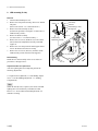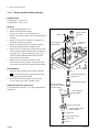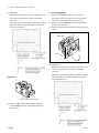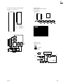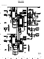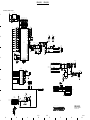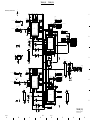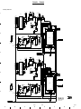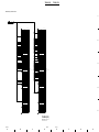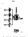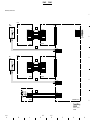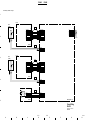
1
Film-Tech
The information contained in this Adobe Acrobat pdf
file is provided at your own risk and good judgment.
These manuals are designed to facilitate the
exchange of information related to cinema
projection and film handling, with no warranties nor
obligations from the authors, for qualified field
service engineers.
If you are not a qualified technician, please make no
adjustments to anything you may read about in these
Adobe manual downloads.
www.film-tech.com
SDDS Player System
DIGITAL FILM SOUND READER
DFP-R3000
®
MAINTENANCE MANUAL
1st Edition
Serial No. 10001 and Higher
! WARNING
This manual is intended for qualified service personnel only.
To reduce the risk of electric shock, fire or injury, do not perform any servicing other than that
contained in the operating instructions unless you are qualified to do so. Refer all servicing to
qualified service personnel.
! WARNUNG
Die Anleitung ist nur für qualifiziertes Fachpersonal bestimmt.
Alle Wartungsarbeiten dürfen nur von qualifiziertem Fachpersonal ausgeführt werden. Um die
Gefahr eines elektrischen Schlages, Feuergefahr und Verletzungen zu vermeiden, sind bei
Wartungsarbeiten strikt die Angaben in der Anleitung zu befolgen. Andere als die angegeben
Wartungsarbeiten dürfen nur von Personen ausgeführt werden, die eine spezielle Befähigung
dazu besitzen.
! AVERTISSEMENT
Ce manual est destiné uniquement aux personnes compétentes en charge de l’entretien. Afin
de réduire les risques de décharge électrique, d’incendie ou de blessure n’effectuer que les
réparations indiquées dans le mode d’emploi à moins d’être qualifié pour en effectuer d’autres.
Pour toute réparation faire appel à une personne compétente uniquement.
LED Properties
Material
: InGaAIP
Peak Wave length : 644 nm (Spectral Line Half Width ∆λ 18nm)
Emission duration : Continuous
LED output power: 2.41 mW (max)
Beam divergence : (H) 60 d (V) 10 d
LED LIGHT
DO NOT STARE INTO BEAM OR VIEW
DERECTLY WITH OPTICAL INSTRUMENTS
CLASS 3A LED PRODUCT
LED-LICHT
NICHT IN DEN STRAHL BLICKEN
ODER MIT OPTISCHEN INSTRUMENTEN
EIN LED-PRODUKT
KLASSE 3A DIREKT ANSCHAUEN
This Digital Film Reader is classified as a CLASS 3A
LED PRODUCT.
Label is located on the top.
Table of Contents
Manual Structure
Purpose of this manual ........................................................................................ 3 (E)
Contents ............................................................................................................... 3 (E)
Related manuals ................................................................................................... 4 (E)
1. Service Overview
1-1.
1-2.
1-3.
1-4.
1-5.
Main Parts Location ..............................................................................1-1 (E)
Removal of Cabinet...............................................................................1-2 (E)
Note on RD-35 Board Replacement .....................................................1-3 (E)
LED Function on the Board ..................................................................1-4 (E)
Tools ......................................................................................................1-4 (E)
2. Periodic Maintenance and Inspection
2-1.
2-2.
Checking and Cleaning before Film Setting .........................................2-1 (E)
Periodic Maintenance Schedule ............................................................2-3 (E)
3. Mechanical Parts Replacement and Alignment
3-1.
3-2.
3-3.
3-4.
3-5.
3-6.
3-7.
DEP-1000
Mechanical Parts Replacement .............................................................3-3 (E)
3-1-1. LED assembly (S and P sides) .............................................3-3 (E)
3-1-2. Roller guide S1 assembly .....................................................3-5 (E)
3-1-3. Roller guides S2, S3 and T1 .................................................3-7 (E)
3-1-4. Tension regulator holder assembly ......................................3-8 (E)
3-1-5. Drum assembly.....................................................................3-9 (E)
3-1-6. Sprocket SUB assembly,
sprocket holder assembly and brake ..................................3-10 (E)
3-1-7. Film retainer rollers (A and B) ...........................................3-11 (E)
3-1-8. CCD (S and P sides) ...........................................................3-14 (E)
Optical Source Adjustment .................................................................3-15 (E)
CCD Bias Adjustment (SE-437 board Adjustment) ...........................3-19 (E)
Film Running Checking ......................................................................3-21 (E)
Optics Adjustment ...............................................................................3-23 (E)
FG checking ........................................................................................3-32 (E)
Error Rate Checking ............................................................................3-33 (E)
1 (E)
4. Spare Parts
4-1.
4-2.
4-3.
4-4.
Notes on Repair Parts .................................................................................. 4-1
Exploded Views .......................................................................................... 4-2
Electrical Parts List ..................................................................................... 4-8
Accessories Supplied ................................................................................ 4-22
5. Semiconductor Pin Assignments
6. Block Diagram
Overall ......................................................................................................... 6-2
7. Board Layouts
SE-437 ......................................................................................................... 7-1
DUS-179, DUS-180, DUS-182, RD-35 ...................................................... 7-2
SE-439 ......................................................................................................... 7-6
TG-208 ........................................................................................................ 7-8
8. Schematic Diagrams
RD-35 .......................................................................................................... 8-2
TG-208 ...................................................................................................... 8-11
SE-437 ....................................................................................................... 8-14
SE-439 ....................................................................................................... 8-15
Frame Wiring ............................................................................................ 8-15
2 (E)
DEP-1000
Manual Structure
Purpose of this manual
This manual is the Maintenance Manual of the Digital Film Sound Reader DFPR3000.
This manual is intended for use by trained system and service engineers, and
describes the detailed service information with the intention of servicing based on
the component parts (schematic diagrams, board layouts, detailed spare parts list and
so on).
Contents
This manual is organized by following sections.
1. Service Overview
This section describes the service information (board location, cabinet removal and
the tools).
2. Periodical Inspection and Maintenance
This section describes the cleaning and schedule of periodical Inspection.
3. Mechanical Replacement and Alignment
This section describes the procedures for the parts at periodical replacement, and
checks and adjustments required after replacement.
4. Spare Parts
This section describes spare parts (mechanical parts list, electrical parts list and
supplied accessories list).
5. Semiconductor Pin Assignment
This section describes the appearance, pin assignments, and function descriptions of
semiconductors.
6. Block Diagrams
This section describes the block diagrams of circuit board and circuit description.
7. Board Layouts
This section describes board layouts (the printed circuit patterns and printed symbols).
8. Schematic Diagrams
This section describes the schematic diagrams of circuit board.
DFP-R3000
3 (E)
Related manuals
. DFP-R3000/DFP-D3000 Operation Manual (Supplied with the DFPD3000)
This manual is necessary for application and operation of the DFP-R3000.
. DFP-R3000 Installation Manual (Prepared separately)
This manual describes the information when installing DFP-R3000.
. DFP-D3000 Maintenance Manual (Prepared separately)
This manual describes the inspection of the DFP-D3000 and the information that
premise the service based on parts.
n
Unless otherwise specified, all names of companies and products are trademarks or registered trademarks
of the respective companies.
4 (E)
DFP-R3000
Section 1
Service Overview
1-1. Main Parts Location
SE-439 board
RD-35 board
TG-208 board *
LED assembly
(P side)
LED assembly
(S side)
SE-437 board
(P side)
SE-437 board
(S side)
Lens
* Applied Serial No. 10001 to 10150
S1 guide
S3 guide
S2 guide
Sprocket
DEGITAL FILM SOUND READER
Drum
DFP-R3000
T1 guide
Film retainer roller
1-1 (E)
1-2. Removal of Cabinet
1-2. Removal of Cabinet
Front panel assembly
(1) Remove the two screws (B3 x 4) and four screws (B2.6 x 6).
(2) While holding the S2 guide to the direction of the arrow 1, remove the front panel assembly in the
direction of the arrow 2.
Optics cover
(1) Remove the front panel assembly.
(Refer to the procedure of the removal of the front panel assembly.)
(2) Remove the four screws (PSW3 x 8), and then remove the optics cover.
Drum cover
(1) Remove the two screws (B3 x 4), and then remove the drum cover from the S1 guide shaft and drum
shaft.
Right side plate
(1) Remove the two screws (B3 x 4) and four screws (B2.6 x 6), and then remove the right side plate.
Left side plate
(1) Remove the four screws (B2.6 x 6), and then remove the left side plate.
B2.6 x 6
Left side plate
Optics cover
Right side plate
PSW3 x 8
1
Drum shaft
B2.6 x 6
B2.6 x 6
B3 x 4
B3 x 4
B3 x 4
S2 guide
S1 guide shaft
B3 x 4
Drum cover
RD-53 board
B3 x 4
2
Front panel assembly
1-2 (E)
B2.6 x 6
DFP-R3000
1-3. Note on RD-35 Board Replacement
1-3. Note on RD-35 Board Replacement
2. Hours meter setting
Checking of hours meter
The DFP-R3000 serial number and following hours meter
setting data are stored in the NVSRAM STK22C48(IC14)
on the RD-35 board.
The setting data is reset when the RD-35 board or the
NVSRAM is replaced.
Therefore, set the serial number and the following hours
meter again when the RD-35 board or NVSRAM has been
replaced.
(1) Input the following commands at the screen of the
terminal software.
Hours meter item
Code
Description
0
Accumulated power ON time
1
Accumulated film running time
2
Accumulated S side LED lighting time
3
Accumulated P side LED lighting time
Serial number and hours meter setting
Set or reset the serial number and hours meter with
following procedure using personal computer and terminal
software.
(^o^) /h
(2) Each hours meter will be displayed on the screen by
eight-digit hexadecimal as shown below.
(X : any hexadecimal digit)
Power ON Time = XXXXXXXX
(display of accumulated power
ON time)
FILM RUN Time = XXXXXXXX
(display of accumulated film
running time)
LED S ON Time = XXXXXXXX
(display of accumulated S side
LED lighting time)
LED P ON Time = XXXXXXXX
(display of accumulated P side
LED lighting time)
Required equipment and tools
Personal computer : IBM PC/AT compatible
Terminal software : Communication format (Baud rate ;
9600 baud, Data length ; 8 bits,
None parity, Stop bit ; Fixed to one
bit)
RS-232C cable (for DFP-D2000)
Hours meter setting
Input the following commands at the screen of the terminal
software started and set the hours meter.
Input eight digits (hexadecimal) for the time to be set at X.
(^o^) /h0, XXXXXXXX
(setting of accumulated power ON time)
(^o^) /h1, XXXXXXXX
Preparation
(setting of accumulated film running time)
(1) Remove the right side plate.
(2) Connect the D-sub 9pin connector on the RD-35 board
and serial port on personal computer using RS-232C
cable (for DFP-D2000).
(3) Start up the terminal software of personal computer.
(^o^) /h2, XXXXXXXX
(setting of accumulated S side LED lighting time)
(^o^) /h3, XXXXXXXX
(setting of accumulated P side LED lighting time)
Hours meter resetting
1.
Serial number setting
Input the following commands at the screen of the
terminal software started and set the serial number.
Set the serial number indicated on the label of DFPR3000.
Be sure to set 6 digits for the serial number.
(X : serial number)
Input the following commands at the screen of the terminal
software started and reset the hours meter.
Each hours meter can be reset independently.
(^o^) /h0, 00000000
(resetting of accumulated power ON time)
(^o^) /h1, 00000000
(resetting of accumulated film running time)
(^o^) /nXXXXXX
(^o^) /h2, 00000000
(resetting of accumulated S side LED lighting time)
Ex.) When a serial number 10123 : (^0^) /n10123
(^o^) /h3, 00000000
(resetting of accumulated P side LED lighting time)
DFP-R3000
1-3 (E)
1-4. LED Function on the Board
1-5. Tools
1-4. LED Function on the Board
. RD-35 board
D5 (GRN) (B2) : 5 V
Light when +5 V power supply is provided correctly
D5 (GRN) (H3) : 12 V
Light when +12 V power supply is provided correctly
. TG-208 board
D5 (GRN) (A1) : 12 V
Light when +12 V power supply is provided correctly
1-5. Tools
Fig.
Description
Part No.
1
Guide Height Adjustment Tool
J-6187-860-A
2
Eccentric Driver (d = ø1.5, D = ø2.5)
Eccentric Driver (d = ø2, D = ø4)
Eccentric Driver (d = ø3, D = ø5)
J-6187-880-A
3-702-390-01
3-702-391-01
3
Thickness Gauge
J-6188-000-A
4
L Shaped Hex. Wrench M3
J-6510-180-A
1
2
D
d
3
4
10
7.5mm
1-4 (E)
DFP-R3000
Section 2
Periodic Maintenance and Inspection
To make the most of the functions, fully realize the performances of this unit and to lengthen the life of
the unit, check and clean the parts every time before film setting, and perform the periodic maintenance.
2-1. Checking and Cleaning before Film Setting
We recommend to perform the checking and cleaning for the main components every time before film
setting.
Check that the each part shown in the “index (illustration on next page)” has not the scratch and the dust,
and perform the cleaning by the following procedures.
Notes
. Be sure to turn the power off before cleaning.
. Each block of the unit consists of the precision parts, and adjusts precisely.
During cleaning, be careful not to damage against the parts, and not to apply an excessive force.
Required Tools
Tooth brush (commercially available goods)
Cleaning cloth : J-6090-011-A
blower brush (commercially available goods)
Preparation
. Turn the DFP-R3000 power off.
Cleaning before film setting
. Cleaning of film running system
Clean the roller guides (S1, S2, S3 and T1), sprocket and film retainer rollers before film setting.
Procedure
1. Dust the parts shown in the “index (illustration on next page)” using a tooth brush.
n
Be careful not to scratch the parts by rubbing hard using a tooth brush.
2. Clean the shaded portions
shown in the “index” using a dry cleaning cloth.
. Cleaning of film running surface of drum
Clean the film running surface of the drum before film setting.
Procedure
Tools and procedures are the same as “Cleaning of film running system”.
Clean the shaded portions
of the drum shown in the “index”.
. Cleaning of lens
Clean the lens before film setting.
The lens is the most important parts in the unit. Be sure to clean the one.
Procedure
1. Dust the lens using a blower brush (commercially available goods).
(Refer to “Index” on next page.)
DFP-R3000
2-1 (E)
2-1. Checking and Cleaning before Film Setting
Index
S3 guide
S1 guide
S2 guide
Sprocket
DEGITAL FILM SOUND READER
Lens
Blower brush
Drum
2-2 (E)
T1 guide
Film retainer roller
Film retainer roller
DFP-R3000
2-2. Periodic Maintenance Schedule
2-2. Periodic Maintenance Schedule
The following table shows the schedule for periodically checking the main parts of the unit to ensure its
full functions and performance.
It is recommended to use the film running hours of DFP-R3000 as a reference for periodic inspections.
The replacing and adjusting of the following parts are described in “Section 3 Mechanical Parts Replacement and Alignment”.
Checking of the film running hours
To check the film running hours, open the “STATUS” menu of the LCD Panel Menu of the DFP-D3000
connected to the DFP-R3000, and check at the FILMRUN item.
(Refer to “LCD Panel Menu” of DFP-D3000/R3000 OPERATION MANUAL for the details of LCD
panel menu.)
Periodic Check Parts List
n
The replacement hours shown in the following list are not the guarantee term parts.
Use this list as guidelines for the maintenance and inspection. The replacement hours of the parts vary
depending on the operation environment and conditions of the unit.
The replacement hours shown in the following list are tentative.
:
:
:
:
:
Checking and Cleaning
Checking
Checking (Adjustment)
Checking (Grease up)
Replacement
Check Item
C.C.F.S./(Note 1)
Inspection Hours (h)
2500
5000
7500
LED assembly block
LED assembly
Roller guide assembly block
Roller guide assembly
X-3167-637-
Roller guide (S) assembly
X-3168-031-
Sprocket sub assembly
X-3168-029-
Sprocket holder assembly
X-3168-033-
Sprocket block
Brake
—
Part No.
A-8318-476-
—
3-194-805-
Film retainer roller (PAD roller)
3-185-158-
Tension regulator block
Tension regulator holder
(B) sub assembly
—
—
—
X-3167-617-
Drum block
Drum assembly
—
—
—
X-3168-030-
(Note 1)
DFP-R3000
“C.C.F.S.” means “Checking and Cleaning before Film Setting”.
(Refer to the section 2-1)
2-3 (E)
Section 3
Mechanical Parts Replacement and Alignment
This section describes the information for the mechanical parts replacement and the required adjustment after the following
parts replacement.
1.
2.
3.
4.
5.
6.
7.
8.
9.
10.
11.
12.
LED assembly (S and P sides)
Roller guide S1
Roller guide S2
Roller guide S3
Roller guide T1
Tension regulator holder assembly
Drum assembly
Sprocket SUB assembly
Sprocket holder assembly
Brake
Film retainer roller (PAD roller)
CCD (SE-437 board) (S and P sides)
Replacement parts
Required adjustment after parts replacement
1. LED assembly (S side)
→ 3-2. Light Source Adjustment (1. S side Shading Adjustment → 3. Shading Correction)
2. LED assembly (P side)
→ 3-2. Light Source Adjustment (1. S side Shading Adjustment → 2. S side Shading Adjustment
→ 3. Shading Compensation)
3. Roller guide S1
→ 2. Roller guide S1 height adjustment → 3-4. Film Running Checking → 3-5. Optics Adjustment
(S and P sides) → 3-7. Error Rate Checking
4. Roller guide S2, S3 or T1
→ 3-4. Film Running Checking → 3-5. Optics Adjustment (S and P sides)
5. Tension regulator
holder assembly
→ 3-4. Film Running Checking → 3-5. Optics Adjustment (S and P sides)
6. Drum assembly
→ 3-2. Light Source Adjustment (S side) → 3-3. CCD Azimuth Adjustment (S side) → 3-7. Error
Rate Checking
7. Sprocket SUB assembly,
→ 3-4. Film Running Checking → 3-6. FG Checking → 3-5. Optics Adjustment (S and P sides)
Sprocket holder assembly, Brake
8. Film retainer roller
→ 2. Clearance adjustment → 3-4. Film Running Checking
9. CCD (S-side)
→ 3-3. CCD Azimuth Adjustment (S side) → 3-5. Optics Adjustment (S side) → 3-2. Light Source
Adjustment (3. Shading Compensation) → 3-7. Error Rate Checking
10. CCD (P side)
→ 3-3. CCD Azimuth Adjustment (P side) → 3-5. Optics Adjustment (P side) → 3-2. Light Source
Adjustment (3. Shading Compensation) → 3-7. Error Rate Checking
11. SE-437 board (S side)
→ 3-3. CCD Azimuth Adjustment (S side) → 3-5. Optics Adjustment (S side) → 3-2. Light Source
Adjustment (3. Shading Compensation) → 3-7. Error Rate Checking
12. SE-437 board (P side)
→ 3-3. CCD Azimuth Adjustment (S side) → 3-5. Optics Adjustment (S side) → 3-2. Light Source
Adjustment (3. Shading Compensation) → 3-7. Error Rate Checking
DFP-R3000
3-1 (E)
Required equipment
Equipment
Specification
Model name
Oscilloscope
DC to 250 MHz
four channels
TEKTRONIX 2465B or equivalent
DFP-D3000
—
—
Projector
—
—
Personal computer
MS-DOS 5.0V or higher
IBM PC/AT compatible
Terminal software
Communication format
(Baud rate ; 9600 baud, Data length ; 8 bits,
Non parity, Stop bit ; Fixed to one bit)
—
SDDS Setup Software
—
—
Required Tools
Name
Part number
Connection cable
Remarks
Supplied with DFP-R3000
RS-232C Null modem cable
—
—
Alignment film
1-759-836-11
with data sheet
Guide height adjustment tool
J-6187-860-A
Filter tool
Pending
Thickness gauge (10 µm)
J-6188-000-A
Thickness gauge
9-911-053-00
L shaped hex. wrench (across ; 2 mm)
7-770-736-03
L shaped hex. wrench (across ; 2.5 mm)
7-770-736-04
Required 2 pcs
L shaped hex. wrench (across ; 3 mm)
J-6510-180-A
Hex. head screw driver (across ; 1.27 mm)
—
Hex. head screw driver (across ; 2.5 mm)
7-700-766-05
Nut driver (across ; 5 mm)
7-721-052-05
Eccentric driver (ø1.5-ø2.5)
J-6187-880-A
Eccentric driver (ø2-ø4)
3-702-390-01
Eccentric driver (ø3-ø5)
3-702-391-01
Cleaning cloth
3-184-527-01
Cleaning fluid
9-919-573-01
Screw locking compound
7-432-114-11
Installation reels (A)
9-936-836-01
Error rate checking
Installation reels (SR)
9-936-837-01
Error rate checking
3-2 (E)
7.5 mm (Refer to “1-4. Tools”.)
DFP-R3000
3-1. Mechanical Parts Replacement
3-1. Mechanical Parts Replacement
3-1-1. LED assembly (S and P sides)
The two LED assemblies use for the S (sound) and P
(picture) sides.
Required tool
L shaped hex. wrench (across ; 2 mm) : 7-770-736-03
1. LED assembly (S-side)
6. Remove the harness from the three hooks of cover
support.
7. Disconnect the harnesses of LED assemblies from the
connectors (CN5 and CN6) on the RD-35 board, and
pull out the harnesses from the hole of base.
8. Remove the two wire clamps from the LED support S
and remove the harness from the wire clamps.
9. Remove the two screws (PS2 x 5), and take out the
LED assembly (S side) from the LED support S.
<Bottom view>
Harness
Wire
clamp
LED support S
Removal
1. Turn the DFP-R3000 power off.
2. Remove the front panel assembly, drum cover and left
side plate.
(Refer to the section “1-2. Cabinet Removal”.)
3. Remove the set screw (2 x 3) using L shaped hex.
wrench (across ; 2 mm) and take out the bearing
retainer.
4. Pull out the LED support S with LED assembly (S
side) from the drum shaft.
5. Remove the two screws (BV3 x 10 with washer) and
take out the cover support.
PS2 x 5
Cover support
Harness
LED assembly
(S side)
LED support S
LED assembly
(S side)
<Top view>
Wire clamps
Roller guide S1 Shaft
Reassembling
Install the new LED assembly in the reverse orders of
procedures 1 through 9 above.
Setscrew
(2 x 3)
BV3 x 10
(with washer)
Adjustment after the replacement
After the replacing has been completed, perform the
following adjustments.
Bearing retainer
LED support S
Cover support
Drum shaft
DFP-R3000
3-2. Light Source Adjustment (1. S side Shading Adjustment → 3. Shading Compensation)
n
When the LED (S side) is replaced, reset the S side LED
lighting time stored in memory on the RD-35 board.
Refer to “1-3. Note on RD-35 Board Replacement” for
method of resetting.
3-3 (E)
3-1. Mechanical Parts Replacement
2. LED assembly (P side)
Removal
1. Turn the DFP-R3000 power off.
2. Remove the front panel assembly, drum cover and left
side plate.
(Refer to the section “1-2. Cabinet Removal”.)
3. Remove the LED assembly (S side).
(Perform the procedure 3 through 9 of “Removal of 1.
LED assembly (S side)”.
4. Remove he drum assembly.
(See the section “3-1-5. Drum assembly”.)
5. Remove the two screws (PSW3 x 14) to take out the
fiber (bottom side) adjustment assembly with LED
support P.
6. Remove the wire clamp from the LED support P and
remove the harness from the wire clamp.
7. Remove the two screws (PS2 x 5), and take out the
LED assembly (P side) from the LED support P.
PSW3 x 14
Wire clamp
Harness
LED assembly (P side)
LED support P
PS2 x 5
Fiver (bottom)
adjustment assembly
Wire clamp
Reassembling
Install the new LED assembly in the reverse orders of
procedures 1 through 7 above.
Adjustment after the replacement
After the replacing has been completed, perform the
following adjustments.
3-2. Light Source Adjustment (1. S side Shading Adjustment → 2. S side Shading Adjustment → 3. Shading
Compensation)
n
When the LED (P side) is replaced, reset the P side LED
lighting time stored in memory on the RD-35 board.
Refer to “1-3. Note on RD-35 Board Replacement” for
method of resetting.
3-4 (E)
DFP-R3000
3-1. Mechanical Parts Replacement
3-1-2. Roller guide S1 assembly
The height of this roller guide is to be made the reference
for the film running.
Perform the replacement and the adjustment with care.
Required Tools
Cleaning cloth :
L shaped hex. wrench (across 2 mm) :
Screw locking compound :
Cleaning fluid :
Guide height adjustment tool :
Thickness gauge (10 µm) :
10. Insert the roller guide S assembly (upper side), two
spacers (ø8), and one spring, and screw in the bearing
holder into the roller guide shaft.
Adjustment after the replacement
After the replacing has been completed, perform the
following adjustments.
3-184-527-01
7-700-736-03
7-432-114-11
9-919-573-01
J-6187-860-A
J-6188-000-A
(Required 2 pcs.)
2. Roller guide S1 height adjustment → 3-4. Film Running
Checking → 3-5. Optics Adjustment → 3-7. Error Rate
Checking
Setscrew (2 x 3)
Bearing retainer
Roller guide S assembly
(upper side)
1. Removal/Reassembling
Removal
1. Turn the DFP-R3000 power off.
2. Remove the front panel assembly.
(Refer to the section “1-2. Cabinet Removal”.)
3. Remove the set screw (2 x 3) using L shaped hex.
wrench (across 2 mm), and take out the ball bearing
retainer.
4. Pull out the one roller guide S (upper side), two
spacers (ø8) and one spring from the roller guide shaft.
5. While pushing down the roller guide S assembly
(lower side), remove the E ring from the roller guide
shaft.
n
In order to protect the roller guide shaft from a damage,
be sure to wrap a vinyl tape around the tip of pliers.
6. Pull out the roller guide S assembly (lower side), two
spacers (ø8), and one spring from the roller guide
shaft.
Spacers (ø8)
Spring
E ring
Spacers (ø8)
Roller guide S assembly
(lower side)
Spring
Roller guide shaft
Wipe the shaft using cleaning cloth
moistened with cleaning fluid.
Reassembling
7. Wipe the roller guide shaft (marked by
) indicated
in the figure with a cleaning cloth moistened with the
cleaning fluid.
8. Insert the roller guide S assembly (lower side), two
spacers (ø8), and one spring into the roller guide shaft.
9. While pushing down the roller guide S assembly
(lower side), attach the E ring to the grooved portion
of the roller guide shaft by using a pair of pliers with
tip both side with which vinyl tape is wrapped.
n
Use the side wrapped with vinyl tape so that the roller
guide shaft is not damaged.
DFP-R3000
Pliers
In order to protect the roller
guide shaft from a damage,
be sure to wrap a vinyl tape.
3-5 (E)
3-1. Mechanical Parts Replacement
2. Roller guide S1 height adjustment
(3) While holding the bearing retainer, tighten the set
screw using the L shaped hex wrench (across 2 mm).
Required Tools
Cleaning cloth :
L shaped hex. wrench (across 2 mm) :
Screw locking compound :
Cleaning fluid :
Guide height adjustment tool :
Thickness gauge (10 µm) :
3-184-527-01
7-700-736-03
7-432-114-11
9-919-573-01
J-6187-860-A
J-6188-000-A
(Required 2 pcs.)
Tightening torque :
1.22 ± 0.10 N . m (12 ± 1 kgf . cm)
n
When tightening the set screw, the roller guide
assembly (upper side) may move upward.
Therefore, be sure to perform the following procedures
after tightening the set screw.
Procedure
(1) Attach the guide height adjustment tool as shown in
the figure.
n
Insert the guide height adjustment tool while pushing
down the roller guide S assembly (lower side).
(2) Pinch the thickness gauge (10 µm) between A portion
of the guide height adjustment tool and upper flange of
the roller guide assembly, and turn lightly the roller
guide assembly by finger.
Turn the bearing retainer and adjust the height of the
roller guide assembly to the position that the roller
guide assembly begins to turn.
Bearing retainer
Upper flange
A portion
(4) Re-attach the guide height adjustment tool as shown in
the figure. Pinch the two thickness gauges (10 µm x 2)
between A portion of the guide height adjustment tool
and upper flange of the roller guide assembly, and try
to turn lightly the roller guide assembly. At this time,
check that the roller guide assembly is turned.
If not turning, perform the steps (2) and (3) again.
Setscrew (4 x 4)
A portion
Bearing retainer
Two thickness gauges
(10 µm x 2)
Guide height
adjustment tool
Upper flange
Roller guide
S assembly
Setscrew (4 x 4)
Thickness gauge (10 µm)
Guide height
adjustment tool
(5) After the adjustment, remove the guide height adjustment tool.
(6) Apply the coating of the locking compound to the set
screw and bearing retainer as shown in the figure.
Roller guide
S assembly
(upper side)
Roller guide
S assembly
(lower side)
Apply locking compound.
Setscrew (4 x 4)
Bearing retainer
Setscrew (4 x 4)
A portion
Bearing retainer
Thickness gauge (10 µm)
Upper flange
Roller guide
S assembly
3-6 (E)
Roller guide
S assembly
Guide height
adjustment tool
(7) Perform the film running checking.
(See the section “3-4. Film Running Checking”.)
(8) Perform the optics adjustment.
(See the section “3-5. Optics Adjustment”.)
(9) Perform the error rate checking.
(See the section “3-7. Error Rate Checking”.)
DFP-R3000
3-1. Mechanical Parts Replacement
3-1-3. Roller guides S2, S3 and T1
The replacement of the roller guide S2, S3 and T1
are the same.
Required Tools
Cleaning cloth : 3-184-527-01
Cleaning fluid : 9-919-573-01
Removal
1. Turn the DFP-R3000 power off.
2. Remove the front panel assembly.
(Refer to the section “1-2. Cabinet Removal”.)
3. Remove the screw (RK4 x 8) and take out
the ornamental washer (ø4), stopper (ø4) and
roller guide S2 (or S3 or T1) from the roller
guide shaft.
RK4 x 8
Ornamental washer (ø4)
Stopper (ø4)
Roller guide S2
Flange is thin.
RK4 x 8
Reassembling
)
4. Wipe the roller guide shaft (marked by
as shown in figure using the cleaning cloth
moistened with the cleaning fluid.
5. Attach the ornamental washer (ø4), stopper
(ø4) and roller guide S2 (or S3 or T1) in the
reverse orders of procedure 1 through 3
above, and tighten the screw (RK4 x 8) on
the top of the roller guide.
n
Attach the roller guide assembly with the
narrower side of the flange facing down.
RK4 x 8
Ornamental
washer (ø4)
Ornamental washer (ø4)
Stopper (ø4)
Stopper (ø4)
Flange
is thin.
Roller guide T1
Roller guide S3
Flange is thin.
Roller guide shafts
Roller guide shaft
Adjustment after the replacement
After the replacing has been completed, perform
the following adjustment/checking.
3-4. Film Running Checking → 3-5. Optics
Adjustment (S and P sides)
Wipe the shaft using cleaning cloth
moistened with cleaning fluid.
DFP-R3000
3-7 (E)
3-1. Mechanical Parts Replacement
3-1-4. Tension regulator holder assembly
Required Tools
Cleaning cloth : 3-184-527-01
Cleaning fluid : 9-919-573-01
Removal
1. Turn the DFP-R3000 power off.
2. Remove the front panel assembly.
(Refer to the section “1-2. Cabinet Removal”.)
3. Remove the tension spring B of the tension regulator B
assembly.
4. Remove the three screws (PSW4 x 12) and take out
the tension regulator B assembly.
5. Remove the spring hook screw B from the flange of
the tension regulator holder B SUB assembly.
6. Remove the screw (PSW3 x 6) from the bottom of the
tension regulator holder B SUB assembly and take out
the stopper (ø3), compression spring A, spacer and
tension regulator holder B SUB assembly from the
tension regulator B assembly.
7. Remove the screw (RK4 x 8), and take out the
ornamental washer (ø4), stopper (ø4) and roller guide
S2 assembly from the tension regulator SUB assembly.
Tension regulator
B assembly
PSW4 x 12
Compression
spring B
Tension regulator
B SUB assembly
Reassembling
8. Wipe the tension regulator sub assembly (marked by
) as shown in the figure using the cleaning cloth
moistened with the cleaning fluid.
9. Reassemble the tension regulator assembly in the
reverse orders of procedure 1 through 7 above.
Adjustment after the replacement
3-4. Film Running Checking → 3-5. Optics Adjustment (S
and P sides)
RK4 x 8
Ornamental washer (ø4)
Stopper (ø4)
Roller guide S2 assembly
Wipe the shafts using
cleaning cloth moistened
with cleaning fluid.
Tension regulator
SUB assembly
Spring hook screw B
Tension regulator holder
B SUB assembly
Spacer (ø6)
Compression spring A
Stopper (ø3)
PSW3 x 6
3-8 (E)
DFP-R3000
3-1. Mechanical Parts Replacement
3-1-5. Drum assembly
Required Tools
Cleaning cloth : 3-184-527-01
Cleaning fluid : 9-919-573-01
Removal
1. Turn the DFP-R3000 power off.
2. Remove the front panel assembly, drum cover, and left
side plate.
(Refer to the section “1-2. Cabinet Removal”.)
3. Remove the LED assembly (S side).
Refer to the “1. LED assembly (S side) replacement of
section 3-1-1. LED assembly (S and P sides)”.
4. Remove the spring and washer, and pull out the drum
assembly from the drum shaft.
Spring
Film running surface.
Washer
Drum assembly
Drum shaft
Wipe the shaft using
cleaning cloth moistened
with cleaning fluid.
Reassembling
) as shown in the
5. Clean the drum shaft (marked by
figure using the cleaning cloth moistened with the
cleaning fluid.
6. Reassemble the drum assembly, washer, spring
washer, and LED assembly (S side) to the drum shaft.
7. Wipe onto the film running surface of the drum
assembly (marked by
) as shown in the figure
using a cleaning cloth moistened with cleaning fluid.
Adjustments after the replacement
After the replacing has been completed, perform the
following adjustments.
3-2. Light Source Adjustment (S side) → 3-3. CCD
Azimuth Adjustment (S side) → 3-7. Error Rate Checking
DFP-R3000
3-9 (E)
3-1. Mechanical Parts Replacement
3-1-6. Sprocket SUB assembly, sprocket
holder assembly and brake
Required Tools
Cleaning cloth : 3-184-527-01
Cleaning fluid : 9-919-573-01
Adjustment/Checking after the replacement
After the replacing has been completed, perform the
following adjustment and checking.
3-4. Film Running Checking → 3-6. FG Checking
→ 3-5. Optics Adjustment (S and P side)
Removal
1. Turn the DFP-R3000 power off.
2. Remove the front panel assembly.
(Refer to the “1-2. Cabinet Removal”.)
3. Remove the screw (RK4 x 8), and take out the
ornamental washer (ø4), spring washer, spacer (ø6)
and sprocket SUB assembly from the sprocket shaft.
n
To avoid being damaged to the sprocket, be sure to put
the sprocket on the workbench as shown in the figure.
RK4 x 8
Ornamental washer (ø4)
Spring
Spacer (ø6)
Sprocket SUB assembly
Sprocket
Protrusions
Brake
Teeth
Sprocket holder assembly
4. Remove the five screws (PS2 x 10) and washer (W2,
CSMALL), and take out the sprocket holder assembly
from the sprocket SUB assembly.
5. Pull out the brake from the sprocket SUB assembly.
W2, SMALL
Reassembling
) as shown in
6. Clean the sprocket shaft (marked by
the figure using cleaning cloth moistened with the
cleaning fluid.
7. Insert the two protrusions of the brake into the two
holes inside the sprocket SUB assembly.
8. Adjust the screw holes of the sprocket SUB assembly
and sprocket holder assembly together, and secure the
five screws (PS2 x 10) and washers (W2, small).
9. Insert the sprocket SUB assembly, spacer (ø6), spring,
and ornamental washer (ø4) into the sprocket shaft in
the reverse order of procedures 1 to 5 above, and
tighten the screw (RK4 x 8).
PS2 x 10
Sprocket shaft
Wipe the shaft using cleaning cloth
moistened with cleaning fluid.
3-10 (E)
DFP-R3000
3-1. Mechanical Parts Replacement
3-1-7. Film retainer rollers (A and B)
Two film retainer rollers A and B are used.
Required Tools
Cleaning cloth :
Molytone grease :
Cleaning fluid :
Eccentric driver :
Thickness gauge :
3-184-527-01
7-662-001-41
9-919-573-01
J-6187-880-A
9-911-053-00
7. Attach the film retainer roller B in the reverse orders
of the removal.
n
Do not apply the coating of the grease to the sprocket
and rim of the film retainer rollers A and B.
Adjustment/Checking after the replacement
After the replacing has been completed, perform the
following adjustment and checking.
2. Clearance adjustment → 3-4. Film Running Checking
1. Removal/Reassembling
Removal
1. Turn the DFP-R3000 power off.
2. Remove the front panel assembly.
(Refer to the section “1-2. Cabinet Removal”.)
3. Open the arm assembly in the arrow direction, and
release the film retainer rollers from the sprocket.
E ring (ø3)
. Film retainer roller A
4. Remove the E-ring (ø3), and pull out the stopper (ø4)
and film retainer roller A from the PR (S) shaft.
. Film retainer roller B
4. Remove the E-ring (ø3), and pull out the PR knob
shaft and film retainer roller B from the PR shaft.
E ring (ø3)
PR knob shaft
Stopper (ø4)
Film retainer
roller A
Film retainer
roller B
PR (S) shaft
Reassembling
. Film retainer roller A
PR shaft
5. Wipe the PR (S) shaft (marked by
) as shown in
the figure using a cleaning cloth moistened with the
cleaning fluid and be sure to re-wipe it using a dry
cleaning cloth.
6. Apply a light coarting of grease to the cleaned portion
of the PR (S) shaft, and be sure to wipe dry with a dry
gauze or paper (so that only a very light coarting of
grease remains).
7. Attach the film retainer roller A in the reverse orders
of the removal.
. Film retainer roller B
5. Wipe the PR shaft (marked by
) as shown in the
figure using a cleaning cloth moistened with the
cleaning fluid and be sure to re-wipe it using a dry
cleaning cloth.
6. Apply a light coarting of grease to the cleaned portion
of the PR shaft, and be sure to wipe dry with a dry
gauze or paper (so that only a very light coarting of
grease remains).
DFP-R3000
Arm assembly
Wipe the shaft using cleaning
cloth moistened with cleaning
fluid.
After cleaning, apply coating
of the grease.
3-11 (E)
3-1. Mechanical Parts Replacement
2. Clearance adjustment
Required Tools
Eccentric driver : J-6187-880-A
Thickness gauge : 9-911-053-00
Procedure
n
Do not damage onto the film running surface of the
sprocket by moving the thickness gauge too hard.
Sprocket
(1) Checking 1
Insert a 0.3 mm thickness gauge between the film
retainer rollers (A and B) and the film running surface
of the sprocket.
While lightly pressing the film retainer rollers in the
direction arrow, turn the film retainer rollers.
In this condition, check that the film retainer rollers
rotate and that the film retainer rollers and sprocket do
not catch the thickness gauges.
Thickness gauge
(0.3 mm)
Thickness gauge
(0.3 mm)
PAD plate
Film running surface
Thickness gauge
(0.3 mm)
Film retainer
roller
Sprocket
3-12 (E)
Film running surface
Thickness gauge
(0.3 mm)
Film retainer
roller
Sprocket
DFP-R3000
3-1. Mechanical Parts Replacement
(2) Checking 2
Insert a 0.4 mm thickness gauge between the film
retainer rollers (A and B) and the film running surface
of the sprocket.
While lightly pressing the film retainer rollers in the
direction arrow, turn the film retainer rollers.
In this condition, check that the film retainer rollers do
not rotate and that the film retainer rollers and sprocket
catch the thickness gauges.
(3) If the checkings 1 and 2 in steps (1) and (2) were not
satisfactory, loosen the two screws (PSW4 x 12) of
the PAD plate by half a turn, insert an eccentric
screwdriver into the adjustment hole of the PAD plate,
and adjust the position of the PAD plate.
After adjusting, tighten the two screws (PSW4 x 12)
loosened temporarily and perform the checkings 1 and
2 in steps (1) and (2) again.
Sprocket
(4) If the checkings 1 and 2 are satisfactory, tighten the
two screws (PSW4 x 12).
(5) Perform the checkings 1 and 2 again.
(6) Perform the film running checking.
(See the section “ 3-4. Film Running Checking”.)
Thickness gauge
(0.4 mm)
Thickness gauge
(0.4 mm)
PSW4 x 12
Adjustment hole
PAD plate
PSW4 x 12
Film running surface
Thickness gauge
(0.4 mm)
Film retainer
roller
Sprocket
DFP-R3000
Film running surface
Thickness gauge
(0.4 mm)
Film retainer
roller
Sprocket
3-13 (E)
3-1. Mechanical Parts Replacement
3-1-8. CCD (S and P sides)
The S and P sides of the CCD are replaced in the same
way.
n
Perform anti-static measures when handling the CCD.
Removal
1. Turn the DFP-R3000 power off.
2. Remove the front panel assembly and optics cover.
(Refer to the section “1-2. Cabinet Removal”.)
3. Disconnect the harness from the connector (CN1) on
the SE-437 board.
4. Remove the two screws (PSW2.6 x 6) fixing the SW437 board.
5. Remove the four screws (PS2 x 4) fixing the CCD
retainer spring assembly to take out the
SE-437 board with CCD.
6. Remove the CCD from the SE-437 board.
Adjustment after the replacement
After the replacing has been completed, perform the
following adjustment.
CCD (S-side)
3-3. CCD Azimuth Adjustment (S side) → 3-5. Optics
Adjustment (S side) → 3-2. Light Source Adjustment (3.
Shading Compensation) → 3-7. Error Rate Checking
CCD (P side)
3-3. CCD Azimuth Adjustment (P side) → 3-5. Optics
Adjustment (P side) → 3-2. Light Source Adjustment (3.
Shading Compensation) → 3-7. Error Rate Checking
. The illustration shows an example when S side CCD is
replaced.
Reassembling
7. Mount new CCD to the socket on the SE-437 board
with CCD retainer spring assembly.
n
As the CCD glass plate is easy to break, handle it with
care.
8. Attach the SE-437 board (CCD) to the CCD fitting
table (optics block) using two screws (PSW2.6 x 6).
n
Be sure to attach the SE-437 board to the place where
the CCD is fit into the CCD fitting table as shown in
figure.
PS2 x 4
Optics block
PS2 x 4
PSW2.6 x 6
CCD
CCD fitting table
CCD retainer
spring assembly
CCD
9. Fix the CCD retainer spring assembly (SE-437 board)
to the CCD fitting table (optics block) using four
screws (PS2 x 4).
3-14 (E)
SE-437 board
DFP-R3000
3-2. Optical Source Adjustment
3-2. Optical Source Adjustment
Perform the optical source adjustment when the S and P
sides LED assemblies are replaced.
n
Perform the optical source adjustment with no film loaded.
. Adjustment when S side LED assembly is replaced.
1. S side shading adjustment
↓
3. Shading Compensation (S and P sides)
. Adjustment when P (S and P) side LED assembly is
replaced.
1. S side shading adjustment
↓
2. P side shading adjustment
↓
3. Shading Compensation (S and P sides)
Preparation
Remove the OPT cover, drum cover, front panel assembly
and left side panel, and then perform the followings.
(1) Pull out the RD-35 board as shown in the figure below
so that the oscilloscope, etc. can be connected to the
TP terminal.
(2) Connect the DFP-R3000 to the DFP-D3000 READER
connector using connection cable.
(3) Connect the D-sub 9pin connector and a serial port of
PC (personal computer) using RS-232C Null modem
cable.
(4) Start up the terminal software of the PC.
(5) Connect the oscilloscope to the following points on the
RD-35 board.
Oscilloscope
CH1
CH2
→
→
RD-35 board
TP1 (VIDEO)
TP2 (Trigger)
Required Equipment and Tools
DFP-D3000
Oscilloscope
Personal computer : IBM PC/AT compatible
Terminal software
RD-35 board
E5
TP4 (FG)
Dsub.9P
Connection cable (Supplied with DFP-R3000)
RS-232C Null modem cable
Eccentric driver (ø2-ø4) (part No. 3-702-390-01)
Eccentric driver (ø3-ø5) (part No. 3-702-391-01)
Hex wrench driver (across 2.5 mm)
Hex wrench driver (across 1.27 mm)
TP3 (CENTER)
TP2 (TRIG)
To PC
E6
To DFP-D3000
DFP-R3000
TP1 (VIDEO)
Pull out
3-15 (E)
3-2. Optical Source Adjustment
1. S side shading adjustment
Procedure
(1) Input the command C1 (press the “C” key and “1” key) from the PC keyboard at
the screen of the terminal software started and then press the Enter key.
(2) Input the command m0 from the PC keyboard and then press the Enter key.
(3) Input the command k0, 70 from the PC keyboard and then press the Enter key.
(4) Adjust the installed position of the S side LED assembly as follows so that the
output waveform of the oscilloscope CH1 is in the specification mentioned
below.
Specification : The minimum b of the CH1 output
waveform should be above 80% of
maximum a.
Adjustment :
Adjustment of horizontal direction
1 Loosen the two screws A about a half turn.
2 Insert the eccentric driver (ø2-ø4) into the adjustment
hole and perform the adjustment.
Adjustment of vertical direction
1 Loosen the screw B about a half turn.
2 Turn the bearing retainer to adjust.
Vertical
direction
Drum
assembly
Screw B
LED assembly
(S side)
Adjusting hole
Screws A
Horizontal
direction
Bearing retainer
(5) After adjustment has been completed, tighten the loosened screws.
Check that the output waveform of the oscilloscope CH1 after tightening meets
the specification in the above step (4).
3-16 (E)
DFP-R3000
3-2. Optical Source Adjustment
2. P side shading adjustment
Procedure
(1) Input the command C1 (press the “C” key and “1” key) from the PC keyboard at
the screen of the terminal software started and then press the Enter key.
(2) Input the command m100 from the PC keyboard and then press the Enter key.
(3) Input the command k1, 70 from the PC keyboard and then press the Enter key.
(4) Adjust the installed position of the P side LED assembly as follows so that the
output waveform of the oscilloscope CH1 is in the specification mentioned
below.
Specification : The minimum b of the CH1 output
waveform should be above 80% of
maximum a.
Adjustment :
Adjustment of horizontal direction
1 Loosen the two screws A about a half turn.
2 Insert the eccentric driver (ø3-ø5) into the adjustment
hole, and perform the adjustment.
Adjustment of vertical direction
1 Loosen the screw B about a half turn using hex wrench
driver (across 1.27 mm).
2 Turn the support C using nut driver (across 5 mm) to
adjust.
Adjusting hole
Screws A
Vertical
direction
Support C
Screw B
LED assembly
(P side)
Horizontal
direction
(5) After adjustment has been completed, tighten the loosened screws.
Check that the output waveform of the oscilloscope CH1 after tightening meets
the specification in the above step (4).
DFP-R3000
3-17 (E)
3-2. Optical Source Adjustment
3. Shading Compensation (S and P sides)
Procedure
(1) Input the command a from PC and then press the Enter key.
(2) Check that the following message (error message in the following table is not displayed) will be
displayed on the screen of PC.
. Examples of messages
n
1. The following are examples of messages displayed when there is no error in the shading
compensation. The values of each item differs according to the LED assembly (value after “=”,
etc.).
2. Replace the LED assembly when the value of the “AD GAIN Setting” is above “00B0”.
(^0^)/a
Adjust AD gain S side
AD GAIN Setting
= 0076
Finish adjust max = 03FF
clamp out max = 03F8 min
Adjust shading S side
Adjust AD gain P side
AD GAIN Setting
= 007B
Finish adjust max = 03F4
clamp out max = 03F5 min
Adjust shading P side
AF
BC
DE
HL
SP
0044 FF81 FFF9 FFFF 1084
(^0^)/
min = 032F
= 0324
S side information
min = 033A
= 0339
P side information
The following will be displayed when errors occur in shading compensation.
Display
Description
Remedy
1. S (P) LED Current limit over
The light amount of the LED does
not meet the specification.
Replace the S (or P) side LED.
2. S (P) LED dark error
3. S (P) LED shading
limit over error
The difference between the maximum Re-adjust the LED assembly.
and minimum light amounts of the
LED does not meet the specification.
4. Sampling time out
Fault of RD-35 board.
Check the RD-35 board.
5. Dark level too high
Example error display
. S side LED dark error
(^0^)/a
Adjust AD gain S side
AD GAIN Setting
= 0100
Finish adjust max = 0190 min = 013B
S LED dark error
AF
BC
DE
HL
SP
0044 FE81 FFF1 FFFF 1084
(^0^)/
. S side LED shading limit over error
(^0^)/a
Adjust AD gain S side
AD GAIN Setting
= 0074
Finish adjust max = 03F2 min = 004B
S LED shading limit over error
AF
BC
DE
HL
SP
0044 FE81 FFF1 FFFF 1084
(^0^)/
3-18 (E)
DFP-R3000
3-3. CCD Bias Adjustment (SE-437 board Adjustment)
3-3. CCD Bias Adjustment
(SE-437 board Adjustment)
Perform the CCD bias adjustment when CCD and SE-437
board are replaced.
Required Equipment and Tools
DFP-D3000
Oscilloscope
Personal computer: IBM PC/AT compatible
Terminal software
RS-232C Null modem cable
Paper (Thickness ; 0.5 mm or more, size ; 100 x 100 mm)
: The paper is able to shut off the light.
Preparation
Remove the OPT cover, drum cover, front panel assembly
and left side panel, and then perform the followings.
(1) Pull out the RD-35 board as shown in the figure below
so that the oscilloscope, etc. can be connected to the
TP terminal.
(2) Connect the DFP-R3000 to the DFP-D3000 READER
connector using connection cable.
(3) Connect the D-sub 9pin connector and a serial port of
PC (personal computer) using RS-232C Null modem
cable.
(4) Start up the terminal software of the PC.
(5) Connect the oscilloscope to the following points on the
RD-35 board.
RD-35 board
E5
TP4 (FG)
Dsub.9P
TP3 (CENTER)
TP2 (TRIG)
To PC
TP1 (VIDEO)
E6
To DFP-D3000
Oscilloscope
CH1
CH2
Pull out
RD-35 board
→ TP1 (VIDEO)
→ TP2 (Trigger)
1. S side adjustment
(1) Input the command C1 (press the “C” key and “1”
key) from the PC keyboard at the screen of the terminal software started and then press the Enter key.
(2) Input the command m0 from the PC keyboard and then
press the Enter key.
(3) Shut off the light incident upon the CCD lens by using
a paper.
Lens
Optics block
Paper
DFP-R3000
3-19 (E)
3-3. CCD Bias Adjustment (SE-437 board Adjustment)
(4) Adjustment
Adjust RV1 of the SE-437 (S side) so that a pulse type
waveform is generated at A portion of the output
waveform.
The pulse type waveform appears when RV1 is rotated
fully in the clockwise direction and then in the counterclockwise direction.
2. P side adjustment
(1) Input the command C1 (press the “C” key and “1”
key) from the PC keyboard at the screen of the terminal software started and then press the Enter key.
(2) Input the command m100 from the PC keyboard and
then press the Enter key.
(3) Shut off the light incident upon the CCD lens by using
a paper.
Lens
Optics block
Paper
(4) Adjustment
Adjust RV1 of the SE-437 (P side) so that a pulse type
waveform is generated at A portion of the output
waveform.
The pulse type waveform appears when RV1 is rotated
fully in the clockwise direction and then in the counterclockwise direction.
Adjustment
RV1
SE-437 board (S side)
(5) After the adjustment has been completed, input the
command C0 from the PC keyboard, and then press
the Enter key.
3-20 (E)
DFP-R3000
3-4. Film Running Checking
3-4. Film Running Checking
Adjustment
Perform the film running checking when roller guides (S1,
S2, S3 and T1), sprocket SUB assembly, sprocket holder
assembly, brake, tension regulator holder and film retainer
roller are replaced.
Perform the film running checking with DFP-R3000
installed to the projector.
RV1
SE-437 board (P side)
(5) After the adjustment has been completed, input the
command C0 from the PC keyboard, and then press
the Enter key.
Required Equipment and Tools
Projector
DFP-D3000
Connection cable (Supplied with DFP-R3000)
Alignment film (with data sheet)
Preparation
Remove the OPT cover, drum cover, front panel assembly
and left side panel, and then perform the followings.
(1) Pull out the RD-35 board as shown in the figure below
so that the oscilloscope, etc. can be connected to the
TP terminal.
(2) Install the DFP-R3000 into the projector.
(3) Connect the DFP-R3000 to the DFP-D3000 READER
connector using connection cable.
(4) Load the alignment film into the DFP-R3000 and
projector, and the run the alignment film.
(5) Connect the oscilloscope to the following points on the
RD-35 board.
Oscilloscope
CH1
CH2
→
→
RD-35 board
TP1 (VIDEO)
TP2 (Trigger)
RD-35 board
E5
TP4 (FG)
Dsub.9P
TP3 (CENTER)
TP2 (TRIG)
To PC
TP1 (VIDEO)
E6
To DFP-D3000
DFP-R3000
Pull out
3-21 (E)
3-4. Film Running Checking
Procedure
(1) Set the sweep times of the oscilloscope so that the
pulse width (high level) of the reference pulse (oscilloscope CH2).
(2) Check that the deviation A of the output waveform
(RF signal) of the oscilloscope CH1 meets the following specifications in respect to the S correction value
in the data sheet provided with the alignment film.
Specification : A = S correction value ± 0.1 DIV
(3) Check that the teeth of the sprocket do not touch
against the both sides of the perforations (holes) of the
alignment film.
If it touches, adjust the installation of the sprocket
again.
Alignment film
Tooth of sprocket
(scales)
Perforations (holes)
Sprocket
Tooth of sprocket
Film
No touch.
When the S correction value is + :
C portion of the signal leads B portion of the center of the
rising pulse for the amount of the correction value.
When the S correction value is _ :
C portion of the signal trails B portion of the center of the
rising pulse for the amount of the correction value.
3-22 (E)
DFP-R3000
3-5. Optics Adjustment
3-5. Optics Adjustment
Perform the optics adjustment when roller guides (S1, S2,
S3 and T1), tension regulator holder and CCD (SE-437
board) (S and P sides) are replaced.
Perform the optics adjustment with DFP-R3000 installed to
the projector.
Adjustment items (Procedure of S and P sides are the
same.)
CCD magnification and focus rough adjustment
↓
CCD position rough adjustment
↓
CCD azimuth rough adjustment
↓
CCD focus fine adjustment
↓
CCD azimuth fine adjustment
↓
CCD magnification fine adjustment
Required Equipment and Tools
DFP-D3000
Oscilloscope
Personal computer : IBM PC/AT compatible
Terminal software
Connection cable (Supplied with DFP-R3000)
RS-232C Null modem cable
Alignment film (with data sheet)
Filter tool
Eccentric driver (ø1.5-ø2.5) (part No. J-6187-880-A)
Hex wrench driver (across 2.5 mm)
Preparation
Remove the OPT cover, drum cover, front panel assembly
and left side panel, and then perform the followings.
(1) Pull out the RD-35 board as shown in the figure below
so that the oscilloscope, etc. can be connected to the
TP terminal.
(2) Connect the DFP-R3000 to the DFP-D3000 READER
connector using connection cable.
(3) Connect the D-sub 9pin connector and a serial port of
PC (personal computer) using RS-232C Null modem
cable.
(4) Start up the terminal software of the PC.
(5) Connect the oscilloscope to the following points on the
RD-35 board.
Oscilloscope
CH1
CH2
CH3
RD-35 board
TP1 (VIDEO)
TP2 (Trigger)
TP3 (Center)
RD-35 board
E5
TP4 (FG)
Dsub.9P
TP3 (CENTER)
TP2 (TRIG)
To PC
TP1 (VIDEO)
E6
To DFP-D3000
DFP-R3000
→
→
→
Pull out
3-23 (E)
3-5. Optics Adjustment
1. S side optics adjustment
(5) Check that the film data width of the oscilloscope CH1
meets the following specification.
n
By touching against the lens and the protection glass of the
CCD adjustment table, do not make them dirty.
Specification : Film data width = 6 ± 0.1 scales
Step 1. Preparation
(1) Load the alignment film into the DFP-R3000 and
projector, and then run the alignment film.
(2) Input the command C1 (press the “C” key and “1”
key) from the PC keyboard at the screen of the terminal software started and then press the Enter key.
Step 2. CCD magnification and focus rough adjustment
(1) Input the command m0 from the PC and then press the
Enter key.
(2) Loosen the two hexagon cap screws as the bottom of
the optics block about a half turn.
Optics block
Hex head (S side)
Bottom side
. When the film data width is narrower than the above
specification, turn the adjustment screw at the sixth from
the mechanical chassis counterclockwise and perform
the procedure (4) and (5) above.
. When the film data width is wider than the above
specification, turn the adjustment screw at the sixth from
the mechanical chassis clockwise and perform the
procedure (4) and (5) above.
Optics block
(3) Set the sweep times of the oscilloscope so that the
pulse width (high level) of the oscilloscope CH2
output waveform is 6 DIV (scales).
(4) Rotate and adjust the fifth and sixth CCD adjustment
screws from the mechanical deck chassis using a hex
wrench driver so that amplitude A of the output
waveform of the oscilloscope CH1 becomes maximum.
SE-437 board
(S side)
Adjustment screw
(S side)
3-24 (E)
Adjustment screw
(S side)
DFP-R3000
3-5. Optics Adjustment
Step 3. CCD position adjustment
Adjustment
(1) Loosen the two screws (PSW2.6 x 6) and four CCD
fixing screws (PS2 x 4) on the SE-437 board (S side)
abut a half turn.
If A portion of the signal leads B portion of the center of
the rising pulse more than the correction value, move the
CCD from the outside of the optical block to the inside.
Adjust by inserting the eccentric screwdriver in the
adjustment hole a on the outside of the CCD.
Screws (PS 2.6 x 5)
CCD
fixing
screws
CCD
fixing
screws
When A portion of the signal trails B portion of the center
of the rising pulse more than the correction value, move
the CCD from the inside of the optical block to the outside.
Adjust by inserting the eccentric screwdriver in the
adjustment hole b on the inside of the CCD.
CCD fixing screws
SE-437 board (S side)
Screws (PS 2.6 x 5)
CCD fixing screw
Adjustment hole b
(In side)
Adjustment hole a
(Out side)
(2) Adjust the position to install the CCD using a eccentric
screwdriver so that the following specification is met.
Adjust according to the correction value in the data
sheet provided with the alignment film as shown
below.
Specification :
A portion of the film data signal of the oscilloscope
CH1 should be deviated from center B of the rising
pulse of the reference signal of CH2 for the amount of
the S correction value (± 0.1 mark).
When the S correction value is + :
A portion of the signal leads B portion of the center of
the rising pulse for the amount of the correction value.
When the S correction value is _ :
A portion of the signal trails B portion of the center of
the rising pulse for the amount of the correction value.
DFP-R3000
SE-437 board (S side)
(3) Tighten the six screws loosened at the procedure (1)
above.
(4) After the tightening the screws, re-check to meet the
specification in the procedure (2) above.
3-25 (E)
3-5. Optics Adjustment
Step 4. CCD azimuth rough adjustment
(1) Input the command m10 from the PC keyboard and
then press the Enter key.
(2) Loosen the S side azimuth fixing screw about a half
turn using hex wrench driver (across 2.5 mm).
Step 5. CCD focus fine adjustment
(1) Connect the filter tool between the TP1 on the RD-35
board and oscilloscope CH1 as shown in the figure.
E5
Optics block
CCD azimuth
adjusting screw
(S side)
TP4
CCD azimuth
fixing screw (S side)
SE-437 board
(S side)
Oscilloscope
CH1
Filter tool
TP J1 W1
EJ
W2
TP3
TP2
TP1
E6
RD-35 board
(2) Input the command m0 from the PC and then press the
Enter key.
(3) Rotate and adjust the fifth and sixth CCD adjustment
screws from the mechanical deck chassis so that the ◊
part (eye patterns) of the output waveform (TP1) of the
oscilloscope CH1 becomes maximum.
(3) Rotate and adjust the CCD azimuth adjustment screws
so that the output waveform of the oscilloscope meets
the following specification.
Specification : A portion (second) of the output
waveform should be parallel.
(4) Tighten the loosened two hexagon cap screws at the
bottom of the optics block in “procedure (3) of Step 2”
and check that the ◊ portions (eye patterns) do not
change.
(4) After the adjustment has been completed, tighten the
CCD azimuth fixing screw loosened at the procedure
(2) above.
3-26 (E)
DFP-R3000
3-5. Optics Adjustment
Step 6. CCD azimuth fine adjustment
Step 7. CCD magnification fine adjustment
(1) Connect the filter tool between the TP1 on the RD-35
board and oscilloscope CH1 as shown in the figure.
(The same as “Step 5. CCD focus fine adjustment”.)
(2) Input the command m10 from the PC keyboard and
then press the Enter key.
(3) Loosen the S side CCD azimuth fixing screw about a
half turn using hex wrench driver (across 2.5 mm).
(1) Connect the filter tool between the TP1 on the RD-35
board and oscilloscope CH1 as shown in the figure.
(The same as “Step 5. CCD focus fine adjustment”.)
(2) Input the command w0 from the PC keyboard and then
press the Enter key.
(3) Check that the displayed value of “LPF 2T1T” (
section in the figure) meets the following specification.
Specification :
Optics block
CCD azimuth
adjusting screw
(S side)
CCD azimuth
fixing screw (S side)
Displayed value of LPF 2TIT
= S side magnification correction value* ± 8
* S side magnification correction value :
Value indicated on the data sheet provided with the
alignment film used in adjustments.
SE-437 board
(S side)
RF OFSET
RF GAIN
VCO OFSET
2TEDGE 1TEDGE LENGTH CL2T A2
RAW_VCO LP_32VCO CALC_FS ERR
LPF_2T1T
DIF_LEVEL HANE_LEVEL
3T_PEAK_AVE PK_GAIN_LIM
HIKIKOMI [5T/3T] [AFC]
3T LOCATION
3T PATTERN 1..DETECTED
(4) Rotate and adjust the CCD azimuth adjustment screws
so that the output waveform of the oscilloscope meets
the following specification.
:
:
:
:
:
:
:
:
:
:
:
00F3
0024
1D80
E2A1
0051
0960
0960
0275
[OK]
E2D5
1111
E3C3 0906 E2A2 C3
0A1C 0886 0190
01FF
005A
[OK]
E2F3 E317 E33B E35D E37B E39F E3C3
1110
(4) If the above specification is not met, perform steps 2 to
6 to meet it.
Specification : A portion (second) of the output
waveform should be parallel.
(5) After the adjustment has been completed, tighten the
CCD azimuth fixing screw loosened at the procedure
(3).
DFP-R3000
3-27 (E)
3-5. Optics Adjustment
2. P side optics adjustment
(5) Check that the film data width of the oscilloscope CH1
meets the following specification.
n
By touching against the lens and the protection glass of the
CCD adjustment table, do not make them dirty.
Specification : Film data width = 6 ± 0.1 scales
Step 1. Preparation
(1) Load the alignment film into the DFP-R3000 and
projector, and then run the alignment film.
(2) Input the command C1 (press the “C” key and “1”
key) from the PC keyboard at the screen of the terminal software started and then press the Enter key.
Step 2. CCD magnification and focus rough adjustment
(1) Input the command m100 from the PC keyboard and
then press the Enter key.
(2) Loosen the two hexagon cap screws as the bottom of
the optics block about a half turn.
Optics block
Hex head (P side)
Bottom side
. When the film data width is narrower than the above
specification, turn the adjustment screw at the third
from the mechanical chassis counterclockwise and
perform the procedure (4) and (5) above.
. When the film data width is wider than the above
specification, turn the adjustment screw at the third
from the mechanical chassis clockwise and perform
the procedure (4) and (5) above.
Optics block
(3) Set the sweep times of the oscilloscope so that the
pulse width (high level) of the oscilloscope CH2
output waveform is 6 DIV (scales).
(4) Rotate and adjust the second and third adjustment
screws from the mechanical deck chassis using a hex
wrench driver so that amplitude A of the output
waveform of the oscilloscope CH1 becomes maximum.
SE-437 board
(P side)
Adjustment screw
(P side)
3-28 (E)
Adjustment screw
(P side)
DFP-R3000
3-5. Optics Adjustment
Step 3. CCD position adjustment
Adjustment
(1) Loosen the two screws (PSW2.6 x 6) and four CCD
fixing screws (PS2 x 4) on the SE-437 board (P side)
about a half turn.
If A portion of the signal leads B portion of the center of
the rising pulse more than the correction value, move the
CCD from the outside of the optical block to the inside.
Adjust by inserting the eccentric screwdriver in the
adjustment hole a on the outside of the CCD.
Screws (PS 2.6 x 5)
CCD
fixing
screws
CCD
fixing
screws
SE-437 board (P side)
(2) Adjust the position to install the CCD using a eccentric
screwdriver so that the following specification is met.
Adjust according to the correction value in the data
sheet provided with the alignment film as shown
below.
When A portion of the signal trails B portion of the center
of the rising pulse more than the correction value, move
the CCD from the inside of the optical block to the outside.
Adjust by inserting the eccentric screwdriver in the
adjustment hole b on the inside of the CCD.
Adjustment hole a
CCD fixing screws
(Out side)
Screws (PS 2.6 x 5)
CCD fixing screw
Adjustment hole b
(In side)
Specification : A portion of the film data signal of the
oscilloscope CH1 should be deviated
from center B of the rising pulse of the
reference signal of CH2 for the
amount of the P correction value (± 0.1
mark).
When the P correction value is + :
A portion of the signal leads B portion of the center of
the rising pulse for the amount of the correction value.
When the P correction value is _ :
A portion of the signal trails B portion of the center of
the rising pulse for the amount of the correction value.
DFP-R3000
SE-437 board (P side)
(3) Tighten the six screws loosened at the procedure (1)
above.
(4) After the tightening the screws, re-check to meet the
specification in the procedure (2) above.
3-29 (E)
3-5. Optics Adjustment
Step 4. CCD azimuth rough adjustment
(1) Input the command m110 from the PC keyboard and
then press the Enter key.
(2) Loosen the P side azimuth fixing screw about a half
turn using hex wrench driver (across 2.5 mm).
Step 5. CCD focus fine adjustment
(1) Connect the filter tool between the TP1 on the RD-35
board and oscilloscope CH1 as shown in the figure.
E5
Optics block
CCD azimuth
adjusting screw (P side)
TP4
CCD azimuth
fixing screw (P side)
SE-437 board
(P side)
Oscilloscope
CH1
Filter tool
TP J1 W1
EJ
W2
TP3
TP2
TP1
E6
RD-35 board
(2) Input the command m100 from the PC keyboard and
then press the Enter key.
(3) Rotate and adjust the second and third CCD adjustment screws from the mechanical deck chassis so that
the ◊ part (eye patterns) of the output waveform (TP1)
of the oscilloscope CH1 becomes maximum.
(3) Rotate and adjust the CCD azimuth adjustment screws
so that the output waveform of the oscilloscope meets
the following specification.
Specification : A portion (second) of the output
waveform should be parallel.
(4) Tighten the loosened two hexagon cap screws at the
bottom of the optics block in “procedure (3) of Step
2”, and check that the ◊ portions (eye patterns) do not
change.
(4) After the adjustment has been completed, tighten the
CCD azimuth fixing screw loosened at the procedure
(2) above.
3-30 (E)
DFP-R3000
3-5. Optics Adjustment
Step 6. CCD azimuth fine adjustment
Step 7. CCD magnification fine adjustment
(1) Connect the filter tool between the TP1 on the RD-35
board and oscilloscope CH1 as shown in the figure.
(The same as “Step 5. CCD focus fine adjustment”.)
(2) Input the command m110 from the PC keyboard and
then press the Enter key.
(3) Loosen the P side CCD azimuth fixing screw about a
half turn using hex wrench driver (across 2.5 mm).
(1) Connect the filter tool between the TP1 on the RD-35
board and oscilloscope CH1.
(The same as “Step 5. CCD focus fine adjustment”.)
(2) Input the command w1 from the PC keyboard and then
press the Enter key.
(3) Check that the displayed value of “LPF 2T1T” (
section in the figure) meets the following specification.
Specification :
Optics block
CCD azimuth
adjusting screw (P side)
CCD azimuth
fixing screw (P side)
SE-437 board
(P side)
Displayed value of LPF 2TIT
= P side magnification correction value* ± 8
* P side magnification correction value :
Value indicated on the data sheet provided with the
alignment film used in adjustments.
RF OFSET
RF GAIN
VCO OFSET
2TEDGE 1TEDGE LENGTH CL2T A2
RAW_VCO LP_32VCO CALC_FS ERR
LPF_2T1T
DIF_LEVEL HANE_LEVEL
3T_PEAK_AVE PK_GAIN_LIM
HIKIKOMI [5T/3T] [AFC]
3T LOCATION
3T PATTERN 1..DETECTED
(4) Rotate and adjust the CCD azimuth adjustment screws
so that the output waveform of the oscilloscope meets
the following specification.
:
:
:
:
:
:
:
:
:
:
:
00F3
0024
1D80
E2A1
0051
0960
0960
0275
[OK]
E2D5
1111
E3C3 0906 E2A2 C3
0A1C 0886 0190
01FF
005A
[OK]
E2F3 E317 E33B E35D E37B E39F E3C3
1110
(4) If the above specification is not met, perform steps 2 to
6 to meet it.
Specification : A portion (second) of the output
waveform should be parallel.
(5) After the adjustment has been completed, tighten the
CCD azimuth fixing screw loosened at the procedure
(3).
DFP-R3000
3-31 (E)
3-6. FG checking
3-6. FG checking
Perform the FG checking when sprocket SUB assembly,
sprocket holder and brake are replaced.
(4) Change the measuring range of the oscilloscope as
shown below, and check that the FG waveform of the
oscilloscope is not chipped.
Required Equipment and Tools
DFP-D3000
Projector
Oscilloscope
Connection cable (Supplied with DFP-R3000)
Alignment film (with data sheet)
Preparation
Remove the front panel assembly and left side panel and
then connect the DFP-R3000 and DFP-D3000 READER
connector using connection cable.
Procedure
(1) Connect the oscilloscope to the following points on the
RD-35 board.
Oscilloscope
CH1
→
→
(5) If the duty ratio does not meet the specification,
perform the installation of the replaced part again.
RD-35 board
TP4 (FG)
(2) Load the alignment film into the DFP-R3000 and
projector, and then run the film.
(3) Check that the output (FG waveform) of oscilloscope
meets the following specification.
B = 50 ± 10 %
Specification : Duty ratio —
A
3-32 (E)
DFP-R3000
3-7. Error Rate Checking
3-7. Error Rate Checking
Check the error rate using the film for checking error rate.
Check the error rate checking with DFP-R3000 installed to
the projector and connected to DEP-D3000.
(5) Select the “Liner Error Test” command located under
the “Test” menu of “DFP-D3000 System Setup”
screen.
DFP-D3000 System Setup screen
Required Equipment and Tools
DFP-D3000
Projector
Personal computer ; PC/AT compatible
(Operating system ; Microsoft Windows95)
Film for error rate checking
Installation reels (A) (part No. 9-936-836-01)
Installation reels (SR) (part No. 9-936-837-01)
SDDS Setup software
Connection cable (Supplied with DFP-D3000)
RS-232C Null modem cable
Procedure
Step 1. Preparation
(1) Connect the DFP-R3000 to the DFP-D3000 READER
connector using connection cable.
(2) Connect the RS-232C connector of the DFP-D3000
and a serial port of PC (personal computer) using RS232C Null modem cable.
(3) Load the installation reels (A) or (SR) into the DFPR3000 and projector.
(6) Select the error rate measurement track (P Track, S
Track or ACM) on “DFP-D3000 Liner Error Data”
dialog box.
(7) Click Start Poll button, and measure the error rate
when the film is running. (Run the film about five
minutes.)
Check that only the “Excellent” (Green) and “Good”
(Yellow) indicators of the Error Meter display of the
“DEP-D3000 Linear Error Data” dialog box light up.
Step 2. Checking the error rate
(1) Start up Windows95 in PC.
(2) Insert SDDS Setup software disk into floppy disk drive
on PC.
(3) Open “3.5 inch FD” from “My Computer” of Windows95 and start up “Dfp.exe” of SDDS Setup
software disk.
(4) Run the installation reels.
DFP-R3000
If the “Fair” and “Poor” indicators also light up, adjust
the installing position of DEP-R3000 again to meet the
error rate.
DFP-D3000 Linear Error Data screen
3-33 (E)
Section 4
Spare Parts
4-1. Notes on Repair Parts
1. Safety Related Components Warning
w
Components marked ! are critical to safe operation.
Therefore, specified parts should be used in the case of
replacement.
2. Standardization of Parts
Some repair parts supplied by Sony differ from those
used for the unit. These are because of parts commonality and improvement.
Parts list has the present standardized repair parts.
3. Stock of Parts
Parts marked with “o” at SP(Supply Code)column of
the spare parts list may not be stocked. Therefore, the
delivery date will be delayed.
4. Units Representation
The following represented units are changed or
omitted in writing.
DFP-R3000
Units
Representation
Capacitance
µF
uF
Inductance
µH
uH
Resistance
Z
Abbreviation
Temperature
dC
XXX-DEG-C
4-1
CHASSIS, OPTICS BLOCK
4-2. Exploded Views
2
B2.6 x 6
7
TG-208
BOARD
20
12
11
16
PSW 3x6
PSW 3x6
PSW3 x 8
13
B 2.6x6
*1
10
B 3x4
PS2.6 x 6
14
1
SW3
W3
3
PS2 x 4
19
21
PS2 x 5
W3
SW3
BOLT, HEXAGON
SOCKET 3 x 10
17
15
8
PS2 x 4
B2.6 x 6
18
5
15
4
6
18
18
14
PSW
3x8
15
PS2 x 8
17
SW3
W3
PSW3 x 8
*1
21
15
17
N3
K2 x 3
TYPE2
K2 x 3
B3 x 4
18
9
17
K 2x3
W3
SW3
W3
SW3
22
W3
SW3
22
B3 x 4
BOLT, HEXAGON
SOCKET 3 x 16
B2.6 x 6
4-2
DFP-R3000
CHASSIS, OPTICS BLOCK
No.
Part No.
SP Description
1
2
3
4
5
A-8318-471-A
* A-8318-474-A
X-3167-697-1
X-3168-036-1
1-758-171-11
o
o
o
o
s
MOUNTED CIRCUIT BOARD, SE-437
MOUNTED CIRCUIT BOARD, RD-35
SPRING ASSY, CCD RETAINER
PANEL ASSY, FRONT
LENS, SDDS
6
7
8
9
10
1-958-555-14
2-139-018-02
3-184-840-01
3-187-347-01
3-194-784-01
o
s
o
s
o
HARNESS, SUB (CCD1)
NUT (D SUB 9P), PLATE
COVER, LENS
SPRING, COMPRESSION
PLATE, RIGHT SIDE
11
12
13
14
15
3-194-788-01
3-194-789-01
3-194-830-01
3-200-272-01
3-539-237-00
o
o
o
s
s
PLATE, LEFT SIDE
PANEL, CONNECTOR
COVER, OPT
CAP SCREW (3X25)
SPRING (3), COMPRESSION
16
17
18
19
20
3-673-910-21
3-693-831-01
4-931-471-01
8-759-493-44
1-958-635-11
o
s
s
s
o
SCREW, CONNECTOR
WASHER, GUIDE
SCREW (STEP)
IC RL0256DEG-011
HARNESS, SUB (CNSDIR)
21
22
3-185-241-01 s NUT (M3), STEP
7-683-405-04 s BOLT, HEXAGON SOCKET 3X10
* RD-35 board (Suffix: -12, 13) includs TG-208 board.
DFP-R3000
4-3
DRUM, LED ASSEMBLY
109
*2
109
*1
*2
112
PSW3 x 15
PSW
3 x 12
PS2.6 x 16
*1
102
104
PSW3 x 15
113
107
107
PS2 x 5
SET SCREW HEXAGON
SOCKET 2.6 x 3
FLAT POINT
101
103
107
114
110
115
107
114
108
PS2 x 5
107
106
SET SCREW
HEXAGON
SOCKET 2 x 3
FLAT POINT
SET SCREW
HEXAGON
SOCKET 2 x 3
FLAT POINT
B3 x 4
103
106
105
111
B3 x 4
4-4
DFP-R3000
DRUM, LED ASSEMBLY
No.
101
102
103
104
105
Part No.
SP Description
A-8318-476-A
X-3168-030-1
X-3168-031-1
2-144-109-01
3-178-213-21
s
s
s
s
s
LED ASSY
DRUM ASSY
GUIDE (S) ASSY, ROLLER
SHAFT (MAIN)
SCREW B3X10 (WITH WASHER)
106
107
108
109
110
3-185-150-02
3-185-161-01
3-186-836-01
3-194-814-01
3-194-816-01
o
o
s
s
s
RETAINER, BEARING
SPACER (DAI 8)
SPRING, COMPRESSION
SUPPORT
SPRING, COMPRESSION
111
112
113
114
115
3-194-823-01
3-534-235-00
3-558-379-02
3-660-815-00
7-624-111-04
o
s
o
s
s
COVER, DRUM
SPRING, COMPRESSION
SPRING, COMPRESSION
CLIP, CABLE
STOP RING 7.0, TYPE-E
!
DFP-R3000
4-5
SPROCKET, ROLLER GUIDE, TENSION REGULATOR
219
*1
205
PS2 x 10
W2, SMALL
204
209
226
221
*2
PSW3 x 8
220
225
PSW3 x 8
BOLT. HEXAGON
SOCKET 4 x 10
216
*2
201
W4, MIDDLE
213
PSW3 x 8
215
206
PSW3 x 6
210
*1
207
203
214
223
221
220
202
221
207
224
PSW4 x 12
227
203
223
220
223
211
208
222
212
217
203
218
223
PSW4 x 12
220
221
4-6
DFP-R3000
SPROCKET, ROLLER GUIDE, TENSION REGULATOR
No.
Part No.
201
202
203
204
205
A-8318-470-A
X-3167-617-1
X-3167-637-1
X-3168-029-2
X-3168-033-2
o
s
s
s
s
MOUNTED CIRCUIT BOARD, SE-439
TENSION REGULATOR B SUB ASSY
GUIDE ASSY, ROLLER
SPROCKET SUB ASSY
HOLDER ASSY, SPROCKET
206
207
208
209
210
2-623-515-02
3-185-152-02
3-185-158-12
3-185-161-01
3-185-167-01
s
s
s
o
o
SPRING (A), COMPRESSION
SPRING HOOK SCREW (B)
ROLLER, FILM RETAINER
SPACER (DAI 8)
SPACER (DIA 6)
211
212
213
214
215
3-185-289-03
3-186-589-01
3-186-850-01
3-187-701-01
3-194-786-01
s
o
o
s
o
SPRING, RING
SHAFT, PR KNOB
STOPPER (DIA 3)
SPRING, EXTENSION
SHAFT (S (35)), ROLLER GUIDE
216
217
218
219
220
3-194-787-02
3-194-801-01
3-194-802-02
3-194-805-01
3-194-809-01
o
o
o
s
s
BRACKET, FG
SHAFT (T (35)), ROLLER GUIDE
PLATE, PAD
BRAKE
SCREW RK 4X8
221
222
223
224
225
3-194-810-01
3-194-813-01
3-194-815-01
3-654-058-01
3-703-150-11
s
s
o
o
o
WASHER (DIA. 4), ORNAMENT
RING (DIA. 3),E TYPE RETAINING
STOPPER (DIA. 4)
SPACER 3X3
CLAMP
226
227
3-186-836-01 s SPRING, COMPRESSION
7-624-111-04 s STOP RING 7.0, TYPE-E
DFP-R3000
SP Description
4-7
4-3. Electrical Parts List
------------------------------RD-35 BOARD(Board No.Suffix:-12)
------------------------------Ref. No.
or Q'ty Part No.
SP Description
(RD-35 BOARD(Board No.Suffix:-12))
Ref. No.
or Q'ty Part No.
1pc
A-8318-474-A o MOUNTED CIURCUIT BOARD, RD-35
(This mounted circuit board includes TG-208, DUS-179,
DUS-180, DUS-182 boards.)
The parts of following reference numbers are mounted
on the RD-35 board(suffix:-12), but they do not fuction
electricalley in DFP-R3000 with serial numbers(10001 to
10150).
Ref.Nos.:
. C24,C34-39,C45,C48,C50,C52,C55,C61-C67,C69-73,C104-134,
C137,C138,C142-144,C153-158,C167-170
. D11,12
. E1-4
. L7-10
. IC6,IC7,IC19,IC23,IC26,IC28,IC32,IC35
. Q14,Q15
. R9,R10,R20,R26,R48,R54,R67,R77,R78,R81-90,R98,R105,
R130-R149,R151-179,R214-217
1pc
1pc
2pcs
2pcs
1pc
2-139-018-01
3-194-789-01
3-673-910-21
7-682-947-01
8-759-197-33
s
o
o
s
s
NUT (D SUB 9P), PLATE
PANEL, CONNECTOR
SCREW, CONNECTOR
SCREW +PSW 3X6
IC AM29F010-70JC
C1
C2
C3
C4
C5
1-115-785-11
1-107-907-11
1-107-907-11
1-163-038-91
1-128-526-11
s
s
s
s
s
ELECT 470uF 20% 25V
ELECT 22uF 20% 50V
ELECT 22uF 20% 50V
CERAMIC, CHIP 0.1uF 25V
ELECT 100uF 20% 25V
C6
C7
C8
C9
C10
1-126-972-11
1-163-038-91
1-128-526-11
1-163-038-91
1-163-038-91
s
s
s
s
s
ELECT 1000uF 20% 25V
CERAMIC, CHIP 0.1uF 25V
ELECT 100uF 20% 25V
CERAMIC, CHIP 0.1uF 25V
CERAMIC, CHIP 0.1uF 25V
C11
C12
C13
C14
C15
1-128-526-11
1-163-038-91
1-163-038-91
1-163-038-91
1-163-038-91
s
s
s
s
s
ELECT 100uF 20% 25V
CERAMIC, CHIP 0.1uF
CERAMIC, CHIP 0.1uF
CERAMIC, CHIP 0.1uF
CERAMIC, CHIP 0.1uF
25V
25V
25V
25V
C16
C17
C18
C19
C20
1-163-038-91
1-163-038-91
1-163-038-91
1-163-038-91
1-163-038-91
s
s
s
s
s
CERAMIC,
CERAMIC,
CERAMIC,
CERAMIC,
CERAMIC,
25V
25V
25V
25V
25V
C21
C22
C23
C25
C26
1-163-038-91
1-163-038-91
1-164-346-11
1-115-741-11
1-115-741-11
s
s
s
s
s
CERAMIC, CHIP 0.1uF 25V
CERAMIC, CHIP 0.1uF 25V
CERAMIC 1uF 16V
ELECT 0.0022F 20% 10V
ELECT 0.0022F 20% 10V
C27
C28
C29
C30
C31
1-128-526-11
1-163-038-91
1-163-038-91
1-163-038-91
1-163-038-91
s
s
s
s
s
ELECT 100uF 20% 25V
CERAMIC, CHIP 0.1uF
CERAMIC, CHIP 0.1uF
CERAMIC, CHIP 0.1uF
CERAMIC, CHIP 0.1uF
C32
C33
1-164-346-11 s CERAMIC 1uF 16V
1-163-038-91 s CERAMIC, CHIP 0.1uF 25V
4-8
CHIP
CHIP
CHIP
CHIP
CHIP
0.1uF
0.1uF
0.1uF
0.1uF
0.1uF
25V
25V
25V
25V
SP Description
C40
C41
C42
C43
C44
1-163-038-91
1-163-227-11
1-163-038-91
1-163-038-91
1-163-038-91
s
s
s
s
s
CERAMIC,
CERAMIC,
CERAMIC,
CERAMIC,
CERAMIC,
CHIP
CHIP
CHIP
CHIP
CHIP
0.1uF 25V
10PF 5% 50V
0.1uF 25V
0.1uF 25V
0.1uF 25V
C46
C47
C49
C51
C53
1-163-038-91
1-128-526-11
1-163-038-91
1-163-038-91
1-163-085-00
s
s
s
s
s
CERAMIC, CHIP 0.1uF 25V
ELECT 100uF 20% 25V
CERAMIC, CHIP 0.1uF 25V
CERAMIC, CHIP 0.1uF 25V
CERAMIC, CHIP 2PF 50V
C54
C56
C57
C58
C59
1-163-038-91
1-163-038-91
1-163-038-91
1-107-907-11
1-128-526-11
s
s
s
s
s
CERAMIC, CHIP 0.1uF 25V
CERAMIC, CHIP 0.1uF 25V
CERAMIC, CHIP 0.1uF 25V
ELECT 22uF 20% 50V
ELECT 100uF 20% 25V
C60
C68
C74
C75
C76
1-128-526-11
1-163-038-91
1-163-038-91
1-163-038-91
1-163-038-91
s
s
s
s
s
ELECT 100uF 20% 25V
CERAMIC, CHIP 0.1uF
CERAMIC, CHIP 0.1uF
CERAMIC, CHIP 0.1uF
CERAMIC, CHIP 0.1uF
C77
C78
C79
C80
C81
1-163-038-91
1-163-038-91
1-104-914-11
1-104-914-11
1-163-038-91
s
s
s
s
s
CERAMIC,
CERAMIC,
TANTALUM
TANTALUM
CERAMIC,
CHIP
CHIP
22uF
22uF
CHIP
0.1uF 25V
0.1uF 25V
20% 16V
20% 16V
0.1uF 25V
C82
C83
C84
C85
C86
1-163-038-91
1-163-038-91
1-163-038-91
1-163-038-91
1-163-038-91
s
s
s
s
s
CERAMIC,
CERAMIC,
CERAMIC,
CERAMIC,
CERAMIC,
CHIP
CHIP
CHIP
CHIP
CHIP
0.1uF
0.1uF
0.1uF
0.1uF
0.1uF
25V
25V
25V
25V
25V
C87
C88
C89
C90
C91
1-163-038-91
1-163-038-91
1-163-038-91
1-163-038-91
1-163-038-91
s
s
s
s
s
CERAMIC,
CERAMIC,
CERAMIC,
CERAMIC,
CERAMIC,
CHIP
CHIP
CHIP
CHIP
CHIP
0.1uF
0.1uF
0.1uF
0.1uF
0.1uF
25V
25V
25V
25V
25V
C92
C93
C94
C95
C96
1-111-034-11
1-163-038-91
1-104-914-11
1-163-038-91
1-163-038-91
s
s
s
s
s
ELECT 220uF 20% 16V
CERAMIC, CHIP 0.1uF 25V
TANTALUM 22uF 20% 16V
CERAMIC, CHIP 0.1uF 25V
CERAMIC, CHIP 0.1uF 25V
C97
C98
C99
C100
C101
1-163-038-91
1-128-526-11
1-163-038-91
1-163-038-91
1-163-038-91
s
s
s
s
s
CERAMIC, CHIP 0.1uF
ELECT 100uF 20% 25V
CERAMIC, CHIP 0.1uF
CERAMIC, CHIP 0.1uF
CERAMIC, CHIP 0.1uF
C102
C103
C135
C136
C139
1-163-038-91
1-163-038-91
1-163-038-91
1-104-914-11
1-126-795-11
s
s
s
s
s
CERAMIC, CHIP 0.1uF 25V
CERAMIC, CHIP 0.1uF 25V
CERAMIC, CHIP 0.1uF 25V
TANTALUM 22uF 20% 16V
ELECT 10uF 20% 50V
C140
C141
C145
C146
C147
1-104-914-11
1-163-038-91
1-163-038-91
1-163-038-91
1-126-795-11
s
s
s
s
s
TANTALUM 22uF 20% 16V
CERAMIC, CHIP 0.1uF 25V
CERAMIC, CHIP 0.1uF 25V
CERAMIC, CHIP 0.1uF 25V
ELECT 10uF 20% 50V
C148
C149
C150
C151
1-163-038-91
1-163-038-91
1-126-795-11
1-163-038-91
s
s
s
s
CERAMIC, CHIP 0.1uF 25V
CERAMIC, CHIP 0.1uF 25V
ELECT 10uF 20% 50V
CERAMIC, CHIP 0.1uF 25V
25V
25V
25V
25V
25V
25V
25V
25V
DFP-R3000
(RD-35 BOARD(Board No.Suffix:-12))
(RD-35 BOARD(Board No.Suffix:-12))
Ref. No.
or Q'ty Part No.
Ref. No.
or Q'ty Part No.
SP Description
SP Description
C152
C160
C161
C162
C163
1-163-038-91
1-163-038-91
1-163-038-91
1-163-038-91
1-163-038-91
25V
25V
25V
25V
25V
IC20
IC21
IC22
IC24
IC25
8-759-399-13
8-752-334-64
8-759-528-91
8-759-534-96
8-759-528-92
s
s
s
s
s
IC
IC
IC
IC
IC
AD9696KR-REEL
CXD1171M
DS1000Z-150(TE2)
SN74AHCT125PW-E05
TK16111MTL
C164
C165
C166
1-163-038-91 s CERAMIC, CHIP 0.1uF 25V
1-163-038-91 s CERAMIC, CHIP 0.1uF 25V
1-163-038-91 s CERAMIC, CHIP 0.1uF 25V
CN1
CN2
CN4
CN5
CN6
1-958-635-11
1-764-079-21
1-764-081-21
1-764-078-11
1-764-078-11
IC27
IC29
IC30
IC31
IC33
8-759-291-14
8-759-399-13
8-752-334-64
8-759-528-91
8-759-534-96
s
s
s
s
s
IC
IC
IC
IC
IC
DS1000Z-25(TE2)
AD9696KR-REEL
CXD1171M
DS1000Z-150(TE2)
SN74AHCT125PW-E05
CN7
CN8
CN9
1-564-004-11 o PIN, CONNECTOR 5P
1-764-081-21 s PIN, CONNECTOR (PC BOARD) 9P, MALE
1-573-566-11 s CONNECTOR, D-SUB(ANGLE TYPE)9P, FEMALE
IC34
IC36
IC37
IC38
IC39
8-759-528-92
8-759-291-14
8-759-443-30
8-759-528-73
8-759-424-30
s
s
s
s
s
IC
IC
IC
IC
IC
TK16111MTL
DS1000Z-25(TE2)
MC33269DTRK-3.3
CXD9067Q
MC74HC174AFEL
D1
D2
D3
D4
D5
8-719-068-70
8-719-067-23
8-719-067-38
8-719-068-69
8-719-987-43
s
s
s
s
s
DIODE
DIODE
DIODE
DIODE
DIODE
RK39
RD22FM-T1
SFPB-74VL
FMB-G24H
CL-150PG-CD
IC40
IC41
IC42
IC43
8-759-424-30
8-759-175-30
8-759-426-24
8-759-426-24
s
s
s
s
IC
IC
IC
IC
MC74HC174AFEL
NJM78L12UA-TE1
TC7ST08FU(TE85R)
TC7ST08FU(TE85R)
D6
D7
D8
D9
D10
8-719-987-43
8-719-941-23
8-719-941-23
8-719-941-23
8-719-941-23
s
s
s
s
s
DIODE
DIODE
DIODE
DIODE
DIODE
CL-150PG-CD
DA204U
DA204U
DA204U
DA204U
L1
L2
L3
L6
L7
1-424-643-11
1-424-643-11
1-424-643-11
1-424-643-11
1-424-643-11
s
s
s
s
s
COIL,
COIL,
COIL,
COIL,
COIL,
L8
L9
L10
1-424-643-11 s COIL, CHOKE 10uH
1-424-643-11 s COIL, CHOKE 10uH
1-424-643-11 s COIL, CHOKE 10uH
D11
D12
D13
D14
8-719-941-23
8-719-941-23
8-719-941-23
8-719-941-23
s
s
s
s
DIODE
DIODE
DIODE
DIODE
DA204U
DA204U
DA204U
DA204U
E5
E6
E7
E8
E9
1-535-881-21
1-535-881-21
1-535-881-21
1-535-881-21
1-535-881-21
o
o
o
o
o
TERMINAL,
TERMINAL,
TERMINAL,
TERMINAL,
TERMINAL,
TP
TP
TP
TP
TP
(AUTO
(AUTO
(AUTO
(AUTO
(AUTO
INSERTION)
INSERTION)
INSERTION)
INSERTION)
INSERTION)
Q1
Q2
Q3
Q4
Q6
8-729-105-68
8-729-105-68
8-729-105-68
8-729-105-68
8-729-105-68
s
s
s
s
s
TRANSISTOR
TRANSISTOR
TRANSISTOR
TRANSISTOR
TRANSISTOR
2SC3356-K
2SC3356-K
2SC3356-K
2SC3356-K
2SC3356-K
E10
E11
E12
E13
E14
1-535-881-21
1-535-881-21
1-535-881-21
1-535-881-21
1-535-881-21
o
o
o
o
o
TERMINAL,
TERMINAL,
TERMINAL,
TERMINAL,
TERMINAL,
TP
TP
TP
TP
TP
(AUTO
(AUTO
(AUTO
(AUTO
(AUTO
INSERTION)
INSERTION)
INSERTION)
INSERTION)
INSERTION)
Q7
Q8
Q9
Q10
Q12
8-729-117-32
8-729-117-32
8-729-807-51
8-729-117-32
8-729-807-51
s
s
s
s
s
TRANSISTOR
TRANSISTOR
TRANSISTOR
TRANSISTOR
TRANSISTOR
2SC4177
2SC4177
2SD1623-S
2SC4177
2SD1623-S
Q13
Q16
Q17
Q18
8-729-117-32
8-729-807-51
8-729-807-51
8-729-022-29
s
s
s
s
TRANSISTOR
TRANSISTOR
TRANSISTOR
TRANSISTOR
2SC4177
2SD1623-S
2SD1623-S
2SJ332S
FB1
FB2
1-543-309-21 s BEAD, FERRITE
1-543-309-21 s BEAD, FERRITE
IC1
IC2
IC4
IC5
IC8
8-759-988-13
8-759-477-81
8-752-078-32
8-759-493-43
8-759-528-46
s
s
s
s
s
IC
IC
IC
IC
IC
LM393PS
TK11220BMCL
CXB1341R
LM2587SX-5.0
XRD44L60CIV
R1
R2
R3
R4
R5
1-216-073-00
1-216-033-00
1-216-097-91
1-216-073-00
1-216-113-00
s
s
s
s
s
METAL, CHIP 10K 5% 1/10W
METAL, CHIP 220 5% 1/10W
RES, CHIP 100K 5% 1/10W
METAL, CHIP 10K 5% 1/10W
METAL, CHIP 470K 5% 1/10W
IC9
IC10
IC11
IC12
IC13
8-752-334-64
8-759-347-83
8-759-296-24
8-759-540-06
8-759-492-33
s
s
s
s
s
IC
IC
IC
IC
IC
CXD1171M
TK11233AUTB
CY7C199-20VC
AM29F010-RD35IC12-V1.0
KL5C80A12CFP
R6
R7
R8
R11
R13
1-216-097-91
1-216-113-00
1-216-073-00
1-216-644-11
1-216-644-11
s
s
s
s
s
RES, CHIP 100K 5% 1/10W
METAL, CHIP 470K 5% 1/10W
METAL, CHIP 10K 5% 1/10W
METAL, CHIP 510 0.5% 1/10W
METAL, CHIP 510 0.5% 1/10W
IC14
IC15
IC16
IC17
IC18
8-759-477-48
8-759-420-77
8-759-926-12
8-759-252-59
8-759-925-90
s
s
s
s
s
IC
IC
IC
IC
IC
STK22C48-S45
PST574CMT-T1
SN74HC139ANS
MAX202CSE
SN74HC74ANS
R14
R15
R16
R17
R18
1-216-657-11
1-216-059-00
1-216-644-11
1-216-644-11
1-216-657-11
s
s
s
s
s
METAL,
METAL,
METAL,
METAL,
METAL,
R19
R21
1-216-644-11 s METAL, CHIP 510 0.5% 1/10W
1-216-644-11 s METAL, CHIP 510 0.5% 1/10W
DFP-R3000
s
s
s
s
s
o
s
s
s
s
CERAMIC,
CERAMIC,
CERAMIC,
CERAMIC,
CERAMIC,
CHIP
CHIP
CHIP
CHIP
CHIP
0.1uF
0.1uF
0.1uF
0.1uF
0.1uF
HARNESS, SUB (CNSDIR)
PIN, CONNECTOR (PC BOARD)
PIN, CONNECTOR (PC BOARD)
PIN, CONNECTOR (PC BOARD)
PIN, CONNECTOR (PC BOARD)
4P,
9P,
3P,
3P,
MALE
MALE
MALE
MALE
CHOKE
CHOKE
CHOKE
CHOKE
CHOKE
CHIP
CHIP
CHIP
CHIP
CHIP
10uH
10uH
10uH
10uH
10uH
1.8K 0.5% 1/10W
2.7K 5% 1/10W
510 0.5% 1/10W
510 0.5% 1/10W
1.8K 0.5% 1/10W
4-9
(RD-35 BOARD(Board No.Suffix:-12))
(RD-35 BOARD(Board No.Suffix:-12))
Ref. No.
or Q'ty Part No.
Ref. No.
or Q'ty Part No.
SP Description
SP Description
R22
R23
R24
R25
R27
1-216-657-11
1-216-644-11
1-216-644-11
1-216-660-11
1-216-644-11
s
s
s
s
s
METAL,
METAL,
METAL,
METAL,
METAL,
CHIP
CHIP
CHIP
CHIP
CHIP
1.8K 0.5% 1/10W
510 0.5% 1/10W
510 0.5% 1/10W
2.4K 0.5% 1/10W
510 0.5% 1/10W
R106
R107
R108
R109
R110
1-216-037-00
1-216-057-00
1-216-057-00
1-216-033-00
1-216-061-00
s
s
s
s
s
METAL,
METAL,
METAL,
METAL,
METAL,
CHIP
CHIP
CHIP
CHIP
CHIP
330 5% 1/10W
2.2K 5% 1/10W
2.2K 5% 1/10W
220 5% 1/10W
3.3K 5% 1/10W
R28
R29
R30
R31
R32
1-216-644-11
1-216-655-11
1-216-644-11
1-216-037-00
1-216-057-00
s
s
s
s
s
METAL,
METAL,
METAL,
METAL,
METAL,
CHIP
CHIP
CHIP
CHIP
CHIP
510 0.5% 1/10W
1.5K 0.5% 1/10W
510 0.5% 1/10W
330 5% 1/10W
2.2K 5% 1/10W
R111
R112
R113
R114
R115
1-216-049-91
1-216-073-00
1-216-073-00
1-216-073-00
1-216-073-00
s
s
s
s
s
METAL,
METAL,
METAL,
METAL,
METAL,
CHIP
CHIP
CHIP
CHIP
CHIP
1K 5% 1/10W
10K 5% 1/10W
10K 5% 1/10W
10K 5% 1/10W
10K 5% 1/10W
R33
R34
R35
R36
R37
1-216-057-00
1-216-644-11
1-216-644-11
1-216-644-11
1-216-644-11
s
s
s
s
s
METAL,
METAL,
METAL,
METAL,
METAL,
CHIP
CHIP
CHIP
CHIP
CHIP
2.2K 5% 1/10W
510 0.5% 1/10W
510 0.5% 1/10W
510 0.5% 1/10W
510 0.5% 1/10W
R116
R117
R118
R119
R120
1-216-073-00
1-216-073-00
1-216-073-00
1-216-073-00
1-216-073-00
s
s
s
s
s
METAL,
METAL,
METAL,
METAL,
METAL,
CHIP
CHIP
CHIP
CHIP
CHIP
10K
10K
10K
10K
10K
R39
R40
R43
R44
R45
1-216-644-11
1-216-677-11
1-216-644-11
1-216-624-11
1-216-623-11
s
s
s
s
s
METAL,
METAL,
METAL,
METAL,
METAL,
CHIP
CHIP
CHIP
CHIP
CHIP
510 0.5% 1/10W
12K 0.5% 1/10W
510 0.5% 1/10W
75 0.5% 1/10W
68 0.5% 1/10W
R121
R122
R123
R124
R125
1-216-073-00
1-216-073-00
1-216-073-00
1-216-073-00
1-216-049-91
s
s
s
s
s
METAL,
METAL,
METAL,
METAL,
METAL,
CHIP
CHIP
CHIP
CHIP
CHIP
10K 5% 1/10W
10K 5% 1/10W
10K 5% 1/10W
10K 5% 1/10W
1K 5% 1/10W
R46
R47
R49
R50
R51
1-216-644-11
1-216-619-11
1-216-644-11
1-216-644-11
1-216-651-11
s
s
s
s
s
METAL,
METAL,
METAL,
METAL,
METAL,
CHIP
CHIP
CHIP
CHIP
CHIP
510 0.5% 1/10W
47 0.5% 1/10W
510 0.5% 1/10W
510 0.5% 1/10W
1K 0.5% 1/10W
R126
R127
R128
R129
R180
1-216-603-11
1-216-073-00
1-216-073-00
1-216-603-11
1-216-061-00
s
s
s
s
s
METAL,
METAL,
METAL,
METAL,
METAL,
CHIP
CHIP
CHIP
CHIP
CHIP
10 0.5% 1/10W
10K 5% 1/10W
10K 5% 1/10W
10 0.5% 1/10W
3.3K 5% 1/10W
R52
R53
R55
R56
R57
1-216-623-11
1-216-611-11
1-216-635-11
1-216-635-11
1-216-631-11
s
s
s
s
s
METAL,
METAL,
METAL,
METAL,
METAL,
CHIP
CHIP
CHIP
CHIP
CHIP
68 0.5% 1/10W
22 0.5% 1/10W
220 0.5% 1/10W
220 0.5% 1/10W
150 0.5% 1/10W
R181
R182
R183
R184
R185
1-216-061-00
1-216-061-00
1-216-061-00
1-216-061-00
1-216-061-00
s
s
s
s
s
METAL,
METAL,
METAL,
METAL,
METAL,
CHIP
CHIP
CHIP
CHIP
CHIP
3.3K
3.3K
3.3K
3.3K
3.3K
R58
R59
R60
R61
R62
1-216-651-11
1-216-644-11
1-216-611-11
1-216-644-11
1-216-625-11
s
s
s
s
s
METAL,
METAL,
METAL,
METAL,
METAL,
CHIP
CHIP
CHIP
CHIP
CHIP
1K 0.5% 1/10W
510 0.5% 1/10W
22 0.5% 1/10W
510 0.5% 1/10W
82 0.5% 1/10W
R186
R187
R189
R190
R191
1-216-061-00
1-216-061-00
1-216-105-91
1-216-105-91
1-216-675-11
s
s
s
s
s
METAL,
METAL,
METAL,
METAL,
METAL,
CHIP
CHIP
CHIP
CHIP
CHIP
3.3K 5% 1/10W
3.3K 5% 1/10W
220K 5% 1/10W
220K 5% 1/10W
10K 0.5% 1/10W
R63
R64
R65
R66
R68
1-216-049-91
1-216-651-11
1-216-651-11
1-216-651-11
1-216-021-00
s
s
s
s
s
METAL,
METAL,
METAL,
METAL,
METAL,
CHIP
CHIP
CHIP
CHIP
CHIP
1K
1K
1K
1K
68
R192
R193
R194
R195
R196
1-216-675-11
1-216-675-11
1-216-635-11
1-216-635-11
1-216-659-11
s
s
s
s
s
METAL,
METAL,
METAL,
METAL,
METAL,
CHIP
CHIP
CHIP
CHIP
CHIP
10K 0.5% 1/10W
10K 0.5% 1/10W
220 0.5% 1/10W
220 0.5% 1/10W
2.2K 0.5% 1/10W
R69
R70
R71
R72
R73
1-216-021-00
1-216-073-00
1-216-021-00
1-216-021-00
1-216-073-00
s
s
s
s
s
METAL,
METAL,
METAL,
METAL,
METAL,
CHIP
CHIP
CHIP
CHIP
CHIP
68 5% 1/10W
10K 5% 1/10W
68 5% 1/10W
68 5% 1/10W
10K 5% 1/10W
R197
R198
R199
R200
R201
1-216-667-11
1-216-065-91
1-216-675-11
1-216-675-11
1-216-675-11
s
s
s
s
s
METAL, CHIP 4.7K 0.5% 1/10W
RES, CHIP 4.7K 5% 1/10W
METAL, CHIP 10K 0.5% 1/10W
METAL, CHIP 10K 0.5% 1/10W
METAL, CHIP 10K 0.5% 1/10W
R74
R75
R79
R80
R91
1-216-061-00
1-216-061-00
1-216-651-11
1-216-651-11
1-216-057-00
s
s
s
s
s
METAL,
METAL,
METAL,
METAL,
METAL,
CHIP
CHIP
CHIP
CHIP
CHIP
3.3K 5%
3.3K 5%
1K 0.5%
1K 0.5%
2.2K 5%
1/10W
1/10W
1/10W
1/10W
1/10W
R202
R203
R204
R205
R206
1-216-635-11
1-216-635-11
1-216-667-11
1-216-065-91
1-216-083-00
s
s
s
s
s
METAL, CHIP 220 0.5% 1/10W
METAL, CHIP 220 0.5% 1/10W
METAL, CHIP 4.7K 0.5% 1/10W
RES, CHIP 4.7K 5% 1/10W
METAL, CHIP 27K 5% 1/10W
R92
R95
R96
R99
R100
1-216-083-00
1-216-057-00
1-216-057-00
1-216-049-91
1-216-073-00
s
s
s
s
s
METAL,
METAL,
METAL,
METAL,
METAL,
CHIP
CHIP
CHIP
CHIP
CHIP
27K 5% 1/10W
2.2K 5% 1/10W
2.2K 5% 1/10W
1K 5% 1/10W
10K 5% 1/10W
R207
R208
R209
R210
R211
1-216-077-00
1-216-083-00
1-216-077-00
1-216-659-11
1-216-097-91
s
s
s
s
s
METAL, CHIP 15K 5% 1/10W
METAL, CHIP 27K 5% 1/10W
METAL, CHIP 15K 5% 1/10W
METAL, CHIP 2.2K 0.5% 1/10W
RES, CHIP 100K 5% 1/10W
R101
R102
R103
R104
1-216-057-00
1-216-083-00
1-216-049-91
1-216-033-00
s
s
s
s
METAL,
METAL,
METAL,
METAL,
CHIP
CHIP
CHIP
CHIP
2.2K 5% 1/10W
27K 5% 1/10W
1K 5% 1/10W
220 5% 1/10W
R212
R213
1-216-073-00 s METAL, CHIP 10K 5% 1/10W
1-218-477-11 s RES, CHIP 220 5% 1/4W
S1
1-572-438-11 s SWITCH, TACTIL
4-10
5% 1/10W
0.5% 1/10W
0.5% 1/10W
0.5% 1/10W
5% 1/10W
5%
5%
5%
5%
5%
5%
5%
5%
5%
5%
1/10W
1/10W
1/10W
1/10W
1/10W
1/10W
1/10W
1/10W
1/10W
1/10W
DFP-R3000
------------------------------RD-35 BOARD(Board No.Suffix:-13)
------------------------------Ref. No.
or Q'ty Part No.
SP Description
(RD-35 BOARD(Board No.Suffix:-12))
Ref. No.
or Q'ty Part No.
SP Description
T1
1-475-738-11 s TRANSFORMER, DC-DC CONVERTER
TP1
TP2
TP3
TP4
1-535-881-21
1-535-881-21
1-535-881-21
1-535-881-21
X1
1-760-527-11 s OSCILLATOR, CRYSTAL 32.000MHz
------------DUS-179 BOARD
------------Ref. No.
or Q'ty Part No.
o
o
o
o
TERMINAL,
TERMINAL,
TERMINAL,
TERMINAL,
TP
TP
TP
TP
(AUTO
(AUTO
(AUTO
(AUTO
INSERTION)
INSERTION)
INSERTION)
INSERTION)
SP Description
This board is included in RD-35 board(board No.suffix:-12).
C1
1-164-156-11 s CERAMIC, CHIP 0.1uF 25V
IC1
8-759-268-95 s IC SN74HCT00ANS-E05
------------DUS-180 BOARD
------------Ref. No.
or Q'ty Part No.
C1
1-164-156-11 s CERAMIC, CHIP 0.1uF 25V
IC1
8-759-925-74 s IC SN74HC04ANS
SP Description
This board is included in RD-35 board(board No.suffix:-12).
C1
C2
1-163-227-11 s CERAMIC, CHIP 10PF 5% 50V
1-163-227-11 s CERAMIC, CHIP 10PF 5% 50V
R1
R2
1-216-041-00 s METAL, CHIP 470 5% 1/10W
1-216-041-00 s METAL, CHIP 470 5% 1/10W
DFP-R3000
1pc
1pc
3pcs
2pcs
2-139-018-01
3-194-789-01
3-200-867-01
3-673-910-21
s
o
o
o
NUT (D SUB 9P), PLATE
PANEL, CONNECTOR
SUPPORT
SCREW, CONNECTOR
3pcs
3pcs
2pcs
7-621-759-65 s +PSW, 2.6X8
7-621-773-95 s SCREW +B 2.6X6
7-682-947-01 s SCREW +PSW 3X6
C1
C2
C3
C4
C5
1-115-785-11
1-107-907-11
1-107-907-11
1-163-038-91
1-128-526-11
s
s
s
s
s
ELECT 470uF 20% 25V
ELECT 22uF 20% 50V
ELECT 22uF 20% 50V
CERAMIC, CHIP 0.1uF 25V
ELECT 100uF 20% 25V
C6
C7
C8
C9
C10
1-126-972-11
1-165-319-11
1-128-526-11
1-163-038-91
1-163-038-91
s
s
s
s
s
ELECT 1000uF 20% 25V
CHIP, CERAMIC 0.1MF 50V
ELECT 100uF 20% 25V
CERAMIC, CHIP 0.1uF 25V
CERAMIC, CHIP 0.1uF 25V
C11
C12
C13
C14
C15
1-128-526-11
1-163-038-91
1-163-038-91
1-163-038-91
1-163-038-91
s
s
s
s
s
ELECT 100uF 20% 25V
CERAMIC, CHIP 0.1uF
CERAMIC, CHIP 0.1uF
CERAMIC, CHIP 0.1uF
CERAMIC, CHIP 0.1uF
25V
25V
25V
25V
C16
C17
C18
C20
C21
1-163-038-91
1-163-038-91
1-163-038-91
1-163-038-91
1-163-038-91
s
s
s
s
s
CERAMIC,
CERAMIC,
CERAMIC,
CERAMIC,
CERAMIC,
25V
25V
25V
25V
25V
C22
C23
C25
C26
C27
1-163-038-91
1-165-319-11
1-115-741-11
1-115-741-11
1-128-526-11
s
s
s
s
s
CERAMIC, CHIP 0.1uF 25V
CHIP, CERAMIC 0.1uF 50V
ELECT 0.0022F 20% 10V
ELECT 0.0022F 20% 10V
ELECT 100uF 20% 25V
C28
C29
C30
C31
C32
1-163-038-91
1-163-038-91
1-163-038-91
1-163-038-91
1-164-346-11
s
s
s
s
s
CERAMIC, CHIP 0.1uF
CERAMIC, CHIP 0.1uF
CERAMIC, CHIP 0.1uF
CERAMIC, CHIP 0.1uF
CERAMIC 1uF 16V
C33
C40
C41
C42
C43
1-163-038-91
1-163-038-91
1-163-227-11
1-163-038-91
1-163-038-91
s
s
s
s
s
CERAMIC,
CERAMIC,
CERAMIC,
CERAMIC,
CERAMIC,
C44
C46
C47
C49
C51
1-163-038-91
1-163-038-91
1-128-526-11
1-163-038-91
1-163-038-91
s
s
s
s
s
CERAMIC, CHIP 0.1uF
CERAMIC, CHIP 0.1uF
ELECT 100uF 20% 25V
CERAMIC, CHIP 0.1uF
CERAMIC, CHIP 0.1uF
C53
C54
C56
C57
C58
1-163-085-00
1-163-038-91
1-163-038-91
1-163-038-91
1-107-907-11
s
s
s
s
s
CERAMIC, CHIP 2PF 50V
CERAMIC, CHIP 0.1uF 25V
CERAMIC, CHIP 0.1uF 25V
CERAMIC, CHIP 0.1uF 25V
ELECT 22uF 20% 50V
C59
C60
C68
C74
C75
1-128-526-11
1-128-526-11
1-163-038-91
1-163-038-91
1-163-038-91
s
s
s
s
s
ELECT 100uF 20% 25V
ELECT 100uF 20% 25V
CERAMIC, CHIP 0.1uF 25V
CERAMIC, CHIP 0.1uF 25V
CERAMIC, CHIP 0.1uF 25V
CHIP
CHIP
CHIP
CHIP
CHIP
0.1uF
0.1uF
0.1uF
0.1uF
0.1uF
SP Description
This board is included in RD-35 board(board No.suffix:-12).
------------DUS-182 BOARD
------------Ref. No.
or Q'ty Part No.
1pc
A-8318-474-A o MOUNTED CIRCUIT BOARD, RD-35
(This mounted circuit board includes TG-208 board.)
CHIP
CHIP
CHIP
CHIP
CHIP
25V
25V
25V
25V
0.1uF 25V
0.1uF 25V
10PF 5% 50V
0.1uF 25V
0.1uF 25V
25V
25V
25V
25V
4-11
(RD-35 BOARD(Board No.Suffix:-13))
(RD-35 BOARD(Board No.Suffix:-13))
Ref. No.
or Q'ty Part No.
Ref. No.
or Q'ty Part No.
SP Description
SP Description
C76
C77
C83
C84
C85
1-163-038-91
1-163-038-91
1-163-038-91
1-163-038-91
1-163-038-91
s
s
s
s
s
CERAMIC,
CERAMIC,
CERAMIC,
CERAMIC,
CERAMIC,
CHIP
CHIP
CHIP
CHIP
CHIP
0.1uF
0.1uF
0.1uF
0.1uF
0.1uF
25V
25V
25V
25V
25V
D7
D8
D9
D10
D13
8-719-941-23
8-719-941-23
8-719-941-23
8-719-941-23
8-719-941-23
C86
C87
C88
C89
C90
1-163-038-91
1-163-038-91
1-163-038-91
1-163-038-91
1-163-038-91
s
s
s
s
s
CERAMIC,
CERAMIC,
CERAMIC,
CERAMIC,
CERAMIC,
CHIP
CHIP
CHIP
CHIP
CHIP
0.1uF
0.1uF
0.1uF
0.1uF
0.1uF
25V
25V
25V
25V
25V
D14
8-719-941-23 s DIODE DA204U
C91
C92
C93
C94
C95
1-163-038-91
1-111-034-11
1-163-038-91
1-104-914-11
1-163-038-91
s
s
s
s
s
CERAMIC, CHIP 0.1uF 25V
ELECT 220uF 20% 16V
CERAMIC, CHIP 0.1uF 25V
TANTALUM 22uF 20% 16V
CERAMIC, CHIP 0.1uF 25V
E1
E2
E3
E4
E5
1-535-881-21
1-535-881-21
1-535-881-21
1-535-881-21
1-535-881-21
o
o
o
o
o
TERMINAL,
TERMINAL,
TERMINAL,
TERMINAL,
TERMINAL,
TP
TP
TP
TP
TP
(AUTO
(AUTO
(AUTO
(AUTO
(AUTO
INSERTION)
INSERTION)
INSERTION)
INSERTION)
INSERTION)
C96
C97
C98
C99
C100
1-163-038-91
1-163-038-91
1-128-526-11
1-163-038-91
1-163-038-91
s
s
s
s
s
CERAMIC, CHIP 0.1uF
CERAMIC, CHIP 0.1uF
ELECT 100uF 20% 25V
CERAMIC, CHIP 0.1uF
CERAMIC, CHIP 0.1uF
E6
E7
E8
E9
E10
1-535-881-21
1-535-881-21
1-535-881-21
1-535-881-21
1-535-881-21
o
o
o
o
o
TERMINAL,
TERMINAL,
TERMINAL,
TERMINAL,
TERMINAL,
TP
TP
TP
TP
TP
(AUTO
(AUTO
(AUTO
(AUTO
(AUTO
INSERTION)
INSERTION)
INSERTION)
INSERTION)
INSERTION)
25V
25V
E11
E12
E13
E14
1-535-881-21
1-535-881-21
1-535-881-21
1-535-881-21
o
o
o
o
TERMINAL,
TERMINAL,
TERMINAL,
TERMINAL,
TP
TP
TP
TP
(AUTO
(AUTO
(AUTO
(AUTO
INSERTION)
INSERTION)
INSERTION)
INSERTION)
C101
C102
C103
C135
C136
1-163-038-91
1-163-038-91
1-163-038-91
1-163-038-91
1-104-914-11
s
s
s
s
s
CERAMIC,
CERAMIC,
CERAMIC,
CERAMIC,
TANTALUM
0.1uF 25V
0.1uF 25V
0.1uF 25V
0.1uF 25V
20% 16V
FB1
FB2
1-543-309-21 s BEAD, FERRITE
1-543-309-21 s BEAD, FERRITE
C139
C140
C141
C145
C146
1-126-795-11
1-104-914-11
1-163-038-91
1-163-038-91
1-163-038-91
s
s
s
s
s
ELECT 10uF 20% 50V
TANTALUM 22uF 20% 16V
CERAMIC, CHIP 0.1uF 25V
CERAMIC, CHIP 0.1uF 25V
CERAMIC, CHIP 0.1uF 25V
IC1
IC2
IC4
IC5
IC9
8-759-988-13
8-759-563-05
8-752-078-32
8-759-493-43
8-752-334-64
s
s
s
s
s
IC
IC
IC
IC
IC
LM393PS
EPM7032STC44-10
CXB1341R
LM2587SX-5.0
CXD1171M
C147
C148
C149
C150
C151
1-126-795-11
1-163-038-91
1-163-038-91
1-126-795-11
1-163-038-91
s
s
s
s
s
ELECT 10uF 20% 50V
CERAMIC, CHIP 0.1uF 25V
CERAMIC, CHIP 0.1uF 25V
ELECT 10uF 20% 50V
CERAMIC, CHIP 0.1uF 25V
IC11
IC12
IC13
IC14
IC15
8-759-296-24
8-759-540-06
8-759-492-33
8-759-477-48
8-759-420-77
s
s
s
s
s
IC
IC
IC
IC
IC
CY7C199-20VC
AM29F010-RD35IC12-V1.0
KL5C80A12CFP
STK22C48-S45
PST574CMT-T1
C152
C160
C161
C162
C163
1-163-038-91
1-163-038-91
1-163-038-91
1-163-038-91
1-163-038-91
s
s
s
s
s
CERAMIC,
CERAMIC,
CERAMIC,
CERAMIC,
CERAMIC,
IC16
IC17
IC18
IC37
IC38
8-759-926-12
8-759-252-59
8-759-925-90
8-759-443-30
8-759-528-73
s
s
s
s
s
IC
IC
IC
IC
IC
SN74HC139ANS
MAX202CSE
SN74HC74ANS
MC33269DTRK-3.3
CXD9067Q
C164
C165
C166
1-163-038-91 s CERAMIC, CHIP 0.1uF 25V
1-163-038-91 s CERAMIC, CHIP 0.1uF 25V
1-163-038-91 s CERAMIC, CHIP 0.1uF 25V
IC39
IC40
IC41
IC42
IC43
8-759-424-30
8-759-424-30
8-759-175-30
8-759-426-24
8-759-426-24
s
s
s
s
s
IC
IC
IC
IC
IC
MC74HC174AFEL
MC74HC174AFEL
NJM78L12UA-TE1
TC7ST08FU(TE85R)
TC7ST08FU(TE85R)
CN1
CN2
CN4
CN5
CN6
1-958-635-11
1-764-079-21
1-764-081-21
1-764-078-11
1-764-078-11
o
s
s
s
s
HARNESS, SUB (CNSDIR)
PIN, CONNECTOR (PC BOARD)
PIN, CONNECTOR (PC BOARD)
PIN, CONNECTOR (PC BOARD)
PIN, CONNECTOR (PC BOARD)
IC44
IC45
IC46
8-759-268-95 s IC SN75HCT00ANS-E05
8-759-268-95 s IC SN75HCT00ANS-E05
8-759-267-91 s IC SN74HC04ANS-E05
CN7
CN8
CN9
CN100
1-564-004-11
1-764-081-21
1-573-566-11
1-784-088-11
o
s
s
o
PIN, CONNECTOR 5P
PIN, CONNECTOR (PC BOARD) 9P, MALE
CONNECTOR, D-SUB(ANGLE TYPE)9P, FEMALE
CONNECTOR, BOARD TO BOARD 140P
L1
L2
L3
L6
1-424-643-11
1-424-643-11
1-424-643-11
1-424-643-11
s
s
s
s
COIL,
COIL,
COIL,
COIL,
D1
D2
D3
D4
D5
8-719-068-70
8-719-067-23
8-719-067-38
8-719-068-69
8-719-987-43
s
s
s
s
s
DIODE
DIODE
DIODE
DIODE
DIODE
Q1
Q2
Q3
Q4
Q6
8-729-105-68
8-729-105-68
8-729-105-68
8-729-105-68
8-729-105-68
s
s
s
s
s
TRANSISTOR
TRANSISTOR
TRANSISTOR
TRANSISTOR
TRANSISTOR
D6
8-719-987-43 s DIODE CL-150PG-CD
Q7
Q8
Q9
8-729-117-32 s TRANSISTOR 2SC4177
8-729-117-32 s TRANSISTOR 2SC4177
8-729-807-51 s TRANSISTOR 2SD1623-S
4-12
CHIP
CHIP
CHIP
CHIP
22uF
CHIP
CHIP
CHIP
CHIP
CHIP
0.1uF
0.1uF
0.1uF
0.1uF
0.1uF
RK39
RD22FM-T1
SFPB-74VL
FMB-G24H
CL-150PG-CD
25V
25V
25V
25V
25V
25V
25V
4P,
9P,
3P,
3P,
MALE
MALE
MALE
MALE
s
s
s
s
s
DIODE
DIODE
DIODE
DIODE
DIODE
DA204U
DA204U
DA204U
DA204U
DA204U
CHOKE
CHOKE
CHOKE
CHOKE
10uH
10uH
10uH
10uH
2SC3356-K
2SC3356-K
2SC3356-K
2SC3356-K
2SC3356-K
DFP-R3000
(RD-35 BOARD(Board No.Suffix:-13))
(RD-35 BOARD(Board No.Suffix:-13))
Ref. No.
or Q'ty Part No.
Ref. No.
or Q'ty Part No.
SP Description
Q10
Q12
Q13
Q16
Q17
8-729-117-32
8-729-807-51
8-729-117-32
8-729-807-51
8-729-807-51
Q18
8-729-022-29 s TRANSISTOR 2SJ332S
R1
R2
R3
R4
R5
1-216-073-00
1-216-033-00
1-216-097-91
1-216-073-00
1-216-113-00
s
s
s
s
s
METAL, CHIP 10K 5% 1/10W
METAL, CHIP 220 5% 1/10W
RESCHIP 100K 5% 1/10W
METAL, CHIP 10K 5% 1/10W
METAL, CHIP 470K 5% 1/10W
R6
R7
R8
R11
R13
1-216-097-91
1-216-113-00
1-216-073-00
1-216-644-11
1-216-644-11
s
s
s
s
s
RESCHIP 100K 5% 1/10W
METAL, CHIP 470K 5% 1/10W
METAL, CHIP 10K 5% 1/10W
METAL, CHIP 510 0.5% 1/10W
METAL, CHIP 510 0.5% 1/10W
R14
R15
R16
R17
R18
1-216-657-11
1-216-059-00
1-216-644-11
1-216-644-11
1-216-657-11
s
s
s
s
s
METAL,
METAL,
METAL,
METAL,
METAL,
CHIP
CHIP
CHIP
CHIP
CHIP
1.8K 0.5% 1/10W
2.7K 5% 1/10W
510 0.5% 1/10W
510 0.5% 1/10W
1.8K 0.5% 1/10W
R19
R21
R22
R23
R24
1-216-644-11
1-216-644-11
1-216-657-11
1-216-644-11
1-216-644-11
s
s
s
s
s
METAL,
METAL,
METAL,
METAL,
METAL,
CHIP
CHIP
CHIP
CHIP
CHIP
510 0.5% 1/10W
510 0.5% 1/10W
1.8K 0.5% 1/10W
510 0.5% 1/10W
510 0.5% 1/10W
R25
R27
R28
R29
R30
1-216-660-11
1-216-644-11
1-216-644-11
1-216-655-11
1-216-644-11
s
s
s
s
s
METAL,
METAL,
METAL,
METAL,
METAL,
CHIP
CHIP
CHIP
CHIP
CHIP
2.4K 0.5% 1/10W
510 0.5% 1/10W
510 0.5% 1/10W
1.5K 0.5% 1/10W
510 0.5% 1/10W
R32
R33
R34
R35
R36
1-216-057-00
1-216-057-00
1-216-644-11
1-216-644-11
1-216-644-11
s
s
s
s
s
METAL,
METAL,
METAL,
METAL,
METAL,
CHIP
CHIP
CHIP
CHIP
CHIP
2.2K 5% 1/10W
2.2K 5% 1/10W
510 0.5% 1/10W
510 0.5% 1/10W
510 0.5% 1/10W
R37
R39
R40
R43
R44
1-216-644-11
1-216-644-11
1-216-677-11
1-216-644-11
1-216-624-11
s
s
s
s
s
METAL,
METAL,
METAL,
METAL,
METAL,
CHIP
CHIP
CHIP
CHIP
CHIP
510 0.5% 1/10W
510 0.5% 1/10W
12K 0.5% 1/10W
510 0.5% 1/10W
75 0.5% 1/10W
R45
R46
R47
R49
R50
1-216-623-11
1-216-644-11
1-216-619-11
1-216-644-11
1-216-644-11
s
s
s
s
s
METAL,
METAL,
METAL,
METAL,
METAL,
CHIP
CHIP
CHIP
CHIP
CHIP
68 0.5% 1/10W
510 0.5% 1/10W
47 0.5% 1/10W
510 0.5% 1/10W
510 0.5% 1/10W
R51
R52
R53
R55
R56
1-216-651-11
1-216-623-11
1-216-611-11
1-216-635-11
1-216-635-11
s
s
s
s
s
METAL,
METAL,
METAL,
METAL,
METAL,
CHIP
CHIP
CHIP
CHIP
CHIP
1K 0.5% 1/10W
68 0.5% 1/10W
22 0.5% 1/10W
220 0.5% 1/10W
220 0.5% 1/10W
R57
R58
R59
R60
R61
1-216-631-11
1-216-651-11
1-216-644-11
1-216-611-11
1-216-644-11
s
s
s
s
s
METAL,
METAL,
METAL,
METAL,
METAL,
CHIP
CHIP
CHIP
CHIP
CHIP
150 0.5% 1/10W
1K 0.5% 1/10W
510 0.5% 1/10W
22 0.5% 1/10W
510 0.5% 1/10W
R62
R63
1-216-625-11 s METAL, CHIP 82 0.5% 1/10W
1-216-049-91 s METAL, CHIP 1K 5% 1/10W
DFP-R3000
s
s
s
s
s
TRANSISTOR
TRANSISTOR
TRANSISTOR
TRANSISTOR
TRANSISTOR
2SC4177
2SD1623-S
2SC4177
2SD1623-S
2SD1623-S
SP Description
R64
R65
R66
R68
R69
1-216-651-11
1-216-651-11
1-216-651-11
1-216-021-00
1-216-021-00
s
s
s
s
s
METAL,
METAL,
METAL,
METAL,
METAL,
CHIP
CHIP
CHIP
CHIP
CHIP
1K
1K
1K
68
68
0.5% 1/10W
0.5% 1/10W
0.5% 1/10W
5% 1/10W
5% 1/10W
R70
R71
R72
R73
R74
1-216-073-00
1-216-021-00
1-216-021-00
1-216-073-00
1-216-061-00
s
s
s
s
s
METAL,
METAL,
METAL,
METAL,
METAL,
CHIP
CHIP
CHIP
CHIP
CHIP
10K 5% 1/10W
68 5% 1/10W
68 5% 1/10W
10K 5% 1/10W
3.3K 5% 1/10W
R75
R78
R79
R80
R91
1-216-061-00
1-216-295-91
1-216-651-11
1-216-651-11
1-216-057-00
s
s
s
s
s
METAL,
METAL,
METAL,
METAL,
METAL,
CHIP
CHIP
CHIP
CHIP
CHIP
3.3K 5% 1/10W
0 5% 1/10W
1K 0.5% 1/10W
1K 0.5% 1/10W
2.2K 5% 1/10W
R92
R95
R96
R99
R101
1-216-083-00
1-216-057-00
1-216-057-00
1-216-049-91
1-216-057-00
s
s
s
s
s
METAL,
METAL,
METAL,
METAL,
METAL,
CHIP
CHIP
CHIP
CHIP
CHIP
27K 5% 1/10W
2.2K 5% 1/10W
2.2K 5% 1/10W
1K 5% 1/10W
2.2K 5% 1/10W
R102
R103
R104
R106
R107
1-216-083-00
1-216-049-91
1-216-033-00
1-216-037-00
1-216-057-00
s
s
s
s
s
METAL,
METAL,
METAL,
METAL,
METAL,
CHIP
CHIP
CHIP
CHIP
CHIP
27K 5% 1/10W
1K 5% 1/10W
220 5% 1/10W
330 5% 1/10W
2.2K 5% 1/10W
R108
R109
R110
R111
R112
1-216-057-00
1-216-033-00
1-216-061-00
1-216-049-91
1-216-073-00
s
s
s
s
s
METAL,
METAL,
METAL,
METAL,
METAL,
CHIP
CHIP
CHIP
CHIP
CHIP
2.2K 5% 1/10W
220 5% 1/10W
3.3K 5% 1/10W
1K 5% 1/10W
10K 5% 1/10W
R113
R114
R115
R116
R117
1-216-073-00
1-216-073-00
1-216-073-00
1-216-073-00
1-216-073-00
s
s
s
s
s
METAL,
METAL,
METAL,
METAL,
METAL,
CHIP
CHIP
CHIP
CHIP
CHIP
10K
10K
10K
10K
10K
5%
5%
5%
5%
5%
1/10W
1/10W
1/10W
1/10W
1/10W
R118
R119
R120
R121
R122
1-216-073-00
1-216-073-00
1-216-073-00
1-216-073-00
1-216-073-00
s
s
s
s
s
METAL,
METAL,
METAL,
METAL,
METAL,
CHIP
CHIP
CHIP
CHIP
CHIP
10K
10K
10K
10K
10K
5%
5%
5%
5%
5%
1/10W
1/10W
1/10W
1/10W
1/10W
R123
R124
R125
R126
R127
1-216-073-00
1-216-073-00
1-216-049-91
1-216-603-11
1-216-073-00
s
s
s
s
s
METAL,
METAL,
METAL,
METAL,
METAL,
CHIP
CHIP
CHIP
CHIP
CHIP
10K 5% 1/10W
10K 5% 1/10W
1K 5% 1/10W
10 0.5% 1/10W
10K 5% 1/10W
R128
R129
R146
R150
R171
1-216-073-00
1-216-603-11
1-216-683-11
1-216-061-00
1-216-683-11
s
s
s
s
s
METAL,
METAL,
METAL,
METAL,
METAL,
CHIP
CHIP
CHIP
CHIP
CHIP
10K 5% 1/10W
10 0.5% 1/10W
22K 0.5% 1/10W
3.3K 5% 1/10W
22K 0.5% 1/10W
R175
R179
R180
R181
R182
1-216-061-00
1-216-073-00
1-216-061-00
1-216-061-00
1-216-061-00
s
s
s
s
s
METAL,
METAL,
METAL,
METAL,
METAL,
CHIP
CHIP
CHIP
CHIP
CHIP
3.3K 5% 1/10W
10K 5% 1/10W
3.3K 5% 1/10W
3.3K 5% 1/10W
3.3K 5% 1/10W
R183
R184
R185
R186
1-216-061-00
1-216-061-00
1-216-061-00
1-216-061-00
s
s
s
s
METAL,
METAL,
METAL,
METAL,
CHIP
CHIP
CHIP
CHIP
3.3K
3.3K
3.3K
3.3K
5%
5%
5%
5%
1/10W
1/10W
1/10W
1/10W
4-13
-----------TG-208 BOARD
-----------Ref. No.
or Q'ty Part No.
(RD-35 BOARD(Board No.Suffix:-13))
Ref. No.
or Q'ty Part No.
SP Description
R187
R188
R189
R190
R191
1-216-061-00
1-216-073-00
1-216-105-91
1-216-105-91
1-216-675-11
s
s
s
s
s
METAL,
METAL,
METAL,
METAL,
METAL,
CHIP
CHIP
CHIP
CHIP
CHIP
3.3K 5% 1/10W
10K 5% 1/10W
220K 5% 1/10W
220K 5% 1/10W
10K 0.5% 1/10W
R192
R193
R194
R195
R196
1-216-675-11
1-216-675-11
1-216-635-11
1-216-635-11
1-216-659-11
s
s
s
s
s
METAL,
METAL,
METAL,
METAL,
METAL,
CHIP
CHIP
CHIP
CHIP
CHIP
10K 0.5% 1/10W
10K 0.5% 1/10W
220 0.5% 1/10W
220 0.5% 1/10W
2.2K 0.5% 1/10W
R197
R198
R199
R200
R201
1-216-667-11
1-216-065-91
1-216-675-11
1-216-675-11
1-216-675-11
s
s
s
s
s
METAL, CHIP 4.7K 0.5% 1/10W
RES, CHIP 4.7K 5% 1/10W
METAL, CHIP 10K 0.5% 1/10W
METAL, CHIP 10K 0.5% 1/10W
METAL, CHIP 10K 0.5% 1/10W
R202
R203
R204
R205
R206
1-216-635-11
1-216-635-11
1-216-667-11
1-216-065-91
1-216-083-00
s
s
s
s
s
METAL, CHIP 220 0.5% 1/10W
METAL, CHIP 220 0.5% 1/10W
METAL, CHIP 4.7K 0.5% 1/10W
RES, CHIP 4.7K 5% 1/10W
METAL, CHIP 27K 5% 1/10W
R207
R208
R209
R210
R211
1-216-077-00
1-216-083-00
1-216-077-00
1-216-659-11
1-216-097-91
s
s
s
s
s
METAL, CHIP 15K 5% 1/10W
METAL, CHIP 27K 5% 1/10W
METAL, CHIP 15K 5% 1/10W
METAL, CHIP 2.2K 0.5% 1/10W
RES, CHIP 100K 5% 1/10W
R212
R213
1-216-073-00 s METAL, CHIP 10K 5% 1/10W
1-218-477-11 s RES, CHIP 220 5% 1/4W
S1
1-572-438-11 s SWITCH, TACTIL
T1
1-475-738-11 s TRANSFORMER, DC-DC CONVERTER
TP1
TP2
TP3
TP4
1-535-881-21
1-535-881-21
1-535-881-21
1-535-881-21
X1
1-760-527-11 s OSCILLATOR, CRYSTAL 32.000MHz
4-14
o
o
o
o
TERMINAL,
TERMINAL,
TERMINAL,
TERMINAL,
TP
TP
TP
TP
(AUTO
(AUTO
(AUTO
(AUTO
INSERTION)
INSERTION)
INSERTION)
INSERTION)
SP Description
This board is included in RD-35 board(suffix:-12,13).
C1
C2
C3
C4
C5
1-107-690-11
1-107-690-11
1-107-690-11
1-107-690-11
1-107-690-11
s
s
s
s
s
TANTALUM,
TANTALUM,
TANTALUM,
TANTALUM,
TANTALUM,
CHIP
CHIP
CHIP
CHIP
CHIP
C6
C7
C8
C10
C11
1-107-690-11
1-126-397-11
1-163-038-91
1-163-038-91
1-163-038-91
s
s
s
s
s
TANTALUM, CHIP 6.8uF 20% 35V
ELECT, CHIP 33uF 20% 25V
CERAMIC, CHIP 0.1uF 25V
CERAMIC, CHIP 0.1uF 25V
CERAMIC, CHIP 0.1uF 25V
C12
C13
C14
C15
C16
1-163-038-91
1-163-038-91
1-163-038-91
1-135-259-11
1-163-038-91
s
s
s
s
s
CERAMIC, CHIP 0.1uF
CERAMIC, CHIP 0.1uF
CERAMIC, CHIP 0.1uF
TANTALUM, CHIP 10uF
CERAMIC, CHIP 0.1uF
C18
C19
C20
C21
C22
1-163-227-11
1-163-038-91
1-163-038-91
1-163-038-91
1-163-038-91
s
s
s
s
s
CERAMIC,
CERAMIC,
CERAMIC,
CERAMIC,
CERAMIC,
C23
C24
C25
C26
C27
1-163-038-91
1-163-038-91
1-126-392-11
1-163-038-91
1-163-038-91
s
s
s
s
s
CERAMIC, CHIP 0.1uF 25V
CERAMIC, CHIP 0.1uF 25V
ELECT, CHIP 100uF 20% 6.3V
CERAMIC, CHIP 0.1uF 25V
CERAMIC, CHIP 0.1uF 25V
C28
C29
C30
C31
C34
1-163-038-91
1-163-038-91
1-163-038-91
1-135-259-11
1-163-038-91
s
s
s
s
s
CERAMIC, CHIP 0.1uF
CERAMIC, CHIP 0.1uF
CERAMIC, CHIP 0.1uF
TANTALUM, CHIP 10uF
CERAMIC, CHIP 0.1uF
C35
C36
C37
C38
C39
1-163-038-91
1-163-038-91
1-104-914-11
1-104-914-11
1-163-038-91
s
s
s
s
s
CERAMIC,
CERAMIC,
TANTALUM
TANTALUM
CERAMIC,
C45
C50
C52
C55
C61
1-163-038-91
1-163-021-91
1-163-021-91
1-163-038-91
1-163-038-91
s
s
s
s
s
CERAMIC, CHIP 0.1uF 25V
CERAMIC 0.01uF 10% 50V
CERAMIC 0.01uF 10% 50V
CERAMIC, CHIP 0.1uF 25V
CERAMIC, CHIP 0.1uF 25V
C62
C63
C64
C65
C66
1-163-038-91
1-163-038-91
1-163-038-91
1-104-914-11
1-104-914-11
s
s
s
s
s
CERAMIC,
CERAMIC,
CERAMIC,
TANTALUM
TANTALUM
C67
C69
C71
C72
C73
1-163-038-91
1-163-038-91
1-163-021-91
1-163-021-91
1-163-038-91
s
s
s
s
s
CERAMIC, CHIP 0.1uF 25V
CERAMIC, CHIP 0.1uF 25V
CERAMIC 0.01uF 10% 50V
CERAMIC 0.01uF 10% 50V
CERAMIC, CHIP 0.1uF 25V
C78
C79
C80
C81
C82
1-163-038-91
1-126-395-11
1-126-395-11
1-163-038-91
1-163-038-91
s
s
s
s
s
CERAMIC, CHIP 0.1uF 25V
ELECT, CHIP 22uF 20% 16V
ELECT, CHIP 22uF 20% 16V
CERAMIC, CHIP 0.1uF 25V
CERAMIC, CHIP 0.1uF 25V
C104
C105
1-163-038-91 s CERAMIC, CHIP 0.1uF 25V
1-163-038-91 s CERAMIC, CHIP 0.1uF 25V
CHIP
CHIP
CHIP
CHIP
CHIP
CHIP
CHIP
22uF
22uF
CHIP
CHIP
CHIP
CHIP
22uF
22uF
6.8uF
6.8uF
6.8uF
6.8uF
6.8uF
20%
20%
20%
20%
20%
35V
35V
35V
35V
35V
25V
25V
25V
20% 6.3V
25V
10PF 5% 50V
0.1uF 25V
0.1uF 25V
0.1uF 25V
0.1uF 25V
25V
25V
25V
20% 6.3V
25V
0.1uF 25V
0.1uF 25V
20% 16V
20% 16V
0.1uF 25V
0.1uF 25V
0.1uF 25V
0.1uF 25V
20% 16V
20% 16V
DFP-R3000
(TG-208 BOARD)
(TG-208 BOARD)
Ref. No.
or Q'ty Part No.
Ref. No.
or Q'ty Part No.
SP Description
SP Description
C106
C107
C108
C109
C111
1-135-259-11
1-163-038-91
1-163-038-91
1-163-038-91
1-163-038-91
s
s
s
s
s
TANTALUM, CHIP 10uF
CERAMIC, CHIP 0.1uF
CERAMIC, CHIP 0.1uF
CERAMIC, CHIP 0.1uF
CERAMIC, CHIP 0.1uF
20% 6.3V
25V
25V
25V
25V
IC6
IC7
IC8
IC9
IC10
8-759-528-46
8-759-927-12
8-759-528-46
8-759-485-28
8-759-347-83
s
s
s
s
s
IC
IC
IC
IC
IC
XRD44L60CIV
SN74HCT244ANS
XRD44L60CIV
W42C70-01GT1
TK11233AUTB
C112
C113
C114
C115
C116
1-163-038-91
1-163-038-91
1-163-038-91
1-163-038-91
1-135-259-11
s
s
s
s
s
CERAMIC, CHIP 0.1uF
CERAMIC, CHIP 0.1uF
CERAMIC, CHIP 0.1uF
CERAMIC, CHIP 0.1uF
TANTALUM, CHIP 10uF
25V
25V
25V
25V
20% 6.3V
IC11
IC12
IC20
IC21
IC22
8-759-386-31
8-759-563-05
8-759-399-13
8-752-334-64
8-759-528-91
s
s
s
s
s
IC
IC
IC
IC
IC
74LCX244SJX
EPM7032STC44-10
AD9696KR-REEL
CXD1171M
DS1000Z-150(TE2)
C117
C118
C119
C120
C121
1-163-038-91
1-135-259-11
1-163-038-91
1-163-038-91
1-135-259-11
s
s
s
s
s
CERAMIC, CHIP 0.1uF
TANTALUM, CHIP 10uF
CERAMIC, CHIP 0.1uF
CERAMIC, CHIP 0.1uF
TANTALUM, CHIP 10uF
25V
20% 6.3V
25V
25V
20% 6.3V
IC24
IC25
IC26
IC27
IC29
8-759-534-96
8-759-528-92
8-759-510-71
8-759-291-14
8-759-399-13
s
s
s
s
s
IC
IC
IC
IC
IC
SN74AHCT125PW-E05
TK16111MTL
BA10358F-E2
DS1000Z-25(TE2)
AD9696KR-REEL
C122
C123
C125
C126
C127
1-163-038-91
1-163-038-91
1-163-038-91
1-163-038-91
1-163-038-91
s
s
s
s
s
CERAMIC,
CERAMIC,
CERAMIC,
CERAMIC,
CERAMIC,
25V
25V
25V
25V
25V
IC30
IC31
IC33
IC34
IC35
8-752-334-64
8-759-528-91
8-759-534-96
8-759-528-92
8-759-510-71
s
s
s
s
s
IC
IC
IC
IC
IC
CXD1171M
DS1000Z-150(TE2)
SN74AHCT125PW-E05
TK16111MTL
BA10358F-E2
C128
C129
C130
C131
C132
1-163-038-91
1-163-038-91
1-135-259-11
1-163-038-91
1-135-259-11
s
s
s
s
s
CERAMIC, CHIP 0.1uF
CERAMIC, CHIP 0.1uF
TANTALUM, CHIP 10uF
CERAMIC, CHIP 0.1uF
TANTALUM, CHIP 10uF
25V
25V
20% 6.3V
25V
20% 6.3V
IC36
8-759-291-14 s IC DS1000Z-25(TE2)
C133
C134
C137
C138
C142
1-126-394-11
1-126-394-11
1-126-394-11
1-126-394-11
1-163-038-91
s
s
s
s
s
ELECT, CHIP 10uF 20% 16V
ELECT, CHIP 10uF 20% 16V
ELECT, CHIP 10uF 20% 16V
ELECT, CHIP 10uF 20% 16V
CERAMIC, CHIP 0.1uF 25V
L1
L7
L8
L9
L10
1-406-773-11
1-424-643-11
1-424-643-11
1-424-643-11
1-424-643-11
s
s
s
s
s
COIL,
COIL,
COIL,
COIL,
COIL,
Q1
Q2
Q14
Q15
8-729-036-43
8-729-040-85
8-729-045-92
8-729-045-92
s
s
s
s
TRANSISTOR
TRANSISTOR
TRANSISTOR
TRANSISTOR
C143
C144
C153
C154
C155
1-163-038-91
1-163-038-91
1-163-227-11
1-163-227-11
1-163-227-11
s
s
s
s
s
CERAMIC,
CERAMIC,
CERAMIC,
CERAMIC,
CERAMIC,
R1
R2
R4
R5
R6
1-218-231-11
1-216-295-91
1-216-041-00
1-216-295-91
1-216-049-91
s
s
s
s
s
RESCHIP 1 10% 1/2W
METAL, CHIP 0 5% 1/10W
METAL, CHIP 470 5% 1/10W
METAL, CHIP 0 5% 1/10W
METAL, CHIP 1K 5% 1/10W
C157
C158
C167
C168
C169
1-163-227-11
1-163-227-11
1-115-340-11
1-115-340-11
1-163-038-91
s
s
s
s
s
CERAMIC, CHIP 10PF 5% 50V
CERAMIC, CHIP 10PF 5% 50V
CERAMIC 0.22uF 10% 25V
CERAMIC 0.22uF 10% 25V
CERAMIC, CHIP 0.1uF 25V
R7
R8
R9
R10
R11
1-216-049-91
1-216-049-91
1-216-033-00
1-216-041-00
1-216-603-11
s
s
s
s
s
METAL,
METAL,
METAL,
METAL,
METAL,
CHIP
CHIP
CHIP
CHIP
CHIP
1K 5% 1/10W
1K 5% 1/10W
220 5% 1/10W
470 5% 1/10W
10 0.5% 1/10W
C170
1-163-038-91 s CERAMIC, CHIP 0.1uF 25V
CN1
1-506-487-11 o CONNECTOR, 8P, MALE
D1
D2
D3
D4
D7
8-719-072-41
8-719-072-41
8-719-072-41
8-719-072-41
8-719-072-41
R12
R13
R14
R15
R16
1-216-295-91
1-216-603-11
1-216-295-91
1-216-295-91
1-216-295-91
s
s
s
s
s
METAL,
METAL,
METAL,
METAL,
METAL,
CHIP
CHIP
CHIP
CHIP
CHIP
0 5% 1/10W
10 0.5% 1/10W
0 5% 1/10W
0 5% 1/10W
0 5% 1/10W
D8
D11
D12
8-719-072-41 s DIODE SFPB-52VL
8-719-941-23 s DIODE DA204U
8-719-941-23 s DIODE DA204U
R17
R18
R20
R26
R31
1-216-295-91
1-218-231-11
1-218-231-11
1-216-001-00
1-216-037-00
s
s
s
s
s
METAL, CHIP 0 5% 1/10W
RESCHIP 1 10% 1/2W
RESCHIP 1 10% 1/2W
METAL, CHIP 10 5% 1/10W
METAL, CHIP 330 5% 1/10W
FL1
FL2
1-239-933-12 s FILTER, LOW PASS
1-239-933-12 s FILTER, LOW PASS
IC1
IC2
IC3
IC4
IC5
8-759-563-05
8-759-477-81
8-759-386-31
8-759-563-05
8-759-926-98
R38
R48
R54
R67
R77
1-216-295-91
1-216-025-91
1-216-073-00
1-216-065-91
1-216-033-00
s
s
s
s
s
METAL, CHIP 0 5% 1/10W
METAL, CHIP 100 5% 1/10W
METAL, CHIP 10K 5% 1/10W
RESCHIP 4.7K 5% 1/10W
METAL, CHIP 220 5% 1/10W
R81
R82
R83
1-216-025-91 s METAL, CHIP 100 5% 1/10W
1-218-231-11 s RESCHIP 1 10% 1/2W
1-216-025-91 s METAL, CHIP 100 5% 1/10W
DFP-R3000
s
s
s
s
s
s
s
s
s
s
DIODE
DIODE
DIODE
DIODE
DIODE
IC
IC
IC
IC
IC
CHIP
CHIP
CHIP
CHIP
CHIP
CHIP
CHIP
CHIP
CHIP
CHIP
0.1uF
0.1uF
0.1uF
0.1uF
0.1uF
0.1uF 25V
0.1uF 25V
10PF 5% 50V
10PF 5% 50V
10PF 5% 50V
SFPB-52VL
SFPB-52VL
SFPB-52VL
SFPB-52VL
SFPB-52VL
EPM7032STC44-10
TK11220BMCL
74LCX244SJX
EPM7032STC44-10
SN74HC4040ANS
CHOKE
CHOKE
CHOKE
CHOKE
CHOKE
150uH
10uH
10uH
10uH
10uH
HAT1023R-EL
HAT2027R-EL
2SK1070PIDTL
2SK1070PIDTL
4-15
------------------------------RD-35 BOARD(Board No.Suffix:-14)
------------------------------Ref. No.
or Q'ty Part No.
SP Description
(TG-208 BOARD)
Ref. No.
or Q'ty Part No.
SP Description
R84
R85
R86
R87
R88
1-216-025-91
1-216-025-91
1-216-001-00
1-216-025-91
1-216-025-91
s
s
s
s
s
METAL,
METAL,
METAL,
METAL,
METAL,
CHIP
CHIP
CHIP
CHIP
CHIP
100 5% 1/10W
100 5% 1/10W
10 5% 1/10W
100 5% 1/10W
100 5% 1/10W
1pc
1pc
1pc
2pcs
2pcs
A-8318-474-A
2-139-018-01
3-194-789-01
3-673-910-21
7-682-947-01
R89
R90
R97
R98
R100
1-216-025-91
1-216-025-91
1-216-295-91
1-216-025-91
1-216-073-00
s
s
s
s
s
METAL,
METAL,
METAL,
METAL,
METAL,
CHIP
CHIP
CHIP
CHIP
CHIP
100 5% 1/10W
100 5% 1/10W
0 5% 1/10W
100 5% 1/10W
10K 5% 1/10W
1pc
2pcs
8-759-197-33 s IC AM29F010-70JC
8-759-563-05 s IC EPM7032STC44-10
R105
R130
R131
R132
R133
1-216-065-91
1-216-675-11
1-216-651-11
1-216-651-11
1-216-651-11
s
s
s
s
s
RESCHIP 4.7K 5% 1/10W
METAL, CHIP 10K 0.5% 1/10W
METAL, CHIP 1K 0.5% 1/10W
METAL, CHIP 1K 0.5% 1/10W
METAL, CHIP 1K 0.5% 1/10W
C1
C2
C3
C4
C5
1-115-785-11
1-107-907-11
1-107-907-11
1-163-038-91
1-128-526-11
s
s
s
s
s
ELECT 470uF 20% 25V
ELECT 22uF 20% 50V
ELECT 22uF 20% 50V
CERAMIC, CHIP 0.1uF 25V
ELECT 100uF 20% 25V
R134
R135
R136
R137
R138
1-216-699-11
1-216-651-11
1-216-639-11
1-216-651-11
1-216-121-91
s
s
s
s
s
METAL, CHIP 100K 0.5% 1/10W
METAL, CHIP 1K 0.5% 1/10W
METAL, CHIP 330 0.5% 1/10W
METAL, CHIP 1K 0.5% 1/10W
RESCHIP 1M 5% 1/10W
C6
C7
C8
C9
C10
1-126-972-11
1-165-319-11
1-128-526-11
1-163-038-91
1-163-038-91
s
s
s
s
s
ELECT 1000uF 20% 25V
CHIP, CERAMIC 0.1MF 50V
ELECT 100uF 20% 25V
CERAMIC, CHIP 0.1uF 25V
CERAMIC, CHIP 0.1uF 25V
R139
R140
R141
R142
R143
1-216-635-11
1-216-672-11
1-216-651-11
1-216-675-11
1-216-651-11
s
s
s
s
s
METAL,
METAL,
METAL,
METAL,
METAL,
CHIP
CHIP
CHIP
CHIP
CHIP
220 0.5% 1/10W
7.5K 0.5% 1/10W
1K 0.5% 1/10W
10K 0.5% 1/10W
1K 0.5% 1/10W
C11
C12
C13
C14
C15
1-128-526-11
1-163-038-91
1-163-038-91
1-163-038-91
1-163-038-91
s
s
s
s
s
ELECT 100uF 20% 25V
CERAMIC, CHIP 0.1uF
CERAMIC, CHIP 0.1uF
CERAMIC, CHIP 0.1uF
CERAMIC, CHIP 0.1uF
25V
25V
25V
25V
R144
R146
R148
R149
R151
1-216-627-11
1-216-683-11
1-216-627-11
1-216-675-11
1-216-627-11
s
s
s
s
s
METAL,
METAL,
METAL,
METAL,
METAL,
CHIP
CHIP
CHIP
CHIP
CHIP
100
22K
100
10K
100
C16
C17
C18
C19
C20
1-163-038-91
1-163-038-91
1-163-038-91
1-163-038-91
1-163-038-91
s
s
s
s
s
CERAMIC,
CERAMIC,
CERAMIC,
CERAMIC,
CERAMIC,
25V
25V
25V
25V
25V
R154
R155
R156
R157
R158
1-216-073-00
1-216-675-11
1-216-651-11
1-216-651-11
1-216-651-11
s
s
s
s
s
METAL,
METAL,
METAL,
METAL,
METAL,
CHIP
CHIP
CHIP
CHIP
CHIP
10K 5% 1/10W
10K 0.5% 1/10W
1K 0.5% 1/10W
1K 0.5% 1/10W
1K 0.5% 1/10W
C21
C22
C23
C24
C25
1-163-038-91
1-163-038-91
1-165-319-11
1-163-038-91
1-115-741-11
s
s
s
s
s
CERAMIC, CHIP
CERAMIC, CHIP
CHIP, CERAMIC
CERAMIC, CHIP
ELECT 0.0022F
R159
R160
R161
R162
R163
1-216-699-11
1-216-651-11
1-216-639-11
1-216-651-11
1-216-121-91
s
s
s
s
s
METAL, CHIP 100K 0.5% 1/10W
METAL, CHIP 1K 0.5% 1/10W
METAL, CHIP 330 0.5% 1/10W
METAL, CHIP 1K 0.5% 1/10W
RESCHIP 1M 5% 1/10W
C26
C27
C28
C29
C30
1-115-741-11
1-128-526-11
1-163-038-91
1-163-038-91
1-163-038-91
s
s
s
s
s
ELECT 0.0022F 20% 10V
ELECT 100uF 20% 25V
CERAMIC, CHIP 0.1uF 25V
CERAMIC, CHIP 0.1uF 25V
CERAMIC, CHIP 0.1uF 25V
R164
R165
R166
R167
R168
1-216-635-11
1-216-672-11
1-216-651-11
1-216-675-11
1-216-651-11
s
s
s
s
s
METAL,
METAL,
METAL,
METAL,
METAL,
CHIP
CHIP
CHIP
CHIP
CHIP
220 0.5% 1/10W
7.5K 0.5% 1/10W
1K 0.5% 1/10W
10K 0.5% 1/10W
1K 0.5% 1/10W
C31
C32
C33
C34
C35
1-163-038-91
1-164-346-11
1-163-038-91
1-163-038-91
1-163-038-91
s
s
s
s
s
CERAMIC, CHIP 0.1uF
CERAMIC 1uF 16V
CERAMIC, CHIP 0.1uF
CERAMIC, CHIP 0.1uF
CERAMIC, CHIP 0.1uF
R169
R170
R171
R173
R174
1-216-627-11
1-216-295-91
1-216-683-11
1-216-627-11
1-216-675-11
s
s
s
s
s
METAL,
METAL,
METAL,
METAL,
METAL,
CHIP
CHIP
CHIP
CHIP
CHIP
100 0.5% 1/10W
0 5% 1/10W
22K 0.5% 1/10W
100 0.5% 1/10W
10K 0.5% 1/10W
C36
C37
C38
C39
C40
1-163-038-91
1-104-914-11
1-104-914-11
1-163-038-91
1-163-038-91
s
s
s
s
s
CERAMIC,
TANTALUM
TANTALUM
CERAMIC,
CERAMIC,
CHIP
22uF
22uF
CHIP
CHIP
0.1uF 25V
20% 16V
20% 16V
0.1uF 25V
0.1uF 25V
R176
R214
1-216-627-11 s METAL, CHIP 100 0.5% 1/10W
1-216-295-91 s METAL, CHIP 0 5% 1/10W
C41
C42
C43
C44
C45
1-163-227-11
1-163-038-91
1-163-038-91
1-163-038-91
1-163-038-91
s
s
s
s
s
CERAMIC,
CERAMIC,
CERAMIC,
CERAMIC,
CERAMIC,
CHIP
CHIP
CHIP
CHIP
CHIP
10PF 5% 50V
0.1uF 25V
0.1uF 25V
0.1uF 25V
0.1uF 25V
C46
C47
C49
C50
C51
1-163-038-91
1-128-526-11
1-163-038-91
1-163-021-91
1-163-038-91
s
s
s
s
s
CERAMIC, CHIP 0.1uF 25V
ELECT 100uF 20% 25V
CERAMIC, CHIP 0.1uF 25V
CERAMIC 0.01uF 10% 50V
CERAMIC, CHIP 0.1uF 25V
C52
1-163-021-91 s CERAMIC 0.01uF 10% 50V
4-16
0.5%
0.5%
0.5%
0.5%
0.5%
1/10W
1/10W
1/10W
1/10W
1/10W
s
s
o
o
s
MOUNTED CIRCUIT BOARD, RD-35
NUT (D SUB 9P), PLATE
PANEL, CONNECTOR
SCREW, CONNECTOR
SCREW +PSW 3X6
CHIP
CHIP
CHIP
CHIP
CHIP
0.1uF
0.1uF
0.1uF
0.1uF
0.1uF
0.1uF 25V
0.1uF 25V
0.1MF 50V
0.1uF 25V
20% 10V
25V
25V
25V
25V
DFP-R3000
(RD-35 BOARD(Board No.Suffix:-14))
(RD-35 BOARD(Board No.Suffix:-14))
Ref. No.
or Q'ty Part No.
Ref. No.
or Q'ty Part No.
SP Description
SP Description
C115
C116
C117
C118
C119
1-163-038-91
1-135-259-11
1-163-038-91
1-135-259-11
1-163-038-91
s
s
s
s
s
CERAMIC, CHIP 0.1uF
TANTALUM, CHIP 10uF
CERAMIC, CHIP 0.1uF
TANTALUM, CHIP 10uF
CERAMIC, CHIP 0.1uF
25V
25V
25V
25V
C120
C121
C122
C123
C124
1-163-038-91
1-135-259-11
1-163-038-91
1-163-038-91
1-163-227-11
s
s
s
s
s
CERAMIC, CHIP 0.1uF 25V
TANTALUM, CHIP 10uF 20% 6.3V
CERAMIC, CHIP 0.1uF 25V
CERAMIC, CHIP 0.1uF 25V
CERAMIC, CHIP 10PF 5% 50V
20% 16V
20% 16V
0.1uF 25V
0.1uF 25V
0.1uF 25V
C125
C126
C127
C128
C129
1-163-038-91
1-163-038-91
1-163-038-91
1-163-038-91
1-163-038-91
s
s
s
s
s
CERAMIC,
CERAMIC,
CERAMIC,
CERAMIC,
CERAMIC,
s
s
s
s
s
CERAMIC 0.01uF 10% 50V
CERAMIC 0.01uF 10% 50V
CERAMIC, CHIP 0.1uF 25V
CERAMIC, CHIP 0.1uF 25V
CERAMIC, CHIP 0.1uF 25V
C130
C131
C132
C133
C134
1-135-259-11
1-163-038-91
1-135-259-11
1-126-795-11
1-126-795-11
s
s
s
s
s
TANTALUM, CHIP 10uF 20% 6.3V
CERAMIC, CHIP 0.1uF 25V
TANTALUM, CHIP 10uF 20% 6.3V
ELECT 10uF 20% 50V
ELECT 10uF 20% 50V
1-163-038-91
1-163-038-91
1-163-038-91
1-104-914-11
1-104-914-11
s
s
s
s
s
CERAMIC,
CERAMIC,
CERAMIC,
TANTALUM
TANTALUM
CHIP
CHIP
CHIP
22uF
22uF
0.1uF 25V
0.1uF 25V
0.1uF 25V
20% 16V
20% 16V
C135
C136
C137
C138
C139
1-163-038-91
1-104-914-11
1-126-795-11
1-126-795-11
1-126-795-11
s
s
s
s
s
CERAMIC, CHIP 0.1uF 25V
TANTALUM 22uF 20% 16V
ELECT 10uF 20% 50V
ELECT 10uF 20% 50V
ELECT 10uF 20% 50V
C81
C82
C83
C84
C85
1-163-038-91
1-163-038-91
1-163-038-91
1-163-038-91
1-163-038-91
s
s
s
s
s
CERAMIC,
CERAMIC,
CERAMIC,
CERAMIC,
CERAMIC,
CHIP
CHIP
CHIP
CHIP
CHIP
0.1uF
0.1uF
0.1uF
0.1uF
0.1uF
25V
25V
25V
25V
25V
C140
C141
C142
C143
C144
1-104-914-11
1-163-038-91
1-163-038-91
1-163-038-91
1-163-038-91
s
s
s
s
s
TANTALUM
CERAMIC,
CERAMIC,
CERAMIC,
CERAMIC,
22uF
CHIP
CHIP
CHIP
CHIP
20% 16V
0.1uF 25V
0.1uF 25V
0.1uF 25V
0.1uF 25V
C86
C87
C88
C89
C90
1-163-038-91
1-163-038-91
1-163-038-91
1-163-038-91
1-163-038-91
s
s
s
s
s
CERAMIC,
CERAMIC,
CERAMIC,
CERAMIC,
CERAMIC,
CHIP
CHIP
CHIP
CHIP
CHIP
0.1uF
0.1uF
0.1uF
0.1uF
0.1uF
25V
25V
25V
25V
25V
C145
C146
C153
C154
C155
1-163-038-91
1-163-038-91
1-163-227-11
1-163-227-11
1-163-227-11
s
s
s
s
s
CERAMIC,
CERAMIC,
CERAMIC,
CERAMIC,
CERAMIC,
CHIP
CHIP
CHIP
CHIP
CHIP
0.1uF 25V
0.1uF 25V
10PF 5% 50V
10PF 5% 50V
10PF 5% 50V
C91
C92
C93
C94
C95
1-163-038-91
1-111-034-11
1-163-038-91
1-104-914-11
1-163-038-91
s
s
s
s
s
CERAMIC, CHIP 0.1uF 25V
ELECT 220uF 20% 16V
CERAMIC, CHIP 0.1uF 25V
TANTALUM 22uF 20% 16V
CERAMIC, CHIP 0.1uF 25V
C157
C158
C160
C161
C162
1-163-227-11
1-163-227-11
1-163-038-91
1-163-038-91
1-163-038-91
s
s
s
s
s
CERAMIC,
CERAMIC,
CERAMIC,
CERAMIC,
CERAMIC,
CHIP
CHIP
CHIP
CHIP
CHIP
10PF 5% 50V
10PF 5% 50V
0.1uF 25V
0.1uF 25V
0.1uF 25V
C96
C97
C98
C99
C100
1-163-038-91
1-163-038-91
1-128-526-11
1-163-038-91
1-163-038-91
s
s
s
s
s
CERAMIC, CHIP 0.1uF
CERAMIC, CHIP 0.1uF
ELECT 100uF 20% 25V
CERAMIC, CHIP 0.1uF
CERAMIC, CHIP 0.1uF
25V
25V
25V
25V
C163
C164
C165
C166
C167
1-163-038-91
1-163-038-91
1-163-038-91
1-163-038-91
1-115-340-11
s
s
s
s
s
CERAMIC, CHIP 0.1uF 25V
CERAMIC, CHIP 0.1uF 25V
CERAMIC, CHIP 0.1uF 25V
CERAMIC, CHIP 0.1uF 25V
CERAMIC 0.22uF 10% 25V
C101
C102
C103
C104
C105
1-163-038-91
1-163-038-91
1-163-038-91
1-163-038-91
1-163-038-91
s
s
s
s
s
CERAMIC,
CERAMIC,
CERAMIC,
CERAMIC,
CERAMIC,
25V
25V
25V
25V
25V
C168
C169
C170
C173
C174
1-115-340-11
1-163-038-91
1-163-038-91
1-163-038-91
1-163-038-91
s
s
s
s
s
CERAMIC 0.22uF 10% 25V
CERAMIC, CHIP 0.1uF 25V
CERAMIC, CHIP 0.1uF 25V
CERAMIC, CHIP 0.1uF 25V
CERAMIC, CHIP 0.1uF 25V
C106
C107
C108
C109
C110
1-135-259-11
1-163-038-91
1-163-038-91
1-163-038-91
1-163-038-91
s
s
s
s
s
TANTALUM, CHIP 10uF
CERAMIC, CHIP 0.1uF
CERAMIC, CHIP 0.1uF
CERAMIC, CHIP 0.1uF
CERAMIC, CHIP 0.1uF
20% 6.3V
25V
25V
25V
25V
C177
C178
C179
C180
C181
1-163-038-91
1-163-038-91
1-163-038-91
1-135-259-11
1-163-038-91
s
s
s
s
s
CERAMIC, CHIP 0.1uF
CERAMIC, CHIP 0.1uF
CERAMIC, CHIP 0.1uF
TANTALUM, CHIP 10uF
CERAMIC, CHIP 0.1uF
25V
25V
25V
20% 6.3V
25V
C111
C112
C113
C114
1-163-038-91
1-163-038-91
1-163-038-91
1-163-038-91
s
s
s
s
CERAMIC,
CERAMIC,
CERAMIC,
CERAMIC,
25V
25V
25V
25V
C182
C183
C184
C185
1-163-038-91
1-163-038-91
1-163-038-91
1-135-259-11
s
s
s
s
CERAMIC, CHIP 0.1uF
CERAMIC, CHIP 0.1uF
CERAMIC, CHIP 0.1uF
TANTALUM, CHIP 10uF
25V
25V
25V
20% 6.3V
C53
C54
C55
C56
C57
1-163-085-00
1-163-038-91
1-163-038-91
1-163-038-91
1-163-038-91
s
s
s
s
s
CERAMIC,
CERAMIC,
CERAMIC,
CERAMIC,
CERAMIC,
C58
C61
C62
C63
C64
1-107-907-11
1-163-038-91
1-163-038-91
1-163-038-91
1-163-038-91
s
s
s
s
s
ELECT 22uF 20% 50V
CERAMIC, CHIP 0.1uF
CERAMIC, CHIP 0.1uF
CERAMIC, CHIP 0.1uF
CERAMIC, CHIP 0.1uF
C65
C66
C67
C68
C69
1-104-914-11
1-104-914-11
1-163-038-91
1-163-038-91
1-163-038-91
s
s
s
s
s
TANTALUM
TANTALUM
CERAMIC,
CERAMIC,
CERAMIC,
C71
C72
C73
C74
C75
1-163-021-91
1-163-021-91
1-163-038-91
1-163-038-91
1-163-038-91
C76
C77
C78
C79
C80
DFP-R3000
CHIP
CHIP
CHIP
CHIP
CHIP
22uF
22uF
CHIP
CHIP
CHIP
CHIP
CHIP
CHIP
CHIP
CHIP
CHIP
CHIP
CHIP
CHIP
2PF 50V
0.1uF 25V
0.1uF 25V
0.1uF 25V
0.1uF 25V
0.1uF
0.1uF
0.1uF
0.1uF
0.1uF
0.1uF
0.1uF
0.1uF
0.1uF
CHIP
CHIP
CHIP
CHIP
CHIP
0.1uF
0.1uF
0.1uF
0.1uF
0.1uF
25V
20% 6.3V
25V
20% 6.3V
25V
25V
25V
25V
25V
25V
4-17
(RD-35 BOARD(Board No.Suffix:-14))
(RD-35 BOARD(Board No.Suffix:-14))
Ref. No.
or Q'ty Part No.
Ref. No.
or Q'ty Part No.
SP Description
C186
C187
C188
C189
1-163-038-91
1-163-038-91
1-163-038-91
1-163-038-91
s
s
s
s
CERAMIC,
CERAMIC,
CERAMIC,
CERAMIC,
CN1
CN2
CN4
CN5
CN6
1-506-473-11
1-764-079-21
1-764-081-21
1-764-078-11
1-764-078-11
s
s
s
s
s
CONNECTOR, 8P,
PIN, CONNECTOR
PIN, CONNECTOR
PIN, CONNECTOR
PIN, CONNECTOR
CN8
CN9
1-764-081-21 s PIN, CONNECTOR (PC BOARD) 9P, MALE
1-573-566-11 s CONNECTOR, D-SUB(ANGLE TYPE)9P, FEMALE
D1
D2
D3
D4
D5
8-719-068-70
8-719-067-23
8-719-067-38
8-719-068-69
8-719-987-43
s
s
s
s
s
DIODE
DIODE
DIODE
DIODE
DIODE
RK39
RD22FM-T1
SFPB-74VL
FMB-G24H
CL-150PG-CD
D6
D9
D10
D11
D12
8-719-987-43
8-719-941-23
8-719-941-23
8-719-941-23
8-719-941-23
s
s
s
s
s
DIODE
DIODE
DIODE
DIODE
DIODE
CL-150PG-CD
DA204U
DA204U
DA204U
DA204U
E1
E2
E3
E4
E5
1-535-881-21
1-535-881-21
1-535-881-21
1-535-881-21
1-535-881-21
o
o
o
o
o
TERMINAL,
TERMINAL,
TERMINAL,
TERMINAL,
TERMINAL,
TP
TP
TP
TP
TP
(AUTO
(AUTO
(AUTO
(AUTO
(AUTO
INSERTION)
INSERTION)
INSERTION)
INSERTION)
INSERTION)
E6
E7
E8
E9
E10
1-535-881-21
1-535-881-21
1-535-881-21
1-535-881-21
1-535-881-21
o
o
o
o
o
TERMINAL,
TERMINAL,
TERMINAL,
TERMINAL,
TERMINAL,
TP
TP
TP
TP
TP
(AUTO
(AUTO
(AUTO
(AUTO
(AUTO
INSERTION)
INSERTION)
INSERTION)
INSERTION)
INSERTION)
E11
E12
E13
E14
1-535-881-21
1-535-881-21
1-535-881-21
1-535-881-21
o
o
o
o
TERMINAL,
TERMINAL,
TERMINAL,
TERMINAL,
TP
TP
TP
TP
(AUTO
(AUTO
(AUTO
(AUTO
INSERTION)
INSERTION)
INSERTION)
INSERTION)
FB1
FB2
1-543-309-21 s BEAD, FERRITE
1-543-309-21 s BEAD, FERRITE
FL1
FL2
1-239-933-12 s FILTER, LOW PASS
1-239-933-12 s FILTER, LOW PASS
IC1
IC2
IC3
IC4
IC5
8-759-988-13
8-759-477-81
8-759-386-31
8-752-078-32
8-759-493-43
s
s
s
s
s
IC
IC
IC
IC
IC
LM393PS
TK11220BMCL
74LCX244SJX
CXB1341R
LM2587SX-5.0
IC6
IC7
IC8
IC9
IC10
8-759-528-46
8-759-927-12
8-759-528-46
8-752-334-64
8-759-347-83
s
s
s
s
s
IC
IC
IC
IC
IC
XRD44L60CIV
SN74HCT244ANS-E05
XRD44L60CIV
CXD1171M
TK11233AUTB
IC11
IC12
IC13
IC14
IC15
8-759-296-24
8-759-540-06
8-759-492-33
8-759-399-56
8-759-420-77
s
s
s
s
s
IC
IC
IC
IC
IC
CY7C199-20VC
AM29F010-RD35IC12-V1.0
KL5C80A12CFP
STK12C68-S45
PST574CMT-T1
IC16
IC17
IC18
8-759-926-12 s IC SN74HC139ANS
8-759-252-59 s IC MAX202CSE
8-759-925-90 s IC SN74HC74ANS
4-18
CHIP
CHIP
CHIP
CHIP
0.1uF
0.1uF
0.1uF
0.1uF
25V
25V
25V
25V
MALE
(PC BOARD)
(PC BOARD)
(PC BOARD)
(PC BOARD)
4P,
9P,
3P,
3P,
MALE
MALE
MALE
MALE
SP Description
IC19
IC20
IC21
IC22
IC23
8-759-058-58
8-759-563-07
8-752-334-64
8-759-528-91
8-759-386-31
s
s
s
s
s
IC
IC
IC
IC
IC
TC7S04FU(TE85R)
AD8561AR-REEL7
CXD1171M
DS1000Z-150(TE2)
74LCX244SJX
IC24
IC25
IC26
IC27
IC28
8-759-534-96
8-759-528-92
8-759-510-71
8-759-291-14
8-759-566-59
s
s
s
s
o
IC
IC
IC
IC
IC
SN74AHCT125PW-E05
TK16111MTL
UPC358G2-E2
DS1000Z-25(TE2)
EPM7032STC-CCDV10
IC29
IC30
IC31
IC32
IC33
8-759-563-07
8-752-334-64
8-759-528-91
8-759-485-28
8-759-534-96
s
s
s
s
s
IC
IC
IC
IC
IC
AD8561AR-REEL7
CXD1171M
DS1000Z-150(TE2)
W42C70-01GT1
SN74AHCT125PW-E05
IC34
IC35
IC36
IC37
IC38
8-759-528-92
8-759-510-71
8-759-291-14
8-759-443-30
8-759-528-73
s
s
s
s
s
IC
IC
IC
IC
IC
TK16111MTL
UPC358G2-E2
DS1000Z-25(TE2)
MC33269DTRK-3.3
CXD9067Q
IC42
IC43
IC44
IC45
IC46
8-759-426-24
8-759-426-24
8-759-566-59
8-759-566-60
8-759-566-60
s
s
o
o
o
IC
IC
IC
IC
IC
TC7ST08FU(TE85R)
TC7ST08FU(TE85R)
EPM7032STC-CCDV10
EPM7032STC-PDV10
EPM7032STC-PDV10
L1
L2
L3
L6
L7
1-424-643-11
1-424-643-11
1-424-643-11
1-424-643-11
1-424-643-11
s
s
s
s
s
COIL,
COIL,
COIL,
COIL,
COIL,
L8
L9
L10
1-424-643-11 s COIL, CHOKE 10uH
1-424-643-11 s COIL, CHOKE 10uH
1-424-643-11 s COIL, CHOKE 10uH
Q1
Q2
Q3
Q4
Q6
8-729-105-68
8-729-105-68
8-729-105-68
8-729-105-68
8-729-105-68
s
s
s
s
s
TRANSISTOR
TRANSISTOR
TRANSISTOR
TRANSISTOR
TRANSISTOR
2SC3356-K
2SC3356-K
2SC3356-K
2SC3356-K
2SC3356-K
Q7
Q8
Q9
Q10
Q12
8-729-117-32
8-729-117-32
8-729-807-51
8-729-117-32
8-729-807-51
s
s
s
s
s
TRANSISTOR
TRANSISTOR
TRANSISTOR
TRANSISTOR
TRANSISTOR
2SC4177
2SC4177
2SD1623-S
2SC4177
2SD1623-S
Q13
Q14
Q15
Q18
8-729-117-32
8-729-045-92
8-729-045-92
8-729-022-29
s
s
s
s
TRANSISTOR
TRANSISTOR
TRANSISTOR
TRANSISTOR
2SC4177
2SK1070PIDTL
2SK1070PIDTL
2SJ332S
R1
R2
R3
R4
R5
1-216-073-00
1-216-033-00
1-216-097-91
1-216-073-00
1-216-113-00
s
s
s
s
s
METAL, CHIP 10K 5% 1/10W
METAL, CHIP 220 5% 1/10W
RES, CHIP 100K 5% 1/10W
METAL, CHIP 10K 5% 1/10W
METAL, CHIP 470K 5% 1/10W
R6
R7
R8
R9
R10
1-216-097-91
1-216-113-00
1-216-073-00
1-216-029-00
1-216-039-00
s
s
s
s
s
RES, CHIP 100K 5% 1/10W
METAL, CHIP 470K 5% 1/10W
METAL, CHIP 10K 5% 1/10W
METAL, CHIP 150 5% 1/10W
METAL, CHIP 390 5% 1/10W
R11
1-216-644-11 s METAL, CHIP 510 0.5% 1/10W
CHOKE
CHOKE
CHOKE
CHOKE
CHOKE
10uH
10uH
10uH
10uH
10uH
DFP-R3000
(RD-35 BOARD(Board No.Suffix:-14))
(RD-35 BOARD(Board No.Suffix:-14))
Ref. No.
or Q'ty Part No.
Ref. No.
or Q'ty Part No.
SP Description
SP Description
R12
R13
R14
R15
R16
1-216-295-91
1-216-644-11
1-216-657-11
1-216-059-00
1-216-644-11
s
s
s
s
s
METAL,
METAL,
METAL,
METAL,
METAL,
CHIP
CHIP
CHIP
CHIP
CHIP
0 5% 1/10W
510 0.5% 1/10W
1.8K 0.5% 1/10W
2.7K 5% 1/10W
510 0.5% 1/10W
R75
R77
R78
R81
R82
1-216-061-00
1-216-029-00
1-216-295-91
1-216-025-91
1-218-231-11
s
s
s
s
s
METAL, CHIP
METAL, CHIP
METAL, CHIP
METAL, CHIP
RES, CHIP 1
3.3K 5% 1/10W
150 5% 1/10W
0 5% 1/10W
100 5% 1/10W
10% 1/2W
R17
R18
R19
R20
R21
1-216-644-11
1-216-657-11
1-216-644-11
1-218-231-11
1-216-644-11
s
s
s
s
s
METAL, CHIP
METAL, CHIP
METAL, CHIP
RES, CHIP 1
METAL, CHIP
510 0.5% 1/10W
1.8K 0.5% 1/10W
510 0.5% 1/10W
10% 1/2W
510 0.5% 1/10W
R83
R84
R85
R86
R87
1-216-025-91
1-216-025-91
1-216-025-91
1-216-001-00
1-216-025-91
s
s
s
s
s
METAL,
METAL,
METAL,
METAL,
METAL,
CHIP
CHIP
CHIP
CHIP
CHIP
100 5% 1/10W
100 5% 1/10W
100 5% 1/10W
10 5% 1/10W
100 5% 1/10W
R22
R23
R24
R25
R26
1-216-657-11
1-216-644-11
1-216-644-11
1-216-660-11
1-216-001-00
s
s
s
s
s
METAL,
METAL,
METAL,
METAL,
METAL,
CHIP
CHIP
CHIP
CHIP
CHIP
1.8K 0.5% 1/10W
510 0.5% 1/10W
510 0.5% 1/10W
2.4K 0.5% 1/10W
10 5% 1/10W
R88
R89
R90
R91
R92
1-216-025-91
1-216-025-91
1-216-025-91
1-216-057-00
1-216-083-00
s
s
s
s
s
METAL,
METAL,
METAL,
METAL,
METAL,
CHIP
CHIP
CHIP
CHIP
CHIP
100 5% 1/10W
100 5% 1/10W
100 5% 1/10W
2.2K 5% 1/10W
27K 5% 1/10W
R27
R28
R29
R30
R31
1-216-644-11
1-216-644-11
1-216-655-11
1-216-644-11
1-216-037-00
s
s
s
s
s
METAL,
METAL,
METAL,
METAL,
METAL,
CHIP
CHIP
CHIP
CHIP
CHIP
510 0.5% 1/10W
510 0.5% 1/10W
1.5K 0.5% 1/10W
510 0.5% 1/10W
330 5% 1/10W
R93
R94
R95
R96
R97
1-216-021-00
1-216-021-00
1-216-057-00
1-216-057-00
1-216-295-91
s
s
s
s
s
METAL,
METAL,
METAL,
METAL,
METAL,
CHIP
CHIP
CHIP
CHIP
CHIP
68 5% 1/10W
68 5% 1/10W
2.2K 5% 1/10W
2.2K 5% 1/10W
0 5% 1/10W
R32
R33
R34
R35
R36
1-216-057-00
1-216-057-00
1-216-644-11
1-216-644-11
1-216-644-11
s
s
s
s
s
METAL,
METAL,
METAL,
METAL,
METAL,
CHIP
CHIP
CHIP
CHIP
CHIP
2.2K 5% 1/10W
2.2K 5% 1/10W
510 0.5% 1/10W
510 0.5% 1/10W
510 0.5% 1/10W
R98
R99
R100
R101
R102
1-216-025-91
1-216-049-91
1-216-073-00
1-216-057-00
1-216-083-00
s
s
s
s
s
METAL,
METAL,
METAL,
METAL,
METAL,
CHIP
CHIP
CHIP
CHIP
CHIP
100 5% 1/10W
1K 5% 1/10W
10K 5% 1/10W
2.2K 5% 1/10W
27K 5% 1/10W
R37
R38
R39
R40
R41
1-216-644-11
1-216-295-91
1-216-644-11
1-216-677-11
1-216-295-91
s
s
s
s
s
METAL,
METAL,
METAL,
METAL,
METAL,
CHIP
CHIP
CHIP
CHIP
CHIP
510 0.5% 1/10W
0 5% 1/10W
510 0.5% 1/10W
12K 0.5% 1/10W
0 5% 1/10W
R103
R104
R105
R106
R107
1-216-049-91
1-216-033-00
1-216-065-91
1-216-037-00
1-216-057-00
s
s
s
s
s
METAL, CHIP 1K 5% 1/10W
METAL, CHIP 220 5% 1/10W
RES, CHIP 4.7K 5% 1/10W
METAL, CHIP 330 5% 1/10W
METAL, CHIP 2.2K 5% 1/10W
R42
R43
R44
R45
R46
1-216-295-91
1-216-644-11
1-216-624-11
1-216-623-11
1-216-644-11
s
s
s
s
s
METAL,
METAL,
METAL,
METAL,
METAL,
CHIP
CHIP
CHIP
CHIP
CHIP
0 5% 1/10W
510 0.5% 1/10W
75 0.5% 1/10W
68 0.5% 1/10W
510 0.5% 1/10W
R108
R109
R110
R111
R112
1-216-057-00
1-216-033-00
1-216-061-00
1-216-049-91
1-216-073-00
s
s
s
s
s
METAL,
METAL,
METAL,
METAL,
METAL,
CHIP
CHIP
CHIP
CHIP
CHIP
2.2K 5% 1/10W
220 5% 1/10W
3.3K 5% 1/10W
1K 5% 1/10W
10K 5% 1/10W
R47
R48
R49
R50
R51
1-216-619-11
1-216-025-91
1-216-644-11
1-216-644-11
1-216-651-11
s
s
s
s
s
METAL,
METAL,
METAL,
METAL,
METAL,
CHIP
CHIP
CHIP
CHIP
CHIP
47 0.5% 1/10W
100 5% 1/10W
510 0.5% 1/10W
510 0.5% 1/10W
1K 0.5% 1/10W
R113
R114
R115
R116
R117
1-216-073-00
1-216-073-00
1-216-073-00
1-216-073-00
1-216-073-00
s
s
s
s
s
METAL,
METAL,
METAL,
METAL,
METAL,
CHIP
CHIP
CHIP
CHIP
CHIP
10K
10K
10K
10K
10K
5%
5%
5%
5%
5%
1/10W
1/10W
1/10W
1/10W
1/10W
R52
R53
R54
R55
R56
1-216-623-11
1-216-611-11
1-216-073-00
1-216-635-11
1-216-635-11
s
s
s
s
s
METAL,
METAL,
METAL,
METAL,
METAL,
CHIP
CHIP
CHIP
CHIP
CHIP
68 0.5% 1/10W
22 0.5% 1/10W
10K 5% 1/10W
220 0.5% 1/10W
220 0.5% 1/10W
R118
R119
R120
R121
R122
1-216-073-00
1-216-073-00
1-216-073-00
1-216-073-00
1-216-073-00
s
s
s
s
s
METAL,
METAL,
METAL,
METAL,
METAL,
CHIP
CHIP
CHIP
CHIP
CHIP
10K
10K
10K
10K
10K
5%
5%
5%
5%
5%
1/10W
1/10W
1/10W
1/10W
1/10W
R57
R58
R59
R60
R61
1-216-631-11
1-216-651-11
1-216-644-11
1-216-611-11
1-216-644-11
s
s
s
s
s
METAL,
METAL,
METAL,
METAL,
METAL,
CHIP
CHIP
CHIP
CHIP
CHIP
150 0.5% 1/10W
1K 0.5% 1/10W
510 0.5% 1/10W
22 0.5% 1/10W
510 0.5% 1/10W
R123
R124
R125
R126
R127
1-216-073-00
1-216-073-00
1-216-049-91
1-216-603-11
1-216-073-00
s
s
s
s
s
METAL,
METAL,
METAL,
METAL,
METAL,
CHIP
CHIP
CHIP
CHIP
CHIP
10K 5% 1/10W
10K 5% 1/10W
1K 5% 1/10W
10 0.5% 1/10W
10K 5% 1/10W
R62
R63
R64
R65
R66
1-216-625-11
1-216-049-91
1-216-651-11
1-216-651-11
1-216-651-11
s
s
s
s
s
METAL,
METAL,
METAL,
METAL,
METAL,
CHIP
CHIP
CHIP
CHIP
CHIP
82
1K
1K
1K
1K
0.5% 1/10W
5% 1/10W
0.5% 1/10W
0.5% 1/10W
0.5% 1/10W
R128
R129
R130
R131
R132
1-216-073-00
1-216-603-11
1-216-675-11
1-216-651-11
1-216-651-11
s
s
s
s
s
METAL,
METAL,
METAL,
METAL,
METAL,
CHIP
CHIP
CHIP
CHIP
CHIP
10K 5% 1/10W
10 0.5% 1/10W
10K 0.5% 1/10W
1K 0.5% 1/10W
1K 0.5% 1/10W
R67
R70
R73
R74
1-216-065-91
1-216-073-00
1-216-073-00
1-216-061-00
s
s
s
s
RES, CHIP 4.7K 5% 1/10W
METAL, CHIP 10K 5% 1/10W
METAL, CHIP 10K 5% 1/10W
METAL, CHIP 3.3K 5% 1/10W
R133
R134
R135
R137
1-216-651-11
1-216-699-11
1-216-651-11
1-216-651-11
s
s
s
s
METAL,
METAL,
METAL,
METAL,
CHIP
CHIP
CHIP
CHIP
1K 0.5% 1/10W
100K 0.5% 1/10W
1K 0.5% 1/10W
1K 0.5% 1/10W
DFP-R3000
4-19
(RD-35 BOARD(Board No.Suffix:-14))
(RD-35 BOARD(Board No.Suffix:-14))
Ref. No.
or Q'ty Part No.
Ref. No.
or Q'ty Part No.
SP Description
SP Description
R138
R139
R140
R141
R142
1-216-121-91
1-216-635-11
1-216-672-11
1-216-651-11
1-216-675-11
s
s
s
s
s
RES, CHIP 1M 5% 1/10W
METAL, CHIP 220 0.5% 1/10W
METAL, CHIP 7.5K 0.5% 1/10W
METAL, CHIP 1K 0.5% 1/10W
METAL, CHIP 10K 0.5% 1/10W
R229
R230
R231
R232
R233
1-216-295-91
1-216-295-91
1-216-295-91
1-216-295-91
1-216-295-91
s
s
s
s
s
METAL,
METAL,
METAL,
METAL,
METAL,
CHIP
CHIP
CHIP
CHIP
CHIP
0
0
0
0
0
R143
R144
R147
R148
R149
1-216-651-11
1-216-627-11
1-216-295-91
1-216-627-11
1-216-675-11
s
s
s
s
s
METAL,
METAL,
METAL,
METAL,
METAL,
CHIP
CHIP
CHIP
CHIP
CHIP
1K 0.5% 1/10W
100 0.5% 1/10W
0 5% 1/10W
100 0.5% 1/10W
10K 0.5% 1/10W
R234
R235
R236
R237
R238
1-216-039-00
1-216-295-91
1-216-603-11
1-216-603-11
1-216-049-91
s
s
s
s
s
METAL,
METAL,
METAL,
METAL,
METAL,
CHIP
CHIP
CHIP
CHIP
CHIP
390 5% 1/10W
0 5% 1/10W
10 0.5% 1/10W
10 0.5% 1/10W
1K 5% 1/10W
R150
R151
R154
R155
R156
1-216-061-00
1-216-627-11
1-216-073-00
1-216-675-11
1-216-651-11
s
s
s
s
s
METAL,
METAL,
METAL,
METAL,
METAL,
CHIP
CHIP
CHIP
CHIP
CHIP
3.3K 5% 1/10W
100 0.5% 1/10W
10K 5% 1/10W
10K 0.5% 1/10W
1K 0.5% 1/10W
R239
R240
R241
R242
R243
1-216-049-91
1-216-049-91
1-216-049-91
1-216-049-91
1-216-049-91
s
s
s
s
s
METAL,
METAL,
METAL,
METAL,
METAL,
CHIP
CHIP
CHIP
CHIP
CHIP
1K
1K
1K
1K
1K
R157
R158
R159
R160
R162
1-216-651-11
1-216-651-11
1-216-699-11
1-216-651-11
1-216-651-11
s
s
s
s
s
METAL,
METAL,
METAL,
METAL,
METAL,
CHIP
CHIP
CHIP
CHIP
CHIP
1K 0.5% 1/10W
1K 0.5% 1/10W
100K 0.5% 1/10W
1K 0.5% 1/10W
1K 0.5% 1/10W
R244
R245
R256
R257
1-216-073-00
1-216-073-00
1-216-295-91
1-216-295-91
s
s
s
s
METAL,
METAL,
METAL,
METAL,
CHIP
CHIP
CHIP
CHIP
10K 5% 1/10W
10K 5% 1/10W
0 5% 1/10W
0 5% 1/10W
S1
1-572-438-11 s SWITCH, TACTIL
R163
R164
R165
R166
R167
1-216-121-91
1-216-635-11
1-216-672-11
1-216-651-11
1-216-675-11
s
s
s
s
s
RES, CHIP 1M 5% 1/10W
METAL, CHIP 220 0.5% 1/10W
METAL, CHIP 7.5K 0.5% 1/10W
METAL, CHIP 1K 0.5% 1/10W
METAL, CHIP 10K 0.5% 1/10W
T1
1-475-738-11 s TRANSFORMER, DC-DC CONVERTER
R168
R169
R172
R173
R174
1-216-651-11
1-216-627-11
1-216-295-91
1-216-627-11
1-216-675-11
s
s
s
s
s
METAL,
METAL,
METAL,
METAL,
METAL,
CHIP
CHIP
CHIP
CHIP
CHIP
1K 0.5% 1/10W
100 0.5% 1/10W
0 5% 1/10W
100 0.5% 1/10W
10K 0.5% 1/10W
TP1
TP2
TP3
TP4
TP50
1-535-881-21
1-535-881-21
1-535-881-21
1-535-881-21
1-535-881-21
TP52
TP53
1-535-881-21 o TERMINAL, TP (AUTO INSERTION)
1-535-881-21 o TERMINAL, TP (AUTO INSERTION)
R175
R176
R179
R180
R181
1-216-061-00
1-216-627-11
1-216-073-00
1-216-061-00
1-216-061-00
s
s
s
s
s
METAL,
METAL,
METAL,
METAL,
METAL,
CHIP
CHIP
CHIP
CHIP
CHIP
3.3K 5% 1/10W
100 0.5% 1/10W
10K 5% 1/10W
3.3K 5% 1/10W
3.3K 5% 1/10W
W1
1-958-635-11 o HARNESS, SUB (CNSDIR)
X1
1-760-527-11 s OSCILLATOR, CRYSTAL 32.000MHz
R182
R183
R184
R185
R186
1-216-061-00
1-216-061-00
1-216-061-00
1-216-061-00
1-216-061-00
s
s
s
s
s
METAL,
METAL,
METAL,
METAL,
METAL,
CHIP
CHIP
CHIP
CHIP
CHIP
3.3K
3.3K
3.3K
3.3K
3.3K
R187
R188
R189
R190
R206
1-216-061-00
1-216-073-00
1-216-105-91
1-216-105-91
1-216-083-00
s
s
s
s
s
METAL,
METAL,
METAL,
METAL,
METAL,
CHIP
CHIP
CHIP
CHIP
CHIP
3.3K 5% 1/10W
10K 5% 1/10W
220K 5% 1/10W
220K 5% 1/10W
27K 5% 1/10W
R207
R208
R209
R211
R212
1-216-077-00
1-216-083-00
1-216-077-00
1-216-097-91
1-216-073-00
s
s
s
s
s
METAL, CHIP 15K 5% 1/10W
METAL, CHIP 27K 5% 1/10W
METAL, CHIP 15K 5% 1/10W
RES, CHIP 100K 5% 1/10W
METAL, CHIP 10K 5% 1/10W
R213
R218
R219
R220
R221
1-218-477-11
1-216-021-00
1-216-021-00
1-216-295-91
1-216-295-91
s
s
s
s
s
RES, CHIP 220 5% 1/4W
METAL, CHIP 68 5% 1/10W
METAL, CHIP 68 5% 1/10W
METAL, CHIP 0 5% 1/10W
METAL, CHIP 0 5% 1/10W
R222
R223
R224
R225
1-216-295-91
1-216-295-91
1-216-295-91
1-216-295-91
s
s
s
s
METAL,
METAL,
METAL,
METAL,
4-20
CHIP
CHIP
CHIP
CHIP
0
0
0
0
5%
5%
5%
5%
5%
5%
5%
5%
5%
o
o
o
o
o
TERMINAL,
TERMINAL,
TERMINAL,
TERMINAL,
TERMINAL,
TP
TP
TP
TP
TP
5%
5%
5%
5%
5%
1/10W
1/10W
1/10W
1/10W
1/10W
5%
5%
5%
5%
5%
(AUTO
(AUTO
(AUTO
(AUTO
(AUTO
1/10W
1/10W
1/10W
1/10W
1/10W
INSERTION)
INSERTION)
INSERTION)
INSERTION)
INSERTION)
1/10W
1/10W
1/10W
1/10W
1/10W
1/10W
1/10W
1/10W
1/10W
DFP-R3000
-----------SE-437 BOARD
-----------Ref. No.
or Q'ty Part No.
(SE-437 BOARD)
Ref. No.
or Q'ty Part No.
SP Description
1pc
A-8318-471-A o MOUNTED CIRCUIT BOARD, SE-437
C1
C2
C3
C4
C5
1-163-038-91
1-164-346-11
1-164-346-11
1-164-346-11
1-164-346-11
s
s
s
s
s
CERAMIC, CHIP 0.1uF 25V
CERAMIC 1uF 16V
CERAMIC 1uF 16V
CERAMIC 1uF 16V
CERAMIC 1uF 16V
C6
C7
C8
C9
C10
1-163-127-00
1-163-257-11
1-163-127-00
1-163-257-11
1-163-259-91
s
s
s
s
s
CERAMIC, CHIP
CERAMIC, CHIP
CERAMIC, CHIP
CERAMIC, CHIP
CERAMIC 220PF
C11
C12
C13
C14
C15
1-163-259-91
1-163-127-00
1-163-257-11
1-126-394-11
1-126-394-11
s
s
s
s
s
CERAMIC 220PF 5% 50V
CERAMIC, CHIP 270PF 5% 50V
CERAMIC, CHIP 180PF 5% 50V
ELECT, CHIP 10uF 20% 16V
ELECT, CHIP 10uF 20% 16V
C16
C17
C18
C19
C21
1-126-394-11
1-126-394-11
1-107-826-11
1-126-398-11
1-126-394-11
s
s
s
s
s
ELECT, CHIP 10uF 20% 16V
ELECT, CHIP 10uF 20% 16V
CERAMIC 0.1uF 10% 16V
ELECT, CHIP 4.7uF 20% 35V
ELECT, CHIP 10uF 20% 16V
C22
C23
C24
C25
C26
1-107-826-11
1-126-394-11
1-126-394-11
1-164-346-11
1-164-346-11
s
s
s
s
s
CERAMIC 0.1uF 10% 16V
ELECT, CHIP 10uF 20% 16V
ELECT, CHIP 10uF 20% 16V
CERAMIC 1uF 16V
CERAMIC 1uF 16V
C27
C28
C29
C30
C31
1-107-826-11
1-107-826-11
1-107-826-11
1-107-826-11
1-164-346-11
s
s
s
s
s
CERAMIC
CERAMIC
CERAMIC
CERAMIC
CERAMIC
C32
C32
270PF 5%
180PF 5%
270PF 5%
180PF 5%
5% 50V
0.1uF 10%
0.1uF 10%
0.1uF 10%
0.1uF 10%
1uF 16V
50V
50V
50V
50V
16V
16V
16V
16V
*1 1-162-899-11 s CERAMIC,0.047uF 10% 50V
*2 1-163-038-91 s CERAMIC, CHIP 0.1uF 25V
CN1
1-764-081-21 s PIN, CONNECTOR (PC BOARD) 9P, MALE
IC1
8-759-175-30 s IC NJM78L12UA-TE1
IS2
1-526-657-21 s SOCKET, IC (DP) 22P
Q1
Q2
Q3
Q4
Q5
8-729-031-57
8-729-031-57
8-729-117-32
8-729-031-57
8-729-031-57
s
s
s
s
s
TRANSISTOR
TRANSISTOR
TRANSISTOR
TRANSISTOR
TRANSISTOR
FC154-TL
FC154-TL
2SC4177
FC154-TL
FC154-TL
Q6
Q7
Q8
Q9
Q11
8-729-031-57
8-729-031-57
8-729-031-57
8-729-031-57
8-729-031-57
s
s
s
s
s
TRANSISTOR
TRANSISTOR
TRANSISTOR
TRANSISTOR
TRANSISTOR
FC154-TL
FC154-TL
FC154-TL
FC154-TL
FC154-TL
Q12
8-729-031-57 s TRANSISTOR FC154-TL
R1
R2
R3
R4
R5
1-218-652-11
1-218-652-11
1-218-652-11
1-218-652-11
1-218-652-11
R6
R7
R8
1-218-652-11 s METAL 22 0.50% 1/16W
1-218-652-11 s METAL 22 0.50% 1/16W
1-218-652-11 s METAL 22 0.50% 1/16W
DFP-R3000
s
s
s
s
s
METAL
METAL
METAL
METAL
METAL
22
22
22
22
22
0.50%
0.50%
0.50%
0.50%
0.50%
SP Description
R9
R10
R11
R12
R13
1-216-790-11
1-218-652-11
1-218-712-11
1-216-790-11
1-218-652-11
s
s
s
s
s
METAL, CHIP 2.7 5% 1/16W
METAL 22 0.50% 1/16W
METAL 6.8K 0.50% 1/16W
METAL, CHIP 2.7 5% 1/16W
METAL 22 0.50% 1/16W
R14
R15
R16
R17
R18
1-218-696-11
1-216-790-11
1-218-668-11
1-218-716-11
1-216-790-11
s
s
s
s
s
METAL 1.5K 0.50% 1/16W
METAL, CHIP 2.7 5% 1/16W
METAL 100 0.50% 1/16W
METAL 10K 0.50% 1/16W
METAL, CHIP 2.7 5% 1/16W
R19
R20
R21
R22
R23
1-218-668-11
1-218-716-11
1-218-706-11
*1 1-218-716-11
*2 1-218-692-11
s
s
s
s
s
METAL 100 0.50% 1/16W
METAL 10K 0.50% 1/16W
METAL 3.9K 0.50% 1/16W
METAL 10K 0.50% 1/16W
METAL, CHIP 1K 0.50% 1/16W
R23
R24
R25
R26
R27
*1 1-218-712-11
1-218-710-11
1-218-713-11
*2 1-218-692-11
1-218-706-11
s
s
s
s
s
METAL 6.8k 0.50% 1/16W
METAL, CHIP 5.6K 0.50% 1/16W
METAL 7.5K 0.50% 1/16W
METAL, CHIP 1K 0.50% 1/16W
METAL 3.9K 0.50% 1/16W
R28
R29
R30
R31
R32
1-218-704-11
1-218-692-11
1-216-790-11
1-218-652-11
1-218-692-11
s
s
s
s
s
METAL 3.3K 0.50% 1/16W
METAL, CHIP 1K 0.50% 1/16W
METAL, CHIP 2.7 5% 1/16W
METAL 22 0.50% 1/16W
METAL, CHIP 1K 0.50% 1/16W
RV1
RV1
*1 1-237-035-11 s RES, ADJ, METAL 5K
*2 1-237-036-11 s RES, ADJ, METAL 10K
*1 Board No.Suffix:-12
*2 Board No.Suffix:-13
1/16W
1/16W
1/16W
1/16W
1/16W
4-21
4-4. Accessories Supplied
-----------SE-439 BOARD
-----------Ref. No.
or Q'ty Part No.
Ref. No.
or Q'ty Part No.
SP Description
SP Description
1pc
1pc
1pc
A-8318-470-A o MOUNTED CIRCUIT BOARD, SE-439
1-695-215-11 o CONTACT, FEMALE
1-764-194-11 o HOUSING, CONNECTOR 4P, FEMALE
1pc
4pcs
1pc
4pcs
1-783-382-11
3-185-981-01
3-194-819-03
7-623-710-57
CN1
1-958-554-13 o HARNESS, SUB (FG1)
5pcs
7-682-963-09 s SCREW +PSW 4X12
PH1
8-759-245-23 s PHOTO REFLECTOR TLP908(LB)
----FRAME
----Ref. No.
or Q'ty Part No.
2pcs
2pcs
s
o
o
s
CORD, CONNECTION (SDDS)
BOLT, UNI DIA. SCREW 3/8
ADAPTOR (A)
WASHER 10, WABE TYPE
SP Description
1-758-171-11 s LENS, SDDS
8-759-493-44 s IC RL0256DEG-011
HN101
1-958-555-14 o
(TO CN4/RD-35 BOARD)
1pc
1-764-197-11 o
9pcs
1-695-215-11 o
(TO CN1/SE-437 BOARD)
1pc
1-764-197-11 o
9pcs
1-695-215-11 o
HARNESS, SUB (CCD1)
HN102
1-958-555-14 o
(TO CN8/RD-35 BOARD)
1pc
1-764-197-11 o
9pcs
1-695-215-11 o
(TO CN1/SE-437 BOARD)
1pc
1-764-197-11 o
9pcs
1-695-215-11 o
HARNESS, SUB (CCD1)
HOUSING, CONNECTOR 9P, FEMALE
CONTACT, FEMALE
HOUSING, CONNECTOR 9P, FEMALE
CONTACT, FEMALE
HOUSING, CONNECTOR 9P, FEMALE
CONTACT, FEMALE
HOUSING, CONNECTOR 9P, FEMALE
CONTACT, FEMALE
HN103
1-958-366-12 o HARNESS, SUB (LED1)
(TO CN5/RD-35 BOARD)
1pc
1-764-193-11 o HOUSING, CONNECTOR 3P, FEMALE
4pcs
1-695-215-11 o CONTACT, FEMALE
HN104
1-958-366-12 o HARNESS, SUB (LED1)
(TO CN6/RD-35 BOARD)
1pc
1-764-193-11 o HOUSING, CONNECTOR 3P, FEMALE
4pcs
1-695-215-11 o CONTACT, FEMALE
HN105 : Not Supplied Replace by Components.
(TO CN2/RD-35 BOARD)
1pc
1-764-194-11 o HOUSING, CONNECTOR 4P, FEMALE
3pcs
1-695-215-11 o CONTACT, FEMALE
4-22
DFP-R3000
Index
IC
Section 5
Semiconductor Pin Assignments
Semiconductors of which functions are equivalent are described
here. For parts replacement, refer to the section of Spare Parts in
this manual. The circuit diagram of each IC is obtained from the
IC data book published by the manufacturer.
DIODE
Page
DA204U ............................ 5-2
DA204UT106 ................... 5-2
RD22FM-T1 ..................... 5-2
RK39 ................................ 5-2
SFPB-74VL ...................... 5-2
LED
Page
CL-150PG-CD .................. 5-2
CL-150PG-CD-T .............. 5-2
TRANSISTOR
Page
2SA1611-M5M6 ............... 5-2
2SA1611T1-M5M6 ........... 5-2
2SC2873Y-TE12L ............ 5-2
2SC3356-K ...................... 5-2
2SC3356-T1K .................. 5-2
2SC4177-L6 ..................... 5-2
2SC4177-T1L5L6 ............. 5-2
2SD1623-S ...................... 5-2
2SJ332S .......................... 5-2
2SJ332S-TL ..................... 5-2
2SK435D .......................... 5-2
FC154-TL ......................... 5-2
OTHERS
Page
TLP907-OLB .................... 5-2
IC
Page
74LCX244SJX ................. 5-3
AD9696KR-REEL ............ 5-3
AM29F010-70JC .............. 5-3
BA10358F-E2 .................. 5-3
CXB1341R ....................... 5-4
CXD1171M ...................... 5-4
CXD1171M-TH ................ 5-4
CY7C199-20VC ............... 5-5
DS1000Z-150(TE2) .......... 5-5
DS1000Z-25 ..................... 5-5
DS1000Z-25(TE2) ............ 5-5
TLRH180P ....................... 5-2
KL5C80A12CFP .............. 5-6
LM2587SX-5.0 ................. 5-5
LM393PS ......................... 5-7
LM393PS-E05 .................. 5-7
MAX202CSE .................... 5-7
MAX202CSE-T ................ 5-7
MC33269DTRK-3.3 ......... 5-7
MC74HC174AFEL ........... 5-7
NJM78L12UA-TE1 ........... 5-7
PST574CMT-T1 ............... 5-7
SN74AHCT125PW-E05 ... 5-8
SN74HC139ANS ............. 5-8
SN74HC139ANS-E05 ...... 5-8
SN74HC74ANS ............... 5-8
SN74HC74ANS-E05 ........ 5-8
SN74HCT244ANS ........... 5-3
SN74HCT244ANS-E05 .... 5-3
STK22C48-S45 ................ 5-8
TC7ST08FU(TE85R) .......
TK11220BMCL ................
TK11233AUTB .................
TK16111MTL ...................
5-8
5-9
5-9
5-9
UPC358G2-E2 ................. 5-3
XRD44L60CIV ................. 5-9
DFP-R3000
5-1
IC
Diode,
LED, Transistor, Others
DIODE
TRANSISTOR
LED
—TOP VIEW—
—TOP VIEW—
—TOP VIEW—
DA204U
DA204UT106
CL-150PG-CD
; GREEN
CL-150PG-CD-T
2SA1611-M5M6
2SA1611T1-M5M6
1
6
2
5
3
4
1
FC154-TL (SANYO)
6
2
5
4
3
RD22FM-T1
SFPB-74VL
TLRH180P
—TOP VIEW—
2SC3356-K
2SC3356-T1K
2SC4177-L6
2SC4177-T1L5L6
OTHERS
RK39
—TOP VIEW—
—TOP VIEW—
2SC2873Y-TE12L
2SD1623-S
1
4
2
3
TLP907-OLB
1
4
2
3
2SJ332S
2SJ332S-TL
S
2SK435D (HITACHI)
S
5-2
DFP-R3000
IC
IC
AM29F010-70JC (AMD)
74LCX244SJX (NS)FLAT PACKAGE
SN74HCT244ANS (TI)FLAT PACKAGE
SN74HCT244ANS-E05
C-MOS 1 M (131,072 x 8)-BIT FLASH EEPROM
2
18
17
16
15
14
13
12
11
2
3
4
5
6
7
8
9
G1
2
18
4
16
6
2
18
4
16
6
14
8
12
11
9
13
7
15
5
17
A
Y =
A
0
1
x
HI-Z
G
A
0
1
x
:
:
:
:
Y
0
1
HI-Z
LOW LEVEL
HIGH LEVEL
DON’T CARE
HIGH IMPEDANCE
6
28
8
7
27
7
6
8
26
5
9
25
27
26
10
24
23
11
23
25
4
12
22
13
28
29
21
3
2
14 15 16 17 18 19 20
12
22
24
1
OR
11
9
13
7
15
19
5
17
3
G
19
AD9696KR-REEL (AD)FLAT PACKAGE
ULTRAFAST TTL COMPARATOR
—TOP VIEW—
PIN
No.
I/O
1
2
3
4
5
6
7
8
9
10
11
12
13
14
15
16
—
I
I
I
I
I
I
I
I
I
I
I
I/O
I/O
I/O
—
INPUT
A0 - A16
CE
OE
WE
;
;
;
;
SIGNAL
PIN
No.
I/O
SIGNAL
NC
A16
A15
A12
A7
A6
A5
A4
A3
A2
A1
A0
DQ0
DQ1
DQ2
GND
17
18
19
20
21
22
23
24
25
26
27
28
29
30
31
32
I/O
I/O
I/O
I/O
I/O
I
I
I
I
I
I
I
I
—
I
—
DQ3
DQ4
DQ5
DQ6
DQ7
CE (E)
A10
OE (G)
A11
A9
A8
A13
A14
NC
WE (W)
VDD
31
A0
A1
A2
A3
A4
A5
A6
A7
DQ0
A8
DQ1
A9
DQ2
A10
DQ3
A11
DQ4
A12
DQ5
A13
DQ6
A14
DQ7
13
14
15
17
18
19
20
21
A15
A16
CE (E)
OE (G)
WE (W)
ADDRESS (0 - 16)
CHIP ENABLE
OUTPUT ENABLE
WRITE ENABLE
8 Q OUT
1 VCC
7 Q OUT
+
_
IN_ 3
G
0
0
x
Y
G
G2
IN+ 2
GND
10
10
29
14
8
3
1
11
9
G
G1
12
GND
19
1
32 31 30
5
G2
20
VDD
1
NC
3
NC
4
—TOP VIEW—
VDD
—TOP VIEW—
C-MOS BUS BUFFER WITH 3-STATE OUTPUTS
GND 6
LATCH
5 ENABLE IN
4 VEE
OUTPUT
DQ0 - DQ7 ; DATA (0 - 7)
OPERATION
AUTO-SELECT MANUFACTURER CODE (1)
AUTO-SELECT DEVICE CODE (1)
READ
STANDBY
OUTPUT DISABLE
WRITE
ENABLE SECTOR PROTECT
VERIFY SECTOR PROTECT (3)
0
1
X
HI-Z
BA10358F-E2 (ROHM)FLAT PACKAGE
UPC358G2-E2
WE
;
;
;
;
CE
0
0
0
1
0
0
0
0
OE
0
0
0
X
1
1
VID
0
WE
1
1
1
X
1
0
0
1
A0
0
1
A0
X
X
A0
X
0
A1
0
0
A1
X
X
A1
X
1
A9
I/O
VID CODE
VID CODE
A9
DOUT
X
HI-Z
X
HI-Z
A9 DIN (2)
VID
X
VID CODE
LOW LEVEL
HIGH LEVEL
DON'T CARE
HIGH IMPEDANCE
31
ERASE
VOLTAGE
SWITCH
STATE
CONTROL
INPUT
OUTPUT
BUFFERS
13 - 15
17 - 21
DQ0 - DQ7
DUAL OPERATIONAL AMPLIFIERS
(SINGLE-SUPPLY TYPE)
—TOP VIEW—
COMMAND
REGISTER
VCC 8
CE
2
_+
3
4 VEE
7
+_
OE
22
CHIP ENABLE
OUTPUT ENABLE
LOGIC
24
DATA
LATCH
6
5
EMBEDDED
ALGORITHMS
LOW VDD DETECTOR
12 - 5
27, 26, 23
25, 4, 28
29, 3, 2
PROGRAM/
ERASE PULSE
TIMER
ADDRESS LATCH
1
PROGRAM
VOLTAGE
SWITCH
Y-DECODER
Y-GATING
X-DECODER
1, 048, 576
BIT
CELL
MATRIX
A0 - A16
DFP-R3000
5-3
IC
CXB1341R (SONY)
SERIAL DIGITAL INTERFACE TRANSMISSION ENCODER
17
18
19
20
21
22
23
24
25
26
27
28
29
30
31
32
—
—
—
I
—
I
—
I
—
O
O
—
I
I
I
I
NC
NC
VCCL
MDS
NC
BCAP
VCCL
ICP
GND
CPX
CPY
VCCL
FSR0
FSR1
FSR2
FSR3
33
34
35
36
37
38
39
40
41
42
43
44
45
46
47
48
—
I
I
—
O
I
—
—
O
—
O
—
I
O
I
I
GND
MOD0
MOD1
VCC2
LST
THRU
GND
GND
SX
VCCS
SY
VCCL
ETS
PCK
D9X
D9Y
49
50
51
52
53
54
55
56
57
58
59
60
61
62
63
64
—
I
I
I
I
I
I
I
I
I
I
I
I
I
I
—
VCCT
D8X
D8Y
D7X
D7Y
D6X
D6Y
D5X
D5Y
D4X
D4Y
D3X
D3Y
D2X
D2Y
GND
INPUT
BCAP
D9X - D0X
D9Y - D0Y
ETS
FSR0 - FSR3
ICP
MDS
MOD0, MOD1
PCX
PCY
RESET
SCKX, SCKY
TEST
THRU
:
:
:
:
:
:
:
:
:
:
:
:
:
:
EXTERNAL CAPACITOR FOR VCO
POSITIVE PARALLEL DATA
NEGATIVE PARALLEL DATA
8-BIT/10-BIT SELECT (L = 8-BIT, H OR OPEN = 10-BIT)
EXTERNAL RESISTOR FOR SETTING THE FREE-RUN FREQUENCY OF VCO
EXTERNAL RESISTOR FOR CHARGE PUMP
TEST
VCO RATE SELECT
POSITIVE PARALLEL CLOCK
NEGATIVE PARALLEL CLOCK
PLL RESET
TEST
TEST
TEST
8-BIT
PLL LOCK STATUS
PARALLEL CLOCK
CHARGE PUMP
EXTERNAL RESISTOR FOR SERIAL DIFFERENTIAL
LST
NRZ-NRZI
20
35
34
VCO
MDS
MOD1
MOD0
CXD1171M (SONY)FLAT PACKAGE
CXD1171M-TH
C-MOS 8-BIT D/A CONVERTER
—TOP VIEW—
1
D0 IN 1
D.VDD 24
D1 IN 2
D.VDD 23
D2 IN 3
A.VDD 22
2
3
4
5
6
21
D4 IN 5
IO OUT
20 IO OUT
8
9
16
A.VDD 19
D5 IN 6
D6 IN 7
D0
IO
D1
IO
D3
D4
D5
D6
D7
BLK
VREF
IREF
VB
VG
11
16 VREF IN
10 D.GND
15 IREF IN
VB IN 11
A.GND 14
CK IN 12
B.GND 13
D2 - D4
D5 - D7
BLK
VREF
IREF
VB
CK
1
2
2
2
3-4 3
DECODER
5-8 3
15
:
:
:
:
:
IO
IREF
:
VB, VG :
VREF :
CLOCK INPUT
BLANKING PULSE INPUT
DIGITAL DATA INPUT
CURRENT OUTPUT
INVERT CURRENT OUTPUT
CURRENT REFERENCE INPUT
FOR CAPACITOR
VOLTAGE REFERENCE INPUT
LATCHES
DECODER
2
20
6MSB’S
CURRENT
CELLS
2LSB’S
CURRENT
CELLS
+
21
17
IO
IO
VG
_
CURRENT
CELLS
FOR FULL
SCALE
(
11
12
CK
BLK
D0 - 7
IO
2
9
16
17
17 VG OUT
BLK IN 9
D0, D1
21
D2
A.VDD 18
D7 IN 8
20
12
15
5-4
SCRAMBLER
SERIAL DATA
10-BIT
P/S CONVERTER
10-BIT LATCH
8-BIT
SYNC DET.
2LSBs
2LSBs
CHARGE
PUMP
RESET
D3 IN 4
:
:
:
:
1/2
FREE RUN SET
7
OUTPUT
LST
PCK
CPX, CPY
SX, SY
TEST
32
VCCL
D1X
D1Y
D0X
D0Y
PCX
PCY
SCKX
SCKY
TEST
RESET
VCCT
VCCL
GND
GND
NC
PHASE
COMP.
31
—
I
I
I
I
I
I
I
I
I
I
—
—
—
—
—
ETS
FSR3
1
2
3
4
5
6
7
8
9
10
11
12
13
14
15
16
LOCK
DET.
FSR2
SIGNAL
FSR1
I/O
30
PIN
NO.
29
SIGNAL
FSR0
I/O
22
PIN
NO.
BCAP
SIGNAL
27
I/O
CPY
PIN
NO.
10
37
26
SIGNAL
45
THRU
_
11
I/O
38
_
90d SIFT PSK
RESET
PIN
NO.
SYNC CONV.
10-BIT
1
2
3
4
5
6
7
8
9
10
11
12
13
14
15
16
VCCT
VCCL
GND
GND
NC
VCCL
43
SY
41
SX
SERIAL CLK
1/10 COUNTER
24
VCCL
NC
NC
ICP
GND
PCK
LOAD PULSE
CPX
NC
INT. PARALLEL CLK
GND
VCCL
10-BIT LATCH
VCCL
32
31
30
29
28
27
26
25
24
23
22
21
20
19
18
17
EXT. PARALLEL CLK
GND
VCC2
GND
GND
VCC
VCCT
46
PARALLEL CLK
47
D9X
48
D9Y
50
D8X
51
D8Y
52
D7X
53
D7Y
54
D6X
55
D6Y
56
D5X
57
D5Y
58
D4X
59
D4Y
60
D3X
61
D3Y
62
D2X
63
D2Y
2
D1X
3
D1Y
4
D0X
5
D0Y
6
PCX
7
PCY
8
SCKX
9
SCKY
_
49
50
51
52
53
54
55
56
57
58
59
60
61
62
63
64
VCCS
48
47
46
45
44
43
42
41
40
39
38
37
36
35
34
33
—TOP VIEW—
)
CLOCK
GENERATOR
DFP-R3000
IC
CY7C199-20VC (CYPRESS)J-LEADED PACKAGE
DS1000Z-150(TE2)
DS1000Z-25 (DALLAS)FLAT PACKAGE
DS1000Z-25(TE2)
C-MOS 256 K (32,768 x 8)-BIT SRAM
—TOP VIEW—
21
A5 1
VDD 28
23
24
A6 2
27 WE
A7 3
26 A4
25
26
1
2
A8 4
25 A3
3
4
A9 5
24 A2
A10 6
23 A1
A11 7
22 OE
5
6
7
8
9
10
A12 8
21 A0
A13 9
20 CE
A14 10
19 D7
D0 11
18 D6
D1 12
17 D5
D2 13
16 D4
A0
D0
A1
D1
A2
D2
A3
D3
A4
D4
A5
D5
A6
D6
A7
D7
C-MOS DELAY LINE
12
—TOP VIEW—
13
15
INPUT 1
16
TAP1
VDD 8
TAP2
1
17
TAP2 OUT 2
7 TAP1 OUT
TAP4 OUT 3
6 TAP2 OUT
18
19
INPUT
TAP3
TAP4
TAP5
7
2
6
3
5
A8
4 GND
A9
5 TAP5 OUT
A10
A11
1
A12
20%
INPUT
A13
20%
20%
20%
20%
A14
CE
20
14 GND
11
WE
27
A0 - A14 :
:
CE
D0 - D7 :
:
OE
:
WE
7
2
6
3
TAP1
TAP2
TAP3
TAP4
OE
22
ADDRESS INPUTS
CHIP ENABLE
DATA INPUTS/OUTPUTS
OUTPUT ENABLE
WRITE ENABLE
TYPE. NO.
DS1000M-50
DS1000M-60
DS1000M-75
DS1000M-100
DS1000M-125
DS1000M-150
DS1000M-175
DS1000M-200
DS1000M-250
DS1000M-500
DS1000Z-25
DS1000Z-100
DS1000Z-150
15 D3
DELAY TIME (ns)
TAP3
TAP4
TAP2
30
40
20
36
48
24
60
30
45
80
40
60
75
100
50
120
60
90
140
70
105
160
80
120
200
100
150
400
200
300
10
15
20
40
60
80
60
90
120
TAP1
10
12
15
20
25
30
35
40
50
100
5
20
30
5
TAP5
TAP5
50
60
75
100
125
150
175
200
250
500
25
100
150
INPUT GATE
CE
WE
OUTPUT GATE
5
11 - 13,
15 - 19
D0 - D7
LM2587SX-5.0 (NS)
FLYBACK REGULATOR
—SIDE VIEW—
1
2
3
4
5
20
COLUMN
DECODER
27
POWER
DOWN
1
2
3
4
5
:
:
:
:
:
COMPENSATION
FEED BACK
GND
SWITCH
VIN
22
A10
6
OE
4
SENSE AMPS
A9
3
1024 x 32 x 8
ARRAY
9
A8
2
10
A7
1
A14
A6
26
INPUT BUFFER
8
A5
25
A13
A4
24
7
A3
23
A12
A2
21
A11
A1
ROW DECODER
A0
VIN
5
REG
INT
VOLTAGE
CURRENT LIMITER
THERMAL LIMITER &
UNDER VOLTAGE SHUTDOWN
0.3 V
4
_
COMPENSATION
1
CONTROL
LOGIC
+
SWITCH
DRIVER
SOFT
START
FEEDBACK
2
_
R1
GND
3
R2
+
+
_
+
RSENSE
1.23 V
100 kHz
OSCILLATOR
DFP-R3000
AMP
5-5
IC
KL5C80A12CFP (KAWASAKI STEEL)
C-MOS HIGH SPEED 8-BIT MPU
51
VDD
VDD
55
60
65
VDD
81
GND
GND
GND
70
75
GND
80
—TOP VIEW—
INPUT
50
GND
VDD
85
45
VDD
90
40
GND
95
35
PIN
NO.
I/O
SIGNAL
1
2
3
4
5
6
7
8
9
10
11
12
13
14
15
16
17
18
19
20
21
22
23
24
25
I/O
—
—
I/O
I/O
I/O
O
O
O
O
I/O
I/O
I/O
—
—
—
I/O
I/O
I/O
I/O
—
—
I/O
O
I/O
P33/OUTBP2
VDD
VDD
P32/OUTBP1
P31/SYNC
P30/OUTBS0
5-6
EMRD
EMWR
EIORD
EIOWR
P27
P26
P25
GND
GND
GND
P24
P23
P22
P21
VDD
GND
P20
CLK
BFSIO
31
VDD
GND
PIN
NO.
I/O
SIGNAL
PIN
NO.
I/O
SIGNAL
26
27
28
29
30
31
32
33
34
35
36
37
38
39
40
41
42
43
44
45
46
47
48
49
50
I
I
I
I
O
O
O
O
—
O
O
—
O
O
O
O
O
O
—
O
O
O
—
O
O
MODE1
MODE0
ERDY
RXD
TXD
A15
A14
A13
VDD
A12
A11
GND
A10
A9
A8
A7
A6
A5
VDD
A4
A3
A2
GND
A1
A0
51
52
53
54
55
56
57
58
59
60
61
62
63
64
65
66
67
68
69
70
71
72
73
74
75
I/O
—
—
I/O
I/O
I/O
I/O
I/O
I
I/O
—
I/O
I
O
—
—
—
O
O
O
I/O
I/O
I/O
I/O
I/O
D7
VDD
VDD
D6
D5
D4
D3
D2
RESET
D1
VDD
D0
XIN
XOUT
GND
GND
GND
A18/M1CS
A17/M0CS
A16
P17/HALT
P16/M1
P15/RXC
P14/TXC
P13/XCLK1
:
:
:
ERDY
:
GATEA0
:
GATEA1
:
GATEB0
:
GATEB1
:
GATEB2
:
IR0 - IR7
:
MODE0, MODE1 :
:
NMI
:
RESET
RXC
:
RXD
:
SYDTIN
:
TXC
:
XCLK0
:
XCLK1
:
XIN
:
OUTPUT
A0 - A18
30
PIN
NO.
I/O
SIGNAL
76
77
78
79
80
81
82
83
84
85
86
87
88
89
90
91
92
93
94
95
96
97
98
99
100
I/O
—
I/O
I/O
I/O
I/O
I/O
I/O
—
I/O
I/O
I/O
I/O
I/O
I/O
I/O
I/O
I/O
I/O
I/O
I/O
I/O
I/O
I/O
I/O
P12/GATEA1
GND
P11/XCLK0
P10/GATEA0
P07/IR7
P06/IR6
P05/IR5
P04/IR4
VDD
P03/IR3/NMI
P02/IR2/GATEB2
P01/IR1/GATEB1
P00/IR0/GATEB0
P47/SYNDBD
P46/RTS
P45/DTR
P44/BACK
P43/SYDTIN
P42/CTS
P41/DSR
P40/BREQ
P37/OUTBS2
P36/OUTBP0
P35/OUTA1
P34/OUTA0
BUS REQUEST FOR CPU
CLEAR-TO-SEND SIGNAL FOR USART
DATA SET READY SIGNAL FOR USART
WAIT REQUEST FROM THE EXTERNAL DEVICE
GATE INPUT FOR COUNTER A CHANNEL 0
GATE INPUT FOR COUNTER A CHANNEL 1
GATE INPUT FOR COUNTER B CHANNEL 0
GATE INPUT FOR COUNTER B CHANNEL 1
GATE INPUT FOR COUNTER B CHANNEL 2
EXTERNAL INTERRUPT INPUT LEVEL
MODE SELECT
NON-MASKABLE INTERRUPT FOR CPU
RESET
RECEIVE CLOCK FOR USART
SERIAL DATA FOR USART
EXTERNAL SYNC DETECT SIGNAL FOR USART
TRANSMIT CLOCK FOR USART
EXTERNAL COUNTER CLOCK FOR COUNTER A CHANNEL0
EXTERNAL COUNTER CLOCK FOR COUNTER A CHANNEL1
EXTERNAL CRYSTAL OSCILLATOR
SYNC
SYNDBD
TXD
XOUT
:
:
:
:
:
:
:
:
:
:
:
:
:
:
:
:
:
:
:
:
:
:
:
:
ADDRESS
BUS ACKNOWLEDGE FOR CPU
CLOCK
DATA TERMINAL READY FOR USART
EXTERNAL I/O DEVICE READ SIGNAL
EXTERNAL I/O DEVICE WRITE SIGNAL
EXTERNAL MEMORY READ SIGNAL
EXTERNAL MEMORY WRITE SIGNAL
CPU HALT SIGNAL
CHIP SELECT FOR EXTERNAL ROM
M1 CYCLE FOR CPU
CHIP SELECT FOR EXTERNAL RAM/ROM
COUNTER A CHANNEL 0
COUNTER A CHANNEL 1
PULSE FOR COUNTER B CHANNEL 0
PULSE FOR COUNTER B CHANNEL 1
PULSE FOR COUNTER B CHANNEL 2
STROBE FOR COUNTER B CHANNEL 0
STROBE FOR COUNTER B CHANNEL 2
REQUEST-TO-SEND SIGNAL
SYNC SIGNAL FOR PRE-SCALAR OF COUNTER B
SYNC DETECT SIGNAL/BREAK DETECT SIGNAL FOR USART
SERIAL DATA FOR USART
EXTERNAL CRYSTAL OSCILLATOR
INPUT/OUTPUT
BFSIO
D0 - D7
P00 - P07
P10 - P17
P20 - P27
P30 - P37
P40 - P47
:
:
:
:
:
:
:
BUG FINDER PORT
EXTERNAL DATA BUS
P0 PORT OF PARALLEL PORT BLOCK A
P1 PORT OF PARALLEL PORT BLOCK A
P0 PORT OF PARALLEL PORT BLOCK B
P1 PORT OF PARALLEL PORT BLOCK B
P2 PORT OF PARALLEL PORT BLOCK B
BACK
25
20
15
10
5
1
VDD
VDD
100
GND
GND
GND
VDD
BREQ
CTS
DSR
CLK
DTR
EIORD
EIOWR
EMRD
EMWR
HALT
M0CS
M1
M1CS
OUTA0
OUTA1
OUTBP0
OUTBP1
OUTBP2
OUTBS0
OUTBS2
RTS
DFP-R3000
IC
LM393PS (TI)FLAT PACKAGE
LM393PS-E05
MC74HC174AFEL
DUAL VOLTAGE COMPARATORS
—TOP VIEW—
C-MOS D-TYPE FLIP-FLOP WITH RESET
—TOP VIEW—
8
VCC
7
3
6
RD IN
5
1
VDD 16
6
Q1 OUT 2
_
+
15 Q6 OUT
11
14 D6 IN
14
13
D1 IN 3
9
+
_
1
4
D2 IN 4
2
3
Q2
D3
Q3
D4
Q4
D5
Q5
D6
Q6
13 D5 IN
Q2 OUT 5
EACH FLIP-FLOP
2
INPUTS
RD CK D
0 x x
1
0
1
1
1
0 x
5
7
10
12
15
RD
D3 IN 6
11 D4 IN
10 Q4 OUT
8 GND
Q1 D2
3
2
D
—TOP VIEW—
CK
1
VCC 16
3
4
GND 15
5
C1_ 3
14 T1 OUT
C2+ 4
13 R1 IN
11
10
13
12 R1 OUT
V_ 6
11 T1 IN
T2 OUT 7
10 T2 IN
R2 IN 8
4
Q2 D3
Q3 D4
5
7
6
Q4 D5
11 10
8
C1+
V+
2
RD
Q5 D6
13 12
Q
Q6
14
15
D
Q
RD
RS-232 TRANSMITTER/RECEIVER
C2_ 5
9 CK IN
D1
MAX202CSE (MAXIM)
MAX202CSE-T
OUT
Q
0
0
1
Q0
0 : LOW LEVEL
1 : HIGH LEVEL
x : DON’T CARE
12 Q5 OUT
Q3 OUT 7
V+ 2
Q1
D2
1
GND
4
C1+ 1
D1
Q
Q
RD
9
1
C1_
C2+
V_
6
C2_
T1
T1
T2
T2
R1
R1
R2
R2
14
7
12
9
R1, 2 : RECEIVER 1, 2
T1, 2 : TRANSMITTER 1, 2
NJM78L12UA-TE1 (JRC)+12 V(0.1 A)
POSITIVE VOLTAGE REGULATOR
—SIDE VIEW—
9 R2 OUT
3
+5 V
0.1 µF INPUT
+
IN
0.1 µF
6.3 V
+
OUT
1
GND
2
16
1
0.1 µF
0.1 µF
+
3
+
4
5
11
+5V to +10V
VOLTAGE DOUBLER
2 +10 V
+10V to _10V
VOLTAGE INVERTER
_10 V
6
0.1 µF
+16 V
+5 V
400 K
10
GND
2
IN
3
14
T1
+5 V
TTL/CMOS
INPUTS
OUT
1
RS-232
OUTPUTS
400 K
7
T2
PST574CMT-T1
12
13
R1
5K
TTL/CMOS
OUTPUTS
9
RS-232
INPUTS
SYSTEM RESET IC
—TOP VIEW—
8
R2
OUT
5K
3
1
1 Vcc
OUT 3
Vcc
15
2
GND
GND
2
Vcc
MC33269DTRK-3.3 (MOTOROLA)
+
+
_
_
OUT
VOLTAGE REGULATOR
—TOP VIEW—
3
IN
OUT
2
GND
GND/ADJ
1
GND/ADJ OUTPUT INPUT
(1)
(2)
(3)
DFP-R3000
5-7
IC
SN74AHCT125PW-E05
STK22C48-S45
IL08
STK22C48-S45 (SIMTEK)
C-MOS BUS BUFFER GATES WITH 3-STATE OUTPUT
C-MOS (2 K x 8)-BIT NONVOLATILE SRAM
—TOP VIEW—
—TOP VIEW—
14
VDD
13
12
11
10
9
G
8
10
A
Y
VCAP 1
VDD 28
9
8
G
0
0
1
1
2
3
4
5
GND
7
6
A
0
1
x
Y
0
1
HI-Z
27 WE
2 NC
6
26 HSB
A7 3
:
:
:
:
5
4
A6 4
0
1
x
HI-Z
7
LOW LEVEL
HIGH LEVEL
DON’T CARE
HIGH IMPEDANCE
25 A8
3
25
A5 5
24 A9
24
21
A4 6
NC 23
1
22 OE
A3 7
26
27
A2 8
21 A10
A0
DO0
A1
DO1
A2
DO2
A3
DO3
A4
DO4
A5
DO5
A6
DO6
A7
DO7
SN74HC139ANS (TI)FLAT PACKAGE
SN74HC139ANS-E05
C-MOS DUAL 2-TO-4 DECODER/DEMULTIPLEXER
—TOP VIEW—
1EN IN 1
VDD 16
2
3
2EN IN
1A IN 2
15
1B IN 3
14 2A IN
1Y0 OUT 4
13 2B IN
1Y1 OUT 5
12
2Y0 OUT
1Y2 OUT 6
11
2Y1 OUT
Y0
A
Y1
B
Y2
EN
1Y3 OUT 7
8 GND
Y3
4
5
14
6
13
7
Y0
A
Y1
B
Y2
EN
1
10
2Y2 OUT
9
2Y3 OUT
INPUTS
EN B A
0
0
0
1
0
0
0
1
0
1
1
0
1 x x
Y3
20 CE
A0 10
19 DO7
DO0 11
18 DO6
DO1 12
17 DO5
DO2 13
16 DO4
12
13
15
16
17
18
19
A9
A10
VCAP
HSB
WE
OE
CE
22
15 DO3
14 GND
11
12
A8
20
A1 9
11
10
9
15
OUTPUTS
Y3 Y2 Y1 Y0
1
1
1
0
1
1
0
1
1
0
1
1
0
1
1
1
1
1
1
1
INPUT
A0 - A10
CE
HSB
OE
VCAP
WE
:
:
:
:
:
:
ADDRESS
CHIP ENABLE
HARDWARE STROBE/BUSY
OUTPUT ENABLE
CAPACITOR
WRITE ENABLE
INPUT/OUTPUT
DO0 - DO7 : DATA
0 : LOW LEVEL
1 : HIGH LEVEL
x : DON’T CARE
TC7ST08FU(TE85R)
C-MOS 2-INPUT AND GATE
—TOP VIEW—
SN74HC74ANS (TI)FLAT PACKAGE
SN74HC74ANS-E05
1
5 VDD
2
A
1
B
4
Y=A•B=A+B
2
C-MOS DUAL D-TYPE FLIP-FLOPS WITH DIRECT SET/RESET
—TOP VIEW—
14
VDD
13
12
Q
SD
D
Q
RD
2
3
1
11
4
10
5
Q
SD
D
Q
RD
SD
0
1
0
1
1
1
GND
7
INPUTS
RD CK
1
x
0
x
0
x
1
1
0
1
D
x
x
x
1
0
x
OUTPUTS
Qn+1 Qn+1
1
0
0
1
1
1
1
0
0
1
Qn
Qn
A
0
0
1
1
B
0
1
0
1
Y =
A
B
Y
Y
0
0
0
0 : LOW LEVEL
1 1 : HIGH LEVEL
0 : LOW LEVEL
1 : HIGH LEVEL
x : DON’T CARE
10
SD
D
Q
5
3
12
SD
D
Q
9
11
RD
1
5-8
8
6
4
2
9
GND 3
4
Q
6
RD
Q
8
13
DFP-R3000
IC
TK11220BMCL
XRD44L60CIV (EXAR)
REGULATOR USED FOR POWER SUPPLY
C-MOS CCD IMAGE DIGITIZERS
—TOP VIEW—
V OUT
6
V
IN
1
OUT
_
+
NC
24
23
22
21
20
19
18
17
16
15
14
13
A-GND
A-GND
A-VDD
A-VDD
NC
1
2
3
4
5
6
7
8
9
10
11
12
THERMAL
PROTECTION
_
CONT
+
V
4
37
38
39
40
41
42
43
44
45
46
47
48
A-VDD
V OUT
CONT
NOISE BYPASS
NC
NC
4
3
V IN
A-GND
1
3
GND 5
2 GND
NOISE BYPASS
V IN
NC
6
1
4
NC
NC
CONT
36
35
34
33
32
31
30
29
28
27
26
25
—TOP VIEW—
6
BANDGAP
REFERENCE
3
NOISE BYPASS
PIN
NO.
I/O
SIGNAL
PIN
NO.
I/O
SIGNAL
1
2
3
4
5
6
7
8
9
10
11
12
—
—
O
O
O
—
—
O
O
O
—
—
NC
NC
DB2
DB3
DB4
D-GND
D-VDD
DB5
DB6
DB7
NC
NC
13
14
15
16
17
18
19
20
21
22
23
24
O
O
O
I
—
I
—
—
I
I
I
I
DB8
DB9
OVER
OE
A-VDD
ENABLECAL
A-GND
TEST
STBY1
STBY2
RESET
SCLK
PIN
NO.
I/O
SIGNAL
PIN
NO.
I/O
SIGNAL
25
26
27
28
29
30
31
32
33
34
35
36
—
I
I
I
I
—
I
I
—
I
I
—
NC
LOAD
SDI
VRT
VRTO
A-VDD
IN NEG
IN POS
A-GND
VRBO
VRB
NC
37
38
39
40
41
42
43
44
45
46
47
48
I
I
I
I
—
I
—
O
O
O
O
—
CLAMP
SHD
SHP
RSTCCD
A-GND
CLK POL
A-VDD
SYNC
UNDER
DB0
DB1
NC
TK11233AUTB (TOKO)
REGULATOR USED FOR POWER SUPPLY
INPUT
CLAMP
CLK POL
ENABLECAL
IN NEG
IN POS
LOAD
—TOP VIEW—
4
NOISE BYPASS 1
6
V OUT
V IN
V OUT
6
3
2 GND
FIN 5
1
CONT
NOISE BYPASS
CONT 3
4
CONT
CDS CLAMP CONTROL
CLOCK POLARITY
CALIBRATION ENABLE
CDS INVERTING INPUT
CDS NON-INVERTING INPUT
DATA LOAD
DIGITAL OUTPUT ENABLE
CHIP RESET
CCD RESET PULSE DISCONNECT
SHIFT CLOCK FOR SERIAL REGISTER
DATA INPUT FOR SERIAL REGISTER
CDS CLOCK
CDS CLOCK
STANDBY CONTROL
BOTTOM ADC REFERENCE
INTERNAL BIAS FOR VRB
TOP ADC REFERENCE
INTERNAL BIAS FOR VRT
OUTPUT
DB0 - DB9
OVR
SYNC
UNDER
:
:
:
:
ANALOG-TO-DIGITAL CONVERTED DATA
OVER RANGE OUTPUT BIT
DIGITAL OUTPUT FOR TESTING
UNDER RANGE OUTPUT BIT
OE
V IN
V IN 4
6
3
RESET
RSTCCD
SCLK
SDI
SHD
SHP
STBY1, STBY2
VRB
VRBO
VRT
VRTO
:
:
:
:
:
:
:
:
:
:
:
:
:
:
:
:
:
:
V OUT
THERMAL
PROTECTION
_
+
+
_
BANDGAP
REFERENCE
1
NOISE
BYPASS
VRBO
VRTO
VRT
VRB
IN POS
IN NEG
SHD
SHP
TK16111MTL
RSTCCD
CLAMP
ANALOG VIDEO SIGNAL DELAYER
CLK POL
34
29
VDD
35
32
31
CDS
2 GND
V OUT 3
DFP-R3000
6 V IN
GND 5
DEALY
TIME
CONTROLLER
ADC
REG
40
37
4
V IN
V CONT
V OUT
3
SCLK
SDI
LOAD
47, 48,
3 - 5,
8 - 10,
13, 14
44
39
15
TIMING
GENERATOR
45
DB0 - DB9
SYNC
OVER
UNDER
42
OFFSET
CALIBRATION
6
1 VCC
PGA
38
—TOP VIEW—
DELAY
LINE
XRD44L60CIV (3/3)
GND
28
24
27
26
SERIAL PORT
REGISTERS
16
18
23
22
21
OE
ENABLECAL
RESET
STBY2
STBY1
4 V CONT
5-9
Section 6
Block Diagram
Description
The SDDS PLAYER system consists of READER DFPR3000 and DECODER DFP-D3000.
The recorded SDDS data in a cinema film is read in
READER DFP-R3000 from each S (sound side) track and P
(picture side) track by using the CCD.
The read SDDS data is processed as a digital signal after
waveform equalization, and sent to DECODER DFP-D3000
using a dedicated connection cable.
In DECODER DFP-D3000, the sent digitized signal is
processed error correction.
The error-corrected signal is converted into an ordinary liner
PCM signal from the compressed signal in the ATRAC
DECODER circuit, converted from digital to analog signal
after it has been processed in the DSP block, and output as
analog signal.
The READER DFP-R3000 consists of the following boards.
. Serial Nos.: 10001 to 10600
RD-35 board : 1 (board No. suffix; -12 and -13)
TG-208 board : 1
SE-437 board : 2
SE-439 board : 1
. Serial Nos.: 10601 and higher
RD-35 board : 1 (board No. suffix; -14 and higher)
SE-437 board : 2
SE-439 board : 1
TG-208 board
(Applicable serial Nos. 10001 to 10600)
TG-208 board is composed of the following circuits;
AD converter (IC6, IC8)
CCD timing generator (IC1, 2, 3 and 11)
CCD power supply (IC5, Q1, Q2)
Data reproducing (S side; IC4, 20, 21, 22, Q14 and FL1/P
side; IC12, 29, 30, 31, Q15 and FL2)
Sampling clock generator (S side; IC24, 25, 26, 27/P side;
IC33, 34, 35, 36)
RD-35 board(board No. suffix; -14 and higher)
(Applicable serial Nos. 10601 and higher)
RD-35 board(board No. suffix; -14) is composed of the
following circuits;
DC-DC converter (IC5, T1)
Serial interface (IC4)
SDDS signal processing gate array (IC38)
System control micro computer (IC11, 12, 13, 14, 15 and
16)
RS-232C port (IC17, CN9)
FG output signal shaping (IC1)
LED driver (S side; IC42, Q8, 9 and 10/P side; IC43, Q7, 12
and 13)
AD converter (IC6, IC8)
CCD timing generator (IC1, 2, 3 and 11)
Data reproducing (S side; IC45, 20, 21, 22, Q14 and FL1/P
side; IC46, 29, 30, 31, Q15 and FL2)
Sampling clock generator (S side; IC24, 25, 26, 27/P side;
IC33, 34, 35, 36)
The functions of these boards are described as follows.
RD-35 board (board No. suffix; -12 and -13)
(Applicable serial Nos. 10001 to 10600)
RD-35 board (board No. suffix; -12 and -13) is composed of
the following circuits;
DC-DC converter (IC5, T1)
Serial interface (IC4)
SDDS signal processing gate array (IC38)
System control micro computer (IC11, 12, 13, 14, 15 and
16)
RS-232C port (IC17, CN9)
FG output signal shaping (IC1)
LED driver (IC46, S side; IC39, 42, Q8, 9, 10 and 16/P side;
IC40, 43, Q7, 12, 13 and 17)
DFP-R3000
6-1
6-1
SE-437voard
The CCD (IC2), CCD driver (Q2 to Q12) and CCD power
supply (IC1) are mounted on the SE-437 board.
The two SE-437 boards are used for S side track and P side
track.
SE-439 board
The photo transistor (PH1) for FG sensor is mounted on the
SE-439 board.
Block Diagram
OVERALL
OVERALL
Block Diagram
IC24, 26
BUFFER
IC25, 27
VCO
CXD1171
IC4
EPM7032STC
BLKSHS, VCOPWMS
CN100 CN100
UNREG 15V
IC5, Q1, Q2
DC-DC
CONVERTER
CN4
12V
IC1
78L12
VIDEO
IC2
CCD
Q2-12
CCD
DRIVER
S side block
Offset & Gain
CCDS
8
Analog DATA
Reproduce
PLL
EQ
Clamp
SPHRS, SSHP,
SCLAMP
IC7
PH1, PH2,
PHT, PHRS
IC2
TK11220
IC38, CXD9067Q (SDDS GA)
CCDS
IC6
XRD4460
AD
CN100
CN100
64 M
UNREG 15V
UNREG 15V
TG-208 (3/4)
16 M
IC9
CLK
CN1
LED
(S-side)
IC22
DL
IMGOUTS
TG-208 (1/4)
S-side
IC20
CP
IC19
LPF
SDCLK
IC21
DA
CPINS
DFP-R3000 : S/N 10001 to 10600
DCPINS
VCOUPS, VCODNS, VCOOUTS
RD-35 (Suffix : -12 and -13)
IC3
SPH1, SPH2,
SPHT, SXPHRS
IC1
EPM7032STC
To IC2
SPHT
Shading
Adjust
SPHT
ADCTRL
Edgedet
Start
LED / CCD
TIMING
GEN
SE-437
ADCTRL
EDGEPOS
2V
HSIF
Imageram
TRACK
MUX
SIF
SYNC
DIAG
Track
SLED, SLEDCUR
Sample
selector
CN6
Q8, 9, 10, 16,
IC42
LED DRIVER
IC4
SDI
ENCODER
TXD
Timblk
Q1, 2, 3, 4, 6
LINE
DRIVER
SDDSIF
OUT
CXD11341R
Sample
RAM
CN1
PSBLK
MAU
ALU
Master
Sequencer
PORT
5V
UNREG 12V
IC5, T1
DC-DC
CONVERTER
24V DC
TG-208 (2/4)
P-side
12V
IC1
78L12
CN100 CN100
UNREG 15V
UNREG 15V
CCDP
CCDP
IC8
XRD4460
AD
VIDEO
IC2
CCD
Q2-12
CCD
DRIVER
DSP Control Register
PRE Control Register
CN8
CN1
PH1, PH2,
PHT, PHRS
IC7
IC11
PPH1, PPH2,
PPHT, PXPHRS
P side block
CXD1171
From IC9
PPHRS, PSHP,
PCLAMP
IC2
EPM7032STC
SPHT
PPHT
DA
SEL
Same as above.
TP2 TRIG
TRIG
TP3 CENTER
CENTER
ADCTRL
SE-437
TP1 VIDEO
IC9
DA
DAOUT
ADCTRL
PLED, PLEDCUR
X1
CN5
IC1
CLK16MHz
IC18
÷2
RESET
CN100
VSYNCS
VSYNCP
ADDRESS
VCC
DATA
CN2
CLK
32MHz OSC
Q7, 12, 13, 17,
IC43
LED DRIVER
CN1
Common
Control Register
CPU
IF
FG
RESET
CN100
IC15
RESET IC
BLKSHP, VCOPWMP
IMGOUTP
FG
COMPARETER
IC12
EPM7032STC
VCOUPP, VCODNP, VCOOUTP
IC39, 40, 41
LED CURRENT
ADJ.
5V
CXD1171
IC12
FRASH
ROM
IC37
3.3V REG
IC30
DA
IC14
NVSRAM
IC28
LPF
IC29
CP
IC31
DL
PDCLK
SE-439
DCPINP
PH1
CPINP
LED
(P-side)
CLK
P01
IC33, 35
BUFFER
TG-208 (4/4)
RES
CN9
P02
TXD
RXD
IC13
KL5C8012
(Z80)
IC34, 36
VCO
RS-232C
BFSIO
BFCLK
IC11
SRAM
IC17
RS232C
DRIVER
MAX202
CN7
DEBUG
ADD
DATA
SL1-8
P00
P05
P30
P31
P2
TP4 FG
Overall
DFP-R3000
6-2
6-2
DFP-R3000
Block Diagram
OVERALL
OVERALL
Block Diagram
IC24, 26
BUFFER
DFP-R3000 : S/N 10601 and higher
64 M
IC32
CLK
IC20
CP
FL1
LPF
CXD1171
IC22
DL
SDCLK
IC21
DA
CPINS
RD-35 (Suffix : -14)
DCPINS
VCOUPS, VCODNS, VCOOUTS
IC25, 27
VCO
IC45
EPM7032STC
16 M
IMGOUTS
IC2
TK11220
BLKSHS, VCOPWMS
S-side
IC38, CXD9067Q (SDDS GA)
CN4
CN1
LED
(S-side)
12V
IC1
78L12
S side block
Offset & Gain
UNREG 17V
UNREG 17V
CCDS
VIDEO
IC2
CCD
Q2-12
CCD
DRIVER
Shading
Adjust
IC7
PH1, PH2,
PHT, PHRS
IC3
SE-437
SPHRS, SSHP,
SCLAMP
SPH1, SPH2, SPHT, SXPHRS
8
IC28
EPM7032STC
SPHT
SPHT
Analog DATA
Reproduce
PLL
EQ
Clamp
IC6
XRD4460
AD
Edgedet
Start
LED / CCD
TIMING
GEN
EDGEPOS
2V
HSIF
Imageram
TRACK
MUX
SIF
SYNC
DIAG
Track
SLED, SLEDCUR
Timblk
Sample
selector
CN6
Q8, 9, 10, 16,
IC42
LED DRIVER
IC4
SDI
ENCODER
TXD
CXD11341R
Sample
RAM
ALU
Master
Sequencer
5V
UNREG 17V
ADCTRL
IC5, T1
DC-DC
CONVERTER
24V DC
DSP Control Register
PRE Control Register
CN8
CN1
PSBLK
MAU
PORT
P-side
SDDSIF
OUT
Q1, 2, 3, 4, 6
LINE
DRIVER
CN1
LED
(P-side)
12V
IC1
78L12
UNREG 17V
UNREG 17V
CCDP
IC2
CCD
Q2-12
CCD
DRIVER
P side block
IC8
XRD4460
AD
VIDEO
CXD1171
IC7
PH1, PH2,
PHT, PHRS
IC23
PPHRS, PSHP,
PCLAMP
SE-437
PPH1, PPH2, PPHT, PXPHRS
DA
SEL
Same as above.
IC44
EPM7032STC
PPHT
TP1 VIDEO
IC9
DA
DAOUT
TP2 TRIG
TRIG
TP3 CENTER
CENTER
PPHT
PLED, PLEDCUR
ADCTRL
X1
CN5
SE-439
CLK16MHz
IC18
÷2
RESET
IC1
5V
IC37
3.3V REG
IC30
DA
FL2
LPF
IC29
CP
IC31
DL
PDCLK
CXD1171
IC12
FRASH
ROM
CLK
RES
CN9
P02
P01
IC33, 35
BUFFER
IC14
NVSRAM
IC15
RESET IC
IC46
EPM7032STC
CPINP
FG
COMPARETER
RESET
IMGOUTP
VCOUPP, VCODNP, VCOOUTP
PH1
VSYNCS
VSYNCP
BLKSHP, VCOPWMP
DCPINP
ADDRESS
VCC
FG
DATA
CN2
CLK
32MHz OSC
Q7, 12, 13, 17,
IC43
LED DRIVER
CN1
Common
Control Register
CPU
IF
TXD
RXD
IC13
KL5C8012
(Z80)
IC34, 36
VCO
RS-232C
BFSIO
BFCLK
IC11
SRAM
IC17
RS232C
DRIVER
MAX202
CN7
DEBUG
ADD
DATA
R220-227
P00
P2
TP4 FG
Overall
DFP-R3000
DFP-R3000
6-3
6-3
SE-437
Section 7
Board Layouts
Index
Board name
Circuit function
Page
RD-35
7-2
SE-437
7-2
SE-439
7-6
TG-208
7-8
SE-437
SE-437
-B SIDESUFFIX : -12
-A SIDESUFFIX : -12
DFP-R3000 (SY) : S/N 10001 to 10150
E1
7-1
7-1
C8
C9
R23
R3
R4
R32
Q3
R29
C13
C12
R10
Q6
Q2
R24
C28
R27
C29
R14
C18
R22
C27
R28
R25
Q7
R19
C22
R21
R8
R7
R16
R20
IC1
C21
C1
R30 C30
C25
C31
C19
Q12
Q11
SE-437 -A SIDE-
SE-437 -B SIDE-
SUFFIX : -13
SUFFIX : -13
DFP-R3000 (SY) : S/N 10151 and Higher
DFP-R3000
Q5
Q1
R31
R15
C23
C5
C2
R9
R18
C17
Q4
Q9
Q8
IC2
C14
C16
C3
C4
RV1
R13
CN1
C15
R12
R1
R2
R11
R17
C11
C10 R6
R5
R26
C7
C6
C32
C26
C24
DUS-179, DUS-180, DUS-182, RD-35
RD-35, DUS-182, DUS-180, DUS-179
——————————————————
RD-35 (SUFFIX:-12)
——————————————————
RD-35 -A SIDE-
DFP-R3000 (SY) : S/N 10001 to 10150
SUFFIX : -12
DUS-179 -B SIDE-
DUS-180 -B SIDE-
DUS-182 -B SIDE-
SUFFIX : -11
SUFFIX : -11
SUFFIX : -11
DFP-R3000 (SY) : S/N 10001 to 10150
DFP-R3000 (SY) : S/N 10001 to 10150
DFP-R3000 (SY) : S/N 10001 to 10150
7-2
7-2
CN4
CN5
CN6
CN7
CN8
CN9
H4
H3
H2
B1
H4
A2
D1
D2
D3
D4
D5
D6
D7
D8
D9
D10
D11
D12
D13
D14
C4
* B4
* B5
C5
B2
H3
* G3
* G2
G2
G2
* F1
* E5
H3
H2
E1
E2
E3
E4
E5
E6
E7
E8
E9
E10
E11
E12
E13
E14
H4
G4
H5
G4
A2
A3
C3
A1
A5
E1
E5
F2
G1
C1
IC1
IC2
IC3
IC4
IC5
IC6
IC7
IC8
IC9
IC10
IC11
IC12
IC13
IC14
IC15
IC16
IC17
IC18
IC19
IC20
IC21
IC22
IC23
IC24
IC25
IC26
IC27
IC28
G1
B4
G4
C3
B5
G4
G3
G4
A3
F5
C1
D2
B1
C1
B2
* D1
B2
D1
F2
F1
F2
F1
F1
E1
E2
E1
E2
E4
IC29
IC30
IC31
IC32
IC33
IC34
IC35
IC36
IC37
IC38
IC39
IC40
IC41
IC42
IC43
Q1
Q2
Q3
Q4
Q5
Q6
Q7
Q8
Q9
Q10
Q11
Q12
Q13
Q14
Q15
Q16
Q17
Q18
E5
E4
E5
E5
F5
F4
F5
F4
D3
E3
G2
G3
G2
G2
G2
* B3
B3
* B3
* B3
H4
* B3
H3
H2
H2
H2
H5
H2
H2
F1
E5
* H2
* H3
D5
S1
B2
TP1
TP2
TP3
TP4
TP50
TP51
TP52
A3
A3
A3
A3
F3
F3
D3
T1
C5
X1
D1
*: B SIDE
DFP-R3000
RD-35
RD-35
RD-35 -B SIDESUFFIX : -12
DFP-R3000
7-3
7-3
RD-35
RD-35
——————————————————
RD-35 (SUFFIX:-13)
——————————————————
RD-35 -A SIDE-
DFP-R3000 (SY) : S/N 10151 to 10600
SUFFIX : -13
7-4
7-4
CN2
CN4
CN5
CN6
CN7
CN8
CN9
H1
H4
H3
H2
B1
H4
A2
D1
D2
D3
D4
D5
D6
D7
D8
D9
D10
D11
D12
D13
D14
C4
* B4
* B5
C5
B2
H3
* G3
* G2
G2
G2
* F1
* E5
H3
H2
E1
E2
E3
E4
E5
E6
E7
E8
E9
E10
E11
E12
E13
E14
H4
G4
H5
F4
A2
A3
C3
A1
A5
E1
E5
F2
G1
C1
IC1
IC2
IC3
IC4
IC5
IC6
IC7
IC8
IC9
IC10
IC11
IC12
IC13
IC14
IC15
IC16
IC17
IC18
IC19
IC20
IC21
IC22
IC23
IC24
IC25
IC26
IC27
G1
B4
G4
C3
B5
G4
G2
G4
A3
F5
C1
D2
B1
C1
B2
* D1
B2
D1
F2
F1
F2
F1
F1
E1
E2
E1
E2
IC28
IC29
IC30
IC31
IC32
IC33
IC34
IC35
IC36
IC37
IC38
IC39
IC40
IC41
IC42
IC43
IC44
IC45
IC46
E4
E5
E4
E5
E5
F5
F4
F5
F4
D3
E3
G2
G3
G2
G2
G2
* E2
* F4
G2
Q1
Q2
Q3
Q4
Q6
Q7
Q8
Q9
Q10
Q12
Q13
Q14
Q15
Q16
Q17
Q18
* B3
B3
* B3
* B3
* B3
H3
H2
H2
H2
H2
H2
F1
E5
* H2
* H3
D5
S1
B2
TP1
TP2
TP3
TP4
TP50
TP51
TP52
A3
A3
A3
A3
F3
F3
D3
T1
C5
X1
D1
*: B SIDE
DFP-R3000
RD-35
RD-35
RD-35 -B SIDESUFFIX : -13
DFP-R3000
7-5
7-5
SE-439, RD-35
C143
L6
IC18
R129
E14
C90
IC41
C3
IC1
IC27
IC42
Q9
C60
IC10
D14
Q8
IC43
IC32
CN5
C59
IC40
R231
C70
R9
C153
R10
C154
R230
IC6
C138
C134
R81
R83
R88
R87
Z39 R76
R232
C172
Z36
R97
C176
Z37
R235
C171
Z38
C127
Z34
G1
H1
H3
H3
H2
B1
H5
A2
D1
D2
D3
D4
D5
D6
D7
D8
D9
D10
D11
D12
D13
D14
C4
* B4
* B5
C5
B2
H3
* G3
* G2
G2
G2
* F1
* E5
H3
H2
E1
E2
E3
E4
E5
E6
E7
E8
E9
E10
E11
E12
E13
E14
H4
H5
G3
G5
A2
A3
C3
A1
A5
E1
E4
F2
G1
C1
FB1
FB2
B4
B3
C67
IC44
C144
IC33
C73
FL1
FL2
F2
E4
TP53
E4
Z33
CN8
C69
Z30
Z29
Z28
Z27
Z26
R100
E2
RD-35 -A SIDE-
DFP-R3000 (SY) : S/N 10601 and higher
SUFFIX : -14
SUFFIX : -11
CN4
C50
C157
C52
R48
C39
R85
R84
R89
R90
L8
C26
D4
IC46
IC31
E9
SE-439 -A SIDE-
CN1
CN2
CN4
CN5
CN6
CN7
CN8
CN9
IC35
IC29
C25
E1
Z10
IC7
C131 R176
R257
Q18
L3
C27
C6
R54
IC23
IC34
E11
C139
L2
C5
L1
C1
Z32
IC36
FL2
T1
Z11
C55
R78
C156
R77
C155
R234
C124
Z35
R233
L10
C128
IC30
D1
D6
C45
Z13 R228
R229
C48
C175
R38
C159
R12
C141
C140
R13
R17
R21
R24
R28
R34
R36
R39
Z31
IC5
Q7
TP50
IC3
C164
C11
C8
IC2
Q12
R205
IC28
IC38
TP52
IC37
R61
R50
R46
D13
Z12
C160
E7
Z3
Z2
FB1
R45
R55
Z1
C135
C51
C56
C46
R56
E3
R236
R237
C136
E6
R44
R47
R57
Q2
C54
TP1
C41
IC4
FB2
C58
C47
TP3
TP2
R40
C49
R63
R14
R18
R22
R25
C43
C42
IC9
R29
Q13
E12
C71
C158
C72
R98
E5
D10
R125
IC8
S1
IC15
D5
TP4
CN6
R198
C80
IC21
Q10
IC19
D9
C81
FL1
IC25
IC39
L7
E13
C82
R227
C117 R151
C2
C150
R256
C133
R226
L9
IC12
R225
IC26
CN2
IC20
R180
R181
R182
R183
R184
R185
R186
R187
C113
R224
IC14
IC11
R223
C98
C147
CN1
IC22
C93
IC13
CN9
R222
Z25
Z44
Z43
Z42
Z41
IC45
R220
R221
E10
IC24
C137
C91
IC17
R126
C92
R116
R115
R150
R175
X1
——————————————————
RD-35 (SUFFIX:-14)
——————————————————
C114
Z9 Z7 Z5 Z24 Z22 Z20 Z18
Z8 Z6 Z4 Z23 Z21 Z19 Z17 Z15 Z14
CN7
E8
RD-35, SE-439
IC1
IC2
IC3
IC4
IC5
IC6
IC7
IC8
IC9
IC10
IC11
IC12
IC13
IC14
IC15
IC16
IC17
IC18
IC19
IC20
IC21
IC22
G1
B4
F4
C3
B5
G4
G4
G5
A3
G2
C1
D2
B1
C1
B2
* D1
B2
D1
G2
F1
F2
F1
IC23
IC24
IC25
IC26
IC27
IC28
IC29
IC30
IC31
IC32
IC33
IC34
IC35
IC36
IC37
IC38
IC39
IC40
IC41
IC42
IC43
IC44
IC45
IC46
F4
E1
E2
E1
E2
G3
E5
E4
E5
F2
F5
F4
F5
F4
D3
E3
G2
G3
G1
G2
G2
F5
F1
E5
L1
L2
L3
L6
L7
L8
L9
L10
A4
D4
D5
C1
F2
E4
E2
F4
Q1
Q2
Q3
Q4
Q6
Q7
Q8
Q9
Q10
Q12
Q13
Q14
Q15
Q16
Q17
Q18
* B3
B3
* B3
* B3
* B3
H3
H2
H2
H2
H2
H2
* F1
* E5
* H2
* H3
D5
S1
B2
T1
C5
TP1
TP2
TP3
TP4
TP50
TP52
TP53
A3
A3
A3
A3
F3
D3
F5
X1
D1
*: B SIDE
SE-439
-B SIDESUFFIX : -11
DFP-R3000 (SY) : S/N 10001 and Higher
7-6
7-6
DFP-R3000
DFP-R3000
R86
C66
R82
C62
C65
C179
R242
C130
C121
R156
C189
R163
C187
7-7
C7
R160
C4
C123
C28
C126
C10
R37
R35
R30
R27
R23
R19
R16
R11
C163
R4
R64
C38
C165
R59
R49
R43
C119
R158
R159
C122
7-7
C12
C74
C177
C86
R121
R118
R120
R188
C112
R66
R65
C22
R114
R119
R113
R112
C76
R244
C100
R148
R142
R144
R149
C184
C102
C101
C83
C85
R106
R109
R110
C77
R127
R128
R238
R239
R240
C88
R60
R62
Q4
R245
C181
D11
R138
Q14
C116
R53
Q6
C14
Q1
C40
C33
C31
C30
C84
Q3
C16
C20
C44
R130
R135
C21
R204
R79
R202
C152
C15
C115
C89
R51
C17
C18
C13
R145
R214
R147
R152
R215
R153
C106
C118
R5
R1
R8
R3
C29
C148
R137
R7
C103
C96
C183
R243
C95
C9
C166
R211
R212
C161
R213
C142
C173
C23
C132
R146
R143
R164
R165
C37
R154
R155
R157
R26
C120
C174
R241
C108
C105
C149
C104
R131
R132
Q15
C78
C109
R2
C188
R210
R203
C180
R171 R168
C129
C34
R178
R217
R177
R172
R216
R170
C79
R140
R139
R136
R96
R207
R206
R92
C68
R95
R99
R91
R134
R133
C182
D12
R105
C168
R179
D8
Q16
R93
R71
R94
R72
C146
R197
R80
R194
C151
R167
R169
R173
R174
R67
C167
C24
R201
R199
R200
C110
C36
R108
R209
R208
R102
C75
R107
R111
R101
R75
R190
R73
R196
R195
C178
C61
R41
D7
Q17
R32 R219 R68
R33 R218 R69
R74 C145
R189
R70
R6
R141
C111
C125
R166
R162
C64
C35
C170
R193
R191
R192
C107
C186
R42
C63
C169
RD-35
RD-35
IC16
C94
R117
R122
C99
C97
C87
R123
R124
R31
C162
R103
R104
R52
C53
R58
C57
R20
C19
R161
D2
D3
C185
C32
R15
RD-35 -B SIDE-
SUFFIX : -14
TG-208
TG-208
D5
R31
IC34
L8
IC26
IC35
C1
IC24
IC30
IC36
C3
C69
C4
Z9 Z4 Z5 Z7
E6
TP6
Z26
Z27Z28
Z29Z30
E7
TP1
IC4
IC22
IC20
IC12
L1
IC31
IC29
C7
TG-208 -A SIDE-
DFP-R3000 (SY) : S/N 10001 to 10600
SUFFIX : -11
R18
R1
Q2
C82
CN100
R20
R82
R89
R90
C28
C10
C16 C11
C158
C72
C62
IC9
C155
C169
C63
R17
C18
C19
R4
R5
R77
R78
R97
R16 C156
C176
R76 C172 C21
C67
C66
R86
C27
C29
R11 R13
C64
SUFFIX : -11
7-8
D1
D2
D3
D4
D5
D7
D8
D11
D12
* D1
* D1
* D1
* D1
A1
* D2
* D2
* B2
* C2
E1
E2
E3
E4
E5
E6
E7
E8
A1
A1
A2
A2
B2
B2
C2
C2
FL1
FL2
B2
C2
IC1
IC2
IC3
IC4
IC5
IC6
IC7
IC8
IC9
IC10
IC11
IC12
IC20
IC21
IC22
IC24
IC25
IC26
IC27
IC29
IC30
IC31
IC33
IC34
IC35
IC36
A1
A2
A1
B2
D1
A1
* B1
A2
* B2
A1
A2
C2
B2
B1
B2
B2
B1
B1
B1
C2
C1
C2
C2
C1
C1
C1
L1
L7
L8
L9
L10
D2
B1
C1
B1
C1
Q1
Q2
Q14
Q15
* D1
* D1
* B2
* C2
C65
R98
R100
R88
R87
R48
R54
C157
C52
C35
R85
R84
IC7
R81
R83
R67
C167
C36
R105
C168
TG-208 -B SIDE-
7-8
D2
A1
A2
* B1
C170
C34
R15
C154
C159
R10
R12
R9
R2
R38
R14 C9
C175
R3 C17 C24
C39
C38
R26
C20
C113
C118
R154
R146
C115
C153
C26
D11
Q14
C107
R132
C106
R134
R133
R131
C104
C14
R149
R148
R144
R142
C114
R145
R215
R153
C109
R140
C105
C108
R135
R137
R141
C111 R130
C15
R138
C143
C8
C61
R214
R147
R152
R216
R172
R177
C112
C127
C132
R179
R171
C129
Q15
C13
R157
C121
R159
R158
C6
R136 R139
C12
D12
D8
R156
C119
R7
R19
R6
R166
C125 R155
C31
R163
C122
D7
R162
R8
C144
R143 R151 C117
R174
R173
R169
R167
C128
R170
R217
R178
D4
C123
R165
D3
R161 R164
C120
C142
R160
C126
D1
D2
C30
C23
Q1
C37
R168 R176 C131
CN1
CN4
CN8
CN100
C5
TP4
TP5
TP3
Z19
Z22Z23
Z24Z25
E5
FL2
TP2
IC11
FL1
Z18
IC2
Z3
C71
IC8
C73
Z21
SL10
E4
E8
E3
Z2
C2
IC33
CN1
C138
IC27
C133
C137
IC21
C134
IC1
L7
IC3
C50
IC6
IC25
C130
C25
Z8 Z6 Z11 Z14
C45
CN8
Z16
L10
Z1
L9
E1
C116
E2
C55
SL9
C22
Z20
CN4
IC5
IC10
C81
C79
C80
C78
———————————————————
TG-208 (SUFFIX:-11)
———————————————————
SL9
SL10
A1
A2
TP1
TP2
TP3
TP4
TP5
TP6
B2
B2
B2
C2
C2
C2
*: B SIDE
DFP-R3000
Section 8
Schematic Diagrams
1
Index
Board name
Circuit function
Page
RD-35
8-2
SE-437
8-14
TG-208
8-11
Frame
8-15
2
3
4
5
8-1
DFP-R3000
A
B
C
D
8-1
E
F
G
H
RD-35 (1/4)
RD-35 (1/4)
DFP-R3000 (SY) : S/N 10001 to 10150 (Board No. Suffix -12)
DFP-R3000 (SY) : S/N 10151 to 10600 (Board No. Suffix -13)
R20
1
C37
22
16V
C34 C35 C36
0.1 0.1 0.1
CCDS9
CCDS8
3.3V
ADEN_CAL
1
ADSCLK
ADRESET
ADXSTYB
*3
-2
12V
IC41
NJM78L12UA-TE1
3 IN
R26
10
1/10W
C147
10
50V
OUT 1
GND
C148
0.1
C150
10
50V
C149
0.1
2
Z10
-2 -2 -2
ADSDI
C48
0.1
R54 10k
R48
100
C55
0.1
C50
0.01
C157
10p
-2
C45
0.1
-2
-2
R41 R42
100 100
,NM ,NM
2
NC
LOAD
SDI
VRT
VRTO
VDD
IN_NEG
IN_POS
GND
VRBO
VRB
NC
5V
5V
C151
0.1
NC
NC
DB7
DB6
DB5
DVDD
DGND
DB4
DB3
DB2
N.C.
N.C.
IC6
XRD44L60CIV
C39
0.1
5V
NC
DB1
DB0
UNDER
SYNC
VDD
CK_POL
GND
RSTCCD
SHP
SHD
CLAMP
25
26
27
28
29
30
31
32
33
34
35
36
ADSLOAD
C52
0.01
B
C38
22
16V
24 23 22 21 20 19 18 17 16 15 14 13
DB8
DB9
OVER
XOE
VDD
EN_CAL
GND
T_VIN
XSTBY1
XSTBY2
RESET
SCLK
5V
-2
IC39
MC74HC174AFEL
12
11
10
9
8
7
6
5
4
3
2
1
R191
10k
CCDS7
CCDS6
CCDS5
R192
10k
2
3
4
5
6
7
9
P31
R193
10k
CCDS4
CCDS3
CCDS2
P30
VCC
1Q
1D
2D
2Q
3D
3Q
15
14
13
12
11
10
6Q
6D
5D
5Q
4D
4Q
5VCLR
GND
1
8
R72
68
R198
4.7k
D14
DA204UT106
R80
1k
R194
220
R196
2.2k
R195
220
R71
68
Q16
2SC2873Y-TE12L
5V
C60
100
25V
D8
DA204UT106
CN6
1
LED(S SIDE)
PLED(A)
CN5
1
LED(P SIDE)
R73
10k
R190
220k
R197
4.7k
SLED(A)
5V
R75
3.3k
C146
0.1
Q8
2SC4177-T1L5L6
SLEDCUR
37 38 39 40 41 42 43 44 45 46 47 48
3.3V
5V
SCCDPWR
R9
-2
15 470
5
E2
3.3V
-2
-2
-2
C64
C62 C63 0.1
0.1 0.1 25V
R82
1
C65
22
16V
C175
10p
,NM
DUS-182
MOUNT
-3
20
R10
470
17
10
C154
10p
R199
10k
2 SPHRS
18
-3 -3 -3
-3
IC3(2/8)
74LCX244SJX
P30
C70
0.1
R98
100
C72
0.01
B
C73
0.1
R100 10k
C71
0.01
C158
10p
-3
-3
C69
0.1
-3
R93
100
,NM
R94
100
,NM
NC
LOAD
SDI
VRT
VRTO
VDD
IN_NEG
IN_POS
GND
VRBO
VRB
NC
6Q
6D
5D
5Q
4D
4Q
NC
NC
DB7
DB6
DB5
DVDD
DGND
DB4
DB3
DB2
N.C.
N.C.
IC8
XRD44L60CIV
R79
1k
R202
220
R210
2.2k
R203
220
-3
9
PCCDPWR
D7
DA204UT106
5V
CCDP7
CCDP6
CCDP5
5V
10
IC46(5/6)
SN74HC04ANS-E05
R91
2.2k 1
SLED
5
4
2
3
R92
27k
R95
2.2k
SLED(K)
CN6
2
SLED(G)
CN6
3
PLED(K)
CN5
2
PLED(G)
CN5
3
Q9
2SC2873Y-TE12L
LED(S SIDE)
R96
2.2k
R206
27k
CCDP4
CCDP3
CCDP2
R99
1k
R207
15k
Q10
2SC4177-T1L5L6
D9
DA204UT106
IC43
TC7ST08FU(TE85R)
5V
11
IC3(5/8)
74LCX244SJX
IC3(7/8)
74LCX244SJX
12
R97
0
8
C176
10p
,NM
C172
R76 10p
470
7
R78
470
13
6
C75
0.1
5
4
2
3
PPHRS
5V
5V
R101
2.2k 1
PLED
14
C156
10p
5V
R102
27k
R107
2.2k
Q12
2SC2873Y-TE12L
LED(P SIDE)
R108
2.2k
19
R208
27k
IC3(4/8)
74LCX244SJX
DUS-182 *2
MOUNT
R189
220k
R74
3.3k
5V
C68
0.1
R111
1k
-3
C145
0.1
5V
R209
15k
Q13
2SC4177-T1L5L6
D10
DA204UT106
CCDP0
CCDP1
-3
11
PCLAMP
-3
PCLAMPG
PSHP
R105
4.7k
C168
0.22
R70
10k
C59
100
25V
IC42
TC7ST08FU(TE85R)
5V
C155
10p
E4
5V
PLEDCUR
C67
0.1
12
11
10
9
8
7
6
5
4
3
2
1
IC3(8/8)
74LCX244SJX
R77
470
5V
E3
5V
GND
5V
4
R68
68
Q17
2SC2873Y-TE12L
Q7
2SC4177-T1L5L6
C66
22
16V
37 38 39 40 41 42 43 44 45 46 47 48
*2
DUS-180
MOUNT
R69
68
D13
DA204UT106
R204
4.7k
NC
DB1
DB0
UNDER
SYNC
VDD
CK_POL
GND
RSTCCD
SHP
SHD
CLAMP
25
26
27
28
29
30
31
32
33
34
35
36
1Q
1D
2D
2Q
3D
3Q
15
14
13
12
11
10
R86
10
24 23 22 21 20 19 18 17 16 15 14 13
ADPLOAD
ADSDI
VCC
5VCLR
DB8
DB9
OVER
XOE
VDD
EN_CAL
GND
T_VIN
XSTBY1
XSTBY2
RESET
SCLK
3
2
3
4
5
6
7
9
IC3(1/8)
74LCX244SJX
Z11
5V
5V
R205
4.7k
IC40
MC74HC174AFEL
R200
10k
R201
10k
CCDS0
CCDS1
MOUNT
12
1
5V
C152
0.1
CCDP9
CCDP8
13
3
4
C159
10p
ADEN_CAL
SCLAMPG
R12
470
R38
0
16
C153
10p
*2
IC46(6/6)
SN74HC04ANS-E05 DUS-180
ADSCLK SCLAMP
ADRESET
ADXSTYB SSHP
R67
4.7k
C167
0.22
E1
5V
C24
0.1
IC3(3/8)
74LCX244SJX
IC3(6/8)
74LCX244SJX
*2
3
9
LED OFF
8
IC1(4/6)
SN74HC04ANS-E05
IC10 *3
TK11233AUTB
5V
4
3
3.3V
5
VIN
CNT
SCLAMP
VOUT
C78
0.1
1
C79
22
16V
2
*2
DUS-180
MOUNT
C80
22
16V
SPHT
SPH1
SPH2
SXPHRS
PPHT
PPH1
PPH2
PXPHRS
C82
0.1
*1
20
1
2
3.3V
NOTE;
MARK
CHANGED INFORMATION
*1
JAMPER BETWEEN 5V AND 3.3V
*2
DUS-180 BOARD
RD-35 BOARD
(UNREG17V)
C61
0.1
12V
C81
0.1
5
5V
5V
IC46(1/6)
SN74HC04ANS-E05
3.3V C1
0.1
N.B GND
DUS-180
MOUNT
20
VCC
2
4
6
8
11
13
15
17
18
16
14
12
9
7
5
3
R81 100
R83 100
R84 100
*3
C170
0.1
R85 100
R87 100
(UNREG17V)
12V
R90 100
G1 G2 GND
3
4
1 19 10
7
PCLAMP
IC46(2/6)
SN74HC04ANS-E05
5
6
IC7
SN74HCT244ANS-E0 5
These parts are mounted on the RD-35 board (Suffix;-12),
but they do not function electricaly in DFP-R3000
with following Serial numbers.
Serial Nos.10001 to 10150
. The parts of following reference numbers are mounted on
the RD-35 board (Suffix:-12),but they do not function
electricalley in DFP-R3000 with Serial numbers(10001 to 10150).
Ref Nos.:
. C104 to 134,137,138,142 to 144
. D11,12
. L7 to 10
. Q14,15
. R130 to 149,151 to 179,214 to 217
R88 100
R89 100
APPLIED SERIAL NO.(BOARD NO.)
10151 TO 10600
(SUFFIX;-13)
C169
0.1
*2
DUS-180
MOUNT
IC46(3/6)
SN74HC04ANS-E05
2 3,4
BOARD NO. 1-669-257-12, 13
B-¥BCX145-RD35-1213-SM
BUS
8-2
A
RD-35 (1/4)
B
C
D
8-2
DFP-R3000
E
F
G
H
RD-35 (2/4)
RD-35 (2/4)
DFP-R3000 (SY) : S/N 10001 to 10150 (Board No. Suffix -12)
DFP-R3000 (SY) : S/N 10151 to 10600 (Board No. Suffix -13)
1
5V-4
72 71 70 69 68 67 66 65 64 63 62 61 60 59 58 57 56 55 54 53 52 51 50 49 48 47 46 45 44 43 42 41 40 39 38 37
D0
D1
D2
D3
D4
D5
D6
D7
C163
0.1
FG
TRIG
CENTER
DAOUT0
DAOUT1
DAOUT2
DAOUT3
C164
0.1
XCLK
ADD3
ADD4
ADD5
ADD6
ADD7
SYSRST
SMODE
TMODE
DATA0
DATA1
DATA2
DATA3
VSS
DATA4
DATA5
DATA6
DATA7
VDD
FG
VSS
TRIG
CENTER
DAOUT0
DAOUT1
DAOUT2
DAOUT3
VSS
IC38
CXD9067Q
DAOUT4
DAOUT5
DAOUT6
DAOUT7
TXD0
TXD1
TXD2
VDD
CLK
VSS
BLKSHP
VCOPWMP
VCOUPP
VCODNP
VCOOUTP
VDD
PDCLK
VSS
DCPINP
CPINP
IMGOUTP7
IMGOUTP6
IMGOUTP5
IMGOUTP4
IMGOUTP3
IMGOUTP2
IMGOUTP1
VSS
IMGOUTP0
ADCTRL6
ADCTRL5
ADCTRL4
ADCTRL3
ADCTRL2
ADCTRL1
TXD9
VDD
VSS
TXD8
TXD7
TXD6
TXD5
TXD4
TXD3
VSS
DAOUT4
DAOUT5
DAOUT6
DAOUT7
TXD0
TXD1
TXD2
73
74
75
76
77
78
79
80
81
82
83
84
85
86
87
88
89
90
91
92
93
94
95
96
97
98
99
100
101
102
103
104
105
106
107
108
CCDS0
DCPINS
CPINS
VDD
IMGOUTS7
IMGOUTS6
IMGOUTS5
VSS
IMGOUTS4
IMGOUTS3
IMGOUTS2
IMGOUTS1
IMGOUTS0
BLKSHS
ADCTRL0
ADCTRL7
VSS
PLED
SLED
SVSYNC
PVSYNC
VCOUPS
VCODNS
VCOPWMS
VCOOUTS
VDD
SDCLK
VSS
PLEDCUR
SLEDCUR
IOCS
IOWR
IORD
ADD0
ADD1
ADD2
A3
A4
A5
A6
A7
RESET
TP52
CCDS1
CCDS2
CCDS3
CCDS4
CCDS5
CCDS6
CCDS7
CCDS8
CCDS9
VSS
SXPHRS
SSHP
SCLAMP
SPHT
SPHRS
SPH2
SPH1
PPH1
VDD
PPH2
PPHRS
PPHT
PXPHRS
PSHP
PCLAMP
VSS
CCDP0
CCDP1
CCDP2
CCDP3
CCDP4
CCDP5
CCDP6
CCDP7
CCDP8
CCDP9
36
35
34
33
32
31
30
29
28
27
26
25
24
23
22
21
20
19
18
17
16
15
14
13
12
11
10
9
8
7
6
5
4
3
2
1
CCDS9
CCDS8
CCDS7
CCDS6
CCDS5
CCDS4
CCDS3
CCDS2
CCDS1
CCDS0
DCPINS
CPINS
CCDS1
CCDS2
CCDS3
CCDS4
CCDS5
CCDS6
CCDS7
CCDS8
CCDS9
SXPHRS
SSHP
Z60
IMGOUTS7
IMGOUTS6
IMGOUTS5
TP51
Z59
Z58
Z57
Z56
Z55
SCLAMPG
SPHT
SPHRS
SPH2
SPH1
PPH1
C160
0.1
Z54
Z53
Z52
Z51
Z50
PPH2
PPHRS
PPHT
PXPHRS
PSHP
IMGOUTS4
IMGOUTS3
IMGOUTS2
IMGOUTS1
IMGOUTS0
BLKSHS
CONF_DONE
ADEN_CAL
TP50
PCLAMPG
PLED
SLED
SVSYNC
PVSYNC
VCOUPP
VCODNS
VCOPWMS
VCOOUTS
CCDP0
CCDP1
CCDP2
CCDP3
CCDP4
CCDP5
CCDP6
CCDP7
CCDP8
CCDP9
SDCLK
PLEDCUR
SLEDCUR
IOWR
IORD
A0
A1
A2
A3
A4
A5
A6
A7
RESET
D0
D1
D2
D3
C165
0.1
5V
VCOOUTP
VCODNP
VCOUPP
VCOPWMP
BLKSHP
C166
0.1
3.3V-2
IC37
MC33269DTRK-3.3
3 IN
PDCLK
IMGOUTP1
IMGOUTP2
IMGOUTP3
IMGOUTP4
IMGOUTP5
IMGOUTP6
IMGOUTP7
CPINP
DCPINP
TXD9
ADSCLK Z64
ADSDI
Z65
ADPLOAD Z66
ADSLOAD Z67
ADXSTYB Z68
ADRESET Z69
IMGOUTP0
TXD3
TXD4
TXD5
TXD6
TXD7
TXD8
109 111 113 115 117 119 121 123 125 127 129 131 133 135 137 139 141 143
110 112 114 116 118 120 122 124 126 128 130 132 134 136 138 140 142 144
D4
D5
D6
D7
OUT 2
GND
1
C135 C136
0.1 22
16V
5V-4
3.3V
PPH1
SPH1
SPH2
SPHRS
SPHT
SCLAMP
SSHP
SXPHRS
GND
CCDS9
CCDS8
CCDS7
CCDS6
CCDS5
CCDS4
CCDS3
CCDS2
CCDS1
CCDS0
DCPINS
CPINS
+5V
IMGOUTS7
IMGOUTS6
IMGOUTS5
GND
IMGOUTS4
IMGOUTS3
IMGOUTS2
IMGOUTS1
IMGOUTS0
BLKSHS
CONF_DONE
ADCTRL7
GND
PLED
SLED
SVSYNC
PVSYNC
VCOUPP
VCODNS
VCOPWMS
VCOOUTS
+5V-2
SDCLK
GND
PLEDCUR
SLEDCUR
GND
IOWR
IORD
ADD0
ADD1
ADD2
ADD3
ADD4
ADD5
ADD6
ADD7
SYSRST
DATA0
DATA1
DATA2
DATA3
GND
DATA4
DATA5
DATA6
DATA7
PPH1
SPH1
SPH2
SPHRS
SPHT
SCLAMP
SSHP
SXPHRS
CPINS
DCPINS
CCDS0
PLED
Z61 ADEN_CAL
SLED
SDCLK
3.3V-2
VCOOUTS
VCOPWMS
VCODNS
VCOUPS
Z63 PVSYNC
SVSYNC
Z62
IOWR
SLEDCUR
PLEDCUR
BUS
IMGOUTS5
IMGOUTS6
IMGOUTS7
3,4
A2
A1
A0
IORD
1
5V 3.3V-2
C161
0.1
BLKSHS
IMGOUTS0
IMGOUTS1
IMGOUTS2
IMGOUTS3
IMGOUTS4
C162
0.1
CN100
1
3
5
7
9
11
13
15
17
19
21
23
25
27
29
31
33
35
37
39
41
43
45
47
49
51
53
55
57
59
61
63
65
67
69
71
73
75
77
79
81
83
85
87
89
91
93
95
97
99
101
103
105
107
109
111
113
115
117
119
121
123
125
127
129
131
133
135
137
139
PPH2
PPHRS
PPHT
PXPHRS
PSHP
PCLAMP
CCDP0
CCDP1
CCDP2
CCDP3
CCDP4
CCDP5
CCDP6
CCDP7
CCDP8
CCDP9
BLKSHP
VCOPWMP
VCOUPS
VCODNP
VCOOUTP
PDCLK
TO/FROM
TG-208,CN100
DCPINP
CPINP
IMGOUTP7
IMGOUTP6
IMGOUTP5
IMGOUTP4
IMGOUTP3
IMGOUTP2
IMGOUTP1
IMGOUTP0
ADRESET
ADXSTYB
ADSLOAD
ADPLOAD
ADSDI
ADSCLK
TXD9
TXD8
TXD7
TXD6
TXD5
TXD4
TXD3
XCLK
TXD2
TXD1
TXD0
DAOUT7
DAOUT6
DAOUT5
DAOUT4
DAOUT3
DAOUT2
DAOUT1
DAOUT0
CENTER
TRIG
FG
5V
PPH2
PPHRS
PPHT
PXPHRS
PSHP
PCLAMP
GND
CCDP0
CCDP1
CCDP2
CCDP3
CCDP4
CCDP5
CCDP6
CCDP7
CCDP8
CCDP9
GND
BLKSHP
VCOPWMP
VCOUPS
VCODNP
VCOOUTP
+5V
PDCLK
GND
DCPINP
CPINP
IMGOUTP7
IMGOUTP6
IMGOUTP5
IMGOUTP4
IMGOUTP3
IMGOUTP2
IMGOUTP1
GND
IMGOUTP0
ADCTRL6
ADCTRL5
ADCTRL4
ADCTRL3
ADCTRL2
ADCTRL1
TXD9
+5V-2
GND
TXD8
TXD7
TXD6
TXD5
TXD4
TXD3
GND
CLK
TXD2
TXD1
TXD0
DAOUT7
DAOUT6
DAOUT5
DAOUT4
GND
DAOUT3
DAOUT2
DAOUT1
DAOUT0
CENTER
TRIG
GND
FG
CN100
2
4
6
8
10
12
14
16
18
20
22
24
26
28
30
32
34
36
38
40
42
44
46
48
50
52
54
56
58
60
62
64
66
68
70
72
74
76
78
80
82
84
86
88
90
92
94
96
98
100
102
104
106
108
110
112
114
116
118
120
122
124
126
128
130
132
134
136
138
140
2
3
TO/FROM
TG-208,CN100
4
5
C140 C141
22 0.1
16V
RD-35 (2/4)
BOARD NO. 1-669-257-12, 13
B-¥BCX145-RD35-1213-SM
8-3
DFP-R3000
A
B
C
D
8-3
E
F
G
H
RD-35 (3/4)
RD-35 (3/4)
DFP-R3000 (SY) : S/N 10001 to 10150 (Board No. Suffix -12)
DFP-R3000 (SY) : S/N 10151 to 10600 (Board No. Suffix -13)
1
1
2,4
BUS
C83
0.1
C84
0.1
5V
C85
0.1
5V
C86
0.1
C88
0.1
C87
0.1
5V
C89
0.1
5V
C90
0.1
IC11
CY7C199-20VC
32
84
61
53
52
44
34
21
3
2
Z17
Z18
2
Z19
Z20
Z21
Z22
Z23
Z24
Z4
Z5
Z6
Z7
R118R119R120R121R122R123R124
5V 10k 10k 10k 10k 10k 10k 10k
Z8
Z9
1/10W
1/10W
1/10W
1/10W
1/10W
1/10W
1/10W
P31
P30
R117
10k
1/10W
SL1
SL2
SL3
SL4
3
SL5
SL6
SL7
SL8
SCCDPWR
PCCDPWR
5V
4
5V L6
C94
22
16V
10µH
1
C95
0.1
2
5
R129
10
Q
P37
P36
P35
P34
P33
P32
P31
P30
11
12
13
17
18
19
20
23
P27
P26
P25
P24
P23
P22
P21
P20
80
81
82
83
85
86
87
88
IC13
KL5C80A12CFP
P17
P16
P15
P14
P13
P12
P11
P10
P07
P06
P05
P04
P03
P02
P01
P00
51
54
55
56
57
58
60
62
D7
D6
D5
D4
D3
D2
D1
D0
A18
A17
A16
A15
A14
A13
A12
A11
A10
A9
A8
A7
A6
A5
A4
A3
A2
A1
A0
68
69
70
31
32
33
35
36
38
39
40
41
42
43
45
46
47
49
50
RAMCS
EIORD
EIOWR
EMRD
EMWR
9
10
7
8
IORD
IOWR
MRD
MWR
CLK
BFSIO
RESET
MODE1
MODE0
ERDY
24
25
59
26
27
28
BFCLK
BFSIO
RESET
XIN 63
XOUT 64
CLK
ROMCS
A16
A15
A14
A13
A12
A11
A10
A9
A8
A7
A6
A5
A4
A3
A2
A1
A0
3
R
R126
10
2
A16
A15
A14
A13
A12
A11
A10
A9
A8
A7
A6
A5
A4
A3
A2
A1
A0
D7
D6
D5
D4
D3
D2
D1
D0
VCC
D7
D6
D5
D4
D3
D2
D1
D0
21
20
19
18
17
15
14
13
VSS
A10
A9
A8
A7
A6
A5
A4
A3
A2
A1
A0
20
22
27
26
1
E
G
W
HSB
VCAP
VCCX
C92
220
16V
D7
D6
D5
D4
D3
D2
D1
D0
R180 3.3k
R181 3.3k
R182 3.3k
R183 3.3k
1
R184 3.3k
VCC
3 OUT
GND
R185 3.3k
S1
PUSHSW
19
18
17
16
15
13
12
11
D7
D6
D5
D4
D3
D2
D1
D0
D7
D6
D5
D4
D3
D2
D1
D0
IC14
STK22C48-S45
A5 1
A6 2
A7 3
A8 4
A9 5
A10 6
A11 7
A12 8
A13 9
A14 10
D0 11
D1 12
D2 13
14
A5
A6
A7
A8
A9
A10
A11
A12
A13
A14
IO 0
IO 1
IO 2
GND
VCC
WE
A4
A3
A2
A1
OE
A0
CE
IO 7
IO 6
IO 5
IO 4
IO 3
28
27
26
25
24
23
22
21
20
19
18
17
16
15
MWR
A4
A3
A2
A1
MRD
A0
D7
D6
D5
D4
D3
2
23
VSS
R186 3.3k
R187 3.3k
C93
0.1
25V
5V
CN7
4
2
3
1
5
VCC
BFSIO
BFCLK
NC
GND
BFSIO
BFCLK
2
5V
C96
0.1
IC16(1/2)
SN74HC139ANS-E05
16
5V
R127 10k 1/10W
5V
R128 10k 1/10W
C98
100
A16
3
A15
2
C97 0.1
4
B
0
A
1
5
IC16(2/2)
SN74HC139ANS-E05
6
2
1
C1+
C14
C2+
C102 0.1 5
C2-
VCC
C100 0.1 3
7
1
RAMCS
G
2 C99 0.1
12
13
3
V+
B
0
A
1
11
14
8
6 C101 0.1
10
V-
2
9
15
G
P06
P07
IC18(1/3)
SN74HC74ANS-E05
11
T1 IN T1 OUT
10
T2 IN T2 OUT
12
R1 OUT R1 IN
9
R2 OUT R2 IN
14
7
13
8
TXD
RTS
RXD
CTS
GND
GND
1
15
5V
21
24
25
3
4
5
6
7
8
9
10
14
5V
IC15
PST574CMT-T1
C91
0.1
28
1
30
16
4
LED OFF
A10
A9
A8
A7
A6
A5
A4
A3
A2
A1
A0
MRD
MWR
CE
OE
WE
R125
1k
R116
10k
IC12
AM29F010-70JC
5V
XCLK
Q
2
3
29
28
4
25
23
26
27
5
6
7
8
9
10
11
12
ROMCS22
MRD 24
MWR 31
TXD 30
RXD 29
GND
6
3
A16
A15
A14
A13
A12
A11
A10
A9
A8
A7
A6
A5
A4
A3
A2
A1
A0
16
CLK
4
1
97
98
99
100
1
4
5
6
D7
D6
D5
D4
D3
D2
D1
D0
VCC
77
67
66
65
48
37
22
16
15
14
X1
S
D
P07
P06
CONF_DONE
SVSYNC
PVSYNC
FG
5V
P47
P46
P45
P44
P43
P42
P41
P40
71
72
73
74
75
76
78
79
Z14
Z15
R188
10k
1/10W
89
90
91
92
93
94
95
96
R115
10k
IC17
MAX202CSE-T
3
CN9
3
7
2
8
5
RS-232C
5V
C103
0.1
10
S
12
D
Q
IC18(2/3)
SN74HC74ANS-E05
14
VCC
9
IC18(3/3)
SN74HC74ANS-E05
11
Q
5
8
RD-35 (3/4)
GND
7
BOARD NO. 1-669-257-12, 13
R
B-¥BCX145-RD35-1213-SM
13
8-4
A
B
C
D
8-4
DFP-R3000
E
F
G
H
RD-35 (4/4)
RD-35 (4/4)
DFP-R3000 (SY) : S/N 10001 to 10150 (Board No. Suffix -12)
DFP-R3000 (SY) : S/N 10151 to 10600 (Board No. Suffix -13)
5V
IC2 TK11220BMCL
C12 C13 C14 C15 C16 C17 C18 C19
0.1 0.1 0.1 0.1 0.1 0.1 0.1 0.1
1 VIN
6 CNT
C9
0.1
N.B GND
2
3
1
C10
0.1
C22
0.1
C11
100
25V
5V
FB1
C8
100
25V
C20 C21
0.1 0.1
VOUT 4
R11 510
R16 510
R17 510
TXD8
R19 510
TXD7
R21 510
TXD6
R24 510
TXD5
R28 510
TXD4
R34 510
R23 510
R27 510
R30 510
R35 510
TXD3
R36 510
TXD2
R39 510
R37 510
R43 510
TXD1
R46 510
TXD0
R50 510
R49 510
D9X
D9Y
D8X
D8Y
D7X
D7Y
D6X
D6Y
D5X
D5Y
D4X
D4Y
D3X
D3Y
D2X
D2Y
D1X
D1Y
D0X
D0Y
R61 510
5V
6
7
FSR2
31
R14 1.8k
C30 0.1
R18 1.8k
R22 1.8k
FSR1
30
FSR0
29
R25 2.4k
CPX
26
C40 0.1
C42 0.1
CPY
27
C41
10p
D6
CL-150PG-CD-T
D5
CL-150PG-CD-T
R29
1.5k
C43 0.1
11
RESET
35
34
20
MOD1
MOD0
MDS
5V
C44
0.1
IC4
CXB1341R
R40
12k
Q3
2SC3356-T1K
24
22 C49 0.1
43
41
46
37
R51
1k
8 Z1
9
10
16Z2
17
18
21
38
45
ICP
BCAP
SX
SY
PCK
LST
SCKX
SCKY
TEST
NC
NC
NC
NC
THRU
S8J
12V
5V
5V
Z3
R63
1k
32
C33 0.1
PCX
PCY
C58
22
16V
FSR3
C31 0.1
R59 510
CLK
5V
1 13 19 23 28 44 12 49 42 36
47
48
50
51
52
53
54
55
56
57
58
59
60
61
62
63
2
3
4
5
VCC2
VCCS
VCCT
VCCT
VCCL
VCCL
VCCL
VCCL
VCCL
VCCL
R13 510
TXD9
R44
75
:RN-C
Q1
2SC3356-T1K
C46
0.1
R31
330
1/10W
2
FB2
C47
100
25V
C53
2p
R45
68
:RN-C
R55
220
:RN-C
Q6
2SC3356-T1K
C51
0.1
R56
220
:RN-C
R57
150
:RN-C
C54
0.1
C56
0.1
R60
22
:RN-C
R58
1k
:RN-C
VEET
VEEL
VEEL
VEEP
VEEP
VEEP
VEET
1
D1
RK39
1
2
3
D3
4
D2 SFPB-74VL
64 39 33 25 40 15 14
R65
1k
C7
0.1
TO/FROM
DFP-D3000
W1(1/5)
3
A1
1
G1
C23
0.1
8
7
6
5
L2 10µ
C1
470
25V
C4
0.1
C5
100
25V
RD22FM-T1
3
GND
3
GND
W1(5/5)
(UNREG17V)
12V
T1
EI-255
24V
1
24V
2
4
G1
3
R52
68 :RN-C
C57
0.1
L1
10µH
R66
1k
A1
SDI(G)
W1(2/5)
R64
1k
TO/FROM
DFP-D3000
W1(4/5)
SDI(X)
Q4
2SC3356-T1K
R62
82
:RN-C
SDI OUT
Q2
2SC3356-T1K
R47
47
:RN-C
R53
22
:RN-C
R33
2.2k
1/10W
R32
2.2k
1/10W
C6
1000
50V
GND
4
5
VIN
SW
F_BACK 2
1COMP
R15
2.7k
5V
Q18
2SJ332S-TL
L3 10µ
S
4
5V-4
D4
FMB-G24H
W1(3/5)
4 SHIELD
GND
GND
3
6
C27
100
25V
C25
C26
0.0022F 0.0022F
10V
10V
C32
1
C28
0.1
R213
220
R211
100k
C139
10
50V
R212
10k
IC5
LM2587SX-5.0
IC9
CXD1171M-TH
5V
1
2
3
4
5
6
7
8
9
10
11
12
DAOUT0
DAOUT1
DAOUT2
DAOUT3
DAOUT4
DAOUT5
DAOUT6
DAOUT7
CLK
D0
D1
D2
D3
D4
D5
D6
D7
BLK
DVSS
VB
CLK
DVDD
DVDD
AVDD
-IO
IO
AVDD
AVDD
VG
VREF
IREF
AVSS
DVSS
24
23
22
21
20
19
18
17 C76 0.1
16
15 R110 3.3k
14
13
C74
0.1
VIDEO
R103
1k
TP1
E5
E6
E7
E8
E9
E10
E11
E12
E13
E14
R104
220
4
R106
330
R109
220
TRIG
TP2
CENT
TP3
FG
TP4
C77
0.1
R113
10k
R114
10k
AFG
CENTER
TRIG
R112
10k
BUS
1,2
3
5V
5V
FG
SE-439,CN1
SE-439,CN1
CN2
1
2
3
4
3.3V-2
R1
10k
R3
100k
5V
5V
R2
220
R6
100k
LED A
TR C
GND
NC
C2
22
16V
C3
22
16V
R4
10k
5
R5
470k
7
6
IC1(1/2)
LM393PS-E05
R7
470k
5
R8
10k
5V
2
FG
AFG
C29
0.1
8
1
3
RD-35 (4/4)
4
BOARD NO. 1-669-257-12, 13
IC1(2/2)
LM393PS-E05
B-¥BCX145-RD35-1213-SM
8-5
DFP-R3000
A
B
C
D
8-5
E
F
G
H
RD-35 (1/5)
RD-35 (1/5)
C37
22
16V
C34 C35 C36
0.1 0.1 0.1
SE-437(S SIDE),CN1
R20
1
CCDS9
CCDS8
R41
0
-2
R26
10
1/10W
C38
22 C39
16V 0.1
SCCDPWR
-2 -2 -2
R48
100
C50
0.01
C157
10p
-2
12
11
10
9
8
7
6
5
4
3
2
1
NC
NC
DB7
DB6
DB5
DVDD
DGND
DB4
DB3
DB2
N.C.
N.C.
IC6
XRD44L60CIV
NC
DB1
DB0
UNDER
SYNC
VDD
CK_POL
GND
RSTCCD
SHP
SHD
CLAMP
C45
0.1
NC
LOAD
SDI
VRT
VRTO
VDD
IN_NEG
IN_POS
GND
VRBO
VRB
NC
-2
CN4
4
3
XSPHRS
XSPH1
XSPH2
XSPHT
8
6
7
5
C147
10
50V
,NM
CCDS7
CCDS6
CCDS5
IC7(8/9)
SN74HCT244ANS-E0
5
17
IC7(7/9)
SN74HCT244ANS-E0
15
5
IC7(2/9)
4
SN74HCT244ANS-E0
5
2
TP50
5 R83 100
R84
16 100
18 R85 100
CCDS4
CCDS3
CCDS2
R193
10k
,NM
5
C173
0.1
C174
0.1
TDO
SHD
WIND
GND
VCC
SHP
IC28
EPM7032STC44-10
TMS
TCK
VCC
GND
R38
0
15
IC3(3/9)
74LCX244SJX
16
20
SLED(A)
CN6
1
LED(S SIDE)
PLED(A)
CN5
1
LED(P SIDE)
C150
10
50V
,NM
C149
0.1
,NM
GND
1
8
5V
5V
5V
15
14
13
12
11
10
R72
68
,NM
R198
4.7k
,NM
IC39
MC74HC174AFEL
,NM
D14
R71
68
,NM
DA204UT106
,NM
R80
1k
,NM
R194
220
,NM
R196
2.2k
,NM
R195
220
,NM
R93
68
Q16
2SC2873Y-TE12L
,NM
R94
68
5V
5V
C60
100
25V
,NM
D8
DA204UT106
,NM
R73
10k
R190
220k
R197
4.7k
,NM
C146
0.1
R75
3.3k
Q8
2SC4177-T1L5L6
SLEDCUR
5V C152
0.1
,NM
R199
10k
,NM
R200
10k
,NM
2
3
4
5
6
7
9
R201
10k
,NM
1,2
TCK
16
P30
VCC
1Q
1D
2D
2Q
3D
3Q
5VCLR
1
6Q
6D
5D
5Q
4D
4Q
5V
5V
5V
15
14
13
12
11
10
R69
68
,NM
R205
4.7k
,NM
IC40
MC74HC174AFEL
,NM
R68
68
,NM
D13
DA204UT106
,NM
R79
1k
,NM
R202
220
,NM
R210
2.2k
,NM
R203
220
,NM
R219
68
5V
5V
D7
DA204UT106
,NM
R70
10k
C59
100
25V
,NM
GND
8
R218
68
Q17
2SC2873Y-TE12L
,NM
R204
4.7k
,NM
C145
0.1
R189
220k
R74
3.3k
4
Q7
2SC4177-T1L5L6
IC3(4/9) C175
74LCX244SJX 10p
,NM
C153
10p
6Q
6D
5D
5Q
4D
4Q
5VCLR
VCC
5
Z11
VCC
1Q
1D
2D
2Q
3D
3Q
R241
1k
33
32
31
30
29
28
27
26
25
24
23
NC
RSTCCD
GND
R9
150
C243.3V
0.1
PHT
-2
CLAMP
IC3(1/9)
74LCX244SJX
R230
0
-2
GND
C70
10p
,NM
CLK
11
17
PHTIN
3
Z31
RESET
R231
0
TDI
VCC
8
IC3(7/9)
74LCX244SJX
PHRS
9
1
2
3
4
5
6
7
8
9
10
11
PH2
IC3(8/9)
74LCX244SJX
E1
12
Z12
R229 Z13
0
C48
10p
,NM
P30
2,3
5V
CCDS1
CCDS0
2
16
2
3
4
5
6
7
9
P31
TDI
PH1
18
R192
10k
,NM
5V
-2
R228
470
,NM
R191
10k
,NM
IC7(1/9)
SN74HCT244ANS-E0
5
SPHT
RESET
37 38 39 40 41 42 43 44 45 46 47 48
IC3(2/9)
74LCX244SJX
3
0.1
,NM
SE-437
(S SIDE)
CN1
R81 100
3
44 43 42 41 40 39 38 37 36 35 34
2
1
OUT 2
C148 IN
GND
0.1
,NM
5V C151
DB8
DB9
OVER
XOE
VDD
EN_CAL
GND
T_VIN
XSTBY1
XSTBY2
RESET
SCLK
-2
R54 10k
SVIDEO(X)
SVIDEO(GND)
25
26
27
28
29
30
31
32
33
34
35
36
C55
0.1
C52
0.01
B
C170
0.1
24 23 22 21 20 19 18 17 16 15 14 13
R67
4.7k
S CCD
CN4
2
1
-2
VCC(UNREG17V)
GND
4
BUS
IC41
NJM78L12UA-TE1
,NM
12V
(UNREG17V)
12V
Z10
CN4
9
C167
0.22
SE-437(S SIDE),CN1
3.3V
ADEN_CAL
ADSDI
ADSLOAD
SCCDPWR
1
ADSCLK
ADRESET
ADXSTYB
DFP-R3000 (SY) : S/N 10601 and Higher
12 13 14 15 16 17 18 19 20 21 22
PLEDCUR
VCC
2
TMS
5V
4
3
3
R10
390
3.3V
IC10
TK11233AUTB
13
IC3(5/9)
74LCX244SJX
5
VIN
CNT
7
Z32
VOUT
5V
R12
0
14
IC3(6/9)
74LCX244SJX
C154
10p
C78 C79
0.1 22
16V
2
5V
E3
SLED
C80 C81
22 0.1
16V
5
4
2
3
IC32
7
W42C70-01GT1
IC3(9/9)
74LCX244SJX
C68
0.1
R91
2.2k 1
C177
0.1
G1 G2 GND
5V
5V
IC42
TC7ST08FU(TE85R)
C159
10p
,NM
N.B GND
1
5V
5V
6
R95
2.2k
R92
27k
1
2
4
XCLK
C82
0.1
CN6
2
SLED(G)
CN6
3
PLED(K)
CN5
2
PLED(G)
CN5
3
Q9
2SC2873Y-TE12L
LED(S SIDE)
R96
2.2k
R206
27k
VCC
1 19 10
SLED(K)
FBIN
CLK2
IN
CLK1
FS0
FS1
8
6
5
R99
1k
R236
10
R207
15k
Q10
2SC4177-T1L5L6
D9
DA204UT106
R237
10
GND
5V
3
5V
5V
5V
5V
SE-437(P SIDE),CN1
CN8
9
R82
1
C168
0.22
-3
-3
C73
0.1
C72
0.01
B
C71
0.01
C158
10p
-3
C69
0.1
-3
NC
LOAD
SDI
VRT
VRTO
VDD
IN_NEG
IN_POS
GND
VRBO
VRB
NC
NC
NC
DB7
DB6
DB5
DVDD
DGND
DB4
DB3
DB2
N.C.
N.C.
IC8
XRD44L60CIV
12
11
10
9
8
7
6
5
4
3
2
1
IC7(5/9)
SN74HCT244ANS-E0
5
IC7(6/9)
SN74HCT244ANS-E0
5
IC7(3/9)
SN74HCT244ANS-E0
5
TP53
6
9
13
14
8
R88 100
R89 100
12 R90 100
GND
PHT
NC
RSTCCD
TDO
SHD
WIND
GND
VCC
SHP
IC44
EPM7032STC44-10
TMS
TCK
VCC
GND
5
4
2
LED OFF
4
3
IC19
TC7S04FU(TE85R)
C179
0.1
33
32
31
30
29
28
27
26
25
24
23
C61 5V
0.1
R242
1k
TDO2
1,2
IC7(9/9)
20 SN74HCT244ANS-E0
5
VCC
TCK
1,2
VCC
GND
C156
10p
,NM
CLAMP
17
Z36
R233
0
CLK
3
11
PHTIN
9
VCC
1 19 10
IC23(9/9)
74LCX244SJX
RESET
-3
TDI
PHRS
G1 G2 GND
-3
R78
0
1
2
3
4
5
6
7
8
9
10
11
PH2
E2
5
8
R232 Z39
0
IC23(1/9)
74LCX244SJX
SE-437(P SIDE),CN1
R87 100
7
C178
0.1
IC23(7/9)
74LCX244SJX
12
IC23(8/9)
74LCX244SJX
Q13
2SC4177-T1L5L6
5V
PH1
R76
470
,NM
C172
10p
,NM
8
6
7
5
R209
15k
D10
DA204UT106
44 43 42 41 40 39 38 37 36 35 34
CCDP1
CCDP0
Z35
XPPHRS
XPPH1
XPPH2
XPPHT
R208
27k
R111
1k
5V
Z34
2
CN8
4
3
IC7(4/9)
SN74HCT244ANS-E0
5
PPHT
RESET
-3
IC23(2/9)
74LCX244SJX
VCC(UNREG17V)
GND
5V
11
37 38 39 40 41 42 43 44 45 46 47 48
18
LED(P SIDE)
CCDP4
CCDP3
CCDP2
3.3V
VCC
Q12
2SC2873Y-TE12L
12V
CCDP7
CCDP6
CCDP5
C110
0.1
20
R102
27k
R107
2.2k
R108
2.2k
C169
0.1
NC
DB1
DB0
UNDER
SYNC
VDD
CK_POL
GND
RSTCCD
SHP
SHD
CLAMP
25
26
27
28
29
30
31
32
33
34
35
36
5
4
2
3
(UNREG17V)
C66
22 C67
16V 0.1
R86
10
DB8
DB9
OVER
XOE
VDD
EN_CAL
GND
T_VIN
XSTBY1
XSTBY2
RESET
SCLK
R98
100
PVIDEO(X)
PVIDEO(GND)
R100 10k
CN8
2
1
R42
0
24 23 22 21 20 19 18 17 16 15 14 13
R105
4.7k
P CCD
SE-437(P SIDE),CN1
PLED
Z33
PCCDPWR
-3 -3 -3
4
-3
C75
0.1
R101
2.2k 1
CCDP9
CCDP8
3.3V
ADEN_CAL
C65
22
16V
ADSCLK
ADRESET
ADXSTYB
C64
C62 C63 0.1
0.1 0.1 25V
ADSDI
ADPLOAD
PCCDPWR
IC43
TC7ST08FU(TE85R)
G1 G2 GND
1 19 10
12 13 14 15 16 17 18 19 20 21 22
IC23(3/9)
74LCX244SJX
5
15
Z37
IC23(4/9)
R77 74LCX244SJX R97
150
0
16
4
IC23(5/9)
74LCX244SJX
7
13
RD-35 (1/5)
IC23(6/9)
R234 74LCX244SJX R235
0
390
14
C124
10p
Z38
E4
C176
10p
,NM
C155
10p
6
BOARD NO. 1-669-257-14
C171
10p
,NM
B-¥BCX145-RD35-14-SM
8-6
A
B
C
D
8-6
DFP-R3000
E
F
G
H
RD-35 (2/5)
RD-35 (2/5)
DFP-R3000 (SY) : S/N 10601 and Higher
R130
10k
5V
5V-2 FL1
1 2 3 4 5 6 7 8 9
L7
10µH
IMGOUTS0
IMGOUTS1
IMGOUTS2
IMGOUTS3
IMGOUTS4
IMGOUTS5
IMGOUTS6
IMGOUTS7
XCLK
D0
D1
D2
D3
D4
D5
D6
D7
BLK
DVSS
VB
CLK
DVDD
DVDD
AVDD
-IO
IO
AVDD
AVDD
VG
VRFG
IREF
AVSS
DVSS
10
50V
18
24
23
22
21
20
19
18
17
16
15
14
13
16 15
13 12
C105
0.1
C104
0.1
IC20
AD8561AR-REEL7
5V C107
0.1
C106
10
10
R131
1k
3 15
2
8
7
8
R133
1k
4
Q14
2SK1070PIDTL
S
C109 R136
0.1 330
R139
220
IC22
DS1000Z-150(TE2)
R134
100k
5V-2
R135
1k
3
1
46
R132
1k
C111
0.1
R137
1k
C108
0.1
C180
10
6.3V
R138
1M
R141
1k
SDCLK
5V
D11
DA204UT106
R140
7.5k
C112
0.1
1
5V-2
20
21
C133 19
IC21
CXD1171M-TH
1
2
3
4
5
6
7
8
9
10
11
12
R256
0
IC24(4/5)
SN74AHCT125PW-E0
5
12
C181
0.1
44 43 42 41 40 39 38 37 36 35 34
6
2
3
R148
100
3
IN
7
IC26(2/2)
µPC358G2-E2
8
2
GND
33
32
31
30
29
28
27
26
25
24
23
TCK
1
4
C118
10
6.3V
R154
10k
TCK
VCC
VCC
C117
0.1
VCC
IC45
EPM7032STC44-10
TMS
SMPL
4
10
1
2
3
4
5
R145
0 ,NM
R147
0
R215
0 ,NM
R152
0 ,NM
R153
0 ,NM
EDGE
C116
10
6.3V
8
OUT
2 5 4
R151
100
7
2
6
3
5
GND
EN2T
6
5
IN
8
1
NDATA
WIDTH
9
C115
0.1
C184
0.1
R243
1k
TDO
GND
VCOPWMS
IC24(3/5)
SN74AHCT125PW-E0
5
R149
10k
4
IC24(5/5)
SN74AHCT125PW-E0 5
5V
1
1
DATA
CPOUT
IC24(2/5)
SN74AHCT125PW-E0
5
6
DCLK
3
5
R146
22k
GND
2
R142
10k
R214
0
,NM
DDCLK
GND
7
R144
100
C113
0.1
TDI
CP
1
IC25
TK16111MTL
C137
10
50V
BLKSH
R143
1k
DCP
C114
0.1
IC26(1/2)
µPC358G2-E2
IC24(1/5)
SN74AHCT125PW-E0
5
L9
10µH
5V
5V
VCC
5V
0.1
UP
DN
1
2
3
4
5
6
7
8
9
10
11
BLKSHS
14
C183
0.1
11
13
5V C143
C182
0.1
5V
12 13 14 15 16 17 18 19 20 21 22
IC27
DS1000Z-25(TE2)
VCOOUTS
Z41
Z25
Z43
Z42
Z44
TDO2
1
R155
10k
DCPINS
CPINS
3
PDCLK
4
R257
0
TMS
1
1 2 3 4 5 6 7 8 9
5V
5V-3 FL2
5V-3
L8
10µH
IMGOUTP0
IMGOUTP1
IMGOUTP2
IMGOUTP3
IMGOUTP4
IMGOUTP5
IMGOUTP6
IMGOUTP7
1
2
3
4
5
6
7
8
9
10
11
12
XCLK
D0
D1
D2
D3
D4
D5
D6
D7
BLK
DVSS
VB
CLK
DVDD
DVDD
AVDD
-IO
IO
AVDD
AVDD
VG
VRFG
IREF
AVSS
DVSS
24
23
22
21
20
19
18
17
16
15
14
13
C126
0.1
C119
0.1
IC29
AD8561AR-REEL7
20
21
C134 19
10
50V
IC30
CXD1171M-TH
18
16 15
13 12
R156
1k
15
3
2
10
C120
0.1
5V C122
0.1
C121
10
8
7
8
R158
1k
4
Q15
2SK1070PIDTL
IC31
DS1000Z-150(TE2)
R159
100k
5V-3
R160
1k
C123 R161
0.1 330
3
1
46
R157
1k
S
C125
0.1
R162
1k
C142
R164 0.1
220
C185
10
6.3V
R163
1M
R166
1k
R165
7.5k
5V
D12
DA204UT106
IC33(4/5)
SN74AHCT125PW-E0
5
12
C186
0.1
1
6
6
5
C130
10
6.3V
IN
9
10
R179
10k
1
2
3
4
5
C131
0.1
IC35(2/2)
µPC358G2-E2
8
IN
7
4
VCOPWMP
IC33(3/5)
SN74AHCT125PW-E0
5
OUT
2 5 4
R176
100
R216
0 ,NM
8
1
7
2
6
3
5
R170
0 ,NM
R172
0
R217
0 ,NM
R177
0 ,NM
R178
0 ,NM
TCK
VCC
GND
SMPL
R174
10k
3
VCC
8
C127
0.1
1
VCC
IC46
EPM7032STC44-10
TMS
EDGE
C129
0.1
R173
100
4
IC33(5/5)
SN74AHCT125PW-E0 5
IC34
TK16111MTL
5V
GND
EN2T
6
R171
22k
2
3
NDATA
GND
5
R167
10k
TDO
WIDTH
IC33(2/5)
SN74AHCT125PW-E0
5
3
DATA
CPOUT
GND
7
R169
100
2
DCLK
R168
1k
IC35(1/2)
µPC358G2-E2
1
IC33(1/5)
SN74AHCT125PW-E0
5
GND
14
DDCLK
5V
TDI
CP
5V
BLKSH
C128
0.1
DCP
C138
10
50V
L10
10µH
VCC
5V
1
2
3
4
5
6
7
8
9
10
11
UP
DN
BLKSHP
0.1
C188
0.1
C189
0.1
11
13
5V C144
C187
0.1
44 43 42 41 40 39 38 37 36 35 34
33
32
31
30
29
28
27
26
25
24
23
TDO4
1
TCK
1
5
12 13 14 15 16 17 18 19 20 21 22
4
C132
10
6.3V
IC36
DS1000Z-25(TE2)
VCOOUTP
Z26
Z28
Z30
Z27
Z29
DCPINP
CPINP
RD-35 (2/5)
BOARD NO. 1-669-257-14
1
3,4
B-¥BCX145-RD35-14-SM
BUS
8-7
DFP-R3000
A
B
C
D
8-7
E
F
G
H
RD-35 (3/5)
RD-35 (3/5)
DFP-R3000 (SY) : S/N 10601 and Higher
1
CPINS
DCPINS
CCDS0
IMGOUTS5
IMGOUTS6
IMGOUTS7
PLED
SLED
PVSYNC
SVSYNC
VCOOUTS
VCOPWMS
SDCLK
SLEDCUR
PLEDCUR
IOWR
3.3V-2
BLKSHS
IMGOUTS0
IMGOUTS1
IMGOUTS2
IMGOUTS3
IMGOUTS4
C161
0.1
BUS
A2
A1
A0
IORD
4,5
ADEN_CAL
C162
0.1
1,2
72 71 70 69 68 67 66 65 64 63 62 61 60 59 58 57 56 55 54 53 52 51 50 49 48 47 46 45 44 43 42 41 40 39 38 37
D0
D1
D2
D3
D4
D5
D6
D7
C163
0.1
3
FG
TRIG
CENTER
DAOUT0
DAOUT1
DAOUT2
DAOUT3
DAOUT4
DAOUT5
DAOUT6
DAOUT7
TXD0
TXD1
TXD2
GACLK
TP52
C164
0.1
XCLK
ADD3
ADD4
ADD5
ADD6
ADD7
SYSRST
SMODE
TMODE
DATA0
DATA1
DATA2
DATA3
VSS
DATA4
DATA5
DATA6
DATA7
VDD
FG
VSS
TRIG
CENTER
DAOUT0
DAOUT1
DAOUT2
DAOUT3
VSS
IC38
CXD9067Q
DAOUT4
DAOUT5
DAOUT6
DAOUT7
TXD0
TXD1
TXD2
VDD
CLK
VSS
BLKSHP
VCOPWMP
VCOUPP
VCODNP
VCOOUTP
VDD
PDCLK
VSS
DCPINP
CPINP
IMGOUTP7
IMGOUTP6
IMGOUTP5
IMGOUTP4
IMGOUTP3
IMGOUTP2
IMGOUTP1
VSS
IMGOUTP0
ADCTRL6
ADCTRL5
ADCTRL4
ADCTRL3
ADCTRL2
ADCTRL1
TXD9
VDD
VSS
TXD8
TXD7
TXD6
TXD5
TXD4
TXD3
VSS
73
74
75
76
77
78
79
80
81
82
83
84
85
86
87
88
89
90
91
92
93
94
95
96
97
98
99
100
101
102
103
104
105
106
107
108
A3
A4
A5
A6
A7
RESET
CCDS0
DCPINS
CPINS
VDD
IMGOUTS7
IMGOUTS6
IMGOUTS5
VSS
IMGOUTS4
IMGOUTS3
IMGOUTS2
IMGOUTS1
IMGOUTS0
BLKSHS
ADCTRL0
ADCTRL7
VSS
PLED
SLED
SVSYNC
PVSYNC
VCOUPS
VCODNS
VCOPWMS
VCOOUTS
VDD
SDCLK
VSS
PLEDCUR
SLEDCUR
IOCS
IOWR
IORD
ADD0
ADD1
ADD2
2
CCDS1
CCDS2
CCDS3
CCDS4
CCDS5
CCDS6
CCDS7
CCDS8
CCDS9
VSS
SXPHRS
SSHP
SCLAMP
SPHT
SPHRS
SPH2
SPH1
PPH1
VDD
PPH2
PPHRS
PPHT
PXPHRS
PSHP
PCLAMP
VSS
CCDP0
CCDP1
CCDP2
CCDP3
CCDP4
CCDP5
CCDP6
CCDP7
CCDP8
CCDP9
36
35
34
33
32
31
30
29
28
27
26
25
24
23
22
21
20
19
18
17
16
15
14
13
12
11
10
9
8
7
6
5
4
3
2
1
CCDS1
CCDS2
CCDS3
CCDS4
CCDS5
CCDS6
CCDS7
CCDS8
CCDS9
SPHT
C160
0.1
PPHT
CCDP0
CCDP1
CCDP2
CCDP3
CCDP4
CCDP5
CCDP6
CCDP7
CCDP8
CCDP9
109 111 113 115 117 119 121 123 125 127 129 131 133 135 137 139 141 143
110 112 114 116 118 120 122 124 126 128 130 132 134 136 138 140 142 144
C165
0.1
5V
VCOPWMP
BLKSHP
VCOOUTP
C166
0.1
3.3V-2
IC37
MC33269DTRK-3.3
3 IN
PDCLK
IMGOUTP1
IMGOUTP2
IMGOUTP3
IMGOUTP4
IMGOUTP5
IMGOUTP6
IMGOUTP7
CPINP
DCPINP
TXD3
TXD4
TXD5
TXD6
TXD7
TXD8
TXD9
ADSCLK
ADSDI
ADPLOAD
ADSLOAD
ADXSTYB
ADRESET
IMGOUTP0
4
OUT 2
GND
RD-35 (3/5)
1
5
C135 C136
0.1 22
16V
BOARD NO. 1-669-257-14
C140 C141
22 0.1
16V
B-¥BCX145-RD35-14-SM
8-8
A
B
C
D
8-8
DFP-R3000
E
F
G
H
RD-35 (4/5)
RD-35 (4/5)
DFP-R3000 (SY) : S/N 10601 and Higher
1
1,2
3,5
BUS
C83
0.1
C84
0.1
5V
C85
0.1
5V
5V
5V
C89
0.1
C86
0.1
C88
0.1
C87
0.1
C90
0.1
IC11
CY7C199-20VC
32
84
61
53
52
44
34
21
3
2
Z17
Z18
Z19
Z20
Z21
Z22
Z23
Z24
Z4
Z5
Z6
Z7
R118R119R120R121R122R123R124
5V 10k 10k 10k 10k 10k 10k 10k
Z8
Z9
1/10W
1/10W
1/10W
1/10W
1/10W
1/10W
1/10W
P31
P30
R117
10k
1/10W
R220
0
R221
0
R222
0
R223
0
R224
0
R225
0
R226
0 ,NM
R227
0 ,NM
R175
3.3k
R150
3.3k
Z14
Z15
SCCDPWR
PCCDPWR
5V
R188
10k
1/10W
C94
22
16V
10µH
1
C95
0.1
2
5
R129
10
Q
P37
P36
P35
P34
P33
P32
P31
P30
11
12
13
17
18
19
20
23
P27
P26
P25
P24
P23
P22
P21
P20
71
72
73
74
75
76
78
79
P17
P16
P15
P14
P13
P12
P11
P10
D7
D6
D5
D4
D3
D2
D1
D0
51
54
55
56
57
58
60
62
D7
D6
D5
D4
D3
D2
D1
D0
A18
A17
A16
A15
A14
A13
A12
A11
A10
A9
A8
A7
A6
A5
A4
A3
A2
A1
A0
68
69
70
31
32
33
35
36
38
39
40
41
42
43
45
46
47
49
50
RAMCS
EIORD
EIOWR
EMRD
EMWR
9
10
7
8
IORD
IOWR
MRD
MWR
CLK
BFSIO
RESET
MODE1
MODE0
ERDY
24
25
59
26
27
28
BFCLK
BFSIO
RESET
XIN 63
XOUT 64
CLK
VCC
IC13
KL5C80A12CFP
P07
P06
P05
P04
P03
P02
P01
P00
ROMCS
A16
A15
A14
A13
A12
A11
A10
A9
A8
A7
A6
A5
A4
A3
A2
A1
A0
3
A16
A15
A14
A13
A12
A11
A10
A9
A8
A7
A6
A5
A4
A3
A2
A1
A0
D7
D6
D5
D4
D3
D2
D1
D0
VCC
D7
D6
D5
D4
D3
D2
D1
D0
21
20
19
18
17
15
14
13
A10
A9
A8
A7
A6
A5
A4
A3
A2
A1
A0
20
22
27
26
1
E
G
W
HSB
VCAP
VCCX
IC14
STK12C68-S45
R181 3.3k
R182 3.3k
R183 3.3k
1
R184 3.3k
VCC
3 OUT
GND
R185 3.3k
S1
PUSHSW
C92
220
16V
5V
IC15
PST574CMT-T1
19
18
17
16
15
13
12
11
D7
D6
D5
D4
D3
D2
D1
D0
D7
D6
D5
D4
D3
D2
D1
D0
2
23
VSS
A5 1
A6 2
A7 3
A8 4
A9 5
A10 6
A11 7
A12 8
A13 9
A14 10
D0 11
D1 12
D2 13
14
A5
A6
A7
A8
A9
A10
A11
A12
A13
A14
IO 0
IO 1
IO 2
GND
VCC
WE
A4
A3
A2
A1
OE
A0
CE
IO 7
IO 6
IO 5
IO 4
IO 3
28
27
26
25
24
23
22
21
20
19
18
17
16
15
MWR
A4
A3
A2
A1
MRD
A0
2
D7
D6
D5
D4
D3
R244
10k
R245
10k
R186 3.3k
R187 3.3k
D7
D6
D5
D4
D3
D2
D1
D0
C93
0.1
25V
5V
BFSIO
BFCLK
3
CN7
4
2
3
1
5
VCC
BFSIO
BFCLK
NC
GND
2
5V
C96
0.1
IC16(1/2)
SN74HC139ANS-E05
16
5V
R127 10k 1/10W
R128 10k 1/10W
5V
C98
100
A16
3
A15
2
C97 0.1
4
B
0
A
1
5
IC16(2/2)
SN74HC139ANS-E05
6
2
1
C1+
C100 0.1 3
C14
C2+
C102 0.1 5
C2-
VCC
7
1
RAMCS
G
2 C99 0.1
12
13
3
V+
B
0
A
1
11
14
8
6 C101 0.1
10
P06
9
15
P07
11
T1 IN T1 OUT
10
T2 IN T2 OUT
12
R1 OUT R1 IN
9
R2 OUT R2 IN
14
7
13
8
TXD
RTS
RXD
CTS
GND
GND
1
15
4
2
VG
IC18(1/3)
SN74HC74ANS-E05
LED OFF
21
24
25
3
4
5
6
7
8
9
10
14
VSS
5V
C91
0.1
28
1
30
R180 3.3k
4
5V
A10
A9
A8
A7
A6
A5
A4
A3
A2
A1
A0
MRD
MWR
CE
OE
WE
R125
1k
R116
10k
IC12
AM29F010-RD35IC1
2-V1
16
XCLK
Q
R
R126
10
2
2
3
29
28
4
25
23
26
27
5
6
7
8
9
10
11
12
ROMCS22
MRD 24
MWR 31
TXD 30
RXD 29
GND
6
3
A16
A15
A14
A13
A12
A11
A10
A9
A8
A7
A6
A5
A4
A3
A2
A1
A0
16
CLK
4
1
P47
P46
P45
P44
P43
P42
P41
P40
77
67
66
65
48
37
22
16
15
14
X1
S
D
97
98
99
100
1
4
5
6
80
81
82
83
85
86
87
88
SVSYNC
PVSYNC
FG
5V
5V L6
P07
P06
89
90
91
92
93
94
95
96
R115
10k
IC17
MAX202CSE-T
3
CN9
3
7
2
8
5
RS-232C
5V
C103
0.1
10
S
12
D
Q
IC18(2/3)
SN74HC74ANS-E05
14
VCC
9
IC18(3/3)
SN74HC74ANS-E05
11
Q
8
GND
7
RD-35 (4/5)
R
BOARD NO. 1-669-257-14
13
B-¥BCX145-RD35-14-SM
8-9
DFP-R3000
A
B
C
D
5
8-9
E
F
G
H
RD-35 (5/5)
RD-35 (5/5)
DFP-R3000 (SY) : S/N 10601 and Higher
5V
IC2 TK11220BMCL
1
1 VIN
6 CNT
C8
100
25V
VOUT 4
N.B GND
3
2
C9
0.1
C10
0.1
C22
0.1
C12 C13 C14 C15 C16 C17 C18 C19
0.1 0.1 0.1 0.1 0.1 0.1 0.1 0.1
C11
100
25V
C20 C21
0.1 0.1
FB1
5V
R11 510
R13 510
TXD8
R17 510
R16 510
R19 510
TXD7
R21 510
TXD6
R24 510
TXD5
R28 510
TXD4
R34 510
R23 510
R27 510
2
R30 510
R35 510
TXD3
R36 510
TXD2
R39 510
R37 510
R43 510
R46 510
TXD1
R49 510
R50 510
TXD0
D9X
D9Y
D8X
D8Y
D7X
D7Y
D6X
D6Y
D5X
D5Y
D4X
D4Y
D3X
D3Y
D2X
D2Y
D1X
D1Y
D0X
D0Y
R61 510
5V
6
7
11
RESET
35
34
20
MOD1
MOD0
MDS
FSR2
31
R18 1.8k
FSR1
30
C30 0.1
R22 1.8k
FSR0
29
R25 2.4k
C40 0.1
C42 0.1
CPX
26
C43 0.1
27
CPY
D6
CL-150PG-CD-T
R29
1.5k
D5
CL-150PG-CD-T
R40
12k
Q3
2SC3356-T1K
24
22 C49 0.1
43
41
46
37
R51
1k
8 Z1
9
10
16Z2
17
18
21
38
45
ICP
BCAP
SX
SY
PCK
LST
SCKX
SCKY
TEST
NC
NC
NC
NC
THRU
S8J
R44
75
:RN-C
Q1
2SC3356-T1K
C46
0.1
C47
100
25V
FB2
C53
2p
R45
68
:RN-C
R55
220
:RN-C
Q6
2SC3356-T1K
C51
0.1
R53
22
:RN-C
R56
220
:RN-C
R62
82
:RN-C
Q4
2SC3356-T1K
SDI OUT
Q2
2SC3356-T1K
R47
47
:RN-C
R33
2.2k
1/10W
R32
2.2k
1/10W
R31
330
1/10W
5V
C44
0.1
IC4
CXB1341R
12V
5V
5V
VEET
VEEL
VEEL
VEEP
VEEP
VEEP
VEET
3
R14 1.8k
C41
10p
Z3
R63
1k
32
C33 0.1
PCX
PCY
C58
22
16V
FSR3
C31 0.1
R59 510
CLK
5V
1 13 19 23 28 44 12 49 42 36
47
48
50
51
52
53
54
55
56
57
58
59
60
61
62
63
2
3
4
5
VCC2
VCCS
VCCT
VCCT
VCCL
VCCL
VCCL
VCCL
VCCL
VCCL
TXD9
TO/FROM
DFP-D3000
W1(4/5)
A1
SDI(X)
R57
150
:RN-C
R60
22
:RN-C
C56
0.1
C54
0.1
R58
1k
:RN-C
2
4
G1
3
R52
68 :RN-C
W1(5/5)
A1
1
G1
SDI(G)
C57
0.1
R66
1k
L1
10µH
R65
1k
T1
EI-255
1
TO/FROM
DFP-D3000
24V
1
C7
0.1
W1(1/5)
3
GND
3
4
CLK
DVDD
DVDD
AVDD
-IO
IO
AVDD
AVDD
VG
VREF
IREF
AVSS
DVSS
24
23
22
21
20
19
18
17 C76 0.1
16
15 R110 3.3k
14
13
RD22FM-T1
W1(3/5)
4 SHIELD
C74
0.1
4
5
VIN
1COMP
R103
1k
TP1
R15
2.7k
R104
220
4
L3 10µ
SW
F_BACK 2
GND
GND
3
6
C27
100
25V
C25
C26
0.0022F 0.0022F
10V
10V
C32
1
R106
330
R213
220
R211
100k
C139
10
50V
R212
10k
R109
220
TRIG
TP2
CENT
TP3
5V
FG
TP4
R238
1k
R239
1k
R240
1k
R114
10k
CN1
TCK
TDO4
TMS
1,2
AFG
TRIG
CENTER
R113
10k
1,2
1,2
2,3
4
TDI
5V
5V
TCK
TDO
TMS
N.C
TD1
GND
VCC
GND
1
2
3
4
TG-208,CN1
5
6
7
8
3.3V-2
R1
10k
R3
100k
5V
5V
R2
220
R6
100k
LED A
TR C
GND
NC
C2
22
16V
C3
22
16V
R4
10k
5
R5
470k
7
6
IC1(1/2)
LM393PS-E05
R7
470k
R8
10k
C29
0.1
FG
AFG
5V
E5
E6
E7
E8
E9
E10
E11
E12
E13
RD-35 (5/5)
E14
BOARD NO. 1-669-257-14
8
B-¥BCX145-RD35-14-SM
1
3
C28
0.1
IC5
LM2587SX-5.0
1
2
Q18
5V
2SJ332S-TL
D4
FMB-G24H
GND
VIDEO
BUS
5
C5
100
25V
C6
1000
50V
R112
10k
CN2
1
2
3
4
C4
0.1
GND
C77
0.1
5V
C1
470
25V
S
D0
D1
D2
D3
D4
D5
D6
D7
BLK
DVSS
VB
CLK
C23
0.1
8
7
6
5
L2 10µ
8
1
2
3
4
5
6
7
8
9
10
11
12
DAOUT0
DAOUT1
DAOUT2
DAOUT3
DAOUT4
DAOUT5
DAOUT6
DAOUT7
1
2
3
D3
4
D2 SFPB-74VL
24V
5V
FG
D1
RK39
W1(2/5)
IC9
CXD1171M-TH
SE-439,CN1
SE-437,CN1
(UNREG17V)
12V
64 39 33 25 40 15 14
R64
1k
4
IC1(2/2)
LM393PS-E05
8-10
A
B
C
D
8-10
DFP-R3000
E
F
G
H
TG-208 (1/3)
DFP-R3000 (SY) : S/N 10001 to 10600
TG-208 (1/3)
C37
22
16V
C34 C35 C36
0.1 0.1 0.1
SE-437(S SIDE),CN1
CCDS9
CCDS8
ADEN_CAL
R20
1
1
-2
(UNREG17V)
12V
R26
10
1/10W
Z20
CN4
9
SCCDPWR
-2 -2 -2
C55
0.1
C52
0.01
B
-2
R54 10k
SVIDEO(X)
SVIDEO(GND)
R48
100
C50
0.01
C157
10p
C38
22
16V
24 23 22 21 20 19 18 17 16 15 14 13
-2
C45
0.1
NC
LOAD
SDI
VRT
VRTO
VDD
IN_NEG
IN_POS
GND
VRBO
VRB
NC
NC
NC
DB7
DB6
DB5
DVDD
DGND
DB4
DB3
DB2
N.C.
N.C.
IC6
XRD44L60CIV
NC
DB1
DB0
UNDER
SYNC
VDD
CK_POL
GND
RSTCCD
SHP
SHD
CLAMP
25
26
27
28
29
30
31
32
33
34
35
36
R67
4.7k
S CCD
CN4
2
1
-2
DB8
DB9
OVER
XOE
VDD
EN_CAL
GND
T_VIN
XSTBY1
XSTBY2
RESET
SCLK
C167
0.22
SE-437(S SIDE),CN1
3.3V
SL9
ADSDI
ADSLOAD
D5
CL-150PG-CD-T
R31
330
1/10W
ADSCLK
ADRESET
ADXSTYB
5V
-2
12
11
10
9
8
7
6
5
4
3
2
1
C39
0.1
C170
0.1
VCC(UNREG17V)
GND
CN4
4
3
XSPHRS
XSPH1
XSPH2
XSPHT
CN4
8
6
7
5
IC7(8/9)
SN74HCT244ANS-E0
R81 100
5
17
3
IC7(7/9)
SN74HCT244ANS-E0
15
5 R83 100
5
R84
IC7(2/9)
4
16 100
SN74HCT244ANS-E0
5
2
18 R85 100
CCDS7
CCDS6
CCDS5
SE-437(P SIDE),CN1
IC7(1/9)
SN74HCT244ANS-E0
5
SPHT
RESET
Z16
CCDS4
CCDS3
CCDS2
1,2
TDO2
2
TDO4
R19
0
5V
5V
C20
0.1
C8
0.1
44 43 42 41 40 39 38 37 36 35 34
37 38 39 40 41 42 43 44 45 46 47 48
-2
-2
20
TMS
TCK
VCC
GND
16
TCK
2
TMS
TCK
TDO
TMS
N.C
TD1
GND
VCC
GND
5V
1
2
3
4
RD-35
5
6
7
8
4
IC3(4/9) C175
74LCX244SJX 10p
,NM
C153
10p
1,2
VCC
15
IC3(3/9)
74LCX244SJX
IC1
EPM7032STC44-10
GND
5
Z11
VCC
SHP
R38
0
R9
220
C243.3V
0.1
TDO
WIND
2
R8
1k
8
C9
10p
,NM
RSTCCD
SHD
GND
R7
1k
CN1
33
32
31
30
29
28
27
26
25
24
23
NC
7
IC3(1/9)
74LCX244SJX
R15
0
R6
1k
PHT
17
CLAMP
11
3
GND
Z6
CLK
R2
0
PHTIN
R14 Z8
0
RESET
C17
10p
,NM
VCC
9
8
IC3(7/9)
74LCX244SJX
IC3(8/9)
74LCX244SJX
E2
12
Z1
2
PHRS
18
TDI
PH2
-2
R3
470
,NM
IC3(2/9)
74LCX244SJX
1
2
3
4
5
6
7
8
9
10
11
PH1
CCDS1
CCDS0
12 13 14 15 16 17 18 19 20 21 22
VCC
5V
4
3
7
Z14
13
IC3(5/9)
74LCX244SJX
5
VIN
CNT
R12
0
R10
470
3.3V
IC10
TK11233AUTB
VOUT
14
6
IC3(6/9)
74LCX244SJX
C154
10p
C159
10p
,NM
5V
C16
0.1
N.B GND
G1 G2 GND
1
C78 C79
0.1 22
16V
2
C80 C81
22 0.1
16V
E1
3
IC9
7
W42C70-01GT1
IC3(9/9)
74LCX244SJX
VCC
1 19 10
XCLK
1
2
4
C82
0.1
FBIN
CLK2
IN
CLK1
FS0
FS1
8
6
5
C22
0.1
R11
10
5
VCC
R13
10
-3 -3 -3
-3
R86
10
12V
-3
C72
0.01
B
R100 10k
PVIDEO(X)
PVIDEO(GND)
C73
0.1
C71
0.01
C158
10p
-3
C69
0.1
-3
NC
LOAD
SDI
VRT
VRTO
VDD
IN_NEG
IN_POS
GND
VRBO
VRB
NC
NC
NC
DB7
DB6
DB5
DVDD
DGND
DB4
DB3
DB2
N.C.
N.C.
IC8
XRD44L60CIV
C67
0.1
VCC(UNREG17V)
GND
C169
0.1
NC
DB1
DB0
UNDER
SYNC
VDD
CK_POL
GND
RSTCCD
SHP
SHD
CLAMP
25
26
27
28
29
30
31
32
33
34
35
36
DB8
DB9
OVER
XOE
VDD
EN_CAL
GND
T_VIN
XSTBY1
XSTBY2
RESET
SCLK
R98
100
C66
22
16V
24 23 22 21 20 19 18 17 16 15 14 13
R105
4.7k
P CCD
SE-437(P SIDE),CN1
10
(UNREG17V)
Z21
PCCDPWR
C168
0.22
CN8
2
1
-3
XCLK
CCDP9
CCDP8
R82
1
SL10
3.3V
ADEN_CAL
C65
22
16V
ADSCLK
ADRESET
ADXSTYB
C64
C62 C63 0.1
0.1 0.1 25V
ADSDI
ADPLOAD
3
CN8
9
5V
IC5
16 SN74HC4040ANS-E0
GND
SE-437(P SIDE),CN1
5V
CN8
4
3
Q0
Q1
Q2
Q3
Q4
Q5
Q6
Q7
Q8
Q9
Q10
Q11
RD GND
C23
9
0.1
7
6
Q1
HAT1023R-EL
5
3
4
2
4
13
12
14
15
2
1
C25
100
6.3V
IC7(5/9)
SN74HCT244ANS-E0
5
IC7(6/9)
SN74HCT244ANS-E0
5
IC7(3/9)
SN74HCT244ANS-E0
5
CCDP7
CCDP6
CCDP5
PPHT
RESET
11
6
9
13
14
8
R87 100
7
XPPHRS
XPPH1
XPPH2
XPPHT
R88 100
R89 100
12 R90 100
CN8
8
6
7
5
D1
D2
D3
D4
D7
D8
SFPB-52VL SFPB-52VL SFPB-52VL SFPB-52VL SFPB-52VL SFPB-52VL
5 6 7 8
C1
6.8
35V
C2
6.8
35V
C3
6.8
35V
C4
6.8
35V
C5
6.8
35V
C6
6.8
35V
L1
150µH
(UNREG17V)
12V
C7
33
25V
7 8
Q2
HAT2027R-EL
1
11 8
12
11
10
9
8
7
6
5
4
3
2
1
1 2 3
SE-437
(P SIDE)
CN1
R1
1
1/2W
R18
1
1/2W
4
IC7(4/9)
SN74HCT244ANS-E0
5
Z18
CCDP4
CCDP3
CCDP2
5V
C10
0.1
C11
0.1
44 43 42 41 40 39 38 37 36 35 34
37 38 39 40 41 42 43 44 45 46 47 48
E4
1 19 10
IC11(8/9)
74LCX244SJX
IC11(9/9)
74LCX244SJX 9
11
3
17
TDO
SHD
WIND
GND
VCC
SHP
IC2
EPM7032STC44-10
TMS
TCK
VCC
GND
C156
10p
,NM
Z4
R17
0
33
32
31
30
29
28
27
26
25
24
23
C61 5V
0.1
TDO2
IC7(9/9)
1,2
20 SN74HCT244ANS-E0
5
VCC
TCK
1,2
VCC
-3
NC
RSTCCD
GND
G1 G2 GND
-3
R78
0
GND
IC11(1/9)
74LCX244SJX
PHT
R16 Z9
0
CLAMP
C172
10p
,NM
8
CLK
IC11(7/9)
74LCX244SJX
12
Z3
PHTIN
2
VCC
R76
470
,NM
IC11(2/9)
74LCX244SJX
18
TDI
RESET
Z2
VCC
1
2
3
4
5
6
7
8
9
10
11
PHRS
CCDP1
CCDP0
-3
PH2
20
PH1
3.3V
C21
0.1
5
G1 G2 GND
1 19 10
12 13 14 15 16 17 18 19 20 21 22
IC11(3/9)
74LCX244SJX
5
IC11(4/9)
R77 74LCX244SJX R97
220
0
15
Z5
16
4
E3
C176
10p
,NM
C155
10p
BUS
IC11(5/9)
74LCX244SJX
7
Z7
1,2
3
IC11(6/9)
R4 74LCX244SJX R5
0
470
13
14
6
C18
10p
TG-208 (1/3)
C19
10p
,NM
BOARD NO. 1-671-631-11
NM:No mount
B-¥BCX145-TG208-11-SM
8-11
DFP-R3000
A
B
C
D
8-11
E
F
G
H
TG-208 (2/3)
TG-208 (2/3)
DFP-R3000 (SY) : S/N 10001 to 10600
TP1
5V
R130
10k
5V-2
L7
10µH
1
1
2
3
4
5
6
7
8
9
10
11
12
IMGOUTS0
IMGOUTS1
IMGOUTS2
IMGOUTS3
IMGOUTS4
IMGOUTS5
IMGOUTS6
IMGOUTS7
XCLK
D0
D1
D2
D3
D4
D5
D6
D7
BLK
DVSS
VB
CLK
DVDD
DVDD
AVDD
-IO
IO
AVDD
AVDD
VG
VRFG
IREF
AVSS
DVSS
C133
10
16V
24
23
22
21
20
19
18
17
16
15
14
13
5V-2
IC20
AD9696KR-REEL
IC21
CXD1171M-TH
FL1
5V C107
C105
0.1
12
10 9
TP2
C106
10
14
13
R131
1k
3 15
2
0.1
8
7
8
R133
1k
4
Q14
2SK1070PIDTL
IC22
DS1000Z-150(TE2)
R134
100k
5V-2
R135
1k
S
C109 R136
0.1 330
R139
220
3
1
46
R132
1k
7
C111
0.1
R137
1k
C108
0.1
C15
10
6.3V
R138
1M
SDCLK
5V
R141
1k
D11
DA204UT106
R140
7.5k
C112
0.1
C104
0.1
1 2 3 4 5 6
IC24(4/5)
SN74AHCT125PW-E0
5
12
C26
0.1
2
3
R148
100
5
R151
100
8
IN
7
10
R215
0 ,NM
R152
0 ,NM
R153
0 ,NM
TMS
TCK
VCC
GND
SMPL
IC26(2/2)
µPC358G2-E2
8
R147
0
EDGE
C117
0.1
R145
0 ,NM
7
2
6
3
5
EN2T
4
C29
0.1
33
32
31
30
29
28
27
26
25
24
23
TCK
1
4
C118
10
6.3V
R154
10k
1
2
3
4
5
VCC
IC4
EPM7032STC44-10
VCC
9
6
5
C116
10
6.3V
1
3
OUT
2 5 4
GND
WIDTH
R149
10k
IN
NDATA
GND
IC24(3/5)
SN74AHCT125PW-E0
5
6
4
VCOPWMS
C115
0.1
8
TDO
DATA
CPOUT
IC24(2/5)
SN74AHCT125PW-E0
5
IC24(5/5)
SN74AHCT125PW-E0 5
6
5V
1
1
DCLK
3
R146
22k
GND
2
R142
10k
DDCLK
GND
7
R144
100
C113
0.1
CP
1
IC25
TK16111MTL
C137
10
16V
R143
1k
IC26(1/2)
µPC358G2-E2
TDI
BLKSH
R214
0 ,NM
5V
5V
IC24(1/5)
SN74AHCT125PW-E0
5
C114
0.1
DCP
0.1
14
L9
10µH
VCC
5V
UP
DN
1
2
3
4
5
6
7
8
9
10
11
BLKSHS
5V C143
C28
0.1
11
13
2
C27
0.1
44 43 42 41 40 39 38 37 36 35 34
12 13 14 15 16 17 18 19 20 21 22
IC27
DS1000Z-25(TE2)
VCOOUTS
Z19
Z23
Z25
Z22
Z24
NM:No mount
DCPINS
CPINS
3
TDO2
TMS
1
1
TP3
TP4
5V
R155
10k
5V-3
L8
10µH
IMGOUTP0
IMGOUTP1
IMGOUTP2
IMGOUTP3
IMGOUTP4
IMGOUTP5
IMGOUTP6
IMGOUTP7
4
1
2
3
4
5
6
7
8
9
10
11
12
XCLK
D0
D1
D2
D3
D4
D5
D6
D7
BLK
DVSS
VB
CLK
DVDD
DVDD
AVDD
-IO
IO
AVDD
AVDD
VG
VRFG
IREF
AVSS
DVSS
1 2 3 4 5 6
C134
10
16V
24
23
22
21
20
19
18
17
16
15
14
13
C126
0.1
5V-3
C119
0.1
IC30
CXD1171M-TH
IC29
AD9696KR-REEL
FL2
13
R156
1k
14
C120
0.1
12
10 9
15
3
2
4
Q15
2SK1070PIDTL
C123 R161
0.1 330
3
1
R158
1k
IC31
DS1000Z-150(TE2)
R159
100k
5V-3
R160
1k
0.1
8
7
8
46
R157
1k
7
5V C122
TP5
C121
10
S
C125
0.1
R162
1k
C142
R164 0.1
220
C31
10
6.3V
PDCLK
R163
1M
R166
1k
R165
7.5k
5V
D12
DA204UT106
IC33(4/5)
SN74AHCT125PW-E0
5
12
C30
0.1
R168
1k
IC35(1/2)
µPC358G2-E2
1
IC33(1/5)
SN74AHCT125PW-E0
5
C130
10
6.3V
R176
100
VCOPWMP
9
10
2 5 4
C131
0.1
IC35(2/2)
µPC358G2-E2
8
R179
10k
VCOOUTP
C132
10
6.3V
1
2
3
4
5
7
4
IC33(3/5)
SN74AHCT125PW-E0
5
IN
7
2
6
3
5
R170
0 ,NM
R172
0
R217
0 ,NM
R177
0 ,NM
R178
0 ,NM
TCK
VCC
GND
SMPL
6
5
1
OUT
TMS
EDGE
C129
0.1
8
R174
10k
4
IC33(5/5)
SN74AHCT125PW-E0 5
5
1
R173
100
3
IN
VCC
IC12
EPM7032STC44-10
VCC
6
6
5V
8
GND
EN2T
5
R171
22k
2
3
C127
0.1
1
NDATA
WIDTH
3
IC34
TK16111MTL
TDO
GND
IC33(2/5)
SN74AHCT125PW-E0
5
2
R167
10k
DATA
CPOUT
GND
7
R169
100
DCLK
14
GND
R216
0 ,NM
5V
DDCLK
5V
CP
C128
0.1
TDI
BLKSH
C138
10
16V
L10
10µH
DCP
5V
0.1
VCC
1
2
3
4
5
6
7
8
9
10
11
UP
DN
13
BLKSHP
5V C144
C12
0.1
C13
0.1
C14
0.1
44 43 42 41 40 39 38 37 36 35 34
11
33
32
31
30
29
28
27
26
25
24
23
TDO4
1
TCK
1
12 13 14 15 16 17 18 19 20 21 22
4
IC36
DS1000Z-25(TE2)
Z26
Z28
Z30
Z27
Z29
E5
DCPINP
CPINP
E6
E7
E8
TG-208 (2/3)
NM:No mount
TP6
BOARD NO. 1-671-631-11
1,3
B-¥BCX145-TG208-11-SM
BUS
8-12
A
B
C
D
8-12
DFP-R3000
E
F
G
H
TG-208 (3/3)
TG-208 (3/3)
DFP-R3000 (SY) : S/N 10001 to 10600
1
1,2
BUS
5V
5V
3.3V
PPH1
SPH1
SPH2
SPHRS
SPHT
SCLAMP
SSHP
SXPHRS
GND
CCDS9
CCDS8
CCDS7
CCDS6
CCDS5
CCDS4
CCDS3
CCDS2
CCDS1
CCDS0
DCPINS
CPINS
+5V
IMGOUTS7
IMGOUTS6
IMGOUTS5
GND
IMGOUTS4
IMGOUTS3
IMGOUTS2
IMGOUTS1
IMGOUTS0
BLKSHS
CONF_DONE
ADCTRL7
GND
PLED
SLED
SVSYNC
PVSYNC
VCOUPP
VCODNS
VCOPWMS
VCOOUTS
+5V-2
SDCLK
GND
PLEDCUR
SLEDCUR
GND
IOWR
IORD
ADD0
ADD1
ADD2
ADD3
ADD4
ADD5
ADD6
ADD7
SYSRST
DATA0
DATA1
DATA2
DATA3
GND
DATA4
DATA5
DATA6
DATA7
SPHT
CCDS9
CCDS8
CCDS7
CCDS6
CCDS5
CCDS4
CCDS3
CCDS2
CCDS1
CCDS0
DCPINS
CPINS
IMGOUTS7
IMGOUTS6
IMGOUTS5
IMGOUTS4
IMGOUTS3
IMGOUTS2
IMGOUTS1
IMGOUTS0
BLKSHS
ADEN_CAL
VCOPWMS
VCOOUTS
SDCLK
RESET
CN100
1
3
5
7
9
11
13
15
17
19
21
23
25
27
29
31
33
35
37
39
41
43
45
47
49
51
53
55
57
59
61
63
65
67
69
71
73
75
77
79
81
83
85
87
89
91
93
95
97
99
101
103
105
107
109
111
113
115
117
119
121
123
125
127
129
131
133
135
137
139
PPHT
CCDP0
CCDP1
CCDP2
CCDP3
CCDP4
CCDP5
CCDP6
CCDP7
CCDP8
CCDP9
BLKSHP
VCOPWMP
VCOOUTP
PDCLK
TO/FROM
RD-35(-12/13),
CN100
DCPINP
CPINP
IMGOUTP7
IMGOUTP6
IMGOUTP5
IMGOUTP4
IMGOUTP3
IMGOUTP2
IMGOUTP1
IMGOUTP0
ADRESET
ADXSTYB
ADSLOAD
ADPLOAD
ADSDI
ADSCLK
XCLK
PPH2
PPHRS
PPHT
PXPHRS
PSHP
PCLAMP
GND
CCDP0
CCDP1
CCDP2
CCDP3
CCDP4
CCDP5
CCDP6
CCDP7
CCDP8
CCDP9
GND
BLKSHP
VCOPWMP
VCOUPS
VCODNP
VCOOUTP
+5V
PDCLK
GND
DCPINP
CPINP
IMGOUTP7
IMGOUTP6
IMGOUTP5
IMGOUTP4
IMGOUTP3
IMGOUTP2
IMGOUTP1
GND
IMGOUTP0
ADCTRL6
ADCTRL5
ADCTRL4
ADCTRL3
ADCTRL2
ADCTRL1
TXD9
+5V-2
GND
TXD8
TXD7
TXD6
TXD5
TXD4
TXD3
GND
CLK
TXD2
TXD1
TXD0
DAOUT7
DAOUT6
DAOUT5
DAOUT4
GND
DAOUT3
DAOUT2
DAOUT1
DAOUT0
CENTER
TRIG
GND
FG
CN100
2
4
6
8
10
12
14
16
18
20
22
24
26
28
30
32
34
36
38
40
42
44
46
48
50
52
54
56
58
60
62
64
66
68
70
72
74
76
78
80
82
84
86
88
90
92
94
96
98
100
102
104
106
108
110
112
114
116
118
120
122
124
126
128
130
132
134
136
138
140
2
3
TO/FROM
RD-35(-12/13),
CN100
4
5
TG-208 (3/3)
BOARD NO. 1-671-631-11
B-¥BCX145-TG208-11-SM
8-13
DFP-R3000
A
B
C
D
8-13
E
F
G
H
SE-437
SE-437
DFP-R3000 (SY) : S/N 10001 and Higher
1
*Board No.Suffix-12
12V
R23
6.8k
,NM
Q2
FC154-TL
1
R9
2.7
2
3
6
C2
1
6
C14
10
16V
5
C6
270p
CN1
6
5
R1
22
R10
22
4
4
1
XPH1
1
C7
180p
R2
22
2
2
3
6
2
5
3
Q1
FC154-TL
Q4
FC154-TL
4
12V
1
Q5
FC154-TL
R12
2.7
2
3
6
RV1
5k
C3
1
6
C15
10
16V
*
5
C8
270p
CN1
7
5
R3
22
4
4
1
XPH2
1
VDD
1
C9
180p
R4
22
12V
IC2
RL0256DEG-011
R13
22
2
R21
3.9k
2
C23
C24
10 C25 C26 10
16V 1
1 16V
R23 R24 R14 R25
1k 5.6k 1.5k 7.5k
12
VDD
12V
3
6
3
14 PH1
16 PH2
Q6
FC154-TL
5
VBIAS
VRD
VPBIAS
VOG
VAB
Q7
FC154-TL
4
4
7
18
22
12V
RD-35,CN4/CN8
1
3
Q8
FC154-TL
2
R15
2.7
3
6
5
C10
220p
CN1
5
C4
1
C16
10
16V
C22
0.1
R20
10k
R5
22
PHT
PHAB
PHRS
PHSH
GND
6
VIDEO 2
Q3
2SC4177-T1L5L6
C30
0.1
RV1
10k
R31
22
C27
0.1
R29
1k
R32
1k
VIDEO(X)
VIDEO(GND)
CNI
2
1
RD-35,CN4/CN8
R16
100
4
R26 R27 R22 R28 C29
C18
1k 3.9k 10k 3.3k 0.1
0.1
,NM
C28
0.1
1
R6
22
R30
2.7
GND 11
GND GND
17
20
XPHT
C11
220p
21
19
5
3
9
2
3
6
R17
10k
5
Q9
4 FC154-TL
12V
1
Q11
FC154-TL
2
3
6
R18
2.7
C5
1
C17
10
16V
5
CN1
8
4
C12
270p
R7
22
R19
100
4
XPHRS
1
C13
180p
R8
22
2
3
6
5
Q12
FC154-TL
4
IC1
NJM78L12UA-TE1
CN1
3
4
GND
VCC
1 IN
12V
OUT 2
GND
C1
0.1
RD-35,CN4/CN8
5
CN1
9
C19
4.7
35V
3
C21
10
16V
C31
1
SE-437
CCD PWR
*
R11
6.8k
C32
0.1
BOARD NO. 1-669-256-12, 13
B-¥BCX145-SE437-1213-SM
*0.047
(Board No.Suffix-12)
8-14
A
B
C
D
8-14
DFP-R3000
E
F
G
H
FRAME
FRAME
DFP-R3000 (SY) : S/N 10001 to 10600
1
S-side
LED
(S-side)
CN100 CN100
!
HN101
TLRH180P
VIDEO(GND)
VIDEO(X)
VCC
GND
XPHT
XPH1
XPH2
XPHRS
CCDPWR
CN1
1
2
4
3
5
6
7
8
9
CN4
1
2
4
3
5
6
7
8
9
SVIDEO(GND)
SVIDEO(X)
VCC(UNREG17V)
GND
XSPHT
XSPH1
XSPH2
XSPHRS
SCCDPWR
24V
NC
GND
GND
SDI(X)
SDI(G)
W1
1
2
3
4
A1
G1
3 2
A1
G1
4 1
2
– EXT VIEW –
TG-208 (1/2)
SE-437
HN104
CN6
1 SLED(A)
2 SLED(K)
3 SLED(G)
P-side
LED
(P-side)
3
CN100 CN100
!
HN102
TLRH180P
VIDEO(GND)
VIDEO(X)
VCC
GND
XPHT
XPH1
XPH2
XPHRS
CCDPWR
CN1
1
2
4
3
5
6
7
8
9
CN8
1
2
4
3
5
6
7
8
9
PVIDEO(GND)
PVIDEO(X)
VCC(UNREG17V)
GND
XPPHT
XPPH1
XPPH2
XPPHRS
PCCDPWR
TG-208 (2/2)
SE-437
HN103
4
CN5
1 PLED(A)
2 PLED(K)
3 PLED(G)
1
2
3
4
PH1
TLP907-0
HN105
CN1
1
2
3
4
LED-A
TR-C
GND
GND
CN2
6
7
8
9
LED-A
TR-C
GND
NC
RD-35 (Suffix : -12, 13)
SE-439
5
Frame Wiring
SE-439
BOARD NO. 1-669-255-11
DFP-R3000
8-15
DFP-R3000
A
B
C
D
8-15
E
F
G
H
FRAME
FRAME
DFP-R3000 (SY) : S/N 10601 and Higher
1
S-side
LED
(S-side)
!
HN101
TLRH180P
VIDEO(GND)
VIDEO(X)
VCC
GND
XPHT
XPH1
XPH2
XPHRS
CCDPWR
2
CN1
1
2
4
3
5
6
7
8
9
CN4
1
2
4
3
5
6
7
8
9
SVIDEO(GND)
SVIDEO(X)
VCC(UNREG17V)
GND
XSPHT
XSPH1
XSPH2
XSPHRS
SCCDPWR
W1
1
2
3
4
A1
G1
24V
NC
GND
GND
SDI(X)
SDI(G)
3 2
A1
G1
4 1
– EXT VIEW –
SE-437
HN104
CN6
1 SLED(A)
2 SLED(K)
3 SLED(G)
P-side
LED
(P-side)
3
!
HN102
TLRH180P
VIDEO(GND)
VIDEO(X)
VCC
GND
XPHT
XPH1
XPH2
XPHRS
CCDPWR
CN1
1
2
4
3
5
6
7
8
9
CN8
1
2
4
3
5
6
7
8
9
PVIDEO(GND)
PVIDEO(X)
VCC(UNREG17V)
GND
XPPHT
XPPH1
XPPH2
XPPHRS
PCCDPWR
SE-437
HN103
CN5
1 PLED(A)
2 PLED(K)
3 PLED(G)
4
1
2
3
4
PH1
TLP907-0
HN105
LED-A
TR-C
GND
GND
CN1
1
2
3
4
CN2
6
7
8
9
LED-A
TR-C
GND
NC
RD-35 (Suffix : -14)
SE-439
5
Frame Wiring
SE-439
BOARD NO. 1-669-255-11
DFP-R3000
8-16
A
B
C
D
8-16
DFP-R3000
E
F
G
H
The material contained in this manual consists of
information that is the property of Sony Corporation and
is intended solely for use by the purchasers of the
equipment described in this manual.
Sony Corporation expressly prohibits the duplication of
any portion of this manual or the use thereof for any
purpose other than the operation or maintenance of the
equipment described in this manual without the express
written permission of Sony Corporation.
Le matériel contenu dans ce manuel consiste en
informations qui sont la propriété de Sony Corporation et
sont destinées exclusivement à l’usage des acquéreurs
de l’équipement décrit dans ce manuel.
Sony Corporation interdit formellement la copie de
quelque partie que ce soit de ce manuel ou son emploi
pour tout autre but que des opérations ou entretiens de
l’équipement à moins d’une permission écrite de Sony
Corporation.
Das in dieser Anleitung enthaltene Material besteht aus
Informationen, die Eigentum der Sony Corporation sind,
und ausschließlich zum Gebrauch durch den Käufer der
in dieser Anleitung beschriebenen Ausrüstung bestimmt
sind.
Die Sony Corporation untersagt ausdrücklich die
Vervielfältigung jeglicher Teile dieser Anleitung oder den
Gebrauch derselben für irgendeinen anderen Zweck als
die Bedienung oder Wartung der in dieser Anleitung
beschriebenen
Ausrüstung
ohne
ausdrückliche
schriftliche Erlaubnis der Sony Corporation.
DFP-R3000 (SY) J, E
9-968-523-01
Sony Corporation
Broadcasting & Professional Systems Company
Printed in Japan
1998. 8 08
©1998