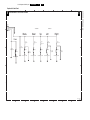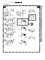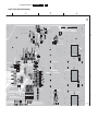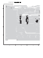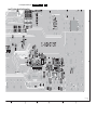
1
Colour Television
Chassis
TPT1.1HA LA
H_17010_000.eps
110907
Contents
Page
1. Technical Specifications, Connections, and Chassis
Overview
2
2. Safety Instructions, Warnings, and Notes
5
3. Directions for Use
6
4. Mechanical Instructions
7
5. Service Modes, Error Codes, and Fault Finding 15
6. Block Diagrams, Test Point Overviews, and
Waveforms
Wiring Diagram
23
Block Diagram Video
24
Block Diagram Audio
25
Waveforms TV & Scaler Board (Part 1)
26
Waveforms TV & Scaler Board (Part 2)
27
7. Circuit Diagrams and PWB Layouts
Side I/O Panel
(D) 28
Keyboard & Control Panel
(E) 30
i-Board
(HC) 32
IR & LED Panel
(J) 34
Display Supply Panel
(P) 36
TV & Scaler Board: D-Sub
(S-A02) 38
TV & Scaler Board: Tuner & Input
(S-A03) 39
TV & Scaler Board: SVP LX66-1
(S-A04) 40
TV & Scaler Board: SVP LX66-2
(S-A05) 41
TV & Scaler Board: SVP LX66-3
(S-A06) 42
TV & Scaler Board: DDRRAM & Flash (S-A07) 43
TV & Scaler Board: HDMI
(S-A08) 44
TV & Scaler Board: MST ADC
(S-A09) 45
TV & Scaler Board: Sound Delay
(S-A10) 46
TV & Scaler Board: Audio Decoder
(S-A11) 47
TV & Scaler Board: Audio Amplifier
(S-A12) 48
TV & Scaler Board: iTV & ComPair
(S-A13) 49
TV & Scaler Board: Power
(S-A14) 50
Contents
Page
8. Alignments
61
9. Circuit Descriptions, Abbreviation List, and IC Data
Sheets
63
Abbreviation List
65
IC Data Sheets
67
10. Spare Parts List
72
11. Revision List
77
29
31
33
35
37
51-60
51-60
51-60
51-60
51-60
51-60
51-60
51-60
51-60
51-60
51-60
51-60
51-60
©
Copyright 2007 Philips Consumer Electronics B.V. Eindhoven, The Netherlands.
All rights reserved. No part of this publication may be reproduced, stored in a
retrieval system or transmitted, in any form or by any means, electronic,
mechanical, photocopying, or otherwise without the prior permission of Philips.
Published by CS 0770 BU CD Customer Service
Printed in the Netherlands
Subject to modification
EN 3122 785 17011
EN 2
1.
Technical Specifications, Connections, and Chassis Overview
TPT1.1HA LA
1. Technical Specifications, Connections, and Chassis Overview
Index of this chapter:
1.1 Technical Specifications
1.2 Connections
1.3 Chassis Overview
Note: Figures below can deviate slightly from the actual
situation, due to the different set executions.
1.1
Technical Specifications
1.1.1
Vision
1.2
Channel selections
Aerial input
1.1.2
Display type
Screen size
Resolution (H × V pixels)
Contrast ratio
Light output (cd/m2)
Response time (ms)
Viewing angle (H×V degrees)
Tuning system
Tuner bands
:
:
:
:
:
:
:
:
:
TV color systems
:
:
:
:
:
:
:
:
:
:
:
:
Video playback
Supported video formats
: (1920 × 1080)p, 2Fh
: 640 × 480 @
60, 72, 75, 85 Hz
: 800 × 600 @
56, 60, 72, 75, 85 Hz
: 1024 × 768 @ 60 Hz
: 125 presets
: 75 ohm, Coax
: IEC75 connector
Supported computer formats
Sound
Sound systems
LCD LPL
32" (80 cm), 16:9
1366 × 768p
600 : 1
500
8
178 × 178
PLL
VHF, UHF,
S-Channel and
Hyperband
PAL B/G
PAL D/K
PAL I
SECAM B/G
SECAM D/K
NTSC
NTSC, PAL, SECAM
(640 × 480)i, 1Fh
(640 × 480)p, 2Fh
(720 × 576)i, 1 Fh
(720 × 576)p, 2Fh
(1280 × 720)p, 3 Fh
: NICAM, 2CS,
AM-MONO,
FM-MONO
: 2×5
Maximum power (WRMS)
1.1.3
Miscellaneous
Power supply:
- AC Power voltage (VAC)
- AC Power frequency (Hz)
: 90 - 264
: 50/60
Ambient conditions:
- Temperature range
- Maximum humidity
: +5 to +40 °C
: 90% R.H.
Power consumption
- Normal operation
- Stand-by
: 150 W
: < 3W
Dimensions (W × H × D cm)
: 79.0 × 54.0 ×11.0
Weight (kg)
: 18.2
Connections
Note: The following connector color abbreviations are used
(acc. to DIN/IEC 757): Bk= Black, Bu= Blue, Gn= Green, Gy=
Grey, Rd= Red, Wh= White, and Ye= Yellow.
Rear and side I/O Connections
D-SUB
HDMI 2
Y
Pb
Pr
CVI 1
HDMI 1
L
L
R
VIDEO
IN
AUDIO
IN
AUDIO
R
PC IN
Y
Pb
CVI 2
Pr
L
R
AUDIO
IN
AUDIO
IN
8?
S-VIDEO
AV
SPDIF
OUT
DATA 1 DATA 2
(RJ45)
SIDE AV
VIDEO IN
(RJ12)
R - AUDIO - L
AC IN
S-VIDEO
1.2.1
H_17010_003.eps
180907
Figure 1-1 Rear and Side I/O connections
Technical Specifications, Connections, and Chassis Overview
AV3 HDMI: Digital Video - In, Digital Audio - In
19
18
1
2
Figure 1-2 HDMI (type A) connector
- D2+
- Shield
- D2- D1+
- Shield
- D1- D0+
- Shield
- D0- CLK+
- Shield
- CLK- n.c.
- n.c.
- DDC_SCL
- DDC_SDA
- Ground
- +5V
- HPD
- Ground
Data channel
Gnd
Data channel
Data channel
Gnd
Data channel
Data channel
Gnd
Data channel
Data channel
Gnd
Data channel
DDC clock
DDC data
Gnd
Hot Plug Detect
Gnd
Hosiden: SVHS (Input)
1 - Ground Y
Gnd
2 - Ground C
Gnd
3 - Video Y
1 VPP / 75 ohm
4 - Video C
0.3 VPP / 75 ohm
Cinch (Input)
Ye - Video CVBS
Wh - Audio L
Rd - Audio R
j
H
j
j
H
j
j
H
j
j
H
j
j
jk
H
j
j
H
H
H
j
j
1 VPP / 75 ohm
0.5 VRMS / 10kohm
0.5 VRMS / 10kohm
jq
jq
jq
AV3 Cinch: Audio - In
Rd - Audio R
0.5 VRMS / 10 kohm
Wh - Audio L
0.5 VRMS / 10 kohm
jq
jq
AV3 VGA: Video 2fH RGB - In
1
6
11
5
10
15
E_06532_002.eps
050404
Figure 1-3 VGA Connector
1
2
3
4
5
6
7
8
9
10
11
12
13
14
15
- Video Red
- Video Green
- Video Blue
- n.c.
- Ground
- Ground Red
- Ground Green
- Ground Blue
- +5V_DC
- Gnd Sync
- n.c.
- DDC_SDA
- H-sync
- V-sync
- DDC_SCL
0.7 VPP / 75 ohm
0.7 VPP / 75 ohm
0.7 VPP / 75 ohm
j
j
j
Gnd
Gnd
Gnd
Gnd
+5 VDC
Gnd
H
H
H
H
j
H
DDC data
0-5V
0-5V
DDC clock
j
j
j
j
AV2 SVHS: Video 1fH Y/C - In
1 - Ground Y
Gnd
2 - Ground C
Gnd
3 - Video Y
1 VPP / 75 ohm
4 - Video C
0.3 VPP / 75 ohm
1.
EN 3
Monitor Out Mini Jack: Video CVBS - Out, Audio - Out
kq
1 - Audio R
0.5 VRMS / 10 kohm
2 - Gnd CVBS
Gnd
H
3 - Video CVBS
1 VPP / 75 ohm
kq
4 - Audio L
0.5 VRMS / 10 kohm
kq
E_06532_017.eps
250505
1
2
3
4
5
6
7
8
9
10
11
12
13
14
15
16
17
18
19
20
TPT1.1HA LA
H
H
j
j
AV1/2 Cinch: Video 1fH CVBS/YPbPr - In, Audio - In
Wh - Audio L
0.5 VRMS / 10 kohm
Rd - Audio R
0.5 VRMS / 10 kohm
Bu - Video Pb
0.7 VPP / 75 ohm
Rd - Video Pr
0.7 VPP / 75 ohm
Gn - Video Y
1 VPP / 75 ohm
jq
jq
jq
jq
jq
Bathroom Speaker - Out
- - mini jack
Speaker out
kq
Aerial - In
- - F-type
Coax, 75 ohm
D
Service connector 1 (UART)
1 - UART_TX
Transmit data
2 - Ground
Gnd
3 - UART_RX
Receive data
k
H
j
Service connector 2 (ComPair)
1 - SDA-S
I2C Data (0 - 5 V)
2 - SCL-S
I2C Clock (0 - 5 V)
3 - Ground
Gnd
Head phone (Output)
Bk - Head phone
10 mW / 32 ohm
RJ12 DATA1 (HM-Link - In/Out)
1 - LED_in
< 0.3 V, active low
2 - IR_in
< 0.3 V, active low
3 - MODE
Vcc
4 - TV Power Status 4.5 to 5 V: TV “On”
< 0.3 V: TV “Stdby”
High impedance: TV “Off”
5 - Gnd
Gnd
6 - IR_out
Signal
RJ45 DATA2 (Xpress Box - In/Out)
1 - +12V
+12V/1W
2 - Gnd
Gnd
3 - H-sync
Signal
4 - V-sync
Signal
5 - TXD232
Signal
6 - RXD232
Signal
7 - SDA3_IR-OUT
Signal
8 - DCM-POR
Signal
9 - CVBSterr
Signal
10 - Gnd CVBSterr
Gnd
jk
j
H
ot
j
j
j
k
H
k
k
H
k
k
k
k
k
H
EN 4
1.3
1.
TPT1.1HA LA
Chassis Overview
E
KEYBOARD CONTROL
PANEL
A
DISPLAY
SUPPLY PANEL
J
Technical Specifications, Connections, and Chassis Overview
IR & LED PANEL
TV & SCALER
BOARD
S-A
i-BOARD
HC
KEYBOARD CONTROL
PANEL
E
SIDE I/O PANEL
D
H_17010_055.eps
200907
Figure 1-4 PWB / CBA locations
Safety Instructions, Warnings, and Notes
TPT1.1HA LA
2.
EN 5
2. Safety Instructions, Warnings, and Notes
Index of this chapter:
1.1 Technical Specifications
1.2 Connections
1.3 Chassis Overview
•
2.1
Safety Instructions
Safety regulations require the following during a repair:
• Connect the set to the Mains/AC Power via an isolation
transformer (> 800 VA).
• Replace safety components, indicated by the symbol h,
only by components identical to the original ones. Any
other component substitution (other than original type) may
increase risk of fire or electrical shock hazard.
Safety regulations require that after a repair, the set must be
returned in its original condition. Pay in particular attention to
the following points:
• Route the wire trees correctly and fix them with the
mounted cable clamps.
• Check the insulation of the Mains/AC Power lead for
external damage.
• Check the strain relief of the Mains/AC Power cord for
proper function.
• Check the electrical DC resistance between the Mains/AC
Power plug and the secondary side (only for sets that have
a Mains/AC Power isolated power supply):
1. Unplug the Mains/AC Power cord and connect a wire
between the two pins of the Mains/AC Power plug.
2. Set the Mains/AC Power switch to the “on” position
(keep the Mains/AC Power cord unplugged!).
3. Measure the resistance value between the pins of the
Mains/AC Power plug and the metal shielding of the
tuner or the aerial connection on the set. The reading
should be between 4.5 Mohm and 12 Mohm.
4. Switch “off” the set, and remove the wire between the
two pins of the Mains/AC Power plug.
• Check the cabinet for defects, to prevent touching of any
inner parts by the customer.
2.2
•
2.3.2
•
•
•
•
•
•
•
•
All ICs and many other semiconductors are susceptible to
electrostatic discharges (ESD w). Careless handling
during repair can reduce life drastically. Make sure that,
during repair, you are connected with the same potential as
the mass of the set by a wristband with resistance. Keep
components and tools also at this same potential. Available
ESD protection equipment:
– Complete kit ESD3 (small tablemat, wristband,
connection box, extension cable and earth cable) 4822
310 10671.
– Wristband tester 4822 344 13999.
Be careful during measurements in the high voltage
section.
Never replace modules or other components while the unit
is switched “on”.
When you align the set, use plastic rather than metal tools.
This will prevent any short circuits and the danger of a
circuit becoming unstable.
2.3
Notes
2.3.1
General
•
Measure the voltages and waveforms with regard to the
chassis (= tuner) ground (H), or hot ground (I), depending
on the tested area of circuitry. The voltages and waveforms
shown in the diagrams are indicative. Measure them in the
All resistor values are in ohms, and the value multiplier is
often used to indicate the decimal point location (e.g. 2K2
indicates 2.2 kohm).
Resistor values with no multiplier may be indicated with
either an “E” or an “R” (e.g. 220E or 220R indicates
220 ohm).
All capacitor values are given in micro-farads (μ= ×10-6),
nano-farads (n= ×10-9), or pico-farads (p= ×10-12).
Capacitor values may also use the value multiplier as the
decimal point indication (e.g. 2p2 indicates 2.2 pF).
An “asterisk” (*) indicates component usage varies. Refer
to the diversity tables for the correct values.
The correct component values are listed in the Spare Parts
List. Therefore, always check this list when there is any
doubt.
BGA (Ball Grid Array) ICs
Introduction
For more information on how to handle BGA devices, visit this
URL: www.atyourservice.ce.philips.com (needs subscription,
not available for all regions). After login, select “Magazine”,
then go to “Repair downloads”. Here you will find Information
on how to deal with BGA-ICs.
BGA Temperature Profiles
For BGA-ICs, you must use the correct temperature-profile,
which is coupled to the 12NC. For an overview of these profiles,
visit the website www.atyourservice.ce.philips.com (needs
subscription, but is not available for all regions)
You will find this and more technical information within the
“Magazine”, chapter “Repair downloads”.
For additional questions please contact your local repair help
desk.
Warnings
•
Schematic Notes
•
2.3.3
Service Default Mode (see chapter 5) with a colour bar
signal and stereo sound (L: 3 kHz, R: 1 kHz unless stated
otherwise) and picture carrier at 475.25 MHz for PAL, or
61.25 MHz for NTSC (channel 3).
Where necessary, measure the waveforms and voltages
with (D) and without (E) aerial signal. Measure the
voltages in the power supply section both in normal
operation (G) and in stand-by (F). These values are
indicated by means of the appropriate symbols.
Manufactured under license from Dolby Laboratories.
“Dolby”, “Pro Logic” and the “double-D symbol”, are
trademarks of Dolby Laboratories.
2.3.4
Lead-free Soldering
Due to lead-free technology some rules have to be respected
by the workshop during a repair:
• Use only lead-free soldering tin Philips SAC305 with order
code 0622 149 00106. If lead-free solder paste is required,
please contact the manufacturer of your soldering
equipment. In general, use of solder paste within
workshops should be avoided because paste is not easy to
store and to handle.
• Use only adequate solder tools applicable for lead-free
soldering tin. The solder tool must be able:
– To reach a solder-tip temperature of at least 400°C.
– To stabilize the adjusted temperature at the solder-tip.
– To exchange solder-tips for different applications.
• Adjust your solder tool so that a temperature of around
360°C - 380°C is reached and stabilized at the solder joint.
Heating time of the solder-joint should not exceed ~ 4 sec.
Avoid temperatures above 400°C, otherwise wear-out of
tips will increase drastically and flux-fluid will be destroyed.
EN 6
•
3.
TPT1.1HA LA
Directions for Use
To avoid wear-out of tips, switch “off” unused equipment or
reduce heat.
Mix of lead-free soldering tin/parts with leaded soldering
tin/parts is possible but PHILIPS recommends strongly to
avoid mixed regimes. If this cannot be avoided, carefully
clear the solder-joint from old tin and re-solder with new tin.
example below it is 2006 week 17). The 6 last digits contain the
serial number.
MODEL
: 32PF9968/10
PROD.NO: AG 1A0617 000001
2.3.5
S
Alternative BOM identification
The third digit in the serial number (example:
AG2B0335000001) indicates the number of the alternative
B.O.M. (Bill Of Materials) that has been used for producing the
specific TV set. In general, it is possible that the same TV
model on the market is produced with e.g. two different types
of displays, coming from two different suppliers. This will then
result in sets which have the same CTN (Commercial Type
Number; e.g. 28PW9515/12) but which have a different B.O.M.
number.
By looking at the third digit of the serial number, one can
identify which B.O.M. is used for the TV set he is working with.
If the third digit of the serial number contains the number “1”
(example: AG1B033500001), then the TV set has been
manufactured according to B.O.M. number 1. If the third digit is
a “2” (example: AG2B0335000001), then the set has been
produced according to B.O.M. no. 2. This is important for
ordering the correct spare parts!
For the third digit, the numbers 1...9 and the characters A...Z
can be used, so in total: 9 plus 26= 35 different B.O.M.s can be
indicated by the third digit of the serial number.
Identification: The bottom line of a type plate gives a 14-digit
serial number. Digits 1 and 2 refer to the production centre (e.g.
AG is Bruges), digit 3 refers to the B.O.M. code, digit 4 refers
to the Service version change code, digits 5 and 6 refer to the
production year, and digits 7 and 8 refer to production week (in
3. Directions for Use
You can download this information from the following websites:
http://www.philips.com/support
http://www.p4c.philips.com
MADE IN BELGIUM
220-240V ~ 50/60Hz
128W
VHF+S+H+UHF
BJ3.0E LA
E_06532_024.eps
130606
Figure 2-1 Serial number (example)
2.3.6
Board Level Repair (BLR) or Component Level Repair
(CLR)
If a board is defective, consult your repair procedure to decide
if the board has to be exchanged or if it should be repaired on
component level.
If your repair procedure says the board should be exchanged
completely, do not solder on the defective board. Otherwise, it
cannot be returned to the O.E.M. supplier for back charging!
2.3.7
Practical Service Precautions
•
•
It makes sense to avoid exposure to electrical shock.
While some sources are expected to have a possible
dangerous impact, others of quite high potential are of
limited current and are sometimes held in less regard.
Always respect voltages. While some may not be
dangerous in themselves, they can cause unexpected
reactions that are best avoided. Before reaching into a
powered TV set, it is best to test the high voltage insulation.
It is easy to do, and is a good service precaution.
Mechanical Instructions
TPT1.1HA LA
4.
EN 7
4. Mechanical Instructions
Index of this chapter:
4.1 Cable Dressing
4.2 Service Positions
4.3 Assy/Panel Removal
4.4 Set Re-assembly
4.1
Notes:
• Figures below can deviate slightly from the actual situation,
due to the different set executions.
• Follow the disassemble instructions in described order.
Cable Dressing
H_17010_014.eps
180907
Figure 4-1 Cable dressing
4.2
Service Positions
1
For easy servicing of this set, there are a few possibilities
created:
• The buffers from the packaging (see figure “Rear cover”).
• Foam bars (created for Service).
4.2.1
Foam Bars
The foam bars (order code 3122 785 90580 for two pieces) can
be used for all types and sizes of Flat TVs. See figure “Foam
bars” for details. Sets with a display of 42" and larger, require
four foam bars [1]. Ensure that the foam bars are always
supporting the cabinet and never only the display. Caution:
Failure to follow these guidelines can seriously damage the
display!
1
Required for sets
42"
By laying the TV face down on the (ESD protective) foam bars,
a stable situation is created to perform measurements and
alignments. By placing a mirror under the TV, you can monitor
the screen.
E_06532_018.eps
171106
Figure 4-2 Foam bars
EN 8
4.
Mechanical Instructions
TPT1.1HA LA
4.3
Assy/Panel Removal
4.3.1
Stand and Back Cover removal
4.3.3
IR and LED Panel removal
Refer to figure “IR and LEDl Panel removal” for details.
1. Disconnect the connector [1] from the panel.
2. Remove the fixation screws [2].
3. Take out the panel.
When defective, replace the whole unit.
Warning: Disconnect the mains power cord before you remove
the rear cover.
Refer to figure “Stand and Back Cover removal” for details.
1. Place the TV set upside down on a table top, using the
foam bars (see part “Foam Bars”).
Caution: do not put pressure on the display, but let the
monitor lean on the speakers or the Front cover.
2. Remove the screws [1] that secure the stand.
3. Pull down the stand to remove it.
4. Remove the screws [2} that secure the rear cover.
5. Lift the rear cover from the bottom side up from the cabinet.
1
2
2
2
H_17010_015.eps
180907
Figure 4-5 IR and LED Panel removal
2
2
2
1
1
2
4.3.4
2
1
2
1
2
Speaker removal
Refer to figure “Speaker removal” for details.
1. Disconnect the connectors [1] from the speaker.
2. Remove the fixation screws [2].
3. Take out the speaker.
When defective, replace the whole unit.
2
H_17010_004.eps
180907
Figure 4-3 Stand and Back Cover removal
1
4.3.2
I-Board removal
Refer to figure “I-Board removal” for details.
1. Disconnect the connectors [1] from the panel.
2. Remove the fixation screws [2].
3. Gently release the glued bottom side [3] of the panel and
lift the panel out of the bracket.
H_17010_006.eps
180907
Figure 4-6 Speaker removal
2
1
2
3
1
H_17010_009.eps
180907
Figure 4-4 I-Board removal
Mechanical Instructions
4.3.5
Keyboard Control Panel removal
Refer to figure “Keyboard Control Panel removal” for details.
1. Disconnect the connector [1] from the panel.
2. Gently release the panel clips in the indicated direction.
3. Take out the panel.
When defective, replace the whole unit.
1
H_17010_010.eps
180907
Figure 4-7 Keyboard Control Panel removal
4.3.6
SIde I/O Panel removal
Refer to figure “Side I/O Panel removal” for details.
1. Disconnect the connector [1] from the panel.
2. Remove the fixation screws [2].
3. Take out the panel.
When defective, replace the whole unit.
2
1
H_17010_005.eps
180907
Figure 4-8 Side I/O Panel removal
TPT1.1HA LA
4.
EN 9
EN 10
4.3.7
4.
TPT1.1HA LA
Mechanical Instructions
SSB and PSU cover removal
Refer to figure “SSB and PSU Cover removal” for details.
1. Remove the fixation screws [1].
2. Take of the cover.
1
1
1
1
1
1
1
1
H_17010_101.eps
190907
Figure 4-9 SSB and PSU Cover removal
Mechanical Instructions
4.3.8
TPT1.1HA LA
4.
Subframe removal
Refer to figure “Subframe removal” for details.
1. Unplug the LVDS connector [1]. Caution: be careful, as
this is a very fragile connector!
2. Disconnect the connectors [2] from the panels and
speakers.
3. Release the tape [3].
4. Remove the fixation screws [4] and [5].
5. Lift the subframe from the cabinet.
4
4
4
4
5
5
1
2
3
5
5
3
4
4
4
4
4
4
2
H_17010_013.eps
180907
Figure 4-10 Subframe removal
EN 11
EN 12
4.3.9
4.
Mechanical Instructions
TPT1.1HA LA
PSU removal
Refer to figure “PSU removal” for details.
1. Unplug the connectors [1].
2. Remove the fixation screw [2] from the bottom side of the
connector plate.
3. Remove the fixation screws [3].
4. Lift out the panel.
3
3
1
1
3
3
3
3
3
2
H_17010_012.eps
180907
Figure 4-11 PSU removal
Mechanical Instructions
4.3.10 Small Signal Board (SSB)
TPT1.1HA LA
4.
1. Unplug the LVDS connector [1]. Caution: be careful, as
this is a very fragile connector!
2. Unplug the connectors [2].
3. Remove the screws [3] to release the board from the
connector plate.
4. Remove the screws [4].
5. Carefully lift the SSB at the top and take it out of the set.
Caution: it is mandatory to remount all different screws at their
original position during re-assembly. Failure to do so may result
in damaging the SSB.
Refer to figures “SSB connector plate” and “SSB removal” for
details.
4
4
4
2
4
4
4
3
3
3
3
3
3
EN 13
3
3
3
H_17010_008.eps
180907
Figure 4-12 SSB removal
EN 14
4.
TPT1.1HA LA
Mechanical Instructions
4.3.11 LCD Panel
Important: Be sure to work in a dust free environment during
the following activities. In addition, the use of (fabric) hand
gloves is advised.
1
2
H_17010_007.eps
180907
Figure 4-13 LCD panel removal
1. Place the TV set face down on the foam bars. Place the
bars at the edges of the set, so they will support the front
frame and not only the glass plate!
2. Remove subframe as described earlier.
3. Release the taped wire [1].
4. Lift the support rim from the set [2].
4.4
Set Re-assembly
To re-assemble the whole set, execute all processes in reverse
order.
Notes:
• While re-assembling, make sure that all cables are placed
and connected in their original position. See figure “Cable
dressing”.
• Take care that all glued parts have been properly refixed
with appropriate glue again.
• Pay special attention not to damage the EMC foams at the
SSB shielding. Check that EMC foams are put correctly on
their places.
Service Modes, Error Codes, and Fault Finding
TPT1.1HA LA
5.
EN 15
5. Service Modes, Error Codes, and Fault Finding
Index of this chapter:
5.1 Service Modes
5.2 Repair Flow Chart
5.3 Software Upgrading
5.1
2. Displays the production code.
3. Displays the software version in from the main processor
4. Displays the software version of the optional other
processor.
5. Code 1 displays the last 5 logged errors.
6. Code 2 displays the first 5 logged errors.
7. Displays the validiti of the HDMI HDCP key.
8. Displays the NVM version.
Service Modes
The Customer Service Mode (CSM) is used for communication
between the call centre and the customer, while the Factory
Mode offers several features for the service technician.
Error Codes
The error code buffer contains all defected errors since the last
time the buffer was erased. The buffer is written from left to
right, new errors are logged at the left side, and all other errors
shift one position to the right. When an error occurs, it is added
to the list of errors, provided the list is not full. When an error
occurs and the error buffer is full, then the new error is not
added, and the error buffer stays intact (history is maintained),
except when the error is a protection error. To prevent that an
occasional error stays in the list forever, the error is removed
from the list after more than 50 hours of operation. When
multiple errors occur (errors occurred within a short time span),
there is a high probability that there is some relation between
them.
This chassis also offers the option of using ComPair, a
hardware interface between a computer and the TV chassis. It
offers the abilities of structured troubleshooting, error code
reading, and software version read-out for all chassis.
Minimum requirements for ComPair: a Pentium processor, a
Windows OS, and a CD-ROM drive (see also paragraph
“ComPair”).
5.1.1
TV mode Switching
The iTV set can be switched between “iTV” and “normal TV”
mode (or vice versa) with the iTV setup remote RC2573/01.
To do this; press 024995 <M> (M=menu). Follow the message
shown on the screen.
5.1.2
Table 5-1 Error Codes
Customer Service Mode (CSM)
Purpose
The Customer Service Mode shows error codes and
information on the TV’s operation settings. The call centre can
instruct the customer (by telephone) to enter CSM in order to
identify the status of the set. This helps the call centre to
diagnose problems and failures in the TV set before making a
service call.
The CSM is a read-only mode; therefore, modifications are not
possible in this mode.
How to enter
To enter CSM, press the following key sequence on the remote
control transmitter: “123654” (do not allow the OSD display to
time out between entries while keying the sequence).
Upon entering the Customer Service Mode, the following
screen will appear:
H_17010_016.eps
180907
Figure 5-1 CSM menu
Menu Explanation
1. Set type, this value gives the complete type number.
Error Code
Event
0x01
Audio decoder error
0x02
I2C bus error
0x03
Tuner error
0x04
NVRAM Error
0x05
Scaler error
How to exit
To exit CSM, use one of the following methods:
• Press the MENU, STATUS (or EXIT/INFO/[i+]), or POWER
button on the remote control transmitter.
• Press the POWER button on the television set.
5.1.3
Factory Mode
How to Enter
To enter the factory mode, use the following method:
• Press the Menu button on the standard remote control.
• Press the following key sequence on the remote control
transmitter: “062596” directly followed by the MENU
button (do not allow the OSD display to time out between
entries while keying the sequence).
• Then with the cursor down key scroll under the install line.
Now no the Panel description is highlighted. Then press
the cursor right button to enter.
After entering the Factory Mode, the following screen is visible,
with panel information at the bottom line in the menu.
EN 16
5.
TPT1.1HA LA
Service Modes, Error Codes, and Fault Finding
5.1.4
Hotel Mode
Before the hotel mode can be activated, the set needs to be
switched into normal consumer mode first. Use an ITV setup
remote control (type: RC2573/01, 12NC: 3139 228 88782) and
key in the code “024995” directly followed by the “M” (Menu)
key. The test messages “TV is Now In MTV Mode” and “Please
Do A Cold Start!” appear on the screen.
Disconnect the set for a few seconds from the mains supply,
and reconnect the set to again. After switching the set “on”, the
set is in normal consumer mode (MTV-Mode).
H_17010_017.eps
180907
Figure 5-2 Factory menu [1/3]
H_17010_019.eps
180907
Figure 5-3 Factory menu [2/3]
H_17010_018.eps
180907
Figure 5-4 Factory menu [3/3]
How to Navigate
When you press the up/down cursor keys you can move
around the items, with the Right cursor you can select an item
and enter it. With the jaMENU button on the remote control, the
set will switch on the normal user menu in the Factory mode.
How to Exit
Switch the set to STANDBY by pressing the POWER button on
the remote control transmitter.
If you turn the television set off by removing the AC Power (i.e.,
unplugging the television) or by using the POWER button on
the TV set, the television set will remain in SDM when AC
Power is re-applied, and the error buffer is not cleared.
After repair, put the set into hotel mode (iTV-Mode) again.
Enter the same code on the remote control as described
above. The text messages “TV Is Now In ITV Mode” and
“Please Do A Cold Start!” appears. Disconnect the set for a few
seconds from the mains supply, and reconnect it to the mains
supply again. After switching “on”, the set is in normal
consumer mode (MTV-Mode).
Service Modes, Error Codes, and Fault Finding
5.2
TPT1.1HA LA
5.
Repair Flow Chart
1.No work/LED is off
Check if
No
power switch is
Replace Power switch
normal
Yes
Check
IR board CN001
No
pin1=0V,pin2=3.7V,
Check IR board
pin3=3V,pin4=2.85V
,pin5=5V,pin6
=3.3V
Yes
Check scaler board U102
pin1=14V,pin4=1.22V,
pin7=16V,pin8=5V,
H_17010_020.eps
180907
Figure 5-5 Start-up flowchart
EN 17
EN 18
5.
TPT1.1HA LA
Service Modes, Error Codes, and Fault Finding
2. No raster/picture too
dim
Check
Inverter board
No
CN852,pin1=16V,
Check Scaler board
pin5=0.9V,pin6
=3V
Yes
Check
Inverter board
No
U811 pin2=5V,Q821
Check U811,Q821
pin=5,6=16V
Yes
Check scaler board
H_17010_021.eps
180907
Figure 5-6 No Raster flowchart
Service Modes, Error Codes, and Fault Finding
TPT1.1HA LA
3. No picture/LED is green
Check
scaler board U102
pin1=14V,pin4=1.22V,
pin7=16V,pin8
=5V
No
Check power
Yes
Check if
working voltage
U152,pin2=3.3V
pin3=5V
No
Check circuit around
each regulator and
eliminate short and
open situation
Yes
No
Check if clock
source X350
Replace X350
Yes
Check if
RGB,clk,H/V and
DE signal output 128
bits TTL
No
Try to replace
flash Rom
EEPROM
Yes
Check
resistors-network
No
Replace bad resistorsnetwork
Yes
Replace LVDS cable
Figure 5-7 No Picture flowchart
H_17010_022.eps
180907
5.
EN 19
EN 20
5.
Service Modes, Error Codes, and Fault Finding
TPT1.1HA LA
4. No TV sound
Check if
tuner TU201 pin11
output IF signal
No
Replace TU201
Yes
Check U301
5. No earphone sound
Check
U760 pin15=3.3V
No
Eliminate short and open
situation
Yes
Check U760
pin20=HPOUTL
pin6=HPOUTR
No
Replace U760
Yes
Replace Side AV Board
6. No remote function
Tty another
remote control
No
Replace one good
remote control
Yes
Check IR receiver
Figure 5-8 No Sound flowchart
H_17010_023.eps
180907
Service Modes, Error Codes, and Fault Finding
TPT1.1HA LA
7. LED and function
key poor
Check circuit around
control board and cable
between control board
and scaler board
8. No HDMI picture
Enter CSM mode
to check item 6
Invalid
Change U701 writen
HDCP KEY
Valid
Check Scaler Board
Figure 5-9 LED and function keys flowchart
H_17010_024.eps
180907
5.
EN 21
EN 22
5.
TPT1.1HA LA
5.3
Software Upgrading
5.3.1
Compair Service Tool
Service Modes, Error Codes, and Fault Finding
Introduction
ComPair (Computer Aided Repair) is a Service tool for Philips
Consumer Electronics products. and offers the following:
1. ComPair helps you to quickly get an understanding on how
to repair the chassis in a short and effective way.
2. ComPair allows very detailed diagnostics and is therefore
capable of accurately indicating problem areas. You do not
have to know anything about I2C or UART commands
yourself, because ComPair takes care of this.
3. ComPair speeds up the repair time since it can
automatically communicate with the chassis (when the uP
is working) and all repair information is directly available.
4. ComPair features TV software up possibilities.
Specifications
ComPair consists of a Windows based fault finding program
and an interface box between PC and the (defective) product.
The (new) ComPair II interface box is connected to the PC via
an USB cable. For the TV chassis, the ComPair interface box
and the TV communicate via a bi-directional cable via the
service connector(s).
How to Connect
This is described in the ComPair chassis fault finding database.
TO TV
TO
UART SERVICE
CONNECTOR
ComPair II
RC in
RC out
TO
I2C SERVICE
CONNECTOR
TO
UART SERVICE
CONNECTOR
Multi
function
Optional Power Link/ Mode
Switch
Activity
I2C
RS232 /UART
PC
ComPair II Developed by Philips Brugge
HDMI
I2C only
Optional power
5V DC
G_06532_036.eps
240807
Figure 5-10 ComPair II interface connection
Caution: It is compulsory to connect the TV to the PC as
shown in the picture above (with the ComPair interface in
between), as the ComPair interface acts as a level shifter. If
one connects the TV directly to the PC (via UART), ICs will be
blown!
How to Order
ComPair II order codes:
• ComPair II interface: 3122 785 91020.
• ComPair32 CD (update): 3122 785 60160.
• ComPair interface cable: 3122 785 90004.
• ComPair interface extension cable: 3139 131 03791.
• ComPair UART interface cable: 3122 785 90630.
Note: If you encounter any problems, contact your local
support desk
LVDS Tool
Support of the LVDS Tool has been discontinued.
Block Diagrams, Test Point Overviews, and Waveforms
TPT1.1HA LA
6.
23
6. Block Diagrams, Test Point Overviews, and Waveforms
Wiring Diagram
Key Board
IR Board
Panel
+24V
Inverter On/Off
Bright_ADJ
I- Board
+24V
Inverter On/OFF
Bright_ADJ
ITV_12V
SSB Board
I2C
+12V
+5V
+5V
I2C_SCL
I2C_SDA
Power Board
CVBS_OUT
HSYNC
VSYNC
AC IN
Side AV
Main Speaker
H_17010_051.eps
190907
Block Diagrams, Test Point Overviews, and Waveforms
TPT1.1HA LA
6.
24
Block Diagram Video
iTV
CVBS
Sync slicer
TUNER
S/PDIF Output
Audio Output CVBS
Output
Panel interface
1920*1080
(1366*768)
Audio DAC/SPDIF
CVBS/S -V ideo
Control interface
PX66
YPbPr 1
DDR memory
YPbPr 2
PC_ D-sub
EDID/
RS232
Scaler /ADC
V ideo
processing
Power supply
(regulator/
Switch)
Manage unit
to each block
EEPROM
IR / Power switch
Key pad
HDMI_1
HDMI
switch
CVBS &
H/V
sync
MCU
EDID
SRAM
HDMI_2
Flash memory
Side CVBS/S -video
RS232 service &ComPair port
H_17010_052.eps
190907
Block Diagrams, Test Point Overviews, and Waveforms
TPT1.1HA LA
6.
25
Block Diagram Audio
TUNER
SSIF
Post AMP
S/PDIF Output
Audio Output
CVBS Output
SPDIF
(without PVR o/p iniTV)
Bathroom
Spk AMP
CVBS/S-Video
Audio
decoder
YPbPr 1
YPbPr 2
PC_ D-sub
processing
Audio
Switch
Head phone
AMP
Side AV board
HDMI
Audio DAC
Audio Delay
Reserved
Side CVBS/S-video
H_17010_053.eps
190907
Block Diagrams, Test Point Overviews, and Waveforms
TPT1.1HA LA
6.
26
Waveforms TV & Scaler Board (Part 1)
1
6
11
16
DDCW P _P C(U1102 Pin 7)
2
7
28.322MHz (X4201 Pin 1)
HDMI 2_5V(U5102
SOUND_EN(U6301
Pi n 8)
pin 44)
R ESE T _H(R4301)
12
17
3
+5V_ T uner(U1201 Pin 3)
+1.5V(C5124)
SOUND_M UT E(U6301 Pin 45)
8
13
18
4
C P U_RESE T (U4103 Pin 2)
P X_VD DM(C4307)
+5V_M S P (C6203)
FAU LT (U6301 Pin 46)
9
14
E_ P AG E(U4101 Pin 7)
DDCW P _HDM I(U5101 Pin 7)
18. 432MHz (X6201 Pin 1)
19
+24V_A MP (C6365)
5
10
10MHz (X4101 Pin 1)
HDMI 1_5V(U5101
Pi n 8)
15
RESE T (U6202 Pin 16)
20
P OWER_ON(R7126)
H_17010_040.eps
190907
Block Diagrams, Test Point Overviews, and Waveforms
TPT1.1HA LA
6.
27
Waveforms TV & Scaler Board (Part 2)
21
26
LED_SEL_OUT
BRIGHT_A DJ (CN7201 Pin 5)
31
36
PX_VD18(FB7213)
PX_1. 8V (C7238)
22
(R7119)
27
PC_TV_LED
INVER TE R_ON_OFF(R7211)
32
37
23
(R7120)
28
STANDB Y(CN7201 Pin 10)
+3. 3V(C7217)
PX_VDDM(C7213)
REMO TE _3V(C7113)
33
38
+5V(C7229)
COMP1_L(FB1213)
24
29
34
41
25
+24V(C7202)
+3.3V_SB(FB7211)
30
PANEL_VCC(C7241)
AL_DACM(R6309)
35
42
+12V(C7208)
+5V_SB(FB7212)
+3. 3V_HDMI (C7250)
LOUT+/ -(CN6303 Pi n 2,1 )
H_17010_041.eps
190907
Circuit Diagrams and PWB Layouts
TPT1.1HA LA
7.
28
7. Circuit Diagrams and PWB Layouts
Side I/O Panel
1
D
2
3
4
5
SIDE I/O PANEL
6
7
2
3
4
5
1
A
HP_det
Front_CVBS
Front_Y
Front_C
HR_LOUT
HR_ROUT
HP_det
CN033
PHONEJACK
C031
6N8 50V
Aud_IN_L
Aud_IN_R
HR_LOUT
HR_ROUT
6N8
C03250V
D
10
9
8
7
6
5
4
3
2
1
A
CN034
63370
R032
Front_Y
0R05 1/10W 5%
5
CN032
DIN JACK
1
2
3
4
R035
75R 1/10W 5%
R034
75R 1/10W 5%
7
6
R033
B
Front_C
B
0R05 1/10W 5%
C035
100P(NI)
C036
820PF
CN031
R031
2
1
R037
2
120R/6000mA
R038
2
C033
C034
330P(NI) 330P(NI)
R042
47K 1/10W
R036
3K3 1/10W 5%
JACK
C037
100P(NI)
Aud_IN_R
47K 1/10W
FB031
120R/6000mA
R041
47K 1/10W
5
1
C
75R 1/10W 5%
3
6
Aud_IN_L
3K3 1/10W 5%
R040
1
47K 1/10W
C
0R05 1/10W 5%
FB032
R039
4
Front_CVBS
D
D
H_17010_049.eps
190907
1
2
3
4
5
Circuit Diagrams and PWB Layouts
TPT1.1HA LA
7.
29
Layout Side I/O Panel
CN031
CN032
CN033
CN034
A2
A3
A1
B2
C031 A1
C032 B1
C033 B2
C034 A2
C035 B3
C036 A3
C037 A2
FB031 A2
FB032 A2
R031 A2
R032 B3
R033 B3
R034 A3
R035 A3
R036 A1
R037 B2
R038 A2
R039 B2
R040 A2
R041 B2
R042 A2
H_17010_050.eps
190907
Circuit Diagrams and PWB Layouts
TPT1.1HA LA
7.
30
Keyboard & Control Panel
1
2
3
4
5
6
7
8
KEYBOARD & CONTROL PANEL
E
E
A
A
CN001
1
2
3
- Channel +
- Volume +
63363 3P 2.0mm
Menu
Down
Up
Left
Right
B
B
Power
R001
1K 1/10W
R002
47K 1/10W
R003
18K 1/10W
R004
3K6 1/10W
R005
5K6 1/10W
C002
100N 16V
C001
100N 16V
SW002
SW001
SW003
SW004
SW005
TACT SW ALPS H1.5MM
C
SW006
C004
100N 16V
C005
100N 16V
TACT SW ALPS H1.5MM
TACT SW ALPS H1.5MM
TACT SW ALPS H1.5MM
C003
100N 16V
TACT SW ALPS H1.5MM
C
TACT SW ALPS H1.5MM
D
D
E
E
H_17010_045.eps
190907
1
2
3
4
5
6
7
8
CN001 A1
C001 C1
C002 B2
C003 C6
C004 C5
C005 C3
R001 B2
R002 B3
R003 B4
R004 B5
R005 B6
SW001 C1
SW002 C2
SW003 C3
SW004 C4
SW005 C5
SW006 C6
Circuit Diagrams and PWB Layouts
TPT1.1HA LA
7.
31
Layout Keyboard & Control Panel
CN001 A1
J002 A2
J003 A4
C001 A4
C002 A3
C003 A2
C004 A2
C005 A3
R001 A3
R002 A4
R003 A4
R004 A2
R005 A2
SW001 A5
SW002 A3
SW003 A4
SW004 A3
SW005 A2
SW006 A2
H_17010_046.eps
190907
Circuit Diagrams and PWB Layouts
TPT1.1HA LA
7.
32
i-Board
1
Outside connector
2
1
+5V
BAT760
1
K
R109
C65
10pF
R111
1
R99
0R
R112
NFR25-15R
I/P
O/P
+
2
C68
1UF
NFR25-15R
C69
1000uF, 10V
6.8uH - 1210
+5V
R87 0R - NL
+
C5
100uF, 16V
3
GND
+12V
+ C6
100uF, 16V
+5VA
L5
0R RES
L20
+
C26
100uF, 16V
IRIN_DATA-IN
+5VA
C9
100nF
11
Sa
10
Sb
9
Sc
8
Vss
7
Vee
6
E
J5
2
LEDIN_CLK_TXD_SCL1
IR-IN_DATA-IN_RXD_SDA1
MODE
STATUS_DATA-OUT
MODE
STATUS_DATA-OUT
R10
R11
R94
100R
100R
100R
10K Q12
BC847B
IR_OUT
2
5
3
4
Zb
1
Y1b
2
Y0b
PEND_IR (not use)
RJIR_IN
Zc
3
Y1c
5
Y0c
Tristate
STATUS_DATA_OUT1
11
Sa
10
Sb
9
Sc
8
Vss
7
Vee
6
E
4
2
+5VA
Q3
BC857BW
2
R15
R16
R70
BZA408B
+5VA
1
+12V
+12V
HEF4053BT
10
15
R20
1
Q5
BC847BW
DCM_POR
8
D4
1
BZA408B
6
TXD232
RXD232
DCM_POR
HSYNC
VSYNC
+5VA
10PIN-CONN GNDA
2
5
3
4
V
C13
27pF
11
Sa
10
Sb
9
Sc
8
Vss
7
Vee
6
E
U6
DS1813
1
RST
VCC
3
R126
0R
R59
10K
Q11
BC847B
TXD232 R62
100R
14
T1_OUT
7
T2_OUT
RXD232 R61
100R
13
R1_IN
8
R2_IN
220R
68R
VSYN
R21
100R
LED_SEL_OUT
U7
1
C1+
3
C14
C2+
5
C211
T1_IN
10
T2_IN
12
R1_OUT
9
R2_OUT
BZX384-C5V6
+5VD
B
RP4
10K-RP
J13
R4
2K2
R3
10K
1
Q1
BC847B
+5VD
C24
100nF
C23
100nF
R29
2K2
C74
1UF
Q6
BC847BW
R32
DCM_POR
SW1
4
Q13
BC847B
1
C37
10nF
DGND1
DGND2
DGND3
1
22K
R63 47K
R31
22K
C15
1uF
3
Tact Switch, SKQNABD010
1
V-
1
R41
2K2
U5
P89C664HBBD
+5VD
C41
RESERVE
R64
10K
A
TXD
VCC
16
HSYNC
2
3
V+
R22
100R
C17
27pF
2PIN-CONN
R30
5K6
L11
6.8uH - 1008
C21
100nF
15
GNDA
Q9
BC847B
2
6
C20 100nF
1
R51 R54
10K 10K
C19
100nF
R69
1K
27pF
R36
100R
RXD
5P-CONN-SR-V
R8
0R OPT
+
GND
R38
Q2
BC847BW
R56
10K
L12
6.8u - 1210
C22
100uF, 16V
R58
47K
1
R42
C16
X1
16MHz
TV_POR
C25
1uF
2
HSYN
VSYN
3
2
R53
47K
1
3
1
Q10
BC857BW
3
R7
100R
Q15
BC847B
1
2
To TV
BD
1
2
3
4
5
2
SR J3
A
Q8
BC857BW
3
3
CVBSTERR
R9
220R
2
C8
100nF
R60
4K7
+5VD
100nF
RXD
TXD
+5VD
+5VA
R55
4K7
STATUS_DATA_OUT1
C84
C14
27pF
2
+5V
C
0R
+5VA
R57
47K
4
VSS
3
E2
2
E1
1
E0
R67 100R
SDA2
SCL2
100R
LED_SEL_OUT
HEF4053BT
R2
100R
+5VD
U8
5
SDA
6
SCL
7
WC
8
VCC
R68
G
IB_IROUT
RC_IR
SDA1
SCL1
4
IR_IN TV
R52
22K
4K7
PC_TV_LED
LIGHT SENSOR
RC_IR
IR_IN TV
TXD
RXD
TXD
RXD
3
Y1c
5
Y0c
C36
100uF, 16V
C42 MC24C16
100nF
R44 10K
1
2
Zc
4
U11
74HC1G86
100R
100R
13
Y1a
12
Y0a
R107
Zb
CVBSTERR
GNDA
2
1
Y1b
2
Y0b
10K
R24
4K7
R25
R26
+
R47
4K7
SCL1
SDA1
SDA3
3
16
10K
R18
1K0
Q4
BC847BW
1
IR_IN TV
2
7
9
+5VA
RXD232
6
U4
14
Za
R19
1
Vdd
TXD232
3
VSYNC
5
C12
100nF
2
4
+5VA
0R
R104
RJIR_IN
150R
HSYNC
3
3
5
R17
2
R23
4K7
SR J2
4P-CONN-SR-V+3V3STBY
4
3
SDA
2
SCL
1
+5VD
To TV
BD
R46 4K7
4K7
R40
22
P2.4/A12
21
P2.3/A11
20
P2.2/A10
19
P2.1/A9
18
P2.0/A8
17
NIC*
16
VSS
15
XTAL1
14
XTAL2
13
P3.7/RD
12
P3.6/WR
10K
100R
100R
+5VD
R39
MODE_R
R48
22K
Q7
BC847B
10K
34
P0.3/AD3
35
P0.2/AD2
36
P0.1/AD1
37
P0.0/AD0
38
VCC
39
NIC*
40
P1.0/T2
41
P1.1/T2EX
42
P1.2/ECI
43
P1.3/CEX0
44
P1.4/CEX1
+5VD
3
1
R122
10K
J6
C18
100nF
1
P1.5/CEX2
2
P1.6/SCL
3
P1.7/SDA
4
RST
5
P3.0/RxD
6
NIC*
7
P3.1/TxD
8
P3.2/INT0
9
P3.3/INT1
10
P3.4/CEX3/T0
11
P3.5/CEX4/T1
SDA3
Za
10nF
16
13
Y1a
12
Y0a
15
B
Vdd
R13
U3
14
C31
10nF
LCM_POW
TV_POR
CLK_LED-IN_SCL1
DATA-IN_SDA1
C11
+5VA
100nF
10K
6
100R
R103
D3
1
100R
6PIN-CONN
1
IR_OUT
6
BZX284-C5V6
BZX284-C5V6
1
2 D1
5
D2
100R
4
C30
C32
10nF
R28
10K
3
RP5
10K-RP
R34
R35
RP1
1
100R
+5VD R33
C35
10nF
+5VD
R27
1nF
3
1
10nF
8
7
6
5
3
Y1c
5
Y0c
10nF
R124
10K-RP
Zc
4
470R
1
RP3
10K-RP
1
2
3
4
Zb
1
Y1b
2
Y0b
C33
C27
100nF
3
15
Za
U2
HEF4053BT
13
Y1a
12
Y0a
2
14
Vdd
16
C
J9
3P-CONN-SR-V
RP2
10K-RP
C34
L19
BLM21P221SN1D
+5VD
L8
R1
100R
D6 BZX284-C5V1
2
1
A
K
5P-CONN-TYCO -NL
SPARE IO
220uF, 10V
R118
C77
IR_PULLUP
6.8uH - 1210
2K7
1
+5VD
+5V
+ C70
U9
LF50CV
SDA2
R117
1K0
5
6
7
8
D5
2
A
2
R116
C81
220uF, 16V
2
NFR254R7
SCL2
3
L6
+5VD
6.8uH - 1210
+5V
R108
3
10uF
100pF
D
+
PC_TV_LED_OUT
LIGHT SENSOR
C63
10pF
4
+ C80
D8
220uF, 16V
C78
4
3
3
6.8uH
C79
2
3P-CONN-PH-H
1K
5
+5V
L23
K
8
7
6
5
C61
10pF
4
Comparator Ground
Inv. I/p
A
1
2
3
4
C62
10pF
C60
10pF
5
LCM_POW
5
IB_IROUT
Odd nos. to IRLED
68R
Q14
PBSS5140U
R72
C83
10pF
TXD
RC_IR
R86
+12V
BLM21P221SN1D
L24
C82
10pF
RXD
2
G
68R
3
R85
Even nos. to SSB
C76
10uF
J12
1
2
3
IR_IN TV
3
R73
4K7
0R
5
V
4
RC_IN
U10
74HC1G86
1
LCM_POW
2
J14
Notice:
J4 connector
+5V
BLM21P221SN1D
Inside connector
220R
1
Drive
Switch
Coll ector
Coll ector
7 Ipk Sense
2
Switch
Emitter
6
3
Vcc
Timing
Capacitor
+
C75
220uF, 16V
R123
R106
+5VD
C57
10pF
1R5
D7
SS24
U12
MC34063AD
8
SDA2
SCL2
C56
10pF
C59
10pF
R115
R125
B12B-PHDSS-B
68R
68R
C58
10pF
R114
8
7
6
5
R83
R84
0R
R71
L25
BLM21P221SN1D
1
LED_RED
R113 1R5
2
BLM21P221SN1D
LED_SEL_OUT
LED_SEL
RC_IR
0R
C7
100nF
L7
BLM21P221SN1D
L22
68uH
+3V3
4
3
2
1
L18
SCL2
SDA2
+3V3STBY
C38
C39
L21
6u8
27pF 27pF
10K
C55
10pF
5
2
LCD Clock
3P-CONN-PH-H
4PIN-CONN
1
2
3
4
C54
10pF
C53
10pF
+12V
33
P0.4/AD4
32
P0.5/AD5
31
P0.6/AD6
30
P0.7/AD7
29
EA/Vpp
28
NIC*
27
ALE
26
PSEN
25
P2.7/A15
24
P2.6/A14
23
P2.5/A13
7
C52
10pF
C72
10pF
3
8
68R
BLM21P221SN1D
L17
C71
10pF
2
R82
PC_TV_LED
J1
4P-CONN-TYCO
4
3
2
1
8
7
6
5
9
68R
1
2
3
LCM_POW
10
R81
HC
J11
+12V
1
2
3
4
PC_TV_LED_OUT
11
3
6
Inside connector
J10
1
2
3
4PIN-CONN
2
R121
Res
1
2
3
4
C51
10pF
GND
C50
10pF
LED_SEL
+3V3STBY
R119
R120
Res
0R
1
2
3
4
68R
J4
12
4
5
1
R80
+5V
6
4
TXD
RXD
SDA3
STATUS_DATA_OUT1
LCM_POW
i-BOARD
D
3
J15
5V_J4
HC
2
R37
100R
ST202ECD
HSYN
D9
BZX384-C2V7
3139 123 6123.1
1
2
H_17360_058.eps
170907
3
4
5
6
Circuit Diagrams and PWB Layouts
TPT1.1HA LA
7.
33
Layout i-Board (Top Side)
3139 123 6123.1
H_17360_059.eps
170907
Layout i-Board (Bottom Side)
3139 123 6123.1
H_17360_060.eps
170907
Circuit Diagrams and PWB Layouts
TPT1.1HA LA
7.
34
IR & LED Panel
1
J
2
3
4
5
IR & LED PANEL
J
+5V_STBY
A
A
1
R0201
330R
Q0203
1
3
2
LED0202
Transceiver
Q0202
2
2
BC858CG
1
2
3
4
5
6
C
R0205
4K7
1
R0208
4K7(NC)
1
R0204
10K
KPB-3025SYKPBAC
2
Q0201
BC847C
2
Q0204
BC847C(NC)
1
2
CN0201
3
LED0201
3
4
R0207
180R 1/10W
B
1
3
3
BC847C
B
+5V_STBY
R0206
4K7
+5V_STBY
C0202
R0203
4K7
C0201
1U 16V
R0202
220R
U0201
3
VS
1
OUT
2
GND
C
TSOP34136SB1
100N 25V(NI)
CONN
D
D
H_17010_047.eps
190907
1
2
3
4
5
Circuit Diagrams and PWB Layouts
TPT1.1HA LA
7.
35
Layout IR & LED Panel (Top Side)
C0201 A3
C0202 B3
CN0201 B4
ED0201 A2
ED0202 A2
Q0201 B2
Q0202 A2
Q0203 B2
Q0204 B2
R0201 A2
R0202 A3
R0203 A3
R0204 B2
R0205 B2
R0206 A2
R0207 B2
R0208 B2
U0201 A3
H_17010_048.eps
190907
Circuit Diagrams and PWB Layouts
TPT1.1HA LA
7.
36
Display Supply Panel
2
3
4
5
6
7
POWER BOARD
10?_1/4W
47?
R922
1K
R934
D953 1N4148
ZD939
RLZ18B_NC
HIC970
Heatsink
R953
150?
R952
1K_1/4W
2
+24V
R961
2
C976
1nF_50V
2
GND
2
4.7K
C991
0.1uF
Jump
+24VF
R975
100K_NC
R971
R948
Jumpwire
R972
2.2K_1%
F
C977
19.6K_1%
IC990
TCET1
103
560pF
R990
2.2K
C995
1K
R945
10K_NC
F
R965
100?
R966
100?
C996
0.47uF
D955
2
IC995
TL431
1N4148
1
3
2
ZD936
RLZ18B_NC
R974
Q992
2N7002
1
+24VF
ZCD
2
1
2
G
STANDBY_IN
1K
2
IC991
TCET1
103
2
STANDBY_INV
3
3
R967
1
C988 R968
0.1uF 100K?
1
4
10K
1
2N3906_NC
G
1
2
R979
R996
4.7K_1% 4.7K_1%
1
3
ZD966
RLZ13B
2
VCC
1
220P_50V_NC
R995
Q937
+12V
ZD965
RLZ27B
C997
R998
220P_NC 20K_1%
R944
0R_NC
+24V
2
1
0R
ZD991
RLZ18B_NC
1
2
R991
1
Jump
+24V
ZD973
RLZ13B_NC
1
12V_ON/OFF
R988
C972
1000uF/16V C973
0.1uF
2
1
R992
R973
1K_NC
D970
SB240
FB 4
4
1
2
3
2
Jumpwire_NC
E
D950
RGP10D
35uH
R976
20R_NC
5 ON/OFF
1
1
D951
RGP10D
1
R947
STANDBY_INV
C971
C970
220u/35V_NC 0.1uF
3
C974
C975
220u/35V 0.1uF
1
D
ZD938
RLZ27B
L970
IC970
LA5779L-E
OUT 2
+24V_INV
2
2
R955
22K
1
R958
4.7K_NC
R950
0.33R/1W
+12V
1 IN
2
Q902
STP10NK80ZFPC949
560p/1KV_NC
1
2
R954
10?
1
2
E
10
10uH
2
WAFER2.5MM
12P64842
2
R956
10?_NC
C956
0.33uF/50V
R916
100K_NC
8
L983
1
1
VDD 6 VCC
OUT 5
FA5541N
3 CS
4 GND
2
C916
0.1uF
C915
0.1uF_NC
220pF
C952
9
+24V
ZD964
RLZ27B_NC
C964
1000UF
35V
C954
ZD937
33uF_50V RLZ18B_NC
Q990
2N3904_NC
1
C951
220pF
BRIGHT
-ADJ
INVER
TER-ON-OFF
C953
0.33uF/50V
1
IC950
1 ZCD
HV 8
2 FB
NC 7
1
To
C917
0.1uF
7
C965
1000UF
35V
C966
1000UF
35V
1
C950
22pF
2
CN915
C955
1uF/50V
33R
13
12
11
2
15uH
D960
SP10150-T
O220
T901
80TL26T909
LS
130K_1/4W
1
R951
22K_NC
RGP10D
R957
ZCD
BEAD_NC
0.0022uF/400V_NC
3
0?
1N4148_NC
2
1
K
A2
D934
18R
D954
1
D958
UF1007
L966
A1
16
15
14
6
RGP10D
R938
200K_NC
FB919
C919
2
1
3
2
R959
+24V_INV
panel
1
C934
ZD934
RLZ18B_NC33uF50V
Low: Standby
12V_ON/OFF
2
18R
1K_DIP
1
STANDBY
D959
P6KE120
2
1
R931
High: Normal
2
STANDBY_IN
R970 1K
+24VF
D961
SP10150-T
O220
D935
R937
C
K
A2
10K
2
FB918
C918
2
1
0.0022uF/400V BEAD
BRIGHT
-ADJ
INVER
TER-ON-OFF
D
1
2
3
4
5
6
7
8
9
10
11
12
C959
2n2/500V
R936
R940
WAFER2.5MM
11P
1
2
3
4
5
6
7
8
9
10
11
12
D957
P6KE120
2
10K
ZD935
RLZ15B
A1
1M_NC
Q936
2N3906
3
2
HD960
Heatsink
2
1
220R
R939
C960
1
3nF/100V_NC
R941
1
1
2
3
4
5
6
7
8
9
10
11
C923
0.1uF
2
0R_NC
R942
1
2 1
To
scaler
1
2
3
4
5
6
7
8
9
10
11
22nF/250V
FB962
BEAD
2
Q993
2N3904
2
3
+12V
C925
0.1uF
R920
0.15R/1W
R943
2
1
+24V +12V
CN913
C961
1
2
FB961
BEAD
C924
22pF
R918
0?
+24V
FB960
BEAD
R932
7.5K
1
C931
390pF
C
R917
22K
3
2
D926
1N4148
Q901
STP20NM60N
1
1
C922
10nF
FB963
BEAD
2
R925
1
1
R921
6.2K?1/8W
N
GD 6
R926
ZCD 5
UCC28051
C921
2.2uF
B
3
2
3
1
2
3 MUL
T
4 CS
C930
22nF
1
2
2
3
4
IC920
1 VSEN VCC 8
2 COMP DRV 7
0?_NC
R930
16K
CN902
CONN_NC
F901_1
Hole
1
2
5mH_NC
L909
Jump
CN900
Hole
Jump
R914
5.6K_1%
R924
33K
R919
2
1
2
2
2
2
1
R905
1
C927
1uF/50V
R913
620?_1%
HQ901
Heatsink
2
R906
Jump_NC
FB904
spotgap
spotgap
SCK101R55
1
2
2
1
2
3
1
1
S903
R912
330K_1%
C920
560PF
R929
820K_1206
FB905
S901
2
R928
820K_1206
C906
2.2uF/450V_NC
11mH
FB901
BEAD
L905
C8B-R6H_NC
1
3
1
4
1
2
1
R901
270K_1206
C901
470pF/250V
R91
1
330K_1%
R923
3k_NC
C905
R927
2.2uF450V 820K_1206
1
1
L901
1
2
NR901
C909
0.47uF/275V
LS-PH04C-003LF
C902
2.2nF/500V
4
L910
A
ZBF094T-T125S-
F901
FUSE4A250V
4
3
2
1
2
1
L
B
C908
0.47uF/275V
2
1
SOCKET
R902
270K_1206
C900
470pF/250V
1N4148_NC
4
9
8
L903
430uH
0R19LS-PH04D-001LF
BD901
GBU6J
1
2
VAR901
varistor
FB903
ZBF094T
-T125S-A
spotgap
FB900
BEAD
4
CN901
3
spotgap
R903
240K_1206
10
2
1
2
L904
C8B-R6H_NC
2
1
6
R907
1
Jump_NC
S902
S900
VAR902
C907
varistor_NC 120uF/450V
1
2
A
R910
330K_1%
D923
1
N
11
P
SCK101R55_NC
1
1
Jump
2
R904
10
NR902
2
1
HD901
Heatsink
2
1
STTH5L06FP
2
HBD901
Heatsink
2
A
2
9
BEAD
D901
2
P
8
FB902
1
1
STANDBY
1
1
2
Q988
2N7002
C987
0.1uF
2
R994
100K?
H
H
H_17010_042.eps
190907
1
2
3
4
5
6
7
8
9
10
11
Circuit Diagrams and PWB Layouts
TPT1.1HA LA
Layout Display Supply Panel (Top Side)
7.
37
Layout Display Supply Panel (Bottom Side)
C915
C916
C917
C920
C921
C922
C923
C924
C925
C927
C930
C931
C950
C951
C952
C953
C955
C956
C971
C973
C974
C976
C977
C987
C988
C991
C995
C996
C997
D923
D926
D953
D954
D955
IC920
IC950
Q936
Q937
Q988
Q990
Q992
Q993
R901
R902
R903
R910
R911
R912
R913
R914
R916
R917
R918
R919
H_17010_043.eps
190907
H_17010_044.eps
190907
A1
A1
A1
C1
C1
C1
A3
C1
A3
C1
C1
C1
C3
C3
C3
C3
C3
C3
A3
A3
A3
A3
A3
B1
B3
B3
B3
B3
B3
C1
C2
C3
B3
B3
C1
C3
C1
C3
B1
C3
B3
C2
D3
D3
D3
C2
C2
C2
C1
C1
A1
C2
C1
C1
R921 C1
R922 C1
R923 C1
R924 C1
R925 C2
R927 C1
R928 C1
R929 C1
R930 C1
R931 A3
R936 C1
R937 B3
R938 B3
R939 C1
R941 C1
R942 C1
R943 C1
R944 C3
R945 C3
R951 C3
R953 C3
R955 C2
R956 C3
R958 C2
R959 B3
R965 B3
R966 B3
R967 B3
R968 B3
R971 A3
R972 A3
R973 A3
R974 B1
R975 A2
R976 A3
R979 B3
R990 B3
R991 B3
R992 B3
R994 B1
R995 B3
R996 B3
R998 B3
ZD934 B1
ZD935 C2
ZD936 C3
ZD937 B3
ZD938 C2
ZD939 C3
ZD964 A3
ZD965 B3
ZD966 B3
ZD973 A3
ZD991 B3
Circuit Diagrams and PWB Layouts
TPT1.1HA LA
7.
38
TV & Scaler Board: D-Sub
1
S-A02
2
3
4
5
6
7
8
D-SUB
S-A02
VGA_SDA
470R 1/10W
6
S1
S2
S3
1Y0
1Y1
2Y0
2Y1
3Y0
3Y1
E
Q1101
15
4
2Z
3Z
R1113
10K 1/10W
12
13
2
1
5
3
R1106
R1107
R1108
R1109
R1104
C1104
R1105
10K 1/10W
100R 1/10W
100R 1/10W
100R 1/10W
100R 1/10W
TX/Compair
PCDDC_SDA
RX/Compair
PCDDC_SCL
R1130
R1129
VGA_SDA
VGA_SCL
D1101
+5V_SB
NA(0R)
NA(0R)
DDC_5V
LS4148
D1102
PCDDC_SDA
PCDDC_SCL
LS4148
DDCWP_PC
PCDDC_SCL
PCDDC_SDA
VGA_5V
R1112
74LV4053PW
A
C1105
NA(4.7UF)100N 25V
10K 1/10W 10K 1/10W
U1102
8 VCC
7 WP
6 SCL
5 SDA
A0
A1
A2
GND
1
2
3
4
AT24C02BN-10SU-1.8
C1107
C1108
330P 50V
330P 50V
NA(22K)
8
7
+3.3V_SB
R1103
GND
VEE
10K 1/10W 11
10
9
R1110
DDC_5V
DDC_5V
100N 25V4.7UF 10V
1Z
VCC
U1101
C1103
C1102
14
16
R1102
A
VGA_SCL
MMBT3904
B
B
ISP_SW
CN1103
NA(100R)
NA(100R)
ZD1102
15
C1110
+3.3V_SB
2K2 1/10W 2K2 1/10W
+3.3V_SB
33P 50V 220P 50V
10R/500mA
1
PC_BIN
R1123
NA(5P6)
C1123
C1124
NA(100N 25V)
NA(100N 25V)
10K 1/10W
2
1
2
FB1101
2
R1119
C1113
R1131
C1122
1
2
DDC_5V
R1118
1
3
C1111
C
75R 1/10W
220N 10V
D-SUB 15P
ZD1103 BAV99(NI)ZD1104 BAV99(NI)
R1117
3
100R 1/10W
PC_GIN
NA(5P6)
ZD1105NA(BAV99) ZD1106NA(BAV99) ZD1107NA(BAV99)
C1112
2
R1115
VGA_SCL
14
10R/500mA
2
C1109
VGA_5V
1
VGA_VSIN
13
FB1103
1
R1116
1
VGA_HSIN
C
12
3
VGA_SDA
NA(5P6)
3
11
100R 1/10W
600R/200mA
2
600R/200mA
2
CN1101
6
1
7
2
8
3
9
4
10
5
PC_RIN
C1106
17
1
1
0R
R1114
FB1104
1
FB1105
1
10R/500mA
1
75R 1/10W
NA(BZX84-C5V6)NA(BZX84-C5V6)
3
ZD1101
2
R1132
R1133
16
0R
CONN(NI)
FB1102
2
R1111
3
R1134
R1135
TX/Compair
RX/Compair
3
1
2
75R 1/10W
NA(100N 25V)
1K 1/10W
C1120
C1121
100N 25V
100N 25V
DET_VGA
R1125
C1101
100N 25V
22K 1/10W
D
C1114
R1136
0R
+3.3V_SB
R1137
C1115
NA(0R)
+5V_SB
CN1102
1
3
5
4
2
FB1106
1
600R/300mA
R1120
2
R1121
C1118
D
3K3 1/10W
R1122
DSUB_R
NA(100P)
2SJ-P520-A12
47K 1/10W
47K 1/10W
100N 25V4.7UF 10V
U1103
1
2
3
4
5
6
7
VGA_HSIN
PC_HSIN
C1116
10P 50V
1A
1Y
2A
2Y
3A
3Y
GND
Vcc
6A
6Y
5A
5Y
4A
4Y
14
13
12
11
10
9
8
FB1107
1
VGA_VSIN
600R/300mA
R1126
2
R1127
C1119
3K3 1/10W
R1128
DSUB_L
NA(100P)
C1117
47K 1/10W
PC_VSIN
47K 1/10W
74LVC14APW
10P 50V
E
E
H_17010_025.eps
180907
1
2
3
4
5
6
7
8
Circuit Diagrams and PWB Layouts
TPT1.1HA LA
7.
39
TV & Scaler Board: Tuner & Input
1
2
S-A03
3
4
5
6
7
8
9
10
TUNER & INPUT
FB1202
2
10R/500mA
1
C1202
5P6 50V
A
+5V_Tuner
C1205
C1204
FQ1256/ I H-5
ZD1204 NA(CON)
NC
AS_IF
2nd IF sound
CVBS
+5V/IF
AF O/P
TH4
TH3
TH2
TH1
1
B
2K2 1/10W
10R 1/10W
C1207
8
R1211
R1212
5V_SCL
5V_SDA
+5V_Tuner
75R 1/10W
FB1203
1
C1203
10R/500mA
2
5P6 50V R1206
75R 1/10W
FB1205
2
CN1203
10R/500mA
1
C1206
5P6 50V R1210
A
YPbPr1_Pb
YPbPr1_Pr
75R 1/10W
JACK
SIF_OUT
R1238
+5V_Tuner R1216
MONO
10U/25V
0R 1/10W
TV_CVBS
FB1207
2
10R/500mA
1
C1208
YPbPr2_Pr
C1223
B
5P6 50V R1217
75R 1/10W
NA(100P)
18
17
16
15
NA(100N) NA(10uF/10V)
9
10
11
12
13
14
10R 1/10W
10R 1/10W
NA(0R)
0R 1/10W
6
4
ZD1203
R1208
R1209
R1201
5
R1207
3
3
ZD1202
NA(100R/3000mA) NA(BZX84-C5V6)NA(BZX84-C5V6)NA(BZX84-C5V6)
2
1
+3.3V_SB
FB1230
1
C1227
C1226
10U/25V 1000UF 25V
9
7
NA(100N) NA(10uF/10V)
NC
NC
+5V
SCL
SDA
AS_TU
4
3
2
1
R1202
S-A03
YPbPr1_Y
100N 25V
1
2
3
4
5
6
2
100R 1/10W
100R 1/10W
NA(100R/3000mA)
2
1
+5V_SB
R1239
R1240
FB1229
1
C1224
C1225
3
RX_iTV
TX_iTV
100R/3000mA
2
+5V
3
1
U1201
CN1209
FB1201
1
C1201
11
FB1208
1
75R 1/10W
10R/500mA
2
C1209
5P6 50V R1218
FB1209
2
10R/500mA
1
C1210
5P6 50V R1219
FB1204
600R/300mA
YPbPr2_Pb
75R 1/10W
YPbPr2_Y
75R 1/10W
CN1205
AUDIO1_L 1
R1203
R1204
2
3K3 1/10W
R1205
CVBS1_L
C1213
2
C
NA(100P)
CN1202
47K 1/10W
47K 1/10W
3
1
2
FB1210
1
600R/300mA(NI)
2
AUXOUT_L
6
4
5
FB1212
2
10R/500mA(NI)
SPDIF_OUT
1
R1222
C1219
NA(1U)
R1220
220R 1/10W
Sub_Woofer
C
FB1213
1
HDMI_SPDIF
600R/300mA
2
C1211
R1223
R1224
3K3 1/10W
R1225
COMP1_L
C1215
JACK (NI).
100P 50V
FB1206
600R/300mA
R1213
3K3 1/10W
47K 1/10W
2
CVBS1_R
R1215
R1214
FB1215
1
600R/300mA(NI)
2
FB1218
1
120R/500mA(NI)
2
AUXOUT_R
C1214
NA(100P)
FB1216
1
R1228
C1212
470UF/16V(NI)
47K 1/10W
47K 1/10W
600R/300mA
2
R1227
R1229
47K 1/10W
3K3 1/10W
R1230
COMP1_R
C1216
CVBS_OUT1
5
AUDIO1_R 1
NA(100P)
120R 1/10W
2
3
1
JACK(NI)
CN1206
NA(100P)
56R 1/10W(NI)
47K 1/10W
D
47K 1/10W
D
6
4
3
1
JACK
FB1219
1
600R/300mA
2
R1232
R1233
3K3 1/10W
R1234
COMP2_R
C1217
NA(100P)
CN1204 JACK
47K 1/10W
7
9
FB1211
1
R1221
120R/500mA
2
75R 1/10W
FB1222
1
CVBS1_MP
600R/300mA
2
R1235
R1236
47K 1/10W
3K3 1/10W
R1237
COMP2_L
C1218
6
8
C1220
1
FB1214
1
R1226
NA(100P)
NA(100P)
2
E
4
5
120R/500mA
2
75R 1/10W
47K 1/10W
SV1_C_MP
CN1207
47K 1/10W
E
3
C1222
FB1217
1
R1231
C1221
820PF
120R/500mA
2
75R 1/10W
1
2
3
4
5
SV1_Y_MP
NA(100P)
1
ZD1201
YPbPr2_Pr
YPbPr2_Y
YPbPr2_Pb
VS_FBL
3
BZX84-C5V6(NI)
63385 5P 2.0mm(NI)
CN1208
RCA_2X2_PHONE
F
AUDIO1_L
2
F
5
7
BATHSPOUT-
8
9
AUDIO1_R
3
1
6
4
BATHSPOUT+
FB1228
2
10R/500mA
SPDIF_OUT
1
CN1201
HP_DET
CVBS2_MP
SV2_C_MP
SV2_Y_MP
CVBS2_L
G
CVBS2_R
HP_LOUT
HP_ROUT
600R/300mA
2
120R/500mA
2
120R/500mA
2
120R/500mA
2
600R/300mA
2
600R/300mA
2
600R/300mA
2
600R/300mA
2
FB1231
1
FB1220
1
FB1221
1
FB1223
1
FB1224
1
FB1225
1
FB1226
1
FB1227
1
10
9
8
7
6
5
4
3
2
1
C1228 C1229 C1230 C1231 33P
100P
H
G
63390 10P 2.0MM
100P 100P
100P
C1233 C1234 C1235
C1232 33P
33P
100P
H
Circuit Diagrams and PWB Layouts
TPT1.1HA LA
7.
40
TV & Scaler Board: SVP LX66-1
1
4
5
6
7
8
100N 25V
Y4
CVBS1
SV1_C_MP
C4215
100N 25V
V9
C
C4216
W2
V2
CVBS_OUT1
CVBS_OUT2
100N 25V
W5
V5
VREFP_1
VREFN_1
C4220
W7
V7
VREFP_2
VREFN_2
CVBS_OUT1
CVBS_OUT2
100N 25V
C4217
B
100N 25V
C4219
100N 25V
C4221
100N 25V
100N 25V
U4
Y5
C4218
ANTSTO
M5
PWR5V
T10
PWR5V
AUDIOCLK
SCK
WS
SD0
W11
Y11
U12
V12
HDMI_MCLK
HDMI_SCK
HDMI_WS
HDMI_SD0
SPDIF
W12
HDMI_SPDIF
SCDT
V11
SCDT
DPA_CLK
DPA_HS
DPA_VS
R4227
R4225
VS_FBL
TXOCTXOC+
B19
A19
B17
A17
TCLK1M
TCLK1P
Y15
Y19
Y20
DPA_0
DPA_1
DPA_2
DPA_3
DPA_4
DPA_5
DPA_6
DPA_7
DPA_8
DPA_9
DPA_10
DPA_11
DPA_12
DPA_13
DPA_14
DPA_15
DPA_16
DPA_17
DPA_18
DPA_19
DPA_20
DPA_21
DPA_22
DPA_23
TE1M
TE1P
DPA_CLK
DPA_HS
DPA_VS
TXO3TXO3+
RX5V1_DDC_SDA
RX5V1_DDC_SCL
B18
A18
U11
T11
TXO2TXO2+
DSDA
DSCL
B16
A16
HDMI_CKHDMI_CK+
W19
V18
W18
Y18
Y17
W17
V17
U17
U16
V16
W16
Y16
W15
V15
U15
U14
V14
W14
Y14
Y13
W13
V13
U13
Y12
TXO1TXO1+
L2
L1
DPA_0
DPA_1
DPA_2
DPA_3
DPA_4
DPA_5
DPA_6
DPA_7
DPA_8
DPA_9
DPA_10
DPA_11
DPA_12
DPA_13
DPA_14
DPA_15
DPA_16
DPA_17
DPA_18
DPA_19
DPA_20
DPA_21
DPA_22
DPA_23
B15
A15
RXCRXC+
U4202B
TXO0TXO0+
HDMI_D2HDMI_D2+
SVP-PX66
A
RSV/TA2M
RSV/TA2P
B20
A20
TXE0TXE0+
RSV/TB2M
RSV/TB2P
D19
C20
TXE1TXE1+
RSV/TC2M
RSV/TC2P
E19
D20
TXE2TXE2+
RSV/TD2M
RSV/TD2P
G19
F20
TXE3TXE3+
RSV/TE2M
RSV/TE2P
H19
G20
RSV/TCLK2M
RSV/TCLK2P
F19
E20
DPB_8
DPB_9
DPB_10
DPB_11
DPB_12
DPB_13
DPB_14
DPB_15
R20
R19
T17
T18
T20
U20
U19
U18
DPB_DE
DPB_VS
DPB_HS
DPB_CLK
TV_CVBS
C4214
P2
P1
TD1M
TD1P
PC_G
PC_B
PC_R
AIN_HS
AIN_VS
RX2RX2+
TC1M
TC1P
Y7
W10
U8
V10
U10
HDMI_D1HDMI_D1+
S-A04
W20
V20
V19
T19
100N 25V
N2
N1
P17 VS
P19 HS
100N 25V
RX1RX1+
TB1M
TB1P
Y_G3
PB_B3
PR_R3
HDMI_D0HDMI_D0+
TA 1M
TA 1P
Y6
Y10
V8
100N 25V
M2
M1
P20 RSV(NC)
C4211
100N 25V
C4213
100N 25V
Y_G2
PB_B2
PR_R2
RX0RX0+
MLF1
PLF2
C4212
100N 25V
W6
Y9
W8
SVP-PX66
U2
R4
PC_GIN
PC_BIN
PC_RIN
PC_HSIN
PC_VSIN
C4207
100N 25V
C4210
100N 25V
Y_G1
PB_B1
PR_R1
W1
Y1
C4209
100N 25V
V6
W9
Y8
FS2
FS1
SV1_Y_MP
CVBS1_MP
CVBS2_MP
C4205
C4204
100N 25V
C4206
100N 25V
W4
V4
YPbPr2_Y
YPbPr2_Pb
YPbPr2_Pr
C4202
100N 25V
C4208
XTALI
XTALO
U4202A
C4203
B14
A14
SVP-LX66-1
YPbPr1_Y
YPbPr1_Pb
YPbPr1_Pr
A
3
FB2
FB1
S-A04
2
100R
DP_HS
470R 1/10W
C
R4226
2K2
TXECTXEC+
R4205
R4224
R4221
R4213
R4210
R4201
R4222
R4219
NA(0R)
NA(0R)
NA(0R)
NA(0R)
NA(0R)
NA(0R)
NA(0R)
NA(0R)
R4212
R4204
R4223
R4220
NA(0R)
NA(0R)
NA(0R)
NA(0R)
B
C
FB4201
1
C4228
100R/3000mA
2
PANEL_VCC
C4227
SV2_C_MP
SV2_Y_MP
C4223
C4222
100N 25V
R4202
100N 25V
X4201
1
C4201
0.0027uF
C4224
0.0027uF
33R 1/10W
TXE3+
TXEC+
TXE2+
2
28.322MHz
R4203
NA(1M)
TXE1TXE0+
TXO3+
TXOC+
+3.3V
C4226
4P7 50V
C4225
4P7 50V
D
R4206
R4207
R4208
NA(4K7)
NA(4K7)
4K7 1/10W
DP_HS
HDMI_WS
HDMI_SD0
HDMI_SCK
R4209
NA(4K7)
CN4201
2
4
6
8
10
12
14
16
18
20
22
24
26
28
30
TXO2TXO1TXO0-
U4201
HDMI_SD0
HDMI_SCK
HDMI_WS
HDMI_MCLK
C4231
C4233
1
2
3
4
5
AOUTR
SDIN
VA
DEM/SCLK
LRCK
GND
MCLK
AOUTL
VQ
FILT+
10
9
8
7
6
R4218
470R 1/10W
R4211
470R 1/10W
+3.3V_HDMI
100N 25V100UF 25V
1
3
5
7
9
11
13
15
17
19
21
23
25
27
29
OD_Select
TXE3TXECTXE2TXE1+
TXE0TXO3TXOCTXO2+
TXO1+
TXO0+
D
HDMI_AR
60948 30P 1.25MM
HDMI_AL
C4232
R4214
R4215
R4216
R4217
100N 25V CS4344-CZZ
3.3uF/50V
C4229
C4230
10U/25V 100N 25V 22U 10V
4K7 1/10W 4K7 1/10W NA(4K7)
4K7 1/10W
E
E
H_17010_027.eps
180907
1
2
3
4
5
6
7
8
Circuit Diagrams and PWB Layouts
TPT1.1HA LA
7.
41
TV & Scaler Board: SVP LX66-2
1
2
3
4
5
6
7
8
SVP-LX66-2
S-A05
S-A05
U4301
A
uP_A3
uP_A4
uP_A5
C4302
uP_A6
C4303
uP_A7
uP_A12
100UF 25V(NI)100N 25V(NI) uP_A14
PX_MD0
PX_MD1
PX_MD2
PX_MD3
PX_MD4
PX_MD5
PX_MD6
PX_MD7
PX_MD8
PX_MD9
PX_MD10
PX_MD11
PX_MD12
PX_MD13
PX_MD14
PX_MD15
PX_MD16
PX_MD17
PX_MD18
PX_MD19
PX_MD20
PX_MD21
PX_MD22
PX_MD23
PX_MD24
PX_MD25
PX_MD26
PX_MD27
PX_MD28
PX_MD29
PX_MD30
PX_MD31
+3.3V_SB
R4302
8051_WR#
uP_A13
uP_A8
uP_A9
uP_A11
R4303
J18
J19
J20
ALE
WR#
RD#
PX_INT#
G18
INTN
8051_CS2PX
J17
CPU_CS
H17
H18
SDA
SCL
R4304
R4305
10R 1/10W
10R 1/10W
+3.3V
3V3_SDA
NA(0R 1/10W)
R4307
3V3_SCL
MA11
MA10
MA9
MA8
MA7
MA6
MA5
MA4
MA3
MA2
MA1
MA0
8051_ALE
8051_WR#
8051_RD#
3V_SDA
R4311
ADDR0
ADDR1
ADDR2
ADDR3
ADDR4
ADDR5
ADDR6
ADDR7
F1
F2
F3
F4
G4
G3
G2
G1
H1
H2
H3
H4
R4313
10K
N17
N18
N19
N20
M20
M19
M18
M17
F16 V5SF
Q4301
2N7002
AD0
AD1
AD2
AD3
AD4
AD5
AD6
AD7
F18 RESET
+3.3V
C
L17
L18
L19
L20
K17
K18
K19
K20
F17 TESTMODE
RP4301 5
6
7
8
RP4304 5
6
7
8
uP_A0
uP_A1
uP_A2
uP_A3
uP_A4
uP_A5
uP_A6
uP_A7
4
3
2
1
4100R 1/16W
3
2
1
100R 1/16W
4
3
2
1
4100R 1/16W
3
2
1
100R 1/16W
G17 PWM0
uP_AD0
uP_AD1
uP_AD2
uP_AD3
uP_AD4
uP_AD5
uP_AD6
uP_AD7
B
MD0
MD1
MD2
MD3
MD4
MD5
MD6
MD7
MD8
MD9
MD10
MD11
MD12
MD13
MD14
MD15
MD16
MD17
MD18
MD19
MD20
MD21
MD22
MD23
MD24
MD25
MD26
MD27
MD28
MD29
MD30
MD31
U4202C
RP4302 5
6
7
8
RP4303 5
6
7
8
C13
B13
A13
D12
C11
B11
A11
A10
B10
C10
D10
D9
A8
B8
C8
D8
D7
C7
B7
A7
D6
A5
B5
A4
C5
A3
A2
A1
C1
C2
C3
D3
8051_RD#
SVP-PX66
DQS3
DQS2
DQS1
DQS0
B2
B6
B9
B12
PX_DQS3
PX_DQS2
PX_DQS1
PX_DQS0
DQM3
DQM2
DQM1
DQM0
B1
A6
A9
A12
PX_DQM3
PX_DQM2
PX_DQM1
PX_DQM0
BA0
BA1
K3
K4
PX_BA0
PX_BA1
CAS#
RAS#
WE#
CLKE
J1
J2
K1
K2
PX_CAS#
PX_RAS#
PX_WE#
PX_CLKE
CS0#
CS1#
J4
J3
PX_CS0#
MCK0
MCK0#
D1
E1
PX_MCK0
PX_MCK0#
MVREF
E3
R4310
C4308
1K 1/10W
uP_AD3
uP_AD4
uP_AD5
uP_AD6
uP_AD7
SRAM_ENABLE
uP_A10
B
R4306
C4304
DDR_VREF
R4309
47K
4K7 1/10W
4.7UF 10V
C4307
C4306
4.7UF 10V
100N 25V
R4314
10K
A
1K 1/10W
RESET_H
R4301
0R05 1/10W
2N7002
PX_MA11
PX_MA10
PX_MA9
PX_MA8
PX_MA7
PX_MA6
PX_MA5
PX_MA4
PX_MA3
PX_MA2
PX_MA1
PX_MA0
Q4302
A2
A1
A0
I/O_0
I/O_1
I/O_2
GND
I/O_3
I/O_4
I/O_5
A10
I/O_6
I/O_7
NA(IS61LV256-12T)
CE
uP_A2
uP_A1
uP_A0
uP_AD0
uP_AD1
uP_AD2
100N 25V
+5V_SB
1U 16V
D
A6
A3
A4
A5
Vcc
WE
A13
A8
A9
A11
OE
8
9
10
11
12
13
14
15
16
17
18
19
20
21
PX_VDDM
R4308
BRIGHT_ADJ
A12
A14
A7
C
C4301
100N 25VC4305
+3.3V
7
6
5
4
3
2
1
28
NA(22R) 27
26
25
24
23
NA(22R) 22
1K 1/10W
D
3V_SCL
R4312
NA(0R 1/10W)
E
E
H_17010_028.eps
190907
1
2
3
4
5
6
7
8
Circuit Diagrams and PWB Layouts
TPT1.1HA LA
7.
42
TV & Scaler Board: SVP LX66-3
1
2
S-A06
3
4
5
6
7
8
SVP LX66-3
S-A06
PX_VDDM
C4439
A
C4440
C4441
C4442
C4443
C4444
C4445
C4446
FB4407
1
C4447
+3.3V_HDMI
22U 10V 100N 25V100N 25V100N 25V100N 25V 100N 25V100N 25V100N 25V 100N 25V
120R/600mA
2
C4402
C4403
C4404
C4405
C4407
C4406
10uF/10V 100N 25V100N 25V100N 25V100N 25V
FB4408
1
C4463
120R/600mA
2
+3.3V_HDMI
A
100N 25V 10uF/10V
22R
C4414
B
PX_VDDM
C4426
FB4401
1
120R/600mA 10uF/10V 100N 25V
2
C4427
C4429
L4401
2.2uH
10uF/10V 100N 25V
C4413
C4432
10uF/10V 100N 25V
L4402
2.2uH
C4416
C4401
10uF/10V100N 25V
L4403
2.2uH
C4417
C4433
10uF/10V 100N 25V
L4404
2.2uH
C4415
C
+3.3V
L4406
C4430
10uF/10V 100N 25V
2.2uH
C4436
C4434
10uF/10V
L4405
2.2uH
C4460
FB4403
1
FB4404
1
C4437
120R/600mA 10uF/10V 100N 25V
2
C4435
C4461
FB4405
1
PX_1.8V
120R/600mA 10uF/10V 100N 25V
2
C4462
C4438
10uF/10V 100N 25V
E2
E8
E4
E7
T3
T2
VDDR
VDDR
VSSR
VSSR
PAVDD1
PAVSS1
T4
R3
PAVDD2
PAVSS2
U1
V1
AVDDAPLL
AVSSAPLL
U5
U7
T8
U6
AVDD_ADC1
AVDD_ADC2
AVDD_ADC3
AVDD_ADC4
T5
T7
T9
T6
AVSS_ADC1
AVSS_ADC2
AVSS_ADC3
AVSS_ADC4
Y3
U9
AVDD3_ADC1
AVDD3_ADC2
V3
W3
AVDD3_BG_ASS
AVSS_BG_ASS
U3
Y2
AVDD3_OUTBUF
AVSS_OUTBUF
120R/600mA
2
C4431
L3
M3
N3
P3
R1
TMDS_GND
TMDS_GND
TMDS_GND
TMDS_GND
TMDS_GND
L4
PVCC
M4
N4
N5
P4
AVCC
AVCC
AVCC
AVCC
B3
C6
C9
C12
D2
L5
P18
T16
VSS
VSS
VSS
VSS
VSS
VSS
VSS
VSS
C4418
LVDS_VDDP
LVDS_VDDO
LVDS_VDDO
LVDS_VDDA
LVDS_VDDD
D18
C17
D17
E17
D16
LVDS_VSSP
LVDS_VSSO
LVDS_VSSO
LVDS_VSSA
LVDS_VSSD
E18
C18
C19
E16
C16
RSV/VSS
VSS
VSS
VSS
VSS
VSS
VSS
VSS
VSS
VSS
VSS
VSS
VSS
VSS
VSS
VSS
VSS
VSS
VSS
VSS
VSS
VSS
H20
K11
K12
K13
L8
L9
L10
L11
L12
L13
M8
M9
M10
M11
M12
M13
N8
N9
N10
N11
N12
N13
VSS
VSS
VSS
VSS
VSS
VSS
VSS
VSS
VSS
VSS
VSS
VSS
VSS
VSS
VSS
10uF/10V 100N 25V
R4402
SVP-PX66
C4419
FB4406
1
C4420
120R/600mA
2
+3.3V
100N 25V 100N 25V22U 10V
C4421
C4422
C4423
100N 25V100N 25V 100N 25V
B
C
H8
H9
H10
H11
H12
H13
J8
J9
J10
J11
J12
J13
K8
K9
K10
C4425
VDDC
VDDC
VDDC
VDDC
VDDC
VDDC
VDDC
VDDC
VDDC
VDDC
VDDC
VDDC
VDDC
VDDC
VDDC
VDDC
VDDC
VDDC
C4424
C14
C15
D13
D14
D15
E13
E14
E15
G16
H5
H16
J5
J16
K5
K16
R16
T14
T15
22R
REGVCC
DGND
R4401
VDDH
VDDH
VDDH
VDDH
VDDH
VDDH
R5
P5
PX_1.8V
U4202D
L16
M16
N16
P16
T12
T13
B4
C4
D4
D5
D11
E5
E6
E9
E10
E11
E12
F5
G5
C4412
VDDM
VDDM
VDDM
VDDM
VDDM
VDDM
VDDM
VDDM
VDDM
VDDM
VDDM
VDDM
VDDM
C4411
22U 10V 100N 25V 100N 25V100N 25V 100N 25V
AVDDLLPLL
AVSSLLPLL
C4410
R2
T1
C4409
RSV/VDDH
RSV/VDDH
C4408
R17
R18
PX_VDDM
+3.3V
C4428
10uF/10V 100N 25V
+3.3V_HDMI
D
FB4402
1
120R/600mA
2
C4449
PX_VD18
C4450
10uF/10V 100N 25V
C4448
C4451
C4452
C4453
D
C4454
22U 10V 100N 25V100N 25V 100N 25V
100N 25V
C4455
C4456
C4457
100N 25VC4459
100N 25V100N 25V100N 25V C4458
100N 25V
E
E
H_17010_029.eps
190907
1
2
3
4
5
6
7
8
C4401 C2
C4403 A5
C4405 A5
C4407 A6
C4409 A3
C4411 A3
C4413 B2
C4415 C2
C4417 C2
C4419 B7
C4421 B7
C4423 B7
C4425 B2
C4427 B2
C4429 B2
C4431 D4
C4433 C2
C4435 D2
C4437 C2
C4439 A1
C4441 A1
C4443 A2
C4445 A2
C4447 A2
C4449 D4
C4451 D5
C4453 D5
C4455 D4
C4457 D5
C4459 D5
C4461 D2
C4463 A6
FB4402 D3
FB4404 D1
FB4406 A7
FB4408 A6
L4402 B1
L4404 C1
L4406 C1
R4402 B1
C4402 A4
C4404 A5
C4406 A5
C4408 A2
C4410 A3
C4412 A3
C4414 B2
C4416 C2
C4418 B7
C4420 B7
C4422 B7
C4424 B2
C4426 B2
C4428 D4
C4430 C2
C4432 B2
C4434 C2
C4436 C2
C4438 D2
C4440 A1
C4442 A1
C4444 A2
C4446 A2
C4448 D4
C4450 D4
C4452 D5
C4454 D5
C4456 D5
C4458 D5
C4460 C2
C4462 D2
FB4401 B1
FB4403 C1
FB4405 C3
FB4407 A4
L4401 B1
L4403 C1
L4405 C1
R4401 B1
U4202D A4
Circuit Diagrams and PWB Layouts
TPT1.1HA LA
7.
43
TV & Scaler Board: DDRRAM & Flash
1
3
8
PX_DQM1
PX_DQM0
15R 1/10W
15R 1/10W
DM0
DM2
A1
G1
DQS0
DQS2
L12
MCL
A3
A10
C3
C4
C5
C8
C9
C10
D5
D8
E4
E9
F4
F9
G4
G9
H4
J4
H9
J9
VSSQ
VSSQ
VSSQ
VSSQ
VSSQ
VSSQ
VSSQ
VSSQ
VSSQ
VSSQ
VSSQ
VSSQ
VSSQ
VSSQ
VSSQ
VSSQ
VSSQ
VSSQ
VSSQ
VSSQ
K4
K9
J5
J6
J7
J8
D4
D6
D7
D9
R4504
R4506
A2
G2
L9
K8
B3
G3
L2
M2
L3
K11
K12
G10
B10
L4
M3
M1
L1
K1
K2
M11
L10
L11
PX_BA0
PX_BA1
PX_CS0#
PX_RAS#
PX_CAS#
PX_WE#
PX_CLKE
PX_MCK0
PX_MCK0#
DQ15
DQ14
DQ13
DQ12
DQ11
DQ10
DQ9
DQ8
E11 RP4507 1
2
E12
3
F11
4
F12
H11 RP4509 1
H12
2
J11
3
J12
4
8 15?
7
6
5
8 15?
7
6
5
PX_MD24
PX_MD25
PX_MD26
PX_MD27
PX_MD29
PX_MD28
PX_MD30
PX_MD31
DM3
DM1
A11
G11
DQS3
DQS1
A12
G12
VREF
M12
VDDQ
VDDQ
VDDQ
VDDQ
VDDQ
VDDQ
VDDQ
VDDQ
VDDQ
VDDQ
VDDQ
VDDQ
VDDQ
VDDQ
VDDQ
VDDQ
B2
B4
B6
B7
B9
B11
D2
D11
E3
F3
H3
J3
E10
F10
H10
J10
R4502
51R 1/10W
PX_MCK0#
R4503
51R 1/10W
C4502
10N 50V
B
PX_VDDM
C4503
C4504
C4501
C4505
C4506
C4507
C4508
22U 10V 100N 25V 100N 25V100N 25V100N 25V100N 25V 100N 25V
C4509
C4510
C4511
C4512
C4513
C4514
C4515
22U 10V 100N 25V 100N 25V100N 25V100N 25V100N 25V 100N 25V
PX_DQM2
PX_DQM3
R4505
R4507
15R 1/10W
15R 1/10W
PX_DQS2
PX_DQS3
C
DDR_VREF
C4516 100N 25V
PX_VDDM
CPU_RESET
R4508
0R05 1/10W
RP45101
2
3
4
RP45111
2
3
4
RP45141
2
3
4
RP45011
2
3
4
R4501
R4510
R4511
R4512
8 0R
7
6
5
8 0R
7
6
5
8 0R
7
6
5
8 0R
7
6
5
0R05 1/10W
0R05 1/10W
0R05 1/10W
0R05 1/10W
R4509
U4502
uP_A0
uP_A1
uP_A2
uP_A3
uP_A4
uP_A5
uP_A6
uP_A7
uP_A8
uP_A9
uP_A10
uP_A11
uP_A12
uP_A13
uP_A14
uP_A15
uP_A16
uP_A17
uP_A18
uP_A19
K4D263238G-VC36
RY_BY
29
31
33
35
38
40
42
44
A0
DQ0
A1
DQ1
A2
DQ2
A3
DQ3
A4
DQ4
A5
DQ5
A6
DQ6
A7
DQ7
A8 S29AL008D70TFI010
A9
CE#
A10
OE#
A11
WE#
A12
A13
VDD
A14
A15
VSS
A16
A17
VSS
A18
NC
A19
26
28
11
37
27
46
47
RP45121
2
3
4
RP45131
2
3
4
8 0R
7
6
5
8 0R
7
6
5
D
PS
8051_RD#
8051_WR#
+3.3V_SB
C4517
uP_AD0
uP_AD1
uP_AD2
uP_AD3
uP_AD4
uP_AD5
uP_AD6
uP_AD7
C4518
100N 25V22U 10V
R4513
0R05 1/10W
30
32
34
36
39
41
43
PX_VDDM
45
25
24
23
22
21
20
19
18
8
7
6
5
4
3
2
1
48
17
16
0R05 1/10W
9
10
12
13
14
15
DQ16
DQ17
DQ18
DQ19
DQ20
DQ21
DQ22
DQ23
PX_MD19
PX_MD17
PX_MD16
PX_MD18
PX_MD20
PX_MD21
PX_MD22
PX_MD23
PX_MCK0
NC_9
NC_10
NC_12
NC_13
NC_14
NC_15
E2
E1
F2
F1
H2
H1
J1
J2
D
7
NC_30
NC_32
NC_34
NC_36
NC_39
NC_41
NC_43
8 15?
7
6
5
8 15?
7
6
5
A7
B8
A8
A9
B12
C11
C12
D12
8 15?
7
6
5
8 15?
7
6
5
VDD
VDD
VDD
VDD
VDD
VDD
VDD
VDD
RP4506 1
2
3
4
1
RP4508 2
3
4
DQ31
DQ30
DQ29
DQ28
DQ27
DQ26
DQ25
DQ24
RP4503 1
2
3
4
RP4505 1
2
3
4
K3
K6
K7
K10
D3
D10
C6
C7
PX_MD7
PX_MD6
PX_MD5
PX_MD4
PX_MD3
PX_MD2
PX_MD1
PX_MD0
RFU2
RFU3
NC_B3
NC_G3
NC_L2
NC_M2
NC_L3
NC_K11
NC_K12
NC_G10
NC_B10
DQ0
DQ1
DQ2
DQ3
DQ4
DQ5
DQ6
DQ7
BA1
BA0
CS#
RAS#
CAS#
WE#
CKE
CK
CK#
A6
B5
A5
A4
B1
C2
C1
D1
VSS
VSS
VSS
VSS
VSS
VSS
VSS
VSS
VSS
VSS
VSS
VSS
VSS
VSS
VSS
VSS
8 15?
7
6
5
8 15?
7
6
5
PX_DQS1
PX_DQS0
6
A
E5
E6
E7
E8
F5
F6
F7
F8
G5
G6
G7
G8
H5
H6
H7
H8
PX_MD15
PX_MD14
PX_MD12
PX_MD13
PX_MD11
PX_MD10
PX_MD8
PX_MD9
RP4502 1
2
3
4
RP4504 1
2
3
4
VSS
VSS
VSS
VSS
VSS
VSS
VSS
VSS
VSS
VSS
A0
A1
A2
A3
A4
A5
A6
A7
A8_AP
A9
A10
A11
U4501
C
5
S-A07
M4
M5
L5
M6
M7
L8
M8
M9
M10
L7
K5
L6
A
B
4
DDRRAM & FLASH
PX_MA0
PX_MA1
PX_MA2
PX_MA3
PX_MA4
PX_MA5
PX_MA6
PX_MA7
PX_MA8
PX_MA9
PX_MA10
PX_MA11
S-A07
2
E
E
H_17010_030.eps
190907
1
2
3
4
5
6
7
8
C4501 B6
C4502 B7
C4503 B6
C4504 B6
C4505 B7
C4506 B7
C4507 B7
C4508 B7
C4509 C6
C4510 C6
C4511 C6
C4512 C7
C4513 C7
C4514 C7
C4515 C7
C4516 C5
C4517 D7
C4518 D7
RP4501 D6
RP4502 B1
RP4503 B5
RP4504 B1
RP4505 B5
RP4506 B1
RP4507 B5
RP4508 B1
RP4509 B5
RP4510 D6
RP4511 D6
RP4512 D7
RP4513 D7
RP4514 D6
R4501 D6
R4502 B7
R4503 B7
R4504 C1
R4505 C5
R4506 C1
R4507 C5
R4508 C6
R4509 C7
R4510 D6
R4511 D6
R4512 E6
R4513 E7
U4501 B2
U4502 D6
Circuit Diagrams and PWB Layouts
TPT1.1HA LA
7.
44
TV & Scaler Board: HDMI
1
S-A08
2
HDMI
3
4
5
R5102
A
R5104
R5103
C5101
D5101
LS4148
D5102
LS4148
10K 1/10W
10K 1/10W
10K 1/10W
DDC_WP
DDCWP_HDMI
HDMI1_DDC_SCL
HDMI1_DDC_SDA
23
TH2
TH4
B
22
20
TH3
HP DET
+5V
GND
DDC DATA
DDC CLK
NC
CE Remote
CKCK Shield
CK+
D0D0 Shield
D0+
D1D1 Shield
D1+
D2D2 Shield
D2+
19
18
17
16
15
14
13
12
11
10
9
8
7
6
5
4
3
2
1
C5115
S-A08
C5103
2
NA(470K)
1K
A0
A1
A2
GND
C5104
100N 25VNA(4.7UF 10V)
1
2
3
4
DDCWP_HDMI
HDMI2_DDC_SCL
HDMI2_DDC_SDA
AT24C02BN-10SU-1.8
A
U5102
8 VCC
7 WP
6 SCL
5 SDA
A0
A1
A2
GND
1
2
3
4
AT24C02BN-10SU-1.8
R5117
HDMI2_HPD
22K 1/10W(NI)
22K 1/10W(NI)
HDMI2_5V
NA(220N 10V)
ZD5106 1
ZD5105 1
2
2
HDMI2_DDC_SDA
HDMI2_DDC_SCL
HDMI1_HPD
R5131
10R 1/10W
Q5101
HDMI1_HPD_3V
100R
R5107
HDMI2_CKHDMI2_CK+
R5136
R5137
HDMI1_DDC_SCL
HDMI1_DDC_SDA
0R(NI)
0R(NI)
R5115
MUN2211TIG
RX5V1_DDC_SCL
RX5V1_DDC_SDA
NA(4K7)
B
HDMI2_D0HDMI2_D0+
HDMI2_HPD
R5132
10R 1/10W
Q5104
HDMI2_D1HDMI2_D1+
HDMI2_HPD_3V
R5113
+3.3V_SB
HDMI2_D2HDMI2_D2+
MUN2211TIG
R5134
TH1
4K7
HDMI_SEL
R5133
Q5105
100R
MUN2211TIG
R5138
0R
R5127
100R
NA(4K7)
+5V_SB
U5103
PI5C3257QEX
5300-519-141-E1
C
R5116
R5106
10K 1/10W
10K 1/10W10K 1/10W
U5101
8 VCC
7 WP
6 SCL
5 SDA
R5110
ZD51041
R5119
R5121
CN5101
R5105
C5102
100N 25VNA(4.7UF 10V)
Q5102 MMBT3904
21
8
HDMI2_5V
HDMI1_5V
10K 1/10W
DDCWP_PC
7
+3.3V_SB
R5114
DDCWP_HDMI
6
R5135
1K
1
2
3
4
5
6
7
8
HDMI2_DDC_SDA
HDMI1_DDC_SDA
RX5V1_DDC_SDA
HDMI2_DDC_SCL
HDMI1_DDC_SCL
RX5V1_DDC_SCL
S
IA0
IA1
YA
IB0
IB1
YB
GND
VCC
E
ID0
ID1
YD
IC0
IC1
YC
C5107
16
15
14
13
12
11
10
9
4.7UF
C5108 10V
100N 25V
HDMI1_5V
D5103
HDMI2_5V
D5104
LS4148
R5128
PWR5V
10K 1/10W
R5130
LS4148
R5129
10K 1/10W
C5105
1N 50V
22K 1/10W
C
+3.3V_HDMI
+3.3V_HDMI
R5118
C5116
C5110
+1.5V
TH4
D
22
20
TH3
HP DET
+5V
GND
DDC DATA
DDC CLK
NC
CE Remote
CKCK Shield
CK+
D0D0 Shield
D0+
D1D1 Shield
D1+
D2D2 Shield
D2+
19
18
17
16
15
14
13
12
11
10
9
8
7
6
5
4
3
2
1
C5106
ZD5103 1
ZD5101 1
2
2
C5113
C5114
R5120
1K5 1/10W
100N 25V
4.7UF 10V 100N 25V100N 25V100N 25V100N 25V
56R 1/8W
HDMI1_HPD
Q5103
U5104
HDMI1_5V
NA(220N 10V)
C5112
HDMI1_DDC_SDA
HDMI1_DDC_SCL
HDMI1_CKHDMI1_CK+
HDMI1_D0HDMI1_D0+
HDMI1_D1HDMI1_D1+
HDMI1_D2HDMI1_D2+
TH1
D0 +A
D0 -A
D1 +A
D1 -A
D2 +A
D2 -A
D3 +A
D3 -A
VDD
D0 +B
D0 -B
D1 +B
D1 -B
D2 +B
D2 -B
D3 +B
D3 -B
1
2
3
4
5
6
7
8
9
10
11
12
13
14
15
16
17
VSS
VDD
D0 +
D0 VSS
D1 +
D1 VDD
SEL
VSS
D2 +
D2 VSS
D3 +
D3 VDD
VSS
C5122
+1.5V
+1.5V
+3.3V_HDMI
C5123
HDMI_CKHDMI_CK+
R5101
R5111
R5139
C5121
MMBT3904
C5124
HDMI_D0HDMI_D0+
1K8
+3.3V_HDMI
1K5
HDMI_SEL
150K 1/10W
HDMI_D1HDMI_D1+
HDMI_D2HDMI_D2+
100N 25V100UF 25V
R5126
3K3 1/10W
R5125
100N 25V100uF 16V
D
270R 1/10W
+1.5V
C5125
C5126
C5127
C5128
C5129
C5133
4.7UF 10V 100N 25V100N 25V100N 25V100N 25V100N 25V
VSS
VDD
VSS
VDD
5300-519-141-E1
38
37
36
35
34
33
32
31
30
29
28
27
26
25
24
23
22
HDMI2_CKHDMI2_CK+
HDMI2_D0HDMI2_D0+
HDMI2_D1HDMI2_D1+
HDMI2_D2HDMI2_D2+
+3.3V_HDMI
HDMI1_CKHDMI1_CK+
HDMI1_D0HDMI1_D0+
HDMI1_D1HDMI1_D1+
HDMI1_D2HDMI1_D2+
39
40
41
42
TH2
23
2
NA(470K)
1K
C5111
PI3HDMI412FT-AZHE
21
20
19
18
21
ZD51021
R5108
R5109
VSS
VDD
VSS
VDD
CN5102
+3.3V_HDMI
+1.5V
E
E
+3.3V_HDMI
H_17010_031.eps
190907
1
2
3
4
5
6
7
8
CN5101 A1
C5101 A5
C5103 A7
C5105 C7
C5107 C5
C5110 C6
C5112 C6
C5114 C6
C5116 C7
C5122 D8
C5124 D7
C5126 D7
C5128 D7
C5133 D8
D5102 A1
D5104 C6
Q5102 A2
Q5104 B7
R5101 D5
R5103 A4
R5105 A6
R5107 B7
R5109 D2
R5111 D5
R5114 A2
R5116 A7
R5118 C7
R5120 C7
R5125 D7
R5127 B7
R5129 C7
R5131 B6
R5133 C4
R5135 C4
R5137 B4
R5139 D5
U5102 A7
U5104 D4
ZD5102 C2
ZD5104 A2
CN5102 C1
C5102 A5
C5104 A7
C5106 D2
C5108 C6
C5111 C6
C5113 C6
C5115 B2
C5121 D7
C5123 D7
C5125 D7
C5127 D7
C5129 D7
D5101 A1
D5103 C6
Q5101 B7
Q5103 D7
Q5105 C4
R5102 A4
R5104 A5
R5106 A6
R5108 C2
R5110 A5
R5113 B7
R5115 B7
R5117 A7
R5119 A2
R5121 A2
R5126 D7
R5128 C7
R5130 C8
R5132 B6
R5134 B4
R5136 B4
R5138 C2
U5101 A5
U5103 C5
ZD5101 D2
ZD5103 D2
ZD5105 B2
Circuit Diagrams and PWB Layouts
TPT1.1HA LA
7.
45
TV & Scaler Board: MST ADC
1
S-A09
2
3
4
5
6
7
8
MST ADC
S-A09
+3.3V_ADC
+3.3V_ADC
A
C5202
C5214
C5204
C5203
C5205
C5206
C5207
C5208
C5209
A
C5210
+2.5V_ADC
C5215
22U 10V 100N 25V100N 25V 100N 25V100N 25V 100N 25V100N 25V100N 25V100N 25V
C5216
100N 25V
C5212
C5213
C5224
C5225
100UF 25V
22U 10V 100N 25V100N 25V100N 25V100N 25V
C5217
C5218
C5219
C5220
C5221
C5201
C5222
100N 25V100N 25V100N 25V100N 25V100N 25V 100N 25V100N 25V
R5223
R5225
YPbPr2_Y
ADC_RESET
3V3_SCL
3V3_SDA
33R 1/10W
C5241
33R 1/10W
C5243
390R 1/10W
C5245
390R 1/10W
C5240
47N 16V
C5242
47N 16V
C5244
47N 16V
C5246
47N 16V 22
25
47N 16V 27
23
47N 16V 26
28
1N 25V 24
BIN2P
GIN2P
RIN2P
BIN2N
GIN2N
RIN2N
SOGIN2
R5201
0R 1/10W
R5229
R5231
R5232
R5233
R5238
D
NA(0R)
390R 1/10W
NA(0R)
10K 1/10W
NA(10K)
HWREST
SCL
SDA
INT
REXT
A0
1
+3.3V_ADC
35
37
38
40
120
36
41
42
51
52
63
64
84
85
112
114
115
117
118
121
124
125
NC
NC
NC
NC
NC
NC
NC
NC
NC
NC
NC
NC
NC
NC
NC
NC
67
75
92
106
32
123
AVDD_MPLL
AVDD_PLL
R5220
33R 1/10W
R5222
390R 1/10W
R5224
390R 1/10W
R5226
VDDC
VDDC
VDDC
VDDC
BIN1P
GIN1P
RIN1P
BIN1N
GIN1N
RIN1N
SOGIN1
HSYNC1
VSYNC1
VDDP
VDDP
VDDP
VDDP
VDDP
VDDP
VDDP
VDDP
4
29
113
119
126
47N 16V 15
18
47N 16V 20
16
47N 16V 19
21
1N 25V 17
13
14
MST3580M-LF-170
DATA 0
DATA 1
DATA 2
DATA 3
DATA 4
DATA 5
DATA 6
DATA 7
83 RP5202 1
82
2
81
3
80
4
79 RP5203 1
2
78
3
77
4
76
8 15R 1/16W
7
6
5
8 15R 1/16W
7
6
5
DPA_0
DPA_1
DPA_2
DPA_3
DPA_4
DPA_5
DPA_6
DPA_7
DATA 8
DATA 9
DATA10
DATA 11
DATA12
DATA13
DATA14
DATA15
62 RP5204 1
61
2
60
3
59
4
58 RP5205 1
57
2
56
3
55
4
8 15R 1/16W
7
6
5
8 15R 1/16W
7
6
5
DPA_8
DPA_9
DPA_10
DPA_11
DPA_12
DPA_13
DPA_14
DPA_15
DATA16
DATA17
DATA18
DATA19
DATA20
DATA21
DATA22
DATA23
50 RP5201 1
49
2
48
3
47
4
46 RP5206 1
45
2
44
3
43
4
8 15R 1/16W
7
6
5
8 15R 1/16W
7
6
5
DPA_16
DPA_17
DPA_18
DPA_19
DPA_20
DPA_21
DPA_22
DPA_23
DATACK
SOGOUT
HSOUT
VSOUT
FIELD/GOP
R5234
R5235
R5236
R5237
R5230
68
69
70
71
72
15R 1/10W
15R 1/10W
15R 1/10W
15R 1/10W
NA(0R)
C
DPA_CLK
DPA_HS
DPA_VS
C5254
C5253
D
C5252
22P 50V 22P 50V 5P6 50V
NC
NC
NC
NC
NC
NC
NC
NC
NC
NC
NC
NC
R5221
C5233
47N 16V
C5235
47N 16V
C5237
47N 16V
C5239
B
93
94
95
96
97
98
99
100
101
108
109
111
YPbPr2_Pb
YPbPr2_Y
YPbPr2_Pr
33R 1/10W
C5234
33R 1/10W
C5236
390R 1/10W
C5238
390R 1/10W
NA(0R)
NA(0R)
GND
GND
GND
GND
GND
GND
GND
GND
GND
GND
GND
GND
GND
GND
GND
GND
GND
R5216
YPbPr1_Y
R5211
33R 1/10W
R5213
390R 1/10W
R5215
390R 1/10W
R5217
R5218
R5219
5
30
31
54
66
74
87
89
91
103
104
105
107
110
116
122
127
R5214
BIN0P
GIN0P
RIN0P
BIN0N
GIN0N
RIN0N
SOGIN0
HSYNC0
VSYNC0
XIN
C
R5212
6
9
47N 16V 11
7
47N 16V 10
12
1N 25V
8
2
3
47N 16V
34
YPbPr1_Pb
YPbPr1_Y
YPbPr1_Pr
C5227
47N 16V
C5226
47N 16V
C5230
47N 16V
C5232
XOUT
PC_GIN
PC_HSIN
PC_VSIN
33R 1/10W
C5228
33R 1/10W
C5229
390R 1/10W
C5231
390R 1/10W
0R 1/10W
0R 1/10W
33
R5206
R5208
R5203
33R 1/10W
R5205
390R 1/10W
R5207
390R 1/10W
R5209
R5210
R5202
AVDD_ADC
AVDD_ADC
AVDD_ADC
AVDD_ADC
AVDD_ADC
R5204
VREFN
PC_BIN
PC_GIN
PC_RIN
128 VREFP
U5201
+2.5V_ADC +3.3V_ADC
39
53
65
73
86
88
90
102
+3.3V_ADC
B
X5201
C5248
100N 25V
1
2
14.3181MHZ
C5250
C5251
27P 50V
27P 50V
E
E
H_17010_032.eps
190907
1
2
3
4
5
6
7
8
C5201 A5
C5203 A4
C5205 A4
C5207 A5
C5209 A5
C5212 A6
C5214 A3
C5216 A6
C5218 A4
C5220 A4
C5222 A5
C5225 A7
C5227 B3
C5229 B3
C5231 C3
C5233 C3
C5235 C3
C5237 C3
C5239 C3
C5241 C3
C5243 C3
C5245 D3
C5248 D3
C5251 E4
C5253 D7
RP5201 C6
RP5203 C6
RP5205 C6
R5201 D2
R5203 B2
R5205 B2
R5207 C2
R5209 C2
R5211 C2
R5213 C2
R5215 C2
R5217 C2
R5219 C2
R5221 C2
R5223 C2
R5225 D2
R5229 D2
R5231 D2
R5233 D2
R5235 D6
R5237 D6
U5201 B3
C5202 A4
C5204 A4
C5206 A4
C5208 A5
C5210 A5
C5213 A6
C5215 A3
C5217 A4
C5219 A4
C5221 A5
C5224 A7
C5226 B3
C5228 B3
C5230 C3
C5232 C3
C5234 C3
C5236 C3
C5238 C3
C5240 C3
C5242 C3
C5244 D3
C5246 D3
C5250 E4
C5252 D7
C5254 D7
RP5202 B6
RP5204 C6
RP5206 C6
R5202 C2
R5204 B2
R5206 B2
R5208 C2
R5210 C2
R5212 C2
R5214 C2
R5216 C2
R5218 C2
R5220 C2
R5222 C2
R5224 D2
R5226 D2
R5230 D6
R5232 D2
R5234 D6
R5236 D6
R5238 D2
X5201 D4
Circuit Diagrams and PWB Layouts
TPT1.1HA LA
7.
46
TV & Scaler Board: Sound Delay
1
2
S-A10
3
4
5
6
7
8
SOUND DELAY
S-A10
A
A
R6102
NA(470R)
+5V
+5V
+5V
C6102
C6101
NA(100N)
U6102
B
16
15
14
13
12
11
10
9
+5V
QB
Vcc
QC
QA
QD
G
QE
RCK
QF
CCKEN
QG
CCK
QH
CCLR
RCO
GND
100UF 25V(NI)
1
2
3
4
5
6
7
8
NA(MMBT2369A)
C6104
NA(4K7)
HDMI_SCK
8,9,14
I2S_DA_IN2
14
C6103 NA(15pF)
U6103
22
23
24
25
26
27
28
1
2
3
4
5
6
7
C
+5V
C6105
NA(100N)
CE
I/O_7
I/O_6
A0
I/O_5
I/O_4
I/O_3
GND
I/O_2
I/O_1
I/O_0
A14
A13
A12
OE
A1
A2
A3
A4
WE
A8
A7
A6
A5
Vcc
A9
A10
A11
21
20
19
18
17
16
15
14
13
12
11
10
9
8
U6104
14
10
9
8
7
6
5
4
3
2
1
I2S_DA_OUT
GND
D7
D6
D5
D4
D3
D2
D1
D0
OE
R6104
NA(0R)
R6105
NA(0R)
R6106
NA(0R)
R6107
NA(0R)
R6108
NA(0R)
R6109
NA(0R)
R6110
NA(0R)
R6111
NA(0R)
R6117
NA(0R)
U6101
LE
Q7
Q6
Q5
Q4
Q3
Q2
Q1
Q0
Vcc
11
12
13
14
15
16
17
18
19
20
10
9
8
7
6
5
4
3
2
1
NA(74HC573PW)
+5V
GND
D7
D6
D5
D4
D3
D2
D1
D0
OE
LE
Q7
Q6
Q5
Q4
Q3
Q2
Q1
Q0
Vcc
11
12
13
14
15
16
17
18
19
20
NA(74HC573PW)
+5V
C
HDMI_SD0
8,9,14
NA(CY7C199-15ZXC)
C6106
C6107
NA(100N)
NA(100N)
U6105
+5V
R6103
NA(100N)
NA(M74HC590M1R)
D
B
Q6101
+5V
16
15
14
13
12
11
10
9
QB
QC
QD
G
RCK
QE
CCKEN
QF
CCK
QG
CCLR
QH
RCO
GND
Vcc
QA
1
2
3
4
5
6
7
8
R6101
R6113
R6115
NA(0R)
NA(0R)
NA(0R)
R6112
R6114
R6116
NA(0R)
NA(0R)
NA(0R)
D
NA(M74HC590M1R)
E
E
H_17010_033.eps
190907
1
2
3
4
5
6
7
8
C6101
C6102
C6103
C6104
C6105
C6106
C6107
Q6101
R6101
R6102
R6103
R6104
R6105
R6106
R6107
R6108
R6109
R6110
R6111
R6112
R6113
R6114
R6115
R6116
R6117
U6101
U6102
U6103
U6104
U6105
B4
B1
B7
B3
C1
D5
D6
B6
D2
B6
B7
C7
C7
C7
C7
C7
C7
D7
D7
D4
D2
D4
D2
D4
D7
C6
B1
C3
C4
D1
Circuit Diagrams and PWB Layouts
TPT1.1HA LA
7.
47
TV & Scaler Board: Audio Decoder
1
2
S-A11
3
4
5
6
7
8
AUDIO DECODER
S-A11
A
A
+5V_MSP
100R/3000mA
2
C6202
C6203
C6204
+5V_MSP
C6205
470K 1/10W
COMP1_R
C6215
1U 10V
R6209
470K 1/10W
C6220
1U 10V
R6205
470K 1/10W
HDMI_AL
C6216
1U 10V
R6206
470K 1/10W
COMP2_L
C6223
1U 10V
R6211
470K 1/10W
COMP1_L
C6225
DSUB_L
1U 10V
R6212
MONO
R6210
CVBS1_R
CVBS1_L
C6217
1U 10V
1U 10V
C6222
1U 10V
C6226
C6224
1U 10V
SC3_IN_R
SC3_IN_L C6228
C6227
1U 10V
1U 10V
CVBS2_R
CVBS2_L
470K 1/10W
R6214
R6213
U6201
470R 1/10W
470K 1/10W
470K 1/10W
R6215
+5V_MSP
10K 1/10W
SW3
100R
1
5
2
4
Y0
Y1
Y2
Y3
10
9
A
B
6
Q6202
R6222
X0
X1
X2
X3
+5V_MSP
MUN2211TIG
C6232
Y
SC3_IN_R
3
MSP_INT
+5V
HDMI_SCK
HDMI_WS
HDMI_SD0
I2S_DA_IN2
14
EN
VEE
VDD
14
R6219
+5V_MSP
10K 1/10W
+5V
Q6201
SW4
R6223
R6216
R6201
0R05 1/10W
0R05 1/10W
I2S_DA_OUT
5V_SDA
5V_SCL
22U 10V 100N 25V
D
C6229 100N 25V
74HC4052D
8
C6231
7
16
X
SC3_IN_L
13
GND
C
12
14
15
11
R6217
R6218
D6201 LS4148
R6220
100R
MUN2211TIG
10R 1/10W
10R 1/10W
10
31
49
AHVSUP
CAPL_M
32
CAPL_A
30
XT_OUT
55
47
MONO
XT_IN
54
45
44
SC1_R
SC1_L
SC1_OR
SC1_OL
28
29
C6214
3P3 50V
18.432MHZ C6221
3P3 50V
B
X6201
C6236
C6238
1U 10V
BATHOUT_A
AUD_R_OUT
1U 10V
C6237
1U 10V
AUXOUT_R
AUXOUT_L
42
41
SC2_R
SC2_L
SC2_OR
SC2_OL
25
26
39
38
SC3_R
SC3_L
DACM_R
20
36
35
SC4_R
SC4_L
DACM_L
21
56
57
60
61
TP
AUD_CL
D_I/O1
D_I/O0
DACM_S
23
63
62
STANDBY
A_SEL
DACA_R
17
HP_R_OUT
3
4
6
12
5
I2S_SL
I2S_WS
I2S_I1
I2S_I2
I2S_DO
DACA_L
18
HP_L_OUT
7
8
9
ADR_DA
ADR_WS
ADR_CL
VREF_T
46
AGNDC
34
2
1
SDA
SCL
16
27K 1/10W
C6234
AVSUP
AN_IN2
10uF/10V
RESET
C6235
C6239
AHVSS
R6204
AN_IN-
52
C6209
10uF/10V 10uF/10V
TEST
1U 10V
C6240
1N 25V
AUD_L_OUT
AR_DACM
C6241
1N 25V
AL_DACM
R6221
C6230
NA(100R)
C
Sub_Woofer
10uF/10V
C6233
10uF/10V
C6201
100N 25V
53
D
MSP3410G-QI-B8-V3
33
1U 10V
AN_IN1
51
VREF2
VERF1
C6219
50
47P 50V
19
27
COMP2_R
C6212
15P 50V
C6211
AVSS
470K 1/10W
C6210
ASG
ASG
ASG
R6208
1U 10V
SIF_OUT
2K2 1/10W
R6203
2K2 1/10W
37
40
43
470K 1/10W
DVSUP
R6207
C6208
48
B
C6213
1U 10V
U6202
DVSS
DSUB_R
C6218
+5V
10uF/10V 100N 25V
11
HDMI_AR
100R/3000mA
2
C6206
100UF 25V 10uF/10V 100N 25V100N 25V
R6202
FB6202
1
C6207
2
FB6201
1
1
+5V
10uF/10V 220N 25V
E
E
H_17010_034.eps
190907
1
2
3
4
5
6
7
8
C6201 D7
C6202 A5
C6203 A6
C6204 A5
C6205 A5
C6206 A5
C6207 A7
C6208 B7
C6209 B7
C6210 B5
C6211 B5
C6212 B3
C6213 B1
C6214 B7
C6215 B1
C6216 B1
C6217 B5
C6218 B1
C6219 B1
C6220 B1
C6221 B7
C6222 B5
C6223 B1
C6224 B5
C6225 B1
C6226 B5
C6227 C5
C6228 C5
C6229 C5
C6230 D7
C6231 D2
C6232 D2
C6233 D7
C6234 D5
C6235 D5
C6236 B7
C6237 B7
C6238 B7
C6239 C7
C6240 C7
C6241 C7
D6201 D5
FB6201 A4
FB6202 A7
Q6201 D2
Q6202 D2
R6201 D5
R6202 B3
R6203 B3
R6204 B2
R6205 B2
R6206 B2
R6207 B2
R6208 B2
R6209 B2
R6210 B5
R6211 B2
R6212 B2
R6213 C3
R6214 C3
R6215 C1
R6216 C5
R6217 D5
R6218 D5
R6219 D1
R6220 D5
R6221 C7
R6222 D1
R6223 D1
U6201 C2
U6202 B5
X6201 B7
Circuit Diagrams and PWB Layouts
TPT1.1HA LA
7.
48
TV & Scaler Board: Audio Amplifier
1
2
3
4
AUDIO AMPLIFIER
S-A12
5
6
7
8
9
10
S-A12
+24V_AMP
+24V
FB6307
1
100R/3000mA
2
+12V
FB6306
1
NA(100R/3000mA)
2
C6301
C6353
11
1U 50V 1000uF 35V
A
A
+5V_MSP
C6304
ROUT+
C6305
C6302
L6302
8
C6303
100N 25V 22U 10V
U6302A
ROUTC6306
470N 25V
L6303
100N 25V
100N 25V
3
C6309
100UF 25V
R6302
2
HP_LOUT
R6303
100R/3000mA
100P 50V
POP_NOISE
SOUND_EN
SOUND_MUTE
FAULT
+24V_AMP
220N 25V
37
220N 25V
39
C6311
43
45
44
47
46
49
U6302B
3K3 1/10W
48
C6315
C6314
47uF 35V 22N 50V
8
10uF/10V
10uF/10V
100N 25V
1
100R/3000mA
C6310
38
+5V_MSP
C6320
C6318
100P 50V
100R 1/10W
41
HP_L_OUT
R6322
1
3K3 1/10W
R6306
22K 1/10W C6317 1uF/16V
2
2
4
R6304
FB6303 C6308
FB6302 C6307
10N 50V
10K 1/10W
39K 1/10W
C6323
B
C6313
C6312
100P 50V
+5V_MSP
R6305
Choke Coil
40
TDA1308T
Choke Coil
42
1
B
3
R6309
100R 1/10W
C6329
1U 10V
R6312
6K8 1/10W
C6330
1U 10V
C6324
PVCCR
34
22N 50V
4
AGND
PGNDR
33
5
LINP
PGNDR
32
6
LINN
VCLAMPR
31
C6331
1U 25V
7
GAIN0
VCLAMPL
30
C6332
1U 25V
8
GAIN0
PGNDL
29
0R 1/10W 9
PVCCL
26
GND
25
R6317
12
NA(0R)
5110-855-110-51(NI)
13
63382 2P 2.0MM
63383 3P 2.0mm
R6318
D
24
4K7 1/10W
0R 1/10W
2
1
22
LOUT+
LOUT-
3
4
23
B
D
+24V_AMP
22N 50V
100K 1/10W
C6337
1U 25V
C6340
1U 25V
C6338
C6339
220N 25V
220N 25V
FB6304
1
100R/3000mA
E
2
A
C
C6334
C
+24V_AMP
FB6301
100R/3000mA
1
1
2
BSLN
ROUT+
ROUT-
GND
1
2
3
ROSC
GND
SYNC
VREG
27
11
CN6301
GND
28
PVCCL
LOUTN
PGNDL
MSTR/SLV
20
CN6303
CN6302
GAIN1
10
21
R6301
R6316
LOUTN
4K7 1/10W
R6315
LOUTP
R6314
U6301
TPA3101D2PHPR
18
1N 25V(NI)
19
1N 25V(NI)
C6355
2
C6354
BSLP
HP_R_OUT
AL_DACM
D
35
RINP
LOUTP
22K 1/10W C6333 1uF/16V
R6313
GND
1U 10V
BSRN
C6322
ROUTN
100R 1/10W
36
16
AR_DACM
ROUTP
R6308
GND
PVCCR
17
39K 1/10W
ROUTN
RINN
BSRP
2
ROUTP
1U 10V
MUTE
C6321
SHUTDOWN
GND
6K8 1/10W
AVCC
1
R6307
10K 1/10W
VBYP
100P 50V
AGND
4
C
C6328
10N 50V
C6327
FAULT
HP_ROUT
R6310
TDA1308T
14
6
15
7
100UF 25V
R6311
HS
C6326
AVCC
5
E
C6341
C6342
L6304
L6301
100P 50V
100P 50V
Choke Coil
Choke Coil
C6343
470N 25V
LOUT+
LOUT-
C6344
C6345
100N 25V
100N 25V
+5V
F
1
F
FB6308
120R
100R 1/10W
2
R6321
C6346
C6349
220NF
R6320
10K 1%
SHUTDOWN
VoBYPASS
GND
IN+
VDD
INVo+
C6347
100N 50V
C6348
1U 16V
8
7
6
5
9
470N
U6303
TPA6201A1DGN
1
2
3
4
HS
SOUND_EN
G
R6323
C6350
C6351
75K 1/10W
G
BATHSPOUT-
BATHSPOUT-
BATHSPOUT+
BATHSPOUT+
120P(NC)
R6324
R6325
BATHOUT_A
470N 10K 1%
C6352
75K 1/10W
120P(NC)
H
H
H_17010_035.eps
190907
1
2
3
4
5
6
7
8
9
10
11
CN6301 D2
CN6302 D1
CN6303 D3
C6301 A5
C6302 B7
C6303 B7
C6304 B1
C6305 B2
C6306 B8
C6307 B7
C6308 B8
C6309 B3
C6310 C7
C6311 C8
C6312 B2
C6313 B3
C6314 C6
C6315 C6
C6317 B3
C6318 C1
C6320 C1
C6321 C6
C6322 C6
C6323 C1
C6324 C8
C6326 C3
C6327 C2
C6328 C3
C6329 C6
C6330 C6
C6331 C8
C6332 D8
C6333 C3
C6334 D8
C6337 D6
C6338 D7
C6339 D8
C6340 E6
C6341 E7
C6342 E8
C6343 E7
C6344 F7
C6345 F8
C6346 F2
C6347 F3
C6348 F3
C6349 G2
C6350 G3
C6351 G2
C6352 G3
C6353 A5
C6354 C5
C6355 C5
FB6301 E7
FB6302 B7
FB6303 B7
FB6304 E7
FB6306 A4
FB6307 A4
FB6308 F3
L6301 E8
L6302 B7
L6303 B8
L6304 E7
R6301 D6
R6302 B3
R6303 B2
R6304 B3
R6305 B1
R6306 C1
R6307 C5
R6308 C5
R6309 C5
R6310 C2
R6311 C3
R6312 C5
R6313 C3
R6314 D5
R6315 D5
R6316 D5
R6317 D5
R6318 D6
R6320 G2
R6321 F2
R6322 B6
R6323 G3
R6324 G2
R6325 G3
U6301 C6
U6302A B2
U6302B C2
U6303 G2
Circuit Diagrams and PWB Layouts
TPT1.1HA LA
7.
49
TV & Scaler Board: iTV & ComPair
1
2
3
4
5
6
7
8
9
10
11
ITV & ComPair
S-A13
S-A13
PORT for Level 1
CN7101
100R 1/10W
100R 1/10W
CN7103
CN7102
A
R7106
R7107
4K7
4K7
4
3
2
1
+3.3V_SB
3V3_SCL
3V3_SDA
NA(100N) NA(4.7UF)
4K7 1/10W 4K7 1/10W
U7102
1
2
3
4
3V_SCL
3V_SDA
1
1
BZX84-C5V6 BZX84-C5V6 BZX84-C5V6
1
+5V
C7103
4
3
2
1
+5V
5V_SCL
5V_SDA
ZD7103 61264 4P 2.5mm
ZD7101
ZD7102
+3.3V
C7102
R7105
R7104
3
2 MINISMDC075F-2
100N 25V 10uF/10V
+3.3V_SB
4
3
2
1
3
R7122 1
C7109
C7108
+5V_SB
3
A
R7102
R7103
RX_iTV
TX_iTV
63384 4P 2.0MM(NI)
63384 4P 2.0MM(NI)
8
7
6
5
NC
VCC
SCL0 SCL1
SDA0 SDA1
GND
EN
R7108
5V_SCL
5V_SDA
+5V
NA(10K)
NA(PCA9515ADP)
+5V_SB
+3.3V
For Compair I/F
+5V
+3.3V_SB
R7144
Q7103
2N7002
CN7104
B
100R 1/10W
TX/Compair
R7110
100R 1/10W
1
2
3
ZD7104
3V_SCL
Q7107
2N7002
5V_SCL
+3.3V
CN7120
R7148
10K
Q7108
2N7002
B
3V_SCL
5V_SCL_iTV
+5V
R7146
R7147
AUD_L_OUT
AUD_R_OUT
+5V_SB
Q7106
2N7002
Q7105
2N7002
Q7109
2N7002
1
NA(4K7)
3V_SDA
63383 3P 2.0mm
Q7110
2N7002
R7149
10K
5V_SDA
5V_SDA_iTV
3V_SDA
+3.3V_SB
+5V_SB
C7104
4.7UF 10V(NI) C7101
+3.3V_SB
C
R7111
C7107
100N 25V 10uF/10V
4K7 1/10W
3
ZD7106
KEYA
C7110
CPU_RESET
CNVSS_EMU
TX/Compair
BZX84-C5V6 100P 50V
1
NI(63382 2P 2.0MM)
CN7111
10R 1/10W
1
2
3
CNVSS
CNVSS_EMU
R7101
0R 1/10W
R7112
4K7 1/10W
4K7 1/10W
1
2
3
CONN(NI)
+3.3V_SB
63390 10P 2.0MM(NI)
R7126
10R 1/10W
ZD7107 3
D
CN7107
1
2
3
4
5
6
7
8
9
10
P6_4
P6_5
RX/Compair
8051_WR#
P5_5
CN7108
R7114
C
CN7105
100N 25V(NI)
R7113 C7106
2
1
1
2
3
R7145
63363 3P 2.0mm
BZX84-C5V6 BZX84-C5V6
KeyPad
NA(0R 1/10W)
NA(0R 1/10W)
+3.3V_SB
ZD7105
1
Q7104
2N7002
NA(4K7)
3
3
RX/Compair
R7109
POWER_ON
1BZX84-C5V6
C7111
C7127
100N 25V
10uF/10V
63383 3P 2.0mm
D
For IR BOARD
1
2
3
4
5
6
+3.3V_SB
Power for I-BOARD (Level 2)
R7117
CN7115
2 MINISMDC075F-2
FB7101
120R
1
2
C7118
C7132
470uF 25V
C7133
0.1uF
470uF 25V
+5V_SB
LightSensor
CN7114
RC_IR
LED_SEL_OUT
C7112
0.1uF
PC_TV_LED
POWER_ON
R7128
100R
R7118
R7119
100R
100R
R7120
R7121
100R
100R
1
2
CONN(NI)
CONN(NI)
CN7112
CN7113
C7130
TH7101
1
2
1
2
CONN(NI)
CONN(NI)
1
2
3
4
5
6
7
+5V_SB
1
63383 3P 2.0mm
+12V_iTV
1
2
63386 6P 2.0MM(NI)
R7115
4K7 1/10W 4K7 1/10W 4K7 1/10W
R7125 1
1
2
3
E
R7116
CN7110
CN7109
CN7119
E
C7131
63387 7P 2.0MM
NA(100N 25V)
NA(10uF)
C7129
33P
C7114
33P
C7113
33P
2
NA(NTCR)
F
Control I/F for I-BOARD (Level 2)
2nd Control I/F
+5V_SB
CVBS Sync Slicer (Level 2)
+5V_SB
F
Video I/F for I-BOARD (Level 2)
C7125
470N
R7143
CN7116
R7138
5V_SCL_iTV
5V_SDA_iTV
10K
CN7118
1
2
3
4
C7119
CVBS_TERR_OUT
1
2
3
4
5
R7131
R7130
R7140
120K 1%
100P
100R
100R
CVBS_VSYNC
CVBS_HSYNC
C7126
47uF 25V
R7139
10K
63385 5P 2.0mm
1
R7134
470R(NI)
BC858CG(NI)
Q7102
1
CVBS_VSYNC
R7137
75R(NI)
1
2
3
4
H. Osc. Res. Phase O/P
Hd O/P
VCC
SYNC O/P
Video I/P
Vd O/P
GND
0R(NI)
C7115
10uF(NC)
330R
CVBS_TERR_OUT
G
C7120
1N
Q7101
BC847C(NI)
R7136
75R(NI)
1
R7124
R7141
1uF
R7132
10K 1/10W(NI)
C7128
NA(10U 10V)
2
CVBS_OUT2
C7121
3
NA(0.1uF)
8
7
6
5
R7142
470K
2
C7116
C7122
22N
U7104
BA7046F
3
+5V_SB
CVBS_HSYNC
2
FB7102
600R(NI)
C7124
470N
C7123
2N2
+5V_SB
R7135
75R(NI)
63384 4P 2.0MM
G
+5V_SB
470K
R7133
10K 1/10W(NI)
H
H
R7123
0R
H_17010_036.eps
190907
1
2
3
4
5
6
7
8
9
10
11
Circuit Diagrams and PWB Layouts
TPT1.1HA LA
7.
50
TV & Scaler Board: Power
1
2
4
7
C7207
C7205 10N 50V
BRIGHT_ADJ
D7202
4K7
LS4148
5K1 1/10W
D7201 BZX384-C9V1
MUN2211TIG
100R
Q7203
R7211
C7210 100N 25V
C7211 100N 25V
C7209
INVERTER_ON_OFF
R7206
10K 1/10W R7207
R7210
100UF 25V
R7217
Q7202
MMBT3904
NA(100R) MUN2211TIG
R7216
Q7216
5
3
IN
OUT
ON/OFF
GND
FB
2 L7201
2K7
NA(100R)
SS34
10K
470uF 25V
U7204
1
5
C7234
3
100N 25V
IN
OUT
ON/OFF
GND
FB
2 L7202
Choke Coil
C7233
100R/3000mA
2
+5V_SB
FB7206
1
R7242
0.1uF 50V
5
3
470uF 35V
ON/OFF
GND
FB
Q7211 5
6
7
8
4
4
+3.3V_ADC
C
C7244
SI4835BDY
+3.3V
MUN2211TIG
3
10K 1/10W 100UF 25V
C7236
VI
R7212
E
+24V
+12V
+12V_iTV
2 L7205
R7213
Q7205
R7260
3.3V_CTL R7218
C7259
D7207
100K 1/10W
+3.3V_SB
Choke Coil
C7262
15K 1/10W
100R
+3.3V
Q7204 5
6
7
8
R7215
SI4835BDY
10K 1/10W C7217
4
SSA34-E3
470uF 25V 100N 25V
D
4
3
2
1
MUN2211TIG
NA(470uF)
R7201
NA(0R)
100UF 25V
10K
U7202
+5V 1
ZD7201
SSA34-E3
2
C7215
3
C7214
NA(0.1uF)
5
3
IN
OUT
ON/OFF
GND
FB
2 L7204
NA(100R/3000mA)
2
PANEL_VCC
C7227
NA
C7257
D7206
+3.3V_SB
R7255
NA(4K7)
R7254
100R(NI)
100K 1/10W
R7222
Q7207
15K 1/10W
C7203
+5V_SB
NA(SSA34-E3) NA(470uF 25V)
NA(100N 25V)
NA(AP1501- 50K5LA)
PANEL_PWR
VO
2
C7213
C7212
100N 25V 100UF 25V
5V_CTL
R7227
E
47N 16V
R7221
4
R7252
PX_VDDM
VI
1
FB7208
1
U7207
1
100N 25V 100UF 25V
47N 16V
100UF 25V 100N 25V
NA(100R/3000mA)
2
NA(100R/3000mA)
2
C7258
C7242
C7238
C7237
10K
AP1501-12K5LA
FB7205
1
FB7204
1
2
VO
R7259
C7232
PX_1.8V
U7205
470uF 25V 100N 25V
NA(100R/3000mA)
2
OUT
100UF 25V
R7241
100R
C7216
100R/3000mA
2
C7260
C7263
100N 25V
1
ADC_PWR
15K 1/10W
4
3
2
1
100UF 25V 100N 25V
SSA34-E3
D
+24V
100K 1/10W
C7235
AP1501-50K5LA
+12V
100UF 25V
D7204
4
B
C7253
C7252
47N 16V
+3.3V_SB
470uF 35V
FB7214
1
U7211
1 IN
100N 25V
0R 1/4W(NI)
+2.5V_ADC
2
VO
1
+12V
R7244
R7245
Q7210
FB7212
1
100R/3000mA
2
NA(100R)
2
C7230
C7254
NI
1
470uF 35V
VI
R7258
100N 25V
4
AP1501-33K5LA
100N 50V
U7208
AME8815BEGT 250Z
C7248
+3.3V
R7257
C7222
C7220
D7203
100N 25V
POP_NOISE
+3.3V_ADC
100R/3000mA
2
+3.3V_SB
Choke Coil
2
1
100UF 25V
AME1117CCGTZ
A
C7250
C7251
NA(MUN2211TIG)
+3.3V_ADC
FB7210
1
FB7202
1
100N 25V
3
U7203
+3.3V_HDMI
2
Vout
NA(330P)
C7249
FB7211
1
100R/3000mA
2
NA(100R)
2
C7218
C7221
Vin
C7246
100UF 25V
100R
STANDBY
63391 11P 2.0MM
+24V
C7247
CPU_RESET
DATALOSS_DET
Q7201
R7205
R7209
470UF/16V 2.2uF/25V100N 25V
NA(0R)
0R
GND
C7206
R7203
R7208
C7219
+12V
63385 5P 2.0mm
C7208
+5V
3
+3.3V_SB
CN7201
U7209
R7202
4K7 1/10W 5%
GND
+12V
C
11
1
A
+12V
10
GND
0.1uF
+24V
9
+3.3V_SB
CN7202
1
2
3
4
5
PANEL_PWM
BRIGHT_ADJ
PWM_SEL
470uF/35V
FB7209
1
FB7201
1
8
S-A14
C7204
C7202
1
2
3
4
5
6
7
8
9
10
11
6
POWER
+24V
B
5
GND
S-A14
3
100R
+5V
Q7206 5
4
3
6
2
7
1
8
R7225
SI4835BDY
U7201
AME1084ECDTZ
C7229
1
ADJ
3
VIN
MUN2211TIG
Q7214
10K 1/10W 100UF 25V
+3.3V
NA(0R)
C7225
C7226
PX_VD18
VOUT
2
C7223
C7224
MUN2211TIG(NI)
100N 25V
F
100N 25V
100UF 25V
+24V
+12V
FB7207
1
FB7203
1
NA(100R)
2
NA(100R)
2
C7243
1
C7201
5
3
NA(470uF) NA(100N)
IN
FB7213
1K 1/10W(NI)
1
R7232
U7206
OUT
ON/OFF
GND
FB
2 L7203
56uH
C7231
NA(100R/3000mA)
2
PX_VD18
C7239
C7256
G
PX1V8_CTL
R7224
R7231
Q7209
15K 1/10W
+12V
NA(100N 25V)
NA(SSA34-E3) NA(470uF)
R7237
R7235
100K 1/10W
D7205
4
AP1501-K5LA(NI)
+3.3V_SB
47N 16V
R7230
PANEL_PWR
NA(4K7)
R7236
100R
F
100UF 25V
PANEL_VCC
4
3
2
1
Q7208 5
6
7
8
R7234
SI4835BDY
C7241
G
MUN2211TIG
Q7215
100R(NI)
10K 1/10W 100UF 25V
2K2 1/10W(NI)
MUN2211TIG(NI)
H
H
H_17010_037.eps
190907
1
2
3
4
5
6
7
8
9
10
11
Circuit Diagrams and PWB Layouts
TPT1.1HA LA
7.
51
Layout TV & Scaler Board (Overview Top Side)
C1101
C1106
C1109
C1110
C1111
C1112
C1113
C1118
C1119
C1201
C1202
C1203
C1204
C1205
C1206
C1207
C1208
C1209
C1210
C1211
C1212
C1213
C1214
C1215
C1216
C1217
C1218
C1219
C1220
C1221
C1222
C1223
C1224
D2
D3
D3
D2
D2
D2
D3
D2
D2
C5
D3
D3
C5
C5
D4
C5
D4
D3
D3
D5
D5
D5
D5
D4
D4
D4
D4
D5
D4
D4
D4
C5
C5
C1225
C1228
C1229
C1230
C1231
C1232
C1233
C1234
C1235
C4101
C4102
C4103
C4104
C4105
C4106
C4107
C4108
C4111
C4112
C4201
C4202
C4203
C4204
C4205
C4206
C4207
C4208
C4209
C4210
C4211
C4212
C4213
C4214
C5
A5
A5
A5
A5
A5
A5
A5
A5
B5
B5
B5
B4
C4
B4
B5
B5
C4
C4
B2
C3
C3
C3
C3
C3
C3
C3
C3
C3
C3
C3
C3
C3
C4215
C4216
C4217
C4218
C4219
C4220
C4221
C4222
C4223
C4224
C4225
C4226
C4227
C4228
C4231
C4232
C4302
C4517
C4518
C5107
C5108
C5116
C5121
C5122
C5123
C5124
C5202
C5204
C5213
C5214
C5226
C5227
C5228
C3
C3
C3
C3
C3
C3
C3
C3
C3
B2
B2
B2
A3
A3
C4
C4
A4
A4
A4
D2
D2
C2
D2
C2
D2
D2
C4
C4
C3
C4
C3
C3
C3
C5229
C5230
C5231
C5232
C5233
C5234
C5235
C5236
C5237
C5238
C5239
C5240
C5241
C5242
C5243
C5244
C5245
C5246
C5248
C5250
C5251
C5252
C5253
C5254
C6101
C6102
C6103
C6104
C6105
C6106
C6107
C6201
C6202
C3
C3
C3
C3
C3
C3
C3
C3
C3
C3
C3
C3
C3
C3
C3
C3
C4
C3
C3
C4
C4
C4
C3
C3
A5
A5
A6
A5
B6
A6
A6
B5
B6
C6203
C6204
C6205
C6206
C6207
C6208
C6209
C6210
C6211
C6212
C6213
C6214
C6215
C6216
C6217
C6218
C6219
C6220
C6221
C6222
C6223
C6224
C6225
C6226
C6227
C6228
C6229
C6230
C6231
C6232
C6233
C6234
C6235
B5
B6
B6
B6
B5
B5
B5
B6
B6
C5
C5
B6
C5
C5
B6
C5
C5
C5
B6
B6
C5
B6
C5
B6
B6
B5
B6
B6
C5
C5
B5
B5
B6
C6236
C6237
C6238
C6239
C6240
C6241
C6301
C6302
C6303
C6304
C6305
C6306
C6307
C6308
C6309
C6312
C6313
C6314
C6315
C6317
C6318
C6320
C6321
C6322
C6323
C6324
C6326
C6327
C6328
C6329
C6330
C6331
C6332
B5
B5
B5
B5
B5
B5
C1
D1
D1
A5
A5
D1
D1
D1
A5
A5
A5
D1
D1
A5
A5
A5
D1
D1
A5
D1
A5
A5
A5
D1
D1
D1
C1
C6333
C6334
C6337
C6338
C6339
C6340
C6341
C6342
C6343
C6344
C6345
C6346
C6347
C6348
C6349
C6350
C6351
C6352
C6353
C6354
C6355
C7101
C7102
C7103
C7104
C7106
C7107
C7108
C7109
C7110
C7111
C7112
C7113
A5
C1
C1
C1
C1
C1
C1
C1
C1
C1
C1
D5
D5
D5
D5
D5
D5
D5
C1
D1
D1
B5
A5
A5
B5
A4
A4
D3
D3
A4
A4
B6
A4
C7114
C7115
C7116
C7118
C7119
C7120
C7121
C7122
C7123
C7124
C7125
C7126
C7127
C7128
C7129
C7130
C7131
C7132
C7133
C7202
C7204
C7205
C7206
C7207
C7208
C7209
C7210
C7211
C7212
C7213
C7214
C7215
C7216
A4
B6
B6
B6
B6
A6
A6
A6
A6
A6
A6
A6
A4
B6
A4
A4
A4
B6
C6
A1
A1
A1
A1
A1
A1
A1
A1
A1
B1
B1
B1
B1
B1
C7217
C7218
C7219
C7220
C7221
C7222
C7223
C7224
C7225
C7226
C7227
C7229
C7230
C7231
C7232
C7233
C7234
C7235
C7236
C7237
C7238
C7239
C7241
C7243
C7244
C7246
C7247
C7248
C7249
C7250
C7251
C7252
C7253
B1
C1
A1
C1
C1
C1
A2
A2
A2
A2
B1
B1
B1
A1
B1
B1
B1
B1
B1
B1
B1
A4
A3
A1
B2
B2
B2
B2
B2
B2
B2
B2
B2
C7254 B2 CN7110 B2 FB1209 D3 FB7201 B1 Q7201 A1 R1201 D5 R1234 D4 R4129 C4 R4219 B3 R5205 C3 R6102 A6 R6218 B6
C7256 A1 CN7111 A4 FB1210 D5 FB7202 B1 Q7202 A1 R1202 D3 R1235 D4 R4130 C4 R4220 B3 R5206 C3 R6103 A6 R6219 C5
C7257 A2 CN7112 A5 FB1211 D4 FB7203 A1 Q7203 A1 R1203 D5 R1236 D4 R4131 C4 R4221 B3 R5207 C3 R6104 A6 R6220 B6
C7258 A2 CN7113 D5 FB1212 D5 FB7205 A2 Q7204 B1 R1204 D5 R1237 D4 R4132 C4 R4222 B3 R5208 C3 R6105 A6 R6221 B5
C7262 B2 CN7114 A4 FB1213 D4 FB7209 C1 Q7205 B1 R1205 D5 R1238 C5 R4133 C4 R4223 B3 R5209 C3 R6106 A6 R6222 C5
C7263 C2 CN7115 B6 FB1214 D4 FB7211 C1 Q7206 B1 R1206 D3 R4101 B5 R4134 C4 R4224 B3 R5210 C3 R6107 A6 R6223 C5
CN1101 D3 CN7116 A5 FB1215 D5 FB7212 B1 Q7207 B1 R1207 D5 R4102 B4 R4135 C4 R4225 C3 R5211 C3 R6108 B6 R6301 C1
CN1102 D2 CN7118 B6 FB1216 D4 FB7213 A1 Q7208 A3 R1208 D5 R4103 B4 R4136 C4 R4226 C2 R5212 C3 R6109 A6 R6302 A5
CN1103 D3 CN7119 A4 FB1217 D4 L6301 C1 Q7209 A4 R1209 D5 R4104 B4 R4137 C4 R4227 C3 R5213 C3 R6110 A6 R6303 A5
CN1201 A5 CN7120 B5 FB1218 D5 L6302 D1 Q7210 B2 R1210 D4 R4105 B4 R4138 C4 R4501 A5 R5214 C3 R6111 A6 R6304 A5
CN1202 D5 CN7201 A1 FB1219 D4 L6303 D1 Q7211 B2 R1211 C5 R4106 B4 R4139 C5 R4508 A5 R5215 C3 R6112 A6 R6305 A5
CN1203 D3 CN7202 A2 FB1220 A5 L6304 C1 Q7215 A1 R1212 C5 R4107 B4 R4140 C4 R4509 A4 R5216 C3 R6113 A6 R6306 A5
CN1204 D4 D6201 B5 FB1221 A5 L7201 C1 Q7216 A1 R1213 D5 R4108 B4 R4141 C5 R4510 A4 R5217 C3 R6114 A5 R6307 D1
CN1205 D5 D7201 A1 FB1222 D4 L7202 B1 R1111 D3 R1214 D5 R4109 B4 R4142 C4 R4511 A5 R5218 C3 R6115 A5 R6308 D1
CN1206 D4 D7202 A1 FB1223 A5 L7203 A1 R1114 D2 R1215 D5 R4110 B5 R4143 C4 R4512 A5 R5219 C3 R6116 A5 R6309 D1
CN1207 D3 D7203 C1 FB1224 A5 L7204 A2 R1115 D2 R1216 C5 R4111 B4 R4144 C4 R4513 A4 R5220 C3 R6117 A6 R6310 A5
CN1208 D5 D7204 B1 FB1225 A5 L7205 C2 R1116 D3 R1217 D4 R4112 B4 R4145 C4 R5107 D2 R5221 C3 R6201 B6 R6311 A5
CN1209 C5 D7205 A1 FB1226 A5 Q5101 D2 R1117 D2 R1218 D3 R4113 B4 R4146 C5 R5113 D2 R5222 C3 R6202 C5 R6312 D1
CN4101 B4 FB1101 D3 FB1227 A5 Q5103 D2 R1118 D2 R1219 D3 R4114 B4 R4147 B4 R5115 D2 R5223 C3 R6203 C5 R6313 A5
CN4201 A3 FB1102 D3 FB1228 D5 Q5104 D2 R1119 D3 R1220 D5 R4115 B4 R4153 B5 R5118 D2 R5224 C3 R6204 C5 R6314 C1
CN5101 D2 FB1103 D3 FB1231 A5 Q6101 A6 R1120 D2 R1221 D4 R4116 B4 R4154 C5 R5120 D2 R5225 C4 R6205 C5 R6315 C1
CN5102 D2 FB1104 D2 FB4201 A3 Q6201 C5 R1121 D2 R1222 D5 R4117 B4 R4155 C4 R5125 D2 R5226 C3 R6206 C5 R6316 C1
CN6301 D1 FB1105 D2 FB6201 B6 Q6202 C5 R1122 D2 R1223 D4 R4118 B4 R4156 C4 R5126 D2 R5229 C4 R6207 C5 R6317 C1
CN6302 D1 FB1106 D2 FB6202 B5 Q7101 B6 R1123 D2 R1224 D4 R4119 B4 R4157 B5 R5127 D2 R5230 C3 R6208 C5 R6318 C1
CN6303 D1 FB1107 D2 FB6301 C1 Q7102 B6 R1125 D2 R1225 D4 R4120 B4 R4158 B5 R5131 D2 R5231 C3 R6209 C5 R6320 D5
CN7101 D3 FB1201 C5 FB6302 D1 Q7103 B5 R1126 D2 R1226 D4 R4121 B4 R4201 B3 R5132 D2 R5232 C4 R6210 B6 R6321 D5
CN7102 B5 FB1202 D3 FB6303 D1 Q7104 A5 R1127 D2 R1227 D4 R4122 B4 R4202 B2 R5136 D2 R5233 C4 R6211 C5 R6322 D1
CN7103 A5 FB1203 D3 FB6304 C1 Q7105 B5 R1128 D2 R1228 D5 R4123 B4 R4203 B2 R5137 D2 R5234 C3 R6212 C5 R6323 D5
CN7104 D3 FB1204 D5 FB6306 C1 Q7106 A5 R1131 D2 R1229 D4 R4124 B4 R4204 B3 R5138 D2 R5235 C3 R6213 C5 R6324 D5
CN7105 B5 FB1205 D4 FB6307 C1 Q7107 B5 R1132 D3 R1230 D4 R4125 B4 R4205 B3 R5201 C4 R5236 C3 R6214 C5 R6325 D5
CN7107 B5 FB1206 D5 FB6308 C5 Q7108 A5 R1133 D3 R1231 D4 R4126 B4 R4210 B3 R5202 C3 R5237 C3 R6215 C5 R7101 B5
CN7108 A4 FB1207 D4 FB7101 B6 Q7109 B5 R1134 D3 R1232 D4 R4127 B4 R4212 B3 R5203 C3 R5238 C4 R6216 B6 R7102 D3
CN7109 C2 FB1208 D3 FB7102 B6 Q7110 A5 R1135 D3 R1233 D4 R4128 C4 R4213 B3 R5204 C3 R6101 A6 R6217 B6 R7103 D3
R7104
R7105
R7106
R7107
R7108
R7109
R7110
R7111
R7112
R7113
R7114
R7115
R7116
R7117
R7118
R7119
R7120
R7121
R7122
R7123
R7124
R7125
R7126
R7128
R7130
R7131
R7132
R7133
R7134
R7135
R7136
R7137
R7138
B5
B5
A5
A5
A5
D3
D3
B5
B5
A4
A4
A4
A4
A4
A4
A4
A4
A4
D3
B6
B6
C6
A4
A4
B6
B6
B6
B6
B6
B6
B6
B6
A6
R7139
R7140
R7141
R7142
R7143
R7146
R7147
R7148
R7149
R7202
R7203
R7205
R7206
R7207
R7208
R7209
R7210
R7211
R7212
R7213
R7215
R7216
R7217
R7218
R7221
R7222
R7224
R7225
R7227
R7230
R7231
R7232
R7234
B6
B6
A6
A6
B6
B5
B5
A5
A5
A1
A1
A1
A1
A1
A1
A1
A1
A1
B1
B1
B1
A1
A1
B1
B1
B1
A1
B1
B1
A4
A4
A1
A3
R7235 A1
R7236 A4
R7237 A1
R7241 B2
R7242 B2
R7244 B2
R7245 B2
R7254 A2
R7255 A2
R7257 B2
R7258 C1
R7259 B1
RP4501 B4
RP4502 A3
RP4503 A3
RP4504 A3
RP4505 A2
RP4506 A3
RP4507 A2
RP4508 A3
RP4509 A2
RP4510 B4
RP4511 B4
RP4512 B4
RP4513 B4
RP4514 B4
RP5201 C4
RP5202 C3
RP5203 C3
RP5204 C4
RP5205 C4
RP5206 C4
TH7101 A4
U1201 D6 ZD10 D4
U4101 B5 ZD11 C5
U4102 B4 ZD1101 D3
U4103 B5 ZD1102 D3
U4201 C4 ZD12 D6
U4202 B3 ZD1201 C2
U4501 A3 ZD13 A6
U4502 A4 ZD14 A1
U5104 D2 ZD19 A4
U5201 C3 ZD7101 D3
U6101 A6 ZD7102 D3
U6102 A5 ZD7103 D3
U6103 A6 ZD7104 D3
U6104 A6 ZD7105 D2
U6105 B6 ZD7106 A4
U6201 C5 ZD7107 A4
U6202 B6 ZD7201 B1
U6301 D1
U6302 A5
U6303 D5
U7102 B5
U7104 A6
U7201 A2
U7202 B1
U7205 B1
U7207 A2
U7208 B2
U7209 B2
U7211 C2
X4101 C4
X4201 B2
X5201 C4
X6201 B6
H_17010_038.eps
190907
Circuit Diagrams and PWB Layouts
TPT1.1HA LA
7.
52
Layout TV & Scaler Board (Part 1 Top Side)
H_17010_038a.eps
190907
Circuit Diagrams and PWB Layouts
TPT1.1HA LA
7.
53
Layout TV & Scaler Board (Part 2 Top Side)
H_17010_038b.eps
190907
Circuit Diagrams and PWB Layouts
TPT1.1HA LA
7.
54
Layout TV & Scaler Board (Part 3 Top Side)
H_17010_038c.eps
190907
Circuit Diagrams and PWB Layouts
TPT1.1HA LA
7.
55
Layout TV & Scaler Board (Part 4 Top Side)
H_17010_038d.eps
190907
Circuit Diagrams and PWB Layouts
TPT1.1HA LA
7.
56
Layout TV & Scaler Board (Overview Bottom Side)
C1102
C1103
C1104
C1105
C1107
C1108
C1114
C1115
C1116
C1117
C1120
C1121
D3
D3
C3
C3
C3
C3
C2
C2
D2
D2
D2
D2
C1122
C1123
C1124
C1226
C1227
C4229
C4230
C4233
C4301
C4303
C4304
C4305
D3
D3
D3
C5
C5
C4
C4
C4
B3
B4
B3
B3
C4306
C4307
C4308
C4401
C4402
C4403
C4404
C4405
C4406
C4407
C4408
C4409
B3
B3
B3
B3
B3
B3
B3
B3
B3
B3
B3
B3
C4410
C4411
C4412
C4413
C4414
C4415
C4416
C4417
C4418
C4419
C4420
C4421
B3
B3
B3
B3
B3
B3
B3
B3
B3
B3
B3
B3
C4422
C4423
C4424
C4425
C4426
C4427
C4428
C4429
C4430
C4431
C4432
C4433
B3
B3
B3
B3
B3
B3
B3
B3
B3
B3
B3
B3
C4434
C4435
C4436
C4437
C4438
C4439
C4440
C4441
C4442
C4443
C4444
C4445
B3
B3
B3
B3
B3
B3
B3
B3
B3
B3
B3
B3
C4446
C4447
C4448
C4449
C4450
C4451
C4452
C4453
C4454
C4455
C4456
C4457
B3
B3
B3
B3
B3
B3
B3
B3
B3
B3
B3
B3
C4458
C4459
C4460
C4461
C4462
C4463
C4501
C4502
C4503
C4504
C4505
C4506
B3
B3
B3
B3
B3
B3
A2
A3
A2
A2
A3
A3
C4507
C4508
C4509
C4510
C4511
C4512
C4513
C4514
C4515
C4516
C5101
C5102
A2
A2
A3
A3
A3
A3
A3
A3
A3
A2
D2
D2
C5103
C5104
C5105
C5106
C5110
C5111
C5112
C5113
C5114
C5115
C5125
C5126
D2
D2
D2
D2
D2
D2
D2
D2
D2
D2
D2
D2
C5127
C5128
C5129
C5133
C5201
C5203
C5205
C5206
C5207
C5208
C5209
C5210
D2
D2
D2
D2
C3
C3
C3
C3
C3
C3
C3
C3
C5212
C5215
C5216
C5217
C5218
C5219
C5220
C5221
C5222
C5224
C5225
C6310
C3
C3
C3
C3
C3
C3
C3
C3
C3
C3
C3
D1
C6311
C7201
C7203
C7242
C7259
C7260
D1101
D1102
D5101
D5102
D5103
D5104
D1
B1
A2
A2
C2
C2
C2
C2
D2
C2
D2
D2
D7206 A2
D7207 C2
FB1229 C5
FB1230 C5
FB4401 B2
FB4402 B2
FB4403 B2
FB4404 B2
FB4405 B2
FB4406 B3
FB4407 B2
FB4408 B2
FB7204 A2
FB7206 C2
FB7207 B1
FB7208 A2
FB7210 B1
FB7214 B2
L4401 C3
L4402 C3
L4403 C3
L4404 C3
L4405 C3
L4406 C3
Q1101 D3 R1108 D3 R4207 C4 R4304 B3 R4402 B2
Q4301 C4 R1109 D3 R4208 C4 R4305 B3 R4403 B3
Q4302 C4 R1110 C3 R4209 C4 R4306 B3 R4404 B3
Q5102 D2 R1112 C3 R4211 C4 R4307 B3 R4502 A3
Q5105 D2 R1113 D3 R4214 C4 R4308 B3 R4503 A2
Q7214 A2 R1129 C3 R4215 C4 R4309 B3 R4504 A3
R1102 C3 R1130 C3 R4216 C5 R4310 B3 R4505 A2
R1103 C3 R1136 C2 R4217 C5 R4311 C4 R4506 A3
R1104 C3 R1137 C2 R4218 C4 R4312 C4 R4507 A2
R1105 C3 R1239 C5 R4301 B3 R4313 C4 R5101 D2
R1106 D3 R1240 C5 R4302 B4 R4314 C4 R5102 D2
R1107 D3 R4206 C5 R4303 B4 R4401 B2 R5103 D2
R5104 D2
R5105 D2
R5106 D2
R5108 D2
R5109 D2
R5110 D2
R5111 D2
R5114 D2
R5116 D2
R5117 D2
R5119 D2
R5121 D2
R5128 D2
R5129 D2
R5130 D2
R5133 D2
R5134 D2
R5135 D2
R5139 D2
R7201 A2
R7252 A2
R7260 B2
RP4301 B3
RP4302 B3
RP4303 B3
RP4304 B3
U1101 D3
U1102 C3
U1103 C2
U4301 B4
U5101 D2
U5102 D2
U5103 D2
U7203 C1
U7204 B1
U7206 A1
ZD1103 D2 ZD5105 D2
ZD1104 D2 ZD5106 D2
ZD1105 D2
ZD1106 D3
ZD1107 D3
ZD1202 C5
ZD1203 C5
ZD1204 C5
ZD5101 D2
ZD5102 D2
ZD5103 D2
ZD5104 D2
H_17010_039.eps
190907
Circuit Diagrams and PWB Layouts
TPT1.1HA LA
7.
57
Layout TV & Scaler Board (Part 1 Bottom Side)
H_17010_039a.eps
190907
Circuit Diagrams and PWB Layouts
TPT1.1HA LA
7.
58
Layout TV & Scaler Board (Part 2 Bottom Side)
H_17010_039b.eps
190907
Circuit Diagrams and PWB Layouts
TPT1.1HA LA
7.
59
Layout TV & Scaler Board (Part 3 Bottom Side)
H_17010_039c.eps
190907
Circuit Diagrams and PWB Layouts
TPT1.1HA LA
7.
60
Layout TV & Scaler Board (Part 4 Bottom Side)
H_17010_039d.eps
190907
Alignments
TPT1.1HA LA
8.
EN 61
8. Alignments
Index of this chapter:
8.1 General Alignment Conditions
8.2 Hardware Alignments
8.3 Software Alignments
8.4 Electrical Alignments
8.5 Serial Number Definition
•
•
Note:
The Service Modes are described in chapter 5. Menu
navigation is done with the CURSOR UP, DOWN, LEFT or
RIGHT keys of the remote control transmitter.
8.1
Table 8-1 White D alignment values
General Alignment Conditions
Normal (9000 K)
Warm (6500 K)
0.278
0.289
0.314
y
0.278
0.291
0.319
Colour Temp.
R
G
B
Cool
243
256
249
Normal
251
256
220
Warm
256
241
189
Black Level Offset Alignment
• Activate SAM.
• Select “RGB Align.” -> “BlackL Offset” and choose a colour.
• Set all “BlackL Offset” values to “0”.
• When finished return to the SAM root menu and press
STANDBY on the RC to store the aligned values to the
NVM.
Hardware Alignments
Software Alignments
Note: For models with “Pixel Plus”, the “Black Offset” (black
level offset) should NOT be changed in SAM. These offset
values of RGB should be set to “0”, and should NOT be
adjusted. Any adjustment of these values will affect the low
light white balance.
With the software alignments of the Service Alignment Mode
(SAM) the Tuner and RGB settings can be aligned.
To store the data: Use the RC button “Menu” to switch to the
main menu and next, switch to “Stand-by” mode.
8.3.1
Cool (11000 K)
x
Table 8-2 Tint settings
There are no hardware alignments foreseen for this chassis.
8.3
Value
If you do not have a colour analyser, you can use the default
values. This is the next best solution. The default values are
average values coming from production (statistics).
• Set the RED, GREEN and BLUE default values per
temperature according to the values in the “Tint settings”
table.
• When finished return to the SAM root menu and press
STANDBY on the RC to store the aligned values to the
NVM.
Perform all electrical adjustments under the following
conditions:
• Power supply voltage (depends on region):
– AP-NTSC: 120 VAC or 230 VAC / 50 Hz (± 10%).
– AP-PAL-multi: 120 - 230 VAC / 50 Hz (± 10%).
– EU: 230 VAC / 50 Hz (± 10%).
– LATAM-NTSC: 120 - 230 VAC / 50 Hz (± 10%).
– US: 120 VAC / 60 Hz (± 10%).
• Connect the set to the mains via an isolation transformer
with low internal resistance.
• Allow the set to warm up for approximately 15 minutes.
• Measure voltages and waveforms in relation to correct
ground (e.g. measure audio signals in relation to
AUDIO_GND).
Caution: It is not allowed to use heatsinks as ground.
• Test probe: Ri > 10 Mohm, Ci < 20 pF.
• Use an isolated trimmer/screwdriver to perform
alignments.
8.2
correct x, y coordinates (see table “White D alignment
values”). Tolerance: dx: ± 0.004, dy: ± 0.004.
Repeat this step for the other colour Temperatures that
need to be aligned.
When finished return to the SAM root menu and press
STANDBY on the RC to store the aligned values to the
NVM.
ADC YPbPr Gray Scale Alignment
When the grey scale is not correct, use this alignment:
• Activate SAM.
• Select “NVM Editor”.
• Enter address “26(dec)” (ADR).
• Set value (VAL) to “197(dec) ± 25".
• Store (STORE) the value.
RGB Alignment
Before alignment, choose “TV MENU” -> “Picture” and set:
• “Brightness” to “50”.
• “Colour” to “50”.
• “Contrast” to “100”.
White Tone Alignment:
• Activate SAM.
• Select “RGB Align.” -> “White Tone” and choose a colour
temperature.
• Use a 100% white screen as input signal and set the
following values:
– All “White point” values initial to “256”.
– All “BlackL Offset” values to “0”.
In case you have a colour analyser:
• Measure with a calibrated (phosphor- independent) colour
analyser (e.g. Minolta CA-210) in the centre of the screen.
Consequently, the measurement needs to be done in a
dark environment.
• Adjust the correct x, y coordinates (while holding one of the
White point registers R, G or B on “256”) by means of
decreasing the value of one or two other white points to the
8.4
Electrical Alignments
8.4.1
PC Mode Adjustment
White balance adjustment
General set-up:
Equipment Requirements: Colour analyser.
EN 62
8.
TPT1.1HA LA
Alignments
8.4.2
White-D adjustment General set-up:Equipment: Quantum Data
Pattern Generator 801GD or 802G or 802R;
Apply 1080i/50Hz and the pattern TVBAR100 is shown in
figure 1.Alignment method:Initial Set-up: Set Smart picture as
“Personal” (Brightness=50, Color=50, Contrast=50);Access to
factory OSD first, then to enable AUTO-COLOR to get Comp
ADC OFFSET and Comp ADC GAIN. Check 64 gray scales
can be distinguishable.Colour Temp Alignments: Check
chromaticity (x, y) co-ordinates specification as in Table 6.
Luminance> 400 cd/m2 in the centre of the screen in RICH
mode.
H_17360_052.eps
130907
Figure 8-1 Colour analyser
Access to factory mode (RS232) in auto-alignment system.The
communication protocol switches to RS232.Input
requirements:
Input Signal Type: PC signalAt factory mode apply 1024X768 /
60Hz with TVBAR100 pattern and set Brightness and contrast
to be 50%.Activate AUTO-COLOR function for auto ADC offset
and gain setup.
H_17360_053.eps
130907
Figure 8-2 TVBAR100
Colour Temp Alignment Apply a 1024*768 / 60Hz signal with
white pattern, set brightness control at 100%, and contrast
control at 50%. Adjust the R, G, B Sub-Gain, for the screen
centre, the 1931 CIE chromaticity (x, y) co-ordinates shall be:
Table 8-3 Reading with Minolta CA-210
Normal
Cool
Warm
CCT
9300K
11500K
6500K
x
0.283 0.015
0.273 0.015
0.314 0.015
y
0.297 0.015
0.280 0.015
0.324 0.015
If you have not CA-210, the following R,G and B values are for
your reference.
Table 8-4 Reference value of R, G, and B
Normal (9300K)
Cool (11500K)
Warm (6500K)
R
127
120
127
G
125
127
125
B
99
122
99
Luminance > 400 cd/m2 in the centre of the screen when both
contrast and brightness are 100%. This group setting about
colour temperature is also applied in HDMI 1/HDMI 2/CVI 1/
CVI 2/AV/Side AV/PC. It means that all these inputs use the
same setting.Display quality adjustmentUse timing mode as
described in 2.2, and uses the POPO (Pixel On Pixel Off)
pattern to adjust the clock until no stripe and adjust the phase
until clear picture. (AUTO ADJUST hot key: press VOLUME n
and VOLUME + keys together for 1 second). Check all six
preset modes.Check the analogue interface cable. Check the
colour poor and noise condition of 64 gray scale pattern.
Comp Mode Adjustment
8.5
Serial Number Definition
BOM Code:
Table 8-5 Panel type
PANEL SUPPLIER
Code
AU
1
CPT
2
LPL(LG)
3
QDI
4
CMO
5
HSD
6
SVA
7
Circuit Descriptions, Abbreviation List, and IC Data Sheets
TPT1.1HA LA
9.
EN 63
9. Circuit Descriptions, Abbreviation List, and IC Data Sheets
Index of this chapter:
9.1 Introduction
9.2 Block Diagram
9.3 Abbreviation List
9.4 IC Data Sheets
Notes:
• Only new circuits (circuits that are not published recently)
are described.
• Figures can deviate slightly from the actual situation, due
to different set executions.
9.1
Introduction
This monitor uses a 1366 × 768 WXGA panel. It supports PC
analogue and DVI (HDMI port) digital inputs up to 1360 × 768
60 Hz mode, and Y/C and CVBS. Also YPbPr signal inputs
from SDTV to HDTV (480i, 480p, 720p, 1080i and 576i, 576p,
720p, 1080i) digital port for HDMI (480iW, 576iW, 480p, 576p,
480pW, 576pW, 720p 50/60 Hz, 1080i 50/60 Hz).
This F3 platform (development name) uses a Trident
SVP-PX66 Scaler IC, which has an embedded ADC for HDTV/
Analog D-sub input up to 108 MHz/10bit, a digital port for
CVBS and Y/C input, a TXT decoder, and a built-in dual 8/
10-bit LVDS transmitter. It uses Trident SVP-PX66 as scaler
engine, which has embedded Analog D-SUB, digital HDMI
receiver, scaling input signal to panel OSD mapping and simple
3D de-interlacer. The extra DDR is to accomplish video frame
9.2
rate conversion and to provide OSD and de-interlacer with
enough memory. The video processing and some audio
functions is done on the Scaler board.
The CPU (M30620SPGP) provides control signals such as
backlight control, RC (remote control), detect keypad input, IIC
I/O communication, TV tuning control, sound control, and
power control.
The embedded video decoder is used to execute all video
signals processing except for HDTV. The HDTV streams go
through an embedded ADC converter. 3D comb and 3D deinterlacer are included in the Scaler. The Scaler can decode
CC, TXT, and V-chip data to display.
One audio decoder MSP34XXG is used for TV sound
processing, and output goes via the TPA3100D2PHPR D-class
amplifier on the Scaler board.
The iTV board (i-Board) is a buy-in product, so it is a black-box
for Service. When defective, replace the whole unit. It is for iTV
“level two” system usage. The iTV “level two” is the system for
a Hotel centre controller to control the monitor and take the
service for the customer. It is a two-way communication
between Hotel centre controller and customer. Beside that, the
most important point is that all of the monitor display and work
action is controlled by iTV. The iTV board can update SW
version or communicate with the centre controller by RS232
board (RS232 and RJ45 interface).
Smart Box is the interface for a PHILIPS Smart Card (NEXT
card, DVB-T card, etc.). It is an option item for the customer.
This Smart Box is controlled by the iTV board and sends the
signal from the Smart Card to the Scaler for display.
Block Diagram
H_17360_015.eps
060907
Figure 9-1 Scaler board (video section) block diagram
EN 64
9.
TPT1.1HA LA
Circuit Descriptions, Abbreviation List, and IC Data Sheets
H_17360_016.eps
060907
Figure 9-2 Scaler board (audio section) block diagram
Circuit Descriptions, Abbreviation List, and IC Data Sheets
9.3
Abbreviation List
1080i
1080p
2CS
2DNR
3DNR
480i
480p
AARA
ACI
ADC
AFC
AGC
AM
AUO
AP
AR
ASD
AV
B-SC1-IN
B-SC2-IN
B-TXT
B/G
BTSC
C-FRONT
CBA
CL
CLUT
ComPair
CSM
CVBS
CVBS-EXT
CVBS-INT
CVBS-MON
CVBS-TER-OUT
DAC
DBE
DFU
DNR
DRAM
DSP
DST
DTS
DVD
DVI
DW
ED
EEPROM
EU
EXT
FBL
FBL-SC1-IN
1080 visible lines, interlaced
1080 visible lines, progressive scan
2 Carrier Sound
Spatial (2D) Noise Reduction
Temporal (3D) Noise Reduction
480 visible lines, interlaced
480 visible lines, progressive scan
Automatic Aspect Ratio Adaptation:
algorithm that adapts aspect ratio to
remove horizontal black bars; keeping
up the original aspect ratio
Automatic Channel Installation:
algorithm that installs TV channels
directly from a cable network by
means of a predefined TXT page
Analogue to Digital Converter
Automatic Frequency Control: control
signal used to tune to the correct
frequency
Automatic Gain Control: algorithm that
controls the video input of the feature
box
Amplitude Modulation
Acer Unipack Optronics
Asia Pacific
Aspect Ratio: 4 by 3 or 16 by 9
Automatic Standard Detection
Audio Video
Blue SCART1 in
Blue SCART2 in
Blue teletext
Monochrome TV system. Sound
carrier distance is 5.5 MHz
Broadcast Television System
Committee
Chrominance front input
Circuit Board Assembly (or PWB)
Constant Level: audio output to
connect with an external amplifier
Colour Look Up Table
Computer aided rePair
Customer Service Mode
Composite Video Blanking and
Synchronisation
CVBS signal from external source
(VCR, VCD, etc.)
CVBS signal from Tuner
CVBS monitor signal
CVBS terrestrial out
Digital to Analogue Converter
Dynamic Bass Enhancement: extra
low frequency amplification
Directions For Use: owner's manual
Dynamic Noise Reduction
Dynamic RAM
Digital Signal Processing
Dealer Service Tool: special
(European) remote control designed
for service technicians
Digital Theatre Sound
Digital Versatile Disc
Digital Visual Interface
Double Window
Enhanced Definition: 480p, 576p
Electrically Erasable and
Programmable Read Only Memory
EUrope
EXTernal (source), entering the set by
SCART or by cinches (jacks)
Fast Blanking: DC signal
accompanying RGB signals
Fast blanking signal for SCART1 in
TPT1.1HA LA
FBL-SC2-IN
FBL-TXT
FLASH
FM
FMR
FRC
FRONT-C
FRONT-DETECT
FRONT-Y_CVBS
FTV
G-SC1-IN
G-SC2-IN
G-TXT
H
HD
HDMI
HP
I
I2C
I2S
IC
IF
Interlaced
IR
IRQ
Last Status
LATAM
LC04
LCD
LED
L/L'
LPL
LS
LVDS
M/N
MOSFET
MPEG
MSP
MUTE
NAFTA
NC
NICAM
NTSC
NVM
O/C
9.
EN 65
Fast blanking signal for SCART2 in
Fast Blanking Teletext
FLASH memory
Field Memory / Frequency Modulation
FM Radio
Frame Rate Converter
Front input chrominance (SVHS)
Front input detection
Front input luminance or CVBS
(SVHS)
Flat TeleVision
Green SCART1 in
Green SCART2 in
Green teletext
H_sync to the module
High Definition: 720p, 1080i, 1080p
High Definition Multimedia Interface,
digital audio and video interface
Head Phone
Monochrome TV system. Sound
carrier distance is 6.0 MHz
Integrated IC bus
Integrated IC Sound bus
Integrated Circuit
Intermediate Frequency
Scan mode where two fields are used
to form one frame. Each field contains
half the number of the total amount of
lines. The fields are written in “pairs”,
causing line flicker.
Infra Red
Interrupt ReQuest
The settings last chosen by the
customer and read and stored in RAM
or in the NVM. They are called at startup of the set to configure it according
the customers wishes
LATin AMerica
Philips chassis name for LCD TV 2004
project
Liquid Crystal Display
Light Emitting Diode
Monochrome TV system. Sound
carrier distance is 6.5 MHz. L' is Band
I, L is all bands except for Band I
LG Philips LCD
Loud Speaker
Low Voltage Differential Signalling,
data transmission system for high
speed and low EMI communication.
Monochrome TV system. Sound
carrier distance is 4.5 MHz
Metal Oxide Semiconductor Field
Effect Transistor
Motion Pictures Experts Group
Multi-standard Sound Processor: ITT
sound decoder
MUTE Line
North American Free Trade
Association: Trade agreement
between Canada, USA and Mexico
Not Connected
Near Instantaneous Compounded
Audio Multiplexing. This is a digital
sound system, used mainly in Europe.
National Television Standard
Committee. Colour system used
mainly in North America and Japan.
Colour carrier NTSC M/N = 3.579545
MHz, NTSC 4.43 = 4.433619 MHz
(this is a VCR norm, it is not
transmitted off-air)
Non Volatile Memory: IC containing
TV related data (for example, options)
Open Circuit
EN 66
9.
ON/OFF LED
OSD
PAL
PC
PCB
PDP
PIG
PIP
PLL
Progressive Scan
PWB
RAM
RC
RC5 (6)
RGB
RGBHV
ROM
SAM
SC
SC1-OUT
SC2-B-IN
SC2-C-IN
SC2-OUT
S/C
SCL
SD
SDA
SDI
SDM
SDRAM
SECAM
SIF
SMPS
SND
SNDL-SC1-IN
SNDL-SC1-OUT
SNDL-SC2-IN
SNDL-SC2-OUT
SNDR-SC1-IN
SNDR-SC1-OUT
SNDR-SC2-IN
SNDR-SC2-OUT
SNDS-VL-OUT
SNDS-VR-OUT
SOPS
S/PDIF
SRAM
STBY
SVHS
SW
THD
TXT
uP
VL
TPT1.1HA LA
Circuit Descriptions, Abbreviation List, and IC Data Sheets
On/Off control signal for the LED
On Screen Display
Phase Alternating Line. Colour system
used mainly in Western Europe
(colour carrier = 4.433619 MHz) and
South America (colour carrier PAL M =
3.575612 MHz and PAL N = 3.582056
MHz)
Personal Computer
Printed Circuit Board (or PWB)
Plasma Display Panel
Picture In Graphic
Picture In Picture
Phase Locked Loop. Used, for
example, in FST tuning systems. The
customer can directly provide the
desired frequency
Scan mode where all scan lines are
displayed in one frame at the same
time, creating a double vertical
resolution.
Printed Wiring Board (or PCB)
Random Access Memory
Remote Control transmitter
Remote Control system 5 (6), the
signal from the remote control receiver
Red, Green, and Blue. The primary
colour signals for TV. By mixing levels
of R, G, and B, all colours (Y/C) are
reproduced.
Red, Green, Blue, Horizontal sync,
and Vertical sync
Read Only Memory
Service Alignment Mode
SandCastle: two-level pulse derived
from sync signals
SCART output of the MSP audio IC
SCART2 Blue in
SCART2 chrominance in
SCART output of the MSP audio IC
Short Circuit
Clock signal on I2C bus
Standard Definition: 480i, 576i
Data signal on I2C bus
Samsung Display Industry
Service Default Mode
Synchronous DRAM
SEequence Couleur Avec Memoire.
Colour system used mainly in France
and Eastern Europe. Colour carriers =
4.406250 MHz and 4.250000 MHz
Sound Intermediate Frequency
Switch Mode Power Supply
SouND
Sound left SCART1 in
Sound left SCART1 out
Sound left SCART2 in
Sound left SCART2 out
Sound right SCART1 in
Sound right SCART1 out
Sound right SCART2 out
Sound right SCART2 out
Surround sound left variable level out
Surround sound right variable level out
Self Oscillating Power Supply
Sony Philips Digital InterFace
Static RAM
Stand-by
Super Video Home System
Sub Woofer / SoftWare
Total Harmonic Distortion
TeleteXT
Microprocessor
Variable Level out: processed audio
output toward external amplifier
VCR
VGA
WD
WYSIWYR
XTAL
YPbPr
Y/C
Y-OUT
YUV
Video Cassette Recorder
Video Graphics Array
Watch Dog
What You See Is What You Record:
record selection that follows main
picture and sound
Quartz crystal
Component video (Y= Luminance, Pb/
Pr= Colour difference signals B-Y and
R-Y, other amplitudes w.r.t. to YUV)
Video related signals: Y consists of
luminance signal, blanking level and
sync; C consists of colour signal.
Luminance-signal
Baseband component video (Y=
Luminance, U/V= Colour difference
signals)
Circuit Descriptions, Abbreviation List, and IC Data Sheets
9.4
TPT1.1HA LA
9.
EN 67
IC Data Sheets
This section shows the internal block diagrams and pin layouts
of ICs that are drawn as “black boxes” in the electrical diagrams
(with the exception of “memory” and “logic” ICs).
9.4.1
Diagram B1A, CS4344/5/6/8
Block Diagram
3.3 V o r 5 V
D e -e m p h a sis
Se ria l A u d io
In p u t
PC M
Se ria l
In te rfa c e
In te rp o la tio n
Filte r
M u ltib it
ΔΣ M o d u la to r
Sw itc h e d
C a p a c ito r
DA C a nd
Filte r
Le ft
O u tp u t
In te rp o la tio n
Filte r
M u ltib it
ΔΣ M o d u la to r
Sw itc h e d
C a p a c ito r
DA C a nd
Filte r
Rig h t
O u tp u t
In te rn a l
V o lta g e
Re fe re n c e
Pin Configuration
SDIN
1
10
AOUTR
DEM/SCLK
2
9
VA
LRCK
3
8
GND
MCLK
4
7
AOUTL
VQ
5
6
FILT+
H_17360_055.eps
140907
Figure 9-3 Internal block diagram and pin configuration
EN 68
Circuit Descriptions, Abbreviation List, and IC Data Sheets
TPT1.1HA LA
Diagram B2A, M16C/62P
Block Diagram
8
8
8
Port P0
Port P1
8
System clock generator
XIN-XOUT
XCIN-XCOUT
PLL frequency synthesizer
Ring oscillator
UART or
clock synchronous serial I/O
Clock synchronous serial I/O
(8 bits X 2 channels)
M16C/60 series16-bit CPU core
Watchdog timer
R0H
R1H
R0L
R1L
SB
USP
DMAC
(2 channels)
ISP
INTB
A0
A1
FB
RAM
(Note 2)
PC
FLG
Multiplier
<VCC1 ports>
Port P11
8
<VCC2 ports>
Port P14
(Note 3)
8
Port P10
D-A converter
(8 bits X 2 channels)
ROM
(Note 1)
8
R2
R3
Memory
Port P9
(15 bits)
Port P85
CRC arithmetic circuit (CCITT )
(Polynomial : X16+X12+X5+1)
<VCC1 ports>
(8 bits X 3 channels)
Three-phase motor
control circuit
7
A-D converter
(10 bits X 8 channels
Expandable up to 26 channels)
Output (timer A): 5
Input (timer B): 6
Port P6
<VCC1 ports>
Port P8
Timer (16-bit)
Port P5
Port P4
8
Internal peripheral functions
8
8
Port P7
Port P2
Port P3
<VCC2 ports>
8
Port P12
Port P13
(Note 3)
(Note 3)
2
8
(Note 3)
8
Note 1: ROM size depends on microcomputer type.
Note 2: RAM size depends on microcomputer type.
Note 3: Ports P11 to P14 exist only in 128-pin version.
P10/D8
P11/D9
P12/D10
P13/D11
P14/D12
P15/D13/INT3
P16/D14/INT4
P17/D15/INT5
P20/AN20/A0(/D0/-)
P21/AN21/A1(/D1/D0)
P22/AN22/A2(/D2/D1)
P23/AN23/A3(/D3/D2)
P24/AN24/A4(/D4/D3)
P25/AN25/A5(/D5/D4)
P26/AN26/A6(/D6/D5)
P27/AN27/A7(/D7/D6)
VSS
P30/A8(/-/D7)
VCC2
P31/A9
P32/A10
P33/A11
P34/A12
P35/A13
P36/A14
P37/A15
P40/A16
P41/A17
P42/A18
P43/A19
Pin Configuration
80 79 78 77 76 75 74 73 72 71 70 69 68 67 66 65 64 63 62 61 60 59 58 57 56 55 54 53 52 51
P07/AN07/D7
P06/AN06/D6
P05/AN05/D5
P04/AN04/D4
P03/AN03/D3
P02/AN02/D2
P01/AN01/D1
P00/AN00/D0
P107/AN7/KI3
P106/AN6/KI2
P105/AN5/KI1
P104/AN4/KI0
P103/AN3
P102/AN2
P101/AN1
AVSS
P100/AN0
VREF
AVCC
P97/ADTRG/SIN4
81
82
83
84
85
86
87
88
89
M16C/62P Group
90
91
92
93
94
95
96
97
98
99
100
1
2 3
4 5
50
49
48
47
46
45
44
43
42
41
40
39
38
37
36
35
34
33
32
31
P44/CS0
P45/CS1
P46/CS2
P47/CS3
P50/WRL/WR
P51/WRH/BHE
P52/RD
P53/BCLK
P54/HLDA
P55/HOLD
P56/ALE
P57/RDY/CLKOUT
P60/CTS0/RTS0
P61/CLK0
P62/RxD0/SCL0
P63/TXD0/SDA0
P64/CTS1/RTS1/CTS0/CLKS1
P65/CLK1
P66/RxD1/SCL1
P67/TXD1/SDA1
6 7 8 9 10 11 12 13 14 15 16 17 18 19 20 21 22 23 24 25 26 27 28 29 30
P96/ANEX1/SOUT4
P95/ANEX0/CLK4
P94/DA1/TB4IN
P93/DA0/TB3IN
P92/TB2IN/SOUT3
P91/TB1IN/SIN3
P90/TB0IN/CLK3
BYTE
CNVss
P87/XCIN
P86/XCOUT
RESET
XOUT
VSS
XIN
VCC1
P85/NMI
P84/INT2
P83/INT1
P82/INT0
P81/TA4IN/U
P80/TA4OUT/U
P77/TA3IN
P76/TA3OUT
P75/TA2IN/W
P74/TA2OUT/W
P73/CTS2/RTS2/TA1IN/V
P72/CLK2/TA1OUT/V
P71/RxD2/SCL2/TA0IN/TB5IN(Note)
P70/TXD2/SDA2/TA0OUT(Note)
9.4.2
9.
Note: P70 and P71 are N channel open-drain output pins.
Package: 100P6S-A
H_17360_054.eps
140907
Figure 9-4 Internal block diagram and pin configuration
Circuit Descriptions, Abbreviation List, and IC Data Sheets
9.4.3
TPT1.1HA LA
9.
Diagram B3A, MSP 34x0G
Block Diagram
Pin Configuration
H_17010_054.eps
190907
Figure 9-5 Internal block diagram and pin configuration
EN 69
EN 70
9.4.4
9.
Circuit Descriptions, Abbreviation List, and IC Data Sheets
TPT1.1HA LA
Diagram B4A, SSTP39VF088
Block Diagram
X-Decoder
Memory
Address
SuperFlash
Memory
Address Buffer & Latches
Y-Decoder
CE#
I/O Buffers and Data Latches
Control Logic
OE#
WE#
DQ7 - DQ0
Pin Configuration
A16
A15
A14
A13
A12
A11
A10
A9
NC
NC
WE#
NC
NC
NC
NC
A19
A18
A8
A7
A6
A5
A4
A3
A2
1
2
3
4
5
6
7
8
9
10
11
12
13
14
15
16
17
18
19
20
21
22
23
24
Standard Pinout
Top View
Die Up
48
47
46
45
44
43
42
41
40
39
38
37
36
35
34
33
32
31
30
29
28
27
26
25
A17
NC
VSS
A0
DQ7
NC
DQ6
NC
DQ5
NC
DQ4
VDD
NC
DQ3
NC
DQ2
NC
DQ1
NC
DQ0
OE#
VSS
CE#
A1
H_17360_056.eps
140907
Figure 9-6 Internal block diagram and pin configuration
Circuit Descriptions, Abbreviation List, and IC Data Sheets
9.4.5
TPT1.1HA LA
9.
EN 71
Diagram B5A, SVP_PX66LX66
Block Diagram
SVP™PX66
DDR/SDR
32 bit DDR
3 CVBS
MP
Noise
Reduction
UMAC
Memory Control
2 Chroma
Analog Mux
PC RGB x 1
(up to SXGA 60Hz)
Ypbpr x 2 (D1/D2/D3/D4)
ADC
108
Mhz
108Mhz
Din_portA
(32 bit) Input
(8/16) bit in or (8 bit in, 8bit out)
MP
6
Generation
Scaler
MP
3D motion
Deinterlacer
3D Video
Decoder
PIP
Deinterlacer
ASS/DSS
2FB & 2 FS (SCART)
(24 + 8) bit in
CRTC
10bit Gama
VBI
Slicer
ICSC
CSC
Single Channel
10-bit LVDS Tx
(85Mhz per
channel)
PIP
Scaler
White
Balance
MP
Sharpness
Control
Color
Management
108Mhz Din_portB
(16 bit) Input/Output
PCLK/H/V
Panel
Timing
LCD Over
Drive
MP
Dynamic
Contrast
OSD
Engine
Single 8bit/10bit LVDS
Channel (1366x768P
Output)
I2S & SPDIF
I2S &
SPDIF
HDMI/DVI Signals In
HDMI/HDCP
RX
MCU
Interface
GPIO
GPIO
8/16 bit
CPU bus
Flash
ROM
I2C
PWM
CVBS_OUT
CVBS Out x 2/
Svideo_out
2 x PWM
I2C
CPU
Pin Configuration
1
2
3
4
5
6
7
8
9
10
11
12
13
14
15
16
17
18
19
A
MD27
MD26
MD25
MD23
MD21
DQM2
MD19
MD12
DQM1
MD7
MD6
DQM0
MD2
TA1P
TB1P
TC1P
TCLK1P
TD1P
TE1P
20
Revd
A
B
DQM3
DQS3
VSS
VDDM
MD22
DQS2
MD18
MD13
DQS1
MD8
MD5
DQS0
MD1
TA1M
TB1M
TC1M
TCLK1M
TD1M
TE1M
Revd
B
C
MD28
MD29
MD30
VDDM
MD24
VSS
MD17
MD14
VSS
MD9
MD4
VSS
MD0
VDDC
VDDC
LVDS_V LVDS_VD LVDS_VSS LVDS_VSS
DO
SSD
O
O
Revd
C
D
MCK0
VSS
MD31
VDDM
VDDM
MD20
MD16
MD15
MD11
MD10
VDDM
MD3
VDDC
VDDC
VDDC
LVDS_V LVDS_VD LVDS_VD
DDD
DP
DO
Rsvd
Rsvd
D
E
MCK0#
VDDR
MVREF
VSSR
VDDM
VDDM
VSSR
VDDR
VDDM
VDDM
VDDM
VDDM
VDDC
VDDC
LVDS_V LVDS_VD LVDS_VSS
SSA
DA
P
Rsvd
Rsvd
E
VDDC
F
MA11
MA10
MA9
MA8
VDDM
V5SF
TESTMOD
E
G
MA4
MA5
MA6
MA7
VDDM
VDDC
PWM0
INTN
Rsvd
Rsvd
G
H
MA3
MA2
MA1
MA0
VDDC
VSS
VSS
VSS
VSS
VSS
VSS
VDDC
SDA
SCL
Rsvd
Rsvd
H
J
CAS#
RAS#
CS1#
CS0#
VDDC
VSS
VSS
VSS
VSS
VSS
VSS
VDDC
CPU_CS
ALE
WR#
RD#
J
K
WE#
CLKE
BA0
BA1
VDDC
VSS
VSS
VSS
VSS
VSS
VSS
VDDC
AD4
AD5
AD6
AD7
K
L
RXC+
RXC-
TMDS_G
ND
PVCC
VSS
VSS
VSS
VSS
VSS
VSS
VSS
VDDH
AD0
AD1
AD2
AD3
L
RX0-
TMDS_G
ND
AVCC
ANTSTO
VSS
VSS
VSS
VSS
VSS
VSS
VDDH
ADDR7
ADDR6
ADDR5
ADDR4
M
RX1-
TMDS_G
ND
AVCC
AVCC
VSS
VSS
VSS
VSS
VSS
VSS
VDDH
ADDR0
ADDR1
ADDR2
ADDR3
N
RX2-
TMDS_G
ND
AVCC
DGND
VDDH
VS
VSS
HS
Rsvd
P
PLF2
REGVC
C
VDDC
Rsvd
Rsvd
DPB_9
DPB_8
R
M
N
P
RX0+
RX1+
RX2+
TMDS_G AVDDLL
PAVSS2
R
ND
PLL
AVSSLLP
AVSS_A AVSS_AD AVSS_AD AVDD_AD AVSS_AD
PAVSS1 PAVDD1 PAVDD2
LL
T
C4
C2
C3
C3
DC1
RESET
Rsvd
Rsvd
F
PWR5V
DSCL
VDDH
VDDH
VDDC
VDDC
VSS
DPB_10
DPB_11
DPB_CLK
DPB_12
T
U
AVDDAP
LL
AVDD3_
OUTBUF
FB2
AVDD_A AVDD_AD AVDD_AD
C4
C2
DC1
PC_R
AVDD3_A
DC2
AIN_VS
DSDA
WS
DPA_22
DPA_15
DPA_14
DPA_8
DPA_7
DPB_15
DPB_14
DPB_13
U
V
AVSSAP
CVBS_O AVDD3_
LL
UT2
BG_ASS
FS1
VREFN_
1
PR_R3
C
AIN_HS
SCDT
SD0
DPA_21
DPA_16
DPA_13
DPA_9
DPA_6
DPA_1
DPB_HS
DPB_VS
V
W
CVBS_O AVSS_B
G_ASS
UT1
FS2
VREFP_
1
Y_G2
VREFP_2
PR_R2
PB_B1
PC_B
AUDIOCL
K
SPDIF
DPA_20
DPA_17
DPA_12
DPA_10
DPA_5
DPA_2
DPA_0
DPB_DE
W
FB1
Y_G3
PC_G
PR_R1
PB_B2
PB_B3
SCK
DPA_23
DPA_19
DPA_18
DPA_CLK DPA_11
DPA_4
DPA_3
DPA_HS
DPA_VS
Y
5
6
7
8
9
10
11
12
13
14
17
18
19
20
Y
XTALI
XTALO
1
MLF1
AVSS_O AVDD3_
CVBS1
UTBUF
ADC1
2
3
4
Y_G1
VREFN_2
15
16
H_17360_057.eps
140907
Figure 9-7 Internal block diagram and pin configuration
EN 72
10.
TPT1.1HA LA
Spare Parts List
10. Spare Parts List
Sets Listed per Model Number (CTN)
Keyboard & Control Panel [E]
32HF7445/93
Various
1050
1053
1054
1055
1056
1057
1058
1185
1186
8351
8352
8353
8354
8355
8356
8357
8801
8802
8803
8804
8806
9965 100 05963
9965 100 06752
9965 100 04965
9965 100 05945
9965 100 06765
9965 100 05947
9965 100 06767
9965 100 06747
9965 100 06747
9965 100 05928
9965 100 06742
9965 100 05930
9965 100 04659
9965 100 06743
9965 100 06744
9965 100 06745
9965 100 05931
9965 100 05932
9965 100 05933
9965 100 06784
9965 100 05934
LC320W01-SLB1
TV & Scaler assy [B]
Power Supply assy [A]
Side I/O assy [D]
IR & LED assy [J]
Keyboard & Ctrl assy [E]
i-Board assy [HC]
Loudspeaker 16Ω 5W
Loudspeaker 16Ω 5W
Cable 3p/430/3p
Cable 6*2p-6+6p
Cable 10p/330/10p
Cable 11p/100/11p
Cable 3+3p-3p
Cable 4p-4p 230mm
Cable 5p-5p 180mm
Cable 2p/470/
Cable 3p/300/
Cable 30p/140/ LVDS
Cable 110mm 75118
Cable 130+400mm
32HF7445/97
1050
1053
1054
1055
1056
1057
1185
1186
8353
8354
8355
8356
8357
8804
SZ003
SZ004
SZ005
SZ006
SZ007
SZ009
9965 100 05963
9965 100 08390
9965 100 04965
9965 100 05945
9965 100 06765
9965 100 05947
9965 100 05935
9965 100 05935
9965 100 05930
9965 100 04659
9965 100 06743
9965 100 06744
9965 100 06745
9965 100 05936
9965 100 05931
9965 100 05932
9965 100 05928
9965 100 06742
9965 100 05934
9965 100 08393
LC320W01-SLB1
TV & Scaler assy [B]
Power Supply assy [A]
Side I/O assy [D]
IR & LED assy [J]
Keyboard & Ctrl assy [E]
Loudspeaker 16Ω 5W
Loudspeaker 16Ω 5W
Cable 10p/330/10p
Cable 11p/100/11p
Cable 3+3p-3p
Cable 4p-4p 230mm
Cable 5p-5p 180mm
Wire
Cable 2p/470/
Cable 3p/300/
Cable 3p/430/3p
Cable 6*2p-6+6p
Cable 130+400mm
i-Board assy [HC]
SW001
SW001
SW002
SW002
SW003
SW003
SW004
SW004
SW005
SW005
SW006
SW006
C001
C001
C002
C002
C003
C004
C005
R001
R002
R003
R004
R005
9965 000 42722
9965 000 42722
9965 000 43338
9965 000 43812
9965 000 43813
9965 000 43816
6n8 50V X7R 0603
6n8 50V X7R 0603
820pF 5% 50V
RCA Jack 1*3 Y/Wh/Rd
Mini Din Jack 4p Bk
Phone Jack 3.5mm 7p Bk
9965 000 40053
9965 000 42277
9965 000 42253
9965 000 42734
9965 000 43490
1KΩ 1/10W 5%
47kΩ 5% 1/10W
18k Ohm 5% 0.1W
3.6kΩ 5% 1/10W
5.6kOhm 5% 0.1W
f
R0201
R0202
R0203
R0205
R0206
R0207
LED0201
LED0202
C031
C032
C036
CN031
CN032
CN033
100nF 16V X7R 0603
100nF 25V 0603
100nF 16V X7R 0603
100nF 25V 0603
100nF 16V X7R 0603
100nF 16V X7R 0603
100nF 16V X7R 0603
IR & LED Panel [J]
Various
g
9965 000 42228
9965 000 43488
9965 000 42228
9965 000 43488
9965 000 42228
9965 000 42228
9965 000 42228
f
b
9965 000 43339 Bead 120Ω/6A
9965 000 43339 Bead 120Ω/6A
Switch Tact SKQGAB
Switch SFKQGMA2125
Switch Tact SKQGAB
Switch SFKQGMA2125
Switch Tact SKQGAB
Switch SFKQGMA2125
Switch Tact SKQGAB
Switch SFKQGMA2125
Switch Tact SKQGAB
Switch SFKQGMA2125
Switch Tact SKQGAB
Switch SFKQGMA2125
g
Side I/O [D]
FB031
FB032
9965 000 42278
9965 000 42279
9965 000 42278
9965 000 42279
9965 000 42278
9965 000 42279
9965 000 42278
9965 000 42279
9965 000 42278
9965 000 42279
9965 000 42278
9965 000 42279
9965 000 42662
9965 000 42218
9965 000 42225
9965 000 42225
9965 000 42225
9965 000 45330
330Ω 5% 1/10W
220Ω 5% 1/10W
4.7kΩ 5% 1/10W
4.7kΩ 5% 1/10W
4.7kΩ 5% 1/10W
180Ohm 5% 0.1W
9965 000 45268 KPB-3025SYKPBAC
9965 100 06766 LED TRA L-174A2F3BT
ce
Q0201
Q0201
Q0202
Q0202
Q0203
Q0203
Q0203
9965 000 42649
9965 100 02479
9965 000 42649
9965 100 02479
9965 000 37785
9965 000 40046
9965 100 02431
BC847C
BC847C
BC847C
BC847C
BC857CG
BC857 SOT23
BC858CG 100mA/30V
9965 000 43852
9965 000 40066
9965 100 02511
9965 000 40066
9965 100 02511
9965 000 40066
9965 100 02511
9965 000 43357
9965 000 43839
9965 000 43357
9965 000 43839
9965 000 40066
9965 100 02511
9965 000 40066
9965 100 02511
9965 000 40066
9965 100 02511
Fuse 250V 4A
Ferr. core BF30TA-2
Ferr. core 35Ohm
Ferr. core BF30TA-2
Ferr. core 35Ohm
Ferr. core BF30TA-2
Ferr. core 35Ohm
Ferrite Bead
Ferrite Bead
Ferrite Bead
Ferrite Bead
Ferr. core BF30TA-2
Ferr. core 35Ohm
Ferr. core BF30TA-2
Ferr. core 35Ohm
Ferr. core BF30TA-2
Ferr. core 35Ohm
PSU [P]
f
R031
R032
R033
R034
R035
R036
R037
R038
R039
R040
R041
R042
9965 000 42212
9965 000 42212
9965 000 43336
9965 000 43336
9965 000 42212
9965 000 43336
9965 000 43487
9965 000 43487
9965 000 42277
9965 000 42277
9965 000 42277
9965 000 42277
0Ω 5% 1/10W
0Ω 5% 1/10W
75Ω 5% 1/10W
75Ω 5% 1/10W
0Ω 5% 1/10W
75Ω 5% 1/10W
3.3kΩ 5% 1/10W
3.3kΩ 5% 1/10W
47kΩ 5% 1/10W
47kΩ 5% 1/10W
47kΩ 5% 1/10W
47kΩ 5% 1/10W
Various
F901
FB900
FB900
FB901
FB901
FB902
FB902
FB903
FB903
FB904
FB904
FB918
FB918
FB960
FB960
FB961
FB961
FB962
FB962
FB963
FB963
ZD935
ZD935
ZD965
ZD966
ZD966
9965 000 40066
9965 100 02511
9965 000 40066
9965 100 02511
9965 000 43893
9965 000 43895
9965 000 43892
9965 000 39777
9965 000 43894
Ferr. core BF30TA-2
Ferr. core 35Ohm
Ferr. core BF30TA-2
Ferr. core 35Ohm
RLZ15B
RLZ15B
RLZ27B LLDS
RLZ 13B LLDS
RLZ13B SEMTECH
9965 000 43824
9965 000 43827
9965 000 43828
9965 000 43824
9965 000 43827
9965 000 43828
9965 000 43348
9965 000 43822
9965 000 43829
9965 000 43832
9965 000 37794
9965 000 43821
9965 000 43838
9965 000 37794
9965 000 43821
9965 000 43838
9965 000 36041
9965 000 36041
9965 000 39731
9965 000 43825
9965 000 43826
9965 000 43889
9965 000 43890
9965 000 43886
9965 100 04670
9965 000 36041
9965 000 43883
9965 000 36041
9965 000 37327
9965 000 43882
9965 000 43885
9965 000 45148
9965 100 04233
9965 000 43909
9965 000 43910
9965 000 43883
9965 000 43884
9965 000 43884
9965 000 43887
9965 000 43909
9965 000 43910
9965 000 37327
9965 000 43906
9965 000 43907
9965 000 43908
9965 000 43823
9965 000 44331
9965 000 44332
9965 000 44331
9965 000 44332
9965 000 44331
9965 000 44332
9965 000 36041
9965 000 43463
9965 000 43833
9965 000 43834
9965 000 43836
9965 000 36041
9965 000 36041
9965 000 42603
9965 000 43830
9965 000 43889
9965 000 36041
9965 000 44292
9965 000 36041
9965 000 44292
9965 000 36041
9965 000 43884
9965 000 43888
9965 100 04668
9965 000 43344
470pF 10% 250VAC
470pF 10% 250VAC
470pF 10% 250VAC
470pF 10% 250VAC
470pF 10% 250VAC
470pF 10% 250VAC
63G214J225GMC
2.2μF 5% 450V
120μF 450V
120μF 450V
Film Capacitor
0.47μF 275VAC
MPX-474K27B15L3
Film Capacitor
0.47μF 275VAC
MPX-474K27B15L3
0.1μF 50V X7R
0.1μF 50V X7R
2200pF 20% 250Vac
2200pF 20% 250VAC
2200pF 20% 250VAC
560pF 50V 0805
560pF 50V 0805
2.2μF 16V
10nF 50V 0805
0.1μF 50V X7R
22pF 50V 0805
0.1μF 50V X7R
1μF 50V Y5V
CHIP 1UF Y5V 0805
22nF 1% 25V 0805
390pF +/-10% 50V
390pF +/-10% 50V
33μF 50V
33μF 50V
22pF 50V 0805
220pF 50V 0805
220pF 50V 0805
0.33μF 50V
33μF 50V
33μF 50V
1μF 50V Y5V
2200pF 500V
2200pF 500V
2200pF 500V
0.022μF 5% 250V
1000uF 35V
1000μF 35V
1000uF 35V
1000μF 35V
1000uF 35V
1000μF 35V
0.1μF 50V X7R
1000μF 25V
1000μF 16V
1000μF 16V
1000μF 25V
0.1μF 50V X7R
0.1μF 50V X7R
220μF 35V
220μF 35V
560pF 50V 0805
0.1μF 50V X7R
0.1uF 50V 0805
0.1μF 50V X7R
0.1uF 50V 0805
0.1μF 50V X7R
220pF 50V 0805
0.22μF 50V
Socket AC
Connector 12p m
g
C900
C900
C900
C901
C901
C901
C905
C905
C907
C907
C908
C908
C908
C909
C909
C909
C916
C917
C918
C918
C918
C920
C920
C921
C922
C923
C924
C925
C927
C927
C930
C931
C931
C934
C934
C950
C951
C952
C953
C954
C954
C955
C959
C959
C959
C961
C964
C964
C965
C965
C966
C966
C971
C972
C972
C972
C972
C973
C974
C975
C975
C977
C987
C987
C988
C988
C991
C995
C996
CN901
CN915
f
R901
R902
9965 000 43879 270kΩ 5% 1/4W
9965 000 43879 270kΩ 5% 1/4W
Spare Parts List
R903
R910
R911
R912
R913
R914
R917
R918
R920
R921
R922
R924
R925
R925
R926
R926
R927
R928
R929
R930
R931
R932
R932
R936
R937
R938
R939
R940
R940
R942
R950
R952
R952
R953
R953
R954
R954
R955
R957
R957
R965
R966
R967
R968
R970
R970
R971
R972
R972
R974
R974
R979
R990
R991
R992
R994
R995
R996
R998
VAR901
9965 000 43878
9965 000 43880
9965 000 43880
9965 000 43880
9965 000 43400
9965 000 43398
9965 000 43390
9965 000 42284
9965 000 43902
9965 000 43877
9965 000 43380
9965 000 43395
9965 000 43874
9965 000 44294
9965 000 36987
9965 000 38141
9965 000 43881
9965 000 43881
9965 000 43881
9965 000 43868
9965 000 42284
9965 000 43898
9965 000 43901
9965 000 43381
9965 000 43393
9965 000 43869
9965 000 43381
9965 000 43896
9965 000 43899
9965 000 43869
9965 000 43903
9965 000 43896
9965 000 43899
9965 000 43867
9965 000 44295
9965 000 36987
9965 000 38141
9965 000 43390
9965 000 43897
9965 000 43900
9965 000 43379
9965 000 43379
9965 000 43380
9965 000 39749
9965 000 43896
9965 000 43899
9965 000 43870
9965 000 43389
9965 000 44296
9965 000 43381
9965 000 44297
9965 000 43875
9965 000 43872
9965 000 43876
9965 000 42284
9965 000 39749
9965 000 43873
9965 000 43875
9965 100 04669
9965 100 02714
240kΩ 5% 1/4W
330kΩ 1% 1/4W
330kΩ 1% 1/4W
330kΩ 1% 1/4W
620Ω 1% 1/8W
5.6kΩ 1% 1/8W
22kΩ 5% 1/8W
0Ω 1/10W
0.15Ω 1% 1W
6.2kΩ 5% 1/8W
1kΩ 1/10W
33kΩ 5% 1/8W
47Ω 5% 1/8W
47Ω 5% 1/8W
10Ω 5% 1/4W
10Ω 5% 1/6W
820kΩ 5% 1/4W
820kΩ 5% 1/4W
820kΩ 5% 1/4W
16kΩ 5% 1/8W
0Ω 1/10W
7.5kΩ 5% 1/4W
7.5kΩ 5% 1/6W
10kΩ 1/10W
330Ω 5% 1/8W
18Ω 5% 1/8W
10kΩ 1/10W
1kΩ 5% 1/4W
1kΩ 5% 1/6W
18Ω 5% 1/8W
0.33Ω 5% 1W
1kΩ 5% 1/4W
1kΩ 5% 1/6W
150Ω 5% 1/8W
150Ω 5% 1/8W
10Ω 5% 1/4W
10Ω 5% 1/6W
22kΩ 5% 1/8W
130kΩ 5% 1/4W
130kΩ 5% 1/6W
100Ω 5% 1/8W
100Ω 5% 1/8W
1kΩ 1/10W
100kΩ 0805
1kΩ 5% 1/4W
1kΩ 5% 1/6W
19.6kΩ 1% 1/8W
2.2kΩ 1% 1/8W
2.2kΩ 1% 1/8W
10kΩ 1/10W
10kΩ 5% 1/8W
4.7kΩ 1% 1/8W
2.2kΩ 5% 1/8W
4.7kΩ 5% 1/8W
0Ω 1/10W
100kΩ 0805
39kΩ 1% 1/8W
4.7kΩ 1% 1/8W
20.5kΩ 1% 1/8W
TVR14511KFC4FY
9965 000 43847
9965 000 43848
9965 000 43843
9965 100 04967
9965 000 43849
9965 000 43850
9965 000 43361
9965 000 43845
9965 000 43846
9965 100 02517
9965 000 42610
9965 000 43841
9965 000 43360
9965 000 43842
9965 000 43844
9965 100 02516
9965 000 43851
9965 100 02519
Line Filter 6mH 1.8A
Line Filter 6mH 2.0A
Choke coil 430μH 0.19Ω
Choke coil 430μH 0.19Ω
Line Filter 11mH 3.5A
Line Filter 11mH 3.5A
15μH 10%
Choke coil 15μH 260MΩ
Choke coil 15μH 260MΩ
Choke coil 15μH 260MΩ
Choke Coil
Choke 35μH 10% 82MΩ
10μH 10%
Choke coil 10μH 17MΩ
Choke coil 10μH 14.6MΩ
Choke coil 10μH 14.6MΩ
XFMR PPH6004AL
HJC-S6197
9965 000 43857
9965 000 36035
9965 000 43891
9965 100 03321
9965 000 40067
9965 000 43435
9965 000 43436
9965 000 40067
STTH5L06FP
LL4148WP
MLL4148 SMD
LL4148-GSO8
RGP10-DO-204AL
BYT42D
RGP10D
RGP10-DO-204AL
b
L901
L901
L903
L903
L910
L910
L966
L966
L966
L966
L970
L970
L983
L983
L983
L983
T901
T901
d
D901
D926
D926
D926
D934
D934
D934
D935
D935
D935
D950
D950
D950
D951
D951
D951
D953
D953
D953
D955
D955
D955
D957
D957
D958
D958
D959
D959
D960
D960
D960
D961
D961
D961
D970
D970
D970
9965 000 43435
9965 000 43436
9965 000 40067
9965 000 43435
9965 000 43436
9965 000 40067
9965 000 43435
9965 000 43436
9965 000 36035
9965 000 43891
9965 100 03321
9965 000 36035
9965 000 43891
9965 100 03321
9965 000 43426
9965 000 43434
9965 000 43437
9965 000 43438
9965 000 43426
9965 000 43434
9965 000 36034
9965 000 43855
9965 000 43856
9965 000 36034
9965 000 43855
9965 000 43856
9965 000 43904
9965 000 43905
9965 100 02828
ce
IC920
IC950
IC970
IC990
IC990
IC990
IC991
IC991
IC991
IC995
IC995
Q901
Q901
Q901
Q902
Q936
Q936
Q988
Q988
Q988
Q992
Q992
Q992
Q993
Q993
Q993
BD901
BD901
BD901
NR901
9965 000 43861
9965 000 43860
9965 000 43859
9965 000 36055
9965 000 40055
9965 000 40056
9965 000 36055
9965 000 40055
9965 000 40056
9965 000 43819
9965 100 02780
9965 000 43862
9965 000 43863
9965 000 43865
9965 000 43864
9965 000 35967
9965 100 02478
9965 000 36033
9965 000 42650
9965 000 42651
9965 000 36033
9965 000 42650
9965 000 42651
9965 000 35966
9965 000 36961
9965 000 40045
9965 000 43858
9965 000 44288
9965 100 03552
9965 000 43820
TV & Scaler Board
Various
1256
1256
1257
1257
FB1101
FB1102
FB1103
FB1104
FB1104
FB1105
FB1105
FB1106
FB1107
FB1201
FB1202
FB1203
FB1204
FB1205
FB1206
FB1207
FB1208
FB1209
FB1211
FB1213
9965 100 06763
9965 100 08391
9965 100 06764
9965 100 08392
9965 000 45218
9965 000 45218
9965 000 45218
9965 000 43997
9965 100 02513
9965 000 43997
9965 100 02513
9965 000 45219
9965 000 45219
9965 100 02512
9965 000 45218
9965 000 45218
9965 000 45219
9965 000 45218
9965 000 45219
9965 000 45218
9965 000 45218
9965 000 45218
9965 100 03317
9965 000 45219
BYT42D
RGP10D
RGP10-DO-204AL
BYT42D
RGP10D
RGP10-DO-204AL
BYT42D
RGP10D
LL4148WP
MLL4148 SMD
LL4148-GSO8
LL4148WP
MLL4148 SMD
LL4148-GSO8
Trans Suppr 120V 5W
P6KE120A DO-15
UF1007 1A 1000V
STTH110
Trans Suppr 120V 5W
P6KE120A DO-15
SP10150
MBRF10150CT
MBRF10150CT
SP10150
MBRF10150CT
MBRF10150CT
SB240
SB240-13-F DO-41
SB240
TPT1.1HA LA
FB1214
FB1216
FB1217
FB1219
FB1220
FB1221
FB1222
FB1223
FB1224
FB1225
FB1226
FB1227
FB1228
FB1231
FB4201
FB4401
FB4402
FB4403
FB4404
FB4405
FB4406
FB4407
FB4408
FB6201
FB6202
FB6301
FB6302
FB6303
FB6304
FB6307
FB6308
FB7101
FB7206
UCC28051D
FB7209
FA5541N
FB7210
LA5779L-HK
FB7211
PC123Y22FZOF
FB7212
PC123 Y82FZ0F
X4101
TCET1103G
X4101
PC123Y22FZOF
X4101
PC123 Y82FZ0F
X4201
TCET1103G
X4201
TL431CZ-AP
X4201
AZ431AZ-AE1
X6201
Mosfet_20A/600V
X6201
Mosfet_20A/600V
ZD1103
STP25NM60N 20A/600V
ZD1103
Mosfet STP10NK80ZFP
ZD1104
KEC 2N3906S-RTK/PS
ZD1104
PMBS3906
ZD5101
RK7002
ZD5102
2N7002 SOT-23
ZD5103
2N7002 SOT-23
ZD5104
RK7002
ZD5105
2N7002 SOT-23
ZD5106
2N7002 SOT-23
ZD7101
PMBS3904
ZD7101
KEC 2N3904S-RTK/PS
ZD7102
MMBT3904
ZD7102
Bridge 6A/600V
ZD7103
GBU606
ZD7103
GBU605
ZD7104
NTC SCK101R55LSY
ZD7104
ZD7105
ZD7105
[S-A]
ZD7106
ZD7106
ZD7107
ZD7107
ZD7201
EEPROM ASSY-U4101
EEPROM ASSY
FLASH ASSY_U4502
g
FLASH ASSY
Bead 10 Ohm/500mA
C1101
Bead 10 Ohm/500mA
C1102
Bead 10 Ohm/500mA
C1103
Bead 600Ω/500mA
C1105
Bead 600Ω/200mA
C1107
Bead 600Ω/500mA
C1108
Bead 600Ω/200mA
C1110
Bead 600 Ohm/300mA
C1111
Bead 600 Ohm/300mA
C1112
Bead 100 Ohm 3A
C1114
Bead 10 Ohm/500mA
C1115
Bead 10 Ohm/500mA
C1116
Bead 600 Ohm/300mA
C1117
Bead 10 Ohm/500mA
C1120
Bead 600 Ohm/300mA
C1121
Bead 10 Ohm/500mA
C1122
Bead 10 Ohm/500mA
C1123
Bead 10 Ohm/500mA
C1124
Bead 120 Ohm/500mA
C1201
Bead 600 Ohm/300mA
C1201
10.
EN 73
9965 100 03317
9965 000 45219
9965 100 03317
9965 000 45219
9965 100 03317
9965 100 03317
9965 000 45219
9965 100 03317
9965 000 45219
9965 000 45219
9965 000 45219
9965 000 45219
9965 000 45218
9965 000 45219
9965 100 02512
9965 000 45221
9965 000 45221
9965 000 45221
9965 000 45221
9965 000 45221
9965 000 45221
9965 000 45221
9965 000 45221
9965 100 02512
9965 100 02512
9965 100 02512
9965 100 02512
9965 100 02512
9965 100 02512
9965 100 02512
9965 100 02776
9965 100 02776
9965 100 02512
9965 100 02512
9965 100 02512
9965 100 02512
9965 100 02512
9965 000 45243
9965 100 04059
9965 100 04060
9965 100 02530
9965 100 04057
9965 100 04058
9965 100 05957
9965 100 05958
9965 000 35994
9965 100 05726
9965 000 35994
9965 100 05726
9965 000 45246
9965 000 45246
9965 000 45246
9965 000 45246
9965 000 45246
9965 000 45246
9965 000 44282
9965 100 02526
9965 000 44282
9965 100 02526
9965 000 44282
9965 100 02526
9965 000 44282
9965 100 02526
9965 000 44282
9965 100 02526
9965 000 44282
9965 100 02526
9965 000 44282
9965 100 02526
9965 000 37806
Bead 120 Ohm/500mA
Bead 600 Ohm/300mA
Bead 120 Ohm/500mA
Bead 600 Ohm/300mA
Bead 120 Ohm/500mA
Bead 120 Ohm/500mA
Bead 600 Ohm/300mA
Bead 120 Ohm/500mA
Bead 600 Ohm/300mA
Bead 600 Ohm/300mA
Bead 600 Ohm/300mA
Bead 600 Ohm/300mA
Bead 10 Ohm/500mA
Bead 600 Ohm/300mA
Bead 100 Ohm 3A
Bead 120Ohm/600mA
Bead 120Ohm/600mA
Bead 120Ohm/600mA
Bead 120Ohm/600mA
Bead 120Ohm/600mA
Bead 120Ohm/600mA
Bead 120Ohm/600mA
Bead 120Ohm/600mA
Bead 100 Ohm 3A
Bead 100 Ohm 3A
Bead 100 Ohm 3A
Bead 100 Ohm 3A
Bead 100 Ohm 3A
Bead 100 Ohm 3A
Bead 100 Ohm 3A
Bead 120 Ohm 3A
Bead 120 Ohm 3A
Bead 100 Ohm 3A
Bead 100 Ohm 3A
Bead 100 Ohm 3A
Bead 100 Ohm 3A
Bead 100 Ohm 3A
Crystal 10Mhz 30pF
Crystal 10Mhz 30pF
Crystal 10Mhz 30pF
Crystal 28.322Mhz 14pF
Crystal 28.322Mhz 14pF
Crystal 28.322Mhz 14pF
Crystal 28.432Mhz 12pF
Crystal 28.432Mhz 12pF
BAV99
BAV99
BAV99
BAV99
PESD0603-140
PESD0603-140
PESD0603-140
PESD0603-140
PESD0603-140
PESD0603-140
BZX84-C5V6
BZX84-C5V6
BZX84-C5V6
BZX84-C5V6
BZX84-C5V6
BZX84-C5V6
BZX84-C5V6
BZX84-C5V6
BZX84-C5V6
BZX84-C5V6
BZX84-C5V6
BZX84-C5V6
BZX84-C5V6
BZX84-C5V6
SMD
9965 000 43488
9965 000 43488
9965 000 45199
9965 000 43488
9965 000 42231
9965 000 42231
9965 000 42401
9965 000 42230
9965 100 02500
9965 000 43488
9965 000 45199
9965 000 43978
9965 000 43978
9965 000 43488
9965 000 43488
9965 000 43488
9965 000 43488
9965 000 43488
9965 000 45200
9965 100 04043
100nF 25V 0603
100nF 25V 0603
4.7uF 10% 10V
100nF 25V 0603
330pF 50V NPO 0603
330pF 50V NPO 0603
220pF NP0 50V 5% 0603
33pF 50V 0603
220nF 10% 10V
100nF 25V 0603
4.7uF 10% 10V
10pF 5% 50V 0603
10pF 5% 50V 0603
100nF 25V 0603
100nF 25V 0603
100nF 25V 0603
100nF 25V 0603
100nF 25V 0603
1000 uF 25V
1000uF 20%
EN 74
C1202
C1203
C1204
C1205
C1206
C1207
C1208
C1209
C1210
C1211
C1222
C1228
C1229
C1230
C1231
C1232
C1233
C1234
C1235
C4101
C4102
C4103
C4104
C4105
C4106
C4107
C4107
C4108
C4111
C4112
C4201
C4202
C4203
C4204h
C4205
C4206
C4207
C4208
C4209
C4210
C4211
C4212
C4213
C4214
C4215
C4216
C4217
C4218
C4219
C4220
C4221
C4222
C4223
C4224
C4225
C4226
C4227
C4228
C4228
C4229
C4230
C4231
C4231
C4232
C4233
C4301
C4304
C4305
C4306
C4307
C4308
C4401
C4402
C4403
C4404
C4405
C4406
C4407
C4408
C4409
C4410
C4411
C4412
C4413
C4414
C4415
C4416
C4417
C4418
C4419
C4420
C4421
C4422
C4423
10.
9965 000 43984
9965 000 43984
9965 000 43488
9965 000 45201
9965 000 43984
9965 000 45201
9965 000 43984
9965 000 43984
9965 000 43984
9965 000 42259
9965 100 04130
9965 000 42259
9965 000 42259
9965 000 42259
9965 000 42259
9965 000 42230
9965 000 42230
9965 000 42230
9965 000 42259
9965 000 43488
9965 000 45199
9965 000 43488
9965 000 43488
9965 000 43488
9965 000 43488
9965 000 45203
9965 100 04042
9965 000 45199
9965 100 05555
9965 100 05555
9965 000 42701
9965 000 43488
9965 000 43488
9965 000 43488
9965 000 43488
9965 000 43488
9965 000 43488
9965 000 43488
9965 000 43488
9965 000 43488
9965 000 43488
9965 000 43488
9965 000 43488
9965 000 43488
9965 000 43488
9965 000 43488
9965 000 43488
9965 000 43488
9965 000 43488
9965 000 43488
9965 000 43488
9965 000 43488
9965 000 43488
9965 000 42701
9965 100 05949
9965 100 05949
9965 000 43488
9965 000 45203
9965 100 04042
9965 000 43488
9965 000 44025
9965 000 42706
9965 100 02504
9965 000 45201
9965 000 43488
9965 000 43488
9965 000 43488
9965 000 45199
9965 000 43488
9965 000 45199
9965 000 42264
9965 000 43488
9965 000 45205
9965 000 43488
9965 000 43488
9965 000 43488
9965 000 43488
9965 000 43488
9965 000 44025
9965 000 43488
9965 000 43488
9965 000 43488
9965 000 43488
9965 000 45205
9965 000 45205
9965 000 45205
9965 000 45205
9965 000 45205
9965 000 43488
9965 000 43488
9965 000 44025
9965 000 43488
9965 000 43488
9965 000 43488
TPT1.1HA LA
5.6pF 50V 0603
5.6pF 50V 0603
100nF 25V 0603
10uF 25V
5.6pF 50V 0603
10uF 25V
5.6pF 50V 0603
5.6pF 50V 0603
5.6pF 50V 0603
100pF 50V 0603
820pF 25V
100pF 50V 0603
100pF 50V 0603
100pF 50V 0603
100pF 50V 0603
33pF 50V 0603
33pF 50V 0603
33pF 50V 0603
100pF 50V 0603
100nF 25V 0603
4.7uF 10% 10V
100nF 25V 0603
100nF 25V 0603
100nF 25V 0603
100nF 25V 0603
100uF 25V
100uF 25V
4.7uF 10% 10V
10pF 5% 50V
10pF 5% 50V
2700pF 50V
100nF 25V 0603
100nF 25V 0603
100nF 25V 0603
100nF 25V 0603
100nF 25V 0603
100nF 25V 0603
100nF 25V 0603
100nF 25V 0603
100nF 25V 0603
100nF 25V 0603
100nF 25V 0603
100nF 25V 0603
100nF 25V 0603
100nF 25V 0603
100nF 25V 0603
100nF 25V 0603
100nF 25V 0603
100nF 25V 0603
100nF 25V 0603
100nF 25V 0603
100nF 25V 0603
100nF 25V 0603
2700pF 50V
4.7pF 50V 0603
4.7pF 50V 0603
100nF 25V 0603
100uF 25V
100uF 25V
100nF 25V 0603
22μF 20% 1206
3.3uF 50V
3.3uF 50V
10uF 25V
100nF 25V 0603
100nF 25V 0603
100nF 25V 0603
4.7uF 10% 10V
100nF 25V 0603
4.7uF 10% 10V
1μF 16V 0805
100nF 25V 0603
10uF 10V 0805
100nF 25V 0603
100nF 25V 0603
100nF 25V 0603
100nF 25V 0603
100nF 25V 0603
22μF 20% 1206
100nF 25V 0603
100nF 25V 0603
100nF 25V 0603
100nF 25V 0603
10uF 10V 0805
10uF 10V 0805
10uF 10V 0805
10uF 10V 0805
10uF 10V 0805
100nF 25V 0603
100nF 25V 0603
22μF 20% 1206
100nF 25V 0603
100nF 25V 0603
100nF 25V 0603
Spare Parts List
C4424
C4425
C4426
C4427
C4428
C4429
C4430
C4431
C4432
C4433
C4434
C4435
C4436
C4437
C4438
C4439
C4440
C4441
C4442
C4443
C4444
C4445
C4446
C4447
C4448
C4449
C4450
C4451
C4452
C4453
C4454
C4455
C4456
C4457
C4458
C4459
C4460
C4461
C4462
C4463
C4501
C4502
C4503
C4504
C4505
C4506
C4507
C4508
C4509
C4510
C4511
C4512
C4513
C4514
C4515
C4516
C4517
C4518
C5101
C5103
C5105
C5107
C5108
C5110
C5111
C5112
C5113
C5114
C5116
C5121
C5122
C5122
C5123
C5124
C5124
C5125
C5126
C5127
C5128
C5129
C5133
C5250
C5251
C6201
C6202
C6202
C6203
C6204
C6205
C6206
C6207
C6208
C6209
C6210
9965 000 45205
9965 000 43488
9965 000 43488
9965 000 45205
9965 000 43488
9965 000 43488
9965 000 43488
9965 000 45205
9965 000 43488
9965 000 43488
9965 000 43488
9965 000 43488
9965 000 45205
9965 000 43488
9965 000 43488
9965 000 44025
9965 000 43488
9965 000 43488
9965 000 43488
9965 000 43488
9965 000 43488
9965 000 43488
9965 000 43488
9965 000 43488
9965 000 44025
9965 000 45205
9965 000 43488
9965 000 43488
9965 000 43488
9965 000 43488
9965 000 43488
9965 000 43488
9965 000 43488
9965 000 43488
9965 000 43488
9965 000 43488
9965 000 45205
9965 000 45205
9965 000 45205
9965 000 45205
9965 000 43488
9965 000 42260
9965 000 44025
9965 000 43488
9965 000 43488
9965 000 43488
9965 000 43488
9965 000 43488
9965 000 44025
9965 000 43488
9965 000 43488
9965 000 43488
9965 000 43488
9965 000 43488
9965 000 43488
9965 000 43488
9965 000 43488
9965 000 44025
9965 000 43488
9965 000 43488
9965 000 42672
9965 000 43488
9965 000 45199
9965 000 45199
9965 000 43488
9965 000 43488
9965 000 43488
9965 000 43488
9965 000 43488
9965 000 43488
9965 000 45203
9965 100 04042
9965 000 43488
9965 100 04044
9965 100 04046
9965 000 45199
9965 000 43488
9965 000 43488
9965 000 43488
9965 000 43488
9965 000 43488
9965 100 04781
9965 100 04781
9965 000 43488
9965 000 45203
9965 100 04042
9965 000 45205
9965 000 45205
9965 000 43488
9965 000 43488
9965 000 43488
9965 000 45205
9965 000 45205
9965 000 42678
10uF 10V 0805
100nF 25V 0603
100nF 25V 0603
10uF 10V 0805
100nF 25V 0603
100nF 25V 0603
100nF 25V 0603
10uF 10V 0805
100nF 25V 0603
100nF 25V 0603
100nF 25V 0603
100nF 25V 0603
10uF 10V 0805
100nF 25V 0603
100nF 25V 0603
22μF 20% 1206
100nF 25V 0603
100nF 25V 0603
100nF 25V 0603
100nF 25V 0603
100nF 25V 0603
100nF 25V 0603
100nF 25V 0603
100nF 25V 0603
22μF 20% 1206
10uF 10V 0805
100nF 25V 0603
100nF 25V 0603
100nF 25V 0603
100nF 25V 0603
100nF 25V 0603
100nF 25V 0603
100nF 25V 0603
100nF 25V 0603
100nF 25V 0603
100nF 25V 0603
10uF 10V 0805
10uF 10V 0805
10uF 10V 0805
10uF 10V 0805
100nF 25V 0603
10nF 50V X7R 0603
22μF 20% 1206
100nF 25V 0603
100nF 25V 0603
100nF 25V 0603
100nF 25V 0603
100nF 25V 0603
22μF 20% 1206
100nF 25V 0603
100nF 25V 0603
100nF 25V 0603
100nF 25V 0603
100nF 25V 0603
100nF 25V 0603
100nF 25V 0603
100nF 25V 0603
22μF 20% 1206
100nF 25V 0603
100nF 25V 0603
1nF 10% 50V 0603
100nF 25V 0603
4.7uF 10% 10V
4.7uF 10% 10V
100nF 25V 0603
100nF 25V 0603
100nF 25V 0603
100nF 25V 0603
100nF 25V 0603
100nF 25V 0603
100uF 25V
100uF 25V
100nF 25V 0603
100uF 10% 16V
100uF 10% 16V
4.7uF 10% 10V
100nF 25V 0603
100nF 25V 0603
100nF 25V 0603
100nF 25V 0603
100nF 25V 0603
27pF 5% 50V
27pF 5% 50V
100nF 25V 0603
100uF 25V
100uF 25V
10uF 10V 0805
10uF 10V 0805
100nF 25V 0603
100nF 25V 0603
100nF 25V 0603
10uF 10V 0805
10uF 10V 0805
15pF -5% 50V 0603
C6211
C6212
C6213
C6214
C6215
C6216
C6217
C6218
C6219
C6220
C6221
C6222
C6223
C6224
C6225
C6226
C6227
C6228
C6229
C6230
C6231
C6232
C6233
C6234
C6235
C6236
C6237
C6238
C6239
C6240
C6241
C6301
C6301
C6302
C6303
C6304
C6305
C6306
C6307
C6308
C6309
C6309
C6310
C6311
C6312
C6313
C6314
C6315
C6317
C6318
C6320
C6321
C6322
C6323
C6324
C6326
C6326
C6327
C6328
C6329
C6330
C6331
C6332
C6333
C6334
C6337
C6338
C6339
C6340
C6341
C6342
C6343
C6344
C6345
C6346
C6347
C6348
C6349
C6351
C6353
C7106
C7107
C7108
C7109
C7110
C7111
C7112
C7113
C7114
C7118
C7118
C7119
C7120
C7121
9965 000 42690
9965 000 45205
9965 000 42400
9965 100 05950
9965 000 42400
9965 000 42400
9965 000 42400
9965 000 42400
9965 000 42400
9965 000 42400
9965 100 05950
9965 000 42400
9965 000 42400
9965 000 42400
9965 000 42400
9965 000 42400
9965 000 42400
9965 000 42400
9965 000 43488
9965 000 45205
9965 000 44025
9965 000 43488
9965 000 45205
9965 000 45205
9965 000 42686
9965 000 42400
9965 000 42400
9965 000 42400
9965 000 42400
9965 000 43977
9965 000 43977
9965 000 43835
9965 000 45208
9965 100 04040
9965 000 43488
9965 000 43488
9965 000 44025
9965 000 43488
9965 000 42259
9965 000 42259
9965 000 45203
9965 100 04042
9965 000 42686
9965 000 42686
9965 000 42259
9965 000 42260
9965 000 45210
9965 000 42684
9965 100 02499
9965 000 45205
9965 000 45205
9965 000 42400
9965 000 42400
9965 000 43488
9965 000 42684
9965 000 45203
9965 100 04042
9965 000 42259
9965 000 42260
9965 000 42400
9965 000 42400
9965 000 42696
9965 000 42696
9965 100 02499
9965 000 42684
9965 000 42696
9965 000 42686
9965 000 42686
9965 000 42696
9965 000 42259
9965 000 42259
9965 100 04040
9965 000 43488
9965 000 43488
9965 100 06762
9965 000 43407
9965 000 42264
9965 000 42263
9965 000 42263
9965 000 45211
9965 000 43488
9965 000 45205
9965 000 45205
9965 000 43488
9965 000 42259
9965 000 43488
9965 000 42262
9965 000 42230
9965 000 42230
9965 000 42604
9965 000 42605
9965 000 42259
9965 000 43977
9965 000 42400
47pF 50V NPO 5% 0603
10uF 10V 0805
1μF 10V Y5V 20% 0603
3.3pF 50V 0603
1μF 10V Y5V 20% 0603
1μF 10V Y5V 20% 0603
1μF 10V Y5V 20% 0603
1μF 10V Y5V 20% 0603
1μF 10V Y5V 20% 0603
1μF 10V Y5V 20% 0603
3.3pF 50V 0603
1μF 10V Y5V 20% 0603
1μF 10V Y5V 20% 0603
1μF 10V Y5V 20% 0603
1μF 10V Y5V 20% 0603
1μF 10V Y5V 20% 0603
1μF 10V Y5V 20% 0603
1μF 10V Y5V 20% 0603
100nF 25V 0603
10uF 10V 0805
22μF 20% 1206
100nF 25V 0603
10uF 10V 0805
10uF 10V 0805
220nF 10% 25V
1μF 10V Y5V 20% 0603
1μF 10V Y5V 20% 0603
1μF 10V Y5V 20% 0603
1μF 10V Y5V 20% 0603
1nF 5% 25V 0603
1nF 5% 25V 0603
1000μF 35V
1000uF 35V
470nF 10% 25V
100nF 25V 0603
100nF 25V 0603
22μF 20% 1206
100nF 25V 0603
100pF 50V 0603
100pF 50V 0603
100uF 25V
100uF 25V
220nF 10% 25V
220nF 10% 25V
100pF 50V 0603
10nF 50V X7R 0603
47uF 35V
22nF -10% 50V
1uF 16V 0603
10uF 10V 0805
10uF 10V 0805
1μF 10V Y5V 20% 0603
1μF 10V Y5V 20% 0603
100nF 25V 0603
22nF -10% 50V
100uF 25V
100uF 25V
100pF 50V 0603
10nF 50V X7R 0603
1μF 10V Y5V 20% 0603
1μF 10V Y5V 20% 0603
1μF 10% 25V 0805
1μF 10% 25V 0805
1uF 16V 0603
22nF -10% 50V
1μF 10% 25V 0805
220nF 10% 25V
220nF 10% 25V
1μF 10% 25V 0805
100pF 50V 0603
100pF 50V 0603
470nF 10% 25V
100nF 25V 0603
100nF 25V 0603
220nF 10% 16V
100nF 10% 50V 0805
1μF 16V 0805
0.47uF 5% 10V 0603
0.47uF 5% 10V 0603
1uF 20-80% 50V
100nF 25V 0603
10uF 10V 0805
10uF 10V 0805
100nF 25V 0603
100pF 50V 0603
100nF 25V 0603
100nF 50V Y5V 0603
33pF 50V 0603
33pF 50V 0603
470μF 25V
470μF 25V EB 10X13mm
100pF 50V 0603
1nF 5% 25V 0603
1μF 10V Y5V 20% 0603
Spare Parts List
C7122
C7123
C7124h
C7125
C7126
C7126
C7126
C7127
C7129
C7132
C7132
C7133
C7202
C7204
C7205
C7206
C7206
C7206
C7207
C7208
C7209
C7209
C7210
C7211
C7212
C7213
C7213
C7214
C7215
C7215
C7216
C7217
C7217
C7218
C7218
C7220
C7220
C7221
C7222
C7223
C7223
C7224
C7225
C7225
C7226
C7227
C7229
C7229
C7230
C7230
C7232
C7233
C7233
C7234
C7234
C7235
C7236
C7236
C7237
C7238
C7238
C7239
C7241
C7241
C7246
C7247
C7247
C7250
C7251
C7251
C7259
C7260
C7262
C7262
C7263
C7263
CN1101
CN1101
CN1102
CN1203
CN1203
CN1204
CN1206
CN1206
CN1208
CN5101
CN5102
CN7104
CN7201
9965 100 06761
9965 100 06760
9965 100 04369
9965 100 04369
9965 100 06753
9965 100 06754
9965 100 06755
9965 000 45205
9965 000 42230
9965 000 42604
9965 000 42605
9965 000 42262
9965 000 45212
9965 100 02503
9965 000 42260
9965 000 45213
9965 100 04818
9965 100 04819
9965 000 43488
9965 000 37774
9965 000 45203
9965 100 04042
9965 000 43488
9965 000 43488
9965 000 43488
9965 000 45203
9965 100 04042
9965 000 43488
9965 000 45203
9965 100 04042
9965 000 42232
9965 000 45203
9965 100 04042
9965 000 43913
9965 000 43914
9965 000 42604
9965 000 42605
9965 000 42262
9965 000 43488
9965 000 45203
9965 100 04042
9965 000 43488
9965 000 45203
9965 100 04042
9965 000 43488
9965 000 42232
9965 000 45203
9965 100 04042
9965 000 43913
9965 000 43914
9965 000 43488
9965 000 42604
9965 000 42605
9965 000 42262
9965 000 43488
9965 000 43488
9965 000 45203
9965 100 04042
9965 000 43488
9965 000 45203
9965 100 04042
9965 000 42232
9965 000 45203
9965 100 04042
9965 000 43488
9965 000 45203
9965 100 04042
9965 000 43488
9965 000 45203
9965 100 04042
9965 000 43488
9965 100 02503
9965 000 42604
9965 000 42605
9965 000 43913
9965 000 43914
9965 000 45214
9965 100 02457
9965 100 05951
9965 000 43922
9965 000 43925
9965 000 42616
9965 000 42612
9965 000 43921
9965 100 06756
9965 100 05953
9965 100 05953
9965 100 04710
9965 100 03429
22nF 20% 50V 0603
2.2nF 10% 50V
470nF 10% 16V
470nF 10% 16V
47uF 25V
47μF 25V
47μF 25V
10uF 10V 0805
33pF 50V 0603
470μF 25V
470μF 25V EB 10X13mm
100nF 50V Y5V 0603
470uF 35V
0.1uF 50V
10nF 50V X7R 0603
2.2UF 25V 1206
2.2uF 10% 25V
2.2uF 10% 25V
100nF 25V 0603
470μF 16V
100uF 25V
100uF 25V
100nF 25V 0603
100nF 25V 0603
100nF 25V 0603
100uF 25V
100uF 25V
100nF 25V 0603
100uF 25V
100uF 25V
47nF 16V X7R 0603
100uF 25V
100uF 25V
470μF 35V
470μF 35V
470μF 25V
470μF 25V EB 10X13mm
100nF 50V Y5V 0603
100nF 25V 0603
100uF 25V
100uF 25V
100nF 25V 0603
100uF 25V
100uF 25V
100nF 25V 0603
47nF 16V X7R 0603
100uF 25V
100uF 25V
470μF 35V
470μF 35V
100nF 25V 0603
470μF 25V
470μF 25V EB 10X13mm
100nF 50V Y5V 0603
100nF 25V 0603
100nF 25V 0603
100uF 25V
100uF 25V
100nF 25V 0603
100uF 25V
100uF 25V
47nF 16V X7R 0603
100uF 25V
100uF 25V
100nF 25V 0603
100uF 25V
100uF 25V
100nF 25V 0603
100uF 25V
100uF 25V
100nF 25V 0603
0.1uF 50V
470μF 25V
470μF 25V EB 10X13mm
470μF 35V
470μF 35V
Connector 15p f
D-SUB 15PIN
Jack 3.5mm 5p
RCA Jack g/b/r g/b/r
RCA Jack g/b/r g/b/r
Connector JACK s y/b
RCA Jack
RCA Jack w/r w/r 2pj
RCA+ Phone Jack
HDMI Header 19p
HDMI Header 19p
Connector 3p
Connector
f
R1102
9965 000 42214 10kΩ 5% 1/10W
R1103
R1104
R1105
R1106
R1107
R1108
R1109
R1110
R1111
R1113
R1114
R1115
R1116
R1117
R1118
R1119
R1120
R1121
R1122
R1123
R1125
R1126
R1127
R1128
R1131
R1132
R1133
R1136
R1137
R1201
R1202
R1203
R1204
R1205
R1206
R1207
R1208
R1210
R1211
R1212
R1213
R1214
R1215
R1216
R1217
R1218
R1219
R1220
R1221
R1222
R1223
R1224
R1225
R1226
R1227
R1229
R1230
R1231
R1232
R1233
R1234
R1235
R1236h
R1237
R1238
R1239
R1240
R4101
R4104
R4110
R4111
R4112
R4115
R4117
R4118
R4119
R4120
R4121
R4122
R4123
R4125
R4126
R4127
R4130
R4135
R4137
R4139
R4140
R4141
R4142
R4145
R4146
R4153
R4154
9965 000 42214
9965 000 42214
9965 000 42214
9965 000 42213
9965 000 42213
9965 000 42213
9965 000 42213
9965 000 42224
9965 000 43336
9965 000 42214
9965 000 42213
9965 000 42213
9965 000 43336
9965 000 42219
9965 000 42219
9965 000 43336
9965 000 43487
9965 000 42277
9965 000 42277
9965 000 42214
9965 000 42220
9965 000 43487
9965 000 42277
9965 000 42277
9965 000 40053
9965 000 42212
9965 000 42212
9965 000 42212
9965 000 42212
9965 000 42212
9965 000 43336
9965 000 43487
9965 000 42277
9965 000 42277
9965 000 43336
9965 000 42656
9965 000 42656
9965 000 43336
9965 000 42219
9965 000 42656
9965 000 43487
9965 000 42277
9965 000 42277
9965 000 43336
9965 000 43336
9965 000 43336
9965 000 43336
9965 000 42218
965 000 43336
9965 000 42657
9965 000 43487
9965 000 42277
9965 000 42277
9965 000 43336
9965 000 43487
9965 000 42277
9965 000 42277
9965 000 43336
9965 000 43487
9965 000 42277
9965 000 42277
9965 000 43487
9965 000 42277
9965 000 42277
9965 000 42212
9965 000 42213
9965 000 42213
9965 000 42212
9965 000 42225
9965 000 42212
9965 000 42225
9965 000 42225
9965 000 42225
9965 000 42225
9965 000 42225
9965 000 42225
9965 000 42225
9965 000 42225
9965 000 42225
9965 000 42225
9965 000 42225
9965 000 42225
9965 000 42225
9965 000 42225
9965 000 42225
9965 000 42225
9965 000 42225
9965 000 42225
9965 000 42225
9965 000 42225
9965 000 42225
9965 000 42225
9965 000 42225
9965 000 42213
10kΩ 5% 1/10W
10kΩ 5% 1/10W
10kΩ 5% 1/10W
100Ω 5% 1/10W
100Ω 5% 1/10W
100Ω 5% 1/10W
100Ω 5% 1/10W
470Ω 5% 1/10W
75Ω 5% 1/10W
10kΩ 5% 1/10W
100Ω 5% 1/10W
100Ω 5% 1/10W
75Ω 5% 1/10W
2.2kΩ 5% 1/10W
2.2kΩ 5% 1/10W
75Ω 5% 1/10W
3.3kΩ 5% 1/10W
47kΩ 5% 1/10W
47kΩ 5% 1/10W
10kΩ 5% 1/10W
22kΩ 5% 1/10W
3.3kΩ 5% 1/10W
47kΩ 5% 1/10W
47kΩ 5% 1/10W
1KΩ 1/10W 5%
0Ω 5% 1/10W
0Ω 5% 1/10W
0Ω 5% 1/10W
0Ω 5% 1/10W
0Ω 5% 1/10W
75Ω 5% 1/10W
3.3kΩ 5% 1/10W
47kΩ 5% 1/10W
47kΩ 5% 1/10W
75Ω 5% 1/10W
10Ω 5% 1/10W
10Ω 5% 1/10W
75Ω 5% 1/10W
2.2kΩ 5% 1/10W
10Ω 5% 1/10W
3.3kΩ 5% 1/10W
47kΩ 5% 1/10W
47kΩ 5% 1/10W
75Ω 5% 1/10W
75Ω 5% 1/10W
75Ω 5% 1/10W
75Ω 5% 1/10W
220Ω 5% 1/10W
75Ω 5% 1/10W
120Ohm 5% 0.1W
3.3kΩ 5% 1/10W
47kΩ 5% 1/10W
47kΩ 5% 1/10W
75Ω 5% 1/10W
3.3kΩ 5% 1/10W
47kΩ 5% 1/10W
47kΩ 5% 1/10W
75Ω 5% 1/10W
3.3kΩ 5% 1/10W
47kΩ 5% 1/10W
47kΩ 5% 1/10W
3.3kΩ 5% 1/10W
47kΩ 5% 1/10W
47kΩ 5% 1/10W
0Ω 5% 1/10W
100Ω 5% 1/10W
100Ω 5% 1/10W
0Ω 5% 1/10W
4.7kΩ 5% 1/10W
0Ω 5% 1/10W
4.7kΩ 5% 1/10W
4.7kΩ 5% 1/10W
4.7kΩ 5% 1/10W
4.7kΩ 5% 1/10W
4.7kΩ 5% 1/10W
4.7kΩ 5% 1/10W
4.7kΩ 5% 1/10W
4.7kΩ 5% 1/10W
4.7kΩ 5% 1/10W
4.7kΩ 5% 1/10W
4.7kΩ 5% 1/10W
4.7kΩ 5% 1/10W
4.7kΩ 5% 1/10W
4.7kΩ 5% 1/10W
4.7kΩ 5% 1/10W
4.7kΩ 5% 1/10W
4.7kΩ 5% 1/10W
4.7kΩ 5% 1/10W
4.7kΩ 5% 1/10W
4.7kΩ 5% 1/10W
4.7kΩ 5% 1/10W
4.7kΩ 5% 1/10W
4.7kΩ 5% 1/10W
100Ω 5% 1/10W
TPT1.1HA LA
R4155
R4156
R4202
R4208
R4211
R4214
R4215
R4217
R4218
R4225
R4226
R4227
R4301h
R4304
R4305
R4306
R4307
R4308
R4309
R4310
R4313
R4314
R4401
R4402
R4501
R4502
R4503
R4504
R4505
R4506
R4507
R4508
R4509
R4510
R4511
R4512
R4513
R5101
R5102
R5103
R5104
R5105
R5106
R5107
R5109
R5111
R5113
R5114
R5116
R5118
R5120
R5121
R5125
R5126
R5128
R5129
R5130
R5131
R5132
R5133
R5134
R5135
R5138
R5139
R6201
R6202
R6203
R6204
R6205
R6206
R6207
R6208
R6209
R6210
R6211
R6212
R6213
R6214
R6215
R6216
R6217
R6218
R6219
R6220
R6222
R6223
R6301
R6302
R6303
R6304
R6305
R6306
R6307
R6308
9965 000 42213
9965 000 42213
9965 000 42222
9965 000 42225
9965 000 42224
9965 000 42225
9965 000 42225
9965 000 42225
9965 000 42224
9965 000 42213
9965 000 42219
9965 000 42224
9965 000 42212
9965 000 42656
9965 000 42656
9965 000 43955
9965 000 42277
9965 000 42225
9965 000 43955
9965 000 43955
9965 000 42214
9965 000 42214
9965 000 42217
9965 000 42217
9965 000 42212
9965 000 42666
9965 000 42666
9965 000 42659
9965 000 42659
9965 000 42659
9965 000 42659
9965 000 42212
9965 000 42212
9965 000 42212
9965 000 42212
9965 000 42212
9965 000 42212
9965 000 44044
9965 000 42214
9965 000 42214
9965 000 42214
9965 000 42214
9965 000 42214
9965 000 42213
9965 000 43955
9965 000 43958
9965 000 42213
9965 000 42214
9965 000 42214
9965 000 43975
9965 000 45225
9965 000 43955
9965 000 45226
9965 000 44831
9965 000 42214
9965 000 42214
9965 000 42220
9965 000 42656
9965 000 42656
9965 000 42213
9965 000 42225
9965 000 43955
9965 000 42212
9965 000 45206
9965 000 42212
9965 000 42219
9965 000 42219
9965 000 42665
9965 000 42665
9965 000 42665
9965 000 42665
9965 000 42665
9965 000 42665
9965 000 42224
9965 000 42665
9965 000 42665
9965 000 42665
9965 000 42665
9965 000 42214
9965 000 42212
9965 000 42656
9965 000 42656
9965 000 42214
9965 000 42221
9965 000 42213
9965 000 42213
9965 000 42212
9965 000 42214
9965 000 43962
9965 000 42220
9965 000 43487
9965 000 43487
9965 000 42669
9965 000 42213
10.
EN 75
100Ω 5% 1/10W
100Ω 5% 1/10W
33Ω 5% 1/10W
4.7kΩ 5% 1/10W
470Ω 5% 1/10W
4.7kΩ 5% 1/10W
4.7kΩ 5% 1/10W
4.7kΩ 5% 1/10W
470Ω 5% 1/10W
100Ω 5% 1/10W
2.2kΩ 5% 1/10W
470Ω 5% 1/10W
0Ω 5% 1/10W
10Ω 5% 1/10W
10Ω 5% 1/10W
1kΩ 1% 1/10W
47kΩ 5% 1/10W
4.7kΩ 5% 1/10W
1kΩ 1% 1/10W
1kΩ 1% 1/10W
10kΩ 5% 1/10W
10kΩ 5% 1/10W
22Ω 5% 1/10W
22Ω 5% 1/10W
0Ω 5% 1/10W
51Ω 5% 1/10W
51Ω 5% 1/10W
15 Ohm 5% 0.1%
15 Ohm 5% 0.1%
15 Ohm 5% 0.1%
15 Ohm 5% 0.1%
0Ω 5% 1/10W
0Ω 5% 1/10W
0Ω 5% 1/10W
0Ω 5% 1/10W
0Ω 5% 1/10W
0Ω 5% 1/10W
1.8kΩ 5% 1/10W
10kΩ 5% 1/10W
10kΩ 5% 1/10W
10kΩ 5% 1/10W
10kΩ 5% 1/10W
10kΩ 5% 1/10W
100Ω 5% 1/10W
1kΩ 1% 1/10W
1.5kΩ 5% 1/10W
100Ω 5% 1/10W
10kΩ 5% 1/10W
10kΩ 5% 1/10W
560Ω 1% 1/8W
1.5k Ohm 1% 0.1W
1kΩ 1% 1/10W
270 Ohm 5% 0.1W
3.3k Ohm 1% 0.1W
10kΩ 5% 1/10W
10kΩ 5% 1/10W
22kΩ 5% 1/10W
10Ω 5% 1/10W
10Ω 5% 1/10W
100Ω 5% 1/10W
4.7kΩ 5% 1/10W
1kΩ 1% 1/10W
0Ω 5% 1/10W
150k Ohm 5% 0.1W
0Ω 5% 1/10W
2.2kΩ 5% 1/10W
2.2kΩ 5% 1/10W
470k Ohm 5% 0.1W
470k Ohm 5% 0.1W
470k Ohm 5% 0.1W
470k Ohm 5% 0.1W
470k Ohm 5% 0.1W
470k Ohm 5% 0.1W
470Ω 5% 1/10W
470k Ohm 5% 0.1W
470k Ohm 5% 0.1W
470k Ohm 5% 0.1W
470k Ohm 5% 0.1W
10kΩ 5% 1/10W
0Ω 5% 1/10W
10Ω 5% 1/10W
10Ω 5% 1/10W
10kΩ 5% 1/10W
27kΩ 5% 1/10W
100Ω 5% 1/10W
100Ω 5% 1/10W
0Ω 5% 1/10W
10kΩ 5% 1/10W
39kΩ 5% 1/10W
22kΩ 5% 1/10W
3.3kΩ 5% 1/10W
3.3kΩ 5% 1/10W
6.8kΩ 5% 1/10W
100Ω 5% 1/10W
EN 76
R6309
R6310
R6311
R6312
R6313
R6314
R6315
R6316
R6318
R6320
R6321
R6322
R6323
R6324
R6325
R7101
R7102
R7103
R7104
R7105
R7106
R7107
R7109
R7110
R7111
R7112
R7113
R7114
R7115
R7116
R7117
R7118
R7119
R7120
R7121
R7122
R7122
R7123
R7125
R7125
R7126
R7128
R7130
R7131
R7138
R7139
R7140
R7141
R7142
R7143
R7148
R7149
R7202
R7205
R7206
R7207
R7208
R7209
R7210
R7211
R7212
R7213
R7215
R7218
R7221
R7222
R7225
R7227
R7230
R7231
R7234
R7236
R7258
R7259
R7260
RP4301
RP4302
RP4303
RP4304
RP4501
RP4502
RP4503
RP4504
RP4505
RP4506
RP4507
RP4508
RP4509
RP4510
RP4511
RP4512
RP4513
RP4514
10.
9965 000 42213
9965 000 43962
9965 000 42214
9965 000 42669
9965 000 42220
9965 000 42225
9965 000 42212
9965 000 42225
9965 000 42215
9965 000 42395
9965 000 42213
9965 000 42213
9965 000 42257
9965 000 42395
9965 000 42257
9965 000 42212
9965 000 42213
9965 000 42213
9965 000 42225
9965 000 42225
9965 000 42225
9965 000 42225
9965 000 42213
9965 000 42213
9965 000 42225
9965 000 42225
9965 000 42225
9965 000 42656
9965 000 42225
9965 000 42225
9965 000 42225
9965 000 42213
9965 000 42213
9965 000 42213
9965 000 42213
9965 100 02440
9965 100 04456
9965 000 42212
9965 100 02440
9965 100 04456
9965 000 42656
9965 000 42213
9965 000 42213
9965 000 42213
9965 000 42214
9965 000 42214
9965 000 42396
9965 000 42662
9965 000 42665
9965 000 42665
9965 000 42214
9965 000 42214
9965 000 42225
9965 000 42255
9965 000 42214
9965 000 42213
9965 000 42212
9965 000 42225
9965 000 45228
9965 000 42213
9965 000 42215
9965 000 42397
9965 000 42214
9965 000 42213
9965 000 42215
9965 000 42397
9965 000 42214
9965 000 42213
9965 000 42215
9965 000 42397
9965 000 42214
9965 000 42213
9965 000 42214
9965 000 42214
9965 000 42214
9965 000 42654
9965 000 42654
9965 000 42654
9965 000 42654
9965 000 42653
9965 000 42655
9965 000 42655
9965 000 42655
9965 000 42655
9965 000 42655
9965 000 42655
9965 000 42655
9965 000 42655
9965 000 42653
9965 000 42653
9965 000 42653
9965 000 42653
9965 000 42653
TPT1.1HA LA
100Ω 5% 1/10W
39kΩ 5% 1/10W
10kΩ 5% 1/10W
6.8kΩ 5% 1/10W
22kΩ 5% 1/10W
4.7kΩ 5% 1/10W
0Ω 5% 1/10W
4.7kΩ 5% 1/10W
100kΩ 5% 1/10W
10kΩ 1% 1/10W
100Ω 5% 1/10W
100Ω 5% 1/10W
75kΩ 1% 1/10W
10kΩ 1% 1/10W
75kΩ 1% 1/10W
0Ω 5% 1/10W
100Ω 5% 1/10W
100Ω 5% 1/10W
4.7kΩ 5% 1/10W
4.7kΩ 5% 1/10W
4.7kΩ 5% 1/10W
4.7kΩ 5% 1/10W
100Ω 5% 1/10W
100Ω 5% 1/10W
4.7kΩ 5% 1/10W
4.7kΩ 5% 1/10W
4.7kΩ 5% 1/10W
10Ω 5% 1/10W
4.7kΩ 5% 1/10W
4.7kΩ 5% 1/10W
4.7kΩ 5% 1/10W
100Ω 5% 1/10W
100Ω 5% 1/10W
100Ω 5% 1/10W
100Ω 5% 1/10W
PTC KMC5S075R001
PTC 0.45Ohm 13.2V
0Ω 5% 1/10W
PTC KMC5S075R001
PTC 0.45Ohm 13.2V
10Ω 5% 1/10W
100Ω 5% 1/10W
100Ω 5% 1/10W
100Ω 5% 1/10W
10kΩ 5% 1/10W
10kΩ 5% 1/10W
120kΩ 1% 0603
330Ω 5% 1/10W
470k Ohm 5% 0.1W
470k Ohm 5% 0.1W
10kΩ 5% 1/10W
10kΩ 5% 1/10W
4.7kΩ 5% 1/10W
5.1 Ohm 5% 0.1W
10kΩ 5% 1/10W
100Ω 5% 1/10W
0Ω 5% 1/10W
4.7kΩ 5% 1/10W
2.7k Ohm 5% 0.1W
100Ω 5% 1/10W
100kΩ 5% 1/10W
15kΩ 5% 1/10W
10kΩ 5% 1/10W
100Ω 5% 1/10W
100kΩ 5% 1/10W
15kΩ 5% 1/10W
10kΩ 5% 1/10W
100Ω 5% 1/10W
100kΩ 5% 1/10W
15kΩ 5% 1/10W
10kΩ 5% 1/10W
100Ω 5% 1/10W
10kΩ 5% 1/10W
10kΩ 5% 1/10W
10kΩ 5% 1/10W
4*100Ω 5%
4*100Ω 5%
4*100Ω 5%
4*100Ω 5%
4*0Ω 5%
4*15 Ohm 5% 1/16W
4*15 Ohm 5% 1/16W
4*15 Ohm 5% 1/16W
4*15 Ohm 5% 1/16W
4*15 Ohm 5% 1/16W
4*15 Ohm 5% 1/16W
4*15 Ohm 5% 1/16W
4*15 Ohm 5% 1/16W
4*0Ω 5%
4*0Ω 5%
4*0Ω 5%
4*0Ω 5%
4*0Ω 5%
Spare Parts List
b
L4401
L4401
L4402
L4402
L4403
L4403
L4404
L4404
L4405
L4405
L4406
L4406
L6301
L6301
L6302
L6302
L6303
L6303
L6304
L6304
L7201
L7201
L7202
L7202
L7203
L7203
L7205
L7205
9965 100 02515
9965 100 04047
9965 100 02515
9965 100 04047
9965 100 02515
9965 100 04047
9965 100 02515
9965 100 04047
9965 100 02515
9965 100 04047
9965 100 02515
9965 100 04047
9965 000 42610
9965 000 43841
9965 000 42610
9965 000 43841
9965 000 42610
9965 000 43841
9965 000 42610
9965 000 43841
9965 000 42610
9965 000 43841
9965 000 42610
9965 000 43841
9965 000 45223
9965 100 04782
9965 000 42610
9965 000 43841
d
D1101
D1101
D1101
D1101
D1102
D1102
D1102
D1102
D5101
D5101
D5101
D5101
D5102
D5102
D5102
D5102
D5103
D5103
D5103
D5103
D5104
D5104
D5104
D5104
D6201
D6201
D6201
D6201
D7201
D7201
D7202
D7202
D7202
D7202
D7203
D7204
D7207
9965 000 45215
9965 100 02831
9965 100 03321
9965 100 03327
9965 000 45215
9965 100 02831
9965 100 03321
9965 100 03327
9965 000 45215
9965 100 02831
9965 100 03321
9965 100 03327
9965 000 45215
9965 100 02831
9965 100 03321
9965 100 03327
9965 000 45215
9965 100 02831
9965 100 03321
9965 100 03327
9965 000 45215
9965 100 02831
9965 100 03321
9965 100 03327
9965 000 45215
9965 100 02831
9965 100 03321
9965 100 03327
9965 000 45216
9965 100 04131
9965 000 45215
9965 100 02831
9965 100 03321
9965 100 03327
9965 000 45217
9965 000 37806
9965 000 37806
ce
Q1101
Q4301
Q4301
Q4301
Q4302
Q4302
Q4302
Q5101
Q5101
Q5102
Q5103
Q5104
Q5104
Q5105
Q5105
Q6201
Q6201
Q6202
9965 000 40045
9965 000 36033
9965 000 42651
9965 000 42652
9965 000 36033
9965 000 42651
9965 000 42652
9965 000 37397
9965 000 42211
9965 000 40045
9965 000 40045
9965 000 37397
9965 000 42211
9965 000 37397
9965 000 42211
9965 000 37397
9965 000 42211
9965 000 37397
Q6202
Q7103
Q7103
Q7103
2.2uH 10% 1206
Q7104
2.2uH 10% 1206
Q7104
2.2uH 10% 1206
Q7104
2.2uH 10% 1206
Q7105
2.2uH 10% 1206
Q7105
2.2uH 10% 1206
Q7105
2.2uH 10% 1206
Q7106
2.2uH 10% 1206
Q7106
2.2uH 10% 1206
Q7106
2.2uH 10% 1206
Q7107
2.2uH 10% 1206
Q7107
2.2uH 10% 1206
Q7107
Choke Coil
Choke 35μH 10% 82MΩ Q7108
Q7108
Choke Coil
Choke 35μH 10% 82MΩ Q7108
Q7109
Choke Coil
Choke 35μH 10% 82MΩ Q7109
Q7109
Choke Coil
Choke 35μH 10% 82MΩ Q7110
Q7110
Choke Coil
Choke 35μH 10% 82MΩ Q7110
Q7201
Choke Coil
Choke 35μH 10% 82MΩ Q7201
Q7202
Choke 56uH 10%
Coil 56uH 10% 92m Ohm Q7203
Q7203
Choke Coil
Choke 35μH 10% 82MΩ Q7204
Q7205
Q7205
Q7206
Q7207
LS4148
Q7207
LL4148 GS08
Q7208
LL4148-GSO8
Q7209
BAS32L
Q7209
LS4148
U1101
LL4148 GS08
U1102
LL4148-GSO8
U1102
BAS32L
U1102
LS4148
U1103
LL4148 GS08
U1201
LL4148-GSO8
U1201
BAS32L
U4102
LS4148
U4103
LL4148 GS08
U4103
LL4148-GSO8
U4201
BAS32L
U4202
LS4148
U4501
LL4148 GS08
U4501
LL4148-GSO8
U5101
BAS32L
U5101
LS4148
U5101
LL4148 GS08
U5102
LL4148-GSO8
U5102
BAS32L
U5102
LS4148
U5103
LL4148 GS08
U5104
LL4148-GSO8
U6201
BAS32L
U6202
BZX384-C9V1
U6202
PDZ9.1B
U6301
LS4148
U6302
LL4148 GS08
U6303
LL4148-GSO8
U7104
BAS32L
U7201
SS34
U7202
SMD
U7202
SMD
U7202
U7203
U7204
U7204
U7205
MMBT3904
U7205
RK7002
U7205
2N7002 SOT-23
U7209
2N7002E
U7209
RK7002
U7209
2N7002 SOT-23
U7211
2N7002E
MUN2211J
PDTC114EK SC-59
MMBT3904
MMBT3904
MUN2211J
PDTC114EK SC-59
MUN2211J
PDTC114EK SC-59
MUN2211J
PDTC114EK SC-59
MUN2211J
9965 000 42211
9965 000 36033
9965 000 42651
9965 000 42652
9965 000 36033
9965 000 42651
9965 000 42652
9965 000 36033
9965 000 42651
9965 000 42652
9965 000 36033
9965 000 42651
9965 000 42652
9965 000 36033
9965 000 42651
9965 000 42652
9965 000 36033
9965 000 42651
9965 000 42652
9965 000 36033
9965 000 42651
9965 000 42652
9965 000 36033
9965 000 42651
9965 000 42652
9965 000 37397
9965 000 42211
9965 000 40045
9965 000 37397
9965 000 42211
9965 000 45224
9965 000 37397
9965 000 42211
9965 000 45224
9965 000 37397
9965 000 42211
9965 000 45224
9965 000 37397
9965 000 42211
9965 000 42645
9965 000 35965
9965 000 42647
9965 100 08599
9965 000 42633
9965 000 42623
9965 100 04062
9965 000 42646
9965 000 42640
9965 000 42641
9965 100 02477
9965 000 42634
9965 000 42632
9965 000 42638
9965 000 35965
9965 000 42647
9965 100 08599
9965 000 35965
9965 000 42647
9965 100 08599
9965 000 45232
9965 000 45233
9965 000 42637
9965 100 02475
9965 100 04463
9965 100 05956
9965 000 42631
9965 100 06758
9965 100 06759
9965 000 42628
9965 000 42627
9965 000 45236
9965 100 04454
9965 000 45238
9965 000 44277
9965 000 45239
9965 000 42208
9965 000 42626
9965 000 45240
9965 000 42209
9965 000 42624
9965 000 45242
9965 100 06757
PDTC114EK SC-59
RK7002
2N7002 SOT-23
2N7002E
RK7002
2N7002 SOT-23
2N7002E
RK7002
2N7002 SOT-23
2N7002E
RK7002
2N7002 SOT-23
2N7002E
RK7002
2N7002 SOT-23
2N7002E
RK7002
2N7002 SOT-23
2N7002E
RK7002
2N7002 SOT-23
2N7002E
RK7002
2N7002 SOT-23
2N7002E
MUN2211J
PDTC114EK SC-59
MMBT3904
MUN2211J
PDTC114EK SC-59
SI4835BDY
MUN2211J
PDTC114EK SC-59
SI4835BDY
MUN2211J
PDTC114EK SC-59
SI4835BDY
MUN2211J
PDTC114EK SC-59
74LV4053PW TSSOP16
M24C02-WMN6TP
AT24C02BN-10SU-1.8
AT24C02BN
74LVC14APM
FQ1256/ I H-5
Tuner FQ1216PN/I H-5
M30300SAGP
AP1701FWL
AME1117BCGTZ
CS4344-CZZ
SVP-PX66 BGA336
K4D26328G-VC36
HY5DU283222BFP-33
M24C02-WMN6TP
AT24C02BN-10SU-1.8
AT24C02BN
M24C02-WMN6TP
AT24C02BN-10SU-1.8
AT24C02BN
PI5C3257QEX
PI3HDMI412FT-AZHE
74HC4052D PHILIPS
MSP3410G-QI-B8V3
MSP3450G-QI-B8-V3
TPA3101D2PHPR 10W
TDA1308T/N2
TPA6201A1DGNR
IC BA7046F SOP8
AME1084ECDTZ
AME1117BCGTZ
AP1117E25LA
LD1117S25TR
AP1117E25LA
AIC1596-50PM5
AP1501-50K5LA
AME1117ECGTZ
LD1117AS18TR
AP1117E18LA
AME1117CCGTZ
LD1117S33 SOT-223
AP1117E33LA
AP1501-12K5LA
Revision List
11. Revision List
Manual xxxx xxx xxxx.0
•
First release.
Manual xxxx xxx xxxx.1
•
Chapter 10: 32HF7445/97 spare parts added
TPT1.1HA LA
11.
EN 77