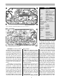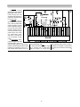
1
EFY
2000
&
PROJECTS
00
VOLUME
More than 90 fully tested
and ready-to-use
electronics circuits
IDEAS
2000
Electronics For You
issues
C o n t e n t s
JANUARY 2000
2000
CONSTRUCTION PROJECTS
1) MICROPROCESSOR-CONTROLLED TRANSISTOR LEAD IDENTIFIER --------------------------------------------- 1
2) CONVERSION OF AUDIO CD PLAYER TO VIDEO CD PLAYER I ----------------------------------------------- 9
CIRCUIT IDEAS
1) MULTIPURPOSE CIRCUIT FOR TELEPHONES ------------------------------------------------------------------------- 13
2) SIMPLE CODE LOCK -------------------------------------------------------------------------------------------------------- 13
3) AUTOMATIC BATHROOM LIGHT ---------------------------------------------------------------------------------------- 14
4) SMART FLUID LEVEL INDICATOR --------------------------------------------------------------------------------------- 15
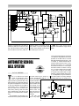
5) AUTOMATIC SCHOOL BELL SYSTEM ---------------------------------------------------------------------------------- 16
6) DESIGNING AN RF PROBE ------------------------------------------------------------------------------------------------ 18
FEBRUARY 2000
CONSTRUCTION PROJECTS
1) PC BASED SPEED MONITORING SYSTEM ---------------------------------------------------------------------------- 19
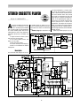
2) STEREO CASSETTE PLAYER ----------------------------------------------------------------------------------------------- 24
CIRCUIT IDEAS
1) BASS AND TREBLE FOR STEREO SYSTEM ---------------------------------------------------------------------------- 29
2) PROTECTION FOR YOUR ELECTRICAL APPLIANCES ---------------------------------------------------------------- 29
3) DIGITAL WATER LEVEL METER ------------------------------------------------------------------------------------------ 30
4) UNIVERSAL HIGH-RESISTANCE VOLTMETER ------------------------------------------------------------------------- 31
5) TRIAC/TRANSISTOR CHECKER ------------------------------------------------------------------------------------------- 32
6) A NOVEL METHOD OF FREQUENCY VARIATION USING 555 --------------------------------------------------- 33
MARCH 2000
CONSTRUCTION PROJECTS
1) RESONANCE TYPE L-C METER ------------------------------------------------------------------------------------------- 34
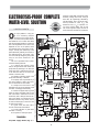
2) ELECTROLYSIS-PROOF COMPLETE WATER-LEVEL SOLUTION --------------------------------------------------- 38
CIRCUIT IDEAS
1) PENDULUM DISPLAY ------------------------------------------------------------------------------------------------------- 42
2) AUDIO LEVEL INDICATOR ------------------------------------------------------------------------------------------------ 42
3) CLEVER RAIN-ALARM ------------------------------------------------------------------------------------------------------ 44
4) LASER CONTROLLED ON/OFF SWITCH -------------------------------------------------------------------------------- 45
5) TELEPHONE CONVERSATION RECORDER ---------------------------------------------------------------------------- 45
6) SIMPLE AND ECONOMIC SINGLE- PHASING PREVENTOR ------------------------------------------------------- 46
APRIL 2000
CONSTRUCTION PROJECTS
1) SMART CLAP SWITCH ----------------------------------------------------------------------------------------------------- 48
2) ELECTRONIC VOTING MACHINE ---------------------------------------------------------------------------------------- 51
CIRCUIT IDEAS
1) WATER-TANK LEVEL METER --------------------------------------------------------------------------------------------- 57
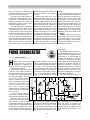
2) PHONE BROADCASTER ---------------------------------------------------------------------------------------------------- 58
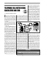
3) TELEPHONE CALL METER USING CALCULATOR AND COB ------------------------------------------------------ 59
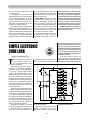
4) SIMPLE ELECTRONIC CODE LOCK -------------------------------------------------------------------------------------- 60
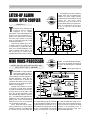
5) LATCH-UP ALARM USING OPTO-COUPLER -------------------------------------------------------------------------- 61
6) MINI VOICE-PROCESSOR ------------------------------------------------------------------------------------------------- 61
C o n t e n t s
MAY 2000
2000
CONSTRUCTION PROJECTS
1) DIGITAL NUMBER SHOOTING GAME --------------------------------------------------------------------------------- 63
2) PC INTERFACED AUDIO PLAYBACK DEVICE: M-PLAYER ---------------------------------------------------------- 66
CIRCUIT IDEAS
1) STEPPER MOTOR DRIVER ------------------------------------------------------------------------------------------------- 73
2) ELECTRONIC DIGITAL TACHOMETER ---------------------------------------------------------------------------------- 74
3) LIGHT-OPERATED LIGHT SWITCH --------------------------------------------------------------------------------------- 75
4) PRECISION DIGITAL AC POWER CONTROLLER ---------------------------------------------------------------------- 76
5) LUGGAGE SECURITY SYSTEM ------------------------------------------------------------------------------------------- 77
JUNE 2000
CONSTRUCTION PROJECTS
1) PORTABLE OZONE GENERATOR ---------------------------------------------------------------------------------------- 78
2) CONFERENCE TIMER ------------------------------------------------------------------------------------------------------- 84
CIRCUIT IDEAS
1) ADD-ON STEREO CHANNEL SELECTOR ------------------------------------------------------------------------------- 87
2) WATER TEMPERATURE CONTROLLER --------------------------------------------------------------------------------- 88
3) EMERGENCY LIGHT -------------------------------------------------------------------------------------------------------- 89
4) PARALLEL TELEPHONES WITH SECRECY ------------------------------------------------------------------------------ 90
5) TWO-DOOR DOORBELL --------------------------------------------------------------------------------------------------- 91
6) POWERFUL PEST REPELLER ---------------------------------------------------------------------------------------------- 91
JULY 2000
CONSTRUCTION PROJECTS
1) BUILD YOUR OWN C-BAND SATELLITE TV-RECEIVER ------------------------------------------------------------- 92
2) EPROM-BASED PROGRAMMABLE NUMBER LOCK ---------------------------------------------------------------- 99
CIRCUIT IDEAS
1) POWER-SUPPLY FAILURE ALARM ------------------------------------------------------------------------------------- 102
2) STOPWATCH USING COB AND CALCULATOR --------------------------------------------------------------------- 102
3) DIAL A VOLTAGE ---------------------------------------------------------------------------------------------------------- 103
4) ELECTRONIC DANCING PEACOCK ------------------------------------------------------------------------------------ 104
5) INVERTER OVERLOAD PROTECTOR WITH DELAYED AUTO RESET ------------------------------------------- 105
6) TELEPHONE LINE BASED AUDIO MUTING AND LIGHT-ON CIRCUIT ---------------------------------------- 106
AUGUST 2000
CONSTRUCTION PROJECTS
1) DISPLAY SCHEMES FOR INDIAN LANGUAGESPART I (Hardware and Software) -------------------- 108
2) 8085 µP-KIT BASED SIMPLE IC TESTER ----------------------------------------------------------------------------- 115
CIRCUIT IDEAS
1) LOW COST PCO BILLING METER ------------------------------------------------------------------------------------- 119
2) AUTOMATIC MUTING CIRCUIT FOR AUDIO SYSTEMS ---------------------------------------------------------- 120
3) 2-LINE INTERCOM-CUM-TELEPHONE LINE CHANGEOVER CIRCUIT ----------------------------------------- 120
4) GUARD FOR REFRIGERATORS AND AIR-CONDITIONERS ------------------------------------------------------- 121
5) RADIO BAND POSITION DISPLAY ------------------------------------------------------------------------------------- 122
C o n t e n t s
SEPTEMBER 2000
2000
CONSTRUCTION PROJECTS
1) DISPLAY SCHEMES FOR INDIAN LANGUAGESPART II (Hardware and Software) -------------------- 123
2) DIGITAL CODE LOCK ----------------------------------------------------------------------------------------------------- 133
CIRCUIT IDEAS
1) BINARY TO DOTMATRIX DISPLAY DECODER/DRIVER ----------------------------------------------------------- 137
2) AUTOMATIC SPEED-CONTROLLER FOR FANS AND COOLERS ------------------------------------------------ 139
3) BLOWN FUSE INDICATOR ---------------------------------------------------------------------------------------------- 140
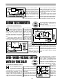
4) OVER-/UNDER-VOLTAGE CUT-OFF WITH ON-TIME DELAY ----------------------------------------------------- 140
5) ONE BUTTON FOR STEP, RUN, AND HALT COMMANDS ------------------------------------------------------- 142
OCTOBER 2000
CONSTRUCTION PROJECTS
1) MOSFET-BASED 50Hz SINEWAVE UPS-CUM-EPS ---------------------------------------------------------------- 143
2) R-2R D/A CONVERTER-BASED FUNCTION GENERATOR USING PIC16C84 MICROCONTROLLER ---- 150
CIRCUIT IDEAS
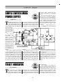
1) SIMPLE SWITCH MODE POWER SUPPLY --------------------------------------------------------------------------- 155
2) TOILET INDICATOR ------------------------------------------------------------------------------------------------------- 155
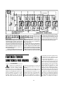
3) FEATHER-TOUCH SWITCHES FOR MAINS -------------------------------------------------------------------------- 156
4) DIGITAL FAN REGULATOR ---------------------------------------------------------------------------------------------- 157
5) TELEPHONE RINGER USING TIMER ICS ----------------------------------------------------------------------------- 159
NOVEMBER 2000
CONSTRUCTION PROJECTS
1) PC-TO-PC COMMUNICATION USING INFRARED/LASER BEAM ----------------------------------------------- 160
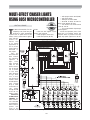
2) MULTI-EFFECT CHASER LIGHTS USING 8051 MICROCONTROLLER ----------------------------------------- 166
CIRCUIT IDEAS
1) AUTOMATIC BATTERY CHARGER ------------------------------------------------------------------------------------- 170
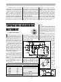
2) TEMPERATURE MEASUREMENT INSTRUMENT ------------------------------------------------------------------- 171
3) VOICE BELL ----------------------------------------------------------------------------------------------------------------- 172
4) MOVING CURTAIN DISPLAY ------------------------------------------------------------------------------------------- 173
5) PROXIMITY DETECTOR -------------------------------------------------------------------------------------------------- 174
DECEMBER 2000
CONSTRUCTION PROJECTS
1) ELECTRONIC BELL SYSTEM --------------------------------------------------------------------------------------------- 175
2) SIMPLE TELEPHONE RECORDING/ANSWERING MACHINE ---------------------------------------------------- 179
CIRCUIT IDEAS
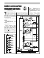
1) MULTICHANNEL CONTROL USING SOFT SWITCHES ------------------------------------------------------------ 183
2) AN EXCLUSIVE SINEWAVE GENERATOR ---------------------------------------------------------------------------- 184
3) TTL THREE-STATE LOGIC PROBE -------------------------------------------------------------------------------------- 185
4) AM DSB TRANSMITTER FOR HAMS ---------------------------------------------------------------------------------- 185
5) GROUND CONDUCTIVITY MEASUREMENT ------------------------------------------------------------------------ 186
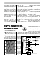
6) STEPPER MOTOR CONTROL VIA PARALLEL PORT ---------------------------------------------------------------- 187
January
2000
CONSTRUCTION
MICROPROCESSOR-CONTROLLED
TRANSISTOR LEAD IDENTIFIER
ARUP KUMAR SEN
T
ransistor lead identification is crucial in designing and servicing. A circuit designer or a serviceman must be
fully conversant with the types of transistors used in a circuit. Erroneous lead
identification may lead to malfunctions,
and, in extreme cases, even destruction
of the circuit being designed or serviced.
Though transistor manufacturers encapsulate their products in different package outlines for identification, it is impossible to memorise the outlines of innumerable transistors manufactured by
the industry. Although a number of
manuals are published, which provide pin
details, they may not always be accessible. Besides, it is not always easy to
find out the details of a desired transistor by going through the voluminous
manuals. But, a handy gadget, called transistor lead identifier, makes the job easy.
All one has to do is place the transistor
in the gadget’s socket to instantly get the
desired information on its display, irrespective of the type and package-outline
of the device under test.
A manually controlled version of the
present project had been published in June
’84 issue of EFY. The present model is totally microprocessor controlled, and hence
all manually controlled steps are replaced
by software commands. A special circuit,
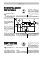
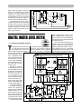
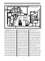
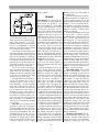
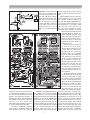
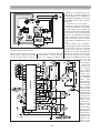
shown in Fig. 1, which acts as an interface
to an 8085-based microprocessor kit, has
been developed for the purpose.
Principle
Base and type identification. When a
semiconductor junction is forward-biased,
conventional current flows from the source
into the p-layer and comes out of the junction through the n-layer. By applying
proper logic voltages, the base-emitter (BE) or base-collector (B-C) junction of a bipolar transistor may be forward-biased.
As a result, if the device is of npn type,
RUPANJANA
current enters only through the base. But,
in case of a pnp device, current flows
through the collector as well as the emitter leads.
During testing, when leads of the
‘transistor under test’ are connected to
terminals 1, 2, and 3 of the test socket
(see Fig.1), each of the leads (collector,
base, and emitter) comes in series with
one of the current directions indicating
LEDs (D2, D4, and D6) as shown in Fig. 1.
Whenever the current flows toward a particular junction through a particular lead,
the LED connected (in proper direction) to
that lead glows up. So, in case of an npndevice, only the LED connected to the base
lead glows. However, in case of a pnpdevice, the other two LEDs are lit. Now, if
generated with Table I, a microprocessor
can easily indicate the type (npn or pnp)
and the base of the device under test,
with respect to the test socket terminals
marked as 1, 2, and 3. The logic numbers, comprising logic 1 (+5V) and logic 0
(0V), applied to generate the base-Id, are
three bit numbers—100, 010, and 001. These
numbers are applied sequentially to the
leads through the testing socket.
Collector identification. When the
base-emitter junction of a transistor is forward-biased and its base-collector junction
is reverse-biased, conventional current
flows in the collector-emitter/emitter-collector path (referred to as C-E path in subsequent text), the magnitude of which depends upon the magnitude of the base current and the beta (current amplification
factor in common-emitter configuration) of
the transistor. Now, if the transistor is biased as above, but with the collector and
emitter leads interchanged, a current of
much reduced strength would still flow in
the C-E path. So, by comparing these two
currents, the collector lead can be easily
identified. In practice, we can apply proper
binary numbers (as in case of the base identification step mentioned earlier) to the ‘device under test’ to bias the junctions sequentially, in both of the aforesaid condi-
TABLE I
Orientation Test socket Test socket Test socket Base-Id Base-Id
No.
terminal 3 terminal 2
terminal 1 for npn for pnp
1
C
B
E
02
05
2
C
E
B
01
06
3
E
C
B
01
06
4
E
B
C
02
05
5
B
E
C
04
03
6
B
C
E
04
03
B=Base C=Collector E=Emitter Note: All bits of higher nibble are set to zero.
a glowing LED corresponds to binary 1, an
LED that is off would correspond to binary
0. Thus, depending upon the orientation
of the transistor leads in the test socket,
we would get one of the six hexadecimal
numbers (taking LED connected to terminal 1 as LSB), if we consider all higher
bits of the byte to be zero. The hexadecimal numbers thus generated for an npn
and pnp transistor for all possible orientations (six) are shown under columns 5
and 6 of Table I. Column 5 reflects the
BCD weight of B (base) position while column 6 represents 7’s complement of the
column 5 number.
We may call this 8-bit hexadecimal
number base identification number or, in
short, base-Id. Comparing the base-Id,
6
Collector-Id for
pnp and npn
04
04
02
01
01
02
TABLE II
Q2 (MSB)
0
0
1
Q1
0
1
0
Q0 (LSB)
1
0
0
—
Q2
0
0
1
TABLE III. SET 1
—
Q1
0
1
0
—
Q0
1
0
0
—
Q2
1
1
0
TABLE IV. SET 2
—
Q1
1
0
1
—
Q0
0
1
1
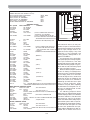
Fig. 1: Schematic circuit diagram of the transistor lead identifier
CONSTRUCTION
tions. As a result, the LEDs connected to the collector and emitter leads start flickering alternately with different brightness. By inserting a resistor in
series with the base, the LED
glowing with lower brightness
can be extinguished.
In the case of an NPN device (under normal biasing
condition), conventional current flows from source to the
collector layer. Hence, the LED
connected to the collector only
would flicker brighter, if a
proper resistor is inserted in
series with the base. On the
other hand, in case of a pnp
device (under normal biasing
condition), current flows from
source to the emitter layer. So,
only the LED connected to the
emitter lead would glow
brighter. As the type of device
is already known by the baseId logic, the collector lead can
be easily identified. Thus, for
a particular base-Id, position
of the collector would be indicated by one of the two numbers (we may call it collectorId) as shown in column 7 of
Table I.
Error processing. During collector identification for
a pnp- or an npn-device, if the
junction voltage drop is low
(viz, for germanium transistors), one of the two currents
in the C - E path (explained
above) cannot be reduced adequately and hence, the data
may contain two logic-1s. On
the other hand, if the device
beta is too low (viz, for power
transistors), no appreciable
current flows in the C-E path,
and so the data may not contain any logic-1. In both the
cases, lead configuration cannot be established. The remedy is to adjust the value of
the resistor in series with the
base. There are three resistors
(10k, 47k, and 100k) to choose
from. These resistors are connected in series with the testing terminals 1, 2, and 3 respectively. The user has to rotate the transistor, orienting
7
CONSTRUCTION
nected to inputs of IC 3
(7486, quad 2input EX - OR
gate). Gates
of IC3 are so
wired that
they function
as controlled
EX - OR gates.
The outputs
o f IC 3 are
controlled by
the logic level
at pin 12.
Thus, we obFig. 2: Effective biasing of PNP transistors using set 1 binary numbers
tain two sets
of outputs
(marked Q 0,
Q 1 , and Q 2 )
from IC 3 as
given
in
Tables III
(for pin 12 at
logic 1) and
IV (for pin 12
at logic 0) respectively.
One of
these two
sets would be
chosen for
the output by
the software,
by controlling the logiFig. 3: Effective biasing of NPN transistors using set 2 binary numbers
cal state of
the base in different terminals (1, 2, or 3) pin 12. Set-1 is used to identify the base
on the socket, until the desired results are and type (npn or pnp) of the ‘transistor
obtained. To alert the user about this ac- under test,’ whereas set-2 is exclusively
tion, a message ‘Adjust LED’ blinks on the used for identification of the collector lead,
display (refer error processing routine in if the device is of npn type.
the software program).
The interface. The three data output lines, carrying the stated binary numbers (coming from pins 3, 6, and 8 of IC3),
The circuit
are connected separately to three bi-diThe binary number generator. In this rectional analogue switches SW1, SW2, and
section, IC1 (an NE555 timer) is used as a SW3 inside IC5 (CD4066). The other sides of
clock pulse generator, oscillating at about the switches are connected to the termi45 Hz. The output of IC1 is applied to clock nals of the test socket through some other
pin 14 of IC2 (4017-decade counter). As a components shown in Fig. 1. The control
result, the counter advances sequentially line of IC3 (pin 12) is connected to the
from decimal 0 to 3, raising outputs Q0, Q1, analogue switch SW4 via pin 3 of IC5. The
and Q2 to logic-1 level. On reaching the other side of SW4 (pin 4) is grounded. If
next count, pin 7 (output Q3) goes high and switch SW4 is closed by the software,
it resets the counter. So, the three outputs set-1 binary numbers are applied to the
(Q0, Q1, and Q2) jointly produce three binary
device under test, and when it is open,
numbers, continuously, in a sequential set-2 binary numbers are applied.
manner (see Table II).
To clearly understand the functionQ0 through Q2 outputs of IC2 are coning of the circuit, let us assume that the
8
‘transistor under test’ is inserted with its
collector in slot-3, the base in slot-2, and
the emitter in slot-1 of the testing socket.
Initially, during identification of the
base and type of the device, all the analogue switches, except SW4, are closed by
the software, applying set-1 binary numbers to the device. Now, if the device is of
pnp type, each time the binary number
100 is generated at the output of IC3, the
BC junction is forward-biased, and hence,
a conventional current flows through the
junction as follows:
Q2 (logic 1)àSW3àR9àinternal LED of
IC 4àslot3àcollector leadà CB junction
à base leadà slot-2à D3à pin 10 of
IC5àSW2àQ1 (logic 0).
Similarly, when the binary number 001
is generated, another current would flow
through the BE junction and the internal
LED of IC7. The number 010 has no effect,
as in this case both the BC and BE junctions become reversed biased.
From the above discussion it is apparent that in the present situation, as
the internal LEDS of IC4 and that of IC7 are
forward-biased, they would go on producing pulsating optical signals, which would
be converted into electrical voltages by
the respective internal photo-transistors.
The amplified pulsating DC voltages are
available across their emitter resistors R7
and R17 respectively. The emitter followers configured around transistors T1 and
T3 raise the power level of the optocoupler’s output, while capacitors C3 and
C5 minimise the ripple levels in the outputs of emitter followers.
During initialisation, 8155 is configured
with port A as an input and ports B and C
as output by sending control word 0E(H)
to its control register.
Taking output of transistor T1 as
MSB(D2), and that of T3 as LSB(D0), the data
that is formed during the base identification, is 101 (binary). The microprocessor
under the software control, receives this
data through port A of 8155 PPI (port number 81). Since all the bits of the higher
nibble are masked by the software, the
data become 0000 0101=05(H). This data is
stored at location 216A in memory and
termed in the software as base-Id.
Now, if the device is of npn type, the
only binary number that would be effective is 010. Under the influence of this
number both BC and BE junctions would
be forward-biased simultaneously, and
hence conventional current would flow in
the following two paths:
CONSTRUCTION
(logic 1)à SW2à R14àinternal
leadàBC junction
àcollector leadàslot-3à D1à SW3à Q2
(logic 0)
2. Q1 (logic 1)à SW2à R14àinternal
LED (IC6)àslot-2àbase leadàBE junction
à emitter leadà slot 1à D5à SW1à Q0
(logic 0)
Thus, only the internal LED of IC6
would start flickering, and the data that
would be formed at the emitters of the
transistors is also 010. Accordingly, the
base-Id that would be developed in this
case is 0000 0010=2(H).
Since, under the same orientation of
the transistor in the socket, the base-Ids
are different for a pnp and an npn device,
the software can decode the type of the
device.
In a similar way we can justify the
production of the other base-Ids, when
their collector, base, and emitter are inserted in the testing socket differently.
Once the base-Id is determined, the
software sends the same number for a
pnp-device (here=05(H)) through port C
(port number 83), with the bit format
shown in Table V.
As a result, the control input of SW2
(pin 12 of IC5) gets logic 0. So the switch
opens to insert resistor R5 in series with
the base circuit. This action is necessary to identify the emitter (and hence
the collector) lead as described earlier
under ‘Principle’ sub-heading.
On the contrary, since an npn-de1.
LT543
Fig. 4: Schematic circuit of special display system
(i)
Q1
LED (IC6)àslot-2àbase
(ii)
(iii)
Fig. 5: Flowcharts for the main program and various subroutines
9
CONSTRUCTION
Fig. 5 (iv)
DISPLAY ROUTINE USING ALTERNATIVE CIRCUIT OF FIG. 4
TABLE V
PC7
0
PC6
0
PC5
0
PC4
0
PC7
0
PC6
0
PC5
0
PC4
0
PC3
0
PC2
1
PC1
0
PC0
1
PC2
1
PC1
0
PC0
1
TABLE VI
PC3
1
vice uses the set-2 binary numbers for
identification of the collector (hence the
emitter), the same number (base-Id) obtained during base identification cannot
be sent through port C, if the device under test is of npn type. The base-Id found
must be EX-ORed first with OF (H). Since
the base-Id found here is 02 (H), the data
to be sent through port C in this case
would be as shown in Table VI.
Note that PC3 becomes logic-1, which
would close switch SW4 to get the set-2
binary numbers.
Once resistor R5 is inserted in the base
circuit, and set-1 binary numbers are applied to the device (pnp type), it would be
biased sequentially in three distinct ways,
of which only two would be effective. The
same are shown in Fig. 2.
In case of binary number 100, the current through the internal LED of IC4 would
distinctly be very low compared to the
current flowing during number 001 ,
through the internal LED of IC7. If R5 is of
sufficiently high value, the former current may be reduced to such an extent
that the related LED would be off. Hence,
the data that would be formed at the emit-
ters of transistors T 1- T 3
would be 001. It would be
modified by the software to
0000 0001=01(H) . This is
termed in the software as
emitter-Id and is stored at
memory location 216B.
On the other hand, if
the device is of npn type,
set-2 binary numbers are
to be applied to it, and the
transistor would be biased
as shown in Fig. 3. Here,
only the internal LED of IC4
would flicker. So, the data
at the output would be
100=04(H). This is termed in
the software as collector-Id,
and is stored in memory lo- Fig. 5 (v)
cation 216C. (In case of pnpdevice, the collector-Id is determined
mathematically by subtracting the BaseId from the emitter-Id.)
So the result could be summarised as:
pnp type:
Base-Id = 05(H), Collector-Id = 01(H).
npn type:
Base-Id = 02(H), Collector-Id = 01(H).
10
With this result, the software would
point to configuration CBE in the data
table, and print the same on the display.
By a similar analysis, lead configuration
for any other orientation of the device in
the test socket would be displayed by the
software, after finding the related baseand collector-Id.
CONSTRUCTION
PARTS LIST
Semiconductors:
IC1
- NE555, timer
IC3
- CD4017, decade counter-decoder
IC3
- 7486, quad EX-OR gates
IC4,IC6,IC7
- MCT2E, optocoupler
IC5
- CD4066, quad bilateral switch
IC8
- LM7805, 3-terminal +5V
regulator
T1,T2,T3
- BC147, npn transistor
D1,D3,D5
- 1N34, point contact diode
D2,D4,D6
- LED, 5mm
D7,D8
- 1N4002, rectifier diode
Resistors (All ¼ watt +/- 5% metal/carbon film
unless stated otherwise)
R1,R9,R10,R14,
R15,R19,R20
- 1 kilo-ohm
R2
- 33 kilo-ohm
R5
- 47 kilo-ohm
R4,R11,R16,R21 - 10 kilo-ohm
R3,R6,R7,R12,R17 - 100 kilo-ohm
R8,R13,R18
- 680 ohm
Capacitors:
C1
- 0.5µF polyster
C2
- 0.1µF polyster
C3-C5
- 220µF/12V electrolytic
C6
- 0.22µF polyster
C7
- 1000µF/12V electrolytic
Miscellaneous:
X1
- 230V/9V-0-9V, 250mA power
transformer
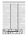
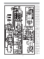
Fig. 6: Actual-size, single-sided PCB layout for the circuit in Fig. 1
Fig. 7: Component layout for the PCB
The Display. The display procedure
described in this article is based on IC
8279 (programmable keyboard/display interface) which is used in the microprocessor kit. The unique feature of the 8279based display system is that, it can run
on its own. You just have to dump the
data to be displayed on its internal RAM,
and your duty is over. 8279 extracts this
data from its RAM and goes on displaying
the same without taking any help or consuming the time of the microprocessor in
the kit.
Unfortunately, not all the microprocessor kits present in the market are fitted with this IC. Instead, some of them
use a soft-scan method for display purpose. Hence, the stated procedure cannot
be run in those kits. Of course, if the
monitor program of the kit is to be used,
which may have an in-built display routine to display the content of four specific memory locations—all at a time, the
same may be used in place of the present
display procedure.
Note: Display subroutine at address
20FC used at EFY, making use of the monitor program of the Vinytics 8085 kit, during program testing, is listed towards the
end of the software program given by the
author. To make use of the author’s display subroutine, please change the code
against ‘CALL DISPLAY’ instruction (code
CDFC 20) everywhere in the program to
code CD 40 21 for 8279 based display or
code CD 07 21 for alternate display referred
in the next paragraph.
Alternatively, one can construct a special display system using four octal Dtype latches (74373) and four seven-segment LED displays (LT543). Only one latch
and one display has been shown in the
schematic circuit of Fig. 4 along with its
interface lines from 8155 or 8255 of the
kit. To drive this display, a special softscan method explained in the following
para has to be used.
The soft scan display procedure.
11
The procedure extracts the first data to
be displayed from memory. The start
memory address of the data to be displayed is to be supplied by the calling
program. This data (8-bit) is output from
port B of 8155/8255 PPI (after proper coding
for driving the seven-segment displays),
used in the kit. Data lines are connected
in parallel to all the octal latches. But
only one of the four latches is enabled
(via a specific data bit of port C of 8155/
8255) to receive the data and transfer the
same to its output to drive the corresponding seven-segment LED display. To enable
a particular latch, a logic 1 is sent through
a particular bit of port C (bit 4 here, for
the first data) by the software. Subsequently, logic 0 is sent through that bit
to latch the data transferred. The program then jumps to seek the second data
from memory, and sends the same
through port B as before. However, in this
case logic 1 is sent through bit 3 of port
C, to latch the data to the second sevensegment LED display, and so on.
Register B of 8085 is used as a counter,
and is initially stored with the binary
number 00001000 (08H). Each time a data is
latched, the logic 1 is shifted right by one
place. So, after the fourth data is latched,
the reg. B content would be 0000 0001. Shift-
CONSTRUCTION
Memory Map And Software listing in 8085 Assembly Language
RAM Locations used for program
:2000H - 21BBH
Stack pointer initialised
:2FFFH
Monitor Program
:0000H - 0FFFH
Display Data Table
:2160H - 219AH
Control/Status Register of 8155
:80H
Port A (Input) of 8155
:81H
Port B (Output) of 8155
:82H
Port C (Output) of 8155
:83H
Address Op Code Label Mnemonic
;Initialisation, base and type identification
2000
31FF2F
MAIN: LXI SP,2FFFH
2003
3E0E
MVI A,0EH
2005
D380
OUT 80H
2007
3E07
MVI A,07H
2009
D383
OUT 83H
200B
CD3320
CALL DELAY
200E
CD3320
CALL DELAY
2011
CD3320
CALL DELAY
2014
AF
XRA A
2015
DB81
IN 81H
portA
2017E607
ANI 07H
2019
326A21
STA 216AH
201C
CA2A20
JZ P
201F
EA3D20
JPE P2
CALL DISPLAY
JMP MAIN
Initialisation of the ports. A as the
input and C as the output port.
Sends 07 through port C to make SW1,
SW2, SW3 ON and SW4 OFF.
Time delay should be allowed before
measuring the logic voltages across
capacitors C1, C2, and C3, so that
they charge to the peak values.
Clears the accumulator
Input data from interface through.
Test only first 3 bits, masking others
Stores the number in memory.
If the number is zero jumps to 202A
If the number has even no. of 1s,
jumps to 203D (refer note 2)
If the number has odd no. of 1s, jump
to 2068 (refer note 1)
No operation
No operation
No operation
No operation
No operation
Points to message “PUSH” in data
table
Displays the message
Jumps to start.
LXI D,FFFFH
DCX D
MOV A,D
ORA E
JNZ 2036
RET
Loads DE with FFFF
Decrements DE
Moves result into Acc.
OR E with Acc.
If not zero, jumps to 2036
Returns to calling program
2022
E26820
JPO P3
2025
2026
2027
2028
2029
202A
00
00
00
00
00
218921
NOP
NOP
NOP
NOP
NOP
LXI H,2189H
202D
2030
CDFC20
C30020
P:
;Delay sub-routine
2033
11FFFF DELAY:
2036
1B
2037
7A
2038
B3
2039
C23620
203C
C9
Comments
;Collector identification program for PNP transistors
203D
216A21
P2:
LXI H,216AH
Points of Base-Id in data table
2040
7E
MOV A,M
Extracts the number to the
accumulator
2041
D383
OUT 83H
Send the number to the interface
2043
216021
LXI H,2160H
Points to message ‘PnP’ in data table
2046
CDFC20
CALL DISPLAY Displays the message
2049
CD3320
CALL DELAY
Waits for few moments
204C
CD3320
CALL DELAY
Waits for few moments
204F
CD3320
CALL DELAY
Waits for few moments
2052
AF
XRA A
Clears the accumulator
2053
DB81
IN 81H
Seeks data from the interface
2055
E607
ANI 07H
Masks all bits except bits 0,1 and 2
2057
EAA021
JPE ERR
If the data contains even no. of 1s
jumps to error processing routine
205A
326B21
STA 216BH
Stores the data (Emitter-Id) in memory
205D
47
MOV B,A
Moves the Emitter-Id. to B register
205E
3A6A21
LDA 216AH
Extracts Base-Id from memory
2061
90
SUB B
Subtracts Emitter-Id from Base-Id
2062
326C21
STA 216CH
Stores the result(Collector-Id)in mem.
2065
C39220
JMP P4
Jumps to select lead configuration
;Collector identification program for NPN transistors
2068
216A21
P3:
LXI H,216AH
Points to Base-Id in data table
206B
7E
MOV A,M
Extract the number to the accumulator
206C
FE07
CPI 07H
Refer note 1
206E
CAB621
JZ ER
Jumps to error processing routine
2071
EE0F
XRI 0FH
Refer note 2
2073
D383
OUT 83H
Send the number to the interface
2075
216421
LXI H,2164H
Points to the message “nPn”
2078
CDFC20
CALL DISPLAY Displays the same
207B
CD3320
CALL DELAY
Waits for few moments
207E
CD3320
CALL DELAY
Waits for few moments
2081
CD3320
CALL DELAY
Waits for few moments
2084
AF
XRA A
Clears the accumulator
2085
DB81
IN 81H
Seeks data from the interface
Address
2087
2089
208C
208F
Op Code
E607
EAA021
326C21
C39220
Label
Mnemonic
ANI 07H
JPE ERR
STA 216CH
JMP P4
;Lead configuration selection program
2092
216A21
P4:
LXI H,216AH
2095
7E
MOV A,M
2096
FE05
CPI 05H
2098
CABA20
JZ P4A
209B
FE06
CPI 06H
209D
CAD020
JZ P4B
20A0
FE03
CPI 03H
20A2
CAE620
JZ P4C
20A5
FE02
CPI 02H
20A7
CABA20
JZ P4A
20AA
FE01
CPI 01H
20AC
CAD020
JZ P4B
20AF
FE04
CPI 04H
20B1
CAE620
JZ P4C
20B4
CDFC20
M:
CALL DISPLAY
20B7
C30020
JMP MAIN
Comments
Checks only first three bits
If 2 bits are at logic-1 jumps to 21A0
Store the No. (Collector-Id)into mem.
Jumps to select lead configuration
Extracts Base-Id from memory location
216A to the accumulator
If the number is 05,
jumps to subroutine 4A
If the number is 06,
jumps to the subroutine 4B
If the number is 03,
jumps to the subroutine 4C
If the number is 02,
jumps to the subroutine 4A
If the number is 06,
jumps to the subroutine 4B
If the number is 04,
jumps to the subroutine 4C
Jumps to display the lead configuration
selected in P4A or P4B or P4C
Jumps back to start
;Lead configuration selection (Base Id.=05 or 02)
20BA
216C21
P4A:
LXI H,216CH
Extracts Collector-Id from memory
location
20BD
7E
MOV A,M
216C to the accumulator
20BE
FE01
CPI 01H
If it is = 01, jumps to 20CA
20C0
CACA20
JZ E
If it is = 04, points to lead
configuration “EbC”
20C3
217521
LXI H,2175H
in data table
20C6
C3B420
JMP M
Jumps to display the lead
configuration pointed
20C9
00
NOP
NOP
20CA
217121
E:
LXI H,2171H
Points to lead config.”CbE” and jumps
20CD
C3B420
JMP M
display the configuration
;Lead configuration selection (Base Id.= 06 or 01)
20D0
216C21
P4B:
LXI H,216CH
Extracts Collector-Id from memory
location
20D3
7E
MOV A,M
216C to the accumulator
20D4
FE02
CPI 02H
If it is STE02, jumps to 20E0
20D6
CAE020
JZ B I
If it is =04, points to lead
20D9
217D21
LXI H,217DH
configuration “bEC” in data table
20DC
C3B420
JMP M
Jumps to display the lead
configuration pointed
20DF
00
NOP
No oPeration
20E0
217921
B:
LXI H,2179H
Points to lead configuration “bCE”
20E3
C3B420
JMP M
and jumps display the configuration
;Lead configuration selection (Base Id.=03 or 04)
20E6
216C21
P4C:
LXI H,216CH
Extracts Collector-Id from memory
location
20E9
7E
MOV A,M
216C to the accumulator
20EA
FE01
CPI 01H
If it is =01, jumps to 20F6
20EC
CAF620
JZ C
If it is =02, points to lead
20EF
218121
LXI H,2181H
configuration “ECb” in data table
20F2
C3B420
JMP M
Jumps to display the lead
20F5
00
NOP
configuration pointed; no operation
20F6
218521
C:
LXI H,2185H
Points to lead configuration “CEb”
20F9
C3B420
JMP M
and jumps to display the configuration
;Display routine using 8279 of the kit (if present)
2140
0E04
MVI C,03
Sets the counter to count 4 characters
2142
3E90
MVI A,90
Sets cont.8279 to auto-incr. mode
2144
320160
STA 6001
Address of 8279 cont. reg.=6001
2147
7E
MOV A,M
Moves 1st data character from mem.
Loc. pointed to by calling instruction.
2148
2F
CMA
Inverts data (refer note below)
2149
320060
STA,6000
Stores data in 8279 data reg.
(addr=6000)
214C
0D
DCR C
Decrements counter
214D
CA5421
JZ 2154
Returns to calling program if count=0
2150
23
INX H
Increments memory pointer
2151
C34721
JMP2147
Jumps to get next character from
memory
2154
C9
RET
Returns to the calling program
Note: In the microprocessor kit used, data is inverted before feeding the 7-seg display.
;Alternative Display Subroutine to be used with interface circuit of Fig. 4
2107
0608
MVI B,08H
Store 0000 1000 in reg.B
2109
3E00
MVI A,00H
Out 00H through Port C to latch data
in all
12
CONSTRUCTION
Address Op Code
210B
D383
210D
7E
Label
Mnemonic
OUT 83H
MOV A,M
210E
2110
D382
78
OUT 82H
MOV A,B
2111
2113
D383
1F
OUT 83H
RAR
2114
FE00
CPI 00H
2116
CA2121
JZ 2121H
2119
47
MOV B,A
211A
211D
211E
CD3320
23
C30921
CALL DELAY
INX H
JMP 2109H
2121
C9
RET
;Error Sub-routine
21A0
219121
21A3
CDFC20
21A6
21A9
21AC
CD3320
CD3320
219621
21AF
21B2
21B5
21B6
CDFC20
C30020
00
218D21
21B9
C3AF21
Data table:
Addr.
Data
2160
37
2161
45
2162
37
2163
00
ERR:
LXI H,2191H
CALL DISPLAY
CALL DELAY
CALL DELAY
LXI H,2196H
BAD:
ER:
CALL DISPLAY
JMP MAIN
NOP
LXI H,218DH
JMP BAD
Display
P
n
P
Addr.
2179
217A
217B
217C
Data
C7
93
97
00
Comments
74373s. (no data would move to O/Ps)
Moves the 1st char. Of the data
pointed, to the accumulator (mem.
address given by
calling program)
By moving out reg.B data throgh port
C
a specific latch is enabled.
Logic 1 of counter data moves right 1
bit
Checks to see logic 1 moves out from
acc.
(All 4 data digits latched)to return to
the calling program.
Else stores back new counter data to B
reg.
Memory pointer incremented by 1
Jumps to the next character from the
table
Returns to the calling program
Points to the message “Adj.” in memory
Calls the display routine to display the
same
Waits
Waits
Points to the message “LEAd” in
memory
Calls the display routine to display
Jumps back to start
No operation
Points to message “bAd” in the data
table
Jumps to display the message
Display
b
C
E
Addr.
2189
218A
218B
218C
Data
37
E3
D6
67
Display
P
U
S
H
Addr.
2164
2165
2166
2167
216A
216B
216C
2171
2172
2173
2174
2175
2176
2177
2178
Data
Display
45
n
37
P
45
n
00
Base-id (store)
Emitter-id (store)
Collector-id (store)
93
C
C7
b
97
E
00
97
E
C7
b
93
C
00
Address of routines/labels:
MAIN
2000
P
P2
203D
P3
P4A
20BA
E
P4C
20E6
C
BAD
21AF
ER
Op Code
216021
CDFC20
216A21
7E
D383
Label
P2:
Mnemonic
LXI H,2160H
CALL DISPLAY
LXI H,216AH
MOV A,M
OUT 83H
Op Code
216421
CDFC20
216A21
7E
FE07
CAB621
EE0F
D383
Label
P3:
Mnemonic
LXI H,2164H
CALL DISPLAY
LXI H,216AH
MOV A,M
CPI 07H
JZ ER
XRI 0FH
OUT 83H
ing operation is done after first moving
the data from the register to the accumulator, and then storing the result back
into the register once again if the zero
flag is not set by the RAR operation.
Display
b
E
C
E
C
b
C
E
b
DELAY
P4
P4B
DISPLAY
Addr.
218D
218E
218F
2190
2191
2192
2193
2194
2196
2197
2198
2199
219A
2033
2092
20D0
20FC
Data
C7
77
E5
00
7
E5
E1
00
83
97
77
E5
00
D
M
B
ERR
Display
b
A
d
a
d
J
L
E
A
D
2036
20B4
20E0
21A0
;Display subroutine used by EFY using monitor program of Vinytics kit.
20FC
C5
DISPLAY: PUSH B
20FD
3E00
MVI A,0H
20FF
0600
MVI B,0H
2101
7E
MOV A,M
2102
CDD005
CALL 05D0H
2105
C1
POP B
2106
C9
RET
Comments
Points to message ‘PnP’in data table
Displays the message
Points to Base-Id in data table
Extract the number to the accumulator
Send number via port C to interface
TABLE VIII
; Modification to Collector Identification Program for npn Transistors
Address
2068
206B
206E
2071
2072
2074
2077
2079
202A
2068
20CA
20F6
21B6
Data
C7
97
93
00
97
93
C7
00
93
97
C7
00
Notes:
1. During Base identification, if the data found has odd parity, only then the program
jumps to this routine (starting at 2068 at P3:) for collector identification. A single logic-1
denotes a good transistor, whereas three logic-1 (i.e. Base-Id = 07) denote a bad transistor
with shorted leads. Hence the program jumps to error processing routine to display the
message “bAd”.
2. The purpose of sending the Base-Id number to the interface through Port-C, is to
insert a resistor in series with the Base (as indicated in the principle above). The logic-1(s) of
the Base-Id, set the switches connected with the collector and emitter leads to “ON”, and that
with the base to “OFF”. The result is, the resistor already present in the base circuit (10K,
47K or 100K which one is applicable), becomes active. To achieve this result, the Base-Id
found for an NPN device is to be inverted first.
TABLE VII
; Modification to Collector Identification Program for pnp Transistors
Address
203D
2040
2043
2046
2047
Addr.
217D
217E
217F
2180
2181
2182
2183
2184
2185
2186
2187
2188
Comments
Points to the message ‘nPn’
Displays the same on display.
Points to Base-Id in DATA table
Extract the number to the accumulator
Refer note.1 (see original program.)
Jumps to error processing routine
Refer note.2 (see original program.)
Send number to interface (via port C)
Now, with the reg. B content = 0000 0001,
one more shifting of the bits towards right
would make the accumulator content =
0000 0000 , which would set the zero
flag. And hence the program would jump
13
back to the calling one. It would be interesting to note the same reg. B content (a
binary number comprising a logic 1) is
sent through port C to enable the particular latch.
Since the base Id numbers and the
code to enable a specific latch are sent
through the same port (port C) in the
alternate display, the base Id must be
sent first for displaying the message PnP/
nPn. Therefore changes or modifications
are required in the original program pertaining to collector identification program
for pnp transistors (at locations 203D
through 2048) and npn transistors (at locations 2068 through 207A) as given in
Tables VII and VIII respectively.
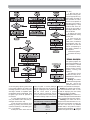
Software flow charts. Software flow
charts for main program and various subroutines are shown in Fig. 5.
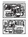
PCB and parts list are included only
for the main interface diagram of Fig. 1.
The actual-size, single-sided PCB for the
same is given in Fig. 6 while its compo❏
nent layout is shown in Fig. 7.
CONSTRUCTION
CONVERSION OF AUDIO CD PLAYER
TO VIDEO CD PLAYER I
G.S. SAGOO
PUNERJOT SINGH MANGAT
T
he analogue technology is giving
way to the digital technology as
the latter offers numerous advantages. Digital signals are not only free
from distortion while being routed from
one point to another (over various media), but error-correction is also possible.
Digital signals can also be compressed
which makes it possible to store huge
amounts of data in a small space. The
digital technology has also made remarkable progress in the field of audio and
video signal processing.
Digital signal processing is being
widely used in audio and video CDs and CD
playing equipment. These compact disks
have brought about a revolution in the
field of audio and the video technology. In
audio CDs, analogue signals are first converted into digital signals and then stored
on the CD. During reproduction, the digi-
tal data, read from the CD, is reconverted
into analogue signals. In case of video signals, the process used for recording and
reproduction of data is the same as used
for audio CDs. However, there is an additional step involved—both during recording as well as reproduction of the digital
video signals on/from the compact disk.
This additional step relates to the compression of data before recording on the
CD and its decompression while it is being
read. As video data requires very large
storage space, it is first compressed using
MPEG- (Motion Picture Expert Group) compatible software and then recorded on the
CD. On reading the compressed video data
from the CD, it is decompressed and passed
to the video processor. Thus with the help
of the compression technique huge amount
of video data (for about an hour) can be
stored in one CD.
PARTS LIST-1
Semiconductors:
IC1
- LM7805 voltage regulator +5V
Resisters (All ¼W, ±5% metal/carbon film,
unless stated otherwise):
R1
- 68 ohm
R2, R3 - 1 kilo-ohm
VR1
- 100 ohm cermet (variable resistor)
Capacitors:
C1
- 1µF paper (unipolar)
C2
- 10µF, 16V electrolytic
Miscellaneous:
X1
- 230V AC primary to 12V-0-12V, 1A sec.
transformer
S1, S2
- Push-to-on tactile switch
- MPEG decoder card (Sony Digital Tech.)
- TV modulator (optional)
- AF plugs/jacks (with screened wire)
- Co-axial connectors, male/female
- Co-axial cable
Conversion
An audio CD player, which is used to play
only audio CDs, can be converted to play
the video CDs as well. Audio CD players
have all the required mechanism/functions
to play video CDs, except an MPEG card,
which is to be added to the player. This
MPEG card is readily available in the market. This MPEG card decompresses the data
available from the audio CD player and converts it into proper level of video signals
before feeding it to the television.
Construction
Step-by-step conversion of audio CD player
to video CD player is described with reference to Fig. 1.
Step 1. Connection of MPEG card
to TV and step-down power transformer to confirm proper working of
the MPEG card.
● Connect IC7805, a 5-volt regulator, to the
MPEG card. Please check for correct pin
assignments.
● Connect audio and video outputs of the
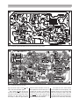
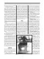
Fig. 1: Complete schematic layout and connection diagram for conversion of
Audio CD to Video CD player
14
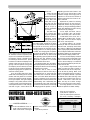
Fig 2: Photograph of TV scene
CONSTRUCTION
card to the audio/video input of TV
via jacks J7 and J11 respectively. Use
only shielded wires for these connections.
● Check to ensure that the step-down
transformer provides 12-0-12 volts at
1 ampere of load, before connecting it
to the MPEG card. Connect it to the MPEG
card via jack J1.
● Switch on the TV to audio/video mode
of operation. Adjust the 100-ohm preset connected at the video output of
MPEG card to mid position.
● Switch on the MPEG card by switching
on 230 volts main supply to the 12-012 volt transformer.
● If everything works right, ‘Sony Digital
Technology’ will be displayed on the
television. The TV screen will display
this for about 5 seconds before going
blank. Adjust the 100-ohm preset for
proper level of video signals.
Step 2. Connections to audio CD
player after confirmation of proper
functioning of MPEG card during
step1.
● Open your audio CD player. Do this very
carefully, avoiding any jerks to the audio CD player, as these may damage the
player beyond repair.
● Look for the IC number in Table II (on
page 47) that matches with any IC in
your audio CD player.
● After finding the right IC, note its RF
EF MIN pin number from the Table I.
● Follow the PCB track which leads away
MPEG
form RF EFM in pin of the IC and find
any solder joint (land) on this PCB track.
Solder a wire (maximum half meter) to
this solder joint carefully. Other end of
this wire should be joined to RF jack J2
of the MPEG card.
Caution: Unplug the soldering iron
form the mains before soldering this
wire because any leakage in the soldering iron may damage the audio CD
player.
● Another wire should be joined between
the ground of the audio CD player and
the ground of jack J2 of the MPEG card.
● This finishes the connection of the MPEG
card to the audio CD player.
Step 3. Playing audio and video CDs.
● Switch on the power for the audio CD
player and the MPEG card.
● Put a video CD in the audio CD player
and press its play button to play the
video CD.
● After a few seconds the video picture
recorded on the CD will appear on the
television.
● The play, pause, eject, rewind, forward,
track numbers, etc buttons present on
the audio CD can be used to control the
new video CD player.
Now your audio CD player is capable
of playing video CDs as well. You can connect a power amplifier to the MPEG card
to get a high-quality stereo sound. The
author tested this project on many audio
players including Thompson Diskman and
CONVERSION OF AUDIO CD PLAYER
TO VIDEO CD PLAYER II
TABLE I
POSSIBLE EXTRA FUNCTIONS
S1 (mode switch)
S2 (function switch)
Slow
Discview
Pal/NTSC
Vol+
VolKey+
KeyL/R/CH
Play/Pause
—
—
Pal NTSC
Volume Up
Volume Down
Left volume down
Right volume down
Left, Right, Mute, Stereo
—
Note: The above mentioned functions can also be accessed
using remote control.
Kenwood Diskman. A photograph of one
of the scenes in black and white is included as Fig. 2. (Please see its coloured
clipping on cover page.)
No special PCB is required and hence
the same is not included.
The author has perferred to use Sony
Digital Technology Card (against KD680 RF35C of C-Cube Technology) because of many
more functions it provides.
Additional accessibility features of this
card (Sony Digital Technology), as shown
in Table I can be invoked by adding two
push-to-on switches between jack 8(J8) and
ground via 1K resistors (Fig 1). These will
enhance the already mentioned functions
and facilities available on this card, even
though it has not been possible to exploit
the card fully due to non-availability of
technical details. I hope these additions
will help the readers get maximum mileage from their efforts.
and backward scan facility with 9-view
pictures, slow-motion play, volume and
tone control and R/L (right/left) vocal.
K.N. GHOSH
W
ant to convert your audio compact disk player into video compact disk player. Here is a
simple, economical but efficient add-on circuit design that converts your audio
CDplayer to video CD player.
Description
Decoder card. The add-on circuit is
based on VCD decoder card, KD680 RF-3Sc,
also known as MPEG card adopting MPEG1 (Motion Picture Expert Group) stan-
dard, the international standard specification for compressing the moving picture and audio, comprising a DSP (digital
signal processor) IC chip, CL860
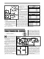
from C-cube (Fig. 3). The VCD
decoder card features small
size, high reliability, and low
power consumption (current
about 300ma) and real and gay
colours. This decoder card has
two play modes (Ver. 1.0 and
Ver. 2.0) and also the forward Fig. 3: Layout diagram of MPEG card from c-cube
15
CONSTRUCTION
DSP IC
EFM
DSP IC
/RF Pin
KS 5950
KS 5990, 5991
KS 9210 B
KS 9211 B E, 9212
KS 9282
KS 9283
KS 9284
CXD 1125 QX
CXD 1130 QZ
CXD 1135
CXD 1163 Q
CXD 1167 R
CXD 1167 Q/QE
CXD 20109
CXD 2500 AQ/BQ
CXD 2505 AQ
5
5
5
5
5, 66
66
66
5
5
5
5
36
5
9, 20
24
24
CXD 2507 AQ
14
CXD 2508 AQ
CXD 2508 AR
CXD 2509 AQ
CXD 2515 Q
CXD 2518 Q
LC 7850 K
LC 7860 N/K/E
LC 7861 N
LC 7862
LC 78620
LC 78620 E
LC 7863
LC 7865
36
36
34
36, 38
36
7
7, 8
8
30
11
11
8
8
LC 7866 E
LC 7867 E
LC 7868 E
LC 7868 K
LC 78681
MN 6617
MN 6222
MN 6625 S
MN 6626
MN 6650
MN 66240
MN 66271 RA
MN 662720
CXA 72S
CXA 1081Q
7, 8
8
8
8
8
74
11
41
3, 62
6
44
44, 52
44
18, 46
2, 27
EFM
/RF Pin
CXA 1372Q 32, 46
CXA 1471S 18, 27
CXA 1571S 18, 35
AN 8370S
12, 31
AN 8373S
9, 35
AN 8800SCE 12
AN 8802SEN 9
TDA 3308
3
LA 9200
35
LA 9200 NM 36
LA 9211 M 72
HA 1215 8 NT 46, 72
SAA 7210
3, 25
(40 pin)
SAA 7310
32
(44 pin)
SAA 7341
36, 38
SAA 7345
8
SAA 7378
15
TC 9200 AF 56
TC 9221 F
60
TC 9236 AF 51,56
TC 9284
53
YM 2201/FK 76
YM 3805
8
YM 7121 B 76
YM 7402
4, 71
HD 49215
71
HD 49233
19
AFS
UPD 6374 CU 23
UPD 6375 CU 46
M 50422 P
15
M 50427 FP 15, 17
M 504239
17
M 515679
4
M 51598 FP 20
MN 35510
43
M 65820 AF 17
M 50423 FP 17
CX 20109
20, 9
SAA7311
25
M50122P
15
M50123 FP 17
M50127 FP 17
UPD6374 CV 3
NM2210FK 76
YM2210FK 76
The decoder card converts your CD players or video games to VCD player to give
almost DVD-quality pictures.
The decoder card mainly consists of
sync signal separator, noise rejection cir-
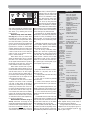
Fig. 4: Layout of TV RF modulator
put (AV in) facility in their TV, can make
use of a pre-assembled audio-video to RF
Semiconductors:
converter (modulator) module of 48.25MHz
IC1
- LM78L05, voltage regulator +5V
IC2
- 78L12, voltage regulator +12V
or 55.25 MHz (channel 2 or channel3),
D1,D2 - 1N4001, rectifier diode
which is easily available in the market
Capacitors:
(refer Fig. 4). The audio and video signals
C1
- 2200µF, 35V electrolytic
from the decoder card are suitably moduC2,C3
- 100µF, 16V electrolytic
lated and combined at the fixed TV
Miscellaneous:
channel’s frequency in the RF modulator.
- 230V AC primary to 18V-0-18V,
1A sec. transformer
The output from the modulator can be con- MPEG decoder card (C-cube Digital
nected to antenna connector of a colour
Tech.)
television.
- TV modulator (optional)
Power supply unit: The VCD decoder
- AF plugs/jacks (with screened wire)
card and theRF modulator requires +5V and
- Co-axial connectors, male/female
- Co-axial cable
+12V
regulated
power
supply
respectively. Supply design
uses two linear regulators7805 and
7812 (Fig. 5).
The voltage
regulators
fitted with
TO 220 -type
heat sink
should be
mounted on
CD
eht
Fig. 5: Power supply to cater for MPEG card and RF modulator
p l a y e r
enclosure’s
rear panel The circuit
can be wired on a general-purpose PCB.
Installation
steps:
1. Find suitable
place in the enclosure
Fig. 6: Block diagram of connections to decoder card and codulator
of the audio CD player
cuit, digital to analogue converter, micro for fixing the decoder card, RF modulator,
computer interface, video signal proces- and the power supply unit. Make approsor, and error detector, etc. Audio and priate diameter holes and fix them firmly.
video signals stored on a CD are in a high2. Make holes of appropriate dimendensity digital format. On replay, the digi- sions on the rear panel for fixing sockets
tal information is read by a laser beam for power supply and RF output.
and converted into analogue
3. Refer to Table II (Combined for Partsignals.
I and II) and confirm DSP chip type of the
One can also use another existing audio CD player for EFM (eight to
VCD decoder card comprising an
fourteenth modulation)/RF Signal (from opMPEG IC 680, from Technics, and
tical pick-up unit of the audio CD player)
a DSP IC chip, CXD2500, with pow- pin number, connect EFMin wire to this
erful error-correction from pin.
Sony. Similarly, another card,
4. Make all the connections as per Fig.
KD 2000-680 RF comprising an
6.
MPEG IC chip, CL680 from TechText of articles on the above project
nics and a DSP IC chip, MN6627 received separately from the two authors
from C-cube.
have been been reproduced above so as to
RF modulator. For those make the information on the subject as
who do not have audio-video in- exhaustive as possible. We are further
PARTS LIST-2
TABLE II
DSP ICs and their EFM RF pin numbers
16
CONSTRUCTION
adding the following information which
we have been able to gather during the
practical testing of the project at EFY.
1. There may be more than one PCB
used in an audio CD player (i.e additional
for FM radio and tape recorder functions)
and even the DSP chips referred in Table1,
may not figure on it. For example, we could
not find the subject IC used in AIWA audio
CD player. The PCB, which is located closest under the laser system, is related to CD
player part. The DSP chip, more often than
not, would be a multipin SMT device. In
the AIWA system we located two such chips
(LA9241M and LC78622E both from Sanyo).
Their data-sheets, picked up from the
Internet, revealed the former chip to be an
ASP (analogue signal processor) and latter
one (LA78622E) is the CD player DSP chip for
which EFMIN is not found in Table I. For
this chip EFMIN pin is pin 10 while pin 8 is
the nearest digital ground pins–which we
used.
2. Of the two converter cards
(one displaying ‘Sony Digital
Technology' and the other displaying ‘C-cube Technology’
on the CTV screen), the latter
card's resolution and colour quality was found to be very good
when tested by us. The C-cube
card needs a single 5V DC supply
Fig. 7: Modified 5V regulator for enhancing current
for its operation.
capability
3. During testing it was ob-
Fig. 8: Two channel video modulator with FM sound
served that frequently, the picture/
frames froze on the CTV screen and the
power to the MPEG converter card had to
be switched off and on again. This fault
was attributed to inability of 7805 regulator to deliver the required current
(about 300 mA) to the MPEG card. The
regulator circuit was therefore modified
as shown in Fig. 7 to provide a bypass
path for current above 110 mA (approximately). A step-down transformer of 9V0-9V, 500mA is adequate if the modulator has its own power supply arrangement (refer paragraph 4 below).
4. RF modulator for TV channels E2
and E3 are available in the market complete with step-down transformer, hence
there may not be any need to wire up a
12V regulator circuit of part II.
5. Apart from the facilities (available
in the MPEG decoder card KD680RF-3SC from
C-cube) as explained by the author, there
are other facilities such as IR remote control of the card functions (via Jack J5)
and realisation of change-over between
NTSC and PAL modes (via jack J 4 –no
connections means PAL mode). Similarly,
Jack J1 is meant for external audio and
video input from exchange and connection of audio and video outputs to
CTV. The foregoing information is available on document accompanying the
MPEG decoder card. However, the detailed
application/information is not provided
and as such we have not tested these
facilities.
6. EFM is a technique used for encoding digital samples of audio signals into
series of pits and lands into the disc surface. During playback these are decoded
into digital representation of audio signal and converted to analogue form using digital-to-analogue converter for eventual feeding to the loud speakers.
7. For those enthusiasts who wish to
rig-up their own video modulator, an application circuit from National Semiconductor Ltd, making use of IC LM 2889 ,
which is pin for pin compatible with
LM1889 (RF section), is given in Fig 8.
—Tech Editor
www.electronicsforu.com
a portal dedicated to electronics enthusiasts
17
CIRCUIT IDEAS
CIRCUIT
IDEAS
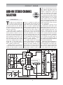
MULTIPURPOSE CIRCUIT
FOR TELEPHONES
G.S. SAGOO
RANJITH G. PODUVAL
T
his add-on device for telephones
can be connected in parallel to the
telephone instrument. The circuit
provides audio-visual indication of
on-hook, off-hook, and ringing
modes. It can also be used to connect the telephone to a CID (caller
identification device) through a relay and also to indicate tapping or
misuse of telephone lines by sounding a buzzer.
In on-hook mode, 48V DC supply
is maintained across the telephone
lines. In this case, the bi-colour LED
glows in green, indicating the idle
state of the telephone. The value of
resistor R1 can be changed somewhat to adjust the LED glow, without loading the telephone lines (by
trial and error).
In on-hook mode of the handset, potentiometer VR1 is so adjusted
that base of T1 (BC547) is forward biased, which, in turn, cuts off transistor T2
(BC108). While adjusting potmeter VR1, ensure that the LED glows only in green and
not in red.
When the hand-set is lifted, the voltage drops to around 12V DC. When this
happens, the voltage across transistor T1’s
base-emitter junction falls below its conduction level to cut it off. As a result tran-
sistor pair T2-T3 starts oscillating and the
piezo-buzzer starts beeping (with switch
S1 in on position). At the same time, the
bi-colour LED glows in red.
In ringing mode, the bi-colour LED
flashes in green in synchronisation with
SIMPLE CODE LOCK
G.S. SAGOO
YASH D. DOSHI
T
he circuit described here is of an
electronic combination lock for
daily use. It responds only to the
right sequence of four digits that are
keyed in remotely. If a wrong key is
touched, it resets the lock. The lock code
can be set by connecting the line wires to
the pads A, B, C, and D in the figure. For
example, if the code is 1756, connect line
1 to A, line 7 to B, line 5 to C, line 6 to D
and rest of the lines—2, 3, 4, 8, and 9—to
the reset pad as shown by dotted lines in
the figure.
The circuit is built around two CD4013
dual-D flip-flop ICs. The clock pins of the
four flip-flops are connected to A, B, C,
18
the telephone ring.
A CID can be connected using a relay.
The relay driver transistor can be connected via point A as shown in the circuit. To use the circuit for warning
against misuse, switch S1 can be left in
on position to activate the piezo-buzzer
when anyone tries to tap the telephone
line. (When the telephone line is tapped,
it’s like the off-hook mode of the telephone hand-set.)
Two 1.5V pencil cells can provide Vcc1
power supply, while a separate power sup-
ply for Vcc2 is recommended to avoid
draining the battery. However, a single
6-volt supply source can be used in conjunction with a 3.3V zener diode to cater
to both Vcc2 and Vcc1 supplies.
and D pads. The correct code sequence for
energisation of relay RL1 is realised by
clocking points A, B, C, and D in that order. The five remaining switches are connected to reset pad which resets all the
flip-flops. Touching the key pad switch A/
B/C/D briefly pulls the clock input pin high
and the state of flip-flop is altered. The Q
output pin of each flip-flop is wired to D
input pin of the next flip-flop while D pin
of the first flip-flop is grounded. Thus, if
correct clocking sequence is followed then
low level appears at Q2 output of IC2 which
energises the relay through relay driver
CIRCUIT
IDEAS
transistor T1. The reset keys
are wired to set pins 6 and
8 of each IC. (Power-on-reset
capacitor C1 has been added
at EFY during testing as the
state of Q output is indeterminate during switching on
operation.)
This circuit can be usefully employed in cars so
that the car can start only
when the correct code sequence is keyed in via the
key pad. The circuit can also
be used in various other applications.
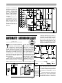
AUTOMATIC BATHROOM LIGHT
JAYAN A.R.
T
his circuit is used to automate the
working of a bathroom light. It is
designed for a bathroom fitted
with an automatic door-closer, where the
manual verification of light status is difficult. The circuit also indicates whether
the bathroom is occupied or not. The circuit uses only two ICs and can be operated from a 5V supply. As it does not use
any mechanical contacts it gives a reliable performance.
One infrared LED (D1) and one infrared
detector diode (D2) form the sensor part of
the circuit. Both the infrared LED and the
detector diode are fitted on the frame of
G.S. SAGOO
a reference potential set by preset VR1.
The preset is so adjusted as to provide
an optimum threshold voltage so that output of IC2(a) is high when the door is
closed and low when the door is open.
Capacitor C1 is connected at the output
to filter out unwanted transitions in out-
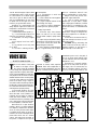
the door with a small separation between them as
shown in Fig. 1. The radiation from IR LED is blocked
by a small opaque strip (fitted on the door) when the
door is closed. Detector diode D2 has a resistance in
the range of meg-ohms when
it is not activated by IR rays.
When the door is opened,
the strip moves along with
it. Radiation from the IR LED
turns on the IR detector diode and the voltage across
Fig. 2
it drops to a
low level.
C o m parator
LM 358 IC 2(a)
compares
the voltage
across the
photodetector against
Fig. 1
19
put voltage generated at the time of opening or closing of the door. Thus, at point
A, a low-to-high going voltage transition
is available for every closing of the door
after opening it. (See waveform A in Fig.
2.)
The second comparator IC2(b) does the
reverse of IC2(a), as the input terminals
are reversed. At point B, a low level is
available when the door is closed and it
CIRCUIT
switches to a high level when
the door is opened. (See waveform B in Fig. 2.) Thus, a lowto-high going voltage transition is available at point B for
every opening of the door,
from the closed position. Capacitor C2 is connected at the
output to filter out unwanted
transitions in the output voltage generated at the time of
closing or opening of the door.
IC 7474, a rising-edge-sensitive dual-D flip-flop, is used
in the circuit to memorise the
occupancy status of the bathroom. IC 1(a) memorises the
state of the door and acts as
Fig. 3
an occupancy indicator while
IC2(b) is used to control the relay to turn on and turn off the bathroom
light. Q output pin 8 of IC1(b) is tied to D
input pin 2 of IC1(a) whereas Q output pin
5 of IC1(a) is tied to D input pin 12 of
IC1(b).
At the time of switching on power for
the first time, the resistor-capacitor combination R3-C3 clears the two flip-flops. As
a result Q outputs of both IC1(a) and IC1(b)
are low, and the low level at the output
of IC1(b) activates a relay to turn on the
bathroom light. This operation is independent of the door status (open/closed).
IDEAS
The occupancy indicator red LED (D3) is off
at this point of time, indicating that the
room is vacant.
When a person enters the bathroom,
the door is opened and closed, which provides clock signals for IC1(b) (first) and
IC1(a). The low level at point C (pin 5) is
clocked in by IC1(b), at the time of opening the door, keeping the light status unchanged.
The high level point D (pin 8) is
clocked in by IC1(a), turning on the occupancy indicator LED (D3) on at the time of
SMART FLUID LEVEL INDICATOR
THOMMACHAN THOMAS
M
ost of the fluid level indicator
circuits use a bar graph or a
seven-segment display to indicate the fluid level. Such a display using
LEDs or digits may not make much sense
to an ordinary person. The circuit presented here overcomes this flaw and displays the level using a seven-segment display—but with a difference. It shows each
level in meaningful English letters. It displays the letter E for empty, L for low, H
for half, A for above average, and F for
full tank .
The circuit is built using CMOS ICs.
CD4001 is a quad. NOR gate and CD4055 is a
BCD to seven-segment decoder and dis-
RUPANJANA
play driver IC. This decoder IC is capable
of producing some English alphabets besides the usual digits 0 through 9. The
BCD codes for various displays are given
in Table I. The BCD codes are generated
by NOR gates because of their interconnections as the sensing probes get immersed in water. Their operation being
self-explanatory is not included here.
Note that there is no display pattern
like E or F available from the IC. Therefore to obtain the pattern for letters E
and F, transistors T1 and T2 are used.
These transistors blank out the unnecessary segments from the seven-segment
display. It can be seen that letter E is
20
closing of the door. (See waveform C in
Fig. 2.)
When the person exits the bathroom,
the door is opened again. The output of
IC1(b) switches to high level, turning off
the bathroom light. (See waveform D in
Fig. 2.) The closing of the door by the
door-closer produces a low-to-high transition at the clock input (pin 3) of IC1(a).
This clocks in the low level at Q output
of IC1(b) point D to Q output of IC1(a)
point C, thereby turning off the occupancy
indicator.
generated by blanking ‘b’ and ‘c’ segments
of the seven-segment display while it decodes digit 8. Letter F is obtained by
blanking segment ‘b’ while it decodes letter P.
As CMOS ICs are used, the current conTABLE I
D
L
L
—
—
—
—
—
—
H
H
H
H
H
H
H
H
C
L
L
—
—
—
—
—
—
L
L
L
L
H
H
H
H
B
L
L
—
—
—
—
—
—
L
L
H
H
L
L
H
H
A
L
H
—
—
—
—
—
—
L
H
L
H
L
H
L
H
DISPLAY
0
1
2
3
4
5
6
7
8
9
L
H
P
A
—
BLANK
CIRCUIT
sumption is extremely low. This makes it
possible to power the circuit from a battery. The input sensing current through
the fluid (with all the four probes im-
IDEAS
mersed in water) is of the order of 70 µA,
which results in low rate of probe deterioration due to oxidation as also low levels of electrolysis in the fluid.
Note: This circuit should not be
used with inflammable or highly reactive
fluids.
The programmable peripheral interfacing
Intel-8255-I chip present in the microprocessor kit has been used. It has three
8-bit wide input/output ports (port A, port
B, and port C). Control word 80 (hex) is
used to initialise all ports of 8255-I as output ports. Bit 0 of port A (PA0) is connected
to the base of transistor BC107 through a
10-kilo-ohm resistor as shown in the figure. It is used to energise the relay when
PA0 pin of 8255-I is high. A siren, hooter,
or any bell sound system with an audio
amplifier of proper wattage (along with 2
or 3 loudspeakers) may be installed in
the school campus. The relay would get
energised after every 40 minutes for a
(PPI)
AUTOMATIC SCHOOL
BELL SYSTEM
RUPANJANA
Dr D.K. KAUSHIK
T
his is an effective and useful
project for educational institutions. In most schools and colleges, the peon rings the bell after every
period (usually of a 40-minute duration).
The peon has to depend on his wrist watch
or clock, and sometimes he can forget to
ring the bell in time. In the present system, the human error has been eliminated. Every morning, when the school
starts, someone has to just switch on the
system and it thereafter work automatically.
The automatic microprocessor controlled school bell system presented here
has been tested by the author on a
Vinytics’ microprocessor-8085 kit (VMC8506). The kit displays
the period number on
two most significant
digits of address field
and minutes of the
period elapsed on the
next two digits of the
address field. The
data field of the kit
PA
displays seconds continuously.
The idea used
here is very simple.
O
21
CIRCUIT
few seconds. The program (software) and
data used for the purpose are given below in mnemonic and machine code forms.
The program is self-explanatory.
The program and data have been entered at specific memory locations. However, the readers are at liberty to use any
other memory area in their kits, depending on their convenience. Two monitor
programs (stored in kit’s ROM/EPROM) at
locations 0347H (for clearing the display)
and 05DOH (for displaying contents of
memory locations 2050H through 2055 in
the address and data fields respectively)
Address Op-code
Label
20 FC
20 FE
2100
2103
2106
2109
210 A
210 B
210 E
3E 80
DE 03
31 FF 27
CD 47 03
C3 69 21
AF
47
21 50 20
CD D0 05
21 11
21 13
21 15
21 18
21 1B
21 1E
21 1F
21 21
3E 01
06 00
21 54 20
CD D0 05
21 55 20
7E
C6 01
FE 0A
21 23
21 26
CA 36 21
77
21 27
21 29
21 2C
21 2F
21 30
21 33
06 02
11 00 FA
CD 00 25
05
C2 29 21
C3 09 21
DD
YY
21 36
21 38
21 39
21 3A
21 3B
21 3D
21 3F
21 42
3E 00
77
2B
7E
C6 01
FE 06
CA 46 21
77
RR
21 43
21 46
C3 27 21
3E 00
21 48
21 49
21 4A
21 4B
21 4D
21 4F
77
2B
7E
C6 01
FE 0A
CA 56 21
21 52
21 53
21 56
21 58
21 59
21 5A
21 5B
21 5D
21 5F
21 62
21 63
77
C3 27 21
3E 00
77
2B
7E
C6 01
FE 04
CA 66 21
77
C3 27 21
AA
UU
VV
Mnemonic
IDEAS
have been used in the program. Please
note that before calling the display routine, registers A and B are required to be
initialised with either 00 or 01 to indicate
to the monitor program as to where the
contents of above-mentioned memory locations are to be displayed (e.g. address
field or data field), and whether a dot
is to be displayed at the end of address
field or not. (Readers should refer to their
kit’s documentation before using the display routine.) In Vinytics’ kit, if register
A contents are 00, the address field is
used for display, and if it is 01, the
Comments
MVI A, 80H
Initialise 8255-I as output port
OUT 03 H
LXI SP, 27FFH Initialise the stack pointer
CALL 0347H
Clears the display
JMP TT
Jump to ring the bell
XRA A
Put A=0
MOV B, A
Put B=0
LXI H, 2050 H Starting address of display
CALL 05D0H
Call output routine to display period
no. & minutes to address field
MVI A, 01H
A=01
MVI B, 00H
B=00
LXI H, 2054H
Current sec.
CALL 05D0H
Address of LSD of current sec.
LXI H, 2055H
MOV A, M
Move the LSD of current sec. to acc.
ADI 01 H
Add 01 to acc.
CPI 0AH
Compare LSD of sec. with 0AH (10
decimal)
JZ RR
If LSD completes 09 jump to RR
MOV M, A
Move the acc. content to 20 55 H
location
MVI B, 02H
Delay
LXI D, FA00H SubCALL 2500H
Routine
DCR B
For
JNZ YY
1 second
JMP AA
After delay of 1 sec.
Jump to AA for display the time
MVI A, 00H
A=0
MOV M, A
Store Acc. To memory location
DCX H
Decrement HL pair content
MOV A, M
Move the MSD of sec to acc.
ADI 01H
Add 01 to Acc.
CPI 06H
Compare MSD of sec with 06H
JZ UU
If sec. complete 59 move to UU
MOV M, A
Store acc. content to memory
location
JMP DD
Jump for delay of 1 sec.
MVI A, 00
Put A=00 after completing 59
seconds
MOV M,A
DCX H
MOV A,M
Move current LSD of minutes to acc.
ADI 01H
Add 01 to acc.
CPI 0A
Compares acc. to 0A H
JZ VV
Jump to VV if LSD of minutes
completes 09
MOV M,A
Move acc. to memory location
JMP DD
Jump for delay of 1 sec.
MVI A,00H
MOV M,A
DCX H
Decrement H-L pair content
MOV A,M
Move MSD of minutes to acc.
ADI 01H
Add 01 to acc.
CPI 04H
Compare acc. content with 04 H
JZ SS
If minutes 40 then jump to SS
MOV M,A
JMP DD
Jump for delay of 1 sec
data field is used for display. Similarly,
if register B contains 00 then no dot
is displayed at the end of address field,
else if B contents are 01, a dot is
displayed.
When the program is executed on the
microprocessor kit, a bell sound would be
heard for a few seconds. The address and
data fields would initially display :
01
00
00
01 indicates start of first period with 00
as elapsed minutes and 00 seconds in the
data field. The data field (seconds) are
continuously incremented.
Address Op-code
Label
Mnemonic
Comments
21 66
21 68
21 69
21 6A
21 6B
21 6E
3E 04
77
AF
47
21 50 20
CD D0 05
SS
MVI A, 04
MOV M, A
XRA A
MOV B,A
LXI H, 2050H
CALL 05D0H
Put A=4
21 71
21 73
21 75
21 78
21 7B
21 7D
3E 01
06 00
21 54 20
CD D0 05
3E 01
D3 00
MVI A, 01H
MVI B, 00H
LXI H, 2054 H
CALL 05D0 H
MVI A, 01H
OUT 00H
21 7F
21 82
21 84
21 85
21 86
21 87
21 88
21 89
21 8A
21 8B
21 8C
21 55 20
3E 00
77
2B
77
2B
77
2B
77
2B
7E
LXI H, 2055H
MVI A, 00H
MOV M, A
DCX H
MOVM, A
DCX H
MOV M, A
DCX H
MOV M,A
DCXH
MOV A, M
21 8D
21 8F
21 91
C6 01
FE 0A
CA 98 21
ADI 01
CPI 0A
JZ XX
21 94
21 95
21 98
21 9A
21 9B
21 9C
21 9D
21 9F
21 A0
21 A2
21 A5
21 A8
21 A9
21 AC
21 AD
21 AE
21 B1
21 B4
21 B6
21 B8
21 BB
21 BE
21 C1
21 C2
21 C4
21 C6
21 C9
21 CB
77
C3 A0 21
3E 00
77
2B
7E
C6 01
77
06 02
11 00 FA
CD 00 25
05
C2 A2 21
AF
47
21 50 20
CD D0 05
3E 01
06 00
21 54 20
CD D0 05
21 55 20
7E
C6 01
FE 06
C2 9F 21
3E 00
D3 00
MOVM, A
JMP XY
MVI A, 00H
MOV M,A
DCX H
MOV A, M
ADI 01H
MOV M,A
MVI B, 02
LXI D, FA 00H
CALL 2500 H
DCR B
JNZ XYZ
XRA
MOV B,A
LXI H, 2050H
CALL 05D0H
MVI A, 0IH
MVI B, 00H
LXI H, 2054 H
CALL 05 D0 H
LXI H, 2055H
MOV A, M
ADI 01H
CPI 06H
JNZ XXX
MVIA, 00H
OUT 00H
22
TT
XX
XXX
XY
XYZ
A=0
B=0
Display the period no. and minutes
in address field
A=1
B=0
Display the seconds in data field
Exite the 8255:1 for engergising the
relay (rings the bell)
Stores 00 to memory location
2055 to
2052 H
Brings the LSD current period
no. to acc
Add 1 to it compare with OA
If LSD of period no. complete 09 then
jump to XX
Else store it to memory location
Jump to XY
A=0
Store it to main location
Store MSD of period no. to acc
Add 1 to it
Store it memory location
Program 1 sec display
A=0
B=0
Program to display
The period no.
Minutes and second
LSD of stored current second to acc
Add 1 to it
Compare with 06
If not 06 jump to XXX
A=0
Output to 8255 to de-energise
the relay
CIRCUIT
IDEAS
Address OP CODE LABEL Mnemonic
Comments
Address
OPCODE
21 CD
Repeat for next period
DATA
20 50
20 51
20 52
20 53
20 54
20 55
00
00
00
00
00
00
DELAY
25 00
25 01
25 02
25 03
25 06
C3 09 21
JMP AA
SUBROUTINE
1B
NEXT
7A
B3
C2 00 25
C9
DCX D
MOV A, D
ORA E
JNZ NEXT
RET
LABEL Mnemonic
DESIGNING AN RF PROBE
RUPANJANA
N.S. HARISANKAR, VU3NSH
R
adio frequency probe is used to
directly measure the level of RF
RMS voltage present across two
points. It is one of the most useful test
instruments for home brewers as well as
for communication equipment service/design labs.
RF voltage level being measured provides useful information only when the
probe has been designed for use with a
specific multimeter. The design of RF
probe is a function of the meter we intend to use it with. If a meter with a
different input resistance is used with the
probe, the reading will be incorrect. The
value of RX (refer figure) is so chosen that
when this resistor is connected in parallel with input resistance of the multimeter, the peak value is about 1.414 times
the RMS voltage. Resistor RX has to drop
this excess voltage so that meter indication is accurate. If we know the input
resistance of the meter, we can calculate
the value of RX with the help of the following relationship:
Let meter DC input resistance
X 1.414 = RY
Then RX = Ry – meter DC input resistance
For example, if meter input resistance is 20 meg-ohm, Ry = 28.28 megohm and RX = 8.28 meg-ohm.
We can convert the RF voltage level
TABLE I
Voltage to Watts Conversion
for 50 ohms Termination
RMS (V)
2.24
3.88
5.0
7.08
12.25
15.90
20.0
22.4
38.75
41.85
50.0
RF Power (W)
0.1
0.3
0.5
1
3
5
8
10
25
35
50
(E) so meas u r e d
across a
given load
resistance
( R ) to
RF
watts
(W )
using the
following
relationship:
Power P
= E2 / R
watts (W)
For example, if RF probe voltage reading across a load resistance of 50 ohms is
found to be, say, 15.85 volts, the power in
the load = 15.85 x 15.85 / 50 = 5W approx.
23
Comments
MSD of period no.
LSD of period no.
MSD of minutes
LSD of minutes
MSD of seconds
LSD of seconds
In other words, for 5-watt power in a
50-ohm load, the voltage across the load
is 15.85 volts.
The rectified DC voltage at the cathode of diode D1 is at about the peak level
of the RF voltage at the tip of the probe.
Use shielded cable in between the probe
output and meter. It will act as feedthrough capacitance and thus avoid RF interference. The maximum RF input voltage level depends on the peak inverse voltage (PIV) of diode D1. The shielded lead
length is too large to give accurate results at UHF. Please refer Tables I and II
Table II
Meter DC Impedence
20 Meg-ohm
10 Meg-ohm
1 Meg-ohm
20 kilo-ohm
Rx
8.25
4.14
41.4
8.28
Meg-ohm
Meg-ohm
kilo-ohm
kilo-ohm
for ready conversion of RF voltage level (RMS) to
equivalent power across a 50-ohm load and deduction of R value for a given meter’s DC input resistance respectively.
X
February
2000
CONSTRUCTION
PC BASED SPEED
MONITORING SYSTEM
G.S. SAGOO
SANTHOSH JAYARAJAN
T
As interface circuit can easily be wired
on any general-purpose PCB, no PCB layout is included for it. The two wires to be
extended to 25-pin parallel port may be
connected using a 25-pin male ‘D’ connector.
Lab Note: Magnetic proximity
switches, from various manufacturers,
are available in the market. The important specifications include operating DC
voltage range, operating current and its
sensitivity, i.e. the maximum distance
from a metallic object such that the
switch operates. These specifications are
normally mentioned on the proximity
switch itself or in the accompanying literature.
his project describes the software the machinery. The output of the circuit,
and hardware necessary to moni- available across resistor R2, is fed to the
tor and capture in real time the PC via 25-pin ‘D’ connector of parallel port
speed of any rotating object. The speed LPT1. Pin 11 pertains to data bit D7 of the
may be defined/stored/displayed in any of input port 379(hex) of the LPT1 port havthe three units: RPM (rev./minute), RPS ing base address 378(hex), and pin 25 is
(rev./second), or RPH (rev./hour). The sys- connected to PC ground. (In fact, pins 18
tem uses a sampling time of two seconds through 25 of the parallel port are strapped
The software
and can store up to 16 minutes of data per together and connected to ground.)
file. The x and y axes can be scaled to read
The proximity switch is mounted on The structural block diagram of the softany speed and the x-axis can be ‘stretched’ a stationary part, such as a bolt or stud, ware is shown in Fig. 4. The software has
to observe clustered points.
in such a way that it senses each tooth of the following four main modules, which
The hardware mainly comprises a the rotating part as shown in Fig. 3. Two are activated from the main menu using
proximity switch whose output is con- fixing nuts are provided on the threaded four of the function keys, F1 through F4.
nected to the printer
(LPT1) port of the computer through an optocoupler. The proximity
switch is used as a
speed-sensor. The program is written in C++
and has effective error
handling capability and
a help facility. This system can be used to
monitor the speed of rotating parts in the in- Fig. 1: Interface circuit for PC based speed monitoring system
dustry or to read and
record wind speeds.
body of the proximity
switch for securing it
firmly onto a fixed
The hardware interface
part of the machinery.
The hardware interface circuit is given
The
software
in Fig. 1. A 230V AC primary to 0-9V, prompts the operator
250mA secondary transformer followed to enter the number of
by IC 7805 is used for catering to the teeth (being sensed
power supply requirement for proximity during every revolu- Fig. 2: Proximity switch
switch and the opto-coupler. The proxim- tion), which is used by
ity switch, as shown in Fig. 2, is a 3-wire the program for calculation
switch (e.g. PG Electronics’ EDP101) of RPM, RPS, or RPH, as
which operates at 6V to 24V DC.
the case may be. In any
The inductive type proximity switch specific application, where
senses any metal surface from a distance non-metallic rotating parts
of about 5 mm to 8 mm. Thus, a gear or are present and inductive
fan blade is ideal for counting the number proximity switch cannot be
of revolutions. The number of teeth that used, one may use phototrigger (switch-on) the proximity switch electric switch to do the
during every revolution are to be known counting for 2-second samfor the software to calculate the speed of pling period.
Fig. 3: Mounting of proximity switch
25
CONSTRUCTION
PARTS LIST
Semiconductors:
IC1
- 7805 regulator 5V
IC2
- MCT2E opto-coupler
Resistors (all ¼ watt, ± 5% metal/carbon
film, unless stated otherwise)
R1
- 300-ohm
R2
- 150-ohm
Capacitors:
C1
- 1000µF, 16V electrolytic
C2
- 0.22µF polyster
Miscellaneous:
X1
- 230V AC primary to 0-9,
250mA sec. transformer
BR-1A
- Bridge rectifier, 1-amp.
S1
- Proximity switch (refer text)
Fig. 4: Structural block diagram of software
HELPS.PG1 file contents
+++SPEED MASTER HELP PAGE+++
This software can be used to capture
and monitor the speed of any rotating
part for a maximum of eight minutes
with a total sampling time of two seconds. The software has four menu levels which can be selected from the Main
Menu.
In Capture/Monitor mode the software has two trigger modes, viz,
Manual, which waits for a key press and
Auto, which waits for the first pulse from
the sensor.
The captured file can be viewed in
any X-axis scale. However, all points coming out of the view page are clipped off.
When using the gear teeth for speed
calculation, please enter the teeth per
revolution to enable internal calculation
of speed to be made.
Enter the filename where the data
is to be stored, when prompted. The
same file can be viewed in the view page
option. If an invalid file name is entered,
or the file cannot be opened, an error is
displayed and the user can exit to Main.
...Press Any Key to Return to Main...
1. Speed monitor and capture module. This module is used to monitor the
speed and store the data in a user-defined file.
(a) The module first prompts for the
filename. The file name is entered with
an extension .DAT.
(b) The next entry is called ‘trigger
mode’. It specifies how the software should
start monitoring and capturing data. The
options are: 1 = manual and 2 = auto. If
option 1 is selected, the system waits for
a key press to start the monitoring and
capturing operation.
If option 2 (auto mode) is selected,
1
15
0
0
0
0
0
0
30
0
30
0
0
0
30
0
FILE Contents of DEMO.DAT
Showing Rev./min.
0
0
0
0
0
0
0
0
0
0
0
0
0
0
15 0
0
0
0
0
30 0
0
0
0
0
0
0
15 0
15 0
90 0
15 0
15 0
0
0
0
0
120 0
0
0
0
0
30 0
0
30 0
0
150 0
0
0
0
0
0
0
0
0
0
0
30 0
0
0
0
0
0
0
0
0
0
0
15 60
0
0
15 0
150 0
0
0
0
0
0
0
0
0
15 0
26
0
0
0
0
0
0
0
15
0
0
15
0
0
0
the system waits for the first pulse
from the proximity switch to start
monitoring and capturing of data.
(c) The next entry relates to ‘units’,
which has the following further options:
1 = Revolutions/min.
2 = Revolutions/sec.
3 = Revolutions/hr
(d) The next entry pertains to the
‘range of speed,’ which must be more
than the maximum speed that is expected. The options are:
1 = 400 units
2 = 800 units, etc
(e) The next entry concerns the ‘number of teeth’ and represents the number
of pulses from the proximity switch per
revolution.
After making the above entries, the
following message is displayed on the
monitor screen:
“Trigger mode: Auto (or Manual) Waiting
for first pulse (or Press any key to start)”
depending on the trigger mode. If manual
mode has been selected, then hit any key
to start. If auto mode is selected, the software waits for the first pulse from the
proximity sensor to proceed. The display
then shows the speed in the units selected
and the capture file name. Pressing ESC
exits the monitor mode after closing the
capture file. Pressing any other key returns to main menu.
2. Viewing a graph file. This module is used to view an existing data file.
Sequential contents of a DEMO.DAT file
are shown in a box (using eight columns).
If a non-existant filename is entered, the
software detects the opening error and
prompts the user for re-entering the
filename. The various prompts for entering the required data are:
(a) File name – Enter the full filename
CONSTRUCTION
with extension.
(b) Enter the x-axis scale factor to enable the graph to be ‘stretched’ on the xaxis to observe cramped points properly.
After entering the x-axis scale, the graph
appears along with all relevant data, like
scale factors for x and y axis, file name,
and units, etc.
(c) While still in the graph mode, you
may view a new graph after pressing F1.
For returning to the main menu, press
F2.
3. Help. This module provides one
page of help and reads from a file called
#include<conio.h>
#include<iostream.h>
#include<graphics.h>
#include<dos.h>
#include<stdio.h>
#include<time.h>
#include<fstream.h>
#include<process.h>
#include<stdlib.h>
void startgraphics();//start graphics system//
void openingmenu();//opening menu//
void monitor();//monitor and save to file//
float readspeed(int unit,int teeth);//read the
speed//
void display(int unit);//display the speed//
void view();//View a Speed vs Time Graph//
void grid();//Draw the graph grid//
void displayhelp(char helpfilename[10]);
void exiit();
void help();
int roundoff(float number);
//Global Variables//
int unit;int teeth;
float speed;
char monitorfile[8];
int gdriver;int gmode;
int mid;
//Program main menu//
void main()
{
startgraphics();
openingmenu();
}
//Graphics initialisation//
void startgraphics()
{
registerbgidriver(EGAVGA_driver);
registerbgifont(small_font);
registerbgifont(triplex_font);
int gdriver = DETECT, gmode;
initgraph(&gdriver, &gmode, “”);
}
//Opening menu//
void openingmenu()
{
setfillstyle(LTSLASH_FILL,5);
bar(10, 10, 635, 470);
setlinestyle(SOLID_LINE,0,2);
rectangle(10,10,635,470);
setlinestyle(SOLID_LINE,0,2);
rectangle(200,40,400,90);
setcolor(BLUE);
line(200,91,400,91);
line(200,92,400,92);
line(401,90,401,40);
settextstyle(2,HORIZ_DIR,8);
setcolor(YELLOW);
outtextxy(220,50,“SPEED TRACK”);
setcolor(LIGHTBLUE);
outtextxy(150,120,“1.SPEED MONITOR &
CAPTURE - F1”);
setcolor(LIGHTRED);
outtextxy(150,180,“2.VIEW SPEED vs TIME
GRAPH - F2”);
setcolor(LIGHTMAGENTA);
outtextxy(150,240,“3.SPEED TRACK HELP F3”);
setcolor(LIGHTCYAN);
outtextxy(150,300,“4.EXIT TO SHELL - F4”);
setcolor(LIGHTGREEN);
outtextxy(180,360,“Enter your choice ”);
outtextxy(200,383,“(F1 TO F4) ”);
USERCHOICE:
while(!kbhit())
{}
char userchoice=getch();
switch(userchoice)
{
case (char(59)):monitor();break;
case (char(60)):view();break;
case (char(61)):help();break;
case (char(62)):exiit();break;
default:goto USERCHOICE;
}
}
HELPS.PG1. If this file cannot be opened,
or is not available, the software prompts
with “Help file not found or cannot be
opened.” Pressing any key from the help
page returns one to main menu. The contents of HELPS.PG1 are given in the box
(on previous page).
Program Listing for SPEEDM.CPP
//Monitoring the speed online and storing the
data//
void monitor()
{
int s;int t;
int trigger;
int yrange;
char unitf[8];
int speedf;
restorecrtmode();
clrscr();
window(1,1,80,25);
clrscr();
textcolor(YELLOW);
textbackground(LIGHTBLUE);
gotoxy(25,3);
cprintf(“ - S P E E D T R A C K -”);
gotoxy(25,4);
cprintf(“=========================”);
gotoxy(25,6);
cprintf(“MONITOR & CAPTURE PAGE”);
window(10,8,75,8);
textcolor(YELLOW);
clrscr();
cprintf(“Enter file name to store Speed data
(****.***) - ”);
scanf(“%8s”, &monitorfile);
GETTRIGGER:
textcolor(YELLOW);
clrscr();
cprintf(“Enter trigger mode(1=Manual,2=First
pulse) - ”);
scanf(“%d”, &trigger);
if(trigger<1 || trigger>2)
{
clrscr();
textcolor(YELLOW+BLINK);
cprintf(“........Value out of range,Enter 1 or
2........”);
delay(2000);
goto GETTRIGGER;
}
GETUNIT:
textcolor(YELLOW);
27
clrscr();
cprintf(“Enter Unit for Speed(1=Rev/min,2=Revs/
sec,3=Revs/Hr) - ”);
scanf(“%d”, &unit);
if(unit<1 || unit>3)
{
textcolor(YELLOW+BLINK);
clrscr();
cprintf(“ ........Value out of range............ ”);
delay(2000);
goto GETUNIT;
}
GETRANGE:
textcolor(YELLOW);
clrscr();
cprintf(“Enter Range for Speed(1=400 units,
2=800 units..etc) - ”);
scanf(“%d”, &yrange);
if(yrange<1 || yrange>100)
{
textcolor(YELLOW+BLINK);
clrscr();
cprintf(“ ........Value out of range............ ”);
delay(2000);
goto GETRANGE;
}
GETTEETH:
textcolor(YELLOW);
clrscr();
cprintf(“ Enter Number of teeth for Sensor - ”);
scanf(“%d”, &teeth);
if(teeth<1 || teeth>100)
{
textcolor(YELLOW+BLINK);
clrscr();
cprintf(“ ........Value out of range............ ”);
delay(2000);
goto GETTEETH;
}
//Open the file for data storage
fstream infile;
infile.open(monitorfile,ios::out);
//Store the units
char *unitf1 = “Rev/min”;
char *unitf2 = “Rev/sec”;
char *unitf3 = “Rev/hr” ;
switch(unit)
{
case 1:infile<<unitf1<<endl;break;
case 2:infile<<unitf2<<endl;break;
case 3:infile<<unitf3<<endl;break;
}
//Entering the units and y scale to capture file//
//fstream infile;
//infile.open(monitorfile,ios::out);
infile<<yrange<<endl;
clrscr();
//Setting the trigger mode//
switch(trigger)
{
case 1:textcolor(YELLOW+BLINK);cprintf
(“Trigger mode: Manual ..Press any key
to Start”);getch();break;
case 2:textcolor(YELLOW+BLINK);cprintf
(“Trigger mode: Auto..Waiting for first pulse..”);
CONSTRUCTION
s=inp(0x379);t=s;while(s==t)s=inp(0x379);break;
default:textcolor(YELLOW+BLINK);cprintf
(“Trigger mode: Manual ..Press any key to
Start”); getch();break;
}
startgraphics();
for(int pointno=1;pointno<481;++pointno)
{
char in;
display(unit);
speedf=roundoff(speed);
infile<<speedf<<endl;
if (kbhit())
{
if ((in = getch()) == ‘\x1B’)break;
}
}
infile.close();//Close the file,clean up and return
to main//
restorecrtmode();
window(10,8,75,8);
textcolor(YELLOW+BLINK);
cprintf(“Data Capture Interrupted or File full(960
sec)..Press any key..”);
getch();
startgraphics();
openingmenu();
}
//Read the speed and convert into the asked
units//
float readspeed(int unit,int teeth)
{
int sett=255;int tes=255;mid=0;
clock_t start, end=0;
sett=inp(0x379);
tes=sett;
for(start=clock();(end-start)/CLK_TCK<2.0;
end=clock())
{
sett=inp(0x379);
if(sett!=tes)++mid;
tes=sett;
}
//Calculation of the speed depending on unit
selected//
switch(unit)
{
case 1:return(mid*15.0/(teeth));
case 2:return(mid/(4.0*teeth));
case 3:return(mid*900.0/teeth);
default:return(mid/(4.0*teeth));
}
}
//Display the speed on the screen update every 2
secs//
void display(int unit)
{
char msgd[80];
char msgf[80];
fstream infile;
setcolor(LIGHTRED);
setbkcolor(LIGHTGREEN);
settextstyle(1,HORIZ_DIR,4);
rectangle(5,5,630,470);
outtextxy(175,30,”SPEED MASTER”);
moveto(150,400);
outtext(“Press ESC to exit.....”);
outtextxy(150,300,”Capture file =”);
sprintf(msgf, “%s”, monitorfile);
outtextxy(400,300,msgf);
moveto(150,100);
outtext(“Speed ”);
switch(unit)
{
case 1:outtextxy(250,100,“in Revs/Min”);break;
case 2:outtextxy(250,100,“in Revs/Sec”);break;
case 3:outtextxy(250,100,“in Revs/Hr”);break;
}
speed=readspeed(unit,teeth);
cleardevice();
sprintf(msgd, “%f”, speed);
outtextxy(250,200,msgd);
}
void view()//View a speed vs time graph//
{
VIEWSTART:
closegraph();
int xscale=1;int yscale;
char msgx[2];char msgmaxy[5];char msgmaxx
[5];char msgy[2];char msgun[8];char gunits[8];
char msgfile[10];
char filename[8];
char msgpoint[5];
int coordinate[10000];
int errorcode;
fstream infile;
window(1,1,80,25);
clrscr();
textcolor(RED);
textbackground(BLUE);
gotoxy(25,3);
cprintf(“ - S P E E D M A S T E R - ”);
gotoxy(25,5);
cprintf(“ VIEW FILE PAGE ”);
window(10,8,50,8);
textcolor(YELLOW);
clrscr();
cprintf(“ Enter name of file to view - ”);
scanf(“%8s”, &filename);
scalefactor:
int i=0;int pointcount=0;
XAXIS:
clrscr();
cprintf(“ Enter X axis scale factor - ”);
scanf(“%d”, &xscale);
if(xscale<0||xscale>9) goto XAXIS;
infile.open(filename,ios::in);
if(infile.fail())
{
window(10,8,70,9);
textcolor(YELLOW+BLINK);
clrscr;
cprintf(“..Error opening file or file does not
exist..\n\r Press F3 to exit,F4 to re-enter ”);
ERRORGRAPH:
while (!kbhit())
{}
char choicegraph;
choicegraph=getch();
switch(choicegraph)
{
case (char(62)):goto VIEWSTART;
case (char (61)):main();break;
default:goto ERRORGRAPH;
}
}
infile>>gunits>>yscale;
while(!infile.eof())
{
infile>>coordinate[i];
++i;
++pointcount;
}
infile.close();
startgraphics();
cleardevice();
setcolor(CYAN);
setbkcolor(DARKGRAY);
rectangle(10,40,490,440);
settextstyle(2,HORIZ_DIR,6);
outtextxy(140,15,“Speed Master..GRAPH VIEW
PAGE..”);
setcolor(GREEN);
outtextxy(492,40,“Graph Variables”);
28
outtextxy(492,60,“X scale =”);
outtextxy(492,75,“Y scale =”);
outtextxy(492,90,“Units =” );
outtextxy(492,105,“File =” );
outtextxy(492,120,“Points = “ );
setcolor(GREEN);
outtextxy(492,150,“Options:”);
outtextxy(492,165,“F1= New Graph”);
outtextxy(492,180,“F2= Main Menu”);
outtextxy(492,210,“NOTE:”);
outtextxy(492,225,“X axis=960sec”);
outtextxy(492,240,“Y axis=400units”);
outtextxy(492,255,“For Xscale=1”);
outtextxy(492,270,“and Yscale=1”);
setcolor(YELLOW);
sprintf(msgx, “%d”, xscale);
outtextxy(580,60, msgx);
sprintf(msgy, “%d”, yscale);
outtextxy(580,75, msgy);
sprintf(msgun, “%s”, gunits);
outtextxy(580,90, msgun);
sprintf(msgfile, “%5s”, filename);
outtextxy(565,105, msgfile);
sprintf(msgpoint, “%d”, pointcount);
outtextxy(567,120, msgpoint);
sprintf(msgmaxx, “%d”, (960/xscale));
outtextxy(480,450,msgmaxx);
sprintf(msgmaxy, “%d”, (400*yscale));
outtextxy(10,20,msgmaxy);
outtextxy(60,20,msgun);
outtextxy(480,460,”Seconds”);
grid();
setviewport(10,40,490,440,1);
setcolor(GREEN);
int x1=0;int y1=0;
int j;
for (j=0;j<pointcount-1;++j)
{
line(x1*xscale,400-y1/yscale,(j+1)*xscale,400coordinate[j]/yscale);
x1=j+1;
y1=coordinate[j];
}
GRAPHMENU:
while (!kbhit())
{}
char choiceg;
choiceg=getch();
switch(choiceg)
{
case (char(59)):goto VIEWSTART;
case (char (60)):closegraph();main();break;
default:goto GRAPHMENU;
}
}
//To draw the graph grid//
void grid()
{
int i;
setcolor(RED);
for(i=140;i<440;i=i+100)
line(10,i,490,i);
setcolor(BLUE);
for (i=70;i<490;i=i+60)
line(i,40,i,440);
}
//Main help call function//
void help()
{
closegraph();
clrscr();
displayhelp(“HELPS.PG1”);
getch();
}
//Exit to shell with graphics clean up//
void exiit()
{
CONSTRUCTION
cleardevice();
setbkcolor(LIGHTGREEN);
setcolor(RED);
moveto(150,200);
outtext(“Exiting to DOS..”);
delay(2000);
closegraph();
exit(1);
}
//Display the helpfile if resident or else indicate
error//
void displayhelp(char helpfilename[10])
{
fstream infile;
textbackground(BLACK);
window(1,1,80,25);
textcolor(LIGHTRED);
const int max=80;
char buffer[max];
clrscr();
infile.open(helpfilename,ios::in);
if(infile.fail())
{
window(10,8,70,9);
textcolor(YELLOW+BLINK);
clrscr;
cprintf(“.....HELP NOT AVALABLE OR ERROR
OPENING FILE.....\n\r ....Press any KEY TO
RETURN TO MAIN....”);
getch();
main();
}
while(!infile.eof())
{
infile.getline(buffer,max);
cout<<buffer;
cout<<endl;
}
infile.close();
getch();
29
main();
}
//Function to round off the float number to the
nearest integer//
int roundoff(float number)
{
int quotient;
float result;
quotient=int(number);
result=number-quotient;
if(result>0.5)
{
return(quotient+1);
}
else
{
return(quotient);
}
}
❏
CONSTRUCTION
STEREO CASSETTE PLAYER
G.S. SAGOO
REJO G. PAREKKATTU
A
n electronics hobbyist always finds
pleasure in listening to a song
from a cassette player assembled
with his own hands. Here are the details
of a stereo cassette player with the following features, which many electronics
enthusiasts would love to assemble and
enjoy:
1. Digital 4-function selector (radio,
tape, line input, and transmit).
2. Four sound modes (normal, low
boost, hi-fi, and x-bas).
3. Bass and treble controls.
4. Function and output level displays.
5. Built-in FM transmitter for cordless
head-phones.
reo cassette player is shown in Fig. 1.
The circuit may be divided into three functional sections as shown in the block diagram.
Section I (Fig. 2). It comprises a ste-
reo head preamplifier, a function selector, and an FM transmitter. The preamplifier is built around IC LA3161. The outputs from 200-ohm stereo R/P (record/
play) head are connected to the left and
right input pins 1 and 8 of LA3161 preamplifier. A 9V regulated power supply, obtained from the voltage regulator built
around transistor T1, is used for the
preamplifier. The outputs of this preamplifier are routed to the function selector
configured around two CD4066 (quad bipolar analogue switches) and an HEF4017
(decade counter).
When any control input pin (5, 6, 12,
Description
The functional block diagram of the ste-
Fig. 1: Functional block diagram of stereo cassette player
Fig. 2: Preamplifier and function selector and FM TX (Section I)
30
CONSTRUCTION
and 13) of
CD4066 , as
shown in
Fig. 3, is
made high,
it can switch
AC and/or
DC signals
between its
corresponding output
pins (3-4, 89, 10-11, and
1-2 respectively) in
both direc-
tions. In other words, it acts like an analogue switch which can be turned on or
off by making its input control pin high
or low. A single IC contains four such
switches/sections (A, B, C, and D). The
control inputs of the two ICS (CD4066)
are derived from the decade counter IC
(HEF4017). Only four outputs of this IC
(Q0 through Q3) are used and the fifth
output Q4 (pin 10) is connected to the
reset pin (pin 15) via diode D1.
When power is turned on, the output
Q0 (pin 3) of this IC will be high. In this
condition any audio signal fed to the ‘raFig. 3: Internal schematic
diagram of CD4066
dio I/P’ terminal reaches the output. If
switcher IC
desired, the audio output from a radio
receiver can be connected
to this input terminal.
Circuit diagram and details of such radio receivers have appeared in earlier issues of EFY.
With each depression
of switch S1, the outputs
of IC4 (Q0-Q3) go high sequentially to control different modes of operation.
When Q1 (pin 2) of IC4
Fig. 4: Simplified schematic diagram of tone and sound
goes high, the audio sigmode control (left channel)
Fig. 5: Tone and sound mode control (Section II)
31
nals from the output of the preamplifier
reach the output terminals of the circuit.
At the same time, a 9V regulated power
supply to the preamplifier is switched on
through transistor T1. When Q2 (pin 4)
goes high, any audio signals applied to
the auxiliary I/P terminals (Aux. I/P (L)
and Aux. I/P(R)) reach the output terminals. When Q3 (pin 7) goes high, the
power to both the FM transmitter and
preamplifier is switched on and the signals from the preamplifier appear at the
base of transistor T3 (BF494) which, in
association with some passive components, forms an FM transmitter. The details of coil L1 are included in the parts
list. The frequency of this transmitter falls
between 88 and 108 MHz.
The frequency can be slightly varied
by adjusting trimmer capacitor VC1. The
transmitted signals can be received on any
FM receiver working in 88-108 MHz
range. LEDs D2 through D5 are bilateral
LEDS which are used to display the selected function.
Section II. This section employs a
JFET dual operational amplifier LF353
whose gain for different audio frequencies is controlled by the corresponding potentiometer settings (VR3 and
VR6 for bass, VR4 and VR5 for
treble for left and right channels
respectively) and, additionally,
by sound mode selector switch
S2. The simplified circuit diagram for left channel is shown
in Fig. 4, while the complete
schematic circuit diagram is
shown in Fig. 5.
In the simplified diagram,
the function of decade counter
IC (HEF 4017) and bipolar analogue switcher ICs (CD4066) are
replaced by a simple switch, SW.
The output of preamplifier (section I) is applied as input to the
inverting terminal of op-amp IC8
and at the output we obtain a
180o phase shifted amplified signal. Potentiometers VR3 and
VR4 are used to control low frequencies (bass) and high frequencies (treble) respectively.
In the normal mode (Q0 output of IC7 high), pole-P of switch
SW is in contact with terminals
1 and 2 simultaneously. In this
condition, normal gain is
achieved for both high and low
frequencies as per settings of
CONSTRUCTION
VR3 and VR4. But the midrange frequency components get attenuated due
to capacitor C41 (0.047µF).
In the hi-fi mode (Q1
output of IC7 high), pole-P
of the switch is in contact
with terminal 1. In this position, normal gain is
achieved for entire audio
frequency range (since capacitor C41 is disconnected
from the feedback path).
When pole-P of switch
SW is in position 2 (Q2 output of IC7 high), the attenuation of mid-range frequency components is reestablished and also the
gain of the amplifier for
very low frequencies increases (since an additional
feedback resistance of 100k
(R25) is introduced in the
feedback loop). This is the
low-frequency boost mode.
When pole-P is in con-
Fig. 6: Preamplifier, audio level indicator, and power supply (Section III)
PARTS LIST
Semiconductors:
IC1
- LA3161 stereo preamplifier
IC2,IC3,IC5,IC6 - CD4066B quad bilateral
analogue switch
IC7,IC4
- HEF4017B decade counter
IC8
- LF353 JFET input dual
op-amp
IC9
- TA7230 stereo power
amplifier
IC10
- KA2281 stereo level
indicator
T1
- 2SC1815 npn transistor
T2
- CL100 npn transistor
T3
- BF494 npn transistor
D1,D12,D13,
D24 D25,D9
- 1N4001 rectifier diode
D2,D3,D4,D5
- Bilateral coloured LEDs
D6-D8,D14-D23 - Coloured LED
D10,D11
- 1N5408 rectifier diode
D26,D27
- 9.1V zener
Resistors (all ¼W, ±5% metal carbon film,
unless stated otherwise)
R1,R6,R10
R2,R7
R3,R8,R22,R23,
R28,R37,R39,R40 R4,R9,R11,
R26,R35
R5
R12,R13
R14-R21,R51-R60R24,R27,R33,R30
R31,R36,R38
-
100-ohm
7.5-kilo-ohm
100-kilo-ohm
10-kilo-ohm
150-ohm
1.2-kilo-ohm
1-kilo-ohm
4.7-kilo-ohm
R25,R32,R29,
R34 R41,R42
R43,R44
R45-R50
R61
R62
VR1-VR3,VR6
VR4,VR5
VR7
VR8,VR9
-
2.2-kilo-ohm
1-ohm
33-kilo-ohm
680-ohm
330-ohm,0.5W
47-kilo-ohm linear
potmeter
- 100-kilo-ohm linear
potmeter
- 220-kilo-ohm linear
potmeter
- 47-kilo-ohm log potmeter
Capacitors:
C1,C5,C17,C27-C30,
C32,C47,C59,C60 - 0.1µF ceramic disc
C2,C4,C24
- 100µF, 25V electrolytic
C3,C11,C26
- 22nF ceramic disc
C6,C16,C22,C23
C34,C36,C22,
C23,C52,C53
- 1nF ceramic disc
C7,C15,C35,C37
C49,C50,C10,
C12,C51,C54
- 10µF, 25V electrolytic
C8,C13,C55,
C56,C57
- 47µF, 25V
C9,C14
- 15nF polyester
C18
- 100pF ceramic disc
C19
- 22pF ceramic disc
C20
- 10pF ceramic disc
C21
- 68pF ceramic disc
C25
- 1µF, 25V electrolytic
C31,C33,C46,C48 - 2.2µF, 25V electrolytic
32
C38,C41,C43,C45 C39,C42
C40,C44
C58,C61
C62
C63-C66
C67,C69
C68,C70
VC1
Miscellaneous:
L1
L2
X1
S1,S2
LS1,LS2
0.047µF polyester
2.2nF polyester
6.2nF polyester
470µF, 25V electrolytic
2200µF electrolytic
4.7µF, 25V electrolytic
1000µF, 25V electrolytic
4700µF, 25V electrolytic
8-25pF trimmer
- 5T, 22 SWG, 5mm dia air
core
- 250T, 18 SWG over a
ferrite rod
- 230V AC primary to 12-012V, 2A sec. transformer
- Push-to-on tactile switch
- Tape drive mechanism
complete with 200-ohm
R/P stereo head, leaf
switch, and 12V DC, 2400
rpm motor
- Telescopic antenna
- 4-ohm, 8W, 9cm diameter
woofers with piezoelectric
tweeter
- Readymade FM/AM radio
reciever kit
- Cabinet
- Shielded cable
- Heat sink and other
hardware items
CONSTRUCTION
Fig. 7. Actual-size, single-sided PCB for stereo cassette player
Fig. 8. Component layout for the PCB
33
CONSTRUCTION
tact with terminal 3 (Q3 output of IC7
high), normal gain is provided for the
high-frequency components (treble) and
higher gain is available for a wide range
of low frequencies (including some midrange frequencies). This is termed as the
X-BAS mode. The gain of the amplifier
for different frequencies, in each of the
above-mentioned modes, is also dependent
on VR3 and VR4 potmeter settings.
In the actual circuit diagram, the bipolar analogue switcher (CD4066) replaces
switch SW. The LEDs D6, D7, and D8
are used to represent the sound modes—
low-boost, hi-fi, and X-BAS repsectively.
Switch S2 is used to select variouse sound
modes. At power on, Q0 (pin 3) of IC7 is
high and therefore normal sound mode
is on.
Section III (Fig. 6). This section comprises an audio power amplifier, a 12V
dual power supply, and an audio level indicator. The power amplifier used is the
popular IC-TA7230, which delivers up to
7-watt (RMS) power per channel into a
4-ohm load. This IC has in-built short circuit protection and over-temperature cutoff. A suitable heat sink must be connected
to the IC to prevent thermal run-away.
Potmeters VR8 and VR9 are volume controls for left and right channels respectively, while VR7 is the balance control.
A dual power supply is used for the
circuit. The +12V section uses a π filter
with capacitors in the parallel arms and
an inductor in the series arm. However,
for the – 12V supply, the inductor of the
series arm (as used for +12V supply) is
replaced by a resistor. Filters are provided
to reduce the ripple factor and thereby
reduce hum (noise). Please refer inductor
details in parts list.
The audio level indicator is built
around IC KA2281. LEDs D14 through
D23 are connected at its outputs to show
the audio level of each channel in five
steps. The input to this audio level indicator is derived from the output of the
power amplifier. The gain of this level
indicator can be varied by changing the
values of resistors R49 and R50.
Assembly
The complete circuit, with the exception
of the audio level indicator, can be as-
34
sembled on a single PCB. A separate PCB
is used for the audio level indicator
and for mounting LEDs (D2 through
D8). Single-sided, actual-size PCB for the
complete circuit is given in Fig. 7. The
component layout for the PCB is shown
in Fig. 8.
Use sockets for all ICs except IC1 and
IC9. Shielded wires must be used for connections to stereo head and all potentiometers. The PCB must be mounted away
from power transformer and DC motor.
Inductor L2 should also be placed
away from the power transformer. If inductor L2 is difficult to procure or fabricate, it may be substituted with a 5-ohm,
5W wire-wound resistor.
A suitable cassette drive mechanism
and cabinet may be used to assemble the
stereo cassette player. Readymade cabinets and cassette mechanisms are available in the market.
Adjust potmeters VR1 and VR2 for
minimum distortion at higher volume
level. Use separate aerials for FM trans❏
mitter and FM receiver.
EAS
C I RC ICR CUUII TT I ID D
EAS
BASS AND TREBLE FOR
STEREO SYSTEM
control. When the slider of potentiometer
VR1 is at the lower end, minimum treble
signal develops across the load. The lowest point is referred to as treble cut. As
the slider is moved upward, more and
more treble signal is picked up. The highest point is referred to as treble boost.
Bass would be cut if capacitive reac-
Hence, bass has nil attenuation, and it is
called bass boost. When the slider is at
the lowest end, capacitor C1 is effectively
in parallel with potentiometer VR2. In this
position, bass will have maximum attenuation, producing bass cut.
Bass boost and bass cut are effective
by ±15 dB at 16 Hz, compared to the output at 1 kHz. Treble boost and treble cut
are also effective by the same amount at
20 kHz, compared to the value at 10 kHz.
After assembling the circuit, we may
check the performance of the bass and
treble sections as follows:
1. Set the slider of the potentiometers
at their mid-positions.
2. Turn-on the stereo system.
3. Set the volume control of stereo
tance in series with the signal increases.
Thus, when the slider of potentiometer
VR2 is at the upper end, capacitor C1 is
shorted and the signal goes directly to
the next stage, bypassing capacitor C1.
system at mid-level.
4. Set the slider at the position of optimum sound effect.
This circuit can be easily assembled
using a general-purpose PCB.
G.S. SAGOO
VIVEK SHUKLA
M
odern audio frequency amplifiers provide flat frequency response over the whole audio
range from 16 Hz to 20 kHz. To get faithful reproduction of sound we need depth
of sound, which is provided by bass (low
notes). Hence low-frequency notes should
be amplified more than the high-frequency
notes (treble). To cater to the individual
taste, and also to offset the effect of noise
present with the signal, provision of bass
and treble controls is made. The combined
control is referred to as tone control.
The circuit for bass and treble control
shown in the figure is quite simple and
cost-effective. This circuit is designed to
be adopted for any stereo system. Here,
the power supply is 12-volt DC, which
may be tapped from the power supply of
stereo system itself. For the sake of clarity, the figure here shows only one channel (the circuit for the other channel being identical). The input for the circuit is
taken from the output of preamplifier
stage for the left as well as right channel
of the stereo system
Potentiometer VR1 (10-kilo-ohm) in
series with capacitor C4 forms the treble
PROTECTION FOR YOUR
ELECTRICAL APPLIANCES
G.S. SAGOO
MALAY BANERJEE
H
ere is a very low-cost circuit to
save your electrically operated
appliances, such as TV, tape recorder, refrigerator, and other instruments
during sudden tripping and resumption of
mains supply. Appliances like refrigerators and air-conditioners are more prone
to damage due to such conditions.
The simple circuit given here switches
off the mains supply to the load as soon
as the power trips. The supply can be
resumed only by manual intervention.
Thus, the supply may be switched on only
after it has stabilised.
35
The circuit comprises a step-down
transformer followed by a full-wave rectifier and smoothing capacitor C1 which acts
as a supply source for relay RL1. Initially,
when the circuit is switched on, the power
supply path to the step-down transformer
X1 as well as the load is incomplete, as
the relay is in de-energised state. To
energise the relay, press switch S1 for a
short duration. This completes the path
for the supply to transformer X1 as also
the load via closed contacts of switch S1.
Meanwhile, the supply to relay becomes
available and it gets energised to provide
a parallel path for the supply to the transformer as well as the load.
If there is any interruption in the
CIRCUIT
IDEAS
power supply, the supply to the transformer is not available and the relay deenergises. Thus, once the supply is interrupted even for a brief period, the relay is
de-energised and you have to press switch
S1 momentarily (when the supply resumes) to make it available to the load.
Very-short-duration (say, 1 to 5 milliseconds) interruptions or fluctuations will
not affect the circuit because of presence
of large-value capacitor which has to discharge via the relay coil. Thus the circuit
provides suitable safety against erratic
power supply conditions.
DIGITAL WATER LEVEL METER
K. UDHAYA KUMARAN, VU3GTH
T
his digital water level meter shows
up to 65 discrete water levels in
the overhead tank (OHT). This
helps to know the quantity of water in
the OHT quite precisely. The
circuit is specially suited for
use in apartments, hostels,
hotels, etc, where many taps
are connected to one OHT.
In such cases, if someone forgets to close the tap, this circuit would alert the operator well in time.
Normally, for multi water level readings, one has to
use complicated circuits employing multi-core wires from
the OHT to the circuit. This
circuit does away with such
an arrangement and uses
just a 2-core cable to monitor
various water levels. Fig. 2.
shows various water levels
and the corresponding readings on 7-sement displays.
IC1 and IC2 shown in Fig.
1 are CD4033 (decade up
counter cum 7-segment decoder) which form a two-digit
frequency counter. The CK
pin 1 and CE pin 2 of IC1 are
used in such a way that the
counter advances when pin 1
is held high and pin 2 undergoes a high-to-low transition.
For water level reading,
G.S. SAGOO
this frequency counter needs two types of
inputs. One of the these is a continuous
30Hz clock (approx.), which is applied to
pin 2 of IC1. The other is a timing pulse,
Fig. 1
36
which is applied to pin 1 of IC1. It comprises a positive pulse of variable duration (0.5 second to 3 seconds, depending
upon the water level in the tank) followed
by 4-second low level.
Thus, during positive duration of timing pulse at pin 1 of IC1, the frequency
counter is allowed to count the number of
negative going pulses which are continuously available at its pin 2. At the same
time the pnp transistor T1 remains cut-off
due to the positive voltage at its base, and
CIRCUIT
Fig. 2
Fig. 3
so the displays (DIS.1 and DIS.2) remain
off. However, at the end of positive pulse
at pin 1 of IC1 (and base of transistor T1),
the frequency counter is latched. During
the following 4-second low level period,
transistor T1 conducts and displays DIS.1
and DIS.2 show the current count. At beginning of the next positive timing pulse
the frequency counter resets (as the reset
pin 15 of IC1 and IC2 receives a differentiated positive going pulse via capacitor C1)
and starts counting afresh.
Thus, this digital water level meter
shows water level reading for four-second
duration and then goes off for a variable
period of 0.5 second to 3 seconds. Thereafter the cycle repeats. This type of display
technique is very useful, because if there
is ripple in water, we shall otherwise observe rapid fluctuations in level readings,
and shall not get a correct idea of the
IDEAS
actual level.
Timer IC4 is used
as a free-running
astable multivibrator
which generates continuous 30Hz clock
pulses with 52 per
cent duty cycle. The
output of IC4 is available at its pin 3,
which is connected to
pin 2 of IC1.
The other timer,
IC3, is used as timing pulse generator
wherein we have independent control
over high and low duration (duty cycle) of
the timing pulses available at its output
pin 3. The different duration of high and
low periods of the timing pulses are
achieved because the charging and discharging paths for the timing capacitor
C2 differ. The charging path of capacitor
C2 consists of resistor R19, diode D1, and
potmeters VR1 for OHT (or VR2 for sump
tank, depending upon the position of slide
switch S1) and VR3. However, the discharge path of capacitor C2 is via diode
D2 and variable resistor VR4.
By adjusting preset VR4, the low-duration pulse period (4 seconds) can be set.
The low-pulse duration should invariably
be greater than 3 seconds.
Potmeter VR1 (or VR2), a linear
wirewound pot, is fitted in such a way in
the overhead tank (or sump tank) that
when water level is minimum, the value
of VR1 = 2 kilo-ohm. When water level in
the tank is maximum, the in-circuit value
of potmeter VR1 increases to 340-kilo-ohm
(approximately). This is achieved by onethird movement of pot shaft. The change
in resistance of VR1 results in the change
in charging period of capacitor C2. Thus,
UNIVERSAL HIGH-RESISTANCE
VOLTMETER
S.C. DWIVEDI
YOGESH KATARIA
T
he full-scale deflection of the universal high-input-resistance voltmeter circuit shown in the figure
depends on the function switch position
as follows:
(a) 5V DC on position 1
37
depending upon the level of water in the
tank, the in-circuit value of VR1 (or VR2)
resistance changes the charging time of
capacitor C2 and so also the duration of
positive pulse period of IC3 from 0.5 second to 3 seconds.
Adjustment of presets for achieving
the desired accuracy of count can be accomplished, without using any frequency
counter, by using the following procedure
(which was adopted by the author during
calibration of his prototype):
1. First adjust the values: VR1 (or
VR2) = 2 kilo-ohm, VR3 = 64 kilo-ohm,
VR4 = 90 kilo-ohm, VR5 = 23.5 kilo-ohm.
2. Now switch on the circuit. The 7segment DIS.1 and DIS.2 blink. If necessary, adjust VR3 such that the display
goes ‘on’ for 4-second period.
3. If display readout is 15, increase
value of pot VR1 from 2-kilo-ohm to 340kilo-ohm. Now, the display should show
90. If there is a difference in the displayed
count, slightly adjust presets VR5 and VR3
in such a way that when VR1 is 2-kilo-ohm
the display readout is 15, and when VR1 is
340-kilo-ohm the display readout is 90.
4. If 15- to 90-count display is achieved
with less than one-third movement of pot
shaft, increase the value of VR5 slightly.
If 15- to 90-count display is not achieved
with one-third movement of pot shaft, decrease value of VR5.
If you need this digital water level
meter to monitor the levels of water in
the overhead as well as the sump tanks,
it can be done by moving DPDT slide
switch to down (DN) position. The indication of the position selected is provided
by different colour LEDs (refer Figs 1 and
2) or by using a single bi-colour LED. To
monitor water level in more than two
tanks, one may use a similar arrangement in conjunction with a rotary switch.
For timing capacitors C2 and C4 use
tantalum capacitors for better stability.
(b) 5V AC rms in position 2
(c) 5V peak AC in position 3
(d) 5V AC peak-to-peak in position 4
The circuit is basically a voltage-toTABLE I
Position 1 of Function Switch
Edc input
5.00V
4.00V
3.00V
2.00V
1.00V
Meter Current
44 µA
34 µA
24 µA
14 µA
4 µA
CIRCUIT
current converter. The design procedure
is as follows:
Calculate RI according to the application from one of the following equations:
(a) DC voltmeter: RIA = full-scale EDC/IFS
(b) RMS AC voltmeter (sine wave only):
RIB = 0.9 full-scale ERMS/ IFS
(c) Peak reading voltmeter (sine wave
only): RIC = 0.636 full-scale EPK/IFS
IDEAS
(d) Peak-to-peak AC voltmeter (sine wave only): RID = 0.318
full-scale EPK-TO-PK / IFS
The term I FS in the above
equations refers to meter’s fullscale deflection current rating in
amperes.
It must be noted that neither
meter resistance nor diode voltage drops affects meter current.
Note: The results obtained
during practical testing of the circuit in EFY lab are tabulated in
Tables I through IV.
A high-input-resistance opamp, a bridge rectifier, a
microammeter, and a few other
discrete components are all that
are required to realise this versatile circuit. This circuit can be used for measurement of DC, AC RMS, AC peak, or
AC peak-to-peak voltage by simply changing the value of the resistor connected
between the inverting input terminal of
the op-amp and ground. The voltage to
be measured is connected to non-invert-
TRIAC/TRANSISTOR CHECKER
PRAVEEN SHANKER
RUPANJANA
H
ere is a very simple circuit which
can be used for testing of SCRs
as well as triacs. The circuit
could even be used for checking of pnp
and npn transistors.
The circuit works on 3V DC, derived
using a zener diode in conjunction with a
step-down transformer and rectifier arrangement, as shown in the figure. Alternatively, one may power the circuit using
two pencil cells.
For testing an SCR, insert it in the
socket with terminals inserted in proper
slots. Slide switch S3 to ‘on’ position (towards ‘a’) and press switch S1 momentarily. The LED would glow and keep
glowing until switch S2 is pressed or
mains supply to step-down transformer
is interrupted for a short duration using
switch S4. This would indicate that the
SCR under test is serviceable.
With switch S3 in ‘off’ position (towards ‘b’), you may connect a
TABLE II
Position 2 of Function Switch
Erms input
5V
4V
3V
2V
1V
Meter Current
46 µA
36 µA
26 µA
18 µA
10 µA
TABLE III
Position 3 of Function Switch
EPk input
5V peak
4V peak
3V peak
2V peak
1V peak
Meter Current
46 µA
36 µA
26 µA
16 µA
6 µA
TABLE IV
Position 4 of Function Switch
EPk-To-Pk
5V peak to peak
4V peak to peak
3V peak to peak
2V peak to peak
1V peak to peak
Meter Current
46 µA
36 µA
26 µA
16 µA
7 µA
ing input of the op-amp.
milliammeter or a multimeter to monitor
the current flowing through the SCR. If
the SCR is ‘no good,’ the LED would never
glow. If the SCR is faulty (leaky), the LED
would glow by itself. In other words, if
the LED glows only on pressing switch
S1 momentarily and goes off on pressing
Fig. 1
switch S2, the SCR is good.
For testing a triac, initially connect
its MT1 terminal to point A (positive),
MT2 to point K (negative), and its gate to
point G. Now, on pressing switch S1 momentarily, the LED would glow. On pressing switch S2 momentarily, the LED
would go off. Next, on pressing switch S5,
the LED will not glow.
Now reverse connections of MT1 and
Fig. 2
38
CIRCUIT
MT2, i.e. connect MT1 to the negative
and MT2 to the positive side. For a good
working triac, S2 would not initiate conduction in the triac and the LED would
remain off. On the other hand, momentary depression of S5 would initiate conduction of the triac and LED1 would glow.
The indication of a leaky triac is similar to that of an SCR. If, during both the
above-mentioned tests, the LED lights up,
only then the triac is good.
Before connecting any SCR/triac in the
circuit, please check its anode/MT1’s connection with the case. (Note: A triac is
IDEAS
actually two SCRs connected back to back.
The first accepts positive pulse for conduction while the second accepts negative pulse for conduction.)
You can also check transistors with
this circuit by introducing a resistor
(about 1 kilo-ohm) between the junction
of switches S1 and S5 and point G. The
collector of npn or emitter of pnp transistor is to be connected to positive (point
A), while emitter of an npn and collector
of a pnp transistor is to be connected to
negative (point K). The base in both cases
is to be connected to point G.
Fig. 2 indicates the conventional current direction and forward biasing condition for pnp and npn
transistors. If the transistor under test is of npn type,
on pressing S1, theLED glows, and on releasing or
lifting the finger, it goes off, indicating that the transistor is good. For pnp transistor, the LEDglows on
pressing switch S5 and goes off when it is released.
This indicates that the transistor under test is good.
A leaky or short-circuitedSCR or transistor would
be indicated by a permanent glow of the LED by
itself, i.e. without pressing switch S1 or S5.
A NOVEL METHOD OF FREQUENCY
VARIATION USING 555
RUP
VYJESH M.V.
E
lectronics For You readers are
very much familiar with the functioning of timer 555 in astable
mode of operation. Traditionally, if at all
there was a need to keep the duty factor
constant and change the frequency continuously, the method was to use a variable capacitor, rated in picofarads. But in
that case, changing the frequency in tens
of hertz range would become tedious. On
the other hand, sacrificing duty factor,
change of frequency can be done by changing the values of R1 or R2.
Both of the above-mentioned problems
can be overcome simply by using a variable resistor, as shown in the circuit diagram. Surprisingly, increase of resistance
ANJA
NA
TABLE I
VR1
(Ω)
10
33
68
100
220
500
1000
2000
3300
4700
5600
Frequency
Frequency
(Hz) (C1=0.1µ)
(Hz) (C1=1µ)
453
46
455
46.5
459
47
462
48
467
50
478
52
506
55
585
63
780
81
1300
140
2200
244
Duty Cycle
Duty Cycle
=66%
=68%
Note: Using higher values of capacitors (e.g.,
10µ) or higher values of resistors (e.g., 6.8k),
the results were found to be erratic.
39
results in increase of frequency, instead of
decrease. When the value of variable resistor is zero, frequency is given by
Now, when the value of variable resistor VR1 is increased, the frequency increases from the value of ‘f ’ as determined
from above formula (with VR1=0).
Lab note: The circuit has been practically verified with two different values
of timing capacitor C1 and the results
obtained are tabulated in Table I.
March
2000
CONSTRUCTION
RESONANCE TYPE L-C METER
RUPANJANA
ARUP KUMAR SEN
T
he voltage developed across a capacitor or an inductor in a seriesresonant LCR circuit reaches its
maximum value at resonance. This fact
can be used to find the value of an unknown inductance or a capacitance. The
present circuit is based on this very principle and it may be used to measure an
inductance of even less than 1 µH, or a
capacitance of the order of a few pico Farads. The quality factor ‘Q’ of the circuit
can be measured if the applied RF voltage and the resonant voltage, developed
across an inductor or a capacitor, are measured with the help of a sensitive RF volt-
varying the value of the standard calibrated capacitor. Since frequency of the
RF source is the same in both the cases
(say f MHz), the unknown value of inductance of the coil under test, LX (in micro
henries), can be calculated using the following relation:
When inductance Lw (in micro Henries) of the work-coil is known, the value
of unknown inductor, LX, can also be calculated using the relation:
Author’s prototype
prising a known value of inductance (called
work-coil) and a standard variable calibrated capacitor. The resonance condition
is detected by a peak detector which detects the peak voltage developed across
Alternatively, the coil under test can
be connected directly to the circuit, without any work-coil in series. In this case
the inductance is given by the relation:
Fig. 1: Schematic diagram of the resonance L-C meter
Fig. 2: 9V power supply
meter, since Q is simply the ratio of these
two voltages.
Methodology
Signal from a variable-frequency RF source
is applied to the coil under test, which is
in series with a resonating network com-
the capacitor at resonance and gives a visual
indication of the same.
An unknown inductance
is measured in two steps
as follows:
1. The circuit is tuned
to resonance, using calibrated tuning capacitor,
with the work-coil in the
circuit. The in-circuit
value of calibrated capacitor is noted. Let this value
be CA in pico Farads.
2. The unknown inductance is brought
in series with the work-coil, and the circuit is retuned to resonance using the calibrated capacitor. Let the new in-circuit
value of the calibrated capacitor be CB
pico Farads.
In both the cases tuning is done by
41
where f is in MHz and C is in pF.
The value of a small unknown capacitor, CX, can also be measured similarly in
the following two steps:
1. A resonant condition is achieved
by varying the standard capacitor against
a particular combination of a work-coil
and a crystal (forming part of crystal oscillator). Let the in-circuit value of tuning capacitor be CA pF.
2. The unknown capacitor is connected
in parallel to the standard capacitor, and
decreasing the value of the standard tuning capacitor brings the resonant condition back. Let this new in-circuit value of
the tuning capacitor be CB pF.
The value of the unknown capacitor CX
would be the difference of these two values
of the standard variable capacitor, i.e.
CONSTRUCTION
The frequency of the RF source may be
varied from 1.8 MHz to 14.3 MHz by connecting different crystals of known resonant frequencies. (Refer parts list.)
Transistor T1, along with capacitors
C3 and C4, and crystal Xtal, forms the
Colpitts oscillator. The crystal operates
Fig. 3: Single-layer coil
near its parallel resonant frequency. NecThe formulae (1) to (3) are based on essary positive feedback is obtained via
the assumption that there would be no capacitors C3 and C4 with a feedback facmutual inductive coupling between the tor β = (C3+C4)/C3. Since the voltage gain
work-coil and the coil under test, and no A of a common-collector stage is less than
stray capacitance exists to affect the reso- unity, β is made slightly greater than unity
nating network. The stray capacitance, if to sustain oscillation. (Loop gain Aβ beany, is to be determined and added to both comes 1 in steady-state condition.) The
CA and CB to get better accuracy. The stray output of the oscillator is taken from emitcapacitance would have no effect upon the ter of transistor T1 and is fed to the power
results obtained using the method pertain- amplifier transistor T3, through a buffer
ing to formula (4) above, as it would be stage. Field-effect transistor T2, configcancelled out by the subtraction procedure. ured as a common drain amplifier, serves
as a buffer amplifier. Due to the high input impedance of the source follower, loadDescription
ing on the oscillator is very low. Moreover,
In the present circuit shown in Fig. 1, any variation in the output load impedthe RF signal source is formed using a ance has no pulling effect on the oscillator
crystal-controlled Colpitt’s oscillator, a frequency. The use of common collector
buffer amplifier, and a power amplifier. configuration for the oscillator and the
power amplifier stages provides a better high-frequency response.
The peak voltage at
resonance is indicated by
the intensity of LED D5
connected to the collector
terminal of transistor T4.
A milliammeter (M1) may
also be used in series with
the LED to get sharper
tuning. The base of transistor T4 is driven by the
average DC voltage developed over a complete cycle,
at the output of a halfbridge rectifier. The rectiFig. 4: Actual-size, single-sided PCB layout for the circuit
fier is formed with two
TABLE I
Work-coil Specifications for Different Crystal Frequencies
Crystal
frequency
(MHz)
1.8
3.5
6.0
10.0
12.0
14.3
SWG
enameled
copper wire
36
36
36
28
28
28
Turns
/inch
120
120
120
63
63
63
Coil
diameter
(in inch)
0.4
0.3*
0.3*
10/16
1016
10/16
No. of
turns closely
wound
88
42
30
10
10
10
Inductance
(µH)
45
15
10
2.3
2.3
2.3
*Note. The coils are to be wound on standard ebonite coil formers (ferrite cored) that
are used in radio work. The listed inductance values are with the core almost
completely dipped in the hole of the former. The values, without a core, would be
approximately half of the listed values.
42
PARTS LIST
Semiconductors:
IC1
- 7809, 3-terminal +9V
regulator
T1, T3
- BF194B npn transistor
T2
- BFW10 field-effect transistor
T4, T5
- BC147 npn transistor
D1-D4
- 1N34/OA79 point-contact
signal diode
D5, D6
- LED, 5mm
D7, D8
- 1N4002 rectifier diode
Resistors (all ¼W, ±5% metal carbon film,
unless stated otherwise)
R1, R7
- 33-kilo-ohm
R2
- 22-kilo-ohm
R3
- 2.7-kilo-ohm
R4
- 330-ohm
R5
- 1-meg-ohm
R6
- 4.7-kilo-ohm
R8
- 620-ohm
R9, R10
- 1-kilo-ohm
VR1, VR2
- 470-kilo-ohm, variable (linear)
Capacitors:
C1, C9
C2, C11
C3
C4 - C8, C10
C12
CT
CF
-
220µF, 25V electrolytic
0.2µF ceramic disc
100pF polyester
820pF polyester
1000µF, 25V electrolytic
10pF - 280pF 2J type
0pF - 10pF trimmer
Miscellaneous:
X1
- 230V AC primary to 12V-012V, 250mA secondary
transformer
LW
- Work-coil (refer Table I)
M1, M2
- DC mA meter, 1 mA F.S.D.
Xtal
- 1.8, 3.5, 6, 10, 12, 14.3 MHz
quartz crystal
SW1, SW2,
SW4
- ON/OFF switch
SW3
- SPDT switch
- BNC and SIP connectors
- Snap connectors for coils
(male/female)
point-contact RF signal diodes (1N34), D1
and D2. The input signal to the bridge is
the voltage developed across the parallel
combination of variable capacitors CT (calibrated tuning capacitor, such as the one
used in radio work with Cmax ≅ 280 pF for
2J) and CF (calibrated fine tuning capacitor 0-10 pF). Diode D1 conducts only during positive half cycle of the input signal
and causes a base current proportional to
the average value of the signal voltage to
flow through the B-E (base-emitter) junction of transistor T4. On the other hand,
diode D2 conducts heavily during negative half cycle and ensures that no reverse-bias leakage current flows through
diode D1 via B-E junction. (The leakage
current reduces the average voltage developed over a complete cycle, and hence,
reduces the intensity of the LED.) If a
second identical detector stage, built
around transistor T5, is connected to the
power amplifier output (emitter of tran-
CONSTRUCTION
sponding to a particular
frequency, and is given by
the relation:
TABLE II
Construction Details of the Coils
Coil Radius(r)
(inch)
L1
10.4/16
10.4/16
L2
L3
0.25
0.25
L4
L5
10.4/16
Length(l)
(inch)
5/16
3/16
1.25
13/16
2/16
Turns(N) L*
(µH)
20
7
10
2.2
77
25
50
15
4
0.4
metres,
where f is the frequency in
MHz.
To wind a coil of required inductance, we may
use the following equation:
TABLE III
Determination of the Unknown
Inductances by Two-frequency
Method
Coil
L1
L2
L3
Peak response
obtained at
fosc (MHz)
3.5
6
10
14.3
1.8
3.5
C(pF)
265.2
74.8
81.6
20.4
265.2
37.8
Results
L(µH)
7.16
2.1
25.2
sistor T3), it would show a dip in the intensity of the LED, as the resonant circuit is tuned to a peak.
Positive 9V supply, for the meter circuit, is derived using a conventional threeterminal fixed-voltage regulator IC 7809.
AC mains voltage is stepped down by
power transformer X1 from 230V AC to
12V AC, which is then rectified to deliver
the unregulated DC input to the regulator IC. (Refer Fig. 2.)
Construction
During construction, special care is to be
exercised towards lead dressing. Any stray
coupling from output to input through a
stray capacitance, or an unwanted mutual inductance, may produce unwanted
oscillations, which would hamper the reliability of the meter. Since stray capacitances play a very adverting role in a measurement, the same should be minimised
by keeping the length of the connecting
wires as short as possible.
The voltage developed across tuning
capacitors (CT and CF) gradually increases
as the frequency of oscillation is lowered.
Hence, the input to the peak detector
must be controlled accordingly for its safe
operation. On the other hand, a reduction in the applied voltage to the peak
detector reduces the current through the
LED, which again enhances the sharp-
Fig. 5: Component layout for the PCB
ness in tuning. The peak detector input
should not have any direct coupling with
the power amplifier via a stray resistance
or capacitance, as it would cause hindrance during the search for a peak.
To get better results, different workcoils are to be used with different crystal
frequencies. The details of these coils are
given in Table I.
If a continuously variable RF source
is desired, one may substitute the crystal
in the oscillator circuit with a suitable
combination of an inductance and a variable condenser. The approximate frequency of oscillation of the circuit can be
determined with the help of a radio receiver—by bringing it close to the meter
circuit. The frequency on the dial at which
maximum reception would be heard is the
desired frequency.
The required inductance for a particular frequency range can be calculated from
the following relation:
Here, C is in µF and Cmax ≅ 280 pF for
2J. λ is the wavelength in metres corre-
Here, r is the mean radius, l is the length of the
coil in inches, and n is the
number of turns per inch
of the selected SWG (as per
wire tables). Initially, a table of l-vs-L is
to be generated for a particular SWG, by
putting various values of winding length
l in equation (6) and finding the resultant
L. The winding length, and consequently
the number of turns required for the inductance calculated above, may then be
found from this table. However, it is to
be noted that formula (6) above could only
help us to get close to the target inductance. The desired value is then achieved
by adjusting its core, after connecting the
coil in the circuit.
In equation (6) we may substitute N
(total number of turns) for product l.n, if
desired.
Methods
Some methods to find the value of inductance are given below:
1. Direct connection. Most of the unknown inductances may be measured by
connecting them directly to the circuit and
using the relation:
Here, f is in MHz and C is in pF. The
steps to be followed are given below:
TABLE IV
1. Switch on the RF generator
Determination of Unknown Inductances (switch S1) with the coil under test
connected to the circuit across points
by Series Connection Method
Coil
Peak response C(pF) Results X1-X2.
obtained at
(µH)
2. Switch on S2 to apply RF power
fosc (MHz)
to the resonating network.
L1(Lw)
6
65
3. Rotate LED-intensity-control
L1(Lw)+L2(Lx)
6
40.8
L2=2.3
potmeter VR1 to obtain the maximum
L3 (Lw)
1.8
265.2
intensity of LED D5.
1.8
156.4 L4=13.6
L3(Lw)+L4(Lx)
4. Tune calibrated tuning capaciL2(Lw)
14.3
20.4
tor CT (and/or fine-tuning calibrated
L2(Lw)+L5(Lx)
14.3
10.3
L5=0.43
capacitor CF) for maximum intensity
43
CONSTRUCTION
of LED D5, or peak on the meter. The
intensity of LED D5, or the deflection of
the meter pointer, would be the maximum at resonance. If no peak is found, it
might be due to low signal input to the
peak detector. Gradually decrease the incircuit resistance value of potmeter VR1.
If still no peak is found, it would mean
that crystal frequency is not appropriate.
Try with another crystal.
5. Note down the capacitance values
from the dials of CT and CF. The total
value of capacitance C is given by C =
CT+CF+CStray.
The value of CStray may be in the range
of 10-30 pF. If CT is sufficiently high, CStray
may be dropped from the calculation.
6. Calculate the value of LX using
equation (7).
2. Series connection. This includes
following steps:
1. Insert a crystal in the crystal socket.
Connect the coil under test across terminals X1-Y and a suitable work-coil across
X2-Y (Table I). Initially short X1-Y terminals using a small wire. Tune CT and CF
to get a peak on LED D5 (or meter). Note
the capacitance values from the dials of
tuning capacitors CT and CF. Let this value
be CA. If no peak is obtained, try with
another crystal and work-coil combination.
2. Remove the short across X1-Y and
retune the circuit by rotating CT (and/or
CF) towards lower capacitance value to
establish the peak once again. Make a
fine adjustment using CF. Note the new
positions on the dials. Let the new sum
of CT and CF be CB.
3. Calculate the value of the unknown
inductance from Eqs (1) or (2) given above.
3. Two-frequency method. If a coil
of inductance LX gives peak responses on
two different frequencies—fA at CA and fB
at CB on tuning the dial—then LX can be
calculated from the formula given below:
Method to find the value of capacitance. Follow the steps given below:
1. Tune the circuit to resonance
against a particular crystal and work-coil
combination.
2. Read the capacitance values from
the dials. Let the sum be CA pF.
3. Connect the capacitor under test in
parallel with CT.
4. Retune the circuit to get the peak
back.
5. Note the new values of capacitance
from the dials. Let the sum be CB pF.
6. Calculate the unknown capacitance
from the relation:
Cx = (CA – C B) pF
Method to determine an unknown
frequency. Frequency of an unknown RF
sinewave signal may be measured by following the steps given below:
1. Connect a suitable work-coil in the
circuit.
2. Connect the RF signal source (with
unknown frequency FX) to the gate of
buffer transistor T2, after disconnecting
the crystal oscillator from it, with the help
of switch S3.
3. Apply power to the meter by turning switch S1 ‘on’.
4. Apply RF power to the resonant
circuit after turning switch S2 ‘on’.
5. Tune the resonant circuit to get a
peak. If no peak is obtained, try with another work-coil.
6. Note the capacitance value from
the dials of the tuning capacitors. Let the
sum be C.
7. Calculate the frequency of the incoming RF signal using the following relation:
MHz
Here, Lw is in µH and C in pF.
Calibration
If a standard variable capacitor is not
available, we may use, after proper calibration, a 2J type variable capacitor which
is generally used for radio work. To calibrate the same, follow the steps given below:
1. Switch on the RF source with a 3.5
MHz crystal, 17µH work-coil, and a 2J
capacitor for CT.
2. Rotate the tuning capacitor towards
its maximum capacity (approx. 280 pF).
3. Tune by varying the slug of the coil
to get a peak on the meter or LED.
4. If you require a resolution of 10
pF, connect a standard low-tolerance 10
pF capacitor in parallel with CT. Instantly
the circuit would be out of tune.
5. Rotate capacitor CT to get back the
peak again. Mark the new position of CT.
It would be Cmax =10 pF.
6. Redo steps 4 and 5 to cover the
entire angular span (=180o). Each time
the new position of CT would be 10pF less
than its previous value.
Limitations
While tuning with CT to get a resonance,
the LCR circuit may produce a peak voltage at the harmonic frequency of the crystal used, which would give misleading results. To avoid this situation, the positions of those harmonic frequencies on the
dial of CT, for a particular crystal and
work-coil combination, should be spotted
first, by rotating the capacitor over its
full swing.
During tuning, if a conductive body is
brought near the resonant network of the
variable capacitor, interference would be
produced.
Results
Coils practically wound, using the formulae given in the article, and inductance
practically determined, using two-frequency method and series connection
method, are tabulated in Tables II, III,
and IV respectively.
Power supply may be assembled separately on the PCB, which may be cut out
from the main PCB. Variable tuning capacitors (CT and CF), snap connectors for
coils (L W and L X ), switches, LEDs,
potmeters, etc may be mounted on front
❏
panel.
www.electronicsforu.com
a portal dedicated to electronics enthusiasts
44
CONSTRUCTION
ELECTROLYSIS-PROOF COMPLETE
WATER-LEVEL SOLUTION
RUPANJANA
LOKESH KUMATH
O
Description
Fig. 1: Circuit diagram of complete water level solution (contd. refer Fig. 2)
ne major problem in using water as a conducting medium
arises due to the process of electrolysis, since the sensor probes used for
level detection are in contact with water
and they get deteriorated over a period of
time. This degradation occurs due to the
deposition of ions on the probes, which
are liberated during the process of electrolysis. Thereby, the conductivity of the
probes decreases gradually and results in
the malfunctioning of the system. This
can be avoided by energising the probes
using an AC source instead of a DC
source.
The circuit presented here incorporates the following features:
1. It monitors the reservoir (sump
tank) on the ground floor and controls the
pump motor by switching it ‘on’ when the
sump tank level is sufficient and turning
it ‘off’ when the water in the sump tank
reaches a minimum level.
2. Emergency switching on/off of the
pump motor manually is feasible.
3. The pump motor is operated only if
the mains voltage is within safe limits.
This increases the life of the motor.
4. It keeps track of the level in the
overhead tank (OHT) and switches on/off
the motor accordingly automatically.
5. It checks the proper working of the
motor by sensing the water flow into the
tank. The motor is switched ‘on’ and ‘off’
three times, with a delay of about 10 seconds, and if water is not flowing into the
overhead tank due to any reason, such as
air-lock inside the pipe, it warns the user
by audio-visual means.
6. It gives visual and audio indications of all the events listed above.
7. An audio indication is given while
the motor is running.
8. The system is electrolysis-proof.
The power supply section (Fig. 1). It
45
comprises a step-down transformer (with
secondary voltage and current rating of
15V-0-15V, 1A respectively), followed by
a bridge rectifier, filter, and 12-volt regulators [LM7812 for +12V (V CC ) and
LM7912 for –12V (V EE)]. Capacitors C1C4, across rectifier diodes, and C8 and
C10, across regulator output, function as
noise eliminators. Diodes D5 and D6 are
CONSTRUCTION
Note: Identically marked points in
Figs 1 and 2 are interconnected
Fig. 2: Part circuit of complete water level solution (contd. from Fig. 1)
used as protection diodes.
The under- and over-voltage cutoff section (Fig. 1). It comprises a dual
comparator, two pnp transistors, and a
few other discrete components. This part
of the circuit is meant to stop the motor in
case of a low mains voltage (typically 180V
to 190V) or a voltage higher than a specified level (say 260V to 270V). The unregulated DC is sampled by means of a potential divider network comprising resistors
R3 and R4. The sampled voltage is given
to two comparators inside IC LM319. The
reference voltages for these two comparators are set by presets VR1 and VR2. The
outputs of both the comparators are active-low (normally high, until the low or
high voltage limits are exceeded). That is,
when the AC mains goes below (or rises
above) the preset levels, the outputs of
the comparators change to logic zero. The
output of either comparator, when low,
results in lighting up of the respective
LED—D7 (for lower limit) and D8 (for
upper limit) via transistors T1 and T2
(2N2907), which are switching transistors.
The outputs from the comparators also
go to 8-input NAND gate IC7 (CD4068) to
control the motor via transistor T7. All
inputs to IC7 are high when all conditions
required for running of the pump motor
are fulfilled. When one or more conditions
are not met, the output of IC7 goes high to
de-energise relay RL1 via transistor T7.
Bipolar squarewave generation
(Fig. 1). One side of the secondary of
transformer X1 is also connected to opamp IC10 (µA 741), which is used here as
a comparator to provide bipolar square
wave (having positive and negative
halves). It is not advised to directly connect the secondary output to the probe in
the tanks because, if due to any reason
the primary and secondary get shorted,
there is a risk of shock, as the secondary
would be directly connected to the probes
immersed in water inside the tank. But if
we use a comparator in between the secondary and probes, the IC would get open
in case primary and secondary windings
are short-circuited. For additional safety,
fuses F2 and F3, both of 1A capacity, are
connected to the output of secondary windings.
Pump motor fault-detection circuit
(Figs 1 and 2). A sensor probe detects
the flow of water. It is fixed just at the
mouth of the inlet pipe, inside the overhead tank. When the motor is off (output
‘G’ of NAND gate IC7 is high), transistor
T9 (2N222) is ‘on’ (saturated) and, therefore, capacitor C15 is short-circuited. It
also pulls the clock input pin 3 of IC4(a)
flip-flop to ground. Zener D30 ensures that
46
transistor T9 does not conduct with logic
0 voltage (1 to 2V) at its base.
When the motor is running (all the
inputs to NAND gate IC7 are high), transistor T9 base is pulled to ground and
thus capacitor C15 starts charging via resistor R16. The RC combination is selected
[using the well-known charging formula
V(t) = Vfinal (1-e-t/RC)] such that it takes
about 15 seconds for the capacitor to reach
1/3 Vcc, i.e. about 4 volts to clock flip-flop
IC4(a) to toggle, taking its Q pin low to
stop the motor (via IC7, transistor T7,
and relay RL1). However, if water starts
flowing within 15 seconds after the starting of motor, transistor T8 would start
conducting and discharge capacitor C15,
not allowing it to charge, irrespective of
the state of transistor T9. Thus capacitor
C15 remains discharged.
But if water does not flow due to any
reason, such as air lock or pump motor
failure, IC4(a) toggles after about 15 seconds, which makes its Q pin 2 low. As a
result, the output of IC7 goes high and
the motor stops. Simultaneously, capacitor C15 is discharged. At the instant Q
goes low, Q (pin 1) goes high and so a
clock is applied to IC5 via resistor-capacitor combination of R18-C16, so that clock
input pin 14 of IC5 goes high after about
10 seconds. As a result, pin 2 of IC5 goes
CONSTRUCTION
Fig. 3: Actual-size, single-sided PCB layout for the circuit shown in Figs 1 and 2
Fig. 4: Component layout for the PCB
high and resets IC4(a) to make Q high
again. This starts the motor again.
But if water still does not flow into
the OHT this time, Q of IC4(a) becomes
low again to switch off the motor. Simultaneously, IC5 gets another clock pulse
and IC4(a) is reset once again after 10
seconds to restart the motor. If this condition repeats for the third time, pin 7 of
IC5 goes high, to reset it. The same output from pin 7 of IC5 functions as a clock
pulse for IC4(b), to give a logic high signal to RESET pin 4 of IC9 (NE555), configured as astable multiviberator.
47
The output of IC9 is used to switch
‘on’ the speaker at the set frequency. The
frequency (tone) can be set using preset
VR4. The Q output of IC4(b) is also used
to light up the ‘Motor Fault’ LED D27.
This fault condition can be reset by pressing switch S2 to reset IC4(a) and IC4(b),
CONSTRUCTION
Fig. 5: Proposed front-panel layout
after taking appropriate remedial action
such as filling the foot-valve of the motor
with water or by removing the air-lock
inside the pipe.
Reservoir/sump tank level detection (Fig. 2). To start the motor when
the water level in the reservoir is sufficient (level B), and to stop the motor when
the level falls below a particular level
(level A), are the two functions performed
by this section. IC6 (timer NE555) is configured here to function in the bistable
mode of operation. When the water level
is below the minimum level A, both pins
2 and 6 of IC6 are low. In this state, the
output is high, as the internal R-S flipflop is in the set condition.
When water rises up to level A and
above, but below level B, pin 2 is at high
level. But in this state no change occurs
at the output because both the inputs to
the flip-flop are at logic zero, and so the
initial condition remains at the output.
When water touches level B probe,
pin 6 goes high and the output low. As a
result, collector of transistor T10 goes high
and the motor starts, if all other inputs
of IC7 are also high. Thus, water level in
the reservoir starts decreasing, and when
it goes below level A, the output of IC6
goes high and the motor stops.
Capacitors C20 and C21 act as filter
capacitors. The value of C21 is selected
such that it takes about 10 seconds to
reach 2/3 Vcc potential at pin 6, thereby
avoiding any erroneous start of the motor due to random fluctuations in the water level of the reservoir due to any reason. Resistors R22 and R23 are bleeder
resistors for discharging these capacitors.
Switches S3 and S4 are used to switch
‘on’ and switch ‘off’ the motor respectively,
in case of any emergency.
Miscellaneous functions (Figs 1
and 2). Transistors T3 through T5 are
used to drive LEDs D9 through D11, which
indicate the level of water inside the overhead tank. The base of transistor T5 is
also connected to RESET pin 4 of IC9 to
sound an alarm (similar to that in case of
motor fault), indicating that the
overhead tank has been filled
completely. At this instant LED
D11 is lit to indicate this condition, while during motor fault
condition motor fault LED D27
is lit. Thus, by using the same
alarm facility and two different
LEDs, two different conditions
are indicated. The collector of the
same transistor T5 is connected to NAND
gate IC7 to switch off the motor when the
tank is filled up to its maximum level.
The ground pin of melody generator
UM66 (IC8) is connected to the emitter of
transistor T7. Thus, the melody IC is ‘on’
when the motor is running. The volume
of this melody can be controlled by preset
VR3.
Diode D23 connected across the relay
is the ‘snubber’ diode to protect emitter
junction of T7. Capacitor C25 is added to
avoid chattering of the relay.
LS1 can be any 0.25W-1W, 8-ohm
speaker. RL1 should be a good-quality
12V, 200-ohm relay, with a contact rating
of at least 10A. The combinations of capacitor-resistor C19-R21 and C27-R32
form power-on reset circuits. Since the
CMOS ICs are used here, the noise margin is quite high. The front-panel layout
for the system is given in Fig. 5.
Precautions
1. The probes should be made of a material which is rust-proof, such as aluminium or brass.
2. Adjust presets VR1 and VR2 using
an auto-transformer.
3. IC1 and IC2 should be provided
with heat-sinks.
4. Level A of the reservoir should be
such that the foot-valve is just under water.
5. The probes energised with AC (connected to output of IC10) should run up
to the bottom of the OHT and sump tanks.
6. The water-flow-sensing probe
should be installed well above the ‘tankfull’ level.
7. Remember that the ‘low level’ LED
indicates that water is between the ‘low
level’ and ‘half level’. When both ‘low level’
and ‘half level’ LEDs are on, the water
level is between ‘half’ and ‘full level’.
8. The probes inserted deep, down to
the bottom, should be completely uncovered up to the top position of the tank,
and the different probes should be as close
48
PARTS LIST
Semiconductors:
IC1
- 7812, +12V regulator
IC2
- 7912, –12V regulator
IC3
- LM319 dual comparator
IC4
- CD4027 dual JK flip-flop
IC5
- CD4017 Johnson ring
counter
IC6, IC9
- NE555 timer
IC7
- CD4068, 8-input NAND gate
IC10
- µA741 op-amp
IC8
- UM66 melody generator
T1, T2, T7
- 2N2907 pnp switching
transistor
T3-T5,T8-T10 - 2N2222 npn switching
transistor
T6
- SL100 npn transistor
D1-D6, D23 - 1N4007 rectifier diode
D7-D11,
D27-D29
- LED, coloured
D12, D13,
D16-D21
D24-D26
- 1N4148 switching diode
D14,D15,D31 - 1N4001 rectifier diode
D22, D30
- 3.1V zener diode
Resistors (all ¼ watt, ±5% carbon film, unless
stated otherwise):
R1, R23
- 100-kilo-ohm
R2, R16
- 68-kilo-ohm
R3, R31
- 6.8-kilo-ohm
R4, R19, R20,
R24, R34,R35 - 2.7-kilo-ohm
R5, R7, R17,
R26-R28,R36 - 1-kilo-ohm
R6, R8, R30 - 560-ohm
R9-R11, R29,
R33
- 620-ohm
R12-R15, R21,
R25, R32
- 10-kilo-ohm
R18
- 270-kilo-ohm
R22
- 82-kilo-ohm
VR1-VR2
- 10-kilo-ohm, preset
VR3, VR4
- 4.7-kilo-ohm, preset
Capacitors:
C1-C4, C8, C10
C22- C24,
C28, C29
- 0.1µF ceramic disc
C5, C6
- 1000µF, 25V electrolytic
C7, C9, C13,
C16-C19, C21,
C26, C27
- 100µF, 25V electrolytic
C11, C12,C20 - 10µF, 25V electrolytic
C14
- 22µF, 25V electrolytic
C15,C25,C30 - 470µF, 25V electrolytic
Miscellaneous:
X1
- 230V AC to 15V-0-15V, 1A
sec. transformer
RL1
- Relay 12V, 200-ohm with contact rating ≥ 10A
- IC bases
LS1
- Speaker, 8-ohm, 1W
- Heat-sinks for IC1 and IC2
S1
- Mains on/off switch
S2-S4
- Single-pole tactile switches
F1
- 0.5A fuse
F2-F3
- 1A fuse
- Sensing probes
as possible (but not too close to avoid any
water droplets sticking across them) to
have minimum water resistance.
A single-sided, actual-size PCB for the
complete circuit of the project is given in
Fig. 3, and a component layout for the
❏
same is given in Fig. 4.
T I D E A S
C I RC ICR CUUII T
IDEAS
The BCD outputs of IC2 are connected to IC3 (CD4028), which is a 1-of10 decoder. As per sequential BCD in-
through Triac10) via corresponding transistors (T1 through T10) to light up the
bulbs connected to them.
Initially, when output O0 of IC3 goes
high, the output of flip-flop formed by
NOR gates N3 and N4 goes high, thus
keeping pin 10 of IC2 at logic 1, and the
counter counts up. Subsequently, when
output O9 become high, the flip-flop is
toggled and pin 10 of IC2 is pulled to
puts (up or down), outputs of IC3 go
high and trigger the triacs (Triac1
logic 0, and the counter starts counting
down. The cycle repeats endlessly.
PENDULUM DISPLAY
RUPANJANA
K.P. VISWANATHAN
T
he circuit presented here can be
used for producing eye-catching
effects like ‘pendulum’ and ‘dashing light’. To and fro motion of
a pendulum can be simulated
by arranging ten bulbs in a
curved fashion and lighting
them up sequentially, first in
one direction and then in the
other, using this circuit. For
pendulum effect, the frequency
of oscillator should be quite low.
Similarly, one may create
a dashing light effect by using
19 bulbs and connecting them
in such a way that bulb number 1 and 19, 2 and 18, 3 and
17, so on are in parallel. For
achieving the dashing light effect, the oscillator frequency
should be comparatively high.
In this circuit NOR gates
N1 and N2 form an oscillator
whose period can be adjusted
through potmeter VR1. Oscillator output is fed to clock pin
15 of IC2 (CD4029), which is
a
binary/BCD
up/down
counter. As long as pin 10 of
IC2 is at logic 1, it counts up;
when it changes to logic 0, it
counts down. This changeover is explained below.
AUDIO LEVEL INDICATOR
S.C. DWIVEDI
LOKESH KUMATH
T
he audio level indicator described
here is quite simple and utilises
readily available ICs. The function of the circuit can be understood
with reference to Fig. 2 which shows
two concentric circles formed by red and
green LEDs respectively.
When the audio level increases, the
speed of the roulette (moving light ef-
fect in the circles) also increases. The
lighting LEDs of one of the two circles
would appear to move in clockwise direction, while the other circle’s LEDs
appear to move in anticlockwise direction. When no audio is available, the
speed of these two roulettes appears to
be constant.
Although the LEDs here are ar49
ranged in circular form and only two
colours are used, a number of different
combinations are possible. For example,
one may have red and green LEDs arranged in two rows, one over the other.
LEDs of one row may be made to appear moving from left to right and of
the other in the opposite direction, i.e
from right to left.
In the circuit shown in Fig. 1, IC
555 is wired to operate in an astable
mode as a voltage controlled oscillator
(VCO). The only difference here is that
pin 5 (which is a frequency controlling
C I R C U I T
I D E A S
Fig. 1
Fig. 2
pin connected to the inverting terminal of a comparator inside the IC) is not
grounded via a capacitor,
but the potential at this pin
is made to change in accordance with the audio
level. This causes the internal flip-flop of timer
NE555 to set and reset according to the audio level,
and hence the output frequency varies correspondingly. This output is fed to
the clock input pin of ring
counter IC CD4017 whose
output advances at a rate
proportional to the clock input or the audio level
present at pin 5 of IC2.
The audio output is not
taken directly from the output of the deck (across
speaker terminals) because
the output across speaker
terminals depends upon the
setting of the volume control and would vary from
one model to the other.
Here, the left and the right
outputs (in case of a stereo
deck) are fed to the input
of an audio amplifier IC
TBA810, via capacitors C1
and C2 (0.01µF). These lowvalue capacitors help to
maintain the required separation between left and
right channels. Otherwise,
at high frequencies the
separation may fall tremendously, thereby short-circuiting L and R channels.
The 10k preset VR1 before IC TBA810 is used to
control the output level so
that at maximum output
the potential at pin 5 of
555 is such that the frequency of 555 is between 1
and 15 Hz (approximately). Otherwise,
all the LEDs at the output of IC3 will
appear flickering.
The other 10k preset VR2 is used to
set the normal speed of the roulette,
between 2 and 3 Hz.
One point to be noted here is, that
the audio signals should be taken from
the output of preamplifier IC of the deck
just before the volume control. The output will depend on the setting of volume control (which we do not want) if
the taken after the volume control.
The power supply for the circuit may
be tapped from the power supply of the
deck, as shown in Fig. 1. The power
supply voltage in a deck is not exactly
12V DC, but is around 15 to18V. It is
preferable to connect a 7812 regulator
IC for 12V regulation.
www.electronicsforu.com
a portal dedicated to electronics enthusiasts
50
C I R C U I T
I D E A S
CLEVER RAIN-ALARM
NA
ANJA
RUP
M.K. CHANDRA MOULEESWARAN
U
sually rain-alarms employ a
single sensor. A serious drawback of this type of sensor is
that even if a single drop of water falls
on the sensor, the alarm would sound.
There is a probability that the alarm
may be false. To overcome this drawback, here we make use of four sensors,
each placed well away from the other at
suitable spots on the roof. The rain alarm
would sound only if all the four sensors
get wet. This reduces the probability of
false alarm to a very great extent.
The four rain-sensors SR1 to SR4,
along with pull-up resistors R1 to R4
(connected to positive rails) and inverters N1 to N4, form the rain-sensor-monitor stage. The sensor wires are brought
to the PCB input points E1 to E5 using a
5-core cable. The four outputs of Schmitt
inverter gates N1 to N4 go to the four
inputs of Schmitt NAND gate N7, that
makes the alarm driver stage.
When all four sensors sense the rain,
all four inputs to gates N1 through N4 go
low and their outputs go high. Thus all
Fig. 1
four inputs to
N A N D
gate N7
also go
high and
its output
at pin 6
goes to
logic 0.
The out-
Fig. 2
51
put of gate N7 is high if any one or more
of the rain-sensor plates SR1 through
SR4 remain dry. The output of gate N7 is
coupled to inverter gates N5 and N6. The
output from gate N5 (logic 1 when rain is
sensed) is brought to ‘EXT’ output connector, which may be used to control
other external devices. The output from
the other inverter gate N6 is used as
enable input for NAND gate N8, which is
configured as a low-frequency oscillator
to drive/modulate the piezo buzzer via
transistor T1. The frequency of the oscillator/modulator stage is variable between
10 Hz and 200 Hz with the help of preset
VR1. The buzzer is of piezo-electric type
having a continuous tone that is interrupted by the low-frequency output of
N8. The buzzer will sound whenever rain
is sensed (by all four sensors).
6V power supply (100mA) is used
here to enable proper interfacing of
the CMOS and TTL ICs used in the
circuit. The power supply requirement is quite low and a 6-volt battery
pack can be easily used. During
quiscent-state, only a negligible current is consumed by the circuit. Even
during active state, not more than
20mA current is needed for driving a
good-quality piezo-buzzer. Please
note that IC2, being of TTL type,
needs a 5V regulated supply. Therefore zener D1, along with capacitor
C2 and resistor R5, are used for this
purpose.
A parallel-track, general-purpose
PCB or a veroboard is enough to hold
all the components. The rain-sensors
SR1 to SR4 can be fabricated as shown
in the construction guide in Fig. 2.
They can be made simply by connecting alternate parallel tracks using
jumpers on the component side. Use
some epoxy cement on and around
the wire joints at A and B to avoid
corrosion. Also, the sensors can be
cemented in place with epoxy cement.
If the number of sensors is to be
increased, just add another set of
CD40106 and 7413 ICs along with the
associated discrete components.
Another good utility of the rainalarm is in agriculture. When drip-irrigation is employed, fix the four sensors
at four corners of the tree-pits, at a suitable height from the ground. Then, as
soon as the water rises to the sensor’s
level, the circuit can be used to switch
off the water pump.
C I R C U I T
I D E A S
LASER CONTROLLED ON/OFF SWITCH
EDI
DWIV
S.C.
Dr K.P. RAO
his circuit is built around a 555
timer using very few components. Since the circuit is very
simple, even a novice can easily build it
and use it as a controlling device. A laser
T
isfactorily, though it can be controlled
from still longer distances. Aiming
(aligning) the laser beam exactly on to
the LDR is a practical problem.
The circuit is very useful in switch-
only in dark or dull-lit environments.
By focussing the laser beam on
LDR1 the connected gadget can be activated through the relay, whereas by focussing laser beam on LDR2 we can
pointer, now easily available in the market, can be used to operate this device.
This circuit has been tested in operational conditions from a distance of
500 metres and was found to work sat-
ing on/off a fan at night without getting off the bed. It can also be used for
controlling a variety of other devices
like radio or music system. The limitation is that the circuit is operational
switch off the gadget. The timer is configured to operate in bistable mode.
The laser pointers are available for
less than Rs 150 in the market. The cost
of the actual circuit is less than Rs 50.
TELEPHONE CONVERSATION
RECORDER
EDI
DWIV
S.C.
PRADEEP VASUDEVA
T
his circuit enables automatic
switching-on of the tape recorder
when the handset is lifted. The
tape recorder gets switched off when
the handset is replaced. The signals are
suitably attenuated to a level at which
they can be recorded using the ‘MICIN’ socket of the tape recorder.
Points X and Y in the circuit are
connected to the telephone lines. Resistors R1 and R2 act as a voltage divider. The voltage appearing across R2
is fed to the ‘MIC-IN’ socket of the tape
recorder. The values of R1 and R2 may
be changed depending on the input impedance of the tape recorder’s ‘MIC-IN’
terminals. Capacitor C1 is used for
blocking the flow of DC.
52
The second part of the circuit controls relay RL1, which is used to switch
on/off the tape recorder. A voltage of 48
volts appears across the telephone lines
in on-hook condition. This voltage drops
to about 9 volts when the handset is
lifted. Diodes D1 through D4 constitute
a bridge rectifier/polarity guard. This
ensures that transistor T1 gets voltage
of proper polarity, irrespective of the
polarity of the telephone lines.
During on-hook condition, the output from the bridge (48V DC) passes
through 12V zener D5 and is applied to
the base of transistor T1 via the voltage divider comprising resistors R3 and
R4. This switches on transistor T1 and
its collector is pulled low. This, in turn,
C I R C U I T
causes transistor T2 to cut off
and relay RL1 is not energised.
When the telephone handset
is lifted, the voltage across points
X and Y falls below 12 volts and
so zenor diode D5 does not conduct. As a result, base of transistor T1 is pulled to ground potential via resistor R4 and thus is cut
off. Thus, base of transistor T2
gets forward biased via resistor
R5, which results in the energisation of
relay RL1. The tape recorder is switched
‘on’ and recording begins.
The tape recorder should be kept
I D E A S
loaded with a cassette and the record
button of the tape recorder should remain pressed to enable it to record the
conversation as soon as the handset is
SIMPLE AND ECONOMIC SINGLEPHASING PREVENTOR
EDI
DWIV
.
C
.
S
PRAVINCHANDRA B. MEHTA
T
hree-phase motors and other appliances are widely used in all
sectors of industry. These appliances are prone to damage due to single
phasing. Apart from damage to the costly
apparatus, it may also cause a production loss. Many circuits of single phasing
preventor (SPP) are available but the circuit suggested here is very simple
and economical.
Easily-available mains
step-down transformers
X1, X2, and X3 (230V AC
primary to 0-12V, 500mA
secondary rating) are used
with their primaries connected in star mode and
secondaries in open delta
mode. The characteristic
of this type of connection
is that when three-phase
balanced input is applied
to the primaries, no output across open delta secondaries will be available.
But in case of major unbalance or single-phasing,
some voltage, called residual voltage, is induced
in the secondaries across
points 1 and 6 shown in
the circuit diagram. Three-phase supply
is given to apparatus (load) through
contactor C. While the primaries of transformers X1, X2, and X3 are connected
ahead of the contactor. The contactor
can be energised via N/C (normally
closed) contacts of relay RL1 by pressing
53
lifted. Capacitor C2 ensures that the relay is not switched on-and-off repeatedly when a number is being dialled in
pulse dialing mode.
switch S1.
As soon as single-phasing or major
unbalance occurs, 8 to 12 volts are induced across point P1-P2, which after
rectification operates relay RL1. As a
result, the supply to contactor coil is cut
off and it de-energises, thereby protecting the apparatus. Lamp L(d) is also lit
up (unless B phase has failed), indicating that SPP has operated. Lamps L(a),
L(b), and L(c) indicate the healthiness of
three phases R, Y, and B. After resumption of the balanced 3-phase supply, the
contactor will automatically energise
(with S1 closed) and supply to the appliance will be resumed.
Notes: 1. In the actual circuit for-
C I R C U I T
warded by the author, the transformers
X1, X2, and X3 primaries as well as
switch S1 were connected after the contacts of contactor. As a result energisation
of contactor was not feasible. Even when
switch S1 was shifted to a ‘live’ phase,
relay RL1 (as well as contactor C) was
energising/de-energising in quick succession during single-phasing and causing sparking—for obvious reasons. Hence
the circuit was suitably modified at EFY
(as presented).
2. The relay was also changed from
12V to 6V rating, as 12V relay was not
I D E A S
energising properly with single-phasing.
3. Proper polarity of the transformer
connections has to be ensured in the
above circuit. To determine proper polarity, connect the primary ends which
are eventually to be connected to three
phases, to any single phase (the other
ends are connected to neutral). Now proceed to connect secondaries of two of the
three transformers in series and measure the AC ouput across the unconnected ends. This should be double (24V
AC) of the individual secondary output
(12V AC). If it is not so, reverse one of
54
the two secondary connections to get the
required output. Similarly, connect the
third transformer secondary in series
with the other two secondaries. The output across the unconnected ends should
now be treble (36V AC). If it is not so,
reverse the connections of the third secondary. Now shift the primary ends
(connected to single phase) to each of
the three phases, as shown in the figure. The voltage across points P1-P2 will
be nearly zero if all three phases are
present.
—Technical Editor
April
2000
CONSTRUCTION
SMART CLAP SWITCH
RUPANJANA
LOKESH KUMATH
C
ircuit of a smart clap switch, incorporating certain unique features, is presented here. It overcomes the shortcomings observed in normal clap switches. The following two special features, which you would not have
observed in other clap switches, are included in its design:
(a) It comprises a 4x4 clap switch, i.e.
it operates only when you clap four times
to switch ‘on’ a device. Similarly, for
switching ‘off’ the device, you are required
to again clap four times.
(b) The clapping should occur within
an interval of about 3.5 seconds, otherwise the clap switch status will remain
unchanged.
In a simple clap switch, the connected
device is switched ‘on’ by a single clap
and is switched ‘off’ in a similar manner
by a single clap. Since the transducer used
in a clap switch is normally a condenser
mic, it is unable to detect difference between a clap and a sound produced when
a metallic object falls to the ground or
simply the sound of a shouting person.
This is a common problem in clap
switches.
In the circuit of the smart clap switch,
this problem is completely eliminated.
Thus, it will not be affected by any spurious sound, including the one produced
when a door is strongly banged. This can
be well understood from the working of
the circuit explained below.
The circuit
230V AC is converted into 12V regulated
DC supply using 15-0-15,1A secondary,
step-down transformer and other related
components. Since CMOS ICs are used in
the circuit, its power consumption is quite
low and the noise immunity of the circuit
is high (about 5.4V).
Resistor R1 biases the condenser microphone and the electrical signals (converted from sound waves) are fed to
buffer stage N1 with high input impedance. The high-frequency noise signals are
bypassed to ground by shunting the microphone with capacitor C1. The mic output is fed to a preamplifier stage built
around op-amp N2. The gain of preamplifier stage is 6.6.
The next stage comprising capacitor
C4 and resistor R6 constitutes a high-pass
filter with a cut-off frequency of about 3
kHz. This filter avoids false activation of
the switch by spurious low-frequency
sounds such as those produced by a fan,
a motorcycle, and other gadgets. Although
this precaution may not be absolutely essential because we are using a coded
sound, it provides additional safety.
The high-pass filter stage is followed
by an amplifier stage around op-amp N3
with a gain of 23. Thus, the overall gain
of the op-amps N2 and N3 is about 150,
which is quite adequate.
The next stage formed using op-amp
N4 is a comparator. The reference voltage connected to the inverting terminal
of the comparator can be varied, from
about 0.2V to about 8V, by adjusting preset VR1. Thus, the sensitivity to clap
sound can be set by preset VR1. The red
LED D1 gives an indication that the clap
signal has been detected.
[Note: IC6 (NE555), configured as a
monostable, with a pulse width of 250 ms,
has been added at EFY lab during the
course of testing, to eliminate the effect
of multiple pulses generated at the output of comparator N4, even with a single
clap.]
The main control section is formed
around IC5 (74C192 or CD40192), which
is a 4-bit up/down presetable decade
counter. 74C192/CD40192 is a CMOS version of 74192. Here, one can even use
74C193/CD40193, a 4-bit up/down binary
counter, since counting up to decimal digit
8 only is involved. The above-mentioned
TABLE I
Q D QC QB QA
0 0 0 0
0 0 0 1
0 0 1 0
0 0 1 1
0 1 0 0
0 1 0 1
0 1 1 0
0 1 1 1
1 0 0 0
Switch/Device status
Device remains ‘off’ in this
region as QC remains at
logic low
Device remains ‘on’ in this
region as QC remains at
logic high
Device is reset to off state
(unstable state)
56
ICs are pin-to-pin compatible.
The other ICs used in the control section are IC3 (dual JK flip-flop) and IC4
(NE555 timer, configured as monostable
flip-flop). When power is applied to the
circuit, IC3, IC4, and IC5 are reset by
power-on reset circuits comprising capacitor-resistor combinations of C14-R19, C11R16, and C15-R21 respectively. Thus, all
outputs of IC5 (QA to QD) are at logic zero.
Hence, all the parallel load inputs (A
through D) of IC5 are also at logic zero.
The Q outputs of IC3 are ‘low’ while its Q
outputs are ‘high’. The CLK2 input of IC3
is initially ‘high’ because transistor T1 is
in conduction state.
Now, when a clap sound is produced,
IC5 gets a low-to-high going clock pulse.
Its count goes up from 0000 to 0001, i.e.
it is incremented by one digit. Since QA
PARTS LIST
Semiconductors:
IC1
- LM324 quad op-amp
IC2
- 7812 +12V regulator
IC3
- CD4027 dual JK flip-flop
IC4, IC6
- NE555 timer
IC5
- 74C192 up/down decade
counter
D1, D9
- Colour LED
D2-D4, D8
- 1N4007 rectifier diode
D5-D7
- 1N4148 switching diode
T1, T2
- 2N2907 pnp transistor
T3
- 2N2222 npn transistor
Resistors (all ¼W, ±5% metal carbon film,
unless stated otherwise)
R1, R15, R26 - 10-kilo-ohm
R2, R3, R18,
R19, R21
- 100-kilo-ohm
R4, R7, R9,
R13, R14, R16
R20, R22, R23 - 1-kilo-ohm
R5, R6
- 5.6-kilo-ohm
R8, R24
- 22-kilo-ohm
R10
- 220-ohm
R11
- 4.7-kilo-ohm
R12
- 680-ohm
R17
- 33-kilo-ohm
R25
- 470-ohm
VR1
- 10-kilo-ohm preset
Capacitors:
C1
- 47nF ceramic disk
C2, C3
- 4.7µF, 25V electrolytic
C4, C6-C8, C12,
C18
- 0.01µF ceramic disk
C5, C10, C13 - 100µF, 25V electrolytic
C9
- 2200µF, 25V electrolytic
C11, C17
- 10µF, 25V electrolytic
C14, C15, C16 - 0.1µF ceramic disk
Miscellaneous:
RL1
- 12V, 200-ohm relay
MIC1
- Condenser microphone
X1
- 230V AC primary to 15V0-15V, 1A secondary
transformer
- Heat-sink
F1, F2
- 1A fuse
CONSTRUCTION
Fig. 1: Schematic diagram of smart clap switch
goes from ‘low’ to
‘high’, it acts as
a clock (CLK1)
for first section
of IC3. As a result Q1 of the
IC3 goes ‘low’ to
trigger
IC4,
which produces
a pulse of about
3.5-second duration at its output
pin 3. The output of IC4 is inverted by transistor T1, which
toggles the second JK flip-flop
inside IC3. As a
consequence, its
Q2 output goes
‘low’ and the
count present at
the parallel load
inputs
are
loaded. The parallel
count
loaded depends
on the number of
clock pulses arriving at IC5
within these 3.5seconds, which
again depends
on the number of
claps produced
within the same
period. Table I
shows the status
at parallel inputs of IC5 and
the status of relay RL1 or the
device connected
via the normallyopen contacts of
the relay to the
supply.
The first clap
activates the
monostable flipflop IC4. It is
clear from Table
I that if no further claps occur
within 3.5 seconds of the first
clap, the parallel
inputs to IC5 become 0000 be57
CONSTRUCTION
Fig. 2: Actual-size, single-sided PCB layout for the circuit
Fig. 3: Component layout for the PCB
cause QC output (connected to C input)
would still be ‘low’ when load input becomes active low, at the end of 3.5-second.
period. Thus 0000 is loaded into IC5, thereby
keeping the relay or the device connected
to the switch in its previous state.
This happens up to a total of three
claps occuring within the allotted time duration of 3.5-seconds. But if three more
claps occur after the first clap, within the
allotted 3.5-second time, the output of IC5
becomes 0100 and the connected device
turns ‘on’. At this stage, the parallel input is 0100 and therefore, on parallel loading, the output of IC5 keeps the device in
the ‘on’ state.
Even if a total of seven claps occur
(i.e. three more claps after the device is
‘on’), the counter remains loaded with
0100, thereby resetting the device to its
previous state. Thus, once the device is
‘on’, it requires a total of four claps within
3.5 seconds to turn ‘off’ the device. This
happens because at the fourth clap count,
the output reaches 1000 (from its previous output of 0100). As a result, QD becomes ‘high’, and IC3 and IC5 are reset
to their initial state.
Diode D5 is used to reset flip-flop 1 of
IC3, once IC4 has been triggered. Transistor T2 is used to reset flip-flop 2 of IC3
when a LD pulse has been applied to IC5.
Manual reset switch S1 (tactile type) is
used to switch off the connected device,
at any instant. It thus serves as an ‘emergency off ’ switch.
Precautions. The microphone should
be soldered as close to the PCB as feasible, using shielded wire. Heat-sink
should be provided for the regulator IC2.
If you desire to change the timings within
which claps should occur, use the formula
given below to calculate the values of timing resistor R and capacitor C for the
pulse width of a monostable flip-flop using timer IC NE555.
t = 1.1 RC seconds
where t is the time for which output goes
‘high’, R is the value of R17 in ohms, and
C is the value of C13 in farads.
Finally, a switch across ‘common’
and ‘N/O’ contacts of the relay may be used
to bypass the smart clap switch, if desired.
Actual-size, single-sided PCB for
the circuit shown in Fig. 1 is given in
Fig. 2. Component layout for the PCB is
given in Fig. 3.
www.electronicsforu.com
a portal dedicated to electronics enthusiasts
58
CONSTRUCTION
ELECTRONIC VOTING MACHINE
JUNOMON ABRAHAM
N
ow-a-days electronic voting machines are being used effectively.
The confidence of the voter in
its flawless working is gradually building
up and these machines are thus becoming quite popular throughout the country. (Please note that the design being
presented here is not intended to resemble
that of electronic voting machines used
by the Election Commission. If any resemblance is noticed between the two, it
is totally unintended.) Features of the
electronic voting machines include avoidance of invalid votes and reduction of
counting time and the consequent expenditure incurred on manpower deployment.
Hardware description
The voting machine circuit being described
here is designed around Intel’s basic 8085
microprocessor. It has two main units:
(i) control and processing unit, and
(ii) keyboard and display unit.
Keyboard and display are interfaced
through a general-purpose programmable
peripheral interface (PPI) IC 8255. The
system monitor programs are stored in
2732 EPROM. RAM 6116 is used for storing counts and a portion of it is also used
as stack. IC 74LS373 (octal D-type latch)
is used for segregating the lower order
address bits from multiplexed address/
data bus of 8085. Two of the higher order
bits are decoded by 74LS138 to generate
chip select signals for IC4 through IC6.
The address/address range for each device is shown in Table I. Please note that
during I/O read/write instructions in µP
TABLE I
Address Map of Devices Used
Address (Hex) Device
0000-01FF
EPROM
8000-80FF
RAM
C0
Port A
C1
Port B
of 8255
C2
Port C
C3
Control port
}
Here we have used ports B and A as output
ports and port C as input port.
RUPANJANA
8085, the 8-bit address used is duplicated
on lower (AD0-AD7) as well as higher (A8A15) address bus.
The system runs with a clock frequency of 1.79 MHz (i.e. half the crystal
oscillator frequency of 3.58 MHz). Auto
reset facility is incorporated in this system for avoiding corruption of count during interruption in power supply. This is
achieved by using the latching property
of SCR. A battery backup (3x1.5V UM3
type) is provided for RAM chip to retain
the latest counts.
The control and processing unit comprises the 8085 microprocessor, memory
(EPROM and RAM), and some function
switches. To get an overview of the voting machine, we shall start with the explanation of the functional switches.
Start switch (S48). When the circuit
is initially powered on, it is in reset state
due to the auto reset facility. If you want to
activate the system, press the ‘start’ button. This causes the SCR to conduct and
take RS pin 36 of 8085 to logic ‘high’. As a
result 8085 microprocessor becomes active. In this state, the microprocessor will
execute the booting program (starting at
location/address 0000H).
Clear switch (S52). This switch is
used for clearing the previous count in
memory. When pressed, the RST 5.5 interrupt starting at location 002CH is activated. Here the vector (0100H) pointing
to the sub-routine for clearing the memory
contents is stored.
Display switch (S50). This switch
activates RST 7.5 interrupt (location
003CH) containing vector for executing
‘display routine’ used for displaying the
count of the votes polled by any candidate. If one wants to see the count of a
specific candidate, ‘display’ switch is
pressed first, followed by the depression
of the switch on the keyboard allocated to
the specific candidate.
Count switch (S51). This switch activates RST 6.5 interrupt (location 0034H,
containing the jump address 00B6 for
count subroutine) for activating the microprocessor to accept only one vote for a
59
candidate, by depressing the keyboard
switch allocated to that candidate.
Reset switch (S49). If any malfunctioning is observed during the operation of
the voting machine, the RESET switch
can be used to shut down the system.
This voting machine has the capability to handle up to 48 candidates. Each
switch on the keyboard represents one
specific candidate. If one does not need
all the 48 switches, only the required
number of switches need to be wired. The
remaining keyboard switches can be done
away with. In this unit, LED D4 is used
to indicate that the system is ready for
accepting the next (one) vote.
Operating Procedure
1. Switch ‘on’ the power, using switch
S53.
2. Press ‘start’ button.
3. A software-based security feature
has been added in this system which requires one to enter the password digits
via the keyboard for getting access to the
machine for its operation. (The maximum
length of password is seven digits, but it
PARTS LIST
Semiconductors:
IC1
- 8085A microprocessor
IC2
- 74LS373 octal latch
IC3
- 74LS138 decoder/
demultiplexer
IC4
- 27C32 EEPROM
IC5
- 6116A RAM
IC6
- 82C55 programmable
peripheral interface
IC7
- 74LS47, BCD to 7-segment
decoder/driver
IC8
- 7805, +5V regulator
T1-T4
- BC547 npn transistor
D1, D3
- 1N4001 rectifier diode
D2, D4
- Colour LED
SCR1
- BT169
Resistors (all ¼W, ±5% metal carbon film,
unless stated otherwise)
R1-R3
- 330-ohm
R4-R11
- 3.3-kilo-ohm
R12
- 47-ohm
R13, R22, R23 - 2.2-kilo-ohm
R14
- 680-ohm
R15-R21
- 68-ohm
Capacitors:
C1
- 10pF ceramic disc
C2
- 0.1µF ceramic disc
Miscellaneous:
Xtal
- 3.58MHz crystal
S53
- On/off switch
S0-S52
- Tactile switch
P21
- Piezo buzzer
DIS1-DIS4 - LT542 common-anode
display
- 4.5V battery
CONSTRUCTION
Fig. 1: Schematic diagram of the electronic voting machine.
60
CONSTRUCTION
her vote.)
7. Now, the voter can
cast his/her vote by pressing the appropriate keyboard switch allocated to
the candidate of his/her
choice. The acceptance of
the vote by the system is
acknowledged by a beep
sound as well as the display of the ‘ ’ symbol in
the display and ‘off’ condition of LED D4.
8. Steps 6 and 7 have
to be repeated for casting
a fresh vote.
9. If the count of any
particular candidate’s
votes (count) is needed to
be displayed, press ‘display’ switch and then the
switch corresponding to
the specific candidate on
the keyboard.
10. Reset the system.
11. Switch ‘off’ the system.
Software description
Fig. 2: Flow chart for the various software programs
can be changed by adjusting some values
in the system software.) At present, only
three-digit password is used. If the password digits entered via keyboard equal
the password stored in the EPROM, LED
D2 glows to give access for operation of
the machine.
4. If the entered password is incorrect, press RESET button (S49) and proceed again from the first step.
5. Clear the previous content of count
memory by pressing ‘clear’ button (S52).
Clearance of memory is indicated by symbol ‘:’ in the display.
6. Now press ‘count’ switch S51. The
display of symbol ‘[’ and the glowing of
LED D4 would mean that the system is
ready for accepting one vote. (Please note
that the ‘count’ switch is placed
under the control of electoral staff so
that it is satisfied with the identity of the
voter before allowing him/her to cast his/
TABLE II
Start Address Map of Hardware Interrupts
Address (hex)
Interrupt
0024
TRAP
002C
RST 5.5
0034
RST 6.5
003C
RST 7.5
61
The system programs are
stored in the EPROM. The
entire software is divided
into five modules, namely,
booting, display, clearing
memory, counting, and
keyboard.
The operation of each
module can easily be understood with reference to
the flowcharts.
Booting. This module
initialises the stack pointer
8255 PPI, verifies the
password entered via the
keyboard, and initialises the interrupts.
Display. This module uses the interrupt service subroutine at RST 7.5. This
is used for displaying the count (votes)
polled by each of the candidates.
Clearing memory. This module is invoked via interrupt service subroutine RST
5.5. It is used to clear the count memory.
Counting. This module uses the interrupt service subroutine RST 6.5. It activates the microprocessor to accept only
one vote. If the count of any candidate
exceeds ‘9999’, it will produce a continuous beep sound and display ‘ ’, and then
onwards the system will not be ready for
CONSTRUCTION
Fig. 3: Actual-size, single-sided PCB layout for the circuit
Fig. 4: Component layout for the PCB
62
CONSTRUCTION
accepting any further vote. Thus, the maximum number of votes that can be registered against any one candidate should
not exceed 9999. This is the limitation in
the present design.
Keyboard. This module is used for
checking key closure and generating the
binary value corresponding to the closed
switch.
Password security
This voting machine has a password option. The length of the password is limited
to a maximum of seven digits. The password should be decided before burning the
program in the EPROM. Password checking is performed during execution of booting program. For entering the password,
the same keyboard switches are used that
otherwise represent specific candidates.
For the setting of password (PW), the
length of PW is chosen first and then it is
loaded into register C using instruction
‘MVI A, length’ in the booting program.
The digits of the password are stored in
memory locations 00F9H to 00FFH. Each
of the PW digits chosen has to be multi-
plied by 4 and converted into hex format,
and then stored in consecutive memory
locations starting from 00F9H. For example, if the PW is 1, 4, 8, the length is
loaded as 03 in register C and the data is
as follows:
EPROM
location
00F9
00FA
00FB
Hex
data
ß 04
ß 10
ß 20
Conversion
PW
digit
ß 04H ß 04 ß 4x1 1
ß 10H ß 16 ß 4x4 4
ß 20H ß 32 ß 4x8 8
An actual-size, single-sided PCB for
the circuit shown in Fig. 1 is given in
Fig. 3, while its component layout is given
in Fig. 4.
Software Listings
Address Opcode
Booting
0000
0003
0005
0007
000A
000C
000D
000E
000F
0010
Program
31 FF 80
3E 89
D3 C3
11 F9 00
0E 03
C5
D5
AF
67
CD 70 00
Mnemonics Comments
0013
0014
0015
D1
C1
1A
LXI SP, 80FF
MVI A, 89
OUT, C3
LXI D, 00F9
MVI C, 03
PUSH B
PUSH D
XRA A
MOV H, A
CALL
KEYBOARD
POP D
POP B
LDAX D
0016
0017
001A
001B
001C
001F
BD
C2 23 00
13
0D
C2 0C 00
3E C8
CMPL
JNZ 0023
INX D
DCR C
JNZ, 000C
MVI A, C8
0021
0022
0023
30
FB
76
SIM
EI
HLT
Initialise SP
Initialise 8255
Port A, B = input, Port C = output
Load Stored Password (PW)
Password length = 3 digits
Makes contents of Acc. zero
Make H reg contents zero
Load Acc. from mem loc pointed by
DE
If PW is incorrect, stop execution
If PW is right, enable the interrupts and glow the LED (D2) to
indicate that the system is
energised
RST 5.5 (contains vector for memory clearing subroutine)
002C
00
NOP
002D
C3 00 01 JMP
Jump to Interrupt Secvice
MEMCLEAR Subroutine MEMCLEAR
RST 6.5 (contains vector for count subroutine)
0034
00
NOP
0035
C3 B6 00 JMP COUNT Jump to Interrupt Service
Subroutine COUNT
RST 7.5
003C
003D
003E
0041
0043
0045
0048
0049
004A
004C
004D
Display subroutine
00
NOP
00
NOP
31 FF 80 LXI SP, 80FF Initialise SP
3E 1E
MVI A, 1E
Load data byte for displaying
26 00
MVI H, 00
display mode indicator ‘ ’
CD 70 00 CALL
KEYBOARD Check key closure
FB
EI
E5
PUSH H
06 10
MVI B, 10
Scan the display
7E
MOV A, M
B0
ORA B
Address
004E
0050
0053
0054
0055
0056
0059
005A
005B
005C
005D
0060
0061
Opcode
DE C1
11 7F 01
1B
7A
B3
C2 53 00
23
78
07
47
D2 4C 00
E1
C3 49 00
Mnemonics Comments
OUT C1
LXID 017F
DCX D
MOV A, D
ORA E
JNZ 0053
INX H
MOV A, B
RLC
MOV B, A
JNC 004C
POP H
JMP 0049
Keyboard subroutine
0070
D3 C1
OUT C1
Display the mode
0072
CD 20 01 CALL DELAY(O/P contents of Acc. thro Port B)
0075
FB
EI
0076
IE 00
MVI E, 00
Scan the keyboard
0078
3E 80
MVI A, 80
007A
06 06
MVI B, 06
007C
07
RLC
007D
6F
MOV L, A
007E
B4
ORA H
007F
D3 C0
OUT C0
0081
DB C2
IN C2
0083
0E 08
MVI C, 08
0085
0F
RRC
0086
DA 9C 00 JC 009C
0089
1C
INR E
008A
16 7F
MVI D, 7F
008C
15
DCR D
008D
C2 8C 00 JNZ 008C
0090
0D
DCR C
0091
C2 85 00 JNZ 0085
0094
7D
MOV A, L
0095
05
DCR B
0096
C2 7C 00 JNZ 007C
0099
C3 76 00 JMP 0076
009C
F3
DI
009D
7B
MOV A, E
If closed key is sensed, multiply
009E
07
RLC
the key number by 4
009F
07
RLC
00A0
6F
MOV L, A
00A1
3E 80
MIV A, 80
00A3
67
MOV H, A
00A4
D3 C0
OUT CO
Generate a beep
00A6
CD 20 01 CALL DELAY
00A9
AF
XRA A
00AA
D3 C0
OUT CO
00AC
C9
RET
63
CONSTRUCTION
Address Opcode
Mnemonics Comments
Address Opcode
00F0
76
Count subroutine
00B6
31 FF 80 LXI SP, 80FF
00B9
3A D0 80 LDA 80D0 Load contents of mem loc 80D0
00BC
FE 80
CPI 80
If overflow occurs, generate
00BE
C2 C4 00 JNZ 00C4
continuous beep
00C1
D3 C0
JNZ 00C4
00C3
76
HLT
00C4
3E 1A
MVI A, 1A
If there is no overflow,
00C6
26 40
MIV H, 40
load data byte for displaying count
00C8
CD 70 00 CALL
count mode indicator ‘[’ and
KEYBOARD glowing LED D4
00CB
0E 04
MIV C, 04
Increment the count of the key
00CD
7E
MOV A, M
number (candidate code) pressed
00CE
3C
INR A
Increment Acc
00CF
77
MOV M, A
Move mem (HL) to Acc.
00D0
FE 0A
CPI OA
00D2
C2 EB 00 JNZ 00EB
00D5
36 00
MVI M, 0
If it becomes 10, make mem
(HL)=0
00D7
23
INX H
00D8
0D
DCR C
00D9
C2 CD 00 JNZ 00CD
00DC
2B
DCX H
00DD
36 0D
MVI M, 0D
00DF
3E 80
MVI A, 80
If overflow occurs, store 80 to
00E1
D3 C0
OUT C0
memory locatio 80D0 and display
00E3
32 D0 80 STA 80D0
‘ ’. Also generate a
00E6
3E 1D
MVI A, 1D
continuous beep
00E8
D3 C1
OUT C1
00EA
76
HLT
00ED
D3 C1
OUT C1
Success display ‘ ’
00EF
FB
EI
Mnemonics Comments
HLT
Password data
00F9
04
00FA
10
00FB
20
See text
Memory clear subroutine
0100
21 00 80 LXIH 8000
0103
36 00
MVI M, 00
Load ‘00’ to RAM areas
0105
2C
INR L
0106
C2 03 01 JNZ 0103
0109
3E 80
MVI A, 80
After clearing, generate
010B
D3 C0
OUT CO
a beep and display ‘:’
010D
CD 20 01 CALL DELAY
0110
3E 1C
MVI A, 1C
0112
D3 C1
OUT C1
0114
AF
XRA A
0115
D3 C0
OUT C0
0117
FB
EI
0118
76
HLT
0.8 sec Delay Subroutine
0120
F5
PUSH PSW
0121
C5
PUSH B
0122
01 FF FF LXI B, FFFF
0125
0B
DCX B
0126
78
MOV A, B
0127
B1
ORA C
0128
C2 25 01 JNZ 0125
012B
C1
POP B
012C
F1
POP PSW
012D
C9
RET
www.electronicsforu.com
a portal dedicated to electronics enthusiasts
64
❏
EAS
C I RC ICR CUUII TT I ID D
EAS
WATER-TANK LEVEL METER
S.C. DWIVEDI
M.K. CHANDRA MOULEESWARAN
T
he water-tank level meter described here is very simple and
useful for monitoring the water
level in an overhead tank (OHT). The water level at 30cm intervals is monitored
and continuously indicated by LEDs arranged in a meter-format. When all the
LEDs are ‘off’, it indicates that the OHT is
empty. When the water level reaches the
top limit, the whole LED-meter begins to
flash.
The height at which the level-sensing
electrodes are fitted is adjustable. Thus,
the minimum and maximum level settings
may be varied as desired. The range of the
meter can also
be enlarged to
cater to any
level.
No special
or critical components are
used. CMOS
ICs are used to
limit the idle
current to a
minimum level.
Even when
all the LEDs
are ‘on’, i.e. water reaches the
top level, the
demand on the
power supply is
reasonably low.
Further, the extremely high input resistance
of the Schmitt
inverter gates
reduces the input current and
thus minimises
the erosion of
electrodes.
The principal part of the
device is its water-level sensor
assembly. By
using easily
available material, it can be fabricated to
meet one’s own specific requirements.
The common ground reference electrode ‘X’ is an aluminium conduit of 15mm
outer diameter and 3-metre length, to cater to a 3-metre deep overhead tank. Insulating spacer rings ‘Y’ (10mm length,
15mm dia.) are fabricated from electrical
wiring conduits of 15mm inner diameter.
These are pushed tightly over the aluminum conduit at preferred places, say 30cm
apart. If the pieces are too tight, they can
be heated in boiling water for softening
and then pushed over ‘X’.
The sensor electrodes ‘Z’ are made out
65
of copper or brass strips (6mm wide and
1mm thick) which are shaped into rings
that can tightly slip over the ‘Y’ pieces.
The ends of these strips are folded firmly
and formed into solder tags S1 to S10 and
SG. The wall-mounting brackets, made of
aluminium die-cast, are screwed directly
on ‘X’ at two suitable places. The sensor
cable ‘WC’ wires are soldered to solder
tags, and some epoxy cement is applied
around the joints and tags to avoid corrosion by water. The common ground reference wire ‘SG’ is taken from tag ‘T’. The
cable’s individual wires from S1 to S10
and SG are cut and matched in length for
a neat layout. The other ends of the cable
are connected to the PCB terminal points
S1 to S10 and SG respectively. No separate ground is needed.
The electronics portion is simple and
straightforward. A long piece of veroboard
can hold all the parts including the power
supply section. For easy installation, the
LEDs can be set at the track side of the
CIRCUIT
board, in a single line, so that they may
be pushed through the cutouts in the front
panel of the enclosure from inside.
The water level at 30cm intervals is
monitored by corresponding sensors, causing the input to the concerned inverters
(normally pulled ‘high’ via resistors R1
through R10) to go ‘low’, as soon as water
reaches the respective sensors.
On initial switching ‘on’ of the power
supply, when the tank is empty, all the
electrodes are open. As a result, all the
inverter inputs are ‘high’ (via the pull-up
resistors R1 to R10) and their outputs are
all ‘low’. Thus, all the LEDs are ‘off’. As
soon as the water starts filling the tank,
the rising water level grounds the first
sensor. The logic 1 output of first inverter
gate N1 causes conduction of transistor
T2 to extend ground to one side of resis-
IDEAS
tors R14 through R23 via emitter-collector path of transistor T2. The LED D1 is
thus lit up.
Similarly, other LEDs turn ‘on’ successively as the water level rises. As soon
as the water in OHT reaches the top level,
the output of gate N10 goes to logic 1 and
causes flashing-type LED D11 to start
flashing. At the same time, transistor T1
conducts and cuts off alternately, in synchronism with LED D11’s flash rate, to
ground the base of transistor T2 during
conduction of transistor T1. As a result,
transistor T2 also starts cutting ‘off’ during conduction of transistor T1, to make
the LED meter (comprising LEDs D1
through D10) flash and thus warn that
the water has reached the top level. When
the water level goes down, the reverse
happens and each LED is turned ‘off’ suc-
The switching voltage of the circuit depends on zener breakdown voltage (here
24V) and switching voltage of the transistor T1 (0.7V). Thus, if we adjust preset
VR1 to get over 24.7 volts, it will cause
the zener to breakdown and transistor T1
to conduct. As a result collector of transistor T1 will get pulled towards negative
supply, to cut off transistor T2. At this
mitter section.
The low-power FM transmitter section comprises oscillator transistor T3, coil
L1, and a few other components. Transistor T3 works as a common-emitter RF
oscillator, with transistor T2 serving as
an electronic ‘on’/‘off’ switch. The audio
signal available across the telephone lines
automatically modulates oscillator frequency via transistor T2 along with its
series biasing resistor R3. The modulated
RF signal is fed to the antenna. The telephone conversation can be heard on an
FM receiver remotely when it is tuned to
FM transmitter frequency.
Lab Note: During testing of the cir-
stage, if you lift the handset of the telephone, the line voltage drops to about 11V
and transistor T1 is cut off. As a result,
transistor T2 gets forward biased through
resistor R2, to provide a DC path for transistor T3 used in the following FM trans-
cuit it was observed that the telephone
used was giving an engaged tone
when dialed by any subscriber. Addition of resistor R5 and capacitor C6 was
found necessary for rectification of the
fault.
PHONE BROADCASTER
S.C. DWIVEDI
ANJAN NANDI
H
ere is a simple yet very useful
circuit which can be used to
eavesdrop on a telephone conversation. The circuit can also be used as
a wireless telephone amplifier.
One important feature of this circuit
is that the circuit derives its power directly from the active telephone lines, and
thus avoids use of any external battery
or other power supplies. This not
only saves a lot of space but also
money. It consumes very low current from telephone lines without
disturbing its performance. The
circuit is very tiny and can be
built using a single-IC type
veroboard that can be easily fitted
inside a telephone connection box
of 3.75 cm x 5 cm.
The circuit consists of two sections, namely, automatic switching
section and FM transmitter section.
Automatic switching section
comprises resistors R1 to R3, preset
VR1, transistors T1 and T2, zener D2,
and diode D1. Resistor R1, along with preset VR1, works as a voltage divider. When
voltage across the telephone lines is 48V
DC, the voltage available at wiper of preset VR1 ranges from 0 to 32V (adjustable).
cessively.
The novel feature of this circuit is that
whenever the water level is below the first
sensor, all the LEDs are ‘off’ and the quiescent current is very low. Thus, a power
‘on’/‘off’ switch is not so essential. Even
when the LED-meter is fully on, the current drawn from the power supply is not
more than 120 mA. A heat-sink may, however, be used for transistor T2, if the tank
is expected to remain full most of the time.
A power supply unit providing unregulated 6V DC to 15V DC at 300mA current
is adequate.
Caution. A point to be noted is that
water tends to stick to the narrow space
at the sensor-spacer junction and can
cause a false reading on the LED-meter.
This can be avoided if the spacers are
made wider than 10 mm.
66
CIRCUIT
IDEAS
minal A and B are combined using a
bridge, comprising diodes D1 to D4, to
obtain 1Hz clock pulses. These clock
pulses are applied to the base of transistor T1. The collector and emitter of transistor T1 are connected across calculator’s
‘=’ terminals.
will be further incremented according to
pulse rate. So one call should always be
included before counting the calls.
For making call in pulse rate 4, slide
switch S1 to ‘off’ (pulse set position) and
press calculator buttons in the following
order: 1, ‘+’, 0.25, ‘=’. Here, 1 is initial
count, and 0.25 is PRE. Now calculator
displays 1.025. This call meter is now
ready to count. Now make the call, and
as soon as the call matures, immediately
slide switch S1 to ‘on’ (start/standby position). The COB starts generating clock
pulses of 1 Hz. Transistor T1 conducts
once every second, and thus ‘=’ button in
calculator is activated electronically once
every second. The calculator display
starts from 1.25, advancing every second
as follows:
The number of pulses forming an
equivalent call may be determined from
the latest telephone directory. However,
the pulse rate (PR) found in the directory
cannot be used directly in this circuit. For
compatibility with this circuit, the pulse
rate applicable for a particular place/distance, based on time of the day/holidays,
is converted to pulse rate equivalent
(PRE) using the formula PRE = 1/PR.
You may prepare a look-up table for
various pulse rates and their equivalents
(see Table). Suppose you are going to
make an STD call in pulse rate 4. Note
down from the table the pulse rate equivalent for pulse rate 4, which is 0.25. Please
note that on maturity of a call in the telephone exchange, the exchange call meter
immediately advances to one call and it
1.25, 1.5, 1.75, 2.00, 2.25, 2.50, and
so on.
After finishing the call, immediately
slide switch S1 to ‘off’ position (pulse set
position) and note down the local call
meter reading from the calculator display.
If decimal value is more than or equal to
0.9, add another call to the whole number value. If decimal value is less than
0.9, neglect decimal value and note down
only whole numbers.
To store this local call meter reading
into calculator memory, press ‘M+’ button. Now local call meter reading is stored
in memory and is added to the previous
local call meter reading. For continuous
display of current local call meter reading, press ‘MRC’ button and slide switch
S1 to ‘on’ (start/standby position). The cur-
TELEPHONE CALL METER USING
CALCULATOR AND COB
S.C. DWIVEDI
K. UDHAYA KUMARAN, VU3GTH
I
n this circuit, a simple calculator, in
conjunction with a COB (chip-onboard) from an analogue quartz
clock, is used to make a telephone call
meter. The calculator enables conversion
of STD/ISD calls to local call equivalents
and always displays current local callmeter reading.
The circuit is simple and presents an
elegant look, with feather-touch operation.
It consumes very low current and is fully
battery operated. The batteries used last
more than a year.
Another advantage of using this circuit is that it is compatible with any type
of pulse rate format, i.e. pulse rate in
whole number, or whole number with
decimal value. Recently, the telephone department announced changes in pulse rate
format, which included pulse rate in whole
number plus decimal value. In such a
case, this circuit proves very handy.
To convert STD/ISD calls to local calls,
this circuit needs accurate 1Hz clock
pulses, generated by clock COB. This COB
is found inside analogue quartz wall clocks
or time-piece mechanisms. It consists of
IC, chip capacitors, and crystal that one
can retrieve from scrap quartz clock
mechanisms. These can be purchased
from watch-repairing shops for less than
Rs 20.
Normally, the COB inside clock
mechanism will be in good condition. However, before using the COB, please check
its serviceability by applying 1.5V DC
across terminals C and D, as shown in
the figure. Then check DC voltage across
terminals A and B; these terminals in a
clock are connected to a coil. If the COB
is in good condition, the multimeter needle
would deflect forward and backward once
every second. In fact, 0.5Hz clock is available at terminals A and B, with a phase
difference of 90o. The advantage of using
this COB is that it works on a 1.5V DC
source.
The clock pulses available from ter-
LOOKUP TABLE
Pulse rate (PR) 2
Pulse rate
eqlt. (PRE)
2.5
3
4
6
8
12
16
24
32
36
48
0.500 0.400 0.333 0.250 0.166 0.125 0.083 0.062 0.041 0.031 0.027 0.020
Note: Here PRE is shown up to three decimal places. In practice, one may use up to five
or six decimal places.
67
CIRCUIT
rent local call meter reading will blink
once every second.
In prototype circuit, the author used
TAKSUN calculator that costs around Rs
80. The display height was 1 cm. In this
calculator, he substituted the two buttontype batteries with two externally connected 1.5V R6 type batteries to run the
calculator for more than an year.
The power ‘off’ button terminals were
made dummy by affixing cellotape on contacts to avoid erasing of memory, should
someone accidentally press the power ‘off’
button. This calculator has auto ‘off’ facility. Therefore, some button needs to be
pressed frequently to keep the calculator
IDEAS
‘on’. So, in the idle condition, the ‘=’ button is activated electronically once every
second by transistor T1, to keep the calculator continuously ‘on’.
Useful hints. Solder the ‘=’ button
terminals by drilling small holes in its
vicinity on PCB pattern using thin copper wire and solder it neatly, such that
the ‘=’ button could get activated electronically as well as manually. Take the copper wire through a hole to the backside
of the PCB, from where it is taken out of
the calculator as terminals G and H.
At calculator’s battery terminals, solder two wires to ‘+’ and ‘–’ terminals.
These wires are also taken out from cal-
SIMPLE ELECTRONIC
CODE LOCK
S.C. DWIVEDI
REJO G. PAREKKATTU
T
he circuit diagram of a simple electronic code lock is shown in figure. A 9-digit code number is used
to operate the code lock.
When power supply to the circuit is
turned on, a positive pulse is applied to
the RESET pin (pin 15) through capacitor C1. Thus, the first output terminal
Q1 (pin 3) of the decade counter IC (CD
4017) will be high and all other outputs
(Q2 to Q10) will be low. To shift the high
state from Q1 to Q2, a positive pulse must
be applied at the clock input terminal (pin
14) of IC1. This is possible only by pressing the push-to-on switch S1 momentarily.
On pressing switch S1, the high state
shifts from Q1 to Q2.
Now, to change the high state from Q2
to Q3, apply another positive pulse at pin
14, which is possible only by pressing switch
S2. Similarly, the high state can be shifted
up to the tenth output (Q10) by pressing
the switches S1 through S9 sequentially
in that order. When Q10 (pin 11) is high,
transistor T1 conducts and energises relay
RL1. The relay can be used to switch ‘on’
power to any electrical appliance.
Diodes D1 through D9 are provided
to prevent damage/malfunctioning of the
IC when two switches corresponding to
‘high’ and ‘low’ output terminals are
pressed simultaneously. Capacitor C2 and
resistor R3 are provided to prevent noise
during switching action.
Switch S10 is used to reset the circuit
manually. Switches S1 to S10 can be
mounted on a keyboard panel, and any
68
culator as terminals E and F. Affix COB on a general-purpose PCB and solder the remaining components neatly. For giving the unit an elegant look,
purchase a jewellery plastic box with flip-type cover
(size 15cm x 15cm). Now fix the board, calculator,
and batteries, along with holder inside the jewellery
box. Then mount the box on the wall and paste the
look-up table inside the box cover in such a way that
on opening the box, it is visible on left side of the box.
Caution. The negative terminals of battery A
and battery B are to be kept isolated from each other
for proper operation of this circuit.
number or letter can be used to mark them. Switch
S10 is also placed together with other switches so
that any stranger trying to operate the lock frequently presses the switch S10, thereby resetting the
circuit many times. Thus, he is never able to turn the
relay ‘on’. If necessary, two or three switches can be
connected in parallel with S10 and placed on the keyboard panel for more safety.
A 12V power supply is used for the
circuit. The circuit is very simple and can
be easily assembled on a general-purpose PCB. The
code number can be easily changed by changing the
connections to switches (S1 to S9).
CIRCUIT
IDEAS
LATCH-UP ALARM
USING OPTO-COUPLER
S.C. DWIVEDI
PRADEEP G.
T
he latch-up alarm described here
is based on single IC NE555,
configured as an astable
multivibrator. The timing components are
selected such that the oscillation frequency of the multivibrator lies within
the audio range. Instead of a flip-flop
stage, an opto-coupler (MCT2E) is used
for latching of the alarm.
Under normal condition, pin 4 of IC1
is pulled to ground via resistor R2, and
its output at pin 3 is held ‘low’. When
switch S1 is pressed momentarily, transistor T1 conducts to bring reset pin 4 of
555 to logic ‘high’. As a result, IC1 is
activated and the alarm starts to sound.
MINI VOICE-PROCESSOR
S.C. DWIVEDI
(BASED ON UMC APPLICATION NOTE AND
DATA SHEET FOR IC UM5506B)
Simultaneously, the LED inside optocoupler glows and the phototransistor
conducts. As a result, trigger transistor
T1 gets base bias via phototransistor and
resistor R6. The alarm sounds
continuously until reset switch S2 is
pressed. When switch S2 is pressed, transistor T1 is switched ‘off’ to bring pin 4
of IC1 to logic ‘low’ and the alarm
is disabled.
speaker. For understanding the operation,
the functions of switches S1 through S4
and their corresponding pins is described
below.
S1(RECL). Pressing (grounding) this
T
he UM5506B is a highly integrated
voice processor CMOS IC with inbuilt ADM (adaptive delta modulation) capability. The chip integrates an
analogue comparator, a 10-bit D/A converter, a low-pass filter, an op-amp, and
a 96-kilobit static RAM. It has an on-chip
amplifier for sound recording and direct
speaker driving capability.
Although 28 pins/pads are shown
in the figure, its COB version mounted
on a PCB, as tested at EFY Lab, had only
16 lines coming out of the COB. These
lines, after proper identification, have
been indicated with asterisk (*) marks in
Fig. 2. Very few external components are
needed for its use in applications such as
greeting cards or toys. The tested PCB
measured 3 cm x 5.25 cm and required
only 3-volt supply for operation.
The IC, along with external components, as shown in Fig. 2, can be used for
recording of sound for a recording length
of 6 seconds. During record mode, the
voice signals picked up by the condenser
mic are converted into digital signals using ADM algorithm and stored in its internal SRAM. During play mode, the digital data is converted back into analogue
signals and played back through the
69
pin ends the power-down mode and initiates a record cycle. Recording continues
as long as this pin is held ‘low’, provided
memory is not completely filled. If
memory is full or the pin is ‘high’, it enters the power-down mode.
CIRCUIT
S2 (PLAYL). Pressing
(grounding) this pin ends the
power-down mode and initiates the play cycle. The
stored/recorded message is
played until finished or this
pin is taken ‘high’.
S3(PLAYE). Pressing
(grounding) this pin momentarily ends the power-down
mode and enters the play
mode. Subsequent taking of
this pin ‘high’ has no effect.
However, pressing this pin
once more finishes the play
mode and the chip enters
the power-down mode.
The action is analogous to
the falling-edge trigger
mode.
S4 (PLAY/RPT). Pressing (grounding) this pin ends
the power-down mode and
enters the play mode. The chip will complete the recorded message and then keep
repeating the message as long as it is
kept pressed. When released, it will en-
IDEAS
ter the power-down mode.
LED1 connected to BUZY pin lights
up to indicate end of power-down
mode and remains ‘on’ during record
70
and play-mode active period. A beep is
produced in the speaker to indicate start
of record cycle and also that the memory
❏
is full.
May
2000
CONSTRUCTION
DIGITAL NUMBER
SHOOTING GAME
RUPANJANA
A. JEYABAL
M
any electronic video games are
available in the market. But
for those who may prefer to assemble the game themselves, a digital
number shooting game circuit is described
here.
A train of single-digit random numbers appears on a 7-segment display, and
the player has to shoot a number by pressing a switch corresponding to that number before it vanishes. If he shoots the
number, he scores ten points which are
displayed on the scoreboard. Successful
shooting is accompanied by a beep sound.
matic diagram of digital number shooting
game is shown in Fig. 2. The Schmitt trigger input NAND gates N1 and N2 of IC
CD4093 (IC1) are used for producing clock
pulses for random number generation.
NAND gate N2, in combination with capacitor C2 and resistor R2, forms an oscillator to produce pulses. NAND gate N1
and its associated components comprising
capacitor C1 and resistor R1 form another
oscillator, whose frequency is ten times
less than of the former oscillator.
The pulses from the two oscillators
are ANDed by NAND gate N2 to get random clock pulses. The output frequency
from gate N2 (pin 4) varies due to phase
The circuit
difference between the two oscillator freFig. 1 shows the block diagram of the quencies and the period of ‘on’ state of
whole circuit. Blocks 1, 2, and 3 consti- output from gate N3 (pin 10).
tute the random number generator. Block
The prototype was carefully watched
4 controls the ten triggering switches and for consecutive 150 random numbers genblock 5 checks for any foul play. The score- erated by IC2 (and displayed on DIS.1).
board is constituted by blocks 6 and 7, No repetition in the order of the numbers
while block 8 is meant for audio indica- was witnessed but, interestingly, at times,
tion.
the same number was repeated thrice.
Block 9 controls the speed of the numRandom number generator and
ber displayed, the digital counter, the switch controller. The output of gate N2
switch controller, and the foul play (pin 4) is connected to pin 1 of decade
checker.
counter/decoder/7-segment LED driver
Clock pulse generator. The sche- CD4033 (IC2). This IC counts and drives
the 7-segment display DIS.1.
The control
pulse produced by
gate N3 activates this
display.
T h e
clock pulses
also go to
d e c a d e
counter/decoder
IC
CD4017
(IC3, pin
14). This IC
controls the
Fig. 1: Block diagram of the digital number shooting game
72
trigger switches. Ten push-to-on switches designated ‘S0’ through ‘S9’ are connected to the ten Q outputs (pins 3, 2, 4,
7, 10, 1, 5, 6, 9, and 11 respectively) of
this IC.
These Q outputs become ‘high’ one by
one sequentially with every clock pulse.
IC2 and IC3 must count in unison, i.e. for
the number shown in the display the corresponding Q output of IC3 should be
‘high’. For the numbers 0 through 9, the
Q0 through Q9 outputs of IC3 respectively
must become ‘high’. For this purpose, the
‘carry out’ (pin 5) of IC2 is connected to
the reset pin 15 of IC3 through a
differentiator circuit comprising resistor
R4 and capacitor C3.
During the transition from 9 to 0, the
state of ‘CO’ pin 5 changes from ‘low’ to
‘high’ and the differentiator circuit produces a sharp pulse to reset IC3. Thus, in
every ten pulses, any timing difference, if
present, is corrected. Resistor R3 (470k)
connected in parallel to capacitor C3
quickly discharges it during the low state
of ‘CO’ pin 5 of IC2.
Control pulse generator. NAND
gate N3, along with its external components, forms another oscillator of very low
PARTS LIST
Semiconductors:
IC1
: CD4093 Schmitt trigger
quad two-input NAND
gate
IC2, IC5, IC6
: CD4033 decade counter/
decoder/7-segment LED
display driver
IC3
: CD4017 decade counter/
decoder
IC4
: CD4027 dual JK flip-flop
T1, T2
: BC547 npn silicon
transistor
DIS.1-DIS.4
: LT543 common-cathode,
7-segment LED display
Resistors (all ¼watt, ±5% carbon film,
unless stated otherwise)
R1,R2,R4,R6-R9 : 100-kilo-ohm
R3
: 470-kilo-ohm
R5
: 1-mega-ohm
R10-R12
: 1-kilo-ohm
VR1
: 1-mega-ohm pot
Capacitors:
C1
: 0.1µF ceramic disk
C2
: 0.01µF ceramic disk
C3
: 0.001µF ceramic disk
C4
: 0.22µF ceramic disk
C5
: 100µF, 16V electrolytic
Miscellaneous:
PZ1
: Piezo buzzer, continuous
type
S0-S10
: Push-to-on switch
S11
: On/Off switch
: DC IN socket
CONSTRUCTION
Fig. 2: Circuit diagram of the digital number shooting game
frequency (of the order of 1 Hz to 4 Hz).
Its frequency can be varied with the help
of potentiometer VR1.
For proper functioning of CD4033 and
CD4017, their clock-enable (CE) pins 2
and 13 respectively must be held ‘low’.
These pins are connected to the output of
gate N3 (pin 10). If these pins are in logic
high state, the ICs are disabled from receiving clock pulses, and the Q outputs of
IC3 and segment drive outputs of IC2 retain their last state before the CE pins go
‘high’.
The control clock pulses from gate
N3 also go to the base of transistor
BC547B (T1). This transistor pulls down
the common cathode of 7-segment LED
display DIS.1 to ground during the high
level of control clock pulses, to display
the number.
The control pulse also performs one
more function. After being inverted by
NAND gate N4, it resets JK flip-flop IC
CD4027 (IC4), which serves as the foul
play checker.
In nutshell, during the low state of
output of gate N3, both IC2 and IC3 are
enabled and the pulses are counted by
IC2, but the number cannot be seen in
the display because transistor T1 is reverse biased and cut-off.
When the output of gate N3 changes
to high state, IC2 and IC3 are disabled.
T1 gets its base voltage and pulls down
the cathode of display DIS.1, and the display shows the number (which is a random number). At the same time, the Q
output of IC3 corresponding to the displayed number goes ‘high’.
Now, if one presses the correct
key corresponding to the number
shown in the display, before it vanishes,
a high-going pulse is applied to clock input pin 3 of IC4. Its Q output (pin 1)
becomes ‘high’, which advances the tens
counter (IC5 of the scoreboard). It also
biases transistor T2, to drive the piezo
buzzer PZ1 for confirmation of the number shot.
Foul play checker/debouncer. Due
to bouncing, the switches produce spurious pulses and lead to erratic operation.
The player may press a switch more than
once to score more, and may keep pressing a switch before the respective number is displayed. This is where the foul
play checker/debouncer circuit comes
into play.
For faithful operation, the circuit requirements are as follows:
73
CONSTRUCTION
Fig. 3: Actual-size, single-sided PCB layout
Fig. 4: Component layout for the PCB
1. The spurious pulses must be ignored.
2. The counter must advance only on
the first pressing of the switch for a number and further pressing must be ignored.
3. The pressing of the switch should
be effected only after the corresponding
number is displayed.
To fulfil all these conditions, the
dual JK flip-flop IC CD4027 (IC4) is
employed and only one of the two flipflops is used. The flip-flop is inhibited
when both J and K inputs are low
(requirements 1 and 2). The data on
the J input is transferred to the Q output
for a positive-going clock pulse only
(requirement 3). The K input (pin 5) of
IC CD4027 is grounded and J input
(pin 6) is connected to Q output (pin 2).
One terminal of all the ten switches is
connected to clock input (pin 3) of IC4.
Control pulses from gate N3 (pin 10)
are inverted by gate N4 before it goes to
reset pin 4.
During the low-level period of gate
N3, output of gate N4 is ‘high’ and the
flip-flop (IC4) is in the reset state. If
any one of the ten switches is pressed,
even though clock pulses are present at
clock input (pin 3) of IC4, the Q output
will not change, as this IC is in the reset
state.
When the output of gate N3 is ‘high’,
the output of gate N4 is ‘low’, which clears
IC4 from the reset state. If the player
presses the correct switch, a clock pulse
is applied to the clock input (pin 3) of IC
CD4027. The ‘high’ level data from J input is transferred to Q output (pin 1) of
this IC and IC5 advances by one count,
which means ten points (DIS.2 is always
zero). Now Q output (pin 2) of IC4, which
is connected to J input, goes ‘low’. As both
J and K inputs are at low level, IC4 is
inhibited and further clock pulses to pin
3 of IC4 have no effect.
74
Score counter and scoreboard.
This block comprises two decade counter/
decoder/7-segment display driver ICs
CD4033 (IC5, IC6), and three common
cathode 7-segment LED displays (DIS.2
through DIS.4). The ‘a’ through ‘f ’
segments of DIS.1, meant for units,
are directly connected to positive supply
rail and its cathode is connected to negative supply rail through a 1k (R12) current-limiting resistor. Thus it always
shows zero.
The Q output (pin 1) of IC4 is connected to clock input (pin 1) of IC5, the
tens counter. The carry-out (pin 5) of IC5
is connected to the clock input (pin 1) of
IC6 for cascading hundreds counter. The
CE (pin 2) and Lamp Test (pin 14) of both
IC5 and IC6 are grounded, for proper
functioning. Both resets (pin 15) are
grounded through a 100k (R9) resistor and
connected to positive supply, through reset switch S10.
Ripple blanking input (pin 3) of IC6
is grounded, so the leading zero to be displayed in DIS.4 will be blanked out. The
ripple blanking output (pin 4) will be low
while the number to be displayed is zero.
Likewise, zero will be blanked out in display DIS.3, because RB0 of IC6 is connected to RB1 of IC5. So when reset
switch S10 is depressed, the unit counter
display shows only zero and the other two
displays are blanked out.
The maximum score which can be displayed is 1000, after which it automatically resets to zero.
Sound-effect generator. For simplicity and compactness, a piezo buzzer (continuous type) is employed. When the Q
output of IC4 goes high, after the correct
switch is pressed, it forward biases transistor BC547B (T2) and drives the piezo
buzzer. This produces a beep sound for
confirmation of successful shooting of that
number.
Construction
This circuit can be assembled on a
readymade PCB or strip board. However,
a proper single-sided PCB for the circuit
of Fig. 2 is shown in Fig. 3 and its component layout is shown in Fig. 4. For
switches, push-to-on tactile or membrane
switches can be used. For power supply,
four pen-torch cells (AA3) can be used with
a battery holder. DC IN socket is provided
for connecting a battery eliminator for operating it on mains supply.
CONSTRUCTION
EDI
DWIV
S.C.
PC INTERFACED AUDIO
PLAYBACK DEVICE: M-PLAYER
N.V. VENKATARAYALU AND M. SOMASUNDARAM
S
ounds of various kinds have always
fascinated human beings. Many devices have been invented for recording and playing back the sounds—
from magnetic tapes to DVD (digital versatile disc), from Adlib cards to high-performance sound cards with ‘surround
sound’ capability. For personal computers (PCs), there is a wide variety of such
devices. A modern PC, generally, has a
‘Sound Blaster’ card installed in it. If your
PC does not have a sound card, here is
a low-cost audio playback circuit with
bass, treble, and volume controls to create your own music player.
The playback device ‘M-player’ (i.e.
media player) described here uses minimal hardware to achieve a moderately
good-quality audio playback device.
The software that accompanies the hardware is meant for a PC running under
MS-DOS or a compatible operating system. This device can play a simple 8-bit
PCM (pulse code modulation) wave file
with some special effects. The PC is connected to the device through the PC parallel port.
Hardware
The circuit functions as an 8-bit mono
player, i.e. the sound files (with .WAV
extension) with sound quantised to eight
bits or 256 levels can be played. In
case of files with 16-bit quantisation, these
are re-quantised as discussed under ‘Software’ subheading. Thus, only eight bits
are sent to the card through the printer
port.
Since there is no duplex communication necessary between the player card
and the PC, it is sufficient to use the eight
output data lines of the port 378H (pins 2
through 9 of 25-pin D-connector). This 8bit digital output is converted into an analogue signal using DAC 0808 (IC1) from
National Semiconductor.
The output current from the DAC
varies with the input digital level
(represented by bits D0 through D7),
the reference voltage (Vref), and the value
of series resistor R1 connected to Vref
pin 14 of DAC0808 IC. The output current Io (in mA) is given by the relationship:
Fig. 1: Circuit of M-player audio playback device
75
where Vref is the reference voltage in volts
and R1 is the resistance in kilo-ohms.
The output current from the DAC is
converted into its corresponding voltage
using a simple current-to-voltage converter wired around one part of the dual
wideband JFET op-amp LF353. The output from IC2(a) is the required audio signal that has to be processed and amplified to feed the speaker. The part following the I-V converter is the bass- and
treble-control circuit employing RC-type
variable low-pass and high-pass filters
connected to the input of audio amplifier
built around the second op-amp inside
LF353 [IC2(b)].
The frequency response of the filters
can be varied using potentiometers VR1
and VR2. The low frequencies or bass can
be cut or boosted with the help of potentiometer VR1. Similarly, high frequencies
or treble can be cut or boosted with the
help of potentiometer VR2. At low frequencies, capacitors C2, C3, and C4 act
as open circuits and the effective feedback is through 10k resistors (R4, R5,
and R6) and potentiometer VR1.
The audio amplifier IC2(b) acts as an
inverting amplifier and the amplification
(or attenuation) of the low-frequency bass
signals depends on the value of potentiometer VR1. The frequency f1 at which C
= C2 = C3 becomes effective is given by
the equation:
CONSTRUCTION
At frequnecies higher than f2 (f>f2,
high end of audio range), capacitors
C2 and C3 overcome the effect of potentiometer VR1. As C2 and C3 behave
as short, potentiometer VR1 has no
effect on the output response. Now, the
gain is controlled by treble potentiometer
VR2. The frequency f2, below which
treble potentiometer VR2 has no
effect on the response, is given by the
equation:
The output of this module is sent to
the final 2-watt audio power amplifier
(LM380) stage through potentiometer VR3
which is used as the volume control. The
power output of this module is fed to an 8-
ohm speaker. The
output-end audio
power amplifier is
designed to give a
gain of around 50.
One can also use
LM380 in various
other configurations
as per one’s requirements. Another
popular configuration is the ‘bridge
configuration’—in
which two LM380s
can be used to ob- Fig. 2: Actual-size PCB layout for M-player
tain larger power
output with a gain
of 300.
Parallel port
The output of the
parallel port is TTL
Semiconductors:
compatible. So, logic
IC1
- DAC0808 8-bit D/A converter
level 1 is indicated
IC2
- LF353 JFET input wide-band
by +5V and logic
op-amp
level 0 by 0V. The
IC3
- LM380, 2-watt audio amplifier
current that one can
Resistors (all ¼watt, ±5% carbon film, unless
sink and source varstated otherwise)
ies from port to
R1
- 4.7-kilo-ohm
port. Most parallel Fig. 3: Component layout for the PCB
R2, R9
- 47-kilo-ohm
ports can sink and
R3
- 1-kilo-ohm
verted into mono 8-bit PCM data. This
R4-R6
- 10-kilo-ohm
source around 12 mA.
R7, R8
- 39-kilo-ohm
The software assumes 0x378 (378H) software is accompanied with a CTUIVR1
- 100-kilo-ohm potmeter
to be the base address of the parallel port based interface.
VR2
- 470-kilo-ohm potmeter
The wave file format is probably the
to which the device is connected. Another
VR3
- 50-kilo-ohm potmeter
possible base address is 0x278 (278H). It least undocumented sound format since
Capacitors:
is advised to modify this address of the there are different schemes with differC1
- 1µF, 25V electrolytic
parallel port in the software program, af- ent number of chunks of related informaC2, C3
- 0.05µF ceramic disk
tion in the file. Even the chunks can be
ter checking the device profile.
C4
- 0.005µF ceramic disk
Actual-size PCB layout for audio play- of variable size. Therefore it is difficult to
C5-C7
- 2.2µF, 25V electrolytic
C8, C9
- 470µF, 25V electrolytic
back circuit of Fig. 1 is given in Fig. 2 get documentation on all available
chunks.
and its component layout in Fig. 3.
Miscellaneous:
This software can be used only on
- 25-pin D connector (male)
- Loudspeaker 8-ohm, 2W
PCM data with data chunk. Every wave
Software
- Power supply: (a) +12V, 500mA
file has some minimum chunks (see Table
- (b) –12V, 100mA
The software accompanying this construc- II). These chunks will be present in every
- (c) +5V, 100mA
tion project is written in Turbo C/C++ for wave file. Then there are other chunks
DOS. It can be used to which are actually non-standard. In PCM
TABLE I
play simple 8-bit PCM itself, the above chunk may be followed
Relevant Details of Parallel Port
wave files. 16-bit wave either by DATA chunk or by LIST chunk
Pin No.
Pin No.
SPP signal
Direction Register
files are converted into 8- which, in turn, has lots of sub-chunks.
(D-type 25)
(centronics)
in/out
bit PCM data before pro- (Any information obtained on these
2
2
Data 0
Out
Data
chunks by the readers may please be
ceeding.
3
3
Data 1
Out
Data
Even stereo wave shared with the authors.)
4
4
Data 2
Out
Data
5
5
Data 3
Out
Data
During playback, the speed with
files can be played; but
6
6
Data 4
Out
Data
which
the processor in the PC can exnot
the
stereo
way.
Only
7
7
Data 5
Out
Data
one channel is chosen. ecute the main loop is first studied using
8
8
Data 6
Out
Data
9
9
Data 7
Out
Data
Up to six-channel PCM a dummy loop and thus the delay is
18 - 25
19-30
Ground
Gnd
data can be read and con- adaptively varied with respect to the speed
PARTS LIST
76
CONSTRUCTION
The software
can be used to play
with the following
From byte
Number Information
effects:
of bytes
• Play normally
RIFF chunk:
• Play with a
0
4
Contains the characters ‘RIFF’
different playback
4
4
Size of the RIFF chunk
rate, i.e. play it fast
WAVE chunk:
or slow
0
4
Contains the characters ‘WAVE’
• Fade-in or
4
Variable The FORMAT chunk
fade-out the volume
The normal FORMAT chunk:
levels either linearly
0
4
Contains the characters ‘fmt’
or exponentially
4
4
Size of the FORMAT chunk
• Reverse the
8
2
Value specifying the scheme
wave file and then
1-PCM, 85-MPEG layer III
play
10
2
Number of channels
The menu items
1-mono, 2-stereo, etc.
can be selected us12
4
Number of samples per second.
This gives us the playback rate.
ing keyboard keys
16
4
Average number of bytes per second.
Alt+F for file, Alt+E
This field is used to allocate buffers, etc.
for effects, and
20
2
Contains block alignment information.
Alt+O for operation.
22
Variable This field contains format-specific data.
Apart from the softFor PCM files, this field is 2 bytes long
ware, the hardware
can be used to vary
of target processor. This is one of the bass, treble, and volume for the wave file
methods to achieve invariance of the play- that is played. Thus, the hardware and
back speed over a wide range of proces- software complement each other to prosor speeds available.
vide a good music player. The software
TABLE II
Wave File Format
does not include mouse support.
Conclusion
We have presented a simple sound card
to playback .wav files with bass and treble
controls. Though the current design
plays only mono files (stereo files are
converted to mono), a stereo file player
can be designed in a similar manner. The
software can be modified to play audio
files other than .wav files without any
change in the hardware circuit. The encoding format of the other audio file types
(like .ra, .mp3) is only to be known. With
that, those files can be decoded and raw
digital 8-bit data can finally be sent to the
hardware device. The hardware device can
even be permanently mounted inside the
PC with all the power supplies (+12V, +5V,
and –12V) tapped from the system’s
SMPS.
Note: The complete source code consisting of Mplayer.cpp, Sounds.h,
Globals.h, the executable file Mplayer.exe,
and a sample wave file are likely to be
included in next month’s CD (optional)
accompanying EFY.
Program Listing
MPLAYER.CPP
#include “Sounds.h”
void DisplayTip(char *string)
{
text_info tinf;
if(strlen(string)<75)
{
gettextinfo(&tinf);
textbackground(LIGHTGRAY);textcolor(RED);
gotoxy(2,25);
for(int i=0;i<75;i++) cprintf(“ ”);
gotoxy(2,25);
cprintf(string);
textattr(tinf.attribute);
gotoxy(tinf.curx,tinf.cury);
}
return;
}
void Window(int x1,int y1,int x2,int y2,char
*caption,int BackCol,int TextCol)
{
text_info tinfo;
int i,j;
gettextinfo(&tinfo);
textbackground(BackCol);textcolor(TextCol);
for(j=y1;j<=y2;j++){
gotoxy(x1,j);
for(i=x1;i<=x2;i++)
cprintf(“ ”);
}
gotoxy(x1+1,y1);
for(i=x1+1;i<=x2-1;i++)
cprintf(“%c”,205);
gotoxy(x1+1,y2);
for(i=x1+1;i<=x2-1;i++)
cprintf(“%c”,205);
for(j=y1+1;j<=y2-1;j++){
gotoxy(x1,j);
cprintf(“%c”,186);
gotoxy(x2,j);
cprintf(“%c”,186);
}
gotoxy(x1,y1);cprintf(“%c”,201);
gotoxy(x2,y1);cprintf(“%c”,187);
gotoxy(x1,y2);cprintf(“%c”,200);
gotoxy(x2,y2);cprintf(“%c”,188);
if(caption!=NULL){
textcolor(WHITE);
gotoxy(x1+2,y1);
cprintf(“%s”,caption);
}
textattr(tinfo.attribute);
return;
}
void DrawScreen(void)
{
textbackground(LIGHTGRAY);textcolor(BLACK);
clrscr();
Window(1,2,80,24,NULL,BLUE,WHITE);
gotoxy(1,1);cprintf(“ File Effects Operation”);
textcolor(RED);
gotoxy(3,1);cprintf(“F”);
gotoxy(12,1);cprintf(“E”);
gotoxy(24,1);cprintf(“O”);
textbackground(BLUE);textcolor(LIGHTBLUE);
gotoxy(3,10);cprintf(“ ”);
delay(75);
gotoxy(3,11);cprintf(“ ”);
delay(75);
gotoxy(3,12);cprintf(“ ”);
77
delay(75);
gotoxy(3,13);cprintf(“ ”);
delay(75);
gotoxy(3,14);cprintf(“ ”);
delay(75);
gotoxy(3,15);cprintf(“ ”);
delay(75);
gotoxy(3,16);cprintf(“ ”);
delay(75);
gotoxy(3,17);cprintf(“ ”);
return;
}
void MenuInitialise(void)
{
int i;
// The FILE menu option
Menu[MNU_FILE].nextMenu=MNU_EFFECT;
Menu[MNU_FILE].prevMenu=MNU_OPERATION;
Menu[MNU_FILE].Child=FALSE;
Menu[MNU_FILE].num_items=4;
for(i=0;i<4;i++)
{
Menu[MNU_FILE].Enabled[i]=TRUE;
Menu[MNU_FILE].subMenu[i]=NONE;
Menu[MNU_FILE].String[i]=(char *)malloc(15);
Menu[MNU_FILE].Tip[i]=(char *)malloc(50);
Menu[MNU_FILE].OptionID[i]=1+i;
}
Menu[MNU_FILE].Enabled[1]=FALSE;
strcpy(&(Menu[MNU_FILE].String[0][0]),“Open”);
strcpy(&(Menu[MNU_FILE].String[1][0]),“Save”);
strcpy(&(Menu[MNU_FILE].String[2][0]),“-”);
strcpy(&(Menu[MNU_FILE].String[3][0]),“Exit”);
strcpy(&(Menu[MNU_FILE].Tip[0][0]),“Open the
*.wav file”);
CONSTRUCTION
strcpy(&(Menu[MNU_FILE].Tip[1][0]),“Save as a
*.wav file”);
strcpy(&(Menu[MNU_FILE].Tip[2][0]),” “);
strcpy(&(Menu[MNU_FILE].Tip[3][0]),”Quit the
program”);
Menu[MNU_FILE].AtX=2;Menu[MNU_FILE].AtY=2;
// The EFFECT menu option
Menu[MNU_EFFECT].nextMenu=MNU_OPERATION;
Menu[MNU_EFFECT].prevMenu=MNU_FILE;
Menu[MNU_EFFECT].Child=FALSE;
Menu[MNU_EFFECT].num_items=5;
for(i=0;i<5;i++)
{
Menu[MNU_EFFECT].Enabled[i]=FALSE;
Menu[MNU_EFFECT].subMenu[i]=NONE;
Menu[MNU_EFFECT].String[i]=
(char*)malloc(15);
Menu[MNU_EFFECT].Tip[i]=(char *)malloc(50);
Menu[MNU_EFFECT].OptionID[i]=11+i;
}
strcpy(&(Menu[MNU_EFFECT].String[0][0]),“Fade
In”);
strcpy(&(Menu[MNU_EFFECT].String[1][0]),“Fade
Out”);
strcpy(&(Menu[MNU_EFFECT].String[2][0]),“-”);
strcpy(&(Menu[MNU_EFFECT].String[3][0]),“Reverse”);
strcpy(&(Menu[MNU_EFFECT].String[4][0]),“Playback
Rate”);
strcpy(&(Menu[MNU_EFFECT].Tip[0][0]),“Reduce
volume with increasing time”);
strcpy(&(Menu[MNU_EFFECT].Tip[1][0]),“Increase
volume with increasing time”);
strcpy(&(Menu[MNU_EFFECT].Tip[2][0]),“ ”);
strcpy(&(Menu[MNU_EFFECT].Tip[3][0]),“Reverse
the wave file”);
strcpy(&(Menu[MNU_EFFECT].Tip[4][0]),“Vary
the Playnack Rate”);
Menu[MNU_EFFECT].subMenu[0]=MNU_FADEIN;
Menu[MNU_EFFECT].subMenu[1]=MNU_FADEOUT;
Menu[MNU_EFFECT].AtX=11;Menu[MNU_EFFECT].
AtY=2;
// The OPERATION menu option
Menu[MNU_OPERATION].nextMenu=MNU_FILE;
Menu[MNU_OPERATION].prevMenu=MNU_EFFECT;
Menu[MNU_OPERATION].Child=FALSE;
Menu[MNU_OPERATION].num_items=3;
for(i=0;i<3;i++)
{
Menu[MNU_OPERATION].Enabled[i]=FALSE;
Menu[MNU_OPERATION].subMenu[i]=NONE;
Menu[MNU_OPERATION].String[i]=
(char*)malloc(15);
Menu[MNU_OPERATION].Tip[i]=
(char*)malloc(50);
Menu[MNU_OPERATION].OptionID[i]=21+i;
}
strcpy(&(Menu[MNU_OPERATION].String[0][0]),“Play”);
strcpy(&(Menu[MNU_OPERATION].String[1]
[0]),“-”);
strcpy(&(Menu[MNU_OPERATION].String[2]
[0]),“Record”);
strcpy(&(Menu[MNU_OPERATION].Tip[0][0]),“Play
the file that was opened”);
strcpy(&(Menu[MNU_OPERATION].Tip[1]
[0]),“ “);
strcpy(&(Menu[MNU_OPERATION].Tip[2][0]),
“Record sound through the microphone”);
Menu[MNU_OPERATION].AtX=23;Menu
[MNU_OPERATION].AtY=2;
// The FADE-IN menu option
Menu[MNU_FADEIN].nextMenu=Menu
[MNU_FADEIN].prevMenu=NONE;
Menu[MNU_FADEIN].Child=TRUE;
Menu[MNU_FADEIN].num_items=2;
for(i=0;i<2;i++)
{
Menu[MNU_FADEIN].Enabled[i]=FALSE;
Menu[MNU_FADEIN].subMenu[i]=NONE;
Menu[MNU_FADEIN].String[i]=
(char *)malloc(15);
Menu[MNU_FADEIN].Tip[i]=(char *)malloc(50);
Menu[MNU_FADEIN].OptionID[i]=31+i;
}
strcpy(&(Menu[MNU_FADEIN].String[0][0]),“Linear”);
strcpy(&(Menu[MNU_FADEIN].String[1][0]),”
Exponential”);
strcpy(&(Menu[MNU_FADEIN].Tip[0][0]),“Apply
Linear attenuation or amplification”);
strcpy(&(Menu[MNU_FADEIN].Tip[1][0]),“Apply
Exponential attenuation or amplification”);
Menu[MNU_FADEIN].AtX=33;Menu
[MNU_FADEIN].AtY=2;
// The FADE-OUT menu option
Menu[MNU_FADEOUT].nextMenu=Menu
[MNU_FADEOUT].prevMenu=NONE;
Menu[MNU_FADEOUT].Child=TRUE;
Menu[MNU_FADEOUT].num_items=2;
for(i=0;i<2;i++)
{
Menu[MNU_FADEOUT].Enabled[i]=FALSE;
Menu[MNU_FADEOUT].subMenu[i]=NONE;
Menu[MNU_FADEOUT].String[i]=
(char *)malloc(15);
Menu[MNU_FADEOUT].Tip[i]=
(char*)malloc(50);
Menu[MNU_FADEOUT].OptionID[i]=41+i;
}
strcpy(&(Menu[MNU_FADEOUT].String[0][0]),
“Linear”);
strcpy(&(Menu[MNU_FADEOUT].String[1][0]),
“Exponential”);
strcpy(&(Menu[MNU_FADEOUT].Tip[0][0]),“Apply
Linear attenuation or amplification”);
strcpy(&(Menu[MNU_FADEOUT].Tip[1][0]),“Apply
Exponential attenuation or amplification”);
Menu[MNU_FADEOUT].AtX=33;Menu
[MNU_FADEOUT].AtY=2;
}
void RemoveMenu(int MenuID)
{
int i,j;
textbackground(BLUE);textcolor(WHITE);
gotoxy(Menu[MenuID].AtX,Menu[MenuID].AtY);
for(i=0;i<30;i++) cprintf(“%c”,205);
for(i=1;i<=Menu[MenuID].num_items+2;i++)
{
gotoxy(Menu[MenuID].AtX,Menu[MenuID].AtY+i);
for(j=0;j<30;j++) cprintf(“ ”);
}
return;
}
int ShowMenu(int MenuID)
{
MENU *menu;
int *subMenu;
int nextMenu, prevMenu;
char **String, **Tip;
int *OptionID;
BOOL *Enabled;
char IsChild;
int num_items;
int longLength,length;
int StartX,StartY;
int i,j;
int CurSelect=0,ch,RetVal;
menu=&(Menu[MenuID]);
num_items=menu->num_items;
String=menu->String;
nextMenu=menu->nextMenu;
prevMenu=menu->prevMenu;
subMenu=menu->subMenu;
IsChild=menu->Child;
OptionID=menu->OptionID;
Tip=menu->Tip;
Enabled=menu->Enabled;
StartX=menu->AtX;
StartY=menu->AtY;
longLength=strlen(String[0]);
78
if(subMenu[0]!=NULL) longLength+=3;
for(i=1;i<num_items;i++)
{
length=strlen(String[i]);
if(subMenu[i]!=NULL) length+=3;
if(length>longLength) longLength=length;
}
textbackground(LIGHTGRAY);textcolor(WHITE);
for(i=StartY;i<StartY+num_items+2;i++)
{
gotoxy(StartX,i);cprintf(“ ”);
gotoxy(StartX+longLength+5,i);cprintf(“ ”);
}
StartX++;
gotoxy(StartX,StartY);cprintf(“%c”,218);
for(i=0;i<longLength+2;i++) cprintf(“%c”,196);
cprintf(“%c”,191);
gotoxy(StartX,num_items+StartY+1);cprintf(“%c”,192);
for(i=0;i<longLength+2;i++) cprintf(“%c”,196);
cprintf(“%c”,217);
for(i=0;i<num_items;i++)
{
if(String[i][0]!=‘-’)
{
textcolor(WHITE);
gotoxy(StartX,StartY+i+1);cprintf(“%c ”,179);
if(Enabled[i])
textcolor(BLACK);
else
textcolor(BROWN);
gotoxy(StartX+2,StartY+i+1);
for(j=0;j<longLength+1;j++)
if(j<strlen(String[i]))
cprintf(“%c”,String[i][j]);
else
cprintf(“ ”);
textcolor(WHITE);
cprintf(“%c”,179);
}
else
{
textcolor(WHITE);
gotoxy(StartX,StartY+i+1);cprintf(“%c”,195);
for(j=0;j<longLength+2;j++) cprintf(“%c”,196);
cprintf(“%c”,180);
}
}
for(;;)
{
DisplayTip(Tip[CurSelect]);
textbackground(GREEN);
if(Enabled[CurSelect])
textcolor(BLACK);
else
textcolor(BROWN);
gotoxy(StartX+1,StartY+CurSelect+1);
cprintf(“ ”);
for(j=0;j<longLength+1;j++)
if(j<strlen(String[CurSelect]))
cprintf(“%c”,String[CurSelect][j]);
else
cprintf(“ ”);
ch=getch();
if(ch==0) ch=getch();
ch+=300;
switch(ch)
{
case ESCAPE:
RemoveMenu(MenuID);
return(-1);
case ENTER:
RemoveMenu(MenuID);
if(Enabled[CurSelect]==TRUE)
return(OptionID[CurSelect]);
else
return(-1);
case LEFT_ARROW:
if(IsChild==TRUE)
{
CONSTRUCTION
RemoveMenu(MenuID);
return(0);
}
else
{
if(prevMenu!=NONE)
{
RemoveMenu(MenuID);
return(ShowMenu(prevMenu));
}
}
break;
case RIGHT_ARROW:
if(subMenu[CurSelect]!=NONE)
{
RetVal=ShowMenu(subMenu[CurSelect]);
if(RetVal!=0)
{
RemoveMenu(MenuID);
return(RetVal);
}
}
else
{
if(nextMenu!=NONE)
{
RemoveMenu(MenuID);
return(ShowMenu(nextMenu));
}
}
break;
case DOWN_ARROW:
textbackground(LIGHTGRAY);
if(Enabled[CurSelect])
textcolor(BLACK);
else
textcolor(BROWN);
gotoxy(StartX+1,StartY+CurSelect+1);
cprintf(“ ”);
for(j=0;j<longLength+1;j++)
if(j<strlen(String[CurSelect]))
cprintf(“%c”,String[CurSelect][j]);
else
cprintf(“ ”);
CurSelect++;
if(CurSelect==num_items) CurSelect=0;
while(String[CurSelect][0]==’-’)
{
if(CurSelect==num_items)
CurSelect=0;
else
CurSelect++;
}
break;
case UP_ARROW:
textbackground(LIGHTGRAY);
if(Enabled[CurSelect])
textcolor(BLACK);
else
textcolor(BROWN);
gotoxy(StartX+1,StartY+CurSelect+1);
cprintf(“ ”);
for(j=0;j<longLength+1;j++)
if(j<strlen(String[CurSelect]))
cprintf(“%c”,String[CurSelect][j]);
else
cprintf(“ ”);
CurSelect—;
if(CurSelect<0)
CurSelect=num_items-1;
while(String[CurSelect][0]==’-’)
{
if(CurSelect<0)
CurSelect=num_items-1;
else
CurSelect—;
}
break;
}
}
}
void ButtonDisplay(int x1,int y1,char state
char *caption)
{
text_info tinfo;
gettextinfo(&tinfo);
int i;
if(state==ENABLE_NOTACTIVE) textcolor
(YELLOW);
if(state==ENABLE_ACTIVE) textcolor(WHITE);
if(state==DISABLE) textcolor(LIGHTGRAY);
textbackground(CYAN);
gotoxy(x1,y1);cprintf(“ %s ”,caption);
textbackground(LIGHTGRAY);textcolor(YELLOW);
cprintf(“%c”,220);
gotoxy(x1+1,y1+1);for(i=0;i<8;i++)cprintf(“%c”,223);
textattr(tinfo.attribute);
}
void ButtonPushed(int x1,int y1,char *caption)
{
text_info tinfo;
gettextinfo(&tinfo);
int i;
textbackground(LIGHTGRAY);textcolor(WHITE);
gotoxy(x1,y1);cprintf(“
”);
gotoxy(x1,y1+1);cprintf(“
”);
textbackground(CYAN);
gotoxy(x1+1,y1);cprintf(“ %s ”,caption);
delay(250);
gotoxy(x1,y1);cprintf(“ %s ”,caption);
textbackground(LIGHTGRAY);textcolor(YELLOW);
cprintf(“%c”,220);
gotoxy(x1,y1+1);cprintf(“ ”);for(i=0;i<8;i++)
cprintf(“%c”,223);
textattr(tinfo.attribute);
}
BOOL DisplayDialog(char mode)
{
int Control=0,ch;
int x=29,y=5,i=0,N=0;
char TempStr[40];TempStr[0]=0;
switch(mode)
{
case FILE_OPEN:
Window(10,3,70,9,“Open
File”,LIGHTGRAY,YELLOW);break;
case FILE_SAVE:
Window(10,3,70,9,“Save
File”,LIGHTGRAY,YELLOW);break;
case PLAYBACK_RATE: Window(10,3,70,9,”
Playback Rate”,LIGHTGRAY,YELLOW);break;
}
ButtonDisplay(25,7,ENABLE_NOTACTIVE,“
Ok ”);
ButtonDisplay(45,7,ENABLE_NOTACTIVE,“Cancel”);
textbackground(LIGHTGRAY);textcolor(YELLOW);
gotoxy(13,5);
if(mode==FILE_OPEN || mode==FILE_SAVE)
{
cprintf(“Enter Filename: ”);
strcpy(TempStr,sFileName);
N=39;
}
else
{
cprintf(“Playback Rate : ”);
strcpy(TempStr,sPlayBackRate);
N=5;
}
textbackground(BLUE);textcolor(WHITE);
cprintf(“
”);
gotoxy(29,5);cprintf(“%s”,TempStr);
i=strlen(TempStr);
x+=i;
for(;;)
{
switch(Control)
{
case 0:
_setcursortype(_NORMALCURSOR);
textbackground(BLUE);textcolor(WHITE);
79
ButtonDisplay(45,7,ENABLE_NOTACTIVE,“Cancel”);
gotoxy(x,y);
break;
case 1:
_setcursortype(_NOCURSOR);
ButtonDisplay(25,7,ENABLE_ACTIVE,“ Ok ”);
break;
case 2:
ButtonDisplay(45,7,ENABLE_ACTIVE,“Cancel”);
ButtonDisplay(25,7,ENABLE_NOTACTIVE,“
Ok ”);
break;
}
ch=getch();
if(ch==0) ch=getch()+300;
ch+=300;
switch(ch)
{
case TAB:
Control=(++Control)%3;
break;
case ESCAPE:
_setcursortype(_NOCURSOR);
ButtonPushed(45,7,“Cancel”);
ch=1; Control=2;
break;
case ENTER:
_setcursortype(_NOCURSOR);
ButtonPushed(25,7,“ Ok “);
ch=1;Control=1;
break;
case SPACE:
if(Control==2){_setcursortype(_NOCURSOR);
ButtonPushed(45,7,“Cancel”);ch=1;}
if(Control==1){_setcursortype(_NOCURSOR);
ButtonPushed(25,7,“ Ok ”);ch=1;}
break;
case BACK_SPACE:
if(Control==0 && i>0)
{
gotoxy(—x,y);
cprintf(“ ”);
i—;
TempStr[i]=0;
gotoxy(29,5);
cprintf(“%s”,TempStr);
}
break;
default:
ch-=300;
if(ch<300 && i<N)
{
TempStr[i++]=(char)ch;
TempStr[i]=0;
gotoxy(29,5);
cprintf(“%s”,TempStr);
x++;
}
break;
}
if(ch==1) break;
}
textbackground(BLUE);textcolor(WHITE);
for(ch=3;ch<=9;ch++)
}
gotoxy(10,ch);
for(i=10;i<=70;i++)
cprintf(“ ”);
}
if(Control==1)
{
if(mode==FILE_SAVE || mode==FILE_OPEN)
strcpy(sFileName,TempStr);
if(mode==PLAYBACK_RATE)strcpy(sPlayBackRate,
TempStr);
return(TRUE);
}
return(FALSE);
}
CONSTRUCTION
void SetEnvVariables(){}
void SaveFile(){}
void main()
{
int ch;
textbackground(BLACK);textcolor(LIGHTGRAY);
clrscr();
_setcursortype(_NOCURSOR);
DrawScreen();
MenuInitialise();
sFileName[0]=0;
strcpy(sPlayBackRate,”22400");
for(;;)
{
DisplayTip(“Ready”);
ch=getch();
if(ch==0) ch=getch();
ch+=300;
switch(ch)
{
case AltF:ch=ShowMenu(MNU_FILE);break;
case AltE:ch=ShowMenu(MNU_EFFECT);break;
case AltO:ch=ShowMenu(MNU_OPERATION);
break;
}
switch(ch)
{
case FILE_EXIT:
ch=AltX;
break;
case FILE_OPEN:
if(DisplayDialog(FILE_OPEN))
if(mOpen())
{
for(int i=0;i<5;i++)
Menu[MNU_EFFECT].Enabled[i]=TRUE;
Menu[MNU_OPERATION].Enabled[0]=TRUE;
for(i=0;i<2;i++)
{
Menu[MNU_FADEIN].Enabled[i]=TRUE;
Menu[MNU_FADEOUT].Enabled[i]=TRUE;
}
}
break;
case FILE_SAVE:
/*if(DisplayDialog(FILE_SAVE))mSave();*/
break;
case FADEIN_LINEAR:
FadeCommon(FADEIN,LINEAR);
break;
case FADEIN_EXP:
FadeCommon(FADEIN,EXPONENTIAL);
break;
case FADEOUT_LINEAR:
FadeCommon(FADEOUT,LINEAR);
break;
case FADEOUT_EXP:
FadeCommon(FADEOUT,EXPONENTIAL);
break;
case REVERSE:
ReverseWave();
break;
case PLAYBACK_RATE:
if(DisplayDialog(PLAYBACK_RATE)==FALSE)
SetPlayBackRate(0);
else
SetPlayBackRate(1);
break;
case PLAY:
mPlay();
break;
}
if(ch==AltX)
{
_setcursortype(_NORMALCURSOR);
textcolor(LIGHTGRAY);
textbackground(BLACK);
clrscr();
printf(“MPLAYER Ver.1.0\n”);
printf(“———————\n”);
printf(“\tM.Somasundaram - [email protected]\n
\tN.V.Venkatarayalu - [email protected]\n\n”);
break;
}
}
}
SOUNDS.H
#include “Globals.h”
/////////// Playback Sounds ///////////////
void mPlay(void)
{
FILE *fp;
unsigned char Sample;
clock_t t1;
long k=0,t=0,i=0;
fp=fopen(“test.aud”,“rb”);
t1=clock();
while(clock()-t1<18.2){
if(k<RateOfPlayBack){
fgetc(fp);
outp(0x37a,0);
if(feof(fp)) break;
t++;}
k++;}
i=k/(RateOfPlayBack+2000);
k=0;rewind(fp);
t1=clock();
while(clock()-t1<18.2){
if(k%i==0){
fgetc(fp);
outp(0x37a,0);
if(feof(fp)) break;
t++;
}
if(k>0) k=k;
k++;}
i=k/(RateOfPlayBack+2000);
k=0;t=0;rewind(fp);
while(feof(fp)==FALSE)
{
t1=clock();
if(k%i==0){
Sample=(unsigned char)fgetc(fp);
outp(DATA_OUT,Sample);
t++;}
k++;
}
fclose(fp);
outp(DATA_OUT,0);
}
///////////// Fade Common Function ////////////////
void FadeCommon(char far InOrOut,char far
Type)
{
FILE *fp, *fpt;
long double i;
long double step;
long double attn1;
fp=fopen(“test.aud”,“rb”);
fpt=fopen(“tmp.aud”,“wb”);
step=1.0/NoSamples;
if(InOrOut==FADEIN)
attn1=0;
else
{
attn1=1;
step=-step;
}
if(Type==LINEAR)
for(i=0.0;i<NoSamples;i++)
{
attn1+=step;
fputc(128+(unsigned char)((long double)(fgetc(fp)128)*attn1),fpt);
}
else
for(i=0.0;i<NoSamples;i++)
{
80
attn1=exp(i*step);
fputc(128+(unsigned char)((long double)(fgetc(fp)128)*attn1),fpt);
}
fclose(fpt);
fclose(fp);
unlink(“test.aud”);
rename(“tmp.aud”,”test.aud”);
}
/////////////// Reverse Wave File ////////////////
void ReverseWave(void)
{
FILE *fp, *fpt;
long double i;
fp=fopen(“test.aud”,“rb”);
fpt=fopen(“tmp.aud”,“wb”);
for(i=0.0;i<NoSamples;i++)
{
fseek(fp,-(long)i,SEEK_END);
fputc(fgetc(fp),fpt);
}
fclose(fpt);
fclose(fp);
unlink(“test.aud”);
rename(“tmp.aud”,”test.aud”);
}
/////////////// Set Playback rate ///////////////
void SetPlayBackRate(long rate)
{
if(rate<65535)
{
if(rate!=0)
{
rate=atol(sPlayBackRate);
RateOfPlayBack=rate;
}
ultoa(RateOfPlayBack,sPlayBackRate,10);
}
return;
}
/////// Open a wav file and set parameters ///////
BOOL mOpen(void)
{
void DisplayTip(char *);
int TYPE_OF_OUTPUT=MONO_OUTPUT;
FILE *fsource, *fdest;
fsource=fopen(sFileName,“rb”);
if(fsource!=NULL)
{
fdest=fopen(“test.aud”,“wb”);
RIFF riff;
WAVE wave;
DATA data;
fread(&riff,sizeof(riff),1,fsource);
fread(&wave,sizeof(wave),1,fsource);
fseek(fsource,20+wave.fmt.fLen,SEEK_SET);
fread(&data,sizeof(data),1,fsource);
if(strncmpi(data.dID,“FACT”,4)==0){
fseek(fsource,data.dLen,SEEK_CUR);
fread(&data,sizeof(data),1,fsource);
}
if(!(strncmpi(riff.rID,“RIFF”,4)==0 && strncmpi
(wave.wID,“WAVE”,4)==0 && strncmpi(data.dID,
“DATA”,4)==0 && strncmpi(wave.fmt.fID,“fmt
”,4)==0 && wave.fmt.wFormatTag==PCM &&
wave.fmt.nChannels<=6))
{
printf(“\a”);
DisplayTip(“Unrecognizable Format -Not PCM
8-bit.”);
return FALSE;
}
unsigned long dlen=data.dLen;
char array[6];int arrayi[6];
int nChannels=wave.fmt.nChannels;
SamplingFrequency=PBR=RateOfPlayBack=
wave.fmt.nSamplesPerSec;
ultoa(RateOfPlayBack,sPlayBackRate,10);
NoSamples=(dlen/nChannels)*TYPE_OF_
CONSTRUCTION
OUTPUT;dlen=NoSamples;
BOOL bits16=FALSE;
if(wave.fmt.FormatSpecific==BITS16) bits16=
TRUE;
if(bits16==FALSE)
while(dlen>0)
{
fread(array,1,nChannels,fsource);
switch(nChannels)
{
case 1: fputc((int)array[0],fdest);
if(TYPE_OF_OUTPUT==STEREO_OUTPUT)
fputc((int)array[0],fdest);
break;
case 2:
fputc((int)array[0],fdest);
if(TYPE_OF_OUTPUT==STEREO_OUTPUT)
fputc((int)array[1],fdest);
break;
case 3:
fputc((int)array[0],fdest);
if(TYPE_OF_OUTPUT==STEREO_OUTPUT)
fputc((int)array[1],fdest);
break;
case 4:
fputc((int)array[0],fdest);
if(TYPE_OF_OUTPUT==STEREO_OUTPUT)
fputc((int)array[2],fdest);
break;
case 6:
fputc((int)array[1],fdest);
if(TYPE_OF_OUTPUT==STEREO_OUTPUT)
fputc((int)array[4],fdest);
break;
}
dlen—;
}
else
{
NoSamples/=2;
dlen=NoSamples;
while(dlen>0)
{
fread(arrayi,2,nChannels,fsource);
switch(nChannels)
{
case 1: array[0]=(char)((long)(arrayi[0]+
32768)*255/65535);
fputc((int)array[0],fdest);
if(TYPE_OF_OUTPUT==STEREO_OUTPUT)
fputc((int)array[0],fdest);
break;
case 2:
array[0]=(char)((long)(arrayi[0]+
32768)*255/65535);
fputc((int)array[0],fdest);
if(TYPE_OF_OUTPUT==STEREO_OUTPUT)
{
array[1]=(char)((long)(arrayi[1]+32768)*255/
65535);
fputc((int)array[1],fdest);
}
break;
case 3:
array[0]=(char)((long)(arrayi[0]+
32768)*255/65535);
fputc((int)array[0],fdest);
if(TYPE_OF_OUTPUT==STEREO_OUTPUT)
{
array[1]=(char)((long)(arrayi[1]+32768)*255/
65535);
fputc((int)array[1],fdest);
}
break;
case 4:
array[0]=(char)((long)(arrayi[0]+
32768)*255/65535);
fputc((int)array[0],fdest);
if(TYPE_OF_OUTPUT==STEREO_OUTPUT)
{
array[2]=(char)((long)(arrayi[2]+32768)*255/
65535);
fputc((int)array[2],fdest);
}
break;
case 6: array[1]=(char)((long)(arrayi[1]+
32768)*255/65535);
fputc((int)array[1],fdest);
if(TYPE_OF_OUTPUT==STEREO_OUTPUT)
{
array[4]=(char)((long)(arrayi[4]+32768)*255/
65535);
fputc((int)array[4],fdest);
}
break;
}
dlen—;
}
}
fclose(fsource);
fclose(fdest);
return TRUE;
}
else
{
printf(“\a”);
DisplayTip(“The file is not available!”);
return FALSE;
}
}
GLOBALS.H
#include <stdio.h>
#include <dos.h>
#include <process.h>
#include <conio.h>
#include <string.h>
#include <math.h>
#include <stdlib.h>
#include <time.h>
#define FALSE 0
#define TRUE 1
#define ENABLE_ACTIVE 1
#define ENABLE_NOTACTIVE 2
#define DISABLE 0
#define NONE -1
#define MNU_FILE 0
#define MNU_EFFECT 1
#define MNU_OPERATION 2
#define MNU_FADEIN 3
#define MNU_FADEOUT 4
#define FILE_OPEN 1
#define FILE_SAVE 2
#define FILE_EXIT 4
#define FADEIN_LINEAR 31
#define FADEIN_EXP 32
#define FADEOUT_LINEAR 41
#define FADEOUT_EXP 42
#define REVERSE 14
#define PLAYBACK_RATE 15
#define PLAY 21
#define RECORD 22
#define AltE 318
#define AltF 333
#define AltO 324
#define AltX 345
#define LEFT_ARROW 375
#define RIGHT_ARROW 377
#define UP_ARROW 372
#define DOWN_ARROW 380
#define ESCAPE 327
#define ENTER 313
#define SPACE 332
#define BACK_SPACE 308
#define TAB 309
#define PCM 1
#define IN 0
#define OUT 1
#define LINEAR 0
#define EXPONENTIAL 1
#define FADEIN 0
#define FADEOUT 1
#define DATA_OUT 0x378
#define BITS16 16
#define BITS8 8
#define STEREO_OUTPUT 2
#define MONO_OUTPUT 1
typedef char BOOL;
typedef struct{
char rID[4];
unsigned long rLen;
}RIFF;
typedef struct{
char fID[4];
unsigned long fLen;
unsigned int wFormatTag;
unsigned int nChannels;
unsigned long nSamplesPerSec;
unsigned long nAvgBytesPerSec;
unsigned int nBlockAlign;
unsigned int FormatSpecific;
}FORMATCHUNK;
typedef struct{
char wID[4];
FORMATCHUNK fmt;
}WAVE;
typedef struct{
char dID[4];
unsigned long dLen;
}DATA;
struct MENU
{
int subMenu[10];
char *Tip[10];
char *String[10];
int OptionID[10];
BOOL Enabled[10];
int num_items;
char Child;
int AtX,AtY;
int nextMenu;
int prevMenu;
} Menu[5];
long RateOfPlayBack=15000,PBR;
long double NoSamples=76455;
double SamplingFrequency=44000;
char sFileName[40];
char sPlayBackRate[6];
www.electronicsforu.com
a portal dedicated to electronics enthusiasts
81
❏
EAS
C I RC ICR CUUII TT I ID D
EAS
STEPPER MOTOR DRIVER
S.C. DWIVEDI
PIYUSH P. TAILOR
S
tepper motors are widely used
where precision and accuracy are
the primary considerations during
rotation or positioning. Microprocessors or
microcontrollers are often employed for
controlling
their operation.
But it may not
always be convenient or necessary to use
microcontrollers, as it
would make the
gadget unnecessarily costlier.
Here is a
simple and lowcost circuit to
drive a stepper
motor on full
power for any
number
of
whole steps.
The present circuit is intended
to drive four-winding stepper motors, but
one can easily modify it for other types.
The popular decade counter CD4017
TABLE I
Half-Power Operation
Step
Supply to coils
number
A
B
C
1
On
Off
Off
2
Off
On
Off
3
Off
Off
On
4
Off
Off
Off
5 Repetition On
Off
Off
|
|
|
|
|
|
|
|
D
Off
Off
Off
On
Off
|
|
TABLE II
Full-Power Operation
Step
Supply to coils
number
A
B
C
1
On
On
Off
2
Off
On
On
3
Off
Off
On
4
On
Off
Off
5 Repetition On
On
Off
|
|
|
|
|
|
|
|
D
Off
Off
On
On
Off
|
|
(IC1) with decoded outputs is used here
as a sequence generator (similar to the
running-light effect). As we need only four
outputs, the fifth output (pin 10) is connected to the RESET pin (pin 15). The
four outputs, in conjunction with four npn
power transistors, function as half-power
full-step drivers. In order to get full power,
eight diodes (8 x 1N4148) are used. Truth
Table I depicts the half-power operation,
while truth Table II depicts the full-power
operation.
The use of hex inverter IC2 (CD4069)
gives two benefits:
1. The inversion through NOT gates
allows the use of pnp power transistors
(4 x BD140), which make it possible to
ground the common terminal of the motor. This is useful in many applications.
2. The two unused inverter gates (N1
and N2) are handy to use as clock generator, in conjunction with preset VR1 and
capacitor C1. Varying the preset allows
the change in clock frequency and hence
the speed of the motor.
If one does not know the sequence of
motor terminals to be connected to terminals A through D of the circuit, then first
connect any one terminal of motor to terminal A of the circuit and connect com82
mon terminal to the ground. Now give
the lowest possible supply (3V) and check
for correct sequence of the remaining
three terminals, using trial-and-error
method for the maximum six combinations/possibilities. At correct sequence, the
motor would rotate in either clockwise or
anti-clockwise direction.
To use external clock pulses, simply
disconnect pin 14 of CD4017B from pin 8
of CD4069B and then connect external
clock pulses to pin 14 of CD4017B. Each
pulse drives the motor by one step, which
may normally be 1.8o or 3.6o, as shown on
the label plate of the motor.
To reverse the direction of rotation,
one should interchange terminals A with
B and C with D simultaneously.
The colours of motor terminal wires,
shown in the diagram, are those of the
stepper motor used in head-drive of a
1.2MB floppy disk drive unit, operating
on 12V with a 3.6o/step, which the author
has used in his prototype.
Notes: 1. Heat-sinks may not be required for the power transistors.
2. Cost of the circuit is less than
Rs 100.
3. Supply voltage for the circuit is
equal to the operating voltage of the motor (i.e. between 3V and 12V).
, where
4. RPM of motor =
f is the frequency of clock pulses and d
the angular displacement in degrees per
step.
CIRCUIT
ELECTRONIC DIGITAL
TACHOMETER
IDEAS
S.C. DWIVEDI
ADITYA U. RANE
achometer is nothing but a simple
electronic digital transducer. It
finds many applications in our
T
stripe is pasted on the rotating part of
the machinery. The reflected light from
the contrasting stripe falls on the junc-
day-to-day life.
Normally, a tachometer is used for
measuring the speed of a rotating shaft,
gear, or a pulley. A tape or a contrasting
t
i
o
n
of the sensor module to alternately activate and deactivate it, depending upon
the size and width of the tape pasted
on the pulley or rotating part
of the machine.
Hence,
one gets
the output
in
the
form
of
sharp pulses for every revolution.
Apart from counting the
revolutions of a moving object,
the circuit can also be used
for counting the objects on a
conveyer belt.
The basic digital tachometer circuit consists of two
stages. The first stage is a
simple monostable, wired
around IC NE555. The second
83
stage consists of a digital counter based
on 4-digit counter IC 74C926. When light
from any source falls on junction of the
infrared module, its output goes low. This
output is connected to pin 2 of NE555
(configured as a monostable) to trigger it.
The output pulses from pin 3 are connected to clock pin 12 of 74C926. Hence,
on receipt of every pulse, the count of IC
74C926 increments by one. For checking
the revolutions in a predetermined time
period, a stopwatch may be used. Before
counting starts, depress reset switch S1
and release it as soon as counting is to
start. At the instant when counting is to
end, one should immediately withdraw either the sensor module or switch ‘off’ the
light source to see the final reading (revolutions) on the display. Accuracy will be
better if the counting period is comparatively larger.
The 74C926 is basically a 4-digit
counter module, which can count from
0000 to its maximum possible value of
9999. It can be operated with VCC of 3 to
15 volts. Here, regulated 5-volt supply is
CIRCUIT
used for the entire circuit. The circuit
shown in Fig. 2 employs 7805 regulator.
This 4-digit counter can be readily interfaced to many circuits such as clock-frequency meter, digital voltmeter, tachom-
eter (as explained here), stop watch, etc.
A reset switch is connected between pin
13 and VCC.
IDEAS
The chip 74C926 pulls its carry output (pin 4) ‘high’ when the counter reaches
6,000. This output can be suitably used
in clock circuits for resetting; for example,
if the clock input is 100 Hz per second,
the carry output will be available every
minute. However, here we are not using
the carry output.
There are different versions of 4-digit
counter modules for different applications.
For example, in 74C927, the second most
significant digit gets divided by 6, rather
than 10. Similarly, in 74C928, the most
significant digit
gets divided by 2,
rather than 10,
and its carry output goes ‘high’ at
the count of
2000, and ‘low’
only when the reset switch is
pulled ‘high’.
Figs 3 and 4
show the applications of the electronic digital tachometer. Basic
principle in both
these applications is the same.
The important factor is that maximum
reflected light from the contrasting stripe
should fall on the IR detector, i.e. θ1
LIGHT-OPERATED LIGHT
SWITCH
EDI
DWIV
S.C.
PRADEEP G.
H
ere is a light-operated, remotecontrolled solidstate switch to
operate a lamp. During darkness,
the resistance of LDR shoots up to megohm range. Thus, the triac does not get
gate drive and hence it does not conduct.
When LDR is illuminated by means
of a torch-light beam, the resistance of
LDR suddenly decreases (below 10-kiloohm). This causes the triac to conduct
and switch ‘on’ the lamp. Light received
84
should be equal to
θ2. The other important thing is
that the contrasting stripe may be
a mirror with a
small piece of tape
pasted on it, as
shown in Fig. 5.
Fig. 6 shows another application of
the same circuit for counting the objects
moving over a conveyer belt. The only
difference between applications shown
in Figs 3, 4, and 6 is that in the first
two applications, one requires a contrasting stripe, whereas in case of Fig. 6, one
requires a light source and a sensor module which are kept on the opposite sides
of the conveyer belt.
When there is no object between the
source (light) and the sensor module, one
gets a continuous pulse at the output pin
3 of monostable IC NE555. But as soon
as the object on moving conveyer belt obstructs the light path, the output of NE555
goes ‘low’. Since output pin 3 of NE555 is
connected to the clock input pin 12 of
74C926, the number of objects get counted
continuously—up to 9999, using a single
74C926. A simple IR light-source circuit
is shown in Fig. 7.
The total cost of fabrication of the
complete circuit is approximately Rs 250.
from the lamp (not from the torch) keeps
LDR’s resistance low. So, the lamp remains continuously ‘on’. Once the lamp is
‘on’, it can be switched ‘off’ again by interrupting the light falling on LDR, by
either waving hand in front of it or by
interrupting
power supply to
the circuit for a
moment.
RFC employed here can be
made by winding
about 15 turns of
18 SWG wire
over an insulated
ferrite rod.
CIRCUIT
IDEAS
PRECISION DIGITAL AC POWER
CONTROLLER
S.C. DWIVEDI
PRATAP CHANDRA SAHU
S
CRs and Triacs are extensively
used in modern electronic power
controllers—in which power is controlled by means of phase angle variation
of the conduction period. Controlling the
phase angle can be made simple and easy
if we set different firing times corresponding to different firing angles. The design
given here is a synchronised program-
one divides the angle described during one
complete cycle of the sinewave (2π = 360o)
into equal parts, then time period T of
the wave will be divided into identical
equal parts. Thus, it becomes fairly easy
to set the different programmable timings synchronised with the AC mains
sinewave at zero crossing. The main advantage of such an arrangement, as al-
mable timer which achieves this objective.
The following equation for a sinewave
shows how firing time and the phase angle
are related to each other:
θ = 2πft or θ∝t
Here, θ is the angle described by a
sinewave in time t (seconds), while f is
the frequency of sinewave in Hz. Time
period T (in seconds) of a sinewave is
equal to the reciprocal of its frequency,
i.e. T = 1/f.
The above equation indicates that if
85
ready mentioned earlier, is that only the
firing time has to be programmed to set
different firing angles. It is to be noted
that the more precise the timer, the more
precise will be the power being controlled.
In this circuit, the time period of
mains waveform is divided into 20 equal
parts. So, there is a time interval of 1 ms
between two consecutive steps. The sampling voltage is unfiltered full-wave and
is obtained from the diode bridge at the
output of the power transformer. The
timer is reset at every zero crossing of
full wave and set again instantly for the
next delay time. This arrangement helps
the timer to be set for every half of mains
wave—when the positive half of the mains
waveform starts building up, the timer is
set for that half and as it begins to cross
zero, it gets reset and set again
for negative half, when the
negative half begins to build up.
The process is repeated. Here,
instead of using two zero crossing detectors—one for each half
of mains wave—a single detector is used to perform both the
functions. This is possible because the sampling wave for
negative half is inverted by the
rectifier diode bridge.
The 18V AC from power
transformer is fed to the four
diodes in bridge configuration,
followed by the filter capacitor
which is again followed by a
three-terminal voltage regulator IC LM7812. The voltage so
obtained drives the circuit. The
unfiltered voltage is isolated
from the filter capacitor by a
diode and is fed to zener diode
D8, which acts as a clipper to
clip voltage above 6 volts.
This voltage is fed to the
base of transistor T1, which is wired
as zero crossing detector. When base
voltage reaches the threshold, it conducts. It thus supplies a narrow positive pulse which resets the timer at
every zero crossing.
A 32.768kHz crystal is used to
get stable output of nearly
1 kHz (1,024Hz) frequency after five
stages of binary division by
an oscillator-cum-divider IC CD4060.
The 32.768kHz crystal is used because it can be found in unused
CIRCUIT
IDEAS
quartz clocks and is readily
available in the market. But use
of a 1kHz crystal using a quadNAND IC CD4093 as clock generator, as shown in Fig. 2, is better as it provides the exact time
interval required. In that case,
CD4060 oscillator/divider is not
required.
The CD4017B counter-cumdecoder IC then divides this
1kHz signal into ten equal intervals, which are programmed
via the single-pole, 10-way rotary switch. Once the delayed output
reaches the desired time interval, the corresponding output of CD4017 inhibits the
counter CD4017 (via pole of rotary switch
and diode D6) and fires the Triac. Transistor T2 here acts as a driver transistor.
The reset pin of 4017 is connected to zero
crossing detector output to reset it at every zero crossing. (The load-current waveforms for a few positions of the rotary
switch, as observed at EFY Lab, are
shown in Fig. 3.)
The circuit can be used as power controller in lighting equipment, hot-air oven,
universal single-phase AC motor, heater,
etc.
LUGGAGE SECURITY SYSTEM
DHURJATI SINHA
W
hile travelling by a train or bus,
we generally lock our luggage
using a chain-and-lock arrangement. But, still we are under tension, apprehending that somebody may cut the
chain and steal our luggage. Here is a
simple circuit to alarm you when
somebody tries to cut the chain.
Transistor T1 enables supply to
the sound generator chip when the
base current starts flowing through
it. When the wire (thin enameled
copper wire of 30 to 40 SWG, used
for winding transformers) loop
around the chain is broken by somebody, the base of transistor T1,
which was earlier tied to positive
rail, gets opened. As a result, tran-
EDI
DWIV
S.C.
sistor T1 gets forward biased to extend
the positive supply to the alarm circuit.
In idle mode, the power consumption of
the circuit is minimum and thus it can be
used for hundreds of travel hours.
To enable generation of different
86
alarm sounds, connections to pin 1 and 6
may be made as per the table.
Select 1 Select 2 Sound effect
(Pin6)
(Pin1)
X
X
Police siren
VDD
X
Fire-engine siren
VSS
X
Ambulance siren
“-”
VDD
Machine-gun sound
Note: X = no connection; “-” = do not care
June
2000
C O N S T R U C T I O N
PORTABLE OZONE GENERATOR
K PADMANABHAN, S ANANTHI AND KIRIT PATEL
S.C. DWIVEDI
T
his article is dedicated to the
good health of EFY readers in
the year 2000 and beyond. It describes an ozone generator for portable
(and portable1) use.
Ozone gas is now-a-days used for
treatment of drinking water, disinfection, and air-purification. What one requires is a small and handy unit to be
plugged into mains to get ozonated air
at suitable pressure flowing out from a
tube It can then be let into environment
or bubbled through water or any other
polluted liquid. But the gadget must be
completely safe to work with.
Ozone generators invariably make
use of a discharge tube to which a high
electric field is applied so as to break
down the oxygen present in the air. This
phenomenon occurs at or near a field
strength of 25 kV/cm, and the resulting
discharge that takes place is known as
corona. The corona has a light bluish
glow. It is in this corona field that oxygen becomes ozone (O3).
Ozone has tendency to revert back to
its original form in about 10-20 minutes,
in the atmosphere. Therefore, it is necessary in any ozone application to generate ozone as and when requied for use
since it cannot be kept stored the way
chlorine is stored (in cylinders). Chlorine is used in our cities to disinfect drinking water supply. It is
highly carcinogenic because when it comes
into contact with remnants of pesticides in
our foodstuff (vegetables), it generate
Fig. 1: Airflow through cylindrical space of discharge tube
halomethanes, which
Fig. 2: Schematic Diagram of portable ozone
88
are carcinogenic. That is why, ozone is
used today in preference to chlorine.
Complete disinfection of water, in
any impure form, is realised with an
ozone content of 4 mg/litre. Ozone generator presented here has a capacity of
producing 10 mg/minute of ozone combined with atmospheric air. This unit
can treat five litres of impure water in
just two minutes.
The discharge tube is supplied air
from an air-group, which is built into the
unit. The unit produces ozonated air at a
pressure head of 15-20 cm of water via
its outlet. So the exit tube can be let into
water containers with water up to a level
of 10-15 cm.
Another advantage of this unit is
that it is light in weight (less than a
kilogram) and carries a very simple control and a microammeter showing the
ozone concentration. It employs a high
voltage of over 5 kV at a high frequency
of 15 kHz to 20 kHz, which would not
cause a lethal shock. Shock voltages are
not cause a lethal shock. Shock voltages
are not dangerous at these high frequencies, while at 50 Hz these high voltages
are quite dangerous.
Commercial ozone generators make
use of mains 50Hz frequency and are
thus very dangerous while assembling.
Extreme care is required to be exercised
by the user while diagnosing any problem with such apparatus. Ozone generator at the higher frequencies used here
C O N S T R U C T I O N
Fig. 3: Actual-size, single-sided PCB layout
Fig. 4: Component layout for the PCB
89
C O N S T R U C T I O N
was also noticed.
The circuit
Metering circuit
is more efficient and silent in its discharge. One can easily assemble this portable ozone generator in a plastic
breadbox (used for storing one full bread),
which is all insulated(with no exposed
metal parts) The cost of making a simple
unit is much less than Rs 1,000.
The air pump used in this project is an
aquarium pump which costs less than Rs
100. This pump works on mains and has a
50Hz vibrator attached to a rubber bellows that provides a pulsating airflows
that provides a pulsating airflow. This air
flows through the cylindrical space of discharge tube as shown in Fig.1. The discharge tube outlet gives ozonated air.
The circuit as shown in Fig.2 generates a controlled high-frequency AC voltage of above 5 kV. The circuit has been
designed such that all components used
in the circuit are economical and freely
available from TV spares shops.
The single-sided, actual-size PCB layout for the complete circuit and its
component layout are shown in Figs 3
and 4 respectively. The entire assembly
of the unit-including the air pump, discharge tube, circuit board, and the fusecan be comfortably fitted within th
breadbox, as shown in Fig.8. Because of
this compact packaging, no mains transformer (which is generally heavy) is employed. The unit should not be touched
after its assembly in the breadbox, nor
should its lid be opened after plugging
into the mains.
Lab note: During practical testing
of the circuit at EFY Lab, an auto-transformer for stepping down the mains voltage to about 120V AC had to be used to
avoid build-up of excessively high voltage-greater than 30 kV peak. At AC input voltage greater than 160V (RMS),
overheating of resistors (parallel combination of resistors R13 and R14) in series with the primary of EHT winding
Pulse generator. A simple pulse generator is realised using two CMOS integrated circuits. The CD4069 is a hex
buffer, while CD4011 is a quad NAND
gate. Two of the 4069 gates are used to
generate 15-20 kHz pulses. The frequency of this oscillator can be varied by
10-Kilo-ohm preset VR1 on the board.
The width of the pulse can also be adjusted using preset VR2, but it is left at
33 per cent duty cycle. The circuit uses
an RC (resistance-capacitance) feedback
for generation of the square-wave oscillations. The 330pF capacitor C1 used
here charges during one-half cycle
through the 110-ohm resistor R3 and
the 1-kilo-ohm width-setting variable
resistor VR2. During the other half, capacitor C1 discharges through 10k resistor R2 and the adjustable-frequency preset VR1. Diodes D1 and D2 differentiate
between the two half cycles.
Note: In Fig. 2, the line joining resistor R1 to D1, D2, and the 3,300pF capacitor C1 represents a joint only and is
not ground.
The second oscillator, shown in Fig.
2, also uses the gates from same IC
CD4069. It is, however, wired using 0.1uF
capacitor C2, instead of the 330pF used
in the former oscillator. The 1k potmeter
VR3 in the circuit is for ozone output
control. This control is brought out, as
shown in Fig. 8, for slightly varying the
ozone output. This control is brought
out, as shown in Fig. 8, for slightly varying the ozone output. This second oscillator works at around 2 kHz. Therefore
when the outputs of the two oscillators
are combined using the NAND gate N6
of CD4011 (IC2) and inverted by gate
N7, one gets a modulated output of high
and low frequencies. Such an excitation
of the discharge tube has been found to
be very efficient and less heat-producing
as compared to a plain high-frequency
or a plain low-frequency excitation.
The output pulse train from pin 11 of
the CD4011 gate N7, which is of the
same polarity after the second inversion
(first inversion takes place in gate N6),
is sent through the pair of complementary transistors T1 and T2 (2N2222 and
2N2907, respectively). These two buffer
the signal for giving adequate charging
current to drive the gate capacitance of
90
MOSFETs during the leading edges of
the square wave.
The 15-ohm resistor R11 and switching diode D9 (1N914) are needed to prevent any negative signal input ot the
power MOSFET IRF840 gate. The power
MOSFET is a boon to switch-mode circuit operation. It looks like te 5V regulator 7805 in TO-220 package, with which
everyone is familiar. It needs a small
aluminium heat-sink
The drain of the MOSFET is connected
in series with a 33-ohm, 10-watt
wirewound resistor (replaced by EFY Lab
with 2 x 47-ohm, 10W resistors R13 and
R14, in parallel). It is then connected to
EHT primary winding of the ferrite core
line output transformer (LOT)-also referred to as EHT transformer. Switching
diode BA159 is also placed in series with
the primary, as shown in Fig. 2. The supply is the rectified DC voltage, which is
derived form the mans voltage directly.
(During testing at EFY Lab, the mains
voltage was stepped down to 120V AC as
mentioned earlier.) An RC series network
comprising 33kpF (3000V rating) capacitor C8 and 100-ohm (10W) resistor R12 is
placed across drain-source terminal of the
MOSFET. The source terminal of the
MOSFET is directly grounded.
Low-voltage supply. The ICs 4069
and 4011, and transistors T1 and T2,
require a low voltage of around 12V. A
separate 12V, 250mA transformer could
also be used with a rectifier bridge and
filter capacitor to derive the necessary
voltage. But, in this compact design, the
same is derived from mains using a capacitor and diode pair. The mains supply,
through the series limiting resistor of 82ohm, 1W (replaced at EFY Lab, with a 10kilo-ohm, 10W resistor R8) sends a current via 0.47uF, 400V polyester capacitor
(replaced at EFY Lab with two such capacitors C4 and C5 in parallel) and diode
D8 to change 100uF capacitor C6 during
positive half cycle. Zener diode D7, with
a breakdown voltage of 12V, limits the
voltage across capacitor C6 to 12V. Diode
D6 provides an easy path during negative half cycle of the AC input. The stable
12V DC supply developed across capacitor C6 is used for the ICs and transistors
2N2222 and 2N2907.
Ferrite-core transformer. The ferrite core transformer used here is the
commonly available B&W television
transformer, known as LOT (line output
transformer). AT2070 type used int he
C O N S T R U C T I O N
circuit has a high-voltage winding for
the EHT of the picture tube. This EHT is
connected to the electrode (aluminium
foil) of the ozone discharge tube.
The LOT used should be two-limb
type, i.e, the low-voltage windings should
be on the left limb of the ferrite core, and
the EHT winding (primary and secondary), which is generally epoxy potted, on
the right limb. The LOT should have an
external EHT diode and not an internally wired EHT diode, as is common in
colour television LOTs. The reason being that only AC voltage is needed here.
Further, it is necessary to remove any
coupling between the two limbs, which
may be present in the LOT windings. A
connection from the left limb to the right
limb is used to increase the mutual coupling. In the circuit presented here that
coupling leads to over-currents in the
event of any discharge tube sparking,
thereby damaging the IRF840 instantly.
It is therefore necessary to cut off the
connection linking the two limb windings
before installation. Preferably, a 1,00ohm, 2#W resistor may be wired in the
place of this cut, if an improved performance of ozone generation is desired.
Lab. note. During testing of EFY
Lab, transformer stamped as LOT 2070
obtained from the market was found to
be single limbed and could generate about
34kV peak voltage at 120V AC input.
Therefore a double-limbed Leader brand
transformer 2095 was procured and used
after removal of the encased TV20 rectifier diode, in a manner exactly as described by the authors. This transformer
could produce about 30kV peak with AC
input of 120V. The corona discharge
across EHT secondary was prominent
with an air-gap of up to 125 cm. At only
80V AC input to the circuit, 100pA space
current was measured using the metering circuit described below.
The metering circuit (Fig. 5). This
employs a simple low-cost 100uA meter
used as VU-meter in audio amplifiers
and is freely available. Either the edgemounting type or the plain type may be
used. It has a
clear
front
plastic case of
25 sq. cm which
is
easily
mounted on the
front side of the
plastic box,
Fig. 6: LED indicator
with a suitable
circuit
small cut made int he box with drill and
fret saw.
The meter has a top which can be
easily removed and replaced, as it is
snug fit. Removal of the meter top exposes the meter scale, which can be redrawn in per cent of 0-1 gm/hour O3.
The meter shows the discharge current through the ozone-generating tube
The earth side of the discharge tube
(aluminium tube) is connected through
a 1-kilo-ohm, 1W resistor to ground. The
EHT wire is connected to the electrode
(aluminium foil) on top of the glass tube
The 1-kilo-ohm resistor develops a voltage in approximate proportion to the
ozone that would have been generated.
A series combination of 4.7-kilo0-ohm
resistor and a diode (1N4001) supply
current to the meter coil.
LED indicator (Fig. 6). The indicator LED on panel gets its current through
a single turn wound on the top limb of the
ferrite transformer. The current is rectified by a 1N4003 diode and filtered by a
10uF, 16V capacitor which supplies the
current through 1-kilo-ohm series resistor to the LED. The glowing of the LED
indicates that the circuit is working.
Lab. Note: At EFY Lab, about eight
turns of insulated wire around top limb
of LOT were used.
AC input. The AC mains supply is
at 230V AC and has a fuse of 500 mA in
series. A switch can be wired in series
with the same, though the same is not
shown in the circuit here. (Please note
that at EFY, 12V AC input was used as
mentioned earlier.)
Testing
Prior to operation of the circuit board
for ozone generation, it is required to
test the circuit properly. This can be
done as follows:
1. The low-voltage pulse generation
part has to be tested first. For this, in
place of the mains-derived 12-volt supply, a separate 12V supply, derived using
an external 12-0-12 volts, 1-amp transformer, and a 7812 voltage regulator, can
be used. The two oscillators should have
frequencies in the specified range and
the presets should be able to adjust them
over the range mentioned. Otherwise,
slight alteration of resistor values may
be needed. The 3300pF capacitor used
should be of good ceramic or polyester
type, with a rating of 100V or more.
91
PARTS LIST
Semiconductors:
IC1 (N1-N5)
- CD4069 hex inverter
IC2 (N6-N7)
- CD4011 quad 2-input
Nand gate
T1
- 2N2222 np transistor
T2
- 2N2907 pnp transistor
T3
- IRF840 n-channel
MOSFET
D1-D4, D9
- 1N914 detector diode
D5-D6, D8, D11 - 1N4007 rectifier diode
D10
- BA159 switching diode
D7
- 12V, 1W zener
D12
- 1N4001 rectifier diode
D13
- Green LED
Resistors (all 1/4-watt, +_ 5% carbon,
unless stated otherwise):
R1, R4
- 100-kilo-ohm
R2, R6, R10
- 10-kilo-ohm
R3
- 110-ohm
R5, R15, R17
- 1-kilo-ohm
R7
- 2.2-ohm, 10 watt fusible
resistor
R8
- 10-kilo-ohm, 10-watt
R9
- 6.8-kilo-oh,m
R11
- 15-ohm
R12
- 100-ohm, 10-watt
R13, R14
- 47-ohm, 10-watt
fusible resistor
R16
- 4.7-kilo-ohm
VR1
- 10-kilo-ohm preset
VR2
- 1-kilo-ohm preset
VR3
- 1-kilo-ohm potmeter
Capacitors:
C1
- 3300pF ceramic disk
C2, C7
- 0.1uF ceramic disk
C3
- 100p, 400V electrolytic
C4, C5
- 0.47uF, 400V polyster
C6
- 100uF, 35V electrolytic
C8
- 3.3 kpF, 300V polyster/
mica
C9
- 10u, 16V electrolytic
Misellaneous:
X1
- LOT 2070 EHT
transformer (without
EHT diode) or Leader
brand LOT 2095 (diode
to be removed)
- Al tube, length=20cm,
diameter=1cm
- Glass tube, length =
17cm, diameter=1.2cm
- HT electrode
- Aluminium full
- M-seal, small packet
- Teflon tape, two rols
- Cork, two numbers
- VU meter
- Short glass tube
- 1.5cm length, dia=5
mm, 2 numbers
- Flexible polythene
pipe 5mm diameterm,
one metre length
- Aquarium pump
F1
- Fuse, 500mA
:
DC IN socket
2. Then, using a CRO, the pulse train
should be observed at the junction of two
bipolar transistors. Next, MOSFET IRF
840 is connected in the circuit.
3. Now apply 12V supply to the end
C O N S T R U C T I O N
of the LOT winding, in place of the mains
rectified 200V DC, as shown in Fig. 2.
For testing, one is not required to use
230V directly at all. The same in Fig. 2.
For testing, one is not required to use
230V directly at all. The same 12V, or
the unregulated 12V prior to the 7812
regulator, can be connected. In Fig. 2,
the BA159 anode is shown connected to
the mains rectified supply at the positive terminal of the 100uF, 400V electrolytic capacitor. But, for the present, connect the unregulated 12V (may be 16V
or slightly more) to the circuit at the
anode of BA159.
4. After switching 'on' the supply,
observe the voltage on the EHT winding, which comes from the LOT, on a DC
multimeter kept at its maximum range
(say, 500 or 1,000V DC). The meter
should show a deflection of above 500V.
5. The presets in the circuit can be
adjusted to tune the ferrite transformer,
for this voltage to be a maximum. Then,
adjust the 1-kilo-ohm potentiometer VR3
so that it shows the possibility of varying the voltage over a limited range,
above a threshold value.
6. Now, the 12V transformer supply
can be disconnected. The 12V low-voltage
generation part has to be separately
tested. For this, remove the connection to
the LOT from the MOSFET. Also remove
the CMOS ICs from sockets. Then, on the
PCB, one can easily check for zener voltage of 12V. If this voltage is less than 12
volts, adjust the value of 82-ohm series
resistor to a lesser value, say, 68-ohm.
Lab. note. At EFY, this part of the
circuit has been modified, and it is possible to get correct 12V output at AC
input voltage of 120 volts. Only the modified circuit is included in Fig. 2.
The circuit will ordinarily work even
at 200-volt mains, but not below that.
The mains input can go up to 240V, but
not more.
Lab note. During testing it was observed that fusible resistors R13 and
R14, rated 10W, got red-hot if voltage
was increased beyond 160 V AC.
Construction of the discharge tube
(Fig. 7). A simple method for constructing the discharge tube is presented here,
which is suitable for any hobbyist. An
aluminium tube of 20cm length and about
1cm diameter is taken. Antenna scrap
tube can be used, provided the same does
not have kinks, bends, or burrs. Fig. 7
shows the construction of the discharge
tube. This aluminium tube is blocked on
the inside with a small amount of M-seal
compound, so that no air can pass directly through its middle hole.
M-seal comes in a pack of two parts.
The sealing compound is prepared as
and when required, bu taking equal quantities of the two and mixing them together throughly. One of the compounds
is black and the other is of cream colour.
The two are taken, each about 1 cc, and
then mixed will. This mixture is inserted
into the tube with a pencil and spread to
attach to the inside wall of the aluminium
tube, blocking any air path. Then, two
side holes of 2mm diameter are made on
the tube at the two ends, about 33 cm
from each end. These holes can be on the
opposite faces of the aluminium tube.
To provide the discharge gap, a
thinwalled glass tube, commonly used as
chemistry test tube, is required. It should
have an inner diameter about 1.2-1.5 mm
greater than thet of the aluminium tube,
i.e., if a 10mm outer dia aluminium tube
is taken, a glass tube of 11.5 mm inner
diameter should be used. This will ensure the best performance with an air
gap of 0.75 mm all around. If the gap is 0.6
mm, it is still better, but then the metal
tube should be extremely perfect.
The glass tube is cut such that it
covers the length of the aluminium tube,
except for about 1.5 cm at each end.
Thus if a 20cm long aluminium tube is
taken, the glass tube will be 17 cm long.
The metal tube should be able to go
freely in it Now, the glass tube may be
Fig. 7: Construction details of discharge tube
92
rotated over a gas burner to soften the
ends of the tube. It should now be made
chamfered on to the metal tube, such
that, at the edges, the glass tube fits the
metal tube with no gap. Still, the glass
tube should be able to slide over the
aluminium tube.
After the glass tube is so positioned
over the metal tube, the ends of the
glass tube are taped using Teflon tape.
The tube assembly, with the glass envelope taped, is held at its edge, leaving
about 15 cm free at either end, and
clamped to the wall of the plastic box, as
shown in Fig. 8. Clamps meant for TV
antennae, which are made of plastic
mouldings, can be used for this purpose.
Preparation of the hot electrode.
The hot electrode, to which a voltage
greater than 6,000 volts is applied at
high frequency, is made by closely wrapping plain aluminium foil around the
outer side of the glass tube. The foil is
wrapped leaving 1 cm uncovered area on
either ends of the tube. The foil is to be
taped for tightness on the outer glass,
using cellulose tape, and a piece of Tefloninsulated wire connected to the aluminium foil brought out. This wire is
connected to the EHT lead from the LOT
on the circuit board.
Assembling the unit. The unit is
easy to assemble. First, the circuit board
is fixed on the bottom of the box with
plastic bushes and screws. If screws are
not needed externally, the bushes can be
pasted on to the box. Then, clamps are
fixed for discharge tube. Polythene tubes
(transparent plastic) are fitted to the
glass tube ends.
At the bottom of box, the air pump,
with its outer plastic casing removed, is
fixed to the bottom with a screw. The
inside of the diaphragm pump is shown
in Fig. 8. The casing of the pump is not
needed for two reasons: to save space
needed for fixing it within the bread box,
and the vibrator part is now accessible.
A small plastic sheet is fixed by applying
glue (Araldite) to
the vibrating armature, so that it
serves as a
simple fan for the
inside. The mains
supply is connected to the
PCB in parallel
with the supply
to the air-pump.
C O N S T R U C T I O N
But now this connection is removed and
only the pump is made to work.
The end of the aquarium air-pump,
which produces air under pressure, is
connected by a s short length of tube to
the corked glass tube of the discharge
tube assembly. The other end of the tube
is fixed to another similar polythene tube
of adequate length (say, one metre).
Now, after allowing the air-pump to
work, one must check whether there is
adequate draft of air through the tube
connected to the air-pump, without any
leakage. Any air leakage prior to tube
entry or through the Teflon tape seals,
or through the inner metal tube, can be
easily detected with figers or soap bubble
test. The leaks have to be plugged
and all air that comes out of the pump
should go through the annular gap of the
discharge path and exit through the outlet tube.
After this check, the meter connection is made from the board's 1-kilo-ohm
shunt discharge resistor R15, with series diode D11 and current limiting resistor R16. The meter is fixed, as stated
earlier, to the from small edge of the
box, which also accommodates the LED
and ozone output control potmeter. The
LED is wired along with diode D12, resistor R17, and capacitor C9 as shown in
Fig. 6.
The lid, on the outside, may be pasted
with the warnign label: “DANGER—DO
NOT OPEN WHEN IN USE”.
After the whole assembly is checked
and mains supply is given, one can watch
the meter reading and green LED on the
panel. The glowing LED indicates that
the circuit, along with LOT, is working
and the meter shows that the there is a
discharge. The sound of the air-pump
wil be heard of course, but one can also
hear the hissing corona sound distinctly.
If lights are 'off', a blue glow may also be
seen on watching from the end of the
glass. A smell like that of rotten fish
from the tube indicates presence of ozone.
The meter reading needs calibration now.
known quantity of KI solution and bubble
the ozonated air from ozone generator
through it, for a definite time (one
minute). The free liberated iodine can be
estimated by titration experiment with
thiosulphate. Thus, by knowing how
much iodine has been liberated, one can
find how much ozone has been absorbed
in the solution by quantitative analysis.
This gives the gas output form the tube
in mg/litre. The gas output can be foud
by finding the time taken to replace the
1 litre of water by the bubbling gas.
After estimating the output of the unit,
marks are made on the meter. This is a
prototype marking which can be followed
in other units of similar design.
Usage
The unit can be used where a 230V AC
mains supply outlet is available. The ozone
generated can be let into air or bubbled
through the solution or water being
treated using ceramic diffusers (available
from aquarium equipment shops). The
time rating of this unit is very short. Sine
there is no fan employed for cooling, both
the discharge tube and circuit board transistor may quickly heat up The tested
rating at ambient temperature of 25o Cis
5 minutes.. This tim is sufficient for all
the applications described below.
Lab note: The circuit could be continuously kept 'on' with reduced AC in-
Calibration
There are two ways ot do the calibration. One is by using an ozone gas
analyser, which is an expensive instrument. So, the other method, which is
economical, is described here.
Potassium iodide (KI) solution is converted to iodine gas by ozone. Taken a
Fig. 8: Photograph of author’s prototype
93
put of 120V AC after changing some of
the component values, including LOT,
at EFY Lab. The changed components/
values have been incorporated into the
final circuit shown in Fig. 2. Since higher
AC voltage (greater than 20 kV) was
available, we could increase the separation between the aluminium and glass
tubes appreciably.
1. Water disinfection. The impure
water can be disinfected by bubbling
ozone through it for a time so that estimated 4 mg/litre is dissolved.
2. Air purification. You can purify
the air of your room by letting out
ozonated air upward into it for five minutes, with a fan running.
3. Mosquito repulsion. Same as
above, but please shut the windows soon
after switching 'off' the ozone generator.
This operation is to be done in he morning to drive away the mosquitoes and in
the early evening at around 5 pm to
prevent them from coming in. The operation may be repeated at midnight when
malaria mosquitoes normally attack.
4. Bleaching. The stains of ink on
clothes can be bleached by applying ozone
gas. On bubbling ozone into the diluted
ink contained in a test tube, the water
becomes clear within a short time.
5. Pollutant treatment. Ozone in
large quantities can be used for treating
polluted water in industry, along with
bacterial treatment. The BOD (biological oxygen demand) can be
brought down to 30 with
ozone only.
6. Mouth washing.
You may ozonate 200 cc of
water and use it for gargling.
7. Vegetable clean.
Only ozonated water
should be used for cleaning
vegetables like cabbage, tomatoes, and carrot. Chlorinated water is harmful.
8. Skin wound healing. An exposure to the
ozone gas quickly heals
skin wounds and rashes.
You may apply ozonated
olive oil to speed up healing.
There are may other
uses of ozone which one can
try. The gas should not,
however, be inhaled directly, continuously. G
C O N S T R U C T I O N
CONFERENCE TIMER
S.C. DWIVEDI
K. UDHAYA KUMARAN VU3GTH
D
uring a conference where speakers are allotted different time
slots for completing their
speech, it is essential to use a suitable
conference timer which could be programmed for the given time slot. It
should not only provide indication as to
when the allotted time slot. It should
not only provide indication as to when
the allotted time is over, but also about
the leftover time at any given instant.
The conference timer presented here is
designed to incorporate all such facilities and is expected to prove quite useful.
This conference timer is just a 2digit (minutes) countdown timer which
can be preset from 01 minute to 99 minutes. The time duration is preset using
PARTS LIST
Semiconductors:
IC1, IC2
- CD4511B, BCD-to-7segment latch/decoder/
driver
IC3,IC4
- CD4510 BCD up/down
counter
IC5
- 4060B 14-stage counter/
divider/oscillator
T1-T4
- BC547 npn transistor
T5
- SL100 npn transistor
D1-D8
- 1N4007 rectifier diode
D9
- 5.1V zener
LED1
- Red LED
DIS1, DIS2
- LTS543 commoncathode display
Resistors (all 1/4-watt, +_5% carbon, unless
stated otherwise):
R1-R14
- 470-ohm
R16-R18
R24, R28, R31 - 100-kilo-ohm
R19
- 100 ohm
R20, R27
- 33-kilo-ohm
R22, R23
- 10-kilo-ohm
R25, R30
- 22-kilo-ohm
R29
- 22-kilo-ohm
R26
- 470-ohm
VR1
- 50-kilo-ohm preset
VR2
- 1-mega-ohm preset
Capacitors:
C1
- 180pF ceramic disk
C2
- 47pF, 25V electrolytic
C3
- 001uF ceramic disk
C4
- 0047uF ceramic disk
Miscellaneous:
RL1
- Relay 6G, 100-ohm
S1
- DPDT slide switch
S2, S3
- Tactile switch
S4
- SPDT slide switch
PB
- Piezo buzzer
tactile switches S2 and S3, with slide
switch S1 in 'set' position. Once the time
duration is preset, the same is displayed
in 7-segment LED displays (DIS.1 and
DIS.2).
As soon as the designated speaker
starts speaking, switch S1 is flipped
from 'set' position to 'start' position. The
displayed time will start decrementing
once a minute until it becomes 00, i.e
Fig. 1: Circuit diagram of conference timer
94
the unit digit (DIS.1) and tens digit
(DIS.2) both become zero. At this juncture, the timer stops decrementing further and an interrupted beep sound is
heard from the buzzer, indicating that
the time allotted to the particular
speaker is over.
In this circuit, IC5 (CD4060B, a 14stage binary counter with internal oscillator) is used for generation of the
basic timing pulses. Presets VR1 and
VR2 are required to be adjusted for obtaining approximately 1 Hz (1.0666 Hz,
to be more precise) pulses from pin 7
(Q4) of IC5, while the pulses from pin
15 (Q10) are available at the rate of one
pulse per minute. For countdown timer
C O N S T R U C T I O N
Fig. 2: Appliance ‘on/off’ switching application for timer
(CD4510B). They convert the
BCD code to 7-segment positive logic output code to display the equivalent decimal
digits. While displaying decimal digits 9 and 6, their tails
are not displayed. The store
function available in these ICs
is not used in this circuit and
hence the store pin 5 of IC1
and IC2 is made permanently
low.
Fig. 3: Actual-size, single-sided PCB layout
Fig. 4: Component layout for the PCB
operation, this pulse (one-per-minute)
is simultaneously applied to pin 15 of
IC3 and IC4 through switch S1 (in start
position), and diodes D3 and D4. For
presetting this timer, bounceless pulses
are required at clock pin 15 of both IC3
and IC4. For this reason 1Hz
(bounceless) pulses available from pin 7
of IC5 are used to preset the timer.
IC1 and IC2 (CD4511B), 7-segment
latch and driver, accept BCD input code
from up/down counters IC3 and IC4
CD4510B is a divided-by-10 BCD up/
down counter. This counter increments
or decrements by one count for every
low-to-high transition of the clock pulse
applied to its clock pin15, depending on
the logic level at its pin 10. Thus, when
pin 10 of IC3 and IC4 are held high, the
counters increment by one count for every clock pulse, and when they are held
low, the counters decrement by one
count for every clock pulse. The up
counting mode is used to preset the con95
ference timer while its down counting
mode is used for normal timer operation.
When presetting, the carry 'pout' pin
7 of IC3 and carry 'in' pin 5 of IC4 are
not cascaded, to permit presetting of
tens and units digits independently (using push-to-on tactile switches S2 and
S3, respectively). In countdown mode
carry 'out' pin 7 of IC3 and carry 'in'
pin 5 of IC4 are cascaded for 2-digit
countdown timer operation. For presetting function, 1Hz (approx.) pulses
are used, while for normal cascaded countdown operation of the
timer, pulse rate of one-pulse-perminute is used. As stated earlier,
these two types of pulses are
available from pins 7 and 15, respectively, of IC5.
Transistor T2 is used to stop
or activate the IC5 binary
counter. When transistor T2 is in
'cut-off'' state, its collector voltage goes 'high'. As a result, the
positive supply rail is extended
to pin 11 of IC5 via resistor R23
and diode D6 to stop IC5 from
counting further. When transistor T2 conducts, its collector voltage goes low and counter IC5 becomes active. The stop and run
functions of IC5 binary counter
are used during countdown operation only. While presetting, the
IC4 binary counter will be in running condition.
When slide switch S1 is slided
to 'set' position, pin 10 of both IC3
and IC4 is taken 'high' to select
the countup mode for presetting
th timer. As the same time, transistor T12 gets forward biased and
conducts. As a result, its collector as well as pin 5 of IC4 go 'low'.
Pin 5 of IC3 is permanently low
and both these ICs are not cascaded. The one-pulse-per-minute
(from pin 15 of IC5) is no longer available to diode D3-D4 junction, while 1Hz
pulse (available from pin 7 of IC5 ) may
be applied to hte clock input in 15 of
IC3 or IC4 by pressing the respective
tactile switches S2 and S3. For presetting the timer, depress tactile switch
S2 and S3 until desired count is displayed in unt and tens digit (DIS.1 and
DIS.2). When desired digit has been displayed in DIS.1 or DIS.2, immediately
release switch S2 and S3, as the case
C O N S T R U C T I O N
may be. Due to conduction of diode D7,
transistor T2 will be ‘on’ state and thus
binary counter (IC5) is in runing
condingion. At the same time, ‘auto reset’ transistor T4 will also be in ‘on’
state, with its collector pulled low. Thus,
IC5 will continue to operate normally.
When slide switch S1 is slided from
‘set’ position to ‘start’ position, the red
LED1 immediately glows. Transistor T4
goes to 'cut-off' and its collector transits from 'low' to 'high' state. The highgoing spike is coupled through capacitor C3 to reset pin 12 of IC5. Thus, IC5
is reset and starts counting from beginning. During this operation, pin 10 of
both IC3 ad IC4 are held low to select
countdown mode of operation. Transistor T1 goes to 'cut-off' state. Thus carry
'out' pin 7 of IC3 and carry 'in' pin 5 of
IC4 are cascaded through resistor R16.
The one-pulse-per-minute is applied to
pin 15 of both ICs (IC3 and IC4) through
diodes D3 and D4. Now the digits displayed in DIS.1-DIS.2 combination start
decrementing once every minute. When
digits displayed in DIS.1-DIS.2 become
'00', carry 'out' pin 7 of both IC3 and
IC4goes 'low' and transistor T2 does not
conduct. As a result, collector of transistor T2 goes 'high' and the binary
counter stops counting. Simultaneously,
transistor T3 conducts and activates the
buzzer (functioning in interrupted
mode). Thus, interrupted beep sound is
heard from the buzzer, indicating that
preset time duration has ended. Pin 7
of both IC3 and IC4 goes 'low' during
display of digits '00' in DIS.1 and DIS.2
During display of any digits other than
'00', the carry 'out' pin 7 of either IC3
or IC4 will be high or both may be 'high'.
When the timer is in countdown mode,
do not press switch S2 or S3 to avoid
96
disturbance in timer setting.
This circuit, apart from using as a
conference timer, may be converted into
programmable 2-digit 'on' or 'off' timer
to switch 'on'/'off' any electrical or electronic appliance after 1 minute to 99
minutes duration by incorporating additional add-on circuit shown in Fig.2.
During 'on'/off timer operation, the digits displayed in DIS.1-DIS.2 help one to
know the exact leftover time to switch
‘on’ ‘off’ the appliance. When using this
circuit as ‘off’ timer, slide switch S4 to
‘off’ position and, for ‘on’ timer operation, slide switch S4 to 'on' position.
When displayed digits become '00', the
relay will be energised to turn 'on'/'off'
the load.
The actual-size, single-sided PCB for
the circuit in Fig.1 is shown in Fig. 3,
while its component layout is given in
G
Fig. 4.
T I D E A S
C I RC ICR CUUII T
IDEAS
ADD-ON STEREO CHANNEL
SELECTOR
RUPANJANA
PRABHASH K.P.
T
he add-on circuit presented here
is useful for stereo systems. This
circuit has provision for connecting stereo outputs from four different
sources/channels as inputs and only one
of them is selected/ connected to the
output at any one time.
When power supply is turned ‘on’,
channel A (A2 and A1) is selected. If no
audio is present in channel A, the circuit waits for some time and then selects the next channel (channel B), This
search operation continues until it detects audio signal in one of the channels. The inter-channel wait or delay
time can be adjusted with the help of
preset VR1. If still longer time is
needed, one may replace capacitor C1
with a capacitor of higher value.
Suppose channel A is connected to
a tape recorder and channel B is connected to a radio receiver. If initially
channel A is selected, the audio from
the tape recorder will be present at the
output. After the tape is played completely, or if there is sufficient pause
between consecutive recordings, the circuit automatically switches over to the
output from the radio receiver. To
manually skip over from one (selected)
active channel, simply push the skip
switch (S1) momentarily once or more,
until the desired channel inputs gets
selected. The selected channel (A, B, C,
or D) is indicated by the glowing of corresponding LED (LED11, LED12,
LED13, or LED14 respectively).
IC CD4066 contains four analogue
switches. These switches are connected
to four separate channels. For stereo
operation, two similar CD4066 ICs are
used as shown in the circuit. These analogue switches are controlled by IC
CD4017 outputs. CD4017 is a 10-bit ring
97
counter IC. Since only one of its outputs is high at any instant, only one
switch will be closed at a time. IC
CD4017 is configured as a 4-bit ring
counter by connecting the fifth output
Q4 (pin 10) to the reset pin. Capacitor
C5 in conjunction with resistor R6 forms
a power-on-reset circuit for IC2, so that
on initial switching ‘on’ of the power
supply, output Q0 (pin 3) is always
‘high’. The clock signal to CD4017 is provided by IC1 (NE555) which acts as an
astable multivibrator when transistor
T1 is in cut-off state.
IC5 (KA2281) is used here for not
only indicating the audio levels of the
selected stereo channel, but also for forward biasing transistor T1. As soon as
a specific threshold audio level is detected in a selected channel, pin 7 and/
or pin 10 of IC5 goes ‘low’. This low
level is coupled to the base of transistor
T1, through diode-resistor combination
of D2-R1/D3-R22. As a result, transistor T1 conducts and causes output of
IC1 to remain ‘low’ (disabled) as long as
the selected channel output exceeds the
preset audio threshold level.
Presets VR2 and VR3 have been included for adjustment of individual audio threshold levels of left stereo channels, as desired. Once the multivibrator
action of IC1 is disabled, output of IC2
does not change further. Hence, search-
C I R C U I T
ing through the channels continues until it receives an audio signal exceeding
the preset threshold value. The skip
I D E A S
switch S1 is used to skip a channel even
if audio is present in the selected channel. The number of channels can be eas-
WATER TEMPERATURE
CONTROLLER
RUPANJANA
VIJAY D. SATHE
T
he circuit presented here controls
the temperature of water as well
as indicates it on an LED
bargraph. When the temperature of water is 0o C, none of the bargraph display LEDs glows. But as the tempera-
98
ily extended up to ten, by using additional 4066 ICs.
ture starts increasing above approximately 30o C, LEDs from LED1 through
LED8 of the bargraph start glowing one
after the other. When temperature is
around 30oC, only LED1 would be ‘on’.
For temperature greater than 97dig C,
all display LEDs will be ‘on’.
To detect the temperature of water,
commonly used resistance-temperature
detector (RTD) PT100 is used. It is connected to one of the arms of a Wheatstone bridge as shown in the figure RTD
PT100 has a resistance of 100 ohms
C I R C U I T
when surrounding temperature is 0dig
C. (To cater to resistance tolerances and
calibration, resistor R6 (22-ohm) and 1kilo-ohm preset VR1 were added at EFY
lab. During testing.) Ideally, at 0oC, the
bridge has to be in balanced condition
and, for other temperatures, the bridge
will be unbalanced. The unbalanced voltage of the bridge is converted into suitable value in the range 0V to 5V (corresponding to temperatures 0oC to 100oC,
respectively) by the instrumentation
amplifier formed by op-amps IC1
through IC3 (uA741). Output of instrumentation amplifier is given to voltage
compactors for driving the display
LEDs.
Before using this circuit, the following adjustments have to be made. First,
immerse the RTD in ice water (0oC)
and adjust preset VR1 such that the
bridge becomes balanced and the output of IC3 becomes )V. Next, immerse
I D E A S
the RTD in boiling water and slightly
adjust preset VR2 such that the output
of IC3 becomes 6V. Respeat the above
two steps four to five times.
To control the temperature of water, ‘on’/’off’ type controller is used.
Lower threshold point is set at 97oC.
An electric heater coil is used for heating the water. When power supply is
switched ‘on’, the heater starts heating
the water. When temperature reaches
80oC, output of IC5(b) goes ‘high’. This
turns ‘on’ relay driver transistor T1 to
energise relay RL1. In this state, relay
RL2. Relay RL2 in energised state cuts
off power supply to the heater coil. Relay RL2, once energised, remains so due
to the latching arrangement provided
by its second pair of contacts. Simultaneously, the buzzer also sounds, due to
forward biasing of transistor T3.
Since the supply to the heater is cutoff, the temperature of water starts de-
EMERGENCY LIGHT
creasing. Gradually, the buzzer goes
‘off’, as output of IC5(d) goes ‘low’. When
temperature goes below 80oC, output
of IC5(b) goes ‘low’ to turn ‘off’ transistor T1 and relay RL1. As a result, the
power supply provided to relay RL2 (via
RL1 N/O contacts) is cut off and relay
RL2 de-energises. This will again turn
‘on’ the mains electric power supply to
the heater coil. Once again, the temperature of water starts increasing and
the cycle repeats to maintain water temperature within the limits 80oC to 97oC.
This controller can be used to control the temperature of water in water
heaters, boilers, etc. The lower and upper threshold points can be changed by
connecting the base terminals of transistors T1 and T2 to different output
terminals of voltage comparators (IC4
and IC5). Base terminals of transistors
T1 and t2 are meant for lower and upper threshold points, respectively.
S.C. DWIVEDI
RAJESH KAMBOJ
T
he circuit of emergency light presented here is unique in the
sense that it is automatic, compact, reliable, low-cost, and easy to assemble for anyone. The circuit consists
of four sections, namely, battery charging section, inverter section, changeover
section, and low battery voltage indication section.
In the battery charging section, 230V
AC mains is converted to 9V AC using
step-down transformer X1. The diodes
D1 and D2 from a full-wave rectifier,
and capacitor C1 filters the rectified
voltage. The output of filter is about
12V DC, which is connected to the collector of transistor T1 provides a fixed
bias of 8.2V. Thus, transistor T1 works
as a regulator and provides a constant
voltage for charging the lead-acid battery. LED1 indicates the charging of battery.
The inverter section comprises
transformer X2, transistor T2, capaci-
99
tor C2 and resistor R3. Transformer X2
is ferrite core type. Its winding details
are shown in Fig. 2. While core details
are shown in Fig. 3. Resistor R3 provides DC bias to the base of transistor
T2, while capacitor C2 couples the positive AC feed-back from winding L1 to
the base of transistor T2 to sustain the
oscillations. The AC power developed
across primary winding L2 is transferred to secondary winding L3, which
ultimately lights up the fluorescent
tubes.
T h e
changeover
section uses
diodes
D3
and D4 as an
automatic
switch. In the
presence of
AC
mains
supply, diode
D3
keeps
transistor T2
in its cut-off
state, while
diode D4 pro-
C I R C U I T
vides DC path for charging of the battery. But, in the absence of AC mains
I D E A S
supply, diode D4 is reverse biased and
acts as an ‘off’ switch, inhibiting
the conduction of diode D3, which allows normal functioning of transistor
PARALLEL TELEPHONES
WITH SECRECY
T2. The inverter can be switched ‘off’,
when not required, by using ‘on/off’
switch S1.
Low battery voltage indicator circuit comprises transistor T3, senser diode D6, LED 2, variable resistor VR1,
and resistors R4 through R6. The
low battery indication can be adjusted
from 4.7V to 5V by using variable resistor VR1. When the battery voltage
is above 4.7V, zener diode D6 comes
out of conduction, keeping transistor
T3 at cut-off level. At the same time,
LED2 gives the indication of low battery volt-age.
The whole circuit can be assembled
in a cabinet of emergency light suitably.
S.C. DWIVEDI
MANUJ PAUL
O
ften a need arises for connection of two telephone instruments in parallel to one line.
But it creates quite a few problems in
their proper performance, such as over
loading and overhearing of the conversation by an undesired person. In order
to eliminate all such problems and get
a clear reception, a simple scheme is
presented here (Fig. 1).
This system will enable the incoming ring to be heard at both the ends.
The DPDT switch, installed with each
of the parallel telephones,
connects
you to the
line in one
position of
the switch
and disconnects you in
the other
position of
the switch.
At any one
time, only
one
telephone
is
connected
100
to the line.
To receive a call at an end where
the instrument is not connected to
the line, you just have to flip the
toggle switch at your end to receive the call, and act as usual to
have a conversation. As soon as the
position of the toggle switch is
changed, the line gets transferred
to the other telephone instrument.
Mount one DPDT toggle switch,
one telephone ringer, and one telephone terminal box on two wooden
electrical switchboards, as shown in
Fig. 3. Interconnect the boards using a 4-pair telephone cable as per
Fig. 1. The
system is
ready
to
use. Ensure
that the two
lower leads
of switch S2
are
connected to
switch S1
after reversal,
as
shown in
the figure.
L a b .
Note: The external ringer for the project
as shown in Fig. 2., was designed/fabricated at EFY Lab.
C I R C U I T
I D E A S
S.C. DWIVEDI
C.K. SUNITH
T
he circuit described her is different form conventional door
bell circuits in the sense that it
can produce two different tones-one of
a lower frequency and the other of a
much higher frequency.
The circuit uses a timer IC 555,
which has been wired in free-running
mode. When switch S1 is depressed, the
circuit oscillates at around 1.5 kHz, resulting in a higher frequency note. When
switch S2 is depressed, transistor T1 is
turned 'on' and thus it shunts resistor
R2 across capacitor C2. As a result, the
circuit now oscillates at approximately
150 Hz and a tone of much lower frequency is generated.
The circuit can be conveniently employed as a doorbell for two separate
doors at the same floor level. Doorbell
switches S1 and S2 can be mounted
near the re-spective doors.
The circuit can be assembled on a
general-purpose PCB and housed inside
PRADEEP G.
A
major drawback of some pest
repellers is that their power output is low and hence their effectiveness suffers. The pest repeller circuit described here generates powerful
ultrasonic signals to repel pests. In addition to the ultrasonic frequency oscillator, separate push-pull power amplifier and transformer are used to boost
ultrasonic signals.
Ultrasonic frequency oscillator is
built around IC CD4047, which provides
complementary outputs. These complementary outputs are amplified by transistors T1 and T2 (BD139) to drive
transistorised push-pull power amplifier
stage comprising power transistors T3
and T4 (2N3055).
The output of the power amplifier is
coupled to a tweeter, through output
a small cabinet. Tone can be adjusted
with the help of preset VR1. Before
power is switched 'on' , it is advisable
to adjust VR1 to approximately 5 kiloohm, that is, at the centre of the full
range of potentiometer VR1. A trimpot
can be used as VR1 for convenience of
assembly.
S.C. DWIVEDI
transformer X1. Transformer X1 is wound
over ferrite core (UU or CC core). Primary winding consists of 150 turns of 28
2
101
SWG while secondary winding comprises
40 turns of 24 SWG wire. Adjust potentiometer VR1 for maximum effectiveness.
July
2000
CONSTRUCTION
BUILD YOUR OWN C-BAND
SATELLITE TV RECEIVER
S.C. DWIVEDI
S. DAS GUPTA
atellite TV reception has gained
much popularity in India over
the last three decades, specially after the live telecasting of the Gulf
war by CNN. Both the S-band and C-band
satellite signals are available to India.
C-band signals are beamed from various
satellites like Asiasat, Aralisat, and
Insat 2B.
In India, the C-band reception is much
more popular compared to the S-band.
The popular satellite programmes which
can be received on C-band include Star
TV, Zee TV, PTV2, CNN, ATN, Sun TV,
and Doordarshan. Besides, programmes
from Russia, China, France, and Saudi
Arabia are also available on C-band channels, although their language is a barrier.
S
covered by a satellite downlink antenna)
measured in terms of effective isotropic
Fundamentals of C-band reception
Fig. 1: Footprint of Star TV (Southern)
You are aware that to receive any satellite signals, a dish antenna is required.
The mechanical aspects and the dish-orientation principles to receive satellite signals in S-band and C-band remain basically the same. The C-band downlink frequencies range from 3.7 GHz to 4.2 GHz
The direct reception system comprises:
(i) Dish antenna
(ii) LNB (low-noise block converter)
and feed horn assembly.
(iii) Satellite receiver.
Dish antenna: There are different
types of dish antennae (e.g. fibre and
mesh) available in various sizes ranging
from 1.8 metres to 4.8 metres. The size of
the dish is dependent on the size of the
distribution network and the strength of
the signal.
The area where the signal is weak
requires a large dish, and vice-versa. The
strength of the signal can also be
recognised from the footprints of different satellites. As an example, the footprint (i.e the geographic area on ground
radiated
p o w e r
(EIRP) in
dBW (decibels w.r.t.
one watt) of
Fig. 2: Feed horn
Asiasat satellite (transmitting Star TV programmes)
over India is given in Fig.1. Star TV recommends the following sizes of dish antennae for various regions:
Personal
receiving
system
Delhi
1.8 mtr
Mumbai 2.0 mtr
Calcutta 3.0 mtr
Chennai 3.7 mtr
Cable distribution
system
3.0 mtr
3.0 mtr
4.8 mtr
6.0 mtr
In order to maintain optimum carrierto-noise ratio (C/N ratio), a larger size of
dish is required for the larger cable distribution network. A dish consists of the
following parts:
(a) The stand or the base structure
103
which supports the entire dish.
(b) The parabolic reflector.
(c) The electromechanical arrangement to move the dish in the horizontal
and vertical planes to track the satellite.
(This arrangement is generally used in a
dish of 3.7 metre and above sizes.)
(d) LNB mounting arrangement.
Base structure should be strong
enough to withstand the entire load of
the dish. To withstand the wind load dur-
ing heavy wind or storms, the base structure should be firmly grounded in concrete.
The parabolic reflector. It is the most
important part of the dish. The reflector
TABLE I
Relationship between F/d and X
F/d
X (mm)
0.42
0
0.40
5
0.38
10
0.36
15
0.34
20
TABLE II
Specification of the DBS tuner
with FM demodulator
Receiving frequency
950 MHz to 1750 MHz
Input impedance
75-ohm
IF
479-5 MHz
Channel select (SY)
By electronic tuning
ODU supply in-and-out 18-25V DC
Tuning voltage
0.6V to 20V DC
IF bandwidth
27 MHz (3 dB down)
Output impedance
75-ohm
Demodulation (SY)
PLL
CONSTRUCTION
Fig. 3(a): Block diagram of C-band satellite receiver
(b) Polarator: Inside
the
feed horn,
there is a
p r o b e ,
which is req u i r e d
to move according to
the polarisation of the
satellite signals.
Fig. 3(b): Pin out of DBS timer with FM demodulator
F o r
receives the signals from the satellite and large dish assemblies, a motorised
focuses them to the focal point where the polarator is prefered. The motor used in
feed horn is positioned. The focused sig- a polarator has three terminals: +5V,
nal picked up by the feed horn is fed into ground, and pulse.
the LNB, which is mounted on feed horn
The motor responds to the width of
itself. The dish antenna kits are now-a- the pulse supplied by the receiver. The
days readily available and can be easily pulsewidth can be varied from 0.8 to 2.8
assembled.
ms with the help of the ‘trim’ controls in
LNB assembly. The LNB assembly the receiver and the position of the V/H
consists of the following three parts: the (vertical/horizontal polarisation) switch. In
scalar ring, polarator, and LNB.
‘H’ position, the probe can rotate by al(a) The scaler ring: There are two most 140o. For a stream of pulses with
types of scalar rings, namely, adjustable fixed width, the probe position will be
and fi
fixed. The probe will move only when the
(i) Adjustale scalar ring: In this, the pulsewidth is changed. Keeping the ‘trim’
scalar ring slides on the feed horn and can control in mean position and changing the
be positioned to suit the focal distance to V/H switch from V to H or H to V results
diameter ratio (F/d) of the dish (refer in pulsewidth changes in one step, enFig. 2). The focal distance ‘X’ is related to abling the probe to rotate through 90o. To
the F/d ratio, as shown in Table I.
know as to why the probe movement is
ii) Fixed scalar ring: Here, the scalar required, we have to know about the
ring is an integral part of the feed horn ‘polarisation’.
and the distance ‘X’ is fixed. It may not
There are three types of polarisations:
always suit the F/d ratio of the dish be- (a) vertical, (b) horizontal, and (c) circuing used. Hence it is not preferred.
lar. Electromagnetic waves have two
104
fields—electric field and magnetic field—
which are mutually at right angle to each
other and also at right angle to the direction of motion.
In vertical polarisation, the electric
field is along the North-South axis of the
satellite.
In horizontal polarisation, the electric
field is at 90o to the North-South axis of
the satellite.
In circular polarisation the electric
field advances like a cork screw. It can be
either left-hand circular (LHC) or righthand circular (RHC).
To convert this circularly polarised
waves into linearly polarised waves (vertical or horizontal), a 6.4mm thick fibre
glass piece is fixed in the feed horn along
its diameter. For example, CNN transmission has circular polarisation, and
therefore the fibre glass piece is essential
to get maximum signal pick-up. On the
other hand, Star TV signal is vertically
polarised, and hence the fibre glass piece
is not required. It should in fact be removed to avoid 3dB loss.
For maximum signal pick-up, the
probe should be in line with the
polarisation of the signal it is receiving.
Probe movement is therefore required for
alignment purpose. If the probe is aligned
to receive a horizontally polarised signal
and the signal being received is vertically
polarised, the probe has to be moved
through 90o for maximum signal pick-up.
This will give a crystal-clear picture. This
can be done either by trim control or with
the help of V/H switch, with the trim control in its centre position.
(c) LNB. The LNB stands for low-noise
block converter. LNB comprises an amplifier and a frequency converter. The signals in C-band (3.7 GHz to 4.7 GHz), which
are received and reflected by the dish, are
fed to the amplifier inside LNB via the
feed horn probe, as mentioned earlier. The
signal-to-noise ratio of the amplifier has
to be rather good because the received
signals are very weak. The lower the noise,
the better will be picture quality.
The converter inside the LNB comprises a fixed frequency oscillator running
at 5150 MHz, which beats with the incoming signal frequency. The difference
frequencies obtained range from 5150 4200 = 950 MHz, to 5150 – 3700 = 1450
MHz, i.e. the input frequency range of
4.2 GHz to 3.7 GHz is converted to 950 to
1450 MHz range. The gain of LNB is typically around 50 dB.
Fig: 4: Circuit diagram of C-band satellite receiver
CONSTRUCTION
105
Another important
parameter of the LNB is
its noise temperature.
The noise equivalent temperature of most of the
good-quality LNBs ranges
from 26 oK to 40 o K (K
stands for kelvin). The
picture on a 26oK LNB
will show less noise compared to that of a 40oK
LNB, especially when the
received signal is weak.
Theoretically, the noise
power is related to the
temperature as follows:
Noise power = KTB
watts
where K is the
Boltsman’s constant =
1.381 x 10⁻²³ T is temperature in oK; and B is the
system bandwidth in Hz.
A coaxial cable connected between the LNB
and receiver serves two
purposes: (i) it feeds +18V
DC to the LNB, to power
the amplifier and converter circuits inside
LNB, and (ii) the converted frequency (950
MHz to 1,450 MHz) is fed
from LNB to ‘C-band’ receiver.
C-band receiver.
The main function of the
receiver is to select a particular channel from the
converted block of frequencies (between 950
and 1450 MHz) and retrieve the audio and video
signal information. The
audio and video output
signals are finally fed to
the TV monitor’s audioand video-input terminals, respectively. If the
TV does not have separate audio and video input points, then feed the
audio and video output
signals from receiver to
an RF modulator which
modulates the RF and
provides a modulated
VHF RF output (corresponding to anyone of the
channels in the VHF
CONSTRUCTION
Fig. 5: Power supply unit
band from channel 2 to channel 12) to
operate the domestic receiver directly.
The block diagram of a satellite receiver is shown in Fig. 3(a).
The coaxial cable from LNB is connected to the tuner (which contains RF
and IF modules) through ‘F’ socket. To
simplify the design for an average constructor, the Mitsumi TSU2-EOIP tuner
is used in the circuit. Pinout of the tuner
are shown in Fig. 3(b) while its specifications are given in Table II. It is a
readymade tuner with tunable range from
950 MHz to 1450 MHz, giving baseband
output directly with audio sub-carrier.
The tuner module is tuned with a voltage (VT) between 0 and 20V and requires
no high/low band switch. It has a terminal for applying the supply voltage for
LNB, which is carried to the LNB via the
down lead, coaxial cable type RG-8 or
RG-11. The module itself is fed +12V and
+5V DC for its operation. The complete
circuit diagram of the receiver is shown
in Fig. 4.
The baseband output from the tuner
module is fed to the audio stage, video
stage, and signal-strength indication circuit.
Audio section. It consists of three
stages: sound intermediate frequency
(SIF) stage, sound driver stage, and sound
output stage.
The audio signal from the baseband
output of tuner module is separated with
the help of an LC (inductance-capacitance)
tuned wave-trap circuit comprising capacitors C1 through C4 and inductors L1
through L3. SIF signal is fed to pin 6
(limiter section) of IC1 (NE564). The positive DC voltage is fed to pins 1, 3, 9, and
PARTS LIST
Semiconductors:
IC1
- NE564 phase locked loop
IC2
- NE592 video amplifier
IC3
- NE555 timer
IC4, IC7
- 7805, 5V regulator
IC5
- 7818, 18V regulator
IC6
- 7812, 12V regulator
T1 - T6
- 2SC2458 npn transistor
D1
- MV2109 varicap diode
D2, D5, D6 - 1N4148 switching diode
D3, D4
- OA79 detector diode
D7 - D14
- 1N4007, 1-amp silicon diode
LED
- Red LED
Resistors (all 1/4W, ± 5% carbon, unless
stated otherwise)
R1, R3, R11 - 220 ohm
R2, R16, R20
R27
- 1 kilo-ohm
R4, R19
- 1.8 kilo-ohm
R5
- 390 ohm
R6
- 1.2 kilo-ohm
R7, R8, R12
R17, R35
- 2.2 kilo-ohm
R9
- 120 ohm
R10
- 5.6 kilo-ohm
R13, R14, R15
R25,R26, R39 - 10 kilo-ohm
R18
- 180 ohm
R21, R33
- 100 ohm
R22, R24
- 150 ohm
R23
- 330 ohm
R28
- 470 ohm
R29
- 82 ohm
R30
- 47 kilo-ohm
R31
- 270 ohm
R32
- 1.5 kilo-ohm
R34
- 8.2 kilo-ohm
R36
- 120 kilo-ohm
R37, R44
- 82 ohm
R38
- 100 kilo-ohm
R40, R41
- 560 ohm
R42
- 15 ohm
R43
- 68 ohm
VR1, VR2,
VR7, VR8
- 4.7 kilo-ohm linear
potentiometer
VR3, VR4,
VR5, VR6
- 4.7 kilo-ohm presets
106
10 of IC1.
Audio IF frequency can be
varied by varying
the voltage of
VCO (voltage-controlled oscillator)
of the IC. The
VCO voltage is
controlled with
the
help
of
potmeter VR2,
which is connected to pin 13 of
IC1 and acts as
an audio IF frequency-controller.
Varactor diode D1
(MV2109) is connected across pins 12 and 13 through capacitors C9 and C11.
Audio bandwidth can also be adjusted
Capacitors:
C1, C7, C11, C18
C21, C27
- 1kpF ceramic disc
C28, C29, C44
C2, C3, C4,26 - 56pF ceramic disc
C5, C6, C9, C13
C15, C31
- 0.01µF ceramic
C8
- 1µF, 25V electrolytic
C10
- 27pF ceramic disk
C12
- 18pF ceramic disk
C14, C16,C24 - 22µF, 25V electrolytic
C17
- 68pF ceramic disk
C19, C20
- 150pF ceramic disk
C22
- 10pF ceramic disk
C23
- 0.1µF ceramic disk
C25
- 220µ/25V electrolytic
C30
- 0.22µF ceramic disk
C32
- 100µF, 25V electrolytic
C33
- 68µF, 25V electrolytic
C34
- 2200µF, 50V electrolytic
C35
- 3300µF, 50V electrolytic
C43
- 10 kpF ceramic disk
C37-C40, C45
C46, C36
- 0.1µF, 400V, ceramic disk
C41
- 33 µF, 40V electrolytic
C42
- 100 µF, 25V electrolytic
Miscellaneous:
- VU meter (250µA)
- Mitsumi tuner (TSU2EOIP)
- PCB
- Chassis, knobs, on/off
switch
- Heat-sink for regulators
L1, L2, L3
- 4.7µH inductor (fixed)
L4
- 2.2µH inductor (fixed)
- 3-pin screw type connector
for motorised feed horn pulse
X1
- 230V AC primary to
17V AC, 1-amp and
24V AC, 1-amp secondary
transformer
S1
- DPDT rocker switch
S2
- On/off switch
CONSTRUCTION
Fig. 6: PCB layout for the circuits in Figs 4 and 5 (track-side)
with the help of potmeter VR1 (audio
B/W control) by changing the voltage at
pin 2 (phase comparator section) of IC.
Potmeter VR1 generally changes the
phase of the audio signal.
After processing of the audio IF signal, including its amplification and rectification, an AF output is available at pin
14. The audio output is further amplified
by transistor amplifiers built around tran-
sistors T1 and T2 (2SC2458), which develop 1-volt peak-to-peak audio output
across resistor R16.
Potmeter VR3 acts as an audio gain
control.
Video section: This is divided into four
stages, namely, video amplifier, video detector, video driver, and video-output
stage.
Signal from baseband output of tuner
107
module is fed via resistor
R17 (2.2 kilo-ohm) to the
base of video amplifier comprising transistor T3
(2SC2458). Capacitor C17
and resistor R19 are used to
suppress the interference.
R20 (1k) is used for emitter
bias.
Video signal is taken
from the emitter of transistor T3 and fed to video detector IC2 (NE592) through
an LC network comprising
capacitors C18 through C20
and inductor L4 (a video
take-off coil). Pin 1 of IC is
taken as reference input and
pin 14 is taken as signal input. A suitable positive bias
is given to pin 1 and pin 14
through resistors R22 to R24.
The output is taken from
pin 8 of IC (positive video)
and fed to the video driver
as well as the output stage
comprising transistors T4
and T5. After amplification
of video signal, 1V peak-topeak video output is taken
from the emitter of transistor T5 through capacitor C25
and resistor R29. Potmeter
VR4 (4.7k) is a video gain
control, which is used to adjust the contrast of picture.
Signal-strength indicator. To indicate the signal
strength of the incoming signal, a 250µA ammeter (or
VU meter used in stereo
decks) is employed. To drive
the meter, an amplifier comprising transistor T6
(2SC2458) is used. The signal from baseband output of
tuner module is fed to the
base of transistor T6
through resistor R18 and capacitor C26. Positive bias is
given to the base of transistor through
resistor R30 (47k). The high-frequency AC
output is taken from the collector of transistor T6 through capacitor C28 and fed
to the voltage doubler circuit comprising
diodes D3 and D4 and capacitors C28
and C29. The output is fed to
microammeter via potmeter VR5, which
can be adjusted for convenient deflection.
A double-sided PCB has been used,
50
ELECTRONICS FOR YOU ❚ JULY 2000
97
Fig. 7: Component layout for the PCB of Fig. 6
CONSTRUCTION
CONSTRUCTION
Pin no:
Voltage (V):
Pin no:
Voltage (V):
IC2 (NE592)
Pin
Volt
Pin
Volt
Transistors
T1
T2
T3
T4
T5
T6
Fig. 8
TABLE III
IC1 (NE 564)
4
5
6.5
6.5
12
13
2
2
1
7.5
9
1
2
1.5
10
4.5
3
1
11
1
1
9V
11
8.5V
2
0V
12
8.5V
3
9V
13
0V
Base
3.2V
7V
8.2V
7V
7V
2V
Emitter
3.2V
7V
8.2V
7V
7V
0V
Collector
7V
12V
12V
12V
12V
2V
4
8.5V
14
9V
5
0V
Testing
6
3
14
4
7
1
15
1.5
8
0
16
0.5
6
0V
7
9V
8
9V
8
0V
10
12V
with component side serving as
a ground plane. From component
side, copper foil has been etched
from around all holes except
those connected to ground. Actual-size solder-side track layout
is shown in Fig. 6. Component
layout for the PCB is shown in
Fig. 7. The author’s prototype is
shown in Fig. 8.
109
After completion of assembly and construction, check the +12V and +18V DC
from power-supply regulator, before connecting it to the PCB. Now connect both
the supplies to PCB and check that +18V
is available at the input ‘F’ socket of tuner
module. Then connect the dish/LNB lead
to the tuner and connect the audio and
video output from receiver either to the
modulator or to the audio- and video-input terminals of the TV set.
Switch ‘on’ the receiver and adjust
channel-selection potentiometer VR1 to
select the desired channel. Audio can be
fine tuned using potmeters VR1 and VR2.
Audio amplitude can be adjusted with the
help of potmeter VR3. Picture contrast is
to be adjusted using potmeter VR4.
In case the receiver does not work
properly, refer to the circuit diagram and
check its connections. Check thoroughly
all the connections and resolder if you
find any dry joints. Finally, check the voltages at the pins of IC5 and transistors,
as given in Table III, for any major
❏
discrepencies.
CONSTRUCTION
EPROM-BASED PROGRAMMABLE
NUMBER LOCK
RUPANJANA
JUNOMON ABRAHAM
M
ost of the code lock/number lock Please note that its reset pin 4 is concircuits presented in EFY so far nected to output A = B (OA=B) pin 3 of
have been based on discrete comparator IC4 (CD4585). Thus, as long
TTL and/or CMOS ICs.
This circuit is based on
a familiar EPROM
27C32, wherein the required code is stored. It
is a number lock, which
can be programmed to
any coded number. The
length of the number
can also vary.
To make a codelock for a particular
number (octal, decimal,
or hexadecimal), that
number is first converted to its binary
equivalent. It is then
entered bit-by-bit into
consecutive memory locations of EPROM 2732
(IC3), starting with the
MSB and ending with
the LSB (D0). Assume
that the required number is 12 (hex). Its
equivalent binary number is 00010010. This
binary number is entered into the EPROM
at memory locations Fig. 1: Complete circuit diagram of number lock
starting with 001(hex),
as 4-bit
as shown in Table I. The first memory
TABLE I
magnilocation is always loaded with binary byte
Memory
Data
tude of
XXXXXXX0 (here, X means “do not care”).
address Hex
Binary
The data is stored in consecutive loca(Hex)
Equivalent input A
tions, starting with location 001H, as
000
X0
XXXXXXX0 to IC4 is
stated earlier.
001
X0
XXXXXXX0 equal to
002
X0
XXXXXXX0 4 - b i t
003
X0
XXXXXXX0 m a g n i 004
X1
XXXXXXX1
Description
005
X0
XXXXXXX0 tude of
The circuit comprises six ICs, inclu006
X0
XXXXXXX0 the other
007
X1
XXXXXXX1 input B
ding the EPROM and the voltage regula008
X0
XXXXXXX0 (to IC4),
tor. IC1 is a timer NE555, which is
Note: X means do not care
configured as a monostable flip-flop.
its output
110
pin 3 is at logic 1 and thus monostable
IC1 is enabled. When magnitude of input
A is not equal to B, the output pin 3 of
IC4 is at logic 0 and as a result IC1 is
disabled.
In enabled state, the monostable IC1
generates an output pulse when switch
S1 (marked zero) is momentarily pressed.
This output pulse from IC1 is used as a
clock pulse for counter IC2 and shift register IC5. While IC2 counts on high-tolow transition of the clock, IC5 shifts on
low-to-high going transition of the clock.
Hence, to synchronise the operation of IC2
and IC5, the clock pulse to IC2 is inverted
by the transistorised inverter stage
around transistor T1.
At power on, IC2 is reset due to poweron-reset circuit built using capacitor C3
and resistor R5. Hence, all its outputs
(including O0 through O5 connected to
addresses A0 through A5 of EPROM IC3)
are initially at logic 0. In other words,
initial address selection for EPROM is
000H, since address lines A6 through A11
of EPROM 27C32 are permanently
CONSTRUCTION
Fig. 2: Acutal-size, single-sided PCB layout
Fig. 3: Component layout for the PCB
grounded in this circuit. With each
clock pulse from IC1, the counter IC2 output increments by one and so also
the address of EPROM. Since the clock
pulses from IC1 are also being applied to
clock pin 6 of 4-bit shift register IC5
(CD4035), let us examine how the data
at its input pins 3, 4 (K, J) and output
pin 1 (O0) changes. Please note that O1
through O3 (at pins 15, 14 and 13 respectively) of the shift register are not used
in this circuit.
On initial switching ‘on’ of power supply to the circuit, IC5 is reset due to the
power-on reset circuit comprising capacitor C5 and resistor R6, connected
to its master reset
pin 5. Thus, initially its output O0
at pin 1 is at logic
0. On receipt of first
clock pulse from
IC1, the data pin
states of J and K
pins (4 and 3) get
shifted to output
pin 1. The logic
level at these two
pins (3 and 4) is
normally zero as
they are pulled to
ground via resistor
R3, when push to
‘on’ switch is in its
normal (off) position. However, if
switch S2 is kept
pressed when clock
pulse is generated
by IC1 (by pressing
switch S1 momentarily), logic 1 is
output to pin 1 of
shift register IC5.
In this circuit,
the final opening or
closing of lock is
achieved through
energisation of relay RL1 via relay-driver transistor T1,
whose base is connected to either O2, O3,
O4, or O5 outputs of IC2 via resistor R7.
The selection of the position where point
A is to be connected would depend on the
binary digits in the code. If binary code is
of 4-bit length (equivalent to one hex
digit), then four clock pulses are needed
for advancing the EPROM address by four
locations. On fourth pulse, O2 will be at
logic 1 (unless IC1 gets disabled due to
non-matching of the code in comparator
CD4585, earlier) to energise relay RL1.
For 8-bit long code (equivalent to two hex
PARTS LIST
Semiconductors:
IC1
- NE 555 timer
IC2
- CD 4040 12-bit binary
counter
IC3
- 27C32 EPROM
IC4
- CD 4585 4-bit magnitude
comparator
IC5
- CD 4035 4-bit shift register
IC6
- 7805 regulator
T1, T2
- BC 547 npn transistor
Resistors (all ¼-watt, ±5% carbon, unless
stated otherwise):
R1, R5
- 10-kilo-ohm
R2
- 220-kilo-ohm
R3
- 2.2-kilo-ohm
R4
- 3.3-kilo-ohm
R6
- 15-kilo-ohm
R7, R8
- 1-kilo-ohm
Capacitors:
C1
- 1µ/10V electrolytic
C2, C4
- 0.01µ ceramic disk
C3
- 10µ/10V electrolytic
C5
- 22µ/10V electrolytic
C6
- 1000µ/16V electrolytic
Miscellaneous:
RL1
- 6V/100-ohm relay
S1, S2
- tactile switch
S3
- On/off switch
- DC power supply
(7.5V to 12V)
digits), the tap A needs to be connected
to O3. Similarly, for 16-bit code, point A
is to be connected to O4, and so on.
Operation
When the power supply to the circuit is
initially switched ‘on’, IC2 and IC5 are
reset, as explained earlier. Both A0 and
B0 inputs to IC4 are zero and thus its
output at pin 3 is ‘high’ and hence IC1 is
enabled. But, since pin 2 of IC1 is pulled
‘high’ via resistor R1, output of IC1 is
initially ‘low’. Initially, all ICs are in their
reset positions because of the capacitors
connected to their reset pins.
Assume that the required code number is lodged in the EPROM and point A
is joined to appropriate output of IC2 depending on the length of lodged code, as
discussed in the description of relay operation. Then, lock relay can be energised
by inputting the correct binary code seri-
www.electronicsforu.com
a portal dedicated to electronics enthusiasts
111
CONSTRUCTION
ally via IC5 with the help of switches S1
(marked zero) and S2 (marked one). A
‘zero’ is entered by momentarily depressing switch S1 alone, and a ‘one’ is entered by depressing switch S1 momentarily, after holding switch S2 in the
pressed condition.
The ‘D0’ bit of EPROM and ‘O0’ bit of
shift register (CD4035) are compared by
magnitude comparator (CD4585). If the
two data bits are equal, the output of comparator remains ‘high’ and it does not interrupt/inhibit the operation of
monostable IC1 (NE555). However, if
there is a mismatch, the output of com-
parator goes ‘low’ and it inhibits IC1.
Thus, further data would not get entered
in the absence of clock pulse from IC1. If
data at each location of EPROM keeps
matching with the data input via switches
S1 and S2, the output of comparator
(at pin 3) will continue to stay ‘high’ to
keep IC1 enabled until all the bits of the
code have thus been compared. At the
end of the code, the tap A will be at logic
1, to energise relay RL1. If you have
by mistake entered wrong code via
switches S1 and S2, you can try again by
switching ‘off’ and then switching ‘on’
the circuit once again, using ‘on’/‘off’
112
switch S3.
Please note that for locking, the circuit need not play any role. The locking
operation could be performed manually.
Only for opening of the lock, this code
lock may be used. However, you are at
liberty to use the lock the other way
around.
An actual-size, single-sided PCB for
the circuit of Fig. 1 is shown in Fig. 2,
while Fig. 3 shows its component layout.
One may extend/modify the circuit by
utilising other seven unused data bits of
EPROM as well (presently only bit D0
❏
has been used in this circuit).
EAS
C I RC ICR CUUII TT I ID D
EAS
POWER-SUPPLY FAILURE ALARM
S.C. DWIVEDI
M.K. CHANDRA MOULEESWARAN
M
ost of the power-supply failure
indicator circuits need a separate power-supply for themselves. But the alarm circuit
presented here needs no additional supply source. It employs an electrolytic capacitor
to store adequate charge, to
feed power to the alarm circuit which sounds an alarm
for a reasonable duration
when the mains supply fails.
During the presence of
mains power supply, the rectified mains voltage is stepped
down to a required low level.
A zener is used to limit the
filtered voltage to 15-volt
level. Mains presence is indicated by an
LED. The low-level DC is used for charging capacitor C3 and reverse biasing
switching transistor T1. Thus, transistor
T1 remains cut-off as long as the mains
supply is present. As soon as the mains
power fails, the charge stored in the capacitor acts as a power-supply source for
transistor T1. Since, in the absence of
mains supply, the base of transistor is
pulled ‘low’ via resistor R8, it conducts
and sounds the buzzer (alarm) to give a
warning of the power-failure.
With the value of C3 as shown, a goodquality buzzer would sound for about a
minute. By increasing or decreasing the
value of capacitor C3, this time can be
altered to serve one’s need.
Assembly is quite easy. The values of
STOPWATCH USING
COB AND CALCULATOR
RUPANJANA
ANANDAN M.A.
T
he heart of this circuit is a COB
which is used in quartz clocks.
SCR1 is used for ‘start’ and ‘stop’
operations. LED1 used in the circuit
serves two purposes. It provides the path
to satisfy the minimum holding current
requirement (about 6 mA for a low-power
SCR) for the SCR, to maintain it in ‘on’
state. By placing the LED in the vicinity
of LCD, one can read the display even
during darkness. The positive going output pulses from the two points of the COB
the components are not critical. If the
alarm circuit is powered from any external DC power-supply source, the mainssupply section up to points ‘P’ and ‘M’
can be omitted from the circuit. Following points may be noted:
1. At a higher DC voltage level, transistor T1 (BC558) may pass some collector-to-emitter leakage current, causing a
continuous murmuring sound from the
buzzer. In that case, replace it with some
low-gain transistor.
2. Piezo buzzer must be a continuous
tone version, with built-in oscillator.
To save space, one may use five smallsized 1000µF capacitors (in parallel) in
place of bulky high-value capacitor C3.
(from Ajanta timepiece used by EFY) are
combined to obtain one pulse per second
output across resistor R4.
(EFY Lab note: Please note that
COBs used in different clocks may give
different outputs—frequency as well as
polarity—which may necessitate reversal
of diodes, use of additional transistor inverter stage, and modification of key operation sequence of calculator.)
The voltage developed across resistor
R4 provides forward bias for transistor T1.
Transistor T1 conducts and switches ‘on’
the optocoupler, whose output (across col-
www.electronicsforu.com
a portal dedicated to electronics enthusiasts
113
CIRCUIT
lector and emitter of the in-built transistor) is connected to the two terminals of
the ‘=’ (of Casio FX-82LB used during actual testing at EFY) button’s keypad tracks,
with collector connected to the more positive terminal than the emitter. Thus, once
every second the ‘=’ button is activated.
To operate the calculator in stopwatch
mode, switch on the calculator and press
the keys in the following sequences:
(a) For seconds mode: [1][+][+]
(b) For minutes mode: [6][0][1/x][+][+]
(c) For hours mode: [3][6][0][0][1/x][+][+]
Note: The invoking of function (1/x)
in different calculators may require pressing of a function key marked ‘INV’ or
‘SHIFT’ or ‘2ndF’, etc. Hence, use the appropriate key in your calculator for 1/x
operation.
For accurate starting, press the ‘0’ key
to reset the count immediately after pressing the start switch. (However, if you desire upcounting from a number other than
‘0’ second/minute/hour in respective modes,
you may do so by keying that number immediately after pressing start switch.) The
final reading can be taken by pressing the
stop switch. The fractional portion of the
results obtained during minutes mode and
hours mode can be converted to sexagesi-
IDEAS
mal notation (i.e. degree, minute, second)
by invoking ‘° ' '' ’ key. For example, a display of 5.87 in hour mode will get converted to 5, 52,12 (5 hrs, 52 min., and 12 sec.)
when one invokes ‘° ' '' ’ function key.
For downcounting in seconds, minutes, or hours mode, the procedure as outlined in the preceding paragraphs is to be
followed except that keys [-][-] should be
depressed in place of [+][+].
Pause/hold can be achieved by pressing the ‘=’ key continuously, or pressing
switch S2. Intermediate time can be stored
by pressing the ‘Min’ key. This reading
can be retrieved by pressing the ‘MR’ key,
after the stop switch has been pressed.
This circuit can easily be installed inside the calculator. There is a vacant space
DIAL A VOLTAGE
RUPANJANA
RATHINDRA NATH BISWAS
I
n a conventional voltage-divider setup, the fixed voltage is applied across
the entire network and the output
is taken from across a selectable tap. Although this approach provides precision
voltage output, it involves complex switching and unusually
large number of resistors. Thus, it
is not economical, as
precision resistors are
quite expensive.
A bridge
that pro-
vides precision DC voltages from 0 to 10
volts, in steps of 0.01V, can be easily and
economically built using a circular voltage divider. In this simple divider arrangement, the points across which the output
114
of 60x22x6 mm inside the Casio FX-82B
calculator. By using a chip LED, the size
restriction for installing the LED can be
overcome. It can be placed near the LCD
display to provide indication of the functioning of the stopwatch. The whole circuit can be assembled on a 55x20 mm
PCB. The start/stop tactile switches can
also be installed inside, with their operating lever popping out through a cutout
above the keypad.
You may find certain keypad buttons
such as ‘hyp’ which you may never require to use. Two such buttons can be
removed to create place for ‘start’ and ‘stop’
switches, if required. By this arrangement,
you can start or stop the clock, without
affecting its working.
is taken remain fixed, while the voltage
source is moved from one pair of points
to another.
As shown in the diagram, a total of
31 resistors are required to provide
settability to within 0.01V. There are a
total of three such dials. Each dial has
ten resistors, except the last one (dial III),
which contains eleven resistors. Dial 1
has ten resistors, having a value of 1 kiloohm each. It is marked from 0 to 9 volts
CIRCUIT
in 1-volt steps. Dial II has ten resistors of
1,100-ohm value each. This dial is marked
from 0 to 0.9 volt in 0.1 volt steps. Dial
III has eleven resistors, having a value of
1,210-ohm each, with dial marking from
0 to 0.09 volt in 0.01 volt steps. The values of the resistors in a given ring are 1.1
times the values of the resistors in the
preceding ring. The bridge shown in the
illustration would read the value of unknown voltage as 6.43 volt (when the null
detector reads ‘0’) as detailed below:
Dial I
- 6 volts
Dial II
- 0.4 volt
Dial II
- 0.03 volt
Total
: 6.43 volt
Note: 1. For the above example, the
equivalent circuit has been reduced to a
simpler form by EFY— in three stages,
as shown in Fig. 2, for the benefit of the
readers.
IDEAS
2. Please do not confuse the dial voltages mentioned inside each of the three
dials with the actual voltages across the
associated resistors, which would be different.
The tighter the tolerance of the resistors, the more accurate will be the measurement of the unknown voltage. For
null detection, any micro-ammeter or galvanometer can be used. However, the
more sensitive the null detector is, the
ELECTRONIC DANCING PEACOCK
EDI
DWIV
S.C.
C.K. SUNITH
A
ll of you must have observed a
dancing peacock, spreading out
its beautiful feathers, turning
around, closing them, and then doing it
all over again. The author has attempted
to reproduce a similar effect using a set
115
m o r e
closely the
bridge
output can
be read. If
l o w e r
value resistors are
used, the
bridge
output impedance becomes lower. However, this would increase the power dissipation in the bridge.
The principal limitation of this arrangement is the allowable power dissipation of the resistor in the first ring,
across which the full supply voltage is
applied. Resistors in dial I must be able
to withstand the full supply voltage of 10
volts. Regulated power supply (10-volt)
only should be used in this circuit.
of LEDs arranged according to a predetermined pattern.
The circuit is built around two dual
JK flip-flop ICs 7476, which have been
wired as a Johnson counter. The count
sequence of this counter is shown in
Table I. The free running oscillator built
around IC1, a popular timer NE555, gen-
CIRCUIT
IDEAS
gins to count in a particular sequence, as shown in Table I. Whenever the output of a flip-flop goes
high, the associated transistor connected at its output saturates. It
drives current through the array of
LEDs connected as collector load,
thereby causing them to turn ‘on’.
Upon arrival of first clock pulse,
the LSB will be set. The counter will
now count 0001. This means that
the array of LEDs at the centre of
the display panel will be lit. When the
next clock pulse arrives, logic 1 will also
be copied to its preceding flip-flop and the
counter will read 0011. As a result, the
array of LEDs adjacent to the centre array (on both sides) will be lit. In this fashion, the count progresses upwards till it
reaches 1111, when all the arrays of LEDs
will be lit. Now the wings of the peacock
are fully spread. At this stage, you may
manually swing the display board both
ways, holding it at its centre bottom by
your thumb and forefinger to resemble a
dancing peacock.
The countdown sequence of the
counter will be initiated upon the arrival
of the next clock pulse, which causes the
count to read 1110. At this stage, the array of LEDs at the centre of the display
panel will be turned ‘off’. The counter then
counts down to 1100 upon the arrival of
the next clock when the array of LEDs
adjacent to the centre array (on both
sides) will also be turned ‘off’. In this manner, the counter continues to count down
till the contents read 0000, when the
whole array of LEDs are turned ‘off’ and
one full cycle is completed. The counter
then starts the counting sequence all over
again.
The circuit can be assembled on a general-purpose PCB. The LEDs can be
stacked into an array as per the pattern
shown in the figure. The circuit requires
both +5V and +12V DC supplies. The circuit can be used as a festival display.
INVERTER OVERLOAD PROTECTOR
WITH DELAYED AUTO RESET
verter in an overload condition. It has the
following desirable features:
• It shuts down the inverter and also
provides audio-visual indication of the
overload condition.
• After shutdown, it automatically restarts the inverter with a delay of 6 seconds. Thus, it saves the user from the
inconvenience caused due to manually resetting the system or running around in
darkness to reset the system at night.
• It permanently shuts down the inverter and continues to give audio warning, in case there are more than three
TABLE I
Johnson Counter Count Sequence
D
C
B
A
Decimal LED’s LIT
MSB
LSB Count
Upon Count
0
0
0
0
0
Nil
0
0
0
1
1
L1 to L3
0
0
1
1
3
L1 to L7
0
1
1
1
7
L1 to L11
1
1
1
1
15
L1 to L15
1
1
1
0
14
L4 to L15
1
1
0
0
12
L8 to L15
1
0
0
0
8
L12 to L15
0
0
0
0
0
Nil
erates approximately 1Hz waveform. The
output of IC1 serves as the clock input
for the counter built around IC2 and IC3.
The circuit can be reset by momentarily depressing switch S1. When the circuit is powered on, capacitor C1 will be
initially uncharged, with the result that
all the flip-flops are cleared. Now, as the
capacitor starts charging toward the positive rail, the clear inputs of all the flipflops go to logic 1 (and stay there) and
the flip-flops are enabled. The counter be-
S.C. DWIVEDI
SIDDHARTH SINGH
A
n overload condition in an inverter
may permanently damage the
power transistor array or burn off
the transformer. Some of the domestic inverters sold in the market do not feature
an overload shutdown facility, while those
incorporating this feature come with a
price tag.
The circuit presented here is an overload detector which shuts down the in-
Fig. 1
116
CIRCUIT
Fig. 2
successive overloads. Under this condition,
the system has to be manually reset. (Successive overload condition indicates that
the inverter output is short-circuited or a
heavy current is being drawn by the connected load.)
The circuit uses an ammeter (0-30A)
as a transducer to detect overload condition. Such an ammeter is generally
present in almost all inverters. This ammeter is connected between the negative
supply of the battery and the inverter, as
shown in Fig. 2. The voltage developed
across this ammeter, due to the flow of
current, is very small. It is amplified by
IC2, which is wired as a differential amplifier having a gain of 100. IC3 (NE555)
IDEAS
is connected as a Schmitt
‘trigger’, whose output goes
low when the voltage at its
pin 2 exceeds 3.3V. IC4
(again an NE555 timer) is
configured as a monostable
multivibrator with a
pulsewidth of 6 seconds.
IC5 (CD4017) is a CMOS
counter which counts the three overload
conditions, after which the system has to
be reset manually, by pressing push-toon switch S1.
The circuit can be powered from the
inverter battery. In standby condition, it
consumes 8-10 mA of current and around
70 mA with relay (RL1), buzzer (PZ1),
and LED1 energised. Please note the following points carefully:
• Points A and B at the input of IC2
should be connected to the corresponding
points (A and B respectively) across the
ammeter.
• Points C and D on the relay terminals have to be connected in series with
the already existing ‘on’/‘off’ switch leads
TELEPHONE LINE BASED AUDIO
MUTING AND LIGHT-ON CIRCUIT
S.C. DWIVEDI
DHURJATI SINHA
V
ery often when enjoying music or
watching TV at high audio level,
we may not be able to hear a telephone ring and thus miss an
important incoming phone call.
To overcome this situation, the
circuit presented here can be
used. The circuit would automatically light a bulb on arrival of a telephone ring and
simultaneously mute the music system/TV audio for the duration the telephone handset
is off-hook. Lighting of the
bulb would not only indicate
an incoming call but also help
in locating the telephone during darkness.
On arrival of a ring, or
when the handset is off-hook,
the inbuilt transistor of IC1
(opto-coupler) conducts and capacitor C1
gets charged and, in turn, transistor T1
gets forward biased. As a result, transis-
117
of inverter as shown in Fig. 1. This means
that one of the two leads terminated on
the existing switch has to be cut and the
cut ends have to be connected to the pole
and N/O contacts respectively of relay
RL1.
• The ammeter should be connected
in series with the negative terminal of the
battery and inverter, as shown in Fig. 2.
Move the wiper of preset VR1 to the
extreme position which is grounded.
Switch ‘on’ the inverter. For a 300W inverter, connect about 250-260W of load.
Now adjust VR1 slowly, until the inverter
just trips or shuts down. Repeat the step
if necessary. Use good-quality preset with
dust cover (e.g. multi-turn trimpot) for
reliable operation.
The circuit can be easily and successfully installed with minimum modifications to the existing inverter. All the components used are cheap and readily available. The whole circuit can be assembled
on a general-purpose PCB. The cost of
the whole circuit including relay, buzzer,
and PCB does not exceed Rs 100.
tor T1 conducts, causing energisation of
relays RL1, RL2, and RL3. Diode D1 connected in anti-parallel to inbuilt diode of
IC1, in shunt with resistor R1, provides
an easy path for AC current and helps in
limiting the voltage across inbuilt diode
to a safe value during the ringing. (The
RMS value of ring voltage lies between
70 and 90 volts RMS.) Capacitor C1 maintains necessary voltage for continuously
forward biasing transistor T1 so that the
relays are not energised during the nega-
CIRCUIT
tive half cycles and off-period of ring signal. Once the handset is picked up, the
relays will still remain energised because
of low-impedance DC path available (via
cradle switch and handset) for the in-built
diode of IC1. After completion of call when
handset is placed back on its cradle, the
low-impedance path through handset is
IDEAS
no more available and thus relays RL1
through RL3 are deactivated.
As shown in the figure, the energised
relay RL1 switches on the light, while
energisation of relay RL2 causes the path
of TV speaker lead to be opened. (For
dual-speaker TV, replace relay RL2 with
a DPDT relay of 6V, 200 ohm.) Similarly,
118
energisation of DPDT relay RL3 opens
the leads going to the speakers and thus
mutes both audio speakers. Use ‘NC’ contacts of relay RL3 in series with speakers
of music system and ‘NC’ contacts of RL2
in series with TV speaker. Use ‘NO’ contact of relay RL1 in series with a bulb to
get the visual indication.
August
2000
CONSTRUCTION
DISPLAY SCHEMES FOR INDIAN
LANGUAGESPART I
(HARDWARE AND SOFTWARE)
K. PADMANABHAN, S. ANANTHI, K. CHANDRASEKHARAN,
AND P. SWAMINATHAN
F
or displaying text of Hindi, English, or any other Indian language
on a TV-like screen, as may be
required for public announcements or for
educative programs etc, presently there
are two possible ways:
1. Use a personal computer (PC), with
all its hardware, such as the hard disk,
monitor etc, and develop or buy a suitable software to display such text on its
screen using its keyboard.
2. Develop a dedicated low-cost microprocessor based system employing a
CRT controller circuit, with suitable firmware for each of the languages.
This article provides the software for
use with a PC based system as well as
use of a dedicated microprocessor based
system, complete with circuitry and firmware programs. Incidentally, it introduces
an important aspect concerning coding of
text characters for Indian languages and
provides an efficient solution. The software developed for both the above
schemes of display is based on the proposed simplified coding solution.
ASCII codes and Indian languages
The typewriter for the English language,
along with its mechanism, has been already adopted for almost all of our Indian languages with practically no change
in its layout. The positions of keys and
their operation remain unchanged. It has
the same four rows of keys, including shift
and space keys, with top row for numerals, and so on.
The combination vowels in Indian languages such as ‘oo’ are made as separate
‘hook’ characters, which upon stroke are
non-space-moving. Persons involved in
development and adoption of the English
keyboard have cleverly tackled the problem of typing the large number of charac-
ters involved in most of the Indian languages, in contrast to a mere 52 (2 x 26)
characters in English language. In spite of
the fact that Hindi, or for that matter
Tamil or Telugu etc, have to deal with a
large number of basic consonants, which
combine, singly or doubly, with a similarly
large set of vowels, the four-row keyboard
deals with all of them adequately to ensure fast typing. Our trained typists are
able to make up to 40 strokes per minute
(approximately 15 words per minute) in
the most intricate of Indian languages.
Today, there is both a concern and
talk in several circles, e.g. computer, telecommunications, and other hi-tech industries, to develop a new type of keyboard
layout for Indian languages, with the aim
of making the software development task
easy enough. In this context, phonetic keyboards have been proposed and are also
in vogue already, with a great deal of software available commercially. These keyboards do not make use of hook characters, but then such a keyboard is not well
suited for training.
Generally, typewriting is a process
based on direct eye-to-limb reflex signal
generation, with little thinking going on
deep down in the brain. If the typist looks
at a letter ‘hu’, he presses the ‘ha’ key
first, and as he sees a hook ‘oo’ below it,
he strikes the corresponding hook key,
and so on. Thus the process can be speeded
up with practice and is not easily forgotten. We know of language typists, who
even after 30 years of work, continue to
type as fast as they did when they were
young. Some of them can even talk while
typing without missing anything.
Now, consider the phonetic keyboard
typist. He has to split each letter mentally into its vowel and consonant parts;
find out the consonant key and the hook
key, and then press them in proper se120
quence. Here, the direct eye-to-finger reflex does not take place, because there is
a thinking process involved. For example,
for typing ‘hoom’, he has to know the
grammer to split that into a ‘ha’, a ‘oo’,
and an ‘mm’. Thus the typist does not
pick up speed even after considerable
practice, and as a result fatigue sets in
quickly for him.
As mentioned earlier, the Indian languages have more characters than those
in the English language. The well-known
ASCII codes for English are just 128 in
number, including several control characters and punctuation marks. Each code
occupies one byte and hence the total code
space is 7FH for the complete English set.
With our Indian languages, we have varied sets of characters. Consonants are quite
many, and therefore it is not easy to accommodate all characters within the same
set space of 128. For this purpose, the
author proposed a scheme of forming such
ASCII-like codes for Hindi as well as other
Indian languages, which occupy a space of
128 bytes only for each. Based on the standard typewriter format for English, Hindi,
Tamil etc, a method for typing text of
these and other languages, all simultaneously, is described in this article.
This proposed scheme of coding would
not cause any disturbance to the present
typists of these languages. They do not
have to undergo fresh training for using
the proposed keyboard.
The method of making the ASCII code
set for any Indian language is based on
the typist’s existing keyboard. For example, in English, the letter ‘d’ has its
code as 64H. So, the code for the Hindi
letter ‘ka’ (d) is also 64 hex. For Tamil
ASCII code 64 hex is used for ‘na’, and so
on… for the other languages. A table of
such codes for the three languages Hindi,
English, and Tamil is shown in Table I.
Character generator for Indian
languages. While characters of any language need a character generator, which
puts dots in a rectangular matrix to depict the shape of the character on the
screen, the English language, in its simplest form of display, manages to write
all its characters within a 5 x 7 matrix.
Therefore, within an 8 x 8 matrix, there
is enough gap to allow for inter-character
and inter-row space. But, in Hindi and
CONSTRUCTION
Fig. 1(a): Schematic diagram of 8085 microprocessor based multilingual display system (memories and decoder portion)
our other Indian languages, we cannot
manage to use even a simple font within
this 8 x 8 matrix (which needs one byte
per line or 8 bytes per character). The
smallest size in Indian language requires
a 12 x 12 matrix, and hence we need 1.5byte space horizontally and a total of 12
x 1.5 = 18 bytes space for each letter.
Further, if one wants better looking fonts,
for all the
text characters in a
manner as
shown in
Table I, it
is now required to
put
the
dots
for
each code
into the
character
generator.
Thus, we
specify text
only by its
codes. For
example,
for English
letter ADD,
the code is
41, 44, 44.
The actual
dots are
available
within the
character
generator,
and hence
the space
needed for
storing text
is just limited to the
characters
or strokes.
But,
in
o t h e r
schemes
generally
employed
in other
software,
the text is
stored as
graphic
patterns
and hence
quite
a
l a r g e
for instance like the standard Time Roman of English, more dots need to be
shown, and hence the character slot size
will be even greater than 12 x 12 dots.
In the proposed scheme a 12 x 12 dot
font size is used, both for the dedicated
microprocessor based display scheme as
well as for the PC based scheme.
Since we have already specified codes
121
amount of memory is needed.
Now take a look at the keyboard—
row by row. The top row contains numerals. Next row starts with ‘Q’ and ‘q’ (in
English) and is used for ‘PHA’ and ‘u’ hook
in Hindi with and without shift key pressing, respectively. So, these have the same
ASCII equivalent codes, i.e., 51 hex and
71 hex, respectively.
CONSTRUCTION
Fig. 1(b): 6845 character and video generator portion of multilingual display system
The character generator is just a list
of dots for the characters in an order. It
does not necessarily require any hardware. Though such a list of dots, if stored
in this order in an EPROM, can be a hardware component. In the PC based design,
this is just a file containing the dot patterns, while in the design using a dedicated CRT controller with a microprocessor, this is actually a hardware component, i.e. an EPROM.
Addressing mode for character generator file scheme. Let us take letter ‘d’
in Hindi, which has the ASCII-equivalent
code of 64 hex. We need a high address
and a low address as usual. Supposing
the high address for Hindi starts at page
10 and it goes up to page17 (with each
page comprising 256 bytes). In page 10,
locations 00 through 7F are used for storing the low addresses while 80 through
FF are used for storing high addresses
for each character. Accordingly for ‘d’, the
low address is stored at 10 64 and the
high address at 10 E4 (1064 + 80 = 10E4).
If we have a look at the hex contents of
these two locations, we shall find:
Address
10 64
10 E4
Data
B4
04
Comments
LS Byte of Address
MS Byte of Address
Note: The page/location-wise hex
contents of file containing these indi122
rect addresses and dot codes are proposed to be issued in EFY-CD during
Sept. 2000.
It means that the actual code is starting from the address 14 B4 (1000 + 04B4).
So, this is indirect addressing mode.
The actual hex values of the dots for
each of the twelve lines (in 18 bytes) for
‘d’ are stored at consecutive locations,
starting with address 14B4, as stated earlier.
This indirect addressing scheme is
used because it enables us to use different types of fonts later, by just pointing
to a different address table. Also, the address table corresponds to the ASCII code,
CONSTRUCTION
Fig. 2: Keyboard for English, Hindi, and Tamil languages
just as in ‘d’,
with 64 being
the code. The
table low-address is also
10 64 and the
high address
equals 10 64
Fig. 3: Character code
+ 80, and so
generation in 12x12 format
on. Further,
we need not even write these codes in
any order, because we are at liberty to
write any address in the look-up table!
(That works really when we ask several
persons to prepare the font codes and mix
them together!)
How exactly does one prepare the
table of dots? Take a graph sheet and
make 12 x 12 rectangles. Paint the character in this slot, as it would appear when
printed. The dots must be darkened to
show up the character. Positioning is important; one has to make sure that hooks,
if appended to this character, will fall
within the space of 12 x 12 without cutting or merging. For example, ‘kra’ and
‘ku’ and ‘koo’ writing must be possible by
adding these respective hooks to the character, if required. Then, looking at Fig. 3,
for ‘ka’ (d), we read the dots (in nibbles)
in complimentary form and write them
down as under:
Line 1 … 000
Line 2 … 000
Line 3 … 000
Line 4 … FFF
Line 5 … 010
Line 6 … 1D6
Line 7 … 139
Line 8 … 139
Line 9 … 1D6
Line 10 … 010
Line 11 … 000
Line 12 … 000
The values are complemented and
written as two nibbles at a location.
Complementing is necessary to make FF
appear as blank on the screen. The table
thus obtained for ‘ka’ (d), occupying 18
bytes (36 nibbles), is shown below:
Address
Code
14 B4
FF FF FF FF F0 00 FE FE
14 BC
29 EC 6E EE F0 1E FE FF
14 C5
FF FF
The table for each language will not
need more than 8 pages in an EPROM or
2k bytes in a file. Thus in one 2764, it is
possible to house the character generator
codes for four languages, say English and
three other Indian languages.
PC based design
In the PC based design, the software written in BASIC loads a table of codes from
a file. This file is having the same data
as the EPROM in the dedicated microprocessor based design.
The software for the computer based
display is made simple enough to be used
with any PC, without the need for large
memory or disk space. It could work even
with one floppy system, with just a 386
based PC even. The C++ or other languages are more library oriented and require a hard disk to work with. The C++
library already has different fonts and
sizes for English and we use this library
to write varied size of text on screen in
English. But, until the library for Indian
languages becomes similarly available, the
C++ is of no use here. Software makers
would have made fonts for several Indian
languages, but they have not put them in
a library form as the promoters of the ‘C’
language did it for English language. No
libraries for video display for Indian languages are currently available exploiting
the compactness of the C++. Until then,
we need to write code as and when we
want, and hence BASIC is better suited.
Hence this program has been developed in BASIC rather than C++ or other
Windows based software, for the simple
reason that it could be used for education
by institutes possessing even simple PCAT computers.
The program for a computer based
123
Hindi, English, and Tamil display is given
in BASIC language on page 49. This works
on an IBM PC with no restrictions of
memory, and can work directly from a
single floppy. This minimises the cost of
the computer system for the display. The
program given is based on Turbo BASIC
version 1.0, but the same is compatible
with Quick BASIC or other similar BASIC interpreter-compilers working on the
PC.
The program first loads the file for
characters for four languages. Then the
user is asked to enter F1 to F4 keys to
select the language and S or L (capital)
for selecting small or large-size font. Any
time during typing text on screen, the
function keys may be pressed to change
the language, if desired.
F1 … Tamil
F2 … English
F3 … Tamil
F4 … Fourth language
The character generator here is a file.
It contains the same set of codes that are
used for the hardware based design
that follows. This is stored as file
‘chtamil2’, which is read and saved in the
array ‘ad (lan%,I%)’ that stores the dots.
This array is used in the program
throughout.
That makes it convenient to type several sentences, up to 30 in a VGA monitor screen on the computer, and then on
the next screen. For example, on one
screen, a Hindi poem could be typed together with its English and Tamil translations.
Printing a page is simply done using
the ‘Graphics.com’ program, which comes
with DOS. This must be run prior to running BASIC as:
A>
Graphics
Then
A>
BASIC
After entering text on one page, it can
be printed using shift + print screen keys.
This program is a simple version, and
other versions with file storage and printing facility can be prepared with extra
statements.
For the use of the typist, it is necessary to write the character strokes of the
respective language(s) on key tops of the
IBM PC keyboard, at least during the initial typing stage.
Note: The program in BASIC, together with its compiled .EXE file, will
be presented in Sept. 2000 EFY-CD. The
8 kilo-byte ‘chtamil2’ file containing the
CONSTRUCTION
TABLE I: ASCII Key Codes for English, Hindi, and Tamil languages
124
CONSTRUCTION
Program in BASIC for Computer Based Display for English, Hindi, Tamil, etc Languages
dim C(3,2048),ad(3,257),d(12),q(8)
open “chtamil2” for random as #1 len=1
field #1, 1 as A$
cls
total%= LOf(1)
for lan%=1 to 3
for i%= 0 to 255 ‘total%
get #1 ‘get one byte
rem pick and store the address for all 256
codes
a= asc(a$)
‘ print a;
ad(lan%,i%) = a
rem low address in 00-7F and high add. in 80
-FF
n=n+1
next
for i%= 3 to 1024*2 -254’total% -256
get #1
‘? i%-3,asc(a$)
c(lan%,i%-3)= asc(a$)
next
next lan%
CLOSE #1
lang%=2
on key(1) gosub 500:key(1) on
on key(2) gosub 510:key(2) on
on key(3) gosub 520:key(3) on
ON KEY(11) GOSUB 540: KEY(11) ON
ON KEY(12) GOSUB 550: KEY(12) ON
ON KEY(13) GOSUB 560: KEY(13) ON
ON KEY(14) GOSUB 570: KEY(14) ON
690 CLS: locate 10,15: ?”Type F1 key for
Tamil, F2 for English and F3 Hindi”
? “Want small or large size font ? Press S or
L”
ad$= input$(1)
if ad$=”S” then screen 12 : goto 700
if ad$=”L” then screen 2: goto 700
goto 690
700 cls: s=0:row=0
i=0
s=1:R=1:L=0
hook=0
2 if lang%=2 then hook=0
if hook=1 then s=s-1
if s<0 then row=row-1: s=40
21 A$=inPUT$(1): ‘got a key
N= ASC(A$)
‘locate 20,51 :print n
‘goto 2
REM remove old cursor
x=s*12:y=row*16+11
for jj%=1 to 10
pset(x+jj%,y),0 :next
if S>40 then s=0 :Row=Row+1
if n=8 then s=s-1:gosub 300 ‘backspace
if N=32 then s=s+1:gosub cur: goto 2 ‘space
if N=10 then row = row + 1 :goto 2 ‘return
if N=13 then row=row +1:s=0: goto 2 ‘line feed
if lang%=1 then
REM This is for TAMIL HOOK characters
if N=80 then hook=1 :goto 23
if N=112 then hook=1 :goto 23
if N=91 then hook=1 :goto 23
if N= 123 then hook=1
:goto 23
if N=43 then hook =1:goto 23
if N= 59 then hook=1:goto 23
hook=0
end if
if lang%=3 then gosub 400
‘ if N= 8
then s=s-1 : goto 300: ‘hook=1:
goto 23
‘if n=28 then s=s+1:goto 300
‘if n=30 then row=row+1:goto 2
hook =0
23 n1= ad(lang%,n) :n5=n1
n2=ad(lang%,n+128)
n3=(n2-1)*256 +n1
N1=(n3):
j=0: for i1= 0 to 17 step 3
i=i1
d(j) = 16*c(lang%,n1+i) + C(lang%,n1+i+1)\ 16
d(j+1) =256*(c(lang%,n1+i+1) mod 16) +
c(lang%,n1+i+2)
j=j+2
next i1 :j=0
for i = 0 to 11
‘?i; hex$(d(i))
next :’ ?n,n5,n2
for l =0 to 11
n= d(l):i=0 :k%=15
gosub 10 ‘put pixels
next l
s=s+1
gosub cur
goto 2
‘put cursor
cur:
x=s*12:y=row*16+11
for jj%=1 to 10
pset(x+jj%,y),15 :next
return
end
rem given a number <256*8 put pixels
10 r = n mod 2
‘? r ;
q(i)=r
x=S*12: y=Row*16+l
100 i=i+1
if i >= 12 then 200
n=n\2
goto 10
200 for j%=0 to 11
if q(11-j%)=0 then pset(x,y),15
x=x+1
next
return
300 for l =0 to 12
x=s*12: y =row *16+l
for j% = 1 to 12
‘ n= 4096 : i=0
pset (x+j%,y),0
‘gosub 40 ‘put pixels
next j%
next l
goto 2
40 r = n mod 2
‘? r ;
q(i)=r
x=S*12: y=Row*16+l
101 i=i+1
if i >= 12 then 201
n=n\2
goto 10
201 s=s-1
for j%=0 to 11
‘pset(x,y),0
if q(11-j%)=1 then pset(x,y),0
x=x+1
next
‘t$=input$(1)
return
500 rem language selection
lang%=1
return
510 lang%=2:return
520 lang%=3:return
REM HINDI HOOKs
400 if n=45 then hook=1:goto 630
if n=61 then hook=1:goto 23 ‘; The sanskrit
hook for word ends
if n=81 then hook=1: goto 23 ‘ ; The adjunct to
“Pa” to make “PPa”
if n=113 then hook=1 :goto 610 ‘; The u hook
as in Pushpa
if n=65 then hook=1 :goto 23 ‘; the “n” part of
“Gend”
if n=83 then hook=1 : goto 23 ‘; the Ttha part
of kuttha
if n=87 then hook=1: goto 23 ‘; The OOm
symbol as in hoom
if n=90 then hook=1: goto 23 ‘;as in “rka”,
the top “rr”
if n=119 then hook=1:goto 620 ‘; oo as in Koo
if n=97 then hook=1: goto 23 ‘;dot top as in
“mm”
if n=115 then hook=1:goto 23 ‘; The “Ey”
hook as in “Gend”
if n=122 then hook=1: goto 23 ‘; “Pna” as in
APna
return
540 gosub remcur:ROW=ROW-1 :RETURN
550 GOSUB REMCUR :S=S+1: RETURN
560 GOSUB REMCUR: S=S-1:RETURN
570 GOSUB REMCUR: ROW=ROW+1:
RETURN
600 rem hindi 13th line hook points
610 x= s*12: y= row*16+12
i =3
pset(x+i,y),15: i=8:pset(x+i,y),15:goto 23
620 x=s*12: y=row*16+12
i =12
pset(x+i,y),15
goto 23
630 x=s*12: y=row*16+12
i=12:
pset(x+i,y),15:goto 23
REMCUR:
x=s*12:y=row*16+11
for jj%=1 to 10
pset(x+jj%,y),0 :next
RETURN
dot patterns for the four languages is required to be present in the working directory for the PC based program to work.
This file is also proposed to be issued
with Sept. 2000 EFY-CD.
Dedicated display unit design
integrated single board within a cost of
Rs 2,000. The TV display of a 36cm (14inch) monitor costs less than Rs 1,000 today, and the same video signal can be
used for multiple positions.
A unit of this type is a low-cost solution
for a public display. The circuits described
in this section can be assembled on an
125
CONSTRUCTION
This involves a simple 8085 microprocessor and an additional CRT controller.
The dedicated CRT controller chip 6845
has been popular ever since it was first
used by the IBM in its display controller
cards. The circuit of this board is shown
in Figs 1(a) and 1(b). It comprises:
1. Video generation circuitry including dot and character clocks.
2. Pixel or video RAM.
3. Character dot pattern EPROM for
four languages
4. 8085 firmware on EPROM for four
languages
5. 6845 CRT controller IC.
Fig. 1(a) shows the 8085 microprocessor and its signals. Crystal of 4 MHz between its pins 1 and 2 provides the clock
for the processor to tick and work. Reset
pin 36 is connected to get itself reset upon
power on. Manual resetting is also possible using reset switch S1. The addresscum-data signal lines AD0-AD7 are connected to a 74LS373 latch to separate the
address signals A0-A7, using the ALE
pulse from pin 30 of 8085. The data-bus
connects to all devices such as EPROMs,
RAM, and the 74245 bidirectional transceiver. Some of the data lines are also
connected to output port (at I/O address
80) using a 7475 IC for providing four
bits of outputs (D0’ to D3’). The input
port (also at I/O address 80) employing a
74365 caters to six bits of input. The PC
keyboard data and clock signals are connected to data bus via two of its input
lines.
The Address decoder is a 74156, which
has open collector outputs. It enables one
or two of the chip select decoded signals to
be combined by just joining them (in wiredOR fashion). Using the address lines A12,
A11, and A10, the decoder provides eight
chip select signals for the address ranges
as shown in the figure. Each output covers a 1k memory range. Thus pins 9 and
10 (shorted) serve as the chip select signal
for EPROM1 covering a 2k memory address space. (Although we use 2764, an 8k
EPROM actually since now-a-days only
8k EPROM ICs are easily available and
easily programmable while 2k capacity
EPROMs are almost obsolete and difficult
to program—we need 25V programming
pulse etc.) The address range for EPROM1 is 0000-07FF. Similarly, pins 11 and 12
are joined together to provide address
range from 0800-0FFF. This is the chip
select signal for the second ERPOM, which
stores the character dot patterns for the
PARTS LIST
Semiconductors:
IC1
- 8085 8-bit microprocessor
IC2, IC21
- 74LS373 octal transparent
latch
IC3, IC4
- 2764 8k byte EPROM
IC5
- 6264 8k byte RAM
IC6
- 74LS245 octal transceiver
IC7
- 74LS156 dual 2-line to 4-line
decoder
IC8
- 74LS365 8-line to 1-line
multiplexer
IC9
- 74LS75 4-bit latch
IC10, IC13 - 74LS02 quad NOR gate
IC11
- 74LS04 hex inverter
IC12, IC14 - 74LS00 quad NAND gate
IC15
- 74LS132 quad NAND
Schmitt trigger
IC16
- 6845 CRT controller
IC17, IC18 - 74LS157 quad 2-line to 1-line
data selector
IC19
- 74LS244 octal bus buffer/
driver
IC20
- 62256, 32k byte static RAM
IC22
- 74LS165 parallel-in shift
register
IC23
- 74LS190 synchronous decade
counter
T1
- BC148B npn transistor
D1
- 1N4148 switching diode
LED1-LED4 - Red LEDs
Resistors (all ¼-watt, ±5% carbon, unless
stated otherwise):
R1-R5
- 1-kilo-ohm
R11-R16,
R6, R17
- 4.7-kilo-ohm
R7-R10,
R22-R23
- 220-ohm
R18, R19
- 10-kilo-ohm
R20
- 220-kilo-ohm
R21
- 680-ohm
VR1
- 470-ohm preset
Capacitors:
C1, C3
- 1 µF, 16V electrolytic
C2
- 22 pF ceramic disk
Miscellaneous:
XTAL1
- 4 MHz crystal
PCKBD
- Keyboard interface connector
four languages. This too is a 2764, and the
chip select signal ranges only 2k, but the
total 8k range is for storing four language
dot patterns, each in one 2k range. Thus
the selection of the range/language is done
by signals from the 7475-output port bits
D0’ and D1’, which are wired to A11 and
A12 address lines of the 2764 character
generator EPROM, which can be selected
using the function keys as explained below.
The input port 80H, using 74365, is
for reading the language selection made.
The language is selected by pressing keys
F1 through F4 on the PC’s keyboard. This
causes bits D0 and D1 to be output on
the 7475 output ports to indicate the selection by two of the LEDs wired at its
output. Two other bits, D4 and D5 of this
input port, are connected to the data and
clock pins of the IBM PC keyboard connector.
126
The RAM chip 6264 (8k memory) is
used in the circuit. However, only 1k
(1000-13FF) of its address space is
utilised. So, its ‘high’ address pins A11
and A12 are permanently made ‘high’.
A chip-select 1 (CS1) is obtained from
pin 6 of the 74156 IC, which covers 140017FF address range. This goes to select
the video RAM 62256. Though a 62256 of
32k memory is used, only 16k is actually
utilised. Its pin 1 is made permanent
‘high’. This chip select uses the address
lines A0 to A5 having an address range
of just 64 bytes, just the low order memory
of the video RAM.
A chip-select 2 (CS2) signal is used to
select a 74LS373 latch used with the video
RAM circuit. This is used to supply the
high order addresses (A6 through A13) to
the video memory.
An additional chip-select 3 (CS3) signal is used for accessing the 6845 CRT
controller to program its mode of operation, so as to get a raster of 312 lines and
50 Hz frame frequency.
In the earlier design by the authors,
an ASCII keyboard had been used. This
ASCII keyboard used a dedicated keyboard controller IC, and the keys were
wired in the fashion of the typewriter
keys, making use of switches fixed on to
a plain PCB and wiring the contacts to
the IC as per its data sheet. There are
ICs for making such an ASCII keyboard.
The AY3-5376 is one such IC. The ASCII
code for the key pressed is output as a 7bit code by this IC.
In this new design, the authors have
used an IBM PC (AT) keyboard. The authors have given such a PC keyboard for
their Home Computer Project (Refer EFY
Electronics Projects, Vol. 11). This was a
keyboard of the older type, the XT keyboard, but now the freely available (for
Rs 300) AT keyboard has been employed
for the current design.
The keyboard is labeled with English,
Hindi, and Tamil characters, as per the
standard typewriter format. The format
for Hindi and Tamil characters are shown
in Fig. 3.
The 8085 generates the control signals IO/M, WR, RD (active low signals).
These are used in conjunction with
74LS02 and 74LS00 gates shown in
Fig. 2(a) to obtain separate read and write
control signals for memory or input-output, i.e. MR, MW, IOR, IOW for use in
the circuit.
To be continued next month
CONSTRUCTION
8085 µP-KIT BASED
SIMPLE IC TESTER
pin ZIF socket and two hex buffer 7407
ICs. The +5V supply needed for the interface circuit (and ground) is obtained from
the kit’s power supply itself. The total
cost of the interface circuit would be less
than Rs 300.
RUPANJANA
Both the 8255s have been configured
for mode ‘0’ operation (which is a basic
S. RAJKUMAR
input/output mode) with registers A and
B as output and register C
ll electronic laboratories in engi(both upper and lower half)
TABLE I
neering colleges and other instias input. The required conControl Words
tutions need a digital IC tester to
S.No. Port A Port C Port B Port C Control Word trol word for the mentioned
verify the serviceability of frequently used
configuration is 89 hex. The
(Upper)
(Lower)
(Hex)
digital ICs, e.g., ICs 7400 (NAND), 7408
characteristics of mode ‘0’
1
O
O
O
O
80
2
O
O
O
I
81
(AND), 7432 (OR), 7486 (EXOR), 7404
operation of 8255 are:
3
O
O
I
O
82
(Hex Inverter), 7407 (Buffer) etc. The
1. Two 8-bit ports
4
O
O
I
I
83
truth tables of all such ICs are available
referred
to as registers A
5
O
I
O
O
88
in digital IC data books. Based on their
and B respectively.
6
O
I
O
I
89
truth tables one can write suitable sub2. Two 4-bit ports
7
O
I
I
O
8A
8
O
I
I
I
8B
routines to test them using an 8085 mireferred to as C register
9
I
O
O
O
90
croprocessor kit and a minimal of inter(lower-comprising bits C0
10
I
O
O
I
91
face circuitry. An 8085 microprocessor kit,
through C3) and C register
11
I
O
I
O
92
having requisite peripheral devices, is nor(upper–comprising bits C4
12
I
O
I
I
93
13
I
I
O
O
98
mally available in most electronic labs,
through C7).
14
I
I
O
I
99
and as such one does not have to buy
3. Ports configured as
15
I
I
I
O
9A
costly IC testers for testing simple type
output
have latched outputs
16
I
I
I
I
9B
of ICs, as mentioned above.
while input ports are not
Note: O = Output; I = Input
It is assumed that the kit has at least
latched.
two 8255 PPI (programmable peripheral tion of the interface circuit required for
4. Any port can be made input or outinterface) ICs whose input/output ports testing of the digital 14-pin ICs using 8085 put. There are 16 possible input/output
have been extended via suitable connec- microprocessor kit is shown in Fig. 1. The configurations. (Please refer Table I for a
tors, for external usage. The configura- interface circuit comprises simply a 14- summary of the configurations and the
control word required to be used during
initialisation of an 8255 for each configuration.) Control word can also be formed
with the help of Fig. 2.
The hex buffer/driver IC 7407 has
open collector outputs. The outputs of ‘IC
under test,’ which is placed in the ZIF
socket, are combined with those of 7407
in a wired-OR (actually wired-AND) fashion. To realise this function, a logic 1 is
always output on the 7407 gates connected
to output pins of ‘IC under test.’ All possible logic input combinations are given
to input pins of ‘IC under test’, while logic
1 is placed at all its output pins via 8255’s
registers A and B, through IC 7407 buffers. For each input combination, the logic
state of the ZIF socket pins (as modified
by the ‘IC under test’) is read (after a
short delay) via ‘C’ registers of the two
8255s. The expected results for each combination of inputs, for above-mentioned
ICs, are shown in Table II in hex digits.
These are stored in memory, in consecuFig. 1: Circuit for interfacing IC under test to 8255 PPIs on 8085 microprocessor kit
A
127
CONSTRUCTION
IC Tester Program Environment
MEMORY MAP (MAY VARY FROM KIT TO KIT):
RAM LOCATIONS USED FOR PROGRAM
STACK POINTER INITIALISED
PORTA (OUTPUT) OF A8255/B8255
PORTB (OUTPUT) OF A8255/B8255
PORTC (INPUT) OF A8255/B8255
CONTROL WORD REGISTER OF A8255/B8255
: 9200H - 9450H
: 9FFFH
: 08/10
: 09/11
: 0A/12
: 0B/13
PROGRAM LISTING
Label Mnemonics
Comments
LXI SP,9FFFH
LXI H,93A0H
MVI A,00H
MVI B,00H
CALL OUTPT
;(UTILITY SUBROUTINE IN THE KIT
; TO DISPLAY ACC CONTENT)
920D CD640A*
CALL RDKBD
;(UTILITY SUBROUTINE IN THE KIT
; TO ACCEPT ONE HEX DIGIT FROM THE
; KEYBOARD AND STORE IN THE ACC)
9210 0E04
MVI C,04H
9212 07
A:
RLC
; SHIFTED TO SECOND(TENS) PLACE
9213 0D
DCR C
9214 C21292
JNZ A
9217 325094
STA 9450H
921A CD640A
CALL RDKBD
; (UTILITY SUBROUTINE IN THE KIT
; TO ACCEPT ONE HEX DIGIT FROM
921D 215094
LXI H,9450H
; THE KEYBOARD AND STORE IN
; THE ACC)
9220 86
ADD M
; COMBINE TWO KEYBOARD ENTRIES
9221 47
MOV B,A
9222 210093
LXI H,9300H
9225 FE00
CPI 00H
; (NAND IC)
9227 CA5E92
JZ TYPE1
922A 211093
LXI H,9310H
922D FE08
CPI 08H
; (AND IC)
922F CA5E92
JZ TYPE1
9232 212093
LXI H,9320H
9235 FE32
CPI 32H
; (OR IC)
9237 CA5E92
JZ TYPE1
923A 213093
LXI H,9330H
923D FE86
CPI 86H
; (EXOR IC)
923F CA5E92
JZ TYPE1
9242 214093
LXI H,9340H
9245 FE04
CPI 04H
; (NOT IC)
9247 CA7592
JZ TYPE2
924A 215093
LXI H,9350H
924D FE07
CPI 07H
; (BUFFER IC)
924F CA7592
JZ TYPE2
9252 216093
LXI H,9360H
9255 FE02
CPI 02H
; (NOR IC)
9257 CA9092
JZ TYPE3
925A 76
HLT ;IN SOME 8085 KITS SUCH AS THAT FROM DYNALOG
; PROGRAM IS TERMINATED WITH ‘RST1’IN PLACE OF ‘HLT’
; NAND, AND, OR, EXOR GATE CHECK
925E 0E00
TYPE1: MVI C,00H
; SET GATE INPUTS
9260 79
LP1:
MOV A,C
9261 F604
ORI 04H
; SET GATE OUTPUT 1
9263 47
MOV B,A ;STORE GATE INPUTS FOR I/P & O/P PINS IN REG B
9264 CDB192
CALL PROCESS
9267 0C
INR C
; NEXT INPUT COMBINATION
9268 79
MOV A,C
9269 FE04
CPI 04H ; CHECK IF ALL INPUT COMBINATIONS ARE OVER
926B C26092
JNZ LP1
926E C3EB92
JMP GOOD
; OR JMP GOOD1
;BUFFER, INVERTER CHECK
9275 0E00
TYPE2: MVI C,00H
; SET GATE INPUT
9277 79
LP2:
MOV A,C
9278 F602
ORI 02H
; SET GATE OUTPUT 1
927A 47
MOV B,A
; STORE GATE INPUT FOR I/P & O/P PINS IN B
927B CDB192
CALL PROCESS
Add.
9200
9203
9206
9208
920A
Opcode
31FF9F
21A093
3E00
0600
CD160B*
128
Fig. 2: Control word logic diagram for mode
tive locations for each IC, for every combination of inputs. If actual data read tallies with the stored data for all combinations of inputs, message ‘GOOD’ is displayed on the kit’s display. If any of the
result fails, i.e. if any of the gates is not
working properly, message ‘BAD’ is displayed on the 8085 kit.
For convenience, the ICs having identical input/output pins and requiring identical input combinations, have been
grouped under one type. (7400, 7408, 7432,
and 7486 have been grouped as ‘Type 1’,
while 7404 and 7407 have been grouped
as ‘Type 2’, and 7402 as ‘Type 3’.)
When the software program (modified
at EFY for working on Dynalog’s Micro
Friend-ILC-V2 kit) is executed on the 8085
kit, the display shows ‘ICIC’. Now enter
the last two digits of the IC number to be
tested (the last but one followed by the
last one, for instance, for IC 7404 enter 0
followed by 4). Please take care to place
the IC in the ZIF socket with proper
orientation and press ‘Next’. Depending
on performance of all the gates of ‘IC under test’, the message ‘GOOD’ or ‘BAD’
will appear on its display.
For addressing peripheral devices
(8255, 8279), I/O mapped address scheme
has been employed. At EFY, the addresses
have been modified in accordance with
the Dynalog kit used for the purpose.
Other users would need to modify the program address space as well as input-output addresses for the peripherals suitably,
in accordance with the specific kit used
by them. Such opcodes which are inputoutput address dependent have been annotated with an asterisk mark. The al-
INR C
; NEXT INPUT COMBINATION
MOV A,C
CPI 02H ; CHECK IF ALL INPUT COMBINATIONS ARE OVER
JNZ LP2
JMP GOOD
; OR JMP GOOD1
MVI C,00H
; SET GATE INPUTS
MOV A,C
RLC
ORI 01H
; SET GATE OUTPUT 1
MOV B,A
CALL PROCESS
INR C
; NEXT INPUT COMBINATION
MOV A,C
CPI 04H ; CHECK IF ALL INPUT COMBINATION ARE OVER
JNZ LP3
JMP GOOD
; OR JMP GOOD1
MVI A,89H ; (8255 CONTROL WORD FOR CONFIGURING REG.
; A & B AS O/P AND REG. C (LOWER 4 BITS &
92B3 D30B*
OUT 0BH
; UPPER 4 BITS) AS I/P)
92B5 D313*
OUT 13H
92B7 78
MOV A,B
92B8 D308*
OUT 08H ;OUTPUT THE COMBINATION FROM PORT A(A8255)
92BA D309*
OUT 09H ;OUTPUT THE COMBINATION FROM PORT B(A8255)
92BC D310*
OUT 10H ;OUTPUT THE COMBINATION FROM PORT A(B8255)
92BE D311*
OUT 11H ;OUTPUT THE COMBINATION FROM PORT B(B8255)
92C0 16FF
MVI D,FFH
; DELAY
92C2 15
LP4:
DCR D
92C3 C2C292
JNZ LP4
92C6 DB0A*
IN 0AH
; READ DATA INTO PORT C OF A8255
92C8 E63F
ANI 3FH
; DON’T CARE FOR BIT 7 & 8
92CA BE
CMP M
; COMPARE RESULT WITH DATA IN MEMORY
92CB C2DA92
JNZ BAD
; OR JMP BAD1
92CE 23
INX H
92CF DB12*
IN 12H
; READ DATA INTO PORT C OF B8255
92D1 E63F
ANI 3FH
; DON’T CARE FOR BIT 7 & 8
92D3 BE
CMP M
; COMPARE RESULT WITH DATA IN MEMORY
92D4 C2DA92
JNZ BAD
; OR JMP BAD1
92D7 23
INX H
92D8 C9
RET
;RESULT DISPLAY USING 8279(BAD)
92DA 3E04*
BAD: MVI A,04H
92DC D301*
OUT 01H
92DE 3E7F*
MVI A,7FH
; 7 SEG CODE-B
92E0 D300*
OUT 00H
92E2 3E77*
MVI A,77H
; 7 SEG CODE-A
92E4 D300*
OUT 00H
92E6 3E3F*
MVI A,3FH
; 7 SEG CODE-D
92E8 D300*
OUT 00H
92EA 76
HLT
;RESULT DISPLAY USING 8279(GOOD)
92EB 3E04*
GOOD: MVI A,04H
92ED D301*
OUT 01H
92EF 3E3D*
MVI A,3DH
; 7 SEG CODE-G
92F1 D300*
OUT 00H
92F3 3E5C*
MVI A,5CH
; 7 SEG CODE-O
92F5 D300*
OUT 00H
92F7 3E5C*
MVI A,5CH
; 7 SEG CODE-O
92F9 D300*
OUT 00H
92FB 3E3F*
MVI A,3FH
; 7 SEG CODE-D
92FD D300*
OUT 00H
92FE 76
HLT
@ ;RESULT DISPLAY USING UTILITY SUBROUTINE OF KIT AT EFY(BAD)
9370 31FF9F
BAD1: LXI SP,9FFFH
9373 210094
LXI H,9400H
9376 3E00
MVI A,00H
9378 0600
MVI B,00H
937A CD160B
CALL OUTPT
; (UTILITY SUBROUTINE IN THE KIT TO
; DISPLAY ACC CONTENT)
937D 76
HLT
@ ;RESULT DISPLAY USING UTILITY SUBROUTINE OF KIT AT EFY(GOOD)
129
a portal dedicated to electronics enthusiasts
927E 0C
927F 79
9280 FE02
9282 C27792
9285 C3EB92
;NOR GATE CHECK
9290 0E00
TYPE3:
9292 79
LP3:
9293 07
9294 F601
9296 47
9297 CDB192
929A 0C
929B 79
929C FE04
929E C29292
92A1 C3EB92
92B1 3E89 PROCESS:
www.electronicsforu.com
CONSTRUCTION
CONSTRUCTION
9380
9383
9386
9388
938A
31FF9F
211094
3E00
0600
CD160B
GOOD1: LXI SP,9FFFH
LXI H,9410H
MVI A,00H
MVI B,00H
CALL OUTPT
938D 76
;DATA TABLE
;NAND
;AND
9300 24
9310 00
9301 09
9311 00
9302 2D
9312 09
9303 2D
9313 24
9304 36
9314 12
9305 1B
9315 12
9306 1B
9316 3F
9307 36
9317 3F
; (UTILITY SUBROUTINE IN THE KIT TO
; DISPLAY ACC CONTENT)
HLT
;OR
9320 00
9321 00
9322 2D
9323 2D
9324 36
9325 1B
9326 3F
9327 3F
;EXOR
9330 00
9331 00
9332 2D
9333 2D
9334 36
9335 1B
9336 1B
9337 36
;NOT
9340 2A
9341 15
9342 15
9343 2A
;NOR
9360 09
9361 26
9362 12
9363 12
9364 24
9365 09
9366 36
9367 1B
;BUFFER
9350 00
9351 00
9352 3F
9353 3F
;ICIC
;BADD
;GOOD
93A0 0C
9400 0D 9410 0D
93A1 01
9401 0D 9411 00
93A2 0C
9402 0A 9412 00
93A3 01
9403 0B 9413 0C
SYMBOL TABLE :
A
9212
TYPE1 925E LP1 9260
TYPE2 9275
LP2
9277
TYPE3 9290 LP3 9292
PROCESS 92B1
LP4
92C2
BAD 92E0 GOOD 92F5
BAD1 9370
GOOD1
9370
NOTE: 1. * INDICATES THAT OPCODE IS DEPENDENT ON I/O ADDRESS USED
IN THE SPECIFIC KIT
2. @ INDICATES THE ROUTINE MODIFIED BY EFY FOR DYNALOG KIT
ZIF Socket Pin No.
Reg. C Ports
Reg. A/B Ports
IC Description
NAND (7400)
(Type 1)
TABLE II: LOGIC STATES OF 8255
8255 (A)
6
5
4
3
2
1
13
C5 C4 C3 C2 C1 C0 HEX C5
B2 B1 B0 A2 A1 A0 Eq. A0
I1
O I 2 I 1 O I2 I 1
1
0
0
1
0
0
24 0
1
0
1
1
0
1
2D 1
1
1
0
1
1
0
36 0
0
1
1
0
1
1
1B 1
PORTS
8255
12 11
C4 C3
A1 A2
I2 O
0
1
0
1
1
1
1
0
(B)
10
C2
B0
I1
0
1
0
1
9
C1
B1
I2
0
0
1
1
8
C0 HEX
B2 Eq.
O
1 09
1 2D
1 1B
0 36
AND (7408)
(Type 1)
0
0
0
1
0
0
1
1
0
1
0
1
0
0
0
1
0
0
1
1
0
1
0
1
00
09
12
3F
0
1
0
1
0
0
1
1
0
0
0
1
0
1
0
1
0
0
1
1
0
0
0
1
00
24
12
3F
OR (7432)
(Type 1)
0
1
1
1
0
0
1
1
0
1
0
1
0
1
1
1
0
0
1
1
0
1
0
1
00
2D
36
3F
0
1
0
1
0
0
1
1
0
1
1
1
0
1
0
1
0
0
1
1
0
1
1
1
00
2D
1B
3F
Ex-OR (7486)
(Type 1)
0
1
1
0
0
0
1
1
0
1
0
1
0
1
1
0
0
0
1
1
0
1
0
1
00
2D
36
1B
0
1
0
1
0
0
1
1
0
1
1
0
0
1
0
1
0
0
1
1
0
1
1
0
00
2D
1B
36
Invertor (7404)
(Type 2)
O
1
0
I
0
1
O
1
0
I
0
1
O
1
0
I
0
1
2A
15
I
0
1
O
1
0
I
0
1
O
1
0
I
0
1
O
1
0
15
2A
Buffer (7407)
(Type 2)
0
1
0
1
0
1
0
1
0
1
0
1
00
3F
0
1
0
1
0
1
0
1
0
1
0
1
00
3F
O I2 I 1 O
I2 I 1 O I2 I1 O
0
0
1
0
0
1
09 1
0
0
1
NOR (7402)
0
1
0
0
1
0
12 0
1
0
0
(Type 3)
1
0
0
1
0
0
24 0
0
1
0
1
1
0
1
1
0
36 0
1
1
0
I = INPUT; O = OUTPUT; Hex Eq = Hex digits read via Reg. C
Note:- Pin 7 of ZIF socket is connected to ground and pin 14 is connected to +5V.
I2
0
1
0
1
I1
0
0
1
1
26
12
09
1B
130
Fig. 3: PCB layout for interface
Fig. 4: Component layout for PCB
ternate result-indicating subroutines specifically used at EFY lab during testing
are also included for benefit of the readers. The complete details of address space
used for the program and peripheral devices are given before the actual program.
The program is self-explanatory, with suitable comments added wherever required.
Although hardware interface circuit
can be assembled easily on a general-purpose PCB, nevertheless an actual-size
single-sided PCB pattern for the same is
shown in Fig. 3 and its component layout
is given in Fig. 4.
CUIT IDEAS
C I RC ICR U
IT IDEAS
LOW-COST PCO BILLING METER
S.C. DWIVEDI
DHURJATI SINHA
T
he circuit presented here can be
used in PCOs for displaying the
actual bill. The overall cost of this
circuit is less than Rs 200 while a commercial equipment serving similar pur-
pose may cost more than Rs 10,000 in the
market. The comparative disadvantages
of the presented circuit are as follows:
1. The calculator used along with this
circuit is required to be switched ‘on’
manually before making a call.
2. Certain manual entries have to
be made in the calculator; for example,
for a pulse rate of Rs 1.26, number 1.26
is to be entered after switching ‘on’ the
calculator followed by pressing of ‘+’
button twice. However, possibility exists for automating these two functions
by using additional circuitry.
In telephony, on-hook condition is
represented by existance of 48V to 52V
across the line. Similarly, the off-hook
condition is represented by the line voltage dropping to a level of 8V to 10V
(depending upon the length of the local
lead line from telephone exchange to
the subscriber’s premises as well as upon
the impedance of telephone instrument).
Handset is normally lifted either for
dialing or in response to a ring.
In the circuit shown in Fig. 1, when
the handset is off-hook, the optocoupler
MCT2E (IC1) conducts and forward biases transistor T1, which, in turn, forward biases transistor T2 and energises
relay RL1. In energised condition of relay, the upper set of relay contacts connects the positive supply rail to PLL
(phase-locked loop) IC2 (LM567) pin 4,
while the lower set of relay contacts
couples the positive telephone lead to
input pin 3 of LM567 via capacitor C1
and resistor R3.
The negative telephone
lead is permanently capacitively coupled
via capacitor
C2. As soon as
call matures,
16kHz tone
pulses would
be pumped
into the telephone line by
131
the telephone exchange at suitable intervals. This interval depends on the pulse
rate of the place called and also the time
of the day and whether it’s a working-day
or holiday. On receipt of 16kHz pulse, output pin 8 of IC LM567 (which is tuned for
centre frequency of 16 kHz) goes ‘low’ for
the duration of the pulse. The output of
IC2 is coupled via transistor T3 to
optocoupler IC3. The output of this
optocoupler is used to bridge the ‘=’ button on a calculator (such as Taksun
make), which has the effect of pressing
the ‘=’ button of the calculator.
Considering that pulse rate for a specific town/time/day happens to be Rs 1.26
per pulse, then before maturity of the call
one enters 1.26 followed by pressing of ‘+’
key twice. Now, if a total of ten billing
pulses have been received from exchange
for the duration of the call, then on
completion of the call, the calculator display would show 12.60. The telephone operator has to bill the customer Rs 14.60
(Rs 12.60 towards call charges plus Rs
2.00 towards service charges).
For tuning of the PLL circuit around
IC2, lift the handset and inject 16kHz tone
across the line input points. Tune IC2 to
centre frequency of 16 kHz with the help
of preset VR1. Proper tuning of the PLL
will cause LED1 to glow even with a very
low-amplitude 16kHz tone.
EFY Lab note. Arrangement used for
simulating a 16kHz pulsed tone is shown
in Fig. 2. Push-to-on switch is used for
generation of fixed-duration pulse for
modulating and switching on a 16kHz oscillator.
For more details regarding pulse rates,
pulse codes, etc, readers are advised to go
through the tariff rates and pulse code
information given in the beginning pages
of telephone directories, such as MTNL,
Delhi directory, Vol. I. One may also dial
183 for getting more details.
CIRCUIT
IDEAS
AUTOMATIC MUTING CIRCUIT
FOR AUDIO SYSTEMS
S.C. DWIVEDI
SUNISH P.
F
ig. 1 shows a muting circuit, which
makes use of IC LB1403. Signal from any preamplifier, such as HA1032,
LA3161, or LA3160, is connected to the base of amplifier transistor T1. Variable resistor VR1 is used
to control the gain of input signal.
Comparator 2 output
at pin 2 of LB1403 is used
for generation of muting
signal at the emitter (point
A) of transistor T2, which
can be directly connected
to muting pin 4 of amplifier employing IC LA4440.
As long as the audio input
to the circuit of Fig. 1 is
below a certain level (say,
150 mV peak to peak), the output at point
A will be high (the value measured at
EFY Lab was around 4.5V). Once the input crosses this threshold level, the output will be around 0V. Capacitor C4 de-
termines the ‘on’/‘off’ muting delay.
Higher the value of this capacitor,
greater will be the muting delay period.
Slight circuit modification will be
needed if this circuit is used with STK
series amplifiers, such as STK 4141, 4142,
4152, and 4191, because they need nega-
2-LINE INTERCOM-CUM-TELEPHONE
LINE CHANGEOVER CIRCUIT
S.C. DWIVEDI
J. SRINIVASAN
T
he circuit presented here can be
used for connecting two telephones
in parallel and also as a 2-line intercom.
Usually a single telephone is connected to a telephone line. If another telephone is required at some distance, a parallel line is taken for connecting the other
telephone. In this simple parallel line operation, the main problem is loss of privacy besides interference from the other
phone. This problem is obviated in the
circuit presented here.
Under normal condition, two telephones (telephone 1 and 2) can be used
as intercom while telephone 3 is connected
to the lines from exchange. In changeover
mode, exchange line is disconnected from
telephone 3 and gets connected to telephone 2.
For operation in intercom mode, one
has to just lift the handset of phone 1
132
tive polarity voltage for muting. The additional circuit to be connected at point A in
that case is shown in Fig. 2.
and then press switch S1. As a result,
buzzer PZ2 sounds. Simultaneously, the
side tone is heard in the speaker of handset of phone 1. The person at phone 2
could then lift the handset and start conversation. Similar procedure is to be followed for initiation of the conversation
from phone 2 using switch S2. In this
mode of operation, a 3-pole, 2-way slideswitch S3 is to be used as shown in the
figure.
In the changeover mode of operation,
switch S3 is used to changeover the telephone line for use by telephone 2. The
switch is normally in the intercom mode
and telephone 3 is connected to the exchange line. Before changing over the ex-
CIRCUIT
change line to telephone
2, the person at telephone 1 may inform the
person at telephone 2 (in
the intercom mode) that
he
is
going
to
changeover the line for
use by him (the person
at telephone 2). As soon
as changeover switch S3
is flipped to the other
position, 12V supply is
cut off and telephones 1
and 3 do not get any
voltage or ring via the
ring-tone-sensing unit.
Once switch S3 is
flipped over for use of
exchange line by the person at telephone
2, and the same (switch S3) is not flipped
back to normal position after a telephone
call is over, the next telephone call via
IDEAS
exchange lines will go to telephone 2 only
and the ring-tone-sensing circuit will still
work. This enables the person at phone 3
to know that a call has gone through. If
GUARD FOR REFRIGERATORS
AND AIR-CONDITIONERS
THOMAS SEBASTIAN
A
myriad of circuits have appeared
in EFY for protection of refrigerators and air-conditioners
against voltage fluctuations and brownouts. Here is a useful and economic cir-
S.C. DWIVEDI
cuit blending three features, namely, under-/over-voltage protection, switch ‘on’
delay, and regulation.
The circuit with commonly available
components is a combination of familiar
133
the handset of telephone 3 is lifted, it is
found to be dead. To make telephone 3
again active, switch S3 should be changed
over to its normal position.
building blocks. The ladder resistancetrimpot configuration in conjunction with
modified bridge comparator ensures reliable sequential operations of boosting,
low-voltage cut-in, bucking, and high-voltage cut-off.
When the input line voltage is above
140V, relay RL2 energises and the boosted
voltage appears at the N/O contact RL1(b)
of relay RL1. However, relay RL1 remains
de-energised under two conditions: first,
if the input is below 170V threshold voltage (being controlled by trimpot VR1), and
second, due to the initial shunting effect
of capacitor C6 at the base junction of
CIRCUIT
transistor T2. The transistor T2 will be
enabled only when the charging capacitor raises its base potential to overcome
the reverse bias voltage at its emitter.
Thus, capacitor C6 and resistor R6 determine the duration of the on-delay, which
is approximately three minutes for the
given values.
As soon as relay RL1 energises due to
the switching action of transistor T2, the
boosted voltage appears at the output. The
adjustment of trimpot VR2 controls the
IDEAS
bucking point. The output is isolated when
the input reaches prohibitive voltage (say
270V), over-voltage sensing being controlled by trimpot VR3 to saturate transistor T4, which, in turn, cuts off relay
RL1 via transistors T5 and T6. As a consequence, no output is available from the
auto-transformer.
The resistor R8 discharges the timing capacitor C6 when RL1 energises.
This is done to ensure that when capacitor C6 is connected back to the base junc-
RADIO-BAND-POSITION DISPLAY
M.K. CHANDRA MOULEESWARAN
T
his circuit is an add-on unit for
radio receivers that lack band-position display. The circuit presented here can show up to nine bands.
It also incorporates a
novel feature to make
the display dance
(blink) with the audio
level from the receiver.
The power-supply for
the circuit can also be
derived from the radioset.
The conversion of
selected channel to
BCD
format
is
achieved using diodes
D1 through D15 in conjunction with resistors
R4 to R7. The voltages
developed across these
resistors (R4 through
R7) serve as logic inputs to BCD inputs of
BCD to 7-segment decoder IC1 (CD4511).
When all switches are
in ‘off’ state, the voltage across resistors R4
through R7 is logic
zero, but when any of the switches S1
through S9 is slided to ‘on’ position, the
output across these resistors changes to
output proper BCD code to represent the
selected channel. This BCD code is converted to 7-segment display by IC1. By
RUPANJANA
this arrangement of diodes, the need for
another decimal-to-BCD converter IC and
associated parts is obviated. Switches S1
through S9 are actually parts of existing
band-switch of the radio. Usually, one or
two changeover contacts would be found
extra in the modular pushbutton-type
band-switches of the radios.
IC1’s display blanking pin 4 is connected to a display-blinker-control circuit
134
tion of transistor T2, on resumption after a power failure or an over-voltage
condition, repeatability of on-delay is
taken care of.
By selecting the current rating of relay contacts (5A or 30A) and auto-transformer (500VA or 4000VA), the circuit can
be adapted suitably for a refrigerator or
air-conditioner to obtain a regulation of
200V to 240V for an input variation of
170V to 270V.
wired around transistors T1 and T2. A
small part of the audio signal from the
speaker terminals is applied to rectifier
diode D16 and filter capacitor C1 to produce a pulsating DC across preset VR1.
The sliding contact of preset VR1 is connected to the base of emitter-follower
stage comprising transistor T2. The output of transistor T2, as amplified by transistor T1, is connected to pin 4 of IC1.
Thus turning ‘on’/‘off’ of display is con-
trolled by the pulsating voltage developed
from audio output of radio.
The power-supply regulator stage is
needed only when radio power-supply is
greater than 6V DC.
September
2000
CONSTRUCTION
DISPLAY SCHEMES FOR INDIAN
LANGUAGESPART II
(HARDWARE AND SOFTWARE)
K. PADMANABHAN, S. ANANTHI, K. CHANDRASEKHARAN,
AND P. SWAMINATHAN
T
he 6845 is a programmable CRT
controller, which can be programmed so as to generate a raster with the desired number of horizontal
and vertical raster lines [refer Fig. 1(b)].
For detailed explanation of its programming method for an application using
6845 CRTC, you can refer chapter 16 of
the book ‘Learn to Use Microprocessors’
published by EFY.
There are two registers in the 6845,
which are selected with the help of ad-
Fig. 4: Video RAM storage flowchart
dress line A0. When A0 and CS3 are low
(selected), the program code accesses the
first register. If A0 is high and CS3 is low,
the second of the two registers is accessed.
In addition, the 6845 has 16 internal registers. The selection of the internal registers for writing is done via the first register while the second register is written
with the data to be transferred into the
selected register.
Here, we need 16 lines for a character
slot. The width of each character slot is
only 8, because that is
what
the
shift register
can handle.
But our multilingual
characters
themselves
are written
in a font of
size 12 x 16.
Therefore
the characters classification for the
6845 does
not really
mean the actual characters shown,
because we
have to use
one-and-ahalf character slots for
each of the
multilingual
character.
This was
the problem
faced earlier
while
attempting use
136
of CRT controller chip (6845). Therefore
the authors went in to design a separate
CRT controller circuit using discrete
CMOS ICs, which was successfully tested.
Later, at the behest of EFY (proposing
use of dedicated chips to make it a
standalone compact project), the authors
developed the present modified circuit using the 6845 CRT controller itself.
Once programmed, the 6845 CRTC
generates the vertical and horizontal sync
signals for the raster at pins 39 and 40,
respectively. The 6845 also provides MA0MA13 signals for addressing the video
memory. The video memory is used here
to store the dot patterns for the data displayed on the TV screen. The video
memory address lines and raster address
lines have been used as under:
MA0-MA5 (6 lines) .. To choose one of
64 character slots in every character row.
RA0-RA3 (4 lines) .. To select one
among the 16 lines on each such row.
MA6-MA9 (4 lines) .. To select one of
the 16 character rows on screen.
During each character row, the 16 row
lines are selected using RA0-RA3 signals,
which are sequentially incremented from
0 to 15. This mode of wiring the CRT
controller to the video memory is not the
usual one. It is unlike the one referred to
in chapter 16 of ‘Learn to Use Microprocessors’ book mentioned earlier. There,
the MA0, MA1, … lines address the video
RAM, but the video RAM data goes to the
character generator. The character generator gets the RA0-RA3, to let it know
which line of the character the data is to
be output at any instant—because there
are many lines of dots for each character.
Here the character generator is not used,
but the video RAM directly stores the dot
points of the display text. They are written by the program into the video RAM.
Here RA0-RA3 are the four line-count signals L1 to L4 for the 16 lines, which are
the heights of each Indian language character (here it includes English as well).
The four row-count signals MA6-MA9
are used here for generating 16 rows of
text per screen. At the end of the 64th
character byte (representing 43rd character) display, the display enable signal is
blanked. This is to cater to the horizontal
flyback period. The sync signal for the
video output is obtained by combining the
H-sync and V-sync outputs from pins 39
and 40 of CRTC via two resistors (of 10k
CONSTRUCTION
Fig. 5: Actual-size, component-side track layout for the schematic diagram of Fig. 1
each) and then coupling it to the base of
transistor BC148B to invert the sync signals at its collector.
The video signal is the dot pattern
obtained from the shift register IC
74LS165. This register is loaded at each
character-clock beginning. The shifting is
accomplished by the dot clock. Pin 7 of IC
137
74LS165 outputs the dot pattern. This is
combined with the sync signal at the collector of transistor BC148B using a diode
and a series resistor. Composite video output is available for connection to the TV
monitor from the collector of transistor
BC148B.
Video RAM. The 62256 is a 32k x 8bit static RAM; but only 16k address space
has been used here, which makes for a
raster of 512 x 256 pixels, or 128k pixels,
or 128/8=16kB. The RAM 62256 has
A0-A13 address lines for its 16k capacity.
The MA0-MA5, the character-count outputs, are given to its first six address pins
A0-A5. Either the 8085 or these character-count signals can select these loworder video memory addresses. A set of
quad 2-line to 1-line data selector ICs 7
and 8 (74157) is used under control of
CS1 (not CS1) to switch between them.
Normally, the MA0-MA5 lines have
access so as to continuously display
the video memory contents, but when
the 8085 writes fresh data, it switches to
A0-A5.
Memory access of the video RAM is
done on the basis of a high-order address
and a low-order address. The eight highorder address values are written into
74LS373 latch (IC21) by the 8085 using
CS2. The output enable of this latch is
under control of CS1, so that the data
previously written into this latch can be
accessed when CS1 is enabled (active low).
The latched outputs of IC21 are for selecting the A6 to A13 pins of the video
memory.
By this scheme of low-order and highorder addressing, the memory group of
16k of video RAM is conveniently accessed
by just 2k space of the 8085’s memory
area. Further, it also facilitates software
writing. The high address data is that
of the row and line-select information.
These are decided by the software based
on what row of character and which line
of that row is to be filled from the character code EPROM, as a specific key is
depressed. The character slot information
in any row is then written by a memory
write into the low-order address of the
RAM.
By using 74LS373, the data into the
latch is written with its output in tri-state
condition (pin 1 high). When pin 1 of
74LS373 is enabled (low), the RAM chip
is written with the character slot data by
the 8085 into its low-order address. Normally, the lines RA0-RA3 and MA6-MA9
CONSTRUCTION
a new key is typed.
The data bus lines are likewise connected by a 74LS245 bidirectional buffer.
The pixel data for the typed-in character
must be written into the video RAM, after
reading the table of dots stored in the character code EPROM and writing the same
into the video RAM. The table of data (dots)
for each language occupies a 2k memory
area, and hence four languages can be selected by address lines A11 and A12 of the
character generator EPROM. For each
character currently being entered, the set
of pixels are read byte-by-byte, stored as
nibbles temporarily in buffer memory by
the program, and then output into the
video RAM nibble-by-nibble.
If desired, four languages may be
typed on the same row using function keys
F1-F4 under software control. The selected language is indicated by two of the
LEDs (LED1 and LED2) at the output of
7475. The same outputs are also wired to
the A11 and A12 address lines of the character EPROM. You may press F1 and
start typing in English, then press F2 and
start typing in Hindi, and so on.
The 74165 video shift register (commonly used with all CRT display-based
circuits) is used to shift the dot signals
loaded in parallel (8 bits) from the
memory into a serial form to get the actual video line signal.
In Fig. 1(b), the dot clock is generated
using a 74132 gate (N15) in conjunction
with a capacitor-resistor combination of
R23 (and preset VR1) and C2 to function
as an oscillator. The frequency is about
10 MHz, which is divided by 8 in 74190
divider/counter. This gives the characterslot clock. The load command to the shift
register is obtained from pin 11/13
(shorted) of the 74190 IC which goes to
pin 2 of IC 74LS165. The 2764 EPROM
is filled with control program at its highest address range of 2k (i.e. 1800-1FFF),
because its pins A11 and A12 are pulled
high.
Basic principles
Fig. 6: Actual-size, solder-side track layout
are extended by buffer IC 74LS244 to the
RAM high address lines if CS1 is low. If
CS1 goes high, the buffer is tri-stated at
its output, allowing the latch (74LS373)
data to reach the address lines A6-A13 of
the video RAM chip. In this way, the video
RAM is addressable by both the CRTC
6845 circuitry as well as the 8085, when
138
The basic principles of Indian language
display software are summarised below
while a flowchart for storage of pixel data
in the video RAM is given in Fig. 4.
1. Multiple language fonts are stored
in an 8k or bigger memory space, if necessary. EPROM occupies 2k locations for
each font of a language. Thus, four language fonts can be stored using 8k
Fig. 7: Component layout for PCB
EPROM.
2. Since 12 horizontal dots per character are insufficient for an Indian language, a 12 x 12 matrix is chosen, though
English appears as an expanded font. The
hook characters in Hindi like ‘Hu’ and
‘hoo’ need one more dot—the 13th dot—
vertically. The hook characters are non139
a portal dedicated to electronics enthusiasts
www.electronicsforu.com
CONSTRUCTION
CONSTRUCTION
space-moving characters in the standard
typewriters of the Indian languages. Particularly in Hindi, there are multiple
hooks, such as in ‘hoom’. In the typewriter, the hook characters do not advance
(move space) after they are typed. The
program checks the code, and if it is a
hook code, it does not write immediately
the dots corresponding to that hook into
the video memory, but waits for the succeeding keyboard stroke(s) for a non-hook
character to follow before shifting the cursor. Thereupon, the program combines the
dot pattern of the hook characters with
that of the following main character, and
then places the net dot pattern into the
video memory.
3. Since memory contains only 8 bits
per location, one-and-a-half memory locations are assigned for each character
shown on screen, thus providing 12 dots
per horizontal row in TV format. (This
is more like the computer format.) In
this way, even characters start at a
memory byte and extend up to the next
byte (its higher order nibble). Odd numbered characters start at the right nibble
(lower order nibble) of a byte and extend
to the next complete byte (refer Fig. 4).
With 64 bytes on each horizontal row,
up to 43 characters can be shown per
row. The hardware caters to a 64 x 16
character display comprising 512 x 256
pixels.
The control software in the 8085 board
for the entire unit does the job of reading
the keyboard, selecting the language, writing the key code into video RAM, and
doing minor editing as well.
A double-sided PTH PCB is required
for assembling the circuit. The actual-size
component-side and solder-side track layouts for the PCB are shown in Figs 5 and
6, respectively. Fig. 7 shows the component layout.
Testing the board
The board may be tested by a sequence of
small programs written into the control
EEROM. Verifications are done as per the
guidelines given below:
1. The first thing to test is whether
the data bus and address lines are functional and the output port 80H is also
functional. Here is a simple program for
the same:
MVI A,55H
OUT 80H
HLT
This can be written into an EEROM
(using any 8085 kit or the one published
in Nov. ’99 issue of EFY) and is fixed into
the board, and then the LEDs on the left
bottom of the board wired at the 7475
(IC9) outputs would indicate the No. 5 as
they glow.
If this is not observed, one has to
check for proper connections from the
data lines to the 7475, connections to the
74156 address decoder, and the gate signals to pins 4.13 of the 7475 as per
Fig. 1.
Further, the connections to the video
RAM 62256 through the buffer IC 74244
and 74157 (pair of ICs 17 and 18) should
be checked for their correctness. When
the CPU 8085 is writing to the video RAM,
the 74157 (pair) connects A0-A5 address
lines of the 8085 to those of the video
RAM. Then, pin 1 of the 74157 ICs should
be pulsing low.
Thus, the following program to write
to 1800H in a loop would check for pulse
at pin 1 of 74157 and a high pulse at pins
1 and 19 of 74244. When the IC 74244 is
passing the 6845 signals, the IC 74373 is
in tri-state condition because its pin 1 is
then high.
P: MVI A,55
STA 1800H
LDA 1800H
OUT 80H
HLT
Or, in place of HLT, a loop may be
executed as under:
JMP P
The above short programs will enable
the checks to be made.
2. Another program to initialise
the 6845 as per the routine given in the
listing is to be entered in the EEROM
and then tested for proper H sync and
V sync signals from pins 39 and 40 of
6845.
3. The video clock signals and the
video output should be checked for proper
random display raster.
4. Another program for checking
ERASE memory should be entered into
the EEROM and then tested for the erasure of clear screen of the raster.
5. The keyboard program should be
tested as per the KBD routine.
Only after successful testing of
the board as per above-mentioned guidelines, the full program as per the listing
given in Appendix 1 should be programmed into control EPROM at its highest 2k address range (1800-1FFF) and
140
fixed on the board.
Conclusion
The two designs, the first one based on a
simple PC and the second one based on
dedicated hardware/software using computer keyboard, for display of Indian language text on a monitor and TV screen
respectively are illustrative of the techniques of video display and software programming for Indian languages. The
former is useful in an industrial or office
environment, while the latter can be used
in public display systems.
The main intention of this article
is not merely to show the design of either
the dedicated display unit or the program
on PC for typing multilingual text, but to
demonstrate the coding scheme for Indian
languages with just 128 8-bit codes instead of the currently talked about 16-bit
codes. Further, the coding scheme suggested here does not disturb existing typists of the 11 Indian languages, for which
typewriters already exist.
The memory saving is a vital factor
when one uses such codes for the Indian
languages like English. Presently, all such
Indian text is treated on a computer or on
the Internet as graphic patterns only and
consumes large memory space. If 1k of
memory is taken for one page of screen
with coding like this, it would take 8k in
an ordinary graphics mode. When archives
of text are to be kept in databases, the
ASCII-like coding is the best.
With program PIXEL.bas or with the
dedicated display unit using IBM PCcompatible keyboard, one can type in
three languages using the ASCII-like
codes.
Note: The following softwares pertaining to this project, which could not be
issued with September EFY-CD due to
unavoidable circumstances, will now be
included in October EFY-CD:
1. Pixel6.BAS
2. Pixel6.EXE
3. Chtamil2
(The above files pertain to computer
based display scheme).
4. Tam.LST
5. Tam.EPR
6. Chtamil3
(The files at sl. no. 4 and 5 pertain to
control program and its hex dump for control EPROM while file at sl. no. 6 contains hex code for character generator
EPROM.
CONSTRUCTION
Errata for Part I of the article
1. Refer Fig. 1(a). Please renumber data
pins 9 through 11 and 13 through 17 of
(Appendix I)
Addr. Code
0000
26 11
28 11
29 11
25 11
00 11
00 11
29 11
50 11
27 11
05 00
D6 00
04 00
DC 00
0000 31 FF 13
0003 F3
0004 C3 80 00
0080
0080 CD E6 04
0083 CD 0B 05
0086 3E 00
0088 D3 80
008A CD 12 04
008D 4F
008E DB 80
0090 E6 03
0092 FE 01
0094 CA CA 00
0097 FE 00
0099 CA A9 00
009C FE 02
009E CA BE 00
00A1 FE 03
00A3 CA A6 00
00A6 C3 8D 00
00A9 79
00AA CD 98 01
00AD D2 B6 00
00B0 CD E5 00
00B3 CD 1A 01
00B6 CD 22 02
00B9 C3 8D 00
00BC 00
00BD 00
00BE 79
00BF CD B4 02
both 2764 ICs (IC3 and IC4) as 11 through
13 and 15 through 19.
2. Refer Fig. 1(b). Interchange connections between pin numbers 1 and 2 of
74LS165 (IC22) (i.e. pin 11/13 of IC23 to
go to pin 2 while pin 14 of IC23 to go to
pin 1 of IC22).
CONTROL PROGRAM LISTING
Label
Mneumonics
Remarks
.ORG 0000H
LINE_NUMB: EQU 1126H
ROW_NUMB: EQU 1128H
CHAR_NUMB: EQU 1129H
NIB_FL: EQU 1125H
BUFFER_MEM: EQU 1100H
NIBLE_BUF: EQU 1100H
CHAR_NO: EQU 1129H
AUX_STORE: EQU 1150H
CHAR_POS: EQU 1127H
F1KEY: EQU 05H
F2KEY: EQU D6H
F3KEY: EQU 04H
F4KEY: EQU DCH
LXI SP,13FFH
DI
JMP 0080H
.ORG 80H
CALL CRTCON_INIT ;initialise c.r.t.c.
CALL CLEAR
;clear video memory
MVI A,00
OUT 80H
CALL KBD
;CALL KEYBOARD
BEG:
MOV C,A
IN 80H
ANI 03H
CPI 01
JZ HINDI
CPI 0
JZ ENGLISH
CPI 02H
JZ TAMIL
FL:
CPI 03H
JZ LANG3
LANG3: JMP BEG
;YET UNDEFINED.
ENGLISH: MOV A,C
E:
CALL CL_CH_CK ;CONTROL CHARACTER CHECK
JNC CURSORA
CALL NIBST
;NIBBLE STORE
CALL VDUST
;VdU STORE MEANS WRITE VdRAM
CURSORA: CALL INC_SP
;CURSOR NEXT
JMP BEG
NOP
NOP
TAMIL:
MOV A,C
CALL CHOOKT
;COMPARE HOOK CHARACTERS IN
TAMIL
00C2 DA D4 00
JC TAMHKFIL
;TAMIL HOOK FILLING
00C5 C3 AA 00
JMP E
00C8 00
NOP
00C9 00
NOP
00CA 79
HINDI:
MOV A,C
00CB CD D2 02
CALL HIHOCK
;COMPARE HOOK CHARACTER
HINDI
00CE DA DA 00
JC HINHK
;HINDI HOOK FILLING ROUTINE
00D1 C3 AA 00
JMP E
00D4 CD 13 03
TAMHKFIL: CALL HIHKFIL ;CALL HOOK CHARACTER FILL
00D7 C3 B6 00
JMP CURSORA
00DA F5
HINHK: PUSH PSW
00DB CD 8A 03
CALL ROW13FIL ;CALL 13TH ROW FILL
00DE F1
POP PSW
00DF CD 48 03
CALL HI_HO_CHFIL ;CALL HINDI HOOK FILL
00E2 C3 B6 00
JMP CURSORA
;NIBBLE STORE ROUTINE (ASCI CODE IN ACC.for current character say $)
00E5 C5
NIBST:
PUSH B
00E6 D5
PUSH D
00E7 E5
PUSH H
00E8 5F
MOV E,A
00E9 16 08
MVI D,8
;Start address of char.gen ROM
00EB 1A
LDAX D
;GET LOW ADDRES OF
CHARACTER TABLE
00EC 4F
MOV C,A
00ED 3E 80
MVI A,80H
;ADD 80H TO A
00EF 83
ADD E
00F0 5F
MOV E,A
00F1 1A
LDAX D
;Get high address of cha. table
00F2 C6 08
ADI 8
00F4 47
MOV B,A
00F5 0A
LDAX B
;b-c contain start address of char.table
00F6
00F8
16 00
21 00 11
00FB
00FC
00FD
00FE
00FF
0100
0101
0103
0104
0105
0106
0107
0109
010A
010B
010C
010D
010F
0112
0113
0116
0117
0118
0119
0A
5F
1F
1F
1F
1F
E6 0F
77
23
14
7B
E6 0F
77
23
14
7A
FE 24
CA 16 01
03
C3 FB 00
E1
D1
C1
C9
B2:
EN:
of “$”
MVI D,00
LXI H,NIBLE_BUF ;BUFFER MEMORY STORING
NIBBLE BY NIBBLE
LDAX B
;Get pixel code, one byte
MOV E,A
;move into E
RAR
;Get first nibble of four dots
RAR
RAR
RAR
ANI 0FH
MOV M,A
;store first nibble, left
INX H
;to store at next address
INR D
;increment counter
MOV A,E
;mov a,e
ANI 0FH
;NEXT FOUR DOTS
MOV M,A
;Store it in buffer
INX H
INR D
MOV A,D
;check if all (12 lines x 3nibles =36)
CPI 24H
;compare if all 36 nibbles for $ saved
JZ EN
INX B
JMP B2
POP H
POP D
POP B
RET
;Data storage in 100-1123 buffer
memory over
;VIDEO RAM STORE ROUTINE
;ROW NO.AND CHARACTER NUMBER AT ENTRY, STORED IN 1128 AND 1127
011A 3A 27 11
VDUST: LDA CHAR_POS ;CHARACTER POSITION ON
SCREEN
011D CD 8A 01
CALL CH_NUMB ;CALCULATES CHAR. SLOT FROM
CHAR.NO.
0120 5F
MOV E,A
0121 16 14
MVI D,14H
0123 3E FF
MVI A,FFH
0125 32 26 11
STA LINE_NUMB ;LINE NO. STORED IN 1126
0128 21 00 11
LXI H,BUFFER_MEM ;POINT TO BUFFER MEMORY
012B 3A 26 11
NXTLIN: LDA LINE_NUMB
012E 3C
INR A
012F 32 26 11
STA LINE_NUMB ;lines 0 -11 decimal
0132 3A 28 11
LDA ROW_NUMB ;rows 0 -15 decimal
0135 17
RAL
0136 17
RAL
0137 17
RAL
0138 17
RAL
0139 E6 F0
ANI F0H
013B 47
MOV B,A
013C 3A 26 11
LDA LINE_NUMB
013F B0
ORA B
;GET HIGH ADDRESS
0140 32 00 18
STA 1800H
;STORE IN VIDEO LATCH 74374
0143 3A 26 11
LDA LINE_NUMB
0146 FE 0C
CPI 0CH
;CHECK FOR > 12 LINES
0148 C2 4C 01
JNZ STORE
014B C9
RET
014C 3A 25 11
STORE: LDA NIB_FL
;1125 H IS USED FOR STORING
ODD/EVEN CHAR. IN D0 BIT
014F 1F
RAR
0150 DA 73 01
JC LOAD_RT
;RIGHT HALF IS TO BE LOADED
0153 7E
LEFT:
MOV A,M
;TAKE BYTE (NIBBLE BUFFER)
0154 17
RAL
0155 17
RAL
0156 17
RAL
0157 17
RAL
0158 E6 F0
ANI F0H
;move nibble left
015A 47
MOV B,A
;save in B
015B 23
INX H
;point to next nibble buffer
015C 7E
MOV A,M
015D B0
ORA B
;join with left nibble
015E 12
STAX D
;store in video ram
015F 13
INX D
0160 23
INX H
;get address of next char.slot
0161 7E
MOV A,M
;Read from buffer
0162 07
RLC
;Move left
0163 07
RLC
0164 07
RLC
0165 07
RLC
0166 E6 F0
ANI F0H
141
CONSTRUCTION
0168
0169
016A
016C
016D
47
1A
E6 0F
B0
12
MOV B,A
LDAX D
ANI 0FH
ORA B
STAX D
;Save in B
;Read video RAM
;store in video RAM (only alter left
nibble)
016E 23
INX H
016F 1B
DCX D
0170 C3 2B 01
JMP NXTLIN ;JUMP TO NEXT LINE
0173 46
LOAD_RT: MOV B,M
;NIBBLE IN B
0174 1A
LDAX D
;Get from video ram
0175 E6 F0
ANI F0H
;save left nibble
0177 B0
ORA B
0178 12
STAX D
0179 23
INX H
017A 7E
MOV A,M
;get next nibble
017B 17
RAL
017C 17
RAL
017D 17
RAL
017E 17
RAL
017F 47
MOV B,A
;save in B, left part
0180 23
INX H
0181 7E
MOV A,M
0182 B0
ORA B
;now a fullbyte
0183 13
INX D
0184 12
STAX D
0185 1B
DCX D
0186 23
INX H
0187 C3 2B 01
JMP NXTLIN
;NEXT LINE
;CHARACTER NO. SUBROUTINE
;A CONTAINS CHARACTER NUMBER IN THE ROW
;a RETURNS SLOT NUMBER. 1125H STORES 0 OR 1 FLAG
;ACCORDING AS CHARACTER NUMBER GIVES EVEN OR ODD.
018A C5
CH_NUMB:PUSH B
018B 47
MOV B,A
018C 1F
RAR
;to divide by 2
018D 4F
MOV C,A
;store in C
018E 3E 00
MVI A,0
0190 17
RAL
0191 32 25 11
STA NIB_FL
;Store in nibble flag
0194 79
MOV A,C
0195 80
ADD B
0196 C1
POP B
0197 C9
RET
;CONTROL CHARACTERS CHECKING ROUTINE
0198 FE 20
CL_CH_CK: CPI 20H
;space code?
019A C2 A3 01
JNZ P1
019D CD 22 02
CALL INC_SP ;
01A0 37
STC
;carry flag cleared to
01A1 3F
CMC
;indicate main program that it was
control code
01A2 C9
RET
;ret
01A3 FE 08
P1:
CPI 08H
;BACKSPACE CODE
01A5 C2 AE 01
JNZ P2
01A8 CD 48 02
CALL DECR_SP ;
01AB 37
STC
01AC 3F
CMC
01AD C9
RET
01AE FE 0A
P2:
CPI 0AH
01B0 C2 C2 01
JNZ P3
01B3 3A 28 11
LDA 1128H
01B6 3C
INR A
01B7 FE 10
CPI 10H
01B9 D2 BF 01
JNC P4
01BC 32 28 11
STA 1128H
01BF C3 C9 01
P4:
JMP P5
01C2 FE 0C
P3:
CPI 0CH
;(CTRL-L =CURSOR LINE LEFT)
01C4 C2 CF 01
JNZ P6
01C7 3E 00
MVI A,0
01C9 32 27 11
P5:
STA 1127H
01CC 37
STC
01CD 3F
CMC
01CE C9
RET
01CF FE 0B
P6:
CPI 0BH
(CURSOR UP control-K)
01D1 C2 E1 01
JNZ P7
01D4 3A 28 11
LDA 1128H
01D7 3D
DCR A
01D8 DA DE 01
JC P8
01DB 32 28 11
STA 1128H
01DE 37
P8:
STC
01DF 3F
CMC
01E0 C9
RET
01E1 FE 09
P7:
CPI 09H
;Ctrl-I cursor goes down
01E3 C2 F5 01
JNZ P10
01E6 3A 28 11
LDA 1128H
01E9 3C
INR A
01EA FE 10
CPI 10H
;not greater than 16 rows
01EC D2 F2 01
JNC P9
01EF 32 28 11
STA 1128H
;Stores 11, but the left L is not useful,
so becomes 01
01F2 37
P9:
STC
01F3 3F
CMC
01F4 C9
RET
01F5 37
P10:
STC
01F6 C9
RET
;CURSOR ROUTINE
01F7 0E 00
CUR_ROUT: MVI C,00
01F9 CD 07 02
CALL CUR_FILL
01FC CD 12 04
CALL KBD
01FF F5
PUSH PSW
0200 0E FF
MVI C,FFH
0202 CD 07 02
CALL CUR_FILL
0205 F1
POP PSW
0206 C9
RET
;CURSOR FILL ROUTINE:
0207 3A 28 11
CUR_FILL: LDA ROW_NUMB
020A 17
RAL
020B 17
RAL
020C 17
RAL
020D E6 F0
ANI F0H
020F 47
MOV B,A
0210 3E 0C
MVI A,0CH
0212 B0
ORA B
0213 32 00 18
STA 1800H
0216 16 14
MVI D,14H
0218 3A 27 11
LDA CHAR_POS ;
021B CD 29 11
CALL CHAR_NO
021E 5F
MOV E,A
021F 79
MOV A,C
0220 12
STAX D
0221 C9
RET
;INCREMENT SPACE ROUTINE
0222 3A 27 11
INC_SP: LDA 1127H
0225 FE 2A
CPI 2AH
0227 D2 34 02
JNC Q1
022A 3C
INR A
022B 32 27 11
STA 1127H
022E CD F7 01 S1:
CALL CUR_ROUT
0231 37
STC
0232 3F
CMC
0233 C9
RET
0234 3A 28 11
Q1:
LDA 1128H
0237 FE 0F
CPI 0FH
0239 D2 40 02
JNC Q2
023C 3C
INR A
023D 32 28 11
STA ROW_NUMB
0240 3E 00
Q2:
MVI A,00H
0242 32 27 11
STA 1127H
0245 C3 2E 02
;DECREMENT BACKSPACE
0248 3A 27 11
DECR_SP:
024B 3D
024C DA 5E 02
024F 32 27 11
0252 CD 61 02
0255 3A 27 11
0258 3D
0259 32 27 11
025C 37
025D C9
025E 37
Q4:
025F 3F
0260 C9
;ERASE CHARACTER:
0261 3A 29 11
ERASE:
0264 CD 29 11
0267 5F
0268 16 14
026A 3E FF
026C 32 26 11
026F 3A 26 11
NXTL:
0272 3C
0273 32 26 11
0276 3A 28 11
0279 17
027A 17
027B 17
027C 17
027D E6 F0
027F 47
0280 3A 26 11
0283 B0
0284 32 00 18
0287 3A 26 11
028A FE 0D
028C C2 90 02
028F C9
0290 3A 25 11
STORE1:
0293 1F
142
;Not any control code!
;Erases cursor after key-entry
;UNDERLINE,13TH LINE
;SAVE IN VIDEO LATCH
;SAVE CHAR. NO. IN e
;STORE UNDERLINE PIXELS
;Character no.
;(42 characters/row)
;Increment char.no.
;store it
;carry flag to indicate main program
;cleared and return
;to increment row number
;clear character number ;first character, next row
JMP S1
LDA 1127H
DCR A
JC Q4
STA 1127H
CALL ERASE
LDA 1127H
DCR A
STA 1127H
STC
RET
STC
CMC
RET
;load char.no.
;decrement
;check not first character
;store one less
;erase all 13 rows
LDA CHAR_NUMB ;find char.slot No.
CALL CHAR_NO
MOV E,A
MVI D,14H
;video RAM high addr.
MVI A,FFH
;ONE LESS THAN ZERO
STA LINE_NUMB
LDA LINE_NUMB
INR A
;line no. increases from 0
STA LINE_NUMB
LDA ROW_NUMB ;row no. is output on left nibble
RAL
RAL
RAL
RAL
ANI F0H
MOV B,A
LDA LINE_NUMB
ORA B
;line no. is output on right nibble
STA 1800H
;IN VIDEO LATCH
LDA LINE_NUMB
CPI 0DH
;is it the 14th line?
JNZ STORE1
;if between 0 and 13, save
RET
LDA NIB_FL
;check for odd or even slot position
RAR
CONSTRUCTION
0294
DA A5 02
JC RIG_NIB
;LEFT NIBBLE ROUTINE
0297 3E FF
LEFT_NIB: MVI A,FFH
0299 13
INX D
029A 1A
LDAX D
029B E6 0F
ANI 0FH
029D 06 F0
MVI B,F0H
029F B0
ORA B
02A0 12
STAX D
02A1 1B
DCX D
02A2 C3 6F 02
JMP NXTL
;RIGHT NIBBLE
02A5 1A
RIG_NIB: LDAX D
02A6 E6 F0
ANI F0H
02A8 06 0F
MVI B,0FH
02AA B0
ORA B
02AB 12
STAX D
02AC 13
INX D
02AD 3E FF
MVI A,FFH
02AF 12
STAX D
02B0 1B
DCX D
02B1 C3 6F 02
JMP NXTL
;COMPARE HOOK CHARACTER (TAMIL)
02B4 FE 50
CHOOKT: CPI 50H
02B6 CA D0 02
JZ NM
02B9 FE 70
CPI 70H
02BB CA D0 02
JZ NM
02BE FE 5B
CPI 5BH
02C0 CA D0 02
JZ NM
02C3 FE 7B
CPI 7BH
02C5 CA D0 02
JZ NM
02C8 FE 2B
CPI 2BH
02CA CA D0 02
JZ NM
02CD 37
STC
02CE 3F
CMC
02CF C9
RET
02D0 37
NM:
STC
;if flag set go to start writing from right
nible
;HOOK CHARACTER( )
;JUMP- NON-MOVING CHARC.
;HOOK CHAR ( )
;CARRY SET FOR HOOK
CHARACTER
02D1 C9
RET
;COMPARE HOOK CHARACTER FOR HINDI
02D2 FE 2D
HIHOCK: CPI 2DH
02D4 CA 11 03
JZ NH
02D7 FE 3D
CPI 3DH
02D9 CA 11 03
JZ NH
02DC FE 51
CPI 51H
02DE CA 11 03
JZ NH
02E1 FE 71
CPI 71H
02E3 CA 11 03
JZ NH
02E6 FE 41
CPI 41H
02E8 CA 11 03
JZ NH
02EB FE 53
CPI 53H
02ED CA 11 03
JZ NH
02F0 FE 57
CPI 57H
02F2 CA 11 03
JZ NH
02F5 FE 77
CPI 77H
02F7 CA 11 03
JZ NH
02FA FE 5A
CPI 5AH
02FC CA 11 03
JZ NH
02FF FE 61
CPI 61H
0301 CA 11 03
JZ NH
0304 FE 73
CPI 73H
0306 CA 11 03
JZ NH
0309 FE 7A
CPI 7AH
030B CA 11 03
JZ NH
030E 37
STC
;NON-HOOK CHAR.
030F 3F
CMC
;CLEARS CARRY FLAG
0310 C9
RET
0311 37
NH:
STC
;SETS CARRY FLAG FOR
0312 C9
RET
; HOOK CHARACTER
;HOOK CHARACTER FILL ROUTINE(OTHER THAN HINDI)
0313 CD E5 00 HIHKFIL: CALL NIBST
;store nibbles of chra. code in
;1100h - 1124h
0316 21 50 11
QA:
LXI H,1150H
0319 11 50 11
LXI D,1150H
;Aux. store
031C 7E
PA:
MOV A,M
;store all data in aux. store
031D 12
STAX D
031E 23
INX H
031F 13
INX D
0320 7D
MOV A,L
0321 FE 24
CPI 24H
0323 C2 1C 03
JNZ PA
0326 CD 12 04
CALL KBD
0329 CD E5 00
CALL NIBST
;get pixel data in 1100h - 1124h
032C 21 00 11
LXI H,1100H
032F 11 50 11
LXI D,1150H
0332 7E
PB:
MOV A,M
0333 2F
CMA
;compliment it as data
0334 47
MOV B,A
;were entered like that
0335 1A
LDAX D
0336 2F
CMA
0337 B0
ORA B
0338 2F
CMA
0339 77
MOV M,A
033A 23
INX H
033B 13
INX D
033C 7D
MOV A,L
033D FE 24
CPI 24H
033F C2 32 03
JNZ PB
0342 CD 1A 01
CALL VDUST
0345 37
STC
0346 3F
CMC
0347 C9
RET
;HINDI HOOK CHAR. FILL (MULTIPLE HOOKS)
0348 CD E5 00 HI_HO_
CHFI:
CALL NIBST
034B 21 00 11
PQ1:
LXI H,1100H
034E 11 50 11
LXI D,1150H
0351 7E
PP1:
MOV A,M
0352 12
STAX D
0353 13
INX D
0354 23
INX H
0355 7D
MOV A,L
0356 FE 24
CPI 24H
0358 C2 51 03
JNZ PP1
035B CD 12 04
CALL KBD
035E F5
PUSH PSW
035F CD E5 00
CALL NIBST
0362 21 00 11
LXI H,1100H
0365 11 50 11
LXI D,1150H
0368 7E
PP2:
MOV A,M
0369 2F
CMA
036A 47
MOV B,A
036B 1A
LDAX D
036C 2F
CMA
036D B0
ORA B
036E 2F
CMA
036F 77
MOV M,A
0370 23
INX H
0371 13
INX D
0372 7D
MOV A,L
0373 FE 24
CPI 24H
0375 C2 68 03
JNZ PP2
0378 F1
POP PSW
0379 CD D2 02
CALL HIHOCK
037C F5
PUSH PSW
037D CD 8A 03
CALL ROW13FIL
0380 F1
POP PSW
0381 DA 4B 03
JC PQ1
0384 CD 1A 01
CALL VDUST
0387 37
STC
0388 3F
CMC
0389 C9
RET
;13th LINE FILLING FOR SOME HINDI HOOKS
038A F5
ROW13FIL:PUSH PSW
038B FE 71
CPI 71H
038D CA 9C 03
JZ HOOKU
0390 FE 77
CPI 77H
0392 CA AA 03
JZ HOOKV
0395 FE 2D
CPI 2DH
0397 CA B8 03
JZ HOOKW
039A F1
POP PSW
039B C9
RET
039C 21 00 11
HOOKU: LXI H,1100H
039F 3E E0
MVI A,E0H
03A1 77
MOV M,A
03A2 23
INX H
03A3 3E 7F
MVI A,7FH
03A5 77
MOV M,A
03A6 2B
DCX H
03A7 C3 C6 03
JMP K
03AA 21 00 11
HOOKV: LXI H,1100H
03AD 3E FF
MVI A,FFH
03AF 77
MOV M,A
03B0 23
INX H
03B1 3E EF
MVI A,EFH
03B3 77
MOV M,A
03B4 2B
DCX H
03B5 C3 C6 03
JMP K
03B8 21 00 11
HOOKW: LXI H,1100H
03BB 3E FC
MVI A,FCH
03BD 77
MOV M,A
03BE 23
INX H
03BF 3E FF
MVI A,FFH
03C1 77
MOV M,A
03C2 2B
DCX H
03C3 C3 C6 03
JMP K
03C6 CD CA 03 K:
CALL THIRL
03C9 F1
POP PSW
143
;OR with ‘hook’ dots
;36 nibbles
;store it
;clear carry flag
;OR WITH HOOK DATA
;OF PREVIOUS KEY
;Hindi hook character check
;For some characters 13th line has a
few dots
;HOOK CODE
;Fill hook data at 1100 -01
;Hook dot for 13th line
;FFEF, one dot
;for “Hoo”- hook
;FCFF, two dots
;call thirteenth line fill
CONSTRUCTION
03CA 3A 29 11
THIRL:
03CD CD 29 11
03D0 5F
03D1 16 14
03D3 3A 28 11
03D6 17
03D7 17
03D8 17
03D9 17
03DA E6 F0
03DC 47
03DD 3E 0C
03DF B0
03E0 32 00 18
03E3 3A 25 11
03E6 1F
03E7 DA F1 03
03EA 7E
03EB 12
03EC 23
03ED 7E
03EE 13
03EF 12
03F0 C9
03F1 7E
R:
03F2 0F
03F3 0F
03F4 0F
03F5 0F
03F6 E6 0F
03F8 47
03F9 1A
03FA E6 F0
03FC B0
03FD 12
03FE 13
03FF 7E
0400 07
0401 07
0402 07
0403 07
0404 E6 F0
0406 47
0407 23
0408 7E
0409 0F
040A 0F
040B 0F
040C 0F
040D E6 0F
040F B0
0410 12
0411 C9
;KEYBOARD ROUTINE
0412 E5
KBD:
0413 D5
0414 C5
0415 CD AE 04
0418 79
0419 FE 12
041B CA 57 04
041E FE 59
0420 CA 57 04
0423 FE 2D
0425 CA 5C 04
0428 CD AE 04 PK:
042B 79
042C FE F0
042E C2 28 04
0431 CD AE 04
0434 FE 12
0436 CC 4D 04
0439 FE 59
043B CC 4D 04
043E FE 2D
0440 CC 52 04
0443 CD 61 04
0446
0449
044A
044B
044C
044D
044E
0450
0451
0452
0453
0455
CD 8B 04
C1
D1
E1
C9
7A
E6 FE
57
C9
7A
E6 FD
57
LDA CHAR_NUMB
CALL CHAR_NUMB
MOV E,A
MVI D,14H
LDA ROW_NUMB
RAL
RAL
RAL
RAL
ANI F0H
MOV B,A
MVI A,0CH
ORA B
STA 1800H
;STORE IN VIDEO LATCH
LDA NIB_FL
RAR
JC R
MOV A,M
;LOAD FIRST ONE BYTE
STAX D
INX H
MOV A,M
INX D
STAX D
;THEN NEXT BYTE
RET
MOV A,M
;fills as for right nible store
RRC
RRC
RRC
RRC
ANI 0FH
MOV B,A
LDAX D
;read video ram
ANI F0H
;DO NOT DISTURB LEFT NIBBLE
ORA B
STAX D
;COMBINE AND STORE
INX D
MOV A,M
;NEXT BYTE NIBBLE BY NIBBLE
RLC
RLC
RLC
RLC
ANI F0H
MOV B,A
INX H
MOV A,M
RRC
RRC
RRC
RRC
ANI 0FH
ORA B
STAX D
;STORE IN VIDEO RAM
RET
PUSH H
PUSH D
PUSH B
CALL PULSE_READ
MOV A,C
CPI 12H
JZ SH_PRES
CPI 59H
;IS IT SHIFTT RIGHT KEY?
JZ SH_PRES
CPI 2DH
;IS IT CONTROL KEY ?
JZ CONTROL
CALL PULSE_READ
MOV A,C
CPI F0H
JNZ PK
CALL PULSE_READ
CPI 12H
CZ SH_REL
CPI 59H
CZ SH_REL
CPI 2DH
CZ CONT_REL
CALL LANGCH
;CHECK IF LANGUAGE CHANGING
F1.. KEYS PRESS’D
CALL ASCII_CONV
POP B
POP D
POP H
RET
SH_REL: MOV A,D
ANI FEH
MOV D,A
RET
CONT_REL: MOV A,D
ANI FDH
MOV D,A
0456
0457
0459
045C
045E
0461
0462
0464
0467
0469
046C
046E
0471
0473
0476
0477
0479
047B
047C
047E
0480
0481
0483
0485
0486
0488
048A
048B
C9
16 01
C3 28 04
16 02
C3 28 04
79
FE 05
CA 77 04
FE D6
CA 7C 04
FE 04
CA 81 04
FE DC
CA 86 04
C9
3E 00
D3 80
C9
3E 01
D3 80
C9
3E 02
D3 80
C9
3E 03
D3 80
C9
7A
048C
048E
0491
0493
0496
E6 01
CA 9E 04
E6 02
CA A4 04
21 00 07
0499
049A
049B
049C
049D
049E
79
85
6F
7E
C9
21 80 07
04A1
04A4
C3 99 04
21 00 07
04A7
04A8
04A9
04AA
04AB
04AD
04AE
79
85
6F
7E
E6 3F
C9
06 08
RET
SH_PRES: MVI D,01H
JMP PK
CONTROL: MVI D,02H
JMP PK
LANGCH: MOV A,C
CPI F1KEY
JZ L1
CPI F2KEY
JZ L2
CPI F3KEY
JZ L3
CPI F4KEY
JZ L4
RET
L1:
MVI A,0
OUT 80H
RET
L2:
MVI A,1
1
OUT 80H
RET
L3:
MVI A,2
2
OUT 80H
RET
L4:
MVI A,3
3
OUT 80H
RET
ASCII_C
ONV:
MOV A,D
ANI 01H
JZ SHIFT_CODE
ANI 02H
JZ CONT_CODE
LXI H,TABLE1
SA1:
SHIFT_
CODE:
CONT_
CODE:
PULSE_
READ:
04B0 0E 00
04B2 DB 80
PP:
04B4 E6 20
04B6 C2 B2 04
04B9 DB 80
QQ:
04BB E6 20
04BD CA B9 04
04C0 DB 80
PK1:
04C2 E6 20
04C4 C2 C0 04
04C7 DB 80
04C9 17
04CA 17
04CB 17
04CC 17
04CD 79
04CE 1F
04CF 4F
04D0 DB 80
QQ1:
04D2 E6 20
04D4 CA D0 04
04D7 05
04D8 C2 C0 04
04DB CD DF 04
04DE C9
04DF 1E 20
DELAY:
04E1 1D
D1:
04E2 C2 E1 04
04E5 C9
;6845 INITIALISE ROUTINE
04E6 11 FB 04
CRTCON_
INIT:
04E9 06 00
04EB 21 00 1C
IP:
04EE 70
04EF 23
04F0 1A
144
;OUTPUT 0 ON leds
;TABLE1 FOR LOWER CASE
NORMAL
MOV A,C
ADD L
MOV L,A
MOV A,M
RET
LXI H,TABLE2
JMP SA1
;TABLE2 FOR SHIFT CODE
LXI H,TABLE1
MOV A,C
ADD L
MOV L,A
MOV A,M
ANI 3FH
RET
;TABLE3 FOR CONTROL CODE
MVI B,08H
MVI C,00
IN 80H
ANI 20H
JNZ PP
IN 80H
ANI 20H
JZ QQ
IN 80H
ANI 20H
JNZ PK1
IN 80H
RAL
RAL
RAL
RAL
MOV A,C
RAR
MOV C,A
IN 80H
ANI 20H
JZ QQ1
DCR B
JNZ PK1
CALL DELAY
RET
MVI E,20H
DCR E
JNZ D1
RET
LXI D,TABLEINIT
MVI B,0
LXI H,1C00H
MOV M,B
INX H
LDAX D
CONSTRUCTION
04F1
04F2
04F3
04F4
04F5
04F7
04FA
04FB
77
04
13
78
FE 10
C2 EB 04
C9
55 40 46 09 TABL
EINIT:
04FF 12 08 10 11
0503 00 10 00 0B
0507 00 00 00 00
;CLEAR SCREEN ROUTINE
050B C5
CLEAR:
050C E5
050D 0E 00
050F 0D
A1:
0510 CA 28 05
0513 26 14
0515 2E 00
0517 79
0518 32 00 18
051B 3E FF
A3:
051D 77
051E 2C
051F 7D
0520 FE 80
0522 C2 1B 05
0525 C3 0F 05
0528 E1
A2:
0529 C1
052A C9
0700
0700 TABLE1:
0700 FF FF FF FF
0704 FF FF FF FF
0708 FF FF FF FF
070C FF FF FF FF
0710 FF FF FF FF
0714
0718
071C
0720
FF 71 31 FF
FF FF 7A 73
61 77 32 FF
FF 63 78 64
0724
0728
072C
764
65 34 33 FF
FF 20 76 66
7A 72 35 FF
0730 FF 6E 62 68
0734
0738
073C
0740
FF 79 36 FF
FF FF 6D 6A
75 37 38 FF
FF 3C 6B 69
0744
0748
074C
6F 30 39 FF
FF 3E 3F FF
3B 70 2D FF
0750
FF FF 2C FF
0754
0758
075C
0760
5B 2B FF FF
FF FF 0D 5D
FF 21 FF FF
FF FF FF FF
0764
0768
076C
0770
FF FF 08 FF
FF 31 FF 34
37 09 FF FF
30 FF 32 35
0774
0778
077C
0780
0780
0784
0788
078C
0790
36 38 FF FF
FF FF 33 2D
2B 39 FF FF
TABLE2:
FF FF FF FF
FF FF FF FF
FF FF FF FF
FF FF FF FF
FF FF FF FF
0794
0798
079C
07A0
FF 51 21 FF
FF FF 5A 53
41 57 40 FF
FF 43 58 44
07A4
07A8
07AC
07B0
45 24 33 FF
FF 20 56 46
5A 52 25 FF
FF 4E 42 48
07B4
07B8
07BC
07C0
FF 59 36 FF
FF FF 4D 4A
55 26 2A FF
FF 2C 2B 49
07C4
07C8
07CC
07D0
4F 29 28 FF
FF 2E 2F FF
2B 50 5F FF
FF FF 22 FF
.DB FFH, 63H, 78H, 64H, 65H, 34H, 33H, FFH, FFH,
20H, 76H, 66H,7AH,72H,35H,FFH
07D4
07D8
07DC
07E0
7B 2B FF FF
FF FF 00 5D
FF 21 FF FF
FF FF FF FF
.DB FFH, 6EH, 62H, 68H, FFH, 79H, 36H, FFH, FFH,
FFH, 6DH, 6AH, 75H, 37H, 38H,FFH
07E4
07E8
07EC
07F0
FF FF 08 FF
FF 31 FF 34
37 09 FF FF
30 FF 32 35
07F4
07F8
07FC
0800
END
36 38 FF FF
FF FF 33 2D
2B 39 FF FF
MOV M,A
INR B
INX D
MOV A,B
CPI 10H
JNZ IP
RET
.DB 55H,40H,46H,09,12H,08H,10H,11H,0,10H,0,0BH,
0,0,0,0
PUSH B
PUSH H
MVI C,00
DCR C
JZ A2
MVI H,14H
MVI L,00
MOV A,C
STA 1800H
MVI A,FFH
MOV M,A
INR L
MOV A,L
CPI 80H
JNZ A3
JMP A1
POP H
POP B
RET
.ORG 700H
.DB FFH,FFH,FFH,FFH,FFH,FFH,FFH,FFH
.DB FFH,FFH,FFH,FFH,FFH,FFH,FFH,FFH
.DB FFH,FFH,FFH,FFH, FFH,71H,31H,FFH,FFH,FFH,
7AH,73H,61H,77H,32H,FFH
.DB FFH, 3CH, 6BH, 69H, 6FH,30H,39H,FFH, FFH,3EH,
3FH,FFH, 3BH,70H,2DH,FFH
.DB FFH, FFH, 2CH, FFH, 5BH,2BH,FFH,FFH, FFH,
FFH,0DH,5DH, FFH,21H,FFH,FFH
.DB FFH, FFH, FFH, FFH, FFH,FFH,08H,FFH, FFH,
31H,FFH,34H, 37H,09H,FFH,FFH
.DB 30H, FFH, 32H, 35H, 36H,38H,FFH,FFH, FFH,
FFH,33H,2DH, 2BH,39H,FFH,FFH
.DB FFH,FFH,FFH,FFH,FFH,FFH,FFH,FFH
.DB FFH,FFH,FFH,FFH,FFH,FFH,FFH,FFH
.DB FFH, FFH, FFH, FFH, FFH, 51H, 21H, FFH,FFH,
FFH,5AH,53H,41H,57H,40H,FFH
.DB FFH, 43H, 58H, 44H, 45H, 24H, 33H, FFH, FFH,
20H, 56H, 46H, 5AH, 52H, 25H, FFH
.DB FFH, 4EH, 42H, 48H, FFH, 59H, 36H, FFH, FFH,
FFH, 4DH, 4AH, 55H, 26H, 2AH,FFH
.DB FFH, 2CH, 2BH, 49H, 4FH,29H,28H,FFH, FFH,2EH,
2FH,FFH, 2BH,50H,5FH,FFH
.DB FFH, FFH, 22H, FFH, 7BH,2BH,FFH,FFH, FFH,
FFH,0D,5DH, FFH,21H,FFH,FFH
.DB FFH, FFH, FFH, FFH, FFH,FFH,08H,FFH, FFH,
31H,FFH,34H, 37H,09H,FFH,FFH
.DB 30H, FFH, 32H, 35H, 36H,38H,FFH,FFH, FFH,FFH,
33H,2DH, 2BH,39H,FFH,FFH
www.electronicsforu.com
A PORTAL DEDICATED TO ELECTRONICS ENTHUSIASTS
145
❏
CONSTRUCTION
DIGITAL CODE LOCK
RUPANJANA
BISWAJIT GUPTA
A
versatile digital code lock circuit
is presented here, which can have
up to 32-digit long secret code.
The length of the secret code can be easily varied by changing the position of
jumpers. The available options are to
make the code 2-, 4-, 8-, 16-, or 32-digit
long. When the keyed-in code matches
with the stored secret code, a relay gets
energised. The contacts of the relay may
be used appropriately to operate, lock, or
unlock any device or appliance, as desired
by the user.
The circuit makes use of a RAM to
store and output the stored code to enable in-situ coding and changing of the
code easily. To retain the contents of RAM
in case of power failure and to save power,
a 4.5V battery backup arrangement is provided, so that the system may operate in
power-down mode with the battery catering to the retention of only the RAM’s
contents. Thus, the power supply to the
circuit can be switched off to minimise
the power consumption to about 0.6 mA.
The Circuit
Memory organisation. A 6116 static
RAM (2048 x 8-bit) IC5 is used in the
circuit with A9 and A10 address pins connected to the ground. Thus, here we are
effectively using an address space of 512
locations only. This address space of 512
locations is further divided into 16 pages
of 32 locations each. Page selection is done
using 4-way DIP switch S2 in the circuit.
Thus, in each page, an address space of
32 is available for storing the secret code.
Each digit of the code comprises a hex
digit, which can be stored as a nibble,
requiring only 4-bit data space. It is stored
as data bits D4 through D7 in each location. Data bits D0 through D3 are not
used and the corresponding pins are
therefore pulled to ground via 10-kilo-ohm
resistor R3. Thus, maximum length of a
code can be up to 32 hex digits. One can,
however, keep one’s secret code spread
over all the 16 pages randomly. For ex-
ample, one can arrange to store an eight
hex-digit secret code as first two digits in
1st page, next three digits in 8th page,
next one digit in 3rd page, and the last
two digits in 14th page.
PARTS LIST
Semiconductors:
IC1
- 74C922 hexadecimal
keyboard encoder
IC2
- 74HC244 octal tri-state buffer
IC3
- 74HC688 8-bit comparator
IC4, IC7
- 74HC132 quad 2-input
NAND gate with Schmitt
trigger input
IC5
- 6116 2k x 8-bit SRAM
IC6, IC8
- 74HC4040 12-stage binary
counter
IC9
- 74LS32 quad 2-input OR gate
IC10
- 74LS74 dual J-K Flip-Flop
IC11
- 7805 regulator 5V
T1
- BS170 n-channel MOSFET
T2
- BC548B npn transistor
D1, D2, D5 - 1N4148 switching diode
D3, D4
- 5.1V, 0.25W zener diode
D6
- 1N4001 rectifier diode
D7, D8
- 1N4007 rectifier diode
LED1
- Red LED
LED2
- Yellow LED
LED3
- Green LED
Capacitors:
C1, C3
- 1µF, 10V tantalum
C2
- 100nF ceramic disk
C4
- 470nF ceramic disk
C5
- 10µF, 10V electrolytic
C6
- 2200µF, 25V electrolytic
C7
- 100nF, ceramic disk
Resistors (all ¼-watt, ±5% carbon, unless
stated otherwise):
R1
- 100-kilo-ohm
R2, R3, R5,
R7, R10, R11- 10-kilo-ohm
R4
- 1.5-kilo-ohm
R6, R8, R9 - 470-ohm
R12
- 27-ohm
R13
- 2.7-kilo-ohm
RN1
- 4x10-kilo-ohm resistor network (5-pin SIP)
Miscellaneous:
RL1
- 12V, 500-ohm relay, PCB
mountable
S1
- SPDT switch
S2
- 4-way DIP switch
S3
- Push-to-on switch
BZ1
- 12V DC buzzer with inbuilt
oscillator
X1
- 230V AC primary to 12V-012V, 500 mA secondary
transformer
146
SRAM 6116 is a volatile type memory.
Therefore battery backup is required to
retain data during power failures. The circuit around transistor T1, comprising diodes D1 through D4, resistors R4 and R5,
capacitor C4, and a 4.5V battery pack
connected to pins 24 and 18 of IC5 (SRAM
6116), allows the changeover of the circuit to operate in power-down mode during power failures. In this mode, the static
RAM chip retains data, while consuming
very little power with as low a current as
0.03 mA to 0.6 mA—depending upon the
chip used. For example, HM611L-5 will
draw 0.03 mA at 2V Vdd (in power-down
mode), as per databook. This gives a long
life to the battery.
Address counter. IC8 (74HC4040) is
a 12-stage binary counter, in which the
five least significant address lines A0
through A4 (for addressing 32 locations)
are sequentially selected on receipt of
clock pulses. Selection for the required
number of hex digits to be used as secret
code can be made by jumpering one of
the output pins (7, 6, 5, 3, or 2) of IC8 to
pin 2 of IC9 (74LS32), using jumper JPN1
for obtaining 2-, 4-, 8-, 16-, or 32-digit
long secret code, respectively.
Keyboard encoding. 16-key keyboard encoder IC1 74C922 from National
Semiconductor is used in conjunction with
a 16-digit keypad for encoding the pressed
key data. It comprises an internal oscillator for clock generation for its own use
and an inbuilt key debounce circuitry. Capacitors C2 and C3 connected to its pins
6 and 5 determine the key scanning frequency and debounce period, respectively.
This chip gives a 4-bit data output
from pin 14 through 17, corresponding to
a pressed key. Whenever a key is pressed,
DA (data available) output pin 12 goes to
logic 1, to indicate availability of fresh
data at its output pins (14 through 17).
This pin 12 reverts to its logic low state
when the pressed key is released. The
data outputs of IC1 are tri-state. Its output enable (OE) pin 13 is grounded
through resistor R2 to keep this chip in
enabled state. The DA output signal at
its pin 12 is used for the following functions via the gates of quad NAND Schmitt
IC4 and IC7:
(a) As a clock for 12-stage binary
counter IC8 (74HC4040) via Schmitt
NAND gates N1 and N8, which advances
the counter by one count for every clock.
(b) For sounding of buzzer BZ1 and
CONSTRUCTION
quad 2-input ORgate chip, of which
only one gate is
used here. This gate
is wired as a reset
circuit (both for
auto and manual
reset operation) for
IC8 and IC6. One
can reset both the
counters (IC6 and
IC8) manually, by
pressing
reset
switch S3.
Auto-reset function will take place
whenever preset
number of digits of
secret code has
been entered, either
for verification/operation or for registration. In verification mode, the secret code would either be right or
wrong. Basically,
the auto-reset function keeps the secret code really secret, and is smart
enough to confuse
an intruder.
Operational
mode control
circuitry
Fig. 1: Schematic diagram of versatile digital code lock
lighting of LED1 via Schmitt NAND gates
N7, N5, and N6 to provide audio-visual
indication to the effect that the data cor-
responding to the pressed key has been
generated for further processing.
Auto-reset circuit. IC9 (74LS32) is a
147
The R1-C1 combination around mode
switch S1 functions
as a bounce eliminator. Switch S1 is
a secret code verification and registration mode selector
switch.
Register mode.
When switch S1
is kept in register
mode, logic ‘0’
output of gate N4
enables
second
section of octal 3state buffer IC2
(74HC244) via pin
19 (OE2). At the same time, OE and WE
pins of RAM are taken to logic 1 and logic
0 states, respectively, to enable writing
of data into the RAM, while 8-bit comparator IC3 is disabled. Thus, the keyboard data (corresponding to a pressed
key) at the output of IC1, buffered by IC2,
is present at D4 through D7 pins of RAM
(IC5). This data gets stored at an address
corresponding to the selected page, via 4way DIP switch S2, and its location is
determined by outputs Q1 through Q5 of
12-bit counter IC8.
If the first key-press operation occurs
soon after pressing reset switch S3, the
first data gets entered at address ‘0’ of
the selected page. On release of the key,
the counter (IC8) increments by one (address also increments by one), as a result
of clock pulse applied to its pin 10. Hence,
the next key-pressed data will get written at the incremented address. Thus,
Fig. 3: Actual-size, single-sided PCB for circuits shown in Figs 1 and 2
148
a portal dedicated to electronics enthusiasts
Fig. 2: Power supply for the code lock
data
corresponding to
each depression of key is
written into sequential locations of the selected page/
pages
Operate/
verify mode.
In
operate/
verify mode position of switch S1, the
state of OE2 (pin 19) of IC2, and OE*
and WE signals (at pin 20 and 21 of
RAM 6116) is reverse of that at register
mode. Thus, RAM is selected for reading
the data corresponding to the address selected via counter IC8. At the same time,
IC3 (74HC688), an 8-bit comparator (configured here as a 5-bit comparator), is
enabled. It will compare the entered digit
of secret code with the SRAM contents
at the location selected by counter IC8,
assuming that before the start of verification operation, counter IC8 is reset with
the help of reset switch S3 so that first
address selected is ‘0’.
When data is entered via keypad for
verification, i.e. to open or close the lock,
address of SRAM (IC5) will be
www.electronicsforu.com
CONSTRUCTION
CONSTRUCTION
can be assembled on a 12x10 cm single-sided, general-purpose PCB, using a few wire jumpers. However, an actual-size, single-sided PCB for the complete circuit shown in Fig. 1, and that of power supply in Fig. 2, is shown in Fig. 3. The component layout for the PCB is shown in Fig. 4.
The total cost of construction of this circuit will
not exceed Rs 800. The use of IC bases for ICs will be
a good practice. MOSFET BS170 used in the circuit
is very sensitive to static electricity, so it needs to be
handledwithcare.A100nFbypasscapacitorshould
beusedwitheachchip.
Operation
Fig. 4: Component layout for the PCB
incremented automatically whenever a
pressed key is released (as during register operation). If the data entered via
keyboard is found equal on comparison
with stored data, the output (OA=B) pin
19 of magnitude comparator IC3 will go
to logic low for the period the keypad
key is kept pressed. On release of the
key, pin 19 will come back to its previous state (logic 1), thus creating a pulse.
During logic 0 state at pin 19 of IC3,
LED2 will glow to indicate correctness of
the code entered. When this LED goes
‘off’, you may enter the next digit of the
secret code. If LED2 does not flash, it
means that the digit you entered was
not the right one. Now press reset switch
S3, and start entering the secret code
from the first digit onward again. This
kind of error and reset operation will,
however, not effect the lock status.
Pin 19 of IC3 is connected to clock
input pin 10 of IC6 (74HC4040). In verification mode, whenever a correct digit of
secret code is entered, LED2 will flash
and IC3 will generate a pulse at its pin
19. This pulse will advance the counter
IC6, until the auto-reset function (dependent on position of jumper JPN1) is invoked by current count value of IC8. If
all the digits of secret code match the
entered digits correctly, IC6 will provide
a pulse at one of its output pins (i.e. 7, 6,
5, 3, or 2), depending upon the selected
secret code length. Pin 7 will give this
pulse for 2-digit length, pin 6 for 4-digit
length, pin 5 for 8-digit length, pin 3 for
16-digit length, and pin 2 for 32-digit
length of secret code. One of these outputs has to be jumpered to pins 3 and 11
of IC10 using jumper JPN2. In fact, the
identical output pins of IC6 and IC8 have
to be connected to pins 3/11 (shorted) of
IC10 and pin 2 of IC9, respectively,
through jumpers JPN2 and JPN1.
IC10 (74LS74) is a dual J-K flip-flop
chip, in which both the flip-flops are configured to work in toggle mode. Both the
flip-flops get same trigger input through
pins 3 and 11 respectively. One of the
flip-flops drives LED3 connected to Q1
(pin 5), while output Q2 at pin 9 connected to the base of transistor T2,
through resistor R11, drives relay RL1,
whose contacts may be used for switching ‘on’/‘off’ supply to a lock or appliance.
One could even use it for locking/unlocking of mains supply to any appliance.
When the lock is in ‘open’ state (i.e. RL1
energised), LED3 will be ‘on’. LED3, when
‘off’, will mean ‘closed’ state of the lock.
The whole circuit (excluding keypad)
149
1.Afterassemblingthecircuit,recheckalltheconnectionsandapplypowerwithoutputtingtheICsintotheir
bases.Verifythesupplyandgroundpinvoltagesatall
theICbases.Thenplug-inallthechipsintotheirbases,
afterturning‘off’thepower.
2. Put switch S1 in ‘register mode’
position. Decide a secret code. Suppose it
is a 4-digit long code; select a page using
4-way DIP switch S2.
3. Use jumper JPN1 to extend pin 6
of IC8 to pin 2 of IC9 and jumper JPN2
to extend pin 6 of IC6 to pins 3/pin 11 of
IC10.
4. Turn ‘on’ power and press reset
switch S3 momentarily. Now press the
keypad key corresponding to the first digit
of your secret code. LED1 will light up
and buzzer will sound briefly. Then enter
the rest of the three digits of your secret
code one-by-one in a similar way.
5. Flip switch S1 to ‘operate/verify’
position, since secret code registration is
over. You have to remember the switch
S2 combination (i.e. page number) and
the secret code. To open or close the lock,
make sure that switch S2 is in the same
position as used during secret code registration. Now press reset switch S3 momentarily and enter secret code digits
one-by-one. On entry of each secret code
digit correctly, you will get a confirmation signal through flashing of LED2. After entering all digits, the lock will respond (relay will energise). If the code
entered was correct, then LED3 will light
up. If secret code has not been entered
correctly, re-enter the same after pressing reset switch S3. Switch S1, along with
the whole circuit, must be kept hidden
while in use, except for the keyboard and
switches S2 and S3.
EAS
C I RC ICR CUUII TT I ID D
EAS
BINARY TO DOTMATRIX DISPLAY
DECODER/DRIVER
RUPANJANA
JUNOMON ABRAHAM
D
otmatrix display is suitable for
displaying alphanumeric characters and symbols. Dedicated
dotmatrix display driver ICs are available,
but these are costly and not easily available commercially. It would therefore be
wise to make your own dotmatrix display,
using easily available common ICs. One
speciality of the circuit design presented
here is that you can yourself decide the
size and shape of the characters. Further,
you can design it for any language.
The principle of displaying a charac-
ter is that, for each character, a corresponding bit pattern is stored in an
EPROM. When we supply a particular binary number, corresponding to the input
hex digits shown in Table I, bitmap of the
character shown against that number gets
transferred to the dotmatrix display. For
example, for letter ‘Z’, you are required to
enter hex 23 (referred as page address),
i.e. 010 on address lines A9 through A7,
and 0011 on address lines A6 through A3.
Addresses A2 through A0 (location addresses) are supplied by oscillator-cum-
Fig. 1: Schematic diagram of binary to dotmatrix display decoder/driver
150
TABLE I
Displayed Hex
Displayed
character input
character
0
00
L
1
01
M
2
02
N
3
03
O
4
04
P
5
05
Q
6
06
R
7
07
S
8
08
T
9
09
U
A
0A
V
B
0B
W
C
0C
X
D
0D
Y
E
0E
Z
F
0F
+
G
10
–
H
11
÷
I
12
x
J
13
=
K
14
Hex
input
15
16
17
18
19
1A
1B
1C
1D
1E
1F
20
21
22
23
24
25
26
27
28
CIRCUIT
counter IC
CD4060, repetitively
outputting
the required
bit pattern,
corresponding to bit pattern for ‘Z’ in
this case.
Fig. 2: LED pattern for letter ‘A’
Let us
Address
050
051
052
053
054
055
056
057
0
0
0
1
1
1
1
1
0
0
1
0
1
0
0
0
0
1
0
0
1
0
0
0
1
0
0
0
1
0
0
0
0
1
0
0
1
0
0
0
0
0
1
0
1
0
0
0
0
0
0
1
1
1
1
1
X
X
X
X
X
X
X
X
1F
28
48
88
48
28
1F
XX
Binary Data
D7
D6
D5
D4
D3
D2
D1
D0
Hexdata
TABLE II
see how the bitmap of a character is formed
to display any specific character. Here we
have used an 8 (rows) x 7 (columns) LED
display. We can use either a readymade
LED matrix display or assemble one ourselves. Fig. 2 shows the LED pattern for
letter ‘A’ whose corresponding bitmap in
memory is shown in Table II. Each
memory location represents one column
of the display. Since seven columns are
used, we need seven locations (though
counter supplies eight locations/addresses)
for each character. The bitmap of each
character is stored in one memory page
(segment) of eight locations (8th location is
not used). The data from the corresponding pages/locations are transferred to the
display by scanning the memory locations
and columns of the display simultaneously.
The EPROM used for the purpose is
27C32, with a memory capacity of 4 kB.
If you want to utilise its full capacity, you
can store codes for up to 512 characters.
The circuit shown here uses 1 kB of
memory space and can show up to 128
characters.
Each character bitmap is stored in a
memory page, and a particular memory
page (character) is selected by giving
its address. This page address is selected
via DIP switches S0 through S7. Each
page is scanned with the help of counter
CD4060, which has an inbuilt oscillator,
whose outputs are connected to A0, A1,
and A2 lines. The same lines are con-
IDEAS
nected to a decoder (4028) to drive the
columns of the display. The rows are connected to the data outputs D0 through
D7 of the EPROM. Thus, when a memory
location is addressed, its data is output
on the corresponding column. The eight
memory locations corresponding to the seAddress
[0]
000
001
002
003
004
005
006
007
[1]
008
009
00A
00B
00C
00D
00E
00F
[2]
010
011
012
013
014
015
016
017
[3]
018
019
01A
01B
01C
01D
01E
01F
[4]
020
021
022
023
024
025
026
027
[5]
028
029
02A
02B
02C
02D
02E
02F
[6]
030
031
032
033
034
035
036
037
Data Address Data
[7]
3C
038
C1
42
039
82
81
03A
84
81
03B
98
82
03C
90
42
03D
B0
3C
03E
C0
xx
03F
xx
[8]
00
040
6E
00
041
91
41
042
91
FF
043
91
01
044
91
00
045
91
00
046
6E
xx
047
xx
[9]
61
048
64
83
049
92
85
04A
91
89
04B
91
91
04C
91
61
04D
92
00
04E
7C
xx
04F
xx
[A]
82
050
1F
81
051
28
81
052
48
91
053
88
B1
054
48
D1
055
28
8E
056
1F
xx
057
xx
[B]
08
058
FF
18
059
91
28
05A
91
48
05B
91
BF
05C
91
08
05D
91
08
05E
6E
xx
05F
xx
[C]
E1
060
3C
A1
061
42
A1
062
81
A1
063
81
A1
064
81
92
065
42
8C
066
24
xx
067
xx
[D]
3C
068
FF
4A
069
81
91
06A
81
91
06B
81
91
06C
81
4A
06D
42
24
06E
3C
xx
06F
xx
151
Address
[E]
070
071
072
073
074
075
076
077
[F]
078
079
07A
07B
07C
07D
07E
07F
[G]
080
081
082
083
084
085
086
087
[H]
088
089
08A
08B
08C
08D
08E
08F
[I]
090
091
092
093
094
095
096
097
[J]
098
099
09A
09B
09C
09D
09E
09F
[K]
0A0
0A1
0A2
0A3
0A4
0A5
0A6
0A7
lected letter are consecutively scanned.
This process repeats itself at a fast rate.
Due to persistence of vision, one sees a
steady display of the corresponding
memory map.
Table III shows the data needed to be
stored in specific EPROM locations. It ca-
TABLE III
Data Address Data
[L]
0A8
FF
FF
0A9
01
91
0AA
01
91
0AB
01
91
0AC
01
91
0AD
01
81
0AE
01
81
0AF
xx
xx
[M]
0B0
FF
FF
0B1
40
90
0B2
20
90
0B3
10
90
0B4
20
90
0B5
40
80
0B6
FF
80
0B7
xx
xx
[N]
0B8
FF
3C
0B9
40
42
0BA
20
81
0BB
18
8D
0BC
04
89
0BD
02
4A
0BE
FF
2C
0BF
xx
xx
[O]
0C0
3C
FF
0C1
42
10
0C2
81
10
0C3
81
10
0C4
81
10
0C5
42
10
0C6
3C
FF
0C7
xx
xx
[P]
0C8
FF
00
0C9
90
00
0CA
90
81
0CB
90
FF
0CC
90
81
0CD
90
00
0CE
60
00
0CF
xx
xx
[Q]
0D0
3C
86
0D1
42
81
0D2
81
81
0D3
81
81
0D4
85
FE
0D5
42
80
0D6
3D
80
0D7
xx
xx
[R]
0D8
FF
FF
0D9
90
10
0DA
90
10
0DB
98
28
0DC
94
44
0DD
92
82
0DE
61
81
0DF
xx
xx
Address Data Address Data
[S]
[Z]
0E0
62
118
81
0E1
91
119
83
0E2
91
11A
85
0E3
91
11B
99
0E4
91
11C
A1
0E5
91
11D
C1
0E6
4E
11E
81
0E7
xx
11F
xx
[T]
[+]
0E8
80
120
10
0E9
80
121
10
0EA
80
122
10
0EB
FF
123
0EC
80
FE
0ED
80
124
10
0EE
80
125
10
0EF
xx
126
10
[U]
127
xx
0F0
FE
[–]
0F1
01
128
10
0F2
01
129
10
0F3
01
12A
10
0F4
01
12B
10
0F5
01
12C
10
0F6
FE 12D
10
0F7
xx
12E
10
[V]
12F
xx
0F8
F8
[÷]
0F9
04
130
10
0FA
02
131
10
0FB
01
132
10
0FC
02
133
54
0FD
04
134
10
0FE
F8
135
10
0FF
xx
136
10
[W]
137
xx
100
FF
[x]
101
02
138
00
102
04
139
44
103
08
13A
28
104
04
13B
10
105
02
13C
28
106
FF
13D
44
107
xx
13E
00
[X]
13F
xx
108
83
[=]
109
44
140
28
10A
28
141
28
10B
10
142
28
10C
28
143
28
10D
44
144
28
10E
83
145
28
10F
xx
146
28
[Y]
147
xx
110
80
Note: xx =
111
40
Don’t care
112
20
113
1F
114
20
115
40
116
80
117
xx
CIRCUIT
ters only to numerics, capital English letters, and some symbols. You are at liberty to store bit patterns for any other
data, in any other style, in the EPROM.
The input ‘BI’ indicating blanking input (actually this is the OE signal of
EPROM) can be used for blanking the
IDEAS
display. You can also use this line for converting it into a blinking display by connecting it to a suitable output pin of
counter CD4060.
You can also adapt the circuit for responding to ASCII input values by storing the character bit pattern in memory
AUTOMATIC SPEED-CONTROLLER
FOR FANS AND COOLERS
S.C. DWIVEDI
PRADEEP VASUDEVA
uring summer nights, the temperature is initially quite high.
As time passes, the temperature
starts dropping. Also, after a person falls
asleep, the metabolic rate of one’s body
decreases. Thus, initially the fan/cooler
needs to be run at full speed. As time
passes, one has to get up again and again
D
after some time, and to slow later on.
After a period of about eight hours, the
fan/cooler is switched off.
Fig. 1 shows the circuit diagram of
the system. IC1 (555) is used as an astable
multivibrator to generate clock pulses.
The pulses are fed to decade dividers/
counters formed by IC2 and IC3. These
to adjust the speed of the fan or the cooler.
The device presented here makes the
fan run at full speed for a predetermined
time. The speed is decreased to medium
ICs act as divide-by-10 and divide-by-9
counters, respectively. The values of capacitor C1 and resistors R1 and R2 are so
adjusted that the final output of IC3 goes
high after about eight hours.
152
pages, their address being equal to the
ASCII value of that character. Moreover,
it is possible to display characters of any
language and, if needed, the size of the
display can also be modified by using some
additional hardware.
The first two outputs of IC3 (Q0 and
Q1) are connected (ORed) via diodes D1
and D2 to the base of transistor T1. Initially output Q0 is high and therefore relay RL1 is energised. It remains energised
when Q1 becomes high. The method of
connecting the gadget to the fan/cooler is
given in Figs 3 and 4.
It can be seen that initially the fan
shall get AC supply directly, and so it
shall run at top speed. When output Q2
becomes high and Q1 becomes low, relay
RL1 is turned ‘off’ and relay RL2 is
switched ‘on’. The fan gets AC through a
resistance and its speed drops to medium.
This continues until output Q4 is high.
When Q4 goes
low and Q5 goes
high, relay RL2 is
switched ‘off’ and
relay RL3 is activated. The fan
now runs at low
speed.
Throughout
the process, pin
11 of the IC is
low, so T4 is cut
off, thus keeping
T5 in saturation
and RL4 ‘on’. At
the end of the
cycle, when pin 11
(Q9)
becomes
high, T4 gets
saturated and T5
is cut off. RL4 is switched ‘off’, thus
switching ‘off’ the fan/cooler.
Using the circuit described above, the
fan shall run at high speed for a comparatively lesser time when either of Q0
or Q1 output is high. At medium
speed, it will run for a moderate
time period when any of three outputs Q2 through Q4 is high, while
at low speed, it will run for a much
longer time period when any of the
four outputs Q5 through Q8 is high.
If one wishes, one can make the
CIRCUIT
IDEAS
fan run at the three speeds for an
equal amount of time by connecting
three decimal decoded outputs of IC3
to each of the transistors T1 to T3.
One can also get more than three
speeds by using an additional relay,
transistor, and associated components, and connecting one or more
outputs of IC3 to it.
In the motors used in certain coolers
BLOWN FUSE INDICATOR
S.C. DWIVEDI
ASHUTOSH KUMAR SINHA
G
enerally, when an equipment indicates no power, the cause may
be just a blown fuse. Here is a
circuit that shows the condition of fuse
through LEDs. This compact circuit is
very useful and reliable. It uses very few
components, which makes it inexpensive
too.
Under normal conditions (when fuse
is alright), voltage drop in first arm is 2V
+ (2 x 0.7V) = 3.4V, whereas in second
arm it is only 2V. So
current flows through
the second arm, i.e.
through the green
LED, causing it to
glow; whereas the red
LED remains off.
When the fuse
blows off, the supply
to green LED gets
blocked, and because
only one
LED is
in the
circuit,
the red LED glows. In case
of power failure, both LEDs
remain ‘off’.
This circuit can be easily
modified to produce a siren
in fuse-blown condition (see
Fig. 2). An optocoupler is
OVER-/UNDER-VOLTAGE CUT-OFF
WITH ON-TIME DELAY
S.C. DWIVEDI
K. UDHAYA KUMARAN, VU3GTH
H
ere is an inexpensive auto cutoff circuit, which is fabricated
using transistors and other discrete components. It can be used to protect loads such as refrigerator, TV, and
VCR from undesirable over and under line
voltages, as well as surges caused due to
sudden failure/resumption of mains power
supply. This circuit can be used directly
as a standalone circuit between
the mains supply and the load, or
it may be inserted between an existing automatic/manual stabiliser
and the load.
The on-time delay circuit not
only protects the load from switching surges but also from quick
changeover (off and on) effect of
153
there are separate windings for separate
speeds. Such coolers do not use a rheostat type speed regulator. The method of
connection of this device to such coolers
is given in Fig. 4.
The resistors in Figs 2 and 3 are the
tapped resistors, similar to those used in
manually controlled fan-speed regulators.
Alternatively, wire-wound resistors of suitable wattage and resistance can be used.
used to trigger the siren. When the fuse
blows, red LED glows. Simultaneously it
switches ‘on’ the siren.
In place of a bicolour LED, two LEDs
of red and green colour can be used. Similarly, only one diode in place of D1 and
D2 may be used. Two diodes are used to
increase the voltage drop, since the two
LEDs may produce different voltage
drops.
over-/under-voltage relay, in case the
mains voltage starts fluctuating in the vicinity of under- or over-voltage preset
points. When the mains supply goes out of
preset (over- or under-voltage) limits, the
relay/load is turned ‘off’ immediately, and
it is turned ‘on’ only when AC mains voltage
settles
within the preset limits for a
period equal to
the ‘on’ time
delay period.
The on-time
delay period is
presetable for 5
Fig. 1: Power seconds to 2
supply
minutes dura-
CIRCUIT
tion, using presets VR3 and VR4. For electronic loads such as TV and VCR, the ontime delay may be set for 10 seconds to 20
seconds. For refrigerators, the delay should
be preset for about 2 minutes duration, to
protect the compressor motor from frequently turning ‘on’ and ‘off’.
In this circuit, the on-time and offtime delays depend on charging and discharging time of capacitor C1. Here the
discharge time of capacitor C1 is quite less
to suit our requirement. We want that on
switching ‘off’ of the supply to the load, the
circuit should immediately be ready to provide the required on-time delay when AC
mains resumes after a brief interruption,
or when mains AC voltage is interrupted
for a short period due to over-/under-voltage cut-off operation. This circuit is also
useful against frequent power supply interruptions resulting from loose electrical
connections; be it at the pole or switch or
relay contacts, or due to any other reason.
Here supply for the over- and undervoltage sampling part of the circuit
[marked +12V(B)] and that required for
the rest of the circuit [marked +12V(A)]
are derived separately from lower half and
upper half respectively of centre-tapped
secondary of step-down transformer X1,
as shown in Fig. 1. If we use common 12V
DC supply for both parts of the circuit,
then during relay ‘on’ operation, 12V DC
to this circuit would fall below preset low
cut-off voltage and thus affect the proper
operation of the sampling circuit. The
IDEAS
base of T4 via zener D4 is connected to capacitor C1, which
was in discharged condition. Thus, LED3
and relay RL1 or
load remain ‘off’.
Capacitor C1
starts charging
slowly towards
+12V(A) rail via
Fig. 2: Schematic diagram of over-/under-voltage cut-off with
resistors R6 and
on-time delay
R7, and presets
value of filtering capacitor C4 is so chosen VR3 and VR4. When the potential across
that a fall in mains voltage may quickly capacitor C1 reaches 6.8V (after a delay
activate under-voltage
TABLE I
sensing circuit, should
Showing State of LEDs for Various Circuit Conditions
the mains voltage reach Circuit condition
LED1 LED2 LED3 Relay/Load
the low cut-off limit.
Over or under voltage
ON
OFF OFF OFF
In the sampling part cut-off in operation
of the circuit, wired On-time delay in operation OFF ON
OFF OFF
around transistor T1, AC voltage normal
OFF
OFF ON
ON
presets VR1 and VR2 are after on-time delay
used for presetting over- or under-voltage termed as on-time delay) to breakdown
cut-off limits, respectively. The limits are zener D4, transistor T4, as also transisset according to load voltage requirement, tor T5, gets forward biased, to switch ‘on’
as per manufacturer’s specifications.
LED3 and relay RL1 or load, while LED2
Once the limits have been set, zener goes ‘off’. Should the mains supply go out
D1 will conduct if upper limit has been of preset limits before completion of the
exceeded, resulting in cut-off of transis- on-time delay, capacitor C1 will immeditor T2. The same condition can also re- ately discharge because of conduction of
sult when mains voltage falls below the transistor T3, and the cycle will repeat
under-voltage setting, as zener D2 stops until mains supply stablises within preconducting. Thus, in either case, transis- set limits for the on-time delay period.
tor T2 is cut-off and transistor T3 is forThe on-time delay is selected by adward biased via resistor R3. This causes justing presets VR3 and VR4, and resistor
LED1 to be ‘on’. Simultaneously, capaci- R6. Zener diode D3 is used to obtain regutor C2 quickly discharges via diode D5 lated 9.1 volts for timing capacitor C1, so
and transistor T3. As collector of transis- that preset on-time delay is more or less
tor T3 is pulled low, transistors T4 and independent of variation in input DC voltT5 are both cut-off, as also transistor T5. age to this circuit (which would vary acThus, LED2 and LED3 are ‘off’ and the cording to the mains AC voltage). To switch
relay is de-energised.
‘off’ the relay/load rapidly during undesNow, when the mains voltage comes ired mains condition, the timing capacitor
within the acceptable range, transistor T2 C1 is discharged rapidly to provide comconducts to cut-off transistor T3. LED1 plete control over turning ‘on’ or ‘off’ of
goes ‘off’. Transistor T5 gets forward bi- relay RL1 (or the load). The functioning of
ased and LED2 becomes ‘on’. However, the LEDs and relay, depending on the cirtransistors T4 and T5 are still ‘off’, since cuit condition, is summarised in Table I.
www.electronicsforu.com
a portal dedicated to electronics enthusiasts
154
CIRCUIT
IDEAS
ONE BUTTON FOR STEP, RUN,
AND HALT COMMANDS
S.C. DWIVEDI
(BASED ON MOTOROLA APPLICATION NOTE)
T
he logic signals to step, run, and
halt a computer or other appropriate digital devices or system
may be generated by this circuit, which
is operated by just a single pushbutton.
The only active devices used are a dual
tarily. The run command occurs if the button is held down for a time exceeding about
300 ms.
This time (300 ms) represents an excellent compromise between circuit speed
and accuracy. If this duration is made
one-shot and a dual flip-flop ICs.
The step command is generated each
time the pushbutton is depressed momen-
much shorter, the
circuit may fail to
differentiate between the step and
run commands, and
may generate the
run command when
the step command is
desired, or vice
versa. Also, repeatedly pressing the
button rapidly to initiate step functions will generate the run
command if the duration is set for much
more than 300 ms. Finally, the device will
be halted if the pushbutton is depressed
momentarily when the circuit is in the
run mode.
As shown in the figure, module A1
acts as an effective switch debouncer for
the pushbutton. For a step command, poking the button quickly will cause ‘Q’ output of A1 to go high and trigger module
A2 (the monostable for run-and-step operations). The Q output of A1 is also fed to
‘D’ input of module A3 (the run-and idle
latch). At the same time, the active low Q
output of A1 triggers the step one-shot
A4, yielding the step function.
The sequence of events discussed above
also describes
the initial portion of the run
command,
whereby the
step pulse can
be used to
manually advance
a
computer’s
program
counter by 1.
The run pulse
can be used to
instruct the
computer to
rapidly execute succeeding steps automatically. The
Q* output of
A2 moves high
300 ms after the pushbutton is depressed.
The positive going (trailing) edge of this
pulse then clocks the state of the
pushbutton (as detected by A1) into A3.
If the circuit/computer is in run mode,
then pressing of the button will cause the
circuit to halt the computer by clocking
in a logic ‘0’ (synchronously available at
data input pin) to the run-and-idle latch
A3. Note that the step pulse generated at
the start of the halt sequence, as shown
in the timing diagram, is of no consequence, since when the step is received,
the machine is already in the run mode
and will override that command.
www.electronicsforu.com
a portal dedicated to electronics enthusiasts
155
October
2000
CONSTRUCTION
MOSFET-BASED 50Hz
SINEWAVE UPS-CUM-EPS
S.C. DWIVEDI
PARTS LIST
R.V. DHEKALE AND S.D. PHADKE
M
ost of the UPS (uninterrupted
power supplies) available in
the market internally use a frequency ranging from 100 Hz to 50 kHz.
The regulation of output voltage is done
using the pulse width modulation technique, which produces a quasi-square
waveform output from the inverter transformer. Such an output waveform produces
lots of noise, which is not desirable for a
computer and other sensitive equipment.
This voltage waveform can drive a computer, but not the tubelight, fan, EPBAX,
TV, VCR, etc properly. The advantage offered by a UPS is that its changeover period is quite low, so that the computer or
any other sensitive load is not interrupted
during the mains failure.
EPS (emergency power supply) of various brands, providing 50Hz squarewave
output, can drive the computer, tubelight,
TV, VCR, fan, etc, but considerable noise
is produced from the EPS or the load.
Another drawback of an EPS is that its
changeover period is relatively high, so
the computer may get reset or continuity
of the play mode of the VCR may get
interrupted on mains failure.
The circuit
A 50Hz sinewave offline UPS-cum-EPS
circuit is presented here which produces
a sinewave output with very low noise
level. It drives the equipment/load (< 250
watts), which normally operates on 230V,
50Hz AC. Changeover period of this system is less than 1 millisecond so that no
Fig. 1: Proposed front and rear panal layouts
equal to 100 Hz, and therefore preset PR1
may need to be suitably adjusted.
The output of the astable
multivibrator is given to pin 5 of the
bistable multivibrator wired around IC
interruption in operation of a computer
or continuity of the play mode of a VCR
and TV is caused. The complete schematic
diagram of the circuit is shown in Fig. 2.
When mains is present and is within
the specified limits, the same is fed to the
load. At the same time, battery is charged.
If mains voltage goes below 170 volts (or
mains power fails) or above 270 volts, system changes over from mains to back-up
mode. In the back-up mode, battery voltage of 12V DC is converted into 230V AC
and applied to the load within 1 millisecond.
However, if battery voltage drops below 10V DC, or output voltage goes below
225V AC, there will be a visual and audible indication of low-battery state. During this warning period, one can save the
data and switch off the computer safely.
But during the low-battery indication, if
the computer or load is not switched off,
it remains on back-up mode. After the
end of back-up time, system switches off
automatically, due to activation of
battery’s deep discharge cut-out circuit,
which reduces the power consumption
from the battery to a negligible value (only
90 mA).
Inverter control circuit. It uses the
basic squarewave (astable multivibrator)
oscillator employing IC 555, with 5.1V
supply voltage derived from 12V battery
by using 5.1V zener ZD3 in series with a
resistance. Astable multivibrator is designed for a frequency of 100 Hz, which
can be varied above or below 100 Hz using preset PR1. The frequency ‘f’ of astable
multivibrator is given by the relationship:
where RB = In-circuit resistance of preset PR1.
If RA=220 ohms and RB=15 kiloohms, then f=100 Hz. Due to the
tolarance of the component values, observed frequency may not be exactly
157
Semiconductors:
IC1
- NE555 timer
IC2
- 7473 dual JK-flip-flop
IC3
- 7812 regulator, 12V
IC4
- DB107 bridge rectifier, 1A
IC5
- TL062 dual op-amp
IC6, IC7
- µA741 op-amp
D1,D2, D5,
D6, D7
- 1N4148 switching diode
D3, D3',
D4, D4’
- 1N5408 rectifier diode, 3A
D8
- Rectifier diode, 16A–(TO3)
ZD1-ZD7
- 5.1V, 1W zener diode
T1-T3
- BEL187 npn transistor
TR
- BT136 triac
SCR1
- BT169 SCR
M1-M6
- IRF250 MOSFET
LED1-LED6 - 3mm LED
Resistors (all ¼-watt, ±5% carbon, unless
stated otherwise):
RA
- 220-ohm
RC
- 4.7-ohm, W/W 20W
R1, R3-R6, R8
R12-R15, R18
R20, R21
- 1-kilo-ohm
R2
- 100-ohm, 1W
- 4.7-kilo-ohm
R7
- 4.7-ohm
R9
- 220-ohm
R10, R11
- 68-kilo-ohm
R16
- 100-ohm
R17
- 470-ohm
R19, R23
- 1.2-kilo-ohm
R22
- 39-kilo-ohm
PR1 (RB)
PR2, PR3,
- 22-kilo-ohm preset
PR6
- 10-kilo-ohm preset
PR4, PR5
- 1-Meg-ohm preset
Capacitors:
C1
- 0.01µF ceramic disk
C2
- 3 x 0.47µF, 600V polyester
C3, C13
- 0.1µF ceramic disk
C4-C7
- 1000µF, 16V electrolytic
C8
- 100µF, 25V electrolytic
C9
- 2200µF, 40V electrolytic
C10
- 0.47µF, 25V electrolytic
C11, C12
- 0.22µF polyester
Miscellaneous:
F1
- 5A cartridge fuse
F2
- 16A cartrige (slow-blow) fuse
X1
- Primary 9-0-9V/20A
Sec. 230V section (1A),
Sec. 600V section (300mA
used as L1) transformer
X2
- 230V AC primary to 16V-016V, 3A secondary transformer.
X3
- 230V AC primary to 0-12V,
500mA secondary transformer
SW1
- DPDT switch, 5A
SW2
- SPDT slide switch
CB
- MCCB 4A
BZ1
- Piezo buzzer
L1
- 1 Henry (part of X1, 600V tapping)
L2, L3
- 100 µH (20T, 22SWG, air-core,
8mm dia.)
RLY
- 57DP-12-2C2 O/E/N 12V, 150ohm (2-changeover) relay
Fig. 2: Schematic diagram of MOSFET-based sinewave inverter optional circuit of no-load/over-load protector (within dotted lines)
CONSTRUCTION
158
7473, which produces the two
50Hz squarewave outputs at
its pins 8 and 9
with a phase difference of 180
degrees between
the two. One of
the outputs is
coupled to the
base of transistor T1 through
diode D1 and series current-limiting resistor R3,
while the second
output is given
to the base of
transistor T2
through diode
D2 and series
resistor
R4.
Transistors T1
and T2 act as
MOSEFT drivers.
Power output stage. The
collector of transistor T1 is connected to the
gates
of
MOSFETs M1
through M3 (referred to as
bank 1), while
that of transistor T2 is connected to the
gates
of
MOSFETs M4
through
M6
(referred
to
as bank 2).
MOSFETs M1
through M3 are
connected in
parallel—gates
of MOSFETs M1
through M3 and
those
of
MOSFETs M4
through M6 are
made common.
Similarly, drains
and sources of
MOSFETs in
each bank are
paralleled as
CONSTRUCTION
Fig. 3: Battery current vs load (squarewave O/P)
Fig. 4: Battery current vs load (sinewave O/P)
shown in the circuit. Drains of
MOSEFTs of one bank are connected to one extreme taping
of 9-volt primary of the inverter transformer X1, and
that of the MOSEFTs of the
second bank are connected to
the other extreme 9-volt taping of the same transformer.
Centre tap of the primary is
directly connected to the positive terminal of 12V, 7Ah battery. Capacitor C2 is connected
across the secondary of the inverter transformer, either directly or via inductor L1
(wound on the same core as extension of secondary winding),
using sine/square slide switch
SW2.
When mains power fails,
relay gets de-energised and
12V battery supply is fed to the
control circuit through top contacts of the relay to produce
squarewave outputs at pin
Nos. 8 and 9 of IC 7473 with a
frequency of 50 Hz. At any instant, if voltage at pin 8 of IC2
is +5V, the voltage at pin 9 of
IC2 is 0V, and vice versa.
Therefore, when transistor T1
conducts, transistor T2 is cut
off, and vice versa. When transistor T1 conducts, the voltage
at collector of transistor T1
drops to 0.7 V, and therefore
MOSFETs of bank 1 remain
cut off while collector of transistor T2 is at 5V. Thus,
MOSFETs of bank 2 conduct
and the current flows through
one-half of inverter transformer X1 primary. During the
next half cycle, the voltage at
pin 8 of IC2 is 0V and that at
pin 9 is +5V. As a result, the
voltage at the collector of transistor T1 is +5V and that at Fig. 5: Actual-size component-side track layout for the PCB
159
the collector of transistor T2 is 0.7V.
Hence, MOSFETs of bank 2 are cutoff while those of bank 1 conduct. This
results in a large DC current swing
through the other half of the inverter
transformer X1 primary. In this way,
two banks of the MOSFETs conduct
alternately to produce 230V AC, 50
Hz across the secondary of the inverter transformer X1. Inductance L1
CONSTRUCTION
Fig. 6: Actual-size solder-side track layout for the PCB.
and capacitor C2 on the secondary side
act as filter/resonant circuit (at 50 Hz) to
produce a waveform approaching a
sinewave. LED1, when ‘on’, indicates that
the system is on back up.
Charger circuit. This circuit comprises step-down transformer X2, followed
by rectifier, regulator, and doublechangeover 12V relay RLY. Mains supply
of 230V AC is applied across the primary
of the transformer through triac BT136.
The gate of the triac is connected to the
output of over-/under-voltage cut-off circuit. As long as the mains voltage is between 170 and 270 volts, +5V is provided
to the gate of the triac and hence it conducts. If AC mains voltage goes out of the
above-mentioned limits, the gate voltage
falls to 0.7 volt and the triac does not
conduct.
160
When traic conducts, 16-016V AC voltage is developed
across the secondary of X2. It
is converted into DC voltage by
the diodes D3 and D4, and the
rectified output is given to the
input of the 12V regulator 7812
(IC3). The output of the regulator is connected across the
relay coil through series resistor R7, which ensures that the
relay just operates when AC
mains is at 170 volts (or more).
When mains voltage is
within the range of 170-270
volts, relay activates. In this
mode, mains voltage is directly
routed to the load through
N/O contacts (lower) of relay
RLY and 4-amp rated contact
breaker (CB). LED2 indicates
that the system is on mains.
At the same time, the rectified
voltage from diodes D3' and D4'
is made available through N/O
contacts (upper) of relay RLY
for charging the battery via
charging resistance RC. If the
mains supply fails or goes out
of the range of 170-270 volts,
relay de-energises and the battery supply of 12V is connected
to the inverter circuit through
N/C contacts (upper). The voltage developed by the inverter
goes to the output socket of
UPS through the N/C contacts
(lower) via 4-amp CB.
Under-/over-voltage cutout. The 230V AC mains is
stepped down to 12V AC, using transformer X3. It is rectified by the bridge rectifier and
filtered by two Pi (F) section
filters to reduce the level of
ripple voltage. The filtered DC
voltage is applied to dual opamp IC5 (used as dual comparator). The reference voltage
for the comparators is developed across zener diode ZD4, which is connected to the filtered DC positive rail via
resistor R9. Even if the AC mains voltage
varies between 170V and 270V, the voltage across zener ZD4 remains constant
at 5.1 volts. The cathode of zener diode
ZD4 is connected to the inverting input
of the comparator IC5(b) and non-inverting input of the comparator IC5(a).
Preset PR2 can be used to vary the
225V AC. This enables the user to take
timely action such as saving data (in case
load comprises a computer).
Battery deep-discharge cut-out. If
the UPS system keeps operating in the
inverter mode, the battery voltage will
drop eventually to prohibitively low level
(say, 5 volts). If such condition occurs frequently, the life of the battery will be considerably reduced. To remove this drawback, it is necessary to use battery deepdischarge cut-out circuit. If battery voltage goes below 9.5 volts, this circuit will
cause the UPS to shut down, which prevents the battery from further discharge.
This circuit is also built around opamp µA741 (IC7) working as a comparator. Voltage at non-inverting input of IC7
is 5.1 volts, which is kept constant by zener diode ZD6 and resistor R20. Preset
PR5 is adjusted in such a way that if battery voltage goes below 9.5 volts, IC7 output would go high to turn on SCR. Once
SCR conducts, the supply voltage for control circuit drops to near 0V. As a result,
the control circuit is unable to produce gate
drive pulses for the two MOSFET banks
and the inverter stops producing AC output.
Suppose the mains supply is not available and you want to switch on the UPS
on load (say, computer). If battery deepdischarge cut-out is set for a battery voltage of 9.5 volts, this means that you want
to ‘cold’ start the UPS. On initial switching ‘on’ of the UPS, the starting current
requirement from the battery is quite high
to cause a drop in battery voltage, due to
which battery deep-discharge cut-out circuit would be activated and inverter is
not switched ‘on’. To overcome this problem, 100µF capacitor C8 is connected
across gate-source terminals of SCR. It
provides necessary delay for the battery
current/voltage to settle down to its stable
value after switching on.
Reverse battery protection. A 16A
to 20A diode (D8) in conjunction with fuse
F2 provides reverse battery protection, in
case battery is connected with reverse polarity. In case of reverse polarity, fuse F2
will blow and battery supply to the circuit will be immediately switched off.
Protection against no-load. An optional circuit for ‘no load‘ condition, during which the output voltage may shoot
up to 290V AC or more, is shown in Fig. 2
(within dotted lines). The rectifier and filter used are identical to that of undervoltage or over-voltage protection circuit,
161
a portal dedicated to electronics enthusiasts
inverting terminal voltage of the comparator IC5(a) above and below the reference
voltage of 5.1V. Similarly, non-inverting
input of the comparator IC5(b) can also
be varied above and below the 5.1V reference voltage applied to the inverting input of IC5(b), using preset PR3.
Preset PR2 is adjusted such that when
AC mains voltage goes below 170 volts,
the voltage at inverting input of comparator IC5(a) goes below 5.1 volts, so that its
output goes high. As a result, transistor
T3 conducts and its collector voltage (connected to the gate of triac TR) drops to
0.7 volt, and hence the triac cuts off. This
causes relay RLY to de-energise and the
system changes over to back-up mode of
operation. Glowing of LED3 indicates the
under-voltage condition.
Similarly, preset PR3 is adjusted such
that when mains voltage goes above 270V
AC, the voltage at non-inverting input of
the conparator IC5(b) goes above 5.1 volts,
so that its output goes high to eventually
cut-off the triac, and the system again
operates in the backup mode. The overvoltage indication is shown by glowing of
LED4.
This means that as long as the mains
voltage is within the range of 170V AC to
270 V AC, the voltage at the collector of
transistor T3 is 12 volts, and hence triac
TR conducts fully and relay RLY activates.
As a result, the system remains on mains
mode. Diodes D6 and D7 act as 2-input
wired-OR gate for combining the outputs
from the two comparators and prevent
the output of one comparator going into
the output terminal of other comparator.
Zener diode ZD6 is used to limit the gate
voltage of the traic to 5.1 volts.
Low-battery indicator. This circuit
is wired around op-amp µA741 (IC6),
which functions as a comparator here.
Battery voltage is applied across pins 7
and 4. Voltage at non-inverting input of
IC6 is maintained constant at 5.1 volts
by zener diode ZD5 and series resistor
R17. Voltage at the inverting input of IC6
can be varied above and below 5.1 volts
using preset PR4. Preset PR4 is adjusted
in such a way that if battery voltage goes
below 10V, the voltage at inverting input
goes below 5.1 volts, so that output voltage at pin 6 of IC6 goes high (about 10
V). Hence, LED5 glows and produces intermittent sound from the buzzer, indicating low-battery status.
At the beginning of the indication, the
output voltage of inverter would be around
www.electronicsforu.com
CONSTRUCTION
CONSTRUCTION
Fig. 7: Component layout for the PCB
while the comparator circuit is identical
to over-voltage comparator. And hence,
no separate explanation is required to be
included. The output of the circuit is connected to the gate of SCR1 in Fig 2.
Spike suppression. Since triac TR is
connected in series with the primary of
charging transformer X2 and gate voltage is obtained from the under-/over-voltage cut-out, a spike is treated on par with
the over-voltage (>270V) condition. If
mains voltage spike goes above 270V AC,
gate voltage of triac TR becomes 0.7 volt,
and hence triac does not conduct. As voltage across the coil of relay RLY is zero,
the relay is de-energised and system
changes over to back-up mode during voltage spike period. Thus the load is protected from the voltage spikes in the
mains.
162
Back-up time. Using a
single battery of 12V, 7Ah with
a load (100 to 120W) comprising computer along with colour
monitor, the back-up time is 10
to 15 minutes with squarewave
output (half with sinewave output). With a battery of 12V,
180Ah, the back-up time is 4 to
5 hours with squarewave output (2 to 2.5 hours with
sinewave output).
Charging resistance. For
12V/7Ah battery, charging resistance RC should be 10 ohms/
20 watts so that the battery will
not be heated during charging.
Similarly, for 12V/90Ah battery, charging resistance Rc
should be 4.7 ohms/25 watts,
and for 12V/180Ah battery, 3.3
ohms/30 watts.
Square/sinewave output
selection. The selection of
sinewave or squarewave output
is done using slide switch SW2.
In squarewave position, capacitor C2 is directly shunted
across 230V terminal of the secondary of transformer X1, while
in sinewave position, coil L1
(extension of 230V secondary,
marked 600V) is added in series with capacitor C2 to resonate at 50 Hz.The power consumption from the battery increases in sinewave output position of switch SW2. The
graphs of supply (battery) current versus the load for each
position of switch SW2, indicating the comparative values, are
shown in Figs 3 and 4. (Note.
The secondary winding current
rating for 230V section for
200W output may be chosen as
1 amp, and that for 600V extension forming inductor L1,
the current rating of the winding may be chosen as 300 mA.)
Output power. Using six MOSFETs
(three per bank) with proper heat sinks
with inverter transformer of 16-ampere
primary rating, the UPS-cum-EPS provides power up to 250 watts. With this
power, two computers with B&W monitors, or one computer with colour monitor and a small printer can be driven.
Using the same circuit, if you use ten
MOSFETs (five per bank) and inverter
CONSTRUCTION
Fig. 8: Wiring diagram of chasis/panel mounted components to the PCB
transformer of 32-amp primary rating, the
power of the UPS-cum-EPS can be increased to 500 watts or 625 VA.
The transformer ratings as mentioned
above are applicable for squarewave output. The transformer primary rating will
be 25 per cent higher in case of sinewave
output. Also the number of MOSFETs per
bank should also be correspondingly
higher. Provision is made for mounting 5
Photograph of author’s prototype
nent-side and
solder-side
track layouts for
the PCB are
shown in Figs 5
and 6, respectively. Fig. 7
shows the component layout
scheme. The
wiring diagram
for the chassis
and
panelmounted components connected to the
PCB via connectors (and few directly to pads) is
shown in Fig. 8.
The pads for
a few components are not
existing in the
PCB using existing pads/
tracks.
The
same may have
to be mounted
externally using
the available
pads in accordance with the
MOSFETs in each bank.
PCB and component
layout. A double-sided PCB
is proposed for the circuit
of Fig. 2. Except the optional circuit of ‘no load protection’, all switches, fuse,
CB, LEDs, and transformers are required to be
mounted inside the cabinet
and front-/
back-panels
of the cabinet suitably Sinewave output waveform as seen on the oscilloscope
(refer Fig. 1
for the proposed front- and circuit diagram of Fig. 2. The affected comback-panel layouts). Large ponents are: (a) C9—across battery termibattery terminals may be nals, (b) D8—reverse palarity battery proused for terminating the tection diode, (c) C11 and C12—capacitors
battery leads. The tracks across source and gates of bank 1 and
connecting drains and bank 2, (d) C2—across pole of
sources of MOSFETs may SW2 and neutral of transformer X1
be suitably strengthened secodary, (e) C8—positive end to junction
by depositing solder over of R22 and gate of SCR1 and negative end
the same.
to ground.
The actual-size compo163
CONSTRUCTION
R-2R D/A CONVERTER-BASED
FUNCTION GENERATOR USING
PIC16C84 MICROCONTROLLER
PRASANNA WAICHAL
D
igital to analogue conversion is a
process wherein the analogue
output voltage or current is a
function of the digital input word (binary
S.C. DWIVEDI
code). D to A converters (DACs) find extensive application in analogue input-output (I/O) systems, waveform generators,
signal processors, motorspeed-controllers, voice
synthesisers, attenuators,
etc.
DACs are characterised by the following two
main performance criteria:
1. Resolution. It is defined as the smallest incremental change in the
quired for the output to stabilise, or
change from its previous value to the new
value corresponding to fresh digital input
word. For a given converter, the output
does not change instantaneously when a
change in the input occurs.
For an ideal linear DAC, the transfer
curve is a linear function of input code
which produces a single analogue discrete
value and has a zero settling time
Basic classifications
A DAC can be classified into one of the
following three types:
1. Current output. Here the output
is a current proportional to the input digital word.
2. Voltage output. Here the output
is a voltage proportional to the input digital word.
3. Multiplying output. In this type
of DAC the output voltage or current is a
function of input digital word multiplied
by the reference input (i.e. the voltage
applied or current fed into its reference
terminal).
Fig. 1: Binary weighted resistance DAC
Fig. 2: 8-bit R-2R DAC
output voltage
that can be resolved by a linear
DAC and is equal
to 1/2n (or 2-n) of
the full-scale
span of the DAC.
Here, ‘n’ represents the number
of bits the DAC
can
process.
Resolution can
also be expressed
in percentage of Fig. 3: Input code versus output voltage transfer function of R-2R DAC
full-scale or
in
bits.
Higher the
number of
bits that a
DAC can
process,
the better
will be its
resolution.
2. Settling time.
It is the
time re- Fig. 4: R-2R network used in conjunction with an op-amp for 3-bit application
164
CONSTRUCTION
PARTS LIST
Semiconductor:
IC1
- PIC16C84, microcontroller
D1-D5
- 1N4148 switching diode
LED1-LED5
- 0.3-inch dia red LED
Resistors (all ¼-watt, ±5% carbon, unless
stated otherwise):
R1, R15-R23
- 10-kilo-ohm
R2-R6
- 560-ohm
R7-R14
- 20-kilo-ohm
Capacitors:
C1, C2
- 27pF ceramic disk
Miscellaneous:
XTAL
- 3.575545MHz crystal
S1
- Push-to-on switch
its variants are used in most of the integrating type DACs. While using integrated-type DACs, the following knowledge will come handy:
(a) Power supply. Single +5V to +15V
or double ±5V to ±15V
(b) Reference input. Varies from chip
to chip.
(c) An operational amplifier is needed
at the output to convert current into voltage.
(d) The cost increases drastically as
the number of bits (resolution) and/or the
speed increases.
(e) Sometimes it is not feasible to use
a dual-supply converter for a single-polarity (usually positive) signal or in battery-powered systems.
Fig. 5: PIC16C84-based R-2R DAC
One of the basic DAC circuits, which
uses precision binary weighted resistors
and an op-amp for the conversion process, is shown in Fig. 1. The requirement
of precision resistors (from R through
TABLE I
2n-1 x R values) is the
Cost comparison between a dedicated 8-bit
TABLE II
main drawback of
IC DAC and an 8-bit R-2R DAC
Important
features
of PIC16C84
this design. It is
Sl.
Item
*Cost (Rs.)
*Cost (Rs.)
Architecture:
RISC
CPU
No.
Dedicated IC
R-2R (Fig.2) overcome in the R10MHz, 400ns instruction cycle
DAC
DAC
2R ladder network Clock:
Instructions:
14-bit wide
type DAC. Such a Program memory:
1.
Supplies
78.00
NIL
1k x 14-bit (EEPROM).
±5V and
DAC, as shown in RAM:
36 x 8-bit (SRAM)
+10V (ref.)
Fig. 2, uses only two Data memory:
64 x 8-bit for user data
2.
IC (DAC)
55.00
NIL
values of resistors Supply voltages:
2.7V to 5.5V with very low current
3.
IC (opamp)
7.00
NIL
consumption
for any combination
4.
Cermet (for
I/O ports:
13 I/O lines with individual control havreference
of bits.
ing 25mA current sinking and 20mA curadjustment)
16.00
NIL
In either of the
rent-sourcing capability
5.
Resistors
2.00
5.00
above two cases, the Timer:
8-bit timer/counter with 8-bit pre-scaler
Total cost
158.00
5.00
maximum output Watchdog timer with on-chip RC oscillator, and 8-level deep
*Note: Costs indicated are typical retail prices.
voltage Vout, with all hardware lock.
input bits at logic 1,
is given by the expression: Vout =
[(2n-1)/2n] x Vin, and the output voltage with only the LSB at logic 1
will be: Vout = 1/2n x Vin. Here, Vout
is the output voltage, n are the
number of bits, and Vin is the reference input voltage (usually, +5
volt in a logic system). For example,
an 8-bit DAC, with a reference voltage level of 5V, will have a range
from 19.53 mV (with only the LSB
at logic 1) to 4.98V (with all eight
bits at logic 1). Because of its simFig. 6: Actual-size single-sided PCB layout for
plicity, the R-2R ladder network or Fig. 7: Component layout for PCB of Fig. 6
the schematic diagram of Fig. 5
165
CONSTRUCTION
Application
Fig. 8: Software flowcharts for generation of various waveforms
The low-cost R-2R ladder-type DAC
(Fig. 2) requires no power supply at all,
nor any active components such as buffers, op-amps, and storage registers. Its
linearity is very good. Just give the digital input and take the analogue output.
It is incredible! At a cost of Rs 5 only for
8-bit resolution or Re 1 only per bit above
8 bits, you can practically implement any
application, which may otherwise require
an integrated circuit. You do not have to
bother about control signals, memory, or
I/O mapping of your micro-system. Just
hook it up to your parallel port and start
working.
Fig. 3 shows the transfer function or
the linearity behaviour of the DAC of Fig.
2, while Table I compares the cost of a
typical low-cost, 8-bit integrated chip
(along with power supply and other parts)
with that of R-2R, 8-bit DAC of Fig. 2.
The R-2R DAC can be used for most of
the applications. An R-2R network can
also be used in conjunction with an opamp. A 3-bit application circuit of the
same is shown in Fig. 4.
A waveform generator using
R-2R and a low-power CMOS
microcontroller PIC16C84 (by
Microchip Technology Inc.,
USA) is presented here. All
standard waveforms such as
sine, square, tri-wave, forward
and reverse ramp are successfully generated using the R2R DAC, in conjunction with
the
above-mentioned
microcontroller. Waveforms
other than sine are generated
quite easily. The sine wave,
however, needs a different approach, which makes use of
lookup-table technique.
The circuit of the function
generator is shown in Fig. 5.
The 8-bit data is sent to the
DAC by the microcontroller,
through one of its ports. The
desired function/waveform is
selected with the help of a
push-to-on switch. The selection is also indicated by a corresponding LED. To keep the
application as simple as possible, only fixed-frequency
waveform generation is described in this article.
PIC16C84 microcontroller is a CMOS device from
Microchip, which is used here
in conjunction with an R-2R
DAC to realise a function generator, as stated earlier. The important
features of this device are reproduced in
Table II.
Besides this, the device has some code
protection bits which, once enabled, will
not allow access to the program memory.
These bits are actually programmed into
the program memory, but user access to
it is not available. (Note. For more information on EEPROM programming of
PIC16C84, datasheet DS30189D in PDF
format, available on Microchip Website,
can be used.)
www.electronicsforu.com
a portal dedicated to electronics enthusiasts
166
The 8-bit port-B of this device has
been used as an output port, which is
directly connected to the DAC. The 5-bit
port-A has been used both to input keypress data and to output display data to
the LEDs. Actually, the I/O pins on this
port are time-shared/multiplexed between
the keys and the LEDs. This means the
same lines are used at one time for reading the keys and at another time for outputting data to drive the LEDs directly.
The time-sharing is so fast that the display through LEDs appears to be stable,
or any key closure is detected error-free.
The circuit works on 5V power supply,
which can be derived from a 9V PP3 battery (or any other source capable of supplying 7. 5V to 9V DC) by using commonly
available 7805 regulator. The current drain
of the circuit is less than 10 mA.
Although the circuit of Fig. 5 can be
easily assembled using a general-purpose
PCB, a proper actual-size single-sided
PCB for the same is given in Fig. 6 along
with its component layout in Fig. 7.
Software
called Mplab. It is available on Technical
Library CD-ROM offered (free, on request)
from its India Liaison Office, Bangalore.
The latest version of this software can
also be downloaded from the Microchip
Website ‘microchip.com’.
The Mplab IDE comes with editor, assembler, and programmer software to support Microchip’s device programmers and
a software simulator. It also supports programs written in ‘C’ language.
For the present device (PIC 16C84),
the author has used Microchip PICSTART
PLUS development programmer. The software for the same, in PDF format, is also
available on the Internet.
Operation
As stated earlier, the present circuit can
produce all standard waveforms. After
power-up, by default the circuit produces
squarewave signal. The LED marked
‘square’ also lights up to indicate that
function. When the ‘select’ key is pressed
once, the output changes to tri-wave. The
waveforms are selected sequentially on
every depression of the ‘select’ switch and
then repeated. Tested frequency range is
1 Hz to 100 Hz (all waveforms).
Sinewave generation. For waveforms other than sinewave, the data to
the DAC changes in binary ascending or
descending order. But since sine function
is not a linear function, each data is predefined and a value table is used in this
case. The value for each step of the
sinewave is read and sent to the output
port. The resolution depends upon the
number of steps. The higher the stepcount, the greater is the resolution, or
vice-a-versa. A simple look-up table (values at 10o intervals), comprising 36 values
The waveform generation technique is
pretty easy and one can implement it
with any other microprocesor or
microcontroller system (e.g. 8085, Address
(Hex)
8032, Z80, 6800, etc). The program 00
flowcharts for generation of various 01
waveforms are shown in Fig. 8. One 02
can write one’s software for the pur- 03
04
pose. However, source program for 05
generation of various waveforms us- 06
ing the circuit of Fig. 5, employing 07
08
PIC16C84 microcontroller, is given in 09
Appendix ‘A’.
0A
For
programming
PIC 0B
microcontroller, including the com- 0C
|
plete development of a system, Mi- |
crochip offers an integrated develop- |
ment environment (IDE) software 2F
TABLE IV
Bank 0
Bank 1
registers
registers
Indirect
Indirect
TMR0
Option
PCL
PCL
Status
Status
FSR
FSR
Port
Tris
Port
Tris
—
Not implemented —
EEdata
Eecon1
Eeaddr
Eecon2
Pclath
Pclath
Intcon
Intcon
General-purpose RAM
area starts
Bank 1 RAM not implemented
RAM ends
167
Address
(Hex)
80
81
82
83
84
85
86
87
88
89
8A
8B
8C
|
|
|
AF
a portal dedicated to electronics enthusiasts
TABLE III
Look-up table of sine values in decimal and
equivalent Hex values (within parenthesis)
at 10 degree interval
100(64)
187(BB)
19(13)
117(75)
177(B1)
6(6)
134(86)
164(A4)
2(2)
150(96)
150(96)
0(0)
164(A4)
134(86)
2(2)
177(B1)
117(75)
6(6)
187(BB)
100(64)
19(13)
194(C2)
88(58)
29(1D)
198(C6)
71(47)
41(29)
208(D0)
55(37)
55(37)
198(C6)
41(29)
71(47)
194(C2)
29(1D)
88(58)
www.electronicsforu.com
CONSTRUCTION
CONSTRUCTION
APPENDIX ‘A’
Assembly language program for implementation of function generator using PIC16C84
ERRORLEVEL –302
INCLUEDE <P16C84.INC>
PCL
equ
0x02
STATUS
equ
0x03
FSR
equ
0x04
PORT_A
equ
0x05
PORT_B
equ
0x06
EEDATA
equ
0x08
EEADDR
equ
0x09
PCLATH
equ
0x0A
INTCON
equ
0x0B
INDF
equ
0x00
OPTION_REG
equ
0x81
TRISA
equ
0x85
TRISB
equ
0x86
EECON1
equ
0x88
EECON2
equ
0x89
;
; RAM 0x0C TO 0x2F (36 BYTES)
;
RP0
equ
0x05
FN_KEY
equ
0x18
SQR
equ
0x01
TRI
equ
0x02
P_RAMP
equ
0x04
N_RAMP
equ
0x08
FN_STATUS
equ
0x0C
KEY
equ
0x0D
TEMP1
equ
0x0E
TEMP2
equ
0x0F
FN_VAL
equ
0x10
ON_DELAY
equ
0x11
OFF_DELAY
equ
0x12
;
;——————————————————;
ORG
0x00
START
CLRF
STATUS
CLRF
INTCON
BSF
STATUS, RP0
MOVLW
B’10000000’
MOVWF
OPTION_REG
CLRF
TRISB
BCF
STATUS, RP0
CLRF
PORT_B
CLRF
PORT_A
CLRF
EEDATA
CLRF
EEADDR
INCF
FN_STATUS
CLRF
FN_VAL
MOVLW
0Xff
;
;——————————————————;
NORMAL
CALL KEY_SEEK
;
;
;
;
;
;
;
;
;
;
;
;
;
;
;
STATUS, RP0
TRISA
STATUS, RP0
FN_STATUS,W
PORT_A
FN_STATUS,W
SQR
STATUS,Z
SQR_WAVE
;
;
;
;
MOVF
XORLW
BTFSC
GOTO
FN_STATUS,W
TRI
STATUS,Z
TRI_WAVE
;
;
;
;
MOVF
XORLW
BTFSC
GOTO
FN_STATUS,W
P_RAMP
STATUS,Z
PRAMP
;
;
;
;
MOVF
XORLW
BTFSC
GOTO
FN_STATUS,W
N_RAMP
STATUS,Z
NRAMP
;
;
;
;
;
;
;
;
;
;
;
;
;
;
;
;
;
;
;
;
;
;
;
;
;
;
;
;
;
;
;
;
;
;
;
;
;
;
;
;
;
;
;
covering complete 360 o, is shown for
this purpose. The look-up table (Table III)
is to be implemented as per the flowchart
;
;
;
;
;
;
;
;
;
;
;
;
;
;
;
;
;
;
;
;
;
;
;
;
;
;
for sinewave generation as shown in
Fig. 8.
Various registers implemented in the
168
;
;
;
;
;
;
;
MOVF
ANDLW
MOVWF
PORT_A,W
0x1C
KEY
;
;
;
MOVF
ANDLW
XORLW
BTFSS
GOTO
PORT_A,W
0x1C
0x1C
STATUS,Z
KEY_LUP
;
;
;
;
;
MOVF
XORLW
BTFSC
GOTO
KEY,W
FN_KEY
STATUS,Z
FN_CHANGE
;
;
;
;
RETLW
0
;
;
;
CHK_FN
;
;
;
;
;
;
;
TRISA
STATUS,RP0
PORT_A,W
0x1C
0x1C
STATUS,Z
0
;
KEY_LUP
;
GOTO
NORMAL
;
SQR_WAVE
MOVLW
0XFF
MOVWF
PORT_B
CALL
DELAY_ON
CLRF
PORT_B
CALL
DELAY_OFF
GOTO
NORMAL
;
TRI_WAVE
HI
MOVF
FN_VAL,W
MOVWF
PORT_B
XORLW
0xFF
BTFSC
STATUS,Z
GOTO
LO
INCF
FN_VAL,F
GOTO
HI
LO
MOVF
FN_VAL,W
MOVWF
PORT_B
XORLW
0
BTFSC
STATUS,Z
GOTO
NORMAL
DECF
FN_VAL,F
GOTO
LO
;
PRAMP
MOVF
FN_VAL,W
MOVWF
PORT_B
INCF
FN_VAL,F
GOTO
NORMAL
;
NRAMP
MOVF
FN_VAL,W
MOVWF
PORT_B
DECF
FN_VAL,F
GOTO
NORMAL
;
;———————————————————;
KEY_SEEK
BSF
STATUS,RP0
MOVLW
0x1F
MOVWF
BCF
MOVF
ANDLW
XORLW
BTFSC
RETLW
;
;
;
SHOW_FN
BSF
CLRF
BCF
MOVF
MOVWF
MOVF
XORLW
BTFSC
GOTO
;
FN_CHANGE
RLF
FN_STATUS,F ;
MOVF
FN_STATUS,W ;
BTFSS
FN_STATUS,4
;
RETLW
0
;
CLRF
FN_STATUS
;
INCF
FN_STATUS,F ;
RETLW
0
;
;
;———————————————————- ;
;
DELAY_ON
BCF
STATUS,RP0
;
MOVLW
0x1F
;
MOVWF
0N_DELAY
;
DL1
DECF
ON_DELAY,F
;
MOVF
ON_DELAY,W
;
BTFSC
STATUS,Z
;
RETLW 0
GOTO
DL1
;
;
DELAY_OFF
BCF
STATUS,RP0
;
MOVLW
0x1F
;
MOVWF
OFF_DELAY
;
DL2
DECF
OFF_DELAY,F ;
MOVF
OFF_DELAY,W ;
BTFSC
STATUS,Z
;
RETLW
0
;
GOTO
DL2
;
;
;———————————————————- ;
;
END
;
;
;*************************************** ;
internal RAM area of microcontroller,
along with their addresses, are shown in
Table IV.
T I D E A S
C I RC ICR CUUII T
IDEAS
SIMPLE SWITCH MODE
POWER SUPPLY
age rating of capacitors C7 and C8 should
be at least twice the secondary output of
each secondary section. BY396 rectifier
diodes shown on the secondary side can
be used for a maximum load current of 3
secondary (output). Ensure that each
winding is separated by an insulation
layer.
Two separate heat sinks are to be provided for the two transistors (BU208D).
The filter capacitor for mains should be
of at least 47µF, 350V rating. It is better
to use a 100µF, 350V capacitor. If the
output is short-circuited by less than 8ohm load, the SMPS would automatically
turn off because of the absence of base
current.
The hfemin (current amplification factor) of BU208D is 2.5. Thus, sufficient
amperes.
Two feedback windings (L1 and L2)
using two turns each of 19 SWG wire are
wound on the same core. These windings
are connected to transistors T1 and T2
with a phase difference of 180o, as shown
by the polarity dots in the figure. First
wind the primary winding (90 turns using 26 SWG wire) on the former. Then
wind the two feedback windings over the
base current is required for fully saturated operation, otherwise the transistors
get over-heated.
At times, due to use of very high value
of capacitors C7 and C8 (say 2200µF or
so) on the secondary side or due to low
load, the oscillations may cease on the
primary side. This can be rectified by increasing the value of capacitor C6 to
0.01µF.
S.C. DWIVEDI
DEEPU P.A.
T
he SMPS described here is suitable for high-wattage stereos and
other similar equipment. The circuit employs two high-voltage power transistors (BU208D) which have built-in reverse-connected diodes across their
collectors and emitters. It can supply
about 250-watt output.
The
circuit
uses a ferrite core
transformer
of
14mm
width,
20mm height, and
42mm length of EE cores. An air gap
of 0.5 mm is required between EE junction. Good
insulation using
plastic-insulating
sheets (Mylar) is to
be maintained between each layer of
winding.
The number of primary turns required
is 90 with 26 SWG wire. The secondary
winding employs 17 SWG wire (for 4A
load current). Each turn of the secondary
develops approximately 2 volts. The
reader can decide about the output voltage and the corresponding secondary
turns, which would work out to be half
the desired secondary voltage. The volt-
TOILET INDICATOR
S.C. DWIVEDI
K.S. SANKAR
T
he circuit shown here displays
the message ‘toiLEt’ or ‘bUSY’,
using just six 7-segment commonanode displays. Such a display can be fixed
on the toilet door and operated using a
reed switch and a ferrite magnet pair,
suitably fixed on toilet door and its frame,
such that the reed switch is closed when
169
the toilet is busy.
Those segments of the displays for
each letter that are common to both the
display words ‘toiLEt’ and ‘bUSY’ are connected through resistors to ground (indicated by bold lines in the figure). These
segments are permanently lit. ‘A’ rail is
connected to segments that make up the
word ‘toiLEt’ and ‘B’ rail for the word
‘bUSY’. The last two displays are not used in the
word ‘bUSY’. Rails ‘A’ and ‘B’ are active low for the
common-anode displays used here. Segments that are
to be always ‘off’ are left disconnected and are shown
as hollow lines. Those segments which are either lit
during ‘toiLEt’ display (pulled ‘low’ via bus ‘A’) or
during ‘bUSY’ display (pulled ‘low‘ via bus ‘B’) are
shown shaded in the figure.
Connect a +5V supply rail to the common anode
pin of all the displays. To test the circuit at this stage,
temporarily ground
either rail ‘A’ or rail
‘B’ (but not both),
and check whether
the display shows
‘toiLET’ and ‘busy’. Use a 9V DC adapter
as the power supply source and stabilise it
through a 7805 regulator.
Normally, switch S1 is open and transistor T1
is forward biased. T1 conducts and thus rail ‘A’ goes
to near 0V, to display the word ‘toiLEt’. If switch S1
is closed, T1 switches ‘off’ and turns ‘on’ transistor
T2 to take point ‘B’ to near ground potential, and thus
the display changes over to indicate the word ‘bUSY’.
Thus, when toilet door is open, the magnetically-
FEATHER-TOUCH
SWITCHES FOR MAINS
S.C. DWIVEDI
D.K. KAUSHIK
A
n ordinary AC switchboard contains separate switches for switch
ing ‘on’/’off’ electric bulbs,
tubelights, fans, etc. A very simple, interesting circuit presented here describes a
feather-touch switchboard which may be
used for switching ‘on’/‘off’ four or even
more devices. The membrane or microswitches (push-to-on type) may be used
with this circuit, which look very elegant.
By momentary depression of a switch, the
electrical appliance will be ‘on’/‘off’, independently.
To understand the principle and design of the circuit, let us consider an existing switchboard consisting of four
switches. One live wire, one neutral wire,
and four wires for four switches are connected to the switchboard, as shown in
the illustration below the circuit diagram.
170
operated (or micro-switch operated) reed switch is
open and the display indicates ‘toiLEt’. Now to make
the message changeover to ‘bUSY’, when someone
goes inside and locks the door, the switch needs to
be closed on closure of the toilet door. One may also
use other methods to achieve the same results.
The switches are removed and the abovementioned wires (live, neutral, L1, L2,
L3, and L4) are connected to the circuit,
as shown in the main diagram.
The circuit comprises four commonly
available ICs and four micro-relays, in addition to four micro-switches/membrane
switches (push-to-on type) and a few other
passive components. IC 7805 is a 5-volt
regulator used for supplying 5V to IC2
and IC3 (7476 ICs). These ICs are dual JK flip-flops. The four J-K flip-flops being
used in toggle mode toggle with each clock
pulse. The clock pulses are generated by
the push-to-on switches S1 through S4
when these are momentarily depressed.
When a switch is momentarily depressed,
its corresponding output changes its existing state (i.e. changes from ‘high’ to
C I R C U I T
‘low’ or
v i c e
versa).
The outputs
of
flip-flops
drive the
c o r r e sponding
relays, in
conjunc-
I D E A S
tion with the four relay driver transistors
SL100. The wires earlier removed are connected to this circuit. On the switch panel
board, the micro-switches are connected,
and under the board the connections are
wired as suggested above.
Relays RL1 though RL4 are 9V, SPSTtype micro-relays of proper contact ratings.
The circuit may be expanded for six
switches by using one more IC 7476, and
DIGITAL FAN REGULATOR
RUPANJANA
C.K. SUNITH
T
he circuit presented here is that
of a digital fan regulator,
variable to provide five speed levels as catered for in ordinary fan regulators. The circuit makes use of easily available components. An optional 7-segment
display with its associated circuitry has
been provided to display your choice of
fan speed.
The heart of the circuit is a modulo-6
binary counter, built around IC2 and IC3
(IC 7476) which are dual JK flip-flops.
The counter counts up in a straight binary progression from 000 to 101 (i.e. from
0 to 5) upon each successive clock edge
and is reset to 000 upon next clock. The
count sequence of the counter has been
summarised in Table I.
Each flip-flop is configured to toggle
TABLE I
Displayed Counter
count
count
IC4’s active Relay
low output activated
0
1
2
3
4
5
0
Q0
Q1
Q2
Q3
Q4
Q5
Q0
000
001
010
011
100
101
000
NIL
RL1
RL2
RL3
RL4
RL5
NIL
171
an IC ULN 2004 which has an array of
seven Darlingtons for driving the relays.
So two more micro-switches and relays
may be connected in a similar fashion.
This circuit can be assembled on a
general-purpose PCB and the total cost
should not exceed Rs 300. It is suggested
that the circuit, after assembly on a PCB,
may be housed in a box of proper size,
which may be fitted on the wall in place
of a normal switchboard.
when the clock goes from high to low. Let
us begin with the assumption that the
counter reads 000 at power on. The
monoshot built around IC1 (NE 555) provides necessary pulses to trigger the
counter upon every depression of switch
S1. Upon the arrival of first clock edge, the
counter advances to 001. The outputs of
the counter go to IC4 (IC 74138), which is
a 3-line to 8-line decoder. When IC4 receives the input address 001, its output Q1
goes low, while other outputs Q0 and Q2
through Q7 stay high. The output Q1, after inversion, drives transistor T1, which
actuates relay RL1. Now power is delivered to the fan through the N/O contact
RL1/1 of relay RL1 and the tapped resistor
RT. For the tapped resistor RT, one can use
the resistance found in conventional fan
regulators with rotary speed regulation.
The outputs of the counter also go to
IC6 (IC 7447), a BCD to 7-segment code
converter, which, in turn, drives a 7-segment LED display. When switch S1 is depressed once again, the counter advances
to count 010. Now, the output Q2 of IC4
goes low, while Q0, Q1 and Q3 through
Q7 go high or remain high. This forces
transistor T2 to saturation and actuates
relay RL2. The display indicates the
counter output in a 7-segment fashion.
The counter proceeds through its normal count sequence upon every depres-
sion of switch S1 up to the count 101.
When switch S1 is depressed once again,
normally the counter should read 110. But
the two most significant bits of the counter
force the output of NAND gate (IC7) to
go low to reset the counter to 000. The
counter now begins to count through its
normal sequence all over again, upon every key depression.
The circuit does not provide the facility to memorise its previous setting once
it is powered off or when there is a mains
failure.
www.electronicsforu.com
a portal dedicated to electronics enthusiasts
172
C I R C U I T
TELEPHONE RINGER
USING TIMER ICs
I D E A S
RUPANJANA
PRABHASH K.P.
U
sing modulated rectangular
waves of different time periods,
the circuit presented here produces ringing tones similar to those
produced by a telephone.
The circuit requires four astable
multivibrators for its working. Therefore two 556 ICs are used here. The
IC 556 contains two timers (similar
to 555 ICs) in a single package. One
can also assemble this circuit using
four separate 555 ICs. The first
multivibrator produces a rectangular
waveform with 1-second ‘low’ duration and 2-second ‘high’ duration. This
waveform is used to control the next
multivibrator that produces another
rectangular waveform.
A resistor R7 is used at the collector of transistor T2 to prevent capacitor C3 from fully discharging
when transistor T2 is conducting. Preset VR1 must be set at such a value
that the two ringing tones are heard
in one second. The remaining two
multivibrators are used to produce
ringing tones corresponding to the
ringing pulses produced by the preceding multivibrator stages.
When switch S1 is closed, transistor T1 cuts off and thus the first
multivibrator starts generating pulses. If
this switch is placed in the power supply
path, one has to wait for a longer time
for the ringing to start after the switch is
closed. The circuit used also has a provision for applying a drive voltage to the
circuit to start the ringing.
Note that the circuit is not meant for
connecting to the telephone lines. Using
appropriate drive circuitry at the input
(across switch S1) one can use this circuit
with intercoms, etc. Since ringing pulses
are generated within the circuit, only a
constant voltage is to be sent to the called
party for ringing.
www.electronicsforu.com
a portal dedicated to electronics enthusiasts
173
November
2000
CONSTRUCTION
PC-TO-PC COMMUNICATION
USING INFRARED/LASER BEAM
RUPANJANA
K.S. SANKAR
S
erial communication between two
PCs has been covered earlier too
in EFY. However, two separate ICs
(1488 and 1489) were used in those
projects (for TTL to RS-232C and viceversa level conversion), using wireless radio wave technology. This level conversion
required use of three different voltages,
i.e. +12V, -12V and +5V.
Here is a novel circuit using MAXIM
Corporation’s IC MAX232, which needs
only a single power supply of 5V for
level conversion. Fig. 1 shows the internal functional diagram of MAX232
IC. The communication over the short
distance of 2 to 3 metres is established
using infrared diodes, as shown in Fig. 2.
The range could be increased up to hunPARTS LIST
Semiconductors:
IC1
- MAX232A +5V powered
multichannel RS232
driver/receiver
IC2
- NE555 timer
IC3
- IR RXR module; Siemens
SFH-506-38 or Telefunken
TS0P-1838
T1
- BC547 npn transistor
T2
- BC548 npn transistor
D1
- 1N4148 diode
LED1-LED3
- Red LED
IRLED1,
IRLED2
- Infrared light emitting
diode
Resistors (all ¼-watt, ±5% carbon, unless
stated otherwise):
R1,R2
- 47-ohm
R3,R4
- 4.7-kilo-ohm
R5,R9
- 1-kilo-ohm
R6
- 1.2-kilo-ohm
R7
- 10-ohm
R8
- 330-ohm
R10
- 2.2-kilo-ohm
R11
- 10-kilo-ohm
VR1
- 4.7-kilo-ohm preset
Capacitors:
C1-C5
- 1µ, 25V electrolytic
C6
- 470µ, 25V electrolytic
C7,C8
- 0.01µ ceramic disk
Miscellaneous:
- 9/25-pin ‘D’ connector
(male/female)
Note: Parts List pertains to circuit in Fig. 3.
dred metres, using a laser diode module
in place of infrared LEDs.
The laser module used is easily available as laser pointer (having about 5 mW
power output). It is to be used with its
three battery cells removed and positive
supply terminal soldered to the casing and
0V point to the contact inside the laser
module.
Assemble the two prototypes on PCBs
or breadboards and connect them to COM1 (or COM-2) port of each PC. Point the
laser beam of one module to fall on the
photodiode of the module connected to the
other PC, and vice versa.
Load PROCOMM or TELIX serial communication software and set the port parameters to 9600 n 8 1 (here, 9600 refers
to the baud rate, n stands for
parity-none, 8 represents bits per character, and 1 indicates number of stop bits) to
establish the communication. File transfer is also possible. The prototype was tested (by the
author) between speeds of
1200 and 9600 bauds, including file transfer between
the two PCs. The software
program for the purpose
was written in ‘C’ language.
The source code of the program is given on page 49 for
COM-1 port.
ers the IR LEDs. Output pin 9 also drives
an LED indicator (LED2) during the positive output at its pin 9. At logic ‘0’ output
at pin 9, LED2 goes ‘off’, but drives the
pnp transistor through a bias resistor of 1
kilo-ohm (R5), to switch ‘on’ IRLED1 and
IRLED2 and also a visible LED3. Since
very low drive current is used, use of highefficiency visible LEDs, which light up at
1 mA, is needed. The electrical pulses sent
by the COM port are now converted into
corresponding modulated pulses of IR
light.
Receiver. The IR signals are detected
by a photodiode (D1). (A photodiode is reverse biased and breaks down when IR
light falls on its junction.) The detected
TTL level (0/5V) signals are coupled to
pin 10 of MAX 232 IC. These TTL levels
are converted to ±9V levels internally (as
per Table 1) and output at pin 7.
A visible LED1 at pin 7 of MAX232
IC indicates that the signals are being
TABLE I
Max 232
TTL +5V
TTL 0V
RS 232 +9V
RS 232 -9V
Conversion Levels
to
-9V RS 232
to
+9V RS 232
to
0V TTL
to
5V TTL
Circuit
Transmitter. Data signals
transmitted through pin 3
of 9-pin (or pin 2 of 25-pin)
‘D’ connector of RS232 COM
port are sent to pin 8 of
MAX232 and it converts
these EIA (Electronic Industry Association) RS232C
compatible levels of +9V to
0/5V TTL levels, as given in
Table I. The output pin 9 of
MAX232 IC drives the pnp
transistor SK100 and pow- Fig. 1: Internal functional diagram of IC MAX232
175
CONSTRUCTION
and both PCs ‘think’ that there is a
null modem cable connected between
them. Table II shows the correspondence between the various pins of a 9pin (or 25-pin) ‘D’ connector of serial
port of PC. In some PCs, the serial
port is terminated into a 9-pin ‘D’ connector and in some others into a 25pin ‘D’ connector.
Testing
Assemble two transceiver modules and
connect each of them, using 3-core cables,
to Com-1 ports of the two PCs. Place
them 15 to 20 cms apart so that the IR
LEDs of each module face the photodiode
detector of the other.
Power ‘on’ both the circuits to operFig. 2: Communication between two PCs for a short range using IR diodes, or longer distance ate at stabilised 5V DC. You may alterusing laser
natively use a 7805 regulator IC with a
9V DC source to obtain regulated 5V
supply.
Check if the
MAX232 IC is working properly by testing pin 2 for 9 to 10V
positive supply and
pin
6
for
-9V supply. MAX232
(refer Fig. 1) uses
1µF, 25V capacitors
C1-C5 as a charge
pump to internally
generate ±9V from 5V
supply. Generally, defective MAX232 ICs
will not show a voltage generation of +9V
and -9V at pins 2 and
6, respectively. Replace ICs, if required.
Although 1µF, 25V capacitors are recommended in the
datasheet, the circuit
Fig. 3: Modified circuit diagram for PC-to-PC communication using 38kHz modulated pulses
works well even with
received. Pin 7 is also connected to pin 2 (receiver pin) of 9-pin (or pin 3 of 25- 10µF, 25V capacitors, which are easily
pin) ‘D’ connec- available.
TABLE II
tor used for the
With both the PCs and supply to the
DB 9 Pin DB25 Pin Signal Direction
Description
serial port in the transceiver modules ‘on’, throw some light
PC, so that the
1
8
In
DCD (data carrier detect)
2
3
In
RX (receiver data)
data may be
TABLE III
3
2
Out
TX (transmit data)
read. The optical Base Address for the Communication Ports
4
20
Out
DTR (data terminal ready)
signals received
Communication
Base address port
5
7
—
GND (signal ground)
by the photo6
6
In
DSR (data set ready)
COM1
03F8H
7
4
Out
RTS (request to sent)
diodes are in fact
COM2
02F8H
8
5
In
CTS (clear to send)
COM3
03F8H
converted
to
9
22
In
RI (ring indicator)
COM4
02F8H
electrical pulses
176
CONSTRUCTION
with the torch on the photodiode. LED1
should flicker at the burst frequency rate
of the transmitter. This proves that the IR
signals are being detected by photodiodes
and converted into RS232-compatible levels by the MAX232 and output at pin 7 of
MAX232 ICs is available for the PC to
read the pulses.
To test the transmitter side, disconnect the module from COM-1 (or COM-2)
port of the PC, and with the device pow-
ered ‘on’, use a short jumper wire from
+5V and touch it at pin 8 of MAX232 IC to
simulate a positive pulse. LED2 should
turn ‘off’ and IRLEDs and LED3 should
turn ‘on’ if the wiring is correct. IRLEDs
would also be glowing, although one cannot see them glowing. Remove the link
wire from +5V to pin 8 of MAX232 IC and
connect back the ‘D’ connector to PC’s
COM-1 (or COM-2) port.
Run a simple communication software
like PROCOM
TABLE IV
or TELIX. Set
8250 Registers: Offset from Base Address
the baud rate,
Offset LCR Bit 7
Meaning
Read/write parity, bits per
character, and
0
0
Transmitter holding register (THR)
Write
[when written to port]
stop bits to
0
0
Receiver data register (RDR)
Read
9600, n, 8, 1,
[when read from port]
respectively,
0
1
Baud rate divisor--low byte (BRDL)
Read/write
1
0
Interrupt enable register (IER)
Read/write and send a few
1
1
Baud rate divsior--high byte (BRDL)
Read/write characters from
2
x
Interrupt identification register (IIR)
Read only
the keyboard
3
x
Line control register (LCR)
Read/write through COM-1
4
x
Modem control register (MCR)
Read/write
(or
COM-2)
5
x
Line status register (LSR)
Read only
port.
You
6
x
Modem status register (MSR)
Read only
should be able
to see LED3
flickering for a
few seconds, indicating data
transmission.
Connect
both PCs to the
circuits and set
the software to
chat mode. You
should be able
to transfer data
between the
PCs, as if a
cable was connected.
Fig. 4: Actual-size, single-sided PCB for the circuit in Fig. 3
Depending
on the sensitivity setting and
power/angle of
IRLEDs, increase the distance to about
35 cms (12
inches) and try
again for better
distance.
For more
power,
use
metal-can type
IRLEDs and reduce the value
of resistor R7
Fig. 5: Component layout for the PCB
for more drive
177
TABLE V
AL Register Bits
7
X
•
•
•
6
X
• •
• •
• •
Bit
5 4 3 2 10
Use
X • • • ••
Baud-rate code
X X • ••
Parity code
• • X ••
Stop-bit code
• • • XX
Character-size code
TABLE VI
Baud Rate
7
0
0
0
0
1
1
1
1
Bit
6 5
0
0
1
1
0
0
1
1
0
1
0
1
0
1
0
1
Value
Bits per
second
0
1
2
3
4
5
6
7
110
150
300
600
1200
2400
4800
9600
TABLE VII
Parity
Bit
4
0
0
1
1
3
0
1
0
1
Value
0
1
2
3
Meaning
None
Odd Parity
None
Even Parity
current. If you
use a laser
beam, as exBit
plained earlier,
2
Value Meaning
remove
the
0
0
One
IRLEDs and the
0
1
Two
device will
track up to 10
TABLE IX
metres withCharacter Size
out any data
Bit
1 0 Value Meaning loss.
TABLE VIII
Stop Bits
0
0
1
1
0
1
0
1
0
1
2
3
Not used
Not used
7-bit*
8-bit
Hints
1. Aligning
the laser beam is a problem, but once it
is aligned carefully and fixed, the data
transmission and reception would be error-free. Transmitter and receiver alignment routines have been included in this
software program to aid in the alignment
process.
2. Ordinary clear photodiodes should
be used for detector. If you use dark-red
plastic-encapsulated diodes, you may have
problems, as these react only to very bright
natural light or infrared light.
EFY Lab Note. While testing, we did
face problems with red plastic-encapsulated diodes as well as clear Darlington
detectors (GE’s L14F1), probably because
of various light sources in the room caus-
CONSTRUCTION
Program Listing for PC-to-PC Communication in C
/* PROGRAM FOR LASER / IR COMMUNICATION BETWEEN TWO PCs */
/* by K.S.Sankar for EFY Nov/Dec’2000 */
#include <stdio.h> /* Header Files */
#include <dos.h>
#include <conio.h>
#include<graphics.h>
#include<stdlib.h>
#define DEL 25 /* Preprocessor - Delay Variable */
#define COM 0X03f8 /*0x02f8 -com2,0x03f8com1 */
char gra=’Y’;
/* Global Variables */
int flag=0;
union REGS inregs,outregs; /* Union declaration for registers */
FILE *fp; /* File declaration */
int status;
char temp=’\n’,t2;
int t1=10;
/* The Main Function */
void main(void)
{
char ch,chr,chs; /* Local Variable */
clrscr();
if(flag==0)
/* splash();*/ /* Calling Splash routine */
flag++;
textcolor(4);gotoxy(26,6);
cprintf(“INFRARED/LASER COMMUNICATION”);
gotoxy(34,9);textcolor(10);
cprintf(“R”);textcolor(7);cprintf(“eceive mode”);
textcolor(14);gotoxy(35,12);
cprintf(“S”);textcolor(7);cprintf(“end mode”);
textcolor(6);gotoxy(37,15);
cprintf(“E”);textcolor(7);cprintf(“xit”);
ch = getch(); /* Select Mode */
switch(toupper(ch))
{
case ‘R’: R:clrscr();
textcolor(4);gotoxy(26,6);
cprintf(“INFRARED/LASER COMMUNICATION”);
textcolor(138);gotoxy(33,9);
cprintf(“RECEIVE MODE”);
textcolor(9);gotoxy(33,12);
cprintf(“A”);textcolor(7);cprintf(“lign device”);
textcolor(11);gotoxy(33,15);
cprintf(“F”);textcolor(7);cprintf(“ile receive”);
textcolor(6);gotoxy(36,18);
cprintf(“Q”);textcolor(7);cprintf(“uit”);
chr = getch();
switch(toupper(chr))
{
case ‘A’: ralgn();break;
case ‘F’: f_rcv();break;
case ‘Q’: main();
default : clrscr();
printf(“Wrong Key Pressed”);
goto R;
}
break;
case ‘S’: S:clrscr();
textcolor(4);gotoxy(26,6);
cprintf(“INFRARED/LASER COMMUNI-
CATION”);
textcolor(142);gotoxy(36,9);
cprintf(“SEND MODE”);
textcolor(9);gotoxy(34,12);
cprintf(“A”);textcolor(7);cprintf(“lign device”);
textcolor(11);gotoxy(34,15);
cprintf(“T”);textcolor(7);cprintf(“ransfer
file”);
textcolor(6);gotoxy(38,18);
cprintf(“Q”);textcolor(7);cprintf(“uit”);
chs = getch();
switch(toupper(chs))
{
case ‘A’: salgn();break;
case ‘T’: f_snd();break;
case ‘Q’: main();
default : clrscr();
printf(“Wrong Key Pressed”);
goto S;
}
break;
case ‘E’: clrscr();
textcolor(143);
gotoxy(35,13);
cprintf(“GOOD BYE”);
exit(1);
default : clrscr();
printf(“Wrong Key Pressed”);
main();
return ;
}
}
/* Function for receive (For Device Alignment)
*/
ralgn(void)
{
char st = ‘ ‘; /* Local variables */
clrscr();
gotoxy(30,2);
textcolor(10);
cprintf(“RECEIVE MODE :”);
textcolor(9);cprintf(“ ALIGN DEVICE”);
printf(“\n”);
initial(); /* Call Initialisation routine */
loop:if(!kbhit())
{
if(st==0x04) /* Check for end of Transmission */
{
clrscr();
textcolor(140);
gotoxy(30,12);
cprintf(“ALIGNED PROPERLY”);
gotoxy(48,24);
printf(“ Press any key to quit .”);
getch();
main(); /* Got to main function after aligning
properly */
}
status = inp(0X3fd); /*Checking status at
com1 port */
if((status & 0x01)==0x00) /* Check for Data
Ready */
goto loop;
else if(!kbhit())
178
{
st = inp(COM); /*Get character from
com1 port till */
printf(“%c”,st); /* key hit or end of
transmission */
goto loop;
}
else
main(); /*Call main function if key hit */
}
return;
}
/*Function for File Receive */
f_rcv()
{
int flag=0,bytecount=0,count; /* Local Variables */
float ot = 0.00,nt = 0.00;
char ch,st[55000],fnm[30];
clrscr();
initial(); /*Calling Initialisation Routine */
ot = clock() / 18.2; /*Calculate exec time in
secs from start of program */
gotoxy(2,2);
printf(“ FILE NAME ? : “);
fp=fopen(gets(fnm),”wb”); /*Get file name in
write mode */
gotoxy(26,10);
printf(“(Ready for) RECEIVING DATA ....”);
gotoxy(50,24);
textcolor(138);
cprintf(“Don’t KEY IN may loss data”);
loop: nt = clock()/18.2; /*Calculate exec time in
secs from start of
program */
status = inp(0X3FD);/*Get character from
com1 port */
if((status & 0x01)==0x00) /* Check for Data
Ready */
{
/* Check for no data reception for five seconds
after
start of reception if no data is received continue other process */
if((bytecount>0) && (nt-ot)>5.0)
{
clrscr();
for(count=0;count<flag;count++)
{
gotoxy(26,10);
textcolor(11);
cprintf(“ Saving data in”);
gotoxy(43,10);
textcolor(12);
cprintf(“ %s”,fnm);
/*Dump the data received in a File */
fprintf(fp,”%c”,st[count]);
}
fclose(fp);
gotoxy(26,13);
textcolor(11);
cprintf(“ File %s of %d bytes created
“,fnm,count);
gotoxy(50,24);
textcolor(7);
CONSTRUCTION
cprintf(“ Press any key to quit .”);
getch();
main();
}
goto loop;
}
else if(!kbhit())
{
st[flag] = inp(COM);/*Get character from
Com1 port */
flag++;
bytecount++;
ot = clock()/18.2; /*Calculate exec time during receiving */
goto loop;
}
else
{
/* If transmission is cut terminate abnormally
*/
clrscr();
for(count=0;count<flag;count++)
{
gotoxy(26,3);
textcolor(140);
cprintf(“ TERMINATED ABNORMALLY “);
gotoxy(26,10);
textcolor(11);
cprintf(“ Saving data in”);
textcolor(12);
cprintf(“ %s”,fnm);
fprintf(fp,”%c”,st[count]);
}
fclose(fp);
gotoxy(26,13);
textcolor(11);
cprintf(“ File %s of %d bytes created
“,fnm,count);
sleep(5);
main();/*Go to main after dumping in file */
}
return;
}
/* Function for send align ( for device alignment) */
salgn(void)
{
int flag=0; /* Local Variables */
char st[127];
clrscr();
initial();
textcolor(14);
cprintf(“Type the sentence ( < 127 chars)”);
puts(“\n”);
gets(st); /* Get string to send */
loop:status = inp(0X3FD); /* Get com1 port status */
if((status & 0x20)==0x00) /* Check Transfer holding register empty */
goto loop;
else
do
{
if(!kbhit()) /* Check for key hit */
{
outport(COM,0X0D); /* Send carriage return
*/
outport(COM,0X0A); /* Send line feed */
if(flag==strlen(st)) /* Check for length of
string*/
{
printf(“\n”);
flag=0;
outport(COM,0X0D);
/* Send carriage return */
delay(5);
outport(COM,0X0A); /* Send carriage return
{
gotoxy(50,24);
printf(“ Press any key to exit !”);
getch();
main(); /*Call main function */
}
else
*/
delay(5);
}
else
{
outport(COM,st[flag]); /* Send character to
com1 port*/
printf(“%c”,st[flag]);
flag++;
delay(DEL);
}
}
if(kbhit()) /* Check key hit */
{
delay(1);
outport(COM,0x04);/*Send End of
transmission */
main();
}
}
while(!kbhit());
}
/*Function for file transfer*/
f_snd()
{
int flag=0,count=0,fl; /* Local Variables */
char ch,st[55000],fnm[20];
clrscr();
initial(); /* Calling Initialisation Routine */
gotoxy(2,2);
printf(“FILE NAME ? : “);
fp = fopen(gets(fnm),”rb”); /* Get file name to
be sent */
if(fp==NULL)
{
clrscr();
gotoxy(35,13);
printf(“ FILE NOT FOUND !”);
delay(1000);
main();
}
else
{
fl = filelength(5); /* Calculate file length */
gotoxy(23,20);
printf(“File being transferred has %u
bytes”,fl);
do
{
ch = fgetc(fp);
st[count] = ch;
count++;
}
while(count<=fl);
}
fclose(fp);
loop: status = inp(0X3FD); /*Check com1 port
status */
if((status & 0x20)==0x00)/* Check Transfer holding register empty */
goto loop;
else
do
{
if(flag==fl) /*Check for file length */
179
{
outport(COM,st[flag]);/*Send each character
in the file*/
printf(“\t%004x”,st[flag]);
flag++;
delay(DEL);
}
}
while(!kbhit()); /* Check for key hit */
}
/*Initiialisation Function */
initial()
{
inregs.h.ah = 0; /*Initialisation of port */
inregs.h.al = 0X63; /* Baudrate , Parity ,
Databits , Stopbit(s) */
inregs.x.dx = 0; /*Select port COM1 */
int86(0x14,&inregs,&outregs);/*Complete
Communication service Interrupt*/
}
/*Function for Splash screen*/
splash(void)
{
int d=DETECT,m,j,i;
struct palettetype pal; /* Structure for palette
colours */
initgraph(&d,&m,””); /*Initialisation for splash
screen */
getpalette(&pal); /*Get palette colours*/
for(i=0;i<=pal.size;i++)
setrgbpalette(pal.colors[i],i*5,i*4,i*4);/*Combination of RGB colours*/
setfillstyle(8,8);
setcolor(15);
settextstyle(1,0,4);
setbkcolor(4);
for(i=0;i<17;i++)
/* Writing text with RGB
palette colors */
{
setcolor(i);
outtextxy(45+i,200+i,”PC to PC Laser/IR
Communication”);
}
sleep(1);
cleardevice();
for(i=0;i<17;i++)
/* Writing text with RGB
palette colors */
{
setcolor(i);
outtextxy(175+i,200+i,”Mostek Electronics”);
}
sleep(1);
cleardevice();
for(i=0;i<17;i++)
/* Writing text with RGB
palette colors */
{
setcolor(i);
outtextxy(160+i,175+i,”K.S.Sankar”);
}
sleep(1);
cleardevice();
closegraph();
}
/*——end———*/
CONSTRUCTION
TABLE X
Line Status Register Bits
ing corruption of the data. Finally, we
succeeded, after modification of the circuit as shown in Fig. 3. We were able to
flawlessly transfer files, from about 5metre distance, between two 386-based
PCs. We included a 38kHz modulator in
the transmitter section and used IR receiver module, which includes a bandpass
filter and demodulator for 38kHz carrier.
Please refer to the author’s circuit idea
captioned ‘Proximity Detector’ in this issue for the working principle etc. For better understanding of the software program given by the author, we have included certain additional information in
the succeeding paragraphs.
The base addresses for the serial
communication ports in a PC are shown
in Table III. The offset address of the registers used
in serial communication is
given in Table IV.
For
serial
port
initialisation, the program
makes use of BIOS interrupt
14H service 00H. It
initialises the serial port
pointed to by the contents of
dx register (0 for Com-1 and 1 for Com-2
port). The contents of ‘al’ register
initialise the specific communication port
for baud rate, parity, stop-bit code, and
character-size code as per Table V (and
expanded in Tables VI through IX respectively).
The transmitter holding register
(THR) and receiver data register (RDR)
both at address Base+0 (the former being write(only) and latter being read
(only)) act as buffers during transmission and reception, respectively, of a character. The other most important register,
which is referred to in the software program frequently, is the line status register (LSR) at Base+5 (i.e. 03FDH for
COM-1 port or 02FDH for COM-2 port).
Meaning of each of the bits of line status
register is given in Table X. Its bit 0 is
set when a byte is logged in the receiver
buffer register and cleared when the byte
is read by the CPU. Its bit 6 is set when
both the transmitter holding register and
the transmitter shift register are empty.
Presently, the software program is
meant for COM-1 port initialised for 600
bauds. It can be changed for 1200, or 2400,
or 4800, etc by changing the contents of
‘al’ register in the initialisation function
to 83H, or A3H, or C3H, etc in place of
63H. Similarly, for using COM-2 port,
change all register addresses starting with
OX3f.. to OX2f.. etc in the program.
With the information included in the
tables and some knowledge of ‘C’ programming, the readers would be able to
understand the program with the help of
comments already included at various
places in the program. The executable file
as well as the source code will also be
included in the CD available (optionally)
with EFY Dec. 2000 issue.
The source code as well as executable
files are proposed to be included in next
❏
month’s EFY-CD.
www.electronicsforu.com
a portal dedicated to electronics enthusiasts
180
CONSTRUCTION
MULTI-EFFECT CHASER LIGHTS
USING 8051 MICROCONTROLLER
ADITYA U. RANE
S.C. DWIVEDI
T
he 8051 microcontroller, first de- follows:
— 8-bit CPU with register A (accuveloped by Intel, finds many applications in small development mulator) and register B.
— 16-bit program counter (PC).
systems such as speed control of DC
— 16-bit data pointer (DPTR).
motors, timers, process-control applications, and temperature controllers. One
of its simple
applications as
multi-effect
chaser lights is
described
in
this project.
Here
the
microcontroller
8051 controls
the switching
sequence
of
eight
triacs
(TR1 through
TR8) via the
buffer transistors T1 through
T8, as shown
in the schematic diagram
of Fig. 1. Each
triac, in turn,
may be used to
control a series
of bulbs (with a
total voltage
drop of 230V
AC and the current
drawn
through BT136
triacs not exceeding 4 amp).
Features
of 8051 microcontroller. The
heart of the circuit is the 8051
microcontroller.
Some of the important
features of the
controller are as Fig. 1: Schematic diagram of multi-effect chaser lights
181
— 8-bit program status word (PSW).
— 8-bit stack pointer.
— 128 bytes of internal RAM.
— No ROM for 8031, 4k ROM for
8051, and 4k EPROM for 8751.
— Two external and three internal
interrupt sources.
— Four programmable input-output
ports/registers.
One of the important parts of the
8051 CPU is its oscillator section. The
oscillator section is present on the chip
itself, only quartz crystal has to be con-
CONSTRUCTION
Pins
P3.0 (RXD)
P3.1 (TXD)
P3.2 (INT0)
P3.3 (INT1)
P3.4 (T0)
P3.5 (T1)
P3.6 (WR)
P3.7 (RD)
cussed relates to its input-output (I/O) ports. The 8051 has
a total of four 8-bit ports,
namely, P0, P1, P2, and P3.
P0. The P0 port may be
used as input, output, or as
combined low-order address
and a bidirectional data bus
for external memory, which is
an alternate function.
P1. Port P1 does not have any alternate function. It means that these pins
are used for interfacing input-output devices like ADC, DAC, 7-segment displays,
LCD, keyboard, etc.
TABLE I
Use
Receive data serially
Transmit data serially
External interrupt zero
External interrupt one
I/P pin for timer 0
I/P pin for timer1
External memory write pulse
External memory read pulse
nected externally between pins 18 and 19.
The crystal frequency should range between 1 MHz and 16 MHz for proper functioning of the controller. If this frequency
is taken below 1 MHz, there is a chance
of losing data of its internal RAM.
Pin 31 happens to
be the external access
pin for the controller.
If this particular pin
is grounded, 8051
fetches program from
the externally connected ROM/EPROM.
And if it is connected
to Vcc, it starts executing the program from
the internal ROM that
has 4k address space
(0000H-0FFFH). For
8031, there is no internal ROM present, and
hence this pin has to
be grounded for its
proper operation.
When
internal
ROM is used, and if the
program exceeds the 4k
Fig. 2: PCB layout for the circuit
internal ROM address
space, then after the
last address 0FFFH, it
starts executing the
program from externally connected ROM/
EPROM. The externally connected ROM/
EPROM can be increased up to 64k, i.e.
0000H-FFFFH. In the
case of RAM, the same
can be extended up to
64k.
It should be noted
that the 8051 is
organised such that
data memory and program memory can be
two entirely different
physical memory entities. Another important aspect to be dis- Fig. 3: Component layout for the PCB
182
P2. Port P2 happens to be the highorder address lines, i.e. A8-A15. This port
can be used for interfacing I/O devices. It
should be noted that port 2 is changed
momentarily by the address signals when
supplying the byte of a 16-bit address.
P3. Port 3 functions in a fashion similar to that of port 1. Each pin of port P3
performs different operations as shown
in Table I.
Hardware
The controller is interfaced with the
external memory (EPROM) via the oc-
PARTS LIST
Semiconductors:
IC1
- 8051 microcontroller
IC2
- 74373 octal ‘D’ type latches
IC3
- 2764 EPROM 8-kbytes
IC4
- 7805 regulator +5V
T1-T8
- BC547 npn transistors
TR1-TR8
- BT 136, triac
LED1-LED8 - Red LED
Resistors (all ¼-watt, ±5% carbon, unless
stated otherwise):
R1-R16
- 560-ohm
R17
- 47-ohm
R18
- 10-kilo-ohm
Capacitors:
C1, C2
- 30pF ceramic disk
C3
- 100µF, 16V electrolytic
C4, C5
- 10µF, 25V electrolytic
Miscellaneous:
XTAL
- 12MHz quartz crystal
L1-L8
- L1 through L8 could each
be a series of bulbs with total voltage-drop of 230V AC
- Heat-sink
S1
- Push-to-on switch
Fig. 6: Hex code for Fig. 3
Fig. 7: Hex code for setting P1.0 and P1.7 bit
troller can read instruction byte from
the program memory.
Under the program control, 8051
provides the output to port P1, which
is further coupled to the base of driver
transistors T1 through T8 (BC547). A
logic 1 at any of the output pins of port
P1 will drive the corresponding LED as
well as the gate of the triac. The corresponding triac therefore fires to drive
the lamp/lamps connected between its
terminal A2 and the neutral line (N). If
you use, say, 12V lamps, you may connect about 20 lamps in series. If each
lamp is of 25-watt (passes about 2A
current) rating, you may connect two
rows of 20 such bulbs across A2 terminal of each triac and neutral line. The
software program determines the triggering sequence of the triacs to provide
the lighting effects.
Software
As mentioned earlier, lighting of bulbs
is controlled by port P1 output code
format. During the execution of the program, the code stored from memory location 0023H up 007CH (total locations
are thus 59H or 89 decimal) will get
loaded into the accumulator one by one
and will get transferred to port P1. If
the format of these codes or their sequence is changed, the output too will
get altered in same manner. Please note
that outputting logic 1 from any pin
(equivalent to setting a specific bit) will
switch ‘on’ the corresponding triac (and
the series of bulbs connected across its
terminals A2 and N), whereas outputting logic 0 from the same pin of port
P1 (equivalent to clearing/resetting the
specific bit) will switch it ‘off’. The output code format from port P1 is shown
in Fig. 4.
Example 1: If there is a requirement
to set only P1.0 bit, the output format
from port P1 will be as shown in Fig. 5.
For converting the above format to
183
a portal dedicated to electronics enthusiasts
tal ‘D’
latch
74LS373.
T h e
Fig. 4: Output code format from
purpose
port P1
of using
74LS373
is to demultiFig. 5: Output code format for
plex the
setting only P1.0
address
lines and the data lines. Hence, after
de-multiplexing, AD0-AD7 forms two
sets of lines—address lines A0-A7 and
data lines D0-D7. The higher-order address lines A8 to A15 are directly available from 8051 pins.
During the memory access cycle, port
P0 first outputs lower bytes of 16-bit
memory address and then the same port
acts as bidirectional data bus to read a
byte of memory, whereas port P2 provides
the higher byte of memory address during the read cycle. It is further seen that
the lower-order address byte of port P0
gets latched into external register of 74373
(IC2) to save the particular byte. The ALE
(Address latch enable) pulse provides the
precise timing to the 74LS373 for latching the low-order address.
If the memory access is meant for
the program memory, the PSEN signal
goes low and enables the EPROM to
output the code on the data bus. The
purpose of using PSEN (program store
enable) is that it provides the output
signal for the program memory/code
memory. When this signal goes low, con-
www.electronicsforu.com
CONSTRUCTION
CONSTRUCTION
Program Listing For Multi-effect Chaser Lights
Add.
Code
Label
Mnemonics
ORG 0000H
CLR A
MOV P1,#00H
MOV DPTR,#0023H
Comments
;ROM starting address
;Clear contents of accumulator
;Clear port 1 (off all LEDs)
;Moving immediate DPTR
;with 0023 (starting address of
;O/P codes)
;Clearing the contents of
register R3
;Clear accumulator
;Adding the contents of
;accumulator and register R3
;Incrementing the contents of
;register R3 by 1
;Copy the code byte, found at
;ROM address formed by adding
;A dn the DPTR, to A
;Move the content the contents
;of accumulator to port 1
;Calling delay
;compare the contents of regis;ter R3 with 59H and jump to
;labell if not equal else continue
;Short jump to label2
;Move immediate register R0
;with 01H
;Move immediate register R1
;with 00H
;Move immediate register R2
;with 00H
;Decrement the content of
;register R2 till it becomes zero
;Decrement R1 till zero
;Decrement R0 till zero
;Return
0000
0001
0004
E4
759000
900023
0007
7B00 LABEL2: MOV R3,#00H
0009
000A
E4
2B
000B
0B
INC R3
000C
93
MOVC A,@A+DPTR
000D
F590
MOV P1,A
000F
0011
1116
BB59F5
ACALL DELAY
CJNE R3,#59H,
LABEL1
0014
0016
80F1
7801
SJMP LABEL2
DELAY: MOV R0,#01H
0018
7900
LABEL5:MOV R1,#00H
001A
7A00
LABEL4:MOV R2,#00
001C
DAFE LABEL3:DJNZ R2,LABEL3
001E
0020
0022
0023
0024
0025
0026
0027
0028
0029
002A
002B
002C
002D
002E
002F
0030
0031
0032
0033
0034
0035
0036
0037
0038
0039
003A
003B
003C
003D
003E
D9FA
DJNZ R1,LABEL4
D8F6
DJNZ R0,LABEL5
22
RET
01
DB 01H ;DB(Define Byte) is
02
DB 02H ;the assembler directive
04
DB 04H
08
DB 08H
10
DB 10H
20
DB 20H
40
DB 40H
80
DB 80H
40
DB 40H
20
DB 20H
10
DB 10H
08
DB 08H
04
DB 04H
02
DB 02H
01
DB 01H
03
DB 03H
07
DB 07H
0F
DB 0FH
1F
DB 1FH
3F
DB 3FH
7F
DB 7FH
FF
DB FFH
7F
DB 7FH
3F
DB 3FH
1F
DB 1FH
0F
DB 0FH
07
DB 07H
03
DB 03H
LABEL1: CLR A
ADD A,R3
normal hex level, you have to apply 8421
logic (Fig. 6) and you get 01H.
Example 2: To set P1.0 and P1.7,
you have to output 81H from port P1
(Fig. 7).
In the software program, total codes
to be displayed are 007CH–0023H =
0059H, as mentioned earlier, and hence
59H is loaded in the main program at
memory location 0012H. Further, register R3 being an 8-bit register, the
Add.
Code
003F
0040
0041
0042
0043
0044
0045
0046
0047
0048
0049
004A
004B
004C
004D
004E
004F
0050
0051
0052
0053
0054
0055
0056
0057
0058
0059
005A
005B
005C
005D
005E
005F
0060
0061
0062
0063
0064
0065
0066
0067
0068
0069
006A
006B
006C
006D
006E
006F
0070
0071
0072
0073
0074
0075
0076
0077
0078
0079
007A
007B
007C
01
11
22
44
88
44
22
11
33
77
FF
77
33
11
81
42
24
18
24
42
81
C3
E7
FF
E7
C3
81
01
02
04
08
10
20
40
80
40
20
10
08
04
02
01
03
0C
30
C0
30
0C
03
0F
F0
FF
00
FF
00
FF
AA
55
AA
55
AA
55
Label
maximum count is restricted to FFH
(255 decimal). Since we are comparing
the contents of register R3 with 59H,
when register R3 reaches that count,
the compare instruction gets satisfied
and it jumps to label 2 (in the program).
In case you wish to extend the codes to
be output from port P1, the loaded count
at memory location 0012H has to be altered correspondingly. The program,
when run, produces an eye-catching
184
Mnemonics
Comments
DB 01H
DB 11H
DB 22H
DB 44H
DB 88H
DB 44H
DB 22H
DB 11H
DB 33H
DB 77H
DB FFH
DB 77H
DB 33H
DB 11H
DB 81H
DB 42H
DB 24H
DB 18H
DB 24H
DB 42H
DB 81H
DB C3H
DB E7H
DB FFH
DB E7H
DB C3H
DB 81H
DB 01H
DB 02H
DB 04H
DB 08H
DB 10H
DB 20H
DB 40H
DB 80H
DB 40H
DB 20H
DB 10H
DB 08H
DB 04H
DB 02H
DB 01H
DB 03H
DB 0CH
DB 30H
DB C0H
DB 30H
DB 0CH
DB 03H
DB 0FH
DB F0H
DB FFH
DB 00H
DB FFH
DB 00H
DB FFH
DB AAH
DB 55H
DB AAH
DB 55H
DB AAH
DB 55H
lighting effect. The complete program
listing is given in the box above.
An actual-size, single-sided PCB for
the circuit in Fig. 1 is shown in Fig. 2
and its component layout is shown in
Fig. 3. It is important that neutral and
phase (live) lines of 230V AC are not
interchanged, because only the neutral
line is required to be grounded to PCB
common ground and not the live line.
❏
T I D E A S
C I RC ICR CUUII T
IDEAS
AUTOMATIC BATTERY CHARGER
S.C. DWIVEDI
YASH DEEP
N
ormally, chargers available in
the market do not have any
sort of control except for a rotary switch that can select different tappings on a rheostat, to vary the charging current. This type of control is not
adequate because of the irregular fluctuations in the mains supply, rendering
the control ineffective.
A simple circuit intended for automatic charging of lead-acid batteries is
presented here. It is flexible enough to
be used for large-capacity inverter batteries. Only the rating of transformer
and power
transistor
needs to
be
increased.
T h e
circuit has
been basically designed for
a car batt e r y
(about 40
Ah
rati n g ) ,
w h i c h
could be
used for
lighting
two 40W
tubelights.
The circuit
includes
Schmitt
trigger relay driver,
f l o a t
charger,
and battery voltage monitor sections.
T h e
Schmitt
trigger is
incorporated to
avoid relay chattering. It is designed for
a window of about 1V. During charging,
when the battery voltage increases beyond 13.64V, the relay cuts off and the
float charging section continues to work.
When battery voltage goes below 11.66V,
the relay is turned on and direct (fast)
charging of the battery takes place at
around 3A.
In the Schmitt trigger circuit, resistors R1 and R2 are used as a simple
voltage divider (divide-by-2) to provide
battery voltage sample to the inverting
input terminal of IC1. The non-invert-
185
ing input terminal of IC1 is used for
reference input derived from the output
of IC2 (7806), using the potentiometer
arrangement of resistors R3 (18 kiloohm) and R4 (1 kilo-ohm).
LED1 is connected across relay to
indicate fast charging mode. Diodes D3
and D6 in the common leads of IC2 and
IC3 respectively provide added protection to the regulators.
The float charging section, comprising regulator 7812, transistors T3 and
T4, and few other discrete components,
becomes active when the battery voltage goes above 13.64V (such that the
relay RL1 is de-energised). In the
energised state of the relay, the emitter and collector of transistor T4 remain
shorted, and hence the float charger is
ineffective and direct charging of battery takes place.
C I R C U I T
The reference terminal of regulator
(IC3) is kept at 3.9V using LED2, LED3,
and diode D6 in the common lead of IC3
to obtain the required regulated output
(15.9V), in excess of its rated output,
which is needed for proper operation of
the circuit. This output voltage is fed to
the base of transistor T3 (BC548), which
along with transistor T4 (2N3055) forms
a Darlington pair. You get 14.5V output
at the emitter of transistor T4, but be-
I D E A S
cause of a drop in diode D7 you effectively get 13.8V at the positive terminal
of the battery. When Schmitt trigger
switches ‘on’ relay RL1, charging is at
high current rate (boost mode). The fast
charging path, starting from transformer
X2, comprises diode D5, N/O contacts of
relay RL1, and diode D7.
The circuit built around IC4 and IC5
is the voltage monitoring section that
provides visual display of battery volt-
TEMPERATURE MEASUREMENT
INSTRUMENT
S.C. DWIVEDI
ANANTHA NARAYAN
I
f wires of two dissimilar metals are
joined at both the ends and the junction formed at one of the ends is
heated more than the other junction, a
current flows in the circuit due to Seebeck thermal emf. This effect is used in
thermocouple (TC) temperature sensors.
The Peltier effect is converse of the
Seebeck effect, which means that if a
current is forced through junctions of
dissimilar metals, one junction starts
getting hot while the other starts getting cold, depending on direction of the
applied emf. This effect is used to make
small portable refrigerators.
It is known that one of the junctions is the sensing or hot junction (Tmes)
and the other junction is the terminating or cold junction (Tref). The voltage
between terminals ‘a’ and ‘b’ is proportional to Tmes - Tref (as given in the Table
I). The formula being Vab = a(Tmes-Tref),
where a is the Seebeck coefficient of
the thermocouple.
In the circuit, use only metal film
resistors (MFRs) of 1 per cent tolerance,
as this is an instrumentation application. Power supply should be a stable
+5V, -5V supply, for which one can use
7805 and 7905 regulators.
The input terminals TC+ and TC–
should go to a 4-way barrier terminal
block. Two extra terminals are used to
mount TH1 Cu thermistor. This forms
an isothermal block, which is good
Table I
MV Thermocouple
0
2.585
5.268
10.777
16.325
21.846
27.338
33.096
Temperature in oC
0
50
100
200
300
400
500
600
Reference junction or cold junction at 0oC.
Remarks
As cold junction is not zero but is at room
temperature (RT), add RT to temperature.
Example
Feed 10.777mV between the TC+ and TCterminals. If RT is 30oC, reading on 2V DPM
will be 230 counts i.e. 230mV.
186
age level in bar graph like fashion.
Regulator 7805 is used for generating
reference voltage. Preset VR1 (20 kiloohm) can be used to adjust voltage levels as indicated in the circuit. Here also
a potmeter arrangement using resistors
R7, R8, and R9 is used as ‘divide by 3’
circuit to sample the battery voltage.
When voltage is below 10V, the buzzer
sounds to indicate that the safe discharge limit has been exceeded.
enough.
A simple way to make a TH1 Cu
thermistor is to take a 1meg-ohm, 2W
resistor as a former and wind 2 metres
of 46 SWG enameled copper (Cu) wire
(5.91ohm/metre) over it. This gives a 12ohm value. Terminate wire ends on resistor leads.
For calibration, you will need a DMM/
DPM and a millivolt source (as shown in
the figure below). First connect source
between terminals TC+ and TC–, then
set source to 0.00 mV (verify with DMM
for zero). The output across +out and –
out terminals must
be in mV
(use DMM),
representing
the
room temperature
(RT). For
example, if
RT is 30 oC
(use a glass
thermometer), +out
should be
30mV. At
0mV input, adjust
VR1 till
30mV is
read
at
+out terminal.
This
is
C I R C U I T
‘zero cal’. Now increase mV input to 21.85
(corresponding to 400oC). Then vary VR2
till +out terminal is at 430mV (temp.
+RT). This is ‘gain cal’. Now, as VR1 and
VR2 are interdependent, you may have
to repeat ‘zero cal’ and ‘gain cal’ a few
times till you get the above values.
Properties of J thermocouple and
design aspects of gain block used in the
temperature measurement instrument
are summarised below:
J Thermocouple (ANSI Symbol ‘J’)
1. J is a thermocouple made of iron
(positive) and constantan (negative).
2. Constantan is an alloy of copper
and nickel.
3. Full range of use is from – 200oC
to +700oC.
4. It is practical to use it only from
0oC to 400oC.
5. It is useful in reducing and alka-
VOICE BELL
I D E A S
line atmosphere.
6. It corrodes/rusts in acidic and
oxidising atmosphere.
7. Colour codes of wires are negativered and positive-white.
8. J type is popular because of low
price and high mV output.
9. J type TC is used in rubber/plastic forming and for general purpose.
Design of gain block
1. Minimum input from thermocouple is as low as 1 to 2 mV. Hence
ultra-low offset (<100µV) op-amp OP07
is used.
2. Inputs may be subjected to wrong
connections or high voltage. Use of resistor R2 limits current and zener ZD1
clamps voltage to a safe level.
3. Gain required is 400mV/21.8mV,
which is approximately 18 at 400ºC.
S.C. DWIVEDI
MUKESH KUMAR SONI
T
his circuit consists of two parts
as shown in the figure. The upper circuit should be assembled
in a box along with regulated 9V power
supply (not shown in figure), while lower
circuit may be assembled on a small general-purpose PCB and fixed inside the
doorbell switch enclosure. Connect points
A and B of one module to the similar
points of the other, using a simple 2core electric cable. The polarity need not
be adhered to, because the bridge rectifier used inside the switch circuit automatically ensures proper polarity.
In the normal condition, any voice
or sound in the vicinity of the door,
where the lower circuit (module 2) is
installed, will be heard on module 1
inside your home. However, as soon as
the door bell switch is pressed by someone, a distinct bell sound will be heard
in the loudspeaker, inside the house.
With switch S1 in open condition,
module 2, which is a simple condenser
mic amplifier, amplifies the sound/audio in its vicinity and the audio output
is available across points A and B. In
module 1, this audio is developed across
preset VR1, which acts as a volume
control. The audio from the wiper of
the preset is coupled to the input of
low-power (1.2-watt) audio amplifier
TBA820M, which after amplification is
fed into a 4-ohm loudspeaker. (The combination of resistor R9 and capacitor C7
187
Gain Av = (Rf+Ri)/Ri. Here Rf is R7
and Ri = R5+R6+VR2 (in circuit-value).
Design of TH1 cold junction compensation copper thermistor
1. J Type TC output changes by
0.052mV per oC as per Table I. Copper
has a temperature coefficient of 0.0042
ohm per ohm/oC. For example, for a copper wire of 12 ohms, it is 12x0.0042=0.05
ohm/oC.
2. For R1 of 5k, current through TH1=
5V/5k=1mA. Change of voltage across
TH1 with temperature is 0.05x1mA =
0.05 mV/deg.
3. This rate is the same as that of J
type thermocouple and hence it simulates cold junction.
Lab Note. During lab testing the
value of VR1 had to be very much increased. However, as per author, it
should be kept at 1 kilo-ohm only.
introduced by EFY Lab in the path of
Vcc pin 6, during actual testing, helps
in noise reduction and limits the power
dissipation in IC2.)
Transistor T1 is normally conducting due to its base pulled to the positive supply rails via resistors R3, R5,
and R4. Therefore collector of transistor T1 is at near ground potential, and
C I R C U I T
hence the melody generator UM66 (IC1)
does not get any power supply and is
thus off.
When bell switch S1 is pushed
(closed), the audio output from
module 1 is shorted to ground and at
the same time transistor T1 base is
pulled to ground via resistor R3. As a
result, transistor T1 is cut off, to pull
I D E A S
its collector high. The voltage at collector of transistor T1, after limiting by
zener ZD1 to 3V, serves as power supply for melody generator UM66. The
output of melody generator is directly
coupled to the input of audio amplifier
and hence only melody is reproduced in
the speaker, when switch S1 is pushed.
The main advantage of this bell is
MOVING CURTAIN DISPLAY
S.C. DWIVEDI
K.P. VISWANATHAN
S
everal circuits have been published in earlier issues of EFY
for producing eye-catching lighting effects, such as lighting up of characters one-by-one and their going off
one-by-one in same direction, i.e. first
character goes off first and so on (firstin first-out, or FIFO). In the present circuit, an attempt is made for changing
this sequence, i.e. the first character to
go off last (last-in first-out, or LIFO).
Easily available ICs are used and
the number of characters is limited to
five. Effects like ‘curtain opening and
closing’ and ‘peacock feathers spreading
and closing’ can be produced. Wiring of
the same is shown in separate figures.
Each line is lit up by 6-volt or 12-volt
bulbs connected in series for 230V AC
operation and controlled via triacs. LEDs
can also be used with proper driving
circuits. (Please ensure that sum of voltage drop across the series-connected
bulbs is equal to around 230V.)
Flip-flops formed by NOR gates are
used for controlling the sequence. NOR
188
that if there are strangers outside the
door, conversing before gaining entry
by pressing the bell switch, you can
eavesdrop and hear their conversation
to guess their intentions.
Lab Note. This circuit can be easily
modified to act as door-phone cum doorbell. So try it out!
gates N1 and N2 form an oscillator
whose period can be controlled using
preset VR1. Oscillator’s output is fed to
clock input pin 14 of IC1 (CD4017),
which is a decade counter.
Initially when output Q0 of IC1 is
high, the output of flip-flop formed by
NOR gates N3 and N4 goes high, thus
triggering triac-1 through driving transistor T1. In the same way, when Q1 to
Q4 outputs go high sequentially, corresponding triacs get triggered and all the
five groups of bulbs light up. The first
part of the sequence is over.
When output Q5 of IC1 become high,
the flip-flop formed by NOR gates N11
and N12 is toggled and the output
is pulled to logic 0, removing the neces-
C I R C U I T
I D E A S
sary
drive
given to triac5. Similarly,
when outputs
Q6 through
Q9 become
high, triac-4
through triac1 go off one
by one and
the earlier lit
up bulbs go
off last. The
second part
of the sequence is also
over and then the
PROXIMITY DETECTOR
RUPANJANA
K.S. SANKAR
T
his proximity detector is constructed using an infrared diode
detector. Infrared detector can
be used in various equipment such as
burglar alarms, touch-free proximity
switches for turning on a light, and solenoid-controlled valves for operating a water tap. Briefly, the circuit consists of
an infrared transmitter and an infrared receiver (such as Siemens SFH50638 used in TV sets).
The transmitter part consists of two
555 timers (IC1 and IC2)
wired in astable mode, as
shown in the figure, for
driving an infrared LED.
A burst output of 38 kHz,
modulated at 100 Hz, is required for the infrared detector to sense the transmission; hence the set-up
as shown is required. To
save power, the duty cycle
of the 38kHz astable
multivibrator is maintained at 10 per cent.
The receiver part has
an infrared detector comprising IC 555 (IC3), wired
for
operation
in
monostable mode, followed
by pnp transistor T1. Upon
reception of infrared signals, the 555 timer (mono)
is turned ‘on’ and it re-
mains ‘on’ as long as the infrared signals are being received.
When no more signals are received,
the mono goes ‘off’ after a few seconds
(the delay depends on timing resistorcapacitor combination of R7-C5). The delay obtained using 470kilo-ohm resistor
and 4.7µF capacitor is about 3 seconds.
Unlike an ordinary mono, the capacitor
in this mono is allowed to charge only
when the reception of the signal has
stopped, because of the pnp transistor
189
cycle repeats itself endlessly.
T1 that shorts the charging capacitor
as long as the output from IR receiver
module is available (active low).
This setup can be used to detect
proximity of an object moving by. Both
transmitter and receiver can be
mounted on a single breadboard/PCB,
but care should be taken that infrared
receiver is behind the infrared LED, so
that the problem due to infrared leakage is obviated.
An object moving nearby actually
reflects the infrared rays from the infrared LED. As the infrared receiver
has a sensitivity angle of 60o, the IR
rays are sensed within this lobe and
the mono in the receiver section is triggered. This principle can be used to
turn ‘on’ the light, using
a relay, when a person
comes nearby. The same
automatically turns ‘off’
after some time, as the
person moves away.
The sensitivity depends on the current-limiting resistor in series with
the infrared LED. It is observed that with in-circuit
resistance of preset VR1
set at 20 ohms, the object
at a distance of about 25
cms can be sensed.
This circuit can be used
for burglar alarms based
on beam interruption, with
the added advantage that
the transmitter and receiver are housed in the
same enclosure, avoiding
any wiring problems.
December
2000
CONSTRUCTION
ELECTRONIC BELL
SYSTEM
Dr D.K. KAUSHIK
I
n this innovative project, a simple
electronic bell system using commonly available ICs is presented for
use in educational institutes. This
simple and easy-to-fabricate project has
the following features:
• It sounds the bell automatically
after every period of 40 minutes.
• It displays in digital form the current time and period number of the class
going on.
• The system automatically switches
off after the last period (11th period). The
digital clock showing the current time,
PARTS LIST
Semiconductors:
IC1
- 7805 +5V regulator
IC2
- 7474 dual ‘D’ flip-flop
IC3
- MM5369 oscillator/driver
IC4
- MM5387/LM8361 clock chip
or equivalent
IC5, IC6
- CD4026 decimal up-counter
with 7-segment driver
IC7-IC10
- CD4017 decade counter
T1, T2
- BC107 npn transistor
T3, T4
- 2N2222 npn switching
transistor
D1-D8
- 1N4001 rectifier diode
LED1, LED2 - Red LED
Resistors (all ¼-watt, ±5% carbon, unless
stated otherwise):
R1, R2
- 2.2-kilo-ohm
R3, R44, R50 - 1.5-kilo-ohm
R4
- 4.7-kilo-ohm
R5, R6, R45
R46, R48
- 10-kilo-ohm
R7-R43
- 330-ohms
R47
- 56-kilo-ohm
R49
- 20-mega-ohm
Capacitors:
C1, C4
- 100µF, 25V electrolytic
C2
- 30pF ceramic disk
C3
- 30pF trimmer
Miscellaneous:
S1-S4
- Tactile switch (SPST)
S5
- Tactile switch (DPDT)
XTAL
- 3.57945MHz crystal
RL1-RL2
- 12V, 200-ohm relay (SPST)
DIS.1-DIS.6 - LT543 common-cathode
7-segment display
- Power amplifier with
loudspeaker
tervals drive transistor T4 (see Fig. 2)
into saturation for a few seconds
(the exact duration being decided by the
delay circuit comprising 56-kilo-ohm reS.C. DWIVEDI
sistor R47, 100µF capacitor C4, and diode D7). When the transistor goes into
saturation, relay RL2 is energised and
the bell sounds for a few seconds.
Any electronic horn/siren using an
audio power
amplifier of desired wattage
may be used for
the bell. In the
prototype, the
author used an
audio tape recorded with the
usual sound of
brass bell, with
tape recorder/
player of 150
watts rating,
driving four 20watt speaker
units. It was
found adequate
for the campus
of any educational institute.
The readers
may, however,
use any other
sound system
according to
Fig. 1: Block diagram of the electronic bell system
their requirements.
however, continues working as usual.
Part III consists of the period counter
and display. It displays the current period in progress. The number of pulses
The principle
received at 40-minute intervals are
Fig. 1 shows the block diagram of the counted by this counter circuit and the
system, which has three parts. Part I display unit displays the period number.
has the usual digital clock comprising
One additional relay circuit is used
quartz crystal oscillator cum frequency so that the power supply given to parts
divider IC MM5369, clock chip MM5387, II and III of the system is automatiand 7-segment common-cathode displays. cally interrupted at the end of the elevThe 1Hz pulse (i.e. one pulse per enth period. Next day the system has
sec.) is taken from the digital clock and to be reset, and the cycle repeats.
used in part II of the circuit. The accuracy of the system depends on this 1Hz
The circuit
pulse, obtained from the standard digital clock circuit. In part II of the sys- Fig. 2 shows the detailed circuit diagram.
tem, the 1Hz pulse is used to obtain The clock circuit of part I of the system is
one pulse after every 40 minutes, by designed using 3.58MHz quartz crystal,
employing a four-stage counter circuit.
MM5369 crystal oscillator and divider
The pulses obtained at 40-minute in- (IC3), MM5387 clock chip (IC4), four com191
Fig. 2: Schematic diagram of electronic bell system for institutes
CONSTRUCTION
192
mon-cathode 7-segment displays,
and a few passive components. For
more details of the digital clock, the
readers may consult ‘Car Clock
Module’ project in September 1986
issue or Electronics Projects (Vol.
7) published by EFY. Push-to-on
switches S1 and S2 (slow and fast
time set) may be used to set the
time of the digital clock.
(Note. For ready reference, pin
configurations of ICs MM5369 and
MM5387/LM8361 are reproduced
here in Figs 3 and 4, respectively.)
The standard 1Hz pulse is
taken from pin 39 of IC4 and connected to clock input pin 14 of decade counter IC7 (CD4017). The
carry pin 12 of IC7 outputs a pulse
every 10 seconds, which is connected to clock pin 14 of the next
CD4017 decade counter (IC8). The
reset terminal (pin 15) of IC8 is
connected to pin 5 (output No. 6)
of the same IC. This IC thus divides the signal by a factor of 6
and its pin 12 (carry pin) gives an
output of one pulse every minute.
This pulse is applied to IC9
(CD4017), where it is further divided by a factor of 10 to produce
an output pulse at every 10-minute
interval. Finally, a pulse at every
40-minute interval is obtained from
IC10 (CD4017), which is configured
as divide-by-four counter, since its
reset pin 15 is shorted to Q4 output pin 10 of IC10.
The output pulse at pin 3 of
IC10 remains high for ten minutes
and low for 30 minutes. This output pulse (every 40 minutes) is connected to the base of transistor T4
through a combination of capacitor
C4 and resistance R47, to energise
the relay and sound the bell. The
capacitor-resistor combination of
C4-R47 acts as a differentiator circuit, while diode D7 clips off the
negative going portion of the pulse.
The delay time may be adjusted by
choosing proper C4-R47 combination values.
After the preset time delay of a
few seconds, the transistor goes
into cut-off and the relay gets deenergised, to switch off the bell.
However, the clock circuit of part I
around IC4 and divider circuit
formed by IC7 through IC10 con-
CONSTRUCTION
tinue to
work as
usual and
hence the
accuracy
of the periods is
Fig. 3: Pin configuration of
MM5369
not
affected by
the ‘on’ and ‘off’ times of transistor T4.
To count and display the current period, a two-digit counter is designed using two CMOS decade counter cum 7segment decoder/driver CD4026 ICs
(IC5 and IC6) and two 7-segment common-cathode displays (LT543). The pulse
obtained every 40 minutes from pin 3
of IC10 is also connected to the input of
this two-digit counter. This counter
counts these pulses and displays them
via the LT543 (showing the current period number in progress). The two-digit
counter counts and displays the period
number up to 11.
The segment ‘d’ output for most significant digit (MSD) and segment ‘c’ output for least significant digit (LSD) from
IC5 and IC6 are connected to the bases
of transistors T1 and T2 respectively,
via 2.2-kilo-ohm resistors R1 and R2.
The collectors of the two transistors are
connected together, working as a NOR
gate. When ‘d’ and ‘c’ segment driving
outputs from IC5 and IC6 respectively,
go low simultaneously (just at the beginning of 12th period), the output (com-
The ‘Q’ output of this flipflop drives relay RL1 through
transistor T3, and thus
switches off the supply to
parts II and III of the system, just at the beginning of
12th period (i.e. at the end of
11th period). Resumption of
the supply may take place
the next day after momentarily pressing switch S3. For
power supply, a 12V car battery with charging facility is
recommended.
An actual-size, singlesided PCB for the circuit
(Fig. 2) is shown in Fig. 5 and
the component layout for the
PCB in Fig. 6. The total cost
of the system, excluding cost
of audio amplifier, tape recorder, horn, etc, is about Rs
1,000.
Operation
Fig. 4: Pin configuration of IC MM5387/LM8361
mon collector voltage of transistors T1
and T2) goes high. This output is also
connected to clock pin 3 of IC2 (IC 7474),
which is a dual ‘D’ flip-flop.
Only one of the two flip-flops is used
here in toggle mode by connecting its
Q pin 6 to data (D) pin 2. The
flip-flop toggles after every clock pulse.
Fig. 5: PCB layout
193
After completing the circuit,
test the circuit according to
circuit description, as discussed above.
For operation of the circuit, switch S3 is
momentarily pressed for resumption of
the supply to parts II and III of the
circuit, as relay RL1 is energised. Period-displaying 7-segment displays DIS.5
and DIS.6 will display any random number, which is reset to 00 by momentary
depression of
switch S4.
Further,
switch
S5
(DPDT)
is
pressed and
then released
exactly at the
time when
the first period is to
start. This resets
IC7
through IC10.
The output
Q0 at pin 3 of
IC10 will go
high,
to
energise the
relay
and
thus switch
on the bell for
a few seconds
and advance
CONSTRUCTION
Fig. 6: Component layout
the period display from 00 to 01 (indicating that the first period has started).
Hereafter, the circuit works automatically, sounding the bell for a few
secondsafterevery40minutes.Intheevening,after
theeleventhperiodisoverandtheinstituteistobe
closed, the power supply to parts II and III of the
circuit gets automatically
switched off.
Though the
ringing of bell
and display of
periods discontinue, the
digital clock
continues to
work
as
usual. Next
morning, the
above operation needs to
be repeated.
This system was successfully
d e m o n strated by
the author in
a science and
technology
exhibition where it was appreciated and
liked by most of the visitors—especially
those from the educational institutes.
o
www.electronicsforu.com
a portal dedicated to electronics enthusiasts
194
CONSTRUCTION
SIMPLE TELEPHONE RECORDING/
ANSWERING MACHINE
S.C. DWIVEDI
B.B. MANOHAR
T
his project is intended to provide
you with a simple recording and
answering machine, which in the
absence of the subscriber/owner of the
telephone instrument, responds to the
incoming calls and also records them
automatically.
Description
handset) carry 50V DC. However, during ringing, the lines carry 133Hz,
80V AC (modulated pulses), as shown
in Fig 5.
Ring detection circuit comprises an
input sensing section followed by
monostable multivibrator and decade
counter. In the input sensing section,
capacitor C1 is used for DC blocking
while 1N4007 diode D1 is used to rectify the AC ringing voltage. The potentiometer formed by resistors R2 and
R3 (shunted by base-to-emitter resis-
the recorder and player. The ‘on’ time
can be set as per length of the message
to be recorded/played; say, two to three
minutes.
4. Simulate offhook state of the telephone, which is initially in on-hook condition.
The schematic diagram incorporating
the control circuitry,
including power supply
and relays, is shown in
Fig. 2. The line diagram, including all accessories used in the
system, is shown in
Fig. 3.
Normally, the telephone lines (in onhook position of the Fig. 1: Block diagram of telephone recording/answering machine
To understand the overall working of
the system, refer to its block diagram
shown in Fig. 1. The incoming telephone
line pair is terminated into the ring detection unit comprising a monostable
flip-flop followed by a ring counter to
detect the incoming calls. After counting a predetermined number of rings, it
triggers a timer (another monostable
flip-flop) via an inverter. The output of
the timer is used for energisation of a
set of relays, which initiate the following actions:
1. Switch
on AC power
to the tape recorder.
2. Switch
on DC voltage
to the tape
player.
3. Reset
the
ring
counter in the
ring detector
section
to
make it ready
for the next incoming call/
ring. However,
any fresh call/
ring will be ignored as long
as the timer
output stays
‘high’.
The
timer output
also controls
the ‘on’ time of Fig. 2: Circuit diagram of telephone recording/answering machine
195
CONSTRUCTION
transistor T1 is pulled ‘low’. This lowgoing pulse is coupled to trigger pin 2
of timer NE555 (IC1) configured as
monostable (retriggerable). The output
pulse width of IC1 is given by the relationship
Pulse width = 1.1 R4 x C3 … seconds
Fig. 3: Line diagram of telephone recording/answering machine showing interconnection
amongst accessories used in the system
tance of transistor T1) acts as voltage/
current limiting network for transistor
T1. During the positive incursions
of the ringing voltage at the base
of transistor T1, it is driven into saturation. As a result, the collector of
Fig. 4: Telephone circuit diagram using single Motorola IC MC34010/MC34011
196
where R4 is in ohms and C3 in Farads.
With the component values shown,
the pulse width will be roughly 0.36
seconds. This will ensure that the mono
pulse does not end during the pause
period (0.2 sec.) between two successive
rings, so that only one pulse is generated at the output of IC1 for each pair
of ring signals separated by 0.2 seconds.
The output of IC1 is coupled to
clock input pin 14 of the decade counter
IC 4017 (IC2), which is used for
counting the rings. From the decade
counter one can select any output from
Q0 through Q9. But in this project,
we take the output from Q3, which
goes high at the beginning of third ring
(so you will
hear only two
rings properly).
The Q3 output at pin 7 of
IC2 is inverted
by N1 inverter
gate of IC3 to
trigger timer
IC4 (configured
as monostable),
whose
pulse
width can be adjusted with the
help of preset
VR1. The pulse
width should be
so adjusted that
the tape player
could replay the
required message and the recorder
could
record the response from the
far-end
subscriber within
the set pulse
width period. As
stated earlier,
timer IC4, when
triggered, initiates four different
functions. These are
CONSTRUCTION
microprocessor interface; otherwise both chips are identical.)
Fig. 5: Ringing tone timing waveform
Important points
IC4 via relays. If we use C90 cassette
tapes for the incoming calls, and assuming that pulse width of timer IC4
is set for 3 minutes, we can record/
answer 15 incoming calls, since we can
use only one side of the tape in this
set-up and hence we can play/record
the messages for 45 minutes only. However, one may use each 3-minute duration for message answering(playing) for
Normally, the player and reaccomplished via relays RL1 - RL3 as corder buttons are always in the
pressed or ‘on’ condition, so that these
follows:
1. The output of timer IC4 energises are automatically switched ‘on’ by timer
relay RL1. On energisation, contacts RL1(a) of this relay extend
+12V to the coils of RL2 and RL3,
thereby energising both of them
(RL2 and RL3). RL1(b) contacts
of relay RL1 (on energisation)
switch on the DC supply to the
record player, whose play button
is supposed to be already depressed. (Please note that DC
power supply for the player is not
catered to in the circuit. The supply voltage will depend on the
‘make’ of the player, and may
vary from one player to the other.
In many cases, battery supply
(provided inside the player itself)
could be routed via RL2(a) contacts.) Thus, it will start playing
the prerecorded message, which
would get coupled to the telephone
lines, since the hook switch would
also be in the released state,
simultaneously via relay RL3
(energised) contacts, as described Fig. 6: Actual-size, single-sided PCB for the circuit in Fig. 2
later.
2. RL2(a) contacts of relay RL2,
on energisation, extend +12V to
reset pin 15 of counter IC2. Thus
the counter remains reset until
IC4 timer’s output goes low again.
RL2(b) contacts of relay RL2, on
energisation, switch on 230V AC
supply to the tape recorder and
thus it can record the message received in the earpiece of the telephone.
3. Relay RL3 performs the
functions of cradle switch for the
telephone in absence of the subscriber (or even during his presence, if he fails to lift his handset
off the cradle during ringing).
Its contacts RL3(a) and RL3(b)
are wired in parallel with the
hook switch, as shown in Fig. 4.
(This application circuit is based
on Motorola single-chip telephone
set IC MC34010 or MC34011.
The latter chip does not provide Fig. 7: Component layout for the PCB
197
CONSTRUCTION
PARTS LIST (Fig. 2)
Semiconductors:
IC1, IC4
- NE555 timer
IC2
- CD4017 decade counter
IC3
- CD40106 inverter
IC5
- 7812 regulator (+12V)
T1
- BC547 npn transistor
D1-D7
- 1N4007 rectifier diode
LED1, LED2 - Red LED
Resistors (all ¼-watt, ±5% carbon, unless
stated otherwise):
R1
- 100-kilo-ohm
R2, R7
- 4.7-kilo-ohm
R3, R4, R8
- 10-kilo-ohm
R5
- 33-kilo-ohm
R6
- 2.2-ohms
R9, R10
- 1-kilo-ohm
VR1
- 1-mega-ohm preset
Capacitors:
C1, C2, C4, C5 - 0.1µF, 25V ceramic disk
C3
- 10µF, 25V electrolytic
C6
- 470µF, 16V electrolytic
C7, C8
- 1000µF, 35V electrolytic
Miscellaneous:
X1
- 230V AC primary to
12V-0-12V, 500mA sec.
transformer
RL1-RL3
- 12V, 150-ohm, 2C/o relay
- Tape player with DC supply
source
- Tape recorder
- Telephone instrument
a minute, with the remaining two minutes reserved for recording other-end
subscriber’s message (i.e. the tape in
the player will run blank for these two
minutes). During these two minutes, if
other-end subscriber is relaying any
message, then the same will be recorded
automatically in the tape recorder that
is already ‘on’.
Whenever the subscriber (owner) intends going out of station, he will have
to rewind the player and press the play
button ‘on’. Similarly, he has to rewind
the recorder for recording the 15 incoming messages and also ensure that
the recording button is in ‘on’ (pressed)
condition. Both the recorder and the
player will be automatically switched
‘on’ for the preset duration whenever
three rings are received, as explained
already.
An actual-size PCB for the circuit
in Fig. 2 is shown in Fig. 6 and its
component layout is shown in Fig. 7.
❏
The author is proprietor/technical director of
VEPCO, Madurai.
www.electronicsforu.com
a portal dedicated to electronics enthusiasts
198
C I R C U I T
MULTICHANNEL CONTROL
USING SOFT SWITCHES
I D E A S
S.C. DWIVEDI
P. SABARINATHAN
T
his circuit uses only one octal Dtype latch, IC 74LS373, and some
associated circuitry to control
eight different gadgets. To control more
devices, identical circuits, in multiples,
can be used. The circuit incorporates
the following features:
(a) Individual ‘on/off’ control for all
channels.
(b) Emergency ‘off’ control for all
channels.
(c) Immediate ‘on’ control for all
channels.
(d) LED indication for ‘on’ channels.
(e) Optional push-to-on buttons or
tactile switches.
When one presses the ‘on’ switch
(S1) of channel 1, a logic low is applied
to data input pin D0. The same level
appears on the data output pin Q0,
because latch-enable pin LE (active
high) is connected to Vcc, and the output-enable OE (active low) is pulled
down using resistor R9. At the same
time, Q0 output is fed back to D0
input, which thus keeps the common
junction of D0 and Q0 (marked ‘A’ in
the figures) at low level, even after
releasing ‘on’ switch S1. This low level
199
is applied to the base of transistor
T1 through diode D9 to turn it on,
and RL1 is activated. LED1 also
glows to indicate that channel 1 is
‘on’. The other channels can also be
switched on, as desired, in a similar
manner.
To switch off channel 1, ‘off’ switch
S9 of channel 1 is pressed to apply
logic high to point ‘A’. Because
C I R C U I T
of the feedback from Q0 to D0, point
‘A’ remains high even after releasing
the ‘off’ switch. As a result, relay
RL1 is deactivated and LED1 also goes
off.
In case of emergency, press the
I D E A S
emergency off switch S17 to disable all
the outputs of IC1. In this state, the
outputs of IC1 are in high impedance
state, and as all transistor bases are
almost ‘open’, all the relays get deactivated.
AN EXCLUSIVE SINEWAVE
GENERATOR
RUPANJANA
J. CHOUDHURY
M
any electronic devices depend
upon the shape of the signals.
It is very easy to produce
squarewave signals from sine wave,
but reproducing sinewave signals from
the square wave is quite difficult. In
case of static squarewave-to-sinewave
converter, in low frequency range, we
can get accurate sine wave, but in high
frequency range the shape will not be a
true sine wave. Here is a solution to
that problem.
200
If all the channels are to be switched
on simultaneously, a ‘low’ logic level
is applied via diodes D17 through
D24, to data inputs D0 to D7, by
pressing switch S18 to activate all the
relays.
The circuit shown here uses five
ICs. The squarewave signal is fed at
pin 1 of IC1 (CD 4024). IC1 is a 7-bit
counter, but here only 6 bits are made
use of. The first four bits are fed as a
signal bus to IC3 (CD4066) quad bilateral switch through IC2 (CD4077B) that
contains four exclusive NOR gates. It
converts the 4-bit signal bus to ‘up
mode’ and ‘down mode’ hexadecimal signals, simultaneously. The converted signal bus switches on and off the ladder
switches inside CD4066. As a result,
the net resistance of ladder varies. This varying resistance varies the charging and discharging current of capacitor C1 in the
feedback path of IC5
(LM741).
The charging and discharging mode is controlled
by IC4 (CD4011). In fact,
capacitor C1 works as an
integrator. The sinewave
producing circuit needs 64bit squarewave pulse for
360o sine wave. A missing
pulse in this 64-bit sequence produces ramp.
In this circuit, all ICs
except IC5 are CMOS ICs
and hence the current consumption is very low.
The value of capacitor
C1 may be calculated from
the relationship: C1 = 0.27/
f0 µF. The value shown in
the circuit is for 50Hz output frequency. The shape
of the sinewave output
may be corrected using
presets VR1 and VR2.
(EFY Lab note. Spikes
were noticed in the output
waveform while operating
with higher frequencies in
the kilohertz range.)
C I R C U I T
I D E A S
TTL THREE-STATE LOGIC PROBE
S.C. DWIVEDI
T. SURESH
A
TTL logic probe is an indispensable tool for digital circuit
troubleshooting. Various methods can be used to design a logic probe.
The most common designs employ opamps, logic (OR, NOT, XOR) gates, and
transistors.
The circuit presented here uses
NAND logic gates of Hitachi HD series
IC HD74LS00, which is a quad-NAND
IC. Special technique has been employed
to obtain three-state operation using
just a single IC.
Gate N1 is wired such that when the
output of gate N1 is at logic ‘0’ (i.e. when
its input is at logic ‘1’), LED1 will glow,
to indicate high state of the point being
S. No. TIP level
Output
1.
2.
3.
LED3 ON
LED1 ON
Ground/logic 0
Vcc/logic 1
Floating/or connected
to high impedance
LED2 ON
probed. Gate N3 is wired to light LED3
when the output of gate N3 is high or
when the point being tested is at logic ‘0’
level. At power-on,
the output of
NAND gate N2
goes low. This is
the default state of
the gate. The output of gate N2 goes
low (indicated by
glowing of LED2)
during the following situations:
1. Power to the
probe is switched
‘on’.
2. The probe’s
tip is floating, i.e.
when it is neither
in contact with a
point at logic ‘0’ nor at logic ‘1’ state.
3. The probe tip is in contact with a
TTL output that is in high impedance
state.
The LED indications for various tip
levels are summarised in the accompanying table.
This logic probe is very well suited
AM DSB TRANSMITTER
FOR HAMS
S.C. DWIVEDI
YUJIN BOBY VU3PRX
T
his circuit of AM transmitter is
designed to transmit AM (amplitude modulated) DSB (double
sideband) signals. A modulated AM signal consists of a carrier and two symmetrically spaced side bands. The two
side bands have the same amplitude
and carry the same information. In fact,
the carrier itself conveys or carries no
information. In a 100% modulated AM
signal 2/3rd of the power is wasted in
the carrier and only 1/6th of the power
is contained in each side band.
In this transmitter we remove the
carrier and transmit only the two side
bands. The effective output of the circuit is three times that of an equivalent
AM transmitter.
Opamp IC 741 is used here as a
microphone amplifier to amplify the
voice picked up by the condenser microphone. The output of opamp is fed
to the double balanced modulator
(DBM) built around four 1N4148 diodes.
The modulation level can be adjusted
with the help of preset VR1.
201
for use with microcontrollers, microprocessors, EEPROMs, SRAMs etc.
Some points to be noted are:
• Use IC1 of type HD74LS00 only.
• If any other type of IC (e.g.
74HCT00 or 74LS00) is used, diodes D2D3-D4 should be added or deleted as
necessary; for example, when using
HD74LS00, one diode D2 is required.
• Use another diode in series with
D2 if the LED indication overlaps the
float indicator.
(EFY Lab note. The probe was
found to work properly only with
HD74LS00.)
The carrier is generated using crystal oscillator wired around BC548 transistor T2. The carrier is further amplified
by transistor T1, which also acts as a
buffer between the carrier oscillator and
the balanced modulator. The working
frequency of the transmitter can be
changed by using crystals of different
frequencies. For multi-frequency operation, selection of different crystals can be
made using a selector switch. The level of
the carrier coupled to the DBM can be
adjusted with the help of preset VR2.
The output of the DBM contains only
the product (of audio and carrier) frequencies. The DBM suppresses both the
input signals and produces double side
band suppressed carrier (DSBSC) at its
output. However, since the diodes used
in the balanced modulator are not fully
matched, the output of the DBM does
C I R C U I T
contain some residual carrier. This is
known as carrier leakage. By adjusting
the 100-ohm preset (VR2) and trimmer
(C7) you can anull the scarier leakage.
To receive DSB signals you need a
beat frequency oscillator to reinsert the
missing carrier. If you don’t have a beat
frequency oscillator, or want to transmit only AM signal, adjust preset VR2
to leak some carrier so that you can
receive the signals on any ordinary radio receiver. In AM mode 100% modulation can be attained by adjusting pre-
I D E A S
sets VR1 and VR2.
The DSBSC signal available at the
output of the balanced modulator is amplified by two stages of RF linear amplifiers. Transistor 2N2222A (T3) is used
as an RF amplifier, which provides
enough signal amplification to drive the
final power amplifier around transistor
SL100B. The output of the final power
amplifier is connected to the antenna.
All coils are to be wound on ferrite
balun core (same as used in TV balun
transformer of size 1.4 cm x 0.6 cm)
GROUND CONDUCTIVITY
MEASUREMENT
S.C. DWIVEDI
PRASAD J.
T
he circuit presented here provides the simplest way to measure earth conductivity. Using
this, radio hobbyists can choose a suitable site for the erection of antennae
that require good grounding; for example,
a
vertical antenna that
uses radial
g r o u n d
plane. This
circuit is
also useful
for selecting
a suitable
site to carry
out
the
earthing of
202
using 24SWG enameled copper wire.
Proper heat-sink should be provided for
SL100B transistor used as final power
amplifier.
Range of the order of a few
kilometres can be easily achieved by
proper choice of site, type of antenna
(such as a resonant half-wave dipole of
length 20 metres for 7.05 MHz frequency) and proper matching of transmitter to the antanna. Use good-quality shielded wire of short length to connect the crystals.
industrial sheds or housing. With a
little ingenuity and experimentation,
one can even predict the availability of
underground water at a site. It should
be noted that geologists employ a similar probe, but in place of 50Hz AC
mains used here, they employ RF for
this purpose.
Though electronics hobbyists having a flair for gardening can measure
the salinity or the fertility of soil to be
used for their special plants, using the
method described here, it however
needs a lot of experimentation and
study.
The circuit presented here employs
a simple AC measurement technique.
The efficiency of the circuit and results
improve as the frequency of AC increases. With regular mains voltage
source of 230 volts, 5-amp current capacity, and 50Hz frequency available,
the measurements result in 25 per cent
C I R C U I T
accuracy, which is quite reasonable and
adequate for some practical applications.
The bulb (which is 230V, 100W, filament type) shown in the figure is
mounted on a wooden box with a bulb
holder. Connection to the mains supply
is obtained using long wires, which are
terminated into a 3-pin power plug that
ensures non-reversibility of live and
neutral leads. The bulb drops the voltage to a safer level at the terminating
probe. Resistor R1 limits the current.
Voltage V1 is measured across resistor
R1 using AC voltmeter.
The probes, which are equidistant
from each other (about 45.7 cm, or 18inches, apart) have a height (below
ground level) of about 30.5 cm (12
inches) and a diameter of 1.25 cm (or
½-inch). The probes may be made of
iron, stainless steel, or copper. (The au-
I D E A S
thor used copper probes.)
The ends of the probes are connected
securely to the wires by means of battery
terminal
lugs
(generally
used in automobiles) or power supply
terminals (used in UPS, DC-AC
converters, etc). The probes P2 and
P3 can be fixed on hylam strips
measuring 75cm(20-inch)x5cm(2-inch)x
5mm(0.2-inch). Hylam strips are generally available from switchboard dealers.
To measure the conductivity ( ),
the probes are driven into the ground,
as shown in the figure, and the circuit
is powered with adequate safety measures against any electric hazard. Voltages V1 across resistor R1 and V2
across probes P2 and P3 are measured
and noted.
The earth conductivity is then calculated as:
STEPPER MOTOR CONTROL
VIA PARALLEL PORT
S.C. DWIVEDI
SHOBHAN KUMAR DUTTA
T
o better understand the circuit,
one needs to have some knowledge of electronics, computer
programming, and the computer’s parallel port.
You will of course need a computer,
12-volt power supply (preferably a battery eliminator), stepper motor, ULN2003
chip, and some connecting wires.
The circuit can be easily assembled
on a breadboard. It is very important
that you work with the smallest stepper
motor available in the market, such as
the one used in
a floppy drive.
If you go in for
the large ones
used in CNC
machines,
there is a
chance of damaging the PC’s
parallel port.
The second
thing to mention is that the
colours of the
wires of the
stepper motor
are non-standard.
The parallel port of the
PC is the most
flexible way of
getting
the
203
Conductivity = 21xV1/V2 millimhos/
metre (m /m)
Please note:
• For poor soil with very little
moisture and bio-fertility, the conductivity ranges from 1 to 8 millimhos per
metre.
• For average soil, the values range
from 10 to 20 millimhos per metre.
• For fertile and good conductive
soil, the conductivity ranges from 80 to
100 millimhos per metre.
• For very saline soil, or salt water
with very good conductivity, the
values might be as high as 5,000
millimhos per metre.
Caution. It should be noted that
the polarity of the AC (phase and
neutral) leads should never be reversed,
to prevent any dangers to human/animal lives.
computer to communicate with the outside world.
The parallel port is generally used to
interface printers, but we have used it to
interface the stepper motor. The parallel
port consists of 25 pins, but it can only
transmit 8 bits of data at a time. The
reason for the large number of pins is
that every data pin has its own ground
return pin. There are other pins for various other functions. We have used only
four data pins and a ground pin.
C I R C U I T
I D E A S
The functions of the various pins are
given in Table I. Pins 2 through 9 are
data pins. Here, we will use data pins 2
to 5, corresponding to data bits D0
through D3 of port 378(hex) for LPT1
or 278(hex) for LPT2. Also, pin 25 is
used as the ground pin.
The PC’s parallel port cannot sink
much current. At the most, it can
handle a few milliamperes. So, if the
parallel port is connected directly to an
electrical device, it will damage the parallel port. Thus, we need a current amplifier in between the parallel port and
the electrical device. The ULN2003,
used precisely for this purpose, has an
array of Darlington transistor pairs. A
Darlington configuration is a way of
connecting two transistors in order to
amplify current to many times the input current value.
The stepper motor has various advantages over other motors, as far as
controlling by a computer is concerned.
It includes high precision of angular
movement, speed of rotation, and high
moving and holding torque. It comes in
various flavours. We are dealing with
unipolar permanent magnet stepper
motor that has four coils arranged as
follows:
Terminals 1 and 2 are common terminals (connected to ground or the positive supply) and the other four terminals are fed to the appropriate signals.
When a proper signal is applied, the
shaft turns by a specific angle, called
the step resolution of the
motor. On continuous appliPin No
cation of the same signal, (D-type 25)
the shaft stays in the same 1
position. Rotation occurs 2
only when the signal is thru
changed in a proper se- 9
quence. There are three 10
modes of operation of a step- 11
per motor, namely, single- 12
coil excitation mode, dual- 13
coil excitation mode, and
14
half-step modes.
15
• Single-coil excita16
tion. Each coil is energised
successively in a rotary 17
fashion. If the four coils are
18 thru 25
assumed to be in a horizontal plane, the bit pattern will be 0001,
0010, 0100, 1000, and 0001.
• Dual-coil excitation. Here, two
adjacent coils are energised successively
in a rotary fashion. The bit pattern will
be 0011, 0110, 1100, 1001, and 0011.
• Half-step mode. Here, the stepper motor operates at half the given
step resolution. The bit pattern is 0001,
0011, 0010, 0110, 0100, 1100, 1000, 1001,
and 0001.
Two software control programs, one
for DOS and another for Linux, are included here. The program for DOS can
be used to run the motor in full- or
half-step mode, or in single-coil or
double-coil excitation mode.
(EFY Lab note. The method used
at EFY for correct identification of the
#include <conio.h>
#include <dos.h>
#define FULLSTEP_SINGLECOIL
//#define FULLSTEP_DOUBLECOIL
//#define HALFSTEP
unsigned char fullstep_singlecoil_val[]={1,2,4,8};
unsigned char fullstep_doublecoil_val[]={3,6,12,
9};
unsigned char halfstep_val[]={8,12,4,6,2,3,9};
void main()
{
unsigned int i=0;
while(!kbhit())
{
#ifdef FULLSTEP_SINGLECOIL
outportb(0x378,fullstep_singlecoil_val[i%sizeof
(fullstep_singlecoil_val)]);
#elif defined(FULLSTEP_DOUBLECOIL)
outportb(0x378,fullstep_doublecoil_val[i%sizeof
(fullstep_doublecoil_val)]);
#elif defined(HALFSTEP)
#include <sys/io.h>
#include <unistd.h>
#include <stdlib.h>
//#define FULLSTEP_SINGLECOIL
//#define FULLSTEP_DOUBLECOIL
#define HALFSTEP
unsigned char fullstep_singlecoil_val[]={1,2,4,8};
unsigned char fullstep_doublecoil_val[]={3,6,12,
9};
unsigned char halfstep_val[]={8,12,4,6,2,3,9};
void main()
{
unsigned int i=0;
if(ioperm(0x378,1,1)==-1) exit(1);
while(1)
{
#ifdef FULLSTEP_SINGLECOIL
outb(fullstep_singlecoil_val[i%sizeof(fullstep_
singlecoil_val)],0x378);
#elif defined(FULLSTEP_DOUBLECOIL)
outb(fullstep_doublecoil_val[i%sizeof(fullstep_
doublecoil_val)],0x378);
#elif defined(HALFSTEP)
outb(halfstep_val[i%sizeof(halfstep_val)],0x378);
TABLE I
Signal
Strobe
D0
thru
D7
Ack
Busy
PE
Select
AFeed
Error
Initialise
SLCT
(Printer)
Ground
Direction
In/Out
In/Out
Register
Out
Data
—
In
In
In
In
Out
In
Out
Out
Status
Status
Status
Status
Control
Status
Control
Control
Yes
—
—
Yes
—
—
Yes
—
—
—
Control
Hardware
Inverted
Yes
stepper motor coils involved measuring
the windings’ resistance as well as their
continuity in ohmsx1 scale, using any
good multimeter. The resistance of individual coils with respect to the middle
points will roughly be half the resistance
of the combined coil pairs (L1 and L2
or L3 and L4 in the figure). After having identified the coils in this fashion,
connect them to the circuit as shown in
the figure. Now, if the sequence of input
to the coils happens to be wrong, the
shaft, instead of moving (clockwise or
anti-clockwise), will only vibrate. This
can be corrected by trial and error, by
interchanging connection to the coils.
The output waveforms for full-step
single-coil mode, as seen on the oscilloscope, are shown in the figure.)
DOS PROGRAM
outportb(0x378,halfstep_val[i%sizeof(halfstep_val)]);
#endif
delay(10);
i++;
if(i==65535u) i=0;
}
outportb(0x378,0);
}
Compile and run the program under any compiler like turboc for dos or Borland C++.
LINUX PROGRAM
204
#endif
usleep(5000);
i++;
if(i==65535u) i=0;
}
outb(0,0x378);
}
Compile and run the program as follows:
#gcc – O6 – o motor motor.c
#./motor
The – O6 flag is necessary for using the ‘outb’
function.
The End