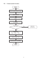
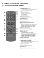
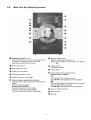
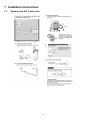
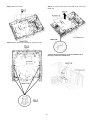
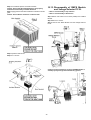
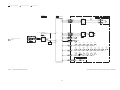
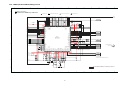
1
PSG1302028CE
CD Stereo System
Model No. SA-AKX36PH
SA-AKX36PN
Product Color: (K)...Black Type
Please refer to the original service manual for:
CD Mechanism Unit , Order No. PSG1102001CE
O Speaker system SB-AKX36PN-K, Order No. PSG1302023CE
O
TABLE OF CONTENTS
PAGE
1 Safety Precautions----------------------------------------------- 3
1.1. General Guidelines---------------------------------------- 3
1.2. Before Use (For PH only)-------------------------------- 4
1.3. Before Repair and Adjustment ------------------------- 4
1.4. Protection Circuitry ---------------------------------------- 4
1.5. Power Supply using SMPS ----------------------------- 5
1.6. Safety Parts Information --------------------------------- 6
2 Warning -------------------------------------------------------------- 7
2.1. Prevention of Electrostatic Discharge (ESD)
to Electrostatically Sensitive (ES) Devices---------- 7
2.2. Precaution of Laser Diode------------------------------- 8
2.3. Service caution based on Legal restrictions -------- 9
2.4. Handling Precautions for Traverse Unit-------------10
3
4
5
6
7
PAGE
2.5. Grounding for electrostatic breakdown
prevention-------------------------------------------------- 11
Service Navigation --------------------------------------------- 12
3.1. Service Information -------------------------------------- 12
3.2. Firmware Update Procedure -------------------------- 13
Specifications ---------------------------------------------------- 14
General/Introduction------------------------------------------- 15
5.1. Media Information---------------------------------------- 15
Location of Controls and Components------------------ 16
6.1. Remote Control Key Button Operation ------------- 16
6.2. Main Unit Key Button Operation---------------------- 17
Installation Instructions -------------------------------------- 18
7.1. Speaker and A/C Connection ------------------------- 18
© Panasonic Corporation 2013. All rights reserved.
Unauthorized copying and distribution is a violation
of law.
8 Service Mode ----------------------------------------------------- 19
8.1. Cold-Start--------------------------------------------------- 19
8.2. Doctor Mode Table--------------------------------------- 20
8.3. Reliability Test Mode (CD Mechanism Unit) ------- 23
8.4. Self-Diagnostic Mode ----------------------------------- 24
8.5. Self-Diagnostic Error Code Table -------------------- 24
8.6. Sales Demonstration Lock Function ---------------- 25
9 Troubleshooting Guide---------------------------------------- 26
10 Disassembly and Assembly Instructions --------------- 27
10.1. Screw Types----------------------------------------------- 27
10.2. Disassembly Flow Chart-------------------------------- 28
10.3. Main Components and P.C.B. Locations ----------- 29
10.4. Disassembly of Top Cabinet--------------------------- 30
10.5. Disassembly of Front Panel Unit --------------------- 31
10.6. Disassembly of Panel P.C.B., LED P.C.B. and
Mic P.C.B. -------------------------------------------------- 32
10.7. Disassembly of Remote Sensor P.C.B.------------- 34
10.8. Disassembly of USB P.C.B. --------------------------- 35
10.9. Disassembly of CD Lid---------------------------------- 35
10.10. Disassembly of Rear Panel---------------------------- 36
10.11. Disassembly of Main P.C.B. --------------------------- 37
10.12. Disassembly of Digital Amplifier IC (IC6000)------ 38
10.13. Disassembly of SMPS Module and Voltage
Selector P.C.B.-------------------------------------------- 39
10.14. Disassembly of CD Mechanism Unit ---------------- 40
10.15. Disassembly of CD Interface P.C.B.----------------- 41
10.16. Disassembly of Fan Unit ------------------------------- 42
11 Service Position ------------------------------------------------- 43
11.1. Checking of Panel P.C.B., LED P.C.B. and Mic
P.C.B.-------------------------------------------------------- 43
11.2. Checking of Main P.C.B. (Side B) -------------------- 43
11.3. Checking of Main P.C.B. (Side A) -------------------- 44
12 Block Diagram --------------------------------------------------- 45
12.1. Servo & System Control -------------------------------- 45
12.2. IC Terminal Chart----------------------------------------- 47
12.3. Audio -------------------------------------------------------- 48
12.4. Power Supply --------------------------------------------- 49
13 Wiring Connection Diagram --------------------------------- 51
14 Schematic Diagram--------------------------------------------- 53
14.1. Schematic Diagram Notes ----------------------------- 53
14.2. MAIN (CD Servo/Micon/Damp) Circuit ------------- 55
14.3. Panel Circuit ----------------------------------------------- 63
14.4. USB, Music Port, Memory LED, Remote
Sensor & CD Interface Circuit ------------------------ 65
15 Printed Circuit Board ------------------------------------------ 66
15.1. Main P.C.B. ------------------------------------------------ 66
15.2. Panel, USB, Music Port & Memory LED
P.C.B.-------------------------------------------------------- 68
15.3. Remote Sensor & CD Interface P.C.B. ------------- 69
16 Appendix Information of Schematic Diagram --------- 71
16.1. Voltage & Waveform Chart ---------------------------- 71
17 Exploded View and Replacement Parts List ----------- 77
17.1. Exploded View and Mechanical replacement
Part List ----------------------------------------------------- 77
17.2. Electrical Replacement Part List --------------------- 83
2
1 Safety Precautions
1.1.
General Guidelines
1. IMPORTANT SAFETY NOTICE
There are special components used in this equipment which are important for safety. These parts are marked by
in the
Schematic Diagrams, Circuit Board Layout, Exploded Views and Replacement Parts List. It is essential that these critical parts
should be replaced with manufacturer’s specified parts to prevent X-RADIATION, shock, fire, or other hazards. Do not modify
the original design without permission of manufacturer.
2. An Isolation Transformer should always be used during the servicing of AC Adaptor whose chassis is not isolated from the AC
power line. Use a transformer of adequate power rating as this protects the technician from accidents resulting in personal
injury from electrical shocks. It will also protect AC Adaptor from being damaged by accidental shorting that may occur during
servicing.
3. When servicing, observe the original lead dress. If a short circuit is found, replace all parts which have been overheated or
damaged by the short circuit.
4. After servicing, see to it that all the protective devices such as insulation barriers, insulation papers shields are properly
installed.
5. After servicing, make the following leakage current checks to prevent the customer from being exposed to shock hazards.
1.1.1.
Leakage Current Cold Check
1. Unplug the AC cord and connect a jumper between the two prongs on the plug.
2. Measure the resistance value, with an ohmmeter, between the jumpered AC plug and each exposed metallic cabinet part on
the equipment such as screwheads, connectors, control shafts, etc. When the exposed metallic part has a return path to the
chassis, the reading should be between 1MΩ and 5.2MΩ.
When the exposed metal does not have a return path to the chassis, the reading must be
1.1.2.
Leakage Current Hot Check
1. Plug the AC cord directly into the AC outlet. Do not use an isolation transformer for this check.
2. Connect a 1.5kΩ, 10 watts resistor, in parallel with a 0.15µF capacitors, between each exposed metallic part on the set and a
good earth ground such as a water pipe, as shown in Figure 1-1.
3. Use an AC voltmeter, with 1000 ohms/volt or more sensitivity, to measure the potential across the resistor.
4. Check each exposed metallic part, and measure the voltage at each point.
5. Reverse the AC plug in the AC outlet and repeat each of the above measurements.
6. The potential at any point should not exceed 0.75 volts RMS. A leakage current tester (Simpson Model 229 or equivalent)
may be used to make the hot checks, leakage current must not exceed 1/2 milliamp. In case a measurement is outside of the
limits specified, there is a possibility of a shock hazard, and the equipment should be repaired and rechecked before it is
returned to the customer.
Figure 1-1
3
1.2.
Before Use (For PH only)
Be sure to disconnect the mains cord before adjusting the voltage selector as shown in Figure 1-2
Use a minus(-) screwdriver to set the voltage selector (on the rear panel) to the voltage setting for the area in which the unit will be
used.
Note that this unit will be seriously damaged if this setting is not made correctly. (There is no voltage selector for some countries,
the correct voltage is already set.)
Figure 1-2
1.3.
Before Repair and Adjustment
Caution:
DO NOT SHORT-CIRCUIT DIRECTLY (with a screwdriver blade, for instance), as this may destroy solid state devices.
After repairs are completed, restore power gradually using a variac, to avoid overcurrent.
Current consumption at AC 110~127 V / 220~240 V, 50/60 Hz in FM Tuner at volume minimum mode should be ~ 500 mA (PH).
Current consumption at AC 120 V, 60 Hz in FM Tuner at volume minimum mode should be ~ 500 mA (PN).
1.4.
Protection Circuitry
The protection circuitry may have operated if either of the following conditions are noticed:
• No sound is heard when the power is turned on.
• Sound stops during a performance.
The function of this circuitry is to prevent circuitry damage if, for example, the positive and negative speaker connection wires are
“shorted”, or if speaker systems with an impedance less than the indicated rated impedance of the amplifier are used.
If this occurs, follow the procedure outlines below:
1. Turn off the power.
2. Determine the cause of the problem and correct it.
3. Turn on the power once again after one minute.
Note:
When the protection circuitry functions, the unit will not operate unless the power is first turned off and then on again.
4
1.5.
Power Supply using SMPS
This model uses SMPS Module to Power up the unit. Below is the part number of the SMPS Model.
N0AB3GL00001 (PN)
N0AD3GL00001 (PH)
1.5.1.
For SA-AKX36PN
Figure 1-3
1.5.2.
For SA-AKX36PH
Figure 1-4
5
1.6.
Safety Parts Information
Safety Parts List:
There are special components used in this equipment which are important for safety.
These parts are marked by
in the Schematic Diagrams, Exploded View & Replacement Parts List. It is essential that these
critical parts should be replaced with manufacturer’s specified parts to prevent shock, fire or other hazards. Do not modify the
original design without permission of manufacturer.
Safety Ref No.
Part No.
16
RGR0443C-A1
Part Name & Description
REAR PANEL
Remarks
PH
PN
16
RGR0443D-A1
REAR PANEL
17
RKM0713-K
TOP CABINET
301
RAE1036Z-V
TRAVERSE ASS'Y
A2
K2CB2CB00022
AC CORD
PN
A2
K2CQ2YY00119
AC CORD
PH
A3
RQT9796-M
O/I BOOK (Sp)
PCB9
N0AB3GL00001
SMPS MODULE
PN
PCB10
N0AD3GL00001
SMPS MODULE
PH
T6000
G4DYA0000214
TRANSFORMER
6
2 Warning
2.1.
Prevention of Electrostatic Discharge (ESD) to Electrostatically Sensitive (ES) Devices
Some semiconductor (solid state) devices can be damaged easily by static electricity. Such components commonly are called Electrostatically Sensitive (ES) Devices.
The following techniques should be used to help reduce the incidence of component damage caused by electrostatic discharge
(ESD).
1. Immediately before handling any semiconductor component or semiconductor-equipped assembly, drain off any ESD on your
body by touching a known earth ground. Alternatively, obtain and wear a commercially available discharging ESD wrist strap,
which should be removed for potential shock reasons prior to applying power to the unit under test.
2. After removing an electrical assembly equipped with ES devices, place the assembly on a conductive surface such as aluminum foil, to prevent electrostatic charge buildup or exposure of the assembly.
3. Use only a grounded-tip soldering iron to solder or unsolder ES devices.
4. Use only an anti-static solder removal device. Some solder removal devices not classified as “anti-static (ESD protected)” can
generate electrical charge sufficient to damage ES devices.
5. Do not use freon-propelled chemicals. These can generate electrical charges sufficient to damage ES devices.
6. Do not remove a replacement ES device from its protective package until immediately before you are ready to install it. (Most
replacement ES devices are packaged with leads electrically shorted together by conductive foam, aluminum foil or comparable conductive material).
7. Immediately before removing the protective material from the leads of a replacement ES device, touch the protective material
to the chassis or circuit assembly into which the device will be installed.
CAUTION:
Be sure no power is applied to the chassis or circuit, and observe all other safety precautions.
8. Minimize bodily motions when handling unpackaged replacement ES devices. (Otherwise harmless motion such as the
brushing together of your clothes fabric or the lifting of your foot from a carpeted floor can generate static electricity (ESD) sufficient to damage an ES device).
7
2.2.
Precaution of Laser Diode
Caution:
This product utilizes a laser diode with the unit turned “on”, invisible laser radiation is emitted from the pickup lens.
Wavelength: 790 nm (CD)
Maximum output radiation power from pickup: 100 µW/VDE
Laser radiation from the pickup unit is safety level, but be sure the followings:
1. Do not disassemble the pickup unit, since radiation from exposed laser diode is dangerous.
2. Do not adjust the variable resistor on the pickup unit. It was already adjusted.
3. Do not look at the focus lens using optical instruments.
4. Recommend not to look at pickup lens for a long time.
Figure 2-1
8
2.3.
Service caution based on Legal restrictions
2.3.1.
General description about Lead Free Solder (PbF)
The lead free solder has been used in the mounting process of all electrical components on the printed circuit boards used for this
equipment in considering the globally environmental conservation.
The normal solder is the alloy of tin (Sn) and lead (Pb). On the other hand, the lead free solder is the alloy mainly consists of tin
(Sn), silver (Ag) and Copper (Cu), and the melting point of the lead free solder is higher approx.30 degrees C (86°F) more than that
of the normal solder.
Definition of PCB Lead Free Solder being used
The letter of “PbF” is printed either foil side or components side on the PCB using the lead free solder.
(See right figure)
Service caution for repair work using Lead Free Solder (PbF)
• The lead free solder has to be used when repairing the equipment for which the lead free solder is used.
(Definition: The letter of “PbF” is printed on the PCB using the lead free solder.)
• To put lead free solder, it should be well molten and mixed with the original lead free solder.
• Remove the remaining lead free solder on the PCB cleanly for soldering of the new IC.
• Since the melting point of the lead free solder is higher than that of the normal lead solder, it takes the longer time to melt the
lead free solder.
• Use the soldering iron (more than 70W) equipped with the temperature control after setting the temperature at 350±30 degrees
C (662±86°F).
Recommended Lead Free Solder (Service Parts Route.)
• The following 3 types of lead free solder are available through the service parts route.
RFKZ03D01K-----------(0.3mm 100g Reel)
RFKZ06D01K-----------(0.6mm 100g Reel)
RFKZ10D01K-----------(1.0mm 100g Reel)
Note
* Ingredient: tin (Sn), 96.5%, silver (Ag) 3.0%, Copper (Cu) 0.5%, Cobalt (Co) / Germanium (Ge) 0.1 to 0.3%
9
2.4.
Handling Precautions for Traverse Unit
The laser diode in the optical pickup unit may break down due to static electricity of clothes or human body. Special care must be
taken avoid caution to electrostatic breakdown when servicing and handling the laser diode in the traverse unit.
2.4.1.
Cautions to Be Taken in Handling the Optical Pickup Unit
The laser diode in the optical pickup unit may be damaged due to electrostatic discharge generating from clothes or human body.
Special care must be taken avoid caution to electrostatic discharge damage when servicing the laser diode.
1. Do not give a considerable shock to the optical pickup unit as it has an extremely high-precise structure.
2. To prevent the laser diode from the electrostatic discharge damage, the flexible cable of the optical pickup unit removed
should be short-circuited with a short pin or a clip.
3. The flexible cable may be cut off if an excessive force is applied to it. Use caution when handling the flexible cable.
4. The antistatic FPC is connected to the new optical pickup unit. After replacing the optical pickup unit and connecting the flexible cable, cut off the antistatic FPC.
Figure 2-2
10
2.5.
Grounding for electrostatic breakdown prevention
• As for parts that use optical pick-up (laser diode), the optical pick-up is destroyed by the static electricity of the working environment.
Repair in the working environment that is grounded.
2.5.1.
Worktable grounding
• Put a conductive material (sheet) or iron sheet on the area where the optical pickup is placed and ground the sheet.
2.5.2.
Human body grounding
• Use the anti-static wrist strap to discharge the static electricity form your body Figure 2-3
Figure 2-3
11
3 Service Navigation
3.1.
Service Information
This service manual contains technical information which will allow service personnel’s to understand and service this model.
Please place orders using the parts list and not the drawing reference numbers.
If the circuit is changed or modified, this information will be followed by supplement service manual to be filed with original service
manual.
• CD Mechanism Unit:
1) This model uses CD Mechanism Unit.
• Micro-processor:
1) The following components are supplied as an assembled part.
- Micro-processor IC, IC2006 (RFKWMAKX36LM)
12
3.2.
Firmware Update Procedure
Start
Write encrypted UPD bin to CD-R
Turn On main set
Insert CD-R (with UPD bin) and
close
TOC reading
"CHECKING"
NG
OK
Writing starts:
"0%" -> "20%" -> "40%" ->
"60%" -> "80%" -> 100%"
"GOOD" display 3 sec
Set auto turn Off -> Cold Start
End
13
"NO PLAY"
process end
4 Specifications
Q Amplifier section
RMS output power stereo mode
Front Ch (both ch driven)
Total RMS stereo mode power
Q Tuner, terminals section
Preset memory
Frequency modulation (FM)
Frequency range
Antenna terminals
Amplitude modulation (AM)
Frequency range
Music port (front)
Sensitivity
Terminal
Aux Input
Q Disc section
Discs played (8 cm or 12 cm)
Pick up
Wavelength
Audio output
Number of channels
FL = Front left channel
FR = Front right channel
*MPEG-1 Layer 3
Q General
Power supply
Power consumption
Dimensions (W x H x D)
Mass
Operating temperature range
Operating humidity range
275 W per channel (3 Ω),
1 kHz, 30% THD
550 W (30% THD)
Power Consumption in
standby mode
FM 30 stations
AM 15 stations
Note:
1. Specifications are subject to change without notice.
Mass and dimension are appropriate
2. Total harmonic distortion is measured by the digital spectrum
analyzer.
87.50 to 108.00 MHz
(50 kHz step) (for PH)
87.5 to 108.0 MHz
(100 kHz step) (for PN)
87.9 to 107.9 MHz
(200 kHz step) (for PN)
75 Ω (unbalanced)
Q System: SC-AKX36PH-K
Main Unit: SA-AKX36PH-K
Front Speakers: SB-AKX36PN-K
Q System: SC-AKX36PN-K
522 kHz to 1629 kHz
(9 kHz step) (for PH)
520 kHz to 1630 kHz
(10 kHz step) (for PH)
520 kHz to 1710 kHz
(10 kHz step) (for PN)
Main Unit: SA-AKX36PN-K
Front Speakers: SB-AKX36PN-K
100 mV, 4.7 kΩ
Stereo, 3.5 mm jack
RCA pin jack
CD, CD-R/RW(CD-DA, MP3*)
790 nm(CD)
2 ch (FL, FR)
Q Internal memory section
Memory
Memory size
2 GB
Media file format support
MP3 (*.mp3)
Memory recording
Bit rate
128 kbps
Memory recording speed
1x, 3x max (CD only)
Recording file format
MP3 (*.mp3)
Capacity of total songs recorded
510 songs
(use 128 kbps, approximately 1 song = 4 mins)
Q USB section
USB port
USB standard
Media file format support
USB device file system
USB port power
Bit rate
USB recording
Bit rate
USB recording speed
Recording file format
AC 110 to 127/220 to 240 V,
50/60 Hz (for PH)
AC 120 V, 60 Hz (for PN)
73 W
220 mm x 334 mm x 250 mm
3 kg
0 °C to +40 °C
35% to 80% RH
(no condensation)
0.5 W (approximate)
USB 2.0 full speed
MP3 (*.mp3)
FAT12, FAT16, FAT32
500 mA (max)
16 kbps to 320 kbps (playback)
128 kbps
1x, 3x max (CD only)
MP3 (*.mp3)
14
5 General/Introduction
5.1.
Media Information
15
6 Location of Controls and Components
6.1.
Remote Control Key Button Operation
16
6.2.
Main Unit Key Button Operation
17
7 Installation Instructions
7.1.
Speaker and A/C Connection
18
8 Service Mode
8.1.
Cold-Start
Here is the procedure to carry out cold-start or initialize to shipping mode.
1. Unplug AC power cord
2. Press & hold [POWER] button
3. Plug AC power cord while [POWER] button being pressed
FL Display will show “_ _ _ _ _ _ _ _”
4. Release [POWER] button
19
8.2.
Doctor Mode Table
8.2.1.
Doctor Mode Table 1
Item
Mode Name
Doctor Mode
Key Operation
FL Display
Description
To enter into Doctor Mode
Front Key
In CD Mode:
1. Press [ ] button on
main unit follow by [4]
and [7] on remote control.
2. To exit, press [DELETE]
button on remote control or,
press [POWER, /I] button on
Main Unit
EEPROM
checksum
check
Displaying of
1. Year Develop.
2. Model Type.
3. ROM Type.
4. Firmware Version.
In CD mode:
1. Enter into Doctor Mode
(Display 1)
1 2
3
4
Version No. (001 ~ 999)
firmware
(Decimal)
specific for each
(Display 2)
Checksum (Hex)
20
8.2.2.
Doctor Mode Table 2
Key Operation
Item
Mode Name
Volume Setting
Check
FL Display
Description
Front Key
To check the volume setting of the
main unit.
In Doctor Mode:
1. Press [7], [8], [9] button on
the remote control.
Press [7]: VOL50
Press [8]: VOL35
Press [9]: VOL0
Volume
FL Display Check To check the FL segment display.
All segments will light up while all LED
blink at 0.5s intervals.
In Doctor mode:
1. Press [1] button on the
remote control.
2. To cancel this mode, press
[0] button on the remote control.
Traverse Test
In Doctor Mode:
1. Press [10] [1] [2] button
on the remote control.
To determine the traverse unit
operation for inner & outer access track.
In this mode,ensure the CD is in the
main unit.
The counter will
increment by one.
When reach 99999999
will change to 00000000
Cancellation Display
Reliability Test
(Combination)
Note: Refer to Section 8.3 Figure 8-2
.for process flow
2. To cancel this mode, press
[0] button on the remote control.
To determine the traverse unit
operation & open/close operation of the
mechanism.
In Doctor Mode:
1. Press [10] [1] [5] button
on the remote control.
In this mode,ensure the CD is in the
main unit.
The counter will
increment by one.
When reach 99999999
will change to 00000000
Cancellation Display
Loading Test
Note: Refer to Section 8.3 Figure 8-3
for process flow
2. To cancel this mode, press
[0] button on the remote control.
To determine the open & close
operation of the CD Mechanism Unit.
In Doctor Mode:
1. Press [10] [2] [1] button
on the remote control.
In this mode, the tray will open & close
automatically.
The counter will
increment by one.
When reach 99999999
will change to 00000000
Cancellation Display
2. To cancel this mode, press
[0] button on the remote control.
Note: Refer to Section 8.3 Figure 8-1
for process flow
21
8.2.3.
Doctor Mode Table 3
Key Operation
Item
Mode Name
CD
Self- Adjustment
Test
FL Display
Description
Front Key
To display result of
self-adjustment for CD.
In Doctor Mode:
1. Press [10] [1] [4] button
on the remote control.
Display of auto adjustment
result
Reference table:
ERROR Code
Status
Condition
0 1 2 4 6 8 A C E F
AOC1/AOC2 O
O O O O O O O -
ABC2/ABC1
O - X O X O X O X -
2nd AOC1
O - O X X O O X X -
FAGC/TAGC O - O O O X X X X AGC2
CD LSI Version
Check
For checking CD LSI Version and
checksum information.
O - O O O O O O O
O : OK;
X : NG (In case that time out happens.)
: Either one of FO AOC, TR AOC and FO
coarse AGC is NG.
: If the AGC is NG (ignore others).
To cancel this mode, press [0]
button on the remote control.
(Display 1)
In Doctor Mode:
1. Press [4] button on the
remote control.
ROM
Type
Version (Decimal)
Year Develop
after
2 sec
(Display 2)
Checksum (Hex)
22
To cancel this mode, press [0]
button on the remote control.
8.3.
Reliability Test Mode (CD Mechanism Unit)
Below is the process flow chart of the aging test for the CD Mechanism Unit .
OPEN
Operation
First Track
Access
OPEN wait
for 1 s
CLOSE
Operation
First Track
Play 5 s
Count up
Last Track
Access
Last Track
Play 5 s
CLOSE wait
for 4 s
Fig. 1. Reliability Test (Loading)
Count up
Fig. 2. Reliability Test (Traverse)
First Track
Access
First Track
Play 10 s
Last Track
Access
Count up
Last Track
Play 10 s
Open
Operation
Open wait
for 1 s
CLOSE
Operation
Fig. 3. Reliability Test (Combination)
23
8.4.
Self-Diagnostic Mode
Item
Mode Name
Self Diagnostic
Mode
FL Display
Description
Key Operation
Front Key
To enter into self diagnostic checking
Step 1: Select CD mode
(Ensure no disc is inserted).
Step 2: Press & hold [ ] button
follow by [
/
] on
main unit for 2 seconds.
Error code
information
System will perform a check on any
unusual/error code from the memory
Example:
Step 1: In self diagnostic mode,
Press [ ] on main unit.
To exit, press [^/I] on main
unit or remote control.
Delete error
code
Step 1: In self diagnostic mode,
Press [0] on remote control.
To clear the stored in memory
(EEPROM IC)
To exit, press [^/I] on main
unit or remote control.
Cold Start
8.5.
To active cold start upon next AC
power up when reset start is
execute the next time.
In self diagnostic mode:
1. Press [3] button on
the remote control.
Self-Diagnostic Error Code Table
Self-Diagnostic Function (Refer Section 8.4. Self-Diagnostic Mode) provides information on any problems occurring for the unit and
its respective components by displaying the error codes. These error code such as U**, H** and F** are stored in memory and held
unless it is cleared.
The error code is automatically display after entering into self-diagnostic mode.
8.5.1.
Power Supply Error Code Table
24
8.5.2.
CD Mechanism Error Code Table (CD Mechanism Unit)
Error Code
Diagnostic Contents
Description of error
Automatic FL Display
Remarks
CD H15
CD Open Abnormal
During operation
POS_SW_R On fail to be
detected with 4 sec. Error
No. shall be clear by force
or during cold start.
Press [ ] on main unit for
next error.
CD H16
CD Closing Abnormal
During operation
POS_SW_CEN On fail to
be detected with 4 sec.
Error No. shall be clear by
force or during cold start.
Press [ ] on main unit for
next error.
F26
Communication between
CD servo LSI and micro-p
abnormal.
During switch to CD function, if SENSE = “L” within
failsafe time of 20ms.
Press [ ] on main unit for
next error.
8.6.
8.6.1.
Sales Demonstration Lock Function
Entering into Sales demonstration lock mode
Here is the procedures to enter into the Sales demonstration lock mode.
Step 1: Turn on the unit.
Step 2: Select to any mode function.
Step 3: Press and hold [ OPEN/CLOSE] and [CD] keys for 5 sec or more.
The display will show upon entering into this mode for 2 sec..
Note: [
8.6.2.
OPEN/CLOSE]
button is invalid and the main unit displays “LOCKED” while the lock function mode is entered.
Cancellation of Sales demonstration lock mode
Step 1: Turn on the unit.
Step 2: Select to any mode function.
Step 3: Set volume to Vol 19.
Step 4: Press and hold [ OPEN/CLOSE] and [CD] keys for 5 sec or more.
The display will show upon entering into this mode for 2 sec..
25
9 Troubleshooting Guide
"Contents for this section is not available at time of issue"
26
10 Disassembly and Assembly Instructions
• Illustration is based on SA-AKX36PH-K.
Caution Note:
• This section describes the disassembly and/or assembly procedures for all major printed circuit boards & main components for the unit. (You may refer to the section of “Main components and P.C.B Locations” as described in the service
manual)
• Before carrying out the disassembly process, please ensure all the safety precautions & procedures are followed.
• During the disassembly and/or assembly process, please handle with care as there may be chassis components with
sharp edges.
• Avoid touching heatsinks due to its high temperature after prolong use. (See caution as described below)
• During disassembly and assembly, please ensure proper service tools, equipments or jigs is being used.
• During replacement of component parts, please refer to the section of “Replacement Parts List” as described in the service manual.
• Select items from the following indexes when disassembly or replacement are required.
• Disassembly of Top Cabinet
• Disassembly of Front Panel Unit
• Disassembly of Panel P.C.B., LED P.C.B. and Mic P.C.B.
• Disassembly of Remote Sensor P.C.B.
• Disassembly of USB P.C.B.
• Disassembly of CD Lid
• Disassembly of Rear Panel
• Disassembly of Main P.C.B.
• Replacement of Digital Amplifier IC (IC6000)
• Disassembly of SMPS Module and Voltage Selector P.C.B.
• Disassembly of CD Mechanism Unit
• Disassembly of CD Interface P.C.B.
• Disassembly of Fan Unit
10.1. Screw Types
27
10.2. Disassembly Flow Chart
10.4.Top Cabinet
10.5. Front panel Unit
10.16. Fan Unit
10.10. Rear Panel
10.6. Panel P.C.B.,
LED P.C.B. and
Mic P.C.B.
10.11. Main P.C.B.
10.7. Remote Sensor
P.C.B.
10.12.Digital Amplifier
IC (IC6000)
10.8. USB P.C.B.
10.13.SMPS Module
and Voltage
Selector P.C.B.
10.9. CD Lid
10.14. CD Mechanism
Unit
10.15. CD Interface
P.C.B.
28
10.3. Main Components and P.C.B. Locations
29
10.4. Disassembly of Top Cabinet
Step 4 Slightly lift up both sides of Top Cabinet in an outward
direction as shown.
Step 5 Remove the Top Cabinet.
Step 1 Remove 2 screws on each side.
Step 2 Remove 5 screws.
Step 3 Slightly pull both side of Top Cabinet outwards as arrow
shown.
Caution: During assembling, ensure that the Top Cabinet
catches are properly inserted into Front Panel Unit.
30
10.5. Disassembly of Front Panel
Unit
Step 3 Release tab at the left side of Front Panel Unit.
• Refer to “Disassembly of Top Cabinet”.
Step 1 Detach 5P Cable at the connector (CN2002) on Main
P.C.B..
Step 2 Detach 30P FFC at the connector (CN2000) on Main
P.C.B..
31
Step 4 Release tabs at bottom.
Step 6 Remove the Front Panel Unit as arrow shown.
10.6. Disassembly of Panel P.C.B.,
LED P.C.B. and Mic P.C.B.
• Refer to “Disassembly of Top Cabinet”.
• Refer to “Disassembly of Front Panel Unit”.
Step 5 Release tab at the right side of Front Panel Unit.
Step 1 Remove the Volume Knob.
Step 2 Remove the Control Knob.
32
Step 3 Remove 7 screws.
Step 5 Lift up the Panel P.C.B. and LED P.C.B. from Front
Panel Unit.
Step 4 Release catches by following the sequences (1-8).
Caution: During assembling, ensure that LED P.C.B. is
properly insert to Front Panel Unit.
33
Caution: During assembling, ensure that Mic P.C.B. is
seated properly through the located & fully catched.
Caution: During assembling, ensure that Panel P.C.B. is
seated properly through the located & fully catched.
10.7. Disassembly of Remote Sensor
P.C.B.
• Refer to “Disassembly of Top Cabinet”.
• Refer to “Disassembly of Front Panel Unit”.
• Refer to “Disassembly of Panel P.C.B., LED P.C.B. and
Mic P.C.B.”.
Step 1 Remove the Remote Sensor P.C.B..
Caution: During assembling, ensure that Remote Sensor
P.C.B. is properly inserted & fully connected to Panel
P.C.B..
Step 6 Remove 1 screw.
Step 7 Release 1 catch.
Step 8 Remove the Panel P.C.B., LED P.C.B. and Mic P.C.B..
34
10.8. Disassembly of USB P.C.B.
10.9. Disassembly of CD Lid
• Refer to “Disassembly of Top Cabinet”.
• Refer to “Disassembly of Front Panel Unit”.
• Refer to “Disassembly of Top Cabinet”.
• Refer to “Disassembly of Front Panel Unit”.
Step 1 Remove 1 screw.
Step 2 Release 1 catch.
Step 3 Remove the USB P.C.B..
Step 1 Remove the spring as arrow shown in order of
sequence (1) to (3).
Caution: During assembling, ensure that the spring is
assembly at correct position.
Caution: During assembling, ensure that USB P.C.B. is
seated properly through the located & fully catched.
Step 2 Remove CD Lid as arrow shown.
35
10.10. Disassembly of Rear Panel
Step 5 Lift up Inner Chassis Unit to release the catch between
the Inner Chassis Unit and the Rear Panel.
• Refer to “Disassembly of Top Cabinet”.
Step 1 Remove 10 screws.
Step 6 Release 2 tabs.
Step 7 Remove Rear Panel.
Step 2 Detach Voltage Selector P.C.B. from Rear Panel as
arrow shown.
Step 3 Release 1 catch at the Fan Unit .
Step 4 Remove the Fan Unit .
36
10.11. Disassembly of Main P.C.B.
Step 8 Remove the Main P.C.B..
Caution: During assembling, ensure that Main P.C.B. is
seated properly through the located & fully guided.
• Refer to “Disassembly of Top Cabinet”.
• Refer to “Disassembly of Rear Panel”.
Step 1 Detach 5P Cable at the connector (CN2002) on Main
P.C.B..
Step 2 Detach 30P FFC at the connector (CN2000) on Main
P.C.B..
Step 3 Detach 13P Cable at the connector (CON2) on SMPS
Module.
Step 4 Detach 10P FFC at the connector (CN8251) on Main
P.C.B..
Step 5 Detach 24P FFC at the connector (FP8201) on Main
P.C.B..
Step 6 Detach 2P Wire at the connector (CN1001) on Main
P.C.B..
Step 7 Remove 2 screws.
37
10.12. Disassembly of Digital Amplifier IC (IC6000)
Step 4 Desolder the pins of the Digital Amplifier IC (IC6000).
Step 5 Remove the Digital Amplifier IC (IC6000).
• Refer to “Disassembly of Main P.C.B.”.
10.12.1. Disassembly of Digital Amplifier IC
(IC6000)
Caution: Handle the Main P.C.B. with caution due to it’s
high temperature after prolonged use. Touching it may
lead to injuries.
Step 1 Place the Main P.C.B. on an insulated material.
Step 2 Remove 2 screws.
10.12.2. Assembly of Digital Amplifier IC
(IC6000)
Step 1 Fix the Digital Amplifier IC (IC6000) onto the Main
P.C.B..
Step 2 Solder the pins of the Digital Amplifier IC (IC6000).
Cautions: Ensure that the pins of the Digital Amplifier IC
(IC6000) is positioned correctly on the Main P.C.B. before
soldering.
Step 3 Lift up the Main P.C.B. as arrow shown.
Caution: Keep the Heatsink Spacers in safe place. Avoid
denting it, place it back during assembling.
38
10.13. Disassembly of SMPS Module
and Voltage Selector P.C.B.
Step 3 Fix Heatsink spacers onto Main Heatsink..
Caotion: Ensure that the Heatsink Spacers are properly
located and seated flatly onto Main Heatsink.
Step 4 Apply grease to the Main Heatsink as indicate in the diagram.
Caution: Ensure Grease thickness is about 0.2mm.
• Refer to “Disassembly of Top Cabinet.”.
• Refer to “Disassembly of Rear Panel”.
Step 1 Detach 13P Cable at a connector (CON2) on the SMPS
Module.
Step 2 Remove 2 screws.
Step 3 Remove the SMPS Module and the Voltage Selector
P.C.B..
Step 5 Upset the Main P.C.B..
Step 6 Fix 2 screws.
Caution: During assembling, ensure that SMPS Module is
seated properly through the located & fully guided.
39
10.14. Disassembly of CD Mechanism Unit
Step 2 Detach Voltage Selector P.C.B. from the Rear Panel.
Step 3 Detach 10P FFC at a connector (CN8251) on Main
P.C.B..
Step 4 Detach 24P FFC at a connector (FP8201) on Main
P.C.B..
Step 5 Detach 2P Wire at a connector (CN1001) on Main
P.C.B..
Step 6 Remove 1 screw.
• Refer to “Disassembly of Top Cabinet”.
• Refer to “Disassembly of Front Panel Unit”.
Step 1 Remove 8 screws.
Step 7 Remove 1 screw.
40
Step 10 Remove 2 screws.
Step 11 Remove the CD Mechanism Unit.
Step 8 Release 2 catches.
Step 9 Lift up and remove the Inner Chassis Unit.
10.15. Disassembly of CD Interface
P.C.B.
• Refer to “Disassembly of Top Cabinet”.
• Refer to “Disassembly of Front Panel Unit”.
• Refer to “Disassembly of CD Mechanism Unit”.
Caution: During assembling, ensure that Inner Chassis
Unit is catched onto Rear Panel properly.
Step 1 Remove 3 screws.
Step 2 Desolder pins of the motor (M7301).
Step 3 Desolder pins of the motor (M7302).
Step 4 Remove the CD Interface P.C.B..
41
10.16. Disassembly of Fan Unit
• Refer to “Disassembly of Top Cabinet”.
Step 1 Remove 1 screw.
Step 2 Detach 2P Wire at a connector (CN1001) on the Main
P.C.B..
Step 3 Release 1 catch.
Step 4 Remove the Fan Unit.
Caution: During assembling, ensure that Fan Unit is
catched onto Rear Panel properly.
42
11 Service Position
11.2. Checking of Main P.C.B. (Side
B)
Note: For description of the disassembly procedures, see
the Section 10.
11.1. Checking of Panel P.C.B., LED
P.C.B. and Mic P.C.B.
Step 1 Remove Top Cabinet.
Step 2 Remove Rear Panel.
Step 3 Remove Main P.C.B..
Step 4 Remove 2 screws.
Step 1 Remove Top Cabinet.
Step 2 Remove Front Panel Unit.
Step 3 Remove the Panel P.C.B., the LED P.C.B. and Mic
P.C.B..
Step 4 Positioned the Panel P.C.B., the LED P.C.B. and Mic
P.C.B. on the insulated material as shown.
Step 5 Attach 30P FFC at a connector (CN2000) on the Main
P.C.B..
Step 6 Panel P.C.B., the LED P.C.B. and Mic P.C.B. can be
checked at diagram shown.
Step 5 Lift up the Main P.C.B. as arrow shown.
43
11.3. Checking of Main P.C.B. (Side
A)
Step 6 Attach 13P Cable at a connector (CON2) on the SMPS
Module.
Step 7 Attach 30P FFC at a connector (CN2000) on the Main
P.C.B..
Step 8 Attach 10P FFC at a connector (CN8251) on the Main
P.C.B..
Step 9 Attach 24P FFC at a connector (FP8201) on the Main
P.C.B..
Step 10 Attach 2P FFC at a connector (CN1001) on the Main
P.C.B..
Step 11 Side B Main P.C.B. can be checked at diagram shown.
Step 1 Remove Top Cabinet.
Step 2 Remove Front Panel Unit.
Step 3 Remove Rear Panel.
Step 4 Remove Main P.C.B..
Step 5 Remove SMPS Module and Voltage Selector P.C.B..
Step 6 Positioned the Main P.C.B., SMPS Module and the Voltage Selector P.C.B. on the insulated material.
Step 7 Attach 13P Cable at a connector (CON2) on the SMPS
Module.
Step 8 Attach 10P FFC at a connector (CN8251) on the Main
P.C.B..
Step 9 Attach 24P FFC at a connector (FP8201) on the Main
P.C.B..
Step 10 Attach 30P FFC at a connector (CN2000) on the Main
P.C.B..
Step 11 Attach 2P FFC at a connector (CN1001) on the Main
P.C.B..
Step 12 Side A Main P.C.B. can be checked at diagram shown.
44
12 Block Diagram
12.1. Servo & System Control
: CD AUDIO INPUT SIGNAL LINE
: USB SIGNAL LINE
: AUDIO OUTPUT SIGNAL LINE
MAIN P.C.B.
IC8001
MN6627992AB
SERVO
PROCESSOR
USB P.C.B.
IC7704
C3ABMY000027
CN6400
16M SDRAM
USB PORT
+5V
TC - 1
A0 ~ A11
USBDM1 123
D-
CN2002 ZJ6400*
D+
CN2002 ZJ6400*
2
USBDP1 125
3
TC - 2
D0 ~ D7
D-
IC2006
RFKWMAKX36LM
16M FLASH
MEMORY
MICROPROCESSOR
SWITCH
+5V
2 D-
2
D+
3 D+
3
Q2500
IC8401
C3FBMY000309
1 VBUS
D6400
D5V
CN2002 ZJ6400*
5
D5V
5
QR2500
SCLK 6
SI 5
SO 2
LED DRIVE
USB REC LED 65
33 CLKSF
34 IO0SF
30 IO1SF
IC2007
C3EBEY000037
90 XI1
EEPROM
X8101
89 XO1
SCL 6
29 EE CLK
SDA 5
28 EE DATA
NRST 19
Q2001
IC8501
C3FBXY000042
RESET
2GB NAND
FLASH MEMORY
CD MECHANISM UNIT
BRS11C
DAT0
DAT1
DAT2
DAT3
DAT3
OPTICAL
PICKUP UNIT
3
4
5
2
16
+3.3V
15 XI
D2002
X2001
38
37
40
39
MSDDAT0
MSDDAT1
MSDDAT2
MSDDAT3
16 XO
13 XTIN
X2002
12 XTOUT
FP8201
60 A
16
FP8201
P33 135
55 AMUTE
ANALOG SEL1 5
SCL5 112
62 USB IN
ANALOG SEL 2 7
58 B
15
FP8201
59 C
20
CD TRACKING SIGNAL
FP8201
SREQ/BLKCK 113
EMO1 26
73 CD STAT (SYS TXD)
EMO2 27
57 D
19
SO/STAT 106
FP8201
55 E
14
SI/MDATA 107
FP8201
72 CD MDATA (SYS RXD)
TU CLK 9
56 F
10
MCLK 108
FP8201
MD/LPD
IRQ1A/MLD 105
61 PD
5
FP8201
54 CD BLKCK
CD-LD
NRST 104
74 CD MCLK
TU RST 10
71 CD MLD
TU SDA 8
61 CD RESET
TU INT 25
ANA SEL1
ANA SEL1
ANA SEL2
ANA SEL2
EMO1
EMO2
TU SCL
TU RST
TU SDA
TU INT
6
USBNOC 133
Q8201
62 LD
LASER DRIVE
USBPP 132
32 BOOT FILE ANALYSIS
TRVP2 52
31 BOOT FILE DET
IC8251
C0GBY0000117
+3.3V
F+
FP8201
VINFC 1
FT+
SRDAT 117
BCLK 116
16 VOTK-
22
FP8201
48 FOP
13 VOFC-
24
FP8201
DAP SDA/DSP SDA 34
AUDIOCLK 118
14 VOFC+
23
VINTK 26
T-
49 TRP
LRCK 115
15 VOTK+
21
SRDATAIN 114
P31 137
P32 136
M7302*
CD I2S MCLK
CD I2S SDO
CD I2S BCLK
CD I2S LRCK
DAP I2S OUT
DAP I2S LRCKO
DAP I2S BCKO
CD I2S MCLK
/DAMP OTW 41
CD I2S SDO
/DAMP CLIP 42
CD I2S BCLK
CD I2S LRCK
/DAMP FAULT 43
FROM/TO AUDIO
AUTO BASS 93
DAP I2S OUT
BKND ERR 49
DAP I2S LRCKO
DAP VALID 50
DAP I2S BCKO
MPORT SW 79
SPINDLEMOTOR
+
SPM-
CN7002 CN8251
9
SPM+
CN7002 CN8251
TRV+
CN7002 CN8251
10
1
+
TRV-
SPM+
1
18 VOSP-
12 VOSL+
TRV-
11 VOSL-
9
DAMP RESET 44
VINSP 23
50 SPOUT
VINSL 4
51 TRVP
LDM+
134
LDM+
CN7002 CN8251
5
3
CN7001
LDM-
LDM-
4
LDM+
8
CN7002 CN8251
4
7
LDM-
SYNC 88
DC DET2 53
10 VOLD+
REV 7
59 LOAD CCW
9 VOLD-
FWD 6
60 LOAD CW
SMPS BP 70
ECO CTNRL 51
PROTECT 22
S7201
RESET
REST SW
CN7002 CN8251
7
REST SW
58 CD REST SW
4
POWER 23
PCONT 90
CN7001
OPEN SW
OPEN SW
CN7002 CN8251
3
5
CN7001
CLOSE SW
DAP PDN
DAP MUTE
DAP SCL
DAP SDA
DAMP OTW
DAMP CLIP
DAMP FAULT
AUTOBASS
TU RST
TU INT
DAP RESET
DAP PDN
DAP MUTE
DAP SDA
DAMP OTW
DAMP CLIP
DAMP FAULT
AUTOBASS
BKND ERR
DAP VALID
DAP VALID
DAMP RESET
FROM/TO AUDIO
DAP SCL
BKND ERR
MPORT SW
TO SERVO & SYSTEM CONTROL
BLOCK (2/2)
TU SDA
MPORT SW
DAMP RESET
TEMP DET
SMPS-ID
TEMP DET
SMPS ID
P30
TRAVERSE MOTOR
CN7001
TEMP DET 97
SMPS ID 95
M7301*
LOADING P.C.B.
DAP RESET
EMO2
TU SCL
17 VOSP+
TRV+
10
CN7002 CN8251
2
SPM-
2
DAP PDN 47
DAP MUTE 48
DAP CLK/DSP CLK 36
5CH MOTOR DRIVER
FP8201
DAP RESET 46
33 EMMC/USB2 DET
EMO1
CLOSE SW
CN7002 CN8251
1
8
OPEN SW
6
CLOSE SW
3
57 CD OPEN SW
EN 76
56 CD CLOSE SW
OC 75
SYNC
DC DET PWR
AM-BP
ECO CTR
PROT
POWER
PCONT
EN
OC
SYNC
DC DET PWR
AM BP
ECO CTR
FROM/TO POWER SUPPLY
PROT
POWER
PCONT
EN
OC
CD INTERFACE P.C.B.
NOTE: “ * ” REF IS FOR INDICATION ONLY
SA-AKX36PH/PN SERVO & SYSTEM CONTROL (1/2) BLOCK DIAGRAM
45
: CD AUDIO INPUT SIGNAL LINE
: USB SIGNAL LINE
: AUDIO OUTPUT SIGNAL LINE
MAIN P.C.B.
IC2006
RFKWMAKX36LM
PANEL P.C.B.
MICROPROCESSOR
QR6001,
QR6003,QR6004
LED DIMMER 78
LED RED 82
LED GREEN 83
LED DIMMER
CN2000 CN6001
3
CN2000 CN6001
GREEN LED
CN2000 CN6001
27
28
+5V
LED DIMMER
LED CA
28
RED LED
MEMORY LED P.C.B.
CN6003 ZJ6700*
1
RED LED
LED CA
1
LED
LIGHTING
CIRCUIT
4
GREEN LED
3
D6700
LED AN
CN6003 ZJ6700*
2
LED AN
2
D6102,D6103,
D6104,D6105,
FL6000
FL DISPLAY
FROM AUDIO
DC DET AMP FAN
DC DET AMP FAN
40 DC DET1
FL DATA 1
FL CS 2
IC1001
C0ABBB000067
FL CLK 3
FL DOUT
CN2000 CN6001
FL CS
CN2000 CN6001
12
11
FL CLK
7 DIN
19
FL CS
FL CLK
8 CLK
21
F- 44
F-
F+ 1
F+
SG1 ~ SG16
GR1 ~ GR12
9 STB
20
CN2000 CN6001
10
FL DOUT
FAN CONTROL
Q1001,Q1002,Q1003,
Q1004,Q1005,QR1001
TO SERVO & SYSTEM CONTROL
BLOCK (1/2)
+
-
2
-
-
CN1001
CN1001
-
1
VOL JOG A 80
POSITIVE
NEGATIVE
VOL JOG B 81
FAN
CIRCUIT
CN2000 CN6001
16
JOG VOLB
CN2000 CN6001
15
IC6000
C0HBB0000057
JOG VOLA
15
VR6100
FL DISPLAY
DRIVER
VOLUME
JOG VOLB
16
+16V
20 FAN OUT1
ROTARY JOG A 67
FAN
JOG VOLA
ROTARY JOG B 68
QR2001
SWITCH
JOG ROTA
CN2000 CN6001
JOG ROTB
CN2000 CN6001
18
17
JOG ROTA
13
VR6200
ALBUM/TRACK
JOG ROTB
14
21 FAN OUT2
KEY1 99
KEY2
CN2000 CN6001
7
S6003
S6000
S6001
S6002
S6004
S6006
PLAYLIST 1
PLAYLIST 2
PLAYLIST 3
PLAYLIST 4
PLAYLIST 5
PLAYLIST 6
S6203
CD
OPEN/CLOSE
S6012
LATIN
PRESET EQ
S6202
S6206
STOP/TUNE MODE
MANUAL EQ
D.BASS
S6103
S6104
S6100
S6101
S6105
S6208
ALBUM/TRACK
MEMORY/USB
CD
RADIO/EXT-IN
PLAY/PAUSE
FORWARD
KEY2
24
S6107
POWER
KEY2 98
KEY3 94
KEY1
CN2000 CN6001
8
KEY3
S6207
USB
REC/PAUSE
S6201
REWIND
S6204
MEMORY
REC/PAUSE
KEY1
23
CN2000 CN6001
6
S6200
KEY3
25
REMOTE SENSOR P.C.B.
IR6500
REMOTE SENSOR
RMT 86
NOTE: “ * ” REF IS FOR INDICATION ONLY
RMT
CN2000 CN6001 CN6002 CN6500
9
22
3,4
3,4
RMT
+3.3V
SA-AKX36PH/PN SERVO & SYSTEM CONTROL (2/2) BLOCK DIAGRAM
46
12.2. IC Terminal Chart
IC7704
16M SDRAM
TC
1
TC
2
SIGNAL NAME
IC8001
SERVO PROCESSOR
PORT NAME
PIN NO
PIN NO
PORT NAME
A0
21
A0
14
A0
A1
22
A1
15
A1
A2
23
A2
16
A2
A3
24
A3
17
A3
A4
27
A4
20
A4
A5
28
A5
21
A5
A6
29
A6
22
A6
A7
30
A7
23
A7
A8
31
A8
24
A8
A9
32
A9
25
A9
A10
20
A10
13
A10
BA0
19
A11
26
A11
IC7704
16M SDRAM
SIGNAL NAME
IC8001
SERVO PROCESSOR
PORT NAME
PIN NO
PIN NO
PORT NAME
DQ0 / DQ15
2 / 49
D0
142
D0
DQ1 / DQ14
3 / 48
D1
143
D1
DQ2 / DQ13
5 / 46
D2
144
D2
DQ3 / DQ12
6 / 45
D3
2
D3
DQ4 / DQ11
8 / 43
D4
3
D4
DQ5 / DQ10
9 / 42
D5
4
D5
DQ6 / DQ9
11 / 40
D6
5
D6
DQ7 / DQ8
12 / 39
D7
6
D7
SA-AKX36PH/PN IC TERMINAL CHART
47
12.3. Audio
: CD AUDIO INPUT SIGNAL LINE
: AUX/TUNER/MUSIC PORT AUDIO INPUT SIGNAL LINE
: AM SIGNAL LINE
: AUDIO OUTPUT SIGNAL LINE
: FM SIGNAL LINE
MAIN P.C.B.
IC6100
C0JBAR000367
AUDIO SELECTOR
ANA SEL2
ANA SEL2
ANA SEL1
ANA SEL1
9 A(LSB)
10 B(MSB)
QR6100
FROM/TO
SERVO & SYSTEM CONTROL
MPORT SW
SWITCH
MPORT SW
MUSIC PORT P.C.B.
JK6301
IC6500
C1AB00003993
5
MPORT SW
4
R
MUSIC PORT
L
ZJ6300* ZJ6000* CN6001 CN2000
1
3
12
ZJ6300* ZJ6000* CN6001 CN2000
MPORT L
ZJ6300* ZJ6000* CN6001 CN2000
2
4
2
9
MPORT SW
MPORT R
22
11
DIGITAL AUDIO
PROCESSOR
19
MPORT R
4
2
1
20
MPORT L
14 R1
IC6000
C1AB00003986
POWER AMPLIFIER
SPEAKERS
5 L1
49 PWM P 4
PWM M 1 38
6 INPUT B
BST A 44
D6501
1
AUTOBASS
6
AUTOBASS
43 PWM P 3
PANEL P.C.B.
7
PWM P 1 39
5 INPUT A
PWM M 2 40
15 INPUT D
PWM P 2 41
14 INPUT C
OUT A 40
OUT A 39
JK6000
4
JK6000
OUT B 35
3
+
LEFT
BST B 43
EMO2
EMO1
JK6002
L
2
DAP RESET
AUX-L
1 L0
DAP PDN
AUX IN
R
3
AUX-R
12 R0
FROM/TO
SERVO & SYSTEM CONTROL
1
DAP MUTE
2 FMI
DAP PDN
DAP MUTE
DAP SCL
DAP SDA
BKND ERR
10 ASEL EMO2
BST D 23
15 EMO1
16 /RESET
OUT D 27
OUT D 28
18 /PDN
21 SCL
2
AM ANT
3
4 AMI
2
1
1
6
2
RIN 15
13 RCH
LIN 16
3 LCH
CD I2S MCLK
CD I2S SDO
CD I2S SDO
CD I2S BCLK
CD I2S BCLK
CD I2S LRCK
CD I2S LRCK
RIGHT
-
34 /BKND ERR
+12V
DC DET AMP FAN
DC DET AMP FAN
11 MCLK
Q6001,Q6002
Q6007,Q6300
24 SDIN1
23 SCLK
/FAULT 16
DAMP FAULT
DAMP FAULT
22 LRCLK
DCLK 17
/CLIP 18
DFS 14
/RESET 4
DOUT 13
+
BST C 24
/OTW 17
4
1
JK6000
20 SDA
L52
JK52
JK6000
OUT C 32
19 /MUTE
DC DETECT
CIRCUIT
CD I2S MCLK
FM ANT
DAP RESET
DAP SCL
FM/AM
RADIO RECEIVER
JK51
EMO1
DAP SDA
BKND ERR
IC52
VUEALLPT056
EMO2
DAMP OTW
DAP CLIP
DAMP RESET
DAMP OTW
DAMP CLIP
DAMP RESET
FROM/TO
SERVO & SYSTEM CONTROL
25 SDIN2
SDIO 8
SCLK 7
RST 5
GCGPIO2 18
DAP I2S OUT
TO SERVO & SYSTEM CONTROL
DAP I2S BCKO
DAP I2S LRCKO
TU INT
FROM/TO
SERVO & SYSTEM CONTROL
DAP I2S OUT
DAP I2S BCKO
DAP I2S LRCKO
29 SDOUT
VALID 37
DAP VALID
DAP VALID
31 LRCLKO
30 SCLKO
TU INT
TU RST
TU RST
TU SCL
TU SCL
TU SDA
TU SDA
NOTE: “ * ” REF IS FOR INDICATION ONLY
SA-AKX36PH/PN AUDIO BLOCK DIAGRAM
48
12.4. Power Supply
MAIN P.C.B.
SMPS MODULE
PW +32.5V
PW SYS3R3V
-
CN1000*
-
6
+32.5V
+3.3V
PW SYS3R3V
SYS3V3
PW +6V
PW +5V
1
2
+5V
PW +5V
3
IC2030
C0DBZYY00311
HIGH SIDE
SWITCH
PW +5V
1 VIN
VOUT 5
VBUS
VBUS
OC
/OC 4
EN
EN 3
EN
IC1003
C0DBAYY01594
FROM/TO
SERVO & SYSTEM CONTROL
+6V DC-DC
CONVERTER
AC INLET
SWITCHING MODE
POWER SUPPLY
CIRCUIT
PW +6V
10 PH
PCONT
EN 3
4
OC
PCONT
1 BOOT
7 VSENSE
PW +16V
PW +16V
5
2 VIN
PW +16V
+16V
IC1002
C0DBAYY01594
+12V DC-DC
CONVERTER
PW +16V
10 PH
EN 3
1 BOOT
7 VSENSE
-
CN1000*
-
1,2
-
-
-
-
32.5V
PW +32.5V
2 VIN
CN1000* POWER
POWER
12
CN1000* PROT
PROT
7
CN1000* ECO CTR
ECO CTR
13
CN1000* AM-BP
-
9
-
CN1000*
-
11
-
CN1000*
-
8
-
CN1000*
-
10
AM-BP
SYNC
SYNC
SMPS-ID
SMPS-ID
TEMP DET
TEMP DET
POWER
PROT
ECO CTR
AM BP
FROM/TO
SERVO & SYSTEM CONTROL
SYNC
SMPS ID
TEMP DET
TO POWER SUPPLY
BLOCK (2/2)
NOTE: “ * ” REF IS FOR INDICATION ONLY
SA-AKX36PH/PN POWER SUPPLY (1/2) BLOCK DIAGRAM
49
MAIN P.C.B.
PW 6V
+6V
IC1000
C0DBGYY03909
+3.3V VOLTAGE
REGULATOR
2
PW 6V
PW +6V
VOUT 2
3 VIN
PW 3V3,PW 3R3V DIG,PW 3R3V DAC,PW 3R3V CD
PW 3V3
+3.3V
D1001
D1002
DC DET PWR
DC DET PWR
QR1000
DC DETECT
Q1000
PW 16V
+12V VOLTAGE
REGULATOR
PW 12V
PW 12V
+12V
D1005
5
PW +16V
PANEL P.C.B.
VP DET
CN2000 CN6001
25
VP DET
6
T6000
SWITCHING
TRANSFORMER
Q6001
-VP
-VP
+16V
CN2000 CN6001
23
1
PW +5V
CN2000 CN6001
+5V
CN2000 CN6001
1
PW SYS3R3V
8
CD3.3V
2
3
SYS3.3V
PW +16V
FL DISPLAY
VOLTAGE SUPPLY
CIRCUIT
-VP
F-
F-
F-
F+
F+
F+
CD3.3V
PW CD3R3V
29
+5V
PW +5V
30
CN2000 CN6001
4
+16V
SYS3.3V
PW SYS3R3V
27
+3.3V
+5V
+3.3V
REMOTE SENSOR P.C.B.
SYS3.3V
CN6002 CN6500
2
SYS3.3V
PW SYS3R3V
2
+3.3V
USB P.C.B.
4
VBUS
VBUS
CN2002 ZJ6400*
1
VBUS
VBUS
1
+5V
TO POWER SUPPLY
BLOCK (1/2)
NOTE: “ * ” REF IS FOR INDICATION ONLY
SA-AKX36PH/PN POWER SUPPLY (2/2) BLOCK DIAGRAM
50
13 Wiring Connection Diagram
TO SMPS MODULE P.C.B.
JK6000
CN6001
21
1
1
CN1000*
2
13
TO SPEAKERS
3
1
4
CN6002
4
29
30
JK6002
A
3
AUX IN
1
MAIN P.C.B.
VR6100
(SIDE B)
2
B
CN2000
1
30
2
4
1 2 3
PANEL P.C.B.
(SOLDER SIDE)
VOLUME
CN6003
29
2
1
JK51
FM ANT
1
CN2001
1
2
5
JK52
1
5
FP8201
24
2
23
1
2
1
9
10
CN1001
2 1
CN8251
10
9
1
T6000
(SWITCHING TRANSFORMER)
6 7 8
5
9
4
3 2 1
1
PbF
2
ZJ6000*
5
FOR DEBUG
TO FAN UNIT
1
CN2002
5
FP9003
1
2
30
6
AM ANT
2
29
FOR MICRO-P DOWNLOADER
VR6200
TO OPTICAL PICKUP UNIT
(CD MECHANISM UNIT BRS11C)
1
1 2 3
PbF
M7302*
(SPINDLE
MOTOR)
ALBUM/TRACK
1
G
2
CN6400
5
CD INTERFACE P.C.B.
1
(SOLDER SIDE)
1
USB PORT
CN7002
10
9
4
JK6301
7
6
6
1
2
2
PbF
M7301*
(TRAVERSE
MOTOR)
CN7001
42
5 1
1
C
USB P.C.B.
(SOLDER SIDE)
ZJ6400*
1
5
ZJ6300*
1
2
ZJ6700*
4
5
1 3
PbF
PbF
5
MUSIC PORT
PbF
1
4
CN6500
2
E
IR6500
3 2 1
MEMORY LED P.C.B.
(SOLDER SIDE)
D
MUSIC PORT P.C.B.
(SOLDER SIDE)
PbF
SENSOR
F
REMOTE SENSOR P.C.B.
(SOLDER SIDE)
TO LOADING P.C.B.
(CD MECHANISM
UNIT BRS11C)
NOTE: " * " REF IS FOR INDICATION ONLY.
SA-AKX36PH/PN WIRING CONNECTION DIAGRAM
51
52
14 Schematic Diagram
14.1. Schematic Diagram Notes
• This schematic diagram may be modified at any time
with the development of new technology.
Notes:
S6000:
S6001:
S6002:
S6003:
S6004:
S6006:
S6012:
S6100:
S6101:
S6103:
S6104:
S6105:
S6107:
S6200:
S6201:
S6202:
S6203:
S6204:
S6206:
S6207:
S6208:
S7201:
VR6100:
VR6200:
Playlist 2 switch.
Playlist 3 switch.
Playlist 4 switch.
Playlist 1 switch.
Playlist 5 switch.
Playlist 6 switch.
Stop ( ) /Tune Mode switch.
CD switch.
Radio/EXT-IN switch.
Album/Track switch.
Memory/USB switch.
Play/Pause ( / ) switch.
CD Open switch.
Latin/Preset EQ switch.
Rewind (
/
) switch.
Manual EQ switch.
Power (
) switch.
Memory Rec switch.
D.Bass switch.
USB Rec switch.
Forward (
/
) switch.
Reset switch.
Volume Jog.
Control Jog.
• Important safety notice:
Components identified by
mark have special characteristics important for safety.
Furthermore, special parts which have purposes of fire-retardant (resistors), high quality sound (capacitors), low-noise
(resistors), etc are used.
When replacing any of components, be sure to use only
manufacturer’s specified parts shown in the parts list.
• Resistor
Unit of resistance is OHM [Ω] (K=1,000, M=1,000,000).
• Capacitor
Unit of capacitance is µF, unless otherwise noted. F=Farads,
pF=pico-Farad.
• Coil
Unit of inductance is H, unless otherwise noted.
•
*
REF IS FOR INDICATION ONLY.
• Voltage and signal line
: +B signal line
: -B signal line
: CD Audio input signal line
: AUX/Tuner/Music Port Audio input signal line
: Audio output signal line
: USB signal line
: AM signal line
: FM signal line
53
54
14.2. MAIN (CD Servo/Micon/Damp) Circuit
1
A
2
3
4
5
6
7
8
9
10
11
12
13
14
SCHEMATIC DIAGRAM - 1
A MAIN (CD SERVO) CIRCUIT
: +B SIGNAL LINE
: AUDIO OUTPUT SIGNAL LINE
: CD AUDIO INPUT SIGNAL LINE
: USB SIGNAL LINE
41 MSDWP
0
CMD_EMMC
R8026
0
C8037
0.1
C8038
0.1
1
0.1
C8060
C8031
D3
D4
0.1
C8058
D5
IOVDD1
D3
42 MSDCD
P85 139
43 MSDCDCLK
P84 138
44 MSDCMD
P31 137
46 DVSS4
P32 136
P33 135
47 DVDD2
P30 134
48 FOP
TRP
51 TRVP
R8214
10K
F
B
USBDP2 127
SERVO PROCESSOR
USBAVSS 126
USBDP1 125
A
USBDM1 123
F
SO/STAT
IRQ1A/MLD
NRST
IOVDD7
DVSS7
DVDD4
TEST0
TEST1
TEST2
SREGVDD
SRAMVDD
AOUT1R
AOUT1L
RDACVSS
RDACVDD
DVSS6
XI1
XO1
IOVDD6
72
C8047
0.015
DVDD3
680P
71
TRCCLK
C8020
70 ARFOUT
TRCST
0.1
C8032
0.1
R8033
0
C8039
0.1
R8034
0
R9002
30
R9001
30
C8028
0.1
C8041
0.1
0
[111] P80
[110] P25
SREQ/BLKCK 113
[109] P24
SCL5 112
[71] ARFFB
[72] ARFIN
68 RFIN
69 ARFDC
TRCD0
C8010
R8001
SRDATAIN 114
TRCD1
4.7
LRCK 115
SCLK
0.33
C8022
66 RFENV
67 RFOUT
SDATA
C8007
BCLK 116
DVSS5
68P
SRDAT 117
65 CTCENV
REGON 119
VCOF
C8009
AUDIOCLK 118
64 CDAVDD
PLLFO
TP 51
0.022
PLLF
TP 50
C8008
DSLF
PW_3R3V_CD
IOVDD8 120
62 LD
63 CDAVSS
TRCD2
R8209
2.2M
TRCD3
LD
EXTRGO
PD
0
DVSS8 122
DVDD5 121
60 A
61 PD
E
0
R8301
R8029
33
R8021
33
R8022
R8000
R8002
111
R9003
15K
R9004
15K
SCLK
SDATA
R8006
220
R8005
1M
X8101
H0J338300002
C8016
12P
R8004
1K
C8026
4.7
C8069
3300P
C8068
3300P
MI
USB_D-
MI
CD_I2S_MCLK
MI
MI
MI
10
CD_I2S_LRCLK
MI
0
DAP_I2S_OUT
MI
CD_BLKCK
MI
USB_IN
MI
TO MAIN (CD SERVO)
CIRCUIT (2/3)
NRST
10K
110
109
6
MI
MI
CD_MLD
MI
CD_RESET
MI
0.1
MI
CD_STAT
R8003
1K
C8025
4.7
1/3
TP 69
2/3
3/3
H
5
CD_MCLK
CD_MDATA
MI: MAIN (MICON) SCHEMATIC DIAGRAM - 4 ~ 7
C8515
0.1
C8046
0.1
C8043
0
R8045
0
0
R8044
R8043
4.7
0.1
C8044
C8048
0.1
C8033
0.1
C8034
0.1
10
10
0.1
C8045
C8011
K8206
0
C8067
C8075
1000P
0.082
R8011
100K
TP 67
4
USB_D+
CD_I2S_SDO
R8010
100K
C8019
C8021
0.33
C8018
1000P
C8027
10
0.01
C8014
C8017
6.3V100
R8211
2.7K
C8015
12P
3
MI
CD_I2S_BCLK
R8210
820
K8202
0
2
MI
BOOT_FILE_ANA
73 74 75 76 77 78 79 80 81 82 83 84 85 86 87 88 89 90 91 92 93 94 95 96 97 98 99 100 101102 103 104 105 106 107 108
SERVO_GND
1
MI
EMMC_USB2_DET
DGND
LB8201
J0JHC0000045
C8013
G
MI
AMUTE
LB8002
0
PW_3R3V_DAC
PW_3R3V_DIG
MI
DAP_I2S_BCKO
USBAVDD1 124
58 B
59 C
C
10K
R8302
CD_INNER_SW
USBAVDD2 128
56 F
57 D
D
R8046
DVSS9 130
55 E
E
DAP_I2S_LRCKO
D0
R8047
10K
USBDM2 129
IC8001
MN6627992AB
53 OSCIN
54 VREF
C8065
10
MI
D1
IOVDD9 131
52 TRVP2
VREF
10
BOOT_MODE_DET
D2
USBPP 132
50 SPOUT
TRVP
C8049
USBNOC 133
49 TRP
SPOUT
10K
1
143
BA1 140
45 IOVDD5
FOP
10
144
BA0 141
MCLK
10K
R8025
[144] D2
[143] D1
[142] D0
SI/MDATA
R8042
CLK_EMMC
C8076
R8031
C8050
142
[37] MSDDAT1
[38] MSDDAT0
[39] MSDDAT3
40 MSDDAT2
NRST_EMMC
R8032
0
2 1
D4
D5
D6
D7
DVDD1
IOVDD2
DVSS1
NWE
NCAS
NRAS
A0
A10
A1
A2
A3
IOVDD3
DVSS2
A5
A4
A6
A7
A8
A9
A11
CLK
IOVDD4
IO2SF
IO1SF
IO3SF
NCSSF
IO0SF
6 5 4 3
39
DAT2_SD
D
CLKSF
38
FIOVDD
37
DAT0_SD
DAT3_SD
C
DVSS3
36 35 34 33 32 31 30 29 28 27 26 25 24 23 22 21 20 19 18 17 16 15 14 13 12 11 10 9 8 7
DAT1_SD
D6
0.1
C8059
D7
NWE
0.1
C8012
NCAS
A0
NRAS
A1
A10
A2
A3
0.1
C8035
A4
A5
A6
A7
A8
A9
0.1
33
C8036
R7158
10
0.1
C8029
LB8402
J0JHC0000045
PW_3V3
C8070
B
A11
CLK_SDRAM
IO1SF
IO2SF
NCSSF
IO0SF
IO3SF
CLKSF
P1
7
8
55
9
10
11
SA-AKX36PH/PN MAIN (CD SERVO) CIRCUIT
12
13
14
15
16
17
18
19
20
21
22
23
24
25
26
27
28
SCHEMATIC DIAGRAM - 2
A MAIN (CD SERVO) CIRCUIT
: +B SIGNAL LINE
: AUDIO OUTPUT SIGNAL LINE
: CD AUDIO INPUT SIGNAL LINE
: USB SIGNAL LINE
P1
P1
FP8201
F-
24 F-
F+
23 F+
T+
22 T+
T-
21 T-
C
R8201
0
D
R8202
0
A
R8203
0
B
R8204
0
F
R8205
0
20 C
19 D
18 CD/DVD SW
17 RF
16 A
15 B
14 F
TO OPTICAL PICKUP UNIT
(CD MECHANISM UNIT BRS11C)
13 PD_GND
MI
PW_5V
LB8204
J0JBC0000134
LB8202
J0JHC0000045
12 VREF
11 VCC(5V)
E
LDM- 7
OPEN_SW 6
VREF
DGND 5
R8254
5.6K
SPM- 2
10
C8254
0.015
C8255
1800P
IC8251
C0GBY0000117
SPM+
FOP
R8258
27K
CD_CLOSE_SW
MI
CD_INNER_SW
MI
CD_OPEN_SW
MI
LD_CW
MI
LD_CCW
MI
TRVP
1 VINFC
R8260
47K
R8255
3.3K
4 VINSL
5 REG01
7 REV
C8071
0.1
C8251
16V47
29 GND
8 VCC
9 VOLD-
NC 20
LDM+
10 VOLD+
PVCC 19
11 VOSL12 VOSL+
TRV+
C8252
0.01
VINSP 23
GND 22
FF+
GND 30
R8257
C8261
1
R8256
100
R8263
1K
C8256
1000P
1 GND-LD
TP 64
PW_3R3V_CD
R8265
100K
5.6K
3 NC
2 DVD-LD
SERVO_GND
R8261
100
BIAS 27
VINTK 26
TRB2 25
NC 24
LDMTRVK8209
0
5 MD/LPD
4 NC
MUTE 28
DGND
PW_6V
TO MAIN (CD SERVO)
CIRCUIT (1/3)
3 REG02
6 FWD
LB8251
J0JHC0000045
6 CD-LD
LB8205
J0JHC0000045
C8253
0.15
R8262
10
R8259
4.7K
2 TRB1
MI
C8258
1200P
5CH MOTOR DRIVER
SPM-
SPM+ 1
7 NC
8 GND
TP 61
CD_INNER_SW
REST_SW 4
CLOSE_SW 3
PD
LB8203
J0JBC0000134
LDM-
10
LDM+ 8
G
TO
CD INTERFACE
CIRCUIT (CN7002)
IN SCHEMATIC
DIAGRAM - 11
0.1
LDM+
9 NC
C8201
TRV-
TRV- 9
10
0.01
TRV+ 10
10 E
C8202
TRV+
0
C8204
C8203
1
R8206
CN8251
K8207
0
K8205
0
D8250
DZ2J056M0L
R8215
5.6
C8260
0.01
TP 63
TRP
Q8201
B1ADCF000001
LD
R8252
1K
SPOUT
LASER DRIVE
C8259
10
R8264
1.2K
R8212
4.7
VCTL 21
LB8252
J0JHC0000045
SPM-
VOSP- 18
VOSP+ 17
13 VOFC-
VOTK- 16
14 VOFC+
VOTK+ 15
SPM+
TO MAIN (CD SERVO)
CIRCUIT (3/3)
T+
T-
C8262
6.3V100
C8072
0.1
C8073
0.1
FP9003
MI
DGND
1 VSS
C8263
0.01
C8102
0.1
C8101
1000P
NRST
PW_3R3V_DIG
K8208
0
2 NRST
3 STBY3.3V
SDATA
C8074
0.1
C8064
6.3V220
C8061
0.1
C8402
6.3V100
C8040
0.1
FOR DEBUG
4 SDATA
SCLK
5 SCLK
CHASSIS GND
MI
PW_3V3
PW_3V3
LB8003
0
MI: MAIN (MICON) SCHEMATIC DIAGRAM - 4 ~ 7
LB8004
0
R8027
10
PW_3R3V_DAC
1/3
15
16
17
18
19
20
21
22
56
23
24
2/3
3/3
25
SA-AKX36PH/PN MAIN (CD SERVO) CIRCUIT
26
27
28
29
30
31
32
33
34
35
36
37
38
39
40
41
42
SCHEMATIC DIAGRAM - 3
A
A MAIN (CD SERVO) CIRCUIT
: +B SIGNAL LINE
: AUDIO OUTPUT SIGNAL LINE
: CD AUDIO INPUT SIGNAL LINE
: USB SIGNAL LINE
C8509
0.1
LB8501
J0JHC0000045
C8513
4.7
C8508
0.1
B
IO3SF
R8017
0
7 HOLD#
SO 2
6 SCLK
IO0SF
R8015
0
C8401
10
0
80 VSS
IO2SF
VSS 4
IC8401
C3FBMY000309
16M FLASH MEMORY
C8510
0.1
LB8052
0
[78] VSS
NC
NC
NC
NC
NC
NC
VSSQ
NC
NC
VSSQ
NC
VSSQ
VSSQ
RFU
VSS
VCC
NC
RFU
RFU
NC
NC
VCC
VCC
VCC
NC
RFU
VCC
NC
NC
NC
NC
IO1SF
VSS
0
NC
R8013
78
NC
NCSSF
R8012
WP# 3
5 SI
C8403
0.01
0
79 VSS
R8016
J0JCC0000301
CLKSF
R8014
RFU
CE# 1
RFU
8 VDD
NC
77 76 75 74 73 72 71 70 69 68 67 66 65 64 63 62 61 60 59 58 57 56 55 54 53 52 51 50 49 48 47 46 45 44 43 42 41 40
LB8401
J0JHC0000045
PW_3R3V_DIG
NC 38
81 RFU
VCC 36
82 VSS
VCC 35
83 VSS
VCC 34
84 VSS
NC 33
85 VSS
VSSQ 32
86 CLK
NC 31
87 CLK
VDDI 30
88 CLK
VDDI 29
89 CLK
NC 28
90 VCC
NC 27
91 VCC
NC 26
92 VCC
NC 25
93 VCC
R8501
0
NRST_EMMC
D0
NC 15
103 NC
NC 14
104 NC
NC 13
NC 12
106 CMD
NC 11
107 CMD
108 CMD
NC 10
VSS 9
109 NC
VCC 8
110 NC
RFU 7
NC
NC
NC
VCC
RFU
VSS
NC
RFU
VSSQ
VCCQ
VCCQ
VSSQ
NC
NC
NC
NC
NC
VCC
NC
VSS
NC
VSSQ
NC
VSSQ
VCCQ
VCCQ
VSSQ
NC
VDD
DAT3 2
NC
DQ0
115 VCCQ
NC
DQ1
DAT0 3
NC
VSSQ
R8505
47K
R8506
47K
R8507
47K
R8504
47K
E
DAT2_SD
DAT1_SD
DAT1 4
[116] CMD
114 NC
VCC
DQ2
D
RFU 6
NC
VDDQ
DQ3
C8502
1
DAT2 5
112 VSSQ
NC
DQ4
DAT0_SD
DAT3_SD
NC 1
117 118 119 120 121 122 123 124125 126 127128 129130 131 132 133 134 135 136 137 138 139 140 141 142143 144 145 146147 148 149 150 151 152 153
1
C7156
C8042
0.1
C8511
0.1
C8507
0.1
C8504
0.1
C8506
0.1
C8501
1
F
D0
D1
D2
D3
0.1
C7159
D4
DAT3 16
102 RFU
NC
VSSQ
DQ5
D5
101 VCC
111 NC
VSS
DQ15
DQ14
VSSQ
DQ13
DQ12
DQ11
DQ10
VDDQ
VSSQ
DQ9
DQ6
DQ7
VDD
0.1
D6
A9
NCAS
NWE
NRAS
A11
A10
A0
A1
A2
A3
DGND
C
C8514
4.7
C7160
C7155
1
D7
/WE
/CAS
/CS
/RAS
1
BA0
2
6
DAT4 17
116
C8505
0.1
NC 21
DAT5 18
VSS
0.1
C7154
C7157
DQ8
VDDQ
NC
/LDOM
CLK
CKE
UDQM
A9
NC
A8
A7
3
A1
A0
4
A2
5
A3
7
DAT6 19
99 RFU
113 VSSQ
8
DAT7 20
100 VSS
CLK
D1
D2
D3
D4
D5
D6
D7
0.01
CLK_SDRAM
A9
0.1
A7
A6
A8
A5
A4
C7158
CMD_EMMC
C8512
0.1
25 24 23 22 21 20 19 18 17 16 15 14 13 12 11 10 9
VDD
16M SDRAM
A10/AP
A6
A5
A4
VSS
IC7704
C3ABMY000027
IC8501
C3FBXY000042
2GB NAND FLASH MEMORY
105 NC
26 27 28 29 30 31 32 33 34 35 36 37 38 39 40 41 42 43 44 45 46 47 48 49 50
TO MAIN (CD SERVO)
CIRCUIT (2/3)
VCC 22
97 NRST
R8503
47K
C7150
0.1
VSS 23
95 NRST
98 CLK
R8502
47K
C8503
1
NC 24
94 NRST
96 NRST
CLK_EMMC
RFU 39
VSS 37
[40] NC
P1
G
1/3
29
30
31
32
33
34
35
36
57
37
38
2/3
3/3
39
SA-AKX36PH/PN MAIN (CD SERVO) CIRCUIT
40
41
42
H
2
1
A
3
4
5
6
7
8
9
10
11
12
13
14
SCHEMATIC DIAGRAM - 4
A MAIN (MICON) CIRCUIT
: +B SIGNAL LINE
: CD AUDIO INPUT SIGNAL LINE
: AUDIO OUTPUT SIGNAL LINE
: FM SIGNAL LINE
: -B SIGNAL LINE
: AUX/TUNER/MUSIC PORT AUDIO INPUT SIGNAL LINE
: AM SIGNAL LINE
: USB SIGNAL LINE
P1
CD: MAIN (CD SERVO): SCHEMATIC DIAGRAM - 1 ~ 3
DA: MAIN (DAMP): SCHEMATIC DIAGRAM - 8
D2001
DA2J10100L
B
560K
R2084
REC_LED
JOG_ROTA
JOG_ROTB
AM_BP
CD
CD
CD
CD
R2310
R2312
R2313
0
0
0
CD_MLD
CD_MDATA
CD_STAT
CD_MCLK
R2091
R2093
R2094
1K
1K
1K
R2095
R2096
1K
1K
USB_IN
CD_RESET
LD_CW
LD_CCW
CD_INNER_SW
CD_OPEN_SW
CD_CLOSE_SW
AMUTE
CD_BLKCK
DC_DET2
R2077
47K
R2107
10K
R2106
10K
R2105
10K
CD
CD
CD
CD
CD
CD
CD
CD
CD
DA
TO MAIN (MICON)
CIRCUIT (2/4)
DC_DET2
R2108
10K
PW_3V3
CN2001
C2051
10
C
OC
1 SYS3.3V
OCD_SDA
R2086
100K
R2332
ECO_CTR
100
2 OCD_SDA
3 VSS
OCD_SCL
FOR MICRO-P DOWNLOADER
4 OCD_SDL
5 NRST
0.1
R2047
1K
C2054
0.1
R2335
100
R2058
10K
AUTOBASS
R2301
100
KEY3
SMPS_REGION
R2309
100
R2049
0
USB_IN
NC
VSS
NC
AMUTE
DAMP_RESET 44
/DAMP_FAULT 43
/DAMP_CLIP 42
85 REGION 2
/DAMP_OTW 41
86 RMT
87 NC
VSS 39
NC 38
IC2006
RFKWMAKX36LM
88 SYNC
89 VDD
90 PCONT
DAP_CLK & DSP_CLK 36
PW_3V3
R2075
4.7K
R2116
10K
100
100
R2316
100
DC_DET1
R2333
[1] FL_DA
[2] FL_CS
[3] FL_CK
94 KEY3
95 SMPS_ID
R2064
0
DAP_SCL
R2066
0
DAP_SDA
3
PROTECT
FAN_OUT2
FAN_OUT1
NRST
VDD18
VDD33
XO
9 10 11 12 13 14 15 16 17 18 19 20 21 22 23 24 25
XI
8
VSS
7
XTIN
5 6
XTOUT
TU_CLK
2
MMOD
TU_SDA
100 VREF+
TU_RST
ANALOG_SEL2
99 KEY1
KEY1
EE_CLK 29
EE_DATA 28
EMO2 27
EMO1 26
R2305
100
R2304
100
EMO2
EMO1
R2331
100
POWER
R2337
10K
R2071
3.9K
FL_CS
R2325
100
R2326
ANA_SEL1
R2302
C2057
6.3V220
R2330
4.7K
C2077
TP 2002 330P
R2120
47K
Q2001
B1GBCFLL0037
100
C2053
18P
C2064
X2001
H0A327200181
100
C2052
R2303
C2055
0.1
C2059
1
D2002
DA2J10100L
8
7
6
5
C2061
0.1
RESET
OCD_SCL
TU_SDA
TP 2003
PROT
2.2K
OCD_SDA
G
TP 2001
FAN_OUT2
DGND
100
R2145
4.7K
TP 2000
R2060
1.2K...PH
0...PN
FL_CK
R2144
4.7K
TU_INT
R2336
R2324
DA
BOOT_FILE_ANA CD
100
R2340
100
FL_DA
DA
BOOT_MODE_DET CD
R2000
F
R2070
4.7K
DA
DAMP_CLIP
DAMP_OTW
EMMC_USB2_DET CD
BOOT_MODE_DET 31
SLOW_MODE 30
DA
C2056
0.1
BOOT_FILE_ANA 32
4
97 TEMP_DET
98 KEY2
[23] POWER
[24] NC
[25] TU_INT
VALID
DAMP_FAULT
10K
EMMC_USB2_DET 33
93 AUTO_BASS
OCD_CLK
C2032
C2029
C2300
C2302
DAP_SDA & DSP_SDA 34
92 REGION 1
1
R2053
22K...PN
56K...PH
100
R2314
R2315
NC 35
ANALOG_SEL1
0.1
R2307
DAP_PDN
DAP_RESET
R2341
0
VDD18 37
MICROPROCESSOR
OCD_SDA
C2042
0.1
0
0.1
0
R2329
0.1
0
R2328
KEY1
10
R2327
KEY2
100
DC_DET1 40
96 NC
TEMP_DET
R2306
DAP_MUTE
NC 45
[51] ECO_CTNRL
[52] REGION 3
[53] DC_DET2
[54] CD_BLKCK
91 VSS
E
100
SDA
C2034
R2308
6 MMOD
VALID
BKND_ERR
50V3.3
DZ2001
DZ2J047M0L
PW_SYS_3R3V
GND
PCONT
0
1K
100
WP
R2046
10K
84 NC
R2055
R2048
[72] CD_MDATA (SYS_RXD)
[73] CD_STAT (SYS_TXD)
[74] CD_MCLK
[75] OC
DAP_RESET 46
100
R2323
SCL
SYNC
83 LED_GREEN
DAP_MUTE 48
DAP_PDN 47
R2317
NC
RMT
82 LED_RED
BKND_ERR 49
VCC
R2109
10K
81 VOL_JOGB
DAP_VALID 50
NC
100
CD_CLOSE_SW
100
R2321
LOAD_CCW
R2320
LED_GREEN
CD_REST_SW
LED_RED
80 VOL_JOGA
CD_OPEN_SW
100
LOAD_CW
100
R2319
CD_RESET
R2318
JOG_VOLB
78 LED_DIMMER
79 MPORT_SW
USB_REC_LED
100
ROTARY_JOGA
R2300
JOG_VOLA
ROTARY_JOGB
LED_DIMMER
MPORT_SW
76 EN
77 NC
CD_MLD
100
SMPS_BP
R2334
CR_TIMER
EN
D
MMOD
75 74 73 72 71 70 69 68 67 66 65 64 63 62 61 60 59 58 57 56 55 54 53 52 51
NC
R2056
10K
1
2
3
4
IC2007
C3EBEY000037
EEPROM
18P
R2338
6.8K
100
1
X2002
H2B800400007
TU_SCL
TU_RST
R2339
68K
2
QR2001
B1GBCFJJ0051
SWITCH
MMOD
3
FAN_OUT1
H
TO MAIN (MICON)
CIRCUIT (3/4)
58
1/4
2/4
3/4
4/4
SA-AKX36PH/PN MAIN (MICON) CIRCUIT
15
16
17
18
19
20
21
22
23
24
25
26
27
28
SCHEMATIC DIAGRAM - 5
A MAIN (MICON) CIRCUIT
: +B SIGNAL LINE
: CD AUDIO INPUT SIGNAL LINE
: AUDIO OUTPUT SIGNAL LINE
: FM SIGNAL LINE
: -B SIGNAL LINE
: AUX/TUNER/MUSIC PORT AUDIO INPUT SIGNAL LINE
: AM SIGNAL LINE
: USB SIGNAL LINE
A
B
R8041
0
PW_3V3
D6501
DA2J10100L
R6514
470 C6505
0.047
2 PWM_HPP_L
NC 55
3 PWM_HPM_R
NC 54
4 PWM_HPP_R
NC 53
5 AVSS
C6504
R6503
0
C6501
0.1
R6511
0
R6512
470 C6507
VR_PWM
PLL_FLTM
6
AVSS_PWM
7 PLL_FLTP
AVDD_PWM
8 VR_ANA PWM_P_4
4700P
0.047
9 AVDD
EMO2
CD
CD_I2S_MCLK
R6542
10K
R6505
4.7K
R6502
4.7K
R6507
4.7K
R6543
4.7K
R6509
0
R6544
4.7K
C6502
10
R6513
15K
C6503
0.1
R6508
0
R6515
18K
R6516
100
R6526
4.7K
DAP_MUTE
R6523
47
DAP_SDA
R6522
0
DAP_SCL
R6517
0
CD_I2S_LRCLK
R6518
0
CD_I2S_BCLK
R6519
R6525
0
0
DAP_TUN_SDIN
CD_I2S_BCLK
CD CD_I2S_LRCLK
10K
10K
10K
10K
R6504
R6506
R6510
DGND
R6501
CD
C6530
0.1
C6528
0.1
R6500
0
C6514
0.1
C6512
0.1
R6534
100
C
51
50
49
R6533
100
PWM_M_4 48
10 ASEL_EMO2
NC 47
11 MCLK
NC 46
12 OSC_RES
NC 45
C6521
0.47
C6516
0.47
C6531
0.1
DVDD2_CORE
14
PWM_P_3 43
15 EMO1 PWM_M_3 42
DAP_PDN
CD_I2S_SDO
52
13 DVSS2_CORE NC 44
EMO1
DAP_RESET
CD
AUTOBASS
C6510
0.47
C6519
0.47
10K
4700P
NC 56
10
C6506
C6500
10
1 PWM_HPM_L
C6527
TO MAIN (MICON)
CIRCUIT (1/4)
R6549
R6527
100
CK6500
R6524
0
R6520
0
R6521
0
C6508
0.1
C6509
10
16 /RESET PWM_P_2 41
17 /HP_SEL PWM_M_2 40
PWM_P_1 39
18 /PDN
19 /MUTE PWM_M_1 38
20 SDA
VALID 37
R6536
100
R6550
100
R6551
R6552
100
100
R6553
100
R6528
47
LRCLK
DVDDD1_CORE 35
C6511
0.1
PSVC 33
25 SDIN2
TEST 32
26 SDIN3
LRCLKO 31
27 SDIN4
SCLKO 30
28 VR_DIG
SDOUT 29
DA
PWM_P_1
DA
PWM_M_1
DA
R2203...AKX36
0
CK2207
D
CK2208
VALID
BKND_ERR
23 SCLK /BKND_ERR 34
24 SDIN1
DA
R6554
4.7K
21 SCL DVSS1_CORE 36
22
PWM_P_2
PWM_M_2
C6513
10
R6529
0
R6530
0
R6531
DAP_I2S_LRCKO CD
DAP_I2S_BCKO CD
0
DAP_I2S_OUT
CD
R2206...PN
0
CK2213
CK2214
R2207...PH
0
E
CK2215
CK2216
IC6500
C1AB00003993
DIGITAL AUDIO PROCESSOR
CD: MAIN (CD SERVO): SCHEMATIC DIAGRAM - 1 ~ 3
DA: MAIN (DAMP): SCHEMATIC DIAGRAM - 8
F
P1
P1
G
TO MAIN (MICON)
CIRCUIT (4/4)
59
1/4
2/4
3/4
4/4
SA-AKX36PH/PN MAIN (MICON) CIRCUIT
H
I
SCHEMATIC DIAGRAM - 6
A MAIN (MICON) CIRCUIT
: +B SIGNAL LINE
: CD AUDIO INPUT SIGNAL LINE
: AUDIO OUTPUT SIGNAL LINE
: FM SIGNAL LINE
: -B SIGNAL LINE
: AUX/TUNER/MUSIC PORT AUDIO INPUT SIGNAL LINE
: AM SIGNAL LINE
: USB SIGNAL LINE
TO MAIN (MICON)
CIRCUIT (1/4)
P1
OC
IC2030
C0DBZYY00311
J
HIGH SIDE SWITCH
EN
4 /OC EN 3
GND 2
C2017
0.1
CN2002
D- 2
MPORT_L
D+ 3
LED DRIVE
NC 30
MPORT_R
PW_12V
NC 29
R6102
10K
VEE
GND
A (LSB)
B (MSB)
L1
INH
R3
L3
16
15
14
13
12
11
10
9
IC6100
C0JBAR000367
JK6002
1
R6146
10K
L
SWITCH
2
R6106
10K
MPORT_L
MPORT_L 20
TO MAIN (MICON)
CIRCUIT (4/4)
AUDIO SELECTOR
QR6100
B1GBCFJJ0041
PW_16V
MPORT_R 22
8
R6103
1K
MPORT_R
MPORT_GND 21
7
R0
6
R CH
L2
5
R1
4
C6101
0.1
ANA_SEL1
DGND 24
PW_16V 23
R6133
10K
C6099
680P
R6134
10K
C6100
680P
AUX IN
R6147
10K
MPORT_SW
MPORT_SW 19
JOG_ROTB
JOG_ROTB 17
R
3
R6148
0
JOG_ROTA
JOG_ROTA 18
4
JOG_VOLA
JOG_VOLB
JOG_VOLA 16
JOG_VOLB 15
R50
0
D+ 14
D- 13
FL_DA
FL_DA 12
FL_CS
FL_CK
FL_CS 11
FL_CK 10
C6087
1
C6091
1
R6130
0
R6129
0
RMT
RMT 9
KEY1
KEY1 8
CK65
KEY2
KEY2 7
KEY3
KEY3 6
DGND
PW_SYS_3R3V
DGND 5
PW_SYS_3R3V 4
TU_INT
R59
CD_I2S_BCLK
R60
2.2K
R61
10K
LED_DIMMER
LED_DIMMER 3
C66
33P
2.2K
IC52
VUEALLPT056
LB52
FM/AM RADIO RECEIVER J0JYC0000118
CK58
CK51
L51
G1CR18JA0020
C51
1000P
VA51
EZAEG2A50AX
G3
3P
C61
0.1
DFS
DOUT
12
GND
11
VDD
CK61
O
TU_SDA
CD: MAIN (CD SERVO): SCHEMATIC DIAGRAM - 1 ~ 3
THERMAL
PAD
10 9 8
CK66 CK68 CK67
R55
220
TU_SCL
R56
220
TU_RST
R57
1K
R54
4.7K
NC
LIN
RIN
14
GCGPO1
C67
15
13
NC
1
FMI
2
RFGND
3
SEN
560
SCLK
2.2K
R52
GCGPO2
R51
DAP_TUN_SDIN
SDIO
CD_I2S_LRCLK
RCLK
CN2000
CK62 CK63
DCLK
16 17 18 19 20 T1
PW_5V
PW_5V 1
JK51
FM ANT
G2
PW_3V3
PW_3V3 2
30
3
C6105
1
LB6100
J0JBC0000134
VP_DET
VP_DET 25
N
C6107
1
LED_RED
NC 26
R6105
10K
R6104
10K
LED_GREEN
LED_RED 27
B
2
R2
C6103
680P
REC_LED
LED_GREEN 28
TO
PANEL CIRCUIT
(CN6001)
IN SCHEMATIC
DIAGRAM - 10
1
R6101
10K
R2504
100K
QR2500
B1GBCFGN0016
USB_D+
USB_D-
1
C6102
680P
L CH
330
VIO
CD
C6106
1
L0
R2503
D5V 5
CD
R6100
10K
DGND
DGND 4
SWITCH
M
C6104
1
PW_5V
VBUS 1
Q2500
B1ADCE000012
L
C2018
4.7
VCC
C
TO
USB CIRCUIT
(ZJ6400*)
IN SCHEMATIC
DIAGRAM - 11
K
VIN
5 VOUT
1
AMI
4
RST
5
LB51
J0JBC0000032
C63
6P
CK64
L53
0
C64
3P
C62
0.1
R53
4.7K
CK53
CK69
C65
3P
G2
C52
0.47
JK52
4
7 6
G1
3
2 AM ANT
1 AM ANT
L52
G2A380Y00002
AM ANT
2
6
1
G1
CK54
CK59
1/4
2/4
3/4
4/4
P
1
2
3
4
5
6
7
8
60
9
10
11
SA-AKX36PH/PN MAIN (MICON) CIRCUIT
12
13
14
SCHEMATIC DIAGRAM - 7
: +B SIGNAL LINE
: CD AUDIO INPUT SIGNAL LINE
: AUDIO OUTPUT SIGNAL LINE
: FM SIGNAL LINE
: -B SIGNAL LINE
: AUX/TUNER/MUSIC PORT AUDIO INPUT SIGNAL LINE
: AM SIGNAL LINE
: USB SIGNAL LINE
P1
A MAIN (MICON) CIRCUIT
I
TO MAIN (MICON)
CIRCUIT (2/4)
J
PCONT
POWER
P1
CN1000*
ECO_CTR
13 ECO_CTR
12 POWER
C1005
SYNC
TEMP_DET
0.1
IC1002
C0DBAYY01594
0
L1001
G1C100MA0291
10 PH
R1025
0
Q1000
B1AAKD000012
+12V VOLTAGE REGULATOR
R1029
10K
TO MAIN (MICON)
CIRCUIT (3/4)
D1002
B0ADDJ000032
C1023
0.1
DC DETECT
2
D1005
DZ2J130M0L
R1027
10K
C1002
10
C1029
1000P
1
C1004
3300P
2 32.5V
C1021
4.7
SS/TR 4
C1018
0.01
R1036
0
2
Q1001
B1ACKD000006
3
R1023
0
R1004
7.5K
9 GND
R1005
56K
8 COMP
QR1001
B1GBCFJJ0051
C1008
10
DZ1000
B0JCPD000025
10
10
R1006
10K
C1030
1000P
C1009
10
SWITCH
L
R1003
0
BOOT 1
VIN 2
R1045
56K
C1020
4.7
SS/TR 4
R1008
15K
C1015
3300P
M
EN 3
FAN DRIVE
C1001
DA
R1001
0
0.1
7 VSENSE
C1000
DA
R1017
0
+6V DC-DC CONVERTER
PW_3V3
DGND
32V5
PW_GND
T1
10 PH
PW_5V
1
1 32.5V
EN 3
IC1003
C0DBAYY01594
R1040
100K
R1039
10K
K
3 PWR_GND
R1044
56K
R1031
56K
L1000
G1C4R7MA0445
+3.3V VOLTAGE REGULATOR
DC_DET2
4 PWR_GND
R1042
0
6 PWRGD RT/CLK 5
C1016
GND VOUT VIN
6 SYS3V3
R1002
0
D1001
B0EAKM000117
IC1000
C0DBGYY03909
TO SMPS MODULE P.C.B.
7 PROT
5 NC
R1032
0
PW_5V
CD
C1022
10
8 SMPS-ID
VIN 2
R1030
15K
THERMAL PAD
PW_6V
8 COMP
BOOT 1
3
QR1000
B1GBCFJJ0051
PW_16V
PW_3V3
R1026
120K
D1000
B0JCPG000030
R1028
20K
C1026
6.3V470
CD
9 GND
7 VSENSE
VP_DET
CD
R1038
390
R1007
68K
THERMAL PAD
DC_DET1
9 AM-BP
PROT
PW_SYS_3R3V
R1000
PW_12V
PW_12V
10 TEMP-DET
SMPS_REGION
+12V DC-DC CONVERTER
DA
11 SYNC
AM_BP
C1019
0.01
6 PWRGD RT/CLK 5
T1
R1016
56K
DGND
CD DA
R1024
0
Q1004
B1ABCF000231
FAN_OUT2
N
DC DETECT
Q1005
B1AAJC000019
CN1001
FAN DRIVE
2 POSITIVE
TO FAN UNIT
$0.1
56K
680
1 NEGATIVE
IC1001
C0ABBB000067
R1018
470K
C1014
10
16
C1017
R1010
270K
1
A OUT
2
A-IN
17
18
R1022
15K
3
A+IN
B-IN 6
4
GND
B+IN 5
C1006
6.3V100
D1004
DA2J10100L
20
R1011
82K
R1013
220
CD: MAIN (CD SERVO): SCHEMATIC DIAGRAM - 1 ~ 3
DA: MAIN (DAMP): SCHEMATIC DIAGRAM - 8
FAN DRIVE
FAN DRIVE
R1019
27
O
Q1003
B1ABCF000231
Q1002
B1ABCF000231
C1027
0.1
C1028
0.1
19
R1015
100
C1007
1
B OUT 7
C1012
0.1
R1012
6.8K
V+ 8
R1009
0
FAN_OUT1
15
R1021
R1020
FAN CONTROL
R1014
100K
C1011
6.3V220
C1010
10
21
22
61
23
24
1/4
2/4
3/4
4/4
25
SA-AKX36PH/PN MAIN (MICON) CIRCUIT
26
27
28
P
1
A
2
3
4
5
6
7
8
9
10
11
12
13
14
SCHEMATIC DIAGRAM - 8
A
A MAIN (DAMP) CIRCUIT
: +B SIGNAL LINE
: AUDIO OUTPUT SIGNAL LINE
B
B
HEATSINK*
G1
C
R6050
10
R6007
10
C6005
10
C6018
0.1
C6019
0.1
R6046
22K
G2
IC6000
C1AB00003986
POWER AMPLIFIER
1 GVDD_AB
BST_A 44
2 VDD
BST_B 43
3 OC_ADJ
VALID
4 /RESET
MI
PWM_P_1
5 INPUT_A
OUT_A 40
MI
PWM_M_1
6 INPUT_B
OUT_A 39
MI
C6023
0.1
C6020
1
D
8 DVDD
PVDD_AB 37
9 GND
PVDD_AB 36
13 AVDD
PWM_P_2
14 INPUT_C PVDD_CD 31
15 INPUT_D PVDD_CD 30
16 /FAULT PVDD_CD 29
MI
DAMP_OTW
17 /OTW
OUT_D 28
MI
DAMP_CLIP
18 /CLIP
OUT_D 27
19 M1
0.1
C6046
1000P
C6055
0.1
C6061
0.01
R6300
0
R6301
0
C
C6069
0.1
R6068
100K
L6300
C6042
G0C100M00009 0.47
C6033
50V47
1
2
C6062
0.01
R6060
3.3
R6066
100K
R6302
0
R6303
0
C6070
0.1
G2
3 LEFT+
20 M2
GND 25
BST_C 24
22 GVDD_CD BST_D 23
TO SPEAKERS
2 RIGHT-
C6036
0.1
C6039
1
C6040
50V470
C6025
0.033
C6030
0.033
3
4
1
2
C6047
1000P
C6059
0.1
C6048
1000P
C6060
0.1
R6061
3.3
C6063
0.01
R6304
0
R6305
0
1 RIGHT+
D
G1
R6069
100K
C6071
0.1
R6067
100K
C6074
0.1
L6301
C6044
G0C100M00009 0.47
GND 26
21 M3
JK6000
4 LEFT-
GND 33
PWM_M_2
C6021
C6032
0.1
R6058
3.3
OUT_C 32
DAMP_FAULT
10
C6031
1
4
C6049
0.1
GND 34
MI
R6011
3
C6045
1000P
OUT_B 35
MI
MI
0.033
GND 41
12 GND
1
0.033
C6028
7 C_STARTPVDD_AB 38
10 GND
11 GND
C6022
C6024
GND 42
CK6001
C6064
0.01
R6062
3.3
R6306
0
R6307
0
R6001
0
PW_GND
MI
DGND
MI
R6002
0
E
E
32V5
MI
R6056
4.7K
MI
PW_12V
R6057
220K
Q6007
B1ABCF000011
C6027
0.1
R6132
220K
Q6002
B1ADBL000010
R6070
33K
SPEAKER PROTECTION
SWITCH
DC DETECT
C6068
10
F
R6055
47K
F
Q6300
B1ABCF000011
R6054
56K
SPEAKER PROTECTION
SWITCH
Q6001
B1ABCF000011
DC DETECT
MI
DC_DET2
G
G
MI: MAIN (MICON) SCHEMATIC DIAGRAM - 4 ~ 7
H
NOTE: “ * ” REF IS FOR INDICATION ONLY
1
2
3
SA-AKX36PH/PN MAIN (DAMP) CIRCUIT
4
5
6
7
8
62
9
10
11
12
13
14
H
14.3. Panel Circuit
1
A
2
3
4
5
6
7
8
9
10
11
12
13
14
SCHEMATIC DIAGRAM - 9
B PANEL CIRCUIT
: -B SIGNAL LINE
: +B SIGNAL LINE
: MUSIC PORT AUDIO INPUT SIGNAL LINE
FL6000
A2BB00000184
NC
21
22
23
F-
NC
20
NC
NC
19
NC
NC
18
NC
NC
17
SG1
NC
16
SG2
NC
15
SG3
GR12
14
SG4
GR11
13
SG5
GR10
12
SG6
GR9
11
SG7
GR8
10
SG8
GR7
9
SG9
GR6
8
SG10
GR5
7
SG11
GR4
6
SG12
GR3
5
SG13
GR2
4
SG14
GR1
3
SG15
NC
2
NC
NC
1
SG16
NC
FL DISPLAY
F+
B
24
25
26
27
28
29
30
31
32
33
34
35
36
37
38
39
40
41
42
43
44
SG1
SG2
SG3
SG4
SG5
SG6
SG7
SG8
SG9
SG10
SG11
SG12
SG13
SG14
SG15
SG16
GR9
GR8
GR7
GR6
GR5
GR4
GR12
GR3
C
GR2
GR1
GR11
GR10
GR9
GR8
GR7
GR6
GR5
1000P
1000P
1000P
1000P
1000P
1000P
1000P
1000P
1000P
GR4
C6014
C6013
C6011
C6009
C6007
C6006
C6005
C6004
C6003
GR3
1000P
1000P
1000P
GR2
C6018
C6016
C6015
GR1
C6002
0.1
C6025
0.1
R6033
22K
C6026
50V22
D
3 P2
4 P3
S14 27
8 CLK
S13 26
S8
S7
S6
S4
82K
S12 25
S11 24
[22] S9
S10 23
GR10
GR11
GR12
SG16
SG15
SG14
SG13
SG12
SG11
TO PANEL
CIRCUIT (2/2)
SG10
12 13 14 15 16 17 18 19 20 21 22
SG9
SG8
SG7
SG6
0.01
SG1
C6017
PW_CD3R3V
SG5
R6023
330P
C6012
330P
C6010
330P
C6008
11 K2
[12] VSS
S5
9 STB
10 K1
E
SG4
FL_CS
S15 28
FL DISPLAY DRIVER
7 DIN
S3
220
470
SG3
R6016
R6017
SG2
FL_CLK
S16 29
IC6000
C0HBB0000057
6 NC
S1
S2
220
VDD
R6018
G9
VEE 30
5 OSC
FL_DA
33
G11 32
G12/S17 31
[33] G10
[44] VSS
G8
G7
G6
G5
G4
G3
G1
G2
VDD
44 43 42 41 40 39 38 37 36 35 34
1 P0
2 P1
-VP
F
D6007
B0EAMM000057
R6026
22
Q6001
B1ABMG000008
POWER SAVE CONTROL
R6025
5.6K
PW_+15V
C6021
25V220
VR6200
ALBUM/TRACK
1 2 3
1 2 3
D6009
DZ2J24000L
T6000
G4DYA0000214
SWITCHING TRANSFORMER
D6006
B0BC033A0282
C6022
4700P
VR6100
VOLUME
D6005
B0EAMM000057
4
R6029
47K
CN6002
1 DGND
L6000
J0JBC0000019
2 SYS3.3V
5
3
2
C6101
100P
C6102
100P
C6201
100P
C6202
100P
R6109
10K
R6110
10K
R6208
10K
R6209
10K
3 RMT
4 RMT
6
1
7
9
G
C6023
50V47
R6032
10
8
F
TO
REMOTE SENSOR
CIRCUIT (CN6500)
IN SCHEMATIC
DIAGRAM - 11
D6012
B0BC2R4A0006
RMT
PW_SYS3.3V
JOG_ROTA
R6030
1
JOG_VOLB
R6028
1
JOG_VOLA
D6008
B0JAME000114
DGND
FL_GND
JOG_ROTB
C6024
16V100
P1
1/2
H
1
2
3
4
5
6
7
8
63
9
10
11
2/2
SA-AKX36PH/PN PANEL CIRCUIT
12
13
14
15
16
17
18
19
20
21
22
23
24
25
26
27
28
SCHEMATIC DIAGRAM - 10
A
B PANEL CIRCUIT
: +B SIGNAL LINE
: -B SIGNAL LINE
: MUSIC PORT AUDIO INPUT SIGNAL LINE
P1
B
CN6001
30
1 NC
2 NC
GREEN_LED
3 LED_GREEN
RED_LED
4 LED_RED
5 NC
6 VP_DET
-VP
FL_GND
7 DGND
PW_+15V
8 +15V
9 MPORT_R
MPORT_R
MPORT_GND
11 MPORT_L
12 MPORT_SW
MPORT_SW
JOG_ROTA
13 JOG_ROTA
14 JOG_ROTB
JOG_ROTB
JOG_VOLA
E
TO
MEMORY LED
CIRCUIT (ZJ6700*)
IN SCHEMATIC
DIAGRAM - 11
15 JOG_VOLA
16 JOG_VOLB
JOG_VOLB
LED_DIMMER
CN6003
17 D+
PW_+5V
LED_CA 1
LED_AN 2
DGND
FL_DA
GREEN_LED
FL_CS
18 D-
21 FL_CLK
RMT
23 KEY1
KEY2
24 KEY2
KEY3
R6114
180
25 KEY3
DGND
26 DGND
PW_SYS3R3V
R6107
270
R6106
820
QR6001
B1GBCFJJ0051
LED DRIVE
R6112
820
QR6004
B1GBCFJJ0051
27 PW_SYS_3R3V
LED_DIMMER
QR6003
B1GBCFJJ0051
28 LED_DIMMER
29 PW_3V3
PW_CD3R3V
PW_+5V
LED DRIVE
R6105
270
D
22 RMT
KEY1
D6102
B3AAA0001129
30 PW_5V
1
RED_LED
E
LED DRIVE
TO PANEL
CIRCUIT (1/2)
ZJ6000*
MPORT_SW
1 MPORT_SW
MPORT_L
D6105
B3AAA0001129
D6104
B3ABA0000905
2 MPORT_L
MPORT_GND
3 MPORT_GND
MPORT_R
4 MPORT_R
R6013
10K
R6007
1.5K
R6006
1.2K
S6000
PLAYLIST 2
S6003
PLAYLIST 1
R6111
10K
R6211
10K
R6100
1.2K
R6101
1.5K
S6103
ALBUM/TRACK
S6104
MEMORY/USB
R6200
1.2K
R6201
1.5K
S6107
CD
OPEN/CLOSE
S6203
POWER
R6008
2.2K
S6001
PLAYLIST 3
R6102
2.2K
S6100
CD
R6202
2.2K
R6009
3.3K
S6002
PLAYLIST 4
R6103
3.3K
S6101
RADIO/EXT-IN
R6203
3.3K
S6200
LATIN
PRESET EQ
S6012
STOP
R6010
4.7K
S6004
PLAYLIST 5
F
S6006
PLAYLIST 6
R6104
4.7K
S6105
PLAY/PAUSE
R6206
4.7K
S6202
MANUAL EQ
S6208
FORWARD
R6207
6.8K
S6206
D.BASS
R6204
15K
S6207
USB
REC/PAUSE
R6210
47K
S6201
REWIND
G
S6204
MEMORY
REC/PAUSE
1/2
NOTE: “ * ” REF IS FOR INDICATION ONLY
16
17
18
19
D
TO
MUSIC PORT
CIRCUIT (ZJ6300*)
IN SCHEMATIC
DIAGRAM - 11
KEY2
KEY3
KEY1
PW_SYS3.3V
5 NC
15
A
TO
MAIN (MICON)
CIRCUIT (CN2000)
IN SCHEMATIC
DIAGRAM - 6
19 FL_DOUT
20 FL_CS
FL_CLK
D6103
B3ABA0000905
C
10 MPORT_GND
MPORT_L
20
21
22
64
23
24
25
2/2
SA-AKX36PH/PN PANEL CIRCUIT
26
27
28
H
14.4. USB, Music Port, Memory LED, Remote Sensor & CD Interface Circuit
1
A
2
3
4
5
6
7
8
9
10
11
12
13
14
SCHEMATIC DIAGRAM - 11
A
C USB CIRCUIT
B
: MUSIC PORT AUDIO INPUT SIGNAL LINE
CN6400
5
1 VBUS G
ZJ6400*
A
TO
MAIN (MICON)
CIRCUIT (CN2002)
IN SCHEMATIC
DIAGRAM - 6
D MUSIC PORT CIRCUIT
: USB SIGNAL LINE
: +B SIGNAL LINE
VBUS 1
B
JK6301
2 D-
D- 2
D+ 3
3 D+
DGND 4
D5V 5
R6400
0
D6400
B3AAA0000487
USB PORT
5
4 DGND G
6
L6300
J0JBC0000019
ZJ6300*
B
TO
PANEL CIRCUIT
(ZJ6000*)
IN SCHEMATIC
DIAGRAM - 10
4
L6301
G0C100M00009
NC 5
MPORT_R 4
3
L6302
J0JBC0000019
MPORT_GND 3
MPORT_L 2
2
RCH
LCH
MUSIC PORT
MPORT_SW 1
C6319
330P
C6323
390P
C
C6318
330P
C6322
0.1
C6317
0.1
C6321
0.01
C6320
0.01
1
C
6
7
E MEMORY LED CIRCUIT
G CD INTERFACE CIRCUIT
: +B SIGNAL LINE
D
D
CN7001
B
TO
PANEL CIRCUIT
(CN6003)
IN SCHEMATIC
DIAGRAM - 10
TL 1
ZJ6700*
5 LDM+
D6700
B3AAA0001129
4 LDM3 OPEN_SW
LED_CA 1
2 DGND
LED_AN 2
1 CLOSE_SW
M7302*
SPINDLE MOTOR
+ CKA4
CKA3
TL 2
TO LOADING P.C.B.
(CD MECHANISM UNIT BRS11C)
CN7002
E
E
1
10 SPM+
9 SPM8 CLOSE_SW
3
1
A
TO
MAIN (CD SERVO)
CIRCUIT (CN8251)
IN SCHEMATIC
DIAGRAM - 2
7 REST_SW
6 DGND
4
2
5 OPEN_SW
4 LDM-
S7201
RESET
3 LDM+
2 TRV-
F REMOTE SENSOR CIRCUIT
1 TRV+
10
: +B SIGNAL LINE
+ CKA1
CKA2
F
F
M7301*
TRAVERSE MOTOR
B
G
TO
PANEL CIRCUIT
(CN6002)
IN SCHEMATIC
DIAGRAM - 9
GND
VCC
G1
RMT
IR6500
REMOTE CONTROL SENSOR
1
2
3
C6500
100P
CN6500
G2
C6501
1000P
G
DGND 1
SYS3.3V 2
RMT 3
RMT 4
NOTE: “ * ” REF IS FOR INDICATION ONLY
H
1
2
3
SA-AKX36PH/PN USB / MUSIC PORT / MEMORY LED / REMOTE SENSOR / CD INTERFACE CIRCUIT
4
5
6
7
8
65
9
10
11
12
13
14
H
15 Printed Circuit Board
15.1. Main P.C.B.
C8046 C8048
C8033
R6148
C6099
C6091
R6129
C6104
C6105
C6087
R6130
C7158
C7154
C7150
C7157
26
C8042
LB8052
R6146
R7158
30
25
R6134
TP61
C66
C8041
C8102
R2305
R2304
R2116
LB8201
R2337
C8043
K8205
R2338
C8011
LB51
TP67
L51
K8206
R6105
C6103
C64
C8026
C52
C8025
TP2001
C6106
R1040
TP69
C8067
C8069
C6107
R2145
TP2002
C2061
C2077
C8034
C8068
R2144
5
LB8003
TP2003
8
IC2007
4
C8101
TP2000
C51
C8075
R2339
1
R6301
R6001
C6046
C6055
R6511
R6500 R6513
R6507 R6526
R6502 R6543
R6544 R6509
C7156
20
C8037
R2316
R2331
35
R8046
R2315
26
R2066
C
40
IC7704
C6100
LB8402
C2056
10
45
15
R2064
R2340
R2330
C2053
E
R2306
R2314
30
25
C2054
R2307
5
50
C8038
20
R2075
QR2001 B
R2308
40
35
1
C7155
10
C2052
R2317
45
R2077
C8065
50
5
15
R6068
R6147
R8004
R2302
R2323
1
R2303
R6505 R6528
R2056
R2332
C7159
R2070
D
R2084
D2001
R2319
R2320
51
IC2006
R2326
R6069
R6002
R2107
C7160
C2042
100
R2324
R2325
C6069
C6063
R2109
R2046
R2047
C2034
R2321
R2318
R2106
55
C2059
C6049
R2105
R2096
60
95
C
R6058
R2095
65
C8050
E
85
90
R8003
R2329
C6045
C6061
C6062
R2094
70
R8047
C2055
D2002
R1028
R2328
C2032
R6510
R2108
R2093
75
80
R2327
C2029
Q2001
B
R2058
R6061
R6060
C8039
R1025
R2053
R6504
R6506
R2091
76
R2049
C2302
R6501
C8028
B
D1002
E
R6520
C6531 R2086
E
R2335
QR1000
C
A
R2060
R2301
R1029
R1032
CA
C6070
C6059
R6521
C2051
R2300
R2309
C2300
R6300
R6303
C6047
R2055
CA
R6066
C1016
C6064
R6062
C1005
R6302
C6060
C6048
R6067
C6516
R6305
R6304
R6534
C6510
C6521
F
R6307
C6071
C6074
R6306
R6527
R6533
D6501
C6519
R6536
R6549
C6527
D1005
R1038
R1001
R1002
R1036
R1017
G
C1023
R6133
CK2213
CK2215
CK2201
H
MAIN P.C.B. (REP4902G...PH)
(REP4902F...PN)
CK2207
A
R6104
C8204
R6100
R6101
C8202
C8203
C8201
C6102
C
LB8202
LB8204
PbF 3610A-1
B
(SIDE A)
A
SA-AKX36PH/PN
MAIN P.C.B.
1
2
3
4
5
6
7
66
8
9
10
11
12
13
Q1000
10
15
20
CK2208
CK2202
R2336
C1002
R1000
R2120
C8059
R2341
C8058
R2333
C8032
R9003
C2064
10
11
12
3
13
14
R2000
15
16
R2313
R2312
1
17
18
R8029
LB8002
R8032
9
X2002
X2001
19
20
21
22
23
105 108
1
3
5
7
9
21
30
C8256
R8263
3
B
4
Q2500
R1024
C1012
R1018
B
E
D1004
C1010
B
R1013
E
C2018
Q1001
B
R1014
C
R1015
C
C
R2504
E
QR2500
E
C
B
Q1004 Q1002
Q1005
R2503
CN2002
5
C
C2017
4
3
2
1
2
3
E
C1014
8
R1012
4
IC1001
1
4
R1011 R1010
B
R1020
5
5
IC2030
C
R1021
B
Q1003
R1009
6
R1022
5
R1039
E
28
C8261
R8262
30
B
C8262
22
29
2
C1007
10
26
28
R2310
R8257 LB8203
R8265
R8254
R8252 C8253
R8256 C8258
C8254
R8259 C8255
C8251
C
1
IC8251
8
27
R2334
1
7
(FOR MICRO-P DOWNLOADER)
E
E
15
6
4
29
25
1
C
CN8251
2
8
CN2001
C1006
5
14
R8260
QR1001
C8072
C8073
TP64
2
R8255 R8258
R8044
R8045
C8252
C8045
C8044
LB8251
C8071
C1011
100
(TO OPTICAL PICKUP UNIT
(CD MECHANISM UNIT BRS11C))
1
8
R2048
R50
FP8201
R6525
R6517
R6522
C6530
C6528
95
R8002
C8010
90
C8016
R8006 R8005
C8015
R8043
10
15
4
6
7
C8064
C8040
20
23
(TO FAN UNIT)
2
C8060
C8070
24
CN1001
85
C8402
5
R8010
R8011
L52
80
X8101
C8515
2
3
LB8252
4
CN2000
1
R8261
3
R1007
24
73 75
C8263
6
C8018
R2071
R8000
C8020
R8210
C8019
R1027
5
R8033
R8034 R9002
C8031
C8076
110
109
R8027
LB8004
C8061
K8208
R8204
FP9003
1
2
K8202
(FOR DEBUG)
1
125
R8022
LB8205
C
TP51
R8031
C8049
R9001
R8001
R8021
R8215
AM ANT
K8207
L53
1
130
115
C8022
6
R1030 R1026
R8302
R8301
135
IC8001
120
R53
R56
C65
C8029
R8501
R8042
C8013
TP50
C8074
6
C62
C63
5
1
C8014
65
C8008
C8009 70
C8007 72
R8203
20
LB52 1
JK52
R54
R8201
16
R8202
11
10
R55
C61
15
R57
IC52
5
60
C8047
D8250
C8017 R8209
R8212
B
C8260 C8259
R8206
R8205
R52
E
C67
VA51
D
10
50
Q8201
C
15
140
55
TP63
R51
R59
10
5
C1026
144
R8214
QR6100
R60
1
20
40
R6106
FM ANT
25
R8025
R8026 45
C8513
E
1
C2057
K8209
C8503 C8508
C
B
30
37
R8502
C8027
10
9
C8036 C8035
3635
R8211 C8021
IC6100
8
C8501
R8505
16 R6102
R6103
5
JK51
C8502
R8506
C6101 LB6100
1
R8504
R8507
R8503
1
R8015
LB8501
IC8501
14
A
C8012
C8509
C8505
C8510
140
L1001
IC1002
C1021
C6509
R6524
R6516
R6523
R6542
R8016
153
4-GND
R1042
D1000
R1044
R8012
R8013
R8014
C8401
1
C8403
13
R6515
R6508
R6503
C6501
C8511
C8506
C8504
C8512
C8507
2-LCH
12
C1019
LB8401
E
1-GND
IC8401
8
R8017
AUX IN
C8514
C1030
11
C6508
C6500
3-RCH
R1016
R1045
C1020
10
25 28
C6502
C6506
C6505
R6514
R6512
R8041
4
DZ1000
C1008
9
C1004
5
C6504
C6507
5
1
8
R1031
3
JK6002
5
7
R6007
R6050
C6033
4
6
10
6
C1018
C6503
C6042
B
3029
D1001
5
R1003
35
C1009
4
C1015
R1004
40
R6529
45
3
3
IC6500
1
F
50
R6530
R6550
5655
C1000
R6531
1
2
2
R6518
5
44
1
C6511
R6519
40
C6024
IC1003
L1000
IC1000
C6513
R8264
C6028
10
Q6001
C
E
R1008
R9004
C6031
1
C6032
L6300
2
35
B
R6070
R6554
IC6000
4-L-
R6054
15
C6068
1
C6512
30
R6011
C6514
20
C6021
22
25
C6020 C6022
C6023
C6036
C6039
C6044
23
C6018
C6030
C6019
C6025
C6040
3-L+
C6005 R6046
TO SPEAKERS
(TO SMPS MODULE P.C.B.)
R1005
R6055
E C
B
CN1000*
B
C
Q6002
B
R1006
C E
Q6007
2-R-
E
C6027
R6057
C
E
R6553
3
R6551
R6552
B
4
C1001
Q6300 R6132
1-R+
G
R6056
HEATSINK
R2206...PN
R2207...PH
1
R1019
2
R2203...AKX36
CK2216
L6301
JK6000
CK2214
H
MAIN P.C.B. (REP4902G...PH)
(REP4902F...PN)
DZ2001
A
1
PbF 3610A-1
(SIDE B)
NOTE: " * " REF IS FOR INDICATION ONLY.
1
2
3
SA-AKX36PH/PN
MAIN P.C.B.
4
5
6
7
67
8
9
10
11
12
13
15.2. Panel, USB, Music Port & Memory LED P.C.B.
B
C
PANEL P.C.B. (REP4884CA)
USB P.C.B. (REP4884CB)
H
PbF 3646AB
S6203
W1007
(POWER)
S6204
(MEMORY
REC/PAUSE)
R6200
S6200
S6202
(LATIN
PRESET EQ)
W1122
G
S6206
2
R6203
W1116
R6201 R6202
2
3
4
W1003
R6008
R6007
R6006
R6013
CN6002
2
1
3
S6208
S6201
W1011
(FORWARD) W1117 (REWIND)
4
14
16
20
W1055
22
W1023
W1052
24
W1024
W1053
26
28
W1056
C
QR6003
E
23
27
29
W1118
W1119
W1043
W1025
W1049
W1028
W1050
W1048
W1029
B
MUSIC PORT P.C.B. (REP4884CA)
W1111
C
E
3
4
W1098
W1097
W1100
W1101
W1090
W1102
W1093
W1124
L6000
1
MUSIC PORT
W1087
D6012
R6032
W1108
W1104
C6002
R6028
E
R6010
(MEMORY 6)
D6008
C6024
S6012
(PLAY/PAUSE)
(STOP/TUNE MODE)
T6000
R6029
6
7
9
R6104
4
Q6001
D6009
D6007
E
1
C
D6006
VR6200
R6103
3
D6005
C6023
B
2
MEMORY LED P.C.B. (REP4884CA)
PbF 3646AA
(SWITCHING
TRANSFORMER)
8
5
W1109
B
S6105
W1127
R6009
1
R6102
S6100
R6025
(MEMORY 5)
(MEMORY 4)
C6026
R6026
S6006
S6004
S6002
C6021
R6114
R6033
W1105
C
W1106
5
W1084
W1107
C6003
W1092
C6004
W1094
W1086
C6005
W1126
W1085
R6023
W1089
1
C6017
C6006
W1091
44
10
C6007
W1096
C6009
C6320
PbF 3646AC
6
W1095
C6011
ZJ6300*
W1099
39
C6013
W1057
C6014
W1058
C6010 R6016
11
5
C6321
C6008 R6017
34
5
C6012 R6018
IC6000
W1059
C6015
12
33
W1060
15
W1061
D
16
C6016
3
4
L6301 C6318
6
17
1
C6018
W300
2
7
22
3
C6322
1
2
JK6301
L6302 C6319
1
2
L6300 C6317
VOLUME
C6323
R6112
2
W1065
R6105
1
W1112
D6105
QR6004
W1083
R6107
D6102
CN6003
D6103 R6106
25
B
QR6001
D
VR6100
E
23
5
W1042
D6104
B
C
C6102 R6110
C6101 R6109
30
28
4
21
W1045
W1054
W1072 W1039
W1067
W1075
W1063
W1062
35
W1064
W1073 W1040
W1021
40
W1051
W1047
W1115
W1026
44
W1044
W1114
C6025
W1020
E
3
W1017
W1027
F
2
17
30
W1016
FL6000
1
15
25
W1019
R6030
ZJ6400*
13
19
W1015
W1018
11
18
W1022
R6211
R6400
9
12
W1012
W1009
(MEMORY 3)
W1010
(MEMORY 2)
D6400
7
8
10
W1006
5
6
W1014
W1000
(MEMORY 1)
W1001
S6001
W1002
S6000
4
1
R6210 R6204 R6207
S6003
USB PORT
3
CN6001
W1120
W1121
1
W1008
W1005
(USB
REC/PAUSE)
(D.BASS) R6206
(MANUAL EQ)
W1123
W1004
CN6400
S6207
R6101
R6111
C6022
(CD)
1
4
S6107
(CD OPEN/CLOSE)
2
PbF 3646AD
5
(RADIO/EXT-IN)
R6100
ZJ6700*
ZJ6000*
W1128
S6101
D6700
3
TL1 TL2
2
2
1
3
S6104
C6201 R6208
C6202 R6209
(MEMORY/USB)
S6103
(ALBUM/TRACK)
ALBUM/TRACK
A
NOTE: " * " REF IS FOR INDICATION ONLY
1
2
3
SA-AKX36PH/PN
PANEL / USB / MUSIC PORT / MEMORY LED P.C.B.
4
5
6
7
68
8
9
10
11
12
13
15.3. Remote Sensor & CD Interface P.C.B.
F
G
REMOTE SENSOR P.C.B. (REP4884CE)
CD INTERFACE P.C.B. (REP4945A)
H
M7302*
PbF 3646AE
2
3
4
CN6500
(SPINDLE
MOTOR)
C6501 C6500
1
1
IR6500
G
3
2
1
2
S7201
(RESET)
SENSOR
CN7002
9
7
5
2
4
1
3
10
8
6
4
3
2
1
F
CN7001
M7301*
2
TO LOADING P.C.B.
(CD MECHANISM
UNIT BRS11C)
(TRAVERSE
MOTOR)
4
1
5
2
3
1
PbF 3556A
E
D
C
B
A
NOTE: " * " REF IS FOR INDICATION ONLY
1
2
3
SA-AKX36PH/PN
REMOTE SENSOR / CD INTERFACE P.C.B.
4
5
6
7
69
8
9
10
11
12
13
70
16 Appendix Information of Schematic Diagram
16.1.
Voltage & Waveform Chart
Note:
• Indication Voltage Values are in standard values for the unit measured by the DC electronic circuit tester (high-impedance) with
the chassis taken as standard.
Therefore, there may exist some errors in voltage values, depending on the internal impedance of the DC circuit tester.
• Circuit voltage and waveform described herein shall be regarded as reference information when probing defect point because it
may differ from actual measuring value due to difference of Measuring instrument and its measuring condition and product itself.
16.1.1. Main P.C.B. (1/5)
IC52
REF NO.
MODE
TUNER
1
0
2
1.5
3
0
REF NO.
MODE
POWER ON
STANDBY
1
0
0
2
3.2
3.0
3
5.8
5.4
REF NO.
MODE
CD PLAY
STANDBY
1
7.0
7.0
2
0
0
3
3.3
3.3
4
0
0
5
0
0
6
0
0
7
0
0
8
16.0
16.0
3
3.3
3.3
4
2.2
2.2
5
0.5
0.5
6
0
0
7
0.8
0.8
8
0.7
0.7
9
0
0
10
12.4
12.4
4
3.0
5
0
6
0
7
3.0
8
3.3
9
0
10
3.3
11
3.3
12
0
13
1.4
14
0.3
15
0
16
0
17
3.3
18
0
19
0
20
0
12
1.5
1.5
13
1.5
1.5
14
0
0
15
1.0
1.0
16
1.7
1.7
17
3.3
3.3
18
1.8
1.8
19
3.3
3.3
20
3.3
3.3
32
0
0
33
0
0
34
3.3
3.3
35
0
0
36
3.3
3.3
37
1.8
1.8
38
0
0
39
0
0
40
3.3
3.3
52
0
0
53
3.2
3.2
54
3.2
3.2
55
0
0
56
3.3
3.3
57
3.3
3.3
58
3.3
3.3
59
0
0
60
0
0
72
3.2
3.2
73
3.3
3.3
74
3.2
3.2
75
3.3
3.3
76
3.3
3.3
77
0
0
78
3.2
3.2
79
1.1
1.1
80
3.3
3.3
92
0.3
0.3
93
0.6
0.6
94
0
0
95
1.6
1.6
96
0
0
97
2.0
2.0
98
3.3
3.3
99
3.3
3.3
100
3.3
3.3
IC1000
IC1001
REF NO.
MODE
1
2
POWER ON 18.6 32.2
STANDBY 18.5 32.2
IC1002
IC1003
REF NO.
MODE
CD PLAY
STANDBY
1
2
12.0 16.0
12.0 16.0
3
3.3
3.3
4
2.2
2.2
5
0.5
0.5
6
0
0
7
0.8
0.8
8
0.8
0.8
9
0
0
10
6.0
6.0
REF NO.
MODE
CD PLAY
STANDBY
1
3.2
3.2
2
3.2
3.2
3
3.2
3.2
4
0
0
5
1.0
1.0
6
0
0
7
0
0
8
3.3
3.3
9
3.0
3.0
10
0
0
REF NO.
MODE
CD PLAY
STANDBY
21
3.3
3.3
22
3.3
3.3
23
3.3
3.3
24
0
0
25
3.3
3.3
26
3.3
3.3
27
0
0
28
0
0
29
0
0
30
3.3
3.3
REF NO.
MODE
CD PLAY
STANDBY
41
3.3
3.3
42
3.3
3.3
43
3.3
3.3
44
3.3
3.3
45
0
0
46
3.2
3.2
47
3.2
3.2
48
3.2
3.2
49
3.2
3.2
50
2.8
2.8
REF NO.
MODE
CD PLAY
STANDBY
61
3.3
3.3
62
3.3
3.3
63
0
0
64
0
0
65
0
0
66
0
0
67
0.9
0.9
68
1.0
1.0
69
3.3
3.3
70
0
0
REF NO.
MODE
CD PLAY
STANDBY
81
3.3
3.3
82
0
0
83
0
0
84
0
0
85
0
0
86
0
0
87
0
0
88
1.6
1.6
89
3.3
3.3
90
3.3
3.3
IC2006
11
0
0
IC2006
31
0
0
IC2006
51
0
0
IC2006
71
3.2
3.2
IC2006
91
0
0
SA-AKX36PH/PN MAIN P.C.B.
71
16.1.2. Main P.C.B. (2/5)
IC2007
REF NO.
MODE
CD PLAY
STANDBY
1
0
0
2
0
0
3
0
0
4
0
0
5
0
0
REF NO.
MODE
CD PLAY
STANDBY
1
5.2
5.2
2
0
0
3
3.3
3.3
4
3.3
3.3
5
5.2
5.2
REF NO.
MODE
CD PLAY
STANDBY
1
2
12.1 12.2
12.1 12.2
3
1.2
1.2
4
2.5
2.5
5
1.6
1.6
6
1.6
1.6
7
2.7
2.7
22
23
24
12.1 27.9 27.0
12.1 27.9 27.0
25
0
0
26
0
0
27
28
29
30
31
32
16.4 16.4 32.0 32.0 32.0 16.4
16.4 16.4 32.0 32.0 32.0 16.4
6
0
0
7
0
0
8
3.3
3.3
IC2030
IC6000
8
3.2
3.2
9
0
0
10
0
0
11
0
0
12
0
0
13
7.6
7.6
14
1.6
1.6
15
1.6
1.6
16
3.2
3.2
17
3.2
3.2
18
3.2
3.2
19
0
0
20
0
0
33
0
0
34
0
0
35
36
37
38
39
40
16.4 32.0 32.0 32.0 16.3 16.4
16.4 32.0 32.0 32.0 16.3 16.4
12
0.8
0.8
13
1.0
1.0
14
1.2
1.2
15
0
0
16
12.0
12.0
12
1.0
1.0
13
0
0
14
3.2
3.3
15
3.2
3.3
16
3.2
3.3
17
3.2
3.3
18
3.2
3.3
19
3.2
3.3
20
3.2
3.3
32
0
0
33
0
0
34
3.2
3.3
35
3.2
3.3
36
0
0
37
3.3
3.3
38
1.7
1.6
39
1.6
1.7
40
1.6
1.7
52
1.8
1.8
53
0
0
54
0
0
55
0
0
56
0
0
12
1.5
1.5
13
3.3
3.3
14
3.2
3.2
15
3.2
3.2
16
3.2
3.2
17
3.2
3.2
18
0
0
19
3.2
3.2
20
0
0
IC6000
REF NO.
MODE
CD PLAY
STANDBY
21
0
0
REF NO.
MODE
CD PLAY
STANDBY
41
0
0
42
0
0
43
44
27.0 27.0
27.0 27.0
REF NO.
MODE
CD PLAY
STANDBY
1
0.8
0.8
2
0
0
3
1.0
1.0
4
0
0
5
1.2
1.2
6
0
0
7
0
0
8
0
0
9
0
0
10
0.7
0.7
REF NO.
MODE
CD PLAY
STANDBY
1
0
0
2
0
0
3
0
0
4
0
0
5
0
0
6
0.6
0.6
7
1.1
1.1
8
1.7
1.8
9
3.2
3.3
10
0
0
REF NO.
MODE
CD PLAY
STANDBY
21
3.2
3.3
22
1.6
1.6
23
1.5
1.5
24
0.8
0.8
25
1.5
1.5
26
0
0
27
0
0
28
1.8
1.8
29
1.8
1.8
30
1.7
1.7
REF NO.
MODE
CD PLAY
STANDBY
41
1.6
1.6
42
1.6
1.6
43
1.5
1.6
44
0
0
45
0
0
46
0
0
47
0
0
48
1.6
1.6
49
1.6
1.6
50
3.3
3.3
REF NO.
MODE
CD PLAY
STANDBY
1
3.3
3.3
2
1.5
1.5
3
1.5
1.5
4
0
0
5
1.5
1.5
6
1.5
1.5
7
3.3
3.3
8
1.5
1.5
9
1.5
1.5
10
0
0
IC6000
IC6100
11
0
0
IC6500
11
1.0
1.0
IC6500
31
1.7
1.7
IC6500
51
0
0
IC7704
11
1.6
1.6
SA-AKX36PH/PN MAIN P.C.B.
72
16.1.3. Main P.C.B. (3/5)
IC7704
REF NO.
MODE
CD PLAY
STANDBY
21
0
0
22
1.7
1.7
23
1.8
1.8
24
1.6
1.6
25
3.3
3.3
26
0
0
27
1.6
1.6
28
1.6
1.6
29
1.7
1.7
30
1.7
1.7
REF NO.
MODE
CD PLAY
STANDBY
41
0
0
42
1.3
1.3
43
1.3
1.3
44
3.3
3.3
45
1.3
1.3
46
1.3
1.3
47
0
0
48
1.3
1.3
49
1.3
1.3
50
0
0
REF NO.
MODE
CD PLAY
STANDBY
1
3.2
3.2
2
1.3
1.3
3
1.1
1.1
4
1.2
1.2
5
1.2
1.2
6
1.3
1.3
7
3.2
3.2
8
1.2
1.2
9
0
0
10
3.2
3.2
REF NO.
MODE
CD PLAY
STANDBY
21
0
0
22
0
0
23
0
0
24
0
0
25
3.2
3.2
26
3.2
3.2
27
1.3
1.3
28
3.2
3.2
29
3.2
3.2
30
3.2
3.2
REF NO.
MODE
CD PLAY
STANDBY
41
0
0
42
1.0
1.0
43
0.8
0.8
44
0.8
0.8
45
3.2
3.2
46
0
0
47
1.2
1.2
48
1.7
1.7
49
1.7
1.7
50
1.5
1.5
REF NO.
MODE
CD PLAY
STANDBY
61
1.7
1.7
62
0.2
0.2
63
0
0
64
3.3
3.3
65
3.2
3.2
66
3.2
3.2
67
0
0
68
1.0
1.0
69
0
0
70
1.0
1.0
REF NO.
MODE
CD PLAY
STANDBY
81
0
0
82
0
0
83
0
0
84
0
0
85
0
0
86
0
0
87
1.2
1.2
88
3.3
3.3
89
1.2
1.2
90
1.2
1.2
REF NO.
MODE
CD PLAY
STANDBY
101
1.2
1.2
102
0
0
103
3.2
3.2
104
3.1
3.1
105
3.0
3.0
106
3.2
3.2
107
3.1
3.1
108
3.1
3.1
109
0
0
110
0
0
REF NO.
MODE
CD PLAY
STANDBY
121
1.2
1.2
122
0
0
123
3.0
0
124
3.2
3.2
125
3.0
0
126
0
0
127
0
0
128
3.2
3.2
129
0
0
130
0
0
REF NO.
MODE
CD PLAY
STANDBY
141
0
0
142
1.0
1.0
143
1.1
1.1
144
1.1
1.1
31
3.2
3.2
32
3.2
3.2
33
0
0
34
3.3
3.3
35
0
0
36
3.2
3.2
37
0
0
38
3.2
3.2
39
1.3
1.3
40
1.4
1.4
12
3.2
3.2
13
0
0
14
0
0
15
0
0
16
0
0
17
0
0
18
3.2
3.2
19
0
0
20
0
0
32
3.2
3.2
33
0.6
0.6
34
3.0
3.0
35
3.2
3.2
36
0
0
37
1.2
1.2
38
1.2
1.2
39
1.2
1.2
40
0.8
0.8
52
1.5
1.5
53
1.6
1.6
54
3.3
3.3
55
1.6
1.6
56
1.6
1.6
57
1.9
1.9
58
0
0
59
1.7
1.7
60
1.7
1.7
72
1.6
1.6
73
1.6
1.6
74
1.4
1.4
75
1.4
1.4
76
0.4
0.4
77
0
0
78
3.3
3.3
79
3.3
3.3
80
0
0
92
3.3
3.3
93
3.3
3.3
94
0
0
95
1.6
1.6
96
1.6
1.6
97
3.3
3.3
98
0
0
99
0
0
100
0
0
112
3.2
3.2
113
3.1
3.1
114
3.0
3.0
115
1.6
1.6
116
1.4
1.4
117
0.8
0.8
118
1.0
1.0
119
3.2
3.2
120
3.2
3.2
132
0
0
133
0
0
134
3.2
3.2
135
0
0
136
1.6
1.6
137
1.6
1.6
138
1.6
1.6
139
0
0
140
0
0
IC7704
IC8001
11
3.2
3.2
IC8001
31
3.2
3.2
IC8001
51
0
0
IC8001
71
1.2
1.2
IC8001
91
0
0
IC8001
111
0
0
IC8001
131
3.2
3.2
IC8001
SA-AKX36PH/PN MAIN P.C.B.
73
16.1.4. Main P.C.B. (4/5)
IC8251
REF NO.
MODE
CD PLAY
STANDBY
1
1.7
1.7
2
0
0
3
0
0
4
1.6
1.6
5
0
0
6
3.0
3.1
7
3.0
3.0
8
5.8
5.8
9
0
0
10
0
0
REF NO.
MODE
CD PLAY
STANDBY
21
1.5
1.0
22
0
0
23
1.6
1.7
24
0
0
25
0
0
26
1.7
1.7
27
1.7
1.7
28
3.3
3.3
29
0
0
30
0
0
REF NO.
MODE
CD PLAY
STANDBY
1
2.1
2.4
2
2.6
2.6
3
3.3
3.3
4
0
0
5
3.0
3.2
6
0.6
0.5
7
3.3
3.3
8
3.3
3.3
REF NO.
MODE
CD PLAY
STANDBY
1
0
0
2
1.0
1.0
3
1.2
1.2
4
1.2
1.2
5
1.2
1.2
6
0
0
7
0
0
8
3.3
3.3
9
0
0
10
0
0
REF NO.
MODE
CD PLAY
STANDBY
21
0
0
22
3.3
3.3
23
0
0
24
0
0
25
0
0
26
0
0
27
0
0
28
0
0
29
0
0
30
0
0
REF NO.
MODE
CD PLAY
STANDBY
41
0
0
42
0
0
43
0
0
44
0
0
45
0
0
46
0
0
47
0
0
48
0
0
49
0
0
50
0
0
REF NO.
MODE
CD PLAY
STANDBY
61
0
0
62
3.3
3.3
63
3.3
3.3
64
3.3
3.3
65
3.3
3.3
66
0
0
67
0
0
68
0
0
69
0
0
70
0
0
REF NO.
MODE
CD PLAY
STANDBY
81
0
0
82
0
0
83
0
0
84
0
0
85
0
0
86
3.3
3.3
87
3.3
3.3
88
3.3
3.3
89
3.3
3.3
90
3.3
3.3
REF NO.
MODE
CD PLAY
STANDBY
101
3.3
3.3
102
0
0
103
0
0
104
0
0
105
0
0
106
3.3
3.3
107
3.3
3.3
108
3.3
3.3
109
0
0
110
0
0
REF NO.
MODE
CD PLAY
STANDBY
121
0
0
122
3.3
3.3
123
0
0
124
0
0
125
0
0
126
0
0
127
0
0
128
3.3
3.3
129
3.3
3.3
130
0
0
11
3.0
3.0
12
3.0
3.0
13
2.5
2.7
14
2.7
2.7
15
2.6
2.6
16
2.7
2.7
17
2.4
2.7
18
2.8
2.7
19
5.0
5.0
20
0
0
12
0
0
13
0
0
14
0
0
15
0
0
16
1.2
1.2
17
0
0
18
0
0
19
0
0
20
0
0
32
0
0
33
0
0
34
3.3
3.3
35
3.3
3.3
36
3.3
3.3
37
0
0
38
0
0
39
0
0
40
0
0
52
0
0
53
0
0
54
3.3
3.3
55
0
0
56
0
0
57
0
0
58
0
0
59
0
0
60
0
0
72
0
0
73
0
0
74
0
0
75
0
0
76
0
0
77
0
0
78
0
0
79
0
0
80
0
0
92
3.3
3.3
93
3.3
3.3
94
0
0
95
0
0
96
0
0
97
0
0
98
3.3
3.3
99
0
0
100
0
0
112
0
0
113
0
0
114
0
0
115
3.3
3.3
116
3.3
3.3
117
3.3
3.3
118
0
0
119
0
0
120
0
0
132
0
0
133
0
0
134
0
0
135
0
0
136
3.3
3.3
137
0
0
138
0
0
139
0
0
140
0
0
IC8251
IC8401
IC8501
11
0
0
IC8501
31
0
0
IC8501
51
0
0
IC8501
71
0
0
IC8501
91
3.3
3.3
IC8501
111
0
0
IC8501
131
0
0
SA-AKX36PH/PN MAIN P.C.B.
74
16.1.5. Main P.C.B. (5/5)
IC8501
REF NO.
MODE
CD PLAY
STANDBY
141
0
0
REF NO.
MODE
CD PLAY
STANDBY
Q1000
Q1001
E
C
B
12.4 12.4 12.0
12.4 12.4 12.0
E
C
B
16.0 16.0 12.0
16.0 16.0 12.0
REF NO.
MODE
CD PLAY
STANDBY
E
3.3
3.3
REF NO.
MODE
CD PLAY
STANDBY
REF NO.
MODE
CD PLAY
STANDBY
142
3.3
3.3
143
0
0
144
3.3
3.3
145
0
0
Q1005
C
16.0
16.0
146
0
0
147
0
0
148
0
0
149
0
0
E
0
0
C
7.0
7.0
E
5.0
5.0
Q6007
Q6300
E
C
B
15.7 15.3 16.1
16.2 15.8 16.2
E
C
B
16.2 15.8 16.2
16.0 16.0 16.0
E
3.0
3.2
QR2001
C
0.5
0.5
E
0
0
C
5.0
5.0
153
0
0
Q1003
B
7.0
7.0
E
0
0
C
3.3
3.3
B
5.0
5.0
E
0
0
C
2.1
2.1
B
2.3
3.2
E
0
0
Q1004
C
3.3
3.3
B
7.0
7.0
E
0
0
B
0
0
E
12.6
12.2
B
12.0
12.0
E
0
0
Q6001
Q8201
QR2500
B
3.3
3.3
152
0
0
Q2500
B
3.3
3.3
E
0
0
C
0
0
151
0
0
Q1002
E
0
0
Q2001
B
7.0
7.0
150
3.3
3.3
C
3.3
3.3
B
0
0
Q6002
C
3.3
3.3
QR1000
C
3.2
3.2
C
0
0
B
14.0
13.6
QR1001
C
0
0
B
3.3
3.3
QR6100
B
0
0
E
0
0
C
2.8
2.8
B
0
0
SA-AKX36PH/PN MAIN P.C.B.
16.1.6. Panel P.C.B.
REF NO.
MODE
CD PLAY
STANDBY
IC6000
1
0
0
2
0
0
3
0
0
4
0
0
5
1.9
1.9
6
0
0
7
0
0
8
0
0
9
0.7
0.7
10
0
0
11
0
0
12
0
0
13
3.3
3.3
14
15
16
17
18
19
20
-16.1 -14.1 -21.5 -21.5 -19.7 -21.5 -17.8
-16.1 -14.1 -21.5 -21.5 -19.7 -21.5 -17.8
IC6000
REF NO.
MODE
CD PLAY
STANDBY
21
22
23
24
25
26
27
28
29
30
31
32
33
34
35
36
37
38
39
40
-19.5 -21.5 -23.4 -21.5 -15.9 -19.6 -17.8 -21.5 -21.5 -21.5 -21.5 -21.5 -21.5 -21.5 -21.5 -21.5 -21.5 -21.5 -21.5 -21.5
-19.5 -21.5 -23.4 -21.5 -15.9 -19.6 -17.8 -21.5 -21.5 -21.5 -21.5 -21.5 -21.5 -21.5 -21.5 -21.5 -21.5 -21.5 -21.5 -21.5
REF NO.
MODE
CD PLAY
STANDBY
41
42
-21.6 -21.9
-21.6 -21.9
REF NO.
MODE
CD PLAY
STANDBY
IC6000
43
3.3
3.3
44
0
0
Q6001
E
0
0
C
15.1
15.1
QR6001
B
0
0
E
0
0
C
3.3
3.3
QR6003
B
1.0
1.0
E
0
0
C
3.3
3.3
QR6004
B
3.3
3.3
E
0
0
C
0
0
B
3.3
3.3
SA-AKX36PH/PN PANEL P.C.B.
75
16.1.7. Waveform Table
WF No. IC2006-12 (PLAY)
WF No. IC2006-13 (PLAY)
WF No. IC2006-15 (PLAY)
WF No. IC2006-16 (PLAY)
4Vp-p(50nsec/div)
3.2Vp-p(50nsec/div)
1.8Vp-p(10usec/div)
2.8Vp-p(10usec/div)
WF No. IC6000-5,6,14,15 (PLAY)
WF No. IC6000-27,28,32,35,39,40
(PLAY)
WF No. IC6500-24 (PLAY)
WF No. IC6500-25 (PLAY)
2.4Vp-p(1usec/div)
32Vp-p(1usec/div)
3.4Vp-p(500nsec/div)
3.2Vp-p(10usec/div)
WF No. IC6500-38,39,40,41
(PLAY)
WF No. IC8001-89,90 (PLAY)
WF No. IC8001-117 (PLAY)
2.4Vp-p(1usec/div)
2.5Vp-p(200usec/div)
3.4Vp-p(100nsec/div)
76
17 Exploded View and Replacement Parts List
17.1. Exploded View and Mechanical replacement Part List
17.1.1. Cabinet Parts Location
c
*ZJ6700
(MEMORY
LED P.C.B.)
FL6000
H
22
19
19
19
7
c
24
CN6003
17
G
19
(PANEL P.C.B.)
43
20
CN6002
22
19
CN6500
IR6500
VR6200
(REMOTE SENSOR P.C.B.)
22
F
T6000
19
30
20
19
44
31
CN6001
VR6100
*ZJ6000
6
3
E
k
a
19
22
20
29
*ZJ6400
(USB P.C.B.)
b
22
34
19
k
36
(MUSIC PORT P.C.B.)
*ZJ6300
CN6400
41
JK6301
D
49
20
35
32
42
27
C
29
11
B
26
37
10
26
38
40
33
28
A
SA-AKX36PH/PN-K
CABINET DRAWINGS
NOTE: " * " PART IS NOT SUPPLIED / REF IS FOR INDICATION ONLY.
1
2
3
4
5
6
7
77
8
9
10
11
12
13
H
e
f
a
G
16
21
2
JK52 JK6002
JK51
CN1001
23
FP9003
b
23
JK6000
i
j
4
(FOR PH ONLY)
14
CN8251
CN2002
F
22
*D-AMP HEATSINK UNIT
21
22
22
22
22
14
(BRS11C)
CN2001
(MAIN P.C.B.)
CN2000
FP8201
h
18
d
21
18
*CN1000
d
g
h
5
E
22 (FOR
PH ONLY)
22
21
i
22
15
22
22
f
301
8
21
(SMPS MODULE)
D
21
25
1
21
e
C
21
CN7002
(CD INTERFACE P.C.B.)
12
21
312
312
312
CN7001
S7201
12
21
j
13
13
g
9
B
26
26
A
SA-AKX36PH/PN-K
CABINET DRAWINGS
NOTE: " * " PART IS NOT SUPPLIED / REF IS FOR INDICATION ONLY.
1
2
3
4
5
6
7
78
8
9
10
11
12
13
17.1.2. Packaging
ACCESSORIES BAG
H
*P2
A1 REMOTE CONTROL
A1-1 R/C BATTERY COVER
G
SA-AKX36PH/PN
A2
P3
AC CORD
(FOR PH ONLY)
F
A2
AC CORD
(FOR PN ONLY)
*P2
A3
OI BOOK
A4
FM INDOOR ANTENNA
A5
AM LOOP ANTENNA
A6
AC PLUG ADAPTOR
E
SB-AKX36PN
D
(FOR PH ONLY)
C
P1
B
A
FRONT
POLYFOAM (TOP)
*P2
SC-AKX36PH/PN-K
PACKAGING DRAWINGS
POLYFOAM (BOTTOM)
1
2
3
4
5
6
7
79
8
9
10
11
12
13
80
17.1.3. Mechanical Replacement Part List
Safety
Safety
Ref.
No.
Part No.
1
2
L6FALEFH0030
REE1730
3
REE1734
4
REX1472
5
REX1561
6
REX1587
Part Name &
Qty
Description
CABINET
AND
CHASSIS
7
REX1594
8
9
10
11
12
13
14
15
16
RMK0837
RMKX1031A-1
RGW0428-S1
RGW0435-K
RMA2442
RMQ2134
RMZX1022
RSC1228
RGR0443C-A1
FAN UNIT
10P FFC (MAIN-CD
INTERFACE)
30P FFC (MAINPANEL)
5P
CABLE
WIRE
(USB-MAIN)
13P CABLE WIRE
(SMPS-MAIN)
5P
CABLE
WIRE
(MUSIC
PORTPANEL)
2P
CABLE
WIRE
(MEMORY
LEDPANEL)
INNER CHASSIS
BOTTOM CHASSIS
VOLUME KNOB
SKIP KNOB
CHASSIS SUPPORT
MECHA HOLDER
HEATSINK SPACER
THERMAL PAD
REAR PANEL
16
RGR0443D-A1
REAR PANEL
1
17
RKM0713-K1
TOP CABINET
1
18
19
RHD26043-1
RHD26046-L
SCREW
SCREW
2
9
Remarks
1
1
1
1
1
1
2
2
2
1
1
PH
PN
1
Ref.
No.
20
21
22
22
23
24
25
26
27
Part No.
RHD30007-K2J
RHD30111-31
RHD30119-S
RHD30119-S
RHDX031008
RMNV0079-1
RMNX0298
RKAX0042-K
RGK2479-S
28
RGK2480-S
29
RGK2449-K
30
RGU2851-S
31
RGU2852-S
32
RGU2882-S
33
RGU2883-S
34
RGL0785-Q
35
36
RKW1027-Q
RFKGAKX36LK
37
38
40
41
RMGX0033A-K
RGK2438-K
RMB0930
RGQ0741-W
1
1
1
1
81
Part Name &
Qty Remarks
Description
SCREW
4
SCREW
10
SCREW
14 PN
SCREW
15 PH
SCREW
2
FL HOLDER
1
PCB SPACER
1
LEG CUSHION
4
LEFT
FUNCTION
1
ORNAMENT
RIGHT
FUNCTION
1
ORNAMENT
RING
ORNAMENT
2
TOP/BOTTOM
LEFT
PLAYLIST
1
BUTTON
RIGHT
PLAYLIST
1
BUTTON
LEFT
FUNCTION
1
BUTTON
RIGHT
FUNCTION
1
BUTTON
USB
REC
LIGHT
1
PCS
CENTER ORNAMENT
1
FRONT
PANEL
1
ASS'Y
CD LID CUSHION
1
CD LID
1
CD LID SPRING
1
VOULME
LIGHT
1
DIFFUSER
Safety
Ref.
No.
42
Part No.
RGQ0744-W
43
44
RKW1025-Q
RGU2848-K
Part Name &
Qty
Description
VOLUME
LIGHT
1
SHEET
FL WINDOW
1
POWER BUTTON
1
Remarks
TRAVERSE DECK
301
RAE1036Z-V
TRAVERSE ASS'Y
1
312
XTN2+6GFJ
SCREW
3
PACKING
ALS
P1
P1
P2
P3
RPG0C35
RPG0C36
RPN2489
RPFX0198-1
MATERI-
PACKING CASE
PACKING CASE
POLYFOAM
MIRAMAT
1
1
1
1
PN
PH
ACCESSORIES
A1
A1-1
N2QAYB000850
RKK-PM500EBK
1
1
K2CB2CB00022
REMOTE CONTROL
R/C
BATTERY
COVER
AC CORD
A2
A2
1
PN
K2CQ2YY00119
AC CORD
1
PH
A3
RQT9796-M
O/I BOOK (Sp)
1
A4
RSAX0002
1
A5
A6
N1DYYYY00011
K2DAYYY00002
FM
INDOOR
ANTENNA
AM LOOP ANTENNA
AC PLUG ADAPTOR
1
1
PH
82
17.2. Electrical Replacement Part List
Safety
Safety
Ref.
No.
Part No.
Part Name &
Qty
Description
PRINTED CIRCUIT
BOARDS
Remarks
PCB1
REP4902G
MAIN P.C.B.
1
PCB2
REP4902F
MAIN P.C.B.
1
PCB3
PCB4
PCB5
REP4884CA
REP4884CB
REP4884CA
1
1
1
PCB6
REP4884CA
1
(RTL)
PCB7
REP4884CE
1
(RTL)
PCB8
REP4945A
1
(RTL)
PCB9
N0AB3GL00001
PANEL P.C.B.
USB P.C.B.
MUSIC
PORT
P.C.B.
MEMORY
LED
P.C.B.
REMOTE
SENSOR
P.C.B.
CD
INTERFACE
P.C.B.
SMPS MODULE
(RTL)
PH
(RTL)
PN
(RTL)
(RTL)
(RTL)
1
PN
PCB10
N0AD3GL00001
SMPS MODULE
1
PH
(E.S.D)
[SPG]
(E.S.D)
(E.S.D)
(E.S.D)
(E.S.D)
(E.S.D)
, JIGS
& ADJ
(E.S.D)
(E.S.D)
INTEGRATED
CUITS
VUEALLPT056
IC
1
IC1000
IC1001
IC1002
IC1003
IC2006
C0DBGYY03909
C0ABBB000067
C0DBAYY01594
C0DBAYY01594
RFKWMAKX36LM
IC
IC
IC
IC
IC
1
1
1
1
1
IC2007
IC2030
C3EBEY000037
C0DBZYY00311
IC
IC
1
1
Part No.
C0HBB0000057
C1AB00003986
C0JBAR000367
C1AB00003993
C3ABMY000027
MN6627992AB
C0GBY0000117
C3FBMY000309
C3FBXY000042
Part Name &
Description
IC
IC
IC
IC
IC
IC
IC
IC
IC
Qty
Remarks
1
1
1
1
1
1
1
1
1
(E.S.D)
(E.S.D)
(E.S.D)
(E.S.D)
(E.S.D)
(E.S.D)
(E.S.D)
(E.S.D)
(E.S.D)
1
1
1
1
1
1
1
1
1
1
1
1
1
1
1
1
1
1
1
1
1
1
(E.S.D)
(E.S.D)
(E.S.D)
(E.S.D)
(E.S.D)
(E.S.D)
(E.S.D)
(E.S.D)
(E.S.D)
(E.S.D)
(E.S.D)
(E.S.D)
(E.S.D)
(E.S.D)
(E.S.D)
(E.S.D)
(E.S.D)
(E.S.D)
(E.S.D)
(E.S.D)
(E.S.D)
(E.S.D)
TRANSISTORS
Q1000
Q1001
Q1002
Q1003
Q1004
Q1005
Q2001
Q2500
Q6001
Q6001
Q6002
Q6007
Q6300
Q8201
QR1000
QR1001
QR2001
QR2500
QR6001
QR6003
QR6004
QR6100
CIR-
IC52
Ref.
No.
IC6000
IC6000
IC6100
IC6500
IC7704
IC8001
IC8251
IC8401
IC8501
83
B1AAKD000012
B1ACKD000006
B1ABCF000231
B1ABCF000231
B1ABCF000231
B1AAJC000019
B1GBCFLL0037
B1ADCE000012
B1ABCF000011
B1ABMG000008
B1ADBL000010
B1ABCF000011
B1ABCF000011
B1ADCF000001
B1GBCFJJ0051
B1GBCFJJ0051
B1GBCFJJ0051
B1GBCFGN0016
B1GBCFJJ0051
B1GBCFJJ0051
B1GBCFJJ0051
B1GBCFJJ0041
TRANSISTOR
TRANSISTOR
TRANSISTOR
TRANSISTOR
TRANSISTOR
TRANSISTOR
TRANSISTOR
TRANSISTOR
TRANSISTOR
TRANSISTOR
TRANSISTOR
TRANSISTOR
TRANSISTOR
TRANSISTOR
TRANSISTOR
TRANSISTOR
TRANSISTOR
TRANSISTOR
TRANSISTOR
TRANSISTOR
TRANSISTOR
TRANSISTOR
Safety
Ref.
No.
D1000
D1001
D1002
D1004
D1005
D2001
D2002
D6005
D6006
D6007
D6008
D6009
D6012
D6102
D6103
D6104
D6105
D6400
D6501
D6700
D8250
DZ1000
DZ2001
Part No.
B0JCPG000030
B0EAKM000117
B0ADDJ000032
DA2J10100L
DZ2J130M0L
DA2J10100L
DA2J10100L
B0EAMM000057
B0BC033A0282
B0EAMM000057
B0JAME000114
DZ2J24000L
B0BC2R4A0006
B3AAA0001129
B3ABA0000905
B3ABA0000905
B3AAA0001129
B3AAA0000487
DA2J10100L
B3AAA0001129
DZ2J056M0L
B0JCPD000025
DZ2J047M0L
Part Name &
Description
DIODES
DIODE
DIODE
DIODE
DIODE
DIODE
DIODE
DIODE
DIODE
DIODE
DIODE
DIODE
DIODE
DIODE
DIODE
DIODE
DIODE
DIODE
DIODE
DIODE
DIODE
DIODE
DIODE
DIODE
VARIABLE
TORS
Qty
1
1
1
1
1
1
1
1
1
1
1
1
1
1
1
1
1
1
1
1
1
1
1
Remarks
Safety
(E.S.D)
(E.S.D)
(E.S.D)
(E.S.D)
(E.S.D)
(E.S.D)
(E.S.D)
(E.S.D)
(E.S.D)
(E.S.D)
(E.S.D)
(E.S.D)
(E.S.D)
(E.S.D)
(E.S.D)
(E.S.D)
(E.S.D)
(E.S.D)
(E.S.D)
(E.S.D)
(E.S.D)
(E.S.D)
(E.S.D)
Ref.
No.
CN7002
CN8251
FP8201
FP9003
EVEKE2F3524B
K9AA012Y0012
L51
L52
L1000
L1001
L6000
L6300
L6300
L6301
L6301
L6302
LB51
LB52
LB6100
LB8202
LB8205
LB8501
R8016
EZAEG2A50AX
G1CR18JA0020
G2A380Y00002
G1C4R7MA0445
G1C100MA0291
J0JBC0000019
G0C100M00009
J0JBC0000019
G0C100M00009
J0JBC0000019
J0JBC0000019
J0JBC0000032
J0JYC0000118
J0JBC0000134
J0JHC0000045
J0JHC0000045
J0JHC0000045
J0JCC0000301
VOLUME JOG
CONTROL JOG
ESD SUPRESSOR
G4DYA0000214
1
1
EVQ21405RJ
EVQ21405RJ
EVQ21405RJ
EVQ21405RJ
EVQ21405RJ
EVQ21405RJ
EVQ21405RJ
EVQ21405RJ
EVQ21405RJ
EVQ21405RJ
EVQ21405RJ
EVQ21405RJ
EVQ21405RJ
EVQ21405RJ
S6201
S6202
S6203
S6204
S6206
S6207
S6208
S7201
EVQ21405RJ
EVQ21405RJ
EVQ21405RJ
EVQ21405RJ
EVQ21405RJ
EVQ21405RJ
EVQ21405RJ
K0L1BA000158
SW
SW
SW
SW
SW
SW
SW
SW
SW
SW
SW
SW
SW
SW
EQ
SW
SW
SW
SW
SW
SW
SW
SW
X2001
X2002
X8101
1
K1KA02AA0186
K1MY30AA0124
K1MY06B00012
K1KA05AA0193
K1MN30B00046
K1KA04A00553
K1YZ02000015
K1FY104A0034
K1KB04B00043
K1MY05BA0539
INDUCTOR
ANTENNA COIL
INDUCTOR
INDUCTOR
INDUCTOR
INDUCTOR
INDUCTOR
INDUCTOR
INDUCTOR
INDUCTOR
INDUCTOR
INDUCTOR
INDUCTOR
INDUCTOR
INDUCTOR
INDUCTOR
INDUCTOR
1
1
1
1
1
1
1
1
1
1
1
1
1
1
1
1
1
TRANSFORMER
1
H0A327200181
H2B800400007
H0J338300002
OSCILLATOR
OSCILLATOR
OSCILLATOR
1
1
1
REMOTE SENSOR
MEMORY 2
MEMORY 3
MEMORY 4
MEMORY 1
MEMORY 5
MEMORY 6
STOP
CD
RADIO/EXT-IN
ALBUM/TRACK
MEMORY/USB
PLAY/PAUSE
CD OPEN
LATIN/PRESET
1
1
1
1
1
1
1
1
1
1
1
1
1
1
REWIND
MANUAL EQ
POWER
MEMORY REC
D.BASS
USB REC
FORWARD
RESET
1
1
1
1
1
1
1
1
IR6500
B3RAB0000110
REMOTE SENSOR
1
LCD DISPLAY
FL6000
A2BB00000184
LCD DISPLAY
1
JACKS
JK51
JK52
JK6000
JK6002
JK6301
K4ZZ02000103
K4AC02B00042
K4AC04B00030
K2HA2YYA0009
K2HC103A0031
JK
JK
JK
JK
JK
FM ANT
AM ANT
SPEAKER
AUX IN
MUSIC PORT
1
1
1
1
1
CHIP JUMPERS
K8202
K8205
K8206
K8207
K8209
L53
LB8002
LB8003
LB8004
LB8052
LB8201
LB8203
LB8204
LB8251
LB8252
LB8401
LB8402
W300
W1000
CONNECTORS
CN1001
CN2000
CN2001
CN2002
CN6001
CN6002
CN6003
CN6400
CN6500
CN7001
1
1
1
1
OSCILLATORS
SWITCHES
S6000
S6001
S6002
S6003
S6004
S6006
S6012
S6100
S6101
S6103
S6104
S6105
S6107
S6200
Qty
TRANSFORMER
RESIS-
VARISTORS
VA51
K1MY10B00016
K1MY10AA0124
K1MY24A00001
K1KA05AA0051
Part Name &
Description
10P CONNECTOR
10P CONNECTOR
24P CONNECTOR
5P CONNECTOR
COILS AND INDUCTORS
T6000
VR6100
VR6200
Part No.
2P CONNECTOR
30P CONNECTOR
6P CONNECTOR
5P CONNECTOR
30P CONNECTOR
4P CONNECTOR
2P WIRE HOLDER
USB CONNECTOR
4P CONNECTOR
5P CONNECTOR
1
1
1
1
1
1
1
1
1
1
84
D0GBR00J0004
D0GBR00J0004
D0GBR00J0004
D0GBR00J0004
D0GBR00J0004
D0GBR00J0004
D0GAR00J0005
D0GBR00J0004
D0GBR00J0004
D0GBR00J0004
D0GBR00J0004
D0GBR00J0004
D0GBR00J0004
D0GBR00J0004
D0GBR00J0004
D0GBR00J0004
D0GBR00J0004
D0GBR00JA008
D0GFR00JA017
0
0
0
0
0
0
0
0
0
0
0
0
0
0
0
0
0
0
0
1/10W
1/10W
1/10W
1/10W
1/10W
1/10W
1/16W
1/10W
1/10W
1/10W
1/10W
1/10W
1/10W
1/10W
1/10W
1/10W
1/10W
1/10W
1/4W
1
1
1
1
1
1
1
1
1
1
1
1
1
1
1
1
1
1
1
Remarks
Safety
Ref.
No.
W1001
W1002
W1003
W1004
W1005
W1006
W1007
W1008
W1009
W1010
W1011
W1012
W1014
W1015
W1016
W1017
W1018
W1019
W1020
W1021
W1022
W1023
W1024
W1025
W1026
W1027
W1028
W1029
W1039
W1040
W1042
W1043
W1044
W1045
W1047
W1048
W1049
W1050
W1051
W1052
W1053
W1054
W1055
W1056
W1057
W1058
W1059
W1060
W1061
W1062
W1063
W1064
W1065
W1067
W1072
W1073
W1075
W1083
W1084
W1085
W1086
W1087
W1089
W1090
W1091
W1092
W1093
W1094
W1095
W1096
W1097
W1098
W1099
Part No.
D0GFR00JA017
D0GBR00JA008
D0GFR00JA017
D0GFR00JA017
D0GFR00JA017
D0GFR00JA017
D0GFR00JA017
D0GDR00JA017
D0GFR00JA017
D0GFR00JA017
D0GFR00JA017
D0GFR00JA017
D0GBR00JA008
D0GFR00JA017
D0GFR00JA017
D0GFR00JA017
D0GFR00JA017
D0GFR00JA017
D0GFR00JA017
D0GFR00JA017
D0GFR00JA017
D0GFR00JA017
D0GFR00JA017
D0GFR00JA017
D0GDR00JA017
D0GDR00JA017
D0GDR00JA017
D0GDR00JA017
D0GFR00JA017
D0GFR00JA017
D0GFR00JA017
D0GFR00JA017
D0GDR00JA017
D0GFR00JA017
D0GFR00JA017
D0GDR00JA017
D0GFR00JA017
D0GFR00JA017
D0GFR00JA017
D0GBR00JA008
D0GBR00JA008
D0GDR00JA017
D0GFR00JA017
D0GFR00JA017
D0GFR00JA017
D0GFR00JA017
D0GFR00JA017
D0GFR00JA017
D0GFR00JA017
D0GDR00JA017
D0GFR00JA017
D0GFR00JA017
D0GDR00JA017
D0GDR00JA017
D0GBR00JA008
D0GBR00JA008
D0GFR00JA017
D0GFR00JA017
D0GBR00JA008
D0GFR00JA017
D0GFR00JA017
D0GBR00JA008
D0GFR00JA017
D0GDR00JA017
D0GFR00JA017
D0GFR00JA017
D0GFR00JA017
D0GFR00JA017
D0GBR00JA008
D0GFR00JA017
D0GFR00JA017
D0GFR00JA017
D0GFR00JA017
0
0
0
0
0
0
0
0
0
0
0
0
0
0
0
0
0
0
0
0
0
0
0
0
0
0
0
0
0
0
0
0
0
0
0
0
0
0
0
0
0
0
0
0
0
0
0
0
0
0
0
0
0
0
0
0
0
0
0
0
0
0
0
0
0
0
0
0
0
0
0
0
0
Part Name &
Description
1/4W
1/10W
1/4W
1/4W
1/4W
1/4W
1/4W
1/8W
1/4W
1/4W
1/4W
1/4W
1/10W
1/4W
1/4W
1/4W
1/4W
1/4W
1/4W
1/4W
1/4W
1/4W
1/4W
1/4W
1/8W
1/8W
1/8W
1/8W
1/4W
1/4W
1/4W
1/4W
1/8W
1/4W
1/4W
1/8W
1/4W
1/4W
1/4W
1/10W
1/10W
1/8W
1/4W
1/4W
1/4W
1/4W
1/4W
1/4W
1/4W
1/8W
1/4W
1/4W
1/8W
1/8W
1/10W
1/10W
1/4W
1/4W
1/10W
1/4W
1/4W
1/10W
1/4W
1/8W
1/4W
1/4W
1/4W
1/4W
1/10W
1/4W
1/4W
1/4W
1/4W
Qty
Safety
Remarks
1
1
1
1
1
1
1
1
1
1
1
1
1
1
1
1
1
1
1
1
1
1
1
1
1
1
1
1
1
1
1
1
1
1
1
1
1
1
1
1
1
1
1
1
1
1
1
1
1
1
1
1
1
1
1
1
1
1
1
1
1
1
1
1
1
1
1
1
1
1
1
1
1
Ref.
No.
W1100
W1101
W1102
W1104
W1105
W1106
W1107
W1108
W1109
W1111
W1112
W1114
W1115
W1116
W1117
W1118
W1119
W1120
W1121
W1122
W1123
W1124
W1126
W1127
W1128
Part No.
D0GFR00JA017
D0GFR00JA017
D0GFR00JA017
D0GFR00JA017
D0GFR00JA017
D0GFR00JA017
D0GFR00JA017
D0GFR00JA017
D0GBR00JA008
D0GBR00JA008
D0GFR00JA017
D0GFR00JA017
D0GDR00JA017
D0GBR00JA008
D0GBR00JA008
D0GDR00JA017
D0GDR00JA017
D0GFR00JA017
D0GFR00JA017
D0GFR00JA017
D0GDR00JA017
D0GFR00JA017
D0GFR00JA017
D0GFR00JA017
D0GDR00JA017
0
0
0
0
0
0
0
0
0
0
0
0
0
0
0
0
0
0
0
0
0
0
0
0
0
Part Name &
Description
1/4W
1/4W
1/4W
1/4W
1/4W
1/4W
1/4W
1/4W
1/10W
1/10W
1/4W
1/4W
1/8W
1/10W
1/10W
1/8W
1/8W
1/4W
1/4W
1/4W
1/8W
1/4W
1/4W
1/4W
1/8W
Qty
1
1
1
1
1
1
1
1
1
1
1
1
1
1
1
1
1
1
1
1
1
1
1
1
1
RESISTORS
K8208
R50
R51
R52
R53
R54
R55
R56
R57
R59
R60
R1000
R1001
R1002
R1003
R1004
R1005
R1006
R1007
R1008
R1009
R1010
R1011
R1012
R1013
R1014
R1015
R1016
R1017
R1018
R1019
R1020
R1021
R1022
R1024
R1025
R1026
R1027
R1028
R1029
R1030
R1031
R1032
R1036
R1038
85
F1H1H104B047
D0GBR00J0004
D0GB222JA065
D0GB561JA065
D0GA472JA023
D0GA472JA023
D0GA221JA023
D0GB221JA065
D0GA102JA023
D0GB222JA065
D0GB222JA065
D0GBR00J0004
D0GBR00J0004
D0GBR00J0004
D0GBR00J0004
ERJ3RBD752V
D1BB5602A074
D1BB1002A074
D0GB683JA065
D0GB153JA065
D0GBR00J0004
D0GB274JA065
D0GB823JA065
D0GB682JA065
D0GB221JA065
D0GB104JA065
D0GB101JA065
D0GB563JA065
D0GBR00J0004
D0GB474JA065
D0AF270JA039
D0GB681JA065
D0GB563JA065
D0GB153JA065
D0GBR00J0004
D0GBR00J0004
D0GB124JA065
D1BB1002A074
D0GB203JA065
D0GB103JA065
D0GB153JA065
D0GB563JA065
D0GBR00J0004
D0GBR00J0004
D0GB391JA065
0.1uF
0
2.2K
560
4.7K
4.7K
220
220
1K
2.2K
2.2K
0
0
0
0
7.5K
56K
10K
68K
15K
0
270K
82K
6.8K
220
100K
100
56K
0
470K
27
680
56K
15K
0
0
120K
10K
20K
10K
15K
56K
0
0
390
50V
1/10W
1/10W
1/10W
1/16W
1/16W
1/16W
1/10W
1/16W
1/10W
1/10W
1/10W
1/10W
1/10W
1/10W
1/16W
1/10W
1/10W
1/10W
1/10W
1/10W
1/10W
1/10W
1/10W
1/10W
1/10W
1/10W
1/10W
1/10W
1/10W
1/4W
1/10W
1/10W
1/10W
1/10W
1/10W
1/10W
1/10W
1/10W
1/10W
1/10W
1/10W
1/10W
1/10W
1/10W
1
1
1
1
1
1
1
1
1
1
1
1
1
1
1
1
1
1
1
1
1
1
1
1
1
1
1
1
1
1
1
1
1
1
1
1
1
1
1
1
1
1
1
1
1
Remarks
Safety
Ref.
No.
R1039
R1040
R1042
R1044
R1045
R2000
R2046
R2047
R2048
R2049
R2053
R2053
R2055
R2056
R2058
R2060
R2060
R2064
R2066
R2070
R2071
R2075
R2077
R2084
R2086
R2091
R2093
R2094
R2095
R2096
R2105
R2106
R2107
R2108
R2109
R2116
R2120
R2144
R2145
R2203
R2206
R2207
R2300
R2301
R2302
R2303
R2304
R2305
R2306
R2307
R2308
R2309
R2310
R2312
R2313
R2314
R2315
R2316
R2317
R2318
R2319
R2320
R2321
R2323
R2324
R2325
R2326
R2327
R2328
R2329
R2330
R2331
R2332
Part No.
D0GB103JA065
D0GB104JA065
D0GBR00J0004
D0GB563JA065
D0GB563JA065
D0GB101JA065
D0GB103JA065
D0GB102JA065
D0GB102JA065
D0GBR00J0004
D0GB223JA065
D0GB563JA065
D0GBR00J0004
D0GB103JA065
D0GB103JA065
D0GB122JA065
D0GBR00J0004
D0GBR00J0004
D0GBR00J0004
D0GB472JA065
D0GB392JA065
D0GB472JA065
D0GB473JA065
D0GB564JA065
D0GB104JA065
D0GB102JA065
D0GB102JA065
D0GB102JA065
D0GB102JA065
D0GB102JA065
D0GB103JA065
D0GB103JA065
D0GB103JA065
D0GB103JA065
D0GB103JA065
D0GB103JA065
D0GB473JA065
D0GB472JA065
D0GB472JA065
D0GBR00J0004
D0GBR00J0004
D0GBR00J0004
D0GB101JA065
D0GB101JA065
D0GB101JA065
D0GB101JA065
D0GB101JA065
D0GB101JA065
D0GB101JA065
D0GB101JA065
D0GB101JA065
D0GB101JA065
D0GBR00J0004
D0GBR00J0004
D0GBR00J0004
D0GB101JA065
D0GB101JA065
D0GB101JA065
D0GB101JA065
D0GB101JA065
D0GB101JA065
D0GB101JA065
D0GB101JA065
D0GB101JA065
D0GB101JA065
D0GB101JA065
D0GB101JA065
D0GBR00J0004
D0GBR00J0004
D0GBR00J0004
D0GB472JA065
D0GB101JA065
D0GB101JA065
Part Name &
Description
10K
1/10W
100K
1/10W
0
1/10W
56K
1/10W
56K
1/10W
100
1/10W
10K
1/10W
1K
1/10W
1K
1/10W
0
1/10W
22K
1/10W
56K
1/10W
0
1/10W
10K
1/10W
10K
1/10W
1.2K
1/10W
0
1/10W
0
1/10W
0
1/10W
4.7K
1/10W
3.9K
1/10W
4.7K
1/10W
47K
1/10W
560K
1/10W
100K
1/10W
1K
1/10W
1K
1/10W
1K
1/10W
1K
1/10W
1K
1/10W
10K
1/10W
10K
1/10W
10K
1/10W
10K
1/10W
10K
1/10W
10K
1/10W
47K
1/10W
4.7K
1/10W
4.7K
1/10W
0
1/10W
0
1/10W
0
1/10W
100
1/10W
100
1/10W
100
1/10W
100
1/10W
100
1/10W
100
1/10W
100
1/10W
100
1/10W
100
1/10W
100
1/10W
0
1/10W
0
1/10W
0
1/10W
100
1/10W
100
1/10W
100
1/10W
100
1/10W
100
1/10W
100
1/10W
100
1/10W
100
1/10W
100
1/10W
100
1/10W
100
1/10W
100
1/10W
0
1/10W
0
1/10W
0
1/10W
4.7K
1/10W
100
1/10W
100
1/10W
Qty
1
1
1
1
1
1
1
1
1
1
1
1
1
1
1
1
1
1
1
1
1
1
1
1
1
1
1
1
1
1
1
1
1
1
1
1
1
1
1
1
1
1
1
1
1
1
1
1
1
1
1
1
1
1
1
1
1
1
1
1
1
1
1
1
1
1
1
1
1
1
1
1
1
Remarks
Safety
PN
PH
PH
PN
PN
PH
86
Ref.
No.
R2333
R2334
R2335
R2336
R2337
R2338
R2339
R2340
R2341
R2503
R2504
R6001
R6002
R6006
R6007
R6007
R6008
R6009
R6010
R6011
R6013
R6016
R6017
R6018
R6023
R6025
R6026
R6028
R6029
R6030
R6032
R6033
R6046
R6050
R6054
R6055
R6056
R6057
R6058
R6060
R6061
R6062
R6066
R6067
R6068
R6069
R6070
R6100
R6100
R6101
R6101
R6102
R6102
R6103
R6103
R6104
R6104
R6105
R6105
R6106
R6106
R6107
R6109
R6110
R6111
R6112
R6114
R6129
R6130
R6132
R6133
R6134
R6146
Part No.
D0GB103JA065
D0GB101JA065
D0GB101JA065
D0GB223JA065
D0GB103JA065
D0GB682JA065
D0GB683JA065
D0GB101JA065
D0GBR00J0004
D0GB331JA065
D0GB104JA065
D0GBR00J0004
D0GBR00J0004
D0GB122JA065
D0GB100JA065
D0GB152JA065
D0GB222JA065
D0GB332JA065
D0GB472JA065
D0GB100JA065
D0GB103JA065
D0GB221JA065
D0GB471JA065
D0GB221JA065
D0GB823JA065
D0GB562JA065
D0GB220JA065
D0GB1R0JA065
D0GB473JA065
D0GB1R0JA065
D0GB100JA065
D0GB223JA065
D0GB223JA065
D0GB100JA065
D0GB563JA065
D0GB473JA065
D0GB472JA065
D0GB224JA065
D0GB3R3JA065
D0GB3R3JA065
D0GB3R3JA065
D0GB3R3JA065
D0GB104JA065
D0GB104JA065
D0GB104JA065
D0GB104JA065
D0GB333JA065
D0GB103JA065
D0GB122JA065
D0GB103JA065
D0GB152JA065
D0GB103JA065
D0GB222JA065
D0GB102JA065
D0GB332JA065
D0GB103JA065
D0GB472JA065
D0GB103JA065
D0GB271JA065
D0GB103JA065
D0GB821JA065
D0GB271JA065
D0GB103JA065
D0GB103JA065
D0GB103JA065
D0GB821JA065
D0GB181JA065
D0GBR00J0004
D0GBR00J0004
D0GB224JA065
D0GB103JA065
D0GB103JA065
D0GB103JA065
Part Name &
Description
10K
1/10W
100
1/10W
100
1/10W
22K
1/10W
10K
1/10W
6.8K
1/10W
68K
1/10W
100
1/10W
0
1/10W
330
1/10W
100K
1/10W
0
1/10W
0
1/10W
1.2K
1/10W
10
1/10W
1.5K
1/10W
2.2K
1/10W
3.3K
1/10W
4.7K
1/10W
10
1/10W
10K
1/10W
220
1/10W
470
1/10W
220
1/10W
82K
1/10W
5.6K
1/10W
22
1/10W
1
1/10W
47K
1/10W
1
1/10W
10
1/10W
22K
1/10W
22K
1/10W
10
1/10W
56K
1/10W
47K
1/10W
4.7K
1/10W
220K
1/10W
3.3
1/10W
3.3
1/10W
3.3
1/10W
3.3
1/10W
100K
1/10W
100K
1/10W
100K
1/10W
100K
1/10W
33K
1/10W
10K
1/10W
1.2K
1/10W
10K
1/10W
1.5K
1/10W
10K
1/10W
2.2K
1/10W
1K
1/10W
3.3K
1/10W
10K
1/10W
4.7K
1/10W
10K
1/10W
270
1/10W
10K
1/10W
820
1/10W
270
1/10W
10K
1/10W
10K
1/10W
10K
1/10W
820
1/10W
180
1/10W
0
1/10W
0
1/10W
220K
1/10W
10K
1/10W
10K
1/10W
10K
1/10W
Qty
1
1
1
1
1
1
1
1
1
1
1
1
1
1
1
1
1
1
1
1
1
1
1
1
1
1
1
1
1
1
1
1
1
1
1
1
1
1
1
1
1
1
1
1
1
1
1
1
1
1
1
1
1
1
1
1
1
1
1
1
1
1
1
1
1
1
1
1
1
1
1
1
1
Remarks
Safety
Ref.
No.
R6147
R6148
R6200
R6201
R6202
R6203
R6204
R6206
R6207
R6208
R6209
R6210
R6211
R6300
R6301
R6302
R6303
R6304
R6305
R6306
R6307
R6400
R6500
R6501
R6502
R6503
R6504
R6505
R6506
R6507
R6508
R6509
R6510
R6511
R6512
R6513
R6514
R6515
R6516
R6517
R6518
R6519
R6520
R6521
R6522
R6523
R6524
R6525
R6526
R6527
R6528
R6529
R6530
R6531
R6533
R6534
R6536
R6542
R6543
R6544
R6549
R6550
R6551
R6552
R6553
R6554
R7158
R8000
R8001
R8002
R8003
R8004
R8005
Part No.
D0GB103JA065
D0GBR00J0004
D0GB122JA065
D0GB152JA065
D0GB222JA065
D0GB332JA065
D0GB153JA065
D0GB472JA065
D0GB682JA065
D0GB103JA065
D0GB103JA065
D0GB473JA065
D0GB103JA065
D0GFR00J0005
D0GFR00J0005
D0GFR00J0005
D0GFR00J0005
D0GFR00J0005
D0GFR00J0005
D0GFR00J0005
D0GFR00J0005
D0GBR00J0004
D0GBR00J0004
D0GB103JA065
D0GB472JA065
D0GBR00J0004
D0GB103JA065
D0GB472JA065
D0GB103JA065
D0GB472JA065
D0GBR00J0004
D0GBR00J0004
D0GB103JA065
D0GBR00J0004
D0GB471JA065
D0GB153JA065
D0GB471JA065
D0GB183JA065
D0GB101JA065
D0GBR00J0004
D0GBR00J0004
D0GBR00J0004
D0GBR00J0004
D0GBR00J0004
D0GBR00J0004
D0GB470JA065
D0GBR00J0004
D0GBR00J0004
D0GB472JA065
D0GB101JA065
D0GB470JA065
D0GBR00J0004
D0GBR00J0004
D0GBR00J0004
D0GB101JA065
D0GB101JA065
D0GB101JA065
D0GB103JA065
D0GB472JA065
D0GB472JA065
D0GB103JA065
D0GB101JA065
D0GB101JA065
D0GB101JA065
D0GB101JA065
D0GB472JA065
D0GB330JA065
D0GBR00J0004
D0GAR00J0005
D0GB103JA065
D0GB102JA065
D0GB102JA065
D0GB105JA065
Part Name &
Description
10K
1/10W
0
1/10W
1.2K
1/10W
1.5K
1/10W
2.2K
1/10W
3.3K
1/10W
15K
1/10W
4.7K
1/10W
6.8K
1/10W
10K
1/10W
10K
1/10W
47K
1/10W
10K
1/10W
0
1/4W
0
1/4W
0
1/4W
0
1/4W
0
1/4W
0
1/4W
0
1/4W
0
1/4W
0
1/10W
0
1/10W
10K
1/10W
4.7K
1/10W
0
1/10W
10K
1/10W
4.7K
1/10W
10K
1/10W
4.7K
1/10W
0
1/10W
0
1/10W
10K
1/10W
0
1/10W
470
1/10W
15K
1/10W
470
1/10W
18K
1/10W
100
1/10W
0
1/10W
0
1/10W
0
1/10W
0
1/10W
0
1/10W
0
1/10W
47
1/10W
0
1/10W
0
1/10W
4.7K
1/10W
100
1/10W
47
1/10W
0
1/10W
0
1/10W
0
1/10W
100
1/10W
100
1/10W
100
1/10W
10K
1/10W
4.7K
1/10W
4.7K
1/10W
10K
1/10W
100
1/10W
100
1/10W
100
1/10W
100
1/10W
4.7K
1/10W
33
1/10W
0
1/10W
0
1/16W
10K
1/10W
1K
1/10W
1K
1/10W
1M
1/10W
Qty
Remarks
Safety
1
1
1
1
1
1
1
1
1
1
1
1
1
1
1
1
1
1
1
1
1
1
1
1
1
1
1
1
1
1
1
1
1
1
1
1
1
1
1
1
1
1
1
1
1
1
1
1
1
1
1
1
1
1
1
1
1
1
1
1
1
1
1
1
1
1
1
1
1
1
1
1
1
Ref.
No.
R8006
R8010
R8011
R8012
R8013
R8014
R8015
R8017
R8021
R8022
R8025
R8026
R8027
R8029
R8031
R8032
R8033
R8034
R8041
R8042
R8043
R8044
R8045
R8046
R8047
R8201
R8202
R8203
R8204
R8205
R8206
R8209
R8210
R8211
R8212
R8214
R8215
R8252
R8254
R8255
R8256
R8257
R8258
R8259
R8260
R8261
R8262
R8263
R8264
R8265
R8301
R8302
R8501
R8502
R8503
R8504
R8505
R8506
R8507
R9001
R9002
R9003
R9004
Part No.
D0GB221JA065
D0GA104JA023
D0GA104JA023
D0GBR00J0004
D0GBR00J0004
D0GBR00J0004
D0GBR00J0004
D0GBR00J0004
D0GA330JA023
D0GA100JA023
D0GAR00J0005
D0GAR00J0005
D0GB100JA065
D0GA330JA023
D0GA103JA023
D0GBR00J0004
D0GAR00J0005
D0GAR00J0005
D0GBR00J0004
D0GA103JA023
D0GAR00J0005
D0GAR00J0005
D0GAR00J0005
D0GB103JA065
D0GB103JA065
D0GBR00J0004
D0GBR00J0004
D0GBR00J0004
D0GBR00J0004
D0GBR00J0004
D0GBR00J0004
D0GB225JA065
D0GB821JA065
D0GB272JA065
D0GB4R7JA065
D0GB103JA065
D0GB5R6JA065
D0GB102JA065
D0GB562JA065
D0GB332JA065
D0GB101JA065
D0GB562JA065
D0GB273JA065
D0GB472JA065
D0GB473JA065
D0GB101JA065
D0GB100JA065
D0GB102JA065
D0GB122JA065
D0GB104JA065
D0GBR00J0004
D0GBR00J0004
D0GAR00J0005
D0GA473JA023
D0GA473JA023
D0GA473JA023
D0GA473JA023
D0GA473JA023
D0GA473JA023
ERJ2RKD300X
ERJ2RKD300X
D0GA153JA023
D0GA153JA023
Part Name &
Description
220
1/10W
100K
1/16W
100K
1/16W
0
1/10W
0
1/10W
0
1/10W
0
1/10W
0
1/10W
33
1/16W
10
1/16W
0
1/16W
0
1/16W
10
1/10W
33
1/16W
10K
1/16W
0
1/10W
0
1/16W
0
1/16W
0
1/10W
10K
1/16W
0
1/16W
0
1/16W
0
1/16W
10K
1/10W
10K
1/10W
0
1/10W
0
1/10W
0
1/10W
0
1/10W
0
1/10W
0
1/10W
2.2M
1/10W
820
1/10W
2.7K
1/10W
4.7
1/10W
10K
1/10W
5.6
1/10W
1K
1/10W
5.6K
1/10W
3.3K
1/10W
100
1/10W
5.6K
1/10W
27K
1/10W
4.7K
1/10W
47K
1/10W
100
1/10W
10
1/10W
1K
1/10W
1.2K
1/10W
100K
1/10W
0
1/10W
0
1/10W
0
1/16W
47K
1/16W
47K
1/16W
47K
1/16W
47K
1/16W
47K
1/16W
47K
1/16W
30
1/16W
30
1/16W
15K
1/16W
15K
1/16W
Qty
1
1
1
1
1
1
1
1
1
1
1
1
1
1
1
1
1
1
1
1
1
1
1
1
1
1
1
1
1
1
1
1
1
1
1
1
1
1
1
1
1
1
1
1
1
1
1
1
1
1
1
1
1
1
1
1
1
1
1
1
1
1
1
CAPACITORS
C51
C52
C61
C62
C63
C64
C65
87
F1H1H102B047
F1H1A474A107
F1H1H104B047
F1H1H104B047
F1H1H6R0B050
F1H1H3R0B050
F1H1H3R0B050
1000pF 50V
0.47uF 10V
0.1uF
50V
0.1uF
50V
6pF
50V
3pF
50V
3pF
50V
1
1
1
1
1
1
1
Remarks
Safety
Ref.
No.
C66
C67
C1000
C1001
C1002
C1004
C1005
C1006
C1007
C1008
C1009
C1010
C1011
C1012
C1014
C1015
C1016
C1018
C1019
C1020
C1021
C1023
C1026
C1030
C2017
C2018
C2029
C2032
C2034
C2042
C2051
C2052
C2053
C2054
C2055
C2056
C2057
C2059
C2061
C2064
C2077
C2300
C2302
C6002
C6003
C6004
C6005
C6005
C6006
C6007
C6008
C6009
C6010
C6011
C6012
C6013
C6014
C6015
C6016
C6017
C6018
C6018
C6019
C6020
C6021
C6021
C6022
C6022
C6023
C6023
C6024
C6024
C6025
Part No.
F1H1H330A889
F1H1H3R0B050
F1J1A106A043
F1J1A106A043
F1J1E1060001
F1H1H332B047
F1H1H104B047
F2A0J101A208
F1H1E105A153
F1J1A106A043
F1J1A106A043
F1J1A106A043
F2A0J221A016
F1H1H104B047
F1J1A106A043
F1H1H332B047
F1H1H104B047
F1H1H103B047
F1H1H103B047
F1J1E475A257
F1K1H475A256
F1H1H104B047
F2A0J471B035
F1H1H102B047
F1H1C104A178
F1J1A4750002
F1H1H104B047
F1H1H104B047
F1H1H104B047
F1H1H104B047
F1J1A106A043
F1H1H180B052
F1H1H180B052
F1H1H104B047
F1H1H104B047
F1H1H104B047
F2A0J221A016
F1H1E105A153
F1H1H104B047
F2A1H3R3A213
F1H1H331A885
F1H1H104B047
F1J1A106A043
F1H1H104B047
F1H1H102B047
F1H1H102B047
F1H1H102B047
F1K1E1060001
F1H1H102B047
F1H1H102B047
F1H1H331B052
F1H1H102B047
F1H1H331B052
F1H1H102A219
F1H1H331B052
F1H1H102B047
F1H1H102B047
F1H1H102B047
F1H1H102B047
F1H1H103A219
F1H1H102B047
F1H1H104B047
F1H1H104B047
F1H1E105A153
F1H1H104B047
F2A1E221B422
F1H1E105A153
F1H1H472A219
F1H1H104B047
F2A1H470B412
F1H1H333B055
F2A1C101A115
F1H1H104B047
Part Name &
Description
33pF
50V
3pF
50V
10uF
10V
10uF
10V
10uF
25V
3300pF 50V
0.1uF
50V
100uF
6.3V
1uF
25V
10uF
10V
10uF
10V
10uF
10V
220uF
6.3V
0.1uF
50V
10uF
10V
3300pF 50V
0.1uF
50V
0.01uF 50V
0.01uF 50V
4.7uF
25V
4.7uF
50V
0.1uF
50V
470uF
6.3V
1000pF 50V
0.1uF
16V
4.7uF
10V
0.1uF
50V
0.1uF
50V
0.1uF
50V
0.1uF
50V
10uF
10V
18pF
50V
18pF
50V
0.1uF
50V
0.1uF
50V
0.1uF
50V
220uF
6.3V
1uF
25V
0.1uF
50V
3.3uF
50V
330pF
50V
0.1uF
50V
10uF
10V
0.1uF
50V
1000pF 50V
1000pF 50V
1000pF 50V
10uF
25V
1000pF 50V
1000pF 50V
330pF
50V
1000pF 50V
330pF
50V
1000pF 50V
330pF
50V
1000pF 50V
1000pF 50V
1000pF 50V
1000pF 50V
0.01uF 50V
1000pF 50V
0.1uF
50V
0.1uF
50V
1uF
25V
0.1uF
50V
220uF
25V
1uF
25V
4700pF 50V
0.1uF
50V
47uF
50V
0.033uF 50V
100uF
16V
0.1uF
50V
Qty
Remarks
Safety
1
1
1
1
1
1
1
1
1
1
1
1
1
1
1
1
1
1
1
1
1
1
1
1
1
1
1
1
1
1
1
1
1
1
1
1
1
1
1
1
1
1
1
1
1
1
1
1
1
1
1
1
1
1
1
1
1
1
1
1
1
1
1
1
1
1
1
1
1
1
1
1
1
88
Ref.
No.
C6025
C6026
C6027
C6028
C6030
C6031
C6032
C6033
C6036
C6039
C6040
C6042
C6044
C6045
C6046
C6047
C6048
C6049
C6055
C6059
C6060
C6061
C6062
C6063
C6064
C6068
C6069
C6070
C6071
C6074
C6087
C6091
C6099
C6100
C6101
C6101
C6102
C6102
C6103
C6104
C6105
C6106
C6107
C6201
C6202
C6317
C6318
C6319
C6320
C6321
C6322
C6323
C6500
C6500
C6501
C6501
C6502
C6503
C6504
C6505
C6506
C6507
C6508
C6509
C6510
C6511
C6512
C6513
C6514
C6516
C6519
C6521
C6527
Part No.
F1H1H333B055
F2A1H220B411
F1H1H104B047
F1H1H333B055
F1H1H333B055
F1K1H105A138
F1H1H104B047
F2A1H4710072
F1H1H104B047
F1K1H105A138
F2A1H4710072
ECQV1H474JL3
ECQV1H474JL3
F1H1H102B047
F1H1H102B047
F1H1H102B047
F1H1H102B047
F1H1H104B047
F1H1H104B047
F1H1H104B047
F1H1H104B047
F1H1H103B047
F1H1H103B047
F1H1H103B047
F1H1H103B047
F1K1E1060001
F1H1H104B047
F1H1H104B047
F1H1H104B047
F1H1H104B047
F1H1A105A062
F1H1A105A062
F1H1H681A889
F1H1H681A889
F1H1H101B052
F1H1H104B047
F1H1H101B052
F1H1H681A889
F1H1H681A889
F1H1A105A062
F1H1A105A062
F1H1A105A062
F1H1A105A062
F1H1H101B052
F1H1H101B052
F1H1H104B047
F1H1H331B052
F1H1H331B052
F1H1H103B047
F1H1H103B047
F1H1H104B047
F1H1H391A889
F1H1H101B052
F1J1A106A043
F1H1H102A219
F1H1H104B047
F1J1A106A043
F1H1H104B047
F1H1H472A219
F1H1C473A088
F1H1H472A219
F1H1C473A088
F1H1H104B047
F1J1A106A043
F1H1E474A116
F1H1H104B047
F1H1H104B047
F1J1A106A043
F1H1H104B047
F1H1E474A116
F1H1E474A116
F1H1E474A116
F1J1A106A043
Part Name &
Description
0.033uF 50V
22uF
50V
0.1uF
50V
0.033uF 50V
0.033uF 50V
1uF
50V
0.1uF
50V
470uF
50V
0.1uF
50V
1uF
50V
470uF
50V
0.47uF 50V
0.47uF 50V
1000pF 50V
1000pF 50V
1000pF 50V
1000pF 50V
0.1uF
50V
0.1uF
50V
0.1uF
50V
0.1uF
50V
0.01uF 50V
0.01uF 50V
0.01uF 50V
0.01uF 50V
10uF
25V
0.1uF
50V
0.1uF
50V
0.1uF
50V
0.1uF
50V
1uF
10V
1uF
10V
680pF
50V
680pF
50V
100pF
50V
0.1uF
50V
100pF
50V
680pF
50V
680pF
50V
1uF
10V
1uF
10V
1uF
10V
1uF
10V
100pF
50V
100pF
50V
0.1uF
50V
330pF
50V
330pF
50V
0.01uF 50V
0.01uF 50V
0.1uF
50V
390pF
50V
100pF
50V
10uF
10V
1000pF 50V
0.1uF
50V
10uF
10V
0.1uF
50V
4700pF 50V
0.047uF 16V
4700pF 50V
0.047uF 16V
0.1uF
50V
10uF
10V
0.47uF 25V
0.1uF
50V
0.1uF
50V
10uF
10V
0.1uF
50V
0.47uF 25V
0.47uF 25V
0.47uF 25V
10uF
10V
Qty
1
1
1
1
1
1
1
1
1
1
1
1
1
1
1
1
1
1
1
1
1
1
1
1
1
1
1
1
1
1
1
1
1
1
1
1
1
1
1
1
1
1
1
1
1
1
1
1
1
1
1
1
1
1
1
1
1
1
1
1
1
1
1
1
1
1
1
1
1
1
1
1
1
Remarks
Safety
Ref.
No.
C6528
C6530
C6531
C7150
C7154
C7155
C7156
C7157
C7158
C7159
C7160
C8007
C8008
C8009
C8010
C8011
C8012
C8013
C8014
C8015
C8016
C8017
C8018
C8019
C8020
C8021
C8022
C8025
C8026
C8027
C8028
C8029
C8031
C8032
C8033
C8034
C8035
C8036
C8037
C8038
C8039
C8040
C8041
C8042
C8043
C8044
C8045
C8046
C8047
C8048
C8049
C8050
C8058
C8059
C8060
C8061
C8064
C8065
C8067
C8068
C8069
C8070
C8071
C8072
C8073
C8074
C8075
C8076
C8101
C8102
C8201
C8202
C8203
Part No.
F1H1H104B047
F1H1H104B047
F1H1H104B047
F1H1H104B047
F1H1H104B047
F1H1A105A062
F1H1A105A062
F1H1H103B047
F1H1H104B047
F1H1H104B047
F1H1H104B047
F1H1A334A107
F1H1H223B047
F1H1H680A831
F1G1A1040006
F1H1H104B047
F1G1A1040006
F2A0J101A208
F1H1H103B047
F1G1H120A565
F1G1H120A565
F1J1A106A043
F1H1A334A107
F1H1H102B047
F1H1H681B047
F1H1C823A178
F1H0J4750005
F1H0J4750005
F1H0J4750005
F1H1H102B047
F1H1H104B047
F1G1A1040006
F1G1A1040006
F1H1H104B047
F1H1H104B047
F1H1H104B047
F1G1A1040006
F1G1A1040006
F1H1H104B047
F1H1H104B047
F1H1H104B047
F1G1A1040006
F1H1H104B047
F1H1H104B047
F1H1H104B047
F1H0J4750005
F1G1A1040006
F1H1H104B047
F1H1H153B047
F1H1H104B047
F1J1A106A043
F1H1A105A062
F1G1A1040006
F1G1A1040006
F1H1A105A062
F1G1A1040006
F2A0J221A016
F1J1A106A043
F1J1A106A043
F1H1H332B047
F1H1H332B047
F1J1A106A043
F1G1A1040006
F1G1A1040006
F1G1A1040006
F1G1A1040006
F1J1A106A043
F1J1A106A043
F1H1H102B047
F1H1H104B047
F1J1A106A043
F1H1H104B047
F1H1H103B047
Part Name &
Description
0.1uF
50V
0.1uF
50V
0.1uF
50V
0.1uF
50V
0.1uF
50V
1uF
10V
1uF
10V
0.01uF 50V
0.1uF
50V
0.1uF
50V
0.1uF
50V
0.33uF 10V
0.022uF 50V
68pF
50V
0.1uF
10V
0.1uF
50V
0.1uF
10V
100uF
6.3V
0.01uF 50V
12pF
50V
12pF
50V
10uF
10V
0.33uF 10V
1000pF 50V
680pF
50V
0.082uF 16V
4.7uF
6.3V
4.7uF
6.3V
4.7uF
6.3V
1000pF 50V
0.1uF
50V
0.1uF
10V
0.1uF
10V
0.1uF
50V
0.1uF
50V
0.1uF
50V
0.1uF
10V
0.1uF
10V
0.1uF
50V
0.1uF
50V
0.1uF
50V
0.1uF
10V
0.1uF
50V
0.1uF
50V
0.1uF
50V
4.7uF
6.3V
0.1uF
10V
0.1uF
50V
0.015uF 50V
0.1uF
50V
10uF
10V
1uF
10V
0.1uF
10V
0.1uF
10V
1uF
10V
0.1uF
10V
220uF
6.3V
10uF
10V
10uF
10V
3300pF 50V
3300pF 50V
10uF
10V
0.1uF
10V
0.1uF
10V
0.1uF
10V
0.1uF
10V
10uF
10V
10uF
10V
1000pF 50V
0.1uF
50V
10uF
10V
0.1uF
50V
0.01uF 50V
Qty
Safety
Remarks
1
1
1
1
1
1
1
1
1
1
1
1
1
1
1
1
1
1
1
1
1
1
1
1
1
1
1
1
1
1
1
1
1
1
1
1
1
1
1
1
1
1
1
1
1
1
1
1
1
1
1
1
1
1
1
1
1
1
1
1
1
1
1
1
1
1
1
1
1
1
1
1
1
89
Ref.
No.
C8204
C8251
C8252
C8253
C8254
C8255
C8256
C8258
C8259
C8260
C8261
C8262
C8263
C8401
C8402
C8403
C8501
C8502
C8503
C8504
C8505
C8506
C8507
C8508
C8509
C8510
C8511
C8512
C8513
C8514
C8515
Part No.
F1J1A106A043
F2A1C470B455
F1H1H103B047
F1H1A154A107
F1H1H153B047
F1H1H182B047
F1H1H102B047
F1H1H122B047
F1J1A106A043
F1H1H103B047
F1H1A105A062
F2A0J101A208
F1H1H103B047
F1J1A106A043
F2A0J101A208
F1H1H103B047
F1H1A105A025
F1H1A105A025
F1H1A105A025
F1G1A1040006
F1G1A1040006
F1G1A1040006
F1G1A1040006
F1G1A1040006
F1G1A1040006
F1G1A1040006
F1G1A1040006
F1G1A1040006
F1H0J4750005
F1H0J4750005
F1G1A1040006
Part Name &
Description
10uF
10V
47uF
16V
0.01uF 50V
0.15uF 10V
0.015uF 50V
1800pF 50V
1000pF 50V
1200pF 50V
10uF
10V
0.01uF 50V
1uF
10V
100uF
6.3V
0.01uF 50V
10uF
10V
100uF
6.3V
0.01uF 50V
1uF
10V
1uF
10V
1uF
10V
0.1uF
10V
0.1uF
10V
0.1uF
10V
0.1uF
10V
0.1uF
10V
0.1uF
10V
0.1uF
10V
0.1uF
10V
0.1uF
10V
4.7uF
6.3V
4.7uF
6.3V
0.1uF
10V
Qty
1
1
1
1
1
1
1
1
1
1
1
1
1
1
1
1
1
1
1
1
1
1
1
1
1
1
1
1
1
1
1
Remarks
MMH1302
90