1
CS485xx
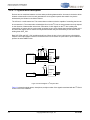
32-bit Audio DSP Family
CS485xx
H ardwa re Us er ’s Manual
Copyright 2009 Cirrus Logic
http://www.cirrus.com
AUG ’09
DS734UM7
CS485xx Hardware User’s Manual
Contacting Cirrus Logic Support
For all product questions and inquiries contact a Cirrus Logic Sales Representative.
To find the one nearest to you go to www.cirrus.com
IMPORTANT NOTICE
Cirrus Logic and its subsidiaries (“Cirrus”) believe that the information contained in this document is accurate and reliable. However, the information is subject to change without notice and is provided “AS IS” without warranty of any kind (express or implied). Customers are advised to obtain the latest version
of relevant information to verify, before placing orders, that information being relied on is current and complete. All products are sold subject to the terms
and conditions of sale supplied at the time of order acknowledgment, including those pertaining to warranty, indemnification, and limitation of liability. No
responsibility is assumed by Cirrus for the use of this information, including use of this information as the basis for manufacture or sale of any items, or for
infringement of patents or other rights of third parties. This document is the property of Cirrus and by furnishing this information, Cirrus grants no license,
express or implied under any patents, mask work rights, copyrights, trademarks, trade secrets or other intellectual property rights. Cirrus owns the copyrights associated with the information contained herein and gives consent for copies to be made of the information only for use within your organization
with respect to Cirrus integrated circuits or other products of Cirrus. This consent does not extend to other copying such as copying for general distribution,
advertising or promotional purposes, or for creating any work for resale.
CERTAIN APPLICATIONS USING SEMICONDUCTOR PRODUCTS MAY INVOLVE POTENTIAL RISKS OF DEATH, PERSONAL INJURY, OR SEVERE
PROPERTY OR ENVIRONMENTAL DAMAGE (“CRITICAL APPLICATIONS”). CIRRUS PRODUCTS ARE NOT DESIGNED, AUTHORIZED OR WARRANTED FOR USE IN PRODUCTS SURGICALLY IMPLANTED INTO THE BODY, AUTOMOTIVE SAFETY OR SECURITY DEVICES, LIFE SUPPORT
PRODUCTS OR OTHER CRITICAL APPLICATIONS. INCLUSION OF CIRRUS PRODUCTS IN SUCH APPLICATIONS IS UNDERSTOOD TO BE FULLY
AT THE CUSTOMER'S RISK AND CIRRUS DISCLAIMS AND MAKES NO WARRANTY, EXPRESS, STATUTORY OR IMPLIED, INCLUDING THE IMPLIED WARRANTIES OF MERCHANTABILITY AND FITNESS FOR PARTICULAR PURPOSE, WITH REGARD TO ANY CIRRUS PRODUCT THAT IS
USED IN SUCH A MANNER. IF THE CUSTOMER OR CUSTOMER'S CUSTOMER USES OR PERMITS THE USE OF CIRRUS PRODUCTS IN CRITICAL APPLICATIONS, CUSTOMER AGREES, BY SUCH USE, TO FULLY INDEMNIFY CIRRUS, ITS OFFICERS, DIRECTORS, EMPLOYEES, DISTRIBUTORS AND OTHER AGENTS FROM ANY AND ALL LIABILITY, INCLUDING ATTORNEYS' FEES AND COSTS, THAT MAY RESULT FROM OR ARISE
IN CONNECTION WITH THESE USES.
Cirrus Logic, Cirrus, the Cirrus Logic logo designs, DSP Composer, Cirrus Extra Surround, Cirrus Original Multichannel Surround, Cirrus Original Surround,
and Cirrus Framework are trademarks of Cirrus Logic All other brand and product names in this document may be trademarks or service marks of their
respective owners.
Dolby, Dolby Digital, Dolby Headphone, Dolby Virtual Speaker, AC-3, Pro Logic, and Audistry are registered trademarks of Dolby Laboratories, Inc. AAC,
Dolby Headphone2, Dolby Virtual Speaker2, and Dolby Digital Surround EX are trademarks of Dolby Laboratories, Inc. Supply of an implementation of
Dolby technology does not convey a license nor imply a right under any patent, or any other industrial or intellectual property right of Dolby Laboratories,
to use the implementation in any finished end-user or ready-to-use final product. It is hereby notified that a license for such use is required from Dolby
Laboratories.
DTS , DTS Neo6, and DTS Digital Surround are registered trademarks of the Digital Theater Systems, Inc. DTS-ES, DTS-ES 96/24, DTS 96/24 are trademarks of the Digital Theater Systems, Inc. It is hereby notified that a third-party license from DTS is necessary to distribute software of DTS in any finished
end-user or ready-to-use final product.
THX® is a registered trademark of Lucasarts Entertainment Company Corporation.
Re-equalization is a trademark of Lucasfilm, Ltd.
SRS, Circle Surround, Trusurround XT, and TruBass are registered trademarks of SRS Labs, Inc. Circle Surround II is a trademark of SRS Labs, Inc. The
Circle Surround technology rights incorporated in the Cirrus Logic chip are owned by SRS Labs, Inc. and by Valence Technology, Ltd., and licensed to
Cirrus Logic
Users of any Cirrus Logic chip containing enabled Circle Surround® technology (i.e., Circle Surround® licensees) must first sign a license to purchase production quantities for consumer electronics applications which may be granted upon submission of a preproduction sample to, and the satisfactory passing
of performance verification tests performed by SRS Labs, Inc., or Valence Technology, Ltd. E-mail requests for performance specifications and testing rate
schedule may be made to [email protected]. SRS Labs, Inc. and Valence Technology, Ltd., reserve the right to decline a use license for any submission that does not pass performance specifications or is not in the consumer electronics classification.
All equipment manufactured using any Cirrus Logic chip containing enabled Circle Surround® technology must carry the Circle Surround® logo on the front
panel in a manner approved in writing by SRS Labs, Inc., or Valence Technology, Ltd. If the Circle Surround logo is printed in user manuals, service manuals, or advertisements, it must appear in a form approved in writing by SRS Labs, Inc. or Valence Technology, Ltd. The rear panel of products containing
Circle Surround technology and user manuals, service manuals, and advertising for those products must all carry the legends as described in Licensor’s
most current version of the Circle Surround Trademark Usage Manual.
Intel is a trademark of Intel Corporation.
Motorola and SPI are registered trademarks of Motorola, Inc.
I2C is a trademark of Philips Semiconductor Corporation.
Atmel is a registered trademark of Atmel Corporation.
Direct Stream Digital is a registered trademark of registered trademark of SONY KABUSHIKI: TA Sony Corporation.
DS734UM7
Copyright 2009 Cirrus Logic
ii
Contents
CS485xx Hardware User’s Manual
Contents
Contents. . . . . . . . . . . . . . . . . . . . . . . . . . . . . . . . . . . . . . . . . . . . . . . . . . . . . . . . . . . . . . . . . . . . . . . . iii
Figures . . . . . . . . . . . . . . . . . . . . . . . . . . . . . . . . . . . . . . . . . . . . . . . . . . . . . . . . . . . . . . . . . . . . . . . . . v
Tables. . . . . . . . . . . . . . . . . . . . . . . . . . . . . . . . . . . . . . . . . . . . . . . . . . . . . . . . . . . . . . . . . . . . . . . . . vii
Chapter 1. Introduction ......................................................................................... 1-1
1.1 Overview . . . . . . . . . . . . . . . . . . . . . . . . . . . . . . . . . . . . . . . . . . . . . . . . . . . . . . . . . . . . . . . . . . .1-1
1.1.1 Chip Features .................................................................................................................1-1
1.2 Code Overlays . . . . . . . . . . . . . . . . . . . . . . . . . . . . . . . . . . . . . . . . . . . . . . . . . . . . . . . . . . . . . .1-6
1.3 Functional Overview of the CS485xx Chip . . . . . . . . . . . . . . . . . . . . . . . . . . . . . . . . . . . . . . .1-7
1.3.1 DSP Core .......................................................................................................................1-7
1.3.2 Debug Controller (DBC) .................................................................................................1-8
1.3.3 Digital Audio Output (DAO) Controller............................................................................1-8
1.3.4 Digital Audio Input (DAI) Controller ................................................................................1-8
1.3.5 Direct Stream Digital® (DSD) Controller .........................................................................1-8
1.3.6 General Purpose I/O.......................................................................................................1-8
1.3.7 Serial Control Ports (SPI™ or I2C™ Standards)..............................................................1-8
1.3.8 Serial Flash Controller ....................................................................................................1-9
1.3.9 DMA Controller ...............................................................................................................1-9
1.3.10 Internal Timers..............................................................................................................1-9
1.3.11 Watchdog Timer ...........................................................................................................1-9
1.3.12 Clock Manager and PLL ...............................................................................................1-9
1.3.13 Programmable Interrupt Controller .............................................................................1-10
Chapter 2. Operational Modes.............................................................................. 2-1
2.1 Introduction . . . . . . . . . . . . . . . . . . . . . . . . . . . . . . . . . . . . . . . . . . . . . . . . . . . . . . . . . . . . . . . .2-1
2.2 Operational Mode Selection . . . . . . . . . . . . . . . . . . . . . . . . . . . . . . . . . . . . . . . . . . . . . . . . . . .2-2
2.3 Slave Boot Procedures . . . . . . . . . . . . . . . . . . . . . . . . . . . . . . . . . . . . . . . . . . . . . . . . . . . . . . .2-2
2.3.1 Slave Boot ......................................................................................................................2-3
2.3.2 Performing a Slave Boot.................................................................................................2-3
2.3.2.1 Slave Boot Procedure....................................................................................2-5
2.3.3 Boot Messages...............................................................................................................2-6
2.3.3.1 Slave Boot ....................................................................................................2-6
2.3.3.2 Soft Reset .....................................................................................................2-6
2.3.3.3 Messages Read from CS485xx .....................................................................2-6
2.4 Master Boot Procedure . . . . . . . . . . . . . . . . . . . . . . . . . . . . . . . . . . . . . . . . . . . . . . . . . . . . . . .2-7
2.5 Softboot . . . . . . . . . . . . . . . . . . . . . . . . . . . . . . . . . . . . . . . . . . . . . . . . . . . . . . . . . . . . . . . . . . .2-8
2.5.1 Softboot Messaging........................................................................................................2-8
2.5.2 Softboot Procedure.........................................................................................................2-8
2.5.2.1 Softboot Steps ...............................................................................................2-9
2.5.2.2 Softboot Example ..........................................................................................2-9
2.6 Low Power Mode . . . . . . . . . . . . . . . . . . . . . . . . . . . . . . . . . . . . . . . . . . . . . . . . . . . . . . . . . . .2-12
2.6.1 Low Power Mode Messaging .......................................................................................2-12
2.6.2 Getting into Low Power Mode ......................................................................................2-12
2.6.3 Getting Out of Low Power Mode ..................................................................................2-12
Chapter 3. Serial Control Port .............................................................................. 3-1
3.1 Introduction . . . . . . . . . . . . . . . . . . . . . . . . . . . . . . . . . . . . . . . . . . . . . . . . . . . . . . . . . . . . . . . .3-1
3.2 Serial Control Port Configuration. . . . . . . . . . . . . . . . . . . . . . . . . . . . . . . . . . . . . . . . . . . . . . .3-1
3.2.1 I2C Port...........................................................................................................................3-2
3.2.2 I2C System Bus Description ...........................................................................................3-3
DS734UM7
Copyright 2009 Cirrus Logic
iii
Contents
CS485xx Hardware User’s Manual
3.2.2.1 I2C Bus Dynamics..........................................................................................3-4
3.2.2.2 I2C Messaging ...............................................................................................3-7
3.2.2.3 Performing a Serial I2C Write ........................................................................3-7
3.2.2.4 Performing a Serial I2C Read ........................................................................3-9
3.3 SPI Port . . . . . . . . . . . . . . . . . . . . . . . . . . . . . . . . . . . . . . . . . . . . . . . . . . . . . . . . . . . . . . . . . . .3-13
3.3.1 SPI System Bus Description.........................................................................................3-14
3.3.1.1 SPI Bus Dynamics .......................................................................................3-15
3.3.1.2 SPI Messaging.............................................................................................3-17
3.3.1.3 Performing a Serial SPI Write......................................................................3-17
3.3.1.4 Performing a Serial SPI Read......................................................................3-18
Chapter 4. Digital Audio Input Interface .............................................................. 4-1
4.1 Introduction . . . . . . . . . . . . . . . . . . . . . . . . . . . . . . . . . . . . . . . . . . . . . . . . . . . . . . . . . . . . . . . .4-1
4.2 Digital Audio Input Port Description . . . . . . . . . . . . . . . . . . . . . . . . . . . . . . . . . . . . . . . . . . . .4-1
4.2.1 DAI Pin Description ........................................................................................................4-2
4.2.2 Supported DAI Functional Blocks...................................................................................4-3
4.2.2.1 Dual Clock Domain - 10 Channel Input .........................................................4-3
4.2.2.2 Single Clock Domain - 12 Channel Input .......................................................4-4
4.2.3 Digital Audio Formats .....................................................................................................4-5
4.2.3.1 I2S Format .....................................................................................................4-5
4.2.3.2 Left-Justified Format ......................................................................................4-6
4.3 DAI Hardware Configuration . . . . . . . . . . . . . . . . . . . . . . . . . . . . . . . . . . . . . . . . . . . . . . . . . . .4-6
4.3.1 DAI Hardware Naming Convention ................................................................................4-6
Chapter 5. Direct Stream Data (DSD) Input Interface ......................................... 5-1
5.1 Digital Audio Input Port Description . . . . . . . . . . . . . . . . . . . . . . . . . . . . . . . . . . . . . . . . . . . .5-1
5.1.1 DSD Pin Description.......................................................................................................5-1
5.1.2 Supported DSD Functional Blocks .................................................................................5-1
Chapter 6. Digital Audio Output Interface ........................................................... 6-1
6.1 Introduction . . . . . . . . . . . . . . . . . . . . . . . . . . . . . . . . . . . . . . . . . . . . . . . . . . . . . . . . . . . . . . . .6-1
6.2 Digital Audio Output Port Description . . . . . . . . . . . . . . . . . . . . . . . . . . . . . . . . . . . . . . . . . . .6-1
6.2.1 DAO Pin Description.......................................................................................................6-1
6.2.2 Supported DAO Functional Blocks .................................................................................6-4
6.2.3 DAO Interface Formats...................................................................................................6-4
6.2.3.1 I2S Format .....................................................................................................6-4
6.2.3.2 Left-Justified Format ......................................................................................6-4
6.2.3.3 One-line Data Mode Format (Multichannel)...................................................6-5
6.2.4 DAO Hardware Configuration.........................................................................................6-5
6.2.5 S/PDIF Transmitter.........................................................................................................6-9
Chapter 8. General Purpose Input/Output Pins .................................................. 7-1
7.1 Introduction . . . . . . . . . . . . . . . . . . . . . . . . . . . . . . . . . . . . . . . . . . . . . . . . . . . . . . . . . . . . . . . .7-1
7.2 GPIO Description . . . . . . . . . . . . . . . . . . . . . . . . . . . . . . . . . . . . . . . . . . . . . . . . . . . . . . . . . . . .7-1
7.3 Watchdog Timer Description . . . . . . . . . . . . . . . . . . . . . . . . . . . . . . . . . . . . . . . . . . . . . . . . . .7-2
Chapter 8. System Integration.............................................................................. 8-1
8.1 Typical Connection Diagrams. . . . . . . . . . . . . . . . . . . . . . . . . . . . . . . . . . . . . . . . . . . . . . . . . .8-1
8.2 Pin Description. . . . . . . . . . . . . . . . . . . . . . . . . . . . . . . . . . . . . . . . . . . . . . . . . . . . . . . . . . . . .8-10
8.2.1 Power and Ground .......................................................................................................8-10
8.2.1.1 Power...........................................................................................................8-10
iv
Copyright 2009 Cirrus Logic
DS734UM7
Figures
CS485xx Hardware User’s Manual
8.2.1.2 Ground.........................................................................................................8-11
8.2.1.3 Decoupling...................................................................................................8-11
8.2.2 PLL Filter ......................................................................................................................8-11
8.2.2.1 Analog Power Conditioning .........................................................................8-11
8.2.3 PLL ...............................................................................................................................8-12
8.3 Clocking . . . . . . . . . . . . . . . . . . . . . . . . . . . . . . . . . . . . . . . . . . . . . . . . . . . . . . . . . . . . . . . . . .8-12
8.4 Control . . . . . . . . . . . . . . . . . . . . . . . . . . . . . . . . . . . . . . . . . . . . . . . . . . . . . . . . . . . . . . . . . . .8-13
8.4.1 Operational Mode .........................................................................................................8-13
8.5 48-Pin LQFP Pin Assigments . . . . . . . . . . . . . . . . . . . . . . . . . . . . . . . . . . . . . . . . . . . . . . . . .8-15
8.6 Pin Assignments . . . . . . . . . . . . . . . . . . . . . . . . . . . . . . . . . . . . . . . . . . . . . . . . . . . . . . . . . . .8-18
Revision History . . . . . . . . . . . . . . . . . . . . . . . . . . . . . . . . . . . . . . . . . . . . . . . . . . . . . . . . . . . . . . .8-22
Figures
Figure 1-1. CS48560 Chip Functional Block Diagram ..................................................................................1-2
Figure 1-2. CS48540 Chip Functional Block Diagram ..................................................................................1-3
Figure 1-3. CS48520 Chip Functional Block Diagram ..................................................................................1-4
Figure 2-1. Operation Mode Block Diagrams ...............................................................................................2-1
Figure 2-2. Slave Boot Sequence ................................................................................................................2-4
Figure 2-3. Master Boot Sequence Flowchart ..............................................................................................2-7
Figure 2-4. Soft Boot Sequence Flowchart ..................................................................................................2-9
Figure 2-5. Soft Boot Example Flowchart ...................................................................................................2-10
Figure 2-6. Flowchart of Steps Used to Exit Low Power Mode ..................................................................2-13
Figure 3-1. Serial Control Port Internal Block Diagram ................................................................................3-2
Figure 3-2. Block Diagram of I2C System Bus .............................................................................................3-3
Figure 3-3. I2C Start and Stop Conditions ....................................................................................................3-4
Figure 3-4. I2C Address with ACK and NACK ..............................................................................................3-5
Figure 3-5. Data Byte with ACK and NACK .................................................................................................3-6
Figure 3-6. Stop Condition with ACK and NACK ..........................................................................................3-6
Figure 3-7. Repeated Start Condition with ACK and NACK .........................................................................3-7
Figure 3-8. I2C Write Flow Diagram .............................................................................................................3-8
Figure 3-9. I2C Read Flow Diagram ...........................................................................................................3-10
Figure 3-10. Sample Waveform for I2C Write Functional TIming ...............................................................3-12
Figure 3-11. Sample Waveform for I2C Read Functional Timing ...............................................................3-12
Figure 3-12. SPI Serial Control Port Internal Block Diagram .....................................................................3-13
Figure 3-13. Block Diagram of SPI System Bus .........................................................................................3-15
Figure 3-14. SPI Address and Data Bytes .................................................................................................3-16
Figure 3-15. SPI Write Flow Diagram .........................................................................................................3-18
Figure 3-16. SPI Read Flow Diagram ........................................................................................................3-19
Figure 3-17. Sample Waveform for SPI Write Functional Timing ...............................................................3-21
DS734UM7
Copyright 2009 Cirrus Logic
v
Figures
CS485xx Hardware User’s Manual
Figure 3-18. Sample Waveform for SPI Read Functional Timing ..............................................................3-21
Figure 4-1. 10-Channel DAI Port Block Diagram .........................................................................................4-3
Figure 4-2. 8-Channel DAI Port Block Diagram ...........................................................................................4-3
Figure 4-3. 6-Channel DAI Port Block Diagram ...........................................................................................4-4
Figure 4-4. 12-Channel DAI Port Block Diagram .........................................................................................4-5
Figure 4-5. I2S format (Rising Edge Valid SCLK) .........................................................................................4-6
Figure 4-6. Left-justified Format (Rising Edge Valid SCLK) .........................................................................4-6
Figure 5-1. DSD Port Block Diagram on CS48560 ......................................................................................5-2
Figure 6-1. CS48560 DAO Block Diagram ...................................................................................................6-2
Figure 6-2. CS48540 DAO Block Diagram ...................................................................................................6-3
Figure 6-3. CS48520 DAO Block Diagram ...................................................................................................6-3
Figure 6-4. I2S Compatible Serial Audio Formats (Rising Edge Valid DAO_SCLK) ....................................6-4
Figure 6-5. Left-justified Digital Audio Formats (Rising Edge Valid DAO_SCLK) ........................................6-4
Figure 6-6. One-line Data Mode Digital Audio Formats ...............................................................................6-5
Figure 7-1. Typical Connection for Watchdog Timer Alarm .........................................................................7-2
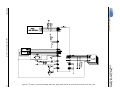
Figure 8-1. SPI Slave, 10 channels of Digital Audio Input, All Audio Clocks
Synchronous to S/PDIF RX ...........................................................................................................................8-2
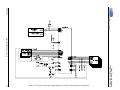
Figure 8-2. I2C Slave, 10 Channels of Digital Audio Input, Dual Clock Domains,
Output Audio Clocks Synchronous to HDMI Rx ............................................................................................8-3
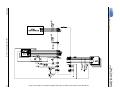
Figure 8-3. I2C Slave, 12 Channels of Digital Audio Input, Single Clock Domain,
All Audio Clocks Synchronous to XTAL_OUT ...............................................................................................8-4
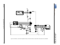
Figure 8-4. I2C master, 10 Channels of Digital Audio Input, All Audio Clocks
Synchronous to S/PDIF Rx ...........................................................................................................................8-5
Figure 8-5. SPI Slave, 10 Channels of Digital Audio Input,
All Audio Clocks Synchronous to S/PDIF Rx ................................................................................................8-6
Figure 8-6. SPI Slave, 10 Channels of Digital Audio Input,
Dual Clock Domains, Output Audio Clocks Synchronous to HDMI Rx .........................................................8-7
Figure 8-7. SPI Slave, 12 Channels of Digital Audio Input, Single
Clock Domain, All Audio Clocks Synchronous to XTAL_OUT ......................................................................8-8
Figure 8-8. SPI Master, 10 Channels of Digital Audio Input, All
Audio Clocks Synchronous to S/PDIF Rx. ....................................................................................................8-9
Figure 8-9. PLL Filter Topology ..................................................................................................................8-12
Figure 8-10. Crystal Oscillator Circuit Diagram ..........................................................................................8-13
Figure 8-11. 48-Pin LQFP Pin Layout of CS48560 ....................................................................................8-15
Figure 8-12. 48-Pin LQFP Pin Layout of CS48540 ....................................................................................8-16
Figure 8-13. 48-Pin LQFP Pin Layout of CS48520 ....................................................................................8-17
vi
Copyright 2009 Cirrus Logic
DS734UM7
Tables
CS485xx Hardware User’s Manual
Tables
Table 1-1. List of Available Firmware Modules and Associated Application Note. .......................................1-4
Table 1-2. Device and Firmware Selection Guide ........................................................................................1-7
Table 2-1. Operation Modes .........................................................................................................................2-2
Table 2-2. SLAVE_BOOT message for CS485xx ........................................................................................2-6
Table 2-3. SOFT_RESET message for CS485xx ........................................................................................2-6
Table 2-4. Boot Read Messages from CS485xx ..........................................................................................2-6
Table 2-5. Boot Command Messages for CS485xx .....................................................................................2-7
Table 2-6. SOFTBOOT Message .................................................................................................................2-8
Table 2-7. SOFTBOOT_ACK Message .......................................................................................................2-8
Table 2-8. wakeup_uld Options and Values................................................................................................2-14
Table 3-1. Serial Control Port 1 I2C Signals .................................................................................................3-4
Table 3-2. Serial Control Port SPI Signals .................................................................................................3-14
Table 4-1. Digital Audio Input Port ...............................................................................................................4-2
Table 4-2. Input Data Format Configuration (Input Parameter A) ................................................................4-7
Table 4-3. Input SCLK Polarity Configuration (Input Parameter B) ..............................................................4-8
Table 4-4. Input LRCLK Polarity Configuration (Input Parameter C) ...........................................................4-8
Table 4-5. DAI2_DATA Clock Source (Input Parameter E) ..........................................................................4-9
Table 4-6. DAI1_DATA Clock Source (Input Parameter F) ..........................................................................4-9
Table 4-7. Chip Version (Input Parameter G) ..............................................................................................4-9
Table 4-8. DAII TDM (Input Parameter H) ....................................................................................................4-9
Table 5-1. DSDl Audio Input Port .................................................................................................................5-1
Table 6-1. Digital Audio Output (DAO) Pins .................................................................................................6-1
Table 6-2. Output Clock Mode Configuration (Parameter A) .......................................................................6-5
Table 6-3. DAO1 & DAO2 Clocking Relationship Configuration (Parameter B) ...........................................6-6
Table 6-4. Output DAO_SCLK/LRCLK Configuration (Parameter C) ..........................................................6-6
Table 6-5. Output Data Format Configuration (Parameter D) ......................................................................6-8
Table 6-6. Output DAO_LRCLK Polarity Configuration (Parameter E) ........................................................6-9
Table 6-7. Output DAO_SCLK Polarity Configuration (Parameter F) ..........................................................6-9
Table 6-8. DAO TDM (Parameter G) ............................................................................................................6-9
Table 6-9. S/PDIF Transmitter Pins ...........................................................................................................6-10
Table 6-10. S/PDIF Transmitter Configuration ...........................................................................................6-10
Table 7-1. Digital Audio Output (DAO) Pins .................................................................................................7-1
Table 8-1. Core Supply Pins ......................................................................................................................8-10
Table 8-2. I/O Supply Pins .........................................................................................................................8-10
Table 8-3. Core and I/O Ground Pins .........................................................................................................8-11
Table 8-4. PLL Supply Pins ........................................................................................................................8-11
DS734UM7
Copyright 2009 Cirrus Logic
vii
Tables
CS485xx Hardware User’s Manual
Table 8-5. PLL Filter Pins ...........................................................................................................................8-12
Table 8-6. Reference PLL Component Values ...........................................................................................8-12
Table 8-7. DSP Core Clock Pins ................................................................................................................8-13
Table 8-8. Reset Pin ...................................................................................................................................8-14
Table 8-9. Hardware Strap Pins .................................................................................................................8-14
Table 8-10. Pin Assignments of CS48560 .................................................................................................8-18
Table 8-11. Pin Assignments of CS48540 .................................................................................................8-19
Table 8-12. Pin Assignments of CS48520 .................................................................................................8-20
viii
Copyright 2009 Cirrus Logic
DS734UM7
Overview
CS485xx Hardware User’s Manual
Chapter 1
Introduction
1.1 Overview
The CS485xx is a programmable audio DSP that combines a programmable, 32-bit fixed-point, generalpurpose DSP with dedicated audio peripherals. Its “audio-centric” interfaces facilitate the coding of highprecision audio applications and provide a seamless connection to external audio peripheral ICs.
The CS485xx can be used as a ROM-based processor in systems that require only the applications stored
in on-board ROM, or it can operate as a RAM-based processor in systems that require custom code. The
CS485xx provides up to 150 MIPS of processing power and includes several 3rd party algorithms in ROM. It
has been designed with a generous amount of on-chip program and data RAM, and has all necessary
peripherals required to support the latest standards in consumer entertainment products. In addition,
external serial Flash memory can be attached to the serial control port (SCP) for storage of run-time
parameters, or as a boot-ROM for custom applications. This device is suitable for a variety of highperformance audio applications. These include:
•
Digital TVs
•
Car Audio Head Units and Amplifiers
•
Portable DVDs
•
DVD Mini/Receivers
•
Portable Audio Docking Stations
•
Shelf Systems
•
Digital Speakers
1.1.1 Chip Features
• 3rd Party Processing Algorithms in ROM
• Dual-path Audio Processing on Audio
Outputs
• Low-power Standby Mode
• 192 kHz S/PDIF Transmitter
• Up to 12-channel Serial Audio Inputs
• Serial Control Port Using SPI™ or I2C™
• Up to 12-channel Serial Audio Outputs
• 6-channel Direct Stream Digital® (DSD) Input
Port for High-resolution Audio
• Customer Software Security Keys
• GPIO Support for All Common Sub-circuits
• Large On-chip X,Y, and Program RAM & ROM
• Hardware Watchdog Timer
• Dual Clock Domains on Audio Inputs
1-1
Copyright 2009 Cirrus Logic, Inc.
DS734UM7
Overview
CS485xx Hardware User’s Manual
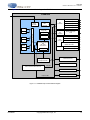
Figure 1-1 illustrates the functional block diagram for CS48560.
CS48560
Stereo Audio Input/DSD
DAI1
Stereo Audio Input/DSD
Peripheral
Bus
Controller
Debug
Controller
SRAM
Stereo Audio Input/DSD
Ext (64 bit)
SRAM
Memory Controller
ROM
Security
X
Y
ROM
32-bit Dual Datapath
DSP
with 72-bit
Accumulators
Stereo Audio Input /
DSD
Stereo Audio Output
DAO1
64 bit
P
DAI2
DAI
Controller
Log/Exp
Y
Stereo Audio Input/DSD
Stereo Audio Input/DSD
X
ROM
SRAM
DAI
Controller
DAO
Controller
Stereo Audio Output
Stereo Audio Output
Stereo Audio Output or
SPDIF Transmitter
DAO2
Stereo Audio Output
Stereo Audio Output
Decryptor
P
Programmable
Interrupt Controller
Serial Control Port
Timers
DMA Controller with 8 Channels
DMA Bus
GPIOs
Peripheral Bus
Clock Manager and PLL
Figure 1-1. CS48560 Chip Functional Block Diagram
DS734UM7
Copyright 2009 Cirrus Logic, Inc.
1-2
Overview
CS485xx Hardware User’s Manual
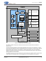
Figure 1-2 illustrates the functional block diagram for CS48540.
CS48540
DAI1
Peripheral
Bus
Controller
Debug
Controller
Stereo Audio Input
DAI
Controller
Stereo Audio Input
Stereo Audio Input
SRAM
X
Ext (64 bit)
ROM
DAI
Controller
Y
ROM
SRAM
Memory Controller
Log/Exp
SRAM
Security
DAO1
64 bit
X
P
Y
ROM
DAI2
Stereo Audio Output
Stereo Audio Output
SPDIF Transmitter
DAO2
Decryptor
Stereo Audio Output
DAO
Controller
32-bit Dual Datapath
DSP
with 72-bit
Accumulators
Stereo Audio Input
Stereo Audio Output
P
Programmable
Interrupt Controller
Serial Control Port
Timers
DMA Controller with 8 Channels
DMA Bus
GPIOs
Peripheral Bus
Clock Manager and PLL
Figure 1-2. CS48540 Chip Functional Block Diagram
1-3
Copyright 2009 Cirrus Logic, Inc.
DS734UM7
Overview
CS485xx Hardware User’s Manual
Figure 1-3 illustrates the functional block diagram for CS48520.
CS48520
DAI1
Peripheral
Bus
Controller
Debug
Controller
SRAM
Ext (64 bit)
ROM
Memory Controller
Y
Security
DAO1
64 bit
X
P
Y
ROM
DAI2
DAI
Controller
Log/Exp
SRAM
Stereo Audio Input/DSD
X
ROM
SRAM
DAI
Controller
Stereo Audio Output
DAO
Controller
32-bit Dual Datapath
DSP
with 72-bit
Accumulators
SPDIF Transmitter
DAO2
Decryptor
Stereo Audio Input
Stereo Audio Output
P
Serial Control Port
Programmable
Interrupt Controller
Timers
DMA Controller with 8 Channels
DMA Bus
GPIOs
Peripheral Bus
Clock Manager and PLL
Figure 1-3. CS48520 Chip Functional Block Diagram
See AN298, CS485xx Firmware User’s Manual for a list the firmware modules that are available on
CS485xx DSPs.
The audio processing algorithms, post-processing application codes, and/or Cirrus Framework™ modules
and the associated application notes are available through the Cirrus Software Licensing Program. Standard
post-processing code modules are only available to customers who qualify for the Cirrus Framework™
CS485xx Family DSP Programming Kit. Please refer to the Related Documents section of this manual for
additional application note information.
The CS485xx supports master-mode interface on the serial control port to interface to SPI™ and I2C® serial
FLASH chips, thus allowing products to be field upgraded as new audio algorithms are developed.
DS734UM7
Copyright 2009 Cirrus Logic, Inc.
1-4
Code Overlays
CS485xx Hardware User’s Manual
This chip, teamed with Cirrus digital interface products and mixed-signal data converters, enables the design
of next-generation digital entertainment products.
Licenses are required for all of the 3rd party audio processing algorithms listed in "Code Overlays". Please
contact your local Cirrus Logic Sales representative for more information.
1.2 Code Overlays
The suite of software available for the CS485xx family consists of an operating system (OS) and a library of
overlays. The overlays have been divided into three main groups called Matrix-processors, Virtualizerprocessors, and Post-processors. All software components are defined below:
•
OS/Kernel - Encompasses all non-audio processing tasks, including loading data from external
memory, processing host messages, calling audio-processing subroutines, error concealment, etc.
•
Matrix-processor- Any Module that performs a matrix decode on PCM data to produce more output
channels than input channels (2Ön channels). Examples are Dolby® ProLogic® IIx and DTS
Neo:6®. Generally speaking, these modules increase the number of valid channels in the audio I/O
buffer.
•
Virtualizer-processor - Any module that encodes PCM data into fewer output channels than input
channels (nÖ2 channels) with the effect of providing “phantom” speakers to represent the physical
audio channels that were eliminated. Examples are Dolby Headphone® and Dolby® Virtual
Speaker®. Generally speaking, these modules reduce the number of valid channels in the audio I/O
buffer.
•
Post-processors - Any module that processes audio I/O buffer PCM data in-place after the matrix- or
virtualizer-processors. Examples are bass management, audio manager, tone control, EQ, delay,
customer-specific effects, etc.
The bulk of each overlay is stored in ROM within the CS485xx, but a small image is required to configure the
overlays and boot the DSP. This small image can either be stored in an external serial FLASH/EEPROM, or
downloaded via a host controller through the SPI™/I2C™ serial port.
The overlay structure reduces the time required to reconfigure the DSP when a processing change is
requested. Each overlay can be reloaded independently without disturbing the other overlays. For example,
when a new matrix-processor is selected, the OS, virtualizer-, and post-processors do not need to be
reloaded — only the new matrix-processor (the same is true for the other overlays).
1-5
Copyright 2009 Cirrus Logic, Inc.
DS734UM7
Functional Overview of the CS485xx Chip
CS485xx Hardware User’s Manual
Table 1-1 lists the firmware available based on device selection. Please refer AN298, CS485xx Firmware
User’s Manual for the latest listing of application codes and Cirrus Framework™ modules available.
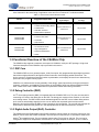
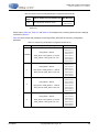
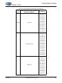
Table 1-1. Device and Firmware Selection Guide
Device
Suggested Application
Channel Count
Input/Output
Package
• Digital TV
• Portable Audio Docking Station
CS48520-CQZ
• Portable DVD
Up to 4 channel in / 4
channel out
48-pin LQFP
Up to 8 channel in / 8
channel out
48-pin LQFP
Up to 12 channel in /12
channel out
48-pin LQFP
• DVD Mini / Receiver
• Multimedia PC Speakers
CS48520 features Plus:
CS48540-CQZ
CS48540-DQZ
• 8 Channel Car Audio
• Sound Bar
• DVD Receiver
CS4840 features Plus:Features:
CS48560-CQZ
CS48560-DQZ
• 12 channel Car Audio
• High-end Digital TV
• Dual Source/Dual Zone
• SACD
1.3 Functional Overview of the CS485xx Chip
The CS485xx chip supports a maximum clock speed of 150 MHz in a 48-pin LQFP package. A high-level
functional description of the CS485xx chip is provided in this section.
1.3.1 DSP Core
The CS485xx DSP core is a general-purpose, 32-bit, fixed-point, fully programmable digital signal processor
that achieves high performance through an efficient instruction set and highly parallel architecture. The
device uses two’s complement fractional number representation, and employs busses for two data memory
spaces and one program memory space.
CS485xx core enhancements include portability of the design, speed improvement, and improvements for
synthesis, verification, and testability. Each member of the CS485xx family has different SRAM and ROM
sizes. Please refer to the CS485xx data sheet for specification details and ordering information.
1.3.2 Debug Controller (DBC)
An I2C slave debug controller (DBC) is integrated within the CS485xx DSP core. Two pins are reserved for
connecting a PC host to the debug port on the DSP. The debug port consists of two modules, an I2C slave
and a debug master. The DBC master sends dedicated signals into the DSP core to initiate debug actions
and it receives acknowledge signals from the core to indicate the requested action has been taken.
Basically, this interface allows the DBC to insert instructions into the pipeline. The core will acknowledge the
action when it determines the pipeline is in the appropriate state for the inserted action to be taken.
1.3.3 Digital Audio Output (DAO) Controller
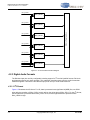
The CS485xx has two Digital Audio Output (DAO) controllers, which contain up to 6 stereo output pins. One
DAO pin can be used as a S/PDIF transmitter. The DAO port can transmit up to 12 channels of serial audio
data in I2S-compatible format. The port supports sample rates (Fs) as high as 192 kHz. The port can be
configured to support two independent clock domains. The audio samples are stored in up to 12 channel
DS734UM7
Copyright 2009 Cirrus Logic, Inc.
1-6
Functional Overview of the CS485xx Chip
CS485xx Hardware User’s Manual
buffers which are 32 bits wide. The O/S can dedicate DMA channels to fill the DAO data buffers from
memory. DAO control is handled through the peripheral bus.
1.3.4 Digital Audio Input (DAI) Controller
The CS485xx Digital Audio Input (DAI) controller can operate with a single clock domain or in a dual-clockdomain mode. In the dual-clock-domain mode, there are two SCLKs and two LRCLKs and up to five serial
audio input pins which can accept up to 10 channels of audio data. In single-clock-domain mode there is
only one SCLK and one LRCLK, but there are up to six serial audio input pins which can accept up to 12
channels of audio data.
DAI control is handled through the peripheral bus. Each DAI pin can be configured to load audio samples in
a variety of formats. In addition to accepting multiple formats, the DAI controller has the ability to accept
multiple stereo channels on a single DAI_DATAx pin. All six DAI data pins are slaves and normally use the
DAI clock pins, but they may also be reconfigured to use the DAO serial output clock pins (DAO_SCLK and
DAO_LRCLK). A single global configuration register provides a set of enable bits to ensure that ports may
be started synchronously.
1.3.5 Direct Stream Digital (DSD) Controller
The CS48560 also has a DSD controller which allows the DSP to be integrated into a system that supports
SACD audio. The DSD data pins are multiplexed with the DAI1 pins. The DSD port consists of a bit clock
(DSD_CLK) and up to six DSD data inputs (DSD[5:0]).
1.3.6 General Purpose I/O
A 17-bit, general-purpose I/O (GPIO) port is provided on the CS485xx chip to enhance system flexibility.
Many of the functional pins can be used for either GPIO or other peripheral functions.
Each GPIO pin can be individually configured as an output, an input, or an input with interrupt. A GPIO
interrupt can be triggered on a rising edge (0-to-1 transition), falling edge (1-to-0 transition), or logic level
(either 0 or 1). Each pin configured as an input with interrupt can be assigned its own interrupt trigger
condition. All GPIOs share a common interrupt vector.
1.3.7 Serial Control Ports (SPI™ or I2C™ Standards)
The CS485xx has a serial control port (SCP) that supports SPI™ and I2C™ Master/Slave communication
modes. The serial control port allows external devices such as microcontrollers and serial FLASH to
communicate with the CS485xx chip through either I2C or SPI serial communication standards.
The CS485xx SPI and I2C serial communication protocols are identical from a functional standpoint. The
main difference between the two is the protocol being implemented between the CS485xx and the external
device. In addition, the I2C slave has a true I2C mode that utilizes data-flow mechanisms inherent to the I2C
protocol. If this mode is enabled, the I2C slave will hold SCP_CLK low to delay a transfer as needed.
The communication protocol (SPI or I2C) and mode (master or slave) is selected by the state of the HS[3:0]
pins at the rising edge of RESET.
The serial clock pin can support frequencies as high as 25 MHz in SPI mode.
The CS485xx has two additional serial communication pins not specified in either the I2C or SPI
specification. The port uses the SCP_IRQ pin to indicate that a read message is ready for the host. The port
uses the SCP_BSY pin to warn the host to pause communication.
1-7
Copyright 2009 Cirrus Logic, Inc.
DS734UM7
Functional Overview of the CS485xx Chip
CS485xx Hardware User’s Manual
1.3.8 Serial Flash Controller
The CS485xx boot ROM supports a protocol that allows autoboot from a serial Flash or EEPROM device.
Boot modes are supported for 13-bit addressing, 16-bit addressing, and 20-bit addressing. A dedicated
FLASH/EEPROM (EE_CS) chip select pin allows Flash devices to be connected without additional chip
select logic.
1.3.9 DMA Controller
The DMA controller contains 8 channels. The O/S uses 3 channels, 2 for the DAO, and 1 for the DAI. The
DMA block is able to move data to/from X or Y memory, or alternate between both X and Y memory. The
DMA controller moves data to/from X and/or Y memory opportunistically (if the core is not currently
accessing that particular memory space during the current cycle). The DMA controller has a “Dead Man’s”
timer so that if the core is running an inner loop and accessing memory every cycle, the DMA controller can
interrupt the core to run a DMA cycle.
1.3.10 Internal Timers
Two identical 32-bit timer blocks run off the CS485xx DSP clock. The timer count decrements with each
clock tick of the DSP clock when the timer is enabled. When the timer count reaches zero, it is re-initialized,
and may be programmed to generate an interrupt to the DSP.
1.3.11 Watchdog Timer
The CS485xx has an integrated watchdog timer that acts as a “health” monitor for the DSP. The watchdog
timer must be reset by the DSP before the counter expires, or the entire chip is reset. This peripheral
ensures that the CS485xx will reset itself in the event of a temporary system failure. In standalone mode
(that is, no host microcontroller (MCU) is present), the DSP will reboot from external FLASH. In slave mode
(that is, host MCU present) a GPIO will be used to signal the host that the watchdog has expired and the
DSP should be rebooted and reconfigured.
1.3.12 Clock Manager and PLL
The CS485xx Clock Manager and PLL module contains an Analog PLL, RTL Clock Synthesizer, and Clock
Manager. The Analog PLL is a customized analog hard macro that contains the Phase Detector (PD),
Charge Pump, Loop Filter, VCO, and other non-digital PLL logic. The Clock Synthesizer is a digital design
wrapper around the analog PLL that allows clock frequency ranges to be programmed. The Clock Manager
is a digital design wrapper for the Clock Synthesizer that provides the logic (control registers) necessary to
meet chip clocking requirements.
The Clock Manager and PLL module generates two master clocks:
•
HCLK - global chip clock (clocks the DSP core, internal memories, SDRAM, Flash, and all
peripherals)
•
OVFS - oversampled audio clock. This clock feeds the DAO block which has dividers to generate
the DAO_MCLK, DAO_SCLK, and DAO_LRCLK.
The Clock Manager has the ability to bypass the PLL so that the HCLK will run directly off the PLL Reference
Clock (REFCLK). While operating in this mode, the OVFS clock can still be divided off the VCO so the PLL
can be tested.
A built-in crystal oscillator circuit with a buffered output is provided. The buffered output frequency ratio is
selectable between 1:1 (default) or 2:1.
DS734UM7
Copyright 2009 Cirrus Logic, Inc.
1-8
Functional Overview of the CS485xx Chip
CS485xx Hardware User’s Manual
1.3.13 Programmable Interrupt Controller
The Programmable Interrupt Controller (PIC) forces all incoming interrupts to be synchronized to the global
clock, HCLK. The PIC provides up to 16 interrupts to the DSP Core. The interrupts are prioritized with
interrupt 0 as the highest priority and interrupt 15 as the lowest priority. Each interrupt has a corresponding
interrupt address that is also supplied to the DSP core. The interrupt address is the same as the IRQ number
(interrupt 0 uses interrupt address 0 and interrupt 15 uses interrupt address 15). Both an enable mask and a
run mask are provided for each interrupt. The enable mask allows the enabled interrupts to generate a
PIC_REQ signal to the DSP core, and the run mask allows the enabled interrupts to generate a PIC_CLR,
thereby bringing the core out of its halt state when it accepts the interrupt.
§§1
1. The “§§” symbol is used throughout this manual to indicate the end of the text flow in a chapter.
1-9
Copyright 2009 Cirrus Logic, Inc.
DS734UM7
Functional Overview of the CS485xx Chip
CS485xx Hardware User’s Manual
DS734UM7
Copyright 2009 Cirrus Logic, Inc.
1-10
Introduction
CS485xxr Hardware User’s Manual
Chapter 2
Operational Modes
2.1 Introduction
The CS485xx has several operational modes that can be used to conform to many system configurations.
The operational modes for the CS485xx specify both the communication mode and boot mode. This chapter
discusses the selection of operational modes, booting procedures and process of performing a soft reset.
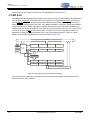
The CS485xx can be either a slave device or a master device for the boot procedure. In Master Boot Mode,
the CS485xx is the master boot device and can automatically boot the application code from external serial
ROM (the slave boot device). In Slave Boot Mode, the CS485xx is the slave boot device and requires the
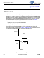
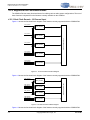
system host controller (the master boot device) to load the application code. Please see Figure 2-1 .
Thus, there are two boot modes for the CS485xx:
•
Master Boot (From serial SPI or I2C FLASH/EEPROM)
•
Slave Boot (Using SPI or I2C)
When the CS485xx is configured for an operational mode where it is the slave boot device, one of the below
communication modes must be specified by the host controller (i.e. the master boot device). These
communication modes are described in detail in Chapter 3, "Serial Control Port". Please see this section for
block diagrams and flowcharts depicting each of the Slave and Master boot modes.
Control Bus
System Host
Controller
(Master)
CS4953xx
(Slave)
Slave Boot
External
Memory Bus
External ROM
(Slave)
CS4953xx
(Master)
Master Boot
Figure 2-1. Operation Mode Block Diagrams
2-1
Copyright 2009 Cirrus Logic, Inc.
DS734UM7
Operational Mode Selection
CS485xxr Hardware User’s Manual
2.2 Operational Mode Selection
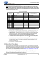
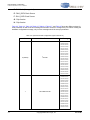
The operational mode for the CS485xx is selected by the values of the HS[4:0] pins on the rising edge of
RESET. This value determines the communication mode used until the part is reset again. This value also
determines the method for loading application code. The table below shows the different operational modes
and the HS[4:0] values for each mode.
Table 2-1. Operation Modes
HS[4:0]
Mode
Boot Master
Device
Boot Slave Device
X
0
0
0
0
Master I2Ca
CS485xx
I2C External ROM
X
1
0
0
0
Master SPI 1 b
CS485xx
SPI (Mode 1) External ROM5, 6, 7
X
0
0
0
1
Master SPI 2 c
CS485xx
SPI (Mode 2) External ROM5, 6, 7
X
1
0
0
1
Master SPI 3 d
CS485xx
SPI (Mode 3) External ROMe, f,g
X
0
0
1
0
RESERVED
X
1
0
1
0
RESERVED
X
X
1
0
0
Slave I2C
System Host
CS485xx
X
X
1
0
1
Slave SPI
System Host
CS485xx
X
X
1
1
0
RESERVED
X
X
1
1
1
RESERVED
X
X
0
1
1
RESERVED
a. In I2C master mode, the Image Start address (0x0) is sent as a 16-bit value, with the default I2C
address of 0x50, I2C clock frequency = Fdclk / 72.
b. SPI master mode 1 is to support the legacy 16-bit SPI EEPROM. The following defaults are used: SPI
Command Byte 0x03, Image Start address 0x0 is sent as a 16-bit value, no dummy bytes, SPI clock
frequency = Fdclk / 4.
c. In SPI Master mode 2, the following defaults are used: SPI Command Byte 0x68, Image Start address
0x0 is sent as a 24-bit value, 4 dummy bytes sent following the address (and before reading image
data), SPI clock frequency = Fdclk / 2. This mode supports the Atmel® SPI Flash memory.
d. In SPI Master mode 3, the following defaults are used: SPI command byte 0x03, Image Start address
0x0 is sent as a 24-bit value, no dummy bytes, SPI clock frequency = Fdclk / 2. This mode supports the
ST SPI EEPROM devices.
e. For all SPI Master boot modes, by default GPIO13 is used as EE_CS.
f. For Flash Master modes, the following defaults are used: clock ratio=1:1, Endian Mode = little-endian,
Chip Select polarity = active-low, 0-cycle delay from CS Address Change to Output Enable, 4-cycle
delay from CS to Read Access.
g. Fdclk is specified in the CS485xx Data Sheet.
2.3 Slave Boot Procedures
When the CS485xx is the slave boot device, the system host controller (as the master boot device) must
follow an outlined procedure for correctly loading application code. The slave boot procedure is described in
this section. Slave boot requires the system host controller to send messages to, and read back messages
from, the CS485xx. These messages have been outlined in Section 2.3.3 "Boot Messages" on page 2-6.
The CS485xx has different.uld files (overlays) for certain processing tasks. Slave booting the CS485xx
requires loading multiple overlays - differing from previous Cirrus Logic Audio DSP families (that is,
CS493xx, CS494xxx). Please refer to AN298, “CS485xx Firmware User’s Manual” regarding more
information on the breakdown of processing tasks for each overlay.
DS734UM7
Copyright 2009 Cirrus Logic, Inc.
2-2
Slave Boot Procedures
CS485xxr Hardware User’s Manual
Pseudocode and flowcharts will be used to describe each of these boot procedures in detail. The flow charts
use the following messages:
•
Write_* – Write to CS485xx
•
Read_* – Read from CS485xx
Please note that * above can be replaced by SPI™ or I2C® depending on the mode of host communication.
For each case, the general download algorithm is the same. The system designer should also refer to the
control port sections of this document in Chapter 3, "Serial Control Port" for the details of when writing to
and reading from the CS485xx is valid.
After completing the full download to the CS485xx, a KICK START message is sent to cause the application
code to begin execution. Please note that it takes time to lock the PLL when initially booting the DSP.
Typically this time is less than 200 ms. If a message is sent to the DSP during this time, the SCP_BSY pin
will go low to indicate that the DSP is busy. Any messages sent when the SCP_BSY pin is LOW will be lost.
If the SCP_BSY pin stays LOW longer than 200 ms, the host must reboot the DSP.
2.3.1 Slave Boot
The Slave Boot procedure is a sequence in which the external host is the bus master and directly loads the
CS485xx application code. The system host controller has two communication modes available, as specified
in Table 2-1. from the serial control port (SPI or I2C). The boot messages used can be found in Section 2.3.3
"Boot Messages" on page 2-6. For information on how to configure the CS485xx overlays, such as hardware
configuration messages, software configuration messages, and the kick-start message, please refer to
AN298, “CS485xx Firmware User’s Manual”.
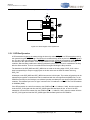
2.3.2 Performing a Slave Boot
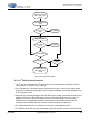
Figure 2-2 shows the steps taken during a Slave Boot. The procedure is discussed in Section 2.3.2.1.
2-3
Copyright 2009 Cirrus Logic, Inc.
DS734UM7
Slave Boot Procedures
CS485xxr Hardware User’s Manual
START
RESET (LOW)
SET HS[3:0] PINS FOR
OPERATIONAL MODE
RESET (HIGH)
WAIT 50 μS
WRITE_* (SLAVE_BOOT)
READ_* (MSG)
MSG
==BOOT_START
N
EXIT(ERROR)
Y
SEND .ULD FILE
READ_* (MSG)
MSG==
BOOT_SUCCESS
N
EXIT (ERROR)
Y
Y
MORE .ULD FILES?
N
WRITE_* (SOFT_RESET)
READ_* (MSG)
MSG ==APP_START
N
EXIT (ERROR)
Y
SEND HARDWARE
CONFIGURATIONS
SEND FIRMWARE
CONFIGURATIONS
* is replaced with SPI,
I2C, etc. depending on
the communication
protocol used.
WRITE_* (KICKSTART)
DONE
Figure 2-2. Slave Boot Sequence
DS734UM7
Copyright 2009 Cirrus Logic, Inc.
2-4
Slave Boot Procedures
CS485xxr Hardware User’s Manual
2.3.2.1 Slave Boot Procedure
1. Toggle RESET. A download sequence is started when the host holds the RESET pin low for the
required time. The mode pins (HS[4:0]) must be in the appropriate state to set the host
communication mode before and immediately after the rising edge of RESET. Pull-up and pull-down
resistors are typically used to set the default state of the HS[4:0] pins.
2. Send the SLAVE_BOOT message. The host sends the SLAVE_BOOT message to the CS485xx
using the control port specified (serial port) and format specified (I2C, SPI, Intel, etc.) by the HS[4:0]
pins at reset.
3. Wait for IRQ low. The host then waits for SCP_IRQ to go low.
4. Read the BOOT_START message. If the initialization is successful, CS485xx sends out the
BOOT_START message and the host proceeds to step 5.
If initialization fails, the host must return to Step 1, and if failure is met again, the communication timing and
protocol should be inspected.
5. Send the ULD File. The host sends a.uld file to the CS485xxx.
6. Wait for IRQ low. The host then waits for SCP_IRQ to go low.
7. Read the BOOT_SUCCESS message. The host then reads a message from the appropriate
communications port. Each.ULD file contains a checksum that is compared at the end of the boot
process. CS485xx sends a BOOT_SUCCESS message to the host if the checksum is correct after the
download.
If the checksum was incorrect, CS485xx responds with a BOOT_ERROR_CHECKSUM message. This
indicates that the image read by the DSP is corrupted. The communications interface hardware and code
image integrity should be checked if this occurs.
8. Repeat steps 2-7 for all code images/overlays. The host repeats these steps until all overlays for
the application have been successfully loaded. See the application note for more information on the
overlays necessary at start-up.
9. Send the SOFT_RESET message. After reading the BOOT_SUCCESS message on the last code
image/overlay, the host must send a SOFT_RESET message which will cause the application code to
begin executing.
10.Wait for IRQ low. The host then waits for SCP_IRQ to go low.
11.Read the APP_START message. If code execution is successful, the CS485xx sends out a
APP_START message. This indicates that the code has been initialized and can accept further
configuration messages. The host should not attempt further communication with the CS485xx until the
APP_START message has been read.
If the CS485xx does not send an application start message, the host must return to Step 1.
12.Send Hardware Configuration messages. The slave boot procedure is completed. The operating
system on the CS485xx is now ready for host configuration of hardware and software.
Hardware configuration messages are used to define the behavior of the CS485xx’s audio ports. A more
detailed description of the hardware configurations can be found in Section x of this manual.
13.Send Software Configuration messages.The software configuration messages are specific to each
application. The application code user’s guide for each application provides a list of all pertinent
configuration messages.
14.Send the KICKSTART message(s). The CS485xx application locks the PLL and begins processing
audio after receiving this message.
2-5
Copyright 2009 Cirrus Logic, Inc.
DS734UM7
Slave Boot Procedures
CS485xxr Hardware User’s Manual
2.3.3 Boot Messages
The Slave Boot procedure uses a number of messages to configure and synchronize the boot process.
Please use the messages listed below when implementing the boot process as a part of the system host
controller firmware.
2.3.3.1 Slave Boot
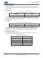
Table 2-2. SLAVE_BOOT message for CS485xx
MNEMONIC
VALUE
SLAVE_BOOT
0x80000000
The SLAVE_BOOT message is used when the system host controller will send each.uld file directly to the
CS485xx. The SLAVE_BOOT message must be issued for each overlay image (.uld file) that is downloaded
to the CS485xx. Please see Figure 2-2 for more details.
2.3.3.2 Soft Reset
Table 2-3. SOFT_RESET message for CS485xx
MNEMONIC
VALUE
SOFT_RESET
0x40000000
The SOFT_RESET message is the message sent to the CS485xx after all of the overlays have been
successfully booted. The SOFT_RESET leaves execution of the bootloader and begins execution of the
loaded overlays. The overlays can be configured once the SOFT_RESET message has been sent.
2.3.3.3 Messages Read from CS485xx
Table 2-4 defines the boot read messages, in mnemonic and actual hex value, used in CS485xx boot
sequences. Note that there is a unique {ID} for every.uld file.
Table 2-4. Boot Read Messages from CS485xx
DS734UM7
MNEMONIC
VALUE
BOOT_START
0x00000001
BOOT_SUCCESS
0x00000002
APP_START
0x00000004
BOOT_ERROR_CHECKSUM
0x000000FF
INVALID_BOOT_TYPE
0x000000FE
BOOT_FAILURE
0x000000F8
APPLICATION_FAILURE
0xF0{ID}0000
Copyright 2009 Cirrus Logic, Inc.
2-6
Master Boot Procedure
CS485xxr Hardware User’s Manual
Table 2-5 is a quick reference showing the different boot commands understood by the CS485xx, in
mnemonic and actual hex value, used in CS485xx boot sequences.
Table 2-5. Boot Command Messages for CS485xx
MNEMONIC
VALUE
DETAILED TABLE
SLAVE_BOOT
0x80000000
Table 2-2
SOFT_RESET
0x40000000
Table 2-3
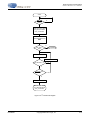
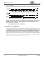
2.4 Master Boot Procedure
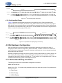
A master boot sequence is initiated immediately after the rising edge of RESET. The location of the overlay
to boot is outlined in Table 2-1. Once the rising edge of RESET has occurred, the CS485xx will load a single
overlay from address 0x0. It should be noted that the loaded overlay must reconfigure one of the control
ports to be slave to the bus for a system host controller to configure the part. Thus, this type of boot process
will be useful in systems without a system host controller or with a simple controller that only performs a
monitoring task. Currently this mode is not used for any applications.
Start
RESET ( Low)
Set HS[4:0 ] Pins For
Operational Mode
RESET ( High)
Done
Figure 2-3. Master Boot Sequence Flowchart
2-7
Copyright 2009 Cirrus Logic, Inc.
DS734UM7
Softboot
CS485xxr Hardware User’s Manual
2.5 Softboot
The O/S application code for the CS485xx allows users to swap out one or more overlays during run time,
without the need for re-download of the entire overlay stack. This is helpful for reducing the time required for
switching between different types of incoming audio data streams.
The Softboot procedure includes initial messaging that sends the CS485xx into a boot state where the host
can boot the CS485xx with different overlays according to the boot methods described in this chapter. This
includes a soft reset of the CS485xx, which then requires that the host send or re-send the hardware and
software configuration messages.
2.5.1 Softboot Messaging
Two messages are relevant to the softboot procedure for the CS485xx. These messages are: SOFTBOOT
and SOFTBOOT_ACK.
The SOFTBOOT message is sent from the host controller to the CS485xx to indicate to the CS485xx that the
system requires swapping of overlays.
Table 2-6. SOFTBOOT Message
Mnemonic
Value
SOFTBOOT
0x81000009
0x00000001
The SOFTBOOT_ACK is sent from the CS485xx to the host controller to indicate that the host can now boot
the CS485xx with the new overlays.
Table 2-7. SOFTBOOT_ACK Message
Mnemonic
Value
SOFTBOOT_ACK
0x00000005
2.5.2 Softboot Procedure
Figure 2-4 describes the Softboot procedure. This is a step-by-step guideline that can be used as an aid in
developing the system controller code required to drive the CS485xx.
DS734UM7
Copyright 2009 Cirrus Logic, Inc.
2-8
Softboot
CS485xxr Hardware User’s Manual
START
WRITE_* (SOFTBOOT)
N
IRQ == LOW?
Y
READ_* (MSG)
N
N
TIMEOUT?
Y
EXIT(ERROR)
MSG == SOFTBOOT_ACK?
Y
LOAD OVERLAYS
DONE
Figure 2-4. Soft Boot Sequence Flowchart
2.5.2.1 Softboot Steps
1. Send the SOFTBOOT message. The host sends the SOFTBOOT message to the CS485xx to begin
overlay swap.
2. Wait for IRQ low. The host then waits for SCP_IRQ to go low. If the TIMEOUT period has been
reached, the host should exit. If the IRQ pin is LOW, proceed to step 3.
3. Read the SOFTBOOT_ACK message. If the message is the SOFTBOOT_ACK message
(0x00000005), then the host should proceed to step 4. If the message is not the SOFTBOOT_ACK
message, the host should return to step 2.
4. Load Overlays. Repeat the boot procedure used to originally load the overlays into the CS485xx (i.e.
SLAVE_BOOT), but only the overlays that need to be swapped should be loaded. Skip the hard reset
sequence, starting the boot procedure from Step 2. Please note that this includes re-downloading all
hardware and software configurations for the CS485xx overlays.
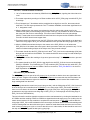
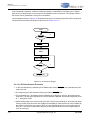
2.5.2.2 Softboot Example
Figure 2-5 is an example flow diagram and step-by-step description of the Softboot procedure based on the
SLAVE_BOOT procedure described earlier.
2-9
Copyright 2009 Cirrus Logic, Inc.
DS734UM7
Softboot
CS485xxr Hardware User’s Manual
START
WRITE_* (SOFTBOOT)
N
IRQ == LOW?
N
TIMEOUT?
Y
Y
READ_* (MSG)
N
EXIT(ERROR)
MSG == SOFTBOOT_ACK?
Y
WRITE_* (SLAVE_BOOT)
READ_* (MSG)
MSG
==BOOT_START
N
EXIT(ERROR)
Y
SEND .ULD FILE
READ_* (MSG)
MSG==
BOOT_SUCCESS
N
EXIT(ERROR)
Y
Y
MORE .ULD FILES?
N
WRITE_* (SOFT_RESET)
READ_* (MSG)
MSG ==APP_START
N
EXIT(ERROR)
Y
SEND HARDWARE
CONFIGURATIONS
SEND FIRMWARE
CONFIGURATIONS
* is replaced with SPI,
I2C, etc. depending on
the communication
protocol used.
WRITE_* (KICKSTART)
DONE
Figure 2-5. Soft Boot Example Flowchart
2.5.2.2.1 Softboot Example Procedure
1. Send the SOFTBOOT message. The host sends the SOFTBOOT message to the CS485xx to begin
overlay swap.
2. Wait for IRQ low. The host then waits for SCP_IRQ to go low. If the TIMEOUT period has been
reached, the host should exit. If the IRQ pin is LOW, proceed to step 3.
DS734UM7
Copyright 2009 Cirrus Logic, Inc.
2-10
Softboot
CS485xxr Hardware User’s Manual
3. Read the SOFTBOOT_ACK message. If the message is the SOFTBOOT_ACK message
(0x00000005), then the host should proceed to step 4. If the message is not the SOFTBOOT_ACK
message, the host should return to step 2.
4. Send the SLAVE_BOOT message. The host sends the SLAVE_BOOT message to the CS485xx
using the format specified (I2C or SPI) by the HS[4:0] pins at reset.
5. Wait for IRQ low. The host then waits for SCP_IRQ to go low.
6. Read the BOOT_START message. If the initialization is successful, CS485xx will send the
BOOT_START message to the host. If the message is any other value, then the host should abort.
7. Send the ULD File. After receiving the BOOT_START message, the host sends a.uld file to the
CS485xxx.
8. Wait for IRQ low. The host then waits for SCP_IRQ to go low. This indicates that the DSP has written
a message to the output buffer and the boot process is complete.
9. Read the BOOT_SUCCESS message. The host then reads another message from the appropriate
communications port. Each.ULD file contains a checksum that is compared at the end of the boot
process. The CS485xx sends a BOOT_SUCCESS message to the host if the checksum is correct after
the download.
If the checksum was incorrect, CS485xx responds with a BOOT_ERROR_CHECKSUM message. This
indicates that the image read by the DSP is corrupted. The communications interface hardware and code
image integrity should be checked if this occurs.
10.Repeat steps 4-8 for all code images/Overlays. The host repeats these steps until all overlays for
the application have been successfully loaded. See the application note for more information on the
overlays necessary at start-up.
11.Send the SOFT_RESET message. After reading the BOOT_SUCCESS message on the last code
image/overlay, the host must send a SOFT_RESET message which will cause the application code to
begin executing.
12.Wait for IRQ low. The host then waits for SCP_IRQ to go low.
13.Read the APP_START message. If code execution is successful, the CS485xx sends out an
APP_START message. This indicates that the code has been initialized and can accept further
configuration messages. The host should not attempt further communication with the CS485xx until the
APP_START message has been read.
If the CS485xx does not send an application start message, the host must return to Step 1. If the message
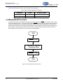
read is any value other than APP_START, the system controller should abort.
14.Send Hardware Configuration messages. The application code boot procedure is completed. The
operating system on the CS485xx is now ready for host configuration of hardware and software.
Hardware configuration messages are used to define the behavior of the CS485xx’s audio ports.
15.Send Software Configuration messages.The software configuration messages are specific to each
application. The application code User’s Guide for each application provides a list of all pertinent
configuration messages.
16.Send the KICKSTART message. The CS485xx begins processing audio after receiving this
message.
2-11
Copyright 2009 Cirrus Logic, Inc.
DS734UM7
Low Power Mode
CS485xxr Hardware User’s Manual
2.6 Low Power Mode
The CS485xx has a low power mode to enable power savings when not in use. Low power mode is
entered during the softboot procedure.
2.6.1 Low Power Mode Messaging
One message is relevant to the low power mode procedure for the CS48xxxx. This message is
SOFTBOOT_LP.
The host must read any ACK and prior messages before low power mode may commence.
Mnemonic
Value
SOFTBOOT_LP
0x81000009
0x00000011
2.6.2 Getting into Low Power Mode
Follow these steps to get into low power mode:
1. The system controller should send the SOFTBOOT_LP message (0x81000009 0x00000011).
2. The CS48xxxx is now in low power mode.
3. To test that the CS48xxxx is in low power mode the host controller can send a message and verify
that there is no response. Additionally all the GPIO pins will be set to inputs in low power mode
with weak pull-ups so there state can be checked to verify low power mode is active.
2.6.3 Getting Out of Low Power Mode
Follow these steps to get out of low power mode:
1. Set DSP_RESET low.
2. Set DSP_RESET high.
3. Send the SLAVE_BOOT message (0x80000000).
4. Read the BOOT_START message (0x00000001).
5. Send the WAKEUP_*.ULD file.
Note: “*” .uld name is dependent on the current memory configuration. For example: if loading
os_48520_p2_*.uld, then send wakeup_p2.uld. If loading os_48520_p4_*.uld, then send wakeup_p4.uld,
and so forth. See Table 2-8.
6. Read the BOOT_SUCCESS message (0x00000002).
7. Send the SOFT_RESET message (0x40000000).
8. Read the APP_START message (0x00000004).
9. Send Hardware Configuration messages.
10.Send Software Configuration messages.
11.Send the KICKSTART messages.
Figure 2-6 shows a flowchart of the steps used to exit Low Power mode.
DS734UM7
Copyright 2009 Cirrus Logic, Inc.
2-12
Low Power Mode
CS485xxr Hardware User’s Manual
Start
SET DSP_RESET (LOW)
SET DSP_RESET (HIGH)
WRITE_* (SLAVE_BOOT)
READ_* (MSG)
MSG==
BOOT_START
Y
N
EXIT (ERROR)
Y
SEND .ULD FILE
Send .uld from Table 2-8
READ_* (MSG)
MSG==
BOOT_SUCCESS
N
EXIT (ERROR)
Y
WRITE_* (SOFT_RESET)
READ_* (MSG)
MSG==
APP_START
N
EXIT (ERROR)
Y
SEND HARDWARE
CONFIGURATIONS
SEND SOFTWARE
CONFIGURATIONS
WRITE_* (KICKSTART)
DONE
Figure 2-6. Flowchart of Steps Used to Exit Low Power Mode
2-13
Copyright 2009 Cirrus Logic, Inc.
DS734UM7
Low Power Mode
CS485xxr Hardware User’s Manual
0x
Table 2-8. wakeup_uld Options and Values
.uld Options
Values
WAKEUP_P2.ULD
0x08004409
0x00000002
0x00000000
0xb485aa01
0x01000359
0x00000001
0x00000000
0xffffffff
0x427a0e9b
WAKEUP_P4.ULD0x
0x08004409
0x00000002
0x00000001
0xb485aa01
0x01000359
0x00000001
0x00000000
0xffffffff
0x427a0e9a
WAKEUP_P6.ULD
0x08004409
0x00000002
0x00000002
0xb485aa01
0x01000359
0x00000001
0x00000000
0xffffffff
0x427a0e99
WAKEUP_P8.ULD
0x08004409
0x00000002
0x00000003
0xb485aa01
0x01000359
0x00000001
0x00000000
0xffffffff
0x427a0e98
§§
DS734UM7
Copyright 2009 Cirrus Logic, Inc.
2-14
Introduction
CS485xx Hardware User’s Manual
Chapter 3
Serial Control Port
3.1 Introduction
The CS485xx uses the Serial Control Port (SCP) to communicate with external devices such as host
microprocessors using either I2C or SPI serial communication formats. The port can be configured as either
a master or slave. The CS485xx DSP serial port communicates using the SCP_CLK, SCP_MOSI,
SCP_MISO (SPI serial master and slave modes), and SCP_SDA (for I2C serial master and slave modes)
pins.
In both SPI and I2C modes, the serial control port performs 8-bit transfers and is always configured as a
slave for external device-controlled data transfers. As a slave, it cannot drive the clock signal nor initiate data
transfers. The port can request a read from the host by dropping the SCP_IRQ pin. The port can also
indicate that the host should stop sending data by dropping the SCP_BSY pin.
Note: The host must obey the SCP_BSY pin status. Messages sent to the DSP’s serial control port
(SCP) when SCP_BSY pin is low will be lost.
The CS485xx SPI and I2C serial communication modes are identical from a functional standpoint. The main
difference between the two is the actual protocol being implemented between the CS485xx and the host. In
addition, the I2C slave has a true I2C mode that utilizes data flow mechanisms inherent to the I2C protocol. If
this mode is enabled, the I2C slave will hold SCP_CLK low to delay a transfer as needed -- this is in addition
to activating SCP_BSY.
3.2 Serial Control Port Configuration
The serial control port configuration for an operating mode is determined by the state of hardware boot
select pins as the CS485xx exits reset. The rising edge of the RESET pin samples the HS[4:0] pins to
determine the communication mode and boot style. The CS485xx O/S currently supports two serial control
port configurations for host control:
•
I2C Slave (Write Address = 0x80, Read Address = 0x81)
•
SPI Slave (Write Address = 0x80, Read Address = 0x81)
The HS[4:0] signals latched by RESET are read by the boot ROM code to determine the format (SPI slave or
I2C slave). If a slave mode is chosen, the ROM code then configures the serial control port for slave mode
and looks for the BOOT_START message. If a master mode is chosen, the ROM code starts fetching code
from address 0x00. Please see Chapter 2, "Operational Modes" for additional details on configuring
CS485xx ports and communication modes.
Procedures for configuring the serial control port for SPI and I2C communication modes are provided in this
section.
3-1
Copyright 2009 Cirrus Logic, Inc.
DS734UM7
Serial Control Port Configuration
CS485xx Hardware User’s Manual
3.2.1 I2C Port
The CS485xx I2C bus has been developed for 8-bit digital control applications, such as those requiring
microcontrollers. The I2C bus interface is a bidirectional serial port that uses 2 lines (data and clock) for data
transmission and reception with software-addressable external devices. Each external device interfaced to
the CS485xx I2C port has the ability to communicate directly with the other devices and is assigned a unique
address whether it is a CPU, memory, or some other device. A block diagram of the CS485xx I2C Serial
Control Port is provided in Figure 3-1.
Internal Bus
SCP_IRQ
SCP_BSY
MSB (Byte 3)
Byte2
Byte 1
LSB (Byte 0)
MSB (Byte 3)
Byte2
Byte 1
LSB (Byte 0)
LSB (Byte 0)
Byte1
Byte 2
MSB (Byte 3)
LSB (Byte 0)
Byte1
Byte 2
MSB (Byte 3)
I2C Control /
Clocking
SCP_CLK
EN
7 6 5 4 3 2 1 0
SCP_SDA
EN
Figure 3-1. Serial Control Port Internal Block Diagram
DS734UM7
Copyright 2009 Cirrus Logic, Inc.
3-2
Serial Control Port Configuration
CS485xx Hardware User’s Manual
3.2.2 I2C System Bus Description
Devices can be considered masters or slaves when performing data transfers. A master is the device which
initiates a data transfer on the bus and generates the clock signals to permit that transfer. Any device
addressed by the initiator is considered a slave.
The I2C-bus is a multi-master bus. This means that more than one device capable of controlling the bus can
be connected to it. The master-slave relationships found on the I2C bus are not permanent and only depend
on the direction of data transfer at that time. Generation of clock signals on the I2C bus is always the
responsibility of master devices; each master generates its own clock signals when transferring data on the
bus. Bus clock signals from a master can only be altered when they are stretched by a slow slave device
holding down SCP_CLK.
Both SCP_SDA and SCP_CLK are bidirectional lines. When the bus is free, both lines are pulled high by
resistors. The output stages of devices connected to the bus must have an open-drain or open-collector to
perform the wired-AND function.
3.3V
3.3k
3.3k
3.3k
3.3k
CS485xx
System Microcontroller
GPIO
CLK
RESET
SCP_CLK
SDA
SCP_SDA
GPIO
GPIO
SCP_IRQ
SLAVE
ONLY
SCP_BSY
3.3V
3.3k
3.3k
CS485xx
Serial FLASH
CLK
SCP_CLK
SDA
SCP_SDA
MASTER
ONLY
Figure 3-2. Block Diagram of I2C System Bus
Table 3-1 shows the signal names, descriptions, and pin number of the signals associated with the I2C Serial
Control Port on the CS485xx.
3-3
Copyright 2009 Cirrus Logic, Inc.
DS734UM7
Serial Control Port Configuration
CS485xx Hardware User’s Manual
Table 3-1. Serial Control Port 1 I2C Signals
Pin Name
Pin Description
LQFP-48
Pin #
Pin
Type
SCP_CLK
I2C Control Port Bit Clock.
In master mode, this pin serves as the serial control clock output
(open drain in I2C mode / output in SPI mode). In serial slave
mode, this pin serves as the serial control clock input. In I2C
slave mode the clock can be pulled low by the port to stall the
master.
36
Open
Drain
SCP_SDA
Bidirectional Data I2C Mode Master/Slave Data IO. In I2C
master and slave mode, this open drain pin serves as the data
input and output.
35
Open
Drain
SCP_IRQ
Control Port Data Ready Interrupt Request, Output, Active Low
This pin is driven low when the DSP has a message for the host
to read. The pin will go high when the host has read the
message and the DSP has no further messages.
39
Open
Drain
SCP_BSY
Serial Control Port Input Busy, Output, Active Low
This pin is driven low when the control port’s receive buffer is
full. Internal Buffer is 4 bytes (1 DSP Word) deep.
41
Open
Drain
3.2.2.1 I2C Bus Dynamics
The Start condition for an I2C transaction is defined as the first falling edge on the SCP_SDA line while
SCP_CLK is high. An I2C Stop condition is defined as the first rising edge on the SCP_SDA line while
SCP_CLK is high. Hence for valid data transfer, SCP_SDA must remain stable during the high period of the
clock pulse. Start and Stop conditions are always generated by the master. The bus is considered to be busy
after the Start condition. The bus is considered to be free again following the Stop condition. The bus stays
busy if a repeated Start condition is generated instead of a Stop condition. In this respect, the Start and
repeated Start conditions are functionally identical.
Start
Stop
SCP_CLK
SCP_CLK
SCP_SDA
SCP_SDA
Figure 3-3. I2C Start and Stop Conditions
DS734UM7
Copyright 2009 Cirrus Logic, Inc.
3-4
Serial Control Port Configuration
CS485xx Hardware User’s Manual
The number of bytes that can be transmitted per transfer is unrestricted. Data is transferred with the mostsignificant bit (MSB) first. The first byte is an address byte that is always sent by the master after a Start or
repeated Start condition. This byte must be a 7-bit I2C slave address + R/W bit. The 7-bit I2C address for the
CS485xx is 1000000b (0x80). The R/W bit is used to notify the slave if the current transaction is for the
master to write data to the slave (R/W = 0) or read data from the slave (R/W = 1).
After the master has sent the address byte, the master releases the SCP_SDA line. If the slave received the
address byte, it will drive the SCP_SDA line low to acknowledge (ACK) to the master that the byte was
received. The SCP_SDA line must remain stable and low during the high period of the next clock pulse.
When a slave doesn’t acknowledge the slave address, the data line must be left high by the slave (NACK).
Start
SCP_CLK
SCP_SDA
A[6]
A[5]
A[4]
A[3]
A[2]
A[1]
A[0]
M
R/W
ACK
S
Start
SCP_CLK
SCP_SDA
A[6]
A[5]
A[4]
A[3]
A[2]
A[1]
A[0]
M
R/W NACK
S
M = Master Drives SDA
S = Slave Drives SDA
Figure 3-4. I2C Address with ACK and NACK
For write operations, the R/W bit must be set to zero (R/W = 0, Address = 0x80). After the 8-bit data byte has
been clocked, the master will release the SCP_SDA line. If the slave received the byte correctly, it will drive
the SCP_SDA line low for the next bit clock to acknowledge (ACK) that the data was received. If the data
was not received correctly, the slave can communicate this by leaving the SCP_SDA line high (NACK).
For read operations, the R/W bit must be set to one (R/W = 1, Address = 0x81), then the master will read a
data byte from the slave. After the 8-bit data byte has been clocked, the master will release the SCP_SDA
line. If the master received the byte correctly, it will drive the SCP_SDA line low for the next bit clock to
acknowledge (ACK) that the data was received. If the data was not received correctly, the master can
communicate this by leaving the SCP_SDA line high (NACK). The protocol on the last byte, however, is
different. When the master receives the last byte, it signals the end of the data to the slave by allowing
SCP_SDA to float high (NACK).
3-5
Copyright 2009 Cirrus Logic, Inc.
DS734UM7
Serial Control Port Configuration
CS485xx Hardware User’s Manual
Start
SCP_CLK
SCP_SDA
A[6]
A[5]
A[4]
A[3]
A[2]
A[1]
A[0]
R/W ACK
Data Byte
ACK
Write
M
S
M
S
Read
M
S
S
M
Data Byte
NACK
Start
SCP_CLK
SCP_SDA
A[6]
A[5]
A[4]
A[3]
A[2]
A[1]
A[0]
R/W ACK
Write
M
S
M
S
Read
M
S
S
M
M = Master Drives SDA
S = Slave Drives SDA
Figure 3-5. Data Byte with ACK and NACK
After an ACK or NACK from the master or slave, the slave must leave the SCP_SDA line high so the master
can then generate either a Stop condition to abort the transfer, or a another Start condition to start a new
transfer.
Stop
SCP_CLK
SCP_SDA
Data Byte
ACK
Write
M
S
M
Read
S
M
M
Stop
SCP_CLK
SCP_SDA
Data Byte
NACK
Write
M
S
M
M
M
Read
S
M = Master Drives SDA
S = Slave Drives SDA
Figure 3-6. Stop Condition with ACK and NACK
If a slave can’t receive or transmit another complete byte of data until it has performed some other function,
for example servicing an internal interrupt, it can hold the SCP_CLK line low to force the master into a wait
state. Data transfer then continues when the slave is ready for another byte of data and releases SCP_CLK.
DS734UM7
Copyright 2009 Cirrus Logic, Inc.
3-6
Serial Control Port Configuration
CS485xx Hardware User’s Manual
Start
SCP_CLK
SCP_SDA
Data Byte
ACK
A[6]
A[5]
A[4]
A[3]
A[2]
A[1]
A[0]
R/W
Write
M
S
M
S
Read
S
M
M
S
ACK
Start
SCP_CLK
SCP_SDA
Data Byte
NACK
A[6]
A[5]
A[4]
A[3]
A[2]
A[1]
A[0]
R/W ACK
Write
M
S
M
S
Read
S
M
M
S
M = Master Drives SDA
S = Slave Drives SDA
Figure 3-7. Repeated Start Condition with ACK and NACK
3.2.2.2 I2C Messaging
Messaging to the CS485xx using the I2C bus requires usage of all the information provided in the above I2C
Section 3.2.2 “I2C System Bus Description” on page 3-3 and Section 3.2.2.1 “I2C Bus Dynamics” on page
3-4. Every I2C transaction to the CS485xx will involve 4-byte words - for control and application image
download. A detailed description of the serial SPI communication mode is provided in this section. This
includes:
•
A flow diagram and description for a serial I2C write
•
A flow diagram and description for a serial I2C read
3.2.2.2.1 SCP_BSY Behavior
The SCP_BSY signal is not part of the I2C protocol, but it is provided so that the slave can signal to the
master that it cannot receive any more data. It performs the same function as that of holding SCP_CLK low
to halt transmission. A falling edge of the SCP_BSY signal indicates the master must halt transmission.
Once the SCP_BSY signal goes high, the suspended transaction may continue. It is important for the host to
obey the SCP_BSY pin status for proper communication with the DSP.
3.2.2.3 Performing a Serial I2C Write
Information provided in this section is intended as a functional description indicating how to use the
configured serial control port to perform a I2C write from an external device (master) to the CS485xx DSP
(slave). The system designer must ensure that all timing constraints of the I2C write cycle are met (see the
CS485xx datasheet for timing specifications). When writing to the CS485xx, the same protocol described in
this section will be used when writing single-word messages to the boot firmware, writing multiple-word
overlay images to the boot firmware, and writing multiple-word messages to application firmware. The
examples given can therefor be expanded to fit any I2C writing situation.
The flow diagram shown in Figure 3-8 below, illustrates the sequence of events that define the I2C write
protocol for SCP. This protocol is discussed in the high-level procedure in Section 3.2.2.3.1.
3-7
Copyright 2009 Cirrus Logic, Inc.
DS734UM7
Serial Control Port Configuration
CS485xx Hardware User’s Manual
SEND I2C START:
DRIVE SCP_SDA LOW
WHILE SCP_CLK IS
HIGH
WRITE ADDRESS BYTE
0x80
N
EXIT (ERROR)
SCP_SDA ==
ACK?
Y
SEND DATABYTE
N
EXIT (ERROR)
SCP_SDA ==
ACK?
Y
N
4 BYTES SENT?
Y
N
Y
MORE DATA?
SCP_BSY
(LOW)?
N
Y
I2C STOP:
DRIVE SCP_SDA HIGH
WHILE SCP_CLK IS
HIGH
Figure 3-8. I2C Write Flow Diagram
3.2.2.3.1 I2C Write Protocol Procedure
1. An I2C transfer is initiated with an I2C start condition which is defined as the data (SCP_SDA) line
falling while the clock (SCP_CLK) is held high.
2. This is followed by a 7-bit address and the read/write bit held low for a write. So, the master should
send 0x80. The 0x80 byte represents the 7-bit I2C address 1000000b, and the least significant bit set
to ‘0’, designates a write.
3. After each byte (including the address and each data byte) the master must release the data line and
provide a ninth clock for the CS485xx DSP (slave) to acknowledge (ACK) receipt of the byte. The
CS485xx will drive the data line low during the ninth clock to acknowledge. If for some reason
CS485xx does not acknowledge (NACK), it means that the communications channel has been
corrupted and the CS485xx should be re-booted. A NACK should never happen here.
4. The master should then clock one data byte into the device, most-significant bit first.
5. The CS485xx (slave) will (and must) acknowledge (ACK) each byte that it receives which means that
DS734UM7
Copyright 2009 Cirrus Logic, Inc.
3-8
Serial Control Port Configuration
CS485xx Hardware User’s Manual
after each byte, the master must provide an acknowledge clock pulse on SCP_CLK and release the
data line, SCP_SDA.
6. If the master has no more data words to write to the CS485xx, then proceed to step 8. If the master
has more data words to write to the CS485xx, then proceed to step 7.
7. The master should poll the SCP_BSY signal until it goes high. If the SCP_BSY signal is low, it
indicates that the CS485xx is busy performing some task that requires pausing the serial control port.
Once the CS485xx is able to receive more data words, the SCP_BSY signal will go high. Once the
SCP_BSY signal is high, proceed to step 4.
Note: The DSP’s I2C port also implements clock stretching to indicate that the host should pause
communication. So the host has the option of checking for SCP_CLK held low rather than
SCP_BSY low.
8. At the end of a data transfer, a stop condition must be sent. The stop condition is defined as the rising
edge of SCP_SDA while SCP_CLK is high.
3.2.2.4 Performing a Serial I2C Read
Information provided in this section is intended as a functional description indicating how to use the
configured serial control port to perform an I2C read from an external device (master) to the CS485xx DSP
(slave). The system designer must ensure that all timing constraints of the I2C Read Cycle are met (see the
CS485xx Data Sheet for timing specifications). I2C read transactions from the CS485xx will always involve
reading 4-byte words.
The flow diagram shown in Figure 3-9 illustrates the sequence of events that define the I2C read protocol for
SCP. This protocol is discussed in the high-level procedure in Section 3.2.2.4.1.
3-9
Copyright 2009 Cirrus Logic, Inc.
DS734UM7
Serial Control Port Configuration
CS485xx Hardware User’s Manual
START
N
SCP_IRQ
(LOW)?
Y
SEND I2C START: DRIVE
SCP_SDA LOW WHILE
SCP_CLK IS HIGH
WRITE ADDRESS BYTE
0x81
N
EXIT (ERROR)
SCP_SDA ==
ACK?
Y
READ DATA BYTE
SEND ACK
BYTES READ = 4?
N
Y
SCP_IRQ LOW?
Y
N
SEND NACK
SEND I2C STOP: DRIVE
SCP_SDA HIGH WHILE
SCP_CLK IS HIGH
Figure 3-9. I2C Read Flow Diagram
DS734UM7
Copyright 2009 Cirrus Logic, Inc.
3-10
Serial Control Port Configuration
CS485xx Hardware User’s Manual
3.2.2.4.1 I2C Read Protocol Procedure
1. An I2C read transaction is initiated by CS485xx driving SCP_IRQ low, signaling that it has data to be
read.
2. The master responds by sending an I2C Start condition which is SCP_SDA going low while SCP_CLK
is held high.
3. This is followed by a 7-bit address and the read/write bit set high for a read. So, the master should
send 0x81. The 0x81 byte represents the 7-bit I2C address 1000000b, and the least significant bit set
to ‘1’, designates a read.
4. After the address byte, the master must release the data line and provide a ninth clock for the
CS485xx DSP (slave) to acknowledge (ACK) receipt of the byte. The CS485xx will drive the data line
low during the ninth clock to acknowledge. If for some reason CS485xx does not acknowledge
(NACK), it means that the communications channel has been corrupted and the CS485xx should be
re-booted. A NACK should never happen here.
5. The data is ready to be clocked out on the SCP_SDA line at this point. Data clocked out by the host is
valid on the rising edge of SCP_CLK and data transitions occur just after the falling edge of SCP_CLK.
6. After the CS485xx has written the byte to the master on the SCP_SDA line, it will release the
SCP_SDA line. If the master has more bytes in the 4-byte word to read, then proceed to step 7. If the
master is finished reading all bytes of the 4-byte word, then proceed to step 8.
7. The master should drive the SCP_SDA line low for the 9th SCP_CLK clock to acknowledge (ACK) that
the byte was received from the CS485xx. The master should then return to step 5 to read another byte
of the 4-byte word.
8. If SCP_IRQ is still low after reading a 4-byte word, proceed to step 7. If SCP_IRQ has risen, proceed
to step 9.
9. The master should let the SCP_SDA line stay high for the 9th SCP_CLK clock as a no-acknowledge
(NACK) to CS485xx. This, followed by an I2C stop condition (SCP_SDA driven high, while SCP_CLK
is high) signals an end of read to CS485xx. See the next section, "SCP_IRQ Behavior" for the an indepth explanation of SCP_IRQ.
3.2.2.4.2 SCP_IRQ Behavior
The SCP_IRQ signal is not part of the I2C protocol, but is provided so that the slave can signal that it has
data to be read. A high-to-low transition on SCP_IRQ indicates to the master that the slave has data to be
read. When a master detects a high-to-low transition on SCP_IRQ, it should send a Start condition and
begin reading data from the slave.
SCP_IRQ is guaranteed to remain low (once it has gone low), until the falling edge of SCP_CLK for the last
bit of the last byte to be transferred out of CS485xx (i.e. the rising edge of SCP_CLK before the ACK). If
there is no more data to be transferred, SCP_IRQ will go high at this point. After going high, SCP_IRQ is
guaranteed to stay high until the next rising edge of SCP_CLK (i.e. it will stay high until the rising edge of
SCP_CLK for the ACK/NACK bit).
This end-of-transfer condition signals the master to end the read transaction by clocking the last data bit out
of CS485xx and then sending a NACK to CS485xx to signal that the read sequence is over. At this point, the
master should send an I2C stop condition to complete the read sequence. If SCP_IRQ is still low after the
rising edge of SCP_CLK on the last data bit of the current byte, the master should send an acknowledge and
continue reading data from the serial control port. It should be noted that all data should be read out of the
serial control port during one cycle or a loss of data will occur. In other words, all data should be read out of
the chip until SCP_IRQ signals the last byte by going high.
3-11
Copyright 2009 Cirrus Logic, Inc.
DS734UM7
DS734UM7
Start
Stop
M
S
M
Data Byte 1
S
M
Data Byte 0 (LSB)
AC
K
S
Data Byte 2
AC
K
M
Data Byte 3 (MSB)
AC
K
7-bit Address
AC
K
SCP_SDA
R
/W
AC
K
SCP_CLK
S
M
S
M
Figure 3-10. Sample Waveform for I2C Write Functional TIming
Note: The I2C slave is always responsible for driving the ACK for the address byte.
Stop
Data Byte 0 (LSB)
K
Data Byte 1
NA
C
Data Byte 2
AC
K
Data Byte 3 (MSB)
AC
K
7-bit Address
AC
K
SCP_SDA
/W
AC
K
SCP_CLK
R
Copyright 2009 Cirrus Logic, Inc.
Start
SCP_IRQ
M
S
S
M
S
M
S
M
S
M
M
M = Master Drives SDA
S = Slave Drives SDA
Figure 3-11. Sample Waveform for I2C Read Functional Timing
2.The I2C master is responsible for controlling ACK during I2C reads. In general, the receiver in an I2C transaction is responsible for
providing ACK.
3.SCP_IRQ remains low until the rising edge of the clock for the last bit of the last byte read from the I2C slave.
4.A NACK is sent by the master after the last byte to indicate the end of the read cycle. This must be followed with an I2C Stop condition or
I2C Repeated-Start condition.
3-12
Serial Control Port Configuration
CS485xx Hardware User’s Manual
Notes: 1.The I2C slave is drives the ACK for the address byte.
SPI Port
CS485xx Hardware User’s Manual
If there are more data words to read, IRQ will fall at the rising edge of CLK for the NACK. Otherwise, IRQ
remains high until an I2C Stop condition or an I2C Repeated-Start condition occurs.
3.3 SPI Port
The CS485xx Serial Peripheral Interface (SPI) bus has been developed for 8-bit digital control applications,
such as those requiring microcontrollers. SPI communication is accomplished with 6 lines: Serial Control
Port Input Busy (SCP_BSY), Serial Control Port Data Ready Interrupt Request (SCP_IRQ), Serial Chip
Select (SCP_CS), Serial Control Clock (SCP_CLK), Master Out/Slave In data (SCP_MOSI), and a Master
In/Slave Out data (SCP_MISO). Although the separate data I/O lines provide full-duplex capabilities, the
CS485xx chip only uses a half-duplex SPI-bus. Each device on the bus may respond to one or more unique
commands, and can operate as either a transmitter or receiver. A device is considered the master in a
transaction if it drives the CS pin of another device, and is also mastering the SCP_CLK line. A block
diagram of the CS485xx SPI Serial Control Port is provided in Figure 3-12.
Internal Bus
SCP_CS
SCP_IRQ
MSB (Byte 3)
Byte2
Byte 1
LSB (Byte 0)
MSB (Byte 3)
Byte2
Byte 1
LSB (Byte 0)
LSB (Byte 0)
Byte1
Byte 2
MSB (Byte 3)
LSB (Byte 0)
Byte1
Byte 2
MSB (Byte 3)
SCP_BSY
SCP_CLK
SCP_MOSI
SPI Control /
Clocking
SCP_MISO
7 6 5 4 3 2 1 0
Figure 3-12. SPI Serial Control Port Internal Block Diagram
Table 3-2 shows the signal names, descriptions, and pin number of the signals associated with the SPI
Serial Control Port on the CS485xx.
3-13
Copyright 2009 Cirrus Logic, Inc.
DS734UM7
SPI Port
CS485xx Hardware User’s Manual
Table 3-2. Serial Control Port SPI Signals
Pin Name
Pin Description
LQFP-48
Pin #
Pin
Type
SCP_CS
SPI Chip Select, Active Low
In serial SPI slave mode, this pin is used as the active-low chip-select
input signal. In SPI serial master mode, if this pin is driven low by
another master device on the bus, it will cause a mode fault to occur.
38
Input
SCP_CLK
SPI Control Port Bit Clock
In master mode, this pin serves as the serial control clock output. In
serial slave mode, this pin serves as the serial control clock input.
36
I/O
SCP_MOSI
SPI Mode Master Data Output/Slave Data Input
SCP_MOSI in SPI slave mode this pin serves an the data input, in SPI
master mode this pin serves as the data output.
34
I/O
SCP_MISO
SPI Mode Master Data Input/Slave Data Output
In SPI slave mode this pin serves as the data input. In SPI master
mode this pin serves as the data output.
35
I/O
SCP_IRQ
Serial Control Port Data Ready Interrupt Request Output, Active Low
This pin is driven low when the DSP has a message for the host to
read. The pin will go high when the host has read the message and the
DSP has no further messages. This pin reflects the state of the SCP
port Transmit Buffer Empty Flag.
39
Open
Drain
SCP_BSY
Serial Control Port Input Busy, Output, Active Low
This pin is driven low when the control port’s receive buffer is full. This
pin reflects the state of the SCP or PCP Receive Buffer Full Fag.
41
Open
Drain
Master Mode Serial EPROM Chip Select, Active Low
41
Output
EE_CS
3.3.1 SPI System Bus Description
The SPI bus is a multi-master bus. This means that more than one device capable of controlling the bus can
be connected to it. Generation of clock signals on the SPI bus is always the responsibility of master devices;
each master generates its own clock signals when transferring data on the bus. Bus clock signals from a
master cannot be altered by any other device on the bus, otherwise a collision will occur. The slave chipselect signals can only be controlled by master devices.
SCP_MOSI (Master Out/Slave In) and SCP_MISO (Master In/Slave Out) are bidirectional lines that change
their behavior depending on whether the device is operating in master or slave mode. Only the master can
drive the MOSI signal while only the slave can drive the MISO signal.
3-14
Copyright 2009 Cirrus Logic, Inc.
DS734UM7
SPI Port
CS485xx Hardware User’s Manual
Both modes of the CS485xx serial port are shown in Figure 3-13.
3.3V
3.3k
System Microcontroller
3.3k
CS485xx
GPIO
RESET
GPIO
SCK
MOSI
MISO
SCP_CS
SCP_CLK
SCP_MOSI
SCP_MISO
SCP_IRQ
SCP_BSY
GPIO
GPIO
SLAVE
ONLY
CS485xx
SPI EEPROM
MOSI
MISO
CS
CLK
SCP_MOSI
SCP_MISO
SCP_CS
SCP_CLK
MASTER
ONLY
Figure 3-13. Block Diagram of SPI System Bus
3.3.1.1 SPI Bus Dynamics
A SPI transaction begins by the master driving the slave chip select SCP_CS low. SPI transactions end by
the master driving the SCP_CS high. This SPI bus is considered busy while any device’s SCP_CS signal is
low. The bus is free only when all slave SCP_CS signals are high. A high-to-low transition on the SCP_CS
line defines an SPI Start condition. A low-to-high transition on the SCP_CS line defines an SPI Stop
condition. Start and Stop conditions are always generated by the master. The bus is considered to be busy
after the Start condition. The bus is considered to be free again following the Stop condition.
The data bits of the SCP_MOSI and SCP_MISO line are valid on the rising edge of SCP_CLK. It is the
slave’s responsibility to accept or supply bytes on the bus at the rate at which the master is driving
SCP_CLK.
All data put on the SCP_MOSI and SCP_MISO lines must be in 8-bit bytes. The number of bytes that can be
transmitted per transfer is unrestricted. Data is transferred with the most-significant bit (MSB) first. For the
CS485xx slave SPI port, the first byte is an address byte that must always be sent by the master after a Start
condition. This address byte is an “I2C-type” command of a 7-bit address + a R/W bit. The 7-bit SPI address
is 1000000b (0x80).
If the SPI transaction is a write from master to the CS485xx (R/W = 0, Address = 0x80), then the master will
clock the SCP_CLK signal and drive the SCP_MOSI signal with data bytes for the to read. If the SPI
transaction is a read to the master from the CS485xx (R/W = 1, Address = 0x81), then the master will drive
the SCP_CLK signal and read the SCP_MISO signal with the data bytes from the CS485xx.
3-15
Copyright 2009 Cirrus Logic, Inc.
DS734UM7
SPI Port
CS485xx Hardware User’s Manual
SCP_CS
SCP_CLK
SCP_MOSI
7-bit SPI Address
R/W
7-bit SPI Address
R/W
Data Byte
SCP_CS
SCP_CLK
SCP_MOSI
SCP_MISO
Data Byte
SCP_CS
SCP_CLK
SCP_MOSI
7-bit SPI Address
R/W
7-bit SPI Address
R/W
Data Byte
SCP_CS
SCP_CLK
SCP_MOSI
SCP_MISO
Data Byte
SCP_CS
SCP_CLK
SCP_MOSI
7-bit SPI Address
R/W
7-bit SPI Address
R/W
Data Byte
SCP_CS
SCP_CLK
SCP_MOSI
SCP_MISO
Data Byte
Figure 3-14. SPI Address and Data Bytes
3.3.1.1.1 SCP_BSY Behavior
The SCP_BSY signal is not part of the SPI protocol, but it is provided so that the slave can signal to the
master that it cannot receive any more data. A falling edge of the SCP_BSY signal indicates the master must
halt transmission. Once the SCP_BSY signal goes high, the suspended transaction may continue. The host
must obey the SCP_BSY pin or control data will be lost.
DS734UM7
Copyright 2009 Cirrus Logic, Inc.
3-16
SPI Port
CS485xx Hardware User’s Manual
3.3.1.2 SPI Messaging
Messaging to the CS485xx using the SPI bus requires usage of all the information provided in the SPI Bus
SCP_CS
SCP_CLK
SCP_MOSI
7-bit SPI Address
R/W
7-bit SPI Address
R/W
Data Byte
SCP_CS
SCP_CLK
SCP_MOSI
SCP_MISO
Data Byte
Description and Bus Dynamics above. For control and application image downloading, SPI transactions to
the CS485xx will involve 4-byte words. A detailed description of the serial SPI communication mode is
provided in this section. This includes:
•
A flow diagram and description for a serial SPI write
•
A flow diagram and description for a serial SPI read
3.3.1.3 Performing a Serial SPI Write
Information provided in this section is intended as a functional description indicating how to perform an SPI
write from an external device (master) to the CS485xx DSP (slave). The system designer must ensure that
all timing constraints of the SPI Write Cycle are met (see the CS485xx datasheet for timing specifications).
When performing an SPI write, the same protocol is used whether writing single-word messages to the boot
firmware, writing multiple-word overlay images to the boot firmware, or writing multiple-word messages to
the application firmware. The example shown in this section can be generalized to fit any SPI write situation.
The flow diagram shown in Figure 3-15 , illustrates the sequence of events that define the SPI write protocol.
This protocol is discussed in the high-level procedure in Section 3.3.1.3.1.
3-17
Copyright 2009 Cirrus Logic, Inc.
DS734UM7
SPI Port
CS485xx Hardware User’s Manual
SPI START: SCP_CS
(LOW)
WRITE ADDRESS BYTE
0x80
WRITE 4 DATA BYTES
Y
MORE DATA?
SCP_BSY
(LOW)?
N
N
Y
SPI STOP: SCP_CS
(HIGH)
Figure 3-15. SPI Write Flow Diagram
3.3.1.3.1 SPI Write Protocol Procedure
1. A SPI transfer is initiated when the chip select SCP_CS is driven low. SCP_CS driven low indicates
that CS485xx is in SPI slave mode.
2. This is followed by a 7-bit address and the read/write bit set low for a write. So, the master should
send 0x80. The 0x80 byte represents the 7-bit SPI address 1000000b, and the least significant bit set
to ‘0’, designates a write.
3. The master should then clock the 4-byte data word into the slave device, most-significant bit first, one
byte at a time. The data byte is transferred to the CS485xx DSP (slave) on the falling edge of the
eighth serial clock. For this reason, the serial clock should be held low so that eight transitions from
low-to-high-to-low will occur for each byte.
4. If the master has no more data words to write to the CS485xx, then proceed to step 6. If the master
has more data words to write to the CS485xx, then proceed to step 5.
5. The master should poll the SCP_BSY signal until it goes high. If the SCP_BSY signal is low, it
indicates that the CS485xx is busy performing some task that requires halting the serial control port.
Once the CS485xx is able to receive more data words, the SCP_BSY signal will go high. Once the
SCP_BSY signal is high, proceed to step 3.
6. The master finishes the SPI write transaction by driving the CS485xx SCP_CS signal high.
3.3.1.4 Performing a Serial SPI Read
Information provided in this section is intended as a functional description indicating how an external device
(Master) performs an SPI read from the CS485xx (slave). The system designer must ensure that all timing
constraints of the SPI read cycle are met (see the CS485xx datasheet for timing specifications).
DS734UM7
Copyright 2009 Cirrus Logic, Inc.
3-18
SPI Port
CS485xx Hardware User’s Manual
When performing a SPI read, the same protocol is used whether reading a single byte or multiple bytes.
From a hardware perspective, it makes no difference whether communication is a single byte or multiple
bytes of any message length, so long as the correct hardware protocol is followed. The example shown in
this section can be generalized to fit any SPI read situation.
The flow diagram shown in Figure 3-16, illustrates the sequence of events that define the SPI read protocol.
This protocol is discussed in the high-level procedure in Section 3.3.1.4.1
START
SCP_IRQ
(LOW)?
N
Y
SCP_CS LOW
WRITE ADDRESS BYTE
0x81
READ 4 DATA BYTES
SCP_IRQ STILL
LOW?
Y
N
SCP_CS HIGH
Figure 3-16. SPI Read Flow Diagram
3.3.1.4.1 SPI Read Protocol Procedure
1. A SPI read transaction is initiated by the CS485xx slave driving SCP_IRQ low to indicate that it has
data to be read.
2. The master begins a SPI transaction driving chip select (SCP_CS) low.
3. This is followed by a 7-bit address and the read/write bit set high for a read. So, the master should
send 0x81. The 0x81 byte represents the 7-bit SPI address 1000000b, and the least significant bit set
to ‘1’, designates a read.
4. After the falling edge of the serial control clock (SCP_CLK) for the read/write bit, the master can begin
clocking out the 4-byte word from the CS485xx on the MISO pin. Data clocked out of the CS485xx by
the master is valid on the rising edge of SCP_CLK and data transitions occur on the falling edge of
SCP_CLK. The serial clock should be held low so that eight transitions from low-to-high-to-low will
occur for each byte.
3-19
Copyright 2009 Cirrus Logic, Inc.
DS734UM7
SPI Port
CS485xx Hardware User’s Manual
5. If SCP_IRQ is still low after 4 bytes, then proceed to step 4 and read another 4 bytes out of the
CS485xx slave.
6. If SCP_IRQ is high, the SCP_CS line of CS485xx should be driven high to end the read transaction.
DS734UM7
Copyright 2009 Cirrus Logic, Inc.
3-20
DS734UM7
SCP_CS
SCP_CLK
/W
7-bit Address
R
SCP_MOSI
Data Byte 3 (MSB)
Data Byte 2
Data Byte 1
Data Byte 0 (LSB)
Figure 3-17. Sample Waveform for SPI Write Functional Timing
S C P _ M IS O
7 - b it A d d r e s s
/W
S C P _ M O S I
R
Copyright 2009 Cirrus Logic, Inc.
S C P _ C S
S C P _ C L K
D a ta
B y te
3
(M S B )
D a ta
B y te
2
D a ta
B y te
1
D a ta
B y te
0
(L S B )
S C P _ IR Q
Figure 3-18. Sample Waveform for SPI Read Functional Timing
Notes: 1.IRQ remains low until the rising edge of the clock for the last bit of the last byte to be read from the SPI slave.
2.After going high, IRQ remains high until the CS signal is raised to end the SPI transaction. If there are more bytes to read, IRQ will fall
after CS has gone high.
SPI Port
CS485xx Hardware User’s Manual
3-21
SPI Port
CS485xx Hardware User’s Manual
3.3.1.4.2 SCP_IRQ Behavior
The SCP_IRQ signal is not part of the SPI protocol, but is provided so that the slave can signal that it has
data to be read. A high-to-low transition on SCP_IRQ indicates to the master that the slave has data to be
read. When a master detects a high-to-low transition on SCP_IRQ, it should send a Start condition and
begin reading data from the slave.
SCP_IRQ is guaranteed to remain low (once it has gone low), until the rising edge of SCP_CLK for the last
bit of the last byte to be transferred out of CS485xx. If there is no more data to be transferred, SCP_IRQ will
go high at this point. After going high, SCP_IRQ is guaranteed to stay high until the rising edge of SCP_CS.
This end-of-transfer condition signals the master to end the read transaction by clocking the last data bit out
of CS485xx and then driving the CS485xx SCP_CS line high to signal that the read sequence is over. If
SCP_IRQ is still low after the rising edge of SCP_CLK on the last data bit of the current byte, the master
should continue reading data from the serial control port. It should be noted that all data should be read out
of the serial control port during one cycle or a loss of data will occur. In other words, all data should be read
out of the chip until SCP_IRQ signals the last byte by going high as described above.
§§
3-22
Copyright 2009 Cirrus Logic, Inc.
DS734UM7
Introduction
CS485xx Hardware User’s Manual
Chapter 4
Digital Audio Input Interface
4.1 Introduction
CS485xx supports a wide variety of audio data formats through various input and output ports. Hardware
availability is entirely dependent on whether the software application code being used supports the required
mode. This data sheet presents most of the modes available with the CS485xx hardware. However, not all of
the modes are available with any particular piece of application code. The Application Code User’s Guide for
the particular code being used should be referenced to determine if a particular mode is supported. In
addition, if a particular mode is desired, but not presented, please contact your sales representative
regarding its availability.
4.2 Digital Audio Input Port Description
The CS485xx Digital Audio Input ports (DAI1 and DAI2) are designed to provide either five digital audio input
pins (up to 10 channels total) or six digital audio pins (up to 12 channels) depending on the mode of
operation configured. The pins can be configured to load audio samples in a number of formats, or accept
multiple stereo channels on a single input pin.
DAI features include:
4-1
•
Five Digital Audio Input Pins Capable of Supporting Many Audio Formats with Dual Clock Domains
on CS48560
•
Four Digital Audio Input Pins Capable of Supporting Many Audio Formats with Dual Clock Domains
on CS48540
•
Two Digital Audio Input Pins Capable of Supporting Many Audio Formats with Dual Clock Domains
on CS48520
•
Two Independent Input Clock Domains (DAI1_SCLK/DAI1_LRCLK or DAI2_SCLK/DAI2_LRCLK)
•
Six Digital Audio Input Pins when Configured for Single Clock Domain Operation on CS48560
•
Four Digital Audio Input Pins when Configured for Single Clock Domain Operation on CS48540
•
Two Digital Audio Input Pins when Configured for Single Clock Domain Operation on CS48520
•
Up to 32-bit Data Widths
•
Sample Rates up to 192 kHz
•
Two Simultaneous Audio Streams with Different Sample Frequencies (Fs) for Dual-path Processing
Support
•
2, 4, or 6 Channels on a Single Pin (DAI_DATAx)
Copyright 2009 Cirrus Logic, Inc.
DS734UM7
Digital Audio Input Port Description
CS485xx Hardware User’s Manual
4.2.1 DAI Pin Description
Table 4-1 shows the mnemonic and pin description of the pins associated with the DAI port on CS485xx.
Table 4-1. Digital Audio Input Port
Pin Name
Pin Description
LQFP-48
Pin #
Pin Type
DAI1_LRCLK or
DAI1_DATA5
Sample Rate Clock 1 PCM Audio Input Sample Rate
(LeftRight) Clock
DAI1_LRCLK is the sample rate input clock for the serial
PCM audio data on DAI_DATA[3:0] when in dual-clock
domain mode.
DAI_DATA4 is used for PCM Audio Input Data when
configured for single-clock domain mode.
Note:
DAI1_DATA4 is not available on CS48540
DAI1_DATA4 is not available on CS48520
6
Input
DAI1_SCLK
Bit Clock 1 PCM Audio Input Bit Clock
DAI1_SCLK is the bit clock input for the serial PCM
audio data on DAI_DATA[3:0]..
8
Input
DAI1_DATA0
PCM or Compressed Audio Input Data 0 PCM Audio
Input Data 0
Serial data input that can accept PCM audio data that is
synchronous to DAI_SCLK1/DAI_LRCLK1 or
DAO_SCLK/DAO_LRCLK..
10
Input
DAI1_DATA1
PCM Audio Input Data
Note:
DAI1_DATA1 is not available on CS48520
11
Input
DAI1_DATA2
PCM Audio Input Data
Note:
DAI1_DATA2 is not available on CS48520
13
Input
DAI1_DATA3
PCM Audio Input Data
Note:
DAI1_DATA3is not available on CS48540
DAI1_DATA3 is not available on CS48520
14
Input
17
Input
Bit Clock 2 PCM Audio Input Bit Clock
DAI2_SCLK is the bit clock input for the serial PCM
audio data on DAI2_DATA0 in dual-clock domain mode.
DAI2_SCLK is the bit clock input for the serial PCM
audio data on DAI_DATA[5:0] in single-clock domain
mode.
18
Input
PCM Audio Input Data
15
Input
DAI2_LRCLK
DAI2_SCLK
DAI2_DATA0 or
DAI1_DATA4
DS734UM7
Sample Rate Clock 2 PCM Audio Input Sample Rate
(LeftRight) Clock
DAI2_LRCLK is the sample rate input clock for the serial
PCM audio data on DAI2_DATA0 in dual-clock domain
mode.
DAI2_LRCLK is the sample rate input clock for seral
PCM audio data on DAI_DATA[5:0] in single-clock
domain mode.
Copyright 2009 Cirrus Logic, Inc.
4-2
Digital Audio Input Port Description
CS485xx Hardware User’s Manual
4.2.2 Supported DAI Functional Blocks
The CS485xx DAI has many functional blocks for realizing various audio system configurations. The use of
these functions is dependent on the firmware currently available on the CS485xx.
4.2.2.1 Dual Clock Domain - 10 Channel Input
Figure 4-1 shows the functional block diagram of the features currently supported with the CS48560 DAI.
DAI1_DATA0
DAI1_DATA0
DAI1_DATA1
DAI1_DATA2
DAI1_DATA2
DAI1_DATA3
DAI_LRCLK1
DAI_SCLK1
DAI2_DATA0
DAI_LRCLK2
DAI_SCLK2
DMA to Peripheral Bus
DAI1_DATA1
DAI1_DATA3
DAI2_DATA0
Figure 4-1. 10-Channel DAI Port Block Diagram
Figure 4-2 shows the functional block diagram of the features currently supported with the CS48540 DAI.
DAI1_DATA0
DAI1_DATA1
DAI_LRCLK1
DAI_SCLK1
DAI1_DATA1
DAI1_DATA2
DAI1_DATA2
DAI2_DATA0
DAI_LRCLK2
DAI_SCLK2
DMA to Peripheral Bus
DAI1_DATA0
DAI2_DATA0
Figure 4-2. 8-Channel DAI Port Block Diagram
Figure 4-3 shows the functional block diagram of the features currently supported with the CS48520 DAI.
4-3
Copyright 2009 Cirrus Logic, Inc.
DS734UM7
DAI1_DATA0
DAI_LRCLK1
DAI_SCLK1
DAI2_DATA0
DAI_LRCLK2
DAI_SCLK2
DAI1_DATA0
DAI2_DATA0
DMA to Peripheral Bus
Digital Audio Input Port Description
CS485xx Hardware User’s Manual
Figure 4-3. 6-Channel DAI Port Block Diagram
Currently supported are 4 lines of linear PCM input (DAI1_DATA3:0) on the first clock domain and 1
additional line of linear PCM (DAI2_DATA0) on the second clock domain, which will support up to 10
channels of PCM. These two input ports can have separate clock domains, or share a single clock domain.
The firmware currently available can operate on only one of these input ports at a time, providing for stereo
PCM processing or multichannel PCM processing. Please see AN298 for details on configuring the firmware
to select these different inputs.
4.2.2.2 Single Clock Domain - 12 Channel Input
The DAI can also be configured to accept up to 12 channels of linear PCM audio (6 serial audio data inputs)
by converting DAI1_LRCLK into a data pin (DAI1_DATA5). Consequently, there is only one possible clock
domain (DAI2_LRCLK/SCLK).
DS734UM7
Copyright 2009 Cirrus Logic, Inc.
4-4
Digital Audio Input Port Description
CS485xx Hardware User’s Manual
DAI1_DATA0
DAI1_DATA0
DAI1_DATA1
DAI1_DATA2
DAI1_DATA2
DAI1_DATA3
DAI1_DATA3
DMA to Peripheral Bus
DAI1_DATA1
DAI1_DATA4
DAI1_DATA4
DAI1_DATA5
DAI_LRCLK2
DAI_SCLK2
DAI1_DATA5
Figure 4-4. 12-Channel DAI Port Block Diagram
4.2.3 Digital Audio Formats
The DAI data input pins are fully configurable including support for I2S and left-justified formats. DAI clock
and data pins support only slave operation. This subsection describes some common audio formats that
CS485xx supports. It should be noted that the input ports use up to 32-bit PCM resolution.
4.2.3.1 I2S Format
Figure 4-5 illustrates the I2S format. For I2S, data is presented most-significant bit (MSB) first, one SCLK
delay after the transition of DAIn_LRCLK, and is valid on the rising edge of DAIn_SCLK. For the I2S format,
the left subframe is presented when DAIn_LRCLK is low, and the right subframe is presented when
DAIn_LRCLK is high.
4-5
Copyright 2009 Cirrus Logic, Inc.
DS734UM7
DAI Hardware Configuration
CS485xx Hardware User’s Manual
DAIn_LRCLK
Left Channel
Right Channel
DAIn_SCLK
DAI_DATA
+5 +4 +3 +2 +1 LSB
MSB-1 -2 -3 -4 -5
MSB-1 -2 -3 -4
+5 +4 +3 +2 +1 LSB
Figure 4-5. I2S format (Rising Edge Valid SCLK)
4.2.3.2 Left-Justified Format
Figure 4-6 illustrates the left-justified format with a rising-edge DAIn_SCLK. Data is presented mostsignificant bit first on the first DAIn_SCLK after a DAIn_LRCLK transition and is valid on the rising edge of
DAIn_SCLK. For the left-justified format, the left subframe is presented when DAIn_LRCLK is high and the
right subframe is presented when DAIn_LRCLK is low. The left-justified format can also be programmed for
data to be valid on the falling edge of DAIn_SCLK.
L eft C h a n nel
DAIn_LRCLK
Rig ht C h a n n el
DAIn_SCLK
DAIn_DATA
MSB
-1 -2
-3
-4
-5
+5
+4
+3
+2
+1
LSB
MSB -1
-2
-3
-4
+5
+4
+3
+2
+1
LSB
Figure 4-6. Left-justified Format (Rising Edge Valid SCLK)
4.3 DAI Hardware Configuration
After code download or soft reset, and before kickstarting the application, the host has the option of
changing the default hardware configuration. (Please see AN298, “CS485xx Firmware User’s Manual” for
more information on kickstarting). In general, the hardware configuration can only be changed immediately
after download or after soft reset.
Hardware configuration messages are used to physically reconfigure the hardware of the audio decoder, as
when enabling or disabling address checking for the serial communication port. Hardware configuration
messages are also used to initialize the format (e.g., I2S, left justified, etc.) for digital data inputs, as well as
the data format and clocking options for the digital output port.
4.3.1 DAI Hardware Naming Convention
The naming convention of the input hardware configuration is as follows:
INPUT A B C D E F G H
Where A, B, C, D, E, F, G, and H are the parameters used to fully define the input port. The parameters are
defined as follows:
A - Data Format
B - SCLK Polarity
C - LRCLK Polarity.
DS734UM7
Copyright 2009 Cirrus Logic, Inc.
4-6
DAI Hardware Configuration
CS485xx Hardware User’s Manual
D - DAI Mode (Unsupported)
E - DAI2_DATA Clock Source
F - DAI1_DATA Clock Source
G - Chip Version
H - Chip Version
Table 4-2, Table 4-3, Table 4-4, Table 4-5, Table 4-6, Table 4-7, and Table 4-7show the different values for
each parameter as well as the hex message that needs to be sent to configure the port. When creating the
hardware configuration message, only one hex message should be sent per parameter.
.
Table 4-2. Input Data Format Configuration (Input Parameter A)
A Value
0 (default)
1
4-7
Data Format
Hex Message
I2S 24-bit
0x81800010
0xFFFF0000
0x81400010
0x01001F00
0x81800011
0xFFFF0000
0x81400011
0x01001F00
0x81800012
0xFFFF0000
0x81400012
0x01001F00
0x81800013
0xFFFF0000
0x81400013
0x01001F00
0x81800014
0xFFFF0000
0x81400014
0x01001F00
Left-Justified 24-bit
0x81800010
0xFEEF0000
0x81400010
0x00001F00
0x81800011
0xFEEF0000
0x81400011
0x00001F00
0x81800012
0xFEEF0000
0x81400012
0x00001F00
0x81800013
0xFEEF0000
0x81400013
0x00001F00
0x81800014
0xFEEF0000
0x81400014
0x00001F00
Copyright 2009 Cirrus Logic, Inc.
DS734UM7
DAI Hardware Configuration
CS485xx Hardware User’s Manual
Table 4-3. Input SCLK Polarity Configuration (Input Parameter B)
B Value
0 (default)
1
SCLK Polarity (DAI_SCLK1 &
DAI_SCLK2)
Hex Message
Data Clocked in on SCLK Rising Edge
0x81800010
0xFFDFFFFF
0x81800011
0xFFDFFFFF
0x81800012
0xFFDFFFFF
0x81800013
0xFFDFFFFF
0x81800014
0xFFDFFFFF
Data Clocked in on SCLK Falling Edge
0x81400010
0x00200000
0x81400011
0x00200000
0x81400012
0x00200000
0x81400013
0x00200000
0x81400014
0x00200000
.
Table 4-4. Input LRCLK Polarity Configuration (Input Parameter C)
C Value
0 (default)
1
LRCLK Polarity
(Both DAI and CDI Port)
HEX Message
LRCLK=Low indicates Channel 0
(i.e. Left)
0x81800010
0xFFDFFFFF
0x81800011
0xFFDFFFFF
0x81800012
0xFFDFFFFF
0x81800013
0xFFDFFFFF
0x81800014
0xFFDFFFFF
LRCLK=Low indicates Channel 1
(i.e. Right)
0x81400010
0x00200000
0x81400011
0x00200000
0x81400012
0x00200000
0x81400013
0x00200000
0x81400014
0x00200000
Note: The.D Value, DAI Mode, is not supported on the CS485xx platform.
DS734UM7
Copyright 2009 Cirrus Logic, Inc.
4-8
DAI Hardware Configuration
CS485xx Hardware User’s Manual
Table 4-5. DAI2_DATA Clock Source (Input Parameter E)
E
Value
DAI2_DATA Clock Source
HEX Message
0
DAI1_LRCLK/DAI1_SCLK
0x81800015
0xCFFFFFFF
DAI2_LRCLK/DAI2_SCLK
0x81400015
0x10000000
0x81800015
0xDFFFFFFF
1 (default)
Table 4-6. DAI1_DATA Clock Source (Input Parameter F)
F Value
DAI1_DATA Clock Source
HEX Message
0 (default)
DAI1_LRCLK/DAI1_SCLK
0x81800015
0xF00FFFFF
DAI2_LRCLK/DAI2_SCLK
0x81400015
0x05500000
0x81800015
0xF55FFFFF
1
Table 4-7. Chip Version (Input Parameter G)
G Value
0
1
2
Chip Version
HEX Message
CS48520
0x81400015
0x00080000
0x81800015
0xFFF80000
CS48540
0x81400015
0x00088800
0x81800015
0xFFF88800
CS48560
0x81400015
0x0008D100
0x81800015
0xFFF8D100
Table 4-8. DAII TDM (Input Parameter H)
H Value
0
4-9
DAI TDM Sourcea,b
HEX Message
DAI1_D0 (Pin 10)
0x81800015
0xFFF00000
0x81000010
0x01101F00
0x81000011
0x01103F20
0x81000012
0x01105F40
0x81000013
0x01107F60
0x81000014
0x01109F80
Copyright 2009 Cirrus Logic, Inc.
DS734UM7
DAI Hardware Configuration
CS485xx Hardware User’s Manual
a. TDM (Time Division Multiplex) is only available on the CS48560 product.
b. Accepts a maximum of 12 channlels of input.
§§
DS734UM7
Copyright 2009 Cirrus Logic, Inc.
4-10
Digital Audio Input Port Description
CS485xx Hardware User’s Manual
Chapter 5
Direct Stream Data (DSD) Input Interface
CS48560 is capable of accepting DSD audio data directly. DSD data differs from PCM in that audio is
provided as a contiguous stream of 1’s and 0’s on a single line. There is no framing clock (LRCLK), and
there is only one channel per line. The CS48560 supports internal conversion of DSD data to PCM which
can then be processed by the DSP.
Note: If DSD functionality is needed in a system design, contact your Cirrus Logic FAE.
5.1 Digital Audio Input Port Description
The CS48560 DSD port is designed to accept DSD audio data from up to 6 pins simultaneously (6 channels
total).
DSD features include:
•
Up to Six DSD Input Pins
•
One Shared DSD_CLK for All Data Pins
•
Supports 44.1 kHz and 88.2 kHz Sample Rates
5.1.1 DSD Pin Description
Table 5-1 shows the mnemonic and pin description of the pins associated with the DSD port on CS48560.
Table 5-1. DSDl Audio Input Port
Pin Name
DSD_CLK
Pin Description
Bit clock used for latching the DSD audio
data. This clock is shared by DSD[5:0].
LQFP-48
Pin Type
Pin #
8
Input
DSD0
DSD Audio Input 0
10
Input
DSD1
DSD Audio Input 1
11
Input
DSD2
DSD Audio Input 2
13
Input
DSD3
DSD Audio Input 3
14
Input
DSD4
DSD Audio Input 4
15
Input
DSD5
DSD Audio Input 5
6
Input
5.1.2 Supported DSD Functional Blocks
Figure 5-1 below shows the functional block diagram of the features currently supported with the CS48560
DSD Port.
5-1
Copyright 2009 Cirrus Logic, Inc.
DS734UM7
Digital Audio Input Port Description
CS485xx Hardware User’s Manual
DSD0
DSD_DATA0
DSD1
DMA to Peripheral Bus
DSD_DATA1
DSD2
DSD_DATA2
DSD3
DSD_CLK
DSD_DATA3
DSD4
DSD_DATA4
DSD5
DSD_DATA5
Figure 5-1. DSD Port Block Diagram on CS48560
§§
DS734UM7
Copyright 2009 Cirrus Logic, Inc.
5-2
Introduction
CS485xx Hardware User’s Manual
Chapter 6
Digital Audio Output Interface
6.1 Introduction
The CS485xx Digital Audio Output port can provide up to 12 channels of PCM data (up to 32-bit resolution).
The Digital Audio Output port is implemented with a modified 3-wire Inter-IC Sound (I2S) interface along with
an oversampling master clock (MCLK). The I2S interface includes a frame clock at the current sampling
frequency (LRCLK), a bit clock for clocking the bits of the audio word (SCLK), and up to 6 audio data output
signals (DATA[5:0]). Each of the output data signals can be connected to the digital stereo input of an audio
digital-to-analog converter (DAC) for up to 12 channels of stereo PCM output.
The DAO port may slave to an externally generated SCLK and LRCLK or it may master these clocks if
MCLK is provided. The port supports data rates from 32 kHz to 192 kHz. One DAO pin can also be
configured to provide a 32-kHz to 192-kHz S/PDIF transmitter (XMTA) output. Figure 6-1, Figure 6-2, Figure
6-3 illustrate the DAO block diagrams for the CS48560, CS48540 , and CS48520 products respectively.
6.2 Digital Audio Output Port Description
6.2.1 DAO Pin Description
Table 6-1 identifies the pins associated with the Digital Audio Output Port.
Table 6-1. Digital Audio Output (DAO) Pins
LQFP-48
Pin #
Pin
Type
Sample Rate Clock
21
I/O
Bit Clock
23
I/O
Digital Audio Output
20
Output
27
Output
Note: DAO1_DATA2 is not
available on CS48520
26
Output
DAO1_DATA3/XMTA
Digital Audio Output
29
Output
DAO2_DATA0
Digital Audio Output
31
Output
Note: DAO2_DATA1 is not
available on CS48520 or
CS48540.
32
Output
Master Clock
25
I/O
Pin Name
DAO_LRCLK
DAO_SCLK
DAO1_DATA0
Pin Description
Digital Audio Output
DAO1_DATA1
Note: DAO1_DATA1 is not
available on CS48520
Digital Audio Output
DAO1_DATA2
Digital Audio Output
DAO2_DATA1
DAO_MCLK
6-1
Copyright 2009 Cirrus Logic, Inc.
DS734UM7
Digital Audio Output Port Description
CS485xx Hardware User’s Manual
DAO_MCLK is the master clock and is firmware configurable to be either an input (slave) or an output
(master). If MCLK is to be used as an output, the internal PLL must be used. As an output MCLK can be
configured to provide a 128Fs, 256Fs, or 512Fs clock, where Fs is the output sample rate.
•
DAO_SCLK is the bit clock used to clock data out on DAOn_DATA[n].
•
DAO_LRCLK is the data framing clock whose frequency is equal to the sampling frequency for the
DAO data outputs.
•
DAOn_DATA[n] are the data outputs and are typically configured for outputting two channels of I2S
or left-justified PCM data.
.
DAO1_DATA0
Peripheral Bus to DMA
DAO1_DATA1
DAO1_DATA2
DAO1_DATA3, XMTA
DAO1_DATA3
SPDIF
ENCODER
DAO2_DATA0
DAO2_DATA1
Clock
Manager
DAO_MCLK
DAO_SCLK
DAO_LRCLK
Figure 6-1. CS48560 DAO Block Diagram
DS734UM7
Copyright 2009 Cirrus Logic, Inc.
6-2
Digital Audio Output Port Description
CS485xx Hardware User’s Manual
.
DAO1_DATA0
Peripheral Bus to DMA
DAO1_DATA1
DAO1_DATA2
SPDIF
ENCODER
XMTA
DAO2_DATA0
Clock
Manager
DAO_MCLK
DAO_SCLK
DAO_LRCLK
Figure 6-2. CS48540 DAO Block Diagram
Peripheral Bus to DMA
.
DAO1_DATA0
SPDIF
ENCODER
XMTA
DAO2_DATA0
Clock
Manager
DAO_MCLK
DAO_SCLK
DAO_LRCLK
Figure 6-3. CS48520 DAO Block Diagram
6-3
Copyright 2009 Cirrus Logic, Inc.
DS734UM7
Digital Audio Output Port Description
CS485xx Hardware User’s Manual
6.2.2 Supported DAO Functional Blocks
As mentioned in Section 6.1, DAO_DATA3 on CS48560 is unique in that it is designed to serve as either an
output for I2S or left-justified PCM data or as a S/PDIF transmitter (XMTA). On the CS48540 and CS48520 it
is only a s S/PDIF transmitter (XMTA). When configured as a S/PDIF transmitter, it encodes digital audio
data according to the Sony/Phillips Digital Interface Format (S/PDIF), also known as IEC60958, or the AES/
EBU interface format.
6.2.3 DAO Interface Formats
The DAO interface has up to 6 stereo data outputs that are fully configurable including support for I2S, leftjustified, and multichannel (one-line data mode) formats. This section describes some common audio
formats that the CS485xx DAO interface supports. It should be noted that the digital output ports provide up
to 32-bit PCM resolution.
6.2.3.1 I2S Format
In this format, data is presented most-significant bit (MSB) first, one DAO_SCLK delay after the transition of
DAO_LRCLK, and is valid on the rising edge of DAO_SCLK. The left subframe is presented when
DAO_LRCLK is low, and the right subframe is presented when DAO_LRCLK is high. Figure 6-4 provides
details on I2S compatible (maximum of 32 bits) serial audio formats.
DAO_LRCLK
Left Channel
Right Channel
DAO_SCLK
DAO_DATA
MSB-1 -2 -3 -4 -5
+5 +4 +3 +2 +1 LSB
MSB-1 -2 -3 -4
+5 +4 +3 +2 +1 LSB
Figure 6-4. I2S Compatible Serial Audio Formats (Rising Edge Valid DAO_SCLK)
6.2.3.2 Left-Justified Format
Figure 6-5 illustrates the left-justified (LJ) format with a rising edge DAO_SCLK. Data is presented mostsignificant bit first on the first DAO_SCLK after a DAO_LRCLK transition and is valid on the rising edge of
DAO_SCLK. The left subframe is presented when DAO_LRCLK is high and the right subframe is presented
when DAO_LRCLK is low. This format can also be programmed for data to be valid on the falling edge of
DAO_SCLK.
L e ft C h a n n e l
DAO_LRCLK
R ig ht C h a n n el
DAO_SCLK
DAO_DATA
MSB
-1
-2
-3
-4
-5
+5
+4
+3
+2
+1
LSB
MSB -1
-2
-3
-4
+5
+4
+3
+2
+1
LSB
Figure 6-5. Left-justified Digital Audio Formats (Rising Edge Valid DAO_SCLK)
DS734UM7
Copyright 2009 Cirrus Logic, Inc.
6-4
Digital Audio Output Port Description
CS485xx Hardware User’s Manual
6.2.3.3 One-line Data Mode Format (Multichannel)
The CS485xx is capable of multiplexing all digital audio outputs on one line, as illustrated in Figure 6-6. This
mode is available only through special request. Please contact your local Cirrus representative for further
details.
DA O _LRC LK
DA O _SC LK
DA O _DATA
M SB
L SB
M SB
M C lo c k s
Pe r C ha n ne l
LSB
M SB
M C lo c k s
P e r C h a n ne l
LSB
M C lo c k s
P e r C ha n ne l
MSB
LSB
M SB
M C lo c k s
Pe r C ha nn e l
L SB
M SB
M C lo c k s
Pe r C h a n ne l
LSB
MSB
M C lo c k s
Pe r C ha n nel
Figure 6-6. One-line Data Mode Digital Audio Formats
6.2.4 DAO Hardware Configuration
The DAO naming convention is as follows:
OUTPUT A B C D E F G
where the parameters are defined as:
A - DAO Clock Mode (Master/Slave for DAO_LRCLK and DAO_SCLK)
B - DAO1 & DAO2 Clocking Relationship
C - DAO_MCLK, DAO_SCLK, DAO_LRCLK Frequency Ratio
D - Data Format (I2S, Left Justified)
E - DAO_LRCLK Polarity
F - DAO_SCLK Polarity\
G - DAO TDM
Table 6-2, Table 6-3, Table 6-4, Table 6-5, Table 6-6, Table 6-7, and Table 6-8 show the different values for
each parameter as well as the hex message that needs to be sent to configure the port. When creating the
hardware configuration message, only one hex message should be sent per parameter.
Table 6-2 shows values and messages for DAO output clock mode configuration parameters.
Table 6-2. Output Clock Mode Configuration (Parameter A)
6-5
A
Value
DAO Modes (MCLK, LRCLK and
SCLK)
0 (Default)
DAO_MCLK - Slave
DAO_LRCLK - Slave
DAO_SCLK - Slave
1
DAO_MCLK - Slave
DAO_LRCLK - Master
DAO_SCLK - Master
Copyright 2009 Cirrus Logic, Inc.
Hex Message
0x8140001C
0x00002000
0x8140001D
0x00002000
0x8180001C
0xFFFFDFFF
0x8180001D
0xFFFFDFFF
DS734UM7
Digital Audio Output Port Description
CS485xx Hardware User’s Manual
Table 6-3. DAO1 & DAO2 Clocking Relationship Configuration (Parameter B)
B
Value
0a
DAO1 & DAO2 Clocking Relationship Hex Message
DAO2 dependent on DAO1 clocks
0x8140001B
0x00002000
a. This command is required because the DAO2 clocks are not
bonded out.
Please refer to Table 6-4, Table 6-5, and Table 6-6 for examples of the clocking directions for the settings
contained in Table 6-2.
Table 6-4 shows values and messages for the output DAO_SCLK/LRCLK frequency configuration
parameter.
Table 6-4. Output DAO_SCLK/LRCLK Configuration (Parameter C)
C Value
DAO_SCLK Frequency
DAO_MCLK = 256 FS
0 (default)
DAO_SCLK = DAO_MCLK / 4 = 64 FS
DAO_LRCLK = DAO_SCLK / 64 = FS
DAO_MCLK = 256 FS
1
DAO_SCLK = DAO_MCLK / 2 = 128 FS
DAO_LRCLK = DAO_SCLK / 128 = FS
DAO_MCLK = 256 FS
2
DAO_SCLK = DAO_MCLK / 1 = 256 FS
DAO_LRCLK = DAO_SCLK / 256 = FS
DAO_MCLK = 128 FS
3
DS734UM7
DAO_SCLK = DAO_MCLK / 2 = 64 FS
DAO_LRCLK = DAO_SCLK / 64 = FS
Copyright 2009 Cirrus Logic, Inc.
Hex Message
0x8100002D
0x00007711
0x8100002E
0x00007711
0x8180001C
0xFFFFFF8F
0x8140001C
0x00000020
0x8100002D
0x00017701
0x8100002E
0x00017701
0x8180001C
0xFFFFFF8F
0x8140001C
0x00000040
0x8100002D
0x00037700
0x8100002E
0x00037700
0x8180001C
0xFFFFFF8F
0x8140001C
0x00000060
0x8100002D
0x00007701
0x8100002E
0x00007701
0x8180001C
0xFFFFFF8F
0x8140001C
0x00000020
6-6
Digital Audio Output Port Description
CS485xx Hardware User’s Manual
Table 6-4. Output DAO_SCLK/LRCLK Configuration (Parameter C) (Continued)
C Value
DAO_SCLK Frequency
DAO_MCLK = 128 FS
4
DAO_SCLK = DAO_MCLK / 1 = 128 FS
DAO_LRCLK = DAO_SCLK / 128 = FS
DAO_MCLK = 512 FS
5
DAO_SCLK = DAO_MCLK / 8 = 64 FS
DAO_LRCLK = DAO_SCLK / 64 = FS
DAO_MCLK = 512 FS
6
DAO_SCLK = DAO_MCLK / 4 = 128 FS
DAO_LRCLK = DAO_SCLK / 128 = FS
DAO_MCLK = 512 FS
7
DAO_SCLK = DAO_MCLK / 2 = 256 FS
DAO_LRCLK = DAO_SCLK / 256 = FS
DAO_MCLK = 384 FS
8
DAO_SCLK = DAO_MCLK / 4 = 96 FS
DAO_LRCLK = DAO_SCLK / 96 = FS
DAO_MCLK = 384 FS
9
6-7
DAO_SCLK = DAO_MCLK / 2 = 192 FS
DAO_LRCLK = DAO_SCLK / 192 = FS
Copyright 2009 Cirrus Logic, Inc.
Hex Message
0x8100002D
0x00017700
0x8100002E
0x00017700
0x8180001C
0xFFFFFF8F
0x8140001C
0x00000040
0x8100002D
0x00007713
0x8100002E
0x00007713
0x8180001C
0xFFFFFF8F
0x8140001C
0x00000020
0x8100002D
0x00017711
0x8100002E
0x00017711
0x8180001C
0xFFFFFF8F
0x8140001C
0x00000040
0x8100002D
0x00037701
0x8100002E
0x00037701
0x8180001C
0xFFFFFF8F
0x8140001C
0x00000060
0x8100002D
0x00037211
0x8100002E
0x00037211
0x8180001C
0xFFFFFF8F
0x8140001C
0x00000030
0x8100002D
0x00077201
0x8100002E
0x00077201
0x8180001C
0xFFFFFF8F
0x8140001C
0x00000050
DS734UM7
Digital Audio Output Port Description
CS485xx Hardware User’s Manual
Table 6-5 shows values and messages for the data format configuration parameters.
Table 6-5. Output Data Format Configuration (Parameter D)
D
Value
0 (default)
1
2
DS734UM7
DAO Data Format (or DAO_DATA0 for
Multichannel Modes)
Hex Message
I2S 32-bit
0x81000020
0x00000001
0x81000021
0x00000001
0x81000022
0x00000001
0x81000023
0x00000001
0x81000024
0x00000001
0x81000025
0x00000001
0x81000026
0x00000001
0x81000027
0x00000001
Left Justified 32-bit
0x81000020
0x00000000
0x81000021
0x00000000
0x81000022
0x00000000
0x81000023
0x00000000
0x81000024
0x00000000
0x81000025
0x00000000
0x81000026
0x00000000
0x81000027
0x00000000
0x8180001c
0xFFFFFBFF
0x8180001d
0xFFFFFBFF
TDM 32-bit
0x81000020
0x00011701
0x81000021
0x00000001
0x81000022
0x00000001
0x81000023
0x00000001
0x81000024
0x00011701
0x81000025
0x00000001
0x81000026
0x00000001
0x81000027
0x00000001
Copyright 2009 Cirrus Logic, Inc.
6-8
Digital Audio Output Port Description
CS485xx Hardware User’s Manual
Table 6-6 shows values and messages for the DAO_LRCLK polarity configuration parameter.
Table 6-6. Output DAO_LRCLK Polarity Configuration (Parameter E)
E Value
DAO_LRCLK Polarity
0 (default)
LRCLK=Low indicates Left Subchannel
1
LRCLK=Low indicates Right Subchannel
Hex Message
0x8140001C
0x00000700
0x8140001D
0x00000700
0x8180001C
0xFFFFFBFF
0x8140001C
0x00000300
0x8180001D
0xFFFFFBFF
0x8180001D
0x00000300
Table 6-7 shows values and messages for the DAO_SCLK polarity configuration parameter.
Table 6-7. Output DAO_SCLK Polarity Configuration (Parameter F)
F Value
DAO_SCLK Polarity
0 (default)
Data Valid on Rising Edge (clocked out on
falling)
1
Data Valid on Falling Edge (clocked out on
rising)
Hex Message
0x8180001C
0xFFFFEFFF
0x8180001D
0xFFFFEFFF
0x8140001C
0x00001000
0x8140001D
0x00001000
Table 6-8 shows values and messages for the DAO TDM Modes for the CS48560 DSPs.
Table 6-8. DAO TDM (Parameter G)
G Value
DAO1_D0
DAO1_D1 DAO1_D2
DAO1_D3
0 (default)
2 ch
2 ch
2 ch
2 ch
1
4 ch
0 ch
2 ch
2 ch
2
6 ch
0 ch
0 ch
2 ch
Hex Message
0x8140001C
0x00000700
0x8140001C
0x00000600
0x8180001C
0xFFFFFEFF
0x8140001C
0x00000400
0x8180001C
0xFFFFFCFF
6.2.5 S/PDIF Transmitter
The S/PDIF transmitter provided on the XMTA pin can output an IEC60958-compliant S/PDIF stream. The
modulation clock source for the S/PDIF transmitter is the clock present on the DAO_MCLK pin. The sample
rate of the transmitter will be the same setting as for the DAO port.
The DAO_DATA3/XMTA S/PDIF output pin on the CS48560 can be configured as:
6-9
•
I2S output - Default
•
S/PDIF Transmitter - Sent configuration from Table 6-10
Copyright 2009 Cirrus Logic, Inc.
DS734UM7
Digital Audio Output Port Description
CS485xx Hardware User’s Manual
The DAO_DATA3/XMTA S/PDIF output pin on the CS48540 and CS48520 can be configured as:
•
S/PDIF Transmitter - Sent configuration from Table 6-10
A soft reset is required when switching between any of the above modes.
Table 6-9. S/PDIF Transmitter Pins
Pin Name
Pin Description
LQFP-48
Pin #
Pin
Type
DAO_DATA3/XMTA
S/PDIF Audio Output A
29
Output
Table 6-10. S/PDIF Transmitter Configuration
Description
Hex Message
Enable S/PDIF Audio Output A on
DAO_DATA3/XMTA
0x8100001e
0x00005080
§§
DS734UM7
Copyright 2009 Cirrus Logic, Inc.
6-10
System Clocking Controls
CS485xx Hardware User’s Manual
Chapter 7
Crystal Oscillator and System Clocking
7.1 System Clocking Controls
The CS485xx incorporates one programmable phase locked loop (PLL) clock synthesizer. The PLL take an
input reference clock and produces all the clocks required to run the DSP and peripherals.
The input reference clock may come from an external 24.576 MHz oscillator connected to the XTI pin. In this
case the XTO pin should be left disconnected. This is the preferred source in A/V Receiver designs that
require low-jitter clocks.
The built in crystal oscillator circuit may be used to generate the reference clock for the PLLs. A parallel
resonant-type crystal is connected between the XTI and XTO pins as shown in Figure 7-1. The value of C1
is specific to each crystal. The CS485xx Data Sheet specifies acceptable crystal parameters (including CL
and ESR).
When a crystal is used, XTAL_OUT may be used to clock other devices in the system such as an external S/
PDIF receiver.
Table 7-1 describes the XTAL_OUT, XTI, and XTO pins.
Table 7-1. DSP Core Clock Pins
LQFP-100
Pin #
Pin Name
Pin
Type
43
XTAL_OUT
Output
Buffered version of XTI. Can be programmed
to be Fxtal / 2.
Pin Description
44
XTI
Input
Reference Clock Input/Crystal Oscillator Input.
An external clock may be input directly to this
pin or one end of a crystal may be connected
to this pin.
45
XTO
Output
Crystal Oscillator Output. One end of a crystal
oscillator is connected to this pin. This pin
cannot be used to drive external circuitry.
The PLL is controlled by the clock manager in the DSP O/S application software. AN298, CS485xx Firmware
User’s Manual should be referenced regarding what CLKIN input frequency and PLL multiplier values are
supported.
Figure 7-1 shows the schematic of the CS485xx crystal oscillator.
7-1
Copyright 2008 Cirrus Logic, Inc.
DS734UM7
Configuring the Crystal Oscillator
CS485xx Hardware User’s Manual
XTAL_OUT
To System
XTO
1 Meg
X1
XTI
C1
C1
CS485xx
Figure 7-1. Crystal Oscillator Schematic
7.2 Configuring the Crystal Oscillator
After code download or soft reset, and before kickstarting the application, the host has the option of
changing the default hardware configuration. (Please see AN298, “CS485xx Firmware User’s Manual” for
more information on kickstarting). In general, the hardware configuration can only be changed immediately
after download or after soft reset.
Hardware configuration messages are used to configure the XTAL_OUT divider.
7.2.1 Crystal Oscillator Hardware Configuration Messages
Table 7-2 shows the command for configuring the XTAL_OUT pin for Divide-by-2 operation.
Table 7-2. XTAL_OUT Configuration
Description
Hex Message
XTAL_OUT Divide-by-2
0x81400042
0x00000800
§§
DS734UM7
Copyright 2008 Cirrus Logic, Inc.
7-2
Introduction
CS485xx Hardware User’s Manual
Chapter 8
General Purpose Input/Output Pins
8.1 Introduction
The CS485xx has up to 19 GPIO pins available for system control functions. In order to fit the most
functionality possible into a small package, all of the GPIOs are multiplexed with other audio and control
ports on the CS485xx. This means that the number of GPIOs available to a given system depends on how
many of the pins are being used for audio functionality.
The GPIOs are also a crucial part of the Watchdog Timer implementation. One GPIO can be dedicated as a
watchdog alarm to indicate when the timer has expired.
8.2 GPIO Description
Table 8-1 identifies the GPIO pins available on the CS485xx.
Table 8-1. Digital Audio Output (DAO) Pins
Pin Name
8-1
Example Multiplexed Audio
Function
LQFP-48
Pin #
Pin
Type
GPIO0
DAI1_DATA1
11
I/O
GPIO1
DAI1_DATA2
13
I/O
GPIO2
DAI1_DATA3
14
I/O
GPIO3
DAO1_DATA1
27
I/O
GPIO4
DAO1_DATA2
26
I/O
GPIO5
DAO1_DATA3
29
I/O
GPIO6
DAO2_DATA0
31
I/O
GPIO7
DAO2_DATA1
32
I/O
GPIO8
SCP_CS
38
I/O
GPIO9
SCP_MOSI
34
I/O
GPIO10
SCP_MISO
35
I/O
GPIO11
SCP_CLK
36
I/O
GPIO12
SCP_IRQ
39
I/O
GPIO13
SCP_BSY
41
I/O
GPIO14
DAI2_LRCLK
17
I/O
GPIO15
DAI2_SCLK
18
I/O
GPIO16
DAI1_DATA0
10
I/O
GPIO17
DAI2_DATA0
15
I/O
GPIO18
DAO_MCLK
25
I/O
Copyright 2009 Cirrus Logic, Inc.
DS734UM7
Watchdog Timer Description
CS485xx Hardware User’s Manual
8.3 Watchdog Timer Description
As mentioned earlier in the overview of the CS485xx, there is an integrated Watchdog Timer that acts as a
“health” monitor for the DSP. The Watchdog Timer must be reset by the DSP before the counter expires, or
the entire chip is reset. This peripheral ensures that the CS485xx will reset itself in the event of a temporary
system failure. In standalone mode (That is, no host MCU is present), the DSP will reboot from external
FLASH. In slave mode (that is, host MCU is present) a GPIO will be used to signal the host that the
Watchdog Timer has expired and the DSP should be rebooted and reconfigured.
The Watchdog Alarm Indicator is a very simple circuit which requires only a GPIO connection between the
CS485xx and the host MCU, and a pull-up resistor a shown in Figure 8-1.
+3.3V
Host MCU
CS485xx
R1
GPIO
Input
Figure 8-1. Typical Connection for Watchdog Timer Alarm
The GPIO pins of the CS485xx are configured as inputs after a hard reset, at which point the line will be
pulled high. Once application code has been loaded and configured on the DSP, the GPIO will be
reconfigured as an output and driven low to indicate that the CS485xx is operating normally. In the event that
something happens to prevent the DSP from servicing the Watchdog Timer, the CS485xx will reset itself
internally and reconfigure the GPIO as an input. At this point, the pull-up (R1) will pull the line high to inform
the MCU that a problem has occurred and the CS485xx should be reconfigured.
A relatively strong resistor is recommended for R1 (10k ohm or smaller) to ensure that the rising edge of the
Watchdog Alarm Indicator remains clean. The CS485xx has integrated pull-up resistors that are engaged
after a reset of the part, but they are very weak (~47k ohm) and should not be used as the only pull-up for
the Watchdog Alarm Indicator.
The GPIO used for the Watchdog Alarm Indicator is selected during the configuration of application code on
the CS485xx. The details of selecting a Watchdog GPIO can be found in AN298.
§§
8-2
Copyright 2009 Cirrus Logic, Inc.
DS734UM7
Typical Connection Diagrams
CS485xx Hardware User’s Manual
Chapter 8
System Integration
9.1 Typical Connection Diagrams
Figure 9-1 is a typical connection diagram for the CS485xx in SPI slave mode with 10 channels of digital
audio input and all audio clocks synchronous to S/PDIF RX.
Figure 9-2 is a typical connection diagram for the CS485xx in I2C slave mode with 10 channels of digital
audio input, dual-clock domain, output audio clocks synchronous to HDMI Rx.
Figure 9-3 is a typical connection diagram for the CS485xx in I2C slave mode with 12 channels of digital
audio input, a single-clock domain, and all audio clocks synchronous to XTAL_OUT.
Figure 9-4 is a typical connection diagram for the CS485xx in I2C master mode with 10 channels of digital
audio input and all audio clocks synchronous to S/PDIF Rx.
Figure 9-5 is a typical connection diagram for the CS485xx in SPI slave mode with 10 channels of digital
audio input and all Audio Clocks Synchronous to S/PDIF Rx.
Figure 9-6 is a typical connection diagram for the CS485xx in SPI slave mode with 10 channels of digital
audio input, dual clock domains, and output audio clocks synchronous to HDMI Rx.
Figure 9-7 is a typical connection diagram for the CS485xx in SPI slave mode with 12 channels of digital
audio input, a single clock domain, and all audio clocks synchronous to XTAL_OUT.
Figure 9-8 is a typical connection diagram for the CS485xx in SPI master mode with 10 channels of digital
audio input and all audio clocks synchronous to S/PDIF Rx.
Place PLL current reference resistor as close as possible to the DSP. A unified, solid ground plane is
recommended for optimal performance. Pay close attention to the direction of all clock signals shown in the
diagram. These designs are configured to slave to clocks on the input side. On the output side, the DSP
slaves to MCLK from the S/PDIF receiver and masters SCLK and LRCLK for the DACs. This is the
recommended clocking for AVR applications.
Series Termination resistor values depend on the transmission line impedances of the actual PCB used. The
design engineer should calculate the transmission line impedance of the traces and size the series R such
that R = (Z – 20), where 20 represents the source impedance of the CS485xx drivers.
The typical connection diagrams show “0.1uF x 3” to indicate that 1 decoupling capacitor should be placed
next to each power pin.
9-1
Copyright 2009 Cirrus Logic, Inc.
DS734UM7
DS734UM7
Copyright 2009 Cirrus Logic, Inc.
9-2
Typical Connection Diagrams
CS485xx Hardware User’s Manual
Figure 9-1. SPI Slave, 10 channels of Digital Audio Input, All Audio Clocks Synchronous to S/PDIF RX
DS734UM7
Copyright 2009 Cirrus Logic, Inc.
Typical Connection Diagrams
CS485xx Hardware User’s Manual
9-3
Figure 9-2. I2C Slave, 10 Channels of Digital Audio Input, Dual Clock Domains, Output Audio Clocks Synchronous to HDMI Rx
DS734UM7
Copyright 2009 Cirrus Logic, Inc.
Typical Connection Diagrams
CS485xx Hardware User’s Manual
9-4
Figure 9-3. I2C Slave, 12 Channels of Digital Audio Input, Single Clock Domain, All Audio Clocks Synchronous to XTAL_OUT
DS734UM7
Copyright 2009 Cirrus Logic, Inc.
Typical Connection Diagrams
CS485xx Hardware User’s Manual
9-5
Figure 9-4. I2C master, 10 Channels of Digital Audio Input, All Audio Clocks Synchronous to S/PDIF Rx
DS734UM7
Copyright 2009 Cirrus Logic, Inc.
Typical Connection Diagrams
CS485xx Hardware User’s Manual
9-6
Figure 9-5. SPI Slave, 10 Channels of Digital Audio Input, All Audio Clocks Synchronous to S/PDIF Rx
DS734UM7
Copyright 2009 Cirrus Logic, Inc.
9-7
Typical Connection Diagrams
CS485xx Hardware User’s Manual
Figure 9-6. SPI Slave, 10 Channels of Digital Audio Input, Dual Clock Domains, Output Audio Clocks Synchronous to HDMI Rx
DS734UM7
Copyright 2009 Cirrus Logic, Inc.
Typical Connection Diagrams
CS485xx Hardware User’s Manual
9-8
Figure 9-7. SPI Slave, 12 Channels of Digital Audio Input, Single Clock Domain, All Audio Clocks Synchronous to XTAL_OUT
DS734UM7
Copyright 2009 Cirrus Logic, Inc.
Typical Connection Diagrams
CS485xx Hardware User’s Manual
9-9
Figure 9-8. SPI Master, 10 Channels of Digital Audio Input, All Audio Clocks Synchronous to S/PDIF Rx.
Pin Description
CS485xx Hardware User’s Manual
9.2 Pin Description
9.2.1 Power and Ground
The following sections describe the CS485xx power and ground pins. Decoupling and conditioning of the
power supplies is also discussed. Following the recommendations for decoupling and power conditioning
will help to ensure reliable performance.
9.2.1.1 Power
The CS485xx Family of DSPs take two supply voltages — the core supply voltage (VDD) and the I/O supply
voltage (VDDIO). There is also a separate analog supply voltage required for the internal PLL (VDDA).
These pins are described in the following tables and descriptions.
The DSP Core supply voltage pins require a nominal 1.8V. The DSP I/O supply voltage pins require a
nominal 3.3V.
Table 9-1. Core Supply Pins
LQFP-48
Pin #
Pin Name
16
VDD1
28
VDD2
42
VDD3
Pin
Type
Input
Pin Description
1.8V DSP Core supply.
This powers all internal logic and
the on-chip SRAMs and ROMs
Table 9-2. I/O Supply Pins
DS734UM7
LQFP-48
Pin #
Pin Name
12
VDDIO1
24
VDDIO2
37
VDDIO3
Pin
Type
Pin Description
Input
3.3V I/O supply
Copyright 2009 Cirrus Logic, Inc.
9-10
Pin Description
CS485xx Hardware User’s Manual
9.2.1.2 Ground
For two-layer circuit boards, care should be taken to have sufficient grounding between the DSP and parts in
which it will be interfacing (DACs, ADCs, S/PDIF Receivers, microcontrollers, and especially external
memory). Insufficient grounding can degrade noise margins between devices resulting in data integrity
problems.
Table 9-3. Core and I/O Ground Pins
LQFP-48
Pin #
Pin Name
4
GND1
9
GND2
22
GND3
33
GND4
7
GNDIO1
19
GNDIO2
30
GNDIO3
40
GNDIO4
Pin Type
Pin Description
Core Ground.
Input
I/O Ground
9.2.1.3 Decoupling
It is necessary to decouple the power supply by placing capacitors directly between the power and ground of
the CS485xx. Each pair of power/ground pins (VDD1/GND1, etc.) should have its own decoupling capacitor.
The recommended procedure is to place a 0.1 uF capacitor as close as physically possible to each power
pin connected with a wide, low-inductance trace. A bulk capacitor of at least 10 uF is recommended for each
power plane.
9.2.2 PLL Filter
9.2.2.1 Analog Power Conditioning
In order to obtain the best performance from the CS485xx internal PLL, the analog power supply VDDA
must be as noise free as possible. A ferrite bead and two capacitors should be used to filter the VDDIO to
generate VDDA. This power scheme is shown in the Typical Connection diagrams.
Table 9-4. PLL Supply Pins
9-11
LQFP-48
Pin #
Pin Name
Pin Type
48
VDDA
Input
PLL supply. This voltage must be 3.3V. This
must be clean, noise-free analog power.
46
GNDA
Input
PLL ground. This ground should be as noisefree as possible.
Pin Description
Copyright 2009 Cirrus Logic, Inc.
DS734UM7
Clocking
CS485xx Hardware User’s Manual
9.2.3 PLL
The internal phase locked loop (PLL) of the CS485xx requires an external current reference resistor. The
resistor is used to calibrate the PLL and must meet the tolerances specified below. The layout topology is
shownTable 9-9. Care should be taken when laying out the current sense circuitry to minimize trace lengths
between the DSP and resistor, and to keep high-frequency signals away from the resistor. Any noise
coupled onto the these traces will be directly coupled into the PLL, which could affect performance. Please
Table 9-5 and Table 9-6 for pin numbers and external component value.
Table 9-5. PLL Filter Pins
LQFP-48
Pin #
Pin Name
Pin Type
47
PLL_REF_RES
Input
3.3V
Pin Description
Current Reference Resistor for
PLL filter
CS48500
Bead
VDDA
10u
0.1u
PLL_REF_RES
R1
GNDA
Figure 9-9. PLL Filter Topology
Table 9-6. Reference PLL Component Values
Symbol
Reference Value
R1
5.1 kΩ, 1%
9.3 Clocking
The CS485xx incorporates a programmable phase locked loop (PLL) clock synthesizer. The PLL takes an
input reference clock and produces all the clocks required to run the DSP and peripherals.
The CS485xx has a built-in crystal oscillator circuit. See Chapter 7, "Crystal Oscillator and System
Clocking" for more details on system clocking and the crystal oscillator.
9.4 Control
The CS485xx supports 2 control interface protocols (SPI and I2C), one slave mode for each protocol, and
multiple master modes.
DS734UM7
Copyright 2009 Cirrus Logic, Inc.
9-12
Control
CS485xx Hardware User’s Manual
9.4.1 Operational Mode
The control interface protocol used is determined by the state of the Hardware Strap pins, HS[4:0] which are
sampled at the rising edge of RESET. The HS[4:0] pins should be pulled to VDD or GND using 10 kΩ
resistors according to the specific control mode desired as shown in Table 2-1 on page 2- 2.
The following sections describe the pins used to select the different control modes. For example diagrams of
system connection, please see “Typical Connection Diagrams” on page 1. For information on timing
diagrams and messaging protocol to the CS485xx, please see Chapter 2, "Operational Modes".
Configuration and control of the CS485xx decoder and its peripherals are indirectly executed through a
messaging protocol supported by the operating system (O/S) running on the DSP. In other words, successful
communication can only be accomplished by following the low-level hardware communication format and
high-level messaging protocol. The specifications of the messaging protocol used by the O/S can be found
in AN298, “CS485xx Firmware User’s Manual”. The system designer only needs to read the subsection
describing the communication mode being used. This Manual, the CS485xx Hardware User’s Manual will
explain each communication mode in more detail.
Table 9-7. Reset Pin
LQFP-48
Pin #
Pin Name
Pin Type
Pin Description
Reset, async. active-low Chip Reset
2
RESET
Input
Reset should be low at power-up to
initialize the DSP and to guarantee that the
device is not active during initial power-on
stabilization periods.
Table 9-8. Hardware Strap Pins
9-13
LQFP-48
Pin #
Pin Name
32
HS4
31
HS3
26
HS2
27
HS1
20
HS0
Pin Type
Input
Pin Description
Operational Mode Select
Pull-up or Pull-down resistors on these pins set the DSP
operational mode at reset. Hardware Strap Mode Select
The state of these pins is latched at the rising edge of
RESET. The boot ROM uses the state of these pins to
select the boot mode.
Copyright 2009 Cirrus Logic, Inc.
DS734UM7
48-Pin LQFP Pin Assigments
CS485xx Hardware User’s Manual
9.5 48-Pin LQFP Pin Assigments
GPIO4, DAO1_ DATA2, HS2
GPIO18, DAO_MCLK
26
25
GNDIO3
30
GPIO3, DAO1_ DATA1, HS1
GPIO6, DAO2 _DATA0, HS3
31
27
GPIO7, DAO2_D ATA1, HS4
32
VDD2
GND4
33
28
GPIO9, SCP_MOSI
34
GPIO5, DAO1_DATA3, X MTA
GPIO10, SCP__MISO / SDA
35
29
GPIO11, SCP_CLK
36
Figure 9-10 shows the 48-Pin LQFP Pin Layout of the CS48560.
VDDIO3
37
24
VDDIO2
GPIO8, SCP_CS#
38
23
DAO_SCLK
GPOI12, SCP_IRQ#
39
22
GNDIO4
40
21
DAO_LRCLK
GPIO13, SCP_BSY#, EE_CS#
41
20
DAO1_DATA0, HS0
VDD3
42
XTAL_OUT
CS48560
19
48 LQFP
43
GND3
GNDIO2
18
GPIO15, DAI2_SCLK
11
12
VDDIO1
GND2
GPIO0, DAI1_DATA1, TM1, DSD1
GPIO1, DAI1_DATA2, TM2, DSD2
10
13
GPIO16, DAI1_DATA0, TM0, DSD0
48
9
VDDA (3.3V)
8
GPIO2, DAI1_DATA3, TM3, DSD3
DAI1_SCLK, DSD-CLK
14
7
47
GNDIO1
PLL_REF_RES
6
GPIO17, DAI2_DATA0, DSD4
DAI1_LRCLK, DAI1_DATA4, DSD5
15
5
46
DBCK
GNDA
4
VDD1
GND1
16
3
45
DBDA
XTO
2
GPIO14, DAI2_LRCLK
RESET#
17
1
44
TEST
XTI
Figure 9-10. 48-Pin LQFP Pin Layout of CS48560
DS734UM7
Copyright 2009 Cirrus Logic, Inc.
9-14
48-Pin LQFP Pin Assigments
CS485xx Hardware User’s Manual
GPIO18, DAO_MCLK
GPIO5, XMTA
29
25
GNDIO3
30
GPIO4, DAO1_ DATA2, HS2
GPIO6, DAO2_DATA0, HS3
31
26
GPIO7, HS4
32
GPIO3, DAO1_ DATA1, HS1
GND4
33
27
GPIO9, SCP_MOSI
34
VDD2
GPIO10, SCP__MISO / SDA
35
28
GPIO11, SCP_CLK
36
Figure 9-11 shows the 48-Pin LQFP Pin Layout of the CS48540.
VDDIO3
37
24
VDDIO2
GPIO8, SCP_CS#
38
23
DAO_SCLK
GPOI12, SCP_IRQ#
39
22
GNDIO4
40
21
DAO_LRCLK
GPIO13, SCP_BSY#, EE_CS#
41
20
DAO1_DATA0, HS0
VDD3
42
XTAL_OUT
CS48540
19
48 LQFP
43
GND3
GNDIO2
18
GPIO15, DAI2_SCLK
11
12
VDDIO1
GND2
GPIO0, DAI1_DATA1
GPIO1, DAI1_DATA2
10
13
GPIO16, DAI1_DATA0
48
9
VDDA (3.3V)
8
GPIO2
DAI1_SCLK
14
7
47
GNDIO1
PLL_REF_RES
6
GPIO17, DAI2_DATA0
DAI1_LRCLK
15
5
46
DBCK
GNDA
4
VDD1
GND1
16
3
45
DBDA
XTO
2
GPIO14, DAI2_LRCLK
RESET#
17
1
44
TEST
XTI
Figure 9-11. 48-Pin LQFP Pin Layout of CS48540
9-15
Copyright 2009 Cirrus Logic, Inc.
DS734UM7
48-Pin LQFP Pin Assigments
CS485xx Hardware User’s Manual
GPIO4, HS2
GPIO18, DAO_MCLK
26
25
GNDIO3
30
GPIO3, HS1
GPIO6, DAO2 _DATA0, HS3
31
27
GPIO7, HS4
32
VDD2
GND4
33
28
GPIO9, SCP_MOSI
34
GPIO5, XMTA
GPIO10, SCP__MISO / SDA
35
29
GPIO11, SCP_CLK
36
Figure 9-12 shows the 48-Pin LQFP Pin Layout of the CS48520.
VDDIO3
37
24
VDDIO2
GPIO8, SCP_CS#
38
23
DAO_SCLK
GPOI12, SCP_IRQ#
39
22
GNDIO4
40
21
DAO_LRCLK
GPIO13, SCP_BSY#, EE_CS#
41
20
DAO1_DATA0, HS0
VDD3
42
XTAL_OUT
CS48520
19
48 LQFP
43
GND3
GNDIO2
18
GPIO15, DAI2_SCLK
11
12
VDDIO1
GND2
GPIO0
GPIO1
10
13
GPIO16, DAI1_DATA0
48
9
VDDA (3.3V)
8
GPIO2
DAI1_SCLK
14
7
47
GNDIO1
PLL_REF_RES
6
GPIO17, DAI2_DATA0
DAI1_LRCLK
15
5
46
DBCK
GNDA
4
VDD1
GND1
16
3
45
DBDA
XTO
2
GPIO14, DAI2_LRCLK
RESET#
17
1
44
TEST
XTI
Figure 9-12. 48-Pin LQFP Pin Layout of CS48520
DS734UM7
Copyright 2009 Cirrus Logic, Inc.
9-16
Pin Assignments
CS485xx Hardware User’s Manual
9.6 Pin Assignments
Table 9-9 shows the names and functions for each pin of the CS48560.
Table 9-9. Pin Assignments of CS48560
LQFP-48
Pin #
9-17
Function 1
(Default)
Description of Default
Function
Secondary Functions
Description of Secondary Functions
Pwr
Type
TEST
Test
3.3V (5V tol)
2
RESET
Active Low Chip Reset
3.3V (5V tol)
IN
3
DBDA
Debug Data
3.3V (5V tol)
BiDi
4
GNDD1
Core ground
0V
PWR
5
DBCK
Debug Clock
3.3V (5V tol)
BiDi
6
DAI1_LRCLK
PCM Audio Input Sample
Rate (Left/Right) Clock
IN
7
GNDIO1
I/O ground
8
DAI1_SCLK
PCM Audio Input Bit Clock
9
GNDD2
Core ground
10
GPIO16
General Purpose Input/Output 1. DAI1_DATA0
2. DSD0
11
GPIO0
General Purpose Input/Output 1. DAI1_DATA1
2. DSD1
12
VDDIO1
I/O power supply voltage
13
GPIO1
General Purpose Input/Output 1. DAI1_DATA2
2. DSD2
14
GPIO2
15
GPIO17
1. Digital Audio Input Data
2. DSD Audio Input Data
3.3V (5V tol)
1. DSD_CLK
1. DSD Audio Input Clock
3.3V (5V tol)
0V
Pullup
at
Reset
IN
Y
IN
Y
IN
1
1. DAI1_DATA4
2. DSD5
Reset
State
Y
PWR
IN
Y
0V
PWR
1. Digital Audio Input Data
2. DSD Audio Input Data
3.3V (5V tol)
BiDi
IN
Y
1. Digital Audio Input Data
2. DSD Audio Input Data
3.3V (5V tol)
BiDi
IN
Y
3.3V
PWR
1. Digital Audio Input Data
2. DSD Audio Input Data
3.3V (5V tol)
BiDi
IN
Y
General Purpose Input/Output 1. DAI1_DATA3
2. DSD3
1. Digital Audio Input Data
2. DSD Audio Input Data
3.3V (5V tol)
BiDi
IN
Y
General Purpose Input/Output 1. DAI2_DATA0
2. DSD4
1. Digital Audio Input Data
2. DSD Audio Input Data
3.3V (5V tol)
BiDi
IN
Y
BiDi/OD
IN
Y
IN
Y
1.8V
PWR
16
VDDD1
Core power supply voltage
17
GPIO14
General Purpose Input/Output 1. DAI2_LRCLK
1. PCM Audio Input Sample Rate (Left/
Right) Clock
3.3V (5V tol)
18
GPIO15
General Purpose Input/Output 1. DAI2_SCLK
PCM Audio Input Bit Clock
3.3V (5V tol)
BiDi
19
GNDIO2
I/O ground
0V
PWR
20
DAO1_DATA0
Digital Audio Output 0
3.3V (5V tol)
BiDi
IN
21
DAO_LRCLK
PCM Audio Sample Rate
Clock
3.3V (5V tol)
BiDi
IN
Y
22
GNDD3
Core ground
0V
PWR
23
DAO_SCLK
PCM Audio Output Bit Clock
3.3V (5V tol)
BiDi
IN
Y
24
VDDIO2
I/O power supply voltage
3.3V
PWR
25
GPIO18
General Purpose Input/Output 1. DAO_MCLK
1. Audio Master Clock
3.3V (5V tol)
BiDi
IN
Y
26
GPIO4
General Purpose Input/Output 1. DAO1_DATA2
2. HS2
1. Digital Audio Output
2. Hardware Strap Mode Select
3.3V (5V tol)
BiDi
IN
Y
27
GPIO3
General Purpose Input/Output 1. DAO1_DATA1
2. HS1
1. Digital Audio Output
2. Hardware Strap Mode Select
3.3V (5V tol)
BiDi
IN
Y
1.8V
PWR
3.3V (5V tol)
BiDi
IN
Y
1. HS0
28
VDDD2
Core power supply voltage
29
GPIO5
General Purpose Input/Output 1. DAO1_DATA3
2. XMTA
1. Hardware Strap Mode Select.
1. Digital Audio Output
2. S/PDIF Audio Output A
30
GNDIO3
I/O ground
0V
PWR
31
GPIO6
General Purpose Input/Output 1. DAO2_DATA0
2. HS3
1. Digital Audio Output
2. Hardware Strap Mode Select
3.3V (5V tol)
BiDi
IN
Y
32
GPIO7
General Purpose Input/Output 1. DAO2_DATA1
2. HS4
1. Digital Audio Output
2. Hardware Strap Mode Select
3.3V (5V tol)
BiDi
IN
Y
33
GNDD4
Core ground
0V
PWR
34
GPIO9
General Purpose Input/Output 1. SCP_MOSI
1. SPI Mode Master Data Output/Slave Data 3.3V (5V tol)
Input
BiDi
IN
Y
35
GPIO10
General Purpose Input/Output 1. SCP_MISO
2. SCP_SDA
1. SPI Mode Master Data Input/Slave Data
Output
2. I2C Mode Master/Slave Data IO
BiDi/OD
IN
Y
Copyright 2009 Cirrus Logic, Inc.
3.3V (5V tol)
DS734UM7
Pin Assignments
CS485xx Hardware User’s Manual
Table 9-9. Pin Assignments of CS48560 (Continued)
LQFP-48
Pin #
36
Function 1
(Default)
GPIO11
Description of Default
Function
Type
Reset
State
Pullup
at
Reset
BiDi/OD
IN
Y
Secondary Functions
Description of Secondary Functions
General Purpose Input/Output 1. SCP_CLK
1. SPI/I2C Control Port Clock
Pwr
3.3V (5V tol)
PWR
37
VDDIO3
I/O power supply voltage
38
GPIO8
General Purpose Input/Output 1. SCP_CS
1. SPI Chip Select
3.3V (5V tol)
3.3V
BiDi
IN
Y
39
GPIO12
General Purpose Input/Output 1. SCP_IRQ
1. Serial Control Port Data Ready Interrupt
Request
3.3V (5V tol)
BiDi/OD
IN
Y
40
GNDIO4
I/O ground
41
GPIO13
General Purpose Input/Output 1. SCP_BSY
2. EE_CS
IN
Y
42
VDDD3
Core power supply voltage
1.8V
PWR
43
XTAL_OUT
Buffered Reference Clock
Input/Crystal Oscillator Input
3.3V (5V tol)
BiDi
44
XTI
Reference Clock Input/Crystal
Oscillator Input
3.3V (5V tol)
ANA
45
XTO
Crystal Oscillator Output
3.3V
ANA
46
GNDA
PLL ground
3.3V
PWR
47
PLL_REF_RES
Current Reference Output for
PLL. Connect to resistor.
3.3V
ANA
48
VDDA
PLL power.
3.3V
PWR
Reset
State
Pullup
at
Reset
IN
Y
IN
Y
PWR
0V
1. Serial Control Port Input Busy
2. EEPROM Boot Chip Select.
3.3V (5V tol)
BiDI/OD
Table 9-10 shows the names and functions for each pin of the CS48540.
Table 9-10. Pin Assignments of CS48540
LQFP-48
Pin #
Function 1
(Default)
Description of Default
Function
Secondary Functions
Description of Secondary Functions
Pwr
Type
IN
1
TEST
Test
3.3V (5V tol)
2
RESET
Active Low Chip Reset
3.3V (5V tol)
IN
3
DBDA
Debug Data
3.3V (5V tol)
BiDi
4
GNDD1
Core ground
0V
PWR
5
DBCK
Debug Clock
3.3V (5V tol)
BiDi
6
DAI1_LRCLK
PCM Audio Input Sample
Rate (Left/Right) Clock
3.3V (5V tol)
IN
7
GNDIO1
I/O ground
0V
8
DAI1_SCLK
PCM Audio Input Bit Clock
3.3V (5V tol)
Y
PWR
IN
Y
9
GNDD2
Core ground
0V
PWR
10
GPIO16
General Purpose Input/Output 1. DAI1_DATA0
1. Digital Audio Input Data
3.3V (5V tol)
BiDi
IN
Y
11
GPIO0
General Purpose Input/Output 1. DAI1_DATA1
1. Digital Audio Input Data
3.3V (5V tol)
BiDi
IN
Y
3.3V
PWR
12
VDDIO1
I/O power supply voltage
13
GPIO1
General Purpose Input/Output 1. DAI1_DATA2
14
GPIO2
General Purpose Input/Output
15
GPIO17
General Purpose Input/Output 1. DAI2_DATA0
1. Digital Audio Input Data
1. Digital Audio Input Data
3.3V (5V tol)
BiDi
IN
Y
3.3V (5V tol)
BiDi
IN
Y
3.3V (5V tol)
BiDi
IN
Y
1.8V
PWR
BiDi/OD
IN
Y
IN
Y
16
VDDD1
Core power supply voltage
17
GPIO14
General Purpose Input/Output 1. DAI2_LRCLK
1. PCM Audio Input Sample Rate (Left/
Right) Clock
3.3V (5V tol)
18
GPIO15
General Purpose Input/Output 1. DAI2_SCLK
PCM Audio Input Bit Clock
3.3V (5V tol)
BiDi
19
GNDIO2
I/O ground
0V
PWR
20
DAO1_DATA0
Digital Audio Output 0
3.3V (5V tol)
BiDi
IN
IN
Y
IN
Y
1. HS0
1. Hardware Strap Mode Select.
21
DAO_LRCLK
PCM Audio Sample Rate
Clock
3.3V (5V tol)
BiDi
22
GNDD3
Core ground
0V
PWR
23
DAO_SCLK
PCM Audio Output Bit Clock
3.3V (5V tol)
BiDi
24
VDDIO2
I/O power supply voltage
3.3V
PWR
DS734UM7
Copyright 2009 Cirrus Logic, Inc.
9-18
Pin Assignments
CS485xx Hardware User’s Manual
Table 9-10. Pin Assignments of CS48540 (Continued)
LQFP-48
Pin #
Function 1
(Default)
Description of Default
Function
Type
Reset
State
Pullup
at
Reset
Secondary Functions
Description of Secondary Functions
Pwr
25
GPIO18
General Purpose Input/Output 1. DAO_MCLK
1. Audio Master Clock
3.3V (5V tol)
BiDi
IN
Y
26
GPIO4
General Purpose Input/Output 1. DAO1_DATA2
2. HS2
1. Digital Audio Output
2. Hardware Strap Mode Select
3.3V (5V tol)
BiDi
IN
Y
27
GPIO3
General Purpose Input/Output 1. DAO1_DATA1
2. HS1
1. Digital Audio Output
2. Hardware Strap Mode Select
3.3V (5V tol)
BiDi
IN
Y
1.8V
PWR
1. S/PDIF Audio Output A
3.3V (5V tol)
BiDi
IN
Y
0V
PWR
28
VDDD2
Core power supply voltage
29
GPIO5
General Purpose Input/Output 1. XMTA
30
GNDIO3
I/O ground
31
GPIO6
General Purpose Input/Output 1. DAO2_DATA0
2. HS3
1. Digital Audio Output
2. Hardware Strap Mode Select
3.3V (5V tol)
BiDi
IN
Y
32
GPIO7
General Purpose Input/Output 1. HS4
1. Hardware Strap Mode Select
3.3V (5V tol)
BiDi
IN
Y
0V
PWR
BiDi
IN
Y
33
GNDD4
Core ground
34
GPIO9
General Purpose Input/Output 1. SCP_MOSI
1. SPI Mode Master Data Output/Slave Data 3.3V (5V tol)
Input
35
GPIO10
General Purpose Input/Output 1. SCP_MISO
2. SCP_SDA
1. SPI Mode Master Data Input/Slave Data
Output
2. I2C Mode Master/Slave Data IO
3.3V (5V tol)
BiDi/OD
IN
Y
36
GPIO11
General Purpose Input/Output 1. SCP_CLK
1. SPI/I2C Control Port Clock
3.3V (5V tol)
BiDi/OD
IN
Y
1. SPI Chip Select
3.3V (5V tol)
BiDi
IN
Y
3.3V (5V tol)
BiDi/OD
IN
Y
IN
Y
Reset
State
Pullup
at
Reset
IN
Y
IN
Y
37
VDDIO3
I/O power supply voltage
38
GPIO8
General Purpose Input/Output 1. SCP_CS
PWR
3.3V
39
GPIO12
General Purpose Input/Output 1. SCP_IRQ
40
GNDIO4
I/O ground
1. Serial Control Port Data Ready Interrupt
Request
PWR
0V
1. Serial Control Port Input Busy
2. EEPROM Boot Chip Select.
3.3V (5V tol)
BiDI/OD
41
GPIO13
General Purpose Input/Output 1. SCP_BSY
2. EE_CS
42
VDDD3
Core power supply voltage
1.8V
PWR
43
XTAL_OUT
Buffered Reference Clock
Input/Crystal Oscillator Input
3.3V (5V tol)
BiDi
44
XTI
Reference Clock Input/Crystal
Oscillator Input
3.3V (5V tol)
ANA
45
XTO
Crystal Oscillator Output
3.3V
ANA
46
GNDA
PLL ground
3.3V
PWR
47
PLL_REF_RES
Current Reference Output for
PLL. Connect to resistor.
3.3V
ANA
48
VDDA
PLL power.
3.3V
PWR
Table 9-11 shows the names and functions for each pin of the CS48520.
Table 9-11. Pin Assignments of CS48520
LQFP-48
Pin #
9-19
Function 1
(Default)
Description of Default
Function
Secondary Functions
Description of Secondary Functions
Pwr
Type
1
TEST
Test
3.3V (5V tol)
IN
2
RESET
Active Low Chip Reset
3.3V (5V tol)
IN
3
DBDA
Debug Data
3.3V (5V tol)
BiDi
4
GNDD1
Core ground
0V
PWR
5
DBCK
Debug Clock
3.3V (5V tol)
BiDi
IN
6
DAI1_LRCLK
PCM Audio Input Sample
Rate (Left/Right) Clock
3.3V (5V tol)
7
GNDIO1
I/O ground
0V
8
DAI1_SCLK
PCM Audio Input Bit Clock
3.3V (5V tol)
9
GNDD2
Core ground
0V
PWR
10
GPIO16
General Purpose Input/Output 1. DAI1_DATA0
3.3V (5V tol)
BiDi
1. Digital Audio Input Data
Copyright 2009 Cirrus Logic, Inc.
Y
PWR
IN
Y
IN
Y
DS734UM7
Pin Assignments
CS485xx Hardware User’s Manual
Table 9-11. Pin Assignments of CS48520 (Continued)
LQFP-48
Pin #
11
Function 1
(Default)
GPIO0
Description of Default
Function
Type
Reset
State
Pullup
at
Reset
IN
Y
Secondary Functions
Description of Secondary Functions
Pwr
General Purpose Input/Output
3.3V (5V tol)
BiDi
12
VDDIO1
I/O power supply voltage
3.3V
PWR
13
GPIO1
General Purpose Input/Output
3.3V (5V tol)
BiDi
IN
Y
14
GPIO2
General Purpose Input/Output
3.3V (5V tol)
BiDi
IN
Y
3.3V (5V tol)
BiDi
IN
Y
BiDi/OD
IN
Y
IN
Y
15
GPIO17
General Purpose Input/Output 1. DAI2_DATA0
1. Digital Audio Input Data
1.8V
PWR
16
VDDD1
Core power supply voltage
17
GPIO14
General Purpose Input/Output 1. DAI2_LRCLK
1. PCM Audio Input Sample Rate (Left/
Right) Clock
3.3V (5V tol)
18
GPIO15
General Purpose Input/Output 1. DAI2_SCLK
PCM Audio Input Bit Clock
3.3V (5V tol)
BiDi
19
GNDIO2
I/O ground
0V
PWR
20
DAO1_DATA0
Digital Audio Output 0
3.3V (5V tol)
BiDi
IN
21
DAO_LRCLK
PCM Audio Sample Rate
Clock
3.3V (5V tol)
BiDi
IN
Y
22
GNDD3
Core ground
0V
PWR
23
DAO_SCLK
PCM Audio Output Bit Clock
3.3V (5V tol)
BiDi
IN
Y
24
VDDIO2
I/O power supply voltage
3.3V
PWR
25
GPIO18
General Purpose Input/Output 1. DAO_MCLK
1. Audio Master Clock
3.3V (5V tol)
BiDi
IN
Y
26
GPIO4
General Purpose Input/Output 1 HS2
1. Hardware Strap Mode Select
3.3V (5V tol)
BiDi
IN
Y
27
GPIO3
General Purpose Input/Output 1. HS1
1 Hardware Strap Mode Select
3.3V (5V tol)
BiDi
IN
Y
28
VDDD2
Core power supply voltage
1.8V
PWR
29
GPIO5
General Purpose Input/Output 1. XMTA
3.3V (5V tol)
BiDi
IN
Y
0V
PWR
3.3V (5V tol)
BiDi
IN
Y
3.3V (5V tol)
BiDi
IN
Y
0V
PWR
BiDi
IN
Y
1. HS0
1. Hardware Strap Mode Select.
1. S/PDIF Audio Output A
30
GNDIO3
I/O ground
31
GPIO6
General Purpose Input/Output 1. DAO2_DATA0
2. HS3
1. Digital Audio Output
2. Hardware Strap Mode Select
32
GPIO7
General Purpose Input/Output 1. HS4
1. Hardware Strap Mode Select
33
GNDD4
Core ground
34
GPIO9
General Purpose Input/Output 1. SCP_MOSI
1. SPI Mode Master Data Output/Slave Data 3.3V (5V tol)
Input
35
GPIO10
General Purpose Input/Output 1. SCP_MISO
2. SCP_SDA
1. SPI Mode Master Data Input/Slave Data
Output
2. I2C Mode Master/Slave Data IO
3.3V (5V tol)
BiDi/OD
IN
Y
36
GPIO11
General Purpose Input/Output 1. SCP_CLK
1. SPI/I2C Control Port Clock
3.3V (5V tol)
BiDi/OD
IN
Y
3.3V
PWR
37
VDDIO3
I/O power supply voltage
38
GPIO8
General Purpose Input/Output 1. SCP_CS
1. SPI Chip Select
3.3V (5V tol)
BiDi
IN
Y
39
GPIO12
General Purpose Input/Output 1. SCP_IRQ
1. Serial Control Port Data Ready Interrupt
Request
3.3V (5V tol)
BiDi/OD
IN
Y
40
GNDIO4
I/O ground
41
GPIO13
General Purpose Input/Output 1. SCP_BSY
2. EE_CS
IN
Y
0V
1. Serial Control Port Input Busy
2. EEPROM Boot Chip Select.
3.3V (5V tol)
PWR
BiDI/OD
42
VDDD3
Core power supply voltage
1.8V
PWR
43
XTAL_OUT
Buffered Reference Clock
Input/Crystal Oscillator Input
3.3V (5V tol)
BiDi
44
XTI
Reference Clock Input/Crystal
Oscillator Input
3.3V (5V tol)
ANA
45
XTO
Crystal Oscillator Output
3.3V
ANA
46
GNDA
PLL ground
3.3V
PWR
47
PLL_REF_RES
Current Reference Output for
PLL. Connect to resistor.
3.3V
ANA
48
VDDA
PLL power.
3.3V
PWR
DS734UM7
Copyright 2009 Cirrus Logic, Inc.
9-20
Revision History
CS485xx Hardware User’s Manual
Revision History
Revision
Date
Changes
UM1
UM2
December 06 2006
December 11 2006
Preliminary Release
Updated with comments from final review.
UM3
October 09, 2007
Updated “Single Clock Domain - 12 Channel Input” on page 4.
UM4
December 20, 2007
UM5
February 09, 2009
UM6
March 11, 2009
UM7
August 05,, 2009
Updated Type column in pin assignment descriptions found in
Table 8-10, Table 8-11, and Table 8-12 for Pins 1 and 3.
Updated Table 4-2, Table 4-3, Table 4-4, and Table 4-5. Added
Table 4-6, Table 4-7, and Table 4-8. Updated Table 6-2, Table
6-4, Table 6-5, and Table 6-6. Added Table 6-3 and Table 6-8.
Updated description and Table Title for Figure 9-1. Added
Section 2.6.
Updated Table 6-8.
Added Chapter 7, "Crystal Oscillator and System Clocking".
Updated Left-Justified 24-bit configuration settings in
Table 4-2. Modified Section 9.3.
§§
9-21
Copyright 2009 Cirrus Logic, Inc.
DS734UM7
Revision History
CS485xx Hardware User’s Manual
DS734UM7
Copyright 2009 Cirrus Logic, Inc.
9-22