1
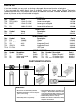
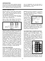
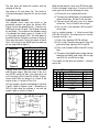
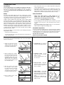
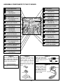
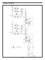
POCKET DICE KIT
MODEL K-28
Assembly and Instruction Manual
Elenco Electronics, Inc.
®
Copyright © 2009, 1989 by Elenco® Electronics, Inc. All rights reserved.
Revised 2009
REV-F
No part of this book shall be reproduced by any means; electronic, photocopying, or otherwise without written permission from the publisher.
753228
PARTS LIST
If you are a student, and any parts are missing or damaged, please see instructor or bookstore.
If you purchased this pocket dice kit from a distributor, catalog, etc., please contact Elenco® Electronics
(address/phone/e-mail is at the back of this manual) for additional assistance, if needed. DO NOT contact your
place of purchase as they will not be able to help you.
RESISTORS
Qty.
r6
r2
r1
Symbol
R2,4,5,6,8,9
R3, R7
R1
Value
1.2kΩ 5% 1/4W
1.5kΩ 5% 1/4W
100kΩ 5% 1/4W
Qty.
r1
Symbol
C1
Value
.01μF
Color Code
brown-red-red-gold
brown-green-red-gold
brown-black-yellow-gold
Part #
141200
141500
161000
CAPACITORS
Description
Discap
Part #
241031
SEMICONDUCTORS
Qty.
r1
r4
r1
r2
r 14
Symbol
D19
D15 - D18
IC1
IC2, IC3
D1 - D14
Value
1N4001
1N4148
4011
4018
Description
Diode
Diode
Integrated Circuit
Integrated Circuit
LED (red)
Part #
314001
314148
334011
334018
350002
MISCELLANEOUS
Qty.
r1
r1
r1
Symbol
S1
S2
Description
PC Board
Switch push button
Switch Slide
Part #
518028
540001
541102
Qty.
r1
r1
r2
Symbol
B1
IC1
IC2, IC3
Description
Battery Snap 9V
IC Socket 14-pin
IC Socket 16-pin
Part #
590098
664014
664016
PARTS IDENTIFICATION
Resistor
Diode
Capacitor
LED
Integrated Circuit
IC Socket
Push Button Switch
Battery Snap
Batteries:
• Do not short circuit the battery terminals.
• Never throw the battery in a fire or attempt to
open its outer casing.
• Use only 9V alkaline battery (not included).
• Insert battery with correct polarity.
• Non-rechargeable batteries should not be
recharged. Rechargeable batteries should
only be charged under adult supervision, and
should not be recharged while in the product.
• Remove battery when it is used up.
• Batteries are harmful if swallowed, so keep
away from small children.
-1-
Slide Switch
IDENTIFYING RESISTOR VALUES
Use the following information as a guide in properly identifying the value of resistors.
BAND 1
1st Digit
Color
Black
Brown
Red
Orange
Yellow
Green
Blue
Violet
Gray
White
BAND 2
2nd Digit
Digit
0
1
2
3
4
5
6
7
8
9
Color
Black
Brown
Red
Orange
Yellow
Green
Blue
Violet
Gray
White
Multiplier
Digit
0
1
2
3
4
5
6
7
8
9
Color
Black
Brown
Red
Orange
Yellow
Green
Blue
Silver
Gold
Resistance
Tolerance
Multiplier
1
10
100
1,000
10,000
100,000
1,000,000
0.01
0.1
Color
Silver
Gold
Brown
Red
Orange
Green
Blue
Violet
Tolerance
±10%
±5%
±1%
±2%
±3%
±0.5%
±0.25%
±0.1%
BANDS
2
1
Multiplier
Tolerance
IDENTIFYING CAPACITOR VALUES
Capacitors will be identified by their capacitance value in pF (picofarads), nF (nanofarads), or μF (microfarads).
Most capacitors will have their actual value printed on them. Some capacitors may have their value printed in
the following manner. The maximum operating voltage may also be printed on the capacitor.
Electrolytic capacitors have a positive
and a negative electrode. The
negative lead is indicated on the
packaging by a stripe with minus
signs and possibly arrowheads.
Multiplier
For the No.
0
1
2
3
Multiply By
1
10
100
1k
Second Digit
First Digit
Warning:
If the capacitor
is connected
with incorrect
polarity, it may
heat up and
either leak, or
cause the
capacitor to
explode.
4
5
8
10k 100k .01
Means
pico
nano
micro
milli
unit
kilo
mega
0.1
Multiplier
103K
100V
Tolerance*
Maximum Working Voltage
The value is 10 x 1,000 =
10,000pF or .01μF 100V
Polarity
Marking
* The letter M indicates a tolerance of +20%
The letter K indicates a tolerance of +10%
The letter J indicates a tolerance of +5%
Note: The letter “R”
may be used at times
to signify a decimal
point; as in 3R3 = 3.3
METRIC UNITS AND CONVERSIONS
Abbreviation
p
n
μ
m
–
k
M
9
Multiply Unit By
.000000000001
.000000001
.000001
.001
1
1,000
1,000,000
Or
10-12
10-9
10-6
10-3
100
103
106
-2-
1. 1,000 pico units
= 1 nano unit
2. 1,000 nano units
= 1 micro unit
3. 1,000 micro units = 1 milli unit
4. 1,000 milli units
= 1 unit
5. 1,000 units
= 1 kilo unit
6. 1,000 kilo units
= 1 mega unit
INTRODUCTION
Dice are the most ancient gambling implement
known to man, and the most universal, having been
known in nearly all parts of the world since earliest
times. Today they are used in some games of skill,
such as backgammon, but are used chiefly in
gambling games. In the United States the most
popular dice game is Craps.
CIRCUIT DESCRIPTION
Each die consists of seven light emitting diodes
(LEDs). Since there are two dice, we need 14
LEDs. The trick is to light the right LEDs to give the
six possible dice combinations.
depends on the value of capacitor C1 and resistor
R1. The value chosen results in a frequency of
approximately 60 cycles per second. The output at
IC1B will be a square wave.
The Pocket Dice kit consists of three main circuits.
They are (1) a clock oscillator, (2) a presettable
counter and (3) a decoder circuit.
In the Pocket Dice
IC1
IC1
kit, we want the
A
B
oscillator to run for a
R1
short time. As long
as the oscillator is
S1
C1
running, the dice
will be constantly
Figure 2
changing numbers.
The number changes once with every cycle, or 60
times per second. For the dice to come up with a
number, we must stop the clock. This is done by
shorting out the feedback with switch SW1. Once
the switch is closed, the clock will stop and a
random number will appear on the dice.
Figure 1 shows a block diagram of the functions.
We will study each function and get an
understanding on how the Pocket Dice kit works.
First Die
Second Die
Decoder 1
4
Clock
5
6
Decoder 2
4
5
6
Counter 1
Counter 2
IC2
IC3
Figure 1
Referring to Figure 1, the clock puts out a series of
pulses at about 60 per second. The counter IC2
receives the clock pulses and outputs 0’s or 1’s on
pins 4, 5 and 6. The outputs can represent any one
of six combinations 000, 001, 010, 110, 111 or 101.
Each time the clock puts out a pulse, the output of
the counter changes. The 0’s and 1’s are fed to the
decoder circuit which transforms the 0 and 1
combinations into a series of lit LEDs to display the
die patterns. Pin 13 of IC2 changes state once
every time the IC passes through the six state
sequence. Thus, it puts out a pulse at a frequency
of one-sixth of the digital clock or 10 pulses per
second. This signal is fed the input of IC3 and
becomes its clock input. IC3 and its decoder work
the same as IC2 except at a slower clock rate.
THE PRESETTABLE COUNTER FUNCTION
IC2 and IC3 are the presettable counters. These
counters convert the clock pulses in six
combinations of “1” and “0”. These IC’s have a
single input at pin 14 and three outputs on pins 4, 5
and 6. With every pulse change at the input, the
output will change as shown in Figure 3. Note the
corresponding dice number as the result of the 0
and 1 output of pins 4, 5 and 6.
Clock Pulse
By tying pin 6 to pin
Output Pins
1, we programmed
the counter to put out
only 6 combinations
as shown in Figure 3.
Every time the clock
puts out a pulse, the
counter will change
its output. On the
first
pulse,
the
counter pins 4 and 5
will be low (0) and pin
Figure 3
6 will be high (1).
This results in the die number two. The next clock
pulse will result in the counter output of all lows (0)
and the die will show the number one. Thus, the
sequence continues until all six numbers are shown.
THE CLOCK FUNCTION
Figure 2 shows the diagram of the clock circuit. It
consists of two NAND gate digital integrated
circuits. In our circuit, the two inputs are tied
together which forms an inverter circuit. When the
input of IC1A is low, the output will be high, thus
when the input of IC1B is high, its output will be low.
This output is fed to the input of IC1A via capacitor
C1 and is called positive feedback, a key element to
make a circuit oscillate. The frequency of oscillation
-3-
1
2
3
4
5
6
4
0
0
0
1
1
1
5
0
0
1
1
1
0
6
1
0
0
0
1
1
The next pulse will repeat the process with two
showing on the die.
When the die displays a one, only LED D3 will light.
For this to happen, output pin 4, 5 and 6 or IC2 will
have to go low (0) and the following will result.
The output of IC2 also drives IC3. This results in
IC3 output changing in step with IC2, but at a slower
rate.
1) D3 turns on as its cathode will be low.
2) The input of the NAND gate is low therefore its
output will be high. D2 and D1 will not light.
THE DECODER CIRCUIT
3) The input of the OR gate is low, so its output
will be low. Thus, D4 and D5 will not light.
The decoder circuit takes the output of the
presettable counter and lights the correct LEDs.
Figure 4 shows the decoder circuit. It consists of a
NAND gate and an OR gate. The OR gate is formed
by two diodes. The purpose of the decoder circuits
is to “decode” the outputs of pins 4, 5 and 6 of IC2
or IC3 to light the correct LEDs. The truth tables for
the NAND and the OR gates are shown in Figure 5.
They show the output C versus the inputs A and B.
Thus, if the inputs of the NAND gate are both low
(0), the output will be high (1).
NAND
NAND Gate
A
0
1
0
1
OR Gate
B
0
0
1
1
4) Pin 4 of IC2 is low, therefore LED D6 and D7
will not light.
Let’s try another number - 3. Here we must light
LEDs D3, D4 and D5. The output of pin 4 is low, pin
5 and pin 6 low (0, 1, 0).
1) Pin 6 is low, therefore LED D3 will light.
2) Pin 5 is high, Therefore the outputs of the OR
gate will be high, lighting LED D4 and D5.
3) Pin 4 is low, therefore LEDs D6 and D7 will not
light.
OR
C A B C
1 0 0 0
1 1 0 1
1 0 1 1
0 1 1 1
4) The inputs of the NAND gate are high and low,
therefore the NAND gate output will be high
and LEDs D1 and D2 will not light.
Try to figure out the other four patterns. It actually
can be fun.
Figure 5
Figure 4
Pins on IC2
LEDs Lit
Die Number
4 5 6
Six
1 1 1 D4, D1, D7, D6, D2, D5
D4,
D7,
D6,
D5,
D3
Five
1 1 0
D4, D7, D6, D5
Four
1 0 1
D4, D3, D5
Three
0 1 0
D4, D5
Two
0 0 1
D3
One
0 0 0
Figure 7
Figure 6 shows the wiring of the LEDs to the NAND
and OR gates output. Note that when IC pin 10 is
low, LED D2 and D1 will light. Also, when pin 5 or 6
of IC2 are high, LEDs D4 and D5 will light. Figure 7
shows which LEDs are being lit as a result of the
outputs of pin 4, 5 and 6 of IC2 or IC3.
Let’s go through a couple of decodings to see how
it works. Refer to Figures 6 and 7. Remember an
LED will light when the cathode is low and the
anode is high as shown in Figure 8.
9
5
8
D2 D1
10
9V
+
Input High
Current
Lit
IC2
D3
6
D16
4
Limiting
D15
D5 D4
0V
Resistors
Input Low
D7 D6
Not Lit
Figure 6
Figure 8
-4-
CONSTRUCTION
Introduction
• Turn off iron when not in use or reduce temperature setting when
using a soldering station.
The most important factor in assembling your K-28 Pocket Dice Kit is
good soldering techniques. Using the proper soldering iron is of prime
importance. A small pencil type soldering iron of 25 - 40 watts is
recommended. The tip of the iron must be kept clean at all times and
well-tinned.
• Tips should be cleaned frequently to remove oxidation before it becomes
impossible to remove. Use Dry Tip Cleaner (Elenco® #SH-1025) or Tip
Cleaner (Elenco® #TTC1). If you use a sponge to clean your tip, then use
distilled water (tap water has impurities that accelerate corrosion).
Solder
Safety Procedures
For many years leaded solder was the most common type of solder
used by the electronics industry, but it is now being replaced by leadfree solder for health reasons. This kit contains lead-free solder, which
contains 99.3% tin, 0.7% copper, and has a rosin-flux core.
• Always wear safety glasses or safety goggles to
protect your eyes when working with tools or
soldering iron, and during all phases of testing.
• Be sure there is adequate ventilation when soldering.
Lead-free solder is different from lead solder: It has a higher melting
point than lead solder, so you need higher temperature for the solder to
flow properly. Recommended tip temperature is approximately 700OF;
higher temperatures improve solder flow but accelerate tip decay. An
increase in soldering time may be required to achieve good results.
Soldering iron tips wear out faster since lead-free solders are more
corrosive and the higher soldering temperatures accelerate corrosion,
so proper tip care is important. The solder joint finish will look slightly
duller with lead-free solders.
'
• Locate soldering iron in an area where you do not have to go around
it or reach over it. Keep it in a safe area away from the reach of
children.
• Do not hold solder in your mouth. Solder is a toxic substance.
Wash hands thoroughly after handling solder.
Assemble Components
In all of the following assembly steps, the components must be installed
on the top side of the PC board unless otherwise indicated. The top
legend shows where each component goes. The leads pass through the
corresponding holes in the board and are soldered on the foil side.
Use only rosin core solder.
Use these procedures to increase the life of your soldering iron tip when
using lead-free solder:
• Keep the iron tinned at all times.
• Use the correct tip size for best heat transfer. The conical tip is the
most commonly used.
DO NOT USE ACID CORE SOLDER!
What Good Soldering Looks Like
Types of Poor Soldering Connections
A good solder connection should be bright, shiny, smooth, and uniformly
flowed over all surfaces.
Soldering Iron
1. Solder all components from the
copper foil side only. Push the
soldering iron tip against both the
lead and the circuit board foil.
Rosin
Component Lead
1. Insufficient heat - the solder will
not flow onto the lead as shown.
Foil
Soldering iron positioned
incorrectly.
Circuit Board
2. Apply a small amount of solder to
the iron tip. This allows the heat to
leave the iron and onto the foil.
Immediately apply solder to the
opposite side of the connection,
away from the iron. Allow the
heated component and the circuit
foil to melt the solder.
3. Allow the solder to flow around
the connection. Then, remove
the solder and the iron and let the
connection cool. The solder
should have flowed smoothly and
not lump around the wire lead.
Soldering Iron
2. Insufficient solder - let the
solder flow over the connection
until it is covered.
Use just enough solder to cover
the connection.
Solder
Foil
Solder
Gap
Component Lead
Solder
3. Excessive solder - could make
connections that you did not
intend to between adjacent foil
areas or terminals.
Soldering Iron
Solder
Foil
4. Solder bridges - occur when
solder runs between circuit paths
and creates a short circuit. This is
usually caused by using too much
solder.
To correct this, simply drag your
soldering iron across the solder
bridge as shown.
4. Here is what a good solder
connection looks like.
-5-
Soldering Iron
Foil
Drag
ASSEMBLE COMPONENTS TO THE PC BOARD
S1 - Push Button Switch
S2 - Slide Switch
J5 - Jumper Wire
J6 - Jumper Wire
(see Figure A)
B1 - Battery Snap 9V
(see Figure D)
J3 - Jumper Wire
(see Figure A)
C1 - .01μF (103) Capacitor
D19 - 1N4001 Diode
(see Figure C)
IC3 - 16-pin Socket
IC3 - 4018 Integrated Circuit
(see Figure B)
R7 - 1.5kΩ 5% 1/4W Resistor
(brown-green-red-gold)
IC2 - 16-pin Socket
IC2 - 4018 Integrated Circuit
(see Figure B)
J1 - Jumper Wire
(see Figure A)
R3 - 1.5kΩ 5% 1/4W Resistor
(brown-green-red-gold)
D17 - 1N4148 Diode
D18 - 1N4148 Diode
(see Figure C)
J4 - Jumper Wire
(see Figure A)
R2 - 1.2kΩ 5% 1/4W Resistor
(brown-red-red-gold)
R6 - 1.2kΩ 5% 1/4W Resistor
(brown-red-red-gold)
D16 - 1N4148 Diode
D15 - 1N4148 Diode
(see Figure C)
R1 - 100kΩ 5% 1/4W Resistor
(brown-black-yellow-gold)
R5 - 1.2kΩ 5% 1/4W Resistor
(brown-red-red-gold)
IC1 - 14-pin Socket
IC1 - 4011 Integrated Circuit
(see Figure B)
R4 - 1.2kΩ 5% 1/4W Resistor
(brown-red-red-gold)
R8 - 1.2kΩ 5% 1/4W Resistor
(brown-red-red-gold)
R9 - 1.2kΩ 5% 1/4W Resistor
(brown-red-red-gold)
J2 - Jumper Wire
(see Figure A)
Figure C
Figure A
Figure B
Use a discarded resistor lead
for a jumper wire. Bend the
wire to the correct length and
mount it to the PC board.
Insert the IC socket into the PC
board with the notch in the
direction shown on the top
legend. Solder the IC socket into
place. Insert the IC into the
socket with the notch in the same
direction as the notch on the
socket.
IC
Socket
PC Board
-6-
Mount the diode with
the band in the same
direction shown on PC
board.
Band
Figure D
Mount the battery snap
to B1 on the PC board
as shown below with
the red wire in the (+)
hole and the black wire
in the (–) hole.
Red Wire
Black Wire
ASSEMBLY CONTINUED
D8 - LED (red)
D9 - LED (red)
D10 - LED (red)
D11 - LED (red)
D12 - LED (red)
D13 - LED (red)
D14 - LED (red)
(see Figure E)
D1
D2
D3
D4
D5
D6
D7
-
LED (red)
LED (red)
LED (red)
LED (red)
LED (red)
LED (red)
LED (red)
(see Figure E)
Figure E
Mount the LED with the flat
side in the same direction as
marked on the PC board.
Mount flush
with PC board
Flat
Foil Side of PC Board
TROUBLESHOOTING
Contact Elenco® Electronics if you have any problems. DO NOT contact your place of purchase as they will not
be able to help you.
1. One of the most frequently occurring problems is
poor solder connections.
2. Be sure that all components have been mounted
in their correct places.
a) Be sure that diodes D15-D19 have not been
installed backwards. The band on the
diodes should be in the same direction as
shown on the top legend.
a) Tug slightly on all parts to make sure that
they are indeed soldered.
b) All solder connections should be shiny.
Resolder any that are not.
b) Be sure that LEDs D1-D14 have not been
installed backwards. The flat side on the
LEDs should be in the same direction as
shown on the top legend.
c) Solder should flow into a smooth puddle
rather than a round ball. Resolder any
connection that has formed into a ball.
c) Have the ICs been inserted into their
sockets correctly? The notch or dot on the
ICs should be in the same direction as
shown on the top legend.
d) Have any solder bridges formed? A solder
bridge may occur if you accidentally touch
an adjacent foil by using too much solder or
by dragging the soldering iron across
adjacent foils. Break the bridge with your
soldering iron.
d) Be sure to use a fresh 9-volt battery.
-7-
CRAPS
yet decided. He must roll them again and again, as
often as necessary, and he will win if his point
appears before a 7, but he will lose if a 7 appears
first. All intervening rolls are meaningless.
Players:
Any number from two and up. The
players bet amongst themselves. In gambling
houses, the players are grouped around a large
table resembling a billiard table, stenciled with a
layout shown where bets should be placed and what
odds are paid.
When the shooter loses, those who faded him take
such part of the center bets as belong to them
(always exactly double the amount they bet, for all
center bets are at even money). When the shooter
wins (passes) all of the money in the center belongs
to him and he may make another center bet if he
wishes, increasing or decreasing his previous bet as
he sees fit, but no one is ever forced to bet, and he
may give up the dice if he prefers.
The Play: The player who starts the game places
in the center whatever he wishes to bet and
announces its amount. Any other player or players
may fade such portions of the bet as they wish, by
placing that amount in the center with the shooters
bet. Any part of the bet not faded is withdrawn by
the shooter. No more than the amount offered may
be faded.
The shooter loses the dice when he gets a point and
fails to make it. In this case, or when he voluntarily
passes the dice, the player at his left becomes the
next shooter.
The shooter rolls the dice. The shooter wins if his
first roll is a 7 or 11 (a natural). He loses if it is a 2,
3 or 12 (craps); he has a point to make if it is a 4, 5,
6, 8, 9 or 10. When he gets a point, the result is not
QUIZ
1. How many pulses per second does the clock circuit
output?
r A. 10
r B. 25
r C. 60
r D. 2
6. By tying pin 6 to pin _____, we program the counter to
output only _____ combinations.
r A. 14,8
r B. 2, 5
r C. 13, 7
r D. 1,6
2. The output of the counter can be one of _________
combinations.
r A. 100
r B. 6
r C. 30
r D. 200
7. The OR gate in the circuit is formed by two _________.
r A. resistors.
r B. LED’s.
r C. diodes.
r D. capacitors.
8. What die number lights up if pins 4 and 5 are high and
6 is low on IC2?
r A. two
r B. nine
r C. five
r D. one
3. What type of logic gate is IC1?
r A. OR
r B. AND
r C. XNOR
r D. NAND
9. Each die consists of how many LED’s?
r A. 10
r B. 7
r C. 12
r D. 10
4. The frequency of the clock circuit depends on the value
of capacitor C1 and _________.
r A. diode D1.
r B. IC2.
r C. resistor R1.
r D. LED D3.
10. The output of the clock circuit produces a _________
wave.
r A. triangle
r B. ramp
r C. saw
r D. square
5. How many of IC2 outputs pins are used.
r A. 3
r B. 5
r C. 1
r D. 4
Answers: 1) C; 2) B; 3) D; 4) C; 5) A; 6) D; 7) C; 8) C; 9) B; 10) D
-8-
DEFINITION OF TERMS
Capacitor
An electrical component that can store electrical pressure (voltage) for periods of time.
Color Code
A method for marking resistors using colored bands.
Digital Circuit
A wide range of circuits in which all inputs and outputs have only two states, such as
high/low.
Diode
An electronic device that allows current to flow in only one direction.
Disc Capacitor
A type of capacitor that has low capacitance and is used mostly in high frequency circuits.
Farad, (F)
The unit of measure for capacitance.
Feedback
To adjust the input to something based on what its output is doing.
Frequency
The rate at which something repeats.
Ground
A common term for the 0V or “–” side of a battery or generator.
Integrated Circuit
A type of circuit in which transistors, diodes, resistors, and capacitors are all
constructed on a semiconductor base.
Kilo- (K)
A prefix used in the metric system. It means a thousand of something.
LED
Common abbreviation for light emitting diode.
Leads
The wires sticking out of an electronic component, used to connect it to the circuit.
Light Emitting Diode
A diode made from gallium arsenide that has a turn-on energy so high that light is
generated when current flows through it.
Meg- (M)
A prefix used in the metric system. It means a million of something.
Micro- (μ)
A prefix used in the metric system. It means one millionth (0.000001) of something.
Milli- (m)
A prefix used in the metric system. It means one thousandth (0.001) of something.
NAND Gate
A type of digital circuit which gives a HIGH output if some of its inputs are LOW.
NOR Gate
A type of digital circuit which gives a HIGH output if none of its inputs are HIGH.
Ohm, (Ω)
The unit of measure for resistance.
OR Gate
A type of digital circuit which gives a HIGH output if any of its inputs are HIGH.
Oscillator
A circuit that uses feedback to generate an AC output.
Printed Circuit Board
A board used for mounting electrical components. Components are connected using
metal traces “printed” on the board instead of wires.
Resistance
The electrical friction between an electric current and the material it is flowing through;
the loss of energy from electrons as they move between atoms of the material.
Resistor
Components used to control the flow of electricity in a circuit. They are made of carbon.
Schematic
A drawing of an electrical circuit that uses symbols for all the components.
Semiconductor
A material that has more resistance than conductors but less than insulators. It is
used to construct diodes, transistors, and integrated circuits.
Series
When electrical components are connected one after the other.
Short Circuit
When wires from different parts of a circuit (or different circuits) connect accidentally.
Solder
A tin-lead metal that becomes a liquid when heated to above 360 degrees. In addition
to having low resistance like other metals, solder also provides a strong mounting that
can withstand shocks.
Switch
A device to connect (“closed” or “on”) or disconnect (“open” or “off”) wires in an
electric circuit.
Voltage
A measure of how strong an electric charge across a material is.
Voltage Divider
A resistor configuration to create a lower voltage.
Volts (V)
The unit of measure for voltage.
-9-
SCHEMATIC DIAGRAM
-10-
Elenco® Electronics, Inc.
150 Carpenter Avenue
Wheeling, IL 60090
(847) 541-3800
Fax: (847) 520-0085
Website: www.elenco.com
e-mail: [email protected]