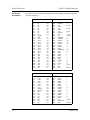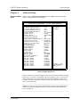
1
CBI/CGI
CB BASIC
S5721-xxx
TECHNICAL REFERENCE
Intel® Pentium® III
or
Intel® Celeron®
PROCESSOR-BASED
SBC
WARRANTY
The product is warranted against material and manufacturing defects for two years from
date of delivery. Buyer agrees that if this product proves defective Chassis Plans is only
obligated to repair, replace or refund the purchase price of this product at Chassis Plans’
discretion. The warranty is void if the product has been subjected to alteration, neglect,
misuse or abuse; if any repairs have been attempted by anyone other than Chassis Plans;
or if failure is caused by accident, acts of God, or other causes beyond the control of
Chassis Plans. Chassis Plans reserves the right to make changes or improvements in any
product without incurring any obligation to similarly alter products previously
purchased.
In no event shall Chassis Plans be liable for any defect in hardware or software or loss or
inadequacy of data of any kind, or for any direct, indirect, incidental or consequential
damages arising out of or in connection with the performance or use of the product or
information provided. Chassis Plans’ liability shall in no event exceed the purchase
price of the product purchased hereunder. The foregoing limitation of liability shall be
equally applicable to any service provided by Chassis Plans
RETURN POLICY
Products returned for repair must be accompanied by a Return Material Authorization
(RMA) number, obtained from Chassis Plans prior to return. Freight on all returned
items must be prepaid by the customer, and the customer is responsible for any loss or
damage caused by common carrier in transit. Items will be returned from Chassis Plans
via Ground, unless prior arrangements are made by the customer for an alternative
shipping method
To obtain an RMA number, call us at (858) 571-4330. We will need the following information:
Return company address and contact
Model name and model # from the label on the back of the board
Serial number from the label on the back of the board
Description of the failure
An RMA number will be issued. Mark the RMA number clearly on the outside of each
box, include a failure report for each board and return the product(s) to our San Diego,
CA facility:
Chassis Plans
8295 Aero Place, Suite 200
San Diego, CA 92123
Attn: Repair Department
858-571-4330
TRADEMARKS
IBM, PC, VGA, EGA, OS/2 and PS/2 are trademarks or registered trademarks of
International Business Machines Corp.
AMI and AMIBIOS are trademarks or registered trademarks of American
Megatrends Inc.
Intel, Pentium, Celeron and AGP are registered trademarks of Intel Corporation.
MS-DOS and Microsoft are registered trademarks of Microsoft Corp.
PICMG and the PICMG logo are registered trademarks of the PCI Industrial Computer
Manufacturers Group.
SCSISelect is a trademark of Adaptec, Inc.
All other brand and product names may be trademarks or registered trademarks of their
respective companies.
LIABILITY
DISCLAIMER
This manual is as complete and factual as possible at the time of printing; however, the
information in this manual may have been updated since that time. Chassis Plans
reserves the right to change the functions, features or specifications of their products at
any time, without notice.
Copyright © 2003 by Chassis Plans All rights reserved.
E-mail: [email protected]
Web:
www.chassisplans.com
Chassis Plans, LLC
8295 Aero Place • Suite 200 • San Diego, California 92123
Sales: (858) 571-4330 • Fax: (858) 57104330 • Web http://www.chassisplans.com
CBI/CGI Technical Reference
Table of Contents
Specifications . . . . . . . . . . . . . . . . . . . . . . . . . . . . . . . . . . . . . . . . . . . . . .1-1
Introduction . . . . . . . . . . . . . . . . . . . . . . . . . . . . . . . . . . . . . . . . . . .1-1
Models . . . . . . . . . . . . . . . . . . . . . . . . . . . . . . . . . . . . . . . . . . . . . . .1-1
Features . . . . . . . . . . . . . . . . . . . . . . . . . . . . . . . . . . . . . . . . . . . . . .1-3
SBC Block Diagram. . . . . . . . . . . . . . . . . . . . . . . . . . . . . . . . . . . . .1-5
SBC Processor Board Layout. . . . . . . . . . . . . . . . . . . . . . . . . . . . . .1-6
Processor . . . . . . . . . . . . . . . . . . . . . . . . . . . . . . . . . . . . . . . . . . . . .1-7
Bus Interfaces . . . . . . . . . . . . . . . . . . . . . . . . . . . . . . . . . . . . . . . . . .1-7
Data Path . . . . . . . . . . . . . . . . . . . . . . . . . . . . . . . . . . . . . . . . . . . . .1-7
Bus Speed - ISA . . . . . . . . . . . . . . . . . . . . . . . . . . . . . . . . . . . . . . . .1-7
Bus Speed - PCI . . . . . . . . . . . . . . . . . . . . . . . . . . . . . . . . . . . . . . . .1-7
Bus Speed - System & Memory . . . . . . . . . . . . . . . . . . . . . . . . . . . .1-7
System & Memory Buses. . . . . . . . . . . . . . . . . . . . . . . . . . . . . . . . .1-7
DMA Channels. . . . . . . . . . . . . . . . . . . . . . . . . . . . . . . . . . . . . . . . .1-7
Interrupts . . . . . . . . . . . . . . . . . . . . . . . . . . . . . . . . . . . . . . . . . . . . .1-7
BIOS (Flash). . . . . . . . . . . . . . . . . . . . . . . . . . . . . . . . . . . . . . . . . . .1-7
Cache Memory . . . . . . . . . . . . . . . . . . . . . . . . . . . . . . . . . . . . . . . . .1-7
DRAM Memory . . . . . . . . . . . . . . . . . . . . . . . . . . . . . . . . . . . . . . . .1-8
Memory Hole . . . . . . . . . . . . . . . . . . . . . . . . . . . . . . . . . . . . . . . . . .1-9
Error Checking and Correction . . . . . . . . . . . . . . . . . . . . . . . . . . . .1-9
PCI Local Bus Interface . . . . . . . . . . . . . . . . . . . . . . . . . . . . . . . . . .1-9
Universal Serial Bus (USB) . . . . . . . . . . . . . . . . . . . . . . . . . . . . . . .1-9
Concurrent PCI. . . . . . . . . . . . . . . . . . . . . . . . . . . . . . . . . . . . . . . . .1-9
AGP VGA Interface . . . . . . . . . . . . . . . . . . . . . . . . . . . . . . . . . . . . .1-9
System Hardware Monitor . . . . . . . . . . . . . . . . . . . . . . . . . . . . . . . .1-9
10/100Base-T Ethernet Interface . . . . . . . . . . . . . . . . . . . . . . . . . . .1-10
PCI Ultra Wide SCSI Interface . . . . . . . . . . . . . . . . . . . . . . . . . . . .1-10
PCI Enhanced IDE Ultra DMA/33 Interfaces (Dual) . . . . . . . . . . .1-11
Floppy Drive Interface . . . . . . . . . . . . . . . . . . . . . . . . . . . . . . . . . . .1-11
Serial Interface . . . . . . . . . . . . . . . . . . . . . . . . . . . . . . . . . . . . . . . . .1-11
Enhanced Parallel Interface . . . . . . . . . . . . . . . . . . . . . . . . . . . . . . .1-11
PS/2 Mouse Interface . . . . . . . . . . . . . . . . . . . . . . . . . . . . . . . . . . . .1-11
Keyboard Interface . . . . . . . . . . . . . . . . . . . . . . . . . . . . . . . . . . . . . .1-11
Watchdog Timer . . . . . . . . . . . . . . . . . . . . . . . . . . . . . . . . . . . . . . . .1-11
Power Fail Detection . . . . . . . . . . . . . . . . . . . . . . . . . . . . . . . . . . . .1-11
Battery . . . . . . . . . . . . . . . . . . . . . . . . . . . . . . . . . . . . . . . . . . . . . . .1-12
Power Requirements. . . . . . . . . . . . . . . . . . . . . . . . . . . . . . . . . . . . .1-12
Chassis Plans
i
CBI/CGI Technical Reference
Table of Contents
Specifications (continued)
Temperature/Environment . . . . . . . . . . . . . . . . . . . . . . . . . . . . . . . .1-12
Mean Time Between Failures (MTBF) . . . . . . . . . . . . . . . . . . . . . .1-12
UL Recognition . . . . . . . . . . . . . . . . . . . . . . . . . . . . . . . . . . . . . . . .1-12
Configuration Jumpers . . . . . . . . . . . . . . . . . . . . . . . . . . . . . . . . . . .1-13
Ethernet LEDs and Connector . . . . . . . . . . . . . . . . . . . . . . . . . . . . .1-15
System BIOS Setup Utility. . . . . . . . . . . . . . . . . . . . . . . . . . . . . . . .1-15
Connectors . . . . . . . . . . . . . . . . . . . . . . . . . . . . . . . . . . . . . . . . . . . .1-16
ISA/PCI Reference . . . . . . . . . . . . . . . . . . . . . . . . . . . . . . . . . . . . . . . . .2-1
ISA Bus Pin Numbering. . . . . . . . . . . . . . . . . . . . . . . . . . . . . . . . . .2-1
ISA Bus Pin Assignments . . . . . . . . . . . . . . . . . . . . . . . . . . . . . . . .2-2
ISA Bus Signal Descriptions . . . . . . . . . . . . . . . . . . . . . . . . . . . . . .2-3
I/O Address Map . . . . . . . . . . . . . . . . . . . . . . . . . . . . . . . . . . . . . . .2-7
Interrupt Assignments . . . . . . . . . . . . . . . . . . . . . . . . . . . . . . . . . . .2-7
PCI Local Bus Overview . . . . . . . . . . . . . . . . . . . . . . . . . . . . . . . . .2-8
PCI Local Bus Signal Definition . . . . . . . . . . . . . . . . . . . . . . . . . . .2-9
PCI Local Bus Pin Numbering. . . . . . . . . . . . . . . . . . . . . . . . . . . . .2-10
PCI Local Bus Pin Assignments . . . . . . . . . . . . . . . . . . . . . . . . . . .2-11
PCI Local Bus Signal Descriptions . . . . . . . . . . . . . . . . . . . . . . . . .2-14
PICMG Edge Connector Pin Assignments . . . . . . . . . . . . . . . . . . .2-18
System BIOS . . . . . . . . . . . . . . . . . . . . . . . . . . . . . . . . . . . . . . . . . . . . . .3-1
BIOS Operation . . . . . . . . . . . . . . . . . . . . . . . . . . . . . . . . . . . . . . . .3-1
Password Entry . . . . . . . . . . . . . . . . . . . . . . . . . . . . . . . . . . . . . .3-3
BIOS Errors. . . . . . . . . . . . . . . . . . . . . . . . . . . . . . . . . . . . . . . . .3-4
Running AMIBIOS Setup . . . . . . . . . . . . . . . . . . . . . . . . . . . . . . . .3-5
AMIBIOS Setup Utility Main Menu . . . . . . . . . . . . . . . . . . . . . . . .3-6
AMIBIOS Setup Utility Options . . . . . . . . . . . . . . . . . . . . . . . . . . .3-6
Auto-Detect Hard Disks . . . . . . . . . . . . . . . . . . . . . . . . . . . . . . . . . .3-11
Change Password . . . . . . . . . . . . . . . . . . . . . . . . . . . . . . . . . . . . . . .3-11
Change Supervisor Password . . . . . . . . . . . . . . . . . . . . . . . . . . . . . .3-11
Change User Password. . . . . . . . . . . . . . . . . . . . . . . . . . . . . . . . . . .3-12
Disabling the Password(s) . . . . . . . . . . . . . . . . . . . . . . . . . . . . . . . .3-13
Auto Configuration Options. . . . . . . . . . . . . . . . . . . . . . . . . . . . . . .3-13
Auto Configuration with Optimal Settings . . . . . . . . . . . . . . . . .3-13
Auto Configuration with Fail Safe Settings . . . . . . . . . . . . . . . .3-14
ii
Chassis Plans
CBI/CGI Technical Reference
Table of Contents
System BIOS (continued)
Save Settings and Exit . . . . . . . . . . . . . . . . . . . . . . . . . . . . . . . . . . .3-14
Exit Without Saving . . . . . . . . . . . . . . . . . . . . . . . . . . . . . . . . . . . . .3-14
Key Conventions . . . . . . . . . . . . . . . . . . . . . . . . . . . . . . . . . . . . . . .3-15
Standard CMOS Setup . . . . . . . . . . . . . . . . . . . . . . . . . . . . . . . . . . . . . .4-1
Standard CMOS Options . . . . . . . . . . . . . . . . . . . . . . . . . . . . . . . . .4-1
Boot Sector Virus Protection . . . . . . . . . . . . . . . . . . . . . . . . . . . . . .4-6
Advanced Setup. . . . . . . . . . . . . . . . . . . . . . . . . . . . . . . . . . . . . . . . . . . .5-1
Advanced CMOS Setup . . . . . . . . . . . . . . . . . . . . . . . . . . . . . . . . . .5-1
Advanced Chipset Setup . . . . . . . . . . . . . . . . . . . . . . . . . . . . . . . . .5-10
Power Management . . . . . . . . . . . . . . . . . . . . . . . . . . . . . . . . . . . . . . . .6-1
PCI/Plug and Play Setup . . . . . . . . . . . . . . . . . . . . . . . . . . . . . . . . . . . .7-1
Peripheral Setup . . . . . . . . . . . . . . . . . . . . . . . . . . . . . . . . . . . . . . . . . . .8-1
Appendix A - BIOS Messages . . . . . . . . . . . . . . . . . . . . . . . . . . . . . . . .A-1
BIOS Beep Codes. . . . . . . . . . . . . . . . . . . . . . . . . . . . . . . . . . . . . . .A-1
BIOS Error Messages. . . . . . . . . . . . . . . . . . . . . . . . . . . . . . . . . . . .A-2
ISA BIOS NMI Handler Messages . . . . . . . . . . . . . . . . . . . . . . . . .A-5
Port 80 Codes . . . . . . . . . . . . . . . . . . . . . . . . . . . . . . . . . . . . . . . . . .A-6
Additional Bus Checkpoints. . . . . . . . . . . . . . . . . . . . . . . . . . . . . . .A-12
Appendix B - Adaptec, Inc. Software License . . . . . . . . . . . . . . . . . . .B-1
Appendix C - SCSISelect Configuration Utility. . . . . . . . . . . . . . . . . .C-1
Declaration of Conformity
Chassis Plans
iii
CBI/CGI Technical Reference
This page intentionally left blank.
Copyright 2003 by Trenton Technology Inc. All rights reserved.
iv
Chassis Plans
CBI/CGI Technical Reference
HANDLING
PRECAUTIONS
_______________________________________________________________________
WARNING: This product has components which may be damaged by electrostatic
discharge.
_______________________________________________________________________
To protect your single board computer (SBC) from electrostatic damage, be sure to
observe the following precautions when handling or storing the board:
SOLDER-SIDE
COMPONENTS
Chassis Plans
•
Keep the SBC in its static-shielded bag until you are ready to perform your
installation.
•
Handle the SBC by its edges.
•
Do not touch the I/O connector pins. Do not apply pressure or attach labels
to the SBC.
•
Use a grounded wrist strap at your workstation or ground yourself
frequently by touching the metal chassis of the system before handling any
components. The system must be plugged into an outlet that is connected to
an earth ground.
•
Use antistatic padding on all work surfaces.
•
Avoid static-inducing carpeted areas.
This SBC has components on both sides of the PCB. It is important for you to observe
the following precautions when handling or storing the board to prevent solder-side
components from being damaged or broken off:
•
Handle the board only by its edges.
•
Store the board in padded shipping material or in an anti-static board rack.
•
Do not place an unprotected board on a flat surface.
v
CBI/CGI Technical Reference
This page intentionally left blank.
Copyright 2003 by Trenton Technology Inc. All rights reserved.
vi
Chassis Plans
CBI/CGI Technical Reference
Specifications
Chapter 1
Specifications
INTRODUCTION
The CBI full-featured PCI/ISA processors are single board computers (SBCs) which
feature an Intel® Celeron® microprocessor or Intel® Pentium® III microprocessor, Intel
440BX AGPset, 66/100MHz system and memory buses, Intel Accelerated Graphics Port
(AGP) video interface, SDRAM, PCI Local Bus, cache, floppy controller, dual EIDE
(Ultra DMA/33) interface, PCI Ultra Wide SCSI controller, PCI 10/100Base-T Ethernet
controller, two serial ports, parallel port, speaker port, mouse port and keyboard port
on a single ISA-size card. These single-slot, high performance SBCs plug into PICMG®
PCI/ISA passive backplanes and provide full PC compatibility for the system expansion
slots.
The CGI models of this SBC feature the Intel 440GX AGPset, supporting memory
configurations up to 1GB.
The CB BASIC model has all of the standard features of the CBI, but does not include
the Intel video interface, PCI Ultra Wide SCSI controller or PCI 10/100Base-T Ethernet
controller.
MODELS
Model #
Model Name
Speed
CBI - BX:
Intel® Pentium® III Processor - 100MHz FSB/256K cache:
S5721-110-xM
S5721-109-xM
S5721-108-xM
S5721-107-xM
S5721-106-xM
S5721-105-xM
S5721-104-xM
S5721-103-xM
S5721-102-xM
S5721-101-xM
CBI/1.0
CBI/900
CBI/850
CBI/800
CBI/750
CBI/700
CBI/650
CBI/600E
CBI/550E
CBI/500E
1.0GHz
900MHz
850MHz
800MHz
750MHz
700MHz
650MHz
600MHz
550MHz
500MHz
Intel® Celeron® Processor - 100MHz FSB/128K cache:
S5721-205-xM
S5721-204-xM
CBI/900C
CBI/850C
900MHz
850MHz
Intel® Celeron® Processor - 66MHz FSB/128K cache:
S5721-016-xM
S5721-015-xM
S5721-014-xM
S5721-013-xM
S5721-012-xM
S5721-011-xM
S5721-010-xM
S5721-009-xM
S5721-008-xM
S5721-007-xM
S5721-006-xM
Chassis Plans
CBI/800C
CBI/766
CBI/733
CBI/700C
CBI/667
CBI/633
CBI/600
CBI/566
CBI/533
CBI/500
CBI/466
800MHz
766MHz
733MHz
700MHz
667MHz
633MHz
600MHz
566MHz
533MHz
500MHz
466MHz
1-1
Specifications
MODELS
(CONTINUED)
CBI/CGI Technical Reference
Model #
Model Name
Speed
CBI - BX: (continued)
Intel® Celeron® Processor - 66MHz FSB/128K cache: (cont’d)
S5721-005-xM
S5721-004-xM
S5721-003-xM
S5721-002-xM
CBI/433
CBI/400
CBI/366
CBI/333
433MHz
400MHz
366MHz
333MHz
CGI - GX:
Intel® Pentium® III Processor - 100MHz FSB/256K cache:
S5721-150-xM
S5721-149-xM
S5721-148-xM
S5721-147-xM
S5721-146-xM
S5721-145-xM
S5721-144-xM
S5721-143-xM
S5721-142-xM
S5721-141-xM
CGI/1.0
CGI/900
CGI/850
CGI/800
CGI/750
CGI/700
CGI/650
CGI/600E
CGI/550E
CGI/500E
1.0GHz
900MHz
850MHz
800MHz
750MHz
700MHz
650MHz
600MHz
550MHz
500MHz
Intel® Celeron® Processor - 100MHz FSB/128K cache:
S5721-245-xM
S5721-244-xM
CGI/900C
CGI/850C
900MHz
850MHz
Intel® Celeron® Processor - 66MHz FSB/128K cache:
S5721-056-xM
S5721-055-xM
S5721-054-xM
S5721-053-xM
S5721-052-xM
S5721-051-xM
S5721-050-xM
S5721-049-xM
S5721-048-xM
S5721-047-xM
S5721-046-xM
S5721-045-xM
S5721-044-xM
S5721-043-xM
S5721-042-xM
CGI/800C
CGI/766
CGI/733
CGI/700C
CGI/667
CGI/633
CGI/600
CGI/566
CGI/533
CGI/500
CGI/466
CGI/433
CGI/400
CGI/366
CGI/333
800MHz
766MHz
733MHz
700MHz
667MHz
633MHz
600MHz
566MHz
533MHz
500MHz
466MHz
433MHz
400MHz
366MHz
333MHz
CB BASIC - BX:
Intel® Pentium® III Processor - 100MHz FSB/256K cache:
S5721-130-xM
S5721-129-xM
S5721-128-xM
1-2
CBB/1.0
CBB/900
CBB/850
1.0GHz
900MHz
850MHz
Chassis Plans
CBI/CGI Technical Reference
MODELS
(CONTINUED)
Model #
Specifications
Model Name
Speed
CB BASIC - BX: (continued)
Intel® Pentium® III Processor - 100MHz FSB/256K: (cont’d)
S5721-127-xM
S5721-126-xM
S5721-125-xM
S5721-124-xM
S5721-123-xM
S5721-122-xM
S5721-121-xM
CBB/800
CBB/750
CBB/700
CBB/650
CBB/600E
CBB/550E
CBB/500E
800MHz
750MHz
700MHz
650MHz
600MHz
550MHz
500MHz
Intel® Celeron® Processor - 100MHz FSB/128K cache:
S5721-225-xM
S5721-224-xM
CBB/900C
CBB/850C
900MHz
850MHz
Intel® Celeron® Processor - 66MHz FSB/128K cache:
S5721-036-xM
S5721-035-xM
S5721-034-xM
S5721-033-xM
S5721-032-xM
S5721-031-xM
S5721-030-xM
S5721-029-xM
S5721-028-xM
S5721-027-xM
S5721-026-xM
S5721-025-xM
S5721-024-xM
S5721-023-xM
S5721-022-xM
CBB/800C
CBB/766
CBB/733
CBB/700C
CBB/667
CBB/633
CBB/600
CBB/566
CBB/533
CBB/500
CBB/466
CBB/433
CBB/400
CBB/366
CBB/333
800MHz
766MHz
733MHz
700MHz
667MHz
633MHz
600MHz
566MHz
533MHz
500MHz
466MHz
433MHz
400MHz
366MHz
333MHz
where xM indicates memory size (0M = 0MB memory,
8M =8MB memory, etc.)
FEATURES
•
Intel® Pentium® III (FC-PGA) microprocessor
•
1.0GHz, 900MHz, 850MHz, 800MHz, 750MHz, 700MHz or 650MHz,
600EMHz, 550EMHz or 500EMHz with 256K cache and a 100MHz Front
Side Bus (FSB)
or Intel® Celeron® microprocessor
•
Chassis Plans
•
900MHz or 850MHz with 128K cache and a 100MHz FSB
•
800MHz, 766MHz, 733MHz, 700MHz, 667MHz, 633MHz, 600MHz,
566MHz, 533MHz, 500MHz, 466MHz, 433MHz, 400MHz, 366MHz or
333MHz with 128K cache and a 66MHz FSB
Intel 440BX AGPset with 66/100MHz system and memory buses, and PCI
bandwidth greater than 100MB/second. 440GX AGPset also available.
1-3
Specifications
FEATURES
(CONTINUED)
1-4
CBI/CGI Technical Reference
•
Intel Accelerated Graphics Port (AGP) VGA on-board video interface
•
PCI Local Bus supports off-board PCI option cards, PCI 10/100Base-T Ethernet
controller and on-board PCI Ultra Wide SCSI controller - Adaptec AIC-7880
•
DRAM error checking and correction (ECC) support
•
Compatible with PCI Industrial Computer Manufacturers Group (PICMG) 1.0
Specification
•
Supports up to 512MB of Synchronous DRAM (SDRAM) on board; 440GX
AGPset supports up to 1GB
•
Floppy drive and dual PCI EIDE Ultra DMA/33 drive interface
•
Two serial ports and one parallel port
•
Automatic or manual peripheral configuration
•
Watchdog timer
•
System hardware monitor
•
Supports 1M x 64 to 32M x 64 DIMMs for non-ECC configurations; supports
1M x 72 to 32M x 72 DIMMs for ECC configurations. 440GX configurations
support up to 64M x 72 DIMMs.
•
Shadow RAM for System BIOS and peripherals increases system speed and
performance
•
Full PC compatibility
Chassis Plans
CBI/CGI Technical Reference
Specifications
SBC BLOCK
DIAGRAM
Chassis Plans
1-5
Specifications
CBI/CGI Technical Reference
SBC PROCESSOR
BOARD LAYOUT
1-6
Chassis Plans
CBI/CGI Technical Reference
PROCESSORS
•
Specifications
Intel® Pentium® III (FC-PGA) microprocessor
•
1.0GHz, 900MHz, 850MHz, 800MHz, 750MHz, 700MHz or 650MHz,
600EMHz, 550EMHz or 500EMHz with 256K cache and a 100MHz Front
Side Bus (FSB)
or Intel® Celeron® microprocessor
•
900MHz or 850MHz with 128K cache and a 100MHz FSB
•
800MHz, 766MHz, 733MHz, 700MHz, 667MHz, 633MHz, 600MHz,
566MHz, 533MHz, 500MHz, 466MHz, 433MHz, 400MHz, 366MHz or
333MHz with 128K cache and a 66MHz FSB
BUS INTERFACES
ISA and PCI Local Bus compatible
DATA PATH
DRAM/Memory - 64-bit
ISA Bus - 16-bit
PCI Bus - 32-bit
Video - 64-bit
BUS SPEED - ISA
8.33MHz
BUS SPEED - PCI
33MHz
BUS SPEED SYSTEM &
MEMORY
•
Intel® Pentium® III - 100MHz
•
Intel® Celeron® - 66MHz or 100MHz
SYSTEM &
MEMORY BUSES
The Intel 440BX/GX AGPset supports the system and memory buses at both 66MHz and
100MHz speeds. The 100MHz system and memory buses provide a higher bandwidth
path for transferring data between main memory/chip set and the processor.
DMA CHANNELS
The SBC is fully PC compatible with seven DMA channels, each supporting type F
transfers.
INTERRUPTS
The SBC is fully PC compatible with interrupt steering for PCI plug and play compatibility.
BIOS (FLASH)
The BIOS is a Hi-Flex AMIBIOS with built-in advanced CMOS setup for system parameters, peripheral management for configuring on-board peripherals, PCI-to-PCI bridge
support and PCI interrupt steering. The BIOS chip is a boot block Flash device 28F002BX-T120. The BIOS may be upgraded from floppy disk by pressing <Ctrl> +
<Home> immediately after reset or power-up with the floppy disk in drive A:. Custom
BIOSs are available.
CACHE MEMORY
For Pentium III processors, the processor includes an integrated on-die, 256K 8-way set
associative level two (L2) cache. The L2 cache implements the Advanced Transfer
Cache architecture with a 256-bit wide bus. The processor also includes a 16K level one
Chassis Plans
1-7
Specifications
CBI/CGI Technical Reference
(L1) instruction cache and 16K L1 data cache. These cache arrays run at the full speed
of the processor core.
For Celeron processors, a 128K unified, non-blocking second level (L2) cache improves
performance by reducing the average memory access time and providing fast access to
recently used instructions and data.
DRAM MEMORY
The DRAM interface consists of two dual in-line memory module (DIMM) sockets and
supports auto detection of memory up to 512MB of Synchronous DRAM (SDRAM) for
the 440BX or up to 1GB of SDRAM for the 440GX. Minimum memory size is 8MB.
The System BIOS automatically detects memory type, size and speed.
The SBC uses industry standard 64-bit or 72-bit wide gold finger DIMM SDRAM
modules in two 168-pin DIMM sockets.
______________________________________________________________________
NOTE: Memory can be installed in one or both DIMM sockets. If only one DIMM
module is used, it must be populated in the top DIMM socket (Bank 1 - BK1). If two
modules are used, they must be the same DIMM type, but may be different sizes (see
table below). EDO DIMMs are not supported. All DIMMs must have gold contacts.
______________________________________________________________________
The SBC supports DIMM memory modules which are PC-100 compliant and have the
following features:
•
168-pin DIMMs with gold-plated contacts
•
100MHz SDRAM
•
Non-ECC (64-bit) or ECC (72-bit) memory
•
3.3 volt
•
Single or double-sided DIMMs in the sizes listed below
•
Buffered or Registered configuration
The following DIMM sizes are supported:
DIMM
Size
DIMM Type
Non-ECC
8MB
16MB
32MB
64MB
128MB
256MB
512MB
Unbuffered
Unbuffered
Unbuffered
Unbuffered
Unbuffered
Registered
Registered
1M x 64
2M x 64
4M x 64
8M x 64
16M x 64
32M x 64
64M x 64
ECC
1M x 72
2M x 72
4M x 72
8M x 72
16M x 72
32M x 72
64M x 72 *
* CGI models only
All memory components and DIMMs used with the SBC must be PC-100 compliant,
which means that they comply with Intel's PC SDRAM specifications. These include the
PC SDRAM Specification (memory component specific), the PC Unbuffered DIMM
1-8
Chassis Plans
CBI/CGI Technical Reference
Specifications
Specification, the PC Registered DIMM Specification and the PC Serial Presence Detect
Specification.
MEMORY HOLE
The SBC supports a 1MB memory hole option at 512KB-640KB or 15MB-16MB.
ERROR CHECKING
AND CORRECTION
The memory interface supports ECC modes via BIOS setting for multiple-bit error
detection and correction of all errors confined to a single nibble.
PCI LOCAL BUS
INTERFACE
The SBC is fully compliant with the PCI Local Bus 2.1 Specification. It has optimized
the PCI interface to allow the processor to sustain the highest possible bandwidth
(greater than 100MB/sec sustained) and low latency of the PCI Bus. It supports PCI-toPCI bridge technology, a pipelined snoop ahead feature and improved PCI to DRAM
write-back policy. The PCI Local Bus interfaces to standard PCI option cards in the
backplane, and to the on-board PCI Ultra Wide SCSI controller and PCI 10/100Base-T
Ethernet controller. The PCI Local Bus interface to the backplane is compliant with the
PCI Industrial Computer Manufacturers Group (PICMG) 1.0 Specification.
UNIVERSAL SERIAL
BUS (USB)
The SBC supports two USB 1.0 ports for serial transfers at 12 or 1.5Mbit/sec. The
Universal Serial Bus (USB) is an interface allowing for connectivity to many standard
PC peripherals via an external port.
CONCURRENT PCI
Concurrent PCI maximizes system performance with simultaneous processor, PCI and
AGP Bus activities. It includes multitransaction timing, enhanced write performance, a
passive release mechanism and support for PCI 2.1 compliant delayed transactions.
AGP VGA
INTERFACE (NOT
The 69000 HiQVideo video/graphic accelerator is an Accelerated Graphics Port (AGP)
device. AGP is designed to off-load the PCI Bus by allowing graphics data to move
directly from system memory. The 69000 integrates 2MB of high-speed SDRAM frame
buffer memory into the chip.
AVAILABLE ON
BASIC MODELS)
By embedding SDRAM and graphics controller logic on the same die, the 69000 delivers
uncompromising performance. The increase in the frame buffer bandwidth enables the
69000 to support high-color, high-resolution graphics modes and real-time video acceleration. The interface supports pixel resolutions up to 1600 x 1200 non-interlaced.
Software drivers for enhanced performance and resolution are available for most popular
operating systems.
SYSTEM
HARDWARE
MONITOR
The system hardware monitoring system monitors system voltages, temperature and fan
speeds.
The circuitry is based on National Semiconductor's LM80. The LM80 monitors seven
system voltages, two fan speeds and the board ambient temperature. All of the voltages,
fan speeds and temperature measurements have associated programmable watchdog
limits. When any of these programmed limits are exceeded, the monitor software can be
used to notify the SBC. In addition, the externally available OS# signal can be used to
notify external hardware of any over-temperature condition.
Fan speed monitoring can be configured to monitor two system fans.
Chassis Plans
1-9
Specifications
CBI/CGI Technical Reference
The LM80 also monitors an external chassis intrusion switch via the system hardware
monitor connector (P18).
A general purpose output (GPO) is also provided at the system hardware monitor
connector. This signal can be used to provide a user-defined function.
The following system voltages are monitored by the LM80:
•
-12 volts
•
3.3 volts provided by the on-board voltage regulator for components on the
SBC
•
3.3 volts backplane power used by the option slots
•
+5 volts
•
+12 volts
•
VCC_CORE, voltage provided by on-board VRM
•
1.5 volt, VTT voltage used by processor's GTL+ bus
10/100BASE-T
ETHERNET
INTERFACE (NOT
The PCI Ethernet interface is implemented using an Intel 82559 and operates in
10Base-T and 100Base-TX Fast Ethernet modes. The interface is compliant with
IEEE 802.3 and PCI Local Bus 2.1 Specifications.
AVAILABLE ON
BASIC MODELS)
The main components of the interface are:
•
Intel 82559 for 10/100-Mb/s media access control (MAC) with SYM, a
serial ROM port and a PCI Bus Master interface
•
Serial ROM for storing the Ethernet address and the interface configuration
and control data
•
Integrated RJ-45/Magnetics module connector on the SBC's I/O bracket for
direct connection to the network. The connector requires a category 5
(CAT5) unshielded twisted-pair (UTP) 2-pair cable for a 100-Mb/s network
connection or a category 3 (CAT3) or higher UTP 2-pair cable for a 10-Mb/s
network connection.
•
Link status and activity LEDs on the I/O bracket for status indication (See
Ethernet LEDs and Connector later in this section.)
Software drivers are supplied for most popular operating systems.
PCI ULTRA WIDE
SCSI INTERFACE
(NOT AVAILABLE
ON BASIC
MODELS)
The SCSI interface is a PCI Bus Master device which supports Ultra Wide SCSI data
transfer up to 40MB per second and bursts data to the host at full PCI speeds. Active
termination is provided with terminator voltage protected by self-resetting fuses. A
jumper is provided to disable the termination. The SCSI controller is an Adaptec
AIC-7880. Software drivers are available for most popular operating systems.
The Adaptec SCSISelect Configuration Utility allows you to view and/or change the
default configuration settings for the Ultra Wide SCSI adapter. This utility is described
in Appendix C - SCSISelect Configuration Utility.
1-10
Chassis Plans
CBI/CGI Technical Reference
Specifications
PCI ENHANCED
IDE ULTRA
DMA/33
INTERFACE (DUAL)
Dual high performance PCI Bus Master EIDE interfaces are capable of supporting two
IDE Type 4 disk drives each in a master/slave configuration. The interface supports
Ultra DMA/33 with synchronous DMA mode transfers up to 33MB per second.
FLOPPY DRIVE
INTERFACE
The SBC supports two floppy disk drives. Drives can be 360K to 2.88MB, in any
combination.
SERIAL INTERFACE
Two high-speed FIFO (16C550) serial ports with independently programmable baud
rates are supported. The IRQ for each serial port has BIOS selectable addressing.
ENHANCED
PARALLEL
INTERFACE
The SBC provides a PC/AT compatible bidirectional parallel port and supports enhanced
parallel port (EPP) mode and extended capabilities port (ECP) mode. The ECP mode is
IEEE 1284 compliant. The IRQ for the parallel port has BIOS selectable addressing.
PS/2 MOUSE
INTERFACE
The SBC is compatible with a PS/2-type mouse. The mouse connection can be made by
using either the PS/2 mouse header or the bracket mounted PS/2 mouse mini DIN
connector. Mouse voltage is protected by a self-resetting fuse.
KEYBOARD
INTERFACE
The SBC is compatible with an AT-type keyboard. The keyboard connection can be
made by using either the keyboard header or the bracket mounted keyboard mini DIN
connector. Keyboard voltage is protected by a self-resetting fuse.
WATCHDOG TIMER
The watchdog timer is a hardware timer which resets the SBC if the timer is not
refreshed by software periodically. The timer is typically used to restart a system in
which an application becomes hung on an external event. When the application is hung,
it no longer refreshes the timer. The watchdog timer then times out and resets the SBC.
The watchdog timer has two levels of enable. First, the watchdog timer jumper must be
moved to the "enabled" position, which puts the watchdog timer under software control.
The second level involves software control of the watchdog's timer retriggering. Bit 6 of
the 82371EB GPOREG register at I/O address 437H must be set to a zero (0), which
blocks the triggering clock to the watchdog timer circuit, thus scheduling a hardware
reset in about 1.5 seconds.
To refresh the watchdog timer, the software in the application toggles bit 6 of the
GPOREG register. First the bit must be set to a one (1) to clear the watchdog timer
delay; then it must be set to a zero (0), which schedules a system reset in 1.5 seconds.
Toggling bit 6 of the GPOREG must occur within a period of less than 1.5 seconds to
insure that a system reset is not issued.
A set of watchdog timer software code and sample programs are available from
Technical Support.
POWER FAIL
DETECTION
Chassis Plans
A hardware reset is issued when on-board +5V voltage drops below 4.75 volts. In
addition, if the 3.3V Monitor jumper (JU15) is enabled, a reset is issued if 3.3V is below
tolerance. (See the Configuration Jumpers section later in this chapter.)
1-11
Specifications
BATTERY
CBI/CGI Technical Reference
A built-in lithium battery is provided, for ten years of data retention for CMOS memory.
______________________________________________________________________
CAUTION: There is a danger of explosion if the battery is incorrectly replaced.
Replace it only with the same or equivalent type recommended by the manufacturer.
Dispose of used batteries according to the manufacturer's instructions.
______________________________________________________________________
POWER
REQUIREMENTS
The following are typical values:
Processor
Speed
+5V *
+12V
-12V
Intel® Pentium® III -100MHz FSB:
850MHz
800MHz
7.6 Amps
7.1 Amps
< 100 mAmps
< 100 mAmps
< 100 mAmps
< 100 mAmps
Intel® Celeron® - 66MHz FSB:
733MHz
667MHz
633MHz
TEMPERATURE/
ENVIRONMENT
MEAN TIME
BETWEEN
FAILURES (MTBF)
6.5 Amps
6.1 Amps
5.6 Amps
< 100 mAmps
< 100 mAmps
< 100 mAmps
< 100 mAmps
< 100 mAmps
< 100 mAmps
Operating Temperature:
0º C. to 60º C.
0º C. to 55º C. for 700MHz Intel® Pentium® III and above
Storage Temperature:
- 40º C. to 70º C.
Humidity:
5% to 90% non-condensing
CBI/CGI:
66,000 POH (Power-On Hours) at 40° C., per MIL-HDBK-217F
CB BASIC:
95,000 POH (Power-On Hours) at 40° C., per MIL-HDBK-217F
UL RECOGNITION
This SBC is a UL recognized product listed in file #E208896.
This board was investigated and determined to be in compliance under the Bi-National
Standard for Information Technology Equipment. This included the Electrical Business
Equipment, UL 1950, Third Edition, and CAN/CSA C22.22 No. 950-95.
1-12
Chassis Plans
CBI/CGI Technical Reference
CONFIGURATION
JUMPERS
Specifications
The setup of the configuration jumpers on the SBC is described below. * indicates the
default value of each jumper.
______________________________________________________________________
NOTE: For two-position jumpers (3-post), "RIGHT" is toward the bracket end of the
board; "LEFT" is toward the memory sockets.
______________________________________________________________________
Jumper
Description
JU7
Combo I/O (P5A) Speaker Connect
(Also refer to JU18 - Combo I/O Reset Connect.)
Install to connect speaker data signal to pin 8 of the Combo
I/O connector (P5A). *
Remove to disconnect.
JU8
Password Clear
Install for one power-up cycle to reset the password to the
default (null password).
Remove for normal operation. *
JU9
CRT Type Select
Install on the LEFT for a monochrome CRT.
Install on the RIGHT for a color CRT. *
JU10/JU11
System Flash ROM Operational Modes
The Flash ROM has two programmable sections: the Boot
Block for “flashing” in the BIOS and the Main Block for the
executable BIOS and PnP parameters. Normally only the
Main Block is updated when a new BIOS is flashed into the
system.
JU10
JU11
Program All (Boot and Main)
Bottom
Bottom
Normal PnP (Program Main Block) Bottom * Top *
Write Protect
Top
Top
JU12
CMOS Clear
Install to clear.
Remove to operate. *
__________________________________________________
NOTE: The CMOS Clear jumper works on power-up. To
clear the CMOS, power down the system, install the jumper,
then turn the power back on. CMOS is cleared during the
POST routines. Then power down the system again and
remove the jumper before the next power-up.
__________________________________________________
Chassis Plans
1-13
Specifications
CONFIGURATION
JUMPERS
(CONTINUED)
CBI/CGI Technical Reference
Jumper
Description
JU13
SCSI Termination Enable (not available on BASIC models)
Install to disable on-board active termination for the SCSI
interface.
Remove to enable active termination. *
JU14
Fan Speed Monitor
This jumper must be removed (disabled).
JU15
3.3V Monitor Enable
Install to enable the 3.3V monitor.
Remove to disable the monitor. *
NOTE: On SBCs with revision L-07 and later, the position of
this jumper is horizontal; on earlier revisions it is vertical.
__________________________________________________
NOTE: JU15 enables the 3.3 volt monitor, which monitors
the 3.3V power plane of the backplane. This voltage is routed
to the SBC via the PICMG connector. The monitor generates
a RESET to the SBC if 3.3V is below tolerance. If your
system does not supply 3.3V to the backplane, this jumper
must be removed (disabled).
__________________________________________________
JU16
Watchdog Timer
Install on the LEFT for normal reset operation. *
Install on the RIGHT to enable watchdog timer operation.
JU18
Combo I/O (P5A) Reset Connect
(Also refer to JU7 - Combo I/O Speaker Connect.)
Install to connect reset data signal to pin 1 of the Combo I/O
connector (P5A). *
Remove to disconnect.
JU19
SCSI Activity LED Enable (not available on BASIC models)
Install to light the hard drive LED for SCSI drive activity. *
Remove if you do not have a SCSI drive (i.e., the SCSI
controller is not being used).
1-14
Chassis Plans
CBI/CGI Technical Reference
ETHERNET LEDS
AND CONNECTOR
(NOT AVAILABLE
ON BASIC
MODELS)
Specifications
The Ethernet interface has two LEDs for status indication and an RJ-45 network
connector.
LED/Connector
Description
Link/Activity LED Green LED which indicates the link status
Off
The Ethernet interface did not find a valid link on the
network connection. Transmit and receive are not
possible.
On (solid)
The Ethernet interface has a valid link on the network
connection and is ready for normal operation. The Speed
LED identifies connection speed.
On (flashing)
Indicates network transmit or receive activity.
Speed LED
Amber LED which identifies the connection speed.
Off
Indicates a 10Mb/s connection.
On
Indicates a 100Mb/s connection.
RJ-45 Network
Connector
SYSTEM BIOS
SETUP UTILITY
Chassis Plans
The RJ-45 network connector requires a category 5
(CAT5) unshielded twisted-pair (UTP) 2-pair cable for a
100-Mb/s network connection or a category 3 (CAT3) or
higher UTP 2-pair cable for a 10-Mb/s network
connection.
The System BIOS is a Hi-Flex AMIBIOS with a ROM-resident setup utility. The BIOS
Setup Utility allows you to select the following options:
•
Standard CMOS Setup
•
Advanced CMOS Setup
•
Advanced Chipset Setup
•
Power Management Setup
•
PCI/Plug and Play Setup
•
Peripheral Setup
•
Auto-Detect Hard Disks
•
Change User Password/Change Supervisor Password
•
Auto Configuration with Optimal Settings
•
Auto Configuration with Fail Safe Settings
•
Save Settings and Exit
•
Exit Without Saving
1-15
Specifications
CONNECTORS
CBI/CGI Technical Reference
______________________________________________________________________
NOTE: Pin 1 on the connectors is indicated by the square pad on the PCB.
______________________________________________________________________
P2
-
Keylock Connector
5 pin single row header, Amp #640456-5
Pin
1
2
3
4
5
P3
-
Floppy Drive Connector
34 pin dual row header, Robinson Nugent #IDH-34LP-S3-TR
Pin
1
3
5
7
9
11
13
15
17
19
21
23
25
27
29
31
33
P4
-
Signal
Gnd
Gnd
Gnd
Gnd
Gnd
Gnd
Gnd
Gnd
Gnd
Gnd
Gnd
Gnd
Gnd
Gnd
Gnd
Gnd
Gnd
Pin
2
4
6
8
10
12
14
16
18
20
22
24
26
28
30
32
34
Signal
N-RPM
NC
D-Rate0
P-Index
N-Motoron 1
N-Drive Sel2
N-Drive Sel1
N-Motoron 2
N-Dir
N-Stop Step
N-Write Data
N-Write Gate
P-Track 0
P-Write Protect
N-Read Data
N-Side Select
Disk Chng
Keyboard Connector
6 pin mini DIN, Kycon #KMDG-6S-BS-PS
Pin
1
2
3
4
5
6
1-16
Signal
LED Power
Key
Gnd
Keylock Data
Gnd
Signal
Kbd Data
Reserved
Gnd
Kbd Power (+5V fused) with self-resetting fuse
Kbd Clock
Reserved
Chassis Plans
CBI/CGI Technical Reference
CONNECTORS
(CONTINUED)
P4A -
Specifications
Keyboard Header
5 pin single row header, Amp #640456-5
Pin
1
2
3
4
5
P5
-
Speaker Port Connector
4 pin single row header, Amp #640456-4
Pin
1
2
3
4
P5A -
-
-
Signal
Pin
Carrier Detect
2
Receive Data-I
4
Transmit Data-O
6
Data Terminal Ready-O 8
Signal Gnd
10
Signal
Data Set Ready-I
Request to Send-O
Clear to Send-I
Ring Indicator-I
NC
Serial Port 2 Connector
10 pin dual row header, 3M #30310-6002HB
Pin
1
3
5
Chassis Plans
Signal
Reset (See JU18 in the Configuration Jumpers section.)
Gnd
NC
Kbd Clock
Kbd Data
Kbd Lock Data
Kbd Power (+5V fused) with self-resetting fuse
Speaker Data
Serial Port 1 Connector
10 pin dual row header, 3M #30310-6002HB
Pin
1
3
5
7
9
P7
Signal
Speaker Data
Key
Gnd
+5V
Combo I/O Connector
8 pin single row header, Amp #640456-8
Pin
1
2
3
4
5
6
7
8
P6
Signal
Kbd Clock
Kbd Data
Key
Kbd Gnd
Kbd Power (+5V fused) with self-resetting fuse
Signal
Carrier Detect
Receive Data-I
Transmit Data-O
Pin
2
4
6
Signal
Data Set Ready-I
Request to Send-O
Clear to Send-I
1-17
Specifications
CONNECTORS
(CONTINUED)
CBI/CGI Technical Reference
P7
-
Serial Port 2 Connector (continued)
Pin
7
9
P8
-
-
Pin
2
4
6
8
10
12
14
16
18
20
22
24
26
Signal
Auto Feed XT
Error
Init
Slct In
Gnd
Gnd
Gnd
Gnd
Gnd
Gnd
Gnd
Gnd
NC
Signal
Ms Data
Reserved
Gnd
Kbd Power (+5V fused) with self-resetting fuse
Ms Clock
Reserved
PS/2 Mouse Header
6 pin single row header, Amp #640456-6
Pin
1
2
3
4
5
6
1-18
Signal
Strobe
Data Bit 0
Data Bit 1
Data Bit 2
Data Bit 3
Data Bit 4
Data Bit 5
Data Bit 6
Data Bit 7
ACK
Busy
Paper End
Slct
PS/2 Mouse Connector
6 pin mini DIN, Kycon #KMDG-6S-BS-PS
Pin
1
2
3
4
5
6
P9A -
Signal
Ring Indicator-I
NC
Parallel Port Connector
26 pin dual row header, 3M #30326-6002HB
Pin
1
3
5
7
9
11
13
15
17
19
21
23
25
P9
Signal
Pin
Data Terminal Ready-O 8
Signal Gnd
10
Signal
Ms Data
Reserved
Kbd Gnd
Kbd Power (+5V fused) with self-resetting fuse
Ms Clock
Reserved
Chassis Plans
CBI/CGI Technical Reference
CONNECTORS
(CONTINUED)
P10 -
Specifications
External Reset Connector
2 pin header, Amp #640456-2
Pin
1
2
P11 -
Primary IDE Hard Drive Connector
40 pin dual row header, Robinson Nugent #IDH-40LP-S3-TR
Pin
1
3
5
7
9
11
13
15
17
19
21
23
25
27
29
31
33
35
37
39
P11A -
Signal
Reset
Data 7
Data 6
Data 5
Data 4
Data 3
Data 2
Data 1
Data 0
Gnd
DRQ 0
IOW
IOR
IORDY
DACK 0
IRQ 14
Add 1
Add 0
CS 1P
IDEACTP
Pin
2
4
6
8
10
12
14
16
18
20
22
24
26
28
30
32
34
36
38
40
Signal
Gnd
Data 8
Data 9
Data 10
Data 11
Data 12
Data 13
Data 14
Data 15
NC
Gnd
Gnd
Gnd
+5V
Gnd
IOCS16
Gnd
Add 2
CS 3P
Gnd
Secondary IDE Hard Drive Connector
40 pin dual row header, Robinson Nugent #IDH-40LP-S3-TR
Pin
1
3
5
7
9
11
13
15
17
19
21
23
25
27
Chassis Plans
Signal
Negative External Reset
Gnd
Signal
Reset
Data 7
Data 6
Data 5
Data 4
Data 3
Data 2
Data 1
Data 0
Gnd
DRQ 1
IOW
IOR
IORDY
Pin
2
4
6
8
10
12
14
16
18
20
22
24
26
28
Signal
Gnd
Data 8
Data 9
Data 10
Data 11
Data 12
Data 13
Data 14
Data 15
NC
Gnd
Gnd
Gnd
+5V
1-19
Specifications
CONNECTORS
(CONTINUED)
CBI/CGI Technical Reference
P11A -
Primary IDE Hard Drive Connector (continued)
Pin
29
31
33
35
37
39
P12 -
Signal
DACK 1
MIRQ 0
Add 1
Add 0
CS 1S
IDEACTS
Pin
30
32
34
36
38
40
Signal
Gnd
IOCS16
Gnd
Add 2
CS 3S
Gnd
Hard Drive LED Connector
4 pin single row header, Amp #640456-4
(This connector is used for both IDE and SCSI drives. See
JU19 in the Configuration Jumpers section.)
Pin
1
2
3
4
P13 -
PCI Ultra Wide SCSI Controller Connector
(not available on BASIC models)
50/68 pin high density connector, Amp #749069-7
Pin
1
2
3
4
5
6
7
8
9
10
11
12
13
14
15
16
17
18
19
20
21
22
1-20
Signal
+5V Pull-up
Light
Light
+5V Pull-up
Signal
Gnd
Gnd
Gnd
Gnd
Gnd
Gnd
Gnd
Gnd
Gnd
Gnd
Gnd
Gnd
Gnd
Gnd
Gnd
Gnd
TERMPWR
TERMPWR
NC
Gnd
Gnd
Gnd
Pin
35
36
37
38
39
40
41
42
43
44
45
46
47
48
49
50
51
52
53
54
55
56
Signal
SCZDB12
SCZDB13
SCZDB14
SCZDB15
SCZDBPH
SCZDB0
SCZDB1
SCZDB2
SCZDB3
SCZDB4
SCZDB5
SCZDB6
SCZDB7
SCZDBP
Gnd
Gnd
TERMPWR
TERMPWR
NC
Gnd
SCZATN
Gnd
Chassis Plans
CBI/CGI Technical Reference
CONNECTORS
(CONTINUED)
P13 -
Specifications
PCI Ultra Wide SCSI Controller Connector (continued)
Pin
23
24
25
26
27
28
29
30
31
32
33
34
P15 -
Signal
Gnd
Gnd
Gnd
Gnd
Gnd
Gnd
Gnd
Gnd
Gnd
Gnd
Gnd
WIDEPS
Pin
57
58
59
60
61
62
63
64
65
66
67
68
Signal
SCZBSY
SCZACK
ASCRST
SCZMSG
SCZSEL
SCZCD
SCZREQ
SCZIO
SCZDB8
SCZDB9
SCZDB10
SCZDB11
PCI SVGA Interface Connector
(not available on BASIC models)
15 pin VGA connector, Amp #748390-5
Pin Signal
Pin Signal
Pin Signal
1
2
3
4
5
P16 -
Gnd
7
Gnd
8
Gnd
9
NC
10
Gnd
Red
Green
Blue
NC
Gnd
11
NC
12
EEDI
13
HSYNC
14
VSYNC
15
EECS
PCI 10/100Base-T Ethernet Connector
(not available on BASIC models)
8 pin shielded RJ-45 connector, Pulse #J0035D21B
Pin
1
2
3
4
5
6
7
8
Chassis Plans
6
Signal
TD+
TDRX+
NC
NC
RXNC
NC
1-21
Specifications
CONNECTORS
(CONTINUED)
CBI/CGI Technical Reference
P17 -
Universal Serial Bus (USB) Connector
8 pin dual row header, Molex #702-46-0821
(+5V fused with self-resetting fuses)
Pin
1
3
5
7
P18 -
Pin
2
4
6
8
Signal
+5V-USB1
USB1USB1+
Gnd-USB1
System Hardware Monitor Connector
6 pin single row header, Amp #640456-6
Pin
1
2
3
4
5
6
P19 -
Signal
+5V-USB0
USB0USB0+
Gnd-USB0
Signal
Gnd
GPO (General Purpose Output)
CI (Chassis Intrusion Input)
FAN1 (Fan 1 Tachometer Input)
FAN2 (Fan 2 Tachometer Input)
OS# (Temperature Sense Output)
CPU Fan
3 pin single row header, Molex #22-23-2031
Pin
1
2
3
Signal
Gnd
+12V
FanTach
Copyright 2003 by Trenton Technology Inc. All rights reserved.
1-22
Chassis Plans
CBI/CGI Technical Reference
Chapter 2
ISA/PCI Reference
ISA/PCI Reference
ISA BUS PIN
NUMBERING
62-pin ISA Bus
Connector
Component Side
of Board
36-pin ISA Bus
Connector
Chassis Plans
2-1
ISA/PCI Reference
ISA BUS PIN
ASSIGNMENTS
CBI/CGI Technical Reference
The following tables summarize pin assignments for the Industry Standard Architecture
(ISA) Bus connectors.
I/O Pin Signal Name
A1
A2
A3
A4
A5
A6
A7
A8
A9
A10
A11
A12
A13
A14
A15
A16
A17
A18
A19
A20
A21
A22
A23
A24
A25
A26
A27
A28
A29
A30
A31
IOCHK#
D7
D6
D5
D4
D3
D2
D1
D0
CHRDY
AEN
SA19
SA18
SA17
SA16
SA15
SA14
SA13
SA12
SA11
SA10
SA9
SA8
SA7
SA6
SA5
SA4
SA3
SA2
SA1
SA0
I/O Pin Signal Name
C1
C2
C3
C4
C5
C6
C7
C8
C9
C10
C11
C12
C13
C14
C15
C16
C17
C18
2-2
SBHE#
LA23
LA22
LA21
LA20
LA19
LA18
LA17
MRDC#
MWTC#
D8
D9
D10
D11
D12
D13
D14
D15
I/O
I/O Pin Signal Name
I
I/O
I/O
I/O
I/O
I/O
I/O
I/O
I/O
I
O
I/O
I/O
I/O
I/O
I/O
I/O
I/O
I/O
I/O
I/O
I/O
I/O
I/O
I/O
I/O
I/O
I/O
I/O
I/O
I/O
B1
B2
B3
B4
B5
B6
B7
B8
B9
B10
B11
B12
B13
B14
B15
B16
B17
B18
B19
B20
B21
B22
B23
B24
B25
B26
B27
B28
B29
B30
B31
I/O
I/O Pin Signal Name
I/O
I/O
I/O
I/O
I/O
I/O
I/O
I/O
I/O
I/O
I/O
I/O
I/O
I/O
I/O
I/O
I/O
I/O
D1
D2
D3
D4
D5
D6
D7
D8
D9
D10
D11
D12
D13
D14
D15
D16
D17
D18
Gnd
RESDRV
+5V
IRQ9
-5V
DRQ2
-12V
NOWS#
+12V
Gnd
SMWTC#
SMRDC#
IOWC#
IORC#
DAK3#
DRQ3
DAK1#
DRQ1
REFRESH#
BCLK
IRQ7
IRQ6
IRQ5
IRQ4
IRQ3
DAK2#
T-C
BALE
+5V
OSC
Gnd
M16#
IO16#
IRQ10
IRQ11
IRQ12
IRQ15
IRQ14
DAK0#
DRQ0
DAK5#
DRQ5
DAK6#
DRQ6
DAK7#
DRQ7
+5V
Master16#
Gnd
I/O
Ground
O
Power
I
Power
I
Power
I
Power
Ground
O
O
I/O
I/O
O
I
O
I
I/O
O
I
I
I
I
I
O
O
O
Power
O
Ground
I/O
I
I
I
I
I
I
I
O
I
O
I
O
I
O
I
Power
I
Ground
Chassis Plans
CBI/CGI Technical Reference
ISA BUS SIGNAL
DESCRIPTIONS
ISA/PCI Reference
The following is a description of the ISA Bus signals. All signal lines are TTLcompatible.
AEN (O)
Address Enable (AEN) is used to degate the microprocessor and other devices from the I/O
channel to allow DMA transfers to take place. When this line is active, the DMA controller has
control of the address bus, the data-bus Read command lines (memory and I/O), and the Write
command lines (memory and I/O).
BALE (O) (Buffered)
Address Latch Enable (BALE) is provided by the bus controller and is used on the system board
to latch valid addresses and memory decodes from the microprocessor. It is available to the I/O
channel as an indicator of a valid microprocessor or DMA address (when used with AEN).
Microprocessor addresses SA[19::0] are latched with the falling edge of BALE. BALE is forced
high during DMA cycles.
BCLK (O)
BCLK is the system clock. The clock has a 50% duty cycle. This signal should only be used for
synchronization. It is not intended for uses requiring a fixed frequency.
CHRDY (I)
I/O Channel Ready (CHRDY) is pulled low (not ready) by a memory or I/O device to lengthen I/
O or memory cycles. Any slow device using this line should drive it low immediately upon
detecting its valid address and a Read or Write command. Machine cycles are extended by an
integral number of clock cycles. This signal should be held low for no more than 2.5 microseconds.
D[15::0] (I/O)
Data signals D[15::0] provide bus bits 15 through 0 for the microprocessor, memory, and I/O
devices. D15 is the most-significant bit and D0 is the least-significant bit. All 8-bit devices on
the I/O channel should use D[7::0] for communications to the microprocessor. The 16-bit
devices will use D[15::0]. To support 8-bit devices, the data on D[15::8] will be gated to D[7::0]
during 8-bit transfers to these devices. 16-bit microprocessor transfers to 8-bit devices will be
converted to two 8-bit transfers.
DAK[7::5]#, DAK[3::0]# (O)
DMA Acknowledge DAK[7::5]# and DAK[3::0]# are used to acknowledge DMA requests
DRQ[7::5] and DRQ[3::0]. They are active low.
DRQ[7::5], DRQ[3::0] (I)
DMA Requests DRQ[7::5] and DRQ[3::0] are asynchronous channel requests used by
peripheral devices and the I/O channel microprocessors to gain DMA service (or control of the
system). They are prioritized, with DRQ0 having the highest priority and DRQ7 having the
lowest. A request is generated by bringing a DRQ line to an active level. A DRQ line must be
held high until the corresponding DMA Request Acknowledge (DAK) line goes active.
DRQ[3::0] will perform 8-bit DMA transfers; DRQ[7::5] will perform 16-bit transfers.
Chassis Plans
2-3
ISA/PCI Reference
CBI/CGI Technical Reference
IO16# (I)
I/O 16-bit Chip Select (IO16#) signals the system board that the present data transfer is a 16-bit,
1 wait-state, I/O cycle. It is derived from an address decode. IO16# is active low and should be
driven with an open collector or tri-state driver capable of sinking 20 mAmps.
IOCHK# (I)
I/O Channel Check (IOCHK#) provides the system board with parity (error) information about
memory or devices on the I/O channel. When this signal is active, it indicates an uncorrectable
system error.
IORC# (I/O)
I/O Read (IORC#) instructs an I/O device to drive its data onto the data bus. It may be driven by
the system microprocessor or DMA controller, or by a microprocessor or DMA controller
resident on the I/O channel. This signal is active low.
IOWC# (I/O)
I/O Write (IOWC#) instructs an I/O device to read the data on the data bus. It may be driven by
any microprocessor or DMA controller in the system. This signal is active low.
IRQ[15::14], IRQ[12::9], IRQ[7::3] (I)
Interrupt Requests IRQ[15::14], IRQ[12::9] and IRQ[7::3] are used to signal the microprocessor
that an I/O device needs attention. The interrupt requests are prioritized, with IRQ[15::14] and
IRQ[12::9] having the highest priority (IRQ9 is the highest) and IRQ[7::3] having the lowest
priority (IRQ7 is the lowest). An interrupt request is generated when an IRQ line is raised from
low to high. The line must be held high until the microprocessor acknowledges the interrupt
request (Interrupt Service routine).
LA[23::17] (I/O)
These signals (unlatched) are used to address memory and I/O devices within the system.
They give the system up to 16MB of addressability. These signals are valid when BALE is high.
LA[23::17] are not latched during microprocessor cycles and therefore do not stay valid for the
whole cycle. Their purpose is to generate memory decodes for 1 wait-state memory cycles.
These decodes should be latched by I/O adapters on the falling edge of BALE. These signals
also may be driven by other microprocessors or DMA controllers that reside on the I/O channel.
M16# (I)
M16# Chip Select signals the system board if the present data transfer is a 1<N>wait-state, 16bit, memory cycle. It must be derived from the decode of LA[23::17]. M16# should be driven
with an open collector or tri-state driver capable of sinking 20 mAmps.
Master16# (I)
Master16# is used with a DRQ line to gain control of the system. A processor or DMA controller
on the I/O channel may issue a DRQ to a DMA channel in cascade mode and receive a DAK#.
Upon receiving the DAK#, an I/O microprocessor may pull Master16# low, which will allow it to
control the system address, data, and control lines (a condition known as tri-state). After
Master16# is low, the I/O microprocessor must wait one system clock period before driving the
address and data lines, and two clock periods before issuing a Read or Write command. If this
signal is held low for more than 15<N>microseconds, system memory may be lost because of a
lack of refresh.
2-4
Chassis Plans
CBI/CGI Technical Reference
ISA/PCI Reference
NOWS# (I)
The No Wait State (NOWS#) signal tells the microprocessor that it can complete the present bus
cycle without inserting any additional wait cycles. In order to run a memory cycle to a 16-bit
device without wait cycles, NOWS# is derived from an address decode gated with a Read or
Write command. In order to run a memory cycle to an 8-bit device with a minimum of two wait
states, NOWS# should be driven active on system clock after the Read or Write command is
active gated with the address decode for the device. Memory Read and Write commands to a
8-bit device are active on the falling edge of the system clock. NOWS# is active low and should
be driven with an open collector or tri-state driver capable of sinking 20 mAmps.
OSC (O)
Oscillator (OSC) is a high-speed clock with a 70-nanosecond period (14.31818 MHz). This
signal is not synchronous with the system clock. It has a 50% duty cycle.
REFRESH# (I/O)
The REFRESH# signal is used to indicate a refresh cycle and can be driven by a microprocessor on the I/O channel.
RESDRV (O)
Reset Drive (RESDRV) is used to reset or initialize system logic at power-up time or during a
low line-voltage outage. This signal is active high.
SA[19::0] (I/O)
Address bits SA[19::0] are used to address memory and I/O devices within the system. These
twenty address lines, in addition to LA[23::17], allow access of up to 16MB of memory.
SA[19::0] are gated on the system bus when BALE is high and are latched on the falling edge of
BALE. These signals are generated by the microprocessor or DMA Controller. They also may
be driven by other microprocessors or DMA controllers that reside on the I/O channel.
SBHE# (I/O)
System Bus High Enable (SBHE#) indicates a transfer of data on the upper byte of the data bus,
D[15::8]. 16-bit devices use SBHE# to condition data bus buffers tied to D[15::8].
SMRDC# (O), MRDC# (I/O)
These signals instruct the memory devices to drive data onto the data bus. SMRDC# is active
only when the memory decode is within the low 1MB of memory space. MRDC# is active on all
memory read cycles. MRDC# may be driven by any microprocessor or DMA controller in the
system. SMRDC is derived from MRDC# and the decode of the low 1MB of memory. When a
microprocessor on the I/O channel wishes to drive MRDC#, it must have the address lines valid
on the bus for one system clock period before driving MRDC# active. Both signals are active
low.
SMWTC# (O), MWTC# (I/O)
These signals instruct the memory devices to store the data present on the data bus. SMWTC#
is active only when the memory decode is within the low 1MB of the memory space. MWTC# is
active on all memory write cycles. MWTC# may be driven by any microprocessor or DMA
controller in the system. SMWTC# is derived from MWTC# and the decode of the low 1MB of
memory. When a microprocessor on the I/O channel wishes to drive MWTC#, it must have the
address lines valid on the bus for one system clock period before driving MWTC# active. Both
signals are active low.
Chassis Plans
2-5
ISA/PCI Reference
CBI/CGI Technical Reference
T-C (O)
Terminal Count (T-C) provides a pulse when the terminal count for any DMA channel is reached.
2-6
Chassis Plans
CBI/CGI Technical Reference
ISA/PCI Reference
I/O ADDRESS MAP*
INTERRUPT
ASSIGNMENTS*
Hex Range
Device
000-01F
020-03F
040-05F
060-06F
070-07F
080-09F
0A0-0BF
0C0-0DF
0F0
0F1
0F8-0FF
DMA Controller 1
Interrupt Controller 1, Master
Timer
8042 (Keyboard)
Real-time Clock, NMI (non-maskable interrupt) Mask
DMA Page Register
Interrupt Controller 2
DMA Controller 2
Clear Math Coprocessor Busy
Reset Math Coprocessor
Math Coprocessor
1F0-1F8
200-207
278-27F
2F8-2FF
300-31F
360-36F
378-37F
380-38F
3A0-3AF
3B0-3BF
3C0-3CF
3D0-3DF
3F0-3F7
3F8-3FF
Fixed Disk
Game I/O
Parallel Printer Port 2
Serial Port 2
Prototype Card
Reserved
Parallel Printer Port 1
SDLC, Bisynchronous 2
Bisynchronous 1
Monochrome Display and Printer Adapter
Reserved
Color/Graphics Monitor Adapter
Diskette Controller
Serial Port 1
Interrupt
Description
IRQ0
IRQ1
IRQ2
IRQ3
IRQ4
IRQ5
IRQ6
IRQ7
IRQ8
IRQ9
IRQ10
IRQ11
IRQ12
IRQ13
IRQ14
IRQ15
Timer Output 0
Keyboard (Output Buffer Full)
Interrupt 8 through 15
Serial Port 2
Serial Port 1
Parallel Port 2
Diskette Controller
Parallel Port 1
Real-time Clock Interrupt
Software Redirected to INT 0AH (IRQ2)
Unassigned
Unassigned
PS/2 Mouse
Coprocessor
Fixed Disk Controller
Unassigned (may be assigned by the system to the
secondary IDE)
* These are typical parameters, which may not reflect your current system.
Chassis Plans
2-7
ISA/PCI Reference
PCI LOCAL BUS
OVERVIEW
CBI/CGI Technical Reference
The PCI (Peripheral Component Interconnect) Local Bus is a high performance, 32-bit or
64-bit bus with multiplexed address and data lines. It is intended for use as an interconnect mechanism between highly integrated peripheral controller components,
peripheral add-in boards and processor/memory systems.
The "local bus" moves peripheral functions with high bandwidth requirements closer to
the system’s processor bus and can produce substantial performance gains with graphical
user interfaces (GUIs) and other high bandwidth functions (i.e., full motion video, SCSI,
LANs, etc.).
The PCI Local Bus accommodates future system requirements and is applicable across
multiple platforms and architectures.
The PCI component and add-in card interface is processor independent, enabling an
efficient transition to future processor generations, by bridges or by direct integration,
and use with multiple processor architectures. Processor independence allows the PCI
Local Bus to be optimized for I/O functions, enables concurrent operation of the local
bus with the processor/memory subsystem, and accommodates multiple high performance peripherals in addition to graphics. Movement to enhanced video and multimedia
displays and other high bandwidth I/O will continue to increase local bus bandwidth
requirements. A transparent 64-bit extension of the 32-bit data and address buses is
defined, doubling the bus bandwidth and offering forward and backward compatibility of
32-bit (132MB/s peak) and 64-bit (264MB/s peak) PCI Local Bus peripherals.
2-8
Chassis Plans
CBI/CGI Technical Reference
PCI LOCAL BUS
SIGNAL DEFINITION
ISA/PCI Reference
The PCI interface requires a minimum of 47 pins for a target-only device and 49 pins for
a master to handle data and addressing, interface control, arbitration and system
functions. The diagram below shows the pins in functional groups, with required pins on
the left side and optional pins on the right side.
Required Pins:
Optional Pins:
Address & Data:
64-bit Extension
AD[31::00]
AD[63::32]
C/BE[3::0]#
C/BE[7::4]#
PAR
PAR64
REQ64#
ACK64#
Interface Control:
FRAME#
TRDY#
IRDY#
STOP#
DEVSEL#
IDSEL
PCI
COMPLIANT
DEVICE
Error Reporting:
Interface Control:
LOCK#
INTA#
INTB#
INTC#
INTD#
Cache Support:
PERR#
SERR#
SBO#
SDONE
Arbitration
(masters only):
JTAG (IEEE 1149.1):
TDI
TDO
TCK
TMS
TRST#
REQ#
GNT#
System:
CLK
RST#
PCI Pin List
Chassis Plans
2-9
ISA/PCI Reference
CBI/CGI Technical Reference
PCI LOCAL BUS
PIN NUMBERING
Component Side
of Board
5-volt/32-bit PCI Connector
2-10
Chassis Plans
CBI/CGI Technical Reference
PCI LOCAL BUS
PIN ASSIGNMENTS
ISA/PCI Reference
The PCI Local Bus pin assignments shown below are for the PCI option slots on the
backplane.
The PCI Local Bus specifies both 5-volt and 3.3-volt signaling environments. The
following bus pin assignments are for the 5-volt connector. The 3.3-volt connector bus
pin assignments are the same with the following exceptions:
*
The pins noted as +V (I/O) are +5 volts or +3.3 volts, depending on which
connector is being used.
†
Pins B12, B13, A12 and A13 are Gnd (ground) on the 5-volt connector, but
are Connector Keys on the 3.3-volt connector.
††
Pin B49 is Gnd (ground) on the 5-volt connector, but is M66EN on the 3.3volt connector.
†††
Pins B50, B51, A50 and A51 are Connectors Keys on the 5-volt connector,
but are Gnd (ground) on the 3.3-volt connector.
I/O Pin Signal Name
B1
B2
B3
B4
B5
B6
B7
B8
B9
B10
B11
B12
B13
B14
B15
B16
B17
B18
B19
B20
B21
B22
B23
B24
B25
B26
B27
B28
B29
B30
B31
B32
B33
B34
B35
Chassis Plans
-12V
TCK
Gnd
TDO
+5V
+5V
INTB#
INTD#
PRSNT1#
Reserved
PRSNT2#
Gnd †
Gnd †
Reserved
Gnd
CLK
Gnd
REQ#
+V (I/O) *
AD31
AD29
Gnd
AD27
AD25
+3.3V
C/BE3#
AD23
Gnd
AD21
AD19
+3.3V
AD17
C/BE2#
Gnd
IRDY#
I/O Pin Signal Name
A1
A2
A3
A4
A5
A6
A7
A8
A9
A10
A11
A12
A13
A14
A15
A16
A17
A18
A19
A20
A21
A22
A23
A24
A25
A26
A27
A28
A29
A30
A31
A32
A33
A34
A35
TRST#
+12V
TMS
TDI
+5V
INTA#
INTC#
+5V
Reserved
+V (I/O) *
Reserved
Gnd †
Gnd †
Reserved
RST#
+V (I/O) *
GNT#
Gnd
Reserved
AD30
+3.3V
AD28
AD26
Gnd
AD24
IDSEL
+3.3V
AD22
AD20
Gnd
AD18
AD16
+3.3V
FRAME#
Gnd
32-bit connector start
2-11
ISA/PCI Reference
CBI/CGI Technical Reference
PCI LOCAL BUS
PIN ASSIGNMENTS
(CONTINUED)
I/O Pin Signal Name
2-12
I/O Pin Signal Name
B36
B37
B38
B39
B40
B41
B42
B43
B44
B45
B46
B47
B48
B49
+3.3V
DEVSEL#
Gnd
LOCK#
PERR#
+3.3V
SERR#
+3.3V
C/BE1#
AD14
Gnd
AD12
AD10
Gnd ††
A36
A37
A38
A39
A40
A41
A42
A43
A44
A45
A46
A47
A48
A49
TRDY#
Gnd
STOP#
+3.3V
SDONE
SBO#
Gnd
PAR
AD15
+3.3V
AD13
AD11
Gnd
AD9
B50
B51
Connector Key †††
Connector Key †††
A50
A51
Connector Key †††
Connector Key †††
5-volt key
5-volt key
B52
B53
B54
B55
B56
B57
B58
B59
B60
B61
B62
AD8
AD7
+3.3V
AD5
AD3
Gnd
AD1
+V (I/O) *
ACK64#
+5V
+5V
A52
A53
A54
A55
A56
A57
A58
A59
A60
A61
A62
C/BE0#
+3.3V
AD6
AD4
Gnd
AD2
AD0
+V (I/O) *
REQ64#
+5V
+5V
32-bit connector end
Chassis Plans
CBI/CGI Technical Reference
PCI LOCAL BUS
PIN ASSIGNMENTS
(CONTINUED)
The following pin assignments apply only to backplanes with 64-bit PCI option slots.
I/O Pin Signal Name
I/O Pin Signal Name
Connector Key
Connector Key
Connector Key
Connector Key
B63
B64
B65
B66
B67
B68
B69
B70
B71
B72
B73
B74
B75
B76
B77
B78
B79
B80
B81
B82
B83
B84
B85
B86
B87
B88
B89
B90
B91
B92
B93
B94
Chassis Plans
ISA/PCI Reference
Reserved
Gnd
C/BE6#
C/BE4#
Gnd
AD63
AD61
+V (I/O) *
AD59
AD57
Gnd
AD55
AD53
Gnd
AD51
AD49
+V (I/O) *
AD47
AD45
Gnd
AD43
AD41
Gnd
AD39
AD37
+V (I/O) *
AD35
AD33
Gnd
Reserved
Reserved
Gnd
A63
A64
A65
A66
A67
A68
A69
A70
A71
A72
A73
A74
A75
A76
A77
A78
A79
A80
A81
A82
A83
A84
A85
A86
A87
A88
A89
A90
A91
A92
A93
A94
Gnd
C/BE7#
C/BE5#
+V (I/O) *
PAR64
AD62
Gnd
AD60
AD58
Gnd
AD56
AD54
+V (I/O) *
AD52
AD50
Gnd
AD48
AD46
Gnd
AD44
AD42
+V (I/O) *
AD40
AD38
Gnd
AD36
AD34
Gnd
AD32
Reserved
Gnd
Reserved
64-bit spacer
64-bit spacer
64-bit connector start
64-bit connector end
2-13
ISA/PCI Reference
PCI LOCAL BUS
SIGNAL
DESCRIPTIONS
CBI/CGI Technical Reference
The PCI Local Bus signals are described below and may be categorized into the
following functional groups:
•
System Pins
•
Address and Data Pins
•
Interface Control Pins
•
Arbitration Pins (Bus Masters Only)
•
Error Reporting Pins
•
Interrupt Pins (Optional)
•
Cache Support Pins (Optional)
•
64-Bit Bus Extension Pins (Optional)
•
JTAG/Boundary Scan Pins (Optional)
A # symbol at the end of a signal name indicates that the active state occurs when the
signal is at a low voltage. When the # symbol is absent, the signal is active at a high
voltage.
The following are descriptions of the PCI Local Bus signals.
ACK64# (optional)
Acknowledge 64-bit Transfer, when actively driven by the device that has positively decoded its
address as the target of the current access, indicates the target is willing to transfer data using
64bits. ACK64# has the same timing as DEVSEL#.
AD[31::00]
Address and Data are multiplexed on the same PCI pins. A bus transaction consists of an
address phase followed by one or more data phases. During the address phase, AD[31::00]
contain a physical address (32 bits). During data phases, AD[07::00] contain the least significant byte (lsb) and AD[31::24] contain the most significant byte (msb).
AD[63::32] (optional)
Address and Data are multiplexed on the same pins and provide 32additional bits. During an
address phase (when using the DAC command and when REQ64# is asserted), the upper
32bits of a 64-bit address are transferred; otherwise, these bits are reserved but are stable and
indeterminate. During a data phase, an additional 32bits of data are transferred when REQ64#
and ACK64# are both asserted.
C/BE[3::0]#
Bus Command and Byte Enables are multiplexed on the same PCI pins. During the address
phase of a transaction, these pins define the bus command; during the data phase they are
used as byte enables. The byte enables are valid for the entire data phase and determine
which byte lanes carry meaningful data. C/BE0# applies to byte0 (lsb) and C/BE3# applies to
byte 3 (msb).
2-14
Chassis Plans
CBI/CGI Technical Reference
ISA/PCI Reference
C/BE[7::4]# (optional)
Bus Command and Byte Enables are multiplexed on the same pins. During an address phase
(when using the DAC command and when REQ64# is asserted), the actual bus command is
transferred on C/BE[7::4]#; otherwise, these bits are reserved and indeterminate. During a data
phase, C/BE[7::4]# are byte enables indicating which byte lanes carry meaningful data when
REQ64# and ACK64# are both asserted. C/BE4# applies to byte4 and C/BE7# applies to
byte7.
CLK
Clock provides timing for all transactions on PCI and is an input to every PCI device.
DEVSEL#
Device Select, when actively driven, indicates that the driving device has decoded its address
as the target of the current access. As an input, DEVSEL# indicates whether any device on the
bus has been selected.
FRAME#
Cycle Frame is an interface control pin which is driven by the current master to indicate the
beginning and duration of an access. When FRAME# is asserted, data transfers continue;
when it is deasserted, the transaction is in the final data phase.
GNT#
Grant indicates to the agent that access to the bus has been granted. This is a point to point
signal. Every master has its own GNT#.
IDSEL
Initialization Device Select is used as a chip select during configuration read and write transactions.
INTA#, INTB#, INTC#, INTD# (optional)
Interrupts on PCI are optional and defined as "level sensitive," asserted low (negative true),
using open drain output drivers. PCI defines one interrupt for a single function and up to four
interrupt lines for a multi-function device or connector.
Interrupt A is used to request an interrupt. For a single function device, only INTA# may be
used, while the other three interrupt lines have no meaning.
Interrupt B, Interrupt C and Interrupt D are used to request additional interrupts and only have
meaning on a multi-function device.
IRDY#
Initiator Ready indicates the initiating agent’s (bus master’s) ability to complete the current data
phase of the transaction. IRDY# is used in conjunction with TRDY#. During a write, IRDY#
indicates that valid data is present on AD[31::0]. During a read, it indicates that the master is
prepared to accept data.
LOCK#
Lock indicates an operation that may require multiple transactions to complete. When LOCK#
is asserted, non-exclusive transactions may proceed to an address that is not currently locked.
Chassis Plans
2-15
ISA/PCI Reference
CBI/CGI Technical Reference
PAR
Parity is even parity across AD[31::00] and C/BE[3::0]#. Parity generation is required by all PCI
agents. The master drives PAR for address and write data phases; the target drives PAR for
read data phases.
PAR64 (optional)
Parity Upper DWORD is the even parity bit that protects AD[63::32] and C/BE[7::4]#. The
master drives PAR64 for address and write data phases; the target drives PAR64 for read data
phases.
PERR#
Parity Error is for the reporting of data parity errors during all PCI transactions except a Special
Cycle. There are no special conditions when a data parity error may be lost or when reporting
of an error may be delayed.
PRSNT1# and PRSNT2#
PRSNT1# and PRSNT2# are related to the connector only, not to other PCI components. They
are used for two purposes: indicating that a board is physically present in the slot and providing
information about the total power requirements of the board.
REQ#
Request indicates to the arbiter that this agent desires use of the bus. This is a point to point
signal. Every master has its own REQ#.
REQ64# (optional)
Request 64-bit Transfer, when actively driven by the current bus master, indicates it desires to
transfer data using 64 bits. REQ64# has the same timing as FRAME#. REQ64# has meaning
at the end of reset.
RST#
Reset is used to bring PCI-specific registers, sequencers and signals to a consistent state.
SBO# (optional)
Snoop Backoff is an optional cache support pin which indicates a hit to a modified line when
asserted. When SBO# is deasserted and SDONE is asserted, it indicates a "clean" snoop
result.
SDONE (optional)
Snoop Done is an optional cache support pin which indicates the status of the snoop for the
current access. When deasserted, it indicates the result of the snoop is still pending. When
asserted, it indicates the snoop is complete.
SERR#
System Error is for reporting address parity errors, data parity errors on the Special Cycle
command, or any other system error where the result will be catastrophic. If an agent does not
want a non-maskable interrupt (NMI) to be generated, a different reporting mechanism is
required.
2-16
Chassis Plans
CBI/CGI Technical Reference
ISA/PCI Reference
STOP#
Stop indicates that the current target is requesting the master to stop the current transaction.
TCK (optional)
Test Clock is used to clock state information and test data into and out of the device during
operation of the TAP (Test Access Port).
TDI (optional)
Test Data Input is used to serially shift test data and test instructions into the device during TAP
(Test Access Port) operation.
TDO (optional)
Test Data Output is used to serially shift test data and test instructions out of the device during
TAP (Test Access Port) operation.
TMS (optional)
Test Mode Select is used to control the state of the TAP (Test Access Port) controller in the
device.
TRDY#
Target Ready indicates the target agent’s (selected device’s) ability to complete the current data
phase of the transaction. TRDY# is used in conjunction with IRDY#. During a read, TRDY#
indicates that valid data is present on AD[31::00]. During a write, it indicates that the target is
prepared to accept data.
TRST# (optional)
Test Reset provides an asynchronous initialization of the TAP controller. This signal is optional
in the IEEE Standard Test Access Port and Boundary Scan Architecture.
Chassis Plans
2-17
ISA/PCI Reference
PICMG EDGE
CONNECTOR PIN
ASSIGNMENTS
CBI/CGI Technical Reference
The pin assignments shown below are for the PICMG portion of the edge connector on
the processor board. These pin assignments match those of the PICMG connector of the
processor slot on the backplane.
I/O Pin Signal Name
B1
B2
B3
B4
B5
B6
B7
B8
B9
B10
B11
B12
B13
B14
B15
B16
B17
B18
B19
B20
B21
B22
B23
B24
B25
B26
B27
B28
B29
B30
B31
B32
B33
B34
B35
B36
B37
B38
B39
B40
B41
B42
B43
B44
B45
B46
B47
B48
B49
2-18
-12V
NC
Gnd
NC
+5V
+5V
INTB#
INTD#
REQ3#
REQ1#
GNT3#
Gnd
Gnd
CLKS0
Gnd
CLKS1
Gnd
REQ0#
+5V
AD31
AD29
Gnd
AD27
AD25
BKPL3.3V
C/BE3#
AD23
Gnd
AD21
AD19
NC
AD17
C/BE2#
Gnd
IRDY#
NC
DEVSEL#
Gnd
LOCK#
PERR#
NC
SERR#
NC
C/BE1#
AD14
Gnd
AD12
AD10
M66EN
I/O Pin Signal Name
A1
A2
A3
A4
A5
A6
A7
A8
A9
A10
A11
A12
A13
A14
A15
A16
A17
A18
A19
A20
A21
A22
A23
A24
A25
A26
A27
A28
A29
A30
A31
A32
A33
A34
A35
A36
A37
A38
A39
A40
A41
A42
A43
A44
A45
A46
A47
A48
A49
NC
+12V
NC
NC
+5V
INTA#
INTC#
+5V
CLKS2
+5V
CLKS3
Gnd
Gnd
GNT1#
RST#
+5V
GNT0#
Gnd
REQ2#
AD30
NC
AD28
AD26
Gnd
AD24
GNT2#
NC
AD22
AD20
Gnd
AD18
AD16
NC
FRAME#
Gnd
TRDY#
Gnd
STOP#
NC
SDONE
SBO#
Gnd
PAR
AD15
NC
AD13
AD11
Gnd
AD9
32-bit connector start
Chassis Plans
CBI/CGI Technical Reference
PICMG EDGE
CONNECTOR PIN
ASSIGNMENTS
(CONTINUED)
Chassis Plans
ISA/PCI Reference
I/O Pin Signal Name
I/O Pin Signal Name
B50
B51
Connector Key
Connector Key
A50
A51
Connector Key
Connector Key
B52
B53
B54
B55
B56
B57
B58
B59
B60
B61
B62
AD8
AD7
NC
AD5
AD3
Gnd
AD1
+5V
ACK64#
+5V
+5V
A52
A53
A54
A55
A56
A57
A58
A59
A60
A61
A62
C/BE0#
NC
AD6
AD4
Gnd
AD2
AD0
+5V
REQ64#
+5V
+5V
32-bit connector end
2-19
ISA/PCI Reference
PICMG EDGE
CONNECTOR PIN
ASSIGNMENTS
(CONTINUED)
CBI/CGI Technical Reference
The following pin assignments apply only to SBCs with 64-bit PICMG connectors.
I/O Pin Signal Name
I/O Pin Signal Name
Connector Key
Connector Key
Connector Key
Connector Key
B63
B64
B65
B66
B67
B68
B69
B70
B71
B72
B73
B74
B75
B76
B77
B78
B79
B80
B81
B82
B83
B84
B85
B86
B87
B88
B89
B90
B91
B92
B93
B94
NC
Gnd
C/BE6#
C/BE4#
Gnd
AD63
AD61
+5V
AD59
AD57
Gnd
AD55
AD53
Gnd
AD51
AD49
+5V
AD47
AD45
Gnd
AD43
AD41
Gnd
AD39
AD37
+5V
AD35
AD33
Gnd
NC
NC
Gnd
A63
A64
A65
A66
A67
A68
A69
A70
A71
A72
A73
A74
A75
A76
A77
A78
A79
A80
A81
A82
A83
A84
A85
A86
A87
A88
A89
A90
A91
A92
A93
A94
Gnd
C/BE7#
C/BE5#
+5V
PAR64
AD62
Gnd
AD60
AD58
Gnd
AD56
AD54
+5V
AD52
AD50
Gnd
AD48
AD46
Gnd
AD44
AD42
+5V
AD40
AD38
Gnd
AD36
AD34
Gnd
AD32
NC
Gnd
NC
64-bit spacer
64-bit spacer
64-bit connector start
64-bit connector end
Copyright 2003 by Trenton Technology Inc. All rights reserved.
2-20
Chassis Plans
CBI/CGI Technical Reference
System BIOS
Chapter 3
System BIOS
BIOS OPERATION
Sections 3 through 8 of this manual describe the operation of the American Megatrends
AMIBIOS and the AMIBIOS Setup Utility. Refer to Running AMIBIOS Setup later in
this chapter for standard Setup screens, options and defaults. The available Setup
screens, options and defaults may vary if you have a custom BIOS.
When the system is powered on, AMIBIOS performs the Power-On Self Test (POST)
routines. These routines are divided into two phases:
1) System Test and Initialization. Test and initialize system boards for
normal operations.
2) System Configuration Verification. Compare defined configuration with
hardware actually installed.
If an error is encountered during the diagnostic tests, the error is reported in one of two
different ways. If the error occurs before the display device is initialized, a series of
beeps is transmitted. If the error occurs after the display device is initialized, the error
message is displayed on the screen. See BIOS Errors later in this section for more information on error handling.
The following are some of the Power-On Self Tests (POSTs) which are performed when
the system is powered on:
•
CMOS Checksum Calculation
•
Keyboard Controller Test
•
CMOS Shutdown Register Test
•
8254 Timer Test
•
Memory Refresh Test
•
Display Memory Read/Write Test
•
Display Type Verification
•
Entering Protected Mode
•
Memory Size Calculation
•
Conventional and Extended Memory Test
•
DMA Controller Tests
•
Keyboard Test
• System Configuration Verification and Setup
_______________________________________________________________________
NOTE: When you perform a warm boot by pressing <Ctrl> + <Alt> + <Del>, all
memory tests are bypassed.
_______________________________________________________________________
AMIBIOS checks system and cache memory and reports them on both the initial
AMIBIOS screen and the AMIBIOS System Configuration screen which appears after
POST is completed. AMIBIOS attempts to initialize the peripheral devices by verifying
Chassis Plans
3-1
System BIOS
CBI/CGI Technical Reference
the validity of the system setup information stored in the system CMOS RAM. (See
Running AMIBIOS Setup later in this chapter.) If AMIBIOS detects a fault, the screen
displays the error condition(s) which has/have been detected. If no errors are detected,
AMIBIOS attempts to load the system from any bootable device, such as a floppy disk or
hard disk.
Normally, the only POST routine visible on the screen is the memory test. The following
screen displays when the system is powered on:
AMIBIOS (C)1998 American Megatrends Inc.
TRENTON Technology Inc.
Hit DEL if you want to run SETUP
Initial Power-On Screen
You have two options:
•
Press <Del> to access the AMIBIOS Setup Utility.
This option allows you to change various system parameters such as date
and time, disk drives, etc. The Running AMIBIOS Setup section of this
manual describes the options available.
You may be requested to enter a password before gaining access to the
AMIBIOS Setup Utility. (See Password Entry later in this section.)
If you enter the correct password or no password is required, the AMIBIOS
Setup Main Menu displays. (See Running AMIBIOS Setup later in this
section.)
•
Allow the bootup process to continue without invoking the AMIBIOS Setup
Utility.
In this case, after AMIBIOS loads the system, you may be requested to enter
a password. (See Password Entry later in this section.)
Once the POST routines complete successfully, a screen displays showing the current
configuration of your system, including processor type, base and extended memory
amounts, floppy and hard drive types, display type and peripheral ports.
In systems with more than 1MB, AMIBIOS reports 384KB less RAM than it finds,
because it accounts for the address space between 640K and 1024K which is unavailable
to DOS. This space is used for video RAM, video BIOS, system BIOS and adapter
ROMs.
3-2
Chassis Plans
CBI/CGI Technical Reference
System BIOS
Password Entry
The system may be configured so that the user is required to enter a password each time
the system boots or whenever an attempt is made to enter AMIBIOS Setup. The
password function may also be disabled so that the password prompt does not appear
under any circumstances.
The Password Check option in the Advanced CMOS Setup program allows you to
specify when the password prompt displays: Always or only when Setup is attempted.
The supervisor and user passwords may be changed using the Change Supervisor
Password and Change User Password options on the AMIBIOS Setup Main Menu. If
the passwords are null, the password prompt does not display at any time. A more
detailed description of the password setup function may be found in the Running
AMIBIOS Setup section later in this chapter.
When password checking is enabled, the following password prompt displays:
Enter CURRENT Password:
Type the password and press <Enter>.
_______________________________________________________________________
NOTE: The null password is the system default and is in effect if a password has not
been assigned or if the CMOS has been corrupted. In this case, the password prompt
does not display. To set up passwords, you may use the Change Supervisor Password
and Change User Password options on the AMIBIOS Setup Main Menu. (See Running
AMIBIOS Setup later in this chapter.)
_______________________________________________________________________
If an incorrect password is entered, the following screen displays:
Enter CURRENT Password: X
Enter CURRENT Password:
Chassis Plans
3-3
System BIOS
CBI/CGI Technical Reference
You may try again to enter the correct password. If you enter the password incorrectly
three times, the system responds in one of two different ways, depending on the value
specified in the Password Check option on the Advance CMOS Setup screen:
1) If the Password Check option is set to Setup, the system does not let you
enter Setup, but does continue the booting process. You must reboot the
system manually to retry entering the password.
2) If the Password Check option is set to Always, the system locks and you
must reboot. After rebooting, you will be requested to enter the password.
Once the password has been entered correctly, you are allowed to continue.
BIOS Errors
If an error is encountered during the diagnostic checks performed when the system is
powered on, the error is reported in one of two different ways:
1) If the error occurs before the display device is initialized, a series of beeps is
transmitted.
2) If the error occurs after the display device is initialized, the screen displays
the error message. In the case of a non-fatal error, a prompt to press the
<F1> key may also appear on the screen.
Explanations of the beep codes and BIOS error messages may be found in Appendix A BIOS Messages.
As the POST routines are performed, test codes are presented on Port 80H. These codes
may be helpful as a diagnostic tool and are listed in Appendix A - BIOS Messages.
If certain non-fatal error conditions occur, you are requested to run the AMIBIOS Setup
Utility. The error messages are followed by this screen:
AMIBIOS (C)1998 American Megatrends, Inc.
TRENTON Technology Inc.
RUN SETUP UTILITY
Press F1 to Resume
Press <F1>. You may be requested to enter a password before gaining access to the
AMIBIOS Setup Utility. (See Password Entry earlier in this section.)
If you enter the correct password or no password is required, the AMIBIOS Setup Utility
Main Menu displays.
3-4
Chassis Plans
CBI/CGI Technical Reference
RUNNING
AMIBIOS SETUP
System BIOS
AMIBIOS Setup keeps a record of system parameters, such as date and time, disk drives,
display type and other user-defined parameters. The Setup parameters reside in the Read
Only Memory Basic Input/Output System (ROM BIOS) so that they are available each
time the system is turned on. AMIBIOS Setup stores the information in the complementary metal oxide semiconductor (CMOS) memory. When the system is turned off, a
backup battery retains system parameters in the CMOS memory.
Each time the system is powered on, it is configured with these values, unless the CMOS
has been corrupted or is faulty. The AMIBIOS Setup Utility is resident in the ROM
BIOS so that it is available each time the computer is turned on. If, for some reason, the
CMOS becomes corrupted, the system is configured with the default values stored in this
ROM file.
As soon as the system is turned on, the power-on diagnostic routines check memory,
attempt to prepare peripheral devices for action, and offer you the option of pressing
<Del> to run AMIBIOS Setup.
If certain non-fatal errors occur during the Power-On Self Test (POST) routines which
are run when the system is turned on, you may be prompted to run AMIBIOS Setup by
pressing <F1>.
Chassis Plans
3-5
System BIOS
AMIBIOS SETUP
UTILITY MAIN
MENU
CBI/CGI Technical Reference
When you press <F1> in response to an error message received during the POST
routines or when you press the <Del> key to enter the AMIBIOS Setup Utility, the
following screen displays:
AMIBIOS HIFLEX SETUP UTILITY - VERSION X.XX
(C)1998 American Megatrends, Inc. All Rights Reserved
Standard CMOS Setup
Advanced CMOS Setup
Advanced Chipset Setup
Power Management Setup
PCI / Plug and Play Setup
Peripheral Setup
Auto-Detect Hard Disks
Change User Password
Change Supervisor Password
Auto Configuration with Optimal Settings
Auto Configuration with Fail Safe Settings
Save Settings and Exit
Exit Without Saving
Standard CMOS Setup for changing time, date, hard disk type, etc.
ESC:Exit ↑↓:Sel F2/F3:Color F10:Save & Exit
AMIBIOS Setup Main Menu
When the AMIBIOS Setup Main Menu screen displays, you may continue to subscreens
designed to change parameters for each of the AMIBIOS Setup areas. Use the Down
Arrow key to highlight the desired option and press <Enter> to proceed to the appropriate subscreen.
AMIBIOS SETUP
UTILITY OPTIONS
The AMIBIOS Setup Utility allows you to change system parameters to tailor your
system to your requirements. Various options which may be changed are listed below.
Further explanations of these options and available values may be found in later chapters
of this manual, as noted below.
_______________________________________________________________________
NOTE: Do not change the values for any option unless you understand the impact on
system operation. Depending on your system configuration, selection of other values
may cause unreliable system operation.
_______________________________________________________________________
Use the Down Arrow key to select the desired option. The following Setup areas are
available for modification:
•
3-6
Select Standard CMOS Setup to make changes to Standard CMOS Setup
parameters as described in the Standard CMOS Setup chapter of this
manual. The following options may be modified:
•
Date/Time
•
Floppy Drive A:/Floppy Drive B: Types
Chassis Plans
CBI/CGI Technical Reference
•
Chassis Plans
System BIOS
•
Primary Master and Slave Disk Types
•
Secondary Master and Slave Disk Types
•
Logical Block Address (LBA) Mode
•
Block Mode
•
PIO Mode
•
32Bit Mode
•
Boot Sector Virus Protection
Select Advanced CMOS Setup to make changes to Advanced CMOS
Setup parameters as described in the Advanced Setup chapter of this manual.
The following options may be modified:
•
Quick Boot
•
ARMD Emulation for IDE Devices
•
1st Boot Device
•
2nd Boot Device
•
3rd Boot Device
•
Try Other Boot Devices
•
Initialize I2O Devices
•
Display Mode at Add-On ROM Init
•
Floppy Access Control
•
Hard Disk Access Control
•
S.M.A.R.T. for Hard Disks
•
BootUp Num-Lock
•
PS/2 Mouse Support
•
System Keyboard
•
Primary Display
•
Password Check
•
Parity Check
•
Boot to OS/2
•
Internal Cache
•
External Cache
•
System BIOS Cacheable
•
Video and Adapter ROM Shadow
3-7
System BIOS
CBI/CGI Technical Reference
•
Select Advanced Chipset Setup to make changes to Advanced Chipset
Setup parameters as described in the Advanced Setup chapter of this manual.
The following options may be modified:
•
USB Function
•
USB KB/Mouse Legacy Support
•
Port 64/60 Emulation
•
System Error Signal (SERR#)
•
Parity Error Signal (PERR#)
•
USWC Write Post
•
BX Master Latency Timer
•
Multi-Transaction Timer
•
PCI1 to PCI0 Access
•
DRAM Integrity Mode
•
DRAM Refresh Rate
•
Memory Hole
•
Graphics Aperture Size *
•
AGP Multi-Transaction Timer *
•
AGP Low-Priority Timer *
•
AGP System Error Signal (SERR) *
•
AGP Parity Error Response *
•
8bit and 16bit I/O Recovery Time
•
PIIX4 System Error Signal (SERR#)
•
USB Passive Release Enable
•
PIIX4 Passive Release
•
PIIX4 Delayed Transaction
•
TypeF DMA Buffer Controls 1 and 2
•
DMA-0, DMA-1, DMA-2, DMA-3, DMA-5, DMA-6 and
DMA-7 Types
* Not available on BASIC models
•
3-8
Select Power Management Setup to make changes to Power Management
Setup parameters as described in the Power Management Setup chapter of
this manual. The following options may be modified:
•
ACPI Aware O/S
•
Power Management/APM
Chassis Plans
CBI/CGI Technical Reference
•
System BIOS
•
Power Button Function
•
Green PC Monitor Power State
•
Video Power Down Mode
•
Hard Disk Power Down Mode
•
Hard Disk Time Out
•
Power Saving Type
•
Standby/Suspend Timer Unit
•
Standby Time Out
•
Suspend Time Out
•
Slow Clock Ratio
•
Display Activity
•
Device 0 through Device 8 Monitor
Select PCI/Plug and Play Setup to make changes to PCI/Plug and Play
Setup parameters as described in the PCI/Plug and Play Setup chapter of
this manual. The following options may be modified:
•
On Board LAN *
•
On Board Video *
•
On Board SCSI *
•
Plug and Play Aware O/S
•
PCI Latency Timer
•
PCI VGA Palette Snoop
•
PCI IDE BusMaster
•
OffBoard PCI IDE Card
•
OffBoard PCI IDE Primary and Secondary IRQs
•
DMA Channels 0, 1, 3, 5, 6 and 7
•
IRQ5 /IRQ9/IRQ10/IRQ11/IRQ15
•
Reserved Memory Size and Address
* Not available on BASIC models
•
Chassis Plans
Select Peripheral Setup to make changes to Peripheral Setup parameters as
described in the Peripheral Setup chapter of this manual. The following
options may be modified:
•
OnBoard FDC
•
OnBoard Serial Port 1
•
OnBoard Serial Port 2
3-9
System BIOS
CBI/CGI Technical Reference
•
•
3-10
OnBoard Parallel Port
•
Parallel Port Mode
•
EPP Version
•
Parallel Port IRQ
•
Parallel Port DMA Channel
OnBoard IDE
•
Select Auto-Detect Hard Disks to have AMIBIOS automatically detect the
type and parameters of each hard drive if you have IDE drive(s). This
option is described later in this chapter.
•
Select Change User Password to establish or change the password for the
user. This function is described later in this chapter.
•
Select Change Supervisor Password to establish or change the password
for the supervisor. This function is described later in this chapter.
•
Select Auto Configuration with Optimal Settings to load the Optimal
default settings. These settings are best-case values which should provide
the best performance characteristics. This function is described later in this
chapter.
•
Select Auto Configuration with Fail Safe Settings to load the Fail Safe
default settings. These settings are more likely to configure a workable
computer, but they may not provide optimal performance. This function is
described later in this chapter.
•
Select Save Settings and Exit to store your changes in the CMOS. The
CMOS checksum is calculated and written to the CMOS. Control is then
passed back to AMIBIOS and the booting process continues, using the new
CMOS values. This function is described later in this chapter.
•
Select Exit Without Saving to pass control back to the AMIBIOS without
writing any changes to the CMOS. AMIBIOS continues with the booting
process. This function is described later in this chapter.
Chassis Plans
CBI/CGI Technical Reference
AUTO-DETECT
HARD DISKS
System BIOS
The Auto-Detect Hard Disks option allows you to have AMIBIOS automatically detect
the type of hard disk drive(s) in your system. The automatic detection functions only if
you have IDE drives. The parameters are reported on the Standard CMOS Setup screen.
AMIBIOS searches first for the primary master and slave hard disk drives, then for the
secondary master and slave drives. If it can access a drive, it reads the disk parameters.
It then searches the AMIBIOS drive type table for matching parameters to determine the
disk type and displays both the type and parameters on the screen. If no matching
parameters are found in the table, AMIBIOS specifies the type as "User" and fills in the
parameter values it found on the drive. If it cannot access the drive or if it is not an IDE
drive, AMIBIOS times out and specifies that the disk drive is "Not Installed."
_______________________________________________________________________
NOTE: The auto detect feature displays disk parameter values as established by the
drive manufacturer. If the drive has been formatted using any other values, accepting the
auto detect values will cause erratic behavior. You must either reformat the drive to meet
the manufacturer's specifications or use Standard CMOS Setup to enter parameters which
match the current format of the drive.
_______________________________________________________________________
If you do not want to accept the hard disk type and its associated parameters as reported
by AMIBIOS or if the drive is "Not Installed," you may use Standard CMOS Setup to set
up the correct parameters for the drive.
Once the parameters are correct for all of the drives, you may exit from the Standard
CMOS Setup screen and save the settings in the CMOS.
CHANGE
PASSWORD
AMIBIOS Setup has an optional password feature which can be configured so that a
password must be entered each time the system boots or just when a user attempts to
enter AMIBIOS Setup. (See the Advanced CMOS Setup section of this manual for information on how to enable the Password Check option.)
The Change Supervisor Password and Change User Password options on the
AMIBIOS Setup Main Menu allow you to establish passwords, change the current
passwords or disable the password prompts by entering null passwords. The passwords
are stored in CMOS RAM.
The Change User Password function is accessible only if the supervisor password has
been established previously. If you have signed on under the user password, you cannot
change the supervisor password.
_______________________________________________________________________
NOTE: The null password is the system default and is in effect if a password has not
been assigned or if the CMOS has been corrupted. In this case, the "Enter CURRENT
Password" prompt is bypassed when you boot the system, and you must establish a new
password.
_______________________________________________________________________
CHANGE
SUPERVISOR
PASSWORD
If you select the Change Supervisor Password option, the following window displays:
Enter new supervisor password: _
Chassis Plans
3-11
System BIOS
CBI/CGI Technical Reference
This is the message which displays before you have established a password or if the last
password entered was the null password. If a password has already been established, you
are asked to enter the current password before being prompted to enter the new
password.
Type the new password and press <Enter>. The password cannot exceed six (6)
characters in length. The screen does not display the characters as you type them.
After you have entered the new password, the following window displays:
Retype new supervisor password: _
Re-key the new password as described above.
If the password confirmation is miskeyed, AMIBIOS Setup displays the following
message:
Incorrect password, press any key to continue
No retries are permitted; you must restart the procedure from the AMIBIOS Setup Main
Menu.
If the password confirmation is entered correctly, the following message displays:
New supervisor password installed, press any key to continue
When you press any key, the screen returns to the AMIBIOS Setup Main Menu screen,
which allows you to save the password change or exit from Setup without saving the new
password. To save the new password in CMOS memory, be sure to select Save Settings
and Exit.
If you save the changes when you exit AMIBIOS Setup, the password is stored in CMOS
RAM. The next time the system boots, you are prompted for the password if the
password function is present and is enabled. (See Advanced CMOS Setup later in this
manual for an explanation of how to enable password checking.)
_______________________________________________________________________
NOTE: Be sure to keep a record of the new password each time it is changed. If you
forget it, use the Password Clear jumper to reset it to the default (null password). See the
Specifications chapter of this manual for details.
_______________________________________________________________________
CHANGE USER
PASSWORD
3-12
The Change User Password function is accessible only if the supervisor password has
been established previously.
Chassis Plans
CBI/CGI Technical Reference
System BIOS
The Change User Password option is similar in functionality to the Change Supervisor
Password and displays the same messages, except that "user" replaces "supervisor." If
you have signed on under the user password, you cannot change the supervisor
password.
DISABLING THE
PASSWORD(S)
To disable password checking so that the password prompt does not appear under any
circumstances, you may create null passwords using the Change Supervisor Password
and Change User Password functions by pressing <Enter> without typing in a new
password. You will be asked to confirm the password. Select <Enter> again and the
following message displays:
Supervisor password disabled, press any key to continue
When you press any key, the screen returns to the AMIBIOS Setup Main Menu, which
allows you to save the password change or exit from Setup without saving the null
password. To save the null password(s) in CMOS memory, be sure to select Save
Settings and Exit.
AUTO
CONFIGURATION
OPTIONS
Each AMIBIOS Setup option has two default settings (Optimal and Fail Safe). These
settings can be applied to all AMIBIOS Setup options when you select the appropriate
auto configuration option from the AMIBIOS Setup Main Menu.
You can use these auto configuration options to quickly set the system configuration
parameters which should provide the best performance characteristics, or you can select
a group of settings which have a better chance of working when the system is having
configuration-related problems.
Auto Configuration with Optimal Settings
This option allows you to load the Optimal default settings. These settings are best-case
values which should provide the best performance characteristics. If CMOS RAM is
corrupted, the Optimal settings are loaded automatically.
If you select the Auto Configuration with Optimal Settings option, the following
window displays:
Load high performance settings (Y/N) ? N
You have two options:
Chassis Plans
•
Press 'N' and <Enter> to leave the current values in effect.
•
Press 'Y' and <Enter> to load the Optimal default settings.
3-13
System BIOS
CBI/CGI Technical Reference
Auto Configuration with Fail Safe Settings
This option allows you to load the Fail Safe default settings when you cannot boot your
computer successfully. These settings are more likely to configure a workable computer.
They may not provide optimal performance, but are the most stable settings. You may
use this option as a diagnostic aid if your system is behaving erratically. Select the Fail
Safe settings and then try to diagnose the problem after the computer boots.
If you select the Auto Configuration with Fail Safe Settings option, the following
window displays:
Load failsafe settings (Y/N) ? N
You have two options:
SAVE SETTINGS
AND EXIT
•
Press 'N' and <Enter> to leave the current values in effect.
•
Press 'Y' and <Enter> to load the Fail Safe default settings.
The features selected and configured in the Setup screens are stored in the CMOS when
this option is selected. The CMOS checksum is calculated and written to the CMOS.
Control is then passed back to the AMIBIOS and the booting process continues, using
the new CMOS values.
If you select the SAVE SETTINGS AND EXIT option, the following window displays:
Save current settings and exit (Y/N) ? Y
You have two options:
EXIT WITHOUT
SAVING
•
Press 'N' and <Enter> to return to the AMIBIOS Setup Main Menu.
•
Press 'Y' and <Enter> to save the system parameters and continue with the
booting process.
This option passes control back to AMIBIOS without writing any changes to the CMOS.
If you select the EXIT WITHOUT SAVING option, the following window displays:
Quit without saving the current settings (Y/N) ? N
You have two options:
3-14
•
Press 'N' and <Enter> to return to the AMIBIOS Setup Main Menu.
•
Press 'Y' and <Enter> to continue with the booting process without saving
any system parameters.
Chassis Plans
CBI/CGI Technical Reference
KEY CONVENTIONS
Chassis Plans
System BIOS
Listed below is an explanation of the keys you may use for navigation and selection in
the AMIBIOS Setup Utility:
Key
Task
<Esc>
Close the current operation and return to
the previous level.
<Tab>
Move to the next field.
Arrow keys
Move to the next field in the desired
direction.
<Enter>
Select the current item.
<F2>/<F3>
Change background and foreground colors.
<F10>
Save all changes made to Setup and exit
from the AMIBIOS Setup Utility.
Plus key (+), <PgUp>
Increment a value.
Minus key (-), <PgDn>
Decrement a value.
3-15
System BIOS
CBI/CGI Technical Reference
This page intentionally left blank.
Copyright 2003 by Trenton Technology Inc. All rights reserved.
3-16
Chassis Plans
CBI/CGI Technical Reference
Standard CMOS Setup
Chapter 4
Standard CMOS Setup
STANDARD CMOS
SETUP
When you select Standard CMOS Setup from the AMIBIOS Setup Utility Main Menu,
the following Setup screen displays:
AMIBIOS SETUP - STANDARD CMOS SETUP
(C)1998 American Megatrends, Inc. All Rights Reserved
Date (mm/dd/yyyy): Mon Jan 01, 1996
Time (hh/mm/ss):
12:30:00
Floppy Drive A:
Floppy Drive B:
Pri
Pri
Sec
Sec
Master
Slave
Master
Slave
:
:
:
:
Base Memory: 640 KB
Extd Memory: 14 MB
1.44 MB 3-1/2
Not Installed
Type
Auto
Auto
Auto
Auto
LBA Blk PIO 32Bit
Size Cyln Head WPcom Sec Mode Mode Mode Mode
Off
Off
Off
Off
Boot Sector Virus Protection
Disabled
ESC:Exit ↑↓:Sel
PgUp/PgDn:Modify
F2/F3:Color
Month: Jan - Dec
Day:
01 - 31
Year: 1901 - 2099
Standard CMOS Setup Screen
When you display the Standard CMOS Setup screen, the format is similar to the sample
shown above. If values display for all parameters, the Setup parameters have been
defined previously. The available values for each option are displayed at the bottom of
the screen when you tab or arrow into the field.
_______________________________________________________________________
NOTE: The values on this screen do not necessarily reflect the values appropriate for
your SBC. Refer to the explanations below for specific instructions about entering
correct information.
_______________________________________________________________________
STANDARD CMOS
SETUP OPTIONS
The descriptions for the system options listed below show the values as they appear if
you have not yet run Standard CMOS Setup. Once values have been defined, they
display each time Standard CMOS Setup is run.
Date
The Setup screen displays the system option:
Date (mm/dd/yyyy):
Chassis Plans
Mon Jan 01, 1996
4-1
Standard CMOS Setup
CBI/CGI Technical Reference
The Help window displays allowable settings:
Month : Jan - Dec
Day
:
01 - 31
Year
: 1901 - 2099
There are three fields for entering the date. Use the left and right arrow keys or the tab
key to move from one field to another; use the plus and minus (or PgUp and PgDn) keys
to scroll through the allowable values for the field. As you scroll through the month, day
or year field, the day of the week changes automatically to reflect the new date.
Time
The Setup screen displays the system option:
Time (hh/mm/ss):
00:00:00
The Help window displays:
Time is 24 hour format:Hour:00-23 Minute:00-59 Second:00-59
(1:30AM = 01:30:00, 1:30PM = 13:30:00)
There are three fields for entering the time. Use the left and right arrow keys or the tab
key to move from one field to another; use the plus and minus (or PgUp and PgDn) keys
to scroll through the allowable values for the field.
Floppy Drive A:/Floppy Drive B:
The floppy drive type(s) in your system can be configured using these options.
The Setup screen displays the system options:
Floppy Drive A:
Floppy Drive B:
1.44 MB 3-1/2
Not Installed
Available options are:
Not Installed
360 KB 5-1/4
1.2 MB 5-1/4
720 KB 3-1/2
1.44 MB 3-1/2
2.88 MB 3-1/2
The Not Installed option can be used for diskless work stations.
Primary and Secondary Hard Disk Drives
The SBC supports up to four hard disk drives through a primary and secondary controller
in a master/slave configuration. The primary controller uses I/O port addresses 1F0H
4-2
Chassis Plans
CBI/CGI Technical Reference
Standard CMOS Setup
through 1F7H, 3F6H and IRQ14. The secondary controller uses I/O port addresses 170H
through 177H, 376H and IRQ15.
The AMIBIOS enhanced IDE (EIDE) interface can support IDE Type 4 disk drives.
This EIDE interface allows disk drives greater than 528MB to be used.
The hard disk drives can be detected automatically by AMIBIOS (if they are IDE drives)
or can be defined manually by the user, as described below.
The Setup screen displays the system options:
Pri Master:
Pri Slave:
Sec Master:
Sec Slave:
Auto
Auto
Auto
Auto
The Help window displays:
1-46:
Predefined types
USER:
Enter parameters manually
AUTO:
Set parameters automatically on each boot
CD-ROM: Use for ATAPI CD-ROM drives
Or press ENTER to set all HDD parameters automatically
To set up the hard disk drive parameter(s), use the plus (+) key or PgDn key to scroll
through the drive types to locate the correct type of disk drive(s) in your computer.
As you scroll through the disk types, the drive Type displays, along with values for size,
cylinders, heads, write precompensation and sectors. Available predefined hard disk
drive types are listed at the end of this section. If the parameters supplied by the
manufacturer of your disk drive do not match any of these preprogrammed drive types,
you may have AMIBIOS detect the drive type automatically (if it is an IDE drive), or
you may select the User drive type to enter the parameters manually as described below.
Set the drive type to CD-ROM to boot from a CD-ROM drive.
Not Installed is available for use as an option. This option can be used for diskless work
stations.
Automatic Detection of Drive Type
If any of the hard disks are IDE drives, AMIBIOS can automatically configure the drive
type by detecting the IDE drive parameters and reporting them on the Standard CMOS
Setup screen.
You may invoke automatic detection of IDE drives in one of three ways:
•
Chassis Plans
Press Enter when the cursor is in the Type field. AMIBIOS detects the
drive type and parameters as requested. If the drive type is not defined in
the drive type table, this option displays User as the drive type and displays
the parameters which were detected by AMIBIOS. The detected drive type
values may then be saved in the CMOS.
4-3
Standard CMOS Setup
CBI/CGI Technical Reference
•
Set the drive type to Auto to have AMIBIOS detect the drive type and
parameters automatically each time the system is booted up. This option
does not display the drive type on the Standard CMOS Setup screen, but
does display it on the System Configuration screen shown after a successful
bootup.
•
Select the Auto-Detect Hard Disks option on the AMIBIOS Setup Main
Menu to have AMIBIOS automatically detect the type and parameters of
each hard drive and place the information into the Standard CMOS Setup
screen. The detected drive type values may then be saved in the CMOS.
This option is described in the Running AMIBIOS Setup section of the
System BIOS chapter of this manual.
_______________________________________________________________________
NOTE: The auto detect feature displays disk parameter values as established by the
drive manufacturer. If the drive has been formatted using any other values, accepting the
auto detect values will cause erratic behavior. You must either reformat the drive to meet
the manufacturer's specifications or use the User type to enter parameters which match
the current format of the drive.
_______________________________________________________________________
User-Defined Drive Types
If the parameters supplied by the manufacturer of your disk drive do not match any of the
preprogrammed drive types provided by AMIBIOS, you may enter the parameters
manually.
The user-defined parameters for each of the four drives may be different, which effectively allows four different user-definable hard disk types.
Scroll to the end of the drive type list to the User type. You can manually enter the Cyln,
Head, WPcom and Sec parameters. The Size parameter is automatically calculated and
displayed by the system based on the other parameters entered.
Use the arrow keys or tab key to move between fields. Once you have placed the cursor
in a field, type in the correct value.
The following explains the drive parameters which you must enter for a drive type which
is not in the list:
Type is the numeric designation for a drive with certain identification parameters.
Cylinders (Cyln) is the number of disk cylinders found in the specified drive
type.
Heads (Head) is the number of disk heads found in the specified drive type.
Write Precompensation (WPcom) is the read delay circuitry which takes into
account the timing differences between the inner and outer edges of the surface
of the disk. The size of the sector gets progressively smaller as the track
diameter diminishes. Yet each sector must still hold 512 bytes. Write precompensation circuitry on the hard disk compensates for the physical difference in
4-4
Chassis Plans
CBI/CGI Technical Reference
Standard CMOS Setup
sector size by boosting the write current for sectors on inner tracks. This
parameter designates the track (cylinder) number where write precompensation
begins.
Sectors (Sec) designates the number of disk sectors per track.
Size is the formatted capacity of the drive (in megabytes) based on the following
formula:
# of heads x # of cylinders x # of sects/cyln x 512 bytes/sect
IDE Drive Type Setup Options
For each of the four hard disk drives which is an IDE drive, the following options are
also available for the drive:
Logical Block Addressing (LBA) Mode
This option allows you to enable IDE LBA (Logical Block Addressing) Mode for the
specified primary or secondary IDE drive. Data is accessed by block addresses rather
than by the traditional cylinder-head-sector format. This allows you to use drives larger
than 528MB.
If LBA Mode is set to On and is supported by the hard disk drive, and if the drive is
formatted, AMIBIOS enables LBA mode and translates the physical parameters of the
drive to logical parameters. If a hard disk drive which supports LBA mode and has a
capacity greater than 528MB was formatted with LBA mode disabled, AMIBIOS does
not enable LBA mode even if the LBA Mode parameter is set to On in Standard CMOS
Setup.
If LBA Mode is set to Off, AMIBIOS uses the physical parameters of the hard disk and
does not translate parameters. The operating system which uses the parameter table then
sees only 528MB of hard disk space even if the drive contains more than 528MB.
Available options are:
Off
On
Block (Blk) Mode
This option supports transfer of multiple sectors to and from the specified primary or
secondary IDE drive.
Block mode boosts IDE drive performance by increasing the amount of data transferred
during an interrupt. Block mode allows transfers of up to 64KB per interrupt, whereas
only 512 bytes of data can be transferred per interrupt if block mode is not used.
If Block Mode is set to On and is supported by the IDE drive, AMIBIOS enables multisector transfers. AMIBIOS sets the number of sectors to be transferred per interrupt to
the value returned by the "identify drive" command.
Chassis Plans
4-5
Standard CMOS Setup
CBI/CGI Technical Reference
Available options are:
Off
On
Programmed I/O (PIO) Mode
IDE PIO mode programs timing cycles between the IDE drive and the programmable
IDE controller. As the PIO mode increases, the cycle time decreases.
Set the PIO Mode option to Auto to have AMIBIOS select the PIO mode used by the
IDE drive being configured. If you select a specific value for the PIO mode, you must
make absolutely certain that you are selecting the PIO mode supported by the IDE drive
being configured.
Available options are:
Auto
0
1
2
3
4
5
32Bit Mode
Hard disk drives connected to the SBC via the ISA Bus transfer data 16 bits at a time.
An IDE drive on the PCI Local Bus can use a 32-bit data path.
If the 32Bit Mode parameter is set to On, AMIBIOS enables 32-bit data transfers. If the
host controller does not support 32-bit transfer, this feature must be disabled.
Available options are:
Off
On
BOOT SECTOR
VIRUS PROTECTION
This option allows you to request AMIBIOS to issue a warning when any program or
virus issues a Disk Format command or attempts to write to the boot sector of the hard
disk drive.
The Setup screen displays the system option:
Boot Sector Virus Protection
Disabled
Available options are:
Disabled
Enabled
If the Boot Sector Virus Protection option is set to Enabled, the following message
displays when a write is attempted to the boot sector.
Boot Sector Write!!! Possible VIRUS: Continue (Y/N)?
4-6
Chassis Plans
CBI/CGI Technical Reference
Standard CMOS Setup
Select ‘Y’ or ‘N’ as appropriate. You may have to select ‘N’ several times to prevent the
boot sector write.
The following message displays if any attempt is made to format any cylinder, head or
sector of any hard disk drive via the BIOS INT 13 Hard Disk Drive Service:
Format!!! Possible VIRUS: Continue (Y/N)?
Select ‘Y’ or ‘N’ as appropriate. If you select ‘Y’ to continue, formatting proceeds
normally. If you do not want to continue formatting, you may have to select ‘N’ several
times, depending on how many retries are performed by the upper-level software. For
example, DOS does at least five retries before the Format utility is actually terminated.
_______________________________________________________________________
NOTE: You should not enable boot sector virus protection when formatting a hard
drive.
_______________________________________________________________________
The DOS hard disk Format utility does not use INT 13H function AH=05H to format the
hard disk. It only verifies the hard disk using the INT 13H Verify function (AH=04H).
The virus warning message is not displayed during DOS hard disk drive formatting.
Saving and Exiting
When you have made all desired changes to Standard CMOS Setup, press <Esc> to
return to the AMIBIOS Setup Main Menu screen.
You may make changes to other Setup options before exiting from AMIBIOS Setup.
You may save the changes you have just made or you may exit from Setup without
saving your changes.
Chassis Plans
4-7
Standard CMOS Setup
CBI/CGI Technical Reference
This page intentionally left blank.
Copyright 2003 by Trenton Technology Inc. All rights reserved.
4-8
Chassis Plans
CBI/CGI Technical Reference
Advanced Setup
Chapter 5
Advanced Setup
ADVANCED CMOS
SETUP
When you select Advanced CMOS Setup from the AMIBIOS Setup Utility Main
Menu, the following Setup screen displays:
AMIBIOS SETUP - ADVANCED CMOS SETUP
(C)1998 American Megatrends, Inc. All Rights Reserved
Quick Boot
Pri Master ARMD Emulated as
Pri Slave ARMD Emulated as
Sec Master ARMD Emulated as
Sec Slave ARMD Emulated as
1st Boot Device
2nd Boot Device
3rd Boot Device
Try Other Boot Devices
Initialize I2O Devices
Display Mode at Add-On ROM Init
Floppy Access Control
Hard Disk Access Control
S.M.A.R.T. for Hard Disks
BootUp Num-Lock
PS/2 Mouse Support
System Keyboard
Primary Display
Password Check
Parity Check
Boot To OS/2
Internal Cache
External Cache
System BIOS Cacheable
C000,16k, Shadow
C400,16k, Shadow
C800,16k, Shadow
CC00,16k, Shadow
D000,16k, Shadow
D400,16k, Shadow
D800,16k, Shadow
DC00,16k, Shadow
Disabled
Auto
Auto
Auto
Auto
1st IDE-HDD
Floppy
ATAPI CDROM
Yes
Yes
Force BIOS
Read-Write
Read-Write
Disabled
On
Enabled
Present
VGA/EGA
Setup
Enabled
No
WriteBack
WriteBack
Enabled
Cached
Cached
Disabled
Disabled
Disabled
Disabled
Disabled
Disabled
Available Options:
Disabled
Enabled
ESC:Exit ↑↓:Sel
PgUp/PgDn:Modify
F2/F3:Color
Advanced CMOS Setup Screen
When you display the Advanced CMOS Setup screen, the format is similar to the sample
shown above, except the screen displays only twenty options at a time. If you need to
change other options, use the down arrow key to locate the appropriate option. The
available values for each option are displayed on the right side of the screen when you
tab or arrow into the field.
_______________________________________________________________________
NOTE: The values on this screen do not necessarily reflect the values appropriate for
your SBC. Refer to the explanations below for specific instructions about entering
correct information.
_______________________________________________________________________
Chassis Plans
5-1
Advanced Setup
ADVANCED CMOS
SETUP OPTIONS
CBI/CGI Technical Reference
The descriptions for the system options listed below show the values as they appear if
you have not yet run Advanced CMOS Setup. Once values have been defined, they
display each time Advanced CMOS Setup is run.
Quick Boot
This option allows you to have the AMIBIOS boot quickly when the computer is
powered on or go through more complete testing.
When this option is set to Disabled, AMIBIOS tests all system memory. It waits up to
40 seconds for a READY signal from the IDE hard disk drive. It waits for .5 seconds
after sending a RESET signal to the IDE drive to allow the drive time to get ready again.
It also checks whether the user has pressed the <Del> key and runs the AMIBIOS Setup
program if the key has been pressed.
If the option is set to Enabled, AMIBIOS checks only the first 1MB of system memory.
It does not wait up to 40 seconds for a READY signal from the IDE hard disk drive. If a
READY signal is not received immediately, AMIBIOS does not configure the drive. It
does not wait for .5 seconds after sending a RESET signal to the IDE drive to allow the
IDE drive time to get ready again.
If you have set your system up for a quick boot, you cannot run AMIBIOS Setup at
system boot, because there is no delay for the "Hit DEL if you want to run SETUP"
message.
The Setup screen displays the system option:
Quick Boot
Disabled
Available options are:
Disabled
Enabled
Primary/Secondary Master/Slave ARMD Emulation
These options specify the type of ARMD (ATAPI Removable Media Device) emulation
used for a non-disk device attached to the specified IDE device.
If the option is set to Auto, AMIBIOS automatically determines the proper emulation
type and will support particular storage devices with ATAPI interface. The default
emulation types are Floppy for LS120, Hard Disk for MO and Hard Disk for IOMEGA
Zip.
The Setup screen displays the system options:
Pri Master ARMD Emulated as
Pri Slave ARMD Emulated as
Sec Master ARMD Emulated as
Sec Slave ARMD Emulated as
5-2
Auto
Auto
Auto
Auto
Chassis Plans
CBI/CGI Technical Reference
Advanced Setup
Available options are:
Auto
Floppy
Hard Disk
1st Boot Device
This option specifies the device type of the first boot drive from which AMIBIOS
attempts to boot after AMIBIOS post routines complete.
The Setup screen displays the system option:
1st Boot Device
1st IDE-HDD
Available options are:
Disabled
1st IDE-HDD
2nd IDE-HDD
3rd IDE-HDD
4th IDE-HDD
Floppy
ARMD-FDD
ARMD-HDD
ATAPI CDROM
SCSI
NETWORK
I2O
2nd Boot Device/ 3rd Boot Device
These options specify the device types of the second and third boot drives from which
AMIBIOS attempts to boot if it cannot boot from the device specified in the 1st Boot
Device option.
The Setup screen displays the system options:
2nd Boot Device
3rd Boot Device
Floppy
ATAPI CDROM
Available options are:
Disabled
1st IDE-HDD
2nd IDE-HDD
3rd IDE-HDD
4th IDE-HDD
Floppy
ARMD-FDD
ARMD-HDD
ATAPI CDROM
Try Other Boot Devices
If AMIBIOS cannot find a boot drive among any of the drives specified in the 1st Boot
Device, 2nd Boot Device and 3rd Boot Device options, this option allows you to have
AMIBIOS attempt to boot from any other drive in the system. If set to No, AMIBIOS
will try to boot only from the boot devices specified in the previous three options.
Chassis Plans
5-3
Advanced Setup
CBI/CGI Technical Reference
The Setup screen displays the system option:
Try Other Boot Devices
Yes
Available options are:
No
Yes
Initialize I2O Devices
If this option is set to Yes, AMIBIOS initializes any attached I2O devices (processors or
storage devices).
The Setup screen displays the system option:
Initialize I2O Devices
Yes
Available options are:
No
Yes
Display Mode At Add-On ROM Init
This option specifies the system display mode which is set at the time the AMIBIOS post
routines initialize an optional option ROM.
The Setup screen displays the system option:
Display Mode at Add-On ROM Init
Force BIOS
Two options are available:
•
Select Force BIOS to use the display mode currently being used by
AMIBIOS.
•
Select Keep Current to use the current display mode.
Floppy Access Control
This option specifies the read/write access which is set when booting from a floppy
drive. This option is effective only if the device is accessed through the BIOS.
The Setup screen displays the system option:
Floppy Access Control
Read-Write
Available options are:
Read-Write
Read-Only
5-4
Chassis Plans
CBI/CGI Technical Reference
Advanced Setup
Hard Disk Access Control
This option specifies the read/write access which is set when booting from a hard disk
drive. This option is effective only if the device is accessed through the BIOS.
The Setup screen displays the system option:
Hard Disk Access Control
Read-Write
Available options are:
Read-Write
Read-Only
S.M.A.R.T. For Hard Disks
This option allows AMIBIOS to use the SMART (Self-Monitoring Analysis and
Reporting Technology) protocol for reporting server system information over a network.
The Setup screen displays the system option:
S.M.A.R.T. for Hard Disks
Disabled
Available options are:
Disabled
Enabled
BootUp Num-Lock
This option enables you to turn off the Num-Lock option on the enhanced keyboard
when the system is powered on. If Num-Lock is turned off, the arrow keys on the
numeric keypad can be used, as well as the other set of arrow keys on the enhanced
keyboard.
The Setup screen displays the system option:
BootUp Num-Lock
On
Available options are:
Off
On
PS/2 Mouse Support
This option indicates whether or not a mouse is supported. If it is set to Enabled,
AMIBIOS supports a PS/2-type mouse.
Chassis Plans
5-5
Advanced Setup
CBI/CGI Technical Reference
The Setup screen displays the system option:
PS/2 Mouse Support
Enabled
Available options are:
Disabled
Enabled
System Keyboard
This option indicates whether or not a keyboard is attached to the computer.
The Setup screen displays the system option:
System Keyboard
Present
Available options are:
Absent
Present
Primary Display
This option specifies the type of display monitor in the system. The Absent option can
be used for network file servers.
The Setup screen displays the system option:
Primary Display
VGA/EGA
Available options are:
Absent
VGA/EGA
CGA 40 x 25
CGA 80 x 25
Mono (monochrome)
Password Check
This option determines when a password is required for access to the system.
The Setup screen displays the system option:
Password Check
5-6
Setup
Chassis Plans
CBI/CGI Technical Reference
Advanced Setup
Two options are available:
•
Select Setup to have the password prompt appear only when an attempt is
made to enter the AMIBIOS Setup program.
•
Select Always to have the password prompt appear each time the system is
powered on.
_______________________________________________________________________
NOTE: To disable password checking, a null password should be entered in the Change
Supervisor Password or Change User Password function in the AMIBIOS Setup Main
Menu. (See the Running AMIBIOS Setup section of this manual.) The null password is
the system default and is in effect if a password has not been assigned or if the CMOS
has been corrupted.
_______________________________________________________________________
Parity Check
This option allows you to enable parity checking of all system memory.
The Setup screen displays the system option:
Parity Check
Enabled
Available options are:
Disabled
Enabled
Boot To OS/2
This option should be set to Yes if you are running the IBM OS/2 operating system and
using more than 64MB of system memory on the SBC.
The Setup screen displays the system option:
Boot To OS/2
No
Available options are:
No
Yes
Internal Cache
This option specifies the caching algorithm used for L1 internal cache memory.
The Setup screen displays the system option:
Internal Cache
Chassis Plans
WriteBack
5-7
Advanced Setup
CBI/CGI Technical Reference
Three options are available:
•
Select Disabled to disable both L1 internal cache memory on the SBC and
L2 secondary cache memory.
•
Select WriteThru to use the write-through caching algorithm.
•
Select WriteBack to use the write-back caching algorithm.
External Cache
This option specifies the caching algorithm used for L2 cache memory. If the Internal
Cache option described above is set to Disabled, this option is not available for modification.
The Setup screen displays the system option:
External Cache
WriteBack
Three options are available:
•
Select Disabled to disable L2 cache memory.
•
Select WriteThru to use the write-through caching algorithm.
•
Select WriteBack to use the write-back caching algorithm.
System BIOS Cacheable
The System BIOS, which is in the F000H memory segment, is automatically shadowed
to RAM for faster execution. This option indicates that this memory segment can be
read from or written to cache memory.
The Setup screen displays the system option:
System BIOS Cacheable
Enabled
Available options are:
Disabled
Enabled
Video or Adapter ROM Shadow
ROM shadow is a technique in which BIOS code is copied from slower ROM to faster
RAM. The BIOS is then executed from the RAM.
Each option allows for a segment of 16KB to be shadowed from ROM to RAM. If one
of these options is enabled and there is BIOS code present in that particular segment, the
BIOS is shadowed.
Video BIOS shadowing may be done in two 16KB segments at C000H and C400H.
Enabling shadowing can speed up the operation of a machine because RAM can be
5-8
Chassis Plans
CBI/CGI Technical Reference
Advanced Setup
accessed more rapidly than ROM and the data bus is wider to RAM. The default setting
for the video BIOS segments is Cached.
Other 16KB ROM segments may be shadowed in the memory area from C800H to
E000H, depending upon preferences and system requirements. The ROM area that is not
used by ISA adapter cards is allocated to PCI adapter cards.
The Setup screen displays the system option:
XXXX,16K Shadow
Cached
where XXXX is the base address of the segment of memory to be shadowed.
Three options are available:
•
Select Enabled to write the contents of the specified ROM area to the same
address in system memory (RAM) for faster execution.
•
Select Cached to write the contents of the specified ROM area to the same
address in system memory (RAM), if an adapter ROM is using the ROM
area. This also indicates that the contents of the RAM area can be read from
and written to cache memory.
•
Select Disabled if you do not want to copy the specified ROM area to
RAM. The contents of the video ROM cannot be read from or written to
cache memory.
Saving and Exiting
When you have made all desired changes to Advanced CMOS Setup, press <Esc> to
return to the AMIBIOS Setup Main Menu screen.
You may make changes to other Setup options before exiting from AMIBIOS Setup.
You may save the changes you have just made or you may exit from Setup without
saving your changes.
Chassis Plans
5-9
Advanced Setup
CBI/CGI Technical Reference
This page intentionally left blank.
5-10
Chassis Plans
CBI/CGI Technical Reference
ADVANCED
CHIPSET SETUP
Advanced Setup
When you select Advanced Chipset Setup from the AMIBIOS Setup Main Menu, the
following Setup screen displays:
AMIBIOS SETUP - ADVANCED CHIPSET SETUP
(C)1998 American Megatrends, Inc. All Rights Reserved
USB Function
Enabled
USB KB/Mouse Legacy Support
Auto
Port 64/60 Emulation
Disabled
SERR#
Disabled
PERR#
Disabled
USWC Write Post
Enabled
BX Master Latency Timer (Clks)
64
Multi-Trans Timer (Clks)
32
PCI1 to PCI0 Access
Enabled
DRAM Integrity Mode
None
DRAM Refresh Rate
15.6 us
Memory Hole
Disabled
Graphics Aperture Size
64MB
AGP Mlti-Trans Timer (AGP Clks) 32
AGP Low-Priority Timer (AGP Clks)16
AGP SERR
Enabled
AGP Parity Error Response
Enabled
8bit I/O Recovery Time
Disabled
16bit I/O Recovery Time
Disabled
PIIX4 SERR#
Disabled
USB Passive Release
Enabled
PIIX4 Passive Release
Enabled
PIIX4 Delayed Transaction
Enabled
TypeF DMA Buffer Control1
Disabled
TypeF DMA Buffer Control2
Disabled
DMA-0 Type
Normal ISA
DMA-1 Type
Normal ISA
DMA-2 Type
Normal ISA
DMA-3 Type
Normal ISA
DMA-5 Type
Normal ISA
DMA-6 Type
Normal ISA
DMA-7 Type
Normal ISA
Available Options:
Disabled
Enabled
ESC:Exit ↑↓:Sel
PgUp/PgDn:Modify
F2/F3:Color
Advanced Chipset Setup Screen
When you display the Advanced Chipset Setup screen, the format is similar to the
sample shown above, except the screen displays only twenty options at a time. If you
need to change other options, use the down arrow key to locate the appropriate option.
The available values for each option are displayed on the right side of the screen when
you tab or arrow into the field.
_______________________________________________________________________
NOTE: The values on this screen do not necessarily reflect the values appropriate for
your SBC. Refer to the explanations below for specific instructions about entering
correct information.
_______________________________________________________________________
Chassis Plans
5-11
Advanced Setup
ADVANCED
CHIPSET SETUP
OPTIONS
CBI/CGI Technical Reference
The descriptions for the system options listed below show the values as they appear if
you have not run the Advanced Chipset Setup program yet. Once values have been
defined, they display each time Advanced Chipset Setup is run.
_______________________________________________________________________
NOTE: Do not change the values for the options on this screen unless you understand
the impact on system operation. Depending on your system configuration, selection of
other values may cause unreliable system operation.
_______________________________________________________________________
USB Function
This option allows you to enable the Universal Serial Bus (USB).
If this option is set to Disabled, the USB KB/Mouse Legacy Support and Port 64/60
Emulation options are not available for modification.
The Setup screen displays the system option:
USB Function
Enabled
Available options are:
Disabled
Enabled
USB Keyboard/Mouse Legacy Support
This option allows you to enable support for older keyboards and mouse devices.
If the USB Function option is set to Disabled, this option is not available for modification.
The Setup screen displays the system option:
USB KB/Mouse Legacy Support
Auto
Available options are:
Disabled
Keyboard
Auto
Keyb+Mouse
Port 64/60 Emulation
If the USB Function option is set to Disabled, this option is not available for modification.
The Setup screen displays the system option:
Port 64/60 Emulation
5-12
Disabled
Chassis Plans
CBI/CGI Technical Reference
Advanced Setup
Available options are:
Disabled
Enabled
SERR#
This option enables the System Error (SERR#) signal on the bus.
The Setup screen displays the system option:
SERR#
Disabled
Available options are:
Disabled
Enabled
PERR#
This option enables the Parity Error (PERR#) signal on the bus.
The Setup screen displays the system option:
PERR#
Disabled
Available options are:
Disabled
Enabled
USWC Write Post
This option sets the status of Uncacheable, Speculatable, Write-Combined (USWC)
posted writes to I/O.
The Setup screen displays the system option:
USWC Write Post
Enabled
Available options are:
Disabled
Enabled
BX Master Latency Timer (Clks)
This option specifies the master latency timings (in PCI clocks) for devices on the SBC.
Chassis Plans
5-13
Advanced Setup
CBI/CGI Technical Reference
The Setup screen displays the system option:
BX Master Latency Timer (Clks)
64
Available options are:
Disabled
32
64
96
128
160
192
224
Multi-Transaction Timer (Clks)
This option specifies the multi-transaction latency timings (in PCI clocks) for devices on
the SBC.
The Setup screen displays the system option:
Multi-Trans Timer (Clks)
32
Available options are:
Disabled
32
64
96
128
160
192
224
PCI1 to PCI0 Access
This option enables access between two different PCI buses (PCI1 and PCI0).
The Setup screen displays the system option:
PCI1 to PCI0 Access
Enabled
Available options are:
Disabled
Enabled
DRAM Integrity Mode
This option allows you to set the type of system memory checking used in your system.
The Setup screen displays the system option:
DRAM Integrity Mode
5-14
None
Chassis Plans
CBI/CGI Technical Reference
Advanced Setup
Three options are available:
•
None - No error checking or error reporting is done.
•
EC - Multibit errors are detected and reported as parity errors. Single-bit
errors are corrected by the chipset. Corrected bits of data from memory are
not written back to DRAM system memory.
•
ECC Hardware - Multibit errors are detected and reported as parity errors.
Single-bit errors are corrected by the chipset and are written back to DRAM
system memory.
If a soft (correctable) memory error occurs, writing the fixed data back to
DRAM system memory will resolve the problem. Most DRAM errors are
soft errors. If a hard (uncorrectable) error occurs, writing the fixed data
back to DRAM system memory does not solve the problem. In this case, the
second time the error occurs in the same location, a Parity Error is reported,
indicating an uncorrectable error.
DRAM Refresh Rate
This option specifies the interval between refresh signals to DRAM system memory.
Settings are in microseconds ("us").
The Setup screen displays the system option:
DRAM Refresh Rate
15.6 us
Available options are:
15.6 us
31.2 us
64.4 us
124.8 us
249.6 us
Memory Hole
This option may be used to specify an area in memory which cannot be addressed on the
ISA Bus.
The Setup screen displays the system option:
Memory Hole
Disabled
Available options are:
Disabled
512KB-640KB
15MB-16MB
Chassis Plans
5-15
Advanced Setup
CBI/CGI Technical Reference
Graphics Aperture Size (not available on BASIC models)
This option specifies the amount of system memory which can be used by the Accelerated Graphics Port (AGP).
The Setup screen displays the system option:
Graphics Aperture Size
64MB
Available options are:
4 MB
8 MB
16MB
32MB
64MB
128 MB
256 MB
AGP Multi-Transaction Timer (AGP Clks) (not available on BASIC models)
This option sets the AGP multi-transaction timer. The settings are in units of AGP
clocks.
The Setup screen displays the system option:
AGP Mlti-Trans Timer (AGP Clks) 32
Available options are:
Disabled
32
64
96
128
160
192
224
AGP Low-Priority Timer (AGP Clks) (not available on BASIC models)
The Setup screen displays the system option:
AGP Low-Priority Timer (AGP Clks) 16
Available options are:
Disabled
16
32
48
64
80
96
112
128
144
176
192
208
224
240
AGP SERR (not available on BASIC models)
This option allows you to use a System Error (SERR#) signal for the AGP Bus.
5-16
Chassis Plans
CBI/CGI Technical Reference
Advanced Setup
The Setup screen displays the system option:
AGP SERR
Enabled
Available options are:
Disabled
Enabled
AGP Parity Error Response (not available on BASIC models)
This option enables the Accelerated Graphics Port (AGP) to respond to parity errors.
The Setup screen displays the system option:
AGP Parity Error Response
Enabled
Available options are:
Disabled
Enabled
8 Bit I/O Recovery Time
This option specifies the length of the delay inserted between consecutive 8-bit I/O
operations.
The Setup screen displays the system option:
8bit I/O Recovery Time
Disabled
Available options are:
Disabled
8 Sysclk
1 Sysclk
2 Sysclk
3 Sysclk
4 Sysclk
5 Sysclk
6 Sysclk
7 Sysclk
16 Bit I/O Recovery Time
This option specifies the length of the delay inserted between consecutive 16-bit I/O
operations.
The Setup screen displays the system option:
16bit I/O Recovery Time
Chassis Plans
Disabled
5-17
Advanced Setup
CBI/CGI Technical Reference
Available options are:
Disabled
3 Sysclk
1 Sysclk
2 Sysclk
4 Sysclk
PIIX4 SERR#
This option enables the System Error (SERR#) signal for the Intel PIIX4 chip.
The Setup screen displays the system option:
PIIX4 SERR#
Disabled
Available options are:
Disabled
Enabled
USB Passive Release
This option enables passive release for the Universal Serial Bus (USB).
The Setup screen displays the system option:
USB Passive Release
Enabled
Available options are:
Disabled
Enabled
PIIX4 Passive Release
This option enables passive release for the Intel PIIX4 chip.
The Setup screen displays the system option:
PIIX4 Passive Release
Enabled
Available options are:
Disabled
Enabled
PIIX Delayed Transaction
This option enables delayed transactions for the Intel PIIX4 chip.
5-18
Chassis Plans
CBI/CGI Technical Reference
Advanced Setup
The Setup screen displays the system option:
PIIX4 Delayed Transaction
Enabled
Available options are:
Disabled
Enabled
Type F DMA Buffer Control1/Type FDMA Buffer Control2
These options specify the DMA channels where Type F buffer control is implemented.
The Setup screen displays the system options:
Type F DMA Buffer Control1
Type F DMA Buffer Control2
Disabled
Disabled
Available options are:
Channel-0
Channel-1
Channel-2
Channel-3
Disabled
Channel-5
Channel-6
Channel-7
DMA-0 through DMA-7 Type
The DMA-# Type options specify the bus on which the specified DMA channel can be
used.
The Setup screen displays the system option:
DMA-# Type
Normal ISA
where # is the DMA Channel number.
Available options are:
Normal ISA
PC/PCI
Distributed
Saving and Exiting
When you have made all desired changes to Advanced Chipset Setup, press <Esc> to
return to the AMIBIOS Setup Main Menu screen.
You may make changes to other Setup options before exiting from AMIBIOS Setup.
You may save the changes you have just made or you may exit from Setup without
saving your changes.
Chassis Plans
5-19
Advanced Setup
CBI/CGI Technical Reference
This page intentionally left blank.
Copyright 2003 by Trenton Technology Inc. All rights reserved.
5-20
Chassis Plans
CBI/CGI Technical Reference
Power Management Setup
Chapter 6
Power Management Setup
POWER
MANAGEMENT
SETUP
When you select Power Management Setup from the AMIBIOS Setup Utility Main
Menu, the following Setup screen displays:
AMIBIOS SETUP - POWER MANAGEMENT SETUP
(C)1998 American Megatrends, Inc. All Rights Reserved
ACPI Aware O/S
Power Management/APM
Power Button Function
Green PC Monitor Power State
Video Power Down Mode
Hard Disk Power Down Mode
Hard Disk Time Out (Minute)
Power Saving Type
Standby/Suspend Timer Unit
Standby Time Out
Suspend Time Out
Slow Clock Ratio
Display Activity
Device 6 (Serial port 1)
Device 7 (Serial port 1)
Device 8 (Parallel port)
Device 5 (Floppy disk)
Device 0 (Primary master IDE)
Device 1 (Primary slave IDE)
Device 2 (Secondary master IDE)
Device 3 (Secondary slave IDE)
No
Disabled
On/Off
Stand By
Disabled
Disabled
Disabled
POS
4 Min
Disabled
Disabled
50%-62.5%
Ignore
Ignore
Ignore
Ignore
Ignore
Ignore
Ignore
Ignore
Ignore
Available Options:
No
Yes
ESC:Exit ↑↓:Sel
PgUp/PgDn:Modify
F2/F3:Color
Power Management Setup Screen
When you display the Power Management Setup screen, the format is similar to the
sample shown above, except the screen displays only twenty options at a time. If you
need to change other options, use the down arrow key to locate the appropriate option.
The available values for each option are displayed on the right side of the screen when
you tab or arrow into the field.
_______________________________________________________________________
NOTE: The values on this screen do not necessarily reflect the values appropriate for
your SBC. Refer to the explanations below for specific instructions about entering
correct information.
_______________________________________________________________________
POWER
MANAGEMENT
SETUP OPTIONS
The descriptions for the system options listed below show the values as they appear if
you have not yet run Power Management Setup. Once values have been defined, they
display each time Power Management Setup is run.
ACPI Aware O/S
This option indicates whether or not the operating system under which you are running
complies with Intel's Advanced Configuration and Power Interface (ACPI) specification.
Chassis Plans.
6-1
Power Management Setup
CBI/CGI Technical Reference
The Setup screen displays the system option:
ACPI Aware O/S
No
Available options are:
No
Yes
Power Management/APM
This option allows you to enable Advanced Power Management (APM) on your system.
If this option is disabled, you cannot change any other options on the Power
Management Setup screen, except the ACPI Aware O/S.
The Setup screen displays the system option:
Power Management/APM
Disabled
Available options are:
Disabled
Enabled
Power Button Function
This option specifies how the power button mounted externally on the computer chassis
is used.
The Setup screen displays the system option:
Power Button Function
On/Off
Two options are available:
•
Select Suspend to use the power button to place the computer into Suspend
mode or Full On power mode.
•
Select On/Off to use the power button to turn the computer on or off.
Green PC Monitor Power State
This option specifies the power management state, if any, which the Green PC-compliant
video monitor enters after a specified period of display inactivity has expired. The
period of inactivity before a monitor enters Standby mode is specified in the Standby
Time Out option; the period of inactivity for Suspend mode is specified in the Suspend
Time Out option.
The Setup screen displays the system option:
Green PC Monitor Power State
6-2
Stand By
Chassis Plans.
CBI/CGI Technical Reference
Power Management Setup
Available options are:
Stand By
Suspend
Off
Video Power Down Mode
If the video subsystem remains inactive for a specified period of time, AMIBIOS
conserves power by placing the subsystem into the power management state specified in
this option. The period of inactivity before the subsystem enters Standby mode is
specified in the Standby Time Out option; the period of inactivity for Suspend mode is
specified in the Suspend Time Out option.
The Setup screen displays the system option:
Video Power Down Mode
Disabled
Available options are:
Disabled
Stand By
Suspend
Hard Disk Power Down Mode
If the hard disk drive remains inactive for a specified period of time, AMIBIOS
conserves power by placing the drive into the power management state specified in this
option. The period of inactivity before the drive is powered down is specified in the
Hard Disk Time Out option.
The Setup screen displays the system option:
Hard Disk Power Down Mode
Disabled
Available options are:
Disabled
Stand By
Suspend
Hard Disk Time Out (Minute)
This option specifies the length of time AMIBIOS waits before turning off power to the
hard disk drive if the drive remains inactive. When this period expires, the hard disk
drive enters the power-conserving mode specified in the Hard Disk Power Down Mode
option described above.
The Setup screen displays the system option:
Hard Disk Time Out (Minute)
Chassis Plans.
Disabled
6-3
Power Management Setup
CBI/CGI Technical Reference
Available options are:
Disabled
1 through 15, in increments of 1 minute
Power Saving Type
The Setup screen displays the system option:
Power Saving Type
POS
Available options are:
POS (Power On Suspend)
Sleep
Stop Clock
Deep Sleep
Standby/Suspend Timer Unit
This option specifies the unit of time used for the Standby and Suspend time-out periods.
The Setup screen displays the system option:
Standby/Suspend Timer Unit
4 Min
Available options are:
32 secs
4 msec
4 min
4 sec
Standby Time Out
This option specifies the length of the period of system inactivity when the computer is
in full power-on mode before it is placed in Standby mode. In Standby mode, some
power use is curtailed.
The default for this option depends on the value selected in the Standby/Suspend Timer
Unit option.
The Setup screen displays the system option:
Standby Time Out
Disabled
Available options are:
Disabled
32 through 4064, in increments of 32 (if the Standby/Suspend
Timer Unit option is set to 32 secs)
4 through 508, in increments of 4 (if the Standby/Suspend
Timer Unit option is set to 4 msec, 4 min or 4 sec)
6-4
Chassis Plans.
CBI/CGI Technical Reference
Power Management Setup
Suspend Time Out
This option specifies the length of the period of system inactivity when the computer is
already in Standby mode before it is placed in Suspend mode. In Suspend mode, nearly
all power use is curtailed.
The default for this option depends on the value selected in the Standby/Suspend Timer
Unit option.
The Setup screen displays the system option:
Suspend Time Out
Disabled
Available options are:
Disabled
32 through 4064, in increments of 32 (if the Standby/Suspend
Timer Unit option is set to 32 secs)
4 through 508, in increments of 4 (if the Standby/Suspend
Timer Unit option is set to 4 msec, 4 min or 4 sec)
Slow Clock Ratio
This option specifies the speed at which the system clock runs when the system is in
Standby power saving mode. The settings are expressed as a percentage between the
normal processor clock speed and the processor clock speed when the system is in the
power-conserving state.
The Setup screen displays the system option:
Slow Clock Ratio
50%-62.5%
Available options are:
0-12.5%
12.5%-25%
25%-37.5%
37.5%-50%
50%-62.5%
62.5%-75%
75%-87.5%
Display Activity
This option enables event monitoring on the video display. If the option is set to
Monitor and the computer is in a power-saving mode, AMIBIOS watches for display
activity. If any activity occurs, the computer enters the full power-on mode and
AMIBIOS restarts the Standby and Suspend time-out timers.
The Setup screen displays the system option:
Display Activity
Chassis Plans.
Ignore
6-5
Power Management Setup
CBI/CGI Technical Reference
Available options are:
Ignore
Monitor
Device 0 through Device 8 Monitoring
These options allow you to enable event monitoring for your peripherals and hard disk
drives. If an option is set to Monitor and the computer is in a power-saving mode,
AMIBIOS watches for activity on the hardware interrupt request line (IRQ) for the
specified device. If any activity occurs, the computer enters full power-on mode.
AMIBIOS then restarts the Standby and Suspend time-out timers.
The Setup screen displays the system options:
Device 6 (Serial port 1)
Device 7 (Serial port 2)
Device 8 (Parallel port)
Device 5 (Floppy disk)
Device 0 (Primary master IDE)
Device 1 (Primary slave IDE)
Device 2 (Secondary master IDE)
Device 3 (Secondary slave IDE)
Ignore
Ignore
Ignore
Ignore
Ignore
Ignore
Ignore
Ignore
Available options are:
Ignore
Monitor
Saving and Exiting
When you have made all desired changes to Power Management Setup, press <Esc> to
return to the AMIBIOS Setup Main Menu screen.
You may make changes to other Setup options before exiting from AMIBIOS Setup.
You may save the changes you have just made or you may exit from Setup without
saving your changes.
Copyright 2003 by Trenton Technology Inc. All rights reserved.
6-6
Chassis Plans.
CBI/CGI Technical Reference
PCI/Plug and Play Setup
Chapter 7
PCI/Plug and Play Setup
PCI/PLUG AND
PLAY SETUP
When you select PCI/Plug and Play Setup from the AMIBIOS Setup Utility Main
Menu, the following Setup screen displays:
AMIBIOS SETUP - PCI / PLUG AND PLAY SETUP
(C)1998 American Megatrends, Inc. All Rights Reserved
On Board LAN
On Board Video
On Board SCSI
Plug and Play Aware O/S
PCI Latency Timer (PCI Clocks)
PCI VGA Palette Snoop
PCI IDE BusMaster
OffBoard PCI IDE Card
OffBoard PCI IDE Primary IRQ
OffBoard PCI IDE Secondary IRQ
DMA Channel 0
DMA Channel 1
DMA Channel 3
DMA Channel 5
DMA Channel 6
DMA Channel 7
IRQ5
IRQ9
IRQ10
IRQ11
IRQ15
Reserved Memory Size
Reserved Memory Address
Enabled
Enabled
Enabled
No
64
Disabled
Disabled
Auto
Disabled
Disabled
PnP
PnP
PnP
PnP
PnP
PnP
PCI/PnP
PCI/PnP
PCI/PnP
PCI/PnP
PCI/PnP
Disabled
C8000
Available Options:
Disabled
Enabled
ESC:Exit ↑↓:Sel
PgUp/PgDn:Modify
F2/F3:Color
PCI/Plug and Play Setup Screen
When you display the PCI/Plug and Play Setup screen, the format is similar to the
sample shown above, except the screen displays only twenty options at a time. If you
need to change other options, use the down arrow key to locate the appropriate option.
The available values for each option are displayed on the right side of the screen when
you tab or arrow into the field.
_______________________________________________________________________
NOTE: The values on this screen do not necessarily reflect the values appropriate for
your SBC. Refer to the explanations below for specific instructions about entering
correct information.
_______________________________________________________________________
PCI/PLUG AND
PLAY SETUP
OPTIONS
Chassis Plans.
The descriptions for the system options listed below show the values as they appear if
you have not yet run PCI/Plug and Play Setup. Once values have been defined, they
display each time Power Management Setup is run.
7-1
PCI/Plug and Play Setup
CBI/CGI Technical Reference
On Board LAN (not available on BASIC models)
The Setup screen displays the system option:
On Board LAN
Enabled
Available options are:
Disabled
Enabled
On Board Video (not available on BASIC models)
The Setup screen displays the system option:
On Board Video
Enabled
Available options are:
Disabled
Enabled
On Board SCSI (not available on BASIC models)
The Setup screen displays the system option:
On Board SCSI
Enabled
Available options are:
Disabled
Enabled
Plug and Play Aware O/S
This option indicates whether the operating system installed in the computer is Plug and
Play-aware. AMIBIOS only detects and enables PnP ISA adapter cards which are
required for system boot. An operating system which is PnP-aware detects and enables
all other Plug and Play adapter cards. Set this option to No if the operating system (such
as DOS, OS/2, Windows 3.x) does not use PnP.
_______________________________________________________________________
NOTE: You must set this option correctly or PnP-aware adapter cards installed in your
computer will not be configured properly.
_______________________________________________________________________
The Setup screen displays the system option:
Plug and Play Aware O/S
7-2
No
Chassis Plans.
CBI/CGI Technical Reference
PCI/Plug and Play Setup
Available options are:
No
Yes
PCI Latency Timer (PCI Clocks)
This option specifies the latency of all PCI devices on the PCI Local Bus. The settings
are in units equal to PCI clocks.
The Setup screen displays the system option:
PCI Latency Timer (PCI Clocks)
64
Available options are:
32
64
96
128
160
192
224
248
PCI VGA Palette Snoop
Palette snooping allows multiple VGA devices operating on different buses to handle
data from the processor on each set of palette registers on every video device, e.g. if there
are two VGA devices in your system (one PCI and one ISA). Bit 5 of the command
register in the PCI device configuration space is the VGA Palette Snoop bit (0 is
disabled).
This option must be set to Enabled if any ISA adapter card installed in the system
requires VGA palette snooping.
The Setup screen displays the system option:
PCI VGA Palette Snoop
Disabled
Two options are available:
•
Disabled - Data read and written by the processor is only directed to the PCI
VGA device's palette registers.
•
Enabled - Data read and written by the processor is directed to both the PCI
VGA device's palette registers and the ISA VGA device's palette registers,
permitting the palette registers of both devices to be identical.
PCI IDE BusMaster
This option specifies whether the IDE controller on the PCI Local Bus has bus mastering
capability. AMIBIOS can perform bus master transfers using scatter/gather DMA on the
PCI IDE interface. No special drivers are needed, but the IDE drive must support PCI
bus mastering.
Chassis Plans.
7-3
PCI/Plug and Play Setup
CBI/CGI Technical Reference
The Setup screen displays the system option:
PCI IDE BusMaster
Disabled
Available options are:
Disabled
Enabled
OffBoard PCI IDE Card
This option specifies the PCI expansion slot on the SBC where the off-board PCI IDE
controller is installed, if any. If an off-board PCI IDE controller is used, the on-board
IDE controller on the SBC is automatically disabled.
If Auto is selected, AMIBIOS automatically determines the correct setting for this
option.
This option forces IRQ14 and IRQ15 to PCI slots on the PCI Local Bus. This is
necessary to support non-compliant PCI IDE adapter cards.
If this option is set to Auto, the OffBoard PCI IDE Primary IRQ and OffBoard PCI
IDE Secondary IRQ options may not be modified.
The Setup screen displays the system option:
OffBoard PCI IDE Card
Auto
Available options are:
Auto
Slot1
Slot2
Slot3
Slot4
Slot5
Slot6
OffBoard PCI IDE Primary IRQ/Secondary IRQ
These options specify the PCI interrupts used by the primary and secondary IDE
channels on the off-board PCI IDE controller.
If the OffBoard PCI IDE Card option described above is set to Auto, these options are
not available.
The Setup screen displays the system options:
OffBoard PCI IDE Primary IRQ
OffBoard PCI IDE Secondary IRQ
7-4
Disabled
Disabled
Chassis Plans.
CBI/CGI Technical Reference
PCI/Plug and Play Setup
Available options are:
Disabled
INTA
INTB
INTC
INTD
Hardwired
DMA Channels 0, 1, 3, 5, 6 and 7
These options allow you to specify the bus type used by each DMA channel.
The Setup screen displays the system option:
DMA Channel #
PnP
where # is the DMA Channel number.
Available options are:
PnP
ISA/EISA
IRQ5/IRQ9/IRQ10/IRQ11/IRQ15
These options indicate whether or not the specified interrupt request (IRQ) is available
for use by the system for PCI/Plug and Play features or is reserved for use by option
cards on the ISA Bus. This allows you to specify IRQs for use by legacy ISA adapter
cards.
The IRQ setup options indicate whether AMIBIOS should remove an IRQ from the pool
of available IRQs passed to BIOS configurable devices. The available IRQ pool is determined by reading the ESCD NVRAM. If more IRQs must be removed from the pool,
you can set the IRQ option to ISA/EISA. On-board I/O is configurable by AMIBIOS;
the IRQs used by on-board I/O are configured as PCI/PnP.
The Setup screen displays the system option:
IRQ#
PCI/PnP
where # is the number of the interrupt request (IRQ) available to the option
specified (PCI or ISA).
Available options:
PCI/PnP
ISA/EISA
_______________________________________________________________________
NOTE: If the OnBoard IDE option on the Peripheral Setup screen is set to
Secondary or Both, IRQ15 is assigned by the system and is not available to the user.
_______________________________________________________________________
Chassis Plans.
7-5
PCI/Plug and Play Setup
CBI/CGI Technical Reference
Reserved Memory Size
This option specifies the size of the memory area reserved for legacy ISA adapter cards.
If this option is set to Disabled, the Reserved Memory Address option is not available
for modification.
The Setup screen displays the system option:
Reserved Memory Size
Disabled
Available options are:
Disabled
16K
32K
64K
Reserved Memory Address
This option specifies the beginning address (in hexadecimal) of the ROM memory area
reserved for use by legacy ISA adapter cards.
If the Reserved Memory Size option is set to Disabled, this option is not available for
modification.
The Setup screen displays the system option:
Reserved Memory Address
C8000
Available options are:
C0000
C4000
C8000
CC000
D0000
D4000
D8000
DC000
Saving and Exiting
When you have made all desired changes to PCI/Plug and Play Setup, press <Esc> to
return to the AMIBIOS Setup Main Menu screen.
You may make changes to other Setup options before exiting from AMIBIOS Setup.
You may save the changes you have just made or you may exit from Setup without
saving your changes.
Copyright 2003 by Trenton Technology Inc. All rights reserved.
7-6
Chassis Plans.
CBI/CGI Technical Reference
Peripheral Setup
Chapter 8
Peripheral Setup
PERIPHERAL
SETUP
When you select Peripheral Setup from the AMIBIOS Setup Utility Main Menu, the
following Setup screen displays:
AMIBIOS SETUP - PERIPHERAL SETUP
(C)1998 American Megatrends, Inc. All Rights Reserved
OnBoard FDC
OnBoard Serial Port1
OnBoard Serial Port2
OnBoard Parallel Port
Parallel Port Mode
EPP Version
Parallel Port IRQ
Parallel Port DMA Channel
OnBoard IDE
Auto
Auto
Auto
Auto
ECP
N/A
Auto
Auto
Both
Available Options:
Auto
Disabled
Enabled
ESC:Exit ↑↓:Sel
PgUp/PgDn:Modify
F2/F3:Color
Peripheral Setup Screen
When you display the Peripheral Setup screen, the format is similar to the sample shown
above. The available values for each option are displayed on the right side of the screen
when you tab or arrow into the field.
_______________________________________________________________________
NOTE: The values on this screen do not necessarily reflect the values appropriate for
your SBC. Refer to the explanations below for specific instructions about entering
correct information.
_______________________________________________________________________
PERIPHERAL
SETUP OPTIONS
The descriptions for the system options listed below show the values as they appear if
you have not yet run Peripheral Setup. Once values have been defined, they display each
time Peripheral Setup is run.
The AMIBIOS allows automatic or manual setup of peripheral devices. The floppy
drive controller, serial port, parallel port and IDE controller options on the Peripheral
Setup screen can each be set to Auto, which causes AMIBIOS to configure the peripherals automatically as described under each heading below.
When you set these options to values other than Auto, the values you set up manually are
used by AMIBIOS when booting the system. AMIBIOS reports any I/O conflicts after
displaying the BIOS Configuration Summary screen.
Chassis Plans
8-1
Peripheral Setup
CBI/CGI Technical Reference
OnBoard FDC
The on-board floppy drive controller may be enabled or disabled using this option.
When this option is set to Auto, AMIBIOS attempts to enable any floppy drive controller
on the ISA Bus. If no floppy controller is found on the ISA Bus, the on-board floppy
controller is enabled.
The Setup screen displays the system option:
OnBoard FDC
Auto
Available options are:
Auto
Disabled
Enabled
OnBoard Serial Port 1/OnBoard Serial Port 2
Each of these options enables the specified serial port on the SBC and establishes the
base I/O address for the port.
The Setup screen displays the system options:
OnBoard Serial Port1
OnBoard Serial Port2
Auto
Auto
Available options are:
Auto
Disabled
3F8H
2F8H
3E8H
2E8H
When this option is set to Auto, AMIBIOS also attempts to avoid address conflicts. If
the off-board serial ports are configured to specific starting I/O ports via jumper settings,
AMIBIOS configures the on-board serial ports to avoid conflicts.
AMIBIOS checks the ISA Bus for serial ports. Any off-board serial ports found on the
ISA Bus are left at their assigned addresses. Serial Port 1, the first on-board serial port,
is configured with the first available address and Serial Port 2, the second on-board serial
port, is configured with the next available address. The default address assignment order
is 3F8H, 2F8H, 3E8H, 2E8H. Note that this same assignment order is used by
AMIBIOS to place the active serial port addresses in lower memory (BIOS data area) for
configuration as logical COM devices.
After all addresses have been assigned, any remaining on-board serial ports are disabled.
8-2
Chassis Plans
CBI/CGI Technical Reference
Peripheral Setup
For example, if there is one off-board serial port on the ISA Bus and its address is set to
2F8H, Serial Port 1 is assigned address 3F8H and Serial Port 2 is assigned address 3E8H.
Configuration is then as follows:
COM1 - Serial Port 1 (at 3F8H)
COM2 - off-board serial port (at 2F8H)
COM3 - Serial Port 2 (at 3E8H)
OnBoard Parallel Port
This option enables the parallel port on the SBC and establishes the base I/O address for
the port.
The Setup screen displays the system option:
OnBoard Parallel Port
Auto
Available options are:
Auto
Disabled
378
278
3BC
When this option is set to Auto, AMIBIOS checks the ISA Bus for off-board parallel
ports. Any parallel ports found on the ISA Bus are left at their assigned addresses. The
on-board Parallel Port is automatically configured with the first available address not
used by an off-board parallel port. The default address assignment order is 3BCH, 378H,
278H. Note that this same assignment order is used by AMIBIOS to place the active
parallel port addresses in lower memory (BIOS data area) for configuration as logical
LPT devices.
Parallel Port Mode
This option specifies the parallel port mode. ECP and EPP are both bidirectional data
transfer schemes which adhere to the IEEE P1284 specifications.
The Setup screen displays the system option:
Parallel Port Mode
ECP
Three options are available:
Chassis Plans
•
Normal uses normal parallel port mode.
•
EPP allows the parallel port to be used with devices which adhere to the
Enhanced Parallel Port (EPP) specification. EPP uses the existing parallel
port signals to provide asymmetric bidirectional data transfer driven by the
host device.
8-3
Peripheral Setup
CBI/CGI Technical Reference
•
ECP allows the parallel port to be used with devices which adhere to the
Extended Capabilities Port (ECP) specification. ECP uses the DMA
protocol to achieve transfer rates of approximately 2.5MB/second. ECP
provides symmetric bidirectional communication.
EPP Version
This option specifies the Enhanced Parallel Port (EPP) specification number which is
used in the system. It is available only if the Parallel Port Mode option is set to EPP.
The Setup screen displays the system option:
EPP Version
N/A
Available options are:
N/A
1.7
1.9
Parallel Port IRQ
This option specifies the interrupt request (IRQ) which is used by the parallel port.
The Setup screen displays the system option:
Parallel Port IRQ
Auto
Available options are:
Auto
5
7
Parallel Port DMA Channel
This option sets the DMA channel used by the parallel port. It is only available if the
Parallel Port Mode option is set to ECP.
The Setup screen displays the system option:
Parallel Port Channel
Auto
Available options are:
Auto
0
1
3
8-4
Chassis Plans
CBI/CGI Technical Reference
Peripheral Setup
OnBoard IDE
This option specifies the on-board integrated drive electronics (IDE) controller
channel(s) to be used.
The Setup screen displays the system option:
OnBoard IDE
Both
Available options are:
Both
Disabled
Primary
Secondary
_______________________________________________________________________
NOTE: If this option is set to Secondary or Both, the system assigns interrupt
request 15 (IRQ15).
_______________________________________________________________________
Saving and Exiting
When you have made all desired changes to Peripheral Setup, press <Esc> to return to
the AMIBIOS Setup Main Menu screen.
You may make changes to other Setup options before exiting from AMIBIOS Setup.
You may save the changes you have just made or you may exit from Setup without
saving your changes.
Chassis Plans
8-5
Peripheral Setup
CBI/CGI Technical Reference
This page intentionally left blank.
Copyright 2003 by Trenton Technology Inc. All rights reserved.
8-6
Chassis Plans
CBI/CGI Technical Reference
Appendix A
BIOS Messages
BIOS BEEP CODES
Errors may occur during the POST (Power-On Self Test) routines which are performed
each time the system is powered on.
Non-fatal errors are those which, in most cases, allow the system to continue the bootup
process. The error message normally appears on the screen. See BIOS Error Messages
later in this appendix for descriptions of these messages.
Fatal errors are those which will not allow the system to continue the bootup procedure.
These fatal errors are usually communicated through a series of audible beeps. Each
error message has its own specific beep code, defined by the number of beeps following
the error detection. The following table lists the errors which are communicated audibly.
All errors listed, with the exception of #8, are fatal errors.
Beep
Count
Message
Description
1
Refresh Failure
The memory refresh circuitry of the processor
board is faulty.
2
Parity Error
A parity error was detected in the base memory
(the first block of 64KB) of the system.
3
Base 64KB Memory
Failure
A memory failure occurred within the first 64KB
of memory.
4
Timer Not Operational
A memory failure occurred within the first 64KB
of memory, or Timer #1 on the processor board
has failed to function properly.
5
Processor Error
The CPU (Central Processing Unit) on the
processor board has generated an error.
6
8042 - Gate A20 Failure
The keyboard controller (8042) contains the
Gate A20 switch which allows the processor to
operate in protected mode. This error message
means that the BIOS is not able to switch the
processor into protected mode.
7
Processor Exception
Interrupt Error
The processor on the SBC has generated an
exception interrupt.
8
Display Memory
Read/Write Error
The system video adapter is either missing or
its memory is faulty.
NOTE: This is not a fatal error.
9
Chassis Plans
ROM Checksum Error
The ROM checksum value does not match the
value encoded in the BIOS.
A-1
CBI/CGI Technical Reference
BIOS BEEP CODES
(CONTINUED)
BIOS ERROR
MESSAGES
Beep
Count
Message
Description
10
CMOS Shutdown
Register Read/Write
Error
The shutdown register for the CMOS RAM has
failed.
11
Cache Memory Bad;
Do Not Enable Cache
The cache memory test failed. Cache memory
is disabled.
Do not press <Ctrl><Alt><Shift><+> to enable
cache memory.
If a non-fatal error occurs during the POST routines performed each time the system is
powered on, the error message will appear on the screen in the following format:
ERROR Message Line 1
ERROR Message Line 2
Press F1 to Resume
Note the error message and press the <F1> key to continue with the bootup procedure.
_______________________________________________________________________
NOTE: If the Wait for ’F1’ If Any Error option in the Advanced Setup portion of the
BIOS Setup Program has been set to Disabled, the "Press F1 to Resume" prompt will not
appear on the last line. The bootup procedure will continue without waiting for operator
response.
_______________________________________________________________________
For most of the error messages, there is no ERROR Message Line 2. Generally, for those
messages containing an ERROR Message Line 2, the text will be "RUN SETUP
UTILITY." Pressing the <F1> key will invoke the BIOS Setup Utility.
A description of each error message appears below. The errors are listed in alphabetical
order, not in the order in which they may occur.
A-2
Message
Description
8042 Gate-A20 Error
The gate-A20 portion of the keyboard controller (8042) has failed
to operate correctly. Replace the 8042 chip.
Address Line Short!
An error has occurred in the address decoding circuitry of the
processor board.
C: Drive Error
The BIOS is not receiving any response from hard disk drive C:.
Check Standard Setup using the BIOS Setup Utility to see if the
correct hard disk drive has been selected.
C: Drive Failure
The BIOS cannot get any response from hard disk drive C:. It
may be necessary to replace the hard disk.
Cache Memory Bad,
Do Not Enable Cache!
Cache memory is defective.
Chassis Plans
CBI/CGI Technical Reference
BIOS ERROR
MESSAGES
(CONTINUED)
Chassis Plans
Message
Description
CH-2 Timer Error
Most AT standard system boards include two timers. An error
with Timer #1 is a fatal error, explained in BIOS Beep Codes
earlier in this appendix. If an error occurs with Timer #2, this
error message appears.
CMOS Battery State Low
There is a battery in the system which is used for storing the
CMOS values. This battery appears to be low in power and
needs to be replaced.
CMOS Checksum Failure
After the CMOS values are saved, a checksum value is generated
to provide for error checking. If the previous value is different
from the value currently read, this error message appears. To
correct the error, run the BIOS Setup Utility.
CMOS Display Type Mismatch
The type of video stored in CMOS does not match the type
detected by the BIOS. Run the BIOS Setup Utility to correct the
error.
CMOS Memory Size Mismatch
If the BIOS finds the amount of memory on the system board to
be different from the amount stored in CMOS, this error message
is generated. Run the BIOS Setup Utility to correct the error.
CMOS System Options Not Set
The values stored in the CMOS are either corrupt or nonexistent.
Run the BIOS Setup Utility to correct the error.
CMOS Time & Date Not Set
Use Standard Setup in the BIOS Setup Utility to set the date and
time of the CMOS.
D: Drive Error
The BIOS is not receiving any response from hard disk drive D:.
Check Standard Setup using the BIOS Setup Utility to see if the
correct hard disk drive has been selected.
D: Drive Failure
The BIOS cannot get any response from hard disk drive C:. It
may be necessary to replace the hard disk.
Diskette Boot Failure
The disk used to boot up in floppy drive A: is corrupt, which
means it cannot be used to boot up the system. Use another
boot disk and follow the instructions on the screen.
Display Switch Not Proper
Some systems require that a video switch on the processor be
set to either color or monochrome, depending upon the type of
video being used. To correct this situation, set the switch
properly after the system is powered off.
DMA Error
An error has occurred in the DMA controller on the processor
board.
DMA #1 Error
An error has occurred in the first DMA channel on the processor
board.
DMA #2 Error
An error has occurred in the second DMA channel on the
processor board.
FDD Controller Failure
The BIOS is not able to communicate with the floppy disk drive
controller. Check all appropriate connections after the system is
powered off.
A-3
CBI/CGI Technical Reference
BIOS ERROR
MESSAGES
(CONTINUED)
Message
Description
HDD Controller Failure
The BIOS is not able to communicate with the hard disk drive
controller. Check all appropriate connections after the system
is powered off.
INTR #1 Error
Interrupt channel #1 has failed the POST routine.
INTR #2 Error
Interrupt channel #2 has failed the POST routine.
Invalid Boot Diskette
The BIOS can read the disk in floppy drive A:, but it cannot boot
up the system with it. Use another boot disk and follow the
instructions on the screen.
KB/Interface Error
The BIOS has found an error with the keyboard connector on
the processor board.
Keyboard Error
The BIOS has encountered a timing problem with the keyboard.
The Keyboard option in the Standard Setup portion of the BIOS
Setup Utility may be set to Not Installed, which will cause the
BIOS to skip the keyboard POST routines.
Keyboard Is Locked...
Unlock It
The keyboard lock on the system is engaged. It must be
unlocked to continue the bootup procedure.
No ROM BASIC
This error occurs when a proper bootable sector cannot be
found on either floppy disk drive A: or hard disk drive C:. The
BIOS will try at this point to run ROM Basic, and the error
message is generated when the BIOS does not find it.
Off Board Parity Error
The BIOS has encountered a parity error in memory installed
on an adapter card in an I/O (Bus) expansion slot. The message
appears as follows:
OFF BOARD PARITY ERROR
ADDR (HEX) = (XXXX)
where XXXX is the address (in hexadecimal) at which the error
has occurred. “Off Board” means that it is part of the memory
installed via an expansion card in an I/O (Bus) slot, as opposed
to memory attached directly to the processor board.
On Board Parity Error
The BIOS has encountered a parity error in memory installed on
the processor board. The message appears as follows:
ON BOARD PARITY ERROR
ADDR (HEX) = (XXXX)
where XXXX is the address (in hexadecimal) at which the error
has occurred. “On Board” means that it is part of the memory
directly attached to the processor board, as opposed to memory
installed via an expansion card in an I/O (Bus) slot.
Parity Error ????
A-4
The BIOS has encountered a parity error with some memory in
the system, but it is not able to determine the address of the
error.
Chassis Plans
CBI/CGI Technical Reference
ISA BIOS NMI
HANDLER
MESSAGES
Message
Description
Memory Parity Error
Memory failed. The message appears as follows:
MEMORY PARITY ERROR AT XXXXX
where XXXXX is the address (in hexadecimal) at which the error
has occurred. If the memory location cannot be determined, the
message is “Memory Parity Error ????”
I/O Card Parity Error
An expansion card failed. The message appears as follows:
I/O PARITY ERROR AT XXXXX
where XXXXX is the address (in hexadecimal) at which the error
has occurred. If the address cannot be determined, the message
is “I/O Card Parity Error ????”
DMA Bus Time-Out
Chassis Plans
A device has driven the bus signal for more than 7.8 microseconds.
A-5
CBI/CGI Technical Reference
PORT 80 CODES
The following codes are presented on Port 80H as the BIOS performs its reset procedure.
Code
Description
Uncompressed Initialization Code Checkpoints:
D0
NMI is disabled. Power-on delay starting. Initialization code checksum to be verified
next.
D1
Initializing DMA controller, performing keyboard controller BAT test, starting memory
refresh and entering 4GB flat mode next.
D3
Starting memory sizing next.
D4
Returning to real mode. Executing any OEM patches and setting stack next.
D5
Passing control to uncompressed code in shadow RAM at E000:0000H. Initialization
code copied to segment 0 and control to be transferred to segment 0.
D6
Control in segment 0. Checking if <Ctrl>+<Home> was pressed and verifying system
BIOS checksum. If <Ctrl>+<Home> was pressed or system BIOS checksum is bad,
going to checkpoint code E0H next. Otherwise, going to checkpoint code D7H.
D7
Main BIOS runtime code to be decompressed and control to be passed to main BIOS
in shadow RAM.
Boot Block Recovery Code Checkpoints:
A-6
E0
Onboard floppy controller initialized, if any. Beginning base 512KB memory test next.
E1
Initializing interrupt vector table next.
E2
Initializing DMA and interrupt controllers next.
E6
Enabling floppy drive controller and timer IRQs. Enabling internal cache memory.
ED
Initializing floppy drive.
EE
Looking for floppy diskette in drive A:. Reading first sector of diskette.
EF
Read error occurred while reading floppy drive in drive A:.
F0
Searching for AMIBOOT.ROM file in root directory.
F1
AMIBOOT.ROM file not in root directory.
F2
Reading and analyzing floppy diskette FAT to find clusters occupied by
AMIBOOT.ROM file.
F3
Reading AMIBOOT.ROM file next, cluster by cluster.
F4
AMIBOOT.ROM file not correct size.
F5
Disabling internal cache memory next.
FB
Detecting type of flash ROM next.
Chassis Plans
CBI/CGI Technical Reference
PORT 80 CODES
(CONTINUED)
Code
Description
FC
Erasing flash ROM next.
FD
Programming flash ROM next.
FF
Flash ROM programming successful. Restarting system BIOS next.
Runtime code is uncompressed in F000 shadow RAM.
Chassis Plans
03
NMI is disabled. Checking for soft reset/power-on next.
05
BIOS stack has been built. Disabling cache memory next.
06
Uncompressing POST code next.
07
Initializing CPU and CPU data area next.
08
CMOS checksum calculation to be done next.
0A
CMOS checksum calculation done. Initializing CMOS status register for date and
time next.
0B
CMOS status register initialized. Next, performing any required initialization before
keyboard BAT command issued.
0C
Keyboard controller input buffer free. Issuing BAT command to keyboard controller
next.
0E
Keyboard controller BAT command result verified. Performing any necessary initialization after keyboard controller BAT test next.
0F
Initialization after keyboard controller BAT command test done. Keyboard command
byte to be written next.
10
Keyboard controller command byte is written. Issuing Pin 23, 24 blocking/unblocking
command next.
11
Checking if <End> or <Ins> keys were pressed during power-on next. Initializing
CMOS RAM if the “Initialize CMOS RAM in every boot” AMIBIOS POST option was
set in AMIBCP or the <End> key was pressed.
12
Disabling DMA controllers 1 and 2 and interrupt controllers 1 and 2 next.
13
Video display disabled and port B initialized. Initializing chipset next.
14
8254 timer test to begin next.
19
8254 timer test over. Starting memory refresh test next.
1A
Memory refresh line is toggling. Checking 15 microsecond on/off time next.
23
Reading 8042 input port and disabling MEGAKEY Green PC feature next. Making
BIOS code segment writable and performing any necessary configuration before
initializing the interrupt vectors.
A-7
CBI/CGI Technical Reference
PORT 80 CODES
(CONTINUED)
Code
Description
24
Configuration required before interrupt vector initialization complete. Interrupt vector
initialization about to begin.
25
Interrupt vector initialization done. Clearing password if POST diagnostic switch is
on.
27
Any initialization before setting video mode to be done next.
28
Initialization before setting video is complete. Configuring monochrome mode and
color mode settings next.
2A
Bus initialization (system, static, output devices) to be done next, if present. (See
end of Port 80H Codes for details of different buses.)
2B
Passing control to video ROM to perform any required configuration before video
ROM test.
2C
All necessary processing before passing control to video ROM is done. Looking for
video ROM next and passing control to it.
2D
Video ROM has returned control to BIOS POST. Performing any required processing
after video ROM had control.
2E
Completed post-video ROM test processing. If EGA/VGA controller not found,
performing display memory read/write test next.
2F
EGA/VGA controller not found. Display memory read/write test about to begin.
30
Display memory read/write test passed. Looking for retrace checking next.
31
Display memory read/write test or retrace checking failed. Performing alternate
display memory read/write test next.
32
Alternate display memory read/write test passed. Looking for alternate display retrace
checking next.
34
Video display checking over. Setting display mode next.
37
Display mode set. Displaying power-on message next.
38
Initializing bus (input, IPL, general devices) next, if present. (See end of Port 80H
Codes for details of different buses.)
39
Displaying bus initialization error messages. (See end of Port 80H Codes for details
of different buses.)
3A
New cursor position read and saved. Displaying “Hit <DEL>” message next.
3B
“Hit <DEL>” message displayed. Protected mode memory test about to start.
40
Preparing descriptor tables next.
42
Descriptor tables prepared. Entering protected mode for memory test next.
43
Entered protected mode. Enabling interrupts for diagnostics mode next.
A-8
Chassis Plans
CBI/CGI Technical Reference
PORT 80 CODES
(CONTINUED)
Chassis Plans
Code
Description
44
interrupts enabled (if diagnostics switch is on). Initializing data to check memory
wraparound at 0:0 next.
45
Data initialized. Checking for memory wraparound at 0:0 and finding total system
memory size next.
46
Memory wraparound test done. Memory size calculation done. Writing patterns to test
memory next.
47
Memory pattern written to extended memory. Writing patterns to base 640KB memory
next.
48
Patterns written in base memory. Determining amount of memory below 1MB
memory next.
49
Amount of memory below 1MB found and verified. Determining amount of memory
above 1MB memory next.
4B
Amount of memory above 1MB found and verified. Checking for soft reset and
clearing memory below 1MB for soft reset next. (If power-on situation, going to checkpoint 4EH next.)
4C
Memory below 1MB has been cleared via soft reset. Clearing memory above 1MB
next.
4D
Memory above 1MB has been cleared via soft reset. Saving memory size next.
(Going to checkpoint 52H next.)
4E
Memory test started, but not as result of soft reset. Displaying first 64KB memory
size next.
4F
Memory size display started. Display is updated during memory test. Performing
sequential and random memory tests next.
50
Memory below 1MB has been tested and initialized. Adjusting displayed memory
size for relocation and shadowing next.
51
Memory size display adjusted for relocation and shadowing. Testing memory above
1MB next.
52
Memory above 1MB has been tested and initialized. Saving memory size information
next.
53
Memory size information and CPU registers are saved. Entering real mode next.
54
Shutdown was successful. CPU in real mode. Disabling Gate A20 line, parity and
NMI next.
57
A20 address line, parity and NMI are disabled. Adjusting memory size depending on
relocation and shadowing next.
58
Memory size adjusted for relocation and shadowing. Clearing “Hit <DEL>” message
next.
59
“Hit <DEL>” message cleared. “Wait...” message displayed. Starting DMA and
interrupt controller tests next.
A-9
CBI/CGI Technical Reference
PORT 80 CODES
(CONTINUED)
A-10
Code
Description
60
DMA page register test passed. Performing DMA controller 1 base register test next.
62
DMA controller 1 base register test passed. Performing DMA controller 2 base
register test next.
65
DMA controller 2 base register test passed. Programming DMA controllers 1 and 2
next.
66
Completed programming DMA controllers 1 and 2. Initializing 8259 interrupt
controller next.
67
Completed 8259 interrupt controller initialization.
7F
Extended NMI sources enabling in progress.
80
Keyboard test started. Clearing output buffer, checking for stuck keys. Issuing
keyboard reset command next.
81
Keyboard reset error or stuck key found. Issuing keyboard controller interface test
command next.
82
Keyboard controller interface test completed. Writing command byte and initializing
circular buffer next.
83
Command byte written, global data initialization completed. Checking for locked key
next.
84
Locked key checking over. Checking for memory size mismatch with CMOS RAM
data next.
85
Memory size check done. Displaying soft error and checking for password or
bypassing Setup next.
86
Password checked. Performing any required programming before Setup next.
87
Programming before Setup complete. Uncompressing Setup code and executing
Setup utility next.
88
Returned from Setup program and screen is cleared. Performing any necessary
programming after Setup next.
89
Programming after Setup complete. Displaying power-on screen message next.
8B
First screen message displayed. “Wait...” message displayed. Performing PS/2
mouse check and extended BIOS data area allocation check next.
8C
Programming Setup options next.
8D
Setup options are programmed. Resetting hard disk controller next.
8F
Hard disk controller reset done. Configuring floppy drive controller next.
91
Floppy drive controller configured. Configuring hard disk drive controller next.
95
Initializing bus option ROMs from C800 next. (See end of Port 80H Codes for details
of different buses.)
Chassis Plans
CBI/CGI Technical Reference
PORT 80 CODES
(CONTINUED)
Chassis Plans
Code
Description
96
Initializing before passing control to adapter ROM at C800.
97
Initialization before C800 adapter ROM gains control completed. Adapter ROM
check next.
98
Adapter ROM had control and has returned control to BIOS POST. Performing any
required processing after option ROM returned control.
99
Any initialization required after option ROM test has completed. Configuring timer
data area and printer base address next.
9A
Set timer and printer base addresses. Setting RS-232 base address next.
9B
Returned after setting RS-232 base address. Performing any required initialization
before coprocessor test next.
9C
Required initialization before coprocessor test is over. Initializing coprocessor next.
9D
Coprocessor initialized. Performing any required initialization after coprocessor test
next.
9E
Initialization after coprocessor test is complete. Checking extended keyboard,
keyboard ID and Num-Lock key next. Issuing keyboard ID command next.
A2
Displaying any soft errors next.
A3
Soft error display complete. Setting keyboard typematic rate next.
A4
Keyboard typematic rate set. Programming memory wait states next.
A5
Memory wait state programming over. Clearing screen and enabling parity and NMI
next.
A7
NMI and parity enabled. Performing any initialization required before passing control
to adapter ROM at E000H next.
A8
Initialization before passing control to adapter ROM at E000H completed. Passing
control to adapter ROM at E000H next.
A9
Returned from E000 ROM control. Going to do any initialization required after E000
option ROM control.
AA
Initialization after E000H option ROM control completed. Displaying system configuration next.
AB
Uncompressing DMI data and executing DMI POST initialization next.
B0
System configuration is displayed.
B1
Copying any code to specific areas.
00
Copying of code to specific areas done. Passing control to INT 19H boot loader next.
A-11
CBI/CGI Technical Reference
PORT 80 CODES
(CONTINUED)
ADDITIONAL BUS
CHECKPOINTS
The System BIOS passes control to the different buses at the following checkpoints to do
various tasks:
Code
Description
2A
Initializing different bus system, static and output devices, if present.
38
Initializing bus input, IPL and general devices, if present.
39
Displaying bus initialization error message, if any.
95
Initializing bus adapter ROMs from C8000H through D8000H.
While control is in the different bus routines, additional checkpoints are output to
Port 80H as word values to identify the routines being executed. These are word
checkpoints. The low byte of the checkpoint is the system BIOS checkpoint where
control is passed to the different bus routines, and the high byte indicates that the routine
is being executed in different buses.
The information included in the high byte of these checkpoints is detailed below:
Bits
Description
Bits 7-4
0000
0001
0010
0011
0100
0101
0110
0111
Bits 3-0
Specify the bus
0
1
2
3
4
5
Function 0. Disable all devices on the bus.
Function 1. Initialize static devices on the bus.
Function 2. Initialize output devices on the bus.
Function 3. Initialize input devices on the bus.
Function 4. Initialize IPL devices on the bus.
Function 5. Initialize general devices on the bus.
Function 6. Initialize error reporting for the bus.
Function 7. Initialize add-on ROMs for all buses.
Generic DIM (Device Initialization Manager)
On-board system devices
ISA devices
EISA devices
ISA PnP devices
PCI devices
Copyright 2003 by Trenton Technology Inc. All rights reserved.
A-12
Chassis Plans
CBI/CGI Technical Reference
Appendix B
Adaptec, Inc. Software License
CAREFULLY READ THE FOLLOWING TERMS AND CONDITIONS. BY
USING ANY FILES FROM ADAPTEC, YOU AGREE TO BE BOUND BY
THESE TERMS AND CONDITIONS. IF YOU DO NOT AGREE TO THESE
TERMS AND CONDITIONS, PROMPTLY RETURN THE SOFTWARE AND
ALL ACCOMPANYING ITEMS.
This License grants you a non-exclusive license to use the Adaptec Software and related
documentation ("Software") on the following terms and conditions:
1. LICENSE: You may: (a) use and (b) copy the Software in machine readable form
solely for back-up purposes or use within a single working location; provided you
reproduce Adaptec's copyright notice and proprietary legends.
2. RESTRICTIONS: You may not distribute copies of the Software. The Software
contains trade secrets and in order to protect them you may not decompile, reverse
engineer, disassemble, or otherwise reduce the Software to a human perceivable form.
YOU MAY NOT MODIFY, ADAPT, TRANSLATE, RENT, LEASE, LOAN, RESELL
FOR PROFIT, DISTRIBUTE OR CREATE DERIVATIVE WORKS BASED UPON
THE SOFTWARE OR ANY PART THEREOF.
3. OWNERSHIP: The Software is copyrighted by, proprietary to and a trade secret of
Adaptec. Adaptec retains the title, ownership and intellectual property rights in and to
the Software and all subsequent copies regardless of the form or media. The Software is
protected by the copyright laws of the United States and international copyright treaties.
This License is not a sale of the Software.
4. TERMINATION: This License is effective until terminated. This License will
terminate automatically without notice if you fail to comply with any of the provisions.
Upon termination you shall destroy all copies of the Software including any partial
copies.
5. DISCLAIMER OF WARRANTY: YOU ACCEPT ALL RISKS WHICH MAY
ARISE FROM THE USE OF THE SOFTWARE, INCLUDING BUT NOT LIMITED
TO CORRUPTION OF EXISTING DATA OR SOFTWARE. ADAPTEC MAKES NO
WARRANTIES, EXPRESS OR IMPLIED, AND SPECIFICALLY DISCLAIMS ANY
WARRANTY OF NONINFRINGEMENT OF THIRD PARTIES' RIGHTS,
WARRANTIES OF MERCHANTABILITY AND OF FITNESS FOR A PARTICULAR
PURPOSE. Some states do not allow the exclusion of implied warranties or limitations
of how long an implied warranty may last, so the above exclusion may not apply to you.
You may also have other rights which vary from state to state.
6. LIMIT OF LIABILITY: UNDER NO CIRCUMSTANCES AND UNDER NO
LEGAL THEORY, TORT, CONTRACT, OR OTHERWISE, SHALL ADAPTEC OR
ITS SUPPLIERS OR RESELLERS BE LIABLE TO YOU OR ANY OTHER PERSON
FOR ANY INDIRECT, SPECIAL, INCIDENTAL, OR CONSEQUENTIAL
DAMAGES OF ANY CHARACTER INCLUDING, WITHOUT LIMITATION,
DAMAGES FOR LOSS OF PROFITS, DATA, GOODWILL, WORK STOPPAGE,
COMPUTER FAILURE OR MALFUNCTION, OR ANY AND ALL OTHER
COMMERCIAL DAMAGES OR LOSSES, EVEN IF ADAPTEC SHALL HAVE
BEEN ADVISED OF THE POSSIBILITY OF SUCH DAMAGES.
Chassis Plans
B-1
CBI/CGI Technical Reference
7. EXPORT: By using this Software, you acknowledge that the laws and regulations of
the United States restrict the export and re-export of the Software. Further, you agree
that you will not export or re-export the Software or media in any form without the
appropriate United States and foreign government approval.
8. U.S. GOVERNMENT RESTRICTED RIGHTS: If the Software is acquired under
the terms of a GSA contract, use, reproduction or disclosure is subject to the restrictions
set forth in the applicable ADP Schedule contract. If the Software is acquired under the
terms of a DoD or civilian agency contract, use, duplication or disclosure by the
Government is subject to the restrictions of this License in accordance with 48 C.F.R.
12.212 of the Federal Acquisition Regulations and its successors and 48 C.F.R.
227.7202-1 of the DoD FAR Supplement and its successors.
9. GENERAL: You agree this is the complete agreement concerning this License. In
order to amend this License, a writing executed by both parties is required. You assume
full responsibility for the legal and responsible use of the Software. This License shall
be governed by California law as such law applies to agreements between California
residents entered into and to be performed within California, except as governed by
Federal law. Should any provision of this License be declared unenforceable in any
jurisdiction, then such provision shall be deemed to be severable from this License and
shall not affect the remainder hereof. All rights in the Software not specifically granted
in this License are reserved by Adaptec.
If you have any questions concerning this License, contact:
Adaptec, Inc.
Legal Department
691 South Milpitas Boulevard
Milpitas, California 95035
Copyright 2003 by Trenton Technology Inc. All rights reserved.
B-2
Chassis Plans
CBI/CGI Technical Reference
Appendix C
SCSISelect Configuration Utility
INTRODUCTION
This appendix provides operating instructions for the Adaptec SCSISelect Configuration
Utility, which allows you to view and change the configuration settings for the Adaptec
SCSI adapter supplied on your single board computer (SBC). It also allows you to list
the SCSI IDs of devices on the host adapter, format SCSI disk drives, and check drives
for defects.
RUNNING THE
CONFIGURATION
UTILITY
To run the SCSISelect Configuration Utility, you must run the executable DOS program
cfg7880.exe, which is provided with your SBC.
The configuration utility program may be run from your floppy drive or your hard drive.
It is recommended that you run the program without any device drivers or TSRs loaded.
To select a line item for modification on any SCSISelect screen, use the arrow keys to
move the cursor to the line item and then press <Enter>. The settings available for that
line item display, with an asterisk (*) indicating the default value. Use the arrow keys to
select the appropriate setting and press <Enter> to accept the setting and return to the
setup screen. A line item might lead you to another screen with associated options. You
can select the option(s) you wish to change as described above.
The SCSISelect screens, options and available settings are described later in this
Appendix. The screens illustrated show the default settings for each line item. At any
time during the SCSISelect session, you may press the <F6> key to reset to these default
settings.
If you select <F6>, the following message displays:
Reset ALL Options to Default Setting?
Yes
No
If you select Yes, all options revert to default settings. Any changes you have made
previously will be lost, so be sure this is what you want to do before selecting this option.
EXITING
SCSISELECT
To exit from the SCSISelect utility, return to the Options Menu and press <Esc>.
If you have not made any changes to the adapter settings, the following message
displays:
Exit Utility?
Yes
No
Select the appropriate response.
Chassis Plans
C-1
CBI/CGI Technical Reference
If you have made changes to the adapter settings, the following message displays:
Save Changes Made?
Yes
No
If you do not want to save your changes, select No to exit from the utility. If you made
changes to the adapter settings, select Yes to save your changes. The following message
displays:
Please press any key to reboot
Press any key to reboot the computer. Any changes you made in SCSISelect take effect
after the computer reboots.
C-2
Chassis Plans
CBI/CGI Technical Reference
OPTIONS MENU
When you invoke the SCSISelect Configuration Utility, a screen similar to the
following displays:
Adaptec AIC7880 Ultra/Ultra W < SCSISelect(TM) > Utility vX.XX
AIC-7880 Ultra/Ultra W at Bus:Device XX:XXh
Would you like to configure the host adapter, or run the
SCSI disk utilities? Select the option and press <Enter>.
Press <F5> to switch between color and monochrome modes.
Options
Configure/View Host Adapter Settings
SCSI Disk Utilities
Arrow keys to move cursor, <Enter> to select option, <Esc> to exit
(*=default)
Options Screen
The two options available on this menu lead you to screens which allow you to view
and/or change the adapter or device settings and to perform disk utility operations on
these devices.
Chassis Plans
•
Select Configure/View Host Adapter Settings to view and/or change the
current settings for the host adapter and/or its devices.
•
Select SCSI Disk Utilities to format disk drives attached to the host adapter
or to check the disk drives for defects and reassign bad blocks.
C-3
CBI/CGI Technical Reference
CONFIGURE/VIEW
HOST ADAPTER
SETTINGS
The Configure/View Host Adapter option displays the current settings for the SCSI bus
interface and allows you to change these settings.
When you select this option from the Options Menu, a screen similar to the following
displays:
Adaptec AIC7880 Ultra/Ultra W < SCSISelect(TM) > Utility vX.XX
AIC-7880 Ultra/Ultra W at Bus:Device XX:XXh
Configuration
SCSI Bus Interface Definitions
Host Adapter SCSI ID................... 7
SCSI Parity Checking................... Enabled
Host Adapter SCSI Termination.......... Low ON/High ON
Additional Options
Boot Device Options.................... Press <Enter>
SCSI Device Configuration.............. Press <Enter>
Advanced Configuration Options......... Press <Enter>
<F6> - Reset to Host Adapter Defaults
Arrow keys to move cursor, <Enter> to select option, <Esc> to exit
(*=default)
Configure/View Host Adapter Settings Screen
The SCSI bus interface definitions displayed on this screen are described in the
following pages. For additional options, you may:
•
Select Boot Device Options to display and/or change boot device settings.
•
Select SCSI Device Configuration to display and/or change the individual
settings for the devices attached to the host adapter.
•
Select Advanced Configuration Options to display and/or change the
advanced configuration settings for the host adapter.
Host Adapter SCSI ID
Each device on the SCSI bus, including the adapter, must have a unique SCSI ID.
Allowable IDs are 0 through 7 on 8-bit adapters, and 0 through 15 on 16-bit adapters.
The SCSI ID serves two purposes:
1) It uniquely defines each SCSI device on the bus.
2) It determines which device controls the bus when two or more devices try to
use the bus at the same time. For 8-bit devices, SCSI ID 7 has the highest
C-4
Chassis Plans
CBI/CGI Technical Reference
priority and SCSI ID 0 has the lowest priority. For 16-bit devices, the
priority of IDs is 7 through 0, then 15 through 8,with SCSI ID 7 having the
highest priority and SCSI ID 8 having the lowest priority.
All adapters (8-bit and 16-bit) have a default SCSI ID of 7, which gives the host adapter
the highest priority on the SCSI bus.
Available options are:
8-bit Adapters:
0 through 7
16-bit Adapters:
0 through 15
SCSI Parity Checking
Each adapter uses SCSI parity checking to verify the accuracy of data transfer on the
SCSI bus. By default, parity checking is set to Enabled.
Most currently available SCSI devices support SCSI parity. However, if a device on the
SCSI bus does not support SCSI parity, set the SCSI Parity Checking option to
Disabled.
Available options are:
Enabled
Disabled
Host Adapter SCSI Termination
A set of resistors, called terminators, must be either installed in or enabled on the first
and last SCSI devices on each SCSI bus; otherwise, the devices will not operate properly.
Because the adapter is usually the SCSI device at one end of the bus, adapter termination
for an 8-bit adapter is set to Enabled by default. If an 8-bit adapter is not at the end of
the SCSI bus, set the Host Adapter SCSI Termination option to Disabled.
On 16-bit adapters, termination is enabled for both the low byte (bits 0-7) and the high
byte (bits 8-15). The table on the next page shows appropriate termination settings for a
16-bit adapter:
Available options are:
8-bit Adapters:
Enabled
Disabled
16-bit Adapters:
Low ON/High ON
Low OFF/High OFF
Low OFF/High ON
Chassis Plans
C-5
CBI/CGI Technical Reference
Description
Termination
Adapter is at end of SCSI bus; bus has only
8-bit devices or only 16-bit devices
Low ON/High ON
(default)
Adapter is at end of SCSI bus; bus has both
8-bit and 16-bit devices. Last device must be
16-bit and be terminated.
Low ON/High ON
Adapter is not at end of SCSI bus; bus has
only 16-bit devices.
Low OFF/High OFF
Adapter is not at end of SCSI bus; bus has
both 8-bit and 16-bit devices.
Low OFF/High ON
16-bit Adapter Termination Settings
C-6
Chassis Plans
CBI/CGI Technical Reference
BOOT DEVICE
OPTIONS
The Boot Device Configuration screen displays the current settings for the boot device
and allows you to change these settings.
When you select Boot Device Options from the Configure/View Host Adapter Settings
screen, a screen similar to the following displays:
Adaptec AIC7880 Ultra/Ultra W < SCSISelect(TM) > Utility vX.XX
AIC-7880 Ultra/Ultra W at Bus:Device XX:XXh
Boot Device Configuration
Run SCSI Disk Utilities to get devices in your system.
Boot Target ID.......................................... 0
Options Below Have NO EFFECT if Multiple LUN Support is Disabled
Boot LUN Number......................................... 0
__
__
Advanced Configuration Options.......... Press <Enter>
<F6> - Reset to Host Adapter Defaults
Arrow keys to move cursor, <Enter> to select option, <Esc> to exit
(*=default)
Boot Device Configuration Screen
The Boot Device options (Boot Target ID and Boot LUN Number) let you specify the
boot device. The default boot device is the device at SCSI ID 0 and logical unit number
(LUN) 0.
Boot Target ID
This option allows you to specify a different boot device by selecting a different SCSI
ID.
Available options are:
8-bit Adapters:
0 through 7
16-bit Adapters:
0 through 15
Boot LUN Number
If the boot device has multiple logical units, you must also specify the boot LUN.
Available options are:
0 through 7
Chassis Plans
C-7
CBI/CGI Technical Reference
SCSI DEVICE
CONFIGURATION
The SCSI Device Configuration screen displays the current settings for each SCSI ID
and allows you to change these settings.
When you select this option from the Configure/View Host Adapter Settings menu, a
screen similar to the following displays:
Adaptec AIC7880 Ultra/Ultra W < SCSISelect(TM) > Utility vX.XX
SCSI Device ID
#0
#1
#2
#3
#4
#5
#6
Initiate Sync Negotiation.. yes yes yes yes yes yes yes
Maximum Sync Transfer Rate. 20.0 20.0 20.0 20.0 20.0 20.0 20.0
Enable Disconnection....... yes yes yes yes yes yes yes
Initiate Wide Negotiation.. yes yes yes yes yes yes yes
____ Options Listed Below Have NO EFFECT if the BIOS is Disabled
Send Start Unit Command.... no
no
no
no
no
no
no
Include in BIOS Scan....... yes yes yes yes yes yes yes
SCSI Device ID
#8
#9
#10
#11
#12
#13
#14
Initiate Sync Negotiation.. yes yes yes yes yes yes yes
Maximum Sync Transfer Rate. 20.0 20.0 20.0 20.0 20.0 20.0 20.0
Enable Disconnection....... yes yes yes yes yes yes yes
Initiate Wide Negotiation.. yes yes yes yes yes yes yes
____
Options Listed Below Have NO EFFECT if the BIOS is Disabled
Send Start Unit Command.... no
no
no
no
no
no
no
Include in BIOS Scan....... yes yes yes yes yes yes yes
#7
yes
20.0
yes
yes
____
no
yes
#15
yes
20.0
yes
yes
____
no
yes
Arrow keys to move cursor, <Enter> to select option, <Esc> to exit
(*=default)
SCSI Device Configuration Screen
The SCSI Device Configuration screen lists the current device settings for each SCSI ID,
even if the ID is not assigned to a device.
If you do not know the SCSI ID of the device you want to configure, press <Esc> until
the Options Menu displays, and then select the SCSI Disk Utilities option. A list of SCSI
devices and their SCSI IDs displays. Note the ID of the device you want to configure
and then return to the SCSI Device Configuration screen.
SCSI DEVICE
SETTINGS
The settings for each SCSI device on the SCSI bus can be modified individually as
described below.
Initiate Sync Negotiation
Synchronous negotiation is a SCSI feature that allows the SCSI adapter and its attached
SCSI devices to transfer data in synchronous mode. Synchronous data transfer is faster
than asynchronous data transfer.
C-8
Chassis Plans
CBI/CGI Technical Reference
The Initiate Sync Negotiation setting determines whether the adapter initiates
synchronous negotiation with the SCSI device. If this option is set to the default setting
of Yes, the adapter initiates synchronous negotiation with the SCSI device. Normally,
you should leave this option set to Yes, because most SCSI devices support synchronous
negotiation, which allows for faster data transfer. If a device does not support
synchronous negotiation, the adapter automatically transfers the data in asynchronous
mode.
If you change the setting to No, the adapter does not initiate synchronous negotiation;
however, the adapter always responds to synchronous negotiation if the SCSI device
initiates it. If neither the adapter nor the SCSI device negotiates for synchronous data
transfers, data is transferred in asynchronous mode.
Available options are:
Yes
No
Maximum Sync Transfer Rate
This setting determines the maximum synchronous data transfer rate that the adapter will
negotiate with the device. The adapter automatically negotiates for the rate requested by
the device. The allowable maximum rates are in megabytes.
If the adapter is set not to negotiate for synchronous data transfer (i.e., if the Initiate
Sync Negotiation option is set to No), the value selected here is the maximum rate at
which the adapter accepts data from the device during negotiation. This is standard SCSI
protocol.
If the Support for Ultra SCSI Speed option on the Advanced Configuration Options
screen is disabled, the only values available for maximum sync transfer rate are those for
8-bit adapters (see below); in this case, the default is 20.0. If Support for Ultra SCSI
Speed is enabled, the values for 16-bit adapters are available and the default is 40.0.
Available options are:
8-bit Adapters:
20.0
16.0
13.4
10.0
16-bit Adapters:
40.0
32.0
26.8
20.0
Enable Disconnection
This setting determines whether the adapter allows a SCSI device to disconnect from the
SCSI bus (sometimes called Disconnect/Reconnect). Enabling disconnection allows the
Chassis Plans
C-9
CBI/CGI Technical Reference
adapter to perform other operations on the SCSI bus while the SCSI device is temporarily disconnected.
When the Enable Disconnection option is set to the default setting of Yes, the SCSI
device may disconnect from the SCSI bus. The SCSI device may choose not to
disconnect, however, even if permitted by the adapter (this can usually be configured on
the SCSI device). When this option is set to No, the SCSI device cannot disconnect from
the SCSI bus.
Leave the Enable Disconnection option set to Yes if the adapter connects to two or more
SCSI devices. This optimizes SCSI bus performance. If the adapter connects to only
one SCSI device, set this option to No to achieve slightly better performance.
Available options are:
Yes
No
Initiate Wide Negotiation
This option, which only displays for 16-bit adapters, lets the adapter initiate wide negotiation with a 16-bit SCSI device. The adapter will not attempt wide negotiation with 8-bit
devices, so you can leave this option set to Yes even if the bus includes 8-bit devices.
Available options are:
Yes
No
Send Start Unit Command
This setting determines whether the adapter sends the Start Unit command (SCSI
command 1B) to the SCSI device. The default setting for Send Start Unit Command is
No (disabled).
Enabling this option reduces the load on a computer's power supply by allowing the
adapter to turn on SCSI devices one by one when the computer boots; otherwise, all
SCSI devices turn on at the same time. Before you enable this option for a device, make
sure the AIC-7880 BIOS is enabled. Also, check the device documentation to make sure
the device supports the command. On most devices, you must also change a switch or
jumper setting on the device to enable the device to respond to the command.
If you enable Send Start Unit Command for more than one SCSI device, the adapter
first sends the Start Unit command to the boot device specified in the Boot Target ID
option of the Boot Device Configuration screen. When the boot device responds, Start
Unit commands are sent to the remaining devices, beginning with the device with the
lowest SCSI ID. The boot time varies depending on how long each drive takes to spin
up.
C-10
Chassis Plans
CBI/CGI Technical Reference
Available options are:
Yes
No
Include in BIOS Scan
This option indicates whether or not the specified SCSI device should be included in a
scan of the devices which is done during bootup. Setting this option to No for devices
which are not attached saves time during bootup since the BIOS will not spend time
checking for unassigned devices.
Available options are:
Yes
No
Chassis Plans
C-11
CBI/CGI Technical Reference
ADVANCED
CONFIGURATION
OPTIONS
When you select Advanced Configuration Options from the Configure/View Host
Adapter Settings Menu, the following screen displays:
Adaptec AIC7880 Ultra/Ultra W < SCSISelect(TM) > Utility vX.XX
AIC-7880 Ultra/Ultra W at Bus:Device XX:XXh
Advanced Configuration Options
Plug and Play Scam Support.............................. Disabled
Reset SCSI Bus at IC Initialization..................... Enabled
_____ Options Listed Below Have NO EFFECT if the BIOS is Disabled _____
Host Adapter BIOS (Config. Utility Reserves BIOS space).
Support Removable Disks Under BIOS as Fixed Disks.......
Extended BIOS Translation for DOS Drives > 1 GByte......
Display <Ctrl-A> Message During BIOS Initialization.....
Multiple LUN Support....................................
BIOS Support for Bootable CD-ROM........................
BIOS Support for Int13 Extensions.......................
Support for Ultra SCSI Speed............................
Enabled
Boot Only
Enabled
Enabled
Disabled
Enabled
Enabled
Disabled
Arrow keys to move cursor, <Enter> to select option, <Esc> to exit
(*=default)
Advanced Configuration Options Screen
The Advanced Configuration Options screen displays the current settings for the selected
adapter and allows you to change these settings.
Plug and Play Scam Support
When this option is set to Enabled, it allows the adapter to automatically assign a SCSI
ID to an attached SCSI device that supports SCAM-1 (SCSI Configured AutoMatically)
protocol. Most non-SCAM devices tolerate SCAM protocol, so you can usually enable
this option even if you have some non-SCAM devices. In rare cases, an old SCSI-1
device may not tolerate SCAM and may cause your computer to hang or operate erratically. If this happens, set the option back to Disabled.
The default for this option is Disabled. When you attempt to change it to Enabled, the
following informational message displays:
WARNING: ‘Reset SCSI Bus at IC Initialization’ cannot be DISABLED
if ‘Plug and Play Scam Support’ is ENABLED.
(Compliant to Scan Protocol)
Available options are:
Enabled
Disabled
C-12
Chassis Plans
CBI/CGI Technical Reference
Reset SCSI Bus at IC Initialization
The default for this option is Enabled. When the Plug and Play Scam Support option
is set to Enabled, you cannot change this option to Disabled.
Available options are:
Enabled
Disabled
Host Adapter BIOS
This option enables or disables the AIC-7880 BIOS. The BIOS must be enabled if you
want the computer to boot from a SCSI hard disk drive connected to the adapter. In
addition, the BIOS must be enabled if you want to enable any of the following options:
•
Support Removable Disks Under BIOS as Fixed Disks
•
Extended BIOS Translation for DOS Drives > 1 GByte
•
Multiple LUN Support
•
BIOS Support for Bootable CD-ROM
•
BIOS Support for Int 13 Extensions
•
Support for Ultra SCSI Speed
•
Send Start Unit SCSI Command
If the devices on the SCSI bus are controlled by device drivers (and therefore do not need
a BIOS), you can disable the AIC-7880 BIOS to free about 16KB of memory. This also
shortens the boot time by up to 60 seconds.
Available options are:
Enabled
Disabled
Support Removable Disks Under BIOS as Fixed Disks
This setting controls which removable-media drives are supported by the AIC-7880
BIOS.
When you attempt to change the setting of this option, the following informational
message displays:
WARNING: Do not remove media from a removable media drive if
it is under BIOS control.
Chassis Plans
C-13
CBI/CGI Technical Reference
Available options are:
•
Boot Only - Only the removable-media drive designated as the boot device
is treated as a hard disk drive. This is the default option.
•
All Disks - All removable-media drives supported by the AIC-7880 BIOS
are treated as hard drives. This setting has no effect on drives under
NetWare, because NetWare automatically supports removable-media drives
as fixed disks.
•
Disabled - No removable-media drives running under DOS are treated as
hard disk drives. In this situation, driver software is needed, because the
drives are not controlled by the BIOS.
Extended BIOS Translation for DOS Drives > 1 GByte
All current versions of MS-DOS are limited to 1024 cylinders per drive. The standard
translation scheme for SCSI host adapters, using 64 heads and 32 sectors, provides a
maximum accessible capacity of 1 GByte. To support disk drives larger than 1 GByte,
the AIC-7880 BIOS includes an extended translation scheme that supports disk drives as
large as 8 GBytes under MS-DOS.
This option is not available if the Host Adapter BIOS option is set to Disabled. The
default for this option is Enabled and should not be changed. With extended translation
enabled, drives handled by the AIC-7880 BIOS use extended translation if their
formatted capacity is greater than 1 GByte, and drives smaller than 1 GByte use standard
translation.
_______________________________________________________________________
NOTE: If you decide to change the translation scheme, be sure to back up the disk
drives first. All data is erased when you change from one translation scheme to another.
_______________________________________________________________________
When you partition a disk larger than 1 GByte, use the MS-DOS fdisk utility as you
normally would. Because the cylinder size increases up to 8MB under extended translation, the partition size you choose must be a multiple of 8MB. If you request a size that
is not a multiple of 8MB, fdisk rounds up to the nearest whole multiple of 8MB.
Available options are:
Enabled
Disabled
Display <Ctrl-A> Message During BIOS Initialization
This option has no effect since the configuration utility is invoked using the cfg7880.exe
program.
Multiple LUN Support
This option allows the BIOS to support multiple logical units. Set this option to Enabled
if any devices have multiple logical units.
C-14
Chassis Plans
CBI/CGI Technical Reference
Available options are:
Enabled
Disabled
BIOS Support for Bootable CD-ROM
To boot from a CD-ROM, this option must be set to Enabled. If you are booting from a
hard disk or other device, make sure no bootable CD-ROM is installed, or set this option
to Disabled.
Available options are:
Enabled
Disabled
BIOS Support for Int 13H Extensions
When this option is set to Enabled, the adapter BIOS supports El Torito Int 13H extensions, which are required for bootable CD-ROMs. You can disable this option if the boot
device is not a CD-ROM, but it is not necessary to do so.
Available options are:
Enabled
Disabled
Support for Ultra SCSI Speed
This option should be set to Enabled if you want to use Ultra SCSI speeds with the
AIC-7880.
Available options are:
Enabled
Disabled
Chassis Plans
C-15
CBI/CGI Technical Reference
SCSI DISK
UTILITIES
The SCSI Disk Utilities screen allows you to format or verify a device on the SCSI bus.
When you select SCSI Disk Utilities from the Options Menu, SCSISelect scans the SCSI
bus for SCSI devices and displays a screen similar to the following:
Adaptec AIC7880 Ultra/Ultra W < SCSISelect(TM) > Utility vX.XX
AIC-7880 Ultra/Ultra W at Bus:Device XX:XXh
Select SCSI Disk and press <Enter>
SCSI
SCSI
SCSI
SCSI
SCSI
SCSI
SCSI
SCSI
SCSI
SCSI
SCSI
SCSI
SCSI
SCSI
SCSI
SCSI
ID
ID
ID
ID
ID
ID
ID
ID
ID
ID
ID
ID
ID
ID
ID
ID
# 0:
# 1:
# 2:
# 3:
# 4:
# 5:
# 6:
# 7:
# 8:
# 9:
#10:
#11:
#12:
#13:
#14:
#15:
SEAGATE ST34371W
No device
No device
No device
No device
No device
No device
AIC-7880 Ultra/Ultra W
No device
No device
No device
No device
No device
No device
No device
No device
Arrow keys to move cursor, <Enter> to select option, <Esc> to exit
(*=default)
SCSI Disk Utilities Screen
This screen lists the SCSI IDs on the SCSI bus and the types of devices assigned to
each ID. If your system has an Ultra Wide SCSI adapter, 16 devices display (IDs
0 through 15). If you have an 8-bit adapter, only IDs 0 through 7 display.
Select the device you wish to format or verify and press <Enter>. If the device has
multiple logical units, a menu of LUNs displays. Select the LUN of the unit you want to
format or verify and press <Enter>.
The following menu displays:
Format Disk
Verify Disk Media
Format Disk
A disk must have a low-level format before you can use the operating system's partitioning and high-level formatting utilities, such as MS-DOS fdisk and format. Most
C-16
Chassis Plans
CBI/CGI Technical Reference
SCSI drives are preformatted and need not be formatted again. If a drive is not preformatted, you can use SCSISelect to perform a low-level format on the drive. The
formatting is compatible with most SCSI disk drives.
_______________________________________________________________________
NOTE: A low-level format destroys all data on the drive. Be sure to back up your data
before performing this operation. You cannot abort a low-level format once it starts.
_______________________________________________________________________
When you select the Format Disk option, a prompt displays showing the SCSI ID, type
and size of the device you have selected and asks you to confirm that you want to format
the disk:
SCSI ID #0 : SEAGATE ST34371W
Capacity:
4148 MBytes
WARNING!!!
formatted.
This drive is about to be low-level
All data on the disk will be erased.
Format Disk?
Yes
No
Two options are available:
•
Select Yes to start formatting the disk immediately.
•
Select No to cancel the format command without performing the format and
return to the SCSI Disk Utilities screen.
Verify Disk Media
This option lets you scan a disk device for defects. If SCSISelect finds bad blocks, it
prompts you to reassign them so they are no longer used.
When you select the Verify Disk option, a prompt displays showing the SCSI ID, type
and size of the device you have selected and asks you to confirm that you want to verify
the disk:
SCSI ID #0 : SEAGATE ST34371W
Capacity:
4148 MBytes
This drive will be scanned for media defects. All
recoverable defects will be remapped.
Verify Disk?
Yes
No
Chassis Plans
C-17
CBI/CGI Technical Reference
Two options are available:
•
Select Yes to continue with the verify procedure and reassign bad blocks.
If you choose to perform the verify, SCSISelect notifies you of bad blocks
and prompts you to reassign them. You may press <Esc> at any time to stop
the verification process.
•
Select No to cancel the verify command without performing the verify and
return to the SCSI Disk Utilities screen.
Copyright 2003 by Trenton Technology Inc. All rights reserved.
C-18
Chassis Plans
Declaration of Conformity
APPLICATION OF COUNCIL DIRECTIVE(S)
89/336/EEC
Standard(s) to which Conformity is Declared:
EN55022: 1994/A2:1997, CLASS A
EN50082-2: 1995
Manufacturer:
Chassis Plans, LLC
8295 Aero Place, Suite 200
San Diego, CA 92123 USA
Telephone: (858) 571-4330
FAX:
(858) 571-6146
Type of Equipment:
PCI CPU Board
Model Name(s):
S5721 (Also Known As:
CBI/850, CBI/800, CBI/750, CBI/700, CBI/650,
CBI/600E, CBI/550E, CBI/500E, CBI/850C, CBI/800C,
CBI/766, CBI/733, CBI/700C, CBI/667, CBI/633,
CBI/600, CBI/566, CBI/533, CBI/500, CBI/466,
CBI/433, CBI/400, CBI/366 and CBI/333)
I, the undersigned, hereby declare that the specified equipment conforms to
the Directive(s) and Standard(s) listed above.
Name:
Charles B. Hinson
Title:
Development Quality Assurance Manager
Date:
July 10, 2001
Chassis Plans
8295 Aero Place • Suite 200 • San Diego, California 92123
Sales: (858) 571-4330 • Fax: (858) 571-6146 • Web: http://www.chassisplans.com
This page intentionally left blank.
Copyright 2003 by Trenton Technology Inc. All rights reserved.