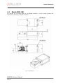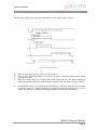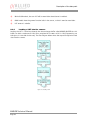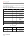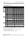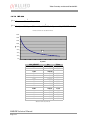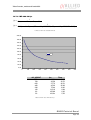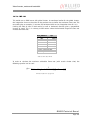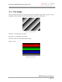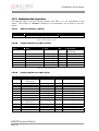
1
AVT Marlin
Technical Manual
For CCD models with serial numbers: xx/yy-6zzzzzzz
and all CMOS models
Allied Vision Technologies GmbH
Taschenweg 2a
D-07646 Stadtroda / Germany
Before operation
We place the highest demands for quality on our cameras. This technical manual is the guide to
the installation and setting up of the camera for operation.
This version 1.3 of the technical manual applies to Marlins, having serial numbers starting
with 6 after the – eg. Xx/yy-6zzzzzzz and all CMOS versions, regardless of S/N.
For CCD Marlins with different serial numbers the previous version 1.2 of the technical
manual applies.
Please read through this manual carefully before operating the camera.
Legal notice
For customers in the U.S.A.
This equipment has been tested and found to comply with the limits for a Class A digital device,
pursuant to Part 15 of the FCC Rules. These limits are designed to provide reasonable protection
against harmful interference when the equipment is operated in a commercial environment. This
equipment generates, uses, and can radiate radio frequency energy and, if not installed and used
in accordance with the instruction manual, may cause harmful interference to radio
communications. Operation of this equipment in a residential area is likely to cause harmful
interference in which case the user will be required to correct the interference at his own
expense. You are cautioned that any changes or modifications not expressly approved in this
manual could void your authority to operate this equipment. The shielded interface cable
recommended in this manual must be used with this equipment in order to comply with the
limits for a computing device pursuant to Subpart J of Part 15 of FCC Rules.
For customers in Canada
This apparatus complies with the Class A limits for radio noise emissions set out in the Radio
Interference Regulations.
Pour utilisateurs au Canada
Cet appareil est conforme aux normes classe A pour bruits radioélectriques, spécifiées dans le
Règlement sur le brouillage radioélectrique.
Life support applications
These products are not designed for use in life support appliances, devices, or systems where
malfunction of these products can reasonably be expected to result in personal injury. Allied
customers using or selling these products for use in such applications do so at their own risk and
agree to fully indemnify Allied for any damages resulting from such improper use or sale.
MARLIN Technical Manual
Safety instructions
Allied Vision Technologies GmbH 02/2005
All rights reserved.
Managing Director: Mr. Frank Grube
Tax-ID: DE 184383113
Copyright
Support:
Taschenweg 2A
D-07646 Stadtroda, Germany
Tel.: +49/36428/6770
Fax: +49/36428/677-28
email: [email protected]
All texts, pictures and graphics are protected by copyright and other laws protecting intellectual
property. It is not permitted to copy or modify them for trade use or transfer, nor may they be
used on web sites.
Trademarks
Unless stated otherwise, all trademarks appearing in this document of Allied Vision Technologies
are brands protected by law.
Warranty
The information supplied by Allied Vision Technologies is supplied without any guarantees or
warranty whatsoever, be it specific or implicit. Also excluded are all implicit warranties
concerning the negotiability, the suitability for specific applications or the non-breaking of laws
and patents. Even if we assume that the information supplied to us is accurate, errors and
inaccuracy may still occur.
Document History
Version
0.9
0.91
Date
18.12.2003
09.01.2004
1.0
20.01.2004
1.1
07.09.2004
1.2
1.3
1.31
08.10.2004
23.02.2005
12.04.2005
Remarks
First Issue
Typos corrected, minor changes,
spectral sens. of IR cut filter added
Wording checked, Marlin W90/270
added
F-131C added, added features to
make docu. compliant w. FW 2.05,
wording checked, impulse diagrams
corrected
Manual compliant to FW 2.06
For Marlins w. ser.# xx/yy-6zzzzzzz
Color: FW 2005032 CMOS included
MARLIN Technical Manual
Page 3
Safety instructions
Contents
1
Safety instructions ...................................................................................... 9
1.1
Environmental conditions....................................................................................... 10
2
3
4
Marlin types and highlights........................................................................ 11
System components................................................................................... 12
Specifications ........................................................................................... 14
4.1
4.2
4.3
4.4
4.5
4.6
4.7
4.8
4.9
4.10
4.11
MF-033B .............................................................................................................. 14
MF-033C .............................................................................................................. 15
MF-046B .............................................................................................................. 16
MF-046C .............................................................................................................. 17
MF-080B (-30 fps*) ............................................................................................... 18
MF-080C (-30 fps*) ............................................................................................... 19
MF-145B2 ............................................................................................................ 20
MF-145C2............................................................................................................. 21
F-131B ................................................................................................................ 22
F-131C ............................................................................................................... 23
Spectral sensitivity............................................................................................... 24
5
6
Quick start................................................................................................ 29
Camera dimensions ................................................................................... 30
6.1
6.2
6.3
6.4
6.5
6.6
Marlin standard housing......................................................................................... 30
Marlin W90........................................................................................................... 31
Marlin W90 S90..................................................................................................... 32
Marlin W270 ......................................................................................................... 33
Marlin W270 S90 ................................................................................................... 34
Tripod adapter ...................................................................................................... 35
7
Camera interfaces ..................................................................................... 36
7.1
7.2
7.3
7.4
7.5
7.6
IEEE-1394 port pin assignment ............................................................................... 36
HiRose jack pin assignment .................................................................................... 37
Status LEDs .......................................................................................................... 38
Operating the camera: ........................................................................................... 39
Control and video data signals ................................................................................ 39
7.5.1 Inputs ...................................................................................................... 39
7.5.2 Outputs .................................................................................................... 44
Pixel data ............................................................................................................ 48
8
Description of the data path ...................................................................... 50
8.1
Block diagrams of the cameras................................................................................ 50
8.1.1 Black and white cameras: ............................................................................ 51
8.1.2 Color cameras: ........................................................................................... 52
Sensor ................................................................................................................. 53
8.2.1 IBIS5A multiple slope (High Dynamic Range mode) ........................................ 54
White balance ...................................................................................................... 57
8.3.1 One Push automatic white balance ............................................................... 59
8.3.2 Automatic white balance............................................................................. 60
Manual gain ......................................................................................................... 62
8.2
8.3
8.4
MARLIN Technical Manual
Page 4
Safety instructions
8.5
8.6
8.7
8.8
8.16
Auto gain .............................................................................................................62
Setting the brightness (black level or offset) .............................................................65
Auto shutter .........................................................................................................65
Lookup table (LUT) and Gamma function...................................................................67
8.8.1 Loading a LUT into the camera .....................................................................68
Shading correction.................................................................................................70
8.9.1 Automatic generation of correction data ........................................................70
8.9.2 Loading a shading image into the camera ......................................................75
8.9.3 Loading a shading image out of the camera ...................................................76
DSNU & blemish correction (MF-131B only) ..............................................................77
Horizontal mirror function .....................................................................................80
Binning (CCD b/w models) .....................................................................................81
8.12.1 Vertical binning ........................................................................................81
8.12.2 Horizontal binning ....................................................................................82
8.12.3 Full binning..............................................................................................82
Sub-sampling (CMOS) ............................................................................................83
Sharpness............................................................................................................84
Color interpolation and correction...........................................................................85
8.15.1 Color interpolation (BAYER demosaicing)......................................................85
8.15.2 Color correction ........................................................................................86
8.15.3 RGB
YUV conversion ..............................................................................86
8.15.4 Hue and Saturation ...................................................................................86
Serial interface.....................................................................................................87
9
Controlling image capture.......................................................................... 91
9.1
Trigger modi .........................................................................................................91
9.1.1 Trigger delay..............................................................................................94
Exposure time .......................................................................................................96
9.2.1 Extended shutter ........................................................................................96
One-Shot..............................................................................................................97
9.3.1 One-Shot command on the bus to start of exposure .........................................97
9.3.2 End of exposure to first packet on the bus .....................................................98
Multi-Shot ............................................................................................................98
ISO_Enable / Free-Run ...........................................................................................99
Asynchronous broadcast .........................................................................................99
Jitter at start of exposure ..................................................................................... 100
Frame memory and deferred image transport ........................................................... 101
9.8.1 HoldImg mode ......................................................................................... 102
9.8.2 FastCapture.............................................................................................. 103
Sequence mode ................................................................................................... 104
9.9.1 Changing the parameters within a sequence ................................................. 107
8.9
8.10
8.11
8.12
8.13
8.14
8.15
9.2
9.3
9.4
9.5
9.6
9.7
9.8
9.9
10
Video formats, modes and bandwidth ....................................................... 109
10.1
10.2
10.3
10.4
10.5
10.6
MF-033B/ MF-033C ............................................................................................. 109
MF-046B/ MF-046C ............................................................................................. 110
MF-080B/ MF-080C (-30 fps) ................................................................................ 111
MF-145B/ MF-145C ............................................................................................. 112
MF-131B/ MF-131C ............................................................................................. 113
Area of interest (AOI) ......................................................................................... 114
MARLIN Technical Manual
Page 5
Safety instructions
10.7
Frame rates ........................................................................................................116
10.7.1 MF-033 ..................................................................................................120
10.7.2 MF-046 ..................................................................................................121
10.7.3 MF-080 ..................................................................................................122
10.7.4 MF-080-30 fps.........................................................................................123
10.7.5 MF-145 ..................................................................................................124
10.7.6 MF-131 ..................................................................................................125
11
How does bandwidth affect the frame rate? .............................................. 126
11.1
Test images........................................................................................................127
12
Configuration of the camera..................................................................... 129
12.1
12.2
12.3
Camera_Status_Register .......................................................................................129
Configuration ROM ..............................................................................................131
Implemented registers .........................................................................................134
12.3.1 Camera initialize register ..........................................................................134
12.3.2 Inquiry register for video format................................................................134
12.3.3 Inquiry register for video mode .................................................................134
12.3.4 Inquiry register for video frame rate and base address ..................................136
12.3.5 Inquiry register for basic function..............................................................142
12.3.6 Inquiry register for feature presence ..........................................................142
12.3.7 Inquiry register for feature elements ..........................................................145
12.3.8 Inquiry register for absolute value CSR offset address ...................................148
12.3.9 Status and control register for feature ........................................................149
12.3.10 Feature control error status register..........................................................150
12.3.11 Video mode control and status registers for Format_7 .................................150
12.4 Advanced features...............................................................................................151
12.4.1 Version information inquiry.......................................................................153
12.4.2 Advanced feature inquiry ..........................................................................154
12.4.3 MaxResolution ........................................................................................154
12.4.4 Timebase................................................................................................155
12.4.5 Extended shutter .....................................................................................156
12.4.6 Test images ............................................................................................157
12.4.7 Sequence control.....................................................................................158
12.4.8 Lookup tables (LUT).................................................................................159
12.4.9 Shading correction ..................................................................................160
12.4.10 Deferred image transport ........................................................................162
12.4.11 Frame information .................................................................................162
12.4.12 High dynamic range mode (MF-131B/C only) .............................................163
12.4.13 DSNU control.........................................................................................163
12.4.14 Input/output pin control ........................................................................165
12.4.15 Delayed Integration enable .....................................................................166
12.4.16 Auto shutter .........................................................................................167
12.4.17 Auto gain .............................................................................................168
12.4.18 Auto function AOI..................................................................................168
12.4.19 Color correction .....................................................................................169
12.4.20 Trigger delay .........................................................................................169
12.4.21 Mirror...................................................................................................169
12.4.22 GPDATA_BUFFER ....................................................................................170
MARLIN Technical Manual
Page 6
Safety instructions
12.4.23
13
14
15
Soft Reset ............................................................................................ 170
Firmware update ..................................................................................... 171
Declarations of conformity....................................................................... 172
Index ..................................................................................................... 182
MARLIN Technical Manual
Page 7
Safety instructions
Conventions used in this manual
To give this manual an easily understood layout and to emphasize important information, the
following typographical styles and symbols are used:
Styles
Style
Courier
upper case
italics
parentheses
and/or blue
Function
Programs, inputs,
etc.
Register
Modes, fields
Links
Example
“Input”
REGISTER
Mode
(Link)
Symbols:
This symbol highlights important instructions that
malfunctions.
MARLIN Technical Manual
Page 8
should be followed to
avoid
Safety instructions
1
Safety instructions
There are no switches or parts inside the camera that require adjustment. The guarantee
becomes void upon opening the camera casing.
If the product is disassembled, reworked or repaired by other than a recommended service
person, AVT or its suppliers will take no responsibility for the subsequent performance or
quality of the camera.
The camera does NOT generate dangerous voltages internally. However, because the IEEE1394a standard permits cable power distribution at voltages higher than 24 V, various
international safety standards apply. Reference documents applicable in the United States
include:
• Information Processing and Business Equipment, UL 478
• National Electric Code, ANSI/NFPA 70
• Standard for the Protection of Electronic Computer/Data-Processing Equipment, ANSI/NFPA
75
Reference documents applicable in Europe include materials to secure the European Union CE
marking as follows:
• Telecommunications Terminal Equipment (91/263/EEC)
• EMC Directive (89/339/EEC)
• CE Marking Directive (93/68/EEC)
• LOW Voltage Directive (73/23/EEC) as amended by the CE Marking
Reference documents applicable in Japan include:
• Electronic Equipment Technology Criteria by the Ministry of Trading and Industry (Similar to
NFPA 70)
• Wired Electric Communication Detailed Law 17 by the Ministry of Posts and Telecom Law for
Electric Equipment
• Dentori law issued by the Ministry of Trading and Industry
• Fire law issued by the Ministry of Construction
Make sure NOT to touch the shield of the camera cable connected to a computer and the
ground terminal of the lines at the same time.
Use only DC-power supplies with insulated cases. These are identified by having only TWO
power connectors.
Although IEEE-1394a is functionally plug and play, the physical ports may be damaged by
excessive ESD (electrostatic discharge), when connected under powered conditions. It is
good practice to bring the metal part, which is the shield of the IEEE-1394 cable, in contact
with the housing of the camera, before plugging it into the camera and on the other side in
contact with metal parts of the computer, before plugging it into the port of the computer.
This ensures that excessive charge can flow safely to ground.
When you feel uncomfortable with the previous advice or when you do not know the
connectivity of an installation at all, we strongly recommend to power all systems down
before connecting or disconnecting a camera.
MARLIN Technical Manual
Page 9
Safety instructions
1.1
Environmental conditions
Ambient temperature:
when camera in use:
when being stored :
+ 5° C ... + 45° C
- 10° C ... + 60° C
Relative humidity:
Protection:
20 % … 80 % no condensed water
IP 30
MARLIN Technical Manual
Page 10
Marlin types and highlights
2
Marlin types and highlights
With Marlin cameras, entry into the world of digital image processing is simpler and more costeffective than ever before.
With the new MARLIN, Allied Vision Technologies presents a whole series of attractive digital
camera entry-level models of the FireWire ™type.
These products offer an unequalled price-performance relationship and make the decision to
switch from using analogue to digital technology easier that ever before.
The AVT Marlin family consists of five very compact IEEE 1394 C-mount cameras, which are
equipped with highly sensitive high-quality sensors (CCD,CMOS). Each of these cameras is
available in black/white and color versions.
A large selection of different sensor sizes (1/2 ", 1/3 ", 2/3 ") and resolutions (VGA, SVGA, XGA,
SXGA) ensures the suitability of the cameras for all applications.
The MARLIN family consists of the following models:
MARLIN F-033B/C
1/2 " Sony Progressive Scan CCD imager; (VGA) 656 (h) x 494 (v); up to 74 fps at full resolution.
MARLIN F-046B/C
1/2 " Sony Progressive Scan CCD imager; (SVGA) 780 (h) x 582 (v); up to 53 fps.
MARLIN F-080B/C
1/3 " Sony Progressive Scan CCD imager; (XGA) 1032 (h) x 778 (v); up to 20 fps.
MARLIN F-080B/C 30 fps
1/3 " Sony Progressive Scan CCD imager; (XGA) 1032 (h) x 778 (v); up to 30 fps.
MARLIN F-131B/C
2/3 " Global Shutter CMOS imager; (SXGA) 1280 (h) x 1024 (v); up to 25 fps.
MARLIN F-145B2/C2
1/2 " Sony Progressive Scan CCD; (SXGA) 1392 (h) x 1040 (v); up to 10 fps (15 fps available on
request) at full resolution.
Operating in 8-bit and 10 Bit mode mode (CCD b/w only), the cameras ensure very high quality
images under almost all circumstances. The MARLIN is equipped with an asynchronous trigger
shutter as well as true partial scan, and integrates numerous useful and intelligent Smart
Features for image processing.
All models are equipped with an optical filter to eliminate the influence of infra red light
hitting the sensor. Please be advised that, as a side effect, this filter reduces the sensitivity
in the visible spectrum.
For certain applications it may thus be recommended to take out the filter by means of a
special tool which can be ordered from AVT under the following number: E9020001.
Taking out the filter requires special care. Ask your dealer to help you if you are not
confident with the procedure.
MARLIN Technical Manual
Page 11
System components
3
System components
The following system components are included with each camera::
AVT Marlin
4.5m 1394 standard cable
Jenofilt 217 IR cut filter (built in)
4.5m latching cable
Driver and documentation
Optional:
Tripod Adapter
The following illustration shows the spectral sensitivity of the IR cut filter
Figure 1: Spectral sensitivity of Jenofilt 217
MARLIN Technical Manual
Page 12
System components
To demonstrate the properties of the camera, all examples in this manual are based on the
“FirePackage” OHCI API software and the “SmartView” application.
These utilities can be obtained from Allied Vision Technologies. A free version of “SmartView” is
available for download at www.alliedvisiontec.com.
The camera also works with all IIDC (formerly DCAM) compatible IEEE 1394 programs and image
processing libraries.
AVT offers different lenses from a variety of manufacturers. The following table lists selected
image formats depending on camera type, distance and the focal width of the lens.
Focal Width MF033/046/145
4.8mm
8mm
12mm
16mm
25mm
35mm
50mm
Focal Width MF-080
4.8mm
8mm
12mm
16mm
25mm
35mm
50mm
Focal Width MF-131
4.8mm
8mm
12mm
16mm
25mm
35mm
50mm
Distance = 0,5m
Distance = 1m
0,5m x 0,67m
0,3m x 0,4m
0,195m x 0,26m
0,145m x 0,19m
9,1cm x 12,1cm
6,4cm x 8,51cm
4,4cm x 5,85cm
Distance = 0,5m
0,375m x 0,5m
0,22m x 0,29m
0,145m x 0,19m
11cm x 14,7cm
6,9cm x 9,2cm
4,8cm x 6,4cm
3,3cm x 4,4cm
Distance = 0.5m
0.7m x 0.93m
0.4m x 0.53m
0.27m x 0.36m
0.2m x 0.27m
12.5cm x 16.63cm
8.8cm x 11.7cm
6cm x 7.98cm
1,0m x 1,33m
0,6m x 0,8m
0,39m x 0,58m
0,29m x 0,38m
18,2cm x 24,2cm
12,8cm x 17,02cm
8,8cm x 11,7cm
Distance = 1m
0,75m x 1m
0,44m x 0,58m
0,29m x 0,38m
22cm x 29,4cm
13,8cm x 18,4cm
9,6cm x 12,8cm
6,6cm x 8,8cm
Distance = 1m
1.4m x 1.86m
0.8m x 1.06m
0.54m x 0.72m
0.4m x 0.54m
25cm x 33.25cm
17.6cm x 23.4cm
12cm x 15.96cm
Table 1: Focal Width vs. field of view
MARLIN Technical Manual
Page 13
Specifications
4
Specifications
4.1
MF-033B
Specification
Image device
Effective Picture Elements
Lens Mount
Picture Sizes
Cell Size
ADC
Data Path
Frame rates
Gain Control
Shutter Speed
External Trigger Shutter
Internal FIFO-Memory
# Look Up Tables
Smart Functions
Transfer Rate
Digital Interface
Power Requirements
Power Consumption
Dimensions
Mass
Operating Temperature
Storage Temperature
Regulations
Options
1/2 " (diag. 8 mm) type progressive scan SONY IT CCD
656 (H) x 494 (V)
C-mount: 17.526 mm (in air); ∅ 25.4 mm (32 T.P.I.)
Mechanical Flange Back to filter distance: 8.2 mm
640 x 480 pixels (Format_0)
656 x 494 pixels (Format_7 Mode_0)
328 x 494 pixels (Format_7 Mode_1)
656 x 246 pixels (Format_7 Mode_2)
328 x 246 pixels (Format_7 Mode_3)
9.9 µm x 9.9 µm
12 Bit
8/10 Bit
3.75 Hz; 7.5 Hz; 15 Hz; 30 Hz; 60 Hz; up to 74 Hz in Format_7
Manual: 0–24 dB (0.035 dB/step); Auto gain (select. AOI)
20 …67.108.864 µs (~67s); Auto shutter (select. AOI)
Trigger_Mode_0, Trigger_Mode_1, Advanced feature:
Trigger_Mode_15 (bulk); image transfer by command; Trigger delay
Up to 17 frames
One, user programmable (10 Bit -> 8 Bit); Gamma (0.45)
Real time shading correction image sequencing, two configurable
inputs two configurable outputs, image mirror (L-R↔ R-L), binning,
serial port (IIDC v. 1.31)
100 Mb/s, 200 Mb/s, 400 Mb/s
IEEE 1394 IIDC v. 1.3
DC 8 V – 36 V via IEEE 1394cable or 12-pin HIROSE
Less than 3 Watts (@ 12 V d.c.)
58 mm x 44 mm x 29 mm (L x W x H); w/o tripod and lens
<120 g (without lens)
+5 – +45 ° Celsius
-10 – +60 ° Celsius
EN 55022,EN61000,EN 55024,FCC Class A, DIN ISO 9022
Removable IR-cut-filter, host adapter card, locking IEEE-1394 cable,
API (FirePackage), TWAIN (WIA)- and WDM stream driver
Table 2: Specification MF-033B
The design and specifications for the products described above may change without notice.
MARLIN Technical Manual
Page 14
Specifications
4.2
MF-033C
Specification
Image device
Effective Picture Elements
Lens Mount
Picture Sizes
Cell Size
ADC
Color Modes
Data Path
Frame rates
Gain Control
Color Control
White Balance
Shutter Speed
External Trigger Shutter
Internal FIFO-Memory
# Look Up Tables
Smart Functions
Transfer Rate
Digital Interface
Power Requirements
Power Consumption
Dimensions
Mass
Operating Temperature
Storage Temperature
Regulations
Options
1/2 " (diag. 8 mm) type progressive scan SONY IT CCD
656 (H) x 494 (V)@Raw8 (492 @YUV)
C-mount: 17.526 mm (in air); ∅ 25.4 mm (32 T.P.I.)
Mechanical Flange Back to filter distance: 8.2 mm
640 x 480 pixels (Format_0)
656 x 492 pixels (Format_7 Mode_0)
656 x 494 pixels (Format_7 Mode_1)
9.9 µm x 9.9 µm
12 Bit
Raw8, YUV4:2:2, YUV4:1:1
8 Bit
3.75 Hz; 7.5 Hz; 15 Hz; 30 Hz; up to 74 Hz in Format_7 (RAW); 68
Hz (YUV 4:1:1); up to 51 Hz in YUV 4:2:2
Manual: 0–16 dB (0.035 dB/step); Auto gain (select. AOI)
Hue (-40°… +40°) and saturation (0…200%)
Manual (U/V); One_Push; Auto (select. AOI)
20 …67.108.864 µs (~67s); Auto shutter (select. AOI)
Trigger Mode_0, Trigger_Mode_1, Advanced feature:
Trigger_Mode_15 (bulk); image transfer by command; Trigger delay
Up to 17 frames
One, user programmable (10 Bit -> 8 Bit); Gamma (0.45)
Real time shading correction image sequencing, two configurable
inputs two configurable outputs, image mirror (L-R↔ R-L), serial
port (IIDC v. 1.31)
100 Mb/s, 200 Mb/s, 400 Mb/s
IEEE 1394 IIDC v. 1.3
DC 8 V – 36 V via IEEE 1394 cable or 12-pin HIROSE
Less than 3 Watts (@ 12 V d.c.)
58 mm x 44 mm x 29 mm (L x W x H); without tripod and lens
<120 g (without lens)
+5 – +45 ° Celsius
-10 – +60 ° Celsius
EN 55022, EN 61000, EN 55024, FCC Class A, DIN ISO 9022
Host adapter card, locking IEEE-1394 cable, API (FirePackage),
TWAIN (WIA)- and WDM stream driver
Table 3: Specification MF-033C
The design and specifications for the products described above may change without notice.
MARLIN Technical Manual
Page 15
Specifications
4.3
MF-046B
Specification
Image device
1/2 " (diag. 8 mm) type progressive scan SONY IT CCD
Effective Picture Elements 780 (H) x 582 (V)
Lens Mount
C-mount: 17.526 mm (in air); ∅ 25.4 mm (32 T.P.I.)
Mechanical Flange Back to filter distance: 8.2 mm
Picture Sizes
640 x 480 pixels (Format_0);
780 x 582 (Format_7 Mode_0);
388 x 582 (Format_7 Mode_1);
780 x 290 (Format_7 Mode_2);
388 x 290 (Format_7 Mode_3)
Cell Size
8.3 µm x 8.3 µm
ADC
12 Bit
Data Path
8/10 Bit
Frame rates
3.75 Hz; 7.5 Hz; 15 Hz; 30 Hz; up to 53 Hz in Format_7
Gain Control
Manual: 0–24 dB (0.035 dB/step); Auto gain (select. AOI)
Shutter Speed
20 …67.108.864 µs (~67s); Auto shutter (select. AOI)
External Trigger Shutter
Trigger_Mode_0, Trigger_Mode_1, Advanced feature:
Trigger_Mode_15 (bulk); image transfer by command; Trigger delay
Internal FIFO-Memory
Up to 13 frames
# Look Up Tables
One, user programmable (10 Bit -> 8 Bit); Gamma (0.45)
Smart Functions
Real time shading correction; image sequencing, two configurable
inputs, two configurable outputs, image mirror (L-R↔ R-L), binning,
serial port (IIDC v. 1.31)
Transfer Rate
100 Mb/s, 200 Mb/s, 400 Mb/s
Digital Interface
IEEE 1394 IIDC v. 1.3
Power Requirements
DC 8 V – 36 V via IEEE 1394 cable or 12-pin HIROSE
Power Consumption
Less than 3 Watts (@ 12 V d.c.)
Dimensions
58 mm x 44 mm x 29 mm (L x W x H); without tripod and lens
Mass
<120 g (without lens)
Operating Temperature
+5 – +45 ° Celsius
Storage Temperature
-10 – +60 ° Celsius
Regulations
EN 55022, EN 61000, EN 55024, FCC Class A, DIN ISO 9022
Options
Removable IR-cut-filter, host adapter card, locking IEEE-1394 cable,
API (FirePackage), TWAIN (WIA)- and WDM stream driver
Table 4: Specification MF-046B
The design and specifications for the products described above may change without notice.
MARLIN Technical Manual
Page 16
Specifications
4.4
MF-046C
Specification
Image device
Effective Picture
Elements
Lens Mount
Picture Sizes
Cell Size
ADC
Color Modes
Data Path
Frame rates
Gain Control
Color Control
White Balance
Shutter Speed
External Trigger Shutter
Internal FIFO-Memory
# Look Up Tables
Smart Functions
Transfer Rate
Digital Interface
Power Requirements
Power Consumption
Dimensions
Mass
Operating Temperature
Storage Temperature
Regulations
Options
1/2 " (diag. 8 mm) Type progressive scan SONY IT CCD
780 (H) x 582 (V)@Raw8; 780 (H) x 580 (V)@YUV
C-mount: 17.526 mm (in air); ∅ 25.4 mm (32 T.P.I.)
Mechanical Flange Back to filter distance: 8.2 mm
640 x 480 pixels (Format_0);
780 x 580 (Format_7 Mode_0);
780 x 582 (Format_7 Mode_1);
8.3 µm x 8.3 µm
12 Bit
Raw8, YUV4:2:2, YUV4:1:1
8 Bit
3.75 Hz; 7.5 Hz; 15 Hz; 30 Hz; up to 53 Hz in Format_7 (Raw8) (36 Hz
YUV4:2:2; 49Hz YUV4:1:1)
Manual: 0–16 dB (0.035 dB/step); Auto gain (select. AOI)
Hue (-40°… +40°) and saturation (0…200%)
Manual (U/V); One_Push; Auto (select. AOI)
20 …67.108.864 µs (~67s); Auto shutter (select. AOI)
Trigger_Mode_0, Trigger_Mode_1, Advanced feature: Trigger_Mode_15
(bulk); image transfer by command; Trigger delay
Up to 13 frames
One, user programmable (10 Bit -> 8 Bit); Gamma (0.45)
Real time shading correction; image sequencing, two configurable
inputs, two configurable outputs, image mirror (L-R↔ R-L), serial port
(IIDC v. 1.31)
100 Mb/s, 200 Mb/s, 400 Mb/s
IEEE 1394 IIDC v. 1.3
DC 8 V – 36 V via IEEE 1394 cable or 12-pin HIROSE
Less than 3 Watts (@ 12 V d.c.)
58 mm x 44 mm x 29 mm (L x W x H); without tripod and lens
<120 g (without lens)
+5 – +45 ° Celsius
-10 – +60 ° Celsius
EN 55022, EN61000, EN 55024, FCC Class A, DIN ISO 9022
Host adapter card, locking IEEE-1394 cable, API (FirePackage), TWAIN
(WIA)- and WDM stream driver
Table 5: Specification MF-046C
The design and specifications for the products described above may change without notice.
MARLIN Technical Manual
Page 17
Specifications
4.5
MF-080B (-30 fps*)
Specification
Image device
1/3 " (diag. 6 mm) type progressive scan SONY IT CCD
Effective Picture Elements 1032 (H) x 778 (V)
Lens Mount
C-mount: 17.526 mm (in air); ∅ 25.4 mm (32 T.P.I.)
Mechanical Flange Back to filter distance: 8.2 mm, CS-mount on
demand
Picture Sizes
1024 x 768 pixels (Format_1) supporting all smaller fixed formats;
1032 x 778 (Format_7 Mode_0)
516 x 778 (Format_7 Mode_1);
1032 x 388 (Format_7 Mode_2);
516 x 388 (Format_7 Mode_3)
Cell Size
4.65 µm x 4.65 µm
ADC
12 Bit
Data Path
8/10 Bit
Frame rates
3.75 Hz; 7.5 Hz; 15 Hz; 30 Hz*; up to 20 (30*) Hz in Format_7
Gain Control
Manual: 0–24 dB (0.035 dB/step); Auto gain (select. AOI)
Shutter Speed
20 …67.108.864 µs (~67s); Auto shutter (select. AOI)
External Trigger Shutter
Trigger_Mode_0, Trigger_Mode_1, Advanced feature:
Trigger_Mode_15 (bulk); image transfer by command; Trigger delay
Internal FIFO-Memory
Up to 7 frames
# Look Up Tables
One, user programmable (10 Bit -> 8 Bit); Gamma (0.45)
Smart Functions
Real time shading correction; image sequencing, two configurable
inputs, two configurable outputs, image mirror (L-R↔ R-L), binning,
serial port (IIDC v. 1.31)
Transfer Rate
100 Mb/s, 200 Mb/s, 400 Mb/s
Digital Interface
IEEE 1394 IIDC v. 1.3
Power Requirements
DC 8 V – 36 V via IEEE 1394 cable or 12-pin HIROSE
Power Consumption
Less than 3 Watts (@ 12 V d.c.)
Dimensions
58 mm x 44 mm x 29 mm (L x W x H); without tripod and lens
Mass
<120 g (without lens)
Operating Temperature
+5 – +45 ° Celsius
Storage Temperature
-10 – +60 ° Celsius
Regulations
EN 55022, EN 61000,EN 55024,FCC Class A, DIN ISO 9022
Options
Removable IR-cut-filter, host adapter card, locking IEEE-1394 cable,
API (FirePackage), TWAIN (WIA)- and WDM stream driver
Table 6: Specification MF-080B
The design and specifications for the products described above may change without notice.
*: Variant: F-080-30 fps only.
This variant offers higher speed at a slight expense in image quality.
MARLIN Technical Manual
Page 18
Specifications
4.6 MF-080C (-30 fps*)
Specification
Image device
1/3 " (diag. 6 mm) type progressive scan SONY IT CCD
Effective Picture Elements 1032 (H) x 778 (V)@Raw8; 1032 (H) x 776 (V)@YUV
Lens Mount
C-mount: 17.526 mm (in air); ∅ 25.4 mm (32 T.P.I.)
Mechanical Flange Back to filter distance: 8.2 mm, CS-mount on
demand
Picture Sizes
1024 x 768 pixels (Format_1 ) supporting all smaller fixed formats;
1032 x 776 (Format_7 Mode_0);
1032 x 778 (Format_7 Mode_1);
Cell Size
4.65 µm x 4.65 µm
ADC
12 Bit
Color Modes
Raw8,YUV4:2:2,YUV4:1:1
Data Path
8 Bit
Frame rates
3.75 Hz; 7.5 Hz; 15 Hz; 30 Hz*; up to 20 (30*) Hz in Format_7 Raw8
(20 Hz at YUV4:1:1 /20 Hz YUV4:2:2)
Gain Control
Manual: 0–16 dB (0.035 dB/step); Auto gain (select. AOI)
Color Control
Hue (-40°… +40°) and saturation (0…200%)
White Balance
Manual (U/V); One_Push; Auto (select. AOI)
Shutter Speed
20 …67.108.864 µs (~67s); Auto shutter (select. AOI)
External Trigger Shutter
Trigger_Mode_0, Trigger_Mode_1, Advanced feature:
Trigger_Mode_15 (bulk); image transfer by command; Trigger delay
Internal FIFO-Memory
Up to 7 frames
# Look Up Tables
One, user programmable (10 Bit -> 8 Bit); Gamma (0.45)
Smart Functions
Real time shading correction; image sequencing, two configurable
inputs, two configurable outputs, image mirror (L-R↔ R-L), serial
port (IIDC v. 1.31)
Transfer Rate
100 Mb/s, 200 Mb/s, 400 Mb/s
Digital Interface
IEEE 1394 IIDC v. 1.3
Power Requirements
DC 8 V – 36 V via IEEE 1394 cable or 12-pin HIROSE
Power Consumption
Less than 3 Watts (@ 12 V d.c.)
Dimensions
58 mm x 44 mm x 29 mm (L x W x H); without tripod and lens
Mass
<120 g (without lens)
Operating Temperature
+5 – +45 ° Celsius
Storage Temperature
-10 – +60 ° Celsius
Regulations
EN 55022, EN 61000, EN 55024, FCC Class A, DIN ISO 9022
Options
Host adapter card, locking IEEE-1394 cable, API (FirePackage),
TWAIN (WIA)- and WDM stream driver
Table 7: Specification MF-080C
The design and specifications for the products described above may change without notice.
*: Variant: F-080C-30 fps (RAW-mode) only.
MARLIN Technical Manual
Page 19
Specifications
4.7
MF-145B2
Specification
Image device
1/2 " (diag. 8 mm) type progressive scan SONY IT CCD
Effective Picture Elements 1392 (H) x 1040 (V)
Lens Mount
C-mount: 17.526 mm (in air); ∅ 25.4 mm (32 T.P.I.)
Mechanical Flange Back to filter distance: 8.2 mm
Picture Sizes
Up to 1280 x 960 pixels (Format_2), supporting all smaller fixed
formats; 1392 x 1040 pixels (Format_7 Mode_0);
696 x 1040 (Format_7 Mode_1);
1392 x 520 (Format_7 Mode_2);
696 x 520 (Format_7 Mode_3)
Cell Size
4.65 µm x 4.65 µm
ADC
12 Bit
Data Path
8/10 Bit
Frame rates
3.75 Hz; 7.5 Hz; 15 Hz*; up to 10 Hz (15 Hz)* in Format_7
Gain Control
Manual: 0–24 dB (0.035 dB/step); Auto gain (select. AOI)
Shutter Speed
20 …67.108.864 µs (~67s); Auto shutter (select. AOI)
External Trigger Shutter
Trigger_Mode_0, Trigger_Mode_1, Advanced feature:
Trigger_Mode_15 (bulk); image transfer by command; Trigger delay
Internal FIFO-Memory
Up to 3 frames
# Look Up Tables
One, user programmable (10 Bit -> 8 Bit); Gamma (0.45)
Smart Functions
Real time shading correction; image sequencing, two configurable
inputs, two configurable outputs, image mirror (L-R↔ R-L), binning,
serial port (IIDC v. 1.31)
Transfer Rate
100 Mb/s, 200 Mb/s, 400 Mb/s
Digital Interface
IEEE 1394 IIDC v. 1.3
Power Requirements
DC 8 V – 36 V via IEEE 1394 cable or 12-pin HIROSE
Power Consumption
Less than 3 Watts (@ 12 V d.c.)
Dimensions
58 mm x 44 mm x 29 mm (L x W x H); without tripod and lens
Mass
<120 g (without lens)
Operating Temperature
+5 – +45 ° Celsius
Storage Temperature
-10 – +60 ° Celsius
Regulations
EN 55022, EN 61000, EN 55024, FCC Class A, DIN ISO 9022
Options
Removable IR-cut-filter, host adapter card, locking IEEE-1394 cable,
API (FirePackage), TWAIN (WIA)- and WDM stream driver
Table 8: Specification MF145B2
The design and specifications for the products described above may change without notice.
*: Variant: F-145B2-15 only.
This variant offers higher speed at a slight expense in image quality.
MARLIN Technical Manual
Page 20
Specifications
4.8
MF-145C2
Specification
Image device
1/2 " (diag. 8 mm) Type progressive scan SONY IT CCD
Effective Picture Elements 1392 (H) x 1040 (V)@Raw8; 1392 (H) x 1036 (V)@YUV
Lens Mount
C-mount: 17.526 mm (in air); ∅ 25.4 mm (32 T.P.I.)
Mechanical Flange Back to filter distance: 8.2 mm
Picture Sizes
Up to 1280 x 960 pixels (Format_2 ) supporting all smaller fixed
formats; 1392 x 1036 (Format_7 Mode_0);
1392 x 1040 (Format_7 Mode_1)
Cell Size
4.65 µm x 4.65 µm
ADC
12 Bit
Color Modes
Raw8, YUV4:2:2, YUV4:1:1
Data Path
8 Bit
Frame rates
3.75 Hz; 7.5 Hz, 15 Hz*; up to 10 Hz (15 Hz)* in Format_7
Gain Control
Manual: 0–16 dB (0.035 dB/step); Auto gain (select. AOI)
Color Control
Hue (-40°… +40°) and saturation (0…200%)
White Balance
Manual (U/V); One_Push; Auto (select. AOI)
Shutter Speed
20 …67.108.864 µs (~67s); Auto shutter (select. AOI)
External Trigger Shutter
Trigger_Mode_0, Trigger_Mode_1, Advanced feature:
Trigger_Mode_15 (bulk); image transfer by command; Trigger delay
Internal FIFO-Memory
Up to 3 frames
# Look Up Tables
One, user programmable (10 Bit -> 8 Bit); Gamma (0.45)
Smart Functions
Real time shading correction; Image sequencing, two configurable
inputs, two configurable outputs, image mirror (L-R↔ R-L), serial
port (IIDC v. 1.31)
Transfer Rate
100 Mb/s, 200 Mb/s, 400 Mb/s
Digital Interface
IEEE 1394 IIDC v. 1.3
Power Requirements
DC 8 V – 36 V via IEEE 1394 cable or 12-pin HIROSE
Power Consumption
Less than 3 Watts (@ 12 V d.c.)
Dimensions
58 mm x 44 mm x 29 mm (L x W x H); without tripod and lens
Mass
<120 g (without lens)
Operating Temperature
+5 – +45 ° Celsius
Storage Temperature
-10 – +60 ° Celsius
Regulations
EN 55022, EN 61000, EN 55024, FCC Class A, DIN ISO 9022
Options
Host adapter card, locking IEEE-1394 cable, API (FirePackage),
TWAIN (WIA) -and WDM stream driver
Table 9: Specification MF-145C2
The design and specifications for the products described above may change without notice.
*: Variant: F-145C2-15 only.
This variant offers higher speed at a slight expense in image quality.
MARLIN Technical Manual
Page 21
Specifications
4.9
F-131B
Specification
Image device
2/3 " (diag. 11 mm) Type global shutter CMOS sensor
Effective Picture Elements 1280 (H) x 1024 (V)
Lens Mount
C-mount: 17.526 mm (in air); ∅ 25.4 mm (32 T.P.I.)
Mechanical Flange Back to filter distance: 8.2 mm
Picture Sizes
Up to 1280 x 960 pixels (Format_2), supporting all smaller fixed
formats; 1280 x 1024 pixels (Format_7 Mode_0);
640 x 1024 pixels (Format_7 Mode_1, sub-sampling)
1280 x 512 pixels (Format_7 Mode_2, sub-sampling)
640 x 512 pixels (Format_7 Mode_3, sub-sampling)
Cell Size
6.7 µm x 6.7 µm
ADC
10 Bit
Data Path
8 Bit
Frame rates
3.75 Hz; 7,5 Hz; 15 Hz; up to 25 Hz in Format_7; 30 Hz @ SVGA and
smaller
Gain Control
Manual: 0– 16 dB (13 x 1.25 dB)
Shutter Speed
20 µs- 67s; Auto shutter (select. AOI)
External Trigger Shutter
Trigger_Mode_0, Trigger_Mode_1, Advanced feature:
Trigger_Mode_15 (bulk); image transfer by command; Trigger delay
Internal FIFO-Memory
Up to 4 frames
# Look Up Tables
One, user programmable (10 Bit -> 8 Bit); separate Gamma (0.45)
LUT
Smart Functions
Dark signal non uniformity (DSNU) correction, Real time shading
correction; two configurable inputs, two configurable outputs, high
dynamic range (HDR) mode, image mirror (L-R↔ R-L), sub-sampling,
serial port (IIDC v. 1.31)
Transfer Rate
100 Mb/s, 200 Mb/s, 400 Mb/s
Digital Interface
IEEE 1394 IIDC v. 1.3
Power Requirements
DC 8 V – 36 V via IEEE 1394 cable or 12-pin HIROSE
Power Consumption
Less than 3 Watts (@ 12 V d.c.)
Dimensions
58 mm x 44 mm x 29 mm (L x W x H); without tripod and lens
Mass
<120 g (without lens)
Operating Temperature
+5 – +45 ° Celsius
Storage Temperature
-10 – +60 ° Celsius
Regulations
EN 55022, EN 61000, EN 55024, FCC Class A, DIN ISO 9022
Options
Host adapter card, locking IEEE-1394 cable, API (FirePackage),
TWAIN (WIA) -and WDM stream driver
Table 10: Specification MF-131B
The design and specifications for the products described above may change without notice.
MARLIN Technical Manual
Page 22
Specifications
4.10 F-131C
Specification
Image device
Effective Picture
Elements
Lens Mount
Picture Sizes
Cell Size
ADC
Data Path
Frame rates
Gain Control
White Balance
Shutter Speed
External Trigger Shutter
Internal FIFO-Memory
# Look Up Tables
Smart Functions
Transfer Rate
Digital Interface
Power Requirements
Power Consumption
Dimensions
Mass
Operating Temperature
Storage Temperature
Regulations
Options
2/3 " (diag. 11 mm) Type global shutter CMOS sensor
1280 (H) x 1024 (V)
C-mount: 17.526 mm (in air); ∅ 25.4 mm (32 T.P.I.)
Mechanical Flange Back to filter distance: 8.2 mm
Up to 1280 x 960 pixels (Format_2), supporting all smaller fixed
formats; 1280 x 1024 pixels (Format_7)
640 x 1024 pixels (Format_7 Mode_1, sub-sampling)
1280 x 512 pixels (Format_7 Mode_2, sub-sampling)
640 x 512 pixels (Format_7 Mode_3, sub-sampling)
6.7 µm x 6.7 µm
10 Bit
8 Bit
3.75 Hz; 7,5 Hz; 15 Hz; up to 25 Hz in Format_7 Raw8; (12 fps
@YUV4:2:2; 17 fps @YUV4:1:1)
Manual: 0–16 dB (13 x 1.25 dB))
Manual (U/V); One_Push; Auto (select. AOI)
20 µs- 67s; Auto shutter (select. AOI)
Trigger_Mode_0, Trigger_Mode_1, Advanced feature: Trigger_Mode_15
(bulk); image transfer by command; Trigger delay
Up to 4 frames
One, user programmable (10 Bit -> 8 Bit); separate Gamma (0.45) LUT
Dark signal non uniformity (DSNU) correction, Real time shading
correction; two configurable inputs, two configurable outputs, high
dynamic range (HDR) mode, image mirror (L-R↔ R-L), sub-sampling,
serial port (IIDC v. 1.31)
100 Mb/s, 200 Mb/s, 400 Mb/s
IEEE 1394 IIDC v. 1.3
DC 8 V – 36 V via IEEE 1394 cable or 12-pin HIROSE
Less than 3 Watts (@ 12 V d.c.)
58 mm x 44 mm x 29 mm (L x W x H); without tripod and lens
<120 g (without lens)
+5 – +45 ° Celsius
-10 – +60 ° Celsius
EN 55022, EN 61000, EN 55024, FCC Class A, DIN ISO 9022
Host adapter card, locking IEEE-1394 cable, API (FirePackage), TWAIN
(WIA) -and WDM stream driver
Table 11: Specification MF-131C
The design and specifications for the products described above may change without notice.
MARLIN Technical Manual
Page 23
Specifications
4.11 Spectral sensitivity
Figure 2: Spectral sensitivity of MF-033B without cut filter and optics.
Figure 3: Spectral sensitivity of MF-033C without cut filter and optics
MARLIN Technical Manual
Page 24
Specifications
Figure 4: Spectral sensitivity of MF-046B without cut filter and optics.
Figure 5: Spectral sensitivity of MF-046C without cut filter and optics.
MARLIN Technical Manual
Page 25
Specifications
Figure 6: Spectral sensitivity of MF-080B without cut filter and optics
Figure 7: Spectral sensitivity of MF-080C without cut filter and optics.
MARLIN Technical Manual
Page 26
Specifications
Figure 8: Spectral sensitivity of MF-145B2 without cut filter and optics
Figure 9: Spectral sensitivity of MF-145C2 without cut filter and optics
MARLIN Technical Manual
Page 27
Specifications
Figure 10: Spectral sensitivity of MF-131B without cut filter and optics
Figure 11: Spectral sensitivity of MF-131C without cut filter and optics
MARLIN Technical Manual
Page 28
Quick start
5
Quick start
To attach an IEEE-1394 camera to a PC or laptop, the target machine must be equipped with an
IEEE-1394 port and have the appropriate driver and software installed. This IEEE-1394 port is
already present in many modern PCs and laptops. Should this not be the case, you can upgrade
by installing one or more IEEE-1394 ports in the form of a card for the PCI slot, or as a PC card
(PCMCIA) for the PC card slot. AVT offers a wide range of adaptors for different requirements.
After starting the operating system, the plug and play mechanism on the PC should recognize the
new hardware and prompt you to install the IEEE-1394 driver from Microsoft.
AVT supplies since 3Q/2004 an additional TWAIN (VIA) drivers and WDM stream software to
integrate the images into third party software which has these interfaces.
Alternatively the FirePackage API SDK can be used. This replaces the MS-IEEE-1394 driver with
the driver produced by the company Intek.
A more detailed description for these installation routines can be found in the “FirePackage”
software manuals.
The latter driver works in conjunction with the “SmartView” program. This viewer enables not
only quick and easy access to all integrated IEEE-1394 ports and all the connected IEEE-1394
cameras, but also supports almost all smart features of the AVT Marlin family of cameras.
After selecting a card and a camera an image of this camera will immediately displayed.
In the Edit settings dialog box you can adjust the settings for the standard registers according to
the IIDC specification, e.g. exposure time or gain.
Direct access to the register level, e.g. to activate the advanced features of the camera, is carried
out via the Direct access dialog box.
We refer to a separate description of this viewer and its capabilities.
Figure 12: SmartView
MARLIN Technical Manual
Page 29
Camera dimensions
6
Camera dimensions
6.1
Marlin standard housing
☺
Body size:
Weight:
58 mm x 44 mm x 29 mm (l x w x h)
120 g (without lens)
Figure 13: Camera dimensions
MARLIN Technical Manual
Page 30
Camera dimensions
6.2
Marlin W90
This version has the sensor tilted by 90 degrees clockwise, so that it views upwards.
Figure 14: Marlin W90
MARLIN Technical Manual
Page 31
Camera dimensions
6.3
Marlin W90 S90
This version has the sensor tilted by 90 degrees clockwise, so that it views upwards and
additionally rotated by 90 degrees clockwise.
.
Figure 15: Marlin W90 S90
MARLIN Technical Manual
Page 32
Camera dimensions
6.4
Marlin W270
This version has the sensor tilted by 270 degrees clockwise, so that it views downwards.
Consult your dealer, if you have inquiries for this version.
Figure 16: Marlin W270
MARLIN Technical Manual
Page 33
Camera dimensions
6.5
Marlin W270 S90
This version has the sensor tilted by 270 degrees clockwise, so that it views downwards.
Additionally the sensor is tilted by 90 degrees clockwise.
☺
Figure 17: Marlin W270 S90
MARLIN Technical Manual
Page 34
Camera dimensions
6.6
Tripod adapter
Figure 18: Tripod dimensions
MARLIN Technical Manual
Page 35
Camera interfaces
7
Camera interfaces
In addition to the two status LEDs, there are two jacks located at the rear of the camera. The
12-pin HiRose plug provides different control inputs and output lines. The IEEE-1394 connector
with lock mechanism provides access to the IEEE-1394 bus and thus makes it possible to control
the camera and output frames.
Figure 19: Rear view of camera
7.1
IEEE-1394 port pin assignment
The IEEE-1394 plug is designed for industrial use and has the following pin assignment as per
specification:
Pin
1
2
3
Figure 20: IEEE-1394 connector
Signal
Cable
power
Cable
GND
TPB-
Pin Signal
4
TPB+
5
TPA-
6
TPA+
Table 12: IEEE-1394 pin assignment
Cables with latching connectors on one or both sides can be used and are available with lengths
of 4.5m or 10m. Ask your local dealer for more details.
MARLIN Technical Manual
Page 36
Camera interfaces
7.2
HiRose jack pin assignment
The HiRose plug is also designed for industrial use and in addition to providing access to the
inputs and outputs on the camera, it also provides a serial interface for e.g. the firmware update.
The following diagram shows the pinning as viewed in pin direction.
AVT supplies suitable I/O cables at different lengths (up to 10m) upon request.
Figure 21: HiRose connector pin assignment
Pin
1
Signal
External
GND
2
Power IN
Use
GND for
RS232
only
Pin
7
Signal
GPInput
GND
Use
Common
GND for
inputs
8
RS232 RxD
(CCD-models
only)
3
4
5
6
GPInput 1
(default
trigger)
9
TTL, Edge, 10
progr.
GP Output 1 Open
(default
emitter
IntEna)
11
12
RS232 TxD
OutVCC
Common
VCC for
outputs
GPInput 2
TTL
GPOutput 2 Open
emitter
Table 13: HiRose pinning
Pin 1 is internally NOT bridged with pin 7 to avoid ground noise to be induced into the
camera and prevent ground loops. Use pin 1 only when you want to connect to the serial
interface of the camera in combination with pin 8 and 9.
MARLIN Technical Manual
Page 37
Camera interfaces
7.3
Status LEDs
On LED
The green power LED indicates that the camera is being supplied with sufficient voltage and is
ready for operation.
Status LED (yellow)
The following states are displayed via the LED:
Com
asynchronous and isochronous data transmission active
(indicated asynchronously to transmission over the 1394 bus)
LED off – waiting for external trigger
LED on – receiving external trigger
Trg
Table 14: LED indication
Blink codes are used to signal warnings or error states:
Class S1
Warning
1 blink
DCAM
2 blinks
MISC
3 blinks
Error code S2
FPGA Boot error
FPGA
4 blinks
Stack
5 blinks
1-5
blinks
Stack setup
Stack start
No FLASH object
No DCAM object
Register mapping
VMode_ERROR_STATUS
FORMAT_7_ERROR_1
FORMAT_7_ERROR_2
1 blink
2 blinks
1 blink
1 blink
2 blinks
1 blink
2 blinks
3 blinks
Table 15: Error Codes
The longer OFF-time of 3.5 sec signals the beginning of a new class period. The error codes follow
after a shorter OFF-time of 1.5 sec.
Example:
3.5 sec
one blink
1.5 sec
2 blinks
indicates a warning: Format_7_Error_1
MARLIN Technical Manual
Page 38
Camera interfaces
7.4
Operating the camera:
Power for the camera is supplied either via the FireWire™ bus or the HiRose conector’s pin 2
(CCD-models only).
The input voltage must be within the following range:
Vcc min.: +8 V
Vcc max.: +36 V
An input voltage of 12 V is recommended to make most efficient use of the camera.
As mentioned above for the CCD-models: The HiRose connector supplies power via a diode
to the camera. This means that there is no power out at pin 2, when the camera is powered
via the bus. Consult the factory, if you need power output at this pin instead of power in.
7.5
Control and video data signals
The camera has 2 inputs and 2 outputs. These can be configured by software. The different modes
are described below.
7.5.1 Inputs
All inputs have been implemented as shown on the diagram below.
Figure 22: Input schematics
Flux voltage from LED type 1.5 V at 10 mA
min. on-current:
max. off-current:
max. input current:
min. pulse width
5 mA
0.25 mA
15 mA
2.2 µs
Cycle delay of the optical coupler
tpdHL: 2275 ns
tpdLH: 2290 ns
Table 16: Input characteristics
MARLIN Technical Manual
Page 39
Camera interfaces
The inputs can be connected directly to +5 V. If a higher voltage is used, an external resistor
must be placed in series. Use @+12 V a 820 Ω and @+24 V a 2.2 kΩ resistor.
Voltages above +45 V may damage the optical coupler
The optical coupler inverts all input signals. Polarity is controlled via the IO_INP_CTRL1..2
register.
Input polarity
Input signal
Optocoupler
Input
Figure 23: Input block diagram
MARLIN Technical Manual
Page 40
Input state
Camera interfaces
7.5.1.1
Triggers
All inputs configured as triggers are linked by AND. If several inputs are being used as triggers, a
high signal must be present on all inputs in order to generate a trigger signal. The polarity for
each signal can be set separately via the inverting inputs. The camera must be set to "external
triggering" to trigger image capture by the trigger signal.
All input and output signals running over the HiRose plug are controlled by an advanced feature
register.
Register
0xF1000300
0xF1000304
Name
IO_INP_CTRL1
IO_INP_CTRL2
Field
Presence_Inq
Bit
[0]
--Polarity
[1..6]
[7]
--InputMode
--PinState
[8..10]
[11..15]
[16..30]
[31]
Description
Indicates presence of
this feature (read
only)
0: low active, 1: high
active
Mode
RD: Current state of
pin
Same as
IO_INP_CTRL1
Table 17: Input configuration register
IO_INP_CTRL 1-2
The Polarity flag determines whether the input is low active (0) or high active (1). The input
mode can be seen in the following table. The PinState flag is used to query the current status of
the input.
For inputs the PinState bit refers to the inverted output side of the optical coupler. This signals
that an open input sets the PinState bit to “1”.
Default
ID
Mode
0x00
0x01
0x02
0x03
0x04
0x05
0x06..0x0F
0x10..0x1F
Off
reserved
Trigger input
reserved
reserved
tbd (SPI external DCLK)
reserved
reserved
Input 1
Table 18: Input routing
MARLIN Technical Manual
Page 41
Camera interfaces
7.5.1.2 Trigger delay
Since firmware version 2.03, the cameras feature various ways to delay image capture based on
external trigger.
With 1V31 of IIDC spec. there is a standard CSR at Register F0F00534/834h to control a delay up
to FFFh * timebase value. The following table explains the Inquiry register and the meaning of
the various bits.
Register
0xF0F00534
Name
Field
TRIGGER_DELAY_INQUIRY
Presence_Inq
Abs_Control_Inq
[1]
One_Push_Inq
[2]
[3]
Readout_Inq
[4]
ON_OFF
[5]
Auto_Inq
[6]
Manual_Inq
[7]
Min_Value
[8..19]
Max_Value
[20..31]
Table 19: Trigger_Delay_Inquiry register
MARLIN Technical Manual
Page 42
Bit
[0]
Description
Indicates presence of
this feature (read
only)
Capability of control
with absolute value
Reserved
One Push auto mode
(Controlled
automatically by the
camera once)
Capability of reading
out the value of this
feature
Capability of
switching this
feature ON and OFF
Auto Mode
(Controlled
automatically by the
camera)
Manual Mode
(Controlled by user)
Min. value for this
feature
Max. value for this
feature
Camera interfaces
Register
0xF0F00834
Name
TRIGGER_DELAY
Field
Presence_Inq
Bit
[0]
Abs_Control
[1]
ON_OFF
Value
[2..5]
[6]
[7..19]
[20..31]
Description
Presence of this
feature: 0:N/A;
1:Available
Absolute value
control
O: Control with value
in the value field
1: Control with value
in the absolute value
CSR
If this bit= 1 the
value in the value
field has to be
ignored
Reserved
Write ON or OFF this
feature, ON=1
Read: Status of the
feature; OFF=0
Reserved
Value
Table 20: Trigger Delay CSR
In addition, the cameras have an advanced register which allows to even more precisely delay the
image capture after receiving a hardware trigger.
Trigger delay advanced register
Register
0xF1000400
Name
TRIGGER_DELAY
Field
Presence_Inq
Bit
[0]
--ON_OFF
--DelayTime
[1..5]
[6]
[7..10]
[11..31]
Description
Indicates presence of
this feature (read
only)
Trigger delay on/off
Delay time in µs
Table 21: Trigger Delay Advanced CSR
21
The advanced register allows to delay the start of the integration by max. 2 µs, which is max.
2.1s after a trigger edge was detected.
Switching trigger delay to ON also switches external Trigger_Mode_0 to ON.
This feature works with external Trigger_Mode_0 only.
MARLIN Technical Manual
Page 43
Camera interfaces
7.5.2 Outputs
The camera has 2 non-inverting outputs with open emitters. These are shown in the following
diagram:
Max. emitter current 500 mA
Max. collector emitter voltage 45 V
Voltage above +45 V may damage the optical coupler.
The output connection is different to the AVT Dolphin series to achieve higher output
swing.
Depending on the voltage applied at OutVCC and the type of input which you want to drive,
it may be necessary to switch an external resistor in series between GPOutl and ground. The
use of 1 kΩ@ 5V or 2.4 kΩ@ 12V can be recommended. Typical delay is not more than 40
µs.
Figure 24: Output schematics
Output features are configured by software. Any signal can be placed on any output.
The main features of output signals are described below:
IntEna (Integration Enable) Signal
This signal displays the time in which exposure was made. By using a register this output can be
delayed by up to 1.05 seconds.
Fval (Frame valid) Signal
This feature signals readout from the sensor. This signal Fval follows IntEna.
Busy Signal
This indicator appears when the exposure is being made; the sensor is being read from or data
transmission is active. The camera is busy.
MARLIN Technical Manual
Page 44
Camera interfaces
Output
function
Output
polarity
IntEna
FVal
Opto-
Busy
Output signal
coupler
Output
state
Figure 25: Output block diagram
IO_OUTP_CTRL 1-2
The outputs are controlled via two advanced feature registers.
The Polarity flag determines whether the output is active low (0) or active high (1). The output
mode can be viewed in the table below. The current status of the output can be queried and set
via the PinState flag.
From firmware 2.03 onwards it is possible to read back the status of an output pin regardless of
the output mode. This allows for example the host computer to determine if the camera is busy
by simply polling the BUSY output.
Register
0xF1000320
0xF1000324
Name
IO_OUTP_CTRL1
IO_OUTP_CTRL2
Field
Presence_Inq
Bit
[0]
--Polarity
[1..6]
[7]
--Output mode
--PinState
[8..10]
[11..15]
[16..30]
[31]
Description
Indicates presence of
this feature (read only)
0: active low, 1: active
high (inverting)
Mode
RD: Current state of pin
WR: New state of pin
Same as
IO_OUTP_CTRL1
Table 22: Output configuration register
MARLIN Technical Manual
Page 45
Camera interfaces
Output mode
ID
0x00
0x01
0x02
Mode
Off
Output state follows ‘PinState’ bit
Integration enable
0x04
0x05
0x06
0x07
0x08
reserved
reserved
FrameValid
Busy
Follow corresponding input
(Inp1 • Out1, Inp2 • Out2, …)
reserved
reserved
0x09..0x0F
0x10..0x1F
Default
Output 1
Output 2
Table 23: Output routing
The “Polarity” setting refers to the input side of the optical coupler output, “PinState 0” switches
off the output transistor and produces a low level over the resistor connected from the output to
ground.
MARLIN Technical Manual
Page 46
Camera interfaces
The following diagram illustrates the dependencies of the various output signals.
Figure 26: Output Impulse Diagram
Note that the polarity of the signals can be changed.
Firing a new trigger while IntEna is still active can result in image corruption due to double
exposure occurring.
Note that trigger delay in fact delays the image capture whereas the IntEna_Delay only
delays the leading edge of the IntEna output signal but does not delay the image capture.
As mentioned before, it is possible to set the outputs by software. Doing so, the achievable
maximum frequency is strongly dependent on individual software capabilities. As a rule of
thumb, the camera itself will limit the toggle frequency to not more than 700 Hz.
MARLIN Technical Manual
Page 47
Camera interfaces
7.6 Pixel data
Pixel data are transmitted as isochronous data packets in accordance with the 1394 interface
described in IIDC v. 1.3. The first packet of a frame is identified by the “1” in the sync bit (sy) of
the packet header.
Table 24: Isochronous data block packet format: Source: IIDC v. 1.3 specification
The video data for each pixel are outputted in either 8or 10-bit format. Each pixel has a range of
256 or 1024 shades of gray. The digital value 0 is black and 255 or 1023 is white. In 16 bit mode
the data output is MSB aligned.
The following table provides a description of the video data format for the different modes.
(Source: IIDC v. 1.3 specification)
Table 25: YUV 4:2:2 and YUV 4:1:1 format: Source: IIDC v. 1.3 specification
MARLIN Technical Manual
Page 48
Camera interfaces
Table 26: Y8 and Y16 format: Source: IIDC v. 1.3 specification
Table 27: Data structure: Source: IIDC v. 1.3 specification
MARLIN Technical Manual
Page 49
Description of the data path
8
Description of the data path
8.1
Block diagrams of the cameras
The following diagrams illustrate the data flow and the bit resolution of image data after being
read from the CCD or CMOS sensor chip in the camera. The individual blocks are described in more
detail in the following paragraphs.
MARLIN Technical Manual
Page 50
Description of the data path
8.1.1
Black and white cameras:
Figure 27: Block diagram b/w camera
MARLIN Technical Manual
Page 51
Description of the data path
8.1.2
Color cameras:
Figure 28: Block diagram color camera
MARLIN Technical Manual
Page 52
Description of the data path
8.2
Sensor
The Marlin family is equipped with various sensor types and resolutions. Both CCD and CMOS
types are available in color and monochrome.
The following table provides an overview:
Model
Techn.
MF-033B
MF-033C
MF-046B
MF-046C
MF-080B
MF-080C
MF-145B2
MF-145C2
CCD
CCD
CCD
CCD
CCD
CCD
CCD
CCD
Manufacturer
SONY
SONY
SONY
SONY
SONY
SONY
SONY
SONY
Sensor
Type
ICX-414AL
ICX-414AQ
ICX-415AL
ICX-415AQ
ICX-204AL
ICX-204AK
ICX-205AL
ICX-205AK
MF-131B
MF-131C
CMOS
CMOS
FillFactory IBIS5A
FillFactory IBIS5A
Sensor
Size
½” (8 mm)
½” (8 mm)
½” (8 mm)
½” (8 mm)
1/3” (6 mm)
1/3” (6 mm)
½” (8 mm)
½” (8 mm)
2/3”(11mm)
2/3”(11mm)
Microlens
Yes, HAD
Yes, HAD
Yes, HAD
Yes, HAD
Yes, HAD
Yes, HAD
Yes, HAD
Yes, HAD
Chip Size
Pixel Size
[mm]
[µm]
7.48 x 6.15
7.48 x 6.15
7,48 x 6.15
7.48 x 6.15
5.8 x 4.92
5.8 x 4.92
7.6 x 6.2
7.6 x 6.2
9.9 x 9.9
9.9 x 9.9
8.3 x 8.3
8.3 x 8.3
4.65 x 4.65
4.65 x 4.65
4.65 x 4.65
4.65 x 4.65
659 x 494
659 x 494
782 x 582
782 x 582
1034 x 779
1034 x 779
1392 x1040
1392 x1040
6.7 x 6.7
6.7 x 6.7
1280 x1024
1280 x1024
Not needed 8.6 x 6.9
Not needed 8.6 x 6.9
Eff. Pixels
Table 28: Sensor data
MARLIN Technical Manual
Page 53
Description of the data path
8.2.1
IBIS5A multiple slope (High Dynamic Range mode)
The MF-131 sensor has a high dynamic range of about 60 dB. This can be extended to almost 100
dB by switching to a special mode.
This mode is called dual (in the case of rolling shutter) or multiple slope mode (in the case of
global shutter).
The following diagram, taken from FillFactory’s application notes, explains the functionality.
Figure 29: Multiple slope (high dynamic range) pixel charge as a function of time
The colored lines represent the analogue signal on the photodiode which decreases as a result of
exposure. The slope is determined by the amount of light at each pixel (the more light, the
steeper the slope). When the pixels reach the saturation level, the analogue signal will no longer
change despite further light exposure. As shown in the diagram, without any dual or multiple
slope pulse, pixels P3’ and P4’ reach saturation before the sample moment of the analogue
values.
When dual slope is enabled, a second reset pulse will be given (blue line) at a certain time before
the end of the integration time.
This dual slope reset pulse resets the analogue signal of the pixels below the dual slope reset
level to this level. After the reset, the analogue signal starts to decrease with the same slope as
before (pink P3 and yellow P4 lines).
This introduces a knee-point in the exposure function.
If the dual slope reset pulse is placed at the end of the integration time (90% for instance), the
analogue signal which would have normally reached the saturation level is no longer saturated at
read out. This effect increases the optical dynamic range of the sensor.
MARLIN Technical Manual
Page 54
Description of the data path
It is important to notice that pixel signals above the dual slope reset level will be left unaffected
(green P1 and green P2).
The Marlin F131 offers up to three knee-points when in global shutter mode. This functionality is
controlled via the following registers.
Register
0xF1000280
0xF1000284
0xF1000284
0xF1000288
0xF1000288
0xF100028C
0xF100028C
Name
HDR_CONTROL
KNEEPOINT_1
KNEEPOINT_2
KNEEPOINT_3
Field
Presence_Inq
Bit
[0]
Description
Indicates presence of this
feature (read only)
--ON_OFF
--MaxKneePoints
[1..5]
[6]
[7..19]
[20…23]
--KneePoints
[24..27]
[28..31]
--Kneepoint1
--Kneepoint2
--Kneepoint3
[0..15]
[16..31]
[0..15]
[16..31]
[0..15]
[16..31]
Enable/disable HDR mode
R: Number of knee-points
possible in this mode
W: Number of active kneepoints
R/W: Time in µs
R/W: Time in µs
R/W: Time in µs
Table 29: High dynamic range configuration register
It is recommended that knee-points be adjusted to 10 %, 5 % and 2.5 % of the total
exposure or shutter time being applied at the end of the exposure.
Example:
Adjust image so that the dark areas are well displayed. Calculate the used shutter time. Activate
HDR-Mode.
Assuming shutter time to be 40 ms = 40,000 µs:
Kneepoint_1 = 10 % * 40,000 µs = 4,000 µs = 0xFA0
Kneepoint_2 = 5 % * 40,000 µs = 2,000 µs = 0x7D0
Kneepoint_3 = 2.5 % * 40,000 µs = 1,000 µs = 0x3E8
The following needs to be written:
HDR_CONTROL: (Adress: 0xF1000280)
0x02000003
KNEEPOINT_1: (Adress: 0xF1000284)
0x00000FA0
KNEEPOINT_2: (Adress: 0xF1000288)
0x000007D0
KNEEPOINT_3: (Adress: 0xF100028C)
0x000003E8
For further tuning, readjust KNEEPOINT_X but maintain ratio KNEEPOINT_1 > KNEEPOINT_2 >
KNEEPOINT_3.
MARLIN Technical Manual
Page 55
Description of the data path
The figure below, taken from the sensor’s data sheet, illustrates the nonlinear behavior of the
photo response curve in dual slope mode.
Figure 30: IBIS5A nonlinear photo response curve with two slopes
MARLIN Technical Manual
Page 56
Description of the data path
8.3
White balance
The color cameras have both manual and automatic white balance. White balance is applied so
that non-colored image parts are displayed non-colored.
White balance does not use the so called PxGA® (Pixel Gain Amplifier) of the analog front end
(AFE) but a digital representation in the FPGA in order to modify the gain of the two channels
with lower output by +9.5dB (in 106 steps) relative to the channel with highest output.
The following screenshot is taken from the datasheet of the AFE and illustrates the details:
The analog color signal, coming in pulse amplitude modulation from the sensor is in the form of
the BAYER™ color pattern sequence. It is initially processed in the CDS (correlated double
sampler) then bypasses the PxGA before further amplification and digitization.
Figure 31: Block diagram of AFE (Source: Analog Devices)
From the user’s point, the white balance settings are made in register 80Ch of IIDC v. 1.3. This
register is described in more detail on the next page.
MARLIN Technical Manual
Page 57
Description of the data path
Register
0xF0F0080C
Name
WHITE_BALANCE
Field
Presence_Inq
Bit
[0]
Abs_Control
[1]
One_Push
[2..4]
[5]
ON_OFF
[6]
A_M_MODE
[7]
U/B_Value
[8..19]
V/R_Value
[20..31]
Description
Presence of this
feature: 0: N/A;
1: Available
Absolute value
control
O: Control with value
in the value field
1: Control with value
in the absolute value
CSR
If this bit= 1 the
value in the value
field has to be
ignored
Reserved
Write: Set Bit high to
start
Read: Status of the
feature: Bit high:
WIP, Bit low: Ready
Write ON or OFF this
feature, ON=1
Read: Status of the
feature; OFF=0
Set bit high for Auto
feature
Read for Mode;
0= MANUAL; 1= AUTO
U/B value; Write if
not Auto; Read
V/R Value
Table 30: White balance register
The values in the U/B_Value field produce changes from green to blue; the V/R_Value field from
green to red as illustrated below.
Figure 32: U/V slider range
MARLIN Technical Manual
Page 58
Description of the data path
8.3.1 One Push automatic white balance
It is activated by setting the “One Push” bit in the WHITE_BALANCE register (see WHITEBALANCE). The camera automatically generates frames, based on the current settings of all
registers (GAIN, OFFSET, SHUTTER, etc.).
For white balance, in total six frames are processed and a grid of at least 300 samples is equally
spread over the work area. This area can be the field of view or a subset of it. The R-G-B
component values of the samples are added and are used as actual values for both the One Push
and the automatic white balance.
This feature uses the assumption that the R-G-B component sums of the samples shall be equal;
i.e., it assumes that the average of the sampled grid pixels is to be monochrome.
The following ancillary conditions should be observed for successful white balance:
There are no stringent or special requirements on the image content, it requires only the
presence of monochrome pixels in the image.
Automatic white balance can be started both during active image capture and when the
camera is in idle state.
If the image capture is active (e.g. “IsoEnable” set in register 614h), the frames used by the
camera for white balance are also outputted on the 1394 bus. Any previously active image
capture is restarted after the completion of white balance.
Automatic white balance can also be enabled by using an external trigger. However, if there is a
pause of >10 seconds between capturing individual frames this process is aborted.
The following flow diagram illustrates the automatic white balance sequence.
Figure 33: Automatic white balance sequence
MARLIN Technical Manual
Page 59
Description of the data path
Finally, the calculated correction values can be read from the WHITE_BALANCE register 80Ch.
8.3.2 Automatic white balance
There is also an Auto white balance feature realized, which continuously optimizes the color
characteristics of the image.
As a reference, it uses a grid of at least 300 samples equally spread over the area of interest or a
fraction of it. The position and size of the control area (Auto_Function_AOI) can be set via the
following advanced registers.
Register
0xF1000390
Name
AUTOFNC_AOI
Field
Presence_Inq
ShowWorkArea
ON_OFF
0xF1000394
AF_AREA_POSITION
0xF1000398
AF_AREA_SIZE
Left
Top
Width
Height
Bit
[0]
[1..3]
[4]
[5]
[6]
[7..31]
[0..15]
[16..31]
[0..15]
[16..31]
Description
Indicates presence of this
feature (read only)
Show work area
Enable/Disable AOI
work area position
work area size
Table 31: Advanced register: AUTOFNC_AOI
AUTOFNC_AOI affects the auto shutter, auto gain and auto white balance features and is
independent of the Format7 AOI settings. If this feature is switched off the work area position
and size follow the current active image size.
The possible increment of this work-area position and size is 128 pixels. The camera
automatically adjusts the settings to allowed values (see below for valid values):
Left, Top
Width, Height
0, 128, 256, 384, 512, 768, 1024…
128, 256, 384, 512, 768, 1024…
Table 32: Legal values for AF_AREA_SIZE
Due to the fact that the active image size might not be dividable by 128 without a remainder,
the auto function AOI work-area size might be greater.
This allows for the positioning of the work-area to be at the bottom of the active image.
E.g. if the active image size is 640 x 480 pixel the camera accepts a maximum of 640 x 512 pixel
as the auto function AOI work area (if the control area position is 0:0).
Another case is for outdoor applications: the sky will be excluded from the generation of the
reference levels.
MARLIN Technical Manual
Page 60
Description of the data path
If the adjustment fails and the work area size and/or position becomes invalid this feature is
automatically switched off – make sure to read back the ON_OFF flag if this feature doesn’t
work as expected.
Within this area, the R-G-B component values of the samples are added and used as actual values
for the feedback.
The following drawing illustrates the AUTOFNC_AOI settings in greater detail.
Figure 34: AUTOFNC_AOI positioning
The algorithm bases on the assumption that the R-G-B component sums of the samples shall be
equal, i.e., it assumes that the mean of the sampled grid pixels is to be monochrome.
MARLIN Technical Manual
Page 61
Description of the data path
8.4
Manual gain
As shown in figure 29, all cameras are equipped with a gain setting, allowing the gain to be
“manually” adjusted on the fly by means of a simple command register write.
The following ranges can be used when manually setting the gain for the analog video signal:
Type
Range
B/W CCD-cameras 0 ... 680
Color CCD-cameras 0 ... 450
CMOS camera 1 … 14
Range in dB
0 … 24 dB
0 … 16 dB
0 … 16 dB
Table 33: Manual gain range of the various Marlin types
The increment length is ~0.0354 dB/step for CCD-models and 1.25 dB for CMOS.
Setting the gain does not change the offset (black value) for CCD models.
A higher gain also produces greater image noise. This reduces image quality. For this
reason, try first to increase the brightness, using the aperture of the camera optics and/or
longer shutter settings.
8.5
Auto gain
In combination with auto white balance, all CCD- models are equipped with auto gain feature.
When enabled auto gain adjusts the gain within the default gain limits (see table 33) or within
the limits set in advanced register F1000370h in order to reach the brightness set in auto
exposure register as reference. Increasing the auto exposure value increases the average
brightness in the image and vice versa.
The applied algorithm uses a proportional plus integral controller (PI controller) to achieve
minimum delay with zero overshot.
The following table shows both the gain and auto exposure CSR.
Register
0xF0F00820
Name
GAIN
MARLIN Technical Manual
Page 62
Field
Presence_Inq
Bit
[0]
Abs_Control
[1]
Description
Presence of this
feature: 0: N/A;
1: Available
Absolute value
control
O: Control with value
in the value field
1: Control with value
in the absolute value
CSR
If this bit= 1 the
Description of the data path
One_Push
ON_OFF
[6]
A_M_MODE
[7]
Value
Register
0xF0F00804
Name
AUTO_EXPOSURE
[2..4]
[5]
[8..19]
[20..31]
Field
Presence_Inq
Bit
[0]
Abs_Control
[1]
One_Push
[2..4]
[5]
value in the value
field has to be
ignored
Reserved
Write: Set Bit high to
start
Read: Status of the
feature: Bit high:
WIP, Bit low: Ready
Write ON or OFF this
feature, ON=1
Read: Status of the
feature; OFF=0
Set bit high for Auto
feature
Read for Mode;
0= MANUAL; 1= AUTO
reserved
Read/Write Value;
this field is ignored
when writing the
value in Auto or OFF
mode; if readout
capability is not
available reading this
field has no meaning
Description
Presence of this
feature: 0: N/A;
1: Available
Absolute value
control
O: Control with value
in the value field
1: Control with value
in the absolute value
CSR
If this bit= 1 the
value in the value
field has to be
ignored
Reserved
Write: Set Bit high to
start
Read: Status of the
feature: Bit high:
WIP, Bit low: Ready
MARLIN Technical Manual
Page 63
Description of the data path
ON_OFF
[6]
A_M_MODE
[7]
Value
[8..19]
[20..31]
Write ON or OFF this
feature, ON=1
Read: Status of the
feature; OFF=0
Set bit high for Auto
feature
Read for Mode;
0= MANUAL; 1= AUTO
reserved
Read/Write Value;
this field is ignored
when writing the
value in Auto or OFF
mode; if readout
capability is not
available reading this
field has no meaning
Table 34: Gain and Auto_Exposure CSR
The table below illustrates the advanced auto gain control register.
Register
0xF1000370
Name
AUTOGAIN_CTRL
MAXVALUE
Field
Presence_Inq
Max Value
Min value
MINVALUE
Bit
[0]
[1..3]
[4..15]
[16..19]
[20..31]
Description
Indicates presence of this
feature (read only)
Max value
Min value
Table 35: Advanced register for auto gain control
Values can only be changed within the limits of gain CSR.
Changes in auto exposure register only have an effect when auto gain is active.
Auto exposure limits are 50..205.
Auto gain is not possible with CMOS models due to coarse gain settings.
MARLIN Technical Manual
Page 64
Description of the data path
8.6
Setting the brightness (black level or offset)
It is possible to set the black level in the camera within the following ranges:
CCD-models: 0...+16 gray values (@ 8 bit). Increments are in 1/16 LSB (@ 8 bit).
CMOS-model: 0 … +127 (@ 8 bit)
The formula for gain and offset setting is: Y`= G*Y+Offset
Setting the gain does not change the offset (black value) for CCD models.
Setting the gain changes the offset (black value) for CMOS models. This is due to the lack
of black clamping circuitry in sensor.
The IIDC register brightness at offset 800h is used for this purpose. Description is identical to
GAIN.
8.7
Auto shutter
In combination with auto white balance, all CCD- and CMOS models are equipped with autoshutter feature.
When enabled, the auto shutter adjusts the shutter within the default shutter limits or within
those set in advanced register F1000360h in order to reach the reference brightness set in auto
exposure register. Increasing the auto exposure value increases the average brightness in the
image and vice versa.
The applied algorithm uses a proportional plus integral controller (PI controller) to achieve
minimum delay with zero overshot.
The following table shows the Shutter CSR.
Register
0xF0F0081C
Name
SHUTTER
Field
Presence_Inq
Bit
[0]
Abs_Control
[1]
One_Push
[2..4]
[5]
Description
Presence of this
feature: 0: N/A;
1: Available
Absolute value
control
O: Control with value
in the value field
1: Control with value
in the absolute value
CSR
If this bit= 1 the
value in the value
field has to be
ignored
Reserved
Write: Set Bit high to
start
MARLIN Technical Manual
Page 65
Description of the data path
ON_OFF
[6]
A_M_MODE
[7]
-
[8..19]
Read: Status of the
feature: Bit high:
WIP, Bit low: Ready
Write ON or OFF this
feature, ON=1
Read: Status of the
feature; OFF=0
Set bit high for Auto
feature
Read for Mode;
0= MANUAL; 1= AUTO
reserved
Table 36: Shutter CSR
The table below illustrates the advanced register for auto shutter control. The purpose of this
register is to limit the range within auto shutter is working.
Register
0xF1000360
Name
AUTOSHUTTER_CTRL
Field
Presence_Inq
0xF1000364
0xF1000368
AUTOSHUTTER_LO
AUTOSHUTTER_HI
Min Value
Max Value
Bit
[0]
[1..31]
[0..31]
[0..31]
Description
Indicates presence of this
feature (read only)
Min value
Max value
Table 37: Auto shutter ctrl. advanced register
Values can only be changed within the limits of shutter CSR.
Changes in auto exposure register only have an effect when auto shutter is enabled.
Auto exposure limits are 50..205.
When both auto shutter and auto gain are enabled, priority is given to increasing shutter when
brightness decreases. This is done to achieve the best image quality with lowest noise.
For increasing brightness, priority is given to lowering gain first for the same purpose.
MARLIN Technical Manual
Page 66
Description of the data path
8.8
Lookup table (LUT) and Gamma function
The AVT Marlin camera provides one user-defined lookup table (LUT). The use of this LUT allows
any function (in the form Output = F(Input)T to be stored in the camera’s RAM and to apply it on
the individual pixels of an image at run-time.
The address lines of the RAM are connected to the incoming digital data, these in turn point to
the values of functions which are calculated offline, e.g. with a spreadsheet program.
This function needs to be loaded into the camera’s RAM before use.
0.5
One example of using a LUT is the Gamma LUT: Output = (Input) . This is used with all CCD
models. This is known as compensation for the nonlinear brightness response of many displays
e.g. CRT monitors. The lookup table converts the 10 bits from the digitizer to 8 bits.
224
192
160
128
96
64
32
0
0
128
256
384
512
640
768
896
Figure 35: Gamma LUT
The input value is the 10-bit value from the digitizer. The gamma LUT of the CCD models
outputs the most significant 8 Bit as shown above.
As gamma correction for the CCD models is also implemented via the lookup table, it is not
possible to use a different LUT when gamma correction is enabled.
MARLIN Technical Manual
Page 67
Description of the data path
With all CCD models, the user LUT will be overridden when Gamma is enabled.
CMOS models have the gamma function built in the sensor, so that it wont be overridden.
LUT content is volatile.
8.8.1
Loading a LUT into the camera
Loading the LUT is carried out through the data exchange buffer called GPDATA_BUFFER. As this
buffer can hold a maximum of 2 kB, and a complete LUT at 1024 x 8 bit is 1 kB, programming can
take place in a one block write step. The flow diagram below shows the sequence required to load
data into the camera.
Figure 36: Loading a LUT
MARLIN Technical Manual
Page 68
Description of the data path
The table below describes the registers required.
Register
0xF1000240
0xF1000244
0xF1000248
Name
LUT_CTRL
LUT_MEM_CTRL
LUT_INFO
Field
Presence_Inq
Bit
[0]
--ON_OFF
[1..5]
[6]
--LutNo
[7..25]
[26..31]
Presence_Inq
[0]
--EnableMemWR
[1..4]
[5]
--AccessLutNo
AddrOffset
Presence_Inq
[6..7]
[8..15]
[16..31]
[0]
--NumOfLuts
[1..7]
[8..15]
MaxLutSize
[16..31]
Description
Indicates presence of
this feature (read
only).
Enable/Disable this
feature.
Use Lookup table with
number LutNo.
Indicates presence of
this feature (read
only).
Enable write access.
byte
Indicates presence of
this feature (read
only).
Max. # of Lookup
tables.
Max. Lookup Table size
(bytes).
Table 38: LUT configuration register
MARLIN Technical Manual
Page 69
Description of the data path
8.9
Shading correction
Shading correction is used to compensate for non-homogeneities caused by lighting or optical
characteristics within specified ranges. To correct a frame, a multiplier from 1...2 is calculated for
each pixel in 1/256 steps – this allows for shading to be compensated by up to 50 %.
Besides generating shading data off-line and downloading it to the camera, the camera allows
correction data to be generated automatically in the camera itself.
Upon generation of the shading image in he camera, it can be uploaded to the host computer for
nonvolatile storage purposes.
The following pictures describe the process of automatic generation of correction data. The line
profiles were created using MVTEC’s “ActivVision Tools”.
Figure 37: Shading correction: Source image with non-uniform illumination
On the left you see the source image with non-uniform illumination. The graph on the right
clearly shows the brightness level falling off to the right.
By defocusing the lens, high-frequency image data are removed from the source image, therefore
its not included in the shading image.
8.9.1
Automatic generation of correction data
Requirements
Shading correction compensates for non-homogeneities by giving all pixels the same gray value
as the brightest pixel. This means that only the background must be visible and the brightest
pixel has a gray value of less than 255 when automatic generation of shading data is started.
It may be necessary to use a neutral white reference, e.g. a piece of paper, instead of the real
image.
Algorithm
After the start of automatic generation, the camera pulls in the number of frames set in the
GRAB_COUNT register. Recommended values are 4, 8 or 16. An arithmetic mean value is
calculated from them (to reduce noise).
MARLIN Technical Manual
Page 70
Description of the data path
After this, a search is made for the brightest pixel in the mean value frame. A factor is then
calculated for each pixel to be multiplied by, giving it the gray value of the brightest pixel.
All of these multipliers are saved in a “shading reference image“. The time required for this
process depends on the number of frames to be calculated.
Correction alone can compensate for shading by up to 50 % and relies on 10 bit pixel data to
avoid the generation of missing codes.
How to proceed:
Figure 38: Automatic generation of a shading image
MARLIN Technical Manual
Page 71
Description of the data path
The table below describes the registers required.
Register
0xF1000250
0xF1000254
0xF1000258
Name
SHDG_CTRL
SHDG_MEM_CTRL
SHDG_INFO
Field
Presence_Inq
Bit
[0]
BuildError
--ShowImage
[1]
[2..3]
[4]
BuildImage
[5]
ON_OFF
Busy
--GrabCount
Presence_Inq
[6]
[7]
[8..23]
[24..31]
[0]
--EnableMemWR
[1..4]
[5]
EnableMemRD
[6]
--AddrOffset
Presence_Inq
[7]
[8..31]
[0]
--MaxImageSize
[1..7]
[8..31]
Description
Indicates
presence of this
feature (read
only).
tbd
Show shading
data as image.
Build a new
ShadingImage.
Shading On/Off.
Build in progress.
Number of images
Indicates
presence of this
feature (read
only).
Enable write
access.
Enable read
access.
Bytes
Indicates
presence of this
feature (RD only).
Max shading Img.
size (Bytes).
Table 39: Shading control register
The maximum value of GRAB_COUNT depends on the type of camera and the number of
frame buffers that exist. GRAB_COUNT is also automatically corrected to the power of
two.
The SHDG_CTRL register should not be queried at very short intervals This is because each
query delays the generation of the shading image. An optimal interval time is 500 ms.
MARLIN Technical Manual
Page 72
Description of the data path
The following pictures illustrate the sequence of commands for generating the shading image.
The correction sequence controlled via “Directcontrol” uses the average of 16 frames (10H) to
calculate the correction frame.
The top picture shows the input image (with lens out of focus). The bottom picture shows the
shading corrected output image (unfocused lens).
Figure 39: Generation of shading image
The calculation of shading data is always carried out at the current resolution setting. If the
Area of Interest (AOI) is later larger than the window in which correction data was
calculated, none of the pixels lying outside are corrected.
For Format_7 it is advisable to generate the shading image in the largest displayable frame
format. This ensures that any smaller AOI’s are completely covered by the shading correction.
The automatic generation of shading data can also be enabled when image capture is already
running. The camera then pauses the running image capture for the time needed for
generation and resumes after generation is completed.
MARLIN Technical Manual
Page 73
Description of the data path
Shading correction can be combined with the Image mirror, binning and gamma functionality
(CCD models only). Using shading correction in combination with the gamma feature on the
CMOS models may lead to improper results.
After the lens has been focused again the image below will be seen, but now with a considerably
more uniform gradient. This is also made apparent in the graph on the right.
Figure 40: Example of shaded image
MARLIN Technical Manual
Page 74
Description of the data path
8.9.2
Loading a shading image into the camera
GPDATA_BUFFER is used to load a shading image into the camera. Because the size of a shading
image is larger than GPDATA_BUFFER, input must be handled in several steps:
Figure 41: Loading the shading reference image
MARLIN Technical Manual
Page 75
Description of the data path
8.9.3
Loading a shading image out of the camera
GPDATA_BUFFER is used to load a shading image out of the camera. Because the size of a
shading image is larger than GPDATA_BUFFER, input must be handled in several steps:
Figure 42: Uploding shading image to host
MARLIN Technical Manual
Page 76
Description of the data path
8.10 DSNU & blemish correction (MF-131B only)
In order to further reduce the dark signal non uniformity (DSNU) of the CMOS sensor to levels
similar to CCD sensors, the MARLIN F-131B is equipped with a special DSNU reduction function,
extending the shading correction.
The DSNU function applies an additive correction to every pixel in order to equalize the dark level
of the pixels. This function also enables correction of single and double blemished pixels by
replacing them with their neighbourhood pixels. DSNU and blemish pixel correction are generated
simultaneously but can be switched on/off separately.
The following screenshots demonstrate how it works:
On the left picture (without correction) it can be seen that over the complete field of view there
is a certain spread of the histogram, indicating non uniform dark pixels and blemished pixel(s)
with brightness around 192(U). With pure DSNU correction the spread is considerably smaller.
Figure 43: Effect of DSNU correction
The table below shows the advanced register map, required to control this functionality.
Register
0xF1000290
Name
DSNU_CONTROL
Field
Presence_Inq
Bit
[0]
ComputeError
--ShowImage
[1]
[2..3]
[4]
ComputeData
[5]
ON_OFF
[6]
Busy
[7]
Description
Indicates
presence of this
feature (read
only)
tbd
Show correction
data as image
Compute new
DSNU correction
data
DSNU correction
On/Off
OFF: High
Computation in
MARLIN Technical Manual
Page 77
Description of the data path
progress
--LoadData
[8]
[9]
ZeroData
[10]
--GrabCount
[11..23]
[24..31]
load factory DSNU
correction data
zero DSNU
correction data
Number of images
Table 40: Register for controlling DSNU correction
Having generated the correction data it is possible to separately control the blemish pixel
correction with the help of the following register:
Register
0x1000294
Name
BLEMISH_CONTROL
Field
Presence_Inq
Bit
[0]
ComputeError
[1]
--ShowImage
[2..3]
[4]
ComputeData
[5]
ON_OFF
[6]
Busy
[7]
--LoadData
[8]
[9]
ZeroData
[10]
--GrabCount
[11..23]
[24..31]
Table 41: Register for controlling blemish pixel correction
MARLIN Technical Manual
Page 78
Description
Indicates
presence of this
feature (read
only)
see
DSNU_CONTROL
see
DSNU_CONTROL
see
DSNU_CONTROL
Blemish
correction On/Off
ON: High
Default: OFF
see
DSNU_CONTROL
see
DSNU_CONTROL
see
DSNU_CONTROL
see
DSNU_CONTROL
Description of the data path
The effect of the additional blemish correction can be demonstrated with the next screenshot.
Not only is the spread now smaller, there are also no pixels above a considerably lower grey level
(U at. app. 96 in this case).
Figure 44: Histogram with blemish correction
For maximum efficiency, perform a new DSNU correction every time the shutter, gain or
offset settings are changed. Generate the image by closing the lens to eliminate image
information.
DSNU correction feature is not available for the MF-131C. The FPN correction in former
releases of the MF-131 worked different and is replaced by the DSNU correction.
The use of DSNU correction should be accompanied with shading correction for both low level
as well as high level corrected pixels.
DSNU and blemish correction are volatile.
MARLIN Technical Manual
Page 79
Description of the data path
8.11 Horizontal mirror function
All Marlin cameras are equipped with an electronic mirror function, which mirrors pixels from the
left side of the image to the right side and vice versa. The mirror is centered to the actual FOV
center and can be combined with all image manipulation functions, like binning, shading and
DSNU.
This function is especially useful when the camera is looking at objects with the help of a mirror
or in certain microscopy applications.
Mirror can be controlled with the following advanced register:
Register
0x1000410
Name
MIRROR_CONTROL
Field
Presence_Inq
Bit
[0]
-
[1..5]
[6]
-
[7..31]
Description
Indicates presence
of this feature
(read only)
ON/OFF this
feature: HIGH for
ON, default :OFF
Table 42: Mirror control register
The use of the mirror function with color cameras and image output in RAW format has
implications on the BAYER- ordering of the colors:
Mirror OFF: R-G-G-B
Mirror ON: G-R-B-G
Figure 45: Mirror and Bayer order
During switchover one image may be temporarily corrupted.
MARLIN Technical Manual
Page 80
Description of the data path
8.12 Binning (CCD b/w models)
Binning is the process of combining neighboring pixels while being read out from the CCD chip.
All CCD equipped b/w Marlin models have this feature.
Binning is used primarily for 3 reasons:
A reduction in the number of pixels and thus the amount of data while retaining the original
image area angle,
an increase in the frame rate (vertical binning only),
an improvement in the signal to noise ratio of the image.
Signal to noise ratio (SNR) and signal to noise separation specify the quality of a signal with
regard to its reproduction of intensities. The value signifies how high the ratio of noise is in
regard to the maximum wanted signal intensity expected.
The higher this value, the better the signal quality. The unit of measurement used is generally
known as the decibel (dB), a logarithmic power level. 6 dB is the signal level at approximately a
factor of 2.
However, the advantages of increasing signal quality are accompanied by a reduction in
resolution.
Binning is possible only in video Format_7. The type of binning used depends on the video mode.
Changing binning modes involve the generation of new shading reference images due to a
change in the image size.
In general a difference is made between two types of binning, that can also be combined:
8.12.1
Vertical binning
Vertical binning increases the light sensitivity of the camera by a factor of two by adding
together the values of two adjoining vertical pixels output as a single pixel. At the same time
this normally improves signal to noise separation by about 2 dB.
Figure 46: Vertical binning
MARLIN Technical Manual
Page 81
Description of the data path
This reduces vertical resolution, depending on the model.
If vertical binning is activated the image may appear to be over-exposed and must be corrected.
Use Format_7 Mode_2 to activate vertical binning.
The image appears vertically compressed in this mode and does no longer show true aspect
ratio.
8.12.2
Horizontal binning
In horizontal binning adjacent horizontal pixels in a line are combined in pairs.
This means that in horizontal binning the light sensitivity of the camera is also increased by a
factor of two (6 dB). Signal to noise separation improves by approx. 3 dB. Horizontal resolution
is lowered, depending on the model.
Use Format_7 Mode_1 to activate horizontal binning.
Figure 47: Horizontal binning
The image appears horizontally compressed in this mode and does no longer show true aspect
ratio.
8.12.3
Full binning
If horizontal and vertical binning are combined, every 4 pixels are consolidated into a single
pixel. At first two horizontal pixels are put together and then combined vertically.
This increases light sensitivity by a total of a factor of 4 and at the same time signal to noise
separation is improved by about 6 dB. Resolution is reduced, depending on the model.
Use Format_7 Mode_3 to activate full binning.
Figure 48: Full binning
MARLIN Technical Manual
Page 82
Description of the data path
8.13 Sub-sampling (CMOS)
Sub-sampling is the process of skipping neighboring pixels (with the same color) while being
read out from the CMOS chip.
All CMOS equipped Marlin models, both color and b/w have this feature (FW > 2.03).
Sub-sampling is used primarily for 2 reasons:
A reduction in the number of pixels and thus the amount of data while retaining the original
image area angle,
an increase in the frame rate.
Similar to binning mode the cameras support horizontal, vertical and h+v sub-sampling mode.
Use Format_7 Mode_1 to activate horizontal sub-sampling. The different sub-sampling patterns
are shown below.
Figure 49: Left: Horizontal sub-sampling B/W; right: Color
The image appears horizontally compressed in this mode and does no longer show true aspect
ratio.
Use Format_7 Mode_2 to activate vertical sub-sampling. The different sub-sampling patterns are
shown below.
Figure 50 Vertical sub-sampling B/W; right: Color
The image appears vertically compressed in this mode and does no longer show true aspect
ratio.
MARLIN Technical Manual
Page 83
Description of the data path
Use Format_7 Mode_3 to activate h+v sub-sampling. The different sub-sampling patterns are
shown below.
Figure 51: H+V subsampling B/W; right: Color
Changing sub-sampling modes involve the generation of new shading reference images due
to a change in the image size.
8.14 Sharpness
All color models are equipped with a two step sharpness control, applying a discreet horizontal
high pass in the green channel as shown in the next three line profiles.
Figure 52: Sharpness: left: 0, middle: 1, right: 2
MARLIN Technical Manual
Page 84
Description of the data path
8.15 Color interpolation and correction
The color sensors capture the color information via so called primary color (R-G-B) filters placed
over the individual pixels in a ”BAYER mosaic” layout. An effective Bayer -> RGB color
interpolation already takes place in all Marlin color version cameras. Before converting to the
YUV format, color correction is done after Bayer demosaicing.
Color processing can be bypassed by using the so called RAW image transfer.
RAW-mode is primarily used to
save bandwidths on the IEEE-1394 bus
achieve higher frame rates
use different BAYER demosaicing algorithms on the PC
RAW-mode is accessible via Format_7 Mode_1.
If the PC does not perform BAYER to RGB post-processing the b/w image will be
superimposed with a checkerboard pattern.
8.15.1
Color interpolation (BAYER demosaicing)
In color interpolation a red, green or blue value is determined for each pixel. Only two lines are
needed for this interpolation:
R1
G1
R2
G2
G3
B1
G4
B2
P1
P2
Input:
Output:
P3
Figure 53: Bayer demosaicing (interpolation)
P1red = R1
P 2 red = R 2
G1 + G3
P1green =
2
P1blue = B1
G1 + G 4
P 2 green =
2
P 2 blue = B1
P3 red = R 2
G2 + G4
2
= B2
P3 green =
P3blue
Please note that on the color camera, a black border one pixel wide forms on the left and
right image borders. This is also a consequence of BAYER demosaicing as the image width
displayed on the color camera is not scaled down.
MARLIN Technical Manual
Page 85
Description of the data path
8.15.2
Color correction
Color correction is performed on all color CCD models before YUV conversion and mapped via a
matrix as follows.
red * = Crr ⋅ red + Cgr ⋅ green + Cbr ⋅ blue
green * = Crg ⋅ red + Cgg ⋅ green + Cbg ⋅ blue
blue * = Crb ⋅ red + Cgb ⋅ green + Cbb ⋅ blue
Sensor specific coefficients Cxy are scientifically generated to ensure that GretagMacbeth™
ColorChecker®-colors are displayed with highest color fidelity and color balance.
Color correction is deactivated in Mono8 mode (RAW image transport).
Color correction can also be switched off in YUV mode with the help of the following register:
0xF10003A0
COLOR_CORR
Marlin C-type CCD cameras only:
Write: 02000000h to switch Color correction OFF
Write: 00000000h to switch Color correction ON (Default)
8.15.3
RGB
YUV conversion
The conversion from RGB to YUV is made using the following formulae:
Y = 0.3 ⋅ R + 0.59 ⋅ G + 0.11 ⋅ B
U = −0.169 ⋅ R − 0.33 ⋅ G + 0.498 ⋅ B + 128
V = 0.498 ⋅ R − 0.420 ⋅ G − 0.082 ⋅ B + 128
As mentioned above: Color processing can be bypassed by using the so called RAW image
transfer.
RGB -> YUV conversion can be bypassed by using RGB8 format and mode. This is advantageous from the edge color definition but needs more bandwidth (300% instead of 200% relative
to b/w or RAW consumption) for the transmission, so that the maximal frame frequency will
drop.
8.15.4
Hue and Saturation
Marlin CCD color models are equipped with hue and saturation registers.
The Hue register at offset 810h allows to change the color of objects without changing the
white balance by +/- 40 steps (+/- 10°) from the nominal perception. Use this setting to
manipulate the color appearance after having done the white balance.
The saturation register at offset 814h allows to change the intensity of the colors by +/-100%.
This means a setting of zero changes the image to black and white and a setting of 511 doubles
the color intensity compared to the nominal one at 256.
MARLIN Technical Manual
Page 86
Description of the data path
8.16 Serial interface
With FW > 2.03, all Marlin cameras are equipped with the SIO (serial input/output) feature as
described in IIDC 1v31. This means that the Marlin’s serial interface which is used for firmware
upgrades can further be used as a general RS232 interface.
Data written to a specific address in the IEEE-1394 address range will be sent through the serial
interface. Incoming data of the serial interface is put in a camera buffer and can be polled via
simple read commands from this buffer. Controlling registers enable the settings of baud rates
and the check of buffer sizes and serial interface errors.
Note that hardware handshaking is not supported.
Note that typical PC hardware is not supporting 230400 bps.
Base address for the function is: F0F02100h. The following registers give an overview:
Offset
000h
Name
SERIAL_MODE_REG
Field
Baud_Rate
Char_Length
Parity
Stop_Bit
Bit
[0..7]
Description
Baud rate setting
WR: Set baud rate
RD: Read baud rate
0: 300 bps
1: 600 bps
2: 1200 bps
3: 2400 bps
4: 4800 bps
5: 9600 bps
6: 19200 bps
7: 38400 bps
8: 57600 bps
9: 115200 bps
10: 230400 bps
Other values reserved
[8..15] Character length
setting
WR: Set data length
(7 or 8 bit)
RD: Get data length
7: 7 bits
8: 8 bits
Other values reserved
[16..17] Parity setting
WR: Set parity
RD: Get parity setting
0: None
1: Odd
2: Even
[18..19] Stop bits
WR: Set stop bit
MARLIN Technical Manual
Page 87
Description of the data path
0004h
SERIAL_CONTROL_REG
SERIAL_STATUS_REG
MARLIN Technical Manual
Page 88
RD: Get stop bit
setting
0: 1; 1: 1.5; 2: 2
[20..23] Reserved
Buffer_Size_Inq [24..31] Buffer Size (RD only)
This field indicates
the maximum size of
receive/transmit data
buffer
If this field is 1,
Buffer_Status_Control
and SIO_Data_Reg.
Char 1-3 should be
ignored
RE
[0]
Receive enable
RD: Current status
WR: 0: disable
1: Enable
TE
[1]
Transmit enable
RD: Current status
WR: 0: disable
1: Enable
[2..7] Reserved
TDRD
[8]
Transmit data buffer
ready
Read only
0: not ready; 1: ready
[9]
Reserved
RDRD
[10] Receive data buffer
ready
Read only
0: not ready; 1: ready
[11] Reserved
ORER
[12] Receive data buffer
overrun error
Read: current status
0: no error
WR: 0 to clear status
(1: Ignored)
FER
[13] Receive data framing
error
Read: current status
0: no error
WR: 0 to clear status
(1: Ignored)
PER
[14] Receive data parity
error
Description of the data path
008h
00Ch
010h
..
0FFh
100h
RBUF_ST
[15..31]
[0..7]
RBUF_CNT
[8..15]
TBUF_ST
[16..31]
[0..7]
TBUF_CNT
[8..15]
-
[16..31]
SIO_DATA_REGISTER
CHAR_0
[0..7]
SIO_DATA_REGISTER
CHAR_1
SIO_DATA_REGISTER
CHAR_2
SIO_DATA_REGISTER
CHAR_3
RECEIVE_BUFFER_STATUS_CONTRL
TRANSMIT_BUFFER_STATUS_CONTRL
Read: current status
0: no error
WR: 0 to clear status
(1: Ignored)
Reserved
SIO receive buffer
status
RD: Number of bytes
pending in receive
buffer; WR: Ignored
SIO receive buffer
control
WR: Number of bytes
to be read from the
receive FiFo
RD: Number of bytes
left for readout from
the receive FiFo
Reserved
SIO output buffer
status
RD: Space left in TX
buffer; WR: Ignored
SIO output buffer
control
RD: Number of bytes
written to transmit
FiFo
WR: Number of bytes
to transmit
Reserved
Reserved
Character_0
RD: Read char. from
receive buffer
WR: Write char. to
transmit buffer
[8..15] Character_1
RD/WR
[16..23] Character_2
RD/WR
[24..31] Character_3
RD/WR
Table 43: SIO CSR
MARLIN Technical Manual
Page 89
Description of the data path
Reading data requires the following series of actions:
•
•
•
•
Query RDRD flag (buffer ready?) and write the number of bytes the host wants to read to
RBUF_CNT.
Read the number of bytes pending in the receive buffer RBUF_ST (more data in the buffer
than the host wanted to read?) and the number of bytes left for reading from the receive
FiFo in RBUF_CNT (more data the host wanted to read than were in the buffer?).
Read received characters from SIO_DATA_REGISTER, beginning at char 0.
To input more characters, repeat from step 1.
Writing data requires the following series of actions:
•
•
•
•
Query TDRD flag (buffer ready?) and write the number of bytes to send (copied from SIO
register to transmit FiFo) to TBUF_CNT.
Read the available data space left in TBUF_ST (in the case the buffer can hold more bytes
than are to transmit) and number of bytes written to transmit buffer in TBUF_CNT (in the
case that more data is to transmit than fits in the buffer).
Write character to SIO_DATA_REGISTER, beginning at char 0.
To output more characters, repeat from step 1.
Contact your local dealer if you require further information or additional test programs or
software.
AVT recommends the use of Hyperterminal™ or other communication programs to test the
functionality of this feature.
MARLIN Technical Manual
Page 90
Controlling image capture
9
Controlling image capture
The cameras support the SHUTTER_MODES specified in IIDC V1.3. For all models this shutter is a
global shutter; meaning that all pixels are exposed to the light at the same moment and for the
same time span.
In continuous modes the shutter is opened shortly before the vertical reset happens, thus acting
in a frame-synchronous way.
Combined with an external trigger, it becomes asynchronous in the sense that it occurs whenever
the external trigger occurs. Individual images are recorded when an external trigger impulse is
present. This ensures that even fast moving objects can be grabbed with no image lag and with
minimal image blur.
The external trigger is fed as a TTL signal through Pin 4 of the HiRose connector.
For CMOS sensors, a global shutter is not common. Normally a rolling curtain shutter is used to
shorten the exposure or integration time. The curtain’s width defines the integration time and
the curtain sweeps with the frame readout time over the image. Although this is appropriate for
still images, image distortion will be created with moving objects, because the upper image part
is scanned earlier than the lower image part. For this reason the MF-131 features global shutter
only. A side effect of global shutter is that the integration or shutter time is added to the
readout time, thus affecting the frame rates to be achieved.
9.1
Trigger modi
The cameras support IIDC conforming Trigger_Mode_0 and Trigger_Mode_1 and special
Trigger_Mode_15.
Trigger_Mode_0 sets the shutter time according to the value set in the shutter (or extended
shutter) register. Trigger_Mode_1 sets the shutter time according to the active low time of the
pulse applied (or active high time in the case of an inverting input).
Figure 54: Trigger_mode_0 and 1
MARLIN Technical Manual
Page 91
Controlling image capture
Trigger_Mode_15 is a bulk trigger, combining one external trigger event with continuous or
oneshot or multishot internal trigger.
It is an extension to the IIDC trigger modes. One external trigger event can be used to trigger a
multitude of internal image intakes.
This is especially useful for:
Exactly grabbing one image based on the first external trigger.
Filling the camera’s internal image buffer with one external trigger without overriding
images.
Grab an unlimited amount of images after one external trigger (Surveillance)
The next image details this mode.
Figure 55: Trigger_Mode_15
The functionality is controlled via bit [6] and bitgroup [12-15] of the DCAM register:
Register
0xF0F00830
Name
TRIGGER_MODE
Field
Presence_Inq
Bit
[0]
Abs_Control
[1]
ON_OFF
MARLIN Technical Manual
Page 92
[2..5]
[6]
Description
Presence of this
feature: 0:N/A;
1:Available
Absolute value
control
O: Control with value
in the value field
1: Control with value
in the absolute value
CSR
If this bit= 1 the
value in the value
field has to be
ignored
Reserved
Write ON or OFF this
feature, ON=1
Read: Status of the
feature; OFF=0
Controlling image capture
Trigger_Polarity
Trigger_Source
Trigger_Value
Trigger_Mode
Parameter
[7]
If Polarity_Inq = 1:
W: 0 for low active
input; 1 for high
active input
If Polarity_Inq = 0:
Read only
[8..10]
Select trigger source
ID from trigger source
ID_Inq.
[11]
Trigger input raw
signal value (read
only)
[12..15] Trigger_Mode (0-15)
[16..19] Reserved
[20..31] Parameter for trigger
function, if required
Table 44: Trigger_Mode_15
The screenshots below illustrate the use of Trigger_Mode_15 on a register level:
The first line switches continuous mode off, leaving viewer in listen mode.
The second line prepares 830h register for external trigger and Mode_15.
Left:
The last line switches camera back to cont. mode. Only one image is grabbed precisely with the
first external trigger. To repeat rewrite line three.
Middle:
Toggle One_Shot Bit [0] of the One_Shot register 61C so that only one image is grabbed, based
on the first external trigger. To repeat rewrite line three.
Right:
Toggle Multi_Shot bit [1] of the One_Shot register 61C so that Ah images are grabbed, starting
with the first external trigger. To repeat rewrite line three.
Figure 56: Using Trigger_Mode_15; Continuous, oneshot, multishot
Shutter for the images is controlled by shutter register.
MARLIN Technical Manual
Page 93
Controlling image capture
9.1.1
Trigger delay
As already mentioned earlier, since firmware version 2.03, the cameras feature various ways to
delay image capture based on external trigger.
With 1V31 of IIDC spec. there is a standard CSR at Register F0F00534/834h to control a delay up
to FFFh * timebase value. The following table explains the Inquiry register and the meaning of
the various bits.
Register
0xF0F00534
Name
Field
TRIGGER_DELAY_INQUIRY
Presence_Inq
Bit
[0]
Abs_Control_Inq [1]
One_Push_Inq
[2]
[3]
Readout_Inq
[4]
ON_OFF
[5]
Auto_Inq
[6]
Manual_Inq
[7]
Min_Value
[8..19]
Max_Value
[20..31]
Description
Indicates presence of
this feature (read
only)
Capability of control
with absolute value
Reserved
One Push auto mode
(Controlled
automatically by the
camera once)
Capability of reading
out the value of this
feature
Capability of
switching this
feature ON and OFF
Auto Mode
(Controlled
automatically by the
camera)
Manual Mode
(Controlled by user)
Min. value for this
feature
Max. value for this
feature
Table 45: Trigger_Delay_Inquiry register
Name
0xF0F00834
TRIGGER_DELAY
MARLIN Technical Manual
Page 94
Field
Presence_Inq
Bit
[0]
Abs_Control
[1]
Description
Presence of this
feature: 0:N/A;
1:Available
Absolute value
control
O: Control with value
in the value field
Controlling image capture
ON_OFF
Value
[2..5]
[6]
[7..19]
[20..31]
1: Control with value
in the absolute value
CSR
If this bit= 1 the
value in the value
field has to be
ignored
Reserved
Write ON or OFF this
feature, ON=1
Read: Status of the
feature; OFF=0
Reserved
Value
Table 46: Trigger Delay CSR
In addition, the cameras have an advanced register which allows to even more precisely delay the
image capture after receiving a hardware trigger.
Trigger delay advanced register
Register
0xF1000400
Name
TRIGGER_DELAY
Field
Presence_Inq
Bit
[0]
--ON_OFF
--DelayTime
[1..5]
[6]
[7..10]
[11..31]
Description
Indicates presence of
this feature (read
only)
Trigger delay on/off
Delay time in µs
Table 47: Trigger Delay Advanced CSR
21
The advanced register allows to delay the start of the integration by max. 2 µs, which is max.
2.1s after a trigger edge was detected.
Switching trigger delay to ON also switches external Trigger_Mode_0 to ON.
This feature works with external Trigger_Mode_0 only.
MARLIN Technical Manual
Page 95
Controlling image capture
9.2
Exposure time
The exposure (shutter) time for continuous mode and Trigger_Mode_0 is based on the following
formula:
Shutter register value x timebase + offset
The register value is the value set in the corresponding IIDC register (SHUTTER [81Ch]). This
number is in the range between 1 and 4095.
The shutter register value is multiplied by the time base register value (see TIMEBASE). The
default value here is set to 20 µs.
A camera-specific offset of 24 to 43 µs is also added to this value.
Example
Camera:
MF-033
Register value: 100
Timebase:
20 µs
100 x 20 µs + 24 µs = 2024 µs exposure time.
The minimum adjustable exposure time set by register is 10 µs. => the real minimum exposure
time of an MF-033 is then 10 µs + 24 µs = 34 µs.
9.2.1
Extended shutter
The exposure time for long-term integration of up to 67 sec can be extended via the
EXTENDED_SHUTTER register.
Register
0xF100020C
Name
EXTD_SHUTTER
Field
Presence_Inq
Bit
[0]
--ExpTime
[1.. 5]
[6..31]
Description
Indicates presence of
this feature (read
only)
Exposure time in µs
Table 48: Extended shutter configuration
The longest exposure time, 3FFFFFFh, corresponds to 67.11 sec.
Exposure times entered via the 81Ch register are mirrored in the extended register, but
not vice versa.
Longer integration times not only increase sensitivity, but also may increase some
unwanted effects such as noise and pixel-to-pixel non uniformity. Depending on the
application, these effects may limit the longest useable integration time.
Changes in this register have immediate effect, even when the camera is transmitting.
Extended shutter becomes inactive after writing to a format/mode/frame rate register.
MARLIN Technical Manual
Page 96
Controlling image capture
9.3
One-Shot
The camera can record an image by setting the “OneShot bit” in the 61Ch register. This bit is
automatically cleared after the image is captured. If the camera is placed in Iso_Enable mode
(see ISO_Enable / Free-Run), this flag is ignored.
If OneShot mode is combined with the external trigger, the “OneShot” command is used to arm
it. The following screenshot shows the sequence of commands needed to put the camera into this
mode. It enables the camera to grab exactly one image with an external trigger edge.
If there is no trigger impulse after the camera has been armed, OneShot can be cancelled by
clearing the bit.
Figure 57: One_shot control
9.3.1
One-Shot command on the bus to start of exposure
The following sections describe the time response of the camera using a single frame (OneShot)
command. As set out in the IIDC specification, this is a software command that causes the
camera to record and transmit a single frame.
The following values apply only when the camera is idle and ready for use. Full resolution must
also be set.
OneShot->Microcontroller-Sync:
<=250 µs (processing time in the microcontroller)
µC-Sync/ExSync->Integration-Start
8 µs
Microcontroller-Sync is an internal signal. It is generated by the microcontroller to initiate a
trigger. This can either be a direct trigger or a release for ExSync if the camera is externally
triggered.
MARLIN Technical Manual
Page 97
Controlling image capture
9.3.2
End of exposure to first packet on the bus
After the exposure, the CCD or CMOSsensor is read out; some data is written
into the FRAME_BUFFER before being
transmitted to the bus.
The time from the end of exposure to the
start of transport on the bus is:
500µs ± 62.5µs
This time ‘jitters’ with the cycle time of
the bus (125µs).
Figure 58: Data flow and timing after end of exposure
9.4
Multi-Shot
Setting “MultiShot” and entering a quantity of images in Count_Number in the 61Ch register
enables the camera to record a specified number of images.
The number is indicated in bits 16 to 31. If the camera is put into Iso_Enable mode (ISO_Enable
/ Free-Run), this flag is ignored and deleted automatically once all the images have been
recorded.
If MultiShot mode is activated and the images have not yet all been captured, it can be cancelled
by resetting the flag. The same result can be achieved by setting the number of images to “0”.
MARLIN Technical Manual
Page 98
Controlling image capture
Multi-Shot can also be combined with the external trigger in order to grab a certain number of
images based on an external trigger. This is especially helpful in combination with the so called
Deferred_Mode to limit the amount of grabbed images to the FIFO size.
9.5
ISO_Enable / Free-Run
Setting the MSB (bit 0) in the 614h register (ISO_ENA) puts the camera into ISO_Enable mode or
Continuous_Shot. The camera captures an infinite series of images. This operation can be quit by
deleting the “0” bit.
9.6
Asynchronous broadcast
The camera accepts asynchronous broadcasts. This involves asynchronous write requests that use
node number 63 as the target node with no acknowledge.
This makes it possible for all cameras on a bus to be triggered by software simultaneously - e.g.
by broadcasting a “One_Shot”. All cameras receive the “One_Shot” command in the same
IEEE-1394 bus cycle. This creates uncertainty for all cameras in the range of 125 µs.
Inter-camera latency is described in chapter 9.7.
The following screenshot shows an example of broadcast commands sent with the Firedemo
example of FirePackage (version 1V51 or newer):
Line 1 shows the broadcast command, which stops all cameras connected to the same IEEE-1394
bus. It is generated by holding the <shift> key down while clicking on <Write>.
Line 2 generates a “broadcast One_Shot” in the same way, which forces all connected
cameras to simultaneously grab one image.
Figure 59: Broadcast One_Shot
MARLIN Technical Manual
Page 99
Controlling image capture
9.7
Jitter at start of exposure
The following chapter discusses the latency time which exists for all CCD-models when either a
hardware or software trigger is generated, until the actual image exposure starts.
Owing to the well-known fact that an Interline Transfer CCD-sensor has both a light sensitive
area and a separate storage area, it is common to interleave image exposure of a new frame and
output that of the previous one. It makes continuous image flow possible, even with an external
trigger.
This is different to the way the CMOS- sensor of the MF-131 works: the image sensitive area is
also the storage area, which means that it cannot be used for the integration of the new frame
until it has been read out.
Continuous image flow is thus only possible with the so-called rolling shutter.
Asynchronous image acquisition only makes sense with the global shutter; leading to a noninterleaving exposure – readout – exposure sequence. For every exposure cycle the sensor is
completely reset so that the camera needs to be idle.
For the CCD’s the uncertain time delay before the start of exposure depends on the state of the
sensor. A distinction is made as follows:
FVal is active
the sensor is reading out, camera is busy
In this case the camera must not change horizontal timing so that the trigger event is
synchronized with the current horizontal clock. This introduces a max. uncertainty which is
equivalent to the line time. The line time depends on the sensor used and therefore can vary
from model to model.
FVal is inactive
the sensor is ready, the camera is idle
In this case the camera can resynchronize the horizontal clock to the new trigger event, leaving
only a very short uncertainty time of the master clock period.
Model
MF-033
MF-046
MF-080
MF-131
MF-145
Camera idle
33,33 ns
33,33 ns
50 ns
25 ns
50 ns
Camera busy
27,03 µs
32,17 µs
63,50 µs
Not applicable
92,25 µs
Table 49: Jitter at exposure start
Jitter at the beginning of an exposure has no effect on the length of exposure, i.e. it is
always constant.
By default, the MF-131, the CMOS sensor uses global shutter, so it cannot be re-triggered
until the previous image has been read out.
MARLIN Technical Manual
Page 100
Controlling image capture
9.8
Frame memory and deferred image transport
An image is normally captured and transported in consecutive steps. The image is taken, read out
from the sensor, digitized and sent over the 1394 bus.
As all Marlin cameras are equipped with built in image memory, this order of events can be
paused or delayed by using the deferred image transport feature.
Marlin cameras are equipped with 8 MB of RAM. The table below shows how many frames can be
stored by each model. The memory is arranged in a FiFo (First in First out) manner. This makes
addressing for individual images unnecessary.
Model
MF-033
MF-046
MF-080
MF-131
MF-145
Memory Size
17 frames
13 frames
7 frames
4 frames
3 frames
Table 50: FiFo memory size
Deferred image transport is especially useful for multi camera applications where a multitude of
cameras grab a certain number of images without having to take available bus bandwidth, DMAand ISO-channels into account. Image transfer is controlled from the host computer by
addressing individual cameras and reading out the desired number of images. Functionality is
controlled by the following register:
Register
0xF1000260
Name
DEFERRED_TRANS
Field
Presence_Inq
Bit
[0]
--SendImage
[1..4]
[5]
HoldImg
[6]
FastCapture
[7]
--FiFoSize
[8..15]
[16..23]
NumOfImages
[24..31]
Description
Indicates presence of this
feature (read only)
Send NumOfImages now
(auto reset)
Enable/Disable deferred
transport mode
Enable/disable fast capture
mode
Size of FiFo in number of
images (read only)
W: Number of images to send
R: Number of images in
buffer
Table 51: Deferred mode configuration register
MARLIN Technical Manual
Page 101
Controlling image capture
9.8.1
HoldImg mode
By setting the HoldImg flag, transport of the image over the 1394 bus is stopped completely. All
captured images are stored in the internal ImageFiFo. The camera reports the maximum possible
number of images in the FiFoSize variable.
Pay attention to the maximum number of images that can be stored in FiFo. If you capture
more images than the number in FiFoSize, the oldest images are overwritten.
The extra SendImage flag is set to “true” to import the images from the camera. The
camera sends the number of images that are entered in the NumOfImages parameter.
If NumOfImages is “0” all images stored in FIFO are sent.
If NumOfImages is not “0”, the corresponding number of images is sent.
If the HoldImg field is set to “false”, all images in ImageFIFO are deleted. No images are
sent.
The last image in the FiFo will be corrupted, when simultaneously used as input buffer
while being read out. Read out one image less than max. buffer size in this case.
MARLIN Technical Manual
Page 102
Controlling image capture
The following screenshot displays the sequence of commands needed to work with deferred mode.
……………………….Stop continuous mode of camera
…………………….Check pres. of deferred mode and FiFo size (Dh= 13 fr.)
…………………….Switch deferred mode on
…………………….Do first One_shot
…………………….Do second One_shot
…………………….Check that two images are in FiFo
…………………….Read out the first image of FiFo
…………………….Check how many images are left in FiFo
…………………….Read out the second image of FiFo
……………………….Check how many images are left in FiFo
Figure 60: Example of controlling deferred mode
9.8.2
FastCapture
This mode can be activated only in Format_7.
When FastCapture is set to “false”, the maximum frame rate both for image acquisition and read
out is associated with the packet size set in the BYTE_PER_PACKET register. The lower this value
is, the lower the attainable frame rate is.
By setting FastCapture to “true“, all images are recorded at the highest possible frame rate, i.e.
the setting above does not affect the frame rate for the image intake but only the read out. This
mode is ideal for applications where a burst of images need to be recorded at the highest sensor
speed but the output can be at a lower frame frequency to save bandwidth.
MARLIN Technical Manual
Page 103
Controlling image capture
9.9
Sequence mode
Generally all AVT Marlin cameras enable certain image settings to be modified on the fly, e.g.
gain and shutter can be changed by the host computer by writing into the gain and shutter
register even while the camera is running. An uncertainty of one or two images remains because
normally the host does not know (especially with external trigger) when the next image will
arrive.
Sequence mode is a different concept where the camera holds a set of different image parameters
for a sequence of images. The parameter set is stored volatile in the camera for each image to be
recorded. This sequence of parameter sets is simply called a sequence. The advantage is that the
camera can easily synchronize this parameter set with the images so that no uncertainty can
occur. All CCD model AVT Marlin cameras support 32 different sequence params.
Examples:
For a sequence of images, each image can be recorded with a different shutter or gain to obtain
different brightness effects.
The image area (AOI) of a sequence of images can automatically be modified, thus creating a
panning or sequential split screen effect.
The following registers can be modified to affect the individual steps of the sequence.
All modes
Cur_V_Mode, Cur_V_Format, ISO_Channel, ISO_Speed, Brightness,
White_Balance (color cameras only), Shutter, Gain, LookupTable, TestImage
Fixed modes only Cur_V_Frm_Rate
Format_7 only
Image_Position, Image_Size, Color_Coding_ID, Byte_Per_Packet
Table 52: Registers to be modified within a sequence
Sequence mode requires special care if changing image size and frame rate related
parameters. This is because these changes not only affect settings in the camera but also
require corresponding settings in the receiving software in the PC. Incorrect handling
may lead to image corruption or loss of subsequent images. Please ask for detailed
support when you want to use this feature.
MARLIN Technical Manual
Page 104
Controlling image capture
How is sequence mode implemented?
There is a FIFO (first in first out) memory for each of the IIDC v. 1.3 registers listed above. The
depth of each FIFO is fixed to 32(dez) complete sets. Functionality is controlled by the following
advanced registers.
Register
0xF1000220
0xF1000224
Name
SEQUENCE_CTRL
SEQUENCE_PARAM
Field
Presence_Inq
Bit
[0]
--AutoRewind
ON_OFF
[1..4]
[5]
[6]
--MaxLength
[7..15]
[16..23]
SeqLength
[24..31]
--ApplyParameters
[0..4]
[5]
IncImageNo
[6]
--ImageNo
[7..23]
[24..31]
Description
Indicates presence of
this feature (read
only)
Enable/Disable this
feature
Max possible length
of a sequence (read
only)
Length of the
sequence (32dez for
all CCD models)
Apply settings to
selected image of
sequence; auto-reset
Increment ImageNo
after ApplyParameters
has finished
Number of image
within a sequence
Table 53: Sequence configuration register
MARLIN Technical Manual
Page 105
Controlling image capture
The following flow diagram shows how to set up a sequence.
Figure 61: Sequence mode flow diagram
During sequencing, the camera obtains the required parameters, image by image, from the
corresponding FIFOs (e.g. information for exposure time).
MARLIN Technical Manual
Page 106
Controlling image capture
Points to pay attention to when working with a sequence:
If more images are recorded than defined in SeqLength ,the settings for the last image
remain in effect.
If sequence mode is cancelled, the camera can use the FIFO for other tasks. For this reason,
a sequence must be loaded back into the camera after sequence mode has been cancelled.
To repeat the sequence, stop the camera and send the “MultiShot” or “IsoEnable” command
again. Each of these two commands resets the sequence.
Using SingleShot mode in combination with a sequence does not make sense, because
SingleShot mode restarts the sequence every time.
The sequence may not be active when setting the AutoRewind flag. For this reason it is
important to set the flag before the “MultiShot” or “ISO_Enable” commands.
If the sequence is used with the deferred transport feature, the number of images entered
in Seq_Length may not be exceeded.
The following screenshot shows an example of a sequence for eight different image settings. It
uses the AVT program AVTFiretool as graphical representation. Please note the changes in the
shutter time; that creates descending image brightness, and the change in the image position;
which creates a panning effect.
Figure 62: Example of sequence mode settings
9.9.1
Changing the parameters within a sequence
To change the parameter set for one image, it is not necessary to modify the settings for the
entire sequence. The image can simply be selected via the ImageNo field and it is then possible
to change the corresponding IIDC v. 1.3 registers.
MARLIN Technical Manual
Page 107
Controlling image capture
Points to pay attention to when changing the parameters:
If the ApplyParameters flag is used when setting the parameters, all not-configured values
are set to default values. As changing a sequence normally affects only the value of a
specific register, and all other registers should not be changed, the ApplyParameters flag
may not be used here.
The values stored for individual images can no longer be read.
If the camera is switched into sequence mode, the changes to the IIDC v. 1.3 registers for
the image specified in ImageNo take immediate effect.
Changes in the image size and the BytePacket settings need to be mirrored in the host
computer when using e.g. FirePackage, as they affect the amount of data, and the number
of packets to be sent for one image, and thus the creation of new image-events.
Sequence mode requires special care if changing image size and frame rate related
parameters. This is because these changes not only affect settings in the camera but also
require corresponding settings in the receiving software in the PC. Incorrect handling may
lead to image corruption or loss of subsequent images. Please ask for detailed support
when you want to use this feature.
MARLIN Technical Manual
Page 108
Video formats, modes and bandwidth
10 Video formats, modes and bandwidth
The different Marlin models support different video formats, modes and frame rates.
These formats and modes are standardized in the IIDC (formerly DCAM) specification.
Resolutions smaller than the generic sensor resolution are generated from the center of the
sensor and without binning.
The maximum frame rates can only be achieved with shutter settings lower than
1/framerate. This means that with default shutter time of 40ms, a camera will not achieve
frame rates higher than 25 fr/s. In order to achieve higher frame rates, please reduce the
shutter time proportionally.
10.1 MF-033B/ MF-033C
Format
0
7
Mode
Resolution
0
1
2
3
4
5
6
160 x 120
320 x 240
640 x 480
640 x 480
640 x 480
640 x 480
640 x 480
0
656 x 492 MONO8
656 x 492 YUV
328 x 492 MONO8
656 x 494 MONO8 (RAW)
656 x 244 MONO8
328 x 244 MONO8
1
2
3
60
fps
YUV444
YUV422
YUV411
YUV422
RGB8
MONO8
MONO16
x
x x*
30
fps
x
x
x
x x*
x
15
fps
x
x
x
x x*
x
7.5
fps
x
x
x
x x*
x
3.75
fps
1.875
fps
x
x
x
x x*
x
x
x
x
x x*
x
@74 fps
@51(YUV:4:2:2)/68(YUV:4:1:1) fps
@74 fps, H-binning
@73 fps
@129 fps, V-binning
@129 fps, H+V binning
Table 54: Video formats MF-033
*: Color camera outputs RAW image, which needs to be converted outside of camera.
MARLIN Technical Manual
Page 109
Video formats, modes and bandwidth
10.2 MF-046B/ MF-046C
Format
0
7
Mode
Resolution
0
1
2
3
4
5
6
160 x 120
320 x 240
640 x 480
640 x 480
640 x 480
640 x 480
640 x 480
0
780 x 580 MONO8
780 x 580 YUV
388 x 580 MONO8
780 x 582 MONO8 (RAW)
780 x 288 MONO8
388 x 288 MONO8
1
2
3
60
fps
YUV444
YUV422
YUV411
YUV422
RGB8
MONO8
MONO16
30
fps
x
x
x
x x*
x
15
fps
x
x
x
x x*
x
7.5
fps
x
x
x
x x*
x
3.75
fps
x
x
x
x x*
x
@53 fps
@36(YUV:4:2:2)/49(YUV:4:1:1) fps
@53 fps, H-binning
@52 fps
@93 fps, V-binning
@93 fps, H+V binning
Table 55: Video formats MF-046
*: Color camera outputs RAW image, which needs to be converted outside of camera.
MARLIN Technical Manual
Page 110
1.875
fps
x
x
x
x x*
x
Video formats, modes and bandwidth
10.3 MF-080B/ MF-080C (-30 fps)
Format
0
1
7
Mode
Resolution
0
1
2
3
4
5
6
160 x 120
320 x 240
640 x 480
640 x 480
640 x 480
640 x 480
640 x 480
YUV444
YUV422
YUV411
YUV422
RGB8
MONO8
MONO16
0
1
2
800 x 600
800 x 600
800 x 600
YUV422
RGB8
MONO8
3
4
5
6
7
1024 x 768
1024 x 768
1024 x 768
800 x 600
1024 x 768
YUV422
RGB8
MONO8
MONO16
MONO16
0
1032 x 776 MONO8
1032 x 776 YUV
516 x 776 MONO8
1032 x 778 MONO8 (RAW)
1032 x 388 MONO8
516 x 388 MONO8
1
2
3
60
fps
30
fps
15
fps
7.5
fps
3.75
fps
1.875
fps
x
x
x
x x*
x
x
x
x
x x*
x
x
x
x
x x*
x
x
x
x
x x*
x
x
x
x
x x*
x
x
x
x
x x*
x
x
x x*
x
x
x x*
x
x
x x*
x
x
x
x x*
x
x
x
x
x x*
x
x
x
x
x x*
x
x
x x*
x
x
x x*
x
x
@20 fps (30 fps**)
@20 fps
@20 fps, H-binning (30 fps**)
@20 fps (30 fps**)
@35 fps, V-binning (59 fps**)
@35 fps, H+V binning (59 fps**)
Table 56: Video formats MF-080
*: Color camera outputs RAW image, which needs to be converted outside of camera.
30 fps column applying to this variant only.
** applying to 30 fps variant only
MARLIN Technical Manual
Page 111
Video formats, modes and bandwidth
10.4 MF-145B/ MF-145C
Format
Mode
Resolution
0
0
1
2
3
4
5
6
160 x 120
320 x 240
640 x 480
640 x 480
640 x 480
640 x 480
640 x 480
1
0
1
2
3
4
5
6
7
800 x 600
800 x 600
800 x 600
1024 x 768
1024 x 768
1024 x 768
800 x 600
1024 x 768
0
1
2
3
4
5
6
7
2
0
0
1
7
2
3
60
fps
30
fps
YUV444
YUV422
YUV411
YUV422
RGB8
MONO 8
MONO 16
15
fps
7.5
fps
3.75
fps
1.875
fps
x
x
x
x x*
x
x
x
x
x x*
x
x
x
x
x x*
x
x
x
x
x x*
x
YUV422
RGB8
MONO8
YUV422
RGB8
MONO 8
MONO16
MONO16
x
x
x x*
x
x
x
x x*
x
x
x x*
x
x
x
x
x x*
x
x
x x*
x
x
x
x
x x*
x
x
x x*
x
x
1280 x 960
1280 x 960
1280 x 960
YUV422
RGB8
MONO 8
x**
x
x
x x*
x
x
x x*
x
x
x x*
1600 x 1200
1600 x 1200
1600 x 1200
1280 x 960
1600 x 1200
YUV422
RGB8
MONO8
MONO16
MONO16
x
x
x
1392 x 1036 YUV411/422
1392 x 1040 MONO8
696 x 1040 MONO8
1392 x 1038 MONO8 (RAW)
1392 x 520 MONO8
696 x 520 MONO8
x x*
x
x
x**
x**
x**
@10 fps ; 15 fps**
Raw Bayer pattern @10 fps; 15 fps**
@10 fps; 15 fps**, H-binning
@10 fps ; 15 fps**
@17 fps; 24 fps**, V-binning
@17 fps; 24 fps**, H+V-binning
Table 57: Video formats MF-145
Owing to color interpolation, the maximum height is 1036 pixels in YUV modes and the first and
last pixel columns contain no image information.
*: Color camera outputs RAW image, which needs to be converted outside of camera.
**: Applying for variant F-145B/C2-15 only.
This variant offers higher speed at a slight expense in image quality.
MARLIN Technical Manual
Page 112
Video formats, modes and bandwidth
10.5 MF-131B/ MF-131C
Format
0
1
2
Mode
60
fps
0
1
2
3
4
5
6
160 x 120
320 x 240
640 x 480
640 x 480
640 x 480
640 x 480
640 x 480
0
1
2
3
4
5
6
7
800 x 600
800 x 600
800 x 600
1024 x 768
1024 x 768
1024 x 768
800 x 600
1024 x 768
YUV422
RGB
MONO8
YUV422
RGB
MONO 8
MONO16
MONO16
0
1
2
3
4
5
6
7
1280 x 960
1280 x 960
1280 x 960
1600 x 1200
1600 x 1200
1600 x 1200
1280 x 960
1600 x 1200
YUV422
RGB
MONO 8
YUV422
RGB
MONO
MONO16
MONO16
0
1280 x 1024 MONO8
1280 x 1020 YUV
640 x 1024 MONO8
640 x 1020 YUV
1280 x 512 MONO8
1280 x 508 YUV
640 x 512 MONO8
640 x 508 YUV
1
7
Resolution
2
3
YUV444
YUV422
YUV411
YUV422
RGB
MONO 8
MONO 16
30
fps
x**
x***
15
fps
7.5
fps
x
x
x
x
x
x
x
x
x
x
x
x
x
x
x
x
x
x
x
x
x
x
x
x
x
x
x
x
3.75
fps
1.875
fps
@25 fps*
YUV 4:1:1 @ 17 fps*; YUV 4:2:2 @ 12 fps*
@48 fps*
YUV 4:1:1 @ 33 fps*; YUV 4:2:2 @ 25 fps*
@50 fps*
YUV 4:1:1 @ 33 fps*; YUV 4:2:2 @ 25 fps*
@94 fps*
YUV 4:1:1 @ 64 fps*; YUV 4:2:2 @ 50 fps*
Table 58: Video formats MF-131
*: With minimum shutter; Increasing shutter will decrease max. frame frequency
proportionally due to global shutter principle.
**: With shutter <= 23 ms only; ***: With shutter <= 18ms only.
Generally full resolution mono frame rates are achievable only with shutter settings which
fulfil the equation: Shutter <= 1/fps- 40ms
MARLIN Technical Manual
Page 113
Video formats, modes and bandwidth
10.6 Area of interest (AOI)
The image sensor on the camera has a defined resolution. This indicates the maximum number of
lines and pixels per line that the recorded image may have.
However, often only a certain section of the entire image is of interest. The amount of data to be
transferred can be decreased by limiting the image to a section when reading it out from the
camera. At a lower vertical resolution the sensor can be read out faster and thus the frame rate is
increased.
The setting of AOIs is supported only in video Format_7.
While the size of the image read out for most other video formats and modes is fixed by the IIDC
specification, thereby determining the highest possible frame rate, in Format_7 mode the user
can set the “upper left corner” and “width and height” of the section (Area of Interest) he is
interested in to determine the size and thus the highest possible frame rate.
Setting the AOI is done in the IMAGE_POSITION and IMAGE_SIZE registers.
Attention should be paid to the increments entered in the UNIT_SIZE_INQ
UNIT_POSITION_INQ registers when configuring IMAGE_POSITION and IMAGE_SIZE.
and
IMAGE_POSITION and IMAGE_SIZE contain in the respective bits values for the column and line of
the upper left corner and values for the width and height.
Figure 63: Area of Interest
MARLIN Technical Manual
Page 114
Video formats, modes and bandwidth
The left position + width and the upper position + height may not exceed the maximum
resolution of the sensor.
The coordinates for width and height must be divisible by 4.
In addition to the Area of Interest, some other parameters have an effect on the maximum frame
rate:
the time for reading the image from the sensor and transporting it into the FRAME_BUFFER
the time for transferring the image over the FireWire™ bus
the length of the exposure time.
MARLIN Technical Manual
Page 115
Video formats, modes and bandwidth
10.7 Frame rates
An IEEE-1394 camera requires bandwidth to transport images.
The IEEE-1394a bus has very large bandwidth of at least 32 MB/s for transferring (isochronously)
image data. Per cycle up to 4096 bytes (or around 1000 quadlets = 4 bytes) can thus be
transmitted.
Depending on the video format settings and the configured frame rate, the camera requires a
certain percentage of maximum available bandwidth. Clearly the bigger the image and the higher
the frame rate, there is more data to be transmitted.
The following tables indicate the volume of data in various formats and modes to be sent within
one cycle (125µs) at 400 Mb/s of bandwidth.
The tables are divided into three formats; F_0 up to VGA, F_1 up to XGA, and F_2 up to UXGA.
They enable you to calculate the required bandwidth and to ascertain the number of cameras that
can be operated independently on a bus and in which mode.
Format
0
Mode
Resolution
60
fps
0
160 x 120 YUV (4:4:4)
24 bit/pixel
1
320 x 240 YUV (4:2:2)
16 bit/pixel
2
640 x 480 YUV (4:1:1)
12 bit/pixel
3
640 x 480 YUV (4:2:2)
16 bit/pixel
4
640 x 480 RGB
24 bit/pixel
5
640 x 480 (MONO8)
8 bit/pixel
6
640 x 480 Y (MONO16)
16 Bit/pixel
7
640 x 480 Y (MONO16)
Reserved
4H
2560p
640q
30
fps
15
fps
7.5
fps
3.75
fps
1/2H
80p
60q
1H
320p
160q
2H
1280p
480q
2H
1280p
640q
2H
1280p
960q
2H
1280p
320q
2H
1280p
640q
1/4H
40p
30q
1/2H
160p
80q
1H
640p
240q
1H
640p
320q
1H
640p
480q
1H
640p
160q
1H
640p
320q
1/8H
20p
15q
1/4H
80p
40q
1/2H
320p
120q
1/2H
320p
160q
1/2H
320p
240q
1/2H
320p
80q
1/2H
320p
160q
1/8H
40p
20q
1/4H
160p
60q
1/4H
160p
80q
1/4H
160p
120q
1/4H
160p
40q
1/4H
160p
80q
Table 59: Format_0
As an example, VGA MONO8 @ 60 fps requires four lines (640 x 4 = 2560 pixels/byte) to transmit
every 125 µs: this is a consequence of the sensor’s line time of about 30 µs, so that no data
needs to be stored temporarily. It takes 120 cycles (120 x 125 µs = 15 ms) to transmit one
frame, which arrives every 16.6 ms from the camera. Again no data need to be stored
temporarily.
Thus around 64 % of the available bandwidth is used.
MARLIN Technical Manual
Page 116
Video formats, modes and bandwidth
Format
Mode Resolution
30
fps
15
fps
7.5
fps
3.75
fps
5/2H
2000p
1000q
5/4H
1000p
500q
5/8H
500p
250q
6/16H
250p
125q
1
800 x 600 YUV
(4:2:2)
16 bit/pixel
800 x 600 RGB
24 Bit/pixel
2
800 x 600 Y (MONO8) 5H
4000p
8 bit/pixel
5/2H
2000p
500q
5/4H
1000p
750q
5/4H
1000p
250q
3/2H
1536p
768q
5/8H
500p
375q
5/8H
500p
125q
3/4H
768p
384q
3/8H
384p
192q
3/16H
192p
96q
3/2H
1536p
384q
5/4H
1000p
500q
3/2H
1536p
768q
3/4H
768p
576q
3/4H
768p
192q
5/8H
500p
250q
3/4H
768p
384q
3/8H
384p
288q
3/8H
384p
96q
5/16H
250p
125q
3/8H
384p
192q
3/16H
192p
144q
3/16H
192p
48q
0
60
fps
1000q
4
1024 x 768 YUV
(4:2:2)
16 bit/pixel
1024 x 768 RGB
24 bit/pixel
5
1024 x 768 Y (MONO)
8 bit/pixel
6
800 x 600 (MONO16)
16 bit/pixel
3
1
7
3H
3072p
768q
5/2H
2000p
1000q
1024 x 768 Y
(MONO16)
16 bit/pixel
1.875
fps
3/16H
192p
96q
Table 60: Format_1
MARLIN Technical Manual
Page 117
Video formats, modes and bandwidth
Format
Mode Resolution
60
fps
1
1280 x 960 YUV
(4:2:2)
16 bit/pixel
1280 x 960 RGB
24 bit/pixel
2
1280 x 960 Y (MONO8)
8 bit/pixel
0
4
1600 x 1200
YUV(4:2:2)
16 bit/pixel
1600 x 1200 RGB
24 bit/pixel
5
1600 x 1200 Y (MONO)
8 bit/pixel
3
2
6
7
30
fps
1280 x 960 Y
(MONO16)
16 bit/pixel
1600 x
1200Y(MONO16) 16
bit/pixel
15
fps
2H
2560p
640q
5/2H
4000p
1000q
7.5
fps
3.75
fps
1.875
fps
1H
1280p
640q
1/2H
640p
320q
1/4H
320p
160q
1H
1280p
960q
1H
1280p
320q
5/4H
2000p
1000q
1/2H
640p
480q
1/2H
640p
160q
5/8H
1000p
500q
1/4H
320p
240q
1/4H
320p
80q
5/16H
500p
250q
5/4H
2000p
500q
1H
1280p
640q
5/8H
1000p
750q
5/8H
1000p
250q
1/2H
640p
320q
5/16
500p
375q
5/16H
500p
125q
1/4H
320p
160q
5/4H
2000p
1000q
5/8H
1000p
500q
5/16H
500p
250q
Table 61: Format_2
As already mentioned, the recommended limit for transferring isochronous image data is 1000q
(quadlets) per cycle or 4096 bytes (with 400 Mb/s of bandwidth).
The third table shows that a MF-145B2 @ 7.5 fps has to send 1280 pixels or 1 line of video per
cycle. The camera thus uses 32 % of available bandwidth. This allows up to three cameras with
these settings to be operated independently on the same bus.
If the cameras are operated with an external trigger the maximum trigger frequency may
not exceed the highest continuous frame rate, so preventing frames from being dropped or
corrupted.
IEEE-1394 adapter cards with PCILynx™ chipsets have a limit of 4000 bytes per cycle.
The frame rates in video modes 0 to 2 are specified and set fixed by IIDC V. 1.3.
MARLIN Technical Manual
Page 118
Video formats, modes and bandwidth
In video Format_7 frame rates are no longer fixed but can be varied dynamically by the
parameters described below.
The following formula is used to calculate for the CCD models the highest frame rate in Format_7:
FPS In = FPSCCD =
1
TCh arg eTrans + TDummy + TDump + TScan
Formula 1: Frame rate calculation
It assumes that the maximum frame rate is the inverse of the sum of all events in a CCD, which
take time such as:
•
•
•
•
The time to transfer the storage to the vertical shift register (Charge transfer time)
The time to shift out the dummy lines
The time to dump the lines outside the AOI
The time to shift out the lines of the AOI. (Scanning time)
For the different sensors, different values apply.
Frame rates may be further limited by bandwidth limitation from the IEEE-1394 bus.
Details are described in the next chapter.
MARLIN Technical Manual
Page 119
Video formats, modes and bandwidth
10.7.1 MF-033
Different parameters apply for the different models.
fps =
1
TCh arg eTrans + TDummy + TDump + TScan
fps =
1
30 µs + 68.5µs + (494 − AOI _ HEIGHT ) ⋅ 3.45µs + AOI _ HEIGHT ⋅ 27.1µs
Formula 2: Frame rate calculation MF-033
600,00
AOI_HEIGHT
494
480
400
320
240
120
20
500,00
400,00
300,00
fps
200,00
100,00
0,00
0
100
200
300
400
500
600
Table 62: Frame rates MF-033
MARLIN Technical Manual
Page 120
fps
74,15
76,02
88,79
106,71
133,71
215,48
439,41
Tf/ms
13,49
13,15
11,26
9,37
7,48
4,64
2,28
Video formats, modes and bandwidth
10.7.2 MF-046
fps =
fps =
1
TCh arg eTrans + TDummy + TDump + TScan
1
31µs + 88µs + (582 − AOI _ HEIGHT ) ⋅ 4.15µs + AOI _ HEIGHT ⋅ 32.2 µs
Formula 3: Frame rate calculation MF-046
450,00
400,00
350,00
300,00
250,00
200,00
150,00
fps
100,00
50,00
0,00
0
100
200
AOI_HEIGHT
582
480
400
320
300
240
120
20
300
400
fps
53,02
62,51
72,70
86,88
91,33
107,92
169,48
323,07
500
600
700
Tf/ms
18,86
16,00
13,75
11,51
10,95
9,27
5,90
3,10
Table 63: Frame rates MF-046
MARLIN Technical Manual
Page 121
Video formats, modes and bandwidth
10.7.3 MF-080
fps =
fps =
1
TCh arg eTrans + TDummy + TDump + TScan
1
71.93µs + 129.48µs + (779 − AOI _ HEIGHT ) ⋅ 8.24 µs + AOI _ HEIGHT ⋅ 63.48µs
Formula 4: Frame rate calculation MF-080
160,00
140,00
120,00
FPS
100,00
80,00
60,00
fps
40,00
20,00
0,00
0
100
200
300
400
500
600
700
800
AOI_HEIGHT
AOI_HEIGHT
778
770
fps
20,16
20,34
Tf/ms
49,60
49,16
768
20,39
760
500
20,57
29,21
49,04
48,60
34,24
490
29,68
33,69
480
30,18
470
460
450
30,69
31,22
31,77
33,14
32,58
32,03
31,48
240
50,31
120
110
100
90
80
75,48
78,76
82,34
86,27
90,58
Table 64: Frame rates MF-080
MARLIN Technical Manual
Page 122
19,88
13,25
12,70
12,14
11,59
11,04
900
Video formats, modes and bandwidth
10.7.4 MF-080-30 fps
fps =
fps =
1
TCh arg eTrans + TDummy + TDump + TScan
1
47.96 µs + 86.32 µs + (779 − AOI _ HEIGHT ) ⋅ 5.5µs + AOI _ HEIGHT ⋅ 42.32 µs
Formula 5: Frame rate calculation MF-080
200,00
180,00
160,00
140,00
120,00
100,00
fps
80,00
60,00
40,00
20,00
0,00
0
100
200
300
AOI_HEIGHT
778
768
600
480
240
120
60
30
400
500
fps
30,24
30,58
37,72
45,26
75,44
113,16
150,88
181,05
600
700
800
900
Tf/ms
33,06
32,70
26,51
22,09
13,26
8,84
6,63
5,52
Table 65: Frame rates of MF-080-30f ps
MARLIN Technical Manual
Page 123
Video formats, modes and bandwidth
10.7.5
fps =
fps =
MF-145
1
TCh arg eTrans + T Dummy + T Dump + TScan
1
105µs + 288µs + (1040 − AOI _ HEIGHT ) ⋅19.6 µs + AOI _ HEIGHT ⋅ 92.3µs
Formula 6: Frame rate calculation MF-145
60,00
50,00
40,00
30,00
fps
20,00
10,00
0,00
0
200
400
AOI_HEIGHT
1040
960
600
480
240
120
60
600
800
fps
10,38
11,04
15,53
17,96
26,16
33,90
39,78
Tf/ms
96,39
90,57
64,40
55,67
38,23
29,50
25,14
Table 66: Frame rates MF-145
MARLIN Technical Manual
Page 124
1000
1200
Video formats, modes and bandwidth
10.7.6 MF-131
This model uses a CMOS sensor with global shutter. As mentioned earlier for the global shutter,
the integration time must be added to the readout time to define the maximum frame rate. The
next table gives an example: (it assumes full horizontal width and an integration time of 1 ms).
Limiting the field of view in both vertical as well as horizontal direction gives a proportional
increase in speed. This is in contrary to CCD sensors where the horizontal image limit does not
increase the frame rate.
AOI_HEIGHT
1024
960
600
480
240
120
60
fps
24,42
26,01
40,97
50,69
96,46
175,84
298,78
format7, glob al-shutter
1ms integration-time
Table 67: Frame rates MF-131
In order to calculate the maximum achievable frame rate (with certain shutter time) the
following equation can be used:
fps =
1
Width • Height • 0.00000003 [s ] + Shutter [s ]
Formula 7: Equation for fps @ F-131
MARLIN Technical Manual
Page 125
How does bandwidth affect the frame rate?
11
How does bandwidth affect the frame
rate?
In some modes the IEEE-1394a bus limits the attainable frame rate. According to the 1394a
specification on isochronous transfer, the largest data payload size of 4096 bytes per 125 µs
cycle is possible with bandwidth of 400 Mb/s. In addition, because of a limitation in an IEEE1394 module (GP2Lynx), only a maximum number of 4095 packets per frame are allowed.
The following formula establishes the relationship between the required Byte_Per_Packet size
and certain variables for the image. It is valid only for Format_7.
BYTE _ PER _ PACKET = fps • AoiWidth• AoiHeight• ByteDepth• 125µs
Formula 7: Byte_per_Packet calculation
If the value for “BYTE_PER_PACKET” is greater than 4096 (the maximum data payload), the
sought-after frame rate cannot be attained. The attainable frame rate can be calculated using
this formula:
(Provision: “BYTE_PER_PACKET” is divisible by 4):
fps ≈
BYTE _ PER _ PACKET
AoiWidth ⋅ AoiHeight ⋅ ByteDepth
⋅ 125 µ s
Formula 8: Max. fps Calculation
ByteDepth based on the following values:
Mono8
Mono16
YUV4:2:2
YUV4:1:1
=> 8 bits/pixel
=> 16 bits/pixel
=> 16 bits/pixel
=> 12 bits/pixel
=1
=2
=2
= 1.5
byte per pixel
bytes per pixel
bytes per pixel
bytes per pixel
Example formula for the b/w camera:
Mono16, 1392 x 1040 – 15 fps desired
BYTE _ PER _ PACKET = 15 ⋅ 1392 ⋅ 1040 ⋅ 2 ⋅ 125µs = 5428 > 4096
⇒ fps reachable ≈
4096
= 11,32
1392 ⋅ 1040 ⋅ 2 ⋅ 125µs
Formula 9: Example max. fps calculation
MARLIN Technical Manual
Page 126
How does bandwidth affect the frame rate?
11.1 Test images
The b/w cameras have two test images that look the same. Both images show a gray bar running
diagonally. One test image is static, the other moves upwards by 1 pixel/frame.
Figure 64: Gray bar test image
Formula for calculating the gray value:
Gray value = (x+y) MOD256 (8-bit mode)
The color cameras have the following test image :
YUV4:2:2 mode
Figure 65: Color test image
MARLIN Technical Manual
Page 127
How does bandwidth affect the frame rate?
Mono8 (raw data):
Figure 66: Bayer-coded test image
The color camera outputs Bayer-coded raw data in Mono8 instead of – as described in IIDC v. 1.3
– a real Y signal. The first pixel of the image is always the red pixel from the sensor.
MARLIN Technical Manual
Page 128
Configuration of the camera
12
Configuration of the camera
All camera settings are made by writing specific values into the corresponding registers. This
applies to both values for general operating states such as video formats and modes, exposure
times, etc. and to all extended features of the camera that are turned on and off and controlled
via corresponding registers.
12.1 Camera_Status_Register
The interoperability of cameras from different manufacturers is ensured by IIDC, formerly DCAM
(Digital Camera Specification), published by the IEEE-1394 Trade Association.
IIDC is primarily concerned with setting memory addresses (e.g. CSR: Camera_Status_Register)
and their meaning.
In principle all addresses in IEEE-1394 networks are 64 bits long.
The first 10 bits describe the Bus_Id, the next 6 bits the Node_Id.
Of the subsequent 48 bits, the first 16 are is always FFFFh, leaving the description for the
Camera_Status_Register in the last 32 bits.
If in the following, mention is made of a CSR F0F00600h, this means in full:
Bus_Id, Node_Id, FFFF F0F00600h
Writing and reading to and from the register can be done with programs such as “FireView” or by
other programs that are developed using an API library(e.g. FirePackage).
Every register is 32 bit (Big Endian) and implemented as follows:
Bit
0
MSB
Bit
1
Bit
2
...
Most Left
Bit
30
Bit
31
LSB
Figure 67: 32-bit register
This requires, for example, that to enable ISO_Enabled mode (ISO_Enable / Free-Run), (bit 0 in
register 614h), the value 80000000 h must be written in the corresponding register.
MARLIN Technical Manual
Page 129
Configuration of the camera
Figure 68: Configuration of the camera
Sample program:
The following sample code in C shows how the register is set for frame rate, video mode/format
and trigger mode using the FireCtrl DLL from the FirePackage API. Also shown is how the camera
is switched into ISO_Enabled mode:
…
WriteQuad(m_cmdRegBase + CCR_FRAME-RATE, Frame-Rate << 29);
WriteQuad(m_cmdRegBase + CCR_VMODE, mode << 29);
WriteQuad(m_cmdRegBase + CCR_VFORMAT, format << 29);
WriteQuad(m_cmdRegBase + CCR_TRGMODE, extTrigger ? 0x82000000 : 0);
Sleep(100);
WriteQuad(m_cmdRegBase + CCR_ISOENABLE, 0x80000000);
…
MARLIN Technical Manual
Page 130
Configuration of the camera
12.2 Configuration ROM
The information in the Configuration ROM is needed to identify the node, its capabilities and
which drivers are required.
The base address for the “configuration ROM” for all registers is FFFF F0000000h.
The ConfigRom is divided into the
•
•
Bus info block: providing critical information about the bus-related capabilities,
Root directory: specifying the rest of the content and organization, such as:
o Node unique ID leaf
o Unit directory and
o Unit dependant info
The base address of the camera control register is calculated as follows based on the cameraspecific base address:
Offset 0-7 8-15 16-23 24-31
Bus info block
Root directory
400h
04
24
45
EE
404h
31
33
39
34
…. ASCII for 1394
20
00
A0
00
…. Bus capabilities
40Ch
00
0A
47
01
…. Node_Vendor_Id, Chip_id_hi
410h
00
00
414h
00
04
B7
85
418h
03
00
0A
47
41Ch
0C
00
83
C0
420h
8D
00
00
02
424h
D1
00
00
04
408h
Serial number
…. Chip_id_lo
According to IEEE1212, the root
directory may have another length.
The keys (e.g. 8D) point to the offset
factors rather than the offset
(e.g.420h) itself.
Table 68: Config Rom
MARLIN Technical Manual
Page 131
Configuration of the camera
The entry with key 8D in the root directory (420h in this case) provides the offset for the unique
ID leaf node as follows:
420h + 000002 * 4 = 428h
Offset 0-7 8-15 16-23 24-31
Node unique ID
leaf
428h
00
02
CA
71
42Ch
00
0A
47
01
430h
00
00
Serial number
The entry with key D1 in the root directory (424h in this case) provides the offset for the unit
directory as follows: 424h + 000004 * 4 = 434h
Offset 0-7 8-15
Unit directory
16-23
24-31
434h
00
03
93
7D
438h
12
00
A0
2D
43Ch
13
00
01
02
440h
D4
00
00
01
The entry with key D4 in the unit directory (440h in this case) provides the offset for unit
dependent info:
440h + 000001 * 4 = 444h
Offset 0-7 8-15 16-23
444h
MARLIN Technical Manual
Page 132
00
03
7F
24-31
89
Configuration of the camera
448h
40
3C
00
00
44Ch
81
00
00
02
450h
82
00
00
06
Unit dependent
info
Table 69: ConfigRom cont.
And finally, the entry with key 40 (448h in this case) provides the offset for the camera control
register:
FFFF F0000000h + 3C0000h * 4 = FFFF F0F00000h
The base address of the camera control register is thus
FFFF F0F00000h.
The offset entered in the table always refers to the base address of F0F00000h.
This means that if you want to use the “DirectControl” program to read or write to a
register, the following value must be entered in the Address field:
“F0F00000h + Offset”
MARLIN Technical Manual
Page 133
Configuration of the camera
12.3 Implemented registers
The following tables show how standard registers from IIDC v. 1.3 are implemented in the
camera. Base address is F0F00000h. Differences and explanations can be found in the third
column.
12.3.1
Offset
000h
Camera initialize register
Name
INITIALIZE
Notes
Assert MSB = 1 for Init.
Table 70: Camera initialize register
12.3.2
Offset
100h
Inquiry register for video format
Name
V_FORMAT_INQ
Field
Format_0
Bit
[0]
Format_1
Format_2
Format_3
Format_6
Format_7
-
[1]
[2]
[3..5]
[6]
[7]
[8..31]
Description
Up to VGA (non
compressed)
SVGA to XGA
SXGA to UXGA
Reserved
Still Image Format
Partial Image Fomat
Reserved
Table 71: Format inquiry register
12.3.3
Offset
180h
184h
Inquiry register for video mode
Name
V_MODE_INQ
(Format_0)
V_MODE_INQ
(Format_1)
MARLIN Technical Manual
Page 134
Field
Mode_0
Bit
[0]
Description
160 x 120 YUV 4:4:4
Mode _1
Mode _2
Mode _3
Mode _4
Mode _5
Mode _6
Mode _X
Mode_0
[1]
[2]
[3]
[4]
[5]
[6]
[7]
[8..31]
[0]
320 x 240 YUV 4:2:2
640 x 480 YUV 4:1:1
640 x 480 YUV 4:2:2
640 x 480 RGB
640 x 480 MONO8
640 x 480 MONO16
Reserved
Reserved zero)
800 x 600 YUV 4:2:2
Mode _1
Mode _2
Mode _3
Mode _4
[1]
[2]
[3]
[4]
800 x 600 RGB
800 x 600 MONO8
1024 x 768 YUV 4:2:2
1024 x 768 RGB
Configuration of the camera
188h
18Ch
…
197h
198h
19Ch
Mode _5
Mode _6
Mode _7
Mode_0
V_MODE_INQ
(Format_2)
[5]
[6]
[7]
[8..31]
[0]
1024 x 768 MONO8
800 x 600 MONO16
1024 x 768 MONO16
Reserved (zero)
1280 x 960 YUV 4:2:2
Mode _1
[1]
Mode _2
[2]
Mode _3
[3]
Mode _4
[4]
Mode _5
[5]
Mode _6
[6]
Mode _7
[7]
[8..31]
Reserved for other V_MODE_INQ_x for Format_x.
1280 x 960 RGB
1280 x 960 MONO8
1600 x 1200 YUV 4:2:2
1600 x 1200 RGB
1600 x 1200 MONO8
1280 x 960 MONO16
1600 x 1200 MONO16
Reserved (zero)
always 0
V_MODE_INQ_6 (Format_6)
V_MODE_INQ
(Format_7)
Mode_0
[0]
always 0
Format_7 Mode_0
Mode _1
Mode _2
Mode _3
Mode _4
Mode _5
Mode _6
Mode _7
-
[1]
[2]
[3]
[4]
[5]
[6]
[7]
[8..31]
Format_7 Mode_1
Format_7 Mode_2
Format_7 Mode_3
Format_7 Mode_4
Format_7 Mode_5
Format_7 Mode_6
Format_7 Mode_7
Reserved (zero)
Table 72: Video mode inquiry register
MARLIN Technical Manual
Page 135
Configuration of the camera
12.3.4
Offset
200h
204h
208h
20Ch
Inquiry register for video frame rate and base address
Name
V_RATE_INQ
(Format_0, Mode_0)
V_RATE_INQ
(Format_0, Mode_1)
V_RATE_INQ
(Format_0, Mode_2)
V_RATE_INQ
(Format_0, Mode_3)
MARLIN Technical Manual
Page 136
Field
FrameRate_0
Bit
[0]
Description
Reserved
FrameRate _1
FrameRate _2
FrameRate _3
FrameRate _4
FrameRate _5
FrameRate _6
FrameRate _7
FrameRate_0
[1]
[2]
[3]
[4]
[5]
[6]
[7]
[8..31]
[0]
Reserved
7.5 fps
15 fps
30 fps
60 fps
120 fps (v1.31)
240 fps (v1.31)
Reserved (zero)
1.875 fps
FrameRate _1
FrameRate _2
FrameRate _3
FrameRate _4
FrameRate _5
FrameRate _6
FrameRate _7
FrameRate_0
[1]
[2]
[3]
[4]
[5]
[6]
[7]
[8..31]
[0]
3.75 fps
7.5 fps
15 fps
30 fps
60 fps
120 fps (v1.31)
240 fps (v1.31)
Reserved (zero)
1.875 fps
FrameRate _1
FrameRate _2
FrameRate _3
FrameRate _4
FrameRate _5
FrameRate _6
FrameRate _7
FrameRate_0
[1]
[2]
[3]
[4]
[5]
[6]
[7]
[8..31]
[0]
3.75 fps
7.5 fps
15 fps
30 fps
60 fps
120 fps (v1.31)
240 fps (v1.31)
Reserved (zero)
1.875 fps
FrameRate _1
FrameRate _2
FrameRate _3
FrameRate _4
FrameRate _5
FrameRate _6
FrameRate _7
-
[1]
[2]
[3]
[4]
[5]
[6]
[7]
[8..31]
3.75 fps
7.5 fps
15 fps
30 fps
60 fps
120 fps (v1.31)
240 fps (v1.31)
Reserved (zero)
Configuration of the camera
Offset
210h
214h
218h
21Ch
…
21Fh
220h
Name
V_RATE_INQ
(Format_0, Mode_4)
Bit
[0]
Description
1.875 fps
FrameRate _1
FrameRate _2
FrameRate _3
FrameRate _4
FrameRate _5
FrameRate _6
FrameRate _7
FrameRate_0
[1]
[2]
[3]
[4]
[5]
[6]
[7]
[8..31]
[0]
3.75 fps
7.5 fps
15 fps
30 fps
60 fps
120 fps (v1.31)
240 fps (v1.31)
Reserved (zero)
1.875 fps
FrameRate _1
FrameRate _2
FrameRate _3
FrameRate _4
FrameRate _5
FrameRate _6
FrameRate _7
FrameRate_0
[1]
[2]
[3]
[4]
[5]
[6]
[7]
[8..31]
[0]
3.75 fps
7.5 fps
15 fps
30 fps
60 fps
120 fps (v1.31)
240 fps (v1.31)
Reserved (zero)
1.875 fps
FrameRate _1
[1]
FrameRate _2
[2]
FrameRate _3
[3]
FrameRate _4
[4]
FrameRate _5
[5]
FrameRate _6
[6]
FrameRate _7
[7]
[8..31]
Reserved V_RATE_INQ_0_x (for other Mode_x of
Format_0)
3.75 fps
7.5 fps
15 fps
30 fps
60 fps
120 fps (v1.31)
240 fps (v1.31)
Reserved (zero)
always 0
V_RATE_INQ
(Format_0, Mode_5)
V_RATE_INQ
(Format_0, Mode_6)
V_RATE_INQ
(Format_1, Mode_0)
Field
FrameRate_0
FrameRate_0
[0]
Reserved
FrameRate _1
FrameRate _2
FrameRate _3
FrameRate _4
FrameRate _5
FrameRate _6
FrameRate _7
-
[1]
[2]
[3]
[4]
[5]
[6]
[7]
[8..31]
3.75 fps
7.5 fps
15 fps
30 fps
60 fps
120 fps (v1.31)
240 fps (v1.31)
Reserved (zero)
MARLIN Technical Manual
Page 137
Configuration of the camera
Offset
224h
228h
22Ch
230h
234h
Name
V_RATE_INQ
(Format_1, Mode_1)
V_RATE_INQ
(Format_1, Mode_2)
V_RATE_INQ
(Format_1, Mode_3)
V_RATE_INQ
(Format_1, Mode_4)
V_RATE_INQ
(Format_1, Mode_5)
MARLIN Technical Manual
Page 138
Field
FrameRate_0
Bit
[0]
Description
Reserved
FrameRate _1
FrameRate _2
FrameRate _3
FrameRate _4
FrameRate _5
FrameRate _6
FrameRate _7
FrameRate_0
[1]
[2]
[3]
[4]
[5]
[6]
[7]
[8..31]
[0]
Reserved
7.5 fps
15 fps
30 fps
60 fps
120 fps (v1.31)
240 fps (v1.31)
Reserved (zero)
Reserved
FrameRate _1
FrameRate _2
FrameRate _3
FrameRate _4
FrameRate _5
FrameRate _6
FrameRate _7
FrameRate_0
[1]
[2]
[3]
[4]
[5]
[6]
[7]
[8..31]
[0]
Reserved
7.5 fps
15 fps
30 fps
60 fps
120 fps (v1.31)
240 fps (v1.31)
Reserved (zero)
1.875 fps
FrameRate _1
FrameRate _2
FrameRate _3
FrameRate _4
FrameRate _5
FrameRate _6
FrameRate _7
FrameRate_0
[1]
[2]
[3]
[4]
[5]
[6]
[7]
[8..31]
[0]
3.75 fps
7.5 fps
15 fps
30 fps
60 fps
120 fps (v1.31)
240 fps (v1.31)
Reserved (zero)
1.875 fps
FrameRate _1
FrameRate _2
FrameRate _3
FrameRate _4
FrameRate _5
FrameRate _6
FrameRate _7
FrameRate_0
[1]
[2]
[3]
[4]
[5]
[6]
[7]
[8..31]
[0]
3.75 fps
7.5 fps
15 fps
30 fps
60 fps
120 fps (v1.31)
240 fps (v1.31)
Reserved (zero)
1.875 fps
FrameRate _1
FrameRate _2
[1]
[2]
3.75 fps
7.5 fps
Configuration of the camera
Offset
238h
23Ch
240h
244h
Name
V_RATE_INQ
(Format_1, Mode_6)
V_RATE_INQ
(Format_1, Mode_7)
V_RATE_INQ
(Format_2, Mode_0)
V_RATE_INQ
(Format_2, Mode_1)
Field
FrameRate _3
FrameRate _4
FrameRate _5
FrameRate _6
FrameRate _7
FrameRate_0
Bit
[3]
[4]
[5]
[6]
[7]
[8..31]
[0]
Description
15 fps
30 fps
60 fps
120 fps (v1.31)
240 fps (v1.31)
Reserved (zero)
1.875 fps
FrameRate _1
FrameRate _2
FrameRate _3
FrameRate _4
FrameRate _5
FrameRate _6
FrameRate _7
FrameRate_0
[1]
[2]
[3]
[4]
[5]
[6]
[7]
[8..31]
[0]
3.75 fps
7.5 fps
15 fps
30 fps
60 fps
120 fps (v1.31)
240 fps (v1.31)
Reserved (zero)
1.875 fps
FrameRate _1
FrameRate _2
FrameRate _3
FrameRate _4
FrameRate _5
FrameRate _6
FrameRate _7
FrameRate_0
[1]
[2]
[3]
[4]
[5]
[6]
[7]
[8..31]
[0]
3.75 fps
7.5 fps
15 fps
30 fps
60 fps
120 fps (v1.31)
Reserved
Reserved (zero)
1.875 fps
FrameRate _1
FrameRate _2
FrameRate _3
FrameRate _4
FrameRate _5
FrameRate _6
FrameRate _7
FrameRate_0
[1]
[2]
[3]
[4]
[5]
[6]
[7]
[8..31]
[0]
3.75 fps
7.5 fps
15 fps
30 fps
60 fps
Reserved
Reserved
Reserved (zero)
1.875 fps
FrameRate _1
FrameRate _2
FrameRate _3
FrameRate _4
FrameRate _5
FrameRate _6
[1]
[2]
[3]
[4]
[5]
[6]
3.75 fps
7.5 fps
15 fps
30 fps
60 fps
Reserved
MARLIN Technical Manual
Page 139
Configuration of the camera
Offset
248h
24Ch
250h
254h
258h
Name
V_RATE_INQ
(Format_2, Mode_2)
V_RATE_INQ
(Format_2, Mode_3)
V_RATE_INQ
(Format_2, Mode_4)
V_RATE_INQ
(Format_2, Mode_5)
V_RATE_INQ
(Format_2, Mode_6)
MARLIN Technical Manual
Page 140
FrameRate _7
Field
FrameRate_0
[7]
[8..31]
Bit
[0]
Reserved
Reserved (zero)
Description
1.875 fps
FrameRate _1
FrameRate _2
FrameRate _3
FrameRate _4
FrameRate _5
FrameRate _6
FrameRate _7
FrameRate_0
[1]
[2]
[3]
[4]
[5]
[6]
[7]
[8..31]
[0]
3.75 fps
7.5 fps
15 fps
30 fps
60 fps
120 fps (v1.31)
Reserved
Reserved (zero)
1.875 fps
FrameRate _1
FrameRate _2
FrameRate _3
FrameRate _4
FrameRate _5
FrameRate _6
FrameRate _7
FrameRate_0
[1]
[2]
[3]
[4]
[5]
[6]
[7]
[8..31]
[0]
3.75 fps
7.5 fps
15 fps
30 fps
60 fps
Reserved
Reserved
Reserved (zero)
1.875 fps
FrameRate _1
FrameRate _2
FrameRate _3
FrameRate _4
FrameRate _5
FrameRate _6
FrameRate _7
FrameRate_0
[1]
[2]
[3]
[4]
[5]
[6]
[7]
[8..31]
[0]
3.75 fps
7.5 fps
15 fps
30 fps
Reserved
Reserved
Reserved
Reserved (zero)
1.875 fps
FrameRate _1
FrameRate _2
FrameRate _3
FrameRate _4
FrameRate _5
FrameRate _6
FrameRate _7
FrameRate_0
[1]
[2]
[3]
[4]
[5]
[6]
[7]
[8..31]
[0]
3.75 fps
7.5 fps
15 fps
30 fps
60 fps
Reserved
Reserved
Reserved (zero)
1.875 fps
FrameRate _1
[1]
3.75 fps
Configuration of the camera
Offset
25Ch
260h
…
2BFh
2C0h
2C4h
..
2DFh
2E0h
FrameRate _2
FrameRate _3
FrameRate _4
FrameRate _5
FrameRate _6
FrameRate _7
Field
FrameRate_0
[2]
[3]
[4]
[5]
[6]
[7]
[8..31]
Bit
[0]
7.5 fps
15 fps
30 fps
60 fps
Reserved
Reserved
Reserved (zero)
Description
1.875 fps
FrameRate _1
FrameRate _2
FrameRate _3
FrameRate _4
FrameRate _5
FrameRate _6
FrameRate _7
Reserved V_RATE_INQ_y_x (for other
Format_y, Mode_x)
[1]
[2]
[3]
[4]
[5]
[6]
[7]
[8..31]
3.75 fps
7.5 fps
15 fps
30 fps
60 fps
Reserved
Reserved
Reserved
Name
V_RATE_INQ
(Format_2, Mode_7)
V_REV_INQ_6_0 (Format_6, Mode0)
Reserved V_REV_INQ_6_x (for other
Mode_x of Format_6)
always 0
always 0
V-CSR_INQ_7_0
[0..31]
2E4h
V-CSR_INQ_7_1
[0..31]
2E8h
V-CSR_INQ_7_2
[0..31]
2ECh
V-CSR_INQ_7_3
[0..31]
2F0h
V-CSR_INQ_7_4
[0..31]
2F4h
V-CSR_INQ_7_5
[0..31]
2F8h
V-CSR_INQ_7_6
[0..31]
2FCh
V-CSR_INQ_7_7
[0..31]
CSR_quadlet offset for
Format_7 Mode_0
CSR_quadlet offset for
Format_7 Mode_1
CSR_quadlet offset for
Format_7 Mode_2
CSR_quadlet offset for
Format_7 Mode_3
CSR_quadlet offset for
Format_7 Mode_4
CSR_quadlet offset for
Format_7 Mode_5
CSR_quadlet offset for
Format_7 Mode_6
CSR_quadlet offset for
Format_7 Mode_7
Table 73: Frame rate inquiry register
MARLIN Technical Manual
Page 141
Configuration of the camera
12.3.5
Inquiry register for basic function
Offset Name
Field
400h BASIC_FUNC_INQ
Bit
Advanced_Feature_Inq
[0]
Vmode_Error_Status_Inq
[1]
Feature_Control_Error_Status_Inq [2]
Opt_Func_CSR_Inq
[3]
[4..7]
1394b_mode_Capability
Cam_Power_Cntl
One_Shot_Inq
Multi_Shot_Inq
-
Memory_Channel
Description
Inquiry for advanced features
(Vendor unique Features)
Inquiry for existence of
Vmode_Error_Status register
Inquiry for existence of
Feature_Control_Error_Status
Inquiry for Opt_Func_CSR
Inquiry for
[8]
1394b_mode_Capability
[9..15] Reserved
Camera process power
[16]
ON/OFF capability
[17..18] Reserved
One Shot transmission
[19]
capability
Multi Shot transmission
[20]
capability
[21..27] Reserved
Maximum memory channel
number (N)
If 0000, no user memory
[28..31] available
Table 74: Basic function inquiry register
12.3.6
Inquiry register for feature presence
Offset Name
404h
FEATURE_HI_INQ
Field
MARLIN Technical Manual
Page 142
Brightness
Auto_Exposure
Sharpness
White_Balance
Hue
Saturation
Gamma
Shutter
Gain
Iris
Focus
Temperature
Trigger
Trigger_Delay
Bit
[0]
[1]
[2]
[3]
[4]
[5]
[6]
[7]
[8]
[9]
[10]
[11]
[12]
[13]
Description
Brightness Control
Auto_Exposure Control
Sharpness Control
White_Balance Control
Hue Control
Saturation Control
Gamma Control
Shutter Control
Gain Control
Iris Control
Focus Control
Temperature Control
Trigger Control
Trigger_Delay Control
Configuration of the camera
White_Shading
Frame_Rate
408h
FEATURE_LO_INQ
Zoom
Pan
Tilt
Optical_Filter
Capture_Size
Capture_Quality
40Ch
OPT_FUNCTION_INQ
PIO
SIO
Strobe_out
Reserved
[14]
White_Shading Control
[15]
Frame_Rate Control
[16..31] Reserved
[0]
Zoom Control
[1]
Pan Control
[2]
Tilt Control
[3]
Optical_Filter Control
[4..15] Reserved
[16]
Capture_Size for
Format_6
[17]
Capture_Quality for
Format_6
[16..31] Reserved
[0]
Reserved
[1]
Parallel Input/Output
control
[2]
Serial Input/Output
control
[4..31] Strobe signal output
Address error on access
410h
..
47Fh
Offset Name
Field
Bit
Description
480h Advanced_Feature_Inq Advanced_Feature_Quadlet_Offset [0..31] Quadlet offset of the
advanced feature CSR’s
from the base address
of initial register space
(Vendor unique)
This register is the
offset for the
Access_Control_Register
and thus the base
address for Advanced
Features.
Access_Control_Register
does not prevent access
to advanced features.
In some programs it
should still always be
activated first.
“Advanced Feature Set
Unique Value” is 7ACh
and CompanyID is
A47h.
MARLIN Technical Manual
Page 143
Configuration of the camera
484h
PIO_Control_CSR_Inq
PIO_Control_Quadlet_Offset
[0..31]
488h
SIO_Control_CSR_Inq
SIO_Control_Quadlet_Offset
[0..31]
Strobe_Output_Quadlet_Offset
[0..31]
48Ch Strobe_Output_CSR_Inq
Table 75: Feature presence inquiry register
MARLIN Technical Manual
Page 144
Quadlet offset of
the PIO_Control
CSR’s from the base
address of initial
register space
(Vendor unique)
Quadlet offset of
the SIO_Control
CSR’s from the base
address of initial
register space
(Vendor unique)
Quadlet offset of
the Strobe_Output
signal CSR’s from
the base address of
initial register space
(Vendor unique)
Configuration of the camera
12.3.7
Inquiry register for feature elements
Register
0xF0F00500
Name
504h
508h
50Ch
510h
514h
518h
51Ch
520h
524h
528h
52Ch
AUTO_EXPOSURE_INQ
SHARPNESS_INQ
WHITE_BAL_INQ
HUE_INQ
SATURATION_INQ
GAMMA_INQ
SHUTTER_INQ
GAIN_INQ
IRIS_INQ
FOCUS_INQ
TEMPERATURE_INQ
BRIGHTNESS_INQUIRY
Field
Presence_Inq
Bit
[0]
Description
Indicates presence of
this feature (read
only)
Abs_Control_Inq [1]
Capability of control
with absolute value
[2]
Reserved
One_Push_Inq [3]
One Push auto mode
(Controlled
automatically by the
camera once)
Readout_Inq
[4]
Capability of reading
out the value of this
feature
ON_OFF
[5]
Capability of
switching this feature
ON and OFF
Auto_Inq
[6]
Auto Mode
(Controlled
automatically by the
camera)
Manual_Inq
[7]
Manual Mode
(Controlled by user)
Min_Value
[8..19]
Min. value for this
feature
Max_Value
[20..31] Max. value for this
feature
Same definition as Brightness_inq.
Same definition as Brightness_inq.
Same definition as Brightness_inq.
Same definition as Brightness_inq.
Same definition as Brightness_inq.
Same definition as Brightness_inq.
Same definition as Brightness_inq.
Same definition as Brightness_inq.
always 0
always 0
Same definition as Brightness_inq.
MARLIN Technical Manual
Page 145
Configuration of the camera
Offset
530h
Name
TRIGGER_INQ
Field
Presence_Inq
Abs_Control_Inq
Readout_Inq
Bit
[0]
[1]
[2..3
[4]
ON_OFF
[5]
Polarity_Inq
[6]
[7..15]
Trigger_Mode0_Inq [16]
Trigger_Mode1_Inq [17]
Trigger_Mode2_Inq [18]
Trigger_Mode3_Inq [19]
Offset
534h
Name
TRIGGER_DELAY_INQUIRY
Field
Presence_Inq
Abs_Control_Inq
MARLIN Technical Manual
Page 146
[20..31
Bit
[0]
[1]
Description
Indicates
presence of
this feature
(read only)
Capability of
control with
absolute
value
Reserved
Capability of
reading out
the value of
this feature
Capability of
switching
this feature
ON and OFF
Capability of
changing the
polarity of
the rigger
input
Reserved
Presence of
Trigger_Mode
0
Presence of
Trigger_Mode
1
Presence of
Trigger_Mode
2
Presence of
Trigger_Mode
3
Reserved
Description
Indicates
presence of
this feature
(read only)
Capability of
control with
absolute
Configuration of the camera
538..57Ch
580h
584h
588h
58Ch
590
..
5BCh
5C0h
5C4h
5C8h
..
5FCh
600h
604h
608h
60Ch
ZOOM_INQ
PAN_INQ
TILT_INQ
OPTICAL_FILTER_INQ
Reserved for other
FEATURE_LO_INQ
One_Push_Inq
[2]
[3]
Readout_Inq
[4]
ON_OFF
[5]
Auto_Inq
[6]
Manual_Inq
[7]
Min_Value
[8..19]
Max_Value
[20..31]
value
Reserved
One Push
auto mode
Controlled
automatically
by the
camera once)
Capability of
reading out
the value of
this feature
Capability of
switching
this feature
ON and OFF
Auto Mode
(Controlled
automatically
by the
camera)
Manual Mode
(Controlled
by user)
Min. value for
this feature
Max. value
for this
feature
Reserved for other FEATURE_HI_INQ
always 0
always 0
always 0
always 0
always 0
CAPTURE_SIZE_INQ
CAPTURE_QUALITY_INQ
Reserved for other
FEATURE_LO_INQ
CUR-V-Frm_RATE/Revision
CUR-V-MODE
CUR-V-FORMAT
ISO-Channel
always 0
always 0
always 0
Bits [0..2] for the frame rate
Bits [0..2] for the current video mode
Bits [0..2] for the current video format
Bits [0..3] for channel, [6..7] for ISO-speed
MARLIN Technical Manual
Page 147
Configuration of the camera
610h
614h
618h
61Ch
620h
624
628h
Camera_Power
ISO_EN/Continuous_Shot
Memory_Save
One_Shot, Multi_Shot, Count
Number
Mem_Save_Ch
Cur_Mem_Ch
Vmode_Error_Status
always 0
Bit 0: 1 for Cont. Shot; 0 for stop
always 0
See text
always 0
always 0
Error in combination of Format/Mode/ISO
Speed: Bit(0): No error; Bit(0)=1: error
Table 76: Feature elements inquiry register
12.3.8
Offset
700h
704h
708h
70Ch
710h
714h
718h
71Ch
720h
724h
728h
72Ch
730h
734
..
77Fh
780h
784h
788h
78Ch
790h
..
7BFh
7C0h
7C4h
7C8h
..
7FFh
Inquiry register for absolute value CSR offset address
Name
ABS_CSR_HI_INQ_0
ABS_CSR_HI_INQ_1
ABS_CSR_HI_INQ_2
ABS_CSR_HI_INQ_3
ABS_CSR_HI_INQ_4
ABS_CSR_HI_INQ_5
ABS_CSR_HI_INQ_6
ABS_CSR_HI_INQ_7
ABS_CSR_HI_INQ_8
ABS_CSR_HI_INQ_9
ABS_CSR_HI_INQ_10
ABS_CSR_HI_INQ_11
ABS_CSR_HI_INQ_12
Reserved
Notes
always 0
always 0
always 0
always 0
always 0
always 0
always 0
always 0
always 0
always 0
always 0
always 0
always 0
always 0
ABS_CSR_LO_INQ_0
ABS_CSR_LO_INQ_1
ABS_CSR_LO_INQ_2
ABS_CSR_LO_INQ_3
Reserved
always 0
always 0
always 0
always 0
always 0
ABS_CSR_LO_INQ_16
ABS_CSR_LO_INQ_17
Reserved
always 0
always 0
always 0
Table 77: Absolute value inquiry register
MARLIN Technical Manual
Page 148
Configuration of the camera
12.3.9
Status and control register for feature
The OnePush feature, WHITE_BALANCE, is currently implemented. If this flag is set, the feature
becomes immediately active, even if no images are being input (see One Push automatic white
balance).
Offset
800h
804h
808h
80Ch
Name
BRIGHTNESS
AUTO-EXPOSURE
SHARPNESS
WHITE-BALANCE
810h
HUE
814h
SATURATION
818h
81Ch
820h
824h
828h
82Ch
830h
GAMMA
SHUTTER
GAIN
IRIS
FOCUS
TEMPERATURE
TRIGGER-MODE
834h
..
87C
880h
884h
888h
88Ch
890
..
8BCh
8C0h
8C4h
8C8h
..
8FCh
Reserved for other FEATURE_HI
Notes
See above
See above
See above
See above
always 0 for Mono
See above
always 0 for Mono
See above
always 0 for Mono
See above
see Advanced Feature Timebase
See above
always 0
always 0
always 0
Can be effected via Advanced
Feature IO_INP_CTRLx.
always 0
Zoom
PAN
TILT
OPTICAL_FILTER
Reserved for other FEATURE_LO
always 0
always 0
always 0
always 0
always 0
CAPTURE-SIZE
CAPTURE-QUALITY
Reserved for other FEATURE_LO
always 0
always 0
always 0
Table 78: Feature control register
MARLIN Technical Manual
Page 149
Configuration of the camera
12.3.10 Feature control error status register
Offset
640h
644h
Name
Feature_Control_Error_Status_HI
Feature_Control_Error_Status_LO
Notes
always 0
always 0
Table 79: Feature control error register
12.3.11 Video mode control and status registers for Format_7
The offset to the base address is in V-CSR_INQ_7_x. The offset 100h must be added for Mode 1,
200h for Mode 2 200h and 300h for Mode 3.
Offset
000h
004h
008h
00Ch
010h
014h
034h
038h
03Ch
040h
044h
Name
MAX_IMAGE_SIZE_INQ
UNIT_SIZE_INQ
IMAGE_POSITION
IMAGE_SIZE
COLOR_CODING_ID
COLOR_CODING_INQ
PIXEL_NUMER_INQ
TOTAL_BYTES_HI_INQ
TOTAL_BYTES_LO_INQ
PACKET_PARA_INQ
BYTE_PER_PACKET
Notes
See above
See above
See above
See above
See above
Table 80: Format_7 control and status register
For all modes in Format_7, ErrorFlag_1 and ErrorFlag_2 are refreshed on each access to the
Format_7 Register.
Contrary to IIDC DCAM v. 1.3, registers relevant to Format_7 are refreshed on each access.
The “Setting_1” bit is automatically cleared after each access.
When ErrorFlag_1 or ErrorFlag_2 are set and Format_7 is configured, no image capture is
started.
Contrary to IIDC v.1.3, COLOR_CODING_ID is set to a default value after an INITIALIZE or
“reset”.
Contrary to IIDC DCAM v.1.3, the UnitBytePerPacket field is already filled in with a fixed
value in the PACKET_PARA_INQ register.
MARLIN Technical Manual
Page 150
Configuration of the camera
12.4 Advanced features
The camera has a variety of extended features going beyond the possibilities described in IIDC v.
1.3. The following chapter summarizes all available advanced features in ascending register order.
The following table gives an overview of all available registers:
Register
Register name
0XF1000010
0XF1000040
0XF1000044
0XF1000200
0XF1000208
0XF100020C
0XF1000210
0XF1000220
0XF1000224
0XF1000240
0XF1000244
0XF1000248
0XF1000250
0XF1000254
0XF1000258
0XF1000260
0XF1000270
0XF1000274
0XF1000280
0XF1000284
0XF1000288
0XF100028C
0XF1000290
0XF1000294
0XF1000300
0XF1000304
0XF1000308
0XF1000320
0XF1000324
0XF1000328
0XF1000340
0XF1000360
0XF1000364
0XF1000368
0XF1000370
0XF1000390
0XF10003A0
VERSION_INFO
ADV_INQ_1
ADV_INQ_2
MAX_RESOLUTION
TIMEBASE
EXTD_SHUTTER
TEST_IMAGE
SEQUENCE_CTRL
SEQUENCE_PARAM
LUT_CTRL
LUT_MEM_CTRL
LUT_INFO
SHDG_CTRL
SHDG_MEM_CTRL
SHDG_INFO
DEFERRED_TRANS
FRAMEINFO
FRAMECOUNTER
HDR_CONTROL
KNEEPOINT_1
KNEEPOINT_2
KNEEPOINT_3
DSNU_CONTROL
BLEMISH_CONTROL
IO_INP_CTRL1
IO_INP_CTRL2
IO_INP_CTRL3
IO_OUTP_CTRL1
IO_OUTP_CTRL2
IO_OUTP_CTRL3
IO_INTENA_DELAY
AUTOSHUTTER_CTRL
AUTOSHUTTER_LO
AUTOSHUTTER_HI
AUTOGAIN_CTRL
AUTOFNC_AOI
COLOR_CORR
Remarks
except MF131x
except MF131x
MF131x only
MF131x only
MF131x only
MF131x only
MF131B only; Firmware 2.02
MF131x only; Firmware 2.02
Dolphin series only
Dolphin series only
Marlin/Oscar series only
Marlin/Oscar series only
Marlin/Oscar series only
Marlin/Oscar series only
Marlin/Oscar series only
Marlin/Oscar CCD type Color
cameras only
MARLIN Technical Manual
Page 151
Configuration of the camera
0XF1000400
0XF1000410
0XF1000414
0XF1000510
0XF1000FFC
0XF1001000
TRIGGER_DELAY
MIRROR_IMAGE
MNR
SOFT_RESET
GPDATA_INFO
GPDATA_BUFFER
Marlin/Oscar series only
Table 81: Advanced Registers Summary
Advanced features should always be activated before accessing them.
Currently all registers can be written without being activated. This makes it easier to
operate the camera using “Directcontrol”.
AVT reserves the right to require activation in future versions of the software.
MARLIN Technical Manual
Page 152
Configuration of the camera
12.4.1
Version information inquiry
The presence of each of the following features can be queried by the “0” bit of the corresponding
register.
Register
F1000010
Name
VERSION_INFO1
Field
µC type ID
µC version
F1000014
F1000018
VERSION_INFO3
Camera type ID
FPGA version
F100001C
Bit
[0..15]
[16..31]
[0..31]
[0..15]
[16..31]
[0..31]
Description
Reserved
Bcd-coded vers.#
Reserved
See below
Bcd-coded vers.#
Reserved
Table 82: Version information register
This register holds information about the node_hw_version, the node_sw_version and the
node_spec_ID (camera type). µC version and FPGA version are bcd-coded, which means that e.g.
firmware version 0.85 is read as 0x0085. The FPGA type ID identifies the camera type with the
help of the following list:
Table 83: Camera type ID list
Marlins with serial numbers beginning with 6xx identify itself as M2F…
MARLIN Technical Manual
Page 153
Configuration of the camera
12.4.2
Advanced feature inquiry
Register
0xF1000040
Name
ADV_INQ_1
0xF1000044
ADV_INQ_2
0xF1000048
0xF100004C
ADV_INQ_3
ADV_INQ_4
Field
MaxResolution
TimeBase
ExtdShutter
TestImage
FrameInfo
Sequences
VersionInfo
Lookup Tables
Shading
DeferredTrans
HDR mode
DSNU
Blemish correction
TriggerDelay
Misc. features
Soft Reset
High SNR
Color Correction
GP_Buffer
Input_1
Input_2
Output_1
Output_2
IntEnaDelay
-
Bit
[0]
[1]
[2]
[3]
[4]
[5]
[6]
[7]
[8]
[9]
[10]
[11]
[12]
[13]
[14]
[15]
[16]
[17]
[18]
[19..30]
[31]
[0]
[1]
[2]
[3..7]
[8]
[9]
[10]
[11..15]
[16]
[17]
[18..31]
[0..31]
[0..31]
Description
MF-131B/C only
MF-131B only
MF-131B only
Oscar only
Table 84: Advanced feature inquiry register
12.4.3
MaxResolution
This register indicates the highest resolution for the sensor and is read-only.
This register normally outputs the MAX_IMAGE_SIZE_INQ Format_7 Mode_0 value.
MARLIN Technical Manual
Page 154
Configuration of the camera
Register
0xF1000200
Name
Field
MAX_RESOLUTION MaxHeight
Bit
[0..15]
Description
Sensor height (rd
only)
[16..31] Sensor width (rd only)
MaxWidth
Table 85: Max. resolution inquiry register
12.4.4
Timebase
Corresponding to IIDC, exposure time is set via a 12-bit value in the corresponding register
(SHUTTER_INQ [51Ch] and SHUTTER [81Ch]).
This means that a value in the range of 1 to 4095 can be entered.
Marlin cameras use a time-base which is multiplied by the shutter register value. This multiplier
is configured as the time base via the TIMEBASE register.
Register
0xF1000208
Name
TIMEBASE
Field
Presence_Inq
Bit
[0]
Description
Indicates presence
of this feature (read
only)
--Timebase_ID
[1..27]
[28..31]
Table 86: Timebase configuration register
IDs 0-9 are in bits 28 to 31. Refer to the following table for code. Default time-base is 20µs.
This means that the integration time can be changed in 20 µs increments with the shutter
control.
Time-base can only be changed when the camera is in idle state and becomes active only
after setting the shutter value.
ID
0
1
2
3
4
Timebase
1
2
5
10
20
µs
µs
µs
µs
µs
ID
5
6
7
8
9
Timebase
50
100
200
500
1000
µs
µs
µs
µs
µs
Table 87: Timbease ID
The ABSOLUTE VALUE CSR register, introduced in IIDC v. 1.3, is not implemented.
MARLIN Technical Manual
Page 155
Configuration of the camera
12.4.5
Extended shutter
The exposure time for long-term integration of up to 67 sec can be entered with µs- precision via
the EXTENDED_SHUTTER register.
Register
0xF100020C
Name
EXTD_SHUTTER
Field
Presence_Inq
Bit
[0]
--ExpTime
[1.. 5]
[6..31]
Description
Indicates presence of
this feature (read
only)
Exposure time in µs
Table 88: Extended shutter configuration register
The longest exposure time, 3FFFFFFh, corresponds to 67.11 sec.
Exposure times entered via the 81Ch register are mirrored in the extended register, but not
vice versa.
Changes in this register have immediate effect, even when camera is transmitting.
Extended shutter becomes inactive after writing to a format/mode/framerate register.
Extended shutter setting will thus be overwritten by the normal timebase/shutter setting
after Stop/Start of FireView or FireDemo.
MARLIN Technical Manual
Page 156
Configuration of the camera
12.4.6
Test images
Bits 8-14 indicate which test images are saved. Setting bits “28-31” activates or deactivates
existing test images.
Register
0xF1000210
Name
TEST_IMAGE
Field
Presence_Inq
Bit
[0]
--Image_Inq_1
[1..7
[8]
Image_Inq_2
[9]
Image_Inq_3
[10]
Image_Inq_4
[11]
Image_Inq_5
[12]
Image_Inq_6
[13]
Image_Inq_7
[14]
--TestImage_ID
[15..27]
[28..31]
Description
Indicates presence of this
feature (read only)
Presence of test image 1
0: N/A 1: Available
Presence of test image 2
0: N/A 1: Available
Presence of test image 3
0: N/A 1: Available
Presence of test image 4
0: N/A 1: Available
Presence of test image 5
0: N/A 1: Available
Presence of test image 6
0: N/A 1: Available
Presence of test image 7
0: N/A 1: Available
0: No test image active
1: Image 1 active
2: Image 2 active
…
Table 89: Test image configuration register
MARLIN Technical Manual
Page 157
Configuration of the camera
12.4.7
Sequence control
It is possible to make certain settings for a sequence of images beforehand by using this register.
Register
0xF1000220
0xF1000224
Name
SEQUENCE_CTRL
SEQUENCE_PARAM
Field
Presence_Inq
Bit
[0]
--AutoRewind
ON_OFF
[1..4]
[5]
[6]
--MaxLength
[7..15]
[16..23]
SeqLength
[24..31]
--ApplyParameters
[0..4]
[5]
IncImageNo
[6]
--ImageNo
[7..23]
[24..31]
Table 90: Sequence control register
MARLIN Technical Manual
Page 158
Description
Indicates presence of
this feature (read
only)
Enable/Disable this
feature
Max. possible length
of a sequence (read
only)
Length of the
sequence
Apply settings to
selected image of
sequence; auto-reset
Increment ImageNo
after ApplyParameters
has finished
Number of image
within a sequence
Configuration of the camera
12.4.8
Lookup tables (LUT)
The LUT_CTRL register activates this feature and enables certain LUTs. The LUT_INFO register
indicates how many LUTs the camera can store and the maximum size of the individual LUTs.
Register
0xF1000240
0xF1000244
0xF1000248
Name
LUT_CTRL
LUT_MEM_CTRL
LUT_INFO
Field
Presence_Inq
Bit
[0]
--ON_OFF
[1..5]
[6]
--LutNo
[7..25]
[26..31]
Presence_Inq
[0]
--EnableMemWR
[1..4]
[5]
--AccessLutNo
AddrOffset
Presence_Inq
[6..7]
[8..15]
[16..31]
[0]
--NumOfLuts
[1..7]
[8..15]
MaxLutSize
[16..31]
Description
Indicates presence of
this feature (read
only)
Enable/Disable this
feature
Use lookup table with
number LutNo
Indicates presence of
this feature (read
only)
Enable write access
Indicates presence of
this feature (read
only)
Max. # of lookup
tables
Max. lookup table
size
Table 91: LUT control register
MARLIN Technical Manual
Page 159
Configuration of the camera
12.4.9
Shading correction
Owing to technical circumstances, the interaction of recorded objects with one another, optical
effects and lighting non-homogeneities may occur in the images.
Because these effects are normally not desired, they should be eliminated as far as possible in
subsequent image editing. The camera has automatic shading correction to do this.
Provided that a shading image is present in the camera, the on/off bit can be used to enable
shading correction.
The “on/off” and “ShowImage” bits must be set for saved shading images to be displayed.
Always make sure that the shading image is saved at the highest resolution of the camera.
If a lower resolution is chosen and ShowImage is set to “true”, the image will not be
displayed correctly.
MARLIN Technical Manual
Page 160
Configuration of the camera
Register
0xF1000250
0xF1000254
0xF1000258
Name
SHDG_CTRL
SHDG_MEM_CTRL
SHDG_INFO
Field
Presence_Inq
Bit
[0]
BuildError
--ShowImage
[1]
[2..3]
[4]
BuildImage
[5]
ON_OFF
Busy
--GrabCount
Presence_Inq
[6]
[7]
[8..23]
[24..31]
[0]
--EnableMemWR
[1..4]
[5]
EnableMemRD
[6]
--AddrOffset
Presence_Inq
[7]
[8..31]
[0]
--MaxImageSize
[1..7]
[8..31]
Description
Indicates
presence of this
feature (read
only)
tbd
Show shading
data as image
Build a new
ShadingImage
Shading On/Off
Build in progress
Number of images
Indicates
presence of this
feature (read
only)
Enable write
access
Enable read
access
In bytes
Indicates
presence of this
feature (read
only)
Max.
ShadingImage
size (Bytes)
Table 92: Shading control register
MARLIN Technical Manual
Page 161
Configuration of the camera
12.4.10 Deferred image transport
Using the register, the sequence of recording and the transfer of the images can be paused.
Setting “HoldImg” prevents transfer of the image. The images are stored in ImageFIFO.
The images indicated by NumOfImages are sent by setting the “SendImage” bit.
When “FastCapture” is set (in Format_7 only), images are recorded at the highest possible frame
rate.
Register
0xF1000260
Name
DEFERRED_TRANS
Field
Presence_Inq
Bit
[0]
Description
Indicates presence of this
feature (read only)
--SendImage
[1..4]
[5]
HoldImg
[6]
FastCapture
[7]
--FiFoSize
[8..15]
[16..23]
NumOfImages
[24..31]
Send NumOfImages now
(auto reset)
Enable/Disable deferred
transport mode
Enable/disable fast capture
mode
Size of FiFo in number of
images (read only)
W: Number of images to send
R: Number of images in
buffer
Table 93: Deferred image configuration register
12.4.11 Frame information
This register can be used to double check the number of images received by the host computer
against the number of images which were transmitted by the camera. The camera increments this
counter with every FrameValid signal.
Register
0xF1000270
0xF1000274
Name
FRAMEINFO
Field
Presence_Inq
Bit
[0]
FRAMECOUNTER
ResetFrameCnt
--FrameCounter
[1]
[2..31]
[0..31]
Table 94: Frame information register
MARLIN Technical Manual
Page 162
Description
Indicates presence of
this feature (read
only)
Reset frame counter
Number of captured
frames since last
reset
Configuration of the camera
12.4.12 High dynamic range mode (MF-131B/C only)
The CMOS sensor of the MF-131 offers a special mode by which various nonlinearity points, the
so-called knee-points, can be freely adjusted. This enables the high dynamic range of the sensor
to be compressed into 8 Bit, preserving interesting details of the image. This mode is also known
as multiple slope (dual slope).
Register
0xF1000280
0xF1000284
0xF1000284
0xF1000288
0xF1000288
0xF100028C
0xF100028C
Name
HDR_CONTROL
KNEEPOINT_1
KNEEPOINT_2
KNEEPOINT_3
Field
Presence_Inq
Bit
[0]
Description
Indicates presence of this
feature (read only)
--ON_OFF
--MaxKneePoints
[1..5]
[6]
[7..19]
[20…23]
--KneePoints
[24..27]
[28..31]
--Kneepoint1
--Kneepoint2
--Kneepoint3
[0..15]
[16..31]
[0..15]
[16..31]
[0..15]
[16..31]
Enable/disable HDR mode
Number of knee-points
possible in this mode
Number of active kneepoints
Time in µs
Time in µs
Time in µs
Table 95: High dynamic range configuration register
12.4.13 DSNU control
The table below shows the advanced register map, required to control this functionality.
Register
0xF1000290
Name
DSNU_CONTROL
Field
Presence_Inq
Bit
[0]
ComputeError
--ShowImage
[1]
[2..3]
[4]
ComputeData
[5]
ON_OFF
[6]
Busy
[7]
Description
Indicates
presence of this
feature (read
only)
tbd
Show correction
data as image
Compute new
DSNU correction
data
DSNU correction
On/Off
OFF: High
Computation in
progress
MARLIN Technical Manual
Page 163
Configuration of the camera
--LoadData
[8]
[9]
ZeroData
[10]
--GrabCount
[11..23]
[24..31]
load factory DSNU
correction data
zero DSNU
correction data
Number of images
Table 96: Register for controlling DSNU correction
Having generated the correction data it is possible to separately control the blemish pixel
correction with the help of the following register:
Register
0xF1000294
Name
BLEMISH_CONTROL
Field
Presence_Inq
ComputeError
--ShowImage
Page 164
[0]
[1]
[2..3]
[4]
ComputeData
[5]
ON_OFF
[6]
Busy
[7]
--LoadData
[8]
[9]
ZeroData
[10]
--GrabCount
[11..23]
[24..31]
Table 97: Blemish Control
MARLIN Technical Manual
Bit
Description
Indicates
presence of this
feature (read
only)
see
DSNU_CONTROL
see
DSNU_CONTROL
see
DSNU_CONTROL
blemish
correction On/Off
ON: High
Default: OFF
see
DSNU_CONTROL
see
DSNU_CONTROL
see
DSNU_CONTROL
see
DSNU_CONTROL
Configuration of the camera
12.4.14 Input/output pin control
All input and output signals running over the HiRose plug are controlled by this register.
Register
0xF1000300
0xF1000304
Name
IO_INP_CTRL1
IO_INP_CTRL2
Field
Presence_Inq
Bit
[0]
--Polarity
[1..6]
[7]
--InputMode
--PinState
[8..10]
[11..15]
[16..30]
[31]
Description
Indicates presence of
this feature (read
only)
0: low active, 1: high
active
Mode
RD: Current state of
pin
Same as
IO_INP_CTRL1
Table 98: Input control configuration register
IO_INP_CTRL 1-2
The Polarity flag determines whether the input is low active (0) or high active (1). The input
mode can be seen in the following table. The PinState flag is used to query the current status of
the input.
For inputs, the PinState bit refers to the inverted output side of the optical coupler. This means
that an open input sets the PinState bit to “1”.
Default
ID
Mode
0x00
0x01
0x02
0x03
0x04
0x05
0x06..0x0F
0x10..0x1F
Off
reserved
Trigger input
reserved
reserved
tbd (SPI external DCLK)
reserved
reserved
Input 1
Table 99: Input routing
Trigger
If more than one input is being operated in trigger mode, these inputs are logically linked by
AND.
MARLIN Technical Manual
Page 165
Configuration of the camera
IO_OUTP_CTRL 1-2
The Polarity flag determines whether the output is low active (0) or high active (1). The output
mode can be seen in the following table. The current status of the output and be queried and set
via the PinState flag.
Register
0xF1000320
0xF1000324
Name
IO_OUTP_CTRL1
IO_OUTP_CTRL2
Field
Presence_Inq
Bit
[0]
--Polarity
[1..6]
[7]
--Output mode
--PinState
[8..10]
[11..15]
[16..30]
[31]
Description
Indicates presence of
this feature (read only)
0: low active, 1: high
active
Mode
RD: Current state of pin
WR: New state of pin
Same as
IO_OUTP_CTRL1
Table 100: Output control configuration register
Output mode
ID
0x00
0x01
0x02
0x03
0x04
0x05
0x06
0x07
0x08
0x09..0x0F
0x10..0x1F
Mode
Default
Off
Output state follows ‘PinState’ bit
Integration enable
Output 1
reserved
tbd (SPI internal DCLK)
tbd (SPI external DCLK)
FrameValid
Busy
Follow
corresponding
input Output 2
(Inp1 → Out1, Inp2 → Out2, …)
reserved
reserved
Table 101: Output ID
The “Polarity“ setting refers to the input side of the inverting optical coupler output, “PinState
0” switches off the output transistor and produces high level over the resistor.
12.4.15 Delayed Integration enable
A delay time between initiating exposure on the sensor and the activation edge of the IntEna
signal can be set using this register. The on/off flag activates/deactivates integration delay. The
time can be set in µs in DelayTime.
MARLIN Technical Manual
Page 166
Configuration of the camera
Please note that only one edge is delayed.
If IntEna_Out is used to control an exposure, it is possible to have a variation in brightness
or to precisely time a flash.
Figure 69: Delayed integration timing
Register
0xF1000340
Name
Field
IO_INTENA_DELAY Presence_Inq
Bit
[0]
Description
Indicates
presence of
this feature
(read only)
--ON_OFF
[1..5]
[6]
--DELAY_TIME
[7..11]
[12..31] Delay time in
µs
Enable/Disable
integration
enable delay
Table 102: Delayed integration configuration register
12.4.16 Auto shutter
The table below illustrates the advanced register for auto shutter control. Purpose of this register
is to limit the range within auto shutter is working.
Register
0xF1000360
Name
Field
AUTOSHUTTER_CTRL Presence_Inq
0xF1000364
0xF1000368
AUTOSHUTTER_LO
AUTOSHUTTER_HI
Min Value
Max Value
Bit
Description
Indicates presence of this
feature (read only)
[1..31] [0..31] Min value
[0..31] Max value
[0]
TableTable 103: Auto shutter ctrl. advanced register
MARLIN Technical Manual
Page 167
Configuration of the camera
12.4.17 Auto gain
The table below illustrates the advanced auto gain control register.
Register
0xF1000370
Name
AUTOGAIN_CTRL
Field
Presence_Inq
MAXVALUE
Max Value
Min value
MAXVALUE
Bit
[0]
Description
Indicates presence of
this feature (read only)
[1..3] [4..15] Max value
[16..19] [20..31] Min value
Table 104: Advanced register for auto gain control
12.4.18 Auto function AOI
AUTOFNC_AOI affects the auto shutter, auto gain and auto white balance features and is
independent of the Format7 AOI settings. If this feature is switched off the work area position
and size follow the current active image size.
As a reference it uses a grid of at least 300 samples equally spread over the area of interest or a
fraction of it. The position and size of the control area (Auto_Function_AOI) can be set via the
following advanced registers.
Register
0xF1000390
Name
AUTOFNC_AOI
Field
Presence_Inq
ShowWorkArea
ON_OFF
0xF1000394
0xF1000398
AF_AREA_POSITION Left
Top
AF_AREA_SIZE
Width
Height
Bit
[0]
Description
Indicates presence of
this feature (read only)
Show work area
Enable/Disable AOI
work area position
[1..3]
[4]
[5]
[6]
[7..31]
[0..15]
[16..31]
[0..15] work area size
[16..31]
Table 105: Advanced registe: AUTOFNC_AOI
The possible increment of the work area position and size is 128 pixel. The camera automatically
adjusts your settings to allowed values.
MARLIN Technical Manual
Page 168
Configuration of the camera
12.4.19 Color correction
Color correction can also be switched off in YUV mode with the help of the following register.
Register
Name
0xF10003A0
COLOR_CORR
Field
Bit
Description
Marlin C-type CCD cameras only:
Write: 02000000h to switch Color correction OFF
Write: 00000000h to switch Color correction ON
(Default)
Table 106: Color correction
12.4.20 Trigger delay
Register
0xF1000400
Name
TRIGGER_DELAY
Field
Presence_Inq
Bit
[0]
--ON_OFF
--DelayTime
[1..5]
[6]
[7..10]
[11..31]
Description
Indicates presence
of this feature (read
only)
Trigger delay on/off
Delay time in µs
Table 107: Trigger Delay Advanced CSR
21
The advanced register allows to delay the start of the integration by max. 2 µs, which is max.
2.1s after a trigger edge was detected.
12.4.21 Mirror
All Marlin cameras are equipped with an electronic mirror function, which mirrors pixels from the
left side of the image to the right side and vice versa. The mirror is centered to the actual FOV
center and can be combined with all image manipulation functions, like binning, shading and
DSNU.
Register
0xF1000410
Name
MIRROR_CONTROL
Field
Presence_Inq
Bit
[0]
-
[1..5]
[6]
-
[7..31]
Description
Indicates presence
of this feature
(read only)
ON/OFF this
feature: HIGH for
ON, default :OFF
Table 108: Mirror control register
MARLIN Technical Manual
Page 169
Configuration of the camera
12.4.22 GPDATA_BUFFER
GPDATA_BUFFER is a register that regulates the exchange of data between camera and host for
programming the LUT and the upload/download of the shading image.
GPDATA_INFO
GPDATA_BUFFER
Register
0xF1000FFC
Buffer size query
indicates the actual storage range
Name
GPDATA_INFO
Field
--BufferSize
Bit
Description
[0..15]
[16..31] Size of GPDATA_BUFFER
(byte)
0xF1001000 GPDATA_BUFFER
…
0xF10017FC
Table 109: GPData buffer register
GPDATA_BUFFER can be used by only one function at a time.
12.4.23 Soft Reset
Register
Name
0xF1000510 SOFT_RESET
Field
Presence Inquiry
Reset
DELAY
Bit
[0]
[1..5]
[6]
[7..19]
[20..31]
Description
Read only
Reserved
Initiate reset
Reserved
Delay reset in 10ms steps
The SOFT_RESET feature is similar to the INITIALIZE register, with the following differences:
• 1 or more bus reset will occur
• the FPGA will be rebooted
The reset can be delayed by setting the Delay to a value unequal to 0 – the delay is defined in
10ms steps.
Once the SOFT_RESET is issued the camera further responds to read or write requests, but will
not process these requests!
MARLIN Technical Manual
Page 170
Firmware update
13
Firmware update
Firmware updates are possible without opening the camera.
You need:
•
•
•
•
Programming cable E 1000666
Software “AVTCamProg”
PC or laptop with serial Interface (RS 232)
Documentation for firmware update
Please make sure that the new Marlin firmware matches with the serial numbering. This
means Marlins with serial numbers xx/yy-6zzzzzzz need different firmware than Marlins with
other serial numbers.
Any mixture may result in an nonfunctional or even damaged camera.
Please contact your local dealer for further information.
MARLIN Technical Manual
Page 171
Declarations of conformity
14
Declarations of conformity
MARLIN Technical Manual
Page 172
Declarations of conformity
MARLIN Technical Manual
Page 173
Declarations of conformity
MARLIN Technical Manual
Page 174
Declarations of conformity
MARLIN Technical Manual
Page 175
Declarations of conformity
MARLIN Technical Manual
Page 176
Declarations of conformity
MARLIN Technical Manual
Page 177
Declarations of conformity
MARLIN Technical Manual
Page 178
Declarations of conformity
MARLIN Technical Manual
Page 179
Declarations of conformity
MARLIN Technical Manual
Page 180
Declarations of conformity
MARLIN Technical Manual
Page 181
Index
15
Index
Advanced Feature Inquiry 153, 154
Advanced features 143, 149, 151
Area of Interest 104, 114, 115
Asynchronous broadcast 99
Bandwidth 109, 116, 118, 126
BAYER demosaicing 85
Binning 81, 82
Black value 62, 65
Brightness 65
Bus_Id 129
Busy Signal 44
Color correction 85, 86
Color information 85
Corrected image 71
Correction data 70, 73
Cycle delay 39
Data packets 48
Data path 50
Data payload size 126
Deferred image transport 101
Deferred Image Transport 162
Environmental conditions 10
Error states 38
Exposure time 29, 96, 100, 106, 115, 155, 156
Extended Shutter 96, 156
FastCapture 55, 101, 103, 162, 163
FireView 29
Flux voltage 39
focal width 13
Format_7 73, 81, 103, 104, 114, 150
Frame rates 14, 15, 16, 17, 18, 19, 20, 21, 22, 23, 116, 118
Free-Run 99
Fval Signal 44
Gain 29, 62, 64, 65, 104
Gamma function 67
HiRose jack 36
HiRose jack pin assignment 37
HiRose plug 37, 41, 165
HoldImg 55, 101, 102, 162, 163
HoldImg mode 102
IEEE 1394 13, 109
IEEE-1394 plug 36
IIDC 13, 29, 48, 49, 57, 91, 96, 97, 105, 107, 108, 114, 118, 128, 129, 134, 150, 151, 155
Input mode 41, 165
Input voltage 39
MARLIN Technical Manual
Page 182
Index
Input/Output pin control 41, 45, 165, 166
Inputs 8, 36, 37, 39, 40, 41, 59, 165
IntEna signal 44, 166
Interpolation 85
ISO_Enable 97, 98, 99, 107, 129
Jitter 100
LEDs 36, 38
Lookup tables (LUTs) 67, 68, 69, 159, 170
MaxResolution 154
Multi-Shot 98
Node_Id 129
Offset 62, 65, 96, 133, 150
OneShot 97
Output mode 45, 46, 166
Outputs 15, 36, 37, 39, 44
Power 39
RBG to YUV 86
rolling shutter 100
Sequence 104, 105, 107, 108
Sequence control 158
Sequence mode 104, 105, 106, 107, 108
Shading correction 70, 160
Shading images 70, 72, 73, 75, 76, 160, 161, 170
Spectral sensitivity 24, 25, 26, 27, 28
Status LEDs 38
Sub-sampling 83
System components 12
Test images 127, 157
Time response 97
Timebase 96, 154, 155
Triggers 14, 15, 16, 17, 18, 19, 20, 21, 22, 23, 38, 41, 59, 91, 97, 118, 130, 165
TWAIN VIA 29
Video data format 48
Video formats 109, 114
Video modes 109, 110, 111, 112, 113
29
White balance 57, 59
MARLIN Technical Manual
Page 183