1
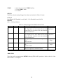
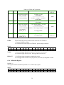
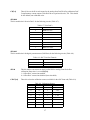
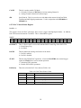
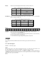
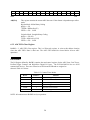
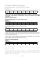
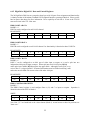
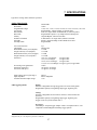
PCI-DAS1602/16
Multifunction Analog
& Digital I/O Board
User’s Manual
Revision 3
August, 2001
© Copyright 2001, Measurement Computing Corporation
LIFETIME WARRANTY
Every hardware product manufactured by Measurement Computing Corp. is warranted against defects in materials or
workmanship for the life of the product, to the original purchaser. Any products found to be defective will be
repaired or replaced promptly.
LIFETIME HARSH ENVIRONMENT WARRANTYTM
Any Measurement Computing Corp. product which is damaged due to misuse may be replaced for only 50% of the
current price. I/O boards face some harsh environments, some harsher than the boards are designed to withstand.
When that happens, just return the board with an order for its replacement at only 50% of the list price. Measurement
Computing Corp. does not need to profit from your misfortune. By the way, we will honor this warranty for any other
manufacture’s board that we have a replacement for!
30 DAY MONEY-BACK GUARANTEE
Any Measurement Computing Corp. product can be returned within 30 days of purchase for a full refund of the price
paid for the product being returned. If you are not satisfied, or chose the wrong product by mistake, you do not have
to keep it. Please call for a RMA number first. No credits or returns accepted without a copy of the original invoice.
Some software products are subject to a repackaging fee.
These warranties are in lieu of all other warranties, expressed or implied, including any implied warranty of
merchantability or fitness for a particular application. The remedies provided herein are the buyer’s sole and
exclusive remedies. Neither Measurement Computing Corp., nor its employees shall be liable for any direct or
indirect, special, incidental or consequential damage arising from the use of its products, even if Measurement
Computing Corp. has been notified in advance of the possibility of such damages.
MEGA-FIFO, the CIO prefix to data acquisition board model numbers, the PCM prefix to data acquisition board
model numbers, PCM-DAS08, PCM-D24C3, PCM-DAC02, PCM-COM422, PCM-COM485, PCM-DMM,
PCM-DAS16D/12, PCM-DAS16S/12, PCM-DAS16D/16, PCM-DAS16S/16, PCI-DAS6402/16, Universal Library,
InstaCal, Harsh Environment Warranty and Measurement Computing Corp. are registered trademarks of
Measurement Computing Corp.
IBM, PC, and PC/AT are trademarks of International Business Machines Corp. Windows is a trademark of
Microsoft Corp. All other trademarks are the property of their respective owners.
Information furnished by Measurement Computing Corp. is believed to be accurate and reliable. However, no
responsibility is assumed by Measurement Computing Corp. neither for its use; nor for any infringements of patents
or other rights of third parties, which may result from its use. No license is granted by implication or otherwise under
any patent or copyrights of Measurement Computing Corp.
All rights reserved. No part of this publication can be reproduced, stored in a retrieval system, or transmitted, in any
form by any means, electronic, mechanical, by photocopying, recording or otherwise without the prior written
permission of Measurement Computing Corp.
Notice
Measurement Computing Corp. does not authorize any Measurement Computing Corp. product for
use in life support systems and/or devices without the written approval of the President of
Measurement Computing Corp. Life support devices/systems are devices or systems which, a) are
intended for surgical implantation into the body, or b) support or sustain life and whose failure to
perform can be reasonably expected to result in injury. Measurement Computing Corp. products
are not designed with the components required, and are not subject to the testing required to
ensure a level of reliability suitable for the treatment and diagnosis of people.
HM PCI-DAS1602_16.lwp
Table of Contents
1 INTRODUCTION . . . . . . . . . . . . . . . . . . . . . . . . . . . . . . . . . . . . . . . . . . . . . . . . . . . . . . . . 1
2 INSTALLATION . . . . . . . . . . . . . . . . . . . . . . . . . . . . . . . . . . . . . . . . . . . . . . . . . . . . . . . .
2.1 SOFTWARE INSTALLATION . . . . . . . . . . . . . . . . . . . . . . . . . . . . . . . . . . . . . . . . . . . .
2.2 HARDWARE INSTALLATION . . . . . . . . . . . . . . . . . . . . . . . . . . . . . . . . . . . . . . . . . . .
2.3 CONNECTING SIGNALS TO THE PCI-DAS1602/16 . . . . . . . . . . . . . . . . . . . . . . . . . .
2.4 ANALOG INPUT CONNECTIONS . . . . . . . . . . . . . . . . . . . . . . . . . . . . . . . . . . . . . . . .
2.4.1 Single-Ended . . . . . . . . . . . . . . . . . . . . . . . . . . . . . . . . . . . . . . . . . . . . . . . . . . . . . . . .
2.4.2 Floating Differential . . . . . . . . . . . . . . . . . . . . . . . . . . . . . . . . . . . . . . . . . . . . . . . . . . .
2.4.3 Differential . . . . . . . . . . . . . . . . . . . . . . . . . . . . . . . . . . . . . . . . . . . . . . . . . . . . . . . . . .
1
1
2
3
3
3
3
4
3 FUNCTIONAL OVERVIEW . . . . . . . . . . . . . . . . . . . . . . . . . . . . . . . . . . . . . . . . . . . . . . . 5
4 SELF-CALIBRATION . . . . . . . . . . . . . . . . . . . . . . . . . . . . . . . . . . . . . . . . . . . . . . . . . . . 6
4.1 ANALOG INPUT CALIBRATION . . . . . . . . . . . . . . . . . . . . . . . . . . . . . . . . . . . . . . . . . 6
4.2 ANALOG OUTPUT CALIBRATION . . . . . . . . . . . . . . . . . . . . . . . . . . . . . . . . . . . . . . . 7
5 PROGRAMMING & APPLICATIONS . . . . . . . . . . . . . . . . . . . . . . . . . . . . . . . . . . . . . . 8
5.1 PROGRAMMING LANGUAGES . . . . . . . . . . . . . . . . . . . . . . . . . . . . . . . . . . . . . . . . . . 8
5.2 PACKAGED APPLICATIONS PROGRAMS . . . . . . . . . . . . . . . . . . . . . . . . . . . . . . . . . 8
6 REGISTER ARCHITECTURE . . . . . . . . . . . . . . . . . . . . . . . . . . . . . . . . . . . . . . . . . . . . . 9
6.1 BADR0 . . . . . . . . . . . . . . . . . . . . . . . . . . . . . . . . . . . . . . . . . . . . . . . . . . . . . . . . . . . . . . . 9
6.2 BARD1 . . . . . . . . . . . . . . . . . . . . . . . . . . . . . . . . . . . . . . . . . . . . . . . . . . . . . . . . . . . . . . . 9
6.2.1 Interrupt / ADC FIFO Register . . . . . . . . . . . . . . . . . . . . . . . . . . . . . . . . . . . . . . . . . . 9
6.2.2 ADC Channel MUX and Control Register . . . . . . . . . . . . . . . . . . . . . . . . . . . . . . . . . 12
6.2.3 Trigger Control/Status Register . . . . . . . . . . . . . . . . . . . . . . . . . . . . . . . . . . . . . . . . . 13
6.2.4 Calibration Register . . . . . . . . . . . . . . . . . . . . . . . . . . . . . . . . . . . . . . . . . . . . . . . . . . 16
6.2.5 DAC Control/Status Register . . . . . . . . . . . . . . . . . . . . . . . . . . . . . . . . . . . . . . . . . . . 18
6.3 BADR2 . . . . . . . . . . . . . . . . . . . . . . . . . . . . . . . . . . . . . . . . . . . . . . . . . . . . . . . . . . . . . . 19
6.3.1 ADC Data Register . . . . . . . . . . . . . . . . . . . . . . . . . . . . . . . . . . . . . . . . . . . . . . . . . . 19
6.3.2 ADC FIFO Clear Register . . . . . . . . . . . . . . . . . . . . . . . . . . . . . . . . . . . . . . . . . . . . . 20
6.4 BADR3 . . . . . . . . . . . . . . . . . . . . . . . . . . . . . . . . . . . . . . . . . . . . . . . . . . . . . . . . . . . . . . 20
6.4.1 ADC Pacer Clock Data and Control Registers . . . . . . . . . . . . . . . . . . . . . . . . . . . . . . 21
6.4.2 High Drive Digital I/O Data and Control Registers . . . . . . . . . . . . . . . . . . . . . . . . . . 22
6.4.3 DAC Pacer Clock Data and Control Registers . . . . . . . . . . . . . . . . . . . . . . . . . . . . . . 23
6.5 BADR4 . . . . . . . . . . . . . . . . . . . . . . . . . . . . . . . . . . . . . . . . . . . . . . . . . . . . . . . . . . . . . . 25
6.5.1 DAC Data Register . . . . . . . . . . . . . . . . . . . . . . . . . . . . . . . . . . . . . . . . . . . . . . . . . . 25
6.5.2 DAC FIFO Clear Register . . . . . . . . . . . . . . . . . . . . . . . . . . . . . . . . . . . . . . . . . . . . . 26
7 SPECIFICATIONS . . . . . . . . . . . . . . . . . . . . . . . . . . . . . . . . . . . . . . . . . . . . . . . . . . . . . . 27
This page is blank.
1 INTRODUCTION
The PCI-DAS1602/16 is a multifunction measurement and control board designed to operate in
computers with PCI bus accessory slots. The architecture of the boards is loosely based on the original
CIO-DAS16; the standard of ISA bus data acquisition. New, denser connectors allow up to 100 signal
lines where once 37 was the standard.
The PCI-DAS1602/16 is easier to install and use than any previous DAS16. There are no switches or
jumpers on the board, so go ahead and install the PCI-DAS1602/16 into your computer then turn your
computer on.
2 INSTALLATION
2.1 SOFTWARE INSTALLATION
The board has no switches and jumpers to set before installing the board in your computer. The simplest
way to configure your board is to use the InstaCalTM program provided on the CD (or floppy disk) .
InstaCal will show you any available options and will create a configuration file that your application
software (and the Universal Library) will refer to so the software you use will automatically have access
to the exact configuration of the board.
Please refer to the Software Installation Manual regarding the installation and operation of InstaCal. The
following hard copy information is provided as a matter of completeness.
1
2.2 HARDWARE INSTALLATION
The PCI-DAS1602/16 employs a 100-pin connector. See Figure 2-1 below for the pinout.
A na log G ro u nd
A na log Inp u t C h 0 H ig h
A na log Inp u t C h 0 L o w / 8 H ig h
A na log Inp u t C h 1 H ig h
A na log Inp u t C h 1 L o w / 9 H ig h
A na log Inp u t C h 2 H ig h
A na log Inp u t C h 2 L o w / 1 0 H igh
A na log Inp u t C h 3 H ig h
A na log Inp u t C h 3 L o w / 11 H ig h
A na log Inp u t C h 4 H ig h
A na log Inp u t C h 4 L o w / 1 2 H igh
A na log Inp u t C h 5 H ig h
A na log Inp u t C h 5 L o w / 1 3 H igh
A na log Inp u t C h 6H ig h
A na log Inp u t C h 6 L o w / 1 4 H igh
A na log Inp u t C h 7 H ig h
A na log Inp u t C h 7 L o w / 1 5 H igh
A n a lo g G ro un d
NC
NC
NC
NC
NC
NC
NC
NC
NC
NC
NC
NC
NC
NC
NC
NC
D /A G N D 0
D /A O U T 0
D /A G N D 1
D /A O U T 1
CLK 4
G AT E 4
OUT 4
A /D E xte rn al P a ce r
A na log Trig ge r In
D /A E xte rn al P a ce r
A /D E xte rn al Trig g er
NC
NC
PC +5V
SSH OUT
P C G rou n d
51
52
53
54
55
56
57
58
59
60
61
62
63
64
65
66
67
68
69
70
71
72
73
74
75
76
77
78
79
80
81
82
83
84
85
86
87
88
89
90
91
92
93
94
95
96
97
98
99
1 00
1
2
3
4
5
6
7
8
9
10
11
12
13
14
15
16
17
18
19
20
21
22
23
24
25
26
27
28
29
30
31
32
33
34
35
36
37
38
39
40
41
42
43
44
45
46
47
48
49
50
D ig ita l A 0
D ig ita l A 1
D ig ita l A 2
D ig ita l A 3
D ig ita l A 4
D ig ita l A 5
D ig ita l A 6
D ig ita l A 7
D ig ita l B 0
D ig ita l B 1
D ig ita l B 2
D ig ita l B 3
D ig ita l B 4
D ig ita l B 5
D ig ita l B 6
D ig ita l B 7
D ig ita l C 0
D ig ita l C 1
D ig ita l C 2
D ig ita l C 3
D ig ita l C 4
D ig ita l C 5
D ig ita l C 6
D ig ita l C 7
NC
NC
NC
NC
NC
NC
NC
NC
NC
NC
NC
NC
NC
NC
P C G ro un d
PC +12V
P C G ro u n d
P C -1 2 V
NC
NC
A /D Inte rn a l P ac er O utp u t
D /A In te rn al P a ce r O u tp ut
E xte rn a l D /A P ac er G ate
NC
E xterna l In te rru p t
P C G ro u n d
P C I-D A S 16 0 2/1 6 C o n ne cto r D iag ra m
Figure 2-1. 100-Pin Connector Pinout
2
2.3 CONNECTING SIGNALS TO THE PCI-DAS1602/16
Use a C100FF-2 cable to connect to the board. The cable has a pair of 50-pin ribbon cable legs joined
together at a 100-pin header connector. You can use two CIO-MINI50 screw terminal boards to
terminate field signals and route them into the PCI-DAS1602/16 with the C100FF-2 cable.
Analog inputs to the PCI-DAS1602/16 can be connected in three different configurations; these are
single-ended, floating-differential, and differential.
WARNING - PLEASE READ
Measure the voltage between ground at the signal source and ground at the PC. If
there is more than 10 volts, do not connect the PCI-DAS1602/16 to this signal source
because you will not be able to make any readings. A voltage more than 30 volts will
likely damage the board or the computer. A voltage this high can also be hazardous
to your health.
2.4 ANALOG INPUT CONNECTIONS
2.4.1 Single-Ended
Single-ended inputs are most appropriate in systems where the signal source and the data acquisition
board share a common ground. This is a very common scenario and includes almost all systems where
the data acquisition system is supplying either the power (+5V and GND) or the excitation (from a D/A).
In this case you can take advantage of the PCI-DAS1602/16’s 16-channel mode without affecting
performance.
Single-ended inputs are also useful the signal source is electrically isolated (also referred to as floating)
from the data acquisition board’s ground (e.g. connecting to the two terminals of a battery). However, the
use of differential input configuration will provide better noise immunity than single-ended when
monitoring an isolated signal source. Unless you absolutely need more than eight channels, we
recommend using the differential input mode for isolated input signals.
Please refer to the next paragraph for connection information for the connection of isolated signals to
differential inputs.
.
2.4.2 Floating Differential
A floating differential input is two wires from the signal source and a 10K ground reference resistor
installed at the PCI-DAS1602/16 input. The two signals from the signal source are Signal High
(CH# High) and Signal Low (CH# Low).
The reference resistor is connected between the PCI-DAS1602/16 CH# Low and Analog Ground pins.
This floating configuration is appropriate when the signal source is floating with respect to ground, (e.g.
a battery or 4-20 mA transmitter), the lead lengths are long, your system is subject to substantial EMI
interference.
3
CAUTION
Is that signal source really floating? Check it with a voltmeter before risking the
PCI-DAS1602/16 and PC! If you can measure a constant voltage between the grounds of
the PC and your signal source, it’s probably not floating.
2.4.3 Differential
Proper measurement of a differential signal requires three wires from the signal source. The signals are
Signal High (CH# High), Signal Low (CH# Low) and Signal Ground (Analog Ground).
A differential connection allows you to connect the PCI-DAS1602/16 to a signal source with a ground
that is different, but not isolated from the PC ground, but less than 10V difference, and still make a true
measurement of the signal between CH# High and CH# Low.
EXAMPLE:
Non-Isolated laboratory instruments with three prong wall plug. There are usually differences in wall
GND potentials between outlets.
4
3
Functional Overview
FUNCTIONAL BLOCK DIAGRAM
The PCI-DAS1602/16 is a multifunction measurement and control board. See Figure 3-1 below for a
self-descriptive functional block diagram of the board.
Figure 3-1. Functional Block Diagram
5
4 SELF-CALIBRATION in the PCI-DAS1602/16
The PCI-DAS1602/16 provides self-calibration of the analog source and measure systems thereby
eliminating the need for external equipment and user adjustments. All adjustments are made via 8-bit
calibration DACs or digital potentiometers referenced to an on-board factory calibrated standard. The
PCI-DAS1602/16 is shipped fully-calibrated from the factory with cal coefficients stored in nvRAM. At
run time, these calibration factors are loaded into system memory and are automatically retrieved each
time a different DAC/ADC range is specified. The user has the option to recalibrate with respect to the
factory-measured voltage standards at any time by simply selecting the "Calibrate" option in InstaCal.
Full calibration typically requires less than two minutes and requires no user intervention.
4.1 ANALOG INPUT CALIBRATION
A variety of methods are used to calibrate the different elements on the board. The analog front-end has
several "knobs" to turn. Offset calibration is performed in both the instrumentation amplifier gain stage
and the ADC itself. Front-end gain adjustment is performed only via the ADC reference. This strategy
was chosen since the gain tolerance of the in-amp circuit is quite good and there is adequate gain tuning
range using only the ADC.
The analog output circuits are calibrated for gain and offset as well. Offset adjustments for the analog
output are made in the output buffer section. The tuning range of this adjustment allows for max DAC
and output buffer offsets. Gain calibration of the analog outputs are performed via DAC reference
adjustments.
Figure 4.1 below is a block diagram of the analog front-end calibration system:
Cal
Ref
Analog-In
ADC
Offset Adj
Offset Adj
Trim Dac
Ref
Uni/Bip
Offset
Digital Offset Pot
Figure 4-1. Analog Input Front-End Calibration System
6
Digital Gain Pot
4.2 ANALOG OUTPUT CALIBRATION
The analog output circuits are calibrated for both gain and offset. Coarse and Fine offset adjustments are
made in the output buffer section. The tuning range of these adjustments allows for maximum DAC and
output buffer offsets. Coarse and Fine gain calibration is performed via adjustments to the DAC
reference.
Note that there are no references associated with the DAC calibration - a fully calibrated ADC set to the
respective DAC range is used as the measurement system. Sub-ranging of the ADC is used to ensure
highly accurate offset adjustments.
The calibration scheme for the Analog Out section is shown in Figure 4-2 below. This circuit is
duplicated for both DAC0 and DAC1.
Analog-Out
16
Analog Out
DAC
Ref
Trim Dac
(Coarse)
Gain Adj
Trim Dac
(Fine)
Offset Adj
Trim Dac
(Coarse)
Trim Dac
(Fine)
Figure 4-2. Analog Output Calibration Scheme
7
5 PROGRAMMING & APPLICATIONS
Although the PCI-DAS1602/16 is part of the larger DAS family, there is no correspondence between
registers. Software written at the register level for the other DAS's will not work with the
PCI-DAS1602/16. This includes any driver or library where the target board is other than a
PCI-DAS1602/16.
5.1 PROGRAMMING LANGUAGES
The Universal Library provides complete access to the PCI-DAS1602/16 functions from a range of
programming languages; both DOS and Windows. If you are planning to write programs, or would like
to run the example programs for Visual Basic or any other language, please consider using the Universal
Library.
5.2 PACKAGED APPLICATIONS PROGRAMS
Many packaged application programs, such as SoftWIRE, DAS Wizard, Labtech Notebook and HP-VEE
have drivers for the PCI-DAS1602/16. If the package you own does not appear to have drivers for the
PCI-DAS1602/16, please fax or e-mail the package name and the revision number from the install disks.
We will research the package for you and advise how to obtain PCI-DAS1602/16 drivers.
Some application drivers are included with the Universal Library package, but not with the Application
package. If you have purchased an application package directly from the software vendor, you may need
to purchase our Universal Library and drivers. Please contact us for more information.
8
6
REGISTER ARCHITECTURE
The PCI-DAS1602/16 operation registers are mapped into the PC I/O address space. Unlike its ISA
counterpart, this board has several base addresses each corresponding to a reserved block of addresses in
I/O space. Of six Base Address Regions (BADR) available in the PCI 2.1 specification, five are
implemented in this design and are summarized in Table 6-1 as follows:
Table 6-1. PCI-DAS1602/16 Register Summary
I/O Region
Function
Operations
BADR0
PCI Controller Operation Registers
32-Bit DWORD
BADR1
General Control/Status Registers
16-Bit WORD
BADR2
ADC Data, FIFO Clear Registers
16-Bit WORD
BADR3
Pacer, Counter/Timer and DIO Registers
BADR4
DAC Data, FIFO Clear Registers
8-Bit BYTE
16-Bit WORD
BADRn will likely be different on different machines. Assigned by the PCI BIOS, these Base Address
values cannot be guaranteed to be the same even on subsequent power-on cycles of the same machine.
All software must interrogate BADR0 at run-time with a READ_CONFIGURATION_DWORD
instruction to determine the BADRn values.
Please see the "AMCC S5933 PCI Controller Data Book, Spring 1996" for more information.
6.1 BADR0
BADR0 is reserved for the AMCC S5933 PCI Controller operations. This region supports 32-bit
DWORD operations
6.2 BADR1
The I/O region defined by BADR1 contains 5 control and status registers for ADC, DAC, interrupt and
Autocal operations. This region supports 16-bit WORD operations.
6.2.1 Interrupt / ADC FIFO Register
BARD1 + 0
Interrupt Control, ADC status. A read/write register.
WRITE
15
-
14
13
12
DAEMCL ADFLCL DAEMIE
11
10
9
8
7
6
5
4
3
2
1
0
-
-
-
-
INTCL
EOACL
DAHFCL
EOAIE
DAHFIE
INTE
INT1
INT0
Write operations to this register allow the user to select interrupt sources, enable interrupts, clear
interrupts as well as ADC FIFO flags. The following is a description of the Interrupt/ADC FIFO
Register:
9
INT[1:0]
General Interrupt Source selection bits.
INT1
INT0
Source
0
0
External
0
1
End of Channel Scan
1
0
AD FIFO Half Full
1
1
AD FIFO Not Empty
INTE
Enables interrupt source selected via the INT[1:0] bits.
1 = Selected interrupt Enabled.
0 = Selected interrupt Disabled
DAHFIE
Enables DAC FIFO Half-Full signal as an interrupt source. Used for high speed DAC
operations.
1= Enable DAC FIFO Half-Full interrupt.
0 = Disable DAC FIFO Half-Full interrupt
EOAIE
Enables End-of-Acquisition interrupt. Used during FIFO'd ADC operations to indicate
that the desired sample size has been gathered.
1 = Enable EOA interrupt.
0 = Disable EOA interrupt
DAHFCL
A write-clear to reset DAC FIFO Half-Full interrupt status.
1 = Clear DAC FIFO Half-Full interrupt.
0 = No effect.
EOACL
A write-clear to reset EOA interrupt status.
1 = Clear EOA interrupt.
0 = No effect.
INTCL
A write-clear to reset INT[1:0] selected interrupt status.
1 = Clear INT[1:0] interrupt
0 = No effect.
DAEMIE
Enables DAC FIFO Empty signal as an interrupt source.
1 = Enables DAC FIFO Empty interrupt.
0 = Disables DAC FIFO Empty interrupt.
ADFLCL
A write-clear to reset latched ADC FIFO Full status.
1 = Clear ADC FIFO Full latch.
0 = No Effect.
DAEMCL
A write-clear to reset DAEM interrupt status.
1= Clear DAEM interrupt.
0 = No effect.
NOTE: It is not necessary to reset any write-clear bits after they are set.
BARD1 + 0 (Cont’d.)
10
Interrupt Control, ADC status. A read/write register.
READ
15
14
13
12
11
10
9
8
7
6
5
4
3
2
1
0
-
DAEMI
LADFUL
ADNE
ADNEI
ADHFI
EOBI
XINTI
INT
EOAI
DAHFI
-
-
-
-
-
Write operations to this register allow you to check status of the selected interrupts and ADC FIFO flags.
The following is a description of Interrupt / ADC FIFO Register Read bits:
DAHFI
Status bit of DAC FIFO Half-Full interrupt
1 = Indicates a DAC FIFO Half-Full interrupt has been latched.
0 = Indicates a DAHF interrupt has not occurred.
EOAI
Status bit of ADC FIFO End-of-Acquisition interrupt.
1 = Indicates an EOA interrupt has been latched.
0 = Indicates an EOA interrupt has not occurred.
INT
Status bit of General interrupt selected via INT[1:0] bits. This bit indicates that any one
of these interrupts has occurred.
1 = Indicates a General interrupt has been latched.
0 = Indicates a General interrupt has not occurred.
XINTI
Status bit of External interrupt. External interrupt requires a rising TTL logic level input.
1 = Indicates an External interrupt has been latched.
0 = Indicates an interrupt has not occurred.
EOBI
Status bit ADC End-of-Burst interrupt. Only valid for ADC Burst Mode enabled.
1 = Indicates an EOB interrupt has been latched.
0 = Indicates an EOB interrupt has not occurred.
ADHFI
Status bit of ADC FIFO Half-Full interrupt. Used during REP INSW operations.
1 = Indicates an ADC Half-Full interrupt has been latched. FIFO has been filled with
more than 255 samples.
0 = Indicates an ADC Half-Full interrupt has not occurred. FIFO has not yet exceeded
1/2 of its total capacity.
ADNEI
Status bit of ADC FIFO Not-Empty interrupt. Used to indicate ADC conversion
complete in single conversion applications.
1 = Indicates an ADC FIFO Not-Empty interrupt has been latched and that one data word
can be read from the FIFO.
0 = Indicates an ADC FIFO Not-Empty interrupt has not occurred. FIFO has been
cleared, read until empty or ADC conversion still in progress.
ADNE
Real-time status bit of ADC FIFO Not-Empty status signal.
1 = Indicates ADC FIFO has at least one word to be read.
0 = Indicates ADC FIFO is empty.
11
LADFUL
Status bit of ADC FIFO FULL status. This bit is latched.
1 = Indicates the ADC FIFO has exceeded full state. Data may have been lost.
0 = Indicates non-overflow condition of ADC FIFO.
DAEMI
Status bit of DAC FIFO Empty interrupt. Used to indicate that a FIFO'd DAC Operation
has completed.
1 = DAC FIFO Empty interrupt condition has occurred.
0 = DAC FIFO Empty interrupt condition has not occurred.
6.2.2 ADC Channel MUX And Control Register
BADR1 + 2
This register sets channel mux HI/LOA limits, ADC gain, offset and pacer source.
It is a Read/Write register.
WRITE
15
14
13
12
11
10
9
8
7
6
5
4
3
2
1
0
-
-
ADPS1
ADPS0
UNIBIP
SEDIFF
GS1
GS0
CHH8
CHH4
CHH2
CHH1
CHL8
CHL4
CHL2
CHL1
CHL8 - CHL1,
CHH8 - CHH1
When these bits are written, the analog input multiplexers are set to the channel specified by CHL8 CHL1. After each conversion, the input multiplexers increment to the next channel, reloading to the
"HL" start channel after the "CHI" stop channel is reached. LOA and HI channels are the decode of the
4-bit binary patterns.
GS[1:0]
These bits determine the ADC range as indicated below:
GS1
GS0
Range
0
0
10V
0
1
5V
1
0
2.5V
1
1
1.25V
SEDIFF
Selects measurement configuration for the Analog Front-End.
1 = Sets Analog front-end to single-ended mode. This mode supports up to 16 channels.
0 = Sets Analog front-end to differential mode. This mode supports up to 8 channels.
UNIBIP
Selects offset configuration for the Analog Front-End.
1 = Analog Front-End Unipolar for selected range
0 = Analog Front-End Bipolar for selected range.
Table 6-2 summarizes all possible Offset/Range configurations:
12
Table 6-2. Offset/Range Configurations
UNIBIP
GS1
GS0
Input Range
Input Gain
Measurement
Resolution
0
0
0
±10V
1
305µV
0
0
1
± 5V
2
153µV
0
1
0
±2.5V
4
76µV
0
1
1
±1.25V
8
38µV
1
0
0
0 to 10V
1
153µV
1
0
1
0 to 5V
2
76µV
1
1
0
0 to 2.5V
4
38µV
1
1
1
0 to 1.25V
8
19µV
ADPS[1:0]
These bits select the ADC Pacer Source. Maximum Internal/External Pacer frequency is
200 kHz (Table 6-3).
Table 6-3. ADC Pacer Source Coding
ADPS1
ADPS0
Pacer Source
0
0
SW Convert
0
1
82C54 Counter/Timer
1
0
External Falling
1
1
External Rising
Note: When ADPS[1:0] = 00, SW conversions are initiated via a word write to BADR2 + 0. Data is 'don't
care.'
READ
15
14
13
12
11
10
9
8
7
6
5
4
3
2
1
0
-
EOC
-
-
-
-
-
-
-
-
-
-
-
-
-
-
EOC
Real-time, non-latched status of ADC End-of-Conversion signal.
1 = ADC DONE
0 = ADC BUSY
6.2.3 Trigger Control/Status Register
BADR1 + 4
This register provides control bits for all ADC trigger modes. It is a Read/Write register.
WRITE
15
14
13
12
11
10
9
8
7
6
5
4
3
2
1
0
-
-
C0SRC
FFM0
ARM
HMODE
CHI_EN
CLO_EN
XTRCL
PRTRG
BURSTE
TGEN
TGSEL
TGPOL
TS1
TS0
13
TS[1:0]
These bits select one-of-three possible ADC Trigger Sources (Table 6-4):
Table 6-4. ADC Trigger Sources
TS1
TS0
Source
0
0
Disabled
0
1
SW Trigger
1
0
External (Digital)
1
1
External (Analog)
Note: TS[1:0] should be set to 0 while setting up Pacer source and count values.
TGPOL
This bit sets the polarity for the external trigger/gate. Internally, the ADC is triggered on
a rising edge or gated on with an active high signal. Use TGPOL to condition external
trigger/gate for proper polarity.
1 = External trigger/gate input inverted.
0 = External trigger/gate input not inverted.
TGSEL
This bit selects whether external ADC control signal is an edge or a level. Use TGPOL
signal to create rising edge or high level input.
1 = Edge-triggered.
0 = Level-triggered.
TGEN
This bit is used to enable External Trigger/Gate function
1 = Selected Trigger Source enabled.
0 = Selected Trigger Source has no effect.
Note that external trigger/gate requires proper setting of the TS[1:0],
TGPOL, TGSEL and TGEN bits.
Example: Application requires use of external falling edge to start acquisition. Set:
TS1 = 1, TS0 = 0 -> External Digital Trigger
TGPOL = 1
-> Invert falling edge
TGSEL = 1
-> Edge Triggered event
TGEN = 1
-> Enable External Trigger.
After TGEN is set, the next falling edge will start a Paced ADC conversion. Subsequent triggers will
have no effect until external trigger flop is cleared (with XTRCL).
BURSTE
Bit enables ADC Burst mode. Start/Stop channels are selected via the CHLx, CHHx bits
in ADC CTRL/STAT register at BADR1 + 2.
1 = Burst Mode enabled
0 = Burst Mode disabled
PRTRG
This bit enables ADC Pre-trigger Mode. This bit works with the ARM and FFM0 bits
when using Pre-trigger mode.
1 = Enable Pre-trigger Mode
0 = Disable Pre-trigger Mode
14
A write-clear to reset the XTRIG flip-flop.
1 = Clear XTRIG status.
0 = No Effect.
XTRCL
CHI_EN
These bits select the Analog Trigger/Gate Mode as described in Table 6-5 below.
CLO_EN
Note that the CHI Threshold is set by DAC1, CLO Threshold is set by DAC0.
HMODE
CHI >= CLO by definition.
Table 6-5. Analog Trigger/Gate Mode Selection Codes
CHI_EN
CLO_EN
HMODE
Analog Trigger/Gate Function
Mode
0
0
0
Signal goes high when ATRIG is more positive than
CHI. Signal goes low when ATRIG becomes more
negative than CLO. Hysteresis level is the difference
between CHI and CLO.
Negative
Hysteresis
0
0
1
Signal goes high when ATRIG is more negative than
CLO. Signal goes low when ATRIG becomes more
positive than CHI. Hysteresis level is the difference
between CHI and CLO.
Positive
Hysteresis
0
1
X
Signal goes high when ATRIG more negative than
CLO.
CHI has no effect.
Negative
Slope
1
0
X
Signal goes high when ATRIG is more positive than
CHI.
CLO has no effect.
Positive
Slope
1
1
X
Signal goes high when within region defined by
CHI-CLO. Signal is low outside this region.
Window
ARM, FFM0
These bits work in conjunction the PRTRG bit during FIFO'd ADC operations. Refer to table 6-6. Note
that one FIFO = 512 samples.
15
Table 6-6. FIFO'd ADC Operations
PRTRG
FFM0
ARM is set...
FIFO Mode
0
0
Via SW when remaining
count < one FIFO
-----------------------Via SW immediately
# Samples >1 FIFO
Normal Mode
---------------------------------1/2 FIFO < # Samples < one FIFO
Normal Mode
0
1
1
0
1
1
C0SRC
Via SW immediately
Sample CTR
Starts on...
ADHF
ADC Pacer
# Samples <1/2 FIFO
Normal Mode
Via SW when remaining
# Post-Trigger Samples > one FIFO
count < one FIFO
Pre-Trigger Mode
--------------------------------------------------------Via SW after XTRIG has 1/2 FIFO < # Post-Trigger Samples < one FIFO
been detected
(INDX_GT=1)
Pre-Trigger Mode
Via SW after XTRIG has
been detected
(INDX_GT=1)
# Post-Trigger Samples < 1/2 FIFO
Pre-Trigger Mode
ADHF
Via SW after
INDX_GT=1
This bit allows the user to select the clock source for user Counter 0.
1 = Internal 10 MHz oscillator
0 = External clock source input via CTR0CLK pin on 100-pin connector.
READ
15
14
13
12
11
10
9
8
7
6
5
4
3
2
1
0
-
-
-
INDX-GT
-
-
-
-
XTRIG
-
-
-
-
-
-
-
XTRIG
1 = External Trigger flip-flop has been set. This bit is write-cleared.
0 = External Trigger flip-flop reset. No trigger has been received.
INDX-GT
1 = PreTrigger index counter has completed its count
0 = PreTrigger index counter is not yet gated on, or has not yet completed its count.
6.2.4 Calibration Register
BADR1 + 6
This register controls all autocal operations. It is a Write-only register.
WRITE
15
14
13
12
11
10
9
8
7
6
5
4
3
2
1
0
SDI
CALEN
CSRC2
CSRC1
CSRC0
SEL08
SEL8402
SEL8800
CD7
CD6
CD5
CD4
CD3
CD2
CD1
CD0
16
CD[7:0]
These 8 bits are the D/A code inputs for the analog-front DAC08 offset calibration DAC.
Complimentary current outputs of the DAC08 are equal at mid-scale, 7Fh. This should
be the default, non-calibrated value.
SEL8800
This bit enables the 8-bit trim DACs for the following circuits (Table 6-7):
Table 6-7. Trim DACs
DAC Channel
Cal Function
0
DAC0 Fine Gain
1
DAC0 Coarse Gain
2
DAC0 Offset
3
DAC1 Offset
4
DAC1 Fine Gain
5
DAC1 Coarse Gain
6
DAC0 Fine Offset
7
DAC1 Fine Offset
SEL8402
This bit enables the 8-bit digital potentiometers (50 KOhm) for the following circuits (Table 6-8).
Table 6-8. ADC Trim Pot Channels
Trimmer Channel
Cal Function
0
ADC Gain Cal
1
ADC Offset Cal
SEL08
This bit enables conversions on the 8-bit DAC08 for Analog Front-End offset
calibration. Data value is set via CD[7:0].
1 = Offset DAC conversions enabled.
0 = Offset DAC conversions disabled (last value held).
CSRC[2:0]
These bits select the calibration sources available for the ADC front end (Table 6-9).
Table 6-9. Calibration Sources
CSRC2
CSRC1
CSRC0
Cal Source
0
0
0
AGND
0
0
1
7.0V
0
1
0
3.5V
0
1
1
1.75V
1
0
0
0.875V
1
0
1
-10.0V
1
1
0
VDAC0
1
1
1
VDAC1
17
CALEN
This bit is used to enable Cal Mode.
1 = Selected Cal Source, CSRC[2:0], is fed into Analog Channel 0.
0 = Analog Channel 0 functions as normal input.
SDI
Serial Data In. This bit is used to set serial address/data stream for the DAC8800
TrimDac and 8402 digital potentiometer. Used in conjunction with SEL8800 and
SEL8402 bits.
6.2.5 DAC Control/Status Register
BADR1 + 8
This register selects the DAC gain/range, Pacer source, trigger and High-Speed Modes. In addition,
DAC FIFO status information is available. This is a Read/Write register.
WRITE
15
14
13
12
11
10
9
8
7
6
5
4
3
2
1
0
-
-
-
-
DAC1R1
DAC1R0
DAC0R1
DAC0R0
-
HS1
HS0
DAPS1
DAPS0
START
DACEN
LDAEMCL
LDAEMCL
This is a Write-clear bit to reset the latched EMPTY status flag of the DAC FIFO.
1 = Reset Empty Flag
0 = No Effect.
DACEN
This bit enables the Analog Out features of the board.
1 = DAC0/1 enabled.
0 = DAC0/1 disabled.
START
This bit starts FIFO'd DAC operations. If used with DAXTRG, the external trigger
signal, the START bit is used to arm the operation.
1 = Start/Arm FIFO operations.
0 = Disable FIFO'd DAC operations.
DAPS[1:0]
These bits select the DAC Pacer Source (Table 6-10):
Table 6-10. DAC Pacer Source Codes
DAPS1
DAPS0
Pacer Source
0
0
SW Convert
0
1
Internal 82C54 Programmed via BADR3 + 9, + A
1
0
External Falling Edge
1
1
External Rising Edge
18
These bits select the High-Speed DAC Modes as follows (Table 6-11):
HS[1:0]
Table 6-11. High-Speed DAC Modes Select Codes
DACnR[1:0]
HS1
HS0
DAC Mode
0
0
Disabled
0
1
DAC0
1
0
DAC1
1
1
Simultaneous DAC0/1
These bits select the independent gains/ranges for either DAC0 or DAC1. n=0 for DAC0
and n=1 for DAC1 (Table 6-12).
Table 6-12. Gains/Ranges for DAC0 or DAC1
DACnR1
DACnR0
Range
LSB Size
0
0
Bipolar 5V
153uV
0
1
Bipolar 10V
305uV
1
0
Unipolar 5V
76uV
1
1
Unipolar 10V
153uV
READ
15
14
13
12
11
10
9
8
7
6
5
4
3
2
1
0
-
-
-
-
-
-
-
-
-
-
-
-
-
-
-
LDAEM
LDAEM
This is the latched version of the DAC FIFO_EMPTY signal. This bit must be
write-write cleared with the DAEMCL bit.
1 = DAC FIFO was emptied at some point during FIFO'd operations. Incorrect data may
have been clocked into the selected DAC(s).
0 = DAC FIFO did not empty during FIFO'd operations. Status OK.
6.3 BADR2
The I/O Region defined by BADR2 contains the ADC Data register and the ADC FIFO clear
register.
6.3.1 ADC Data Register
BADR2 + 0 ADC Data register.
WRITE
Writing to this register is only valid for SW initiated conversions. The ADC Pacer source must be set to
00 via the ADPS[1:0] bits. A null write to BADR2 + 0 with begin a single conversion.
Conversion status can be determined in two ways. The EOC bit in BADR1 + 0 can be polled until true
or ADNEI (the AD FIFO not-empty interrupt) can be used to signal that the ADC conversion is complete
and the data word is present in the FIFO.
READ
19
15
14
13
12
11
10
9
8
7
6
5
4
3
2
1
0
AD15
AD14
AD13
AD12
AD11
AD10
AD9
AD8
AD7
AD6
AD5
AD4
AD3
AD2
AD1
AD0
MSB
AD[15:0]
LSB
This register contains the current ADC data word. Data format is dependent upon offset
mode:
Bipolar Mode: Offset Binary Coding
0000 h = −FS
7FFFh = Mid-scale (0V)
FFFFh = +FS − 1 LSB
Unipolar Mode: Straight Binary Coding
0000 h = −FS (0V)
7FFFh = Mid-scale (+FS/2)
FFFFh = +FS − 1 LSB
6.3.2 ADC FIFO Clear Register
BADR2 + 2 ADC FIFO Clear register. This is a Write-only register. A write to this address location
clears the ADC FIFO. Data is don't care. The ADC FIFO should be cleared before all new ADC
operations.
6.4 BADR3
The I/O Region defined by BADR3 contains data and control registers for the ADC Pacer, DAC Pacer,
Pre/Post-Trigger Counters and High-Drive Digital I/O bytes. The PCI-DAS1602/16 has two 8254
counter/timer devices. These are referred to as 8254A and 8254B and are assigned as
shown in Table 6-13 below:
Table 6-13. Counter/Timer Modes
Device
Counter #
Function
8254A
0
ADC Post-Trigger Sample Counter
8254A
1
ADC Pacer Lower Divider
8254A
2
ADC Pacer Upper Divider
8254B
0
ADC Pre-Trigger Index/User Counter
8254B
1
DAC Pacer Lower Divider
8254B
2
DAC Pacer Upper Divider
NOTE: All reads/writes to BADR3 are byte operations.
20
6.4.1 ADC Pacer Clock Data And Control Registers
8254A COUNTER 0 DATA - ADC RESIDUAL SAMPLE COUNTER
BADR3 + 0
READ/WRITE
7
6
5
4
2
3
1
0
D7
D6
D5
D4
D3
D2
D1
D0
Counter 0 is used to stop the acquisition when the desired number of samples have been gathered. It is
gated on when a 'residual' number of conversions remain. Counter 0 will be enabled by use of the ARM
bit (BADR1 + 4).
Counter 0 is to operated in Mode 0.
8254A COUNTER 1 DATA - ADC PACER DIVIDER LOWER
BADR3 + 1
READ/WRITE
7
6
5
4
2
3
1
0
D7
D6
D5
D4
D3
D2
D1
D0
8254A COUNTER 2 DATA - ADC PACER DIVIDER UPPER
BASE + 2
READ/WRITE
7
6
5
4
2
3
1
0
D7
D6
D5
D4
D3
D2
D1
D0
Counter 1 provides the lower 16 bits of the 32-bit pacer clock divider. Its output is fed to the clock input
of Counter 2 which provides the upper 16 bits of the pacer clock divider. The clock input to Counter 1 is
a precision 10 MHz oscillator source.
Counter 2 output is called the 'Internal Pacer' and can be selected by software to be the ADC Pacer
source. Configure Counters 1 & 2 to operate in 82C54 Mode 2.
ADC 82C54 CONTROL REGISTER
BADR3 + 3
WRITE ONLY
7
6
5
4
2
3
1
0
D7
D6
D5
D4
D3
D2
D1
D0
The control register is used to set the operating modes of 82C54 Counters 0, 1, and 2. A counter is
configured by writing the correct mode information to the control register followed by a count written to
the specific counter register.
The counters on the 82C54 are 16-bit devices. Since the interface to the 82C54 is only eight bits wide,
count data is written to the Counter Register as two successive bytes. First the low byte is written, then
the high byte. The Control Register is eight bits wide. Further information can be obtained on the 82C54
data sheet, available from Intel or Harris.
21
6.4.2 High-Drive Digital I/O Data and Control Registers
The 24 High-Drive DIO lines are grouped as three byte-wide I/O ports. Port assignment and functionality
is identical to that of the industry standard 8255 Peripheral Interface operating in Mode 0. Please see the
Intel or Harris data sheets for more information. Drive capability of each line is 15 mA in the TTL HI
state and 24 mA in the TTL LOA state.
HDIO PORT A DATA
BADR3 + 4
PORT A can be configured as an 8-bit I/O channel.
READ/WRITE
7
6
5
4
2
3
1
0
D7
D6
D5
D4
D3
D2
D1
D0
HDIO PORT B DATA
BADR3 + 5
PORT B can be configured as an 8-bit I/O channel. Its functionality is identical to that of PORT A.
READ/WRITE
7
6
5
4
2
3
1
0
D7
D6
D5
D4
D3
D2
D1
D0
HDIO PORT C DATA
BADR3 + 6
PORT C can be configured as an 8-bit port of either input or output, or it can be split into two
independent 4-bit ports of input or output. When split into two 4-bit I/O ports, D[3:0]
make up the lower nibble, D[7:4] comprise the upper nibble. Although it can be split, every
write to Port C is a byte operation. Unwanted information must be ANDed out during reads
and writes must be ORd with current value of the other 4-bit port.
READ/WRITE
7
6
5
4
2
3
1
0
D7
D6
D5
D4
D3
D2
D1
D0
HDIO CONTROL REGISTER
BADR3 + 7
The HDIO Control register is used configure Ports A, B, and C as inputs or outputs. Operation is
identical to that of the 8255 in Mode 0.
WRITE
7
6
5
4
2
3
1
0
1
0
0
D4
D3
0
D1
D0
Note: Bits 3,5-7 are hardwired to the values shown (Mode 0). Actual writes to these bit positions are
"don't care."
22
The following table contains codes for the possible I/O Port configurations for the HDIO:
Table 6-14. I/O Port Configuration Coding
D4
D3
D1
D0
PORT A
PORT C
UPPER
PORT B
PORT C
LOWER
HEX
DECIMAL
0
0
0
0
OUT
OUT
OUT
OUT
0
0
0
0
0
1
OUT
OUT
OUT
IN
1
1
0
0
1
0
OUT
OUT
IN
OUT
2
2
0
0
1
1
OUT
OUT
IN
IN
3
3
0
1
0
0
OUT
IN
OUT
OUT
8
8
0
1
0
1
OUT
IN
OUT
IN
9
9
0
1
1
0
OUT
IN
IN
OUT
A
10
0
1
1
1
OUT
IN
IN
IN
B
11
1
0
0
0
IN
OUT
OUT
OUT
10
16
1
0
0
1
IN
OUT
OUT
IN
11
17
1
0
1
0
IN
OUT
IN
OUT
12
18
1
0
1
1
IN
OUT
IN
IN
13
19
1
1
0
0
IN
IN
OUT
OUT
18
24
1
1
0
1
IN
IN
OUT
IN
19
25
1
1
1
0
IN
IN
IN
OUT
1A
26
1
1
1
1
IN
IN
IN
IN
1B
27
6.4.3 DAC Pacer Clock Data and Control Registers
8254B COUNTER 0 DATA - ADC PRE-TRIGGER INDEX COUNTER
BADR3 + 8
READ/WRITE
7
6
5
4
2
3
1
0
D7
D6
D5
D4
D3
D2
D1
D0
Counter 0 of the DAC 8254 device is actually used as the ADC Pre-Trigger index counter. This counter
serves to mark the boundary between pre- and post-trigger samples when the ADC is operating in
Pre-Trigger Mode. The External ADC Trigger flip-flop gates Counter 0 ON; the ADC FIFO Half-Full
signal gates it OFF.
Knowing the desired number of post-trigger samples, software can then calculate how many 1/2 FIFO
data packets need to be collected and what corresponding residual sample count needs to be written to
BADR3 + 0.
23
8254B COUNTER 1 DATA - DAC PACER DIVIDER LOWER
BADR3 + 9
READ/WRITE
7
6
5
4
2
3
1
0
D7
D6
D5
D4
D3
D2
D1
D0
8254B COUNTER 2 DATA - DAC PACER DIVIDER UPPER
BADR3 + Ah
READ/WRITE
7
6
5
4
2
3
1
0
D7
D6
D5
D4
D3
D2
D1
D0
Counter 1 provides the lower 16 bits of the 32-bit pacer clock divider. Its output is fed to the clock input
of Counter 2 which provides the upper 16-bits of the pacer clock divider. The clock input to Counter 1 is
a precision 10 MHz oscillator source.
Counter 2's output is called the 'Internal Pacer' and can be selected by software to the be the ADC Pacer
source. Counters 1 and 2 should be configured to operate in 8254 Mode 2.
8254B CONTROL REGISTER
BADR3 + Bh
WRITE ONLY
7
6
5
4
2
3
1
0
D7
D6
D5
D4
D3
D2
D1
D0
The control register is used to set the operating Modes of 8254 Counters 0,1 & 2. A counter is configured
by writing the correct Mode information to the Control Register, then the proper count data must be
written to the specific Counter Register.
The Counters on the 8254 are 16-bit devices. Since the interface to the 8254 is only 8-bits wide, Count
data is written to the Counter Register as two successive bytes. First the low byte is written, then the high
byte. The Control Register is 8-bits wide. Further information can be obtained on the 82C54 data sheet,
available from Intel or Harris.
24
6.5 BADR4
The BADR4 contains the shared DAC data register and the DAC FIFO clear register.
6.5.1 DAC Data Register
BADR4 + 0
DAC Data register. A Write-only register.
WRITE
15
14
13
12
11
10
9
8
7
6
5
4
3
2
1
0
DA15
DA14
DA13
DA12
DA11
DA10
DA9
DA8
DA7
DA6
DA5
DA4
DA3
DA2
DA1
DA0
MSB
DA[15:0]
LSB
These bits represent the DAC data word. Format is dependent upon offset mode as
described below:
Bipolar Mode: Offset Binary Coding
0000 h = −FS
7FFFh = Mid-scale (0V)
FFFFh = +FS −1LSB
Unipolar Mode: Straight Binary Coding
0000 h = −FS (0V)
7FFFh = Mid-scale (+FS/2)
FFFFh = +FS −1LSB
Paced DAC operations require that the FIFO be loaded with the appropriate data. A REP OUTSW
instruction to this address will do this. It is important to note that the FIFO is the shared data source
between DAC0 and DAC1. Care must be taken to ensure that DAC0 data always precedes DAC1 data
during simultaneous operations. Target DAC selection is made via the HS[1:0] bits described earlier in
section 6.2.5, DAC Control/Status Register, BADR1 + 8.
25
Table 6-15. Target DAC Selection Codes
HS1
HS0
SELECTED DAC(S)
LOCATION #
FIFO DATA
0
0
None
N/A
N/A
0
1
DAC0
0
1
2
3
|
DAC0
DAC0
DAC0
DAC0
|
1
0
DAC1
0
1
2
3
|
DAC1
DAC1
DAC1
DAC1
|
1
1
DAC0 & DAC1
0
1
2
3
|
DAC0
DAC1
DAC0
DAC1
|
NOTE: FIFO location #0 is the first value written to the Cleared DAC FIFO.
6.5.2 DAC FIFO Clear Register
BADR4 + 2
DAC FIFO Clear register. A Write-only register. A write to this address location clears the DAC FIFO.
Data is don't care. The DAC FIFO should be cleared before all new DAC operations.
26
7 SPECIFICATIONS
Typical for 25 DegC unless otherwise specified.
Analog Input Section
A/D converter type
Resolution
Programmable ranges
A/D pacing
Data transfer
Bust mode
Polarity
Number of channels
Interrupts
Interrupt enable
AD976ABN
16 bits
±10V, ±5V, ±2.5V, ±1.25V, 0 to 10V, 0 to 5V, 0 to 2.5V, 0 to 1.25V
Programmable: internal counter or external source
From 512 sample FIFO via REPINSW, int, software-polled
Programmable option at 5 µs sample intervals during burst
Unipolar/Bipolar, software-selectable
8 differential or 16 single-ended, software-selectable
INTA# - mapped to IRQn via PCI BIOS at boot-time
Programmable
A/D conversion time
Throughput
Differential Linearity error (Bipolar)
Integral Linearity error (Bipolar)1
Differential Linearity error (Unipolar)
Integral Linearity error (Unipolar)2
Gain Error
No missing codes guaranteed
Gain drift (A/D specs)
Zero drift (A/D specs)
5 µs
200 kHz min
±1 LSB
±1.5 LSB
±1 LSB
±1.5 LSB
±10V, 0 to 10V Ranges:
22.5 ppm
±5V, 0 to 5V Ranges:
22.5 ppm
±2.5V, 0 to 2.5V Ranges: 22.5 ppm
±1.25,V 0 to 1.25V Ranges: 22.5 ppm
16 bits
±20 ppm/°C, all ranges
±10 ppm/°C, all ranges
Input leakage current (@25 Deg C)
Input impedance
Absolute maximum input voltage
200 nA
Min 10 MegOhms
±15V
A/D Triggering Modes
Max
Max
Max
typical, 45 ppm Max
Digital:
Software-configurable for Edge (triggered) or level-activated (gated).
Programmable polarity (rising/falling edge trigger, high/low gate).
Analog:
Software-configurable for above/below reference, in/out window and
hysteresis.
Programmable polarity (rising/falling edge trigger, high/low gate).
Trigger levels set by DAC0 and/or DAC1.
Pre-trigger:
Unlimited pre- and post-trigger samples. Total # of samples must be >256.
Compatible with both Digital and Analog trigger options.
1
Integral linearity for 1.25V bipolar is specified at ±3LSB max
Integral linearity for 1.25V unipolar is specified at ±3LSB max
2
27
Analog Outputs:
Resolution
Number of channels
D/A type
Voltage Ranges
Offset error
Gain error
Differential nonlinearity
Integral nonlinearity
Monotonicity
D/A Gain drift
D/A Bipolar offset drift
D/A Unipolar offset drift
Output Coupling
Amp Output Impedance
16 bits
2
AD669BR
±10V, ±5V, 0 to 5V, 0 to 10V. Independently-selectable between
channels.
±100uV max, all ranges (calibrated)
±30.5 ppm max (calibrated)
±1 LSB max
±1 LSB max
16 bits at 25 DegC
±15 ppm/°C max
±5 ppm/°C max
±3 ppm/°C max
DC
0.1 Ohms max
Data transfer
From 512 sample FIFO via REPOUTSW or programmed I/O.
Data interleaved for dual analog output mode.
Throughput
100 kHz, 2 channels simultaneous.
Settling time (20V step to .0008%) 13 µs max
Settling time (10V step to .0008%) 6 µs typ
Slew Rate
10V Ranges: 6V/µs
5V Ranges: 3V/µs
D/A trigger modes
Current Drive
Output short-circuit duration
software or external gate.
±5 mA min
25 mA indefinite
Miscellaneous
Double buffered input latches
Update DACs individually or simultaneously (software-selectable)
Power up and reset, all DAC's cleared to 0 volts
Digital Input / Output
Digital Type
Output:
Input:
Configuration
Number of channels
Output High
Output Low
Input High
Input Low
Power-up / reset state
Interrupts
Interrupt enable
Interrupt sources
82C55 emulation
74LS244
74LS373
2 banks of 8, 2 banks of 4, programmable by bank as input or
output
24 I/O
2.4 volts @ −15mA min
0.5 volts @ 64 mA min
2.0 volts min, 7 volts absolute max
0.8 volts max, −0.5 volts absolute min
Input mode (high impedance)
INTA# - mapped to IRQn via PCI BIOS at boot-time
Programmable
External (rising TTL edge event), Residual counter, A/D
End-of-conversion, A/D End-of-channel-scan, A/D
FIFO-not-empty, A/D FIFO-half-full, D/A FIFO-not-empty, D/A
FIFO-half-full
28
Counter Section
Counter type
Configuration
82C54
Two 82C54 devices. three down-counters per 82C54, 16 bits each
82C54A: (Counters #1, 2, & 3)
Counter 0 - ADC residual sample counter.
Source: ADC Clock.
Gate:
Programmable source.
Output: End-of-Acquisition interrupt.
Counter 1 - ADC Pacer Lower Divider
Source: 10 MHz oscillator
Gate:
Tied to Counter 2 gate, programmable source.
Output: Chained to Counter 2 Clock.
Counter 2 - ADC Pacer Upper Divider
Source: Counter 1 Output.
Gate:
Tied to Counter 1 gate, programmable source.
Output: ADC Pacer clock (if software selected), available at user
connector.
82C54B: (Counters #4, 5 &6)
Counter 0 - Pretrigger Mode
Source: ADC Clock.
Gate:
External trigger
Output: End-of-Acquisition interrupt.
Counter 0 - Non-Pretrigger Mode: User counter 4
Source: User input at 100-pin connector or internal 10 MHz
(software selectable)
Gate:
User input at 100-pin connector.
Output: Available at 100-pin connector.
Counter 1 - DAC Pacer Lower Divider
Source: 10 MHz oscillator
Gate:
Tied to Counter 2 gate, programmable source.
Output: Chained to Counter 2 Clock.
Counter 2 - DAC Pacer Upper Divider
Source: Counter 1 Output.
Gate:
Tied to Counter 1 gate, programmable source.
Output: DAC Pacer clock, available at user connector.
Clock input frequency
High pulse width (clock input)
Gate width high
Input low voltage
Input high voltage
Output low voltage
Output high voltage
10 MHz max
30 ns min High, 50 ns min Low
50 ns min (high or low)
0.8V max
2.0V min
0.4V max
3.0V min
Environmental
Operating temperature range
Storage temperature range
Humidity
0 to 70°C
−40 to 100°C
0 to 90% non-condensing
Power Consumption
Icc: Operating (A/D converting to FIFO)
2.0A typical, 2.1A max
29
For Your Notes.
30
EC Declaration of Conformity
We, Measurement Computing Corp., declare under sole responsibility that the product:
PCI-DAS1602/16
Part Number
High speed analog I/O board for the PCI bus
Description
to which this declaration relates, meets the essential requirements, is in conformity with, and CE marking has been
applied according to the relevant EC Directives listed below using the relevant section of the following EC standards
and other normative documents:
EU EMC Directive 89/336/EEC: Essential requirements relating to electromagnetic compatibility.
EU 55022 Class B: Limits and methods of measurements of radio interference characteristics of information
technology equipment.
EN 50082-1: EC generic immunity requirements.
IEC 801-2: Electrostatic discharge requirements for industrial process measurement and control equipment.
IEC 801-3:
equipment.
Radiated electromagnetic field requirements for industrial process measurements and control
IEC 801-4: Electrically fast transients for industrial process measurement and control equipment.
Carl Haapaoja, Director of Quality Assurance
Measurement Computing Corporation
16 Commerce Boulevard,
Middleboro, Massachusetts 02346
(508) 946-5100
Fax: (508) 946-9500
E-mail: [email protected]
www. measurementcomputing.com