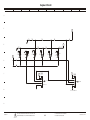
1
zenith
SERVICE MANUAL
Product Type:
Chassis:
Manual Part #:
Model Line:
Product Year:
Model Series:
Presentation Series
DIGITAL FCS
3828VD0171G
H
2006
H27H49S
H32H49S
CONTENTS
General Information/Remote Controls................................ 1
Installer’s Menu ............................................................ 2
Servicing/Trobleshooting ................................................ 3
Model/Module Parts List ................................................. 4
Exploded Views ............................................................. 5
Schematics ................................................................... 6
Published by
Technical Publications
Zenith Electronics Corporation
P. O. Box 240007
Huntsville, Al 35824
Copyright © May 2006 by Zenith Electronics Corporation
Printed in U. S. A.
PRODUCT SAFETY SERVICING GUIDELINES FOR AUDIO-VIDEO PRODUCTS
IMPORTANT SAFETY NOTICE
A.C. Voltmeter
This Manual was prepared for use only by properly trained audio-visual service technicians.
When servicing this product, under no circumstances should the original design be modified
or altered without permission from Zenith Electronics Corporation. All components should be
replaced only with types identical to those in
the original circuit and their physical location, wiring and lead dress must conform to
original layout upon completion of repairs.
Special components are also used to prevent xradiation, shock and fire hazard. These components are indicated by the letter “x” included
in their component designators and are required
to maintain safe performance. Zenith Electronics Corporation allows no deviations without
prior approval. Circuit diagrams may occasionally differ from the actual circuit used. This
way, implementation of the latest safety and
performance improvement changes into the set is
not delayed until the new service literature is
printed.
CAUTION: Do not attempt to modify this product
in any way. Never perform customized installations without manufacturer’s approval. Unauthorized modifications will not only void the warranty, but may lead to property damage or user
injury.
Service work should be performed only
after you are thoroughly familiar with these
safety checks and servicing guidelines.
Graphic symbols
The exclamation point within an equilateral triangle is intended to alert the
service personnel to important safety
information in the service literature.
The lightning flash with arrowhead symbol within an equilateral triangle is
intended to alert the service personnel
to the presence of non-insulated “dangerous voltage” that may be of sufficient magnitude to constitute a risk of
electric shock.
The pictorial representation of a fuse
and its rating within an equilateral triangle is intended to convey to the service personnel the following fuse replacement caution notice:
CAUTION: FOR CONTINUED PROTECTION AGAINST
RISK OF FIRE, REPLACE ALL FUSES WITH THE
SAME TYPE AND RATING AS MARKED NEAR EACH
FUSE.
0.15uF
Good Earth Ground
such as the Water
Pipe, Conduit, etc.
Place this probe
on each exposed
metal part.
10 WATT
X-RADIATION
1. Be sure procedures and instructions to all
service personnel cover the subject of x-radiation. The only potential source of x-rays
in current TV receivers is the picture tube.
However, this tube does not emit x-rays when
the HV is at the factory-specified level. The
proper value is given in the applicable schematic. Operation at higher voltages may cause
a failure of the picture tube or high-voltage
supply and, under certain circumstances may
produce radiation in excess of desirable levels.
2. Only factory-specified CRT anode connectors
must be used.
3. It is essential that the service personnel
have available an accurate and reliable highvoltage meter.
4. When the high-voltage circuitry is operating
properly, there is no possibility of an xradiation problem. Every time a color chassis
is serviced, the brightness should be run up
and down while monitoring the high voltage
with a meter, to be certain that the high
voltage does not exceed the specified value
and that it is regulating correctly.
5. When troubleshooting and making test measurements in a product with a problem of excessively high voltage, avoid being unnecessarily close to the picture tube and the high
voltage power supply. Do not operate the product longer than necessary to locate the cause
of excessive voltage.
6. Refer to HV, B+, and shutdown adjustment
procedures described in the appropriate schematics and diagrams (where used).
SERVICE INFORMATION
While servicing, use an isolation transformer
for protection from AC line shock. After the
original service problem has been corrected,
make a check of the following:
IMPLOSION
1. All direct view picture tubes are equipped
with an integral implosion protection system;
take care to avoid damage during installation.
2. Use only the recommended factory replacement
tubes.
FIRE AND SHOCK HAZARD
1. Be sure that all components are positioned to
avoid a possibility of adjacent component shorts.
This is especially important on items transported to and from the repair shop.
2. Verify that all protective devices such as
insulators, barriers, covers, shields, strain
reliefs, power supply cords, and other hardware
have been reinstalled per the original design.
Be sure that the safety purpose of the polarized
line plug has not been defeated.
3. Soldering must be inspected to discover possible cold solder joints, solder splashes, or
sharp solder points. Be certain to remove all
loose foreign particles.
4. Check for physical evidence of damage or
deterioration to parts and components, for frayed
leads or damaged insulation (including the AC
cord), and replace if necessary.
5. No lead or component should touch a receiving
tube or a resistor rated at 1 watt or more. Lead
tension around protruding metal surfaces must
be avoided.
6. After re-assembly of the set, always perform
an AC leakage test on all exposed metallic parts
of the cabinet (the channel selector knobs, antenna terminals, handle and screws) to be sure
that set is safe to operate without danger of
electrical shock. DO NOT USE A LINE ISOLATION
TRANSFORMER DURING THIS TEST. Use an AC voltmeter having 5000 ohms per volt or more sensitivity in the following manner: Connect a 1500 ohm,
10 watt resistor, paralleled by .15 mfd 150V AC
type capacitor between a known good earth ground
(water pipe, conduit, etc.) and the exposed metallic parts, one at a time. Measure the AC
voltage across the combination of 1500 ohm resistor and .15mfd capacitor. Reverse the AC plug
by using a non-polarized adaptor and repeat AC
voltage measurements for each exposed metallic
part. Voltage measured must not exceed 0.75 volts
RMS. This corresponds to 0.5 milliamp AC. Any
value exceeding this limit constitutes a potential shock hazard and must be corrected immediately.
3828VD0171G
1500 OHM
TIPS ON PROPER INSTALLATION
1. Never install any receiver in a closed-in
recess, cubbyhole, or closely fitting shelf
space over, or close to, a heat duct, or in the
path of heated air flow.
2. Avoid conditions of high humidity such as:
outdoor patio installations where dew is a
factor, near steam radiators where steam leakage is a factor, etc.
3. Avoid placement where draperies may obstruct
venting. The customer should also avoid the
use of decorative scarves or other coverings
that might obstruct ventilation.
4. Wall- and shelf-mounted installations using
a commercial mounting kit must follow the factory-approved mounting instructions. A product mounted to a shelf or platform must retain
its original feet (or the equivalent thickness
in spacers) to provide adequate airflow across
the bottom. Bolts or screws used for fasteners
must not touch any parts or wiring. Perform
leakage tests on customized installations.
5. Caution customers against mounting a product
on a sloping shelf or in a tilted position,
unless the receiver is properly secured.
6. A product on a roll-about cart should be
stable in its mounting to the cart. Caution
the customer on the hazards of trying to roll
a cart with small casters across thresholds or
deep pile carpets.
7. Caution customers against using a cart or
stand that has not been listed by Underwriters
Laboratories, Inc. for use with its specific
model of television receiver or generically
approved for use with TVs of the same or larger
screen size.
8. Caution customers against using extension
cords. Explain that a forest of extensions,
sprouting from a single outlet, can lead to
disastrous consequences to home and family.
i
DIGITAL FCS - SAFETY
PRODUCT SAFETY SERVICING GUIDELINES FOR AUDIO-VIDEO PRODUCTS
X-RADIATION
flection. If the shutdown condition disappears,
the TV set can be turned-on only if the AC is
interrupted for about 20 Seconds and then the
on/off switch is activated.
To prevent possible exposure to X-Radiation caused
by excessive CPT anode voltage, The Digital FCS
chassis incorporate a ¨High Voltage Shutdown¨
circuit. This circuit senses the level of a
Shutdown pulse from the ¨Flyback Transformer¨
representative of the actual high voltage on the
CPT anode. When this level exceeds a predetermined voltage, the circuit shuts down the horizontal drive, preventing further generation of
anode voltage. In this condition, the horizontal drive is latched off.
CPT ANODE HIGH VOLTAGE MEASUREMENT PROCEDURE
Each CPT screen size has it´s own safe operating
anode and shutdown voltage. Critical safety component (designated with and ´X´ in the component
designator) are designed to operate the CPT at a
safe operating anode voltage and provide proper
shutdown thresholds. If replacement of any of
these components is deemed necessary, it is important to use original type LGERS components.
After replacement is made, confirm proper anode
voltage using the following procedure.
SHUTDOWN CIRCUIT OPERATION
The shutdown pulse voltage from pin 9 of TX3201
(Fly-Back Transformer) is peak detected (rectified) by the action of diode D3205 and capacitor
C3218. This form a DC voltage appearing on C3218
representative of the CPT anode voltage (HV)
produced by TX3201. This DC voltage is divided
down by the voltage divider series circuit of
precision resistors R3001 (with in parallel provision for R3002) and R3003 (also with in parallel provision for R3004). This divider output
voltage appears on Emitter of Q3000. In the
event that the CPT anode voltage becomes excessive, the voltage in Emitter of Q3000 will be
higher than the voltage in the Base of Q3000
(5.1V Base voltage is fixed by ZD3003) and therefore Q3000 enters in conduction mode. Therefore
a DC voltage will appear on R3005 and this voltage will put D3000 in conduction. The D3000
cathode voltage level (close to 5V, a ¨logical
high¨) is sent to pin 34 (HPROT input) of video
processor ICM2200 stopping the Horizontal Drive
Output (H-DRV pin 40) pulse train therefore shutting down to Horizontal Output Fly-Back transformer. switching off the HV and horizontal de-
CRT Screen
Size
27”
32”
3828VD0171G
Measurement of the CPT anode voltage must be
performed using a high impedance-high voltage
meter, with no raster on the screen, and operating at nominal horizontal frequency 37.9 kHz.
(This TV internally up-converts the video signal horizontal frequency from the 15,734 Hz of
NTSC to 37.9 kHz of SVGA for displaying).
After discharging the CPT, connect a high impedance-high voltage meter to the CPT anode. Turn
the television ón´ and confirm a good signal is
being displayed. Reduce Brightness and Contrast
settings until the picture is well extinguished.
Observe the anode voltage meter reading and compare with the table below fro the proper CPT
screen size. If the voltage reading is higher
than the maximum, verify circuit component values and proper operation.
CRT Anode Voltage
Nominal Anode Voltage
Min. Shutdown Voltage
(KV)
(KV)
Nominal
HV + 2
30 ± 1.0
Nominal HV + 2
30 ± 1.0
ii
Max. Shutdown Voltage
(KV)
36
36
DIGITAL FCS - SAFETY
INSTALLER MENU
INSTALLER MENU
2-I. AC ON (AC Power Switchable)
Use the Installer Menu to set up or change operational settings. See descriptions of the Installer items on the following pages.
Allows the TV to turn ON just by applying AC
power. Pressing the POWER button is not necessary. This is desirable when the TV is plugged
into a cable box or a power outlet controlled by
a wall switch. Use ADJUST to select 0 or 1,
where 0 is the default is OFF, and 1 is ON.
NOTE: When set to 1 (ON), the TV does not respond to POWER On/Off commands from either the
remote or the TV front control panel, and the
SLEEP TIMER is also nonfunctional.
ACCESSING THE INSTALLER’S MENU
Installer’s menu items can be accessed by using
the optional LP702 installer’s remote control.
Just press and hold MENU (about 8 seconds) until
the display changes, then press 9, 8, 7, 6, then
ENTER. To exit the Installer’s Menu, press ENTER
again. Any changes you make will be stored in
nonvolatile memory.
The Installer’s menu opens with item 0-I,
INST. SEQ. Use the SELECT key to sequence
through the available menu items. Or, access an
item directly by entering the item number, then
pressing MENU. For example, to access the Sleep
Timer option which is item 15-I, press 1, 5,
then MENU. To change a setting use the Left/
Right ADJ keys.
3-I. BAND/AFC (Band/Automatic Frequency Control)
There are 8 possible settings for this option:
0 = Broadcast Fixed 4 = Broadcast AFC
5 = CATV Fixed 1 = CATV AFC
6 = HRC Fixed 2 = HRC AFC
7 = ICC Fixed 3 = ICC AFC
Channels are accessed faster when fixed modes
are used. The AFC (search modes) should only be
used when some channels are not on nominal frequencies.
NOTE: BAND is automatically set by AUTO PROGRAM.
If some channels were not found by AUTO PROGRAM,
select the appropriate AFC setting here and add
the channels using the ADD/DEL option in the
Setup Menu.
USING THE INSTALLER’S MENU
Using the Installer’s Menu Items 0-I - 89-I are
accessible only in the Installer’s Menu. Their
numbers, descriptions, ranges, factory default
settings, and a place for listing any changes
made onsite are given below and on the following
pages. The Factory Menu that is intended for
qualified service technicians only, is not shown
(XX-F items). Normally Factory menu items do not
require adjustment.
00-I
INSTALLER SEQ
4-I. STRT CHANNEL (Start Channel)
When active, this function allows you to determine the initial channel number when the TV is
turned ON. This feature is useful for an inhouse information channel, since the TV would
always select that channel when it is turned on.
Setting this to 255 causes the last channel
viewed when TV was turned off to be the tuned to
channel when the TV is turned on again.
The range of values is 0 - 255. Use ADJ (adjust)
keys to choose numbers that determine the start
channel.
0
SN: FFFF-FFFFFFFF
UPN: 255-255-255-255
D2 <-> MICRO COMM STATUS OK
5-I. CHAN LOCK (Channel Lock)
CHAN LOCK is ideal if a cable box (or similar)
is the sole source for programming—and the TV
must always be on the same channel. Changing
channels with Channel Up/Down or keypad numbers
is impossible. Channel Lock is inactive when set
to 0 (default).
Generally, this feature is used in conjunction
with START CHANNEL (item 4-I.) where the start
channel may, for example, be set to 3 or 4. If
the start channel is 3, then the TV will remain
on channel 3. then the TV will remain on channel
3.
NOTE: When CHANNEL LOCK is active and is
active and CHANNEL OVERIDE is disabled, AUTO
PROGRAM is not functional.
Typical Installers Menu
Detailed Descriptions of Installer Menu Items
0-I. INSTALLER SEQUENCE Gives access to Installer Menu depending on the code selected.
0 = 9876 1 = 4321
2 = 1478 3 = 3698
1-I. POWER MANAGE (Power Management)
Determines hours of no activity before automatic shutoff. The POWER MANAGE function is for
saving energy. When set to 0, Power Manage is
OFF. Settings range from 0 - 7, with 1 - 7
representing the hours that the TV will remain
on, unless there has been activity from the
front control panel or remote control.
3828VD0171G
6-I. GHOST CH (Ghost Channel)
When set to 1, the current channel number is
displayed in the upper right corner of the CRT.
The number moves slightly to prevent damage to
the screen. The default is “0” or OFF. NOTE:
When captions are on, “Ghost Channel” is not
displayed.
2-1
DIGITAL FCS - INSTALLER MENU
INSTALLER MENU
Note: Clock must be set in order to use Timers.
7-I. START VOLUME
This function allows the Installer to determine
the initial volume select that volume level when
it is turned on. The range of values are 0 - 63,
255. If 255 is selected, the current volume
level will be retained in memory when the TV is
turned off; at TV turn on, volume level is automatically set to the previous or last level.
17-I. ALARM
Gives you the option of making the alarm function available to the user. Set to 1, Alarm
function is available to user. Set to 0 to disable the Alarm function.
Note: Clock must be set in order to set the
Alarm.
8-I. MIN VOLUME (Minimum Volume)
This function determines the minimum volume level
allowable with the VOLUME (VOL) Up/Down control. In this way, for example, someone cannot
set the sound too low to hear. The range is from
0 to 63—change values with ADJ (adjust). The
factory default is 0, which provides full range
of volume control. It may be best to set the
same value on every TV.
NOTE: The minimum volume level cannot have a
value setting higher than in the MAX VOLUME
level (described below).
18-I. NOT USED
19-I. NOT USED
20-I. FEATURE LEVEL
Default set to ZEN 1 for Zenith IR remote control operation. Set O, P LBL for Zenith Private
Label IR remote control operation.
Warning: Note: Installer should leave Item 20-I
FEATURE LEVEL set to 1 (default). Do not
set to “0” or remote will not control TV.
9-I. MAX VOLUME (Maximum Volume)
21-I. V-CHIP
This function determines the maximum volume level
allowable with the VOLUME Up/Down control. In
this way, for example, someone cannot set the
sound level high enough to disturb others.
The range is 0 to 63, with 63 as the default
which gives the user the full range of volume
control. Change values with ADJUST keys. It may
be best to set the same value on every TV.
NOTE: The maximum volume level cannot have a
value setting lower than the MIN VOLUME level
(described above).
Set to 1 to activate V-Chip (Parental Control);
have it available to user to filter or control
and restrict viewable program content. Set to 0
to turn V-Chip feature off, not available to
user; no programming
restrictions can be set.
22-I. MAX BLK HRS (Maximum Blocking Hours)
Set 0 to 99 for the maximum V-Chip (Parental
Control) block hours. Default setup is 12 blocking hours.
10-I. MUTE DISABLE
Enables or disables sound mute function. If set
to 1, sound cannot be muted. If set to 0, sound
can be muted.
23-I. CAPTION LOCK
Set to 1 to restore previous Caption On/Off
state after TV turns off. When set to 0, Captions are always off, when TV is initially turned
on.
11-I. KEY DEFEAT (Keyboard Defeat)
When set to 1, it prevents the end user from
accessing screen menus with the front panel—
MENU, SELECT, and ADJUST do not function. When
set to 0, those keys are functional. The menus
can always be accessed with MENU on the remote.
24-I. TEXT MODE
Determines whether TEXT 1, TEXT 2, TEXT 3, or
TEXT 4 decoding is enabled when TEXT is turned
on (either from the Setup Menu or directly with
CC on the remote).
TIP: Set Text Mode to 1 only if text is offered
in your video system.
12-I. NOT USED
13-I. NOT USED
25-I. FUNCTION PRE. (Function Preview)
Set to 0 to suppress CHANNEL PREVIEW from the
FUNCTION menu with some Pay-Per-View systems.
14-I. NOT USED
15-I. SLEEP TIMER
26-I. NOT USED
When set to 1, the Sleep Timer feature is available to the user (but no message is displayed
prior to turn-off). When set to 0, the Sleep
Timer is not functional.
27-I. NOT USED
28-I. CH. OVERRIDE (Channel Override)
16-I. EN. TIMER (Enable Timer)
When set to 1, the user can select channels with
either CHANNEL Up/Down or by direct keypad entry. When set to 0, only those channels that are
entered for scanning may be selected by direct
keypad entry.
Set to 1, On/Off Timer functions are available
to user. Set to 0 to disable On/Off Timer functions.
3828VD0171G
2-2
DIGITAL FCS -INSTALLER MENU
INSTALLER MENU
Note: If set to 0, Auto program is locked; (as
shown on Setup menu) channel search is not available.
45-I. NOT USED
46-I. STRT AUX SRCE (Starting Aux Source)
Sets the starting AUX source.
29-I. OLD OCV (On Command VideoTM)
47-I. AUX STATUS
Set to 1 for operation with systems from On
Command
Corporation.
Set to 1 for M.P.I. AUX source to be reported as
a channel number instead of channel 0. Set to 0
to disable AUX identification change.
30-I. ACK MASK
48-I. DIS. SETUP M. (Disable Setup Menu)
M.P.I. Communication Parameter. Leave at default setting unless changed by Pay-Per-View
provider.
Set to 1 to disable the Setup menu. Setup menu
will not appear. Set to 0 to enable the Setup
menu.
31-I. POLL RATE
49-I. DIS. AUDIO M. (Disable Audio Menu)
M.P.I. Communication Parameter. Leave at default setting unless changed by Pay-Per-View
provider.
Set to 1 to disable the Audio menu. Audio menu
will not appear. Set to 0 to enable the Audio
menu.
32-I. TIMING PULSE
50-I. DIS. VIDEO M. (Disable Video Menu)
M.P.I. Communication Parameter. Leave at default setting unless changed by Pay-Per-View
provider.
Set to 1 to disable the Video menu. Video menu
will not appear. Set to 0 to enable the Video
menu.
33-I. NOT USED
51-I. DIS. VCHIP M. (Disable Parental Control Menu)
Set to 1 to disable V-Chip menu. V-Chip menu
will not appear. Set to 0 to enable the V-Chip
menu.
34-I. CAMPORT ENABLE
Set to 1 to enable the front AUX (Camport) input.
Set to 0 to disable front AUX input.
52-I. DIS. SOURCE M (Disable Source Menu)
Set to 1 to disable Source menu. Source menu
will not appear. Set to 0 to enable the Source
menu.
35-I. NOT USED
36-I. NOT USED
53-I. DIS. CH-TIME (Disable Channel-Time Display)
37-I. REAR Y/C EN. (Rear S-Video Enable)
Set to 1 to enable the rear S-Video input.
Set to 0 to disable the rear S-Video input.
Set to 1 to disable the Channel-Time display.
Channel-Time display will not appear. Set to 0
to enable the Channel-Time display.
38-I. NOT USED
54-I. EN. SET. COL. (Enable Setup Menu Custom Color)
39-I. NOT USED
Set to 1 to enable custom color settings for the
Setup menu. Set to 0 to disable custom color
settings for the Setup menu.
40-I. AUTO CAMPORT
55-I. FOR. SETUP M. (Setup Menu Foreground Color)
Set to 1 to automatically switch to Camport when
equipment is connected to front Video input.
Set to 0 to disable front Video automatic source
selection.
Set
0 =
1 =
2 =
according to Color Chart.
Black
3 = Yellow
6 = Cyan
Red
4 = Blue
7 = White
Green
5 = Violet
41-I. AUTO COMPORT
56-I. BCK. SETUP M. (Setup Menu Background Color)
Set to 1 to automatically switch to Comport when
equipment is connected to front computer input.
Set to 0 to disable front computer automatic
source selection.
Set
0 =
1 =
2 =
according to Color Chart.
Black
3 = Yellow
6 = Cyan
Red
4 = Blue
7 = White
Green
5 = Violet
42-I. NOT USED
57-I. EN. AUDIO. COL. (Enable Audio Menu Custom Color)
43-I. NOT USED
Set to 1 to enable custom color settings for the
Audio menu. Set to 0 to disable custom color
settings for the Audio menu.
44-I. NOT USED
3828VD0171G
2-3
DIGITAL FCS - INSTALLER MENU
INSTALLER MENU
58-I. FOR. AUDIO. COL. (Audio Menu Foreground Color)
68-I. BCK. SRC. M. (Source Menu Background Color)
Set
0 =
1 =
2 =
Set
0 =
1 =
2 =
according to Color Chart.
Black
3 = Yellow
6 = Cyan
Red
4 = Blue
7 = White
Green
5 = Violet
according to Color Chart.
Black
3 = Yellow
6 = Cyan
Red
4 = Blue
7 = White
Green
5 = Violet.
59-I. BCK. AUDIO. COL. (Audio Menu Background Color)
69-I. EN. CH-T COL (Enable Channel-Time Custom Color)
Set
0 =
1 =
2 =
Set to 1 to enable custom color for the ChannelTime display. Set to 0 to disable custom color
for the Channel-Time display.
according to Color Chart.
Black
3 = Yellow
6 = Cyan
Red
4 = Blue
7 = White
Green
5 = Violet
70-I. FOR. CH-T COL (Channel-Time Display Foreground Color) Set according to Color Chart.
60-I. EN. VIDEO. COL. (Enable Video Menu Custom Color)
0 = Black
3 = Yellow
6 = Cyan
1 = Red
4 = Blue
7 = White
2 = Green
5 = Violet
Note: If foreground and background color are
the same, menu background is transparent.
Set to 1 to enable custom color settings for the
Video menu. Set to 0 to disable custom color
settings for the Video menu.
61-I. FOR. VIDEO M. (Video Menu Foreground Color)
Set
0 =
1 =
2 =
according to Color Chart.
Black
3 = Yellow
6 = Cyan
Red
4 = Blue
7 = White
Green
5 = Violet
71-I. BCK. CH-T COL (Channel-Time Background Color)
Set according to Color Chart.
0 = Black
3 = Yellow
6 = Cyan
1 = Red
4 = Blue
7 = White
2 = Green
5 = Violet
Note: If foreground and background color are
the same, menu background is transparent.
62-I. BCK. VIDEO. COL. (Video Menu Background Color)
Set
0 =
1 =
2 =
according to Color Chart.
Black
3 = Yellow
6 = Cyan
Red
4 = Blue
7 = White
Green
5 = Violet
72-I. NOT USED
73-I. CH NOT AVBLE (Channel Not Available)
63-I. EN. PTL. COL. (Enable Parental Menu Custom Color)
If set to 1 and channel override is set to 0,
“NOT AVAILABLE” message is displayed when direct accessing a channel not in the favorite
channel list.
Set to 1 to enable custom color settings for the
V-Chip menu. Set to 0 to disable custom color
settings for the V-Chip menu.
64-I. FOR. PTL. M. (V-Chip Menu Foreground Color)
Set
0 =
1 =
2 =
74-I. CH-TIME SIZE (Channel-Time Size)
according to Color Chart.
Black
3 = Yellow
6 = Cyan
Red
4 = Blue
7 = White
Green
5 = Violet
If set to 1 and transparent background is selected for Channel- Time display, (foreground
color = background color and custom color enabled) a large channel number is displayed instead of the normal Channel-Time display.
65-I. BCK. PTL. M. (V-Chip Menu Background Color)
Set
0 =
1 =
2 =
75-I. NOT USED
according to Color Chart.
Black
3 = Yellow
6 = Cyan
Red
4 = Blue
7 = White
Green
5 = Violet
76-I. DEFEAT XDS
Set to 1 to disable XDS display. Even if provided by broadcaster, XDS display will not appear. Set to 0 to enable XDS display. If provided by broadcaster, XDS display will appear
after new channel selection.
66-I. EN. SRC. COL. (Enable Source Menu Custom Color)
Set to 1 to enable custom color for the Source
menu.
Set to 0 to disable custom color for the Source
menu.
77-I. NOT USED
67-I. FOR. SRC. M. (Source Menu Foreground Color)
78-I. UPN MSB
Set
0 =
1 =
2 =
User programmable number, most significant byte
readable by M.P.I. command. (Line - Day)
according to Color Chart.
Black
3 = Yellow
6 = Cyan
Red
4 = Blue
7 = White
Green
5 = Violet
79-I. UPN MSB-1
User programmable number, most significant byte1 readable by M.P.I. command. (Week)
3828VD0171G
2-4
DIGITAL FCS - INSTALLER MENU
INSTALLER MENU
80-I. UPN MSB-2
97-I. NOT USED
User programmable number, most significant byte2 readable by M.P.I. command. (SN-HIGH)
98-I. NOT USED
81-I. UPN LSB
99-I. NOT USED
User programmable number, least significant byte
readable by M.P.I. command. (SN-LOW)
100-I. NOT USED
82-I. CHKSM ERROR
101-I. NOT USED
Enforces rigid M.P.I checksum validation.
Set to 1 for validation.
Set to 0 to turn off.
102-I. NOT USED
103-I. NOT USED
83-I. HANDSHK TIME (Handshake Time)
Adds an additional delay to the handshake time
which is 64 msec, thus relaxing M.P.I. timing
requirements to be compatible with PC based Windows controlled systems, range is 0 - 5.
Set to 0 to retain standard 64 msec delay. Set
to 1 - 5 to increase @ 16 msec ea., the delay up
to 144 msec.
104-I. NOT USED
105-I. NOT USED
106-I. A RATIO LOCK (Aspect Ratio Lock)
If set to 1, current picture aspect ratio is
retained at power Off. At power On, previous
aspect ratio will be used. If set to 0, resets
aspect ratio to default setting at TV turn On.
84-I. PERMANENT BLK (Permanent Block)
Allows Parental Control blocking schemes to be
permanent by removing the blocking hours function.
Set to 1 to install Parental Control blocking
restrictions permanently. Set to 0 for userspecified hours control of blocking schemes.
FACTORY MENU
ACCESSING THE FACTORY’S MENU
Using the remote control or the keyboard on the
front panel can access the Factory’s Menu items.
With the remote, just press and hold MENU (about
8 seconds) until the display changes, then press
1, 9, 3, 7, then ENTER. To exit the Factory’s
Menu, press ENTER again. Any changes you make
will be stored in nonvolatile memory. To access
the Factory Menu with the set’s keyboard press
and hold the MENU key until the Ch/Time display
appears, simultaneously press the ADJUST RIGHT
& CHANNEL UP keys.
85-I. A. MUTE TIME (Audio Mute Time)
Controls audio muting delay time when switching
between AUX sources. Range is 0 to 254 msec.
86-I. V. MUTE TIME (Video Mute Time)
Controls video muting delay time when switching
between AUX sources. Range is 0 to 254 msec.
87-I. NOT USED
88-I. EN NOISE MUTE (Enable Noise Mute)
USING THE FACTORY MENU
Enables soft mute when a signal is not present.
The Factory Menu has two pages, the Factory Menu
1 and the Factory Menu 2. The Factory Menu 1 is
to control or modify the main characteristics
of the CV RF, CV base band and Y/C signals. The
Factory Menu 2 is to control or modify the main
characteristics of the NTSC YUV and RGB Computer input signals. Their numbers, descriptions, ranges, factory default settings, and a
place for listing any changes made onsite are
given below and on the following pages.
89-I. POKE ENABLE
Enables poke function through M.P.I. commands.
90-I. NOT USED
91-I. NOT USED
92-I. NOT USED
The Factory’s menu opens with item 003-F VERT
POS item. Use the SELECT key to sequence through
the available menu items, or access an item
directly by entering the item number, and then
pressing MENU. For example, to access the item
015-F, press 1, 5, then MENU. To change the
settings use the Left/Right ADJ keys.
93-I. NOT USED
94-I. NOT USED
95-I. NOT USED
96-I. NOT USED
3828VD0171G
2-5
DIGITAL FCS - INSTALLER MENU
FACTORY MENU
006-F G2 ADJUST: Max value of 254d and default
DETAILED DESCRIPTIONS OF FACTORY MENU
ITEMS
value of 127d. It is required to adjust the
cutoff level when the horizontal line becomes
visible at center of screen during G2 adjustment.
000-F FACT MENU: Use the Select key to select
item #00, which is the first item in the Factory’s
Menu. The Factory Mode item should always be
left off (Zero is off). When The Factory Mode is
on, the Factory Menu line appears at the top of
the screen to allow for proper setting of the
video.
When the Factory Mode is turned off, all TV
functions are returned to normal. The dashes on
the menus are removed indicating that the Factory Mode is off. There are 4 ways to turn off
the Factory Mode:
1. Change Factory’s Menu Item “00 F Mode” to 0.
2. Run Auto Program.
3. Use the Clock Set feature to set the time.
4. Use Factory off IR code.
Notes:
• When the Factory Mode is on, the TV set will
automatically turn on when AC power is applied.
The POWER key will not turn the set off. The
only way to turn off the set is by removing the
AC power.
• Settings Displayed in Customer Menus: When
adjusting a bar graph setting in the Video and
Audio Menus, a number is displayed showing the
actual numeric value stored in EEPROM for that
setting. On menu items without a bar graph setting, two dashes indicate that the Factory Mode
is on. • Video Preference Settings Inhibited: In
the Video Menu, the Custom Video Preference settings are inhibited while the Factory Mode is on
and will NOT be stored in EEPROM. (This allows
the factory to temporarily change the settings
and not store them permanently.)
007-F RF SUB_BRIGHT: Max value of 63d and default value of 31d for NTSC video format Depends
of factory adjustment.
008-F RF WHITE ADJ: Max value of 63d and default value of 25d for 27" and 28d for 32". It is
required as test condition to reduce the contrast level during RF sub brightness adjustment.
009-F RF BLACK ADJ: Max value of 63d and default value of 63d for 27" and 60d for 32". It is
required as test condition to increase the black
level during the RF sub brightness adjustment.
AUDIO OPTIONS
010-F VOL CLIPPING: Reduce clipping effects
due the gain combination of volume, bass and
treble settings. Range: 0-3. Fixed value = 0
(Reduce volume when gain combination > 12dB).
011-F SPAT STRENGHT: Spatial effect strength.
Fixed value = 63 (enlargement = 50%).
012-F SPAT MODE: Define the spatial effect mode.
Fixed value = 0 (Stereo Base width Enlargement
and Pseudo Stereo Effect).
013-F SPAT GAIN: Spatial effect high-pass gains.
Fixed value = 2 (2/3 high-pass gain).
001-F PRESET PX: Used to store the customer
menu adjustments in the nonvolatile memory of
the EAROM. Settings for Contrast, Brightness,
Color and Tint are stored in this manner. 0 is
Custom and 1 is Preset.
014-F PRE AUX_INPUT: Defines the input gain
value for auxiliary input signals. Fixed value =
25 (0 dB gain).
015-F PRE AUD_DEMOD: Defines the input prescale
002-F PRESET AX: Saves your custom audio set-
gain for the demodulated audio signal. Fixed
value = 24.
tings (Bass, table, balance, audio mode,
soundrite, front surr, speaker) in nonvolatile
memory (not affected by power loss). Memory status is indicated by a 1 for “custom settings
already stored”, or 0 for “custom settings have
not been stored.”
016-F AVC: Automatic volume correction decay
time. Fixed value = 4.
NTSC: IC CXA2150
003-F VERT POS: Moves Captions and displays
vertically on the screen. Use the ADJUST keys.
017-F SUBCONT Sub contrast adjustment. Range:
0- 15, 0 = Minimum, 15 = Maximum. Contrast gain
control (Y system level adjustment). Range: 015, 0H = -1.9 dB, 7H = 0 dB, FH = +1.7 dB.
004-F HORZ POS: Moves Captions and displays
horizontally on the screen. Use the ADJUST keys.
G2 ADJUSTMENT.
018-F SUBBRIGHT Sub-brightness control. Range
0- 63, settings for output DC bias out RGB OUT.
OH=-13IRE, 1Fh=CENTER, 3Fh=+13IRE.
005-F AIR AFT: Enable/Disable (1/0). This feature is for enable or disable the AFT execution
in AIR Band.
019-F RDRIVE R channel drive gain control. Range:
0- 63, 0H = -4.2 dB, 29H = 0 dB, 3FH = +2.1 dB.
Fixed value.
3828VD0171G
2-6
DIGITAL FCS - FACTORY MENU
FACTORY MENU
020-F GDRIVE G channel drive gain control. Range:
0- 63, 0H = -4.2 dB, 29H = 0 dB, 3FH = +2.1 dB.
Fixed value.
037-F LTIMODE AUX: Luminance transient improvement for aux video inputs. Default value
in 1.
021-F BDRIVE B channel drive gain control. Range:
038-F SYSTEM AUX: Signal frequency band switch-
0- 63, 0H = -4.2 dB, 29H = 0 dB, 3FH = +2.1 dB.
Fixed value.
ing; select the band in accordance with the TV
System. Range: 0- 3, 0 = NORMAL, 1 = FF, 2 = HD,
3 = FIX-HD (setting which gives greater importance to frequency response than 2).
022-F RCUTOFF R channel cutoff control Range:
0-63, 0H = -9.1dB, 1FH = 0 dB, 3FH = +4.4 dB.
Fixed value.
039-F DCTRAN: Y system DC transmission ratio
setting. Range: 0-3, 2 = 90%.
023-F GCUTOFF G channel cutoff control Range:
0-63, 0H = -9.1dB, 1FH = 0 dB, 3FH = +4.4 dB.
Fixed value.
040-F YOFFSET: DC offset canceling for y sig-
024-F BCUTOFF B channel cutoff control Range:
0-63, 0H = -9.1dB, 1FH = 0 dB, 3FH = +4.4 dB.
Fixed value.
041-F DPICLEV: Dynamic picture (black expan-
025-F BLKBTM RGB-OUT bottom limiter level control (valid when BLKSW = 1). The limiter level
is replaced with the reference DC for each H in
RGB system, and the drop voltage from that DC
defines it; it is not dependent on DC level
control setting made by BRIGHT, etc. This limiter functions for all video signals. For further details, refer to the description of operation. Range: 0-3.
026-F PICTURE: Picture gain control.
nal. Default value is 7.
sion) control. Range: 0-3, 0 = OFF, 1 = Low:
inflection point 25 IRE, 2 = Medium: inflection
point 30 IRE, 3 = High: inflection point 35 IRE.
042-F LRGB2LEV: LRGB2 system picture level control. Range: 0-15, 0H = -8 dB, Fh = 0 dB.
043-F ABLMODE: Switch for ABL mode. Range: 0-3,
0 = Picture ABL only mode, 1 = Picture/brightness ABL mode: Low, 2 = Picture/brightness ABL
mode: Medium, 3 = Picture/brightness ABL mode:
High.
Range:
044-F ABLTH: Adjustment of threshold voltage
0-63.
027-F BRIGHTNESS: Brightness level range: 0-
for ABLIN (Pin 44) input. Range 0-15. Default
value is 2.
63.
045-F PABL: RGB output level detection DC setting for peak ABL. Default value is 15d.
028-F GAMMA Control of gamma correction amount.
0H = OFF. 3H = MAX.
046-F CBOFFSET: For canceling the offset be0 = OFF, 1 = ON, R:98%, G:100%, B:102.5%.
tween CrCb of IN1 and SELIN systems. Range: 063. This variable range is DC variation amount
of respective input pins.
030-F PLIMITLEV: Setting of level detection DC
047-F CROFFSET: For canceling the offset be-
029-F DCOL: Dynamic color mode setting. Range:
at RGBOUT of PEAK-ABL. 0 = 115IRE.
031-F WBSW: White balance offset setting. 0=off,
tween CrCb of IN1 and SELIN systems. Range: 063. This variable range is DC variation amount
of respective input pins.
normal color temperature.
048-F AKBTIM: AKB Blue channel reference pulse
032-F CTILEV AUX: Chrominance transient im-
timing setting. Default value is 18d.
provement for Aux video input.
049-F VMLEV: Not available.
033-F CTIMODE AUX: Chrominance transient mode
for Aux video input.
050-F CDOFF: Sharpness CD ON/OFF. Default value
is 1 (off).
034-F COLAXIS: Color detection axis setting. 0=
for NTSC.
051-F SHPCD: Sharpness gain control in part of
035-F GAMMAL: Fine tuning for gamma.
high color saturation when Cr input signal is
100% Default value is 3.
036-F LTILEV AUX: Luminance signal edge en-
052-F VM-COR: Not available.
hancement setting for Aux video inputs. Range:
0-3, 0 = OFF, 1 = Low, 2 = Medium, 3 = High.
3828VD0171G
053-F VMF0: Not available.
2-7
DIGITAL FCS - FACTORY MENU
FACTORY MENU
054-F SHPF0: Sharpness fo setting. 3= 3Mhz @
076-F V_LIN: Vertical linearity adjustment.
Normal mode
Range: 0- 15, Initial value: 07.
055-F BLKOFF: Blanking ON/OFF SW when AKBOFF=1
077-F V_S_CORRECTION: Vertical S correction.
Default value is 0.
Range: 0-15, Initial value: 5.
056-F CLPPHASE: Internal clamp phase pulse control. Default value is 0 (+5%).
078-F UP_VLIN: Vertical linearity control. Range:
057-F CLPSHIFT: Internal clamp pulse start phase
079-F LO_VLIN: Vertical linearity control. Range:
setting 1= Clamp phase setting –3.125%
0- 15, Initial value: 0.
058-F CLPGATE: Switch for gating internal clamp
pulse with input Hsync. 1=gated with inHsync.
080-F H_SIZE: Horizontal amplitude adjustment.
059-F LEFTBLK
081-F H_POSITION: Horizontal position adjust-
0- 15, Initial value: 0.
Range: 0-63, Initial value: 43.
ment. Range: 0-63, Initial value: 31.
060-F RIGHTBLK
082-F PIN_PHASE: Horizontal trapezoidal adjust061-F HBLKSW: HBLK control enable for 4:3 soft-
ment. Range: 0-63, Initial value: 31.
ware full display mode on a 16:9 CRT. Default
value is 1.
083-F PIN_AMP: Pincushion adjustment. Range:
0-63, Initial value: 31.
062-F SABL: S-ABL gain setting. 3=S-ABL gain
084-F UP_CPIN: Horizontal pin adjustment for
max.
top edge. Range: 0-63, Initial value: 38.
063-F SHPF1: High fo sharpness gain control.
085-F LO_CPIN: Horizontal pin adjustment for
Default value is 2.
bottom edge. Range: 0-63, Initial value: 34.
064-F PREOVER Sharpness preshoot/overshoot ratio setting. Range: 0-3, 0 = 1:1.5 (pre:over), 3
= 2:1 (pre:over). Default value is 0.
086-F UP_UCP: Horizontal pin adjustment for extreme top edge. Range: 0-3, Initial value: 0.
087-F LO_UCP: Horizontal pin adjustment for extreme bottom edge. Range: 0-3, Initial value: 0.
065-F VMLMT:
066-F VMDLY:
088-F UP_UCG: Horizontal pin gain adjustment
for extreme top edge. Range: 0-3, Initial value:
0.
067-F AKBOFF:
068-F UPBLK
089-F LO_UCG: Horizontal pin gain adjustment
for extreme bottom edge. Range: 0-3, Initial
value: 0.
069-F LOBLK
070-F AFC_BOW: Vertical line bow adjustment.
Range: 0-63, Initial value: 31.
090-F UC_POL: Horizontal pin polarity setting
for extreme top & bottom edge. Range: 0-1, Initial value: 0.
071-F AFC_ANGLE: Vertical line slope adjustment. Range: 0-63, Initial value: 31.
091-F V_COMP: HV fluctuation compensation amount
setting for vertical picture size. Range: 0-15,
Initial value: 07.
072-F V_ASPECT: Aspect control ratio. Range:
0-63, Fixed Value: 47 for 4:3 CRT.
092-F H_COMP: HV fluctuation compensation amount
Range: 0-63, Initial value: 50.
setting for horizontal picture size.
Range: 0-15, Initial value: 07.
074-F V_POSITION: Vertical position adjustment.
093-F PIN_COMP: HV fluctuation compensation
Range: 0-63, Initial value: 31.
amount setting for horizontal pin distortion.
Range: 0-7, Initial value: 0.
073-F V_SIZE: Vertical amplitude adjustment.
075-F V_SCROLL: Vertical picture scroll control. Range: 0-63, Initial value: 28.
3828VD0171G
2-8
DIGITAL FCS- FACTORY MENU
FACTORY MENU
115-F HUEM: Tint control for NTSC signals.
094-F AFC_COMP: HV fluctuation compensation
amount setting for H position. Range: 0-7, Initial value: 0.
116-F AGCMDM: AGC behavior can be chosen from
four possible modes.
095-F APC-MODE
117-F AGCADJ1M: Automatic gain adjustment ADC1.
096-F SYNC-PHASE
118-F CLMPST1SM: Measure pulse duration for ADC1
097-F RST-SW
119-F CLMPHIGHM: Vertical end of clamping pulse.
NTSC: IC CXA2151
Default value is 255 (Line 766).
098-F HSMASK: Sets whether or not to add HSYNC
120-F CLMPLOWM: Vertical start of clamping pulse.
Default value is 3 (Line 6)
within VSYNC at SELHOUT. 1= Do not add HSYNC.
099-F VTC: Sets the vertical sync separation
time constant. 3=13us.
121-F VDETIFSM: Vertical sync detection slop,
0=Normal, 1=slow. Default value in 1.
100-F HWIDTH: Sets the SELH OUT output pulse
122-F CLMPD1SM: Clamping pulse duration for ADC1
width. 2=1.7us.
123-F ISHFTM: Adjustment for horizontal PLL.
101-F HFREQ: Select the frequency of the dummy
sync output to SELHOUT. 1=31.25Khz.
NTSC: IC VSP9405
124-F NOTCHOFFM: Luminance notch filter 0=enabled and 1=bypassed 053-F TNOTCHOFFM: Default
value is 0.
102-F HPOLM: Horizontal polarity in HINP. De-
125-F TNOTCHOFFM: Luminance notch-filter.
fault value is 2 (Auto detect polarity).
126-F NTCHSELM: Luminance notch selection. 3=broad
103-F COMBUSEM: Comb filter usage CD1.
notch.
104-F CRCBM: Choice of UV or Cb Cr output.
127-F TRAPBLUM: Notch frequency for 4.250Mhz.
2=modified Cr Cb color space.
0=4.25Mhz.
105-F YCSELM: Y/C select among composite video
and s-video inputs.
128-F TRAPREDM: Notch frequency for 4.406Mhz.
0=4.406Mhz, 057-F COMBUSEM: Default value is 2
106-F NOSIGBM: No signal behavior. 0=noisy screen
129-F PIXPLINM: Pixels per line slave channel.
when out of sync.
0=defined by DISPMODE Y Pr Pb IC VSP9405.
107-F CLMPST1M: Measure pulse start for ADC1.
130-F WRPOSXM: Horizontal position of master picture in the memory. 0=left border position.
108-F CHRFM: Select Chroma bandwidth.
131-F WRPOSYM: Vertical position of master picture in the memory. 0=Upper border position.
109-F PLLTCM: Time constant HPLL (VCR...TV) Default value in 0 (very fast).
132-F FMSYN: Synchronization of film mode signal. 0=no delay.
110-F COMBM: Delay line. 1=Do not use delay
line.
133-F FMSYNUNS: Synchronization of film mode signal. 0=no delay.
111-F CKILLM: Chroma level for Color off.
134-F YUVMAT:
112-F YCDELM AUX: The between Y and C is well
YUV color matriz. 0= Y Cr Cb.
aligned and can also be adjusted in steps of 50
ns for Aux video inputs.
135-F TINT: Tint control for YUV input.
113-F NSREDM: Fine-tuning of the PLL time con-
136-F RDPOSXM_L: Horizontal read position mas-
stant can be done.
ter.
114-F LPCDELM: Window shift for fine error cal-
137-F RDPOSXM_H: Default value is 0.
culation. Default value in 0 (no offset).
3828VD0171G
2-9
DIGITAL FCS - FACTORY MENU
FACTORY MENU
138-F READM: Read mode master channel. 0=Readings A and B fields.
161-F VERWIDTHM_H: Default value is 1.
162-F VERWIDTHM_L: Vertical picture width. De-
139-F RDPOSYM: Vertical read position.
fault value is 31.
140-F RSHIFTM: Raster shift master. 1=Enable.
163-F PKCTIBPM AUX: Band pass Peaking factor for
CTI of Aux video inputs. Default value is 3.
141-F NRONM: Temporal noise reduction. 1= Enabled.
164-F PKCTIHPM AUX: High pass Peaking factor for
CTI of Aux video inputs. Default value is 2.
142-F TNRNR4YM: Temporal noise reduction for
Luma. 1= Enabled.
165-F LTIM: Luminance transient improvements.
0=disabled.
143-F TNRMD4YM: Motion detection of temporal
noise reduction for Luma. 0=Frame based.
166-F APK1BPM: 1st adaptive peaking factor (band
pass part). Default value is 0.
144-F TNRNR4CM: Motion detection of temporal
noise reduction for Chroma. 0=Frame based.
167-F APK2BPM: 2nd adaptive peaking factor (band
pass part). Default value is 4.
145-F TNRCLYM: TNR luminance classification.
168-F ATH1BPM: Peaking denoising threshold (band
146-F TNRCLCM: TNR chrominance classification.
pass part). 0=off.
147-F VAAPRESCM: Vertical low pass filter (pre-
169-F ATH2BPM: 2nd Peaking threshold (band pass
scaler) 0=Disabled.
part). 0=0.
148-F VPKPRESCM: Vertical peaking. 15= Verti-
170-F THEM: Turning point threshold. Default value
cal peaking has no effect.
is 3.
149-F VCRPRESCM: Shift of chrominance signal.
171-F APK1HPM_10: 1st adaptive peaking factor
0=No shift.
(high pass part). Default value is 0.
150-F NALPFIPM: No active lines per field in-
172-F APK2HPM: 2nd adaptive peaking factor (high
put.
pass part). Default value is 3.
151-F VPREBYPM: Vertical pre-scaler by pass.
173-F ATH1HPM: Peaking denoising threshold (high
0=enabled.
pass part). 0=off.
152-F DPBRT: Brightness level range from 0 to
174-F ATH2HPM: 2nd Peaking threshold (high pass
63. Default is 3.
part). 0=0.
153-F DPCON: Contrast level range from 0 to 63.
175-F APK1BPM_32: 1st adaptive peaking factor
Default is 30.
(band pass part). Default value is 0.
154-F DPCNS: Contrast noise shaper. 0=disabled.
176-F APK1HPM_32: 1st adaptive peaking factor
(high pass part). Default value is 0.
155-F HORPOSM_H: Default value is 0.
177-F CORONM: Coring or denoising for low ampli156-F HORPOSM_L: Horizontal position inside active picture area. Default value is 325.
157-F VERPOSM_H: Default value is 0.
tudes. Default value is 0 (coring off, denoising
on).
178-F DCIONM: Digital contrast improvements. 1=enabled.
158-F VERPOSM_L: Vertical position inside ac-
179-F AB_FTCM: Filter time constant for bright-
tive picture area. Default value is 16.
ness average. Default value is 0.
159-F HORWIDTHM_H: Default value is 3.
180-F PK_FTCM: Filter time constant for frame
peak value. Default value is 0.
160-F HORWIDTHM_L: Horizontal picture width.
Default value is 32.
3828VD0171G
2-10
DIGITAL FCS- FACTORY MENU
FACTORY MENU
181-F GCMON: Progressive picture improvement.
205-F VOUTPOL: Vertical output polarity. 0=high
0=off.
active.
182-F HSPPL: H sync shift. Default value is 0
206-F BLANPOL: Blank polarity. 0=high active.
183-F VSLPF: V sync shift. Default value is 0
207-F VBLANDEL_95: Vertical delay in lines from
in v sync. Default value is 0.
184-F CVSEL1: Output select for CVBS2.
208-F BLANLEN_H: Default value is 0.
185-F CVSEL2: Output select for CVBS4 or Y.
209-F BLANLEN_L: Default value is 0.
186-F CLMPSIG1: Clamping signals ADC1. 0=1st color
decoder.
210-F VBLANDEL_40: Vertical length in lines from
start of active blank signal. Default value is 0.
187-F YCTOCOMB: YC to Comb filter. 0=Normal operation.
211-F VBLANLEN_H: Vertical length in lines from
start of active blank signal. Default value is 0.
188-F VDG: Vertical difference gain. 1=medium2
212-F VBLANLEN_L: Vertical length in lines from
189-F HDG: Horizontal difference gain. 2=medium2
start of active blank signal. Default value is 0.
190-F DDR: Diagonal dot reduction.
213-F PKLY: Voltage level for Y DAC output. Default value is 237d.
1=medium1
191-F COR: Vertical peaking coring. 0=disabled
192-F NOSEL: Notch filter select. 3=max peaked.
214-F PKLU: Voltage level for U DAC output. Default value is 254d.
193-F DCR: Vertical peakigDC rejection filter.
215-F COARSEDEL: Luminance coarse delay output.
0=disabled.
Default value is 5d.
194-F VPK: Vertical peaking gain. 0= NO VPK.
216-F FINEDEL: Luminance fine delay output. Default value is 0.
195-F LINLENH60: Number of pixels for 60HZ. Default value is 3.
196-F DISCOMB: Disable comb filter. Depending
217-F PKLV: Voltage level for V DAC output. Default value is 254d.
video source selected.
218-F MDVFON: Default value is 1.
197-F HWID: Minimum width of H sync. Default
219-F FM-RES: Default values is 0.
value is 0.
220-F FM-THYON: Default value is 0.
198-F FION: Increment freeze before V sync. 0= no
freeze.
221-F FM-THRON: Default value is 1.
199-F PPLIP_H: Default value is 2.
222-F FMATH: Default value is 0.
200-F PPLIP_L: Pixel per line. Default value is 0.
223-F FMDTH: Default value is 15.
201-F TO1RGB: YUV output selection. Default value
TDA4887 NTSC
is 0.
224-F RGAIN CTRL NTSC: Red gain control is used
202-F BLANDEL: Delay in pixels from h sync. De-
for white point adjustment. Range: 0-255d.
fault value is 0 (no delay).
203-F VBLANPOL: Vertical blanking signal polar-
225-F GGAIN CTRL NTSC: Green gain control is
used for white point adjustment. Range:0-255d.
ity. 0= positive.
204-F HOUTPOL: Horizontal output polarity. 0=
226-F BGAIN CTRL NTSC: Blue gain control is used
for white point adjustment. Range: 0-255d.
high active.
3828VD0171G
2-11
DIGITAL FCS - FACTORY MENU
FACTORY MENU
227-F R-CUTOFF NTSC: Red cutoff control is used
to adjust cut-off voltage at the cathode. Range:
0-255d.
006-F MAX COLOR: Max value of 63d and default
value of 55d for 27" and 47d for 32". This value
is used in one formula to limit the maximum color
level.
228-F G-CUTOFF NTSC: Green cutoff control is
used to adjust cut-off voltage at the cathode.
Range: 0-255d.
007-F RF SUB_TINT: Max value of 15d and default
value of 7d. This value is used in one formula to
center the tint level of RF input.
229-F B-CUTOFF NTSC: Blue cutoff control is used
to adjust cut-off voltage at the cathode. Range:
0-255d.
008-F AUX SUB_TINT: Max value of 15d and default
value of 7d. This value is used in one formula to
center the tint level of composite video inputs.
230-F OSD CONT NTSC: OSD amplitude can be controlled by OSD contrast with a range of 12dB.
Default value is 7d.
231-F AC BLK LEV NTSC: Black level for AC cou-
009-F YC SUB_TINT: Max value of 15d and default
value of 7d. This value is used in one formula to
center the tint level of S-Video inputs WHITE
BALANCE RESET.
pling with 3bit DAC. Default value is 0.
010-F NTSC CUT: Max value of 254d and default
232-F BRI NTSC: Default value is 0 (internal
brightness control with grey scale tracking).
value of 127d. This register is used in one formula to reset the red, green and blue cutoff
values of RF, Composite video and S-Video inputs
before G2 setup and white balance adjustment.
233-F DISV NTSC: RGB Video signal on/off. Default value is 0 (enabled).
011-F NTSC GAIN: Max value of 254d and default
234-F FPOL NTSC: Default value is 0 (Negative
feedback polarity selected, No external DAC voltage outputs).
value of 127d. This register is used in one formula to reset the red, green and blue gain values
of RF, Composite video and S-Video inputs before
G2 setup and white balance adjustment.
235-F DEPTH_PB NTSC: Produces an ultra black
012-F SVGA CUT OFFSET: Max value of 254d and
level during blanking and output clamping which
is the most negative signal at the signal output
pins. Default value is 1.
default value of 127d. . This register is used in
one formula to reset the red, green and blue
cutoff values of SVGA inputs before G2 setup and
white balance adjustment.
236-F APCONSVGA
013-F SVGA GAIN OFFSET: Max value of 254d and
NTSC VIDEO ADJUST
default value of 127d. This register is used in
one formula to reset the red, green and blue gain
values of SVGA input before G2 setup and white
balance adjustment.
001-F AUX OFFSET: Black level settings for com-
014-F YPrPb CUT OFFSET: Max value of 254d and
FACTORY MENU 2
posite video and S-Video inputs. Depends of RF
sub brightness adjustment. Max value of 64d and
default value of 32d.
002-F YUV OFFSET: Black level setting for Y Pr
Pb input. Depends of RF sub brightness adjustment. Max value of 64d and default value of 32d.
003-F MAX CONTRAST: Max value of 64d and default
value of 40d for 27"and 33d for 32" for NTSC video
format. This value is used in one formula to
limit the max contrast level.
default value of 127d. . This register is used in
one formula to reset the red, green and blue
cutoff values of Component inputs before G2 setup
and white balance adjustment.
015-F Y PrPb GAIN OFFSET: Max value of 254d and
default value of 127d. This register is used in
one formula to reset the red, green and blue gain
values of component inputs before G2 setup and
white balance adjustment.
DEFLECTION OFFSETS
016-F H_SIZE OFFSET
004-F MAX BRIGHT: Max value of 64d and default
value of 55d for 27" and 64d for 32". This value
is used in one formula to limit the max brightness level.
017-F H_POSITION OFFSET
005-F SUB COLOR: Max value of 63d and default
value of 32d.This value is used in one formula to
limit the minimum color level.
019-F V_SCROLL OFFSET
3828VD0171G
018-F V_SIZE OFFSET
2-12
DIGITAL FCS - FACTORY MENU
FACTORY MENU
020-F PIN_AMP OFFSET
041-F UP_UCP: Horizontal pin adjustment for extreme top edge. Range: 0-3, Initial value: 0.
021-F UP_CPIN OFFSET
042-F LO_UCP: Horizontal pin adjustment for extreme bottom edge. Range: 0-3, Initial value: 0.
022-F LO_CPIN OFFSET
SVGA
043-F UP_UCG: Horizontal pin gain adjustment for
extreme top edge. Range: 0-3, Initial value: 0.
023-F UP-BLK
024-F LO-BLK
044-F LO_UCG: Horizontal pin gain adjustment for
extreme bottom edge. Range: 0-3, Initial value: 0.
025-F AFC_BOW: Vertical line bow adjustment. Range:
045-F UC_POL: Horizontal pin polarity setting
0-63, Initial value: 31.
for extreme top & bottom edge. Range: 0-1, Initial value: 0.
026-F AFC_ANGLE: Vertical line slope adjustment.
Range: 0-63, Initial value: 31.
046-F V_COMP: HV fluctuation compensation amount
027-F V_ASPECT: Aspect control ratio. Range: 0-
setting for vertical picture size. Range: 0-15,
Initial value: 07.
63, Fixed Value: 47 for 4:3 CRT.
047-F H_COMP: HV fluctuation compensation amount
028-F V_SIZE: Vertical amplitude adjustment.
Range: 0-63, Initial value: 50.
029-F V_POSITION: Vertical position adjustment.
Range: 0-63, Initial value: 31.
030-F V_SCROLL: Vertical picture scroll control.
Range: 0-63, Initial value: 28.
setting for horizontal picture size. Range: 0-15,
Initial value: 07.
048-F PIN_COMP: HV fluctuation compensation amount
setting for horizontal pin distortion.Range: 0-7,
Initial value: 0.
049-F AFC_COMP: HV fluctuation compensation amount
setting for H position. Range: 0-7, Initial value: 0.
031-F V_LIN: Vertical linearity adjustment. Range:
0- 15, Initial value: 07.
050-F RGAIN OFFSET
051-F GGAIN OFFSET
032-F V_S_CORRECTION: Vertical S correction.
Range: 0-15, Initial value: 5.
052-F BGAIN OFFSET
033-F UP_VLIN: Vertical linearity control. Range:
053-F R-CUT OFFSET
0- 15, Initial value: 0.
054-F G-CUT OFFSET
034-F LO_VLIN: Vertical linearity control. Range:
0- 15, Initial value: 0.
055-F B-CUT OFFSET
035-F H_SIZE: Horizontal amplitude adjustment.
056-F SUBBRIGHT SVGA: Max value of 64d and de-
Range: 0-63, Initial value: 43.
fault value of 31d for SVGA format. Depends on
factory adjustment of NTSC video format.
036-F H_POSITION: Horizontal position adjustment. Range: 0-63, Initial value: 31.
037-F PIN_PHASE: Horizontal trapezoidal adjustment. Range: 0-63, Initial value: 31.
038-F PIN_AMP: Pincushion adjustment. Range: 063, Initial value: 31.
039-F UP_CPIN: Horizontal pin adjustment for top
edge. Range: 0-63, Initial value: 38.
057-F MAXCONTRAST SVGA: Max value of 64d and
default value of 52d for 27"and 58d for 32"for
NTSC video format. This value is used in one
formula to limit the max contrast level on SVGA
format.
058-F MAXBRIGHT SVGA: Max value of 64d and default value of 35d for 27" and 54d for 32". This
value is used in one formula to limit the max
brightness level on SVGA format.
059-F OSD CONT SVGA: OSD amplitude can be con040-F LO_CPIN: Horizontal pin adjustment for bottom
edge. Range: 0-63, Initial value: 34.
3828VD0171G
2-13
trolled by OSD contrast with a range of 12dB.
Default value is 7d.
DIGITAL FCS - FACTORY MENU
FACTORY MENU
060-F AC BLK LEV SVGA: Black level for AC cou-
079-F USATADJ: U saturation adjustment. Default
pling with 3bit DAC. Default value is 0.
value is 40d.
061-F BRI SVGA: Default value is 1 (internal
brightness control without grey scale tracking).
080-F VSATADJ: V saturation adjustment. Default
062-F DEPTH PB SVGA: Produces an ultra black
081-F ADCSEL: Select ADC for sync signal conversion. 0=Use ADC_G
level during blanking and output clamping which
is the most negative signal at the signal output
pins. Default value is 1.
value is 42d.
082-F AABYP: Bypass RGB/YUV anti-aliasing filter. 0 = use filter
063-F DISV SVGA: RGB Video signal on/off. Default value is 0 (enabled).
083-F CLMPVG: Clamping value G ADC. 1=80.
064-F FPOL SVGA: Default value is 0 (Negative
084-F DCLMPF: Clamping value fast blank input.
feedback polarity selected, No external DAC voltage outputs).
0= enabled.
085-F AGCADJR: Gain adjustment Red. Default value
Y Pr Pb: IC
VSP9405.
is 32d.
065-F PWTHDM: Selection of white peak threshold.
086-F AGCADJB: Gain adjustment Blue. Default value
Default value is 3.
is 32d.
066-F LMOFSTDM: Luminance offset in color de-
087-F MIXOP: Mixing configuration. Default value
coder during visible picture. 0= No offset NTSC.
is 1.
067-F VINPM: Vertical pulse detection. 0= from
088-F CLMPRB: Clamping value Red and Blue ADC.
sync signal
089-F AGCADJG: Gain adjustment Green. Default
068-F HINPM: Synchronization input. 0= from CVBS
value is 32d.
front end.
090-F AGCADJF: Gain adjustment fast blank. De069-F BRTADJ: Brightness adjustment for Y Pr Pb.
fault value is 32d.
Default value is 235d.
070-F CONADJ: Contrast adjustment for Y Pr Pb.
091-F RBOFST: Clamping correction for R/B ADC.
Default value is 4d.
Default value is 42d.
092-F FBLOFFST: Fast blank offset correction.
071-F CHRSFR: Chroma sub-sampling filter.1=enabled
Default value is 32d.
072-F AASEL: Digital anti-aliasing selection.0=-
093-F YUVSEL: YUV or RGB input selection. De-
3Db @ 10.6Mhz
fault values is 0 (YUV expected).
073-F FBLDEL: Fast blanking delay vs RGB/YUV in-
094-F OPDEL_MSB: Vertical delay for output operation. Default value is 0.
put. 2= 100ns delay.
074-F GOFST: Clamping correction for G ADC. 2=64
G/Y with sync, pedestal offset visible.
095-F OPDEL: Vertical delay for output operation. Default value is 247d
075-F MIXGAIN: Gain of fast blanking signal. De-
Y Pr Pb:
IC TDA4887
fault value is 3.
096-F RGAIN CTRL Y PrPb: Red gain control is
076-F YFDEL: Y delay adjustment. Default value is
used for white point adjustment. Range: 0-255d.
55d.
097-F GGAIN CTRL Y PrPb: Green gain control is
077-F UVDEL: UV delay adjustment. Default value
used for white point adjustment. Range:0-255d.
is 55d.
098-F BGAIN CTRL Y PrPb: Blue gain control is
078-F RGBSEL: RGB input selection. 0= Use RGB/YUV
used for white point adjustment. Range: 0-255d.
input1.
3828VD0171G
2-14
DIGITAL FCS - FACTORY MENU
FACTORY MENU
099-F R-CUTOFF Y PrPb: Red cutoff control is
110-F LTILEV_YC: Luminance signal edge enhance-
used to adjust cut-off voltage at the cathode.
Range: 0-255d.
ment setting for S-Video inputs. Range: 0-3, 0 =
OFF, 1 = Low, 2 = Medium (default value), 3 =
High.
100-F G-CUTOFF Y PrPb: Green cutoff control is
used to adjust cut-off voltage at the cathode.
Range: 0-255d.
111-F LTIMODE_YC: Luminance transient improvement for S-Video inputs. Default value in 1 Y Pr
Pb: IC CXA2150
101-F B-CUTOFF Y PrPb: Blue cutoff control is
used to adjust cut-off voltage at the cathode.Range:
0-255d.
112-F CTILEV_RF: Chrominance transient improvement for RF input. Default value is 3.
102-F OSD CONT Y PrPb: OSD amplitude can be
113-F CTIMODE_RF: Chrominance transient mode for
controlled by OSD contrast with a range of 12dB.
Default value is 7d.
RF input. Default value is 1 NTSC: VSP9405.
114-F LTILEV_RF: Luminance signal edge enhancecoupling with 3bit DAC. Default value is 0.
ment setting for RF input. Range: 0-3, 0 = OFF, 1
= Low, 2 = Medium, 3 = High.
104-F BRI Y PrPb: Default value is 0 (internal
115-F LTIMODE_RF: Luminance transient improve-
brightness control with grey scale tracking).
ment for RF input. Default value in 1.
105-F DEPTH PB YUV: Produces an ultra black level
116-F SYSTEM_RF: Signal frequency band switch-
during blanking and output clamping which is the
most negative signal at the signal output pins.
Default value is 1.
ing; select the band in accordance with the TV
System. Range: 0- 3, 0 = NORMAL, 1 = FF, 2 = HD,
3 = FIX-HD (setting which gives greater importance to frequency response than 2).
103-F AC BLK LEV Y PrPb: Black level for AC
106-F DISV Y PrPb: RGB Video signal on/off. Default value is 0 (enabled).
107-F FPOL Y PrPb: Default value is 0 (Negative
117-F YCDELM_RF: The between Y and C is well
aligned and can also be adjusted in steps of 50 ns
for RF input. Default value is 31.
feedback polarity selected, No external DAC voltage outputs.
118-F PKCTIBPM_RF: Band pass Peaking factor for
NTSC: IC CXA2150
CTI of RF input. Default value is 1.
108-F LTILEV_YPRPB: Luminance signal edge en-
119-F PKCTIHPM_RF: High pass Peaking factor for
hancement setting for Component video input. Range:
0-3, 0 = OFF, 1 = Low, 2 = Medium (default), 3 =
High.
CTI of RF input. Default value is 1.
109-F LTIMODE_YPRPB: Luminance transient improvement for component video input. Default value in 1.
3828VD0171G
2-15
DIGITAL FCS - FACTORY MENU
CIRCUIT OVERVIEW
BASIC CIRCUIT THEORY
SWITCHED POWER SUPPLY START UP
The voltage output of the rectifier
BRX3400 (+V1 150VDC) is supplied to
the Main Switch Mode Regulator Power
Supply (SMPS).
The Main SMPS consists of ICX3670,
ICX3750, and ICX3751. Its chopper transformer consists of TX3670.
POWER SUPPLY DEFINITION
The Power Supply uses a COLD chassis
and is a single sided circuit board
that has been developed for screen sizes
27" through 32". The power supply features two switch mode power regulators
for voltages sources. One is intended
for Standby sources and the other one
supplies the main switched voltages.
Both power supplies use direct regulation. One error amplifier and one
optocoupler are used for each power
supply. This chassis also is Energy
Star compliant for low power consumption in standby mode (less than 1 Watt
of consumption). This is the main reason for the standby power supply.
When the PIN 4 of ICX3670 terminal voltage reaches 16 VDC (typical), the control circuit enables regulator operation. Once the regulator output voltage is established, the drive winding
DX3653 starts to charge CX3653 via
DX3653. The voltage on CX3653 thus recovers to the nominal drive voltage.
DEFLECTION AND HIGH VOLTAGE SECTION
The principal function of the Deflection and HV circuits is to supply horizontal and vertical currents to the
deflection yoke coils, and the high
voltage generation. They are designed
for use in a single frequency television. The new FCS converts the NTSC
horizontal scan 15.75KHz to 37.9 KHz
scan by means of a digital video processor.
This section can be divided into 5 functional blocks.
1. Horizontal Deflection and HV Generation
2. Base Drive
3. Pincushion Modulator Circuit
4. Shutdown Circuit
5. Vertical Deflection
SWITCH MODE REGULATOR
This chassis has two switching power
supplies (quasi-resonant topology type).
The AC line is routed through the fuse
FX3400 (5A @ 250 V slow blow) and then
through the bridge rectifier circuit
BRX3400 and CX3406 for the switched
power supply and through the bridge
rectifier circuit BRX3410 and CX3414
for the stand-by power supply. The AC
operation range is between 90 Vrms to
135 Vrms. A filter consisting of LX3400,
CX3402 and CX3403 is employed before
the rectifier circuits to reduce noise
from the AC line and vice versa (EMI).
STAND-BY START UP
The voltage output of rectifier BRX3410
(+V2 150VDC) is applied to the standby
SMPS which consists of ICX3612, ICX3700,
ICX3701, and the standby chopper transformer TX3612.
When the PIN 5 of ICX3612 terminal voltage reaches 17.5 VDC (typical), the
control circuit enables regulator operation. Once the regulator output voltage is established, the drive winding
DX3601 starts to charge CX3605 via
DX3601. The voltage on CX3605 thus recovers to the nominal drive voltage.
3828VD0171G
Horizontal Deflection and HV Generation
The Horizontal Deflection circuitry is
a common flyback type used in many television and monitor applications. QX3204
is the Horizontal Output Transistor.
When QX3204 is initially turned on,
current is allowed to flow from the B+
supply, through TX3201 and QX3204. This
allows energy to be stored in TX3201.
3-1
DIGITAL FCS - CIRCUIT OVERVIEW
CIRCUIT OVERVIEW
When QX3204 is turned off some of this
energy is returned to charge the Scapacitor(s) CX3209, CX3208, and CX3210.
After several cycles (repeating at scanning frequency) sufficient voltage appears across the S-capacitor providing
an additional path producing current
flow though the horizontal deflection
yoke coil (connector CN3Y3). The Damper
Diodes DX3202 and DX3203 provide the
negative current path. The result is a
positive and negative saw tooth current through the horizontal deflection
coils (approximately 12 to 14 Amps.
peak to peak). When QX3204 is turned
off about 1300 Volts peak of flyback
voltage is produced from the stored
energy in the horizontal deflection
coils and TX3201. This voltage is induced to secondary windings of TX3201
to generate the high voltage, 30 KV.
The flyback (or retrace) period is about
5 uS.
A capacitive divider, CX3205 and CX3207,
provides a low voltage flyback pulse
(H-FBP) used for synchronization, phase
comparison, etc. This pulse is sent to
the main chassis via pin 3 of connector
CN1D2. Linearity Coil, L3200, is a saturating inductor skewed by a permanent
magnet bonded to the coil. It produces
a nonlinear inductance curve vs the
current. This characteristic cancels
non-linearities in the deflection current caused by horizontal deflection
coil resistance.
Base Drive
The base Drive circuit provides high
forward and reverse current to drive
the base of the Horizontal Output Transistor QX3204, from a low level input
(H-DRV from the Deflection Processor,
ICM2200, in Main Chassis) at pin 2 of
connector CN1D2. This signal is approximately 9 volts peak at the operating frequency and has a duty cycle of
about 40% high, 60% low.
Current from H-DRV is amplified by transistor Q3200 and Q3201, providing a
low impedance to rapidly drive the gate
of the drive transistor, Q3203. This
action results in an alternating current flow in the primary of driver transformer, TX3200. During Q3203 on time,
3828VD0171G
3-2
energy is stored in TX3200 and rapid
turn off of QX3204 is initiated. During Q3203 off time, the energy previously stored in TX3200 is used to drive
the base of QX3204.
Pincushion Modulator Circuit
This circuit receives a pincushion and
size correction signal. EW-DRV from the
Deflection Processor (ICM2200), Pin 4
of connector CN1D2, modulates the Yoke
current to provide keystone and pincushion geometric correction. EW-DRV
is a vertical deflection rate parabola.
Shutdown Circuit
The flyback pulse voltage from pin 9 of
TX3201 (Flyback Transformer) is peak
detected (rectified) by the action of
diode D3205 and capacitor C3218. This
form a DC voltage appearing on C3218
representative of the CRT anode voltage (HV) produced by TX3201. Precision
resistors R3001, R3002, R3003 and R3004
divide this voltage down. This lower
voltage appears on one input of the
comparator circuit formed by Q3000 and
ZD3003. In the event the CRT anode voltage become excessive, the comparator
circuit output will go to high level at
approximately 5 volts. This signal (HPROT) is send to Deflection Processor
(ICM2200), Pin 7 of connector CN1D2,
causing Horizontal Drive to be disabled and latched, preventing further
generation of anode voltage. The drive
will remain off until power (via remote control or front panel) is cycled
from “Off” to “On”.
Vertical Deflection
The Vertical Deflection circuit, IC2100,
is a linear amplifier that can directly
drive the yoke current (including the
required DC component). The sawtooh
waveforms needed, as inputs, by IC2100
are generated in the Deflection Processor, ICM2200, in Main Chassis, VD+
and VD- pin 11 and 22 of connector
CN1D2.
DIGITAL FCS - CIRCUIT OVERVIEW
SERVICING
PURITY ADJUSTMENT
1. Purity tab positioning. Set the 2
pole purity tabs together in the 3 or 9
o’clock positions and the 4and 6-pole purity tabs together in the
12 or 6 o’clock positions.
2. Move yoke to the maximum forward
funnel position.
3. Next, switch the crosshatch generator to a red field.
4. Pull the yoke toward the rear of the
CRT neck, keeping it centered, until a
red raster is displayed.
5. If the red raster is not displayed
as a pure red field, adjust the 2-pole
purity tabs until a pure field is obtained.
6. Check for proper yoke tilt setting.
the neck of the CRT (in a 45° arc) from
the top-dead center position to converge the red and blue lines vertically.
b. After the 4-pole control has been
adjusted to superimpose the red and
blue lines on top of one another.
Use the 6-pole static adjustment to
place the converged red and blue lines
over the green line. Move the two tabs
together around the neck of the CRT (in
a 30° arc) from the top-dead-center
position to move the lines vertically.
Adjusting the two tabs separately will
move the converged beam to the left or
right. Using a crosshatch generator
capable of producing individual fields,
adjust the generator to produce a red
field. Use the purity tabs to center a
red stripe.
CONVERGENCE ADJUSTMENT
1. Release locking assembly.
2. Connect crosshatch generator to the
receiver and adjust static (center)
convergence as follows:
a. Adjust the 4-pole static control by
moving the two tabs separately to converge the red and blue lines horizontally. Move the two tabs together around
VERTICAL-TILT WEDGE ADJUSTMENT
The vertical lines at 6 and 12 o’clock
are converged by vertically tilting the
yoke and inserting a wedge at the top
of the yoke until it is firmly seated
between the CRT glass and the horizontal coils.
CRT Ring Location Purity
Adjust Tabs Beam Movement
for Convergence
Wedges' Adhesive Tape (3)
Deflection Yoke
Ring
Pairs
Purity & Convergence
Magnet Assembly Unit
Movement of Red
and Blue Beams
Rotation direction
of Both Tabs
B
R
6 Pole
6 Pole
Convergence
R&B over G
Purity Magnet
B
OR
Opposite
R
B
Same
R
OR
B
B
B
4 Pole
Opposite
OR
R
4 Pole
Yoke's Glass Cloth Tape
Convergence
R over B
Same
R
B
R
R
OR
B
R
Rubber Wedges (3)
3828VD0171G
3-3
DIGITAL FCS - SERVICING
SERVICING
positions and secure each wedge with a
piece of tape, as described above.
HORIZONTAL-TILT WEDGE ADJUSTMENT
The vertical lines at 3 o’clock and 9
o’clock are converged by horizontally
tilting the yoke and inserting a
wedge.
Adjust first at 4 or 8 o’clock, whichever has the larger space, until the
wedge is firmly seated between the CRT
glass and yoke coils. Then, insert the
3rd wedge in the remaining horizontal
tilt position until it is firmly seated
between the CRT glass and yoke coils.
Convergence at the 3 and 9 o’clock should
be maintained during this operation.
When the 3 wedges are firmly installed
and positioned for acceptable convergence, lock the wedges in place by applying a 2.5 inches long strip of tape
across the tabs of each wedge firmly
against the CRTM glass. The CRT glass
surface should be clean and free of
dust and other foreign material.
IMPROVING CRT CORNER PURITY
CRTs that display corner purity problems even after following the service
procedures can be modified with a picture correction kit (P/N 949-00050).
The purity can be improved by placing a
picture-correction magnet (included in
the kit) on the CRT funnel. Refer to
the following modification steps and
illustration to place the magnet properly. Fully degauss the CRT before installing correction magnets.
MODIFICATION 1. Place the magnet on
the CRT funnel as shown in the figure
displayed below, in the quadrant exhibiting impurity.
2. Rotate the magnet in place to the
position shown for best purity.
3. Place a piece of 1/2" by 2" long
Fiberglass tape over the magnet to hold
it in place.
4. Degauss the CRT once magnet is in
place to insure that the magnet is not
over the internal magnet shield.
UNUSUAL TILT CASE
There may be some instances where the
picture tube and yoke will require vertical tilt in the opposite (up) direction to obtain convergence. In such
cases, insert the vertical tilt wedge
at the bottom (6 o’clock) position.
Follow through on the horizontal tilt
adjustment by using the 2 and 10 o’clock
Note: If the magnet is placed over the internal
magnet shield, any apparent purity
correction will disappear after degaussing.
Reposition the correction magnet off the
internal shield and degauss again.
2" To 3"
MAGNET
Clamp and Screw
6 Pole Magnets
2 Pole Magnets
4 Pole Magnets
3828VD0171G
3-4
DIGITAL FCS - SERVICING
SERVICING
is selected as default input.) The rear
jack pack includes one set of audio
jacks for the S-Video, another set of
audio jacks for the Aux. Video input,
and a third pair for the RGB Computer
input. The Audio processor IC1400
switches between the Sounf IF input on
pin 47 (ANA_IN+) from Tuner/IF section
and pins 41 & 42 (SC1_IN_L & SC1_IN_R,
the L/R channels from the A/V Switch
ICM2900). The A/V Switch chooses from
among five inputs from external audio
sources (Rear and Front jack packs).
The I²C bus controls both IC’s. The
power amplifier IC801 takes the Left
and Right channels from the audio processor DACM_R (pin 24) and DACM_L (pin
25) outputs. Variable output monitor
is taken from the audio processor
SC1_OUT_R (pin 30) and SC1_OUT_L (pin
31) outputs.
VIDEO OUTPUT AMP IC
IC5121, IC5141 and IC5161 consists of
one monolithic video output amplifier.
It is called a transadmittancetransimpedance amplifier because it can
be split into two amplifier stages in
series. The first stage is a voltage to
current stage (trans admittance) and
the second stage is a current to
voltage stage (trans impedance). At the
second stage voltage to current feedback is applied by resistor (R5125)
connected from out (pin 13) to in (pin
5). The trans admittance of the first
stage can be chosen by means of a resistor between pin 1 and pin 3, represented on this circuit by RM5122. The
signal input is through a differential
pair of transistors. The signal is connected on pin 2 (Vin). The input configuration consists of a bipolar npn
transistor in a long tailed pair configuration. Input current is 30uA type.
Black current data pin (7) is not used.
Video output current is delivered by a
quasi-complementary class A/B push-pull
stage designed in DMOS technology which
can source and sink a current of 100mA
for video output voltages of 125Vp-p.
A feature of this output stage is the
low saturation voltage (typ. 4V) and
the low voltage drop at high level (typ.
Vdd- 6V). Frequency response is improved by means of a capacitor
(CM5121) in series with a resistor
(RM5123) connected between pins 1 and
3 of the IC. Value of those elements is
compromise between bandwidth, overshoot,
and ringing.
SWITCHING THEORY
Audio source selection for Digital FCS
chassis sets is made through the Source
Select internal switch inside the IC1400
audio processor. This switch is controlled by Loudspeaker Source Select
register to select ANA_IN+ Tuner /IF
signal or SC1_IN (Audio/Video switch),
or SC2_IN (Not used). The A/V Switch
chooses one of the Audio/Video input
External sources: Video Aux., S-Video,
Rear Computer, Front Computer/Video or
from Scan Card (when this is plugged in
to the rear jack pack and it has L/R
audio inputs).
The A/V switch ICM2900 selects which
auxiliary input goes to the audio processor.
After the A/V switch makes the audio
source selection the L/R channels
(LOUT1/ROUT1) are fed to the audio processor. The output signals of the audio processor (DACM_L and DACM_R) are
applied to the Audio power amplifier
IC800. The coupling between the Audio
processor and the Audio power amplifier is made through the electrolytic
capacitors C811 and C821. This is done
in order to block the DC level of the
DACM_R and DACM_L pins respectively.
AUDIO PROCESSING
STEREO MODULE
There are six different Audio inputs:
Antenna/Cable, Aux video, S-Video, Rear
Computer, and Front Computer/ Front
Video. The sixth input come from a provision for one scan card that can be
plugged in to the rear jack pack. The
Tuner/IF section processes the Antenna/
Cable signal. It then passes as Sound
IF (4.5MHz) to the audio processor to
be demodulated.
At the front jack pack one pair of
audio jacks is used with both the Computer and Aux. Video inputs. (If both
video inputs are in use the Aux. Video
3828VD0171G
3-5
DIGITAL FCS - SERVICING
SERVICING
SIGNALS
Three types of signals, ATSC, NTSC and
SVGA, are processed in the set. The
ATSC signals are down converted to NTSC
signals and it are processed as composite video signals. The input pin,
of the A/V Switch is the pin 15.
•CV RF: The IF section sends the composite video to the ICM2900 A/V switch
(CXA2089Q, I2C bus supported) at pin
47.
•CV-2: Fed from the rear jack pack to
the A/V switch at input pin 8.
•CV-4: This input, called Camport, is
fed to the A/V switch via pin 23.
•Y1-IN: This is the luminance input of
the Y/C (super video) connector and is
fed to the A/V switch through pin 3.
•C1-IN: This is the chroma part of the
Y/C (super video) connector and is fed
to the A/V switch through pin 5.
All of these signals must be input to
the A/V switch with a loaded 75ohms @ 1
V p-p level. The microprocessor selects the signal through the I2C bus.
Switched composite video is sent to
the pin 53 of ICM2001 IC Micronas. This
IC has internally a 4H 3L comb filter
used to separate the luminance and
chroma components. Switched luminance
and chrominance signals are sent to
pin 55 and 56 of the ICM2001.
INTEGRATED CIRCUITS
ICM2001 (VSP9405B, I2C bus supported)
is a SCANRATE CONVERTER including CHROMA
DECODER. Package is a QFP80.. It receives luminance and chroma signals plus
composite video signal and decodes them
to YUV video with synchrony. The diagram shows the connections of the luminance signal to the synchrony inputs. This is because the chip extracts
the horizontal and vertical sync pulses
from the luminance composite sync. All
output signals are up converted to
37.9Khz
The YUV – H, V sync signals from the
ICM2001 are fed to the ICM2700 at pin
4(IN3_H) and pin 5 (IN3_V). The ICM2700
(CXA2151, I2C bus supported) is a multiscan and incorporates four system video
switch including H, V sync signal processing. It has sync signal automatic
identification circuit with fixed mode.
Also, receives the H, V SYNC –SCAN (comes
from SCAN CARD) at pins 36 (IN1_H/L1)
3828VD0171G
3-6
and 37 (IN1_V/L2) and the H, V SYNC –
FRONT (comes from front jack pack) at
pins 44 (IN2_H/L1) and 45 (IN2_V/L2)
to be switched in itself. The ICM2200
(CXA2150Q, I2C bus supported) is a bipolar IC which integrates base band Y/
C signal processing, RGB processing,
Horizontal sync signal processing that
support 37.9Khz. The output of the
ICM2200 is three lines of video (RGB)
and two lines of sync (HV). The RGB
lines are connected to the ICM2702
(BA7657F) together with external RGB
computer signals come from ICM2701
(BA7657F) are switched to video output
board.
VIDEO OUTPUT BOARD
The Video Output Board is composite by
one 160Mhz Video pre-amplifier IC, three
monolithic power amplifier ICs (one for
each color signal) and one Spot Killer
circuit.
The Video pre-amplifier IC5101 receives
the RGB OSD, Fast Blanking OSD, Clock
and Data signals from the main board
through CN9C3 12-pins connector. The
main RGB signals are carried in to the
video module through the CN9C2 8-pins
connector. The ABL, CLAMP and Horizontal Fly Back signals are feed to the
pre-amplifier IC through the CN9C4, 4pins connector.
The power supply is 8V DC –5%, +10%.
The pin 7 is the power supply for the
input stage and the pins 21,18 and 15
are the power supplies for the RGB output stages.
The main functions of this IC are, Main
picture Contrast and Brightness control, OSD Contrast control, RGB Cutoff
and RGB Gain adjustments and ABL control.
The RGB input signals are capacitive
coupled by CM5109, CM5110 and CM5111
4700pF smd capacitors and actively
clamped to the internal reference black
level during signal black level. The
Input signal amplitude is 0.7V (black
to white) and should not exceed 1V. The
coupling capacitors
Also functions as storage capacitors
between clamping pulses. Very small
input currents will discharge the coupling capacitors resulting in black
output signals for missing input clamping pulses. (Pin 5 CL1).
DIGITAL FCS - SERVICING
SERVICING
In the output stage the nominal input
signal will be amplified to provide a
4.6V output color signal
At maximum contrast and maximum gain
settings. Reference or pedestal black
levels are adjusted by output clamping
(pin 11 HFB).
In order to achieve fast rise and fall
times of the output signals with minimum crosstalk between Channels, each
signal stage has its own supply voltage pin.
The pin LIM (pin 24) is a linear contrast control pin, which allows sub
contrast setting, contrast modulation
and beam current limiting. The maximum
contrast is defined by the actual I2C
bus setting. Input signals at pin LIM
act on video and OSD signals and do not
affect the contrast bit resolution.
ABL processing occurs inside of IC preamplifier. The open circuit voltage of
the Beam Current Limiting is approximately 5V, contrast reduction starts
at input voltages <4.4V and signal amplification will be reduced with descending input voltages.
The RGB output signals of this IC goes
directly coupled to the input pins each
power amplifier IC. Pin 2 of IC5121,
IC5141 and IC 5161.
3828VD0171G
The core of the Red amplifier is IC5121.
This IC is an operational amplifier,
configured as an inverting amplifier.
The inverting input is on pin 2 and the
non-inverting input is on pin 4. The
Feedback resistor is R5125. The amplifier has a gain peaking network between pin 1 and pin 3. This network is
internally connected to the collectors
of the differential input transistors.
The input signal is connected to the
inverting input of the amplifier through
resistor R5151 to avoid Hi frequency
oscillations. The non-inverting input
is connected to a voltage bias formed
by resistors R5101and R5102. The C5122
is for AC decoupling and CM5123 is for
Hi Frequency filter purposes (one for
each IC). The IC takes this voltage
bias as a reference voltage for the
input signal. The reference voltage is
the same for the three-color amplifiers. The output is at pin 12 of the IC
and goes to the CRT cathode through the
resistors R5127, R5128, for arcing protection, and the coil L5121 for peaking improvement.
3-7
DIGITAL FCS - SERVICING
MODEL PARTS
PART NUMBER
0CB10212474
0CC0800K115
0CC100CK41A
0CC101CK41A
0CC101DR41A
0CC1020K405
0CC102CK41A
0CC200CK41A
0CC2210K415
0CC221CK41A
0CC270CK41A
0CC331CK41A
0CC4710K405
0CC680CK41A
0CC681CK41A
0CE1057K636
0CE105CK636
0CE105DK618
0CE105SK6DC
0CE106BT630
0CE106DF618
0CE106DK618
0CE106SH6DC
0CE106VF6DC
0CE107DF618
0CE107DJ618
0CE107DK618
0CE107SF6DC
0CE108BJ618
0CE108DD618
0CE108DF618
0CE108DH618
0CE108DH630
0CE108DJ618
0CE224DK618
0CE225DK618
0CE226BK618
0CE226DF618
0CE226DK618
0CE226SF6DC
0CE227BK618
0CE227CR650
0CE227DD618
0CE227DF618
0CE227SF6DC
0CE227VF6DC
0CE228DD618
0CE335DK618
0CE336SD6DC
0CE337RR6F0
0CE474DK618
0CE4753J618
0CE475BK618
0CE475CK636
0CE475DK618
0CE476BK618
0CE476DF618
0CE476DH618
MODEL: H27H49S
DESCRIPTION
Capacitor,Film,DIP
Capacitor,Ceramic,Radial
Capacitor,Ceramic,Chip
Capacitor,Ceramic,Chip
Capacitor,Unclassified
Capacitor,Unclassified
Capacitor,Ceramic,Chip
Capacitor,Ceramic,Chip
Capacitor,Ceramic,Radial
Capacitor,Ceramic,Chip
Capacitor,Ceramic,Chip
Capacitor,Ceramic,Chip
Capacitor,Ceramic,Radial
Capacitor,Ceramic,Chip
Capacitor,Ceramic,Chip
Capacitor,AL,Radial
Capacitor,AL,Radial
Capacitor,AL,Radial
Capacitor,AL,Chip
Capacitor,AL,Radial
Capacitor,AL,Radial
Capacitor,AL,Radial
Capacitor,AL,Chip
Capacitor,AL,Chip
Capacitor,AL,Radial
Capacitor,AL,Radial
Capacitor,AL,Radial
Capacitor,AL,Chip
Capacitor,AL,Radial
Capacitor,AL,Radial
Capacitor,AL,Radial
Capacitor,AL,Radial
Capacitor,AL,Radial
Capacitor,AL,Radial
Capacitor,AL,Radial
Capacitor,AL,Radial
Capacitor,AL,Radial
Capacitor,AL,Radial
Capacitor,AL,Radial
Capacitor,AL,Chip
Capacitor,AL,Radial
Capacitor,AL,Radial
Capacitor,AL,Radial
Capacitor,AL,Radial
Capacitor,AL,Chip
Capacitor,AL,Chip
Capacitor,AL,Radial
Capacitor,AL,Radial
Capacitor,AL,Chip
Capacitor,AL,Radial
Capacitor,AL,Radial
Capacitor,Unclassified
Capacitor,AL,Radial
Capacitor,AL,Radial
Capacitor,AL,Radial
Capacitor,AL,Radial
Capacitor,AL,Radial
Capacitor,AL,Radial
PART NUMBER
0CE476DK618
0CE476DR618
0CE476EU61A
0CE476SF6DC
0CE476VF6DC
0CE477BH618
0CE477DD618
0CE477DH618
0CE478BH650
0CE5651K652
0CK10201515
0CK10302932
0CK1030K945
0CK1030W510
0CK103CK56A
0CK103DN56A
0CK104AK46A
0CK104CF56A
0CK105CD56A
0CK2210W515
0CK47101515
0CK56101515
0CN1020K519
0CN1030F679
0CN6810K519
0CQ1041N509
0CQ2231N509
0CQ3341N401
0CQ4731N509
0CQ5631N409
0CQ6831N509
0CQZVBK002A
0CQZVBK002C
0CQZVBK002D
0CZZVSB008D
0DD060009AC
0DD100009AQ
0DD120000BB
0DD560000AA
0DL233309AC
0DR140039AC
0DR150009EA
0DR200009DA
0DR360000AA
0DR500000CA
0DRGF00069A
0DRGF00104A
0DRGF00104B
0DRGF00104C
0DRGF00298A
0DRON00182A
0DRON00268A
0DSGF00019A
0DZ110009AD
0DZ330009DF
0DZ510009DB
0DZ620009AH
0DZ820009AH
3828VD0171G
MODEL: H27H49S
DESCRIPTION
Capacitor,AL,Radial
Capacitor,AL,Radial
Capacitor,AL,Radial
Capacitor,AL,Chip
Capacitor,AL,Chip
Capacitor,AL,Radial
Capacitor,AL,Radial
Capacitor,AL,Radial
Capacitor,AL,Radial
Capacitor,AL,Radial
Capacitor,Ceramic,Radial
Capacitor,Unclassified
Capacitor,Ceramic,Radial
Capacitor,Ceramic,Radial
Capacitor,Ceramic,Chip
Capacitor,Ceramic,Chip
Capacitor,Unclassified
Capacitor,Ceramic,Chip
Capacitor,Ceramic,Chip
Capacitor,Ceramic,Radial
Capacitor,Ceramic,Radial
Capacitor,Ceramic,Radial
Capacitor,Ceramic,Axial
Capacitor,Ceramic,Axial
Capacitor,Ceramic,Axial
Capacitor,Film,DIP
Capacitor,Film,DIP
Capacitor,Film,DIP
Capacitor,Film,DIP
Capacitor,Film,DIP
Capacitor,Film,DIP
Capacitor, Film Box
Capacitor, Film Box
Capacitor, Film Box
Capacitor,Unclassified
Diode, Rectifier
Diode, Rectifier
Diode, Rectifier
Diode Assembly
Led, Chip
Diode,Rectifier
Diode,Rectifier
Diode,Rectifier
Diode,Rectifier
Diode, Swithching
Diode,Schottky
Diode, Rectifier
Diode, Rectifier
Diode, Bridge
Diode,Schottky
Diode, Rectifier
Diode,Schottky
Diode, Swithching
Diode,Zener
Diode,Zener
Diode,Zener
Diode,Zener
Diode,Zener
4-1
DIGITAL FCS-49 SERIES MODEL PARTS
MODEL PARTS
PART NUMBER
0DZ910009AJ
0FS5001B51D
0IAL241610B
0IAL242561B
0ICTMFA001A
0ICTMMI060A
0IFA753307A
0IKE358000A
0IKE704200B
0IKE780500P
0IKE780500Q
0IKE780800J
0ILI817000G
0ILNRJR017A
0IMCR02243A
0IMCRKE002B
0IMCRMN013A
0IMCRMN029B
0IMCRMZ001A
0IMCRSG010A
0IMCRSG011A
0IMCRSJ001B
0IMCRSO007A
0IMCRSO008A
0IMMRHY057E
0IPH488700A
0IPH612000B
0IPMG00006A
0IPMGSK019A
0IPRP00727A
0IRH765700B
0ISA164500B
0ISA784500A
0ISG111733B
0ISG726300B
0ISO208900A
0ISS781200H
0ISTLFA114A
0ISTLPH052B
0ISTLSG009A
0LA0101K119
0LA0102K119
0LA0102K139
0LA0152K119
0LA0471K119
0LA0472K119
0LA0472K139
0LA0681K119
0LA0820K119
0LA1000K119
0LA1000K139
0LA1800K119
0RD0101H609
0RD0102F609
0RD0102H609
0RD0152H609
0RD0331F609
0RD0392H609
MODEL: H27H49S
DESCRIPTION
Diode,Zener
Fuse, Time Delay
IC, Atmel
IC, Eeprom
IC, Voltage Regulator
IC,Video Processors
IC, Voltage Detector
IC, Op Amplifier
IC Assembly
IC, Voltage Regulator
IC, Voltage Regulator
IC, Voltage Regulator
Photo, Coupler
IC, Video Amplifier
IC,Unclassified
IC, LDO Voltage Regulator
IS, Sound/Audio Processor
IC,Unclassified
IC,DC,DC Converter
IC, Transceiver
IC,Voltage Regulator
IC, LDO Voltage Regulator
IC, Micro Controller
IC, Graphic Controller
IC,DDR SDRAM
IC, Pre Amplifier
IC, Video Amplifier
IC, Voltage Regulator
IC, PWM Controller
IC, Data Controller
IC, Analog Switch
IC, Motor Driver
IC,Vertical Deflection Circuit
IC, LDO Voltage Regulator
IC, Power Amplifier
IC, Analog Switch
IC, LDO Voltage Regulator
IC,TTL
IC, BUS Repeater
IC,CMOS
Inductor,Wire Wound,Axial
Inductor,Wire Wound,Axial
Inductor,Wire Wound,Axial
Inductor,Wire Wound,Axial
Inductor,Wire Wound,Axial
Inductor,Wire Wound,Axial
Inductor,Wire Wound,Axial
Inductor,Wire Wound,Axial
Inductor,Wire Wound,Axial
Inductor,Wire Wound,Axial
Inductor,Wire Wound,Axial
Inductor,Wire Wound,Axial
Resistor,Carbon Film
Resistor,Carbon Film
Resistor,Carbon Film
Resistor,Carbon Film
Resistor,Carbon Film
Resistor,Carbon Film
PART NUMBER
0RD0472F609
0RD0752F609
0RD1000F609
0RD1001F609
0RD1001H609
0RD1002F609
0RD1003F609
0RD1003H609
0RD1202F609
0RD1500F609
0RD1501F609
0RD1501H609
0RD1801F609
0RD2001F609
0RD2002F609
0RD2200F609
0RD2201F609
0RD2202F609
0RD2400H609
0RD2701F609
0RD2701H609
0RD2702F609
0RD2703F609
0RD3300F609
0RD3301F609
0RD3301H609
0RD3302F609
0RD3303F609
0RD3900H609
0RD4700F609
0RD4700H609
0RD4701F609
0RD4702F609
0RD4703H609
0RD5601F609
0RD5602F609
0RD5603F609
0RD6203F609
0RD6800H609
0RD6801F609
0RD7500F609
0RF0101K607
0RF0470K607
0RF0471H609
0RF0561H609
0RF1000H609
0RKZVTA001C
0RKZVTA001K
0RMZVBK002D
0RN0271J607
0RN1002F409
0RN1602F409
0RN1623G109
0RN2201G509
0RN2202F409
0RN3571G109
0RN3602F409
0RN4702F409
MODEL: H27H49S
DESCRIPTION
Resistor,Carbon Film
Resistor,Carbon Film
Resistor,Carbon Film
Resistor,Carbon Film
Resistor,Carbon Film
Resistor,Carbon Film
Resistor,Carbon Film
Resistor,Carbon Film
Resistor,Carbon Film
Resistor,Carbon Film
Resistor,Carbon Film
Resistor,Carbon Film
Resistor,Carbon Film
Resistor,Carbon Film
Resistor,Carbon Film
Resistor,Carbon Film
Resistor,Carbon Film
Resistor,Carbon Film
Resistor,Carbon Film
Resistor,Carbon Film
Resistor,Carbon Film
Resistor,Carbon Film
Resistor,Carbon Film
Resistor,Carbon Film
Resistor,Carbon Film
Resistor,Carbon Film
Resistor,Carbon Film
Resistor,Carbon Film
Resistor,Carbon Film
Resistor,Carbon Film
Resistor,Carbon Film
Resistor,Carbon Film
Resistor,Carbon Film
Resistor,Carbon Film
Resistor,Carbon Film
Resistor,Carbon Film
Resistor,Carbon Film
Resistor,Carbon Film
Resistor,Carbon Film
Resistor,Carbon Film
Resistor,Carbon Film
Resistor,Fusible
Resistor,Fusible
Resistor,Fusible
Resistor,Fusible
Resistor,Fusible
Resistor,Metal Film
Resistor,Metal Film
Resistor,Cement
Resistor,Metal Film
Resistor,Metal Film
Resistor,Metal Film
Resistor,Metal Film
Resistor,Metal Film
Resistor,Metal Film
Resistor,Metal Film
Resistor,Metal Film
Resistor,Metal Film
3828VD0171G
4-2
DIGITAL FCS-49 SERIES MODEL PARTS
MODEL PARTS
PART NUMBER
0RN6201F409
0RN6801F409
0RN7501G409
0RRZVTA001B
0RS0101H609
0RS0101K607
0RS0121K607
0RS0151K607
0RS0221H609
0RS0221K607
0RS0331K607
0RS0391K607
0RS0472H609
0RS1000H609
0RS1001H609
0RS1003K607
0RS2002K607
0RS2702K607
0RS4700K607
0RX2402L607
0RZZVBK007C
0TFIR10003A
0TFON80002A
0TR102009AM
0TR126609AA
0TR127509AC
0TR205900AB
0TR319809AA
0TR320709AA
0TR322809AA
0TR387500AA
0TR390609FA
0TR733009AA
0TR945009AA
0TR959009AA
0TRKE80046A
0TRTH10004A
140-275B
140-315A
141-018E
150-717J
150-717K
150-C02F
150-W01A
151-E06A
156-A01B
156-A01T
156-A02M
162-002B
163-048D
163-058D
164-003G
170-844K
180-A01A
180-C02M
181-007C
181-007H
181-009D
MODEL: H27H49S
DESCRIPTION
Resistor,Metal Film
Resistor,Metal Film
Resistor,Metal Film
Resistor,Array
Resistor,Metal Oxide Film
Resistor,Metal Oxide Film
Resistor,Metal Oxide Film
Resistor,Metal Oxide Film
Resistor,Metal Oxide Film
Resistor,Metal Oxide Film
Resistor,Metal Oxide Film
Resistor,Metal Oxide Film
Resistor,Metal Oxide Film
Resistor,Metal Oxide Film
Resistor,Metal Oxide Film
Resistor,Metal Oxide Film
Resistor,Metal Oxide Film
Resistor,Metal Oxide Film
Resistor,Metal Oxide Film
Resistor,Metal Oxide Film
Resistors,Unclassified
FET
FET
TR,BIPOLAR
TR,BIPOLAR
TR,BIPOLAR
TR,BIPOLAR
TR,BIPOLAR
Transistor Assembly
TR,BIPOLAR
TR,BIPOLAR
TR,BIPOLAR
TR,BIPOLAR
TR,BIPOLAR
TR,BIPOLAR
TR,BIPOLAR
TR,BIPOLAR
Switch, Push Button
Switch, Tact
Relay, Contact
Coil, Choke
Coil,Choke
Coil, Choke
Coil,Choke
Transformer, Swithching
Crystal
Crystal
Crystal
LED,DIP
Thermistor,NTC
Thermistor,PTC
Varistor
Drawing, Assembly
Resistor,Wire Wound
Resistor,Carbon Composition
Capacitor,Film,DIP
Capacitor,Film,DIP
Capacitor,Film,DIP
PART NUMBER
181-009V
181-010E
181-010G
181-010H
181-013U
181-014N
181-014Y
181-015D
181-015H
181-033T
181-091E
181-091G
181-091P
181-091Q
181-120K
3091V00B78G
3141VFN003F
3508V00405D
3581V00036B
3581V00036G
3790V00705A
3809V00B05F
3828VA0466H
3846V00119A
387-907J
387-907K
387-A03J
387-A04J
387-A05A
387-A05C
387-A05G
387-A06C
387-A06F
387-A09J
387-A10C
387-A15A
387-J06E
387-J08K
387-J10D
387-J12J
387-J12K
5016V20002A
5016V20004A
5020V00755B
5020V00756B
5240VD0003A
5240VE0005A
6102000004A
6140VB0012B
6140VC2006D
6140VE0001T
6140VR0008A
6170VC0002A
6170VMCA12N
6170VMCA582
6174V-6012M
6200C000026
6200C000027
3828VD0171G
MODEL: H27H49S
DESCRIPTION
Capacito, Drawing
Capacitor,Film,DIP
Capacitor,Film,DIP
Capacitor,Film,DIP
Capacitor,Film,DIP
Capacitor,Film,DIP
Capacitor,Film,DIP
Capacitor,Film,DIP
Capacitor,Film,DIP
Capacitor,Ceramic,Radial
Capacitor,Ceramic,Radial
Capacitor,Ceramic,Radial
Capacitor,Ceramic,Radial
Capacitor,Ceramic,Radial
Capacitor,Ceramic,Radial
Cover Assembly
Chassis Assembly
Decor
Door Assembly
Door Assembly
Window
Cover Assembly
Manual
Name Plate
Harness, Single
Harness, Single
Harness, Single
Harness,Single
Harness, Single
Harness, Single
Harness,Single
Harness, Single
Harness, Single
Harness, Single
Harness, Single
Harness, Single
Harness,Single
Harness, Single
Harness,Single
Harness, Single
Harness, Single
Magnet, Stick Ferrite
Magnet,Rubber
Button
Button
Lead Set
Harness, Single
Varistor
Coil, Choke
Coil, Degaussing
Coil, Linearity
Inductor,Wire Wound,Chip
Transformer, Switching
Transformer, SMPS (Coil)
Transformer,Switching
FBT (Fly Back Transformer)
Filter, Saw
Filter, Ceramic
4-3
DIGITAL FCS-49 SERIES MODEL PARTS
MODEL PARTS
PART NUMBER
6200C000028
6201V00002A
6204B62705A
6210TCE001A
6210VH0001A
6212AA2984B
6212AA2988A
6212AB3004D
6212BA3010A
6335929007A
6400VA0025B
6401VC0121A
6401VC0121B
6600Q000070
6600R00004A
6612VEH001C
6613V00004T
6620VBC003A
6631V25014D
6631V25035H
6631V25A04A
6634D00005A
6700AT0001A
6700NF0017A
6710V00121D
6726VV0006J
6850VA0001B
6871VMM769D
6871VPM079E
6871VSMV19D
6871VSMW41B
6910A90008A
6918VAX002E
MODEL: H27H49S
DESCRIPTION
Filter,Unclassified
Filtes Assembly
Oscillator, Crystal
Filter, Bead
Filter,Ferrite Core
Crystal
Resonator, Crystal
Resonator,Ceramic
Resonator,Ceramic
CPT, ITC
Speaker,Fullrange
Speaker Assembly
Speaker Assembly
Switch,Slide
Switch,Tact
Jack,Modular
Jack,RCA
Socket,CRT
Harness, Single
Harness, Single
Harness, Single
Conector,RF
Tuner,Digital
Tuner,Analog
Remote Controller
Receiver Module
Cable
PCB Assembly, Main
PCB Assembly, Power
PCB Assembly, Sub
PCB Assembly, Sub
Battery, Alkaline
Spark Gap, Axial
MODEL: H32H49S
PART NUMBER
DESCRIPTION
0CC0800K115
Capacitor,Ceramic,Radial
0CC100CK41A
Capacitor,Ceramic,Chip
0CC101CK41A
Capacitor,Ceramic,Chip
0CC101DR41A
Capacitor,Unclassified
0CC1020K405
Capacitor,Unclassified
0CC102CK41A
Capacitor,Ceramic,Chip
0CC200CK41A
Capacitor,Ceramic,Chip
0CC2210K415
Capacitor,Ceramic,Radial
0CC221CK41A
Capacitor,Ceramic,Chip
0CC270CK41A
Capacitor,Ceramic,Chip
0CC331CK41A
Capacitor,Ceramic,Chip
0CC4710K405
Capacitor,Ceramic,Radial
0CC680CK41A
Capacitor,Ceramic,Chip
0CC681CK41A
Capacitor,Ceramic,Chip
0CE1057K636
Capacitor,AL,Radial
0CE105CK636
Capacitor,AL,Radial
0CE105DK618
Capacitor,AL,Radial
0CE105SK6DC
Capacitor,AL,Chip
0CE106BT630
Capacitor,AL,Radial
0CE106DF618
Capacitor,AL,Radial
0CE106DK618
Capacitor,AL,Radial
0CE106SH6DC
Capacitor,AL,Chip
0CE106VF6DC
Capacitor,AL,Chip
MODEL: H32H49S
PART NUMBER
DESCRIPTION
0CE107DF618
Capacitor,AL,Radial
0CE107DH618
Capacitor,AL,Radial
0CE107DJ618
Capacitor,AL,Radial
0CE107DK618
Capacitor,AL,Radial
0CE107SF6DC
Capacitor,AL,Chip
0CE108BJ618
Capacitor,AL,Radial
0CE108DD618
Capacitor,AL,Radial
0CE108DF618
Capacitor,AL,Radial
0CE108DH618
Capacitor,AL,Radial
0CE108DH630
Capacitor,AL,Radial
0CE108DJ618
Capacitor,AL,Radial
0CE224DK618
Capacitor,AL,Radial
0CE225DK618
Capacitor,AL,Radial
0CE226BK618
Capacitor,AL,Radial
0CE226DF618
Capacitor,AL,Radial
0CE226DK618
Capacitor,AL,Radial
0CE226SF6DC
Capacitor,AL,Chip
0CE227BK618
Capacitor,AL,Radial
0CE227DD618
Capacitor,AL,Radial
0CE227DF618
Capacitor,AL,Radial
0CE227DH618
Capacitor,AL,Radial
0CE227RR6F0
Capacitor,AL,Radial
0CE227SF6DC
Capacitor,AL,Chip
0CE227VF6DC
Capacitor,AL,Chip
0CE228DD618
Capacitor,AL,Radial
0CE228DF618
Capacitor,AL,Radial
0CE335DK618
Capacitor,AL,Radial
0CE336SD6DC
Capacitor,AL,Chip
0CE474DK618
Capacitor,AL,Radial
0CE4753J618
Capacitor,Unclassified
0CE475BK618
Capacitor,AL,Radial
0CE475CK636
Capacitor,AL,Radial
0CE475DK618
Capacitor,AL,Radial
0CE476BK618
Capacitor,AL,Radial
0CE476DF618
Capacitor,AL,Radial
0CE476DH618
Capacitor,AL,Radial
0CE476DK618
Capacitor,AL,Radial
0CE476DR618
Capacitor,AL,Radial
0CE476SF6DC
Capacitor,AL,Chip
0CE476VF6DC
Capacitor,AL,Chip
0CE477BH618
Capacitor,AL,Radial
0CE477DD618
Capacitor,AL,Radial
0CE477DH618
Capacitor,AL,Radial
0CE477RR6F0
Capacitor,AL,Radial
0CE478BH650
Capacitor,AL,Radial
0CE5651K652
Capacitor,AL,Radial
0CF2041UF60
Capacitor,Film,DIP
0CF2241L438
Capacitor,Film,DIP
0CK10201515
Capacitor,Ceramic,Radial
0CK10302932
Capacitor,Unclassified
0CK1030K945
Capacitor,Ceramic,Radial
0CK1030W510
Capacitor,Ceramic,Radial
0CK103CK56A
Capacitor,Ceramic,Chip
0CK103DN56A
Capacitor,Ceramic,Chip
0CK104AK46A
Capacitor,Unclassified
0CK104CF56A
Capacitor,Ceramic,Chip
0CK105CD56A
Capacitor,Ceramic,Chip
0CK2210W515
Capacitor,Ceramic,Radial
3828VD0171G
4-4
DIGITAL FCS-49 SERIES MODEL PARTS
MODEL PARTS
MODEL: H32H49S
PART NUMBER
DESCRIPTION
0CK47101515
Capacitor,Ceramic,Radial
0CK56101515
Capacitor,Ceramic,Radial
0CN1020K519
Capacitor,Ceramic,Axial
0CN1030F679
Capacitor,Ceramic,Axial
0CN6810K519
Capacitor,Ceramic,Axial
0CQ1032K439
Capacitor,Film,DIP
0CQ1041N509
Capacitor,Film,DIP
0CQ2231N509
Capacitor,Film,DIP
0CQ3331N509
Capacitor,Film,DIP
0CQ3341N401
Capacitor,Film,DIP
0CQ4731N509
Capacitor,Film,DIP
0CQ5631N409
Capacitor,Film,DIP
0CQZVBK002A
Capacitor, Film, Box
0CQZVBK002C
Capacitor, Film, Box
0CQZVBK002D
Capacitor, Film, Box
0CZZVSB008B
Capacitor,Unclassified
0DD060009AC
Diode, Rectifier
0DD100009AQ
Diode, Rectifier
0DD120000BB
Diode, Rectifier
0DD260000BB
Diode, Bridge
0DD560000AA
Diode Assembly
0DL233309AC
Led, Chip
0DR140039AC
Diode,Rectifier
0DR150009EA
Diode, Rectifier
0DR200009DA
Diode, Rectifier
0DR360000AA
Diode, Rectifier
0DR500000CA
Diode, Switching
0DRGF00069A
Diode,Schottky
0DRGF00104A
Diode, Rectifier
0DRGF00104B
Diode, Rectifier
0DRGF00298A
Diode,Schottky
0DRON00182A
Diode, Rectifier
0DRON00268A
Diode,Schottky
0DSGF00019A
Diode, Switching
0DZ330009DG
Diode,Zener
0DZ510009DB
Diode,Zener
0DZ620009AH
Diode,Zener
0DZ820009AH
Diode,Zener
0DZ910009AJ
Diode,Zener
0FS3001A282
Fuse, Time Delay
0FS5001B51D
Fuse, Time Delay
0IAL241610B
IC, Atmel
0IAL242561B
IC, EEPROM
0ICTMFA001A
IC, Voltage Regulator
0ICTMMI060A
IC,Video Processors
0IFA753307A
IC, Voltage Detector
0IKE358000A
IC, OP Amplifier
0IKE455800E
IC, OP Amplifier
0IKE704200B
IC Assembly
0IKE780500P
IC, Voltage Regulator
0IKE780500Q
IC, Voltage Regulator
0IKE780800J
IC, Voltage Regulator
0ILI817000G
Photo, Coupler
0ILNRJR017A
IC, Video Amplifier
0IMCR02243A
IC,Unclassified
0IMCRAU004A
IC, LDO Voltage Regulator
0IMCRKE002B
IC, LDO Voltage Regulator
0IMCRMN013A
IC, Sound/Audio Processor
MODEL: H32H49S
PART NUMBER
DESCRIPTION
0IMCRMN029B
IC,Unclassified
0IMCRMZ001A
IC,DC,DC Converter
0IMCRSG010A
IC, Transceiver
0IMCRSG011A
IC,Voltage Regulator
0IMCRSJ001B
IC, LDO Voltage Regulator
0IMCRSO007A
IC, Micro Controller
0IMCRSO008A
IC, Graphic Controller
0IMMRHY060B
IC, DDR SDRAM
0IPH488700A
IC, Pre Amplifier
0IPH612000B
IC, Video Amplifier
0IPMGSK019A
IC, PWM Controller
0IPRP00727A
IC, Data Controller
0IRH765700B
IC, Analog Switch
0ISA164500B
IC, Moto Driver
0ISA784500A
IC,Vertical Deflection Circuit
0ISG726300B
IC, Power Amplifier
0ISK665813A
IC,HIC
0ISO208900A
IC, Analog Switch
0ISS781200H
IC, LDO Voltage Regulator
0ISTLFA114A
IC,TTL
0ISTLPH052B
IC, Bus Repeater
0ISTLSG009A
IC,CMOS
0LA0101K119
Inductor,Wire Wound,Axial
0LA0102K119
Inductor,Wire Wound,Axial
0LA0102K139
Inductor,Wire Wound,Axial
0LA0152K119
Inductor,Wire Wound,Axial
0LA0471K119
Inductor,Wire Wound,Axial
0LA0472K119
Inductor,Wire Wound,Axial
0LA0472K139
Inductor,Wire Wound,Axial
0LA0681K119
Inductor,Wire Wound,Axial
0LA0820K119
Inductor,Wire Wound,Axial
0LA1000K119
Inductor,Wire Wound,Axial
0LA1000K139
Inductor,Wire Wound,Axial
0LA1800K119
Inductor,Wire Wound,Axial
0RD0101H609
Resistor,Carbon Film
0RD0102F609
Resistor,Carbon Film
0RD0102H609
Resistor,Carbon Film
0RD0152H609
Resistor,Carbon Film
0RD0271H609
Resistor,Carbon Film
0RD0331F609
Resistor,Carbon Film
0RD0392H609
Resistor,Carbon Film
0RD0472F609
Resistor,Carbon Film
0RD0752F609
Resistor,Carbon Film
0RD1000F609
Resistor,Carbon Film
0RD1001F609
Resistor,Carbon Film
0RD1001H609
Resistor,Carbon Film
0RD1002F609
Resistor,Carbon Film
0RD1003F609
Resistor,Carbon Film
0RD1003H609
Resistor,Carbon Film
0RD1004F609
Resistor,Carbon Film
0RD1202F609
Resistor,Carbon Film
0RD1500F609
Resistor,Carbon Film
0RD1501F609
Resistor,Carbon Film
0RD1501H609
Resistor,Carbon Film
0RD1801F609
Resistor,Carbon Film
0RD1802H609
Resistor,Carbon Film
0RD2001F609
Resistor,Carbon Film
0RD2002F609
Resistor,Carbon Film
3828VD0171G
4-5
DIGITAL FCS-49 SERIES MODEL PARTS
MODEL PARTS
MODEL: H32H49S
PART NUMBER
DESCRIPTION
0RD2200F609
Resistor,Carbon Film
0RD2201F609
Resistor,Carbon Film
0RD2202F609
Resistor,Carbon Film
0RD2400H609
Resistor,Carbon Film
0RD2701F609
Resistor,Carbon Film
0RD2701H609
Resistor,Carbon Film
0RD2702F609
Resistor,Carbon Film
0RD2703F609
Resistor,Carbon Film
0RD3300F609
Resistor,Carbon Film
0RD3301F609
Resistor,Carbon Film
0RD3301H609
Resistor,Carbon Film
0RD3302F609
Resistor,Carbon Film
0RD3303F609
Resistor,Carbon Film
0RD3900H609
Resistor,Carbon Film
0RD4700F609
Resistor,Carbon Film
0RD4700H609
Resistor,Carbon Film
0RD4701F609
Resistor,Carbon Film
0RD4702F609
Resistor,Carbon Film
0RD4703F609
Resistor,Carbon Film
0RD4703H609
Resistor,Carbon Film
0RD5100H609
Resistor,Carbon Film
0RD5601F609
Resistor,Carbon Film
0RD5602F609
Resistor,Carbon Film
0RD5603F609
Resistor,Carbon Film
0RD6200H609
Resistor,Carbon Film
0RD6201F609
Resistor,Carbon Film
0RD6203F609
Resistor,Carbon Film
0RD6800H609
Resistor,Carbon Film
0RD6801F609
Resistor,Carbon Film
0RD6801H609
Resistor,Carbon Film
0RD7500F609
Resistor,Carbon Film
0RD8201F609
Resistor,Carbon Film
0RF0101K607
Resistor,Fusible
0RF0470K607
Resistor,Fusible
0RF0471H609
Resistor,Fusible
0RF0561H609
Resistor,Fusible
0RF1000H609
Resistor,Fusible
0RKZVTA001C
Resistor,Metal Film
0RMZVBK002D
Resistor,Cement
0RN0271J607
Resistor,Metal Film
0RN1002F409
Resistor,Metal Film
0RN1623G109
Resistor,Metal Film
0RN2201G509
Resistor,Metal Film
0RN2202F409
Resistor,Metal Film
0RN3571G109
Resistor,Metal Film
0RN3602F409
Resistor,Metal Film
0RN6201F409
Resistor,Metal Film
0RN6801F409
Resistor,Metal Film
0RN7501G409
Resistor,Metal Film
0RRZVTA001B
Resistor,Array
0RS0101H609
Resistor,Metal Oxide Film
0RS0121K607
Resistor,Metal Oxide Film
0RS0151K607
Resistor,Metal Oxide Film
0RS0221H609
Resistor,Metal Oxide Film
0RS0221K607
Resistor,Metal Oxide Film
0RS0391K607
Resistor,Metal Oxide Film
0RS0472H609
Resistor,Metal Oxide Film
0RS1000H609
Resistor,Metal Oxide Film
MODEL: H32H49S
PART NUMBER
DESCRIPTION
0RS1001H609
Resistor,Metal Oxide Film
0RS1003K607
Resistor,Metal Oxide Film
0RS1802K607
Resistor,Metal Oxide Film
0RS2202K607
Resistor,Metal Oxide Film
0RS2702K607
Resistor,Metal Oxide Film
0RS4700K607
Resistor,Metal Oxide Film
0RS6800H609
Resistor,Metal Oxide Film
0RX2402L607
Resistor,Metal Oxide Film
0RZZVBK007A
Resistors,Unclassified
0TFIR10003A
FET
0TFON80002A
FET
0TR102009AM
TR, Bipolar
0TR126609AA
TR, Bipolar
0TR127509AC
TR, Bipolar
0TR205900AB
TR, Bipolar
0TR319809AA
TR, Bipolar
0TR320709AA
Transistor Assembly
0TR322809AA
TR, Bipolar
0TR387500AA
TR, Bipolar
0TR390609FA
TR, Bipolar
0TR471000AA
TR, Bipolar
0TR733009AA
TR, Bipolar
0TR945009AA
TR, Bipolar
0TR959009AA
TR, Bipolar
0TRKE80046A
TR, Bipolar
0TRTH10004A
TR, Bipolar
140-275B
Switch, Push Button
140-315A
Switch, Tact
141-018E
Relay, Contact
150-717J
Coil, Choke
150-717K
Coil,Choke
150-C02F
Coil, Choke
150-W01A
Coil,Choke
151-E06A
Transformer, Switching
156-A01B
Crystal
156-A01T
Crystal
156-A02M
Crystal
162-002B
Led, DIP
163-048D
Thermistor,NTC
164-003D
Varistor
170-797U
Drawing, Assembly
180-A01A
Resistor,Wire Wound
180-C02M
Resistor,Carbon Composition
181-007C
Capacitor,Film,DIP
181-007H
Capacitor,Film,DIP
181-009D
Capacitor,Film,DIP
181-009V
Capacitor, Drawing
181-010G
Capacitor,Film,DIP
181-013U
Capacitor,Film,DIP
181-014B
Capacitor,Film,DIP
181-014N
Capacitor,Film,DIP
181-014Y
Capacitor,Film,DIP
181-015H
Capacitor,Film,DIP
181-033T
Capacitor,Ceramic,Radial
181-091G
Capacitor,Ceramic,Radial
181-091P
Capacitor,Ceramic,Radial
181-091Q
Capacitor,Ceramic,Radial
181-091V
Capacitor,Ceramic,Radial
3828VD0171G
4-6
DIGITAL FCS-49 SERIES MODEL PARTS
MODEL PARTS
MODEL: H32H49S
PART NUMBER
DESCRIPTION
181-120K
Capacitor,Ceramic,Radial
3091V00496K
Cover Assembly
3141VFN003G
Chassis Assembly
3508V00397E
Decor
3581V00037C
Door Assembly
3581V00037M
Door Assembly
3790V00703A
Window
3809V00343E
Cover Assembly
3846V00119A
Name Plate
387-907J
Harness, Single
387-907K
Harness, Single
387-A03J
Harness, Single
387-A04J
Harness,Single
387-A05A
Harness, Single
387-A05C
Harness, Single
387-A05G
Harness,Single
387-A06F
Harness, Single
387-A09J
Harness, Single
387-A10C
Harness, Single
387-A15A
Harness, Single
387-J06D
Cable & Wire,Unclassified
387-J08K
Harness, Single
387-J10B
Harness, Single
387-J12J
Harness, Single
387-J12K
Harness, Single
5016V20002A
Magnet, Stick Ferrite
5016V20004A
Magnet,Rubber
5240VD0003A
Lead Set
5240VE0005A
Harnees, Single
6140VB0012B
Coil, Choke
6140VC2006F
Coil, Degaussing
6140VE0001T
Coil, Linearity
6140VR0008A
Inductor,Wire Wound,Chip
6170VC0002A
Transformer, Switching
6170VMCA12P
Transformer,Switching
6170VMCA582
Transformer,Switching
6174V-6012N
Transformer, BT
6200C000026
Filter, Saw
6200C000027
Filter, Ceramic
6200C000028
Filter,Unclassified
6201V00002A
Filter Assembly
6204B62705A
Oscillator, Crystal
6210TCE001A
Filter, Bead
6210VH0001A
Filter,Ferrite Core
6212AA2984B
Crystal
6212AA2988A
Resonator, Crystal
6212AB3004D
Resonator,Ceramic
6212BA3010A
Resonator,Ceramic
6322B62206A
Thermistor,PTC
6335V34008B
CPT Assembly
6400VA0025B
Speaker,Fullrange
6401VC0N04E
Speaker Assembly
6401VC0N05E
Speaker Assembly
6600Q000070
Switch,Slide
6600R00004A
Switch,Tact
6612VBH001B
Jack,DIN
6612VEH001C
Jack,Modular
6613V00004T
Jack,RCA
MODEL: H32H49S
PART NUMBER
DESCRIPTION
6613V00027A
Connector,Unclassified
6613V00028A
Connector,Unclassified
6620VBD002A
Socket,CRT
6631V25014D
Harness, Single
6631V25035H
Harness, Single
6631V25A04A
Harness, Single
6700AT0001A
Tuner,Digital
6700NF0017A
Tuner,Analog
6726VV0006J
Receiver Module
6850VA0002A
Cable,Assembly
68719SMJ78C
PCB Assembly, Sub
68719SMK99A
PCB Assembly, Sub
68719SML00A
PCB Assembly, Sub
6871VMM769E
PCB Assembly, Main
6871VPM079F
PCB Assembly, Power
6871VSMV19E
PCB Assembly, Sub
6871VSMV20G
PCB Assembly, Sub
6871VSMV33E
PCB Assembly, Sub
6871VSMV75B
PCB Assembly, Sub
6871VSMW20J
PCB Assembly, Sub
6871VSMW41B
PCB Assembly, Sub
6918VAX002E
Spark Gap, Axial
All FC models level repair only. Parts contact information is below.
Voice: 1-888-3-ZENITH
Fax:
1-888-6-ZENITH
Mail: Zenith National Parts
201 James Record Road
Huntsville, AL 35824-1513
3828VD0171G
4-7
DIGITAL FCS-49 SERIES MODEL PARTS
H27G48S Exploded View
1
REF
1
2
3
4
5
6
7
8
2
3
D E S C R IP T IO N
C A B IN E T A S S E M B L Y
S P E AK E R , F ULLR AN G E
C H A S S IS A S S E M B L Y K E Y B O A R D
W IN D O W
C P T A S S E M B L Y (C R T )
BAC K C O V E R AS S E M BLY
C H A S S IS A S S E M B L Y M A IN /S M P S
R E M O T E C O NT R O LLE R
4
5
6
7
8
9
10
H27G 48S
3091V 00B 78G
6400V A 0025B
3141V S N C 61H
3790V 00705A
6335V 29025J
3809V 00B 05F
3141V F N 003A
6710V 00121A
SCALE
6
0.800
5
POWER
PRG
CABLE
VCR
SURF
TV
AUX
MUTE
FLASHBK
CHANNEL
VOLUME
VOLUME
CHANNEL
1
2
4
5
7
8
0
4
3
6
9
ENTER
QUIT
MENU
A
RECORD
B
CC
C
TIMER
PAUSE
TV/VCR
SOURCE
PLAY
FD
FW
REWIND
STOP
MBR3447C
6710V00121A
(124-00233-04)
3
8
2
7
1
3828VD0171E
5-1
FCS 48 SERIES SHEET 1
H32G48S Exploded View
1
2
REF
1
2
3
4
5
6
7
8
DESCRIPTION
CABINET ASSEMBLY
SPEAKER, FULLRANGE
CHASSIS ASSEMBLY KEYBOARD
WINDOW
CPT ASSEMBLY (CRT)
BACK COVER ASSEMBLY
CHASSIS ASSEMBLY MAIN/SMPS
REMOTE CONTROLLER
3
4
5
6
7
8
9
10
H32G48S
3091V00496K
6400VA0025B
3141VSNC61H
3790V00703A
6335V34006A
3809V00343E
3141VFN003C
6710V00121A
SCALE
6
0.800
5
POWER
PRG
CABLE
VCR
SURF
TV
AUX
MUTE
FLASHBK
CHANNEL
VOLUME
VOLUME
CHANNEL
4
1
2
4
5
7
8
0
3
6
9
ENTER
QUIT
MENU
A
RECORD
B
CC
C
TIMER
PAUSE
TV/VCR
SOURCE
PLAY
FD
FW
REWIND
STOP
MBR3447C
6710V00121A
(124-00233-04)
3
8
2
7
1
3828VD0171E
5-2
FCS 48 SERIES SHEET 2
Diagram Interconnect Circuit
1
2
3
4
5
6
7
8
9
10
G
VOL UP
SW2
SW3
SW4
VOL DOWN
MUTE
C LOSED C APTION
CN2F6
SW5
1
CN6K2
SW6
C N2K5
1
27V MODEL
SW100
C
CN6P2A
B-FRONT
G-FRONT
H-FRONT
5V
CN5K2A
R-FRONT
R-FRONT
COMPUTER SENSE
L FRONT-IN
CAMPORT SENSE
CN1
GND2
VERT-FRONT
CN8B4
VIDEO FRONT IN
REV. F
OU T
C H DOWN
VC C
GN D
C H UP
F
CNTILT
IC4500
CN26K
C N2R7
V
C N2 GA8
C N2E6
G-OSD
CN2C9
B-OSD
D
C ON2
SVM-OUT
CN8VGA2
HORZ-FRONT
C N1VGA100
B
B-SCAN
R-SCAN
R-FRONT
CN1VGA10
G-SCAN
E2 5
G-FRONT
G
E2 8
B-FRONT
R
H-SYNC-SCAN
E2 4
CNO2
CNO1
V-SYNC-SCAN
E2 3
FB-OSD
E2 7
C N1E11
E5 6
R-OSD
E2 6
CN2C1
SCL 2
ICX3670
HOT
E2 2
W16 4
C OLD
SDA 2
G3
CN3C9
CN2E6
CN1E11
CN1C2
CN10VGA1
TX3670
CN2VGA8
G1
BLUE-VIDEO-IN
RED-VIDEO-IN
GREEN-VIDEO-IN
CN2R7
H-SYNC
V-SYNC
REV. F
CN2A1
LX3400
G4
E
CN1B2
G2
1
2
MPI-DIN3
MPI-DOUT4
SPI-DOUT5
SPI-DIN6
SPI-CLK7
8
9
IR-DATA-OUT
CN3R8
CN1A2
CN2B1
VERT-FRONT
CN6F2
H-FBP1
CLAMP2
ABL3
4
CN4C9
ABL
H-PROT
V-SYNC
VM-CORR
V-PROT
VDVD+
IC800
CN9C2
FB-OSD
B-OSD
CN9C3
QX3205
CN2D1
IC1400
IC5161
DIREC TION
PROC ESS
SDA2
GND
SC L2
GND
R- OSD
G-OSD
SLC2
GND
G- OSD
R-OSD
GND
SDA2
B - OSD
GND
GND
FB - OSD
R
GND
G
GND
B
GND
N.C .
N.C .
C N9 C 2
QX3204
CN1D2
H-FB P
C
H-DRV
H-FB P
EW-DRV
CN9C4
CN7R2
VIDEO FRONT
IN
CAMPORT-SENCE
SE
E
B
L- FRONT-IN
IC5101
IC5101
R- FRONT-IN
IC2100
CN1C3
CN4B8
TX3201
IC5141
IC5121
LARGE SIGNAL
SMALL SIGNAL
A
3828VD0171E
CRITICAL SAFETY COMPONENTS ARE IDENTIFIED BY THE LETTER “X” IN THEIR
COMPONENTS DESIGNATORS. REPLACE ONLY WITH PART NUMBERS SPECIFIED.
6-1
ALL COMPONENTS WITH “M” IN THE DESIGNATOR
ARE A SURFACE MOUNTED COMPONENT.
FCS 48 SERIES SHEET 1
AV Switch
1
2
3
4
5
6
7
8
9
10
G
+ 9V
SWC
C M29 4 2
0 .1
16 V
+ 9V
AV
F
SHT. 6-6
SHT. 6-6
SHT. 6-6
+ 9V
SWD
10
C2947
Q2 9 0 0
0 TR9 4 5 0 0 9 AA
KSC 9 4 5 C - Y
C2901
WF
PROV
50V
R2 9 0 0
75
C
B
470µ F
16 V
+ 9V
SWC
3 9 0 pF
10 0 V
11
WF
R2 9 0 3
75
C
C M29 0 3
Q2 9 0 1
KSC 9 4 5 C - Y
0 TR9 4 5 0 0 9 AA
0 .0 1
25V
ZD2 9 0 0
9 .1V 1/ 2W
L- YUV
R- YUV
Y2
C2909
Y- MON- OUT
C - MON- OUT
R2 9 0 9
1µ F
50V
5 .6 K
RM2 9 19
PROV
R- REAR- IN
C OMP
LEFT
IN
24
C OMP
RIGHT
IN
19
RM2 9 2 1
PROV
L- C OMP- IN
R- C OMP- IN
1
WF8
2V
W
F
CN4B
8
3 6 6 - 9 2 1G
11
AUDIO
LEFT
OUT
10
AUDIO
RIGHT
OUT
9
RM2 9 2 3
PROV
VIDEO- FRONT- IN
MON- OUT- L
2
MON- OUT- R
11
CAMPORT- SENSE
4
COMPUTER- SENSE
2
L- FRONT- IN
6
7
RM2 4 0 5
PROV
C2408
10 µ F
50V
DL2 4 0 0
8
6200C000032
WF
HC F0 36 1
VOUT2
C1
ROUT2 3 2
ICM2900
S2- 1
0 ISO2 0 8 9 0 0A
C XA2 0 8 9 Q
S- 1
V2
1µ F
50V
TO FRONT
JAC K
LOUT2
COUT2
DC- OUT
Y2
SDA
RV2
SCL
ADR
C M2 9 3 6
PROV
50V
18 0 pF
50V
RM2 4 0 1
C2937
220µ F
16 V
47
3 3 0 pF
50V
VC C 1
C - OUT
5 Y- OUT
4
GND
RM2 4 0 4
22K
+ 9V
SWF
C 2 4 11
47µ F
16 V
RM2 4 0 3
10 K
+ 9V
SWF
C
RM2 9 4 5
220
RM2 9 4 4
10 K
31
30
29
28
27
26
25
B
E
C
C M2 9 3 2
PROV
50V
RM2 9 4 1
220
7
C M2 9 3 5
PROV
50V
WF
C V- MAIN
Y- C V- SD
E
RM2 9 3 3
220
RM2 9 4 0
10 K
RM2 9 4 2
15 0
C M2 9 3 4
10 0 pF
50V
RM2 9 4 3
15 0
C M2 9 3 3
PROV
50V
+ 9V
SWC
+ 9V
SWF
RM2 9 5 4
220
B
Q2 9 0 5
0 TR9 4 5 0 0 9 AA
KSC 9 4 5 C - Y
E
6
C M2 9 4 4
3 3 0 pF
50V
RM2 9 5 7
10 0
Y- C V- MIC RO
L2 9 0 5
15 µ H
RM2 9 5 5
0
C M2 9 4 5
PROV
50V
C
RM2 9 3 7
220
RM2 9 3 5
10 0
5 .6 K
B
E
RM2 9 3 6
10 K
Q2 9 0 2
KSC 9 4 5 C - Y
0 TR9 4 5 0 0 9 AA
RM2 9 3 8
15 0
RM2 9 5 6
1K
C2930
ZD2 9 0 4
9 .1V 1/ 2 W
0 DZ9 10 0 0 9 AJ
MTZJ9 .1B
RM2 9 2 5
75
5
C M2 9 4 6
12 0 pF
50V
RM2 9 5 8
47
3
WF
Y- MAIN
RM2 9 2 9
PROV
RM2 9 3 9
15 0
RM2 9 3 1
PROV
R2 9 3 2
1µ F
50V
5 .6 K
RM2 9 5 1
5 .6 K
+ 9V
AV
RM2 9 2 8
PROV
0
C2955
SDA2
SC L2
RIGHT- SC AN 1
RM2 9 5 3
5 .6 K
1µ F
50V
RM2 9 5 0
PROV
SHT. 6-10
SHT. 6-10
4
C2956
1µ F
50V
2
LEFT- SC AN 3
5
RM2 9 5 2
PROV
RM2 9 2 7
PROV
6
C AMPORT- SENSE
RM2 9 6 2
5 .6 K
C OMPUTER- SENSE
MON- OUT- L
MON- OUT- R
A
CRITICAL SAFETY COMPONENTS ARE IDENTIFIED BY THE LETTER “X” IN THEIR
COMPONENTS DESIGNATORS. REPLACE ONLY WITH PART NUMBERS SPECIFIED.
SHT. 6-6
4
C N7 R2
3 6 6 - 9 2 1E
5 .6 K
C2931
SHT. 6-6
WF
10 µ F
50V
R2 9 3 0
1µ F
50V
SHT. 6-10
WF
C - MAIN
R2 9 2 6
47
SHT. 6-10
WF
C
C M2 9 2 8
SHT. 6-6
RM2 9 4 7
15 0
Q2 9 0 3
0 TR9 4 5 0 0 9 AA
KSC 9 4 5 C - Y
B
Q2 9 0 4
0 TR9 4 5 0 0 9 AA
KSC 9 4 5 C - Y
RM2 9 4 6
15 0
+ 9V
SWF
RM2 9 3 4
10 0
R2 9 2 4
3
1
C M2 4 0 3
PROV
50V
C M2 4 0 1
C M2 9 2 7
5 .6 K
VID- IN 2
RM2 4 0 2
1.2 K
PROV
50V
R- FRONT- IN
WF11
1.5V
YOUT2
LV2
C2
4 .7 µ H
C M2 4 0 0
RM2 9 4 8
1K
10 0 pF
50V
RM2 4 0 0
47
L2 4 0 0
+ 9V
AV
PROV
50V
RM2 9 6 1
3828VD0171E
C M2 4 0 6
PROV
50V
C M2 4 0 2
R2 9 2 2
8
WF10
2V
L2 4 0 1
4 .7 µ H
W2 4 0 1
PROV
RM2 4 0 6
10 0
2 2 0 pF
50V
33
RV1
PROV
50V
C2929
3
5
WF
WF9
1.5V
1µ F
50V
C2925
25
VCC 3 4
PROV
50V
C M29 2 2
5 .6 K
1µ F
50V
C2923
WF7
1V
MUTE 3 5
Y1
PROV
5 0 V C M29 2 1
R2 9 2 0
BIAS
C 2 9 19
CIN1
L- REAR- IN
1µ F
50V
LOUT1
RM2 9 17
PROV
LV1
PROV
50V
C M29 17
R2 9 18
5 .6 K
VOUT1
C 2 9 16
YIN1 3 6
RV4 2 4
V4 2 3
LV4 2 2
S- 3 2 1
S2- 3 2 0
C3 19
RV3 18
Y3 17
LV3 16
V3 15
14
13
AUX- VIDEO- IN
17
20
10 µ F
50V
0DZ910009AJ
ROUT1
ZD2 9 0 3
9 .1V 1/ 2 W
MTZJ9 .1B
14
23
C2924
10 µ F 5 0 V
C M29 2 0
C 2 9 15
R2 9 16
47
L- SVID- IN
W2 4 0 0
PROV
C M2 4 0 5
10 µ F
50V
S- 2
13
VIDEO
IN
PROV
50V
0 .0 1
50V
MTZJ9 .1B
RM2 9 15
75
RIGHT
IN
B
ZD2 9 0 2
9 .1V 1/ 2 W
C M29 14
PROV 5 0 V
0DZ910009AJ
18
LEFT
IN
C
R2 9 12
75
C M29 13
C M29 12
TRAP1
MTZJ9 .1B
R- SVID- IN
C
L2 9 0 0
47µ H
V1
S2- 2
WF6
5.3V
LEFT
IN
22
1µ F
50V
YOUT1
D
21
1
2
3
4
5
6
7
8
9
10
11
12
GND
ZD2 9 0 1
9 .1V 1/ 2 W
0DZ910009AJ
47
RIGHT
IN
PROV
50V
C 2 9 11
COUT1
C M29 0 8
LTV
Y1- IN
C 1- IN
Q2 4 0 0
KSA7 3 3 C - Y
0 TR7 3 3 0 0 9 AA
9
C M2 9 4 0
10 µ F
50V
47
R2 9 10
75
Q2 4 0 1
KSA7 3 3 C - Y
C PROV
B
PROV
C2939
C 2 9 10
RM2 9 0 8
PROV
B
E
RM2 4 10
E
WF
C M2 4 0 4
10 0 pF
50V
RM2 4 11
PROV
RM2 4 0 9
1K
C2938
R2 9 13
WF5
2V
PROV
50V
RM2 4 0 7
10 K
TV
15
16
C
12 pF
50V
R2 9 0 7
5 .6 K
1µ F
50V
RM2 9 0 6
PROV
12
Y
18 0 µ H
0 .0 1
25V
R2 9 11
Y/ C
IN
680
RM2 9 6 0
PROV
RTV
C
C M2 4 0 7
220
RM2 9 0 4
220
7
8
WF4
660MV
C M2 9 4 1
37
38
39
40
41
42
43
44
45
46
47
48
Y
L2 9 0 2
RM2 9 0 5
E
MTZJ9 .1B
WF3
1V
RM2 9 4 9
RM2 4 0 8
10 0
0DZ910009AJ
11
2
3
4
5
6
Y/ C
OUT
PROV
50V
B
JP1
6 6 13 V0 0 0 19 A
E
C2906
10 µ F
50V
C M29 0 4
SHT. 6-8
+ 9V
SWF
+ 9V
SWF
RM2 9 5 9
PROV
RM2 9 0 1
220
SHT. 6-8
AUX- L
+ 9 VSWF
C 2 4 10
10 0 µ F
16 V
SHT. 6-8
AUX- R
PROV
50V
RM2 9 0 2
47
E
C2900
C V- RF
C M29 0 2
+ 9 VSWD
+ 9V
SWF
L2 4 0 2
47µ H
C M24 0 9
PROV
50V
WF2
2V
C2943
10 µ F
50V
L2 9 0 4
15 µ H
C M2 9 4 8
PROV 5 0 V
C M2 9 4 9
PROV 5 0 V
WF1
2V
+ 9V
SWD
+ 9 VSWC
L2 9 0 3
15 µ H
1
+ 9V
AV
6-2
ALL COMPONENTS WITH “M” IN THE DESIGNATOR
ARE A SURFACE MOUNTED COMPONENT.
SHT. 6-10
SHT. 6-10
SHT. 6-9
SHT. 6-9
FCS 48 SERIES SHEET 2
Video Processor
1
2
3
4
5
6
7
8
9
G
10
12
RM2 2 5 3
10 0
WF12
1V
10 0
IC M2 2 0 2
2 2 1- 6 9 4 - 1
7 4 LS12 3 D
RM2 2 4 2
2K
1A
1B
1C LR
1Q
2Q
2 C ext
2 Rext
GND
VC C
1Rext
1C ext
1Q
2Q
2 C LR
2B
2A
16
15
14
13
12
11
10
9
C M22 5 2
2 2 0 0 pF
50V
C2204
10 0 µ F
16 V
A
C M22 2 4
0 .0 1
+ 9V
25V
VDO
A
C
C2223
1µ F
50V
+ 9V
VDO
+ 9VVDO
B
C 2 2 13
10 0 µ F
16 V
C M22 2 6
0 .0 1
25V
A
A
A
A
HORZ- SW
+ 9V
VDO
RM2 2 8 6
PROV
B
RM2 2 10
10 K
RM2 2 11
8 .2 K
C2205
1µ F
50V
C M22 2 5
0 .0 1
25V
D
D
RM2 2 6 7
PROV
RM2 2 13
18 K
RM2 2 15
2 .4 K
RM2 2 6 9
12 K
RM2 2 7 0
12 K
C M22 4 9
0 .0 1
25V
A
A
16 V
0 .1
C M22 15
16 V
0 .1
C M22 18
16 V
0 .1 16 V
C M22 14
C M22 16
0 .1
16 V
0 .1
16 V
C M22 17
0 .4 7 5 0 V
4 .7 K
RM2 2 5 6
0 .1
C
C
+ 5V
AV
C2242
10 µ F
50V
C
C2209
220µ F
16 V
C
1 R1
2
RM2 2 7 2
470
Q2 2 11
0 TR9 5 9 0 0 9 AA
B F9 5 9
3
C
4
B
B
RM2 2 7 6
L2 2 0 3
10 0 µ H
5
6
7
+ 9V
VDO
C M2 2 3 3
0 .0 1
25V
D2 2 0 0
0DD414809ED
1N4 14 8
E
C
RM2 2 3 2
PROV
C M2 2 3 2
10 0 0 pF
50V
C
D2 2 0 1
0DD414809ED
1N4 14 8
C
VC C
D1
R2
C P1
D2
S1
C P2
Q1
S2
D
D
C M22 0 7
0 .0 1
25V
12
RM2 2 7 4
10 0 K
11
Q1
Q2
GND
Q2
10
RM2 2 7 5
1K
9
8
C
Q2 2 0 5
0 TR9 5 9 0 0 9 AA
B F9 5 9
RM2 2 3 6
B
1K
RM2 2 3 3
1K
RM2 2 3 5
PROV
RM2 2 3 4
1K
C
C M2 2 4 3
3 3 PF
50V
C M2 2 4 4
3 3 PF
50V
V- SYNC
H- FB P
RM2 2 2 3
SHT. 6-10
SHT. 6-10
C N2 D1
3 6 6 - 9 2 1L
1
RM2 2 7 8
PROV
C
B
10 0
RM2 2 2 1
4 .7 K
+ 9V
VDO
RM2 2 2 4
+ 9V
VDO
1K
E
RM2 2 2 0
C M22 0 8
0 .0 1
25V
13
1
+ 9V
VDO
Q2 2 0 3
RM2 2 6 5
8 .2 K
C
RM2 2 7 3
10 0 K
14
C2241
10 µ F
50V
E
RM2 2 7 1
1K
C
+ 5V
AV
C
C
B F9 5 9
D
3 6 6 - 9 2 1C
D
RM2 2 6 4
56K
0TR959009AA
RM2 2 6 6
8 .2 K
4
10 0
C M2 2 3 1
RM2 2 2 8
2 .7 K
PROV
50V
B
RM2 2 6 1
3 .3 K
VERT- SW
H- DRV2
IP2 2 0 0
H- FB P3
EW- DRV4
RM2 2 4 7
1K
5
C M2 2 5 3
10 0 pF
5 0V
D
D
SHT. 6-2
C
C M2 2 3 0
0 .1
16 V
+ 9V
VDO
L2 2 0 5
10 µ H
0 .0 4 7
16 V
RM2 2 2 2
10 K
D
D
+ 9V
AV
C2247
10 0 µ F
16 V
RM2 2 6 0
RM2 2 14
560K
L2 2 0 4
47µ H
RM2 2 12
470
D
RM2 2 6 8
PROV
AB L3
RM2 2 4 1
10 0
0 .1
+ 9V
VDO
C M2 2 5 4
C RY2 2 0 0
2 .6 9 MHz
6 2 12 B A2 0 0 2 B
+ 9V
VDO
C2246
C M2 2 4 5
220µ F
0 .0 1
16 V
25V
B
B
RM2 2 3 8
C2234
RM2 2 3 7 10 K
1µ F
C 2 2 11
10 0
50V
B
C 2 2 10
0 .1
50V
22µ F 50V
B
51
50
49
48
47
46
45
44
43
42
41
40
39
38
37
36
35
34
33
SHT. 6-2
1
2
3
4
5
6
7
8
Q2 2 0 1
KSC 9 4 5 C - Y E
0 TR9 4 5 0 0 9 AA
VSAW1
VSAW0
V- AGC
V- OSC
EW- DRV
DF- PARA
MP- PARA
GND- V
HC - PARA
VS- IN
GND- H
H- DRV
HP- IN
L2- FIL
VC OMP- IN
HC OMP- IN
VPROT
HPROT
C ERA
+ 5V
TNR
C
RM2 2 7 7
1.8K
SELH- OUT
C XA2 15 0 Q
RM2 2 16
D
C M2 2 5 0
2 2 0 0 pF
50V
HORZ- SW
+ 5V
TNR
C LAMP2
16
15
14
13
12
11
10
9
V- TIM
VM- C ORR
TP2
L2 2 0 6
10 µ H
10 0
10 0
ICM2200
0 IMC RSO0 0 7 A
64
63
62
61
60
59
58
57
56
55
54
53
52
RM2 2 2 7
RM2 2 0 9
0
VC C
1Rext
1C ext
1Q
2Q
2 C LR
2B
2A
H- FB P.
11
IC M2 2 0 1
RM2 2 2 6
10 0
SC L2
10 0
1A
1B
1C LR
1Q
2Q
2 C ext
2 Rext
GND
RM2 2 3 9
1.8 K
2 2 1- 2 7 9 - 1
SN7 4 LS7 4 D
RM2 2 2 5
10 0
RM2 2 0 8
50V
SHT. 6-10
SDA2
PROV
1
2
3
4
5
6
7
8
A
R- OUT
G- OUT
B - OUT
VC C - OUT
PRE- RGB
SAB L- IN
IK- IN
AB L- FIL
AB L- IN
VC C 9
VTIM
V- DRV+
V- DRV-
0 .1
RM2 2 4 6
A
+ 5V
TNR
D2 2 0 2
C2229
50V
RM2 2 0 7
SHT. 6-10
SHT. 6-5
C N4 C 9
IC M2 2 0 3
2 2 1- 6 9 4 - 1
7 4 LS12 3 D
RM2 2 5 4
15 0
1N4 14 8
16 V
50V
C M2 2 2 8
0 .4 7
50V
0 .1
0 .4 7
Y- IN
C B - IN
C R- IN
F0
F1
SDA
SC L
SC P
HS- IN
VREG5
VB IAS
IREF- HV
AFC - FIL
C M2 2 2 7
C2203
20
21
22
23
24
25
26
27
28
29
30
31
32
RM2 2 6 3
1.2 K
U- INT
0 .4 7
B - INT
+ 5V
TNR
A
GNDOUT
YSYM2
GNDSIG
B 2- IN
G2- IN
R2- IN
YSYM1
B 1- IN
G1- IN
R1- IN
PAB L- FIL
DPDT- OFF
YF- OFF
VM- OUT
VM- MOD
C LP- C
B PH
IREF- YC
VC C 5
C2201
C2202
V- INT
TP22 0 4
RM2 2 4 0
10 0
0DSGF00019A
C M22 19
A
4 .7 µ F 5 0 V C 2 2 4 0
A
A
W2 2 0 1
9 7 1- 16
Y- INT
SHT. 6-6
25V
0 .0 1
C M22 12
Q2 2 0 0
PROV
KSA7 3 3 C - Y
B
SHT. 6-5
1
2
3
4
5
6
7
8
9
10
11
12
13
14
15
16
17
18
19
PROV
C2206
10 0 µ F
16 V
6 .8 K
RM2 2 0 4
B
PROV
RM2 2 0 5
0
C2220
RM2 2 0 6
E
A
A
A
RM2 2 5 1
10 0
RM2 2 0 3
PROV
SVM- OUT
SHT. 6-6
RM2 2 5 7
0 .1
1K
RM2 2 5 8
1K
+ 9V
VDO
SHT. 6-6
SHT. 6-5
G- INT
RM2 2 5 2
15 0
10 0
0 .4 7
50V
A
RM2 2 5 9
E
R- INT
TP22 0 5
RM2 2 5 0
0 .1
+ 9V
VDO
0 .0 1 2 5 V
F
C
RM2 2 6 2
15 0
RM2 2 4 9
RM2 2 5 5
3 .3 M
C2239
SHT. 6-5
WF
TP22 0 3
D
RM2 2 2 9
1
C
B
C Q2 2 0 4
0 TR9 5 9 0 0 9 AA
B F9 5 9
E
RM2 2 3 1
RM2 2 4 8
10 K
Q2 2 0 9
0 TR9 5 9 0 0 9 AA
E B F9 5 9
10 K
RM2 2 3 0
1K
IP2 2 0 2
C
AB L6
H- PROT7
8
9
IP2 2 0 1
V- PROT10
VD- 11
D
VD+ 12
TO LARGE SIGNAL
MODULE
A
3828VD0171E
CRITICAL SAFETY COMPONENTS ARE IDENTIFIED BY THE LETTER “X” IN THEIR
COMPONENTS DESIGNATORS. REPLACE ONLY WITH PART NUMBERS SPECIFIED.
6-3
ALL COMPONENTS WITH “M” IN THE DESIGNATOR
ARE A SURFACE MOUNTED COMPONENT.
FCS 48 SERIES SHEET 3
Video Sync Processor
1
2
3
4
5
6
7
8
9
10
G
F
RM2 7 5 6
10 0
SDA2
RM2 75 5
10 0
SC L2
L27 0 3
C2756
47µ F
25V
RM27 5 7
75
SELC ROUT
SELC B OUT
SELYOUT
Vcc2
NC
SC L
SDA
ADDRESS
IN1_ 1
EXTC LK/ XTAL
IN2_ 2
NC
ICM2700
0 IMC RSO0 08 A
IN2_ 3
IREF
C XA215 1Q
IN2_ H/ L1
NC
IN2_ V/ L2
YGIN
IN2_ L3
YGOUT
IN2_ SW
V_ PH
GND1
H_ PH
1 2
3
4
5
6
7
8
Vcc3
C
IN2_ 1
IN4_ V
V- SYNC - FRONT
NC
IN4_ H
H- SYNC - FRONT
Vcc1
IN4_ 3
D
SELHOUT
IN4_ 2
C 2 7 58
10 0µ F
16 V
IN1_ SW
IN4_ 1
10 0 µ H
C M27 5 9
0 .1
50 V
SELVOUT
GND3
L2 7 0 4
15
GND2
IN1_ L3
IN3_ V
+ 5V
TNR
IN1_ V/ L2
IN3_ H
0 .4 7
50V
37
38
39
40
41
42
43
44
45
46
47
48
R2 7 3 2
10 0
IN1_ 2
C2734
IN3_ 3
V- SYNC - SC AN
47µ H
36 35 34 33 32 31 30 29 28 27 26 25
IN1_ 3
E
R2 7 3 1
10 0
IN3_ 2
0 .4 7
50V
IN1_ H/ L1
C2733
IN3_ 1
H- SYNC - SC AN
C M2 7 5 7
0 .1
50V
WF
C2761
0 .47
50V
C 27 5 0
4 7µ F
2 5V
RM2 7 58
HORZ- YUV
10 0
C2762
VERT- YUV
0 .4 7
5 0V
24
23
22
21
20
19
18
17
16
15
14
13
WF
RM2 7 54
10 0
RM2 7 5 3
10 0
VERT- SW
SELH- OUT
SHT. 6-3
SHT. 6-3
WF
16
C RY270 0
2 2 4- 2 32 - 1
4C.0SB247596 F16
7Mhz
C M2 75 5
10 0 PF
50V
RM2 7 5 2
PROV
RM2 7 5 1
10 K 1%
C M2 7 5 4
0 .1
RM2 7 5 0 5 0V
0 .1
C 2 75 3
1µ F
5 0V
C M2 7 5 2
0 .0 1
50V
9 10 11 12
13
B
+ 5V
TNR
L2 7 0 2
47µ H
C M2 75 1
0 .1
50V
+ 5V
TNR
WF13
3.36V
WF15
3.96V
WF14
3.36V
WF16
2.88V
RM27 5 9
10 0
WF
14
A
3828VD0171E
CRITICAL SAFETY COMPONENTS ARE IDENTIFIED BY THE LETTER “X” IN THEIR
COMPONENTS DESIGNATORS. REPLACE ONLY WITH PART NUMBERS SPECIFIED.
6-4
ALL COMPONENTS WITH “M” IN THE DESIGNATOR
ARE A SURFACE MOUNTED COMPONENT.
FCS 48 SERIES SHEET 4
RGB Switcher
1
2
3
4
5
6
7
8
9
10
G
+ 5V
C 2 7 17
4 7µ F
16 V
C2721
C M27 18
0 .0 1
25V
47µ F
16 V
C M2 7 2 2
WF17
700MV
0 .0 1
25V
ICM2701
C2701
47 µ F
16 V
C M27 02
C 2 70 3
E
47µ F
16 V
C M27 0 4
0 .0 1
25V
1 R1- IN
HD1- IN 2 4
2 SYNC DET
HD2 - IN 2 3
47µ F
16 V
C M27 0 6
0 .0 1
25V
4 GND
5 B 1- IN
SHT. 6-4
VC C 2 0
G- OUT 19
7 R2 - IN
C V- IN 18
9 G2 - IN
SHT. 6-4
R- OUT 2 1
6 GND
8 GND
D
10 GND
1N4 14 8
D2 7 0 9
B - OUT 15
11 B 2 - IN
VD- OUT 14
12 VD1- IN
VD2 - IN 13
0DD414809ED
CN8VGA2
1N4 14 8
47µ F
16 V
C M27 2 4
47µ F
16 V
C M2 7 2 8
RM2 7 3 0
0 .1
RM2 7 2 9
PROV
4 GND
PROV
25V
RM27 2 7
0 .1
C
B
HD1- IN 2 4
RM2 7 3 9
PROV
VC C 2 0
47µ F
16 V
C M2 7 2 6
7 R2 - IN
8 GND
PROV
25V
C V- IN 18
10 GND
47µ F
16 V
C M2 7 3 0
12 VD1- IN
R
1
1
2
G
3
E
RM2 7 3 7
PROV
RM2 7 17
0
5
6
Q27 0 2
PROV
KSC 9 4 5 C - Y
SVM- OUT 7
8
SVM- OUT
RM2 7 14
PROV
C ONTROL- 2
C TL 16
SHT. 6-3
SHT. 6-10
+ 9V
VDO
B - OUT 15
11 B 2 - IN
PROV
25V
B
C OMP- SYNC 17
OUT
9 G2 - IN
C 27 2 9
RM2 7 36
0
G- OUT 19
3 6 6 - 9 2 1G
B
+ 9V
VDO
C
6 GND
CN2C9
17
WF
4
RM2 7 3 8
0
R- OUT 2 1
Q2 7 0 3
PROV
KSC 9 4 5C - Y
RM2 7 19
PROV
HD- OUT 2 2
5 B 1- IN
C 27 2 5
E
RM2 7 21
0
HD2 - IN 2 3
TO VIDEO
OUTPUT
B OARD
+ 9V
VDO
VD- OUT 14
Q2 7 0 1
PROV
KSC 9 4 5 C - Y
RM2 73 4
0
VD2 - IN 13
B
RM2 7 3 5
PROV
RM2 7 2 8
PROV
C
E
RM2 7 4 0
0
RM2 7 12
PROV
C TL 16
D2 7 10
0DD414809ED
C 2 7 23
C2731
PROV
50V
C OMP- SYNC 17
OUT
V- SYNC - SC AN
H- SYNC - SC AN
3 G1- IN
C2727
HD- OUT 2 2
2 SYNC DET
0 .01
25V
0 .01
25V
NEW
B A7 6 57 F
3 G1- IN
C2705
0 .0 1
25V
NEW
B A7 6 5 7 F
1 R1- IN
47µ F
16V
C M27 2 0
L2 7 0 1
10 0 µ H
F
ICM2702
C 2 7 19
+ 5V
+ 5V
TNR
C M2 73 2
PROV
50V
B - INT
RM2 7 2 5
0 .1
G- INT
R- INT
RM2 7 2 6
PROV
C ONTROL- 1
3 6 6 - 9 2 1J
SHT. 6-3
SHT. 6-3
SHT. 6-3
SHT. 6-10
10
C
9
V- SYNC - SC AN
8
7
RM2 7 0 1
1K
H- SYNC - SC AN
5
G- SC AN
4
3
RM2 7 0 6
30
C M27 0 8
11 R- SC AN
TO SC AN C ARD
SHT. 6-4
SHT. 6-4
RM2 7 0 4
30
RM2 7 0 3
150
RM2 7 0 5
15 0
RM2 7 0 7
15 0
RM2 70 9
12 0
RM2 7 10
12 0
RM2 7 11
12 0
0 .0 1
25V
C 27 0 7
0 .0 1
2 5V
C2709
0 .01
25V
C 2 7 11
D27 0 1
D2 7 0 3
D2 7 0 5
0DD414809ED
0DD414809ED
0DD414809ED
1N4 14 8
1N4 14 8
1N4 14 8
4 7µ F
16V
R2 717
30
12
B - FRONT 11
10
G- FRONT 9
R2 7 19
30
47 µ F
16 V
8
R- FRONT 7
R2 7 2 1
30
47µ F
16 V
RM2 7 16
10 0
D27 0 2
0DD414809ED
1N4 14 8
D2 7 0 4
RM2 7 18
100
0DD414809ED
1N4 14 8
R2 7 12
10 0
V- SYNC - FRONT
RM2 7 20
10 0
D2 7 0 6
0DD414809ED
1N4 14 8
6
RM2 7 2 2
15 0
RM2 7 2 3
150
6-5
RM2 7 24
15 0
C 2 7 13
0 .4 7
50V
HORZ- FRONT 5
4
+ 5V
SB F
C 2 7 14
R27 14
10 0
H- SYNC - FRONT
CRITICAL SAFETY COMPONENTS ARE IDENTIFIED BY THE LETTER “X” IN THEIR
COMPONENTS DESIGNATORS. REPLACE ONLY WITH PART NUMBERS SPECIFIED.
3 6 6 - 9 2 1L
C 2 7 15
4 7µ F
16 V
C M2 7 16
0.0 1
25 V
3
0 .4 7
5 0V
2
VERT- FRONT
RM2 7 13
1K
RM2 7 15
1K
A
3828VD0171E
CN6F2
C M27 12
C M27 10
B - SC AN
2
B
+ 9V
VDO
RM2 7 0 2
1K
RM2 7 08
30
6
ALL COMPONENTS WITH “M” IN THE DESIGNATOR
ARE A SURFACE MOUNTED COMPONENT.
D2 7 0 7
0 DD4 14 8 0 9 ED
1N4 14 8
D2 7 0 8
0 DD4 14 8 0 9ED
1N4 14 8
1
1
TO FRONT JAC K
ASSEMB LY
FCS 48 Series
SHEET 5
Scan Converter
1
2
3
4
5
6
7
8
9
10
G
+ 9V
AV
+ 3 .3
SC B
SHT. 6-2
SHT. 6-2
C M20 2 9
Y- MAIN
0 .1
16 V
E
+ 1.8
SC B
+ 1.8
VFA
0 .1
16V
C M2 02 3
0.1
16 V
+ 1.8
VFA
+ 3 .3
VFA
C 2 02 2
4 70 µ F
10 V
L2 0 0 3
9 71- 16
C M2 9 0 5
SHT. 6-3
20
Q20 0 1
0 TR7 3 3 0 0 9AA
KSA7 3 3 C - Y
E
RM20 05
75
U- INT
RESET
VDDDACU
VOUT
AUOUT
656IO3
VSSDACU
656IO4
+ 3 .3
VFA
+ 1.8
VFD
RM2 00 4
10 0
Q2 0 0 2
0 TR7 3 3 0 0 9AA
KSA73 3 C - Y
RM2 0 0 8
75
Y- INT
RM2 00 7
10 0
RM2 0 10
10 0
Q2 0 03
0TR7 33 00 9 AA
KSA7 3 3 C - Y
HOUT
C M2 0 2 1
0.1
16 V
+ 1.8
VFD
3
4
5
6
7
8
R29 82
6 .8 K
C 2 9 52
R29 83
3 .3 K
10 µ F
50V
R2 9 8 4
ZD2 90 8
9 .1V 1/ 2 W 4 7
0DZ910009AJ
MTZJ9 .1B
L- IN
9
10
R29 8 5
75
PROV
R2 9 7 9
1K
+ 9V
AV
C
R29 8 6
+ 1.8
VFD
B
Q2 9 0 9
0 TR94 50 0 9 AA
KSC 9 4 5 C - Y
C M2 0 19
0 .1
16 V
+ 3.3
VFD
C 29 5 3 R2 9 8 9
R- YUV
5.6 K
SHT. 6-2
C 29 5 4 R2 9 9 1
L- YUV
5.6 K
SHT. 6-2
Y2
SHT. 6-2
1µ F
50V
E
R2 9 8 7
150
1µ F
50V
C M2 018
0 .1
16 V
+ 3 .3
VFD
RM2 0 2 9
RM2 0 3 0
10 K
C M2 0 15
PROV
50V
C
C 2 0 14
22 µ F
16 V
E
B
SC AN- C ONV- RESET
SHT. 6-10
Q2 0 0 8
0 TR9 4 5 0 0 9 AA
KSC 94 5C - Y
VERT- YUV
RM2 0 11
10 0
HORZ- YUV
+ 5V
AV
SHT. 6-4
SHT. 6-4
RM2 015
4 .7K
G
SC L2
D
Q2 0 0 5
2N7 0 0 0
0 TFON8 0 0 0 2A
+ 3 .3
VFD
SHT. 6-10
+ 5V
AV
B
RM2 012
4 .7K
C
RM2 0 13
4 .7 K
G
S
D
SDA2
SHT. 6-10
Q2 0 0 4
2N7 0 0 0
0 TFON8 0 0 0 2A
A
3828VD0171E
R2 9 7 8
75
C M2 0 13
PROV
50V
RM2 0 14
4 .7 K
E
MTZJ9 .1B
C M2 0 17
0 .1
3
B
C
0DZ910009AJ
U- IN
100
+ 3 .3
VFD
E
RM2 0 0 9
0
18
10 µ F
50V
D2 0 0 0
1N4 14 8
0DD414 8 0 9ED
S
WF
R2 9 7 6
3 .3 K
R29 77
ZD2 9 0 7
9 .1V 1/ 2 W 4 7
10 0
RM2 0 17
10 0
C M20 12
0 .1
16 V
2
C2951
V- IN
C M2 0 2 0
0 .1
16V
RM20 16
0
+ 3 .3
VFD
C M2011
0 .1
16V
RM20 06
0
WF
19
SHT. 6-3
BIN1
VDDP3
VSSDACV
RM2 0 18
0.1
V50/ BLANK
AVOUT
ADR/ TDI
VSSP3
H50/ IRQ
VDDDACV
656IO5
CLKOUT
656IO6
656HIN/ CLKF20
V/ INTR
VDDD3
SCL
VSSP1
VDDP2
VSSD3
+ 5V
AV
B
VDDARGB
656IO2
VDDP1
C M20 10
0 .1
16 V
B
+ 5V
AV
VSSARGB
656IO1
VSP9 4 0 5 B
TCLK
C
SHT. 6-3
VDD33RGB
RIN2
VSS33RGB
GIN2
VSSD5
VDDAC1
CVBS1
VSSAC1
CVBS2
CVBS3
CVBS4
CVBS5
CVBS6
CVBS7
BIN2
656IO0
NEW
XIN
Q2 9 0 8
0 TR9 4 5 00 9AA
C KSC 9 4 5 C - Y
R2 9 8 1
B
10 0
E
R29 8 0
0 .1
16 V
1
2
3
4
5
6
7
8
9
10
11
12
13
14
15
16
17
18
19
20
RM2 00 1
10 0
RM2 00 3
0
WF
VDD33C
XOUT
VSSD4
C N1
3 6 6 - 9 21J
R- IN
0 .1
16 V
C M2 9 18
40
39
38
37
36
35
34
33
32
31
30
29
28
27
26
25
24
23
22
21
R2 97 1
75
0DZ910009AJ
MTZJ9 .1B
R2 9 7 5
6 .8 K
RM2 0 2 3
10 0
RM2 00 2
75
V- INT
VDDD4
ICM2001
VDDAPLL
+ 5V
AV
C
VDDAFBL
VSSD1
VDDACY
C M20 09
0 .1
16 V
VDDD1
VSSP2
+ 3 .3
VFA
VSSAFBL
656IO7
C M20 0 8
0 .1
16 V
FBL1
VSSAC2
656CLK
+ 3 .3
VFA
VDDAC2
656VIN/ BLANK
C M20 06
0 .1
16 V
FBL2
TMS
C 2 0 07
220µ F
10 V
RIN1
CVBSO1
SDA
D
+ 3 .3 VFD
CVBSO2
VDDD2
10µ H
HC U- 00139
GIN1
VSSD2
L2 0 0 2
2 0 .25 MHz
C M20 0 5
2 7 pF
50V
+ 3 .3
VFD
WF20
610MV
6212AA2988A
CVBSO3
VSSDACY
C RY2 0 0 1
C M20 0 4
2 7pF
5 0V
+ 3 .3
SC B
C M200 1
0 .1
16 V
61
62
63
64
65
66
67
68
69
70
71
72
73
74
75
76
77
78
79
80
R2 9 7 0
ZD2 9 0 6
9 .1V 1/ 2 W 4 7
PROV
R2 97 2
1K
+ 9V
AV
C M2 9 0 7
60
59
58
57
56
55
54
53
52
51
50
49
48
47
46
45
44
43
42
41
C M20 0 2
0 .1
16 V
C2003
470µ F
10 V
WF19
610MV
VSS33C
E
+ 1.8
VFA
+ 1.8 VFD
L2 00 1
10 µ H
AYOUT
+ 1.8
VFD
+ 1.8
SC B
10 µ F
50 V
Y- IN11
Q2 90 7
0 TR9 45 00 9 AA
C KSC 9 45 C - Y
B
R2 9 7 4
10 0
E
R2 9 7 3
0.1
16 V
WF18
800MV
C 2 95 0
R2 9 6 9
3 .3 K
+ 9V
AV
C M2 0 2 6
0 .1
16 V
C M20 27
0 .1
16 V
R2 9 6 8
6 .8 K
PROV
R2 9 6 5
1K
+ 1.8 VFA
0 .1
16 V
C M20 2 8
C - MAIN
Q2 9 0 6
0 TR9 4 5 0 0 9 AA
KSC 9 45 C - Y
R2 9 6 7
B
10 0
R2 96 6
PROV
F
C V- MAIN
C
10 µ H
R2 99 0
SHT. 6-2
C 2 0 24
220µ F
10V
C M2 0 2 5
0 .1
16 V
C M20 30
L2 00 4
R2 9 8 8
+ 3 .3 VFA
PROV
+ 3 .3
VFA
CRITICAL SAFETY COMPONENTS ARE IDENTIFIED BY THE LETTER “X” IN THEIR
COMPONENTS DESIGNATORS. REPLACE ONLY WITH PART NUMBERS SPECIFIED.
6-6
ALL COMPONENTS WITH “M” IN THE DESIGNATOR
ARE A SURFACE MOUNTED COMPONENT.
FCS 48 Series
SHEET 6
Tilt Circuit
1
2
3
4
5
6
7
8
9
10
G
F
IC4500
0 ISA16 45 00 B
LB 164 5N
Vc c 2
PROTEC TION
6
7
8
9
10
Vc c 1
5
OUT2
SW2
4
3
1
2
SW1
NC
PROTEC TION
OUT1
GND
CNTILT
+ 12
TLT
1
3 66 - 92 1B
E
R45 00
11
TO TILT
C OIL
15
1/ 2 W
C 4 50 1
C 450 0
0 .1
50V
2
3
0.0 1
16V
+ 12
TLT
+ 5V
TNR
R4 50 2
10 0
+ 5V
TNR
R4 5 0 1
1K
D
C 4 5 02
47 µ F
50 V
R45 03
47 K
R4 50 7
12K
C
R4 5 04
10K
B
Q4 50 1
0 TR319 8 09 AA
KTC 3 19 8
C
E
R4 50 5
100
B
R45 0 6
10 K
E
D4 50 0
+ 5V
TNR
0DS113379B A
1SS13 3
Q4 5 00
0 TR319 80 9 AA
KTC 319 8
C
R45 0 8
4 .7K
C4503
4 .7µ F
5 0V
R4 5 11
22 K
C
R4 5 09
B
1K
E
SHT. 6-10
Q4 50 2
10
0TR3 19 80 9 AA TILT1 R45
PROV
KTC 3 19 8
TILT2
SHT. 6-10
B
A
3828VD0171E
CRITICAL SAFETY COMPONENTS ARE IDENTIFIED BY THE LETTER “X” IN THEIR
COMPONENTS DESIGNATORS. REPLACE ONLY WITH PART NUMBERS SPECIFIED.
6-7
ALL COMPONENTS WITH “M” IN THE DESIGNATOR
ARE A SURFACE MOUNTED COMPONENT.
FCS 48 SERIES SHEET 7
Tuner
1
2
3
4
5
6
7
8
9
G
10
+ 5V
TNR
RM12 5 7
10 0
+ 9V
AV
RM1212
L12 0 4
10 0 µ H
10 0
C M12 11
0 .0 1
50V
RM120 7
1.5K
F
RM120 6
390
+ 33
TNR
11
C M12 0 2
10 0 0 pF
50V
RM123 5
PROV
WF21
5.1V
SHT. 6-10
RM12 3 2
10 0 K
L12 10
15 µ H
L12 0 7
15 µ H
C 12 2 2
47µ F
16 V
0 .0 1
50V
C
Q12 0 1
0 TR9 5 9 0 0 9 AA
B F9 5 9
B
RM1216
1K
E
RM1217
0
C 12 3 5
220µ F
16 V
C M12 4 0
0 .1
50V
C M12 3 8
0 .1
50V
RM12 3 6
220
RM12 3 1
PROV
C M12 3 4
0 .1
16 V
RM12 3 7
2 .2 K
0 .1
16 V
C M12 2 0
0 .0 1
50V
L12 0 9
10 µ H
RM12 3 8
12 0
C M12 3 1
PROV
50V
Q12 0 3
0 TR9 5 9 0 0 9 AA
B F9 5 9
RM12 4 1
47K
C
RM12 3 9
10 0
C RY12 0 1
15 6 - A0 1B
3 .5 7 9 MHz
B
C M12 3 6
2 2 0 pF
50V
E
+ 5V
TNR
RM12 3 0
22
RM12 2 9
1K
C M12 3 3
2 2 0 pF
50V
C M12 3 7
2 2 0 pF
50V
C M12 3 2
PROV
50V
RM12 4 0
12 0
C 12 2 1
47µ F
16 V
SIF
L12 0 5
10 µ H
C 12 14
47µ F
16 V
C M12 15
0 .0 1
50V
C 12 17
0 .4 7
50V
RM12 2 3
220
RM122 2
PROV
C M12 16
PROV
50V
RM12 19
10 0
RM12 2 8
10 0
C M12 18
10 0 0 pF
50V
RM122 1
470
+ 5V
TNR
C
RM122 0
330
U12 0 1
6200C000027
4TPS4
.5 MHz
.5 MB 9
Q12 0 2
0 TR7 3 3 0 0 9 AA
KSA7 3 3 C - Y
B
SHT. 6-9
RM12 2 4
2 .2 K
U12
02
SFSH4 .5 MDB
RM12 2 5
0
WF
22
RM12 5 8
PROV
RM12 5 9
PROV
R12 2 6
10 K
4 .5 MHz
6200C000026
RM12 2 7
0
C V- RF
RM1218
220
SHT. 6-10
+ 5V
TNR
E
+ 5V
TNR
WF22
75MV
WF23
1V
C M12 2 4
0 .1
16 V
+ 5V
TNR
L12 0 6
10 µ H
B
C M12 2 3
C M12 19
IC M12 0 0
NEW
M6 1113 FP
RM120 2
82K
C
VIF IN1 16
SDA2
C M12 3 0 L12 0 8
PROV
PROV
50V
5 APC
SHT. 6-10
C 12 03
0 .0 1
16 V
17
SHT. 6-10
SC L2
C 12 01
4 .7 µ F
50V
VIF IN2
RM120 1
PROV
C 12 28
0 .2 2
50V
4 VIDEO DET
10 0 K
AFT
C M12 2 7
0 .0 1
50V
RM120 0
3 VC C
SIGNAL- METER
2 VIDEO IN
SHT. 6-10
RM12 5 4
10 K
10 0 K
RM12 3 3
+ 5V
TNR
EQ AMP 2 0
F/ B
C M12 2 9
IF AGC 2 19
0 .0 1
50V
IF AGC 1 18
D
C M12 0 4
PROV
1
TP3
C M12 2 5
0 .1
16 V
RM120 3
470
0 .0 1
50V
11
AGC
15 K
C M12 3 9
C M12 0 5
PROV
50V
11
2
E
C M12 5 4
2 2 0 0 pF
50V
+ 5V
TNR
RM12 3 4
REF. SIGNAL
NC
RM120 4
470
10 AUDIO
LEVEL
AS
3
RM12 5 2
12 K
Q12 11
0 TR9 4 5 0 0 9 AA
KSC 9 4 5 C - Y
C 12 07
220µ F
16 V
12
4
B
L12 0 0
10 µ H
C M12 0 6
10 0 0 pF
50V
LOGIC VC C
5
SC L
SHT. 6-10
+ 5V
TNR
9 AUDIO
OUT
SDA
C M12 5 2
2 2 0 0 pF
50V
Y- C V- SD
C 12 09
47µ F
16 V
13
5V
6
C M12 0 8
10 0 0 pF
50V
AFT
7
C
L12 0 1
15 µ H
8 SIF OUT
8
5V
C
RM1210
22
RF AGC 14
NC
S- DETEC T
B
RM12 5 1
470K
1 VIDEO OUT
E
21
WF
RM12 5 3
3 .9 K
7 SIF IN
9
330
RM12 5 6
68K
RM12 5 5
PROV
Q12 10
0 TR7 3 3 0 0 9 AA
KSA7 3 3 C - Y
RM1213
10 K
GND 15
33V
C M12 12
10 0 0 pF
50V
RM12 5 0
1µ F
50V
6 VC O F/ B
10
10 0 0 pF
50V
RM120 9
33
WT12 0 0
IF
E
C 12 5 0
Q12 0 0
0 TR9 5 9 0 0 9 AA
E B F9 5 9
B
10 0
LG- TAEM- H0 0 1P
U12 0 0
6200C000028
M19 6 2 M
C M12 13
RM12 0 8
10 0 0 pF
50V
6 7 0 0 NFNS11C
NC
RM12 11
10 0
C
C M12 10
RM120 5
10 0
L12 0 3
0 .8 2 µ H
C 12 5 3
4 .7 µ F
50V
C M12 5 1
10 0 0 pF
50V
SHT. 6-2
WF
23
A
3828VD0171E
CRITICAL SAFETY COMPONENTS ARE IDENTIFIED BY THE LETTER “X” IN THEIR
COMPONENTS DESIGNATORS. REPLACE ONLY WITH PART NUMBERS SPECIFIED.
6-8
ALL COMPONENTS WITH “M” IN THE DESIGNATOR
ARE A SURFACE MOUNTED COMPONENT.
FCS 48 SERIES SHEET 8
Audio Processor
1
2
3
4
5
6
7
8
9
10
G
IC1400
0 IMC RMN013 A
MSP- 34 25 G
1
1
2
XTAL_ OUT
NC
XTAL_ IN
3
52
2pF
50 V
C RY140 0
15 6- A02M
18 .432MHz
51
TESTEN 5 0
F
5
6
SHT. 6-10
SHT. 6-10
R14 01
100
R14 02
100
SC L2
SDA2
7
8
9
10
E
11
D_ C TR_ I/ O0
ADR_ SEL
NC
ANA_ IN-
STANDB YQ ANA_ IN+
I2C _ C L
AVSUP
I2C _ DA
AVSS
I2S_ C L
MONO_ IN
I2S_ WS
VREFTOP
2pF
50 V
C
Q14 02
0TR94 5009 AA
KSC 9 45C - Y E
49
48
C M1411
47
5 6pF
5 0V
C M1412
+ 5V
AV
5 6pF
5 0V
46
C M1413
1000 pF
5 0V
45
C M1414
4 70 pF
5 0V
+ 5V
AV
14
C M14 17
0.01
25V
43
L1400
15 µ H
IC 140 1
15
0IFA753307A
KA7533ZTA
OUT
C 1400
3.3µ F
5 0V
D
C M14 0 1
0 .01
2 5V
16
VC C
GND
C M14 02
0.0 1
25 V
C 14 03 C M140 4
2 20µ F 1000 pF
16 V
5 0V
C M14 05
4 70 pF
5 0V
17
18
19
20
21
+ 8V
AUD
22
C 14 08
4 7µ F
16 V
C
RM1403
3 .3 K
23
SC 2_ IN_ R
ADR_ WS
SC 2_ IN_ L
ADR_ C L
NC
DVSUP
NC
DVSS
AGNDC
I2S_ DA_ IN2
AHVSS
NC
C APL_ M
RESETQ
AHVSUP
NC
NC
VREF2
NC
SC 1_ OUT_ L
SC 1_ OUT_ R
SIF
SHT. 6-8
0 .0 1
2 5V
RM14 08
22 K
C M14 33
PROV
50V
RM140 9
47 0
15µ H
C 14 15
100 µ F
16V
C 1416
10µ F
50V
C 1418
AUX- R
0 .4 7
5 0V
AUX- L
C 1419
SC 1_ IN_ L 4 1
ADR_ DA
C M143 2
B
44
I2S_ DA_ IN1
RM140 0
10K
C 14 26
4 7µ F
16 V
RM14 07
68 K
L14 02
SC 1_ IN_ R 4 2
I2S_ DA_ OUT
12
13
RM14 10
1.5K
C M14 10
D_ C TR_ I/ O1
4
+ 8V
AUD
C M14 09
TP
0 .47
50V
40
SHT. 6-2
SHT. 6-2
RM8 01
1K
C 803
4 7µ F
5 0V
39
38
IC800
4 92 1V000 21R
37
0 ISG7263 00 B
4 92 0V00 02 2M
TDA72 63
36
C 1420
3 .3µ F
50V
35
34
33
RM8 24
47
2 .2 K
C M1421
0.01
25 V
10µ F
50V
C M14 23
47 0pF
50 V
C M14 24
10 00 pF
50V
RM82 0
15 µ H
2 20
C 14 25
100µ F
16V
1
1µ F
5 0V
C M8 2 0
0.0 1
25 V
MUTE
SC
PROTEC TION
C 8 23
0.1
50V
REFERENC ES
Tj
R8 23
3 .3
TURN- ON
AND- OFF
TH
PROTEC TION
3
+ 22
AMP
+ 8V
AUD
1
1
10 00µ F
25 V
31
30
SHT. 6-10
CN9L4
3 66- 92 1B
L
1
RM82 1
10K
MUTE
4.7 K
C 8 24
10
C821
RM8 00
RFI 2 7K
2
L1403
B
GND
C 822
47 µ F
50 V
+ 8V
AUD
C 1422
32
RM82 2
C
Q8 00
0TR94 50 09 AA
KSC 9 45 C - Y E
GND
2
3
TO LEFT
SPEAKER
GND
24
Q1401
0TR733 009 AA
KSA7 33C - Y
E
B
RM140 5
2 20
C
C M14 06
22 00 pF
50 V
RM1404
3.3 K
Q1400 E
0 TR7 33 00 9AA
KSA73 3C - Y
C
B
B
25
DAC M_ R
VREF1
DAC M_ L
NC
29
28
26
NC
NC
27
MON- OUT- R
SHT. 6-2
MON- OUT- L
C 14 30
RM1411
22 0
B
C
C M142 8
PROV
50 V
C M140 7
2 200 pF
5 0V
Q14 03
0 TR73 30 09 AA
KSA7 3 3C - Y
E
RM1415
22 0
4.7µ F
50 V
R14 14
1.5K
RM1413
PROV
B
C
Q1404
0TR7 330 0 9AA
KSA73 3C - Y
C 1431
R1418
4.7 µ F
50 V
1.5K
RM810
9
C 80 1
0.1
50 V
GND
GND
C 8 11
C 814
8
2 20
4
1µ F
50V
RM8 11
10 K
11
R
10 00µ F
25V
C M8 10
0.0 1
25V
2
3
C 8 13
0.1
50V
6
GND
GND
RM814
4
R8 13
3 .3
TO RIGHT
SPEAKER
GND
2 .2K
RM1417
PROV
CN9R4
3 66 - 92 1C
5
C 812
47 µ F
50 V
RM1416
1K
RM140 6
220
C 8 00
100 0µ F
3 5V
RM1412
1K
E
C M142 9
PROV
50 V
SHT. 6-2
C 1427
47 µ F
16V
GND
RM8 12
47
GND
A
3828VD0171E
CRITICAL SAFETY COMPONENTS ARE IDENTIFIED BY THE LETTER “X” IN THEIR
COMPONENTS DESIGNATORS. REPLACE ONLY WITH PART NUMBERS SPECIFIED.
6-9
ALL COMPONENTS WITH “M” IN THE DESIGNATOR
ARE A SURFACE MOUNTED COMPONENT.
FCS 48 SERIES SHEET 9
Microcontroller
1
2
3
4
5
6
7
8
9
10
G
SHT. 6-7
SHT. 6-7
TILT2
TILT1
1N4 14 8
Q6 00 1
0 TR9 4 5 0 0 9 AA
KSC 9 4 5 C - Y
E
D6 0 0 2
RM6 0 12
10 K
RM6 0 11
HORZ- SW
L6 0 0 0
1µ H
C6008
PROV
11
3
4
5
L6 0 0 1
1µ H
C N2 K6
3 6 6 - 9 2 1D
+ 5V
SB F
RM6 0 18
470K
C M60 0 6
0 .0 1
25V
C M60 0 7
0 .01
25V
C M60 10
50V
4 7 pF
C6022
50V
1µ F
RM6 0 2 5
10 K
C M60 15
22 0 pF
50 V
IR- DATA- OUT
Y- C V- MIC RO
RM6 0 3 0
JUMPER
WF
RM6 0 2 6
C M60 16 2 .2 K
4 7 0 pF
50V
29
RM6 03 1
1M
17
18
C M60 2 0
10 0 0 pF
50V
C 6 0 19
4 .7 µ F
50V
C M60 2 1
2 2 0 pF
50V
19
B
V- DET
FB
H- DET
N.C .
N.C .
C M60 2 4
2 2 0 pF
50V
23
C RY6 0 0 0
RM6 0 3 2 15
6 - A0 1P
1M
8 MHz
25
50
48
47
A/ D_ KEY2
SP1 4 5
DOUT
SPI- DIN
C ONTROL1
TILT2
C ONTROL2
SC L1
IR- DET
SC L2
N.C .
SDA1
N.C .
SDA2
AVcc
FS
HLF
C NVSS
XIN
OSC - IN
RM6 0 6 8
PROV
RM6 0 6 7
PROV
C
Q6 0 0 4
PROV
KSC 9 4 5 C - Y
E
26
L6 0 0 3
C 6 0 3 2 4 .7 µ H
10 0 µ F
16 V
R6 0 6 6
470
C
Vcc
50V
RM6 0 5 1 RM60 4 9
4 .7 K
4 .7 K
SPI- DOUT 5
SPI- C LK 7
RM6 0 4 7
4 .7 K
RM6 0 4 5
4 .7 K
+ 5V
UP
RM6 0 5 6
10 0
RM6 0 5 2
220
8
9
IR- DATA- OUT10
RM6 0 5 4
220
RM6 0 5 3
220
C M6 0 4 6
4 7 pF
50V
C ONTROL- 1
C ONTROL- 2
C M6 0 4 7
4 7 pF
50V
SC AN- C ONV- RESET
RM6 0 4 3
10 K
RM6 0 4 8
220
SC L2
RM6 0 4 6
220
36
RM6 0 4 4
220
35
C M6 0 4 3
4 7 pF
50V
C M6 0 4 2
4 7 pF
50V
32
31
30
C M6 0 4 1
4 7 pF
50V
C M6 0 4 0
4 7 pF
50V
SDA2
+ 5V
SB F
RM6 0 4 2
220
C M6 0 3 9
12 0 pF
50V
RM6 0 4 0
470K
C M6 0 3 7
4 7 0 0 pF
50V
C M6 0 3 8
4 7 pF
50V
RM6 0 3 8
4 .7 K
RM6 0 3 7
4 .7 K
C M6 0 3 6
10 0 0 pF 5 0 V
C M6 0 3 5
10 0 0 pF 5 0 V
DEG- C TRL
+ 5V
SB F
L6 0 0 4
PROV
C M60 3 3
PROV
50V
RM6 0 4 1
10 0
C N4 G9
RM6 0 3 6
1.5 K
28
RM6 0 3 9
10 0
POWER- C TRL
C RY6 0 0 1
2 9 6 2 12 B A2 5 0 6 A
1
FS 2
PROV
C6062
8 pF
RM6 0 3 4
PROV
C M6 0 3 4
PROV
50V
SDA2 3
L6 0 0 5
1µ H
C 6 0 6 3 RM6 0 3 5
10 pF
PROV
SC L2 4
C M6 0 5 8
0.0 1
25 V
24
25
C M60 3 0
0 .0 1
25V
MPI- DOUT4
RM6 0 5 0
220
WF
+ 5VSB F
C6031
220µ F
16 V
C M6 0 4 5
4 7 pF
50V
+ 5V
SB F
37
27
MPI- DIN 3
RM6 0 5 8
10 0
SPI- DIN 6
C M6 0 4 8
4 7 pF
50V
4 7 pF
50V
2
+ 5V
SB F
RM6 0 5 5
10 0 K
C M60 4 4
1
C M6 0 4 9
4 7 pF
50V
C6059
4 .7 µ F
50V
C6060
1µ F
50V
B
Q6 0 0 3
PROV
KSC 9 4 5 C - Y
+ 5V
SB F
+ 5V
UP
+ 5V
SB F
VSS
RM6 0 5 9
3 .3 K
RM6 0 6 0
10 0
C M6 0 5 0
4 7 pF
50V
38
33
OSC - OUT
XOUT
39
MPI
DAin
RESET
C M6 0 5 3
4 7 pF
50V
C N10 VGA1
3 8 7 - A10 C
1
RM6 0 5 7
6 .8 K
42
34
DEG- C TL
4 7 pF 5 0 V
C M60 5 1
+ 5V
SB F
43
MPI
DAout
POWER
C M60 5 2
+ 12
LSP
+ 5V
SB F
44
SC AN 4 1
RESET
40
N.C .
MUTE
RM6 0 6 1
75
4 7 pF
SP1 4 6
C LK
SIGN- MTR
RM6 0 62
4 .7 K
C M6 0 5 4
62 pF
50 V
49
A/ D_ KEY1
RM6 0 2 9 20
RVC O
15 K
C M60 2 3 2 1
VHOLD
10 0 0 pF
03
22
C VIN
C M60 2 7
2 0 pF
50V
+ 5V
SB F
PDD
AFT
FB - OSD
51
C SA2 7 .0 0 MXZ0 4 0
0 .1
50V
RM6 0 6 9 B
PROV
C M60 6 1
PROV
50V
16
24
C M60 2 6
2 0 pF
50V
C6025
B
14
C M60 17
4 7 pF
50V
C M60 18
4 7 pF
50V
RM6 0 2 8
1K
G
12 C OMPUTER
SENSE
13 C AMPORT
SENSE
15
C OMPUTER- SENSE
C AMPORT- SENSE
SIGNAL- METER
MUTE
11
C M60 13
4 7 pF 5 0 V
C M60 14
4 7 pF 5 0 V
+ 5V
SB F
L6 0 0 2
4 .7 µ H
RM6 0 2 7
JUMPER
VSYNC
10 TILT1
4 7 pF
50V
RM6 0 2 2
220
RM6 0 2 3
10 K
RM6 0 16
470K
C M60 11
4 7 pF 5 0 V
C M60 12
RM6 0 6 5
10 K
+ 5V
SB F
C M60 0 9
10 0 0 pF
50V
RM6 0 19
1K
RM6 0 17
1K
+ 5V
SB F
C M60 0 5
4 7 pF
50V
28
+ 5V
SB F
2
C
7
9
RM6 0 14
2 .2 K
R
6 SIGNAL
DETEC T
8
WF
WF27
4.64V
WF29
2.1V
50V
4 7 pF
C M60 0 2
4 7 pF RM6 0 13
50V
2 .2 K
E
RM6 0 2 4
220
RM6 0 15
39K
S- DETEC T
D
5
+ 5V
SB F
E
WF28
3.76V
4
C M60 0 4
2.2 K
C
B
4 .7 K
C6003
Q6 0 0 2
0 .1
10 0 V
0 TR9 4 5 0 0 9 AA
KSC 9 4 5 C - Y
0DD414809ED
3
RM6 0 0 8
2 .2 K
RM6 0 10
4 .7 K RM6 0 09
1N4 14 8
WF26
5.12V
RM6 00 7
1K
+ 5V
SB F
AFT
VERT- SW
4 7 pF
50V
0DD414809ED
HSYNC
52
1
0
2
C N3 C 9
3 6 6 - 9 2 1L
11SDA2
RM6 0 0 6
10 K
V- SYNC
D6 0 01
18 0
C
C M60 0 1
2
0DD414809ED
1N4 14 8
WF25
5V
+ 5V
SB F
RM6 0 0 5
4 .7 K RM6 0 0 4
C M6 0 5 7
4 7 pF
50V
3 SC L2
E
C M6 0 5 6
4 7 pF
50V
4
RM6 0 0 2
1K B
D6 0 0 0
C M6 0 5 5
4 7 pF
50V
6
RM6 0 0 3
1K
1
1
5 R- OSD
10 0 0 pF
50V
RM6 0 0 0
18 0
+ 5V
SB F
7 G- OSD
H- FB P
F
C
8
C M60 0 0
IC 6 0 0 0
NEW
M3 7 2 78
WF
WF
10
WF24
5V
RM6 0 2 0
220
9 B - OSD
RM6 0 2 1
220
27
C M60 6 4
50V
PROV
RM6 0 0 1
4 .7 K
Q60 0 0
0 TR9 4 5 0 0 9 AA
KSC 9 45 C - Y
26
11 FB - OSD
12
+ 5V
AV
WF
RM6 0 3 3
27K
IC 6 0 0 2
VC C
OUT
1
0 IKE7 0 4 2 0 0 B
KIA7 0 4 2 P( AT)
C6028
2 .2 µ F
50V
IC 6 0 0 1
C M6 0 2 9
0 .0 1
25V
11
8
2
7
3
6
4
5
SDA1 5
SC L1 6
3 6 6 - 9 2 1E
D6 0 0 3
0DD414809ED
1N4 14 8
4
RM6 0 6 3
10 0
RM6 0 6 4
10 0
0AT2
IAL2
40800A
4C08
E
A
3828VD0171E
CRITICAL SAFETY COMPONENTS ARE IDENTIFIED BY THE LETTER “X” IN THEIR
COMPONENTS DESIGNATORS. REPLACE ONLY WITH PART NUMBERS SPECIFIED.
6-10
ALL COMPONENTS WITH “M” IN THE DESIGNATOR
ARE A SURFACE MOUNTED COMPONENT.
FCS 48 SERIES
SHEET 10
Power Supply
1
2
3
4
5
6
7
8
9
10
G
RX3 9 2 0
DEG- C TRL
2 .2 K
SHT. 6-10
IC X3 8 2 0
4 9 2 1V0 0 16 3 A
0 IMC RKE0 02 A
408- 002F
IN
OUT
PDD
RX3 8 2 3
C TL
C X3 8 2 9
47µ F
KIA7 8 R0 9 PI
16 V
CN2B 1
GND
5 .6
1/ 2 W
C X3 8 3 5
10 0 0 µ F
16 V
0 DRGF0 0 104 A
GUF10 J
C X3 8 4 0
470µ F
16 V
+ 5V
UP
DX3 8 2 0
0 DRGF0 0 104 A
GUF10 J
3 6 6 - 9 2 1N
11
TP1
RX3 8 3 2
2
QX3 8 2 0
0 TR3 2 2 8 0 9 AA
KTC 3 2 2 8 - 0
680
TILT CIRCUIT
3
IC X3 8 2 1
+ 12
TLT
4
5
4 9 2 1- NEW
0 IKE7 8 0 5 0 0 1
4 9 2 0 V0 0 0 2 2
KIA7 8 R0 5 PI
RX3 8 2 4
+ 12 TLT
+ 33
TNR
6
7
15
2W
RX3 8 2 5
LX3 8 21
27µ H
C X3 8 2 1
470µ F
16 V
+ 3 3 TNR
8
+ 5V
AV
IC X3 8 2 2
IC X3 8 2 3
IC X3 8 2 2
IC X3 8 2 3
IN
OUT
15
2W
C TL
RX3 8 2 0
CXA2150Q & MSP3425G
270
1/ 2 W
+ 5 VAV
5V
C X3 8 3 0
47µ F
16 V
C X3 8 3 6
10 0 0 µ F
16 V
GND
C
B
RX3 8 2 1
POWER- C TRL
SHT. 6-10
680
E
RX3 8 2 2
15 0
2W
RX3 8 3 3
9
E
+ 8 VA UD
DX3 8 2 1
RX3 8 3 9
SHT. 6-10
MSP3435
+ 8V
AUD
+ 9 VA V
9V
3 .3
2W
F
CXA2069, CXA250Q
+ 9V
AV
680
10
IC X3 8 2 2
11
12
LX3 8 22
S
F
82µ H
C X3 8 2 2 15 0 - C 0 2 F
0 .1
50V
13
14
RX3 8 2 7
6 .2
7W
C X3 8 2 6
2200µ F
16 V
4 9 2 1- NEW
0 IKE7 8 0 5 0 0 1
4 9 2 0 V0 0 0 2 2
KIA7 8 R0 5 PI
+ 5V
TNR
IN
C TL
C X3 8 3 2
47µ F
16 V
OUT
IC X3 8 2 1
IC X3 8 2 3
IC X3 8 2 2
IC X3 8 2 3
GND
TUNER, SWITHER1(BA7657F) & SWITCHER2(BA7657F)
+ 5 VTNR
5V
C X3 8 3 8
10 0 0 µ F
16 V
TO LARGE SIGNAL
MODULE
RX3 8 3 5
680
IC X3 8 2 3
D
LX3 8 23
RX3 8 2 6
27µ H
3 .3
2W
C X3 8 2 3
0 .1
50V
C X3 8 2 7
10 0 0 µ F
16 V
4 9 2 1- NEW
0 IKE7 8 0 5 0 0 1
4 9 2 0 V0 0 0 2 2
KIA7 8 R0 5 PI
IN
+ 5 VUP
OUT
IC X3 8 2 1
C TL
C X3 8 3 1
47µ F
16 V
µ P & RESET
+ 5V
UP
GND
5V
IC X3 8 2 2
IC X3 8 2 3
IC X3 8 2 2
C X3 8 3 7
470µ F
16 V
RX3 8 3 4
4 .7 K
IC X3 8 2 4
C
CN2A1
3 6 6 - 9 2 1E
LSP SUPPLY
1
RX3 8 2 8
C X3 8 2 8
2200µ F
16 V
68
2W
C X3 8 3 3
47µ F
16 V
C TL
GND
1
C X3 8 2 0
0 .1
50V
4
VPS9405B
+ 3 .3 SC B
3.3V
C X3 8 3 9
470µ F
16 V
S
3
RX3 8 3 6
680
C X3 8 2 5
2200µ F
16 V
6
E
TO LARGE SIGNAL
MODULE
B
CN2C1
3 6 6 - 9 2 1D
11
4
C N2 P6
3 6 6 - 9 2 1B
+ 22
AMP
+ 2 2 A MP
2
3
C
RX3 8 3 7
5 .6
7W
LX3 8 70
F
82µ H
15 0 - C 0 2 F
S
C X3 8 7 0
0 .1
50V
+ 9V
AV
11
2
C X3 8 7 1
2200µ F
35V
RX3 8 2 9
4 .7 K
3
QX3 8 2 2
0 TR3 2 2 8 0 9 AA
KTC 3 2 2 8 - 0
RX3 8 3 0
270
1/ 2 W
C
B
RX3 8 3 8
5 .6
7W
IC X3 8 2 5
4 9 2 1- NEW
LD10 8 6 V18
0 IMC RSG0 11A
408- 004
IN 1.8 V OUT
QX3 8 2 1
0 TR10 4 6 00 AB
KTA10 4 6 YU
5
B
+ 3.3
SC B
0 IPMGKE0 0 6 B
KIA7 8 R3 3 PI
IN
OUT
+ 12 LSP
LX3 8 20
F
82µ H
15 0 - C 0 2 F
2
C X3 8 2 4
0 .1
50V
+ 12
LSP
LX3 8 24
S
F
82µ H
15 0 - C 0 2 F
+ 1.8
SC B
VPS9405B
+ 1.8 SC B
GND
C X3 8 3 4
47µ F
16 V
C X3 8 4 2
10 0 0 µ F
16 V
RX3 8 3 1
4 .7 K
E
5
GND AUDIO
A
3828VD0171E
TO LARGE SIGNAL
MODULE
CRITICAL SAFETY COMPONENTS ARE IDENTIFIED BY THE LETTER “X” IN THEIR
COMPONENTS DESIGNATORS. REPLACE ONLY WITH PART NUMBERS SPECIFIED.
6-11
ALL COMPONENTS WITH “M” IN THE DESIGNATOR
ARE A SURFACE MOUNTED COMPONENT.
FCS 48 SERIES SHEET 11
Horizontal & Vertical Deflection
1
2
3
4
5
6
7
8
9
10
G
1
8
2
1
+ 28 V
1
R3211
PROV
2
3
C
1
R3218
3.3K
2
2
VEE 4
1.5
2W
1
R322 0
P/ L
1/ 2 W
2
C X3213
5.6µ F
50V
2
1
2
1
Q320 9
0TR3 19 809 AA
KTC 319 8 E
B
2
E
2
1
C X320 8
P/ L
20 0V
7
B
2
1
2
1
R32 28
PROV
D3 20 4
1N414 8
+ 15
PDR
0DD414809ED
1
R32 25
47 K
2
R322 9
47K
2
C
B
2
E
2
0TR319809AA
E
1
1
1
1
R3 20 2
10 0
E
1/ 2 W
R3 203
10 K
20 1
C Q3
0TR126609AA
KTA126 6
G
2
2
2
S
1
B
2
0DSGF00019A
1N414 8
1
3
1
2
2
1
1
2
R3 201
10 K
2
2
1
C
1
2
6
25
88
R320 4
27K
2W
1
C X3210
P/ L
63 0V
C X3206
0.0 27
63 0V
1
C 3 20 2
1
1
2
1
2
1
2
GUF10J
R32 07
39
1/ 2W
B+
C X32 03
PROV
2KV
DX3 2 0 2
DX3 2 0 2
10 3 - 0 0 5 9 2
5 VUZ5 2
0DRGF00104A
0.04 7
200 V
R3 20 5
4 70
2W
C X32 09
P/ L
40 0V
1
1
2
2
RX32 37
0.4 7
2W
2
DX48 01
8
+ 12
VDO
9
C X480 0
0 .01
160 0V
1
QX3 2 0 4 - B
2 SC 5 5 7 0
0 TRTH10 0 0 4 A
DX3 2 0 2
E B C
C X3 20 4
P/ L
2 KV
1
DX3 20 2
4 92 1- NEW
10 3- 00 59 2
4 92 0V0 00 61D
5VUZ5 2
RP1HV( 1)
+ VH
2
11
FOC US 1( WH)
SC REEN
+ 15
VDC
R3 231
1K
C
Q32 07
0TR3 19 80 9AA
KTC 3198 E
E
2
1
1
B
2
1
R3 00 4
PROV
2%
1/ 4 W
PROV
C
0DR360000AA
408 - 011W
3 66 - 9 21L
1
1
8
9
10
11
IC2100
11
C
1
THERMAL
PROTEC T
2
3
4 EW- DRV
1
5
6 AB L
C 2104
4 70 µ F
25 V
6
7 H- PROT
7
11
1
R2 113
3 .9
2W
2
4
5
GND\ VEE
- 15
VDC
3 H- FB P
2
2
3
3
4
4
5
5
6
6
7
7
2
ZD2100
PROV
1
1/ 2 W
ZD2 102
PROV
D210 3
C X210 6
100 µ F
3 5V
2
0DR150009EA
8 V- SYNC
2
8
RGP15J
1
2
R2125
47K
C 2117
4 7µ F
2 5V
1
2
C 2 101
100 0µ F
25 V
+ 15
VDC
2
MTZJ5 .1B
1
R32 42
1
1
R30 05
3 3K
2
R3 245
R3 24 1
1
1
1K
1/ 2W
C 3 22 4
0.1
10 0V
2
1
D32 08
2
0DSGF00019A
1N414 8
2
P/ L
1
1
R32 40
3 90
1/ 2W
RX48 22
ZD320 1
8 .2V
+ VDF
2
2
1.5K
1/ 2W
C X3 22 3
0 .04 7
2 00V
1/ 2 W
MTZJ8 .2 B
RX4817
2 2K
2
RX4818
2 2K
2W
T4 8 0 0
151- E0 6 A
5
8
2
W4 819
R2 12 6
100
PROV
LX48 00
S
F
1.1µ H
150 - 7 17 K
RX482 1
1
1
+ 15
VDC
2
1
2.2
1/ 2 W
C X4 80 7
820 0pF
100 V
R4 80 2
10
1/ 2 W
RX48 20
12
3
C
B
FB 2100
9
1
10
V- PROT
11
VD-
12
VD+
10
B
11
12
TO SMALL
SIGNAL
MODULE
2
R2 102
P/ L
1
C 2 107
PROV
16V
1
2
R2 104
C 2108
10 00pF
50 V
2
2
1
2
R210 3
6.2K
1%
1
C 2111
PROV
10 0V
1
1
2
C 2112
2
1
PROV
1
2
2
PROV
10 0V
2
1
2
1
1
2
C 2 110
100 0 pF
50 V
2
C 48 01
220 µ F
25 V
97 1- 16
2
1
RX2110
6 80
1/ 2W
2
1
RX2111
68 0
1/ 2 W
2
1
C 2114
0.056
10 0V
2
1
1
6 .2K
1%
9 71- 16
2
1
RX2 108
2.7
1W
2
1
2
1
100 µ F
2 5V
RX2 109
2.7
1W
R48 03
10K
1
2
2
1
2
1
4
1
R480 7
2
VC C
2
8
R480 9
10 K
1
1
2
2
1
C 48 09
7
2
B
1
2
2
97 1- 16
3
6
3
R48 15
62 0
1/ 2W
2
R4 808
10 K
1
6
R48 11
P/ L
10 0µ F
25 V
3
1
2
4 4 VEE
4
5
R48 12
2 .7K
5
1
E
QX4 80 1
0 TR127 509 AC
C KTA12 75 - Y( KTA1013 )
2
R4 814
15K
1/ 2W
1
2
R48 16
510
1/ 2W
2
IC4800
0IKE45 58 00 E
1K
A
KIA45 58
CRITICAL SAFETY COMPONENTS ARE IDENTIFIED BY THE LETTER “X” IN THEIR
COMPONENTS DESIGNATORS. REPLACE ONLY WITH PART NUMBERS SPECIFIED.
R4 813
6.8 K
1/ 2W
7
2
5
1
8
1
E
1
100 µ F
25V
1
R48 06
2 7K
1
QX4 800
4 92 1V00 188E
0 TR47 1000 AA
4 08 - - 00 8A
2 SC 4710
2
R2112
3828VD0171E
2
1
1
1
R4 80 4
10K
C 48 03
0.4 7
50V
2
2 20
2
2
1
C 48 02
2
C 4 804
R48 05
1
FB 2101
R210 6
R210 5
P/ L
1
C 2 109
PROV
16 V
1
C 2 113
0.33
100V
R2107
1
1/ 2 W
RX4819
2 2K
2W
1.5K
1/ 2 W
C X48 06
82 00pF
16 00 V
C X480 8
P/ L
100V
1
2
9 VM- C ORR
1
5.6 K
1/ 2W
0DZ820009AH
C 2105
47 0µ F
25 V
1
1
1/ 2 W
C
R2 114
3 .9
2W
2
1
1
1
2
B
+ 15VDC
RU2M
0DZ510009DB
1/ 2 W
+ 15
VDC
0DD200009AF
RX3 23 9
9 71- 16
R2 12 7
2K
Q210 0
0TR733009AA
KSA733C - Y
+ 15
VDC
1
2W
+ 15
VDC
R212 4
4 7K
E
49 21V00 188 H
0ISA78 45 00A
40 8- 00 4K
LA784 5
PUMP
UP
VC C
2 H- DRV
LX3 202
9 71- 16
2
R2 123
2 .2 K
RX2 10 0
GUF10J
C 3 217
2
5 60 pF
1000 V
D2 10 0
560 pF
100 0V
ZD30 03
5.1V
1
20 K
2
0DRGF00104A
R30 00
7 .5K
1% 1/ 4W
RX212 1
10 µ F
50V
C 2116
1000 pF
5 00 V
2
RGP15J
3
C 32 20
10 0µ F
5 0V
1
C 210 0
C 3 218
100 µ F
35V
C
+ 28V
0DR150009EA
7
2
3
+ 28 V
1
0.4 7
2W
D3 20 5
1
Q3 00 0
0TR12 66 09 AA
KTA126 6
0DSGF00019A
2
2
B
D30 00
2
7
1
R3 00 2
56 K
E
0DZ820009AH
6
2
R30 01
7 .5K
1% 1/ 4W
1/ 2 W
MTZJ8 .2 B
1
Q32 08
0 TR126 60 9 AA
KTA12 66
3
RX323 5
1
R3 003
2.2K
2%
1/ 4W
ZD32 00
8.2 V
3
9
560 pF
100 0V
D3 20 6
8
2
1
2
4921V00188C
FB 3203
9 71- 16
RX323 6
4 .7
1/ 2 W
1
B
DX32 03
FMG- 3 6S
RU2 M
1
W3 201
6
9
RX32 33
P/ L
W 2W
RX32 34
P/ L
1/ 2 W
1
8
1
2
C 3 219
12
4
2
1 2W
0DD200009AF
2
3
R323 2
10K
1
2
2
1
2
2
R3 23 0
1K
1/ 2W
2
RX2101
2 20
R2 122
4 .7K
FOC US 2 ( RED)
DN INPUT
1
5 60 pF
10 00 V
D2101
- 15VDC
C 210 3
10 00 µ F
25V
1
C X320 7
6200 pF
16 00 V
R32 08
39
1/ 2W
- 15
VDC
+ VH
1
C X3 204 A
P/ L
2 KV
2
1
13
2
2
2
5
5
RX48 01
47
1/ 2 W
0DD100009AQ
1
1N4 148
1
HV
10
+ VDF
7
1
C 2115
( 27" )
( 32" )
6174V- 6010C
2
2
+ VDF
6
R3 23 8
CN1D2
6174V- 6012K
6174V- 6012L
1
14
1
0DRGF00104A
47 0
2W
2
2
GUF10J
C X3 226
0 .01
4 00V
2
R324 4
1
2
1
3
1
1
5
C X3 225
4 70pF
2 KV
1
2
2
E
+8
VID
4
5 60 pF
1000 V
D3 207
2
1
2
1
44
9
C X320 5
P/ L
16 00 VDC
RX320 6
P/ L
9 71- 16
5W
D320 1
C 32 22
47 µ F
25 0V
3
TX3 2 0 1
C X3 229
2 200 pF
2 KV
1
C 210 2
FB 32 04
33
7
8
LX32 00
5 .2µ H
6 140 VE0 00 1T
2
1
1
3
D3 200
2
2
1
910
C 32 01
220pF
500V
2
D
1
1
1µ F
50 V
C
Q3210
0TR9 5900 9 AA
B F9 59
1
2
2
B
6170VC 0002A
9
KTC 3 198
C 3 200
TX320 0
Q32 00
2
R32 43
47 0
1/ 2 W
3
Q32 03
0 TF6 30 00 0C B
IRFS630 B
3
B
+ 15
PDR
1
R32 00
10
1/ 2 W
1
2
2
2
1
LX32 03
24 µ H
150- W01A
QX3 20 4- A
4 92 1- NEW
0 TRTH100 04 A
4 92 0V0 00 61D
2 SC 5 570
2
2
2
R32 09
24 0
1/ 2W
C 3 211
100 0pF
100 0V
F
R32 27
PROV
1
1
6
1
QX32 05
49 21V00 188 B
0TR2 059 0 0AB
40 8- 00 6Z
KTD205 9
C
2
1
1
1
2
7
3
6
4
5
2
2
5
3
3
C X32 12
5.6µ F
50 V
R322 1
P/ L
1/ 2 W
R3 216
1.5K
1
1
4
2
1
4
R32 26
47 K
D
B
2
2
S1
C 32 27
R3 224
PROV
3
1
1
1K
1/ 2W
E
1
C
E
3
R3 217
4 70
1
+ 15
VDC
2
1
6
C 3214
0 .0 1
16 V
2
R32 15
6.8 K
1%
0.1 5 0V
1
2
5
1
2
7
5
2
2
2
7
6
R32 14
36K
1%
1
1
2
1
2
B+
C 32 21
+ VDO
2
1
1
1
2
CN1C3
3 66 - 92 1J
LX32 01
S
F
56 0µ H
150- 7 17 J
R322 3
2
1
C 3 22 8
68 0pF
50 V
R3 213
1K
2
R3212
330 K
R3 222
+ VH
1
2
+ VDO
1
3
R3210
27 K
1
VC C
11
4
2
F
1
1
3
TP1
F
8
Q32 0 6
KTA127 5- Y( KTA1013)
0TR12 75 09 AC
S
2
1
R32 19
2.7 K
1/ 2W
2
0IKE358 00 0A
KIA35 8P
2
CN3Y3
36 6- 043 K
C N2C 3
366 - 92 1B
+ 5V
VDO
11
IC3200
C 3215
0.0 1
50V
1
TO
VIDEO
OUTPUT
B OARD
2
C 32 16
10 0µ F
50 V
TO DEFLEC TION
YOKE
+ 28V
3
+ 2 8V
6-12
ALL COMPONENTS WITH “M” IN THE DESIGNATOR
ARE A SURFACE MOUNTED COMPONENT.
2
R48 10
10 K
1
1
2
C 4 80 5
100 µ F
25 V
FCS 48 SERIES SHEET 12
AC Input
1
2
3
4
5
6
7
8
9
10
G
HOT SIDE
C OLD SIDE
+ 12
VSS
KX3 9 0 0
14 1- 0 18 E
DG12 D1- O( M)
12 V
4
1
DX3 9 0 0
0 DRGF0 0 10 4 A
GUF10 J
2
1
2
3
F
3
C
2
1
KX3 8 7 0
E
4
2
1
1
1
2
TO DEGAUSSER
C OIL
2
1
2
E
DEG- C TRL
2
2 .2K
12 V
1
1
1
QX3 9 0 0
0TR3 2 28 0 9 AA
KTC 3 2 2 8 - 0
+ 12
VSS
14 1- 0 18 E
DG12 D1- O( M)
CN3T8
366- 043B
RX3 9 0 0
B
3
C X3 90 0
0 .1
2 7 5 VAC
THX3 9 0 1
2
1
C
DX3 8 7 0
0 DRGF00 10 4 A
GUF10 J
3
2
2
6 32 2 V6 2 2 0 6 A
ZPB 3 1B L5 R0 N
HOT SIDE
C OLD SIDE
E
1
PWR- C TRL- LSM
RX3 8 7 0
2.2 K
B
1
2
QX3 8 7 0
0 TR32 2 80 9 AA
KTC 3 2 2 8 - 0
C OLD SIDE
HOT SIDE
FX3400
0 FS5 0 0 1B 5 1D
D
366- 043C
1
1
1
121
4 31- 8 13 A
RX3 4 0 2
FHX3400B
2
1
3
PROV
5W
THX3 4 0 0
4 31- 8 13A
2
2
VRX3 4 0 0
16 4 - 0 0 3D
560V
2
1
C X3 4 0 2
0 .4 7
2 7 5 VAC
C X34 0 3
0.4 7
27 5 VAC
163 - 0 4 8 D
3
KL15 L2 R5
C X3 4 0 4
10 0 0 pF
10 0 0 V
HOT SIDE
C OLD SIDE
LFZ3 5 V0 4
+ V1
47 0pF
10 0 0 V
2
1
1
C X3 4 0 6
22 0 µ F
25 0 V
C X3 4 0 5
10 0 0 pF
10 0 0 V
1
C
0 DD5 6 0 0 0 0 AA
4 0 8- 0 2 5 T
D5 SB 60
6140VB 0012B
C X3 4 0 7
LFZ3 5 V0 4
2
2 1
FHX3400A
AC INPUT
0 DD2 6 0 0 0 0 B B
D2 SB A60 ( STK)
6140VB 0012B
B4 9RX3410
21V0 0 0 9 1D
LX3410
18 m H
B RX3400
LX3400
18 m H
5A
2 5 0V
SLOW B LOW
Mfd by Lit t elfuse
Type 2 18 0 0 5
CN3R8
1
RX34 01
PROV
1/ 2 W
2
C X3 4 10
0 .2 2
2 7 5 VAC
1
4
1
2
2
3
THX3 4 10
C X3 4 11
0 .2 2
2 7 5 VAC
1
2
KL15 L2 R5
1
HOT SIDE
RX3 4 00
8 .2 M
1/ 2 W
+ V2
2
16 3 - 0 4 8 D
2
C X3 412
10 0 0 pF
10 0 0 V
1
C X34 14
47 0 µ F
25 0 V
2
C X3 413
10 0 0 pF
10 0 0 V
1
2
C X3 4 15
220µ F
250V
2
1
2
RX3 4 11
470K
1/ 2 W
2
+ VD2
C X3 4 16
2 2 00 pF
KV
C OLD SIDE
C X3 4 17
2 2 0 0 pF
4 KV
C X3 4 0 0
2 2 0 0 pF
4 KV
B
C X34 0 1
PROV
4 KV
1
2
1
SPGND
6 6 30 UZ0 2 6 0 1
C OLD SIDE
HOT SIDE
A
3828VD0171E
CRITICAL SAFETY COMPONENTS ARE IDENTIFIED BY THE LETTER “X” IN THEIR
COMPONENTS DESIGNATORS. REPLACE ONLY WITH PART NUMBERS SPECIFIED.
6-13
ALL COMPONENTS WITH “M” IN THE DESIGNATOR
ARE A SURFACE MOUNTED COMPONENT.
FCS 48 SERIES SHEET 13
Switched PWS
1
2
3
4
5
6
7
8
9
10
G
C X3 67 0
1
2
47 0pF
100 0 V
FB 3 66 0
F
1
VE
DX3 6 60
2
1
0.7 93 µ H
VE
2
1
34
49 21V0 0N11V
0DRON0 0 18 2 A
40 8 - 0 0 2E
MUR86 0
6200JB 8011T
1
2
1
C X3 8 50
22 0µ F
25 0V
1
2
2
1
1
C OLD SIDE
1
1
1
FML- G12 S
2
C X3 66 3
47 0µ F
25 V
1
F
2
+ V2
2
49 21V00 18 8L
2
GND
1
1
C X36 57
47 0 pF
10 00 V
1
9
9
RX36 50
15 K
5W
2
1
1
18
C X36 56
0.1
63 0 V
2
18
7
7
17
5
1
5
2
1
2
3
4
DX3 65 1
1
2
5
1
C X3 65 0
150 0pF
160 0V
2
1
2
2
6
12
5
DX36 55
0DRGF0 00 69 A
SB 140
3 A 125 V
SLOW B LOW
MFD B Y B ELL FUSE
Type MS3
6
13
2
C X3 6 5 1
27 0pF
1KV
2
2
1N4 14 8
1N414 8
4
4
11
RX36 52
2 .7 K
1
0DSGF00019A
11
1
1
2
10
2
1
2
C X3 65 4
4 70 pF
50 V
C X36 52
100 0pF
5 0V
1
1
2
2
C X36 5 5
4 70 pF
5 0V
1
2
2
1
2
2
3
GND
5
2
RX36 54
3 .3K
1
C X3 85 5
0.4 7
50 V
1
2
2
1
RX3 85 4
PROV
1/ 2 W
2
+ 11V
6200JB 8011T
49 2 1V0 018 8G
0DD120 00 0B B
40 8- 0 08 A
FML- G12S
2
C X3 6 64
47 00 µ F
25 V
GND- AUDIO
FX3662
0 FS3 0 0 1A2 82
RX3 6 53
10
1/ 2 W
FB 36 62
2
3A 12 5V
SLOW B LOW
MFD B Y B ELL FUSE
Type MS3
DX36 53
1
GUF10 J
1
3A 12 5V
SLOW B LOW
MFD B Y LITTLEFUSE
TYPE 4 73 00 3
C X3 6 72
2
1
0 .7 93 µ H
2
4 7 0 pF
10 00 V
6200JB 8011T
+ 22
AUD
DX3 6 6 2
1
+ 22AUD
2
34
1
ZDX3 65 4
3 3V 1/ 2 W
PROV
GDZJ3 3B
4 92 1V00 18 8G
0 DD12 00 00 B B
40 8- 0 08 A
FML- G12 S
HOT SIDE
1
2
C X36 6 2
10 0 0µ F
3 5V
1
2
2
C X38 62
10 0 0 µ F
35 V
GND- AUDIO
1
RX3 85 1
1K
1/ 2W
GND- AUDIO
C OLD SIDE
2
+ 15
PHC
RX3 7 5 0
1.5K
1/ 2W
IC X3 7 5 0
1
0ILI8170 00 G
LTV817M- VB
B
PWR- C TRL- LSM
2
0DRGF00104A
2
2
3
1
2
C X3 8 56
4 70 µ F
2 5V
6
2
0 .79 3µ H
3 A 125 V
SLOW B LOW
MFD B Y LITTLEFUSE
TYPE 47 30 03
1
2
4
10
1
RX36 5 6
0 .1
2W
+ 12VDO
2
C TL
2
1
1
2
2
DX3 65 2
1
0DSGF00019A
FB 3 65 1
2.0 3 8µ H
6200JB 8011U
1
DX3 6 6 4
FB 3 66 4
16
13
RX36 55
1K
2
2
47 0pF
10 00 V
FX3664
0FS3 00 1A2 8 2
8
14
62 00 JB 80 11U
S 4
RX3 85 3
2 .2
2W
C X38 5 4
4 70 µ F
2 5V
+ 12
VDO
C X3 67 4
NEW
EER49 54 S
15
2
4 92 1- NEW
0 IMC RKE0 03 A
4 08 - 00 2F
KIA7 8 R12 PI
IN
OUT
3 .3K
1/ 2 W
TX3670
FB 3 65 0
2.0 3 8µ H
D 3
C
2
15
2
VIN 2
OC P/ FB
C X3 6 5 3
2 2 0µ F
50V
2
1
1
D
IC X3 8 5 0
1
GUF10 J
1
C X3 85 3
4 70 µ F
2 5V
2
LX3 85 4
82µ H
150 - C 0 2 F
RX3 85 5
0DRGF00104A
STR- F6658B
408- 003C
0ISK665813A
+ 15PDR
2
RX3 65 1
2 2K
2W
2
2
2
1
1
ICX3670
1
GDZJ33 B
10 0µ H
1
+ VD2
DX3 65 0
C X3 85 2
22 0µ F
50 V
1
0DZ330009DG
LX38 53
2
0DD120000B B
2
2
ZDX3 85 2
1/ 2 W 33 V
+ 15
PDR
+ 15PHC
3A 12 5V
SLOW B LOW
MFD B Y LITTLEFUSE
TYPE 4 7 30 0 3
1
+ 33TNR
2
P/ L
2W
RX3 85 0
15 K
5W
RX3 85 8
15 K
5W
+ 15
PHC
DX3 6 6 3
2
0 .79 3µ H
6200JB 8011T
1
2
S
HOT SIDE
2
3A 12 5 V
SLOW B LOW
MFD B Y B ELL FUSE
Type MS3
E
2
4 70 pF
10 00 V
FB 3 6 6 3
RX3 8 52
2
10 0µ H
1
C X3 6 7 3
FX3663
0FS3 00 1A2 82
LX3 8 5 2
B+
2
1
1
+ 33
TNR
B+
LX3 85 0
S
F
8 2µ H
15 0- C 0 2F
C X36 60
4 70 µ F
2 50 V
4
11
3
2
4
3
VE
2
2
1
1
RX3 75 1
1.5K
1/ 2 W
1
2
C X3 75 1
0.02 2
50 V
1
2
1
2
C
+ 22
AUD
2
C X37 50
2 20 pF
5 0V
1
2
3
1
RX37 5 5
P/ L
1%
1
RX3 85 6
5 .6
1/ 2 W
1
IC X38 51
0IKE7 80 80 0J
KIA78 0 8 API
IN
2
IC X3 75 1
2
0ICTMFA001A
RX37 5 4
162 K
0.1%
1/ 4W
KA4 3 1LZ
1
RX37 5 3
3.5 7 K
0.1%
1/ 4W
2
+ 8VID
3
3
8V
C X3 85 7
50 V
0.47
2
C X38 60
2 20 µ F
5 0V
15 0 m A
GND
1
2
4
TO SMALL
SIGNAL
MODULE
5
GND- AUDIO
IC X38 52
0IKE7 80 50 0P
KIA78 L0 5B P( AT)
1
2
+8
VID
OUT
1
2
R
A
3 87 - A05 A
1
+ 12
VDO
1
2
2
RX37 52
56 0K
RX3 7 5 6
P/ L
1%
CN1C2
RX38 57
1
IN
2
5 .6
1/ 2 W
1
C X3 85 8
0.4 7
50 V
+ 5VVDO
OUT
1
2
+ 5V
VDO
3
2
5V
GND 15 0 m A
1
2
C X38 61
2 20 µ F
5 0V
A
3828VD0171E
CRITICAL SAFETY COMPONENTS ARE IDENTIFIED BY THE LETTER “X” IN THEIR
COMPONENTS DESIGNATORS. REPLACE ONLY WITH PART NUMBERS SPECIFIED.
6-14
ALL COMPONENTS WITH “M” IN THE DESIGNATOR
ARE A SURFACE MOUNTED COMPONENT.
FCS 48 SERIES SHEET 14
Standby PWS
1
2
3
4
5
6
7
8
9
10
G
HOT SIDE
C OLD SIDE
F
+ 12
VSB
CN1A2
3 8 7 - A0 6 J
1
1
1
2
2
PDD
3
TO SMALL
SIGNAL
MODULE
3
E
DX3 7 2 0
1
+ V1
RX3 7 2 0
2
1
PDD
4
PROV
1/ 2 W
PROV
GUF10 J
4
2
2
1
RX3 7 2 1
PROV
1
2
C X3 7 2 1
PROV
50V
5
5
6
6
RX3 6 0 0
10 0 K
2W
TX3 6 12
NEW
NEW
C X3 6 0 0
0 .1
630V
66
+ 12
VSS
1
DX3 6 0 0
0 DRGF0 0 10 4 A
GUF10 J
DX3 6 10
FB 36 10
7
2
1
88
2
0 .7 9 3 µ H
6 2 0 0 JB 8 0 11T
10
10
4
1
+ 12
VSB
LX3 6 10
+ 12VSS
S
1
4 9 2 1V0 0 18 8G
0 DD12 0 0 0 0 B B
408- 008A
FML- G12 S
1
2
+ 12VSB
F
82µ H
150 - C 0 2 F
2
34
C X3 6 10
10 0 0 µ F
35V
2
1
2
C X3 6 11
10 0 0 µ F
35V
99
DX3 6 0 1
2
GND
N.C .
6
5
4 FB / START 5
OLP
UP
2
1
6
3
VC C
2
1
D
7
7
8
8
SOURC E/ D
OC P
D
3
C X3 6 0 5
22µ F
50V
1
IC X3 6 12
0IPMGSK0 19A
STR- A6 15 1
2
2
1
1/ 2 W
0 DRGF0 0 10 4 A
GUF10 J
1
C
RX3 6 0 2
33K
1
ZDX3 6 0 2
5 .6 V 1/ 2 W
PROV
MTZJ5 .6 B
1
2
C X3 6 0 2
4 .7 µ F
50V
DEG- C TRL
RX3 7 0 4
6 .2 K
1%
PDD
CN1B 2
6 6 3 1V2 5 A0 4 A
1
2
C X3 6 0 4
4 7 0 pF
50V
1
2
C X3 6 0 3
2 2 0 pF
50V
3
3
2
3
11
1
1
2
2
2
1
RX3 7 0 1
1K
1/ 2 W
4
C X3 7 0 2
1
1
1
2
C OLD SIDE
RX3 7 0 5
6 .2 K
1%
1
4
2
1
1
IC X3 7 0 0
0 ILI8 17 0 0 0 G
LTV817 M- VB
4
2
1
HOT SIDE
RX3 7 0 0
680
1/ 2 W
1
4
1
1
1
4
RX3 6 0 1
1.2
2W
1
RX3 6 0 3
1
01
2
2
2
+ V1
C
1
2
0 .4 7
50V
3
R
IC X3 7 0 1
0 IC TMFA0 0 1A
KA4 3 1LZ
RX3 7 0 2
1
5
2
33K
+ 33
TNR
7
1
A
1
2
2
1
RX3 7 0 3
3 .5 7 K
1/ 4 W
0 .1%
+ 12
VSB
8
TO SMALL
SIGNAL
MODULE
9
10
+ 11V
HOT SIDE
6
11
12
C OLD SIDE
13
14
B
PWR- C TRL- LSM
A
3828VD0171E
CRITICAL SAFETY COMPONENTS ARE IDENTIFIED BY THE LETTER “X” IN THEIR
COMPONENTS DESIGNATORS. REPLACE ONLY WITH PART NUMBERS SPECIFIED.
6-15
ALL COMPONENTS WITH “M” IN THE DESIGNATOR
ARE A SURFACE MOUNTED COMPONENT.
FCS 48 SERIES SHEET 15
MPI
1
2
3
4
5
6
7
8
9
10
G
F
+ 12
C ON11E1
VSB
6 6 30 VL0 2 811
11
1
2
+ 12 VSB
+ 5V
SB F + 5 VSB F
TP1
2
R49 9 5
10 K
1
R4 99 6
3 MPI_ DATA_ IN
3
1
2
2
470
4 MPI_ DATA_ OUT
3
C
R4 99 3
4
B
1
2
E
5
SHT. 6-19
6
7
8
Q4 906
0 TR9 45 0 09 AA
KSC 9 45 C - Y
5
6
1
2
+ 5V
SB F
7
2
10 K
E
1
R4 99 4
22K
2
1
C 4 96 7
2 20pF
5 00V
+ 5V
SB F + 5 VSB F
8
2
9 + 5 VSB F
9
1
10 IR_ DATA
10
11 C LONESENSE- PTY- SELEC T
11
1
2
C 4 94 6
10 0µ F
16 V
R49 9 7
10 K
R49 9 2
1
1 1
2
1
220
3
+ 5V
SB F
1
B
2
2
E
2
1
R49 8 4
1K
2
1
R4 9 8 5
11
1
1
3
4
5
6
2
2
3
1
R4 9 82
4
1
2
1
1
E
B
2
9
C 4 96 6
2 2 0 pF
500V
3
3
4
4
5
5
6
6
2
3
C
Q4 9 0 3
0 TR7 33 0 09 AA
KSA73 3 C - Y
R4 98 9
1
3
C
2
2 20
2
2
6
B
7
1
8
1
R4 9 90
4.7K
2
7
Q4 90 5
0TR9 4 50 0 9 AA
KSC 9 45 C - Y
3 .3 K
R4 9 8 3
1M
470K
5
2
R4 98 7
2
4 70
C
2
1
C ON6 E2
6 6 30 VL0 2 811
2
C
R4 99 1
4 .7 K
D
2
MPI
66 12 VEH0 0 1A
R4 98 6
22 K
E1
Q49 0 4
0 TR9 45 0 09 AA
KSC 94 5 C - Y
1
C 4 9 65
2 2 0pF
5 0 0V
8
9
10
10
11
11
B
A
3828VD0171E
CRITICAL SAFETY COMPONENTS ARE IDENTIFIED BY THE LETTER “X” IN THEIR
COMPONENTS DESIGNATORS. REPLACE ONLY WITH PART NUMBERS SPECIFIED.
6-16
ALL COMPONENTS WITH “M” IN THE DESIGNATOR
ARE A SURFACE MOUNTED COMPONENT.
FCS 48 SERIES SHEET 16
RGB Card Circuit
1
2
3
4
5
6
7
8
9
10
G
C N3
6 63 0 VL0 2 7 11
1
2
3
F
4
5
6
7
8
E
9
10
J1
11
6 6 30 GL00 5 15
15
14
13
D
12
11
16
17
5
10
4
9
3
8
2
7
1
6
1
C N2
6 63 0 VL0 2 7 11
1
2
3
4
C
5
6
SHT. 6-19
7
8
9
B
10
11
A
3828VD0171E
CRITICAL SAFETY COMPONENTS ARE IDENTIFIED BY THE LETTER “X” IN THEIR
COMPONENTS DESIGNATORS. REPLACE ONLY WITH PART NUMBERS SPECIFIED.
6-17
ALL COMPONENTS WITH “M” IN THE DESIGNATOR
ARE A SURFACE MOUNTED COMPONENT.
FCS 48 SERIES SHEET 17
RGB PREAMP
1
2
3
4
5
6
7
8
9
10
G
+ 5V
TO SMALL
SIGNAL
B OARD
F
D5 10 4
PROV
RM5 15 8
2 .2 K
WF
CN9C3
3 6 6 - 9 2 1L
C LAMP 2
2
C M513 0
PROV
25V
SC L2
R- OSD
C M513 1
PROV
25V
2
E
1
3K
2
2
1
R5 15 4
2
RM5 10 5
B - OSD
2
1
3K
2
1
RM5 115
3K
2
1
RM5 114
3K
2
2
NEW
TDA48 8 6
RM5 113
3K
2 R- OSD
2
G
4
B
6
7
8
RM5 117
C M510 9
10 0
4 7 0 0 pF
50V
RM5 11
C M5110
10 0
4 7 0 0 pF
50 V
RM5 11
10 0
C M5111
0 .1
25V
4 7 0 0 pF
50V
+8
VID
1
L5 10 2
10 µ H
2
C 5 114
47µ F
50V
2
1
C M5113
0 .1
25V
RM5 13 0
PROV
2
1
1
15 0
C M5 117
VP2 18
VoB
10 VinB
VP3 15
11 HFB
GND 14
12 SDA
SC L 13
C M513 2
PROV
25V
16
2
270K
R5 15 2
10 K
2
R5 15 0
R5 14 1
1
12 K
2
R- OUT
SHT. 6-20
G- OUT
SHT. 6-20
B - OUT
SHT. 6-20
270K
R5 13 8
1
2
15 0
C M5 116
2
1
C 5 13 5
8 pF
50V
2
1
2
1
R5 13 9
10 K
0 .1
25V
FB / RB 17
9 GND
C 5 13 4
8 pF
50V
0 .1
25V
FB / RG 2 0
7 VP
1
R5 15 1
VP1 2 1
VoG 19
R5 12 0
2
12 K
VoR 2 2
6 VinR
8 VinG
2
1
TO SMALL
SIGNAL
B OARD
C M5112
R5 15 3
FB / RR 2 3
4 B - OSD
5 C L1
1
1.5 K
1/ 2 W
LIM 2 4
3 G- OSD
CN9C2
3 6 6 - 9 2 1G
R
C 5 118
10 µ F
16 V
1
IC5101
1
1 FB L
C
RM5 15 5
PROV
1
1
12
5
TO SMALL
SIGNAL
B OARD
2
RM5 15 6
PROV
3K
11 FB - OSD
3
4
RM5 15 7
PROV
1
RM5 10 4
G- OSD
4
2
1
10 0
2
10
1
WF
30
RM5 10 3
8
9
3
+ 5V
6
7
AB L 3
RM5116
4
5
1
1
1 SDA2
3
3 6 6 - 9 2 1C
H- FB P- VDO 1
2
D
CN9C4
31
R5 13 7
1
2
12 K
R5 14 0
1
2
270K
R5 12 1
2
1
10 0
C M5 115
0 .1
25V
C 5 13 6
8 pF
50V
2
1
2
1
R5 13 6
10 K
R- REF
C M5 13 3
PROV
25V
SHT. 6-20
G- REF
SHT. 6-20
B - REF
SHT. 6-20
B
WF30
4.88V
R5 13 1
10 0
WF31
5.6V
R5 13
10 0
A
3828VD0171E
CRITICAL SAFETY COMPONENTS ARE IDENTIFIED BY THE LETTER “X” IN THEIR
COMPONENTS DESIGNATORS. REPLACE ONLY WITH PART NUMBERS SPECIFIED.
6-18
ALL COMPONENTS WITH “M” IN THE DESIGNATOR
ARE A SURFACE MOUNTED COMPONENT.
FCS 48 SERIES SHEET 18
Edge Connector
1
2
3
4
5
6
7
8
9
10
G
F
C ON1
6 6 3 0 VL0 2 7 11
E
SHT. 6-16
C N1E11
6 6 3 0 VL0 2 7 11
1
+ 12 LSP
1
2
PS- GND
2
3
MPI- DIN
3
4
MPI- DOUT
4
5
SPI- DATA- OUT
5
6
SPI- DATA- IN
6
7
SPI- C LOC K
7
8
DATA- GND
8
9
+ 5 VUP
9
10
IR- DATA- OUT
10
11
C LONESENSE- PTY- SELEC T
11
C N1VGA10
366- 922J
+ 12 LSP 1
PS- GND2
MPI- DIN3
MPI- DOUT4
SPI- DATA- OUT5
SHT. 6-10
SPI- DATA- IN6
SPI- C LOC K7
DATA- GND 8
+ 5 VUP 9
IR- DATA- OUT10
C N2 R7
366- 922E
6
5 SPARE
4 AUDIO- GND
SHT. 6-2
D
3 LEFT- AUDIO- IN
2 AUDIO- GND
1 RIGHT- AUDIO- IN
C
C ON2
PROV
C N2 VGA8
366- 922J
C N2 E6
6 6 3 0 VL0 2 7 11
1 SPARE
SPARE
1
AUDIO- GND
2
1 RED- VIDEO- IN
2
AUDIO- GND
3
RED- VIDEO- IN
RED- VIDEO- IN
3
4
RIGHT- AUDIO- IN
RIGHT- AUDIO- IN
4
6
LEFT- AUDIO- IN
LEFT- AUDIO- IN
6
7
GREEN- VIDEO- IN
GREEN- VIDEO- IN
7
8
B LUE- VIDEO- IN
B LUE- VIDEO- IN
8
2
3 B LUE- VIDEO- IN
4
5
5
5 GREEN- VIDEO- IN
SHT. 6-5
6
SHT. 6-17
7 H- SYNC
8
9
B
9
9 V- SYNC
10
H- SYNC
H- SYNC
10
11 V- SYNC
V- SYNC
11
10
A
3828VD0171E
CRITICAL SAFETY COMPONENTS ARE IDENTIFIED BY THE LETTER “X” IN THEIR
COMPONENTS DESIGNATORS. REPLACE ONLY WITH PART NUMBERS SPECIFIED.
6-19
ALL COMPONENTS WITH “M” IN THE DESIGNATOR
ARE A SURFACE MOUNTED COMPONENT.
FCS 48 SERIES SHEET 19
Video Output
1
2
3
4
5
6
7
8
9
10
G
TO
POWER
SUPPLY
CN3C1
3 8 7 - A0 9 J
1
1
DAG1
9
8
7
5
11
OUT
OUTO
12
13
NC
200V
10
12
9
11
NC
GND
8
10
7
9
IK
12 V
6
8
5
7
4
6
IIN
VB
RC +
3
5
2
4
3
VIN
RC -
2
1
1
1
2
33
14
2
15
A
1
W
F
D5 12 2
0 DD0 60 0 0 9 AC
1
R5 12 8
L5 12 1
TVR0 6 J
2
R- OUT
2
1
6 .8µ H
8
2
47 0
1/ 2 W
B - OUT
1
1
2
1K
E
C M512 1
2 2 pF
50V
VB
1
+ 12
VDO
6
350V
5
1
1
L5 10 4
10 µ H
C 5122
47µ F
25V
+ 18 0
VDO
R5 12 5
12
CRT1
6
6 6 2 0 VB C 0 0 3 A
2
1
C M512 3
0 .1
16 V
1
2
E5 14 1
6 9 18 VAX0 0 2 E
2
A
R5 12 6
47
1W
PC S0 3 0 A
+ 18 0
VDO
350V
2
27K
3W
2
4
E5 12 2
PROV
350V
D5 10 3
0 DD4 0 0 7 0 0 B A
UF4 0 0 7
2
5
1
3
4
G2
2
2
1
A
1
2
1
R5 10 9
10 0 K
1/ 2 W
C 510 5
2
C 5 126
0 .0 1
500V
1
2
2
1
1
C M512 5
PROV
5 0 0V
+ 12
VDO
1
D5 10 2
1
C M512 4
0 .1
16 V
2
1
JUMPER
2
C 5 10 6
10 0 0 µ F
25V
UF4 0 0 7
1
2
RM5 124
1K
1
1
R5 10 6
W
F
1
E
B
2
2
100 K
R- REF
1
1
W5 10 0
P/ L
2
1
W5 10 2
1
A
A
2
971- 16
W5 10 1
1
D5 10 1
1
R5 10 8
1K
0DD400700B A
2
1
UF4 0 0 7
Q5 10 1
0TR7 33 0 09 AA
KSA7 3 3 C - Y
2
971- 16
C 5 10 4
0 .01
2000V
2
A
A
A
A
3
G- REF
C
2
2
1
R5 111
1K
1/ 2 W
2
2
2
B
B - REF
1
R5 110
4 70 K
1/ 2 W
2
C
3
2
10 µ F
350V
1
32
RM5 10 7
10 0 K
1
E
Q5 10 2
0 TR2 4 8 2 0 0 AA
KTC 2 4 8 2
7
10
6
9
8
11
5
IC5141
4 9 2 1V0 0 18 1V
IC5161
4 9 2 1V00 18 1V
TDA612 0 Q
TDA612 0 Q
1
1
2
10
4
6
5
C
1
14
15
1
OUT
OUTO
+ 18 0
VDO
A
14
15
2
TVR0 6 J
R5 14 8
1
L5 14 1
2
1
1
B
VB
C M514 1
2 2 pF
50 V
L5 10 6
10 µ H
C 5 128
PROV
1
2
1
RM5 14 3
1K
RM5 16 2
1
1
2
1
C M514 3
0 .1
16 V
VB
+ 12
VDO
2
27K
3W
+ 12
VDO
R5 14 6
47
1W
1
R5 10 1
1
C M514 4
0 .1
16 V
2
1
1
RM5 14 4
1K
1
C M514 5
PROV
500V
1
RM5 16 3
1K
+ 18 0
VDO
R516 5
1
1
R5 10 2
2 .2 K
1
1
2
+ 12
VDO
C M516 3
0 .1
16 V
2
2
2
C M5 16 4
0 .1
16 V
2
E5 16 1
6 9 18 VAX0 0 2 E
A
R516 6
47
1W
2
1
1
1
1
2
27K
3W
1
C 5 12 9
PROV
2
470
1/ 2 W
350V
2
2
2
2
2
C 5 146
0 .0 1
500V
VB
L510 5
10µ H
C M5 16 1
2 2 pF
50V
R5 16 7
1
6 .8 µ H
2
2
6 .8 K
2
1
1
2
L5 16 1
2
470
C M516 7
0 .1
25V
1K
R5 14 5
1
R5 16 8
1
+ 18 0
VDO
D5 16 2
0 DD0 60 0 0 9 AC
TVR0 6 J
2
2
2
2
1
1
C M514 7
0 .1
25V
2
RM5 142
1K
R5 13 5
47
2
6 .8 µ H
470
1
6 6 2 0 VB D0 0 2 A
13
12
NC
200V
11
NC
10
GND
9
IK
8
12 V
7
IIN
6
5
VB
RC +
4
D514 2
0 DD0 6 0 0 0 9 AC
3
1
VIN
RC -
OUT
2
13
2
12
2
1
11
13
OUTO
NC
200V
10
12
9
11
8
10
9
7
NC
GND
8
6
IK
12 V
IIN
5
7
4
6
VB
RC +
3
5
2
4
VIN
3
2
1
RC -
CRT2
R5 14 7
4 70
1/ 2 W
R5 112
9 7 1- 16
1/ 2 W
A
7
0 .01
2000V
2
+ 18 0
VDO
2
8
G2
C 5 10 1
A
9
12
300V
3
1
1
3
11
7
A
1
RM5 12 3
1K
1
10
11
2
2
1
VB
10
8
E5 12 1
6 9 18 VAX00 2 E
C M512 7
0 .1
25V
2
RM512 2
9
9
7
1
2
G- OUT
A
A
R5 127
1
470
A
C 5 10 8
47µ F
25V
1
2
13
2
+8
VID
+ 8 VID
C 5 10 7
47µ F
25V
1
+ 18 0
VDO
A
C 5 10 0
47µ F
25V
1
A
+ 5V
+ 5V
DAG2
366- 009D
2
10 µ H
A
SHT. 6-18
SHT. 6-18
SHT. 6-18
6
10µ H
C 5 10 3
10 µ F
350V
2
1
1
C N3 C 2
3 8 7 - A0 3 D
TDA612 0 Q
1
+ 12 VDO
L5 10 3
2
F
D
4
1
+ 12
VDO
L5 10 1
1
SHT. 6-18
SHT. 6-18
SHT. 6-18
2
IC5121
4 9 2 1V0 0 18 1V
WF33
93V
WF32
3.16V
1
3
366- 009D
+ 18 0
VDO
+ 18 0 VDO
RM5 16 4
1K
C 5 16 6
0 .0 1
500V
2
2
1
1
C M5 16 5
PROV
500V
2
1
A
3828VD0171E
CRITICAL SAFETY COMPONENTS ARE IDENTIFIED BY THE LETTER “X” IN THEIR
COMPONENTS DESIGNATORS. REPLACE ONLY WITH PART NUMBERS SPECIFIED.
6-20
ALL COMPONENTS WITH “M” IN THE DESIGNATOR
ARE A SURFACE MOUNTED COMPONENT.
FCS 48 SERIES SHEET 20
Front Jack Circuit
1
2
3
4
5
6
7
8
9
10
G
JP1
CN1
6630GL00515
NEW
PJ-6054
AUDIO
LEFT IN
AUDIO
RIGHT IN
VIDEO IN
F
15
14
4
5
6
7
1
1
2
3
1
3
13
2
4
5
6
7
12
11
5
10
4
9
3
8
2
7
1
6
E
VERT-FRONT
+5V
HORZ-FRONT
R-FRONT
G-FRONT
B-FRONT
8
7 R-FRONT-IN
6
5 L-FRONT-IN
4 COMPUTER-SENSE
3 CAMPORT-SENSE
1
2
3
4
4
5
5
6
6
7
7
8
9
10
11
1
2
C
12
1 VIDEO-FRONT-IN
D
CN2F6
366-921L
CN8B4
366-921G
B
A
3828VD0171E
CRITICAL SAFETY COMPONENTS ARE IDENTIFIED BY THE LETTER “X” IN THEIR
COMPONENTS DESIGNATORS. REPLACE ONLY WITH PART NUMBERS SPECIFIED.
6-21
ALL COMPONENTS WITH “M” IN THE DESIGNATOR
ARE A SURFACE MOUNTED COMPONENT.
FCS 48 SERIES SHEET 21
Keyboard Circuit
1
2
3
4
5
6
7
8
9
10
G
F
+ 5V
SB
R11
R10
R9
1K
1K
1K
R8
R7
1K
1K
E
+ 5V
SB
SW7
14 0- 3 15 A
+ 5V
SB
D
R12
R13
R14
R15
R16
1K
1K
1K
1K
1K
MENU
SW6
14 0 - 3 15 A
C LOSED
C APTION
SW5
14 0 - 3 15 A
VOLUME
DOWN
SW4
14 0 - 3 15 A
VOLUME
UP
1
SW3
140 - 3 15 A
2
1
C HANNEL
DOWN
SW2
14 0 - 3 15 A
1
C HANNEL
UP
2
R6
10 K
R5
10 K
C
+ 5V
SB
+ 5V
SB
CN6K2
38 7 - A0 5 E
CN2K5
38 7 - A0 5 B
1
1
2
2
3
SHT. 6-10
3
4
5
SHT. 6-23
4
TO MAIN PC B
5
B
TO IR- LED- POWER PC B
A
3828VD0171E
CRITICAL SAFETY COMPONENTS ARE IDENTIFIED BY THE LETTER “X” IN THEIR
COMPONENTS DESIGNATORS. REPLACE ONLY WITH PART NUMBERS SPECIFIED.
6-22
ALL COMPONENTS WITH “M” IN THE DESIGNATOR
ARE A SURFACE MOUNTED COMPONENT.
FCS 48 SERIES SHEET 22
Ir Led Circuit
1
2
3
4
5
6
7
8
9
10
G
SW100
14 0 - 2 7 5 B
F
LED100
POWER
7
2
3
4
16 2 - 0 0 2 B
INDIC ATOR LED
8
1
1
1
5
6
2
+ 5V
SB
IR10 0
2
R10 0
750
CN5K2A
3 6 6 - 9 2 1D
1
11
6 7 2 6 VV00 0 6 J
2
3
4
2
3
5
3
1
1
2
1
2 7 V C AB INET
3
VC
GND
OUT
C
2
R2 0 0
10 0
1
1
CN6P2A
2
SHT. 6-22
3
4
5
2
2
3 8 7 - P/ L
R4 0 0
10 K
1
E
R3 0 0
330
1
1
2
+ 5V
SB
2
C200
4 .7 µ F
3 5V
D
SW1
14 0 - 2 7 5 B
LED1
16 2 - 0 0 2 B
POWER
7
8
1
2
3
4
5
6
INDIC ATOR LED
1
1
2
+ 5V
SB
IR1
2
R1
750
CN5K2
3 6 6 - 9 2 1D
1
11
6 7 2 6 VV0 0 0 6J
2
3
C
4
3
5
3
2
2
1
1
1
3
VC
GND
OUT
C
3 2 V C AB INET
2
1
1
CN6P2
3 8 7 - P/ L
R2
10 0
2
3
SHT. 6-22
4
5
2
2
1
R4
10 K
+ 5V
SB
R3
1
2
330
1
2
C2
4 .7 µ F
35V
B
A
3828VD0171E
CRITICAL SAFETY COMPONENTS ARE IDENTIFIED BY THE LETTER “X” IN THEIR
COMPONENTS DESIGNATORS. REPLACE ONLY WITH PART NUMBERS SPECIFIED.
6-23
ALL COMPONENTS WITH “M” IN THE DESIGNATOR
ARE A SURFACE MOUNTED COMPONENT.
FCS 48 SERIES SHEET 23
3828VD0171E
CRITICAL SAFETY COMPONENTS ARE IDENTIFIED BY THE LETTER “X” IN THEIR
COMPONENTS DESIGNATORS. REPLACE ONLY WITH PART NUMBERS SPECIFIED.
6-24
C M2 9 18
C M2 9 0 8
C M2 9 3 4
RM2 9 4 8
C M2 9 3 6
C M2 9 3 2
RM2 9 3 3
RM2 9 0 5
C M2 9 0 4
C M2 9 4 2
C M2 9 12
C M2 9 0 2
C M2 4 0 9
RM2 9 2 5
C M2 9 0 5
C M2 9 4 1
RM2 4 0 9
RM2 9 0 4
C M2 9 0 3
RM14 16
RM2 9 4 5
ALL COMPONENTS WITH “M” IN THE DESIGNATOR
ARE A SURFACE MOUNTED COMPONENT.
C M12 3 9
RM2 2 2 3
RM12 5 7
RM14 0 4
C M12 2 0
RM12 3 4
RM12 2 9
RM2 9 6 0
RM2 9 2 3
RM2 9 2 1
C M12 2 3
C M12 15
RM12 2 3 RM12 2 8
RM12 2 5
RM12 10
C M12 12
RM12 0 9
C M12 13
FID8
RM12 18
RM12 17
C M12 2 5
C M12 18
C M12 19
C M12 3 7
RM12 16
C M12 16 RM12 2 2
RM12 0 5
C M12 0 8
C M12 0 6
C M6 0 3 3
C M6 0 3 4
C M6 0 2 9
C M6 0 3 5
C M6 0 3 6
C M6 0 3 7
C M6 0 3 8
C M6 0 3 9
C M6 0 4 0
C M6 0 4 1
C M6 0 4 2
C M6 0 4 3
C M6 0 4 4
C M6 0 4 5
C M6 0 4 6
C M6 0 4 7
C M6 0 4 8
C M6 0 4 9
C M6 0 5 0
C M6 0 5 1
C M6 0 5 2
C M6 0 5 3
RM12 2 7
C M12 11
RM12 11
RM12 12
RM12 0 7 RM12 0 8
RM12 2 1
RM12 2 0
RM12 2 4
RM14 0 9
C M14 3 3
RM12 3 0
C M12 5 4
RM12 5 5
RM12 5 4
RM12 5 3 C M12 5 2
RM12 3 7 RM12 3 8
RM12 3 1 C M12 3 1
RM12 3 3
RM14 0 7
RM12 3 2
RM14 10
C M14 12
C M12 2 4
RM14 0 8
C M12 2 7
C M14 3 2
RM12 13
C M12 2 9
C M12 3 4
RM12 5 6
RM14 0 6
RM14 0 3
C M12 3 6
RM12 4 1
RM2 4 0 8
C M2 4 0 7
RM2 4 10
RM2 4 0 7
RM2 4 11
C M2 4 0 3
C M2 4 0 2
RM2 4 0 2
RM2 4 0 0
C M2 4 0 0
RM2 4 0 1
C M2 4 0 1
RM2 4 0 4
RM2 4 0 3
C M12 5 1
RM12 5 1
RM14 13 RM14 17 RM12 5 0
RM14 0 0
RM14 0 5
C M14 0 1
RM12 0 2
C M12 0 4
RM12 0 3
RM12 0 4
C M12 0 5
RM12 0 0 RM12 0 1
C M12 0 2
C M12 10
RM12 0 6
RM2 9 6 1 RM2 9 6 2
RM2 9 2 8
C M2 0 0 2
RM12 5 2
C M14 0 7
C M14 2 4
C M14 2 3
C M14 2 8
C M14 0 6
C M14 0 4
C M14 0 5
C M14 11
C M14 10
RM8 12
RM8 2 4
RM8 14
AGC C HEC K
RM2 9 2 7
C M2 0 0 6
C M2 9 2 8
C M2 9 2 7
C M2 9 2 2
C M2 9 2 1
C M2 9 17
C M2 0 2 7
C M2 9 4 0
C M2 4 0 4
RM2 4 0 5
C M2 4 0 5
RM2 4 0 6
C M2 4 0 6
RM14 12
RM14 11
RM14 15
C M14 2 1
C M14 17
C M14 2 9
RM2 9 4 9
C M2 0 2 6
C M2 9 4 6
C M2 9 4 5
RM2 9 4 4
RM2 9 5 4
RM2 2 0 5
C M2 9 3 3 RM2 9 4 6
RM2 9 4 3 C M2 9 3 5
RM2 9 4 7
RM2 9 3 5
RM2 9 3 4
RM2 9 5 8
RM2 9 5 5
C M2 9 4 4
RM2 9 5 7
RM2 9 5 6
C M2 7 5 5
C M2 0 0 1
C M2 0 2 3
RM2 0 16
C M2 7 5 1
RM2 9 4 1
RM2 9 4 0
C M2 0 11
C M14 13
C M14 14
C M14 0 2
RM2 9 4 2
C M2 0 0 4
C M2 0 0 5
RM2 0 15
C M14 0 9
RM8 0 1
RM8 0 0
C M8 2 0
RM8 2 0
RM8 2 1 RM8 2 2
RM2 7 2 2
RM2 7 2 3
C M6 0 2 7
C M6 0 2 6
C M6 0 2 4
C M6 0 2 3
RM6 0 2 9
C M6 0 2 1
C M6 0 2 0
C M6 0 18
C M6 0 17
C M6 0 15
C M6 0 14
C M6 0 13
C M6 0 12
C M6 0 11
C M6 0 10
C M6 0 0 6
C M6 0 0 5
C M6 0 0 4
C M6 0 0 1
7
RM2 9 2 9
RM2 2 6 9
RM2 9 3 8
RM2 9 3 9
RM2 9 3 6
RM2 9 3 7
RM2 0 0 1
RM2 0 0 4
RM2 0 13
C M2 2 12
C M2 7 16
RM2 7 16
RM2 9 5 3
RM2 9 5 1
RM2 2 3 0
C M2 9 0 7
C M2 2 2 4
RM2 0 0 7
RM2 2 6 4
RM2 2 6 3
RM2 2 13
RM2 2 14
RM2 2 6 1
C M2 2 3 1
RM2 2 2 8
C M2 2 2 8
RM2 2 0 6
RM2 7 18
RM2 7 2 0
RM2 7 2 4
RM2 7 15
RM2 7 13 RM8 11
C M8 10
RM8 10
6
RM2 9 3 1
RM2 2 3 5
RM2 2 16
RM2 2 2 4
RM2 2 2 0
RM2 2 2 1
C M2 2 5 3
RM2 2 2 9
RM2 2 6 7
C M2 2 0 8
RM2 2 6 6
RM2 2 6 5
C M2 2 0 7
RM2 2 6 8
C M2 2 2 5
RM2 0 0 8
RM2 0 0 9
RM2 0 0 5
RM2 0 0 6
RM2 0 0 2
RM2 0 0 3
RM2 2 4 8
RM2 2 0 9
RM2 2 0 8
RM2 2 4 6
C M2 2 2 6
RM2 2 0 7
RM2 7 5 7
C M2 7 5 4
RM2 7 5 0
C M2 7 5 2
C M2 7 5 9
RM2 2 0 4
C M2 7 5 7
RM6 0 6 5
RM2 2 11
RM2 2 15
RM2 2 5 5
C M2 2 17
C M2 2 18
C M2 2 19
RM2 7 5 5
RM2 7 0 2
RM2 7 0 1
RM2 7 0 7
5
RM2 9 5 2
FID5
C M2 2 4 9
RM2 2 3 1
C M2 2 3 0
C M2 2 14
C M2 2 15
C M2 2 16
RM2 2 5 0
C M2 2 2 7
RM2 2 10
RM2 2 8 6
RM2 2 2 2
RM2 2 5 2
RM2 2 6 2
C M2 7 0 6
C M2 7 0 4
RM2 7 0 3
RM2 7 0 5
RM2 7 5 6
RM2 2 7 0
C M2 2 3 3
RM2 2 7 6
C M2 2 4 5
RM2 2 4 9
RM2 2 5 3
C M2 7 12
RM2 2 5 4
C M2 7 10
C M2 7 0 2
RM6 0 3 6
RM2 2 3 3 RM2 2 3 4
RM2 2 3 6
RM2 7 3 4
RM2 7 3 5
D
RM2 2 3 2
C M2 2 3 2
RM2 2 4 7
RM2 7 4 0
C M2 7 0 8
RM6 0 3 7
RM6 0 3 8
RM6 0 3 9
RM6 0 4 0
RM6 0 4 3
RM6 0 4 5
RM6 0 4 7
RM6 0 4 9
RM6 0 5 1
4
RM2 9 5 0
RM2 7 12
RM2 7 3 7
RM2 7 3 6
C M2 7 3 0
RM6 0 0 3
RM2 7 17
C M2 7 2 4
RM6 0 17 RM6 0 19 C M6 0 0 7
RM6 0 16 RM6 0 18
RM6 0 6 7 RM6 0 6 8
RM6 0 2 7
RM2 7 3 8
RM6 0 3 2
C M2 7 2 8
C M6 0 0 9
RM6 0 3 1
RM6 0 3 0
RM6 0 2 8
RM6 0 2 6
C M6 0 16
RM6 0 2 5
RM6 0 2 4
RM6 0 2 3
RM6 0 2 2
RM6 0 2 1
RM6 0 2 0
RM6 0 14
RM6 0 15
RM6 0 13
RM6 0 0 8
RM6 0 0 7
RM6 0 0 4
RM6 0 0 0
RM6 0 0 1
E
RM6 0 0 6
C M6 0 0 0
RM6 0 0 2
RM6 0 6 4
RM2 7 0 4
RM2 7 10
RM2 7 0 6
RM2 7 11
RM2 7 0 8
RM2 7 0 9
RM6 0 6 3
RM2 7 14
RM2 7 19
C
C M2 7 2 6
RM6 0 3 3
C M2 7 2 2
C M2 7 2 0
C M6 0 5 8
RM6 0 5 6
RM6 0 5 5
RM6 0 5 8
RM6 0 6 1 RM6 0 5 7
RM6 0 6 2 RM6 0 6 0
C M6 0 5 4 RM6 0 5 9
RM6 0 4 1
RM6 0 4 2
RM6 0 4 4
RM6 0 4 6
RM6 0 4 8
RM6 0 5 0
RM6 0 5 2
RM6 0 5 3
RM6 0 5 4
3
RM2 7 3 9
RM2 7 2 1
C M2 7 3 2
B
C M2 7 18
C M6 0 5 5
C M6 0 5 6
C M6 0 5 7
RM6 0 3 4
F
RM6 0 11
C M6 0 0 2
RM6 0 0 9
C M6 0 3 0
FID7
2
RM6 0 10
RM6 0 0 5
C M6 0 6 1
1
RM6 0 12
RM6 0 6 9
Small Signal Bottom
8
9
10
G
RM12 5 9
RM12 5 8
RM6 0 3 5
C M12 3 3
RM12 3 5
C M12 3 0
RM12 19
RM2 9 0 1
RM2 9 0 2
RM2 9 5 9
RM2 9 0 6
C M2 9 14 C M2 9 13
RM2 9 0 8
C M2 9 4 8
RM2 9 19
RM2 9 17
RM2 9 15
FID6
A
FCS 48 SERIES
SHEET 24
Small Signal Top
1
2
3
4
5
6
7
8
9
10
G
C N7R2
E
C
B B
C X3 8 2 0
Q4 5 0 0
C4501
R4 5 0 9
IC 4500
LX3 8 2 0
C2929
ZD2 9 0 4
C2931
Q2 2 11
C2930
ZD2 9 0 3
R2 9 3 0
C2956
R2 9 3 2
R2 9 8 1
R2 9 8 6
C2954
L2 9 0 2
C 2 9 10 C 2 9 2 3
C2953
C2909
Q2 9 0 1
C2901
ZD2 9 0 1
C 2 9 11
Q2 9 0 0
C2900
L2 9 0 0
L2 9 0 5
W2 4 0 0
R2 9 13
R2 9 12
ZD2 9 0 0
W2 4 0 1
11
IC 800
1
C 12 0 1
GND1B
B
C 12 14
C 12 3 5
B
FID17
L12 0 8
FID18
L12 0 9
E
B
C
Q12 0 3
U12 0 0
C RY12 0 1
Q12 0 0
B
C
C 12 0 3
FID4
E
L12 0 3
6-25
L12 0 5
E
C
C 12 2 2
AGC
C HEC K
6 8 7 0 VM0 4 5 8 F
L12 0 6
E
C 14 0 8
L12 0 0
Q12 0 1
C 12 2 1
Q12 0 2
L12 0 7
C 14 2 6
L12 10
C 12 5 3
C
C
C 12 17
B
C
E
B
E
Q12 11
C 12 2 8
C 14 0 0
C 8 12
B
C
E
U12 0 2 U12 0 1
Q14 0 2
E
C
B
IC 14 0 1
Q14 0 1
C822
DIREC TION
PROC ESS
C 12 5 0
C
Q14 0 0
L14 0 0
C821
L2 4 0 0
C2938
E
VC C
OUT
E
C
Q12 10
L2 7 0 2
D2 7 0 2
R14 0 1
R14 0 2
C 2 4 11
C 14 3 1
Q8 0 0
C 8 11
C 14 3 0
E
C 14 0 3
C N9L4
CRITICAL SAFETY COMPONENTS ARE IDENTIFIED BY THE LETTER “X” IN THEIR
COMPONENTS DESIGNATORS. REPLACE ONLY WITH PART NUMBERS SPECIFIED.
C2947
R2 9 11
E
C 12 0 9
C 2 7 15
L2 7 0 4
C 14 2 0
C N4G9
C N2A1
R2 9 0 0
1
B
1
1
R2 9 10
R2 9 0 3
R2 9 7 9
R2 9 8 3
R2 9 8 2
R2 9 7 4
L2 0 0 3
L2 0 0 4
R14 14
JP3
JP4
ZD2 9 0 2
C Q2 4 0 0
Q2 4 0 1
B
B C E
E
W1
C N9R4
R4 5 10
FID3
Q14 0 4
B
C RY14 0 0
C 824
E
B
GND
C2758
D2 7 0 1
D2 7 0 5
D2 7 0 3
C803
C801
L2 4 0 1
E
C2408
C
B
C N10VGA1
Q4 5 0 2
R4 5 0 7
R4 5 0 6
C
R8 2 3
R8 13
C4502
C X3 8 2 5
D4 5 0 0
1
1
L2 7 0 3
D2 7 0 8
D2 7 0 7
C N6F2
C823
C 814
R4 5 0 2
R4 5 0 1
R4 5 0 3
R4 5 0 5
R4 5 0 0
E
Q4 5 0 1
1
C4500
3828VD0171E
R4 5 0 8
R4 5 11
VC C
C
C NTILT
B
C4503
R4 5 0 4
E
C
Q14 0 3
C 14 16
C
C 8 13
Q2 9 0 5
B
C 14 2 7
C 14 2 5 C 14 2 2
C2762
C2761
C6028
GND
OUT
C 2 4 10
C
E
B
C
R2 9 9 0
C2925
B
DL2400
R2 7 17
C6062
D6 0 0 3
R2 9 7 6
R2 9 7 5
DIREC TION
PROC ESS
L14 0 2
FID10
C 2 7 13 C 2 7 14
C 800
C2943
R2 9 7 8
R14 18
R2 7 2 1
C6031
C6032
C6063
C2906
C2022
B
E
Q2 0 0 8
C 2 0 14
C 14 15 C 14 18 C 14 19
C N3C 9
SHIELD
R2 9 2 4
R2 9 0 7
C2024
C2750
C RY6 0 0 1
L6 0 0 4
IC 6 0 0 2
A
DIREC TION
PROC ESS
FID15
C2753
D2 7 0 6
R2 7 19
D2 7 0 4
E
L6 0 0 3
IC 6001
R2 9 7 2
C2939
FID13
C RY2 7 0 0
R2 7 14
C2734
C
E
D2 7 10
R2 7 12
Q6 0 0 0
D6 0 0 0
C N8VGA2
IC 6000
C6059
B
R2 9 2 2
C
D2 0 0 0
Q2 2 0 0
FID2 6
R2 9 7 1
R2 9 7 7
R2 9 0 9
R2 9 8 8
R2 9 8 9
FID14
C2240
ZD2 9 0 7
E
R2 9 8 7
C2924
L2 4 0 2
C2756
RX3 8 3 2
C
D6 0 0 1
D2 7 0 9
C
L2 9 0 4
Q2 0 0 5
W2 2 0 1
C2220
C2201
C2206
R2 9 8 4
R2 9 8 5
R2 9 7 0
R2 9 9 1
C RY2 0 0 1
IC 1400
RX3 8 3 5
Q6 0 0 2
B B
C2705 C2733
C RY6 0 0 0
L6 0 0 5
B
C
E
Q2 9 0 3
L2 0 0 2
L14 0 3
IN
R2 7 3 1
C TL
IN
B
C
E
C 2 7 11
R2 7 3 2
C6008
R2 9 6 8
R2 9 6 7
R2 9 6 9
R2 9 6 5
Q2 0 0 1
Q2 0 0 3
C RY2 2 0 0
C2204
C2202
C2239
L2 2 0 6
C X3 8 3 8
IC X3821
C X3 8 3 6
C TL
IN
RX3 8 3 3
C6003
1
C
B
E
Q6 0 0 1
L6 0 0 1
C 6 0 19
L6 0 0 0
C
C6022
C N2K6
E
C6025
Q6 0 0 3
C6060
D6 0 0 2
L6 0 0 2
B
C2007
C
C2234
RX3 8 2 7
C X3 8 3 2
C X3 8 3 0
C X3 8 3 1
1
FID9
C2701
Q2 9 0 9
B
E
B
C
C2955
Q2 2 0 5
B
B
L2 0 0 1
FID2 5
C
R6 0 6 6 B
C2937
FID16
C
ZD2 9 0 6
C2951
C
C
GND OUT
C2950
E
GND OUT
R2 9 8 0
L2 9 0 3
IC X3 8 2 2
C2709
ZD2 9 0 8
B
E
B
C2203
FID11
C2707
C2952
Q2 9 0 8
Q2 9 0 2
C2003
1
C TL
B
C2223
E
C 2 9 19
R2 9 2 0
B
C
E
C2703
Q6 0 0 4
R2 9 7 3
D G S
GND OUT
C
C
C2246
RX3 8 3 4
IC X3 8 2 3
C
S
C X3 8 4 2
D2 2 0 1
FID12
C 2 2 11
C2729
C2205
E
Q2 9 0 7
B
E
E
C 12 0 7
RX3 8 2 5
C X3 8 4 0
B
C
JP2
R2 9 16
Q2 9 0 4
C2727
E
Q2 2 0 1
C2725
E
R2 9 6 6
Q2 0 0 2
Q2 2 0 9
Q2 7 0 1
Q2 7 0 2
C2723
C 2 7 19
RX3 8 3 9
C2229
FID2 2
D
Q2 2 0 3 C
E B
Q2 0 0 4
RX3 8 2 6
GND
OUT
C TL
Q2 9 0 6
C2209
FID2 1
C X3 8 3 9
C X3 8 3 7
D2 2 0 2
GNDC 1
R2 9 18
C 2 9 15
D
RX3 8 3 6
B
G
C X3 8 3 4
FID2 4
E
FID2 0
C2721
DX3 8 2 1
RX3 8 3 8
IC X3 8 2 4
IN
C
E
C X3 8 2 9
C2242
GNDA1
FID2
FID2 8
C2241
Q2 2 0 4
D2 2 0 0
IN
FID19
C N4B 8
C
C 2 2 10
OUT
IN
IC X3825
E
IC X3820
C2247
C
RX3 8 2 3
GND
E
B
C X3 8 3 5
RX3 8 3 7
E
E
C
B
L2 7 0 1
RX3 8 2 4
QX3 8 2 2
C
RX3 8 2 1
C
B
C X3 8 3 3
RX3 8 3 1
C
RX3 8 3 0
RX3 8 2 8
QX3 8 2 1
B
B
C2731
E
L2 2 0 5
B
RX3 8 2 9
E
C 2 7 17
DX3 8 2 0
C
C TL
QX3 8 2 0
C X3 8 2 7
E
C
B
LX3 8 7 0
E
OUT
LX3 8 2 3
C X3 8 2 8
C X3 8 2 6
GND
LX3 8 2 1
F
L2 2 0 3
C E B
FID2 3
B
C N2D1
L2 2 0 4
C X3 8 7 1
LX3 8 2 2
1
1
C N2C 9
RX3 8 2 2
FID1
C X3 8 7 0
RX3 8 2 0
Q2 7 0 3
LX3 8 2 4
C X3 8 2 3
C X3 8 2 1
FID2 7
C 2 2 13
RX3 9 2 0
C X3 8 2 2
C N4 C 9
C N2P6
C 2 9 16
1
R2 9 2 6
C N2C 1
L12 0 1
C N2B 1
C X3 8 2 4
WT1200
R12 2 6
L12 0 4
MAY/ 11/ 2004
ALL COMPONENTS WITH “M” IN THE DESIGNATOR
ARE A SURFACE MOUNTED COMPONENT.
FCS 48 SERIES
SHEET 25
Large Signal Top
1
2
3
4
5
6
7
8
9
10
GND1A
W6
C X3 2 0 4
C X3 2 0 3
LX3 2 0 3
E3 9
GN D5A
RX4 8 0 1
DX4 8 0 1
LX3 2 0 2
RX32 33
RX3 2 3 6
RX3 2 3 9
RX3 2 3 4
RX4 8 2 2
T4800
ZD3 0 0 3
D3 2 0 6
RX4 8 17
R4 8 0 6
C4803
R4 8 0 7
R4 8 0 8
D3 2 0 8
R4 8 0 3
C3224
RX4 8 2 1
RX4 8 2 0
R3 0 0 3
R3 0 0 4
R3 2 18
R3 2 17
G4 1
C 2 10 5 D2 10 3
C X4 8 0 7
C X4 8 0 8
R4 8 0 5
R4 8 16
C
G4 0
W2 7
E3 4
E3 5
RX4 8 19
W4 8 19
G3 8
R4 8 15
ZD2 10 0
R2 12 3
R4 8 13
E3 6
R4 8 14
R4 8 11
R4 8 12
C 2 10 4
QX4800
ZD2 10 2
R4 8 0 9
C4805
C4809
R2 114
R2 10 3
R4 8 0 4
C4802
C 2 111
R2 10 6
C 2 10 8
C4804
R2 10 4
RX2 12 1
C X2 10 6
C 2 112
IC 4 8 0 0
R4 8 10
R2 10 7
RX2 10 8
RX2 10 9
W2 1
W2 5
C 2 113
W3 1
R3 2 2 7
R3 2 2 8
D3 2 0 4
R3 2 2 9
E3 1
R2 112
W2 8
C 3 2 16
C 3 2 15
C X4 8 0 6
G4 2
E
C N1D2
R4 8 0 2
LX4 8 0 0
QX4 8 0 1
B
G7 2
D3 2 0 5
R3 2 4 5
W2 0
R2 10 2
R2 10 5
C 2 110
R2 12 2
G4 4
R3 2 4 2
ZD3 2 0 1
W2 4
E3 3
C 2 117
G4 3
C 3 2 17
R3 2 4 1
W2 3
C
C 2 116 R2 12 4
R2 12 7
C 2 10 7
C 2 10 9
C E
R3 2 2 4
R3 2 2 6
R3 2 2 5
W3 0
W2 9
Q3 2 0 9
B
ZDX3 8 5 2
RX3 8 5 2
C X3 8 5 2
R3 2 11
C X3660
W4 1
B
Q3 2 10
R3 2 3 8
Q2 10 0
EC
B
R2 12 5
R2 12 6
IC X3 8 5 1
IN OUT GND C TL
OUT
C X3 8 5 8
RX3 8 5 7
RX3 8 5 6
RX3 8 5 5
RX3 8 5 4
C X3 8 5 6
W3
W3 2
3
R 2 11
E3 2
E
R3 2 13
E3 0
R3 2 14
Q3 2 0 6
R3 2 19
C 3 2 14
R3 2 16
E
C 3 2 18
R3 0 0 2
R3 0 0 1
R3 2 4 0
B C
W3 5
W19
B
IC X3850
G5 2
C3227
IC X3 8 5 2
GND
IN
G5 0 IN
C X3 8 5 7
R3 2 4 3
C 2 115
G5 1
GND
OUT
R3 0 0 5
R3 2 2 2
E
B
C N1C 3
R3 0 0 0
G3 7
IC 3 2 0 0
R3 2 12
C3228
R3 2 10
GND4A
R3 2 2 0
R3 2 2 1
G6 7
RX3 8 5 8
G7 0
G7 1
LX3 8 5 2
G5 6
G5 5
C X3 6 7 4
W4 0
G5 4
GND7 A
K
G7 5
C X3 6 7 0 W15
FB 3 6 6 3
A
G5 7
K
G7 3
QX3205
D3 0 0 0
C
G4 6
C
W2
C X3 8 6 1
C X3 8 5 3
G7 4
LX3 8 5 4
C X3 8 6 0
LX3 8 5 3
C X3 8 5 5
C X3 8 5 4
RX3 8 5 3
E2 9
DX3660
DX3 6 6 3
GND8 A
C X3664
GND6A
W2 6
FX3 6 6 3
C X3 6 7 3
W11
W9
R3 2 15
FB 3 6 6 0
12 5 V
3A
3A
12 5 V
_ A_ V
W8
LX3 8 5 0
Q3 0 0 0
C X3 2 12
G4 5
C X3 2 2 3
C 2 10 3
W3 4
R3 2 2 3
GND3A
RX3 7 5 4
RX3 7 5 5
E2 5
E2 4
RX3 2 3 5
C3222
W18
R A
D3 2 0 7
C3221
W17
C3220
W2 2
R3 2 3 1
W12
W13
DIREC TION
PROC ESS
W4
C 2 10 1
C X3 2 13
W3 3
K
C 3 2 19
RX2 10 1
D2 10 1
D2 10 0
FB 2 10 1
FB 2 10 0
G3 2
C 2 10 2
C 2 10 0
C X3 2 0 9
C X3 2 0 6
C 3 2 11
R3 2 3 2
RX3 2 3 7
C X3 2 2 9
RX2 10 0
RX2 111
RX2 110
C 2 114
DX3203
C N3Y3
S
D
G2 4
G2 3
R3 2 0 5
ZD3 2 0 0
R3 2 0 0
HOT
C OLD
IC X3 7 5 0
RX3 6 5 3
C OLD RX3 7 5 0
C3200
G6 9
E2 3
C X3 6 6 3
FB 3 6 6 2
C X3 6 7 2
A
G5 8
FB 3 6 6 4
W1
_ A_ V
FX3 6 6 4
_ A_ V
G5 9
G3 6
1
C N2C 3 C X4 8 0 0
E
W7
DX3 6 5 3
RX3 7 5 2
HOT
C OLD
3A
12 5 V
E
E5 6
DX3662
DX3664
K
DX3610
E2 2
C X3 8 6 2
C N1C 2
C X3 7 5 1
RX3 7 5 3
RX3 8 5 1
C N1B 2
G3 1
G3 4
RX3 7 5 6
RX3 7 2 0
RX3 7 2 1
FX3 6 6 2
C
G6 1
G6 0
C X3 6 11
C N1A2
C X3 6 6 2
G3 5
LX3 2 0 1
A
C X3 7 2 1
LX3 2 0 0
G3 3
IC X3 7 5 1
K
G7 6
C X3 2 0 7
W16
K
DX3 7 2 0
C X3 8 5 0
E
E2 8
E2 7
A
LX3 6 10
RX3 7 0 0
W3 7
FB 3 6 5 1
HOT
TX3670
E2 6
W10
B
QX3 8 7 0
A
R
RX3 8 7 0
DX3 6 5 2
C X3415
TX3612
1
RX3 7 0 3
A
C X3 7 0 2
DX3 8 7 0
RX3 6 5 2
C X3 6 5 4
Q3 2 0 1
B
C
R3 2 0 9
C X3 7 5 0
C X3 40 1
C X3 6 10
W3 8
FB 3 6 5 0
RX3 6 0 0
RX3 6 0 1
C X3 6 0 5
IC X3 6 12
RX3 6 0 3
C X3 6 0 4
RX3 6 0 2
ZDX3 6 0 2
C X3 6 0 2
HOT
RX3 4 11
KX3 8 7 0
RX3 7 0 4
W3 9
C X3 6 5 6
B
C
E
C X3 2 0 8
E3 8
E
IC X3 7 0 0
DIREC TION
PROC ESS
W5
GND9A
C X3 6 5 5
C X3 6 5 7
1
G6 3
C
K
RX3 7 0 2
RX3 6 5 4
DX3 6 5 1
G2 6
DX3 6 5 0
FB 3 6 10
ZDX3 6 5 4
C X3 6 5 1
C X3 6 5 2
1
B
RX3 6 5 0
G2 7
RX3 7 0 1
RX3 7 0 5
C X3 6 5 0
DX3 6 0 1
DX3 6 0 0
C X3 6 5 3
C X3 2 10
B
C OLD
RX3 6 5 5
W4 2
C X3 6 0 0
E8
GND
DX3 6 5 5
E5
W4 3
C X3 40 0
IC X3 7 0 1
D 5
G2
4
C
6
24
C X3 6 0 3
365
R3
C X3406
RX
RX3 7 5 1
RX3 4 0 1
Q3 2 0 0
B C E R3 2 0 2
C E
R3 2 0 3
E3 7
B
OC P/ FB
C X3 4 0 5
D
S
G2 2
Q3 2 0 3
HOT
C X3414
IC X3670
E5 4
G6 2
Q3 2 0 7
G6 5
R3 2 3 0
G6 4
~
C3202
E5 5
E4 0
R3 2 0 4
W3 2 0 1
G4 9
G4 7
+
E7
VIN
THX3 4 0 0
G18
C X3 2 2 6
C OLD
C X3 4 0 4
B RX3400 G4 8
~
G17
C X3 4 12
E6
RX3 4 0 2 G5 3
E
E5 3
E4 9
E4 7
E4 8
1
LX3 4 0 0
C X3 4 0 7
E4 6
G2 1
R3 2 0 1
C X3 4 13
THX3 4 10
C X3 4 0 3
G2 0
E5 0
G8
C X3 4 10
G16
G6 6
VRX3 4 0 0
C X3 4 0 2
G12
B RX3410
-
FX3400
~
FHX3 4 0 0 B
~
G7
G4
G11
E4 3
G19
G15
E5 1
QX3204
C
C X3 2 0 5
E4 5
C X3 2 0 4 A
_ A_ V
G10
RX3 2 0 6
C X3 4 11
5A 250V
FHX3 4 0 0 A
DX3 2 0 2
C X3 2 2 5
G14
E5 2
E
18
RX 4 8
E4 1
RX3 6 5 1
G9
B
G13
C4801
GNDB 1
HOT
LX3 4 10
G6
D3 2 0 0
G5
C OLD
C3201
RX3 9 0 0
FB 3 2 0 3
B
G3
G2
R3 2 0 8
D3 2 0 1
FB 3 2 0 4
G7 7
C
+
F
JUN- 15 - 2 0 0 4
E
G2 8
G1
TX3201
E4 4
G
1
6 8 7 0 VM0 4 5 9 F
HVGND
E4 2
Q3 2 0 8
TH X3 90
C N3R8
DIREC TION
PROC ESS
RX3 8 5 0
G6 8
C OLD
HOT
KX3 9 0 0
SPGND
GND2A
TX3200
G2 9
C
C X3 9 0 0
6
RX3 4 0 0
341
C N3T8
C OLD
HOT
17
X3 4
DX3 9 0 0
CX
C OLD
HOT
HOT
QX3 9 0 0
C OLD
R3 2 0 7
G
G3 9
IC 2100
A
3828VD0171E
CRITICAL SAFETY COMPONENTS ARE IDENTIFIED BY THE LETTER “X” IN THEIR
COMPONENTS DESIGNATORS. REPLACE ONLY WITH PART NUMBERS SPECIFIED.
6-26
ALL COMPONENTS WITH “M” IN THE DESIGNATOR
ARE A SURFACE MOUNTED COMPONENT.
FCS 48 SERIES
SHEET 26
One Panel Bottom
1
2
3
4
5
6
7
8
9
10
G
F
C M5 113
AB L
C LAMP
GND
RM5 10 3
RM5 113
RM5 10 4
RM5 114
RM5 10 5
RM5 115
RM5 116
N.C .
+ 18 0 V
+ 5V
N.C .
+ 8V
GND
GND
GND
+ 12 V
GND
SC L2
HEATER
GND
GND
C M5 12 7
C M5 12 5
C M5 12 4
C
GND
H- FB P- VDO
C M5 117
C M5 116
C M5 112
SDA2
RM5 13 0
C M5 13 2
C M5 115
C M5 13 3
C M5 13 0
C M5 13 1
C M5 10 9 RM5 117
C M5 110 RM5 118
C M5 111 RM5 119
RM5 12 4
C M5 12 3
RM5 12 2
RM5 12 3
C M5 12 1
D
RM5 15 8
RM5 15 5
RM5 15 6
RM5 15 7
E
R- OSD
GND
G- OSD
GND
B - OSD
GND
FB - OSD
GND
R
GND
G
HEATER
GND
RED
B LUE
B
GND
N.C .
C M5 16 4
C M5 16 7
RM5 16 4
RM5 14 4
C M5 16 5
RM5 14 2
RM5 14 3
C M5 14 1
GREEN
N.C .
RM5 16 2
C M5 16 1
RM5 10 7
C M5 16 3
C M5 14 5
C M5 14 4
B
C M5 14 7
C M5 14 3
G2
RM5 16 3
A
3828VD0171E
CRITICAL SAFETY COMPONENTS ARE IDENTIFIED BY THE LETTER “X” IN THEIR
COMPONENTS DESIGNATORS. REPLACE ONLY WITH PART NUMBERS SPECIFIED.
6-27
ALL COMPONENTS WITH “M” IN THE DESIGNATOR
ARE A SURFACE MOUNTED COMPONENT.
FCS 48 SERIES
SHEET 27
One Panel Top
1
2
3
4
5
6
7
8
9
10
G
IC 5161
W5 10 1
Q5 10 2
R5 10 9
R5 14 6
C
E
C H UP
R5 10 1
C 5 12 9
W15
2
W2 3
C RT
W2 2
C 5 16 6
R5 16 8
D5 16 2
1
C RT1
C H DOWN
W6
R5 10 2
R5 16 5
C 5106
R5 110 W5 10 0
E5 12 2
R5 111
R5 14 7
E5 14 1
W4
SW3
R13
R5 14 5
R12
W2 0 3
C 5 10 4
L5 14 1
R5 14 1
W7
R7
C 5 10 5
DAG2
R8
C 5105
C 5 14 6
SW2
DIREC TION
PROC ESS
F
R16
DAG1 D5 10 3
D5 10 1
D5 14 2
R5 14 8
R15
R5 10 6
C 5106
B E
GREEN
R5 13 5
1
IC 5141
B LUE
D5 10 2
Q5 10 1
JUN- 18- 2004
L5 10 5
R5 10 8
W17
B
C
6 8 7 0 VS17 5 8 F
W2 7
GND
R
W16
GND
G- OSD
W9
W13
W11
B - OSD
L5 10 2
R5 13 1
GND
W8
W2 0
+ 5V
N.C
N.C
+ 18 0 V
GND
R- OSD
C N9 C 3
C N9 C 4
D5 10 4
1
SC L2
GND
SDA2
GND
W19
JUN- 18 - 2 0 0 4
C LAMP
H- FB P
R5 15 4
AB L
W12
C N8B 4
R3
DIREC TION
PROC ESS
C2
C N2F6
GND2C
C N1
REV. F
R1
JP1
1
IR1
GND
OUT
VC C
32V MODEL
C N6P2
GND1C
R4
1
C N9 C 2
R5 14 0
R5 13 3
C 5 114
R5 15 2
C 5 118
REV.F
L5 10 3
L5 10 1
GND
GND
+ 8V
+ 12 V
N.C
C N3 C 1
R5 15 1
RED
C 5 10 0
C 5103
L5 16 1
G
C 5 10 8 C 5 10 7
FB - OSD
C N5K2
R2
GND
GND
C 5 13 4
W2 8
IC 5121
B
GND
IC 5101
R5 15 3
1
W2 0 4
C 5 13 5
W2 9
L5 10 4
D
R5 13 9
R5 12 5
SW6
C LOSED C APTION
W2 0 2
GND
HEATER
C N3C 2
C 5 13 6
C 5 12 2
GND
GND
C 5 12 6
R5 13 6
R5 12 0
N.C .
R5 12 1
W5 10 2
L5 12 1
MUTE
R6
R5 16 6
W2 4
C 5 10 1
D5 12 2
R5 12 6
W5
VOL DOWN
R5
1
REV. E
SW1
R5 12 7
N.C .
C 5 10 3
R5 16 7
R5 13 7
E5 12 1
W3 0
SW7
VC C
GND
R5 12 8
1
OUT
E5 16 1
B LUE
RED
HEATER
C N2K5
C N5K2A
R4 0 0
R3 0 0
R2 0 0
IR100
C200
VOL UP
R10 0
W18
R5 112
W2 5
G2
REV. F
C N6P2A
GREEN
R5 13 8
W2 0 1
SW5
LED100
L5 110 6
W2 0 0
C N6K2
E
R9
1
27V MODEL
SW4
REV. F
SW100
R14
R11
R10
R5 15 0
C 5 12 8
LED1
C
REV. F
B
C4965
E
MPI
C4967
C4966
1
Q4 9 0 4
R4 9 8 6
R4 9 8 7
C
Q4 9 0 3
B
R4 9 8 4
R4 9 8 2
R4 9 9 5
B
B
C
E
Q4 9 0 5
R4 9 9 0
R4 9 9 6
R4 9 9 1
C
Q4 9 0 6
DIREC TION
PROC ESS
E
R4 9 9 4
C4946
W16 4
CRITICAL SAFETY COMPONENTS ARE IDENTIFIED BY THE LETTER “X” IN THEIR
COMPONENTS DESIGNATORS. REPLACE ONLY WITH PART NUMBERS SPECIFIED.
R4 9 8 9
R4 9 8 5
R4 9 8 3
R4 9 9 2
R4 9 9 3
1
1
C ON2
C N2E6
A
3828VD0171E
R4 9 9 7
C N1VGA10
C ON6 E2
C N2VGA8
E
1
1
C N2R7
B
W16 0
C
C N1E11
REV. F
C ON1
C ON11E1
6-28
ALL COMPONENTS WITH “M” IN THE DESIGNATOR
ARE A SURFACE MOUNTED COMPONENT.
FCS 48 SERIES
SHEET 28
zenith