1
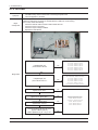
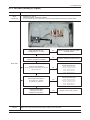
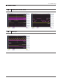
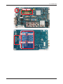
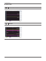
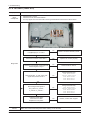
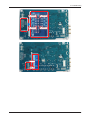
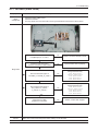
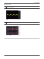
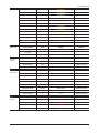
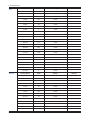
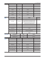
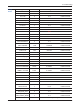
4. Troubleshooting 4. Troubleshooting 4-1. Troubleshooting 4-1-1. Previous check 1. Check the various cable connections first. • Check to see if there is a burnt or damaged cable. • Check to see if there is a disconnected or loose cable connection. • Check to see if the cables are connected according to the connection diagram. 2. Check the power input to the Main Board. 4-1 4. Troubleshooting 4-1-2. No Power Symptom Major checkpoints -- The LEDs on the front panel do not work when connecting the power cord. -- The SMPS relay does not work when connecting the power cord. -- The units appears to be dead. The IP relay or the LEDs on the front panel does not work when connecting the power cord if the cables are improperly connected or the Main Board or SMPS is not functioning. In this case, check the following: -- Check the internal cable connection status inside the unit. -- Check the fuses of each part. -- Check the output voltage of SMPS. -- Replace the Main Board. Change 18p power cable. Lamp(Backlight) Off, power indicator LED off? Diagnostics No 32" C5X0 : BN39-01267A 37" C5X0 : BN39-01267E 40" C5X0 : BN39-01267E 46" C5X0 : BN39-01267F 26" C450 : BN96-01267B 32" C450 : BN96-01267A Yes Change the Inverter(Balance B’d). Lamp(Backlight) Off, power indicator LED on ? No 32" C530/550 : BN81-04436A 37" C5X0 : BN81-04438A 40" C5X0 : BN81-04447A 46" C5X0 : BN81-04443A 26" C450 : BN81-04451A 32" C450/C540 : BN81-04464A Yes Does proper Stand-By DC A5V appear at TP - A5V ? Yes No Does proper Main DC B13V, B5V appear at TP - B13V, B5V ? Yes No Does proper DC A3.3V appear at TP - A3.3V ? Yes No Does proper B3.3V, B1.8V, SPI_3.3V appear at BD213 (B3.3V) BD219 (DDR B1.8V) TP - SPI_3.3V ? Yes 4-2 No Change the Main Assy. C550 : BN94-02700A C540(32") : BN94-02750A C540 : BN94-02750B C530 : BN94-02617A C450 : BN94-02655A 4. Troubleshooting Change the LVDS cable. Does proper DC B13V appear at LVDS connector Pin #1~5 of T-con b’d? No 32" C530/C550 : BN96-13171A 37" C5X0 : BN96-13171B 40" C5X0 : BN96-13171C 46" C5X0 : BN96-13171D 26" C450 : BN96-12469D 32" C450/C540 : BN96-13227A Yes Change the T-con b’d. Does proper DC B13V appear at F1 of T-con b’d? No 32" C550/C530 : BN96-13171A 37" C5X0 : BN96-13171B 40" C5X0 : BN96-13171C 46" C5X0 : BN96-13171D 26" C450 : BN96-12469D 32" C450/C540 : BN96-13227A Yes Check a other function. (No picture part) Replace a LCD Panel. A power is supplied to set ? No 32" C550/C530 : BN07-00826A 32" C540 : BN96-13227A 37" C5X0 : BN07-00828A 40" C5X0 : BN07-00822A 46" C5X0 : BN07-00832A 26" C450 : BN07-00818A 32" C450 : BN07-00819A Diagnostics Caution Make sure to disconnect the power before working on the IP board. 4-3 4. Troubleshooting 4. Troubleshooting BD213 BD219 B13V A3.3V B5V SPI_3.3V A5V Pin #1~5 40” T-Con 4-4 4-4 F1 4. Troubleshooting 4-1-3. No Video (Analog PC signal) Symptom Major checkpoints -- Audio is normal but no picture is displayed on the screen. -- Check the PC source -- Check the Arsenal, Check the Chelsea. -- This may happen when the LVDS cable connecting the Main Board and the Panel is disconnected. Power indicator LED is off. Lamp(Backlight) on, no video ? No Check a set in the 'Stand-by mode'. or 'DPMS mode'. Yes Check the PC source and check the connection of D-SUB ? No Input the analog PC signal properly. Yes Diagnostics 1 Does the signal appear at TP - PC_R, PC_G, PC_B, PC_HS, PC_VS (R, G, B, H, V) ? Check CN901, PC cable. Change the Main Assy. C550 : BN94-02700A C540(32) : BN94-02750A C540 : BN94-02750B C530 : BN94-02617A C450 : BN94-02655A No Yes 2 Does the digital data appear at TP-E_TXCLK+, E_TXCLK-, O_TXCLK+, O_TXCLK- ? Check IC301 (SX1) Change the Main Assy. C550 : BN94-02700A C540(32) : BN94-02750A C540 : BN94-02750B C530 : BN94-02617A C450 : BN94-02655A No Yes Check the LVDS cable? Check the T-Con B'd? Replace the LCD panel? Caution No Please, Contact Tech support. Make sure to disconnect the power before working on the IP board. 4-5 4. Troubleshooting O_TXCLK- O_TXCLK+ PC_G E_TXCLK- PC_R PC_B E_TXCLK+ PC_HB PC_VB 4-6 4-6 4. Troubleshooting WAVEFORMS 1 PC input (V-sink , H-sink , R/G/B) 2 LVDS output 4-7 4. Troubleshooting 4-1-4. No video (HDMI1, 2, 3, 4 - Digital signal) Symptom Major checkpoints -- Audio is normal but no picture is displayed on the screen. -- Check the HDMI source. -- Check the HDMI switch, Check the Chelsea. -- This may happen when the LVDS cable connecting the Main Board and the Panel is disconnected. Power indicator LED is off. Lamp(Backlight) on, no video ? No Check a set in the 'Stand-by mode'. Yes Check the HDMI source and check the connection of HDMI cable ? No Input the HDMI signal properly. Yes Diagnostics 3 Does the signal appear at CN1002 (Pin#12, #7) (HDMI1) CN1003 (Pin#12, #7) (HDMI2) CN1004 (Pin#12, #7) (HDMI3) CN1001 (Pin#12, #7) (HDMI4) (HDMI RX_Clk , RX_Data) ? Check CN1001,CN1002, CN1003, CN1004. Check HDMI cable. Change the Main Assy. C550 : BN94-02700A C540(32) : BN94-02750A C540 : BN94-02750B C530 : BN94-02617A C450 : BN94-02655A No Yes 2 Does the digital data appear at TP-E_TXCLK+, E_TXCLK-, O_TXCLK+, O_TXCLK- ? Check IC301 (SX1) Change the Main Assy. C550 : BN94-02700A C540(32) : BN94-02750A C540 : BN94-02750B C530 : BN94-02617A C450 : BN94-02655A No Yes Check the LVDS cable? Check the T-Con B'd? Replace the LCD panel? Caution 4-8 No Please, Contact Tech support. Make sure to disconnect the power before working on the IP board. 4. Troubleshooting 4. Troubleshooting Pin #12 Pin #7 Pin #35 Pin #34 Pin #12 O_TXCLK- O_TXCLK+ E_TXCLK+ E_TXCLK- Pin #20 Pin #19 4-9 4-9 4. Troubleshooting WAVEFORMS 3 HDMI input (RX_Data, RX_Clk) 2 LVDS output 4-10 4. Troubleshooting 4-1-5. No Video (Tuner_CVBS) Symptom Major checkpoints -- Audio is normal but no picture is displayed on the screen. -- Check the Tuner CVBS source. -- Check the Tuner, Check the Chelsea. -- This may happen when the LVDS cable connecting the Main Board and the Panel is disconnected. Power indicator LED is off. Lamp(Backlight) on, no video ? No Check a set in the 'Stand-by mode' Yes Check the RF source and check the connection of RF cable ? No Input the RF source properly. Yes Diagnostics Change the Main Assy. Does the DC B5V_TU_PW, TU33V_PW appear at #3, #5 Pin of Tuner ? C550 : BN94-02700A C540(32) : BN94-02750A C540 : BN94-02750B C530 : BN94-02617A C450 : BN94-02655A No Yes 2 Does the digital data appear at TP-E_TXCLK+, E_TXCLK-, O_TXCLK+, O_TXCLK- ? Check IC301 (SX1) Change the Main Assy. C550 : BN94-02700A C540(32) : BN94-02750A C540 : BN94-02750B C530 : BN94-02617A C450 : BN94-02655A No Yes Check the LVDS cable? Check the T-Con B'd? Replace the LCD panel? Caution No Please, Contact Tech support. Make sure to disconnect the power before working on the IP board. 4-11 4. Troubleshooting 4. Troubleshooting O_TXCLK- O_TXCLK+ Pin #35 Pin #34 Pin #20 Pin #19 E_TXCLK+ TU33V B5V_TU 4-12 4-12 E_TXCLK- 4. Troubleshooting WAVEFORMS 2 LVDS output 4-13 4. Troubleshooting 4-1-6. No Video (Tuner DTV) Symptom Major checkpoints -- Audio is normal but no picture is displayed on the screen. -- Check the DTV source. -- Check the Tuner, Check the Chelsea. -- This may happen when the LVDS cable connecting the Main Board and the Panel is disconnected. Power indicator LED is off. Lamp(Backlight) on, no video ? No Check a set in the 'Stand-by mode' Yes Check the connection of RF cable ? No Input the RF source properly. Yes Diagnostics Check the 'signal strength' in Self Diagnosis menu Strength is enough ? No Check the D-TV source. Yes Change the Main Assy. Does the DC B5V_TU_PW, TU33V_PW appear at #3, #5 Pin of Tuner ? C550 : BN94-02700A C540(32) : BN94-02750A C540 : BN94-02750B C530 : BN94-02617A C450 : BN94-02655A No Yes 2 Does the digital data appear at TP-E_TXCLK+, E_TXCLK-, O_TXCLK+, O_TXCLK- ? Check IC301 (SX1) Change the Main Assy. C550 : BN94-02700A C540(32) : BN94-02750A C540 : BN94-02750B C530 : BN94-02617A C450 : BN94-02655A No Yes Check the LVDS cable? Check the T-Con B'd? Replace the LCD panel? Caution 4-14 No Please, Contact Tech support. Make sure to disconnect the power before working on the IP board. 4. Troubleshooting 4. Troubleshooting O_TXCLK- O_TXCLK+ Pin #35 Pin #34 Pin #20 Pin #19 E_TXCLK+ E_TXCLK- TU33V B5V_TU 4-12 4-15 4. Troubleshooting WAVEFORMS 2 4-16 LVDS output 4. Troubleshooting 4-1-7. No Video (Video CVBS) Symptom Major checkpoints -- Audio is normal but no picture is displayed on the screen. -- Check the Video CVBS source -- Check the Chelsea. -- This may happen when the LVDS cable connecting the Main Board and the Panel is disconnected. Power indicator LED is off. Lamp(Backlight) on, no video ? No Check a set in the 'Stand-by mode' Yes Check the video source and check the connection of video cable? No Input the video source properly. Yes Diagnostics Check CN701, CN704. Change the Main Assy. 4 Does the CVBS data appear at TP-COMP1_Y TP-SIDE_AV_CVBS ? C550 : BN94-02700A C540(32) : BN94-02750A C540 : BN94-02750B C530 : BN94-02617A C450 : BN94-02655A No Yes 2 Does the digital data appear at TP-E_TXCLK+, E_TXCLK-, O_TXCLK+, O_TXCLK- ? Check IC301 (SX1) Change the Main Assy. C550 : BN94-02700A C540(32) : BN94-02750A C540 : BN94-02750B C530 : BN94-02617A C450 : BN94-02655A No Yes Check the LVDS cable? Check the T-Con B'd? Replace the LCD panel? Caution No Please, Contact Tech support. Make sure to disconnect the power before working on the IP board. 4-17 4. Troubleshooting 4. Troubleshooting O_TXCLK- O_TXCLK+ Pin #35 Pin #34 Pin #20 Pin #19 E_TXCLK+ E_TXCLK- SIDE_AV_CVBS COMP1_ 4-18 4-18 4. Troubleshooting WAVEFORMS 4 CVBS OUT (Grey Bar) 2 LVDS output 4-19 4. Troubleshooting 4-1-8. No Video (Component) Symptom Major checkpoints -- Audio is normal but no picture is displayed on the screen. -- Check the Component source -- Check the chelsea. -- This may happen when the LVDS cable connecting the Main Board and the Panel is disconnected. Power indicator LED is off. Lamp(Backlight) on, no video ? No Check a set in the 'Stand-by mode'. Yes Check the component source and check the connection of component cables (Y,Pb,Pr) ? No Input the video source properly. Yes Diagnostics 4 Does the component data appear at TP - COMP1_Y, COMP1_PB, COMP1_PR TP - COMP2_Y, COMP2_PB, COMP2_PR (Comp / Y, Pb, Pr) ? Check CN701. Change the Main Assy. C550 : BN94-02700A C540(32) : BN94-02750A C540 : BN94-02750B C530 : BN94-02617A C450 : BN94-02655A No Yes 2 Does the digital data appear at TP-E_TXCLK+, E_TXCLK-, O_TXCLK+, O_TXCLK- ? Check IC301 (SX1) Change the Main Assy. C550 : BN94-02700A C540(32) : BN94-02750A C540 : BN94-02750B C530 : BN94-02617A C450 : BN94-02655A No Yes Check the LVDS cable? Check the T-Con B'd? Replace the LCD panel? Caution 4-20 No Please, Contact Tech support. Make sure to disconnect the power before working on the IP board. 4. Troubleshooting 4. Troubleshooting O_TXCLK- O_TXCLK+ Pin #35 Pin #34 Pin #20 Pin #19 E_TXCLK+ COMP2_ E_TXCLK- COMP1_P COMP1_P COMP1_Y COMP1_PB COMP1_PR 4-21 4-21 4. Troubleshooting WAVEFORMS 5 Compnent_Y (Gray scale) / Pb / Pr (Color bar) 2 LVDS output 4-22 4. Troubleshooting 4-1-9. No Sound Symptom Major checkpoints -- Video is normal but there is no sound.. -- When the speaker connectors are disconnected or damaged. -- When the sound processing part of the Main Board is not functioning. -- Speaker defect.. Check the source and check the connection of sound cable (Comp/PC/DVI to HDMI) ? No Check a set in the 'Stand-by mode'. Yes Check the component source and check the connection of component cables (Y,Pb,Pr) ? No Input the video source properly. Yes Does the sound data appear at TP - COMP1_SL, COMP1_SR (AV1, COMP1) TP - COMP2_SL, COMP2_SR (Comp2) TP - SIDE_AV_SL, SIDE_AV_SR(AV2) TP - 914, 915 (PC/DVI) ? Diagnostics Check CN701, CN704, CN902. Change the Main Assy. C550 : BN94-02700A C540(32) : BN94-02750A C540 : BN94-02750B C530 : BN94-02617A C450 : BN94-02655A No Yes Change the Main Assy. Does the DC B3.3V, B12V appear at TP - B3.3V, B12V? C550 : BN94-02700A C540(32) : BN94-02750A C540 : BN94-02750B C530 : BN94-02617A C450 : BN94-02655A No Yes Check IC201 (Saturn4). Check IC904 (Sound AMP). Change the Main Assy. 7 Does the sound data appear at - L-, L+, R-, R+ ? C550 : BN94-02700A C540(32") : BN94-02750A C540 : BN94-02750B C530 : BN94-02617A C450 : BN94-02655A No Yes Replace speaker? BN96-12871A Caution No Please, Contact Tech support. Make sure to disconnect the power before working on the IP board. 4-23 Troubleshooting 4.4.Troubleshooting SIDE_AV_SL A3.3V SIDE_AV_SR TP91 COMP2_S B13VS COMP2_S COMP1_SL COMP1_S 4-24 4-24 TP91 - L-, L+, R-, R+ 4. Troubleshooting WAVEFORMS 7 Speaker out 4-25 4. Troubleshooting 4-2. Alignments and Adjustments 4-2-1. General Alignment Instuction 1. Usually, a color LCD-TV needs only slight touch-up adjustment upon installation. Check the basic characteristics such as height, horizontal and vertical sync. 2. Use the specified test equipment or its equivalent. 3. Correct impedance matching is essential. 4. Avoid overload. Excessive signal from a sweep generator might overload the front-end of the TV. When inserting signal markers, do not allow the marker generator to distort test result. 5. Connect the TV only to an AC power source with voltage and frequency as specified on the backcover nameplate. 6. Do not attempt to connect or disconnect any wire while the TV is turned on. Make sure that the power cord is disconnected before replacing any parts. 7. To protect against shock hazard, use an isolation transformer. 4-26 4. Troubleshooting 4-3. Factory Mode Adjustments 4-3-1 Entering Factory Mode To enter ‘Service Mode’ Press the remote -control keys in this sequence : - If you do not have Factory remote - control Power OFF MUTE 1 8 2 Power On 4-3-2 How to Access Service Mode Using the Customer Remote 1. Turn the power off and set to stand-by mode 2. Press the remote buttons in this order; POWER OFF-MUTE-1-8-2-POWER ON to turn the set on. 3. The set turns on and enters service mode. This may take approximately 20 seconds. 4. Press the Power button to exit and store data in memory. - If you fail to enter service mode, repeat steps 1 and 2 above. 5. Initial SERVICE MODE DISPLAY State Option Control SVC Expert ADC/WB Advanced T-TDT5AUSC-XXX T-TDT5AUSS-XXX EDID SUCCESS CALIB : AV X COM X PC X HDMI X Option : XXXX XXXX XXXX X SDAL-XXX RFS : 0130 T-TDT5AUSC 20XX-XX-XX TYPE : XX MODEL : XXXXX MAC FAIL FACTORY DATA VER : XXX EERC VERSION : XXX DTP-AP-COMP-310-01 DTP-HIIG-0304 DTP-BP-0314 DATE OF PURCHASE : XX/XX/XX * How to enter the hidden factory mode. a. into the factory mode b. move the tap to Advanced c. key input : 0 + 0 + 0 + 0 ** hidden menu : Advanced 6. Buttons operations withn Service Mode Menu Full Menu Display/Move to Parent Menu Direction Keys / Item Selection by Moving the Cursor Direction Keys / Data Increase / Decrease for the Selected Item Source Cycles through the active input source that are connected to the unit 4-27 4. Troubleshooting 4-3-3 Factory Data Option OPTION Factory Name Data Range Remark Factory Reset Type Local Set … LC350/LC450/LC450H/LC451LC452/LC457HLC459H/ LC480/LC530/LC530H/LC539H/LC540/LC550/LC560/ LC580/LC570/LC610/LC620/LC630/LC631/LC632/LC633/ LC640/LC650/LC652/LC653/LC654/LC670/ UC4000/UC4000H/UC4010/UC5000/UC5100/UC6000/ UC6200/UC6300/UC6400/UC6400H/UC6500/UC6510/ UC6530/UC6540/UC6550/UC6600/UC6620/UC6630/ UC6700/UC6720/UC6730/UC6740/UC6800/UC6830/ UC6900/UC6900H/UC8000/ PC420/PC430/PC431/PC432/PC450/PC451/PC480/ PC520/PC530/PC531/PC540/PC541/PC550/PC551/ PC560/PC580/PC590/PC670/PC6100/PC6400/PC6500/ PC7000/PC7700/PC8000 Model LC450 LC530 LN540 LC550 TUNER DRX3900J fixed DDR 0 fixed Light Effect OFF ON/OFF Ch Table … Country USA Front Color 4-28 NONE/19O6TH0C/19A6TH0C/22I6TH0C/22A6TH0C/22D6 TH0C/22P6TH0C/26A6AH0C/26D6AH0C/26L6AH0C/26P6 AH0C/32A6AH0C/32D6AH0C/32L6AH0C/32P6AH0C/32A6 AF0C/32L6AF0C/32A1AF0C/32L1AF0C/37L6AF0C/37L1A 26D6AH0E F0C/40A6AF0C/40D6AF0C/40L6AF0C/40A1AF0C/40L1AF 32D6UF0E 0C/40A1UF0C/40D1UF0C/40L1UF0C/46A6AF0C/46D6AF 32L6AF0C 0C/46L6AF0C/46A1AF0C/46L1AF0C/46A1UF0C/46D1UF0 37L6AF0C C/46L1UF0C/55A1UF0C/55L1UF0C/65L1UF0C/19O6TH0 40D6AF0C E/22D6TH0E/26D6AH0E/32D6AH0E/32D6UF0E/32A1UF0 46L6AF0C E/32D1UF0E/37L6UF0E/37D1UF0E/37L1UF0E/40D6UF0E /40A1UF0E/40D1UF0E/46D6UF0E/46L6UF0E/46A1UF0E/ 46D1UF0E/46L1UF0E/55A1UF0E/55D1UF0E/55L1UF0E/6 5L1UF0E/42HHcD3/50HHcD450FArN4/50FArV458FArN1/5 8FArV163FArN1/ USA/PANAMA NONE/W-MILKY/T-M-Brn/T-W-Brn/T-W-Gray/W-D-Gray/ W-M-Whit/W-Violet/T-C-Gray/T-R-BLK/S-BLK/S-RBLK/ S-C-Gray/ INFO+FACTORY 4. Troubleshooting Control Control Factory Name Range EDID SUB MENU Sub Option SUB MENU Remark PDP Option EDID Hotel Option SUB MENU Shop Option SUB MENU Asia Option SUB MENU Sound SUB MENU Config Option SUB MENU INFO+FACTORY SCC SUB MENU INFO+FACTORY INFO+FACTORY Factory Name Data Range EDID ON/OFF Off ON/OFF EDID WRITE ALL … Success/failure EDID WRITE PC … Success/failure EDID WRITE HDMI … Success/failure EDID WRITE HDMI1 … fixed EDID WRITE HDMI2 … fixed EDID WRITE HDMI3 … fixed EDID WRITE HDMI4 … fixed EDID 1.2 PORT NONE NONE/Not Support/HDMI2/HDMI3/HDMI4 EDID WRITE DVI … fixed 4-29 4. Troubleshooting Sub Option Factory Name Data Range Remark RF Mute Time 600ms 0ms~1000ms RS-232 Jack UART Debug/Login/UART Watchdog OFF ON/OFF WD Count 0 0~255 Dimm Type EXT fixed Lvds Format JEIDA JEIDA/VESA/19INCH Language_Arbic … fixed INFO+FACTORY TOOLS Support 32 0~255 INFO+FACTORY LNA Support 0 0~255 INFO+FACTORY MediaPlay DB On whth 5MB fixed MediaPlay Movie chapterinMedia fixed MediaPlay DLNA OFF fixed MediaPlay PlayList OFF fixed NETWORK Support Wireless Not Support/Cable/Wireless INFO+FACTORY Info Link Server Type operationg operationgdevelopment/developing INFO+FACTORY Info Link Country USA None/USA INFO+FACTORY TTX List … fixed INFO+FACTORY TTX Group … fixed INFO+FACTORY 24Px4 Support OFF ON/OFF INFO+FACTORY Power Indicator Support OFF ON/OFF INFO+FACTORY BD Wise Support ON ON/OFF INFO+FACTORY Data Service Support OFF ON/OFF INFO+FACTORY Alternate Del OFF ON/OFF INFO+FACTORY OTN Server Type operationg operation/development OTN Test Server OFF OFF/ A/B/C/D/E Zone OTN Support OFF ON/OFF OTN Duration OFF ON/OFF OTN Fail Test OFF ON/OFF IIC Bus Stop OFF ON/OFF INFO+FACTORY Visual Test Disable fixed INFO+FACTORY T-CON USB Download Failure fixed OTN Reset Emergency Log Copy Checksum INFO+FACTORY 0x0000 View Log 4-30 INFO+FACTORY SUB MENU ColorSpace Support HueSate Type RGB Type / HueSate Type INFO+FACTORY Gemstar On/Off OFF ON/OFF INFO+FACTORY WSS Support OFF ON/OFF INFO+FACTORY PVR Support OFF ON/OFF INFO+FACTORY CI Support OFF ON/OFF INFO+FACTORY 4. Troubleshooting View Log Eeprom Reset SUB MENU INFO+FACTORY Spread Spectrum SUB MENU INFO+FACTORY DDR Margin SUB MENU INFO+FACTORY H.264 Margin 200 0~2000 MPEG Margin 50 0~2001 Tuner Margin 50 0~2002 SST SUB MENU SST_Th SUB MENU 2nd mips ON ON/OFF 2nd mips count 0 0~255 Region KOR fixed PnP Language … fixed PC Auto Ident Enable Auto/Enable Factory Name Data Range Select Log Type IR Key NVRAM / DIAGNOSIS / IR KEY Data Range INFO+FACTORY Remark Log View Delete Log Eeprom Reset Spread Spectrum DDR Margin Factory Name EER Reset Remark INFO+FACTORY NVR All Clear OFF INFO+FACTORY Factory Name Data Range Remark LVDS SSC ON/OFF ON ON/OFF INFO+FACTORY LVDS SSC MWR 0X19H 0X00~0X7F INFO+FACTORY LVDS SSC MFR 0X7FH 0X00~0X7F INFO+FACTORY DDR SSC ON/OFF OFF ON/OFF INFO+FACTORY DDR SSC MWR 0X19H 0X00~0X7F INFO+FACTORY DDR SSC MFR 0X7FH 0X00~0X7F INFO+FACTORY SSC Fraction Default ON ON/OFF INFO+FACTORY LVDS Strength 6 0~6 INFO+FACTORY Factory Name Data Range Remark A CTRL_OFFSET_0_3 0X0 fixed INFO+FACTORY A CTRL_OFFSET_D 0X0 fixed INFO+FACTORY B CTRL_OFFSET_0_3 0X0 fixed INFO+FACTORY B CTRL_OFFSET_D 0X0 fixed INFO+FACTORY 4-31 4. Troubleshooting SST SST_Th 4-32 Factory Name Data Range Y0 Ref 166 0~255 Y1 Ref 148 0~255 Y2 Ref 119 0~255 Y3 Ref 101 0~255 Y4 Ref 76 0~255 Y5 Ref 60 0~255 Y6 Ref 31 0~255 Y7 Ref 0 0~255 Cb0 Ref 128 0~255 Cb1 Ref 64 0~255 Cb2 Ref 148 0~255 Cb3 Ref 85 0~255 Cb4 Ref 171 0~255 Cb5 Ref 108 0~255 Cb6 Ref 194 0~255 Cb7 Ref 0 0~255 Cr0 Ref 128 0~255 Cr1 Ref 137 0~255 Cr2 Ref 64 0~255 Cr3 Ref 74 0~255 Cr4 Ref 181 0~255 Cr5 Ref 192 0~255 Cr6 Ref 118 0~255 Cr7 Ref 0 0~255 Factory Name Data Range Y0 TH 20 0~255 Y1 TH 20 0~255 Y2 TH 20 0~255 Y3 TH 20 0~255 Y4 TH 20 0~255 Y5 TH 20 0~255 Y6 TH 20 0~255 Y7 TH 20 0~255 Cb0 TH 20 0~255 Cb1 TH 20 0~255 Cb2 TH 20 0~255 Cb3 TH 20 0~255 Cb4 TH 20 0~255 Cb5 TH 20 0~255 Remark Remark 4. Troubleshooting Hotel Option Shop Option Asia Option Cb6 TH 20 0~255 Cb7 TH 20 0~255 Cr0 TH 20 0~255 Cr1 TH 20 0~255 Cr2 TH 20 0~255 Cr3 TH 20 0~255 Cr4 TH 20 0~255 Cr5 TH 20 0~255 Cr6 TH 20 0~255 Cr7 TH 20 0~255 Factory Name Data Range Hotel Mode OFF ON/OFF SI Vender Samsung Samsung/2M/Locatel/VDA/VDA-S/Acentic/ Premiere/Sustinere/Quadriga/ETV/Ibahn/ Magilink/Otrum/PeninsulaSiemens/OCC/ MTI/MstreamsDAWNXTV/Enseo/Cardinal/ Guestek/OFF/Movielink/Swisscom Power On Channel 3 1~135 Channel Type ATV ATV/DTV/CATV/CDTV Power On Volume 10 0~100 Min Volume 0 0~100 Max Volume 100 0~100 Panel Button Lock Unlock Unlock/Lock/OnlyPower Power On Source TV TV/AV/Comp/PC/HDMI1/HDMI2/HDMI3/ HDMI4 Remark Factory Name Data Range Shop Mode OFF ON/OFF Exhibition Mode OFF ON/OFF Factory Name Data Range Remark TTX OFF ON/OFF INFO+FACTORY China HD OFF ON/OFF INFO+FACTORY NT Conversion OFF ON/OFF INFO+FACTORY Sepco 120Hz OFF ON/OFF INFO+FACTORY Unbalance OFF ON/OFF INFO+FACTORY FMTransmitter Support OFF ON/OFF INFO+FACTORY FMTransmitter Carrier OFF ON/OFF INFO+FACTORY AF Level adjust 3 0~7 INFO+FACTORY TX Power Level 0 0~3 INFO+FACTORY Mono Last Memory OFF ON/OFF INFO+FACTORY 4-33 4. Troubleshooting Sound Factory Name Data Range High Devi OFF ON/OFF Carrier_Mute ON ON/OFF Volume Curve Type2 Type1/Type2/error Speaker Delay Normal 10 0~255 Pilot Level High Thld 0x08h 0x00~0xff Pilot Level Low Thld 0x05h 0x00~0xff FM Prescale 17 0~255 INFO+FACTORY AM Prescale 10 0~255 INFO+FACTORY NICAM Prescale 33 0~255 INFO+FACTORY Amp Volume 0x10h 0x00~0xff INFO+FACTORY Amp Scale 0x78h 0x00~0xff INFO+FACTORY Amp Check Sum 0x0000a820 fixed INFO+FACTORY Woofer Type 4 1~7 INFO+FACTORY Woofer Scale 0x7Fh 0x00~0xff INFO+FACTORY Woofer Check Sum 4-34 Remark INFO+FACTORY INFO+FACTORY Speaker EQ ON ON/OFF PEQ Test 0 0~7 INFO+FACTORY Amp Model TAS5715 SAT369B/TAS5715/NPT7300 INFO+FACTORY Speaker cut-off Freq 4 0~16 INFO+FACTORY SPDIF PCM Gain -9dB -10dB~0dB 4. Troubleshooting Config Option Factory Name Data Range Remark Num of ATV 1 1~2 INFO+FACTORY Num of DTV 1 0~2 INFO+FACTORY Num of AV 2 0~3 INFO+FACTORY Num of SVIDEO 0 1~3 INFO+FACTORY Num of Comp 2 1~3 INFO+FACTORY Num of HDMI 4 0~4 INFO+FACTORY Num of PC 1 0~1 INFO+FACTORY Num of SCART 0 0~2 INFO+FACTORY Num of DVI 0 0~1 INFO+FACTORY Num of OPTICAL Link 0 fixed INFO+FACTORY Num of MEDIA 1 0~1 INFO+FACTORY Num of PANEL KEY 6 0~8 INFO+FACTORY Num of USB Port 2 0~2 INFO+FACTORY Num of HeadPhone 0 0~1 INFO+FACTORY MFT Offset 62.5 50/62.5 INFO+FACTORY Select LCD/PDP LCD LCD/PDP INFO+FACTORY HDMI/DVI SEL 1 1~4 INFO+FACTORY Indicator Led OFF ON/OFF INFO+FACTORY Wall Mount OFF ON/OFF INFO+FACTORY HV Flip ON ON/OFF INFO+FACTORY Num of Display 2 1~2 INFO+FACTORY DVI/HDMI SOUND Auto Auto/DVI INFO+FACTORY HDMI HOT PLUG Disable Enable/Disable INFO+FACTORY HOTPLUG SWITCHING Boot Disable/Boot/Source INFO+FACTORY HOTPLUG DURATION 1200ms 0~2000ms INFO+FACTORY CLK TERM DURATION 1200ms 0~2000ms INFO+FACTORY HDMI FLT CNT SIG 200ms 0~1000ms INFO+FACTORY HDMI FLT CNT LOS 600ms 0~1000ms INFO+FACTORY UNSTABLE BAN CNT 3500ms 0~100000ms INFO+FACTORY HDMI Err Cnt 5 0~10 INFO+FACTORY HDMI ROBIN ON ON/OFF INFO+FACTORY HDMI Callback OFF ON/OFF INFO+FACTORY HDMI CTS Thld 8 0~15 INFO+FACTORY HDMI CTS Cnt1 1 0~15 INFO+FACTORY TMDS_EQ2_Boost 1 0~7 INFO+FACTORY TMDS_EQ2_Gain 0 0~3 INFO+FACTORY TMDS_PLL_Loop 3 0~3 INFO+FACTORY TMDS_CPREG_BLEED 1 0~1 INFO+FACTORY HDMI EQ AUTO AUTO/Low/Middle/High/Strong INFO+FACTORY 4-35 4. Troubleshooting SCC SCC Input Data sSCC Const pSCC Const 4-36 HDMI Write Type Combine Combine/Separate INFO+FACTORY HDMI Switch SIL9287 NONE/SIL9287/TMDS461 INFO+FACTORY DVI SET TIME 300ms 0~1000ms INFO+FACTORY Type Of PANEL KEY Horizontal Horzontal/Vertical/PDPVertical/Nne INFO+FACTORY EcoSensor Support ON ON/OFF INFO+FACTORY LEDMotionPlus Support OFF ON/OFF INFO+FACTORY Natural Mode Support ON ON/OFF INFO+FACTORY All Share Support ON ON/OFF INFO+FACTORY Relax Mode Support OFF ON/OFF INFO+FACTORY DVI-I Support OFF ON/OFF INFO+FACTORY Melfas Function Support OFF ON/OFF INFO+FACTORY Light Level Support OFF ON/OFF INFO+FACTORY Factory Name Data Range Remark SCC Mode Dynamic Dynamic/Movie INFO+FACTORY SCC ON/OFF OFF ON/OFF INFO+FACTORY SCC Input Data SUB MENU INFO+FACTORY sSCC Const SUB MENU INFO+FACTORY pSCC Const SUB MENU INFO+FACTORY SCC Source Data PBA PBA/PANEL INFO+FACTORY SWAP PBA PBA/PANEL INFO+FACTORY Factory Name Data Range Remark Hx 272 0~512 INFO+FACTORY Hy 273 0~512 INFO+FACTORY Lx 274 0~512 INFO+FACTORY Ly 275 0~512 INFO+FACTORY Factory Name Data Range Remark sSCC Hx 550 0~1024 INFO+FACTORY sSCC Hy 566 0~1024 INFO+FACTORY sSCC Lx 598 0~1024 INFO+FACTORY sSCC Ly 550 0~1024 INFO+FACTORY Factory Name Data Range Remark pSCC Hx 550 0~1024 INFO+FACTORY pSCC Hy 566 0~1024 INFO+FACTORY pSCC Lx 598 0~1024 INFO+FACTORY pSCC Ly 550 0~1024 INFO+FACTORY 4. Troubleshooting SVC SVC Factory Name Data Range Test Pattern Remark SUB MENU Panel Auto Setting Failure fixed INFO+FACTORY Panel Display Time 8Hr fixed Logic Usb D/L Off fixed INFO+FACTORY Factory Name Data Range Remark Pattern Sel OFF OFF/ White/Grey/Black Red/Green/Blue RFC PC Mode … fixed Logic Pattern Sel … fixed Logic Level Sel … fixed Factory Name Data Range Tuner Status Test Pattern TUNER STATUS DVB DVB SUB MENU ISDB-T SUB MENU Factory Name Range SNR fixed BER fixed Singal Strength fixed Bandwidth fixed Frequency fixed LNA Status fixed FFT fixed Modulation fixed Code Rate fixed GI fixed Hier Modulation fixed Frequency Offset fixed Timing Offset fixed AGC fixed UCB fixed PLL Type fixed DEMOD Type fixed TPS LOCK fixed RS Lock fixed SSI fixed SQI fixed Remark Remark 4-37 4. Troubleshooting ISDB-T 4-38 Factory Name Range FFT Size_1 fixed Guard Interval_1 fixed Freq. Offset_1 fixed SNR_1 fixed IF AGC_1 fixed TMCC Lock_1 fixed TS Packet_1 fixed Master Lock_1 fixed A_Modulation_1 fixed A_Code Rate_1 fixed A_Timer InterLeave_1 fixed A_Segments Num_1 fixed A_Ber_1 fixed B_Modulation_! fixed B_Code Rate_1 fixed B_Timer InterLeave_1 fixed B_Segments Num_1 fixed B_BER_1 fixed C_Modulation_1 fixed C_Code Rate_1 fixed C_Timer InterLeave_1 fixed C_Segments Num_1 fixed C_BER_1 fixed Remark 4. Troubleshooting Expert Expert Factory Name Data Range N / D ADJ Off Off / On / FIX SOURCE ... fixed ADC/WB ADC/WB ADC ADC Target Factory Name Range ADC SUB MENU ADC Target SUB MENU ADC RESULT SUB MENU WB SUB MENU Remark Factory Name Data Range AV Calibration Success Success / Failure Comp Calibration Success Success / Failure PC Calibration Success Success / Failure HDMI Calibration Success Success / Failure Factory Name Data Range 1st_AV_Low 18 0 ~ 255 1st_AV_High 220 0 ~ 255 1st_AV_Delta 1 0 ~ 255 1st_COMP_Low 16 0 ~ 255 1st_COMP_High 235 0 ~ 255 1st_COMP_Delta 1 0 ~ 255 1st_PC_Low 2 0 ~ 255 1st_PC_High 235 0 ~ 255 1st_PC_Delta 1 0 ~ 255 2nd_Low 1 0 ~ 255 2nd_High 235 0 ~ 255 2nd_Delta 1 0 ~ 255 4-39 4. Troubleshooting ADC RESULT WB 4-40 Factory Name Data Range 1st_AV_Gain 127 0 ~ 255 1st_AV_Offset 139 0 ~ 255 1st_Comp_Gain 68 0 ~ 255 1st_Comp_Gain_Cb 68 0 ~ 255 1st_Comp_Gain_Cr 68 0 ~ 255 1st_Comp_Offset 127 0 ~ 255 1st_Comp_Offset_Cb 127 0 ~ 255 1st_Comp_Offset_Cr 127 0 ~ 255 1st_PC_R_Gain 96 0 ~ 255 1st_PC_G_Gain 95 0 ~ 255 1st_PC_B_Gain 94 0 ~ 255 1st_PC_R_Offset 127 0 ~ 255 1st_PC_G_Offset 127 0 ~ 255 1st_PC_B_Offset 127 0 ~ 255 2nd_R_Offset 110 0 ~ 255 2nd_G_Offset 110 0 ~ 255 2nd_B_Offset 110 0 ~ 255 2nd_R_Gain 165 0 ~ 255 2nd_G_Gain 165 0 ~ 255 2nd_B_Gain 165 0 ~ 255 Factory Name Data Range Sub Brightness 128 0 ~ 255 R_Offset 128 0 ~ 255 G_Offset 128 0 ~ 255 B_Offset 128 0 ~ 255 Sub Contrast 128 0 ~ 255 R_Gain 128 0 ~ 255 G_Gain 128 0 ~ 255 B_Gain 128 0 ~ 255 Movie R Offset 122 0 ~ 255 Movie B Offset 145 0 ~ 255 Movie R Gain 156 0 ~ 255 Movie B Gain 39 0 ~ 255 4. Troubleshooting 4-4. White Balance - Calibration 4-4-1 White Balance -Calibration 1. Calibration AV Calibration Comp Calibration PC Calibration HDMI Calibration 4-4-2 White Balance - Adjustment 3. W/B (low light) (hight light) Sub Bright R offset G offset B offset Sub Contrast R gain G gain B gain (W/B adjustment Condition refer next page) 4-5. White Ratio (Balance) Adjustment 1. You can adjust the white ratio in factory mode (1:Calibration, 3:White-Balance). 2. Since the adjustment value and the data value vary depending on the input source, you have to adjust these in CVBS, Component 1 and HDMI 1 modes. 3. The optimal values for each mode are configured by default. (Refer to Table 1, 2) It varies with Panel’s size and Specification. - Equipment : CS-210 - Pattern: MIK K-7256 #92 “Flat W/B Pattern" as standard - Use other equipment only after comparing the result with that of the Master equipment. - Set Aging time : 60min - Calibration and Manual setting for WB adjustment. HDMI : Calibration at #24 Chessboard Pattern Manual adjustment #92 pattern (720p) COMP: Calibration at #24 Chessboard Pattern Manual adjustment at #92 pattern (720p) CVBS: Calibration at #24 Chessboard Pattern Manual adjustment at #92 pattern (NTSC) - If finishing in HDMI mode, adjustment coordinate is almost same in AV/COMP mode. - White Balance Manual Adjustment 4-41 4. Troubleshooting • 32C550/C530 Adjustment Coordinate CA-210 P-Mode x y [ Dynamic Cool1 ] HDMI Comp CVBS H/L 272 278 L/L 272 278 [ Movie Warm2 ] HDMI Comp CVBS H/L 306 327 L/L 306 327 x y Y (Luminance) 64.7 fL (Sub_CT:134 Fix) 4.9 fL (Sub-Brt:128 Fix) (Sub_CT:Unadjusted) (Sub_Brt:Unadjusted) T(K) + MPCD 12,000 (±0) 12,000 (±0) 6,500 (+6) 6,500 (+6) • 37C550/C530 Adjustment Coordinate CA-210 P-Mode [ Dynamic Cool1 ] HDMI Comp CVBS H/L 272 278 L/L 272 278 [ Movie Warm2 ] HDMI Comp CVBS H/L 306 327 L/L 306 327 Y (Luminance) 63.5 fL (Sub_CT:134 Fix) 4.8 fL (Sub-Brt:128 Fix) (Sub_CT:Unadjusted) (Sub_Brt:Unadjusted) T(K) + MPCD 12,000 (±0) 12,000 (±0) 6,500 (+6) 6,500 (+6) • 40C550/C540/C530 Adjustment Coordinate CA-210 P-Mode x y [ Dynamic Cool1 ] HDMI Comp CVBS H/L 272 278 L/L 272 278 [ Movie Warm2 ] HDMI Comp CVBS H/L 306 327 L/L 306 327 Y (Luminance) 64.1 fL (Sub_CT:134 Fix) 4.9 fL (Sub-Brt:128 Fix) (Sub_CT:Unadjusted) (Sub_Brt:Unadjusted) T(K) + MPCD 12,000 (±0) 12,000 (±0) 6,500 (+6) 6,500 (+6) • 46C550/C540/C530 Adjustment Coordinate CA-210 P-Mode x y [ Dynamic Cool1 ] HDMI Comp CVBS H/L 272 278 L/L 272 278 [ Movie Warm2 ] HDMI Comp CVBS H/L 306 327 L/L 306 327 4-42 Y (Luminance) 66.5 fL (Sub_CT:134 Fix) 4.9 fL (Sub-Brt:128 Fix) (Sub_CT:Unadjusted) (Sub_Brt:Unadjusted) T(K) + MPCD 12,000 (±0) 12,000 (±0) 6,500 (+6) 6,500 (+6) 4. Troubleshooting • 32C540/C450 Adjustment Coordinate CA-210 P-Mode x y [ Dynamic Cool1 ] HDMI Comp CVBS H/L 272 278 L/L 272 278 [ Movie Warm2 ] HDMI Comp CVBS H/L 306 327 L/L 306 327 x y Y (Luminance) 64.1 fL (Sub_CT:134 Fix) 4.6 fL (Sub-Brt:128 Fix) (Sub_CT:Unadjusted) (Sub_Brt:Unadjusted) T(K) + MPCD 12,000 (±0) 12,000 (±0) 6,500 (+6) 6,500 (+6) • 26C450 Adjustment Coordinate CA-210 P-Mode [ Dynamic Cool1 ] HDMI Comp CVBS H/L 272 278 L/L 272 278 [ Movie Warm2 ] HDMI Comp CVBS H/L 306 327 L/L 306 327 Y (Luminance) 63.0 fL (Sub_CT:134 Fix) 5.3 fL (Sub-Brt:128 Fix) (Sub_CT:Unadjusted) (Sub_Brt:Unadjusted) T(K) + MPCD 12,000 (±0) 12,000 (±0) 6,500 (+6) 6,500 (+6) - Adjustment Specification White Balance : High light (±1), Low light (±3) Luminance : High light (Don’t care), Low light (±0.2 Ft/L) 4-6. Servicing Information 4-6-1 USB Download Method Software Upgrade upgrades can be performed via broadcasting signal or by downloading the new firmware from samsung.com to a USB memory device. Current Version is the software already installed in the TV. Note Software is represented as ‘Year/Month/Day_Version’. Installing the latest version is recommended. ሪሪ By USB: Insert a USB drive containing the firmware upgrade file downloaded from samsung.com into the TV. Please be careful not to disconnect the power or remove the USB drive until upgrades is complete. The TV will turn off and on automatically after completing the firmware upgrade. When software is upgraded, video and audio settings you have made will return to their default settings. We recommend you to write down your settings so that you can easily reset them after the upgrade. ሪሪ By Online: Upgrades the software using the Internet. NoteFirst, configure your network. For detailed procedures on using the Network Setup, refer to the ‘Setting the Network’ instructions. NoteIf the internet connection doesn’t operate properly, the connection may be broken. Please retry downloading. If the problem still happens, download by USB and upgrade. ሪሪ Alternative Software (Backup): If there is an issue with the new firmware and it is affecting operation, you can change the software to the previous version. NoteIf software was changed, existing software is displayed. 4-43 6. Wiring Diagram 6. Wiring Diagram 6-1. Wiring Diagram C530/C540/C550 : 32",37 / C450 : 26",32" 6-1 6. Wiring Diagram C530/C540/C550 : 40", 46" 6-2 6. Wiring Diagram 6-2. Connector FCN402 (to Panel) C550/C540(40"/46")/C530 ZCN1303_HD(to Panel) C540(32")/C450 1 Panel_ VCC 16 ODD[CLK]+ 2 Panel_ VCC 17 ODD[CLK]- 3 Panel_ VCC 18 GND 4 Panel_ VCC 19 ODD[2]+ GND 5 Panel_ VCC 20 34 ODDCLK+ 6 GND TCON_ WP 35 ODDCLK- 7 10 NC 36 GND 11 SDA_ Panel 37 ODD[2]+ 12 SCL_ Panel 38 ODD[2]- 13 GND 39 ODD[1]+ 14 EVEN[4]+ 40 ODD[1]- 15 EVEN[4]- 41 ODD[0]+ 16 EVEN[3]+ 42 ODD[0]- 17 EVEN[3]- 43 GND 18 GND 44 GND 19 EVENCLK+ 45 GND 20 EVENCLK- 46 21 GND 22 EVEN[2]+ 1 NC 27 EVEN[0]- 2 NC 28 GND 3 NC 29 ODD[4]+ 4 NC 30 ODD[4]- 5 NC 31 ODD[3]+ 6 NC 32 ODD[3]- 7 FORMAT 33 8 SDA_ Panel 9 CN501(LAN) C550 1 LAN_TX- 5 LAN_VCC 2 GND 6 LAN_RX- 3 LAN_TX+ 7 NC 4 LAN_RX+ 8 GND CN901(PC) 1 PC_RED 9 PC_5V ODD[2]- 2 PC_ GREEN 10 IDENT_ PC 21 GND 3 PC_BLUE 11 R_FANET GND 22 ODD[1]+ 4 T_FANET 12 8 GND 23 ODD[1]- SDA_ DOWN TCON_ WP 5 GND 13 PC_HS 9 24 GND 6 GND 14 PC_VS 10 FORMAT 25 ODD[0]+ 11 NC 26 ODD[0]- 7 GND 15 SCL_ DOWN 12 GND 27 GND 8 GND 13 ODD[3]+ 28 SDA_ TCON 14 ODD[3]- 29 SCL_ TCON 15 GND 30 NC CN902(PC/DIV SOUND) 1 GND 4 NC 2 PC_SR_IN 5 NC 3 PC_SL_IN 6 NC CN202 (to Powr board) 1 B12VS 10 GND NC 2 SW_ POWER 11 GND 47 Panel_ VCC 3 B12VS 12 H_OUT 48 Panel_ VCC 4 A5V 13 B13V 5 B5V 14 PWM_ DIMMING 6 B5V 15 B13V 23 EVEN[2]- 49 Panel_ VCC 24 EVEN[1]+ 50 Panel_ VCC 7 B5V 16 SW_ INVERTER 25 EVEN[1]- 51 Panel_ VCC 8 GND 17 B13V 26 EVEN[0]+ 9 GND 18 IP_DET CN903(DEBUG) 1 GND 4 DEBUG_ TX 2 DEBUG_ RX 5 DEBUG_ TX 3 DEBUG_ TX 6 GND CN401(FUNCTION) 1 IR 6 KEY_INPUT1 2 GND 7 KEY_INPUT2 3 A5V 8 LED_STB 4 MSCL 9 FUNC_9 5 MSDA 10 LED_CONTROL 6-3 6. Wiring Diagram CN701(UNIVERSAL JACK) CN1002 (HDMI1) CN1004 (HDMI3) C550/C540 1 HDMI1_ RX2+ 11 GND 1 HDMI3_ RX2+ 11 GND 2 GND 12 HDMI1_ RXCLK- 2 GND 12 HDMI3_ RXCLK- 3 HDMI1_ RX2- 13 HDMI_ CEC 3 HDMI3_ RX2- 13 HDMI_ CEC 4 HDMI1_ RX1+ 14 GND 4 HDMI3_ RX1+ 14 GND 5 GND 15 SCL 5 GND 15 SCL 6 HDMI1_ RX1- 16 SDA 6 HDMI3_ RX1- 16 SDA COMP1_ PR 7 HDMI1_ RX0+ 17 GND 7 HDMI3_ RX0+ 17 GND 24 COMP1_ PR 8 GND 18 5V 8 GND 18 5V GND 25 GND 9 HDMI1_ RX0- 19 HPD 9 HDMI3_ RX0- 19 HPD 11 COMP2_ PB 26 IDENT_COMP1 10 HDMI1_ RXCLK+ 10 HDMI3_ RXCLK+ 12 COMP2_ PB 27 COMP1_PB 13 GND 28 GND 14 IDENT_ COMP2 29 IDENT_AV COMP2_Y 30 COMP1_Y 1 GND 16 GND 2 COM2_SL 17 COMP1_SL 3 COM2_ SR 18 COMP1_ SR 4 GND 19 GND 5 COMP2_ SR 20 COMP1_ SR 6 COMP2_ SL 21 COMP1_SL 7 GND 22 GND 8 COMP2_ PR 23 9 COMP2_ PR 10 15 1 HDMI2_ RX2+ 11 GND 1 HDMI4_ RX2+ 11 GND 2 GND 12 HDMI2_ RXCLK- 2 GND 12 HDMI4_ RXCLK- 3 HDMI2_ RX2- 13 HDMI_ CEC 3 HDMI4_ RX2- 13 HDMI_ CEC 4 HDMI2_ RX1+ 14 GND 4 HDMI4_ RX1+ 14 GND 5 GND 15 SCL 5 GND 15 SCL 6 HDMI2_ RX1- 16 SDA 6 HDMI4_ RX1- 16 SDA 7 HDMI2_ RX0+ 17 GND 7 HDMI4_ RX0+ 17 GND 8 GND 18 5V 8 GND 18 5V 9 HDMI2_ RX0- 19 HPD 9 HDMI4_ RX0- 19 HPD 10 HDMI2_ RXCLK+ 10 HDMI4_ RXCLK+ CN1202 (SPEAKER) 1 R+ 3 L+ 2 R- 4 L- CN705_2U (REAR USB) C550 1 USB_VCC 3 USB_DP 2 USB_DM 4 GND CN706 (SIDE USB) 1 USB_VCC 3 USB_DP 2 USB_DM 4 GND CN1001 (SIDE HDMI4) CN1003 (HDMI2) CN1201 (MONITOR OUT) CN704 (SIDE AV) C550/C540/C30 1 GND 6 SL_IN 1 GND 5 NC 2 IDENT_AV 7 GND 2 OUT_R 6 GND 3 CVBS 8 SL_IN 3 OUT_R 7 NC 4 GND 9 SR_IN 4 GND 5 SR_IN 6-4 6. Wiring Diagram 6-3. Connector Functions Connector Functions Main CN201 IP CN802 Supply main power and dimming signal from IP board to Main Board. Main CN1302/ZCN1303_HD T-CON CNF1 The LVDS signal transfered from Main Board to Panel . IP CN803 Panel CN1 (14 Pin) Supply power from IP board to Driver Board. IP CNI802 Panel CN1 (2 Pin) Supply power from IP board to Driver Board. IP CNI801 Panel CN3 (7 Pin) Supply power from IP board to Driver Board. 6-4. Cables Use Code LEAD (Main-IP 18P) 32" C5X0 : BN39-01267A(200mm) 37" C5X0 : BN39-01267C(300mm) 40" C5X0 : BN39-01267E(250mm) 46" C5X0 : BN39-01267F(350mm) 26" C450 : BN39-01267B(150mm) 32" C450 : BN39-01267A(200mm) LVDS (Main - TCON) 32" C550/530 : BN96-07611W 37" C550/530 : BN96-07612X 40" C5X0 : BN96-07613Y 46" C5X0 : BN96-07614Z 26" C450 : BN96-07766J 32" C450/C540 : BN96-07766K Photo Use Code LEAD (IP-Driver B’D 14P) 32" C5X0 : BN39-01274A(80mm) 37" C5X0 : BN39-01272A(100mm) 26" C450 : BN39-01274A(80mm) 32" C450 : BN39-01274A(80mm) LEAD (IP-Driver B’D 2P) 40" C5X0 : BN39-01024D(200mm) 46" C5X0 : BN39-01021B(250mm) LEAD (IP-Driver B’D 7P) 40" C5X0 : BN39-00830B(200mm) 46" C5X0 : BN39-01279A(250mm) Photo 6-5 1 2 3 4 5 6 7 8 9 PAGE REVISION SHEET NUMBER REV R.D PFC_DC HOT 1 of 2 COLD A A PFC BLOCK ST_BY BLOCK DP804-1 N.C HS 1 BD801S TS6B05G Min.600V, 6A CP814 221 1KV DP804 1N5408 DO-201AD HS 1 CB801 630V 2.2nF 9 8 10 7 6 LX802S 630110S DP801 KDS184 SOT-23 CP801S 450V 1uF 1000nF Min. 450V Category B QP801S STF13NM60N TO-220F BP801 BEAD 3216 RP802 2.2J 3216 BP804 BEAD LEAD Type 4 4 5 5 3 3 6 6 2 2 7 7 1 1 8 8 1 2 3 5 RP811 15J 3216 RP825 10Kohm 2012 RP826 270Kohm 2012 ICP801 FAN7530M 8-SOP RP827 200Kohm 2012 LX801S 625120S AR801 DSP-501N-A21F 1 INV 2 MOT OUT 7 3 COMP GND 6 ZCD 5 4 RX801S 330KF 3216 (1/4W) RX802S 330KF 3216 (1/4W) CS VCC D CX801S 470nF 275Vac RP806 1MF 2012 RP815 1MF 2012 RP807 1MF 2012 RP816 1MF 2012 RP808 1MF 2012 RP817 1MF 2012 RP812 1MF 2012 CP807 104 1608 CP803 220 1608 CP808 22uF 50V RB857 120F 1608 VP802 N.C DP805 KDS184 SOT-23 4 1 3 2 RB858 6.8KF 1608 RB862 33KF 1608 CB854 224 1608 RB859 6.8KF 1608 RB851 470F 1608 CB853 N.C 1608 D B13V RB861 68KF 1608 RB860 6.8KF 1608 CB806 47uF 50V QM851 KTN2222AS SOT-23 P_GND QM801 KTN2907AS SOT-23 QB802 KTD1691-Y TO-126 RM802 4.7KF 1608 CM801 103 1608 UM801 KIA431AM SOT-23 2 CN804S YW396-03AB 7.5A/250V~ RM808 6.8KF 1608 CP812 103 1608 RP810 20KF 1608 RM801 51KF 1608 RP824 20KF 1608 UP801 KIA431AM SOT-23 VP801 N.C CM810 103 1608 CP811 103 1608 ZDM802 Z02W18VY SOT-23 S-GND CN801S DAC-11PM 10A/250V~ RP809 43KF 1608 RB807 100KF 1608 RB808 1KF 1608 CP813 103 1608 CP810 103 1608 CM861 102 1608 QB852 KTN2222AS SOT-23 ZDB803 BZX84C15LT1 SOT-23 DB804 KDS184 SOT-23 P_GND CB855 103 1608 RB805 100KF 1608 BM804 LEAD Bead BM803 LEAD Bead RM866 1KF 1608 RM867 1KF 1608 PC801S PS2561A-1-V-A DIP-4 -Min. 3750V -Int.dist.:>6mm -Ext.dist.:>6mm IC_VCC E L PC804S PS2561-1-V-A DIP-4 -Min. 3750V -Int.dist.:>6mm -Ext.dist.:>6mm UB851 KIA431AM SOT-23 DP803 KDS184 SOT-23 FP801A FUSE_CLIP 3 ZDB802 KDZ18B SOD-123 CB803 332 50V ZDM851 BZX84C15-V SOT-23 FP801B FUSE_CLIP 2 RB856 100KF 1608 C RP819 27KF 1608 CP804 472 1608 RB863 510 ohm 3216 CB857 470uF 10V RB855 1MF 1608 DB803 UF4007 CP802 470 1608 CB852 820uF 25V CB851 820uF 25V B13V CY804S 100pF/400V DA/DS FP801S T5.0AH/250V 1 6 ZDB801 BZX84C30LT1G SOT23 CP805 473 1608 CP806 224 1608 Min.250Vac N RB802 0R0 3216 CB804 104 1608 RB804 0R0 3216 100pF VX801S Marking Y1 or Y2 INR14D751 460Vac,4500A,(8/20us) 1 RB803 0.6ohm 2W CB802 22uF 50V RP818 5.1KF 1608 RP820 10KF 1608 RP801 10KF 1608 RP814 1MF 2012 CB805 474 1608 CB856 224 1608 5 8 RP823 47KF 1608 RX803S 330KF 3216 (1/4W) Min. 250Vac 0.47uF Marking X1 or X2 RP804 10Kohm 2012 DB805 BAT54C SOT-23 B5V 3 8 DB802 1N4007 RP805 1MF 2012 B 4 CB808 104 1608 RP813 1MF 2012 QB851 AOI4184 TO-251AA 7 RP822 0.1ohm 5W NT811S SCK15056LGY014 A5V DB851 MBRF2080CTL TO-220F 9 ICB801 ICE3BR1765J CP809 120uF 450V Min. 250Vac 0.47uF Marking X1 or X2 CY801S 470pF/400V Min.250Vac 470pF Marking Y1 or Y2 HS 3 1 2 RP803 10KF 1608 C TB801S P37-STB DB801 RGP15M 10 CX803S 470nF 275Vac CY802S 470pF/400V Min.250Vac 470pF Marking Y1 or Y2 RB801 39Kohm 2W 11 4 B BP803 BEAD LEAD Type DP802 BYV-29X600 TO-220F LP801S H2-FHD-PFC RB852 200F 1608 RB854 10KF 1608 E PS_ON RB853 51KF 1608 S-GND CY806S 220pF/400V DA/DS P_GND F USER SAMSUNG ELECTRONICS NOTE N.C : No Connection MODEL NAME DATE 2010.03.10 SCALE SEC P/N : BN44-00339A REVISION REV R.D PDM NUMBER LEVEL PSLF211401A(P3237F1_ASM) 1 2 3 4 5 6 7 DRAWN 8 N.J.PARK CHECKED Y.S.NOH APPROVED H.G.CHOI 9 F 1 2 3 4 5 6 7 8 9 PAGE REVISION SHEET NUMBER REV R.D HOT MAIN BLOCK 2 of 2 COLD CM801S 1000V 33nF A PFC_DC TM801S P37-PH EER3445 33nF 800V or 1000V Category B IC_VCC DM852 MBRF20100CT TO-220F HS2 ICM801 FSFR1800US 1 16 2 15 3 14 Vdl AR RT SG CS B24V PG L_Vcc Vctr H_Vcc CM811 4.7nF 1KV 4 13 5 12 14 B24V 13 B24V P_GND 9 8 7 A HS 4 6 5 4 3 2 1 6 11 7 10 8 12 DM851 N.C RM863 150KF 1608 B24V 11 B24V 10 CM851 1000uF 35V 9 HS 3 RM865 43KF 1608 RM862 2Kohm 3W CM852 1000uF 35V 9 GND 8 GND RM864 43KF 1608 DM853 MBRF2060CT TO-220F 7 GND 6 GND B B 5 Inv_Error 4 S-GND BLU_ON 3 NC 2 CM802 224 1608 E-PWM 1 B13V CN803 SMAW200A-14A2 RM812 OJ 1608 CM853 820uF 25V DM801 UF4007 RM870 10K 3216 RM811 30F 1608 ZDM801 KDZ18B SOD-123 RM805 9.1KF 1608 C RM814 10K 3216 CM809 104 1608 CM803 10uF 50V RM868 10K 3216 RM871 10K 3216 RM869 10K 3216 RM872 10K 3216 RM806 1KF 1608 CM805 104 1608 RM861 10KF 1608 CM806 681 1608 CM807 50V 22uF BM801 LEAD Bead CM804 N.C 1608 RM807 3.3KF 1608 RM859 1KF 2012 CY803S BM802 220pF/400V LEAD Bead DA/DS Min.250Vac 220pF Marking Y1 or Y2 C QM852 KTN2222AS SOT-23 CM857 221 1608 RM813 3.3KF 1608 RM858 47KF 2012 RM852 2.2KF 1608 RM803 0.25ohm 2W RM804 33KF 1608 S-GND DM802 BAT54C SOT-23 PC803S PS2561A-1-V-A DIP-4 CM808 153 1608 RM851 1KF 1608 -Min. 3750V -Int.dist.:>6mm -Ext.dist.:>6mm B13V RM856 9.1KF 1608 RM853 N.C 1608 2 4 5 6 7 8 9 10 11 12 B13V CM856 N.C 2012 D 1 3 B13V 5V_DET BLU_ON E-PWM H_SYNC GND GND D GND P_GND B5V B5V B5V B13V CM854 474 1608 B13V RM854 27KF 1608 GND B5V 13 14 15 STD_5V 16 A5V A5V 17 Power 18 on/off PS_ON PS_ON CN802 SMAW200-18C3 CM855 N.C 1608 UM851 KIA431AM SOT-23 RM855 2.4KF 1608 RM860 68KF 1608 E E S-GND F USER SAMSUNG ELECTRONICS NOTE N.C : No Connection MODEL NAME DATE 2010.03.10 SCALE SEC P/N : BN44-00339A REVISION REV R.D PDM NUMBER LEVEL PSLF211401A(P3237F1_ASM) 1 2 3 4 5 6 7 DRAWN 8 N.J.PARK CHECKED Y.S.NOH APPROVED H.G.CHOI 9 F