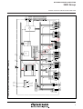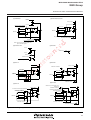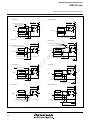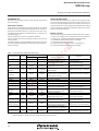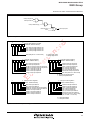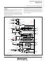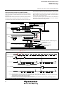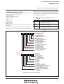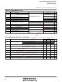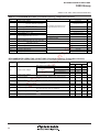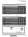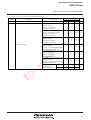
1
To our customers,
Old Company Name in Catalogs and Other Documents
On April 1st, 2010, NEC Electronics Corporation merged with Renesas Technology
Corporation, and Renesas Electronics Corporation took over all the business of both
companies. Therefore, although the old company name remains in this document, it is a valid
Renesas Electronics document. We appreciate your understanding.
Renesas Electronics website: http://www.renesas.com
April 1st, 2010
Renesas Electronics Corporation
Issued by: Renesas Electronics Corporation (http://www.renesas.com)
Send any inquiries to http://www.renesas.com/inquiry.
Notice
1.
2.
3.
4.
5.
6.
7.
All information included in this document is current as of the date this document is issued. Such information, however, is
subject to change without any prior notice. Before purchasing or using any Renesas Electronics products listed herein, please
confirm the latest product information with a Renesas Electronics sales office. Also, please pay regular and careful attention to
additional and different information to be disclosed by Renesas Electronics such as that disclosed through our website.
Renesas Electronics does not assume any liability for infringement of patents, copyrights, or other intellectual property rights
of third parties by or arising from the use of Renesas Electronics products or technical information described in this document.
No license, express, implied or otherwise, is granted hereby under any patents, copyrights or other intellectual property rights
of Renesas Electronics or others.
You should not alter, modify, copy, or otherwise misappropriate any Renesas Electronics product, whether in whole or in part.
Descriptions of circuits, software and other related information in this document are provided only to illustrate the operation of
semiconductor products and application examples. You are fully responsible for the incorporation of these circuits, software,
and information in the design of your equipment. Renesas Electronics assumes no responsibility for any losses incurred by
you or third parties arising from the use of these circuits, software, or information.
When exporting the products or technology described in this document, you should comply with the applicable export control
laws and regulations and follow the procedures required by such laws and regulations. You should not use Renesas
Electronics products or the technology described in this document for any purpose relating to military applications or use by
the military, including but not limited to the development of weapons of mass destruction. Renesas Electronics products and
technology may not be used for or incorporated into any products or systems whose manufacture, use, or sale is prohibited
under any applicable domestic or foreign laws or regulations.
Renesas Electronics has used reasonable care in preparing the information included in this document, but Renesas Electronics
does not warrant that such information is error free. Renesas Electronics assumes no liability whatsoever for any damages
incurred by you resulting from errors in or omissions from the information included herein.
Renesas Electronics products are classified according to the following three quality grades: “Standard”, “High Quality”, and
“Specific”. The recommended applications for each Renesas Electronics product depends on the product’s quality grade, as
indicated below. You must check the quality grade of each Renesas Electronics product before using it in a particular
application. You may not use any Renesas Electronics product for any application categorized as “Specific” without the prior
written consent of Renesas Electronics. Further, you may not use any Renesas Electronics product for any application for
which it is not intended without the prior written consent of Renesas Electronics. Renesas Electronics shall not be in any way
liable for any damages or losses incurred by you or third parties arising from the use of any Renesas Electronics product for an
application categorized as “Specific” or for which the product is not intended where you have failed to obtain the prior written
consent of Renesas Electronics. The quality grade of each Renesas Electronics product is “Standard” unless otherwise
expressly specified in a Renesas Electronics data sheets or data books, etc.
“Standard”:
8.
9.
10.
11.
12.
Computers; office equipment; communications equipment; test and measurement equipment; audio and visual
equipment; home electronic appliances; machine tools; personal electronic equipment; and industrial robots.
“High Quality”: Transportation equipment (automobiles, trains, ships, etc.); traffic control systems; anti-disaster systems; anticrime systems; safety equipment; and medical equipment not specifically designed for life support.
“Specific”:
Aircraft; aerospace equipment; submersible repeaters; nuclear reactor control systems; medical equipment or
systems for life support (e.g. artificial life support devices or systems), surgical implantations, or healthcare
intervention (e.g. excision, etc.), and any other applications or purposes that pose a direct threat to human life.
You should use the Renesas Electronics products described in this document within the range specified by Renesas Electronics,
especially with respect to the maximum rating, operating supply voltage range, movement power voltage range, heat radiation
characteristics, installation and other product characteristics. Renesas Electronics shall have no liability for malfunctions or
damages arising out of the use of Renesas Electronics products beyond such specified ranges.
Although Renesas Electronics endeavors to improve the quality and reliability of its products, semiconductor products have
specific characteristics such as the occurrence of failure at a certain rate and malfunctions under certain use conditions. Further,
Renesas Electronics products are not subject to radiation resistance design. Please be sure to implement safety measures to
guard them against the possibility of physical injury, and injury or damage caused by fire in the event of the failure of a
Renesas Electronics product, such as safety design for hardware and software including but not limited to redundancy, fire
control and malfunction prevention, appropriate treatment for aging degradation or any other appropriate measures. Because
the evaluation of microcomputer software alone is very difficult, please evaluate the safety of the final products or system
manufactured by you.
Please contact a Renesas Electronics sales office for details as to environmental matters such as the environmental
compatibility of each Renesas Electronics product. Please use Renesas Electronics products in compliance with all applicable
laws and regulations that regulate the inclusion or use of controlled substances, including without limitation, the EU RoHS
Directive. Renesas Electronics assumes no liability for damages or losses occurring as a result of your noncompliance with
applicable laws and regulations.
This document may not be reproduced or duplicated, in any form, in whole or in part, without prior written consent of Renesas
Electronics.
Please contact a Renesas Electronics sales office if you have any questions regarding the information contained in this
document or Renesas Electronics products, or if you have any other inquiries.
(Note 1) “Renesas Electronics” as used in this document means Renesas Electronics Corporation and also includes its majorityowned subsidiaries.
(Note 2) “Renesas Electronics product(s)” means any product developed or manufactured by or for Renesas Electronics.
To all our customers
Regarding the change of names mentioned in the document, such as Mitsubishi
Electric and Mitsubishi XX, to Renesas Technology Corp.
The semiconductor operations of Hitachi and Mitsubishi Electric were transferred to Renesas
Technology Corporation on April 1st 2003. These operations include microcomputer, logic, analog
and discrete devices, and memory chips other than DRAMs (flash memory, SRAMs etc.)
Accordingly, although Mitsubishi Electric, Mitsubishi Electric Corporation, Mitsubishi
Semiconductors, and other Mitsubishi brand names are mentioned in the document, these names
have in fact all been changed to Renesas Technology Corp. Thank you for your understanding.
Except for our corporate trademark, logo and corporate statement, no changes whatsoever have been
made to the contents of the document, and these changes do not constitute any alteration to the
contents of the document itself.
Note : Mitsubishi Electric will continue the business operations of high frequency & optical devices
and power devices.
Renesas Technology Corp.
Customer Support Dept.
April 1, 2003
MITSUBISHI MICROCOMPUTERS
3820 Group
SINGLE-CHIP 8-BIT CMOS MICROCOMPUTER
• LCD drive control circuit
DESCRIPTION
The 3820 group is the 8-bit microcomputer based on the 740 family core technology.
The 3820 group has the LCD drive control circuit and the serial I/
O as additional functions.
The various microcomputers in the 3820 group include variations
of internal memory size and packaging. For details, refer to the
section on part numbering.
For details on availability of microcomputers in the 3820 group, refer to the section on group expansion.
•
•
•
FEATURES
• Basic machine-language instructions ....................................... 71
• The minimum instruction execution time ............................ 0.5 µs
(at 8MHz oscillation frequency)
• Memory size
ROM .................................................................. 4 K to 32 K bytes
RAM ................................................................. 192 to 1024 bytes
Programmable input/output ports ............................................. 43
Software pull-up/pull-down resistors (Ports P0-P7 except Port P4 0)
Interrupts .................................................. 16 sources, 16 vectors
(includes key input interrupt)
Timers ........................................................... 8-bit ✕ 3, 16-bit ✕ 2
Serial I/O1 ..................... 8-bit ✕ 1 (UART or Clock-synchronized)
Serial I/O2 .................................... 8-bit ✕ 1 (Clock-synchronized)
•
•
•
•
•
•
•
•
Bias ................................................................................... 1/2, 1/3
Duty ............................................................................ 1/2, 1/3, 1/4
Common output .......................................................................... 4
Segment output ......................................................................... 40
2 Clock generating circuit
Clock (X IN-XOUT) .................................. Internal feedback resistor
Sub-clock (XCIN -XCOUT) .......... Without internal feedback resistor
(connect to external ceramic resonator or quartz-crystal oscillator)
Watchdog timer ............................................................. 15-bit ✕ 1
Power source voltage
In high-speed mode .................................................... 4.0 to 5.5 V
(at 8MHz oscillation frequency and high-speed selected)
In middle-speed mode ................................................2.5 to 5.5 V
(at 8MHz oscillation frequency and middle-speed selected)
In low-speed mode ...................................................... 2.5 to 5.5 V
(Extended operating temperature version: 3.0 V to 5.5 V)
Power dissipation
In high-speed mode ........................................................... 32 mW
(at 8 MHz oscillation frequency)
In low-speed mode .............................................................. 45 µW
(at 32 kHz oscillation frequency, at 3 V power source voltage)
Operating temperature range ................................... – 20 to 85°C
(Extended operating temperature version: –40 to 85°C)
APPLICATIONS
Household appliances, consumer electronics, etc.
P30/SEG16
P31/SEG17
P32/SEG18
P33/SEG19
P34/SEG20
P35/SEG21
P36/SEG22
P37/SEG23
P00/SEG24
P01/SEG25
P02/SEG26
P03/SEG27
P04/SEG28
P05/SEG29
P06/SEG30
P07/SEG31
P10/SEG32
P11/SEG33
P12/SEG34
P13/SEG35
P14/SEG36
P15/SEG37
P16/SEG38
P17/SEG39
PIN CONFIGURATION (TOP VIEW)
64 63 62 61 60 59 58 57 56 55 54 53 52 51 50 49 48 47 46 45 44 43 42 41
65
40
66
39
67
38
68
37
69
36
70
35
34
71
M38203M4-XXXFP
M38203M4-XXXFP
72
73
74
33
32
31
75
30
76
29
77
28
78
27
79
80
26
25
1 2 3 4
5 6 7 8 9 10 11 12 13 14 15 16 17 18 19 20 21 22 23 24
SEG0
COM3
COM2
COM1
COM0
VL3
VL2
VL1
P61/RTP1
P60/INT3/RTP0
P57/INT2
P56/TOUT
P55/CNTR1
P54/CNTR0
P53/SRDY2
P52/SCLK2
P51/SOUT2
P50/SIN2
P47/SRDY1
P46/SCLK1
P45/TXD
P44/RXD
P43/INT1
P42/INT0
SEG15
SEG14
SEG13
SEG12
SEG11
SEG10
SEG9
SEG8
VCC
SEG7
SEG6
SEG5
SEG4
SEG3
SEG2
SEG1
Package type : 80P6N-A
80-pin plastic molded QFP
P20
P21
P22
P23
P24
P25
P26
P27
VSS
XOUT
XIN
P70/XCOUT
P71/XCIN
RESET
P40
P41/φ
MITSUBISHI MICROCOMPUTERS
3820 Group
SINGLE-CHIP 8-BIT CMOS MICROCOMPUTER
P32/SEG18
P33/SEG19
P34/SEG20
P35/SEG21
P36/SEG22
P37/SEG23
P00/SEG24
P01/SEG25
P02/SEG26
P03/SEG27
P04/SEG28
P05/SEG29
P06/SEG30
P07/SEG31
P10/SEG32
P11/SEG33
P12/SEG34
P13/SEG35
P14/SEG36
P15/SEG37
PIN CONFIGURATION (TOP VIEW)
60 59 58 57 56 55 54 53 52 51 50 49 48 47 46 45 44 43 42 41
P31/SEG17
P30/SEG16
SEG15
SEG14
SEG13
SEG12
SEG11
SEG10
SEG9
SEG8
VCC
SEG7
SEG6
SEG5
SEG4
SEG3
SEG2
SEG1
SEG0
COM3
61
40
62
39
63
38
64
37
65
36
66
35
67
34
68
33
M38203M4-XXXGP
M38203M4-XXXHP
69
70
71
72
31
30
29
73
28
74
27
75
26
76
25
77
24
78
23
79
22
21
80
3 4 5 6 7 8 9 10 11 12 13 14 15 16 17 18 19 20
COM2
COM1
COM0
VL3
VL2
VL1
P61/RTP1
P60/INT3/RTP0
P57/INT2
P56/TOUT
P55/CNTR1
P54/CNTR0
P53/SRDY2
P52/SCLK2
P51/SOUT2
P50/SIN2
P47/SRDY1
P46/SCLK1
P45/TXD
P44/RXD
1 2
Package type : 80P6S-A/80P6D-A
80-pin plastic-molded QFP
2
32
P16/SEG38
P17/SEG39
P20
P21
P22
P23
P24
P25
P26
P27
VSS
XOUT
XIN
P70/XCOUT
P71/XCIN
RESET
P40
P41/φ
P42/INT0
P43/INT1
9 10
I/O port P6
P6(2)
28 29
P7(2)
I/O port P7
XCOUT
XCIN
XCOUT
Subclock
output
Watchdog timer
XCIN
Subclock
input
RESET
φ
Clock generating
circuit
31
29
INT2
30
28
I/O port P5
11 12 13 14 15 16 17 18
P5(8)
PS
PCL
S
Y
X
A
P4(8)
I/O port P4
19 20 21 22 23 24 25 26
RTP0,RTP1
SI/O2(8)
TOUT
CNTR0,CNTR1
PCH
CPU
1
27
Reset input
RESET
P3(8)
Input port P3
P2(8)
LCD display
RAM
(20 bytes)
RAM
I/O port P2
33 34 35 36 37 38 39 40
Timer 3(8)
Timer 2(8)
Timer Y(16)
Timer X(16)
ROM
Timer 1(8)
32
VSS
(0V)
57 58 59 60 61 62 63 64
Data bus
SI/O1(8)
73
(5V)
VCC
φ
Clock
output
XOUT
INT0,INT1
Clock
input
XIN
Real time port function
FUNCTIONAL BLOCK DIAGRAM (Package : 80P6N-A)
49 50 51 52 53 54 55 56
I/O port P0
I/O port P1
P0(8)
P0(8)
41 42 43 44 45 46 47 48
P1(8)
LCD
drive control
circuit
COM0
COM1
COM2
COM3
5
65
66
67
68
69
70
71
72
74
75
76
77
78
79
80
1
2
3
4
SEG0
SEG1
SEG2
SEG3
SEG4
SEG5
SEG6
SEG7
SEG8
SEG9
SEG10
SEG11
SEG12
SEG13
SEG14
SEG15
VL1
VL2
VL3
6
7
8
MITSUBISHI MICROCOMPUTERS
3820 Group
SINGLE-CHIP 8-BIT CMOS MICROCOMPUTER
3
Key-on wake up
MITSUBISHI MICROCOMPUTERS
3820 Group
SINGLE-CHIP 8-BIT CMOS MICROCOMPUTER
PIN DESCRIPTION
Pin
VCC
Name
Function
Function except a port function
Power source
• Apply voltage of 2.5 V to 5.5 V to V CC, and 0 V to VSS.
(Extended operating temperature version : 3.0 V to 5.5 V)
RESET
Reset input
• Reset input pin for active “L”
XIN
Clock input
XOUT
Clock output
• Input and output pins for the main clock generating circuit.
• Feedback resistor is built in between X IN pin and XOUT pin.
• Connect a ceramic resonator or a quartz-crystal oscillator between the X IN and X OUT pins to set
the oscillation frequency.
• If an external clock is used, connect the clock source to the XIN pin and leave the X OUT pin open.
• This clock is used as the oscillating source of system clock.
VL1 – VL3
LCD power source
• Input 0 ≤ VL1 ≤ VL2 ≤ V L3 ≤ VCC voltage
• Input 0 – V L3 voltage to LCD
COM 0 – COM3
Common output
• LCD common output pins
• COM2 and COM3 are not used at 1/2 duty ratio.
• COM3 is not used at 1/3 duty ratio.
SEG 0 – SEG15
Segment output
• LCD segment output pins
P00 /SEG 24 –
P07 /SEG 31
I/O port P0
•
•
•
•
P10 /SEG 32 –
P17 /SEG 39
I/O port P1
•
•
•
•
P20 – P27
I/O port P2
•
•
•
•
8-bit I/O port
CMOS compatible input level
CMOS 3-state output structure
I/O direction register allows each pin to be individually
programmed as either input or output.
• Pull-up control is enabled.
• Key input (key-on wake up) interrupt
input pins
P30 /SEG 16 –
P37 /SEG 23
Input port P3
• 8-bit Input port
• CMOS compatible input level
• Pull-down control is enabled.
• LCD segment pins
P40
Input port P4
• 1-bit input pin
• CMOS compatible input level
P41 / φ
I/O port P4
•
•
•
•
VSS
P42 /INT0 ,
P43 /INT1
P44/RXD,
P45/TXD,
P46 /SCLK1,
P47/SRDY1
4
8-bit I/O port
CMOS compatible input level
CMOS 3-state output structure
I/O direction register allows each port to be individually
programmed as either input or output.
• Pull-down control is enabled.
• LCD segment pins
8-bit I/O port
CMOS compatible input level
CMOS 3-state output structure
I/O direction register allows each port to be individually
programmed as either input or output.
• Pull-down control is enabled.
7-bit I/O port
CMOS compatible input level
CMOS 3-state output structure
I/O direction register allows each pin to be individually
programmed as either input or output.
• Pull-up control is enabled.
• φ clock output pin
• Interrupt input pins
• Serial I/O1 function pins
MITSUBISHI MICROCOMPUTERS
3820 Group
SINGLE-CHIP 8-BIT CMOS MICROCOMPUTER
PIN DESCRIPTION
Pin
Name
Function
Function except a port function
P50 /SIN2,
P51 /SOUT2,
P52 /SCLK2 ,
P53/SRDY2
I/O port P5
P54 /CNTR0 ,
P55 /CNTR1
•
•
•
•
8-bit I/O port
CMOS compatible input level
CMOS 3-state output structure
I/O direction register allows each pin to be individually
programmed as either input or output.
• Pull-up control is enabled.
• Serial I/O2 function pins
• Timer function pins
P56/T OUT
• Timer output pin
P57 /INT2
• Interrupt input pin
P60/INT3/RTP0
I/O port P6
P61 /RTP1
P70 /XCOUT,
P71 /XCIN
I/O port P7
•
•
•
•
2-bit I/O port
CMOS compatible input level
CMOS 3-state output structure
I/O direction register allows each pin to be individually
programmed as either input or output.
• Pull-up control is enabled.
• Interrupt input pins(P60)
•
•
•
•
• Sub-clock generating circuit input
pins
(Connect a resonator. External clock
cannot be used.)
2-bit I/O port
CMOS compatible input level
CMOS 3-state output structure
I/O direction register allows each pin to be individually
programmed as either input or output.
• Pull-up control is enabled.
• Real time port function pin
5
MITSUBISHI MICROCOMPUTERS
3820 Group
SINGLE-CHIP 8-BIT CMOS MICROCOMPUTER
PART NUMBERING
Product M3820 3 M 4 - XXX FP
Package type
FP : 80P6N-A package
GP : 80P6S-A package
HP : 80P6D-A package
FS : 80D0 package
ROM number
Omitted in some types.
Normally, using hyphen
When electrical characteristic, or division of quality
identification code using alphanumeric character
– : standard
D : Extended operating temperature version
ROM/PROM size
1 : 4096 bytes
2 : 8192 bytes
3 : 12288 bytes
4 : 16384 bytes
5 : 20480 bytes
6 : 24576 bytes
7 : 28672 bytes
8 : 32768 bytes
The first 128 bytes and the last 2 bytes of ROM
are reserved areas ; they cannot be used.
Memory type
M : Mask ROM version
E : EPROM or One Time PROM version
RAM size
0 : 192 bytes
1 : 256 bytes
2 : 384 bytes
3 : 512 bytes
4 : 640 bytes
5 : 768 bytes
6 : 896 bytes
7 : 1024 bytes
6
MITSUBISHI MICROCOMPUTERS
3820 Group
SINGLE-CHIP 8-BIT CMOS MICROCOMPUTER
GROUP EXPANSION
(3) Packages
80P6N-A ............................. 0.8 mm-pitch plastic molded QFP
80P6S-A ........................... 0.65 mm-pitch plastic molded QFP
80P6D-A ............................. 0.5 mm-pitch plastic molded QFP
80D0 ................ 0.8 mm-pitch ceramic LCC (EPROM version)
Mitsubishi plans to expand the 3820 group as follows:
(1) Support for mask ROM, One Time PROM, and EPROM
versions
(2) ROM/PROM size .......................................... 8 K to 32 K bytes
RAM size ..................................................... 512 to 1024 bytes
Memory Expansion Plan
New product
ROM size (bytes)
32K
M38207M8/E8
28K
24K
20K
Mass product
16K
M38203M4/E4
12K
8K
4K
192 256
384
512
640
768
896
1024
RAM size (bytes)
As of May 1996
Currently supported products are listed below.
Product
M38203M4-XXXFP
M38203E4-XXXFP
M38203E4FP
M38203M4-XXXGP
M38203E4-XXXGP
M38203E4GP
M38203M4-XXXHP
M38203E4-XXXHP
M38203E4HP
M38203E4FS
M38207M8-XXXFP
M38207E8-XXXFP
M38207E8FP
M38207M8-XXXGP
M38207E8-XXXGP
M38207E8GP
M38207M8-XXXHP
M38207E8-XXXHP
M38207E8HP
M38207E8FS
(P) ROM size (bytes)
ROM size for User in ( )
RAM size (bytes)
Package
80P6N-A
16384
(16254)
512
80P6S-A
80P6D-A
80D0
80P6N-A
32768
(32638)
1024
80P6S-A
80P6D-A
80D0
Remarks
Mask ROM version
One Time PROM version
One Time PROM version (blank)
Mask ROM version
One Time PROM version
One Time PROM version (blank)
Mask ROM version
One Time PROM version
One Time PROM version (blank)
EPROM version
Mask ROM version
One Time PROM version
One Time PROM version (blank)
Mask ROM version
One Time PROM version
One Time PROM version (blank)
Mask ROM version
One Time PROM version
One Time PROM version (blank)
EPROM version
7
MITSUBISHI MICROCOMPUTERS
3820 Group
SINGLE-CHIP 8-BIT CMOS MICROCOMPUTER
GROUP EXPANSION
(EXTENDED OPERATING TEMPERATURE VERSION)
(2) ROM size ................................................... 16 K to 32 K bytes
RAM size ..................................................... 512 to 1024 bytes
(3) Packages
80P6N-A ............................. 0.8 mm-pitch plastic molded QFP
80P6S-A ............................0.65 mm-pitch plastic molded QFP
Mitsubishi plans to expand the 3820 group (extended operating
temperature version) as follows:
(1) Support for mask ROM, One Time PROM, and EPROM
versions
Memory Expansion Plan
New product
ROM size (bytes)
32K
M38207M8D
28K
24K
20K
New product
16K
M38203M4D
12K
8K
4K
192 256
384
512
640
768
896
1024
RAM size (bytes)
As of May 1996
Currently supported products are listed below.
8
Product
ROM size (bytes)
ROM size for User in ( )
M38203M4DXXXFP
16384(16254)
M38207M8DXXXFP
M38207M8DXXXGP
RAM size (bytes)
Package
Remarks
512
1024
80P6N-A
Mask ROM version
32768(32638)
80P6N-A
Mask ROM version
32768(32638)
1024
80P6S-A
Mask ROM version
MITSUBISHI MICROCOMPUTERS
3820 Group
SINGLE-CHIP 8-BIT CMOS MICROCOMPUTER
GROUP EXPANSION
(LOW POWER SOURCE VOLTAGE VERSION)
Mitsubishi plans to expand the 3820 group (low power source voltage version) as follows:
(1) Support for mask ROM version
(2) ROM size ...................................................... 8 K to 32 K bytes
RAM size .................................................................. 512 bytes
(3) Packages
80P6N-A ............................. 0.8 mm-pitch plastic molded QFP
80P6S-A ........................... 0.65 mm-pitch plastic molded QFP
80P6D-A ............................. 0.5 mm-pitch plastic molded QFP
Memory Expansion Plan
ROM size (bytes)
32K
28K
24K
20K
New product
16K
M38203M4L
12K
New product
8K
M38203M2L
4K
192 256
384
512
640
768
896
1024
RAM size (bytes)
As of May 1996
Currently supported products are listed below.
Product
M38203M2LXXXFP
M38203M2LXXXGP
M38203M2LXXXHP
M38203M4LXXXFP
M38203M4LXXXGP
M38203M4LXXXHP
ROM size (bytes)
ROM size for User in ( )
RAM size (bytes)
80P6N-A
8192
(8062)
512
16384
(16254)
Package
80P6S-A
80P6D-A
80P6N-A
80P6S-A
80P6D-A
Remarks
Mask ROM version
Mask ROM version
Mask ROM version
Mask ROM version
Mask ROM version
Mask ROM version
9
MITSUBISHI MICROCOMPUTERS
3820 Group
SINGLE-CHIP 8-BIT CMOS MICROCOMPUTER
FUNCTIONAL DESCRIPTION
Central Processing Unit (CPU)
The 3820 group uses the standard 740 family instruction set. Refer to the table of 740 family addressing modes and machine instructions or the SERIES 740 <Software> User’s Manual for details on the instruction set.
Machine-resident 740 family instructions are as follows:
The FST and SLW instruction cannot be used.
The STP, WIT, MUL, and DIV instruction can be used.
CPU Mode Register
The CPU mode register is allocated at address 003B16 .
The CPU mode register contains the stack page selection bit and
the internal system clock selection bit.
7
0
CPU mode register
(CPUM (CM) : address 003B16)
Processor mode bits
b1 b0
0 0 : Single-chip mode
0 1 :
1 0 : Not available
1 1 :
Stack page selection bit
0 : 0 RAM in the zero page is used as stack area
1 : 1 RAM in page 1 is used as stack area
Not used (returns “1” when read)
(Do not write “0” to this bit)
Port X C switch bit
0 : I/O port
1 : X CIN, XCOUT
Main clock ( X IN–XOUT ) stop bit
0 : Oscillating
1 : Stopped
Main clock division ratio selection bit
0 : f(X IN)/2 (high-speed mode)
1 : f(X IN)/8 (middle-speed mode)
Internal system clock selection bit
0 : X IN-XOUT selected (middle-/high-speed mode)
1 : X CIN-XCOUT selected (low-speed mode)
Fig. 1 Structure of CPU mode register
10
MITSUBISHI MICROCOMPUTERS
3820 Group
SINGLE-CHIP 8-BIT CMOS MICROCOMPUTER
MEMORY
Special Function Register (SFR) Area
The Special Function Register area in the zero page contains control registers such as I/O ports and timers.
RAM
RAM is used for data storage and for stack area of subroutine
calls and interrupts.
Zero Page
The 256 bytes from addresses 000016 to 00FF16 are called the
zero page area. The internal RAM and the special function registers (SFR) are allocated to this area.
The zero page addressing mode can be used to specify memory
and register addresses in the zero page area. Access to this area
with only 2 bytes is possible in the zero page addressing mode.
Special Page
ROM
The first 128 bytes and the last 2 bytes of ROM are reserved for
device testing and the rest is user area for storing programs.
Interrupt Vector Area
The 256 bytes from addresses FF0016 to FFFF16 are called the
special page area. The special page addressing mode can be
used to specify memory addresses in the special page area. Access to this area with only 2 bytes is possible in the special page
addressing mode.
The interrupt vector area contains reset and interrupt vectors.
RAM area
RAM size
(bytes)
Address
XXXX16
192
256
384
512
640
768
896
1024
00FF16
013F16
01BF16
023F16
02BF16
033F16
03BF16
043F16
000016
SFR area
004016 LCD display RAM area
RAM
Zero page
005416
010016
XXXX16
Reserved area
044016
ROM area
Not used
ROM size
(bytes)
Address
YYYY16
Address
ZZZZ16
4096
8192
12288
16384
20480
24576
28672
32768
F00016
E00016
D00016
C00016
B00016
A00016
900016
800016
F08016
E08016
D08016
C08016
B08016
A08016
908016
808016
YYYY16
Reserved ROM area
(128 bytes)
ZZZZ16
ROM
FF0016
FFDC16
Interrupt vector area
FFFE16
FFFF16
Special page
Reserved ROM area
Fig. 2 Memory map diagram
11
MITSUBISHI MICROCOMPUTERS
3820 Group
SINGLE-CHIP 8-BIT CMOS MICROCOMPUTER
000016
Port P0 (P0)
002016
Timer X (low-order) (TXL)
000116
Port P0 direction register (P0D)
002116
Timer X (high-order) (TXH)
000216
Port P1 (P1)
002216
Timer Y (low-order) (TYL)
000316
Port P1 direction register (P1D)
002316
Timer Y (high-order) (TYH)
000416
Port P2 (P2)
002416
Timer 1 (T1)
000516
Port P2 direction register (P2D)
002516
Timer 2 (T2)
000616
Port P3 (P3)
002616
Timer 3 (T3)
002716
Timer X mode register (TXM)
000716
000816
Port P4 (P4)
002816
Timer Y mode register (TYM)
000916
Port P4 direction register (P4D)
002916
Timer 123 mode register (T123M)
000A16
Port P5 (P5)
002A16
φ output control register (CKOUT)
000B16
Port P5 direction register (P5D)
002B16
000C16
Port P6 (P6)
002C16
000D16
Port P6 direction register (P6D)
002D16
000E16
Port P7 (P7)
002E16
000F16
Port P7 direction register (P7D)
002F16
001016
003016
001116
003116
001216
003216
001316
003316
001416
003416
001516
003516
001616
PULL register A (PULLA)
003616
001716
PULL register B (PULLB)
003716
Watchdog timer control register (WDTCON)
001816
Transmit/Receive buffer register (TB/RB)
003816
Segment output enable register (SEG)
001916
Serial I/O1 status register (SIO1STS)
003916
LCD mode register (LM)
001A16
Serial I/O1 control register (SIO1CON)
003A16
Interrupt edge selection register (INTEDGE)
001B16
UART control register (UARTCON)
003B16
CPU mode register (CPUM)
001C16
Baud rate generator (BRG)
003C16
Interrupt request register 1(IREQ1)
001D16
Serial I/O2 control register (SIO2CON)
003D16
Interrupt request register 2(IREQ2)
001E16
001F16
Serial I/O2 register (SIO2)
Fig.3 Memory map of special function register (SFR)
12
003E16
Interrupt control register 1(ICON1)
003F16
Interrupt control register 2(ICON2)
MITSUBISHI MICROCOMPUTERS
3820 Group
SINGLE-CHIP 8-BIT CMOS MICROCOMPUTER
I/O PORTS
Direction Registers (ports P2, P41–P4 7, and
P5–P7)
The 3820 group has 43 programmable I/O pins arranged in seven
I/O ports (ports P0–P2 and P4–P7). The I/O ports P2, P41–P4 7,
and P5–P7 have direction registers which determine the input/output direction of each individual pin. Each bit in a direction register
corresponds to one pin, each pin can be set to be input port or
output port.
When “0” is written to the bit corresponding to a pin, that pin becomes an input pin. When “1” is written to that bit, that pin becomes an output pin.
If data is read from a pin set to output, the value of the port output
latch is read, not the value of the pin itself. Pins set to input are
floating. If a pin set to input is written to, only the port output latch
is written to and the pin remains floating.
7
0
PULL register A
(PULLA : address 0016 16)
P00–P07 pull-down
P10–P17 pull-down
P20–P27 pull-up
P30–P37 pull-down
P70, P71 pull-up
Not used (return "0" when read)
7
0
PULL register B
(PULLB : address 0017 16)
P41–P43 pull-up
P44–P47 pull-up
P50–P53 pull-up
P54–P57 pull-up
P60, P61 pull-up
Not used (return "0" when read)
Direction Registers (ports P0 and P1)
Ports P0 and P1 have direction registers which determine the input /output direction of each individual port.
Each port in a direction register corresponds to one port, each
port can be set to be input or output.
When “0” is written to the bit 0 of a direction register, that port becomes an input port. When “1” is written to that port, that port becomes an output port.
Bits 1 to 7 of ports P0 and P1 direction registers are not used.
0 : Disable
1 : Enable
Note : The contents of PULL register A
and PULL register B do not affect
ports programmed as the output ports.
Fig. 4 Structure of PULL register A and PULL register B
Ports P3 and P40
These ports are only for input.
Pull-up/Pull-down Control
By setting the PULL register A (address 001616) or the PULL register B (address 001716 ), ports except for port P4 0 can control either pull-down or pull-up (pins that are shared with the segment
output pins for LCD are pull-down; all other pins are pull-up) with a
program.
However, the contents of PULL register A and PULL register B do
not affect ports programmed as the output ports.
13
MITSUBISHI MICROCOMPUTERS
3820 Group
SINGLE-CHIP 8-BIT CMOS MICROCOMPUTER
Pin
Name
Input/Output
P00 /SEG24 –
P07 /SEG31
Port P0
Input/output,
individual ports
P10 /SEG32 –
P17 /SEG39
Port P1
Input/output,
individual ports
P20 – P27
Port P2
Input/output,
individual bits
P30 /SEG16 –
P37 /SEG23
Port P3
Input
CMOS compatible
input level
Input
CMOS compatible
input level
P40
I/O Format
CMOS compatible
input level
CMOS 3-state output
CMOS compatible
input level
CMOS 3-state output
CMOS compatible
input level
CMOS 3-state output
P41 / φ
P42 /INT0 ,
P43 /INT1
Non-Port Function
LCD segment output
LCD segment output
Key input(Key-on
wake up) interrupt
input
LCD segment output
Input/output,
individual bits
P44 /RXD
P45 /TXD
P46 /SCLK1
P47/SRDY1
P50 /SIN2
P51 /SOUT2
P52 /SCLK2
P53/SRDY2
CMOS compatible
input level
CMOS 3-state output
External interrupt input
Serial I/O1 function I/O
Serial I/O2 function I/O
P54 /CNTR0
Port P5
P55 /CNTR1
Input/output,
individual bits
CMOS compatible
input level
CMOS 3-state output
Timer I/O
Timer I/O
P56/T OUT
Timer output
P57 /INT2
External interrupt input
P60/INT3/RTP0
Port P6
Input/output,
individual bits
CMOS compatible
input level
CMOS 3-state output
P61 /RTP1
P70 /XCOUT
Port P7
P71 /XCIN
COM 0-COM3
SEG0 -SEG15
Common
Segment
Input/output,
individual bits
CMOS compatible
input level
CMOS 3-state output
output
output
LCD common output
LCD segment output
External interrupt input
Real time port
function output
Real time port
function output
Sub-clock
generating circuit
I/O
PULL register B
φ output control
register
PULL register B
Interrupt edge selection
register
PULL register B
Serial I/O1 control register
Serial I/O1 status register
UART control register
PULL register B
Serial I/O2 control
register
PULL register B
Timer X mode register
PULL register B
Timer Y mode register
PULL register B
Timer 123 mode register
PULL register B
Interrupt edge
selection register
PULL register B
Timer X mode register
Interrupt edge
selection register
PULL register B
Timer X mode register
PULL register A
CPU mode register
LCD mode register
Note : Make sure that the input level at each pin is either 0 V or VCC during execution of the STP instruction.
When an input level is at an intermediate potential, a current will flow from VCC to V SS through the input-stage gate.
14
Diagram No.
(1)
(2)
(3)
(4)
φ clock output
Port P4
Related SFRs
PULL register A
Segment output
enable register
PULL register A
Segment output
enable register
PULL register A
Interrupt control
register 2
PULL register A
Segment output
enable register
(5)
(2)
(6)
(7)
(8)
(9)
(10)
(11)
(12)
(13)
(14)
(10)
(15)
(2)
(16)
(17)
(18)
(19)
(20)
MITSUBISHI MICROCOMPUTERS
3820 Group
SINGLE-CHIP 8-BIT CMOS MICROCOMPUTER
(1)Ports P0,P1
(2)Ports P2,P42,P43,P57
VL2/VL3
Pull-up control
VL1/VSS
Segment output enable bit
(Note)
Direction register
Direction register
Data bus
Data bus
Port latch
Port latch
Key input (Key-on wake up) interrupt input
INT0–INT2 interrupt input
Pull-down control
Segment output enable bit
Note. Bit 0 of port P0 direction register and
port P1 direction register.
(3)Ports P30–P37
(4)Port P40
VL2/VL3
Data bus
VL1/VSS
Data bus
Pull-down control
Segment output enable bit
(6)Port P44
(5)Port P41
Pull-up control
Pull-up control
Serial I/O1 enable bit
Reception enable bit
Direction register
Direction register
Port latch
Data bus
Data bus
Port latch
φ output control bit
φ
Serial I/O1 input
(8)Port P46
(7)Port P45
Pull-up control
P45/TXD P-channel output disable bit
Serial I/O1 enable bit
Transmission enable bit
Serial I/O1 synchronization clock
selection bit
Serial I/O1 enable bit
Serial I/O1 mode selection bit
Serial I/O1 enable bit
Direction register
Direction register
Data bus
Port latch
Serial I/O1 output
Pull-up control
Data bus
Port latch
Serial I/O1 clock output
Serial I/O1 clock input
Fig. 5 Port block diagram (1)
15
MITSUBISHI MICROCOMPUTERS
3820 Group
SINGLE-CHIP 8-BIT CMOS MICROCOMPUTER
(9) Port P47
(10) Ports P50,P55
Serial I/O1 mode selection bit
Pull-up control
Pull-up control
Serial I/O1 enable bit
SRDY1 output enable bit
Direction register
Direction register
Data bus
Data bus
Port latch
Port latch
Serial I/O2 input
CNTR1 interrupt input
Serial I/O1 ready output
(11) Port P51
(12) Port P52
Pull-up control
Serial I/O2 transmit completion signal
Internal synchronization clock
select bits
Serial I/O2 port selection bit
Pull-up control
Serial I/O2 port selection bit
Direction register
Direction register
Data bus
Data bus
Port latch
Port latch
Serial I/O2 clock output
Serial I/O2 output
Serial I/O2 clock input
(13) Port P53
(14) Port P54
Pull-up control
Pull-up control
SRDY2 output enable bit
Direction register
Data bus
Direction register
Port latch
Data bus
Port latch
Timer X operating mode bit
(Pulse output mode selection)
Timer output
Serial I/O2 ready output
CNTR0 interrupt input
(15) Port P56
(16) Ports P60, P61
Pull-up control
Pull-up control
Direction register
Direction register
Data bus
Port latch
TOUT output control bit
Timer output
Data bus
Port latch
Real time port control bit
Data for real time port
INT3 interrupt input
Except P61
Fig. 6 Port block diagram (2)
16
MITSUBISHI MICROCOMPUTERS
3820 Group
SINGLE-CHIP 8-BIT CMOS MICROCOMPUTER
(17) Port P70
(18) Port P71
Port selection/Pull-up control
Data bus
Port selection/Pull-up control
Port XC switch bit
Port XC switch bit
Direction register
Direction register
Port latch
Port latch
Data bus
Oscillation circuit
Sub-clock generating circuit input
Port P71
Port XC switch bit
(19) COM0 –COM3
(20) SEG0 – SEG15
VL2/VL3
The voltage applied to the sources of
P-channel and N-channel transistors
is the controlled voltage by the bias
value.
VL3
VL1/VSS
VL2
VL1
The gate input signal of each transistor is
controlled by the LCD duty ratio and the
bias value.
VSS
Fig. 7 Port block diagram (3)
17
MITSUBISHI MICROCOMPUTERS
3820 Group
SINGLE-CHIP 8-BIT CMOS MICROCOMPUTER
INTERRUPTS
Interrupt Operation
Interrupts occur by sixteen sources: seven external, eight internal,
and one software.
When an interrupt is received, the contents of the program counter
and processor status register are automatically stored into the
stack. The interrupt disable flag is set to inhibit other interrupts
from interfering.The corresponding interrupt request bit is cleared
and the interrupt jump destination address is read from the vector
table into the program counter.
Interrupt Control
Each interrupt is controlled by an interrupt request bit, an interrupt
enable bit, and the interrupt disable flag except for the software interrupt set by the BRK instruction. An interrupt occurs if the corresponding interrupt request and enable bits are “1” and the interrupt disable flag is “0”.
Interrupt enable bits can be set or cleared by software.
Interrupt request bits can be cleared by software, but cannot be
set by software.
The BRK instruction cannot be disabled with any flag or bit. The I
(interrupt disable) flag disables all interrupts except the BRK instruction interrupt.
Notes on Use
When the active edge of an external interrupt (INT 0–INT3, CNTR0 ,
or CNTR 1) is changed, the corresponding interrupt request bit
may also be set. Therefore, please take following sequence;
(1) Disable the external interrupt which is selected.
(2) Change the active edge selection.
(3) Clear the interrupt request bit which is selected to “0”.
(4) Enable the external interrupt which is selected.
Table 1. Interrupt vector addresses and priority
Interrupt Source
Priority
Vector Addresses (Note 1)
High
Low
FFFD 16
FFFC 16
Reset (Note 2)
1
INT 0
2
FFFB16
FFFA16
INT 1
3
FFF916
FFF816
Serial I/O1
receive
4
FFF716
FFF616
Serial I/O1
transmit
5
FFF516
FFF416
Timer X
Timer Y
Timer 2
Timer 3
6
7
8
9
FFF316
FFF116
FFEF16
FFED16
FFF216
FFF016
FFEE 16
FFEC16
CNTR 0
10
FFEB 16
FFEA 16
CNTR 1
11
FFE916
FFE816
Timer 1
12
FFE716
FFE616
INT 2
13
FFE516
FFE416
INT 3
14
FFE316
FFE216
Key input
(Key-on wake up)
15
FFE116
FFE016
Serial I/O2
16
FFDF 16
FFDE16
BRK instruction
17
FFDD 16
FFDC16
Interrupt Request
Generating Conditions
At reset
At detection of either rising or
falling edge of INT0 input
At detection of either rising or
falling edge of INT1 input
At completion of serial I/O1
data reception
At completion of serial I/O1
transmit shift or when transmit
buffer register is empty
At timer X underflow
At timer Y underflow
At timer 2 underflow
At timer 3 underflow
At detection of either rising or
falling edge of CNTR0 input
At detection of either rising or
falling edge of CNTR1 input
At timer 1 underflow
At detection of either rising or
falling edge of INT2 input
At detection of either rising or
falling edge of INT3 input
At falling of conjunction of input
level for port P2 (at input mode)
At completion of serial I/O2
data transmission or reception
At BRK instruction execution
Notes 1: Vector addresses contain interrupt jump destination addresses.
2: Reset function in the same way as an interrupt with the highest priority.
18
Remarks
Non-maskable
External interrupt
(active edge selectable)
External interrupt
(active edge selectable)
Valid when serial I/O1 is selected
Valid when serial I/O1 is selected
External interrupt
(active edge selectable)
External interrupt
(active edge selectable)
External interrupt
(active edge selectable)
External interrupt
(active edge selectable)
External interrupt
(valid when an “L” level is applied)
Valid when serial I/O2 is selected
Non-maskable software interrupt
MITSUBISHI MICROCOMPUTERS
3820 Group
SINGLE-CHIP 8-BIT CMOS MICROCOMPUTER
Interrupt request bit
Interrupt enable bit
Interrupt disable flag (I)
Interrupt request
BRK instruction
Reset
Fig. 8 Interrupt control
7
0 Interrupt edge selection register
(INTEDGE : address 003A16)
INT0 interrupt edge selection bit
INT1 interrupt edge selection bit
INT2 interrupt edge selection bit
INT3 interrupt edge selection bit
Not used (return “0” when read)
7
0
0 : Falling edge active
1 : Rising edge active
Interrupt request register 1
(IREQ1 : address 003C16)
7
0
Interrupt request register 2
(IREQ2 : address 003D16)
CNTR0 interrupt request bit
CNTR1 interrupt request bit
Timer 1 interrupt request bit
INT2 interrupt request bit
INT3 interrupt request bit
Key input interrupt request bit
Serial I/O2 interrupt request bit
Not used (returns “0” when read)
INT0 interrupt request bit
INT1 interrupt request bit
Serial I/O1 receive interrupt request bit
Serial I/O1 transmit interrupt request bit
Timer X interrupt request bit
Timer Y interrupt request bit
Timer 2 interrupt request bit
Timer 3 interrupt request bit
0 : No interrupt request issued
1 : Interrupt request issued
7
0 Interrupt control register 1
(ICON1 : address 003E16)
INT0 interrupt enable bit
INT1 interrupt enable bit
Serial I/O1 receive interrupt enable bit
Serial I/O1 transmit interrupt enable bit
Timer X interrupt enable bit
Timer Y interrupt enable bit
Timer 2 interrupt enable bit
Timer 3 interrupt enable bit
7
0
0 Interrupt control register 2
(ICON2 : address 003F16)
CNTR0 interrupt enable bit
CNTR1 interrupt enable bit
Timer 1 interrupt enable bit
INT2 interrupt enable bit
INT3 interrupt enable bit
Key input interrupt enable bit
Serial I/O2 interrupt enable bit
Not used (returns “0” when read)
(Do not write “1” to this bit)
0 : Interrupts disabled
1 : Interrupts enabled
Fig. 9 Structure of interrupt-related registers
19
MITSUBISHI MICROCOMPUTERS
3820 Group
SINGLE-CHIP 8-BIT CMOS MICROCOMPUTER
Key Input Interrupt (Key-on Wake Up)
A key input interrupt request is generated by applying “L” level to
any pin of port P3 that have been set to input mode. In other
words, it is generated when AND of input level goes from “1” to “0”.
An example of using a key input interrupt is shown in Figure 9,
where an interrupt request is generated by pressing one of the
keys consisted as an active-low key matrix which inputs to ports
P20–P23.
Port PXx
"L" level output
PULL register A
Bit 2 = "1"
✽
✽ ✽
✽
✽ ✽
Port P27
direction register = "1"
Key input interrupt request
Port P27
latch
P27 output
Port P26
direction register = "1"
Port P26
latch
P26 output
✽
✽ ✽
✽
✽ ✽
Port P25
direction register = "1"
Port P25
latch
P25 output
Port P24
direction register = "1"
Port P24
latch
P24 output
✽
✽ ✽
✽
✽ ✽
P23 input
P22 input
✽
✽ ✽
✽
✽ ✽
P21 input
P20 input
Port P23
direction register = "0"
Port P2
Input reading circuit
Port P23
latch
Port P22
direction register = "0"
Port P22
latch
Port P21
direction register = "0"
Port P21
latch
Port P20
direction register = "0"
Port P20
latch
✽ P-channel transistor for pull-up
✽ ✽ CMOS output buffer
Fig. 10 Connection example when using key input interrupt and port P2 block diagram
20
MITSUBISHI MICROCOMPUTERS
3820 Group
SINGLE-CHIP 8-BIT CMOS MICROCOMPUTER
TIMERS
Read and write operation on 16-bit timer must be performed for
both high and low-order bytes. When reading a 16-bit timer, read
the high-order byte first. When writing to a 16-bit timer, write the
low-order byte first. The 16-bit timer cannot perform the correct operation when reading during the write operation, or when writing
during the read operation.
The 3820 group has five timers: timer X, timer Y, timer 1, timer 2,
and timer 3. Timer X and timer Y are 16-bit timers, and timer 1,
timer 2, and timer 3 are 8-bit timers.
All timers are down count timers. When the timer reaches “0016 ”,
an underflow occurs at the next count pulse and the corresponding timer latch is reloaded into the timer and the count is continued. When a timer underflows, the interrupt request bit corresponding to that timer is set to “1”.
Real time port
control bit "1"
Data bus
Q D
P60 data for real time port
P60
P60 direction register
Latch
"0"
P60 latch
Real time port
control bit "1"
Q D
P61 data for real time port
P61
P61 direction register
Latch
"0"
Real time port
control bit "0"
P61 latch
f(XIN)/16
(f(XCIN)/16 in low-speed mode*)
P54/CNTR0
Timer X stop
control bit
Timer X operating mode bit
"00","01","11"
CNTR0 active
edge switch bit
"0"
Timer X mode register
write signal
"1"
"10"
"1"
Pulse width
measurement
CNTR0 active
mode
edge switch bit "0"
Timer X write
control bit
Timer X (low) latch (8)
Timer X (high) latch (8)
Timer X (low) (8)
Timer X (high) (8)
CNTR0
interrupt
request
Pulse output mode
QS
Timer Y operating mode bit
"00","01","10"
T
"1"
P54 direction register
Q
Pulse width HL continuously measurement mode
P54 latch
"11"
Rising edge detection
Pulse output mode
CNTR1 active
edge switch bit
"0"
P55/CNTR1
Timer X
interrupt
request
Falling edge detection
f(XIN)/16
(f(XCIN)/16 in low-speed mode*)
Timer Y stop
control bit
"00","01","11"
Period
measurement mode
Timer Y (low) latch (8)
Timer Y (high) latch (8)
Timer Y (low) (8)
Timer Y (high) (8)
Timer Y
interrupt
request
"10"Timer Y operating
mode bit
"1"
f(XIN)/16
(f(XCIN)/16 in low-speed mode*)
Timer 1 count source
selection bit
"0"
Timer 1 latch (8)
Timer 2 count source
selection bit
Timer 2 latch (8)
"0"
Timer 1 (8)
XCIN
"1"
CNTR1
interrupt
request
Timer 2 (8)
"1"
Timer 2 write
control bit
Timer 1
interrupt
request
Timer 2
interrupt
request
f(XIN)/16
(f(XCIN)/16 in low-speed mode*)
TOUT output
TOUT output
control bit
active edge
switch bit "0"
Q S
P56/TOUT
P56 direction register
"1"
P56 latch
T
Q
TOUT output control bit
f(XIN)/16(f(XCIN)/16 in low-speed mode*)
* Internal clock φ = XCIN/2.
"0"
Timer 3 latch (8)
Timer 3 (8)
"1"
Timer 3 count
source selection
bit
Timer 3
interrupt
request
Fig. 11 Timer block diagram
21
MITSUBISHI MICROCOMPUTERS
3820 Group
SINGLE-CHIP 8-BIT CMOS MICROCOMPUTER
Timer X
Timer X is a 16-bit timer that can be selected in one of four modes
and can be controlled the timer X write and the real time port by
setting the timer X mode register.
Timer mode
The timer counts f(XIN)/16 (or f(X CIN)/16 in low-speed mode).
Pulse output mode
Each time the timer underflows, a signal output from the CNTR 0
pin is inverted. Except for this, the operation in pulse output mode
is the same as in timer mode. When using a timer in this mode, set
the corresponding port P54 direction register to output mode.
Event counter mode
The timer counts signals input through the CNTR0 pin.
Except for this, the operation in event counter mode is the same
as in timer mode. When using a timer in this mode, set the corresponding port P5 4 direction register to input mode.
Pulse width measurement mode
The count source is f(XIN )/16 (or f(XCIN )/16 in low-speed mode. If
CNTR0 active edge switch bit is “0”, the timer counts while the input signal of CNTR0 pin is at “H”. If it is “1”, the timer counts while
the input signal of CNTR 0 pin is at “L”. When using a timer in this
mode, set the corresponding port P5 4 direction register to input
mode.
Timer X Write Control
If the timer X write control bit is “0”, when the value is written in the
address of timer X, the value is loaded in the timer X and the latch
at the same time.
If the timer X write control bit is “1”, when the value is written in the
address of timer X, the value is loaded only in the latch. The value
in the latch is loaded in timer X after timer X underflows.
If the value is written in latch only, unexpected value may be set in
the high-order counter when the writing in high-order latch and the
underflow of timer X are performed at the same timing.
Note on CNTR0 Interrupt Active Edge Selection
CNTR0 interrupt active edge depends on the CNTR0 active edge
switch bit.
Real Time Port Control
While the real time port function is valid, data for the real time port
are output from ports P6 0 and P6 1 each time the timer X
underflows. (However, after rewriting a data for real time port, if the
real time port control bit is changed from “0” to “1”, data is output
without the timer X.) If the data for the real time port is changed
while the real time port function is valid, the changed data are output at the next underflow of timer X.
Before using this function, set the corresponding port direction
registers to output mode.
7
0
Timer X mode register
(TXM : address 0027 16)
Timer X write control bit
0 : Write value in latch and counter
1 : Write value in latch only
Real time port control bit
0 : Real time port function invalid
1 : Real time port function valid
P60 data for real time port
0 : "L" level output
1 : "H" level output
P61 data for real time port
0 : "L" level output
1 : "H" level output
Timer X operating mode bits
b5 b4
0 0 : Timer mode
0 1 : Pulse output mode
1 0 : Event counter mode
1 1 : Pulse width measurement mode
CNTR0 active edge switch bit
• CNTR0 interrupt
0 : Falling edge active
1 : Rising edge active
• Pulse output mode
0 : Start at initial level "H" output
1 : Start at initial level "L" output
• Event counter mode
0 : Rising edge active
1 : Falling edge active
• Pulse width measurement mode
0 : Measure "H" level width
1 : Measure "L" level width
Timer X stop control bit
0 : Count start
1 : Count stop
Fig. 12 Structure of timer X mode register
22
MITSUBISHI MICROCOMPUTERS
3820 Group
SINGLE-CHIP 8-BIT CMOS MICROCOMPUTER
Timer Y
Timer Y is a 16-bit timer that can be selected in one of four modes.
Timer mode
The timer counts f(XIN)/16 (or f(XCIN )/16 in low-speed mode).
Period measurement mode
CNTR1 interrupt request is generated at rising/falling edge of
CNTR1 pin input signal. Simultaneously, the value in timer Y latch
is reloaded in timer Y and timer Y continues counting down. /Except for the above-mentioned, the operation in period measurement mode is the same as in timer mode.
The timer value just before the reloading at rising/falling of CNTR1
pin input signal is retained until the timer Y is read once after the
reload.
The rising/falling timing of CNTR 1 pin input signal is found by
CNTR 1 interrupt. When using a timer in this mode, set the corresponding port P5 5 direction register to input mode.
Event counter mode
The timer counts signals input through the CNTR1 pin.
Except for this, the operation in event counter mode is the same
as in timer mode. When using a timer in this mode, set the corresponding port P5 5 direction register to input mode.
7
0
Timer Y mode register
(TYM : address 0028 16)
Not used (return "0" when read)
Timer Y operating mode bits
b5 b4
0 0 : Timer mode
0 1 : Period measurement mode
1 0 : Event counter mode
1 1 : Pulse width HL continuously
measurement mode
CNTR1 active edge switch bit
• CNTR1 interrupt
0 : Falling edge active
1 : Rising edge active
• Period measurement mode
0 : Measure falling edge to falling edge
1 : Measure rising edge to rising edge
• Event counter mode
0 : Rising edge active
1 : Falling edge active
Timer Y stop control bit
0 : Count start
1 : Count stop
Fig. 13 Structure of timer Y mode register
Pulse width HL continuously measurement mode
CNTR 1 interrupt request is generated at both rising and falling
edges of CNTR1 pin input signal. Except for this, the operation in
pulse width HL continuously measurement mode is the same as in
period measurement mode. When using a timer in this mode, set
the corresponding port P55 direction register to input mode.
Note on CNTR1 Interrupt Active Edge Selection
CNTR1 interrupt active edge depends on the CNTR1 active edge
switch bit. However, in pulse width HL continuously measurement
mode, CNTR1 interrupt request is generated at both rising and
falling edges of CNTR1 pin input signal regardless of the setting of
CNTR1 active edge switch bit.
23
MITSUBISHI MICROCOMPUTERS
3820 Group
SINGLE-CHIP 8-BIT CMOS MICROCOMPUTER
Timer 1, Timer 2, Timer 3
Timer 1, timer 2, and timer 3 are 8-bit timers. The count source for
each timer can be selected by timer 123 mode register. The timer
latch value is not affected by a change of the count source. However, because changing the count source may cause an inadvertent count down of the timer. Therefore, rewrite the value of timer
whenever the count source is changed.
Timer 2 Write Control
If the timer 2 write control bit is “0”, when the value is written in the
address of timer 2, the value is loaded in the timer 2 and the latch
at the same time.
If the timer 2 write control bit is “1”, when the value is written in the
address of timer 2, the value is loaded only in the latch. The value
in the latch is loaded in timer 2 after timer 2 underflows.
Timer 2 Output Control
When the timer 2 (T OUT) is output enabled, an inversion signal
from pin TOUT is output each time timer 2 underflows.
In this case, set the port P5 6 shared with the port TOUT to the output mode.
Note on Timer 1 to Timer 3
When the count source of timer 1 to 3 is changed, the timer counting value may be changed large because a thin pulse is generated
in count input of timer. If timer 1 output is selected as the count
source of timer 2 or timer 3, when timer 1 is written, the counting
value of timer 2 or timer 3 may be changed large because a thin
pulse is generated in timer 1 output.
Therefore, set the value of timer in the order of timer 1, timer 2 and
timer 3 after the count source selection of timer 1 to 3.
24
7
0
Timer 123 mode register
(T123M :address 0029 16)
TOUT output active edge switch bit
0 : Start at "H" output
1 : Start at "L" output
TOUT output control bit
0 : TOUT output disabled
1 : TOUT output enabled
Timer 2 write control bit
0 : Write value in latch and counter
1 : Write value in latch only
Timer 2 count source selection bit
0 : Timer 1 underflow
1 : f(XIN)/16
(Middle-/high-speed mode)
f(XCIN)/16
(Low-speed mode)(Note)
Timer 3 count source selection bit
0 : Timer 1 underflow
1 : f(XIN)/16
(Middle-/high-speed mode)
f(XCIN)/16
(Low-speed mode)(Note)
Timer 1 count source selection bit
0 : f(XIN)/16
(Middle-/high-speed mode)
f(XCIN)/16
(Low-speed mode)(Note)
1 : f(XCIN)
Not used (return "0" when read)
Note : Internal clock φ is f (XCIN)/2 in the low-speed mode.
Fig. 14 Structure of timer 123 mode register
MITSUBISHI MICROCOMPUTERS
3820 Group
SINGLE-CHIP 8-BIT CMOS MICROCOMPUTER
SERIAL I/O1
Clock Synchronous Serial I/O1 Mode
Serial I/O1 can be used as either clock synchronous or asynchronous (UART) serial I/O1. A dedicated timer (baud rate generator)
is also provided for baud rate generation.
Clock synchronous serial I/O1 mode can be selected by setting
the mode selection bit of the serial I/O1 control register to “1”.
For clock synchronous serial I/O1, the transmitter and the receiver
must use the same clock. If an internal clock is used, transfer is
started by a write signal to the TB/RB (address 001816).
Data bus
Serial I/O1 control register
Address 0018 16
Receive buffer register (RB)
Receive buffer full flag (RBF)
Serial I/O receive interrupt request (RI)
Receive shift register
P44/RXD
Address 001A 16
Shift clock
Clock control circuit
P46/SCLK1
f(X
IN)
XIN
Serial I/O1 synchronization
clock selection bit
Frequency division ratio 1/(n+1)
BRG count source selection bit
Baud rate generator
Address 001C 16
1/4
P47/SRDY1
F/F
1/4
Clock control circuit
Falling-edge detector
Shift clock
P45/TXD
Transmit shift register shift completion flag (TSC)
Transmit interrupt source selection bit
Serial I/O transmit interrupt request (TI)
Transmit shift register
Transmit buffer register (TB)
Address 0018 16
Transmit buffer empty flag (TBE)
Serial I/O1 status register
Address 0019 16
Data bus
Fig. 15 Block diagram of clock synchronous serial I/O1
Transfer shift clock
(1/2 to 1/2048 of the internal
clock, or an external clock)
Serial output TxD
D0
D1
D2
D3
D4
D5
D6
D7
Serial input RxD
D0
D1
D2
D3
D4
D5
D6
D7
Receive enable signal SRDY1
Write signal to receive/transmit
buffer register (address 001816)
TBE = 0
TBE = 1
TSC = 0
RBF = 1
TSC = 1
Overrun error (OE)
detection
Notes 1 : The serial I/O1 transmit interrupt (TI) can be selected to occur either when the transmit buffer register has emptied (TBE=1)
or after the transmit shift operation has ended (TSC=1), by setting the transmit interrupt source selection bit (TIC) of the
serial I/O1 control register.
2 : If data is written to the transmit buffer register when TSC=0, the transmit clock is generated continuously and serial data is
output continuously from the TxD pin.
3 : The serial I/O1 receive interrupt (RI) is set when the receive buffer full flag (RBF) becomes “1” .
Fig. 16 Operation of clock synchronous serial I/O1 function
25
MITSUBISHI MICROCOMPUTERS
3820 Group
SINGLE-CHIP 8-BIT CMOS MICROCOMPUTER
ter, but the two buffers have the same address in memory. Since
the shift register cannot be written to or read from directly, transmit
data is written to the transmit buffer register, and receive data is
read from the receive buffer register.
The transmit buffer register can also hold the next data to be
transmitted, and the receive buffer register can hold a character
while the next character is being received.
Asynchronous Serial I/O1 (UART) Mode
Clock asynchronous serial I/O1 mode (UART) can be selected by
clearing the serial I/O1 mode selection bit of the serial I/O1 control
register to “0”.
Eight serial data transfer formats can be selected, and the transfer
formats used by a transmitter and receiver must be identical.
The transmit and receive shift registers each have a buffer regis-
Data bus
Address 0018 16
Serial I/O1 control register Address 001A16
Receive buffer register(RB)
Receive buffer full flag (RBF)
OE
Character length selection bit
P44/RXD
STdetector
7 bits
Serial I/O receive interrupt request (RI)
Receive shift register
1/16
8 bits
PE FE
UART control register
SP detector
Address 001B16
Clock control circuit
Serial I/O1 synchronization clock selection bit
P46/SCLK1
f(XIN)
BRG count source selection bit Frequency division ratio 1/(n+1)
Baud rate generator
Address 001C 16
1/4
ST/SP/PA generator
Transmit shift register shift completion flag (TSC)
1/16
Transmit shift register
P45/TXD
Transmit interrupt source selection bit
Serial I/O1 status register
Character length selection bit
Transmit buffer register(TB)
Address 001816
Transmit buffer empty flag (TBE)
Serial I/O1 status register Address 001916
Data bus
Fig. 17 Block diagram of UART serial I/O1
Transmit or receive clock
Transmit buffer register
write signal
TBE=0
TSC=0
TBE=1
Serial output TXD
TBE=0
TSC=1✽
TBE=1
ST
D0
D1
SP
ST
D0
Receive buffer register
read signal
SP
D1
✽
1 start bit
7 or 8 data bits
1 or 0 parity bit
1 or 2 stop bit (s)
Generated at 2nd bit in 2-stop-bit mode
RBF=0
RBF=1
Serial input RXD
ST
D0
D1
SP
RBF=1
ST
D0
D1
SP
Notes 1: Error flag detection occurs at the same time that the RBF flag becomes "1" (at 1st stop bit, during reception).
2: The transmit interrupt (TI) can be selected to occur when either the TBE or TSC flag becomes "1", depending on the setting of the transmit interrupt
source selection bit (TIC) of the serial I/O1 control register.
3: The serial I/O1 receive interrupt (RI) is set when the RBF flag becomes "1".
4: After data is written to the transmit buffer register when TSC=1, 0.5 to 1.5 cycles of the data shift cycle is necessary until changing to TSC=0.
Fig. 18 Operation of UART serial I/O1 function
26
MITSUBISHI MICROCOMPUTERS
3820 Group
SINGLE-CHIP 8-BIT CMOS MICROCOMPUTER
Serial I/O1 Control Register (SIO1CON) 001A16
The serial I/O1 control register contains eight control bits for the
serial I/O1 function.
UART Control Register (UARTCON) 001B16
The UART control register consists of four control bits (bits 0 to 3)
which are valid when asynchronous serial I/O is selected and set
the data format of an data transfer. One bit in this register (bit 4) is
always valid and sets the output structure of the P45/T XD pin.
Serial I/O1 Status Register (SIO1STS) 001916
The read-only serial I/O1 status register consists of seven flags
(bits 0 to 6) which indicate the operating status of the serial I/O
function and various errors.
Three of the flags (bits 4 to 6) are valid only in UART mode.
The receive buffer full flag (bit 1) is cleared to “0” when the receive
buffer is read.
If there is an error, it is detected at the same time that data is
transferred from the receive shift register to the receive buffer register, and the receive buffer full flag is set. A write to the serial I/O
status register clears all the error flags OE, PE, FE, and SE (bit 3
to bit 6, respectively). Writing “0” to the serial I/O enable bit SIOE
(bit 7 of the Serial I/O Control Register) also clears all the status
flags, including the error flags.
All bits of the serial I/O1 status register are initialized to “0” at reset, but if the transmit enable bit (bit 4) of the serial I/O control register has been set to “1”, the transmit shift register shift completion
flag (bit 2) and the transmit buffer empty flag (bit 0) become “1”.
Transmit Buffer/Receive Buffer Register (TB/
RB) 001816
The transmit buffer register and the receive buffer register are located at the same address. The transmit buffer register is writeonly and the receive buffer register is read-only. If a character bit
length is 7 bits, the MSB of data stored in the receive buffer register is “0”.
Baud Rate Generator (BRG) 001C16
The baud rate generator determines the baud rate for serial transfer.
The baud rate generator divides the frequency of the count source
by 1/(n + 1), where n is the value written to the baud rate generator.
27
MITSUBISHI MICROCOMPUTERS
3820 Group
SINGLE-CHIP 8-BIT CMOS MICROCOMPUTER
7
0
Serial I/O1 status register
(SIO1STS : address 0019 16)
Transmit buffer empty flag (TBE)
0: Buffer full
1: Buffer empty
Receive buffer full flag (RBF)
0: Buffer empty
1: Buffer full
Transmit shift register shift completion flag (TSC)
0: Transmit shift in progress
1: Transmit shift completed
Overrun error flag (OE)
0: No error
1: Overrun error
Parity error flag (PE)
0: No error
1: Parity error
Framing error flag (FE)
0: No error
1: Framing error
Summing error flag (SE)
0: OE U PE U FE =0
1: OE U PE U FE =1
Not used (returns “1” when read)
7
0
UART control register
(UARTCON : address 001B 16)
Character length selection bit (CHAS)
0: 8 bits
1: 7 bits
Parity enable bit (PARE)
0: Parity checking disabled
1: Parity checking enabled
Parity selection bit (PARS)
0: Even parity
1: Odd parity
Stop bit length selection bit (STPS)
0: 1 stop bit
1: 2 stop bits
P45/TXD P-channel output disable bit (POFF)
0: CMOS output (in output mode)
1: N-channel open-drain output (in output mode)
Not used (return“1” when read)
Fig. 19 Structure of serial I/O1 control registers
28
7
0
Serial I/O1 control register
(SIO1CON : address 001A 16)
BRG count source selection bit (CSS)
0: f(X IN)
1: f(X IN)/4
Serial I/O1 synchronization clock selection bit (SCS)
•In clock synchronous mode
0 : BRG output/4
1 : External clock input
•In UART mode
0 : BRG output/16
1 : External clock input/16
SRDY1 output enable bit (SRDY)
0: P4 7 SRDY1 pin operates as I/O port P47
1: P4 7 SRDY1 pin operates as signal output pin SRDY1
(SRDY1 signal indicates receive enable state)
Transmit interrupt source selection bit (TIC)
0: When transmit buffer has emptied
1: When transmit shift operation is completed
Transmit enable bit (TE)
0: Transmit disabled
1: Transmit enabled
Receive enable bit (RE)
0: Receive disabled
1: Receive enabled
Serial I/O1 mode selection bit (SIOM)
0: Clock asynchronous serial I/O1 (UART) mode
1: Clock synchronous serial I/O1 mode
Serial I/O1 enable bit (SIOE)
0: Serial I/O1 disabled
(pins P4 4–P4 7 operate as I/O pins)
1: Serial I/O1 enabled
(pins P4 4–P4 7 operate as serial I/O1 pins)
MITSUBISHI MICROCOMPUTERS
3820 Group
SINGLE-CHIP 8-BIT CMOS MICROCOMPUTER
SERIAL I/O2
b7
b0
The serial I/O2 function can be used only for clock synchronous
serial I/O.
For clock synchronous serial I/O2 the transmitter and the receiver
must use the same clock. If the internal clock is used, transfer is
started by a write signal to the serial I/O2 register.
Serial I/O2 control register
(SIO2CON : address 001D16)
Internal synchronization clock select bits
b2 b1 b0
0 0 0: f(XIN)/8
0 0 1: f(XIN)/16
0 1 0: f(XIN)/32
0 1 1: f(XIN)/64
1 0 0: Do not set
1 0 1:
1 1 0: f(XIN)/128
1 1 1: f(XIN)/256
Serial I/O2 Control Register (SIO2CON) 001D16
The serial I/O2 control register contains 7 bits which control various serial I/O functions.
Serial I/O2 port selection bit
0: I/O port
1: SOUT2,SCLK2 signal output
SRDY2 output enable bit
0: I/O port
1: SRDY2 signal output
Transfer direction selection bit
0: LSB first
1: MSB first
Synchronization clock selection bit
0: External clock
1: Internal clock
Not used (returns “0” when read)
Fig. 20 Structure of serial I/O2 control register
1/8
Divider
1/16
XIN
Internal synchronization
clock select bits
1/32
Data bus
1/64
1/128
1/256
P53 latch
Synchronization clock
selection bit
"0"
SRDY2
"1"
Synchronization circuit
"1"
SRDY2 output enable bit
SCLK2
P53/SRDY2
"0"
External clock
P52 latch
"0"
P52/SCLK2
"1"
Serial I/O2 port selection bit
Serial I/O counter 2 (3)
Serial I/O2
interrupt request
P51 latch
"0"
P51/SOUT2
"1"
Serial I/O2 port selection bit
P50/SIN2
Serial I/O shift register 2 (8)
Fig. 21 Block diagram of serial I/O2 function
29
MITSUBISHI MICROCOMPUTERS
3820 Group
SINGLE-CHIP 8-BIT CMOS MICROCOMPUTER
Transfer clock (Note 1)
Serial I/O2 register
write signal
(Note 2)
Serial I/O2 output S OUT2
D0
D1
D2
D3
D4
D5
D6
D7
Serial I/O2 input S IN2
Receive enable signal S RDY2
Serial I/O2 interrupt request bit set
Notes 1: When the internal clock is selected as the transfer clock, the divide ratio can be selected by setting bits 0 to 2 of the serial
I/O2 control register.
2: When the internal clock is selected as the transfer clock, the S OUT2 pin goes to high impedance after transfer completion.
Fig. 22 Timing of serial I/O2 function
30
MITSUBISHI MICROCOMPUTERS
3820 Group
SINGLE-CHIP 8-BIT CMOS MICROCOMPUTER
the segment output enable register and the LCD display RAM, the
LCD drive control circuit starts reading the display data automatically, performs the bias control and the duty ratio control, and displays the data on the LCD panel.
LCD DRIVE CONTROL CIRCUIT
The 3820 group has the built-in Liquid Crystal Display (LCD) drive
control circuit consisting of the following.
LCD display RAM
Segment output enable register
LCD mode register
Selector
Timing controller
Common driver
Segment driver
Bias control circuit
A maximum of 40 segment output pins and 4 common output pins
can be used.
Up to 160 pixels can be controlled for LCD display. When the LCD
enable bit is set to “1” after data is set in the LCD mode register,
•
•
•
•
•
•
•
•
7
Table 2. Maximum number of display pixels at each
duty ratio
Duty ratio
2
3
4
Maximum number of display pixel
80 dots
or 8 segment LCD 10 digits
120 dots
or 8 segment LCD 15 digits
160 dots
or 8 segment LCD 20 digits
0
Segment output enable register
(SEG : address 0038 16)
Segment output enable bit 0
0 : Input ports P30–P37
1 : Segment output SEG16–SEG23
Segment output enable bit 1
0 : I/O ports P00, P01
1 : Segment output SEG24,SEG25
Segment output enable bit 2
0 : I/O ports P02–P07
1 : Segment output SEG26–SEG31
Segment output enable bit 3
0 : I/O ports P10,P11
1 : Segment output SEG32,SEG33
Segment output enable bit 4
0 : I/O port P12
1 : Segment output SEG34
Segment output enable bit 5
0 : I/O ports P13–P17
1 : Segment output SEG35–SEG39
Not used (return "0" when read)
(Do not write "1" to this bit)
7
0
LCD mode register
(LM : address 0039 16)
Duty ratio selection bits
0 0 : Not available
0 1 : 2 (use COM 0,COM1)
1 0 : 3 (use COM 0–COM2)
1 1 : 4 (use COM 0–COM3)
Bias control bit
0 : 1/3 bias
1 : 1/2 bias
LCD enable bit
0 : LCD OFF
1 : LCD ON
Not used (returns "0" when read)
(Do not write "1" to this bit)
LCD circuit divider division ratio selection bits
0 0 : LCDCK count source
0 1 : 2 division of LCDCK count source
1 0 : 4 division of LCDCK count source
1 1 : 8 division of LCDCK count source
LCDCK count source selection bit (Note)
0 : f(XCIN)/32
1 : f(XIN)/8192
Note : LCDCK is a clock for a LCD timing controller.
Fig. 23 Structure of segment output enable register and LCD mode register
31
Fig. 24 Block diagram of LCD controller/driver
32
Selector
Selector
Selector
Address 004116
SEG0
SEG1
SEG2
SEG3
Segment Segment Segment Segment
driver
driver
driver
driver
Selector
Address 004016
Data bus
P30/SEG16
Selector
Bias control bit
VSS VL1 VL2 VL3
Bias control
LCD display RAM
P16/SEG38 P17/SEG39
Segment Segment
driver
driver
Selector
Address 005316
2
COM0 COM1 COM2 COM3
Common Common Common Common
driver
driver
driver
driver
Timing controller
2
LCD circuit
divider division
ratio selection bits
Duty ratio selection bits
LCD enable bit
LCDCK
1/32
LCD
divider
“0”
f(XCIN)
LCDCK count source
selection bit
“1”
f(XIN)/ 256
MITSUBISHI MICROCOMPUTERS
3820 Group
SINGLE-CHIP 8-BIT CMOS MICROCOMPUTER
MITSUBISHI MICROCOMPUTERS
3820 Group
SINGLE-CHIP 8-BIT CMOS MICROCOMPUTER
Bias Control and Applied Voltage to LCD
Power Input Pins
To the LCD power input pins (VL1 –VL3 ), apply the voltage shown in
Table 3 according to the bias value.
Select a bias value by the bias control bit (bit 2 of the LCD mode
register).
Table 3. Bias control and applied voltage to VL1–VL3
Bias value
1/3 bias
1/2 bias
Common Pin and Duty Ratio Control
The common pins (COM 0–COM 3 ) to be used are determined by
duty ratio.
Select duty ratio by the duty ratio selection bits (bits 0 and 1 of the
LCD mode register).
Voltage value
VL3 =VLCD
VL2 =2/3 VLCD
VL1 =1/3 VLCD
VL3 =VLCD
VL2 =VL1=1/2 VLCD
Note 1 : VLCD is the maximum value of supplied voltage for the
LCD panel.
Table 4. Duty ratio control and common pins used
Duty
ratio
2
Duty ratio selection bit
Bit 0
Bit 1
1
0
1
1
3
4
0
1
Common pins used
COM0, COM1 (Note 1)
COM0–COM2 (Note 2)
COM0–COM3
Notes 1 : COM2 and COM3 are open
2 : COM3 is open
Contrast control
VL3
Contrast control
VL3
R1
VL2
R4
VL2
R2
VL1
VL1
R5
R3
1/3 bias
R1 = R2 = R3
1/2 bias
R4 = R5
Fig. 25 Example of circuit at each bias
33
MITSUBISHI MICROCOMPUTERS
3820 Group
SINGLE-CHIP 8-BIT CMOS MICROCOMPUTER
LCD Display RAM
LCD Drive Timing
Address 004016 to 005316 is the designated RAM for the LCD display. When “1” are written to these addresses, the corresponding
segments of the LCD display panel are turned on.
The LCDCK timing frequency (LCD drive timing) is generated internally and the frame frequency can be determined with the following equation;
f(LCDCK)=
(frequency of count source for LCDCK)
(divider division ratio for LCD)
Frame frequency=
f(LCDCK)
duty ratio
Bit
7
6
5
4
3
2
1
0
Address
COM 3 COM 2 COM 1 COM 0 COM 3 COM 2 COM 1 COM 0
004016
004116
004216
004316
004416
004516
004616
004716
004816
004916
004A16
004B16
004C16
004D16
004E16
004F16
005016
005116
005216
005316
Fig. 26 LCD display RAM map
34
SEG1
SEG3
SEG5
SEG7
SEG9
SEG11
SEG13
SEG15
SEG17
SEG19
SEG21
SEG23
SEG25
SEG27
SEG29
SEG31
SEG33
SEG35
SEG37
SEG39
SEG0
SEG2
SEG4
SEG6
SEG8
SEG10
SEG12
SEG14
SEG16
SEG18
SEG20
SEG22
SEG24
SEG26
SEG28
SEG30
SEG32
SEG34
SEG36
SEG38
MITSUBISHI MICROCOMPUTERS
3820 Group
SINGLE-CHIP 8-BIT CMOS MICROCOMPUTER
Internal logic
LCDCK timing
1/4 duty
Voltage level
VL3
VL2=VL1
VSS
COM0
COM1
COM2
COM3
VL3
VSS
SEG0
OFF
COM3
ON
COM2
COM1
OFF
COM0
COM3
ON
COM2
COM1
COM0
1/3 duty
VL3
VL2=VL1
VSS
COM0
COM1
COM2
VL3
VSS
SEG0
ON
OFF
COM0
COM2
ON
COM1
OFF
COM0
COM2
ON
COM1
OFF
COM0
COM2
1/2 duty
VL3
VL2=VL1
VSS
COM0
COM1
VL3
VSS
SEG0
ON
OFF
ON
OFF
ON
OFF
ON
OFF
COM1
COM0
COM1
COM0
COM1
COM0
COM1
COM0
Fig. 27 LCD drive waveform (1/2 bias)
35
MITSUBISHI MICROCOMPUTERS
3820 Group
SINGLE-CHIP 8-BIT CMOS MICROCOMPUTER
Internal logic
LCDCK timing
1/4 duty
Voltage level
VL3
VL2
VL1
VSS
COM0
COM1
COM2
COM3
VL3
SEG0
VSS
OFF
COM3
ON
COM2
COM1
OFF
COM0
COM3
ON
COM2
COM1
COM0
1/3 duty
VL3
VL2
VL1
VSS
COM0
COM1
COM2
VL3
SEG0
VSS
ON
OFF
COM0
COM2
ON
COM1
OFF
COM0
COM2
ON
COM1
OFF
COM0
COM2
1/2 duty
VL3
VL2
VL1
VSS
COM0
COM1
VL3
SEG0
VSS
ON
OFF
ON
OFF
ON
OFF
ON
OFF
COM1
COM0
COM1
COM0
COM1
COM0
COM1
COM0
Fig. 28 LCD drive waveform (1/3 bias)
36
MITSUBISHI MICROCOMPUTERS
3820 Group
SINGLE-CHIP 8-BIT CMOS MICROCOMPUTER
WATCHDOG TIMER
Then the program executes from the reset vector address.
Usually, a program is designed so that data can be written into the
watchdog timer control register before the watchdog timer H
underflows. If data is not written once into the watchdog timer control register, the watchdog timer does not function.
At execution of the STP instruction, both clock and watchdog timer
stops. At the same time that the stop mode is released, the watchdog timer restarts a count (Note). On the other hand, at execution
of the WIT instruction, the watchdog timer does not stop.
The time from execution of writing to the watchdog timer control
register until an underflow of the watchdog timer register H is as
follows: (When bit 7 of the watchdog timer control register is “0”)
Middle / High-speed mode (f(XIN)=8 MHz) .................. 32.768 ms
Low-speed mode (f(XCIN )=32 kHz) ..................................... 8.19 s
Note: During the stop release wait time [XIN (or XCIN ) : about 8200
clock cycles], the watchdog timer counts.
Accordingly, does not underflow the watchdog timer H.
The watchdog timer gives a mean of returning to the reset status
when a program cannot run on a normal loop (for example, because of a software run-away).
The watchdog timer consists of an 8-bit watchdog timer L and a 6bit watchdog timer H.
Initial Value of Watchdog Timer
At reset or when writing data into the watchdog timer control register, the watchdog timer H is set to “3F16 ” and the watchdog timer
L is set to “FF16 ”. As a write instruction, it is possible to use any instruction that can cause a write signal such as STA, LDM and
CLB. Write data except bit 7 has no significance and the above
value is set independently.
•
•
Watchdog Timer Operation
The watchdog timer stops at reset and starts a countdown by writing to the watchdog timer control register. When the watchdog
timer H underflows, an internal reset occurs, and the reset status
is released after waiting the reset release time.
When writing to
watchdog timer
control register
XCIN
Data bus
When writing to
watchdog timer control
register
set “3F16”
set “FF16”
Internal system “1”
clock selection bit
(Note)
Watchdog timer L (8)
1/16
“0”
“1”
Watchdog timer H (6)
Watchdog timer H
count source selection bit
“0”
XIN
Undefined instruction
Reset
Reset circuit
RESET
Internal reset
Reset release wait time (about 8200 X IN clock cycles)
Note: This bit is bit 7 of CPU mode register. It selects the mode (middle/high-speed or low-speed)
Fig. 29 Watchdog timer block diagram
7
0
Watchdog timer control register
(WDTCON : address 0037 16)
Watchdog timer H bits (read only)
Not used (returns “1” when read)
Watchdog timer H count source selection bit
0 : Underflow from watchdog timer L
1 : f(XIN)/16 or f(X CIN)/16
Fig. 30 Structure of watchdog timer control register
37
MITSUBISHI MICROCOMPUTERS
3820 Group
SINGLE-CHIP 8-BIT CMOS MICROCOMPUTER
φ CLOCK OUTPUT FUNCTION
The internal system clock φ can be output from port P4 1 by setting
the φ output control register. Set bit 1 of the port P4 direction register to when outputting φ clock.
7
0
φ output control register
(CKOUT : address 002A 16)
φ output control bit
0 : Port function
1 : φ clock output
Not used (return “0” when read)
Fig. 31 Structure of φ output control register
38
MITSUBISHI MICROCOMPUTERS
3820 Group
SINGLE-CHIP 8-BIT CMOS MICROCOMPUTER
RESET CIRCUIT
To reset the microcomputer, RESET pin should be held at an “L”
level for 2 µs or more. Then the RESET pin is returned to an “H”
level (the power source voltage should be between 2.5 V and
5.5 V, and the oscillation should be stable), reset is released. In order to give the XIN clock time to stabilize, internal operation does
not begin until after 8200 XIN clock cycles (timer 1 and timer 2 are
connected together and 512 cycles of f(XIN)/16) are complete. After the reset is completed, the program starts from the address
contained in address FFFD 16 (high-order byte) and address
FFFC16 (low-order byte).
Make sure that the reset input voltage is less than 0.5 V for VCC of
2.5 V (Extended operating temperature version: the reset input
voltage is less than 0.6V for VCC of 3.0V).
Power on
RESET
VCC
Power source
voltage
0.2VCC
Note. Reset release voltage : VCC = 2.5V
(Extended operating temperature version : 3.0V)
RESET
Register contents
( 1 ) Port P0 direction register
0016
( 2 ) Port P1 direction register
(000316) • • •
0016
( 3 ) Port P2 direction register
(000516) • • •
0016
( 4 ) Port P4 direction register
(000916) • • •
0016
( 5 ) Port P5 direction register
(000B16) • • •
0016
( 6 ) Port P6 direction register
(000D16) • • •
0016
( 7 ) Port P7 direction register
(000F16) • • •
0016
( 8 ) PULL register A
(001616) • • • 0 0 0 0 1 0 1 1
( 9 ) PULL register B
(001716) • • •
0016
(10) Serial I/O1 status register
(001916) • • • 1 0 0 0 0 0 0 0
(11) Serial I/O1 control register
(001A16) • • •
(12) UART control register
(001B16) • • • 1 1 1 0 0 0 0 0
(13) Serial I/O2 control register
(001D16) • • •
0016
(14) Timer X (low-order)
(002016) • • •
FF16
(15) Timer X (high-order)
(002116) • • •
FF16
(16) Timer Y (low-order)
(002216) • • •
FF16
(17) Timer Y (high-order)
(002316) • • •
FF16
(18) Timer 1
(002416) • • •
FF16
(19) Timer 2
(002516) • • •
0116
(20) Timer 3
(002616) • • •
FF16
(21) Timer X mode register
(002716) • • •
0016
(22) Timer Y mode register
(002816) • • •
0016
(23) Timer 123 mode register
(002916) • • •
0016
(24) φ output control register
(002A16) • • •
0016
(25) Watchdog timer control register
(003716) • • • 0 1 1 1 1 1 1 1
(26) Segment output enable register
(003816) • • •
0016
(27) LCD mode register
(003916) • • •
0016
(28) Interrupt edge selection register
(003A16) • • •
0016
(29) CPU mode register
(003B16) • • • 0 1 0 0 1 0 0 0
(30) Interrupt request register 1
(003C16) • • •
0016
(31) Interrupt request register 2
(003D16) • • •
0016
(32) Interrupt control register 1
(003E16) • • •
0016
(33) Interrupt control register 2
(003F16) • • •
0016
0016
(Note)
0V
Reset input
voltage
0V
Address
(000116) • • •
VCC
Power source voltage
detection circuit
Fig. 32 Example of reset circuit
(34) Processor status register
(35) Program counter
(PS) ✕ ✕ ✕ ✕ ✕ 1 ✕ ✕
(PCH) Contents of address FFFD 16
(PCL) Contents of address FFFC 16
Note. ✕ : Undefined
The contents of all other registers and RAM are undefined
at poweron reset, so they must be initialized by software.
Fig. 33 Internal state of microcomputer immediately after reset
39
MITSUBISHI MICROCOMPUTERS
3820 Group
SINGLE-CHIP 8-BIT CMOS MICROCOMPUTER
XIN
φ
RESET
Internal reset
Address
Reset address from
vector table
?
Data
?
?
?
FFFC
FFFD
ADL
ADH, ADL
ADH
SYNC
XIN : about 8200
clock cycles
Fig. 34 Reset sequence
40
Notes 1 : X IN and φ are in the relation : f(XIN) = 8 • f(φ)
Notes 2 : A question mark (?) indicates an undefined status that depens on the previous status.
MITSUBISHI MICROCOMPUTERS
3820 Group
SINGLE-CHIP 8-BIT CMOS MICROCOMPUTER
CLOCK GENERATING CIRCUIT
Oscillation Control
The 3820 group has two built-in oscillation circuits. An oscillation
circuit can be formed by connecting a resonator between XIN and
XOUT (X CIN and XCOUT ). Use the circuit constants in accordance
with the resonator manufacturer's recommended values. No external resistor is needed between XIN and XOUT since a feed-back resistor exists on-chip. However, an external feed-back resistor is
needed between XCIN and XCOUT.
To supply a clock signal externally, input it to the X IN pin and make
the XOUT pin open. The sub-clock X CIN-X COUT oscillation circuit
cannot directly input clocks that are externally generated. Accordingly, be sure to cause an external resonator to oscillate.
Immediately after poweron, only the XIN oscillation circuit starts
oscillating, and XCIN and X COUT pins function as I/O ports. The
pull-up resistor of X CIN and XCOUT pins must be made invalid to
use the sub-clock.
Stop mode
If the STP instruction is executed, the internal clock φ stops at an
“H” level, and X IN and X CIN oscillators stop. Timer 1 is set to “FF16”
and timer 2 is set to “0116 ”.
Either X IN or X CIN divided by 16 is input to timer 1 as count
source, and the output of timer 1 is connected to timer 2.
The bits of the timer 123 mode register except bit 4 are cleared to
“0”. Set the timer 1 and timer 2 interrupt enable bits to disabled
(“0”) before executing the STP instruction.
Oscillator restarts at reset or when an external interrupt is received, but the internal clock φ is not supplied to the CPU until
timer 2 underflows. This allows time for the clock circuit oscillation
to stabilize.
Frequency Control
Middle-speed mode
The internal clock φ is the frequency of XIN divided by 8.
After reset, this mode is selected.
Wait mode
If the WIT instruction is executed, the internal clock φ stops at an
“H” level. The states of XIN and XCIN are the same as the state before the executing the WIT instruction. The internal clock restarts
at reset or when an interrupt is received. Since the oscillator does
not stop, normal operation can be started immediately after the
clock is restarted.
High-speed mode
The internal clock φ is half the frequency of XIN.
Low-speed mode
• The internal clock φ is half the frequency of XCIN.
• A low-power consumption operation can be realized by stopping
the main clock XIN in this mode. To stop the main clock, set bit 5
of the CPU mode register to “1”.
When the main clock XIN is restarted, set enough time for oscillation to stabilize by programming.
Note: If you switch the mode between middle/high-speed and lowspeed, stabilize both XIN and X CIN oscillations. The sufficient time is required for the sub-clock to stabilize, especially immediately after poweron and at returning from stop
mode. When switching the mode between middle/highspeed and low-speed, set the frequency on condition that
f(XIN)>3f(XCIN ).
XCIN
XCOUT
Rf
XIN
Rd
CCOUT
CCIN
XOUT
CIN
COUT
Fig. 35 Ceramic resonator circuit
XCIN
Rf
CCIN
XCOUT
XIN
Open
Rd
CCOUT
XOUT
External oscillation
circuit
VCC
VSS
Fig. 36 External clock input circuit
41
MITSUBISHI MICROCOMPUTERS
3820 Group
SINGLE-CHIP 8-BIT CMOS MICROCOMPUTER
XCOUT
XCIN
"0"
"1"
Port XC switch bit
XIN
XOUT
Timer 1 count
source selection
bit
Internal system clock selection bit
(Note 1)
"1"
Low-speed mode
1/2
Timer 2 count
source selection
bit
1/4
1/2
Middle/High-speed mode
Timer 1
"0"
Timer 2
"0"
"1"
Main clock division ratio selection bit
Middle-speed mode
Timing φ
(Internal system clock)
High-speed mode
or Low-speed mode
Main clock stop bit
Q
S
S
R
STP instruction
WIT
instruction
Q
R
Reset
Interrupt disable flag I
Interrupt request
Note : When using the low-speed mode, set the port XC switch bit to "1" .
Fig. 37 Clock generating circuit block diagram
42
Q S
R
STP instruction
MITSUBISHI MICROCOMPUTERS
3820 Group
SINGLE-CHIP 8-BIT CMOS MICROCOMPUTER
Reset
4
"
M
"1
6
"
"0
"1
M
"
"0
C
CM 4
"1"
C
"0
"
4
CM
6
"
"1 CM
"
"1
High-speed mode (f(φ) =4MHz)
CM7=0(8MHz selected)
CM6=0(High-speed)
CM5=0(8MHz oscillating)
CM4=0(32kHz stopped)
"0"
"0"
"0"
CM7=0(8MHz selected)
CM6=1(Middle-speed)
CM5=0(8MHz oscillating)
CM4=0(32kHz stopped)
"
"0
"
Middle-speed mode (f(φ) =1 MHz)
CM 6
"1"
"0"
CM 6
"1"
"0"
High-speed mode (f(φ) =4MHz)
CM7=0(8MHz selected)
CM6=0(High-speed)
CM5=0(8MHz oscillating)
CM4=1(32kHz oscillating)
CM 7
"1"
CM 7
"1"
"0"
"0"
CM7=0(8MHz selected)
CM6=1(Middle-speed)
CM5=0(8MHz oscillating)
CM4=1(32kHz oscillating)
5
"1
"
6
"1
"
"0
"
"1
Low-speed mode (f( φ) =16 kHz)
M
C
"
M
"
"0
"0"
"0"
"0
C
CM
6
"
"1 CM
CM7=1(32kHz selected)
CM6=0(High-speed)
CM5=0(8MHz oscillating)
CM4=1(32kHz oscillating)
"0
"
5
CM 5
"1"
Low-speed mode (f(φ) =16 kHz)
CM 5
"1"
Low-speed mode (f( φ) =16 kHz)
CM7=1(32kHz selected)
CM6=1(Middle-speed)
CM5=0(8MHz oscillating)
CM4=1(32kHz oscillating)
CM7=1(32kHz selected)
CM6=1(Middle-speed)
CM5=1(8MHz stopped)
CM4=1(32kHz oscillating)
CM 4
"1"
CM 6
"1"
Middle-speed mode (f(φ) =1 MHz)
"
CM 6
"1"
Low-speed mode (f(φ) =16 kHz)
"0"
CM7=1(32kHz selected)
CM6=0(High-speed)
CM5=1(8MHz stopped)
CM4=1(32kHz oscillating)
7
4
CPU mode register
(CPUM : address 003B 16)
CM4 : Port Xc switch bit
0: I/O port
1: X CIN, XCOUT
CM5 : Main clock (X IN–XOUT) stop bit
0: Oscillating
1: Stopped
CM6: Main clock division ratio selection bit
0: f(X IN)/2 (high-speed mode)
1: f(X IN)/8 (middle-speed mode)
CM7: Internal system clock selection bit
0: X IN–XOUT selected
(middle-/high-speed mode)
1: X CIN–XCOUT selected
(low-speed mode)
Notes 1: Switch the mode by the allows shown between the mode blocks. (Do not switch between the mode directly without an allow.)
2: The all modes can be switched to the stop mode or the wait mode and returned to the source mode when the stop mode or the wait
mode is released.
3: Timer and LCD operate in the wait mode.
4: In middle-/high-speed mode, when the stop mode is released, a delay of approximately 1 ms occurs automatically by timer 1 and
timer 2.
5: In low-speed mode, when the stop mode is released, a delay of approximately 0.25 s occurs automatically by timer 1 and timer 2.
6: Wait until oscillation stabilizes after oscillating the main clock XIN before the switching from the low-speed mode to middle-/highspeed mode.
7: The example assumes that 8 MHz is being applied to the XIN pin and 32 kHz to the XCIN pin. φ indicates the internal clock.
Fig. 38 State transitions of internal clock φ
43
MITSUBISHI MICROCOMPUTERS
3820 Group
SINGLE-CHIP 8-BIT CMOS MICROCOMPUTER
NOTES ON PROGRAMMING
Processor Status Register
The contents of the processor status register (PS) after a reset are
undefined, except for the interrupt disable flag (I) which is “1”. After a reset, initialize flags which affect program execution.
In particular, it is essential to initialize the index X mode (T) and
the decimal mode (D) flags because of their effect on calculations.
Serial I/O
In clock synchronous serial I/O, if the receive side is using an external clock and it is to output the S RDY signal, set the transmit enable bit, the receive enable bit, and the S RDY output enable bit to
“1”.
Serial I/O1 continues to output the final bit from the T XD pin after
transmission is completed. The S OUT2 pin from serial I/O2 goes to
high impedance after transmission is completed.
Interrupts
The contents of the interrupt request bits do not change immediately after they have been written. After writing to an interrupt request register, execute at least one instruction before performing a
BBC or BBS instruction.
Decimal Calculations
To calculate in decimal notation, set the decimal mode flag (D) to
“1”, then execute an ADC or SBC instruction. Only the ADC and
SBC instructions yield proper decimal results. After executing an
ADC or SBC instruction, execute at least one instruction before
executing a SEC, CLC, or CLD instruction.
In decimal mode, the values of the negative (N), overflow (V), and
zero (Z) flags are invalid.
The carry flag can be used to indicate whether a carry or borrow
has occurred. Initialize the carry flag before each calculation.
Clear the carry flag before an ADC and set the flag before an
SBC.
Timers
If a value n (between 0 and 255) is written to a timer latch, the frequency division ratio is 1/(n + 1).
Multiplication and Division Instructions
The index mode (T) and the decimal mode (D) flags do not affect
the MUL and DIV instruction.
The execution of these instructions does not change the contents
of the processor status register.
Ports
The contents of the port direction registers cannot be read.
The following cannot be used:
• The data transfer instruction (LDA, etc.)
• The operation instruction when the index X mode flag (T) is “1”
• The addressing mode which uses the value of a direction register as an index
• The bit-test instruction (BBC or BBS, etc.) to a direction register
• The read-modify-write instruction (ROR, CLB, or SEB, etc.) to a
direction register
Use instructions such as LDM and STA, etc., to set the port direction registers.
44
Instruction Execution Time
The instruction execution time is obtained by multiplying the frequency of the internal clock φ by the number of cycles needed to
execute an instruction.
The number of cycles required to execute an instruction is shown
in the list of machine instructions.
The frequency of the internal clock φ is half of the XIN frequency.
MITSUBISHI MICROCOMPUTERS
3820 Group
SINGLE-CHIP 8-BIT CMOS MICROCOMPUTER
DATA REQUIRED FOR MASK ORDERS
ROM PROGRAMMING METHOD
The following are necessary when ordering a mask ROM production:
(1) Mask ROM Order Confirmation Form
(2) Mark Specification Form
(3) Data to be written to ROM, in EPROM form (three identical
copies)
The built-in PROM of the blank One Time PROM version and builtin EPROM version can be read or programmed with a generalpurpose PROM programmer using a special programming
adapter. Set the address of PROM programmer in the user ROM
area.
Package
Name of Programming Adapter
80P6N-A
PCA4738F-80A
80P6S-A
PCA4738G-80
80P6D-A
PCA4738H-80
80D0
PCA4738L-80A
The PROM of the blank One Time PROM version is not tested or
screened in the assembly process and following processes. To ensure proper operation after programming, the procedure shown in
Figure 39 is recommended to verify programming.
Programming with PROM
programmer
Screening (Caution)
(150°C for 40 hours)
Verification with
PROM programmer
Functional check in
target device
Caution : The screening temperature is far higher
than the storage temperature. Never
expose to 150 °C exceeding 100 hours.
Fig. 39 Programming and testing of One Time PROM version
45
MITSUBISHI MICROCOMPUTERS
3820 Group
SINGLE-CHIP 8-BIT CMOS MICROCOMPUTER
ABSOLUTE MAXIMUM RATINGS
Symbol
VCC
VI
VI
VI
VI
Parameter
Power source voltage
Input voltage P00 –P07, P10–P17, P2 0–P27,
P30 –P37, P40–P47, P5 0–P57,
P60 , P61, P70, P7 1
Input voltage VL1
Input voltage VL2
Input voltage VL3
Input voltage RESET, XIN
VO
Output voltage P00 –P07 , P10–P17
VO
Output voltage P30–P37
Output voltage P20–P27 , P41–P47, P50 –P57,
P60, P61, P70 , P71
Output voltage SEG 0–SEG15
Output voltage XOUT
Power dissipation
Operating temperature
Storage temperature
VI
VO
VO
VO
Pd
Topr
Tstg
RECOMMENDED OPERATING CONDITIONS
Symbol
Power source voltage
VSS
Power source voltage
“H” input voltage
VIH
“H” input voltage
VIH
VIH
“H” input voltage
“H” input voltage
“L” input voltage
VIL
VIL
“L” input voltage
VIL
VIL
“L” input voltage
“L” input voltage
46
All voltages are based on V SS.
Output transistors are cut off.
At output port
At segment output
At segment output
Ta = 25 °C
Ratings
–0.3 to 7.0
Unit
V
–0.3 to V CC +0.3
V
–0.3 to V L2
VL1 to VL3
VL2 to VCC +0.3
–0.3 to VCC +0.3
–0.3 to VCC +0.3
–0.3 to VL3 +0.3
–0.3 to VL3 +0.3
V
V
V
V
V
V
V
–0.3 to VCC +0.3
V
–0.3 to VL3 +0.3
–0.3 to VCC +0.3
300
–20 to 85
–40 to 125
V
V
mW
°C
°C
(VCC = 2.5 to 5.5 V, Ta = –20 to 85 °C, unless otherwise noted.)
Parameter
VCC
VIH
Conditions
High-speed mode f(X IN)=8 MHz
Middle-speed mode f(XIN)=8 MHz
Low-speed mode
P00 –P07, P10–P17, P3 0–P37, P41 , P45, P47, P51 ,
P53 , P56, P61, P7 0, P71 (CM 4=0)
P20 –P27, P42–P44, P4 6, P50, P52 , P54, P55 , P57,
P60
RESET
XIN
P00 –P07, P10–P17, P3 0–P37, P40 , P41, P45, P47 ,
P51 , P53, P56, P6 1, P70, P71 (CM4=0)
P20 –P27, P42–P44, P4 6, P50, P52 , P54, P55 , P57,
P60
RESET
XIN
Min.
4.0
2.5
2.5
Limits
Typ.
5.0
5.0
5.0
0
Max.
5.5
5.5
5.5
Unit
V
V
0.7 VCC
VCC
V
0.8 VCC
VCC
V
0.8 VCC
0.8 VCC
VCC
VCC
V
V
0
0.3 VCC
V
0
0.2 VCC
V
0
0
0.2 V CC
0.2 VCC
V
V
MITSUBISHI MICROCOMPUTERS
3820 Group
SINGLE-CHIP 8-BIT CMOS MICROCOMPUTER
RECOMMENDED OPERATING CONDITIONS
Symbol
ΣI OH(peak)
ΣI OH(peak)
ΣI OL(peak)
ΣI OL(peak)
ΣI OH(avg)
ΣI OH(avg)
ΣI OL(avg)
ΣI OL(avg)
I OH(peak)
I OL(peak)
I OL(peak)
Parameter
“H” total peak output current
“H” total peak output current
“L” total peak output current
“L” total peak output current
“H” total average output current
“H” total average output current
“L” total average output current
“L” total average output current
“H” peak output current
“L” peak output current
“L” peak output current
I OH(avg)
I OH(avg)
“H” average output current
“H” average output current
I OL(avg)
I OL(avg)
“L” average output current
“L” average output current
f(CNTR 0)
f(CNTR 1)
Clock input frequency
for timers X and Y
(duty cycle 50 %)
f(XIN)
Main clock input oscillation
frequency (Note 4)
f(XCIN )
Notes
(VCC = 2.5 to 5.5 V, Ta = –20 to 85 °C, unless otherwise noted.)
P00–P07 , P10 –P17, P2 0–P2 7 (Note 1)
P41–P47,P5 0–P57, P60, P6 1, P70, P71 (Note 1)
P00–P07 , P10 –P17, P2 0–P2 7 (Note 1)
P41–P47,P5 0–P57, P60, P6 1, P70, P71 (Note 1)
P00–P07 , P10 –P17, P2 0–P2 7 (Note 1)
P41–P47,P5 0–P57, P60, P6 1, P70, P71 (Note 1)
P00–P07 , P10 –P17, P2 0–P2 7 (Note 1)
P41–P47,P5 0–P57, P60, P6 1, P70, P71 (Note 1)
P00–P07, P10–P17 , P20–P27, P41 –P47, P50–P57 ,
P60, P61, P70 , P71 (Note 2)
P00–P07 , P10 –P17 (Note 2)
P20–P27, P41–P47 , P50–P57, P60 , P61, P70, P7 1
(Note 2)
P00–P07, P10–P17 (Note 3)
P20–P27, P41–P47 , P50–P57, P60 , P61, P70, P7 1
(Note 3)
P00–P07, P10–P17 (Note 3)
P20–P27, P41–P47 , P50–P57, P60 , P61, P70, P7 1
(Note 3)
4.0 V ≤ V CC ≤ 5.5 V
VCC ≤ 4.0 V
High-speed mode (4.0 V ≤ VCC ≤ 5.5 V)
High-speed mode (VCC ≤ 4.0 V)
Middle-speed mode
Sub-clock input oscillation frequency (Note 4, 5)
Min.
Limits
Typ.
Max.
Unit
–40
–40
40
40
–20
–20
20
20
mA
mA
mA
mA
mA
mA
mA
mA
–5
mA
5
mA
10
mA
–1.0
mA
–2.5
mA
2.5
mA
5.0
mA
4.0
MHz
(2XVCC)–4 MHz
8.0
(4XVCC)–8
8.0
50
32.768
MHz
MHz
MHz
kHz
1: The total output current is the sum of all the currents flowing through all the applicable ports. The total average current is an av
erage value measured over 100 ms. The total peak current is the peak value of all the currents.
2: The peak output current is the peak current flowing in each port.
3: The average output current is an average value measured over 100 ms.
4: When the oscillation frequency has a duty cycle of 50 %.
5: When using the microcomputer in low-speed mode, make sure that the sub-clock input oscillation frequency f(X CIN) is less than
f(XIN )/3.
47
MITSUBISHI MICROCOMPUTERS
3820 Group
SINGLE-CHIP 8-BIT CMOS MICROCOMPUTER
ELECTRICAL CHARACTERISTICS
Symbol
VOH
VOH
VOL
VOL
VT+ – VT–
VT+ – V T–
VT+ – V T–
I IH
Parameter
“H” output voltage P00–P0 7, P10–P1 7, P30–P3 7
“H” output voltage P20–P2 7, P41–P4 7,P50–P57,
P60, P61, P70, P71 (Note 1)
“L” output voltage P00–P0 7, P10–P1 7, P30–P3 7
“L” output voltage P20–P2 7, P41–P4 7, P50–P5 7,
P60, P61, P70, P71 (Note 1)
Hysteresis
Hysteresis
Hysteresis
“H” input current
I IH
“H” input current
I IH
I IH
“H” input current
“H” input current
“L” input current
I IL
I IL
I IL
I IL
VRAM
(VCC =4.0 to 5.5 V, Ta = –20 to 85 °C, unless otherwise noted.)
“L” input current
CNTR0 , CNTR1, INT0 –INT 3, P20 –P27
R XD, SCLK1, SIN2, SCLK2
RESET
P00–P0 7, P10–P1 7, P30–P3 7
P20–P2 7, P40–P4 7, P50–P5 7,
P60, P61, P70, P71
RESET
X IN
P00–P0 7, P10–P1 7, P30–P3 7,
P40, P70
P20–P2 7, P41–P4 7, P50–P5 7,
P60, P61, P71
“L” input current
RESET
“L” input current
X IN
RAM hold voltage
Test conditions
I OH = –0.1 mA
I OH = –25 µA
VCC = 2.5 V
I OH = –5 mA
I OH = –1.25 mA
I OH = –1.25 mA
VCC = 2.5 V
I OL = 5 mA
I OL = 1.25 mA
I OL = 1.25 mA
VCC = 2.5 V
I OL = 10 mA
I OL = 2.5 mA
I OL = 2.5 mA
VCC = 2.5 V
RESET: VCC=2.5 V to 5.5 V
VI = VCC
Pull-downs “off”
VCC= 5.0 V, VI = VCC
Pull-downs “on”
VCC= 3.0 V, VI = VCC
Pull-downs “on”
Min.
VCC–2.0
Limits
Typ.
Unit
V
VCC–1.0
V
VCC–2.0
VCC–0.5
V
V
VCC–1.0
V
2.0
0.5
V
V
1.0
V
2.0
0.5
V
1.0
V
V
V
V
V
0.5
0.5
0.5
5.0
µA
30
70
140
µA
6.0
25
45
µA
5.0
µA
5.0
µA
µA
–5.0
µA
–5.0
µA
VI = V CC
VI = V CC
VI = V CC
VI = VSS
Pull-ups “off”
VCC= 5.0 V, VI = VSS
Pull-ups “on”
VCC= 3.0 V, VI = VSS
Pull-ups “on”
VI = V SS
VI = V SS
When clock is stopped
Max.
4.0
–30
–70
–140
µA
–6
–25
–45
µA
–5.0
µA
µA
5.5
V
–4.0
2.0
Note : When “1” is set to port XC switch bit (bit 4 of address 003B16) of CPU mode register, the drive ability of port P70 is different from the
value above mentioned.
48
MITSUBISHI MICROCOMPUTERS
3820 Group
SINGLE-CHIP 8-BIT CMOS MICROCOMPUTER
ELECTRICAL CHARACTERISTICS
Symbol
I CC
Parameter
Power source current
(VCC =2.5 to 5.5 V, T a = –20 to 85 °C, unless otherwise noted.)
Limits
Test conditions
Min.
Typ.
• High-speed mode, VCC = 5 V
f(XIN) = 8 MHz
6.4
f(XCIN ) = 32.768 kHz
Output transistors “off”
• High-speed mode, VCC = 5 V
f(XIN) = 8 MHz (in WIT state)
1.6
f(XCIN ) = 32.768 kHz
Output transistors “off”
• Low-speed mode, VCC = 5V, Ta ≤ 55°C
f(XIN) = stopped
25
f(XCIN ) = 32.768 kHz
Output transistors “off”
• Low-speed mode, VCC = 5 V, Ta = 25°C
f(XIN) = stopped
7.0
f(XCIN ) = 32.768 kHz (in WIT state)
Output transistors “off”
• Low-speed mode, VCC = 3 V, Ta ≤ 55°C
f(XIN) = stopped
15
f(XCIN ) = 32.768 kHz
Output transistors “off”
• Low-speed mode, VCC = 3V, Ta = 25°C
f(XIN) = stopped
4.5
f(XCIN ) = 32.768 kHz (in WIT state)
Output transistors “off”
All oscillation stopped
(in STP state)
Output transistors “off”
Ta = 25 °C
Ta = 85 °C
0.1
Max.
Unit
13
mA
3.2
mA
36
µA
14.0
µA
22
µA
9.0
µA
1.0
10
µA
49
MITSUBISHI MICROCOMPUTERS
3820 Group
SINGLE-CHIP 8-BIT CMOS MICROCOMPUTER
TIMING REQUIREMENTS 1(V CC = 4.0 to 5.5 V, VSS = 0 V, Ta = –20 to 85 °C, unless otherwise noted.)
Symbol
t w(RESET)
t c(X IN)
t wH(XIN)
t wL(XIN)
t c(CNTR)
t wH(CNTR)
t wL(CNTR)
t wH(INT)
t wL(INT)
t c(S CLK1)
t wH(SCLK1)
t wL(SCLK1)
tsu(R X D–SCLK1)
th(S CLK1–RX D)
t c(S CLK2)
t wH(SCLK2)
t wL(SCLK2)
tsu(SIN2 –SCLK2)
th(S CLK2–SIN2 )
Parameter
Reset input “L” pulse width
Main clock input cycle time (XIN input)
Main clock input “H” pulse width
Main clock input “L” pulse width
CNTR0, CNTR1 input cycle time
CNTR0, CNTR1 input “H” pulse width
CNTR0 , CNTR1 input “L” pulse width
INT0 to INT3 input “H” pulse width
INT0 to INT3 input “L” pulse width
Serial I/O1 clock input cycle time (Note)
Serial I/O1 clock input “H” pulse width (Note)
Serial I/O1 clock input “L” pulse width (Note)
Serial I/O1 input set up time
Serial I/O1 input hold time
Serial I/O2 clock input cycle time
Serial I/O2 clock input “H” pulse width
Serial I/O2 clock input “L” pulse width
Serial I/O2 input set up time
Serial I/O2 input hold time
Min.
2
125
45
40
250
105
105
80
80
800
370
370
220
100
1000
400
400
200
200
Limits
Typ.
Max.
Unit
µs
ns
ns
ns
ns
ns
ns
ns
ns
ns
ns
ns
ns
ns
ns
ns
ns
ns
ns
Note: When f(XIN) = 8 MHz and bit 6 of address 001A16 is “1” (clock synchronous).
Divide this value by four when f(XIN) = 8 MHz and bit 6 of address 001A 16 is “0” (UART).
TIMING REQUIREMENTS 2(VCC = 2.5 to 4.0 V, VSS = 0 V, Ta = –20 to 85 °C, unless otherwise noted.)
Symbol
Parameter
t w(RESET)
t c(X IN)
t wH(XIN)
t wL(XIN)
Reset input “L” pulse width
Main clock input cycle time (XIN input)
Main clock input “H” pulse width
Main clock input “L” pulse width
t c(CNTR)
CNTR0, CNTR1 input cycle time
t wH(CNTR)
CNTR0, CNTR1 input “H” pulse width
t wL(CNTR)
CNTR0, CNTR1 input “L” pulse width
t wH(INT)
t wL(INT)
t c(S CLK1)
t wH(SCLK1)
t wL(SCLK1)
tsu(R X D–SCLK1)
th(S CLK1–RX D)
t c(S CLK2)
t wH(SCLK2)
t wL(SCLK2)
tsu(SIN2 –SCLK2)
th(S CLK2–SIN2 )
INT0 to INT3 input “H” pulse width
INT0 to INT3 input “L” pulse width
Serial I/O1 clock input cycle time (Note)
Serial I/O1 clock input “H” pulse width (Note)
Serial I/O1 clock input “L” pulse width (Note)
Serial I/O1 input set up time
Serial I/O1 input hold time
Serial I/O2 clock input cycle time
Serial I/O2 clock input “H” pulse width
Serial I/O2 clock input “L” pulse width
Serial I/O2 input set up time
Serial I/O2 input hold time
Note: When f(XIN) = 2 MHz and bit 6 of address 001A16 is “1” (clock synchronous).
Divide this value by four when f(XIN) = 2 MHz and bit 6 of address 001A 16 is “0” (UART).
50
Limits
Min.
2
125
45
40
500/
(V CC–2)
Typ.
Max.
Unit
µs
ns
ns
ns
ns
250/
(V CC–2)–20
250/
(V CC–2)–20
ns
230
230
2000
950
950
400
200
2000
950
950
400
300
ns
ns
ns
ns
ns
ns
ns
ns
ns
ns
ns
ns
ns
MITSUBISHI MICROCOMPUTERS
3820 Group
SINGLE-CHIP 8-BIT CMOS MICROCOMPUTER
SWITCHING CHARACTERISTICS 1(VCC = 4.0 to 5.5 V, VSS = 0 V, Ta = –20 to 85 °C, unless otherwise noted.)
Symbol
t wH(SCLK1 )
t wL(SCLK1 )
td(SCLK1–TX D)
tv(SCLK1–TXD)
t r(SCLK1 )
t f(SCLK1 )
t wH(SCLK2 )
t wL(SCLK2 )
td(SCLK2–S OUT2)
tv(SCLK2–SOUT2 )
t f(SCLK2 )
t r(CMOS)
t f(CMOS)
Parameter
Serial I/O1 clock output “H” pulse width
Serial I/O1 clock output “L” pulse width
Serial I/O1 output delay time (Note 1)
Serial I/O1 output valid time (Note 1)
Serial I/O1 clock output rising time
Serial I/O1 clock output falling time
Serial I/O2 clock output “H” pulse width
Serial I/O2 clock output “L” pulse width
Serial I/O2 output delay time
Serial I/O2 output valid time
Serial I/O2 clock output falling time
CMOS output rising time (Note 2)
CMOS output falling time (Note 2)
Limits
Min.
Typ.
Max.
tc(SCLK1)/2–30
tc(SCLK1)/2–30
140
–30
30
30
tc(SCLK2) /2–160
tc(SCLK2) /2–160
0.2✕tC(SCLK2)
0
10
10
40
30
30
Unit
ns
ns
ns
ns
ns
ns
ns
ns
ns
ns
ns
ns
ns
Notes1: When the P45 /TXD P-channel output disable bit of the UART control register (bit 4 of address 001B 16) is “0”.
2: XOUT and XCOUT pins are excluded.
SWITCHING CHARACTERISTICS 2 (V CC = 2.5 to 4.0 V, VSS = 0 V, Ta = –20 to 85 °C, unless otherwise noted.)
Symbol
t wH(SCLK1 )
t wL(SCLK1 )
td(SCLK1–TX D)
tv(SCLK1–TXD)
t r(SCLK1 )
t f(SCLK1 )
t wH(SCLK2 )
t wL(SCLK2 )
td(SCLK2–S OUT2)
tv(SCLK2–SOUT2 )
t f(SCLK2 )
t r(CMOS)
t f(CMOS)
Parameter
Serial I/O1 clock output “H” pulse width
Serial I/O1 clock output “L” pulse width
Serial I/O1 output delay time (Note 1)
Serial I/O1 output valid time (Note 1)
Serial I/O1 clock output rising time
Serial I/O1 clock output falling time
Serial I/O2 clock output “H” pulse width
Serial I/O2 clock output “L” pulse width
Serial I/O2 output delay time
Serial I/O2 output valid time
Serial I/O2 clock output falling time
CMOS output rising time (Note 2)
CMOS output falling time (Note 2)
Min.
tc(SCLK1)/2–50
tc(SCLK1)/2–50
Limits
Typ.
Max.
350
–30
50
50
tc(SCLK2) /2–240
tc(SCLK2) /2–240
0.2✕tC(SCLK2)
0
20
20
50
50
50
Unit
ns
ns
ns
ns
ns
ns
ns
ns
ns
ns
ns
ns
ns
Notes1:When the P4 5/TXD P-channel output disable bit of the UART control register (bit 4 of address 001B 16) is “0”.
2: XOUT and XCOUT pins are excluded.
51
MITSUBISHI MICROCOMPUTERS
3820 Group
SINGLE-CHIP 8-BIT CMOS MICROCOMPUTER
ABSOLUTE MAXIMUM RATINGS (Extended Operating Temperature Version)
Symbol
VCC
VI
VI
VI
VI
Parameter
Power source voltage
Input voltage P00 –P07, P10–P17, P2 0–P27,
P30 –P37, P40–P47, P5 0–P57,
P60 , P61, P70, P7 1
Input voltage VL1
Input voltage VL2
Input voltage VL3
Input voltage RESET, XIN
VO
Output voltage P00 –P07 , P10–P17
VO
Output voltage P30–P37
Output voltage P20–P27 , P41–P47, P50 –P57,
P60, P61, P70 , P71
Output voltage SEG 0–SEG15
Output voltage XOUT
Power dissipation
Operating temperature
Storage temperature
VI
VO
VO
VO
Pd
Topr
Tstg
Conditions
All voltages are based on V SS.
Output transistors are cut off.
At output port
At segment output
At segment output
Ta = 25 °C
Ratings
–0.3 to 7.0
Unit
V
–0.3 to V CC +0.3
V
–0.3 to V L2
VL1 to VL3
VL2 to V CC +0.3
–0.3 to VCC +0.3
–0.3 to VCC +0.3
–0.3 to VL3 +0.3
–0.3 to VL3 +0.3
V
V
V
V
V
V
V
–0.3 to VCC +0.3
V
–0.3 to VL3 +0.3
–0.3 to VCC +0.3
300
–40 to 85
–65 to 150
V
V
mW
°C
°C
RECOMMENDED OPERATING CONDITIONS (Extended Operating Temperature Version)
(V CC = 3.0 to 5.5 V, Ta = –40 to –20 °C and VCC = 2.5 to 5.5 V, Ta = –20 to 85 °C, unless otherwise noted.)
Symbol
Parameter
High-speed mode f(XIN)=8 MHz
VCC
Power source voltage
Middle-speed mode
f(XIN )=8 MHz
Low-speed mode
VSS
Power source voltage
“H” input voltage
VIH
VIH
VIH
VIH
“H” input voltage
P00 –P07, P10–P17 , P30–P37, P41 , P45, P47, P5 1,
P53 , P56, P61, P7 0, P71 (CM 4=0)
P20 –P27, P42–P44 , P46, P50, P52, P54 , P55, P57 ,
P60
VIL
“L” input voltage
VIL
VIL
“L” input voltage
RESET
XIN
P00 –P07, P10–P17 , P30–P37, P40 , P41, P45, P4 7,
P51 , P53, P56, P6 1, P70, P7 1 (CM4=0)
P20 –P27, P42–P44 , P46, P50, P52, P54 , P55, P57 ,
P60
RESET
“L” input voltage
XIN
VIL
52
“H” input voltage
“H” input voltage
“L” input voltage
Ta = –20 to 85 °C
Ta = –40 to –20 °C
Ta = –20 to 85 °C
Ta = –40 to –20 °C
Min.
4.0
2.5
3.0
2.5
3.0
Limits
Typ.
5.0
5.0
5.0
5.0
5.0
0
Max.
5.5
5.5
5.5
5.5
5.5
Unit
V
V
0.7 VCC
VCC
V
0.8 VCC
VCC
V
0.8 VCC
0.8 VCC
VCC
VCC
V
V
0
0.3 VCC
V
0
0.2 VCC
V
0
0.2 V CC
0.2 VCC
V
V
0
MITSUBISHI MICROCOMPUTERS
3820 Group
SINGLE-CHIP 8-BIT CMOS MICROCOMPUTER
RECOMMENDED OPERATING CONDITIONS (Extended Operating Temperature Version)
(VCC = 3.0 to 5.5 V, Ta = –40 to –20 °C and VCC = 2.5 to 5.5 V, Ta = –20 to 85 °C unless otherwise noted.)
Symbol
ΣI OH(peak)
ΣI OH(peak)
ΣI OL(peak)
ΣI OL(peak)
ΣI OH(avg)
ΣI OH(avg)
ΣI OL(avg)
ΣI OL(avg)
I OH(peak)
Parameter
“H” total peak output current
“H” total peak output current
“L” total peak output current
“L” total peak output current
“H” total average output current
“H” total average output current
“L” total average output current
“L” total average output current
“H” peak output current
I OL(peak)
I OL(peak)
“L” peak output current
“L” peak output current
I OH(avg)
I OH(avg)
“H” average output current
“H” average output current
I OL(avg)
I OL(avg)
“L” average output current
“L” average output current
f(CNTR 0)
f(CNTR 1)
Clock input frequency
for timers X and Y
(duty cycle 50 %)
f(XIN)
Main clock input oscillation
frequency (Note 4)
f(XCIN )
Notes
P00–P07 , P10 –P17, P2 0–P2 7 (Note 1)
P41–P47,P5 0–P57, P60, P6 1, P70, P71 (Note 1)
P00–P07 , P10 –P17, P2 0–P2 7 (Note 1)
P41–P47,P5 0–P57, P60, P6 1, P70, P71 (Note 1)
P00–P07 , P10 –P17, P2 0–P2 7 (Note 1)
P41–P47,P5 0–P57, P60, P6 1, P70, P71 (Note 1)
P00–P07 , P10 –P17, P2 0–P2 7 (Note 1)
P41–P47,P5 0–P57, P60, P6 1, P70, P71 (Note 1)
P00–P07, P10–P17 , P20–P27, P41 –P47, P50–P57 ,
P60, P61, P70 , P71 (Note 2)
P00–P07 , P10 –P17 (Note 2)
P20–P27, P41–P47 , P50–P57, P60 , P61, P70, P7 1
(Note 2)
P00–P07, P10–P17 (Note 3)
P20–P27, P41–P47 , P50–P57, P60 , P61, P70, P7 1
(Note 3)
P00–P07, P10–P17 (Note 3)
P20–P27, P41–P47 , P50–P57, P60 , P61, P70, P7 1
(Note 3)
4.0 V ≤ V CC ≤ 5.5 V
VCC ≤ 4.0 V
High-speed mode (4.0 V ≤ VCC ≤ 5.5 V)
High-speed mode (VCC ≤ 4.0 V)
Middle-speed mode
Sub-clock input oscillation frequency (Note 4, 5)
Min.
Limits
Typ.
Max.
Unit
–40
–40
40
40
–20
–20
20
20
mA
mA
mA
mA
mA
mA
mA
mA
–5
mA
5
mA
10
mA
–1.0
mA
–2.5
mA
2.5
mA
5.0
mA
4.0
MHz
(2XVCC)–4 MHz
8.0
(4XVCC)–8
8.0
50
32.768
MHz
MHz
MHz
kHz
1: The total output current is the sum of all the currents flowing through all the applicable ports. The total average current is an av
erage value measured over 100 ms. The total peak current is the peak value of all the currents.
2: The peak output current is the peak current flowing in each port.
3: The average output current is an average value measured over 100 ms.
4: When the oscillation frequency has a duty cycle of 50 %.
5: When using the microcomputer in low-speed mode, make sure that the sub-clock input oscillation frequency f(XCIN) is less than
f(XIN )/3.
53
MITSUBISHI MICROCOMPUTERS
3820 Group
SINGLE-CHIP 8-BIT CMOS MICROCOMPUTER
ELECTRICAL CHARACTERISTICS (Extended Operating Temperature Version)
(VCC =2.5 to 5.5 V, Ta = –20 to 85 °C, and V CC =3.0 to 5.5 V, Ta = –40 to –20 °C, unless otherwise noted.)
Symbol
VOH
VOH
VOL
VOL
VT+ – V T–
VT+ – V T–
VT+ – V T–
I IH
Parameter
“H” output voltage P00–P0 7, P10–P1 7, P30–P3 7
“H” output voltage P20–P2 7, P41–P4 7,P50–P57,
P60, P61, P70, P71 (Note)
“L” output voltage P00–P0 7, P10–P1 7, P30–P3 7
“L” output voltage P20–P2 7, P41–P4 7, P50–P5 7,
P60, P61, P70, P71 (Note)
Hysteresis
Hysteresis
Hysteresis
“H” input current
I IH
“H” input current
I IH
I IH
“H” input current
“H” input current
“L” input current
I IL
I IL
I IL
I IL
VRAM
“L” input current
CNTR0 , CNTR1, INT0 –INT3 , P20 –P27
RXD, SCLK1, SIN2 , SCLK2
RESET
P00–P0 7, P10–P1 7, P30–P3 7
P20–P2 7, P40–P4 7, P50–P5 7,
P60, P61, P70, P71
RESET
X IN
P00–P0 7, P10–P1 7, P30–P3 7,
P40, P70
P20–P2 7, P41–P4 7, P50–P5 7,
P60, P61, P71
“L” input current
RESET
“L” input current
X IN
RAM hold voltage
Test conditions
I OH = –2.5 mA
I OH = –0.6 mA
VCC = 3.0 V
I OH = –5 mA
I OH = –1.25 mA
I OH = –1.25 mA
VCC = 3.0 V
I OL = 5 mA
I OL = 1.25 mA
I OL = 1.25 mA
VCC = 3.0 V
I OL = 10 mA
I OL = 2.5 mA
I OL = 2.5 mA
VCC = 3.0 V
RESET: VCC=3.0 V to 5.5 V
VI = V CC
Pull-downs “off”
VCC= 5.0 V, VI = V CC
Pull-downs “on”
VCC= 3.0 V, VI = V CC
Pull-downs “on”
Min.
VCC–2.0
Limits
Typ.
Unit
V
VCC–0.9
V
VCC–2.0
VCC–0.5
V
V
VCC–0.9
V
2.0
0.5
V
V
1.1
V
2.0
0.5
V
1.1
V
V
V
V
V
0.5
0.5
0.5
5.0
µA
30
70
170
µA
6.0
25
55
µA
5.0
µA
5.0
µA
µA
–5.0
µA
–5.0
µA
VI = VCC
VI = VCC
VI = VCC
VI = V SS
Pull-ups “off”
VCC= 5.0 V, VI = V SS
Pull-ups “on”
VCC= 3.0 V, VI = V SS
Pull-ups “on”
VI = VSS
VI = VSS
When clock is stopped
Max.
4.0
–30
–70
–140
µA
–6
–25
–45
µA
–5.0
µA
µA
V
–4.0
2.0
5.5
Note : When “1” is set to port XC switch bit (bit 4 of address 003B 16) of CPU mode register, the drive ability of port P70 is different from the
value above mentioned.
54
MITSUBISHI MICROCOMPUTERS
3820 Group
SINGLE-CHIP 8-BIT CMOS MICROCOMPUTER
ELECTRICAL CHARACTERISTICS (Extended Operating Temperature Version)
(VCC =3.0 to 5.5 V, Ta = –40 to –20 °C and VCC =2.5 to 5.5 V, Ta = –20 to 85 °C, unless otherwise noted.)
Symbol
I CC
Parameter
Power source current
Test conditions
Min.
• High-speed mode, VCC = 5 V
f(XIN) = 8 MHz
f(XCIN ) = 32.768 kHz
Output transistors “off”
• High-speed mode, VCC = 5 V
f(XIN) = 8 MHz (in WIT state)
f(XCIN ) = 32.768 kHz
Output transistors “off”
• Low-speed mode, VCC = 5V, Ta ≤ 55°C
f(XIN) = stopped
f(XCIN ) = 32.768 kHz
Output transistors “off”
• Low-speed mode, VCC = 5 V, Ta = 25°C
f(XIN) = stopped
f(XCIN ) = 32.768 kHz (in WIT state)
Output transistors “off”
• Low-speed mode, VCC = 3 V, Ta ≤ 55°C
f(XIN) = stopped
f(XCIN ) = 32.768 kHz
Output transistors “off”
• Low-speed mode, VCC = 3V, Ta = 25°C
f(XIN) = stopped
f(XCIN ) = 32.768 kHz (in WIT state)
Output transistors “off”
All oscillation stopped
(in STP state)
Output transistors “off”
Ta = 25 °C
Ta = 85 °C
Limits
Typ.
Max.
6.4
13
mA
1.6
3.2
mA
25
36
µA
7.0
14.0
µA
15
22
µA
4.5
9.0
µA
0.1
1.0
10
Unit
µA
55
MITSUBISHI MICROCOMPUTERS
3820 Group
SINGLE-CHIP 8-BIT CMOS MICROCOMPUTER
TIMING REQUIREMENTS 1 (Extended Operating Temperature Version)
(VCC = 4.0 to 5.5 V, VSS = 0 V, Ta = –40 to 85 °C, unless otherwise noted.)
Symbol
t w(RESET)
t c(XIN)
t wH(XIN)
t wL(XIN)
t c(CNTR)
t wH(CNTR)
t wL(CNTR)
t wH(INT)
t wL(INT)
t c(SCLK1 )
t wH(SCLK1)
t wL(SCLK1)
tsu(R XD–SCLK1)
th(S CLK1–RXD)
t c(SCLK2 )
t wH(SCLK2)
t wL(SCLK2)
tsu(SIN2–S CLK2)
th(S CLK2–SIN2)
Parameter
Reset input “L” pulse width
Main clock input cycle time (X IN input)
Main clock input “H” pulse width
Main clock input “L” pulse width
CNTR 0, CNTR1 input cycle time
CNTR0 , CNTR1 input “H” pulse width
CNTR0, CNTR1 input “L” pulse width
INT 0 to INT3 input “H” pulse width
INT 0 to INT3 input “L” pulse width
Serial I/O1 clock input cycle time (Note)
Serial I/O1 clock input “H” pulse width (Note)
Serial I/O1 clock input “L” pulse width (Note)
Serial I/O1 input set up time
Serial I/O1 input hold time
Serial I/O2 clock input cycle time
Serial I/O2 clock input “H” pulse width
Serial I/O2 clock input “L” pulse width
Serial I/O2 input set up time
Serial I/O2 input hold time
Min.
2
125
45
40
250
105
105
80
80
800
370
370
220
100
1000
400
400
200
200
Limits
Typ.
Max.
Unit
µs
ns
ns
ns
ns
ns
ns
ns
ns
ns
ns
ns
ns
ns
ns
ns
ns
ns
ns
Note: When f(X IN) = 8 MHz and bit 6 of address 001A16 is “1” (clock synchronous).
Divide this value by four when f(XIN) = 8 MHz and bit 6 of address 001A16 is “0” (UART).
TIMING REQUIREMENTS 2 (Extended Operating Temperature Version)
(VCC = 2.5 to 4.0 V, VSS = 0 V, Ta = –20 to 85 °C, and V CC = 3.0 to 4.0 V, VSS = 0 V, Ta = –40 to –20 °C, unless otherwise noted.)
Limits
Symbol
Parameter
Min.
Typ.
Max.
t w(RESET)
Reset input “L” pulse width
2
t c(XIN)
Main clock input cycle time (X IN input)
125
t wH(XIN)
Main clock input “H” pulse width
45
t wL(XIN)
Main clock input “L” pulse width
40
500/
t c(CNTR)
CNTR 0, CNTR1 input cycle time
(V CC–2)
250/
t wH(CNTR)
CNTR 0, CNTR1 input “H” pulse width
(V CC–2)–20
250/
t wL(CNTR)
CNTR 0, CNTR1 input “L” pulse width
(V CC–2)–20
t wH(INT)
INT 0 to INT3 input “H” pulse width
230
t wL(INT)
INT 0 to INT3 input “L” pulse width
230
t c(SCLK1 )
Serial I/O1 clock input cycle time (Note)
2000
t wH(SCLK1)
Serial I/O1 clock input “H” pulse width (Note)
950
t wL(SCLK1)
Serial I/O1 clock input “L” pulse width (Note)
950
tsu(R XD–SCLK1) Serial I/O1 input set up time
400
th(S CLK1–RXD)
Serial I/O1 input hold time
200
t c(SCLK2 )
Serial I/O2 clock input cycle time
2000
t wH(SCLK2)
Serial I/O2 clock input “H” pulse width
950
t wL(SCLK2)
Serial I/O2 clock input “L” pulse width
950
tsu(SIN2–S CLK2) Serial I/O2 input set up time
400
th(S CLK2–SIN2)
Serial I/O2 input hold time
300
Note: When f(X IN) = 2 MHz and bit 6 of address 001A16 is “1” (clock synchronous).
Divide this value by four when f(XIN) = 2 MHz and bit 6 of address 001A16 is “0” (UART).
56
Unit
µs
ns
ns
ns
ns
ns
ns
ns
ns
ns
ns
ns
ns
ns
ns
ns
ns
ns
ns
MITSUBISHI MICROCOMPUTERS
3820 Group
SINGLE-CHIP 8-BIT CMOS MICROCOMPUTER
SWITCHING CHARACTERISTICS 1 (Extended Operating Temperature Version)
(VCC = 4.0 to 5.5 V, VSS = 0 V, Ta = –40 to 85 °C, unless otherwise noted.)
Symbol
t wH(SCLK1)
t wL(SCLK1)
td(S CLK1–TXD)
tv(SCLK1–TX D)
t r(SCLK1 )
t f(SCLK1)
t wH(SCLK2)
t wL(SCLK2)
td(S CLK2–SOUT2 )
tv(SCLK2–S OUT2)
t f(SCLK2)
t r(CMOS)
t f(CMOS)
Parameter
Serial I/O1 clock output “H” pulse width
Serial I/O1 clock output “L” pulse width
Serial I/O1 output delay time (Note 1)
Serial I/O1 output valid time (Note 1)
Serial I/O1 clock output rising time
Serial I/O1 clock output falling time
Serial I/O2 clock output “H” pulse width
Serial I/O2 clock output “L” pulse width
Serial I/O2 output delay time
Serial I/O2 output valid time
Serial I/O2 clock output falling time
CMOS output rising time (Note 2)
CMOS output falling time (Note 2)
Min.
tc(SCLK1)/2–30
tc(SCLK1)/2–30
Limits
Typ.
Max.
140
–30
30
30
tc(SCLK2)/2–160
tc(SCLK2)/2–160
0.2✕tC(SCLK2 )
0
40
30
30
10
10
Unit
ns
ns
ns
ns
ns
ns
ns
ns
ns
ns
ns
ns
ns
Notes1: When the P45/TXD P-channel output disable bit of the UART control register (bit 4 of address 001B 16) is “0”.
2: X OUT and XCOUT pins are excluded.
SWITCHING CHARACTERISTICS 2 (Extended Operating Temperature Version)
(VCC = 2.5 to 4.0 V, VSS = 0 V, Ta = –20 to 85 °C, and V CC = 3.0 to 4.0 V, Ta = –40 to –20 °C, unless otherwise noted.)
Limits
Symbol
Parameter
Typ.
Min.
t wH(SCLK1)
t wL(SCLK1)
td(S CLK1–TXD)
tv(SCLK1–TX D)
t r(SCLK1 )
t f(SCLK1)
t wH(SCLK2)
t wL(SCLK2)
td(S CLK2–SOUT2 )
tv(SCLK2–S OUT2)
t f(SCLK2)
t r(CMOS)
t f(CMOS)
Max.
tc(SCLK1)/2–50
tc(SCLK1)/2–50
Serial I/O1 clock output “H” pulse width
Serial I/O1 clock output “L” pulse width
Serial I/O1 output delay time (Note 1)
Serial I/O1 output valid time (Note 1)
Serial I/O1 clock output rising time
Serial I/O1 clock output falling time
Serial I/O2 clock output “H” pulse width
Serial I/O2 clock output “L” pulse width
Serial I/O2 output delay time
Serial I/O2 output valid time
Serial I/O2 clock output falling time
CMOS output rising time (Note 2)
CMOS output falling time (Note 2)
350
–30
50
50
tc(SCLK2) /2–240
tc(SCLK2) /2–240
0.2✕tC(SCLK2 )
0
50
50
50
20
20
Unit
ns
ns
ns
ns
ns
ns
ns
ns
ns
ns
ns
ns
ns
Notes1: When the P45/TXD P-channel output disable bit of the UART control register (bit 4 of address 001B 16) is “0”.
2: X OUT and XCOUT pins are excluded.
Measurement output pin
1kΩ
100pF
Measurement output pin
CMOS output
100pF
N-channel open-drain output (Note)
Note: When bit 4 of the UART
control register (address 001B 16) is “1”.
(N-channel open-drain output mode)
Fig.40 Circuit for measuring output switching characteristics
57
MITSUBISHI MICROCOMPUTERS
3820 Group
SINGLE-CHIP 8-BIT CMOS MICROCOMPUTER
ABSOLUTE MAXIMUM RATINGS (Low Power Source Voltage Version)
Symbol
VCC
VI
VI
VI
VI
Parameter
Power source voltage
Input voltage P00–P07, P10–P17 , P20–P27,
P30–P37, P40–P47 , P50–P57,
P60, P61, P70 , P71
Input voltage VL1
Input voltage VL2
Input voltage VL3
Input voltage RESET, XIN
VO
Output voltage P00 –P07, P10–P17
VO
Output voltage P30 –P37
Output voltage P20 –P27, P41–P47, P5 0–P57,
P60, P61, P7 0, P71
Output voltage SEG0–SEG15
Output voltage XOUT
Power dissipation
Operating temperature
Storage temperature
VI
VO
VO
VO
Pd
Topr
Tstg
Conditions
All voltages are based on VSS.
Output transistors are cut off.
At output port
At segment output
At segment output
Ta = 25 °C
Ratings
–0.3 to 7.0
Unit
V
–0.3 to V CC +0.3
V
–0.3 to V L2
VL1 to VL3
VL2 to VCC +0.3
–0.3 to VCC +0.3
–0.3 to VCC +0.3
–0.3 to VL3 +0.3
–0.3 to VL3 +0.3
V
V
V
V
V
V
V
–0.3 to VCC +0.3
V
–0.3 to VL3 +0.3
–0.3 to VCC +0.3
300
–20 to 85
–40 to 150
V
V
mW
°C
°C
RECOMMENDED OPERATING CONDITIONS (Low Power Source Voltage Version)
(VCC = 2.2 to 5.5 V, Ta = –20 to 85 °C, unless otherwise noted.)
Symbol
Parameter
VCC
Power source voltage
VSS
Power source voltage
“H” input voltage
VIH
VIH
“H” input voltage
VIH
VIH
“H” input voltage
“H” input voltage
“L” input voltage
VIL
VIL
“L” input voltage
VIL
VIL
“L” input voltage
“L” input voltage
58
High-speed mode f(XIN)=8 MHz
Middle-speed mode f(XIN)=8 MHz
Low-speed mode
P00–P07, P10–P17 , P30–P37, P41 , P45, P47 , P51,
P53, P56, P61 , P70, P71 (CM 4=0)
P20–P27, P42–P44 , P46, P50 , P52, P54, P55 , P57,
P60
RESET
XIN
P00–P07, P10–P17 , P30–P37, P40 , P41, P45 , P47,
P51, P53, P56 , P61, P70, P7 1 (CM4=0)
P20–P27, P42–P44 , P46, P50 , P52, P54, P55 , P57,
P60
RESET
XIN
Min.
4.0
2.2
2.2
Limits
Typ.
5.0
5.0
5.0
0
Max.
5.5
5.5
5.5
Unit
V
V
0.7 VCC
VCC
V
0.8 VCC
VCC
V
0.8 VCC
0.8 VCC
VCC
VCC
V
V
0
0.3 VCC
V
0
0.2 VCC
V
0
0
0.2 VCC
0.2 VCC
V
V
MITSUBISHI MICROCOMPUTERS
3820 Group
SINGLE-CHIP 8-BIT CMOS MICROCOMPUTER
RECOMMENDED OPERATING CONDITIONS (Low Power Source Voltage Version)
(VCC = 2.2 to 5.5 V, Ta = –20 to 85 °C, unless otherwise noted.)
Symbol
ΣI OH(peak)
ΣI OH(peak)
ΣI OL(peak)
ΣI OL(peak)
ΣI OH(avg)
ΣI OH(avg)
ΣI OL(avg)
ΣI OL(avg)
I OH(peak)
I OL(peak)
I OL(peak)
Parameter
“H” total peak output current
“H” total peak output current
“L” total peak output current
“L” total peak output current
“H” total average output current
“H” total average output current
“L” total average output current
“L” total average output current
“H” peak output current
“L” peak output current
“L” peak output current
I OH(avg)
I OH(avg)
“H” average output current
“H” average output current
I OL(avg)
I OL(avg)
“L” average output current
“L” average output current
f(CNTR 0)
f(CNTR 1)
Clock input frequency
for timers X and Y
(duty cycle 50 %)
Min.
Limits
Typ.
P00–P07 , P10 –P17, P2 0–P2 7 (Note 1)
P41–P47,P5 0–P57, P60, P6 1, P70, P71 (Note 1)
P00–P07 , P10 –P17, P2 0–P2 7 (Note 1)
P41–P47,P5 0–P57, P60, P6 1, P70, P71 (Note 1)
P00–P07 , P10 –P17, P2 0–P2 7 (Note 1)
P41–P47,P5 0–P57, P60, P6 1, P70, P71 (Note 1)
P00–P07 , P10 –P17, P2 0–P2 7 (Note 1)
P41–P47,P5 0–P57, P60, P6 1, P70, P71 (Note 1)
P00–P07, P10–P17 , P20–P27, P41 –P47, P50–P57 ,
P60, P61, P70 , P71 (Note 2)
P00–P07 , P10 –P17 (Note 2)
P20–P27, P41–P47 , P50–P57, P60 , P61, P70, P7 1
(Note 2)
P00–P07, P10–P17 (Note 3)
P20–P27, P41–P47 , P50–P57, P60 , P61, P70, P7 1
(Note 3)
P00–P07, P10–P17 (Note 3)
P20–P27, P41–P47 , P50–P57, P60 , P61, P70, P7 1
(Note 3)
4.0 V ≤ V CC ≤ 5.5 V
Main clock input oscillation
frequency (Note 4)
VCC ≤ 4.0 V
f(XCIN )
Sub-clock input oscillation frequency (Note 4, 5)
–40
–40
40
40
–20
–20
20
20
mA
mA
mA
mA
mA
mA
mA
mA
–5
mA
5
mA
10
mA
–1.0
mA
–2.5
mA
2.5
mA
5.0
mA
4.0
MHz
(20XVCC–8) MHz
9
High-speed mode (VCC ≤ 4.0 V)
Middle-speed mode
Notes
Unit
(10XVCC–4)
MHz
9
MHz
8.0
High-speed mode (4.0 V ≤ VCC ≤ 5.5 V)
f(XIN)
Max.
32.768
8.0
50
MHz
kHz
1: The total output current is the sum of all the currents flowing through all the applicable ports. The total average current is an av
erage value measured over 100 ms. The total peak current is the peak value of all the currents.
2: The peak output current is the peak current flowing in each port.
3: The average output current is an average value measured over 100 ms.
4: When the oscillation frequency has a duty cycle of 50 %.
5: When using the microcomputer in low-speed mode, make sure that the sub-clock input oscillation frequency f(X CIN) is less than
f(XIN )/3.
59
MITSUBISHI MICROCOMPUTERS
3820 Group
SINGLE-CHIP 8-BIT CMOS MICROCOMPUTER
ELECTRICAL CHARACTERISTICS (Low Power Source Voltage Version)
(VCC =4.0 to 5.5 V, Ta = –20 to 85 °C, unless otherwise noted.)
Symbol
VOH
VOH
VOL
VOL
VT+ – VT–
VT+ – VT–
VT+ – VT–
I IH
Parameter
“H” output voltage P00–P0 7, P10–P1 7, P30–P3 7
“H” output voltage P20–P2 7, P41–P4 7,P50–P5 7,
P60, P61, P70, P71 (Note)
“L” output voltage P00–P0 7, P10–P1 7, P30–P3 7
“L” output voltage P20–P2 7, P41–P4 7, P50–P57,
P60, P61, P70, P71 (Note)
Hysteresis
Hysteresis
Hysteresis
“H” input current
I IH
“H” input current
I IH
I IH
“H” input current
“H” input current
“L” input current
I IL
I IL
I IL
I IL
“L” input current
“L” input current
“L” input current
CNTR0, CNTR1 , INT0–INT 3, P20 –P27
RXD, SCLK1, SIN2, SCLK2
RESET
P00–P0 7, P10–P1 7, P30–P3 7
P20–P2 7, P40–P4 7, P50–P57,
P60, P61, P70, P71
RESET
XIN
P00–P0 7, P10–P1 7, P30–P37,
P40, P70
P20–P2 7, P41–P4 7, P50–P57,
P60, P61, P71
RESET
XIN
Test conditions
IOH = –0.1 mA
IOH = –25 µA
VCC = 2.2 V
IOH = –5 mA
IOH = –1.25 mA
IOH = –1.25 mA
VCC = 2.2 V
IOL = 5 mA
IOL = 1.25 mA
IOL = 1.25 mA
VCC = 2.2 V
IOL = 10 mA
IOL = 2.5 mA
IOL = 2.5 mA
VCC = 2.2 V
RESET: VCC=2.2 V to 5.5 V
VI = VCC
Pull-downs “off”
VCC= 5.0 V, VI = VCC
Pull-downs “on”
VCC= 3.0 V, VI = VCC
Pull-downs “on”
Min.
VCC–2.0
Limits
Typ.
Unit
V
VCC–1.0
V
VCC–2.0
VCC–0.5
V
V
VCC–1.0
V
2.0
0.5
V
V
1.1
V
2.0
0.5
V
1.0
V
0.5
0.5
0.5
V
V
V
V
5.0
µA
30
70
170
µA
6.0
25
55
µA
5.0
µA
5.0
µA
µA
–5.0
µA
–5.0
µA
VI = V CC
VI = V CC
VI = V CC
VI = VSS
Pull-ups “off”
VCC= 5.0 V, VI = VSS
Pull-ups “on”
VCC= 3.0 V, VI = VSS
Pull-ups “on”
VI = V SS
VI = V SS
Max.
8.0
4.0
–30
–70
–140
µA
–6
–25
–45
µA
–5.0
µA
µA
–8.0
Note : When “1” is set to port XC switch bit (bit 4 of address 003B16) of CPU mode register, the drive ability of port P7 0 is different from the
value above mentioned.
60
MITSUBISHI MICROCOMPUTERS
3820 Group
SINGLE-CHIP 8-BIT CMOS MICROCOMPUTER
ELECTRICAL CHARACTERISTICS (Low Power Source Voltage Version)
(VCC =2.2 to 5.5 V, Ta = –20 to 85 °C, unless otherwise noted.)
Symbol
VRAM
I CC
Parameter
RAM hold voltage
Power source current
Test conditions
When clock is stopped
• High-speed mode, VCC = 5 V
f(XIN) = 8 MHz
f(XCIN ) = 32.768 kHz
Output transistors “off”
• High-speed mode, VCC = 5 V
f(XIN) = 8 MHz (in WIT state)
f(XCIN ) = 32.768 kHz
Output transistors “off”
• Low-speed mode, VCC = 5V, Ta ≤ 55°C
f(XIN) = stopped
f(XCIN ) = 32.768 kHz
Output transistors “off”
• Low-speed mode, VCC = 5 V, Ta = 25°C
f(XIN) = stopped
f(XCIN) = 32.768 kHz (in WIT state)
Output transistors “off”
• Low-speed mode, VCC = 3 V, Ta ≤ 55°C
f(XIN) = stopped
f(XCIN ) = 32.768 kHz
Output transistors “off”
• Low-speed mode, VCC = 3V, Ta = 25°C
f(XIN) = stopped
f(XCIN) = 32.768 kHz (in WIT state)
Output transistors “off”
All oscillation stopped
(in STP state)
Output transistors “off”
Ta = 25 °C
Ta = 85 °C
Min.
2.0
Limits
Typ.
Max.
5.5
Unit
V
6.4
13
mA
1.6
3.2
mA
25
36
µA
7.0
14.0
µA
15
22
µA
4.5
9.0
µA
0.2
2.0
20
µA
61
MITSUBISHI MICROCOMPUTERS
3820 Group
SINGLE-CHIP 8-BIT CMOS MICROCOMPUTER
TIMING REQUIREMENTS 1 (Low Power Source Voltage Version)
(VCC = 4.0 to 5.5 V, VSS = 0 V, Ta = –20 to 85 °C, unless otherwise noted.)
Symbol
_____
t w(RESET)
t c(X IN)
t wH(XIN)
t wL(XIN)
t c(CNTR)
t wH(CNTR)
t wL(CNTR)
t wH(INT)
t wL(INT)
t c(S CLK1)
t wH(SCLK1)
t wL(SCLK1)
tsu(R X D–SCLK1)
th(S CLK1–RX D)
t c(S CLK2)
t wH(SCLK2)
t wL(SCLK2)
tsu(SIN2 –SCLK2)
th(S CLK2–SIN2 )
Parameter
Reset input “L” pulse width
Main clock input cycle time (XIN input)
Main clock input “H” pulse width
Main clock input “L” pulse width
CNTR0, CNTR1 input cycle time
CNTR0, CNTR1 input “H” pulse width
CNTR0 , CNTR1 input “L” pulse width
INT0 to INT3 input “H” pulse width
INT0 to INT3 input “L” pulse width
Serial I/O1 clock input cycle time (Note)
Serial I/O1 clock input “H” pulse width (Note)
Serial I/O1 clock input “L” pulse width (Note)
Serial I/O1 input set up time
Serial I/O1 input hold time
Serial I/O2 clock input cycle time
Serial I/O2 clock input “H” pulse width
Serial I/O2 clock input “L” pulse width
Serial I/O2 input set up time
Serial I/O2 input hold time
Min.
2
125
45
40
250
105
105
80
80
800
370
370
220
100
1000
400
400
200
200
Limits
Typ.
Max.
Unit
µs
ns
ns
ns
ns
ns
ns
ns
ns
ns
ns
ns
ns
ns
ns
ns
ns
ns
ns
Note: When f(XIN) = 8 MHz and bit 6 of address 001A16 is “1” (clock synchronous).
Divide this value by four when f(XIN) = 8 MHz and bit 6 of address 001A 16 is “0” (UART).
TIMING REQUIREMENTS 2 (Low Power Source Voltage Version)
(VCC = 2.5 to 4.0 V, VSS = 0 V, Ta = –20 to 85 °C, unless otherwise noted.)
Symbol
_____
Parameter
t w(RESET)
t c(XIN)
t wH(XIN)
t wL(XIN)
Reset input “L” pulse width
Main clock iuput cycle time (X IN input)
Main clock input “H” pulse width
Main clock input “L” pulse width
t c(CNTR)
CNTR 0, CNTR1 input cycle time
t wH(CNTR)
CNTR 0, CNTR1 input “H” pulse width
t wL(CNTR)
CNTR 0, CNTR1 input “L” pulse width
t wH(INT)
t wL(INT)
t c(SCLK1 )
t wH(SCLK1)
t wL(SCLK1)
tsu(R XD–SCLK1)
th(S CLK1–RXD)
t c(SCLK2 )
t wH(SCLK2)
t wL(SCLK2)
tsu(SIN2–S CLK2)
th(S CLK2–SIN2)
INT 0 to INT3 input “H” pulse width
INT 0 to INT3 input “L” pulse width
Serial I/O1 clock input cycle time (Note)
Serial I/O1 clock input “H” pulse width (Note)
Serial I/O1 clock input “L” pulse width (Note)
Serial I/O1 input set up time
Serial I/O1 input hold time
Serial I/O2 clock input cycle time
Serial I/O2 clock input “H” pulse width
Serial I/O2 clock input “L” pulse width
Serial I/O2 input set up time
Serial I/O2 input hold time
Note: When f(X IN) = 2 MHz and bit 6 of address 001A16 is “1” (clock synchronous).
Divide this value by four when f(XIN) = 2 MHz and bit 6 of address 001A16 is “0” (UART).
62
Limits
Min.
2
125
45
40
900/
(VCC–0.4)
450/
(VCC–0.4)–20
450/
(VCC–0.4)–20
230
230
2000
950
950
400
200
2000
950
950
400
300
Typ.
Max.
Unit
µs
ns
ns
ns
ns
ns
ns
ns
ns
ns
ns
ns
ns
ns
ns
ns
ns
ns
ns
MITSUBISHI MICROCOMPUTERS
3820 Group
SINGLE-CHIP 8-BIT CMOS MICROCOMPUTER
SWITCHING CHARACTERISTICS 1 (Low Power Source Voltage Version)
(V CC = 4.0 to 5.5 V, VSS = 0 V, Ta = –20 to 85 °C, unless otherwise noted.)
Symbol
twH(SCLK1 )
twL(SCLK1 )
td(SCLK1–TX D)
tv(SCLK1–TXD)
tr(S CLK1)
tf(SCLK1 )
twH(SCLK2 )
twL(SCLK2 )
td(SCLK2–S OUT2)
tv(SCLK2–SOUT2 )
tf(SCLK2 )
tr(CMOS)
tf(CMOS)
Parameter
Min.
tc(SCLK1)/2–30
tc(SCLK1)/2–30
Serial I/O1 clock output “H” pulse width
Serial I/O1 clock output “L” pulse width
Serial I/O1 output delay time (Note 1)
Serial I/O1 output valid time (Note 1)
Serial I/O1 clock output rising time
Serial I/O1 clock output falling time
Serial I/O2 clock output “H” pulse width
Serial I/O2 clock output “L” pulse width
Serial I/O2 output delay time
Serial I/O2 output valid time
Serial I/O2 clock output falling time
CMOS output rising time (Note 2)
CMOS output falling time (Note 2)
Limits
Typ.
Max.
140
–30
30
30
tc(SCLK2) /2–160
tc(SCLK2) /2–160
0.2✕tC(SCLK2)
0
40
30
30
10
10
Unit
ns
ns
ns
ns
ns
ns
ns
ns
ns
ns
ns
ns
ns
Notes 1: When the P4 5/TXD P-channel output disable bit of the UART control register (bit 4 of address 001B 16) is “0”.
2: XOUT and XCOUT pins are excluded.
SWITCHING CHARACTERISTICS 2 (Low Power Source Voltage Version)
(V CC = 2.2 to 4.0 V, VSS = 0 V, Ta = –20 to 85 °C, unless otherwise noted.)
Symbol
twH(SCLK1 )
twL(SCLK1 )
td(SCLK1–TX D)
tv(SCLK1–TXD)
tr(S CLK1)
tf(SCLK1 )
twH(SCLK2 )
twL(SCLK2 )
td(SCLK2–S OUT2)
tv(SCLK2–SOUT2 )
tf(SCLK2 )
tr(CMOS)
tf(CMOS)
Parameter
Serial I/O1 clock output “H” pulse width
Serial I/O1 clock output “L” pulse width
Serial I/O1 output delay time (Note 1)
Serial I/O1 output valid time (Note 1)
Serial I/O1 clock output rising time
Serial I/O1 clock output falling time
Serial I/O2 clock output “H” pulse width
Serial I/O2 clock output “L” pulse width
Serial I/O2 output delay time
Serial I/O2 output valid time
Serial I/O2 clock output falling time
CMOS output rising time (Note 2)
CMOS output falling time (Note 2)
Min.
tc(SCLK1)/2–50
tc(SCLK1)/2–50
Limits
Typ.
Max.
350
–30
50
50
tc(SCLK2)/2–240
tc(SCLK2)/2–240
0.2✕tC(SCLK2)
0
50
50
50
20
20
Unit
ns
ns
ns
ns
ns
ns
ns
ns
ns
ns
ns
ns
ns
Notes 1: When the P4 5/TXD P-channel output disable bit of the UART control register (bit 4 of address 001B 16) is “0”.
2: XOUT and XCOUT pins are excluded.
Measurement output pin
1kΩ
100pF
Measurement output pin
CMOS output
100pF
N-channel open-drain output (Note)
Note: When bit 4 of the UART
control register (address 001B 16) is “1”.
(N-channel open-drain output mode)
Fig.41 Circuit for measuring output switching characteristics
63
MITSUBISHI MICROCOMPUTERS
3820 Group
SINGLE-CHIP 8-BIT CMOS MICROCOMPUTER
TIMING DIAGRAM
tC(CNTR)
tWL(CNTR)
tWH(CNTR)
CNTR0,CNTR1
0.8VCC
0.2VCC
tWL(INT)
tWH(INT)
INT0–INT3
0.8VCC
0.2VCC
tW(RESET)
RESET
0.8VCC
0.2VCC
tC(XIN)
tWL(XIN)
tWH(XIN)
0.8VCC
XIN
tf
SCLK1
SCLK2
0.2VCC
tWL(SCLK1),tWL(S CLK2)
tC(SCLK1),tC(SCLK2)
tr
tWH(SCLK1),tWH(SCLK2)
0.8VCC
0.2VCC
tsu(RXD-SCLK1)
tsu(SIN2-SCLK2)
RXD
SIN2
0.8VCC
0.2VCC
td(SCLK1-TXD),td(SCLK2-SOUT2)
TXD
SOUT2
64
th(SCLK1-RXD)
th(SCLK2-SIN2)
tv(SCLK1-TXD),
tv(SCLK2-SOUT2)
MITSUBISHI MICROCOMPUTERS
3820Group
SINGLE-CHIP 8-BIT CMOS MICROCOMPUTER
Keep safety first in your circuit designs!
•
Mitsubishi Electric Corporation puts the maximum effort into making semiconductor products better and more reliable, but there is always the possibility that trouble may occur with them. Trouble with
semiconductors may lead to personal injury, fire or property damage. Remember to give due consideration to safety when making your circuit designs, with appropriate measures such as (i) placement of
substitutive, auxiliary circuits, (ii) use of non-flammable material or (iii) prevention against any malfunction or mishap.
•
These materials are intended as a reference to assist our customers in the selection of the Mitsubishi semiconductor product best suited to the customer’s application; they do not convey any license under any
intellectual property rights, or any other rights, belonging to Mitsubishi Electric Corporation or a third party.
Mitsubishi Electric Corporation assumes no responsibility for any damage, or infringement of any third-party’s rights, originating in the use of any product data, diagrams, charts or circuit application examples
contained in these materials.
All information contained in these materials, including product data, diagrams and charts, represent information on products at the time of publication of these materials, and are subject to change by Mitsubishi
Electric Corporation without notice due to product improvements or other reasons. It is therefore recommended that customers contact Mitsubishi Electric Corporation or an authorized Mitsubishi Semiconductor
product distributor for the latest product information before purchasing a product listed herein.
Mitsubishi Electric Corporation semiconductors are not designed or manufactured for use in a device or system that is used under circumstances in which human life is potentially at stake. Please contact
Mitsubishi Electric Corporation or an authorized Mitsubishi Semiconductor product distributor when considering the use of a product contained herein for any specific purposes, such as apparatus or systems for
transportation, vehicular, medical, aerospace, nuclear, or undersea repeater use.
The prior written approval of Mitsubishi Electric Corporation is necessary to reprint or reproduce in whole or in part these materials.
If these products or technologies are subject to the Japanese export control restrictions, they must be exported under a license from the Japanese government and cannot be imported into a country other than the
approved destination.
Any diversion or reexport contrary to the export control laws and regulations of Japan and/or the country of destination is prohibited.
Please contact Mitsubishi Electric Corporation or an authorized Mitsubishi Semiconductor product distributor for further details on these materials or the products contained therein.
Notes regarding these materials
•
•
•
•
•
•
© 1996 MITSUBISHI ELECTRIC CORP.
H-DF047-C KI-9609
New publication, effective Sep. 1996.
Specifications subject to change without notice.
REVISION DESCRIPTION LIST
Rev.
No.
1.0
3820GROUP DATA SHEET
Revision Description
First Edition
Rev.
date
971128
(1/1)