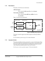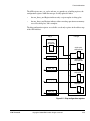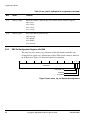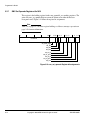
1
PrimeCell AHB SRAM/NOR
Memory Controller (PL241)
®
Revision: r0p1
Technical Reference Manual
Copyright © 2006 ARM Limited. All rights reserved.
ARM DDI 0389B
PrimeCell AHB SRAM/NOR Memory Controller (PL241)
Technical Reference Manual
Copyright © 2006 ARM Limited. All rights reserved.
Release Information
The following changes have been made to this book.
Change History
Date
Issue
Confidentiality
Change
17 March 2006
A
Non-Confidential
First release for r0p0.
20 December 2006
B
Non-Confidential
Updated for r0p1.
Proprietary Notice
Words and logos marked with ® or ™ are registered trademarks or trademarks of ARM Limited in the EU and
other countries, except as otherwise stated below in this proprietary notice. Other brands and names
mentioned herein may be the trademarks of their respective owners.
Neither the whole nor any part of the information contained in, or the product described in, this document
may be adapted or reproduced in any material form except with the prior written permission of the copyright
holder.
The product described in this document is subject to continuous developments and improvements. All
particulars of the product and its use contained in this document are given by ARM Limited in good faith.
However, all warranties implied or expressed, including but not limited to implied warranties of
merchantability, or fitness for purpose, are excluded.
This document is intended only to assist the reader in the use of the product. ARM Limited shall not be liable
for any loss or damage arising from the use of any information in this document, or any error or omission in
such information, or any incorrect use of the product.
Where the term ARM is used it means “ARM or any of its subsidiaries as appropriate”.
Confidentiality Status
This document is Non-Confidential. The right to use, copy and disclose this document may be subject to
license restrictions in accordance with the terms of the agreement entered into by ARM and the party that
ARM delivered this document to.
Product Status
The information in this document is final, that is for a developed product.
Web Address
http://www.arm.com
ii
Copyright © 2006 ARM Limited. All rights reserved.
ARM DDI 0389B
Contents
PrimeCell AHB SRAM/NOR Memory Controller
(PL241) Technical Reference Manual
Preface
About this manual .......................................................................................... x
Feedback ..................................................................................................... xiv
Chapter 1
Introduction
1.1
1.2
Chapter 2
Functional Overview
2.1
2.2
2.3
2.4
Chapter 3
Functional description ................................................................................. 2-2
SMC ............................................................................................................ 2-4
Functional operation ................................................................................... 2-7
SMC functional operation .......................................................................... 2-15
Programmer’s Model
3.1
3.2
3.3
ARM DDI 0389B
About the AHB MC ...................................................................................... 1-2
Supported devices ...................................................................................... 1-5
About the programmer’s model ................................................................... 3-2
Register summary ....................................................................................... 3-3
Register descriptions .................................................................................. 3-6
Copyright © 2006 ARM Limited. All rights reserved.
iii
Contents
Chapter 4
Programmer’s Model for Test
4.1
Chapter 5
Device Driver Requirements
5.1
Appendix A
SMC integration test registers .................................................................... 4-2
Memory initialization ................................................................................... 5-2
Signal Descriptions
A.1
A.2
A.3
A.4
A.5
A.6
A.7
A.8
About the signals list ...................................................................................
Clocks and resets .......................................................................................
AHB signals ................................................................................................
SMC memory interface signals ...................................................................
SMC miscellaneous signals ........................................................................
Low-power interface ...................................................................................
Configuration signal ....................................................................................
Scan chains ................................................................................................
A-2
A-3
A-4
A-5
A-6
A-7
A-8
A-9
Glossary
iv
Copyright © 2006 ARM Limited. All rights reserved.
ARM DDI 0389B
List of Tables
PrimeCell AHB SRAM/NOR Memory Controller
(PL241) Technical Reference Manual
Table 2-1
Table 2-2
Table 2-3
Table 2-4
Table 2-5
Table 2-6
Table 2-7
Table 2-8
Table 2-9
Table 2-10
Table 2-11
Table 2-12
Table 2-13
Table 2-14
Table 2-15
Table 2-16
Table 2-17
Table 2-18
Table 2-19
Table 2-20
ARM DDI 0389B
Change History ............................................................................................................. ii
Static memory clocking options ............................................................................... 2-12
Asynchronous read opmode chip register settings ................................................. 2-28
Asynchronous read SRAM cycles register settings ................................................. 2-28
Asynchronous read in multiplexed-mode opmode chip register settings ................ 2-29
Asynchronous read in multiplexed-mode SRAM cycles register settings ............... 2-29
Asynchronous write opmode chip register settings ................................................. 2-30
Asynchronous write SRAM cycles register settings ................................................ 2-30
Asynchronous write in multiplexed-mode opmode chip register settings ................ 2-31
Asynchronous write in multiplexed-mode SRAM cycles register settings ............... 2-31
Page read opmode chip register settings ................................................................ 2-31
Page read SRAM cycles register settings ............................................................... 2-31
Synchronous burst read opmode chip register settings .......................................... 2-32
Synchronous burst read SRAM cycles register settings ......................................... 2-32
Synchronous burst read in multiplexed-mode opmode chip register settings ......... 2-34
Synchronous burst read in multiplexed-mode read SRAM cycles register settings 2-34
Synchronous burst write opmode chip register settings .......................................... 2-35
Synchronous burst write SRAM cycles register settings ......................................... 2-35
Synchronous burst write in multiplexed-mode opmode chip register settings ......... 2-36
Synchronous burst write in multiplexed-mode SRAM cycles register settings ........ 2-36
Synchronous read and asynchronous write opmode chip register settings ............ 2-37
Copyright © 2006 ARM Limited. All rights reserved.
v
List of Tables
Table 2-21
Table 3-1
Table 3-2
Table 3-3
Table 3-4
Table 3-5
Table 3-6
Table 3-7
Table 3-8
Table 3-9
Table 3-10
Table 3-11
Table 3-12
Table 3-13
Table 3-14
Table 3-15
Table 3-16
Table 3-17
Table 3-18
Table 3-19
Table 3-20
Table 3-21
Table 3-22
Table 3-23
Table 4-1
Table 4-2
Table 4-3
Table 4-4
Table A-1
Table A-2
Table A-3
Table A-4
Table A-5
Table A-6
Table A-7
vi
Synchronous read and asynchronous write opmode chip register settings ............ 2-37
Register summary ..................................................................................................... 3-4
smc_memc_status Register bit assignments ........................................................... 3-6
smc_memif_cfg Register bit assignments ................................................................ 3-7
smc_memc_cfg_set Register bit assignments ......................................................... 3-9
smc_memc_cfg_clr Register bit assignments .......................................................... 3-9
smc_direct_cmd Register bit assignments ............................................................. 3-10
smc_set_cycles Register bit assignments .............................................................. 3-11
smc_set_opmode Register bit assignments ........................................................... 3-13
smc_refresh_period_0 Register bit assignments .................................................... 3-15
smc_sram_cycles Register bit assignments ........................................................... 3-16
smc_opmode Register bit assignments .................................................................. 3-17
smc_user_status Register bit assignments ............................................................ 3-18
smc_user_config Register bit assignments ............................................................ 3-19
smc_periph_id Register bit assignments ................................................................ 3-19
smc_periph_id_0 Register bit assignments ............................................................ 3-20
smc_periph_id_1 Register bit assignments ............................................................ 3-21
smc_periph_id_2 Register bit assignments ............................................................ 3-21
smc_periph_id_3 Register bit assignments ............................................................ 3-21
smc_pcell_id Register bit assignments ................................................................... 3-22
smc_pcell_id_0 Register bit assignments ............................................................... 3-23
smc_pcell_id_1 Register bit assignments ............................................................... 3-23
smc_pcell_id_2 Register bit assignments ............................................................... 3-24
smc_pcell_id_3 Register bit assignments ............................................................... 3-24
SMC test register summary ...................................................................................... 4-2
smc_int_cfg Register bit assignments ...................................................................... 4-3
smc_int_inputs Register bit assignments ................................................................. 4-3
smc_int_outputs Register bit assignments ............................................................... 4-4
Clocks and resets ..................................................................................................... A-3
AHB signals .............................................................................................................. A-4
SMC memory interface signals ................................................................................. A-5
SMC miscellaneous signals ...................................................................................... A-6
Low-power interface signals ..................................................................................... A-7
Configuration signal .................................................................................................. A-8
Scan chain signals .................................................................................................... A-9
Copyright © 2006 ARM Limited. All rights reserved.
ARM DDI 0389B
List of Figures
PrimeCell AHB SRAM/NOR Memory Controller
(PL241) Technical Reference Manual
Figure 1-1
Figure 2-1
Figure 2-2
Figure 2-3
Figure 2-4
Figure 2-5
Figure 2-6
Figure 2-7
Figure 2-8
Figure 2-9
Figure 2-10
Figure 2-11
Figure 2-12
Figure 2-13
Figure 2-14
Figure 2-15
Figure 2-16
Figure 2-17
Figure 2-18
Figure 2-19
ARM DDI 0389B
Key to timing diagram conventions ............................................................................. xii
AHB MC (PL241) configuration ................................................................................. 1-2
AHB MC (PL241) configuration ................................................................................. 2-2
AHB MC (PL241) clock domains ............................................................................... 2-3
SMC block diagram ................................................................................................... 2-4
SMC SRAM pad interface external connections ....................................................... 2-6
Big-endian implementation ...................................................................................... 2-10
AHBC memory map ................................................................................................ 2-11
Request to enter low-power mode .......................................................................... 2-13
AHB domain denying a low-power request ............................................................. 2-13
Accepting requests .................................................................................................. 2-14
SMC aclk domain FSM ........................................................................................... 2-15
Chip configuration registers .................................................................................... 2-23
Device pin mechanism ............................................................................................ 2-25
Software mechanism ............................................................................................... 2-26
Asynchronous read ................................................................................................. 2-29
Asynchronous read in multiplexed-mode ................................................................ 2-29
Asynchronous write ................................................................................................. 2-30
Asynchronous write in multiplexed-mode ................................................................ 2-31
Page read ................................................................................................................ 2-32
Synchronous burst read .......................................................................................... 2-33
Copyright © 2006 ARM Limited. All rights reserved.
vii
List of Figures
Figure 2-20
Figure 2-21
Figure 2-22
Figure 2-23
Figure 3-1
Figure 3-2
Figure 3-3
Figure 3-4
Figure 3-5
Figure 3-6
Figure 3-7
Figure 3-8
Figure 3-9
Figure 3-10
Figure 3-11
Figure 3-12
Figure 3-13
Figure 3-14
Figure 3-15
Figure 3-16
Figure 3-17
Figure 3-18
Figure 3-19
Figure 4-1
Figure 4-2
Figure 4-3
Figure 4-4
Figure 5-1
Figure 5-2
Figure 5-3
Figure A-1
viii
Synchronous burst read in multiplexed-mode ........................................................ 2-34
Synchronous burst write ......................................................................................... 2-35
Synchronous burst write in multiplexed-mode ........................................................ 2-36
Synchronous read and asynchronous write ............................................................ 2-38
SMC register map ..................................................................................................... 3-2
SMC configuration register map ............................................................................... 3-3
SMC chip configuration register map ........................................................................ 3-3
SMC user configuration register map ....................................................................... 3-4
SMC peripheral and PrimeCell identification configuration register map .................. 3-4
smc_memc_status Register bit assignments ........................................................... 3-6
smc_memif_cfg Register bit assignments ................................................................ 3-7
smc_memc_cfg_set Register bit assignments ......................................................... 3-8
smc_memc_cfg_clr Register bit assignments .......................................................... 3-9
smc_direct_cmd Register bit assignments ............................................................. 3-10
smc_set_cycles Register bit assignments .............................................................. 3-11
smc_set_opmode Register bit assignments ........................................................... 3-12
smc_refresh_period_0 Register bit assignments .................................................... 3-15
smc_sram_cycles Register bit assignments ........................................................... 3-15
smc_opmode Register bit assignments .................................................................. 3-16
smc_user_status Register bit assignments ............................................................ 3-18
smc_user_config Register bit assignments ............................................................ 3-19
smc_periph_id Register bit assignments ................................................................ 3-20
smc_pcell_id Register bit assignments ................................................................... 3-22
SMC integration test register map ............................................................................ 4-2
smc_int_cfg Register bit assignments ...................................................................... 4-2
smc_int_inputs Register bit assignments ................................................................. 4-3
smc_int_outputs Register bit assignments ............................................................... 4-4
SMC and memory initialization sheet 1 of 3 ............................................................. 5-3
SMC and memory initialization sheet 2 of 3 ............................................................. 5-4
SMC and memory initialization sheet 3 of 3 ............................................................. 5-5
AHB MC PL241 grouping of signals ......................................................................... A-2
Copyright © 2006 ARM Limited. All rights reserved.
ARM DDI 0389B
Preface
This preface introduces the PrimeCell AHB SRAM/NOR Memory Controller (MC)
(PL241) Technical Reference Manual. It contains the following sections:
•
About this manual on page x
•
Feedback on page xiv.
ARM DDI 0389B
Copyright © 2006 ARM Limited. All rights reserved.
ix
Preface
About this manual
This is the Technical Reference Manual (TRM) for the PrimeCell AHB SRAM/NOR
Memory Controller.
Product revision status
The rnpn identifier indicates the revision status of the product described in this manual,
where:
rn
Identifies the major revision of the product.
pn
Identifies the minor revision or modification status of the product.
Intended audience
This manual is written for system designers, system integrators, and verification
engineers who are designing a System-on-Chip (SoC) device that uses the AHB MC.
The manual describes the external functionality of the AHB MC.
Using this manual
This manual is organized into the following chapters:
Chapter 1 Introduction
Read this chapter for a high-level view of the AHB MC and a description
of its features.
Chapter 2 Functional Overview
Read this chapter for a description of the major components of the AHB
MC and how they operate.
Chapter 3 Programmer’s Model
Read this chapter for a description of the AHB MC registers.
Chapter 4 Programmer’s Model for Test
Read this chapter for a description of the additional logic for integration
testing.
Chapter 5 Device Driver Requirements
Read this chapter for a description of device driver requirements for the
Static Memory Controller (SMC).
x
Copyright © 2006 ARM Limited. All rights reserved.
ARM DDI 0389B
Preface
Appendix A Signal Descriptions
Read this appendix for a description of the AHB MC input and output
signals.
Glossary
Read the Glossary for definitions of terms used in this manual.
Conventions
Conventions that this manual can use are described in:
•
Typographical
•
Timing diagrams on page xii
•
Signals on page xii
•
Numbering on page xiii.
Typographical
The typographical conventions are:
ARM DDI 0389B
italic
Highlights important notes, introduces special terminology,
denotes internal cross-references, and citations.
bold
Highlights interface elements, such as menu names. Denotes
signal names. Also used for terms in descriptive lists, where
appropriate.
monospace
Denotes text that you can enter at the keyboard, such as
commands, file and program names, and source code.
monospace
Denotes a permitted abbreviation for a command or option. You
can enter the underlined text instead of the full command or option
name.
monospace italic
Denotes arguments to monospace text where the argument is to be
replaced by a specific value.
monospace bold
Denotes language keywords when used outside example code.
< and >
Angle brackets enclose replaceable terms for assembler syntax
where they appear in code or code fragments. They appear in
normal font in running text. For example:
•
MRC p15, 0 <Rd>, <CRn>, <CRm>, <Opcode_2>
•
The Opcode_2 value selects the register that is accessed.
Copyright © 2006 ARM Limited. All rights reserved.
xi
Preface
Note
Angle brackets can also enclose a permitted range of values. The
example, <0-3>, shows that in name extensions, only one of the
values 0, 1, 2, or 3 is valid.
Timing diagrams
The figure named Key to timing diagram conventions explains the components used in
timing diagrams. Variations, when they occur, have clear labels. You must not assume
any timing information that is not explicit in the diagrams.
Shaded bus and signal areas are undefined, so the bus or signal can assume any value
within the shaded area at that time. The actual level is unimportant and does not affect
normal operation.
&ORFN
+,*+WR/2:
7UDQVLHQW
+,*+/2:WR+,*+
%XVVWDEOH
%XVWRKLJKLPSHGDQFH
%XVFKDQJH
+LJKLPSHGDQFHWRVWDEOHEXV
Key to timing diagram conventions
Signals
The signal conventions are:
xii
Signal level
The level of an asserted signal depends on whether the signal is
active-HIGH or active-LOW. Asserted means HIGH for
active-HIGH signals and LOW for active-LOW signals.
Lower-case n
Denotes an active-LOW signal.
Prefix A
Denotes global Advanced eXtensible Interface (AXI) signals.
Prefix AR
Denotes AXI read address channel signals.
Prefix AW
Denotes AXI write address channel signals.
Copyright © 2006 ARM Limited. All rights reserved.
ARM DDI 0389B
Preface
Prefix B
Denotes AXI write response channel signals.
Prefix C
Denotes AXI low-power interface signals.
Prefix H
Denotes Advanced High-performance Bus (AHB) signals.
Prefix P
Denotes Advanced Peripheral Bus (APB) signals.
Prefix R
Denotes AXI read data channel signals.
Prefix W
Denotes AXI write data channel signals.
Numbering
The Verilog numbering convention is:
<size in bits>'<base><number>
This is a Verilog method of abbreviating constant numbers. For example:
•
'h7B4 is an unsized hexadecimal value.
•
'o7654 is an unsized octal value.
•
8'd9 is an eight-bit wide decimal value of 9.
•
8'h3F is an eight-bit wide hexadecimal value of 0x3F. This is
equivalent to b00111111.
•
8'b1111 is an eight-bit wide binary value of b00001111.
Further reading
This section lists publications by ARM Limited, and by third parties.
ARM Limited periodically provides updates and corrections to its documentation. See
http://www.arm.com for current errata sheets, addenda, and the Frequently Asked
Questions list.
ARM publications
This manual contains information that is specific to the AHB MC. See the following
documents for other relevant information:
ARM DDI 0389B
•
PrimeCell AHB SRAM/NOR Memory Controller (PL241) Integration Manual
(ARM DII 0151)
•
PrimeCell AHB SRAM/NOR Memory Controller (PL241) Implementation Guide
(ARM DDI 0144)
•
AMBA™ Specification (Rev 2.0) (ARM IHI 0011)
•
AMBA 3 APB Protocol v1.0 Specification (ARM IHI 0024).
Copyright © 2006 ARM Limited. All rights reserved.
xiii
Preface
Feedback
ARM Limited welcomes feedback on the AHB MC and its documentation.
Feedback on this product
If you have any comments or suggestions about this product, contact your supplier
giving:
•
the product name
•
a concise explanation of your comments.
Feedback on this manual
If you have any comments on this manual, send email to [email protected] giving:
•
the title
•
the number
•
the relevant page number(s) to which your comments apply
•
a concise explanation of your comments.
ARM Limited also welcomes general suggestions for additions and improvements.
xiv
Copyright © 2006 ARM Limited. All rights reserved.
ARM DDI 0389B
Chapter 1
Introduction
This chapter introduces the AHB MC. It contains the following sections:
•
About the AHB MC on page 1-2
•
Supported devices on page 1-5.
ARM DDI 0389B
Copyright © 2006 ARM Limited. All rights reserved.
1-1
Introduction
1.1
About the AHB MC
The AHB MC is an Advanced Microcontroller Bus Architecture (AMBA) compliant
System-on-Chip (SoC) peripheral. It is developed, tested, and licensed by ARM
Limited.
The AHB MC takes advantage of the newly developed Static Memory Controller
(SMC). The AHB MC has an AHB port with access to the external memory. The AHB
port has a bridge interface to the memory controller. There is a separate AHB port to
configure the memory controller. Specific configurations of the SMC are instantiated to
target specific memory devices. Figure 1-1 shows the AHB MC (PL241) configuration.
$+%0&3/
$+%
$+%LQWHUIDFH
0
6
60&
$+%
FRQILJXUDWLRQ
SRUW
$+%WR$3%
EULGJH
0
ELW65$0125
IRXUFKLSV
$3%6
Figure 1-1 AHB MC (PL241) configuration
This section describes:
•
AHB interface on page 1-3
•
AHB to APB bridge on page 1-3
•
SMC on page 1-4
•
Clock domains on page 1-4
•
Low-power interfaces on page 1-4.
1-2
Copyright © 2006 ARM Limited. All rights reserved.
ARM DDI 0389B
Introduction
1.1.1
AHB interface
The interface converts the incoming AHB transfers to the protocol used internally by
the AHB MC.
The interface has the following features:
•
all AHB fixed length burst types are directly translated to fixed length bursts
•
all undefined length INCR bursts are converted to INCR4 bursts
•
broken bursts are supported
•
the bufferable bit of the HPROT signal determines if the interface must wait for
a write transfer to complete internally
•
a Read After Write (RAW) hazard detection buffer avoids RAW hazards
•
AHB response signals are registered to improve timing
•
locked transfers are supported within a 512MB region
•
HWDATA is registered to improve internal timing paths
•
a big-endian 32-bit mode option is implemented
•
AHB error response logic is removed as no internal components generate errors.
This interface is a fully validated component. This ensures that it obeys both the AHB
protocol and the internal protocol that the interconnect uses.
See Chapter 2 Functional Overview for more information.
1.1.2
AHB to APB bridge
This bridge converts AHB transfers from the configuration port to the APB transfers
that the internal memory controllers require.
See Chapter 2 Functional Overview for more information.
ARM DDI 0389B
Copyright © 2006 ARM Limited. All rights reserved.
1-3
Introduction
1.1.3
SMC
The SMC is a high-performance, area-optimized SRAM memory controller.
The SMC is pre-configured and validated for:
•
the SRAM memory type
•
the number of SRAM memory devices
•
the maximum SRAM memory width.
The SRAM memory interface type is defined as supporting:
•
synchronous or asynchronous SRAM
•
Pseudo Static Random Access Memory (PSRAM)
•
NOR flash
•
NAND flash devices with an SRAM interface.
The SMC block offers the following features:
•
it is configured to support the maximum SRAM memory data width of 32-bit
•
programmable cycle timings, and memory width per chip select
•
atomic switching of memory device and controller operating modes
•
support for the PL220 External Bus Interface (EBI) PrimeCell, enabling sharing
of external address and data bus pins between memory controller interfaces
•
support for a low-power interface
•
support for a remap signal
•
support for clock domains to be synchronous or asynchronous
See Chapter 2 Functional Overview for more information.
1.1.4
Clock domains
The memory controller has two clock domains:
•
AHB clock domain
•
static memory clock domain.
See Chapter 2 Functional Overview for more information.
1.1.5
Low-power interfaces
The memory controller has two low-power interfaces, one for each clock domain.
See Chapter 2 Functional Overview for more information.
1-4
Copyright © 2006 ARM Limited. All rights reserved.
ARM DDI 0389B
Introduction
1.2
Supported devices
The SMC supports SRAM/NOR, see SMC on page 1-4. The Release Note provides a
specific list of memory devices tested with each configuration.
Some memory devices or series of memory devices have specific requirements:
Intel W18 series NOR FLASH, for example 28f128W18td
These devices, when in synchronous operation, use a WAIT pin.
However non-array operations when in synchronous mode do not use the
WAIT pin and it is always asserted. The controller cannot differentiate
between array and non-array accesses and therefore cannot support these
non-array accesses.
Therefore, W18 devices can only carry out non-array operations such as
Read Status in asynchronous modes of operation.
Cellular RAM 1.0, 64MB PSRAM, for example mt45w4mw16bfb_701_1us
You can program these devices using a CRE pin or by software access.
Whenever you program these devices through software access, using a
sequence of two reads followed by two writes, ensure that the third
access, that is, the first write is a CE# controlled write.
SMC only does WE# controlled writes. This is to simplify the design of the
SMC by having fewer timing registers and simpler timing controls.
Therefore, you can only program these devices by using the CRE pin
method of access.
Note
Because the memory controller maps INCR transfers into INCR4 transfers, it does not
support memory mapped FIFO components.
ARM DDI 0389B
Copyright © 2006 ARM Limited. All rights reserved.
1-5
Introduction
1-6
Copyright © 2006 ARM Limited. All rights reserved.
ARM DDI 0389B
Chapter 2
Functional Overview
This chapter describes the major components of the AHB MC and how they operate. It
contains the following sections:
•
Functional description on page 2-2
•
SMC on page 2-4
•
Functional operation on page 2-7.
•
SMC functional operation on page 2-15.
ARM DDI 0389B
Copyright © 2006 ARM Limited. All rights reserved.
2-1
Functional Overview
2.1
Functional description
Figure 2-1 shows an AHB MC (PL241) configuration.
$+%0&3/
$+%LQWHUIDFH
$+%
0
6
60&
$+%
FRQILJXUDWLRQ
SRUW
$+%WR$3%
EULGJH
0
ELW65$0125
IRXUFKLSV
$3%6
Figure 2-1 AHB MC (PL241) configuration
This section is divided into:
•
AHB interface
•
AHB to APB bridge
•
Clock domains on page 2-3
•
Low-power interface on page 2-3
•
SMC on page 2-4.
2.1.1
AHB interface
The AHB MC fully supports the AMBA AHB 2.0 specification. This interface
component converts the incoming AHB transfers to the required transfers of the internal
interconnect protocol. Because of the design of the internal interconnect, some
optimizations are made in the interface to improve performance.
See AHB interface operation on page 2-7 for more information.
2.1.2
AHB to APB bridge
The internal memory controllers of the AHB MC use the AMBA3 APB protocol for
their configuration ports. To enable the AHB MC to externally function as an AHB
device, the APB configuration ports are connected to an AHB to APB bridge. The
bridge converts incoming AHB transfers from the configuration port to the APB
transfers that the internal memory controller requires. This bridge is part of the
PrimeCell infrastructure components, part BP127.
See AHB to APB bridge operation on page 2-10 for more information.
2-2
Copyright © 2006 ARM Limited. All rights reserved.
ARM DDI 0389B
Functional Overview
2.1.3
Clock domains
The memory controller has two clock domains:
AHB clock domain
This is clocked by hclk, smc_aclk and reset by hresetn.
Static memory clock domain
This is clocked by smc_mclk0, smc_mclk0n and reset by
smc_mreset0n.
Figure 2-2 shows the two clock domains.
$+%FORFNGRPDLQ
$+%LQWHUIDFH
$+%
6WDWLFPHPRU\FORFNGRPDLQ
$+%0&3/
0
6
VPFBDFON
65$0
PHPRU\
60&
$+%
FRQILJXUDWLRQ
SRUW
$+%WR$3%
EULGJH
0
$3%6
KFON
VPFBPFON
Figure 2-2 AHB MC (PL241) clock domains
The memory controller supports many different options for clocking the different
domains.
See Clock domain operation on page 2-11 for more information.
2.1.4
Low-power interface
The memory controller has two low-power interfaces, one for each clock domain. These
operate with a simple three signal protocol. It is expected that a system clock controller
drives these interfaces and associated clocks. Each domain has individual control to
enable independent handshaking with the system clock controller.
See Low-power interface operation on page 2-12 for more information.
ARM DDI 0389B
Copyright © 2006 ARM Limited. All rights reserved.
2-3
Functional Overview
2.2
SMC
Figure 2-3 shows a block diagram of the SMC.
0HPRU\FORFNGRPDLQ
$+%FORFNGRPDLQ
$3%VODYH
LQWHUIDFH
0HPRU\
PDQDJHU
(%,
LQWHUIDFH
/RZSRZHU
LQWHUIDFH
0HPRU\
LQWHUIDFH
3DG
LQWHUIDFH
65$0
PHPRU\
LQWHUIDFH
)RUPDW
60&
LQWHUIDFH
,QWHUUXSWV
Figure 2-3 SMC block diagram
The main blocks of the SMC are:
•
SMC interface on page 2-5
•
APB slave interface on page 2-5
•
Format on page 2-5
•
Memory manager on page 2-5
•
Memory interface on page 2-5
•
Pad interface on page 2-6
•
Interrupts on page 2-6.
2-4
Copyright © 2006 ARM Limited. All rights reserved.
ARM DDI 0389B
Functional Overview
2.2.1
SMC interface
The SMC interface processes the incoming AHB transfers and sends them to the
command format block.
2.2.2
APB slave interface
The SMC has 4KB of memory allocated to it.
The APB slave interface accesses the SMC registers to program the memory system
configuration parameters and to provide status information. See Chapter 3
Programmer’s Model and APB slave interface operation on page 2-19 for more
information.
2.2.3
Format
The format block receives memory accesses from the SMC interface and the memory
manager. Read and write requests are arbitrated on a round robin basis. Requests from
the manager have the highest priority. The format block also maps AHB memory
transfers onto appropriate memory transfers and passes these to the memory interface
through the command FIFO.
See Format block on page 2-19 for more information.
2.2.4
Memory manager
The memory manager tracks and controls the current state of smc_aclk domain logic.
The block is responsible for:
•
updating timing registers and controlling direct commands issued to memory
•
controlling entry-to and exit-from low-power mode through the APB interface
•
the low-power interface.
See Memory manager operation on page 2-22 for more information.
2.2.5
Memory interface
The SRAM memory interface consists of command, read data and write data FIFOs,
plus a control FSM. To support an EBI, the memory interface also contains an EBI
FSM. This controls interaction with the EBI and prevents the memory interface FSM
from issuing commands until it has been granted the external bus.
See Memory interface operation on page 2-27 for more information.
ARM DDI 0389B
Copyright © 2006 ARM Limited. All rights reserved.
2-5
Functional Overview
2.2.6
Pad interface
The pad interface module provides a registered I/O interface for data and control
signals. It also contains interrupt generation logic.
Figure 2-4 shows the SRAM pad interface external signals. Clock and reset signals are
omitted.
VPFBGDWDBLQB>@
VPFBIEFONBLQB
65$0
SDGLQWHUIDFH
VPFBLQWB
VPFBZDLWB
VPFBDGYBQB
VPFBEDDBQB
VPFBEOVBQB>@
VPFBFONBRXWB>@
VPFBFUHB
VPFBFVBQB>@
VPFBGDWDBHQB
VPFBGDWDBRXWB>@
VPFBRHBQB
VPFBZHBQB
Figure 2-4 SMC SRAM pad interface external connections
2.2.7
Interrupts
The SRAM memory interface support interrupts. The interrupt is triggered on the rising
edge of the smc_int_0 input for the SRAM memory interface.
See Interrupts operation on page 2-27 for more information.
2-6
Copyright © 2006 ARM Limited. All rights reserved.
ARM DDI 0389B
Functional Overview
2.3
Functional operation
This section is divided into:
•
AHB interface operation
•
AHB to APB bridge operation on page 2-10
•
Clock domain operation on page 2-11
•
Low-power interface operation on page 2-12
•
SMC functional operation on page 2-15.
2.3.1
AHB interface operation
This section describes:
•
AHB fixed burst types
•
Undefined length INCR bursts on page 2-8
•
Broken bursts on page 2-8
•
Bufferable bit of the HPROT signal on page 2-8
•
Read after write hazard detection buffer on page 2-9
•
AHB response signals on page 2-9
•
Locked transfers on page 2-9
•
Registered HWDATA on page 2-10
•
Big-endian 32-bit mode on page 2-10
•
Removal of AHB error response logic on page 2-10.
AHB fixed burst types
All AHB fixed length bursts directly map to burst types that the internal interconnect
uses. The internal interconnect and the memory controller are based on transferring
bursts of data. The larger the burst size, the more efficient the transfer and overall
performance. The standard AHB fixed length burst types are directly mapped to the
internal protocol.
Burst operation has performance benefits because when the first beat of a burst is
accepted, it contains data about the remaining beats. For example, from the first beat of
a read burst, all the data required to complete the transfer can be read from memory.
This first transfer has some delay before data is returned. Subsequent beats of the burst
can have less delay because the data they require might have already been read from the
memory.
ARM DDI 0389B
Copyright © 2006 ARM Limited. All rights reserved.
2-7
Functional Overview
Undefined length INCR bursts
All undefined length INCR bursts are converted to INCR bursts of length four. Many
AHB masters rely on using undefined length INCR bursts to access data. If each INCR
transfer is processed as a single transfer by the internal protocol then the performance
is significantly degraded.
The bridge converts the incoming INCR transfers to INCR transfers of length four,
INCR4. This mean that the bridge speculatively requests data from the internal
interconnect, before it knows it is going to require it. If the AHB master continues the
burst, then the data can be returned quickly because it has already been requested. When
the INCR burst finishes, the bridge disregards any data requested from the internal
interconnect that is not required.
Any INCR burst of less than four beats results in a broken INCR4. Undefined length
INCR bursts of more than four beats are split into an appropriate number of INCR4s
plus a broken INCR4, if required.
Broken bursts
To fully support the AMBA AHB 2.0 specification, the bridge supports all broken AHB
bursts. Although bursts cannot be broken by an AHB master, if the AHB system has
multiple masters then the AHB system arbitration can break a burst. Also, because the
bridge converts INCR to INCR4, broken INCR4s occur when undefined length INCRs
of a length not equal to a multiple of four are performed.
To support broken bursts, the bridge must keep track of how many beats of a burst have
been performed and ensure it obeys the protocol of the interconnect. For read bursts, this
means draining the interconnect of any requested data that is not required. For write
bursts this means artificially extending write data with enough beats to obey the
protocol. The interconnect uses write strobes to indicate the bytes of the data bus that
are valid. When extending broken bursts, these strobes are deasserted so that the
artificial data does not corrupt the actual memory.
Bufferable bit of the HPROT signal
The bufferable bit of the HPROT signal determines whether the bridge must wait for a
write transfer to complete internally. The AHB protection control bits support the
concept of bufferable data accesses. The HPROT[2] signal determines this. The
internal interconnect supports the concept of a write response to indicate when data has
actually been written to memory. The bridge exploits these features by not waiting for
the write response if the access is described as bufferable. This enables numerous
bufferable writes to occur with minimum latency. These are accepted by the
interconnect and queued in the memory controller.
2-8
Copyright © 2006 ARM Limited. All rights reserved.
ARM DDI 0389B
Functional Overview
If transfers are described as non-bufferable then the bridge must wait for the write
response to indicate that the transfer has been completed to memory. If numerous
bufferable writes are performed, followed by a non-bufferable write, then the bridge
must wait until it receives the write response associated with the final write.
Read after write hazard detection buffer
A RAW hazard detection buffer avoids potential RAW hazards. The protocol used
internally to AHB MC does not perform memory coherency checks to catch Write After
Read (WAR) or RAW hazards.
Because of the nature of the AHB protocol, WAR hazards never occur because the read
must have completed before the write can be accepted.
Because the bridge permits writes to be buffered internally, there is a potential for a
RAW hazard to occur. If you perform a bufferable write then it might not complete
immediately. If a read to that same memory location is performed then both transfers
can be in the queue and the internal memory controller can reorder these transactions
for performance reasons so that the read occurs before the write. This means that the
data read might be the value before the most recent write. The bridge has to detect these
potential cases and stall the read transfer until any buffered writes that might cause a
RAW hazard have been completed.
The bridge contains logic to monitor up to four outstanding write addresses. If an
incoming read occurs to a 4KB region that has been written to, then it is stalled. If four
bufferable writes occur then the AHB is stalled until a response is seen for the first of
the four writes in the buffer.
AHB response signals
The interconnect used within the AHB MC contains many combinatorial paths that link
different AHB input ports. To improve the synthesis timing, the AHB responses are
registered to limit these paths to within the design.
Locked transfers
AHB MC supports locked transfers, within a 512MB region. This is because of the way
the interconnect processes locked transfers. There is a significant performance penalty
in using locked transfers. Transfers that are locked together wait for all other ports to
complete any outstanding transfers before they can begin. While a locked sequence
occurs to a specific 512MB memory region, all other access to that region is stalled. All
locked writes are processed as non-bufferable writes and so have to wait for the
appropriate write response before indicating their completion.
ARM DDI 0389B
Copyright © 2006 ARM Limited. All rights reserved.
2-9
Functional Overview
Registered HWDATA
The interconnect used within the AHB MC contains combinatorial paths for the write
data. To improve the synthesis timing, HWDATA is registered and makes these paths
internal to the design.
Big-endian 32-bit mode
The AHB MC supports the option of storing data to memory in big-endian 32-bit mode.
Each bridge contains the logic to implement this data mapping depending on the
big_endian input tie-off. Figure 2-5 shows that if the tie off is asserted then the data
buses are reordered.
ELW
/LWWOHHQGLDQGHIDXOW
%LJHQGLDQPRGH
Figure 2-5 Big-endian implementation
Removal of AHB error response logic
The internal protocol used within AHB MC supports the concept of errors. However
none of the components used ever generate errors. This means that the bridge does not
require any logic to generate AHB errors because there are no circumstances when
errors can be generated.
2.3.2
AHB to APB bridge operation
The internal memory controller has an APB configuration port. The AHB configuration
port is mapped to it using an AHB to APB bridge. Figure 2-6 on page 2-11 shows that
each internal memory controller configuration port has a 4KB address space.
2-10
Copyright © 2006 ARM Limited. All rights reserved.
ARM DDI 0389B
Functional Overview
[))))
5HDGDV]HUR
[
60&FRQILJ
[
5HVHUYHG
[
$+%&PHPRU\PDS
Figure 2-6 AHBC memory map
The other fourteen 4KB regions are read as zero. The lower 16 bits of the AHB address
decode the memory controller that is being used. An external AHB decoder determines
where in the system memory map, this 64KB region is located. See About the
programmer’s model on page 3-2 for information on the internal memory controller
configuration registers. The configuration port of the internal memory controller is
APB, so only word reads and writes are supported.
2.3.3
Clock domain operation
The memory controller supports two clock domains:
•
the AHB clock domain
•
the static memory clock domain.
The hclk input drives the AHB clock domain. This clock drives the AHB interfaces and
bus matrix. The static memory controller has a separate clock input in this domain. This
is called smc_aclk. This signal is separated to enable the clock to be stopped
independently of hclk for low-power operation, see Low-power interface operation on
page 2-12. These two clocks must always be driven from the same clock source. The
input signal hresetn resets this clock domain.
The static memory clock domain controls the memory interface logic of the SMC. The
input signal smc_mclk0 and its inverse smc_mclk0n drive this domain. Each external
static memory chip is driven by a gated smc_mclk0 signal, these are called
smc_clk_out_0[3:0]. Clocks are only driven out to chips that require them. The static
memory interface has a fed back clock input, smc_fbclk_in_0, to help with clock skews
on the external pads.
The memory controller supports many different options for clocking the different
domains:
ARM DDI 0389B
Copyright © 2006 ARM Limited. All rights reserved.
2-11
Functional Overview
Static memory clocking options
Table 2-1 lists the static memory clocking options.
Table 2-1 Static memory clocking options
Options
Tie-off values
Fully synchronous
hclk = smc_mclk0
smc_async0 = smc_msync0 = 1
smc_a_gt_m0_sync = 0
Synchronous multiples
hclk = n x smc_mclk0
where:
n = integer value
smc_async0 = smc_msync0 = 1
smc_a_gt_m0_sync = 0
m x hclk = smc_mclk0
where:
m = integer value
smc_async0 = smc_msync0 = 1
smc_a_gt_m0_sync = 1
Asynchronous
Extra registers are used to avoid metastability when
crossing the asynchronous clock boundary.
2.3.4
smc_async0 = smc_msync0 = 0
smc_a_gt_m0_sync = 0
Low-power interface operation
The memory controller has two low-power interfaces. These interfaces indicate whether
the clock for a specific domain can be switched off to reduce power consumption. It is
expected that these interfaces are controlled by a system clock controller. One interface
controls each of the following domains:
•
AHB clock domain
•
static memory clock domain.
Each domain uses a simple three signal interface to indicate whether the clocks are
required. The signals consist of:
a request input
<domain>_csyreq
an acknowledge output
<domain>_csysack
2-12
Copyright © 2006 ARM Limited. All rights reserved.
ARM DDI 0389B
Functional Overview
an active output
<domain>_cactive
Where:
<domain> is ahb or smc.
Figure 2-7 explains the protocol for the interface by showing a request to enter
low-power mode.
7
7
7
7
7
KFON
DKEBFV\VUHT
DKEBFV\VDFN
DKEBFDFWLYH
Figure 2-7 Request to enter low-power mode
The memory controller receives a request to enter low-power mode, indicated by
<domain>_csysreq being driven LOW by the system clock controller, as shown at T1.
The memory controller then has the chance to perform any required operations to
prepare for the clock to be switched off. The memory controller acknowledges the
request by asserting <domain>_csysack LOW, as shown at T2. At this point the
<domain>_cactive signal is used to indicate whether the request has been accepted or
denied. If the request is accepted, <domain>_cactive is LOW, as shown in Figure 2-7.
If the request is denied, <domain>_cactive is HIGH. If the request is accepted, then the
clock to that domain can be switched off. The peripheral is brought out of low-power
state by restarting the clock and driving <domain>_csysreq HIGH, as shown at T4. The
memory controller completes the handshake by driving <domain>_csysack HIGH, as
shown at T5. Figure 2-8 shows the AHB domain denying a low-power request.
7
7
7
7
KFON
DKEBFV\VUHT
DKEBFV\VDFN
DKEBFDFWLYH
Figure 2-8 AHB domain denying a low-power request
When ahb_csysack is asserted LOW, the ahb_cactive signal is HIGH, as shown at T3,
indicating the AHB domain is busy and the clock cannot be switched off. The
handshake must be completed.
ARM DDI 0389B
Copyright © 2006 ARM Limited. All rights reserved.
2-13
Functional Overview
The AHB domain accepts or denies requests based on whether it is busy performing any
transfers. Figure 2-9 shows that static memory controllers always accept requests after
they have performed the required operations to prepare the external memory for the
clock to be switched off.
7
7
7
7
7
VPFBDFON
VPFBFV\VUHT
VPFBFV\VDFN
VPFBFDFWLYH
Figure 2-9 Accepting requests
The low-power request smc_csysreq is driven LOW at time T1. When the memory
controller is happy for the clock to be switched off, the smc_csysack signal is driven
LOW to acknowledge the request, as shown at T2. smc_cactive is driven LOW, so the
system clock controller knows the request has been accepted. When acknowledged, the
system clock controller can disable both the smc_aclk and smc_mclk0 signals.
The two domains have separate interfaces to enable individual handshaking with the
system clock controller. The only usage model is to switch off both domains. Each
individual low-power interface protocol must be observed before all the clocks can be
disabled.
2-14
Copyright © 2006 ARM Limited. All rights reserved.
ARM DDI 0389B
Functional Overview
2.4
SMC functional operation
This section describes:
•
Operating states
•
Clocking and resets on page 2-16
•
Miscellaneous signals on page 2-18
•
APB slave interface operation on page 2-19
•
Format block on page 2-19
•
Memory manager operation on page 2-22
•
Interrupts operation on page 2-27
•
Memory interface operation on page 2-27.
2.4.1
Operating states
The operation of the SMC is based on three operating states. In this section, each state
is described. Figure 2-10 shows the state machine.
5HVHW
5HDG\
/RZSRZHU
Figure 2-10 SMC aclk domain FSM
The SMC states are as follows:
Reset
Power is applied to the device, and hresetn is held LOW.
Ready
Normal operation of the device. You can access the SMC register bank
through the AHB configuration port and external memory devices
accessed through the SMC interface.
Low-power The device does not accept new AHB transfers, and only certain registers
are accessible through the APB interface. You can stop the SMC clocks
to reduce power consumption.
ARM DDI 0389B
Copyright © 2006 ARM Limited. All rights reserved.
2-15
Functional Overview
The state transitions are:
Ready to Reset
When reset is asserted to the smc_aclk domain, it enters the Reset
state.
Reset to Ready
When reset is deasserted to the smc_aclk domain, it enters the
Ready state.
Ready to Low-power
The Low-power state is entered when the SMC next becomes idle
after either:
•
the SMC receives a low-power request through the APB
smc_memc_cfg_set Register
•
the SMC receives a low-power request through the SMC
low-power interface.
Low-power to Ready
The SMC exits the Low-power state back to Ready when either:
•
the SMC low-power request bit is cleared in the APB
smc_memc_cfg_clr Register
•
the SMC low-power interface negates the low-power
request.
Low-power to Reset
When Reset is asserted to the smc_aclk reset domain, it enters the
Reset state.
2.4.2
Clocking and resets
This section describes:
•
Clocking
•
Resets on page 2-17.
Clocking
All configurations of the SMC support at least two clock domains, and have the
following clock inputs:
•
smc_aclk
•
smc_mclk0
•
smc_mclk0n.
2-16
Copyright © 2006 ARM Limited. All rights reserved.
ARM DDI 0389B
Functional Overview
These clocks can be grouped into two clock domains:
AHB domain
smc_aclk is in this domain. You can only stop the smc_aclk
domain signals when the SMC is in low-power mode.
Memory clock domain
The smc_mclk0 and smc_mclk0n are in this domain.
smc_mclk0n is an inverted version of smc_mclk0. smc_mclk0 is
used for timing and control signals.
You can tie off the smc_async and smc_msync pins so that the smc_aclk and
smc_mclk0 clock domains can operate synchronously or asynchronously with respect
to each other.
Synchronous clocking
The benefit of synchronous clocking is that you can reduce the read and
write latency by removing the synchronization registers between clock
domains. However, because of the integer relationship of the clocks, you
might not be able to get the maximum performance from the system
because of constraints placed on the bus frequency by the external
memory clock speed. In synchronous mode, the handshaking between the
smc_aclk and smc_mclk0 domains enables synchronous operation of
the two clocks at multiples of each other, that is, ratios of n:1 and 1:m.
Asynchronous clocking
The main benefit of asynchronous clocking is that you can maximize the
system performance, while running the memory interface at a fixed
system frequency. Additionally, in sleep-mode situations when the
system is not required to do much work, you can lower the frequency to
reduce power consumption.
Output clocks
A clock output is provided for every external memory device on the
SRAM memory interface type.
Resets
The SMC has two reset inputs:
hresetn
This is the reset signal for the smc_aclk domain.
smc_mreset0n
This is the reset signal for the smc_mclk0 domain.
ARM DDI 0389B
Copyright © 2006 ARM Limited. All rights reserved.
2-17
Functional Overview
You can change both reset signals asynchronously to their respective clock domain.
Internally to the SMC the deassertion of the hresetn signal is synchronized to
smc_aclk. The deassertion of smc_mreset0n is synchronized internally to smc_mclk0
and smc_mclk0n.
2.4.3
Miscellaneous signals
You can use the following signals as general-purpose control signals for logic external
to the SMC:
smc_user_config[7:0]
General purpose output ports that are driven directly from the
write-only APB register. If you do not require these ports leave
them unconnected. See also the SMC User Configuration Register
at 0x1204 on page 3-19.
smc_user_status[7:0]
General purpose input ports that are readable from the APB
interface through the smc_user_status Register. If you do not
require these ports then tie them either HIGH or LOW. These ports
are connected directly to the APB interface block. Therefore, if
they are driven from external logic that is not clocked by the SMC
smc_aclk signal, then you require external synchronization
registers. See also the SMC User Status Register at 0x1200 on
page 3-18.
You can use the following miscellaneous signals as tie-offs to change the operational
behavior of the SMC:
smc_a_gt_m0_sync
When HIGH, indicates that smc_aclk is greater than and synchronous to
smc_mclk0.
smc_async0 When HIGH, indicates smc_aclk is synchronous to smc_mclk0.
Otherwise they are asynchronous. Ensure that smc_async0 is tied to the
same value as smc_msync0.
smc_dft_en_clk_out
Use this signal for Automatic Test Pattern Generator (ATPG) testing
only. Tie it LOW for normal operation.
2-18
Copyright © 2006 ARM Limited. All rights reserved.
ARM DDI 0389B
Functional Overview
smc_msync0
When HIGH, indicates smc_mclk0 is synchronous to smc_aclk.
Otherwise they are asynchronous. Ensure that smc_msync0 is tied to the
same value as smc_async0.
smc_rst_bypass
Use this signal for ATPG testing only. Tie it LOW for normal operation.
smc_use_ebi
When HIGH, indicates that the SMC must operate with a PrimeCell EBI.
See the ARM PrimeCell External Bus Interface (PL220) Technical
Reference Manual.
2.4.4
APB slave interface operation
To enable a clean registered interface to the external infrastructure, the APB interface
always adds a wait state for all reads and writes by driving pready LOW during the first
cycle of the access phase.
In two instances, a delay of more than one wait state can be generated:
2.4.5
•
when a direct command is received and there are outstanding commands that
prevent a new command being stored in the command FIFO
•
when an APB access is received and a previous direct command has not
completed.
Format block
This section describes:
•
Hazard handling
•
SRAM memory accesses on page 2-20.
Hazard handling
There are four types of hazard:
•
Read After Read (RAR)
•
Write After Write (WAW)
•
Read After Write (RAW)
•
Write After Read (WAR).
The AHB interface deals with RAW hazards. WAR hazards do not occur in the AHB.
ARM DDI 0389B
Copyright © 2006 ARM Limited. All rights reserved.
2-19
Functional Overview
The SMC ensures the ordering of read transfers from a single port is maintained RAR,
and additionally that the ordering of write transfers from a single master is maintained
WAW.
SRAM memory accesses
This section describes:
•
Standard SRAM access
•
Memory address shifting
•
Memory burst alignment
•
Memory burst length on page 2-21
•
Booting using the SRAM on page 2-21.
Standard SRAM access
The programmer’s view is a flat area of memory.
The base addresses of external memory devices are defined by the
smc_address_match0_<0-3>[7:0 ] and smc_address_mask0_<0-3>[ 7:0] tie-off
pins. You can read the values of these tie-off pins through the opmode registers.
Memory address shifting
To produce the address presented to the memory device, the AHB address is aligned to
the memory width. This is done because the AHB address is a byte-aligned address,
while the memory address is a memory-width-aligned address.
Note
During initial configuration of a memory device, the memory mode register can be
accessed with a sequence of transfers to specific addresses. You must take into
consideration the shifting performance by the SMC when accessing memory mode
registers.
Memory burst alignment
The SMC provides a programmable option for controlling the formatting of memory
transfers with respect to memory burst boundaries, through the burst_align bit of the
opmode registers.
When set, the burst_align bit causes memory bursts to be aligned to a memory burst
boundary. This setting is intended for use with memories that use the concept of internal
pages. This can be an asynchronous page mode memory, or a synchronous PSRAM. If
a burst crosses a memory burst boundary, the SMC partitions the transfer into multiple
2-20
Copyright © 2006 ARM Limited. All rights reserved.
ARM DDI 0389B
Functional Overview
memory bursts, terminating a memory transfer at the burst boundary. Also ensure the
page size is an integer multiple of the burst length, to avoid a memory burst crossing a
page boundary.
When the burst_align bit is not set, the SMC ignores the memory burst boundary when
mapping commands onto memory commands. This setting is intended for use with
devices such as NOR flash. These devices have no concept of pages.
Memory burst length
The SMC enables you to program the memory burst length on an individual chip basis,
from length 1 to 32 beats, or a continuous burst. However, the length of memory bursts
are limited by the size of the read and write data FIFOs, and the programmed memory
burst must not exceed this upper limit.
For read transfers, the maximum memory burst length is the depth of the read data
FIFO, and it is four. For writes, the burst length is the depth of the write FIFO, and is
four.
Booting using the SRAM
The SMC enables the lowest SRAM chip select, normally chip 0, to be bootable. To
enable SRAM memory to be bootable, the SRAM interface does not require any special
functionality, other than knowing the memory width of the memory concerned. This is
indicated by a top-level tie-off. To enable the SMC to work with the slowest memories
the timing registers reset to the worst case values. When the smc_remap_0 port signal
is HIGH, the memory with the bootable chip select is set by the smc_sram_mw_0[1:0]
tie-off port signal.
Additionally, while the SMC input smc_remap_0 is HIGH, the bootable chip is aliased
to base address 0x0.
ARM DDI 0389B
Copyright © 2006 ARM Limited. All rights reserved.
2-21
Functional Overview
2.4.6
Memory manager operation
The memory manager module is responsible for controlling the state of the SMC and
the updating of chip configuration registers.
This subsection describes:
•
Low-power operation
•
Chip configuration registers
•
Direct commands on page 2-24.
Low-power operation
The SMC accepts requests to enter the Low-power state through either the SMC
low-power interface or the APB register interface.
The SMC does not enter the power-down state until it has received an idle indication
from all areas of the peripheral, that is:
•
there is no valid transfer held in the Format block
•
there are no valid transfers held in the SMC interface
•
all FIFOs are empty
•
all memory interface blocks are IDLE.
When the Low-power state is entered, no new memory transfers are accepted until the
SMC has been moved out of Low-power state. The SMC does not request to move out
of Low-power state, and never refuses a power-down request.
Chip configuration registers
The SMC provides a mechanism for synchronizing the switching of operating modes of
the SMC with that of the memory device.
The smc_set_cycles Register and smc_set_opmode Register act as holding registers for
new operating parameters until the SMC detects the memory device has switched
modes.
Figure 2-11 on page 2-23 shows the memory manager containing a bank of registers for
each memory chip supported by the SMC. The manager register bank consists of all the
timing parameters smc_sram_cycles0_<0-3> and smc_opmode0_<0-3>, that are
required for the controller to correctly time any type of access to a supported memory
type.
2-22
Copyright © 2006 ARM Limited. All rights reserved.
ARM DDI 0389B
Functional Overview
The APB registers smc_set_cycles and smc_set_opmode act as holding registers, the
configuration registers within the manager are only updated if either:
•
the smc_direct_cmd Register indicates only a register update is taking place
•
the smc_direct_cmd Register indicates either a modereg operation or an memory
access has taken place, and is complete.
The chip configuration registers are available as read only registers in the address map
of the APB interface.
DSEBLI
PDQDJHU
PHPFBFIJ
VHWF\FOHV
VHWRSPRGH
'
4
FKLSF\FOHV
FKLSRSPRGH
'
4
FKLSBFIJ
FKLSF\FOHV
FKLSRSPRGH
'
4
FKLSBFIJ
FKLSF\FOHV
FKLSRSPRGH
'
4
FKLSBFIJ
FKLSF\FOHV
FKLSRSPRGH
'
4
FKLSBFIJ
Figure 2-11 Chip configuration registers
ARM DDI 0389B
Copyright © 2006 ARM Limited. All rights reserved.
2-23
Functional Overview
Direct commands
The SMC enables code to be executed from the memory while simultaneously, from the
software perspective, moving the same chip to a different operating mode. This is
achieved by synchronizing the update of the chip configuration registers from the
holding registers with the dispatch of the memory configuration register write.
The SMC provides two mechanisms for simultaneously updating the controller and
memory configuration registers.
Device pin mechanism
For memories that use an input pin to indicate that a write is
intended for the configuration register, for example in some
PSRAM devices, the write mechanism can be done through the
APB direct command register. Figure 2-12 on page 2-25 shows
the sequence of events.
Software mechanism
For memories that require a sequence of read and write
commands, for example, most NOR Flash devices use the SMC
interface, with the write data bus indicating when the last transfer
has completed and when it is safe for the SMC to update the chip
configuration registers. Figure 2-13 on page 2-26 shows the
sequence of events.
2-24
Copyright © 2006 ARM Limited. All rights reserved.
ARM DDI 0389B
Functional Overview
6WDUW
:ULWHWLPLQJSDUDPHWHUV
DQGRSHUDWLQJPRGHWR
WKHPHPRU\FRQWUROOHU
KROGLQJUHJLVWHUV
:ULWHUHTXLUHGH[WHUQDOFKLS
VHOHFWQXPEHUDQGUHTXLUHG
PRGHUHJLVWHUYDOXHWRWKH
'LUHFW&RPPDQG5HJLVWHU
7KHPHPRU\FRQWUROOHUSDVVHVWKLVPRGHUHJLVWHU
FRPPDQGWRWKHPHPRU\LQWHUIDFHDQGVHWVDUHTXHVW
UHTVLJQDO7KHPHPRU\FRQWUROOHUGRHVQRWDFFHSWDQ\
PRUHFRQILJXUDWLRQSRUWFRPPDQGVXQWLO
UHTLVFOHDUHG
:KHQWKHPHPRU\LQWHUIDFHLVVXHVWKHPRGHUHT
FRPPDQGWRPHPRU\LWUHVSRQGVWRWKHUHTVLJQDOZLWKDQ
DFNUHVSRQVHVLJQDO7KHPHPRU\LQWHUIDFHEORFNVDQ\
PRUHDFFHVVHVWRWKDWFKLSVHOHFWXQWLOUHTLVFOHDUHG
7KHPHPRU\FRQWUROOHUGHWHFWVWKHDFNVLJQDODQGXSGDWHV
WKHPRGHDQGWLPLQJUHJLVWHUVRIWKHUHOHYDQWFKLSVHOHFW
DQGQHJDWHVUHT
7KHPHPRU\LQWHUIDFHGHWHFWVWKHQHJDWLRQRIUHTFOHDUV
DFNDQGUHHQDEOHVDFFHVVHVWRWKHXSGDWHGFKLSVHOHFW
PHPRU\
(QG
Figure 2-12 Device pin mechanism
ARM DDI 0389B
Copyright © 2006 ARM Limited. All rights reserved.
2-25
Functional Overview
6WDUW
$
:ULWHWLPLQJSDUDPHWHUV
DQGRSHUDWLQJPRGHWR
WKHPHPRU\FRQWUROOHU
KROGLQJUHJLVWHUV
:ULWHUHTXLUHGH[WHUQDOFKLS
VHOHFWQXPEHUDQGUHTXLUHG
PRGHUHJLVWHUYDOXHWRWKH
'LUHFW&RPPDQG5HJLVWHU
7KHPHPRU\FRQWUROOHUGHWHFWVWKHDFNVLJQDODQGXSGDWHV
WKHPRGHDQGWLPLQJUHJLVWHUVRIWKHUHOHYDQWFKLSVHOHFW
DQGQHJDWHVUHT
7KHPHPRU\LQWHUIDFHGHWHFWVWKHQHJDWLRQRIUHTFOHDUV
DFNDQGUHHQDEOHVDFFHVVHVWRWKHXSGDWHGFKLSVHOHFW
PHPRU\
(QG
7KHPHPRU\FRQWUROOHUSDVVHVWKLVPRGHUHJLVWHU
FRPPDQGWRWKHPHPRU\LQWHUIDFHDQGVHWVDUHTXHVWUHT
VLJQDO7KHPHPRU\FRQWUROOHUGRHVQRWDFFHSWDQ\PRUH
FRQILJXUDWLRQSRUWFRPPDQGVXQWLO
UHTLVFOHDUHG
:KHQWKHPHPRU\LQWHUIDFHGHWHFWVWKHUHTVLJQDOLWWULHV
WRPDWFKDOOFRPPDQGVLVVXHGWRWKHUHTXLUHGFKLSVHOHFW
ZLWKWKHPDWFKYDOXH
:ULWHWKHUHTXLUHGPHPRU\PRGHUHJLVWHUYDOXHV
:KHQWKHPHPRU\LQWHUIDFHPDWFKHVWKHUHTXLUHGFKLSVHOHFWDQG
PDWFKYDOXHWRWKHGDWDEXVXVLQJE\WHODQHVWUREHVWRGHWHUPLQH
YDOLGLW\LWDVVHUWVDFNDQGEORFNVDQ\PRUHDFFHVVHVWRWKDWFKLS
VHOHFWXQWLOUHTLVFOHDUHG
$
Figure 2-13 Software mechanism
2-26
Copyright © 2006 ARM Limited. All rights reserved.
ARM DDI 0389B
Functional Overview
2.4.7
Interrupts operation
The next read to any chip select on the appropriate memory interface clears the
interrupt.
The interrupt outputs are generated through a combinational path from the relevant
input pin. This enables you to place the SMC in Low-power state, and to stop the clocks
while waiting for an interrupt.
When interrupts are disabled, a synchronized version of the interrupt input is still
readable through the APB interface.
2.4.8
Memory interface operation
The memory interface issues commands to the memory from the command FIFO, and
controls the cycle timings of these commands. A new command is only issued when the
previous command is complete and any turn-around times have been met. Additionally,
a read command is not issued unless there is space for all the impending data in the read
data FIFO.
Note
You must not set the rd_bl parameter in the smc_opmode Register to a value greater
than the read data FIFO depth of four.
If enabled, the EBI can prevent commands being issued when the SMC is not granted
the external bus.
Figure 2-14 on page 2-29 to Figure 2-23 on page 2-38 show the timing parameters.
They are divided into SRAM timing tables and diagrams.
The internal signal read_data is included in the read transfer waveforms to indicate the
clock edge on which data is registered by the SMC.
SRAM timing tables and diagrams
All address, control, and write data outputs of the SMC are registered on the rising edge
of smc_mclk0n, equivalent to the falling edge of smc_mclk0, for both synchronous and
asynchronous accesses. The clock output to memory, smc_clk_out, is driven directly
by smc_mclk0, but gated to prevent toggling during asynchronous accesses, or when
no transfers are occurring.
ARM DDI 0389B
Copyright © 2006 ARM Limited. All rights reserved.
2-27
Functional Overview
Read data output by the memory device is also registered on the rising edge of
smc_mclk0n, equivalent to the falling edge of smc_mclk0, for asynchronous reads. For
synchronous reads, read data is registered using the fed back clock, smc_fbclk_in. For
synchronous and asynchronous accesses, the data is then pushed onto the read data
FIFO to be returned by the SMC interface.
This subsection describes:
•
Asynchronous read
•
Asynchronous read in multiplexed-mode on page 2-29
•
Asynchronous write on page 2-30
•
Asynchronous write in multiplexed-mode on page 2-31
•
Asynchronous page mode read on page 2-31
•
Synchronous burst read on page 2-32
•
Synchronous burst read in multiplexed-mode on page 2-34
•
Synchronous burst write on page 2-35
•
Synchronous burst write in multiplexed-mode on page 2-36
•
Synchronous read and asynchronous write on page 2-37.
Asynchronous read
Table 2-2 and Table 2-3 list the smc_opmode0_<0-3> and SRAM Register settings. See
Register summary on page 3-3.
Table 2-2 Asynchronous read opmode chip register settings
Field
mw
rd_sync
rd_bl
wr_sync
wr_bl
baa
adv
bls
ba
Value
-
b0
b000
-
-
-
-
-
-
Table 2-3 Asynchronous read SRAM cycles register settings
Field
t_rc
t_wc
t_ceoe
t_wp
t_pc
t_tr
Value
b0011
-
b001
-
-
-
Figure 2-14 on page 2-29 shows a single asynchronous read transfer with an initial
access time, tRC, of three cycles and an output enable assertion delay, tCEOE, of one
cycle.
2-28
Copyright © 2006 ARM Limited. All rights reserved.
ARM DDI 0389B
Functional Overview
VPFBPFON
W5& VPFBFVBQB>@
VPFBRHBQB
W&(2( VPFBDGGB>@
$
'
VPFBGDWDBLQB>@
'
UHDGBGDWD
Figure 2-14 Asynchronous read
Asynchronous read in multiplexed-mode
Table 2-4 and Table 2-5 list the smc_opmode0_<0-3> and SRAM Register settings.
Table 2-4 Asynchronous read in multiplexed-mode opmode chip register settings
Field
mw
rd_sync
rd_bl
wr_sync
wr_bl
baa
adv
bls
ba
Value
-
b0
b000
-
-
-
b1
-
-
Table 2-5 Asynchronous read in multiplexed-mode SRAM cycles register settings
Field
t_rc
t_wc
t_ceoe
t_wp
t_pc
t_tr
Value
b0111
-
b101
-
-
-
Figure 2-15 shows a single asynchronous read transfer in multiplexed-SRAM mode,
with tRC = 7, and tCEOE = 5.
VPFBPFON
W5& VPFBFVBQB
VPFBRHBQB
W&(2( VPFBDGYBQB
VPFBGDWDBHQB
VPFBGDWDBRXWB
$
'
'
UHDGBGDWD
Figure 2-15 Asynchronous read in multiplexed-mode
ARM DDI 0389B
Copyright © 2006 ARM Limited. All rights reserved.
2-29
Functional Overview
Note
In multiplexed-mode, both address and data are output by the SMC on the
smc_data_out_0[31:0] output bus. Read data is accepted on the smc_data_in_0[31:0]
bus.
Asynchronous write
Table 2-6 and Table 2-7 list the smc_opmode0_<0-3> and SRAM Register settings.
Table 2-6 Asynchronous write opmode chip register settings
Field
mw
rd_sync
rd_bl
wr_sync
wr_bl
baa
adv
bls
ba
Value
-
-
-
b0
b000
-
-
-
-
Table 2-7 Asynchronous write SRAM cycles register settings
Field
t_rc
t_wc
t_ceoe
t_wp
t_pc
t_tr
Value
-
b0100
-
b010
-
-
Figure 2-16 shows an asynchronous write with a write cycle time tWC of four cycles and
a smc_we_n_0 assertion duration, tWP, of two cycles.
Note
The timing parameter tWC is controlling the deassertion of smc_we_n_0. You can use
it to vary the hold time of smc_cs_n_0[3:0], smc_add_0[31:0] and
smc_data_out_0[31:0]. This differs from the read case where the timing parameter
tCEOE controls the delay in the assertion of smc_oe_n_0. Additionally, smc_we_n_0 is
always asserted one cycle after smc_cs_n_0[3:0] to ensure the address bus is valid.
VPFBPFON
VPFBFVBQB>@
W:& W:3 VPFBZHBQB
VPFBDGGB>@
$
VPFBGDWDBRXWB>@
'
Figure 2-16 Asynchronous write
2-30
Copyright © 2006 ARM Limited. All rights reserved.
ARM DDI 0389B
Functional Overview
Asynchronous write in multiplexed-mode
Table 2-8 and Table 2-9 list the smc_opmode0_<0-3> and SRAM Register settings.
Table 2-8 Asynchronous write in multiplexed-mode opmode chip register settings
Field
mw
rd_sync
rd_bl
wr_sync
wr_bl
baa
adv
bls
ba
Value
-
-
-
b0
b000
b0
b0
-
-
Table 2-9 Asynchronous write in multiplexed-mode SRAM cycles register settings
Field
t_rc
t_wc
t_ceoe
t_wp
t_pc
t_tr
Value
-
b0111
-
b100
-
-
Figure 2-17 shows an asynchronous write in multiplexed-mode. tWC is seven cycles. tWP
is four cycles, and is extended by two cycles for the address phase of the transaction.
VPFBPFON
W:& VPFBFVBQB>@
VPFBDGYBQB
W:3 VPFBZHBQB
VPFBGDWDBRXWB>@
$
'
VPFBGDWDBHQB
Figure 2-17 Asynchronous write in multiplexed-mode
Asynchronous page mode read
Table 2-10 and Table 2-11 list the smc_opmode0_<0-3> and SRAM Register settings.
Table 2-10 Page read opmode chip register settings
Field
mw
rd_sync
rd_bl
wr_sync
wr_bl
baa
adv
bls
ba
Value
-
b0
<page length>
-
-
-
-
-
b1
Table 2-11 Page read SRAM cycles register settings
ARM DDI 0389B
Field
t_rc
t_wc
t_ceoe
t_wp
t_pc
t_tr
Value
b0011
-
b010
-
b001
-
Copyright © 2006 ARM Limited. All rights reserved.
2-31
Functional Overview
Figure 2-18 shows a page read access, with an initial access time, tRC, of three cycles,
an output enable assertion delay, tCEOE, of two cycles and a page access time, tPC, of one
cycle.
Page mode is enabled in the SMC by setting the opmode Register for the relevant chip
to asynchronous reads and the burst length to the page size.
Note
Multiplexed-mode page accesses are not supported.
VPFBPFON
VPFBFVBQB>@
W5& W3& W3& $
$
$
VPFBRHBQB
W&(2( VPFBDGGB>@
'
VPFBGDWDBLQB>@
'
'
UHDGBGDWD
$
'
'
$
'
'
'
'
'
Figure 2-18 Page read
Synchronous burst read
Table 2-12 and Table 2-13 list the smc_opmode0_<0-3> and SRAM Register settings.
Table 2-12 Synchronous burst read opmode chip register settings
Field
mw
rd_sync
rd_bl
wr_sync
wr_bl
baa
adv
bls
ba
Value
-
b1
<burst length>
-
-
-
b1
-
-
Table 2-13 Synchronous burst read SRAM cycles register settings
2-32
Field
t_rc
t_wc
t_ceoe
t_wp
t_pc
t_tr
Value
b0100
-
b010
-
-
-
Copyright © 2006 ARM Limited. All rights reserved.
ARM DDI 0389B
Functional Overview
Figure 2-19 shows a burst read with the smc_wait_0 output of the memory used to
delay the transfer.
•
•
Note
Synchronous memories have a configuration register enabling smc_wait_0 to be
asserted either on the same clock cycle as the delayed data or a cycle earlier. The
SMC only supports smc_wait_0 being asserted one cycle early, enabling
smc_wait_0 to be initially sampled with the fed back clock and then with
smc_mclk0 before being used by the FSM. This enables the easiest timing
closure. Additionally, you must configure the memory for smc_wait_0 to be
active LOW.
In synchronous operation, the SMC relies on the smc_wait_0 signal being
deasserted HIGH to indicate that the memory can finish the transfer. When in
synchronous mode some memories do not deassert the smc_wait_0 signal during
non-array read transfers. Non-array read transfers are typically status register
reads. To avoid stalling the system with these memories, in synchronous mode
you must not perform non-array read transfers with the memory and SMC.
VPFBPFON
VPFBIEFONBLQB
VPFBDGGUHVV
$''5
W5& VPFBFVBQB>@
VPFBDGYBQB
VPFBRHBQB
W&(2( VPFBGDWDBLQB>@
'
'
'
'
VPFBZDLWB
ZDLWBUHJBIEFON
ZDLWBUHJBPFON
UHDGBGDWD
'
'
'
'
Figure 2-19 Synchronous burst read
ARM DDI 0389B
Copyright © 2006 ARM Limited. All rights reserved.
2-33
Functional Overview
Synchronous burst read in multiplexed-mode
Table 2-14 and Table 2-15 list the smc_opmode0_<0-3> and SRAM Register settings.
Table 2-14 Synchronous burst read in multiplexed-mode opmode chip register
settings
Field
mw
rd_sync
rd_bl
wr_sync
wr_bl
baa
adv
bls
ba
Value
-
b1
<burst length>
-
-
-
-
-
-
Table 2-15 Synchronous burst read in multiplexed-mode read SRAM cycles
register settings
Field
t_rc
t_wc
t_ceoe
t_wp
t_pc
t_tr
Value
b0100
-
b010
-
-
-
Figure 2-20 shows the same synchronous read burst transfer as Figure 2-19 on
page 2-33, but in multiplexed-mode.
VPFBPFON
VPFBIEFONBLQB
W5& VPFBFVBQB>@
VPFBDGYB
VPFBRHBQB
W&(2( GDWD
$
'
'
'
'
VPFBGDWDBHQB
VPFBZDLWB
ZDLWBUHJBIEFON
ZDLWBUHJBPFON
UHDGBGDWD
'
'
'
'
Figure 2-20 Synchronous burst read in multiplexed-mode
2-34
Copyright © 2006 ARM Limited. All rights reserved.
ARM DDI 0389B
Functional Overview
Synchronous burst write
Table 2-16 and Table 2-17 list the smc_opmode0_<0-3> and SRAM Register settings.
Table 2-16 Synchronous burst write opmode chip register settings
Field
mw
rd_sync
rd_bl
wr_sync
wr_bl
baa
adv
bls
ba
Value
-
-
-
b1
<burst length>
-
b1
-
-
Table 2-17 Synchronous burst write SRAM cycles register settings
Field
t_rc
t_wc
t_ceoe
t_wp
t_pc
t_tr
Value
-
b0100
-
b001
-
-
Figure 2-21 shows a synchronous burst write transfer that is delayed by the smc_wait_0
signal. You must configure the memory to assert smc_wait_0 one cycle early and with
an active LOW priority. The smc_wait_0 signal is again registered with the fed back
clock and smc_mclk0 before being used. The smc_wait_0 signal is used in the
smc_mclk0 domain to the memory interface FSM.
VPFBPFON
VPFBIEFONBLQB
VPFBDGGB>@
VPFBFVBQB>@
$''5
W:& VPFBDGYBQB
W:3 VPFBZHBQB
VPFBGDWDBRXWB>@
'
'
'
'
VPFBZDLWB
ZDLWBUHJBIEFON
ZDLWBUHJBPFON
Figure 2-21 Synchronous burst write
ARM DDI 0389B
Copyright © 2006 ARM Limited. All rights reserved.
2-35
Functional Overview
Synchronous burst write in multiplexed-mode
Table 2-18 and Table 2-19 list the smc_opmode0_<0-3> and SRAM Register settings.
Table 2-18 Synchronous burst write in multiplexed-mode opmode chip register
settings
Field
mw
rd_sync
rd_bl
wr_sync
wr_bl
baa
adv
bls
ba
Value
-
-
-
b1
<burst length>
-
b1
-
-
Table 2-19 Synchronous burst write in multiplexed-mode SRAM cycles register
settings
Field
t_rc
t_wc
t_ceoe
t_wp
t_pc
t_tr
Value
-
b0100
-
b001
-
-
Figure 2-22 shows the same synchronous burst write as Figure 2-21 on page 2-35, but
in multiplexed-mode.
VPFBPFON
VPFBIEFONBLQB
W:& VPFBFVBQB>@
VPFBDGYBQB
W:3 VPFBZHBQB
VPFBGDWDBRXWB>@
$
'
'
'
VPFBGDWDBHQB
VPFBZDLWB
ZDLWBUHJBIEFON
ZDLWBUHJBPFON
Figure 2-22 Synchronous burst write in multiplexed-mode
2-36
Copyright © 2006 ARM Limited. All rights reserved.
ARM DDI 0389B
Functional Overview
Synchronous read and asynchronous write
Table 2-20 and Table 2-21 list the smc_opmode0_<0-3> and SRAM Register settings.
Table 2-20 Synchronous read and asynchronous write opmode chip register
settings
Field
mw
rd_sync
rd_bl
wr_sync
wr_bl
baa
adv
bls
ba
Value
-
b1
b001
b0
b000
b0
b1
b0
-
Table 2-21 Synchronous read and asynchronous write opmode chip register
settings
Field
t_rc
t_wc
t_ceoe
t_wp
t_pc
t_tr
Value
b0100
b0110
b010
b001
-
b011
Figure 2-23 on page 2-38 shows the turnaround time tTR, enforced between
synchronous read and asynchronous write. The turnaround time is enforced between:
•
Reads followed by writes
•
Writes followed by reads
•
Read following a read from a different chip select.
ARM DDI 0389B
Copyright © 2006 ARM Limited. All rights reserved.
2-37
Functional Overview
VPFBPFON
VPFBFONBRXWB>@
VPFBIEFONBLQB
$''5$
VPFBDGGB>@
$''5%
VPFBFVBQB>@
W75 VPFBDGYBQB
VPFBRHBQB
VPFBZHBQB
GDWD
'%
'$
'$
'$
'$
VPFBGDWDBHQB
GDWD
UHDGBGDWD
'$
'$
'$
'$
Figure 2-23 Synchronous read and asynchronous write
Programming tRC and tWC when the controller operates in synchronous mode
For tRC:
•
when using memory devices that are not wait-enabled, you must program tRC to
be the number of clock cycles required before valid data is available following the
assertion of cs_n
•
when using memory devices that are wait-enabled, you must program tRC to be
the number of clock cycles required before wait is active and stable, following the
assertion of cs_n. That is:
t_RC = 3 + t_CEOE
Note
t_CEOE is only required if wait is asserted when oe_n goes LOW.
2-38
Copyright © 2006 ARM Limited. All rights reserved.
ARM DDI 0389B
Functional Overview
For tWC:
•
when using memory devices that are not wait-enabled, you must program tWC to
be the number of clock cycles required before the first data is written, following
the assertion of cs_n
•
when using memory devices that are wait-enabled, you must program tWC to be
the number of clock cycles required before wait is active and stable, following the
assertion of cs_n. That is:
t_WC = 3
Note
If a memory device is configured so that there are two or less clock cycles
between the assertion of wait and data being required then you must program tWC
as if the memory device is not wait-enabled.
ARM DDI 0389B
Copyright © 2006 ARM Limited. All rights reserved.
2-39
Functional Overview
2-40
Copyright © 2006 ARM Limited. All rights reserved.
ARM DDI 0389B
Chapter 3
Programmer’s Model
This chapter describes the registers of the SMC and provides information for
programming the device. It contains the following sections:
•
About the programmer’s model on page 3-2
•
Register summary on page 3-3
•
Register descriptions on page 3-6.
ARM DDI 0389B
Copyright © 2006 ARM Limited. All rights reserved.
3-1
Programmer’s Model
3.1
About the programmer’s model
The SMC has 4KB of memory allocated to it from a base address of 0x1000 to a
maximum address of 0x1FFF. Figure 3-1 shows that the register map address range is
split into the following regions:
SMC configuration registers
Use these registers for the global configuration, and control of operating
state, of the SMC.
SMC chip select configuration registers
These registers hold the operating parameters of each chip select.
SMC user configuration registers
These registers provide general purpose I/O for user specific
applications.
SMC integration test registers
Use these registers to verify correct integration of the SMC within a
system, by enabling non-AMBA ports to be set and read.
SMC PrimeCell Id registers
These registers enable the identification of system components by
software.
[))&
60&
3ULPH&HOO,'
[)(
60&
,QWHJUDWLRQWHVW
[(
60&8VHUFIJ
[
60&&KLSFIJ
[
60&0HP&FIJ
[
Figure 3-1 SMC register map
3-2
Copyright © 2006 ARM Limited. All rights reserved.
ARM DDI 0389B
Programmer’s Model
3.2
Register summary
Figure 3-2 shows the SMC configuration register map.
VPFBUHIUHVKBSHULRGB
VPFBVHWBRSPRGH
VPFBVHWBF\FOHV
VPFBGLUHFWBFPG
VPFBPHPFBFIJBFOU
VPFBPHPFBFIJBVHW
VPFBPHPLIBFIJ
VPFBPHPFBVWDWXV
[
[
[
[
[&
[
[
[
Figure 3-2 SMC configuration register map
Figure 3-3 shows the SMC chip<0-3> configuration register map:
RSPRGH
[
VUDPBF\FOHV [
65$0FKLS
FRQILJXUDWLRQ
&KLS
VPFBRSPRGHB
[
VPFBVUDPBF\FOHVB [
&KLS
VPFBRSPRGHB
[
VPFBVUDPBF\FOHVB [
&KLS
VPFBRSPRGHB
[
VPFBVUDPBF\FOHVB [
&KLS
VPFBRSPRGHB
[
VPFBVUDPBF\FOHVB [
Figure 3-3 SMC chip configuration register map
ARM DDI 0389B
Copyright © 2006 ARM Limited. All rights reserved.
3-3
Programmer’s Model
Note
Figure 3-3 on page 3-3 shows the maximum number of supported chips. If you intend
to use fewer, then the highest chip configuration blocks of the correct type are read back
as zero.
Figure 3-4 shows the SMC user configuration memory register map.
VPFBXVHUBFRQILJ
VPFBXVHUBVWDWXV
[
[
Figure 3-4 SMC user configuration register map
Figure 3-5 shows the SMC peripheral and PrimeCell configuration register map.
VPFBSFHOOBLGB
VPFBSFHOOBLGB
VPFBSFHOOBLGB
VPFBSFHOOBLGB
VPFBSHULSKBLGB
VPFBSHULSKBLGB
VPFBSHULSKBLGB
VPFBSHULSKBLGB
[))&
[))
[))
[))
[)(&
[)(
[)(
[)(
Figure 3-5 SMC peripheral and PrimeCell identification configuration register map
Table 3-1 lists the SMC Registers.
Table 3-1 Register summary
Name
Base offset
Type
Reset value
Description
smc_memc_status
0x1000
RO
0x00000000
See SMC Memory Controller Status Register at
0x1000 on page 3-6.
smc_memif_cfg
0x1004
RO
0x0000002D
See SMC Memory Interface Configuration
Register at 0x1004 on page 3-7.
smc_memc_cfg_set
0x1008
WO
N/A
See SMC Set Configuration Register at 0x1008
on page 3-8.
smc_memc_cfg_clr
0x100C
WO
N/A
See SMC Clear Configuration Register at
0x100C on page 3-9.
smc_direct_cmd
0x1010
WO
N/A
See SMC Direct Command Register at 0x1010
on page 3-10.
3-4
Copyright © 2006 ARM Limited. All rights reserved.
ARM DDI 0389B
Programmer’s Model
Table 3-1 Register summary (continued)
Name
Base offset
Type
Reset value
Description
smc_set_cycles
0x1014
WO
N/A
See SMC Set Cycles Register at 0x1014 on
page 3-11.
smc_set_opmode
0x1018
WO
N/A
See SMC Set Opmode Register at 0x1018 on
page 3-12.
smc_refresh_period_0
0x1020
R/W
0x00000000
See SMC Refresh Period 0 Register at 0x1020
on page 3-15.
smc_sram_cycles0_<0-3>
0x1000 + chip
configuration
base address
RO
0x0002B3CC
smc_sram_cycles configuration where:
See SMC SRAM Cycles Registers <0-3> at
0x1100, 0x1120, 0x1140, 0x1160 on page 3-15.
smc_opmode0_<0-3>
0x1004 + chip
RO
0x00000802
opmode configuration where:
See SMC Opmode Registers <0-3> at 0x1104,
0x1124, 0x1144, 0x1164 on page 3-16.
configuration
base address
smc_user_status
0x1200
RO
0x00000000
See SMC User Status Register at 0x1200 on
page 3-18.
smc_user_config
0x1204
WO
-
See SMC User Configuration Register at
0x1204 on page 3-19.
smc_int_cfg
0x1E00
R/W
0x00000000
See SMC Integration Configuration Register at
0x1E00 on page 4-2.
smc_int_inputs
0x1E04
RO
-
See Integration Inputs Register at 0x1E04 on
page 4-3.
smc_int_outputs
0x1E08
WO
-
See Integration Outputs Register at 0x1E08 on
page 4-4.
smc_periph_id_<0-3>
0x1FE0-0x1FEC
RO
See registers
smc_periph_id_n
See SMC Peripheral Identification Registers
<0-3> at 0x1FE0-0x1FEC on page 3-19.
smc_pcell_id_<0-3>
0x1FF0-0x1FFC
RO
See registers
smc_pcell_id_n
See SMC PrimeCell Identification Registers
<0-3> at 0x1FF0-0x1FFC on page 3-22.
ARM DDI 0389B
Copyright © 2006 ARM Limited. All rights reserved.
3-5
Programmer’s Model
3.3
Register descriptions
This section describes the SMC registers.
3.3.1
SMC Memory Controller Status Register at 0x1000
The read-only smc_memc_status Register provides information on the configuration of
the SMC and also the current state of the SMC. This register cannot be read in the Reset
state. Figure 3-6 shows the register bit assignments.
8QGHILQHG
UDZBLQWBVWDWXV
5HVHUYHG
LQWBVWDWXV
5HVHUYHG
LQWBHQ
VWDWH
Figure 3-6 smc_memc_status Register bit assignments
Table 3-2 lists the register bit assignments.
Table 3-2 smc_memc_status Register bit assignments
3-6
Bits
Name
Function
[31:6]
-
Reserved, read undefined
[5]
raw_int_status0
Current raw interrupt status for interface 0
[4]
-
Reserved, read undefined
[3]
int_status0
Current interrupt status for interface 0
[2]
-
Reserved, read undefined
[1]
int_en0
Status of memory interface 0 interrupt enable
[0]
state
b0 indicates that the SMC is in Ready state
b1 indicates that the SMC is in Low-power state.
Copyright © 2006 ARM Limited. All rights reserved.
ARM DDI 0389B
Programmer’s Model
3.3.2
SMC Memory Interface Configuration Register at 0x1004
The read-only smc_memif_cfg Register provides information on the configuration of
the memory interface. This register cannot be read in the Reset state. Figure 3-7 shows
the register bit assignments.
8QGHILQHG
5HVHUYHG
H[FOXVLYHBPRQLWRUV
UHPDS
PHPRU\BZLGWK
PHPRU\BFKLSV
PHPRU\BW\SH
Figure 3-7 smc_memif_cfg Register bit assignments
Table 3-3 lists the register bit assignments.
Table 3-3 smc_memif_cfg Register bit assignments
Bits
Name
Function
[31:18]
-
Reserved, read undefined.
[17:16]
exclusive_monitors
Returns the number of exclusive access monitor resources that are implemented in the
SMC:
b00 = 0 monitors
b01 = 1 monitors
b10 = 2 monitors
b11 = 4 monitors.
[15:7]
-
Reserved, read undefined.
[6]
remap0
Returns the value of the smc_remap0 input.
[5:4]
memory_width0
Returns the maximum width of the SMC memory data bus for interface 0:
b00 = 8 bits
b01 = 16 bits
b10 = 32 bits
b11 = Reserved.
ARM DDI 0389B
Copyright © 2006 ARM Limited. All rights reserved.
3-7
Programmer’s Model
Table 3-3 smc_memif_cfg Register bit assignments (continued)
Bits
Name
Function
[3:2]
memory_chips0
Returns the number of different chip selects that the memory interface 0 supports:
b00 = 1 chip
b01 = 2 chips
b10 = 3 chips
b11 = 4 chips.
[1:0]
memory_type0
Returns the memory interface 0 type:
b00 = reserved
b01 = SRAM
b10 = NAND
b11 = reserved.
3.3.3
SMC Set Configuration Register at 0x1008
The write-only smc_memc_cfg_set Register enables the memory controller to be
changed to Low-power state, and interrupts enabled. This register cannot be written to
in the Reset state. Figure 3-8 shows the register bit assignments.
8QGHILQHG
ORZBSRZHUBUHT
5HVHUYHG
LQWBHQDEOH
Figure 3-8 smc_memc_cfg_set Register bit assignments
3-8
Copyright © 2006 ARM Limited. All rights reserved.
ARM DDI 0389B
Programmer’s Model
Table 3-4 lists the register bit assignments.
Table 3-4 smc_memc_cfg_set Register bit assignments
3.3.4
Bits
Name
Function
[31:3]
-
Reserved, undefined. Write as zero.
[2]
low_power_req
b0 = no effect
b1 = request the SMC to enter Low-power state when it next becomes idle.
[1]
-
Reserved, undefined. Write as zero.
[0]
int_enable0
b0 = no effect
b1 = interrupt enable, memory interface 0.
SMC Clear Configuration Register at 0x100C
The write-only smc_memc_cfg_clr Register enables the memory controller to be
moved out of the Low-power state, and the interrupts disabled. This register cannot be
written to in the Reset state. Figure 3-9 shows the register bit assignments.
8QGHILQHG
ORZBSRZHUBH[LW
5HVHUYHG
LQWBGLVDEOH
Figure 3-9 smc_memc_cfg_clr Register bit assignments
Table 3-5 lists the register bit assignments.
Table 3-5 smc_memc_cfg_clr Register bit assignments
ARM DDI 0389B
Bits
Name
Function
[31:3]
-
Reserved, undefined. Write as zero.
[2]
low_power_exit
b0 = no effect
b1 = request the SMC to exit Low-power state.
[1]
-
Reserved, undefined. Write as zero.
[0]
int_disable0
b0 = no effect
b1 = interrupt disable, memory interface 0.
Copyright © 2006 ARM Limited. All rights reserved.
3-9
Programmer’s Model
3.3.5
SMC Direct Command Register at 0x1010
The write-only smc_direct_cmd Register passes commands to the external memory, and
controls the updating of the chip configuration registers with values held in the
set_opmode and set_cycles registers.
This register cannot be written to in either the Reset or Low-power state. Figure 3-10
shows the register bit assignments.
8QGHILQHG
$GGU
VHWBFUH
FPGBW\SH
FKLSBVHOHFW
Figure 3-10 smc_direct_cmd Register bit assignments
Table 3-6 lists the register bit assignments.
Table 3-6 smc_direct_cmd Register bit assignments
Bits
Name
Function
[31:26]
-
Reserved, undefined. Write as zero.
[25:23]
chip_select
Selects chip configuration register bank to update and enables chip mode register access depending
on cmd_type. The encoding is:
b000-b011 = chip selects 1-4 on interface 0
b100-b111 = reserved.
[22:21]
cmd_type
Determines the current command. The encoding is:
b00 = UpdateRegs and AHB command
b01 = ModeReg access
b10 = UpdateRegs
b11 = ModeReg and UpdateRegs.
[20]
set_cre
Maps to configuration register enable, smc_cre, output, when a ModeReg command is issued. The
encoding is:
b0 = smc_cre is LOW
b1 = smc_cre is HIGH when ModeReg write occurs.
[19:0]
addr
Bits mapped to external memory address bits [19:0] when command is ModeReg access.
Addr[19:16] are undefined.
Addr[15:0] matches wdata[15:0] when the commands are UpdateRegs and AHB command access.
3-10
Copyright © 2006 ARM Limited. All rights reserved.
ARM DDI 0389B
Programmer’s Model
3.3.6
SMC Set Cycles Register at 0x1014
This is the holding register for the smc_set_cycles0_<n>. The write-only
smc_set_cycles Register enables the time interval to be set for holding registers before
data can be written to the memory manager specific registers. This register cannot be
written to in either the Reset or Low-power state. Figure 3-11 shows the register bit
assignments.
Note
Table 3-7 describes register holding, see Memory manager operation on page 2-22 for
more information.
8QGHILQHG
6HWBW
6HWBW
6HWBW
6HWBW
6HWBW
6HWBW
6HWBW
Figure 3-11 smc_set_cycles Register bit assignments
Table 3-7 lists the register bit assignments.
Table 3-7 smc_set_cycles Register bit assignments
ARM DDI 0389B
Bits
Name
Function
[31:23]
-
Reserved, undefined. Write as zero.
[22:20]
Set_t6
Reserved.
[19:17]
Set_t5
Holding register for value to be written to the specific chip Register tTR field.
[16:14]
Set_t4
Holding register for value to be written to the specific chip Register tPC field.
[13:11]
Set_t3
Holding register for value to be written to the specific chip Register tWP field.
[10:8]
Set_t2
Holding register for value to be written to the specific chip Register tCEOE field.
[7:4]
Set_t1
Holding register for value to be written to the specific chip Register tWC field.
[3:0]
Set_t0
Holding register for value to be written to the specific chip Register tRC field.
Copyright © 2006 ARM Limited. All rights reserved.
3-11
Programmer’s Model
3.3.7
SMC Set Opmode Register at 0x1018
This register is the holding register for the smc_opmode0_<n> working registers. The
write-only smc_set_opmode Register cannot be written to in either the Reset or
Low-power state. Figure 3-12 shows the register bit assignments.
Note
Table 3-8 on page 3-13 describes register holding, see Memory manager operation on
page 2-22 for more information.
8QGHILQHG
VHWBEXUVWBDOLJQ
VHWBEOV
VHWBDGY
VHWBEDD
VHWBZUBEO
VHWBZUBV\QF
VHWBUGBEO
VHWBUGBV\QF
VHWBPZ
Figure 3-12 smc_set_opmode Register bit assignments
3-12
Copyright © 2006 ARM Limited. All rights reserved.
ARM DDI 0389B
Programmer’s Model
Table 3-8 lists the register bit assignments.
Table 3-8 smc_set_opmode Register bit assignments
Bits
Name
Function
[31:16]
-
Reserved, undefined, write as zero.
[15:13]
set_burst_align
Holding register for value to be written to the specific SRAM chip opmode Register
burst_align field.
These bits determine whether memory bursts are split on memory burst boundaries:
000 = bursts can cross any address boundary
001 = burst split on memory burst boundary, that is, 32 beats for continuous
010 = burst split on 64 beat boundary
011 = burst split on 128 beat boundary
100 = burst split on 256 beat boundary
others = reserved.
Note
For asynchronous transfers:
•
the AHB MC always aligns read bursts to the memory burst boundary, when
set_rd_sync = 0
•
the AHB MC always aligns write bursts to the memory burst boundary, when
set_wr_sync = 0.
[12]
set_bls
Holding register for value to be written to the specific SRAM chip smc_opmode Register
byte lane strobe (bls) field. This bit affects the assertion of the byte-lane strobe outputs.
b0 = bls timing equals chip select timing. This is the default setting.
b1 = bls timing equals smc_we_n_0 timing. This setting is used for eight bit wide memories
that have no smc_bls_n_0[3:0] inputs. In this case the smc_bls_n_0[3:0] output of the
memory controller is connected to the smc_we_n_0 memory input.
[11]
set_adv
Holding register for the value to be written to the specific SRAM chip smc_opmode Register
address valid (adv) field. The memory uses the address advance signal smc_adv_n_0 when
set.
[10]
set_baa
Holding register for value to be written to the specific SRAM chip smc_opmode Register
Burst Address Advance (baa) field. The memory uses the smc_baa_n_0 signal when set.
ARM DDI 0389B
Copyright © 2006 ARM Limited. All rights reserved.
3-13
Programmer’s Model
Table 3-8 smc_set_opmode Register bit assignments (continued)
Bits
Name
Function
[9:7]
set_wr_bl
Holding register for value to be written to the specific SRAM chip smc_opmode Register bls
field.
Encodes the memory burst length:
b000 = 1 beat
b001 = 4 beats
b010 = 8 beats
b011 = 16 beats
b100 = 32 beats
b101 = continuous
b110-b111 = reserved.
[6]
set_wr_sync
Holding register for value to be written to the specific SRAM chip smc_opmode Register
wr_sync field. The memory writes are synchronous when set. This bit is reserved for a
NAND memory interface.
[5:3]
set_rd_bl
Holding register for value to be written to the specific SRAM chip smc_opmode Register bls
field.
Encodes the memory burst length:
b000 = 1 beat
b001 = 4 beats
b010 = 8 beats
b011 = 16 beats
b100 = 32 beats
b101 - continuous
b110-b111 = reserved.
[2]
set_rd_sync
Holding register before being written to the specific SRAM chip smc_opmode Register
rd_sync field. Memory in sync mode when set.
[1:0]
set_mw
Holding register for value to be written to the specific SRAM chip smc_opmode Register
memory width (mw) field.
Encodes the memory data bus width:
b00 = 8 bits
b01 = 16 bits
b10 = 32 bits
b11 = reserved.
You can program this to the configured width or half that width. See SMC Memory Interface
Configuration Register at 0x1004 on page 3-7.
3-14
Copyright © 2006 ARM Limited. All rights reserved.
ARM DDI 0389B
Programmer’s Model
3.3.8
SMC Refresh Period 0 Register at 0x1020
The read/write smc_refresh_period_0 Register enables the AHB MC to perform refresh
cycles for PSRAM devices that you connect to memory interface 0. You cannot access
this register in either the Reset or low-power states. Figure 3-13 shows the register bit
assignments.
8QGHILQHG
SHULRG
Figure 3-13 smc_refresh_period_0 Register bit assignments
Table 3-9 lists the register bit assignments.
Table 3-9 smc_refresh_period_0 Register bit assignments
Bits
Name
Function
[31:4]
-
Reserved, read undefined.
[3:0]
period
Sets the number of consecutive memory bursts that are permitted, prior to the AHB MC deasserting
chip select to enable the PSRAM to initiate a refresh cycle. The options are:
b0000 = disables the insertion of idle cycles between consecutive bursts
b0001 = an idle cycle occurs after each burst
b0010 = an idle cycle occurs after 2 consecutive bursts
b0011 = an idle cycle occurs after 3 consecutive bursts
b0100 = an idle cycle occurs after 4 consecutive bursts
.
.
.
b1111 = an idle cycle occurs after 15 consecutive bursts.
3.3.9
SMC SRAM Cycles Registers <0-3> at 0x1100, 0x1120, 0x1140, 0x1160
There is an instance of this register for each SRAM chip supported. The read-only
smc_sram_cycles Register cannot be read in the Reset state. Figure 3-14 shows the
register bit assignments.
8QGHILQHG
WBWU
WBSF
WBZS
WBFHRH
WBZF
WBUF
Figure 3-14 smc_sram_cycles Register bit assignments
ARM DDI 0389B
Copyright © 2006 ARM Limited. All rights reserved.
3-15
Programmer’s Model
Table 3-10 lists the register bit assignments.
Table 3-10 smc_sram_cycles Register bit assignments
3.3.10
Bits
Name
Function
[31:20]
-
Reserved, read undefined
[19:17]
t_tr
Turnaround time for SRAM chip configuration
[16:14]
t_pc
Page cycle time for SRAM chip configuration
[13:11]
t_wp
smc_we_n assertion delay
[10:8]
t_ceoe
smc_oe_n assertion delay for SRAM chip configurations
[7:4]
t_wc
Write cycle time
[3:0]
t_rc
Read cycle time
SMC Opmode Registers <0-3> at 0x1104, 0x1124, 0x1144, 0x1164
There is an instance of the smc_opmode Register for each chip supported. This register
is read-only and cannot be read in the Reset state.
The reset values of these registers are configuration-dependent. You can set the memory
width for the chip select 0 of each memory interface with a tie off to enable booting from
that chip. The reset value of memory width for all other chip selects is the configured
width. You must set all other bits to 0x0, apart from address_match and address_mask.
These are set by tie-offs at the top level.
Figure 3-15 shows the register bit assignments.
DGGUHVVBPDWFK
DGGUHVVBPDVN
ZUBEO
UGBEO
PZ
EXUVWBDOLJQ
EOV
DGY
EDD
ZUBV\QF
UGBV\QF
Figure 3-15 smc_opmode Register bit assignments
3-16
Copyright © 2006 ARM Limited. All rights reserved.
ARM DDI 0389B
Programmer’s Model
Table 3-11 lists the register bit assignments.
Table 3-11 smc_opmode Register bit assignments
Bits
Name
Function
[31:24]
address_match
Returns the value of this tie-off. This is the comparison value for address bits [31:24] to
determine the chip that is selected.
[23:16]
address_mask
Returns the value of this tie-off. This is the mask for address bits[31:24] to determine the
chip that must be selected. A logic 1 indicates the bit is used for comparison.
[15:13]
burst_align
These bits determine whether memory bursts are split on memory burst boundaries:
000 = bursts can cross any address boundary
001 = burst split on memory burst boundary, that is, 32 beats for continuous
010 = burst split on 64 beat boundary
011 = burst split on 128 beat boundary
100 = burst split on 256 beat boundary
others = reserved.
Note
For asynchronous transfers:
•
the AHB MC always aligns read bursts to the memory burst boundary, when
rd_sync = 0
•
the AHB MC always aligns write bursts to the memory burst boundary, when
wr_sync = 0.
[12]
bls
This bit affects the assertion of the byte-lane strobe outputs:
b0 = bls timing equals chip select timing. This is the default setting.
b1 = bls timing equals smc_we_n_0 timing. This setting is used for 8-bit memories that have
no Byte Lane Strobe inputs. In this case, the smc_bls_n_0[3:0] output of the memory
controller is connected to the smc_we_n_0 memory input.
[11]
adv
The memory uses the address advance signal smc_adv_n_0 when set.
[10]
baa
The memory uses the burst advance signal smc_baa_n_0 when set.
[9:7]
wr_bl
Determines the memory burst length for writes:
b000 = 1 beat
b001 = 4 beats
b010 = 8 beats
b011 = 16 beats
b100 = 32 beats
b101 = continuous
b110-b111 = reserved.
ARM DDI 0389B
Copyright © 2006 ARM Limited. All rights reserved.
3-17
Programmer’s Model
Table 3-11 smc_opmode Register bit assignments (continued)
Bits
Name
Function
[6]
wr_sync
When set, the memory operates in write sync mode.
[5:3]
rd_bl
Determines the memory burst lengths for reads:
b000 = 1 beat
b001 = 4 beats
b010 = 8 beats
b011 = 16 beats
b100 = 32 beats
b101 = continuous
b110-b111 = reserved.
[2]
rd_sync
When set, the memory operates in read sync mode.
[1:0]
mw
Determines the SMC memory data bus width:
b00 = 8 bits
b01 = 16 bits
b10 = 32 bits
b11 = reserved.
3.3.11
SMC User Status Register at 0x1200
The smc_user_status Register is a general purpose read-only register that returns the
state on the smc_user_status[7:0] primary inputs. The smc_user_status Register can be
read in all states. Figure 3-16 shows the register bit assignments.
8QGHILQHG
VPFBXVHUBVWDWXV
Figure 3-16 smc_user_status Register bit assignments
Table 3-12 lists the register bit assignments.
Table 3-12 smc_user_status Register bit assignments
3-18
Bits
Name
Function
[31:8]
-
Reserved, read undefined
[7:0]
smc_user_status
The value returns the state of the smc_user_status[7:0] primary input pins
Copyright © 2006 ARM Limited. All rights reserved.
ARM DDI 0389B
Programmer’s Model
3.3.12
SMC User Configuration Register at 0x1204
The smc_user_config Register is a general purpose write-only register. This register sets
the value of the smc_user_config[7:0] primary outputs. The smc_user_config Register
can be written in all states. Figure 3-17 shows the register bit assignments.
8QGHILQHG
VPFBXVHUBFRQILJ
Figure 3-17 smc_user_config Register bit assignments
Table 3-13 lists the register bit assignments.
Table 3-13 smc_user_config Register bit assignments
3.3.13
Bits
Name
Function
[31:8]
-
Reserved, undefined. Write as zero.
[7:0]
smc_user_config
This value sets the state of the smc_user_config[7:0] primary output pins.
SMC Peripheral Identification Registers <0-3> at 0x1FE0-0x1FEC
The smc_periph_id Registers are four 8-bit read-only registers, that span address
locations 0xFE0-0xFEC. The registers can conceptually be treated as a single register that
holds a 32-bit peripheral ID value. They are read by an external master to determine
what version of the device the SMC is. None of the registers 0-3 can be read in the Reset
state.
Table 3-14 lists the register bit assignments.
Table 3-14 smc_periph_id Register bit assignments
ARM DDI 0389B
Bits
Name
Description
[31:25]
-
Reserved, read undefined.
[24]
integration_cfg
Configuration options are peripheral-specific.
See SMC Peripheral Identification Register 3 on page 3-21.
[23:20]
-
The peripheral revision number is revision-dependent.
[19:12]
designer
Designer’s ID number. This is 0x41 for ARM.
[11:0]
part_number
Identifies the peripheral. The part number for the SMC is 0x352.
Copyright © 2006 ARM Limited. All rights reserved.
3-19
Programmer’s Model
Figure 3-18 shows the correspondence between bits of the smc_ periph_id registers and
the conceptual 32-bit Peripheral ID Register.
$FWXDOUHJLVWHUELWDVVLJQPHQW
LQWHJUDWLRQBFIJ
GHVLJQHUB
UHYLVLRQ GHVLJQHUB
SDUWBQXPEHUB
8QGHILQHG
SDUWBQXPEHUB
UHYLVLRQ
LQWHJUDWLRQBFIJ
&RQFHSWXDOUHJLVWHUELWDVVLJQPHQW
8QGHILQHG
GHVLJQHU
SDUWBQXPEHU
Figure 3-18 smc_periph_id Register bit assignments
The following section describe the smc_periph_id Registers
•
SMC Peripheral Identification Register 0
•
SMC Peripheral Identification Register 1 on page 3-21
•
SMC Peripheral Identification Register 2 on page 3-21
•
SMC Peripheral Identification Register 3 on page 3-21.
SMC Peripheral Identification Register 0
The smc_periph_id_0 Register is hard-coded and the fields within the register indicate
the value. Table 3-15 lists the register bit assignments.
Table 3-15 smc_periph_id_0 Register bit assignments
3-20
Bits
Name
Function
[31:8]
-
Reserved, read undefined
[7:0]
part_number_0
These bits read back as 0x52
Copyright © 2006 ARM Limited. All rights reserved.
ARM DDI 0389B
Programmer’s Model
SMC Peripheral Identification Register 1
The smc_periph_id_1 Register is hard-coded and the fields within the register indicate
the value. Table 3-16 lists the register bit assignments.
Table 3-16 smc_periph_id_1 Register bit assignments
Bits
Name
Function
[31:8]
-
Reserved, read undefined
[7:4]
designer_0
These bits read back as 0x1
[3:0]
part_number_1
These bits read back as 0x3
SMC Peripheral Identification Register 2
The smc_periph_id_2 Register is hard-coded and the fields within the register indicate
the value. Table 3-17 lists the register bit assignments.
Table 3-17 smc_periph_id_2 Register bit assignments
Bits
Name
Function
[31:8]
-
Reserved, read undefined
[7:4]
revision
These bits read back as 0x3
[3:0]
designer_1
These bits read back as 0x4
SMC Peripheral Identification Register 3
The smc_periph_id_3 Register is hard-coded and the fields within the register indicate
the value of 0x0. Table 3-18 lists the register bit assignments.
Table 3-18 smc_periph_id_3 Register bit assignments
Bits
Name
Function
[31:8]
-
Reserved, read undefined.
[7:1]
-
Reserved for future use. Read undefined.
[0]
integration_cfg
When set, the integration test register map at address offset 0xE00 is present for reading and
writing. If clear, the integration test registers have not been implemented.
ARM DDI 0389B
Copyright © 2006 ARM Limited. All rights reserved.
3-21
Programmer’s Model
3.3.14
SMC PrimeCell Identification Registers <0-3> at 0x1FF0-0x1FFC
The smc_pcell_id Registers are four 8-bit wide registers, that span address locations
0xFF0-0FFC. The registers can conceptually be treated as a single register that holds a
32-bit PrimeCell ID value. You can use the register for automatic BIOS configuration.
The smc_pcell_id Register is set to 0xB105F00D. The register can be accessed with one
wait state. Table 3-19 lists the register bit assignments.
Table 3-19 smc_pcell_id Register bit assignments
SMC pcell_id_0-3 register
Bits
Value
Register
Bits
Description
-
-
smc_pcell_id_3
[31:8]
Read undefined
[31:24]
0xB1
smc_pcell_id_3
[7:0]
These bits read back as 0xB1
-
-
smc_pcell_id_2
[31:8]
Read undefined
[23:16]
0x05
smc_pcell_id_2
[7:0]
These bits read back as 0x05
-
-
smc_pcell_id_1
[31:8]
Read undefined
[15:8]
0xF0
smc_pcell_id_1
[7:0]
These bits read back as 0xF0
-
-
smc_pcell_id_0
[31:8]
Read undefined
[7:0]
0x0D
smc_pcell_id_0
[7:0]
These bits read back as 0x0D
Figure 3-19 shows the register bit assignments.
$FWXDOUHJLVWHUELWDVVLJQPHQW
VPFBSFHOOBLGB
VPFBSFHOOBLGB
VPFBSFHOOBLGB
VPFBSFHOOBLGB
VPFBSFHOOBLGB
VPFBSFHOOBLGB
VPFBSFHOOBLGB
VPFBSFHOOBLGB
&RQFHSWXDOUHJLVWHUELWDVVLJQPHQW
Figure 3-19 smc_pcell_id Register bit assignments
3-22
Copyright © 2006 ARM Limited. All rights reserved.
ARM DDI 0389B
Programmer’s Model
The following sections describe the smc_pcell_id Registers:
•
SMC PrimeCell Identification Register 0
•
SMC PrimeCell Identification Register 1
•
SMC PrimeCell Identification Register 2 on page 3-24
•
SMC PrimeCell Identification Register 3 on page 3-24.
Note
These registers cannot be read in the Reset state.
SMC PrimeCell Identification Register 0
The smc_pcell_id_0 Register is hard-coded and the fields within the register indicate
the value. Table 3-20 lists the register bit assignments.
Table 3-20 smc_pcell_id_0 Register bit assignments
Bits
Name
Function
[31:8]
-
Reserved, read undefined
[7:0]
smc_pcell_id_0
These bits read back as 0x0D
SMC PrimeCell Identification Register 1
The smc_pcell_id_1 Register is hard-coded and the fields within the register indicate
the value. Table 3-21 lists the register bit assignments.
Table 3-21 smc_pcell_id_1 Register bit assignments
ARM DDI 0389B
Bits
Name
Function
[31:8]
-
Reserved, read undefined
[7:0]
smc_pcell_id_1
These bits read back as 0xF0
Copyright © 2006 ARM Limited. All rights reserved.
3-23
Programmer’s Model
SMC PrimeCell Identification Register 2
The smc_pcell_id_2 Register is hard-coded and the fields within the register indicate
the value. Table 3-22 lists the register bit assignments.
Table 3-22 smc_pcell_id_2 Register bit assignments
Bits
Name
Function
[31:8]
-
Reserved, read undefined
[7:0]
smc_pcell_id_2
These bits read back as 0x5
SMC PrimeCell Identification Register 3
The smc_pcell_id_3 Register is hard-coded and the fields within the register indicate
the value. Table 3-23 lists the register bit assignments.
Table 3-23 smc_pcell_id_3 Register bit assignments
3-24
Bits
Name
Function
[31:8]
-
Reserved, read undefined
[7:0]
smc_pcell_id_3
These bits read back as 0xB1
Copyright © 2006 ARM Limited. All rights reserved.
ARM DDI 0389B
Chapter 4
Programmer’s Model for Test
This chapter describes the additional logic for functional verification and production
testing. It contains the following section:
•
SMC integration test registers on page 4-2.
ARM DDI 0389B
Copyright © 2006 ARM Limited. All rights reserved.
4-1
Programmer’s Model for Test
4.1
SMC integration test registers
Test registers are provided for integration testing.
Figure 4-1 shows the SMC integration test register map.
VPFBLQWBRXWSXWV
VPFBLQWBLQSXWV
VPFBLQWBFIJ
[(
[(
[(
Figure 4-1 SMC integration test register map
Table 4-1 lists the SMC integration test registers.
Table 4-1 SMC test register summary
4.1.1
Name
Base
offset
Type
Reset
value
Description
smc_int_cfg
0x1E00
R/W
0x0
SMC Integration Configuration Register at 0x1E00
smc_int_inputs
0x1E04
RO
-
Integration Inputs Register at 0x1E04 on page 4-3
smc_int_outputs
0x1E08
WO
-
Integration Outputs Register at 0x1E08 on page 4-4
SMC Integration Configuration Register at 0x1E00
The read/write smc_int_cfg Register selects the integration test registers. This register
is only for test. This register cannot be read or written to in the Reset state.
Figure 4-2 shows the register bit assignments.
8QGHILQHG
LQWBWHVWBHQ
Figure 4-2 smc_int_cfg Register bit assignments
4-2
Copyright © 2006 ARM Limited. All rights reserved.
ARM DDI 0389B
Programmer’s Model for Test
Table 4-2 lists the register bit assignments.
Table 4-2 smc_int_cfg Register bit assignments
Bits
Name
Function
[31:1]
Undefined
Read undefined. Write as zero.
[0]
int_test_en
When set, outputs are driven from the integration test registers and tied-off, and inputs can change
for integration testing.
4.1.2
Integration Inputs Register at 0x1E04
The read-only smc_int_inputs Register enables an external master to access the inputs
of the SMC using the APB interface. This register is only for test. This register cannot
be read in the Reset state.
Figure 4-3 shows the register bit assignments.
8QGHILQHG
VPFBPV\QF
VPFBDV\QF
VPFBHELEDFNRII
VPFBHELJQW
VPFBXVHBHEL
VPFBFV\VUHT
Figure 4-3 smc_int_inputs Register bit assignments
Table 4-3 lists the register bit assignments.
Table 4-3 smc_int_inputs Register bit assignments
ARM DDI 0389B
Bits
Name
Function
[31:6]
-
Reserved, read undefined
[5]
smc_msync0
Returns the value of this top-level tie-off
[4]
smc_async0
Returns the value of this top-level tie-off
[3]
smc_ebibackoff0
Returns the value of the smc_ebibackoff0 input
Copyright © 2006 ARM Limited. All rights reserved.
4-3
Programmer’s Model for Test
Table 4-3 smc_int_inputs Register bit assignments (continued)
4.1.3
Bits
Name
Function
[2]
smc_ebignt0
Returns the value of the smc_ebigrant0 input
[1]
smc_use_ebi
Returns the value of the smc_use_ebi input
[0]
smc_csysreq
Returns value of this external input
Integration Outputs Register at 0x1E08
The write-only smc_int_outputs Register enables an external master to access the
outputs of the SMC using the APB interface. This register cannot be read in the Reset
state.
Figure 4-4 shows the register bit assignments.
8QGHILQHG
VPFBHELUHT
VPFBFV\VDFN
VPFBFDFWLYH
Figure 4-4 smc_int_outputs Register bit assignments
Table 4-4 lists the register bit assignments.
Table 4-4 smc_int_outputs Register bit assignments
4-4
Bits
Name
Function
[31:3]
-
Reserved, undefined, write as zero
[2]
smc_ebireq0
Sets the value of the smc_ebireq0 output when in integration test mode
[1]
smc_csysack
Sets the value of this external output when in integration test mode
[0]
smc_cactive
This value is driven onto the external output when int_test_en is set HIGH
Copyright © 2006 ARM Limited. All rights reserved.
ARM DDI 0389B
Chapter 5
Device Driver Requirements
This chapter contains various flow diagrams to aid in the development of a software
driver for the SMC. It contains the following section:
•
Memory initialization on page 5-2.
ARM DDI 0389B
Copyright © 2006 ARM Limited. All rights reserved.
5-1
Device Driver Requirements
5.1
Memory initialization
Figure 5-1 on page 5-3 and Figure 5-3 on page 5-5 shows the sequence of events that a
device driver must carry out to initialize the memory controller and a memory device to
ensure the configuration of both is synchronized.
Typically, PSRAM devices can have the mode register programmed using the address
bus only. NOR flash memory devices are examples of memory that requires mode
register accesses to be carried out using a sequence of accesses using the address and
data buses. Check the data sheet for the specific memory device you are configuring to
determine the configuration method.
5-2
Copyright © 2006 ARM Limited. All rights reserved.
ARM DDI 0389B
Device Driver Requirements
6WDUW
,QLWLDOL]HYDULDEOHV
:ULWHWLPLQJLQIRUPDWLRQ
WRVPFBVHWBF\FOHV
KROGLQJ5HJLVWHU
3VHXGR&RGHIRU¶VPFBVHWBF\FOHV·6XEURXWLQH
LQWVHWBF\FOHVWWWWWWW^
6KLIWHDFKSDUDPHWHUWRWKHFRUUHFWELWSRVLWLRQ
IRUH[DPSOH
VHWBF\FOHVBYDO W_W_W_
W_W_W_W
8SGDWHWKH60&·VVHWBF\FOHVKROGLQJUHJLVWHU
IRUH[DPSOH
SOBDKEPF!VPFBVHWBF\FOHV VHWBF\FOHVBYDO
UHWXUQ
`
:ULWHRSHUDWLQJPRGH
LQIRUPDWLRQWR
VPFBVHWBRSPRGH
KROGLQJ5HJLVWHU
3VHXGR&RGHIRU¶VPFBVHWBRSPRGH·6XEURXWLQH
LQWVPFBVHWBRSPRGHVHWBEXUVWBDOLJQVHWBE\WHBODQBVWUREH
HWF^
6KLIWHDFKSDUDPHWHUWRWKHFRUUHFWELWSRVLWLRQ
IRUH[DPSOH
VHWBRSPRGHBRSWLRQV VHWBEXUVWBDOLJQ_
VHWBE\WHBODQHBVWUREH_
8SGDWHWKH60&
VVHWBRSPRGHKROGLQJUHJLVWHU
IRUH[DPSOH
SOBDKEPF!VPFBVHWBRSPRGH VHWBRSPRGHBRSWLRQV
UHWXUQ
`
6KHHW
Figure 5-1 SMC and memory initialization sheet 1 of 3
ARM DDI 0389B
Copyright © 2006 ARM Limited. All rights reserved.
5-3
Device Driver Requirements
6KHHW
,V
PHPRU\GHYLFH
0RGH5HJDFFHVVHGE\
DGGUHVVDQGGDWD
RUDGGUHVV
RQO\"
$GGUHVVRQO\
$GGUHVVDQGGDWD
,VVXHDGLUHFWBFPGE\
ZULWLQJFRPPDQG
LQIRUPDWLRQWR
VPFBGLUHFWBFPG
5HJLVWHUWKDWPXVW
LQFOXGHWKHPDWFKGDWD
YDOXH
,VVXHDGLUHFWBFPG
E\ZULWLQJFRPPDQG
LQIRUPDWLRQWR
VPFBGLUHFWBFPG
5HJLVWHU
3VHXGR&RGHIRU¶VPFBGLUHFWBFPG·6XEURXWLQH
LQWGLUHFWBFPGPHPBLIFKLSBVHOFPGBW\SHVHWBFUHGDWD
^
6KLIWHDFKSDUDPHWHUWRWKHFRUUHFWELWSRVLWLRQ
IRUH[DPSOH
GLUHFWBFPGBYDO PHPBLI_FKLSBVHO_
FPGBW\SH_VHWBFUH_
GDWD
8SGDWHWKH60&·VGLUHFWBFPGUHJLVWHUIRUH[DPSOH
SOBDKEPF!VPFBGLUHFWBFPG GLUHFWBFPGBYDO
3HUIRUPWKHUHTXLUHG
VHTXHQFHRIPHPRU\
DFFHVVHVWKHODVW
DFFHVVFRQWDLQLQJWKH
PDWFKGDWDYDOXH
UHWXUQ
`
6KHHW
Figure 5-2 SMC and memory initialization sheet 2 of 3
5-4
Copyright © 2006 ARM Limited. All rights reserved.
ARM DDI 0389B
Device Driver Requirements
6KHHW
9HULI\
WKHQHZWLPLQJV
DQGRSHUDWLQJ
PRGH"
<HV
&KHFNIRUFRUUHFW
VPFBVUDPBF\FOHVB[
5HJLVWHUFRQWHQWV
1R
&KHFNIRUFRUUHFW
VPFBRSPRGHB[
5HJLVWHUFRQWHQWV
(QG
Figure 5-3 SMC and memory initialization sheet 3 of 3
Where:
x = denotes the appropriate chip select.
ARM DDI 0389B
Copyright © 2006 ARM Limited. All rights reserved.
5-5
Device Driver Requirements
5-6
Copyright © 2006 ARM Limited. All rights reserved.
ARM DDI 0389B
Appendix A
Signal Descriptions
This appendix lists and describes the processor signals. It contains the following
sections:
•
About the signals list on page A-2
•
Clocks and resets on page A-3
•
AHB signals on page A-4
•
SMC memory interface signals on page A-5
•
SMC miscellaneous signals on page A-6
•
Low-power interface on page A-7
•
Configuration signal on page A-8
•
Scan chains on page A-9.
ARM DDI 0389B
Copyright © 2006 ARM Limited. All rights reserved.
A-1
Signal Descriptions
A.1
About the signals list
This appendix lists the PL241 signals. Figure A-1 shows how the signals are grouped.
$+%0&3/
6WDWLF
PHPRU\
LQWHUIDFH
&ORFNV
DQG
UHVHWV
$+%
60&
WLHRIIV
$+%&
/RZ
SRZHU
LQWHUIDFH
&RQILJXUDWLRQ
VLJQDOV
Figure A-1 AHB MC PL241 grouping of signals
where:
AHBC = AHB Configuration signals
A-2
Copyright © 2006 ARM Limited. All rights reserved.
ARM DDI 0389B
Signal Descriptions
A.2
Clocks and resets
Table A-1 lists the clock and reset signals.
Table A-1 Clocks and resets
ARM DDI 0389B
Name
Type
Source/
destination
Description
hclk
Input
Clock source
AHB clock
hresetn
Input
Reset source
AHB clock domain reset
smc_aclk
Input
Clock source
SMC AHB clock
smc_mclk0
Input
Clock source
SMC memory clock
smc_mclk0n
Input
Clock source
SMC inverted memory clock
smc_mreset0n
Input
Reset source
SMC memory clock domain reset
Copyright © 2006 ARM Limited. All rights reserved.
A-3
Signal Descriptions
A.3
AHB signals
Table A-2 lists the AHB signals.
Table A-2 AHB signals
Name
Type
Source/
destination
Description
hsel<x>
Input
AHB
Transfer is to this port
haddr<x>[31:0]
Input
AHB
Address of transfer
htrans<x>[1:0]
Input
AHB
Transfer type
hwrite<x>
Input
AHB
Transfer is write or read
hsize<x>[2:0]
Input
AHB
Size of transfer
hburst<x>[2:0]
Input
AHB
Burst type of transfer
hprot<x>[3:0]
Input
AHB
Protection of transfer
hwdata<x>[31:0]
Input
AHB
Write data
hmastlock<x>
Input
AHB
Locked transfer
hready<x>
Input
AHB
System ready
hrdata<x>[31:0]
Output
AHB
Read data
hreadyout<x>
Output
AHB
Slave ready
hresp<x>[1:0]
Output
AHB
Slave response
where:
<x> = 0 or C, where C = Configuration.
A-4
Copyright © 2006 ARM Limited. All rights reserved.
ARM DDI 0389B
Signal Descriptions
A.4
SMC memory interface signals
Table A-3 lists the SMC memory interface signals.
Table A-3 SMC memory interface signals
ARM DDI 0389B
Name
Type
Source/
destination
Description
smc_fbclk_in_0
Input
Memory
Fed back clock
smc_data_in_0[31:0]
Input
Memory
Data in
smc_wait_0
Input
Memory
Wait
smc_int_0
Input
Memory
Interrupt
smc_clk_out_0[3:0]
Output
Memory
Clock
smc_add_0[31:0]
Output
Memory
Address
smc_cs_n_0[3:0]
Output
Memory
Chip select
smc_we_n_0
Output
Memory
Write enable
smc_oe_n_0
Output
Memory
Output enable
smc_adv_n_0
Output
Memory
Address advance signal
smc_baa_n_0
Output
Memory
Bank address
smc_cre_0
Output
Memory
Configuration register enable
smc_bls_n_0[3:0]
Output
Memory
Byte lane strobes
smc_data_out_0[31:0]
Output
Memory
Data out
smc_data_en_0
Output
Memory
Data enable
smc_use_ebi
Input
Memory
Use EBI tie-off
smc_ebigrant0
Input
Memory
EBI grant
smc_ebibackoff0
Input
Memory
EBI back off
smc_ebireq0
Output
Memory
EBI request
Copyright © 2006 ARM Limited. All rights reserved.
A-5
Signal Descriptions
A.5
SMC miscellaneous signals
Table A-4 lists the SMC miscellaneous signals.
Table A-4 SMC miscellaneous signals
Name
Type
Source/
destination
Description
smc_async0
Input
Tie-off
AHB clock synchronous to memory clock
smc_msync0
Input
Tie-off
Memory clock synchronous to AHB clock
smc_a_gt_m0_sync
Input
Tie-off
When HIGH, indicates that smc_aclk is greater than and
synchronous to smc_mclk0
smc_address_mask0_0[7:0]
Input
Tie-off
Address mask for chip select 0
smc_address_match0_0[7:0]
Input
Tie-off
Address match for chip select 0
smc_address_mask0_1[7:0]
Input
Tie-off
Address mask for chip select 1
smc_address_match0_1[7:0]
Input
Tie-off
Address match for chip select 1
smc_address_mask0_2[7:0]
Input
Tie-off
Address mask for chip select 2
smc_address_match0_2[7:0]
Input
Tie-off
Address match for chip select 2
smc_address_mask0_3[7:0]
Input
Tie-off
Address mask for chip select 3
smc_address_match0_3[7:0]
Input
Tie-off
Address match for chip select 3
smc_remap_0
Input
Tie-off
Remap
smc_mux_mode_0
Input
Tie-off
Multiplexor mode
smc_sram_mw_0[1:0]
Input
Tie-off
Memory width tie-off
smc_user_status[7:0]
Input
Tie-off
User signals to the configuration port
smc_user_config[7:0]
Output
System
User signals from the configuration port
smc_int
Output
System
Interrupt
A-6
Copyright © 2006 ARM Limited. All rights reserved.
ARM DDI 0389B
Signal Descriptions
A.6
Low-power interface
Table A-5 lists the low-power interface signals.
Table A-5 Low-power interface signals
ARM DDI 0389B
Name
Type
Source/
destination
Description
ahb_csysreq
Input
System controller
AHB interfaces low-power mode request
smc_csysreq
Input
System controller
SMC low-power mode request
ahb_csysack
Output
System controller
AHB interfaces low-power mode acknowledge
ahb_cactive
Output
System controller
AHB interfaces active
smc_csysack
Output
System controller
SMC low-power mode acknowledge
smc_cactive
Output
System controller
SMC active
Copyright © 2006 ARM Limited. All rights reserved.
A-7
Signal Descriptions
A.7
Configuration signal
Table A-6 lists the configuration signal.
Table A-6 Configuration signal
A-8
Name
Type
Source/
destination
Description
big_endian
Input
Tie-off
Big-endian mode configuration tie-off
Copyright © 2006 ARM Limited. All rights reserved.
ARM DDI 0389B
Signal Descriptions
A.8
Scan chains
Table A-7 lists the scan chain signals.
Table A-7 Scan chain signals
ARM DDI 0389B
Name
Type
Source/
destination
Description
se
Input
Scan chains
Scan enable for all clock domains
ahb_rst_bypass
Input
Scan chains
AHB reset bypass
smc_rst_bypass
Input
Scan chains
SMC reset bypass
smc_dft_en_clk_out
Input
Scan chains
SMC DFT enable for clock out
si_hclk
Input
Scan chains
Scan in for hclk domain
smc_si_aclk
Input
Scan chains
SMC scan in for smc_aclk domain
smc_si_mclk0
Input
Scan chains
SMC scan in for smc_mclk0 domain
smc_si_mclk0n
Input
Scan chains
SMC scan in for smc_mclk0n domain
smc_si_fbclk_in_0
Input
Scan chains
SMC scan in for smc_fbclk_in_0 domain
smc_si_int_0
Input
Scan chains
SMC scan in for smc_int_0 domain
so_hclk
Output
Scan chains
Scan out for hclk domain
smc_so_aclk
Output
Scan chains
SMC scan out for smc_aclk domain
smc_so_mclk0
Output
Scan chains
SMC scan out for smc_mclk0 domain
smc_so_mclk0n
Output
Scan chains
SMC scan out for smc_mclk0n domain
smc_so_fbclk_in_0
Output
Scan chains
SMC scan out for smc_fbclk_in_0 domain
smc_so_int_0
Output
Scan chains
SMC scan out for smc_int_0 domain
Copyright © 2006 ARM Limited. All rights reserved.
A-9
Signal Descriptions
A-10
Copyright © 2006 ARM Limited. All rights reserved.
ARM DDI 0389B
Glossary
This glossary describes some of the terms used in technical documents from ARM
Limited.
Advanced High-performance Bus (AHB)
A bus protocol with a fixed pipeline between address/control and data phases. It only
supports a subset of the functionality provided by the AMBA AXI protocol. The full
AMBA AHB protocol specification includes a number of features that are not
commonly required for master and slave IP developments and ARM Limited
recommends only a subset of the protocol is usually used. This subset is defined as the
AMBA AHB-Lite protocol.
See also Advanced Microcontroller Bus Architecture and AHB-Lite.
Advanced Microcontroller Bus Architecture (AMBA)
A family of protocol specifications that describe a strategy for the interconnect. AMBA
is the ARM open standard for on-chip buses. It is an on-chip bus specification that
describes a strategy for the interconnection and management of functional blocks that
make up a System-on-Chip (SoC). It aids in the development of embedded processors
with one or more CPUs or signal processors and multiple peripherals. AMBA
complements a reusable design methodology by defining a common backbone for SoC
modules.
ARM DDI 0389B
Copyright © 2006 ARM Limited. All rights reserved.
Glossary-1
Glossary
Advanced Peripheral Bus (APB)
A simpler bus protocol than AHB. It is designed for use with ancillary or
general-purpose peripherals such as timers, interrupt controllers, UARTs, and I/O ports.
Connection to the main system bus is through a system-to-peripheral bus bridge that
helps to reduce system power consumption.
AHB
See Advanced High-performance Bus.
Aligned
A data item stored at an address that is divisible by the number of bytes that defines the
data size is said to be aligned. Aligned words and halfwords have addresses that are
divisible by four and two respectively. The terms word-aligned and halfword-aligned
therefore stipulate addresses that are divisible by four and two respectively.
AMBA
See Advanced Microcontroller Bus Architecture.
APB
See Advanced Peripheral Bus.
Beat
Alternative word for an individual transfer within a burst. For example, an INCR4 burst
comprises four beats.
See also Burst.
BE-8
Big-endian view of memory in a byte-invariant system.
See also BE-32, LE, Byte-invariant and Word-invariant.
BE-32
Big-endian view of memory in a word-invariant system.
See also BE-8, LE, Byte-invariant and Word-invariant.
Big-endian
Byte ordering scheme in which bytes of decreasing significance in a data word are
stored at increasing addresses in memory.
See also Little-endian and Endianness.
Big-endian memory
Memory in which:
•
a byte or halfword at a word-aligned address is the most significant byte or
halfword within the word at that address
•
a byte at a halfword-aligned address is the most significant byte within the
halfword at that address.
See also Little-endian memory.
Glossary-2
Copyright © 2006 ARM Limited. All rights reserved.
ARM DDI 0389B
Glossary
Boundary scan chain
A boundary scan chain is made up of serially-connected devices that implement
boundary scan technology using a standard JTAG TAP interface. Each device contains
at least one TAP controller containing shift registers that form the chain connected
between TDI and TDO, through which test data is shifted. Processors can contain
several shift registers to enable you to access selected parts of the device.
Burst
A group of transfers to consecutive addresses. Because the addresses are consecutive,
there is no requirement to supply an address for any of the transfers after the first one.
This increases the speed at which the group of transfers can occur. Bursts over AMBA
are controlled using signals to indicate the length of the burst and how the addresses are
incremented.
See also Beat.
Byte
An 8-bit data item.
Byte lane strobe
A signal that is used for unaligned or mixed-endian data accesses to determine the byte
lanes that are active in a transfer. One bit of this signal corresponds to eight bits of the
data bus.
Multi-master AHB
Typically a shared, not multi-layer, AHB interconnect scheme. More than one master
connects to a single AMBA AHB link. In this case, the bus is implemented with a set of
full AMBA AHB master interfaces. Masters that use the AMBA AHB-Lite protocol
must connect through a wrapper to supply full AMBA AHB master signals to support
multi-master operation.
Endianness
Byte ordering. The scheme that determines the order that successive bytes of a data
word are stored in memory. An aspect of the system’s memory mapping.
See also Little-endian and Big-endian
Little-endian
Byte ordering scheme in which bytes of increasing significance in a data word are stored
at increasing addresses in memory.
See also Big-endian and Endianness.
Little-endian memory
Memory in which:
•
a byte or halfword at a word-aligned address is the least significant byte or
halfword within the word at that address
•
a byte at a halfword-aligned address is the least significant byte within the
halfword at that address.
See also Big-endian memory.
ARM DDI 0389B
Copyright © 2006 ARM Limited. All rights reserved.
Glossary-3
Glossary
SBO
See Should Be One.
SBZ
See Should Be Zero.
SBZP
See Should Be Zero or Preserved.
Scan chain
A scan chain is made up of serially-connected devices that implement boundary scan
technology using a standard JTAG TAP interface. Each device contains at least one TAP
controller containing shift registers that form the chain connected between TDI and
TDO, through which test data is shifted. Processors can contain several shift registers
to enable you to access selected parts of the device.
Should Be One (SBO)
Should be written as 1 (or all 1s for bit fields) by software. Writing a 0 produces
Unpredictable results.
Should Be Zero (SBZ)
Should be written as 0 (or all 0s for bit fields) by software. Writing a 1 produces
Unpredictable results.
Should Be Zero or Preserved (SBZP)
Should be written as 0 (or all 0s for bit fields) by software, or preserved by writing the
same value back that has been previously read from the same field on the same
processor.
Unaligned
A data item stored at an address that is not divisible by the number of bytes that defines
the data size is said to be unaligned. For example, a word stored at an address that is not
divisible by four.
Undefined
Indicates an instruction that generates an Undefined instruction trap. See the ARM
Architecture Reference Manual for more information on ARM exceptions.
UNP
See Unpredictable.
Unpredictable
Means that the behavior of the ETM cannot be relied on. Such conditions have not been
validated. When applied to the programming of an event resource, only the output of
that event resource is Unpredictable.
Unpredictable behavior can affect the behavior of the entire system, because the ETM
is capable of causing the core to enter debug state, and external outputs can be used for
other purposes.
Unpredictable
Glossary-4
For reads, the data returned when reading from this location is unpredictable. It can have
any value. For writes, writing to this location causes unpredictable behavior, or an
unpredictable change in device configuration. Unpredictable instructions must not halt
or hang the processor, or any part of the system.
Copyright © 2006 ARM Limited. All rights reserved.
ARM DDI 0389B
Glossary
Remapping
Changing the address of physical memory or devices after the application has started
executing. This is typically done to permit RAM to replace ROM when the initialization
has been completed.
Reserved
A field in a control register or instruction format is reserved if the field is to be defined
by the implementation, or produces Unpredictable results if the contents of the field are
not zero. These fields are reserved for use in future extensions of the architecture or are
implementation-specific. All reserved bits not used by the implementation must be
written as 0 and read as 0.
ARM DDI 0389B
Copyright © 2006 ARM Limited. All rights reserved.
Glossary-5
Glossary
Glossary-6
Copyright © 2006 ARM Limited. All rights reserved.
ARM DDI 0389B