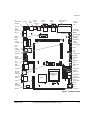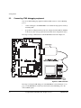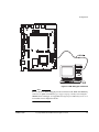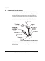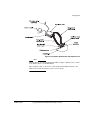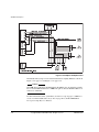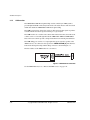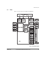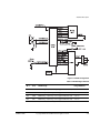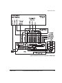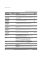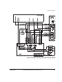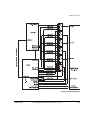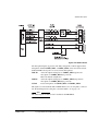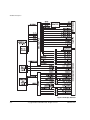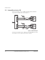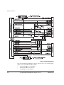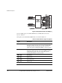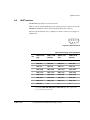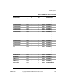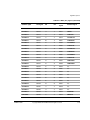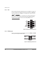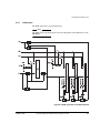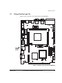
1
RealView Platform Baseboard for
ARM926EJ-S
™
HBI-0117
User Guide
Copyright © 2003-2010 ARM Limited. All rights reserved.
ARM DUI 0224I
RealView Platform Baseboard for ARM926EJ-S
User Guide
Copyright © 2003-2010 ARM Limited. All rights reserved.
Release Information
Change History
Date
Issue
Confidentiality
Change
November 2003
A
Non-Confidential
First release.
April 2004
B
Non-Confidential
Second release. Added configuration details for USB
debug, PCI, and Boot Monitor.
November 2005
C
Non-Confidential
Third release. Corrected reported defects and added
requested enhancements.
August 2006
D
Non-Confidential
Fourth release. Corrected reported defects and added
requested enhancements.
May 2007
E
Non-Confidential
Fifth release. Corrected reported defects and added
requested enhancements.
October 2007
F
Non-Confidential
Sixth release. Corrected reported defect.
April 2008
G
Non-Confidential
Seventh release. Corrected reported defect.
March 2009
H
Non-Confidential
Eighth release. Corrected reported defect.
July 2010
I
Non-Confidential
Ninth release. Document update.
Proprietary Notice
Words and logos marked with ® or ™ are registered trademarks or trademarks owned by ARM Limited, except
as otherwise stated below in this proprietary notice. Other brands and names mentioned herein may be the
trademarks of their respective owners.
Neither the whole nor any part of the information contained in, or the product described in, this document
may be adapted or reproduced in any material form except with the prior written permission of the copyright
holder.
The product described in this document is subject to continuous developments and improvements. All
particulars of the product and its use contained in this document are given by ARM in good faith. However,
all warranties implied or expressed, including but not limited to implied warranties of merchantability, or
fitness for purpose, are excluded.
This document is intended only to assist the reader in the use of the product. ARM Limited shall not be liable
for any loss or damage arising from the use of any information in this document, or any error or omission in
such information, or any incorrect use of the product.
ii
Copyright © 2003-2010 ARM Limited. All rights reserved.
ARM DUI 0224I
Confidentiality Status
This document is Non-Confidential. The right to use, copy and disclose this document may be subject to
license restrictions in accordance with the terms of the agreement entered into by ARM and the party that
ARM delivered this document to.
Product Status
The information in this document is final, that is for a developed product.
Web Address
http://www.arm.com
ARM DUI 0224I
Copyright © 2003-2010 ARM Limited. All rights reserved.
iii
Conformance Notices
This section contains conformance notices.
Federal Communications Commission Notice
This device is test equipment and consequently is exempt from part 15 of the FCC Rules under section 15.103
(c).
CE Declaration of Conformity
The system should be powered down when not in use.
The PB926EJ-S generates, uses, and can radiate radio frequency energy and may cause harmful interference
to radio communications. However, there is no guarantee that interference will not occur in a particular
installation. If this equipment causes harmful interference to radio or television reception, which can be
determined by turning the equipment off or on, you are encouraged to try to correct the interference by one
or more of the following measures:
•
ensure attached cables do not lie across the card
•
reorient the receiving antenna
•
increase the distance between the equipment and the receiver
•
connect the equipment into an outlet on a circuit different from that to which the receiver is connected
•
consult the dealer or an experienced radio/TV technician for help
Note
It is recommended that wherever possible shielded interface cables be used.
iv
Copyright © 2003-2010 ARM Limited. All rights reserved.
ARM DUI 0224I
Contents
RealView Platform Baseboard for ARM926EJ-S
User Guide
Preface
About this manual ...................................................................................... xviii
Feedback .................................................................................................... xxv
Chapter 1
Introduction
1.1
1.2
1.3
Chapter 2
Getting Started
2.1
2.2
2.3
2.4
2.5
2.6
Chapter 3
Setting up the RealView Platform ............................................................... 2-2
Setting the configuration switches .............................................................. 2-3
Connecting JTAG debugging equipment .................................................... 2-8
Connecting the Trace Port Analyzer ......................................................... 2-10
Supplying power ....................................................................................... 2-13
Using the PB926EJ-S Boot Monitor and platform library .......................... 2-14
Hardware Description
3.1
3.2
ARM DUI 0224I
About the PB926EJ-S ................................................................................. 1-2
PB926EJ-S architecture .............................................................................. 1-4
Precautions ................................................................................................. 1-9
ARM926EJ-S PXP Development Chip ........................................................ 3-3
FPGA ........................................................................................................ 3-17
Copyright © 2003-2010 ARM Limited. All rights reserved.
v
Contents
3.3
3.4
3.5
3.6
3.7
3.8
3.9
3.10
3.11
3.12
3.13
3.14
3.15
3.16
3.17
3.18
3.19
3.20
3.21
3.22
Chapter 4
3-22
3-33
3-35
3-56
3-59
3-61
3-65
3-68
3-71
3-72
3-74
3-75
3-79
3-80
3-81
3-84
3-87
3-88
3-92
3-94
Programmer’s Reference
4.1
4.2
4.3
4.4
4.5
4.6
4.7
4.8
4.9
4.10
4.11
4.12
4.13
4.14
4.15
4.16
4.17
4.18
4.19
4.20
4.21
4.22
4.23
4.24
4.25
vi
Reset controller ........................................................................................
Power supply control ................................................................................
Clock architecture .....................................................................................
Advanced Audio Codec Interface, AACI ...................................................
Character LCD controller ..........................................................................
CLCDC interface ......................................................................................
DMA ..........................................................................................................
Ethernet interface .....................................................................................
GPIO interface ..........................................................................................
Interrupts ..................................................................................................
Keyboard/Mouse Interface, KMI ...............................................................
Memory Card Interface, MCI ....................................................................
PCI interface .............................................................................................
Serial bus interface ...................................................................................
Smart Card interface, SCI ........................................................................
Synchronous Serial Port, SSP ..................................................................
User switches and LEDs ..........................................................................
UART interface .........................................................................................
USB interface ...........................................................................................
Test, configuration, and debug interfaces ................................................
Memory map ............................................................................................... 4-3
Configuration and initialization .................................................................... 4-9
Status and system control registers ......................................................... 4-17
AHB monitor ............................................................................................. 4-41
Advanced Audio CODEC Interface, AACI ................................................ 4-42
Character LCD display ............................................................................. 4-44
Color LCD Controller, CLCDC .................................................................. 4-47
Direct Memory Access Controller and mapping registers ........................ 4-52
Ethernet .................................................................................................... 4-55
General Purpose Input/Output, GPIO ....................................................... 4-56
Interrupt controllers ................................................................................... 4-57
Keyboard and Mouse Interface, KMI ........................................................ 4-67
MBX .......................................................................................................... 4-68
MOVE video coprocessor ......................................................................... 4-69
MultiMedia Card Interfaces, MCIx ............................................................ 4-70
MultiPort Memory Controller, MPMC ........................................................ 4-71
PCI controller ............................................................................................ 4-74
Real Time Clock, RTC .............................................................................. 4-85
Serial bus interface ................................................................................... 4-86
Smart Card Interface, SCI ........................................................................ 4-88
Synchronous Serial Port, SSP .................................................................. 4-89
Synchronous Static Memory Controller, SSMC ........................................ 4-91
System Controller ..................................................................................... 4-95
Timers ....................................................................................................... 4-96
UART ........................................................................................................ 4-97
Copyright © 2003-2010 ARM Limited. All rights reserved.
ARM DUI 0224I
Contents
4.26
4.27
4.28
Appendix A
Signal Descriptions
A.1
A.2
A.3
A.4
A.5
A.6
A.7
A.8
A.9
A.10
A.11
A.12
A.13
Appendix B
About memory expansion ........................................................................... E-2
Fitting a memory board ............................................................................... E-5
EEPROM contents ...................................................................................... E-6
Connector pinout ....................................................................................... E-13
Mechanical layout ..................................................................................... E-20
RealView Logic Tile
F.1
F.2
ARM DUI 0224I
Connecting the PB926EJ-S to the PCI enclosure ...................................... D-2
Backplane hardware .................................................................................. D-6
Connectors ............................................................................................... D-10
Memory Expansion Boards
E.1
E.2
E.3
E.4
E.5
Appendix F
About the CLCD display and adaptor board .............................................. C-2
Installing the CLCD display ........................................................................ C-6
Touchscreen controller interface .............................................................. C-11
Connectors ............................................................................................... C-15
Mechanical layout .................................................................................... C-19
PCI Backplane and Enclosure
D.1
D.2
D.3
Appendix E
Electrical specification ................................................................................. B-2
Clock rate restrictions .................................................................................. B-5
Mechanical details ...................................................................................... B-9
CLCD Display and Adaptor Board
C.1
C.2
C.3
C.4
C.5
Appendix D
Synchronous Serial Port interface ............................................................... A-2
Smart Card interface ................................................................................... A-3
UART interface ........................................................................................... A-5
USB interface .............................................................................................. A-6
Audio CODEC interface .............................................................................. A-7
MMC and SD flash card interface ............................................................... A-8
CLCD display interface ............................................................................. A-10
VGA display interface ............................................................................... A-13
GPIO interface .......................................................................................... A-14
Keyboard and mouse interface ................................................................. A-15
Ethernet interface ...................................................................................... A-16
RealView Logic Tile header connectors .................................................... A-17
Test and debug connections ..................................................................... A-33
Specifications
B.1
B.2
B.3
Appendix C
USB interface ............................................................................................ 4-99
Vector Floating Point, VFP9 .................................................................... 4-100
Watchdog ................................................................................................ 4-101
About the RealView Logic Tile .................................................................... F-2
Fitting a RealView Logic Tile ....................................................................... F-3
Copyright © 2003-2010 ARM Limited. All rights reserved.
vii
Contents
F.3
Appendix G
Configuring the USB Debug Connection
G.1
G.2
G.3
G.4
viii
Header connectors ..................................................................................... F-4
Installing the RealView ICE Micro Edition driver ........................................ G-2
Changes to RealView Debugger ................................................................ G-5
Using the USB debug port to connect RealView Debugger ....................... G-6
Using the Debug tab of the RealView Debugger Register pane .............. G-10
Copyright © 2003-2010 ARM Limited. All rights reserved.
ARM DUI 0224I
List of Tables
RealView Platform Baseboard for ARM926EJ-S
User Guide
Table 2-1
Table 2-2
Table 2-3
Table 2-4
Table 2-5
Table 2-6
Table 2-7
Table 3-1
Table 3-2
Table 3-3
Table 3-4
Table 3-5
Table 3-6
Table 3-7
Table 3-8
Table 3-9
Table 3-10
Table 3-11
Table 3-12
Table 3-13
ARM DUI 0224I
Change History ............................................................................................................. ii
Selecting the boot device .......................................................................................... 2-4
Default switch positions ............................................................................................. 2-4
LED Indicators ........................................................................................................... 2-5
Boot Monitor commands ......................................................................................... 2-15
Boot Monitor Configure commands ......................................................................... 2-16
Boot Monitor Debug commands .............................................................................. 2-16
Boot Monitor NOR flash commands ........................................................................ 2-17
Configuration switch S1 ............................................................................................ 3-8
FPGA image selection ............................................................................................ 3-19
Reset sources and effects ....................................................................................... 3-24
Reset signal descriptions ........................................................................................ 3-29
ARM926EJ-S PXP Development Chip clocks ......................................................... 3-40
Asynchronous clock signals .................................................................................... 3-46
HCLKM1 selection .................................................................................................. 3-47
HCLKM2 selection .................................................................................................. 3-47
HCLKS selection ..................................................................................................... 3-48
GLOBALCLK selection ............................................................................................ 3-52
PB926EJ-S clocks and clock control signals .......................................................... 3-54
Audio system specification ...................................................................................... 3-56
AC’97 audio debug signals on J45 .......................................................................... 3-58
Copyright © 2003-2010 ARM Limited. All rights reserved.
ix
List of Tables
Table 3-14
Table 3-15
Table 3-16
Table 3-17
Table 3-18
Table 3-19
Table 3-20
Table 3-21
Table 3-22
Table 3-23
Table 3-24
Table 3-25
Table 4-1
Table 4-2
Table 4-3
Table 4-4
Table 4-5
Table 4-6
Table 4-7
Table 4-8
Table 4-9
Table 4-10
Table 4-11
Table 4-12
Table 4-13
Table 4-14
Table 4-15
Table 4-16
Table 4-17
Table 4-18
Table 4-19
Table 4-20
Table 4-21
Table 4-22
Table 4-23
Table 4-24
Table 4-25
Table 4-26
Table 4-27
Table 4-28
Table 4-29
Table 4-30
Table 4-31
Table 4-32
Table 4-33
Table 4-34
Table 4-35
x
Display interface signals ......................................................................................... 3-63
DMA signals for external devices ........................................................................... 3-67
Ethernet signals ...................................................................................................... 3-68
MMC/SD interface signals ...................................................................................... 3-75
MMC signals ........................................................................................................... 3-78
Serial bus addresses .............................................................................................. 3-80
Serial bus signals .................................................................................................... 3-80
Smart Card interface signals .................................................................................. 3-83
SSP signal descriptions .......................................................................................... 3-85
Serial interface signal assignment .......................................................................... 3-90
USB interface signal assignment ............................................................................ 3-93
JTAG related signals .............................................................................................. 3-98
Memory map ............................................................................................................. 4-3
Selecting the boot device ........................................................................................ 4-10
Memory chip selects and address range ................................................................ 4-16
Register map for system control registers .............................................................. 4-18
ID Register, SYS_ID bit assignment ....................................................................... 4-21
Oscillator Register, SYS_OSCx bit assignment ..................................................... 4-23
Lock Register, SYS_LOCK bit assignment ............................................................. 4-24
Configuration register 1 .......................................................................................... 4-26
Configuration register 2 .......................................................................................... 4-27
Flag registers .......................................................................................................... 4-30
Reset level control .................................................................................................. 4-31
MCI control ............................................................................................................. 4-32
Flash control ........................................................................................................... 4-32
SYS_CLCD register ................................................................................................ 4-33
SYS_CLCDSER register ........................................................................................ 4-34
BOOT configuration switches ................................................................................. 4-35
SYS_MISC .............................................................................................................. 4-36
DMA map registers ................................................................................................. 4-37
SYS_DMAPSRx, DMA mapping register format .................................................... 4-38
Oscillator test registers ........................................................................................... 4-40
AHB monitor implementation .................................................................................. 4-41
AACI implementation .............................................................................................. 4-42
Modified AACI PeriphID3 register ........................................................................... 4-43
Character LCD display implementation .................................................................. 4-44
Character LCD control and data registers .............................................................. 4-45
Character LCD display commands ......................................................................... 4-46
CLCDC implementation .......................................................................................... 4-47
PrimeCell CLCDC register differences ................................................................... 4-48
Values for different display resolutions ................................................................... 4-48
Assignment of display memory to R[7:0], G[7:0], and B[7:0] .................................. 4-49
PL110 hardware playback mode ............................................................................ 4-51
DMAC implementation ............................................................................................ 4-52
DMA channels ........................................................................................................ 4-53
DMA mapping register format ................................................................................. 4-54
Ethernet implementation ......................................................................................... 4-55
Copyright © 2003-2010 ARM Limited. All rights reserved.
ARM DUI 0224I
List of Tables
Table 4-36
Table 4-37
Table 4-38
Table 4-39
Table 4-40
Table 4-41
Table 4-42
Table 4-43
Table 4-44
Table 4-45
Table 4-46
Table 4-47
Table 4-48
Table 4-49
Table 4-50
Table 4-51
Table 4-52
Table 4-53
Table 4-54
Table 4-55
Table 4-56
Table 4-57
Table 4-58
Table 4-59
Table 4-60
Table 4-61
Table 4-62
Table 4-63
Table 4-64
Table 4-65
Table 4-66
Table 4-67
Table 4-68
Table 4-69
Table 4-70
Table 4-71
Table 4-72
Table 4-73
Table 4-74
Table 4-75
Table 4-76
Table 4-77
Table A-1
Table A-2
Table A-3
Table A-4
Table A-5
ARM DUI 0224I
GPIO implementation .............................................................................................. 4-56
VIC Primary Interrupt Controller implementation ..................................................... 4-57
SIC implementation ................................................................................................. 4-57
Primary interrupt controller registers ....................................................................... 4-58
Interrupt signals to primary interrupt controller ........................................................ 4-59
Secondary interrupt controller registers .................................................................. 4-61
Interrupt signals to secondary interrupt controller ................................................... 4-62
KMI implementation ................................................................................................ 4-67
MBX implementation ............................................................................................... 4-68
MCI implementation ................................................................................................ 4-70
MPMC implementation ............................................................................................ 4-71
SDRAM register values ........................................................................................... 4-72
PCI controller implementation ................................................................................. 4-74
PCI bus memory map for AHB M2 bridge ............................................................... 4-75
PCI controller registers ............................................................................................ 4-75
PCI_IMAPx register format ..................................................................................... 4-77
PCI_SELFID register format ................................................................................... 4-77
PCI_FLAGS register format .................................................................................... 4-78
PCI_SMAPx register format .................................................................................... 4-79
PCI backplane configuration header addresses (self-config) .................................. 4-80
PCI backplane configuration header addresses (normal configuration) .................. 4-80
PCI configuration space header .............................................................................. 4-81
PCI bus commands supported ................................................................................ 4-84
RTC implementation ............................................................................................... 4-85
Serial bus implementation ....................................................................................... 4-86
Serial bus register ................................................................................................... 4-86
Serial bus device addresses ................................................................................... 4-87
SCI implementation ................................................................................................. 4-88
SSP implementation ................................................................................................ 4-89
SSMC implementation ............................................................................................ 4-91
Register values for Intel flash, standard async read mode, no bursts ..................... 4-92
Register values for Intel flash, async page mode ................................................... 4-92
Register values for Samsung SRAM ....................................................................... 4-93
Register values for Spansion BDS640 .................................................................... 4-93
Register values for Spansion LV256 ....................................................................... 4-93
System controller implementation ........................................................................... 4-95
Timer implementation .............................................................................................. 4-96
UART implementation ............................................................................................. 4-97
USB implementation ............................................................................................... 4-99
USB controller base address .................................................................................. 4-99
VFP9 implementation ............................................................................................ 4-100
Watchdog implementation ..................................................................................... 4-101
SSP signal assignment ............................................................................................. A-2
Smartcard connector signal assignment ................................................................... A-3
Signals on expansion connector ............................................................................... A-4
Serial plug signal assignment ................................................................................... A-5
Multimedia Card interface signals ............................................................................. A-9
Copyright © 2003-2010 ARM Limited. All rights reserved.
xi
List of Tables
Table A-6
Table A-7
Table A-8
Table A-9
Table A-10
Table A-11
Table A-12
Table A-13
Table A-14
Table A-15
Table A-16
Table B-1
Table B-2
Table B-3
Table B-4
Table B-5
Table B-6
Table B-7
Table C-1
Table C-2
Table C-3
Table C-4
Table C-5
Table C-6
Table C-7
Table C-8
Table D-1
Table D-2
Table D-3
Table D-4
Table D-5
Table D-6
Table E-1
Table E-2
Table E-3
Table E-4
Table E-5
Table E-6
Table F-1
Table G-1
Table G-2
xii
CLCD Interface board connector J18 ..................................................................... A-10
VGA connector signals ........................................................................................... A-13
Mouse and keyboard port signal descriptions ........................................................ A-15
Ethernet signals ...................................................................................................... A-16
HDRX (J9) signals .................................................................................................. A-18
HDRY (J12) signals ................................................................................................ A-22
HDRZ (J8) signals .................................................................................................. A-26
Test point functions ................................................................................................. A-34
Trace connector J14 ............................................................................................... A-37
AHB monitor connector J17 .................................................................................... A-39
FPGA debug connector J39 ................................................................................... A-40
PB926EJ-S electrical characteristics ........................................................................ B-2
Current requirements from DC IN (12V) ................................................................... B-3
Current requirements from J34 ................................................................................. B-3
Maximum current load on supply voltage rails .......................................................... B-4
ARM926EJ-S PXP Development Chip bus timing .................................................... B-6
ARM926EJ-S PXP Development Chip memory timing ............................................. B-7
Peripherals and controller timing .............................................................................. B-8
Displays available with adaptor board ...................................................................... C-7
Power configuration .................................................................................................. C-9
Touchscreen host interface signal assignment ....................................................... C-11
CLCD interface connector J2 .................................................................................. C-15
LCD prototyping connector J1 ................................................................................ C-16
Touchscreen prototyping connector J3 ................................................................... C-17
Inverter prototyping connector J4 ........................................................................... C-17
A/D and keypad J13 ............................................................................................... C-18
LED indicators .......................................................................................................... D-7
Configuration switches .............................................................................................. D-8
Power and reset switches ......................................................................................... D-8
Test points ................................................................................................................ D-8
ATX power connector ............................................................................................. D-10
Mictor connector pinout .......................................................................................... D-11
Memory width encoding ............................................................................................ E-4
Chip Select information block ................................................................................... E-7
Example contents of a static memory expansion EEPROM ..................................... E-8
Example contents of a dynamic memory expansion EEPROM .............................. E-11
SDR, Single data rate dynamic memory connector signals .................................... E-14
Static memory connector signals ............................................................................ E-16
RealView Logic Tile clock signals ............................................................................. F-8
Reset behavior register names and values ............................................................ G-11
Device property register names and values ........................................................... G-12
Copyright © 2003-2010 ARM Limited. All rights reserved.
ARM DUI 0224I
List of Figures
RealView Platform Baseboard for ARM926EJ-S
User Guide
Figure 1-1
Figure 1-2
Figure 2-1
Figure 2-2
Figure 2-3
Figure 2-4
Figure 2-5
Figure 2-6
Figure 3-1
Figure 3-2
Figure 3-3
Figure 3-4
Figure 3-5
Figure 3-6
Figure 3-7
Figure 3-8
Figure 3-9
Figure 3-10
Figure 3-11
Figure 3-12
ARM DUI 0224I
Key to timing diagram conventions ............................................................................. xx
PB926EJ-S layout ..................................................................................................... 1-3
PB926EJ-S block diagram ........................................................................................ 1-6
Location of S1-1 and S6-1 ........................................................................................ 2-3
JTAG connection ....................................................................................................... 2-8
USB debug port connection ...................................................................................... 2-9
Example of MultiTrace and JTAG connection ......................................................... 2-10
Example of RealView ICE and RealView Trace ...................................................... 2-11
Power connectors ................................................................................................... 2-13
ARM926EJ-S PXP Development Chip block diagram .............................................. 3-4
Configuration signals from SYS_CFGDATAx ........................................................... 3-9
Example of multiple masters ................................................................................... 3-12
AHB map ................................................................................................................. 3-13
Core APB and DMA APB map ................................................................................ 3-14
Memory devices ...................................................................................................... 3-15
AHB monitor connection ......................................................................................... 3-16
FPGA block diagram ............................................................................................... 3-17
FPGA configuration ................................................................................................. 3-19
FPGA reload sequence ........................................................................................... 3-20
PB926EJ-S reset logic ............................................................................................ 3-23
Reset signal sequence ............................................................................................ 3-25
Copyright © 2003-2010 ARM Limited. All rights reserved.
xiii
List of Figures
Figure 3-13
Figure 3-14
Figure 3-15
Figure 3-16
Figure 3-17
Figure 3-18
Figure 3-19
Figure 3-20
Figure 3-21
Figure 3-22
Figure 3-23
Figure 3-24
Figure 3-25
Figure 3-26
Figure 3-27
Figure 3-28
Figure 3-29
Figure 3-30
Figure 3-31
Figure 3-32
Figure 3-33
Figure 3-34
Figure 3-35
Figure 3-36
Figure 3-37
Figure 3-38
Figure 3-39
Figure 3-40
Figure 3-41
Figure 3-42
Figure 3-43
Figure 3-44
Figure 3-45
Figure 4-1
Figure 4-2
Figure 4-3
Figure 4-4
Figure 4-5
Figure 4-6
Figure 4-7
Figure 4-8
Figure 4-9
Figure 4-10
Figure 4-11
Figure 4-12
Figure 4-13
Figure 4-14
xiv
Programmable reset level ....................................................................................... 3-26
Boot memory remap logic ....................................................................................... 3-28
Power-on reset and configuration timing ................................................................ 3-32
Standby switch and power-supply control .............................................................. 3-34
Clock architecture ................................................................................................... 3-35
ARM926EJ-S PXP Development Chip internal multiplexors .................................. 3-39
Default clock sources and frequencies ................................................................... 3-42
Clock sources for asynchronous AHB bridges ....................................................... 3-45
Serial data and SYS_OSCx register format ............................................................ 3-49
Example of selecting a tile clock for the AHB S bridge ........................................... 3-53
Clock multiplexors ................................................................................................... 3-55
Audio interface ........................................................................................................ 3-57
Character display .................................................................................................... 3-60
Display interface ..................................................................................................... 3-62
DMA channels ........................................................................................................ 3-66
Ethernet interface architecture ................................................................................ 3-68
GPIO block diagram ............................................................................................... 3-71
External and internal interrupt sources ................................................................... 3-72
KMI block diagram .................................................................................................. 3-74
MMI interface .......................................................................................................... 3-77
PCI bridge ............................................................................................................... 3-79
Serial bus block diagram ........................................................................................ 3-80
SCI block diagram .................................................................................................. 3-82
SSP block diagram ................................................................................................. 3-84
Switch and LED interface ....................................................................................... 3-87
UARTs block diagram ............................................................................................. 3-89
UART0 interface ..................................................................................................... 3-89
Simplified interface for UART[3:1] .......................................................................... 3-90
OTG243 block diagram ........................................................................................... 3-92
Test and debug connectors, links, and LEDs ......................................................... 3-95
JTAG connector signals ........................................................................................ 3-101
JTAG signal routing .............................................................................................. 3-102
RealView Logic Tile JTAG circuitry ....................................................................... 3-103
ARM Data bus memory map .................................................................................... 4-8
Booting from NOR flash 1 ....................................................................................... 4-12
Booting from static expansion memory ................................................................... 4-13
Booting from AHB expansion .................................................................................. 4-14
ID Register, SYS_ID ............................................................................................... 4-21
SYS_SW ................................................................................................................. 4-21
SYS_LED ................................................................................................................ 4-22
Oscillator Register, SYS_OSCx .............................................................................. 4-23
Lock Register, SYS_LOCK ..................................................................................... 4-24
SYS_CFGDATA1 ................................................................................................... 4-25
SYS_CFGDATA2 ................................................................................................... 4-26
SYS_RESETCTL .................................................................................................... 4-31
SYS_MCI ................................................................................................................ 4-32
SYS_CLCD ............................................................................................................. 4-33
Copyright © 2003-2010 ARM Limited. All rights reserved.
ARM DUI 0224I
List of Figures
Figure 4-15
Figure 4-16
Figure 4-17
Figure 4-18
Figure 4-19
Figure 4-20
Figure 4-21
Figure 4-22
Figure 4-23
Figure 4-24
Figure 4-25
Figure 4-26
Figure 4-27
Figure 4-28
Figure 4-29
Figure A-1
Figure A-2
Figure A-3
Figure A-4
Figure A-5
Figure A-6
Figure A-7
Figure A-8
Figure A-9
Figure A-10
Figure A-11
Figure A-12
Figure A-13
Figure A-14
Figure A-15
Figure A-16
Figure A-17
Figure A-18
Figure A-19
Figure B-1
Figure C-1
Figure C-2
Figure C-3
Figure C-4
Figure C-5
Figure C-6
Figure C-7
Figure C-8
Figure C-9
Figure D-1
Figure D-2
Figure D-3
ARM DUI 0224I
SYS_CLCDSER ...................................................................................................... 4-34
SYS_BOOTCS ........................................................................................................ 4-35
SYS_MISC .............................................................................................................. 4-36
DMA mapping register ............................................................................................ 4-37
Oscillator Register, SYS_OSCRESETx .................................................................. 4-39
AACI ID register ...................................................................................................... 4-42
SYS_DMAP0-2 mapping register format ................................................................ 4-54
Primary interrupt registers ....................................................................................... 4-59
Secondary interrupt registers .................................................................................. 4-62
AHB M2 to PCI mapping ......................................................................................... 4-76
PCI_IMAPx register ................................................................................................. 4-76
PCI_SELFID register ............................................................................................... 4-77
PCI_FLAGS register ............................................................................................... 4-78
PCI to AHB S mapping ............................................................................................ 4-79
PCI_SMAPx register ............................................................................................... 4-79
SSP expansion interface ........................................................................................... A-2
Smartcard contacts assignment ................................................................................ A-3
J28 SCI expansion .................................................................................................... A-4
Serial connector ........................................................................................................ A-5
USB interfaces .......................................................................................................... A-6
Audio connectors ...................................................................................................... A-7
MMC/SD card socket pin numbering ........................................................................ A-8
MMC card .................................................................................................................. A-8
CLCD Interface connector J18 ................................................................................ A-12
VGA connector J19 ................................................................................................. A-13
GPIO connector ...................................................................................................... A-14
KMI connector ......................................................................................................... A-15
Ethernet connector J5 ............................................................................................. A-16
HDRX, HDRY, and HDRZ (upper) pin numbering ................................................... A-17
Test points and debug connectors .......................................................................... A-33
Multi-ICE JTAG connector J31 ................................................................................ A-36
USB debug connector J30 ...................................................................................... A-36
Embedded logic analyzer connector J33 ................................................................ A-38
AMP Mictor connector ............................................................................................. A-38
Baseboard mechanical details .................................................................................. B-9
CLCD adaptor board connectors (bottom view) ....................................................... C-2
Small CLCD enclosure ............................................................................................. C-3
Large CLCD enclosure ............................................................................................. C-4
Displays mounted directly onto top of adaptor board. .............................................. C-5
CLCD adaptor board connection .............................................................................. C-6
CLCD buffer and power supply control links .......................................................... C-10
Touchscreen and keypad interface ........................................................................ C-12
Touchscreen resistive elements ............................................................................. C-12
CLCD adaptor board mechanical layout ................................................................ C-19
Installing the platform board into the PCI enclosure ................................................ D-3
Multiple boards on PCI bus ...................................................................................... D-5
PCI backplane .......................................................................................................... D-6
Copyright © 2003-2010 ARM Limited. All rights reserved.
xv
List of Figures
Figure D-4
Figure D-5
Figure D-6
Figure E-1
Figure E-2
Figure E-3
Figure E-4
Figure E-5
Figure E-6
Figure E-7
Figure F-1
Figure F-2
Figure F-3
Figure F-4
Figure F-5
Figure F-6
Figure G-1
Figure G-2
Figure G-3
Figure G-4
Figure G-5
Figure G-6
Figure G-7
Figure G-8
xvi
JTAG signal flow on the PCI backplane ................................................................... D-9
AMP Mictor connector J4 ........................................................................................ D-11
PCI expansion board JTAG connector J5 .............................................................. D-12
Dynamic memory board block diagram .................................................................... E-2
Static memory board block diagram ......................................................................... E-3
Memory board installation locations ......................................................................... E-5
Chip select information block .................................................................................... E-8
Samtec connector ................................................................................................... E-13
Dynamic memory board layout ............................................................................... E-20
Static memory board layout .................................................................................... E-20
Signals on the RealView Logic Tile expansion connectors ...................................... F-2
RealView Logic Tile fitted on PB926EJ-S ................................................................. F-3
HDRX, HDRY, and HDRZ (upper) pin numbering .................................................... F-5
RealView Logic Tile tristate for I/O ........................................................................... F-6
Clock signals and the RealView Logic Tile ............................................................. F-10
Bus signals for RealView Logic Tile and FPGA ...................................................... F-13
Nodes added to Connection Control window ............................................................ G-5
The Connection Control window ............................................................................... G-6
ARM926EJ-S PXP Development Chip detected ...................................................... G-7
Error shown when unpowered devices are detected ................................................ G-7
Error shown when no devices are detected .............................................................. G-8
Error shown when the USB debug port is not functioning ........................................ G-8
Connection Properties window ................................................................................. G-8
The Debug tab of the Register pane ....................................................................... G-10
Copyright © 2003-2010 ARM Limited. All rights reserved.
ARM DUI 0224I
Preface
This preface introduces the RealView Platform Baseboard for ARM926EJ-S User
Guide. It contains the following sections:
•
About this manual on page xviii
•
Feedback on page xxv.
ARM DUI 0224I
Copyright © 2003-2010 ARM Limited. All rights reserved.
xvii
Preface
About this manual
This document describes how to set up and use the RealView Platform Baseboard for
the ARM926EJ-S (PB926EJ-S).
Product revision status
The rnpn identifier indicates the revision status of the product described in this manual,
where:
rn
Identifies the major revision of the product.
pn
Identifies the minor revision or modification status of the product.
Intended audience
This document has been written for experienced hardware and software developers to
aid the development of ARM-based products using the PB926EJ-S as part of a
development system.
Using this manual
This document is organized into the following chapters:
Chapter 1 Introduction
Read this chapter for an introduction to the PB926EJ-S. This chapter
shows the physical layout of the board and identifies the main
components.
Chapter 2 Getting Started
Read this chapter for a description of how to set up and start using the
PB926EJ-S. This chapter describes how to connect the add-on boards and
how to apply power.
Chapter 3 Hardware Description
Read this chapter for a description of the hardware architecture of the
PB926EJ-S. This chapter describes the peripherals, clocks, resets, and
debug hardware provided by the board.
Chapter 4 Programmer’s Reference
Read this chapter for a description of the PB926EJ-S memory map and
registers. There is also basic information on the peripherals and
controllers present in the platform baseboard.
xviii
Copyright © 2003-2010 ARM Limited. All rights reserved.
ARM DUI 0224I
Preface
Appendix A Signal Descriptions
Refer to this appendix for a description of the signals on the connectors.
Appendix B Specifications
Refer to this appendix for electrical, timing, and mechanical
specifications.
Appendix C CLCD Display and Adaptor Board
Refer to this appendix for details of the CLCD display and interface.
Appendix D PCI Backplane and Enclosure
Refer to this appendix for details of the PCI backplane board.
Appendix E Memory Expansion Boards
Refer to this appendix for details of the memory expansion boards.
Appendix F RealView Logic Tile
Refer to this appendix for details on installing an ARM RealView Logic
Tile product.
Appendix G Configuring the USB Debug Connection
Refer to this appendix for details on configuring the USB debug port for
use with RealView Debugger.
Conventions
Conventions that this manual can use are described in:
•
Typographical
•
Timing diagrams on page xx
•
Signals on page xxi
•
Numbering on page xxi.
Typographical
The typographical conventions are:
ARM DUI 0224I
italic
Highlights important notes, introduces special terminology,
denotes internal cross-references, and citations.
bold
Highlights interface elements, such as menu names. Denotes
signal names. Also used for terms in descriptive lists, where
appropriate.
Copyright © 2003-2010 ARM Limited. All rights reserved.
xix
Preface
monospace
Denotes text that you can enter at the keyboard, such as
commands, file and program names, and source code.
monospace
Denotes a permitted abbreviation for a command or option. You
can enter the underlined text instead of the full command or option
name.
monospace italic
Denotes arguments to monospace text where the argument is to be
replaced by a specific value.
monospace bold
Denotes language keywords when used outside example code.
< and >
Angle brackets enclose replaceable terms for assembler syntax
where they appear in code or code fragments. They appear in
normal font in running text. For example:
•
MRC p15, 0 <Rd>, <CRn>, <CRm>, <Opcode_2>
•
The Opcode_2 value selects which register is accessed.
Timing diagrams
The figure named Key to timing diagram conventions explains the components used in
timing diagrams. Variations, when they occur, have clear labels. You must not assume
any timing information that is not explicit in the diagrams.
Shaded bus and signal areas are undefined, so the bus or signal can assume any value
within the shaded area at that time. The actual level is unimportant and does not affect
normal operation.
Clock
HIGH to LOW
Transient
HIGH/LOW to HIGH
Bus stable
Bus to high impedance
Bus change
High impedance to stable bus
Key to timing diagram conventions
xx
Copyright © 2003-2010 ARM Limited. All rights reserved.
ARM DUI 0224I
Preface
Signals
The signal conventions are:
Signal level
The level of an asserted signal depends on whether the signal is
active-HIGH or active-LOW. Asserted means HIGH for
active-HIGH signals and LOW for active-LOW signals.
Lower-case n
Denotes an active-LOW signal.
Prefix A
Denotes global Advanced eXtensible Interface (AXI) signals:
Prefix AR
Denotes AXI read address channel signals.
Prefix AW
Denotes AXI write address channel signals.
Prefix B
Denotes AXI write response channel signals.
Prefix C
Denotes AXI low-power interface signals.
Prefix H
Denotes Advanced High-performance Bus (AHB) signals.
Prefix P
Denotes Advanced Peripheral Bus (APB) signals.
Prefix R
Denotes AXI read data channel signals.
Prefix W
Denotes AXI write data channel signals.
Numbering
The numbering convention is:
<size in bits>'<base><number>
This is a Verilog method of abbreviating constant numbers. For example:
•
'h7B4 is an unsized hexadecimal value.
•
'o7654 is an unsized octal value.
•
8'd9 is an eight-bit wide decimal value of 9.
•
8'h3F is an eight-bit wide hexadecimal value of 0x3F. This is
equivalent to b00111111.
•
8'b1111 is an eight-bit wide binary value of b00001111.
ARM DUI 0224I
Copyright © 2003-2010 ARM Limited. All rights reserved.
xxi
Preface
Further reading
This section lists publications by ARM Limited, and by third parties.
ARM Limited periodically provides updates and corrections to its documentation. See
http://www.arm.com for current errata sheets, addenda, and the Frequently Asked
Questions list.
ARM publications
This manual contains information that is specific to the PB926EJ-S Platform
Baseboard. See the following documents for other relevant information:
The following publications provide information about the registers and interfaces on the
ARM926EJ-S PXP Development Chip:
•
ARM926EJ-S Development Chip Reference Guide (ARM DDI 0287)
•
ARM926EJ-S Technical Reference Manual (ARM DDI 0198)
•
ARM926EJ-S™ PrimeXsys Platform Virtual Component Technical Reference
Manual (ARM DDI 0232)
•
ARM926EJ-S™ PrimeXsys Platform Virtual Component User Guide
(ARM DUI 0213)
•
ARM MOVE Coprocessor Technical Reference Manual (ARM DDI 0251)
•
ARM VFP9-S Coprocessor Technical Reference Manual (ARM DDI 0238)
•
ARM MBX HR-S Graphics Core Technical Reference Manual (ARM DDI 0241).
The following publications provide reference information about the ARM architecture:
•
AMBA™ Specification (ARM IHI 0011)
•
ARM Architecture Reference Manual (ARM DDI 0100).
The following publications provide information about related ARM products and
toolkits:
•
Multi-ICE™ User Guide (ARM DUI 0048)
•
RealView™ ICE User Guide (ARM DUI 0155)
•
Trace Debug Tools User Guide (ARM DUI 0118)
•
ARM MultiTrace® User Guide (ARM DUI 0150)
•
ARM RealView Logic Tile LT-XC2V4000+ User Guide (ARM DUI 0186)
•
RealView™ Debugger User Guide (ARM DUI 0153)
•
RealView Compilation Tools Compilers and Libraries Guide (ARM DUI 0205)
•
RealView Compilation Tools Developer Guide (ARM DUI 0203)
•
RealView Compilation Tools Linker and Utilities Guide (ARM DUI 0206).
xxii
Copyright © 2003-2010 ARM Limited. All rights reserved.
ARM DUI 0224I
Preface
The following publications provide information about ARM PrimeCell® and other
peripheral or controller devices:
•
ARM PrimeCell Advanced Audio CODEC Interface (PL041) Technical Reference
Manual (ARM DDI 0173)
•
ARM PrimeCell Color LCD Controller (PL110) Technical Reference Manual
(ARM DDI 0161)
•
ARM PrimeCell DMA (PL080) Technical Reference Manual (ARM DDI 0196)
•
ARM Dual-Timer Module (SP804) Technical Reference Manual
(ARM DDI 0271)
•
ARM PrimeCell GPIO (PL061) Technical Reference Manual (ARM DDI 0190)
•
ARM PrimeCell Keyboard Mouse Controller (PL050) Technical Reference
Manual (ARM DDI 0143)
•
ARM PrimeCell Multimedia Card Interface (PL180) Technical Reference Manual
(ARM DDI 0172)
•
ARM Multiport Memory Controller (GX175) Technical Reference Manual
(ARM DDI 0277)
•
ARM PrimeCell Real Time Clock Controller (PL031) Technical Reference
Manual (ARM DDI 0224)
•
ARM PrimeCell Smart Card Interface (PL131) Technical Reference Manual
(ARM DDI 0228)
•
ARM PrimeCell Synchronous Serial Port Controller (PL022) Technical Reference
Manual (ARM DDI 0194)
•
ARM PrimeCell Synchronous Static Memory Controller (PL093) Technical
Reference Manual (ARM DDI 236)
•
ARM PrimeCell System Controller (SP810) Technical Reference Manual
(ARM DDI 0254)
•
ARM PrimeCell UART (PL011) Technical Reference Manual (ARM DDI 0183)
•
ARM PrimeCell Vector Interrupt Controller (PL190) Technical Reference
Manual (ARM DDI 0181)
•
ARM PrimeCell Watchdog Controller (SP805) Technical Reference Manual
(ARM DDI 0270)
•
ETM9 Technical Reference Manual (ARM DDI 0157).
ARM DUI 0224I
Copyright © 2003-2010 ARM Limited. All rights reserved.
xxiii
Preface
Other publications
This section lists relevant documents published by third parties:
The following publication describes the JTAG ports with which Multi-ICE or RealView
ICE communicates:
•
IEEE Standard Test Access Port and Boundary Scan Architecture (IEEE Std.
1149.1).
The following datasheets describe some of the integrated circuits or modules used on
the PB926EJ-S:
xxiv
•
CODEC with Sample Rate Conversion and 3D Sound (LM4549) National
Semiconductor, Santa Clara, CA.
•
Mobile DiskOnChip Plus 32/64MByte, M-Systems Inc., Newark, CA.
•
MultiMedia Card Product Manual SanDisk, Sunnyvale, CA.
•
Serially Programmable Clock Source (ICS307), ICS, San Jose, CA.
•
Serial Microwire Bus EEPROM (M93LC46) STMicroelectronics, Amsterdam,
The Netherlands.
•
1.8 Volt Intel StrataFlash® Wireless Memory with 3.0 Volt I/O Intel Corporation,
Santa Clara, CA. See the Build of Materials (BOM) file for the part number of the
flash device.
•
TFT-LCD Module (LQ084V1DG21) Sharp Corporation, Osaka, Japan.
•
Three-In-One Fast Ethernet Controller (LAN91C111) SMSC, Hauppauge, NY.
•
Touch Screen Controller (TCS2200) Texas Instruments, Dallas, TX.
Copyright © 2003-2010 ARM Limited. All rights reserved.
ARM DUI 0224I
Preface
Feedback
ARM® Limited welcomes feedback both on the PB926EJ-S and on the documentation.
Feedback on this product
If you have any comments or suggestions about this product, contact your supplier
giving:
•
the product name
•
a concise explanation of your comments.
Feedback on this manual
If you have any comments about this document, send email to [email protected] giving:
•
the title
•
the number
•
the relevant page number(s) to which your comments apply
•
a concise explanation of your comments.
ARM® Limited also welcomes general suggestions for additions and improvements.
ARM DUI 0224I
Copyright © 2003-2010 ARM Limited. All rights reserved.
xxv
Preface
xxvi
Copyright © 2003-2010 ARM Limited. All rights reserved.
ARM DUI 0224I
Chapter 1
Introduction
This chapter introduces the PB926EJ-S. It contains the following sections:
•
About the PB926EJ-S on page 1-2
•
PB926EJ-S architecture on page 1-4
•
Precautions on page 1-9.
ARM DUI 0224I
Copyright © 2003-2010 ARM Limited. All rights reserved.
1-1
Introduction
1.1
About the PB926EJ-S
The PB926EJ-S provides a development system that you can use to develop products
around the ARM926EJ-S PXP Development Chip.
You can use the PB926EJ-S as a basic development system with a power supply and a
connection to a JTAG interface unit.
You can expand the PB926EJ-S by adding:
•
ARM RealView Logic Tiles containing custom IP
•
a PCI expansion enclosure
•
Dynamic memory expansion board
•
Static memory expansion board
•
VGA monitor or CLCD adaptor and CLCD display
•
MMC, SD, or SIM cards
•
custom devices to the 32-bit GPIO
•
USB devices to the three USB ports
•
serial devices to the synchronous serial port and the four UARTs
•
keyboard and mouse
•
audio devices to the onboard CODEC
•
an Ethernet network to the onboard Ethernet controller.
The basic system provides a good platform for developing code for the ARM7 and
ARM9 series of processors. The ARM926EJ-S PXP Development Chip is much faster
than a software simulator or a core implemented in RealView Logic Tiles. Code
developed for the ARM926EJ-S PXP Development Chip will also run on the ARM10
and ARM11 processor series.
The expanded system with RealView Logic Tiles can be used to develop
AMBA-compatible peripherals and to test ASIC designs. The fast processor core and
the peripherals present in the ARM926EJ-S PXP Development Chip, PB926EJ-S
FPGA, and RealView Logic Tile FPGA enable you to develop and text complex
systems operating at, or near, their target operating frequency.
Figure 1-1 on page 1-3 shows the layout of the PB926EJ-S.
1-2
Copyright © 2003-2010 ARM Limited. All rights reserved.
ARM DUI 0224I
Introduction
S1
configuration
switches
Mouse
OTG
USB
USB
0 (top)
1 (bottom)
UART
0 (top)
1 (bottom)
UART
2 (top)
3 (bottom)
CLCD expansion
connector
Line out
(top)
Line in
(bottom)
2X16
character
LCD
GP PUSH
(green LED)
Mic in
RESET
(orange LED)
FPGA
debug
DEV CHIP
CONFIG
(blue LED)
MMC
0 (top)
1 (bottom)
FPGA
CONFIG
(yellow LED)
Smart
card
0 (top)
1 (bottom)
JTAG
Trace
port
Logic Tile
expansion
0
CFGEN LED
(orange)
1
0
S6 GP
(user)
switches
CONFIG
link
Standby/
power
GP
(user)
LEDs
Ethernet
Power LED
(red)
Keyboard
ChipScope
Dynamic
memory
expansion
GPIO 0,1
GPIO 2,3
AHB
monitor
ARM926EJ-S
Development
Chip
FPGA
VGA
USB debug
3V3 OK
(green LED)
5V OK
(green LED)
Power
Static
memory
expansion
Fuse
PCI
expansion
Battery
Figure 1-1 PB926EJ-S layout
ARM DUI 0224I
Copyright © 2003-2010 ARM Limited. All rights reserved.
1-3
Introduction
1.2
PB926EJ-S architecture
The major components on the platform are:
•
ARM926EJ-S PXP Development Chip equipped with:
— ARM926EJ-S processor that supports 32-bit ARM and 16-bit Thumb
instructions sets and includes features for direct execution of Java byte
codes. Executing Java byte codes requires the Java Technology Enabling
Kit (JTEK)
— Tightly-Coupled Memory (TCM) for code (32KB) and data (32KB)
— cache memory for code (32KB) and data (32KB)
— Memory Management Unit (MMU)
— Multi-layer bus matrix that gives highly efficient simultaneous transfers
— MOVE™ video encoding coprocessor
— MBX graphics accelerator
— Multi-Port Memory Controller (MPMC) for direct connection to dynamic
memory
— Synchronous Static Memory Controller (SSMC) for direct connection to
static (SRAM or flash) memory
— VFP9 Vector Floating Point coprocessor
— two external AHB master bridges and one external AHB slave bridge
— AHB monitor for detailed analysis of bus activity
— System Controller
— DMA controller
— Vectored Interrupt Controller (VIC)
— Color LCD controller (CLCDC)
— Three UARTs,
— Synchronous Serial Port (SSP)
— Smart Card Interface (SCI)
— Four eight-bit GPIOs
— Real Time Clock (RTC)
— Two programmable timers
— Watchdog timer
— Embedded Trace Macrocell (ETM9)
— Embedded-ICE logic for JTAG debugging
— Phase-Locked Loop (PLL)
— Configuration Block.
1-4
Copyright © 2003-2010 ARM Limited. All rights reserved.
ARM DUI 0224I
Introduction
•
•
•
•
•
•
•
•
•
•
•
•
•
•
•
ARM DUI 0224I
Field Programmable Gate-Array (FPGA) that implements:
— SSP, Smart Card, two MMC/SD card, UART, and two KMI controllers
— configuration registers
— interface to onboard Ethernet controllers
— interface to onboard audio CODEC
— interface to onboard On-the-Go (OTG) USB controller (three connectors)
— registers for status, ID, onboard switches, LEDs, and clock control
— a secondary interrupt controller and external DMA control logic
— interface to PCI bus (for expansion through optional PCI expansion
enclosure).
128MB of 32-bit wide SDRAM
2MB of 32-bit wide static RAM
128MB of 32-bit wide NOR flash (two devices)
up to 320MB of static memory in an optional static memory expansion board
up to 256MB of SDRAM in an optional dynamic memory expansion board
programmable clock generators
connectors for VGA, color LCD display interface board, PCI, UART, GPIO,
keyboard, mouse, Smart Card, USB, audio, MMC, SSP, and Ethernet
RealView Logic Tile connector (one or more optional RealView Logic Tiles can
be used to develop custom IP)
debug and test connectors for JTAG, AHB monitor, ChipScope, and Trace port
DIP switches and LEDs
2 row by 16 character LCD display
power conversion circuitry
Real-Time Clock (RTC)
time of year clock with backup battery.
Copyright © 2003-2010 ARM Limited. All rights reserved.
1-5
Introduction
1.2.1
System architecture
Figure 1-2 shows the architecture of the PB926EJ-S.
CLCD
expansion
connector
PB926EJ-S
VGA
DAC and
PAL
ARM926EJ-S Dev. Chip
ETM9
JTAG
RTC
AHB bus
monitor
3x
UARTs
SCI
Watch
dog
Multi-layer AHB and bus switch
Interrupt
DMAC
SSMC
MPMC
controller
System
controller
32-bit
GPIO
CLCDC
SSP
MBX
AHB bridges
SDRAM
AHBM1
AHBM2
AHBS
Timers
ARM 926EJ-S,
VFP9, and MOVE
MUX
Flash
Trace Port
Adaptor
Status
LEDs
Control
switches
Memory
expansion
connector
USB debug
Clocks, reset, JTAG, configuration,
and control circuitry
JTAG
interface
Realview Logic Tile
expansion connectors
(also shared connections to I/O
signals from GPIO, AHB monitor,
SCI, UART, SSP, and CLCD)
Chip scope
interface
2x16 char
LCD
display
SCI
I/O
User
LEDs
User
switches
Serial
bus
UART
DMA
expansion
KMI
KMI
Mouse
LCD
Control
registers
JTAG
Keyboard
FPGA
Memory
expansion
connector
SRAM
Sec. interrupt
controller
AACI
Configuration
APB
bridge
MCI
Audio
Codec
Ethernet
USB
PCI
LAN
91C911
Ethernet
OTG243
USB
Figure 1-2 PB926EJ-S block diagram
1-6
Copyright © 2003-2010 ARM Limited. All rights reserved.
ARM DUI 0224I
Introduction
1.2.2
ARM926EJ-S PXP Development Chip
For details on the ARM926EJ-S PXP Development Chip, see ARM926EJ-S PXP
Development Chip on page 3-3 and the ARM926EJ-S PXP Development Chip
Reference Manual.
1.2.3
PB926EJ-S FPGA
The FPGA provides system control and configuration functions for the PB926EJ-S that
enable it to operate as a standalone development system or with expansion RealView
Logic Tiles or PCI cards. See FPGA on page 3-17.
The FPGA also implements additional peripherals, for example the audio CODEC,
USB, Ethernet and PCI interfaces.
1.2.4
Displays
The ARM926EJ-S PXP Development Chip outputs signals for a color LCD display. An
external interface board can be connected to the CLCD connector to drive different size
displays.
The CLCD signals from the ARM926EJ-S PXP Development Chip are converted on the
PB926EJ-S to a VGA signal. The resolution of the VGA signal is configurable. See
Appendix C CLCD Display and Adaptor Board.
There is also a two row by sixteen character display mounted on the PB926EJ-S. This
display can be used for debugging or as the output from applications.
1.2.5
RealView Logic Tile expansion
The ARM RealView Logic Tiles, such as the LT-XC2V6000, enable the development
of AMBA AHB and APB peripherals, or custom logic, for use with ARM cores. You
can place standard or custom peripherals in the FPGA on the RealView Logic Tile.
Three AHB buses, the static memory interface, and the DMA and interrupt signals are
brought out to the RealView Logic Tile connectors. See Appendix F RealView Logic
Tile.
ARM DUI 0224I
Copyright © 2003-2010 ARM Limited. All rights reserved.
1-7
Introduction
1.2.6
Memory
The volatile memory system includes SSRAM and SDRAM memory. You can expand
this memory by installing external static or dynamic memory expansion boards.
The nonvolatile memory system consists of 128MB of 32-bit flash. The flash is
managed by the static memory controller in the ARM926EJ-S PXP Development Chip.
You can expand the flash memory by installing an external static memory expansion
board. See Appendix E Memory Expansion Boards.
1.2.7
Clock generators
The PB926EJ-S contains the following clock sources:
•
crystal oscillators (these are the reference frequencies for the Real Time Clock,
USB, AACI, Ethernet, and programmable oscillators)
•
five programmable ICS307 clock sources. Two of these are used as the reference
for the CPU system clock in the ARM926EJ-S PXP Development Chip and the
CLCD controller clock. The other three programmable clocks can be used as
external reference clocks for the AHB buses.
•
if fitted, the PCI backplane or RealView Logic Tiles. The external clocks can be
selected as the reference clocks for the PB926EJ-S.
See Clock architecture on page 3-35.
1.2.8
Debug and test interfaces
The JTAG connector enables JTAG hardware debugging equipment, such as Multi-ICE
or RealView ICE, to be connected to the PB926EJ-S. The JTAG signals can also be
controlled by the on-board USB debug port controller. See JTAG and USB debug port
support on page 3-96.
A Mictor connector on the PB926EJ-S enables monitoring of the ARM926EJ-S PXP
Development Chip Embedded Trace Macrocell (ETM9) signals by a Trace Port
Analyzer (TPA). The trace port is medium trace size (16-bit packet). See Trace
connector pinout on page A-37 for connection information.
1-8
Copyright © 2003-2010 ARM Limited. All rights reserved.
ARM DUI 0224I
Introduction
1.3
Precautions
This section contains safety information and advice on how to avoid damage to the
PB926EJ-S.
1.3.1
Ensuring safety
The PB926EJ-S can be powered from one of the following sources:
•
the supplied power supply connected to J35
•
a bench power supply connected to the screw terminals on header J34
•
an external PCI bus.
Warning
Do not supply more than one power source. If you are using the baseboard with the PCI
enclosure for example, do not connect a power source to J35 or J34.
To avoid a safety hazard, only connect Safety Extra Low Voltage (SELV) equipment to
the connectors on the PB926EJ-S.
1.3.2
Preventing damage
The PB926EJ-S is intended for use in a laboratory or engineering development
environment. If operated without an enclosure, the board is sensitive to electrostatic
discharges and generates electromagnetic emissions.
Caution
To avoid damage to the board, observe the following precautions.
•
never subject the board to high electrostatic potentials
•
always wear a grounding strap when handling the board
•
only hold the board by the edges
•
avoid touching the component pins or any other metallic element
•
do not connect more than one power source to the platform
•
always power down the board when connecting RealView Logic Tiles or
expansion boards.
Caution
Do not use the board near equipment that is:
•
sensitive to electromagnetic emissions (such as medical equipment)
•
a transmitter of electromagnetic emissions.
ARM DUI 0224I
Copyright © 2003-2010 ARM Limited. All rights reserved.
1-9
Introduction
1-10
Copyright © 2003-2010 ARM Limited. All rights reserved.
ARM DUI 0224I
Chapter 2
Getting Started
This chapter describes how to set up and prepare the PB926EJ-S for use. It contains the
following sections:
•
Setting up the RealView Platform on page 2-2
•
Setting the configuration switches on page 2-3
•
Connecting JTAG debugging equipment on page 2-8
•
Connecting the Trace Port Analyzer on page 2-10
•
Supplying power on page 2-13
•
Using the PB926EJ-S Boot Monitor and platform library on page 2-14.
ARM DUI 0224I
Copyright © 2003-2010 ARM Limited. All rights reserved.
2-1
Getting Started
2.1
Setting up the RealView Platform
The following items are supplied with the PB926EJ-S:
•
the PB926EJ-S printed-circuit board mounted on a metal tray
•
an AC power supply that provides a 12VDC output
•
a CD containing sample programs, Boot Monitor code, FPGA and PLD images,
and additional documentation
•
this user guide.
To set up the PB926EJ-S as a standalone development system:
1.
Set the configuration switches to select the boot memory location, operating
frequency, and FPGA image. See Setting the configuration switches on page 2-3.
2.
If you are using memory expansion boards, connect them to the PB926EJ-S. See
Appendix E Memory Expansion Boards.
3.
If you are using an external display:
•
For VGA displays, connect the cable from the display to the VGA
connector on the PB926EJ-S.
•
For CLCD displays, connect the CLCD adaptor board cable to the
PB926EJ-S. See Appendix C CLCD Display and Adaptor Board.
4.
If you are using expansion Logic Tiles, mount the tile on the tile expansion
connectors. See Appendix F RealView Logic Tile and the manual for your Logic
Tile.
5.
If you are using a Trace Port Analyzer (TPA), connect the Trace Port interface
buffer board. See Connecting the Trace Port Analyzer on page 2-10.
6.
If you are using a debugger, connect to the JTAG or USB debug port on the board.
See Connecting JTAG debugging equipment on page 2-8.
7.
Apply power to the PB926EJ-S. See Supplying power on page 2-13.
8.
If you are using the supplied Boot Monitor software to select and run an
application, see Using the PB926EJ-S Boot Monitor and platform library on
page 2-14
Note
If you are using the PB926EJ-S with the PCI backplane, see also Appendix D PCI
Backplane and Enclosure.
2-2
Copyright © 2003-2010 ARM Limited. All rights reserved.
ARM DUI 0224I
Getting Started
2.2
Setting the configuration switches
Configuration switches S1 and S6, shown in Figure 2-1, control how the PB926EJ-S
configures itself and the action to take after reset.
Figure 2-1 Location of S1-1 and S6-1
2.2.1
Boot memory configuration
The configuration switches S1-1 to S1-8 determine boot memory type, the FPGA
image, and the Logic Tile image, memory configuration, and FPGA options at power
on.
Use switch S1-1 and S1-2 to select the boot device as shown in Table 2-1 on page 2-4.
Note
If the switch lever is down, the switch is ON. The default is OFF, switch lever up.
ARM DUI 0224I
Copyright © 2003-2010 ARM Limited. All rights reserved.
2-3
Getting Started
Table 2-1 Selecting the boot device
S1-2
S1-1
Device
OFF
OFF
Reserved (boot from NOR flash 2 - default setting)
OFF
ON
NOR flash 1, see Booting from NOR flash 1 on page 4-12
ON
OFF
Reserved
ON
ON
AHB expansion memory, see Booting from AHB expansion memory on page 4-14
Configuration switches S1-1 to S1-8 are not normally changed from their factory
default positions listed in Table 2-2. For more information on configuration switch S1,
see Configuration control on page 3-7.
Table 2-2 Default switch positions
Switch
Default
Function in default position
S1-1 and S1-2
OFF
Selects NOR flash 2 as boot memory
S1-3
OFF
Selects synchronous AHB bridge mode.
S1-4
OFF
Reserved (SSMC enabled), leave in OFF position
S1-5
OFF
Selects OSCCLK frequency of 35MHz.
S1-6 and S1-7
OFF
Selects PB926EJ-S FPGA image 0
S1-8
OFF
Selects Logic Tile FPGA image 0
Note
For information on other configuration links see Test, configuration, and debug
interfaces on page 3-94. For the function of the status LEDs see LED Indicators on
page 2-5,
2-4
Copyright © 2003-2010 ARM Limited. All rights reserved.
ARM DUI 0224I
Getting Started
2.2.2
LED indicators
Table 2-3 lists the PB926EJ-S LED indicators and their function.
Table 2-3 LED Indicators
ARM DUI 0224I
LED ID
Color
Device
Function
5V OK
Green
D29
Indicates that the 5V power supply is on
3V3 OK
Green
D34
Indicates that the 3V3 power supply is on
Standby
Red
D39
Indicates that the PB926EJ-S is in standby mode and the
power is off. This LED only functions when power is
supplied to the board via connector J35
Config
Amber
D44
Indicates that the PB926EJ-S is in configuration mode.
Configuration mode is entered by fitting the CONFIG
link J32 on the board and powering-up
The CONFIG link is a switch on some board versions.
FPGA
Config
Yellow
D6
Directly indicates the status of the FPGA Config
pushswitch S4. LED is off when the switch is pressed
DEV CHIP
Reconfig
Blue
D3
Directly indicates the status of the DEV CHIP Reconfig
pushswitch S5. LED is off when the switch is pressed
Reset
Amber
D4
Directly indicates the status of the Reset pushswitch S2.
LED is off when the switch is pressed
GP (User)
Pushswitch
Green
D5
Directly indicates the status of the general purpose
pushswitch S3. LED is off when the switch is pressed
GP (User)
LEDs
Green
D12-18,
D20
Eight general purpose LEDs. These LEDs are controlled
individually by the lower eight bits of the SYS_LED
register. See User switches and LEDs on page 3-87 for
further details
Ethernet
Green
Yellow
J5
Ethernet activity indicators. These LEDs are integral to
the Ethernet connector J5 and are configured by writing
to a register in the LAN91C111 fast Ethernet controller.
See Ethernet interface on page 3-68 for further details
Global
Done
Green
D8
Indicates that all the FPGA devices on the Logic Tiles
have been configured
Copyright © 2003-2010 ARM Limited. All rights reserved.
2-5
Getting Started
Table 2-3 LED Indicators (continued)
2-6
LED ID
Color
Device
Function
Local
Done
Green
D7
Indicates that the PB926EJ-S FPGA device has been
configured
USB Debug
Busy
Amber
D22
Indicates that the embedded Real View ICE Micro
Edition hardware is active
USB Debug
On
Green
D23
Indicates that the embedded RealView ICE Micro
Edition hardware is enabled
Copyright © 2003-2010 ARM Limited. All rights reserved.
ARM DUI 0224I
Getting Started
2.2.3
Boot Monitor configuration
Switches S6-1 and S6-3 control the Boot Monitor.
The setting of S6-1 determines whether the Boot Monitor starts after a reset:
S6-1 OFF
A prompt is displayed enabling you to enter Boot Monitor commands.
S6-1 ON
The Boot Monitor executes a boot script that has been loaded into flash.
The boot script can execute any Boot Monitor commands. It typically
selects and runs an image in application flash. You can store one or more
code images in flash memory and use the boot script to start an image at
reset. Use the SET BOOTSCRIPT command to enter a boot script from the
Boot Monitor (see Table 2-4 on page 2-15).
Output of text from STDIO for both applications and Boot Monitor I/O depends on the
setting of S6-3:
S6-3 ON
STDIO is redirected to UART0. This occurs even under semihosting.
S6-3 OFF
STDIO autodetects whether to use semihosting I/O or a UART. If a
debugger is connected and semihosting is enabled, STDIO is redirected
to the debugger console window. Otherwise, STDIO goes to the UART.
S6-3 does not affect file I/O operations performed under semihosting. Semihosting
operation requires a debugger and a JTAG interface device. See Redirecting character
output to hardware devices on page 2-21 for more details on I/O.
Note
Switch S6-2 and S6-4 to S6-8 are not used by the Boot Monitor and are available for
user applications.
ARM DUI 0224I
Copyright © 2003-2010 ARM Limited. All rights reserved.
2-7
Getting Started
2.3
Connecting JTAG debugging equipment
You can use JTAG debugging equipment and the JTAG connector, or the USB debug
port, to:
•
connect a debugger to the ARM926EJ-S core and download programs to memory
and debug them
•
program new configuration images into the configuration flash, FPGA, and PLDs
on the board. (You cannot program the normal flash from configuration mode.)
The setup for using a JTAG interface with the PB926EJ-S is shown in Figure 2-2.
Figure 2-2 JTAG connection
The setup for using the USB debug port on the PB926EJ-S is shown in Figure 2-3 on
page 2-9. The PB926EJ-S contains logic that interfaces the USB debug port to the
onboard JTAG signals.
2-8
Copyright © 2003-2010 ARM Limited. All rights reserved.
ARM DUI 0224I
Getting Started
Figure 2-3 USB debug port connection
Note
For more details on JTAG debugging and selection between the JTAG and USB debug
connector, see JTAG and USB debug port support on page 3-96. If you are using the
ARM RealView® Debugger, see Appendix G Configuring the USB Debug Connection
for installation and configuration details.
ARM DUI 0224I
Copyright © 2003-2010 ARM Limited. All rights reserved.
2-9
Getting Started
2.4
Connecting the Trace Port Analyzer
The ARM926EJ-S PXP Development Chip incorporates an ARM9 Embedded Trace
Macrocell (ETM9). This enables you to carry out real-time debugging by connecting
external trace equipment to the PB926EJ-S. The ETM9 monitors the program execution
and sends a compressed trace to the Trace Port Analyzer (TPA). The TPA buffers this
information and transmits it to the debugger where it is decompressed and used to
reconstruct the complete instruction flow. The trace size is medium (16-bit packets).
For MultiTrace, connect the TPA to the buffer board and plug the adaptor into the
PB926EJ-S as shown in Figure 2-4. MultiTrace requires a Multi-ICE JTAG unit.
Figure 2-4 Example of MultiTrace and JTAG connection
For RealView Trace, connect the Trace Port Analyzer (TPA) to the adaptor board and
plug the adaptor into the PB926EJ-S as shown in Figure 2-4. RealView Trace requires
a RealView ICE JTAG unit. The Ethernet and power supply cables connect to the
RealView ICE unit.
2-10
Copyright © 2003-2010 ARM Limited. All rights reserved.
ARM DUI 0224I
Getting Started
Figure 2-5 Example of RealView ICE and RealView Trace
Note
The high-density cable from the RealView ICE box requires a buffer board to connect
to the JTAG connector on the PB926EJ-S.
The low-density cable can be used to connect the RealView ICE box directly to the
JTAG connector, but this interface operates at lower speed.
ARM DUI 0224I
Copyright © 2003-2010 ARM Limited. All rights reserved.
2-11
Getting Started
2.4.1
About using trace
The components used for trace capture are:
ETM
The Embedded Trace Macrocell is part of the ARM926EJ-S PXP
Development Chip. It monitors the ARM core buses and outputs
compressed information through the trace port to a trace connector. The
on-chip ETM contains trigger and filter logic to control what is traced.
Trace connector and adaptor board
The trace connector enables you to connect a TPA to the PB926EJ-S. The
connector is a high-density AMP Mictor connector. The pinout for this
connector is provided in Test and debug connections on page A-33.
The adaptor board buffers the high-speed signals between the Trace
connector and the Trace Port Analyzer.
JTAG unit
This is a protocol converter that converts debug commands from the
debugger into JTAG messages for the ETM.
Trace Port Analyzer
The TPA is an external device (such as RealView Trace) that connects to
the trace connector (through the adaptor board) and stores information
sent from the ETM.
Debugger and Trace software
The debugger and trace software controls the JTAG, ETM, and Trace Port
Analyzer. The trace software reconstructs program flow from the
information captured in the Trace Port Analyzer.
Note
The trace and debug components must match the debugger you are using:
ARM eXtended Debugger (AXD)
AXD is a component of the ARM Developer Suite (ADS). Use AXD with
Multi-ICE, Trace Debug Toolkit, and Multi-Trace.
ARM RealView Debugger (RVD)
RVD is a component of RealView Compilation Tools (RVCT). Use RVD
with RealView ICE and RealView Trace or with Multi-ICE and
Multi-Trace.
2-12
Copyright © 2003-2010 ARM Limited. All rights reserved.
ARM DUI 0224I
Getting Started
2.5
Supplying power
When using the PB926EJ-S as a standalone development system, you must connect the
supplied brick power supply to power socket J35 or an external bench power supply to
the screw-terminal connector. See Figure 2-6.
Figure 2-6 Power connectors
Note
If you are using the supplied brick power supply connected to J35, the Standby/power
pushbutton toggles the power on and off.
If you are using an external power supply connected to J34, or you are powering the
board from the PCI backplane, the Standby/power switch is not used and power is
controlled by shutting down the external power source.
Caution
You can use only one power source for the system. Use only the PCI connector, J34, or
J35. Do not, for example, use the PCI connector and J34 at the same time.
ARM DUI 0224I
Copyright © 2003-2010 ARM Limited. All rights reserved.
2-13
Getting Started
2.6
Using the PB926EJ-S Boot Monitor and platform library
The PB926EJ-S Boot Monitor is a collection of tools and utilities designed as an aid to
developing applications on thePB926EJ-S.
When the Boot Monitor starts on reset, the following actions are performed:
•
clock dividers are loaded with appropriate values
•
the memory controllers are initialized
•
a stack is set up in memory
•
Boot Monitor code is copied into SDRAM
•
C library I/O routines are remapped and redirected
•
the current bootscript, if any, is run.
2.6.1
Running the Boot Monitor
To run Boot Monitor and have it display a prompt to a terminal connected to UART0,
set switch S6-1 to OFF and reset the system. Standard input and output functions use
UART0 by default. The default setting for UART0 is 38400 baud, 8 data bits, no parity,
1 stop bit. There is no hardware or software flow control.
Note
If the Boot Monitor has been accidently deleted from flash memory, it can be rebuilt and
reloaded. See Rebuilding the Boot Monitor on page 2-18.
Boot Monitor commands
The command interpreter accepts user commands from the debugger console window
or an attached terminal and carries out actions to complete the commands.
Note
Commands are accepted in uppercase or lowercase. The Boot Monitor accepts
abbreviations of commands if the meaning is not ambiguous. For example, for QUIT, you
can type QUIT, QUI, QU, Q, quit, qui, qu, or q.
2-14
Copyright © 2003-2010 ARM Limited. All rights reserved.
ARM DUI 0224I
Getting Started
Table 2-4 lists the commands for the Boot Monitor.
Table 2-4 Boot Monitor commands
Command
Action
@ script_file
Runs a script file.
ALIAS alias commands
Create an alias command alias for the string of commands contained in commands.
CLEAR BOOTSCRIPT
Clear the current boot script. The Boot Monitor will prompt for input on reset even if the
S6-1 is set to ON to indicate that a boot script should be run.
CONFIGURE
Enter Configure subsystem. Commands listed in Table 2-5 on page 2-16 can now be
executed.
CONVERT BINARY binary_file
LOAD_ADDRESS address
[ENTRY_POINT address]
Provides information to the system that is required by the RUN command in order to
execute a binary file. A new file with name binary_file is produced, but with an .exe file
extension.
DEBUG
Enter the debug subsystem. Commands listed in Table 2-6 on page 2-16 can now be
executed.
DISABLE CACHES
Disable both the I and D caches.
DISPLAY BOOTSCRIPT
Display the current boot script.
ECHO text
Echo text to the current output device.
ENABLE CACHES
Enable both the I and D caches.
EXIT
Exit the Boot Monitor. The processor is held in a tight loop until it is interrupted by a JTAG
debugger.
FLASH
Enter the flash file system for the NOR flash on the PB926EJ-S. See Table 2-7 on
page 2-17 for flash commands.
HELP
List the Boot Monitor commands.
QUIT
Alias for EXIT. Exit the Boot Monitor.
SET BOOTSCRIPT script_file
Specify script_file as the boot script. If the run boot script switch S6-1 is ON,
script_file will be run at system reset.
Table 2-5 on page 2-16 lists the commands for the Configure subsystem.
Note
You must reset the board for the Boot Monitor Configure commands to take effect
ARM DUI 0224I
Copyright © 2003-2010 ARM Limited. All rights reserved.
2-15
Getting Started
Table 2-5 Boot Monitor Configure commands
Command
Action
DISPLAY DATE
Display date.
DISPLAY HARDWARE
Display hardware information (for example, the FPGA revisions).
DISPLAY TIME
Display time.
EXIT
Exit the configure commands and return to executing standard Boot Monitor commands.
HELP
List the configure commands.
QUIT
Alias for EXIT. Exit the Configure commands and return to standard Boot Monitor
commands.
SET DATE dd/mm/yy
Set date. The date can also be entered as dd-mm-yy
SET TIME hh:mm:ss
Set time. The time can also be entered as hh-mm-ss
SET AHBM1
Configures AHBM1 bridge
SET AHBM2
Configures AHBM2 bridge
SET AHBS
Configures AHBS bridge
Table 2-6 lists the commands for the Debug subsystem.
Table 2-6 Boot Monitor Debug commands
Command
Action
DEPOSIT address value [size]
Load memory specified by address with value. The size parameter is optional. If
used, it can be BYTE, HALFWORD, or WORD. The default is WORD.
DISABLE MESSAGES
Disable debug messages
ENABLE MESSAGES
Enable debug messages
EXAMINE address
Examine memory at address
EXIT
Exit the debug commands and return to executing standard Boot Monitor
commands.
GO address
Run the code starting at address.
HELP
List the debug commands.
2-16
Copyright © 2003-2010 ARM Limited. All rights reserved.
ARM DUI 0224I
Getting Started
Table 2-6 Boot Monitor Debug commands (continued)
Command
Action
QUIT
Alias for EXIT. Exit the Debug commands and return to standard Boot Monitor
commands.
START TIMER
Start a timer.
STOP TIMER
Stop the timer started with the START TIMER command and display the elapsed time.
Table 2-7 lists the commands for the NOR Flash subsystem.
Table 2-7 Boot Monitor NOR flash commands
Command
Action
DISPLAY IMAGE name
Displays details of image name.
ERASE IMAGE name
Erase an image or binary file from flash.
ERASE RANGE start end
Erase an area of NOR flash from the start address to the end address.
Warning
This command can erase the Boot Monitor image if it is stored in NOR flash. See Loading
Boot Monitor into NOR flash on page 2-20.
EXIT
Exit the flash commands and return to executing standard Boot Monitor commands.
HELP
List the flash commands.
LIST AREAS
List areas in flash. An area is one or more contiguous blocks that have the same size and
use the same programming algorithm.
LIST IMAGES
List images in flash.
LOAD name
Load the image image_name into memory.
QUIT
Alias for EXIT. Exit the NOR flash commands and return to standard Boot Monitor
commands.
RESERVE SPACE address size
Reserve space in NOR flash. This space will not be used by the Boot Monitor. address is
the start of the area and size is the size of the reserved area.
RUN name
Load the image name from flash and run it.
ARM DUI 0224I
Copyright © 2003-2010 ARM Limited. All rights reserved.
2-17
Getting Started
Table 2-7 Boot Monitor NOR flash commands (continued)
Command
Action
UNRESERVE SPACE address
Free the space starting at address in NOR flash. This space can be used by the Boot
Monitor.
WRITE BINARY file
[NAME new_name]
[FLASH_ADDRESS address]
[LOAD_ADDRESS address]
[ENTRY_POINT address]
Write a binary file to flash. By default, the image is identified by its file name. Use
NAME new_name to specify a name instead of using the default name.
Use FLASH_ADDRESS address to specify where in flash the image is to be located. The
optional LOAD_ADDRESS and ENTRY_POINT arguments enable you to specify the load address
and the entry point.
If an entry point is not specified, the load address is used as the entry point.
Note
Remote file access requires semihosting. Use a debugger connection to provide
semihosting.
WRITE IMAGE file
[NAME new_name]
[FLASH_ADDRESS address]
Write an ELF image file to flash. By default, the image is identified by its file name. For
example, t:\images\boot_monitor.axf is identified as boot_monitor. Use NAME new_name to
specify a name instead of using the default name.
Use FLASH_ADDRESS address to specify where in flash the image is to be located. If the image
is linked to run from flash, the link address is used and address is ignored.
Note
Remote file access requires semihosting. Use a debugger connection to provide
semihosting.
2.6.2
Rebuilding the Boot Monitor
All firmware components are built using GNUmake, which is available for UNIX,
Linux and for most Windows versions. (To use GNUmake under windows Cygwin must
be installed, for more information contact Redhat.)
Because the platform library used by the Boot Monitor requires callout startup routines
support specific to RVCT, the Boot Monitor (and any application that uses the platform
library for directing STDIO) can only be rebuilt using RVCT tools.
To rebuild the Boot Monitor, set your default directory to
install_directory/Firmware/Boot_Monitor and type make from a DOS command line.
You can specify the following build options after the make command:
•
BIG_ENDIAN=1/0, defining image endianness (Default 0, little endian)
•
THUMB=1/0, defining image state (Default 0, ARM)
•
DEBUG=1/0, defining optimization level (Default 0, optimized code)
2-18
Copyright © 2003-2010 ARM Limited. All rights reserved.
ARM DUI 0224I
Getting Started
•
VFP=1/0, defines VFP support (Default 0, no VFP support).
Note
The image must be build as a simple image. Scatter loading is not supported.
The build options define the subdirectory in the Builds directory that contains the
compile and link output:
<Debug>_<State>_<Endianness>_Endian + further component specific options
For example, Release_ARM_Little_Endian or Debug_Thumb_Big_Endian_NoDiskOnChip.
After rebuilding the Boot Monitor, load it into NOR flash, see Loading Boot Monitor
into NOR flash on page 2-20.
ARM DUI 0224I
Copyright © 2003-2010 ARM Limited. All rights reserved.
2-19
Getting Started
2.6.3
Loading Boot Monitor into NOR flash
If the flash becomes corrupt and the board no longer runs the Boot Monitor, the Boot
Monitor must be reprogrammed into flash.
Note
The Boot Monitor is normally located in NOR flash 2 instead of NOR flash 1. You can,
however, load the Boot Monitor into NOR flash 1 instead of NOR flash 2 if this is
requiredfor a specific application.
Because the debugger does not initialize SDRAM, the Boot Monitor image cannot be
loaded and run directly. Use the scripts in the BoardFiles directory on the CD to setup
the board:
1.
Power off the board
2.
Set switch S1-1 to ON to select booting from NOR flash 1
Set switch S1-1 to OFF to select booting from NOR flash 2
Set all other S1 switches to OFF
Set all S6 switches to OFF.
3.
Connect a RealView ICE or Multi-ICE to the JTAG port or a debug cable to the
USB debug port.
4.
Power on the board.
5.
Connect the debugger to the target
•
For ARM eXtended Debugger, from the Command Line Interface
Debug > Obey VPB926EJS_SDRAM_Init_axd.li
•
For RealView Debugger:From the Debug menu → Include Commands
From File
Select VPB926EJS_SDRAM_Init_rvd.li
6.
SDRAM is now initialized and the memory is remapped.
7.
From the debugger, load and execute the file Boot_Monitor.axf
8.
Load the image into one of the NOR flash memories:
•
To load the image to NOR flash 2, at the Boot Monitor prompt enter:
>FLASH
Flash> WRITE IMAGE path\Boot_Monitor.axf NAME boot_monitor
FLASH_ADDRESS 0x30000000
2-20
Copyright © 2003-2010 ARM Limited. All rights reserved.
ARM DUI 0224I
Getting Started
where path is the directory (C:\temp for example) that contains the boot
monitor image.
•
To load the image to NOR flash 1, at the Boot Monitor prompt enter:
>FLASH
Flash> WRITE IMAGE path\Boot_Monitor.axf NAME boot_monitor
FLASH_ADDRESS 0x34000000
where path is the directory (C:\temp for example) that contains the boot
monitor image.
Note
Very long path names can cause problems with semihosting. To avoid this, move
the image to a temporary directory.
9.
Loading the image into flash takes a few minutes to complete. Wait until the
prompt is displayed again before proceeding.
10.
Turn the board off and then on.
Boot Monitor starts automatically.
2.6.4
Redirecting character output to hardware devices
The redirection of character I/O is carried out within the Boot Monitor platform library
routines in retarget.c and boot.s. During startup, the platform library executes a
SoftWare Interrupt instruction (SWI). If the image is being executed without a debugger
(or the debugger is not capturing semihosting calls) the value returned by this SWI is
–1, otherwise the value returned is positive. The platform library uses the return value
to determine the hardware device used for outputting from the C library I/O functions.
(Redirection is through a SWI to the debugger console or directly to a hardware device)
ARM DUI 0224I
Copyright © 2003-2010 ARM Limited. All rights reserved.
2-21
Getting Started
Supported devices for character output are:
•
:UART-0 (default destination if debugger is not capturing semihosting calls)
•
:UART-1
•
:UART-2
•
:UART-3
•
:CHARLCD.
The STDIO calls are redirected within retarget.c. Redirection depends on the setting
of switch S6-3, see Boot Monitor configuration on page 2-7.
2.6.5
Rebuilding the platform library
All firmware components are built using GNUmake, which is available for UNIX,
Linux and for most Windows versions. (To use GNUmake under windows Cygwin must
be installed, for more information contact Redhat.)
To rebuild the platform library component, set your default directory to
install_directory/Firmware/platform and type make from a DOS command line.
The platform library has a number of build options that can be specified with the make
command:
•
BIG_ENDIAN=1/0, defining image endianness (Default 0, little endian)
•
THUMB=1/0, defining image state (Default 0, ARM)
•
DEBUG=1/0, defining optimization level (Default 0, optimized)
•
VFP=1/0, defines VFP support (Default 0 no VFP support).
The build options define the directory that contains the compile and link output. The
make file creates a directory called Builds if it is not already present. The Builds
directory contains subdirectories for the specified make options (for example,
Debug_ARM_Little_Endian). To delete the objects and images for all targets and delete the
Builds directory, type make clean all.
2-22
Copyright © 2003-2010 ARM Limited. All rights reserved.
ARM DUI 0224I
Getting Started
2.6.6
Building an application with the platform library
The platform library on the CD provides all required initialization code to bring the
PB926EJ-S up from reset. The library is used by the Boot Monitor, but it can be used
by an application independently of the other code in the Boot Monitor.
The platform library supports:
•
remapping of boot memory
•
SDRAM initialization
•
UARTs
•
Time-of-Year clock
•
output to the character LCD display
•
C library system calls.
To build an image that uses the I/O and memory control features present in the platform
library:
1.
Write the application as normal. There must be a main() routine in the application.
2.
Link the application against the Boot Monitor platform library file platform.a.
The file platform.a is in one of the target build subdirectories
(install_dir\software\firmware\Platform\Builds\target_build). Choose the
Builds subdirectory that matches your application. For example,
Release_ARM_Little_Endian for ARM code.
Define the image entry point to be __main and the region __main to be the first
section in the execution region:
-entry __main -first __main
Note
If you are not using the platform.a library, you must provide your own
initialization and I/O routines.
You can also build the platform library functionality directly into your application
without building the platform code as a separate library. This might be useful, for
example, if you are using an IDE to develop your application.
See the filelist.txt file in the software directory for more details on software
included on the CD. The selftest directory, for example, contains source files
that can be used as a starting point for your own application.
To run the image from RAM, load the image with a debugger and execute as normal.
The image uses the procedure described in Redirecting character output to hardware
devices on page 2-21 to redirect standard I/O either to the debugger or to be handled by
the application itself.
ARM DUI 0224I
Copyright © 2003-2010 ARM Limited. All rights reserved.
2-23
Getting Started
2.6.7
Loading and running an application from NOR flash
To run an image from NOR flash:
1.
Build the application as described in Building an application with the platform
library on page 2-23 and specify a link address suitable for flash. There are the
following options for selecting the address:
Load region in flash
The image is linked such that its load region, though not necessarily its
execution region, is in flash. The load region specified when the image
was linked is used as the location in flash and the FLASH_ADDRESS
option is ignored. If the blocks in flash are not free, the command fails.
Use the FLASH RUN command to run the image.
Load region not in flash and image location not specified
The image is programmed into the first available contiguous set of
blocks in flash that is large enough to hold the image. Use the FLASH
LOAD and then the FLASH RUN commands to load and run the image.
Load region not in flash, but image stored at a specified flash address
Use the FLASH_ADDRESS option to specify the location of the
image in flash. If the option is not used, the image is programmed into
the first available contiguous set of blocks in flash that is large enough
to hold the image. Use the FLASH LOAD or FLASH RUN commands to load
and run the image.
Note
Images with multiple load regions are not supported.
If the image is loaded into flash, but the FLASH RUN command relocates code to
SDRAM for execution, the execution address must not be in the top 4MBytes of
SDRAM since this is used by the Boot Monitor.
2.
The image must be programmed into flash using the Boot Monitor. Flash support
is implemented in the Boot Monitor image.
Run the Boot Monitor image from the debugger and enter the flash subsystem,
type FLASH at the prompt:
>FLASH
flash>
2-24
Copyright © 2003-2010 ARM Limited. All rights reserved.
ARM DUI 0224I
Getting Started
3.
The command used to program the image depends on the type of image:
•
To program the ELF image into flash, use the following command line:
flash> WRITE IMAGE elf_file_name NAME name FLASH_ADDRESS address
The entry point and load address for ELF images are taken from the image
itself.
•
To program a binary image into flash, use the following command line:
flash> WRITE BINARY image_file_name NAME name FLASH_ADDRESS address1
LOAD_ADDRESS address2 ENTRY_POINT address3
flash>
Note
name is a short name for the image. If the NAME option is not used at the command
prompt, name will be derived from the file name.
4.
The image is now in flash and can be run by the Boot Monitor. At the prompt,
type:
flash> RUN name
2.6.8
Using a boot script to run an image automatically
Use a boot script to run an image automatically after power-on:
1.
Create a boot script from the Boot Monitor by typing:
> CREATE myscript.txt
; put any startup code here
FLASH RUN file_name
2.
Press Ctrl-Z to indicate the end of the boot script and return to the Boot Monitor
prompt.
3.
Verify the file was entered correctly by typing:
>TYPE myscript.txt
The contents of the file is displayed to the currently selected output device.
4.
Specify the boot script to use at reset from the Boot Monitor by typing:
>SET BOOTSCRIPT myscript.txt
ARM DUI 0224I
5.
Set S6-1 ON to instruct the Boot Monitor to run the boot script at power on.
6.
Reset the platform. The Boot Monitor runs and executes the boot script
myscript.txt. In this case, it relocates the image file_name and executes it.
Copyright © 2003-2010 ARM Limited. All rights reserved.
2-25
Getting Started
2-26
Copyright © 2003-2010 ARM Limited. All rights reserved.
ARM DUI 0224I
Chapter 3
Hardware Description
This chapter describes the on-board hardware. It contains the following sections:
•
ARM926EJ-S PXP Development Chip on page 3-3
•
FPGA on page 3-17
•
Reset controller on page 3-22
•
Power supply control on page 3-33
•
Clock architecture on page 3-35
•
Advanced Audio Codec Interface, AACI on page 3-56
•
Character LCD controller on page 3-59
•
CLCDC interface on page 3-61
•
DMA on page 3-65
•
Ethernet interface on page 3-68
•
GPIO interface on page 3-71
•
Interrupts on page 3-72
•
Keyboard/Mouse Interface, KMI on page 3-74
•
Memory Card Interface, MCI on page 3-75
•
PCI interface on page 3-79
•
Serial bus interface on page 3-80
•
Smart Card interface, SCI on page 3-81
ARM DUI 0224I
Copyright © 2003-2010 ARM Limited. All rights reserved.
3-1
Hardware Description
•
•
•
•
•
3-2
Synchronous Serial Port, SSP on page 3-84
User switches and LEDs on page 3-87
USB interface on page 3-92
UART interface on page 3-88
Test, configuration, and debug interfaces on page 3-94.
Copyright © 2003-2010 ARM Limited. All rights reserved.
ARM DUI 0224I
Hardware Description
3.1
ARM926EJ-S PXP Development Chip
The ARM926EJ-S PXP Development Chip and its interfaces are described in the
following sections:
•
ARM926EJ-S PXP Development Chip overview
•
Configuration control on page 3-7
•
AHB bridges and the bus matrix on page 3-10
•
AHB monitor on page 3-16
•
ARM926EJ-S PXP Development Chip clocks on page 3-39
•
DMA on page 3-65
•
Memory interface on page 3-15
•
Reset controller on page 3-22
•
CLCDC interface on page 3-61
•
GPIO interface on page 3-71
•
UART interface on page 3-88
•
Smart Card interface, SCI on page 3-81
•
Synchronous Serial Port, SSP on page 3-84.
For more detail on using the ARM926EJ-S PXP Development Chip components, see
also:
•
the ARM926EJ-S Development Chip Reference Manual
•
AHB buses used by the FPGA and RealView Logic Tiles on page F-11
•
Chapter 4 Programmer’s Reference.
3.1.1
ARM926EJ-S PXP Development Chip overview
Figure 3-1 on page 3-4 shows the main blocks of the ARM926EJ-S PXP Development
Chip.
ARM DUI 0224I
Copyright © 2003-2010 ARM Limited. All rights reserved.
3-3
Hardware Description
Figure 3-1 ARM926EJ-S PXP Development Chip block diagram
3-4
Copyright © 2003-2010 ARM Limited. All rights reserved.
ARM DUI 0224I
Hardware Description
The ARM926EJ-S PXP Development Chip incorporates the following features:
ARM926EJ-S
The ARM926EJ-S CPU is a member of the ARM9 Thumb® family. The
ARM926EJ-S (r0p3) macrocell is a 32-bit cached processor with
ARMv5TE architecture that supports the ARM and Thumb instruction
sets and includes features for direct execution of Java byte codes.
Executing Java byte codes requires the Java Technology Enabling Kit
(JTEK).
The ARM926EJ-S contains a Memory Management Unit (MMU), 32KB
data and instruction caches, and 32KB of data and instruction Tightly
Coupled Memory (TCM). The TCM operates with a single wait-state and
provides higher data rates than external memory.
ETM9
The Embedded Trace Macrocell (ETM) provides signals for off-chip
trace. The ETM transmits a 16-bit packet to an external trace port
analyzer where the signals can be stored and later analyzed to reconstruct
the code flow.
VFP9
This high-performance, low-power Vector Floating-Point (VFP)
coprocessor implements the VFPv2 vector floating-point architecture.
MOVE
The MOVE coprocessor is a video encoding accelerator designed to
accelerate Motion Estimation (ME) algorithms within block-based video
encoding schemes such as MPEG4 and H.263. For more information on
the MOVE coprocessor, see the ARM MOVE Coprocessor Technical
Reference Manual.
MBX
This high-performance graphic accelerator operates on 3D scene data (as
batches of triangles) sent from the main processor. Triangles are written
directly to a tile accelerator so that the CPU is not stalled during
processing. For more information on the MBX coprocessor, see the ARM
MBX HR-S Graphics Core Technical Reference Manual.
Clock control
The ARM926EJ-S PXP Development Chip contains deskew PLL that
uses an external reference clock to generate internal clocks for the CPU,
AHB bus, memory, and off-chip peripherals. Dividers in the chip are
programmable and give considerable flexibility in clock rates for the
CPU, bridges, and memory.
AHB buses The ARM926EJ-S processor uses two separate AHB masters for
instructions and data to maximize system speed. The DMA controller has
two AHB masters. The CLCD controller has one AHB master.
ARM DUI 0224I
Copyright © 2003-2010 ARM Limited. All rights reserved.
3-5
Hardware Description
There are also two expansion master buses (AHB M1 and AHB M2) and
one expansion slave bus (AHB S). The expansion bus bridges are
configurable to support different performance and complexity trade-offs.
A bus matrix inside the ARM926EJ-S PXP Development Chip manages
the multiple paths between each master and the peripherals and memory.
The AHB Monitor provides information on bus accesses that can be
recorded by an attached logic analyzer. The bus accesses and other
performance information can be recorded to aid software profiling. See
AHB monitor on page 3-16 and the ARM926EJ-S PXP Development Chip
Reference Manual for more information.
Memory controllers
The ARM926EJ-S PXP Development Chip includes a multi-port
memory controller (for dynamic memory) and a static memory
controller. Both controllers have 32-bit interfaces to external memory.
See Memory interface on page 3-15.
DMA controller
The PrimeCell DMAC enables peripheral-to-memory,
memory-to-peripheral, peripheral-to-peripheral, and
memory-to-memory transactions. See DMA on page 3-65.
Interrupt controller
The PrimeCell VIC provides an interface to the interrupt system and
provides vectored interrupt support for high-priority interrupt sources
from:
•
peripherals in the ARM926EJ-S PXP Development Chip
•
peripherals in the FPGA (a secondary interrupt controller is present
in the FPGA)
•
peripherals in expansion Logic Tiles.
See Interrupts on page 3-72.
CLCD controller
The CLCDC provides a flexible display interface that supports a VGA
monitor and color or monochrome LCD displays. See CLCDC interface
on page 3-61.
UARTs
3-6
The UARTs perform serial-to-parallel conversion on data received from
a peripheral device and parallel-to-serial conversion on data transmitted
to the peripheral device. See UART interface on page 3-88.
Copyright © 2003-2010 ARM Limited. All rights reserved.
ARM DUI 0224I
Hardware Description
Timers
There are four 32-bit down counters that can be used to generate
interrupts at programmable intervals. A Real-Time-Clock is fed with an
external 1Hz signal.
Synchronous serial port
The SSP provides a master or slave interface for synchronous serial
communications using Motorola SPI, TI, or National Semiconductor
Microwire devices.
Smart Card interface
The Smart Card interface signals are programmable to enable support for
a Smart Card, Security Identity Module (SIM) card, or similar module.
Watchdog
3.1.2
A Watchdog module can be used to trigger an interrupt or system reset in
the event of software failure.
Configuration control
The PB926EJ-S uses configuration switches and the SYS_CFGDATAx registers in the
FPGA to control configuration of the ARM926EJ-S PXP Development Chip at
power-up. In a typical product, configuration is static and the configuration signals are
tied HIGH or LOW as appropriate.
After reset, configuration can be modified by the system controller and the
configuration registers in the FPGA. For example, you can simulate a system that boots
in big-endian or with the vector table located at address 0xFFFF0000 by changing the
value of bits 0 and 1 in the SYS_CFGDATA2 register and pressing the SDC
RECONFIG button.
See Status and system control registers on page 4-17 and Configuration registers
SYS_CFGDATAx on page 4-25.
ARM DUI 0224I
Copyright © 2003-2010 ARM Limited. All rights reserved.
3-7
Hardware Description
Configuration switches
The S1 boot option select switches are listed in Table 3-1. For more information on
setting boot memory options, see Setting the configuration switches on page 2-3 and
Configuration and initialization on page 4-9, and Boot Select Register, SYS_BOOTCS
on page 4-34. Switch S1 values determine the BOOTCSSEL[7:0] signals. (S1-1
controls BOOTCSSEL0 and S1-8 controls BOOTCSSEL7.)
Table 3-1 Configuration switch S1
Switch
Description
S1-1
and
S1-2
Controls the chip select signals for the static memory, see also Setting the configuration switches
on page 2-3.
The factory default setting is booting from NOR flash 2, S1-1 OFF and S1-2 OFF.
S1-3
Forces asynchronous AHB bridge mode.
The factory default is OFF, the mode for each bridge is selected by the value of bits [24:22] of the
SYS_CFGDATA2 register. The default for the register bits is LOW, synchronous mode used for
all bridges, see Configuration registers SYS_CFGDATAx on page 4-25.
S1-4
Reserved for selection of the controller to use for static memory.
The factory default is OFF.
Caution
This switch must not be changed from the default position as the functionality is not supported.
S1-5
Selects low-frequency startup mode. OSCCLK0 is programmed for 10MHz.
This startup mode is used, for example, when there is an external Logic Tile connected that cannot
support high frequency at startup.
The factory default is OFF.
See Selecting slow start on page 3-50.
S1-6
and
S1-7
Selects one of four PB926EJ-S FPGA images to load on power up (or after the FPGA CONFIG
button is pressed).
The factory default is FPGA image zero, S1-7 OFF and S1-6 OFF.
Note
Only one image is supplied with the PB926EJ-S. See FPGA configuration on page 3-18.
S1-8
3-8
Logic Tile stack image. Selects one of two Logic Tile FPGA images to load on power up.
The factory default is Logic Tile FPGA image zero, S1-8 OFF. See the documentation provided
with your Logic Tile for details on the FPGA_IMAGE signal.
Copyright © 2003-2010 ARM Limited. All rights reserved.
ARM DUI 0224I
Hardware Description
Configuration from the DEV CHIP RECONFIG pushbutton
FPGA registers SYS_CFGDATA1 and SYS_CFGDATA2 contain configuration data
that is applied to the ARM926EJ-S PXP Development Chip when the DEV CHIP
RECONFIG pushbutton is pressed.
When nPBSDCREFCONFIG is asserted, the configuration values stored in the FPGA
configuration registers are output to the development chip data bus (HDATAM1 and
HDATAM2) pins.
Figure 3-2 Configuration signals from SYS_CFGDATAx
ARM DUI 0224I
Copyright © 2003-2010 ARM Limited. All rights reserved.
3-9
Hardware Description
The configuration block in the development chip samples the state of the HDATAMx
pins while the rest of the chip is held in reset. The state of these pins is stored and used
to drive configuration signals within the chip and to define the operating mode of the
chip when reset is released. For more detail on the configuration signals, see
Configuration registers SYS_CFGDATAx on page 4-25 and the ARM926EJ-S
Development Chip Reference Manual.
Note
For details on configuring the clocks, see ARM926EJ-S PXP Development Chip clocks
on page 3-39.
Changing the ARM926EJ-S PXP Development Chip configuration at
runtime
To change the configuration of the ARM926EJ-S PXP Development Chip:
1.
Program the appropriate values in the SYS_CFGDATAx registers, see
Configuration registers SYS_CFGDATAx on page 4-25.
2.
Perform a configuration reset of the PB926EJ-S, but do not power-cycle, by
either:
•
pressing the DEVCHIP RECONFIG pushbutton (next to the blue LED)
•
programming the reset-depth register to level 2 (see Reset Control Register,
SYS_RESETCTL on page 4-31) and then performing a normal reset from
software, the reset pushbutton, or JTAG.
Restoring the default configuration
To restore the default processor configuration, power-cycle the PB926EJ-S or press the
FPGA CONFIG pushbutton (next to the yellow LED).
3.1.3
AHB bridges and the bus matrix
The ARM926EJ-S PXP Development Chip is based on the ARM926EJ-S PrimeXSys
Platform. The PrimeXSys Platform contains a multi-layer AHB bus matrix that routes
the signals from six masters to a number of slaves. These six masters are CPU-D,
CPU-I, DMA port0, DMA port1, CLCDC, Expansion master. The slaves include
internal AHB-APB bridges, the MPMC and SSMC memory controllers and three
expansion slaves, one of which is the internal AHB monitor block. (See Figure 3-1 on
page 3-4).
3-10
Copyright © 2003-2010 ARM Limited. All rights reserved.
ARM DUI 0224I
Hardware Description
External masters drive the ARM926EJ-S PXP Development Chip AHB S port which
goes through an AHB-AHB bridge to the expansion master port on the matrix. This
master can access most of the slaves within the ARM926EJ-S PXP Development Chip,
including the GX175 MPMC (SDRAM controller), the PL093 SSMC (static memory
controller), and the expansion slaves.
External slaves are connected to the ARM926EJ-S PXP Development Chip AHB M1
and AHB M2 ports. Two of the expansion slave ports on the internal bus matrix are fed
to AHB-AHB bridges which drive the AHB M1 and AHB M2 ports. These ports are
accessible by all five of the internal masters and the expansion master connected to the
AHB S port.
Simultaneous access
Figure 3-3 on page 3-12 shows how the matrix allows multiple masters to use the buses
at the same time:
ARM DUI 0224I
•
The ARM926EJ-S Data AHB master is accessing 0x10004000 and this decodes to
the external AHB M2 bus (the CODEC interface in the FPGA).
•
The ARM926EJ-S Instruction AHB master is accessing 0x02000000 and this
decodes to dynamic memory on one of the MPMC slaves (DYCS0).
•
The CLCDC master is accessing 0x01000000 and this decodes to dynamic memory
on one of the MPMC slaves (DYN CS0). The MPMC will manage the multiple
accesses to the slave ports.
•
The DMAC is doing a memory to peripheral transfer. DMA master 1 is accessing
0x38000000 which decodes to static memory (SRAM). DMA master 0 is accessing
0x80000000 which is mapped to the AHB M1 bus (if a Logic Tile is installed, the
tile must decode this access and provide a response).
•
An external master in the PCI controller or a Logic Tile is accessing 0x101F0000
and this decodes to the DMA APB.
Copyright © 2003-2010 ARM Limited. All rights reserved.
3-11
Hardware Description
Figure 3-3 Example of multiple masters
The default memory map for each of the internal buses is slightly different as shown in
Figure 3-4 on page 3-13 and Figure 3-5 on page 3-14.
Caution
The AHB S bus is driven by the PCI bridge in the FPGA or by an external Logic Tile.
Do not use the FPGA PCI master to AHB S bus path to drive the PCI M2 addresses at
0x41000000–0x6FFFFFFF.
For more information on the system buses, see Memory map on page 4-3, AHB buses
used by the FPGA and RealView Logic Tiles on page F-11, and the ARM926EJ-S
Development Chip Reference Manual.
3-12
Copyright © 2003-2010 ARM Limited. All rights reserved.
ARM DUI 0224I
Hardware Description
Figure 3-4 AHB map
ARM DUI 0224I
Copyright © 2003-2010 ARM Limited. All rights reserved.
3-13
Hardware Description
Figure 3-5 Core APB and DMA APB map
3-14
Copyright © 2003-2010 ARM Limited. All rights reserved.
ARM DUI 0224I
Hardware Description
3.1.4
Memory interface
Memory access is provided by a MultiPort Memory Controller (MPMC) and a Static
Memory Controller (SSMC) located in the ARM926EJ-S PXP Development Chip. One
or two expansion memory boards can be added to increase the amount of flash, SRAM,
and SDRAM memory.
Memory (or memory-mapped peripherals) can also be accessed on an optional Logic
Tile or PCI card.
Note
The memory at 0x00000000 and 0x34000000 at boot time is determined by the boot select
switches and the remap signals (see Memory aliasing at reset on page 3-27). The region
at 0x80000000–0xFFFFFFFF is recommended for accesses to a Logic Tile. PCI cards must
be initialized before use (see PCI configuration on page 4-79).
Figure 3-6 Memory devices
ARM DUI 0224I
Copyright © 2003-2010 ARM Limited. All rights reserved.
3-15
Hardware Description
3.1.5
AHB monitor
The ARM926EJ-S PXP Development Chip contains a multi-layer AHB system to
provide high bandwidth connectivity between the various bus masters and slaves both
within and outside the ARM926EJ-S PXP Development Chip.
The AHB layer monitors observe the activity on their respective bus signals to produce
real-time information that is exported off-chip to a logic analyzer.
The AHB monitor also contains event counters that monitor bus transactions. The event
counters can be accessed through the both the ARM DATA AHB and ARM AHB S
buses. The event counters provide a simple mechanism for monitoring bus utilization.
The AHB debug port consists of 33 output pins that export status data packets at the
AHB clock rate. A localized clock is exported on AHBMONITOR[33]. The interface
between the development chip and the debug connector is shown in Figure 3-7.
The base address of the AHB monitor is at 0x101D0000.
Figure 3-7 AHB monitor connection
See the ARM926EJ-S Reference Manual and AHB monitor on page 4-41.
3-16
Copyright © 2003-2010 ARM Limited. All rights reserved.
ARM DUI 0224I
Hardware Description
3.2
FPGA
Figure 3-8 shows the architecture of the FPGA on the PB926EJ-S.
Figure 3-8 FPGA block diagram
ARM DUI 0224I
Copyright © 2003-2010 ARM Limited. All rights reserved.
3-17
Hardware Description
For details on FPGA components, see:
•
FPGA configuration
•
Reset controller on page 3-22
•
Clock architecture on page 3-35
•
Advanced Audio Codec Interface, AACI on page 3-56
•
Character LCD controller on page 3-59
•
Ethernet interface on page 3-68
•
Keyboard/Mouse Interface, KMI on page 3-74
•
Memory Card Interface, MCI on page 3-75
•
PCI interface on page 3-79
•
Smart Card interface, SCI on page 3-81
•
User switches and LEDs on page 3-87
•
UART interface on page 3-88
•
USB interface on page 3-92.
Note
The ARM926EJ-S PXP Development Chip and FPGA buses on the PB926EJ-S are
shared with the Logic Tile headers. If you are using a Logic Tile, ensure that the tile
manages the bus signals correctly (AHB buses used by the FPGA and RealView Logic
Tiles on page F-11).
3.2.1
FPGA configuration
At power-up the FPGA loads its configuration data from a flash memory device.
Parallel data from the flash memory is streamed by the configuration PLD into the
configuration ports of the FPGA. Figure 3-9 on page 3-19 and Figure 3-10 on page 3-20
show the FPGA configuration mechanism. The image loaded into the FPGA is
determined by configuration switches S1-6 and S1-7 as listed in Table 3-2 on page 3-19.
3-18
Copyright © 2003-2010 ARM Limited. All rights reserved.
ARM DUI 0224I
Hardware Description
Figure 3-9 FPGA configuration
Table 3-2 FPGA image selection
S1-7
S1-6
FPGA image
image Addressa
OFF
OFF
FPGA image 1 (this is the image supplied with the board)
0x0
OFF
ON
FPGA image 2 (this image is not supplied with the board)
0x200000
ON
OFF
FPGA image 3 (this image is not supplied with the board)
0x400000
ON
ON
FPGA image 4 (this image is not supplied with the board)
0x600000
a. S1-7 and S1-6 determine the state of the configuration flash address bits 22 and 21.
ARM DUI 0224I
Copyright © 2003-2010 ARM Limited. All rights reserved.
3-19
Hardware Description
nTRST
LOCAL_DONE
GLOBAL_DONE
nSYSPOR
2.6μs
7μs
Released by Logic Tiles
Figure 3-10 FPGA reload sequence
Note
The configuration flash can hold four FPGA images. However, only one FPGA image
is provided.
The configuration flash is a separate device and not part of the user flash.
You can use a JTAG debugger or the Progcards utility to reprogram the PLDs, FPGA,
and flash if the PB926EJ-S is placed in configuration mode. See also JTAG and USB
debug port support on page 3-96.
The PB926EJ-S is supplied with the configuration PLD and flash image already
programmed. The information in this section is provided, however, in case of accidental
erasure of the configuration PLD or flash image.
Caution
You are advised not to reprogram these devices with any images other than those
provided by ARM Limited.
Program the configuration PLD as follows:
1.
Connect an interface cable to either the JTAG or USB debug port.
2.
Put the PB926EJ-S into configuration mode by fitting the CONFIG link J32 on
the board and powering-up.
Note
The CONFIG link is a switch on some board versions.
3.
3-20
Start the JTAG application and autoconfigure.
Copyright © 2003-2010 ARM Limited. All rights reserved.
ARM DUI 0224I
Hardware Description
If autoconfiguration fails, load the configuration file (.cfg) for the board. For
details on manual configuration, see the readme.txt file on the CD.
4.
Run the Progcards utility from:
install_directory\Versatile\PB926EJS\build\Release\boardfiles\
5.
Choose the required image for the configuration PLD.
Caution
The 1.5V cell battery provides the VBATT backup voltage to the external DS1338
time-of-year clock and FPGA encryption key circuitry within the FPGA. Removing the
battery erases the encryption key.
Each board is provided with an encryption key that is unique to the board. The standard
image supplied with the board is not encrypted. However, encrypted images might be
supplied by ARM in the future. If you are using encrypted images and the key is erased,
you must return the board to ARM to have the key reloaded.
The battery is expected to last for approximately 10 years from manufacture of the
PB926EJ-S. To replace the battery:
ARM DUI 0224I
1.
Power on the PB926EJ-S. If the battery is removed while the board is powered
down, the encryption key will be erased.
2.
Remove the old battery.
3.
Insert the new battery and ensure that the positive terminal is facing upwards in
the holder.
Copyright © 2003-2010 ARM Limited. All rights reserved.
3-21
Hardware Description
3.3
Reset controller
The reset controller initializes the ARM926EJ-S PXP Development Chip, the FPGA,
and external controllers as a result of a reset. The PB926EJ-S can be reset from the
following sources:
•
power failure
•
reset button
•
PCI backplane
•
Logic Tiles
•
JTAG
•
software.
Note
Use the RESET pushbutton (nPBRESET), the JTAG reset signal (nSRST), the PCI
backplane reset signal (P_nRST), the Logic Tile reset signal (nSYSPOR or nSRST
from the tile), or a software reset to reset the ARM926EJ-S core. The current
ARM926EJ-S PXP Development Chip configuration settings are retained. (The effect
of these reset sources pushbutton can be modified by setting the reset level flags, see
Reset level on page 3-24.)
Use the DEV CHIP RECONFIG pushbutton to reset the processor and reload the chip
configuration settings from the FPGA configuration registers.
Use the FPGA CONFIG pushbutton to reload the FPGA image without repowering the
entire system. The FPGA configuration registers are reloaded with their default values.
(Pressing FPGA CONFIG also resets the core and reloads the Logic Tile images.)
3.3.1
Reset and reconfiguration logic
Figure 3-11 on page 3-23 shows the reset and reconfigure logic. (Not all JTAG reset
signals are shown.)
3-22
Copyright © 2003-2010 ARM Limited. All rights reserved.
ARM DUI 0224I
Hardware Description
Figure 3-11 PB926EJ-S reset logic
ARM DUI 0224I
Copyright © 2003-2010 ARM Limited. All rights reserved.
3-23
Hardware Description
3.3.2
Reset level
Table 3-3 lists the default levels of reset that results from external sources.
Table 3-3 Reset sources and effects
FPGA reloaded
and Dev. Chip
configured with
default values
Dev. Chip
reconfigured
from
SYS_CFGDATA
registers
Reset
generated
for CPU,
memory and
peripherals
External source
Reset
level
Hardware
nBOARDPOR
generated
Power on
0
Yes
Yes
Yes
Yes
FPGA CONFIG
pushbutton
1
No
Yes
Yes
Yes
DEV CHIP RECONFIG
pushbutton
2
No
No
Yes
Yes
RESET pushbutton or
software reset
6
No
No
No
Yes
Figure 3-12 on page 3-25 shows the activity on the reset signals at different levels of
reset.
The level of reset that results from pressing the RESET pushbutton or generating a
software reset can be configured by the SYS_RESETCTL register (see also, Reset
Control Register, SYS_RESETCTL on page 4-31). The ability to configure the reset level
gives greater flexibility in designing applications, FPGA images, and Logic Tile IP.
Set SYS_RESETCTL[8] to generate a software reset.
The reset levels specified by SYS_RESETCTL[2:0] are:
•
b000 is reserved
•
b001 resets to level 1, CONFIGCLR
•
b010 resets to level 2, CONFIGINIT
•
b011 resets to level 3, DLLRESET (DLL located in FPGA)
•
b100 resets to level 4, PLLRESET (located in ARM926EJ-S PXP Development
Chip)
•
b101 resets to level 5, PORESET
•
b110 resets to level 6, DOCRESET
•
b111 is reserved.
3-24
Copyright © 2003-2010 ARM Limited. All rights reserved.
ARM DUI 0224I
Hardware Description
Figure 3-12 Reset signal sequence
A state machine in the FPGA (see Figure 3-13 on page 3-26) uses the value of
SYS_RESETCTL and the external reset signals to sequence the reset signals (see also,
Reset Control Register, SYS_RESETCTL on page 4-31).
ARM DUI 0224I
Copyright © 2003-2010 ARM Limited. All rights reserved.
3-25
Hardware Description
Figure 3-13 Programmable reset level
See Table 3-4 on page 3-29 for a description of the reset signals.
3-26
Copyright © 2003-2010 ARM Limited. All rights reserved.
ARM DUI 0224I
Hardware Description
3.3.3
Memory aliasing at reset
Under normal operation, the PB926EJ-S has dynamic memory located at 0x0. In order
to load the boot code however, non-volatile memory must be remapped to the boot
address.
Remapping the memory is done by changing how the chip select signals in the
ARM926EJ-S PXP Development Chip connect to the external chip select signals that
control memory devices. Figure 3-14 on page 3-28 shows the two stage remapping
process:
•
If DEVCHIP REMAP signal is HIGH, from the system controller, it disables the
nMPMCDYCS0 signal that is normally generated by accesses to memory region
0x00000000–0x03FFFFFF.
Accesses to memory region 0x00000000–0x03FFFFFF are remapped to:
—
the AHB expansion memory chip select if BOOTCSSEL[1:0] is b11
—
nSTATICCS1 if one of BOOTCSSEL[1:0] is not b11.
This remapping occurs inside the ARM926EJ-S PXP Development Chip.
•
If FPGA_REMAP is HIGH, from the SYS_MISC register, nSTATICCS1 is
remapped to:
—
NOR flash 2 (nDOCCS) if BOOTCSSEL[1:0] is b00
—
NOR flash 1 (nNORCS) if BOOTCSSEL[1:0] is b01.
This remapping occurs inside the FPGA.
At reset, the DEVCHIP REMAP and FPGA_REMAP signals are both HIGH.
Which of nDOCCS, nNORCS, or AHB expansion memory is active at reset therefore
depends on the value of the BOOTCSSEL[1:0]. See Remapping of boot memory on
page 4-9.
Note
If the size of the physical memory selected by nDOCCS, nNORCS, or AHB expansion
memory is less than the address range of 0x00000000–0x03FFFFFF, the physical memory
is aliased and repeated to fill the address space.
The static expansion memory selected by nEXPCS2 cannot be used as boot memory.
The expansion memory can be moved to address 0x0, but the memory no longer appears
at its original location and the code in the boot monitor that jumps to high memory is
not usable.
ARM DUI 0224I
Copyright © 2003-2010 ARM Limited. All rights reserved.
3-27
Hardware Description
Figure 3-14 Boot memory remap logic
3-28
Copyright © 2003-2010 ARM Limited. All rights reserved.
ARM DUI 0224I
Hardware Description
3.3.4
Reset signals
Table 3-4 describes reset signals.
Table 3-4 Reset signal descriptions
Name
Function
AACIRESET
System reset to audio CODEC.
APPLYCFGWORD
This internal signal causes the FPGA to apply configuration data from the
SYS_CFGDATAx registers in the FPGA to the M1 and M2 data buses, see
Configuration registers SYS_CFGDATAx on page 4-25.
nBOARDPOR
This signal resets the configuration PLD and configuration flash.
This signal is also used to generate the nTRST pulse at power on.
nCONFIGCLR
Loads the default configuration for the ARM926EJ-S PXP Development Chip. The
default configuration data is hard-coded into the ARM926EJ-S PXP Development
Chip.
CONFIGINIT
This signal causes the ARM926EJ-S PXP Development Chip to load configuration
data from the M1 and M2 data buses. This enables configuration of the chip without
resetting the entire system.
C_nSRST
JTAG open-collector reset signal (shared with FPGAnINIT) to or from the Logic
Tile. This signal is part of the configuration JTAG chain.
C_nTRST
JTAG TRST signal to the configuration JTAG chain in the Logic Tile. This signal is
part of the configuration JTAG chain.
D_nSRST
JTAG open-collector reset request signal to or from the Logic Tile. This signal is part
of the debug JTAG chain.
D_nTRST
JTAG TRST signal to the debug JTAG chain in the Logic Tile. This signal is part of
the debug JTAG chain.
ETHnRESET
System reset to Ethernet controller.
FPGA_nPROG
The FPGA_nPROG signal forces all FPGAs in the system to reconfigure. This signal
enables the FPGAs to be reconfigured without powering-down the system.
GLOBAL_DONE
This is an open-collector configuration signal that goes HIGH when all FPGAs have
finished configuring. The system is held in reset until this signal goes HIGH.
HRESETn
This signal is resets the AMBA AHB components within the FPGA. It is driven active
at the same time as nRESET.
nPBFPGACONFIG
This signal is generated from the FPGA RECONFIG pushbutton and causes a total
reconfiguration of the system.
ARM DUI 0224I
Copyright © 2003-2010 ARM Limited. All rights reserved.
3-29
Hardware Description
Table 3-4 Reset signal descriptions (continued)
Name
Function
nPBRESET
Push-button reset signal to the FPGA. The signal is generated by pressing the reset
button.
nPBSDCRECONFIG
This signal is generated from the DEV CHIP CONFIG pushbutton and causes a
reconfiguration of the ARM926EJ-S PXP Development Chip.
nPLLRESET
Reset for ARM926EJ-S PXP Development Chip PLL clock circuit.
nPORESET
Power-on reset to development chip, configuration flash, and expansion memory. The
CPU core, all system peripherals, and all system controller registers are reset. For
details on system registers reset at different reset levels, see Table 4-4 on page 4-18.
nPOWERFAIL
This signal shuts down the onboard regulators. It is triggered by the supply voltage
falling to less than 9V. (The signal is only valid if the DC IN supply is used.)
Note
There is a nPWRFAIL signal to the interrupt controller, but this signal is not affected
by the power supply voltage. nPWRFAIL can, however, be used to test automatic
shutdown code (see Miscellaneous System Control Register, SYS_MISC on
page 4-36).
P_nRST
System reset from PCI backplane.
P_nTRST
JTAG TRST signal from PCI backplane.
Note
There is a separate JTAG connector and an independent scan chain on the PCI
backplane. The JTAG chain on the PB926EJ-S does not normally extend to the PCI
expansion backplane. There is a separate JTAG connector on the PCI backplane for
configuring devices on the backplane and on installed PCI cards. There are also links
that can be fitted to the PB926EJ-S that connects the two JTAG chains together, but
these links are normally only fitted for manufacturing tests.
nPWRFAIL
This signal is provided by the FPGA to the interrupt controller. User software can test
this signal and shut down before a power loss causes a loss of data.
Note
This signal is not driven by any power-detection logic. It is provided so that custom
implementations of the FPGA image have a signal that could be manipulated by a
register. Creating such an FPGA image would enable testing of user software that
implements a shutdown routine.
3-30
Copyright © 2003-2010 ARM Limited. All rights reserved.
ARM DUI 0224I
Hardware Description
Table 3-4 Reset signal descriptions (continued)
Name
Function
nRESET
Reset signal to the development chip and FPGA. The CPU core, all system
peripherals, and some system controller registers are reset. This signal is synchronized
with the system bus clock to provide AMBA compliance. For details on system
registers reset at different reset levels, see Table 4-4 on page 4-18.
nSRST
nSRST is an active LOW open-collector signal that can be driven by the JTAG
equipment to reset the board. Some JTAG equipment senses this line to determine
when you have reset a board.
This is also used in configuration mode to control the initialization of the FPGA.
Note
nSRST splits into D_nSRST and C_nSRST to provide separate debug and
configuration signals on the Logic Tile connector HDRZ.
nSYSPOR
Power-on reset signal that initializes the reset level state machine after
GLOBAL_DONE goes HIGH. This signal is also fed to a Logic Tile header.
nSYSRST
System reset to the Logic Tile header. This signal is synchronized with the system bus
clock to provide AMBA compliance.
nTRST
TAP controller reset (the board drives this signal with nBOARDPOR).
Note
nTRST splits into SDC_nTRST, D_nTRST, and C_nTRST to provide separate
debug and configuration signals on HDRZ of the Logic Tile.
USBnRESET
System reset to USB controller.
USBWAKEUP
Signal to USB controller to re-initialize.
ARM DUI 0224I
Copyright © 2003-2010 ARM Limited. All rights reserved.
3-31
Hardware Description
3.3.5
Reset timing
Figure 3-15 shows the power-on reset sequence.
nBOARDPOR is generated at power-up and distributed to the memory expansion
boards and to the FPGA configuration PLD. It also causes the assertion of the nTRST
signal guarantee the embedded ICE macrocell is reset in the ARM926EJ-S PXP
Development Chip.
Figure 3-15 Power-on reset and configuration timing
Note
The release time for GLOBAL_DONE depends on any Logic Tiles in the system. It
might be held LOW longer if the tiles take longer to configure.
3-32
Copyright © 2003-2010 ARM Limited. All rights reserved.
ARM DUI 0224I
Hardware Description
3.4
Power supply control
If the PB926EJ-S is powered from the brick power supply, a nominal 12V level
(VSMP) is supplied to the 5V and 3V regulators. If VSMP, drops too low, shutdown
signals nPOWERFAIL, nSHDN1, and nSHDN2 become active and power is switched
off. The shutdown circuitry is shown in Figure 3-16 on page 3-34. The power supply
can be toggled on and off by pressing the Power/Standby pushbutton.
If the PB926EJ-S is powered from the PCI backplane or the screw terminals, the VSMP
voltage is not present. Therefore:
•
the 5VSB standby voltage is not present
•
nSHDN1 is held LOW
•
nSHDN2 is held HIGH (this enables the 5V analog regulator)
•
the Power/Standby pushbutton has no effect and you must use the external power
source to turn the system on or off.
ARM DUI 0224I
Copyright © 2003-2010 ARM Limited. All rights reserved.
3-33
Hardware Description
Figure 3-16 Standby switch and power-supply control
3-34
Copyright © 2003-2010 ARM Limited. All rights reserved.
ARM DUI 0224I
Hardware Description
3.5
Clock architecture
The clock domains for the PB926EJ-S are shown in Figure 3-17.
Figure 3-17 Clock architecture
ARM DUI 0224I
Copyright © 2003-2010 ARM Limited. All rights reserved.
3-35
Hardware Description
The clock domains for the PB926EJ-S are:
ARM926EJ-S PXP Development Chip
The ARM926EJ-S PXP Development Chip CPU clock is normally a
multiplied version of GLOBALCLK that is based on OSC0.
Alternatively, the CPU can be clocked from a 32kHz clock or OSC2 to
test low-power operating modes.
There are three external AHB bridges on the chip. These normally
operate in synchronous mode and the bridge clocks are based on the CPU
clock. (The internal AHB clock HCLK is divided down from the CPU
clock.) In asynchronous mode, the external part of the AHB bridges can
be clocked from OSC0, OSC1, OSC2, or OSC3 depending on the clock
multiplexors.
The RTC in the ARM926EJ-S PXP Development Chip is clocked from a
dedicated 32kHz signal that is derived from the 32kHz oscillator module.
The CLCDC uses OSC4 as the reference for its data clock.
The memory and MBX clocks are derived from the internal AHB clock.
The UART, SSP, and SCI peripherals located in the ARM926EJ-S PXP
Development Chip are normally clocked from the internal HCLK. An
external 24MHz clock from the programmable clock generators can be
selected as the reference clock instead of using the clock source inside the
chip.
The dual timer modules in the ARM926EJ-S PXP Development Chip are
clocked from an external 1MHz clock derived from the 24MHz
reference.
FPGA
The FPGA contains clock control logic that can set the frequency of the
programmable clock generators and direct their outputs to internal and
external peripherals.
PCI
A PCICLK is derived from the 33MHz or 66MHz reference oscillator on
the PCI backplane. The PCI clock is connected to the PCI controller in
the FPGA to synchronize accesses with the PCI bus. The PCI controller
is also connected to the AHB S and AHB M2 buses. The clocks for the
AHB buses come from the clock multiplexor.
Audio CODEC
The Audio CODEC has a dedicated crystal oscillator. The reference
clock from the CODEC is connected to the AACI in the FPGA.
3-36
Copyright © 2003-2010 ARM Limited. All rights reserved.
ARM DUI 0224I
Hardware Description
RTC
There is an external real-time clock clocked by a dedicated 32kHz crystal
oscillator. The RTC outputs the 32kHz clock to the FPGA where it is
buffered and then sent to the ARM926EJ-S PXP Development Chip
where it can be used as the CPU clock for low-power mode.
Ethernet
The Ethernet controller has a 25MHz dedicated crystal oscillator for
timing the Ethernet bus. HCLKM2 (typically generated from the
programmable oscillator OSC0) is used as a reference frequency for the
controller interface to the FPGA.
USB
The 24MHz reference from the programmable oscillator OSC0 is used as
a reference frequency for the external USB controller.
Logic Tile
A Logic Tile can be connected to the expansion connectors. The tile
normally uses the GLOBALCLK from the PB926EJ-S as the clock for
its AHB buses. The tile can, however, also generate GLOBALCLK.
(The signal nGLOBALCLKEN from Z50 on the Logic Tile indicates to
the PB926EJ-S whether GLOBALCLK is supplied from OSC0 or from
the Logic Tile. This signal is pulled HIGH by the Logic Tile to select the
Logic Tile GLOBALCLK as the source for GLOBALCLK on the
PB926EJ-S.)
The tile can also generate the external clocks for the AHB bridges when
they are operating in asynchronous mode. In normal operation, the AHB
bridges operate in synchronous mode and the PB926EJ-S is the source of
the bridge clocks connected to the tile.
The static memory clocks, CLCD data clock, and several of the
peripheral clocks from the PB926EJ-S are connected to the tile.
Debug
The JTAG connector supplies the reference JTAG clock TCK. There is
also an on-board USB debug port that is driven by the 24MHz reference
and a dedicated 6MHz crystal oscillator.
The various clocks and clock selection mechanism are described in the following
sections:
•
ARM926EJ-S PXP Development Chip clocks on page 3-39
•
ICS307 programmable clock generators on page 3-48
•
Peripheral clocks on page 3-54
•
RealView Logic Tile clocks on page 3-52.
Note
The clocking selection and control logic in the PB926EJ-S enables you to emulate many
different clock systems and operating modes (for example, low-power mode with slow
clocks, operation without a PLL, and synchronous or asynchronous AHB bridges).
ARM DUI 0224I
Copyright © 2003-2010 ARM Limited. All rights reserved.
3-37
Hardware Description
The default values for clock selection and control are appropriate for most situations.
You must modify the multiplexor settings if you are doing one of the following:
3-38
•
Using an external Logic Tile to generate the reference clocks for the CPU or AHB
bridges.
•
Operating one of the AHB bridges in the ARM926EJ-S PXP Development Chip
in asynchronous mode with a dedicated clock input for timing the external part of
the bridge.
Copyright © 2003-2010 ARM Limited. All rights reserved.
ARM DUI 0224I
Hardware Description
3.5.1
ARM926EJ-S PXP Development Chip clocks
This section describes the clocks used by the ARM926EJ-S PXP Development Chip.
Figure 3-18 shows the clock circuitry inside the chip.
HCLKEXT
ARM926EJ-S Dev. Chip
0
1
0
1
CPUCLK
HCLK
divider
Low-power
mode logic
On-chip
peripherals
MBX
clock
divider
CFGHCLKDIVSEL[1:0]
MBX
MPMC
CFGHCLKEXTDIVSEL[2:0]
CFGSMCCLKDIVSEL[1:0]
SMC clock
divider
CFGAHBM1ASYNC
0
1
HCLKS
HCLKM2
HCLKM1
XTALCLKEXT
CLCDC
0
1
CFGAHBSASYNC
HDATAM1
Configuration signals
(from SYS_CFGDATAx regs) HDATAM2
GLOBALCLK (OSC0)
PLLCLKEXT
PLLCLKEXT (OSC2)
REFCLK32KDRVF2S
(from 32KHz osc.)
REFCLK32K
CFGAHBM2ASYNC
SSMC
0
1
AHB
S
bridge
AHB
M2
bridge
Asynchronous mode
bus clocks
(from clock
multiplexor logic)
AHB
M1
bridge
Peripheral
clocks
UARTCLKEXT
SCIREFCLKEXT
TIMCLKEXT
SSPCLKEXT
CFGDATA values
CFGMBXCLKDIVSEL[1:0]
SDRAM
ARM
926EJ-S
CFGUSEPLL
Flash
CFGPLLBYPASS
System controller
HCLKEXT
divider
HCLK
CLCDCLKEXT (OSC4)
PLL
Alternative
peripheral
clocks
Figure 3-18 ARM926EJ-S PXP Development Chip internal multiplexors
ARM DUI 0224I
Copyright © 2003-2010 ARM Limited. All rights reserved.
3-39
Hardware Description
Table 3-5 lists the clock signals.
Table 3-5 ARM926EJ-S PXP Development Chip clocks
Clock signal
Frequency
Description
Source
GLOBALCLK
6–75MHz
This is a master clock that is shared between the FPGA, Logic Tile,
and ARM926EJ-S PXP Development Chip.
ICS307
OSC0
HCLKM1
6–50MHz
The AHB master interface clock is used by the AHB Bridge 1 to
off-chip peripherals when it operates in asynchronous mode. By
default, the multiplexor selects GLOBALCLK (driven by OSC0)
as the external clock source.
ICS307
OSC1
Note
By default, the AHB M1, AHB M2, and AHB S bridges all operate
in synchronous mode and the external reference clocks are ignored.
HCLKM2
6–40MHz
The AHB master interface clock is used by the AHB Bridge 2 to
off-chip peripherals when it operates in asynchronous mode. By
default, the multiplexor selects GLOBALCLK (driven by OSC0)
as the external clock source.
ICS307
OSC2
HCLKS
6–33MHz
The AHB master interface clock is used by the AHB Bridge to
on-chip peripherals when it operates in asynchronous mode. By
default, the multiplexor selects GLOBALCLK (driven by OSC0)
as the external clock source.
ICS307
OSC3
PLLCLKEXT
6–200MHz
When the development chip PLL is not used, this input can be used
to drive the CPU and AMBA clocks. This clock is selected by the
Clock and Reset Controller which is controlled by the System
Controller.
ICS307
OSC0
Note
By default, the ARM926EJ-S PXP Development Chip uses a PLL
to generate the CPU and AMBA clocks based on the
XTALCLKEXT signal. PLLCLKEXT and REFCLK32K are
not used.
REFCLK32K
3-40
32.768kHz
(fixed)
This clock is selected by the Clock and Reset Controller which is
controlled by the System Controller. This signal is also used to
generate a 1Hz clock for the Real Time Clock. When the
development chip PLL is not used, this input can be used to drive
the CPU and AMBA clocks.
Copyright © 2003-2010 ARM Limited. All rights reserved.
Crystal
ARM DUI 0224I
Hardware Description
Table 3-5 ARM926EJ-S PXP Development Chip clocks (continued)
Clock signal
Frequency
Description
Source
Peripheral clocks
24MHz and
1MHz
The SSP, SCI, and UART use an external 24MHz as reference. The
timers use an external 1MHZ clock as reference.
24MHz
crystal
XTALCLKDRV
6–75MHz
For the default clock multiplexor setting, this signal is driven from
the FPGA (from OSC0) and is distributed as HCLKM1,
HCLKM2, HCLKS, PLLCLKEXT, GLOBALCLK, and
XTALCLKEXT.
ICS307
OSC0
XTALCLKEXT
6–75MHz
When the ARM926EJ-S PXP Development Chip PLL is used, this
input is used as the reference clock for the PLL. When the on-chip
PLL is not used this input can be used as the reference clock for the
CPU and AMBA clocks. This clock is selected by the Clock and
Reset Controller which is controlled by the System Controller.
ICS307
OSC0
Default operation
Figure 3-19 on page 3-42 shows a simplified block diagram with default clock settings
and the internal and external multiplexors replaced by an equivalent circuit.
Caution
It is recommended that you use the default value of 0xE0 for the clock multiplexing
signals HCLKCTRL[7:0]. Changing the value of HCLKCTRL[7:0] is only required
if you want to individually control the source for XTALCLKEXT (GLOBALCLK),
AHB M1, AHB M2, or AHB S.
If you install a Logic Tile for example, you can add additional clock generation and
control logic in the tile FPGA. If you change the multiplexing signals, ensure that you
have programmed the oscillators to generate the correct bridge frequencies or have
implemented the correct clock generation logic in your RealView Logic Tile.
ARM DUI 0224I
Copyright © 2003-2010 ARM Limited. All rights reserved.
3-41
Hardware Description
HCLKEXT (35MHz)
ARM926EJ-S
Dev. Chip
CPUCLK
(210MHz)
PLL
PLL used with
XTALCLKEXT to
generate HCLKEXT
and HCLK
HCLK
divider
(3)
ARM926EJ-S
On-chip
peripherals
MBX
clock
divider
(2)
MBX
(35MHz)
MPMC
CFGMBXCLKDIVSEL[1:0]
70MHz
SDRAM
CFGHCLKEXTDIVSEL[2:0]
CFGSMCCLKDIVSEL[1:0]
35MHz
Internal AHB
clock 70MHz
HDATAM1
HDATAM2
External AHB clock 35MHz
(all bridges operating in
synchronous mode)
AHB
S
bridge
AHB
M2
bridge
AHB
M1
bridge
Clock multiplexors (equivalent circuit)
GLOBALCLK
HCLKCTRL[7:0]
SYS_CFGDATA0
SYS_CFGDATA1
SMC
clock
divider
(2)
Flash
CFGDATA values
CFGHCLKDIVSEL[1:0]
XTALCLKEXT (35MHz)
HCLKEXT
divider
(2)
HCLK (70MHz)
GLOBALCLK
HCLKM1_F2L
HCLKM2_F2L
HCLKS_F2L
(To RealView
Logic Tile)
24MHz
crystal
GLOBALCLK
(to FPGA logic)
FPGA AHB
clocks 35MHz
OSCCLK0
(35MHz)
OSC0
FPGA
SYS_OSCx registers and
serializer
ICS307 control signals
Figure 3-19 Default clock sources and frequencies
3-42
Copyright © 2003-2010 ARM Limited. All rights reserved.
ARM DUI 0224I
Hardware Description
For the default clock source and configuration values:
•
OSC0 provides the XTALCLKEXT input clock for the PLL in the ARM926EJ-S
PXP Development Chip.
•
The PLL output CPUCLK is used as the CPU core clock and as the input to the
HCLK divider.
•
HCLK is CPUCLK divided by 1, 2, 3, or 4 depending on the value of
CFGHCLKDIVSEL[1:0]. HCLK is used as the SDRAM clock MPMCCLK,
and as the inputs to the MBX and SMC clock dividers.
•
HCLKEXT is HCLK divided by 1 to 8 depending on the value of
CFGHCLKEXTDIVSEL[2:0]. HCLKEXT is the reference clock for the
external part of the AMBA bridges M1, M2, and S. This clock is the feedback
clock for the PLL, therefore the frequency of HCLKEXT is the same as that of
XTALCLKEXT.
Setting the clock frequencies involves trade-offs between CPU performance, bus
performance, MBX performance, and memory access time. The clocks must also be
within their operational limits, see Clock rate restrictions on page B-5.
The AHB bridges operate in synchronous mode by default. The internal part of the AHB
bridge is clocked by HCLK and external part of the bridge is clocked by HCLKEXT.
HCLKEXT is the feedback to the PLL, so the HCLKEXT frequency is the same as
the PLL reference frequency XTALCLKEXT.
CPUCLK is generated by multiplying the reference XTALCLKEXT by the
HCLKDIV and HCLKEXTDIV values. For example, if XTALCLKEXT is 20MHz,
HCLKDIV is 3, and HCLKDIV is 3, the frequency of CPUCLK is 20*3*3 or 180MHz.
Selecting the values for HCLKDIV and HCLKEXTDIV must result in values for
CPUCLK, HCLK and HCLKEXT that are within their maximum frequency ranges.
Example of changing the CPU and bus clock frequencies
Use the following steps to set the external AMBA bus clock to 35MHz, the CPUCLK
rate to 210MHz, and the internal AMBA bus and SDRAM frequency to 70MHz:
•
The external AMBA bus clock is at the same frequency as the XTALCLKEXT
signal, so OSC0 must be set to 35MHz. This requires that the SYS_OSC0 register
is loaded with b0000010110010100111 (0x02CA7).
This sets the Divide Select bits to b000 (divide by 10), the Reference Divider bits
to b0010110 (divide by 24), and the VCO Divider bits to b010100111 (multiply by
175). See ICS307 programmable clock generators on page 3-48 and Oscillator
registers, SYS_OSCx on page 4-23 for details on programming OSC0.
ARM DUI 0224I
Copyright © 2003-2010 ARM Limited. All rights reserved.
3-43
Hardware Description
•
If CPUCLK is 210MHz the total multiplier ratio of HCLKDIV and
HCLKEXTDIV must be 6.
•
The HCLK divider is set to divide by 3 (CFGHCLKDIVSEL[1:0]=b10 ). This
gives an internal AMBA bus and SDRAM clock of 70MHz. See Configuration
control on page 3-7 and Memory characteristics on page 4-15.
•
The HCLKEXT divider must be set to divide by 2
(CFGHCLKEXTDIVSEL[2:0]=b001) so that the total divider ratio for
HCLKDIV and HCLKEXTDIV is 6. This results in an PLL feedback clock and
external HCLK of 35MHz.
•
CPUCLK is 3*2*35MHz (210MHz) as required.
•
An MBX clock 70MHz is within the permitted range, so its divider is set to 1
(CFGMBXCLKDIVSEL[1:0]= b00).
•
An SMC of 70MHz is outside the operating frequency range for flash memory, so
the SMC clock divider must be set to 2 (CFGSMCCLKDIVSEL[1:0]= b01).
The flash memory in synchronous mode operates at 35MHz.
Operating the AHB bridges in asynchronous mode
The following signals control the external part of the AHB bridges if they are operating
in asynchronous mode:
3-44
CFGM1ASYNC
If HIGH, the external HCLKM1 is selected as the clock for the
external part of bus bridge M1. The signal is controlled by the
value of bit 22 of the SYS_CONFIGDATA2 register. The default
is LOW, the internal clock HCLKEXT is used and the bridge
operates in synchronous mode.
CFGM2ASYNC
If HIGH, the external HCLKM2 is selected as the clock for the
external part of bus bridge M2. The signal is controlled by the
value of bit 23 of the SYS_CONFIGDATA2 register. The default
is LOW, the internal clock HCLKEXT is used and the bridge
operates in synchronous mode.
CFGSASYNC
If HIGH, the external HCLKS is selected as the clock for the
external part of bus bridge S. The signal is controlled by the value
of bit 24 of the SYS_CONFIGDATA2 register. The default is
LOW, the internal clock HCLKEXT is used and the bridge
operates in synchronous mode.
Copyright © 2003-2010 ARM Limited. All rights reserved.
ARM DUI 0224I
Hardware Description
Figure 3-20 Clock sources for asynchronous AHB bridges
ARM DUI 0224I
Copyright © 2003-2010 ARM Limited. All rights reserved.
3-45
Hardware Description
Table 3-6 Asynchronous clock signals
Clock signal
Frequency
Description
Source
HCLKCTRL[7:0]
-
These signals control the multiplexor that selects clocks for the
ARM926EJ-S PXP Development Chip.
FPGA
HCLKM1M2F
HCLKM2M2F
HCLKSMF2F
-
These are FPGA input clocks (for M1, M2, and S) that can be
routed to HCLKxM2F and used as clocks for the M1, M2, and S
buses in the FPGA.
Clock
select
logic
HCLKM1F2F
HCLKM2F2F
HCLKSF2F
-
These are FPGA output clocks (for M1, M2, and S) that can be used
as feedback signals to DLLs in the FPGA.
Clock
select
logic
HCLKM1F2S
HCLKM2F2S
HCLKSF2S
-
These are FPGA output clocks (for M1, M2, and S) that can be used
as ARM926EJ-S PXP Development Chip reference clocks.
FPGA
HCLKM1F2L
HCLKM2F2L
HCLKSF2L
-
These are FPGA output clocks (for M1, M2, and S) that can be used
as RealView Logic Tile reference clocks. By default, these are
driven by OSC0.
FPGA
HCLKM1L2S
HCLKM2L2S
HCLKSL2S
-
These are RealView Logic Tile output clocks (for M1, M2, and S)
that can be used as ARM926EJ-S PXP Development Chip
reference clocks.
RealView
Logic Tile
HCLKM1L2F
HCLKM2L2F
HCLKSL2F
-
These are RealView Logic Tile output clocks (for M1, M2, and S)
that can be used as clocks for buses in the FPGA.
RealView
Logic Tile
ICS307 control
signals
-
The signals ICS307_CLK, ICS307_DATA, and
ICS307_STRB[4:0] clock data from the SYS_OSCx registers in
the FPGA to the programmable oscillators.
OSC0
For the image provided with the FPGA and the default
HCLKCTRL[7:0] value of 0xE0, programmable oscillator OSC0
is the source for the XTALCLKEXT, GLOBAL_CLK,
HCLKM1, HCLKM2, HCLKS, and PLLCLKEXT signals.
OSC1
Programmable oscillator OSC1 is the source for PLLCLKEXT
and can be selected as the source for the HCLKM1 signal.
OSC2
Programmable oscillator OSC2 can be used the source for the
HCLKM2 signal.
OSC3
Programmable oscillator OSC3 can be used the source for the
HCLKS signal.
3-46
Copyright © 2003-2010 ARM Limited. All rights reserved.
ARM DUI 0224I
Hardware Description
Table 3-7 to Table 3-9 on page 3-48 list the source of the bridge clocks for different
values of the HCLKCTRL[7:0] signals (from SYS_CONFIGDATA1[23:16]). The
default value of HCLKCTRL[7:0] is 0xE0.
Table 3-7 HCLKM1 selection
HCLKCTRL signal
[4]
[0]
[1]
[5]
HCLKM1 driven by:
1
1
X
X
GLOBALCLK (driven from tile,
nGLOBALCLKEN pulled HIGH)
1
0
X
X
GLOBALCLK (driven from OSC0)
0
X
1
X
HCLKM1L2S and HCLKM1L2F (from tile)
0
X
0
1
OSC0 (default)
0
X
0
0
OSC1
Table 3-8 HCLKM2 selection
HCLKCTRL signal
ARM DUI 0224I
[4]
[0]
[2]
[6]
HCLKM2 driven by:
1
1
X
X
GLOBALCLK (driven from tile,
nGLOBALCLKEN pulled HIGH)
1
0
X
X
GLOBALCLK (driven from OSC0)
0
X
1
X
HCLKM2L2S and HCLKM2L2F (from tile)
0
X
0
1
OSC0 (default)
0
X
0
0
OSC2
Copyright © 2003-2010 ARM Limited. All rights reserved.
3-47
Hardware Description
Table 3-9 HCLKS selection
HCLKCTRL signal
[4]
[0]
[3]
[7]
HCLKS driven by:
1
1
X
X
GLOBALCLK (driven from tile,
nGLOBALCLKEN pulled HIGH)
1
0
X
X
GLOBALCLK (driven from OSC0)
0
X
1
X
HCLKSL2S and HCLKSL2F (from tile)
0
X
0
1
OSC0 (default)
0
X
0
0
OSC3
ICS307 programmable clock generators
Five programmable (6–200 MHz) clocks are supplied to the FPGA by the
programmable MicroClock ICS307 clock generators (OSC0–OSC4):
OSCCLK0 This is the default reference clock for XTALCLKDRV. This is normally
used as GLOBALCLK, the external AHB bridge clocks, and the
reference for the PLL that generates CPUCLK.
OSC0 uses a 24MHz crystal as its reference. A fixed-frequency 24MHz
signal, REFCLK24MHZ, is output from OSC0 and used as a reference
signal for:
•
The input for programmable oscillators OSC1–OSC4.
•
the USB controller clock
•
the USB debug controller clock
•
the external peripheral clocks for the SCI, UART, and SSP in the
ARM926EJ-S PXP Development Chip.
•
the input to divide-by-24 logic in the FPGA that produces the
1MHz reference clock for the timers.
OSCCLK1 An alternative reference clock for the AHB M1 bridge clocks from the
FPGA to the clock selection multiplexors (HCLKM1F2S,
HCLKM1F2F, and HCLKM1F2L). By default, this clock is not used
and the AHB M1 bridge operates in synchronous mode.
3-48
Copyright © 2003-2010 ARM Limited. All rights reserved.
ARM DUI 0224I
Hardware Description
OSCCLK2 An alternative reference clock for PLLCLKEXT. This clock can be
selected as the source for CPUCLK if the ARM926EJ-S PXP
Development Chip is in low-power emulation mode.
This is also the alternative reference clock for the AHB M2 bridge clocks
from the FPGA to the clock selection multiplexors (HCLKM2F2S,
HCLKM2F2F, and HCLKM2F2L). By default, this clock is not used
and the AHB M2 bridge operates in synchronous mode.
OSCCLK3 An alternative reference clock for the AHB S bridge clocks from the
FPGA to the clock selection multiplexors (HCLKSF2S, HCLKSF2F,
and HCLKSF2L). By default, this clock is not used and the AHB S
bridge operates in synchronous mode.
OSCCLK4 This the reference for the CLCD controller (a buffered version of this
clock is output to the ARM926EJ-S PXP Development Chip as
CLCDCLKEXT).
The output frequencies of the ICS307s are controlled by divider values loaded into the
serial data input pins on the oscillators. The divider values are defined by the
SYS_OSCx and SYS_OSCRESETx registers. The data stream and register format is
shown in Figure 3-21. See Oscillator registers, SYS_OSCx on page 4-23 for details on
the clock control registers.
Figure 3-21 Serial data and SYS_OSCx register format
Note
Bit 23 is loaded into the shift register first and bit 0 is loaded last. Data is clocked into
the ICS307DATA pins of the oscillators on the rising edge of ICS307CLK. One of the
ICS307STRB[4:0] signals is pulsed HIGH to latch the serial data into the divider
control register.
You can calculate the oscillator output frequency from the formula:
ARM DUI 0224I
Copyright © 2003-2010 ARM Limited. All rights reserved.
3-49
Hardware Description
where:
VDW
RDW
DIVIDE
Is the VCO divider word (4 – 511) from SYS_OSCx[8:0]
Is the reference divider word (1 – 127) from SYS_OSCx[15:9]
Is the divide ratio (2 to 10) selected from SYS_OSCx[18:16]:
•
b000 selects divide by 10
•
b001 selects divide by 2
•
b010 selects divide by 8
•
b011 selects divide by 4
•
b100 selects divide by 5
•
b101 selects divide by 7
•
b110 selects divide by 3
•
b111 selects divide by 6.
For more information on the ICS clock generator and a frequency calculator, see the ICS
web site at www.icst.com. For details of the clock control registers, see Status and system
control registers on page 4-17.
Selecting slow start
The PB926EJ-S can be restarted with low-frequency clocks. This is useful, for example,
if you are testing a peripheral in an external RealView Logic Tile that cannot support
high frequency operation at startup. This mode does not require you to write a
startup-application that writes to SYS_OSC0.
To restart the system in low-frequency mode, set switch S1-5 to ON and power-cycle
the system or press the DEV CHIP CONFIG pushbutton. The resulting frequencies are:
OSCCLK0 The reference clock is programmed for 10MHz operation. The ratios for
the clock dividers are not changed.
HCLKEXT This 10MHz clock controls the external half of the AHB bridges when
they are operating in synchronous mode.
HCLK
This 20MHz clock controls the internal half of the AHB bridges and is
the reference clock for the memory controllers.
CPUCLK
This 60MHz clock drives the ARM926EJ-S processor.
To return to the default operating mode, set switch S1-5 to OFF and reset the system.
Selecting the low-frequency clocks in power-saving mode
The system controller in the ARM926EJ-S PXP Development Chip can switch the
system into power-saving modes (slow, doze, and sleep).
3-50
Copyright © 2003-2010 ARM Limited. All rights reserved.
ARM DUI 0224I
Hardware Description
In the power-saving modes, an external low-frequency clock is used as CPUCLK. If
the AHB bridges operated synchronous mode, the resulting timing for the external part
of the AHB bridge would be CPUCLK divided by the values used for HCLKDIV and
HCLKEXTDIV and the bus would be extremely slow. Therefore, the AHB bridges
must operate in asynchronous mode and the bus timing is controlled by external clocks
HCLKM1, HCLKM2, and HCLKS.
The following signals control the PLL usage:
CFGPLLBYPASS If HIGH, the PLL is bypassed and XTALCLKEXT is the input to
the CPUCLK multiplexor. The signal is controlled by the value
of bit 11 of the SYS_CONFIGDATA2 register. The default is
LOW and the PLL output is used.
CFGUSEPLL
If LOW, an external clock (REFCLK32K, PLLCLKEXT, or
XTALCLKEXT) is used instead of the PLL output as CPUCLK.
The signal is controlled by the value of bit 10 of the
SYS_CONFIGDATA2 register. The default is HIGH and the
output from the PLL is used and the power-saving modes are
disabled.
By default, HCLKM1, HCLKM2, and HCLKS are driven from GLOBALCLK.
(GLOBALCLK is by default operating at OSC0 frequency.) For details on changing
the AHB asynchronous bridge clock frequencies, see Operating the AHB bridges in
asynchronous mode on page 3-44.
Peripheral clocks
The UART, Smart Card Interface, and Synchronous Serial Port in the ARM926EJ-S
PXP Development Chip are clocked from a 24MHz reference clock from the FPGA.
The clock is a buffered version of the REFCLK24MHZ (from the crystal oscillator
circuit that is part of OSC0).
The Dual Timer Counter modules in the ARM926EJ-S PXP Development Chip are
clocked by a 1MHz reference clock from the FPGA. The 1MHz clock is generated by
dividing the 24MHz reference by 24 in the FPGA.
ARM DUI 0224I
Copyright © 2003-2010 ARM Limited. All rights reserved.
3-51
Hardware Description
3.5.2
RealView Logic Tile clocks
The PB926EJ-S can be expanded by adding RealView Logic Tiles. The
HCLKCTRL[0] signal (SYS_CONFIGDATA1[16]) indicates the state of the
nGLOBALCLKEN signal that selects the source for GLOBALCLK (see Table 3-10).
Table 3-10 GLOBALCLK selection
HCLKCTRL[0]
XTALCLK/GLOBALCLK driven by:
0
XTALCLKDRV signal from FPGA (from OSC0).
This is the default.
1
GLOBALCLK signal from RealView Logic Tile
(nGLOBALCLKEN pulled HIGH by the
RealView Logic Tile)
See Appendix F RealView Logic Tile for details on tile clocks.
Caution
By default, the clock multiplexors select XTALCLKDRV from the FPGA (buffered
version of OSC0 output) as the reference clock.
Setting Z50 HIGH on the RealView Logic Tile pulls nGLOBALCLKEN HIGH and
selects the RealView Logic Tile as the source for the global clock and the AHB bridge
clocks. However, you must ensure that you implement appropriate clock generation and
selection logic in your RealView Logic Tile and that the clocks operate correctly at
power on.
The RealView Logic Tile can also be selected to provide the external bridge clocks
when an AHB bridge is operating in asynchronous mode. See Operating the AHB
bridges in asynchronous mode on page 3-44 for more details.
3-52
Copyright © 2003-2010 ARM Limited. All rights reserved.
ARM DUI 0224I
Hardware Description
Figure 3-22 Example of selecting a tile clock for the AHB S bridge
ARM DUI 0224I
Copyright © 2003-2010 ARM Limited. All rights reserved.
3-53
Hardware Description
3.5.3
Peripheral clocks
Table 3-11 lists the other memory and peripheral clocks on the PB926EJ-S.
For more detail on the clocking system, see the files in the Schematics directory of the
CD supplied with the PB926EJ-S.
Table 3-11 PB926EJ-S clocks and clock control signals
Clock signal
Frequency
Description
Source
AACIBITCLK
12.288MHz
This is the synchronization clock from the audio CODEC. The
clock is an input to the AACI PrimeCell.
Crystal
oscillator
CLCDCLKEXT
6–50MHz
The clock for PL110 CLCD Controller in the development chip
can be derived from this input.
ICS307
OSC4
ETHLCLK
AHB M2
ETHLCLK is used to synchronize data transfers between the
external controller and the FPGA. (The Ethernet controller uses a
25MHz crystal for clocking signals to and from the Ethernet
connector.)
HCLKM2
(typically
OSC0)
MPMCCLK[4:0]
-
The dynamic memory clocks from the MPMC in the development
chip. This is a buffered version of HCLK.
MPMC
controller
PCICLK
-
This is the clock from the PCI backplane.
SCIREFCLKEXT
24MHz
The clock for PL131 SCI in the development chip can be derived
from this input. This is a buffered version of REFCLK24MHZ.
24MHz
reference
SMCLK[2:0]
-
The static memory clocks from the SSMC in the development
chip. This is HCLK divided by 1, 2, or 3.
SSMC
controller
3.5.4
Clock multiplexor logic
Figure 3-23 on page 3-55 shows the clock multiplexor switches and the effect of the
HCLKCTRL[4:0] signals.
Note
The HCLKx_L2S and HCLKx_L2F clocks must be driven from the same reference
source in the RealView Logic Tile. The HCLKx_F2S and HCLKx_F2F clocks are
driven from the same source in the PB926EJ-S FPGA. Two signals are used for each
clock for loading purposes and to allow for future expansion.
3-54
Copyright © 2003-2010 ARM Limited. All rights reserved.
ARM DUI 0224I
Hardware Description
Figure 3-23 Clock multiplexors
ARM DUI 0224I
Copyright © 2003-2010 ARM Limited. All rights reserved.
3-55
Hardware Description
3.6
Advanced Audio Codec Interface, AACI
The FPGA contains an ARM PrimeCell Advanced Audio CODEC Interface (AACI)
that provides communication with a CODEC using the AC-link protocol. This section
provides a brief overview of the AACI. For detailed information, see PrimeCell
Advanced Audio CODEC Interface (PL041) Technical Reference Manual.
Note
For a description of the audio CODEC signals, refer to the LM4549 datasheet available
from the National Semiconductor website. See also Advanced Audio CODEC Interface,
AACI on page 4-42.
The AACI on the PB926EJ-S connects to a National Semiconductor LM4549 audio
CODEC. The audio CODEC is compatible with AC’97 Rev 2.1. Table 3-12 lists the
specifications for the audio system.
Table 3-12 Audio system specification
Characteristic
Value
Raw digital audio data format
PCM
Number of audio channels
Out 2 (stereo)
In 1 of 2 (mono)
Audio sample data width
12, 16 or 18-bit native. Other data sizes require software
conversion of sample data.
Sample rates supported
4kHz to 48kHz, variable in 1Hz steps. Record and
playback sample rates can be independently selected.
Audio power output
250mWRMS into 32Ω
Figure 3-24 on page 3-57 shows the architecture of audio interface.
3-56
Copyright © 2003-2010 ARM Limited. All rights reserved.
ARM DUI 0224I
Hardware Description
Figure 3-24 Audio interface
Two microphone inputs are present on J4. Only monophonic sound is supported, but
microphone channel CODEC_MIC1 or CODEC_MIC2 can be selected in software.
Solder link LK1 selects passive or active (electret) microphones:
Link AB
Active microphone with power on CODEC_MIC1 (tip). Passive
microphone on CODEC_MIC2 (not powered).
This is the default configuration.
Link BC
Active microphone with power on CODEC_MIC2 (ring). Passive
microphone on CODEC_MIC1 (not powered).
No link
Passive microphone on CODEC_MIC1 and CODEC_MIC2.
The signals associated with the audio CODEC interface are also assigned to connector
J45, the AACI expansion socket pins, as shown in Table 3-13 on page 3-58.
Note
The AACI expansion connector J45 is not fitted to the PB926EJ-S.
ARM DUI 0224I
Copyright © 2003-2010 ARM Limited. All rights reserved.
3-57
Hardware Description
Table 3-13 AC’97 audio debug signals on J45
3-58
Pin number
Signal name
Description
1
AACIBITCLK
Clock from the CODEC to the AACI
2
AACISYNC
Frame synchronization signal from the AACI
3
AACISDATAIN
Serial data from the CODEC to the AACI
4
AACI_RESET
Reset signal from the AACI to the CODEC
5
AACISDATAOUT
Serial data from the AACI to the CODEC
6
GND
Signal ground
Copyright © 2003-2010 ARM Limited. All rights reserved.
ARM DUI 0224I
Hardware Description
3.7
Character LCD controller
The FPGA contains a simple controller that provides an interface to a standard
HD44780 16 x 2 character LCD alphanumeric display module.
The character display has an 8-bit interface, DB[7:0] (CHARLCDD[7:] from the
controller).
The device is controlled by the E, RnW, and RS pins. The controller drives these pins
with the CHARLCDE, CHARLCDnWRITE, and CHARLCDRS signals.
A 3.3V to 5V translation buffer is used to interface the to the 5Vlogic levels of the
character LCD. RS selects the access of either the data register or the command register.
A read of the command register returns the busy flag in DB[7].
LK10 is installed at the factory to match the voltage requirement of the particular
display module installed on the board.
Note
The LCD display is much slower than the peripheral bus. Poll the busy flag or write an
interrupt service routine to determine if the device is ready to accept commands. See
Character LCD display on page 4-44.
An interrupt signal is generated by the character LCD controller a short time after the
raw data is valid. However this interrupt signal is reserved for future use and you must
use a polling routine instead of an interrupt service routine.
ARM DUI 0224I
Copyright © 2003-2010 ARM Limited. All rights reserved.
3-59
Hardware Description
Figure 3-25 Character display
3-60
Copyright © 2003-2010 ARM Limited. All rights reserved.
ARM DUI 0224I
Hardware Description
3.8
CLCDC interface
A PrimeCell CLCD controller is present in the ARM926EJ-S PXP Development Chip.
The PB926EJ-S provides a display interface with outputs to:
•
a VGA connector for connecting a VGA or SVGA monitor
•
a CLCD adaptor board with CLCD, keypad, and touchscreen connectors. (See
Appendix C CLCD Display and Adaptor Board for information on the
touchscreen controller and the CLCD displays.)
•
an optional RealView Logic Tile. (The tile can be used to create a custom
interface to a non-standard CLCD display or to process the display data.)
A PLD rearranges the CLCDC display signals for the selected resolution and color
depth for a CLCD display. A DAC converts the rearranged CLCD signals into VGA
analog signals. The LCDMODE[1:0] signals select the mapping of CLCD video data
to the RGB signals for different resolutions.
Use the Synchronous Serial Port (SSP) to access the touchscreen controller on the
adapter board.
Figure 3-26 on page 3-62 shows the architecture of the display interface.
ARM DUI 0224I
Copyright © 2003-2010 ARM Limited. All rights reserved.
3-61
Hardware Description
Figure 3-26 Display interface
3-62
Copyright © 2003-2010 ARM Limited. All rights reserved.
ARM DUI 0224I
Hardware Description
See Color LCD Controller, CLCDC on page 4-47 and the ARM926EJ-S Development
Chip Reference Manual for interface details.
The ARM926EJ-S PXP Development Chip also contains a MOVE video encoding
coprocessor and a MBX graphics accelerator, see the ARM MOVE Coprocessor
Technical Reference Manual and ARM MBX HR-S Graphics Core Technical Reference
Manual for details.
Table 3-14 Display interface signals
Signal
Description
CLD[23:0]
LCD panel data. This is the digital RGB signals and synchronization signals.
CLCP
LCD panel clock to or from the RealView Logic Tile. A buffered version of this signal is output to
the CLCD adaptor board as BUF_CLCP. This signal can also be driven to the RealView Logic
Tile on LT_CLCP.
CLLP
Line synchronization pulse (STN)/horizontal synchronization pulse (TFT) to or from the
RealView Logic Tile. A buffered version of this signal is output to the CLCD adaptor board as
BUF_CLLP. This signal can also be driven to the RealView Logic Tile on LT_CLLP.
CLFP
Frame pulse (STN)/vertical synchronization pulse (TFT) to or from the RealView Logic Tile. A
buffered version of this signal is output to CLCD adaptor board as BUF_CLFP. This signal can
also be driven to the RealView Logic Tile on LT_CLFP.
CLAC
STN AC bias drive or TFT data enable output to or from the RealView Logic Tile. A buffered
version of this signal is output to the CLCD adaptor board as BUF_CLAC. This signal can also
be driven to the RealView Logic Tile on LT_CLAC.
CLLE
Line end signal to or from the RealView Logic Tile. A buffered version of this signal is output to
the CLCD adaptor board as BUF_CLLE. This signal can also be driven to the RealView Logic
Tile on LT_CLLE.
CLPOWER
LCD panel power enable. Depending on the link settings on the CLCD adaptor board, this signal
can be used to turn off power to the display.
B[7:0]
Blue output signals to D/A converter and to or from the RealView Logic Tile. A buffered version
of these signals are output to the CLCD adaptor board as BUF_B[7:0].
G[7:0]
Green output signals to D/A converter and to or from the RealView Logic Tile. A buffered version
of these signals are output to the CLCD adaptor board as BUF_G[7:0].
R[7:0]
Red output signals to D/A converter and to or from the RealView Logic Tile. A buffered version
of these signals are output to the CLCD adaptor board as BUF_R[7:0].
RED, GREEN,
BLUE
Analog output from D/A converter for red, green, and blue signals to VGA connector.
ARM DUI 0224I
Copyright © 2003-2010 ARM Limited. All rights reserved.
3-63
Hardware Description
Table 3-14 Display interface signals (continued)
Signal
Description
TSSCLK
Clock to touchscreen controller.
TSMOSI
Data from touchscreen controller.
TSMISO
Data from touchscreen controller.
TSnDAV
Touchscreen controller data available signal.
TSnPENIRQ
Touchscreen controller pen down interrupt.
TSnKPADIRQ
Touchscreen controller key pressed interrupt.
TSnSS
Touchscreen controller chip select.
Power control
The nLCDIOON, CLPOWER, PWR3V5VSWITCH, VDDNEGSWITCH, and
VDDPOSSWITCH signals can be used by the LCD adaptor board to select voltage for the display
panel. Links on the board are set at manufacture to specify whether the panel voltages are fixed or
programmable.
LCDID[4:0]
These signals are determined by resistor links on the LCD adaptor board. They indicate the type
of display that is attached to the adaptor board.
LCDMODE[1:0]
These signals select the VGA display resolution. The signals control remapping of the CLD[23:0]
data signals to the B[7:0], G[7:0], and R[7:0] signals to the CLCD display and the DAC for the
VGA display.
LCDDATnCOM
This signal indicates to the external controller on the CLCD expansion board whether the current
value is data or a command.
LCDSD0
Serial data in or out for an external controller on the CLCD expansion board.
LCDSD0OUTnIN
This signal controls the direction of the serial data bus.
LCDXWR
Write signal to an external controller on the CLCD expansion board.
LCDXCS
Chip select signal to an external controller on the CLCD expansion board.
LCDXRD
Read signal to an external controller on the CLCD expansion board.
VGA_CLK
The VGA clock synchronizes the conversion of the B[7:0], G[7:0], and R[7:0] signals into the
RED, GREEN, and BLUE analog signals.
VGA_HSYNC
The VGA horizontal synchronization signal.
VGA_VSYNC
The VGA vertical synchronization signal.
3-64
Copyright © 2003-2010 ARM Limited. All rights reserved.
ARM DUI 0224I
Hardware Description
3.9
DMA
On-chip peripherals in the ARM926EJ-S PXP Development Chip use DMA channels
6–15.
DMA control signals for channels 0–5 are passed to the RealView Logic Tile connectors
and signals for channels 0–2 are also passed to the DMA mapping multiplexors in the
FPGA. Figure 3-27 on page 3-66 shows the DMA architecture.
See also Direct Memory Access Controller and mapping registers on page 4-52.
Caution
The FPGA and RealView Logic Tile share the signals for channels 0 to 2. Ensure that
the RealView Logic Tile logic does not drive the DMA signals at the same time as the
FPGA is driving the signals. You can, for example, put a tristate control in your
RealView Logic Tile peripherals such that the RealView Logic Tile peripheral DMA
signals can be disabled if a FPGA peripheral is using a shared DMA channel.
The DMA control signals have pull-up or pull-down resistors as appropriate. It is not
necessary therefore to drive unused signals.
ARM DUI 0224I
Copyright © 2003-2010 ARM Limited. All rights reserved.
3-65
Hardware Description
Figure 3-27 DMA channels
The DMA control signals for external devices are listed in Table 3-15 on page 3-67.
Note
Some FPGA peripherals do not use all of the DMA control signals. The USB controller,
for example, uses only the DMACSREQ and DMACCLR signals.
3-66
Copyright © 2003-2010 ARM Limited. All rights reserved.
ARM DUI 0224I
Hardware Description
The names of DMA control signals change as they pass through the mapping logic in
the FPGA. For the USB controller, DMACSREQ signals correspond to
USBDREQ[1:0] and the DMACCLR signals correspond to USBDACK[1:0].
Table 3-15 DMA signals for external devices
ARM DUI 0224I
Signal
Description
DMACBREQ[5:0]
Burst request inputs to DMAC for channels 5 to 0.
DMACLBREQ[5:0]
Last burst request inputs to DMAC for channels 5 to 0.
DMACSREQ[5:0]
Single request inputs to DMAC for channels 5 to 0.
DMACLSREQ[5:0]
Last single request inputs to DMAC for channels 5 to 0.
DMACCLR[5:0]
Clear outputs from DMAC. These signals acknowledge the request
from the corresponding DMASREQ or DMABREQ signals.
DMACTC[5:0]
Terminal count outputs from DMAC.
Copyright © 2003-2010 ARM Limited. All rights reserved.
3-67
Hardware Description
3.10
Ethernet interface
The Ethernet interface is implemented with a SMC LAN91C111 10/100 Ethernet
single-chip MAC and PHY. This is provided with a slave interface to the system bus by
the FPGA.
The internal registers of the LAN91C111 are memory-mapped onto the AHB M2 bus
and occupy 16 word locations at 0x10010000.
The isolating RJ45 connector incorporates two network status LEDs. The function of
the LEDs can be set to indicate link, activity, transmit, receive, full duplex, or 10/100
selection. See the data sheet for the LAN91C111 for more details on programming the
registers.
The architecture of the Ethernet interface is shown in Figure 3-28.
Figure 3-28 Ethernet interface architecture
Table 3-16 Ethernet signals
3-68
Signal
Description
USBETHD[31:0]
Data lines to USB and Ethernet controllers.
USBETHA[8:2]
Address lines to USB and Ethernet controllers.
ETHA[15:13]
Address lines to Ethernet controller.
ETHnBE[3:0]
Byte-enable signals to Ethernet controller.
TPO+, TPO-
Signal from controller to Ethernet interface.
Copyright © 2003-2010 ARM Limited. All rights reserved.
ARM DUI 0224I
Hardware Description
Table 3-16 Ethernet signals (continued)
3.10.1
Signal
Description
TPI+, TPI-
Signal from interface to controller.
LEDA, LEDB
Activity indicator LEDs. The function of the LEDs can be configured by writing
to a LAN91C111 register.
ETHRESET
Reset signal to LAN91C111.
ETHARDY
Asynchronous ready signal.
ETHSRDY
Synchronous ready signal.
ETHnRDYRTN
Signals to the controller to complete synchronous read cycles.
ETHnADS
Latches address to controller.
ETHLCLK
Clock to controller interface.
ETHnRD
Read signal for asynchronous interface.
ETHnWR
Write signal for asynchronous interface.
ETHnDATACS
Enables accesses to the controller data path.
ETHnCYCLE
Used to control EISA burst mode synchronous cycles if LOW.
ETHAEN
Address valid signal to controller.
ETHnLDEV
Asserted LOW if the address enable signal, ETHAEN, is low and the address lines
decode to the controller address programmed into the base address register.
ETHWnR
Defines bus direction for synchronous accesses.
ETHnVLBUS
This signal is connected to ground by a pull-down resistor. If LOW, the controller
uses VL bus accesses. If HIGH, the controller uses EISA DMA accesses.
About the SMSC LAN91C111
The SMCS LAN91C11 is a fast Ethernet controller that incorporates a Media ACcess
(MAC) Layer, a PHYsical (PHY) layer, and an 8KB dynamically configurable transmit
and receive FIFO.
The controller supports dual-speed 100Mbps or 10Mbps and auto configuration. When
auto configuration is enabled, the chip is automatically configured for network speed
and for full or half-duplex operation.
ARM DUI 0224I
Copyright © 2003-2010 ARM Limited. All rights reserved.
3-69
Hardware Description
The controller uses a local VL-Bus host interface with a bridge to the AHB bus provided
by the FPGA. The FPGA generates the appropriate access control signals for the host
side of the Ethernet controller. The VL-Bus is a synchronous bus that supports 32-bit
accesses.
The LAN91C111 is a little-endian device. The default configuration for the system bus
is also little-endian. If you configure the system bus for big-endian operation you must
perform half-word and byte swapping in software.
A serial EEPROM provides the following parameters to the LAN91C111 at reset:
•
the individual MAC address, that is, the Ethernet MAC address
•
Media Independent Interface (MII) interface configuration
•
register base address.
When the PB926EJ-S is manufactured, an ARM value for the Ethernet MAC address
and the register base address are loaded into the EEPROM. The register base address is
0. A unique MAC address is programmed at manufacture, but the address can be
reprogrammed if required. Reprogramming of the EEPROM is done through Bank 1
(general and control registers).
3-70
Copyright © 2003-2010 ARM Limited. All rights reserved.
ARM DUI 0224I
Hardware Description
3.11
GPIO interface
The GPIO signals GPx_[7:0] from the ARM926EJ-S PXP Development Chip are
connected to the GPIO connectors and the RealView Logic Tile as shown in
Figure 3-29.
The GPIO signals are also connected to the expansion connector for the optional
RealView Logic Tile. This enables you to use the GPIO signals with custom logic you
implement in the tile.
See also General Purpose Input/Output, GPIO on page 4-56, the ARM926EJ-S
Development Chip Reference Manual and the ARM PrimeCell GPIO (PL061) Technical
Reference Manual. See GPIO interface on page A-14 for connector pinout information.
Figure 3-29 GPIO block diagram
Note
Bit 7 of GPIO 3 is used for the battery voltage signal BATOK from the system
controller.
ARM DUI 0224I
Copyright © 2003-2010 ARM Limited. All rights reserved.
3-71
Hardware Description
3.12
Interrupts
The ARM926EJ-S PXP Development Chip contains the primary interrupt controller
and a secondary interrupt controller is in the FPGA, see Figure 3-30.
Figure 3-30 External and internal interrupt sources
3-72
Copyright © 2003-2010 ARM Limited. All rights reserved.
ARM DUI 0224I
Hardware Description
The primary interrupt controller manages interrupts from internal devices and provides
11 pins for use by the external secondary interrupt controller and multiplexor present in
the FPGA. VICINTSOURCE31 is the output from the secondary controller.
VICINTSOURCE[30:21] can be driven from individual interrupt signals from
peripherals in the FPGA or on a RealView Logic Tile.
For details on the programming model for the interrupt controllers, see:
ARM DUI 0224I
•
the ARM926EJ-S Development Chip Reference manual
•
the ARM PrimeCell Vector Interrupt Controller (PL190) Technical Reference
Manual manual
•
Primary interrupt controller on page 4-58.
Copyright © 2003-2010 ARM Limited. All rights reserved.
3-73
Hardware Description
3.13
Keyboard/Mouse Interface, KMI
The Keyboard and Mouse Interfaces (KMI) are implemented with two PrimeCells
incorporated into the FPGA. This is shown in Figure 3-31.
Figure 3-31 KMI block diagram
See also Keyboard and Mouse Interface, KMI on page 4-67 and the ARM PrimeCell PS2
Keyboard Mouse Controller (PL050) Technical Reference Manual.
3-74
Copyright © 2003-2010 ARM Limited. All rights reserved.
ARM DUI 0224I
Hardware Description
3.14
Memory Card Interface, MCI
Two ARM PL180 PrimeCell MCIs provide the interface to two multimedia (MMC) or
Secure Digital (SD) cards.
Each interface can be driven as either an MMC or SD interface.
3.14.1
MMC or SD operation
The MMC socket provides nine pins that connect to the card when it is inserted into the
socket. (The nine-way socket is compatible with SD cards. However MMC uses only
seven of the nine pins.)
The socket contains two switches that are operated by inserting or removing the card.
These are used to provide signaling on the nCARDIN and WPROT signals.
The function of the interface signals depends on whether an MMC or SD card is fitted.
Both card types default to MMC but the SD card has an additional operating mode
called widebus mode. Table 3-17 shows the use of the signals for both modes of
operation.
Table 3-17 MMC/SD interface signals
ARM DUI 0224I
Signal
Widebus mode (SD only)
MMC mode (default)
MCIxDAT3
card detect/Data(3)
chip select (active LOW)
MCIxCMD
command/Response
command/Response
MCIxCLK
clock
clock
MCIxDAT0
data (0)
data
MCIxDAT1
data (1)
not used
MCIxDAT2
data (2)
not used
nCARDINx
card presence detect (active LOW)
card presence detect (active LOW)
WPROTx
card write-protection detect
card write-protection detect
Copyright © 2003-2010 ARM Limited. All rights reserved.
3-75
Hardware Description
3.14.2
Card insertion and removal
Insert the card into the socket with the contacts face down for the connector on the top
of the PB926EJ-S or face up for the bottom connector. Cards are normally labelled on
the top surface and provide an arrow to indicate the correct way to insert them.
Remove the card by gently pressing it into the socket. It springs back and can be
removed. This ensures that the card detection switches within the socket operate
correctly.
3.14.3
Card interface description
Figure 3-32 on page 3-77 shows the memory card interface.
3-76
Copyright © 2003-2010 ARM Limited. All rights reserved.
ARM DUI 0224I
Hardware Description
Figure 3-32 MMI interface
ARM DUI 0224I
Copyright © 2003-2010 ARM Limited. All rights reserved.
3-77
Hardware Description
Table 3-18 MMC signals
Signal
Description
MCIPWRx
Enables supply voltage to card.
MCIxCMD
Command selection.
CARDINx
Card detect signal. Read the current state from SYS_MCI.
MCIxDAT[3:0]
Card data bus.
WPROTx
Write protection indication. Read the current state from
SYS_MCI.
MCICLKx
Clock to card.
See MMC and SD flash card interface on page A-8 for details of the MMC/SD card
socket and pin numbering.
See also MultiMedia Card Interfaces, MCIx on page 4-70 and the ARM PrimeCell
Multimedia Card Interface (PL180) Technical Reference Manual.
3-78
Copyright © 2003-2010 ARM Limited. All rights reserved.
ARM DUI 0224I
Hardware Description
3.15
PCI interface
The PCI subsystem enables you to use PCI expansion cards with the PB926EJ-S and
the PCI enclosure.
PCI bridges pass valid accesses between the PB926EJ-S and the PCI bus.
The slave bridge connected to the AHB M2 bus recognizes addresses 0x41000000 to
0x6FFFFFFF as being intended for a target within the PCI address space of the memory
map, and passes accesses within this region to the PCI bus. The PCI_IMAPx registers
define the address translation values for the PCI I/O, PCI configuration, and PCI
memory windows.
The PCI_SMAPx registers define the address translation values for PCI accesses to the
AHB S bus.
The AHB to PCI bridge supports read and write accesses in both directions, as shown
in Figure 3-33.
Figure 3-33 PCI bridge
See also and Appendix D PCI Backplane and Enclosure and PCI controller on
page 4-74.
ARM DUI 0224I
Copyright © 2003-2010 ARM Limited. All rights reserved.
3-79
Hardware Description
3.16
Serial bus interface
The FPGA implements a serial bus interface that is used to identify the memory
expansion modules and read and set the time-of-year clock.
Each device on the serial bus has its own slave address. The unique address for each
slave on the serial bus is shown in Table 3-19.
Table 3-19 Serial bus addresses
Slave address
(7-bit)
Slave device
b1010000
Dynamic memory module
b1010001
Static memory module
b1101000
Time-of-year clock
The block diagram of the interface is shown in Figure 3-34. See Serial bus interface on
page 4-86 for more information on the programming interface. The two serial bus
signals are described in Table 3-20.
Figure 3-34 Serial bus block diagram
Table 3-20 Serial bus signals
3-80
Signal
Description
SBSCL
Open-collector clock. This clock is driven by the FPGA, but can be
held LOW by an external device if it is not ready to receive or
transmit data.
SBSDA
Open-collector data signal.
Copyright © 2003-2010 ARM Limited. All rights reserved.
ARM DUI 0224I
Hardware Description
3.17
Smart Card interface, SCI
The ARM926EJ-S PXP Development Chip contains a PrimeCell Smart Card Interface
(SCI). A second SCI is implemented in the FPGA.
There are two sets of Smart Card connectors on the board, J25/J48 and J26/J49. Only
one header is fitted for each channel. The connector numbers refer to different size
connectors that can be can be fitted. (J25 and J26 are large connectors. J48 and J49 are
small connectors.)
Figure 3-35 on page 3-82 shows the tristate buffers that are used to provide the interface
between the SCI and the cards. The 16-way box header J28 enables you to monitor the
signals or to connect an off-board smart card connector.
SCI0 output signals go to both the RealView Logic Tile connectors and the Smart Card
connector. The signals from the SC0 connector to the interface can be disabled by a tile
pulling nDRVEN1 HIGH. This enables a RealView Logic Tile to implement a device
that communicates with the ARM926EJ-S PXP Development Chip using the Smart
Card interface protocol.
ARM DUI 0224I
Copyright © 2003-2010 ARM Limited. All rights reserved.
3-81
Hardware Description
Figure 3-35 SCI block diagram
You can set the Smart Card interface voltage to operate at 5V, 3.3V or 1.8V by setting
jumpers on J27 (for SCI0) and J50 (for SCI1).
•
Connect pins AB for 3.3V operation
•
Connect pins CB for 5V operation
•
omit the link for 1.8V operation.
3-82
Copyright © 2003-2010 ARM Limited. All rights reserved.
ARM DUI 0224I
Hardware Description
The default setting is linking pins AB. Both 3.3V and 5V cards will function with this
setting.
Note
The Smart Card VCC is switched on and off by the SCIVCCENx signal from the
PrimeCell.
See also Smart Card Interface, SCI on page 4-88 and the SCI PrimeCell PL131
Technical Reference Manual.
Table 3-21 Smart Card interface signals
ARM DUI 0224I
Signal
Description
SCICLKINx
PrimeCell SCI clock input.
nSCICLKENx
Tristate output buffer control for clock (active LOW).
SCICLKOUTx
Clock output.
nSCIDATAENx
Tristate control for external off-chip buffer (active LOW).
SCIDATAINx
PrimeCell SCI serial data input.
nSCIDATAOUTENx
Data output enable (typically drives an open-drain configuration,
active LOW).
nSCICARDRSTx
Reset to card (active LOW).
SCIFCBx
Function code bit, used in conjunction with nSCICARDRST.
SCIDETECTx
Card detect signal from card interface device (active HIGH).
nDRVINEN1
Device select signal from RealView Logic Tile. This signal can
be driven HIGH by the logic tile to enable it to drive the
SCIDATAIN0, SCICLKIN0, and SCIDETECT0 signals. The
signal is normally pulled LOW by a resistor to ground.
Copyright © 2003-2010 ARM Limited. All rights reserved.
3-83
Hardware Description
3.18
Synchronous Serial Port, SSP
3V3
TSMISO
TSMOSI
TSSCLK
LCDDATnCOM
TSnKPADIRQ
TSnPENIRQ
TSnDAV
TSnSS
CLCD expansion
FPGA
AHB M2
SSPRXD
SSPCLKIN
SSPFSSIN
SSPnCS
Buffers
ARM926EJ-S Dev. Chip
PL022 SSPC PrimeCell
SSPCLKOUT
SSPFSSOUT
SSPTXD
nSSPCTLOE
nSSPOE
J29, SSP expansion
SSPCLKOUT
SSPFSSOUT
SSPTXD
nSSPCTLOE
nSSPOE
SSPRXD
SSPCLKIN
SSPFSSIN
nDRVINEN1
Logic Tile
The ARM926EJ-S PXP Development Chip contains a PrimeCell SSP controller. Use
the expansion connector J29 to connect to the SSP. The FPGA controls the SSP
peripheral chip select, SSPnCS, as shown in Figure 3-36. The SSP signals are shared
with the RealView Logic Tile and CLCD adaptor board.
Figure 3-36 SSP block diagram
3-84
Copyright © 2003-2010 ARM Limited. All rights reserved.
ARM DUI 0224I
Hardware Description
Table 3-22 SSP signal descriptions
Name
Description
SSPnCS
Chip select to external device connected to SSP controller.
SSPFSSOUT
PrimeCell SSP frame or slave select output (master).
SSPCLKOUT
PrimeCell SSP clock output (master).
SSPRXD
PrimeCell SSP receive data input.
SSPTXD
PrimeCell SSP transmit data output.
nSSPCTLOE
Output enable signal (active LOW) for the SSPCLKOUT output from the
PrimeCell SSP. This output is asserted (LOW) when the device is in master
mode and de-asserted (HIGH) when the device is in slave mode.
SSPFSSIN
PrimeCell SSP frame input (slave).
SSPCLKIN
PrimeCell SSP clock input (slave).
nSSPOE
Output enable signal (active LOW) to indicate when SSPTXD is valid.
nDRVIEN1
Device select signal from RealView Logic Tile. This signal can be driven
HIGH by the logic tile to enable it to drive the SSPRXD signal.
The SSP functions as a master or slave interface that enables synchronous serial
communication with slave or master peripherals having one of the following:
•
a Motorola SPI-compatible interface
•
a Texas Instruments synchronous serial interface
•
a National Semiconductor Microwire interface.
Use the SSP controller to access:
ARM DUI 0224I
•
Touch screen, keypad, LCD bias, and analogue inputs on the optional LCD
adaptor board. See Appendix C CLCD Display and Adaptor Board.
•
Optional SSP devices, such as an EEPROM, that are connected to the expansion
header J29.
Copyright © 2003-2010 ARM Limited. All rights reserved.
3-85
Hardware Description
Note
Although it is possible to connect both the CLCD adaptor board and an off board
SSP device at the same time, care must be taken to ensure the correct SSP
interface protocol is used when communicating with each device. The interface
can be shared because the data from the touch screen controller data (TSMISO)
is buffered with an open drain driver into SSPRXD.
•
Synthesized SSP peripherals in a RealView Logic Tile FPGA. See Appendix F
RealView Logic Tile.
Note
Use the RealView Logic Tile HDRY signal YL62 (nDRVINEN1) to disable the
SSP buffer and avoid conflicts between the peripheral in the RealView Logic Tile
and the LCD adaptor board or SSP expansion header.
See also Synchronous Serial Port, SSP on page 4-89 and the ARM PrimeCell
Synchronous Serial Port Controller (PL022) Technical Reference Manual.
3-86
Copyright © 2003-2010 ARM Limited. All rights reserved.
ARM DUI 0224I
Hardware Description
3.19
User switches and LEDs
The FPGA provides a switch and LED register that enables you to read the
general-purpose pushbutton switch and the user switches (S6) and light the user LEDs
(located next to switch S6). See Figure 1-1 on page 1-3 for the location of the switches
and LEDs. Figure 3-37 shows the interface.
Note
Switch S6-1 and S6-2 are used to control the Boot Monitor. See Boot Monitor
configuration on page 2-7.
Set bits [7:0] in the SYS_LED register at 0x10000008 to illuminate LEDs 7–0. The state
of the user switches S6[8:1] is present on bits [7:0] of the SYS_SW register at
0x10000004.
The state of the general-purpose pushbutton S3 can be read from bit 4 of the SYS_MISC
register at 0x10000060. Setting bit 3 of SYS_MISC causes a S3 depression to generate a
PWRFAIL interrupt. The interrupt can be used to test auto-shutdown code or to awaken
the processor from sleep mode. See Miscellaneous System Control Register, SYS_MISC
on page 4-36.
Figure 3-37 Switch and LED interface
ARM DUI 0224I
Copyright © 2003-2010 ARM Limited. All rights reserved.
3-87
Hardware Description
3.20
UART interface
Three UARTs (SER0, SER1, and SER2) are provided by the ARM926EJ-S PXP
Development Chip.
A fourth serial interface, SER3, is implemented with a PrimeCell UART incorporated
into the system controller FPGA.
The three UARTs provided by the ARM926EJ-S PXP Development Chip have the
following features:
•
functionally similar to standard 16C550 devices
•
port function corresponds to the DTE configuration
•
SER0 (UART0) has full CTS, RTS, DCD, DSR, DTR, and RI modem control
signals
•
SER1 and SER2 (UART1 and UART2) have simple modem control signals CTS
and RTS
•
programmable baud rates of up to 1.5Mbits per second (the line drivers however,
are only guaranteed to 250kbps)
•
16-byte transmit FIFO
•
16-byte receive FIFO
•
programmable interrupt.
Signals from UART0, UART1, and UART2 are also connected to the expansion
connector for the optional RealView Logic Tile. UART0 has two IrDA signals that are
connected to the RealView Logic Tile expansion headers: SIROUT0 and SIRIN0. There
is no IrDA interface logic on the PB926EJ-S itself.
3-88
Copyright © 2003-2010 ARM Limited. All rights reserved.
ARM DUI 0224I
RS232
UART1x output signals
UART1x input signals
UART2x output signals
UART2x input signals
SER1x
SER1x
SER2x
SER2x
Versatile
Logic Tile
J10A
SER0x
SER0x
J10B
RS232
UART0 IrDA signals
UART0x output signals
UART0x input signals
J11A
nDRVINEN1
nDRVINEN0
RS232
PL011
PL011
PL011
PrimeCell PrimeCell PrimeCell
ARM926EJ-S Dev. Chip
Hardware Description
SER3x
SER3x
J11B
UART3x output signals
UART3x input signals
RS232
PL011
PrimeCell
FPGA
AHBM2
Figure 3-38 UARTs block diagram
The signals from the ARM926EJ-S PXP Development Chip are converted from logic
level to RS232 level by MAX3243E buffers as shown in Figure 3-39 and Figure 3-40
on page 3-90.
Figure 3-39 UART0 interface
ARM DUI 0224I
Copyright © 2003-2010 ARM Limited. All rights reserved.
3-89
Hardware Description
Figure 3-40 Simplified interface for UART[3:1]
See also UART on page 4-97 and the ARM PrimeCell UART (PL011) Technical
Reference Manual.
The signals associated with the UART interface are shown in Table 3-23.
Table 3-23 Serial interface signal assignment
3-90
Signal
Description
nDRVINEN0
This signal can be driven HIGH by an attached logic tile. This
tristates the signals from serial connectors J10A and J10B (SER0
and SER1) and allows the RealView Logic Tile to drive these
signals. The signal is normally pulled LOW by a resistor to ground.
nDRVINEN1
This signal can be driven HIGH by an attached logic tile. This
tristates the signals from serial connector J11A (SER2) and allows
the RealView Logic Tile to drive these signals. The signal is
normally pulled LOW by a resistor to ground.
SERx_TXD
Transmit data
SERx_RTS
Ready to send
SERx_DTRa
Data terminal ready
SERx_CTS
Clear to send
SERx_DSRa
Data set ready
Copyright © 2003-2010 ARM Limited. All rights reserved.
ARM DUI 0224I
Hardware Description
Table 3-23 Serial interface signal assignment (continued)
Signal
Description
SERx_DCDb
Data carrier detect
SERx_RXD
Receive data
SERx_RIb
Ring indicator
a. For UART1, UART2, and UART3, the DTR and DSR signals are connected together and are
not input to the ARM926EJ-S Dev. Chip or FPGA.
b. For UART1, UART2, and UART3, the DCD and RI signals are not connected to the
ARM926EJ-S Dev. Chip or FPGA.
ARM DUI 0224I
Copyright © 2003-2010 ARM Limited. All rights reserved.
3-91
Hardware Description
3.21
USB interface
The FPGA provides the bus interface to an external OTG243 USB controller. Three
USB interfaces are provided on the PB926EJ-S, see Figure 3-41.
The internal registers of the controller are memory-mapped onto the AHB M2 bus at
0x10020000.
Figure 3-41 OTG243 block diagram
OTG243 USB port 1 provides an OTG device interface and connects to J6. OTG243
USB ports 2 and 3 can function in either master or slave mode and connect to the dual
type A connector J7 (USB2 is the top connector).
3-92
Copyright © 2003-2010 ARM Limited. All rights reserved.
ARM DUI 0224I
Hardware Description
The signals associated with the USB interfaces are shown in Table 3-24.
Table 3-24 USB interface signal assignment
Signal name
Direction
Description
DPx
Bidirectional
D+ data line
DMx
Bidirectional
D– data line
USBETHD[31:0]
Bidirectional
Data lines of USB controller
USBETHA[8:2]
From FPGA
Address lines of USB controller
USBnCS
From FPGA
Controller chip select
USBnRD
From FPGA
Read strobe to controller
USBnWR
From FPGA
Write strobe to controller
USBnINT
To FPGA
Controller interrupt out
USBnRESET
From FPGA
Controller reset
USBWAKEUP
From FPGA
FPGA drives this signal HIGH to wake up the controller
REFCLK24MHZ2U
From FPGA
24MHz reference clock to controller
nOC
From OTG
Over current detect (disconnects power to USB2 and USB3)
USBEOT[1:0]
To FPGA
DMA end of transfer. USBEOT1 for channel 1, USBEOT0 for channel 0.
USBDRQ[1:0]
From FPGA
DMA request. USBDRQ1 for channel 1, USBDRQ0 for channel 0.
USBDACK[1:0]
To FPGA
DMA acknowledge. USBDACK1 for channel 1, USBEDACK0 for
channel 0.
nEXVBO
From FPGA
Connects additional power to the OTG (VBUS)
VBP
From FPGA
Connects additional power to the OTG (VBUS)
VBUS
-
If the OTG is in slave mode, this is the incoming 5V digital power supply
from the cable.
Note
For a full description of the USB controller, refer to the datasheet for the
TransDimension OTG243.
ARM DUI 0224I
Copyright © 2003-2010 ARM Limited. All rights reserved.
3-93
Hardware Description
3.22
Test, configuration, and debug interfaces
The following test and configuration interfaces are located on the PB926EJ-S:
•
JTAG, see JTAG and USB debug port support on page 3-96
•
Logic analyzer, see ChipScope integrated logic analyzer on page 3-104
•
Trace, see Embedded trace support on page 3-104
•
ARM926EJ-S PXP Development Chip AHB bus monitor, see AHB monitor on
page 3-16
•
Configuration switches and status indicators, see Configuration control on
page 3-7 and User switches and LEDs on page 3-87.
•
Boot Monitor, see Using the PB926EJ-S Boot Monitor and platform library on
page 2-14.
Note
There are also test points and debug connectors for individual interface circuits. See Test
and debug connections on page A-33.
Figure 3-42 on page 3-95 shows the test and debug connectors, links, and LEDs.
3-94
Copyright © 2003-2010 ARM Limited. All rights reserved.
ARM DUI 0224I
Hardware Description
JTAG
connector
FPGA
debug
CFGEN
LED
Trace
Port
Adapter
connector
J32
CONFIG
LINK
USB debug
BUSY LED
AHB
monitor
ChipScope
USB debug
ON LED
USB debug
connector
Figure 3-42 Test and debug connectors, links, and LEDs
Note
The CONFIG link is a switch on some board versions. If so, placing the switch in the
OFF position is the same as no link fitted.
ARM DUI 0224I
Copyright © 2003-2010 ARM Limited. All rights reserved.
3-95
Hardware Description
3.22.1
JTAG and USB debug port support
The PB926EJ-S supports debugging using embedded or external hardware. The
debugging interface can be controlled by:
JTAG hardware
The RealView Debugger and the AXD debugger, for example, use an
external interface box, such as RealView ICE or Multi-ICE, to connect to
the JTAG connector. If you are using an external JTAG debug tool, the
embedded debug hardware is disabled.
USB debug port
The USB debug port is embedded on the PB926EJ-S. An application,
Progcards or the RealView Debugger, for example, can control the JTAG
signals from the USB port of the PC. The PC and the PB926EJ-S are
connected by a standard USB cable.
Note
ARM Multi-ICE and RealView ICE ground pin 20 of the JTAG connector. On the
PB926EJ-S, pin 20 is connected to a pull-up resistor and the nICEDETECT signal.
The USB debug port is automatically disabled if a JTAG emulator is connected and
nICEDETECT is LOW. If you are using third-party debugging hardware, ensure that
a ground is present on pin 20 of the JTAG connector.
The PB926EJ-S has two scan chains:
Debug
The D_x signals are used for the development chip and synthesized JTAG
TAP controllers in the RealView Logic Tile. This is the normal mode of
operation (see JTAG debug (normal) mode).
Config
The C_x signals are used to program the FPGA and PLDs. This chain is
available in configuration mode (see JTAG configuration mode on
page 3-97). See also ChipScope integrated logic analyzer on page 3-104.
JTAG debug (normal) mode
During normal operation and software development, the PB926EJ-S operates in debug
mode.
The debug mode is selected by default (when a jumper is not fitted on the CONFIG link,
see Figure 3-42 on page 3-95). In debug mode:
3-96
•
the signal nCFGEN is HIGH
•
the CONFIG LED is off on the PB926EJ-S (and on each tile in the stack)
Copyright © 2003-2010 ARM Limited. All rights reserved.
ARM DUI 0224I
Hardware Description
•
the JTAG signals are routed through the ARM926EJ-S PXP Development Chip
•
a debugger, RealView Debugger for example, controls the scan chain
•
The PLDs and FPGAs are not visible on the scan chain unless they contain
debuggable devices
•
If RealView Logic Tiles are present and have debuggable devices, the D_x signals
are part of their JTAG scan chain
•
the FPGAs in the system load their images from configuration flash.
JTAG configuration mode
This mode is selected if the CONFIG link is fitted (see Figure 3-42 on page 3-95).
Note
The CONFIG link has been replaced by a switch on some board versions. The switch
must be in the ON position to select JTAG configuration mode.
In configuration mode:
ARM DUI 0224I
•
The signal nCFGEN is low.
•
The CONFIG LED is lit on the PB926EJ-S (and on each tile in the stack).
•
The JTAG scan path is rerouted to include configurable devices.
•
A configuration utility, ProgCards for example, controls the scan chain.
•
If RealView Logic Tiles are present, the C_x signals are part of the JTAG scan
chain.
•
All FPGAs and PLDs in the system (including any devices in a RealView Logic
Tile) are added into the scan chain.
•
The TAP controller in the ARM926EJ-S PXP Development Chip is not visible
and is replaced by a Boundary Scan TAP controller that is used for board-level
production testing.
•
This enables the board to be configured or upgraded in the field using JTAG
equipment or the onboard USB debug port.
•
The nonvolatile PLDs devices can be reprogrammed directly by JTAG.
•
FPGA images can be loaded from the scan chain.
Copyright © 2003-2010 ARM Limited. All rights reserved.
3-97
Hardware Description
The FPGAs are volatile. In normal mode, they load their configuration from
nonvolatile flash memory. In configuration mode, they can be loaded from either
JTAG or the configuration flash memory.
Note
The configuration flash memory does not have a JTAG port, but it can be
programmed using JTAG by loading a flash-loader design into the FPGAs and
PLDs. The flash-loader can then transfer data from the JTAG programming utility
to the configuration flash.
After configuration you must:
1.
remove the CONFIG link
2.
power cycle the development system.
JTAG signals
Table 3-25 provides a description of the JTAG and related signals.
Note
In the description in Table 3-25, the term JTAG equipment refers to any hardware that
can drive the JTAG signals to devices in the scan chain. Typically this is RealView ICE,
Multi-ICE, or the embedded USB debug logic.
Table 3-25 JTAG related signals
Name
Description
Function
TDI
Test data in
(from JTAG equipment)
TDI and TDO connect each component in the scan chain.
TDO
Test data out
(to JTAG equipment)
TDO is the return path of the data input signal TDI. The JTAG
components are connected in the return path so that the length of
track driven by the last component in the chain is kept as short as
possible.
TMS
Test mode select
(from JTAG equipment)
TMS controls transitions in the TAP controller state machine.
TCK
Test clock
(from JTAG equipment)
TCK synchronizes all JTAG transactions. TCK connects to all
JTAG components in the scan chain. Series termination resistors are
used to reduce reflections and maintain good signal integrity.
3-98
Copyright © 2003-2010 ARM Limited. All rights reserved.
ARM DUI 0224I
Hardware Description
Table 3-25 JTAG related signals (continued)
Name
Description
Function
RTCK
Return TCK
(to JTAG equipment)
Some devices sample TCK and delay the time at which a
component actually captures data. Using a mechanism called
adaptive clocking, the RTCK signal is returned by the core to the
JTAG equipment, and the TCK is not advanced until the core has
captured the data. In adaptive clocking mode, RealView ICE or
Multi-ICE waits for an edge on RTCK before changing TCK. In a
multiple device JTAG chain, the RTCK output from a component
connects to the TCK input of the next device in the chain.
nCFGEN
Configuration enable
nCFGEN is an active LOW signal used to put the boards into
configuration mode. In configuration mode all FPGAs and PLDs
are connected to the scan chain so that they can be configured by the
JTAG equipment. (The TAP controller in the PB926EJ-S is not
accessible.)
nSRST
System reset
(bidirectional)
nSRST is an active LOW open-collector signal that can be driven
by the JTAG equipment to reset the target board. Some JTAG
equipment senses this line to determine when a board has been reset
by the user.
This is also used in configuration mode to control the initialization
pin (nINIT) on the FPGAs.
Though not a JTAG signal, nSRST is described because it can be
controlled by JTAG equipment.
nTRST
Test reset (from JTAG
equipment)
This active LOW open-collector signal is used to reset the JTAG
port and the associated debug circuitry on the ARM926EJ-S PXP
Development Chip. It is asserted at power-up, and can be driven by
the JTAG equipment. This signal is also used in configuration mode
to control the programming pin, nPROG, on FPGAs.
DBGRQ
Debug request
(from JTAG equipment)
DBGRQ is a request for the processor core to enter the debug state.
It is provided for compatibility with third-party JTAG equipment.
ARM DUI 0224I
Copyright © 2003-2010 ARM Limited. All rights reserved.
3-99
Hardware Description
Table 3-25 JTAG related signals (continued)
Name
Description
Function
DBGACK
Debug acknowledge
(to JTAG equipment)
DBGACK indicates to the debugger that the processor core has
entered debug mode. It is provided for compatibility with
third-party JTAG equipment.
GLOBAL_DONE
FPGA configured
GLOBAL_DONE is an open-collector signal that indicates when
FPGA configuration is complete. Although this signal is not a JTAG
signal, it does affect nSRST. The GLOBAL_DONE signal is
routed between all RealView boards.
nRTCKEN
Return TCK enable
nRTCKEN is an active LOW signal driven by any tile that requires
RTCK to be routed back to the JTAG equipment. If nRTCKEN is
HIGH, the baseboard drives RTCK LOW. If nRTCKEN is LOW,
the baseboard drives the TCK signal back to the JTAG equipment.
The JTAG path chosen depends on whether the system is in configuration mode or
debug mode. The CONFIG link controls the nCFGEN signal that is routed through the
PB926EJ-S and tile connectors. Figure 3-43 on page 3-101, Figure 3-44 on page 3-102,
and Figure 3-45 on page 3-103 show the JTAG signal routing.
3-100
Copyright © 2003-2010 ARM Limited. All rights reserved.
ARM DUI 0224I
Hardware Description
Figure 3-43 JTAG connector signals
ARM DUI 0224I
Copyright © 2003-2010 ARM Limited. All rights reserved.
3-101
Hardware Description
Figure 3-44 JTAG signal routing
3-102
Copyright © 2003-2010 ARM Limited. All rights reserved.
ARM DUI 0224I
Hardware Description
Figure 3-45 RealView Logic Tile JTAG circuitry
ARM DUI 0224I
Copyright © 2003-2010 ARM Limited. All rights reserved.
3-103
Hardware Description
3.22.2
ChipScope integrated logic analyzer
The ChipScope connector (J33) enables you to connect a ChipScope compatible
analyzer to the configuraion scan chain while a JTAG debugger is connected to the
debug scan chain. This enables you to debug the FPGAs on stacked tiles while
examining code on the CPU.
Note
In debug mode:
•
the ChipScope connector is enabled
•
the FPGA on the baseboard is excluded from the configuration scan chain.
In configuration mode:
•
the ChipScope connector is disabled
•
the FPGA on the baseboard is included in the configuration scan chain.
See JTAG signal routing on page 3-102 and RealView Logic Tile JTAG circuitry on
page 3-103 for full routing details.
For more details on the integrated logic analyzer, see the ChipScope details on the
Xilinx website (www.xilinx.com).
3.22.3
Embedded trace support
The ARM926EJ-S PXP Development Chip incorporates an ARM9 Embedded Trace
Macrocell (ETM9). This enables you to carry out real-time debugging by connecting
external trace equipment to the Trace connector on the PB926EJ-S. To trace program
flow, the ETM broadcasts branch addresses, data accesses, and status information
through the trace port. Later in the debug process, the complete instruction flow can be
reconstructed by the ARM Trace Debug Tools (TDT) or RealView Debugger. The
ETM9 in the ARM926EJ-S PXP Development Chip is a medium size ETM9 Rev 2a.
Note
Connection of the trace port analyzer is described in Connecting the Trace Port
Analyzer on page 2-10.
3-104
Copyright © 2003-2010 ARM Limited. All rights reserved.
ARM DUI 0224I
Chapter 4
Programmer’s Reference
This chapter describes the memory map and the configuration registers for the
peripherals in the ARM926EJ-S PXP Development Chip. It contains the following
sections:
•
Memory map on page 4-3
•
Configuration and initialization on page 4-9
•
Status and system control registers on page 4-17
•
AHB monitor on page 4-41
•
Advanced Audio CODEC Interface, AACI on page 4-42
•
Character LCD display on page 4-44
•
Color LCD Controller, CLCDC on page 4-47
•
Direct Memory Access Controller and mapping registers on page 4-52
•
Ethernet on page 4-55
•
General Purpose Input/Output, GPIO on page 4-56
•
Interrupt controllers on page 4-57
•
Keyboard and Mouse Interface, KMI on page 4-67
•
MBX on page 4-68
•
MultiMedia Card Interfaces, MCIx on page 4-70
•
MOVE video coprocessor on page 4-69
ARM DUI 0224I
Copyright © 2003-2010 ARM Limited. All rights reserved.
4-1
Programmer’s Reference
•
•
•
•
•
•
•
•
•
•
•
•
•
MultiPort Memory Controller, MPMC on page 4-71
PCI controller on page 4-74
Real Time Clock, RTC on page 4-85
Serial bus interface on page 4-86
Smart Card Interface, SCI on page 4-88
Synchronous Serial Port, SSP on page 4-89
Synchronous Static Memory Controller, SSMC on page 4-91
System Controller on page 4-95
Timers on page 4-96
USB interface on page 4-99
UART on page 4-97
Vector Floating Point, VFP9 on page 4-100
Watchdog on page 4-101.
For detailed information on the programming interface for ARM PrimeCell peripherals
and controllers, see the appropriate technical reference manual. For the DMA channels,
interrupt signals, and release versions of ARM IP, see the section of this chapter that
describes the peripheral.
4-2
Copyright © 2003-2010 ARM Limited. All rights reserved.
ARM DUI 0224I
Programmer’s Reference
4.1
Memory map
The locations for memory, peripherals, and controllers are listed in Table 4-1 and ARM
Data bus memory map on page 4-8.
There are multiple buses in the ARM926EJ-S PXP Development Chip. Not all of the
buses can access all of the memory regions. See AHB bridges and the bus matrix on
page 3-10 and the ARM926EJ-S Reference Manual for details on the bus matrix and bus
accesses.
Note
The MOVE and VFP coprocessors are not memory-mapped peripherals so they do not
appear in the memory map listed in Table 4-1. See the appropriate technical reference
manual for more detail on these devices.
Table 4-1 Memory map
Peripheral
Location
Interrupta PIC
and SIC
MPMC Chip Select 0. Normally the bottom 64MB of the
first bank of SDRAM (During boot remapping, this can be
NOR flash or memory on a RealView Logic Tile.)
Board
-
0x00000000–
0x03FFFFFF
64MB
MPMC Chip Select 0, top 64MB of the first bank of
SDRAM
Board
-
0x04000000–
0x07FFFFFF
64MB
MPMC Chip Select 1, dynamic expansion memory
Memory
expansion
-
0x08000000–
0x0FFFFFFF
128MB
System registers
FPGA
-
0x10000000–
0x10000FFF
4KB
PCI controller configuration registers
FPGA
-
0x10001000–
0x10001FFF
4KB
Serial Bus Interface
FPGA
-
0x10002000–
0x10002FFF
4KB
Secondary Interrupt Controller (SIC)
FPGA
PIC 31
0x10003000–
0x10003FFF
4KB
Advanced Audio CODEC Interface
FPGA
PIC24, SIC 24
0x10004000–
0x10004FFF
4KB
ARM DUI 0224I
Copyright © 2003-2010 ARM Limited. All rights reserved.
Address
Region
size
4-3
Programmer’s Reference
Table 4-1 Memory map (continued)
Interrupta PIC
and SIC
Region
size
Peripheral
Location
Multimedia Card Interface 0 (MMCI0)
FPGA
MCI0A: PIC 22,
SIC 22 MCI0B:
SIC 1
0x10005000–
0x10005FFF
4KB
Keyboard/Mouse Interface 0
FPGA
SIC 3
0x10006000–
0x10006FFF
4KB
Keyboard/Mouse Interface 1
FPGA
SIC 4
0x10007000–
0x10007FFF
4KB
Character LCD Interface
FPGA
SIC 7
0x10008000–
0x10008FFF
4KB
UART 3
FPGA
SIC 6
0x10009000–
0x10009FFF
4KB
Smart Card1 Interface
FPGA
SIC 5
0x1000A000–
0x1000AFFF
4KB
Multimedia Card Interface 1 (MMCI1)
FPGA
MCI1 A: PIC 23,
SIC 23 MCI1B:
SIC 2
0x1000B000–
0x1000BFFF
4KB
Reserved for future use
-
-
0x1000C000–
0x1000FFFF
16KB
Ethernet Interface
FPGA
PIC 25, SIC 25
0x10010000–
0x1001FFFF
64KB
USB Interface
FPGA
PIC 26, SIC 26
0x10020000–
0x1002FFFF
64KB
Reserved
-
-
0x10030000–
0x100FFFFF
832KB
(13 *
64KB)
Synchronous Static Memory Controller configuration
registers
Dev. chip
-
0x10100000–
0x1010FFFF
64KB
Multi-Port Memory Controller configuration registers
Dev. chip
-
0x10110000–
0x1011FFFF
64KB
Color LCD Controller
Dev. chip
PIC 16
0x10120000–
0x1012FFFF
64KB
4-4
Copyright © 2003-2010 ARM Limited. All rights reserved.
Address
ARM DUI 0224I
Programmer’s Reference
Table 4-1 Memory map (continued)
Peripheral
Location
Interrupta PIC
and SIC
DMA Controller
Dev. chip
PIC 17
0x10130000–
0x1013FFFF
64KB
Vectored Interrupt Controller (PIC)
Dev. chip
-
0x10140000–
0x1014FFFF
64KB
Reserved
FPGA
-
0x10150000–
0x101CFFFF
64KB
AHB Monitor Interface
Dev. chip
-
0x101D0000–
0x101DFFFF
64KB
System Controller
Dev. chip
-
0x101E0000–
0x101E0FFF
4KB
Watchdog Interface
Dev. chip
PIC 0
0x101E1000–
0x101E1FFF
4KB
Timer modules 0 and 1 interface
(Timer 1 starts at 0x101E2020)
Dev. chip
PIC 4
0x101E2000–
0x101E2FFF
4KB
Timer modules 2 and 3 interface
(Timer 3 starts at 0x101E3020)
Dev. chip
PIC 5
0x101E3000–
0x101E3FFF
4KB
GPIO Interface (port 0)
Dev. chip
PIC 6
0x101E4000–
0x101E4FFF
4KB
GPIO Interface (port 1)
Dev. chip
PIC 7
0x101E5000–
0x101E5FFF
4KB
GPIO Interface (port 2)
Dev. chip
PIC 8
0x101E6000–
0x101E6FFF
4KB
GPIO Interface (port 3)
Dev. chip
PIC 9
0x101E7000–
0x101E7FFF
4KB
Real Time Clock Interface
Dev. chip
PIC 10
0x101E8000–
0x101E8FFF
4KB
Reserved
-
-
0x101E9000–
0x101EFFFF
4KB
Smart Card 0 Interface
Dev. chip
PIC 15
0x101F0000–
0x101F0FFF
4KB
ARM DUI 0224I
Copyright © 2003-2010 ARM Limited. All rights reserved.
Address
Region
size
4-5
Programmer’s Reference
Table 4-1 Memory map (continued)
Peripheral
Location
Interrupta PIC
and SIC
UART 0 Interface
Dev. chip
PIC 12
0x101F1000–
0x101F1FFF
4KB
UART 1 Interface
Dev. chip
PIC 13
0x101F2000–
0x101F2FFF
4KB
UART 2 Interface
Dev. chip
PIC 14
0x101F3000–
0x101F3FFF
4KB
Synchronous Serial Port Interface
Dev. chip
PIC 11
0x101F4000–
0x101F4FFF
4KB
Reserved
-
-
0x101F5000–
0x13FFFFFF
94MB
Reserved for use by RealView Logic Tile bus AHB M2.
-
-
0x14000000–
0x1FFFFFFF
192MB
SSMC Chip Selects 4–7, static expansion memory
Board
-
0x20000000–
0x2FFFFFFF
256MB
SSMC Chip Select 0, NOR flash 2
Board
-
0x30000000–
0x33FFFFFF
64MB
SSMC Chip Select 1, normally NOR flash 1 (During boot
remapping, this can be either of the NOR flash devices or
static expansion memory)
Board
-
0x34000000–
0x37FFFFFF
64MB
SSMC Chip Select 2, SRAM
Board
-
0x38000000–
0x3BFFFFFF
64MB
SSMC Chip Select 3, static expansion memory
Memory
expansion
-
0x3C000000–
0x3FFFFFFF
64MB
MBX Graphics Accelerator Interface
Dev. chip
PIC 19
0x40000000–
0x40FFFFFF
16MB
Note
Region
size
Address
This was Disk-on-Chip memory on revB/C product
versions.
4-6
Copyright © 2003-2010 ARM Limited. All rights reserved.
ARM DUI 0224I
Programmer’s Reference
Table 4-1 Memory map (continued)
Peripheral
Location
PCI interface bus windows
Interrupta PIC
and SIC
Address
Region
size
PCI
PCI3: PIC 30,
SIC 30 PCI2:
PIC 29, SIC 29
PCI1: PIC 28,
SIC 28 PCI0:
PIC 27, SIC 27
0x41000000–
0x6FFFFFFF
752MB
MPMC Chip Selects 2–3, expansion dynamic memory
Expansion
memory
-
0x70000000–
0x7FFFFFFF
256MB
RealView Logic Tile expansion ( AHB M1 bus). (If a
RealView Logic Tile is installed, accesses in this range
must be decoded by the tile. This is the recommended
address range for placing memory-mapped peripherals in
a RealView Logic Tile.)
Board
(RealView
Logic Tile
headers)
PIC 21–PIC 30
(shared with
SIC)
0x80000000–
0xFFFFFFFF
2GB
PCI
PCI
PCI
PCI
PCI
PCI
SelfCfg window:
Cfg window:
I/O window:
memory window 0:
memory window 1:
memory window 2:
0x41000000
0x42000000
0x43000000
0x44000000
0x50000000
0x60000000
a. The primary interrupt controller is in the ARM926EJ-S PXP Development Chip. The secondary controller is in the FPGA. See
Primary interrupt controller on page 4-58 and Interrupt controllers on page 4-57.
Figure 4-1 on page 4-8 shows the ARM Data bus memory map. See AHB bridges and
the bus matrix on page 3-10 for details on other buses in the ARM926EJ-S PXP
Development Chip.
ARM DUI 0224I
Copyright © 2003-2010 ARM Limited. All rights reserved.
4-7
Programmer’s Reference
Figure 4-1 ARM Data bus memory map
4-8
Copyright © 2003-2010 ARM Limited. All rights reserved.
ARM DUI 0224I
Programmer’s Reference
4.2
Configuration and initialization
This section describes how the ARM926EJ-S PXP Development Chip and external
memory and peripherals are configured and initialized at power on. See Status and
system control registers on page 4-17 and Boot Select Register, SYS_BOOTCS on
page 4-34 for details on configuration operations that can be performed after the system
has started. See also Configuration control on page 3-7 and Configuration registers
SYS_CFGDATAx on page 4-25.
4.2.1
Remapping of boot memory
On reset, the ARM926EJ-S PXP Development Chip begins executing code at address
0x0. This address is normally volatile SDRAM. Remapping allows non-volatile static
memory to be decoded for accesses to low memory. Remapping of non-volatile memory
to the boot region at 0x00000000–0x03FFFFFF is done by the following signals:
BOOTCSSEL[1:0]
These signals (from configuration switches S1-1 and S1-2) select the
non-volatile memory to use if remapping is active (DEVCHIP REMAP
HIGH).
DEVCHIP REMAP
This signal (from the System Controller register at 0x101E0000) in the
ARM926EJ-S PXP Development Chip redirects accesses to memory
region 0x00000000–0x03FFFFFF (normally decoded to dynamic chip select
0) to either static chip select 1 to non-volatile memory.
Depending on the state of BOOTSEL[1:0], the non-volatile memory
used for boot memory can be either NOR flash, static expansion memory
on a memory expansion board, or memory on a RealView Logic Tile. At
reset, the DEVCHIP REMAP signal is HIGH.
FPGA_REMAP
This signal (from the SYS_MISC register in the FPGA) redirects chip
select 3 (normally 0x34000000–0x37FFFFFF) to one of NOR flash 2
(0x30000000), NOR flash 1 (0x34000000), or static expansion memory
(0x3C000000) depending on the state of BOOTCSSEL[1:0]. At reset, the
FPGA_REMAP signal is HIGH.
ARM DUI 0224I
Copyright © 2003-2010 ARM Limited. All rights reserved.
4-9
Programmer’s Reference
Configuration switch S1 modifies the memory map of static memory at reset as listed
in Table 4-2. S1-1 controls BOOTCSSEL0 and S1-2 controls BOOTCSSEL1. If a
switch is ON, the corresponding BOOTCSSEL signal is HIGH.
Table 4-2 Selecting the boot device
S1-2
S1-1
Device
OFF
OFF
Reserved. (selects NOR flash 2)
OFF
ON
NOR flash 1, see Booting from NOR flash 1 on page 4-12
ON
OFF
Reserved
ON
ON
AHB expansion memory on a RealView Logic Tile, see Booting from AHB expansion
memory on page 4-14
A simplified version of the remap logic is shown in Figure 3-14 on page 3-28.
Removing boot remapping and enabling SDRAM at 0x0
The ARM926EJ-S PXP Development Chip begins executing at 0x0 after a reset. But
because DEVCHIP REMAP and FPGA_REMAP are active at reset, the remapping
logic uses causes boot instructions to be fetched from non-volatile static memory.
The boot code must perform the following actions on reset to remove the remapping and
enable SDRAM at 0x0:
1.
At reset, the remap signals are both high, therefore static memory is remapped to
address 0x0. Perform any critical CPU initialization at this time.
Ensure that you do not access SDRAM at this point as it has not been initialized.
2.
For NOR flash 1 (nNORCS), jump to a location in the range
0x34000000–0x37FFFFFF. Jumping out of the range 0x000000000–0x03FFFFFF means
that the remapped memory at 0x0 is no longer needed and can be unmapped.
The code jumps to 0x34000000–0x37FFFFFF rather than the physical location of the
boot memory because the boot code does not know which physical memory
device it is located in and because the control registers for the other static memory
device selects are not installed.
Note
For AHB expansion memory on a RealView Logic Tile, the jump location
depends on the decoding address for the AHB expansion memory (typically in the
range 0x14000000–0x1FFFFFFF). AHB memory is not aliased at
0x34000000–0x37FFFFFF.
4-10
Copyright © 2003-2010 ARM Limited. All rights reserved.
ARM DUI 0224I
Programmer’s Reference
3.
Clear the DEVCHIP REMAP bit by writing a 1 to bit 8 of the System Controller
register at 0x101E0000. This removes the remapping of boot memory to 0x0.
4.
Initialize the MPMC controller with the appropriate values for the type of
dynamic RAM used.
5.
Use the SDRAM at location 0x0 to hold additional initialization code and the
stack for the application.
6.
Jump to the initialization code in SDRAM.
7.
Set up all static chip select control registers. If you are not booting from NOR
flash, you must also set up the control register for nSTATICCS1.
8.
Clear the FPGA_REMAP signal by writing a 0 to bit 2 of SYS_MISC register.
This removes the remapping of memory to 0x34000000–0x37FFFFFF.
Note
Refer to the code examples supplied on the CD for an example of boot source code.
ARM DUI 0224I
Copyright © 2003-2010 ARM Limited. All rights reserved.
4-11
Programmer’s Reference
Booting from NOR flash 1
The memory maps for S1-2 OFF (BOOTSEL1 LOW) and S1-1 ON (BOOTSEL0
HIGH) are shown in Figure 4-2.
0x3FFFFFFF
Static
expansion
Static
expansion
Static
expansion
Static
expansion
Static CS 3
0x3C000000
0x3BFFFFFF
SRAM
SRAM
SRAM
SRAM
NOR
flash 1
NOR
flash 2
NOR
flash 2
NOR
flash 1
NOR
flash 2
NOR
flash 2
NOR
flash 2
NOR
flash 2
MPMC
SDRAM
MPMC
SDRAM
MPMC
SDRAM
MPMC
SDRAM
Disk on
chip
MPMC
SDRAM
CS0
NOR
flash 1
MPMC
SDRAM
CS0
HIGH
HIGH
LOW
HIGH
HIGH
LOW
LOW
LOW
State at
reset
SDRAM at
0x0 visible
(not used)
Normal
operation
Static CS2
0x38000000
0x37FFFFFF
Static CS1
0x34000000
0x33FFFFFF
Static CS 0
0x30000000
0x07FFFFFF
DEVCHIP REMAP
FPGA_REMAP
SDRAM CS0
0x04000000
0x03FFFFFF
0x0
Remapped
memory
Figure 4-2 Booting from NOR flash 1
4-12
Copyright © 2003-2010 ARM Limited. All rights reserved.
ARM DUI 0224I
Programmer’s Reference
Booting from static expansion memory
The memory maps for S1-2 ON (BOOTSEL1 HIGH) and S1-1 OFF (BOOTSEL0
LOW) are shown in Figure 4-3.
0x3FFFFFFF
Static
expansion
Static
expansion
Static
expansion
Static
expansion
Static CS 3
0x3C000000
0x3BFFFFFF
SRAM
Static
expansion
SRAM
Static
expansion
SRAM
NOR
flash 2
SRAM
NOR
flash 2
NOR
flash 1
NOR
flash 1
NOR
flash 1
NOR
flash 1
MPMC
SDRAM
MPMC
SDRAM
MPMC
SDRAM
MPMC
SDRAM
Static
expansion
MPMC
SDRAM
CS0
NOR
flash 2
MPMC
SDRAM
CS0
HIGH
HIGH
LOW
HIGH
HIGH
LOW
LOW
LOW
State at
reset
SDRAM at
0x0 visible
(not used)
Normal
operation
Static CS2
0x38000000
0x37FFFFFF
Static CS1
0x34000000
0x33FFFFFF
Static CS 0
0x30000000
0x07FFFFFF
DEVCHIP REMAP
FPGA_REMAP
SDRAM CS0
0x04000000
0x03FFFFFF
0x0
Remapped
memory
Figure 4-3 Booting from static expansion memory
ARM DUI 0224I
Copyright © 2003-2010 ARM Limited. All rights reserved.
4-13
Programmer’s Reference
Booting from AHB expansion memory
The memory maps for S1-2 ON (BOOTSEL1 HIGH) and S1-1 ON (BOOTSEL0
HIGH) are shown in Figure 4-4.
The AHB expansion memory on the RealView Logic Tile is on the AHB M2 bus.
Note
If you are booting from static memory on a RealView Logic Tile, jump to the natural
address of your expansion memory before disabling DEVCHIP REMAP.
0x3FFFFFFF
Static
expansion
Static
expansion
Static
expansion
Static
expansion
Static CS 3
0x3C000000
0x3BFFFFFF
SRAM
SRAM
SRAM
SRAM
NOR
flash 2
NOR
flash 2
NOR
flash 2
NOR
flash 2
NOR
flash 1
NOR
flash 1
NOR
flash 1
NOR
flash 1
MPMC
SDRAM
MPMC
SDRAM
MPMC
SDRAM
MPMC
SDRAM
AHB
expansion
MPMC
SDRAM
CS0
AHB
expansion
MPMC
SDRAM
CS0
HIGH
HIGH
LOW
HIGH
HIGH
LOW
LOW
LOW
State at
reset
SDRAM at
0x0 visible
(not used)
Normal
operation
Static CS2
0x38000000
0x37FFFFFF
Static CS1
0x34000000
0x33FFFFFF
Static CS 0
0x30000000
0x07FFFFFF
DEVCHIP REMAP
FPGA_REMAP
SDRAM CS0
0x04000000
0x03FFFFFF
0x0
Remapped
memory
Figure 4-4 Booting from AHB expansion
4-14
Copyright © 2003-2010 ARM Limited. All rights reserved.
ARM DUI 0224I
Programmer’s Reference
4.2.2
Memory characteristics
Some memory access characteristics, for example chip select polarity and memory
width, are set by the CONFIGDATA signals. Changing these values might be required,
for example, if you are booting from expansion memory. The signal states are
determined by the SYS_CFGDATAx registers. These registers contain configuration
data to be applied to HDATAM2 pins of the ARM926EJ-S PXP Development Chip
when nPBSDCRECONFIG is asserted by pressing the DEV CHIP RECONFIG
pushbutton. See Configuration from the DEV CHIP RECONFIG pushbutton on
page 3-9 for details of the CONFIGDATA signals.
The values in the SYS_CFGDATAx registers retain their value during the ARM926EJ-S
PXP Development Chip reconfiguration. The DEV CHIP RECONFIG pushbutton can
therefore be used to test different configuration options without resetting the system.
See Configuration registers SYS_CFGDATAx on page 4-25 for details of the power-on
default values.
See also the ARM Multiport Memory Controller (GL175) Technical Reference Manual
and the ARM PrimeCell Static Memory Controller (PL093) Technical Reference
Manual for detailed information on the memory controllers.
ARM DUI 0224I
Copyright © 2003-2010 ARM Limited. All rights reserved.
4-15
Programmer’s Reference
Memory banks
Table 4-3 lists the controller memory banks, chip selects, and memory range.
Table 4-3 Memory chip selects and address range
4-16
Bank
Chip select
Address range
Device
MPMC bank 4
nMPMCDYCS0
0x00000000–0x07FFFFFF
SDRAM
MPMC bank 5
nMPMCDYCS1
0x08000000–0x0FFFFFFF
Expansion dynamic memory
MPMC bank 6
nMPMCDYCS2
0x70000000–0x77FFFFFF
Expansion dynamic memory
MPMC bank 7
nMPMCDYCS3
0x78000000–0x7FFFFFFF
Expansion dynamic memory
SSMC bank 0
nSTATICCS0
0x30000000–0x33FFFFFF
NOR flash 2
SSMC bank 7
nSTATICCS1
0x34000000–0x37FFFFFF
NOR flash 1
SSMC bank 3
nSTATICCS2
0x38000000–0x3BFFFFFF
SRAM
SSMC bank 1
nSTATICCS3
0x3C000000–0x3FFFFFFF
Expansion static memory
SSMC bank 4
nSTATICCS4
0x20000000–0x23FFFFFF
Expansion static memory
SSMC bank 5
nSTATICCS5
0x24000000–0x27FFFFFF
Expansion static memory
SSMC bank 6
nSTATICCS6
0x28000000–0x2BFFFFFF
Expansion static memory
SSMC bank 1
nSTATICCS7
0x2C000000–0x2FFFFFFF
Expansion static memory
Copyright © 2003-2010 ARM Limited. All rights reserved.
ARM DUI 0224I
Programmer’s Reference
4.3
Status and system control registers
The PB926EJ-S status and system control registers enable the processor to determine
its environment and to control some on-board operations. The registers, listed in
Table 4-4 on page 4-18, are located from 0x10000000.
See also the ARM PrimeCell System Controller (SP810) Technical Reference Manual
for details of control registers in the SP810 System Controller that is in the
ARM926EJ-S PXP Development Chip. See also Reset controller on page 3-22 for a
description of the reset logic.
Note
All registers are 32 bits wide and do not support byte writes. Write operations must be
word-wide. Bits marked as reserved in the following sections must be preserved using
read-modify-write operations.
In Table 4-4 on page 4-18, the entry for Reset Level indicates the highest reset level that
modifies its contents:
ARM DUI 0224I
Level 6
This a programmable reset level that is triggered by a software reset,
nSRST, P_nRST, or nPBRESET. See Reset controller on page 3-22 for
a description of programmable reset levels and the reset signals.
Level 2
Pressing the SDC RECONFIG button drives the nPBSDCRECONFIG
signal active and initiates reconfiguration. The registers are loaded from
a writable configuration register. For example, configuration loads the
OSC0 clock values from SYS_OSCRESET0. This allows the clock to be
changed for testing new divider values. A hard reset of level 0 resets both
the OSC0 and SYS_OSCRESET0 registers to the hard-wired default
values.
Level 1
Pressing the FPGA CONFIG initiates reconfiguration of the FPGA.
Level 0
The system power on reset (nSYSPOR) is a level 0 reset and initializes
all registers to their default value.
Copyright © 2003-2010 ARM Limited. All rights reserved.
4-17
Programmer’s Reference
Table 4-4 Register map for system control registers
Name
Address
Accessa
Reset
level
SYS_ID
0x10000000
Read only
-
System Identity. See ID Register, SYS_ID on
page 4-21.
SYS_SW
0x10000004
Read only
-
Bits [7:0] map to S6 (user switches)
SYS_LED
0x10000008
Read/Write
6
Bits [7:0] map to user LEDs (located next to S6)
SYS_OSC0
0x1000000C
Read/Write
Lockable
2
Settings for the ICS307 programmable oscillator chip
OSC0. This oscillator provides the PLLCLKEXT
and XTALCLKEXT signal sources. See Oscillator
registers, SYS_OSCx on page 4-23 and ARM926EJ-S
PXP Development Chip clocks on page 3-39.
SYS_OSC1
0x10000010
Read/Write
Lockable
2
Settings for the ICS307 programmable oscillator chip
OSC1. This oscillator provides the HCLKM1 signal
source.
SYS_OSC2
0x10000014
Read/Write
Lockable
2
Settings for the ICS307 programmable oscillator chip
OSC2. This oscillator provides the HCLKM2 signal
source.
SYS_OSC3
0x10000018
Read/Write
Lockable
2
Settings for the ICS307 programmable oscillator chip
OSC3. This oscillator provides the HCLKS signal
source.
SYS_OSC4
0x1000001C
Read/Write
Lockable
2
Settings for the ICS307 programmable oscillator chip
OSC4. This oscillator provides the CLCDCLKEXT
signal source.
SYS_LOCK
0x10000020
Read/Write
6
Write 0xA05F to unlock. See Lock Register,
SYS_LOCK on page 4-24.
SYS_100HZ
0x10000024
Read only
0
100Hz counter.
SYS_CFGDATA1
0x10000028
Read/Write
Lockable
0
Configuration data to be applied to HDATAM1 pins
at power on or when the SDC CONFIG pushbutton is
pressed.
SYS_CFGDATA2
0x1000002C
Read/Write
Lockable
0
Configuration data to be applied to HDATAM2 pins
at power on or when the SDC CONFIG pushbutton is
pressed.
4-18
Description
Copyright © 2003-2010 ARM Limited. All rights reserved.
ARM DUI 0224I
Programmer’s Reference
Table 4-4 Register map for system control registers (continued)
Name
Address
Accessa
Reset
level
SYS_FLAGS
0x10000030
Read only
6
General-purpose flags (reset by any reset). See Flag
registers, SYS_FLAGx and SYS_NVFLAGx on
page 4-30.
SYS_FLAGSSET
0x10000030
Write
6
Set bits in general-purpose flags.
SYS_FLAGSCLR
0x10000034
Write
6
Clear bits in general-purpose flags.
SYS_NVFLAGS
0x10000038
Read only
0
General-purpose nonvolatile flags (reset only on
power up).
SYS_NVFLAGSSET
0x10000038
Write
0
Set bits in general-purpose nonvolatile flags.
SYS_NVFLAGSCLR
0x1000003C
Write
0
Clear bits in general-purpose nonvolatile flags.
SYS_RESETCTL
0x10000040
Read/Write
Lockable
0
The reset control register sets reset depth and
programmable soft reset.
SYS_PCICTL
0x10000044
Read only
-
Read returns a HIGH in bit [0] if a PCI board is
present in the expansion backplane.
SYS_MCI
0x10000048
Read only
-
Contains the “card present” and “write enabled”
status for the MMCI0 and MMCI1 cards
SYS_FLASH
0x1000004C
Read/Write
6
Controls write protection of flash devices.
SYS_CLCD
0x10000050
Read/Write
6
Controls LCD power and multiplexing.
SYS_CLCDSER
0x10000054
Read/Write
6
Control interface to activate the 2.2 inch display on
the LCD adaptor.
SYS_BOOTCS
0x10000058
Read only
-
Contains the settings of the boot switch S1.
SYS_24MHz
0x1000005C
Read only
6
32-bit counter clocked at 24MHz.
SYS_MISC
0x10000060
Read only
6
See Miscellaneous System Control Register,
SYS_MISC on page 4-36 for details.
SYS_DMAPSR0
0x10000064
Read/Write
6
Selection control for remapping DMA from external
peripherals to DMA channel 0.
SYS_DMAPSR1
0x10000068
Read/Write
6
Selection control for remapping DMA from external
peripherals to DMA channel 1.
SYS_DMAPSR2
0x1000006C
Read/Write
6
Selection control for remapping DMA from external
peripherals to DMA channel 1.
ARM DUI 0224I
Description
Copyright © 2003-2010 ARM Limited. All rights reserved.
4-19
Programmer’s Reference
Table 4-4 Register map for system control registers (continued)
Reset
level
Name
Address
Accessa
SYS_OSCRESET0
0x1000008C
Read/Write
Lockable
0
Value to load into the SYS_OSC0 register if the
DEV CHIP RECONFIGURE pushbutton is pressed
(APPLYCFGWORD active).
At power-on reset, the SYS_OSCRESET0 is loaded
with the same default value as used for SYS_OSC0.
SYS_OSCRESET1
0x10000090
Read/Write
Lockable
0
Value to load into the SYS_OSC1 register if the
DEV CHIP RECONFIGURE pushbutton is pressed
(APPLYCFGWORD active).
At power-on reset, the SYS_OSCRESET1 is loaded
with the same default value as used for SYS_OSC1.
SYS_OSCRESET2
0x10000094
Read/Write
Lockable
0
Value to load into the SYS_OSC2 register if the
DEV CHIP RECONFIGURE pushbutton is pressed
(APPLYCFGWORD active).
At power-on reset, the SYS_OSCRESET2 is loaded
with the same default value as used for SYS_OSC2.
SYS_OSCRESET3
0x10000098
Read/Write
Lockable
0
Value to load into the SYS_OSC3 register if the
DEV CHIP RECONFIGURE pushbutton is pressed
(APPLYCFGWORD active).
At power-on reset, the SYS_OSCRESET3 is loaded
with the same default value as used for SYS_OSC3.
SYS_OSCRESET4
0x1000009C
Read/Write
Lockable
0
Value to load into the SYS_OSC4 register if the
DEV CHIP RECONFIGURE pushbutton is pressed
(APPLYCFGWORD active).
At power-on reset, the SYS_OSCRESET4 is loaded
with the same default value as used for SYS_OSC4.
SYS_TEST_OSC0
0x100000C0
Read only
6
32-bit counter clocked from ISC307 clock 0.
SYS_TEST_OSC1
0x100000C4
Read only
6
32-bit counter clocked from ISC307 clock 1.
SYS_TEST_OSC2
0x100000C8
Read only
6
32-bit counter clocked from ISC307 clock 2.
SYS_TEST_OSC3
0x100000CC
Read only
6
32-bit counter clocked from ISC307 clock 3.
SYS_TEST_OSC4
0x100000D0
Read only
6
32-bit counter clocked from ISC307 clock 4.
Description
a. If Access is lockable, the register can only be written if SYS_LOCK is unlocked (see Lock Register, SYS_LOCK on page 4-24).
4-20
Copyright © 2003-2010 ARM Limited. All rights reserved.
ARM DUI 0224I
Programmer’s Reference
4.3.1
ID Register, SYS_ID
The SYS_ID register at 0x10000000 is a read-only register that identifies the board
manufacturer, board type, and revision. Figure 4-5 shows the bit assignment of the
register.
Figure 4-5 ID Register, SYS_ID
Table 4-5 describes the PB926EJ-S ID Register assignment.
Table 4-5 ID Register, SYS_ID bit assignment
4.3.2
Bits
Access
Description
[31:24]
Read
MAN, manufacturer:
0x41 = ARM
[23:16]
Read
ARCH, architecture:
0x00 = ARM926
[15:12]
Read
FPGA type: 0x7 = XC2V2000
[11:4]
Read
Build value (ARM internal use)
[3:0]
Read
REV, Major revision
0x4 = multilayer AHB
Switch Register, SYS_SW
Use the SYS_SW register at 0x10000004 to read the general purpose (user) switch S6. A
value of 1 indicates that the switch is on.
Figure 4-6 SYS_SW
ARM DUI 0224I
Copyright © 2003-2010 ARM Limited. All rights reserved.
4-21
Programmer’s Reference
4.3.3
LED Register, SYS_LED
Use the SYS_LED register at 0x10000008 to set the user LEDs. (The LEDs are located
next to user switch S6.) Set the corresponding bit to 1 to illuminate the LED.
Figure 4-7 SYS_LED
4-22
Copyright © 2003-2010 ARM Limited. All rights reserved.
ARM DUI 0224I
Programmer’s Reference
4.3.4
Oscillator registers, SYS_OSCx
The oscillator registers, SYS_OSC0 to SYS_OSC4, at 0x1000000C–0x1000001C are
read/write registers that control the frequency of the clocks generated by the ICS307
programmable oscillators. A serial interface transfers the values in the registers to the
programmable oscillators when a reset occurs.
Note
If the DEV CHIP RECONFIG pushbutton is pressed, the contents of the
SYS_OSCRESETx registers are copied into the SYS_OSCx registers before the
contents are transmitted to the programmable oscillators. This allows the clock
frequencies and the clock divider ratios to be changed at the same time.
Figure 4-8 shows the bit assignment of the registers.
Figure 4-8 Oscillator Register, SYS_OSCx
Table 4-6 lists the details of the SYS_OSCx registers. For more detail on bit values, see
ICS307 programmable clock generators on page 3-48 and Clock rate restrictions on
page B-5.
Table 4-6 Oscillator Register, SYS_OSCx bit assignment
Bits
Access
Description
[31:19]
Reserved, Use read-modify-write to preserve value.
[18:16]
Read/write
DIVIDE[2:0], output divider select
[15:9]
Read/write
RDW[6:0], reference divider word
[8:0]
Read/write
VDW[8:0], VCO divider word
Note
Before writing to a SYS_OSC register, unlock it by writing the value 0x0000A05F to the
SYS_LOCK register. After writing the SYS_OSC register, relock it by writing any
value other than 0x0000A05F to the SYS_LOCK register.
ARM DUI 0224I
Copyright © 2003-2010 ARM Limited. All rights reserved.
4-23
Programmer’s Reference
4.3.5
Lock Register, SYS_LOCK
The SYS_LOCK register at 0x10000020 locks or unlocks access to the following
registers:
•
Oscillator registers, SYS_OSCx
•
Reset values for oscillators, SYS_OSCRESETx
•
Configuration registers, SYS_CFGDATAx
•
Reset control register, SYS_RESETCTL
The control registers cannot be modified while they are locked. This mechanism
prevents the registers from being overwritten accidently. The registers are locked by
default after a reset. Figure 4-9 shows the bit assignment of the register.
Figure 4-9 Lock Register, SYS_LOCK
Table 4-7 describes the PB926EJ-S Lock Register bit assignment.
Table 4-7 Lock Register, SYS_LOCK bit assignment
4-24
Bits
Access
Description
[31:17]
Reserved. Use read-modify-write to preserve value.
[16]
Read
LOCKED, this bit indicates if the control
registers are locked or unlocked:
0 = unlocked
1 = locked.
[15:0]
Read/write
LOCKVAL, write the value 0xA05F to unlock
the control registers. Write any other value to
this register to lock the registers.
Copyright © 2003-2010 ARM Limited. All rights reserved.
ARM DUI 0224I
Programmer’s Reference
4.3.6
100Hz Counter, SYS_100HZ
The SYS_100HZ register at 0x10000024 is a 32-bit counter incremented at 100Hz. The
100Hz reference is derived from the 32KHz crystal oscillator. The register is set to zero
by a reset.
4.3.7
Configuration registers SYS_CFGDATAx
The read/write registers SYS_CFGDATA1 and SYS_CFGDATA2 contain
configuration data that is applied to the ARM926EJ-S PXP Development Chip
HDATAM1 and HDATAM2 pins when the DEV CHIP RECONFIG pushbutton is
pressed.
In a production ASIC, the configuration signals would be tied HIGH or LOW, but they
are configurable in the ARM926EJ-S PXP Development Chip. This enables you to test
different build options. For example, you can simulate a system that boots in big-endian
or with the vector table located at address 0xFFFF0000 by changing the value of bits 0 and
1 in the SYS_CFGDATA2 register and pressing the SDC RECONFIG button.
For details on the configuration process, see Configuration from the DEV CHIP
RECONFIG pushbutton on page 3-9.
SYS_CFGDATA1 at address 0x10000028 contains the configuration settings to apply to
HDATA1 pins and the clock multiplexing logic. Figure 4-10 and Table 4-8 on page 4-26
show the configuration signals for each bit and the default value loaded at power on
reset.
Figure 4-10 SYS_CFGDATA1
ARM DUI 0224I
Copyright © 2003-2010 ARM Limited. All rights reserved.
4-25
Programmer’s Reference
Table 4-8 Configuration register 1
Bits
Power-on
reset state
Description
[31:24]
-
Reserved for future use.
[23:16]
b11110000
HCLKCTRL[7:0], clock selection multiplexors control.
The value of b1111000 selects GLOBALCLK as source for the external clocking of the
AHB M1, M2, and S bridges when they are operating in asynchronous mode.
The external bridge clocks are not used by default however, as the AHB bridges operate
in synchronous mode unless SYS_CONFIGDATA2[26:22] bits are changed from their
default values (see ARM926EJ-S PXP Development Chip clocks on page 3-39).
Note
HCLKCTRL[0] is read-only and reflects the state of the nGLOBALCLKEN signal
from signal Z50 on an external RealView Logic Tile: If no tile is connected,
nGLOBALCLKEN is pulled LOW by a resistor inside the PB926EJ-S FPGA and
GLOBALCLK is generated from OSC0. If nGLOBALCLKEN is pulled HIGH, the
RealView Logic Tile is driving GLOBALCLK and the local source is disabled.
[15:0]
-
Reserved for future use for AHB M1 configuration, should be zero.
SYS_CFGDATA2 at address 0x1000002C contains the configuration settings to apply to
HDATA2 pins. Figure 4-11 and Table 4-9 on page 4-27 show the configuration signals
for each bit and the default value loaded at power on reset.
Figure 4-11 SYS_CFGDATA2
4-26
Copyright © 2003-2010 ARM Limited. All rights reserved.
ARM DUI 0224I
Programmer’s Reference
Table 4-9 Configuration register 2
Bits
Power-on
reset state
Description
[31:29]
-
Reserved for future use.
[28]
b0
CFGINCROVERRIDES, AMBA on-chip AHB slave bridge. Override burst transfer with
INCR mode (active HIGH).
[27]
b0
CFGINCROVERRIDEM2, AMBA off-chip AHB bridge 2. Override burst transfer with
INCR mode (active HIGH).
[26]
b0
CFGINCROVERRIDEM1, AMBA off-chip AHB bridge 1. Override burst transfer with
INCR mode (active HIGH).
[25]
b0
CFGAHBPASST, AMBA bridges. Switch the AHB M1, M2, and S bridges to pass-through
mode (active HIGH).
[24]
b0
CFGAHBSASYNC, clock control. Force the slave bridge AHB S to asynchronous mode
(active HIGH).
See ARM926EJ-S PXP Development Chip clocks on page 3-39.
[23]
b0
CFGAHBM2ASYNC, clock control. Force bridge AHB M2 to asynchronous mode (active
HIGH).
See ARM926EJ-S PXP Development Chip clocks on page 3-39.
[22]
b0
CFGAHBM1ASYNC, clock control. Force off-chip bridge 1 to asynchronous mode (active
HIGH).
See ARM926EJ-S PXP Development Chip clocks on page 3-39.
Note
If Switch S1-3 is ON, CFGAHBM1ASYNC, CFGAHBM2ASYNC, and
CFGAHBSASYNC are all forced HIGH and asynchronous mode is used for the AHB M1,
M2, and S bridges.
If Switch S1-3 is OFF, the mode for each bridge is selected by the bit value.
[21:20]
b01
CFGSMCCLKDIVSEL[1:0], clock control. Sets the HCLK to SMCLK divide ratio. The
divide value is set as follows: b00 = 1 b01 = 2 (The default clock is 35MHz, one half HCLK.)
b10 = 3 b11 = 4
See ARM926EJ-S PXP Development Chip clocks on page 3-39.
[19:18]
b00
CFGMBXCLKDIVSEL[1:0], clock control. Sets the HCLK to MBXCLK divide ratio. The
divide value is set as follows: b00 = 1 (The default MBX clock is 70MHz, the same as HCLK.)
b01 = 2 b10 = 3 b11 = 4
See ARM926EJ-S PXP Development Chip clocks on page 3-39.
ARM DUI 0224I
Copyright © 2003-2010 ARM Limited. All rights reserved.
4-27
Programmer’s Reference
Table 4-9 Configuration register 2 (continued)
Bits
Power-on
reset state
[17:15]
b001
Description
CFGHCLKEXTDIVSEL[2:0], clock control.
Sets the HCLK to HCLKEXT divide ratio. The divide value is set as follows: b000 = 1 b001
= 2 b010 = 3 b011 = 4 b100 = 5 b101 = 6 b110 = 7 b111 = 8
Note
The default SYS_OSC0 setting gives an OSC0 clock of 35MHz.
For the default values of the system multiplexors, OSCCLK0 provides the reference clock to
the PLL in the ARM926EJ-S PXP Development Chip. The PLL clock adjusts its output
frequency (CPUCLK) so that HCLKEXT is at the same frequency as the reference clock.
The default values for CFGHCLKDIVSEL[1:0] and CFGHCLKEXTDIVSEL[2:0] result
in HCLK equal to 70MHz (two times HCLKEXT) and CPUCLK equal to 210MHz (three
times HCLK).
See ARM926EJ-S PXP Development Chip clocks on page 3-39.
[14:13]
b10
CFGHCLKDIVSEL[1:0], clock control. Sets the CPUCLK to HCLK divide ratio. The
divide value is set as follows: b00 = 1 b01 = 2 b10 = 3 b11 = 4
See ARM926EJ-S PXP Development Chip clocks on page 3-39.
[12]
b0
CFGPLLSHORTFB, clock control (active HIGH). Removes the clock tree delay from the
PLL feedback (see ARM926EJ-S PXP Development Chip clocks on page 3-39).
[11]
b0
CFGPLLBYPASS, clock control (active HIGH). Forces the PLL output to be bypassed. The
XTALCLKEXT signal is used to clock the AMBA subsystem (see ARM926EJ-S PXP
Development Chip clocks on page 3-39).
[10]
b1
CFGUSEPLL, clock control (active HIGH). Uses the output from the PLL in the
ARM926EJ-S PXP Development Chip to clock the AMBA subsystem (see ARM926EJ-S PXP
Development Chip clocks on page 3-39).
[9]
b0
CFGBOOTCSPOL, memory control. Defines the polarity of the static chip select
STATICCS1 at reset when the MPMC is used as the static memory controller. When HIGH,
nMPMCSTCS1 is active HIGH.When LOW, nMPMCSTCS1 is active LOW.
[8:7]
b10
CFGBOOTMEMWIDTH[1:0], memory width for STATICCS1 from the SSMC.
These bits are read only and indicate the width of the selected BOOT memory.
The memory width is specified as follows: b00 = 8-bit b01 = 16-bit b10 = 32-bit b11 = reserved
Note
BOOT memory is selected by the value of BOOTCSSEL[1:0]. The value of
BOOTCSSEL[1:0] is set by the Configuration switches S1-1 and S1-2. See Selecting the boot
device on page 4-10.
4-28
Copyright © 2003-2010 ARM Limited. All rights reserved.
ARM DUI 0224I
Programmer’s Reference
Table 4-9 Configuration register 2 (continued)
Bits
Power-on
reset state
Description
[6]
b1
CFGBRIDGEMEMMAP, AMBA bridge mapping. Reserved. Must be set to 1.
[5]
b0
CFGREMAPDYEXEN, dynamic memory and expansion memory alias enable (see
Remapping of boot memory on page 4-9). When HIGH and CFGREMAPSTEXEN is LOW,
then dynamic memory is aliased to 0x00000000. When HIGH and CFGREMAPSTEXEN is
HIGH, then expansion memory is aliased to 0x00000000.
Note
This bit is read-only. To remap to AHB expansion memory both BOOTCSSEL[1] and
BOOTCSSEL[0] must be HIGH. The combination of CFGREMAPSTENEX LOW and
CFGREMAPDYEXEN LOW is not supported.
[4]
b1
CFGREMAPSTEXEN, static memory and expansion memory alias enable (see Remapping
of boot memory on page 4-9). When HIGH and CFGREMAPDYEXEN is LOW, then static
memory is aliased to 0x00000000. When HIGH and CFGREMAPDYEXEN is HIGH, then
expansion memory is aliased to 0x00000000.
Note
The combination of CFGREMAPSTENEX LOW and CFGREMAPDYEXEN LOW is not
supported.
[3]
b0
CFGMPMCnSMC, memory controller select. If this signal is HIGH, the static memory
controller is disabled. Reserved. Must be set to 0.
[2]
b1
CFGVFPENABLE, coprocessor multiplexor signal for VFP9-S. Coprocessor enable (active
HIGH).
[1]
b0
BIGENDINIT, ARM926EJ-S processor endian control. Defines the byte endian mode at
reset. When LOW, little endianness is used. When HIGH, big endianness is used.
[0]
b0
VINITHI, ARM926EJ-S processor exception location. Determines the reset location of the
exception vectors for the ARM926EJ-S.When LOW, the vectors are located at 0x0000000.
When HIGH, the vectors are located at 0xFFFF0000.
A convention for ARM cores is to map the exception vectors to begin at address 0. However,
the ARM926EJ-S PXP Development Chip enables the vectors to be moved to 0xFFFF0000 by
setting the V bit in coprocessor 15 register 1. To maintain compatibility across all cores, the
default reset value maps the vector to begin at address 0 (see also the ARM926EJ-S
Development Chip Reference Manual).
ARM DUI 0224I
Copyright © 2003-2010 ARM Limited. All rights reserved.
4-29
Programmer’s Reference
4.3.8
Flag registers, SYS_FLAGx and SYS_NVFLAGx
The registers shown in Table 4-10 provide two 32-bit register locations containing
general-purpose flags. You can assign any meaning to the flags.
Table 4-10 Flag registers
Register name
Address
Access
Reset by
Description
SYS_FLAGS
0x10000030
Read
Reset
Flag register
SYS_FLAGSSET
0x10000030
Write
Reset
Flag Set register
SYS_FLAGSCLR
0x10000034
Write
Reset
Flag Clear register
SYS_NVFLAGS
0x10000038
Read
POR
Nonvolatile Flag register
SYS_NVFLAGSSET
0x10000038
Write
POR
Nonvolatile Flag Set register
SYS_NVFLAGSCLR
0x1000003C
Write
POR
Nonvolatile Flag Clear register
The PB926EJ-S provides two distinct types of flag registers:
•
The SYS_FLAGS Register is cleared by a normal reset, such as a reset caused by
pressing the reset button.
•
The SYS_NVFLAGS Register retains its contents after a normal reset and is only
cleared by a Power-On Reset (POR).
Flag and Nonvolatile Flag Registers
The SYS_FLAGS and SYS_NVFLAGS registers contain the current state of the flags.
Flag and Nonvolatile Flag Set Registers
The SYS_FLAGSSET and SYS_NVFLAGSSET registers are used to set bits in the
SYS_FLAGS and SYS_NVFLAGS registers:
•
write 1 to SET the associated flag
•
write 0 to leave the associated flag unchanged.
Flag and Nonvolatile Flag Clear Registers
Use the SYS_FLAGSCLR and SYS_NVFLAGSCLR registers to clear bits in
SYS_FLAGS and SYS_NVFLAGS:
•
write 1 to CLEAR the associated flag
•
write 0 to leave the associated flag unchanged.
4-30
Copyright © 2003-2010 ARM Limited. All rights reserved.
ARM DUI 0224I
Programmer’s Reference
4.3.9
Reset Control Register, SYS_RESETCTL
The SYS_RESETCTL register at 0x10000040 sets reset depth and programmable soft
reset, see Reset controller on page 3-22 and Reset level on page 3-24. The function of
the register bits are shown in Table 4-11. You must unlock the register (see Lock
Register, SYS_LOCK on page 4-24) before the register contents can be modified.
Figure 4-12 SYS_RESETCTL
Table 4-11 Reset level control
Bits
Access
Description
[31:9]
Read write
Reserved. Use read-modify-write to preserve value.
[8]
Write
Set this bit to generate a reset at the level specified by bits [2:0]
[7:3]
Read write
Reserved. Use read-modify-write to preserve value.
[2:0]
Read write
Select reset level:
b001–b000 resets to level 1, CONFIGCLR b010 resets to level 2,
CONFIGINIT b011 resets to level 3, DLLRESET b100 resets to
level 4, PLLRESET b101 resets to level 5, PORRESET b111–b111
resets to level 6, DOCRESET
4.3.10
PCI Control Register, SYS_PCICTL
The SYS_PCICTL register at 0x10000044 enables the bridge to the PCI bus:
•
Setting bit 0 HIGH enables PCI bus accesses.
•
Read returns a HIGH in bit 0 if a PCI board is present in the expansion backplane.
See Appendix D PCI Backplane and Enclosure, PCI controller on page 4-74, and PCI
interface on page 3-79 for more information on the PCI backplane.
4.3.11
MCI Register, SYS_MCI
The SYS_MCI register at 0x10000048 provides status information on the Multimedia
card sockets. The function of the register bits are shown in Table 4-12 on page 4-32.
ARM DUI 0224I
Copyright © 2003-2010 ARM Limited. All rights reserved.
4-31
Programmer’s Reference
Figure 4-13 SYS_MCI
Table 4-12 MCI control
4.3.12
Bits
Access
Description
[31:5]
-
Reserved. Use read-modify-write to preserve value.
[4]
-
Reserved (data multiplex)
[3]
Read
Write protect 1
[2]
Read
Write protect 0
[1]
Read
Card detect 1
[0]
Read
Card detect 0
Flash Control Register, SYS_FLASH
Bit 0 of the SYS_FLASH register at 0x1000004C controls write protection of NOR flash
devices. The function of the register bits are shown in Table 4-13.
Table 4-13 Flash control
4.3.13
Bits
Access
Description
[31:1]
-
Reserved. Use read-modify-write to preserve value.
[0]
Read/write
Disables writing to flash if LOW (power-on reset state is
LOW)
CLCD Control Register, SYS_CLCD
The SYS_CLCD register at 0x10000050 controls LCD power and multiplexing and
controls the interface to the touchscreen as listed in Table 4-14 on page 4-33. See also
LCD power control on page C-7.
4-32
Copyright © 2003-2010 ARM Limited. All rights reserved.
ARM DUI 0224I
Programmer’s Reference
Figure 4-14 SYS_CLCD
Table 4-14 SYS_CLCD register
Bits
Access
Description
[31:14]
-
Reserved. Use read-modify-write to preserve value.
[13]
Read
TSnDAV status, LOW indicates that data is available for reading from the touchscreen.
[12:8]
Read
CLCDID[4:0], returns the setting of the ID links on the CLCD adaptor board
Value
0
1
2
3-31
Display
320x240 QVGA
640x480 VGA
220x176 QCIF
Reserved
[7]
Read/write
SSP expansion chip select. If HIGH, the chip select (SSPnCS) on the SSP expansion
connector is active. SSPCS is inverted to SSPnCS at the FPGA pin.
See Synchronous Serial Port, SSP on page 3-84.
[6]
Read/write
Touchscreen enable (TSnSS) to controller on CLCD adaptor board
[5]
Read/write
VDDNEGSWITCHa, enable NEG voltage on the CLCD adaptor board
[4]
Read/write
PWR3V5VSWITCHa, enable FIXED voltage on the CLCD adaptor board
[3]
Read/write
VDDPOSSWITCHa, enable POS voltage on the CLCD adaptor board
[2]
Read/write
LCDIOONa, enable the RGB signal buffers on CLCD adaptor board
[1:0]
Read/write
LCD Mode [1:0], controls mapping of video memory to RGB signals. See Display
resolutions and display memory organization on page 4-48.
Bit 1 Bit 0 Display mode
0
0
8:8:8
0
1
5:5:5:1
1
0
5:6:5, red LSB
1
1
5:6:5, blue LSB
a. The voltage control selection in the SYS_CLCD register might be overridden by links on the CLCD adaptor board.
ARM DUI 0224I
Copyright © 2003-2010 ARM Limited. All rights reserved.
4-33
Programmer’s Reference
4.3.14
2.2 inch LCD Control Register SYS_CLCDSER
The SYS_CLCDSER register at 0x10000054 controls the interface to the serial power-on
logic in the 2.2inch display on the LCD adaptor board. See Table 4-15 and LCD power
control on page C-7. Use this register to configure the 2.2inch display at power-on.
Figure 4-15 SYS_CLCDSER
Table 4-15 SYS_CLCDSER register
4.3.15
Bits
Access
Description
[31:7]
-
Reserved. Use read-modify-write to preserve value.
[6]
Read
Serial data in (LCDSD0IN)
[5]
Read/write
Serial data out (LCDSD0OUT)
[4]
Read/write
Serial data direction control (LCDSD0OUTnIN)
[3]
Read/write
Device selection control (LCDXCS)
[2]
Read/write
Write data control (LCDXWR)
[1]
Read/write
Read data control (LCDDXRD)
[0]
Read/write
Data or command control (LCDDATnCOM)
Boot Select Register, SYS_BOOTCS
This read-only SYS_BOOTCS register at 0x10000058 returns the settings of the S1
configuration switches. The function of the register bits are shown in Table 4-16 on
page 4-35. If a switch is ON, the corresponding signal is 1. See also Configuration and
initialization on page 4-9 and Configuration control on page 3-7.
4-34
Copyright © 2003-2010 ARM Limited. All rights reserved.
ARM DUI 0224I
Programmer’s Reference
Figure 4-16 SYS_BOOTCS
Table 4-16 BOOT configuration switches
Bits
Access
Description
[31:8]
-
Reserved. Use read-modify-write to preserve value.
[7]
Read
Stack image (RealView Logic Tile image 0 or 1). The default is tile image 0 (S1-8
OFF).
[6:5]
Read
FPGA image to load on power on.
b00
b01
b10
b11
Image
Image
Image
Image
0 (default, S1-7 and S1-6 OFF)
1
2
3
[4]
Read
Low-frequency startup mode. If 1, OSCCLC0 is programmed to generate a 10MHz
reference clock instead of a 35MHz reference. The default is 0 (S1-5 OFF).
[3]
Read
Reserved. S1-4 must be set to 0 (OFF)
[2]
Read
If 1, the AHB bus bridge operates in asynchronous mode instead of synchronous
mode. The default is 0 (S1-3 OFF).
[1:0]
Read
Static boot memory select switches (S1-2 and S1-1)
b00
b01
b10
b11
ARM DUI 0224I
NOR flash 2
NOR flash 1 (default setting)
Static expansion memory
AHB expansion memory
Copyright © 2003-2010 ARM Limited. All rights reserved.
4-35
Programmer’s Reference
4.3.16
24MHz Counter, SYS_24MHZ
The SYS_24MHZ register at 0x1000005C provides a 32-bit count value. The count
increments at 24MHz frequency from the 24MHz crystal reference output
REFCLK24MHZ from OSC0. The register is set to zero by a reset.
4.3.17
Miscellaneous System Control Register, SYS_MISC
The SYS_MISC register at 0x10000060 provides miscellaneous status and control
signals as shown in Table 4-17.
TILEDET
Reserved
FPGA
5 4 3 2 1 0
RTCOUT
ETMEXTOUT
7
SUS EN
P_nINTA
Reserved
8
GP Push
13 12 11
31
Figure 4-17 SYS_MISC
Table 4-17 SYS_MISC
4-36
Bits
Access
Description
[31:13]
-
Reserved. Use read-modify-write to preserve value.
[12]
Read/write
Set HIGH to permit either a LOW on LogicTile signal
XL[136] or a PCI core interrupt to drive PCI P_nINTA
LOW.
Set LOW to permit only a PCI core interrupt to drive PCI
P_nINTA LOW.
[11:8]
Read
Reserved. (ETMEXTOUT[3:0] state is used to detect if
the development chip is an emulation).
[7:5]
-
Reserved. Use read-modify-write to preserve value.
[4]
Read
GP PUSHSWITCH state. If pressed, the value is 1. (See
User switches and LEDs on page 3-87.)
[3]
Read/write
Suspend Enable. Set HIGH to allow the GP
PUSHSWITCH to toggle the PWRFAIL pin on
ARM926EJ-S PXP Development Chip. The PWRFAIL
pin is not connected to any power-fail logic, but the pin can
be used to test application code that must respond to a
power failure.
Copyright © 2003-2010 ARM Limited. All rights reserved.
ARM DUI 0224I
Programmer’s Reference
Table 4-17 SYS_MISC (continued)
4.3.18
Bits
Access
Description
[2]
Read/write
FPGA remap control (FPGA_REMAP)
[1]
Read
RTCOUT signal from the external DS1338 real-time
clock. This 32kHz signal can be used as a timer.
[0]
Read
nTILEDET signal. Pulled LOW if a RealView Logic Tile
is connected to the expansion headers.
DMA peripheral map registers, SYS_DMAPSRx
The DMA map registers, SYS_DMAPSR0 to SYS_DMAPSR3, permit the mapping of
DMA channels 0, 1, and 2 to three of the external peripherals.
Table 4-18 DMA map registers
Name
Address
Access
Description
SYS_DMAPSR0
0x10000064
Read/write
controls mapping of external
peripheral DMA request and
acknowledge signals to DMA channel
0
SYS_DMAPSR1
0x10000068
Read/write
controls mapping to DMA channel 1
SYS_DMAPSR2
0x1000006C
Read/write
controls mapping to DMA channel 2
The registers are set to zero by a reset. The DMA mapping is disabled by default.
Table 4-19 on page 4-38 lists the bit assignments. See Direct Memory Access Controller
and mapping registers on page 4-52 for more information on the DMA logic.
Figure 4-18 DMA mapping register
ARM DUI 0224I
Copyright © 2003-2010 ARM Limited. All rights reserved.
4-37
Programmer’s Reference
Table 4-19 SYS_DMAPSRx, DMA mapping register format
Bit
Access
Description
[31:8]
-
Reserved. Use read-modify-write to preserve value.
[7]
Read/write
Set to 1 to enable mapping of external peripheral
DMA signals to the DMA controller channel
[6:5]
-
Reserved. Use read-modify-write to preserve value.
[4:0]
Read/write
FPGA peripheral mapped to this channel
b00000 = AACI Tx
b00001 = AACI Rx
b00010 = USB A
b00011 = USB B
b00100 = MCI 0
b00101 = MCI 1
b00110 = UART3 Tx
b00111 = UART3 Rx
b01000 = SCI int A
b01001 = SCI int B
b01010–b11111 Reserved
4-38
Copyright © 2003-2010 ARM Limited. All rights reserved.
ARM DUI 0224I
Programmer’s Reference
4.3.19
Oscillator reset registers, SYS_OSCRESETx
The oscillator reset registers, SYS_OSCRESET0 to SYS_OSCRESET4, at
0x1000008C–0x1000009C are read/write registers that control the frequency of the clocks
generated by clock generators OSC0, OSC1, OSC2, OSC3, and OSC4 if the DEV CHIP
RECONFIG pushbutton is pressed.
Figure 4-19 shows the bit assignment of the registers.
Figure 4-19 Oscillator Register, SYS_OSCRESETx
Note
Before writing to a SYS_OSCRESETx register, unlock it by writing the value
0x0000A05F to the SYS_LOCK register (see Lock Register, SYS_LOCK on page 4-24).
After writing the SYS_OSCRESETx register, relock it by writing any value other than
0x0000A05F to the SYS_LOCK register.
For more detail on bit values, see ICS307 programmable clock generators on page 3-48
and Oscillator registers, SYS_OSCx on page 4-23.
Note
At power-on reset (nSYSPOR), the SYS_OSCRESETx are loaded with the same
default values used for SYS_OSCx.
The values of the SYS_OSCRESETx values can be changed after powering on. Pushing
the DEV CHIP RECONFIG pushbutton loads the values of the SYS_OSCRESETx
registers into the SYS_OSCx registers and loads the programmable oscillators with the
new values.
ARM DUI 0224I
Copyright © 2003-2010 ARM Limited. All rights reserved.
4-39
Programmer’s Reference
4.3.20
Oscillator test registers, SYS_TEST_OSCx
The oscillator test registers, SYS_TEST_OSC0 to SYS_TEST_OSC4, provide 32-bit
count values. The count increments at frequency of the corresponding ICS307
programmable oscillator. The registers are set to zero by a reset.
Table 4-20 Oscillator test registers
4-40
Name
Address
Access
Description
SYS_TEST_OSC0
0x100000C0
Read
Counter clocked from clock 0
SYS_TEST_OSC1
0x100000C4
Read
Counter clocked from clock 1
SYS_TEST_OSC2
0x100000C8
Read
Counter clocked from clock 2
SYS_TEST_OSC3
0x100000CC
Read
Counter clocked from clock 3
SYS_TEST_OSC4
0x100000D0
Read
Counter clocked from clock 4
Copyright © 2003-2010 ARM Limited. All rights reserved.
ARM DUI 0224I
Programmer’s Reference
4.4
AHB monitor
The AHB monitor observes the activity on the AHB bus signals in the bus matrix and
produces real-time information that is exported off-chip. It also records statistical
information into counter registers that are accessible through the AHB interface.
Table 4-21 AHB monitor implementation
Property
Value
Location
ARM926EJ-S PXP Development Chip
Memory base address
0x101D0000
Interrupt
NA
DMA
NA
Release version
SP816
Reference documentation
ARM926EJ-S PXP Development Chip Reference Manual
For more information on the protocols used by the AHB monitor, see the ARM926EJ-S
Development Chip Reference Manual and AHB monitor on page 3-16.
ARM DUI 0224I
Copyright © 2003-2010 ARM Limited. All rights reserved.
4-41
Programmer’s Reference
4.5
Advanced Audio CODEC Interface, AACI
The PrimeCell Advanced Audio CODEC Interface (AACI) is an AMBA compliant SoC
peripheral that is developed, tested, and licensed by ARM Limited.
Table 4-22 AACI implementation
4.5.1
Property
Value
Location
FPGA (the CODEC is an external LM4549).
Memory base address
0x10004000
Interrupt
24 on secondary controller.
DMA
Selectable as channel 0,1, or 2. See DMA peripheral map
registers, SYS_DMAPSRx on page 4-37.
Release version
ARM AACI PL041 r1p0 (256 FIFO depth in compact mode).
Reference documentation
ARM PrimeCell Advanced Audio CODEC Interface (PL041)
Technical Reference Manual and National Semiconductor
LM4549 Data Sheet. See also changed PrimeCell ID listed in
Table 4-23 on page 4-43 and Advanced Audio Codec Interface,
AACI on page 3-56.
PrimeCell Modifications
The AACI PrimeCell in the PB926EJ-S has a different FIFO depth than the standard
PL041. Therefore, the AACIPeriphID3 register contains the values listed in Table 4-23
on page 4-43.
Figure 4-20 AACI ID register
4-42
Copyright © 2003-2010 ARM Limited. All rights reserved.
ARM DUI 0224I
Programmer’s Reference
Table 4-23 Modified AACI PeriphID3 register
Bit
Access
Description
[31:8]
-
Not used.
[7:6]
-
Reserved. Use read-modify-write to preserve
value.
[5:3]
Read
FIFO depth in compact mode:
b000
b001
b010
b011
b100
b101
b110
b111
[2:0]
Read
Number of channels:
b000
b001
b010
b011
b100
b101
b110
b111
ARM DUI 0224I
8
16
32
64
128
256 (default)
512
1024
4
1 (default)
2
3
4
5
6
7
Copyright © 2003-2010 ARM Limited. All rights reserved.
4-43
Programmer’s Reference
4.6
Character LCD display
This is a custom peripheral that provides an interface to a standard HD44780 16 x 2
character LCD module.
Table 4-24 Character LCD display implementation
Property
Value
Location
FPGA
Memory base address
0x10008000
Interrupt
NA
DMA
NA
Release version
custom logic
Reference documentation
datasheet for the Hitachi HD44780 display (see also Character
LCD controller on page 3-59)
Note
The HD44780 display interface is very slow.
Requests to read or write data or a command to the character LCD are captured and
executed later. It is not until 500ns later that the access is completed. Poll access
complete flag (bit 0 of CHAR_RAW) or wait for a Char LCD interrupt on SIC7 to check
that the last access has completed.
After accepting a command, the character LCD typically requires 37μs to finish
processing. Some commands, Return Home for example, take substantially longer
(20ms). Poll the busy signal to determine when the display is ready for a new data or
command write.
An interrupt signal is generated by the character LCD controller a short time after the
raw data is valid. However this interrupt signal is reserved for future use and you must
use a polling routine instead of an interrupt service routine.
4-44
Copyright © 2003-2010 ARM Limited. All rights reserved.
ARM DUI 0224I
Programmer’s Reference
The control and data registers for the character LCD interface are listed in Table 4-25.
Table 4-25 Character LCD control and data registers
Address
Name
Type
Description
0x10008000
CHAR_COM
Write command, read
busy status
A write to this address will cause a write to the
HD44780 command register some cycles later.A
read from this address will cause a read from the
HD44780 busy register some cycles later.
Note
The data read from this address is not valid LCD
register data. Use the CHAR_RAW and
CHAR_RD registers to return LCD register data.
0x10008004
CHAR_DAT
Write data RAM, read
data RAM
A write to this address will cause a write to the
HD44780 data register some cycles later.A read
to this address will cause a read to the HD44780
data register some cycles later.The data read from
this address is not valid LCD register data. Use
the CHAR_RAW and CHAR_RD registers to
return LCD register data.
0x10008008
CHAR_RD
Read captured data
from an earlier read
command
Bits [7:0] contain the data from last request read,
valid only when bit 0 is set in CHAR_RAW. Bits
[31:8] should be ignored.
0x1000800C
CHAR_RAW
Write to reset access
complete flag, read to
determine if data in
CHAR_RD is valid
Bit 0 indicates AccessComplete (write 0 to clear).
The bit is set if read data is valid. Bits [31:1]
should be ignored.
0x10008010
CHAR_MASK
Write interrupt mask
Set bit 0 to 1 to enable AccessComplete to
generate an interrupt on SIC 7.
0x10008014
CHAR_STAT
Read status
Bit 0 is the state of AccessComplete ANDed with
the CHAR_MASK
ARM DUI 0224I
Copyright © 2003-2010 ARM Limited. All rights reserved.
4-45
Programmer’s Reference
An overview of the commands available is listed in Table 4-26.
Table 4-26 Character LCD display commands
Command
Bit
pattern
Clear display
b00000001
Clears entire display and sets display RAM address counter to
zero.
Return home
b0000001x
Sets display RAM address counter to zero and returns the cursor
to the first character position. Display RAM contents are not
erased.
Entry mode set
b000001DS
Sets cursor move direction to increment (D HIGH) or decrement (D
LOW).
Specifies display shift (S HIGH).
This setting affects future display RAM read or write operation.
Display on/off
control
b00001DCB
Sets entire display on /off (D HIGH for on)
Sets cursor on/off (C HIGH for on)
Sets cursor position character blinking on/off (B HIGH for on).
Cursor or
display shift
b0001CDxx
Moves cursor (C LOW) or shifts display (C HIGH) right (D HIGH)
or left (D LOW) without changing display RAM contents.
Function set
b001LNFxx
Sets interface data length to 8 (L HIGH, the default) or 4 (L LOW).
Sets number of display lines to two (N HIGH, the default) or Sets
one (N LOW).
Sets character font to 5x10 (F HIGH, the default) or 5x8 (F LOW).
Set CGRAM
address
b01AAAAAA
Sets character generator RAM address to bAAAAAA. Character
generator RAM data is sent and received after this setting.
Set DDRAM
address
b1AAAAAAA
Sets display RAM address to bAAAAAAA. Display RAM data is sent
and received after this setting.
Description
For more details on the character display, see the Hitachi HD44780 datasheet. Example
code for accessing the character LCD is provided on the CD as part of the Boot Monitor
and Selftest applications. This code is copied to your hard disk during installation, see:
•
install_dir\software\firmware\Platform\source\lcd_dbg.c
•
install_dir\software\projects\selftest\apcharlcd\apcharldc.c.
4-46
Copyright © 2003-2010 ARM Limited. All rights reserved.
ARM DUI 0224I
Programmer’s Reference
4.7
Color LCD Controller, CLCDC
The PrimeCell Color LCD Controller (CLCDC) is an AMBA compliant SoC peripheral
that is developed, tested, and licensed by ARM Limited.
Table 4-27 CLCDC implementation
Property
Value
Location
ARM926EJ-S PXP Development Chip
Memory base address
0x10120000
Note
There are also LCD power control registers at 0x10000050 and
0x10000054. See CLCD Control Register, SYS_CLCD on
page 4-32 and 2.2 inch LCD Control Register SYS_CLCDSER
on page 4-34.
Interrupt
16 on primary controller
DMA
NA
Release version
ARM CLCDC PL110 r0p0-00alp0 (extended to include the
hardware cursor from ARM CLCDC PL110 r0p0)
Reference documentation
ARM PrimeCell Color LCD Controller (PL110) Technical
Reference Manual For details on the hardware cursor registers,
see the ARM926EJ-S Technical Reference Manual. See also
address modifications listed in PrimeCell Modifications on
page 4-48, Display resolutions and display memory
organization on page 4-48, and CLCDC interface on
page 3-61)
The following locations are reserved, and must not be used during normal operation:
•
locations at offsets 0x030 to 0x1FE are reserved for possible future extensions
•
locations at offsets 0x400 to 0x7FF are reserved for test purposes.
ARM DUI 0224I
Copyright © 2003-2010 ARM Limited. All rights reserved.
4-47
Programmer’s Reference
4.7.1
PrimeCell Modifications
The register map for the variant of the PL110 used in the ARM926EJ-S PXP
Development Chip is not the same as that listed for the standard PL110. The differences
are listed in Table 4-28.
Table 4-28 PrimeCell CLCDC register differences
Address
(Dev.
Chip)
Reset value
(Dev. Chip)
Description in PL110
TRM
0x10120018
0x0
LCDControl, LCD panel
pixel parameters
CLCDC TRM lists address as 0x1012001C
0x1012001C
0x0
LCDIMSC, interrupt mask
set and clear
CLCDC TRM lists address as 0x10120018
0x10120800–
0x10120C2C
0x0
Not present
Hardware cursor registers from PL111 (see the
ARM926EJ-S Technical Reference Manual for details)
0x10120FE0
0x93
CLCDPeriphID0
CLCDC TRM lists value as 0x10
0x10120FE4
0x10
CLCDPeriphID1
CLCDC TRM lists value as 0x11
4.7.2
Difference
Display resolutions and display memory organization
Different display resolutions require different data and synchronization timing. Use
registers CLCD_TIM0, CLCD_TIM1, CLCD_TIM2, and SYS_OSCCLK4 to define
the display timings. Table 4-29 lists the register and clock values for different display
resolutions.
Table 4-29 Values for different display resolutions
Display resolution
CLCDCLK frequency
and SYS_OSCCLK4
register value
CLCD_TIM0
register at
0x10120000
CLCD_TIM1
register
0x10120004
CLCD_TIM2
register at
0x10120008
QVGA(240x320) (portrait) on VGA
25MHz, 0x2C77
0xC7A7BF38
0x595B613F
0x04eF1800
QVGA (320x240) (landscape) on
VGA
25MHz, 0x2C77
0x9F7FBF4C
0x818360eF
0x053F1800
QCIF (176x220) (portrait) on VGA
25MHz, 0x2C77
0xe7C7BF28
0x8B8D60DB
0x04AF1800
VGA (640x480) on VGA
25MHz, 0x2C77
0x3F1F3F9C
0x090B61DF
0x067F1800
4-48
Copyright © 2003-2010 ARM Limited. All rights reserved.
ARM DUI 0224I
Programmer’s Reference
Table 4-29 Values for different display resolutions (continued)
Display resolution
CLCDCLK frequency
and SYS_OSCCLK4
register value
CLCD_TIM0
register at
0x10120000
CLCD_TIM1
register
0x10120004
CLCD_TIM2
register at
0x10120008
SVGA (800x600) on SVGA
36MHz, 0x2CAC
0x1313A4C4
0x0505F657
0x071F1800
Epson 2.2in panel QCIF (176x220)
10MHz, 0x2C2A
0x00000128
0x000000DB
0x04AF1800
Sanyo 3.8in panel QVGA
(320x240)
10MHz, 0x2C2A
0x0505054C
0x050514EF
0x053F1800
The mapping of the 32 bits of pixel data in memory to the RGB display signals depends
on the resolution and display mode. Table 4-30 lists software usage of memory bits and
Table 4-31 on page 4-51 lists the correspondence between the hardware pins and the
bits in memory.
Note
For resolutions based on 16 bits per pixel, two pixels (pixel0 and pixel1) are encoded in
one 32-bit word.
Rx, Gx, and Bx in Table 4-30 and Table 4-31 on page 4-51 refer to bits used to set the
red, green, and blue brightness.
Table 4-30 Assignment of display memory to R[7:0], G[7:0], and B[7:0]
ARM DUI 0224I
Memory
bit
8/8/8
1/5/5/5
5/6/5 red (lsb)
5/6/5 blue (lsb)
31
unused
pixel1 I (intensity)
pixel1 B5 (msb)
pixel1 R5 (msb)
30
unused
pixel1 B5 (msb)
pixel1 B4
pixel1 R4
29
unused
pixel1 B4
pixel1 B3
pixel1 R3
28
unused
pixel1 B3
pixel1 B2
pixel1 R2
27
unused
pixel1 B2
pixel1 B1 (lsb)
pixel1 R1 (lsb)
26
unused
pixel1 B1 (lsb)
pixel1 G5 (msb)
pixel1 G5 (msb)
25
unused
pixel1 G5 (msb)
pixel1 G4
pixel1 G4
24
unused
pixel1 G4
pixel1 G3
pixel1 G3
Copyright © 2003-2010 ARM Limited. All rights reserved.
4-49
Programmer’s Reference
Table 4-30 Assignment of display memory to R[7:0], G[7:0], and B[7:0] (continued)
4-50
Memory
bit
8/8/8
1/5/5/5
5/6/5 red (lsb)
5/6/5 blue (lsb)
23
B7 (msb)
pixel1 G3
pixel1 G2
pixel1 G2
22
B6
pixel1 G2
pixel1 G1
pixel1 G1
21
B5
pixel1 G1 (lsb)
pixel1 G0 (lsb)
pixel1 G0 (lsb)
20
B4
pixel1 R5 (msb)
pixel1 R5 (msb)
pixel1 B5 (msb)
19
B3
pixel1 R4
pixel1 R4
pixel1 B4
18
B2
pixel1 R3
pixel1 R3
pixel1 B3
17
B1
pixel1 R2
pixel1 R2
pixel1 B2
16
B0 (lsb)
pixel1 R1 (lsb)
pixel1 R1 (lsb)
pixel1 B1 (lsb)
15
G7 (msb)
pixel0 I (intensity)
pixel0 B5 (msb)
pixel0 R5 (msb)
14
G6
pixel0 B5 (msb)
pixel0 B4
pixel0 R4
13
G5
pixel0 B4
pixel0 B3
pixel0 R3
12
G4
pixel0 B3
pixel0 B2
pixel0 R2
11
G3
pixel0 B2
pixel0 B1 (lsb)
pixel0 R1 (lsb)
10
G2
pixel0 B1 (lsb)
pixel0 G5 (msb)
pixel0 G5 (msb)
9
G1
pixel0 G5 (msb)
pixel0 G4
pixel0 G4
8
G0 (lsb)
pixel0 G4
pixel0 G3
pixel0 G3
7
R7 (msb)
pixel0 G3
pixel0 G2
pixel0 G2
6
R6
pixel0 G2
pixel0 G1
pixel0 G1
5
R5
pixel0 G1 (lsb)
pixel0 G0 (lsb)
pixel0 G0 (lsb)
4
R4
pixel0 R5 (msb)
pixel0 R5 (msb)
pixel0 B5 (msb)
3
R3
pixel0 R4
pixel0 R4
pixel0 B4
2
R2
pixel0 R3
pixel0 R3
pixel0 B3
1
R1
pixel0 R2
pixel0 R2
pixel0 B2
0
R0 (lsb)
pixel0 R1 (lsb)
pixel0 R1 (lsb)
pixel0 B1 (lsb)
Copyright © 2003-2010 ARM Limited. All rights reserved.
ARM DUI 0224I
Programmer’s Reference
Table 4-31 PL110 hardware playback mode
Dev. chip signal
TFT24bit 8/8/8
memory bit, color
TFT16bit 1/5/5/5
memory bit, color
TFT16bit 5/6/5 red
LSB memory bit,
color
TFT16bit 5/6/5 blue
LSB memory bit,
color
CLD23
23, B7
-
-
-
CLD22
22, B6
-
-
-
CLD21
21, B5
-
-
-
CLD20
20, B4
-
-
-
CLD19
19, B3
-
-
-
CLD18
18, B2
-
-
-
CLD17
17, B1
14/30, B5
14/30, B3
14/30, R3
CLD16
16, B0
13/29, B4
13/29, B2
13/29, R2
CLD15
15, G7
12/28, B3
12/28, B1
12/28, R1
CLD14
14, G6
11/27, B2
11/27, B0
11/27, R0
CLD13
13, G5
10/26, B1
10/26, G5
10/26, G5
CLD12
12, G4
15/31, I (B0)
15/31, B4
15/31, R4
CLD11
11, G3
9/25, G5
9/25, G4
9/25, G4
CLD10
10, G2
8/24, G4
8/24, G3
8/24, G3
CLD9
9, G1
7/23, G3
7/23, G2
7/23, G2
CLD8
8, G0
6/22, G2
6/22, G1
6/22, G1
CLD7
7, R7
5/21, G1
5/21, G0
5/21, G0
CLD6
6, R6
15/31, I (G0)
15/31, B4
15/31, R4
CLD5
5, R5
4/20, R5
4/20, R4
4/20, B4
CLD4
4, R4
3/19, R4
3/19, R3
3/19, B3
CLD3
3, R3
2/18, R3
2/18, R2
2/18, B2
CLD2
2, R2
1/17. R2
1/17, R1
1/17, B1
CLD1
1, R1
0/16, R1
0/16, R0
0/16, B0
CLD0
0, R0
15/31, I (R0)
15/31, B4
15/31, R4
ARM DUI 0224I
Copyright © 2003-2010 ARM Limited. All rights reserved.
4-51
Programmer’s Reference
4.8
Direct Memory Access Controller and mapping registers
The PrimeCell Direct Memory Access Controller (DMAC) is an AMBA compliant SoC
peripheral that is developed, tested, and licensed by ARM Limited. The DMAC is
located in the ARM926EJ-S PXP Development Chip and three DMA mapping registers
are located in the FPGA.
Table 4-32 DMAC implementation
Property
Value
Location
ARM926EJ-S PXP Development Chip
Memory base address
0x10130000 for DMAC (PL010) 0x10000064 for DMA mapping
register SYS_DMAPSR0 0x10000068 for DMA mapping
register SYS_DMAPSR1 0x1000006C for DMA mapping
register SYS_DMAPSR2
Interrupt
17 on the primary controller
DMA
NA
Release version
ARM DMAC PL080 r1p0
Reference documentation
ARM PrimeCell DMA (PL080) Technical Reference Manual
(see also DMA on page 3-65)
Sixteen peripheral DMA interfaces are provided by the PrimeCell DMAC, of which ten
are used by the ARM926EJ-S PXP Development Chip peripherals (UART0–3, SCI, and
SSP) and six are made available for devices in the FPGA or RealView Logic Tile.
Note
The DMA controller cannot access the Tightly Coupled Memory in the ARM926EJ-S
core. Other access limitations are:
•
The DMAC master 0 can always access the DMA APB and FPGA peripherals
•
DMAC master 1 can always access dynamic and static memory.
•
Accesses to other regions are usually mapped to AHB M2.
See AHB bridges and the bus matrix on page 3-10.
4-52
Copyright © 2003-2010 ARM Limited. All rights reserved.
ARM DUI 0224I
Programmer’s Reference
Table 4-33 shows the DMA channel allocation.
Table 4-33 DMA channels
DMA channel
DMA Requester
15
UART0 Tx
14
UART0 Rx
13
UART1 Tx
12
UART1 Rx
11
UART2 Tx
10
UART2 Rx
9
SSP Tx
8
SSP Rx
7
SCI Tx
6
SCI Rx
5
I/O device in RealView Logic Tile
4
I/O device in RealView Logic Tile
3
I/O device in RealView Logic Tile
2
I/O device in RealView Logic Tile or FPGA
1
I/O device in RealView Logic Tile or FPGA
0
I/O device in RealView Logic Tile or FPGA
Note
The three DMA channels 0, 1, and 2 are connected to the FPGA, but there are more than
three FPGA peripherals that can use DMA. Three DMA mapping registers control the
FPGA device that has access to the channels. Table 4-34 on page 4-54 shows the
register format and possible values.
Because channels 0,1, or 2 might be used by FPGA peripherals. It is recommended that,
if possible, you use only channels 3,4, and 5 for RealView Logic Tiles. If user-supplied
peripherals in a tile also requires DMA channels 0,1, or 2, you must program the
corresponding DMA mapping register so that the PB926EJ-S FPGA peripherals do not
drive that DMA channel.
ARM DUI 0224I
Copyright © 2003-2010 ARM Limited. All rights reserved.
4-53
Programmer’s Reference
Figure 4-21 SYS_DMAP0-2 mapping register format
Table 4-34 DMA mapping register format
Bit
Access
Description
[31:8]
-
Reserved
[7]
Read/write
Set to 1 to enable mapping
[6:5]
-
Reserved
[4:0]
Read/write
FPGA peripheral mapped to this channel
b00000 = AACI Tx
b00001 = AACI Rx
b00010 = USB Aa
b00011 = USB B
b00100 = MCI 0
b00101 = MCI 1
b00110 = UART3 Tx
b00111 = UART3 Rx
b01000 = SCI0 int A
b01001 = SCI0 int B
b01010–b11111 Reserved
a. The OTG243 controller provides three USB interfaces, OTG (USB1), USB2, USB3, and OTG.
The OTG243, however, has only two DMA control channels, USB A and USB B, that are
managed by the USBDACK[1:0] and USBDRQ[1:0] signals. To assign a DMA channel to a
USB interface, both the DMA mapping register and the OTG243 must be programmed.
4-54
Copyright © 2003-2010 ARM Limited. All rights reserved.
ARM DUI 0224I
Programmer’s Reference
4.9
Ethernet
The Ethernet interface is implemented in an external SMC LAN91C111 10/100
Ethernet single-chip MAC and PHY. The internal registers of the LAN91C111 are
memory-mapped onto the AHB M2 bus and occupy 16 word locations at 0x10010000.
Table 4-35 Ethernet implementation
Property
Value
Location
Board (LAN91C111 chip)
Memory base address
0x10010000
Interrupt
25 on both the primary and secondary controllers
DMA
None, use memory to memory DMA to access the buffer
memory. The master interface located in the LAN91C11 is not
supported.
Release version
The FPGA contains a custom interface to the LAN91C111 chip
Reference documentation
LAN91C111 Data Sheet (see also Ethernet interface on
page 3-68).
To access the PHY MII registers, you must implement a synchronous serial connection
in software to control the management register in Bank 3. By default, the PHY is set to
isolate in the control register. This disables the external interface. Refer to the
LAN91C111 application note or to the self test program supplied on the CD for
additional information.
When manufactured, an ARM value for the Ethernet MAC address and the register base
address are loaded into the EEPROM. The register base address is 0. The MAC address
is unique, but can be reprogrammed if required. Reprogramming of the EEPROM is
done through Bank 1 (general and control registers).
ARM DUI 0224I
Copyright © 2003-2010 ARM Limited. All rights reserved.
4-55
Programmer’s Reference
4.10
General Purpose Input/Output, GPIO
The PrimeCell General Purpose Input/Output (GPIO) is an AMBA compliant SoC
peripheral that is developed, tested, and licensed by ARM Limited.
Table 4-36 GPIO implementation
Property
Value
Location
ARM926EJ-S PXP Development Chip
Memory base address
0x101E4000 for GPIO 0 0x101E5000 for GPIO 1 0x101E6000 for
GPIO 2 0x101E7000 for GPIO 3 0x101E8000 alias address for
GPIO 3
Interrupt
6 on primary controller for GPIO 0 7 on primary controller for
GPIO 1 8 on primary controller for GPIO 2 9 on primary
controller for GPIO 3
DMA
NA
Release version
ARM GPIO PL061 r1p0
Reference documentation
ARM PrimeCell GPIO (PL061) Technical Reference Manual
(see also GPIO interface on page 3-71)
Note
Bit 7 of GPIO 3 is used for the battery voltage signal BATOK.
4-56
Copyright © 2003-2010 ARM Limited. All rights reserved.
ARM DUI 0224I
Programmer’s Reference
4.11
Interrupt controllers
The PrimeCell Vectored Interrupt Controller (VIC) is an AMBA compliant SoC
peripheral that is developed, tested, and licensed by ARM Limited.
The ARM926EJ-S has two interrupt signals:
•
FIQ for fast, low latency interrupt handling
•
IRQ for more general interrupts.
The VIC in the ARM926EJ-S PXP Development Chip accepts interrupts from
peripherals located on the RealView Logic Tiles or in the FPGA and generates the FIQ
and IRQ signals. The VIC provides a software interface to the interrupt system and
functions as the primary interrupt controller (PIC).
Table 4-37 VIC Primary Interrupt Controller implementation
Property
Value
Location
ARM926EJ-S PXP Development Chip
Memory base address
0x10140000 for PL190 VIC (primary interrupt controller)
Interrupt
FIQ and IRQ
DMA
NA
Release version
ARM VIC PL190 r1p1
Reference documentation
ARM PrimeCell Vector Interrupt Controller (PL190) Technical
Reference Manual, Primary interrupt controller on page 4-58,
and Interrupts on page 3-72).
A secondary interrupt controller is implemented as a custom design in the FPGA. The
output from the secondary controller is connected to the primary controller as
VICINTSOURCE31.
Interrupt sources VICINTSOURCE[30:21] are shared between the RealView Logic
Tile and peripherals located in the FPGA.
Table 4-38 SIC implementation
ARM DUI 0224I
Property
Value
Location
FPGA
Memory base address
0x10003000
Interrupt
31 on the primary interrupt controller
Copyright © 2003-2010 ARM Limited. All rights reserved.
4-57
Programmer’s Reference
Table 4-38 SIC implementation (continued)
4.11.1
Property
Value
DMA
NA
Release version
custom logic
Reference documentation
Secondary interrupt controller on page 4-61 and Interrupts on
page 3-72)
Primary interrupt controller
The primary interrupt control registers are listed in Table 4-39. For more detail on the
primary interrupt controller, see the ARMPL190 VIC Technical Reference Manual.
Table 4-39 Primary interrupt controller registers
Address
Name
Access
Description
0x10140000
PICIRQStatus
Read
IRQ status register
0x10140004
PICFIQStatus
Read
FIQ status register
0x10140008
PICRawIntr
Read
Raw interrupt status register
0x1014000C
PICIntSelect
Read/write
Interrupt select register
0x10140010
PICIntEnable
Read/write
Interrupt enable register
0x10140014
PICIntEnClear
Write
Interrupt enable clear register
0x10140018
PICSoftInt
Read/write
Software interrupt register
0x1014001C
PICSoftIntClear
Write
Software interrupt clear register
0x10140020
PICProtection
Read/write
Protection enable register
0x10140030
PICVectAddr
Read/write
Vector address register
0x10140034
PICDefVectAddr
Read/write
Default vector address register
0x10140100–
PICVectAddr0–
PICVectAddr15
Read/write
Vector address 0 register to
Vector address 15 register
PICVectCntl0–
PICVectCntl15
Read/write
Vector control 0 register to
Vector control 15 register
0x1014013C
0x10140200–
0x1014023C
4-58
Copyright © 2003-2010 ARM Limited. All rights reserved.
ARM DUI 0224I
Programmer’s Reference
Table 4-39 Primary interrupt controller registers (continued)
Address
Name
Access
Description
0x10140300–
0x10140310
PICITCR,
PICITIP1,
PICITIP2,
PICITOP1,
PICITOP2,
Read/write
Test control registers
0x10140FE0–
0x10140FEC
PICPeriphID0–
PICPeriphID3
Read
Peripheral identification registers
0x10140FF0–
0x10140FFC
PICPCellID0–
PICPCellID3
Read
PrimeCell identification registers
The bit assignments for the primary interrupt controller are shown in Figure 4-22 and
Table 4-40. Each bit corresponds to an interrupt source. Use the bit to enable or disable
the interrupt or to check the interrupt status.
Figure 4-22 Primary interrupt registers
Table 4-40 Interrupt signals to primary interrupt controller
ARM DUI 0224I
Bit
Interrupt sourcea
Description
[31]
VICINTSOURCE31
External interrupt from secondary controller
[30]
VICINTSOURCE30
External interrupt signal from RealView Logic Tile or PCI3
interrupt signal
[29]
VICINTSOURCE29
External interrupt signal from RealView Logic Tile or PCI2
interrupt signal
[28]
VICINTSOURCE28
External interrupt signal from RealView Logic Tile or PCI1
interrupt signal
[27]
VICINTSOURCE27
External interrupt signal from RealView Logic Tile or PCI0
interrupt signal
Copyright © 2003-2010 ARM Limited. All rights reserved.
4-59
Programmer’s Reference
Table 4-40 Interrupt signals to primary interrupt controller (continued)
4-60
Bit
Interrupt sourcea
Description
[26]
VICINTSOURCE26
External interrupt signal from RealView Logic Tile or USB
interrupt signal
[25]
VICINTSOURCE25
External interrupt signal from RealView Logic Tile or
ETHERNET interrupt signal
[24]
VICINTSOURCE24
External interrupt signal from RealView Logic Tile or AACI
interrupt signal
[23]
VICINTSOURCE23
External interrupt signal from RealView Logic Tile or MCI1A
interrupt signal
[22]
VICINTSOURCE22
External interrupt signal from RealView Logic Tile or MCI0A
interrupt signal
[21]
VICINTSOURCE21
External interrupt signal from RealView Logic Tile or
DiskOnChip interrupt signal
[20]
GND
Reserved
[19]
MBX
Graphics processor on development chip
[18]
PWRFAIL
Power failure from FPGA
[17]
DMA
DMA controller in development chip
[16]
CLCD
CLCD controller in development chip
[15]
SCI0
Smart Card interface in development chip
[14]
UART2
UART2 on development chip
[13]
UART1
UART1 on development chip
[12]
UART0
UART0 on development chip
[11]
SSP
Synchronous serial port in development chip
[10]
RTC
Real time clock in development chip
[9]
GPIO3
GPIO controller in development chip
[8]
GPIO2
GPIO controller in development chip
[7]
GPIO1
GPIO controller in development chip
[6]
GPIO0
GPIO controller in development chip
[5]
Timer 2 or 3
Timers on development chip
Copyright © 2003-2010 ARM Limited. All rights reserved.
ARM DUI 0224I
Programmer’s Reference
Table 4-40 Interrupt signals to primary interrupt controller (continued)
Bit
Interrupt sourcea
Description
[4]
Timer 0 or 1
Timers on development chip
[3]
Comms TX
Debug communications transmit interrupt.
This interrupt indicates that the communications channel is
available for the processor to pass messages to the debugger.
[2]
Comms RX
Debug communications receive interrupt.
This interrupt indicates to the processor that messages are
available for the processor to read.
[1]
Software interrupt
Software interrupt. Enabling and disabling the software interrupt
is done with the Enable Set and Enable Clear Registers. Triggering
the interrupt however, is done from the Soft Interrupt Set register.
[0]
Watchdog
Watchdog timer
a. The VICINTSOURCEx signals are external to the ARM926EJ-S PXP Development Chip.
4.11.2
Secondary interrupt controller
The register map for the secondary interrupt controller is shown in Table 4-41.
Table 4-41 Secondary interrupt controller registers
ARM DUI 0224I
Address
Name
Access
Description
0x10003000
SIC_STATUS
Read
Status of interrupt (after mask)
0x10003004
SIC_RAWSTAT
Read
Status of interrupt (before mask)
0x10003008
SIC_ENABLE
Read
Interrupt mask
0x10003008
SIC_ENSET
Write
Set bits HIGH to enable the
corresponding interrupt signals
0x1000300C
SIC_ENCLR
Write
Set bits HIGH to mask the corresponding
interrupt signals
0x10003010
SIC_SOFTINTSET
Read/write
Set software interrupt
0x10003014
SIC_SOFTINTCLR
Write
Clear software interrupt
Copyright © 2003-2010 ARM Limited. All rights reserved.
4-61
Programmer’s Reference
Table 4-41 Secondary interrupt controller registers (continued)
Address
Name
Access
Description
0x10003020
SIC_PICENABLE
Read
Read status of pass-through mask
(allows interrupt to pass directly to the
primary interrupt controller)
0x10003020
SIC_PICENSET
Write
Set bits HIGH to set the corresponding
interrupt pass-through mask bits
0x10003024
SIC_PICENCLR
Write
Set bits HIGH to clear the corresponding
interrupt pass-through mask bits
The bit assignments for the secondary interrupt controller are shown in Figure 4-23 and
Table 4-42. Each bit corresponds to an interrupt source. Use the bit to enable or disable
the interrupt or to check the interrupt status. (For the SIC_PICENABLE,
SIC_PICENSET, and SIC_PICENCLR registers, the bits control the pass-through
switches that determine if an interrupt goes only to the SIC or directly to the PCI.)
Figure 4-23 Secondary interrupt registers
Table 4-42 Interrupt signals to secondary interrupt controller
4-62
Bit
Interrupt
source
Description
[31]
Reserved
NA
[30]
PCI3
Interrupt 3 triggered from external PCI bus
[29]
PCI2
Interrupt 2 triggered from external PCI bus
[28]
PCI1
Interrupt 1 triggered from external PCI bus
[27]
PCI0
Interrupt 0 triggered from external PCI bus
[26]
USB
USB controller ready for data or data available
[25]
ETHERNET
Ethernet controller ready for data or data available
Copyright © 2003-2010 ARM Limited. All rights reserved.
ARM DUI 0224I
Programmer’s Reference
Table 4-42 Interrupt signals to secondary interrupt controller (continued)
4.11.3
Bit
Interrupt
source
Description
[24]
AACI
Audio CODEC interface interrupt
[23]
MMCI1A
Multimedia card 1A interrupt
[22]
MMCI0A
Multimedia card 0A interrupt
[21]
DiskOnChip
Interrupt from DiskOnChip flash memory controller
[20:10]
Reserved
NA
[9]
Keypad
Key pressed on display keypad
[8]
Touchscreen
Pen down on CLCD touchscreen (this signal is generated
by the touchscreen controller on the CLCD adaptor board)
[7]
Character LCD
Character LCD ready for data
[6]
UART3
UART 3 empty or data available
[5]
SCI1
Smart Card 1 interface interrupt
[4]
KMI1
Activity on mouse port
[3]
KMI0
Activity on keyboard port
[2]
MMCI1B
Multimedia card 1B interrupt
[1]
MMCI0B
Multimedia card 0B interrupt
[0]
SOFTINT
Software interrupt from secondary controller
(SIC_SOFTINT register)
Handling interrupts
This section describes interrupt handling and clearing in general. For examples of
interrupt detection and handling, see the ARM Developer Suite Developer Guide, the
RealView Compilation Tools User Guide, and the ARM926EJ-S Technical Reference
Manual.
The majority of peripheral interrupts can be routed direct to the ARM926EJ-S PXP
Development Chip primary interrupt controller. Peripherals external to the development
chip have their interrupts routed to the PIC through the SIC_PICEnable register or the
SIC. Routing interrupts through the PIC_Enable register rather than the SIC provides a
faster mechanism for reading external interrupts, however it uses interrupt lines that are
allocated to RealView Logic Tile interrupts.
ARM DUI 0224I
Copyright © 2003-2010 ARM Limited. All rights reserved.
4-63
Programmer’s Reference
Note
Although the primary interrupt controller is a vectored interrupt controller (VIC), the
examples in this section do not used vectored addresses.
To determine an interrupt source, read the STATUS registers in the PIC and SIC to
determine the interrupt controller that generated the interrupt.
The sequence to determine and clear an interrupt is:
1.
Determine the interrupt source by reading PIC_IRQStatus and SIC_STATUS.
The interrupt handler must read PIC_IRQStatus first to determine if the interrupt
was generated by a source that is connected directly to the PIC. If PIC_IRQStatus
indicates that the interrupt source was the SIC, the SIC_STATUS register must be
read identify the interrupting device.
2.
Determine the nature of the interrupt by reading the peripheral masked interrupt
status register.
3.
Clear the peripheral interrupt by setting the appropriate bit in the peripheral
interrupt clear register.
Each peripheral contains its own interrupt mask and clear registers that must be
configured before an interrupt is enabled. The code segments in Example 4-1 to
Example 4-3 on page 4-65 show how primary and secondary peripheral interrupts are
handled. See the selftest program supplied on the CD for more examples of interrupt
handling.
Example 4-1 shows an example of clearing and re-enabling the primary controller SCI0
card out interrupt.
Example 4-1 Clearing and re-enabling SCI0 card out interrupt
#define
#define
#define
#define
PIC_BASE
PIC_IntEnable
PIC_IntEnClear
PIC_SCI0
#define SCI1_CARDOUTIM
#define SCI1_IMSC
#define SCI1_ICR
0x10140000
((volatile unsigned int *)(PIC_BASE
((volatile unsigned int *)(PIC_BASE
(1 << 15)
// Smart Card interrupt
0x002
// Card removed
((volatile int *)(SCI1_BASE + 0x6C))
((volatile int *)(SCI1_BASE + 0x78))
*PIC_IntEnClear = PIC_SCI0;
*SCI0_ICR
= SCI0_CARDOUTIM;
// ...
// code for managing SCI I/0
4-64
+ 0x10))
+ 0x14))
// Mask the PIC SCI0 interrupt
// Clear SCI0 card out flag
Copyright © 2003-2010 ARM Limited. All rights reserved.
ARM DUI 0224I
Programmer’s Reference
// ...
*SCI0_IMSC
*PIC_IntEnable
|= SCI0_CARDOUTIM;
= PIC_SCI0;
// Enable SCI0 card out interrupt
// Enable the PIC SCI0 interrupt
Example 4-2 shows how to detect the SCI1 card out interrupt signal from the secondary
interrupt controller.
Example 4-2 Pseudo code for SIC SCI1 card out interrupt
If PIC_IRQStatus flags set,
If PIC_SRC31 set,
...SIC interrupt handler
If SIC_SCI1 set,
...SCI1 interrupt handler
If SCI1_MIS,SCI1_CARDOUTIM flag set,
...act on interrupt then clear flag with SCI1_ICR
...Test other SCI1 flags
...Test other SIC flags
...Test other PIC flags
Example 4-3 shows clearing and re-enabling the SIC SCI1 card out interrupt by using
PIC_SCR31.
Example 4-3 Clearing and re-enabling SCI1 card out interrupt
#define PIC_BASE
#define PIC_IntEnable
#define PIC_SRC31
0x10140000
((volatile unsigned int *)(PIC_BASE
0x80000000 // SIC interrupt
+ 0x10))
#define
#define
#define
#define
0x10003000
((volatile unsigned int *)(SIC_BASE
((volatile unsigned int *)(SIC_BASE
(1 << 5)
// Smart Card interrupt
+ 0x08))
+ 0x0C))
SIC_BASE
SIC_ENSET
SIC_ENCLR
SIC_SCI1
#define SCI1_CARDOUTIM
#define SCI1_IMSC
#define SCI1_ICR
0x002
// Card removed
((volatile int *)(SCI1_BASE + 0x6C))
((volatile int *)(SCI1_BASE + 0x78))
*PIC_IntEnable
= PIC_SRC31;
*SIC_ENCLR
= SIC_SCI1;
*SCI1_ICR
= SCI1_CARDOUTIM;
// . . .
// code for managing SCI I/0
ARM DUI 0224I
// Mask the PIC SIC (SRC 31) interrupt
// Mask the SIC SCI1 interrupt
// Clear SCI1 card out flag
Copyright © 2003-2010 ARM Limited. All rights reserved.
4-65
Programmer’s Reference
// . . .
*SCI1_IMSC
*SIC_ENSET
*PIC_IntEnable
4-66
|= SCI1_CARDOUTIM;
= SIC_SCI1;
= PIC_SRC31;
// Enable SCI1 card out interrupt
// Enable the SIC SCI1 interrupt
// Enable the PIC SIC interrupt
Copyright © 2003-2010 ARM Limited. All rights reserved.
ARM DUI 0224I
Programmer’s Reference
4.12
Keyboard and Mouse Interface, KMI
The ARM PrimeCell PS2 Keyboard/Mouse Interface (KMI) is an AMBA compliant
SoC peripheral that is developed, tested, and licensed by ARM Limited. Two KMIs are
present on the PB926EJ-S: KMI0 is used for keyboard input and KMI1 is used for
mouse input.
Table 4-43 KMI implementation
ARM DUI 0224I
Property
Value
Location
FPGA
Memory base address
0x10006000 KMI 0 (keyboard) 0x10007000 KMI 1 (mouse)
Interrupt
3 on secondary controller KMI 0 4 on secondary controller
KMI 1
DMA
NA
Release version
ARM KMI PL050 r1p0
Reference documentation
ARM PrimeCell Keyboard Mouse Controller (PL050)
Technical Reference Manual (see also Keyboard/Mouse
Interface, KMI on page 3-74)
Copyright © 2003-2010 ARM Limited. All rights reserved.
4-67
Programmer’s Reference
4.13
MBX
The MBX Graphics Accelerator is an AMBA compliant SoC peripheral that is
developed, tested, and licensed by ARM Limited.
Table 4-44 MBX implementation
Property
Value
Location
ARM926EJ-S PXP Development Chip
Memory base address
0x40000000
Interrupt
19 on primary controller
DMA
NA
Release version
MBX HR-S r1p2
Reference documentation
ARM MBX Graphics Accelerator Technical Reference Manual
The ARM MBX HR-S contains a tile accelerator that operates on 3D scene data (sent
as batches of triangles). The accelerator has a direct connection to the MPMC that
allows rendered images to be saved directly into display memory.
4-68
Copyright © 2003-2010 ARM Limited. All rights reserved.
ARM DUI 0224I
Programmer’s Reference
4.14
MOVE video coprocessor
The MOVE coprocessor is a video encoding acceleration coprocessor designed to
accelerate motion-estimation algorithms within block-based video encoding schemes
such as MPEG4 and H.263.
Details of the MOVE coprocessor function are only available to licensees. Contact
ARM for information on licensing. The release version of the MOVE accelerator is
MOVE r3p0-00bet0
ARM DUI 0224I
Copyright © 2003-2010 ARM Limited. All rights reserved.
4-69
Programmer’s Reference
4.15
MultiMedia Card Interfaces, MCIx
The PrimeCell Multimedia Card Interface (MCI) is an AMBA compliant SoC
peripheral that is developed, tested, and licensed by ARM Limited.
Table 4-45 MCI implementation
4-70
Property
Value
Location
ARM926EJ-S PXP Development Chip MCI 0FPGA MCI 1.
Memory base address
0x10005000 for MCI 0 0x1000B000 for MCI 1.
Interrupt
22 on the primary and secondary controllers for MCI 0A 1 on
the secondary controller for MCI 0B23 on the primary and
secondary controllers for MCI 1A 2 on the secondary controller
for MCI 1B.
DMA
DMA channels for MCI 0 and MCI 1 are selectable as 0,1, or 2.
See Direct Memory Access Controller and mapping registers
on page 4-52.
Release version
ARM MCI PL180 r1p0.
Reference documentation
ARM PrimeCell Multimedia Card Interface (PL180) Technical
Reference Manual (see also Memory Card Interface, MCI on
page 3-75) .
Copyright © 2003-2010 ARM Limited. All rights reserved.
ARM DUI 0224I
Programmer’s Reference
4.16
MultiPort Memory Controller, MPMC
The Multiport Memory Controller (MPMC) is an AMBA compliant SoC peripheral that
is developed, tested, and licensed by ARM Limited.
Table 4-46 MPMC implementation
Property
Value
Location
ARM926EJ-S PXP Development Chip.
Memory base address
0x10110000
Interrupt
NA.
DMA
The MPMC does not use interrupts or DMA. DMA transfers,
however, can be set up to access memory controlled by the
MPMC.
Release version
ARM MPMC GX175 r0p0-00alp2.
Reference documentation
ARM PrimeCell Multiport Memory Controller (GX175)
Technical Reference Manual (see also Memory interface on
page 3-15) .
The MPMC controls the dynamic memory on the PB926EJ-S. SyncFlash is supported
on the dynamic memory bus but it cannot be selected as boot memory.
For information on default values for the memory controllers, see Memory
characteristics on page 4-15. Sample programs that configure and use dynamic
memory can be found on the CD that accompanies the PB926EJ-S.
4.16.1
Register values
Table 4-47 on page 4-72 lists the register values for typical operation with 133MHz
SDRAM. The HCLK frequency is 70MHz and the SDRAM is organized as four banks
of 8MB x 16bit.
Note
The platform.a library contains memory setup routines. See Building an application
with the platform library on page 2-23.
ARM DUI 0224I
Copyright © 2003-2010 ARM Limited. All rights reserved.
4-71
Programmer’s Reference
Table 4-47 SDRAM register values
4-72
Address
offset
Register name
Value
Description
+0x000
MPMCControl
0x1
Enabled
+0x008
MPMCConfig
0x0
Little Endian
+0x020
MPMCDynamicControl
0x3
MPMCCLKOUT runs
continuously, CKE high
+0x024
MPMCDynamicRefresh
0x22
544 cycles of HCLK between
refreshes
+0x028
MPMCDynamicReadConfig
0x111
command delayed strategy,
using MPMCCLKDELAY, data
capture on positive HCLK edge
+0x030
MPMCDynamictRP
0x2
42.86ns
+0x034
MPMCDynamictRAS
0x3
57.14ns
+0x038
MPMCDynamictSREX
0x5
85.71ns
+0x044
MPMCDynamictWR
0x4
71.43ns
+0x048
MPMCDynamictRC
0x5
85.71ns
+0x04c
MPMCDynamictRFC
0x5
85.71ns
+0x050
MPMCDynamictXSR
0x5
85.71ns
+0x054
MPMCDynamictRRD
0x1
28.57ns
+0x058
MPMCDynamictMRD
0x2
42.86ns
+0x05c
MPMCDynamictCDLR
0x1
28.57ns
+0x100
MPMCDynamicConfig0
0x5880
SDRAM32M16BRCX32
+0x104
MPMCDynamicRasCas0
0x202
CAS latency =2, RAS latency
=2
+0x120
MPMCDynamicConfig1
0x5880
SDRAM32M16BRCX32
+0x124
MPMCDynamicRasCas1
0x202
CAS latency =2, RAS latency
=2
+0x140
MPMCDynamicConfig2
0x5880
SDRAM32M16BRCX32
Copyright © 2003-2010 ARM Limited. All rights reserved.
ARM DUI 0224I
Programmer’s Reference
Table 4-47 SDRAM register values (continued)
ARM DUI 0224I
Address
offset
Register name
Value
Description
+0x144
MPMCDynamicRasCas2
0x202
CAS latency =2, RAS latency
=2
+0x160
MPMCDynamicConfig3
0x5880
SDRAM32M16BRCX32
+0x164
MPMCDynamicRasCas3
0x202
CAS latency =2, RAS latency
=2
+0x400
MPMCAHBControl0
0x0
-
+0x408
MPMCAHBTimeOut0
0x2
Timeout value
Copyright © 2003-2010 ARM Limited. All rights reserved.
4-73
Programmer’s Reference
4.17
PCI controller
The PCI controller is implemented in the FPGA and controls the interface to the PCI
bus.
Caution
The PCI controller is provided by Xilinx. The source HDL for this device is not
provided on the CD. The PCI controller will be deleted if you rebuild the FPGA image.
Table 4-48 PCI controller implementation
Property
Value
Location
FPGA
Memory base address
0x10001000 for the map and control registers
PCI configuration region is 0x41000000–0x42FFFFFF
PCI I/O is 0x43000000-0x43FFFFFF
PCI memory region 0 is 0x44FFFFFF-0x4FFFFFFF
PCI memory region 1 is 0x5000000-0x5FFFFFFF
PCI memory region 2 is 0x6000000-0x6FFFFFFF
Interrupt
PCI0 to 27 on primary and secondary controllers
PCI1 to 28 on primary and secondary controllers
PCI2 to 29 on primary and secondary controllers
PCI3 to 30 on primary and secondary controllers.
Note
The PB926EJS cannot generate an interrupt to the PCI bus.
This is a departure from the PCI bus specification.
DMA
None. Memory to memory transfers can be set up in the
DMAC.
Release version
Custom logic (Xilinx)
Reference documentation
PCI v2.2 Specification (see the PCI SIG web site at
www.pcisig.com). See also Table 4-50 on page 4-75, PCI
interface on page 3-79, and Appendix D PCI Backplane and
Enclosure).
4-74
Copyright © 2003-2010 ARM Limited. All rights reserved.
ARM DUI 0224I
Programmer’s Reference
The PCI slave bridge connected to AHB M2 recognizes addresses 0x41000000 to
0x6FFFFFFF as being intended for a target within the PCI address space of the memory
map, and passes accesses within this region to the PCI bus. The PCI master bridge
connected to the PCI bus passes accesses to the AHB S bus.
There are windows that provide access from the AHB M2 bus to the PCI expansion bus
are listed in Table 4-49.
Table 4-49 PCI bus memory map for AHB M2 bridge
4.17.1
Usage
Size
AHB M2 address
PCI self config
16MB
0x41000000–0x41FFFFFF
PCI config
16MB
0x42000000–0x42FFFFFF
PCI I/O
16MB
0x43000000–0x43FFFFFF
PCI memory region 0
256MB
0x44000000–0x4FFFFFFF
PCI memory region 1
256MB
0x50000000–0x5FFFFFFF
PCI memory region 2
256MB
0x60000000–0x6FFFFFFF
Control registers
The SYS_PCICTL, PCI_SELFID, and PCI_FLAGS control the operation of the PCI
bus and provide status information. The PCI_IMAPx and PCI_SMAPx registers define
the address translation values for the PCI I/O, PCI configuration, and PCI memory
windows. See Table 4-50. The default value for all mapping registers is 0x0.
Table 4-50 PCI controller registers
Address
Name
Access
Description
0x10000044
SYS_PCICTL
R/W
Read returns a HIGH in bit 0 if a PCI board is present in the expansion
backplane.
0x10001000
PCI_IMAP0
R/W
Translate AHB M2 address to PCI address for accesses
0x44000000–0x4FFFFFFF.
0x10001004
PCI_IMAP1
R/W
Translate AHB address to PCI address for accesses
0x50000000–0x5FFFFFFF.
0x10001008
PCI_IMAP2
R/W
Translate AHB address to PCI address for accesses
0x60000000–0x6FFFFFFF.
0x1000100C
PCI_SELFID
R/W
Slot location of the PB926EJ-S.
ARM DUI 0224I
Copyright © 2003-2010 ARM Limited. All rights reserved.
4-75
Programmer’s Reference
Table 4-50 PCI controller registers (continued)
Address
Name
Access
Description
0x10001010
PCI_FLAGS
R/W
Master and target abort flags.
0x10001014
PCI_SMAP0
R/W
Translate PCI base address region 0 to AHB address.
0x10001018
PCI_SMAP1
R/W
Translate PCI base address region 1 to AHB address.
0x1000101C
PCI_SMAP2
R/W
Translate PCI base address region 2 to AHB address.
PCI_IMAPx registers
The map registers memory address bits [31:28] for the PCI regions as shown in
Figure 4-24. In this example, the PCI_IMAP2 register contains 0x8 and this is used for
the high bits of the PCI address bus.
Figure 4-24 AHB M2 to PCI mapping
The map register formats are shown in Figure 4-25 and Table 4-54 on page 4-79.
Figure 4-25 PCI_IMAPx register
4-76
Copyright © 2003-2010 ARM Limited. All rights reserved.
ARM DUI 0224I
Programmer’s Reference
Table 4-51 PCI_IMAPx register format
Bits
Description
[31:4]
Reserved. Use read-modify-write to preserve value.
[3:0]
Contains the value to use for bits [31:28] of the PCI address for accesses to this
region.
PCI_SELFID register
Writing the slot location of the PB926EJ-S into this register enables normal
configuration accesses to return information on the PB926EJ-S. That is, normal
configuration accesses to this slot position are converted automatically into self
configuration accesses.
The register format is shown in Figure 4-26 and Table 4-52.
Figure 4-26 PCI_SELFID register
Table 4-52 PCI_SELFID register format
Bits
Description
[31:5]
Reserved. Use read-modify-write to preserve value.
[4:0]
Contains the slot location of the PB926EJ-S on the PCI backplane.
PCI_FLAGS register
This read-only register returns status information about abort conditions on the PCI bus.
The register format is shown in Figure 4-27 on page 4-78 and Table 4-53 on page 4-78.
ARM DUI 0224I
Copyright © 2003-2010 ARM Limited. All rights reserved.
4-77
Programmer’s Reference
Figure 4-27 PCI_FLAGS register
Table 4-53 PCI_FLAGS register format
Bits
Description
[31:2]
Reserved.
[1]
Target abort flag. The bit value is the same as bit 38 of the Command Status
Register in the Xilinx PCI controller. This bit position is reserved for future use.
[0]
Master abort flag. The bit value is the same as bit 39 of the Command Status
Register in the Xilinx PCI controller. This bit will be HIGH if an error occurred
while the PB926EJ-S was operating as a master.
PCI_SMAPx registers
The map registers provide memory address bits [31:28] of the AHB bus for PCI
accesses as shown in Figure 4-28 on page 4-79. In this example, PCI_SMAP2 contains
0x2 and this is used for the high bits for the AHB S address bus.
4-78
Copyright © 2003-2010 ARM Limited. All rights reserved.
ARM DUI 0224I
Programmer’s Reference
Figure 4-28 PCI to AHB S mapping
The map register format is shown in Figure 4-29 and Table 4-54.
Figure 4-29 PCI_SMAPx register
Table 4-54 PCI_SMAPx register format
4.17.2
Bits
Description
[31:4]
Reserved. Use read-modify-write to preserve value.
[3:0]
Contains the value to use for bits [31:28] of the AHB
address when the PCI accesses the slave port.
PCI configuration
This section describes how to configure the PCI controllers on the PB926EJ-S and any
PCI cards attached to the PCI backplane.
ARM DUI 0224I
Copyright © 2003-2010 ARM Limited. All rights reserved.
4-79
Programmer’s Reference
Locating the self-config header table
The slot positions for PCI cards are numbered from 11 to 31. The numbering is based
on the address bit that is connected to the IDSEL line. The base address for the PCI
configuration header is determined as follows:
0x41000000 + ((slot position)<<11)
For example, if the PB926EJ-S is put into slot C where PCI address bit 29 is connected
to the IDSEL signal, then the base address for the PB926EJ-S header table is at memory
location:
0x41000000 + (29<<11) = 0x4100E800
The self-configuration addresses for the slot A, B, and C in the PCI backplane are listed
in Table 4-55.
Table 4-55 PCI backplane configuration header addresses (self-config)
Slot
Address
connected
to IDSEL
Configuration header
memory
C
29
0x4100E800–0x4100E83F
B
30
0x4100F000–0x4100F03F
A
31
0x4100F800–0x4100F83F
The base address for normal configuration is 0x42000000. The normal configuration
addresses for the slot A, B, and C in the PCI backplane are listed in Table 4-55.
Table 4-56 PCI backplane configuration header addresses (normal configuration)
4-80
Slot
Address
connected
to IDSEL
Configuration header
memory
C
29
0x4200E800–0x4200E83F
B
30
0x4200F000–0x4200F03F
A
31
0x4200F800–0x4200F83F
Copyright © 2003-2010 ARM Limited. All rights reserved.
ARM DUI 0224I
Programmer’s Reference
The contents of the PCI configuration header is listed in Table 4-57. The default values
refer to the PB926EJ-S.
Table 4-57 PCI configuration space header
Address
offset
Configuration word function
Default
value
+0x00
Device ID Vendor ID
0x030010EE
+0x04
Status Command
0x02200000
+0x08
Class Code Rev ID
0x0B400000
+0x0C
BIST (Reserved in PB926EJ-S) Header Type Lat. timer Line Size
(Reserved in PB926EJ-S)
0x00000000
+0x10
Base Address Register 0 (I/O bytes)
0x00000001
+0x14
Base Address Register 1 (memory)
0x00000008
+0x18
Base Address Register 2 (memory)
0x00000008
+0x1C
Base Address Register 3 (reserved in PB926EJ-S)
-
+0x20
Base Address Register 4 (reserved in PB926EJ-S)
-
+0x24
Base Address Register 5 (reserved in PB926EJ-S)
-
+0x28
Cardbus CIS Pointer (reserved in PB926EJ-S)
-
+0x2C
Subsystem ID Subsystem Vendor ID
0x00000000
+0x30
Expansion ROM Base Address (Reserved in PB926EJ-S)
-
+0x34
Unused (Reserved in PB926EJ-S) CapPtr
0x00000000
+0x38
(Reserved in PB926EJ-S)
-
+0x3C
Max_Lat Min_Gnt Interrupt PinInterrupt line
0x000001FF
The PCI backplane uses the top 3 bits of PCI address to determine whether that slot
should respond to configuration cycles. When the PB926EJ-S generates PCI
configuration cycles by accessing the 0x41000000 or 0x42000000 region, the only one of
the PCI cards responds.
See the PCI v2.2 specification for more detail on the configuration space header.
ARM DUI 0224I
Copyright © 2003-2010 ARM Limited. All rights reserved.
4-81
Programmer’s Reference
Configuring the PCI interface
To configure a PCI card in the expansion bus, first find the memory location that maps
the PB926EJ-S into the system:
1.
Scan addresses 0x41000000 + (n<<11) to locate the PCI slot holding the
PB926EJ-S. The slot range for n is 11 to 31. If you are using the horizontal slot
on the PCI expansion backplane, n is 29.
2.
Write the value of n that indicates the slot position into the PCI_SELFID register.
3.
Set bit 2 of the Command/Status Register (at offset +0x04) to enable the
PB926EJ-S to be initiator on the system. This enables initiator transfers.
4.
Because the PCI_SELFID register now holds the slot number for the PB926EJ-S,
scanning the normal configuration space at 0x42000000 reveals all PCI cards in the
backplane.
Perform normal configuration cycles on other slot positions to see what else is on
the bus. Instead of the self config area at 0x41000000, use memory locations in
Config area 0x42000000 + (n<<11), where n is 11 to 31. That is, scan:
0x42005800, 0x42006000, 0x42006800, and so on to 0x4200f800.
5.
The accesses return 0xFFFFFFFF if the slot is empty, or the device and vendor id for
card present. (For the PB926EJ-S, the device/vendor id is 0x030010EE.)
If a card is present, read the base address registers to determine how much and
what type of memory is required by each of target boards found in the system.
6.
Write to the base address registers in the header table to setup the PCI memory
map and tell each target the PCI memory addresses they should respond to (see
Table 4-57 on page 4-81).
7.
Set the PCI control registers at 0x10001000 appropriately so an access to one of the
three memory regions causes a PCI access to the correct PCI memory location.
Note
An example of PCI scanning and configuration is provided as an example on the CD.
4-82
Copyright © 2003-2010 ARM Limited. All rights reserved.
ARM DUI 0224I
Programmer’s Reference
Limitations of the PCI interface
The following limitations apply to the PCI interface present on the PB926EJ-S:
•
The interface is 32-bit only.
•
0-bit, 24-bit and unaligned 16-bit transfers are not supported.
•
The initiator creates only single reads and writes. This is quite inefficient and
results in low performance. It does, however, simplify the logic in the FPGA and
allows 66MHz performance.
•
The target issues a retry response for reads until the data is ready.
•
The target issues a retry response for reads or writes when the fifo is full (target
has a 512 deep FIFO, initiator fifo is 16 deep)
•
If another master accesses the PB926EJ-S and it responds with 'retry' or
'disconnect without data', then this access must repeated before any other master
accesses to the PB926EJ-S.
•
The PB926EJ-S breaks up burst transfers. It typically completes the first cycle
and then responds with 'disconnect without data'. The initiator must then retry
with the address that responded with the disconnect.
•
Only three out of five configuration base registers are usable.
•
Cardbus CIS Pointer and Expansion ROM configuration registers are not
implemented.
•
There is no support for BIST.
•
The PB926EJS cannot generate an interrupt to the PCI bus.
Note
This is a departure from the PCI bus specification.
•
ARM DUI 0224I
The target will only respond to some of sixteen PCI bus commands, and initiator
only creates six of the cycle types (see Table 4-58 on page 4-84).
Copyright © 2003-2010 ARM Limited. All rights reserved.
4-83
Programmer’s Reference
Table 4-58 PCI bus commands supported
4-84
Command
code
Name
Supported
on target
Supported on
initiator
b0000
Interrupt Acknowledge
Ignored
Not available
b0001
Special Cycle
Ignored
Not available
b0010
I/O read
Yes
Yes
b0011
I/O write
Yes
Yes
b0100
Reserved
Ignored
Not available
b0101
Reserved
Ignored
Not available
b0110
Memory Read
Yes
Yes
b0111
Memory Write
Yes
Yes
b1000
Reserved
Ignored
Not available
b1001
Reserved
Ignored
Not available
b1010
Configuration Read
Yes
Yes
b1011
Configuration Write
Yes
Yes
b1100
Memory Read Multiple
Yes
Not available
b1101
Dual Address Cycle
Ignored
Not available
b1110
Memory Read Line
Yes
Not available
b1111
Memory Write Invalidate
Yes
Not available
Copyright © 2003-2010 ARM Limited. All rights reserved.
ARM DUI 0224I
Programmer’s Reference
4.18
Real Time Clock, RTC
The PrimeCell Real Time Clock Controller (RTC) is an AMBA compliant SoC
peripheral that is developed, tested, and licensed by ARM Limited.
A counter in the RTC is incremented every second. The RTC can therefore be used as a
basic alarm function or long time-base counter.
The current value of the clock can be read at any time or the RTC can be programmed
to generate an interrupt after counting for a programmed number of seconds. The
interrupt can be masked by writing to the interrupt match set or clear register.
Table 4-59 RTC implementation
Property
Value
Location
ARM926EJ-S PXP Development Chip
Memory base address
0x101E8000
Interrupt
10 on the primary controller
DMA
NA
Release version
ARM RTC PL031 r1p0
Reference documentation
ARM PrimeCell Real Time Clock Controller (PL031) Technical
Reference Manual
Note
There is also a separate Time-of-Year RTC implemented in an external DS1338 chip on
the PB926EJ-S. The external RTC can be accessed by the serial bus interface (see Serial
bus interface on page 4-86). For details on the programming interface to the
Time-of-Year RTC, see the datasheet for the Maxim DS1338 integrated circuit.
ARM DUI 0224I
Copyright © 2003-2010 ARM Limited. All rights reserved.
4-85
Programmer’s Reference
4.19
Serial bus interface
A serial bus interface is implemented in the FPGA. The registers shown in Table 4-61
control the serial bus and provides access to control signals on the two memory
expansion boards and to the time-of-year clock.
Table 4-60 Serial bus implementation
Property
Value
Location
FPGA
Memory base address
0x10002000
Interrupt
NA
DMA
NA
Release version
Custom logic
Reference documentation
Serial bus interface on page 3-80, Appendix E Memory
Expansion Boards, and the datasheet for the Dallas Maxim
DS1338 Real Time Clock.
Table 4-61 Serial bus register
Address
Name
Access
Description
0x10002000
SB_CONTROL
Read
Read serial control bits: Bit [0]
is SCL Bit [1] is SDA
0x10002000
SB_CONTROLS
Write
Set serial control bits: Bit [0] is
SCL Bit [1] is SDA
0x10002004
SB_CONTROLC
Write
Clear serial control bits: Bit [0]
is SCL Bit [1] is SDA
Note
SDA is an open-collector signal that is used for sending and receiving data. Set the
output value HIGH before reading the current value.
4-86
Copyright © 2003-2010 ARM Limited. All rights reserved.
ARM DUI 0224I
Programmer’s Reference
Software must manipulate the SCL and SDA bits directly to access the data in the three
devices. The pre-defined eight-bit device addresses are listed in Table 4-62. See the
\firmware\examples directory on the CD for example code for reading the memory
expansion EEPROM.
Table 4-62 Serial bus device addresses
ARM DUI 0224I
Device
Write address
Read address
Dynamic expansion E2PROM
0xA0
0xA1
Static expansion E2PROM
0xA2
0xA3
Time-of-year clock
0xD0
0xD1
Copyright © 2003-2010 ARM Limited. All rights reserved.
4-87
Programmer’s Reference
4.20
Smart Card Interface, SCI
The PrimeCell Smart Card Interface (SCI) is an AMBA compliant SoC peripheral that
is developed, tested, and licensed by ARM Limited.
Table 4-63 SCI implementation
Property
Value
Location
ARM926EJ-S PXP Development Chip SCI0FPGA SCI1.
Memory base address
0x101F0000 for SCI0 0x1000A000 for SCI1.
Interrupt
15 on the primary controller (SCI0) 5 on the secondary
controller (SCI1).
DMA
7 SCI0 transmit 6 SCI0 receive
DMA channels for SCI1 are selectable as 0,1, or 2. See Direct
Memory Access Controller and mapping registers on
page 4-52.
Release version
ARM SCI PL131 r1p0.
Reference documentation
SCI PrimeCell PL131 Technical Reference Manual (see also
Smart Card interface, SCI on page 3-81) .
The following key parameters are programmable:
•
Smart Card clock frequency and communication baud rate
•
protocol convention
•
card activation and deactivation time
•
check for maximum time for first character of Answer To Reset (ATR) reception
•
check for maximum duration of ATR character stream
•
check for maximum time for receipt of first character of data stream
•
check for maximum time allowed between characters
•
character and block guard time
•
transmit and receive character retry and FIFO level
•
clock start and stop time and inactive level.
See the self-test software that is supplied on the CD accompanying the PB926EJ-S for
a example of detecting a SIM card response to a reset.
4-88
Copyright © 2003-2010 ARM Limited. All rights reserved.
ARM DUI 0224I
Programmer’s Reference
4.21
Synchronous Serial Port, SSP
The PrimeCell Synchronous Serial Port (SSP) is an AMBA compliant SoC peripheral
that is developed, tested, and licensed by ARM Limited.
Table 4-64 SSP implementation
Property
Value
Location
ARM926EJ-S PXP Development Chip
Memory base address
0x101F4000 for SSP
Interrupt
11 on primary controller
DMA
9 for transmit 8 for receive
Release version
ARM SSP PL022 r1p2
Reference documentation
ARM PrimeCell Synchronous Serial Port Controller (PL022)
Technical Reference Manual (see also Synchronous Serial Port,
SSP on page 3-84)
The SSP functions as a master or slave interface that enables synchronous serial
communication with slave or master peripherals having one of the following:
•
a Motorola SPI-compatible interface
•
a Texas Instruments synchronous serial interface
•
a National Semiconductor Microwire interface.
In both master and slave configurations, the PrimeCell SSP performs:
•
parallel-to-serial conversion on data written to a transmit FIFO
•
serial-to-parallel conversion and FIFO buffering of received data.
Interrupts are generated to:
•
request servicing of the transmit and receive FIFO
•
inform the system that a receive FIFO over-run has occurred
•
inform the system that data is present in the receive FIFO.
The SSP controller can be shared with the following resources:
•
ARM DUI 0224I
If the LCD adaptor board is fitted with a touch screen, the controller interfaces to
the SSP port to provide touch screen, keypad, LCD bias and analogue inputs. See
the LCD adaptor board TSCI appendix for further details.
Copyright © 2003-2010 ARM Limited. All rights reserved.
4-89
Programmer’s Reference
Note
Use the SYS_CLCD register to control the SSP chip selects. See CLCD Control
Register, SYS_CLCD on page 4-32.
4-90
•
An offboard SSP device, such as an EEPROM, can be connected to expansion
header J29. If you connect both the LCD adaptor board and the off board SSP
device at the same time, ensure the correct SSP interface protocol is used when
communicating with each device.
•
Synthesized SSP peripherals in a RealView Logic Tile FPGA can be connected
using the RealView Logic Tile expansion connectors. Disable the buffer with the
RealView Logic Tile HDRY signal YL62 (nDRVINEN1) in order to avoid
conflicts with the LCD adaptor board and expansion header.
Copyright © 2003-2010 ARM Limited. All rights reserved.
ARM DUI 0224I
Programmer’s Reference
4.22
Synchronous Static Memory Controller, SSMC
The PrimeCell Synchronous Static Memory Controller (SSMC) is an AMBA compliant
SoC peripheral that is developed, tested, and licensed by ARM Limited.
Table 4-65 SSMC implementation
Property
Value
Location
ARM926EJ-S PXP Development Chip
Memory base address
0x10100000
Interrupt
NA
DMA
NA
Release version
ARM SSMC PL093 r0p0-00rel0
Reference documentation
ARM PrimeCell Static Memory Controller (PL093) Technical
Reference Manual, Configuration and initialization on
page 4-9, and Memory interface on page 3-15
The following key parameters are programmable for each SSMC memory bank:
•
external memory width, 8, 16, or 32-bit
•
burst mode operation
•
write protection
•
external wait control enable
•
external wait polarity
•
write WAIT states for static RAM devices
•
read WAIT states for static RAM and ROM devices
•
initial burst read WAIT state for burst devices
•
subsequent burst read WAIT state for burst devices
•
read byte lane enable control
•
bus turn-around (idle) cycles
•
output enable and write enable output delays.
For information on default values for the memory controllers, see Memory
characteristics on page 4-15.
Note
To enable write access to the NOR flash (static chip select 1), set bit 0 of SYS_FLASH
to HIGH. The default at power-on reset is LOW.
ARM DUI 0224I
Copyright © 2003-2010 ARM Limited. All rights reserved.
4-91
Programmer’s Reference
4.22.1
Register values
Table 4-66 to Table 4-69 on page 4-93 lists the register values for the SSMC for typical
operation of static memory devices and with a 35MHz system clock.
Note
The platform.a library contains memory setup routines. See Building an application
with the platform library on page 2-23.
Table 4-66 Register values for Intel flash, standard async read mode, no bursts
Address
Name of SSMC
register
Value
Description
+0xE0
SMBIDCYR7
0x0
Idle Cycle Control Register for bank 1
+0xE4
SMBWSTRDR7
0x4
Read Wait State Control Reg bank 1
+0xE8
SMBWSTWRR7
0x3
Write Wait State Control Reg Bank 1
+0xEc
SMBWSTOENR7
0x0
Output Enable Assertion Delay 1
+0xF0
SMBWSTWENR7
0x1
Write Enable Assertion Delay 1
+0xF4
SMBCR7
0x303021
Control Register for memory bank 1
+0xFC
SMBWSTBRDR7
0x0
Burst Read Wait state Control Reg 1
Table 4-67 Register values for Intel flash, async page mode
4-92
Address
Name of SSMC
register
Value
Description
+0xE0
SMBIDCYR7
0x0
Idle Cycle Control Register for bank 1
+0xE4
SMBWSTRDR7
0x4
Read Wait State Control Reg bank 1
+0xE8
SMBWSTWRR7
0x3
Write Wait State Control Reg Bank 1
+0xEc
SMBWSTOENR7
0x0
Output Enable Assertion Delay 1
+0xF0
SMBWSTWENR7
0x1
Write Enable Assertion Delay 1
+0xF4
SMBCR7
0x303521
Control Register for memory bank 1
+0xFC
SMBWSTBRDR7
0x0
Burst Read Wait state Control Reg 1
Copyright © 2003-2010 ARM Limited. All rights reserved.
ARM DUI 0224I
Programmer’s Reference
Table 4-68 Register values for Samsung SRAM
Address
Name of SSMC
register
Value
Description
+0x40
SMBIDCYR2
0x0
Idle Cycle Control Register for bank 2
+0x44
SMBWSTRDR2
0x2
Read Wait State Control Reg bank 2
+0x48
SMBWSTWRR2
0x2
Write Wait State Control Reg Bank 2
+0x4c
SMBWSTOENR2
0x0
Output Enable Assertion Delay 2
+0x50
SMBWSTWENR2
0x1
Write Enable Assertion Delay 2
+0x54
SMBCR2
0x303021
Control Register for memory bank 2
+0x5c
SMBWSTBRDR2
0x0
Burst Read Wait state Control Reg 2
Table 4-69 Register values for Spansion BDS640
Address
Name of SSMC
register
Value
Description
+0x60
SMBIDCYR3
0x0
Idle Cycle Control Register for bank 3
+0x64
SMBWSTRDR3
0x3
Read Wait State Control Reg bank 3
+0x68
SMBWSTWRR3
0x2
Write Wait State Control Reg Bank 3
+0x6c
SMBWSTOENR3
0x0
Output Enable Assertion Delay 3
+0x70
SMBWSTWENR3
0x1
Write Enable Assertion Delay 3
+0x74
SMBCR3
0x303021
Control Register for memory bank 3
+0x7c
SMBWSTBRDR3
0x0
Burst Read Wait state Control Reg 3
Table 4-70 Register values for Spansion LV256
ARM DUI 0224I
Address
Name of SSMC
register
Value
Description
+0x80
SMBIDCYR4
0x0
Idle Cycle Control Register for bank 4
+0x84
SMBWSTRDR4
0x4
Read Wait State Control Reg bank 4
+0x88
SMBWSTWRR4
0x3
Write Wait State Control Reg Bank 4
Copyright © 2003-2010 ARM Limited. All rights reserved.
4-93
Programmer’s Reference
Table 4-70 Register values for Spansion LV256 (continued)
4-94
Address
Name of SSMC
register
Value
Description
+0x8c
SMBWSTOENR4
0x1
Output Enable Assertion Delay 4
+0x90
SMBWSTWENR4
0x1
Write Enable Assertion Delay 4
+0x94
SMBCR4
0x303121
Control Register for memory bank 4
+0x9c
SMBWSTBRDR4
0x1
Burst Read Wait state Control Reg 4
Copyright © 2003-2010 ARM Limited. All rights reserved.
ARM DUI 0224I
Programmer’s Reference
4.23
System Controller
The ARM PrimeXsys System Controller is an AMBA compliant SoC peripheral that is
developed, tested, and licensed by ARM Limited.
Table 4-71 System controller implementation
Property
Value
Location
ARM926EJ-S PXP Development Chip
Memory base address
0x101E0000
Interrupt
NA
DMA
NA
Release version
ARM SYSCTRL SP810 r0p0-00ltd0
Reference documentation
ARM PrimeCell System Controller (SP810) Technical
Reference Manual.
See also Status and system control registers on page 4-17.
Note
Bit 8 of the System controller register at 0x101E000 controls
remapping of static memory devices to address 0x0. See also
Remapping of boot memory on page 4-9.
The system controller in the ARM926EJ-S PXP Development Chip provides an
interface to control the operation of the chip.
The PrimeXsys System Controller supports the following functionality:
•
a system mode control state machine
•
crystal and PLL control, system/peripheral clock control and status
•
definition of system response to interrupts
•
reset status capture and soft reset generation
•
Watchdog and timer module clock enable generation
•
remap control
•
general purpose peripheral control registers.
Note
There are also system control registers in the FPGA. See Status and system control
registers on page 4-17.
ARM DUI 0224I
Copyright © 2003-2010 ARM Limited. All rights reserved.
4-95
Programmer’s Reference
4.24
Timers
The Dual-Timer module is an AMBA compliant SoC peripheral that is developed,
tested, and licensed by ARM Limited. There are two Dual-Timer modules present in the
ARM926EJ-S PXP Development Chip.
Table 4-72 Timer implementation
Property
Value
Location
ARM926EJ-S PXP Development Chip
Memory base address
0x101E2000 for Timer 0
0x101E2020 for Timer 1
0x101E3000 for Timer 2
0x101E3020 for Timer 3.
Interrupt
4 on primary controller for Timers 0 and 1 5 on primary
controller for Timers 2 and 3
DMA
NA
Release version
ARM Dual-Timer SP804 r1p0-02ltd0
Reference documentation
ARM PrimeCell Timer Module (SP804) Technical Reference
Manual
The features of the Dual-Timer module are:
•
Two 32/16-bit down counters with free-running, periodic and one-shot modes.
•
Common clock with separate clock-enables for each timer gives flexible control
of the timer intervals.
•
Interrupt output generation on timer count reaching zero.
•
Identification registers that uniquely identify the Dual-Timer module. These can
be used by software to automatically configure itself.
At reset, the timers are clocked by a 32KHz reference from an external oscillator
module. Use the system controller to change the timer reference from 32KHz to 1MHz
(see the ARM926EJ-S Development Chip Reference Manual).
4-96
Copyright © 2003-2010 ARM Limited. All rights reserved.
ARM DUI 0224I
Programmer’s Reference
4.25
UART
The PrimeCell UART is an AMBA compliant SoC peripheral that is developed, tested,
and licensed by ARM Limited. There are three UARTs in the ARM926EJ-S PXP
Development Chip and one UART is in FPGA. The 24MHz reference clock to the
UARTs come from the crystal oscillator that is part of OSC0.
Table 4-73 UART implementation
Property
Value
Location
ARM926EJ-S PXP Development Chip for UART 0-2 FPGA
for UART3
Memory base address
0x101F1000 for UART0 0x101F2000 for UART1 0x101F3000 for
UART2 0x10009000 for UART3
Interrupt
12 on primary controller for UART0 13 on primary controller
for UART1 14 on primary controller for UART2 6 on secondary
controller for UART3
DMA
15 UART0 Tx 14 UART0 Rx 13 UART1 Tx 12 UART1 Rx 11
UART2 Tx 10 UART2 Rx
DMA channels for UART3 Tx and Rx are selectable as 0,1, or
2. See Direct Memory Access Controller and mapping registers
on page 4-52.
Release version
ARM UART PL011 r1p3
Reference documentation
ARM PrimeCell UART (PL011) Technical Reference Manual
(see also UART interface on page 3-88)
The following key parameters are programmable:
•
communication baud rate, integer, and fractional parts
•
number of data and stop bits
•
parity mode
•
FIFO enable and FIFO trigger levels
•
UART or IrDA protocol
•
hardware flow control.
ARM DUI 0224I
Copyright © 2003-2010 ARM Limited. All rights reserved.
4-97
Programmer’s Reference
4.25.1
PrimeCell Modifications
The PrimeCell UART varies from the industry-standard 16C550 UART device as
follows:
•
receive FIFO trigger levels are 1/8, 1/4, 1/2, 3/4, and 7/8
•
the internal register map address space, and the bit function of each register differ
•
the deltas of the modem status signals are not available.
•
1.5 stop bits not available (1 or 2 stop bits only are supported)
•
no independent receive clock.
4-98
Copyright © 2003-2010 ARM Limited. All rights reserved.
ARM DUI 0224I
Programmer’s Reference
4.26
USB interface
The USB interface is provided by an OTG243 controller that provides a standard USB
host controller and an On-The-Go (OTG) dual role device controller. The USB host has
one or two downstream ports. The OTG can function as either a host or slave device.
Table 4-74 USB implementation
Property
Value
Location
Board (an OTG243 chip)
Memory base address
0x10020000, the registers in the OTG243 are memory-mapped
onto the AHB M2 bus
Interrupt
26 on primary and secondary controllers
DMA
There are two DMA channels available for the USB controller.
These are selectable as 0,1, or 2. See Direct Memory Access
Controller and mapping registers on page 4-52.
Release version
Custom interface in FPGA to external OTG243 controller
Reference documentation
TransDimension OTG243 Data Sheet (see also USB interface
on page 3-92 and test program supplied on the CD)
The OTG243 has the following features:
•
fully compliant to the USG On-The-Go specification
•
configurable number of downstream and upstream hosts or functions
•
USB host is USB 2.0 compliant and supports 12Mb/s and 1.5Mb/s
•
programmable interrupts and DMA
•
4KB on-chip RAM.
The OTG243 register base addresses are shown in Table 4-75.
Table 4-75 USB controller base address
ARM DUI 0224I
Address
Description
0x10020000
Chip-level register bank
0x10020080
Host controller register bank
0x10020100
Function controller register bank
Copyright © 2003-2010 ARM Limited. All rights reserved.
4-99
Programmer’s Reference
4.27
Vector Floating Point, VFP9
The VFP9-S coprocessor is an implementation of the Vector Floating-point
Architecture version 2 (VFPv2). It provides low-cost floating-point computation that is
fully compliant with the ANSI/IEEE Std. 754-1985, IEEE Standard for Binary
Floating-Point Arithmetic. The VFP9-S coprocessor supports all addressing modes
described in section 5 of the ARM Architecture Reference Manual.
Table 4-76 VFP9 implementation
Property
Value
Location
ARM926EJ-S PXP Development Chip
Memory base address
The VFP registers are not memory-mapped. Access is from the
coprocessor instructions.
Interrupt
NA
DMA
NA
Release version
VFP9 r0p1
Reference documentation
ARM VFP9 Coprocessor Technical Reference Manual
Note
The following operations from the IEEE 754 standard are not supplied by the VFP9-S
instruction set:
•
remainder
•
round floating-point number to integer-valued floating-point number
•
binary-to-decimal conversions
•
decimal-to-binary conversions
•
direct comparison of single-precision and double-precision values.
Complete implementation of the IEEE 754 standard is achieved by support code that is
provided with the ARM compilation tools.
The latest VFP support code can be obtained as part of Application Note 98. If you are
using RealView Compilation Tools (RVCT), the appropriate code and documentation
are provided within your installation. If you are using the ARM Developer Suite (ADS)
1.2, Application Note 98 can be downloaded from www.arm.com/support/.
4-100
Copyright © 2003-2010 ARM Limited. All rights reserved.
ARM DUI 0224I
Programmer’s Reference
4.28
Watchdog
The PrimeCell Watchdog module is an AMBA compliant SoC peripheral developed,
tested and licensed by ARM Limited. The Watchdog module consists of a 32-bit down
counter with a programmable timeout interval that has the capability to generate an
interrupt and a reset signal on timing out. It is intended to be used to apply a reset to a
system in the event of a software failure.
Note
The Watchdog counter is disabled if the core is in debug state.
Table 4-77 Watchdog implementation
Property
Value
Location
ARM926EJ-S PXP Development Chip
Memory base address
0x101E1000
Interrupt
0 on primary controller
DMA
NA
Release version
ARM WDOG SP805 r1p0-02ltd0
Reference documentation
ARM PrimeCell Watchdog Controller (SP805) Technical
Reference Manual
The following Watchdog module parameters are programmable:
•
interrupt generation enable/disable
•
interrupt masking
•
reset signal generation enable/disable
•
interrupt interval.
ARM DUI 0224I
Copyright © 2003-2010 ARM Limited. All rights reserved.
4-101
Programmer’s Reference
4-102
Copyright © 2003-2010 ARM Limited. All rights reserved.
ARM DUI 0224I
Appendix A
Signal Descriptions
This appendix provides a summary of signals present on the PB926EJ-S connectors. It
contains the following sections:
•
Synchronous Serial Port interface on page A-2
•
Smart Card interface on page A-3
•
UART interface on page A-5
•
USB interface on page A-6
•
Audio CODEC interface on page A-7
•
MMC and SD flash card interface on page A-8
•
CLCD display interface on page A-10
•
VGA display interface on page A-13
•
GPIO interface on page A-14
•
Keyboard and mouse interface on page A-15
•
Ethernet interface on page A-16
•
RealView Logic Tile header connectors on page A-17
•
Test and debug connections on page A-33.
For more information on connectors used on the PB926EJ-S, see the parts list
spreadsheet in the CD schematics directory.
ARM DUI 0224I
Copyright © 2003-2010 ARM Limited. All rights reserved.
A-1
Signal Descriptions
A.1
Synchronous Serial Port interface
Figure A-1 shows the signals on the expansion SSP interface connector J29.
Figure A-1 SSP expansion interface
The signals associated with the SSP are shown in Table A-1.
Table A-1 SSP signal assignment
A-2
Signal name
Description
SSPCLKOUT
Clock output from controller
SSPCLKIN
Clock input to controller
nSSPCTLOE
Control output enable control
nSSPOE
Data output enable control
SSPFSSOUT
Frame sync output
SSPFSSIN
Frame sync input
SSPTXD
Data output
SSPRXD
Data input
SSPnCS
Chip select
Copyright © 2003-2010 ARM Limited. All rights reserved.
ARM DUI 0224I
Signal Descriptions
A.2
Smart Card interface
The PB926EJ-S contains two Smart Card SIM sockets:
•
J48 for SIM 0 (J25 uses an alternate layout for SIM 0 and is not fitted)
•
J49 for SIM1 (J26 uses an alternate layout for SIM 0 and is not fitted).
Sockets J48 and J49 include a switch for card detection.
The signals on the SIM sockets are also connected to the SCI expansion socket. The
signals associated with the SCI are shown in Table A-2.
Table A-2 Smartcard connector signal assignment
Pin
Signal
Description
1
SC_VCCx
Card power (1.8V, 3.3V, or 5V)
2
SC_RSTx
Reset to card
3
SC_CLKx
Clock to or from card
4
NC
Not present on J48 and J49, NC on J25 and J26.
5
GND
Ground
6
SC_VCCx
Card power (1.8V, 3.3V, or 5V)
7
SC_DATAx
Serial data to or from the card
8
NC
Not present on J48 and J49, NC on J25 and J26.
SW1
nSCIDETECTx
Card detect signal from switch in socket (not present
on J25 and J26)
Figure A-2 Smartcard contacts assignment
Figure A-2 shows the signal assignment of a smartcard. Pins 4 and 8 are not connected
and are omitted on some cards.
The SIM card is inserted into one of the SIM card sockets with the contacts face down
on the top connector or face up on the bottom connector.
ARM DUI 0224I
Copyright © 2003-2010 ARM Limited. All rights reserved.
A-3
Signal Descriptions
Figure A-3 shows the pinout of the connector J28. This can be used to connect to an
off-PCB smart card device.
Figure A-3 J28 SCI expansion
Table A-3 lists the signals on the SCI expansion connector.
Table A-3 Signals on expansion connector
A-4
Signal
Pin
Pin
Signal name
Ground
2
1
SIM 0 power
SIM 0 function code bit
4
3
Active LOW reset to SIM 0
SIM 0 data
6
5
SIM 0 clock
Card detect for SIM 0
8
7
NC
Ground
10
9
SIM 1 power
Ground
12
11
Active LOW reset to SIM 1
SIM 1 function code bit
14
13
SIM 1 clock
Card detect for SIM 1
16
15
NC
Copyright © 2003-2010 ARM Limited. All rights reserved.
ARM DUI 0224I
Signal Descriptions
A.3
UART interface
The PB926EJ-S provides four serial transceivers.
Figure A-4 shows the pin numbering for the 9-pin D-type male connector used on the
PB926EJ-S and Table A-4 shows the signal assignment for the connectors.
The pinout shown in Figure A-4 is configured as a Data Communications Equipment
(DCE) device.
1
6
2
7
3
8
4
9
5
Figure A-4 Serial connector
Table A-4 Serial plug signal assignment
Pin
UART0 J10A
(top)
UART1 J10B
(bottom)
UART2 J11A
(top)
UART3 J11B
(bottom)
1
SER0_DCD
NC
NC
NC
2
SER0_RX
SER1_RX
SER2_RX
SER3_RX
3
SER0_TX
SER1_TX
SER2_TX
SER3_TX
4
SER0_DTR
SER1_DTRa
SER2_DTRa
SER3_DTRa
5
SER0_GND
SER1_GND
SER2_GND
SER3_GND
6
SER0_DSR
SER1_DSR
SER2_DSR
SER3_DSR
7
SER0_RTS
SER1_RTS
SER2_RTS
SER3_RTS
8
SER0_CTS
SER1_CTS
SER2_CTS
SER3_CTS
9
SER0_RI
NC
NC
NC
a. The signals SER1_DTR, SER2_DTR, and SER3_DTR are connected to the
corresponding SER1_DSR, SER2_DSR, and SER3_DSR signals. These signals cannot
be set or read under program control.
ARM DUI 0224I
Copyright © 2003-2010 ARM Limited. All rights reserved.
A-5
Signal Descriptions
A.4
USB interface
USB2 and USB3 provide USB host interfaces and connect through the type A connector
J7. USB1 provides an OTG interface and connects through the OTG connector J6.
Note
For a full description of the USB signals refer to the datasheet for the TransDimension
OTG243.
Figure A-5 shows the USB connectors.
Figure A-5 USB interfaces
A-6
Copyright © 2003-2010 ARM Limited. All rights reserved.
ARM DUI 0224I
Signal Descriptions
A.5
Audio CODEC interface
The PB926EJ-S provides three jack connectors that enable you to connect to the
microphone and auxiliary inputs, and line level output on the CODEC. Figure A-6
shows the pinouts of the sockets.
Note
A link on the board enables bias voltage to be applied to the microphone (see Advanced
Audio Codec Interface, AACI on page 3-56).
6 AGND
5 AMP_L
Line out
(J3 top)
4 AMP_R
3
7
2
8
1
Line in
(J3 bottom)
AGND
CODEC_LINE_IN_L
AGND
AGND
CODEC_LINE_IN_R
1 AGND
5 CODEC_MIC1
Microphone
(J4)
2 CODEC_MIC2
Figure A-6 Audio connectors
ARM DUI 0224I
Copyright © 2003-2010 ARM Limited. All rights reserved.
A-7
Signal Descriptions
A.6
MMC and SD flash card interface
The MMC/SD card sockets provides nine pins that connect to the card when it is
inserted into the socket. Figure A-7 shows the pin numbering and signal assignment. In
addition, the socket contains switches that are operated by card insertion and provide
signaling on the CARDINx and MCI_WPROT signals.
DATA2
DATA3
CMD
Ground
VDD
Clock
Ground
DATA0
DATA1
9
1
2
3
4
5
6
7
8
Ground
Write protect
Card in
Ground
Figure A-7 MMC/SD card socket pin numbering
The MMC card uses seven pins, and the SD card uses all nine pins. The additional pins
are located as shown in Figure A-7 with pin 9 next to pin 1 and pins 7 and 8 spaced more
closely together than the other pins. Figure A-8 shows an MCI card, with the contacts
face up.
123 4 5 6 7
Figure A-8 MMC card
A-8
Copyright © 2003-2010 ARM Limited. All rights reserved.
ARM DUI 0224I
Signal Descriptions
Table A-5 lists the signal assignments.
Table A-5 Multimedia Card interface signals
Pin
Signal
Function SD widebus
mode
Function MCI
1
MCIxDATA3
Data
Chip select
2
MCIxCMD
Command/response
Data in
3
GND
Ground
Ground
4
MCIVDDx
Supply voltage
Supply voltage
5
MCICLKx
Clock
Clock
6
GND
Ground
Ground
7
MCIxDATA0
Data 0
Data out
8
MCIxDATA1
Data 1
NC
9
MCIxDATA2
Data 2
NC
10 (DET A)
CARDINx
Card insertion detect
Card insertion detect
11 (DET B)
WPROTx
Write protect status
Write protect status
There are two MMC connectors.
•
MMC 0 is J21 on the top side of the board (replace x with 0 in Table A-5)
•
MMC 1 is J22 on the bottom side (replace x with 1 in Table A-5).
Insert and remove the card as follows:
ARM DUI 0224I
Insertion
For the connector on the top of the board, insert the card into the socket
with the contacts face down. For the connector on the bottom of the
board, insert the card into the socket with the contacts face up as viewed
from the top of the board. Cards are normally labeled on the top surface
with an arrow to indicate correct insertion.
Removal
Remove the card by gently pressing it into the socket. It springs back and
can be removed. Removing the card in this way ensures that the card
detection switches within the socket operate correctly.
Copyright © 2003-2010 ARM Limited. All rights reserved.
A-9
Signal Descriptions
A.7
CLCD display interface
The CLCD interface adaptor board connector (J18) is shown in Figure A-9 on
page A-12. The connectorsignals are listed in Table A-6. See Appendix C CLCD
Display and Adaptor Board for details on the CLCD adaptor board. See CLCDC
interface on page 3-61 for details on CLCD signals.
Table A-6 CLCD Interface board connector J18
A-10
Pin
Signal
Pin
Signal
1
B0
35
B1
2
B2
36
B3
3
B4
37
B5
4
B6
38
B7
5
G0
39
G1
6
G2
40
G3
7
G4
41
G5
8
G6
42
G7
9
R0
43
R1
10
R2
44
R3
11
R4
45
R5
12
R6
46
R7
13
CLLE
47
GND
14
CLAC
48
GND
15
CLCP
49
GND
16
CLLP
50
GND
17
CLFP
51
GND
18
TSnKPADIRQ
52
GND
19
TSnPENIRQ
53
GND
20
TSnDAV
54
LCDID0
21
TSSCLK
55
LCDID1
Copyright © 2003-2010 ARM Limited. All rights reserved.
ARM DUI 0224I
Signal Descriptions
Table A-6 CLCD Interface board connector J18 (continued)
Pin
Signal
Pin
Signal
22
TSnSS
56
LCDID2
23
TSMISO
57
LCDID3
24
TSMOSI
58
LCDID4
25
LCDXWR
59
GND
26
LCDSD0
60
GND
27
LCDXRD
61
GND
28
LCDXCS
62
3V3
29
LCDDATnCOM
63
3V3
30
LCDSD0OUTnIN
64
5V
31
CLPOWER
65
5V
32
nLCDIOON
66
VLCD
33
PWR3V5VSWITCH
67
VLCD
34
VDDPOSSWITCH
68
VDDNEGSWITCH
Note
The R[7:0], G[7:0], and B[7:0] signals are digital CLCD signals. The digital signals
must be converted by the PLC and DAC to produce the R, G, and B analog signals used
on the VGA connector.
ARM DUI 0224I
Copyright © 2003-2010 ARM Limited. All rights reserved.
A-11
Signal Descriptions
B0
B2
B4
B6
G0
G2
G4
G6
R0
R2
R4
R6
CLLE
CLAC
CLCP
CLLP
CLFP
TSnKPADIRQ
TSnPENIRQ
TSnDAV
TSSCLK
TSnSS
TSMISO
TSMOSI
LCDXWR
LCDSD0
LCDXRD
XCDXCS
LCDDATnCOMM
LCDSD0OUTnIN
CLPOWER
nLCDIOON
PWR3V5VSWITCH
VDDPOSSWITCH
1
35
34
68
B1
B3
B5
B7
G1
G3
G5
G7
R1
R3
R5
R7
GND
GND
GND
GND
GND
GND
GND
LCDID0
LCDID1
LCDID2
LCDID3
LCDID4
GND
GND
GND
3V3
3V3
5V
5V
VLCD
VLCD
VDDNEGSWITCH
Figure A-9 CLCD Interface connector J18
A-12
Copyright © 2003-2010 ARM Limited. All rights reserved.
ARM DUI 0224I
Signal Descriptions
A.8
VGA display interface
The VGA connector (J19) is shown in Figure A-10. The connector signals are listed in
Table A-7. A Digital to Analog Converter (DAC) converts the digital CLCD data and
synchronization signals into the analogue VGA signals.
Table A-7 VGA connector signals
Pin
Description
1
RED
2
GREEN
3
BLUE
4
NC
5
GND
6
GND
7
GND
8
GND
9
NC
10
GND
11
NC
12
NC
13
HSYNC
14
VSYNC
15
NC
Figure A-10 VGA connector J19
ARM DUI 0224I
Copyright © 2003-2010 ARM Limited. All rights reserved.
A-13
Signal Descriptions
A.9
GPIO interface
Four eight-bit General Purpose Input/Output (GPIO) controllers are incorporated into
the ARM926EJ-S PXP Development Chip. The signals on the GPIO connector are
shown in Figure A-11.
1
3V3
2
3V3
1
3V3
2
3V3
GP0_0
GND
GP2_0
GND
GP0_1
GND
GP2_1
GND
GP0_2
GND
GP2_2
GND
GP0_3
GND
GP2_3
GND
GP0_4
GND
GP2_4
GND
GP0_5
GND
GP2_5
GND
GP0_6
GND
GP2_6
GND
GP0_7
GND
GP2_7
GND
GP1_0
GND
GP3_0
GND
GP1_1
GND
GP3_1
GND
GP1_2
GND
GP3_2
GND
GP1_3
GND
GP3_3
GND
GP1_4
GND
GP3_4
GND
GP1_5
GND
GP3_5
GND
GP1_6
GND
GP3_6
GND
GND
GP3_7
GP1_7
33
GND
34
J15
GPIO0 and GPIO1
33
34
J16
GPIO2 and GPIO3
Figure A-11 GPIO connector
Note
Each data pin has an on-board 10KΩ pullup resistor to 3.3V.
A-14
Copyright © 2003-2010 ARM Limited. All rights reserved.
ARM DUI 0224I
Signal Descriptions
A.10
Keyboard and mouse interface
The pinout of the KMI connectors J23 and J24 is shown in Figure A-12.
6
5
4
3
2
1
Figure A-12 KMI connector
Table A-8 shows signals on the KMI connectors.
Table A-8 Mouse and keyboard port signal descriptions
Keyboard (KMI0, J24)
Mouse (KMI1, J23)
Signal
Function
Signal
Function
1
KDATA
Keyboard data
MDATA
Mouse Data
2
NC
Not connected
NC
Not connected
3
GND
Ground
GND
Ground
4
5V
5V
5V
5V
5
KCLK
Keyboard clock
MCLK
Mouse clock
6
NC
Not connected
NC
Not connected
Pin
ARM DUI 0224I
Copyright © 2003-2010 ARM Limited. All rights reserved.
A-15
Signal Descriptions
A.11
Ethernet interface
The RJ45 Ethernet connector J5 is shown in Figure A-13.
LEDA (green) and LEDB (yellow) are connected to the LAN91C111 controller. The
function of the LEDs is determined by registers in the controller. Typical usage would
be to monitor transmit activity and packet detection.
Pin 1
LEDA
LEDB
Figure A-13 Ethernet connector J5
The signals on the Ethernet cable are shown in Table A-9.
Table A-9 Ethernet signals
A-16
Copyright © 2003-2010 ARM Limited. All rights reserved.
Pin
Signal
1
Transmit +
2
Transmit -
3
Receive +
4
NC
5
NC
6
Receive -
7
NC
8
NC
ARM DUI 0224I
Signal Descriptions
A.12
RealView Logic Tile header connectors
Figure A-14 shows the pin numbers and power-blade usage of the HDRX, HDRY, and
HDRZ headers on the PB926EJ-S.
Figure A-14 HDRX, HDRY, and HDRZ (upper) pin numbering
Caution
The I/O voltage on some pins of RealView Logic Tiles can be programmed by changing
resistors on the tile. Signals between RealView Logic Tiles can be altered safely if both
the sending and receiving tile use the same voltage.
However, all signals from the tile mounted on the expansion headers and the PB926EJ-S
must use 3.3V I/O levels.
All signals from the PB926EJ-S to the tile use 3.3V I/O levels. The 5V supply on the
headers is to power voltage converters that might be present on the expansion tile.
HDRX (J9) signals on page A-18, HDRY (J12) signals on page A-22, and HDRZ (J8)
signals on page A-26 list the signals on each header pin. See Appendix F RealView
Logic Tile and the ARM LT-XC2V4000+ RealView Logic Tile User Guide for more
information on RealView Logic Tile signals.
ARM DUI 0224I
Copyright © 2003-2010 ARM Limited. All rights reserved.
A-17
Signal Descriptions
A.12.1
HDRX signals
Table A-10 describes the signals on the HDRX (J9) pins.
Note
The tile signal names refer to the signal present on the upper side of a RealView Logic
Tile. That is, the headers on the PB926EJ-S correspond to the upper headers of a tile.
The naming convention simplifies designs that might mount on top of either the
PB926EJ-S or a RealView Logic Tile.
Table A-10 HDRX (J9) signals
A-18
Platform signal
Tile
signal
Pin
Pin
Tile
signal
Platform signal
AHBMONITOR29
XU89
2
1
XU90
AHBMONITOR30
AHBMONITOR28
XU88
4
3
XU91
AHBMONITOR31
AHBMONITOR27
XU87
6
5
XU92
AHBMONITOR32
AHBMONITOR26
XU86
8
7
XU93
AHBMONCLK1
AHBMONITOR25
XU85
10
9
XU94
NC
AHBMONITOR24
XU84
12
11
XU95
NC
AHBMONITOR23
XU83
14
13
XU96
HADDRM2_0
AHBMONITOR22
XU82
16
15
XU97
HADDRM2_1
AHBMONITOR21
XU81
18
17
XU98
HADDRM2_2
AHBMONITOR20
XU80
20
19
XU99
HADDRM2_3
AHBMONITOR19
XU79
22
21
XU100
HADDRM2_4
AHBMONITOR18
XU78
24
23
XU101
HADDRM2_5
AHBMONITOR17
XU77
26
25
XU102
HADDRM2_6
AHBMONITOR16
XU76
28
27
XU103
HADDRM2_7
AHBMONITOR15
XU75
30
29
XU104
HADDRM2_8
AHBMONITOR14
XU74
32
31
XU105
HADDRM2_9
AHBMONITOR13
XU73
34
33
XU106
HADDRM2_10
Copyright © 2003-2010 ARM Limited. All rights reserved.
ARM DUI 0224I
Signal Descriptions
Table A-10 HDRX (J9) signals (continued)
Platform signal
Tile
signal
Pin
Pin
Tile
signal
Platform signal
AHBMONITOR12
XU72
36
35
XU107
HADDRM2_11
AHBMONITOR11
XU71
38
37
XU108
HADDRM2_12
AHBMONITOR10
XU70
40
39
XU109
HADDRM2_13
AHBMONITOR9
XU69
42
41
XU110
HADDRM2_14
AHBMONITOR8
XU68
44
43
XU111
HADDRM2_15
AHBMONITOR7
XU67
46
45
XU112
HADDRM2_16
AHBMONITOR6
XU66
48
47
XU113
HADDRM2_17
AHBMONITOR5
XU65
50
49
XU114
HADDRM2_18
AHBMONITOR4
XU64
52
51
XU115
HADDRM2_19
AHBMONITOR3
XU63
54
53
XU116
HADDRM2_20
AHBMONITOR2
XU62
56
55
XU117
HADDRM2_21
AHBMONITOR1
XU61
58
57
XU118
HADDRM2_22
AHBMONITOR0
XU60
60
59
XU119
HADDRM2_23
NC
XU59
62
61
XU120
HADDRM2_24
ETMEXTOUT0
XU58
64
63
XU121
HADDRM2_25
ETMEXTOUT1
XU57
66
65
XU122
HADDRM2_26
ETMEXTOUT2
XU56
68
67
XU123
HADDRM2_27
ETMEXTOUT3
XU55
70
69
XU124
HADDRM2_28
ETMEXTIN
XU54
72
71
XU125
HADDRM2_29
HRESPM2_1
XU53
74
73
XU126
HADDRM2_30
HRESPM2_0
XU52
76
75
XU127
HADDRM2_31
HGRANTM2
XU51
78
77
XU128
HCLKM1DRVL2F
HREADYM2
XU50
80
79
XU129
HCLKM2DRVL2F
HLOCKM2
XU49
82
81
XU130
HCLKSDRVL2F
ARM DUI 0224I
Copyright © 2003-2010 ARM Limited. All rights reserved.
A-19
Signal Descriptions
Table A-10 HDRX (J9) signals (continued)
A-20
Platform signal
Tile
signal
Pin
Pin
Tile
signal
Platform signal
HBUSREQM2
XU48
84
83
XU131
HCLKM1DRVL2S
HWRITEM2
XU47
86
85
XU132
HCLKM2DRVL2S
HBURSTM2_2
XU46
88
87
XU133
HCLKSDRVL2S
HBURSTM2_1
XU45
90
89
XU134
F2LSPARE0
HBURSTM2_0
XU44
92
91
XU135
F2LSPARE1
HPROTM2_3
XU43
94
93
XU136
F2LSPARE2
HPROTM2_2
XU42
96
95
XU137
F2LSPARE3
HPROTM2_1
XU41
98
97
XU138
NC
HPROTM2_0
XU40
100
99
XU139
NC
HSIZEM2_1
XU39
102
101
XU140
NC
HSIZEM2_0
XU38
104
103
XU141
NC
HTRANSM2_1
XU37
106
105
XU142
NC
HTRANSM2_0
XU36
108
107
XU143
NC
NC
XU35
110
109
XU144
SMWAIT
NC
XU34
112
111
XU145
SMCANCELWAIT
NC
XU33
114
113
XU146
NSMBURSTWAIT
NC
XU32
116
115
XU147
NC
GP3_7
XU31
118
117
XU148
HDATAM2_0
GP3_6
XU30
120
119
XU149
HDATAM2_1
GP3_5
XU29
122
121
XU150
HDATAM2_2
GP3_4
XU28
124
123
XU151
HDATAM2_3
GP3_3
XU27
126
125
XU152
HDATAM2_4
GP3_2
XU26
128
127
XU153
HDATAM2_5
GP3_1
XU25
130
129
XU154
HDATAM2_6
Copyright © 2003-2010 ARM Limited. All rights reserved.
ARM DUI 0224I
Signal Descriptions
Table A-10 HDRX (J9) signals (continued)
Platform signal
Tile
signal
Pin
Pin
Tile
signal
Platform signal
GP3_0
XU24
132
131
XU155
HDATAM2_7
GP2_7
XU23
134
133
XU156
HDATAM2_8
GP2_6
XU22
136
135
XU157
HDATAM2_9
GP2_5
XU21
138
137
XU158
HDATAM2_10
GP2_4
XU20
140
139
XU159
HDATAM2_11
GP2_3
XU19
142
141
XU160
HDATAM2_12
GP2_2
XU18
144
143
XU161
HDATAM2_13
GP2_1
XU17
146
145
XU162
HDATAM2_14
GP2_0
XU16
148
147
XU163
HDATAM2_15
GP1_7
XU15
150
149
XU164
HDATAM2_16
GP1_6
XU14
152
151
XU165
HDATAM2_17
GP1_5
XU13
154
153
XU166
HDATAM2_18
GP1_4
XU12
156
155
XU167
HDATAM2_19
GP1_3
XU11
158
157
XU168
HDATAM2_20
GP1_2
XU10
160
159
XU169
HDATAM2_21
GP1_1
XU9
162
161
XU170
HDATAM2_22
GP1_0
XU8
164
163
XU171
HDATAM2_23
GP0_7
XU7
166
165
XU172
HDATAM2_24
GP0_6
XU6
168
167
XU173
HDATAM2_25
GP0_5
XU5
170
169
XU174
HDATAM2_26
GP0_4
XU4
172
171
XU175
HDATAM2_27
GP0_3
XU3
174
173
XU176
HDATAM2_28
ARM DUI 0224I
Copyright © 2003-2010 ARM Limited. All rights reserved.
A-21
Signal Descriptions
Table A-10 HDRX (J9) signals (continued)
A.12.2
Platform signal
Tile
signal
Pin
Pin
Tile
signal
Platform signal
GP0_2
XU2
176
175
XU177
HDATAM2_29
GP0_1
XU1
178
177
XU178
HDATAM2_30
GP0_0
XU0
180
179
XU179
HDATAM2_31
HDRY signals
Table A-11 describes the signals on the HDRY (J12) pins. The tile signal names refer
to the signal present on the upper side of a RealView Logic Tile.
Table A-11 HDRY (J12) signals
A-22
Platform signal
Tile signal
Pin
Pin
Tile
signal
Platform signal
SCIVCCEN0
YU90
2
1
YU89
SCICLKOUT0
nSCICARDRST0
YU91
4
3
YU88
SCIDATAOUTOD0
nSCICLKEN0
YU92
6
5
YU87
SCIFCB0
nSCIDATAEN0
YU93
8
7
YU86
SCIDETECT0
nSCIDATAOUTEN0
YU94
10
9
YU85
SCICLKIN0
NC
YU95
12
11
YU84
SCIDATAIN0
HADDRS0
YU96
14
13
YU83
NUART0CTS
HADDRS1
YU97
16
15
YU82
UART0RXD
HADDRS2
YU98
18
17
YU81
nUART0DCD
HADDRS3
YU99
20
19
YU80
nUART0DSR
HADDRS4
YU100
22
21
YU79
nUART0RI
HADDRS5
YU101
24
23
YU78
nUART0DTR
HADDRS6
YU102
26
25
YU77
nUART0OUT1
HADDRS7
YU103
28
27
YU76
nUART0OUT2
HADDRS8
YU104
30
29
YU75
nUART0RTS
Copyright © 2003-2010 ARM Limited. All rights reserved.
ARM DUI 0224I
Signal Descriptions
Table A-11 HDRY (J12) signals (continued)
Platform signal
Tile signal
Pin
Pin
Tile
signal
Platform signal
HADDRS9
YU105
32
31
YU74
UART0TXD
HADDRS10
YU106
34
33
YU73
SIRIN0
HADDRS11
YU107
36
35
YU72
nSIROUT0
HADDRS12
YU108
38
37
YU71
nUART1CTS
HADDRS13
YU109
40
39
YU70
UART1RXD
HADDRS14
YU110
42
41
YU69
nUART1RTS
HADDRS15
YU111
44
43
YU68
UART1TXD
HADDRS16
YU112
46
45
YU67
nUART2CTS
HADDRS17
YU113
48
47
YU66
UART2RXD
HADDRS18
YU114
50
49
YU65
nUART2RTS
HADDRS19
YU115
52
51
YU64
UART2TXD
HADDRS20
YU116
54
53
YU63
nDRVINEN0
HADDRS21
YU117
56
55
YU62
nDRVINEN1
HADDRS22
YU118
58
57
YU61
NC
HADDRS23
YU119
60
59
YU60
NC
HADDRS24
YU120
62
61
YU59
NC
HADDRS25
YU121
64
63
YU58
NC
HADDRS26
YU122
66
65
YU57
NC
HADDRS27
YU123
68
67
YU56
NC
HADDRS28
YU124
70
69
YU55
NC
HADDRS29
YU125
72
71
YU54
NC
HADDRS30
YU126
74
73
YU53
NC
HADDRS31
YU127
76
75
YU52
HWRITES
SSPCLKIN
YU128
78
77
YU51
HRESPS1
ARM DUI 0224I
Copyright © 2003-2010 ARM Limited. All rights reserved.
A-23
Signal Descriptions
Table A-11 HDRY (J12) signals (continued)
A-24
Platform signal
Tile signal
Pin
Pin
Tile
signal
Platform signal
SSPFSSIN
YU129
80
79
YU50
HRESPS0
SSPRXD
YU130
82
81
YU49
HREADYS
SSPCLKOUT
YU131
84
83
YU48
HMASTLOCKS
SSPFSSOUT
YU132
86
85
YU47
HSELS
SSPTXD
YU133
88
87
YU46
HBURSTS2
nSSPCTLOE
YU134
90
89
YU45
HBURSTS1
nSSPOE
YU135
92
91
YU44
HBURSTS0
LT_CLCD_SPARE0
YU136
94
93
YU43
HPROTS3
LT_CLCD_SPARE1
YU137
96
95
YU42
HPROTS2
LT_CLCD_SPARE2
YU138
98
97
YU41
HPROTS1
LT_CLCD_SPARE3
YU139
100
99
YU40
HPROTS0
NC
YU140
102
101
YU39
HSIZES1
LCDMODE0
YU141
104
103
YU38
HSIZES0
LCDMODE1
YU142
106
105
YU37
HTRANSS1
NC
YU143
108
107
YU36
HTRANSS0
LTHBUSREQ
YU144
110
109
YU35
NC
LTHGRANT
YU145
112
111
YU34
NC
LTHLOCK
YU146
114
113
YU33
NC
NC
YU147
116
115
YU32
NC
HDATAS0
YU148
118
117
YU31
NC
HDATAS1
YU149
120
119
YU30
NC
HDATAS2
YU150
122
121
YU29
NC
HDATAS3
YU151
124
123
YU28
LT_CLAC
HDATAS4
YU152
126
125
YU27
LT_CLFP
Copyright © 2003-2010 ARM Limited. All rights reserved.
ARM DUI 0224I
Signal Descriptions
Table A-11 HDRY (J12) signals (continued)
Platform signal
Tile signal
Pin
Pin
Tile
signal
Platform signal
HDATAS5
YU153
128
127
YU26
LT_CLCP
HDATAS6
YU154
130
129
YU25
LT_CLLE
HDATAS7
YU155
132
131
YU24
LT_CLLP
HDATAS8
YU156
134
133
YU23
LT_CLCD_B7
HDATAS9
YU157
136
135
YU22
LT_CLCD_B6
HDATAS10
YU158
138
137
YU21
LT_CLCD_B5
HDATAS11
YU159
140
139
YU20
LT_CLCD_B4
HDATAS12
YU160
142
141
YU19
LT_CLCD_B3
HDATAS13
YU161
144
143
YU18
LT_CLCD_B2
HDATAS14
YU162
146
145
YU17
LT_CLCD_B1
HDATAS15
YU163
148
147
YU16
LT_CLCD_B0
HDATAS16
YU164
150
149
YU15
LT_CLCD_G7
HDATAS17
YU165
152
151
YU14
LT_CLCD_G6
HDATAS18
YU166
154
153
YU13
LT_CLCD_G5
HDATAS19
YU167
156
155
YU12
LT_CLCD_G4
HDATAS20
YU168
158
157
YU11
LT_CLCD_G3
HDATAS21
YU169
160
159
YU10
LT_CLCD_G2
HDATAS22
YU170
162
161
YU9
LT_CLCD_G1
HDATAS23
YU171
164
163
YU8
LT_CLCD_G0
HDATAS24
YU172
166
165
YU7
LT_CLCD_R7
HDATAS25
YU173
168
167
YU6
LT_CLCD_R6
HDATAS26
YU174
170
169
YU5
LT_CLCD_R5
HDATAS27
YU175
172
171
YU4
LT_CLCD_R4
HDATAS28
YU176
174
173
YU3
LT_CLCD_R3
ARM DUI 0224I
Copyright © 2003-2010 ARM Limited. All rights reserved.
A-25
Signal Descriptions
Table A-11 HDRY (J12) signals (continued)
A.12.3
Platform signal
Tile signal
Pin
Pin
Tile
signal
Platform signal
HDATAS29
YU177
176
175
YU2
LT_CLCD_R2
HDATAS30
YU178
178
177
YU1
LT_CLCD_R1
HDATAS31
YU179
180
179
YU0
LT_CLCD_R0
HDRZ
The tile signal names refer to the signal present on the upper side of a RealView Logic
Tile. The HDRZ plug and socket have slightly different pinouts.
Table A-12 describes the signals on the HDRZ (J8) pins.
Table A-12 HDRZ (J8) signals
Platform signal
Tile signal
Pin
Pin
Tile signal
Platform signal
NC
ZU255
2
1
ZU128
EXP_SMADDR0
NC
ZU254
4
3
ZU129
EXP_SMADDR1
NC
ZU253
6
5
ZU130
EXP_SMADDR2
NC
ZU252
8
7
ZU131
EXP_SMADDR3
NC
ZU251
10
9
ZU132
EXP_SMADDR4
NC
ZU250
12
11
ZU133
EXP_SMADDR5
NC
ZU249
14
13
ZU134
EXP_SMADDR6
NC
ZU248
16
15
ZU135
EXP_SMADDR7
NC
ZU247
18
17
ZU136
EXP_SMADDR8
NC
ZU246
20
19
ZU137
EXP_SMADDR9
NC
ZU245
22
21
ZU138
EXP_SMADDR10
NC
ZU244
24
23
ZU139
EXP_SMADDR11
NC
ZU243
26
25
ZU140
EXP_SMADDR12
NC
ZU242
28
27
ZU141
EXP_SMADDR13
NC
ZU241
30
29
ZU142
EXP_SMADDR14
A-26
Copyright © 2003-2010 ARM Limited. All rights reserved.
ARM DUI 0224I
Signal Descriptions
Table A-12 HDRZ (J8) signals (continued)
Platform signal
Tile signal
Pin
Pin
Tile signal
Platform signal
NC
ZU240
32
31
ZU143
EXP_SMADDR15
NC
ZU239
34
33
ZU144
EXP_SMADDR16
NC
ZU238
36
35
ZU145
EXP_SMADDR17
NC
ZU237
38
37
ZU146
EXP_SMADDR18
NC
ZU236
40
39
ZU147
EXP_SMADDR19
NC
ZU235
42
41
ZU148
EXP_SMADDR20
NC
ZU234
44
43
ZU149
EXP_SMADDR21
NC
ZU233
46
45
ZU150
EXP_SMADDR22
NC
ZU232
48
47
ZU151
EXP_SMADDR23
NC
ZU231
50
49
ZU152
EXP_SMADDR24
TEST10
ZU230
52
51
ZU153
EXP_SMADDR25
TEST9
ZU229
54
53
ZU154
EXP_SMADDRVALID
TEST8
ZU228
56
55
ZU155
EXP_SMBAA
TEST7
ZU227
58
57
ZU156
EXP_nSTATICCS0
TEST6
ZU226
60
59
ZU157
EXP_nSTATICCS1
TEST5
ZU225
62
61
ZU158
EXP_nSTATICCS2
TEST4
ZU224
64
63
ZU159
EXP_nSTATICCS3
TEST3
ZU223
66
65
ZU160
EXP_nSTATICCS4
TEST2
ZU222
68
67
ZU161
EXP_nSTATICCS5
TEST1
ZU221
70
69
ZU162
EXP_nSTATICCS6
TEST0
ZU220
72
71
ZU163
EXP_nSTATICCS7
EDBGRQ
ZU219
74
73
ZU164
EXP_nSMBLS0
DBGACK
ZU218
76
75
ZU165
EXP_nSMBLS1
HCLKM2RESF2L
ZU217
78
77
ZU166
EXP_nSMBLS2
VICINTSOURCE31
ZU216
80
79
ZU167
EXP_nSMBLS3
ARM DUI 0224I
Copyright © 2003-2010 ARM Limited. All rights reserved.
A-27
Signal Descriptions
Table A-12 HDRZ (J8) signals (continued)
Platform signal
Tile signal
Pin
Pin
Tile signal
Platform signal
VICINTSOURCE30
ZU215
82
81
ZU168
EXP_nEXPCS
VICINTSOURCE29
ZU214
84
83
ZU169
DMACBREQ0
VICINTSOURCE28
ZU213
86
85
ZU170
DMACBREQ1
VICINTSOURCE27
ZU212
88
87
ZU171
DMACBREQ2
VICINTSOURCE26
ZU211
90
89
ZU172
DMACBREQ3
VICINTSOURCE25
ZU210
92
91
ZU173
DMACBREQ4
VICINTSOURCE24
ZU209
94
93
ZU174
DMACBREQ5
VICINTSOURCE23
ZU208
96
95
ZU175
DMACLBREQ0
VICINTSOURCE22
ZU207
98
97
ZU176
DMACLBREQ1
VICINTSOURCE21
ZU206
100
99
ZU177
DMACLBREQ2
PWRFAIL
ZU205
102
101
ZU178
DMACLBREQ3
DMACTC5
ZU204
104
103
ZU179
DMACLBREQ4
DMACTC4
ZU203
106
105
ZU180
DMACLBREQ5
DMACTC3
ZU202
108
107
ZU181
DMACLSREQ0
DMACTC2
ZU201
110
109
ZU184
DMACLSREQ1
DMACTC1
ZU200
112
111
ZU182
DMACLSREQ2
DMACTC0
ZU199
114
113
ZU183
DMACLSREQ3
DMACCLR5
ZU198
116
115
ZU185
DMACLSREQ4
DMACCLR4
ZU197
118
117
ZU186
DMACLSREQ5
DMACCLR3
ZU196
120
119
ZU187
DMACSREQ0
DMACCLR2
ZU195
122
121
ZU188
DMACSREQ1
DMACCLR1
ZU194
124
123
ZU189
DMACSREQ2
DMACCLR0
ZU193
126
125
ZU190
DMACSREQ3
DMACSREQ5
ZU192
128
127
ZU191
DMACSREQ4
NC
CLK_POS_DN_IN
130
129
D_nSRST
nSRST
A-28
Copyright © 2003-2010 ARM Limited. All rights reserved.
ARM DUI 0224I
Signal Descriptions
Table A-12 HDRZ (J8) signals (continued)
Platform signal
Tile signal
Pin
Pin
Tile signal
Platform signal
NC
CLK_NEG_DN_IN
132
131
D_nTRST
nTRST
HCLKM1RESF2L
CLK_POS_UP_OUT
134
133
D_TDO_IN
D_TDO_OUT
HCLKSRESF2L
CLK_NEG_UP_OUT
136
135
D_TDI
TDI
NC
CLK_UP_THRU
138
137
D_TCK_OUT
D_TCK_IN
LT_SMCLK0
CLK_OUT_PLUS1
140
139
D_TMS_OUT
D_TMS_IN
LT_SMCLK1
CLK_OUT_PLUS2
142
141
D_RTCK
SDC_TCK
NC
CLK_IN_PLUS2
144
143
C_nSRST
nSRST
NC
CLK_IN_PLUS1
146
145
C_nTRST
FPGA_NPROG
NC
CLK_DN_THRU
148
147
C_TDO_IN
FPGA_TDI
GLOBALCLK
CLK_GLOBAL
150
149
C_TDI
C_TDI
BOOTCSSEL7
FPGA_IMAGE
152
151
C_TCK_OUT
C_TCK_IN
nSYSPOR
nSYSPOR
154
153
C_TMS_OUT
C_TMS_IN
nSYSRST
nSYSRST
156
155
nTILE_DET
nTILE_DET
nRTCKEN
nRTCKEN
158
157
nCFGEN
NC
NC
SPARE12 (reserved)
160
159
GLOBAL_DONE
GLOBAL_DONE
NC
SPARE10 (reserved)
162
161
SPARE11
(reserved)
NC
NC
SPARE8 (reserved)
164
163
SPARE9
(reserved)
NC
NC
SPARE6 (reserved)
166
165
SPARE7
(reserved)
NC
NC
SPARE4 (reserved)
168
167
SPARE5
(reserved)
NC
NC
SPARE2 (reserved)
170
169
SPARE3
(reserved)
NC
NC
SPARE0 (reserved)
172
171
SPARE1
(reserved)
NC
EXP_SMDATAS0
Z64
174
173
Z63
EXP_nSMOEN
ARM DUI 0224I
Copyright © 2003-2010 ARM Limited. All rights reserved.
A-29
Signal Descriptions
Table A-12 HDRZ (J8) signals (continued)
Platform signal
Tile signal
Pin
Pin
Tile signal
Platform signal
EXP_SMDATAS1
Z65
176
175
Z62
EXP_nSMWEN
EXP_SMDATAS2
Z66
178
177
Z61
NC
EXP_SMDATAS3
Z67
180
179
Z60
NC
EXP_SMDATAS4
Z68
182
181
Z59
NC
EXP_SMDATAS5
Z69
184
183
Z58
NC
EXP_SMDATAS6
Z70
186
185
Z57
NC
EXP_SMDATAS7
Z71
188
187
Z56
NC
EXP_SMDATAS8
Z72
190
189
Z55
NC
EXP_SMDATAS9
Z73
192
191
Z54
NC
EXP_SMDATAS10
Z74
194
193
Z53
NC
EXP_SMDATAS11
Z75
196
195
Z52
NC
EXP_SMDATAS12
Z76
198
197
Z51
NC
EXP_SMDATAS13
Z77
200
199
Z50
F2LSPARE4
EXP_SMDATAS14
Z78
202
201
Z49
HBUSREQM1
EXP_SMDATAS15
Z79
204
203
Z48
HGRANTM1
EXP_SMDATAS16
Z80
206
205
Z47
HLOCKM1
EXP_SMDATAS17
Z81
208
207
Z46
HRESPM1_1
EXP_SMDATAS18
Z82
210
209
Z45
HRESPM1_0
EXP_SMDATAS19
Z83
212
211
Z44
HREADYM1
EXP_SMDATAS20
Z84
214
213
Z43
HWRITEM1
EXP_SMDATAS21
Z85
216
215
Z42
HPROTM1_2
EXP_SMDATAS22
Z86
218
217
Z41
HPROTM1_1
EXP_SMDATAS23
Z87
220
219
Z40
HPROTM1_0
EXP_SMDATAS24
Z88
222
221
Z39
HBURSTM1_2
EXP_SMDATAS25
Z89
224
223
Z38
HBURSTM1_1
A-30
Copyright © 2003-2010 ARM Limited. All rights reserved.
ARM DUI 0224I
Signal Descriptions
Table A-12 HDRZ (J8) signals (continued)
Platform signal
Tile signal
Pin
Pin
Tile signal
Platform signal
EXP_SMDATAS26
Z90
226
225
Z37
HBURSTM1_0
EXP_SMDATAS27
Z91
228
227
Z36
HPROTM1_3
EXP_SMDATAS28
Z92
230
229
Z35
HSIZEM1_1
EXP_SMDATAS29
Z93
232
231
Z34
HSIZEM1_0
EXP_SMDATAS30
Z94
234
233
Z33
HTRANSM1_1
EXP_SMDATAS31
Z95
236
235
Z32
HTRANSM1_0
HADDRM1_0
Z96
238
237
Z31
HDATAM1_31
HADDRM1_1
Z97
240
239
Z30
HDATAM1_30
HADDRM1_2
Z98
242
241
Z29
HDATAM1_29
HADDRM1_3
Z99
244
243
Z28
HDATAM1_28
HADDRM1_4
Z100
246
245
Z27
HDATAM1_27
HADDRM1_5
Z101
248
247
Z26
HDATAM1_26
HADDRM1_6
Z102
250
249
Z25
HDATAM1_25
HADDRM1_7
Z103
252
251
Z24
HDATAM1_24
HADDRM1_8
Z104
254
253
Z23
HDATAM1_23
HADDRM1_9
Z105
256
255
Z22
HDATAM1_22
HADDRM1_10
Z106
258
257
Z21
HDATAM1_21
HADDRM1_11
Z107
260
259
Z20
HDATAM1_20
HADDRM1_12
Z108
262
261
Z19
HDATAM1_19
HADDRM1_13
Z109
264
263
Z18
HDATAM1_18
HADDRM1_14
Z110
266
265
Z17
HDATAM1_17
HADDRM1_15
Z111
268
267
Z16
HDATAM1_16
HADDRM1_16
Z112
270
269
Z15
HDATAM1_15
HADDRM1_17
Z113
272
271
Z14
HDATAM1_14
HADDRM1_18
Z114
274
273
Z13
HDATAM1_13
ARM DUI 0224I
Copyright © 2003-2010 ARM Limited. All rights reserved.
A-31
Signal Descriptions
Table A-12 HDRZ (J8) signals (continued)
Platform signal
Tile signal
Pin
Pin
Tile signal
Platform signal
HADDRM1_19
Z115
276
275
Z12
HDATAM1_12
HADDRM1_20
Z116
278
277
Z11
HDATAM1_11
HADDRM1_21
Z117
280
279
Z10
HDATAM1_10
HADDRM1_22
Z118
282
281
Z9
HDATAM1_9
HADDRM1_23
Z119
284
283
Z8
HDATAM1_8
HADDRM1_24
Z120
286
285
Z7
HDATAM1_7
HADDRM1_25
Z121
288
287
Z6
HDATAM1_6
HADDRM1_26
Z122
290
289
Z5
HDATAM1_5
HADDRM1_27
Z123
292
291
Z4
HDATAM1_4
HADDRM1_28
Z124
294
293
Z3
HDATAM1_3
HADDRM1_29
Z125
296
295
Z2
HDATAM1_2
HADDRM1_30
Z126
298
297
Z1
HDATAM1_1
HADDRM1_31
Z127
300
299
Z0
HDATAM1_0
A-32
Copyright © 2003-2010 ARM Limited. All rights reserved.
ARM DUI 0224I
Signal Descriptions
A.13
Test and debug connections
The PB926EJ-S provides test points, ground points, and connectors to aid diagnostics
as shown in Figure A-15.
Figure A-15 Test points and debug connectors
ARM DUI 0224I
Copyright © 2003-2010 ARM Limited. All rights reserved.
A-33
Signal Descriptions
This section contains the following subsections:
•
Overview of test points
•
JTAG on page A-36
•
USB debug port on page A-36
•
Trace connector pinout on page A-37
•
Embedded logic analyzer on page A-38
•
AHB monitor on page A-38
•
FPGA debug connector pinout on page A-40.
A.13.1
Overview of test points
The functions of the test points on the PB926EJ-S are summarized in Table A-13. For
information about setting the frequency of the core clock and auxiliary clock see Clock
architecture on page 3-35.
Table A-13 Test point functions
A-34
Test point
Signal
Function
TP1
VBATT
1.5V backup battery voltage for RTC
TP2
REFCLK32K
Output from the 32kHz oscillator module
TP3
XTALCLK
Buffered GLOBALCLK
TP4
OSCCLK0
Output from programmable oscillator 0
TP5
OSCCLK1
Output from programmable oscillator 4
TP6
GLOBALCLK
Global clock (the default source is XTALCLKDRV from the FPGA)
TP7
OSCCLK2
Output from programmable oscillator 2
TP8
OSCCLK3
Output from programmable oscillator 3
TP9
OSCCLK4
Output from programmable oscillator 4
TP10
REFCLK24MHZ
24MHz ICS307 reference
TP11
DXN
XC2V2000 test signal (for manufacturing use only)
TP12
DXP
XC2V2000 test signal (for manufacturing use only)
TP13
5V
5V power supply for ARM926EJ-S PXP Development Chip
emulation
TP14
GND
Ground. OV signal
Copyright © 2003-2010 ARM Limited. All rights reserved.
ARM DUI 0224I
Signal Descriptions
Table A-13 Test point functions (continued)
Test point
Signal
Function
TP15
1V8
1.8 V power supply to ARM926EJ-S PXP Development Chip
TP16
SCIDATAOUTTDD0
SC interface data out 0
TP17
SIRIN0
IrDA in 0 from UART0 in the ARM926EJ-S PXP Development Chip
(IrDA interface logic is not provided on the board)
TP18
nSIROUT0
IrDA out 0 from UART0 in the ARM926EJ-S PXP Development
Chip (IrDA interface logic is not provided on the board)
TP19
nUART0OUT1
UART 0 output 1
TP20
nUART0OUT2
UART 0 output 2
TP21
INTCLK
Test clock from USB debug logic
TP22
EnRST
Reset test signal (part of USB debug logic)
TP23
REFCLK1
Output fromICS525 programmable oscillator in USB debug logic
TP24
SPARE1
Test output from PLD
TP25
SPARE2
Test output from PLD
TP26
REFCLK
Output fromICS525 programmable oscillator in USB debug logic
TP27
VLCD
Power supply test (nominal 12V to LCD)
TP28
5VANALOG
Power supply test (5V audio)
TP30
nSCIDATAEN1
SC interface enable 1
TP31
nSCIDATAEN0
SC interface enable 0
TP32
SDC_TDI
JTAG test signal
TP33
PLD_TDO
JTAG test signal
TP34
FPGA_TDI
JTAG test signal
TP35
3V3
3.3V power supply ARM926EJ-S PXP Development Chip
TP36
1V5
1.5 V power supply to FPGA
ARM DUI 0224I
Copyright © 2003-2010 ARM Limited. All rights reserved.
A-35
Signal Descriptions
A.13.2
JTAG
Figure A-16 shows the pinout of the JTAG connector J31 and Table 3-25 on page 3-98
provides a description of the JTAG and related signals. All JTAG active HIGH input
signals have pull-up resistors (DGBRQ is active LOW and has a pull-down resistor).
Note
The term JTAG equipment refers to any hardware that can drive the JTAG signals to
devices in the scan chain. Typically this is RealView ICE or Multi-ICE, although
hardware from other suppliers can also be used to debug ARM processors.
3V3
nTRST
TDI
TMS
TCK
RTCK
TDO
nSRST
DBGRQ
DBGACK
1 2
3V3
GND
GND
GND
GND
GND
GND
GND
GND
GND
19 20
Figure A-16 Multi-ICE JTAG connector J31
A.13.3
USB debug port
Figure A-17 shows the signals on the USB debug connector J30. USBDP and USBDM
are the positive and negative USB data signals.
GND 4
3
USBDP
VCC 1
2
USBDM
Figure A-17 USB debug connector J30
A-36
Copyright © 2003-2010 ARM Limited. All rights reserved.
ARM DUI 0224I
Signal Descriptions
A.13.4
Trace connector pinout
Table A-14 lists the pinout of the trace connector J14. The Mictor connector is shown
in Figure A-19 on page A-38.
Table A-14 Trace connector J14
ARM DUI 0224I
Channel
Pin
Pin
Channel
Not connected
1
2
Not connected
Not connected
3
4
Not connected
GND
5
6
TRACECLK
DBGRQ
7
8
DBGACK
nSRST
9
10
EXTTRIG
TDO
11
12
3V3
RTCK
13
14
3V3
TCK
15
16
TRACEPKT7
TMS
17
18
TRACEPKT6
TDI
19
20
TRACEPKT5
nTRST
21
22
TRACEPKT4
TRACEPKT15
23
24
TRACEPKT3
TRACEPKT14
25
26
TRACEPKT2
TRACEPKT13
27
28
TRACEPKT1
TRACEPKT12
29
30
TRACEPKT0
TRACEPKT11
31
32
PIPESTAT3
TRACEPKT10
33
34
PIPESTAT2
TRACEPKT9
35
36
PIPESTAT1
TRACEPKT8
37
38
PIPESTAT0
Copyright © 2003-2010 ARM Limited. All rights reserved.
A-37
Signal Descriptions
A.13.5
Embedded logic analyzer
Figure A-18 shows the signals on the embedded logic analyzer connector J33. Use an
embedded logic analyzer to debug FPGA designs and software at the same time. For
more information, see the documentation supplied with your analyzer. (The ChipScope
product is described on the Xilinx web site at www.xilinx.com.)
5
7
9
11
SSP connector
3
2
3V3
4
ILA_TMS
6
ILATCK
8
ILA_TDO
10K
10 ILATDI
12 NC
13
14 NC
Figure A-18 Embedded logic analyzer connector J33
A.13.6
AHB monitor
An AHB bus monitor, or logic analyzer, can be connected to the AHB monitor port on
the PB926EJ-S using a high-density AMP Mictor connector J17. The connector carries
33 signals and 1 clock or qualifier. Figure A-19 shows a connector and the identification
of pin 1. Table A-15 on page A-39 lists the pinout of the connector.
Note
Agilent (formerly HP) and Tektronix label these connectors differently, but the
assignments of signals to physical pins is appropriate for both systems and pin 1 is
always in the same place. The figure is labelled according to the Agilent pin assignment.
2
38
1
37
Figure A-19 AMP Mictor connector
A-38
Copyright © 2003-2010 ARM Limited. All rights reserved.
ARM DUI 0224I
Signal Descriptions
Table A-15 AHB monitor connector J17
ARM DUI 0224I
Channel
Pin
Pin
Channel
Not connected
1
2
Not connected
Not connected
3
4
Not connected
AHBMONITOR32
5
6
AHBMONCLK0
AHBMONITOR31
7
8
AHBMONITOR15
AHBMONITOR30
9
10
AHBMONITOR14
AHBMONITOR29
11
12
AHBMONITOR13
AHBMONITOR28
13
14
AHBMONITOR12
AHBMONITOR27
15
16
AHBMONITOR11
AHBMONITOR26
17
18
AHBMONITOR10
AHBMONITOR25
19
20
AHBMONITOR9
AHBMONITOR24
21
22
AHBMONITOR8
AHBMONITOR23
23
24
AHBMONITOR7
AHBMONITOR22
25
26
AHBMONITOR6
AHBMONITOR21
27
28
AHBMONITOR5
AHBMONITOR20
29
30
AHBMONITOR4
AHBMONITOR19
31
32
AHBMONITOR3
AHBMONITOR18
33
34
AHBMONITOR2
AHBMONITOR17
35
36
AHBMONITOR1
AHBMONITOR16
37
38
AHBMONITOR0
Copyright © 2003-2010 ARM Limited. All rights reserved.
A-39
Signal Descriptions
A.13.7
FPGA debug connector pinout
The FPGA debug connector contains address and decode signals that the FPGA
generates to communicate with the USB and Ethernet controllers. Table A-16 lists the
pinout of the FPGA debug connector. The Mictor connector is shown in Figure A-19 on
page A-38.
Table A-16 FPGA debug connector J39
A-40
Channel
Pin
Pin
Channel
Not connected
1
2
Not connected
GND
3
4
Not connected
ETHWnR
5
6
ETHnLDEV
ETHnRDYRTN
7
8
ETHARDY
USBnRESET
9
10
ETHnDATACS
ETHnSRDY
11
12
ETHAEN
USBDACK0
13
14
ETHnADS
USBEOT0
15
16
ETHnCYCLE
ETHA15
17
18
USBnCS
ETHA14
19
20
USBnWR
ETHA13
21
22
USBnRD
ETHA9
23
24
Not connected
USBETHA8
25
26
Not connected
USBETHA7
27
28
Not connected
USBETHA6
29
30
F2LSPARE4
USBETHA5
31
32
F2LSPARE3
USBETHA4
33
34
F2LSPARE2
USBETHA3
35
36
F2LSPARE1
USBETHA2
37
38
F2LSPARE0
Copyright © 2003-2010 ARM Limited. All rights reserved.
ARM DUI 0224I
Appendix B
Specifications
This appendix contains the specification for the PB926EJ-S. It contains the following
sections:
•
Electrical specification on page B-2
•
Clock rate restrictions on page B-5
•
Mechanical details on page B-9.
ARM DUI 0224I
Copyright © 2003-2010 ARM Limited. All rights reserved.
B-1
Specifications
B.1
Electrical specification
This section provides details of the voltage and current characteristics for the
PB926EJ-S.
B.1.1
Bus interface characteristics
Table B-1 shows the PB926EJ-S electrical characteristics.
Table B-1 PB926EJ-S electrical characteristics
B-2
Symbol
Description
Min
Max
Unit
DC IN
DC input voltage
9
15
V
12V
Supply voltage from terminal or PCI
11.4
12.6
V
3V3
Supply voltage (interface signals)
3.1
3.5
V
5V
Supply voltage
4.75
5.25
V
VIH
High-level input voltage
2.0
3.6
V
VIL
Low-level input voltage
0
0.8
V
VOH
High-level output voltage
2.4
-
V
VOL
Low-level output voltage
-
0.4
V
CIN
Capacitance on any input pin
-
20
pF
Copyright © 2003-2010 ARM Limited. All rights reserved.
ARM DUI 0224I
Specifications
B.1.2
Current requirements
This section lists the current requirements of the PB926EJ-S.
Powered from DC IN
Table B-2 shows the current requirements at room temperature and nominal voltage
powered from the DC IN connector. These measurements include the current drawn by
Multi-ICE, approximately 160mA at 3.3V.
Table B-2 Current requirements from DC IN (12V)
System
DC IN
typical
DC IN
max
Standalone
0.7A
3A
With RealView Logic Tile
For example, the LT-XC2V4000 RealView
Logic Tile draws 0.5A from the 3.3V supply.
0.9A
3A
With 3.8” CLCD
0.9A
3A
With 8.4” CLCD
1.4A
3A
Powered from J34 or PCI bus
Table B-3 shows the current requirements if the board is powered from terminal
connector J34 or the PCI bus. The maximum value refers to loading by additional
RealView Logic Tiles or the custom implementations of the CLCD interface.
Table B-3 Current requirements from J34
System
3.3V in
typical
3.3V in
max
5V in
typical
5V in
max
12V in
typical
12V in
max
Standalone
1.3A
3A
0.3A
3A
0.1A
3A
with RealView
Logic Tilesa
1.8A
3A
0.3A
3A
0.1A
3A
with 3.8” CLCD
1.4A
3A
0.4A
3A
0.2A
3A
with 8.4” CLCD
1.4A
3A
0.7A
3A
0.5A
3A
a. For example, the LT-XC2V4000+ RealView Logic Tile draws 0.5A from the 3.3V supply.
ARM DUI 0224I
Copyright © 2003-2010 ARM Limited. All rights reserved.
B-3
Specifications
Loading on supply voltage rails
Table B-4 lists the maximum current load that can be placed on the supply voltage rails.
Table B-4 Maximum current load on supply voltage rails
System
3.3V
5V
5V
Supplied from DC IN (12V at 3A)
2
1.5A
3A
Supplied from J34 or PCI (12V at 3A, 5V at 3A,
and 3.3V at 3A)
3A
3A
3A
Use Table B-4 together with Table B-2 on page B-3 or Table B-3 on page B-3 to
calculate how much current capacity is available from the voltage rails for external loads
such as RealView Logic Tiles or CLCD displays.
B-4
Copyright © 2003-2010 ARM Limited. All rights reserved.
ARM DUI 0224I
Specifications
B.2
Clock rate restrictions
The default clock rates for reliable operation are:
CPUCLK
210MHz
MPMCCLK
70MHz
HCLK
70MHz
HCLKEXT
35MHz
MBXCLK
70MHz
SMCLK
50MHz
If you have added one or more RealView Logic Tiles, you might need to reduce these
clock rates.
For timing on the buses and peripherals, see:
•
AHB bus timing on page B-6
•
Memory timing on page B-7
•
Peripheral timing on page B-7.
Caution
The ICS307 programmable oscillators OSC0, OSC1, OSC2, OSC3, and OSC4 can be
programmed to deliver very high clock signals (200MHZ). The only ARM926EJ-S
PXP Development Chip clock input that can function at this frequency is
PLLCLKEXT.
Also, the settings for VCO divider, output divider, and output select values are
interrelated and must be set correctly. Some combinations of settings do not result in
stable operation. For more information on the ICS clock generator and a frequency
calculator, see the ICS web site at www.icst.com.
ARM DUI 0224I
Copyright © 2003-2010 ARM Limited. All rights reserved.
B-5
Specifications
B.2.1
AHB bus timing
Table B-5 lists the timing for the AHB buses. (The bus clock frequency is typically
35MHz for a tcyc of 28.5ns).
Table B-5 ARM926EJ-S PXP Development Chip bus timing
Bus signals
Clock
tov
toh
tis
tih
HRESETn input
XTALCLKEXT
-
-
10ns
2ns
AHB M1 outputs in synchronous mode (HADDR, HSELx,
HWRITE, HTRANS[1:0], HSIZE[2:0], HBURST[2:0], and
write data)
XTALCLKEXT
16ns
1ns
-
-
AHB M1 inputs in synchronous mode (HREADY, HRESP,
HLOCK, and read data)
XTALCLKEXT
-
-
17ns
0ns
AHB M1 outputs in async mode (HADDR, HSELx, HWRITE,
HTRANS[1:0], HSIZE[2:0], HBURST[2:0], and write data)
HCLKM1
18ns
4ns
-
-
AHB M1 inputs in async mode (HREADY, HRESP, HLOCK,
and read data)
HCLKM1
-
-
17ns
4.5ns
AHB M2 outputs in synchronous mode (HADDR, HSELx,
HWRITE, HTRANS[1:0], HSIZE[2:0], HBURST[2:0], and
write data)
XTALCLKEXT
16ns
1ns
-
-
AHB M2 inputs in synchronous mode (HREADY, HRESP,
HLOCK, and read data)
XTALCLKEXT
-
-
17ns
0ns
AHB M2 outputs in async mode (HADDR, HSELx, HWRITE,
HSIZE[2:0], HBURST[2:0], and write data)
HCLKM2
18ns
4ns
-
-
AHB M2 inputs in async mode (HREADY, HRESP, HLOCK,
and read data)
HCLKM2
-
-
17ns
4.5ns
AHB S outputs in synchronous mode (HREADY, HRESP,
HLOCK, and read data)
XTALCLKEXT
16ns
1ns
-
-
AHB S inputs in synchronous mode (HADDR, HSELx,
HWRITE, HTRANS[1:0], HSIZE[2:0], HBURST[2:0], and
write data)
XTALCLKEXT
-
-
17ns
0ns
AHB S outputs in async mode (HREADY, HRESP, HLOCK,
and read data)
HCLKS
18ns
4ns
-
-
AHB S inputs in async mode (HADDR, HSELx, HWRITE,
HTRANS[1:0], HSIZE[2:0], HBURST[2:0], and write data)
HCLKS
-
-
17ns
4.5ns
B-6
Copyright © 2003-2010 ARM Limited. All rights reserved.
ARM DUI 0224I
Specifications
B.2.2
Memory timing
Table B-6 shows the memory timing. For more detail on timing and example
waveforms, see the ARM PrimeCell Static Memory Controller (PL093) Technical
Reference Manual and the ARM PrimeCell Multiport Memory Controller (GX175)
Technical Reference Manual.)
Table B-6 ARM926EJ-S PXP Development Chip memory timing
Memory signals
Clock
tov
toh
tis
tih
SSMC outputs (SMDATA[31:0] for write,
nSMDATAEN[3:0], SMADDR[25:0], SMCS[7:0],
nSMOEN, nSMWEN, nSMBLS[3:0], and
CANCELSMWAIT)
SMCLK is typically 35MHz for a tcyc of 28.6ns.
SMCLK
10ns
1ns
-
-
SSMC inputs in asynchronous mode (SMDATA[31:0] for read,
SMWAIT, and CANCELSMWAIT)
SMCLK
-
-
5ns
1ns
SSMC inputs in synchronous mode (SMDATA[31:0] for read,
SMWAIT, and CANCELSMWAIT)
SMFBCLK
-
-
5ns
1ns
MPMC outputs (MPMCADDROUT[27:0],
MPMCCKEOUT[3:0], MPMCDQMOUT[3:0],
nMPMCOEOUT, nMPMCRASOUT, nMPMCRPOUT,
nMPMCWEOUT, MPMCDATA[31:0] for write )
MPMCCLK is typically 70MHz for a tcyc of 14.3ns.
MPMCCLK
4ns
0.5ns
-
-
MPMC inputs (MPMCFBCLKIN[3:0],
MPMCTESTREQA, for read)
MPMCFBCLK
-
-
1ns
0.5ns
Note
The SMFBCLK delay from SMCLK must be less than 1.5ns.
Note
The MPMCFBCLK delay from MPMCCLK must be less
than 1.5ns.
B.2.3
Peripheral timing
Table B-7 on page B-8 shows the peripheral and controller timing. For more detail on
timing and example waveforms, see the relevant Technical Reference Manual for the
module.
ARM DUI 0224I
Copyright © 2003-2010 ARM Limited. All rights reserved.
B-7
Specifications
Table B-7 Peripherals and controller timing
Peripheral signals
Clock
tov
toh
tis
tih
CLCDC outputs (CLD[23:0], CLPOWER, CLLP, CLCP,
CLFP, CLAC, and CLLE)
The maximum frequency of CLCDCLK is 100MHz for a tcyc of
10ns.
CLCDCLK
12.5ns
-2.5ns
-
-
SCI outputs (nSCICLKOUTEN, SCICLKOUT,
nSCIDATAOUTEN, nSCICLKEN, and nSCIDATAEN)
SCIREFCLK
14ns
-1ns
-
-
SCI inputs (SCICLKIN, SCIDATAIN, and SCIDETECT)
The maximum frequency of SCIREFCLK is 100MHz for a tcyc
of 10ns.
SCIREFCLK
-
-
12ns
-14ns
SSP outputs (SSPFRMOUT, SSPCLKOUT, SSPTXD,
nSSPCTLOE, and nSSPOE)
SSPCLK
4ns
-2ns
-
-
SSP inputs (SSPRXD, SSPFRMIN, and SSPCLKIN)
The maximum frequency of SSPCLK is 100MHz for a tcyc of
10ns.
SSPCLK
-
-
12ns
-14ns
B-8
Copyright © 2003-2010 ARM Limited. All rights reserved.
ARM DUI 0224I
Specifications
B.3
Mechanical details
Figure B-1 shows the mechanical outline of the PB926EJ-S.
Figure B-1 Baseboard mechanical details
ARM DUI 0224I
Copyright © 2003-2010 ARM Limited. All rights reserved.
B-9
Specifications
B-10
Copyright © 2003-2010 ARM Limited. All rights reserved.
ARM DUI 0224I
Appendix C
CLCD Display and Adaptor Board
This appendix describes the external CLCD adaptor board and display. It contains the
following sections:
•
About the CLCD display and adaptor board on page C-2
•
Installing the CLCD display on page C-6
•
LCD power control on page C-7
•
Touchscreen controller interface on page C-11
•
Connectors on page C-15
•
Mechanical layout on page C-19.
ARM DUI 0224I
Copyright © 2003-2010 ARM Limited. All rights reserved.
C-1
CLCD Display and Adaptor Board
C.1
About the CLCD display and adaptor board
The CLCD interface board provides multiple sockets for different types of CLCD
displays and touchscreens. It connects to the PB926EJ-S by a single cable.
Socket for
Sanyo inverter
Six
pushbuttons
(on top)
Epson
Sharp
touchscreen
CLCD
connector
(on top) connector
Sharp
inverter
connector
Sharp
touchscreen
connector
Sanyo
touchscreen
connector
Sanyo
CLCD
connector
Prototype
CLCD
connector
DIP
switch
LCD Adaptor
Board
connector
Screen X,Y
direction
switches
Epson
CLCD
connector
(on top)
AUX, bat.,
and key
connector
Prototype
inverter
connector
Prototype
touchscreen
connector
Figure C-1 CLCD adaptor board connectors (bottom view)
The design of the interface board enables you to use to choose the CLCD display that
is appropriate for your application. The CLCD displays and touchscreens supported by
the interface board are:
•
Sanyo 3.8 inch QVGA color TFT with touchscreen and fluorescent backlight
•
Sharp 8.4 inch VGA color TFT with touchscreen and fluorescent backlight
•
Epson 2.2 inch 176x220 pixel color TFT with LED backlight.
C-2
Copyright © 2003-2010 ARM Limited. All rights reserved.
ARM DUI 0224I
CLCD Display and Adaptor Board
Six pushbutton switches are mounted on the interface board below the 2.2 or 3.8 inch
display. The state of the switches can be read from the touchscreen controller interface.
The touchscreen interface on the CLCD interface board is described in Touchscreen
controller interface on page C-11. The selftest program supplied on the CD reads the
position of a pen on the touchscreen and displays it on the CLCD or VGA display
connected to the board.
The 2.2 and 3.8 inch CLCD displays and the adaptor board are mounted in a small
enclosure as shown in Figure C-2.
Figure C-2 Small CLCD enclosure
The 8.4 inch display is mounted into a large enclosure that has two connectors: one for
a keypad and one for the PB926EJ-S. (See Figure C-3 on page C-4.)
ARM DUI 0224I
Copyright © 2003-2010 ARM Limited. All rights reserved.
C-3
CLCD Display and Adaptor Board
Figure C-3 Large CLCD enclosure
The 2.2 and 3.8 inch CLCD displays are mounted on the top side of the adaptor board
as shown in Figure C-4 on page C-5.
C-4
Copyright © 2003-2010 ARM Limited. All rights reserved.
ARM DUI 0224I
CLCD Display and Adaptor Board
Figure C-4 Displays mounted directly onto top of adaptor board.
ARM DUI 0224I
Copyright © 2003-2010 ARM Limited. All rights reserved.
C-5
CLCD Display and Adaptor Board
C.2
Installing the CLCD display
To install the CLCD display:
1.
Connect one end of the CLCD expansion cable to the CLCD adaptor board.
2.
Connect the other end of the cable to the PB926EJ-S CLCD expansion connector
on the enclosure.
3.
If required, program the CLCD control registers SYS_CLCD and
SYS_CLCDSER to sequence the power to the LCD display and specify the bit
format. See the CLCDC interface on page 3-61.
Figure C-5 CLCD adaptor board connection
C-6
Copyright © 2003-2010 ARM Limited. All rights reserved.
ARM DUI 0224I
CLCD Display and Adaptor Board
C.2.1
Configuration
The CLCD adaptor board contains factory-installed links that identify the type of
display. The display matching the identification links settings are listed in Table C-1.
The value of the bits CLCDID[4:0] in the SYS_CLCD register can be read from
software to determine the display in use with the board.
Table C-1 Displays available with adaptor board
C.2.2
Backlight
inverter
Touchscreen
Display
Sanyo
TM38QV67A02A
TDK CXA-0341
Part of display
3.8 inch QVGA Color TFT
b00001
Sharp
LQ084V1DG21
TDK
CXA-L0612VJL
DynaPro/3M
95643
8.4 inch VGA color TFT
b00010
Epson
L2F50113T00
LED backlight
None
2.2 inch 176x220 Color TFT
b01111
No display fitted
-
-
-
LCD_ID[4:0]
Manufacturer
b00000
LCD power control
The LCD adaptor board accommodates a wide range of LCDs. Displays can require
from 1 to 4 power supplies that can either be turned on/off simultaneously or need to be
switched on/off in a certain order. System control register SYS_CLCD and the CLCD
PrimeCell system register control power switching. The voltage supplies on the board
are:
Vin
This is permanently on and is not switched. This provides power to the
board (nominal 12V) for the backlight converter.
1V8
This supply is permanently on. It is generated from 5V.
SWITCHED_FIXED
The supply is generated from the 1.8V, 3.3V or 5V supply. It can be
enabled by PWR3V5VSWITCH in SYS_CLCD or permanently
enabled by link 13.
SWITCHED_CLPWR
This supply is generated from 5V. It can be enabled by the CLPOWER
signal in the CLCD PrimeCell control register or permanently enabled by
link 15.
ARM DUI 0224I
Copyright © 2003-2010 ARM Limited. All rights reserved.
C-7
CLCD Display and Adaptor Board
SWITCHED_VDD_NEG
This –5V to –28V supply is generated from 5V. It can be enabled by
VDDNEGSWITCH in SYS_CLCD or permanently enabled by link 14.
SWITCHED_VDD_POS
This 11V to 28V supply is generated from 5V. It can be controlled by the
touchscreen D/A converter or manually with a pot. It can be enabled by
VDDPOSSWITCH in SYS_CLCD or permanently enabled by link 11.
This supply is used to generate the STN bias voltage.
LCD_IO_VDD and Buffer I/O voltage
This is the voltage to the interface logic on the adaptor board and the
display. Link 16 selects the adaptor board interface level as CLPWR or
FIXED. Link 3 selects the display interface level as
SWITCHED_FIXED or SWITCHED_CLPWR.
Caution
Link 3 and link 16 must be set to use the same power source.
INV_IO
This is the voltage to the interface logic on the prototype board. Link 2
selects the level as 5V or 3.3V.
Note
The I/O signals to the CLCD adaptor board pass through tri-state buffers. The buffers
must be powered from the same IO voltage as that required by the CLCD. This enables
the translation of the IO signals from the 3V3 signal levels present on the PB926EJ-S.
The buffers are enabled by LCDIOON in SYS_CLCD.
Figure C-6 on page C-10 shows the block diagram of the adaptor board power-control
circuitry.
C-8
Copyright © 2003-2010 ARM Limited. All rights reserved.
ARM DUI 0224I
CLCD Display and Adaptor Board
Table C-2 shows the power configuration for the three displays. For additional
information on configuring the CLCD displays, see the selftest code provided on the
CD.
Table C-2 Power configuration
Voltage control
Epson 2.2”
Sanyo 3.8”
Sharp 8.4”
Buffer IO
SWITCHED_FIXED
CLPOWER
CLPOWER
SWITCHED_VDD_POS
Software control
15V
Software control
SWITCHED_VDD_NEG
–10V
–10V
–10V
CLPOWER
2.85V
3.3V
3.3V
FIXED_SWITCH
1.8V
5V
5V
INV_IO
5V
3.3V
5V
Buffer enabled (software
control)
Always on
Always on
Set from CLPOWER
register in ARM926EJ-S
PXP Development Chip
Caution
The links for power control are set during manufacture. Do not modify the links unless
you are producing a new custom display board.
Use connector J4 to supply power to an inverter for a backlight. The backlight pins VIN
are provide a nominal 12V supply. The backlight inverter must consume less than 5W.
The I/O voltage level INV_IO is also present on J4. INV_IO can be link selected to be
5V or 3.3V.
In addition to voltage and ground pins, the connector also supplies the brightness
adjustment voltage (0 to INV_IO voltage). The brightness is adjusted by a variable
resistor, VR4, located near J4.
ARM DUI 0224I
Copyright © 2003-2010 ARM Limited. All rights reserved.
C-9
CLCD Display and Adaptor Board
Buffered sync signals (BUF_CLLE,
BUF_CLLP, BUF_CLFP, BUF_CLAC,
and BUF_CLCP)
Sync signals (CLLE, CLLP, CLFP,
CLAC, and CLCP)
Buffers
Buffered video signals (BUFR_R[7:0],
BUFR_G[7:0], and BUFR_B[7:0] )
Video signals R[7:0], G[7:0], B[7:0]
V+
SWITCHED_CLPWR
Power
CL
SWITCHED_FIXED
Link 13
SWITCHED_VDD_NEG
Power
VDD NEG
Link 14
SWITCHED_VDD_POS
Power
VDD POS
R25 (remove for
fixed VDD_POS)
DACOUT
VIN
Link 2
J13
AUX/Batt/keypad
connector
INV_IO
VR4
BRIGHTNESS
J12
LCD_ID[4:0]
Touch screen
controller
J4 Inverter
prototype
connector
TSx
J10 Sharp
Link 11
Sanyo inverter
VDDPOSSWITCH
J8 Sanyo
VDDNEGSWITCH
Power
SWITCHED
FIXED
J9
PWR3V5VSWITCH
Link 12
J3 prototyping
connector
1V8
LCD_IO_VDD
Link 3
Link 15
CLPOWER
LCD_UP_DOWN
Sharp, Sanyo IC, and Epson LCD connector
Link 16
Sharp inverter
5V
3V3
LCD ID resistor
links
J2 Expansion connector (to development board)
GND
LCD_LEFT_RIGHT
J1 prototyping connector
Buffer I/O
voltage
Link 1
Switch
S2
Enable
nLCDIOON
Figure C-6 CLCD buffer and power supply control links
C-10
Copyright © 2003-2010 ARM Limited. All rights reserved.
ARM DUI 0224I
CLCD Display and Adaptor Board
C.3
Touchscreen controller interface
The touchscreen interface is designed to connect to a four-wire resistive touchscreen. It
is driven by the TouchScreen controller TSC2200 and described in:
•
Touchscreen interface architecture
•
Touchscreen controller programmer’s interface on page C-13.
The Selftest program supplied on the CD demonstrates how to communicate with the
touchscreen controller. The program uses the interface code to plot the touchscreen X
and Y coordinates on the LCD or VGA screen.
Connectors J8 and J10 are used for the standard touchscreens provided with the CLCD
assembly. Prototyping connector J3 enables the use of other resistive touchscreens, see
Touchscreen prototyping connector on page C-17.
C.3.1
Touchscreen interface architecture
Figure C-7 on page C-12 shows the touchscreen interface. Table C-3 lists the
touchscreen control signals. The signals to the touchscreen are routed to connector J13.
Table C-3 Touchscreen host interface signal assignment
ARM DUI 0224I
Signal name
Description
TSMOSI
Serial data input to controller
TS_nSS
Chip select
TSSCLK
Clock input
TSMISO
Data output
TSnDAV
Data available
TSnPENIRQ
Pen down interrupt
TSnKPADIRQ
Keypad interrupt
VBAT[2:1] and
AUX[2:1]
External voltage to analog to digital converter in touchscreen
controller. These are reserved for expansion for external devices
connected to the AD and keypad connector J13.
R[4:1] and C[4:1]
Row and column scan signals for a keyboard. The expansion
board switches S3 to S8 currently use eight positions on the
scan matrix, but additional switches can be fitted using the AD
and keypad connector J13.
Copyright © 2003-2010 ARM Limited. All rights reserved.
C-11
TSSCLK
TSnDAV
VBAT[2:1]
AUX[2:1]
TSnKPADIRQ
TSnPENIRQ
RGB and sync
to display
Power shutdown signals
FB2 (DA out)
R1
R2
R3
R4
S3
S4
S5
S6
S7
C1
C2
C3
C4
Power
control
VDD POS
S8
J13 A/D and keypad connector
Interface socket
TSnSS
X_POS
Y_POS
X_NEG
Y_NEG
J10
TSMOSI
Touch
screen
controller
J3
TSMISO
J8
CLCD Display and Adaptor Board
User switches
Figure C-7 Touchscreen and keypad interface
The connection between the resistive elements of the touchscreen and J3, J8, or J10 is
shown in Figure C-8. When the pen is down, the two resistive elements touch and form
a four-resistor network. Measuring the voltages at the two dividers indicates the X and
Y positions.
Connector
X_POS
Y_POS
X_NEG
Y_NEG
Touch screen
resistive sheets
Figure C-8 Touchscreen resistive elements
C-12
Copyright © 2003-2010 ARM Limited. All rights reserved.
ARM DUI 0224I
CLCD Display and Adaptor Board
C.3.2
Touchscreen controller programmer’s interface
The LCD Touch Screen Controller Interface (TSCI) is based on a TSC2200 PDA
analogue interface circuit. Use the ARM926EJ-S PXP Development Chip SSP interface
to configure and read the touch screen. For information on the touch screen registers,
see the TSC2200 data sheet.
The TSC2200 also incorporates a sixteen key keypad interface and two 12bit analogue
inputs that are available through the LCD expansion header J13. With the 3.8 inch
Sanyo and 2.2 inch Epson build options, six keypad push buttons are mounted on the
LCD board.
SSP and TSCI Configuration
The SSP interface is controlled by the SSP PrimeCell and the SSP TSCI chip select is
enabled through SYS_CLCD TSnSS signal. Configuration of the SSP to TSCI interface
requires the data format, phase, size, and clock to be set correctly. Example
configuration code is given in the selftest (TSCI) software on the CD, a code fragment
from this is shown in Example C-1.
Example C-1 SSP to TSCI interface setup
// Set serial clock rate (/3), Phase (SPH), Format (MOT), data size (16bit)
*SSPCR0 = SSPCR0_SCR_DFLT | SSPCR0_SPH | SSPCR0_FRF_MOT | SSPCR0_DSS_16;
// Clock prescale register (/8), with SCR gives 0.78MHz SCLK: 24MHz / 8*(1+3)
*SSPCPSR = SSPCPSR_DFLT;
// Enable serial port operation
*SSPCR1 = SSPCR1_SSE;
The TSC2200 TSCI controller registers must be configured through the SSP interface
to enable correct touch screen operation.
After the TSCI is configured, conversion of touch screen X/Y values is fully automated
by the TSCI controller and the application code simply reads the converted values. Use
either the pen down flag in the touch screen controller interface or SIC interrupt 8 to
detect the current pen state. The pseudo code in Example C-2 on page C-14 shows the
sequence for configuring and reading the TSCI interface.
Read and write functions are used in the selftest code to transfer data to and from the
TSCI registers TSCI_RTSC and TSCI_WTSC. The selftest example configures the
TSCI for 12bit operation and 16 data averages with minimum precharge and sense
times. This gives high accuracy and fast reading of the current pen position.
ARM DUI 0224I
Copyright © 2003-2010 ARM Limited. All rights reserved.
C-13
CLCD Display and Adaptor Board
Example C-2 Configuring and reading the TSCI interface
Configure the SSP interface
Configure the TSCI registers
Enable the touch screen pendown interrupt (on SIC)
...
On touch screen pendown interrupts
... touch screen interrupt handler
Enable the touch screen event timer (TIMER 1-4) for approx. 2mS intervals
...
On touch screen timer events
...
touch screen reading
If (pendown flag (PSM) is cleared)
Disable the touch screen event timer
Clear and re-enable the touch screen interrupt
Else
Read the pen X/Y values
Draw the pen position on the screen
Note
The selftest example provided on the CD uses a simple polled system to determine pen
down and timer events.
The pseudo code in Example C-2 is recommended for OS ports as they typically require
interrupt-driven device drivers.
C-14
Copyright © 2003-2010 ARM Limited. All rights reserved.
ARM DUI 0224I
CLCD Display and Adaptor Board
C.4
Connectors
This section describes the connectors present on the CLCD adaptor board. For details
of the connectors present on the PB926EJ-S, see Appendix A Signal Descriptions.
C.4.1
Interface connector
The signals on the CLCD interface connector J2 are shown in Table C-4.
Table C-4 CLCD interface connector J2
Pin
Signal
Pin
Signal
Pin
Signal
Pin
Signal
1
B0
2
B2
35
B1
36
B3
3
B4
4
B6
37
B5
38
B7
5
G0
6
G2
39
G1
40
G3
7
G4
8
G6
41
G5
42
G7
9
R0
10
R2
43
R1
44
R3
11
R4
12
R6
45
R5
46
R7
13
CLLE
14
CLAC
47
GND
48
GND
15
CLCP
16
CLLP
49
GND
50
GND
17
CLFP
18
TSnKPADIRQ
51
GND
52
GND
19
TSnPENIRQ
20
TSnDAV
53
GND
54
LCDID0
21
TSSCLK
22
TSnSS
55
LCDID1
56
LCDID2
23
TSMISO
24
TSMOSI
57
LCDID3
58
LCDID4
25
LCDXWR
26
LCDSD0
59
GND
60
GND
27
LCDXRD
28
LCDXCS
61
GND
62
3V3
29
LCDDATAnCOMM
30
LCDSD0DIR
63
3V3
64
5V
31
CLPOWER
32
nLCDIOON
65
5V
66
VIN
33
PWRFIXEDSWITCH
34
VDDPOSSWITCH
67
VIN
68
VDDNEGSWITCH
ARM DUI 0224I
Copyright © 2003-2010 ARM Limited. All rights reserved.
C-15
CLCD Display and Adaptor Board
C.4.2
LCD prototyping connector
The signals on the LCD prototyping connector J1 are shown in Table C-5.
Table C-5 LCD prototyping connector J1
C-16
Signal
Pin
Pin
Signal
BUF_CLLP
1
2
BUF_G2
GND
3
4
BUF_G3
CLCP0
5
6
GND
GND
7
8
BUF_G4
BUF_CLFP
9
10
BUF_G5
GND
11
12
GND
BUF_CLAC
13
14
BUF_G6
GND
15
16
BUF_G7
BUF_CLLE
17
18
GND
GND
19
20
BUF_R0
BUF_B0
21
22
BUF_R1
BUF_B1
23
24
GND
GND
25
26
BUF_R2
BUF_B2
27
28
BUF_R3
BUF_B3
29
30
GND
GND
31
32
BUF_R4
BUF_B4
33
34
BUF_R5
BUF_B5
35
36
GND
GND
37
38
BUF_R6
BUF_B6
39
40
BUF_R7
BUF_B7
41
42
SWITCHED_FIXED
GND
43
44
LCD LEFT_RIGHT
Copyright © 2003-2010 ARM Limited. All rights reserved.
ARM DUI 0224I
CLCD Display and Adaptor Board
Table C-5 LCD prototyping connector J1 (continued)
C.4.3
Signal
Pin
Pin
Signal
BUF_G0
45
46
LCD UP_DOWN
BUF_G1
47
48
SWITCHED_VDD_POS
SWITCHED_CLPWR
49
50
SWITCHED_VDD_NEG
Touchscreen prototyping connector
The signals on the touchscreen prototyping connector J3 are shown in Table C-6.
Table C-6 Touchscreen prototyping connector J3
C.4.4
Signal
Pin
Pin
Signal
GND
1
2
GND
X_POS
3
4
GND
Y_NEG
5
6
GND
X_NEG
7
8
GND
Y_POS
9
10
GND
Inverter prototyping connector
The signals on the inverter prototyping connector J4 are shown in Table C-7.
Table C-7 Inverter prototyping connector J4
ARM DUI 0224I
Signal
Pin
Pin
Signal
VIN
1
2
VIN
VIN
3
4
VIN
GND
5
6
GND
BRIGHTNESS
7
8
GND
GND
9
10
INV_IO
Copyright © 2003-2010 ARM Limited. All rights reserved.
C-17
CLCD Display and Adaptor Board
C.4.5
A/D and keypad connector
The signals on the connector J13 are shown in Table C-7 on page C-17.
This connector enables the connection of an external keypad (R[4:1] are the keypad row
scan output signals and C[4:1] are the column detect input signals). There are also
connections to the analog to digital converter inputs on the CLCD adaptor board
(AUX[2:1] and VBAT[2:1]).
Table C-8 A/D and keypad J13
C-18
Signal
Pin
Pin
Signal
3V3
1
20
3V3
AUX1
2
19
GND
AUX2
3
18
GND
VBAT1
4
17
GND
VBAT2
5
16
GND
R1
6
15
C1
R2
7
14
C2
R3
8
13
C3
R4
9
12
C4
GND
10
11
GND
Copyright © 2003-2010 ARM Limited. All rights reserved.
ARM DUI 0224I
CLCD Display and Adaptor Board
C.5
Mechanical layout
Shows the board layout and location of the CLCD, switches, and mounting holes.
Figure C-9 CLCD adaptor board mechanical layout
ARM DUI 0224I
Copyright © 2003-2010 ARM Limited. All rights reserved.
C-19
CLCD Display and Adaptor Board
C-20
Copyright © 2003-2010 ARM Limited. All rights reserved.
ARM DUI 0224I
Appendix D
PCI Backplane and Enclosure
This appendix describes the PCI backplane and enclosure. It contains the following
sections:
•
Connecting the PB926EJ-S to the PCI enclosure on page D-2
•
Backplane hardware on page D-6
•
Connectors on page D-10.
For details on configuring the PCI controller and PCI expansion cards, see PCI
controller on page 4-74.
ARM DUI 0224I
Copyright © 2003-2010 ARM Limited. All rights reserved.
D-1
PCI Backplane and Enclosure
D.1
Connecting the PB926EJ-S to the PCI enclosure
This section describes how to configure the PCI backplane and connect the PB926EJ-S
to the PCI enclosure.
To use the PB926EJ-S with the PCI backplane and enclosure:
1.
Configure the PB926EJ-S as described in Setting up the RealView Platform on
page 2-2.
Caution
Do not connect power to the PB926EJ-S yet.
2.
Connect Multi-ICE to the board, or use the USB debug port. See Connecting
JTAG debugging equipment on page 2-8.
Note
The JTAG connection on the PB926EJ-S does not connect to the PCI backplane.
Use the PB926EJ-S JTAG for debugging applications.
There is also a JTAG socket on the PCI backplane. Only use this connector if you
are reprogramming the PAL on the PCI backplane.
3.
Set the configuration switches on the PCI backplane. See Setting the backplane
configuration switches on page D-4.
4.
If you are using an external display:
•
For VGA displays, connect the cable from the display to the VGA
connector on the PB926EJ-S.
Note
If you are using a VGA card in the PCI bus, connect the VGA display to the
VGA connector on the PCI card. You must provide the interface code for
the PCI display card.
•
D-2
For CLCD displays, connect the CLCD expansion board cable to the
PB926EJ-S and if necessary, connect the display interface cable from the
expansion board to the CLCD display. See Appendix C CLCD Display and
Adaptor Board.
5.
Slide the PB926EJ-S into the PCI connector on the side of the enclosure.
Figure D-1 on page D-3 illustrates an PB926EJ-S mounted in the PCI backplane
in the supplied enclosure.
6.
Apply power to the PCI enclosure.
Copyright © 2003-2010 ARM Limited. All rights reserved.
ARM DUI 0224I
PCI Backplane and Enclosure
Caution
Do not connect power to the screw terminals or to the power socket on the
PB926EJ-S.
7.
Execute the initialization code to setup the PCI address-mapping registers (see
PCI controller on page 4-74)
Figure D-1 Installing the platform board into the PCI enclosure
ARM DUI 0224I
Copyright © 2003-2010 ARM Limited. All rights reserved.
D-3
PCI Backplane and Enclosure
D.1.1
Setting the backplane configuration switches
There are four control switches on the PCI backplane board as shown in Figure D-3 on
page D-6. The switches are arranged into two switch blocks, SW1 and SW2.
SW1-1 and SW1-2 control clock rate:
SW1-1
SW1-2
SW1-1 positions are labeled Manual and Auto and select between
manual or automatic clock selection:
•
In Manual position, the clock is determined by the settings of the
manual clock select switch SW1-2.
•
In Auto position, the clock rate is determined by the capabilities of
the PCI cards installed. The default rate is 33MHz. If however all
PCI cards are capable of functioning at 66MHz, the clock rate will
automatically be increased to 66MHz.
SW1-2 positions are labeled Man1 and Man2 and determine the clock
rate when SW1-1 is in the Manual position. Man1 selects low frequency
(10MHz) and Man2 selects high frequency (50MHz).
Switches SW2-1 and SW2-2 control the PCI backplane JTAG scan chain:
SW2-1
Switch positions for SW2-1 are labeled omitPLD and incPLD and omits
or includes the PLD on the PCI backplane from the PCI scan chain.
SW2-2
Switch positions for SW2-2 are labeled omitPCI and incPCI and omit or
include the PCI sockets in the PCI scan chain. If a PCI card is not present
in a socket, the socket is bypassed by an automatic switch.
If a PCI card does not support JTAG, place a jumper across the TDI and
TDO signals for that card or place insulating tape over the nPRSNT pins
on the socket.
The JTAG scan chain on the PB926EJ-S does not extend to the PCI
backplane.
There are also two connectors on the board that can be connected to external switches:
J6
This connector is paralleled with SW3 and permits control of the power
from a front-panel switch.
J7
This connector is paralleled with SW4 and enables a front-panel switch
to reset the PCI arbiter on the backplane and reset all of the PCI cards.
Note
Front panel switches are not provided as part of the PCI enclosure.
D-4
Copyright © 2003-2010 ARM Limited. All rights reserved.
ARM DUI 0224I
PCI Backplane and Enclosure
D.1.2
Connecting two PB926EJ-S boards
Figure D-2 shows two PB926EJ-S boards and a VGA controller connected to the PCI
backplane. The PCI controller in the top PB926EJ-S is operating as a PCI bus slave and
the PCI controller in the bottom PB926EJ-S is operating as a PCI bus master. The VGA
card is also operating as a slave.
Figure D-2 Multiple boards on PCI bus
Note
You can only plug the PB926EJ-S into a PC PCI motherboard that uses 64-bit sockets
(3.3V signal levels).
You can, however, use either 32 or 64-bit PCI expansion cards in the PCI enclosure.
ARM DUI 0224I
Copyright © 2003-2010 ARM Limited. All rights reserved.
D-5
PCI Backplane and Enclosure
D.2
Backplane hardware
The mechanical layout for the PCI backplane is shown in Figure D-3.
91mm
46mm
10mm
10mm
TP2
18.3mm
20.3mm
TP4
50.6mm
J4 Mictor
J5 JTAG ICE
34mm
TP3
J7
SW3
power
J6
171mm
155mm
SW4
reset
Slot C
LED 10
Slot B
LED 11
1
Slot A
LED 12
2
1
ATX power connector
LED 13
2
DIP
SW1
LED 15
LED 14
LED 7
LED 6
LED 5
LED 2
LED 1
DIP
SW2
LED 16
TP1
6mm
LED 9
20mm
Figure D-3 PCI backplane
The PCI backplane mechanical layout complies to PCI Specification v2.3 for a two slot
short card system board.
D-6
Copyright © 2003-2010 ARM Limited. All rights reserved.
ARM DUI 0224I
PCI Backplane and Enclosure
The switches, indicators, and test points for the PCI backplane are listed in Table D-1,
Table D-2 on page D-8, and Table D-3 on page D-8.
Table D-1 LED indicators
ARM DUI 0224I
LED
Signal
Description
1
MAN1nMAN2
This LED illuminates to indicate Man2 clock selection
2
MANnAUTO
This LED illuminates to indicate Auto clock selection
5
CLK33ACTIVE
This LED illuminates to indicate 33MHz bus speed.
6
CLK66ACTIVE
This LED illuminates to indicate 66MHz bus speed.
7
CLK133ACTIVE
This LED is used for manufacturing tests.
9
PSON
Power supply on/off indicator. The LED is illuminated
when the unit is off (standby).
10
3V3
Power supply voltage present
11
5V
Power supply voltage present
12
12V
Power supply voltage present
13
–12V
Power supply voltage present
14
PCI_nPRSNT1A and
PCI_nPRSNT2A
This LED illuminates to indicate PCI card present and
enabled in slot A.
15
PCI_nPRSNT1B and
PCI_nPRSNT2B
This LED illuminates to indicate PCI card present and
enabled in slot B.
16
PCI_nPRSNT1C and
PCI_nPRSNT2C
This LED illuminates to indicate PCI card present and
enabled in slot C. (This is the slot for the PB926EJ-S.)
Copyright © 2003-2010 ARM Limited. All rights reserved.
D-7
PCI Backplane and Enclosure
Table D-2 Configuration switches
Switch
Signal
Description
SW1-1
MAN1nMAN2
Determines the clock rate when SW1[1] is in the
Manual position. See Setting the backplane
configuration switches on page D-4.
SW1-2
MANnAUTO
Selects between manual (ON) or automatic (OFF) clock
selection
SW2-1
nINCPLD
Omits (ON) or includes (OFF) the PLD in the scan
chain.
SW2-2
TESTnEN
Omits (ON) or includes (OFF) the PCI sockets in the
scan chain.
Table D-3 Power and reset switches
Switch
Signal
Description
SW3
PSON
Power on/off pushbutton. Pressing the switch
toggles the power between on and standby. SW3
signals are also connected to J6 and this enables the
use of an external front-panel switch.
SW4
SYSTEM_nRESET
System reset pushbutton. Pressing the switch
generates a reset to the PCI arbiter on the
backplane and all of the PCI cards. SW4 signals are
also connected to J7 and this enables the use of an
external front-panel switch.
Table D-4 Test points
D-8
Test point
Signal
Description
TP1
GND
Ground
TP2
GND
Ground
TP3
TCLK
JTAG clock
TP4
PCI CLK
PCI clock
Copyright © 2003-2010 ARM Limited. All rights reserved.
ARM DUI 0224I
PCI Backplane and Enclosure
D.2.1
JTAG signals
The JTAG signal flow is shown in Figure D-4.
Note
The JTAG chain on the PCI expansion board is independent of the JTAG chain on the
PB926EJ-S.
Figure D-4 JTAG signal flow on the PCI backplane
ARM DUI 0224I
Copyright © 2003-2010 ARM Limited. All rights reserved.
D-9
PCI Backplane and Enclosure
D.3
Connectors
This section describes the connectors present on the PCI backplane.
D.3.1
Power connector
The power connector is a standard ATX style connector as used in PCs. The pinout for
the connector is listed in Table D-5.
Table D-5 ATX power connector
D-10
Signal
Pin
Pin
Signal
3V3
1
11
3V3
3V3
2
12
–12V
GND
3
13
GND
5V
4
14
nPSON
GND
5
15
GND
5V
6
16
GND
GND
7
17
GND
PWOK
8
18
NC
ATX5VSB
9
19
5V
12V
10
20
5V
Copyright © 2003-2010 ARM Limited. All rights reserved.
ARM DUI 0224I
PCI Backplane and Enclosure
D.3.2
Logic analyzer connector
Figure D-5 and Table D-6 show the pinout of the Mictor connector J4. You can use this
connector to monitor PCI signals on the backplane.
Note
Agilent (formerly HP) and Tektronix label these connectors differently, but the
assignments of signals to physical pins is appropriate for both systems and pin 1 is
always in the same place.
2
38
1
37
Figure D-5 AMP Mictor connector J4
Table D-6 Mictor connector pinout
ARM DUI 0224I
Channel
Pin
Pin
Channel
No connect
1
2
No connect
GND
3
4
No connect
PCI_CLKE
5
6
No connect
PCI_nIRDY
7
8
No connect
PCI_nTDRY
9
10
No connect
PCI_nINTD
11
12
No connect
PCI_nINTC
13
14
SYSTEM_nRESET
PCI_nINTB
15
16
PCI_PAR64
PCI_nINTA
17
18
PCI_nSERR
PCI_nGNTC
19
20
PCI_nPERR
PCI_nGNTB
21
22
PCI_nACK64
PCI_nGNTA
23
24
PCI_nREQ64
PCI_nREQC
25
26
PCI_M66EN
Copyright © 2003-2010 ARM Limited. All rights reserved.
D-11
PCI Backplane and Enclosure
Table D-6 Mictor connector pinout (continued)
D.3.3
Channel
Pin
Pin
Channel
PCI_nREQB
27
28
PCI_nRST
PCI_nREQA
29
30
PCI_nSTOP
SPARE4
31
32
PCI_nDEVSEL
SPARE3
33
34
PCI_nFRAME
SPARE2
35
36
PCI_nLOCK
SPARE1
37
38
PCI_PAR
JTAG connector
The signals on the JTAG connector J5 are shown in Figure D-6.
3V3
PCI_nTRST
TDI
TMS
TCK
NC
TDO
NC
NC
NC
1 2
3V3
GND
GND
GND
GND
GND
GND
GND
GND
GND
19 20
Figure D-6 PCI expansion board JTAG connector J5
D-12
Copyright © 2003-2010 ARM Limited. All rights reserved.
ARM DUI 0224I
Appendix E
Memory Expansion Boards
This appendix describes expansion memory modules for the PB926EJ-S. It contains the
following sections:
•
About memory expansion on page E-2
•
Fitting a memory board on page E-5
•
EEPROM contents on page E-6
•
Connector pinout on page E-13
•
Mechanical layout on page E-20.
ARM DUI 0224I
Copyright © 2003-2010 ARM Limited. All rights reserved.
E-1
Memory Expansion Boards
E.1
About memory expansion
You can fit static and dynamic memory expansion boards to the PB926EJ-S:
•
There are five chip select signals available on the static expansion board. Each of
these can select 64MB of SRAM.
•
There are 3 chip select signals available on the dynamic expansion board. Each of
these can select 128MB of SDRAM.
The block diagrams for typical memory boards are shown in Figure E-1 and Figure E-2
on page E-3.
Note
Figure E-1 and Figure E-2 on page E-3 are examples only. Different expansion boards
might have different features. For example, the links selecting which chip select to use
might be omitted.
See the documentation provided with your memory board for details on signals and link
options.
Expansion connector J13
DQ[31:0]
A[14:0] and control signals
Dynamic
memory
nDYCS[3:1]
Chip select
links
SBSCL
SBSDA
E2PROM
Figure E-1 Dynamic memory board block diagram
E-2
Copyright © 2003-2010 ARM Limited. All rights reserved.
ARM DUI 0224I
Memory Expansion Boards
SMDATA[31:0]
SMAADD[25:0] and control signals
Static
memory
EXPnCS (CS3)
Chip
select
links
Expansion connector
CS[7:4]
3V3
CSWIDTH1
CSWIDTH0
CSWIDTH
select link
GND
SBSCL
SBSDA
E2PROM
Figure E-2 Static memory board block diagram
E.1.1
Operation without expansion memory
You can operate the PB926EJ-S without a memory expansion board because it has 2MB
of SSRAM, 128MB SDRAM, 64MB NOR flash, and 64MB NAND flash permanently
fitted.
You can use the expansion boards, however, to prototype or develop memory devices
that are not available on the PB926EJ-S.
E.1.2
Memory board configuration
The E2PROM on the memory board can be read from the PB926EJ-S to identify the
type of memory on the board and how it is configured. This information can be used by
the application or operating system to initialize the memory space.
ARM DUI 0224I
Copyright © 2003-2010 ARM Limited. All rights reserved.
E-3
Memory Expansion Boards
Memory width selection on the static memory board
The memory width on the memory board is encoded into the CSWIDTH[1:0] signals
as shown in Table E-1.
Table E-1 Memory width encoding
CSWIDTH[1:0]
Width
00
8 bit
01
16 bit
10
32 bit (default)
11
No memory present
Note
Additional configuration information is present in the E2PROM on the expansion
board, see EEPROM contents on page E-6.
E-4
Copyright © 2003-2010 ARM Limited. All rights reserved.
ARM DUI 0224I
Memory Expansion Boards
E.2
Fitting a memory board
To install a memory expansion board:
1.
Ensure that the PB926EJ-S is powered down.
2.
Align the memory expansion board with the connectors on the PB926EJ-S as
shown in Figure E-3.
3.
Press the module into the connector.
Figure E-3 Memory board installation locations
ARM DUI 0224I
Copyright © 2003-2010 ARM Limited. All rights reserved.
E-5
Memory Expansion Boards
E.3
EEPROM contents
There are three serial devices on the PB926EJ-S serial bus:
•
Dynamic Memory Expansion EEPROM at 0xA0 for write, 0xA1 for read
•
Static Memory Expansion EEPROM at 0xA2 for write, 0xA3 for read
•
Real Time Clock (Time of Year) at 0xD0 for write, 0xD1 for read
See Serial bus interface on page 4-86 for details on the serial bus interface.
Both memory Expansion Proems are 256 bytes in size and have a similar structure:
•
Static Memory Expansion EEPROM contains 5 chip select information blocks, a
manufacturer string and a checksum.
•
Dynamic Memory Expansion EEPROM contains 3 chip select information
blocks, a manufacturer string and a checksum.
Each chip select information block contains details about the memory devices accessed
with the corresponding chip select signal. The organization of a chip select information
block is listed in table Table E-2 on page E-7.
Note
Table E-2 on page E-7 organization and the examples given are valid for all pre-v1.0
PISMO compliant memory expansion boards. For v1.0 onwards please check the latest
PISMO specification at www.pismoworld.org
E-6
Copyright © 2003-2010 ARM Limited. All rights reserved.
ARM DUI 0224I
Memory Expansion Boards
Table E-2 Chip Select information block
Function
Address
offset
Memory Type
0x0
0x0 = Reserved, 0x1 = Static NOR flash 2, 0x2 = Static NOR flash 1,
0x3 = Static SRAM, 0x4–0x80 = Reserved, 0x81 = Single Data Rate SDRAM,
0x82 = Sync Flash,
0x83–0xFE = Reserved,
0xFF = Not fitted.
Memory Width
0x01
Bits [3:0] indicate the chip-select width:
Value
0 = byte wide, 1 = 16-bit wide, 2 = 32-bit wide, 3 = Reserved.
Bits [7:4] indicate the device memory width:
0 = byte wide, 1 = 16-bit wide, 2 = 32-bit wide, 3 = Reserved.
Access time
0x02
Two bytes containing the access time (tach) decoded as a binary number of 100ps.
Location 2 contains the LSB and location 3 contains the MSB. For example, a flash
device with 120ns access is 1200 * 0.1ns. The decimal value is 1200 and the hex value
is 0x04B0, therefore location 2 contains 0xb0 and location 3 contains 0x04.
Size
0x04
Four bytes containing the size of the memory in bytes location 4 is the LSB and location
7 is MSB.
Reserved
0x08–0x0F
Eight bytes reserved for future expansion
Device string
0x10–0x2F
Null terminated string of up to 32 characters (31 characters + null character) containing
the manufacturer name and part number.
The base address of the information block is determined by the device chip select used.
ARM DUI 0224I
Copyright © 2003-2010 ARM Limited. All rights reserved.
E-7
Memory Expansion Boards
0x00
EXPnCS
DYCS1
0x30
CS4
DYCS2
0x60
CS5
DYCS3
CS6
Not used
0x90
0xC0
CS7
Not used
Board string
and CRC
Board string
and CRC
0xF0
Static chip select
information block
0xFF
Dynamic chip select
information block
Figure E-4 Chip select information block
The contents of a typical static memory expansion EEPROM with devices on EXPnCS
and CS4 is listed in Table E-3. Unused chip select blocks are filled with 0xFF.
Table E-3 Example contents of a static memory expansion EEPROM
E-8
Address
offset
Contents
Contents
0x00
EXPnCS memory type
0x02 = Static NOR flash
0x01
EXPnCS memory width
0x12 - 16-bit device memory width, 32 bit chip select width
0x02
EXPnCS access time in 0.1ns (LSB)
0xb0 - LSB (of 1200 which 1200 * 0.1ns = 120ns access
time)
0x03
EXPnCS access time in 0.1ns (MSB)
0x04 - MSB (of 1200 which 1200 * 0.1ns = 120ns access
time)
0x04
EXPnCS memory size in bytes (LSB)
0x00
0x05
EXPnCS memory size in bytes
0x00
0x06
EXPnCS memory size in bytes
0x00
0x07
EXPnCS memory size in bytes (MSB)
0x04 (0x04000000 Bytes = 64MBytes)
Copyright © 2003-2010 ARM Limited. All rights reserved.
ARM DUI 0224I
Memory Expansion Boards
Table E-3 Example contents of a static memory expansion EEPROM (continued)
Address
offset
Contents
Contents
0x8–0xF
Reserved
0xFF
0x10–0x2F
EXPnCS memory device string
"Intel GE28F256K3C120" + null character
0x30
CS4 memory type
0x01 = Static SRAM
0x31
CS4 memory width
0x02 - 32 bit wide
0x32
CS4 access time in 0.1ps (LSB)
0x26 - LSB (of 550 which 550 * 0.1ns = 55ns access time)
0x33
CS4 access time in 0.1ps (MSB)
0x02 - MSB (of 550 which 550 * 0.1ns = 55ns access time)
0x34
CS4 memory size in bytes (LSB)
0x00
0x35
CS4 memory size in bytes
0x00
0x36
CS4 memory size in bytes
0x00
0x37
CS4 memory size in bytes (MSB)
0x20 (0x00200000 Bytes = 2MBytes)
0x38–0x3F
Reserved
0xFF
0x40–0x5F
CS4 memory device string
"Samsung K6F8016U6A-F55" + null character
0x60
CS5 memory type
0xFF - not fitted
0x61
CS5 memory width
0xFF
0x62
CS5 access time in 0.1ps (LSB)
0xFF
0x63
CS5 access time in 0.1ps (MSB)
0xFF
0x64
CS5 memory size in bytes (LSB)
0xFF
0x65
CS5 memory size in bytes
0xFF
0x66
CS5 memory size in bytes
0xFF
0x67
CS5 memory size in bytes (MSB)
0xFF
0x68–0x6F
Reserved
0xFF
0x70–0x8F
CS5 memory device string
0xFF
0x90
CS6 memory type
0xFF - not fitted
0x91
CS6 memory width
0xFF
ARM DUI 0224I
Copyright © 2003-2010 ARM Limited. All rights reserved.
E-9
Memory Expansion Boards
Table E-3 Example contents of a static memory expansion EEPROM (continued)
Address
offset
Contents
Contents
0x92
CS6 access time in 0.1ps (LSB)
0xFF
0x93
CS6 access time in 0.1ps (MSB)
0xFF
0x94
CS6 memory size in bytes (LSB)
0xFF
0x95
CS6 memory size in bytes
0xFF
0x96
CS6 memory size in bytes
0xFF
0x97
CS6 memory size in bytes (MSB)
0xFF
0x98–0x9F
Reserved
0xFF
0xA0–0xBF
CS6 memory device string
0xFF
0xC0
CS7 memory type
0xFF - not fitted
0xC1
CS7 memory width
0xFF
0xC2
CS7 access time in 0.1ps (LSB)
0xFF
0xC3
CS7 access time in 0.1ps (MSB)
0xFF
0xC4
CS7 memory size in bytes (LSB)
0xFF
0xC5
CS7 memory size in bytes
0xFF
0xC6
CS7 memory size in bytes
0xFF
0xC7
CS7 memory size in bytes (MSB)
0xFF
0xC8–0xCF
Reserved
0xFF
0xD0–0xEF
CS7 memory device string
0xFF
0xF0–0xFE
Board manufacturer string
"ARM HBI0124A"+ null character
0xFF
Checksum Byte
The LSB of the sum of bytes 0x00–0xFE
The contents of a typical dynamic memory expansion EEPROM with devices on
DYCS1 and DYCS2 is listed in Table E-4 on page E-11.
E-10
Copyright © 2003-2010 ARM Limited. All rights reserved.
ARM DUI 0224I
Memory Expansion Boards
Table E-4 Example contents of a dynamic memory expansion EEPROM
Address
Contents
Example contents
0x00
DYCS1 memory type
0x81 - Single Data Rate SDRAM
0x01
DYCS1 memory width
0x12 - 32 bit chip select width, 16-bit device memory width
0x02
DYCS1 access time in 0.1ps (LSB)
0x4B - LSB (of 75 which 75 * 0.1ns = 7.5ns access time)
0x03
DYCS1 access time in 0.1ps (MSB)
0x00 - MSB
0x04
DYCS1 memory size in bytes (LSB)
0x00
0x05
DYCS1 memory size in bytes
0x00
0x06
DYCS1 memory size in bytes
0x00
0x07
DYCS1 memory size in bytes (MSB)
0x08 (0x08000000 Bytes = 64MBytes)
0x08-0x0F
Reserved
0xFF
0x10-0x2F
DYCS1 memory device string
“Infineon HYB39S512160AT-7.5”
0x30
DYCS2 memory type
0x81 - Single Data Rate SDRAM
0x31
DYCS2 memory width
0x02 - 32 bit wide
0x32
DYCS2 access time in 0.1ps (LSB)
0x4b - LSB (of 75 which 75 * 0.1ns = 7.5ns access time)
0x33
DYCS2 access time in 0.1ps (MSB)
0x00 - MSB
0x34
DYCS2 memory size in bytes (LSB)
0x00
0x35
DYCS2 memory size in bytes
0x00
0x36
DYCS2 memory size in bytes
0x00
0x37
DYCS2 memory size in bytes (MSB)
0x08 (0x08000000 Bytes = 64MBytes)
0x38-0x3F
Reserved
0xFF
0x40-0x5F
DYCS2 memory device string
“Infineon HYB39S512160AT-7.5”
0x60
DYCS3 memory type
0xFF - not fitted
0x61
DYCS3 memory width
0xFF
0x62
DYCS3 access time in 0.1ps (LSB)
0xFF
0x63
DYCS3 access time in 0.1ps (MSB)
0xFF
0x64
DYCS3 memory size in bytes (LSB)
0xFF
ARM DUI 0224I
Copyright © 2003-2010 ARM Limited. All rights reserved.
E-11
Memory Expansion Boards
Table E-4 Example contents of a dynamic memory expansion EEPROM (continued)
E-12
Address
Contents
Example contents
0x65
DYCS3 memory size in bytes
0xFF
0x66
DYCS3 memory size in bytes
0xFF
0x67
DYCS3 memory size in bytes (MSB)
0xFF
0x68-0x6F
Reserved
0xFF
0x70-0x8F
DYCS3 memory device string
0xFF
0x90-0xEF
Reserved
0xFF
0xF0-0xFE
Board manufacturer string
"ARM HBI0123A"
0xFF
Checksum Byte
The LSB of the sum of bytes 0x00 to 0xFE
Copyright © 2003-2010 ARM Limited. All rights reserved.
ARM DUI 0224I
Memory Expansion Boards
E.4
Connector pinout
This section describes the connectors present on the expansion memory boards.
E.4.1
Expansion connector
The static and dynamic memory expansion boards use 120-way Samtec connectors as
shown in Figure E-5. The connector pinout for the dynamic memory board is shown in
Table E-5 on page E-14. The connector pinout for the static memory board is shown in
Table E-6 on page E-16.
Note
The numbering of pins on the connectors is for the connectors as viewed from below.
Figure E-5 Samtec connector
Note
Table E-5 on page E-14 and Table E-6 on page E-16 pinout and naming are valid for all
pre-v1.0 PISMO compliant memory expansion boards. For v1.0 onwards please check
the latest PISMO specification at www.pismoworld.org
ARM DUI 0224I
Copyright © 2003-2010 ARM Limited. All rights reserved.
E-13
Memory Expansion Boards
Table E-5 SDR, Single data rate dynamic memory connector signals
E-14
Pin No.
Signal
Pin No.
Signal
1
DATA[0]
2
3V3
3
DATA[1]
4
3V3
5
DATA[2]
6
3V3
7
DATA[3]
8
3V3
9
DATA[4]
10
VDDIOa
11
DATA[5]
12
VDDIOa
13
DATA[6]
14
VDDIOa
15
DATA[7]
16
VDDIOa
17
DATA[8]
18
1V8
19
DATA[9]
20
1V8
21
DATA[10]
22
1V8
23
DATA[11]
24
1V8
25
DATA[12]
26
NC
27
DATA[13]
28
Reserved, do not drive
29
DATA[14]
30
Reserved, do not drive
31
DATA[15]
32
Reserved, do not drive
33
DATA[16]
34
5V
35
DATA[17]
36
5V
37
DATA[18]
38
5V
39
DATA[19]
40
5V
41
DATA[20]
42
Reserved, do not drive
43
DATA[21]
44
Reserved, do not drive
45
DATA[22]
46
Reserved, do not drive
47
DATA[23]
48
Reserved, do not drive
49
DATA[24]
50
Reserved, do not drive
Copyright © 2003-2010 ARM Limited. All rights reserved.
ARM DUI 0224I
Memory Expansion Boards
Table E-5 SDR, Single data rate dynamic memory connector signals (continued)
Pin No.
Signal
Pin No.
Signal
51
DATA[25]
52
Reserved, do not drive
53
DATA[26]
54
Reserved, do not drive
55
DATA[27]
56
Reserved, do not drive
57
DATA[28]
58
Reserved, do not drive
59
DATA[29]
60
Reserved, do not drive
61
DATA[30]
62
SBSCL, E2PROM serial interface
clock (3.3V signal level)
63
DATA[31]
64
SBSDA, E2PROM serial interface
data (3.3V signal level)
65
ADDR[0]
66
nRESET
67
ADDR[1]
68
nBOARDPOR
69
ADDR[2]
70
NC
71
ADDR[3]
72
NC
73
ADDR[4]
74
NC
75
ADDR[5]
76
NC
77
ADDR[6]
78
NC
79
ADDR[7]
80
NC
81
ADDR[8]
82
NC
83
ADDR[9]
84
NC
85
ADDR[10]
86
NC
87
ADDR[11]
88
NC
89
ADDR[12]
90
NC
91
ADDR[13]
92
NC
93
ADDR[14]
94
NC
95
DQM[0], data mask input to
SDRAMs
96
NC
ARM DUI 0224I
Copyright © 2003-2010 ARM Limited. All rights reserved.
E-15
Memory Expansion Boards
Table E-5 SDR, Single data rate dynamic memory connector signals (continued)
Pin No.
Signal
Pin No.
Signal
97
DQM[1], data mask input to
SDRAMs
98
NC
99
DQM[2], data mask input to
SDRAMs
100
NC
101
DQM[3], data mask input to
SDRAMs
102
NC
103
nRAS
104
NC
105
nCAS
106
NC
107
nWE
108
NC
109
nDYCS[0], SDRAM chip select
110
CKE[2], clock enable
111
nDYCS[1], SDRAM chip select
112
CKE[3], clock enable
113
nDYCS[2], SDRAM chip select
114
nRPOUT, SyncFlash reset power
down
115
nDYCS[3], SDRAM chip select
116
RPVHHOUT, Voltage control for
Micro SyncFlash reset signal
117
CKE[0], clock enable
118
CLK[2], clock out
119
CKE[1], clock enable
120
CLK[3], clock out
a. VDDIO is the I/O voltage to host. This is not routed through on stackable boards.
Table E-6 Static memory connector signals
E-16
Pin No.
Signal
Pin No.
Signal
1
DATA[0]
2
3V3
3
DATA[1]
4
3V3
5
DATA[2]
6
3V3
7
DATA[3]
8
3V3
9
DATA[4]
10
VDDIOa
11
DATA[5]
12
VDDIOa
13
DATA[6]
14
VDDIOa
Copyright © 2003-2010 ARM Limited. All rights reserved.
ARM DUI 0224I
Memory Expansion Boards
Table E-6 Static memory connector signals (continued)
Pin No.
Signal
Pin No.
Signal
15
DATA[7]
16
VDDIOa
17
DATA[8]
18
1V8
19
DATA[9]
20
1V8
21
DATA[10]
22
1V8
23
DATA[11]
24
1V8
25
DATA[12]
26
NC
27
DATA[13]
28
Reserved, do not drive
29
DATA[14]
30
Reserved, do not drive
31
DATA[15]
32
Reserved, do not drive
33
DATA[16]
34
5V
35
DATA[17]
36
5V
37
DATA[18]
38
5V
39
DATA[19]
40
5V
41
DATA[20]
42
Reserved, do not drive
43
DATA[21]
44
Reserved, do not drive
45
DATA[22]
46
Reserved, do not drive
47
DATA[23]
48
Reserved, do not drive
49
DATA[24]
50
Reserved, do not drive
51
DATA[25]
52
Reserved, do not drive
53
DATA[26]
54
Reserved, do not drive
55
DATA[27]
56
Reserved, do not drive
57
DATA[28]
58
Reserved, do not drive
59
DATA[29]
60
Reserved, do not drive
61
DATA[30]
62
SBSCL, E2PROM serial interface
clock (3.3V signal level)
ARM DUI 0224I
Copyright © 2003-2010 ARM Limited. All rights reserved.
E-17
Memory Expansion Boards
Table E-6 Static memory connector signals (continued)
E-18
Pin No.
Signal
Pin No.
Signal
63
DATA[31]
64
SBSDA, E2PROM serial interface
data (3.3V signal level)
65
ADDR[0]
66
nRESET
67
ADDR[1]
68
nBOARDPOR, asserted on
hardware power cycle
69
ADDR[2]
70
nFLWP, flash write protect. Drive
HIGH to write to flash.
71
ADDR[3]
72
nEARLYRESET, Reset signal.
Differs from nRESET in that it is
not delayed by nWAIT.
73
ADDR[4]
74
nWAIT, Wait mode input from
external memory controller. Pull
HIGH if not used.
75
ADDR[5]
76
nBURSTWAIT, Synchronous burst
wait input. This is used by the
external device to delay a
synchronous burst transfer if LOW.
Pull to HIGH if not used.
77
ADDR[6]
78
CANCELWAIT, If HIGH, this
signal enables the system to recover
from an externally waited transfer
that has taken longer than expected
to finish. Pull LOW if not used.
79
ADDR[7]
80
nCS[4]
81
ADDR[8]
82
nCS[3]
83
ADDR[9]
84
nCS[2]
85
ADDR[10]
86
nCS[1]
87
ADDR[11]
88
Reserved, do not drive
89
ADDR[12]
90
Reserved, do not drive
91
ADDR[13]
92
Reserved, do not drive
93
ADDR[14]
94
Reserved, do not drive
Copyright © 2003-2010 ARM Limited. All rights reserved.
ARM DUI 0224I
Memory Expansion Boards
Table E-6 Static memory connector signals (continued)
Pin No.
Signal
Pin No.
Signal
95
ADDR[15]
96
nCS[0]
97
ADDR[16]
98
nBUSY, Indicates that memory is
not ready to be released from reset.
If LOW, this signal holds nRESET
active.
99
ADDR[17]
100
nIRQ
101
ADDR[18]
102
nWEN
103
ADDR[19]
104
nOEN
105
ADDR[20]
106
nBLS[3], Byte Lane Select for bits
[31:24]
107
ADDR[21]
108
nBLS[2], Byte Lane Select for bits
[23:16]
109
ADDR[22]
110
nBLS[1], Byte Lane Select for bits
[15:8]
111
ADDR[23]
111
nBLS[0], Byte Lane Select for bits
[7:0]
113
ADDR[24]
114
CSWIDTH[0], Indicates bus width
for fitted part. Do not route through
stackable boards.
115
ADDR[25]
116
CSWIDTH[1], Indicates bus width
for fitted part. Do not route through
stackable boards.
117
ADDRVALID, Indicates that the
address output is stable during
synchronous burst transfers
118
CLK[1]
119
BAA, Burst Address Advance. Used
to advance the address count in the
memory device
120
CLK[0]
a. VDDIO is the data voltage to host. Do not route through on stackable boards
ARM DUI 0224I
Copyright © 2003-2010 ARM Limited. All rights reserved.
E-19
Memory Expansion Boards
E.5
Mechanical layout
Figure E-6 shows the dynamic memory expansion board (viewed from above).
42.00mm
Pin 1
1.0mm
45.00mm
2mm
Samtec QTH-060-02-F-D-A
(40mm x 7.11mm)
Figure E-6 Dynamic memory board layout
Figure E-7 shows the static memory expansion board (viewed from above).
45.00mm
0.37mm
42.00mm
Pin 1
2mm
Samtec QSH-060-01-F-D-A
(41.27mm x 7.1mm)
Figure E-7 Static memory board layout
E-20
Copyright © 2003-2010 ARM Limited. All rights reserved.
ARM DUI 0224I
Appendix F
RealView Logic Tile
This appendix describes the signals present on the RealView Logic Tile expansion
headers and give the steps required to install a RealView Logic Tile on the PB926EJ-S.
It contains the following sections:
•
About the RealView Logic Tile on page F-2
•
Fitting a RealView Logic Tile on page F-3
•
Header connectors on page F-4.
ARM DUI 0224I
Copyright © 2003-2010 ARM Limited. All rights reserved.
F-1
RealView Logic Tile
F.1
About the RealView Logic Tile
The ARM RealView Logic Tiles, such as the LT-XC2V6000, enable developing AMBA
AHB and APB peripherals, or custom logic, for use with ARM cores. Figure F-1 shows
the RealView Logic Tile signals present on the PB926EJ-S connectors.
Figure F-1 Signals on the RealView Logic Tile expansion connectors
Note
If you connect a RealView Logic Tile, the design in the tile FPGA must implement logic
to handle the AHB bus signals (see AHB buses used by the FPGA and RealView Logic
Tiles on page F-11).
F-2
Copyright © 2003-2010 ARM Limited. All rights reserved.
ARM DUI 0224I
RealView Logic Tile
F.2
Fitting a RealView Logic Tile
Figure F-2 shows a RealView Logic Tile mounted on the PB926EJ-S.
Figure F-2 RealView Logic Tile fitted on PB926EJ-S
ARM DUI 0224I
Copyright © 2003-2010 ARM Limited. All rights reserved.
F-3
RealView Logic Tile
F.3
Header connectors
This section gives an overview of the RealView Logic Tile header connectors on the
PB926EJ-S. For more detail, see the documentation for your RealView Logic Tile.
There are three headers on the top and bottom of the tile. The HDRX and HDRY
headers are 180-way and the HDRZ connectors are 300-way.
Warning
There is a limit to the number of RealView Logic Tiles which can be stacked on a
RealView baseboard. For the PB926EJ-S the recommended limit is two.
When stacking tiles ensure that the power source can maintain the required voltage at
the top tile when supplying maximum current to the system. If necessary, use a seperate
bench supply or power the system from a PCI backplane. See Current requirements
from J34 on page B-3 for further details.
Caution
The FPGA signals on a RealView Logic Tile and the PB926EJ-S are fully
programmable. Ensure that there are no clashes between the signals on the tiles or with
the signals from the PB926EJ-S.
The FPGA can be damaged if several pins configured as outputs are connected together
and attempt to output different logic levels.
Figure F-3 on page F-5 shows the pin numbers and power-blade usage of the HDRX,
HDRY, and HDRZ headers on the upper side of the tile. See RealView Logic Tile header
connectors on page A-17 for details of the signals on the PB926EJ-S header connectors.
F-4
Copyright © 2003-2010 ARM Limited. All rights reserved.
ARM DUI 0224I
RealView Logic Tile
Figure F-3 HDRX, HDRY, and HDRZ (upper) pin numbering
F.3.1
JTAG
The JTAG signals for the FPGA on the RealView Logic Tile are routed through the
headers to the tile at the top of the stack and from there back down through the tile.
There is not a JTAG connector on the RealView Logic Tile. Use the JTAG or USB debug
connector on the PB926EJ-S.
If multiple RealView Logic Tiles are stacked on a PB926EJ-S, the JTAG equipment is
always connected to the PB926EJ-S and the signals are routed upwards to the top tile
and then back down to the PB926EJ-S.
Use the JTAG interface to program the configuration flash in the RealView Logic Tile
or to directly load the RealView Logic Tile FPGA image. For more information on
JTAG signals, see JTAG and USB debug port support on page 3-96.
F.3.2
Variable I/O levels
All HDRX, HDRY, and HDRZ connector signals on the PB926EJ-S are fixed at 3.3V
I/O signalling level.
ARM DUI 0224I
Copyright © 2003-2010 ARM Limited. All rights reserved.
F-5
RealView Logic Tile
Caution
The RealView Logic Tile mounted on the PB926EJ-S must use the default 3.3V signal
levels.
F.3.3
RealView Logic Tile I/O
The signals from the UART0, UART1, UART2, SSP, and SCI connectors to the
ARM926EJ-S PXP Development Chip can be isolated by pulling the nDRVINENx
signals HIGH. This enables logic in the RealView Logic Tile to safely drive the
Development Chip signals without contention with external devices on the connectors
(see Figure F-4).
Logic Tile connectors
UART0
UART0
UART1
UART1
ARM926EJ-S Dev. Chip
nDRVINEN0
SSP
SSP
SCI0
UART2
SCI0
UART2
nDRVINEN1
en
GPIO
GPIO
I/O connectors
UART0
UART1
SSP
SCI0
UART2
Figure F-4 RealView Logic Tile tristate for I/O
F-6
Copyright © 2003-2010 ARM Limited. All rights reserved.
ARM DUI 0224I
RealView Logic Tile
F.3.4
RealView Logic Tile clocks
The PB926EJ-S can receive the global clock or transmit the global clock to all of the
boards in the RealView Logic Tile stack. Table F-1 on page F-8 lists the RealView
Logic Tile clocks. Also, the clock multiplexor can select clock signals from the
RealView Logic Tiles as the source for the M1, M2, and S clocks.
The CLK_GLOBAL signal is present on all RealView Logic Tiles. The signal goes to
the CLK_GLOBAL_INinput of the FPGAs on the tiles.
The FPGA on each tile outputs a CLK_GLOBAL_OUT signal to a tristate buffer. If
the tile signal CLK_GLOBAL_OUT_nEN is LOW, the local tile signal
CLK_GLOBAL_OUT becomes the global clock for the system.
Caution
If the tile signal CLK_GLOBAL_OUT_nEN is LOW, the RealView Logic Tile drives
the CLK_GLOBAL signal. Ensure that nGLOBALCLKEN (signal Z50 on the
RealView Logic Tile) is driven HIGH to disable the clock driver on the PB926EJ-S:
•
If CLK_GLOBAL_OUT_nEN is HIGH and Z50 is LOW, both the RealView
Logic Tile and PB926EJ-S sources for CLK_GLOBAL are disabled and there
will not be a clock signal present on CLK_GLOBAL.
•
If CLK_GLOBAL_OUT_nEN is LOW and Z50 is LOW, both the RealView
Logic Tile and PB926EJ-S sources for CLK_GLOBAL are enabled and the two
CLK_GLOBAL signals will conflict.
OSCCLK0 from OSC0 on the PB926EJ-S is the default reference clock for
XTALCLKDRV. XTALCLKDRV is normally used as the source for the Logic Tile
CLK_GLOBAL signal and for the PB926EJ-S GLOBALCLK, external AHB bridge
clocks, and the PLL reference CPUCLK signals.
The M1, M2, and S clocks for the FPGA and the development chip are selected by the
multiplexing circuitry described in Operating the AHB bridges in asynchronous mode
on page 3-44.
Note
Some of the standard RealView Logic Tile clocks, CLK_NEG_DN_IN for example,
are not used.
Also some clocks that are inputs to the bus clock multiplexors, HCLKM1L2F for
example, are not normally clock outputs on the RealView Logic Tile.
ARM DUI 0224I
Copyright © 2003-2010 ARM Limited. All rights reserved.
F-7
RealView Logic Tile
Ensure that your RealView Logic Tile configuration is compatible with the clock
sources you are using on the PB926EJ-S. See RealView Logic Tile clocks on page 3-52
for more information on clock selection and routing.
Table F-1 RealView Logic Tile clock signals
PB926EJ-S signal
RealView Logic Tile
signal (top header)
Direction
Description
GLOBALCLK
CLK_GLOBAL
I/O
Global clock connected to all RealView Logic
Tiles. Each tile and the PB926EJ-S can accept or
generate the clock.
nGLOBALCLKEN
Z50
To VPB
If driven HIGH by the RealView Logic Tile, this
signal disables the local source for GLOBALCLK
on the PB926EJ-S and allows the RealView Logic
Tile to supply GLOBALCLK. The signal is
normally pulled LOW by a resistor to ground
within the FPGA. The state of nGLOBALCLKEN
can be read from the HCLKCTL[0] bit in the
SYS_CONDATA1 register (see Configuration
registers SYS_CFGDATAx on page 4-25).
HCLKM2F2L
ZU217
To tile
FPGA M2 clock to RealView Logic Tile.
NC
CLK_NEG_DN_IN
-
-
NC
CLK_POS_DN_IN
-
-
HCLKSF2L
CLK_NEG_UP_OUT
To tile
FPGA S clock to RealView Logic Tile.
HCLKM1F2L
CLK_POS_UP_OUT
To tile
FPGA M1 clock to RealView Logic Tile.
NC
CLK_UP_THRU
-
-
LT_SMCLK0
CLK_OUT_PLUS1
To tile
Static memory clock 0 to RealView Logic Tile.
LT_SMCLK1
CLK_OUT_PLUS2
To tile
Static memory clock 1 to RealView Logic Tile.
NC
CLK_IN_PLUS1
-
-
NC
CLK_IN_PLUS2
-
-
NC
CLK_DN_THRU
-
-
HCLKM1L2F
XU128
From tile
RealView Logic Tile clock to multiplexor that
provides M1 clock for the FPGA.
F-8
Copyright © 2003-2010 ARM Limited. All rights reserved.
ARM DUI 0224I
RealView Logic Tile
Table F-1 RealView Logic Tile clock signals (continued)
PB926EJ-S signal
RealView Logic Tile
signal (top header)
Direction
Description
HCLKM2L2F
XU129
From tile
RealView Logic Tile clock to multiplexor that
provides M2 clock for the FPGA.
HCLKSL2F
XU130
From tile
RealView Logic Tile clock to multiplexor that
provides S clock for the FPGA.
HCLKM1L2S
XU131
From tile
RealView Logic Tile clock to multiplexor that
provides M1 clock for the development chip.
HCLKM2L2S
XU132
From tile
RealView Logic Tile clock to multiplexor that
provides M2 clock for the development chip.
HCLKSL2S
XU133
From tile
RealView Logic Tile clock to multiplexor that
provides S clock for the development chip.
AHBMONCLK1
XU93
To tile
AHB monitor clock from ARM926EJ-S PXP
Development Chip to RealView Logic Tile.
ARM DUI 0224I
Copyright © 2003-2010 ARM Limited. All rights reserved.
F-9
RealView Logic Tile
xCLKEXT external clocks for dev. chip peripherals
GLOBALCLK
XTALCLKDRV
HCLKCTRL0
ARM
926EJ-S
Dev.
Chip
nGLOBALCLKEN
ICS307 control
Clock generators and crystals
XTALCLKEXT
FPGA
NC
NC
NC
NC
NC
HCLKM1F2L
HCLKM2F2L
HCLKSF2L
CLK_OUT_PLUS1
CLK_OUT_PLUS2
HCLKS
HCLKM1
HCLKM2
Logic Tile
SMCLK0
SMCLK1
Z50
CLK_DN_THRU
CLK_NEG_DN_IN
CLK_POS_DN_IN
CLK_IN_PLUS1
CLK_IN_PLUS2
CLK_POS_UP_OUT
ZU217
CLK_NEG_UP_OUT
CLK_GLOBAL
XU131
XU132
XU133
XU93
XU128
XU129
XU130
HCLKx_X2S
HCLKM1_L2S
HCLKM2_L2S
HCLKS_L2S
AHBMONCLK1
HCLKx_X2F
HCLKM1_L2F
HCLKM2_L2F
HCLKS_L2F
Clock
select
circuit
HCLKxF2S
HCLKxF2F
HCLKCTRL[4:1]
HCLKSF
HCLKM1F
HCLKM2F
Figure F-5 Clock signals and the RealView Logic Tile
F-10
Copyright © 2003-2010 ARM Limited. All rights reserved.
ARM DUI 0224I
RealView Logic Tile
F.3.5
AHB buses used by the FPGA and RealView Logic Tiles
AHB M1, AHB M2, and AHB S buses are connected to both the FPGA and to the
RealView Logic Tile stack. However, the user-implemented system in the tile must
co-operate with the system implemented within the PB926EJ-S FPGA when using
these buses:
AHB M1
The AHB M1 bus can only be connected to AHB slaves in the Logic Tile
stack.
AHB M2
The AHB M2 bus can only be connected to AHB slaves in the Logic Tile
stack.
AHB S
The AHB S bus can only be connected to AHB masters in the Logic Tile
stack. The Logic Tile AHB master can access an AHB M1 or AHB M2
slave in a logic tile by passing the access through the bus matrix in the
development chip.
AHB M1
The PB926EJ-S FPGA does not contain any slaves attached to the AHB M1 bus. The
ARM926EJ-S PXP Development Chip memory map assigns the top 2GB of address
space (0x80000000–0xFFFFFFFF) to this bus, so a RealView Logic Tile can contain
user-supplied slaves that occupy any of this space. The RealView Logic Tile FPGA
must give a response to all transfers that are generated on the AHB M1 bus, even those
to addresses in the range 0x00000000–0x7FFFFFFF. The PB926EJ-S never generates these
addresses on the AHB M1 bus. A separate tile master might, however, generate accesses
to this region.
It is normal to direct any unwanted transfers to a "default" slave that issues an AHB
ERROR response to any active transfers, but a simple zero wait-state OKAY response
would be sufficient to ensure that a system functions correctly. (This is analogous to an
Integrator Logic Module being responsible for all of the 256MB allocated to the Logic
Module, even if the user-supplied peripherals occupy only a small address space).
If there is not a RealView Logic Tile fitted, pull-up and pull-down resistors on the
PB926EJ-S ensure that all AHB M1 transfers receive a zero-wait state OK response.
AHB M2
Transactions in the addresses range 0x14000000–0x1FFFFFFF are directed to AHB M2 by
the ARM926EJ-S PXP Development Chip, but do not select any of the slaves within the
PB926EJ-S FPGA.
These addresses can be used for expansion slaves within a RealView Logic Tile. If a
RealView Logic Tile contains multiple expansion AHB slaves on AHB M2 then it must
also include a multiplexor to combine these slave outputs. The final stage of
ARM DUI 0224I
Copyright © 2003-2010 ARM Limited. All rights reserved.
F-11
RealView Logic Tile
multiplexing to combine with the PB926EJ-S slave outputs must be done with tristates
in the RealView Logic Tile FPGA and PB926EJ-S FPGA. (This combination of
multiplexing and tristates is identical to that used in Integrator Modules).
It is recommended to use AHB M1 (not AHB M2) for expansion slaves in a RealView
Logic Tile. The large address space will permit simpler decoding which will allow the
bus to run faster. Avoiding the AHB M2 bus will make development simpler because
design errors will not stop the PB926EJ-S peripherals from working. The RealView
Logic Tile FPGA must respond to all transfers in the range 0x14000000–0x1F000000.
These addresses could be directed to a default slave as described in AHB M1 on
page F-11 or to a simple zero-wait state OKAY response. The HRESP and HREADY
outputs must be tristated if other addresses are selected.
If there is not a RealView Logic Tile fitted, a default slave in the PB926EJ-S FPGA is
enabled and accesses to this range receive a simple zero-wait state OKAY response to
BUSY and IDLE requests. An ABORT response is returned for active transfers.
AHB S
The PCI bridge in PB926EJ-S FPGA contains an AHB master that can drive the AHB
S port of the ARM926EJ-S PXP Development Chip. If a RealView Logic Tile
implements another expansion master then it also must add an arbiter for this AHB. This
arbiter takes HBUSREQ from the PCI master in the FPGA and drives HGRANT back
to that master. If the RealView Logic Tile does not contain any expansion AHB masters
then it should drive HGRANT permanently to 1. There is a pullup resistor that does this
when no LT is present.
If a RealView Logic Tile contains multiple expansion AHB masters then it must also
include a multiplexor to combine these master outputs. The final stage of multiplexing
to combine with the PCI master outputs must be done with tristates in the RealView
Logic Tile FPGA and RealView FPGAs (This combination of muxing and tristates is
identical to that used in Integrator Modules).
A RealView Logic Tile that implements an master on the AHB S bus can also access an
AHB M1 or AHB M2 slave implemented in the same RealView Logic Tile or in a
different RealView Logic Tile in the tile stack. After the RealView Logic Tile is granted
control of the S bus, requests to the slave buses on the tiles are decoded by the bus matrix
in the development chip.
Example RealView Logic Tile implementation
Figure F-6 on page F-13 shows a RealView Logic Tile that has a single master and
several slaves.
F-12
Copyright © 2003-2010 ARM Limited. All rights reserved.
ARM DUI 0224I
RealView Logic Tile
S
Slave
Master
Slave
Master
AHB M1
HLOCKM1
S
S
N/C
1
HGRANTM1
HREADYM1
HRESPM1
M1
Slaves
HLOCKM2
HGRANTM2
HREADYM2
HRESPM2
N/C
1
1
1
Decoder
AHB M2
M2 Default Slave
M2
Decoder
S
nTILEDET
0
Logic Tile
1 00 1 0 1 0 1
PCI control
LTBUSREQ
M
PCI
interface
S Master
1
Arbiter
0
FPGA
BUSREQ
S
LTHGRANT
GRANT
ARM926EJ-S
Dev. Chip
S
PCI connector
HRESPS
HMASTLOCK
HREADYS
Master
0
HSELS
1
HADDRx
Master
Slave
AHB S
S
Decoder
Figure F-6 Bus signals for RealView Logic Tile and FPGA
ARM DUI 0224I
Copyright © 2003-2010 ARM Limited. All rights reserved.
F-13
RealView Logic Tile
F.3.6
Reset
A user design in a RealView Logic Tile can reset the PB926EJ-S by driving the nSRST
signal LOW. This has the same effect as pushing the reset button and forces the reset
controller to the level specified by the SYS_RESETCTL register (see also, Reset
Control Register, SYS_RESETCTL on page 4-31). nSRST is synchronized by the reset
controller and can be driven from any clock source. It must, however, be driven active
for a minimum of 84ns (two cycles of 24MHz) to ensure that it is sampled by the reset
controller. In order to avoid a deadlock condition, the user design must stop driving the
nSRST signal after nRESET is asserted.
nSRST is active low and open-drain. It is shared with the JTAG interface and must not
be driven to HIGH state. A resistor on the PB926EJ-S pulls the signal HIGH.
The RealView Logic Tile also uses the nPORESET signal to generate a local
D_nTRST pulse.
The GLOBAL_DONE signal is held LOW until the FPGA on the RealView Logic Tile
has finished configuration. The system is held in reset until this signal goes HIGH.
F-14
Copyright © 2003-2010 ARM Limited. All rights reserved.
ARM DUI 0224I
Appendix G
Configuring the USB Debug Connection
When you install the RealView® ICE Micro Edition software that is provided with
RVDS version 2.1 or higher, various features are added to the RealView® Debugger.
This appendix explains how to use these additional features to configure the PB926EJ-S
USB debug port connection, and how to connect RealView Debugger to the PB926EJ-S.
It contains the following sections:
•
Installing the RealView ICE Micro Edition driver on page G-2
•
Changes to RealView Debugger on page G-5
•
Using the USB debug port to connect RealView Debugger on page G-6
•
Using the Debug tab of the RealView Debugger Register pane on page G-10.
Note
This chapter assumes that you are familiar with how to use RealView Debugger to
connect to a target, and to configure a connection. For details, refer to the RealView
Debugger documentation suite (see the RealView Debugger v1.7 Target Configuration
Guide) and the RealView ICE User Guide.
ARM DUI 0224I
Copyright © 2003-2010 ARM Limited. All rights reserved.
G-1
Configuring the USB Debug Connection
G.1
Installing the RealView ICE Micro Edition driver
The first time you connect a USB cable between the USB debug port on the PB926EJ-S
and your computer, the Windows operating system Plug and Play manager detects the
unit and launches the Add New Hardware Wizard to install the RealView ICE Micro
Edition driver. If the wizard does not appear, you can run it manually from the Control
Panel.
The installation process varies depending on the operating system you are using. See
the following sections:
•
Installing the RealView ICE Micro Edition driver on Windows 98SE
•
Installing the RealView ICE Micro Edition driver on Windows 2000 on page G-3
•
Installing the RealView ICE Micro Edition driver on Windows XP Professional on
page G-4.
G.1.1
Installing the RealView Developer Suite
The basic components of RVDS 2.1 (or higher) and the RVI-ME component of RVD
1.7 (or higher) must already be present on your workstation before you begin
configuring the USB debug port software. To install the RVDS software:
G.1.2
1.
See the installation instructions provided with RVDS for details on installing that
product.
2.
After you have installed RVDS using the standard installation procedure, rerun
the RVDS installation, but select Custom installation instead of Typical
installation.
3.
From the displayed list of items that can be installed, select only the RVI-ME
software and click OK.
4.
Continue the installation as described in the documentation supplied with RVDS.
Installing the RealView ICE Micro Edition driver on Windows 98SE
To install the RealView ICE Micro Edition driver on Windows 98SE:
G-2
1.
Ensure that no RealView Debugger component is running.
2.
Connect a USB cable between the USB debug port and your computer. The Add
New Hardware Wizard is launched, and tells you that Windows has found the
RealView ICE Micro Edition device.
3.
Click Next. Select Search for the best driver for your device.
Copyright © 2003-2010 ARM Limited. All rights reserved.
ARM DUI 0224I
Configuring the USB Debug Connection
4.
G.1.3
Click Next. Specify where you want Windows to search for the driver files:
a.
Select Specify a location.
b.
Click the Browse... button and navigate to the installation directory you
selected for the RVI-ME software in Installing the RealView Developer
Suite on page G-2.
c.
Click OK.
5.
Click Next. The Add New Hardware Wizard locates the driver.
6.
Click Next. Windows installs the driver.
7.
Click Finish to close the wizard.
Installing the RealView ICE Micro Edition driver on Windows 2000
To install the RealView ICE Micro Edition driver on Windows 2000:
ARM DUI 0224I
1.
Ensure that no RealView Debugger component is running.
2.
Connect a USB cable between the USB debug port and your computer. The Found
New Hardware Wizard is launched, and displays a welcome message.
3.
Click Next. The Install Hardware Device Drivers window is opened. Select
Search for a suitable driver for my device.
4.
Click Next. The Locate Driver Files window is opened. Specify where you want
Windows to search for the driver files:
a.
Select Specify a location.
b.
Click the Browse... button and navigate to the installation directory you
selected for the RVI-ME software in Installing the RealView Developer
Suite on page G-2.
c.
Click OK.
5.
Click Next. The Driver Files Search Results window is opened.
6.
Click Next. The Completing the Found New Hardware Wizard window is
opened.
7.
Click Finish to finish the installation and close the wizard.
Copyright © 2003-2010 ARM Limited. All rights reserved.
G-3
Configuring the USB Debug Connection
G.1.4
Installing the RealView ICE Micro Edition driver on Windows XP Professional
To install the RealView ICE Micro Edition driver on Windows XP Professional:
G-4
1.
Ensure that no RealView Debugger component is running.
2.
Connect a USB cable between the USB debug port and your computer. The Add
New Hardware Wizard is launched, and displays a welcome message.
3.
Click Next. Specify how you want Windows to find the required files:
•
Select Install from a list of specific locations and check Search for the
best driver in these locations.
•
Click the Browse... button and navigate to the installation directory you
selected for the RVI-ME software in Installing the RealView Developer
Suite on page G-2.
•
Click OK.
4.
Click Next. A message is displayed informing you that the device you are
installing has not passed Windows Logo testing to verify its compatibility with
Windows XP. Click Continue Anyway.
5.
Windows completes installation of the driver. Click Finish to finish the
installation and close the wizard.
Copyright © 2003-2010 ARM Limited. All rights reserved.
ARM DUI 0224I
Configuring the USB Debug Connection
G.2
Changes to RealView Debugger
When you install the RealView ICE Micro Edition software, it adds the following
capabilities to RealView Debugger:
•
New nodes in the Connection Control window:
—
an ARM-ARM-DIR target vehicle node at the top level lists the direct connection
devices.
—
an VPB926EJ-S USB access provider node that appears at the second level, for
connecting to and configuring the USB debug port
—
target nodes that appear at the third level, for establishing a debugging
connection to the ARM926EJ-S PXP Development Chip.
These nodes are shown in Figure G-1.
Figure G-1 Nodes added to Connection Control window
•
New tabs in the Register pane of the Code window, in addition to the Core tab
that is present for all targets. The additional tabs include:
—
a CP15 tab that displays and sets the values of registers in coprocessor 15
(the System Control coprocessor)
—
a Cache Operations tab that you can use to perform operations on the
cache for the target
—
a TLB Operations tab that you can use to perform operations on the
translation look-aside buffer (TLB) for the target
—
a Debug tab that controls various internal debugger settings, many of which
are specific to the USB debug port.
The CP15, Cache Operations, and TLB Operations tabs control features of the
target hardware. These features are described in the ARM926EJ-S Technical
Reference Manual.
ARM DUI 0224I
Copyright © 2003-2010 ARM Limited. All rights reserved.
G-5
Configuring the USB Debug Connection
G.3
Using the USB debug port to connect RealView Debugger
To connect to the PB926EJ-S using the USB debug port, you use the same RealView
Debugger features that you use for any other target. For more information about
connecting RealView Debugger to targets, refer to the RealView Debugger
documentation suite.
Note
The USB debug port on the PB926EJ-S does not support simultaneous multiple-core
debug (for example, multiple cores present in external RealView Logic Tiles).
G.3.1
Configuration
To use the RealView Debugger with the PB926EJ-S:
1.
Start the RealView Debugger.
2.
Connect a USB cable between the PC and the USB debug port on the PB926EJ-S.
3.
Display the RealView Debugger Connection Control window in one of the
following ways:
•
Click on the blue hyperlink in the File Editor window, if available.
•
Select File → Connection → Connect to Target from the Code window.
•
Use the keyboard shortcut Alt+0 with the Code window active.
The Connection Control window appears, as shown in Figure G-2.
Figure G-2 The Connection Control window
G-6
Copyright © 2003-2010 ARM Limited. All rights reserved.
ARM DUI 0224I
Configuring the USB Debug Connection
4.
Click on VPB926EJ-S USB in the Connection Control window. If the debugger
is able to connect to the PB926EJ-S, the Connection Control window displays
the connection to the ARM926EJ-S PXP Development Chip as shown in
Figure G-3.
Figure G-3 ARM926EJ-S PXP Development Chip detected
Note
If the there is not a VPB926EJ-S USB entry in the Connection Control window,
the RVI-ME software is not installed. Close the RealView Debugger and install
the software (see Installing the RealView ICE Micro Edition driver on page G-2).
You might see one of the following errors:
•
If the PB926EJ-S is not powered, it displays the error shown in Figure G-4.
If you see this error, ensure that power is supplied.
Figure G-4 Error shown when unpowered devices are detected
ARM DUI 0224I
Copyright © 2003-2010 ARM Limited. All rights reserved.
G-7
Configuring the USB Debug Connection
•
If the PB926EJ-S is not detected, one of the errors shown in Figure G-5 or
Figure G-6 is displayed. If you see one of these errors, ensure that the USB
cable is properly attached.
Figure G-5 Error shown when no devices are detected
Figure G-6 Error shown when the USB debug port is not functioning
5.
Right-click on VPB926EJ-S USB in the Connection Control window and select
Connection Properties from the context menu that appears. The Connection
Properties window is displayed as shown in Figure G-7.
Figure G-7 Connection Properties window
6.
G-8
You can change connection properties by selecting controls in the Name column.
Copyright © 2003-2010 ARM Limited. All rights reserved.
ARM DUI 0224I
Configuring the USB Debug Connection
Note
The default values for the connection do not typically require changing.
7.
Close the Connection Properties window and return to the Code window in the
RealView Debugger.
You can now use the RealView Debugger to download programs to the
PB926EJ-S and debug them.
ARM DUI 0224I
Copyright © 2003-2010 ARM Limited. All rights reserved.
G-9
Configuring the USB Debug Connection
G.4
Using the Debug tab of the RealView Debugger Register pane
When you install the RealView ICE Micro Edition software and connect to a
PB926EJ-S, a Debug tab is added to the Register pane of the RealView Debugger Code
window. This controls various internal debugger registers, many of which are specific
to using the USB debug port. To use this tab, you must first connect RealView Debugger
to your PB926EJ-S, as described in Using the USB debug port to connect RealView
Debugger on page G-6. A typical setting window is shown in Figure G-8.
Figure G-8 The Debug tab of the Register pane
There are three groups of settings:
•
Global Properties
•
Device Properties on page G-12
•
Semihosting Properties on page G-13.
G-10
Copyright © 2003-2010 ARM Limited. All rights reserved.
ARM DUI 0224I
Configuring the USB Debug Connection
G.4.1
Global Properties
The Global Properties area of the Debug tab contains settings that control the behavior
of the USB debug port when it resets the target hardware. (See Table G-1.)
Table G-1 Reset behavior register names and values
Setting
Register name
Enumerator
Value
Reset Type
RESETOPERATION
nSRST
0x0
nTRST
0x1
nSRST + nTRST
0x2
Fake
0x3
FALSE
0x0
TRUE
0x1
Running
0x0
Stopped
0x1
Reset On Disconnect (Default)
Default Post Reset State
POSTRESETSTATE
nSRST Hold Time (ms)
RESETHOLDTIME
-
-
nSRST Post Reset Delay (ms)
POSTRESETDELAY
-
-
nTRST Hold Time (ms)
NTRSTHOLDTIME
-
-
nTRST Post Reset Delay (ms)
NTRSTPOSTRESETTIME
-
-
TAP Reset via State Transitions
DOSOFTTAPRESET
FALSE
0x0
TRUE
0x1
FALSE
0x0
TRUE
0x1
Fixed
0x0
Adaptive
0x1
Target nSRST + nTRST linked
JTAG Clock Type
ARM DUI 0224I
RESETONDISCONNECT
LINKED_SRST_TRST
JTAGCLOCKTYPE
Copyright © 2003-2010 ARM Limited. All rights reserved.
G-11
Configuring the USB Debug Connection
G.4.2
Device Properties
The settings in the Device Properties area of the Debug tab of the RealView Debugger
register pane control the device that you are connected to. (See Table G-2.)
Table G-2 Device property register names and values
Setting
Register name
Enumerator
Value
Code Sequence Code Addressa
CODESEQ_CODE_ADDR
-
-
Code Sequence Code Size
CODESEQ_CODE_SIZE
-
-
Code Sequence Timeout (ms)
CODESEQ_TIMEOUT
-
-
Bypass Mem Protection in
Debugbc
BYPASS_MEMPROT_IN_DBG
FALSE
0x0
TRUE
0x1
Enable Turbo Mode
USE_TURBO_MODE
FALSE
0x0
TRUE
0x1
FALSE
0x0
TRUE
0x1
Auto
0x0
None
0x1
Watchpoint
0x2
Breakpoint
0x3
FALSE
0x0
TRUE
0x1
Ignore Bad JTAG IDCODE
Software Breakpoint Mode
Use LDM or STM for Memory
Access
IGNORE_BAD_JTAG_ID
CODE
SOFTWARE_BREAKPOI
NT_MODE
USE_LDM_STM
a. You must configure the Code Sequence… settings in the Debug tab before caching has been
enabled. If you cannot halt the target before its caches are enabled, you must instead configure
these settings before connecting (as described in Configuration on page G-6).
b. You must configure the Bypass Mem Protection in Debug setting in the Debug tab before
memory protection has been enabled. If you cannot halt the target before its memory protection
is enabled, you must instead configure these settings before connecting (as described in
Configuration on page G-6).
c. The Bypass Mem Protection in Debug setting does not take effect until the next time that you
enter debug state.
G-12
Copyright © 2003-2010 ARM Limited. All rights reserved.
ARM DUI 0224I
Configuring the USB Debug Connection
G.4.3
Semihosting Properties
The settings in the Semihosting Properties area of the Debug tab in the RealView
Debugger Register pane are the same as those used for other debug targets. For details
of these settings, see the RealView Debugger User Guide.
ARM DUI 0224I
Copyright © 2003-2010 ARM Limited. All rights reserved.
G-13
Configuring the USB Debug Connection
G-14
Copyright © 2003-2010 ARM Limited. All rights reserved.
ARM DUI 0224I
Index
A
AACI
interface 4-42
specification 3-56
AHB
asynchronous mode 3-43
bridges 3-10
expansion memory 4-14
matrix 3-11
memory map 3-12
monitor 3-16, 4-41
monitor signals A-38
RealView Logic Tile F-11
timing B-6
B
Block diagram
AACI 3-57
AHB Monitor 3-16
asynchronous mode 3-44
ARM DUI 0224I
character LCD 3-59
CLCD board power C-9
CLCDC 3-61
clocks 3-35, 3-41
configuration 3-9
development chip 3-3
DMA 3-65
Ethernet 3-68
FPGA 3-17
FPGA configuration 3-18
GPIO 3-71
interrupt 3-72
JTAG 3-100
KMI 3-74
MCI 3-76
memory expansion E-2
multiple masters 3-12
PCI 3-79
power 3-33
reset logic 3-22
SCI 3-81
serial bus 3-80
SSP 3-84
system 1-6
UART 3-89
USB 3-92
Boot
memory configuration 2-3
register 4-34
Boot Monitor
bootscript 2-25
commands 2-16
configuration 2-7
I/O 2-21
library 2-23
loading into flash 2-20
rebuilding 2-18, 2-22
running 2-14
running application 2-24
C
Character LCD 3-59
ChipScope
Logic Analyzer 3-104
Copyright © 2003-2010 ARM Limited. All rights reserved.
Index-1
Index
CLCD
adaptor connectors C-15
controller 3-61, 4-47
register 4-32, 4-34
Clocks
architecture 3-35
changing 3-43
development chip 3-39
logic tile 3-52
multiplexor 3-54
peripheral 3-51, 3-54
programmable 3-48
RealView Logic Tile F-7
reset register 4-39
restrictions B-5
test register 4-40
Configuration
boot memory 2-3
Boot Monitor 2-7
FPGA 3-18
interfaces 3-94
JTAG 2-8
logic 3-22
memory 4-9
memory board E-3
PCI 4-79
RECONFIG 3-9
registers 4-17, 4-25
reset 3-22, 3-32
runtime 3-10
switches 2-3, 3-7
touchscreen C-13
Trace port 2-10
Configure
Boot Monitor commands 2-15
boot select 4-34
CLCD display C-6
PCI D-2
RealView ICE G-1
Smart Card 3-82
USB debug G-1
Conventions
numerical xxi
signal naming xxi
timing diagram xx
typographical xix
Index-2
D
K
DMA
mapping registers 4-52
registers 4-37
KMI
interface 3-74, 4-67
E
Electrical
specification B-2
Embedded Logic Analyzer A-38
Ethernet
controller 3-69
interface 3-68, 4-55
L
LAN91C111 3-69
LCD
adaptor board C-2
character display 4-44
display resolution 4-49
LED
user 3-87
Library
platform 2-23
F
FPGA
architecture 3-17
configuration 3-18
debug signals A-40
reload sequence 3-20
G
GPIO
interface 4-56
signals 3-71
I
Interrupt
controllers 4-57
handling 4-63
secondary 4-61
sources 3-72
J
JTAG
configuration 2-8
signals 3-98, A-36, D-9
support 3-96
USB debug 2-8
M
MBX
interface 4-68
MCI
interface 3-75, 4-70
register 4-31
Mechanical
CLCD adaptor C-19
memory board E-20
PCI backplane D-6
VPB//PB926EJ-S B-9
Memory
aliasing at reset 3-27
boot 2-3
card 3-76
characteristics 4-15
connector E-13
expansion 4-13
expansion board E-2
flash commands 2-17
flash register 4-32
interface 3-15
map 4-3
MPMC 4-71
NOR flash 4-12
PCI 4-76
remapping 4-9
SDRAM 4-10
SSMC 4-91
Copyright © 2003-2010 ARM Limited. All rights reserved.
ARM DUI 0224I
Index
TCM 1-4
timing B-7
MOVE
coprocessor 4-69
MPMC
controller 4-71
System controller 4-95
Timers 4-96
UART 4-97
Watchdog 4-101
Product revision status xviii
R
N
Numerical conventions xxi
P
PCI
configuration 4-79
configuring D-2
connectors D-10
controller 4-74
interface 3-79
JTAG D-9
limitations 4-83
register 4-31
registers 4-75
switches D-4
Peripheral
timing B-7
Power
CLCD 4-32, 4-34
CLCD adaptor board C-7
connecting 2-13
control 3-33
PCI D-2
Smart Card 3-82
PrimeCell
AACI 3-56, 4-42
CLCDC 3-61, 4-43, 4-47, 4-48
DMAC 4-52
GPIO 4-56
interrupt controller 4-57
KMI 4-67
MCI 3-75, 4-70
MPMC 4-71
RTC 4-85
SCI 4-88
Smart Card 3-81
SSMC 4-91
SSP 3-84, 4-89
ARM DUI 0224I
RealView Debugger G-5
RealView Logic Tile F-2
connectors F-4
signals A-17
Register
MPMC 4-71
PCI 4-75
primary interrupt 4-58
secondary interrupt 4-61
serial bus 4-86
static memory 4-92
status 4-17
system control 4-17
SYS_BOOTCS 4-34
SYS_CFGDATAx 4-25
SYS_CLCD 4-32
SYS_CLCDSER 4-34
SYS_DMAPSRx 4-37
SYS_FLAGx 4-30
SYS_FLASH 4-32
SYS_ID 4-21
SYS_LED 4-22
SYS_LOCK 4-24
SYS_MCI 4-31
SYS_NVFLAGx 4-30
SYS_OSCRESETx 4-39
SYS_OSCx 4-23
SYS_PCICTL 4-31
SYS_RESETCTL 4-31
SYS_SW 4-21
SYS_TEST_OSCx 4-40
SYS_100HZ 4-25
SYS_24MHZ 4-36
Reset
clocks 4-39
controller 3-22
level 3-24, 4-17
logic 3-22
memory alias 3-27
RealView Logic Tile F-14
register 4-31
timing 3-32
Revision
status xviii
RTC
controller 4-85
S
SCI
interface 4-88
Serial bus
inteface 3-80
interface 4-86
Setup
configuration switch 2-3
standalone system 2-2
Signal naming conventions xxi
Signals
AACI 3-57, A-7
AHB monitor A-38
bus F-12
character LCD 3-59
CLCD adaptor C-15
CLCDC 3-63, A-10
clock 3-40
DEVCHIP REMAP 3-27
DMA 3-65
Ethernet 3-68, A-16
FPGA A-40
FPGA_REMAP 3-27
GPIO 3-71, A-14
HCLKCTRL 3-52
JTAG 3-98, A-36, D-9
KMI A-15
MCI 3-75
memory configuration 4-9
MMC A-8
nPBRESET 3-22
nPBSDCREFCONFIG 3-9
nSRST 3-22
nSYSPOR 3-22
primary interrupt 4-59
P_nRST 3-22
RealView Logic Tile A-17, F-2, F-5
reset 3-27
SD card A-8
secondary interrupt 4-61
Copyright © 2003-2010 ARM Limited. All rights reserved.
Index-3
Index
serial bus 3-80
Smart Card 3-83, A-3
SSP A-2
test A-33
touchscreen C-12
Trace A-37
UART 3-89, A-5
USB 3-92, A-6
USB debug A-36
VGA A-13
XTALCLKDRV 3-52
Smart Card
interface 3-81
Specification
electrical B-2
mechanical B-9
SSMC
interface 4-91
SSP
interface 3-84, 4-89
Switches
boot memory 2-3
Boot Monitor 2-7
configuration 3-7
GP pushbutton 3-87
PCI D-4
user 3-87
System contoller 4-95
U
UART
interface 3-88, 4-97
USB
interface 3-92, 4-99
signals A-6
USB debug
port 2-8
RealView Debugger G-6
signals A-36
V
VFP9 4-100
W
Watchdog
implementation 4-101
T
TCM 1-4
Test
points A-34
signals and connectors A-33
Timers
interface 4-96
Timing diagram conventions xx
Touchscreen
configuration C-13
interface C-11
signals C-12
Trace
configuraton 2-10
signals A-37
support 3-104
Typographical conventions xix
Index-4
Copyright © 2003-2010 ARM Limited. All rights reserved.
ARM DUI 0224I