1
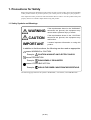
To our customers,
Old Company Name in Catalogs and Other Documents
On April 1st, 2010, NEC Electronics Corporation merged with Renesas Technology
Corporation, and Renesas Electronics Corporation took over all the business of both
companies. Therefore, although the old company name remains in this document, it is a valid
Renesas Electronics document. We appreciate your understanding.
Renesas Electronics website: http://www.renesas.com
April 1st, 2010
Renesas Electronics Corporation
Issued by: Renesas Electronics Corporation (http://www.renesas.com)
Send any inquiries to http://www.renesas.com/inquiry.
Notice
1.
2.
3.
4.
5.
6.
7.
All information included in this document is current as of the date this document is issued. Such information, however, is
subject to change without any prior notice. Before purchasing or using any Renesas Electronics products listed herein, please
confirm the latest product information with a Renesas Electronics sales office. Also, please pay regular and careful attention to
additional and different information to be disclosed by Renesas Electronics such as that disclosed through our website.
Renesas Electronics does not assume any liability for infringement of patents, copyrights, or other intellectual property rights
of third parties by or arising from the use of Renesas Electronics products or technical information described in this document.
No license, express, implied or otherwise, is granted hereby under any patents, copyrights or other intellectual property rights
of Renesas Electronics or others.
You should not alter, modify, copy, or otherwise misappropriate any Renesas Electronics product, whether in whole or in part.
Descriptions of circuits, software and other related information in this document are provided only to illustrate the operation of
semiconductor products and application examples. You are fully responsible for the incorporation of these circuits, software,
and information in the design of your equipment. Renesas Electronics assumes no responsibility for any losses incurred by
you or third parties arising from the use of these circuits, software, or information.
When exporting the products or technology described in this document, you should comply with the applicable export control
laws and regulations and follow the procedures required by such laws and regulations. You should not use Renesas
Electronics products or the technology described in this document for any purpose relating to military applications or use by
the military, including but not limited to the development of weapons of mass destruction. Renesas Electronics products and
technology may not be used for or incorporated into any products or systems whose manufacture, use, or sale is prohibited
under any applicable domestic or foreign laws or regulations.
Renesas Electronics has used reasonable care in preparing the information included in this document, but Renesas Electronics
does not warrant that such information is error free. Renesas Electronics assumes no liability whatsoever for any damages
incurred by you resulting from errors in or omissions from the information included herein.
Renesas Electronics products are classified according to the following three quality grades: “Standard”, “High Quality”, and
“Specific”. The recommended applications for each Renesas Electronics product depends on the product’s quality grade, as
indicated below. You must check the quality grade of each Renesas Electronics product before using it in a particular
application. You may not use any Renesas Electronics product for any application categorized as “Specific” without the prior
written consent of Renesas Electronics. Further, you may not use any Renesas Electronics product for any application for
which it is not intended without the prior written consent of Renesas Electronics. Renesas Electronics shall not be in any way
liable for any damages or losses incurred by you or third parties arising from the use of any Renesas Electronics product for an
application categorized as “Specific” or for which the product is not intended where you have failed to obtain the prior written
consent of Renesas Electronics. The quality grade of each Renesas Electronics product is “Standard” unless otherwise
expressly specified in a Renesas Electronics data sheets or data books, etc.
“Standard”:
8.
9.
10.
11.
12.
Computers; office equipment; communications equipment; test and measurement equipment; audio and visual
equipment; home electronic appliances; machine tools; personal electronic equipment; and industrial robots.
“High Quality”: Transportation equipment (automobiles, trains, ships, etc.); traffic control systems; anti-disaster systems; anticrime systems; safety equipment; and medical equipment not specifically designed for life support.
“Specific”:
Aircraft; aerospace equipment; submersible repeaters; nuclear reactor control systems; medical equipment or
systems for life support (e.g. artificial life support devices or systems), surgical implantations, or healthcare
intervention (e.g. excision, etc.), and any other applications or purposes that pose a direct threat to human life.
You should use the Renesas Electronics products described in this document within the range specified by Renesas Electronics,
especially with respect to the maximum rating, operating supply voltage range, movement power voltage range, heat radiation
characteristics, installation and other product characteristics. Renesas Electronics shall have no liability for malfunctions or
damages arising out of the use of Renesas Electronics products beyond such specified ranges.
Although Renesas Electronics endeavors to improve the quality and reliability of its products, semiconductor products have
specific characteristics such as the occurrence of failure at a certain rate and malfunctions under certain use conditions. Further,
Renesas Electronics products are not subject to radiation resistance design. Please be sure to implement safety measures to
guard them against the possibility of physical injury, and injury or damage caused by fire in the event of the failure of a
Renesas Electronics product, such as safety design for hardware and software including but not limited to redundancy, fire
control and malfunction prevention, appropriate treatment for aging degradation or any other appropriate measures. Because
the evaluation of microcomputer software alone is very difficult, please evaluate the safety of the final products or system
manufactured by you.
Please contact a Renesas Electronics sales office for details as to environmental matters such as the environmental
compatibility of each Renesas Electronics product. Please use Renesas Electronics products in compliance with all applicable
laws and regulations that regulate the inclusion or use of controlled substances, including without limitation, the EU RoHS
Directive. Renesas Electronics assumes no liability for damages or losses occurring as a result of your noncompliance with
applicable laws and regulations.
This document may not be reproduced or duplicated, in any form, in whole or in part, without prior written consent of Renesas
Electronics.
Please contact a Renesas Electronics sales office if you have any questions regarding the information contained in this
document or Renesas Electronics products, or if you have any other inquiries.
(Note 1) “Renesas Electronics” as used in this document means Renesas Electronics Corporation and also includes its majorityowned subsidiaries.
(Note 2) “Renesas Electronics product(s)” means any product developed or manufactured by or for Renesas Electronics.
User’s Manual
M34282T5-OPT
User’s Manual
MCU Board for PC4400 Emulator System
Rev.1.00 2003.09
* MS-DOS is a registered trademark of Microsoft Corporation.
* IBM PC/AT is a registered trademark of International Business Machines Corporation.
Keep safety first in your circuit designs!
• Renesas Technology Corporation and Renesas Solutions Corporation put the maximum effort into making semiconductor products better
and more reliable, but there is always the possibility that trouble may occur with them. Trouble with semiconductors may lead to personal
injury, fire or property damage. Remember to give due consideration to safety when making your circuit designs, with appropriate
measures such as (i) placement of substitutive, auxiliary circuits, (ii) use of nonflammable material or (iii) prevention against any
malfunction or mishap.
Notes regarding these materials
• These materials are intended as a reference to assist our customers in the selection of the Renesas Technology product best suited to
the customer's application; they do not convey any license under any intellectual property rights, or any other rights, belonging to Renesas
Technology Corporation, Renesas Solutions Corporation or a third party.
• Renesas Technology Corporation and Renesas Solutions Corporation assume no responsibility for any damage, or infringement of any
third-party's rights, originating in the use of any product data, diagrams, charts, programs, algorithms, or circuit application examples
contained in these materials.
• All information contained in these materials, including product data, diagrams, charts, programs and algorithms represents information
on products at the time of publication of these materials, and are subject to change by Renesas Technology Corporation and Renesas
Solutions Corporation without notice due to product improvements or other reasons. It is therefore recommended that customers contact
Renesas Technology Corporation, Renesas Solutions Corporation or an authorized Renesas Technology product distributor for the latest
product information before purchasing a product listed herein. The information described here may contain technical inaccuracies or
typographical errors. Renesas Technology Corporation and Renesas Solutions Corporation assume no responsibility for any damage,
liability, or other loss rising from these inaccuracies or errors. Please also pay attention to information published by Renesas Technology
Corporation and Renesas Solutions Corporation by various means, including the Renesas home page (http://www.renesas.com).
• When using any or all of the information contained in these materials, including product data, diagrams, charts, programs, and algorithms,
please be sure to evaluate all information as a total system before making a final decision on the applicability of the information and
products. Renesas Technology Corporation and Renesas Solutions Corporation assume no responsibility for any damage, liability or
other loss resulting from the information contained herein.
• Renesas Technology semiconductors are not designed or manufactured for use in a device or system that is used under circumstances
in which human life is potentially at stake. Please contact Renesas Technology Corporation, Renesas Solutions Corporation or an
authorized Renesas Technology product distributor when considering the use of a product contained herein for any specific purposes,
such as apparatus or systems for transportation, vehicular, medical, aerospace, nuclear, or undersea repeater use.
• The prior written approval of Renesas Technology Corporation and Renesas Solutions Corporation is necessary to reprint or reproduce
in whole or in part these materials.
• If these products or technologies are subject to the Japanese export control restrictions, they must be exported under a license from the
Japanese government and cannot be imported into a country other than the approved destination. Any diversion or reexport contrary to
the export control laws and regulations of Japan and/or the country of destination is prohibited.
• Please contact Renesas Technology Corporation or Renesas Solutions Corporation for further details on these materials or the products
contained therein.
Precautions to be taken when using this product
• This product is a development supporting unit for use in your program development and evaluation stages. In mass-producing your
program you have finished developing, be sure to make a judgment on your own risk that it can be put to practical use by performing
integration test, evaluation, or some experiment else.
• In no event shall Renesas Solutions Corporation be liable for any consequence arising from the use of this product.
• Renesas Solutions Corporation strives to renovate or provide a workaround for product malfunction at some charge or without charge.
However, this does not necessarily mean that Renesas Solutions Corporation guarantees the renovation or the provision under any
circumstances.
• This product has been developed by assuming its use for program development and evaluation in laboratories. Therefore, it does not fall
under the application of Electrical Appliance and Material Safety Law and protection against electromagnetic interference when used in
Japan.
For inquiries about the contents of this document or product, fill in the text file the installer of the emulator debugger generates in the
following directory and email to your local distributor.
\SUPPORT\Product-name\SUPPORT.TXT
Renesas Tools Homepage http://www.renesas.com/en/tools
( 2 / 38 )
Contents
Preface ....................................................................................................................................4
1. Precautions for Safety ......................................................................................................... 5
1.1 Safety Symbols and Meanings ..............................................................................5
2. Handling Precautions .......................................................................................................... 9
2.1 Handling Precautions ............................................................................................ 9
3. Contents of M34282T5-OPT Package ............................................................................. 11
3.1 Package Components of M34282T5-OPT .......................................................... 11
3.2 Other Necessary Products ................................................................................... 11
4. M34282T5-OPT ............................................................................................................... 13
4.1 Outline ................................................................................................................. 13
4.2 Specifications ...................................................................................................... 14
4.3 Switches .............................................................................................................. 15
4.4 Check Pins ........................................................................................................... 17
4.5 Connectors ........................................................................................................... 17
4.6 Connecting MCU Board to Target System ......................................................... 20
4.7 LED ..................................................................................................................... 22
5. Precautions to Be Taken When Debugging ...................................................................... 23
5.1 Reset .................................................................................................................... 23
5.2 Capacity of Internal Memory (ROM, RAM) ...................................................... 23
5.3 Watchdog Timer .................................................................................................. 23
5.4 System Clock ...................................................................................................... 24
5.5 Real-time Capability of Timer ............................................................................ 24
5.6 Power-down Mode .............................................................................................. 24
5.7 Program Execution (G, GB) ................................................................................ 25
5.8 Pulldown Transistor Control ............................................................................... 27
5.9 Port I/O Timing ................................................................................................... 27
5.10 Port I/O Characteristics ..................................................................................... 28
5.11 External Trigger ................................................................................................ 29
5.12 Other Precautions .............................................................................................. 29
6. LED of PC4000E .............................................................................................................. 31
6.1 LED Indication at Emulator Startup ................................................................... 31
6.2 LED Indication during Emulator Operation ....................................................... 31
7. M34282T5-OPT Connection Circuit Diagram ................................................................. 33
8. External Dimensions of Emulator Probe .......................................................................... 35
8.1 20-pin Pin Header ............................................................................................... 35
Appendix A .......................................................................................................................... 36
( 3 / 38 )
Preface
This instruction manual describes the specifications of the M34282T5-OPT emulator board for
Renesas 4282 Group of 4-bit CMOS single-chip MCUs. The M34282T5-OPT is the MCU board for
the PC4400 emulator system connected to the PC4000E emulator main unit and used with a control
board and a function expansion board.
To use the product properly
Precautions for Safety:
• Both in this User's Manual and on the product itself, several icons are used to insure
proper handling of this product and also to prevent injuries to you or other persons,
or damage to your properties.
• The icons' graphic images and meanings are given in "Chapter 1. Precautions for
Safety". Be sure to read this chapter before using the product.
( 4 / 38 )
1. Precautions for Safety
Both in this instruction manual and on the product, several icons are used to insure proper handling
of this product and also to prevent injuries to you or other persons, or damage to your properties.
This chapter describes precautions which should be taken in order to use this product safely and
properly. Be sure to read this chapter before using this product.
1.1 Safety Symbols and Meanings
WARNING
If the requirements shown in the "WARNING"
sentences are ignored, the equipment may
cause serious personal injury or death.
CAUTION
If the requirements shown in the "CAUTION"
sentences are ignored, the equipment may
malfunction.
IMPORTANT
It means important information on using this
product.
In addition to the three above, the following are also used as appropriate.
means WARNING or CAUTION.
Example:
CAUTION AGAINST AN ELECTRIC SHOCK
means PROHIBITION.
Example:
DISASSEMBLY PROHIBITED
means A FORCIBLE ACTION.
Example:
UNPLUG THE POWER CABLE FROM THE RECEPTACLE.
The following pages describe the symbols "WARNING", "CAUTION", and "IMPORTANT".
( 5 / 38 )
WARNING
Warning for Installation:
• Do not set this product in water or areas of high humidity. Spilling water or some other liquid into
the main unit can cause an unrepairable damage.
Warning for Use Environment:
• This equipment is to be used in an environment with a maximum ambient temperature of 35°C. Care
should be taken that this temperature is not exceeded.
CAUTION
Cautions to Be Taken for This Product:
• Do not disassemble or modify this product. Disassembling or modifying this product can cause
damage.
• Use caution when handling the main unit. Be careful not to apply a mechanical shock.
• Do not pull the pod probe by the cables (40-wire half-pitch cable or 20-wire normal-pitch cable).
• Do not use inch-size screws for this equipment. The screws used in this equipment are all ISO
(meter-size) type screws. When replacing screws, use same type screws as equipped before.
( 6 / 38 )
IMPORTANT
Notes on Difference between Actual MCU and Emulator:
• Emulator operation differs from that of a mask MCU as listed below. For details refer to "5.
Precautions to Be Taken When Debugging".
(1) Reset condition
(2) Initial values of internal resource data at power-on
(3) Internal memory (ROM and RAM) capacities, etc.
(4) System clock
(5) Operation of the watchdog timer function
(6) Real-time capability of timer
(7) Operation in power-down mode
(8) Pulldown transistor control
(9) Port I/O timing and characteristics
(10) Low-power detection function
• Therefore, always be sure to evaluate your system with an evaluation MCU (OTP version). Also,
be sure to perform board-mounted evaluation with ES (Engineering Sample) version MCU to make
final confirmation of device operation before starting mask production.
Note on Target System:
• The operation voltage of the M34282T5-OPT is +3.0 V. Therefore the target's supply voltage
should be in the range of +3.0 V ±10%.
Note on System Clock:
• The maximum operating frequency of the M34282T5-OPT is 4.0 MHz (STCK = f(XIN)/8) or 500
kHz (STCK = f(XIN)). When the instruction clock is set to f(XIN), set the system clock frequency
of the M34282T5-OPT to 500 kHz or less.
Notes on Connecting Target System:
• When connecting the target system, be sure to shut OFF the power of the emulator and target
system.
• When connecting the emulator probe, be careful of its orientation.
• When connecting the emulator probe, be careful of a warp of the cable. The warp may cause a break
in the wire.
( 7 / 38 )
MEMO
( 8 / 38 )
2. Handling Precautions
2.1 Handling Precautions
When using the M34282T5-OPT board, pay attention to the following:
(1) About an emulator system
To configure the emulator system with the M34282T5-OPT, the following products are required.
a. Emulator main unit (PC4000E)
This is an universal emulator main unit for the 720 Series.
b. Emulator card cage (PC4400)
This is an emulator card cage to contain the emulator main unit, control board, function
extension board and M34282T5-OPT board.
c. Control board (PCA4400A)
This is an emulator control board for the PC4400 system. The PCA4400A allows the user to
control program execution and reference/change contents of memory, as well as control break
functions etc. of the PC4400 system.
d. Function extension board (PCA4400R)
This is used by inserting into the PC4400, and allows the user to control real-time trace, program
execution time measurement, coverage analysis, etc. of the PC4400 system.
e. Power supply
As the PC4400 emulator system does not contain the power supply, the M34282T5-OPT should
be powered separately by an external power supply such as a switching power supply or a
stabilized power supply. For an external power supply, chose the one which suit to the
specifications below.
- For +5 V:
- For +12 V:
3.0 A or over
0.1 A or over
f. Emulator debugger (RTT72)
This consists of assembler and emulator debugger for the 720 Series. The RTT72 is used with
data files for 4282 Group.
For details, refer to the user's manual of RTT72.
(2) About the MCU board installation
Before installing (and removing) the MCU board, always be sure to power off the PC4000E
emulator main unit and unplug its power cord from the outlet.
(3) Registers that can be operated from the RTT72
Table 2.1 lists the registers that can be operated from the RTT72. The "Yes" means that the register
can be operated; "No" means that the register can not be operated.
Table 2.1 Registers that can be operated from RTT72
Register
Reference
Modify
Register
Reference
Modify
PC
Yes
Yes
V1
No
Yes
CY
Yes
Yes
V2
No
Yes
A
Yes
Yes
LO
No
Yes
B
Yes
Yes
PU0
No
Yes
D
No
Yes
PU1
No
Yes
E
Yes
Yes
X
Yes
Yes
Y
Yes
Yes
*: "0" is always indicated when referencing the register Z.
( 9 / 38 )
MEMO
( 10 / 38 )
3. Contents of M34282T5-OPT Package
3.1 Package Components of M34282T5-OPT
Table 3.1 shows the package components of the M34282T5-OPT. When unpacking your package,
check to see that all of these components are included.
Table 3.1 Contents of M34282T5-OPT
Item
Quantity
M34282T5-OPT
1
40-wire half-pitch cable (40 cm)
1
20-wire normal-pitch cable (10 cm)
1
2-wire cable for external trigger signal (50 cm)
1
PCA4029 pitch converter board
1
Oscillator board OSC-2 (500 kHz)
1
Oscillator board OSC-2 (only J1 connector mounted)
1
M34282T5-OPT Instruction manual (this manual)
1
M34282T5-OPT Instruction Manual (Japanese)
1
*1 The M34282T5-OPT has a 4MHz oscillator circuit board OSC-2 that is incorporated when
shipped from the factory. In addition, an oscillator circuit board OSC-2 for 500 kHz and an
oscillator circuit board OSC-2 on which only J1 connector mounted are included.
*2 Keep the packaging carton and cushion material of the M34282T5-OPT to transport it for repair
or for other purposes in the future.
*3 If you find any item missing or faulty, or any suggestion, contact your local distributor.
3.2 Other Necessary Products
To bring forward program development on the 4282 Group of 4-bit MCUs, the products listed in
Table 3.2 are necessary in addition to those contained in the package above. Get them separately to
be ready when necessary.
Table 3.2 Products required for program development on the 4282 Group MCUs
PC4000E (emulator main unit)
PC4400 (emulator card cage)
Emulator system
PCA4400A (control board)
PCA4400R (function expansion board)
Emulator debugger
RTT72
Serial programmer*
MSP-II
EFP-I (PROM & FLASH programmer main unit)
PROM & FLASH programmer*
EF1SRP-01U (unit for serial writing)
Cable for connecting the target (3-line type)
MS4238-20F (for 20P2N-A package)
PROM programming adapters*
MS4280-20G (for 20P2E/F-A package)
* The serial programmers and PROM programming adapters in Table 3.2 are products of Suisei
Electronics System Co., Ltd. For inquiries about these products, contact Suisei Electronics
System Co., Ltd.
Suisei Electronics System Co., Ltd.
Tsurumi 6-5-24, Tsurumi-ku, Osaka 538-0053, JAPAN
Tel: +81-6-913-4531
Fax: +81-6-913-4534
URL: http://www.suisei.co.jp/index_e.htm
( 11 / 38 )
MEMO
( 12 / 38 )
4. M34282T5-OPT
4.1 Outline
By using with the PC4400 emulator for the 720 Series, the M34282T5-OPT can make up an emulator
system which can be operated by a personal computer.
Figure 4.1 shows the emulator system configuration.
Figure 4.1 Emulator system configuration
* For how to connect to the target system, refer to "4.6 Connecting MCU Board to Target System"
(page 20).
( 13 / 38 )
4.2 Specifications
Table 4.1 lists specifications of the M34282T5-OPT.
Table 4.1 Specifications of M34282T5-OPT
Applicable MCU
4282 Group MCUs
Evaluation MCU
M34282E2GP (on board)
System clock 4 MHz (using OSC-2 [4 MHz])*
Maximum operating
clock frequency
4.0 MHz (STCK=f(XIN)/8)
VDD = 3 V
500 kHz (STCK=f(XIN))
Target system
supply voltage
3V
Power supply
Supplied from the PC4400 (+5 V, +12 V)
Port
Output type
Direction
D0 to D3
Output
D4 to D7
Port emulation
G0 to G3
Device used
P-channel
open drain
Input: 74HC541
Output: TD62787
Input/output
E0
E1
E2
-
Input
Input: 74HC4066
Output: 74HC4066
CARR
CMOS
Output
Output: 74VHC08
Board dimensions
233 mm (L) x 120 mm (W) x 26.0 mm (H)
Operating temperature
5 to 35°C (no dew)
Product
configuration
M34282T5-OPT
40-wire half-pitch cable
20-wire normal-pitch cable
External trigger cable
PCA4029
OSC-2 x2 (for 500 kHz, for changing the frequency)
* The M34282T5-OPT has a 4MHz oscillator circuit board OSC-2 that is incorporated when
shipped from the factory. In addition, an oscillator circuit board OSC-2 for 500 kHz and an
oscillator circuit board OSC-2 on which only J1 connector mounted are included.
( 14 / 38 )
4.3 Switches
Figure 4.2 shows the locations of switches of the M34282T5-OPT and Tables 4.2 and 4.3 list the
functions of each switch and its factory-settings.
Figure 4.2 Switch locations
Table 4.2 Functions of switches (1/2)
Switch
Switch setting
Description
VDD
OFF
ON
OFF
Does not output the V DD from the
M34282T5-OPT to the target system.
OFF
Outputs the VDD from the M34282T5OPT to the target system.
Factory-setting
SW1
VDD
ON
ON
OFF
CPUSE0
L
H
L
SW2
CPUEL0
H
H
Sets the ROM type of MCU.
For M1: "L"
For M2: "H"
H
L
SW3
H
CPUSEL1
H
L
This switch is not used.
Do not change the CPUSEL1 setting.
H
OFF
The pulldown resistors of ports G0
and G1 are OFF.
OFF
ON
SW4
OFF
The pulldown resistors of ports G0
and G1 are ON.
ON
ON
( 15 / 38 )
OFF
Table 4.3 Functions of switches (2/2)
Switch
Switch setting
Description
Factory-setting
OFF
The pulldown resistors of ports G2
and G3 are OFF.
OFF
ON
SW5
OFF
The pulldown resistors of ports G2
and G3 are ON.
ON
OFF
ON
OFF
The pulldown resistor of port D4 is
OFF.
OFF
ON
SW6
OFF
The pulldown resistor of port D4 is
ON.
ON
OFF
ON
OFF
The pulldown resistor of port D5 is
OFF.
OFF
ON
SW7
OFF
The pulldown resistor of port D5 is
ON.
ON
OFF
ON
OFF
The pulldown resistor of port D6 is
OFF.
OFF
ON
SW8
OFF
The pulldown resistor of port D6 is
ON.
ON
OFF
ON
OFF
The pulldown resistor of port D7 is
OFF.
OFF
ON
SW9
OFF
The pulldown resistor of port D7 is
ON.
ON
OFF
ON
OFF
The pulldown resistor of port E0 is
OFF.
OFF
ON
SW10
OFF
The pulldown resistor of port E0 is
ON.
ON
ON
( 16 / 38 )
OFF
4.4 Check Pins
The M34282T5-OPT has the check pins listed in Table 4.4.
Table 4.4 Check pins
Pin
Description
TP1
VDD
Outputs power voltage +3 V to the evaluation MCU.
TP2
XIN
Outputs system clock input to the evaluation MCU.
TP4
WRST
TP5
GND
Outputs "H" level when executing WRST instruction.
By observing pulse width, it is possible to confirm the initializing cycle of the
watchdog timer.
GND
4.5 Connectors
Table 4.5 lists the functions of connectors of the M34282T5-OPT. Figure 4.3 shows the connector
locations.
Table 4.5 Connector list
Connector
Description
J1
Connects the evaluation MCU bus.
J2
Connects the monitor CPU bus.
J3
Connects the target system (40-pin).
J4
Connects external trigger signal (2-pin).
J5
Connects the oscillator board (4-pin).
Figure 4.3 Connector locations
( 17 / 38 )
(1) Connector J3
Table 4.6 lists the pin assignments of 40-wire half-pitch connector (J3) for connecting the
PCA4029. And Figure 4.4 shows the J3 connector pin layout.
Table 4.6 40-wire half-pitch connector (J3) for connecting PCA4029
Line A
Line B
I/O
Line C
I/O
Line D
Pin No.
Signal
Pin No.
Signal
Pin No.
Signal
I/O
Pin No.
Signal
1
GND
1
GND
1
VSS
O
1
VDD
I/O
O
2
GND
2
GND
2
E2
I
2
CARR
O
3
GND
3
GND
3
E1
I/O
3
D0
O
4
GND
4
GND
4
XIN
-
4
D1
O
5
GND
5
GND
5
XOUT
-
5
D2
O
6
GND
6
GND
6
E0
I/O
6
D3
O
7
GND
7
GND
7
G0
I/O
7
D4
I/O
8
GND
8
GND
8
G1
I/O
8
D5
I/O
9
GND
9
GND
9
G2
I/O
9
D6
I/O
10
GND
10
GND
10
G3
I/O
10
D7
I/O
* "I" in the I/O column denotes "Input"; "O" denotes "Output"; "I/O" denotes "Input/output"; "-"
denotes "Not connected".
Figure 4.4 J3 connector pin layout
(2) J4 connector
For the J4 connector, use the 2-wire external trigger signal cable included with your M34282T5OPT board. Connect the black clip to GND and the white clip to the external trigger signal input.
An external trigger signal is used to cause an external trigger break or set an external triggerbased trace point. Table 4.7 lists the pin assignments of the J4 connector.
Table 4.7 Pin assignments of J4 connector
Pin No.
Signal
Description
1
TRIG
External trigger signal input
2
GND
GND
( 18 / 38 )
(3) J5 connector
The J5 connector is a connector used to connect an oscillator board (OSC-2). Table 4.8 lists the
pin assignments of the J5 connector. Figure 4.5 shows the pin layout of the J5 connector. For the
4.0MHz operation with the OSC-2 oscillator board, see Figure 4.6.
Table 4.8 Pin assignments of J5 connector
Pin No.
Signal
Description
1
VCC
Power supply
2
GND
GND
3
CLK
Clock input
4
GND
GND
Figure 4.5 Pin layout of J5 connector
Figure 4.6 Circuit diagram of OSC-2 (4.0 MHz)
( 19 / 38 )
4.6 Connecting MCU Board to Target System
Figure 4.7 shows the connection to the target system using the 20-wire normal-pitch cable.
Connect the M34282T5-OPT with the IC socket for 2.54-mm-pitch 20-pin DIP (e.g. IC26-2003-GS4:
made by Yamaichi Electronics Co., Ltd.) on the target system using the included 20-wire normal-pitch
flat cable.
However, the M34282T5-OPT cannot be connected to the foot pattern of the MCU package (20P2NA or 20P2E/F-A).
For this connection, you need three accessory parts listed below:
(1) 40-wire half-pitch cable (40 cm)
(2) Pitch converter board PCA4029
(3) 20-wire normal-pitch cable (10 cm)
Table 4.9 lists the connector signal assignments of the 20-wire normal-pitch cable. Figure 4.8 shows
the pin layout of the 20-wire normal-pitch cable.
Figure 4.7 Connecting target system
( 20 / 38 )
Table 4.9 20-wire normal-pitch cable pin assignments
20-wire normal-pitch cable
1
VSS
20
VDD
2
E2
19
CARR
3
E1
18
D0
4
XIN (not connected)
17
D1
5
XOUT (not connected)
16
D2
6
E0
15
D3
7
G0
14
D4
8
G1
13
D5
9
G2
12
D6
10
G3
11
D7
*1 The VDD does not input the power supply voltage from the target system, but outputs from the
power circuit on the M34282T5-OPT to the target system.
The VDD can output by setting the switch SW1. For how to set the switches, refer to "4.3 Switches"
(page 15).
*2 XIN is input from the oscillator circuit board OSC-2 and cannot be input from the oscillator circuit
board on the target system.
When changing the system clock frequency, change the frequency of the oscillator circuit board
OSC-2 to use.
Figure 4.8 Pin layout of 20-wire normal-pitch cable
( 21 / 38 )
An evaluation MCU on the M34282T5-OPT and the target system are connected as shown below.
(1) Pin connected directly to the target system (1 type, 1 line)
• VSS
(2) Pins connected to the target system via emulation circuits etc. (5 types, 17 lines)
• G0 to G3
• D0 to D7
• E0 to E2
• CARR
• VDD
(3) Pins not connected to the target system (2 types, 2 lines)
• XIN
• XOUT
* With the M34282T5-OPT, XIN and XOUT pins are not connected to the target system. Therefore,
when changing the system clock frequency, change the frequency of the oscillator circuit board
OSC-2.
4.7 LED
Figure 4.9 shows the LED layout of M34282T5-OPT. The LED lights in green when the power is
supplied to the MCU board.
Figure 4.9 Layout of LED
( 22 / 38 )
5. Precautions to Be Taken When Debugging
5.1 Reset
The M34282T5-OPT can be reset by the reset command of emulator debugger RTT72, but cannot
emulate device operation at power-on reset. Use an evaluation MCU (OTP version) to verify the
operation associated with power-on reset.
5.2 Capacity of Internal Memory (ROM, RAM)
The M34282T5-OPT is equipped with the M34282E2GP as an evaluation MCU. The RAM and
ROM areas that can be referenced by emulator debugger RTT72 are specified by switches SW2 and
SW3 as listed in Table 5.1.
Table 5.1 Memory areas that can be referenced by emulator debugger RTT72
Switch setting
SW3
SW2
RAM area
ROM area
"L"
00h - 0Bh
10h - 1Bh
20h - 2Bh
30h - 3Bh
(4 bits x 48 words)
000h - 3FFh
(9 bits x 1024 words)
"H"
00h - 3Fh
(4 bits x 64 words)
000h - 7FFh
(9 bits x 2048 words)
"H"
* Addresses in the RAM area are shown as described below according to the data pointer registers
X and Y.
Example: RAM address XXh
Y (Y = 0 to B, or Y = 0 to F)
X (X = 0 to 3)
5.3 Watchdog Timer
With the M34282T5-OPT, the watchdog timer cannot be operated. Therefore use an evaluation MCU
(OTP version) to verify the operation associated with the watchdog timer function.
And with the M34282T5-OPT, when executing WRST instruction, the check pin TP4 outputs "H"
level (see Figure 5.1), so you can check the initializing cycle of the watchdog timer by monitoring
the pulse width frequency of TP4.
System clock XIN
WRST
Figure 5.1 Output waveform of check pin TP4
( 23 / 38 )
5.4 System Clock
Depending on how the instruction clock is set, use the M34282T5-OPT in the range of frequencies
listed in table 5.2.
When the instruction clock is set to STCK = f(XIN) and the system clock frequency is over 500 kHz,
the emulator may not work properly.
Table 5.2 Operating frequencies of the M34282T5-OPT
Voltage
Instruction clock
Frequency
STCK = f(XIN)/8
4.0 MHz or less
STCK = f(XIN)
500 kHz or less
3V
* To change the system clock frequency, change the clock frequency of the oscillator circuit board
OSC-2. For details about the oscillation circuit constant, consult your oscillator manufacturer.
5.5 Real-time Capability of Timer
As the evaluation MCU is active even when program execution is stopped or when a command is
executed, its timer values are modified.
Examples:
(1) When single-stepping instructions
(2) After program execution stopped
5.6 Power-down Mode
Although the M34282T5-OPT can execute a program using the POF instruction, there are precautions and restrictions listed in Table 5.3.
Table 5.3 Precautions for power-down mode.
Description
1
Although SAFE and ERROR LEDs of the PC4000E light up in the power-down mode, it is not
an error condition.
2
Do not use the POF instruction when single-stepping a program. The POF instruction can not
be executed correctly when stepped through.
3
No debug command of emulator debugger RTT72 can be executed. In the power-down mode,
execute the debug command after resuming by the key-on wakeup function.
4
The real-time trace result of the area including the POF instruction cannot be displayed
normally.
( 24 / 38 )
5.7 Program Execution (G, GB)
The PC4400 and the M34282T5-OPT's hardware are subject to the following restrictions with
respect to the operation of the program execution commands (G and GB).
(1) Continuous description of instructions
Hardware break points set in a continuous description of instructions following one after another
do not cause a break to occur in the continuous description of instructions. A break occurs only
after fetching the address where the continuous description of instructions is discontinued. (See
Program example 5.1)
However, a break does occur even in a continuous description of instructions when an external
trigger break or forced break is encountered. For execution to be resumed in this case, you need
to make sure that the execution start address is next to the continuous description of instructions.
(See Program example 5.2)
Program example 5.1
POINT:
POINT+2:
LA
LA
LA
XAM
0
1
2
3
; Continuous description of instructions
If a break is set at POINT, execution is halted immediately before the XAM instruction at
address POINT+2.
Program example 5.2
POINT:
POINT+1:
POINT+2:
LA
LA
LA
XAM
0
1
2
3
; Continuous description of instructions
If a forced or external trigger break is applied at POINT, execution is halted at POINT+1. When
resuming program execution after the break, make sure that the start address is at POINT+2,
an address immediately after the continuous description of instructions is discontinued.
( 25 / 38 )
(2) Skip instructions (e.g. SNZP, INY, DEY, SZB, SEAM, SZC and RTS)
In cases when a skip instruction skips the next instruction, a break point set in the skipped
instruction does not cause execution to halt. (See Program examples 5.3 and 5.4)
Program example 5.3
POINT:
POINT_A:
LXY
SZD
B
TAM
•
•
0,0
jmp_adr
0
; Skip when D(0) = 0
If a break point is set at POINT,
D(0) = 0: Execution is halted immediately before the instruction at POINT.
D(0) = 1: Execution is NOT halted because the instruction at POINT is skipped.
To halt execution immediately after a skip instruction, set break points at POINT and POINT_A.
Program example 5.4
POINT:
RC
INY
TABP
LA
0
•
•
; Skip when (Y) = 0
If a break with pass count is set at address POINT, the count is taken and execution is halted
only when the instruction at address POINT is executed.
( 26 / 38 )
5.8 Pulldown Transistor Control
Since ports D4 to D7, E0 and G0 to G3 contain emulation circuits, you can not control the pulldown
resistors using the pulldown control register. If you want to use the internal pulldown resistors, turn
on switches SW4 to SW10 when occasion demands. With the M34282T5-OPT, the port's resistance
value of the pulldown resistor is 150 kΩ.
When changing the resistance value of the pulldown resistor, replace RA1 (ports E0, G3 to G0) and
RA2 (ports G7 to G4) on the M34282T5-OPT. For the position of the pulldown resistor, see Figure 4.3.
5.9 Port I/O Timing
(1) Port input timing
Port input timings are the same as with the actual MCUs.
(2) Port output timing
When using the M34282T5-OPT, output timings are different from those of the actual MCUs for
the ports D0 to D7, E0 and G0 to G3 that are configured with port emulation circuits.
With the actual MCUs, changes occur at the beginning of the T4 state of an output instruction.
With the M34282T5-OPT, changes occur at the beginning of the T2 state of the next output
instruction. Figure 5.2 shows the port timings of the actual MCUs and M34282T5-OPT.
Port output timings of ports E1, E2 and CARR are the same as with the actual MCUs.
Output Instruction
Instruction clock
STCK
Ports D, E and G
output timing
of actual MCU
Port D
output timing
of M34282T5-OPT
Port E
output timing
of M34282T5-OPT
Port G
output timing
of M34282T5-OPT
Figure 5.2 Ports D, E and G output timings
( 27 / 38 )
Next output Instruction
5.10 Port I/O Characteristics
With the M34282T5-OPT, port I/O characteristics are different from actual MCUs because there is
an emulation circuit in ports E0, G0 to G3 and D0 to D7. Table 5.4 lists port I/O characteristics of the
M34282T5-OPT.
Table 5.4 Emulation port I/O characteristics
Port
Device
Item
VIH
Input
74HC541
VIL
E0
Output TD62787
-
VCC = 4.5 V
3.15 V
-
VCC = 2.0 V
-
0.5 V
-
VCE(sat)
-
-
VCC = 2.0 V
1.5 V
VCC = 4.5 V
3.15 V
-
VCC = 2.0 V
-
0.5 V
VCC = 4.5 V
-
ICEX
-
-
VCE(sat)
-
-
VCC = 2.0 V
1.5 V
VCC = 4.5 V
3.15 V
-
VCC = 2.0 V
-
0.5 V
VCC = 4.5 V
-
1.35 V
ICEX
-
-
VCE(sat)
-
-
VCC = 2.0 V
1.5 V
-
IOH = -50 µA
VCC = 4.5 V
3.15 V
-
IOH = -8 mA
VCC = 2.0 V
-
0.1 V
IOL = 50 µA
VCC = 4.5 V
-
0.44 V
IOL = 8 mA
1.35 V
-100 µA VOUT = -50 V
-1.8 V VIN = VIL, IOUT = -100 mA
-2.0 V
VIH
Input
74HC541
VIL
D4 to D7
Output TD62787
VOH
CARR
Output 74VHC08
VOL
( 28 / 38 )
VIN = VIL, IOUT = -350 mA
-
1.35 V
-100 µA VOUT = -50 V
-1.8 V VIN = VIL, IOUT = -100 mA
-2.0 V
D0 to D3
Remarks
-
VIL
Output TD62787
Max.
VCC = 4.5 V
74HC541
G0 to G3
Min.
1.5 V
ICEX
VIH
Input
Voltage
VCC = 2.0 V
VIN = VIL, IOUT = -350 mA
-
-100 µA VOUT = -50 V
-1.8 V VIN = VIL, IOUT = -100 mA
-2.0 V
VIN = VIL, IOUT = -350 mA
5.11 External Trigger
(1) External trigger signal input timing
The latch timing of the external trigger signal is shown in Figure 5.3.
Output Instruction
Next output Instruction
Instruction clock
STCK
External trigger
signal
Figure 5.3 Latch timing of external trigger signal
(2) External trigger signal input characteristics
Trigger breaks work according to the condition (leading edge/trailing edge) of signals input from
the external trigger cable. The external trigger signals of the trace points and the external trigger
signals of the break points use the same signals.
The input characteristics of the external trigger signals are shown in Table 5.5 below. See the table
before using external trigger signals.
Table 5.5 External trigger signal input characteristics
Item
Symbol
H-level threshold voltage
VIH
L-level threshold voltage
VIL
Voltage
Minimum
Maximum
VCC = 2.0 V
1.5 V
-
VCC = 4.5 V
3.15 V
-
VCC = 2.0 V
-
0.5 V
VCC = 4.5 V
-
1.35 V
5.12 Other Precautions
With the M34282T5-OPT, the system which uses the function below cannot be emulated. Therefore,
always be sure to evaluate your system with an evaluation MCU (OTP version).
• Low-voltage detection function
( 29 / 38 )
MEMO
( 30 / 38 )
6. LED of PC4000E
6.1 LED Indication at Emulator Startup
The emulator checks the PC4400 system immediately after startup. During system check the
PC4000E's SAFE LED flashes and the ERROR LED stays on steady. If the SAFE LED does not flash,
it means that the system check program is not operating. In such a case, check whether the PC4000E,
PC4400 card cage and each circuit board are fitted correctly. When the system check is completed,
the emulator status is indicated by the LEDs on the PC4000E.
Table 6.1 shows the LED indications at startup of PC4400.
Table 6.1 LED indication at emulator startup
LED display
Condition of PC4000E
SAFE
ERROR
Turned ON
Turned OFF
Flash alternately
The emulator has started up properly.
Following may be considered:
• Some board in the PC4400 main unit slot is not fitted in
correctly. Check whether each board is fitted correctly.
• An error is detected by the PC4400's system check. The
PC4400 system may be faulty. Contact your local distributor for
repair.
6.2 LED Indication during Emulator Operation
It is possible to check the emulator status during operation by its LED indicators.
Table 6.2 shows the LED indications during emulator operation.
Table 6.2 LED indications during emulator operation
LED display
Condition of PC4000E
SAFE
ERROR
Turned ON
Turned OFF
The emulator is ready to execute debug commands of emulator
debugger RTT72.
Turned ON
The evaluation MCU is in the power-down mode or the emulator
system has been reset.
In this case, no debug command of emulator debugger RTT72
can be executed.
In the power-down mode, execute the debug command after
resuming by the key-on wakeup function.
Turned ON
( 31 / 38 )
MEMO
( 32 / 38 )
7. M34282T5-OPT Connection Circuit Diagram
Figure 7.1 shows the M34282T5-OPT connection circuit diagram. This circuit diagram depicts the
M34282T5-OPT connection centering on circuits connected to the target system. Emulator control
blocks and other similar circuits that are not connected to the target system are omitted.
Figure 7.1 M34282T5-OPT connection circuit diagram
( 33 / 38 )
MEMO
( 34 / 38 )
8. External Dimensions of Emulator Probe
8.1 20-pin Pin Header
Figure 8.1 shows the external dimensions of the emulator probe 2.54-mm-pitch 20-pin pin header of
the M34282T5-OPT.
Figure 8.1 External dimensions of 20-pin pin header
( 35 / 38 )
Appendix A. How to Request for Repair
If your product is found faulty, follow the procedure below to send your product for repair.
Customer
Fill in the Repair Request Sheet included with this product, then send it
along with this product for repair to your local distributor. Make sure
that information in the Repair Request Sheet is written in as much detail
as possible to facilitate repair.
Distributor
After checking the contents of fault, the distributor should please send
the faulty product along with the Repair Request Sheet to Renesas
Solutions Corp.
Renesas Solutions
When the faulty product is repaired, it will be returned to the customer
at the earliest convenience.
CAUTION
Note on Transporting the Product:
• When sending your product for repair, use the packing box and cushion material supplied with this
product when delivered to you and specify handling caution for it to be handled as precision
equipment. If packing of your product is not complete, it may be damaged during transportation.
When you pack your product in a bag, make sure to use conductive polyvinyl supplied with this
product (usually a blue bag). When you use other bags, they may cause a trouble on your product
because of static electricity.
( 36 / 38 )
M34282T5-OPT User's Manual
Rev.1.00
September 1, 2003
REJ10J0272-0100Z
COPYRIGHT ©2003 RENESAS TECHNOLOGY CORPORATION
AND RENESAS SOLUTIONS CORPORATION ALL RIGHTS RESERVED
M34282T5-OPT
User’s Manual
1753, Shimonumabe, Nakahara-ku, Kawasaki-shi, Kanagawa 211-8668 Japan
REJ10J0272-0100Z