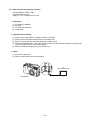
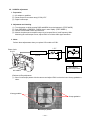
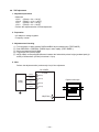
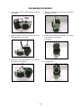
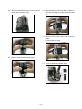
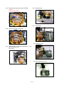
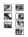
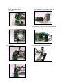
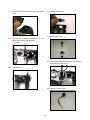
1
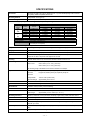
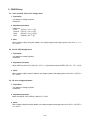
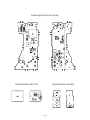
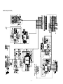
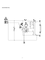
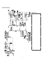
(without price)
QV-3000EX
(KX-716B)
QV-3000EX/Ir
(KX-716C/D/F)
FEB. 2000
Ver. 1
INDEX
R
MAR. / 2002
CONTENTS
SPECIFICATIONS ....................................................................................................................................... 1
To distinguish the model .......................................................................................................................... 3
BLOCK DIAGRAM ...................................................................................................................................... 4
CIRCUIT BLOCK ......................................................................................................................................... 5
ADJUSTMENT ............................................................................................................................................ 6
1. Program version upgrading .............................................................................................................. 7
1-1. How to confirm the program (graphic menu) version .............................................................. 7
1-2. Upgrading procedure using the CompactFlash card ............................................................... 7
1-3. Upgrading procedure using the PC link cable .......................................................................... 8
2. Test mode ........................................................................................................................................... 9
2-1. Booting ......................................................................................................................................... 9
2-2. Item for testing ............................................................................................................................. 9
3. Product conditions .......................................................................................................................... 11
3-1. Color adjustment data writing .................................................................................................. 11
3-2. Flash adjustment ....................................................................................................................... 19
3-3. Flash operation and recharge operation ................................................................................. 20
3-4. Current consumption ................................................................................................................ 21
3-5. VCOM DC adjustment ................................................................................................................ 22
3-6. Operation check ......................................................................................................................... 23
4. D-PCB Assy ...................................................................................................................................... 24
4-1. VCO free run frequency adjustment ........................................................................................ 24
4-2. VCOM AC adjustment and VCOM DC coarse adjustment ..................................................... 24
4-3. RGB AMP, Sub bright adjustment ............................................................................................ 25
4-4. Contrast, Bright adjustments ................................................................................................... 26
4-5. Color adjustment ....................................................................................................................... 27
4-6. TINT adjustment ......................................................................................................................... 28
5. PW-PCB Assy ................................................................................................................................... 29
5-1. VCC3, VCC3-M, VCC5, VCC7 Voltage check ........................................................................... 29
5-2. VCC15, VEE7 Voltage check ..................................................................................................... 29
5-3. BL drive voltage adjustment ..................................................................................................... 29
DISASSEMBLY/ASSEMBLY .................................................................................................................... 30
EXPLODED VIEW ..................................................................................................................................... 46
PARTS LIST .............................................................................................................................................. 47
PRINTED CIRCUIT BOARDS ................................................................................................................... 49
SCHEMATIC DIAGRAMS ......................................................................................................................... 55
SPECIFICATIONS
File Format
Still images (including panoramas): JPEG (Exif. Ver. 2.1), DCF standard (Design rule for Camera
File system), DPOF compatible, Movies: AVI
Recording Medium
CompactFlash card (Type I/II)
Recorded image Size
2048 x 1536 pixels, 1024 x 768 pixels
Standard Memory Capacity,Number of Image Files,Computer Output Image Size
Still
Image size
(pixels)
2048
x
1536
1024
x
768
Quality
File size
FINE
NORMAL
ECONOMY
FINE
NORMAL
ECONOMY
1.4 MB/images
1 MB/images
600 KB/images
350 KB/images
250 KB/images
150 KB/images
Storage Capacity
Recording Time
8 MB memory card
5 images
6 images
11 images
19 images
27 images
43 images
Number of images
64MB memory card
43 images
60 images
99 images
167 images
229 images
365 images
340MB Microdrive
245 images
342 images
562 images
943 images
1292 images
2054 images
Movie
Approxmately 300 KB/second
30 seconds per movie (NORMAL)
10 seconds per movie (PAST)
• The maximum length of a single movie is 10 seconds.
Image Deletion
Single image; all images in a folder; all images in memory (with image protection)
Imaging Element
1/1.8-inch CCD (Total Pixels: 3.34 million, Effective Pixels; 3.24 million)
Lens
F2 to 2.5; f = 7 to 21mm (equivalent to 33 to 100mm lens for 35mm film)
Zoom
Optical zoom, 8X; Digital zoom: 32X (in combination with optical zoom)
Image size is 1024 x 768 pixels when digital zoom is used.
Focusing
Contrast-detect Auto Focus; manual focus with macro mode and focus lock
Focus Range
Normal focus:
0.3m to ∞ (1´ to ∞)
Macro focus:
6cm to 30cm (2.4˝ to 11.8˝) (1X zoom)
9cm to 30cm (3.5˝ to 11.8˝) (2X zoom)
The focusing range is the distance from the lens surface to the subject.
Exposure Control
Light Metering:
Multi-pattern, center point, spot by CCD
Exposure:
Program AE, Shutter priority AE, Aperture priority AE
Exposure
Compensation:
–2EV to +2EV (1/3EV units)
Exposure Range:
Approximately EV7 to EV16
Shutter
CCD electronic shutter; mechanical shutter, 2 to 1/1000 second
Aperture
F2 to F8, auto switching or manual switching
White Balance
Automatic, fixed (4 modes), manual switching
Self-timer
10 seconds, 2 seconds
Built-in Flash
Flash Modes:
AUTO, ON, OFF, Red eye reduction
Flash Range:
Approximately 0.5 to 4 meters (1.6´ to 13.1´)
Recording Functions
One-shot, continuous, movie, panorama, landscape, night scene, portrait, self-timer, macro
Monitor
1.8" TFT, low-glare color HAST LCD (122,100 pixels, 555 x 220)
Viewfinder
LCD Monitor or optical viewfinder
Clock
Built-in quartz digital timepiece for time and date recording and storage with image data; auto
calendar up to 2049
Input/Output Terminals
DIGITAL IN/OUT, USB port (special mini port), AC adaptor connector, VIDEO OUT (NTSC,
PAL)
Infrared Communication
IrDA; IrTran-P (QV-3000EX/Ir only)
—1—
Power Supply
Four AA-size alkaline or lithium batteries
Four AA-size nickel-metal hydride rechargeable batteries (NP-H3)
AC adaptor (AD-C620)
AC adaptor charger (BC-3HA)
Battery Life
The values noted below indicate the number of hours before battery failure under normal
operating temperature (25°C). These values are for reference only, and do not guarantee that
any particular set of batteries actually will provide the service life indicated. Low temperatures
shorten battery life.
AA-size Alkaline
Batteries LR6
AA-size Lithium
Batteries FR6
AA-size Ni-MH
Batteries NP-H3
Continuous
Playback
Approximately 145
Approximately 270
Approximately 170
minutes
minutes
minutes
Continuous
Recording
Approximately 210
Approximately 900
Approximately 660
shots
shots
shots
Type of
Operation
• The above figures are approximations only.
• The above guidelines are based on the following battery types:
Alkaline:
MX1500 (AA) DURACELL ULTRA
Lithium:
Energizer
• Battery life varies with brand.
Continuous recording values show the number of shots without using the flash. The number of
shots depends on use of the flash and whether flash is turned on or off.
Power Consumption
Approximately 6.6W
Dimensions
134.5(W) x 80.5(H) x 57.5(D) mm
Weight
Approximately 320g (11.2 oz) (excluding batteries)
Standard Accessories
Neck strap; lens cap; cap holder; soft case; USB cable; video cable; User’s Manual
(5.3˝(W) x 3.2˝(H) x 2.3˝(D))
• This camera does not have a separate battery to power its clock. Clock settings are cleared whenever power to the camera is
cut off (by batteries going dead while the camera is not connected to an AC power outlet with the AC adaptor) for about 24
hours. After power is resumed, either by loading fresh batteries or connecting to an AC power outlet, you will have to set the
correct time and date again.
• The liquid crystal panel built into this camera is the product of precision engineering, with a pixel yield of 99.99%. This also
means, however that 0.01% of the pixels can be expected to fail to light or to remain lit at all times.
—2—
To distinguish the model
Discriminate between infra-red model and non-infra-red model by the following points.
QV-3000EX (KX-716B) for U.S.A
RE
C
MF/
MODE
OF
F
/
PLA
Y
MO
DE
MEN
U
MF/
/
T
SET
PREVIEW
W
DISP
QV-3000EX/Ir (KX-716C/D/F)
Infra-red transmission button.
RE
C
MF/
MODE
OF
/
F
/
PLA
Y
MO
DE
MEN
U
MF/
/
/
T
SET
PREVIEW
W
DISP
Infra-red transmission button.
—3—
BLOCK DIAGRAM
SUB-PCB
KBPCB
왕,왓
KAPCB
3pin
+,–
ENTER
MENU
CCD-FPC
SELF
LED
TELE
WIDE
DISP
PREVIEW
Buzzer
SUB
Microprocessor
HD404889
4.0 MHz
4pin
BACK UP
Capacitor
SUB-LCD
48.0MHz
FLASH
FOCUS
LED
51pin
EVCC(3.3V)
Vertical/Horizontal
Sensor
CDS/AGC/ADCAD9803
19pin
SW-PCB
USB TRANSCEIVER
24.5454 MHz
29.5 MHz
36.0 MHz
REC/
PLAY /
OFF
SHUTTE
R
SERIAL BUFFER
CF
Controller
REG
ICX252AQ
24.0 MHz
VIDEO DRIVER
TGCXD2497R
—4—
MPU
LR38664Y
6pin
LENS BLOCK
Canon
Zoom X 3
LED-PCB
KEY
MODE TIMER MACRO
FLASH
SHUTTER(Half/Full)
RTC
RTC-4574
D-PCB
CCD
IrDA
Controller
SW
3.58 MHz
ZOOM DRIVER
16pin
MD
Microprocessor
AF DRIVER
Chroma I/F
IR3Y29B
5.0 MHz
FLASH/
MASK
(16M)
IRIS/SHUTTER
DRIVER
SDRAM
(64M X 2)
BUS BUFFER
TC74AC367 X 2
ST-PCB
SJ-PCB
VDD:
VGH:
VGL:
VSH:
26pin
TFT
Controller
CM7019L3
EEPROM
(4K)
FINDER
UNIT
LCD Module
80pin
PW-PCB
BL-PCB
3pin
Flashing
Controller
Charging
Booster
10pin
Flash
Control
DOWN
Converter
VCC5
(5.0V)
10pin
B to B
Photp
Sensor
CCD/LCD
Power
AC
ADPT
3.3V
15.0
-15.0V
5.0V
Motor system
step-down
transformer
VCC3-M
(3.4V)
VCC15
(15.0V)
VEE7
(-7.5V)
Logic circuit
step-down
transformer
BL booster
VCC5
VCC3
(3.3V)
LCD booster
(5.0V)
BLVCC
(5.4V)
CF
VCC7
(8.0V)
CF
SW
CF
LED
BL UNIT
CIRCUIT BLOCK
PCB Circuit Block
PW LCD Power Supply
Outline
Main Devices
7.5V Up Converter
XC6367B101MR
Note
Newly employed part
BL Power Supply
5.4V Up Converter
XC6367A542MR
Newly employed part
Main Power Supply
3.3V Non adjustable step down transformer
XC6365A333MR
Newly employed part
CCD 5V Power Supply
5.0V Voltage regulator
XC62ER5002MR
Newly employed part
LCD Power Supply
Flash Control Power
Video Driver Power Supply
CCD & LCD Power Supply
Power specifications (+15V, -7.5V)
MAX685EEE
Used on QV-8000SX
Lens Unit AP Power
3.3V Non adjustable step down transformer
XC6365B103MR
Newly employed part
Lens Unit Zoom Power
Lens Unit AE Power
Charging Booster Circuit
300V Booster
Used on QV-8000SX
Current control circuit
Charging control circuit
D
Charging Comparator
Light emission control circuit
Used on QV-8000SX
CF Connector
Complying to TYPE-II (Reverse insertion)
Used on QV-2000UX
MPU
Processor Interface
LR38664Y
Serial Interface
Newly employed part
CSP package
CCD Interface
NTSC/PAL Encoder
JPEG
DMA Controller
BUS Interface
Flash Memory
16 Mbit (1 M X 16 bit) Flash Memory
LH28F160S3B
SDRAM
64 Mbit ( 1 Mword X 16 bit X 4 bank) X 2
K4S641632C-TL1 and others
CF Controller
CF controller and I/O interface
uPD65839GC
TFT-LCM
1.8" high definition TFT (HAST)
C0D18T1035FN
Newly employed part
LCD Controller
Complying to high definition TFT (HAST)
CM7019L3-T4N
Newly employed part
(Mask ROM)
Compatible with the Mask ROM
CSP package
Used on QV-2000UX
3.0V driver
Chroma Interface
+5V/+7.5V source, C-VIDEO input
IR3Y29BM
Used on QV-770
Brightness fixed
Stand-by power
3.3V three-terminal regulator
XC62FP3302MR
8-bit MPU
Driving motor control
D780034AGK-A03-8A8
Newly employed part
EEPROM
4Kbit (256word x 16bit)
BR93LC66FV-E2
Used on QV-2000UX
AF//ZOOM
AF ZOOM is 1-2-phase excitation
LB1846M
Newly employed part
Motor driver
AE is 2-phase excitation
Shutter/ AE driver
LB1837M-TE-L
Newly employed part
USB tranceiver
PDIUSB11AP
Used on QV-8000SX
Video 75 ohm dirver
TK15405MTL
Used on QV-8000SX
Flash ROM built in -> Mask ROM after MP
Serial transport driver
Used on QV-7000SX
TG/V/H driver
for 3340 thousand picture element CCD (35.0MHz clock) CXD2497R
Newly employed part
CDS/AGC/ADC
CDS
AD9803JSTRL
Used on QV-8000SX
4-way tilt sensor
Alps electronics
Used on QV-2000UX
IrDA Controller and Serial Controller
PC87109VBE
Used on QV-7000SX
IrDA Module
Small-type IrDA moule (IrDA1.1)
HSDL-3600
Used on QV-2000UX
4bit Microprocessor
Power ON sequence
HD404889
(Mask ROM)
Key scanning
11bit Programmable Gain Amplifier
10-bit A/D converter
Vertical/Horizontal sensor
SUB IrDA Controller
Beep control
I/O and others
RTC
Built-in 32KHz clock real time clock
RTC-4574JE
Used on QV-2000UX
Backup Capacitor
Watch backup (24H)
EECS0HD104H
Used on QV-2000UX
SUB-LCD
BL
Inverter Circuit
Used on QV-2000UX
BL unit
Used on QV-2000UX
BB-PCB
Board-toBoard connection PCB
Used on QV-2000UX
KEY SW
KA-PCB, KB-PCB
SW PW ON/OFF
CCD CCD
Newly employed part
1/1.8 inch, 3,340,000 picture element
ICX252AQ
—5—
Newly employed part
ADJUSTMENT
■ Preparation
1. PC (IBM Compatible)/OS:Windows 95/98
2. Link cable.
3. Adjustment program
1) ADJ716.EXE (Color adjustment data transfer program)
2) FLOAD.EXE
(Camera unit version up program)
3) _ROM.BIN
(Camera unit program data)
4) _GMENU.BIN
(Camera unit menu display data)
4. AC adaptor or stabilizer
5. Digital oscilloscope
6. Multimeter
7. Ammeter
8. Frequency counter
9. TV (with video terminal)
10. Video cable
11. Battery (battery operation/battery cover lock)
12. PC link program : Photo Loader (Communication function confirmation)
13. USB cable/USB driver (USB function confirmation)
14. Test chart (for photography check)
That which carried out color printing of picture data "CHART1.JPG" and the "CHART2.JPG".
CHART1.JPG
CHART2.JPG
—6—
1. Program version upgrading
In the camera unit, program and graphic menu are stored.
Please check the version and update it if the version is not updated.
There are two method of program updating; using CompactFlash card or utilizing PC link cable.
Note:
1. Be sure to use AC adaptor.
PCB D becomes unusable if power down or an error occurs during program transmission.
2. Unit using a mask cannot update the program.
1-1. How to confirm the program (graphic menu) version
1.
2.
Boot the test mode.
Turn the power on while pressing DISP and MENU buttons simultaneously.
Check the LCD display.
(Example)
TEST MODE
PROG
00.
02.
04.
13.
49
r Program version
GMENU
99.
12.
27.
18.
12
r Graphic menu version
····
1-2. Upgrading procedure using the CompactFlash card
(1) Copy the latest program ( _ROM.BIN) and graphic menu ( _GMENU.BIN) on a CompactFlash card
then set the CompactFlash card on the camera.
(2) Connect an AC adaptor on the camera.
(3) Boot the test mode.
Turn the power on while pressing DISP and MENU keys simultaneously.
(4) Camera's display shows the followings.
It is normal if two OK's are shown after about 1 minute.
After then, the camera is set on the Camera mode automatically.
SIZE OK 666464
SIZE OK 1305532
(5) Turn the camera off.
(6) Chgange the CompactFlash card with the one for picture taking.
(7) Boot the test mode and confirm the program version.
Turn the power on while pressing DISP and MENU buttons.
(8) Finally, check the camera's function (shooting and playback).
—7—
1-3. Upgrading procedure using the PC link cable
(1)
(2)
(3)
(4)
Turn the camera off and extract CompactFlash card.
Connect PC link cable.
Boot the transmission program (FLOAD.EXE).
Choose program file ( _ROM.BIN) or graphic menu file ( _GMENU.BIN).
(5) Select data transmission speed (115K/57K/38K).
(If errors occur, lower the transmission speed.)
(6) Click Progress button.
(7) Connect an AC adaptor on the camera and turn the camera on.
(8) Data transmission starts.
(9)
(10)
(11)
(12)
Data transmission is completed normally when Status box shows "program complete."
Disconnect AC adaptor plug (cannot be turned off by the power switch).
Change the CompactFlash card with one for shooting.
Boot the test mode and confirm the version.
Turn the camera on while pressing DISP and MENU buttons.
(13) Shoot a picture and confirm the camera function (shooting and playback.)
—8—
2. Test mode
Note: Do not perform the menu item unless explained here. (It may damage the internal data and
camera becomes unusable.)
2-1. Booting
To boot the test mode;
Turn the camera on while pressing DISP and MENU buttons.
To boot MENU1
Press PREVEIW ➜ PREVEIW ➜ MENU keys in order rapidly.
To boot MENU2
Press FLASH ➜ FLASH ➜ MENU keys in order rapidly.
* To execute
Use + or – keys to select a test item then press shutter button to execute it.
To boot MENU3
Press SELF ➜ SELF ➜ MENU keys in order rapidly.
2-2. Item for testing
1 TEST MODE
TEST MODE
PROG
GMENU
LOADER
ADJ
MOTOR
POWER
CCD ADJ1
CCD ADJ2
STROBE ADJ
ZOOM ADJ
FOCUS ADJ
99.08.16.13.38
99.07.12.15.04
0X00000007
0X0000011A
0X1A
YES
YES
YES
YES
YES
• TEST MODE
• PROGRAM Version
• Graphic Menu Version
• Loader Version
• ADJ Version
• Motor MCU Version
• Power MCU Version
• CCD ADJUST 1 (Yes/No/NG)
• CCD ADJUST 2 (Yes/No/NG)
• STROBE ADJUST (Yes/No/NG)
• ZOOM ADJUST (Yes/No/NG)
• FOCUS ADJUST (Yes/No/NG)
2 MENU1
MENU1
1. INIT.NTSC JAPANESE
2. LED+SUBLCD
3. INIT.NTSC ENGLISH
4. CROSS HATCH
5. ANG DET CHECK
6. INIT.PAL ENGLISH
7. COLOR BAR
8. 50PERCENT GRAY
—9—
Shown in green if all the adjustments
have been done.
YES when adjustments are completed.
NO when adjustments are incomplete.
NG if adjustments are failed.
3 MENU2
MENU2
1. CCD ADJ ALL
2. ZOOM ADJUST
3. CCD1 (AWB AGC)
4. CCD2 (APATURE)
5. CCD3 (SHUTTER)
6. KIZU
7. IRDA MASTER
8. FOCUS ADJUST
9. STOROBE ADJUST
4 MENU3
MENU3
1/3
1. DISPLAY LENS ADJ
2. REC INFO
3. BATT. TEST
4. PROG+GMENU UPDATE
5. PROG UPDATE
6. GMENU UPDATE
7. CHECK SUM
8. OSD DATA CHECK
9. ERROR MESSAGE CHECK
10. SDRAM CHECK
MENU3
11. KEY CHECK
12. LED CHECK
13. CF CHECK
14. SUB LCD CHECK
15. CF WRITE TEST
16. AF DATA SAVE
17. EEPROM TEST
18. ADJ CLEAR
19. NOISE CAPTURE
20. BAYER CAPTURE
2/3
MENU3
21. SHUTTER CLOSE REC
22. SHUTTER SPEED CONST
23. GRAY SCALE (10STEP)
24. WHITE
25. BLACK
26. IRDA SLAVE
27. IRDA FACTORY SLAVE
3/3
— 10 —
3. Product conditions
Note: Help command on adjustment window cannot be used as it uses Japanese system.
3-1. Color adjustment data writing
1. Summary
(1) QV-3000EX is a high quality digital camera and makeshift adjustments cannot cover the quality of the
camera's picture.
Therefore, we have prepared set of lens ass'y that is adjusted precisely in the factory and a floppy disc
containing the lens'es adjustment data as spare parts.
(2) These adjustment data are stored in the EEPROM on PCB D.
2. Repairs
It is necessary to write color adjustment data for the replacements of the following units.
(1) Lens ass'y
(2) PCB D (when EEPROM contents can be read)
(3) PDB D and lens ass'y (when EEPROM contents cannot be read)
3. To replace the lens ass'y
(1) Connect AC adaptor and PC link cable to the camera.
Note: Connect the link cable to serial port COM1.
(2) Turn the camera on to set it on PLAY mode.
(3) Boot adjustment program ADJ716.EXE.
At this time, each adjustment data are 0.
— 11 —
(4) Read the adjustment data of before repairs.
Click the Receipt button. “receive OK” will be indicated and adjustment data are shown.
Reference: At this time you can save the adjustment data in your PC.
File (F) ➜ Save as (A)
Select the drive and name the file then save it.
(Note: Do not forget to put extension code ".ADJ".)
(5) Write down the following numbers.
agc-6ab
strobe-pwm
(6) Replace the lens ass'y.
(Adjusted in the factory and comes with adjustment data)
(7) Connect AC adaptor and PC link cable to the camera.
(8) Turn the camera on and set it on PLAY mode.
(9) Boot the adjustment program (ADJ716.EXE).
— 12 —
(10) Insert the floppy disc containing adjustment data of the lens ass'y in your PC and read the data.
File (F) ➜ Open (O)
Select FDD
Select adjustment data file with extension code .ADJ.
* Adjustment data file name: 9999999.ADJ
* 9999999 is the 7-digit number written on the seal stuck on the side of the lens unit.
(11) Change the following data with the number you have written on step 5 (data before replacing the lens
unit).
Caution: Never change the other data.
Agc-6db
Strobe-pwm
(12) Add the sum of three numerals agc-6db:206, white-Rgain, and white-Bgain on the checksum.
(Example)
agc_6db : 206
+
white_Rgain : 78
+
white_Bgain : 163
||
checksum : 447
Note: If erroneous nuber is input, color adjustment cannot be done.
(13) Transfer the data to the camera.
Click Trans button on ADJ window.
“send OK” will be shown.
— 13 —
(14) Turn the camera off.
(15) Booting the test mode, be sure that each adjustment item is YES.
Power on while pressing DISP and MENU keys simultaneously.
CCD1
CCD2
CCD3
YES
YES
YES
STROBE
KIZU
ZOOM
FOCUS
YES
YES
YES
YES
(16) Check the camera operation by shooting a picture and play it back.
— 14 —
4. To replace PCB D (in case the contents of EEPROM can be read)
(1) Connect AC adaptor and PC link cable to the camera.
Note: Connect the link cable to serial port COM1.
(2) Turn the camera on to set it on PLAY mode.
(3) Boot adjustment program ADJ716.EXE.
At this time, each adjustment data are 0.
(4) Read the adjustment data of before repairs.
Click the Receipt button. "receive OK" will be indicated and adjustment data are shown.
(5) Save the adjustment data in the PC.
File (F) ➜ Save as (A)
Select a drive to save data.
Name a file name then save the data.
(It is better to name the camera's serial number as the file name.)
XXXXXXXX.ADJ (Note: do not forget the extension code .ADJ.)
(6) Replace the PCB D
(7) Connect AC adaptor and PC link cable to the camera.
(8) Turn the camera on and set it on PLAY mode.
(9) Boot the adjustment program (ADJ716.EXE).
— 15 —
(10) Load the saved data of the lens unit.
(11) Transfer the data to the camera.
Click Trans button on ADJ window.
“send OK” will be shown.
(12) Turn the camera off.
(13) Booting the test mode, be sure that each adjustment item is YES.
Power on while pressing DISP and MENU keys simultaneously.
CCD1
CCD2
CCD3
YES
YES
YES
STROBE
KIZU
ZOOM
FOCUS
YES
YES
YES
YES
(14) Check the camera operation by shooting a picture and play it back.
— 16 —
5. In case of replacing PCB D and lens ass'y (EEPROM on PCB D contents cannot be read)
(1) Replace PCB D and lens ass'y.
(2) Connect AC adaptor and PC link cable to the camera.
Note: Connect the link cable to serial port COM1.
(3) Turn the camera on to set it on PLAY mode.
(4) Boot adjustment program ADJ716.EXE.
At this point, adjustment data of each item is zero.
(5) Insert the floppy disc containing adjustment data of the lens ass'y in your PC and read the data.
File (F) ➜ Open (O)
Select FDD
Select adjustment data file with extension code .ADJ.and load it.
(6) Transfer the adjustment data to the camera.
Clock Trans button on ADJ program window.
Send OK. Will be shown.
— 17 —
(7) Turn the camera off.
(8) Booting the test mode, be sure that each adjustment item is YES.
Power on while pressing DISP and MENU keys simultaneously.
CCD1
CCD2
CCD3
YES
YES
YES
STROBE
KIZU
ZOOM
FOCUS
YES
YES
YES
YES
(9) Perform the function check (Record/Playback).
(10) Perform the flash adjustment.
— 18 —
3-2. Flash adjustment
1. General
Do not fail to perform this adjustment when you replace the flash unit.
2. Necessary equipment
(1) Dark room
(2) AC adaptor
(3) Gray paper (Superior's oxford gray No. 22)
The following sizes are available from us (also available from camra shop).
Parts code
1904 5411
1904 5412
Parts name
Superior photographing background paper
Sperior photographing background paper
Specifications
No. 22 (1.75 x 2.7m)
No. 22 (2.72 x 11m)
3. Condition
(1) Perform in a dark room.
(1) Distance between flash lens and gray paper should be 1 meter.
(1) Use lighter color of the gray paper.
Paper should be larger enough to fit in a picture taken from 1 meter distance.
(Reference; more than 1.5m x 2.0m)
4. Adjustment
(1) Connect an AC adaptor to the camera.
(2) Set the camera in REC mode.
(3) Boot the MENU2 in the test mode.
Turn the camera on while pressing DISP and MENU keys sumultaneously.
Press FLASH ➜ FLASH ➜ MENU in order quickly.
(4) Using + and – keys, choose STROB ADJUST and press the shutter button.
(5) When STROBE indicator appears on the right upper corner, turn the light off then press the shutter with
the above conditions.
(6) The camera flashes more than 4 times.
(7) Confirm the following indication and turn the camera off.
EEP WR OK
PWM
XX
(8) Boot the test mode.
Turn the camera on while pressing DISP and MENU keys.
(9) Make sure that STROB ADJ column is YES.
(10) Turn the camera off.
5. Block diagram
Back ground paper.
1m
MENU
MF/
/
SS
ACCE
/
MO
DE
T
SET
PLA
Y
ON/OF
F
RD
CA
W
DISP
— 19 —
3-3. Flash operation and recharge operation
• Set QV-2000UX in “REC” mode.
• Normal Recording mode.
• Apply 6.0 ± 0.1 V voltage on DC in jack.
1. Preparation
(1)
(2)
(3)
(4)
AC adaptor or stabilizer.
Ammeter.
TV (With video terminal).
Video cable.
2. Adjustment and checking
(1)
(2)
(3)
(4)
Shoot a picture with flash OFF. (Make sure there is no flash)
Shoot a picture with flash ON and make sure it flashes once.
Shoot in red eye reduction mode and make sure it flashes twice.
Connect QV-3000EX and TV with video cable and make sure that the pictures taken in steps (2) and
(3) are not whitish, dark or erroneously colored.
(5) Make sure that the charging current is less than 1.3 A.
3. Notes
(1) Excuete in a dark room.
(2) Shoot a colorful object as much as possible.
TV
(With video terminal)
Video cable
QV-3000EX
— 20 —
3-4. Current consumption
• Set QV-3000EX to “PLAY” mode.
1. Preparation
(1) Voltage regulator.
(2) Ammeter.
2. Adjustment procedure
(1) Current consumption (DC in = 6.0 ± 0.1 [V])
• Make sure that current consumption is less than 550 mA in PLAY mode.
• Make sure that current consumption is less than 800 mA in REC mode.
(Flash charge current is not included)
(2) Lower the voltage from 6 V as shown below then make sure the battery warning indicator changes.
DC in = 5.0 ± 0.05 [V] (one indicator is off )
DC in = 4.65 ± 0.05 [V] (two indicators are off)
DC in = 4.35 ± 0.05 [V] (All the indicators are off)
— 21 —
3-5. VCOM DC adjustment
1. Preparation
(1) AC adaptor or stabilizer.
(2) Photo sensor/ Photo sensor amp (C2719)/L.P.F
(3) Digital oscilloscope.
2. Adjustment and checking
(1)
(2)
(3)
(4)
Turn the power on while pressing DISP and MENU keys simultaneously. (TEST MODE)
Push PREVIEW ➜ PREVIEW ➜ MENU keys in order rapidly. (TEST MODE 1)
Choose 50 PERCENT GRAY and execute it.
Monitor the photo sensor amplifier output via a low-pass filter of cutoff frequency 60Hz.
Monitoring the oscilloscope screen, adjust VR321 to minimize 60Hz ripple waveform.
3. Notes
Perform these adjustments when you replace LCD module or PCB L.
L.P.F
Photo diode
S1153
Photo Sensor Amp
C2719
RE
C
MF
OF
F
/
/
/
Oscilloscope
PL
AY
MO
MEN
U
DE
T
SET
PREVIEW
W
Minimize the
ripple components
DISP
LCD
QV-3000EX
(Reference) Easy adjustment
(1) Shot a monoscope pattern with the camera and adjust VR321 so that the best 10-step gradation is
taken.
10-step gradation
10-step gradation
Monoscope pattern
— 22 —
3-6. Operation check
1. Preparation
(1)
(2)
(3)
(4)
(5)
(6)
(7)
(8)
(9)
Batteries.
AC adaptor.
PC (IBM compatible)/OS:Windows 95/98.
Link cable.
Photo loader (program).
TV (with video teminal).
Video cable.
USB cable/USB driver
Test chart (for photography check)
(That which carried out color printing of picture data "CHART1.JPG" and the "CHART2.JPG".)
2. Check matter
(1) Photography check (Please be sure to carry out.)
(2)
(3)
(4)
(5)
(6)
(7)
(8)
(9)
(10)
(11)
(12)
1 Shoot the test chart without flashing.
2 Shoot the test chart with flashing.
3 Confirm the result (compare with properly functioning camera) for;
• Color
• Focus and resolution
Unti-shock check, Battery operations, AC adaptor operations
Switch operation.
CompactFlash insertion/pulling out movement, cover open/close operations
Optical zoom finder function
Sub LCD display check
Resolution, color reproduction check
AE function, AF function, zoom operation
IrDA transmission check (model C for export only)
Video output, serial (3-pin) data transmission, USB function check
Dust and scratches on lens.
Appearance check
3. Note
(1) Make sure Video out setting are appropriate to your country.
(i.e. Japan=NTSC, England = PAL)
4. Test chart picture
CHART1.JPG
CHART2.JPG
— 23 —
4. D-PCB Assy
4-1. VCO free run frequency adjustment
1. Adjustment procedure
• Make sure
VCC5
(CP344) = 5.0 ± 0.05 [V]
VCC15 (CP391) = 15.0 ± 0.45 [V]
VCC7
(CP390) = 8.0 ± 0.05 [V]
VCC3
(CP220) = 3.3 ± 0.08 [V]
• Room temperature should be 20 ± 10 °C
2. Preparation
• AC adaptor or voltage regulator
• Frequency counter
3. Adjustment and checking
(1) Connect SYF (CP355) and GND (CP350).
(2) Monitor HDB (CP704) with frequency counter and adjust VR320 so that frequency becomes 15.734
± 0.1 KHz.
(3) After completing adjustment, disconnect SYF (CP7033) and GND (CP700).
4-2. VCOM AC adjustment and VCOM DC coarse adjustment
1. Adjustment procedure
• Make sure
VCC5
(CP344) = 5.0 ± 0.05 [V]
VCC15 (CP391) = 15.0 ± 0.45 [V]
VCC7
(CP390) = 8.0 ± 0.05 [V]
VCC3
(CP220) = 3.3 ± 0.08 [V]
2. Preparation
• AC adaptor or voltage regulator
• Frequency counter
3. Adjustment procedure
(1) Make sure amplitude of VCOM output (CP364) is 6.6 ± 0.3 V.
(2) Adjust VR321 so that maximum VCOM output (CP364) will be 4.8 ± 0.2 V.
4. Note
When unable to adjust using AC adaptor, use voltage regulator and supply power to be VCC1-1 (CP105)
= 5.0 ± 0.05 V.
— 24 —
4-3. RGB AMP, Sub bright adjustment
1. Adjustment procedure
• Make sure
VCC5
(CP344) = 5.0 ± 0.05 [V]
VCC15 (CP391) = 15.0 ± 0.45 [V]
VCC7
(CP390) = 8.0 ± 0.05 [V]
VCC3
(CP220) = 3.3 ± 0.08 [V]
2. Preparation
• AC adaptor or voltage regulator
• Frequency counter
3. Adjustment and checking
(1) Turn the power on while pressing DISP and MENU keys simultaneously. (TEST MODE)
(2) Push PREVEIW ➜ PREVEIW ➜ MENU keys in order rapidly. (TEST MODE 1)
(3) Select GRAY SCALE (10STEP) and execute.
(4) Apply VCC5-1 (CP362) on the killer terminal (CP308) via 22k ohm resistor.
(5) Trigger VB waveform (CP322) by FRP (CP305) signal to adjust as noted below.
(6) Adjust RGB-AMP VR (VR302) so that VG waveform (CP322)’s pedestal-pedestal voltage is 4.30
± 0.05 Vp-p.
(7) Adjust SUB R BRIGHT VR (VR305) so that VR waveform (CP320)’s pedestal-pedestal voltage is 4.30
± 0.05 Vp-p.
(8) Adjust SUB B BRIGHT VR (VR304) so that VB waveform (CP324)’s pedestal-pedestal voltage is 4.20
± 0.05 Vp-p.
* Make sure that waveforms are not distorted.
* Proceed to CONTRAST, BRIGHT adjustments.
QV-3000EX
VCC15
VCC5
Power
Supply
VCC7
VCC3
VCC5-1
D-PCB
22KΩ
(CP391)
(CP344)
(CP390)
Killer terminal
(CP308)
(CP220)
VR(CP320)
VG(CP322)
Digital oscilloscope
VB(CP324)
Figure 3-1
4.30 ± 0.05 or 4.20 ± 0.05V
(pedestal-pedestal)
3-1
— 25 —
4-4. Contrast, Bright adjustments
1. Adjustment procedure
• Make sure
VCC5
(CP344) = 5.0 ± 0.05 [V]
VCC15 (CP391) = 15.0 ± 0.45 [V]
VCC7
(CP390) = 8.0 ± 0.05 [V]
VCC3
(CP220) = 3.3 ± 0.08 [V]
• RGB AMP and SUB BRIGHT adjustments should be completed (proceed from those adjustments.)
2. Preparation
• AC adaptor or voltage regulator
• Frequency counter
3. Adjustment and checking
(1)
(2)
(3)
(4)
(5)
(6)
(7)
(8)
(9)
Turn the power on while pressing DISP and MENU keys simultaneously. (TEST MODE)
Push PREVEIW ➜ PREVEIW ➜ MENU keys in order rapidly. (TEST MODE 1)
Select GRAY SCALE (10STEP) and execute.
Apply VCC2-1 (CP344) on the killer terminal (CP308) via 22k ohm resistor.
Trigger VB waveform (CP322) by FRP (CP305) signal to adjust as noted below.
Adjust contrast VR (VR306) so that contrast terminal voltage (CP306) is 1.50 ± 0.05 V temporary.
Adjust Bright VR (VR303) so that pedestal-4th step is 2.45 ± 0.05Vp-p.
Adjust Contrast VR (VR306) so that pedestal-10th step (white 100 %) is 2.90 ± 0.05Vp-p.
After the adjustment, remove the 22k ohm resistor between killer terminal (CP308) and VCC5-1 (CP362).
* Make sure that waveforms are not distorted.
QV-3000EX
VCC15
VCC5
Power
Supply
VCC7
VCC3
VCC5-1
D-PCB
22KΩ
(CP391)
(CP344)
(CP390)
Killer terminal
(CP308)
(CP220)
Digital oscilloscope
VG(CP322)
Figure 3-2
2.90 ± 0.05 V
(pedestal-10 step)
3-2
— 26 —
4-5. Color adjustment
1. Adjustment procedure
• Make sure
VCC5
(CP344) = 5.0 ± 0.05 [V]
VCC15 (CP391) = 15.0 ± 0.45 [V]
VCC7
(CP390) = 8.0 ± 0.05 [V]
VCC3
(CP220) = 3.3 ± 0.08 [V]
• Perform this adjustment after Contrast adjustment.
2. Preparation
• AC adaptor or voltage regulator
• Frequency counter
3. Adjustment and checking
(1)
(2)
(3)
(4)
(5)
(6)
Turn the power on while pressing DISP and MENU keys simultaneously. (TEST MODE)
Push PREVEIW ➜ PREVEIW ➜ MENU keys in order rapidly. (TEST MODE 1)
Select and execute COLOR BAR.
Trigger with FRP (CP305) signal.
Adjust VR300 so that pulse width of 4th VB waveform (CP324) (pedestal-peak) is 2.90 ± 0.05Vp-p.
Proceed to TINT adjustment.
4. Note
Perform the adjustment after (continuously from) Color adjustment.
QV-3000EX
VCC5
Power
Supply
VCC7
VCC3
D-PCB
(CP391)
(CP344)
Digital oscilloscope
(CP390)
1 2 3 4
(CP220)
VB(CP324)
— 27 —
2.90 ± 0.05 [Vp-p]
VCC15
4-6. TINT adjustment
1. Adjustment procedure
• Make sure
VCC5
(CP344) = 5.0 ± 0.05 [V]
VCC15 (CP391) = 15.0 ± 0.45 [V]
VCC7
(CP390) = 8.0 ± 0.05 [V]
VCC3
(CP220) = 3.3 ± 0.08 [V]
• Perform this adjustment after Contrast adjustment.
2. Preparation
• AC adaptor or voltage regulator
• Frequency counter
3. Adjustment and checking
(1)
(2)
(3)
(4)
(5)
Turn the power on while pressing DISP and MENU keys simultaneously. (TEST MODE)
Push PREVEIW ➜ PREVEIW ➜ MENU keys in order rapidly. (TEST MODE 1)
Select and execute COLOR BAR.
Trigger with FRP (CP305) signal.
Adjust VR301 so that potential difference between the 2nd and 4th pulses' height (pedestal-peak) (A
and B) of VB waveform (CP324) is less than 0.1Vp-p.
4. Note
Perform the adjustment after (continuously from) Color adjustment.
QV-3000EX
VCC15
VCC5
Power
Supply
VCC7
VCC3
D-PCB
(CP391)
(CP344)
Digital oscilloscope
(CP390)
1 2 3 4
(CP220)
A
VB(CP324)
— 28 —
B
5. PW-PCB Assy
5-1. VCC3, VCC3-M, VCC5, VCC7 Voltage check
1. Preparation
• AC adaptor or voltage regulator
• Multimeter
2. Adjustment procedure
• Make sure
VCC3
VCC3-M
VCC5
VCC7
(CP110) = 3.3 ± 0.1 [V]
(CP111) = 3.4 ± 0.2 [V]
(CP115) = 5.0 ± 0.15 [V]
0.6
(CP950) = 8.0 +– 0.7
[V]
3. Note
When unable to adjust using AC adaptor, use voltage regulator and supply power to be VCC1-1, 2, 3 =
5.0 ± 0.05 V.
5-2. VCC15, VEE7 Voltage check
1. Preparation
• AC adaptor or voltage regulator
• Multimeter
2. Adjustment procedure
Adjust VR100 so that VCC15 (CP118) = 15.0 ± 0.1 [V] and make sure that VEE7 (CP117) = -7.5 ± 0.2 [V].
3. Notes
When unable to adjust using AC adaptor, use voltage regulator and supply power to be VCC1-1 (CP107) =
5.0 ± 0.05 V.
5-3. BL drive voltage adjustment
1. Preparation
• AC adaptor or voltage regulator
• Multimeter
2. Adjustment procedure
Make sure that BL-VCC (CP910) is within 5.0 ± 0.05V.
3. Notes
When unable to adjust using AC adaptor, use voltage regulator and supply power to be VCC-1-1 (CP107) =
5.0 ± 0.05 V.
— 29 —
DISASSEMBLY/ASSEMBLY
1. Put on the lens cap in order to protect scratches
on the lens.
4. Slide the CN cover and remove one screw (BT3
flathead 1.7x3.5 Ni).
2. Open the battery cover and remove one screw
(BT3 panhead 1.4x3.5 black).
5-1. Remove two screws (BT3 flathead 1.7x4.0 black)
from the side of the camera.
First screw
3. Remove one screw (BT3 flathead 1.7x3.5 Ni) from
the bottom of the camera.
5-2. Second screw
— 30 —
5-3. When you assemble the case, screw it while CF
cover is open for better fitting.
7-1. Open the case from CN cover side. It is easier to
open while pushing the upper part of the strap
pin.
6-1. Open the battery cover. Open the case.
7-2. When the case opens a little, open it from the
bottom.
Be careful with the cable.
6-2. Open the case as shown on the figure.
7-3. The figure shows the opened case.
Cable
— 31 —
8-1. Desolder the gray and blue wires from D PCB.
11. Remove the green wire (SUB PCB).
8-2. Enlarged
12. Separated Upper and Lower cases.
9. Remove the cable (D PCB/ CN550).
13-1. Remove four screws (BT3 panhead 1.7 x 5.0 Ni)
that affixing the Display ass'y.
First screw
10. Remove the cable (SUB PCB/ CN451).
13-2. Second screw
— 32 —
13-3. Third screw
16-1. Disconnect three cables (D PCB).
CN706
13-4. Fourth screw
16-2. CN705
14. Remove the cable (D PCB/ CN300).
16-3. CN200
15. Remove the cable (BL PCB/ CN900).
17-1. Disconnect four wires (D PCB).
— 33 —
17-2. Green wire
18-1. Remove D PCB by opening it from the upper part.
Caution:
Be careful with the cable under the PCB.
17-3. White wire
18-2. When Lower case and D PCB are removed.
17-4. Black wire
19-1. Remove two wires (D PCB).
17-5. Yellow wire
19-2. Orange wire
— 34 —
22-2. Second screw
19-3. Black wire
20. D PCB is removed from Lower case.
23. Remove J frame.
21. Peel off the cloth on J frame.
24. Disconnect cable (SJ PCB/ CN100).
22-1. Remove two screws (BT3 panhead 1.7x5.0 Ni)
from J frame.
First screw
25. Remove one screw (BT3 panhead 1.7 x 5.0 Ni)
from Battery frame.
— 35 —
26. Remove one screw (BT3 panhead 1.4 x 3.5 Black)
from Battery frame.
27. Remove one screw (BT3 flathead 1.7 x 4.0 Black)
from side body.
30. Displace BB PCB.
31-1. Peel cloth tape from CCD block.
Caution:
When you assemble, set the lead wires and cloth
tape as shown on the figure below.
28. Peel the cloth tape that affix the cable.
31-2. After the cloth tape is peeled off.
29. Remove Battery Frame.
— 36 —
33-2. Second screw
32-1. Disconnect the lead wire from CCD PCB.
Caution:
Leave the other wires.
33-3. Third screw
32-2. After the lead wire is removed.
34. Remove CL unit.
33-1. Remove three screws (BT3 panhead 1.7 x 5.0
Ni) which affix CL unit.
First screw
35. After removal of CL unit.
— 37 —
36-1. Discharge the capacitor for the flash via 1.5kohm,
5W resistor.
36-2. Connect the discharging jig between negative lead
of the capacitor and check pad CP220.
37-1. Remove two screws (BT3 panhead 1.7 x 3.5
black) affixing PW PCB.
First screw
37-2. Second screw
38-1. Remove two screws (BT3 panhead 1.7 x 3.5
black) from SJ PCB.
First screw
38-2. Second screw
39. Remove the gray lead wire from PW PCB.
— 38 —
40. Disconnect cable from CN640 on PW PCB.
Caution:
Be careful for wire arrangement when you
assemble.
42-2. Be careful for cable arrangement when you
assemble PCB-K716A- PW unit.
42-3. Enlarged picture of CN630 on PW PCB.
41. Disconnect cable from CN210 on SJ PCB.
42-1. Remove PW and SJ PCBs.
These two PCBs are provided as a set for spare
parts.
(PCB-K716A-PW unit)
42-4. Enlarged picture of CN200 on SJ PCB.
Caution:
Incomplete insertion of the cable will break IGBT
on flash PCB.
— 39 —
43-1. Remove four screws (BT3 panhead 1.7 x 3.5
Black) which affix Flash unit.
First screw
43-2. Second screw
43-3. Third screw
44. Remove Flash unit.
The 2-pin cable is not included in Flash unit.
45. If this IGBT (Q220) is faulty, flash may light with
full emission or light only once on red-eye mode.
46-1. Remove SW PCB pulling with pliers.
43-4. Fourth screw
— 40 —
46-2. After removal of SW PCB.
48. Remove one screw (BT3 flathead 1.4 x 4.0 Black)
from Shutter block.
47-1. Remove LED cover.
Use tweezers. It is stuck with both sided tape.
49-1. Remove the hook.
47-2. After removal of LED cover.
49-2. After removal of the hook.
47-3. Caution:
When you assemble, be sure that LCD cover and
case are level.
50. Pull click gear off.
— 41 —
51. Remove REC knob, shutter button, and shutter
spring
53. Remove shutter base.
54. Shutter block parts
52-1. Remove two screws (BT3 panhead 1.7 x 3.5
Black) which affixing shutter base.
First screw
55. Remove one screw (BT3 panhead 1.7 x 3.5 Black)
which affixes ST sensor unit.
52-2. Second screw
56. Remove ST sensor unit.
— 42 —
57. Upper case ass'y
61. Disconnect cable from CN451 on SUB PCB.
58. Disconnect gray lead wire from KA PCB.
62. Peel the cloth tape.
59. Disconnect cable from CN461 on SUB PCB.
63. Displace SUB PCB.
60. Disconnect cable from CN460 on SUB PCB.
64-1. Remove LED PCB by unhooking tow hooks.
— 43 —
64-2. LED PCB outer wire
66-3. Third screw
65. Peel cloth tape from buzzer lead wire.
66-4. Fourth screw
66-1. Remove four screws (BT3 panhead 1.7 x 3 Ni)
which affix KB PCB.
First screw
67-1. Remove three screws (BT3 panhead 1.7 x 3 Ni)
from KA PCB.
First screw
66-2. Second screw
67-2. Second screw
— 44 —
67-3. Third screw
68. Remove KA and KB PCBs.
These PCBs are provided as a set as spare part.
(PCB-K716A-KEY unit)
69. Remove rubber key.
70. ZOOM knob
— 45 —
EXPLODED VIEW
S7
X4
2
3
2-1
2-2
2-8
S3
23
28
13
24
5
32
29
34
16
33
27
2-9
2-3
2-8
2-9
28
31
2-4
35
4
2-5
30
2-6
S2
X2
S1
X2
26
22
S4
X7
(+3.5"FD)
1
2-7
22
25
22
S7
8
10
S7
S7
X2
S7
18
9
48
49
S5
X2
S5
X2
S7
S7
22
19
6
37
(1/2)
7
(2/2)
S5
X2 41
46
S5
X2
37
(2/2)
38
S5
X3
47
7-1
44
S6
40
7
(1/2)
51
7-2
21
15
36
S3
X3
11
39
12 14 20 17 S2 50 43
— 46 —
45
42
PARTS PRICE LIST
MAIN BODY COMPONENT
N
N
N
N
N
N
N
N
N
N
N
N
N
N
N
N
N
N
N
N
N
N
N
N
N
N
N
N
N
N
N
N
N
N
N
N
-
Item
1
2
2-1
2-2
2-3
2-4
2-5
2-6
2-7
2-8
2-9
3
4
5
6
7
7-1
7-2
8
8
9
10
11
11
12
13
14
15
16
17
18
19
20
21
22
23
24
25
26
27
27
28
29
30
31
32
Code No.
1001 5687
1001 5690
6614 4530
1001 1751
1001 2616
6614 4540
1001 5719
3851 2113
1001 5721
6614 4230
6614 4240
1002 5309
1001 5727
1001 5723
1001 5722
1001 5704
1000 8870
1015 1467
1001 5696
1001 5693
1001 5698
1001 5702
1001 4270
1001 2557
1000 8856
1000 8857
1000 8858
1000 8832
1001 1750
1000 8843
1001 2554
1001 2556
6611 0460
1001 2559
6601 1700
1000 8847
1000 8835
1000 8836
1001 2586
1000 8828
1001 2583
1000 8852
1000 8849
6614 5000
6614 5060
6614 5030
Notes: N
Q
R
Parts Name
LENS UNIT
DISPLAY ASSY
FRAME/DISPAY
PANEL/DISPLAY
TFT-LCD MODULE
SPACER/BACK LIGHT
BL ASSY
LAMP/FLUORESCENT
PCB ASSY/BACK LIGHT
TAPE/DOUBLE SIDE
TAPE/DOUBLE SIDE
PCB ASSY/DIGITAL
PCB ASSY/KEY
PCB ASSY/LED
PCB ASSY/SW
PCB ASSY/POWER
CABLE/FLAT
EJECTOR UNIT/CF
PCB ASSY/SUB
PCB ASSY/SUB
BATTERY COVER ASSY
FRAME ASSY/BT
PLATE/RATING
PLATE/RATING
COVER/FD-A
COVER/FD-B
COVER/SENSOR
GRIP
PANEL/DISPLAY
COVER/IR
COVER/CF
LABEL/CF
PLATE/CASIO
TAPE/DOUBLE SIDE
SHEET/INSULATION
COVER/CN
CASE/FD
BUTTON/MODE
CUSHION
CASE/UPPER
CASE/UPPER
PIN/STRAP
KNOB/ZOOM
RUBBER KEY
SPRING/CS
BUTTON/MENU
: New registration parts
: Quantity used per unit
: Rank
Specification
K342105*1 TK(K716)
K342106*1 TK(K716)
K241200-1
K441760B-1
COD18T1035FN
K441763-1
K342102*1 TK(K716)
CAS-1.8JS1.8-1
K442091*1 TK(K716)
K441774-2
K441774-3
K442303*1 TK(K716)
K342098*1 TK(K716)
K241383*3 TK(K716)
K241383*4 TK(K716)
K342100*1 TK(K716)
K441943-1
55370-0011
K342099*1 TK(K716)
K342099*2 TK(K716)
K342097*1 TK(K716)
K342096*1 TK(K716)
K442081-1
K442081-2
K441951-1
K441952-1
K441953-1
K441954-1
K441761A-1
K341801-1
K341795-1
K441888-2
C441170-1
K442202-2
K4117-3
K241206-2
K241308-1
K341797-1
K442203-1
K140665-1
K140665-2
K441949-1
K341852-1
K341614-1
K441749-1
K341606-1
- 47 -
Applicable
Common
Common
Common
Common
Common
Common
Common
Common
Common
Common
Common
Common
Common
Common
Common
Common
Common
Common
US
Except for US
Common
Common
US
Except for US
Common
Common
Common
Common
Common
Common
Common
Common
Common
Common
Common
Common
Common
Common
Common
US
Except for US
Common
Common
Common
Common
Common
Q
1
1
1
1
1
1
1
1
1
2
2
1
1
1
1
1
1
1
1
1
1
1
1
1
1
1
1
1
1
1
1
1
1
1
5
1
1
1
1
1
1
2
1
1
1
1
Price Code
EJ
CW
AC
AI
DE
AA
BV
AW
BK
AA
AA
EF
BN
CN
CM
CZ
AE
AY
CO
DB
AU
BA
AA
AA
AD
AD
AC
AD
AC
AB
AE
AA
AG
AA
AA
AE
AF
AH
AA
BY
BY
AG
AA
AA
AB
AE
R
A
B
X
B
B
X
B
A
C
X
X
A
B
B
B
A
X
X
B
B
B
X
X
X
X
X
X
X
X
X
X
X
X
X
X
X
X
X
X
X
X
X
B
X
X
X
N
N
N
N
N
N
N
N
N
N
N
N
N
-
Item
33
34
35
36
37
38
39
40
41
42
43
44
45
46
47
48
49
50
51
Code No.
6614 5040
6614 5050
6614 5020
1000 8829
1000 8859
1000 8862
1000 8851
6613 1210
1000 8839
1000 8837
1000 8838
1000 8840
6613 9110
1001 2588
6614 5210
1000 8833
1001 2597
1001 2594
6614 4410
Parts Name
BUTTON/SET
BUTTON/CS
BUTTON/POWER
CASE/LOWER
STROBE UNIT
STROBE SENSOR UNIT
COVER/LENS
NUT/TRIPOD
BASE/SHUTTER
BUTTON/SHUTTER
KNOB/REC
GEAR/CLICK
SPRING/SHUTTER
HARNESS/STROBE
PCB ASSY/BB
FRAME
PLATE/INTERCEPTION
TAPE/DOUBLE SIDE
COVER/LED
Specification
K341607-1
K341608-1
K341610-1
K140666-1
CO-716
CO-716SU
K441958-1
K341059-1
K241297-1
K341798-1
K341799-1
K341800-1
K441649-1
K441994-1
K441743-1
K341794-1
K441955-1
K442202-1
K341643-1
Applicable
Common
Common
Common
Common
Common
Common
Common
Common
Common
Common
Common
Common
Common
Common
Common
Common
Common
Common
Common
Q
1
1
1
1
1
1
1
1
1
1
1
1
1
1
1
1
1
1
1
Price Code
AE
AE
AF
BW
BW
AX
BA
AC
AC
AG
AF
AA
AA
AB
AR
AC
AA
AA
AA
R
X
X
X
X
A
C
X
X
X
X
X
X
X
X
X
X
X
X
X
N
N
N
N
N
S1
S2
S3
S4
S5
S6
S7
1001 2608
1001 2550
5861 3530
5112 0884
1001 2551
1001 2589
1001 2591
SCREW
SCREW
SCREW
SCREW
SCREW
SCREW
SCREW
PS1 1.7X2.5 NI
BT3 1.7X3.5 BK
BT3 1.7X3.5NI
BT3 1.7X3 NI
BT3 1.7X3.5 BK
BT3 1.4X4.0 BK
BT3 1.7X5.0 NI
Common
Common
Common
Common
Common
Common
Common
2
3
4
7
11
1
10
AA
AA
AA
AA
AA
AA
AA
X
X
X
X
X
X
X
Code No.
1001 2568
1015 1424
3502 2744
1001 2567
1001 2566
1001 2565
1015 1471
1014 8773
1001 2569
Parts Name
CD-ROM
CF CARD (8 MB)
CABLE/USB
HOLDER/CAP
STRAP
CASE/SOFT
CABLE/PC-LINK
CABLE/VIDEO
CAP/LENS
Specification
CK716DCA01R
HB289008C4QV
59204-2301
CH-K716
ST-K716
SC-716
LC9F-DOS-K740-L
VC-K723-FC
K241332-1
Applicable
Except for US
Except for US
Common
Common
Common
Common
Except for US
Common
Common
Q
1
1
1
1
1
1
1
1
1
Price Code
AK
CZ
BK
AF
BB
BJ
BU
AR
AC
R
X
C
C
X
X
X
X
X
C
3816 0266
BATTERY/ALKALINE
LR6PA/2ST
Except for US
2
AG
X
Notes:
N : New registration parts
Q : Quantity used per unit
R : Rank
ACCESSORY
N
N
N
N
N
N
-
Item
- 48 -
PRINTED CIRCUIT BOARDS
DIGITAL-PCB (PCB-716D-D)
— 49 —
SUB-PCB (PCB-716D-SUB)
— 50 —
POWER-PCB (PCB-716D-PW)
— 51 —
BACK LIGHT-PCB (PCB-716D-BL)
KEY-A-PCB (PCB-716D-KA)
— 52 —
KEY-B-PCB (PCB-716D-KB)
SWITCH-PCB (PCB-716D-SW)
— 53 —
FLASH-JACK-PCB (PCB-716D-SJ)
CCD-PCB (PCB-716D-CCD)
LED-PCB (PCB-716D-LED)
— 54 —
SCHEMATIC DIAGRAMS
DIGITAL-PCB (PCB-K716D-DA)
— 55 —
DIGITAL-PCB (PCB-K716D-DB)
— 56 —
SUB-PCB (PCB-K716D-SUB)
NOTE : Mounted only on the model QV-3000EX/Ir.
— 57 —
POWER-PCB (PCB-K716D-PW)
— 58 —
BACK LIGHT-PCB (PCB-K716D-BL)
— 59 —
FLASH-JACK-PCB (PCB-K716D-SJ)
— 60 —
KEY-A-PCB (PCB-K716D-KA)
— 61 —
KEY-B-PCB (PCB-K716D-KB)
— 62 —
SWITCH-PCB (PCB-K716D-SW)
LED-PCB (PCB-K716D-LED)
— 63 —
CCD-PCB (PCB-K716D-CCD)
— 64 —
Ver. 1 :
Change of Page 48.
CASIO TECHNO CO.,LTD.
Overseas Service Division
Nishi-Shinjuku Kimuraya Bldg. 1F
5-25, Nishi-Shinjuku 7-Chome
Shinjuku-ku, Tokyo 160-0023, Japan