1
MD-R2
SERVICE MANUAL
No. S1805MDR2////
MD-R2
• In the interests of user-safety the set should be restored to its
original condition and only parts identical to those specified should
be used.
CONTENTS
Page
IMPORTANT SERVICE NOTES ............................................................................................................................................ 2
SPECIFICATIONS ................................................................................................................................................................. 2
NAMES OF PARTS ............................................................................................................................................................... 3
OPERATION MANUAL .......................................................................................................................................................... 4
QUICK GUIDE ....................................................................................................................................................................... 7
DISASSEMBLY ...................................................................................................................................................................... 8
REMOVING AND REINSTALLING THE MAIN PARTS ....................................................................................................... 10
ADJUSTMENT ..................................................................................................................................................................... 12
EXPLANATION OF ERROR DISPLAY ................................................................................................................................ 24
EXPLANATION OF MECHANISM ERROR ......................................................................................................................... 25
BLOCK DIAGRAM ............................................................................................................................................................... 28
SCHEMATIC DIAGRAM/WIRING SIDE OF P.W.BOARD ................................................................................................... 30
VOLTAGE (MD MAIN PWB) ................................................................................................................................................ 42
NOTES ON SCHEMATIC DIAGRAM .................................................................................................................................. 43
WAVEFORMS OF MD CIRCUIT .......................................................................................................................................... 44
TROUBLE SHOOTING ........................................................................................................................................................ 46
FUNCTION TABLE OF IC .................................................................................................................................................... 51
PARTS GUIDE/EXPLODED VIEW
PACKING OF THE SET
SHARP CORPORATION
–1–
This document has been published to be used
for after sales service only.
The contents are subject to change without notice.
MD-R2
FOR A COMPLETE DESCRIPTION OF THE OPERATION OF THIS UNIT, PLEASE REFER
TO THE OPERATION MANUAL.
IMPORTANT SERVICE NOTES
BEFORE RETURNING THE AUDIO PRODUCT
(Fire & Shock Hazard)
Before returning the audio product to the user, perform the following
safety checks.
1. Inspect all lead dress to make certain that leads are not pinched or
that hardware is not lodged between the chassis and other metal
parts in the audio product.
2. Inspect all protective devices such as insulating materials, cabinet,
terminal board, adjustment and compartment covers or shields,
mechanical insulators etc.
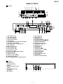
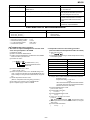
3. To be sure that no shock hazard exists, check for leakage current
in the following manner.
* Plug the AC line cord directly into a 120 volt AC outlet.
* Using two clip leads, connect a 1.5k ohm, 10 watt resistor paralleled
by a 0.15µF capacitor in series with all exposed metal cabinet parts
and a known earth ground, such as conduit or electrical ground
connected to earth ground.
* Use a VTVM or VOM with 1000 ohm per volt, or higher, sensitivity
to measure the AC voltage drop across the resistor (See diagram).
* Connect the resistor connection to all exposed metal parts having a
return path to the chassis (antenna, metal cabinet, screw heads,
knobs and control shafts, escutcheon, etc.) and measure the AC
voltage drop across the resistor.
VTVM
AC SCALE
1.5k ohms
10W
0.15 µ F
TEST PROBE
TO EXPOSED
METAL PARTS
CONNECT TO
KNOWN EARTH
GROUND
All check must be repeated with the AC line cord plug connection
reversed.
Any reading of 0.3 volt RMS (this corresponds to 0.2 milliamp. AC.)
or more is excessive and indicates a potential shock hazard which
must be corrected before returning the audio product to the owner.
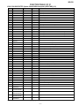
SPECIFICATIONS
General
Type:
Signle readout:
Audio channels:
Frequency response:
Rotation speed:
Error correction:
Coding:
Recording method:
A/D,D/A converter:
Sampling frequency:
Wow and flutter:
MiniDisc deck
Non-contact, 3-bean semi-conductor
laser pick-up
Stereo 2 channels/monaural
(long-play mode) 1 channel
4 - 20,000 Hz (+0/-1 dB)
Approximately 400 to 900 rpm
ACIRC (Advanced Cross Interleave
Reed-Solomon Code)
ATRAC (Adaptive TRansform
Acoustic Coding)
Magnetic modulation overwrite
method
Signal/noise ratio:
Power source:
Power consumption:
Dimensions:
Weight:
Output sockets
Input sockets
Socket
name
LINE IN
Socket
shape
Pin jack
Input
impedance
Over
22 kohms
Reference
input level
Minimum
input level
680 mVrms
170 mVrms
Socket
name
OPTICAL Square
IN (Optical) optical
connector
COAXIAL
(Coaxial)
Pin jack
Socket shape
Output
level
Load
impedance
PHONES
1/4" (6.3 mm) stereo
(Headphones) jack
15 mV
32 ohms
LINE OUT
2 Vrms
50 kohms
Pin jack
OPTICAL
Square optical connector
OUT (Optical)
75 ohms
500 mVp-p
Remote control
Power:
Timer/clock
Type:
Timer:
1-bit
44.1kHz
Unmeasurable (less than ±0.001%
W.peek)
100 dB or better during playback
(line output)
AC 120 V, 60 Hz
17 W
Width: 16-15/16" (430 mm)
Height: 3-11/16" (93 mm)
Depth: 11-15/16" (302 mm)
8.0 Ibs (3.6 kg)
Digital clock with date function
ON/OFF, once a day
DC 3V ("AA" (UM/SUM-3, R6, HP-7
or similar) battery included x 2)
Specifications for this model are subject to change without
prior notice.
–2–
MD-R2
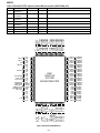
NAME OF PARTS
Front panel
1
11
12
13
2
3
4
5
TOC DISC TRACK DATE
MONO LP PRGM
TOTAL
REMAIN
RANDOM
14 1516 17 18
6
12
TIMER REC
19
7
4
0dB
8
OVER
9
10
AM 1 2 3 4 5 6 7
PM 8 9 10 11 12 13 14
CLOCK 15 16 17 18 19 20
20
21 22
23
24 25 26
27
28
29
30
31 32 33
34
36 37
20. Clock Indicator
21. Eject Button:
22. Remote Sensor
23. Cue/Review Button:
24. Display/Character Button
25. Name/TOC Edit Button
26. Record Level Control
27. Headphone Level Control
28. Headphone Jack
29. Power Button
30. Stop Button:
31. Play/Pause Button:
32. Record Button:
33. Input Select Button
34. Program Button
35. Jog Dial (Next/Previous)
36. Enter Button
37. Delete/Clear/Timer Button
1. TOC Indicator: TOC
2. Total Time Indicator
3. Disc Name Indicator
4. Track Name Indicator
5. Date Indicator
6. Level Meter/Character Information Display
7. Recording Level Indicator
8. Recording Level Too High Indicator
9. Music Calender
10. More Tracks Indcator
11. Pause Indicator:
12. Record Indicator:
13. Play Indicator:
14. Monaural Long-Play Mode Indicator
15. Program Indicator
16. Repeat Indicator:
17. Remaining Time Indicator
18. Random Play Indivator
19. Timer Playback/Timer recording Indicator
Rear panel
1. AC Power Cord
2. Coaxial Input Jack
(Digiral)
3. Optical Input/Output Jacks
(Digital)
4. Line Input/Output Jacks
(Analogue)
5. Reset Button
35
1
2
–3–
3
4
5
–4–
7
AM
CLOCK
TIMER
DELETE/CLEAR
AM
CLOCK
Time setting mode
DATE
Each time the button is pressed,
the display will change.
Date setting mode
DATE
CLOCK
ENTER
5
6
7
4
3
2
1
The unit will enter the time setting mode.
Set the “day” repeating steps 4 and 5.
Set the “month” repeating steps 4 and 5.
Press the ENTER button to set the “year”.
When you turn the jog dial and let go, the year will change
up or down by one.
The year 2000 or later is set as follows:
[00] indicates the year 2000
[01] indicates the year 2001
The range of dates that can be entered is from January 1,
1997 to December 31, 2099.
Set the “year” using the jog dial.
The unit will enter the date setting mode.
Within 10 seconds, press the ENTER button.
Within 10 seconds, turn the jog dial until “TIME ADJUST”
appears.
Press the POWER button to turn the power on and press
the TIMER button.
Setting the date
When recording, the date and time are recorded on the Minidisc.
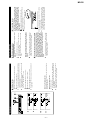
1. Remote Control Transmitter Window
2. Direct Key Buttons
3. Play Mode Button
4. Music Scan Button
5. Input Select Button
6. Display Button
7. Time Button
8. Auto Mark Button
9. Track Down/Review Button:
10. Track Up/Cue Button:
11. Power Button
12. Program Button
13. Clear Button
14. Synchro Record Button:
15. Record Cancel Button
16. Record Mode Button
17. Record Button:
18. Play/Pause Button:
19. Stop Button:
6
5
4
3
2
1
POWER
SETTING THE CLOCK
MD-R2
Names of controls
1
2
3
4
5
6
7
8
9
10
11
12
13
14
15
16
17
18
19
OPERATION MANUAL
11
10
9
8
(Continued)
DATE
DATE
DATE
DATE
PM
CLOCK
PM
CLOCK
PM
CLOCK
PM
CLOCK
ENTER
TIMER
DELETE/CLEAR
When you turn the jog dial and let go, the hour will change
up or down by one. When you turn and hold it, the hour will
change continuously.
The clock uses the 12-hour system. Pay attention to the AM
or PM indicator in the display.
AM 0:00 → midnight, PM 0:00 → noon
Set the “hour” using the jog dial.
–5–
Once you have set the date and time, “TIME ADJUST” will
not be displayed in step 2. Turn the jog dial to make the date
and time appear.
If you do not need to change the settings, just press the
ENTER button without turning the jog dial again.
See “Setting the clock”.
Resetting the date and time
After pressing the TIMER button, turn the jog dial until the date
and time are displayed.
Checking the date and time
When the ENTER button is pressed, the clock will show the
correct time.
9 Press the ENTER button to set the “hour”.
10 Adjust the “minute” using the jog dial.
11 Press the ENTER button to set the “minute”.
8
After step 7, described in the “Setting the date” section
Setting the time
If a power failure occurs or the AC power cord is disconnected for about 10 minutes, when power is restored,
TOC will be written on the disc.
If the AC power plug is disconnected from the AC outlet
or a power failure occurs during recording (before the
TOC information has been recorded on the disc), the
audio portion being recorded at that time will be erased.
When a recording is being added to a MiniDisc which
already has a recording on it, if the TOC is not updated
before the power failure, the added recording will be
erased.
If a power failure occurs during recording
If this happens, remove the disc, and open the disc
holder. The condensation should evaporate in approximately 1 hour. The unit will then function properly.
When the unit has condensation inside, the disc signals
cannot be read, and the product may not function
properly.
In the following cases, condensation may form inside
the unit.
Shortly after turning on a heater.
When the unit is placed in a room where there is excessive steam or moisture.
When the unit is moved from a cool place to a warm
place.
Moisture condensation
TROUBLESHOOTING
1
2
3
When the reset button is pressed, all of the settings in
memory will be erased.
If strange sounds, smells or smoke come out of the unit
or if a foreign object falls into the unit, turn off the power,
unplug the AC power cord from the AC outlet, immediately. Contact your nearest authorized Sharp servicer.
Pen, pencil, etc.
RESET
If this product is subjected to strong external interference (mechanical shock, excessive static electricity,
abnormal supply voltage due to lightning, etc.) or if it
is operated incorrectly, it may malfunction or the display
may not function correctly. If such a problem occurs,
do the following:
Unplug the AC power cord from the AC outlet.
Wait about 20 - 30 seconds and then plug the AC power
lead back into the AC outlet.
Press the reset button on the back of the unit.
If a problem occurs
MD-R2
SYMPTOM
SYMPTOM
–6–
Replace the batteries.
Operate it within a range of 8" (0.2 m)
to 20' (6 m) and within an angle of 15 o
to either side of center.
Load a disc.
Connect the AC power cord.
The batteries inside the remote control
are dead.
The remote control is operated from
an incorrect distance or angle.
No disc has been loaded.
Is the AC power cord plugged in?
The power cannot be turned on from
the remote control.
Insert properly.
POSSIBLE CAUSE
The batteries (polarity) are not inserted
properly.
SYMPTOM
The remote control does not function
or does not operate properly.
REMEDY
Remove the disc and leave the power
turned on. The unit should function
properly in about 1 hour.
Has condensation formed inside the
unit?
Playback sounds are skipped.
Remote control
Place the unit on a firm, level surface
free from vibration.
Is the unit located near excessive vibrations?
Playback stops in the middle of a
track, or playback is not performed
properly.
Put in another recordable disc with
recording space on it.
Can you see the “TOC FULL” message in the display?
Replace the disc.
Place the unit on a firm, level surface
free from vibration.
Replace it with a recordable disc.
Did you try to make recording on a
playback-only MiniDisc?
Is the disc scratched?
Is the unit located near excessive vibrations?
Slide the accidental erase prevention
tab back to its original position.
REMEDY
Is the MiniDisc protected against accidental erasure?
POSSIBLE CAUSE
Even though a disc has been loaded,
“no disc” or “Error” is displayed.
A recording cannot be made.
Audio
It is recommended that you use an
outdoor antenna.
When a radio or TV which uses an
indoor antenna is placed near the
unit, the picture on the TV screen may
be distorted or the radio may not function properly.
Radios make unusual noise or the picture on the TV screen is distorted.
Try setting it again.
REMEDY
Turn the power off and on again, and
then retry the operation.
Did a power failure occur?
POSSIBLE CAUSE
When a button is pressed, the unit
does not respond.
The clock is wrong.
General
If this unit functions abnormally during operation, first check the following items. If the unit continues to function abnormally,
or if an abnormality appears other than listed below, turn off the player's power and disconnect the AC power plug, then
consult your SHARP dealer or service personnel.
If a problem occurs
(Continued)
The disc is out of recording space.
The proper focus cannot be obtained.
The unit has determined that it is out of order
by performing a self-diagnosis.
There is a mechanical problem and the disc is
not working properly.
DISC FULL
FOCUS ERROR
MD ERROR
MECHA ERR*
The data contains an error.
Music is not being recorded.
? DISC
0 0:00
*: Number or symbol
The TOC information could not be created
properly due to a mechanical shock or to
scratches on the disc.
The TOC information on this disc does not
meet the MD specifications or it cannot be read.
The unit has determined that it is abnormal by
performing a self-diagnosis.
U TOC W ERR
U TOC ERR*
TOC W ERROR
There is no space left for recording character
information (track names, disc names, etc.)
The disc has a large amount of damage.
TOC information cannot be read.
The MD does not meet the specifications for
MDs.
TOC FULL*
The temperature is too high.
The MiniDisc is write protected.
PROTECTED
TOC ERR*
You tried to record on a playback-only disc.
The data of disc names and track names are
not able to move from playback-only discs.
PLAYBACK MD
TEMP OVER
The data recorded on this disc is not audio data.
NOT AUDIO
A MiniDisc has not been loaded.
The MiniDisc data cannot be read.
The disc is damaged or there is no TOC on the
disc.
DISC ERR
NO DISC
Incorrect digital signals are input.
Din UNLOCK
The number of characters for the disc name or
track name exceeds 100.
Since this disc has scratches on it, the
recording operation was skipped.
DEFECT
NAME FULL
Recording cannot be performed correctly due to
vibration.
A track cannot be edited.
Can't EDIT
Can't REC
You tried to record from a disc which you are
not allowed to copy.
Can't COPY
Meaning
Nothing is recorded.
(Neither music nor a disc name have been
recorded on this MD.)
BLANK MD
Error messages
When an error message is displayed, proceed as follows:
(Continued)
Remedy
button.
Replace the disc with a recorded disc.
Replace the disc with another disc.
Turn off the power, and try to write the TOC
again. (Remove any source of shock or vibration
while writing.)
Replace it with another disc.
Erase all the data, and try recording.
Ask the store where you purchased this unit,
about repairs.
Replace it with another recordable disc.
Replace the disc with another disc.
Turn off the power, and wait for a while.
Move the write protection tab back to its original
position.
Replace it with a recordable MiniDisc.
Edit only the sound.
Select another track.
Replace the MiniDisc.
Load a MiniDisc.
Reload the MiniDisc.
Shorten the disc or track name.
Turn off the power, and press the
Ask the store where you purchased this unit,
about repairs.
Reload the MiniDisc.
Replace the disc with another recordable disc.
Reload the disc or replace it.
Connect correct digital signals.
Use the analog input jack.
Replace the disc with another recordable disc.
Move the unit away from the source of vibration.
Change the stop position of the track and then
try editing it.
Replace it with another disc which you can
copy from (regular CD).
Replace the disc with a recorded disc.
MD-R2
MD-R2
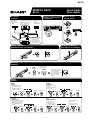
Quick-Guide
Guía rápida
MINIDISC DECK
MD-R2
Turning the power on and off
Conexión y desconexión de
la alimentación
Connection
Conexión
• Stereo, DAT, MD recorder, etc.
• Equipment with a
• MD/CD player
with an optical input/output jack
coaxial jack
• Equipo con toma
coaxial
Remote control
Control remoto
etc.
• Estéreo, DAT, grabadora de
• Reproductor
MD, etc. con toma de
entrada/salida óptica
de MD/CD etc.
• 2 “AA” batteries
• Dos pilas “AA”
POWER
15ϒ 15ϒ
• Stereo, radio cassette
player, etc. with line
input/output jacks
• AC 120V, 60Hz
• 120V de CA, 60Hz
• Estéreo, radio-casete,
etc. con tomas de
entrada/salida de línea
Playing a MiniDisc
Reproducción de un minidisco
To remove a MiniDisc
Para extraer un minidisco
Recording
Grabación
INPUT
SELECT
(Remote control)
(Control remoto)
• Start playing the music
SYNC REC
you want to record using
the other equipment.
• Inicie la reproducción de
la música que desee
grabar usando el otro
equipo.
Editing
Edición
DIVIDE
DIVISIÓN
ERASE
BORRADO
• Play the track which you
• Select the track to be
erased.
want to divide into two.
• Seleccione la pista que
• Reproduzca la pista que
desee borrar.
desee dividir en dos.
ENTER
NAME/TOC EDIT
Åá
ENTER
MOVE
DESPLAZAMIENTO
• Select the second of the two
• Select the track you
NAME/TOC EDIT
TRACK DATE
12
4
que desee desplazar.
40
DISC
TRACK DATE
12
4
0dB
OVER
ENTER
• Select the direction to
move the track.
• Seleccione la dirección
• Seleccione la pista
Åá
0dB
ENTER
want to move.
• Seleccione la segunda de
las dos pistas que desea
combinar.
DISC
NAME/TOC EDIT
COMBINE
COMBINACIÓN
tracks you want to combine.
40
Åá
40
DISC
TRACK DATE
12
4
0dB
OVER
para desplazar la pista.
OVER
ENTER
ENTER
NAME/TOC EDIT
–7–
ENTER
ENTER
MD-R2
DISASSEMBLY
Caution on Disassembly
Follow the below-mentioned notes when disassembling
the unit and reassembling it, to keep it safe and ensure
excellent performance:
1. Take the minidisc out of the unit.
2. When disassembling the machine, be sure to withdraw
the power plug from the socket in advance.
3. When disassemble the parts, remove the nylon band or
wire holder as necessary.
To assemble after repair, be sure to arrange the wires as
they were.
If a screw of different length is fitted to the MD mechanism (the screw of the part to be fitted to the MD
mechanism chassis), it may contact the optical pickup,
resulting in malfunction.
4. When repairing, pay due attention to electrostatic charges
of IC.
STEP
1
REMOVAL
Top Cabinet
PROCEDURE
FIGURE
1. Screw ..................... (A1) x5
8-1
2
Rear Panel
1. Screw ..................... (B1) x5
8-2
3
MD Unit
1. Screw .................... (C1) x4
2. Flat Cable ............... (C2) x1
3. Socket .................. (C3) x1
8-2
4
Front Panel
1. Screw .................... (D1) x5
2. Flat Cable ............... (D2) x1
3. Socket ................... (D3) x1
8-2
5
Main PWB
1. Screw ..................... (E1) x6
(with Transformer)
8-2
6
Jog Dial
1. Knob ....................... (F1) x1
2. Nut .......................... (F2) x1
8-3
7
Display PWB
1. Screw .................. (G1) x10
2. Knob ...................... (G2) x2
8-3
8
Headphones PWB 1. Screw .................... (H1) x1
8-3
9
Switch PWB
1. Screw ..................... (J1) x5
8-3
10
MD Mechanism
Unit
1. Screw ..................... (K1) x4
8-4
11
MD Main PWB
1. Screw ..................... (L1) x2
2. Socket .................... (L2) x6
9-1
12
MD Mechanism
1. Screw .................... (M1) x4
9-2
(E1)x3
ø3x10mm
(E1)x2
ø4x8mm
Washer
(D1)x1
ø3x8mm
(E1)x1
ø3x10mm
(D2)x1
Front Panel
(C2)x1
(C1)x4
ø3x6mm
Main PWB
(D3)x1
(B1)x5
ø3x10mm
Rear Panel
(D1)x1
ø3x8mm
MD Unit
(C3)x1
(D1)x3
ø3x8mm
Figure 8-2
(G2)x2
(F1)x1
(F2)x1
washer
Display PWB
(H1)x1
ø3x10mm
Headphone
PWB
Switch PWB
Front
Panel
(G1)x10
ø3x10mm
(J1)x5
ø3x10mm
Figure 8-3
Shield Case
(A1)x1
ø3x10mm
Top Cabinet
(K1) x 2
ø3 x 6mm
(A1)x1
ø3x10mm
(A1)x3
ø3x10mm
(K1) x 2
ø3 x 6mm
MD Mechanism
Unit
Figure 8-1
Figure 8-4
–8–
MD-R2
( L2 ) x 1
Pickup Flexible
PWB (*1)
MD Mechanism
MD Main PWB
( L1 ) x 4
ø1.7 x 3mm
Pull
(L2)x1
(*1) After disconnecting the optical
pickup flex PWB from the
connector wrap the front end of
flex PWB in conductive aluminium
foil so as to prevent electrostatic
damage of optical pickup.
( L2 ) x 1
( L2 ) x 3
Frame
(M1)x4
ø1.7x8.9mm
Figure 9-1
Figure 9-2
• Jog knob replacement procedure
Front Panel
Jog Decoration
Jog Decoration
Jog Knob
Remove the pawl of jog decoration
with fine piece such as tweezers,
press, and remove the jog knob with
jog decoration.
Jog Knob
Display PWB
FL Window
Figure 9-4
Figure 9-3
Display PWB
Remove the pawl of jog decoration with fine piece
such as tweezers, press, and remove the jog knob
with jog decoration.
Figure 9-5
–9–
MD-R2
REMOVING AND REINSTALLING THE MAIN PARTS
(A1)x1
ø1.7x5mm
MD MECHANISM SECTION
Perform steps 1 to 3 of the disassembly method to remove the
MD mechanism.
Magnetic Head
How to remove the magnetic head
(See Fig. 10-1)
1. Remove the screws (A1) x 1 pc.
Caution:
Take utmost care so that the magnetic head is not damaged
when it is mounted.
MD Mechanism
Figure 10-1
How to remove the cartridge holder
(See Fig. 10-2)
Slider Lever
1. Open the rpller arm lever in the arrow direction, and lower
the clamper lever to the rear side.
2. Apply +5V to the red line side of blue connector of loading
motor, push the rack gear in the arrow direction to move the
cam plate lever until tick is heard.
3. Remove the screw (B1) x1 pc., and the spring (B2) x1 pc.,
fitted to the holder arm, and shift the cartridge holder to the
left side to remove it.
Roller Arm Lever
Cartridge Holder
(B1) x1
ø1.7x5mm
Loading Motor
Clampa Lever
Lack Gear
Cam Plate Lever
(B2) x1
Figure 10-2
(C1)x1
ø1.7x3mm
How to remove the mechanism switch PWB
(See Fig. 10-3)
1. Remove the screws (C1) x 2 pcs., and remove the mechanism switch PWB.
(C1)x1
ø1.7x9.5mm
MD Mechanism
Switch PWB
Figure 10-3
– 10 –
MD-R2
How to remove the sled motor/loading motor
(See Fig. 11-1)
1. Remove the screws (D1) x 1 pcs., and remove the sled
motor/loading motor.
(D1)x2
ø1.7x2mm
(D1)x2
ø1.7x2mm
Caution:
Be careful so that the gear is not damaged.
(The damaged gear emits noise during searching.)
Loading
Motor
Sled Motor
Figure 11-1
How to remove the spindle motor
(See Fig. 11-2)
1. Remove the screws (E1) x 3 pcs., and remove the spidle
motor.
Caution:
Be careful so that the turntable is not damaged.
Turntable
(E1)x3
ø1.7x2.5mm
Spindle Motor
Figure 11-2
How to remove the optical pickup
(See Fig. 11-3)
(F1)x3
ø1.7x9.5mm
1. Remove the screws (F1) x 3 pcs.
Optical Pickup
Caution:
Be careful so that the gear is not damaged.
(The damaged gear emits noise during searching.)
Figure 11-3
– 11 –
MD-R2
ADJUSTMENT
TEST MODE
1) Mode there are 5 kinds TEST MODE as below.
MODE
PUSH KEY
A) MD TEST MODE
ENTER
PLAY
B) AUDIO TEST MODE
CUE
REVIEW
C) KEY TEST MODE
CUE
ENTER
D) RECORDING TEST MODE
ENTER
REC
E) MD TEST2 MODE (DATA MONITOR MODE)
ENTER
STOP
2) How to start and quit TEST MODE.
AC Supply On or push RESET KEY after push two keys.
In all TEST MODE. Power Off (POWER KEY) is quit TEST MODE.
3) TEST MODE description.
A) MD TEST MODE (ENTER+PLAY)
Disp. Will be "AUT YOBI". In this mode push ENTER KEY in mean product alignment's auto adjust mode.
(Disp. Will be "AUTO AJST". In this mode push PLAY KEY in mean auto adjust mode by disc condition.
Then push PLAY KEY again. It start play and display will be "a__C__". The 4 digits after "a" are address.
After "C" are error rate.)
PUSH KEY NAME
ACTION
ENTER
Servo adjust mode or menu from adjust mode.
TIMER
REC. and P.B. mode or to menu from REC.mode.
NAME
Other menu select.
REC
Reverse menu select.
PLAY
Selected menu execution.
STOP
Execute stop.
CUE
Slide motor (PIC) move to out-side.
REVIEW
Slide motor (PIC) move to in-side.
JOG. UP *1
Manual alignment +1, loading motor on (OUT).
JOG. DOWN *1
Manual alignment -1, loading motor on (IN).
POWER
Test mode quit and power off.
EJECT
Disc eject.
*1. Jog. Up/Jog. Down key effect for loading motor control when display panel "tsm____e__". (Push STOP KEY some times
to disp. "tsm____e__".)
NOTE. MD test are necessary mode only for MD Unit.
B) Audio test mode (CUE+REVIEW)
This mode is key examination mode for a set with in MD-unit.
Automatically set recording mode.
Digital opt. Digital coax and analog are effective.
Test mode start is REC KEY push after disc toc. Read.
REC KEY push
1) Record form analog function by 3 sec time.
2) Record form digital opt. Function by 3 sec time.
3) Record from digital coax. Function by 3 sec time.
4) Record stop.
Note. 1) If digital function is din unclock. Skip to follwing next function.
2) Digital synchronize level is -50 dB.
Analog synchronize level is -47 dB.
C) Key test mode (CUE+ENTER)
This mode is key examination mode for a set with out MD-unit.
This mode indicate destination as below dot display.
– 12 –
MD-R2
KEY TEST
KEY NAME
TIMER
KEY NAME
ILLUMINATE
SEGMENT
10 ROW DOT
ILLUMINATE
SEGMENT
INPUT SELECT
TOC
DISPLAY
11 ROW DOT
EJECT
7 ROW DOT
REVIEW
ALL
PLAY
4 ROW DOT
CUE
PM
STOP
5 ROW DOT
ENTER
8 ROW DOT
REC
6 ROW DOT
JOG. UP
17 (M.C.)
NAME
9 ROW DOT
JOG. DOWN
18 (M.C.)
TIME
AM
PROGRAM
PRGM
D) Recording test mode (ENTER+REC)
This mode is auto recording repeat mode.
After disc full. Erase all and rec start again.
MD SECTION
1. Preparation for adjustment
Test disc
Type
1
2
3
Test disc
Part No.
High reflection disc TGYS1 (SONY)
RRCDT0101AFZZ
Low reflection disc Recording minidisc
UDSKM0001AFZZ
Head Adjusting transparent RRCDT0103AFZZ
Extension Cable (See Fig. 26-4)
Type
1
2
3
4
3
Part No.
Extension PWB for servicing
Extension Connector (2 Pin)
Extension Connector (6 Pin)
Extension Cable (5 Pin)
Extension Cable (28 Pin)
RUNTK0457AFZZ
QCNWK0059AFZZ
QCNWK0107AFZZ
QCNWK0109AFZZ
QCNWK0108AFZZ
2. Test mode
Test mode setting method
1. Holding down the ENTER button and MD
(PLAY/PAUSE) button, press the RESET button.
(State A is changed to state B .)
2. Insert the playback disc 1 (high reflection disc) or recording disc 2 (low reflection disc). (State C is set.)
Thus, the test mode state is set.
A tsm
TEST
e
: TEST MODE
STOP state
represents version of MD microcomputer.
(When the MD (STOP) button is ressed in the C state, the indication A
is restored. To restore C again, press the ENTER button.)
B EJECT
TEST
C AUT YOBI
TEST
Entering the specific mode
Whenever the CD
(PLAY/PAUSE) button is pressed, the mode is changed.
AUTO pre-adjustment
AUTO adjustment
RESULT SUB
EEPROM setting
MANUAL adjustment
RESULT
MANUAL pre-adjustment
• Canceling the test mode
When the POWER button is pressed, the test mode is canceled, and the POWER OFF state is set.
– 13 –
MD-R2
• Test Mode
1. AUTO pre-adjustment mode
• Automatic pre-adjustment is performed. (After adjustment the grating adjustment mode is set.)
• The adjustment value is output with the aid of system controller interface.
2. AUTO adjustment mode
• Automatic adjustment is performed.
• The adjustment value is output with the aid of system controller interface.
• Continuous playback is performed. (Error rate indication, jump test)
3. RESULT sub-mode
• The measurement value, set value and calculated value are indicated.
• The set value is changed manually (in servo OFF state).
4. RESULT mode (final adjustment)
• The set value (after calculation) is indicated.
• The set value is changed manually (in servo OFF state).
5. MANUAL pre-adjustment mode
• RF side manual adjustment is performed.
• Focus and tracking signal ATT manual adjustment is performed.
• Focus and tracking signal offset setting is performed.
6. MANUAL adjustment mode
• Focus and tracking signal ATT manual adjustment is performed.
7. EEPROM setting mode
• Various coefficients of digital servo are changed manually.
• Each servo is set to ON individually.
• Temperature detection terminal voltage is measured, and the reference value is determined.
8. TEST-PLAY mode
• Continuous playback from the specified address is performed.
• C1 error rate measurement, ADIP error rate measurement.
9. TEST-REC mode
• Continuous recording from the specified address is performed.
• Change of record laser output (servo gain is also changed according to laser output)
10. INNER mode
• The position where the INNER switch is turned on is measured.
11. EJECT mode
• TEMP setting (of EEPROM setting)
• CONTROL setting (of EEPROM setting)
• Setting of laser power (record/playback power)
1. AUTO pre-adjustment mode (Low reflection disc only)
Step No.
•
Setting Method
Remarks
Display
Step 1
Testmode STOP state
[tsm
Step 2
Press once the ENTER button.
Step 3
Press once the MD PLAY button. The slide moves to the innermost periphery, and automatic
pre-adjustment is started.
• During automatic adjustment
changes as follows.
HAo→RFg→SAg→SBg→PTG→PCH→GTG→GCH→RCG→
SEG→RFG→SAG→HAO→HEO→TCO→LAO
End of adjustment
If adjustment is OK, Step 4.
If adjustment is NG, Step 5.
[
Step 4
Grating adjustment,
adjustment value output
Press once the MD STOP button. STEP 2
[_COMPLETE_]
Step 5
Adjustment value output
Press once the MD STOP button. STEP 2 AUTO pre-adjustment menu
[ Can't _ ADJ. ]
AUTO pre-adjustment menu
: Adjustment name
– 14 –
[
e
]
A U T O
]
:______]
MD-R2
2. AUTO adjustment mode
Step No.
•
Setting Method
Remarks
Display
Step 1
Testmode STOP state
Step 2
Press the ENTER button two times.
[tsm
Step 3
Press once the MD PLAY button. The slide moves to the innermost periphery, and automatic
adjustment is started.
• In case of high reflection disc
changes as follows.
PEG→HAG
•In case of low reflection disc
changes as follows.
PEG→LAG→GCG→GEG→LAG
End of adjustment
If adjustment is OK, Step 4.
If adjustment is NG, Step 7.
[
Step 4
Adjustment value output
Press the MD PLAY button.
Press the MD STOP button.
[_COMPLETE_]
AUTO adjustment menu
]
:______]
STEP 5
STEP 2
Step 5
Continuous playback (pit section)
Continuous playback (groove section)
Step 6
Press the DISPLAY button.
Press the MD STOP button.
Continuous playback (groove section)
STEP 2 AUTO adjustment menu
Step 7
Adjustment value output
Press the MD STOP button.
STEP 2 AUTO adjustment menu
: Adjustment name,
e
[AUTO_AJST_]
[s
[a
c
c
]
]
[a
a
]
[ Can't _ ADJ. ]
: Measurement value,
: Address
3. RESULT sub-mode
Step No.
Setting Method
Remarks
Display
Step 1
Testmode STOP state
[tsm
Step 2
Press the ENTER button three times.
Step 3
Press once the MD PLAY button. Indication of set value
[RFG:__ _ _ _
]
Step 4
Press once the ENTER button.
Indication of set value
[RCG:__ _ _ _
]
Step 5
Press once the ENTER button.
Indication of set value
[RTG:__ _ _ _
]
Step 6
Press once the ENTER button.
Indication of set value
[GTG:__ _ _ _
]
Step 7
Press once the ENTER button.
Indication of set value
[PCH:__ _ _
]
Step 8
Press once the ENTER button.
Indication of set value
[GCH:__ _ _
]
RESULT sub-menu
e
]
[_RST_YOBI_]
Step 9
Press once the ENTER button.
Indication of set value
[SAG:__ _
]
Step 10
Press once the ENTER button.
Indication of set value
[SBG:__ _
]
Step 11
Press once the ENTER button.
Indication of set value
[SEG:__ _
]
Step 12
Press once the ENTER button.
Indication of set value
[SFG:__ _
Step 13
Press once the ENTER button.
Indication of measurement value
[HAO:
_ _ _]
Step 14
Press once the ENTER button.
Indication of measurement value
[HBO:
_ _ _]
Step 15
Press once the ENTER button.
Indication of measurement value
[HEO:
_ _ _]
Step 16
Press once the ENTER button.
Indication of measurement value
[HFO:
_ _ _]
Step 17
Press once the ENTER button.
Indication of measurement value
[LAO:
_ _ _]
Step 18
Press once the ENTER button.
Indication of measurement value
[LBO:
_ _ _]
Step 19
Press once the ENTER button.
Indication of measurement value
[LEO:
_ _ _]
Step 20
Press once the ENTER button.
Indication of measurement value
[LFO:
_ _ _]
Step 21
Press once the ENTER button.
Indication of measurement value
[TCO:_
_ _ _]
Step 22
Press once the ENTER button.
Indication of adjustment error sequence No.
[YOB:_
_ _ _]
Step 23
Press once the ENTER button.
Indication of adjustment status
[D I F:_
_ _ _]
Step 24
Press once the ENTER button.
Indication of pre-adjustment not completed (00)/completed (4B)
[ADJ:_
_ _ _]
Step 25
Press once the MD STOP button. RESULT sub-menu state
[_RST_YOBI_]
: Measurement value,
: Adjustment value,
: Other various informations
•
• ressing the REC button causes reversing.
• When the jog key is turned upward while the setting is displayed, the setting increases, and a new setting is stored in RAM.
• When the jog key is turned downward while the setting is displayed, the setting increases, and a new setting is stored in RAM.
– 15 –
]
MD-R2
3. RESULT mode (final adjustment)
Step No.
Setting Method
Remarks
Display
Step 1
Testmode STOP state
[tsm
Step 2
Press the ENTER button four times.
Step 3
Press once the MD PLAY button. Indication of set value
[HAG:__ _
Step 4
Press once the ENTER button.
Indication of set value
[HBG:__ _
]
Step 5
Press once the ENTER button.
Indication of set value
[LAG:__ _
]
Step 6
Press once the ENTER button.
Indication of set value
[LBG:__ _
]
Step 7
Press once the ENTER button.
Indication of set value
[PEG:__ _
]
Step 8
Press once the ENTER button.
Indication of set value
[PFG:__ _
]
RESULT menu
e
]
[_RSTULT___]
]
Step 9
Press once the ENTER button.
Indication of set value
[GEG:__ _
]
Step 10
Press once the ENTER button.
Indication of set value
[GFG:__ _
]
Step 11
Press once the ENTER button.
Indication of set value
[GCG:__ _ _
]
Step 12
Press once the MD STOP button. RESULT menu state
[_RESULT___]
•
: Set value
• ressing the REC button causes reversing.
• When the jog key is turned upward while the setting is displayed, the setting increases, and a new setting is stored in RAM.
• When the jog key is turned downward while the setting is displayed, the setting increases, and a new setting is stored in RAM.
5. MANUAL auxiliary adjustment mode (only low reflection disc)
Step No.
Step 1
•
Setting Method
Remarks
Testmode STOP state
Display
[tsm
]
Step 2
Press the ENTER button five times.
Step 3
Press once the MD PLAY button. Initial setting → Temperature measuring mode
[TMP:_
___]
Step 4
Press once the ENTER button.
Offset "0" setting → A signal offset tentative measurement
[HAo:
___]
Step 5
Press once the ENTER button.
B signal offset tentative measurement
[HBo:
___]
Step 6
Press once the ENTER button.
E signal offset tentative measurement
[HEo:
___]
Step 7
Press once the ENTER button.
F signal offset tentative measurement
[HFo:
___]
Step 8
Press once the ENTER button.
Offset tentative measurement → Laser ON
[LON:______]
Step 9
Press once the ENTER button.
Innermost periphery move → RF side FG rough adjustment
[RFg:
Step 10
Press once the ENTER button.
Focus ATT (A signal) tentative setting
[SAg:
Step 11
Press once the ENTER button.
Focus ATT (B signal) tentative setting
[SBg:
Step 12
Press once the ENTER button.
RF side pit section TG adjustment
[PTG:
__
]
Step 13
Press once the ENTER button.
Pit section COUT level setting
[PCH:
_
]
Step 14
Press once the ENTER button.
Outer periphery move → RF side groove TG adjustment
[GTG:
__
]
Step 15
Press once the ENTER button.
Groove section COUT level setting
[GCH:
_
]
Step 16
Press once the ENTER button.
RF side TCRS adjustment
[RCG:
__
]
Step 17
Press once the ENTER button.
Tracking ATT (A signal) setting
[SEG:
Step 18
Press once the ENTER button.
Tracking ATT (B signal) setting
[SFG:
Step 19
Press once the ENTER button.
Indication of tracking EFMIO measurement
[gMI:
___]
Step 20
Press once the ENTER button.
RF side pit section FG adjustment
[R F G :
__
Step 21
Press once the ENTER button.
Focus ATT (A signal) setting
[SAG:
Step 22
Press once the ENTER button.
Focus ATT (B signal) setting
[SBG:
]
Step 23
Press once the ENTER button.
Offset "0" setting → A signal offset measurement
[HAO:
___]
Step 24
Press once the ENTER button.
B signal offset measurement
[HBO:
___]
Step 25
Press once the ENTER button.
E signal offset measurement
[HEO:
___]
Step 26
Press once the ENTER button.
F signal offset measurement
[HFO:
___]
Step 27
Press once the ENTER button.
TCRS signal offset measurement
[TCO:
___]
Step 28
Press once the ENTER button.
A signal offset measurement
[LAO:
___]
Step 29
Press once the ENTER button.
B signal offset measurement
[LBO:
___]
Step 30
Press once the ENTER button.
E signal offset measurement
[LEO:
___]
Step 31
Press once the ENTER button.
F signal offset measurement
[LFO:
___]
: Measurement value,
: Set value,
MANUAL auxiliary adjustment mode
e
: Account value
– 16 –
[_MNU_YOBI_]
__
]
]
]
]
]
]
]
MD-R2
• If the jog key upward/downward is pressed during setting indication, the setting increases/decreases, and the new setting is stored in RAM.
• If the REC button is pressed, the setting returns step by step excepting the following case.
A signal offset (HAO) → Offset tentative setting → RF side FG adjustment (RFG)
RF side TCRS adjustment (RCG) → RF side groove TG adjustment (GTG)
RF side groove TG adjustment (GTG) → Innermost periphery move → RF side pit section adjustment (PTG)
RF side pit TG adjustment (PTG) → RF side FG rough adjustment (RFg) → Laser lighting (LON)
Laser lighting (LON) → Offset "0" setting → A signal offset tentative measurement (HAo)
If the measurement value is within the OK range, " " appears on the 8th character.
6. MANUAL adjustment mode
High reflection disc
Step No.
Step 1
Setting Method
Remarks
Testmode STOP state
Display
[tsm
MANUAL adjustment menu
e
]
Step 2
Press the ENTER button six times.
Step 3
Press once the MD PLAY button. Initial setting → Temperature measuring mode
[_MNU_AJST_]
[TMP:_
Step 4
Press once the ENTER button.
Laser ON
[LON:______]
Step 5
Press once the ENTER button.
Innermost periphery move → Tracking ATT (E signal) setting
[PEG:
]
Step 6
Press once the ENTER button.
Tracking ATT (F signal) setting
[PFG:
]
Step 7
Press once the ENTER button.
Indication of tracking EFMIO measurement
[PMI:
Step 8
Press once the ENTER button.
Focus ATT (A signal) setting
[HAG:
]
Step 9
Press once the ENTER button.
Focus ATT (B signal) setting
[HBG:
]
___]
___]
• If the MD STOP button is pressed while the MANUAL adjustment menu is displayed, the state is changed to the TEST mode STOP
state.
• If the REC button is pressed, the setting returns step.
Low reflection disc
Step No.
Setting Method
Remarks
Display
Step 1
Testmode STOP state
[tsm
Step 2
Press the ENTER button six times.
Step 3
Press once the MD PLAY button. Initial setting → Temperature measuring mode
[TMP:_
Step 4
Press once the ENTER button.
Laser ON
[LON:______]
Step 5
Press once the ENTER button.
Innermost periphery move → Tracking ATT (E signal) setting
[PEG:
Step 6
Press once the ENTER button.
Tracking ATT (F signal) setting
[PFG:
Step 7
Press once the ENTER button.
Indication of tracking EFMIO measurement (pit section)
[PMI:
___]
Step 8
Press once the ENTER button.
Focus ATT (A signal) setting
[LAg:
]
]
MANUAL adjustment menu
e
]
[_MNU_AJST_]
___]
]
]
Step 9
Press once the ENTER button.
Focus ATT (B signal) setting
[LBg:
Step 10
Press once the ENTER button.
Outside periphery move → Track closs setting
[GCG:
]
Step 11
Press once the ENTER button.
Tracking ATT (E signal) setting
[GEG:
]
Step 12
Press once the ENTER button.
Tracking ATT (F signal) setting
[PFG:
]
Step 13
Press once the ENTER button.
Indication of tracking EFMIO measurement (groove section)
[GMI:
___]
Step 14
Press once the ENTER button.
Focus ATT (A signal) setting
[LAG:
]
Step 15
Press once the ENTER button.
Focus ATT (B signal) setting
[LBG:
]
• If the MD STOP button is pressed while the MANUAL adjustment menu is displayed, the state is changed to the TEST mode STOP
state.
• If the REC button is pressed, the setting returns step by step excepting the following case.
Track closs ATT setting (GTG) → Innermost periphery move → Focus ATT (B signal) setting (LBg)
7. EEPROM setting mode
a) Focus setting
Step No.
Setting Method
Remarks
Display
Step 1
Testmode STOP state
[tsm
Step 2
Press the ENTER button seventimes.
Step 3
Press once the MD PLAY button. Focus setting menu
[__Focus___]
Step 4
Press once the MD PLAY button. Focus system loop filter gain constant setting
[FG______
]
Step 5
Press once the ENTER button.
Focus system loop filter f characteristic constant 1 setting
[FF1_____
]
Step 6
Press once the ENTER button.
Focus system loop filter f characteristic constant 2 setting
[FF2_____
]
Step 7
Press once the ENTER button.
FZC oscillation histerisis level setting a
[FZHLEV__
]
Step 8
Press once the ENTER button.
Comparison level setting (normal) in case of FOK generation
[FOKLEVn_
]
EEPROM setting menu
– 17 –
e
]
[E E P R O M _ S E T]
MD-R2
Setting Method
Step No.
Remarks
Display
Step 9
Press once the ENTER button.
Comparison level setting in case of FOK generation
(when focus is "ON")
[FOKLEV f_
Step 10
Press once the ENTER button.
LPF coefficient setting (normal) in case of FOK generation
[FOKLPFn_
Step 11
Press once the ENTER button.
LPF coefficient setting in case of FOK generation
(when focus is "ON")
[FOKLPFf_
Step 12
Press once the ENTER button.
Waiting time setting in case of auto-focus retraction
[ W A I T f_ _ _
]
]
]
]
: Setting volue
•
• Pressing the REC button causes reversing.
• When the jog key is turned upward while the setting is displayed, the setting increases, and a new setting is stored in LSI.
• When the jog key is turned downward while the setting is displayed, the setting increases, and a new setting is stored in LSI.
b) Spindle setting
Setting Method
Step No.
Remarks
Display
Step 1
Testmode STOP state
Step 2
Press the ENTER button seven times.
[tsm
Step 3
Press once the MD PLAY button. Focus setting menu
Step 4
Press once the ENTER button.
Step 5
Press once the MD PLAY button. Spindle system loop filter gain constant setting
(Until tracking servo ON)
[SPG_____
Step 6
Press once the ENTER button.
Spindle system loop filter gain constant setting
(After tracking servo ON, inner periphery)
[SPG_in__
]
Step 7
Press once the ENTER button.
Spindle system loop filter gain constant setting
(After tracking servo ON, center)
[SPG_mid_
]
Step 8
Press once the ENTER button.
Spindle system loop filter gain constant setting
(After tracking servo ON, outside periphery)
[SPG_out_
]
EEPROM setting menu
e
]
[E E P R O M _ S E T]
[__Focus___]
Spindle setting menu
[_Spindle__]
]
Step 9
Press once the ENTER button.
Spindle system loop filter f characteristic constant 1 setting
[SP1_____
]
Step 10
Press once the ENTER button.
Spindle system loop filter f characteristic constant 2 setting
[SP2_____
]
Step 11
Press once the ENTER button.
Spindle system loop filter f characteristic constant 3 setting
[SP3_____
]
Step 12
Press once the ENTER button.
Spindle system loop filter f characteristic constant 4 setting
[SP4_____
]
Step 13
Press once the ENTER button.
Spindle system loop filter f characteristic constant 5 setting
[SP5_____
]
Step 14
Press once the ENTER button.
Spindle drive output limitter setting
[SPDLIM__
]
•
: Setting volue
• Pressing the REC button causes reversing.
• When the jog key is turned upward while the setting is displayed, the setting increases, and a new setting is stored in LSI.
• When the jog key is turned downward while the setting is displayed, the setting increases, and a new setting is stored in LSI.
c) Tracking setting
Step No.
Setting Method
Remarks
Step 1
Testmode STOP state
Step 2
Press the ENTER button seven times.
Step 3
Press once the MD PLAY button. Focus setting menu
Display
[tsm
EEPROM setting menu
Tracking setting menu
e
]
[E E P R O M _ S E T]
[__Focus___]
Step 4
Press the ENTER button two times.
Step 5
Press once the MD PLAY button. Tracking system loop filter gain constant setting
[TG______
]
Step 6
Press once the ENTER button.
Spindle system loop filter f characteristic constant 1 setting
[TF1_____
]
Step 7
Press once the ENTER button.
Spindle system loop filter f characteristic constant 2 setting
[TF2_____
]
Step 8
Press once the ENTER button.
Setting of tracking system servo mode 4
[SVCNT4__
]
Step 9
Press once the ENTER button.
Tracking deceleration pulse level setting (for one line jump)
[TRBLV0__
]
Step 10
Press once the ENTER button.
Tracking deceleration pulse level setting (for 10 line jump)
[TRBLVt__
]
Step 11
Press once the ENTER button.
Tracking kick pulse level setting (for one line jump)
[TRKLV0__
]
Step 12
Press once the ENTER button.
Tracking kick pulse level setting (for 10 line jump)
[TRKLVt__
]
Step 13
Press once the ENTER button.
Tracking drive pulse width setting (for one line jump)
[TDPWo___
]
Step 14
Press once the ENTER button.
Tracking drive pulse width setting (for 10 line jump)
[TDPWt___
]
Step 15
Press once the ENTER button.
Tracking slip stop time setting (for one line jump)
[SLCT0___
]
Step 16
Press once the ENTER button.
Tracking slip stop time setting (for 10 line jump)
[SLCTt___
]
Step 17
Press once the ENTER button.
Tracking slip stop time setting (move)
[SLCTm__
– 18 –
[_Tracking_]
]
MD-R2
Setting Method
Step No.
Remarks
Display
Step 18
Press once the ENTER button.
TCRS comparison level 1 for high reflection
[TCRSCIP_
Step 19
Press once the ENTER button.
Comparison level in case of COUT generation (playback)
[COTLVp__
]
]
Step 20
Press once the ENTER button.
Comparison level in case of COUT generation (pecord)
[COTLVr__
]
Step 21
Press once the ENTER button.
Auto-move waiting time setting
[ W A I T m_ _ _
]
•
: Setting volue
• Pressing the REC button causes reversing.
• When the jog key is turned upward while the setting is displayed, the setting increases, and a new setting is stored in LSI.
• When the jog key is turned downward while the setting is displayed, the setting increases, and a new setting is stored in LSI.
d) Sled setting
Step No.
Setting Method
Remarks
Display
Step 1
Testmode STOP state
Step 2
Press the ENTER button seven times.
[tsm
Step 3
Press once the MD PLAY button. Focus setting menu
[__Focus___]
Step 4
Press the ENTER button three times.
[___Sled___]
Step 5
Press once the MD PLAY button. Slide system loop filter gain constant setting
[SLG_____
]
Step 6
Press once the ENTER button.
Slide system loop filter f characteristic constant 2 setting
[SL2_____
]
Step 7
Press once the ENTER button.
Sled output limitter setting
[SLDLIM__
]
Step 8
Press once the ENTER button.
Slide servo output dead zone level setting
[SLDLEV__
]
Step 9
Press once the ENTER button.
Slide kick pulse level setting (forced move)
[SLKLVk__
]
Step 10
Press once the ENTER button.
Slide kick pulse level setting (for 10 lines jump auxiliary use)
[SLKLVt__
]
Step 11
Press once the ENTER button.
Slide kick pulse level setting (move)
[SLKLVm__
EEPROM setting menu
e
]
[E E P R O M _ S E T]
Sled setting menu
•
: Setting volue
• Pressing the REC button causes reversing.
• When the jog key is turned upward while the setting is displayed, the setting increases, and a new setting is stored in LSI.
• When the jog key is turned downward while the setting is displayed, the setting increases, and a new setting is stored in LSI.
TEMP • Input temperature correction.
• Correct the TEMP. data according to the PWB ambient temperature, and input it.
• Since the temperature rise causes error of temperature sensing part (RF IC), the following requirements must be observed.
Perform the TEST mode without mechanical connection.
This operation must be performed quickly after power is supplied.
1
2
Data correction table
Ambient temperature (°C)
Temperature correction
12.2 ~ 15.8
-3
15.9 ~ 19.6
-2
19.7 ~ 23.2
-1
23.2 ~ 26.8
0
26.9 ~ 30.7
+1
30.8 ~ 34.3
+2
34.4 ~ 37.9
+3
EEPROM record value = Microcomputer measurement value +
Correction
* EEPROM record value
Value to be measured by the microcomputer at +25°C
* Microcomputer measurement value
Value to be measured by the microcomputer at specific
temperature
* Correction value
Correction value for conversion to measurement value at
+25°C (see the table shown left)
– 19 –
]
MD-R2
e) TEMP setting
Setting Method
Step No.
Remarks
Step 1
Testmode STOP state
Step 2
Press the ENTER button seven times.
Step 3
Press once the MD PLAY button. Focus setting menu
[tsm
EEPROM setting menu
]
[__Focus___]
Press the ENTER button four times.
Step 5
Press once the MD PLAY button. TEMP reference value setting
TEMP setting menu
Setting Method
e
[E E P R O M _ S E T]
Step 4
Step No.
Display
[___Temp___]
[TEMP_
Remarks
_
]
Display
Step 1
EJECT state (or mechanism-less state)
[__EJECT___]
Step 2
Press the DELETE/CLEAR button. TEMP reference value setting
[TEMP_
_
]
e
]
•
: Setting volue,
: Measurement value
• When the jog key is turned upward while the setting is displayed, the setting increases, and a new setting is stored in LSI.
• When the jog key is turned downward while the setting is displayed, the setting increases, and a new setting is stored in LSI.
f) CONTROL setting
Step No.
Setting Method
Remarks
Step 1
Testmode STOP state
Step 2
Press the ENTER button seven times.
Step 3
Press once the MD PLAY button. Focus setting menu
Display
[tsm
EEPROM setting menu
[E E P R O M _ S E T]
[__Focus___]
Step 4
Press the ENTER button five times.
Step 5
Press once the MD PLAY button. CONTROL 1 setting
[ C O N T R L 1_
]
Step 6
Press once the ENTER button.
CONTROL 2 setting
[ C O N T R L 2_
]
Step 7
Press once the ENTER button.
Setting of spin kick level in MOVE state
[ S P K L E V m_
]
Step 8
Press once the ENTER button.
Setting of readjustment interval time (minutes)
[ A D J T T M_ _
]
Step 9
Press once the ENTER button.
Setting of equalizer coefficients A and D (high reflection)
[ H D E Q A D_ _
]
Step 10
Press once the ENTER button.
Setting of equalizer coefficients A and D (low reflection pit)
[ L D E Q A D_ _
]
Step 11
Press once the ENTER button.
Setting of equalizer coefficients A and D (low reflection groove)
[ G D E Q A D_ _
]
Step 12
Press once the ENTER button.
Setting of equalizer coefficients B and C (high reflection)
[ H D E Q B C_ _
]
Step 13
Press once the ENTER button.
Setting of equalizer coefficients B and C (low reflection pit)
[ L D E Q B C_ _
]
Step 14
Press once the ENTER button.
Setting of equalizer coefficients B and C (low reflection groove)
[ G D E Q B C_ _
Step 15
Press once the ENTER button.
Setting of autolevel slicer gain (high reflection)
[ H A L S G_ _ _
]
Step 16
Press once the ENTER button.
Setting of autolevel slicer gain (low reflection pit)
[ L A L S G_ _ _
]
Step 17
Press once the ENTER button.
Setting of autolevel slicer gain (low reflection groove)
[ G A L S G_ _ _
]
Step 18
Press once the ENTER button.
Setting of autolevel slicer offset (high reflection)
[ H A L S O F_ _
]
Step 19
Press once the ENTER button.
Setting of autolevel slicer offset (low reflection pit)
[ L A L S O F S_
]
Step 20
Press once the ENTER button.
Setting of autolevel slicer offset (low reflection groove)
[ G A L S O F S_
]
Step No.
CONTROL setting menu
Setting Method
[_Control__]
Remarks
]
Display
Step 1
EJECT state (or mechanism-less state)
[__EJECT___]
Step 2
Press the NAME/TOC EDIT button. CONTROL 1 setting
[ C O N T R L 1_
]
Step 3
Press once the ENTER button.
[ C O N T R L 1_
]
CONTROL 2 setting
•
: Setting volue
• When the jog key is turned upward while the setting is displayed, the setting increases, and a new setting is stored in LSI.
• When the jog key is turned downward while the setting is displayed, the setting increases, and a new setting is stored in LSI.
• CONTROL 1
Pit 7
: High frequency superposition ON/OFF in record mode (0:OFF, 1:IN)
Pit 6~4
: Play start SD number (30 to 100 sector, 10 sector step)
Pit 2~0
: High speed jump over-run (384 to 830 lines, 64 lines step)
• CONTROL 2
Pit 4~0
: EEPROM version (a~)
– 20 –
MD-R2
8. TEST-PLAY mode
Setting Method
Step No.
Remarks
Display
Step 1
Testmode STOP state
[tsm
Step 2
Press the DELETE/CLEAR button. TEST-PLAY menu
[TEST_PLAY_]
Step 3
Press once the DISPLAY button. ADRES setting (Target address initial value is indicated)
Press once the MD PLAY button. During search the search output pin 11 is set to "H", and it is
returned to "L" when continuous playback is started.
[ADRES_0050]
Step 4
Continuous playback (pit section) (Address + C1 error indication)
Continuous playback (groove section) (Address + C1 error indication)
[s
[a
c
c
]
]
Step 5
Press once the DISPLAY/
CHARACTER button.
[a
a
]
Step 6
Press once the MD STOP button. TEST-PLAY menu
(Address + ADIP error indication)
e
]
[TEST_PLAY_]
• If the MD STOP button is pressed while the TEST-PLAY menu is displayed, TEST mode STOP state is set.
• If the MD PLAY button is pressed while the TEST-PLAY menu is displayed, continuous playback is started from the current pickup position.
• Whenever the DELETE/CLEAR button is pressed in the address setting mode, the address changes as follows.
0 0 5 0 → 0 3 C 0 → 0 7 0 0 → 0 8 A 0 → 0 0 5 0 → …………
/
+ changes
• Whenever the DISPLAY/CHARACTER button is pressed in the address setting mode, the digit which is changed with as follows.
0 0 5 0 → 0 0 5 0 → 0 0 5 0 → 0 0 5 0 → …………
• The digit of address which has been specified with /
+ and DISPLAY/CHARACTER button in the address setting mode is set to +01H/
-01H.
* If the /
+ button is held down, the setting changes continuously with 100 ms cycle.
• If the TRACK EDIT button is pressed in the continuous playback mode, the number of jump lines changes as follows.
1 line → 10 line → 400 line → 1 line → …………
TR_JUMP]
* After the number of jump lines is indicated for one second, the address indication is restored.
[
• If the /
+ button is pressed in the continuous playback mode, the specified number of lines is jumped in the FWD/REV
direction.
* If the /
+ button is held down, the setting changes with 100 ms cycle.
• Whenever the CD STOP button is pressed in the continuous playback mode, the indication changes as follows.
* Pit section Continuous playback (SUBQ address indication + C1 error indication) remains.
* Groove section
Continuous playback (ADIP address indication + C1 error indication) remains.
↓
Continuous playback (ADIP address indication + ADIP error indication) remains.
↓
Continuous playback (ADIP address indication + C1 error indication) remains.
↓
………
•
: Adress,
: Error late,
: Jump lines
9. TEST-REC mode
Step No.
Setting Method
Remarks
Display
Step 1
Testmode STOP state
Step 2
Press the DELETE/CLEAR button
two times.
TEST-REC menu
[TEST_REC__]
[tsm
e
Step 3
Press once the DISPLAY/
CHARACTER button.
ADRES setting (indication of address initial value)
[a0050_pw
]
Step 4
Press once the MD PLAY button. During search the search output pin 11 is set to "H", and it is
(returned on "L" when continuous playback is started.Address +
C1 error indication) Continuous recording
[a
]
Step 5
Press once the MD STOP button. TEST-REC menu
[TEST_REC__]
pw
]
• If the MD STOP button is pressed while the TEST-PLAY menu is displayed, TEST mode STOP state is set.
• If the MD PLAY button is pressed while the TEST-REC menu is displayed, continuous record is started from the current pickup position.
• Whenever the DELETE/CLEAR button is pressed in the address setting mode, the address changes as follows.
0 0 5 0 → 0 3 C 0 → 0 7 0 0 → 0 8 A 0 → 0 0 5 0 → …………
• Whenever the DISPLAY/CHARACTER button is pressed in the address setting mode, the digit which is changed with /
+ changes
as follows.
0 0 5 0 → 0 0 5 0 → 0 0 5 0 → 0 0 5 0 → …………
• The digit of address which has been specified with /
+ and DISPLAY/CHARACTER button in the address setting mode is set to +01H/
-01H.
* If the /
+ button is held down, the setting changes continuously with 100 ms cycle.
• If the JOG button is pressed in TEST-REC mode and continuous record mode, the laser record power changes.
(Servo gain changes also according to the record power.)
•
: Adress,
: Laser power cord
– 21 –
MD-R2
10. INNER mode
Setting Method
Step No.
Remarks
Display
Step 1
Testmode STOP state
[tsm
Step 2
Press the NAME/TOC EDIT button. INNER menu
[__INNER__]
e
Step 3
Press once the MD PLAY button. INNER switch position measurement
(SUBQ address and C1 error are also indicated.)
[s
Step 4
Press once the MD STOP button. INNER menu
[__INNER__]
c
]
]
: Adress
•
• Press the MD STOP button while the INNER menu is displayed, to shift to the TEST mode STOP state.
11. EJECT mode
Step No.
Setting Method
Remarks
Display
Step 1
Testmode EJECT state
Step 2
Press oncethe DISPLAY/
CHARACTER button.
Max. power output state
[__EJECT___]
[xpw_______]
Step 3
Press once the DISPLAY/
CHARACTER button.
Record power output state
[rpw_______]
Step 4
Press once the DISPLAY
CHARACTER button.
Playback power output state
[ppw_______]
Step 5
Press the DELETE/CLEAR button. TEMP setting of EEPROM setting
(Refer to TEMP setting of EEPROM)
Step 6
Press the NAME/TOC EDIT button. CONTROL setting of EEPROM setting
(Refer to CONTROL setting of EEPROM)
Lead-in switch position measurement mode
Note: Adjust the lead-in switch position to 5FF85 to FFD2.
1. Loosen the screw (A) x 2 pcs. which fix the mechanism switch PWB.
2. Retighten the screw, pressing the mechanism switch PWB in the arrow direction, and then measure the lead-in switch position again.
After position adjustment fix with the three screws (A). (See Fig. 22.)
Note: After tightening the two screws on the PWB apply Screw Lock.
Loosen the
three screws (A).
Lead-In Switch
Mechanism Switch PWB
Figure 22
Forced rotation of loading motor
While the display indication is test mode STOP state or EJECT state,
the loading motor can be forcibly rotated by press theVOL UP/DOWN
button.
– 22 –
MD-R2
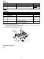
Mechanism Adjustment
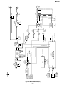
1. Optical pickup grating inspecting method
1
3
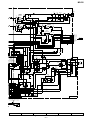
2
42 pin of IC 1101
GND (TP1131)
26 pin of IC 1101
EOUT (TP1133)
OSILLOSCOPE
470p
GND CH1
CH2
470p
25 pin of IC 1101
FOUT (TP1132)
a
100K
X
100K
b
Y
Spindle Motor
LISSAJOUS'S WAVEFORM
Less thana:b = 3:1
Figure 23-1 Optical Pickup Grating Deviation
Measuring Method
After the automatic adjustment is performed in the AUTO
mode (test mode) with the aid of high refection MD disc
("COMPLATE" is displayed), the Lissajous's waveform (x-y) is
adjusted.
1. Slightly loosen the 3 screws of spindle moto, and maken an
adjustment, observing the Lissajous's waveform.
2. After adjustment tighten the screw in arder of 1 , 2 , 3 .
Adjusting hole
3
Spindle motor
1
2. Jitter adjustment and checking method
adjusting
hole
jitter Meter
Check the Lissajou's waveform,
shifting the mounting position with
a screwdriver (to be fitted into the
disc motor adjusting hole).
2
Figure 23-2
1pin of IC 1201 (TP1274)
EFMMON
88 pin of IC 1201 (TP1275)
GND
Figure 23-3 Jitter connection diagram
After performing automatic adjustment in AUTO mode of
TEST mode using the low reflection MD disc, check this jitter
in pit continuous playback and groove continuous playback
mode.
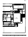
2P extension connector
QCNWK0059AFZZ
5P extension flat cable
QCNWK0109AFZZ
From Magnetic Head
CNP1252
From
motor
From mechanism switch
PWB
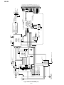
CNP1601(Bottom side)
From Optical
Pickup Unit
CNP1602
CNP1603
CNP1604(Bottom side)
CNP1101
MD Main PWB
28Pextension flat cable
QCNWK0108AFZZ
6P-2P extension connector
QCNWK0107AFZZ
Figure 23-4
– 23 –
Extension PWB for service
(RUNTK0457AFZZ)
Fit the extension PWB for service to the mechanism
MD-R2
EXPLANATION OF ERROR DISPLAY
Error display
Corrective action
Errors
Can't REC
• Defect occurred successively 10 times during REC-PLAY.
• Check that the disc is free from flaw, dust
• As a result of occurrence of defect during REC-PLAY the
and fingerprint.
recordable cluster became zero.
Check whether there is any black spot.
• Adress is unreadable. REC state connot be set for 20 seconds
Check for disc disalignment and run-out.
although retry is repeated.
Can't COPY
• The following judgement is made according to the channel
status of digital signal which was input from D-IN during RECPAUSE or REC-PLAY.
(1) Other than audio signal
(2) Other than signals of home-use appliances
(3) Copy NG due to inversion of copy bit in CD.
• Check whether CD is copy-inhibited one.
(An exabple: CD-R)
Din UNLOCK
• The digital signal which was input from D-IN during RECPAUSE, REC-PLAY or CD FUNC playback caused the
following.
(1) PLL of digital IN was unlocked.
(2) Locking occurred in condition other than FS = 44.1 kHz
• Check whether there is any abnormality
in the D-IN signal line.
TOC FULL
• There were no areas to record music or character
infomation.(music name, disc name, etc.) during REC-PLAY.
• When an attempt to start is made, recordable area does not
remain.
• Replace the disc with a recording/
playback disc in which an area to register
UTOC remains.
UTOC ERR R
• ETNO > LTNO
• FTNO ≠ 0 or 1
• UTOC recorded on disc could not be read.
• UTOC data is not normal. Replace the
disc with other disc.
UTOC ERR A
• Start address > End address
• UTOC data is not normal. Replace the
disc with other disc.
UTOC ERR L0~4
• Any data of UTOC 0 to 4 looped.
• UTOC data is not normal. Replace the
disc with other disc.
NOT AUDIO
• Nonaudio data was recorded in the track mode of currently
selected TNO.
• Select other TNO or replace the disc with
other disc.
? DISC
• Data "MINI" of system ID which has been written in TOC with
ASCII code is not correct.
• The disc type written i TOC does not correcpond to pre/
mastered MD, recording MD and hybrid MD.
• The loaded disc is not applicable.
Replace the disc, and check.
DISC FULL
• When an attempt to set REC-PAUSE was made, there were no • Replace the disc with other recording disc
recordable areas.
in which recording area remains.
PLAYBACK MD
• An attempt to set REC-PAUSE or to start editing was made on • The loaded disc is a Playback-only disc.
the playback-only disc.
Replace the disc with a recording disc.
PROTECTED
• An attempt to record or edit was made on the record/playback
disc with its careless rease preventing tab being in rease
preventing state.
• An attempt was made t oedit the track which was writeprotected by information written in UTOC.
• Return the careless erase preventing tab
to its initial position, and redo.
• The track on which an attempt to edit was
made is a write-protected track. Redo on
another track.
Can't EDIT
• Specific editing conditions were not satisfied.
• The applied operation procedure is not
proper. Redo, applying the ocrrect
procedure.
TEMP OVER
• Owing to occurrence of some trouble internal temperature of
set (MD unit) rose excessively.
• Check by troubleshooting.
• Check whether the ambient temperature
is too high.
DISC ERR RD
PA
WR
• Read data was not correct or data could not be read correctly.
• Trouble occurred during recording if music data, resulting in
record failure.
• Data of TOC or UTOC is not normal or
disc las flaw. Replace the disc with other
disc.
TOC ERR S
TOC ERR R
TOC ERR T
• TOC was read but data was not correct.
• TOC could not be rad.
• The TOC information recorded on disc
does not conform to the MD standard.
Replace the disc with other disc.
• The disc has flaw. Replace the disc with
other disc.
UTOC W ERR
• Trouble occurred during rewriting of UTOC, resulting in UTOC
rewriting failure.
• The disc has flaw. Replace the disc with
other disc.
FOCUS ERROR
• After the disc was loaded, focusing failure occurred.
• Check that the disc is free from flaw,
dust, fingerprint and black spot.
Check for disc disalignment and run-out.
– 24 –
MD-R2
Error display
Corrective action
Errors
BLANK MD
• UTOC was read but total TNO and the number of characters of • Perform recording to check that the disc
is recordable disc.
NAME was 0?
DEFECT
• Focusing error was caused by shock during REC-PLAY.
• Check that the disc is free from flaw,
dust, fingerprint and black spot. Check
for disc disalignment and run-out.
TOC W ERROR
• Although UTOC can be read but UTOC cannot be rewritten.
• Check that the record head contact is
normal. Check that there is no broken
wire between PWB and the recording
head.
MD ERROR
• Data of EEPROOM is not correct.
• Once reset, and redo. If error occurs
persistently, replace EEPROM.
EXPLANATION OF MECHANISM ERROR
Errors
Error display
MECHA_ERR1_*
MECHA_ERR2_*
MECHA_ERR3_*
Ejection failure
Head-up failure
Head-down failure
* = E Ejection completion position
* = MHorizontal midway position
* = L Load completed position
* = D Head-down position
HINF (IC1401 97 PIN)
< 1.3 V
> 3.06 V
1.853~2.48 V
1.3~1.853 V
E2-PROM (IC1402) writing procedure
1. Procedure to replace E2-PROM and to write the initial
value of microcomputer in E2-PROM
2. Temperature reference value setting procedure
(to be executed at room temperature within 21 to 29°C)
(1) Replace E2-PROM.
(2) Refer to the latest E2-PROM data list.
(3) Holding down the ENTER button and MD PLAY button,RESET
button, and start up the test mode.
(4) Indication of version.
[tsm
e
]
E2-PROM version (c to z)
Microcomputer ROM version
Model code
(5) Press the ENTER button 7 times.
[EEPROM SET]
(6) Perform the operation shown in the "E2-PROM setting mode
chart", compare the indication with the E2-PROM data list, and
make a setting according to the E2-PROM data list, using JOG
key.
(7) Set the temperature reference value.
(Refer to "Temperature reference setting procedure".)
(8) The setting must conform to the E2-PROM data list.
(9) Turn off power supply to write in E2-PROM.
(1) Test mode stop state.
e
]
[tsm
(2) Crrect temperature depending on ambient temperature according
to the following table.
Ambient temperature (°C)
Temperature correction
12.2 ~ 15.8
-3
15.9 ~ 19.6
-2
19.7 ~ 23.2
-1
23.2 ~ 26.8
0
26.9 ~ 30.7
+1
30.8 ~ 34.3
+2
34.4 ~ 37.9
+3
An example: When ambient temperature is 22°C and meadured
temperature is 73H
Temperature setting = 73 H - 01 H
= 72 H
* When the measured temperature fluctuates between
two values, take lower one (if temperature fluctuates
between 73H and 72H, take 72H).
(3) Press the ENTER button 7 times.
[EEPROM SET]
(4) Press the MD PLAY button.
[
FOCUS
]
(5) Press the ENTER button 4 times.
[
Temp
]
(6) Press once the MD PLAY button.
[TEMP
]
: Measured temperature,
: Temperature setting
(7) Set temperature to the value determined above, using the
JOG button.
(8) Press the MD STOP button.
[
Temp
]
– 25 –
MD-R2
E2-PROM Data List
Slide setting
Focus setting
Item indication
Item indication
Initial Setting
Initial Setting
FG
97
H
SLG
35
H
FF1
9E
H
SL2
27
H
H
SLDLIM
65
H
FF2
E0
FZHLEV
ED
H
SLDLEV
16
H
FOKLEVn
08
H
SLKLVk
55
H
FOKLEVf
08
H
SLKLVt
3A
H
FOKLPFn
00
H
SLKLVm
55
H
FOKLPFf
88
H
WAITf
90
H
Control setting
Item indication
Spin setting
Item indication
SPG
Initial Setting
20
SPG—in
SPG—mid
B8
76
H
H
H
SPG—out
50
H
SP1
10
H
SP2
87
H
SP3
E3
H
SP4
E3
H
SP5
10
H
SPDLIM
78
H
Tracking setting
Item indication
TG
Initial Setting
45
H
TF1
70
H
TF2
E0
H
SVCNT4
01
H
TRBLVo
53
H
TRBLVt
60
H
TRKLVo
4C
H
TRKLVt
38
H
TDPWo
89
H
TDPWt
1A
H
SLCTo
00
H
SLCTt
40
H
SLCTm
53
H
TCRSCIP
16
H
COTLVP
14
H
COTLVr
28
H
WAITm
FF
H
– 26 –
Initial Setting
CONTRL1
80
H
CONTRL2
02
H
SPKLEVm
26
H
ADJTTM
14
H
HDEQAD
90
H
LDEQAD
8F
H
GDEQAD
91
H
MDEQBC
90
H
LDEQBC
8F
H
GDEQBC
8A
H
HALSG
21
H
LALSG
21
H
GALSG
21
H
HALSOFS
FE
H
LALSOFS
00
H
GALSOFS
00
H
MD-R2
E2-PROM Setting Mode Chart
tms
e
Test mode STOP state
ENTER X7
E E P R O M _ S E T EEPROM setting menu
_ _ EJECT _ _ _
MD PLAY
EJECT state
_ _ Focus_ _ _
MD PLAY
ENTER
ENTER X2
_Spindle__
MD PLAY
FG______
ENTER
REC
ENTER
REC
ENTER
WAITf___
REC
REC
ENTER
ENTER
ENTER
ENTER
ENTER
ENTER
REC
ENTER
ENTER
REC
ENTER
ENTER
REC
ENTER
REC
REC
REC
REC
ENTER
REC
ADJTTM__
ENTER
REC
HDEQAD__
ENTER
REC
LDEQAD__
REC
ENTER
REC
GDEQAD__
ENTER
ENTER
REC
REC
REC
REC
REC
HALSEG__
REC
ENTER
REC
LALSEG__
ENTER
REC
REC
GALSG___
REC
ENTER
REC
HALSOFS_
ENTER
REC
REC
LALSOFS_
COTLVr__
ENTER
REC
GDEQBC__
COTLVp__
ENTER
REC
LDEQBC__
SLCTm___
ENTER
ENTER
ENTER
REC
SLCTt___
ENTER
CONTRL1_
ENTER
SLCTo___
ENTER
MD PLAY
_
HDEQBC__
TDPWt___
ENTER
_C o n t r o l _ _
SPKLEVm_
SLKLVm__
TDPWo___
REC
REC
SLKLVt__
REC
NAME/
TOC EDIT
ENTER
SLKLVk__
REC
ENTER X5
CONTRL2_
SLDLEV__
TRKLVt__
SP5_____
SPDLIM__
REC
TRKLVo__
SP4_____
ENTER
ENTER
ENTER
SLDLIM__
TRBLVt__
SP3_____
REC
REC
TRBLVo__
REC
REC
FOKLPFf_
ENTER
REC
SP1_____
REC
ENTER
T E M P_
SL2_____
SVCNY4__
SP2_____
FOKLPFn_
ENTER
REC
REC
FOKLEVf_
REC
TF2_____
SPG_out_
REC
FOKLEVn_
ENTER
REC
REC
ENTER
_ _ _ Temp _ _ _
MD PLAY
SLG_____
TF1_____
SPG_mid _
FZCLEV__
ENTER
REC
SPG_in__
FF2_____
ENTER
ENTER
___S l e d___
MD PLAY
TG _ _ _ _ _ _
SPG_____
FF1_____
_T r a c k i n g _
MD PLAY
DELETE/
CLEAR
EDIT
ENTER X4
ENTER X3
REC
ENTER
WAITm___
GALSOFS_
Figure 27
– 27 –
REC
Figure 28 BLOCK DIAGRAM (1/2)
– 28 –
M
M903
LOADING MOTOR
HEAD UP/DOWN
M
M902
SLED MOTOR
M
DIRECT SWITCH
SW1952
LEAD INSWITCH
SW1953
PLAYSWITCH
SW1954
RECSWITCH
SW1955
LOADING SWITCH
SW1956
WRITE PRO
LIGHT
RECEIVING
SECTION
RF
LIGHT
RECEIVING
SECTION
ERROR
SIGNAL
MD
Q1251~Q1254
D4.3V
IC1601
M56758FP
5-CH
MOTOR
DRIVER
MONITOR DIODE
LASER DIODE
IC1101
IR3R55
RF
SIGNAL
PROCESSOR
D3.2V
D6.5/4.75 ~ 5.25V
D4.3V
TRACKING
F
E–FSIGNAL A–BSIGNAL
A
B
E
RF1
RF1 ~ RF4SIGNAL
RF2
RF3
RF4
FOCUS
PICK UP UNIT
M901
SPINDLE MOTOR
RECORDING HEAD
HEAD DRIVE
SIGNAL
IC1251
D3.2V
D3.2V
D3.2V
DIGITAL
3.2V
4M
DRAM
IC1202
IX2474AF
ENDEC
ATRAC
IC1201
LR376481
OSCILLATOR
XL1201
(33.8688MHz)
D4.3V
VOLTAGE
REGULATOR
POWER
IC1402
S29294A
E2PROM
D3.2V
MECHAN1SM
6.5/4.75~5.25V
BACKUP
IC1916
AND GATE
74VHC08F
IC1401
IX0232AW
MD SYSTEM
MICRO
COMPUTER
MD MICRO COMPUTER
IC1906
AND GATE TC7ST08F
IC1907
CLOCK GENERATOR TC9246F
IC1990
INVERTOR 74AC04FS
3
4
1
2
CN1904
GND
DIGIN(EIAJ)
1
2
3
4
5
6
7
8
9
10
11
12
13
14
15
16
17
18
19
20
21
22
23
24
CNP1902
DIGOUT(EIAJ)
GND
DFS1
DFS0
MUTE
KDATA
MDDATA
DSTB
D.GND
D.GND
D.GND
D.GND
DVDD
DVDD
SYSCLK
ADDATA
LRCLK
BCLK
DADATA
PDOWN
BACKUP
LOAD IN
RESET
MD-ST
DSCK
SERCH
MD-R2
– 29 –
UN970
REMOTE
SENSOR
KEY IN
BLOCK
JOG
SWITCH
SW901
RX302
DIGITAL IN
(OPTICAL JACK)
TX302
DIGITAL OUT
(OPTICAL JACK)
J301
1
DIGITAL -IN
(COAXIAL JACK)
INVERTER
IC301
74HCU04
6
KEY
JOG
+7V
10
13
8
45 ~ 90 92 ~ 97
DIG
SEG
21 ~ 42 60 ~ 89
FL901
2
IC302
NAND GATE
74HC10AP
-7V
12 16 ~ 19
FL DISPLAY +B
DIGIN VCC
DIGITAL OUT
MD UNIT
DIGITAL IN
17 ~ 21
24
26
10
2
13 ~ 15
IC201
UDA1340
AD/DA
CONVERTER
IC901
IX0237AW
SYSTEM
MICROCOMPUTER
3
5
SYSCLK
AD DATA
LRCLK
1
7
BLCK
DA DATA
4
DATA
8
32 RX-IN
3
2
6
3
5
MODE
CLK
REC VOL
VR901
3
5
10
S-ID,SYN,RESET,DSTB,DSCK
IC101
NJM4560D
OPE AMP
+7V
8
33
3V
-7V
4
IC601
LINE AMP.
NJM4580D
K-DATA,MD DATA
MD
Figure 29 BLOCK DIAGRAM (2/2)
MUTE
LINE IN
J101
1
2
Q601
Q602
MD 5V
MD+
91
100
96
BACK UP 5V
Q504
Q506
Q502
Q503
BACK UP +5V
A/D +5V
FL VP(-31V)
IC501
REGULATOR
S81233YK
DIGITAL 5V
3
1
7
5V SYSTEM
POWER
CIRCUIT
MD+
POWER
CIRCUIT
A-7V
POWER
CIRCUIT
A+7V
POWER
CIRCUIT
+7V
8
FL VP(-32V)
FL
POWER
CIRCUIT
RECTIFYING
CIRCUIT
5
3
-7V
4
F552
1A
F551
1A
7
1
MUTE
T551
POWER TRANSFORMER
H.P.VOL
VR981
FL DISPLAY +B
IC651
NJM4560D
OPE AMP
Q451
Q452
AC 120V
60Hz
HEADPHINES
J981
J101
LINE OUT
MD-R2
MD-R2
DIGITAL RECORD SIGNAL
DIGITAL PLAYBACK SIGNAL
A
ANALOG PLAYBACK SIGNAL
ANALOG RECORD SIGNAL
R607
1K
(0.6V)
R601
470
C601
47/10
C107
1/50
R103
1K
R109
1K
(1/2)
C109
220P
C105
220P
+7V
R113
1K
L-CH
R60
1K
L-CH
7
6 –
R115
100
C117
100/10
R111
1.5K
R605
22K
8
R107
100K
B
C115
47/10
5 +
R105
47K
C60
220
C603
220P
IC101
NJM4560D
OPE AMP.
R608
1K
(0.8V)
C113
47P
R602
470
C602
47/10
C604
220P
J101
ANALOG
LINE IN2
L101
0.22µH
R-CH
C102
0.022
R104
1K
C108
1/50
R106
47K
R108
100K
IC101
NJM4560D
R110
1K
3 +
C110
220P
C120
0.01
C106
220P
R61
1K
R-CH
4
2 –
–7V
R114
1K
R112
1.5K
C116
47/10
1
(2/2)
C60
220P
R606
22K
R116
100
C118
100/10
C114
47P
C
C119
0.022
C202
L201 47/10
10µH
R418
1K
R203
1M
C206
1/50
VINL
VSSA
VDDA
VINR
VREFA
VADCP
VADCN
VSSD
TEST1
VDDD
C2
4.7
C212
OS 3.3/16
9 8 7 6 5 4 3 2 1
OVERFL
L3CLK
SYSCLK
L3MODE
14 13 12 11 10
R417
1K
R202
680K
C201
100/10
D
C203
47/10
VREFD
VOUTL
VSSO
VDDO
VOUTR
AVSS
AVDD
TEST2
TEST3
DATA0
DATAi
BCK
L3DATA
WS
IC201
UDA1340
AD/DA CONVERTER
15 16 17 18 19 20 21 22 23 24 25 26 27 28
E
IC301
74HCU04
INVERTER
R302
330
14 13 12 11 10 9
R301
82
C302
0.022
R411 4.7K
GND
1
2
3
4
5
6
7
C314
0.022
C310
0.022
R305
56K
R304
2.7K
3
2
1
9 10 11 12 13 14
R313
47K
C312
0.022
R312
82K
L302
10µH
R553 68K
+B
C304
0.022
C519
0.022
C531
0.1
R554
68K
MD +7.5V/+5V
R308
22
L301
10µH
3 2 1
C305
0.022
R310
3.3K
C311
0.022
C675
0.001
TX302
C524
1000/6.3
MD SYN
MD LOAD
MD S-ID
MD RESET
MD DSCK
DFS
DAC DATA
DAC MODE
DAC CLK
D-1,2
31V FL VP
1 2 3 4 5 6 7 8 9 10 11 12 13 14 15 16 17 18 19
SERCH
DSCK
MD-ST
RESET
LOAD SW
BUCKUP
PDOWN
KDATA
MDDATA
ADDATA
9 8 7 6 5 4 3 2 1
SYSCLK
D 7.5/5V
D 7.5/5V
D GND
D GND
D GND
D GND
DSTB
D OUT
24 23 22 21 20 19 18 17 16 15 14 13 12 11 10
MUTE
DFS0
DFS1
DADATA
BLCK
LRCLK
CNP471
3 2 1
4
D IN
CNP301
GND
DIGITAL IN-1
DIGITAL OUT
(OPTICAL JACK)
GND
RX302
R409
220K
R552 39K
R309
10K
G
R404 560
R405 330
VDD
8
R307
22K
3 2 1
R401 560
R402 560
R403 560
C470
100P
R410 220K
4
5
GND
R406 220K
6
7
IC302
74HC10AP6
NAND GATE
R407 220K
F
R408 220K
C313
0.022
C303
0.022
R303
220K
MD DATA
P MUTE
P-CNT
MD P-OUT
P-IN
MD DSTB
MD 7.5/5V
MD K-DATA
D301
MTZJ5.1B
C315
0.01
R414 8.2K
R415 8.2K
R416 8.2K
8
VDD
R413 4.7K
J301
COAXIAL
DIGITAL IN2
R412 4.7K
C301
0.01
CN1904
P35 12 - C
TO MD MAIN PWB
CNS471
H
CNS472
CN1902
CNP902
P35 12 - F
TO MD MAIN PWB
P32 1 - D
TO DISPLAY PWB
NOTES ON SCHEMATIC DIAGRAM can be found on page 43.
1
2
3
4
Figure 30 SCHEMATIC DIAGRAM (1/6)
– 30 –
5
6
MD-R2
C451
47/10
IC601
NJM4580D
LINE AMP.
R601
470
R609
1K
R608
1K
R602
470
C604
220P
R613
100
C615
100/10
C611
47P
(2/2)
7
R653
1K
R614
100
C651
150P
R651
100K
C652
150P
R652
100K
IC651
NJM4560D
OPE AMP.
5 +
(1/2)
C653
27P
C655
10/16
R616
47K
–7V
R681
1K
C454
470P
R452 R458
330 10K
C460
470P
Q452
2SC2878 B
C452
47/10
MUSE
R620
10K
Q602
2SC2878 B
R-CH
4
R612
1.5K
R610
1K
R619
10K
C614
47/10
6 –
R454
33K
C456
820P
R618
330
5 +
C608
220P
R606
22K
Q601
2SC2878 B
+7V
IC601
NJM4580D
LINE AMP.
C461
0.01
R-CH
L-CH
1
8
R611
1.5K
C453
470P
L-CH
C459
470P
L MUTE
C613
47/10
(1/2)
2 –
R605
22K
R457
10K
R615
47K
3 +
C607
220P
C603
220P
R455
100
C457
0.022
R456
100
R659
10
7
C657
220/10
6 –
R661
47K
C616
100/10
C612
47P
IC651
NJM4560D
C656
10/16
C658
220/10
2 –
C654
27P
(2/2)
3 +
R654
1K
+7V
C665
100/10
R660
10
1
4
R662
47K
8
R682
1K
CNP473
R607
1K
J101
ANALOG
LINE OUT
Q451
2SC2878 B
R453
33K
C455
820P
R617
330
R451
330
–7V
R668
82
R667
82
C666
100/10
SW501
RESET
C202
L201 47/10
10µH
R418
1K
R203
1M
C205
4.7/25
D651
MTZJ9.1B
L202
10µH
C212
OS 3.3/16
VINL
VDDA
VINR
VSSA
R506
100
R501
8.2
POSISTOR
C208
3.3/16
OS
POWER
TRANSFORMER
T551
C501
1000/25
D551
RL104A
D504
MTZJ9.1B
C512
1/50
C209
4.7/25
R508
100
C511
47/25
2
IC501
IS81233SGYX
REGULATOR
C222
0.022
R510
100
D512
1SS133
+B
1
3
D505
MTZJ6.8A
C514
10/16
C515
10/16
C516
10/16
Q504
2SD2012 Y
D513
1SS133
F551
1A
D554
RL104A
AC POWER
SUPPLY CODE
AC 120V,60Hz
C521
4700/25
C502
4700/25
D552
RL104A
R507
680
Q503
2SD468 C
C220
1000P
GND
C551
0.01
D503
MTZJ9.1B
C530
0.022
+B
(–)
R505
680
C509
47/25
C510
1/50
VREFD
VOUTL
VSSO
VDDO
TEST2
VOUTR
AVSS
AVDD
TEST3
DATA0
R669
2.7K
C221
0.022
Q502
2SB562 C
18 19 20 21 22 23 24 25 26 27 28
D555
RL104A
R502
8.2
POSISTOR
R551
8.2
POSISTOR
C513
47/25
R509
820
C552
0.01
F552
1A
D553
RL104A
T.F
C561
0.01
R517
220
(FIN)
+B
+B
+B
R518
220
D501
MTZJ6.8B
C522
1000/6.3
FL VP
C507
33/50
LOGIC+5V
Q501
KTA1266 GR
R504
33K
R503
1.8K
C504
220/50
C505
10/50
D502
MTZJ33B
D506
MTZJ7.5B
Q505
KRC102 M
C518
100/10
C519
0.022
D507
MTZJ5.6C
Q506
2SD2012 Y
C517
100/10
R512
470
R511
0.8
POSISTOR
GND
(FIN)
FL FIL
+B
+B
FL FIL
C525
100/10
C520
0.001
D510
1SS133
R516
220K
D509
1SS133
R514
100K
D508
MTZJ270D
MAIN PWB-A
CNP472
MD DSCK
DFS
DAC DATA
DAC MODE
DAC CLK
D-1,2
-31V FL VP
U-CON GND
BACK UP 5V
AD5V
FIL 1
FIL 2
7 8 9 10 11 12 13 14 15 16 17 18 19 20 21 22 23 24
P-CNT
MD P-OUT
P-IN
MD DSTB
MD 7.5/5V
MD K-DATA
P32 1 - B
CNS903
TO DISPLAY PWB
R670
330
C207
100/10
IC201
UDA1340
/DA CONVERTER
DATAi
HP_AMP_GND
HP_AMP_L_OUT
HP_AMP_R_OUT
RESET SW
NC
C667
0.1
Q653
KRC102 M
C223
0.022
C206
1/50
VREFA
TEST1
VADCP
VADCN
VSSD
VDDD
R417
1K
9 8 7 6 5 4 3 2 1
OVERFL
11 10
AUX_AMP_R_IN
AUX_AMP_L_GND
AUX_AMP_L_IN
AUX_AMP_R_GND
AUX_VR_L_OUT
GND
AUX_VR_R_OUT
C203
47/10
R202
680K
C201
100/10
1
2
3
4
5
6
7
8
9
10
11
12
CNP902
P32 1 - D
TO DISPLAY PWB
7
8
9
10
Figure 31 SCHEMATIC DIAGRAM (2/6)
– 31 –
11
12
MD-R2
A
HEADPHONES PWB-B3
CNS903
B
CNP473
P31 12 - C
AUX_VR_L_OUT
GND OPEN
AUX_VR_R_OUT
HP_AMP_GND
HP_AMP_L_OUT
HP_AMP_R_OUT
RESET SW
10
NC
12
11
C981
0.001
VR901-2
5K(B)
VR981-1
1K(C)
VR981-2
1K(C)
Headphone
Volume
J981
HEADPHONES
R
L
VR901-1
5K(B)
AUX
Volume
1
2
3
4
5
6
7
8
9
3
2
1
CNS901
C983
0.1
C982
0.001
TO MAIN
PWB
AUX_AMP_R_IN
AUX_AMP_L_GND
AUX_AMP_L_IN
AUX_AMP_R_GND
3
2
1
CNP904
L901
22µH
D
21
20
R968
10K
19
18
R969
10K
17
16
DAC DATA
DFS
MD DSCK
MD K-DATA
15
MD 7.5/5V
MD DSTB
P-IN
MD P-OUT
P-CNT
P MUTE
MD DATA
11
MD RESET
MD S-ID
MD LOAD
MD SYN
C908
1
SW955
M-EJECT
C920
10/16
14
13
1 2 3
CNS902
12
1 2 3
CNP903
SW956
ENTER
R954
1K
SW957
NAME
R955
1.2K
SW958
TIMER
R956
1.5K
SW959
DISP
R957
1.8K
SW960
REVIEW
R958
2.7K
SW961
AUX
R959
3.9K
SW962
PROGRAM
R960
33K
10
SW950
POWER
9
8
7
6
5
4
3
2
1
SW951
M-PLAY
R950
1K
CNP472
P30 6 - H
BACK-UP5V
µ-COM GND
–31V
D-1.2
DAC CLK
DAC MODE
24
22
SW952
M-STOP
R951
1.2K
TO MAIN PWB
23
C909
1
C
FILMNT 2
FILMNT 1
AD5V
CNP902
SWITCH PWB-B2
SW953
M-REC
R952
1.5K
SW954
CUE
R953
1.8K
E
A/D 5V
DSTB
R920
470K
R921
10K
R923
10K
Q901
2SC2412 KR
R922
10K
Q902
2SC2412 KR
MD DATA
R972
470K
R924
10K
F
R926
1K
ANALOG RECORD SIGNAL
R970
1K
UN970
REMOCON
R971
100
G
1
C971
10/16
2
3
C970
100P
DISPLAY PWB-B1
H
NOTES ON SCHEMATIC DIAGRAM can be found on page 43.
1
2
3
4
Figure 32 SCHEMATIC DIAGRAM (3/6)
– 32 –
5
6
R9
12
R9
6.8
B
MD-R2
C914
0.001
C915
0.001
IC
USEG31
USEG32
USEG33
USEG34
USEG35
USEG36
UDIG16
UDIG15
UDIG14
UDIG13
UDIG12
UDIG11
UDIG10
UDIG09
UDIG08
UDIG07
UDIG06
UDIG05
UDIG04
UDIG03
UDIG02
UDIG01
FILMNT1
FILMNT1
FILMNT1
FL901
FILMNT2
FILMNT2
FILMNT2
C916
0.001
C917
0.001
FILMNT1
FILMNT1
FILMNT1
USEG30
USEG29
USEG28
USEG27
USEG26
USEG01
USEG02
USEG03
USEG04
USEG05
USEG06
USEG07
USEG08
USEG09
USEG10
USEG11
USEG12
USEG13
USEG14
USEG15
USEG16
USEG17
USEG18
USEG19
USEG20
USEG21
USEG22
USEG23
USEG24
USEG25
FILMNT2
FILMNT2
FILMNT2
94 93 92 91 90 89 88 87 86 85 84 83 82 81 80 79 78 77 76 75 74 73 72 71 70 69 68 67 66 65 64 63 62 61 60 59 58 57 56 55 54 53 52 51 50 49 48
1 2 3 4 5 6 7 8 9 10 11 12 13 14 15 16 17 18 19 20 21 22 23 24 25 26 27 28 29 30 31 32 33 34 35 36 37 38 39 40 41 42 43 44 45 46 47
R931
47K
R932
47K
R940
47K
R935
47K
–31V
R934
47K
C910
0.1
R936
47K
C901
0.1
R933
47K
R937
47K
R938
47K
R945
47K
5V
R939
47K
R941
47K
R942
47K
R944
47K
R943
47K
C902
0.1
C903
0.1
R930
47K
5V
VREF
AVSS
RA902
1K
SW955
M-EJECT
SW956
ENTER
R954
1K
SW957
NAME
R955
1.2K
SW958
TIMER
R956
1.5K
C923
0.01
RA903
1K
C922
0.01
RA904
1K
Q903
DTC144 ES
RA908
1K
SW961
AUX
RA912
1K
R905
12K
B
A
R959
3.9K
RA913
RA914
1K
1K
RA916
1K
RA918
RA927
1K
1K
RA919
1K
SW901
SW962
PROGRAM
KEY 1
KEY 2
KEY 3
KEY 4
INI/MUTE IN
JOG AD
10
DIG SEL 1
DIG SEL 2
12
R904
6.8K
R958
2.7K
SW960
REVIEW
1
2
3
4
5
6
7
8
9
11
R903
12K
R957
1.8K
SW959
DISP
99 98 97 96 95 94 93 92 91 90 89 88 87 86 85 84 83 82 81
JOG SW
R960
33K
VEE
USEG24
USEG23
USEG22
USEG21
USEG20
USEG19
Vcc
USEG18
USEG17
USEG16
USEG15
USEG14
USEG13
USEG12
USEG11
USEG10
USEG09
100
R969
10K
13
14
15
16
DAC MODE
DAC CLK/EX
DAC DATA/EX
IC901
IX0237AW
SYSTEM
MICROCOMPUTER
17
18
19
20
21
22
23
DFSO/DFS1
(MD) DSTB
(MD) DSCK
(MD) K-DATA
(MD) MD DATA
(MD) LO/EJ
24
25
26
27
Q901
2SC2412 KR
2
RESET 1
8
X902
32.768kHz
1K
1K
1K
1K
RA934
RA935
RA936
RA937
R910
4.7M
(10W)
R909
1.8K
1K
RA933
1K
1K
1K
C904
68P
(CH)
C905
12P
(CH)
3
C907
1
RA931
R906
220K
IC902
PST9127
RA928
RA930
31 32 33 34 35 36 37 38 39 40 41 42 43 44 45 46 47 48 49 50
Q902
2SC2412 KR
7
P-IN
P-CNT
XCOUT
XIN
XOUT
VSS
(MD) SYN
30
RESET
XCIN
29
RA926
1K
(MD) LOAD
(MD) S-ID
MD RESET
UDIG00
UDIG01
UDIG02
UDIG03
UDIG04
UDIG05
28
P OUT
RX-IN
P MUTE
RA925
1K
USEG08 80
USEG07 79
USEG06 78
USEG05 77
USEG04 76
USEG03 75
USEG02 74
USEG01 73
USEG00 72
USEG25 71
USEG26 70
USEG27 69
USEG28 68
USEG29 67
USEG30 66
USEG31 65
USEG32 64
USEG33 63
USEG34 62
USEG35 61
UDIG15 60
UDIG14 59
UDIG13 58
UDIG12 57
UDIG11 56
UDIG10 55
UDIG09 54
UDIG08 53
UDIG07 52
UDIG06 51
X901
8MHz
R911
1M
C906
0.1
9
10
Figure 33 SCHEMATIC DIAGRAM (4/6)
– 33 –
11
12
MD-R2
1
SYRS
SYRD
SYWR
SYD7
A
AOUT
BIN
BOUT
EIN
EOUT
LOGIC
21
22
23
24
LATCH
25
TP1134 R1152
22K
TP1133 R1151
22K
TP1132 R1150
22K
11
C1211
1
12
13
14
15
16
TP1220
FODRF
FODRR
TRDRF
TRDRR
SLDRF
SLDRR
SPDRF
SPDRR
R1653
100K
R1651
R1657
R1655
R1661
R1659
R1665
17
100K
120K
120K
82K
82K
62K
18
19
20
21
22
23
24
25
R1663
62K
SYRS
X176KO
FODRF
FODRR
TRDRF
TRDRR
SLDRF
SLDRR
SPDRF
SPDRR
2
26 27 28
C1210
20
DVCC
19
DATA
18
26
10
WBO-I
DATA
17
LATCH
16
TP1135 R1153
22K
FOUT
CLOCK
15
CLOCK
14
DTEMP
13
DGND
FIN
TP1136 R1154
22K
28
27
TCG
BOUT-IN
FOUT-IN
100
RAA3
29
TCG
BOUT-IN
FOUT-IN
99 98
EFMMON
AVCC
EFMI
AGND
AIN
EIN
TCG
BIN
FIN
VBAT
WBI
VDD1
DGND
TEST0
TEST1
TEST2
11
10
TP1129
TP1130
A3
A2
A1
A0
RF2-1
ADAGI
ADAGC
C1109
1
EFMO
AVCC
EFMI
AIN
C1105
10
C
R1102 TP1137
560
1
2
3
4
5
6
7
8
9
C1202
1
AOUT-IN
EOUT-IN
WBO-I
30
TCGO
EFMO-I
EFMO-I
AOUT-IN
EOUT-IN
5
31
HPF
TCGI
RF2
RF1
FIN
EIN
RF3
RF4
AIN
BIN
12
4
32
22KI
LPF
DTEMP
11
TP1274
TP1138
SGAIN
10
ADIPO
C1119
330P
TP1140
R1155
56K
TP1139
33
22KO
ADIP
AGC
BIAS
DISC
9
ADIPI
WBO
RFADD
STBY
R1105
390K
100
36
ADLPFO
IC1101
IR3R55
SIGNAL
PROSESSOR
REFO
TP1275
TP1142
37
DIFF
REFI
AVCC
8
38
34
BIAS
C1104
0.027
7
39
35
C1103
1
6
40
DIFF
4
5
41
AGND
RF3
42
C1106
0.47
&
SW
3
C1102
1
43
EFMAGC
TP1131
C1107
0.0047
C1116
C1115270P(CH)
C1114 270P(CH)
C1113 270P(CH)
C1112 270P(CH)
270P(CH)
2
RF4
44
EFM
AGC
R
RF1
B
45
EFMAGI
AGND
1
C1110
0.47
46
ATTR
RF2
47
GOUT
48
C1117
0.0033
POUT
C1118
0.033
TP1141
TP1150
L1101
10µH
L1102
0.47µH
C1121
1
R/P
R/P
R1166
1.2K
C1145
0.033
R1100
27
FN
TP
FP
TN
TP1109
TP1108
TP1107
TP1106
TP1105
TP1104
TP1103
TP1102
TP1101
9 8 7 6 5 4 3 2 1
10
15
16
20
21
24
25
R1407
3.3K
LD+
LD–
R1611
12K
26
27
28
CIN
29
INNSW
2
+
M901
MD SPINDLE
M903
MD LOADING
M
M
1
1
2
CN1602
SLD+
SLD–
TP1607
TP1606
CN1603
SP+
SP–
TP1608
TP1609
–
2
1
2
+
1
2
1
2
–
FODRR
FODRF
30
19 SS.GND
VREF
20
VREFO
C1424
0.022
DATA
LATCH
CLOCK
R/P
VM3+
C1657
0.0056
SPN
SPP
VM4+
VM4–
29
VM5+
28
OUT5 27 VM5–
IN5–
26
SLP
SLN
IN4–
OUT4
Q1402
RNC1404
3
2
2
3
Q1403
RN2404
2
3
1
Q1401
RN2404
1
Q1404
RNC1404
R1667
22K R1666
22K
R1669
6.8K
3
4
Figure 34 SCHEMATIC DIAGRAM (5/6)
– 34 –
R1416
10K
IC140
S29294
5
6
7
8
DI
S
DATA CS
GND VC
PRTCT
E2-PRO
TP1612
L1601
1µH
C1661
100/10
NOTES ON SCHEMATIC DIAGRAM can be found on page 43.
2
R1424
10K
R1422
10K
EMPH
ADMUT
3
SLDRF
23
22
1
2
1
SLDRR
IN5+ 25
IN4+ 24
IC1601
M56758FP
5ch MOTOR DRIVER
STID
C1602
1
H
1
TP1455
TP1456
TP1457
R1430
10K
TP1404
TP1458
AVCC
VREF
HINF
GND
TESTK2
TESTK1
MINF
DTEMP
AVCK1
AVCK2
AVCK3
TEST0
TEST1
TEST2
DOUTMT
MUTE
DAMUT
49 50
SPDRF
32
31
18 MUTE2
SPDRR
R1664
10K
VM3–
33
13
IN2+
17 MUTE1
C1631
1
36
34
VM1+
12
21
TP1610
CN1604
TRY+
TRY–
37 IN3+
35
16
R1650
10K
R1662
10K
R/P
R1652
10K
38
OUT1
VM2–
14
OUT2
IN2–
15
32
39
Vm2
GND
VM2+
E
31 32 33 34 35 36 37 38 39 40 41 42 43 44 45 46 47 48 49
J1405
10K
R1412
100K
1
–
C1651
820P(J)
M
TP1611
C1609
1
SPN
SPP
SLP
SLN
M902
MD SLED
C1650
820P(J)
+
C1656
0.0056
OUT3
41
IN3–
40
VBS2
R1658 15K
C1655 0.015
R1660 15K
LD+
LD–
11
FP F+
FN F–
+
–
1.25V
30
VREF
10
IN1+
VBS1
42
C1654
0.015
15
REGB
CH3IN
VREF
TN T– C1652
TP T+ 820P(J)
REG+
R1668
6.8K
G
C1601
1
1
2
3
4
Vm1
5
IN1–
6
7
VM1–
8
9
GND
16
TRDRF
TRDRR
R1654
6.8K
MD SWITCH PWB-G
C1653
820P(J)
R1656
6.8K
LOADING
SW1956
R1409
1K
R1612
56K
MD RECORD
SW1955
L
SYRS
SYRD
SYWR
SYD7
SYD6
SYD5
SYD4
C1610
10
R1609
1.5K
R1617
47K
R1614
18K
R1414 PRO
10K EEPD
R1904
820
R1613
27K
DINT
DSENSE
ST-ID
SERCH
MDRSW
FSW
VARI-P SW
P-DOWN
HDON
LD+
LD–
31
CIN
INNER
SYSD5
SYSD4
19
23
R1610
30K
C1604
56P(CH)
L3
S2
S1
SYRS
SYRD
SYWR
SYSD7
SYSD6
18
SERCH
C1605
100/10
D
A
17
DINT
DSENSE
C1412
680P
VSS
MCCK
VCC
FOK
C1401
0.047
14
22
Q1601
2SA1314C
IC1401
IX0232AW
MD SYSTEM
MICROCOMPUTER
13
LOADIN
TP1616
82 81
LOAD IN
ERROR
BYTE
CNVSS
STID OUT
SEACH OUT
RESET
C1407
0.022
C1422
0.022
LDVAR
ADJS
DATA
LATCH
LOADING
MINF
TP1602
TP1601
12
MCCK
R1415
1K
R1425
2.7K
C1403
680P
LEAD IN
HINF
LOADING
11
RESET
R1423
10K
99 98 97 96 95 94 93 92 91 90 89 88 87 86 85 84 83 82
CLOCK
DSTB
MDDATA
KDATA
DSCK
4M/16M
R/P
FOK
R1420
1K
VREF3.2V
R1429
10K
R1428
1K
MINF
HINF
LDVAR
R1406
3.3K
C1423
0.022
GND
1
2
3
4
5
6
7
8
9
DSTB
MDDATA
KDATA
DSCK
CNS1901
MD PLAY BACK
SW1954
1 2 3 4 5 6 7
TP1605
TP1604
C1421
0.022
R1472
47K
HDON
R1903
820
READ IN
SW1953
Q1254
D 2SK1473
G
CNP1601
LEAD IN
HINF
GND
LOADING
MINF
1
2
3
4
5
9 8
R1413
3.3K
R1901
470
SW1952
14 13 12 11 10
R1408
100K
LEAD IN
1
HINF
2
GND
3
LOADING
4
MINF
5
R1902
1.8K
DIRECT
F
D
G
Q1252
2SK2909
D1252
SB0209CP
S
S Q1253
2SK1473
CW1901
WRITE
PRO
S
HDON
PICKUP UNIT
D
IC1251
74ACT02F TP1255
HEAD DRIVER
G
D
S
R1427
4.7K
Q1251
2SK2909
G
VCC
L.DVAR
TP1405
R1404
1K
C1402
0.047
100
EFMO TP1260
C1254
10
C1255
4.7
LVV
MAGNETIC
HEAD
8
7
6
5
R1223
680
C1251
0.027
D1251
SB0209CP
L.DON
C1252
120P
(CH)
R1251
10
CNP1252
TP1251
VCC
GND
APC
R1426
1K
L1251
47uH
TP1252
EXT.C
1
2
CNS1252
LDOUT
R1401
1K
MINF
HINF
I/V
I/V
I/V
I/V
E
1
2
1
2
3
4
DTEMP
3
2 12
9 8 7 6 5 4 3 2 1
T.COOL
28 27 26 25 24 23 22 21 20 19 18 17 16 15 14 13 12 11 10
LDVAR
LDON
TP1116
TP1115
TP1114
TP1113
TP1112
TP1111
TP1119
TP1118
TP1120
28 27 26 25 24 23 22 21 20 19 18 17 16 15 14 13 12 11 10
F.COOL
CNP1101
FLEXBLE
PWB
SW
+2.8V
B
LVVOUT
APCOUT
LDVCC
DGNG
DGND
LDON
LDVAR
A
COM
RF1
F
E
RF3
RF4
VCC
AGND
MP/R
RF2
APCIN
DGND
LVVIN
FT+
F+
T-
D
TP1123
TP1128
TP1127
TP1126
C1101 R1107
1
1
5
6
MD-R2
6
R1211
220
18
19
20
21
22
23
24
25
R1663
62K
TP1218
TP1217
XRST
SYD7
SYD6
SYD5
SYD4
SYD3
SYD2
SYD1
SYD0
RSTX
DGND
VDD1
DINTX
MCCK
COUT
SENSE
FOK
SFSY
SBSY
SBO
X176KO
FODRF
FODRR
TRDRF
TRDRR
SLDRF
SLDRR
SPDRF
SPDRR
SBCK
TEMON
TOTMON
48 49 50
26 27 28
TP1212
TP1213
23 22
66
65
64
C1203
1
63
62
R1202
1M
R1201
150
XL1201
33.8688MHz
C1204
12P(CH)
C1205
12P
(CH)
61
60
59
58
57
56
TP1273
55
53
TP1214
8
R1969
C1958 56
0.047
CLOCK GENERATOR
C1954
15P
(CH) R1963
1.5K
R1221
220
1
2
3
4
5
6
7
8
R1962
220K
C1953
0.47
A9
A3
A2
A1
A0
12
13
A9
A4
A5
A6
A7
A8
VDD 16
REF
LOCK 15
PD
S2 14
VDDA
S1 13
AMPI
M2 12
AMPO
M1 11
VSSA
CKO 10
XI
NC
VSS 9
C1957
100/6.3
14
Vcc
TP1902
TP1904
R1974
220
1
2
3
4
CNP1904
DIGOUT
GND
GND
DIGIN
CNW903
1
2
3
4
1
2
3
4
TO MAIN PWB
CNP301
P30 3 - H
CNS1904
R1973
6.8K
C1927
0.047
R1968
220
IC1907
TC9246F
OE
CAS
I/O3
I/O4
GND
11 12 13 14 15
16 17 18 19 20
A4
A5
A6
A7
A8
L1203
4.7µH
C1992
0.1
Vcc
1
2
3
4
5
6
7 GND
14
13
12
D1990
1SS372
11
10
9
8
C1991
10
C1990
1
IC1990
74AC04FS
INVERTER
L1201
0.47µH
A4
A5
A6
A7
A8
IC1202
IX2474AF
4M BIT-D-RAM
A9
RAS
WE
I/O2
I/O1
5 4 3 2 1
VCC
A3
A2
A1
A0
9 8 7 6
10
11
51
R1927
22 DOUTO TP1901
GND 7
6
5
4
3
2
1
8
9
C1951
0.047
52
C1952
0.01
10
AND GATE
IC1916
74VHC08F
TP1911
Vcc 5
1
2
3 GND
4
TP1279
54
TP1215
C1206
1
AND GATE
IC1906
TC7ST08F
R1961
100
C1210
1
A3
A2
A1
A0
67
R1254
220
R1967
47
26 27 28 29 30 31 32 33 34 35 36 37 38 39 40 41 42 43 44 45 46 47 48 49 50
11
10
C1207
1
69
68
(CH)
17
100K
120K
120K
82K
82K
62K
71
70
C1913
22P
16
R1653
100K
R1651
R1657
R1655
R1661
R1659
R1665
RC120
220
72
R1964
6.8K
15
IC1201
LR376481
ENDEC
73
C1964
0.001
14
DADATA
ADDATA
DFCK
BCLK
LRCK
74
TP1278
13
18
19
21
20
17
75
C1955
0.047
C1956
47/6.3
12
9
TP1216
FEMON
DADATA
ADDATA
DFCK
BCLK
LRCK
DGND
VDD3
DOUT
DIN
XO
XI
DGND
VDD1
VPD
VXI
CDBCLK
CDLRCK
CDDATA
TEST4
TEST3
TESO1
EXPORT1
EXPORT0
X700KO
R1281
47
11
C1211
1
13 14
ACRCER
PLCK
EFMO
10
78 77 76
99 98
100
SYRS
SYRDX
SYWRX
C1202
1
EFMMON
AVCC
EFMI
AGND
AIN
EIN
TCG
BIN
FIN
VBAT
WBI
VDD1
DGND
TEST0
TEST1
TEST2
RAA3
RAA2
RAA1
1
2
3
4
5
6
7
8
9
TP1210
99 98 97 96 95 94 93 92 91 90 89 88 87 86 85 84 83 82 81 80 79 78 77 76
RAA0
RAA10
VDD2
RAA4
RAA5
RAA6
RAA7
RAA8
RAOEX
DGND
RACASX
RAD2
RAD3
RAA9
RARASX
RAWEX
RAD1
RAD0
TCRS
TP1274
C1209 DINT
1
MCCK
CIN
R1210
100 DSENSE
FOK
SYRS
SYRD
SYWR
SYD7
SYD6
SYD5
SYD4
SYD3
SYD2
SYD1
SYD0
TP1204
TP1275
100
7
C1208
0.047
R1423
10K
R1424
10K
R1418
47K
79
78
77
76
75
74
73
72
71
70
R1477
10K
LDON
TP1416
69
68
67
66
65
µCON 3.2V
63
VCC
EEPK
EEPD
EPCS
EEPRO
R1475
1K
C1406
1
64
62
61
60
59
58
R1476
1K EEPK
EEPD
EPCS
R1474 PRO
1K
R1947
47
57
S2
S1
SYRS
SYRD
SYWR
SYSD7
SYSD6
54
53
52
51
9 40 41 42 43 44 45 46 47 48 49 50
SYD0
SYD1
SYD2
SYD3
Q1821
RNC1407
3
2
TP1454
SYSD5
SYSD4
55
49 50
R/P
FOK
Q1820
2SA1162G
56
SYSD0
SYSD1
SYSD2
SYSD3
BACKUP
BACKUP
TP1412
L3CLK
L3MODE
L3DATA
GND
VREF3.2V
TP1802
C1807
220/4
Q1807
2SA1314C
R1821
1
R1827
270
R1820
1
PDOWN
1
4
Q1822
RNC1407 2
1
5
R1939
1K
R1456
1K
3
LOADIN
RESET Q1451
RNC1407
2
R1452
3
3.3K
1
TP1505
STID
DSCK
TP1506
SERCH
TP1507
KDATA
TP1508
MDDATA
TP1509
DSTB
TP1510
PRTCT
E2-PROM
PCNT0
TP1801
R1804
220K
R1473
100K
C1405
0.1
R1805
100K
R1801
1.8K
DATA CS
GND VCC
4
3
2
1
C1425
0.047
Q1801
2SA1314C
C1802
100/10
SK
EEPK
EPCS
R1414 PRO
10K EEPD
C1407
0.022
R1416
10K
DI
C1805
1
IC1801
XC62EP32
REGULATOR
3
5
6
7
8
1
C1803
2.2
FOK
SYRS
SYRD
SYWR
SYD7
SYD6
SYD5
SYD4
2
IC1402
S29294A
TO MAIN PWB
P30 4 - H
CNP471
R1808
27K
R1809
390
R1802
270
C1801
2.2
P.GND
Q1803
RN1406
2
2
1
1
LR190
22
DFCK
AD
LRCK
BCLK
DADATA
3
Q1802
RN1406
TP1502
TP1503
TP1504
R1454 1K
R1458 6.8K
R1460 6.8K
R1462 6.8K
R1464 220
R1466 220
TP1511
TP1512
TP1515
C1917
68P
JC196
22P
(CH)
TP1518
TP1516
TP1517
TP1519
TP1520
TP1521
R1994
47
R1733
1K
C1724
22P
JC171
22P
AA.GND
R1758
1K
The numbers 1 to 23 are waveform numbers shown in page 44, 45.
7
8
9
10
Figure 35 SCHEMATIC DIAGRAM (6/6)
– 35 –
11
10
11
12
14
15
16
17
18
19
20
21
TP1522
TP1523
TP1524
R1759
1K
R1708
6.8K
CN1902
1
2
3
4
5
6
7
8
9
13
D.GND
L1950
1µH
PCNT0
3
TP1501
C1401
0232AW
SYSTEM
OCOMPUTER
BACKUP
EMPH
ADMUT
XRST
80
C1806
10
XRST
DIGCD
DIGEX
DFS1
DFS0
DAPON
ADPON
A/B
LDON
PCNT1
PCNT0
82 81
VREF3.2V
DTEMP
AVCK1
AVCK2
AVCK3
TEST0
TEST1
TEST2
DOUTMT
MUTE
DAMUT
2 91 90 89 88 87 86 85 84 83 82 81
PCNT0
R1422
10K
TP1458
TP1455
TP1456
TP1457
VREF3.2V
12
22
23
24
PDOWN
BACKUP
LOAD SW
RESET
MD-ST
DSCK
SERCH
KDATA
MDDATA
DSTB
D.GND
D.GND
D.GND
D.GND
DVDD
DVDD
SYSCLK
ADDATA
LRCLK
BLCK
DADATA
DFS1
DFS0
MUTE
MD-R2
A
P39 9 - H
TO MAIN PWB
CNP471
Q1820
R1456
Q1822
L1950
C1252
Q1253
Q1254
7
1
Q1403
Q1404 Q1451
Q1821
C1425
C1255
R1460
R1458
R1454
R1452
R1464
R1462
R1466
C1724
LR190
R1994
TO MAGNETIC
HEAD
P41 9 - H
R1251
R1708
R1733
C1251
R1827
R1939
R1940
IC1251
C1927
C
CN1252
2 1
D1251
1
Q1252
L1251
CN1902
24
C1254
B
D1252
MD MAIN PWB - E (TOP VIEW)
1
Q1251
24
R1223
14
8
8
IC1906
3
4
R1963
7
50
26
45
40
30
35
1
25
55
60
C1211
R1202
5
80
75
85
90
95
RC120
2
1
100
76
CN1603
CNP1101
70
R1210
C1101
R1201
C1204
C1202
R1107
R1612
1
10
C1208
R1211
R1609
IC1201
65
C1209
17
R1617
R1669
TO MD SPINDLE
MOTOR
P41 9 - A
XL1201
R1611
23
15
C1205
C1207
F
20
C1203
C1604 R1614
R1613
R1610
Q1601
C1145 R1166
C1610
22
14 C1992
D1990
8
L1203 C1210
51
R1962
IC1990
2
16
8
C1952
C1955
10
R1409
TO MD SLED
MOTOR
6
5
1
1
C1424
E
1
1
R1221
P41 9 - C
CN1602
C1206
IC1202
R1971
5
1
15
IC1907
R1961
11
15
16
9
C1990
D
16
C1954 C1951 C1964
7
C1953
C1958
1
20
R1968
R1964
IC1916
R1967
R1969
J1921
14
10
11
3
12
2
FLEXIBLE
PWB
P41 9 - G
TO MD PICKUP
UNIT
28
L1102
R1668
L1601
R1100
L1201
G
20 21 19
H
18 14 13
:Through-hole where the top, bottom and +B patterns are connected.
:Through-hole where the top, bottom and ground patterns are connected.
:Through-hole where the top and bottom patterns are connected.
The numbers 1 to 23 are waveform numbers shown in page 44, 45.
1
2
3
4
Figure 36 WIRIMG SIDE OF P.W.BOARD (1/6)
– 36 –
5
6
MD-R2
P39 8 - A
TO MAIN PWB
CNP301
MD MAIN PWB - E (BOTTOM VIEW)
TP1504 TP1516 TP1518
TP1502
R1805
Q1807
TP1901
Q1802
Q1803
TP1803
TP1506
R1424
R1422
R1404
R1401
R1472
C1402
TP1509
TP1510
TP1456
TP1713
TP1416
TP1457
TP1278
81
51
31
50
7
BK
BLACK
PK
PINK
C1653
TP1605 TP1616
TP1609
R1664
C1654
30
C1605
TP1610
C1655
25
R1650
8
C1602
R1658 TP1608
C1601
C1651
R1652
C1650
TP1220
15
C1657
22
TP1102
TP1611
R1660
20
2
1
C1661
CNP1604
C1652
R1654
R1281
C1116
TP1216
TP1274
P41 11 - C
TO MD LOADING
MOTOR
TP1104
TP1218
TP1103
TP1217
TP1612
TP1128
5
R1662
C1656
35
C1631 21
TP1133
TP1130
TP1132 C1112
TP1131
8
42
10
R1254
TP1106
TP1135
R1151
CW1901
5
4
3
2
1
5
TP1275
TP1204
R1102
TP1136
C1115
R1152 C1114
4
R1655
TP1111
TP1115
C1105
TP1127
TP1126
TP1114
25
24
13
R1154
TP1134
20
15
R1666
40
TP1120
TP1137
C1119
TP1138
R1150
C1118
C1102
40 36
35
R1665
R1657
TP1139
TP1123
37 TP1140
10
TP1607
TP1606
IC1601
R1155
TP1142
IC1101 30
R1105
TP1210
R1153
TP1141
12
R1651
TP1109
R1656
R1661
C1107 C1106
TP1118
C1104
GRAY
WHITE
R1663
R1653
C1110
5
TP1213
R1667
1
TP1107
TP1105
TP1108
C1113
C1121
L1101
R1659
C1109
TP1212
R1416
TP1214R1414
TP1279
TP1215
TP1273
TP1458
TP1150
C1103
GY
WH(W)
CNP1601
45
40
30
C1422 R1426
8 TP1454
TP1280
C1421
5
R1427
TP1601
TP1604 TP1602 TP1603
R1474
TP1122
45
VIOLET
P41 8 - D
TO MECHANISM
SWITCH PWB
CN1901
TP1990
C1405
IC1402
R1475
25
TP1711
TP1414
C1406
R1415
1
4
R1476
60
35
48
BLUE
VL
TP1702
TP1415
65
C1609
C1401
R1473
IC1401
15
R1425
70
10
55
1
GREEN
BL
TP1710
TP1413
R1428
75
C1403
TP1113
YELLOW
R1477
5
20
TP1116
YL
GR
TP1701
TP1712
R1418
R1420
85
90
R1413
C1117
ORANGE
80
95
C1412
R1408 J1405
Q1401
TP1112
RED
OR
100
C1423
TP1119
R1406
C1991
TP1515
TP1508
TP1455
R1430
TP1405
R1407
C1802
C1801
BROWN
RD(R)
TP1404
TP1255
1
C1407
TP1511
R1802
TP1507
TP1902
TP1412
R1412
BR
TP1801
TP1260
R1429
Q1402
COLOR TABLE
TP1523
JC196 R1953
R1801
TP1505
1
TP1904
R1974
TP1911
C1956
Q1801
R1759
R1758
C1807
R1423
R1973
4
C1917
J1601
R1820
R1927
CN1904
C1957
R1808
C1913
TP1909
TP1251
IC1801
5
C1806 R1809
TP1802
C1805
TP1906
R1821
TP1910
3
R1804
4
TP1521
TP1907
TP1524
TP1522
C1803
TP1501
TP1905
TP1519 TP1520
TP1512 TP1517
TP1503
R1952 JC171
R1947
TP1252 TP1908
TP1129
1
TP1101
6 7 9
9
10
Figure 37 WIRIMG SIDE OF P.W.BOARD (2/6)
– 37 –
11
12
MD-R2
A
COAXIAL
DIGITAL 2 IN
J301
AC POWER
OPTICA
SUPPLY CORD (216)
OUT
TX302
C315
AC 120V, 60Hz
D301
R301
1 2 3
C301
R304
R310
R308
7
IC301
C310
1
R312
R305
C312
C313
C305
C304
C311
L302
L301
1
8
CNP301
IC302
C
D512
C522
R313
7
C303
14
D513
8
14
Q504
B C E
T551
POWER TRANSFORMER
1
2
3
4
C525
C221
R510
R509
C513
D
D505
T.F
C514
Q506
B
R303
C302
R302
R512
B
C
E
C517
C222
D506
D507
C518
C22
C519
E
R410
B C E
Q505
C505
C512
D553
C521
R518
R554
B
C
E
D554
R517
R514
F552
1A
R501
F551
1A
R504
24 22 20 18 16
23 21 19 17 15
R506
R505
D551
C520
D501
C507
C531
D503
D552
D502
G
C524
C510
C511
D504
C509
E C B
R507
Q501
B
Q503 C
E
C502
R508
R503
C551
C552
D509
R502
D510
D508
R516
F
R511
C561
C504
R411
R412
R413
D555
R551
C501
Q502
MAIN PWB-A
24
H
1
2
3
4
Figure 38 WIRIMG SIDE OF P.W.BOARD (3/6)
– 38 –
5
6
MD-R2
P37 8 - A
TO MAIN PWB
2 IN
CN1904
OPTICAL
IN1
RX302
SW501
RESET
C457
C119
Q451
C604
C212
C223
C519
C524
R403
R404
R401
R409
R407
R406
R408
C652
L202
C531
D651
C470
Q653
CNP471
CNP472
C675
1
8
R669
R105
C105
C107
24
CN1902
P40 5 - C
TO DISPLAY PWB
7
B C E
R552
R553
1
CNP902
3
2
1
C667
1 3 5 7 9 11 13 15 17 19 21 23
2 4 6 8 10 12 14 16 18 20 22 24
R554
C530
IC501
L201
24 22 20 18 16 14 12 10 8 6 4 2
23 21 19 17 15 13 11 9 7 5 3 1
R506
R505
1
4
C656
C220
24
R108
R107
R109
C666
C516
R410
R415
R416
R414
R402
8
IC651
R682
15
R405
R411
R106
R104
C207
5
C665
R652
IC201
R412
R413
TO DISPLAY PWB
R681
R651
B C E
Q505
CNS903
C655
28
14
P40 5 - B
C657
C651
R616
C209
1
C658
R653
R203
R202
R601
C206
C518
R659
R418
C202
R602
D507
R615
C203
C601
D506
R660
R667
C517
C222
C201
B
C
E
C607
R609
C611
R611
C603
R617
R512
R417
C515
4
1 2 3 4 5 6 7 8 9 101112
CNP473
R614
1
R607
C205
C514
Q506
C616
R115
R668
C221
513
C115
C117
C116
R613
IC601
R605
R113
8
Q601
Q602
C615
R606
C109
R111
C113
1
R114
E C B
8
5
C654
5
R608
D505
E C B
R116
C525
C614
C613
C602
C451
C653
C608
R610
C612
R612
C314
C455
IC101
C110 4
R112
C114
C456
C452
C208
Q504
R451
R453
R454
R452
1
2
3
4
R618
CNP301
R457
B C E
R670
E C B
R620
R313
R458
C106
R455
C453
C454
Q452
7
8
L101
C459
C460
R456
L301
IC302
R103
R619
L302
C311
R309
C312
C310
C313
C102
R307
C304
C305
C118
1 2 3
R654
1 2 3
C108
R110
OUT
TX302
C315
J101
ANALOG
LINE OUT
LINE IN2
R-CH L-CH R-CH L-CH
P36 4 - A
TO MD MAIN PWB
9
10
Figure 39 WIRIMG SIDE OF P.W.BOARD (4/6)
– 39 –
11
12
MD-R2
DISPLAY PWB-B1
VR981
A
1
2
3
CNS901
1
C983
C982
C981
1
2
3
CNP904
HEADPHONE
VOLUME
1
1
2
3
4
5
6
7
8
9
10
11
12
3
SW957
NAME
SW958
TIMER
J981
HEADPHONES
B
VR901
AUX
VOLUME
HEADPHONES PWB-B3
SW959
DISP
12
R956
P39 12 - D
CNP473
TO MAIN PWB
CNS903
R957
R955
R958
R959
R953
SW954
CUE
R954
R926
R960
RA930
SW956
ENTER
R905
C906
P39 8 - H
SW901
JOG
1
CNP472
TO MAIN PWB
RA926
R924
RA933
RA925
1
2
3
4
C907
5
6
RA931
RA919 R923
7
8
R920
9
RA928
10
Q901
11
12
SW962
RA916
RA914 14 13
PROGRAM
15
R972
16
R921
R903
17
RA913
RA912 18
19
RA908
20
21
C909
RA904
Q902
22
SW960
23
REVIEW
X901
C901 24
X902
C910
CNP902
1
2
3
R904
IC902
C
R906
R911
C904
RA934
RA935
RA936
RA937
1
R910
R909
C905
RA918
RA927
R922
D
L901
30
31
94
35 25
20
40
45
50
51
10
IC901
60
1
100
5
65
95
70
C902
89
R945
R944
R943
R942
R941
R940
R939
R938
R937
R936
R935
R934
R933
R932
R931
R930
90
75 85
85
80 81
R950
E
C914
C915
C903
15
55
SWITCH PWB-B2
SW951
PLAY
CNP903
1
2
3
CNS902
24
C908
15
80
20
75
25
70
30
65
35
60
1
2
3
R951
SW952
STOP
F
RA902
RA903
40
1
2
3
Q903
C920
R971
C971
C916
UN970
C970
R970
SW950
POWER
G
C917
48
47
R969
C923
C922
SW955
EJECT
SW961
AUX
R968
R952
H
SW953
REC
1
2
3
3
1
4
Figure 40 WIRIMG SIDE OF P.W.BOARD (5/6)
– 40 –
5
6
MD-R2
MD SPINDLE
M901
TO MD MAIN PWB
CN1603
P36 1 - G
RD 1
BK 2
MD SLED
M902
TO MD MAIN PWB
CN1602
P36 1 - E
RD 1
BK 2
MD LOADING
M903
TO MD MAIN PWB
CN1604
P37 12 - F
RD 1
BK 2
COLOR TABLE
P37 12 - E
TO MD MAIN PWB
CN1601
SW1953
LEAD IN
SW1955
RECORD
SW1954
PLAY
R1904
2
4
1
3
5
CN1901
CW1901
R1903
R1902
BR
BROWN
RD(R)
RED
OR
ORANGE
YL
YELLOW
GR
GREEN
BL
BLUE
VL
VIOLET
GY
GRAY
WH(W)
WHITE
BK
BLACK
PK
PINK
R1901
SW1956
LOADING
SW1952
DIRECT
MD MECHANISM SWITCH PWB-C
MD PICKUP UNIT
MAGNETIC
HEAD (40)
FLEXIBLE PWB
CNP1101
P36 6 - F
TO MD MAIN PWB
TO MD MAIN PWB
CNP1252
P36 6 - B
CNS1252
VL
VL
7
8
1
2
9
10
Figure 41 WIRIMG SIDE OF P.W.BOARD (6/6)
– 41 –
11
12
MD-R2
VOLTAGE (MD MAIN PWB)
Q1801
PIN
NO.
E
C
B
VOLTAGE
5V
5V
43V
Q1802
PIN
NO.
E
C
B
VOLTAGE
0V
0V
0.15V
Q1803
PIN
NO.
E
C
B
VOLTAGE
0V
0V
3.1V
Q1807
PIN
NO.
E
C
B
VOLTAGE
3.95V
3.2V
3.3V
Q1820
PIN
NO.
E
C
B
VOLTAGE
3.2V
3.18V
2.4V
Q1821
PIN
NO.
E
C
B
VOLTAGE
0V
0V
3.08V
Q1822
PIN
NO.
E
C
B
VOLTAGE
0V
0V
0.1V
Q1451
PIN
NO.
E
C
B
VOLTAGE
0V
3.18V
0.1V
Q1401
PIN
NO.
E
C
B
VOLTAGE
3.2V
3.2V
0V
Q1402
PIN
NO.
E
C
B
VOLTAGE
0V
0V
2.3V
Q1403
PIN
NO.
E
C
B
VOLTAGE
3.18V
0V
3.15V
Q1404
PIN
NO.
E
C
B
VOLTAGE
VOLTAGE
5.45V
4.4V
4.8V
IC1801
PIN
NO.
1
2
3
4
5
VOLTAGE
0V
44V
3.2V
3.1V
0V
VOLTAGE
2.8V
2.6V
4.9V
2.6V
1.6V
0V
0V
4.9V
0V
2.2V
5V
5V
0V
3.2V
3.1V
5V
IC1990
PIN
NO.
1
2
3
4
5
6
7
8
9
10
11
12
13
14
VOLTAGE
1.45V
1.7V
1.45V
1.7V
1.45V
1.7V
0V
1.7V
1.45V
1.37V
1.7V
1.37V
1.7V
3.17V
IC1101
PIN
NO.
1
2
3
4
5
6
7
8
9
10
11
12
13
14
15
16
17
18
19
20
21
22
23
24
25
26
27
28
29
30
31
32
33
34
35
36
37
38
39
40
41
42
43
44
45
46
47
48
VOLTAGE
0.7V
0.7V
0.7V
0.7V
1.6V
1.6V
0.7V
1.6V
1.6V
1.6V
1.6V
1.6V
3.2V
3.2V
0V
Groove:3.2V
Pit:0V
Low reflection:0V
High reflection:3.2V
0V
0V
1.45V
3.2V
0V
0V
3.2V
1.78V
1.78V
1.35V
1.36V
1.6V
1.6V
1.6V
1.6V
1.6V
0V
1.6V
1.6V
0.3V
1.6V
1.6V
1.6V
1.6V
3.2V
0V
1V
1.6V
1.6V
0.7V
0.7V
0V
3.15V
2.1V
Q1601
PIN
NO.
E
C
B
IC1907
PIN
NO.
1
2
3
4
5
6
7
8
9
10
11
12
13
14
15
16
IC1202
PIN
NO.
1
2
3
4
5
6
7
8
9
10
11
12
13
14
15
16
17
18
19
20
VOLTAGE
1.1V
1.1V
3V
2V
1.5V
1.8V
0.8V
2.4V
1.2V
3.2V
1.2V
2.5V
1.3V
1.7V
1.3V
2.2V
2.4V
1.2V
1.1V
0V
51
52
53
54
55
56
57
58
59
60
61
62
63
64
65
66
67
68
69
70
71
72
73
74
75
76
77
78
79
80
81
82
83
84
85
86
87
88
89
90
91
92
93
94
95
96
97
98
99
100
VOLTAGE
1.48V
0V
1.6V
0V
1.36V
1.77V
1.6V
1.36V
1.77V
1.25V
1.6V
3.17V
0V
0V
0V
0V
1.45V
1.56V
1.62V
1.7V
1.5V
1.63V
1.53V
1.8V
1.4V
1.2V
2.5V
0.8V
1.8V
1.4V
3.2V
1.2V
2.5V
1.3V
1.7V
1.3V
2.2V
0V
2.4V
1.2V
1.1V
1.5V
2V
3V
1.1V
1.1V
0V
3V
1.56V
PLAY:0V
REC:1.5V
58V
0V
0V
58V
0V
0V
3.2V
3.2V
3.2V
3.17V
0V
3.17V
0V
1.3V
1.3V
DIC input:1.58V
Other:0V
1.58V
3.17V
0V
1.5V
1.55V
1.5V
0V
1V
1.55V
1.8V
1.56V
0V
0V
3.16V
0V
0V
0V
1.5V
1.5V
3.1V
3.17V
0V
3.17V
0.5V
0.6V
0.4V
0.4V
0.4V
0.9V
0.7V
0.8V
3.16V
3.15V
0V
– 42 –
PIN
NO.
1
2
3
4
5
6
7
8
9
10
11
12
13
14
15
16
17
18
19
20
21
22
23
24
25
26
27
28
29
30
31
32
33
34
35
36
37
38
39
40
41
42
43
44
45
46
47
48
49
50
51
52
53
54
55
56
57
58
59
60
61
62
63
64
65
66
67
68
69
70
71
72
73
74
75
76
77
78
79
80
81
82
83
84
85
86
87
88
89
90
91
92
93
94
95
96
97
98
99
100
VOLTAGE
0V
0V
0.2V
3.2V
0V
0V
3.1V
0V
0V
0V
0V
3.18V
144V
0V
1.5V
3.2V
3.2V
3.1V
0V
0V
0V
3.15V
3.2V
0V
3.2V
3.2V
0V
0V
2V
3.2V
0V
3.2V
0V
0.8V
2.2V
0.2V
2.3V
0V
PLAY:3.15V
REC:0V
0V
0V
0V
3.2V
0V
0V
3.15V
0V
0V
0V
0V
0V
0V
0V
0V
0V
0V
0V
0V
3.2V
0V
3.2V
3.2V
0V
0V
3.2V
3.2V
3.2V
0V
0V
3.1V
0V
3.1V
3.2V
0V
3.2V
3.2V
0V
0V
0V
3.15V
0V
0V
3.2V
3.2V
3.2V
3.2V
3.2V
3.2V
1.7V
1.8V
1.8V
1.4V
Low reflectio:2.2V
High reflection:0.1V
3.2V
3.2V
0V
2V
3.2V
3.2V
0V
IC1916
IC1601
IC1401
IC1201
PIN
NO.
1
2
3
4
5
6
7
8
9
10
11
12
13
14
15
16
17
18
19
20
21
22
23
24
25
26
27
28
29
30
31
32
33
34
35
36
37
38
39
40
41
42
43
44
45
46
47
48
49
50
PIN
NO.
1
2
3
4
5
6
7
8
9
10
11
12
13
14
15
16
17
18
19
20
21
22
23
24
25
26
27
28
29
30
31
32
33
34
35
36
37
38
39
40
41
42
VOLTAGE
1.25V
4V
1.5V
5.5V
5.5V
1.5V
5V
2.7V
2.8V
0V
0V
2.7V
2.76V
1.6V
1.6V
1.6V
3.15V
3.15V
0V
1.6V
1.6V
1.6V
1.23V
1.23V
1.6V
1.6V
1.62V
2.7V
2.8V
2.7V
2.7V
0V
0V
3.0V
2.4V
0V
1.64V
5.5V
5.5V
1.64V
1.68V
1.68V
IC1251
PIN
NO.
1
2
3
4
5
6
7
8
9
10
11
12
13
14
VOLTAGE
2.6V
2.6V
0.1V
2.6V
2.6V
0.1V
0V
1.56V
0.1V
2.6V
1.56V
0.1V
2.6V
5.2V
Q1251
PIN
NO.
D
S
G
VOLTAGE
4.4V
1.4V
2.6V
Q1252
PIN
NO.
D
S
G
VOLTAGE
4.4V
1.4V
2.6V
Q1253
PIN
NO.
D
S
G
VOLTAGE
15V
0V
2.6V
Q1254
PIN
NO.
D
S
G
VOLTAGE
15V
0V
2.6V
PIN
NO.
1
2
3
4
5
6
7
8
9
10
11
12
VOLTAGE
1.58V
3.2V
1.58V
3.2V
DIC input:2.2V
Other:0V
DIC input:1.58V
Other:0V
1.55V
2.2V
3.2V
3.2V
97A:3.2V
97B:1V
97A:3.2V
97A:0.9V
IC1402
PIN
NO.
1
2
3
4
5
6
7
8
VOLTAGE
0V
3.2V
3.2V
3.2V
0V
0V
0V
0V
IC1906
PIN
NO.
1
2
3
4
5
VOLTAGE
5.5V
1.6V
0V
2.8V
5.5V
MD-R2
NOTES ON SCHEMATIC DIAGRAM
• Resistor:
To differentiate the units of resistors, such symbol as K and
M are used: the symbol K means 1000 ohm and the symbol
M means 1000 kohm and the resistor without any symbol is
ohm-type resistor. Besides, the one with “Fusible” is a fuse
type.
• Capacitor:
To indicate the unit of capacitor, a symbol P is used: this
symbol P means micro-micro-farad and the unit of the
capacitor without such a symbol is microfarad. As to electrolytic capacitor, the expression “capacitance/withstand voltage” is used.
(CH), (TH), (RH), (UJ): Temperature compensation
(ML): Mylar type
(P.P.): Polypropylene type
• Schematic diagram and Wiring Side of P.W.Board for this
model are subject to change for improvement without prior
notice.
• The indicated voltage in each section is the one measured by
Digital Multimeter between such a section and the chassis
with no signal given.
1. In the tuner section,
( ) indicates AM
< > indicates FM stereo
2. In the main section, a tape is being played back.
3. In the deck section, a tape is being played back.
( ) indicates the record state.
4. In the power section, a tape is being played back.
5. In the CD section, the CD is stopped.
• Parts marked with “
”(
) are important for
maintaining the safety of the set. Be sure to replace these
parts with specified ones for maintaining the safety and
performance of the set.
FRONT
VIEW
REF. NO
DESCRIPTION
RESET
SW901
JOG
ON—OFF
SW950
POWER
ON—OFF
SW951
PLAY
ON—OFF
SW952
STOP
ON—OFF
SW953
PEC
ON—OFF
SW954
CUE
ON—OFF
SW955
EJECT
ON—OFF
SW956
ENTER
ON—OFF
SW957
NAME
ON—OFF
SW958
TIMER
ON—OFF
SW959
DISP
ON—OFF
SW960
REVIEW
ON—OFF
SW961
AUX
ON—OFF
SW962
PROGRAM
ON—OFF
SW1952
DIRECT
ON—OFF
SW1953
LEAD IN
ON—OFF
SW1954
PLAY
ON—OFF
SW1955
REC
ON—OFF
SW1956
LOADING
ON—OFF
FRONT
VIEW
ON—OFF
B
(G)
(3)
TOP
VIEW
E
(S)
(1)
E C B
(S) (G) (D)
(1) (2) (3)
2SB562 C
2SC2878 B
2SD468 C
KRC102 M
KTA1266 GR
C
(D)
(2)
E C B
(S) (G) (D)
(1) (2) (3)
2SD2012 Y
2SC2412 KR
2SK2909
RNC1404
RNC1406
RNC1407
TOP VIEW
FRONT
VIEW
G D S
(B) (C) (E)
2SA1314C
2SK1473
POSITION
SW501
SB0209CP
Figure 43 TYPES OF TRANSISTOR AND LED
– 43 –
MD-R2
WAVEFORMS OF MD CIRCUIT
PLAY STATE
Stopped
NORM: 100M S/s
CH1 500mV
AC 10:1
CH1 2V
DC 10:1
500ns/div
1
Offset
TP1274
(EFMMON)
CH1
CH2
CH3
CH4
T
--0.000V
0.000V
0.000V
6
Record Len
Main
500
Zoom
10
1
1997 / 08 / 04 13:35:24
T
Filter
SMOOTH OFF
BW FULL
1
PIT PLAY
Stopped
NORM: 1M S/s
1997 / 08 / 04 09:30:15
T
CH2 2V
DC 10:1
CH3 200mV
AC 10:1
CH4 5V
DC 10:1
1ms/div
Filter
SMOOTH OFF
BW FULL
TP1274
1
TP1218
(TEMON)
T
Record Len
Main
10K
Zoom
100
2
Detay
0.000 000 000s
Detay
0.000 00s
7
Hold Off
MIN
Trigger
NORMAL
EDGE
CH1
Stopped
NORM: 2M S/s
CH1 500mV
AC 10:1
8
CH2 500mV
AC 10:1
TP1212
(TCRS)
4
Stopped
NORM: 1M S/s
CH1 2V
DC 10:1
CH1
CH2
CH3
CH4
1
GROOVE PLAY
1994 / 08 / 04 13:37:11
T
1
Offset
2
Trigger
AUTO
EDGE
CH2
500us/div
T
MIN
3
1997 / 08 / 04 11:43:05
Filter
SMOOTH OFF
BW FULL
TP1103
(T+)
Hold Off
TP1217
(TOTMON)
GROOVE PLAY
T
----0.000V
0.000V
6
CH2 2V
DC 10:1
CH3 200mV
AC 10:1
CH4 5V
DC 10:1
1ms/div
Filter
SMOOTH OFF
BW FULL
TP1274
1
TP1218
Record Len
Main
10K
Zoom
100
3
T
Record Len
Main
10K
Zoom
100
2
Detay
0.000 00s
7
Hold Off
MIN
2
Offset
0.000V
0.000V
--0.000V
CH1
CH2
CH3
CH4
Detay
0.000 000s
TP1101
(T-)
Offset
0.000V
0.000V
--0.000V
CH1
CH2
CH3
CH4
Trigger
NORMAL
EDGE
CH1
8
Hold Off
TP1217
MIN
3
Trigger
AUTO
EDGE
CH2
TP1212
4
PIT PLAY
Stopped
NORM: 50M S/s
CH1 1V
DC 10:1
4
TP1138
(ADLPFO)
Stopped
NORM: 500 S/s
1997 / 08 / 04 11:56:15
T
POWER OFF→STAND-BY
1997 / 08 / 04 12:58:01
T
CH2 2V
DC 10:1
20us/div
CH1 2V
DC 10:1
CH2 2V
DC 10:1
CH3 2V
DC 10:1
CH4 2V
DC 10:1
2s/div
Filter
SMOOTH OFF
BW FULL
T
CH1
CH2
CH3
CH4
9
Offset
0.000V
0.000V
0.000V
0.000V
6
Record Len
Main
10K
Zoom
100
1
TP1216
(FEMON)
Filter
SMOOTH OFF
BW FULL
T
1
TP1218
Record Len
Main
10K
Zoom
100
2
Detay
0.000 000 0s
5
Hold Off
TP1137
(WBO)
MIN
2
Offset
0.000V
0.000V
0.000V
0.000V
CH1
CH2
CH3
CH4
Detay
0.00s
10
Trigger
NORMAL
EDGE
CH1
11
Hold Off
SPDRR
MIN
3
Trigger
AUTO
EDGE
CH1
SPDRF
4
POWER ON
Stopped
NORM: 50M S/s
GROOVE PLAY
1997 / 08 / 04 11:55:38
T
CH1 1V
DC 10:1
4
TP1138
T
CH2 2V
DC 10:1
Stopped
NORM: 1k S/s
20us/div
CH1 2V
AC 10:1
Filter
SMOOTH OFF
BW FULL
CH1
CH2
CH3
CH4
1
Offset
0.000V
0.000V
0.000V
0.000V
Record Len
Main
10K
Zoom
100
9
12
MIN
Trigger
NORMAL
EDGE
CH1
CH4 5V
DC 10:1
1s/div
TP1102
(F+)
Offset
CH1
CH2
CH3
CH4
T
------0.000V
Record Len
Main
10K
Zoom
100
Detay
Hold Off
TP1137
CH3 5V
AC 10:1
1
2
2
1997 / 08 / 04 13:57:22
CH2 2V
AC 10:1
Filter
SMOOTH OFF
BW FULL
TP1216
Detay
0.000 000 0s
5
POWER OFF→STAND-BY
T
0.00s
13
14
Hold Off
DSENSE
MIN
3
Trigger
AUTO
EDGE
CH2
FOK
4
POWER ON
– 44 –
MD-R2
Stopped
NORM: 1k S/s
CH1 2V
DC 10:1
9
CH2 2V
DC 10:1
CH3 5V
DC 10:1
CH4 5V
DC 10:1
1997 / 08 / 04 11:23:12
T
CH1 5V
DC 10:1
1s/div
CH2 5V
DC 10:1
CH3 52V
DC 10:1
2us/div
Filter
SMOOTH OFF
BW FULL
TP1216
1
6
PLAY
Stopped
NORM: 100M S/s
1997 / 08 / 04 14:19:52
T
Offset
0.000V
0.000V
0.000V
0.000V
CH1
CH2
CH3
CH4
TP1218
T
Filter
SMOOTH OFF
BW FULL
T
Record Len
Main
10K
Zoom
100
2
Detay
18
DADATA
20
BCLK
CH1
CH2
CH3
CH4
1
Record Len
Main
2K
Zoom
20
Detay
0.000 000 00s
2
0.00s
15
16
TP1607
(SLD+)
TP1606
(SLD-)
Hold Off
MIN
Trigger
AUTO
EDGE
CH2
17
Trigger
NORMAL
EDGE
CH1
LRCK
3
4
CH2 1V
DC 10:1
CH3 200mV
AC 10:1
CH4 200mV
DC 10:1
CH1 2V
DC 10:1
5s/div
2
500ns/div
T
Offset
0.000V
0.000V
--25.000V
CH1
CH2
CH3
CH4
CH2 2V
DC 10:1
Filter
SMOOTH OFF
BW FULL
Filter
SMOOTH ON
BW FULL
TP1218
1997 / 08 / 04 10:35:14
T
1997 / 08 / 04 14:44:01
T
T
PLAY
Stopped
NORM: 100M S/s
Stopped
NORM: 200 S/s
6
Hold Off
MIN
3
21 DFCK
CH1
CH2
CH3
CH4
1
TP1607
Detay
0.000 000 000s
Detay
3
0.00s
Hold Off
Hold Off
20
MIN
16
MIN
BCLK
Trigger
AUTO
EDGE
CH2
TP1606
Offset
0.000V
0.000V
0.000V
0.000V
Record Len
Main
500
Zoom
10
Record Len
Main
10K
Zoom
20
15
Offset
0.000V
0.000V
0.000V
0.000V
Trigger
NORMAL
EDGE
CH1
2
4
Stopped
NORM: 100M S/s
D/A CONVERSION
PLAY
DIGITAL REC
Stopped
NORM: 100M S/s
1997 / 08 / 04 10:03:45
T
1997 / 08 / 04 16:59:39
T
CH1 2V
DC 10:1
CH2 2V
DC 10:1
5us/div
CH1 2V
DC 10:1
Filter
SMOOTH OFF
BW FULL
17
LRCK
T
22
Record Len
Main
5K
Zoom
50
DiN
T
1
Detay
0.000 000 00s
18
DADATA
Record Len
Main
500
Zoom
50
Hold Off
A/DCONVERSION
CH1 2V
DC 10:1
2
ANALOG REC (NO SIGNAL)
1997 / 08 / 04 10:12:30
CH2 2V
DC 10:1
5us/div
Filter
SMOOTH OFF
BW FULL
LRCK
T
1
CH1
CH2
CH3
CH4
Offset
0.000V
0.000V
0.000V
0.000V
Record Len
Main
5K
Zoom
50
Detay
0.000 000 00s
Hold Off
ADDATA
MIN
2
MIN
23 DOUT
Trigger
NORMAL
EDGE
CH1
T
Offset
0.000V
0.000V
0.000V
0.000V
Detay
0.000 000 000s
MIN
Stopped
NORM: 100M S/s
19
CH1
CH2
CH3
CH4
Hold Off
2
17
500ns/div
Filter
SMOOTH OFF
BW FULL
Offset
0.000V
0.000V
0.000V
0.000V
CH1
CH2
CH3
CH4
1
CH2 2V
DC 10:1
Trigger
NORMAL
EDGE
CH1
– 45 –
Trigger
NORMAL
EDGE
CH1
MD-R2
TROUBLE SHOOTING
When MD fails operate
If the objective lens of optical pickup is contaminated, MD may fail to operate. At first, clean the objective lens to check playback
operation. If MD fails persistently to operate, perform checks as follows.
If dust or foreign substance is accumulated on the pickup lens, playback is disturbed and indication of TOC (content of tracks) may
be disabled. Before adjusting check that the lens is clean. If the lens is contaminated, treat it as follows.
Turn off power supply, impregnate the lens cleaning paper with a small quantity of isopropyl alcohol, and gently wipe the lens with
it with due care so that the lens is not damaged. At this time do not touch the lens directly with your finger.
Is power turned on when the remote control or main unit
POWER button is pressed?
No
Check as stated in item "POWER turning-on failure".
Yes
Is disc loading normal?
No
Check as stated in "Disc Loading is nor normal".
Yes
Is playback state set when the PLAY/PAUSE button is
pressed?
No
Check as stated in item "Playback state cannot be set".
Yes
Is audio output normal?
No
Check as stated in item "Audion playback circuit".
Yes
Is record and playback operations normal?
Yes
No
Check as stated in item "Record playback operations".
OK
• Power turning-on failure.
Is normal operation performed when the main unit POWER is
pressed?
Yes
Check the remote controller and display PWB.
No
Is +5V applied to the pins 15 and 16 of CNP471?
No
Check the main PWB and CNP471.
Yes
Is pulse given to the pin 5 of CNP471?
Check the display PWB, main PWB and CNP471.
No
Yes
Is +3.2V applied to the pin 62 of IC1401?
Check the periphery of IC1401.
No
Yes
Is 8.4672 MHz pulse applied to the pin 15 of IC1401?
No
Check IC1201.
Yes
Is pulse output from the pin 34 of IC1401?
No
Yes
Check CNP471 and system PWB.
– 46 –
Check IC1401.
MD-R2
• Disc loading is not normal.
Yes
Is disc loaded when it is inserted?
No
Check CNP1601 and SW1956.
Is the pin 4 of CNP1601 set to L state?
No
Yes
Is change observed on the pin 23 or 24 of IC1601?
Check IC1401.
No
No
Yes
Is change observed on the pin 30 or 31 of IC1601?
Check CNP1604 and IC1601.
No
Yes
Check CNP1604 and CN1604
Yes
Is ejection performed when the MD taking-out button is
pressed?
No
Yes
Disc retracts soon after completion of disc ejection.
Yes
Check CNP1601 and SW1956.
• Playback state cannot be set.
Is it impossible to set both high reflection disc and low
reflection disc to playback state?
Check as stated in item "TEST mode check".
No
No
Yes
Only the high reflection disc cannot be played back.
Only the low reflection disc cannot be played back.
Yes
Yes
Is 1.02V±0.3V (high reflection disc) applied to the pin 93 of
IC1401 in the TEST mode where the high reflection disc has
been inserted?
Yes
Is 3.2V±0.3V(record enabied) or 2.06V± 0.3V (record disabled)
applied to the IC1401 pin 93 after the low reflection disc has been
set?
No
Yes
No
Check SW1951A/B, mechanism switch PWB, and CNP1601.
After adjustment check as stated in item "Normal playback".
– 47 –
MD-R2
• Normal playback
When it has been confirmed that EEPROM value is normal in the TEST mode
Is initialization performed normally when high reflection disc is
played back?
Does the playback time display advance?
Yes
No
No
Check IC1201
Does disc rotate normally?
No
Is lead-in switch turned on in the TEST mode when the pickup is on
the innermost periphery (Is the pin 6 of OC1401 on L level?)
No
Yes
Is an attempt to read repeatedly the TOC section of low reflection
disc made?
Check SW1953, mechanism switch PWB soldering joint, and
CNP1601 pin 1 periphery.
No
Since the TOC section has not been recorded on the new disc,
replace it with recorded low reflection disc.
Yes
Check the position as stated in item "lead-in switch position
measurement mode" (high reflection disc adjustment).
• Audio playback circuit
When sound is not output although the playback time display advances during playback in the normal mode.
Is audio output waveform observed on the pins 24 to 26 of
IC1701?
No
Check the pins 70, 71, 72 and 74 of IC1201, and the pins
12, 16, 17, and 19 of IC1701.
Yes
Is audio output waveform observed on the pins 22 and 24 of
CNS1901?
Check connection between IC1701 and CNS1901.
No
Yes
Check the main PWB.
– 48 –
MD-R2
• Record and playback operation
Insert the low reflection disc, and after verifying the audio output in the normal mode playback set the record/playback TEST mode
Recording from start address cannot be performed.
Yes
Is RF waveform output to the pin 1 IC1201 or TP1274 when
playback is performed after recording?
Check whether the disc is record-prohibited.
No
Yes
No
Does the level of pins 3 and 26,39 of IC1401 and the pins 9
and 19 of CNS1101 in record state differ from that in
playback state?
Check periphery of IC1401 and CNS1101.
No
Yes
Check for IC1201 soldering failure.
Does RF pattern appear on the pin 50 of IC1201?
Yes
No
Check the IC1251, Q1251 to 1254 and CNS1252.
Is input waveform given to the pins 18 and 20 of CNS1902 in
AUX input record in the NORMAl mode?
Check the system PWB.
No
No
Check connection between IC1701 and CNS1902.
Is input waveform given to the pins 3 to 5 of IC1701?
No
Yes
Check the periphery of IC1701, check the pins 70, 71, 72,
and 73 of IC1201.
• Focus servo failure
Is waveform on the pins 27 and 28 of IC1101 normal in the TEST
mode focus gain coarse adjustment step?
No
Check waveform on the pins 9 and 10 of IC1101 and soldering joint.
Yes
Is level of pin 81 of IC1201 changed from H to L?
Is pulse waveform output to the pin 82 of IC1201?
No
Check waveform on the pins 8 and 9 of IC1201 and soldering joint.
Yes
Does the pulse waveform duty of pins 18 and 19 of IC1201
change? Does waveform of pin 7 of IC1602 change?
No
Check soldering joint and part of IC1201.
Yes
Does waveform change on the pins 12 to 15 of IC1601?
No
Check soldering joint and part of IC1601.
Yes
Does waveform change on the pins 2 and 4 of CNS1101?
No
Yes
OK
– 49 –
Check CNS1101 and pickup.
MD-R2
• Disc motor fails to run
Does waveform appear on the pins 24 and 25 of IC1201 in the
TEST mode focus gain coarse adjustment step?
No
Check soldering joint and parts of pins 24 and 25 of IC1201, and
peripheral circuit.
No
Check soldering joint of PWB of completed IC1601 and CNP1601
disc motor.
No
Check the soldering joint of pins 20 and 21 of IC1201, IC1601,
IC1601, CNS1101.
Yes
Check the waveform on the pins 22 and 23 of IC1201, check the
peripheral parts and soldering joint.
No
Check the waveform on the pins 22 and 23 of IC1201, check the
peripheral parts and soldering joint.
Yes
Does waveform appear on the pins 34 and 35 of IC1601, pins
1 and 2 of CNP1603?
Yes
Replace the completed disc motor.
• Tracking servo failure
Does waveform appear on the pins 8 and 9 of IC1601, and pins
1 and 3 of CNS1101 in the TEST mode focus gain adjustment
step?
Yes
Replace the optical pickup.
• Slide servo failure
Does the pickup move to external and internal periphery when
the
or
button is pressed in the TEST mode?
No
Is there any change on the pins 22 and 23 of IC1201 when the
or
button is pressed?
Yes
Is there any change on the pins 28 and 29 of IC1601, and the
pins 1 and 2 of CNP1602 when the
or
button is
pressed?
No
Check the soldering joint of IC1601 and CNP1602.
Yes
Does voltage on the positive and negative terminals of slide
motor change when the
or
button is pressed?
No
Yes
Replace the slide motor.
– 50 –
Check the soldering joint connected to the slide motor to see
whether there is wire breakage.
MD-R2
FUNCTION TABLE OF IC
IC901 RH-iX0237AFZZ: System Control Microcomputer (IX0237AW) (1/2)
Port Name
Pin No.
Terminal Name Input/Output
Function
1*
P77/AN7
KEY1
Output
Not used
2
P76/AN6
KEY2
Input
Key entry
3
P75/AN5
KEY3
Input
Key entry
4*
P74/AN4
—
Output
Not used
5
P73/AN3
INI
Input
Initial setting entry
6
P72/AN2
JOG_AD
Input
Jog dial entry
7*,8*
P71/AN1,P70/AN0
—
Output
Not used
9*
PB3
—
Output
Not used
10
PB2/DA
DIG SEL1
Output
Digital signal selector selection signal
11*
P57/SRDY3/AN15
DIG SEL2
Output
Not used
12*
P56/SCLK3/AN14
—
Output
Not used
13*
P55/SOUT3/AN13
—
Output
Not used
14
P54/SIN3/AN12
DAC_MODE
Output
Externally provided DAC/ADC serial interface mode signal
15
P52/SRDY2/AN11
DAC_CLK/EX
Output
Externally provided DAC/ADC serial interface clock signal
16
P52/SCLK2/AN10
DAC_DATA/EX
Output
Externally provided DAC/ADC serial interface clock signal
17*
P51/SOUT2/AN9
—
Output
Not used
18
P50/SIN2/AN8
DFS0/DFS1
Input
EMPHASIS information from MD
19
P67/SRDY1/CS/
SCLK12
DSTRB
Input
MD serial interface strobe signal
20
P66/SCLK1
DSCK
Output
MD serial interface clock signal
21
P65/SOUT1
K-DATA
Output
MD serial interface transmission signal
22
P64/SIN1
MD-DATA
Input
MD serial interface reception signal
23
P63/CNTR1
MD-LO/EJ
Output
24*
P62/CNTR0
—
Output
Not used
25*
P61/PWM
—
Output
Not used
26*
P60
—
Output
Not used
27*
P47/T3OUT
—
Output
Not used
28*
P46/T1OUT
—
Output
29
P45/INT1/2CR
P IN
30*
P44/INT4
P.CNT
Output
Power control
31
P41
P-OUT
Output
MD power failure detection signal
32
P42/INT2
RX-IN
33
P41
P-MUTE
34
P40/INT0
—
Input
GND
35
RESET
RESET
Input
RESET signal entry
36
PB1/Xcin
Xcin
Input
Sub clock IN connection (32.7k)
37
PB0/Xcout
Xcout
38
Xin
Xin
39
Xout
Xout
Output
40
VSS
VSS
Input
41
P27
SERCH
42
P26
LOAD
43
P25
S-ID
Output
CD to MD start ID signal
44
P24
MD RESET
Output
RESET signal to MD
45-54
P23/DIG19P12/DIG10
UDIG0-UDIG9
Output
Digit for FL drive
55,56
P11/SEG41/DIG9,
P10/SEG40/DIG8
UDIG10,UDIG11
Output
Digit for FL drive
57-60
P07/SEG39/DIG7P04/SEG36/DIG4
UDIG12-UDIG15
Output
Digit for FL drive
61-64
P05/SEG35/DIG3P00/SEG33/DIG0
S35-S32
Output
Segment for FL drive
65-72
P37/SEG31P30/SEG25
S31-S25
Output
Segment for FL drive
Input
Input
Output
Output
Input
Output
Input
MD loading power voltage selection signal
Not used
Power failure detection
Remote control loght reception signal
Audio mute control signal
Sub clock OUT connection (32.7k)
Main clock IN connection (8M)
Main clock OUT connection (8M)
GND
CD to MD search monitor signal
MD loading detection
In this unit, the terminal with asterisk mark (*) is (open) terminal which is not connected to the outside.
– 51 –
MD-R2
IC901 RH-iX0237AFZZ: System Control Microcomputer (IX0237AW) (2/2)
Pin No.
Port Name
Terminal Name Input/Output
Function
72-80
P97/SEG23P90/SEG16
S0-S8
Output
Segment for FL drive
81-88
P87/SEG15P80/SEG8
S9-S16
Output
Segment for FL drive
89,90
PA7/SEG7,
PA6/SEG6
S17,S18
Output
Segment for FL drive
91
VCC
VCC
92-97
PA5/SEG5PA0/SEG0
S19-S24
98
VEE
VEE
Input
-30V
99
AVSS
AVSS
Input
GND
100
VREF
VREF
Input
+5V
Input
Output
+5V
Segment for FL drive
USEG09
USEG10
USEG11
USEG12
USEG13
USEG14
USEG15
USEG16
USEG17
USEG18
Vcc
USEG19
USEG20
USEG21
USEG22
USEG23
USEG24
VEE
AVSS
VREF
SEG15
SEG14
SEG13
SEG12
SEG11
SEG10
SEG9
SEG8
SEG7
SEG6
SEG5
SEG4
SEG3
SEG2
SEG1
SEG0
Vee
AVss
Vref
100 99 98 97 96 95 94 93 92 91 90 89 88 87 86 85 84 83 82 81
DAC MODE
DAC CLK
DAC DATA
DFS0/DFS1
(MD) DSTB
(MD) DSCK
(MD) K-DATA
(MD) MD DATA
MD LO/EJ
P IN
IC901
IX0237AW
SYSTEM
MICROCOMPUTER
31 32 33 34 35 36 37 38 39 40 41 42 43 44 45 46 47 48 49 50
RESET
XCIN
XC OUT
XIN
XOUT
VSS
(MD) SYN
(MD) LOAD
(MD) S-ID
MD RESET
UDIG00
UDIG01
UDIG02
UDIG03
UDIG04
UDIG05
DIG SEL
P43
INT2
P41
INT0
RESET
XCIN
XCOUT
X IN
X OUT
Vss
P27
P26
P25
P24
DIG19
DIG18
DIG17
DIG16
DIG15
DIG14
INI
JOG AD
1
2
3
4
5
6
7
8
9
10
11
12
13
14
15
16
17
18
19
20
21
22
23
24
25
26
27
28
29
30
P OUT
RX IN
P MUTE
KEY 2
KEY 3
P77
AN6
AN5
P74
AN3
AN2
P71
P70
PB3
PB2
P57
P56
P55
P54
P53
P52
P51
AN8
SRDY1
SCLK1
SOUT1
SIN1
P63
P62
P61
P60
P47
P46
INT1
P44
Figure 52 BLOCK DIAGRAM OF IC
– 52 –
80
79
78
77
76
75
74
73
72
71
70
69
68
67
66
65
64
63
62
61
60
59
58
57
56
55
54
53
52
51
SEG16
SEG17
SEG18
SEG19
SEG20
SEG21
SEG22
SEG23
SEG24
SEG25
SEG26
SEG27
SEG28
SEG29
SEG30
SEG31
SEG32
SEG33
SEG34
SEG35
DIG4
DIG5
DIG6
DIG7
DIG8
DIG9
DIG10
DIG11
DIG12
DIG13
USEG08
USEG07
USEG06
USEG05
USEG04
USEG03
USEG02
USEG01
USEG00
USEG25
USEG26
USEG27
USEG28
USEG29
USEG30
USEG31
USEG32
USEG33
USEG34
USEG35
UDIG15
UDIG14
UDIG13
UDIG12
UDIG11
UDIG10
UDIG09
UDIG08
UDIG07
UDIG06
MD-R2
IC1101 VHiiR3R55//-1:RF Signal Control (IR3R55)
Pin No.
Function
Terminal Name
1
RF1
RF signal input terminal 1 Input of RF signal output of pickup
2
RF2
RF signal input terminal 2 Input of RF signal output of pickup
3
RF3
RF signal input terminal 3 Input of RF signal output of pickup
4
RF4
RF signal input terminal 4 Input of RF signal output of pickup
5
REFI
Reference voltage amp. input terminal
6
REFO
Reference voltage amp. output terminal
7
RFADD
RF1 to 4 resistance addition output terminal
8
TCGI
Track cross detection signal amp. input terminal for groove
9
AIN
Servo signal amp. (focus servo system) inversion input terminal
10
BIN
Servo signal amp. (focus servo system) inversion input terminal
11
EIN
Servo signal amp. (tracking servo system) inversion input terminal
12
FIN
Servo signal amp. (tracking servo system) inversion input terminal
13
BIAS
Bias input terminal
14
AVCC
Analog section power terminal
15*
VSTBY
Logic signal output terminal (STBY signal inversion signal is output.)
16*
XDISC
Logic signal output terminal (DISC signal inversion signal is output.)
17*
XSGAIN
Logic signal output terminal (SGAIN signal inversion signal is output.)
18
AGND
Analog section GND terminal
19
DGND
Digital section GND terminal
20
DTEMP
Chip temperature detection terminal
21
LATCH
Latch signal input terminal
22
CLOCK
Clock signal input terminal
23
DATA
Serial data input terminal
24
DVCC
Digital section power terminal
25
FOUT
Servo signal amp. (tracking servo system) output terminal
26
EOUT
Servo signal amp. (tracking servo system) output terminal
27
BOUT
Servo signal amp. (focus servo system) output terminal
28
AOUT
Servo signal amp. (focus servo system) output terminal
29
TCGO
Track cross detection signal amp. output terminal for groove
30
WBO
Comparator output terminal for ADIP signal binary-coding
31
22KI
Comparator input terminal for ADIP signal binary-coding
32
22KO
ADIP signal HPF amp. output terminal
33
ADLPFO
ADIP signal LPF amp. output terminal
34*
NC
NC
35
ADIPO
ADIP signal preamp. output terminal
36
ADIPI
ADIP signal AGC amp. output terminal
37
ADAGC
ADIP signal AGC smoothing capacitor connection terminal
38
ADAGI
ADIP signal AGC amp. input terminal
39
RF2-1
RF1 and RF2 difference signal
40
EFMO
RF signal preamp. output terminal
41*
WFMI
RF signal AGC amp. output terminal
42
AVCC
Analog section power terminal
43
AGND
Analog section GND terminal
44
EFMAGC
EFM signal AGC smoothing capacitor connection terminal
45
EFMAGI
EFM signal AGC amp. output terminal
46*
ATTR
Pins 47 and 48 output signal attenuation terminal
47
GOUT
Output of signal of RF1+RF2-RF3-RF4 for groove
48
POUT
Rf1 to 4 resistance addition output for pit
In this unit, the terminal with asterisk mark (*) is (open) terminal which is not connected to the outside.
– 53 –
MD-R2
IC1201 VHiLR376481-1:ENDEC/ATRAC (LR376481) (1/2)
Pin No.
Function
Terminal Name Input/Output
1*
EFMMON
2
AVCC
Output
—
3
EFMI
Input
4
AGND
5
AIN
Input
Focus error signal A
6
EIN
Input
Tracking error signal E
7
TCG
Input
Track cross signal
8
BIN
Input
Focus error signal B
9
FIN
Input
Tracking error signal F
10*
VBAT
Input
Power voltage detection signal for constant voltage servo
11
WBI
Input
12
VDD1
—
Digital power
13
DGND
—
Digital GND
—
EFM monitor output
Analog power
EFM signal input from RF amp.
Analog GND
ADIP wobble signal
14,15
TEST0,TEST1
Input
16
TEST2
Input
17
X176KO
18
FODRF
Output
Focus servo forward output. PWM
19
FODRR
Output
Focus servo reverse output. PWM
20
TRDRF
Output
Tracking servo forward output. PWM
21
LATCH
Output
Tracking servo reverse output. PWM
22
CLOCK
Output
Slide servo forward output. PWM
23
DATA
Output
Slide servo reverse output. PWM
24
DVCC
Output
Spindle servo forward output or spindle servo output. PWM
25
FOUT
Output
Spindle servo reverse output or spindle rotation (forward/reverse)selection
26
EOUT
Output
Address output to external D-RAM. ADR3
27
BOUT
Output
Address output to external D-RAM. ADR2
28
AOUT
Output
Address output to external D-RAM. ADR1
29
TCGO
Output
Address output to external D-RAM. ADR0 (LSB)
30*
WBO
Output
Address output to external D-RAM. ADR10 (MSB)
31
22KI
—
32
22KO
Output
Address output to external D-RAM. ADR4
33
ADLPFO
Output
Address output to external D-RAM. ADR5
34
NC
Output
Address output to external D-RAM. ADR6
35
ADIPO
Output
Address output to external D-RAM. ADR7
36
ADIPI
Output
Address output to external D-RAM. ADR8
37
ADAGC
Output
38
ADAGI
—
39
RF2-1
Output
40
EFMO
In/Output
Data input/output from and to external D-RAM. D2
41
WFMI
In/Output
Data input/output from and to external D-RAM. D3 (MSB)
42
AVCC
Output
Data input/output from and to external D-RAM. ADR9
43
AGND
Output
Low address strobe signal output to external D-RAM
44
EFMAGC
Output
Data write enable signal output to external D-RAM
45
EFMAGI
In/Output
Data input/output from and to external D-RAM. D1
46
ATTR
In/Output
Data input/output from and to external D-RAM. D0 (LSB)
47*
GOUT
Output
48*
POUT
Output
ADIP CRC error flag monitor output
49*
PLCK
Output
EFM PLL clock output in playback mode
50
EFM0
Output
EFM signal output in record mode. C1F (C1 error flag) monitor output in playback mode
51*
X700KO
Output
Clock output. f = 705.6 kHz. Clock output is not performed when RSTX = 0.
52*
EXPORT0
Output
Microcomputer extension output port 0
53*
EXPORT1
Output
Microcomputer extension output port 1
Output
Input for test. Connection to GND in case of normal use
Input for test. Endecode/servo mode and ATRAC mode selection
Clock output. f=176.4 kHz (4fs)
Power supply for DRAM interface
Data output enable signal output to external D-RAM
Digital GND
Column address strobe signal output to external D-RAM
Track cross signal
In this unit, the terminal with asterisk mark (*) is (open) terminal which is not connected to the outside.
– 54 –
MD-R2
IC1201 VHiLR376481-1:ENDEC/ATRAC (LR376481) (2/2)
Pin No.
Function
Terminal Name Input/Output
54
TESO1
Output
55
TESO3
In/Output
PLLOSC. Microcomputer extension output port 3 in case of selection
PLLLR. Microcomputer extension output port 2 in case of selection
56
TEST4
In/Output
EXTCLK. Microcomputer extension output port 4 in case of selection
57*
CDDATA
In/Output
High speed dubbing CD data input. Microcomputer extension output port 5 in case of selection
58*
CDLRCK
In/Output
High speed dubbing CD LR data input. Microcomputer extension output port 6 in case of selection
59*
CDBCLK
In/Output
High speed dubbing CD bit data input. Microcomputer extension output port 7 in case of selection
60*
VXI
Input
61*
VPO
Output
62
VDD1
—
Digital power
63
DGND
—
Digital GND
64
XI
Input
65
XO
Output
66
DIN
Input
67
DOUT
Output
68
VDD3
—
Power for internal PLL
69
DGND
—
Digital GND
70
LRCK
Output
Music data Lch/Rch selection output
71
BLCK
Output
Music data shift clock
72
DFCK
Output
AD/DA converter digital filter clock. 256 Fs
73
ADDATA
Input
74
DADATA
Output
Audio data output
75*
FEMON
Output
Focus error signal monitor output
76*
TOTMON
Output
Total signal monitor output
77*
TEMON
Output
78*
SBCK
79*
SBO
Vari-pitch PLL clock input
Vari-pitch PLL phase error output
Oscillation circuit input. 33.8688 MHz
Oscillation circuit input. 33.8688 MHz
Digital input signal
Digital output signal
Audio data input
Tracking error signal monitor output
Input
DIN subcode read clock. EIAJ CP-309 Format
Output
DIN subcode serial data. EIAJ CP-309 Format
80*
SBSY
Output
DIN subcode block sync signal. EIAJ CP-309 Format
81
SFSY
Output
DIN subcode frame sync signal. EIAJ CP-309 Format
82
FOK
Output
Focus OK detection signal. "0" : Focus OK
83
SENSE
Output
Servo status detection signal. "1": Auto-move, auto-jump, auto-focus retraction
84
COUT
Output
Track cross signal output
85
MCCK
Output
Microcomputer clock output. Clock output is performed also when RSTX = 0.
86
DINTX
Output
87
VDD1
—
Digital power
88
DGND
—
Digital GND
89
RSTX
Input
90
SYD0
In/Output
91~96
SYD1~SYD6
In/Output
System controller interface data bus terminal
97
SYD7
In/Output
System controller interface data bus terminal (MSB)
98
SYWRX
Input
System controller interface register writing pulse input
99
SYRDX
Input
System controller register read pulse input
100
SYRS
Input
System controller interface register selection input
System controller interface interruption request output terminal
Chip reset input. "L": Reset
System controller interface data bus terminal (LSB)
In this unit, the terminal with asterisk mark (*) is (open) terminal which is not connected to the outside.
– 55 –
MD-R2
IC1401 RX-iX0232AWZZ:MD System Microcomputer (IX0232AW) (1/2)
Pin No.
Function
Terminal Name Input/Output
1*
P96/ANEX1
Output
2*
P95/ANEX0
Output
Not used
3
P94/DA1
Output
LDVAR (laser power adjustment output)
4*
P93/DA0
Output
ADJS (for automatic adjustment step check)
5*
P92/TB2IN
Output
6
P91/TB1IN
Input
LD SW CK input (interruption input only in single state)
7
P90/TB0IN
Input
ERR input (monitor PLL UNLOCK)
8
BYTE
Input
GND
9
CNVss
Input
GND
10*
P87/XCIN
Output
11*
P86/XOUT
Output
12
RESET
13*
XOUT
14
15
16
Input
Not used
Not used
ST-ID Output
MD search output
RESETInput
—
Extal clock output
Vss
—
GND
XIN
Input
Vcc
—
EXTAL (8.4672 MHz)
+ 3.15V
17
P85/NMI
Input
Connect +B
18
P84/INT2
Input
DINT (interruption input from MD LSI)
19
P83/INT1
Input
DSENSE (servo sense input from MD LSI)
20
P82/INT0
Input
ST-ID Input (MD-ON)
21
P81/TA4IN
Input
CD search input (syncro REC suspension input from MD LSI)
22
P80/TA4OUT
23*
P77/TA3IN
24
P76/TA3OUT
25
P75/TA2IN
26
P74/TA2OUT
Output
HDON (magnetic head current ON/OFF output)
27
P73/TA1IN
Output
LD+ (loading motor + control output)
28
P72/TA1OUT
Output
29
P71/TA0IN
Output
Input
Output
Input
MD RSW Output
FSW1 (SW power frequency selection)
Vari-pitch correspondence given (H)/not given (L)
P-DOWN (power failure detection)
LD- (loading motor + control output)
Input
CIN (track count signal input)
Input
INN SW (inner SW detection input)
30
P70/TA0OUT
31
P67/TXD1
Output
R-DATA
32
P66/RXD1
Output
R-LATCH
33
P65/CLK1
Output
R-CLK
34
P64/CTS1/RTS1/
CTS0/CLKS1
Output
DSTB (system controller communication enable and communication beingexecuted)
35
P63/TXD0
Output
36
P62/RXD0
Input
K DATA (system controller data input)
37
P61/CLK0
Input
DSCK (system controller communication clock input)
38*
P60/CTS0/RTS0
Input
4M/16M DRAM selection input
39
P57/RDY/CLKOUT
Output
40
P56/ALE
Input
MD DATA (MD Data Output)
R/P output (REC/PLAY selection)
FOK (focus servo status monitor input)
41*
WFMI
Input/Output
Not used
42
AVCC
Output
S2 Ouput
43
AGND
Output
S1 Output
44
EFMAGC
Output
SYRS (MD-LSI register selection signal output)
45
EFMAGI
Output
SYRD (MD-LSI read signal output)
46
ATTR
Output
SYWR (MD-LSI right signal output)
47
GOUT
In/Output
48
POUT
In/Output
SYS D6 (data bus 6)
49
PLCK
In/Output
SYS D5 (data bus 5)
50
EFM0
In/Output
SYS D4 (data bus 4)
51
X700KO
In/Output
SYS D3 (data bus 3)
SYS D7 (data bus 7)
In this unit, the terminal with asterisk mark (*) is (open) terminal which is not connected to the outside.
– 56 –
MD-R2
IC1401 RX-iX0232AWZZ:MD System Microcomputer (IX0232AW) (2/2)
Pin No.
Function
Terminal Name Input/Output
52
P42/A18
In/Output
SYS D2 (data bus 2)
53
P41/A17
In/Output
SYS D1 (data bus 1)
54
P40/A16
In/Output
SYS D0 (data bus 0)
55*
P37/A15
Output
Not used
56*
P36/A14
Output
Not used
57*
P35/A13
Output
Not used
58
P34/A12
Output
EEPRO (EEPROM protection cancel)
59
P33/A11
Output
60
P32/A10
In/Output
EEPD (EEPROM sirial data output)
61
P31A9
Output
EEPK (EEPROM sirial colck output)
62
Vcc
63*
P30/A8
64
Vss
65*
P27/A7
Output
L3 DATA (soft serial communication, 2 modes provided, LSB fast)
66*
P26/A6
Output
L3 MODE (soft serial communication, 2 modes provided, LSB fast)
67*
P25/A5
Output
L3 CLK (soft serial communication, 2 modes provided, LSB fast)
68*
P24/A4
Output
Not used
69*
P23/A3
Output
Not used
70
P22/A2
Output
PCNT0 output
EPCS (EEPROM chip selector output)
Input
+ 3.15V
Output
Not used
—
GND
71*
P21/A1
Output
Not used
72
P20/A0
Output
LDON output (H: ON)
73
P17/D15
Output
ANLPTR output
74*
P16/D14
Output
ADPON output (for CK)
75*
P15/D13
Output
DAPON output (for CK)
76
P14/D12
Output
DFS0 output
77
P13/D11
Output
DFS1 output
78*
P12/D10
Output
DIG EX output (for CK)
79*
P11/D9
Output
DIG CD output (for CK)
80
P10/D8
Output
XRST (system reset output)
81*
P07/D7
Output
AD MUTE output (for CK)
82*
P06/D6
Output
EMPHA output (for CK)
83*
P05/D5
Output
DA MUTE output (for CK)
84
P04/D4
Output
MUTE output
85*
P03/D3
Output
DOUTM output (for CK)
86
P02/D2
Input
TEST2 (special mode selection 2)
87
P01/D1
Input
TEST1 (special mode selection 1)
88
P00/D0
Input
TEST0 (special mode selection 0)
89
P107/AN7/KI3
Input
AVCK3 (special mode monitor input)
90
P106/AN6/KI2
Input
AVCK2 (AD/DA section 3.1V monitor input)
91
P105/AN5/KI1
Input
AVCK1 (DOUT section 5V monitor input)
92
P104/AN4/KI0
Input
DTEMP (temperature detection input)
93
P103/AN3
Input
MINF (disc type/REC input)
94
P102/AN2
Input
TEST K1 (test key input 1)
95
P101/AN1
Input
TEST K2 (test key input 2)
96
AVss
97
P100/AN0
98
VREF
—
+ 3.15V
99
AVcc
—
+ 3.15V
100
P97/ADTRG
—
Input
Input
GND
HINF (mechanism position/HEAD position)
Connect +B
In this unit, the terminal with asterisk mark (*) is (open) terminal which is not connected to the outside.
– 57 –
MD-R2
1
RF2
2
RF3
3
GOUT
ATTR
EFMAGI
EFMAGC
AGND
AVCC
EFMI
EFMO
RF2-1
ADAGI
ADAGC
48
47
46
45
44
43
42
41
40
39
38
37
EFM
AGC
RESISTOR & SW
RF1
POUT
IC1101 VHiiR3R55//-1:RF Signal Control (IR3R55)
36 ADIPI
35 ADIPO
DIFF
34 NC
DIFF
RF4
4
REFI
5
REFO
6
RFADD
7
TCGI
8
29 TCGO
AIN
9
28 AOUT
BIN 10
27 BOUT
33 ADLPFO
ADIP
AGC
32 22KO
31 22KI
BIAS
EIN 11
30 WBO
HPF
LPF
26 EOUT
LOGIC
13
14
15
16
17
18
19
20
21
22
23
24
AVCC
XSTBY
XDISC
XSGAIN
AGND
DGND
DTEMP
LATCH
CLOCK
DATA
DVCC
25 FOUT
BAIS
FIN 12
Figure 58-1 BLOCK DIAGRAM OF IC
FEMON
DADATA
ADDATA
DFCK
BCLK
LRCK
DGND
VDD3
DOUT
DIN
XO
XI
DGND
VDD1
VPO
VXI
CDBCLK
CDLRCK
CDDATA
TEST4
TEST3
TESO1
EXPORT1
EXPORT0
X700KO
IC1201 VHiLR376481-1:ENDEC/ATRAC (LR376481)
75 74 73 72 71 70 69 68 67 66 65 64 63 62 61 60 59 58 57 56 55 54 53 52 51
76
77
78
79
80
81
82
83
84
85
86
87
88
89
90
91
92
93
94
95
96
97
98
99
100
LR376481
1 2 3 4 5 6 7 8 9 10 11 12 13 14 15 16 17 18 19 20 21 22 23 24 25
EFMMON
AVCC
EFMI
AGND
AIN
EIN
TCG
BIN
FIN
VBAT
WBI
VDD1
DGND
TEST0
TEST1
TEST2
X176KO
FODRF
FODRR
TRDRF
TRDRR
SLDRF
SLDRR
SPDRF
SPDRR
TOTMON
TEMON
SBCK
SBO
SBSY
SFSY
FOK
SENSE
COUT
MCCK
DINTX
VDD1
DGND
RSTX
SYD0
SYD1
SYD2
SYD3
SYD4
SYD5
SYD6
SYD7
SYWRX
SYRDX
SYRS
Figure 58-2 BLOCK DIAGRAM OF IC
– 58 –
50
49
48
47
46
45
44
43
42
41
40
39
38
37
36
35
34
33
32
31
30
29
28
27
26
EFMO
PLCK
ACRCER
TCRS
RAD0
RAD1
RAWEX
RARASX
RAA9
RAD3
RAD2
RACASX
DGND
RAOEX
RAA8
RAA7
RAA6
RAA5
RAA4
VDD2
RAA10
RAA0
RAA1
RAA2
RAA3
MD-R2
PARTS GUIDE
MODEL
MD-R2
“HOW TO ORDER REPLACEMENT PARTS”
To have your order filled promptly and correctly, please furnish the
following information.
1. MODEL NUMBER
2. REF. No.
3. PART NO.
4. DESCRIPTION
For U.S.A. only
Contact your nearest SHARP Parts Distributor to order.
For location of SHARP Parts Distributor,
Please call Toll-Free;
1-800-BE-SHARP
MARK: SPARE PARTS-DELIVERY SECTION
Explanation of capacitors/resistors parts codes
Capacitors
Resistors
VCC ....................... Ceramic type
VCK ........................ Ceramic type
VCT ........................ Semiconductor type
VC • • MF ............... Cylindrical type (without lead wire)
VC • • MN ............... Cylindrical type (without lead wire)
VC • • TV ................ Square type (without lead wire)
VC • • TQ ............... Square type (without lead wire)
VC • • CY ............... Square type (without lead wire)
VC • • CZ ............... Square type (without lead wire)
VC • • • • • • • • • J .. The 13th character represents capacity difference.
("J" ±5%, "K" ±10%, "M" ±20%, "N" ±30%,
"C" ±0.25 pF, "D" ±0.5 pF, "Z" +80-20%.)
VRD ....................... Carbon-film type
VRS ........................ Carbon-film type
VRN ....................... Metal-film type
VR • • MF ............... Cylindrical type (without lead wire)
VR • • MN ............... Cylindrical type (without lead wire)
VR • • TV ................ Square type (without lead wire)
VR • • TQ ............... Square type (without lead wire)
VR • • CY ............... Square type (without lead wire)
VR • • CZ ............... Square type (without lead wire)
VR • • • • • • • • • J .. The 13th character represents error.
("J" ±5%, "F" ±1%, "D" ±0.5%.)
If there are no indications for the electrolytic capacitors, error is ±20%.
If there are no indications for other parts, the resistors are ±5%
carbon-film type.
NOTE:
Parts marked with “
” are important for maintaining the safety of the set.
Be sure to replace parts with specified ones for maintaining the safety and performance of the set.
– 59 –
MD-R2
NO.
PRICE
RANK
PART CODE
DESCRIPTION
INTEGRATED CIRCUITS
IC101
IC201
IC301
IC302
IC501
IC601
IC651
IC901
VHINJM4560D-1
VHIUDA1340/-1
VHI74HCU04/-1
VHI74HC10AP-1
VHIS81233YX-1
VHINJM4580D-1
VHINJM4560D-1
RH-IX0237AWZZ
J
J
J
J
J
J
J
J
AH
BA
AF
AF
AG
AG
AH
BE
IC902
IC1101
IC1201
IC1202
IC1251
IC1401
VHIPST9127/-1
VHIIR3R55//-1
VHILR376481-1
RH-IX2474AFZZ
VHI74ACT02F-1
RH-IX0232AWZZ
J
J
J
J
J
J
AG
AQ
BD
BF
AF
BA
IC1402
IC1601
IC1801
IC1906
IC1907
IC1916
IC1990
VHIS29294A/-1
VHIM56758FP-1
VHIXC62EP32-1
VHITC7ST08F-1
VHITC9246F/-1
VHI74VHC08FT1
VHI74AC04FS-1
J
J
J
J
J
J
J
AH
AM
AE
AE
AM
AF
AF
Ope Amp.,NJM4560D
AD/DA Convertor,UDA1340
Inverter,74HCU04
NAND Gate,74HC10AP
Regulator,S81233YX
Line Amp.,NJM4580D
Ope Amp.,NJM4560D
System Microcomputer,
IX0237AW
Reset,PST9127
RF Signal,Processor,IR3R55
ENDEC,LR376481
4Mbit D-RAM,IX2474AF
Head Driver,74ACT02F
MD System Microcomputer,
IX0232AW
E2-PROM,S29294A
5-CH Motor Driver,M56758FP
Regulator,XC62EP32
AND Gate,TC7ST08F
Clock Generator,TC9246F
AND Gate,74VHC08FT
µP Converter,74AC04FS
VS2SC2878B/-1
VSKTA1266GR-1
VS2SB562-C/-1
VS2SD468-C/-1
VS2SD2012Y/-1
VSKRC102M//-1
VS2SD2012Y/-1
VS2SC2878B/-1
VSKRC102M//-1
VS2SC2412KR-1
VSDTC144ES/-1
VS2SK2909//-1
VS2SK1473//-1
VSRN2404///-1
VSRNC1404//-1
VSRN2404///-1
VSRNC1404//-1
VSRNC1407//-1
VS2SA1314C/-1
VS2SA1314C/-1
VSRN1406///-1
VS2SA1314C/-1
VS2SA1162G/-1
VSRNC1407//-1
J
J
J
J
J
J
J
J
J
J
J
J
J
J
J
J
J
J
J
J
J
J
J
J
AC
AB
AD
AD
AF
AC
AF
AC
AC
AB
AB
AE
AF
AC
AB
AC
AB
AC
AD
AD
AB
AD
AB
AC
Silicon,NPN,2SC2878 B
Silicon,PNP,KTA1266 GR
Silicon,PNP,2SB562 C
Silicon,NPN,2SD468 C
Silicon,NPN,2SD2012 Y
Digital,NPN,KRC102 M
Silicon,NPN,2SD2012 Y
Silicon,NPN,2SC2878 B
Digital,NPN,KRC102 M
Silicon,NPN,2SC2412 KR
Digital,NPN,DTC144 ES
FET,2SK2909
FET,2SK1473
Digital,PNP,RN2404
Digital,NPN,RNC1404
Digital,PNP,RN2404
Digital,NPN,RNC1404
Digital,NPN,RNC1407
Silicon,PNP,2SA1314 C
Silicon,PNP,2SA1314 C
Digital,NPN,RN1406
Silicon,PNP,2SA1314 C
Silicon,PNP,2SA1162 G
Digital,NPN,RNC1407
VHEMTZJ5R1B-1
VHEMTZJ6R8B-1
VHEMTZJ330B-1
VHEMTZJ9R1B-1
VHEMTZJ6R8A-1
VHEMTZJ7R5B-1
VHEMTZJ5R6C-1
VHEMTZJ270D-1
VHD1SS133//-1
VHD1SS133//-1
VHDRL104A//-1
VHEMTZJ9R1B-1
VHDSB0209CP-1
VHD1SS372//-1
J
J
J
J
J
J
J
J
J
J
J
J
J
J
AC
AC
AB
AB
AA
AA
AB
AA
AA
AA
AB
AB
AC
AD
Zener,5.1V,MTZJ5.1B
Zener,6.8V,MTZJ6.8B
Zener,33V,MTZJ33B
Zener,9.1V,MTZJ9.1B
Zener,6.8V,MTZJ6.8A
Zener,7.5V,MTZJ7.5B
Zener,5.6V,MTZJ5.6C
Zener,27V,MTZJ27D
Silicon,1SS133
Silicon,1SS133
Silicon,RL104A
Zener,9.1V,MTZJ9.1B
Silicon,SB0209CP
Silicon,1SS372
TRANSISTORS
Q451,452
Q501
Q502
Q503
Q504
Q505
Q506
Q601,602
Q653
Q901,902
Q903
Q1251,1252
Q1253,1254
Q1401
Q1402
Q1403
Q1404
Q1451
Q1601
Q1801
Q1802,1803
Q1807
Q1820
Q1821,1822
DIODES
D301
D501
D502
D503,504
D505
D506
D507
D508
D509,510
D512,513
D551~555
D651
D1251,1252
D1990
TRANSFORMER
!
T551
RTRNP0177AWZZ J
AY Power
VP-DHR22K0000
VP-DH100K0000
VP-DH100K0000
VP-DH220K0000
VPBNN100K0000
VPBNNR47K0000
AB
AB
AB
AB
AC
AC
COILS
L101
L201,202
L301,302
L901
L1101
L1102
J
J
J
J
J
J
0.22 µH
10 µH,Choke
10 µH,Choke
22 µH,Choke
10 µH
0.47 µH
NO.
L1201
L1203
L1251
L1601
L1950
PRICE
RANK
PARTS CODE
VPBNNR47K0000
VPBNN4R7K0000
VP-NM470K0000
RCILZ0016AWZZ
RCILZ0016AWZZ
DESCRIPTION
0.47 µH
4.7 µH
47 µH
1 µH
1 µH
J
J
J
J
J
AC
AC
AC
AD
AD
AH 5 kohms (B),Volume
[AUX-Volume]
AH 1 kohm (C),Volume
[Headphone-Volume]
VARIABLE RESISTORS
VR901
RVR-B0016AWZZ
J
VR981
RVR-C0002AWZZ
J
VIBRATORS
X901
X902
XL1201
RCRM-0012AWZZ J
RCRSP0051AFZZ J
RCRSC0001AWZZ J
AF Ceramic,4.19 MHz
AK Crystal,32.768 kHz
AL Crystal,33.8688 MHz
CAPACITORS
C102
C105,106
C107,108
C109,110
C113,114
C115,116
C117,118
C119
C120
C201
C202,203
C205
C206
C207
C208
C209
C212
C220
C221
C222,223
C301
C302~305
C310~314
C315
C451,452
C453,454
C455,456
C457
C459,460
C461
C470
C501
C502
C504
C505
C507
C509
C510
C511
C512
C513
C514~516
C517,518
C519
C520
C521
C522
C524
C525
C530
C531
C551,552
C561
C601,602
C603,604
C607,608
C611,612
C613,614
C615,616
C651,652
C653,654
–1–
VCKZPU1HF223Z
VCKYPU1HB221K
RC-GZA105AF1H
VCKYPU1HB221K
VCCSPU1HL470J
RC-GZA476AF1A
RC-GZA107AF1A
VCKZPU1HF223Z
VCKZPA1HF103Z
RC-GZA107AF1A
RC-GZA476AF1A
RC-GZA475AF1E
RC-GZA105AF1H
RC-GZA107AF1A
RC-EZ0004AWZZ
RC-GZA475AF1E
RC-EZ0004AWZZ
VCKYBT1HB102K
VCKZPU1HF223Z
VCTYBT1HF223Z
VCKZPU1HF103Z
VCKZPU1HF223Z
VCKZPU1HF223Z
VCKZPU1HF102Z
RC-EZ0024AWZZ
VCKYPU1HB471K
VCKYPU1HB821K
VCKZPU1HF223Z
VCKYPU1HB471K
VCKZPA1HF103Z
VCKYPU1HB101K
RC-GZV108AF1E
RC-GZ0059AFZZ
RC-GZV227AF1H
RC-GZA106AF1H
RC-GZA336AF1H
RC-GZA476AF1E
RC-GZA105AF1H
RC-GZA476AF1E
RC-GZA105AF1H
RC-GZA476AF1E
RC-GZA106AF1C
RC-GZA107AF1A
VCKZPU1HF223Z
VCKYPU1HB102K
RC-GZ0059AFZZ
RC-GZA108AF0J
RC-GZA108AF0J
RC-GZA107AF1A
VCKZPU1HF223Z
VCFYDA1HA104J
VCKZPU1HF103Z
VCKZPU1HF103Z
RC-EZ0024AWZZ
VCKYPU1HB221K
VCKYPU1HB221K
VCCSPU1HL470J
RC-GZA476AF1A
RC-GZA107AF1A
VCKYPU1HB151K
VCCSPU1HL270J
J
J
J
J
J
J
J
J
J
J
J
J
J
J
J
J
J
J
J
J
J
J
J
J
J
J
J
J
J
J
J
J
J
J
J
J
J
J
J
J
J
J
J
J
J
J
J
J
J
J
J
J
J
J
J
J
J
J
J
J
J
AA
AA
AB
AA
AA
AB
AB
AA
AA
AB
AB
AB
AB
AB
AD
AB
AD
AA
AA
AA
AA
AA
AA
AD
AA
AA
AA
AA
AA
AA
AD
AF
AC
AB
AB
AB
AB
AB
AB
AB
AB
AB
AA
AA
AF
AC
AC
AB
AA
AB
AA
AA
AD
AA
AA
AA
AB
AB
AA
AA
0.022 µF,50V
220 pF,50V
1 µF,50V,Electrolytic
220 pF,50V
47 pF,50V
47 µF,10V,Electrolytic
100 µF,10V,Electrolytic
0.022 µF,50V
0.01 µF,50V
100 µF,10V,Electrolytic
47 µF,10V,Electrolytic
4.7 µF,25V,Electrolytic
1 µF,50V,Electrolytic
100 µF,10V,Electrolytic
3.3 µF,16V,Electrolytic
4.7 µF,25V,Electrolytic
3.3 µF,16V,Electrolytic
0.001 µF,50V
0.022 µF,50V
0.022 µF,50V
0.01 µF,50V
0.022 µF,50V
0.022 µF,50V
0.001 µF,50V
47 µF,10V,Electrolytic
470 pF,50V
820 pF,50V
0.022 µF,50V
470 pF,50V
0.01 µF,50V
100 pF,50V
1000 µF,25V,Electrolytic
4700 µF,25V,Electrolytic
220 µF,50V,Electrolytic
10 µF,50V,Electrolytic
33 µF,50V,Electrolytic
47 µF,25V,Electrolytic
1 µF,50V,Electrolytic
47 µF,25V,Electrolytic
1 µF,50V,Electrolytic
47 µF,25V,Electrolytic
10 µF,16V,Electrolytic
100 µF,10V,Electrolytic
0.022 µF,50V
0.001 µF,50V
4700 µF,25V,Electrolytic
1000 µF,6.3V,Electrolytic
1000 µF,6.3V,Electrolytic
100 µF,10V,Electrolytic
0.022 µF,50V
0.1 µF,50V,Polyester
0.01 µF,50V
0.01 µF,50V
47 µF,10V,Electrolytic
220 pF,50V
220 pF,50V
47 pF,50V
47 µF,10V,Electrolytic
100 µF,10V,Electrolytic
150 pF,50V
27 pF,50V
MD-R2
NO.
PART CODE
C655,656
C657,658
C665,666
C667
C675
C901~903
C904
C905
C906
C907~909
C910
C914~917
C920
C922,923
C970
C971
C981,982
C983
C1101,1102
C1103
C1104
C1105
C1106
C1107
C1109
C1110
C1112~1116
C1117
C1118
C1119
C1121
C1145
C1202,1203
C1204,1205
C1206,1207
C1208
C1209~1211
C1251
C1252
C1254
C1255
C1401,1402
C1403
C1405
C1406
C1407
C1412
C1421~1424
C1425
C1601,1602
C1604
C1605
C1609
C1610
C1631
C1650~1653
C1654,1655
C1656,1657
C1661
C1724
C1801
C1802
C1803
C1805
C1806
C1807
C1913
C1917
C1927
C1951
C1952
C1953
C1954
C1955
C1956
C1957
C1958
C1964
C1990
C1991
C1992
JC171
RC-GZA106AF1C
RC-GZA227AF1A
RC-GZA107AF1A
VCFYDA1HA104J
VCKZPU1HF102Z
VCKYTV1HF104Z
VCCCTV1HH680J
VCCCTV1HH120J
VCKYTV1HF104Z
VCKYTQ1EF105Z
VCKYTV1HF104Z
VCKYTV1HB102K
RC-EZD106AF1C
VCKYTV1HF103Z
VCKYTV1HB101K
RC-EZD106AF1C
VCKYTV1HB102K
VCKYTV1EF104Z
VCKYTV0JB105K
VCKYTV1CF105Z
VCKYTV1HB273K
RC-KZ0002AWZZ
VCKYTV1CB474K
VCKYTV1HB472K
VCKYTV0JB105K
VCKYTV1CB474K
VCCCCY1HH271J
VCKYCY1HB332K
VCKYTV1HB333K
VCCCCY1HH331J
VCKYTV1CF105Z
VCKYCY1CB333K
VCKYTV1CF105Z
VCCCCY1HH120J
VCKYTV1CF105Z
VCKYCY1CB473K
VCKYTV1CF105Z
VCKYCY1CB273K
VCCCTV1HH121J
RC-KZ0002AWZZ
RC-KZ0003AWZZ
VCKYCY1CB473K
VCKYCY1HB681K
VCKYCY1EF104Z
VCKYTV1CF105Z
VCKYCY1CB223K
VCKYCY1HB681K
VCKYCY1CB223K
VCKYCY1CB473K
VCKYTV1CF105Z
VCCCCY1HH560J
VCEAPS107AF1A
VCKYTQ1CF105Z
RC-KZ0002AWZZ
VCKYTV1CF105Z
VCCSCY1HL821J
VCKYCY1EB153K
VCKYCY1HB562K
VCEAPS107AF1A
VCCCCY1HH220J
VCKYTQ1CF225Z
VCEAPS107AF1A
VCKYTQ1CF225Z
VCKYTV1CF105Z
RC-KZ0002AWZZ
VCEAPS227AF0G
VCCCCY1HH220J
VCCCCY1HH680J
VCKYCY1CB473K
VCKYCY1CB473K
VCKYCY1CB103K
VCKYTV1CB474K
VCCCCY1HH150J
VCKYCY1CB473K
VCEAPS476AF0J
VCEAPS107AF0J
VCKYCY1CB473K
VCKYCY1HB102K
VCKYTV0JB105K
RC-KZ0002AWZZ
VCKYCY1EF104Z
VCCCTV1HH220J
PRICE
RANK
J
J
J
J
J
J
J
J
J
J
J
J
J
J
J
J
J
J
J
J
J
J
J
J
J
J
J
J
J
J
J
J
J
J
J
J
J
J
J
J
J
J
J
J
J
J
J
J
J
J
J
J
J
J
J
J
J
J
J
J
J
J
J
J
J
J
J
J
J
J
J
J
J
J
J
J
J
J
J
J
J
J
AB
AB
AB
AB
AA
AA
AA
AA
AA
AC
AA
AA
AB
AA
AA
AB
AA
AA
AD
AB
AA
AE
AC
AA
AD
AC
AA
AA
AA
AA
AB
AA
AB
AA
AB
AA
AB
AA
AA
AE
AE
AA
AA
AA
AB
AA
AA
AA
AA
AB
AA
AD
AC
AE
AB
AA
AA
AA
AD
AA
AB
AD
AB
AB
AE
AC
AA
AA
AA
AA
AA
AC
AA
AA
AC
AC
AA
AA
AD
AE
AA
AA
DESCRIPTION
NO.
10 µF,16V,Electrolytic
220 µF,10V,Electrolytic
100 µF,10V,Electrolytic
0.1 µF,50V
0.001 µF,50V
0.1 µF,50V
68 pF (CH),50V
12 pF (CH),50V
0.1 µF,50V
1 µF,25V
0.1 µF,50V
0.001 µF,50V
10 µF,16V,Electrolytic
0.01 µF,50V
100 pF,50V
10 µF,16V,Electrolytic
0.001 µF,50V
0.1 µF,25V
1 µF,6.3V
1 µF,16V
0.027 µF,50V
10 µF,10V
0.47 µF,16V
0.0047 µF,50V
1 µF,6.3V
0.47 µF,16V
270 pF (CH),50V
0.0033 µF,50V
0.033 µF,50V
330 pF (CH),50V
1 µF,16V
0.033 µF,16V
1 µF,16V
12 pF (CH),50V
1 µF,16V
0.047 µF,16V
1 µF,16V
0.027 µF,16V
120 pF (CH),50V
10 µF,10V
4.7 µF,10V
0.047 µF,16V
680 pF,50V
0.1 µF,25V
1 µF,16V
0.022 µF,16V
680 pF,50V
0.022 µF,16V
0.047 µF,16V
1 µF,16V
56 pF (CH),50V
100 µF,10V,Electrolytic
1 µF,16V
10 µF,10V
1 µF,16V
820 pF,50V
0.015 µF,25V
0.0056 µF,50V
100 µF,10V,Electrolytic
22 pF (CH),50V
2.2 µF,16V
100 µF,10V,Electrolytic
2.2 µF,16V
1 µF,16V
10 µF,10V
220 µF,4V,Electrolytic
22 pF (CH),50V
68 pF (CH),50V
0.047 µF,16V
0.047 µF,16V
0.01 µF,16V
0.47 µF,16V
15 pF (CH),50V
0.047 µF,16V
47 µF,6.3V,Electrolytic
100 µF,6.3V,Electrolytic
0.047 µF,16V
1000 pF,50V
1 µF,6.3V
10 µF,10V
0.1 µF,25V
22 pF (CH),50V
JC196
PRICE
RANK
PARTS CODE
VCCCTV1HH220J
DESCRIPTION
J
AA 22 pF (CH),50V
J
J
J
J
J
J
J
J
J
J
J
J
J
J
J
J
J
J
J
J
J
J
J
J
J
J
J
J
J
J
J
J
J
J
J
J
J
J
J
J
J
J
J
J
J
J
J
J
J
J
J
J
J
J
J
J
J
J
J
J
J
J
J
J
J
J
J
J
J
J
J
J
J
J
J
J
J
J
AA
AA
AA
AA
AA
AA
AA
AA
AA
AA
AA
AA
AA
AA
AA
AA
AA
AA
AA
AA
AA
AA
AA
AA
AA
AA
AA
AA
AA
AA
AA
AA
AE
AA
AA
AA
AA
AA
AA
AA
AA
AE
AA
AA
AA
AA
AE
AA
AA
AA
AA
AA
AA
AA
AA
AA
AA
AA
AA
AA
AA
AA
AA
AA
AA
AA
AA
AA
AA
AA
AA
AA
AA
AA
AA
AA
AA
AA
RESISTORS
!
!
!
–2–
J1405
LR190
R103,104
R105,106
R107,108
R109,110
R111,112
R113,114
R115,116
R202
R203
R301
R302
R303
R304
R305
R307,308
R309
R310
R312
R313
R401~404
R405
R406~410
R411~413
R414~416
R417,418
R451,452
R453,454
R455,456
R457,458
R501,502
R503
R504
R505
R506
R507
R508
R509
R510
R511
R512
R514
R516
R517,518
R551
R552
R553,554
R601,602
R605,606
R607~610
R611,612
R613,614
R615,616
R617,618
R619,620
R651,652
R653,654
R659,660
R667,668
R669
R670
R681,682
R903
R904
R905
R906
R909
R910
R911
R920
R921~924
R926
R930~945
R950
R951
R952
VRS-TV2AB000J
VRS-CY1JB103J
VRS-TV2AB220J
VRD-ST2CD102J
VRD-ST2CD473J
VRD-ST2CD104J
VRD-ST2CD102J
VRD-ST2CD152J
VRD-ST2CD102J
VRD-ST2CD101J
VRD-ST2CD684J
VRD-ST2CD105J
VRD-ST2CD820J
VRD-ST2CD331J
VRD-ST2CD224J
VRD-ST2CD272J
VRD-ST2CD563J
VRD-ST2CD220J
VRD-ST2CD103J
VRD-ST2CD332J
VRD-ST2CD823J
VRD-ST2CD473J
VRD-ST2CD561J
VRD-ST2CD331J
VRD-ST2CD224J
VRD-ST2CD472J
VRD-ST2CD822J
VRD-ST2CD102J
VRD-ST2CD331J
VRD-ST2CD333J
VRD-ST2CD101J
VRD-ST2CD103J
RH-QX1067AFZZ
VRD-ST2CD182J
VRD-ST2CD333J
VRD-ST2CD681J
VRD-ST2CD101J
VRD-ST2CD681J
VRD-ST2CD101J
VRD-ST2CD821J
VRD-ST2CD101J
RH-QX1066AFZZ
VRD-ST2CD471J
VRD-ST2CD104J
VRD-ST2CD224J
VRD-ST2EE221J
RH-QX1067AFZZ
VRD-ST2CD393J
VRD-ST2CD683J
VRD-ST2CD471J
VRD-ST2CD223J
VRD-ST2CD102J
VRD-ST2CD152J
VRD-ST2CD101J
VRD-ST2CD473J
VRD-ST2CD331J
VRD-ST2CD103J
VRD-ST2CD104J
VRD-ST2CD102J
VRD-ST2CD100J
VRD-ST2EE820J
VRD-ST2CD272J
VRD-ST2CD331J
VRD-ST2CD102J
VRS-TV2AB123J
VRS-TV2AB682J
VRS-TV2AB123J
VRS-TV2AB224J
VRS-TV2AB182J
VRS-TV2AB475J
VRD-ST2CD105J
VRS-TV2AB474J
VRS-TV2AB103J
VRD-ST2CD102J
VRS-TV2AB473J
VRS-TV2AB102J
VRS-TV2AB122J
VRS-TV2AB152J
0 ohm,Jumper,1.25×2mm,Green
10 kohm,1/16W
22 ohms,1/10W
1 kohm,1/6W
47 kohms,1/6W
100 kohm,1/6W
1 kohm,1/6W
1.5 kohms,1/6W
1 kohm,1/6W
100 ohm,1/6W
680 kohms,1/6W
1 Mohm,1/6W
82 ohms,1/6W
330 ohms,1/6W
220 kohms,1/6W
2.7 kohms,1/6W
56 kohms,1/6W
22 kohms,1/6W
10 kohm,1/6W
3.3 kohms,1/6W
82 kohms,1/6W
47 kohms,1/6W
560 ohms,1/6W
330 ohms,1/6W
220 kohms,1/6W
4.7 kohms,1/6W
8.2 kohms,1/6W
1 kohm,1/6W
330 ohms,1/6W
33 kohms,1/6W
100 ohm,1/6W
10 kohm,1/6W
Posistor,8.2 ohms
1.8 kohms,1/6W
33 kohms,1/6W
680 ohms,1/6W
100 ohm,1/6W
680 ohms,1/6W
100 ohm,1/6W
820 ohms,1/6W
100 ohm,1/6W
0.8 ohms,Posistor
470 ohms,1/6W
100 kohm,1/6W
220 kohms,1/6W
220 ohms,1/4W
Posistor,8.2 ohms
39 kohms,1/6W
68 kohms,1/6W
470 ohms,1/6W
22 kohms,1/6W
1 kohm,1/6W
1.5 kohms,1/6W
100 ohm,1/6W
47 kohms,1/6W
330 ohms,1/6W
10 kohm,1/6W
100 kohm,1/6W
1 kohm,1/6W
10 ohm,1/6W
82 ohms,1/6W
2.7 kohms,1/6W
330 ohms,1/6W
1 kohm,1/6W
12 kohms,1/10W
6.8 kohms,1/10W
12 kohms,1/10W
220 kohms,1/10W
1.8 kohms,1/10W
4.7 Mohms,1/10W
1 Mohm,1/6W
470 kohms,1/10W
10 kohm,1/10W
1 kohm,1/6W
47 kohms,1/10W
1 kohm,1/10W
1.2 kohms,1/10W
1.5 kohms,1/10W
MD-R2
NO.
PART CODE
R953
R954
R955
R956
R957
R958
R959
R960
R968,969
R970
R971
R972
R1006
R1008~1011
R1014~1016
R1018~1021
R1022
R1025,1026
R1027
R1028~1031
R1033,1034
R1036,1037
R1038,1039
R1040
R1044
R1046
R1047
R1058
R1061,1062
R1063
R1100
R1102
R1105
R1107
R1150~1154
R1155
R1166
R1201
R1202
R1210
R1211
R1221
R1223
R1251
R1254
R1281
R1401
R1404
R1406,1407
R1408
R1409
R1412
R1413
R1414
R1415
R1416
R1418
R1420
R1422~1424
R1425
R1426
R1427
R1428
R1429,1430
R1452
R1454
R1456
R1458
R1460
R1462
R1464
R1466
R1472
R1473
R1474~1476
R1477
R1609
R1610
R1611
R1612
R1613
R1614
VRS-TV2AB182J
VRS-TV2AB102J
VRS-TV2AB122J
VRS-TV2AB152J
VRS-TV2AB182J
VRS-TV2AB272J
VRS-TV2AB392J
VRD-ST2CD333J
VRS-TV2AB103J
VRS-TV2AB102J
VRS-TV2AB101J
VRS-TV2AB474J
VRS-TV2AB102J
VRS-TV2AB102J
VRS-TV2AB102J
VRS-TV2AB102J
VRS-TV2AB223J
VRS-TV2AB223J
VRS-TV2AB334J
VRS-TV2AB223J
VRS-TV2AB103J
VRS-TV2AB103J
VRS-TV2AB474J
VRS-TV2AB101J
VRD-ST2CD820J
VRS-TV2AB103J
VRS-TV2AB473J
VRS-TV2AB681J
VRS-TV2AB103J
VRS-TV2AB474J
VRS-TQ2BB270J
VRS-CY1JB561J
VRS-CY1JB394J
VRS-CY1JB1R0J
VRS-CY1JB223J
VRS-CY1JB563J
VRS-CY1JB122J
VRS-CY1JB151J
VRS-CY1JB105J
VRS-CY1JB101J
VRS-CY1JB221J
VRS-CY1JB221J
VRS-TV2AB681J
VRS-CY1JB100J
VRS-TV2AB221J
VRS-CY1JB470J
VRS-CY1JB102J
VRS-CY1JB102J
VRS-CY1JB332J
VRS-CY1JB104J
VRS-CY1JB102J
VRS-CY1JB104J
VRS-CY1JB332J
VRS-CY1JB103J
VRS-CY1JB102J
VRS-CY1JB103J
VRS-CY1JB473J
VRS-CY1JB102J
VRS-CY1JB103J
VRS-CY1JB272J
VRS-CY1JB102J
VRS-CY1JB472J
VRS-CY1JB102J
VRS-CY1JB103J
VRS-CY1JB332J
VRS-CY1JB102J
VRS-CY1JB102J
VRS-CY1JB682J
VRS-CY1JB682J
VRS-CY1JB682J
VRS-CY1JB221J
VRS-CY1JB221J
VRS-CY1JB473J
VRS-CY1JB104J
VRS-CY1JB102J
VRS-CY1JB103J
VRS-CY1JB152J
VRS-CY1JB303D
VRS-CY1JB123D
VRS-CY1JB563J
VRS-CY1JB273J
VRS-CY1JB183D
PRICE
RANK
J
J
J
J
J
J
J
J
J
J
J
J
J
J
J
J
J
J
J
J
J
J
J
J
J
J
J
J
J
J
J
J
J
J
J
J
J
J
J
J
J
J
J
J
J
J
J
J
J
J
J
J
J
J
J
J
J
J
J
J
J
J
J
J
J
J
J
J
J
J
J
J
J
J
J
J
J
J
J
J
J
J
AA
AA
AA
AA
AA
AA
AA
AA
AA
AA
AA
AA
AA
AA
AA
AA
AA
AA
AA
AA
AA
AA
AA
AA
AA
AA
AA
AA
AA
AA
AA
AA
AA
AA
AA
AA
AA
AA
AA
AA
AA
AA
AA
AA
AA
AA
AA
AA
AA
AA
AA
AA
AA
AA
AA
AA
AA
AA
AA
AA
AA
AA
AA
AA
AA
AA
AA
AA
AA
AA
AA
AA
AA
AA
AA
AA
AA
AA
AA
AA
AA
AA
DESCRIPTION
1.8 kohms,1/10W
1 kohm,1/10W
1.2 kohms,1/10W
1.5 kohms,1/10W
1.8 kohms,1/10W
2.7 kohms,1/10W
3.9 kohms,1/10W
33 kohms,1/6W
10 kohm,1/10W
1 kohm,1/10W
100 ohm,1/10W
470 kohms,1/10W
1 kohm,1/10W
1 kohm,1/10W
1 kohm,1/10W
1 kohm,1/10W
22 kohms,1/10W
22 kohms,1/10W
330 kohms,1/10W
22 kohms,1/10W
10 kohm,1/10W
10 kohm,1/10W
470 kohms,1/10W
100 ohm,1/10W
82 ohms,1/6W
10 kohm,1/10W
47 kohms,1/10W
680 ohms,1/10W
10 kohm,1/10W
470 kohms,1/10W
27 ohms,1/8W
560 ohms,1/16W
390 kohms,1/16W
1 ohm,1/16W
22 kohms,1/16W
56 kohms,1/16W
1.2 kohms,1/16W
150 ohms,1/16W
1 Mohm,1/16W
100 ohm,1/16W
220 ohms,1/16W
220 ohms,1/16W
680 ohms,1/10W
10 ohm,1/16W
220 ohms,1/10W
47 ohms,1/16W
1 kohm,1/16W
1 kohm,1/16W
3.3 kohms,1/16W
100 kohm,1/16W
1 kohm,1/16W
100 kohm,1/16W
3.3 kohms,1/16W
10 kohm,1/16W
1 kohm,1/16W
10 kohm,1/16W
47 kohms,1/16W
1 kohm,1/16W
10 kohm,1/16W
2.7 kohms,1/16W
1 kohm,1/16W
4.7 kohms,1/16W
1 kohm,1/16W
10 kohm,1/16W
3.3 kohms,1/16W
1 kohm,1/16W
1 kohm,1/16W
6.8 kohms,1/16W
6.8 kohms,1/16W
6.8 kohms,1/16W
220 ohms,1/16W
220 ohms,1/16W
47 kohms,1/16W
100 kohm,1/16W
1 kohm,1/16W
10 kohm,1/16W
1.5 kohms,1/16W
30 kohms,1/16W
12 kohms,1/16W
56 kohms,1/16W
27 kohms,1/16W
18 kohms,1/16W
NO.
R1617
R1650
R1651
R1652
R1653
R1654
R1655
R1656
R1657
R1658
R1659
R1660
R1661
R1662
R1663
R1664
R1665
R1666,1667
R1668,1669
R1708
R1733
R1758,1759
R1801
R1802
R1804
R1805
R1808
R1809
R1820,1821
R1827
R1901
R1902
R1903,1904
R1927
R1939
R1940
R1947
R1952,1953
R1961
R1962
R1963
R1964
R1967
R1968
R1969
R1973
R1974
R1994
RA902~904
RA908
RA912~914
RA916
RA918,919
RA925~928
RA930
RA931
RA933~937
PRICE
RANK
PARTS CODE
VRS-CY1JB473J
VRS-CY1JB103J
VRS-CY1JB104J
VRS-CY1JB103J
VRS-CY1JB104J
VRS-CY1JB682J
VRS-CY1JB124J
VRS-CY1JB682J
VRS-CY1JB124J
VRS-CY1JB153J
VRS-CY1JB823J
VRS-CY1JB153J
VRS-CY1JB823J
VRS-CY1JB103J
VRS-CY1JB623J
VRS-CY1JB103J
VRS-CY1JB623J
VRS-CY1JB223J
VRS-CY1JB682J
VRS-CY1JB682J
VRS-CY1JB102J
VRS-CY1JB102J
VRS-CY1JB182J
VRS-CY1JB271J
VRS-CY1JB224D
VRS-CY1JB104D
VRS-CY1JB273J
VRS-CY1JB391J
VRS-TV2AB1R0J
VRS-CY1JB271J
VRS-TV2AB471J
VRS-TV2AB182J
VRS-TV2AB821J
VRS-TV2AB220J
VRS-CY1JB102J
VRS-CY1JB221J
VRS-TV2AB470J
VRS-CY1JB470J
VRS-CY1JB101J
VRS-CY1JB224J
VRS-CY1JB152J
VRS-CY1JB682J
VRS-CY1JB470J
VRS-CY1JB221J
VRS-TQ2BB560J
VRS-CY1JB682J
VRS-CY1JB221J
VRS-CY1JB470J
VRS-TV2AB102J
VRS-TV2AB102J
VRS-TV2AB102J
VRS-TV2AB102J
VRS-TV2AB102J
VRS-TV2AB102J
VRD-ST2CD102J
VRS-TV2AB102J
VRS-TV2AB102J
J
J
J
J
J
J
J
J
J
J
J
J
J
J
J
J
J
J
J
J
J
J
J
J
J
J
J
J
J
J
J
J
J
J
J
J
J
J
J
J
J
J
J
J
J
J
J
J
J
J
J
J
J
J
J
J
J
DESCRIPTION
AA
AA
AA
AA
AA
AA
AA
AA
AA
AA
AA
AA
AA
AA
AA
AA
AA
AA
AA
AA
AA
AA
AA
AA
AA
AA
AA
AA
AA
AA
AA
AA
AA
AA
AA
AA
AA
AA
AA
AA
AA
AA
AA
AA
AA
AA
AA
AA
AA
AA
AA
AA
AA
AA
AA
AA
AA
47 kohms,1/16W
10 kohm,1/16W
100 kohm,1/16W
10 kohm,1/16W
100 kohm,1/16W
6.8 kohms,1/16W
120 kohms,1/16W
6.8 kohms,1/16W
120 kohms,1/16W
15 kohms,1/16W
82 kohms,1/16W
15 kohms,1/16W
82 kohms,1/16W
10 kohm,1/16W
62 kohms,1/16W
10 kohm,1/16W
62 kohms,1/16W
22 kohms,1/16W
6.8 kohms,1/16W
6.8 kohms,1/16W
1 kohm,1/16W
1 kohm,1/16W
1.8 kohms,1/16W
270 ohms,1/16W
220 kohms,1/16W
100 kohm,1/16W
27 kohms,1/16W
390 ohms,1/16W
1 ohm,1/10W
270 ohms,1/16W
470 ohms,1/10W
1.8 kohms,1/10W
820 ohms,1/10W
22 ohms,1/10W
1 kohm,1/16W
220 ohms,1/16W
47 ohms,1/10W
47 ohms,1/16W
100 ohm,1/16W
220 kohms,1/16W
1.5 kohms,1/16W
6.8 kohms,1/16W
47 ohms,1/16W
220 ohms,1/16W
56 ohms,1/8W
6.8 kohms,1/16W
220 ohms,1/16W
47 ohms,1/16W
1 kohm,1/10W
1 kohm,1/10W
1 kohm,1/10W
1 kohm,1/10W
1 kohm,1/10W
1 kohm,1/10W
1 kohm,1/6W
1 kohm,1/10W
1 kohm,1/10W
AE
AC
AC
AD
AC
AD
AH
AH
AG
AD
AC
AE
AH
AD
AE
AB
AK
AK
AE
AM
AL
AD
Plug,23Pin
Plug,2Pin
Plug,5Pin
Plug,2Pin
Plug,2Pin
Plug,2Pin
Socket,5Pin
Socket,24Pin
Connector Ass’y,2Pin
Plug,4Pin
Plug,4Pin
Plug,24Pin
Plug,24Pin
Plug,12Pin
Plug,24Pin
Plug,3Pin
Connector Ass’y,24Pin
Connector Ass’y,24Pin
Connector Ass’y,3Pin
Connector Ass’y,12Pin
Connector Ass’y,4/4Pin
Flat Cable,5Pin
OTHER CIRCUITRY PARTS
CN1101
CN1252
CN1601
CN1602
CN1603
CN1604
CN1901
CN1902
CN1903
CN1904
CNP301
CNP471
CNP472
CNP473
CNP902
CNP903,904
CNS471
CNS472
CNS901,902
CNS903
CNS1904/CNW301
CW1901
–3–
QCNCWY028AFZZ J
QCNCM891BAFZZ J
QCNCWXC05AFZZ J
QCNCM890BAF02 J
QCNCM890BAFZZ J
QCNCM890BAF06 J
QCNCW037EAWZZ J
QCNCWZC24AWZZ J
QCNWN1044AWZZ J
QCNCM891DAFZZ J
92LCONPB4BPHK J
QCNCWYZ24AWZZ J
QCNCWZM24AWZZ J
92LCONPB12BPHK J
QCNCWZK24AWZZ J
92LCONPB3BPHK J
QCNWN1057AWZZ J
QCNWN1058AWZZ J
QCNWN1054AWZZ J
QCNWN1056AWZZ J
QCNWN6716AFZZ J
QCNWN1042AWZZ J
MD-R2
NO.
!
PRICE
RANK
PART CODE
F551,552
FL901
J101
J301
J981
M901
M902
M903
RX302
92LFUSET102H
VVK15BT37G/-1
92LJACKL1779A
QJAKZ0011AWZZ
QJAKJ0006AWZZ
RMOTV0012AWZZ
RMOTV0013AWM1
RMOTV0014AWM1
VHPGP1F32R/-1
J
J
J
J
J
J
J
J
J
AD
BD
AG
AE
AG
AV
AQ
AQ
AP
SW501
SW901
SW950
SW951
SW952
SW953
SW954
SW955
SW956
SW957
SW958
SW959
SW960
SW961
SW962
SW1952
SW1953
SW1954
SW1955
SW1956
TX302
92LSWICH-1385A
QSW-Z0003AWZZ
QSW-K0006AWZZ
QSW-K0006AWZZ
QSW-K0006AWZZ
QSW-K0006AWZZ
QSW-K0006AWZZ
QSW-K0006AWZZ
QSW-K0006AWZZ
QSW-K0006AWZZ
QSW-K0006AWZZ
QSW-K0006AWZZ
QSW-K0006AWZZ
QSW-K0006AWZZ
QSW-K0006AWZZ
QSW-P0006AWZZ
QSW-M0157AFZZ
QSW-M0002AWZZ
QSW-M0002AWZZ
QSW-M0001AWZZ
VHPGP1F32T/-1
J
J
J
J
J
J
J
J
J
J
J
J
J
J
J
J
J
J
J
J
J
AC
AH
AC
AC
AC
AC
AC
AC
AC
AC
AC
AC
AC
AC
AC
AG
AD
AD
AD
AD
AP
UN970
VHL21043TH2-1
J
AG
J
J
J
J
J
J
J
J
J
J
J
J
J
J
J
J
J
J
J
J
J
J
J
J
J
J
J
J
J
J
J
J
J
J
J
J
J
J
J
J
J
J
J
J
J
J
AD
AD
AM
AP
AP
AF
AD
AF
AL
AD
AC
AC
AB
AB
AB
AB
AB
AC
AB
AB
AB
AC
AC
AC
AC
AC
AC
AC
AF
AC
AC
AC
AL
AD
AD
AC
AP
DESCRIPTION
NO.
Fuse,1A
FL Display
Jack,Analog Line Out
Jack,Digital In
Jack,Headphones
MD Spindle Motor Ass’y
MD Sled Motor Ass’y
MD Loading Motor Ass’y
Optical Fiber Data Link,
GP1F32R
Switch,Key Type [Reset]
Switch,Push Type [Jog]
Switch,Key Type [Power]
Switch,Key Type [Play]
Switch,Key Type [Stop]
Switch,Key Type [Rec]
Switch,Key Type [Cue]
Switch,Key Type [Eject]
Switch,Key Type [Enter]
Switch,Key Type [Name]
Switch,Key Type [Timer]
Switch,Key Type [Disp]
Switch,Key Type [Review]
Switch,Key Type [Aux]
Switch,Key Type [Program]
Switch,Push Type [Direct]
Switch,Push Type [Lead In]
Switch,Push Type [Play]
Switch,Push Type [Rec]
Switch,Push Type [Loading]
Optical Fiber Data Link,
GP1F32T
Remote Sensor,21043TH2
601
602
603
604
605
606
607
608
609
610
611
612
613
M901
M902
M903
SW1952
SW1953
SW1954
SW1955
SW1956
!
LANGF0033AWZZ
LANGF0034AWZZ
LANGK0092AWFW
LCHSM0060AWM1
LHLDX3001AWM1
MLEVF0024AWM1
MLEVF0025AWZZ
MLEVF0026AWZZ
MLEVF0029AWM1
MLEVP0075AWZZ
MLEVP0076AWZZ
MLEVP0077AWZZ
MSPRD0103AWFJ
MSPRD0105AWFJ
MSPRD1318AFFJ
MSPRD1319AFFJ
MSPRD1321AFFJ
MSPRD1334AFFJ
MSPRP0015AWFJ
MSPRP0017AWFJ
MSPRT1566AFFJ
NGERH0066AWZZ
NGERH0067AWZZ
NGERH0068AWZZ
NGERH0069AWZZ
NGERR0002AWZZ
NROLP0010AWZZ
NROLR0001AWZZ
NSFTD0005AWFT
NSFTM0017AWFW
NSFTM0277AFFW
NSFTM0278AFFW
PCOVS3021AWFW
PCUSG0531AFSA
PCUSG0531AFSB
PCUSS0041AWZZ
RCILH0108AFZZ
RCTRH8173AF10
QCNWN6715AFM1
PSHEP0024AWZZ
MLEVP0078AWZZ
MLEVP0079AWZZ
LANGF0036AWZZ
MSPRT0020AWFJ
PSHEP0026AWZZ
LANGZ0020AWFW
AM
AC
AC
AC
AC
AB
AC
AM
LX-BZ0030AWZZ
LX-BZ0031AWZZ
LX-BZ0032AWZZ
LX-BZ0804AFFF
LX-BZ0846AFZZ
LX-BZ0851AFZZ
LX-BZ0852AFFD
LX-BZ0883AFZZ
LX-WZ9268AFZZ
LX-WZ9269AFZZ
XBPSD20P04K00
XSPSN17P03K00
LX-BZ0034AWZZ
RMOTV0012AWZZ
RMOTV0013AWM1
RMOTV0014AWM1
QSW-P0006AWZZ
QSW-M0157AFZZ
QSW-M0002AWZZ
QSW-M0002AWZZ
QSW-M0001AWZZ
J
J
J
J
J
J
J
J
J
J
J
J
J
J
J
J
J
J
J
J
J
AB
AB
AB
AA
AB
AB
AC
AB
AA
AA
AA
AB
AC
AV
AQ
AQ
AG
AD
AD
AD
AD
DESCRIPTION
Screw,ø1.7×9.5mm
Screw,ø1.7×7.5mm
Screw,ø1.7×2mm
Screw,ø1.4×2.2mm
Screw,ø1.7×3mm
Screw,ø1.7×2.5mm
Screw,ø1.7×8.9mm
Screw,ø1.7×5mm
Washer,ø1.5×ø3.2×0.5mm
Washer,ø1.2×ø3×0.25mm
Screw,ø2×4mm with Washer
Screw,ø1.7×3mm
Screw,Special Type
MD Spindle Motor Ass’y
MD Sled Motor Ass’y
MD Loading Motor Ass’y
Switch,Push Type [Direct]
Switch,Push Type [Lead In]
Switch,Push Type [Play]
Switch,Push Type [Rec]
Switch,Push Type [Loading]
CABINET PARTS
MECHANICAL PARTS
1
2
3
4
5
6
7
8
9
10
11
12
13
14
15
16
17
18
19
20
21
22
23
24
25
26
29
30
31
32
33
34
35
37
38
39
40
41
42
45
46
47
48
49
50
51
PRICE
RANK
PARTS CODE
Bracket,MD Guide (A)
Bracket,MD Guide (B)
Frame
Chassis,Drive
Holder,Cartridge Ass’y
Lever,Cam Plate Ass’y
Lever,H/A Shift
Lever,Holder Arm
Lever,Roller Arm Sub Ass’y
Lever,Clamp
Lever,Catch
Lever,Slider
Spring,Roller Holder
Spring,Spindle
Spring,Shift Arm
Spring,Holder Arm
Spring,Lack
Spring,Catch
Spring,Plate (A)
Spring,Drive Shaft
Spring,Roller Arm
Gear,Loading (B)
Gear,Drive
Gear,Loading (A)
Gear,Roller
Gear,Rack
Holder,Roller
Transfer Roller
Shaft,Drive
Shaft,Loading Gear
Shaft,Pickup Slide
Shaft,Pickup Guide
Cover,Shield Top
Cushion (A)
Cushion (B)
Cushion,Head
Magnetic Head
Pickup Unit
MD Flat Cable,24Pin
Sheet,Head
Arm (A)
Arm (B)
Bracket,Cartridge
Spring,Arm
Sheet,Head Lead Wire
Bracket,Protect
!
!
!
!
201
201- 1
92LCAB2627AS1
————
J
201- 2
203
204
205
206
207
208
209
210
211
212
213
214
215
216
217
218
219
220
221
222
224
225
226
227
228
229
601
602
603
604
605
606
607
608
609
610
611
612
92LBADGE1692A
HDECQ0273AWSA
JKNBK0050AWSA
JKNBK0051AWSA
HDECQ0274AWSA
HDECQ0275AWSA
GDORF0048AWSA
MSPRT0021AWZZ
JKNBZ0462AWSA
JKNBZ0439AWSA
JKNBZ0441AWSA
PRDAR0041AWFW
LHLDZ1168AWZZ1
GITAR0288AWSA
QACCD0014AWZZ
LBSHC0002AWZZ
92LN-BAND1318A
LCHSM0062AWFW
LANGZ0018AWFW
GLEGP0006AWSA
GLEGP0006AWSB
PCUSG0029AW00
92LCAB2627CS1
92LFSHOLD1652T
92LLUG1746A
QCNWN1174AWZZ
92LCAUT1472A
LX-EZ0005AWFD
XEBSD26P10000
XJBSD30P08000
XEBSF26P10000
LX-JZ0010AFFD
XJBSF30P10000
XHBSD40P08000
XWSSD40-11000
XJBSD30P06000
XJSSD30P08000
XWHFZ32-05070
LX-WZ0014AGFK
J
J
J
J
J
J
J
J
J
J
J
J
J
J
J
J
J
J
J
J
J
J
J
J
J
J
J
J
J
J
J
J
J
J
J
J
J
J
J
AY Front Panel Ass’y
— Front Panel
(Not Replacement Item)
AC Badge,SHARP
AK FL Window
AC Knob,Jog Volume
AC Knob,Rec Volume
AK Decoration,Jog
AK Decoration,MD
AF MD Door
AB Spring,MD Door
AE Knob,Power
AF Knob,Operation
AE Knob,Eject
AG Heat Sink
AE FL Holder
AR Back Panel
AK AC Power Supply Cord
AD Bushing,AC Power Supply Cord
AA Nylon Band,80mm
AW Main Chassis
AG Bracket,MD Support
AE Insulator
AG Insulator
Cushion,PWB
BB Top Cabinet
AB Holder,Fuse
AA Lug,Terminal
AC Tip with Wire
AA Caution,Fuse
AA Screw,Special
AA Screw,ø2.6×10mm
AA Screw,ø3×8mm
AA Screw,ø2.6×10mm
AA Screw,ø3×10mm
AA Screw,ø3×10mm
AA Screw,ø4×8mm
AA Washer,ø4mm
AA Screw,ø3×6mm
AA Screw,ø3×8mm
AA Washer,ø3.2×ø7×0.5mm
AA Washer,ø2.6mm
J
J
J
J
J
J
AN
AG
AB
AC
AY
AQ
ACCESSORIES
QCNWG0003AWZZ
TINSE0191AWZZ
TINSZ0283AWZZ
TLABM0051AWZZ
RRMCG0123AWSA
92LLID1810A
Pin Cord
Operation Manual
Quick Guide
Feature Label
Remote Control
Battery Lid,Remote Control
P.W.B. ASSEMBLY (Not Replacement Item)
PWB-A
PWB-B1~3
–4–
92LPWB2628MANS J
92LPWB2628DPLS J
—
—
Main
Display/Switch/Headphones
(Combined Ass'y)
MD-R2
NO.
PRICE
RANK
PART CODE
PWB-C
QPWBF0400AWZZ J
PWB-D
92LPWB2604MDSS J
DESCRIPTION
NO.
AC MD Mechanism Switch
(PWB Only)
— MD Main
OTHER SERVICE PARTS
QCNWK0059AFZZ
QCNWK0107AFZZ
QCNWK0108AFZZ
QCNWK0109AFZZ
RRCDT0101AFZZ
RRCDT0103AFZZ
J
J
J
J
J
J
AF
AH
AL
AH
CB
BK
RUNTK0457AFZZ
UDSKM0001AFZZ
J
J
AZ
Extension Cable (2Pin)
Extension Cable (6Pin)
Extension Flat Cable (28Pin)
Extension Flat Cable (5Pin)
Test Disc,Low Reflection
Head Adiusting Transparend
Disc
Extension PWB
Recording Mini Disc
–5–
PARTS CODE
PRICE
RANK
DESCRIPTION
MD-R2
608
8
48
611
16
35
A
45
611
12
10
5
B
11
18
611
609
608
CNS1252
611
29
39
51
C
30
40
B1
609
13
37
A1
607
B2
41
25
3
9
33
A
22
21
D
A2
19
610
38
601
610
23
26
604
31
601
37
20
601
SW1956
17
601
38
607
605
607
42
607
E
PWB-C
6
SW
1952
SW1955
CFW1901
603x2
SW1953
SW1954
1
15
50
32
CNW301
14
7
24
F
603x2
PWB-D
602
612x4
34
602
4
A1
B2
A
G
A2 B1
2
46
49
613
47
613
M902
M903
M901
H
606x3
1
2
3
4
Figure 6 MD MECHANISM EXPLODED VIEW
6 ––
–– 65
5
6
MD-R2
606x3
225
A
606
606x5
B
602x5
215
604x3
609x4
611
PWB-B2
606
C
201
201-1
220
602
x10
214
210
FL901
201-2
PWB-B1
D
MD Unit
212
209
211
601
208
207
E
603
203
Nut
with
SW901
Silicon
Grease
213
603
607x2
PWB-B3
608x2
609
206
Washer
with
204 SW901
605x4
228
612
205x2
PWB-A
F
227x2
610
226x4
217 216
G
218
219
222x2
221x2
229
609x2
H
224
610x3
609x2
610
1
2
3
4
Figure 7 CABINET EXPLODED VIEW
7 ––
–– 66
5
6
MD-R2
PACKING OF THE SET
Polyethylene Bag, Accessories
SSAKH0025AWZZ
Remote Control
Operation Manual
Quick Guide
Packing Add., Left/Right
SPAKA0157AWZZ
Pad (Top)
SPAKZ0363AWZZ
Pad (Bottom)
SPAKZ0371AWZZ
FR
ON
T
Feature Label
Battery
Pin Cord
Polyethylene Bag,
Pin Cord
92LBAG667B
Polyethylene Bag, Unit
SSAKP0056AWZZ
FR
ON
T
Packing Case
SPAKC0596AWZZ
: Not Replacement Item
––67
8 ––
MD-R2
COPYRIGHT
©
1998 BY SHARP COPORATION
ALL RIGHTS RESERVED.
No part of this publication may be reproduced,
stored in a retrieval system, or transmitted in
any from or by any means, electronic, mechanical,
photocopying, recording, or otherwise, without
prior written permission of the publisher.
SHARP CORPORATION
Audio-Visual Systems Group
Quality & Reliability Control Center
Higashihiroshima, Hiroshima 739-01, Japan
Printed in Japan
A9801-1770NS•HA•M
SC
– 68 –