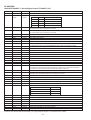
1
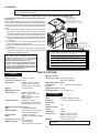
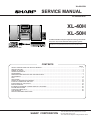
XL-40H/50H
SERVICE MANUAL
No. S2007XL40H///
XL-40H
XL-50H
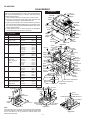
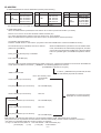
XL-40H/XL-50H Micro Component System consisting of XL-40H/XL50H ( main unit) and CP-XL40H/CP-XL50H (speaker system).
• In the interests of user-safety the set should be restored to its original
condition and only parts identical to those specified should be used.
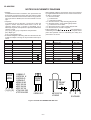
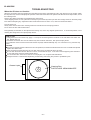
Illustration: XL-40H
CONTENTS
Page
SAFETY PRECAUTION FOR SERVICE MANUAL .......................................................................................................... 2
SPECIFICATIONS ............................................................................................................................................................ 2
NAMES OF PARTS .......................................................................................................................................................... 3
OPERATION MANUAL ..................................................................................................................................................... 5
DISASSEMBLY ................................................................................................................................................................. 6
REMOVING AND REINSTALLING THE MAIN PARTS .................................................................................................... 7
ADJUSTMENT .................................................................................................................................................................. 9
RDS ................................................................................................................................................................................ 10
TEST MODE ................................................................................................................................................................... 11
NOTES ON SCHEMATIC DIAGRAM ............................................................................................................................. 18
TYPE OF TRANSISTOR AND LED ................................................................................................................................ 18
WAVEFORMS OF CD CIRCUIT ..................................................................................................................................... 19
BLOCK DIAGRAM .......................................................................................................................................................... 20
SCHEMATIC DIAGRAM / WIRING SIDE OF P.W.BOARD ............................................................................................ 24
TROUBLESHOOTING .................................................................................................................................................... 34
FUNCTION TABLE OF IC .............................................................................................................................................. 40
LCD SEGMENT .............................................................................................................................................................. 48
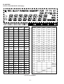
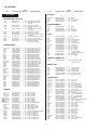
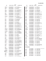
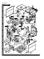
PARTS GUIDE/EXPLODED VIEW
SHARP CORPORATION
–1–
This document has been published to be used
for after sales service only.
The contents are subject to change without notice.
XL-40H/50H
FOR A COMPLETE DESCRIPTION OF THE OPERATION OF THIS UNIT, PLEASE REFER
TO THE OPERATION MANUAL.
SAFETY PRECAUTION FOR SERVICE MANUAL
Laser Diode Properties
Material: GaAIAs
W avelength: 780 nm
Emission Duration: continuous
Laser Output: max. 0.6 mW
Precaution to be taken when replacing and servicing the
Laser Pickup.
The AEL (Accessible Emission Level) of Laser Power Output
for this model is specified to be lower than Class I Requirements.
However, the following precautions must be observed during
servicing to protect your eyes against exposure to the Laser
beam
(1) When the cabinet has been removed, the power is turned
on without a compact disc, and the Pickup is on a position
outer than the lead-in position, the Laser will light for several
seconds to detect a disc. Do not look into the Pickup Lens.
(2) The Laser Power Output of the Pickup inside the unit and
replacement service parts have already been adjusted prior
to shipping.
(3) No adjustment to the Laser Power should be attempted
when replacing or servicing the Pickup.
(4) Under no circumstances look directly into the Pickup Lens
at any time.
(5) CAUTION - Use of controls or adjustments, or performance
of procedures other than those specified herein may result
in hazardous radiation exposure.
LASER KLASSE 1
LUOKAN 1 LASERLAITE
KLASS 1 LASERAPPARAT
CAUTION-INVISIBLE LASER RADIATION WHEN OPEN. DO NOT STARE INTO
BEAM OR VIEW DIRECTLY WITH OPTICAL INSTRUMENTS.
VAROITUS! LAITTEEN KÄYTTÄMINEN MUULLA
KUIN TÄSSÄ KÄYTTÖOHJEESSA MAI NI TULLA
TAVALLA SAATTAA ALTI STAA KÄYTTÄJÄN
TURVALLI SUUSLUOKAN 1 YLITTÄVÄLLE
NÄKYMÄTTÖMÄLLE LASERSÄTEILYLLE.
VARNING-OSYNLIG LASERSTRALNING NAR DENNA DEL AR OPPNAD. STIRRA
EJ IN I STRALEN OCH BETRAKTA EJ STRALEN MED OPTISKA INSTRUMENT.
VARNING - OM APPARATEN ANVÄNDS PÅ ANNAT
SÄTT ÄN I DENNA BRUKSANVI SNI NG SPECI FI
CERAS. KAN ANVÄNDAREN UTSÄTTAS FÖR
OSYNLIG LASERSTRÅLNING, SOM ÖVERSKRIDER
GRÄNSEN FÖR LASERKLASS 1.
VARNING-OSYNLIG LASERSTRALNING NAR DENNA DEL AR OPPNAD.
STIRRA EJ IN I STRALEN OCH BETRAKTA EJ STRALEN GENOM OPTISKT
INSTRUMENT.
ADVERSEL-USYNLIG LASERSTRALING NAR DEKSEL APNES. STIRR IKKE
INN I STRALEN ELLER SE DIREKTE MED OPTISKE INSTRUMENTER.
XL-40H/50H
ADVERSEL-USYNLIG LASERSTRALING VED ABNING. SE IKKE IND I
STRALEN-HELLER IKKE MED OPTISKE INSTRUMENTER.
VARO! AVATTAESSA OLET ALTTIINA NAKYMATON LASERSATEILYLLE.
ALA TUIJOTA SATEESEEN ALAKA KATSO SITA OPTISEN LAITTEEN LAPI.
SPECIFICATIONS
● General
Power source:
AC 230 V, 50 Hz
Power consumption: 26 W
Dimensions:
Width; 160 mm (6-5/16")
Height; 241 mm (9-1/2")
Depth; 249 mm (9-13/16")
Weight:
2.7 kg (6.0 lbs.)
● Amplifier section
Output power:
Output terminals:
PMPO; 28 W (total)
MPO; 14 W (7 W + 7 W)
(DIN 45 324)
RMS; 10 W (5 W + 5 W)
(DIN 45 324)
Speakers; 4 ohms
Headphones; 16-50 ohms
(recommended; 32 ohms)
● Compact disc player section
Type:
Compact disc player
Signal readout:
Non-contact, 3-beam semiconductor laser pickup
D/A converter:
1-bit D/A converter
Filter:
8-times oversampling digital
filter
Frequency response: 20 - 20,000 Hz
Wow and flutter:
Unmeasurable
(less than 0.001% W. peak)
● Tuner section
Frequency range: FM; 87.5-108 MHz
AM; 522-1,620 kHz
● Cassette deck section
Frequency re50 - 14,000 Hz (Normal tape)
sponse:
Signal/noise ratio: 50 dB
Wow and flutter: 0.3 % (DIN 45 511)
CP-XL40H/50H
● Speaker section
Type:
Full range speaker system
Speakers:
10 cm (4") full-range speaker
Rated input
power:
Maximum input
power:
Impedance:
5W
10 W
4 ohms
Dimensions:
Width; 145 mm (5-3/4")
Height; 240 mm (9-1/2")
Depth; 191 mm (7-1/2")
Weight:
1.3 kg (2.9 lbs.)/each
Specifications for this model are subject to change without
prior notice.
–2–
XL-40H/50H
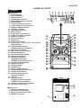
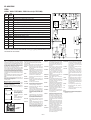
NAMES OF PARTS
XL-40H/50H
1 2 3
■ Front panel
1. Timer Indicator
2. Record Indicator
3. Sleep Indicator
4. (CD) Random Indicator
5. (CD/TUNER) Memory Indicator
6. RDS Indicator
7. Traffic Programme Indicator
8. Traffic Announcement Indicator
9. FM Stereo Mode Indicator
10. (CD) Play Indicator
11. (CD) Repeat Indicator
12. EON Indicator
13. Programme Type Indicator
14. Traffic Information Indicator
15. FM Stereo Indicator
16. CD Compartment
17. EON Button
18. On/Stand-by Button
19. Programme Type/Traffic Information
Search Button
20. (CD/TAPE) Stop Button
(TUNER) Memory Clear Button
21. Record Pause Button
22. Bass/Treble Selector Button
23. Memory/Set Button
24. Clock/Timer/Sleep Button
25. Band Selector Button
26. (CD) Review Button
(TAPE) Rewind Button
(TUNER) Tuning Down Button
27. Function Selector Button
28. Headphone Socket
29. CD Eject Button
30. ASPM Button
31. Remote Control Sensor
32. Display Mode Selector Button
33. Volume Select Button
34. (CD) Play/Pause Button
(TAPE) Play Button
35. Jog Dial
36. (CD) Cue Button
(TAPE) Fast Forward Button
(TUNER) Tuning Up Button
37. Volume/Jog Dial Selector Button
38. Cassette Compartment
4
5
6 7 8 9
10
11
16
17
18
19
20
21
22
23
24
25
26
27
12 13 14 15
29
30
31
32
33
34
35
36
37
38
28
2
3
■ Rear panel
1. AC Power Input Socket
2. FM 75 ohms Aerial Socket
3. AM Loop Aerial Input Socket
4. Speaker Terminals
1
–3–
4
XL-40H/50H
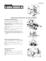
CP-XL40H/50H
■ Speaker section
1. Bass Reflex Duct
2. Full-Range Speaker
3. Speaker Wire
1
2
3
XL-40H/50H
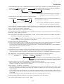
■ Remote control
1. Remote Control Transmitter LED
1
● Tuner control section
2. Programme Type/Traffic Information
Search Button
3. Preset Up/Down Buttons
2
4
5
6
● CD control section
4. Clear Button
5. Random/Repeat Button
6. Memory Button
7. Stop Button
8. Play/Pause Button
9. Track Down/Review Button
10. Track Up/Cue Button
11
12
● Tape control section
11. Record Pause Button
12. Rewind Button
13. Stop Button
14. Play Button
15. Fast Forward Button
16
17
18
19
● Common section
16. Sleep Button
17. Bass Up/Down Buttons
18. Function Selector Buttons
19. On/Stand-by Button
20. Timer Button
21. Clock Button
22. Treble Up/Down Buttons
23. Volume Up/Down Buttons
–4–
3
7
8
9
10
13
14
15
20
21
22
23
To an AC socket
–5–
1
3
3
2,3
AC INPUT
15
15
Notes concerning use:
● Replace the batteries if the operating distance is
reduced or if the operation becomes erratic.
● Periodically clean the transmitter LED on the remote control and the sensor on the main unit
with a soft cloth.
● Exposing the sensor on the main unit to strong
light may interfere with operation. Change the
lighting or the direction of the unit.
● Keep the remote control away from moisture,
excessive heat, shock, and vibrations.
0.2m - 6m
(8” - 20”)
■ Remote control
ton and the
button, plug the AC power lead
into the AC INPUT socket on this unit.
Caution:
● The operation explained above will erase all data
stored in memory, such as clock and timer settings, and tuner and CD presets.
3 Whilst pressing down the MEMORY/SET but-
socket on this unit.
2 Unplug the AC power lead from the AC INPUT
stand-by mode.
1 Press the ON/STAND-BY button to enter the
Reset the microcomputer under the following
conditions:
● To erase all of the stored memory contents (clock
and timer settings, and tuner and CD presets).
● If the display is not correct.
● If the operation is not correct.
RESETTING THE MICROCOMPUTER
Notes:
● Unplug the AC power lead from the AC socket if
the unit is not to be used for a prolonged period
of time.
● Never use a power lead other than the one supplied. Otherwise, a malfunction or an accident
may occur.
Connect the AC power lead to the AC power input
socket, then connect the AC power lead plug to an
AC socket.
To AC INPUT
AC 230 V, 50Hz
■ Connecting the AC power lead
PREPARATION FOR USE
Jog dial
0:00
AM 12:00
● When the jog dial is turned one click clockwise,
the time will increase by 1 hour. When it is turned
one click anti-clockwise, the time will decrease
by 1 hour.
Keep turning the jog dial to change the time continuously.
● When the 12-hour display is selected, “AM” will
change automatically to “PM”.
5 Adjust the hour by turning the jog dial.
4 Press the MEMORY/SET button.
The 24-hour display will appear.
(0:00 - 23:59)
“AM 12:00” → The 12-hour display will appear.
(AM 12:00 - PM 11:59)
● Note that this can only be set when the unit is
first installed or it has been reset (see page 26).
“0:00” →
3 Turn the jog dial to select the time display mode.
ton.
2 Within 3 seconds, press the MEMORY/SET but-
ter the time check mode.
1 Press the CLOCK/TIMER/SLEEP button to en-
CLOCK/TIMER/
SLEEP
MEMORY/SET
(Main unit operation)
In this example, the clock is set for the 24-hour
(0:00) system.
SETTING THE CLOCK
2 Perform steps 1 - 8 above.
THE MICROCOMPUTER”, on page 26.
1 Perform steps 1 - 3 in the section “RESETTING
To change the time display mode:
To change the clock time:
Perform steps 1, 2 and 4 - 8 above.
Note:
● In the event of a power failure or when the AC
power lead is disconnected, the clock display will
go out.
When the AC power supply is restored, the clock
display will flash on and off to indicate the time
when the power failure occurred or when the AC
power lead was disconnected.
If this happens, follow the procedure below to
change the clock time.
● The clock starts operating from “0” second. (Seconds are not displayed.)
8 Press the MEMORY/SET button.
● When the jog dial is turned one click clockwise,
the time will increase by 1 minute. When it is
turned one click anti-clockwise, the time will decrease by 1 minute.
Keep turning the jog dial to change the time continuously.
● The hour setting will not advance even if minutes advance from “59” to “00”.
7 Adjust the minutes by turning the jog dial.
6 Press the MEMORY/SET button.
XL-40H/50H
OPERATION MANUAL
XL-40H/50H
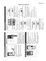
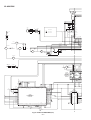
DISASSEMBLY
XL-40H/50H
Caution on Disassembly
Follow the below-mentioned notes when disassembling
the unit and reassembling it, to keep it safe and ensure
excellent performance:
1. Take cassette tape and compact disc out of the unit.
2. Be sure to remove the power supply plug from the wall
outlet before starting to disassemble the unit.
3. Take off nylon bands or wire holders where they need to
be removed when disassembling the unit. After servicing
the unit, be sure to rearrange the leads where they were
before disassembling.
4. Take sufficient care on static electricity of integrated
circuits and other circuits when servicing.
CD PWB
Display
PWB
Main PWB
(A1)x1
ø3x10mm
Front
Panel
XL-40H/50H
STEP
REMOVAL
PROCEDURE
Side Panel(Left/Right) 1. Screw .................. (A1) x8
6-1
2
Top Cabinet
Switch PWB
1. Screw .................. (B1) x1
2. Socket ................. (B2) x2
6-1
3
Rear Panel
1. Screw .................. (C1) x2
6-1
4
Main PWB/
Headphones PWB
1. Screw .................. (D1) x3
2. Screw .................. (D2) x2
3. Bracket ................ (D3) x1
4. Socket ................. (D4) x3
5. Flat wire ............... (D5) x1
6. Socket ................. (D6) x1
6-2
1. Socket ................. (E1) x1
2. Screw .................. (E2) x2
3. Knob .................... (E3) x1
6-2
Display PWB/
LED PWB
(With Jog Motor
Flame)
1. Screw .................. (F1) x2
2. Screw .................. (F2) x3
3. Bracket ................ (F3) x1
4. Socket ................. (F4) x1
5. Hook .................... (F5) x2
6. Hook .................... (F6) x2
6-2
Front Panel
1. Screw .................. (G1) x1
2. Socket ................. (G2) x1
3. Screw .................. (G3) x1
6-2
1. Screw .................. (H1) x4
2. Screw .................. (H2) x1
3. Screw .................. (H3) x1
4. Bracket ................ (H4) x1
6-2
5
Jog Switch PWB
6
7
8
Power PWB
RearPanel
(F2)x2
ø2.5x10mm
(D4)x1
LED (F6)x2
PWB
(E1)x1
(D6)x1
(F5)x2
(E3)x1
(F3)x1
Display PWB
(D4)x1
Front Panel
Jog Switch
PWB
(E2)x2
ø2.5x12mm
Jog Motor
Tape Holder
Mechanism
PWB
Side Panel
(Lift)
(C1)x1
ø3x10mm
(D2)x1
ø3x8mm
Headphones
PWB
(D5)x1
(G2)x1
(D1)x2
ø3x10mm
Main PWB
(F2)x1
ø2.5x10mm
(D3)x1
(D1)x1
ø3x10mm
(F1)x2
ø2.5x14mm
(F4)x1
(G3)x1
ø3x6mm
(D4)x1
Power PWB
(G1)x1
(H3)x1
ø3x8mm
ø3x6mm
1. Open the cassette holder
2. Screw .................. (J1) x4
6-3
Power PWB
10
CD PWB/
1. Screw .................. (K1) x3
Open Close Switch 2. Hook .................... (K2) x2
PWB (Note)
3. Socket ................. (K3) x3
6-4
Sub Power
Transformer
CD Mechanism
6-4
(H4)x1
(D2)x1
ø3x8mm
(H2)x1
ø3x10mm (H1)x4
ø3x6mm
Main Power Transformer
Sub Power Transformer
Figure 6-2
CD PWB
Front Panel
Open
(A1)x4
ø3x10mm
Figure 6-1
Tape Mechanism
1. Screw .................. (L1) x3
(C1)x1
ø3x10mm
(A1)x2
ø3x10mm
9
11
(B1)x1
ø3x10mm
(B2)x1
Side Panel
(Right)
FIGURE
1
(A1)x1
ø3x10mm
(B2)x1
Top Cabinet
(K1)x3
ø2.5x14mm
(K3)x1
Tape
Mechanism
(K3)x2
(L1)x3
ø2.5x10mm
(K2)x2
CD Mechanism
PWB Washer x3
Top Cabinet
Cassette
Holder
(J1)x4
ø2.5x10mm
Open/Close
Switch PWB
CD Motor PWB
Figure 6-3
Note:
After removing the connector for the optical pickup fromthe
connector wrap the conductive aluminium foil around the front
end of connector so as to protect the optical pickup from
electrostatic damage.
Top Cabinet
CD Mechanism
Figure 6-4
Figure 6-5
–6–
XL-40H/50H
CP-XL40H/50H
STEP
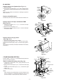
1
REMOVAL
Speaker
Speaker Box
PROCEDURE
FIGURE
1. Front panel .......... (A1) x1
2. Screw .................. (A2) x4
7-1
(A1x1)
Woofer
(A2)x4
ø4x12mm
Driver should be
pried away from
speaker Box.
Driver
Direction of handle
Figure 7-1
REMOVING AND REINSTALLING THE MAIN PARTS
TAPE MECHANISM SECTION
(A2)x1
ø2x7mm
Perform steps 1 to 7 and 9 of the disassembly method to
remove the tape mechanism. (See page 6.)
(A2)x1
ø2x3mm
(A1)x2
ø2x8mm
How to remove the record / playback and erase
heads (See Fig. 7-2.)
1. Remove the screws (A1) x 2 pcs., to remove the erase
head.
2. Remove the screws (A2) x 2 pcs., to remove the record/
playback head.
Note:
After replacing the heads and performing the azimuth
adjustment, be sure to apply screwlock.
Erase Head
Record/
Playback Head
Figure 7-2
How to remove the pinch roller (See Fig. 7-3.)
1. Carefully bend the pinch roller pawl in the direction of the
arrow <A>, and remove the pinch roller (B1) x 1 pc.,
upwards.
<A>
Pinch Roller
Pawl
Pinch Roller
(B1)x1
Figure 7-3
How to remove the belts (See Fig. 7-4.)
1. Remove the main belt (C1) x 1 pc., from the motor pulley.
2. Remove the FF/REW belt (C2) x 1 pc., from the REW/FF
roller.
3. Put on the belts in the reverse order of removal.
Note:
When putting on the belt, ascertain that the belt is not twisted,
and clean it.
Motor
Main Belt
(C1)x1
REW/FF
Clutch
FF/REW Belt
(C2)x1
Figure 7-4
How to remove the motor
(See Figs. 7-5.)
(D2)x3
Special
Screw
(D1)x1
ø2x4mm
Motor
1. Remove the mainbelt.
2. Remove the screws (D1) x 2 pcs., to remove the motor
bracket.
3. Remove the screws (D2) x 3 pcs., to remove the motor.
Note:
When mounting the motor, pay attention to the motor mounting
angle
Motor
Bracket
(D1)x1
ø2x4mm
Motor
Figure 7-5
–7–
XL-40H/50H
(E1)x1
Stop Washer
How to remove the flywheel (See Fig. 8-1.)
Mechanism
Chassis
1. Remove the belt.
2. Remove the stop washer (E1) x 1 pc., with a small precision
screwdriver to extract the flywheel from the capstan metal.
Note:
When the stop washer is deformed or damaged, replace it
with a new one.
Stop
Washer
Driver
Washerx2
Flywheel
How to reinstall the parts
Install each part in the reverse order of the removal with care.
Figure 8-1
How to remove the tape mechanism PWB
(See Fig. 8-2.)
(F1)x1
Tape ø2x3mm
Mechanism
PWB
1. Remove the screws (F1) x 1 pc., to remove the tape
mechanism PWB.
2. Remove the screws (F2) x 1 pc.
3. Remove the solder joints (F3) x 2 pcs., to remove the tape
mechanism PWB.
(F2)x1
ø2x8mm
Tape
Mechanism
PWB
(F3)x2
Solder
Joint
Figure 8-2
How to remove the jog motor
(See Figs. 8-3.)
1. Remove the side panel and top cabinet.
2. Remove the jog belt (G1) x 1 pc., from the motor pulley.
3. Remove the screws (G2) x 2 pcs., to remove the jog motor.
Note:
When putting on the belt, ascertain that the belt is not twisted,
and clean it.
Jog Motor
(G2)x2
ø2x5mm
Worm
Gear
Display PWB
Jog Belt Jog Motor
Holder
(G1)x1
Figure 8-3
Mechanism Cover
CD MECHANISM SECTION
(A1) x2
Perform steps 1, 2 and 10, 11 of the disassembly method to
remove the CD mechanism.
(A1) x2
(A2) x2
ø2.6 x6mm
How to remove the pickup (See Fig. 8-4)
1. Remove the mechanism cover, paying attention to the
pawls (A1) x 4 pcs.
2. Remove the screws (A2) x 2 pcs., to remove the shaft (A3)
x 1 pc.
3. Remove the stop washer (A4) x 1 pc., to remove the gear
(A5) x 1 pc.
4. Remove the pickup.
CD Mechanism
Shaft
(A3) x1
Note:
After removing the optical pickup connector wrap the front
end of connector in conductive aluminium foil so as to
prevent damage of optical pickup by static electricity.
StopWasher
(A4) x1
Gear
(A5) x1
Pickup Unit
Figure 8-4
–8–
XL-40H/50H
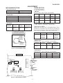
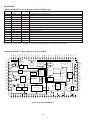
ADJUSTMENT
TUNER SECTION
MECHANISM SECTION
• Driving Force Check
Torque Meter
fL: Low-renge frequency
fH: High-renge frequency
• AM IF/RF
Signal generator: 400 Hz, 30%, AM modulated
Specified Value
Play: TW-2412
Over 80 g
Torque Meter
Specified Value
Play: TW-2111
30 to 60 g. cm
Fast forward: TW-2231
55 to 140 g.cm
Rewind: TW-2231
55 to 140 g.cm
• Tape Speed
Test Tape
MTT-111
Display
Frequency Frequency
• Torque Check
Adjusting
Point
Variable
resistor in
motor.(M901)
Specified
Value
3,000 ±
90 Hz
Setting/ Instrument
Adjusting Connection
Parts
T351
*1
IF
450 kHz
1,620 kHz
AM Band
Coverage
—
522 kHz
(fL): T306 *2
1.1 ± 0.1 V
AM
Tracking
990 kHz
990 kHz
(fL): T302
*1
*1. Input: Antenna, Output: Speaker Terminal
*2. Input: Input is not connected, Output: TP301
Instrument
Connection
• Setting the Test Mode
Keeping the FF/FWD button and MEMORY/SET button
pressed, turn on POWER. Then, the frequency is initially set
in the memory as shown in Table. Call it with the JOG DIAL
knob to use it for adjustment and check of tuner circuit.
Headphone
terminal
TAPE MECHANISM
Preset No.
1
2
3
4
5
M901
Tape
Motor
FM
87.50 MHz
108.00 MHz
98.00 MHz
90.00 MHz
106.00 MHz
AM
Preset No.
6
7
8
9
10
522 kHz
1,620 kHz
990 kHz
603 kHz
1,404 kHz
• FM Mute Level
Signal generator: 1 kHz, 40 kHz dev., FM modulated
Variable
resistor
Frequency
98.00 MHz
(30 dBµV)
Figure 9-1 ADJUSTMENT POINT
Display
98.00 MHz
Adjusting
Parts
VR351*1
Instrument
Connection
Input: SO301
Output: Speaker
Terminal
Adjust so that an output signal appears.
• Check FM VT
Signal generator: 1 kHz, 40 kHz dev., FM modulated
Frequency
MAIN PWB
AM IF
VR351
FM Mute
Level
FE301
T351
TP301
AM Band
Coverage fL
T302
AM
Tracking fL
87.5 MHz
2.2 V ± 0.7 V
TP301
108 MHz
7.3 V ± 1.0 V
TP301
CNP301
AM
ANTENNA
SOCKET
–9–
Instrument
Connection
108 MHz
SO301
FM
ANTENNA
SOCKET
Figure 9-2 ADJUSTMENT POINTS
Check Point
87.5 MHz
R336
T306
Display
XL-40H/50H
RDS
Crystal oscillator input (external reference signal input).
Vssd
Digital ground.
11*
Vddd
Digital power supply (+5V).
12
MODE
Read mode setting (0 : master, 1: slave).
13
RST
RDS-ID/RAM reset (positive polarity).
14
RDDA
RDS data output.
15*
RDCL
RDS clock output (master mode)/ RDS clock input (slave mode).
16*
RDS-ID/ RDS-ID/READY output (negative polarity).
READY
Descriptions of the PTY (Programme Type)
codes, TP (Traffic Programme) and TA (Traffic
Announcement)
With the XL-40H/XL-50H, you can search for and
receive the following PTY, TP and TA signals.
LIGHT M:
NEWS:
Short accounts of facts, events and
publicly expressed views, reportage
and actuality.
CLASSICS: Performances of major orchestral
works, symphonies, chamber music,
etc., and including Grand Opera.
AFFAIRS:
Topical programme expanding or enlarging upon the news, generally in
different presentation style or concept, including debate, or analysis.
OTHER M:
INFO:
Programmes whose purpose is to impart advice in the widest sense.
Note:
When the TP and TA appear at the same time, an
announcement is being made.
When only the TA appears, an announcement is
not being made.
SPORT:
Programme concerned with any aspect of sport.
With the XL-40H/XL-50H, you can display two types
of RDS service. To show them in the display, press
the DISPLAY MODE button.
Each time you press the DISPLAY MODE button,
the display will change to show the following information.
PS
(Programme Service): Station names commonly
known will be displayed.
"NO PS" appears if no
signal is being received.
PTY
(Programme Type): Programme type will be
displayed.
"NO PTY" appears if no
signal is being received.
Station Frequency:
EDUCATE: Programme intended primarily to
educate, of which the formal element
is fundamental.
DISPLAY
MODE
All radio plays and serials.
CULTURE: Programmes concerned with any aspect of national or regional culture,
including language, theatre, etc.
SCIENCE:
Programmes about the natural sciences and technology.
VARIED:
Used for mainly speech-based programmes usually of light-entertainment nature, not covered by other
categories. Examples include: quizzes, panel games, personality interviews.
POP M:
Commercial music, which would generally be considered to be of current
popular appeal, often featuring in current or recent record sales charts.
ROCK M:
Contemporary modern music, usually
written and performed by young musicians.
EASY M:
Current contemporary music considered to be “easy-listening”, as opposed to Pop, Rock or Classical, or
one of the specialised music styles,
Jazz, Folk or Country. Music in this
category is often but not always, vocal, and usually of short duration.
Station frequencies.
13
RST
12
MODE
57kHz
BPF
(SCF)
REFERENCE
VOLTAGE
Vssa
4
3
(Continued)
RDS (Radio Data System) OPERATION
RDS is a broadcasting service which a growing
number of FM stations are now providing. It allows
these FM stations to send additional signals along
with their regular programme signals. For example, the stations send their station names, and information about what type of programme they
broadcast, such as sports or music, etc.
When tuned to an FM station providing the RDS
service, RDS will appear, the station frequency (and
then the station name if sent) will be displayed.
The TP (Traffic Programme) will appear on the display when the received broadcast carries traffic announcements, and the TA (Traffic Announcement)
will appear whilst a traffic announcement is being
received.
EON will appear whilst the EON (Enhanced Other
Networks information) data is being broadcast.
DRAMA:
15
RDCL
14
RDDA
10
6
5
FLOUT
1
Vdda
In this unit, the terminal with asterisk mark (*) is (open) terminal which is not
connected to the outside.
■ Information Provided by RDS
XOUT
XIN
10
CIN
9
8
Crystal oscillator output (4.332MHz).
9
XOUT
XIN
Test input.
8
16
RDS-ID/
READY
Subcarrier input (comparator input).
TEST
RDS-ID
DETECT
CIN
7
OSC
6
TEST
Subcarrier output (filter output).
TEST
FLOUT
7
5
CLK(4.332MHz)
Analog ground.
RAM
(128-bits)
Vssa
MPXIN
Analog power supply (+5V).
4
DATA
DECODER
Baseband (multiplexed) signal input.
Vdda
SMOOTHING
FILTER
MPXIN
3
ANTIALISING
FILTER
2
2
Reference voltage output (Vdda/2).
VREF
VREF
PLL
(57kHz)
1
CLOCK
RECOVERY
(1187.5Hz)
Function
Vssd
Vddd
Port
Name
VREF
Pin
No.
11
IC521 VHiLC72723M-1: RDS Circuit (LC72723M)
Classical Musical for general, rather
than specialist appreciation. Examples of music in this category are instrumental music, and vocal or choral works.
Stock Market reports, commerce,
trading, etc.
CHILDREN: For programmes targeted at a young
audience, primarily for entertainment
and interest, rather than where the
objective is to educate.
SOCIAL:
Programmes about people and things
that influence them individually or in
groups. Includes: sociology, history,
geography, psychology and society.
RELIGION: Any aspect of beliefs and faiths, involving a God or Gods, the nature of
existence and ethics.
PHONE IN: Involving members of the public expressing their views either by phone
or at a public forum.
TRAVEL:
Features and programmes concerned with travel to near and far
destinations, package tours and
travel ideas and opportunities. Not for
use for announcements about problems, delays, or road-works affecting
immediate travel where TP/TA should
be used.
LEISURE:
Programmes concerned with recreational activities in which the listener
might participate. Examples include,
Gardening, Fishing, Antique collecting, Cooking, Food & Wine, etc.
JAZZ:
Polyphonic, syncopated music characterised by improvisation.
COUNTRY: Songs which originate from, or continue the musical tradition of the
American Southern States. Characterised by a straightforward melody
and narrative story line.
– 10 –
OLDIES:
Music from the so-called “golden age”
of popular music.
FOLK M:
Music which has its roots in the musical culture of a particular nation,
usually played on acoustic instruments. The narrative or story may be
based on historical events or the people.
Musical styles not fitting into any of
the other categories. Particularly
used for specialist music of which
Rhythm & Blues and Reggae are
examples.
WEATHER: Weather reports and forecasts and
meteorological information.
FINANCE:
NATION M: Current Popular Music of the Nation
or Region in that country’s language,
as opposed to international ‘Pop’
which is usually US or UK inspired
and in English.
DOCUMENT: Programme concerned with factual
matters, presented in an investigative
style.
TEST:
Broadcast when testing emergency
broadcast equipment or receivers.
ALARM:
Emergency announcement made under exceptional circumstances to give
warning of events causing danger of
a general nature.
NONE:
No programme type (receive only).
TP:
Broadcasts which carry traffic announcements.
TA:
Traffic announcements are being
broadcast at present.
Note:
● When the unit is in the EON stand-by mode and
a programme is selected, the unit will display “TI”
instead of “TP” or “TA”.
XL-40H/50H
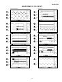
TEST MODE
The test mode applied to this microcomputer has three modes, namely ordinary test mode to be used for adjustment or
measurement, aging test mode to be used for aging test, and self-diagnosis test mode for self-inspection in case of final product
inspection.
The test mode specification prescribes the microcomputer with RDS (RH-IX0026SJZZ) . There are two types of indication
examples; large ones for the microcomputer with RDS, and smaller ones for the microcomputer without RDS.
1. Turning on the test mode
To turn on the specific test mode, press the POWER button, holding down the following two buttons in the ordinary stand-by
mode (power off state). In this case only the main unit button is valid. Even when the POWER of remote control button is set
to on, the test mode is not turned on.
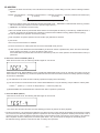
[Ordinary test mode]
1. CD Test Mode (TEST 1)…………………… Volume/JOG Dial Selector + FF/FWD
2. Tuner Test Mode (TEST 2)………………… Volume/JOG Dial Selector + Volume Select
3. Electronic volume Test Mode (TEST 3)…… REW/REV + FF/FWD
4. Timer Test Mode (TEST 4)………………… FUNCTION + Volume Select
5. LCD Test Mode (TEST 5)……………………FUNCTION + FF/FWD
[Self-diagnosis Test Mode]
1. Button input diagnosis test mode (TEST6).… REW/REV + Volume Select
2. CD Test Mode (TEST 1)
In the CD test mode the operation of each step is enabled even when the LID-SW is off. However, if focus cannot be set in step
3 or any error processing is started, it is impossible to proceed to the next step. When the error processing is started, operations
other than termination of test mode by pressing the POWER button or return to the step 1 by pressing the STOP button are inhibited.
1. Step 1 Mode
When the CD test mode is turned on, the following indication lights, the processing (until turning-off of CD STB terminal of CD
initialization operation flow) is executed, and the next button input is waited.
After lighting for one second
If the following operation buttons are pressed in this state, the operation is performed as follows.
"POWER" ................. The test mode is turned off, the power is turned off, and the ordinary standby mode is set.
"FF/FWD" ................. After the pickup returns once to the innermost periphery, it slides toward the outer periphery while this
button is held down.
"REW/REV" .............. After the pickup returns once to the innermost periphery, it slides toward the inner periphery while this
button is pressed. However, if PU-IN is on, input is invalid.
"PLAY" ..................... Shift to step 2
"STOP" ..................... Invalid
"REC PAUSE" .......... Shift to step 5
* In case of initialization the pickup is moved toward the inner periphery. Any buttons other than "POWER" button are not
accepted until the shift of pickup to the inner periphery is completed at this time. If PU-IN SW ON cannot be detected within
10 seconds, the slide motor is stopped, and the following error indication appears. Press the POWER button to end the test
mode, or press the STOP button to return to step 1. Any other operations are inhibited.
– 11 –
XL-40H/50H
2. Step 2 Mode
When the "PLAY" button is pressed in this mode, the laser lighting command LDON (8400) is sent, and the laser is turned on.
Other operations are not performed.
If the following buttons are pressed in this state, the operation is performed as follows.
"POWER" ................ The test mode is turned off, the power is turned off, and the ordinary standby mode is set.
"FF/FWD" ................ The pickup slides toward the outer periphery while this button is held down.
"REW/REV" ............. The pickup slides toward the inner periphery while this button is held down. However, if PU-IN is on, input
is invalid.
"PLAY" ..................... Shift to step 3
"STOP" .................... Return to step 1
"REC PAUSE" ......... Shift to step 5
3. Step 3 Mode
The laser is kept lighting. The processing (until turning-on of CLV servo of CD initialization operation flow) is executed, and
the next button input is waited. (The focus servo is turned on, and focus search is performed.)
The focus search is repeated until the focus is set.
When the following operation buttons are pressed in this state, the operation is executed as follows.
"POWER" ................ The test mode is turned off, the power is turned off, and the ordinary standby mode is set.
"FF/FWD" ................ The pickup slides toward the outer periphery while this button is held down.
"REW/REV" ............. The pickup slides toward the inner periphery while this button is held down. However, if PU-IN is on, input
is invalid.
"PLAY" ..................... If the focus has been set, shift to step 4 is executed. If the focus has not been set, acceptance is inhibited.
"STOP" .................... Return to step 1
"REC PAUSE" ......... Shift to step 5
*If the focus is disturbed after it has been set, the process returns to step 1.
4. Step 4 Mode
The CLV servo ON command (8600) sending operation is performed, and the next button input is waited. (The disc is rotated
to perform CLV locking.)
The time display indicates always "0:00".
When the following buttons are pressed in this state, the operation is executed as follows.
"POWER" ................ The test mode is turned off, the power is turned off, and the ordinary standby mode is set.
"FF/FWD" ................ The pickup slides toward the outer periphery while this button is held down.
"REW/REV" ............. The pickup slides toward the inner periphery while this button is held down. However, if PU-IN is on, input
is invalid.
"PLAY" ..................... Shift to step 5
"STOP" .................... Return to step 1
"REC PAUSE" ......... Shift to step 5
*If the focus is disturbed, the process returns to step 1.
– 12 –
XL-40H/50H
5. Step 5 Mode
The CD initialization operation flow is executed to the end, the mute is set to off, and playback is started. Even when the
playback reaches the outermost periphery of disc, the operation does not stop. The LCD display indicates the playback past
time as in case of ordinary CD playback.
When the following operation buttons are pressed in this sate, the operation is executed as follows.
"POWER" ................. The test mode is turned off, the power is turned off, and the ordinary standby mode is set.
"FF/FWD" ................. The pickup slides toward the outer periphery while this button is held down.
"REW/REV" .............. The pickup slides toward the inner periphery while this button is held down. However, if PU-IN is on, input
is invalid.
"PLAY" ..................... Invalid
"STOP" ..................... Return to step 1
"FUNCTION" ............ Shift to step 6
"BAND" .................... Shift to step 7
*If the focus is disturbed, the process returns to step 1.
Other cautions
• TOC IL is not executed in the test mode.
• As for button operations other than those shown above, only the sound volume operation (with JOG) is accepted.
3. Tuner Test Mode (TEST 2)
1. Outline of tuner (radio) test mode
The tuner test mode is intended to store the adjustment and measurement frequencies in the preset memory CH without
frequency setting by adjusting personnel when the tuner section is adjusted in the production line.
2. Details of tuner test mode
When the power is turned on by using the "POWER" button while the "Volume/JOG Dial Selector" and "Volume Select"
buttons are held down in POWER OFF state, the frequency for adjustment and measurement of destination specified by the
AREA terminal is preset and stored in the preset memory CH. However, Ordinary 1 and Ordinary 2 are set to the designation
(destination selected by SPAN switching operation) set when the test mode is set. (As for frequencies to be preset and stored
for each destination, refer to item 3.)
The tuner test mode is started from preset No.1.
The operations of test mode are identical with the ordinary operations of TUNER function. However, FUNCTION switching
is invalid.
Since it is necessary to discard the content of preset memory when the tuner test mode is ended, "0000" or "1111" bits are
written in the memory to be checked in case of memory check (in case of initial setting) so that memory abnormality is detected
in case of initial setting so as to ensure memory initialization.
When the tuner test mode is turned on, the following indication lights for one second.
• The TUNER TEST2 mode is set as a result of Volume Select + POWER. -> IF AC is set to OFF in the TEST2 mode, the initial
state is restored.
When POWER is set to OFF, the memory of TEST2 mode is protected.
When the power is turned on again, the ordinary operation is enabled while the data is stored in the
memory (besides TUNER).
If AC OFF state is maintained in this state for about 1/2 day, start is executed in the initial state.
• To clear the whole memory, insert the AC cord, holding down MEMORY + PLAY.
– 13 –
XL-40H/50H
3. Preset frequencies for various destinations (random preset memory)
CH
1
2
3
4
5
BAND
FM
STEREO
Europe 2, 4
CH
6
7
8
9
10
11-15
FM 87.50 MHz
FM108.00 MHz
FM 98.00 MHz
FM 90.00 MHz
FM106.00 MHz
BAND
AM
Europe 2, 4
AM 522 kHz
AM1620 kHz
AM 990 kHz
AM 603 kHz
AM1404 kHz
LW
CH
16-25
26
27
28
29
30
BAND
FM
MONO
Europe 2, 4
FM106.00 MHz
FM 90.00 MHz
FM 98.00 MHz
FM108.00 MHz
FM 87.50 MHz
• The hatched sections of the table are not stored in memory.
4. ASPM TEST Mode
When the ASPM button is pressed, the test mode is set. It starts up at FM 106.50 MHz. (ST mode)
Data of 27 CH of 04 to 30 CH are all stored at FM 87.50 MHz (ST).
01 to 03CH are kept empty (If data of 3 CH are stored, max. 30 CH is filled.)
When the ASPM button is operated in the TEST mode 3, the preset data is cleared (overwrite).
A) Operation with ASPM button
Press the "ASPM" button or hold it down. (Any button other than ASPM button cancels the ASPM test mode.)
FM 105.00 MHz (ST) is indicated, and scan is started.
(Start from 105.00 MHz)
When the ASPM button is pressed once in the TUNER TEST
mode, the indication FM 106.50 MHz (ST) appears, and data
of 04 to 30 CH are stored at 87.50 MHz (ST). When the ASPM
button is operated again, the ASPM test operation mode is
set.
During scanning the frequency is indicated.
End at FM 108.00 MHz (ST)
Only the number of preset and stored stations (number of CHs: max. 3 stations) is indicated for one second in the ASPM test
mode. When two stations are stored, "_2 MEMORY" is indicated (lighted)for one second.
("02 MEMORY" indication is not given.)
In case of "_0 MEMORY" the process ends, and the
FM 106.50 MHz (ST) state is resumed.
"END" is not indicated
01CH indication (for one second)
Not in zero-memory state
(An example)
FM P-01
Frequency indication (for one second)
FM 105.50MHz(ST)
02CH indication (for one second)
FM P-02
Frequency indication (for one second)
FM 106.50MHz(ST)
03CH indication (for one second)
FM P-03
Frequency indication (for one second)
FM 107.50MHz(ST)
Confirmation of content of memory
(Examples of concrete indication)
After indication of continuous time series for one second the indication of FM 106.50 MHz (ST) is restored.
(The preset button is not pressed. The time series is indicated automatically, and the content of memory is indicated.)
* PS name is not indicated (while the content of memory is checked)
* If only 1 CH data is stored, FM P-01 -> FM 106.00 MHz -> FM 106.50 MHz (ST)
(An example)
(1 sec)
(1 sec) (ST)
End indication
– 14 –
XL-40H/50H
* When the "PRESET UP" button or "PRESET DOWN" button is pressed after completion, the following indication appears.
CH indication
(for 2 seconds)
Frequency indication
(for 2 seconds)
Time series indication of PS name indication is enabled.
(The same as in case of Ordinary)
NO PS
(Blinking for 5 seconds: 1 Hz)
Note: If PS is fixed after the frequency indication is
resumed, the PS name indication is restored.
* If signal exists at 106.50 MHz, the following indication appears.
FM 106.50 MHz
PS name
When the PS data is given in case of NO PS indication, the
PS name indication is restored.
NO PS
(Blinking for 5 seconds: 1 Hz)
Note: If PS is fixed after the frequency indication is
resumed, the PS name indication is restored.
In case of memory storage with ASPM, for example, if RDS station 107.50 MHz has the PI code (the same as that of RDS
station 105.50 MHz) and VSM is greater than 105.50 MHz (PR-01), data is overwritten on 105.5 MHz which is contained in
"PR-01". (Frequency is changed to 107.50 MHz.)
If VSM is equal, previously stored 105.50 MHz remains.
When RDS station is stored in the test mode, the 2-second blinking of preset No. is not performed so as to save the production
line test time. ("RDS" lighting is performed.)
Note: RDS operation is performed in FM MONO state. However, in case of ASPM, ASPM scan is performed after BAND is
changed from FM MONO to FM STEREO.
Note: When the
(PLAY) button is pressed in TEST 2 mode, it is possible to check the sate of IF count. However, this
function is for designer. It is not necessary for other sections.
B) Cautions concerning the ASPM test mode
a) Cancel: When the "ASPM" button is pressed again during operation after it was first pressed in the test mode, the ASPM
test mode is canceled (interrupted), and the initial state FM 106.50 MHz (ST) indication is restored.
(To check the data which was preset and stored until interruption, use the preset UP/DOWN button. (JOG UP/DOWN is
also available after JOG mode button operation.)
wing indication appears.
b) The ASPM test mode is started in FM stereo state (FM 106.50 MHz ST). If any button other than ASPM button is pressed
even only once after it is started, it becomes invalid, and the ASPM test mode becomes inoperable.
Invalid: The Ordinary mode is set while 4 to 30CH data remain in memory (or 1 to 30 CH MAX data remain in memory).
The "ASPM" button can be repeatedly operated until 01CH to 03CH is filled (up to 3 stations in memory).
The number of stored stations -> Channel No. -> Frequency -> FM 106.50 MHz (ST) is indicated.
(1 second)
(1 second)
(1 second) (Initial state)
Up to 3 stations (1 to 3CH) can be indicated. This indication is
given only in the ASPM test mode. In other mode (not in ASPM
test mode) the number of stored stations -> END is indicated
c) Broadcast (without PI code) which is not RDS is not preset and stored in memory.
When the ASPM mode is set, the "MEMORY/SET" button cannot be operated (the test mode is canceled).
Operation is possible after ASPM test mode operation.
d) Scan frequency: 105.00 MHz -> 108.00 MHz
Data are stored in memory so that the PI code is not duplicated (by seeing the PI code and VSM (S meter value). When
the PI code is duplicated, both VSM (S meter value) are compared. The greater one is stored in memory but the smaller
one is discarded.
For the stations having the same PI code, only one station having the highest electric field intensity is stored, and the
memory is refilled. The channels which can be preset in the ASPM test mode are 01 to 03CH. If 3 stations are stored, 30
CH are filled.
For the stations having the same electric field intensity, the former (preceding station) is stored.
e) Signal of already stored same frequency is not stored. (The previously stored data is kept.)
f) The order of preset memory is 01CH -> 02CH -> 03CH.
– 15 –
XL-40H/50H
g) When 01 to 03CH were all used, scan is aborted at the frequency at which filling occurred, and the following indication
appears.
Number of stored stations -> Indication of stored channel -> Indication of frequency -> Return to initial FM 106.50 MHz (ST)
(1 second)
(1 second)
(1 second)
In this period up to 3 stations are continuously indicated (1 to 3 CH).
h) If even one station could not be preset and stored in the APMS mode, "_0MEMORY" is indicated after scanning, and then
FM 106.50 MHz (ST) indication is restored. (The first digit is space.)
("_0MEMORY" is indicated in the test mode.)
i) When the "ASPM" button is pressed after three stations are stored (after full-memory of 30 stations), "ASPM" blinks for 2
seconds, and then FM 106.50 MHz (ST) indication is restored without ASPM scanning. (RDS automatic lighting)
(In case of ASPM button operation in full memory state)
j) After completion of specific operation FM 106.50 MHz (ST) indication is restored.
k) Test mode
Use of only the function button is inhibited.
l) The first channel to be called (when data is stored in the ASPM mode) is 01CH.
m) After start-up in the ASPM test mode the ASPM key is valid even when it is pressed many times. The test mode is kept.
If three stations are stored (1 to 3CH), full-memory state occurs.
If the ASPM button is pressed after occurrence of full-memory state, the same operation as that described in item i) is
performed.
4. Electronic volume Test Mode (TEST 3)
When the test mode is set, the following indication lights for one second.
When this mode is set, BASS/TREBLE is set to 0 (0 dB) and SURROUND mode is set to off, and start-up function is set to CD
when volume is -14 dB (STEP 17). The button operations in the test mode are the same as those of ordinary operation excepting
sound volume UP/DOWN.
(1) The indication is the same as that of ordinary operation excepting test mode setting.
(2) The sound volume control with the sound volume UP/DOWN button is only the following 3 steps unlike the ordinary state.
Volume- ∞ (STEP 0) <-> Volume-14 dB (STEP 23) <-> Volume-0 (STEP 30)
(3) BASS/TREBLE and SURROUND are switched when button operation is performed.
5. Timer test Mode (TEST 4)
When the test mode is set, the following indication lights for one second.
The current time and timer time are set in the following procedure to perform the timer playback.
1.Set the current time to 1:00, set the timer to ON time 1:02, set the function to Tape, and set volume STEP 8. One minute is counted
as one second, and the timer playback operation is performed. The fade-in (when playback is started) is executed at a rate of
one step for 0.5 sec. After completion of fade-in the fade-out is executed at a rate of one step for 0.5 sec (WAIT 1 sec inserted).
After completion of fade-out the power is turned off (after WAIT 1 sec), and the mode is changed to the standby mode.
The indication during operation is the same as that of ordinary timer operation.
– 16 –
XL-40H/50H
6. LCD Test Mode (TEST 5)
When the LCD test mode is set, all the LCD segments are lighted. After that the indication is changed as follows according to
the "PLAY" button input.
Lighting of all segments
Lighting of odd segments
Lighting of even segments
7. Key input diagnosis Test Mode (TEST 6)
When the test mode is set, the following indication appears.
This test mode is intended to check whether all the main unit buttons can be detected. Accordingly, in this test mode checking
as to whether the "POWER" button was pressed after all the buttons shown below were pressed is performed. If the result is
OK, OK is indicated. Even any one of keys was not pressed, an error is indicated. In case of OK termination or error termination
exit from this mode occurs when the "POWER" button is pressed next time, and the standby mode is set.
1. In case of XL-40H/50H
The following 15 buttons are detected as all buttons.
PLAY, JOG MODE, BAND, BASS/TREBLE, FUNCTION, MEMORY/SET, REC PAUSE, REW, FF, STOP, CLOCK/TIMER/
SLEEP,PTY-TI, EON, APMS, DISPLAY
The OK/NG indication of test result is as follows.
– 17 –
XL-40H/50H
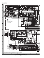
NOTES ON SCHEMATIC DIAGRAM
• Resistor:
To differentiate the units of resistors, such symbol as K and
M are used: the symbol K means 1000 ohm and the symbol
M means 1000 kohm and the resistor without any symbol is
ohm-type resistor. Besides, the one with “Fusible” is a fuse
type.
• Capacitor:
To indicate the unit of capacitor, a symbol P is used: this
symbol P means micro-micro-farad and the unit of the
capacitor without such a symbol is microfarad. As to
electrolytic capacitor, the expression “capacitance/withstand
voltage” is used.
(CH), (TH), (RH), (UJ): Temperature compensation
(ML): Mylar type
(P.P.): Polypropylene type
• Schematic diagram and Wiring Side of P.W.Board for this
model are subject to change for improvement without prior
notice.
REF. NO
DESCRIPTION
• The indicated voltage in each section is the one measured
by Digital Multimeter between such a section and the chassis with no signal given.
1. In the tuner section,
( ) indicates AM
< > indicates FM stereo
2. In the main section, a tape is being played back.
3. In the deck section, a tape is being played back.
( ) indicates the record state.
4. In the power section, a tape is being played back.
5. In the CD section, the CD is stopped.
• Parts marked with “
”(
) are important for
maintaining the safety of the set. Be sure to replace these
parts with specified ones for maintaining the safety and
performance of the set.
POSITION
REF. NO
POSITION
DESCRIPTION
NSW801
PICKUP IN
ON—OFF
SW721
MEMORY/SET
ON—OFF
SW700
JOG
ON—OFF
SW722
BASS/TREBLE
ON—OFF
SW709
ON/STAND-BY
ON—OFF
SW723
BAND
ON—OFF
SW710
CLOCK/TIMER/SLEEP
ON—OFF
SW724
REC. PAUSE
ON—OFF
SW711
TUNING UP
ON—OFF
SW725
STOP/CLEAR
ON—OFF
SW712
PLAY/CD PAUSE
ON—OFF
SW726
TUNING DOWN
ON—OFF
SW713
VOLUME SELECT
ON—OFF
SW727
FUNCTION
ON—OFF
SW714
DISPLAY MODE
ON—OFF
SW728
VOLUME JOG
ON—OFF
SW715
ASPM
ON—OFF
SW801
OPEN/CLOSE
ON—OFF
SW716
EON
ON—OFF
SW901
FOOL PROOF
ON—OFF
SW717
PTY. TI
ON—OFF
SW902
CAM
ON—OFF
FRONT
VIEW
E C B
(1) (2) (3)
2SB562 C
2SC2001 K
2SC380 O
2SD468 C
KRA102 M
KRC102 M
KRC104 M
KRC107 M
KTA1266 GR
KTC3199 GR
FRONT
VIEW
FRONT
VIEW
B C E
2SD2012 Y
MPG3372X
HY2043
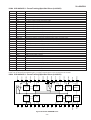
Figure 18 TYPES OF TRANSISTOR AND LED
– 18 –
1
2
3
SVC348S
XL-40H/50H
WAVEFORMS OF CD CIRCUIT
NO DISC FOCUS SEARCH
1
STOP
12
1
FOO
FO+
13
2
IC804 26pin
3
FO-
14
3
SEL
5
6
1
11
2
TEI
15
3
6
SBAD
11
2
3
TEI
1
TRO
2
IC802 49pin
RFO
15
3
FMO
3
IC802 53pin
IC801 22pin
STOP
PLAY
REVIEW
6
1
FEI
TEI
1
TRO
2
IC802 46pin
IC802 43pin
RFGO
11
2
IC801 19pin
IC802 49pin
RFRP
15
3
IC801 17pin
3
FMO
IC802 53pin
STOP
TEI
PLAY
TCD-782 TNO-02 PLAYBACK
16
1
IC802 46pin
TRO
SBAD
LO
1
RO
2
IC802 85pin
2
IC802 49pin
7
FMO
IC802 46pin
IC802 44pin
11
2
CUE
1
FEI
6
TRO
PLAY
IC802 43pin
10
1
IC802 53pin
STOP
5
TEI
IC802 49pin
IC802 46pin
5
PLAY
IC802 46pin
FEI
6
3
STOP
IC802 43pin
9
2
DMO
TOC IL
IC802 57pin
8
SBOK
IC802 55pin
FOCUS SEARCH
7
1
IC802 12pin
IC804 25pin
4
TMAX
IC802 30pin
IC802 48pin
2
PLAY
17
IC802 82pin
3
IC802 44pin
– 19 –
XL-40H/50H
CNP301
FM MUTE LEVEL
VR351
10K(B)
AM ANT
VD301-1
SVC348S
SWITCHING
R_MUTE
Q351
AM OSC OUT
3
4 5
17
FM/AM OUT
VSM
AM LOW CUT
18
6
FM DET
STEREO
SD
GND
IC303
FM IF DET./FM MPX./AM IF
LA1832
9
8
AM MIX OUT
AM IF IN
7
16
14 13
15
MO/ST
2
19
MPX VCO
1
AM OSC.
20
VCC
AM IF IN
FM AFC
REG
AM RF IN
AM OSC OUT
21
23
FM IF IN
T306
22
24
AM MIX OUT AM OSC IN
VD301-2
SVC348S
X351
456kHz
L-CH OUT
T302
PHASE
(AM/FM)
BALUN
R-CH OUT
L341
2
MPX IN
1
2
PHASE
1
IF OUT
AM LOOP
ANTENNA
10 11
12
+5V
AM IF
T351
3
1
ZD351
MTZJ5.1B
CF351
FM IF
CF352
2
+5V
A_12V
A_GND
2
CF301
CF302
1 3
1 3
FM IF
FM IF
Q301
VT
FM
ANTENNA
TERMINAL
SO301
VT
R-MUTE
L-CH
1
7 8 9
Q101-Q104
SWITCHING
NC
SW
6
IF IN
FM
5
MO/ST
DO
4
FM
CL
3
IF REQ
AM IN
PD
FM IN
AIN
DI
1 2
IC101
HEAD SELECTOR
BA3126N
15 14 13 12
17 16
MUTE
18
VDD
19
IC302
LC72131 PLL CONTROLLER
CE
X352
4.5MHz
VT
22 21 20
VSS
4
X IN
FE301
FM FRONT END
IF OUT
F OUT
VCC
GND
GND
GND
ANT.
1
3
X OUT
FM IF
5
NC
FM+B
8 7 6 2
AOUT
D_GND
VT
L-OUT
NF
L-IN
5
1
2
3
4
5
6
7
8
L-CH
RECORD/
PLAYBACK
HEAD
R-CH
ERASE
HEAD
2
CNP101
L-CH
1
2
3
4
5
6
7
8
L-CH
3
L-CH
4
A-GND
A-GND
A-12V
R-CH
ERASE
6
R-CH
7
A-GND
IC101
R-IN
9
Q105
Q106
A_12V
REC
ALC
2
+
-
9
ALC
150K
P/B SW
11
8
R-CH
8
10
MUTE
5
R-CH
IC102
BA3311L
+
IC102
REC./P.B.
EQUALIZER
AMP.
P/B SW
CONT
REC MUTE
1
3
REC SW
A_12V
Q360
10 11
150K
CNS101
FM+B
FM RIPPLE
FILTER
6
7
12
R-OUT
NF
REC SW
SWITCHING
A_12V
Q151
L151
Q152
BIAS OSC
Q171
SWITCHING
SWITCHING
REC
Q153
Q172
SWITCHING
REC BIAS
CONT
SWITCHING
RUN PLS
Q903
SOL
M_12V
PH901
PHOTE INTERRUPTER
U_CON5V
SOL901
SOLENOID
SW902
CAM
CNP901
Q906
MOT
P.F
SOLENOID
DRIVER
Q902
CAM SW
CNS901
Q901
M_GND
Q904
TAPE MOTOR
DRIVER
SWITCHING
CNP703
1 2 3 4 5 6 7 8 9
TO DISPLAY PWB
SWITCHING
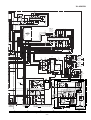
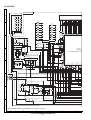
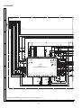
Figure 20 BLOCK DIAGRAM (1/4)
– 20 –
Q905
D-GND
SWITCHING
M_12V
SW901
FOOL
PROOF
7
6
5
4
3
2
1
U_CON 5V
2
7
6
5
4
3
2
1
SOL
2
1
RUN_PLS
-
CFW901
MOT
1
REC
M
+
B-CAN(NC)
BIAS
M901
TAPE MOTOR
XL-40H/50H
UTE
16
15
14
13
11
12
10
9
IC521
RDS CIRUIT
LC72723M
AMP.
1
2
4
3
5
X521
456kHz
6
7
8
Q521
A_12V
A_12V
FM ST
DO
CL
CE
DI
CD+B
P MUTE
P-STB
R-CH OUT
REC R CH
9
8
7
6 TO DISPLAY PWB
5
4
3
2
1
TAPE R
TUN R
CD R
14
15
13
11
12
10
9
8
6
7
5
4
3
DI
SD
12
11
10
CE
VSM
2
1
VSS
RDS CLK
RDS DATA
IC401
LC75342M
CNS704
LOGIC
FUNCTION/VOLUME EQUALIZER
NC
VDD
-MUTE
16
19
18
20
21
22
23
24
26
25
27
29
28
30
CL
17
CD L
TUN L
TAPE L
A_12V
REC L CH
L-CH OUT
A_12V
STEREO
SD
REC L/R CH
L-IN
10
1
L-CH
OUT
TAPE L/R CH
R-IN
8
3
R-CH
OUT
9
6
Q601
Q602
REC
+
SO601
SPEAKER
TERMINALS
+
IC601
LA4600
POWER
AMP.
5
NF
05
06
L-CH
J601
HEADPHONES
L-CH
MUTE
2
VCC
7
4
CD_6R2V
F653
T1A L 250V
CNP652
1
2
Q607
F651
T2.5A L 250V
D651~D654
P-CONT
T651
MAIN POWER
TRANSFORMER
CNS652
1
2
Q606
GND
T.F
VOLTAGE REGULATOR
Q608
Q609
VOLTAGE
REGULATOR
Q683
CD+B
MECHA 12V
(M_12V)
Q605
FROM
DISPLAY
PWB
CNP681
USWD_5R6V
3
P_CONT
2
D_GND
1
RLY681
Q682
Q681
AUDIO 12V
LF651
LINE
FILTER
Q604
(A_12V)
Q603
4 5 6 7 8 9 10 11
DISPLAY PWB
D_GND
CD_6R2V
M-GND
M_12V
CD R
A-GND
CD L
TAPE SW
D-GND
A_12V
M_12V
U_CON 5V
SOL
MOT
D681~D684
1 2 3 4 5 6 7
CNP605
TO CD SERVO PWB
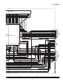
Figure 21 BLOCK DIAGRAM (2/4)
– 21 –
T681
SUB POWER
TRANSFORMER
SO651
AC POWER
INPUT SOCKET
AC230V,50Hz
XL-40H/50H
1 ~ 4
39 ~ 42
X701
8MHz
X702
32.768kHz
SW700
JOG
UP
A
DOWN
B
D701-709
LED
1
1
2
2
3
3
SEG6
SEG5
SEG4
SEG3
SEG2
VLC1
VDD
OSC2
OSC1
VSS
XI
XO
VREF
16 CLID_SW
SW709-SW710
17
KEY
KEY1
SW711-SW717
18 KEY2
SW721-SW728
19 MODEL
20 CLID_PRO
CNP706
21 NC
DI
RESET
DO
24 VREF+
25
REC
CFW701
MOT
22 TAPE_SW
23 VSM
SOL
2
VLC2
CE
1
VLC3
CL
2
COM0
14 MMOD
D_GND
1
COM1
15
CNS706
C
1
2
3
4
5
6
7
8
9
10
11
12
13
SEG1
COM2
SEG0
100 99 98 97 96 95 94 9
COM3
26 27 28 29 30 31 32 3
D_GND
M_12V
Q708
U-COM VDD
U-CON+5V
SYS STOP
SWITCHING
REMOCON
RESET
A_12V
Q707
P CONT
Q709
LED+B
RESET
D_GND
SWITCHING
SWITCHING
3
Q702
2
Q701
Q703
TO POWER PWB
1
RX701
REMOTE
SENSOR
CNS707
3 2
1
SWITCHING
Q706
CFW807
1
+5V
2
CD_6R2V
Q861
2
M_GND
SP-
SL-
SL+
FMO
M_GND
REG
IN
REG
OUT
15 14 13 12 11 10 9
REG.
8
7 6
-
+
4
5
-
3
+
-
-
+
+
IC804
LA6541D
+
-
+
-
RESET
+
CD
RES
IC804
LA6541D
FOCUS/
TRACKING/
SPIN/SLED
DRIVER
DMO
1
SP+
SW801
OPEN/CLOSE
-
-
+
X801
16.93MHz
M_GND
RFGC
FVO
FMO
TEBC
SEL
DMO
FLGA
2VREF
FLGB
FLGC
FLGD
IO0
VDD
IO1
VSS
IO2
IO3
/DMOUT
TESIN
/DACT
/CKSE
PXI
VSS
TESI01
PXO
XI
VDD
XVSS
XO
XVDD
VREF
TRO
FOO
TEI
TSIN
RFRP
RFZI
RFCT
AVDD
37
SLCO
36
AVSS
35
VCOF
TMAX
TMAXS
7 8
PDO
6
ZDET
5
HSSW
4
P2VREF
3
TESI00
2
VDD
1
MONIT
34 VCOREF
33 PVREF
32 LPFO
COFS
97
98
100
+5V
RFI
38
D_GND
31 LPFN
9 10 11 12 13 14 15 16 17 18 19 20 21 22 23 24 25 26 27 28 29 30
+5V
D_GND
Figure 22 BLOCK DIAGRAM (3/4)
– 22 –
13
14
15
16
RFRP
17
18
RFI
19
RFGC
20
21
22
23
24
FEI
FEI
94
99
SBAD
SBAD
93
96
IC801
TA2109F
SERVO PRE AMP.
TEZI
95
SPDA
/RST
39
SPCK
/TSMOD
41
40
SBSY
TEST4
42
SFSY
/CCE
92
DATA
BUCK
91
VSS
VSS
89
90
VDD
VDD
IC802
TC9462F
SERVO/SIGNAL
CONTROL
CLCK
BUS3
43
SBOK
BUS2
44
88
IPF
BUS1
45
87
MBOV
BUS0
86
DOUT
TEST3
46
AOUT
TEST2
85
BCK
TEST1
A_GND
47
VSS
DVSL
84
LRCK
LO
83
EMPH
DVR
50
49
48
/UHSO
DVDD
+5V
80 79 78 77 76 75 74 73 72 71 70 69 68 67 66 65 64 63 62 61 60 59 58 57 56 55 54 53 52 51
81
82
/HSO
RO
TEST0
DVSR
D_GND
D_GND
SBAD
TEO
FEO
TEN
FEN
2VRO
VRO
TEB
RFRP
SEL
RFIS
LDO
RFGO
MDI
RFGC
TN1
AGCI
TPI
RFO
FPI
GND
FNI
RFN
VCC
12
11
10
9
8
7
6
5
4
3
2
1
TEI
TEBC
SEL
E
F
B
A
CD +5V
FOO
FO+
FO-
TR+
TR-
TRO
16 17 18 19 20 21 22 23 24 25 26 27 2
+5V
XL-40H/50H
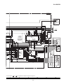
LCD701
LCD DISPLAY
1 ~ 4
5 ~ 38
39 ~ 42
2
768kHz
SEG24
SEG23
SEG22
SEG21
SEG20
SEG19
SEG18
SEG17
SEG16
SEG15
SEG14
SEG13
SEG12
SEG9
SEG11
SEG8
SEG27 73
COM0
SEG28 72
VLC3
VLC2
SEG29 71
SEG30 70
VLC1
SEG31 69
VDD
SEG32 68
OSC2
SEG33 67
OSC1
CCE 66
XO
14 MMOD
VREF
CD_RES
CCE
BUCK
BUS3
BUS2
BUS1
BUS0
CD_STB
PU_IN
BUCK 65
IC701
IX0026SJ
SYSTEM CONTROL
MICROCOMPUTER
XI
15
SEG10
SEG7
SEG6
SEG5
SEG4
SEG3
SEG2
COM1
VSS
CL ID_SW
75 SEG25
74 SEG26
BUS0 61
TAPE_SW
A_12V
CD_RES 59
M_12V
KEY1
18 KEY2
IC702
TA7291S
LOADING MOTOR DRIVER
1
2
3
4
6
5
8
7
D_GND
U_CON5V
SOL
MOT
9
REC
NC
MVOL_IND 53
MVOL_DW
NC 52
DATA
P_CONT
CD+B
P_MUTE
P_STB
MVOL_UP 54
SURR
JOG DOWN
JOG UP
CLE
POWER
CLOCK
RESET
REC
SOL
CE
REMOCON
55
SYS STOP
MVOL_DW
B_CAN
21 NC
22 TAPE_SW
BIAS
CLID_UP
57
56
RUN_PLS
58
CLID_DW
MOT
PU_IN
19 MODEL
20 CLID_PRO
CL
7
TO CD PWB
5
4
3
2
1
BUS1 62
17
DO
8
6
CNS702
CD_STB 60
51
RUN_PLS
D_GND
BIAS
MVOL_UP
BACK LIGHT
M701
JOG MOTOR
26 27 28 29 30 31 32 33 34 35 36 37 38 39 40 41 42 43 44 45 46 47 48 49 50
STEREO
DI
9
BUS2 63
16 CLID_SW
23 VSM
24 VREF+
25
10
BUS3 64
M_12V
SD
1
Hz
1
2
3
4
5
6
7
8
9
10
11
12
13
SEG1
COM2
SEG0
100 99 98 97 96 95 94 93 92 91 90 89 88 87 86 85 84 83 82 81 80 79 78 77 76
COM3
2
2
1
1
CNP705
B_CAN
11
10
9
8
7
6
TO MAIN PWB
5
4
3
2
1
CNP703
M
CNS705
CLE
12
DATA
VSM
SD
STEREO
DO
CL
TO MAIN PWB
CE
DI
CD+B
P_MUTE
P_STB
1
CFW704
CL ID_SW
CD_RES
CCE
BUCK
BUS3
BUS2
BUS1
BUS0
CD_STB
CD_6R2V
PU_IN
10
9
8
7
6
FROM DISPLAY PWB
5
4
3
2
1
REG.
D
/
G/
ED
R
7 6
-
DMO
4
5
-
3
+
-
CD_6R2V
2
CL ID_L
1
A_GND
VCC
8
MUTE
REG
IN
REG
OUT
15 14 13 12 11 10 9
+
SP+
SP-
SL-
SL+
FMO
M_GND
CD STB
CNP702
CD_R
M_GND
-
+
+
M_12V
IC804
LA6541D
D_GND
+
-
+
-
-
-
+
2
3
4
TO MAIN PWB
5
6
7
CNS605
VCC
+
CD
RES
+
-
RESET
CD_6R2V
1
FOO
FO+
FO-
TR+
TR-
TRO
16 17 18 19 20 21 22 23 24 25 26 27 28 29 30
CD_6R2V
SP+
M_GND
SPSL+
SLPU-IN
M_GND
6
6
6
5
5
5
4
4
4
3
3
3
2
2
2
1
1
CNS803
IC801
TA2109F
SERVO PRE AMP.
1
+
SP+
-
SP-
M
NM802
SPINDLE
MOTOR
M
NM801
SLED
MOTOR
SL+
+
SL-
-
PU-IN
GND
NSW801
PICKUP IN
CNP803
PICKUP UNIT
CNS801
SBAD
13
14
15
16
RFRP
17
18
RFI
19
RFGC
20
21
22
23
24
FEI
SBAD
TEO
FEO
TEN
FEN
2VRO
VRO
TEB
RFRP
SEL
RFIS
LDO
RFGO
MDI
RFGC
TN1
AGCI
TPI
RFO
FPI
GND
FNI
RFN
VCC
12
11
10
9
8
7
6
5
4
3
2
1
TEI
TRTR+
FO+
TEBC
FO-
SWITCHING
D-GND
SEL
Q801
+5V
P
VR
E
LD
F
1
1
1
2
2
2
3
3
3
4
4
4
5
5
5
6
6
6
7
7
7
8
8
8
TR-
TR+
TR+
FO+
FO+
FO-
FO-
TR-
GND
ACTUATOR
PD
V
LD
B
A
1/2VCC
CD +5V
CNS802
D_GND
1
2
3
4
5
VREF
+5V
6
7
C
F
B
A
E
1/2V
+5V
1
1
2
2
3
3
4
4
5
5
6
6
7
7
C
F
B
A
E
1/2V
+5V
Figure 23 BLOCK DIAGRAM (4/4)
– 23 –
C
F
B
A
E
GND
MON
LD
VCC
XL-40H/50H
AM TRACKING fL
R364
6.8K
R363
6.8K
C374
0.015
1.3V
4V
12
R355 3.8V
3.3K (1.2V)
C358
1/50
3.8V
(1.9V)
R366
2.2K
(2.2V)
1.3V
R-C
OUT
L-CH
OUT
PHASE MO/ST
(AM/FM)
13
PHASE
10 11
C357
2.2/50
R376
10K
C370
1/50
C355
22P
AM IF
ZD351
MTZJ5.1B
+B
+B
2
C373
0.015
R357
470K
R356
1K
C368
1/50
MPX IN
MPX VCO
FM IF
CF352 2
T351
AM IF
2.1V
2.3V
(0V)
C354
0.022
CF351
2
CF302
FM IF
9
C356
0.001
5V
C353
0.022
3
VCC
8
5V
0V
FM DET
7
3
C372
1/50
15 14
16
C398
100/10
STEREO
6
5V
5
R353 2.9V
C399 270 (4.3V)
0.022
SD
R352
1K
0V
C350
0.022
GND
4
2.1V
C369
56P
R350
2.7K
C367
1/50
17
2.3V
C371
1/50 R361
12K
Q351
1 KRC104 M
4.7V
(0V) 2
R362
12K
IF OUT
C366
0.001
0V (0.9V)
2.1V
(2.7V)
0.6V
2.1V
(2.7V)
AM IF IN
2.1V
1
C383
0.022
R387
5.6K
C386
330P
FM
R373
1K
C384
0.001
R383
5.6K
10.9V
R365
10K
IF IN
NC
MUTE
MO/ST
VDD
FM
FM IN
AM IN
DO
9 10
R385
5.6K
R384
6.8K
C391
47/16
11
3.5V
(0V)
3.7V
(0V)
3.9V
CL
8
5.1V
7
4.8V
DI
6
CE
5
Q360
KTA1266 GR
10.8V
FM RIPPLE
FILTER
11.7V
0V
2.6V (0V)
5.2V
0V
(2.6V)
R379
2.2K
0.9V
PD
0.9V
17 16 15 14 13 12
18
AIN
C385
0.01
3 4
0.1V
2
19
IC302 PLL(TUNER)
LC72131
R374
1K
0.1V
VSS
NC
1
0V
C382
15P(CH)
X IN
2.6V
X352
4.5MHz
AOUT
22 21 20
X OUT
2.6V
C381
12P(CH)
R392
390
IF REQ
R381
10K
C393
1/50
CD SIGNAL
C387
0.022
R377
5.6K
C395
0.022
L351
100µH
R380
1.5K
PLAYBACK SIGNAL
C396
100/10
R391
390
VT
AM SIGNAL
RECORD SIGNAL
R393
1K
NC
R386
330
FM SIGNAL
C380
10/16
C392
0.001
R382
330
+B
R395
47K
L352
100µH
(C376 Serial No. 003xxxxx~)
C
C364
10/16
C365
0.022
C361
0.022
REO
AM OSC
IN
FM IF AM OSC
IN
OUT
C351
0.022
R348
680
19 18
R359
1.8K
D522
1N4148
R360
4.7K
R372
1K
R371
1K
R345
4.7K
C347
0.022
3
X351
456KHz
AM LO FM/AM OUT
CUT
1.7V
(11.4V)
R344
680
20
VSM
C394
47/16
FM IF
CF301
3
1
2
C397
0.022
R343
180
C348
100/16
C345
0.022
C346
0.022
9.5V
Q301
2SC380 O
R346
330
C349
0.001
1
3
1
L342
2.2mH
SO301
FM
ANTENNA
SOCKET
75 OHMS
C341
0.022
+B
C301
0.001
C376
0.001
1
21
C352
10/16
R369B
82
5V
2.5V
2
2.1V
3
R349
33
D304
1N4148
4
9V
22
FM AFC AM RF
IN
IC303 FM IF DET./FM MPX./AM IF
LA1832S
C344
33P
R369A
68
8 7 6 5
B
24 23
FE301
FM FRONT END
D303
1N4148
R347
6.8K
1
2
R336
10K
C334
27P(UJ)
AM OSC.
C360
0.022
AM MIX
OUT
C335
560P
T306
R351
5.6K
C337
0.022
CNP301
L341
BALUN
R323
68K
0.8V
2
+B
AM BAND COVERAGE fL
SWITCHING
L354
L353
1mH
+B
D302
1N4148
1
VR351
10K(B)
VD301
SVC348S
C329
0.022
D301
1N4148
AM LOOP
ANTENNA
C332
0.022
C331
0.047
T302
C343
33P
8.2K
C362
3.3/50
C302
0.001
2.5V
A
FM MUTE
LEVEL
R358
C363
0.022
LOW PASS FILTER
C330
12P(CH)
5V
AM ANT
+B
D
+B
REC L
R115
15K
REC R
3
0V
4
0.3V
(8.3V)
5
0V
6
8V
(10V)
7
0V
8
0V
9
0V
C113
4.7/25
HEAD
SELECTOR
0V
R119
100
R122
4.7K
5
R124
4.7K
9
0V
IC102
BA3311L
REC./P.B.
EQUALIZER
AMP.
0V
C106
270P
Q152
KTA1266 GR
8.3V
3
C153
0.0039
L151
330µH
C154
0.027
(ML)
8
10.1V
10
R134
100K
R141
330
C125
100/25
C123
2.2/50
0V
0V
0V
4.6V
11
6
7
12
C108
47/16
R104
120
R154
10K
2.6V
(0V)
Q151
2SC2001 K
R133
1K
2
C112
10/16
R112
2.2K
C110
0.015
(ML)
Q106
KTC3199 GR
REC MUTE
R108
10K
0.7V
R110
3.9K
R132
4.7K
R106
150K
R155
R153
56
10K
REC. BIAS
C155
100/16
Q171
Q172
KRA102 M
KRC102 M
SWITCHING
R152
100K
D104
1N4148
3
2
Q153
1
KRC104 M
4.7V
(0V)
2
(11.7V)
R151
47K
BIAS OSC
11.7V
(0V)
3 2
10.2V
0.6V
SWITCHING
7.8V
(0V)
1 0V
C126
22/16
1
R125
100K
C122
82P
1
R113
3.3K
4.6V
NC
C104
330P
R116
15K
F
4
0.6V
C116
0.0022
R120
100
C117
10/16
R102
1K
3
C105
270P
C130
4.7/25
Q105
KTC3199 GR
R131
4.7K
REC MUTE
C103
330P
0.3V
(0.8V)
0.7V
C111
10/16
C115
0.0022
R118
22K
1.5V
(0V)
R109
3.9K
C109
0.015
(ML)
C107
47/16
0.3V
0.3V
(0.8V)
(0.8V)
R123
4.7K
SWITCHING
Q102
Q104
KTC3199 GR
KTC3199 GR
0.3V
(0.8V)
C129
4.7/25
R117
22K
R121
4.7K
R126
5.6K
R107
10K
R103
120
SWITCHING
Q103
Q101
KTC3199 GR
KTC3199 GR
1.5V
(0V)
TAPE L
R114
3.3K
ERASE HEAD
2
C114
4.7/25
R139
2.7K
C121
82P
0V
IC101
BA3126N
R140
10K
R138
330
CNS101
CNP101
1
2
3
4
5
6
7
8
1
2
3
4
5
6
7
8
R-CH
C101
0.001
C102
0.001
L-CH
1
C131
820P
E
RECORD/PLAYBACK
HEAD
R101
1K
TAPE R
R111
2.2K
R105
150K
R157
150
+B
R156
150
BI901
SOLENOID DRIVER
C901
0.001
1
D903
1N4148
M_12V
4.9V
1
SWITCHING
3
SOL
1
D904
1N4148
3
U_CON5V
R906
1.5K
C904
0.022
2
D_GND
11.8V
0V
3
MOT
C903
100/25
R901
1.5K
C905
0.022
2
Q906
2 KRA102 M
REC
R902
56K
+B
M 12V
BIAS
11.8V
Q905
2SB562 C
11.7V
SWITCHING
SWITCHING
RUN_PLS
R910
33K
+B
+B
TAPE MOTOR
DRIVER
4.4V
+B
4.9V
Q903
R905
C902 KRC107 M
10K
3.3/50
2
3
3.2V
0.7V
SWITCHING
1 0V
Q902
2SB562 C
11.9V
R909
18K
0.6V
SW901
FOOL
PROOF
SW902
CAM
R903
47K
B_CAN
SOL901
SOLENOID
2
7
6
5
4
3
2
1
Q904
KRC102 M
- 2
7
6
5
4
3
2
1
11.7V
M
R904
270
CNS901
7
6
5
4
3
2
1
R907 11.7V
10K
Q901
KRC102 M
1
PH901
PHOTE
INTERRUPTER
D902
1N4148
+
1
TAPE
MECHANISM PWB-D/E
D901
1N4148
M901
TAPE
MOTOR
CNP901
CFM901
MAIN PWB-A1
G
TAPE_SW
1 2 3 4 5 6 7 8 9
H
CNS703
P27 12-D
TO DISPLAY PWB
• NOTES ON SCHEMATIC DIAGRAM can be found on page 18.
1
2
3
4
Figure 24 SCHEMATIC DIAGRAM (1/6)
– 24 –
5
6
XL-40H/50H
R529
1K
0V
2.5V
0V
2
CE
VDD
9.6V
CL
5V
DI
VSS
1
TEST
3
NC
ROUT LOUT
4.8V
0V
0V
4
5
VREF
4.8V
6
RBS2
LBS2
4.8V
7
C426
0V 10/16
R440
3.9K
4.8V
C424
0.1(ML)
C422
0.1(ML)
8
4.8V
4.8V
9
RBS1 LBS1
4.8V
C420
0.0027
C418
2.2/50
4.8V
4.8V
L4
L3
LC75342M
R4
NC
CE
DI
CL
L2
IC401
CNS704
DO
C416
4.8V 10/16
4.8V
15 14 13 12 11 10
P-STB
R3
4.8V
P MUTE
4.8V
CD+B
R436
10K
R418 R420
1K
1K
R416
1K
C402
10/16
L1
DI
C404
10/16
R2
4.8V
CE
LIN
CNW704
P27 12-F
FROM
DISPLAY
PWB
CL
NC
DO
4.8V
C406
10/16
FM ST
RIN
4.8V
SD
RTRE LTRE
4.8V
0.6V
2.5V
VSM
R438
6.8K
IC401
FUNCTION/
VOLUME
EQUALIZER
LC75342M
RDS DATA
LSL0
0V
0V
5.1V
2.3V
2.5V
0V
RDS CLK
R1
4.8V
P_STB
P_MUTE
+B
C525
22P(CH)
CD R
STEREO
8
C524
560P
TUN R
SD
12
11
10
9
8
7
6
5
4
3
2
1
C526
22P(CH)
X521
456kHz
TAPE R
CLE
VSM
C522
330P
C535
47/16
DATA
CD+B
R521
47K
D521
1N4148
C521
10/16
C523
0.1
+B
L521
2.2mH
5.1V
2.5V
+B
+B
9
IC521
LC72723M
RDS CIRCUIT
1 2 3 4 5 6 7
R532
10K
C536
0.022
1.3V
0V
2V
AMP.
R533
56K
16 15 14 13 12 11 10
2.5V
C537
0.022
1.3V
5.1V
Q521
KTC3199 GR
2.5V
C527
0.1
RSL0
4.8V
R528
1K
+B
R534
56K
C425
10/16
0.9V
R385
5.6K
R424
1K
C391
47/16
R439
3.9K
R423
1K
CL
R425
1K
CE
DI
D402
1N4004
D401
1N4004
+B
+B
+B
D403
1N4004
R435
10K
C430
100/16
C415
10/16
R417 R419
1K
1K
C429
33/16
10/16
C421
0.1(ML)
10/16
C405
C419
0.0027
C403
TAPE L
R437
6.8K
TUN L
C417
2.2/50
R415
1K
C401
10/16
CD L
C423
0.1
16 17 18 19 20 21 22 23 24 25 26 27 28 29 30
360
TA1266 GR
10.8V
L601
0.3mH
8
1.4V
1.7V
C606
4.7/25
C697
0.001
R608
1K
7 4
3
C616
4700/25
C699
0.0033
C615
D601
1N4148 0.022
SO601
SPEAKER
TERMINALS
C617
0.0022
+
SP602
WOOFER
4 Ohm
SPEAKERS
R-CH
SP604
TWEETER
L602
0.3mH
C614
1000/25
9.8V
20V
L-CH
SP601
WOOFER
4 Ohm
5
R662
330
5
3
2
L603
10µH
12.9V
TWEETER
+
C663
820P
6
SP603
C636
0.022
R632
6.8 C618
0.0022
IC601
POWER AMP.
LA4600
C608
22/25
R602
10K
+B
2
0V
0V
C604
0.001
R604
10K
Q602
KTC3199 GR
R607
6.8K
9
R616
6.8K
C640
0.01
IC601
LA4600
C632 C639
0.022 0.01
9.5V
1
CFW601
5
9.8V
R633
10
R603
10K
R113
3.3K
1.4V
C694
330P
Q601
KTC3199 GR
TAPE L
10
C603
0.001
R615
6.8K
C601
33/16
REC R
C613
1000/25
C607
100/25
R634
3.3K
REC L
C637
00.22
C605
4.7/25
R601
10K
TAPE R
C693
330P
C698
330P
C633
0.022
R631
6.8
+B
R661
330
1
J601
HEADPHONES
C662
820P
C661
820P
4
5
9
+B
+B
1
2
1
2
1
2
C654
0.1
D653
+B1
Q603
KTC3199 GR
20V
R629
820
ZD601
MTZJ13A
5.8V
D_GND
5.6V
R683
47
ZD682
MTZJ5.6B
C688
0.022
6.4V
R681
47
RLY681
C684
0.047
R685
10K
R686
47K
R682
1.2K
4.9V
0.8V(0V)
P_CONT
9V
9V
R684
1.2K
USWD_5R6V
CNP681
1 2 3 4 5 6 7 CNP605
CNS605
P29 12-C
FROM CD SERVO PWB
Q682
2SD468 C
CNS707
P26 1-F
FROM
DISPLAY
PWB
C620
470/25
R617
33K
13V R628
100
3
2
1
Q683
KTC3199 GR
When servicing,pay attention as the area enclosed
by this line (
) is directly connected with AC
main voltage.
(238)
TO MAIN
CHASSIS
D681
D682
C695
0.001
C683
2200/16
LF651
LINE
FILTER
D681~D684:
1N4004
C660
0.01
D602
1N4148
D603
1N4148
+B
R620
47
C621
100/25
CD_6R2V
D_GND
M_12V
M_GND
CD_R
12.3V
R621
22K
C622
0.022
CNP703
A_GND
CD_L
A_12V
M_12V
D_GND
MOT
U_CON5V
REC
SOL
+B
CNS703
P27 12-D
TO DISPLAY PWB
GND2
Q604
2SD2012 Y
11.7V
20V
+B
3 4 5 6 7 8 9 10 11
R619
47
GND3
R623
22K
C625
10/16
C624
0.022
Q605
2SD2012 Y
Q683~Q685
VOLTAGE
REGULATOR
Q681
2SD468C
+B
C686
0.022
20V
11.7V
0.2V
+B
D684
D683
T681
SUB POWER
TRANSFORMER
C696
0.01
1
2
1
2
(226)
TO TAPE MECHANISM
CHASSIS
SO651
AC POWER INPUT SOCKET
AC230V, 50Hz
CNP653
7
8
9
0V
D685
1N4004
Q681~Q683
VOLTAGE REGULATOR
GND1
+B
T.F
D654
B1GND
C685
47/16
3
1
(5.2V)
0V
C651
0.1
C652
0.1
Q608
KRA102 M 2
D651
C653
0.1
ZD602
MTZJ7.5C
R625
10K
C626
47/16
2
D652
T651
MAIN POWER TRANSFORMER
D651~D654:
1N4004
BI652
7.5V
R624
1K
Q609
KRC107 M
0V
3
CNP652
7.8V
1
CNS652
D604
1N4148
F651
T2.5A L 250V
F653
T1A L 250V
Q686~Q689
VOLTAGE
REGULATOR
4.5V
C627
0.022
R627
10K
CD TEST POINT
POWER PWB-B
+B
Q606
KTC3199 GR
C689
47/16
Q607
2SD2012 Y
6.2V
20V
+B
10
1
ZD681
MTZJ6.8A
+B
1
10
Figure 25 SCHEMATIC DIAGRAM (2/6)
– 25 –
11
12
XL-40H/50H
R7D4
82
C
2
R7B2
47K
R794
180
D732
HY2043
3
R7B3
2.2K
R796
180
D737
HY2043
R795
180
1
SW710
CLOCK/TIMER/SLEEP
R701
10K
R797
180
SW709
ON/STAND-BY
C
A
B
D
CNS706
CNP706
R728
1K
X701
8 MHz
X702
32.768kHz
+B
BI706
SW700
JOG
C701
22P
(CH)
1
1
1
2
3
2
3
2
3
C702
22P
(CH)
R724
1.2K
R731
1K
R732
1K
R733
1K
IC702
LOADING MOTOR DRIVER
TA7291S
0V
5
6
7
8
9
C772
0.1
CNP705
M701
JOG MOTOR
VLC1 3.3V
8
VDD
9
OSC2 2.6V
10
OSC1 2.6V
11
VSS 0V
12
XI
13
XO 1.9V
14
MMOD 0V
MVOL_DW
R799
2.2K
5V
2.4V
15
VREF
16
CLID_SW
IC701
IX0026SJ
SYSTEM CONTROL MICR
0V
17
KEY1
5V
18
KEY2
5V
19
MODEL 5V
20
CLID_PRO
NC
22
TAPE_SW
5V
23
VSM
0.6V
24
VREF+
5V
+B
+B
C773
47/16
F
+B
BI707
TO POWER CNP707 P25 10-G
PWB
+B
1
1
2
2
3
3
CNS707
+B
+B
D723
1N4148
D722
1N4148
R7A5
10K
C711
RESET
3.3/50
Q701
KRC102 M
3
R7A6
1K
R7A2
100K
C712
0.01
D721
1N4148
G
C710
0.01
C715
100/10
R7A4
120
Q703
KTC3199 GR
SWITCHING
1
1
R7A1
1K
R7A8
82
R7A3
100
RX701
REMOTE
SENSOR
Q702
KTC3199 GR
SWITCHING
2
R7A7
1K
R7B0
10K
ZD701
MTZJ3.3B
D720
1N4148
R7A0
1K
R7A9
3.3K
C714
560P
2
R778
47K
3
+B
+B
R779
47K
C713
10/16
R780
47K
R781
47K
R782
33K
SWITCHING
Q707
KTA1266 GR
R783
33K
+B
+B
Q706
KRC102 M
R792
47K
+B
+B
SWITCHING
2
R793
2.2K
3
C704
0.022
1
H
• NOTES ON SCHEMATIC DIAGRAM can be found on page 18.
1
2
3
2.5V SEG13
VLC2 1.7V
7
2.5V SEG12
VLC3 0V
6
26 27 28 29 30 31 32 33 34 35 36 37 38 39
MVOL_UP
R798
8.2K
E
COM0
2.5V
5
DI
25 0V
R737
1K
2
R721
10K
2
R787
2.2(1/2W)
R722
10K
1
C771
47/16
1
COM1
2.5V
4
21
R725
10K
2.5V
4
R734
1K
+B
CNS705
M
0V
3
11.7V
0V
2
NC
11.7V
1
0V
0V
IC702
R729
47K
R727
47K
C703
0.022
R702
10K
+B
JOG SWITCH
PWB-A7
R723
47K
+B
L701
100µH
SWITCHING
Q709
KRC102 M
COM2
2.5V
3
5V
D730
HY2043
D736
HY2043
2
REMOCON
R720
1.2K
2.5V SEG11
SW711
TUNING UP
5V
R711
1.2K
SYS_STOP
SW721
MEMORY/SET
R749
1K
R750
1K
R751
1K
+B
99 98 97 96 95 94 93 92 91 90 89 88 87
SEG0
COM3
2.5V
R743
1K
R746
1K
R744
1K
R745
1K
R748
1K
R747
1K
Q708
KTA1266 GR
SWITCHING
100
1
POWER 5V
R719
1.2K
2.5V SEG9
SW712
PLAY/CD PAUSE
2.5V SEG10
R710
1.2K
B-CAN
SW722
BASS/TREBLE
R739
1K
CFW701
R740
1K
R741
1K
R775
1K
2
R738
1K
1
2.5V SEG8
R718
1.5K
BIAS 0V
SW713
VOLUME SELECT
2.5V SEG7
R709
1.5K
R730
1K
2
RUN_PLS 0V
SW723
BAND
LED PWB-A4
1
2.5V SEG6
R717
2.2K
CLOCK 5V
SW714
DISPLAY MODE
2.5V SEG5
R708
2.2K
RESET 5V
SW724
REC. PAUSE
2.5V SEG4
R716
2.7K
REC 0V
SW715
ASPM
2.5V SEG3
R707
2.7K
9 10 11 12 13 14 15 16 17 18
MOT 5V
R715
3.9K
2.5V SEG2
SW716
EON
7 8
SOL 0V
R706
3.9K
2.5V SEG1
D703
MPG3372X
SW725
STOP/ CLEAR
SW717
PTY.PI
6
5
CE 0V
R7E1
82
SW726
TUNING DOWN
R705
5.6K
3 4
CL 5V
D702
MPG3372X
SW727
FUNCTION
2
1
DO 5V
D701
MPG3372X
R7D2
82
D705
MPG3372X
R7D6
82
D704
MPG3372X
R7D1
82
SW728
VOLUME/JOG
R7D9
82
B
LC
D706
MPG3372X
R7D8
82
D707
R7D5
MPG3372X
82
D709
MPG3372X
R7D3
82
A
D708
MPG3372X
DISPLAY PWB-A2
4
Figure 26 SCHEMATIC DIAGRAM (3/6)
– 26 –
5
6
XL-40H/50H
LCD701
LCD DISPLAY
SEG24
75
SEG26
2.5V
74
2.5V SEG27
73
2.5V SEG28
72
2.5V SEG29
71
2.5V SEG30
70
2.5V SEG31
69
2.5V SEG32
68
66
5V CCE
65
4V BUCK
4.3V BUS3
64
4.3V BUS2
63
4.3V BUS0
61
5V CD_STB
60
5V CD_RES
59
PU_IN
58
CLID_DW
57
CLID_UP
56
0V MVOL_DW
55
0V MVOL_UP
54
STEREO
0V
SD
0V
DATA
5V
BACK_LIGHT NC
P_CONT
5V
CD+B 5V
P_MUTE 0V
4.6V
P_STB
R761
1K
R774
1K
R762
1K
R763
1K
R764
1K
R765
1K
R766
1K
R767
1K
R768
1K
CCE
BUCK
BUCK
BUS3
BUS3
BUS2
BUS2
BUS1
BUS1
BUS0
BUS0
CD_STB
CD_STB
CD_RES
PU_IN
PU_IN
51
9
8
8
7
7
6
6
5
5
4
4
3
3
2
2
1
1
CNS703
11
A_12V
+B
+B
M_12V
D_GND
U_CON5V
R773
1K
5
RUN_PLS
R776
1K
9
8
6
MOT
4
3
BIAS
SD
10
7
SOL
R785
1K
REC
R777
1K
R757
1K
R758
1K
R759
1K
R760
1K
R742
1K
10
9
R784
47K
36 37 38 39 40 41 42 43 44 45 46 47 48 49 50
R749
1K
R750
1K
R751
1K
R752
1K
R753
1K
R754
1K
10
TAPE_SW
52
5V
CCE
R771
1K
R772
1K
53
5V MVOL_IND
SURR
JOG_DOWN 5V
CLE 5V
JOG_UP 5V
5V
REMOCON
5V
SYS_STOP
POWER 5V
B-CAN
62
4.3V BUS1
5V
CD_RES
67
2.5V SEG33
IC701
X0026SJ
ROL MICROCOMPUTER
BI702 CNS702
CLID_SW
CNP702 TO CD PWB
P28 1-B
SEG25
2.5V
CNP703 TO MAIN PWB
P24 6-H
2.5V SEG23
2.5V SEG22
2.5V SEG21
2.5V SEG20
2.5V SEG19
2.5V SEG18
2.5V SEG17
2.5V SEG16
2.5V SEG15
2.5V SEG14
2.5V SEG13
2.5V SEG12
2.5V SEG11
2.5V SEG10
90 89 88 87 86 85 84 83 82 81 80 79 78 77 76
2.5V
15 16 17 18 19 20 21 22 23 24 25 26 27 28 29 30 31 32 33 34 35 36 37 38 39 40 41 42
B_CAN
2
1
CD+B
12
CLE
DATA
DATA
VSM
VSM
STEREO
CNS704 TO MAIN PWB
P25 8-B
CLE
R789
47K
R786
47K
BIAS
SD
RUN_PLS
STEREO
MVOL_IND
DO
MVOL_UP
CL
MVOL_DW
CE
+B
REC
DI
B_CAN
CD+B
CLID_PRO
P_MUTE
P_STB
P_STB
1
P_MUTE
CFW704
MOT
SOL
CE
+B
CL
DO
DI
TAPE_SW
CLID_SW
+B
+B
+B
+B
7
8
9
10
Figure 27 SCHEMATIC DIAGRAM (4/6)
– 27 –
11
12
XL-40H/50H
A
C
PU_IN
1
2
3
4
5
6
7
8
9
10
CD_STB
BUS0
BUS1
BUS2
BUS3
BUCK
CCE
CLID_SW
CD_RES
B
FROM DISPLAY PWB CNS702 P27 12-C
CNP702
CD SIGNAL
R813
10
L803
10µH
+B
L8
10
R817
1K
R818
1K
D
R812
3.3K
C823
0.01
C825
0.056
C834
470P
C833
470P
R814
3.3K
C824
0.056
C819
0.1
C821
0.1
C822
220/10
0V
C817
0.1
R811
2.2K
15
5V
0V
0V
0V
0V
5V
C832
10/16
C831
10/16
4
R820
1K
R816
10K
R815
10K
C818
0.1
X801
16.93MHZ
R810
3.3K
BUS0 4.3V
BUS1 4.3V
5
BUS2 4.3V
BUS3 4.3V
5V
VSS
0V
0V
NC HSSW 2.1V
1.7V
NC COFS
NC ZDET
0.6V
NC SPDA
P2VREF 4.3V
0V
NC SPCY
TESIOO 0V
0V
NC SBSY
VDD 5V
2.4V
NC SFSY
NC MONIT 0V
0V
NC DATA
VSS 0V
VDD 5V
1.2V
NC CLCK
0V
NC SBOK 5V
NC IFP
LRCK
NC
NC MBOV 0V
EMPH
NC
VSS 0V
UHSO
NC
NC
NC AOUT 0V
3.3V
NC TEST4
NC BCK 2.5V
/CCE
DOUT 2.5V
BUCK 4V
0V
1.4V
1 2 3 4 5 6 7 8 9 10 11 12 13 14 15 16 17 18 19 20 21 22 23 24 25 26 27 28 29 30
R804
100K
12
R806
15K
C802
0.015
C863
470P
13
C850
VDD
FMO
2.1V
TEBC
2.1V
RFGC
1.8V
2.2V DMO
0V FVO NC
7
IC802
TC9462F
SERVO/SIGNAL CONTROL
R802
47K
R801
10K
C801
100P
C820
0.01
C829
100/10
C838
47/10
G
+B
+B
H
• NOTES ON SCHEMATIC DIAGRAM can be found on page 18.
1
2
3
4
Figure 28 SCHEMATIC DIAGRAM (5/6)
– 28 –
5
C813
100/10
5V
C811
47/10
C812
0.01
5V
NC TEST3
TMAX
2.1V
NC TEST2
6
NC TMAXS 2.1V
5V
VREF
C810
50 2.1V
0.001
R809
49
10K
11 2.2V FOO 48
R808
C809
2.2V TEZI 47
3.3K
0.0047
2.2V TEI 46
2.1V TSIN 45
2.1V SBAD 44
2.2V FEI 43
C807
2.1V RFRP 42
0.033
2.1V RFZI 41
2.1V RFCT 40
R807
10K
5V AVDD 39
C806
0.0047
2.1V RFI 38
C805
2.1V SLCO 37
0.0027
0V AVSS 36
C804
1.4V VCOF 35
0.01
VCOREV
2.1V 34
PVREV
C803
2.1V 33
47/10
LPFO
2.1V 32
LPFN
31 2.1V
2.1V TRO
PDO 2.1V
2.5V SEL
14 1
16
NC TEST1
4.3V 2VREF
0V FLGA NC
0V FLGC NC
5V FLGB NC
0V VSS
5V VDD
0V FLGD NC
IO2 NC
IO1 NC
IO0 NC
IO3 NC
/DMOUT NC
0V TESIN
/DACT NC
0V VSS
0V PXI
0V TESI01
5V VDD
0V XVSS
/CKSE NC
0V
5V PXO NC
2.4V
DVSL
TESTO
/RST
4.9V
2.3V
LO
5V
100
C837
470P
DVR
/HSO
F
C836
100/10
R855
100K
R854
100K
R853
100K
R852
100K
C835
0.056
0V
5V
R819
220
17
DVDD
NC
BUS0
BUS1
BUS2
BUS3
BUCK
CCE
CD_RES
C840
100/10
RO 2.4V
NC
C830
0.056
E
81
82
C828
83
100/10
84
85
86
87
C862
0.0022 88
89
90
91
92
93
94
95
96
97
5V 98
5V
99
/TSMOD
5V
DVSR
XVDD
0V
XO
2.6V
2.2V XI
80 79 78 77 76 75 74 73 72 7170 69 68 67 66 65 64 63 62 61 60 59 58 57 56 55 54 53 52 51
0V
6
XL-40H/50H
CD PWB-A3
CFW807
1
1
2
2
SW801
OPEN/CLOSE
C861
0.001
CD_L
A_GND
CD_R
L804
2.2µH
M_GND
M_12V
D_GND
CD_6R2V
C844
0.0068
C887
0.0027
6.3V
4.9V
2.2V
C859
470/10
BI803
C860
0.1
6.3V
2.1V
2.1V
3.1V
2.5V
0V
0V
0V
2.8V
2.2V
2
3
2.8V
NC 2.1V
2.1V
NC 5V
NC 5V
IC804
LA6541D
C857
47/16
CNP605
P25 7-H
(L804/R843
Serial No.
003xxxxx~)
SP+
6
5
4
3
2
1
SP-
16 17 18 19 20 21 22 23 24 25 26 27 28 29 30
SP+
SL-
R863
2.2K
+B
PU-IN
GND
CNS803
R862
2.2K
2.2V
3.1V
0V
2.5V
0V
0V
2.8V
2.8V
2.2V
2.2V
5.1V
5.6V
15 14 13 12 11 10 9 8 7 6 5 4 3 2 1
IC804
LA6541D
FOCUS/
TRACKING/
SPIN/SLED
DRIVER
TO MAIN PWB
+B
+B
R861
2.2K
L801
10µH
1
2
3
4
5
6
7
6
5
4
3
2
1
CNP803
Q861
2SB562 C
5V
6.3V
+B
R843
1K
L803
10µH
1
2
3
4
5
6
7
CNS605
BI605
OPEN/CLOSE
SWITCH
PWB-A6
6
5
4
3
2
1
CD MOTOR PWB-C
+
SP+
SP-
-
SP+
+
SLPU-IN
-
M
NM802
SPINDLE
MOTOR
M
NM801
SLED
MOTOR
GND
NSW801
PICKUP IN
PICKUP UNIT
TR+
TR+
R823
1K
C847
0.1
C848
39P
R828
1.2K
R826
2.7K
R827
27K
C839
2P
R829
68K
C850
220/10
2.1V
2.1V
2.1V
10
9
2.1V
2.1V
2.1V
8
2.1V
2.5V
3.4V
0V
2.1V
2.1V
1.7V
2.1V
0V
2.1V
5V
2.1V
PD
R822
22
R821
150
4.1V
3.4V
VR
LD
BI801
4.3V
C841
100/10
2.1V
2.1V
GND
Q801
KTA1266 GR
SWITCHING
1
2
3
4
5
6
7
8
TRPO+
TR+
PO+
FO-
FOGND
TR-
PD
ACTUATOR
VR
LD
GH6C605B3A1
1/2VCC
+B
C843
0.1
R80E
82K
+
-
C
+
C863
470P
C849
0.056
2.2V
12
11
10
9
8
7
6
5
4
3
2
1
FO-
C855
100/10
R80A
82K
R80B
68K
R80C
82K
R80F
82K
R80G
68K
IC801
TA2109F
SERVO PRE AMP.
F
B
A
E
VREF
+5V
+B
1
2
3
4
5
6
7
1
2
3
4
5
6
7
BI802
+B
C
CNS802
C813
100/10
C812
0.01
C846
0.1
2.2V
2.1V
C842
47/10
2V
C845
100/10
13
14
15
16
17
18
19
20
21
22
23
24
IC801
TA2109F
R825
82K
PO+
R824
27K
1
2
3
4
5
6
7
8
1
2
3
4
5
6
7
8
CNS801
TR-
1
2
3
4
5
6
7
C
-
F
F
B
+
-
B
+
A
E
-
A
+
-
1/2V
+5V
E
GND
MON
LD
B
VCC
• The numbers 1 to 17 are waveform numbers shown in page 19.
7
8
9
10
Figure 29 SCHEMATIC DIAGRAM (6/6)
– 29 –
11
12
XL-40H/50H
ANTENNA
TERMINALS
SO601
SPEAKER
TERMINALS
A
AM LOOP
ANTENNA
ANTENNA
SO301
FM 75 OHMS
LEFT
RIGHT
CNP301
1 2
WH
PK
WH
RECOED/
PLAYBACK
HEAD
R349
R347
C382 C381
R374
X352
C391
R533
R106
R132
R131
C110
IC102
R103
C105
CNP703
CNS901
R105
C109
TO DISPLAY PWB
CNS703
P31 9-A
P33 5-E
TO TAPE
MECHANISM PWB
MAIN PWB-A1
BK
H
1
2
3
4
Figure 30 WIRING SIDE OF P.W.BOARD (1/4)
– 30 –
5
12
11
10
9
8
7
6
5
4
3
2
1
6
FROM
P31 12-C
DISPLAY PWB
R534
R111
C527
R114
R112 R113
C126
R121
C106
C114
C113
C103
C107
GY
GY
GY
GY
GY
GY
BK
WH
RD
WH
BK
BK
YL
BL
WH
BK
HEADPHONES
PWB-A5
RD
CFW704
Q521
CNP901
8 7 6 5 4 3 2 1
R391
R384
R385
R392
C396
ZD351
C523
9 10
11 10 9 8 7 6 5 4 3 2 1
ERASE
HEAD
R371
R372
R373
C384
C357
C524
C522 E
16
C
15
B
R107
J601
HEADPHONES
L521
IC521
R115
CNS101
D522
R382
R386
C370
C398
CF351
C358
R355
C525
1
C111
1
7 6 5 4 3 2 1
CF301
R348
R344
C380
C394
R380
R387 R360
R359
L351
L353
CF302
R352
C356
R353
R528
R529
C526
X521
C102
R138
R156
D521
C536
C521
C116 C115
C130 R118
R117
R119 Q103 C117
R120
E C B
1
E C B
R134
2
R123
B
R125
3
Q106 Q105
3
E
C
B
C R122
2
B B
Q101 R126
E Q102
1
C C
D104 R133
R116
R108
E E
CNP101
C108
C112
8
9
7
R102
R104
8
R110
6
12
7
5
11
10
C104
6
4
9
C123
8
3
5
7
2
6
R141
4
5
1
4
3
3
C125
2
2
1
R101
1
R109
Q171
R151
C154
C535
R532
C129
C121C122
C153
Q151
3 2 1
Q903
5
8
R377
C395
R366
R521
R124
R905
C537
Q351
3
2
1
Q172
7
BK
GY
GY
GY
GY
GY
GY
L352
Q104
C901
D902
E
C
B
R910
R909
12
11
10
9
8
7
6
5
4
3
2
1
Q360
B C E
R383
R395
IC101
CFW601
C663
C662
R157
1
R903
R904
3
2
1
C902
1 2 3
Q904
C904
Q153
D901 Q902
BI901
R902
C903
R907
R153
Q152
C155
R438
Q906
3 2 1
R662
C661
R661
G
E
C
B
R152
C416
3
2
Q901
1
B
C
E
L151
15 R420
D904
R901
C404
D903
C905 R906
C406
E
C
B
R154
R415
R416
Q905
R155
L603
C361 R351 C350
1 2 3 4 5 6 7
CFW601
5
C332
CNP605
C402
C418
C422
R436
C424
R440
5
Q609 R628
1 2 3
C401
C405
R435
20 16 R417
10
5
C420
C620
C386
1
1 2 3 CF352
2
C351
3
4
C352
5
6 C399
7
2
8
9
1
10
11
12
C355
C354 R376
C353
C363
R393
R363
R419
R418
1
C403
25
IC401
C426
1
C417
30
C419
C423
C421
R439
R425
R424
F
Q608
C415
C429 R437
C425
D403
1 2 3
R423
C430
E
R617
R629
R624
1
2
3
C131
R139
C101
R140
CNS605
P32 9-C
R356 C368
C372
R362
C373
C371
ZD601
C622
C369
CNS704
D401
D402
C367
R357
C374
R364
C621
E C B
FROM
CD PWB
24
23
22
21
20
19 C360
18
17
16
15
14
13
IC303
Q603
D
C364
R350 C365
C366
L354
C344
X351
R620
R358
R634
F653
T1A L 250V
C385
T351
C362
R608
C693
VR351
R336
C343
R621
B
C
E
FM
MUTE
LEVEL
C337
R623
R619
C624
Q604
C616
T306
R627
C627
B
C
E
C625
R603
C615
1 2
CNP652
C694
D604
VD301
C335
R625
Q605
C601
R602
B C E
E R607
C
Q602
B
R604
Q601
C626
D602
D603
C606
C605
C330
C331
C334
R323
ZD602
Q607 Q606
E
B
C
C
B
E
R601
R615
C604 C603
R616
P33 8-A
C393
C329
D601
CNS652
R381
R379
12 13 14 15 16 17 18 19 20 21 22
R365
C383
C392
C387
11 10 9 8 7 6 5 4 3 2 1
T302
1 2 3 4 5 6 7 8 9 10
FROM
POWER
PWB
R369B
IC302
C608
C697
C
D301
C607
C698
IC601
R369A
C639
D302
C699
C613
R343
R633
C614
C376
(Serial No.
003xxxxx~)
R345
D303
C640
D304
L601
R631
C636
B
C301
C349
C302
C633
C632
L602
R346
L342
Q301
L341
E
C346
C341
C
B
8 7 6 5
4 3 2 1
C347
1
C345 R370
2
FE301 C348
C397 3
C617
C637
R361
R632
C618
XL-40H/50H
DISPLAY PWB-A2
R752
R734
R702
R730
R738
R781
R737
L701
C702
15
10
50
IC701
51
55
60
65
5
95
90
85
1
100
70 80
LCD701
7576
R761
R774
R762
R763
R764
R765
R766
R767
R768
R771
R772
R773
R785
SW724
REC
PAUSE
SW717
12
C773
PTY.
TI
GY
GY
GY
GY
GY
GY
GY
GY
GY
BK
C704
C713
R7A1
D723
C710
R7A7
1
2
TO CD PWB
CNP702
P32 1-E
CFW704
12
1
IC702
1 2 34 5 6 7 8 9
R715
R709
R787
R708 R798
CNS704
R707
R716
SW711
TUNING
UP
SW712
PLAY/CD
PAUSE
SW715
ASPM
SW714
TO MAIN PWB
R799
P30 6-E
SW726
TUNING
DOWN
SW727
C772
FUNCTION
R706
SW725
STOP/
CLEAR
SW716
EON
COLOR TABLE
1
1
WHITE
LINE
SW728
VOLUME/
JOG
R720
DISPLAY
MODE
R786
R719
D737
R796
R718
R797
D730
CNP705
2 1
CNS705
BK
RD
Q708
D732
R7B2
Q709
R7B3
3
2
1
BR
BROWN
RD(R)
RED
OR
ORANGE
YL
YELLOW
GR
GREEN
BL
BLUE
VL
VIOLET
GY
GRAY
WH(W)
WHITE
BK
BLACK
PK
PINK
M
M701
JOG MOTOR
SW713
R794
B
C
E
D736
R795
Q706
1 2 3
BI706
R7A9
R7B0
R7A4
C715
D720
R7A3
D722
Q703
E C B
R7A6
3
2
1
R784
RX701
10
9
8
7
6
5
4
3
2
1
C771
1
2
C714
Q702
B
C
E
D721
ZD701 R7A8
R7A2
R793
E C B
1
3
1
3
R792
CNS707
WH
1
BK
2
BK
3
TO POWER PWB
CNP681
P33 8-A
BI707
Q707
GY
GY
BK
CFW701
32 1
SW700
JOG
CNS706
CNP706
1 C
2 A
3 B
7
8
9
D709
R7D3
D708
D707
D706
R7D5
R7D8
R7D9
D705
R7D1
D704
R7D6
D703
R7E1
CFW701
D702
1
2
R7D2
R7D4
LED PWB-A4
D701
Q701
R729
MEMORY
/SET
R751
C712
3
2
1
R721
R783
SW723
BAND
VOLUME
SELECT
R7A5
C711
R750
R7A0
R744
R776
R777
R760
R759
R758
R757
R742
R754
R753
R722
10
R710
R782 SW721
R732
R731
R723
R727
C703
1
2
3
4
5
6
7
8
9
10
11
12
13
14
15
16
17
18
19
20
21
22
23
24
25
26
27
28
29
30
31
32
33
34
35
36
37
38
39
40
41
42
20
40
R725
R733
C701 R728
26 25
45
R724
CNS702
BI702
SW709
ON/STAND/BY
X702
X701
R749
30
35
1 2 3 4 5 6 7 8 9 10 11
CNS703
SW722 CLOCK/TIMER/
BASS/ SLEEP
TREBLE
SW710
R705
R779
R780
R711
R745
R778
R717
R748
R701
CNP703
R746
R743
R775
R741
R740
R739
R747
R789
TO MAIN PWB
P30 6-H
10
Figure 31 WIRING SIDE OF P.W.BOARD (2/4)
– 31 –
JOG SWITCH
PWB-A7
11
12
XL-40H/50H
PICKUP UNIT
CD MOTOR PWB-C
CNP803
A
NSW801
PICK UP IN
NM802
SPINDLE
MOTOR
6
5
4
3
2
1
F3895AF
B
7
8
NM801
SLED
MOTOR
L804/R843
(Serial No. 003xxxxx~)
C
1
1
OPEN/CLOSE
SWITCH PWB-A6
TO MAIN PWB
P30 1-E
1
CFW807
CNP605
2
SW801
RD
WH
GY
WH
GY
WH
R804
C802
C804
R801
C803
C801
R862
R861
IC804
R863
C857
C821
BI801
R821
R822
C842
R824
C844 C845
R825 IC801
12
13
C848
15 10
C813
R828 C846
20 5
R826 C847
R827
1
C841
R808 C809
R802
C863
C859
C807
C812
R807
30 31
C860
E
C
B
L801
R80B
R80G Q801
R80E
R80F
R80A
C838
G
C818
10 IC802
45
15
20
40
25 35
55
C805
C820
60
C829
BCE
R812
R811
51
R810 C817
50
R809 C810
65
16
17
18
19
20
21
22
23
24
25
26
27
28
29
30
Q861
R814 C819
70
R806
C836
C837
F
BI803
C822
C823
C824
95
6
L803
85 75
5
15
14
13
12
11
10
9
8
7
6
5
4
3
2
1
R823
81 80
90
100
1
X801
R820
R819
C825
R813
C830
1
C887
R855
C835
C828
BI605
C861
R843
R816
C831
C840
C862
R852
R853
P31 12-B
E
R818
L804
C832
R854
CNS702
1
2
3
4
5
6
7
8
9
10
SW801
OPEN/CLOSE
7
C839
CNP702
1
C834
R817
C833
R815
C806
16
2
CFW807
C811
1
14 3 2
1 2 3 4 5 6
BK
GY
GY
GY
GY
GY
GY
D
FROM
DISPLAY
PWB
CNS803
CNS605
1 2 3 4 5 6 7
C850
15
11
1
CNS801
RD
WH 1
GY 2
WH 3
GY 4
WH 5
GY 6
WH 7
8
8
1
1 R80C
R829 C849
24
C843
4
17
7
BI802
CNS802
RD
1
WH
2
GY
3
WH
4
GY
5
WH
6
GY
7
C855
5 7 6 10 9 8
13 12
CD PWB-A3
H
• The numbers 1 to 17 are waveform numbers shown in page 19.
1
2
3
4
Figure 32 WIRING SIDE OF P.W.BOARD (3/4)
– 32 –
5
6
XL-40H/50H
TO MAIN PWB
CNP652 P30 1-C
FROM
DISPLAY PWB
P31 12-G
CNS707
C652
D652
F651
T2.5A L 250V
R686
C651
C695
R685
D654
1
BI652
D653
2
C653
1 2 3
CNP681
D651
BR
RD
2 1 CNS652
C654
E C B Q683
C688
R683
C689
TO MAIN
CHASSIS
GND
LF651
T651
MAIN POWER
TRANSFORMER
D685
R684
RLY681
B C E
ZD682
Q682
(238)
C660
SO651
C696
Q681
E C B
C686
FROM TAPE
MECHANISM
GND
T681
SUB POWER TRANSFORMER
R681
R682
SO651
AC POWER
INPUT
SOCKET
AC230V, 50HZ
ZD681
C683
C685
1 2
CNP653
C684
T.F
D681
D682
D683
D684
(229)
When servicing, pay attention as the area
enclosed by this line (
) is directly
connected with AC main voltage.
POWER PWB-B
M901
TAPE MOTOR
FROM MAIN PWB
CNS901
P30 4-H
7 6 5 4 3 2 1
CFW901
1
1
WH
2
TAPE
MECHANISM
PWB-D
SW901
FOOL
PROOF
2
SW902
CAM
TAPE
MECHANISM
PWB-E
TAPE MECHANISM
ASSEMBLY
7
YL
BR
RD
CNP901
RD
COLOR TABLE
BR
SOL901
SOLENOID
PH901
PHOTE
INTERRUPTER
8
9
10
Figure 33 WIRING SIDE OF P.W.BOARD (4/4)
– 33 –
11
BROWN
R D (R)
RED
OR
ORANGE
YL
YELLOW
GR
GREEN
BL
BLUE
VL
VIOLET
GY
GRAY
W H(W )
WHITE
BK
BLACK
PK
PINK
12
XL-40H/50H
TROUBLESHOOTING
When the CD does not function
When the CD section does not operate when the objective lens of the optical pickup is dirty, this section may not operate. Clean
the objective lens, and check the playback operation. When this section does not operate even after the above step is taken, check
the following items.
Remove the cabinet and follow the troubleshooting instructions.
"Track skipping and/or no TOC (Table Of Contents) may be caused by build up of dust other foreign matter on the laser pickup
lens. Before attempting any adjustment make certain that the lens is clean. If not, clean it as mentioned below."
Turn the power off.
Gently clean the lens with a lens cleaning tissue and a small amount of isopropyl alcohol.
Do not touch the lens with the bare hand.
Dust gradually accumulates on the objective lens during use, and it may degrade performance. To avoid this problem, use a
cleaning disc designed for CD optical pickup lenses.
HOW TO USE
1. Using the brush in the cleaner cap, apply 1 or 2 drops of the cleaning fluid to the brush on the CD cleaner disc which has
the mark next to it.
2. Place the CD cleaner disc onto the CD disc tray with the brush side down, then press the play button.
3. You will hear music for about 20 seconds and the CD player will automatically stop. If it continues to turn, press the stop
button.
CAUTION
The CD lens cleaner should be effective for 30~50 operations, however if the brushes become worn out earller then please
replace the cleaner disc.
If the CD cleaner brushes become very wet then wipe off any excess fluid with a soft cloth.
Do not drink the cleaner fluid or allow it to come in contact with the eyes. In the event of this happening then drink and /
or rinse with clean water and seek medical advice.
The CD cleaner disc must not be used on car CD players or on computer CD ROM drives.
All rights reserved. Unauthorized duplicating, broadcasting and renting this product is prohibited by law.
Cleaner Liquid
Cleaning Disc
PARTS CODE: UDSKA0004AFZZ
– 34 –
XL-40H/50H
Make sure that the disc is normal, and set the CD TEST MODE (STEP 1).
Is the measured voltage as specified in circuit diagram?
Check the main unit power supply circuit.
No
Yes
Is "Er-CD01" displayed"?
No
Yes
Move the pickup to most internal circumference side of disc.
Turn the power off and reset the CD TEST MODE (STEP 1).
Is "PU ERROR " not displayed?
No
Check the pattern between pin 57 (PUIN) of IC701 and BI803/
CNS803.
Check the between BI803/CNS803 and PU-IN switch.
Yes
Is +5V applied to pin 100 (/RST) of IC802?
No
Check the PWB pattern between pin 45 (CD RES) of IC701 and
pin 100 (/RST) of IC802.
No
Is CD Lid switch SW701
ON condition ?
Yes
Does the CD TEST MODE advance from "STEP 2"?
Yes
No
Set ON condition the CD
Lid switch.
Yes
Check the between pattern IC701 and SW701 If OK.
Check the main unit power supply circuit.
Does the laser come on in CD TEST MODE "STEP 2"?
No
Check the procedure in "LASER FAILURE".
Yes
Does the CD TEST MODE advance from "STEP 3" to "STEP
4"?
Yes
No
Does the spindle motor rotate normally when the CD TEST
MODE changes from "STEP 4" to "STEP 3"?
No
Check the procedure in "FOCUS FAILURE".
Check the procedure in "SPINDLE MOTOR CLV SERVO
FAILURE".
Yes
Is the HF output on pin 38 of IC802 in CD TEST MODE "STEP 5"?
No
Check the procedure "HF ERROR".
Yes
Does the sound heard when the optical pickup move to the
selected play by the FF/REW key.
No
Does the sled motor
move ?
No
Yes
Check the procedure in
"SLED MOTOR
OPERATING FAILURE ".
Yes
Check the procedure "NO SOUND"
Does the LCD track number and time indicator work properly ?
No
Check the pattern between IC701 and LCD701.
Yes
Turn the power off and then back on.
Does the unit initialize properly and start playback when PLAY
key is pressed?
No
Is "Er-CD01 "
displayed ?
No
Is "Er-CD01" displayed?
Yes
Yes
Check the pattern between pin 57 (PUIN) of IC701 and
BI803/CNS803.
Check the between BI803/CNS803 and PU-IN switch.
Check the procedure in "HF ERROR".
Does the unit play in order in the FF mode?
No
Check the procedure in "TRACK SEARCH FAILUR".
Yes
Does playback continue for 30 seconds after the start of
playback ?
No
Yes
Normal
– 35 –
Check the procedure in "SLED SERVO FAILURE".
Yes
XL-40H/50H
• Laser failure.
Is +6.2V applied to the emiter of Q861 ?
No
Check the PWB pattern between pin 16 of CNS602 and emiter of
Q861.
Yes
Check the peripheral parts of IC804 and Q861.
Is +5V applied to the collector of Q861 ?
No
Yes
No
Check the PWB pattern between collector of Q861 and pin 62 of
IC802.
No
Check the PWB pattern between collector of Q861 and pin 1 of
IC801.
No
Does the laser come on when pattern cut between pin 8 (SEL) of
IC801 and pin 57 (SEL) of IC802 ?
Is +5V applied to the pin 62 (VDD) of IC802 ?
Yes
Is +5V applied to the pin 1 (VCC) of Ic801 ?
Yes
Is 0V applied to the pin 57 (SEL) of IC802 ?
Yes
Yes
No
Check the PWB pattern between IC701 and IC802 (BUCK/CCE/
BUS0~3)
Is approx. 2V applied to the collector of Q801.
No
Check the peripheral parts of IC801 and Q801. If it is normal, the
optical pickup is faulty.
No
Check as stated in item "FOCUS SERVO SAWTOOTH WAVE
FAILURE".
Yes
Check BI802/CNS802. If it is normal, the optical pickup is
faulty.
• Focus failure.
Does the optical pickup move up and down when the disc is
removed?
Yes
Is the following waveform ouput at the pin 43 (FEI) of IC802
when the disc is set?
Check the periphery of IC801 and BI802/CNS802. Is it normal?
No
Yes
Yes
pin 43
The optical pickup is faulty.
(FEI)
pin 48
(FOO)
pin 44
(SBAD)
Is the waveform shown above input at the pin 44 (SBAD) of
IC802?
No
Yes
IC801 is faulty.
– 36 –
Check the pattern between pin 13 of IC801 and pin 44 of IC802.
Check the periphery of IC801 and BI802/CNS802.
XL-40H/50H
• Focus servo sawtooth wave failure.
Is sawtooh wave output to the pin 48 (FOO) of IC802 ?
No
IC802 is faulty.
Yes
1.5~2.5sec
Check the PWB pattern between pin 16 of CNS602 and IC804.
Is +6.2V applied to the pins 1 and 30 (VCC) of IC804 ?
No
Yes
Is sawtooth wave obtained between pins 25 and 26 of IC804 ?
No
Yes
Is +5V applied to the pin 2
(MUTE) of IC804 ?
No
Yes
1.5~2.5sec
Check the PWB pattern
between pin 2 of IC804
and pin 58 (CD STB) of
IC701.
Check the PWB pattern between pin 48 (FOO) of IC802 and pins
27 and 28 of IC804. If OK. IC804 is faulty.
Is sawtooth wave obtained between pins 3 and 4 of BI801/
CNS801 ? (as shown above)
Check the PWB pattern between BI801/CNS801 and IC804.
No
Yes
BI801/CNS801 connection failure or optical pickup failure.
• Spindle motor clv servo failure.
Is following wave output to the pin 55 (DMO) of IC802 when
the CD TEST MODE "STEP 3" is changed to " STEP 4" ?
No
Check the procedure in "HF ERROR".
If OK. IC802 is faulty.
No
Check the PWB pattern between pin 55 (DMO) of IC802 and pins
5 and 6 of IC804. If OK. IC804 is faulty.
Yes
DMO
Is above wave obtained between pins 5 and 6 of IC804 ?
Yes
Is above wave obtained between pins 5 and 6 of BI801/
CNS801 ?
Check the PWB pattern between BI801/CNS801 and IC804.
No
Yes
BI801/CNS801 connection failure or optical pickup failure.
– 37 –
XL-40H/50H
• HF error.
Is output (tracking error signal) obtained at the pins 46 (TEI)
and 47 (TEZI) of IC802 the CD TEST MODE "STEP 4" is
changed to "STEP 5"?
No
Is output obtained at the pins 2 and
No
5 of BI802/CNS802
Optical pickup failure.
Yes
Yes
test mode "step 4"
Check the periphery of IC801.
Check the PWB pattern between
pin 12.
(TEO) of IC801 and pins 46 and 47
of IC802.
Is it normal ?
test mode "step 5"
TEI
TEZI
IC801 is faulty.
No
Yes
Check the PWB pattern between pin 50 (TEO) of IC802 and pin 18
of IC804.
Check the periphery of IC804 and BI801/CNS801.
If OK. Optical pickup failure.
Is output (HF signal) obtained at the pin 38 (RFI) of IC802
when the CD TEST MODE "STEP 4" is changed to "STEP 5"?
No
Optical pickup failure.
Yes
Yes
test mode "step 4"
test mode "step 5"
Check the periphery of IC801.
Check the PWB pattern between pin 19 (RFGO) of IC801 and pins
38 (RFI) of IC802.
If OK. IC801 is faulty
RFI
Is output (HF signal) obtained at the pins 41 (RFZI) and 42
(RFRP) of IC802 when the CD TEST MODE "STEP 4" is
changed to "STEP 5"?
Yes
Is output obtained at the pins 1 and
3, 4 of BI802/CNS802.
No
test mode "step 4"
No
Check the periphery of IC801.
Check the PWB pattern between pin17 (RFRP) of IC801 and pins
41 (RFZI) and 42 (RFRP) of IC802.
If OK. IC801 is faulty.
test mode "step 5"
RFZI
RFRP
Is the following wave output to the pin 55 (DMO) of IC802
when the CD TEST MODE "STEP 4" or "STEP 5"?
Yes
test mode "step 4"
No
Check the periphery pins 28~32 of IC802.
If OK. IC802 failure.
No
Check the interval between the pins 82 or 85 of IC802 and the pins
1 or 3 IC601.
test mode "step 5"
DMO
Normal.
• No sound.
No sound from both L and R-ch?
Yes
Check the PWB pattern between R819 and Q861.
Is +4.5V applied to pin 83 (DVDD) of IC802?
Yes
No
Is signal of pins 82 and 85 of IC802 output?
Yes
Check the peripheral parts of IC802. If OK, IC802 is faulty.
No
The main PWB is faulty.
– 38 –
XL-40H/50H
• Track search failure
Does the sled motor run in FF/REW state when the SERVO
TEST MODE "STEP1" is set?
No
Check as stated in item "SLED MOTOR OPERATION FAILURE".
Yes
Is the following wave output to the pin 49 (TRO) of IC802
during track search in normal playback?
No
IC802 failure.
Yes
TRO
Is the following wave output to the pins 12 (TEO) of IC801
during track search in normal playback?
No
Yes
TEO
TEI
Check the PWB pattern between pin 49 (TRO) of IC802 and pin
18 of IC804.
Check the PWB pattern between pins 20 and 21 of IC804 and
Optical pickup.
If OK. Optical pickup failure.
TEZI
Is the above wave output to the pins 46 (TEI) and 47 (TEZ) of
IC802 during track serch in normal playback?
No
Check the PWB pattern between pin 12 (TEO) of IC801 and pins 46
and 47 of IC802. If OK. IC801 failure.
No
Check the PWB pattern between pin 17 (RFO) and 18 (RFIS), 19
(RFRP) of IC801 and pins 41 and 42 of IC802. If OK. IC801 failure.
Yes
Is the following wave output to the pin 41 (RFZI) and 42
(RFRP) of IC802 during track search in normal playback?
Yes
RFRP
RFZI
Normal.
• Sled motor operation failure.
Is following sled feed signal output the pin 53 (FMO) of IC802
when FF/REW key is pressed after the CD TEST MODE
"STEP 1" is seted?
Yes
FF
C801 is faulty.
No
REW
FMO
Is following sled feed signal output the pins 12 and 13 of
IC804 when FF/REW key is pressed after the CD TEST
MODE "STEP 1" is seted?
FF
Yes
No
Check the PWB pattern between pin 53 of IC802 and pins 12 and
13 of IC804.
REW
SL ±
Is sled feed signal output the pins 10 and 11 of IC804?
No
Check the peripheral parts of IC804. If OK, IC804 is faulty.
Yes
Is sled feed voltage applied between both terminals of sled
motor?
Yes
No
Check the BI803/CNS803.
Check the CD mechanism (periphery of sled motor).
If the sled motor does not run when DC2.0V is applied to
both terminals of sled motor, the sled motor is faulty.
• Sled servo failure.
Is following sled signal output the pin 53 (FMO) of IC802
during playback?
IC802 is faulty.
No
Yes
FMO
Normal.
– 39 –
XL-40H/50H
FUNCTION TABLE OF IC
IC401 VHiLC75342M-1: Function/Volume Equalizer (LC75342M)
Pin No.
Port Name
Function
1
DI
Serial data and clock input pin for control.
2
CE
Chip enable pin. Data written into an internal latch in a timing of [H] -> [L]. Each analog switch is activated.
Data transfer enabled at [H] level.
3
VSS
Ground pin.
4
TEST
Electronic volume control pin. To be set to the VSS potential.
5
LOUT
Volume + equalizer output pin.
6
LBASS2
Bass-band filter comprising capacitor and resistor connection pin.
7
LBASS1
Bass-band filter comprising capacitor and resistor connection pin.
8
LTRE
Capacitor connection pin comprising treble band filter.
9
LIN
Volume + equalizer input pin.
10
LSEL0
Input selector output pin.
11*
L4
Input signal pin.
12
L3
Input signal pin.
13
L2
Input signal pin.
14
L1
Input signal pin.
15*
NC
No CONNECT pin. To be open or connected to VSS.
16*
NC
No CONNECT pin. To be open or connected to VSS.
17
R1
Input signal pin.
18
R2
Input signal pin.
19
R3
Input signal pin.
20*
R4
Input signal pin.
21
RSEL0
Input selector output pin.
22
RIN
Volume + equalizer input pin.
23
RTRE
Capacitor connection pin comprising treble band filter.
24
RBASS1
Bass-band filter comprising capacitor and resistor connection pin.
25
RBASS2
Bass-band filter comprising capacitor and resistor connection pin.
26
ROUT
Volume + equalizer output pin.
27*
NC
No CONNECT pin. To be open or connected to VSS.
28
Vref
0.5 x VDD voltage generation block for analog ground. Capacitor of several 10µF to be connected between
Vref and AWSS (VSS) as a counter measure against power ripple.
29
VDD
Supply pin.
30
CL
Serial data and clock input pin for control.
In this unit, the terminal with asterisk mark (*) is (open) terminal which is not connected to the outside.
– 40 –
XL-40H/50H
IC401 VHiLC75342M-1: Function/Volume Equalizer (LC75342M)
TEST VSS CE
4
3
2
DI
CL VDD Vref
NC
1
30
29
27
28
LOUT 5
CONTROL
CIRCUIT
LBASS1 7
LTRE 8
RVref
25 RBASS2
24 RBASS1
CONTROL
CIRCUIT
LBASS2 6
LOGIC
CIRCUIT
CCB
INTERFACE
LVref
26 ROUT
23 RTRE
22 RIN
LIN 9
21 RSEL0
LSEL0 10
11
12
13
14 15 16 17
18
19
20
L4
L3
L2
L1 NC NC R1
R2
R3
R4
Figure 41 BLOCK DIAGRAM OF IC
– 41 –
XL-40H/50H
IC701 RH-iX0026SJZZ: System Microcomputer (IX0026SJ) (1/2)
Pin No.
Terminal Name Input/Output
1-4
COM3-COM0
5-7
VLC3-VLC1
—
LCD power supply terminal.
8
VDD
—
Microcomputer power supply +5V.
Output
Function
LCD common output terminal.
9
OSC2
Output
Oscillator ground terminal for main clock. f=8MHz
10
OSC1
Input
Oscillator ground terminal for main clock. f=8MHz
11
VSS
12
XI
Input
Oscillator ground terminal for sub clock. f=32.768kHz
13
XO
Output
Oscillator ground terminal for sub clock. f=32.768kHz
14
MMOD
Input
15
VREF-
—
16
KEY0 AN0/PA0
Input
CD lid status detection input.
17
KEY1 AN0/PA1
Input
Operation button input, Max-8 buttons.
18
KEY2 AN0/PA2
Input
Operation button input, Max-8 buttons.
19
KEY3 AN0/PA3
Input
MODEL/TUNER destination input.
20*
KEY4 AN0/PA4
Input
Current detection of CD lid control motor.
Used to decide the CD lid drive error to control it.
—
Microcomputer power supply GND.
Memory mode selection terminal.
Power supply GND for AD converter.
21*
KEY5 AN0/PA5
Input
CD servo auto adjustment mode selection input.
22
KEY6 AN0/PA6
Input
Tape mechanism operating status detection input.
Decides the F.P/CAM-SW status with A/D value.
23
KEY7 AN7/PA7
Input
24
VREF+
25
TXD SBO0/P00
Output
26
RXD SBI0/P01
Input
27
SBT0/P02
Output
Synchronous clock output with TUNER PLL IC
28
SBO1/P03
Output
Enable output of TUNER PLL IC. "L" = OFF "H" = ON
29
SBI1/P04
Output
Tape mechanism solenoid drive control output.
30
SBT1/P05
Output
Tape mechanism motor drive control output.
31
DK/BZER P06
Output
Recording/playback selection output of tape circuit.
"H" = Recording mode, "L" = Playback mode
32
RST/P27
Input
Reset signal input
33
RMOUT P10
Input
CLOCK/TIMER/SLEEP button input.
34
P11
Input
Tape run/END detection input. Decided as tape run if pulse is input.
35
TM2IO P12
Output
Recording bias oscillation circuit control output.
"H" = Bias oscillation, "L" = oscillation stop.
36
TM3IO P13
Output
Recording bias oscillation frequency selection control output.
37
TM4IO P14
Input
Power (POWER) button input detection.
38
IRQ0 P20
Input
Switches to the HALT mode when changing to . "L" at power failure detection input.
39
SENS IRQ1/P21
Input
Remote control signal input.
40
IRQ2 P22
Input
Synchronous clock input with RDS IC.
41
IRQ3 P23
Input
Jog dial UP pulse input.
42
IRQ4 P24
Input
Jog dial DOWN pulse input.
43*
P30
Output
SURROUND control output.
44
P31
Output
POWER IC STAND-BY terminal CONTROL.
45
P32
Output
Power mute output. "H" = MUTE ON "L" = MUTE OFF
46
LED0 WE/P50
Output
CD servo power supply circuit control output. "H" = CD power ON "L" = CD power OFF
47
LED1 RE/P51
Output
Main TRANS RELAY CONTROL. "H" = ON "L" = OFF
48
LED2 CS/P52
Input
Data input from RDS IC.
49
LDE3/S51 A16/P53
Input
Radio stereo broadcast reception detection input. "L" = During stereo broadcast reception
50
LED4/S50 A17/P54
Input
Broadcast reception status detection input. "L" = During broadcasting signal reception
51
SEG49 P60/A0
—
Output
52*
SEG48 P61/A1
Output
53
SEG47 P62/A2
Output
Tuner signal meter (S meter) voltage input terminal.
Power supply for A/D converter +5V.
Data output terminal to TUNER PLL IC.
Data input from TUNER PLL IC
LCD backlight control signal output. "H" = Backlight ON, "L" = Backlight OFF
LED illumination control of electric JOG dial. "H" = ON "L" = OFF
In this unit, the terminal with asterisk mark (*) is (open) terminal which is not connected to the outside.
– 42 –
XL-40H/50H
IC701 RH-iX0026SJZZ: System Microcomputer (IX0026SJ) (2/2)
Pin No.
Terminal Name Input/Output
Function
54
SEG46 P63/A3
Output
Electric JOG dial UP.
55
SEG45 P64/A4
Output
Electric JOG dial DOWN.
56*
SEG44 P65/A5
Output
Electric CD lid OPEN.
57*
SEG43 P66/A6
Output
58
SEG42 P67/A7
Input
59
SEG41 P70/A8
Output
Reset signal output for TC9462F
60
SEG40 P71/A9
Output
ON/OFF output terminal of CD servo control IC. "H" = Servo ON "L" = Servo stand-by
61-64
SEG39 P72/A10- Input/Output
SEG36 P75/A13
65
SEG35 P76/A14
Output
Data synchronous clock output for TC9462F.
66
SEG34 P77/A15
Output
Chip enable terminal for TC9462F. "L" = BUS terminal active
67
SEG33 P87/D7
—
68
SEG32 P86/D6
—
LCD segment output.
69-74
SEG31 P85/D5SEG26 P80/D0
—
LCD segment output
Note:
Since RH-******SJZZ, SEG0 of the LCD is connected by the 24-pin LCD to SEG7 of the
microcomputer output terminal, and connections are made up to the shift SEG26 in order.
75-100
SEG25-SEG0
—
LCD segment output
Note:
Since RH-******SJZZ, SEG0 of the LCD is connected by the 24-pin LCD to SEG7 of the
microcomputer output terminal, and connections are made up to the shift SEG26 in order.
Electric CD lid CLOSE.
CD pickup position detection SW input. "L" = Innerst periphery
Data input/output terminal for TC9462F control.
LCD segment output.
In this unit, the terminal with asterisk mark (*) is (open) terminal which is not connected to the outside.
100
99
98
97
96
95
94
93
92
91
90
89
88
87
86
85
84
83
82
81
80
79
78
77
76
S
S
S
S
S
S
S
S
S
S
S
S
S
S
S
S
S
S
S
S
S
S
S
S
S
SEG0
SEG1
SEG2
SEG3
SEG4
SEG5
SEG6
SEG7
SEG8
SEG9
SEG10
SEG11
SEG12
SEG13
SEG14
SEG15
SEG16
SEG17
SEG18
SEG19
SEG20
SEG21
SEG22
SEG23
SEG24
IC701 RH-iX0026SJZZ: System Microcomputer (IX0026SJ)
I
O
I
I
I
I
I
I
I
I
I
O
26
27
28
29
30
31
32
33
34
35
36
37
38
39
40
41
42
43
44
45
46
47
48
49
50
O
I
75
74
73
72
71
70
69
68
67
66
65
64
63
62
61
60
59
58
57
56
55
54
53
52
51
1
2
3
4
5
6
7
8
9
10
11
12
13
14
15
16
17
18
19
20
21
22
23
24
25
I
O
O
O
O
O
I
I
I
O
O
I
I
I
I
I
I
O
O
O
O
O
O
O
I
O
O
O
O
DO
CL
CE
SOL
MOT
REC
RESET
CLOCK
RUN_PLS
BIAS
B-CAN
POWER
SYS STOP
REMOCON
CLE
JOG UP
JOG DOWN
SURR
P-STB
P-MUTE
CD+B
P-CONT
DATA
STEREO
SD
COM3
COM2
COM1
COM0
VLC3
VLC2
VLC1
VDD
OSC2
OSC1
VSS
XI
XO
MMOD
VREFCLID_SW
KEY1
KEY2
MODEL
CLID_PRO
CD_CONF
TAPE_SW
VSM
VREF+
DI
Figure 43 BLOCK DIAGRAM OF IC
– 43 –
S
S
S
S
S
S
S
S
S
O
O
I/O
I/O
I/O
I/O
O
O
I
O
O
O
O
O
SEG25
SEG26
SEG27
SEG28
SEG29
SEG30
SEG31
SEG32
SEG33
CCE
BUCK
BUS3
BUS2
BUS1
BUS0
CD_STB
CD_RES
PU-IN
CLID_DW
CLID_UP
MVOL_DW
MVOL_UP
MVOL_IND
O
B-LIGHT
XL-40H/50H
IC801 VHiTA2109F/-1:Servo Pre Amp. (TA2109F)
Pin No.
Terminal Name
Function
Input/Output
1
VCC
—
2
FNI
Input
Main beam amp input terminal
3
FPI
Input
Main beam amp input terminal
4
TPI
Input
Sub-beam amp input terminal
5
TNI
Input
Sub-beam amp input terminal
6
MDI
Input
Monitor photodiode amp input terminal
7
LDO
Output
8
SEL
Input
Laser diode control signal input and APC circuit ON/OFF signal input terminal
9
TEB
Input
Tracking error balance adjustment signal input terminal
To be controlled by 3-value PWM signal. (PWM carrier = 88.2 kHz)
10
2VRO
11
TEN
Input
12
TEO
Output
13
SBAD
Output
Sub-beam addition signal output terminal
14
FEO
Output
Focus error signal generation amp output terminal
15
FEN
Input
16
VRO
Output
17
RFRP
Output
18
RFIS
Input
19
RFGO
Output
20
RFGC
Input
RF amplitude adjustment control signal input terminal
The amplitude of RF signal can be controlled by using the 3-value PWM signal (PWM
carrier = 88.2 kHz) which is output from the RFGC terminal of TC9432F.
21
AGCI
Input
RF signal amplitude adjustment amp input terminal
22
RFO
Output
23
GND
—
24
RFN
Input
Output
Power voltage terminal
Laser diode amp output terminal
Standard voltage (2VR) output terminal. When Vcc = 5V, 2VR = 4.2V.
Tracking error signal generation amp reversed phase input terminal
Tracking error signal generation amp output terminal
Focus error signal generation amp reversed phase input terminal
Standard voltage (VR) output terminal. When Vcc = 5V, VR = 2.1V.
Track count signal generation amp output terminal
RFRP detection circuit input terminal
RF signal output terminal
RF signal generation amp output terminal
GND terminal
RF reversed phase input terminal
– 44 –
XL-40H/50H
IC801 VHiTA2109F/-1:Servo Pre Amp. (TA2109F)
15kΩ
15kΩ
SBAD 13
7.67kΩ
12 TEO
30kΩ
10kΩ
20µA
50kΩ
10pF
36pF
21kΩ
11 TEN
29kΩ
7.96kΩ
10 2VRO
10kΩ
24kΩ
24kΩ
VRO 16
21kΩ
RFRP 17
20pF
10kΩ
10kΩ
FEO 14
FEN 15
30kΩ
10kΩ
20kΩ
50µA
47kΩ SW1
12kΩ
LDC
1kΩ
20kΩ
20kΩ
SW2
65µA
SW3
PEAK
BOTTOM
RFGO 19
8 SEL
1.74kΩ
12kΩ
RFIS 18
9 TEB
3 STATE
DET.
21kΩ
7 LDO
680kΩ
180kΩ
13kΩ
20pF
RFGC 20
2.12kΩ
6 MDI
I.I
5 TNI
I.I
4 TPI
180kΩ
12kΩ
AGCI 21
20pF
23.5kΩ
re = 130Ω
20kΩ
180kΩ
RFO 22
40pF
20kΩ
60kΩ
3 FPI
20kΩ
2 FNI
20kΩ
1 VCC
3.3kΩ
3.3kΩ
RFN 24
1.53kΩ
40pF
GND 23
180kΩ
60kΩ
SEL
L
HiZ
H
LDC
SW1 SW2
ON OFF
OFF ON
OFF ON
SW3
OFF
ON
ON
Figure 45 BLOCK DIAGRAM OF IC
– 45 –
XL-40H/50H
IC802 VHiTC9462F/-1: Servo/Signal Control (TC9462F) (1/3)
Pin No.
Port Name
Function
Input/Output
1*
TEST0
Input
Test mode terminal. To be opened usually.
2*
3*
/HSO
/UHSO
Output
Output
Playback speed mode flag output terminal.
/UHSO
/HSO
Playback speed
H
H
x1 speed playback
H
L
x2 speed playback
L
H
x4 speed playback
L
L
—
4*
EMPH
Output
Sub-code Q data emphasis flag output terminal. "H": Emphasis ON "L": Emphasis OFF
The output polarity can be inverted by command.
5*
LRCK
Output
Channel clock (44.1 kHz) output terminal. "L": L channel "H": R channel
The output polarity can be inverted by command.
6
VSS
—
7*
BCK
Output
8*
AOUT
Output
Audio data output terminal.
9*
DOUT
Output
Digital out output terminal.
10*
MBOV
Output
Buffer memory over signal output terminal. "H": Over
11*
IPF
Output
Correction flag output terminal.
"H": When AOUT output is correction-disabled symbol in case of C2 correction output.
12*
SBOK
Output
Sub-code Q data CRCC judgment result output terminal. "H": When judgment result is OK.
13*
CLCK
Input/Output
14
VDD
—
Digital + power terminal.
15
VSS
—
Digital ground terminal.
16*
DATA
Output
Sub-code P-W data output terminal.
17*
SFSY
Output
Playback system frame sync signal output terminal.
18*
SBSY
Output
Sub-code block sync output terminal. "H": On S1 position when the sub-code sync is detected.
19*
SPCK
Output
Processor status signal read clock (176.4 kHz) output terminal.
20*
SPDA
Output
Processor status signal output terminal.
21*
COFS
Output
Correction system frame clock (7.35 kHz) output terminal.
22*
MONIT
Output
LSI internal signal monitor terminal.
It is possible to monitor the DSP internal flag and PLL system clock with the microcomputer
command. Terminal for serial output of text data according to command .
23
VDD
24
TESIO0
—
Input
—
Digital ground terminal.
Bit clock (1.4122 MHz) output terminal.
Sub-code P-W data read clock output/input terminal. Selectable with command bit.
Digital + power terminal.
Test input/output terminal. To be fixed to "L" usually.
Terminal to input the text data read clock according to command.
25
P2VREF
26*
HSSW
27*
ZDET
Output
1-bit DAC zero detection flag output terminal.
28
PDO
Output
Terminal to output the phase difference between EFM signal and PLCK signal.
29*
TMAXS
Output
TMAX detection result output terminal. To be selected with command bit TMPS.
30
TMAX
Output
TMAX detection result output terminal. To be selected with command bit TMPS.
Output
2VREF terminal for PLL system.
VREF voltage in case of x2 speed/x4 speed.
TMAX detection result
31
LPFN
Input
32
LPFO
Output
33
PVREF
34
VCOREF
35
VCOF
Output
36
AVSS
—
37
SLCO
Output
38
RFI
—
Input
Input
TMAX output
Longer than specific period
"P2VREF"
Shorter than specific period
"VSS"
Within specific period
"HIZ"
Low-pass filter amp inverted input terminal.
Low-pass filter amp output terminal.
VREF terminal for PLL system.
VCO center frequency standard level terminal. To be fixed to PVref usually.
VCO filter terminal.
Analog system ground terminal.
Data slice level generation DAC output terminal.
RF signal input terminal.
In this unit, the terminal with asterisk mark (*) is (open) terminal which is not connected to the outside.
– 46 –
XL-40H/50H
IC802 VHiTC9462F/-1: Servo/Signal Control (TC9462F) (2/3)
Pin No.
Port Name
Function
Input/Output
39
AVDD
—
40
RFCT
Input
RFRP signal center level input terminal.
41
RFZI
Input
RFRP zero cross input terminal.
42
RFIP
Input
RF ripple signal input terminal.
43
FEI
Input
Focus error signal input terminal.
44
SBAD
Input
Sub-beam addition signal input terminal.
45
TSIN
Input
Test input terminal. To be fixed to Vref usually.
46
TEI
Input
Tacking error input terminal. (Tracking servo ON: Taking-in).
47
TEZI
Input
48
FOO
Output
Focus equalizer output terminal.
49
TRO
Output
Tracking equalizer output terminal.
50
VREF
—
51
RFGC
Output
RF amplitude adjustment control signal output terminal.
3-value PWM signal is output. (PWM carrier = 88.2 kHz)
52
TEBC
Output
Tracking balance control signal output terminal.
3-value PWM signal is output. (PWM carrier = 88.2 kHz)
53
FMO
Output
Feed equalizer output terminal. 3-value PWM signal is output. (PWM carrier = 88.2 kHz)
54*
FVO
Output
Speed error signal or feed search EQ output terminal.
3-value PWM signal is output. (PWM carrier = 88.2 kHz)
55
DMO
Output
Disc equalizer output terminal.
3-value PWM signal is output. (PWM carrier = DSP system 88.2 kHz, sync with PXO)
56
2VREF
57
SEL
Output
APC circuit ON/OFF signal output terminal.
When laser is ON and UHS = L, "Hi-Z". When UHS = H, "H" output is obtained.
58*
FLGA
Output
Internal signal monitor external flag output terminal.
TEZC, FOON, FOK and RFZC signals can be selected with command.
59*
FLGB
Output
Internal signal monitor external flag output terminal.
DFCT, FOON, FMON and RFZC signals can be selected with command.
60*
FLGC
Output
Internal signal monitor external flag output terminal.
TRON, TRSR, FOK, and SRCH signals can be selected with command.
61*
FLGD
Output
Internal signal monitor external flag output terminal.
TRON, DMON, HYS and SHC signals can be selected with command.
62
VDD
—
—
Analog system power terminal.
Tracking error, zero cross input termina.l
Analog standard power terminal.
Analog standard power terminal (2xVREF)
Digital + power terminal.
63
VSS
—
64*
65*
66*
67*
IO0
IO1
IO2
IO3
Input/Output
68*
/DMOUT
Input
Terminal to set the mode to output 2-value PWM of feed equalizer from IO0,1 terminal and 2value PWM of disc equalizer from IO2,3 terminal. "L" active
69*
/CKSE
Input
To be opened usually.
70*
/DACT
Input
DAC test mode terminal. To be opened usually.
71
TESIN
Input
Test input terminal (externally provided VCO clock input terminal). To be fixed to "L" usually.
72
TESIO1
Input
Test input/output terminal. To be fixed to "L" usually.
73
VSS
—
74
PXI
Input
75*
PXO
Output
76
VDD
—
Digital + power terminal.
77
XVSS
—
System clock oscillation circuit ground terminal.
78
XI
Input
79
XO
Output
80
XVDD
—
System clock oscillation circuit + power terminal.
81
DVSR
—
R channel D/A converting section power terminal.
82
RO
Output
Digital ground terminal.
General-use I/O port.
The input port and output port can be selected with command. In case of input port the terminal
state (H/L) can be read with the read command.
In case of output port the terminal state (H/L/HiZ) can be controlled with command.
Digital ground terminal.
DSP system clock oscillation circuit input terminal. To be fixed to "L" usually.
DSP system clock oscillation circuit output terminal.
System clock oscillation input terminal.
System clock oscillation circuit output terminal.
R channel data forward rotation output terminal.
In this unit, the terminal with asterisk mark (*) is (open) terminal which is not connected to the outside.
– 47 –
XL-40H/50H
IC802 VHiTC9462F/-1: Servo/Signal Control (TC9462F) (3/3)
Function
Input/Output
Port Name
Pin No.
83
DVDD
—
D/A converting section power terminal.
84
DVR
—
Reference voltage terminal.
85
LO
Output
L channel data forward rotation output terminal.
86
DVSL
—
87*
TEST1
Input
L channel D/A converting section power terminal.
Test mode terminal. To be opened usually.
88*
TEST2
Input
Test mode terminal. To be opened usually.
89*
TEST3
90-93
BUS0-BUS3
94
VDD
—
Digital + power terminal.
95
VSS
—
Digital ground terminal.
96
BUCK
Input
Microcomputer interface clock input terminal.
97
/CCE
Input
Microcomputer interface chip enable signal input terminal. "L": BUS0 to 3 is active.
98*
TEST4
Input
Test mode termina. To be opened usually.
Input
Test mode terminal. To be opened usually.
Input/Output
Microcomputer interface data input/output terminal.
99*
/TSMOD
Input
Local test mode selection terminal.
100
/RST
Input
Reset signal input terminal. "L": Reset.
In this unit, the terminal with asterisk mark (*) is (open) terminal which is not connected to the outside.
Figure 48 BLOCK DIAGRAM OF IC
– 48 –
XO 79
XVDD 80
99 100
98
97
/CCE
96
BUCK
95
VSS
94
VDD
93
BUS3
92
BUS2
91
BUS1
90
BUS0
89
TEST3
88
TEST2
87
TEST1
86
DVSL
85
LO
84
DVR
83
LPF
XI 78
XVSS 77
PXI 74
VSS 73
TESIN 71
TESIO1 72
/DACT 70
/CKSE 69
/DMOUT 68
IO3 67
IO2 66
IO1 65
IO0 64
VSS 63
VDD 62
FLGD 61
FLGC 60
FLGB 59
SEL 57
PWM
VDD 76
1Bit
DAC
PXO 75
D/A
Microcomputer
interface
ROM
Address
circuit
TEST4
DVDD
82
Synchronizing
signal guarantee
EFM demodulation
RAM
Correction
circuit
/RST
RO
81
1 TEST0
2 /HSO
3 /UHSO
4 EMPH
5 LRCK
6 VSS
7 BCK
8 AOUT
9 DOUT
10 MBOV
11 IPF
12 SBOK
13 CLCK
14 VDD
16 DATA
15 VSS
17 SFSY
18 SBSY
19 SPCK
20 SPDA
21 COFS
22 MONIT
23 VDD
25 P2VREF
24 TESIO0
Digital equalizer
adjustment circuit
FLGA 58
VREF
16KRAM
Servo control
2VREF 56
TRO
Audio output
circuit
Clock
generator
FVO 54
FOO
CLV
servo
A/D
DMO 55
TEZI
Data
slicer
FMO 53
TEI
Digital
out
VCO
TEBC 52
TSIN
Sub-code
demodulation
circuit
Status
RFGC 51
SBAD
26 HSSW
27 ZDET
28 PDO
PLL
TMAX
31
32
34
35
36
37
38
41
FEI
49
RFRP
50
RFZI
42
RFCT
43
AVDD
44
RFI
45
SLCO
46
AVSS
47
VCOF
48
VCOREF
39
PVREF
40
LPFO
33
LPFN
29 TMAXS
30 TMAX
IC802 VHiTC9462F/-1: Servo/Signal Control (TC9462F)
DVSR
/TSMOD
XL-40H/50H
IC804 VHiLA6541D/-1: Focus/Tracking/Spin/Sled Driver (LA6541D)
Pin No.
Port Name
Function
1
VCC
Power (short-circuited to pin 30)
2
MUTE
All BTL AMP output ON/OFF
3
VIN1
BTL AMP1 input terminal
4
VG1
BTL AMP1 input terminal (for gain adjustment)
5
VO1
BTL AMP1 output terminal (noninversion side)
6
VO2
BTL AMP1 output terminal (inversion side)
7
GND
GND terminal (lowest potential)
8
GND
GND terminal (lowest potential)
9
GND
GND terminal (lowest potential)
10
VO3
Output terminal of BTL AMP2 (inversion side)
11
VO4
Output terminal of BTL AMP2 (noninversion side)
12
VG2
Input terminal of BTL AMP2 (for gain adjustment)
13
VIN2
Input terminal of BTL AMP2
14
REG OUT
Connect the collector of externally provided transistor (PNP). 5V power output
15
REG IN
Connect the base of externally provided transistor (PNP).
16*
RES
Reset output
17*
CD
Reset output delay time setting (capacitor provided externally)
18
VIN3
Input terminal of BTL AMP3
19*
VG3
Input terminal of BTL AMP3 (for gain adjustment)
20
VO5
Output terminal of BTL AMP3 (noninversion side)
21
VO6
Output terminal of BTL AMP3 (inversion side)
22
GND
GND terminal (lowest potential)
23
GND
GND terminal (lowest potential)
24
GND
GND terminal (lowest potential)
25
VO7
Output terminal of BTL AMP4 (inversion side)
26
VO8
Output terminal of BTL AMP4 (noninversion side)
27
VG4
Input terminal of BTL AMP4 (for gain adjustment)
28
VIN4
Input terminal of BTL AMP4
29
VREF
Application of standard voltage of level shift circuit
30
VCC
Power (short-circuited to pin 1)
*GND (lowest potential) is connected to the frame of pin center.
In this unit, the terminal with asterisk mark (*) is (open) terminal which is not connected to the outside.
VCC
Vref
VIN4
VG4
Vo8
Vo7
GND
GND
GND
Vo6
Vo5
VG3
VIN3
CD
RES
IC804 VHiLA6541D/-1: Focus/Tracking/Spin/Sled Driver (LA6541D)
30
29
28
27
26
25
24
23
22
21
20
19
18
17
16
Vcc
11kΩ
11kΩ
Level shift
4
BTL AMP
4
BTL AMP
3
Level shift
3
RESET
Level shift
1
BTL AMP
1
BTL AMP
2
Level shift
2
Regulator
11kΩ
10
11
12
13
14
15
Reg OUT
Reg IN
Vo1
9
VIN2
VG1
8
VG2
VIN1
7
Vo4
Mute
6
Vo3
5
GND
4
GND
3
GND
2
Vo2
1
VCC
11kΩ
Figure 49 BLOCK DIAGRAM OF IC
– 49 –
XL-40H/50H
LCD701: RV-LX0007SJZZ LCD Display
z1
z4
z2
r
z3
q
1 2 3 4 5 6 7 8 9 10 11 12 13 14 15 16 17 18 19 20 21 22 23 24 25 26 27 28 29 30 31 32 33 34 35 36 37 38 39 40 41 42
PinNo
com1
1
com1
2
com2
com3
PinNo
com1
com2
com3
com4
22
h5
j5
l5
k5
23
g5
n5
m5
d5
24
a5
p5
f5
e5
com4
25
RDS
b6
c6
ST
com4
com2
3
com3
4
5
z1
b1
c1
z2
26
h6
j6
l6
k6
6
h1
j1
l1
k1
27
g6
n6
m6
d6
7
g1
n1
m1
d1
28
a6
p6
f6
e6
8
a1
p1
f1
e1
29
r
b7
c7
q
9
REC
b2
c2
z3
30
h7
j7
l7
k7
10
h2
j2
l2
k2
31
g7
n7
m7
d7
11
g2
n2
m2
d2
32
a7
p7
f7
e7
12
a2
p2
f2
e2
33
TP
b8
c8
13
SLEEP
b3
c3
MHz
34
h8
j8
l8
k8
14
h3
j3
l3
k3
35
g8
n8
m8
d8
15
g3
n3
m3
d3
36
a8
p8
f8
e8
16
a3
p3
f3
e3
37
EON
PTY
TI
TA
17
RANDOM
b4
c4
kHz
38
SRS(0)
18
h4
j4
l4
k4
39
com4
19
g4
n4
m4
d4
40
20
a4
p4
f4
e4
41
21
MEMORY
b5
c5
z4
42
Figure 50 LCD SEGMENT
– 50 –
com3
com2
com1
XL-40H/50H
PARTS GUIDE
MODEL
XL-40H
XL-50H
XL-40H/XL-50H Micro Component System consisting of XL-40H/XL50H ( main unit) and CP-XL40H/CP-XL50H (speaker system).
“HOW TO ORDER REPLACEMENT PARTS”
To have your order filled promptly and correctly, please furnish the
following information.
1. MODEL NUMBER
2. REF. No.
3. PART NO.
4. DESCRIPTION
For U.S.A. only
Contact your nearest SHARP Parts Distributor to order.
For location of SHARP Parts Distributor,
Please call Toll-Free;
1-800-BE-SHARP
MARK: SPARE PARTS-DELIVERY SECTION
Explanation of capacitors/resistors parts codes
Capacitors
Resistors
VCC ....................... Ceramic type
VCK ........................ Ceramic type
VCT ........................ Semiconductor type
VC • • MF ............... Cylindrical type (without lead wire)
VC • • MN ............... Cylindrical type (without lead wire)
VC • • TV ................ Square type (without lead wire)
VC • • TQ ............... Square type (without lead wire)
VC • • CY ............... Square type (without lead wire)
VC • • CZ ............... Square type (without lead wire)
VC • • • • • • • • • J .. The 13th character represents capacity difference.
("J" ±5%, "K" ±10%, "M" ±20%, "N" ±30%,
"C" ±0.25 pF, "D" ±0.5 pF, "Z" +80-20%.)
VRD ....................... Carbon-film type
VRS ........................ Carbon-film type
VRN ....................... Metal-film type
VR • • MF ............... Cylindrical type (without lead wire)
VR • • MN ............... Cylindrical type (without lead wire)
VR • • TV ................ Square type (without lead wire)
VR • • TQ ............... Square type (without lead wire)
VR • • CY ............... Square type (without lead wire)
VR • • CZ ............... Square type (without lead wire)
VR • • • • • • • • • J .. The 13th character represents error.
("J" ±5%, "F" ±1%, "D" ±0.5%.)
If there are no indications for the electrolytic capacitors, error is ±20%.
If there are no indications for other parts, the resistors are ±5%
carbon-film type.
NOTE:
Parts marked with “
” are important for maintaining the safety of the set.
Be sure to replace parts with specified ones for maintaining the safety and performance of the set.
XL-40H/50H
NO.
PRICE
RANK
PARTS CODE
DESCRIPTION
NO.
INTEGRATED CIRCUITS
IC101
IC102
VHIBA3126N/-1
VHIBA3311L/-1
J
J
IC302
IC303
VHILC72131/-1
VHILA1832S/-1
J
J
IC401
VHILC75342M-1
J
IC521
IC601
IC701
VHILC72723M-1
VHILA4600//-1
RH-IX0026SJZZ
J
J
J
IC702
IC801
IC802
IC804
VHITA7291S/-1
VHITA2109F/-1
VHITC9462F/-1
VHILA6541D/-1
J
J
J
J
AF Head Selector,BA3126N
AK REC./P.B.Equalizer Amp.,
BA3311L
AP PLL (Tuner) LC72131
AN FM IF Det./FM Mpx./AM IF,
LA1832S
AN Function/Volume Equalizer,
LC75342M
AS RDS Circuit,LC72723M
AN Power Amp.,LA4600
AX System Control Microcomputer,
IX0026SJ
AH Loading Motor Driver,TA7291S
AL Servo Pre Amp.,TA2109F
AZ Servo/Signal Control,TC9462F
AW Focus/Tracking/Spin/
Sled Driver,LA6541D
TRANSISTORS
VSKTC3199GR-1
VS2SC2001-K-1
VSKTA1266GR-1
VSKRC104M//-1
VSKRA102M//-1
VSKRC102M//-1
VS2SC380-O/-1
VSKRC104M//-1
VSKTA1266GR-1
VSKTC3199GR-1
VSKTC3199GR-1
VS2SD2012Y/-1
VSKTC3199GR-1
VS2SD2012Y/-1
VSKRA102M//-1
VSKRC107M//-1
VS2SD468-C/-1
VSKTC3199GR-1
VSKRC102M//-1
VSKTC3199GR-1
VSKRC102M//-1
VSKTA1266GR-1
VSKRC102M//-1
VSKTA1266GR-1
VS2SB562-C/-1
VSKRC102M//-1
VS2SB562-C/-1
VSKRC107M//-1
VSKRC102M//-1
VS2SB562-C/-1
VSKRA102M//-1
J
J
J
J
J
J
J
J
J
J
J
J
J
J
J
J
J
J
J
J
J
J
J
J
J
J
J
J
J
J
J
AB
AD
AB
AC
AC
AC
AC
AC
AB
AB
AB
AF
AB
AF
AC
AC
AD
AB
AC
AB
AC
AB
AC
AB
AD
AC
AD
AC
AC
AD
AC
Silicon,NPN,KTC3199 GR
Silicon,NPN,2SC2001 K
Silicon,PNP,KTA1266 GR
Digital,NPN,KRC104 M
Digital,PNP,KRA102 M
Digital,NPN,KRC102 M
Silicon,NPN,2SC380 O
Digital,NPN,KRC104 M
Silicon,PNP,KTA1266 GR
Silicon,NPN,KTC3199 GR
Silicon,NPN,KTC3199 GR
Silicon,NPN,2SD2012 Y
Silicon,NPN,KTC3199 GR
Silicon,NPN,2SD2012 Y
Digital,PNP,KRA102 M
Digital,NPN,KRC107 M
Silicon,NPN,2SD468 C
Silicon,NPN,KTC3199 GR
Digital,NPN,KRC102 M
Silicon,NPN,KTC3199 GR
Digital,NPN,KRC102 M
Silicon,PNP,KTA1266 GR
Digital,NPN,KRC102 M
Silicon,PNP,KTA1266 GR
Silicon,PNP,2SB562 C
Digital,NPN,KRC102 M
Silicon,PNP,2SB562 C
Digital,NPN,KRC107 M
Digital,NPN,KRC102 M
Silicon,PNP,2SB562 C
Digital,PNP,KRA102 M
VHD1N4148//-1
VHD1N4148//-1
VHD1N4004//-1
VHD1N4148//-1
VHD1N4148//-1
VHD1N4004//-1
VHD1N4004//-1
VHD1N4004//-1
VHPMPG3372X-V
VHD1N4148//-1
VHPHY2043//-1
VHPHY2043//-1
VHPHY2043//-1
VHD1N4148//-1
VHCSVC348S/-1
VHEMTZJ5R1B-1
VHEMTZJ130A-1
VHEMTZJ7R5C-1
VHEMTZJ6R8A-1
VHEMTZJ5R6B-1
VHEMTZJ3R3B-1
J
J
J
J
J
J
J
J
J
J
J
J
J
J
J
J
J
J
J
J
J
AA
AA
AB
AA
AA
AB
AB
AB
AD
AA
AD
AD
AD
AA
AK
AC
AC
AC
AA
AD
AA
Silicon,1N4148
Silicon,1N4148
Silicon,1N4004
Silicon,1N4148
Silicon,1N4148
Silicon,1N4004
Silicon,1N4004
Silicon,1N4004
LED,Green,MPG3372X
Silicon,1N4148
LED,Orange,HY2043
LED,Orange,HY2043
LED,Orange,HY2043
Silicon,1N4148
Variable Capacitance,SVC348S
Zener,5.1V,MTZJ5.1B
Zener,13V,MTZJ13A
Zener,7.5V,MTZJ7.5C
Zener,6.8V,MTZJ6.8A
Zener,5.6V,MTZJ5.6B
Zener,3.3V,MTZJ3.3B
DIODES
!
!
D104
D301~304
D401~403
D521,522
D601~604
D651~654
D681~684
D685
D701~709
D720~723
D730
D732
D736,737
D901~904
VD301
ZD351
ZD601
ZD602
ZD681
ZD682
ZD701
DESCRIPTION
FILTERS
XL-40H/50H
Q101~106
Q151
Q152
Q153
Q171
Q172
Q301
Q351
Q360
Q521
Q601~603
Q604,605
Q606
Q607
Q608
Q609
Q681,682
Q683
Q701
Q702,703
Q706
Q707,708
Q709
Q801
Q861
Q901
Q902
Q903
Q904
Q905
Q906
PRICE
RANK
PARTS CODE
!
CF301,302
CF351
L354
LF651
RFILF0072AFZZ
RFILF0003AWZZ
RFILL0001AWZZ
RCILZ0002SJZZ
J
J
J
J
AG
AK
AE
AG
FM IF
FM IF
Low Pass Filter
Line Filter
RFILA0003SJZZ
RCILI0004SJZZ
RTRNP0024SJZZ
RTRNP0025SJZZ
J
J
J
J
AF
AF
BC
AU
AM IF
AM IF
Power,Main
Power,Sub
L151
L341
L342
L351,352
L353
L521
L601,602
L603
L701
L801
L803
L804
VP-MK331K0000
RBLN-0001AWZZ
VP-DH2R2K0000
VP-DH101K0000
VP-DH102K0000
VP-DH2R2K0000
RCILZ0001SJZZ
VP-DH100K0000
VP-DH101K0000
VP-DH100K0000
VP-DH100K0000
VP-DH2R2K0000
J
J
J
J
J
J
J
J
J
J
J
J
T302
T306
RCILA0007SJZZ
RCILB0009SJZZ
J
J
330 µH,Choke
Balun
2.2 mmH,Peaking
100 µH,Choke
1 mH,Choke
2.2 mmH,Peaking
0.3 mH,Coil
10 µH,Choke
100 µH,Choke
10 µH,Choke
10 µH,Choke
2.2 mmH,Peaking
[Serial No.003XXXXX~]
AG AM Antenna
AG AM Oscillation
TRANSFORMERS
!
!
CF352
T351
T651
T681
COILS
AB
AD
AB
AB
AB
AB
AD
AB
AB
AB
AB
AB
VARIABLE RESISTOR
VR351
RVR-M0999AFZZ
J
AB 10 kohm (B),Semi-VR
[FM Mute Level]
J
J
J
J
J
J
AG Ceramic,456 kHz
Crystal,4.5 MHz
AF Crystal,456 kHz
AG Ceramic,8 MHz
AC Crystal,32.768 kHz
AE Ceramic,16.93 MHz
J
J
J
J
J
J
J
J
J
J
J
J
J
J
J
J
J
J
J
J
J
J
J
J
J
J
J
J
J
J
J
AA
AA
AA
AB
AB
AB
AB
AA
AB
AA
AB
AB
AB
AB
AA
AB
AB
AB
AA
AA
AA
AB
AB
AA
AA
AB
AA
AA
AA
AB
AA
VIBRATORS
X351
X352
X521
X701
X702
X801
RCRM-0007SJZZ
RCRSP0006SJZZ
RCRSP0005SJZZ
RCRM-0008SJZZ
RCRSP0011AWZZ
RCRM-0002SJZZ
CAPACITORS
C101,102
C103,104
C105,106
C107,108
C109,110
C111,112
C113,114
C115,116
C117
C121,122
C123
C125
C126
C129,130
C131
C153
C154
C155
C301,302
C329
C330
C331
C332
C334
C335
C337
C341
C343,344
C345~347
C348
C349
–1–
VCKYTV1HB102K
VCKYTV1HB331K
VCKYTV1HB271K
RC-GZA476AF1C
VCQYKA1HM153J
RC-GZA106AF1C
RC-GZA475AF1E
VCKYTV1HB222K
RC-GZA106AF1C
VCCSTV1HL820J
RC-GZA225AF1H
RC-GZA107AF1E
RC-GZA226AF1C
RC-GZA475AF1E
VCKYBT1HB821K
VCQPKA2AA392J
VCQYKA1HM273J
RC-GZA107AF1C
VCKYTV1HB102K
VCKYTV1EF223Z
VCCCPA1HH120J
VCKYTV1EF473Z
VCKYPA1HF223Z
VCCUPA1HJ270J
VCKYTV1HB561K
VCKYPA1HF223Z
VCKYTV1EF223Z
VCCSTV1HL330J
VCKYTV1EF223Z
RC-GZA107AF1C
VCKYTV1HB102K
0.001 µF,50V
330 pF,50V
270 pF,50V
47 µF,16V,Electrolytic
0.015 µF,50V,Mylar
10 µF,16V,Electrolytic
4.7 µF,25V,Electrolytic
0.0022 µF,50V
10 µF,16V,Electrolytic
82 pF,50V
2.2 µF,50V,Electrolytic
100 µF,25V,Electrolytic
22 µF,16V,Electrolytic
4.7 µF,25V,Electrolytic
820 pF,50V
0.0039 µF,100V,Polypropylene
0.027 µF,50V,Mylar
100 µF,16V,Electrolytic
0.001 µF,50V
0.022 µF,25V
12 pF (CH),50V
0.047 µF,25V
0.022 µF,50V
27 pF (UJ),50V
560 pF,50V
0.022 µF,50V
0.022 µF,25V
33 pF,50V
0.022 µF,25V
100 µF,16V,Electrolytic
0.001 µF,50V
XL-40H/50H
NO.
!
!
PRICE
RANK
PARTS CODE
C350,351
C352
C353,354
C355
C356
C357
C358
C360,361
C362
C363
C364
C365
C366
C367,368
C369
C370~372
C373,374
C376
VCKYTV1EF223Z
RC-GZA106AF1C
VCKYTV1EF223Z
VCCSTV1HL220J
VCKYTV1HB102K
RC-GZA225AF1H
RC-GZA105AF1H
VCKYTV1EF223Z
RC-GZA335AF1H
VCKYTV1EF223Z
RC-GZA106AF1C
VCKYTV1EF223Z
VCKYTV1HB102K
RC-GZA105AF1H
VCCSTV1HL560J
RC-GZA105AF1H
VCTYPA1CX153K
VCKYTV1HB102K
J
J
J
J
J
J
J
J
J
J
J
J
J
J
J
J
J
J
AA
AB
AA
AA
AA
AB
AB
AA
AB
AA
AB
AA
AA
AB
AA
AB
AA
AA
C380
C381
C382
C383
C384
C385
C386
C387
C391
C392
C393
C394
C395
C396
C397
C398
C399
C401~406
C415,416
C417,418
C419,420
C421~424
C425,426
C429
C430
C521
C522
C523
C524
C525,526
C527
C535
C536
C537
C601
C603,604
C605,606
C607
C608
C613,614
C615
C616
C617,618
C620
C621
C622
C624
C625
C626
C627
C632,633
C636,637
C639,640
C651,652
C653,654
C660
C661~663
C683
C684
C685
C686
C688
C689
RC-GZA106AF1C
VCCCTV1HH120J
VCCCTV1HH150J
VCKYTV1EF223Z
VCKYTV1HB102K
VCTYPA1CX103K
VCKYPA1HB331K
VCKYTV1EF223Z
RC-GZA476AF1C
VCKYTV1HB102K
RC-GZA105AF1H
RC-GZA476AF1C
VCKYTV1EF223Z
RC-GZA107AF1A
VCKYTV1EF223Z
RC-GZA107AF1A
VCKYPA1HF223Z
RC-GZA106AF1C
RC-GZA106AF1C
RC-GZA225AF1H
VCKYTV1HB272K
RC-QZA104AFYJ
RC-GZA106AF1C
RC-GZA336AF1C
RC-GZA107AF1C
RC-GZA106AF1C
VCKYTV1HB331K
VCKYTV1EF104Z
VCKYTV1HB561K
VCCCTV1HH220J
VCKYTV1EF104Z
RC-GZA476AF1C
VCKYTV1EF223Z
VCKYPA1HF223Z
RC-GZA336AF1C
VCKYTV1HB102K
RC-GZA475AF1E
RC-GZA107AF1E
RC-GZA226AF1E
RC-GZV108AF1E
VCKYPA1HF223Z
RC-GZW478AF1E
VCKYPA1HB222K
RC-GZV477AF1E
RC-GZA107AF1E
VCKYPA1HF223Z
VCKYPA1HF223Z
RC-GZA106AF1C
RC-GZA476AF1C
VCKYTV1EF223Z
VCKYPA1HF223Z
VCKYPA1HF223Z
VCKYPA1HF103Z
VCFYFA1HA104J
VCFYFA1HA104J
VCKYPA1HF103Z
VCKYPA1HB821K
RC-GZV228AF1C
VCFYFA1HA473J
RC-GZA476AF1C
VCKYPA1HF223Z
VCKYPA1HF223Z
RC-GZA476AF1C
J
J
J
J
J
J
J
J
J
J
J
J
J
J
J
J
J
J
J
J
J
J
J
J
J
J
J
J
J
J
J
J
J
J
J
J
J
J
J
J
J
J
J
J
J
J
J
J
J
J
J
J
J
J
J
J
J
J
J
J
J
J
J
AB
AA
AA
AA
AA
AA
AA
AA
AB
AA
AB
AB
AA
AB
AA
AB
AB
AB
AB
AB
AA
AC
AB
AB
AB
AB
AA
AA
AA
AA
AA
AB
AA
AB
AB
AA
AB
AB
AB
AD
AB
AG
AA
AC
AB
AB
AB
AB
AB
AA
AB
AB
AB
AC
AC
AB
AA
AG
AB
AB
AB
AB
AB
DESCRIPTION
NO.
0.022 µF,25V
10 µF,16V,Electrolytic
0.022 µF,25V
22 pF,50V
0.001 µF,50V
2.2 µF,50V,Electrolytic
1 µF,50V,Electrolytic
0.022 µF,25V
3.3 µF,50V,Electrolytic
0.022 µF,25V
10 µF,16V,Electrolytic
0.022 µF,25V
0.001 µF,50V
1 µF,50V,Electrolytic
56 pF,50V
1 µF,50V,Electrolytic
0.015 µF,16V
0.001 µF,50V
[Serial No.003XXXXX~]
10 µF,16V,Electrolytic
12 pF (CH),50V
15 pF (CH),50V
0.022 µF,25V
0.001 µF,50V
0.01 µF,16V
330 pF,50V
0.022 µF,25V
47 µF,16V,Electrolytic
0.001 µF,50V
1 µF,50V,Electrolytic
47 µF,16V,Electrolytic
0.022 µF,25V
100 µF,10V,Electrolytic
0.022 µF,25V
100 µF,10V,Electrolytic
0.022 µF,50V
10 µF,16V,Electrolytic
10 µF,16V,Electrolytic
2.2 µF,50V,Electrolytic
0.0027 µF,50V
0.1 µF,50V,Mylar
10 µF,16V,Electrolytic
33 µF,16V,Electrolytic
100 µF,16V,Electrolytic
10 µF,16V,Electrolytic
330 pF,50V
0.1 µF,25V
560 pF,50V
22 pF (CH),50V
0.1 µF,25V
47 µF,16V,Electrolytic
0.022 µF,25V
0.022 µF,50V
33 µF,16V,Electrolytic
0.001 µF,50V
4.7 µF,25V,Electrolytic
100 µF,25V,Electrolytic
22 µF,25V,Electrolytic
1000 µF,25V,Electrolytic
0.022 µF,50V
4700 µF,25V,Electrolytic
0.0022 µF,50V
470 µF,25V,Electrolytic
100 µF,25V,Electrolytic
0.022 µF,50V
0.022 µF,50V
10 µF,16V,Electrolytic
47 µF,16V,Electrolytic
0.022 µF,25V
0.022 µF,50V
0.022 µF,50V
0.01 µF,16V
0.1 µF,50V,Thin Film
0.1 µF,50V,Thin Film
0.01 µF,16V
820 pF,50V
2200 µF,16V,Electrolytic
0.047 µF,50V,Thin Film
47 µF,16V,Electrolytic
0.022 µF,50V
0.022 µF,50V
47 µF,16V,Electrolytic
C693,694
C695
C696
C697
C698
C699
C701,702
C703,704
C710
C711
C712
C713
C714
C715
C771
C772
C773
C801
C802
C803
C804
C805
C806
C807
C809
C810
C811
C812
C813
C817~819
C820
C821
C822
C823
C824,825
C828,829
C830
C831,832
C833,834
C835
C836
C837
C838
C839
C840,841
C842
C843
C844
C845
C846,847
C848
C849
C850
C855
C857
C859
C860
C861
C862
C863
C887
C901
C902
C903
C904,905
PRICE
RANK
PARTS CODE
VCKYPA1HB331K
VCKYPA1HB102K
VCKYPA1HF103Z
VCKYPA1HB102K
VCKYBT1HB331K
VCKYPA1HB332K
VCCCTV1HH220J
VCKYTV1EF223Z
VCKYTV1EB103K
RC-GZA335AF1H
VCKYTV1EB103K
RC-GZA106AF1C
VCKYTV1HB561K
RC-GZA107AF1A
RC-GZA476AF1C
VCKYTV1EB104K
RC-GZA476AF1C
VCCSPA1HL101J
VCKYTV1EB153K
RC-GZA476AF1A
VCKYTV1EB103K
VCKYTV1HB272K
VCKYTV1HB472K
VCKYTV1EB333K
VCKYTV1HB472K
VCKYTV1HB102K
RC-GZA476AF1A
VCKYTV1EF103Z
RC-GZA107AF1A
VCKYTV1EB104K
VCKYTV1EF103Z
VCKYTV1EB104K
RC-GZA227AF1A
VCKYTV1EF103Z
VCKYTV1EB563K
RC-GZA107AF1A
VCKYTV1EB563K
RC-GZA106AF1C
VCKYTV1HB471K
VCKYTV1EB563K
RC-GZA107AF1A
VCKYTV1HB471K
RC-GZA476AF1A
VCCSTV1HL2R0C
RC-GZA107AF1A
RC-GZA476AF1A
VCKYTV1EF104Z
VCKYTV1HB682K
RC-GZA107AF1A
VCKYTV1EF104Z
VCCSTV1HL390J
VCKYTV1EB563K
RC-GZA227AF1A
RC-GZA107AF1A
RC-GZA476AF1C
RC-GZA477AF1A
VCKYTV1EF104Z
VCKYPA1HB102K
VCKYPA1HB222K
VCKYTV1HB471K
VCKYTV1HB272K
VCKYTV1HB102K
RC-GZA335AF1H
RC-GZA107AF1E
VCKYTV1HF223Z
DESCRIPTION
J
J
J
J
J
J
J
J
J
J
J
J
J
J
J
J
J
J
J
J
J
J
J
J
J
J
J
J
J
J
J
J
J
J
J
J
J
J
J
J
J
J
J
J
J
J
J
J
J
J
J
J
J
J
J
J
J
J
J
J
J
J
J
J
J
AA
AA
AB
AA
AA
AA
AA
AA
AA
AB
AA
AB
AA
AB
AB
AA
AB
AA
AB
AB
AA
AA
AA
AB
AA
AA
AB
AA
AB
AA
AA
AA
AB
AA
AA
AB
AA
AB
AA
AA
AB
AA
AB
AA
AB
AB
AA
AA
AB
AA
AA
AA
AB
AB
AB
AC
AA
AA
AA
AA
AA
AA
AB
AB
AA
330 pF,50V
0.001 µF,50V
0.01 µF,16V
0.001 µF,50V
330 pF,50V
0.0033 µF,50V
22 pF (CH),50V
0.022 µF,25V
0.01 µF,25V
3.3 µF,50V,Electrolytic
0.01 µF,25V
10 µF,16V,Electrolytic
560 pF,50V
100 µF,10V,Electrolytic
47 µF,16V,Electrolytic
0.1 µF,25V
47 µF,16V,Electrolytic
100 pF,50V
0.015 µF,25V
47 µF,10V,Electrolytic
0.01 µF,25V
0.0027 µF,50V
0.0047 µF,50V
0.033 µF,25V
0.0047 µF,50V
0.001 µF,50V
47 µF,10V,Electrolytic
0.01 µF,25V
100 µF,10V,Electrolytic
0.1 µF,25V
0.01 µF,25V
0.1 µF,25V
220 µF,10V,Electrolytic
0.01 µF,25V
0.056 µF,25V
100 µF,10V,Electrolytic
0.056 µF,25V
10 µF,16V,Electrolytic
470 pF,50V
0.056 µF,25V
100 µF,10V,Electrolytic
470 pF,50V
47 µF,10V,Electrolytic
2 pF,50V
100 µF,10V,Electrolytic
47 µF,10V,Electrolytic
0.1 µF,25V
0.0068 µF,50V
100 µF,10V,Electrolytic
0.1 µF,25V
39 pF,50V
0.056 µF,25V
220 µF,10V,Electrolytic
100 µF,10V,Electrolytic
47 µF,16V,Electrolytic
470 µF,10V,Electrolytic
0.1 µF,25V
0.001 µF,50V
0.0022 µF,50V
470 pF,50V
0.0027 µF,50V
0.001 µF,50V
3.3 µF,50V,Electrolytic
100 µF,25V,Electrolytic
0.022 µF,50V
J
J
J
J
J
J
J
J
J
J
J
J
J
AA
AA
AA
AA
AA
AA
AA
AA
AA
AA
AA
AA
AA
0 ohm,Jumper,1.25×2mm,Green
1 kohm,1/10W
1 kohm,1/10W
100 kohm,1/10W
100 ohm,1/4W
120 ohms,1/10W
10 kohm,1/10W
1 kohm,1/10W
1 kohm,1/10W
82 ohms,1/10W
3.3 kohms,1/6W
10 kohm,1/10W
47 kohms,1/10W
RESISTORS
R7A0
R7A1
R7A2
R7A3
R7A4
R7A5
R7A6
R7A7
R7A8
R7A9
R7B0
R7B2
–2–
VRS-TV2AB000J
VRS-TV2AB102J
VRS-TV2AB102J
VRS-TV2AB104J
VRD-ST2EE101J
VRS-TV2AB121J
VRS-TV2AB103J
VRS-TV2AB102J
VRS-TV2AB102J
VRS-TV2AB820J
VRD-ST2CD332J
VRS-TV2AB103J
VRS-TV2AB473J
XL-40H/50H
NO.
R7B3
R7D1
R7D2
R7D3
R7D4
R7D5
R7D6
R7D8
R7D9
R7E1
R80A
R80B
R80C
R80E
R80F
R80G
R101,102
R103,104
R105
R106
R107
R108
R109,110
R111,112
R113,114
R115,116
R117,118
R119,120
R121~124
R125
R126
R131
R132
R133
R134
R138
R139
R140
R141
R151
R152
R153,154
R155
R156,157
R323
R336
R343
R344
R345
R346
R347
R348
R349
R350
R351
R352
R353
R355
R356
R357
R358
R359
R360
R361,362
R363
R364
R365
R366
R369A
R369B
R371~374
R376
R377
R379
R380
R381
R382
R383
R384
R385
R386
R387
PRICE
RANK
PARTS CODE
VRS-TV2AB222J
VRS-TV2AB820J
VRS-TV2AB820J
VRS-TV2AB820J
VRS-TV2AB820J
VRS-TV2AB820J
VRS-TV2AB820J
VRS-TV2AB820J
VRS-TV2AB820J
VRS-TV2AB820J
VRS-TV2AB823J
VRS-TV2AB683J
VRS-TV2AB823J
VRD-ST2CD823J
VRS-TV2AB823J
VRD-ST2CD683J
VRD-ST2CD102J
VRS-TV2AB121J
VRS-TV2AB154J
VRD-ST2CD154J
VRD-ST2CD103J
VRS-TV2AB103J
VRS-TV2AB392J
VRD-ST2CD222J
VRS-TV2AB332J
VRS-TV2AB153J
VRS-TV2AB223J
VRS-TV2AB101J
VRS-TV2AB472J
VRS-TV2AB104J
VRS-TV2AB562J
VRD-ST2CD472J
VRS-TV2AB472J
VRS-TV2AB102J
VRS-TV2AB104J
VRD-ST2EE331J
VRD-ST2CD272J
VRS-TV2AB103J
VRD-ST2CD331J
VRS-TV2AB473J
VRS-TV2AB104J
VRS-TV2AB103J
VRD-ST2EE560J
VRD-ST2EE151J
VRS-TV2AB683J
VRD-ST2CD103J
VRD-ST2CD181J
VRS-TV2AB681J
VRS-TV2AB472J
VRD-ST2CD331J
VRS-TV2AB682J
VRS-TV2AB681J
VRS-TV2AB330J
VRS-TV2AB272J
VRS-TV2AB562J
VRS-TV2AB102J
VRS-TV2AB271J
VRS-TV2AB332J
VRS-TV2AB102J
VRS-TV2AB474J
VRS-TV2AB822J
VRS-TV2AB182J
VRS-TV2AB472J
VRS-TV2AB123J
VRD-ST2CD682J
VRS-TV2AB682J
VRS-TV2AB103J
VRS-TV2AB222J
VRS-TV2AB680J
VRS-TV2AB820J
VRS-TV2AB102J
VRD-ST2CD103J
VRD-ST2CD562J
VRS-TV2AB222J
VRD-ST2CD152J
VRS-TV2AB103J
VRD-ST2EE331J
VRS-TV2AB562J
VRD-ST2CD682J
VRD-ST2CD562J
VRD-ST2EE331J
VRD-ST2CD562J
J
J
J
J
J
J
J
J
J
J
J
J
J
J
J
J
J
J
J
J
J
J
J
J
J
J
J
J
J
J
J
J
J
J
J
J
J
J
J
J
J
J
J
J
J
J
J
J
J
J
J
J
J
J
J
J
J
J
J
J
J
J
J
J
J
J
J
J
J
J
J
J
J
J
J
J
J
J
J
J
J
J
AA
AA
AA
AA
AA
AA
AA
AA
AA
AA
AA
AA
AA
AA
AA
AA
AA
AA
AA
AA
AA
AA
AA
AA
AA
AA
AA
AA
AA
AA
AA
AA
AA
AA
AA
AA
AA
AA
AA
AA
AA
AA
AA
AA
AA
AA
AA
AA
AA
AA
AA
AA
AA
AA
AA
AA
AA
AA
AA
AA
AA
AA
AA
AA
AA
AA
AA
AA
AA
AA
AA
AA
AA
AA
AA
AA
AA
AA
AA
AA
AA
AA
DESCRIPTION
2.2 kohms,1/10W
82 ohms,1/10W
82 ohms,1/10W
82 ohms,1/10W
82 ohms,1/10W
82 ohms,1/10W
82 ohms,1/10W
82 ohms,1/10W
82 ohms,1/10W
82 ohms,1/10W
82 kohms,1/10W
68 kohms,1/10W
82 kohms,1/10W
82 kohms,1/6W
82 kohms,1/10W
68 kohms,1/6W
1 kohm,1/6W
120 ohms,1/10W
150 kohms,1/10W
150 kohms,1/6W
10 kohm,1/6W
10 kohm,1/10W
3.9 kohms,1/10W
2.2 kohms,1/6W
3.3 kohms,1/10W
15 kohms,1/10W
22 kohms,1/10W
100 ohm,1/10W
4.7 kohms,1/10W
100 kohm,1/10W
5.6 kohms,1/10W
4.7 kohms,1/6W
4.7 kohms,1/10W
1 kohm,1/10W
100 kohm,1/10W
330 ohms,1/4W
2.7 kohms,1/6W
10 kohm,1/10W
330 ohms,1/6W
47 kohms,1/10W
100 kohm,1/10W
10 kohm,1/10W
56 ohms,1/4W
150 ohms,1/4W
68 kohms,1/10W
10 kohm,1/6W
180 ohms,1/6W
680 ohms,1/10W
4.7 kohms,1/10W
330 ohms,1/6W
6.8 kohms,1/10W
680 ohms,1/10W
33 ohms,1/10W
2.7 kohms,1/10W
5.6 kohms,1/10W
1 kohm,1/10W
270 ohms,1/10W
3.3 kohms,1/10W
1 kohm,1/10W
470 kohms,1/10W
8.2 kohms,1/10W
1.8 kohms,1/10W
4.7 kohms,1/10W
12 kohms,1/10W
6.8 kohms,1/6W
6.8 kohms,1/10W
10 kohm,1/10W
2.2 kohms,1/10W
68 ohms,1/10W
82 ohms,1/10W
1 kohm,1/10W
10 kohm,1/6W
5.6 kohms,1/6W
2.2 kohms,1/10W
1.5 kohms,1/6W
10 kohm,1/10W
330 ohms,1/4W
5.6 kohms,1/10W
6.8 kohms,1/6W
5.6 kohms,1/6W
330 ohms,1/4W
5.6 kohms,1/6W
NO.
R391,392
R393
R395
R415~420
R423~425
R435,436
R437,438
R439,440
R521
R528,529
R532
R533,534
R601~604
R607
R608
R615,616
R617
R619,620
R621
R623
R624
R625
R627
R628
R629
R631,632
R633
R634
R661,662
R681
R682
R683
R684
R685
R686
R701
R702
R705
R706
R707
R708
R709
R710,711
R715
R716
R717
R718
R719,720
R721,722
R723
R724
R725
R727
R728
R729
R730~734
R737~746
R747~749
R750,751
R752
R753,754
R757~768
R771~777
R778~781
R782,783
R784
R785
R786
R787
R789
R792
R793
R794~797
R798
R799
R801
R802
R804
R806
R807
R808
R809
–3–
PRICE
RANK
PARTS CODE
VRD-ST2EE391J
VRS-TV2AB102J
VRD-ST2CD473J
VRS-TV2AB102J
VRS-TV2AB102J
VRS-TV2AB103J
VRS-TV2AB682J
VRS-TV2AB392J
VRD-ST2CD473J
VRD-ST2CD102J
VRS-TV2AB103J
VRD-ST2CD563J
VRS-TV2AB103J
VRS-TV2AB682J
VRD-ST2EE102J
VRS-TV2AB682J
VRS-TV2AB333J
VRD-ST2EE470J
VRS-TV2AB223J
VRS-TV2AB223J
VRD-ST2EE102J
VRS-TV2AB103J
VRS-TV2AB103J
VRD-ST2EE101J
VRD-ST2EE821J
VRD-ST2EE6R8J
VRD-ST2EE2R2J
VRD-ST2EE332J
VRD-ST2EE331J
VRD-ST2CD470J
VRD-ST2CD122J
VRD-ST2CD470J
VRD-ST2CD122J
VRD-ST2CD103J
VRD-ST2CD473J
VRD-ST2CD103J
VRS-TV2AB103J
VRD-ST2CD562J
VRD-ST2CD392J
VRD-ST2CD272J
VRS-TV2AB222J
VRD-ST2CD152J
VRS-TV2AB122J
VRD-ST2CD392J
VRD-ST2CD272J
VRD-ST2CD222J
VRD-ST2CD152J
VRD-ST2CD122J
VRS-TV2AB103J
VRS-TV2AB473J
VRS-TV2AB122J
VRS-TV2AB103J
VRS-TV2AB473J
VRS-TV2AB102J
VRS-TV2AB473J
VRS-TV2AB102J
VRS-TV2AB102J
VRD-ST2CD102J
VRS-TV2AB102J
VRD-ST2CD102J
VRS-TV2AB102J
VRS-TV2AB102J
VRS-TV2AB102J
VRS-TV2AB473J
VRS-TV2AB333J
VRD-ST2CD473J
VRS-TV2AB102J
VRD-ST2CD473J
VRD-RT2HD2R2J
VRD-ST2CD473J
VRD-ST2CD473J
VRD-ST2CD222J
VRD-ST2CD181J
VRD-ST2CD822J
VRD-ST2CD222J
VRD-ST2CD103J
VRS-TV2AB473J
VRS-TV2AB104J
VRS-TV2AB153J
VRS-TV2AB103J
VRS-TV2AB332J
VRS-TV2AB103J
J
J
J
J
J
J
J
J
J
J
J
J
J
J
J
J
J
J
J
J
J
J
J
J
J
J
J
J
J
J
J
J
J
J
J
J
J
J
J
J
J
J
J
J
J
J
J
J
J
J
J
J
J
J
J
J
J
J
J
J
J
J
J
J
J
J
J
J
J
J
J
J
J
J
J
J
J
J
J
J
J
J
AA
AA
AA
AA
AA
AA
AA
AA
AA
AA
AA
AA
AA
AA
AA
AA
AA
AA
AA
AA
AA
AA
AA
AA
AA
AA
AA
AA
AA
AA
AA
AA
AA
AA
AA
AA
AA
AA
AA
AA
AA
AA
AA
AA
AA
AA
AA
AA
AA
AA
AA
AA
AA
AA
AA
AA
AA
AA
AA
AA
AA
AA
AA
AA
AA
AA
AA
AA
AA
AA
AA
AA
AA
AA
AA
AA
AA
AA
AA
AA
AA
AA
DESCRIPTION
390 ohms,1/4W
1 kohm,1/10W
47 kohms,1/6W
1 kohm,1/10W
1 kohm,1/10W
10 kohm,1/10W
6.8 kohms,1/10W
3.9 kohms,1/10W
47 kohms,1/6W
1 kohm,1/6W
10 kohm,1/10W
56 kohms,1/6W
10 kohm,1/10W
6.8 kohms,1/10W
1 kohm,1/4W
6.8 kohms,1/10W
33 kohms,1/10W
47 ohms,1/4W
22 kohms,1/10W
22 kohms,1/10W
1 kohm,1/4W
10 kohm,1/10W
10 kohm,1/10W
100 ohm,1/4W
820 ohms,1/4W
6.8 ohms,1/4W
2.2 ohms,1/4W
3.3 kohms,1/4W
330 ohms,1/4W
47 ohms,1/6W
1.2 kohms,1/6W
47 ohms,1/6W
1.2 kohms,1/6W
10 kohm,1/6W
47 kohms,1/6W
10 kohm,1/6W
10 kohm,1/10W
5.6 kohms,1/6W
3.9 kohms,1/6W
2.7 kohms,1/6W
2.2 kohms,1/10W
1.5 kohms,1/6W
1.2 kohms,1/10W
3.9 kohms,1/6W
2.7 kohms,1/6W
2.2 kohms,1/6W
1.5 kohms,1/6W
1.2 kohms,1/6W
10 kohm,1/10W
47 kohms,1/10W
1.2 kohms,1/10W
10 kohm,1/10W
47 kohms,1/10W
1 kohm,1/10W
47 kohms,1/10W
1 kohm,1/10W
1 kohm,1/10W
1 kohm,1/6W
1 kohm,1/10W
1 kohm,1/6W
1 kohm,1/10W
1 kohm,1/10W
1 kohm,1/10W
47 kohms,1/10W
33 kohms,1/10W
47 kohms,1/6W
1 kohm,1/10W
47 kohms,1/6W
2.2 ohms,1/2W
47 kohms,1/6W
47 kohms,1/6W
2.2 kohms,1/6W
180 ohms,1/6W
8.2 kohms,1/6W
2.2 kohms,1/6W
10 kohm,1/6W
47 kohms,1/10W
100 kohm,1/10W
15 kohms,1/10W
10 kohm,1/10W
3.3 kohms,1/10W
10 kohm,1/10W
XL-40H/50H
NO.
PRICE
RANK
PARTS CODE
R810
R811
R812
R813
R814
R815,816
R817,818
R819
R820
R821
R822
R823
R824
R825
R826
R827
R828
R829
R843
VRS-TV2AB332J
VRS-TV2AB222J
VRS-TV2AB332J
VRD-ST2EE100J
VRS-TV2AB332J
VRD-ST2CD103J
VRS-TV2AB102J
VRD-ST2CD221J
VRS-TV2AB102J
VRD-ST2CD151J
VRD-ST2EE220J
VRD-ST2CD102J
VRS-TV2AB273J
VRS-TV2AB823J
VRS-TV2AB272J
VRS-TV2AB273J
VRS-TV2AB122J
VRD-ST2CD683J
VRD-ST2CD102J
J
J
J
J
J
J
J
J
J
J
J
J
J
J
J
J
J
J
J
AA
AA
AA
AA
AA
AA
AA
AA
AA
AA
AA
AA
AA
AA
AA
AA
AA
AA
AA
R852~855
R861~863
R901
R902
R903
R904
R905
R906
R907
R909
R910
VRS-TV2AB104J
VRS-TV2AB222J
VRD-ST2CD152J
VRD-ST2CD563J
VRS-TV2AB473J
VRS-TV2AB271J
VRS-TV2AB103J
VRD-ST2CD152J
VRD-ST2CD103J
VRS-TV2AB183J
VRS-TV2AB333J
J
J
J
J
J
J
J
J
J
J
J
AA
AA
AA
AA
AA
AA
AA
AA
AA
AA
AA
DESCRIPTION
NO.
3.3 kohms,1/10W
2.2 kohms,1/10W
3.3 kohms,1/10W
10 ohm,1/4W
3.3 kohms,1/10W
10 kohm,1/6W
1 kohm,1/10W
220 ohms,1/6W
1 kohm,1/10W
150 ohms,1/6W
22 ohms,1/4W
1 kohm,1/6W
27 kohms,1/10W
82 kohms,1/10W
2.7 kohms,1/10W
27 kohms,1/10W
1.2 kohms,1/10W
68 kohms,1/6W
1 kohm,1/6W
[Serial No.003XXXXX~]
100 kohm,1/10W
2.2 kohms,1/10W
1.5 kohms,1/6W
56 kohms,1/6W
47 kohms,1/10W
270 ohms,1/10W
10 kohm,1/10W
1.5 kohms,1/6W
10 kohm,1/6W
18 kohms,1/10W
33 kohms,1/10W
!
!
!
!
SO651
SOL901(237-4)
SW700
SW709
QSOCA0004SJZZ
9GD19212118
QSW-Z0001SJZZ
QSW-K0002SJZZ
J
J
J
J
AH
AP
AF
AC
SW710
QSW-K0002SJZZ
J
AC
SW711
SW712
QSW-K0002SJZZ
QSW-K0002SJZZ
J
J
AC
AC
SW713
QSW-K0002SJZZ
J
AC
SW714
QSW-K0002SJZZ
J
AC
SW715
SW716
SW717
SW721
QSW-K0002SJZZ
QSW-K0002SJZZ
QSW-K0002SJZZ
QSW-K0002SJZZ
J
J
J
J
AC
AC
AC
AC
SW722
QSW-K0002SJZZ
J
AC
SW723
SW724
SW725
SW726
QSW-K0002SJZZ
QSW-K0002SJZZ
QSW-K0002SJZZ
QSW-K0002SJZZ
J
J
J
J
AC
AC
AC
AC
SW727
SW728
QSW-K0002SJZZ
QSW-K0002SJZZ
J
J
AC
AC
J
J
J
AE
AE
AE
SW801
QSW-P0004AWZZ
SW901(237-7) 9GD640101210
SW902(237-8) 9GD640101210
OTHER CIRCUITRY PARTS
PRICE
RANK
PARTS CODE
DESCRIPTION
Socket,AC Power Input
Solenoid Ass’y
Switch,Push Type [JOG]
Switch,Key Type
[ON/STAND-BY]
Switch,Key Type
[CLOCK/TIMER/SLEEP]
Switch,Key Type [TUNING UP]
Switch,Key Type
[PLAY/CD PAUSE]
Switch,Key Type
[VOLUME SELECT]
Switch,Key Type
[DISPLAY MODE]
Switch,Key Type [ASPM]
Switch,Key Type [EON]
Switch,Key Type [PTY.TI]
Switch,Key Type
[MEMORY/SET]
Switch,Key Type
[BASS/TREBLE]
Switch,Key Type [BAND]
Switch,Key Type [REC.PAUSE]
Switch,Key Type [STOP/CLEAR]
Switch,Key Type
[TUNING DOWN]
Switch,Key Type [FUNCTION]
Switch,Key Type
[VOLUME/JOG]
Switch,Push Type [Open/Close]
Switch,Leaf Type [Fool Proof]
Switch,Leaf Type [Cam]
CD MECHANISM PARTS
BI605/CNS605
BI652/CNS652
BI702/CNS702
BI706/CNS706
BI707/CNS707
BI801/CNS801
BI802/CNS802
BI803/CNS803
BI901/CNS901
CFM901
QCNWN0179SJZZ
QCNWN0178SJZZ
QCNWN0180SJZZ
QCNWN0185SJZZ
QCNWN0125SJZZ
QCNWN0186SJZZ
QCNWN0187SJZZ
QCNWN0188SJZZ
QCNWN0176SJZZ
————
J
J
J
J
J
J
J
J
J
AF
AC
AE
AC
AE
AF
AE
AE
AE
—
CFW601
CFW701
CFW704
CFW807
CNP101
CNP301
CNP605
CNP652,653
CNP681
CNP702
CNP703
CNP705
CNP706
CNP803
CNP901
QCNWN0201SJZZ
QCNWN0200SJZZ
QCNWN0183SJZZ
QCNWN0182SJZZ
QCNCM931HAFZZ
QCNCM602BAFZZ
QCNCM705GAFZZ
QCNCM998BAFZZ
QCNCM603CAFZZ
QCNCM004KSJZZ
QCNCM010LAWZZ
QCNCM932BAFZZ
QCNCM932CAFZZ
QCNCM932FAFZZ
————
J
J
J
J
J
J
J
J
J
J
J
J
J
J
AB
AB
AD
AB
AC
AA
AB
AC
AB
AC
AC
AA
AA
AC
—
CNS101
CNS703
CNS704
CNS705
F651
F653
FE301
J601
LCD701
M701
M901(237-9)
NM801
NM802
NSW801
PH901
QCNWN0175SJZZ
QCNCW010LAWZZ
QCNCW623MAFZZ
QCNWN0184SJZZ
QFS-C252ASJNI
QFS-C102ASJNI
RTUNS0012AWZZ
QJAKM0001SJZZ
RV-LX0007SJZZ
RMOTV0409AFZZ
9GD192112344
RMOTV0409AFM1
RMOTV0408AFM3
QSW-F9001AWZZ
————
J
J
J
J
J
J
J
J
J
J
J
J
J
J
AG
AD
AC
RLY681
RX701
SO301
SO601
RRLYD0004SJZZ
VHLN64H380A-1
QTANC0001SJZZ
QTANA0007SJZZ
J
J
J
J
AH
AE
AV
AG
AR
AL
AY
AN
AN
AE
—
AG
AK
AF
AF
Connector Ass’y,7/7Pin
Connector Ass’y,2/2Pin
Connector Ass’y,10/10Pin
Connector Ass’y,3/3Pin
Connector Ass’y,3/3Pin
Connector Ass’y,8/8Pin
Connector Ass’y,7/7Pin
Connector Ass’y,6/6Pin
Connector Ass’y,7/7Pin
Flat Wire,2Pin
(Supplies at REF.No.PWB-D)
Flat Wire,5Pin
Flat Wire,2Pin
Flat Wire,12Pin
Flat Wire,2Pin
Plug,8Pin
Plug,2Pin
Plug,7Pin
Plug,2Pin
Plug,3Pin
Plug,10Pin
Plug,11Pin
Plug,2Pin
Plug,3Pin
Plug,6Pin
Plug,7Pin
(Supplies at REF.No.PWB-D)
Connector Ass’y,8Pin
Socket,11Pin
Socket,12Pin
Connector Ass’y,2Pin
Fuse,T2.5A L 250V
Fuse,T1A L 250V
FM Front End
Jack,Headphones
LCD Display
Motor [JOG]
Motor with Pulley [Tape]
Motor with Gear [Sled]
Motor with Chassis [Spindle]
Switch,Push Type [Pickup In]
Photo Interrupter
(Supplies at REF.No.PWB-E)
Relay
Remote Sensor,N64H380A
Socket,FM Antenna
Terminal,Speaker
–4–
!
301
302
303
304
305
306
306- 1
NGERH0586AFZZ
NGERH0587AFZZ
MLEVP1054AFZZ
NSFTM0291AFFW
PCUSG0613AFZZ
DCTRH8004SJ01
————
J
J
J
J
J
J
AC
AC
AC
AD
AC
BC
—
Gear,Middle
Gear,Drive
Rail,Guide
Shaft,Guide
Cushion
Pickup Unit Ass’y
Pickup Unit
(Not Replacement Item)
Gear,Rack
Spring,Rack
Cover,Mechanism
Screw,ø2.6×6mm
Screw,ø2×5mm
Screw,ø2×3mm
Washer,ø1.5×ø3.8×0.25mm
Motor with Gear [Sled]
Motor with Chassis [Spindle]
Switch,Push Type [Pickup In]
306- 2
306- 3
307
701
702
703
704
NM801
NM802
NSW801
NGERR0043AFZZ
MSPRC0961AFZZ
PCOVP1333AFSA
XBSSD26P06000
XHBSD20P05000
XBBSD20P03000
LX-WZ1070AFZZ
RMOTV0409AFM1
RMOTV0408AFM3
QSW-F9001AWZZ
J
J
J
J
J
J
J
J
J
J
AC
AA
AF
AA
AA
AA
AA
AN
AN
AE
AN Front Panel Ass’y [XL-40H]
AN Front Panel Ass’y [XL-50H]
— Front Panel
(Not Replacement Item)
AE Button,Operation B [XL-40H]
AE Button,Operation B [XL-50H]
AC Shield Cover
AC Cushion,Leg
AC Lead Wire with Lug
AG Cassette Holder [XL-40H]
Cassette Holder [XL-50H]
AF Decoration Plate,LCD Display
AF Decoration Plate,
Cassette Holder [XL-40H]
AF Decoration Plate,
Cassette Holder [XL-50H]
AE LCD Window
AE Cassette Holder Window
AE Button,Operation A [XL-40H]
Button,Operation A [XL-50H]
AC Spring,Cassette Holder
AB Screw,ø2.5×10mm
AF Cassette Holder Damper Gear
Ass’y
AD Ring,JOG Dial Knob
CABINET PARTS
201
201
201- 1
CPNLC1045SJ01
CPNLC1045SJ03
————
J
J
201- 2
201- 2
201- 3
201- 4
201- 5
201- 6
201- 6
201- 7
201- 8
JKNBZ0037SJSA
JKNBZ0037SJSB
PCOVS3004SJFW
PCUSG0003SJZZ
QCNWN0219SJZZ
GDORF0010SJSA
GDORF0014SJSA
HDECP0001SJSA
HDECP0002SJSA
J
J
J
J
J
J
J
J
J
201- 8
HDECP0002SJSB
J
201- 9
201-10
201-11
201-11
201-12
201-13
203
HDECQ0028SJSA
HDECQ0029SJSA
JKNBZ0035SJSA
JKNBZ0035SJSB
MSPRD0006SJFJ
LX-EZ0001SJFN
CGERH0001SJ01
J
J
J
J
J
J
J
208
HDECQ0033SJSA
J
XL-40H/50H
NO.
!
PRICE
RANK
PARTS CODE
209
209
210
211
212
213
214
215
216
216- 1
JKNBK0025SJSA
JKNBK0025SJSB
GCABC1039SJSA
MLEVP0001SJSA
GDORT0003SJSA
CHLDZ1003SJ01
JKNBZ0029SJSC
MSPRD0013SJFJ
CHLDM1002SJ01
————
J
J
J
J
J
J
J
J
J
AC
AC
AH
AL
AF
AG
AC
AC
AH
—
216- 2
217
218
219
220
221
221
222
PMAGF0002AWZZ
GITAS0003SJSA
GITAS0004SJSA
TLABS0003SJZZ
TLABS0004SJZZ
GCABB1020SJSB
GCABB1043SJSA
PCOVS3001SJFW
J
J
J
J
J
J
J
J
AE
AG
AG
AD
AC
AL
AF
AG
223
LCHSM0004SJFW
224
LANGF0020SJFW
225
LHLDW1001SJZZ
226
QCNWN0148SJZZ
227
QFSHD0001AWZZ
228
LANGK0019SJFW
230
PRDAR0016SJFW
231
PCOVS3003SJFW
232
PSHEP0001SJZZ
233
LHLDZ1010SJSA
234
LHLDZ1022SJSA
237
CMECB0004SJ01
237- 1
94R19210703
237- 2
9GD19210943
237- 3
94R192104309
237- 4(SOL901) 9GD19212118
237- 5
9GD62161401
237- 6
94R62010111
237- 7(SW901) 9GD640101210
237- 8(SW902) 9GD640101210
237- 9(M901) 9GD192112344
237-10(PWB-D) 9GD192121303
237-11(PWB-E) 9GD192121304
238
QCNWN0147SJZZ
240
LHLDZ1023SJZZ
241
LHLDZ1024SJZZ
242
LHLDZ1026SJZZ
243
NBLTK0001SJZZ
244
NGERW0001SJZZ
245
NGERW0002SJZZ
246
NPLYP0001SJZZ
247
PCOVU9001SJZZ
601
XEBSD25P10000
603
XEBSF25P08000
604
XJBSD30P08000
605
LX-JZ0001SJFD
608
XHBSD20P05000
609
XEBSD25P14000
610
XESSD25P12000
611
XESSD30P10000
612
XHBSD30P06000
613
XJBSF30P10000
J
J
J
J
J
J
J
J
J
J
J
J
J
J
J
J
J
J
J
J
J
J
J
J
J
J
J
J
J
J
J
J
J
J
J
J
J
J
J
J
J
J
AN
AC
AD
AD
AB
AB
AF
AD
AF
AE
AB
BC
AE
AG
AG
AP
AN
AT
AE
AE
AY
AZ
AW
AC
AD
AC
AC
AA
AD
AD
AB
AC
AA
AA
AA
AA
AA
AA
AA
AA
AA
DESCRIPTION
Knob,JOG Dial [XL-40H]
Knob,JOG Dial [XL-50H]
Top Cabinet
Lever,CD Eject Button
CD Lid
CD Lid Damper Gear Ass’y
Button,CD Eject
Spring,CD Lid
Stabilizer Ass’y
Stabilizer
(Not Replacement Item)
Magnet
Side Panel,Left
Side Panel,Right
Label,Class 3A
Label,Laser
Rear Panel [XL-50H]
Rear Panel [XL-40H]
Bracket,FM/AM Socket/Speaker
Terminal
Main Chassis
Bracket,Sub Transformer
Nylon Band
Lead Wire with Lug
Holder,Fuse
Bracket,Display PWB/Main PWB
Heat Sink
Shield Cover,Main PWB
Sheet,LCD Display
Holder,LCD Display
Holder,LED
Tape Mechanism Ass’y
Belt,FF/REW
Belt,Main
Pinch Roller Arm Ass’y
Solenoid Ass’y
Head,Erase
Head,Record/Playback
Switch,Leaf Type [Fool Proof]
Switch,Leaf Type [Cam]
Motor with Pulley [Tape]
Tape Mechanism PWB Ass’y
Tape Mechanism PWB Ass’y
Lead Wire with Lug
Holder,JOG Motor
Holder,JOG Motor Tray
Holder,JOG Motor Guide
Belt,JOG Motor
Gear,Worm
Wheel,JOG Worm
Pulley,JOG Motor
Sheet,JOG Motor Guide Holder
Screw,ø2.5×10mm
Screw,ø2.5×8mm
Screw,ø3×8mm
Screw,ø3×10mm
Screw,ø2×5mm
Screw,ø2.5×14mm
Screw,ø2.5×12mm
Screw,ø3×10mm
Screw,ø3×6mm
Screw,ø3×10mm
NO.
TLABZ0030SJZZ
J
RRMCG0013SJSB J
GFTAB1021AWSB J
QACCE0001SJZZ
QANTL0002SJZZ
QANTW0002SJZZ
SPAKA0030SJZZ
SPAKA0038SJZZ
SPAKA0039SJZZ
SPAKC0095SJZZ
SPAKC0098SJZZ
SPAKP0005SJZZ
SPAKZ0019SJZZ
SSAKA0002SJZZ
TINSZ0052SJZZ
TLABE0054SJZZ
TLABM0019SJZZ
TLABN0066SJZZ
TLABN0067SJZZ
J
J
J
J
J
J
J
J
J
J
J
J
J
J
J
J
AH
AM
AH
AF
AF
AF
AM
AC
AC
AE
AM
AC
DESCRIPTION
AC Label,Ecology
AS Remote Control
Battery Lid,Remote Control
P.W.B. ASSEMBLY (Not Replacement Item)
!
PWB-A1~8
DCEKK0012SJ03
J
PWB-B
PWB-C
PWB-D
PWB-E
DCEKA0001SJ06
QPWBF3895AFZZ
9GD192121303
9GD192121304
J
J
J
J
Main/Display/CD/LED/
Headphones/Open•Close
Switch/JOG Switch/Washer
(Combined Ass'y)
— Power
AC CD Motor (PWB Only)
— Tape Mechanism
— Tape Mechanism
—
J
AZ
OTHER SERVICE PART
UDSKA0004AFZZ
CD Pickup Lens Cleaner Disc
CP-XL40H/50H
SPEAKER BOX PARTS
701
701
702
703
704
705
706
707
707
SP601,602
GBOXS0001SJZZ
GBOXS0002SJZZ
9GDYFY090B001
9GDYFY090B011
9GDYFY090B003
9GDYFY978B008
9GDYFY910Q013
9GDYFY910Q020
9GDYFY978B010
9GDYFY090B008
9GDYFY090B010
VSD0010PBY24N
J
J
J
J
J
J
J
J
J
J
J
J
AF
AE
AD
AH
Speaker Ass’y [CP-XL40H]
Speaker Ass’y [CP-XL50H]
Front Panel Ass’y [CP-XL40H]
Front Panel Ass’y [CP-XL50H]
Speaker Box Ass’y
Duct Pipe
Screw,ø4×12mm
Cushion,Speaker
Cord,Speaker
Label,Specifications [CP-XL40H]
Label,Specifications [CP-XL50H]
Speaker,Full-Range
PACKING PARTS
SPAKA0031SJZZ
SPAKC0088SJZZ
SPAKP0006SJZZ
SPAKZ0008SJZZ
SPAKZ0009SJZZ
ACCESSORIES/PACKING PARTS
!
PRICE
RANK
PARTS CODE
AC Power Supply Cord
AM Loop Antenna
FM Antenna
Packing Add.,Side
Packing Add.,Top
Packing Add.,Bottom
Packing Case [XL-40H]
Packing Case [XL-50H]
Polyethylene Bag,Unit
Protection Sheet,Top/Bottom
Polyethylene Bag,Accessories
Operation Manual
Label,Bar Code
Label,Feature
Label,Serial No. [XL-40H]
Label,Serial No. [XL-50H]
–5–
J
J
J
J
J
Pad,Speaker
Packing Case,Speaker
Polyethylene Bag,Speaker
Pad,Bottom,Speaker
Pad,Center,Speaker
XL-40H/50H
XL-40H/50H
A
307
B
701
306
304
306-2
701
C
306-1
704
306-3
302
D
702
301
303
E
703x2
NM802
F
305
G
NM801
305x2
NSW801
PWB-C
H
1
2
3
4
Figure 6 CD MECHANISM EXPLODED VIEW
–6–
5
6
XL-40H/50H
XL-40H/50H
212
214
217
613
215
A
613
216
216-2
216-1
613
210
BELT CONNECTION
B
Motor(M901)
613x2
610x2
PWB-A7
PWB-A4
211
FF/REW
Belt
Flywheel
241
PWB-A2
PWB-A8x3
603 601x2
234
233
LCD701
613
601
Main
Belt
C
220
213
FF/REW
Clutch
M701
246
232
243
PWB-A6
601x3
CD
MECHANISM
244
608x2
609x3
PWB-A3
240
245
247
605
613
610x2
PWB-A5
242
208
D
601
201-5
201-2
231
201-11
E
605x2
PWB-A8
201-3
209
201
609x3
201-1
203
222
PWB-A1
604
604
221
604x3
613
Q607
Q605
Q604
230
227x2
TAPE MECHANISM
Silicon
Grease
228
601
604
IC601
612
F
612x4
224
201-7
201-9
PWB-B
604
227x2
601x4
219
613
T681
226
201-4x2
201-12
201-13x2
G
201-8
T651
237
(237-1,237-2,237-3,237-4(SOL901),
237-5,237-6,237-7(SW901),
237-8(SW902), 237-9(M901),
237-10(PWB-D),
237-11(PWB-E))
218
201-6
201-10
611
223
225
201-13x2
H
238
613x2
612
Note: Only the unit and consumale parts are supplied as parts supply for the Tape mechanism.
1
2
3
4
Figure 7 CABINET EXPLODED VIEW
–7–
5
6
XL-40H/50H
CP-XL40H/50H
A
707
702
B
703
C
SP601(L-CH)
SP602(R-CH)
706
704x4
D
701
E
705
FULL-RANGE
SPEAKER
SP601(L-CH)
SP602(R-CH)
F
G
BLACK WITH WHITE LINE
BLACK
H
1
2
3
4
Figure 8 SPEAKER EXPLODED VIEW
–8–
5
6
XL-40H/50H
COPYRIGHT
©
2000 BY SHARP COPORATION
ALL RIGHTS RESERVED.
No part of this publication may be reproduced,
stored in a retrieval system, or transmitted in
any from or by any means, electronic, mechanical,
photocopying, recording, or otherwise, without
prior written permission of the publisher.
SHARP CORPORATION
Communication Systems Group
Quality & Reliability Control Center
Higashihiroshima, Hiroshima 739-0192, Japan
Printed in Japan
A0002-1394NS•HA•C
SG • PILSA(EX)