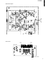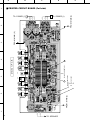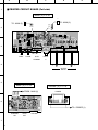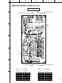
1
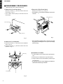
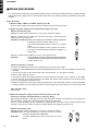
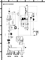
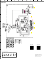
SUBWOOFER SYSTEM
YST-SW800
SERVICE MANUAL
IMPORTANT NOTICE
This manual has been provided for the use of authorized YAMAHA
Retailers and their service personnel.
It has been assumed that basic service procedures inherent to the industry,
and more specifically YAMAHA Products, are already known and
understood by the users, and have therefore not been restated.
WARNING:
Failure to follow appropriate service and safety
procedures when servicing this product may result in
personal injury, destruction of expensive components,
and failure of the product to perform as specified. For
these reasons, we advise all YAMAHA product owners
that any service required should be performed by an
authorized YAMAHA Retailer or the appointed service
representative.
IMPORTANT: The presentation or sale of this manual to any individual
or firm does not constitute authorization, certification
or recognition of any applicable technical
capabilities, or establish a principle-agent relationship
of any form.
The data provided is believed to be accurate and applicable to the unit(s)
indicated on the cover. The research, engineering, and service departments
of YAMAHA are continually striving to improve YAMAHA products.
Modifications are, therefore, inevitable and specifications are subject to
change without notice or obligation to retrofit. Should any discrepancy
appear to exist, please contact the distributor's Service Division.
WARNING:
Static discharges can destroy expensive components.
Discharge any static electricity your body may have
accumulated by grounding yourself to the ground buss
in the unit (heavy gauge black wires connect to this
buss).
IMPORTANT: Turn the unit OFF during disassembly and part
replacement. Recheck all work before you apply power
to the unit.
100721
■ CONTENTS
TO SERVICE PERSONNEL . . . . . . . . . . . . . . . . . . . . 1
SPECIFICATIONS . . . . . . . . . . . . . . . . . . . . . . . . . . . . 1
REAR PANEL . . . . . . . . . . . . . . . . . . . . . . . . . . . . . . . 2
DISASSEMBLY PROCEDURES . . . . . . . . . . . . . . . 3–4
REPAIR PROCEDURES . . . . . . . . . . . . . . . . . . . . . 5–6
ADJUSTMENTS . . . . . . . . . . . . . . . . . . . . . . . . . . . . 7–8
PRINTED CIRCUIT BOARD . . . . . . . . . . . . . . . . . 9–12
BLOCK DIAGRAM . . . . . . . . . . . . . . . . . . . . . . . . . . . 13
SCHEMATIC DIAGRAM . . . . . . . . . . . . . . . . . . . 14–15
PARTS LIST . . . . . . . . . . . . . . . . . . . . . . . . . . . . . 16–24
YST-SW800
YST-SW800
YST-SW800
YST-SW800
■ TO SERVICE PERSONNEL
1. Critical Components Information
Components having special characteristics are marked Z
and must be replaced with parts having specifications equal
to those originally installed.
WALL
OUTLET
2. Leakage Current Measurement (For 120V Models Only)
When service has been completed, it is imperative to verify
that all exposed conductive surfaces are properly insulated
from supply circuits.
●
Meter impedance should be equivalent to 1500 ohm shunted
by 0.15µF.
EQUIPMENT
UNDER TEST
AC LEAKAGE
TESTER OR
EQUIVALENT
INSULATING
TABLE
●
Leakage current must not exceed 0.5mA.
●
Be sure to test for leakage with the AC plug in both
polarities.
WARNING: CHEMICAL CONTENT NOTICE!
The solder used in the production of this product contains LEAD. In addition, other electrical/electronic and/or
plastic (where applicable) components may also contain traces of chemicals found by the California Health and
Welfare Agency (and possibly other entities) to cause cancer and/or birth defects or other reproductive harm.
DO NOT PLACE SOLDER, ELECTRICAL/ELECTRONIC OR PLASTIC COMPONENTS IN YOUR MOUTH FOR
ANY REASON WHATSOEVER!
Avoid prolonged, unprotected contact between solder and your skin! When soldering, do not inhale solder fumes
or expose eyes to solder/flux vapor!
If you come in contact with solder or components located inside the enclosure of this product, wash your hands
before handling food.
■ SPECIFICATIONS
Type . . . . . . . . . Advanced Yamaha Active Servo Technology
Driver . . . . . . . . . . . 25 cm (9-13/16") cone woofer (JA25610)
Magnetically shielded type
Amplifier Output
U, C models . . . . . . . . . . . . . . . . . . . . . . . . . . . . . . . . . . 1kW
A, B, G models . . . . . . . . . . . . . . . . . . . . . . . . . . . 800W/6Ω
Input Impedance
INPUT1 (SP) . . . . . . . . . . . . . . . . . . . . . . . . . . . . . . . . . 4.7kΩ
INPUT2 (PJ) . . . . . . . . . . . . . . . . . . . . . . . . . . . . . . . . . 12kΩ
Frequency Response . . . . . . . . . . . 18 Hz to 160 Hz (-10 dB)
Power Supply
U, C models . . . . . . . . . . . . . . . . . . . . . . . . . AC120V, 60 Hz
A model . . . . . . . . . . . . . . . . . . . . . . . . . . . . AC240V, 50 Hz
B, G models . . . . . . . . . . . . . . . . . . . . . . . . . AC230V, 50 Hz
Power Consumption . . . . . . . . . . . . . . . . . . . . . . . . . . . . 250W
Dimensions (W x H x D) . . . . . . . . . . . . 390 x 482 x 420 mm
(15-3/8" x 19" x 16-9/16")
Weight . . . . . . . . . . . . . . . . . . . . . . . . . . 24 kg (52 lbs. 14 oz)
Finish
All model . . . . . . . . . . . . . . . . . . . . . . . . . . . . . . Black color
G model . . . . . . . . . . . . . . . . . . . . . . . . . . . . . . Cherry color
Accessories . . . . . . . . . . . . . . . . . . . . . . . . . . Nonskid pad x 4
* Specifications subject to change without notice.
U
C
A
B
G
1
. . . . . . . . . . USA model
. . . . . . Canadian model
. . . . . Australian model
. . . . . . . . British model
. . . . . European model
YST-SW800
YST-SW800
■ REAR PANEL
▼ U, C models
▼ A model
▼ B, G models
2
YST-SW800
YST-SW800
■ DISASSEMBLY PROCEDURES
(Remove parts in the order as numbered.)
1. Removal of Front Panel Ass'y
3. Removal of Rear Panel Ass'y
Remove 4 screws ( q ) and then remove the Front
Panel Ass'y in Fig. 1.
* Use an Allen wrench (3mm) to unscrew the Front
Panel Ass'y.
Remove 16 screws ( r ) in Fig. 3.
*
Arrow marks (
removed.
) are printed to identify the screws to be
Rear Panel Ass'y
Front Panel Ass'y
r
q
q
Main (5) P.C.B.
r
Fig. 3
Fig. 1
2. Removal of Loud Speaker
a. Remove 8 screws ( w ) and then remove the Base
Ass'y in Fig. 2.
b. Remove 8 screws ( e ) and then remove the Loud
Speaker in Fig. 2.
* When assembling the Rear Panel, check to ensure that
the gasket is not damaged so as to prevent air leakage
from occurring.
w
w
w
● Installation of emblem
w
Base Ass'y
1. Put the emblem into the cabinet at the specified position.
2. Place a piece of cloth/wood on top of the emblem.
3. Using a mallet, hammer the emblem in place through
e
e
the cloth/wood.
* Use special care not to cause damage to the emblem or
cabinet while hammering the emblem.
Loud Speaker
Fig. 2
3
YST-SW800
YST-SW800
● Installation of power switch
Rapid cures bond (such as 5 minute epoxy) is required to fix the power switch.
As shown in Fig. 4, apply rapid cures bond (such as 5 minute epoxy) to the power switch (the area which
contacts the rear panel), insert it in the rear panel and make sure it is fixed.
(Inserting the power switch in the rear panel only would not be sufficient for its secure installation.)
● Precaution for installation of power cord
After connecting the power cord, be sure to apply the rapid cures bond (such as 5 minute epoxy) to the
cord stopper as shown in Fig. 4,
Bond application diagram (Fig. 4)
Apply rapid cures bond between the switch and rear panel.
Apply rapid cures bond before installing the P.C.B.
Apply rapid cures bond
Glue List
Place
Name
Cord stopper
5 minute epoxy or
2051(Revertex Finewaters SDN.BHD.) or
VYLOK 917DH (National Starch &
Chemical (M) SDM.BHD.)
Power switch
5 minute epoxy or Diabond 1620B
● Dimensions
8
(5/16")
390 (15-3/8")
420 (16-9/16")
390 (15-3/8")
22
(7/8")
482 (19")
390 (15-3/8")
Units : mm (inch)
4
YST-SW800
YST-SW800
■ REPAIR PROCEDURES
It is recommended to disconnect the SW power supply section and the power amplifier because it is highly possible
that the SW power supply section has also broken down due to the overload caused by breakdown in the power
amplifier.
Repair Procedure
1) Remove CB201, CB202 and CB205. (Power (1) P.C.B.)
Then the power supply circuit and the power amplifier circuit will be disconnected.
2) Repair the power amplifier as described below. (Main (1) P.C.B.)
Replace the defective parts.
Whether the major parts are defective or not can be checked as follows.
FET
Remove 3 screws fixing the heat sink to the rear panel and 4 screws fixing the
support P.C.B. to the rear panel.
FET (Q16~19, Q22~24): Measure the resistance value between GATE and SOURCE
to determine whether a failure exists or not.
If the measured resistance value is close to 0Ω, a failure
exists.
If the measured resistance value is close to the value of
the resistor connected between GATE and SOURCE, no
failure exists.
G
DS
TR
Remove 3 screws fixing the Main (1) P.C.B. to the support P.C.B.
TR (Q1~4):
Check DIODE characteristics between BASE and EMITTER
or between BASE and COLLECTOR to determine whether
a failure exists or not.
B
CE
Check the operation as follows.
a. Prepare a stabilized DC power source equipped with +30V and -30V outputs.
b. Connect +B, -B and GND output terminals of the stabilized power source to +B, -B and GND lines of the power
amplifier.
c. Connect the terminal of the oscilloscope to the circuit between q in the figure and GND.
d. Remove CB1. (Main (2) P.C.B.)
e. Connect the output of the signal generator to the circuit between the lead on the (-) side of C1 and GND.
f. Set the frequency of the signal generator to the 100Hz sine wave and the output level to the minimum level.
g. Turn on the stabilized DC power source.
h. Raise the output level of the signal generator gradually and check the output waveform on the oscilloscope.
i. If nothing abnormal is found with the waveform until the output level reaches 40Vp-p, the check result is OK.
After operation check
Connect CB1.
3) Repair the SW power supply section as follows. (Power (1) P.C.B.)
Follow the instruction described below to avoid any danger.
High voltage maintained in C209 and C210 even after the power is turned off is dangerous. It is necessary to
force this electric charge to be discharged before starting the repair work.
For such forced discharge, connect a resistance of approximately 100Ω/5W to each of both terminals of the
capacitor. Then check to make sure that the voltage between the capacitor terminals is 0V.
Replace the defective parts.
Whether the major parts are defective or not can be checked as follows.
TR (Q202~205): It is highly possible that a failure occurs due to a short
between COLLECTOR and EMITTER.
R216, R217:
It is highly possible that a failure occurs due to an open
circuit.
TR
B
5
CE
B
C
E
YST-SW800
YST-SW800
Check the operation and make adjustment as follows.
a. Connect CB205.
b. Connect the probe of the oscilloscope between TP201
and TP202.
c. Turn on the power switch and the STANDBY/ON switch
on the front panel.
d. Check the waveform on the oscilloscope and adjust
VR201 so that a = b is obtained.
Permissible range: a/b = 1.0 ± 0.1
a
0V
280Vp-p
b
CAUTION
Electric potential is always applied to the ground side of the oscilloscope.
Be careful so that no other part comes in contact with it.
V : 50V/div
AC range
H : 10 µsec/div
1 : 1 probe
Caution for operation check of the SW power supply section and the power amplifier
As a high voltage is applied to the SW power supply section and the power amplifier, be careful not
to receive an electric shock.
Power (1) P.C.B
q
Main (1) P.C.B
Q18
Q16
Q22
Q24
Q25
Q23
Q17
Q19
Q39
–B
GND
+B
Main (2) P.C.B
6
YST-SW800
YST-SW800
■ ADJUSTMENTS
● Confirmation of Power Amp operation
For the power amplifier which has been repaired, it
is absolutely necessary to confirm that a correct
waveform is obtained at points indicated by A and B
in the schematic diagram according to the following
procedure.
● Idling Adjustment
To stabilize operation of the amplifier, turn ON the
power with no input signal and wait for 1 or 2 minutes
in non loaded condition before the adjustment.
Adjust VR1 so that the voltage between terminals
TP1 and TP2 is DC 50mV to 250mV.
Devices required
Signal generator (100Hz sine wave)
8Ω or 6Ω load resistor
Oscilloscope (dual trace type)
● Confirmation of AUTO STANDBY operation
Connection
1) Connect the output signal from the signal generator
to the input terminal of YST-SW800.
2) Disconnect the connector terminal connected to the
speaker unit and reconnect it to the load resistor.
3) Connect the HOT side of the oscilloscope CH1 probe
to the point A or B indicated in the figure and the
GND side to the GND of the main unit.
4) Connect the oscilloscope CH2 input to the red side
of the connector cable, which is connected with the
load resistor.
At this time, the GND terminal of CH2 must be left
unconnected.
Setting
1) Set the signal generator to the sine wave, 100Hz and
minimum output level settings.
2) Set the volume of YST-SW800 to the minimum
position.
3) Turn on the power to YST-SW800.
4) Adjust the output level of the signal generator and the
volume of YST-SW800 so that the output level
observed at oscilloscope CH2 is 70Vp-p.
Setting
1) Turn off the power switch.
2) In order to shorten the time required for operation
check; connect a 10kΩ resistor at both ends of R162
on the MAIN (2) P.C.B.
3) Connect the output signal from the signal generator
to the L/MONO terminal of YST-SW800.
4) Set the signal generator for the sine wave of 100Hz,
8mV.
5) Turn on the power switch.
Confirmation
1) Set the AUTO STANDBY switch to the LOW position.
2) Turn on the STANDBY/ON switch.
The display LED lights up (green) and its color
changes to red after 5 to 10 seconds.
3) Turn off the STANDBY/ON switch.
The display LED goes off.
4) Set the AUTO STANDBY switch to the HIGH position.
Waveform observation
With the settings made as described above, observe
the waveform obtained at CH1 for judgment.
Normal
Point A
V : 50V/div
DC range
Abnormal
+B or GND level
Becomes constant
0V
Point B
V : 50V/div
DC range
0V
7
5) Turn on the STANDBY/ON switch.
The display LED lights up (green) and its color
remains unchanged even after time have elapsed.
6) Turn off the STANDBY/ON switch.
The display LED goes off.
(Cathode of D27)
H : 2 msec/div
1 : 1 probe
(Anode of D24)
H : 2 msec/div
1 : 1 probe
Abnormal
-B or GND level
Becomes constant
After confirmation
1) Turn off the power switch.
2) Disconnect the 10kΩ resistor connected to both ends
of R162.
YST-SW800
YST-SW800
● Schematic Diagram
A
B
RE
WH
IDLING CURRENT ADJ.
DC 50mV to 250mV
● Test Points
Point A
Main (1) P.C.B
Q18
Point B
Q16
Q22
Q24
Q25
Q23
Q17
Q19
Q39
–B
GND
+B
DC 50mV to 250mV
8
9
B
Q39
Q24
IDLING CURRENT ADJ.
Q25
A
Q16
Q18
–B1
E
+B1
8
1
TO : POWER (1)
TO : POWER (1)
2
DR+
OUT
DR–
AYST
+V1
7
TO : SPEAKER
FROM : MAIN (2)
–12
+12
BE
BL
BE
RE
BL
RE
#201
DC 50mV to 250mV
Q22
C
IDLING TEST POINT
Q23
5
B
FROM : MAIN (2)
Q17
3
FROM : MAIN (2)
1
WH
RE
6
Q19
4
MAIN ( 1 ) P. C. B.
A
D
E
YST-SW800
■ PRINTED CIRCUIT BOARD (Foil side)
#202
6
8
1
TVOL
E
MAIN
+V2
+12
—12
PWS
VCC
SWL
SWH2
SWH1
SO
9
DR+
OUT
DR—
AYST
+V1
W11
#11
+12
—12
W12
TO : MAIN (1)
FROM : MAIN (4)
TO : MAIN (1)
#12
+B1
E
—B1
B
1
4
FROM : MAIN (5)
3
FROM : MAIN (4)
W2
2
TO : POWER (1)
#2
1
MAIN ( 2 ) P. C. B.
A
C
D
W10
9
1
9
1
E
YST-SW800
■ PRINTED CIRCUIT BOARD (Foil side)
#10
TO : MAIN (1)
MA1
E
TOVL
+12
—12
LIM
MA2
5
VCC
+V1
E
7
10
A
B
C
D
E
YST-SW800
■ PRINTED CIRCUIT BOARD (Foil side)
1
MAIN ( 4 ) P. C. B.
#1
#4
W1
TO : MAIN (2)
W4
MA2
LIM
–12
+12
TOVL
E
MA1
SWL
SWH2
SWH1
SO
TO : MAIN (3)
2
1
9
1
8
3
B, G only
BASS
PHASE
AUTO
STANDBY
INPUT
2
4
+
R
–
–
L
+
OUTPUT
INPUT 1
5
MAIN ( 5 ) P. C. B.
POWER ( 2 ) P. C. B.
FROM : MAIN (2)
VCC
PWS
–12
+12
+V2
MAIN
E
TOVL
POWER
GY
OR
6
TO : POWER (1)
1
STANDBY/
ON
7
11
9
HIGH
CUT
VOLUME
A
B
C
D
E
YST-SW800
1
■ PRINTED CIRCUIT BOARD (Foil side)
POWER ( 1 ) P. C. B.
FROM : MAIN (1)
RE
BL
RE
BE
BL
D
BE
FROM : MAIN (2)
–B1
E
+B1
2
C
3
4
J, U, C only
5
A, B, G only
GY
OR
A, B, G only
TO : POWER (2)
6
Point C
V : 50V/div
DC range
0V
FROM : POWER CORD
(Pin 1 of CB201)
H : 10 µsec/div
1 : 1 probe
Point D
V : 10V/div
DC range
(Pin 1 of CB202)
H : 10 µsec/div
1 : 1 probe
0V
7
12
7
13
INPUT 2
R
+
–
–
+
+
OFF
AUTO STANDBY
SW3
H/L
7
MUSIC
SENSOR
IC4
PWR
4
3
2
C84
R162
8
7
6
4
AUTO POWER
ON/OFF CIRCUIT
Q41
IC6A
VR3
VOLUME
3
HIGH CUT
VR2
D43
IC7A
+
8
L.P.F.
12dB/oct
6
TIMER
IC5
5
L
R
L
R
IC11B
L.P.F.
6dB/oct
6
5
6
–
1
SW2
PHASE
SELECT
D40
D36
D39
IC6B
+
8
IC8
IC9
D48
–B
D49
D50
POWER SUPPLY
D47
7
3
6
1
2
4
5
8
–B
IC202
RY3
See page 15
T201
RY201
IC3
Q26, 27
SUB
POWER SUPPLY
D203
Q202—207
D201, 202
D205—209
SWITCHING
POWER SUPPLY
Q1A, 2A, 4C
Q15, 21, 23, 25
Q1C, 2C, 4A
Q20, 22, 24, 40
+B
REGULATOR
Q201
11
12
13
14
15
16
T202
IC1, 2
Q32
D32, 33, 35
POWER DRIVE
Q39, 3A/C
Q16—19
A.N.I.C
POWER SUPPLY
Q28—31
D28—31
+
–
+B
LIMITER
L.P.F.
12dB/oct
6
STANDBY/ON
SW1
–12
+12
BASS
SELECT
SW4
B.P.F
Q33—36
PRE DRIVE
Q5—12
L201
PROTECTION
0.1
F201
SPEAKER
POWER
SW201
C
Q37
PWR
H.P.F.
12dB/oct
IC7B
4
+
2
4
2
3
IC11A
3
–
+
2
OUTPUT
INPUT 1
L
See page 14
1
B
REGULATOR
A
D
E
YST-SW800
■ BLOCK DIAGRAM
A
B
C
D
E
F
G
H
I
J
K
YST-SW800
■ SCHEMATIC DIAGRAM
1
L.P.F.
B.P.F.
-12.0
0
11.8
8.6
0
7.9
0
8.5
-4.4
POWER DRIVE
PRE DRIVE
11.8
0
0
0
111
112
0
4.1
112
111
111
111
111
111
111
111
0
111
111
0
112
0.7
6.0
110
110
L.P.F.
2
111
111
5.5
110
0
6.0
3.4
0.7
4.7
4.7
4.7
5.1
A
4.7
5.1
5.1
5.5
111
110
110
111
4.7
4.7
0
4.7
3.4
0
0
4.7
2.3
0
0
-12.0
2.9
0
4.7
2.3
2.9
3.4
11.8
2.3
2.9
E-7
SAME PAGE
B
110
0.1
110
0.1
-3.4
0
0.1
0.7
0.7
0
2.3
-2.6
LIMITER
0
111
4.7
0.1
4.7
4.7
RE
0.2
0.2
WH
IDLING CURRENT ADJ.
-111
-111
0
DC 50mV to 250mV
0
0
0.1
-2.1
0.2
-2.7
-0.1
3
0
-0.1
11.8
-12.0
-2.7
0.2
-0.3
-4.3
-2.1
-4.3
-2.7
-2.0
0
0
-3.2
-111
-111
-3.4
-4.3
-5.2
-111
0
0
0
0
1.8
0
-4.3
-111
-4.3
0
-4.3
-111
-110
-110 -110
-111
-111
0
-4.3
-4.3
-4.3
-4.9
-4.9
-5.8
-110
-112
0
0
-110
-111
-111
-112
0.6
-4.9
-5.2
0
-4.3
-4.3
-110
-111
-110
-111
-111
7.2
-111
0.1
L.P.F.
H.P.F.
-111
7.8
11.8
-12.0
0
0
0
0
2.0
0.8
3.1
0
2.1
0
0
4
0
0
A.N.I.C
0
5.9
11.8
-0.3
11.8
-1.5
0
0
0
0
0
0
-0.3
0
Point A
V : 50V/div
DC range
(Cathode of D27)
H : 2 msec/div
1 : 1 probe
Point B
V : 50V/div
DC range
(Anode of D24)
H : 2 msec/div
1 : 1 probe
0
0
0
-0.4
-12.0
6.6
11.8
0
6.5
PROTECTION
6.0
0.8
0
0
-12.0
0V
IC1, 2, 4, 6, 7 : µPC4570HA
Dual OP-Amp
5
-12.0
11.8
1
2
–
1
VCC
+
+
2
3
4
VO1 –Vm1 +Vm1
5
VEE
0
–
112
6
7
8
+Vm2 –Vm2 VO2
15.3
AUTO POWER ON/OFF
CIRCUIT
-111
6
–
–
7.8
7.7
7.7
5.2
7.8
-0.8
-1.5
-0.8
POWER SUPPLY
-1.5
0
-15.3
15.3
-15.3
0
0
0
P15
I-2
CIRCUIT CHANGES BY MARKET.
+
6.5
0
IC11 : NJM4558L
Dual OP-Amp
1.4
112
+
0
-111
9
VCC
7.8
0V
1
2
3
4
5
6
7
8
OUT1
–IN1
+IN1
–VCC
+IN2
–IN2
OUT2
+VCC
0
7.5
6.9
0
3.9
0
P15
I-4
0
3.9
X : NOT USED
IC5 : M51848L
CR Timer
R
P15
I-5
IC3 : µPC1237HA
Protector IC for Power Amplifier
R
Vcc
R
7
–
+
Overload
detect
–
+
1
FLIPFLOP
7
0
0
Mid-point
potential
detect
1
2
3
4
5
6
7
8
GND
TRIGGER
OUT
RESET
REFERENCE
VOLTAGE
THRESHOLD
DISCHARGE
VCC
2
Vcc on
mute
Flip flop
circuit
8
Relay
drive
circuit
SAME PAGE
D-3
6
AC OFF
detect
Latch / automatic
return select
5
3
4
GND
PIN CONNECTION DIAGRAM OF TRANSISTORS, DIODES AND ICS.
8
1SS133
S2L20U
EL02Z
1SR139-400
MTZJ2.0B
MTZJ12.0B
MTZJ24.0B
FMU-12R
FMU-34R
Anode
FMU-12S
FMU-34S
1:Cathode
2:Anode
3:Cathode
1:Anode
2:Cathode
3:Anode
2SC1846S
2SA1837
2SC4793
1
1
2
Cathode
2SA970 (GR, BL)
2SA1015 (O, Y)
2SA1689 (E, F)
2SC1815 (Y, GR)
2SC2240 (GR, BL)
2SC4449 (E, F)
2SC2878 (A, B)
1
3
2
2
3
3
1
2
3
E
C
B
EC
B
B
CE
2SK304 (E)
D
G
2SK237B
2SJ406
G
S
DS
NJM78M12FA
1: OUTPUT
2: COMMON
32
3: INPUT
NJM79M12FA
NJM4558L
µPC1237HA
M51848L
µPC4570HA
8
1
1:COMMON
2:INPUT
3:OUTPUT
32
1
1
9
1
* All voltage are measured with a 10MΩ/V DC electric volt meter.
* Components having special characteristics are marked Z and
must be replaced with parts having specifications equal to those
originally installed.
* Schematic diagram is subject to change without notice.
14
A
B
C
D
E
F
G
H
I
J
K
YST-SW800
■ SCHEMATIC DIAGRAM
1
7.8
11.9
P14
D-6
0
11.9
AC 12.8V
5.9
2
1.2
0
1.2
12.1
0.7
6.0
0
C
3
0.4
-0.5
10.2
9.4
9.4
-0.5
10.2
-18.1
9.3
10.2
0.4
9.3
-0.5
-0.5
4
P14
H-6
9.3
8.8
-0.5
0.4
-1.5
-0.5
8.8
-0.6
-1.3
-1.4
-1.4
-1.5
-1.5
P14
I-6
-1.3
-1.3
-1.4
8.8
-1.3
5
-1.3
0.1
D
CIRCUIT CHANGES BY MARKET.
6
Point C
V : 50V/div
DC range
(Pin 1 of CB201)
H : 10 µsec/div
1 : 1 probe
Point D
V : 10V/div
DC range
(Pin 1 of CB202)
H : 10 µsec/div
1 : 1 probe
7
0V
0V
X : NOT USED
O : USED
PIN CONNECTION DIAGRAM OF TRANSISTORS, DIODES AND ICS.
8
1SS133
1SR139-400
S1NB20
RBV-606
TM1661S-L
2SC2240 (GR, BL)
2SD400 (F)
2SC4163
2SC4140
NJM78L08A
Anode
G
Cathode
15
–
–
+
T2
T1
T1
+
E
C
T2 G
B
B
CE
B
C
E
1:OUTPUT
2:COMMON 1
2 3
3:INPUT
* All voltage are measured with a 10MΩ/V DC electric volt meter.
* Components having special characteristics are marked Z and
must be replaced with parts having specifications equal to those
originally installed.
* Schematic diagram is subject to change without notice.
L
YST-SW800
YST-SW800
PARTS LIST
■ ELECTRICAL PARTS
■ WARNING
Components having special characteristics are marked Z and must be
replaced with parts having specifications equal to those originally installed.
● Carbon resistors (1/6W or 1/4W) are not included in the ELECTRICAL PARTS
List. For the part Nos. of the carbon resistors refer to the last page.
ABBREVIATIONS IN THIS LIST ARE AS FOLLOWS :
C.A.EL.CHP
C.CE
C.CE.ARRAY
C.CE.CHP
C.CE.ML
C.CE.M.CHP
C.CE.SAFTY
C.CE.TUBLR
C.CE.SMI
C.EL
C.MICA
C.ML.FLM
C.MP
C.MYLAR
C.MYLAR.ML
C.PAPER
C.PLS
C.POL
C.POLY
C.PP
C.TNTL
C.TNTL.CHP
C.TRIM
CN
CN.BS.PIN
CN.CANNON
CN.DIN
CN.FLAT
CN.POST
COIL.MX.AM
COIL.AT.FM
COIL.DT.FM
COIL.MX.FM
COIL.OUTPT
DIOD.ARRAY
DIODE.BRG
DIODE.CHP
DIODE.VAR
DIOD.Z.CHP
DIODE.ZENR
DSCR.CE
FER.BEAD
FER.CORE
FET.CHP
FL.DSPLY
FLTR.CE
FLTR.COMB
FLTR.LC.RF
GND.MTL
GND.TERM
HOLDER.FUS
IC.PRTCT
JUMPER.CN
JUMPER.TST
L.DTCT
:
:
:
:
:
:
:
:
:
:
:
:
:
:
:
:
:
:
:
:
:
:
:
:
:
:
:
:
:
:
:
:
:
:
:
:
:
:
:
:
:
:
:
:
:
:
:
:
:
:
:
:
:
:
:
CHIP ALUMI. ELECTROLYTIC CAP
CERAMIC CAP
CERAMIC CAP ARRAY
CHIP CERAMIC CAP
MULTILAYER CERAMIC CAP
CHIP MULTILAYER CERAMIC CAP
RECOGNIZED CERAMIC CAP
CERAMIC TUBULAR CAP
SEMI CONDUCTIVE CERAMIC CAP
ELECTROLYTIC CAP
MICA CAP
MULTILAYER FILM CAP
METALLIZED PAPER CAP
MYLAR FILM CAP
MULTILAYER MYLAR FILM CAP
PAPER CAPACITOR
POLYSTYRENE FILM CAP
POLYESTER FILM CAP
POLYETHYLENE FILM CAP
POLYPROPYLENE FILM CAP
TANTALUM CAP
CHIP TANTALUM CAP
TRIMMER CAP
CONNECTOR
CONNECTOR, BASE PIN
CONNECTOR, CANNON
CONNECTOR, DIN
CONNECTOR, FLAT CABLE
CONNECTOR, BASE POST
COIL, AM MIX
COIL, FM ANTENNA
COIL, FM DETECT
COIL, FM MIX
OUTPUT COIL
DIODE ARRAY
DIODE BRIDGE
CHIP DIODE
VARACTOR DIODE
CHIP ZENER DIODE
ZENER DIODE
CERAMIC DISCRIMINATOR
FERRITE BEADS
FERRITE CORE
CHIP FET
FLUORESCENT DISPLAY
CERAMIC FILTER
COMB FILTER MODULE
LC FILTER ,EMI
GROUND PLATE
GROUND TERMINAL
FUSE HOLDER
IC PROTECTOR
JUMPER CONNECTOR
JUMPER, TEST POINT
LIGHT DETECTING MODULE
L.EMIT
LED.DSPLY
LED.INFRD
MODUL.RF
PHOT.CPL
PHOT.INTR
PHOT.RFLCT
PIN.TEST
PLST.RIVET
R.ARRAY
R.CAR
R.CAR.CHP
R.CAR.FP
R.FUS
R.MTL.CHP
R.MTL.FLM
R.MTL.OXD
R.MTL.PLAT
RSNR.CE
RSNR.CRYS
R.TW.CEM
R.WW
SCR.BND.HD
SCR.BW.HD
SCR.CUP
SCR.TERM
SCR.TR
SUPRT.PCB
SURG.PRTCT
SW.TACT
SW.LEAF
SW.LEVER
SW.MICRO
SW.PUSH
SW.RT.ENC
SW.RT.MTR
SW.RT
SW.SLIDE
TERM.SP
TERM.WRAP
THRMST.CHP
TR.CHP
TR.DGT
TR.DGT.CHP
TRANS
TRANS.PULS
TRANS.PWR
TUNER.AM
TUNER.FM
TUNER.PK
VR
VR.MTR
VR.SW
VR.SLIDE
VR.TRIM
:
:
:
:
:
:
:
:
:
:
:
:
:
:
:
:
:
:
:
:
:
:
:
:
:
:
:
:
:
:
:
:
:
:
:
:
:
:
:
:
:
:
:
:
:
:
:
:
:
:
:
:
:
:
:
LIGHT EMITTING MODULE
LED DISPLAY
LED, INFRARED
MODULATOR, RF
PHOTO COUPLER
PHOTO INTERRUPTER
PHOTO REFLECTOR
PIN, TEST POINT
PLASTIC RIVET
RESISTOR ARRAY
CARBON RESISTOR
CHIP RESISTOR
FLAME PROOF CARBON RESISTOR
FUSABLE RESISTOR
CHIP METAL FILM RESISTOR
METAL FILM RESISTOR
METAL OXIDE FILM RESISTOR
METAL PLATE RESISTOR
CERAMIC RESONATOR
CRYSTAL RESONATOR
TWIN CEMENT FIXED RESISTOR
WIRE WOUND RESISTOR
BIND HEAD B-TITE SCREW
BW HEAD TAPPING SCREW
CUP TITE SCREW
SCREW TERMINAL
SCREW, TRANSISTOR
SUPPORT, P.C.B.
SURGE PROTECTOR
TACT SWITCH
LEAF SWITCH
LEVER SWITCH
MICRO SWITCH
PUSH SWITCH
ROTARY ENCODER
ROTARY SWITCH WITH MOTOR
ROTARY SWITCH
SLIDE SWITCH
SPEAKER TERMINAL
WRAPPING TERMINAL
CHIP THERMISTOR
CHIP TRANSISTOR
DIGITAL TRANSISTOR
CHIP DIGITAL TRANSISTOR
TRANSFORMER
PULSE TRANSFORMER
POWER TRANSFORMER ASS’y
TUNER PACK, AM
TUNER PACK, FM
FRONT-END TUNER PACK
ROTARY POTENTIOMETER
POTENTIOMETER WITH MOTOR
POTENTIOMETER WITH ROTARY SW
SLIDE POTENTIOMETER
TRIMMER POTENTIOMETER
Note) Those parts marked with “#” are not included in the P.C.B. ass'y.
16
YST-SW800
YST-SW800
P.C.B. MAIN
Schm
Ref. PART NO.
*
*
V5890800
V5890900
CB1 VB858600
CB3 VB858700
CB4 VB858300
CB9 VB858700
CB10 VL844700
CB11 VB390100
CB12 VB389800
* C1
VT721000
C2
UA653100
C3
V5877800
C4
V5877800
C5
UA654270
C6
UA654100
C7
UA654100
C8
VT720600
C9
VT727900
C10 VT727900
C11 VK534000
C12 VK534000
C13 UA655220
C14 UA655220
C15 UA654100
C16 UA654100
C17 V5058000
C18 V5058000
C19 V5058000
C20 V5058000
C21 UA654220
C22 UA654220
C23 UA652120
C24 UA652120
C27 V5877900
C28 V5877900
C29 UA655100
* C30 VT720900
* C31 VT720900
C32 UA655470
* C33 VT720600
* C34 VT719700
* C35 VT719800
C36 UA655100
C37 UA654100
C38 UA654220
C39 UA654100
C40 UA654100
C42 V5872500
C43 V5872500
C44 VT724900
C45 VT722300
* C46 VT720600
* C47 VT722300
* New Parts
17
Schm
Ref. PART NO.
Description
P.C.B.
P.C.B.
CN.BS.PIN
CN.BS.PIN
CN.BS.PIN
CN.BS.PIN
CN.BS.PIN
CN.BS.PIN
CN.BS.PIN
C.EL
C.MYLAR
C.EL
C.EL
C.MYLAR
C.MYLAR
C.MYLAR
C.EL
C.EL
C.EL
C.PP
C.PP
C.MYLAR
C.MYLAR
C.MYLAR
C.MYLAR
C.MYLAR
C.MYLAR
C.MYLAR
C.MYLAR
C.MYLAR
C.MYLAR
C.MYLAR
C.MYLAR
C.EL
C.EL
C.MYLAR
C.EL
C.EL
C.MYLAR
C.EL
C.EL
C.EL
C.MYLAR
C.MYLAR
C.MYLAR
C.MYLAR
C.MYLAR
C.EL
C.EL
C.EL
C.EL
C.EL
C.EL
MAIN(UCA)
MAIN(BG)
7P
8P
4P
8P
3P
5P
2P
100uF
1000pF
47uF
47uF
0.027uF
0.01uF
0.01uF
10uF
47uF
47uF
220pF
220pF
0.22uF
0.22uF
0.01uF
0.01uF
4.7uF
4.7uF
4.7uF
4.7uF
0.022uF
0.022uF
120pF
120pF
100uF
100uF
0.1uF
47uF
47uF
0.47uF
10uF
100uF
220uF
0.1uF
0.01uF
0.022uF
0.01uF
0.01uF
470uF
470uF
10uF
100uF
10uF
100uF
*
*
*
16V
50V
160V
160V
50V
50V
50V
16V
100V
100V
200V
200V
50V
50V
50V
50V
250V
250V
250V
250V
50V
50V
50V
50V
160V
160V
50V
16V
16V
50V
16V
10V
10V
50V
50V
50V
50V
50V
160V
160V
50V
25V
16V
25V
*
*
*
*
*
*
*
*
*
*
*
*
C50
C51
C52
C53
C54
C56
C57
C58
C59
C60
C61
C62
C63
C64
C65
C66
C67
C68
C69
C70
C71
C72
C73
C75
C76
C77
C78
C79
C80
C81
C82
C83
C84
C85
C86
D1
D2
D3
D4
D5
D6
D7
D8
D9
D10
D11
D12
D13
D14
D15
D17
D18
D19
FG644100
UA654470
UA654470
VT720600
UA655470
VT720600
FG644100
FG613100
VT724500
UA654680
UA655820
UA655220
UA655220
UA655220
VT724900
VT724900
FG612220
VT724800
UA654390
VT720600
FG612220
VT721100
VT721100
VT720600
UA654820
UA654390
VT719600
VA777700
VA761000
UA655390
UA655220
FG644100
VT721200
VT721100
UA654220
iF004600
iF004600
iF004600
VG435100
VG435100
VU264100
VU264100
VU264100
VU264100
VU264100
VU264100
VU264100
VU264100
V6591600
V6591600
V6591600
iF004600
iF004600
* New Parts
Description
C.CE
C.MYLAR
C.MYLAR
C.EL
C.MYLAR
C.EL
C.CE
C.CE
C.EL
C.MYLAR
C.MYLAR
C.MYLAR
C.MYLAR
C.MYLAR
C.EL
C.EL
C.CE
C.EL
C.MYLAR
C.EL
C.CE
C.EL
C.EL
C.EL
C.MYLAR
C.MYLAR
C.EL
C.CE
C.CE
C.MYLAR
C.MYLAR
C.CE
C.EL
C.EL
C.MYLAR
DIODE
DIODE
DIODE
DIODE.ZENR
DIODE.ZENR
DIODE
DIODE
DIODE
DIODE
DIODE
DIODE
DIODE
DIODE
DIODE
DIODE
DIODE
DIODE
DIODE
0.01uF
50V
0.047uF
50V
0.047uF
50V
10uF
16V
0.47uF
50V
10uF
16V
0.01uF
50V
1000pF
50V
1uF
50V
0.068uF
50V
0.82uF
50V
0.22uF
50V
0.22uF
50V
0.22uF
50V
10uF
50V
10uF
50V
220pF
50V
4.7uF
50V
0.039uF
50V
10uF
16V
220pF
50V
220uF
25V
220uF
25V
10uF
16V
0.082uF
50V
0.039uF
50V
47uF
10V
220pF
50V(BG)
22pF
50V(BG)
0.39uF
50V
0.22uF
50V
0.01uF
50V
330uF
16V
220uF
25V
0.022uF
50V
1SS133
1SS133
1SS133
MTZJ2.0B 2.0V
MTZJ2.0B 2.0V
1SR139-400
1SR139-400
1SR139-400
1SR139-400
1SR139-400
1SR139-400
1SR139-400
1SR139-400
EL02Z
EL02Z
EL02Z
1SS133
1SS133
YST-SW800
YST-SW800
P.C.B. MAIN
Schm
Ref. PART NO.
*
*
Z
Z
Z*
Z*
D20
D21
D22
D23
D24
D25
D26
D27
D28
D29
D30
D31
D32
D33
D34
D35
D36
D39
D40
D43
D44
D47
D48
D49
D50
IC1
IC2
IC3
IC4
IC5
IC6
IC7
IC8
IC9
IC11
L1
L2
L3
L4
L5
PJ1
Q1
Q2
Q3
Q4
Q5
Q6
Q7
Q8
Q9
Q10
Q11
Q12
VU264100
VU264100
VU264100
VU264100
VP779200
VP779200
VP779200
VP779200
iF004600
iF004600
iF004600
iF004600
iF004600
iF004600
VG440200
iF004600
iF004600
VS079300
iF004600
iF004600
V6591600
V5877300
V5877400
VN399400
VN399300
XB247A00
XB247A00
XF663A00
XB247A00
XP741A00
XB247A00
XB247A00
XJ602A00
XD343A00
XM922A00
V5058100
V5058100
V5058100
V5058100
VU038200
V6415800
VQ116600
VQ116600
VQ116600
VQ116600
iA097030
iC1815M0
iC1815M0
iA097030
iA097030
iA101590
V5876800
V5876900
* New Parts
Schm
Ref. PART NO.
Description
DIODE
DIODE
DIODE
DIODE
DIODE
DIODE
DIODE
DIODE
DIODE
DIODE
DIODE
DIODE
DIODE
DIODE
DIODE.ZENR
DIODE
DIODE
LED
DIODE
DIODE
DIODE
DIODE
DIODE
DIODE
DIODE
IC
IC
IC
IC
IC
IC
IC
IC
IC
IC
COIL
COIL
COIL
COIL
COIL
JACK.PIN
TR.PAIR
TR.PAIR
TR.PAIR
TR.PAIR
TR
TR
TR
TR
TR
TR
TR
TR
1SR139-400
1SR139-400
1SR139-400
1SR139-400
S2L20U
S2L20U
S2L20U
S2L20U
1SS133
1SS133
1SS133
1SS133
1SS133
1SS133
MTZJ12B
12V
1SS133
1SS133
SPR-39MVW
1SS133
1SS133
EL02Z
FMU-34S
FMU-34R
FMU-12R 5A 200V
FMU-12S 5A 200V
uPC4570HA
uPC4570HA
uPC1237HA
uPC4570HA
M51848L
uPC4570HA
uPC4570HA
NJM78M12FA
NJM79M12FA
NJM4558L
120uH
120uH
120uH
120uH
0.95uH
2P RJ-1060-01-0500
2SA1837/C4793 O,Y
2SA1837/C4793 O,Y
2SA1837/C4793 O,Y
2SA1837/C4793 O,Y
2SA970 GR,BL
2SC1815 Y,GR
2SC1815 Y,GR
2SA970 GR,BL
2SA970 GR,BL
2SA1015 O,Y
2SA1689 E,F
2SC4449 E,F
#
#
#
#
#
#
#
#
#
Q15
Q16
Q17
Q18
Q19
Q20
Q21
Q22
Q23
Q24
Q25
Q26
Q27
Q28
Q29
Q30
Q31
Q32
Q33
Q34
Q35
Q36
Q37
Q39
Q40
Q41
R1
R3
R4
R5
R6
R9
R10
R11
R12
R13
R14
R15
R20
R23
R24
R25
R26
R27
R28
R29
R30
R31
R32
R33
R34
R35
R36
V5876800
V5877200
V5877000
V5877200
V5877000
iA097030
iC224030
V5877200
V5877000
V5877200
V5877000
V5876900
V5876800
iA097030
iA101590
iC1815M0
iC224030
V3028000
iA097030
iA097030
iC287820
iC287820
iC224030
VC398100
V5876900
iC224030
VF459100
HV755220
HV755560
HV755220
HV754330
VH009600
HV755270
HV755330
HV755100
HV755100
HV756330
HV755270
HV756470
HV754100
HV754100
HV754100
HV754100
HV755820
HV755820
HV754150
V5875400
V5875400
HV754150
HV755820
HV755820
V5875400
V5875400
Description
TR
FET
FET
FET
FET
TR
TR
FET
FET
FET
FET
TR
TR
TR
TR
TR
TR
FET
TR
TR
TR
TR
TR
TR
TR
TR
R.MTL.FLM
R.CAR.FP
R.CAR.FP
R.CAR.FP
R.CAR.FP
R.MTL.FLM
R.CAR.FP
R.CAR.FP
R.CAR.FP
R.CAR.FP
R.CAR.FP
R.CAR.FP
R.CAR.FP
R.CAR.FP
R.CAR.FP
R.CAR.FP
R.CAR.FP
R.CAR.FP
R.CAR.FP
R.CAR.FP
R.WW
R.WW
R.CAR.FP
R.CAR.FP
R.CAR.FP
R.WW
R.WW
2SA1689
2SK2378
2SJ406
2SK2378
2SJ406
2SA970
2SC2240
2SK2378
2SJ406
2SK2378
2SJ406
2SC4449
2SA1689
2SA970
2SA1015
2SC1815
2SC2240
2SK304
2SA970
2SA970
2SC2878
2SC2878
2SC2240
2SC1846
2SC4449
2SC2240
2.2KΩ
220Ω
560Ω
220Ω
33Ω
100KΩ
270Ω
330Ω
100Ω
100Ω
3.3KΩ
270Ω
4.7KΩ
10Ω
10Ω
10Ω
10Ω
820Ω
820Ω
15Ω
0.1Ω
0.1Ω
15Ω
820Ω
820Ω
0.1Ω
0.1Ω
E,F
GR,BL
GR,BL
E,F
E,F
GR,BL
O,Y
Y,GR
GR,BL
E
GR,BL
GR,BL
A,B
A,B
GR,BL
S
E,F
GR,BL
1/4W
1/4W
1/4W
1/4W
1/4W
1/4W
1/4W
1/4W
1/4W
1/4W
1/4W
1/4W
1/4W
1/4W
1/4W
1/4W
1/4W
1/4W
1/4W
1/4W
5W
5W
1/4W
1/4W
1/4W
5W
5W
* New Parts
Note) Those parts marked with “#” are not included in the P.C.B. ass'y.
18
YST-SW800
YST-SW800
P.C.B. MAIN & POWER
Schm
Ref. PART NO.
R37
R38
R39
R40
R41
R42
R47
R54
R55
R56
R57
R58
R59
R60
R61
R63
R64
R65
R71
R73
R74
R75
R81
R82
R83
R84
* R85
R97
R98
R99
R105
R106
R110
R111
R131
R132
R163
R164
R171
Z
RY3
ST1
SW1
SW2
SW3
SW4
TE3
TE3
TP1
TP2
VR1
VR2
VR3
HL223100
HL223100
HL223100
HL223100
HV754220
HV754220
HV754100
HV756390
HV755470
HV755470
HV754100
HV754100
HV754100
HV754100
HV755820
HV755100
HV755100
HV756120
HV754680
HV755820
HV755820
HV755820
VH007200
VH007900
VH007200
VH007200
HL215150
V6146800
HV753100
HV753100
HV756220
HV756220
HV756470
HV756470
HV755470
HV755470
HV755100
HV755100
HV753470
V5876700
BB071360
VS066500
V5178000
V5178100
V5178000
V4811400
VV003100
VT969000
VT969000
VJ692800
VV954800
VV954700
BB070700
* New Parts
19
Schm
Ref. PART NO.
Description
R.MTL.OXD
R.MTL.OXD
R.MTL.OXD
R.MTL.OXD
R.CAR.FP
R.CAR.FP
R.CAR.FP
R.CAR.FP
R.CAR.FP
R.CAR.FP
R.CAR.FP
R.CAR.FP
R.CAR.FP
R.CAR.FP
R.CAR.FP
R.CAR.FP
R.CAR.FP
R.CAR.FP
R.CAR.FP
R.CAR.FP
R.CAR.FP
R.CAR.FP
R.MTL.FLM
R.MTL.FLM
R.MTL.FLM
R.MTL.FLM
R.MTL.OXD
R.WW
R.CAR.FP
R.CAR.FP
R.CAR.FP
R.CAR.FP
R.CAR.FP
R.CAR.FP
R.CAR.FP
R.CAR.FP
R.CAR.FP
R.CAR.FP
R.CAR.FP
RELAY
SCR.TERM
SW.PUSH
SW.SLIDE
SW.SLIDE
SW.SLIDE
TERM.SP
TERM.SP
PIN.TEST
PIN.TEST
VR.TRIM
VR
VR
GND.MTL
1Ω
2W
1Ω
2W
1Ω
2W
1Ω
2W
22Ω
1/4W
22Ω
1/4W
10Ω
1/4W
3.9KΩ
1/4W
470Ω
1/4W
470Ω
1/4W
10Ω
1/4W
10Ω
1/4W
10Ω
1/4W
10Ω
1/4W
820Ω
1/4W
100Ω
1/4W
100Ω
1/4W
1.2KΩ
1/4W
68Ω
1/4W
820Ω
1/4W
820Ω
1/4W
820Ω
1/4W
10KΩ
1/4W
20KΩ
1/4W
10KΩ
1/4W
10KΩ
1/4W
150Ω
1W
0.22Ω+0.22Ω
1Ω
1/4W
1Ω
1/4W
2.2KΩ
1/4W
2.2KΩ
1/4W
4.7KΩ
1/4W
4.7KΩ
1/4W
470Ω
1/4W
470Ω
1/4W
100Ω
1/4W
100Ω
1/4W
4.7Ω
1/4W
DC SDT-S-112DMR
8.3x13
SPPH13-W
SSSF12-P06NO
SSSU123-S09NO
SSSF12-P06NO
8P(BG)
8P(UCA)
IRS-2049
IRS-2049
B470Ω
10KΩ
A5KΩ
VN774800 GND.WSHR
MEP1866
#11102
V6667500 HEAT.SINK OSH-1035-WPL
EG330050 SCR.BND.HD 3x8
FCRM3-BL
*
*
*
*
*
*
*
*
*
*
*
*
*
*
*
*
Z
Z
*
Z
Z
Description
CB201
CB202
CB203
CB203
CB204
CB204
CB205
C201
C201
C202
C203
C204
C205
C206
C206
C207
C208
C209
C209
C210
C210
C211
C212
C213
C214
C215
C216
C217
C218
C219
C220
C221
D201
D202
D203
D204
D205
D206
D207
D208
D209
F201
F201
IC202
V5890500
V5890600
V5890700
LB932040
LB932030
V6577400
VT658200
V6577400
VT658200
VB389900
V5877600
V5900200
VY675100
VY675100
V6146600
V6146600
V5877600
V5877700
VS741700
VT721100
V5873400
V5873800
V5873400
V5873800
VT722700
VT718300
VT718300
V5878200
V5878200
V5900300
VT720600
UA654270
UA654270
UA655150
UA655150
VN932100
VU264100
VR253700
iF004600
VN774600
VU264100
VU264100
VU264100
VU264100
KB001540
KB001890
iG160100
* New Parts
P.C.B.
P.C.B.
P.C.B.
CN.BS.PIN
CN.BS.PIN
HOLDER.FUS
HOLDER.FUS
HOLDER.FUS
HOLDER.FUS
CN.BS.PIN
C.MYLAR
C.MYLAR
C.CE.SAFTY
C.CE.SAFTY
C.CE.SAFTY
C.CE.SAFTY
C.MYLAR
C.MYLAR
C.CE.SAFTY
C.EL
C.EL
C.EL
C.EL
C.EL
C.EL
C.EL
C.EL
C.PP
C.PP
C.MYLAR
C.EL
C.MYLAR
C.MYLAR
C.MYLAR
C.MYLAR
DIODE
DIODE
DIODE.BRG
DIODE
THYRISTOR
DIODE
DIODE
DIODE
DIODE
FUSE
FUSE
IC
POWER(UC)
POWER(A)
POWER(BG)
4P
3P
FUC-04(UC)
PC-FH1(ABG)
FUC-04(UC)
PC-FH1(ABG)
3P
0.47uF
250V(UC)
1uF
250V(ABG)
4700pF 250V(ABG)
4700pF 250V(ABG)
2200pF
250V
2200pF
250V
0.47uF 250V(ABG)
0.22uF
250V(UC)
0.01uF
275V
220uF
25V
1800uF
200V(UC)
1200uF 250V(ABG)
1800uF
200V(UC)
1200uF 250V(ABG)
1000uF
25V
100uF
6.3V
100uF
6.3V
1500pF
630V
1500pF
630V
2.2uF
250V
10uF
16V
0.027uF
50V
0.027uF
50V
0.15uF
50V
0.15uF
50V
RBV-606
1SR139-400
S1NB20 1.0A 200V
1SS133
TM1661S-L 16.00A
1SR139-400
1SR139-400
1SR139-400
1SR139-400
12A
250V(UC)
T6.3A 250V(ABG)
NJM78L08A 8V
YST-SW800
YST-SW800
P.C.B. POWER
Schm
Ref. PART NO.
* L201 VN398100
* L201 VP234300
Q201 iC224030
Q202 VT574100
Q203 VT574100
Q204 V6018400
Q205 V6018400
Q206 VD493300
Q207 VD493300
R201 V6146900
R202 HV756100
R203 HV754220
R204 HV754220
R205 HV758220
R206 HV758220
R207 HV753220
R214 HL217680
R215 HL217680
R216 HL223100
R217 HL223100
R218 HV753680
R219 HV753680
R220 HV753100
R221 HV753100
R222 HV753100
R223 HV753100
Z
RY201 V5876700
Z * T201 XV443A00
Z * T201 XV445A00
Z * T202 XY913A00
Z * T202 XY914A00
Z * T202 XY915A00
TE201 VT658100
TE202 VT658100
TP201 VT969000
TP202 VT969000
* VR201 VJ692700
VK195900
VK173200
EP600830
VN774800
V5901400
V6093700
* New Parts
Description
COIL
COIL
TR
TR
TR
TR
TR
TR
TR
R.WW
R.CAR.FP
R.CAR.FP
R.CAR.FP
R.CAR.FP
R.CAR.FP
R.CAR.FP
R.MTL.OXD
R.MTL.OXD
R.MTL.OXD
R.MTL.OXD
R.CAR.FP
R.CAR.FP
R.CAR.FP
R.CAR.FP
R.CAR.FP
R.CAR.FP
RELAY
TRANS.PWR
TRANS.PWR
TRANS.PWR
TRANS.PWR
TRANS.PWR
TERM.WRAP
TERM.WRAP
PIN.TEST
PIN.TEST
VR.TRIM
SHEET
SCR.TR
SCR.BND.HD
GND.WSHR
HEAT.SINK
HEAT.SINK
Schm
Ref. PART NO.
Description
2x44mH(ABG)
2x8.2mH(UC)
2SC2240 GR,BL
2SC4140
2SC4140
2SC4163
2SC4163
2SD400 F
2SD400 F
6.8Ω
7W
1KΩ
1/4W
22Ω
1/4W
22Ω
1/4W
220KΩ
1/4W
220KΩ
1/4W
2.2Ω
1/4W
68KΩ
1W
68KΩ
1W
1Ω
2W
1Ω
2W
6.8Ω
1/4W
6.8Ω
1/4W
1Ω 1/4W
1Ω 1/4W
1Ω 1/4W
1Ω 1/4W
DC SDT-S-112DMR
(UC)
(ABG)
(UC)
(A)
(BG)
352-TX119
352-TX119
IRS-2049
IRS-2049
B330Ω
19x24
3x15 SP FCM3
3x8
FCRM3-BL
MEP1866
#11102
OSV15100
* New Parts
20
A
B
C
D
E
YST-SW800
■ EXPLODED VIEW
1
5-31
5-15
31 5-37
5-11
5-19
5-33
5-16
5-33
5-20
5-37
5-23
5-17
5-2 (1)
2
5-35
5-34
5-31
5-14
5-1-1
5-34
5-34
5-31
31
5-31
(3)
5-2
(2)
5-1-1 (2)
5-31
5-17
5-6
5-34
5-8
5-1-11
5-1-1 (1)
5-24
28
5-31
3
31
5-17
5-21
5-34
21
1
5-22
4-15
5-34
5-1-1 (4)
5-1-6
1-7
5-1-12
1-8
4
5-1-4
5-1-12
5-1-7
5-1-5
5-1-12
5-31
1-12
4-15
1-11
33
1-12
1-12
4-6
5-9
1-12
4-7
4-5
4-8
27
1-12
33
11-1
5
12-1
1-12
26
12-10
34
27
27
2
35
12-1
27
12-1
12-1
34
34
6
35
12-10
11-10
12-10
12-10
35
32
11-10
7
21
11-2
11-10
32
35
YST-SW800
YST-SW800
■ MECHANICAL PARTS
*
*
*
*
*
*
*
*
*
*
*
#*
#*
#
*
*
*
Z
Z
Z
Z
*
*
*
Z
*
*
*
*
*
*
*
*
*
*
*
*
*
*
Ref.
No.
PART NO.
1
1
1-7
1-8
1-11
1-12
2
4-5
4-6
4-7
4-8
4-15
5-1-1
5-1-1
5-1-4
5-1-5
5-1-6
5-1-7
5-1-11
5-1-12
5-2
5-2
5-2
5-6
5-6
5-6
5-6
5-8
5-9
5-11
5-11
5-11
5-14
5-15
5-16
5-17
5-19
5-20
5-21
5-22
5-23
5-24
5-31
5-33
5-34
5-35
5-37
11-1
11-2
11-10
12-1
12-10
21
V5890000
V5890100
V5859600
V5859700
CB070450
V5195800
XY919A00
V5881900
V5860800
V5860900
V5861200
EP600280
V5890800
V5890900
V5901700
V5877200
V5877000
VC398100
VT669300
VK697600
V5890500
V5890600
V5890700
V3756200
VE371200
VQ790000
VT666200
VT665900
CB069250
V5899200
V5899300
V5899400
V2217000
V5195200
V5860000
V5901500
V5901600
VS755300
V5901800
V5901900
V5906600
V5906700
Ei330086
EX601360
VT669300
EX601890
EP640170
V5899500
V5836700
V5858900
V5859900
03763040
VS755300
Description
CABINET ASS'Y
CABINET ASS'Y
FRONT COVER
GASKET
BINDING TIE
FLANGE NUT
LOUD SPEAKER
FRONT PANEL
SHIELD SHEET
SWITCH KNOB
VOLUME KNOB
BIND HEAD P-TITE SCREW
P.C.B. ASS'Y
P.C.B. ASS'Y
HEAT SINK
FET
FET
TRANSISTOR
PW HEAD B-TITE SCREW
BIND HEAD B-TITE SCREW
P.C.B. ASS'Y
P.C.B. ASS'Y
P.C.B. ASS'Y
POWER CORD
POWER CORD
POWER CORD
POWER CORD ASS'Y
CORD STOPPER
BINDING TIE
REAR PANEL
REAR PANEL
REAR PANEL
SWITCH, SEESAW
COVER
GASKET
GASKET
HEAT SINK
BUSH, B
SUPPORT/PCB-L
SUPPORT/PCB-R
SUPPORT ASS'Y, L
SUPPORT B
BIND HEAD B-TITE SCREW
BIND HEAD P-TITE SCREW
PW HEAD B-TITE SCREW
BIND HEAD BONDING SCREW
SEMS BIND HEAD P-TITE SCREW
BASE
REFLECTOR
FLAT HEAD TAPPING SCREW #1(+
LEG
FLANGE NUT
BUSH, B
Remarks
Markets
BL
CH
L=100
B M6X15.5 MFZN2
25cm 6Ω
3x8
MAIN
MAIN
2SK2378
2SJ406
2SC1846 S
3x8-8
3x10 SP
POWER
POWER
POWER
10A SPT-2
2.5A 250V
5A
ZMC2-Y
(UCA)
(BG)
Q16,Q18,Q22,Q24
Q17,Q19,Q23,Q25
Q39
MFC2
ZMC2-Y
2.1m
2m
2m
(UC)
(A)
(BG)
(UC)
(G)
(B)
(A)
SR-4K-4
BK-1
(UC)
(A)
(BG)
JW
20BS220-L145-K
3x8
3x10
3x8-8
3x6
4x12
FCRM3-BL
FCRM3-BL
MFC2
FCRM3-BL
MFC2-BL
4.0x14
D 6.0X13
MFZN2Y
* New Parts
Note) Those parts marked with “#” are not included in the P.C.B. ass'y.
22
YST-SW800
YST-SW800
Ref.
No.
PART NO.
Description
26
* 27
* 28
31
* 32
* 33
34
* 35
V2729700
V5881600
V6512500
EP040370
V5901000
V6018100
VB131900
V5861300
EMBLEM
SPACER
INSULATOR
BINDING HEAD TAPPING SCREW
BIND HEAD TAPPING SCREW
HEXAGON SOCKET TAPPING SCREW
BIND HEAD SCREW
BIND HEAD SCREW
* 203
ACCESSORIES
V6626800 PAD
23
A
4x30
4x35
4x16
6x25
6x50
1pc.
* New Parts
203
Remarks
X4
MFC2-BL
MFC2BL
MFCR33
MFZN2-BL
Markets
YST-SW800
YST-SW800
Parts List for Carbon Resistors
Value
1.0 Ω
1.8 Ω
2.2 Ω
3.3 Ω
4.7 Ω
5.6 Ω
10 Ω
15 Ω
22 Ω
27 Ω
33 Ω
39 Ω
47 Ω
56 Ω
68 Ω
75 Ω
82 Ω
91 Ω
100 Ω
110 Ω
120 Ω
150 Ω
160 Ω
180 Ω
200 Ω
220 Ω
270 Ω
330 Ω
390 Ω
430 Ω
470 Ω
510 Ω
560 Ω
680 Ω
820 Ω
910 Ω
1.0 kΩ
1.2 kΩ
1.5 kΩ
1.8 kΩ
2.0 kΩ
2.2 kΩ
2.4 kΩ
2.7 kΩ
3.0 kΩ
3.3 kΩ
3.6 kΩ
3.9 kΩ
4.7 kΩ
5.1 kΩ
5.6 kΩ
6.8 kΩ
8.2 kΩ
9.1 kΩ
1/4W Type Part No. 1/6W Type Part No.
HJ35 3100
HF85 3100
❊
HJ35 3180
HJ35 3220
HF85 3220
HJ35 3330
HF85 3330
HJ35 3470
HF85 3470
HJ35 3560
HF85 3560
HF45 4100
HF45 4100
HJ35 4150
HF85 4150
HF45 4220
HF45 4220
HJ35 4270
HF85 4270
HF45 4330
HF45 4330
HJ35 4470
HF85 4390
HF45 4470
HF45 4470
HF45 4560
HF45 4560
HF45 4680
HF45 4680
HF45 4750
HF45 4750
HF45 4820
HF45 4820
HF45 4910
HF45 4910
HF45 5100
HF45 5100
HJ35 5110
HF85 5110
HF45 5120
HF45 5120
HF45 5150
HF45 5150
❊
HJ35 5160
HF45 5180
HF45 5180
HF45 5200
HF45 5200
HF45 5220
HF45 5220
HF45 5270
HF45 5270
HF45 5330
HF45 5330
HF45 5390
HF45 5390
HF45 5430
HF45 5430
HF45 5470
HF45 5470
HF45 5510
HF45 5510
HF45 5560
HF45 5560
HF45 5680
HF45 5680
HF45 5820
HF45 5820
HF45 5910
HF45 5910
HF45 6100
HF45 6100
HF45 6120
HF45 6120
HF45 6150
HF45 6150
HF45 6180
HF45 6180
HJ35 6200
HF85 6200
HF45 6220
HF45 6220
HJ35 6240
HF85 6240
HF45 6270
HF45 6270
HF45 6300
HF45 6300
HF45 6330
HF45 6330
HJ35 6360
HF85 6360
HF45 6390
HF45 6390
HF45 6470
HF45 6470
HF45 6510
HF45 6510
HF45 6560
HF45 6560
HF45 6680
HF45 6680
HF45 6820
HF45 6820
HF45 6910
HF45 6910
Value
10 kΩ
11 kΩ
12 kΩ
13 kΩ
15 kΩ
18 kΩ
22 kΩ
24 kΩ
27 kΩ
30 kΩ
33 kΩ
36 kΩ
39 kΩ
47 kΩ
51 kΩ
56 kΩ
62 kΩ
68 kΩ
82 kΩ
91 kΩ
100 kΩ
110 kΩ
120 kΩ
150 kΩ
180 kΩ
220 kΩ
270 kΩ
300 kΩ
330 kΩ
390 kΩ
470 kΩ
560 kΩ
680 kΩ
820 kΩ
1.0 MΩ
1.2 MΩ
1.5 MΩ
1.8 MΩ
2.2 MΩ
3.3 MΩ
3.9 MΩ
4.7 MΩ
1/4W Type Part No. 1/6W Type Part No.
HF45 7100
HF45 7100
HF45 7110
HF45 7110
HF85 7120
HJ35 7120
HF45 7130
HF45 7130
HF45 7150
HF45 7150
HF45 7180
HF45 7180
HF45 7220
HF45 7220
HF45 7240
HF45 7240
HF85 7270
HJ35 7270
HF45 7300
HF45 7300
HF45 7330
HF45 7330
HF45 7360
HF45 7360
HF45 7390
HF45 7390
HF45 7470
HF45 7470
HF45 7510
HF45 7510
HF45 7560
HF45 7560
HF45 7620
HF45 7620
HF45 7680
HF45 7680
HF45 7820
HF45 7820
HF45 7910
HF45 7910
HF45 8100
HF45 8100
HF45 8110
HF45 8110
HF45 8120
HF45 8120
HF45 8150
HF45 8150
HF45 8180
HF45 8180
HF85 8220
HJ35 8220
HF45 8270
HF45 8270
HF45 8300
HF45 8300
HF45 8330
HF45 8330
HF85 8390
HJ35 8390
HF45 8470
HF45 8470
HF85 8560
HJ35 8560
HF85 8680
HJ35 8680
HF85 8820
HJ35 8820
HF45 9100
HF45 9100
❊
HJ35 9120
HF85 9150
HJ35 9150
HF85 9180
HJ35 9180
HF85 9220
HJ35 9220
HF85 9330
HJ35 9330
❊
HJ35 9390
HF85 9470
HJ35 9470
1/4W Type
HF45
1/4W Type
HJ35
1/6W Type
HF85
10mm
5mm
1992
24
YST-SW800
YST-SW800