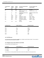
1
Platform Developer’s Kit
RC200/203 Manual
RC200/203 Manual
Celoxica, the Celoxica logo and Handel-C are trademarks of Celoxica Limited.
All other products or services mentioned herein may be trademarks of their respective owners.
Neither the whole nor any part of the information contained in, or the product described in, this document
may be adapted or reproduced in any material form except with the prior written permission of the
copyright holder.
The product described in this document is subject to continuous development and improvement. All
particulars of the product and its use contained in this document are given by Celoxica Limited in good
faith. However, all warranties implied or express, including but not limited to implied warranties of
merchantability, or fitness for purpose, are excluded.
This document is intended only to assist the reader in the use of the product. Celoxica Limited shall not
be liable for any loss or damage arising from the use of any information in this document, or any
incorrect use of the product.
The information contained herein is subject to change without notice and is for general guidance only.
Copyright © 2005 Celoxica Limited. All rights reserved.
Authors: RG
Document number: 1
Customer Support at http://www.celoxica.com/support/
Celoxica in Europe
Celoxica in Japan
Celoxica in the Americas
T: +44 (0) 1235 863 656
T: +81 (0) 45 331 0218
T: +1 800 570 7004
E: [email protected]
E: [email protected]
E: [email protected]
Page 2
www.celoxica.com
RC200/203 Manual
Contents
1 RC200/203
BOARD .................................................................................................... 8
2 RC200/203 OVERVIEW................................................................................................ 9
2.1 STANDARD KIT ...................................................................................................... 9
2.2 PROFESSIONAL KIT ............................................................................................. 10
2.3 EXPERT KIT ........................................................................................................ 10
2.4 RC200/203 SUPPORT SOFTWARE ........................................................................ 11
3 INSTALLATION AND SET-UP ........................................................................................ 12
4 HARDWARE DESCRIPTION .......................................................................................... 13
4.1 RC200/203 DEVICES .......................................................................................... 13
4.2 RC200/203 CONNECTORS .................................................................................. 14
4.3 CPLD 14
4.3.1 Control and data pins ............................................................................................................ 14
4.3.2 CPLD clock............................................................................................................................ 15
4.3.3 Register map in the CPLD for the FPGA .............................................................................. 15
4.3.4 CPLD / parallel port interface ................................................................................................ 16
4.4 FPGA 18
4.4.1 FPGA operation modes......................................................................................................... 19
4.4.2 Programming the FPGA using the FTU2 program................................................................ 19
4.4.3 Programming the FPGA from the parallel port...................................................................... 19
4.4.4 Programming the FPGA from SmartMedia ........................................................................... 20
4.4.5 Programming from a specific address in the SmartMedia: ................................................... 20
4.4.6 Reading data from the CPLD to the FPGA ........................................................................... 20
4.4.7 Writing data to the CPLD from the FPGA ............................................................................. 21
4.4.8 Transferring data between the FPGA and host..................................................................... 21
4.4.9 Using the FPGA in parallel port control mode....................................................................... 21
4.5 PARALLEL PORT ................................................................................................. 21
4.6 SMARTMEDIA FLASH MEMORY ............................................................................. 22
4.6.1 SmartMedia connections to the CPLD .................................................................................. 22
4.6.2 FPGA access of SmartMedia ................................................................................................ 22
4.6.3 Parallel port access of SmartMedia ...................................................................................... 23
4.7 ZBT SRAM BANKS ............................................................................................ 23
4.8 CLOCK GENERATOR (PLL) .................................................................................. 24
4.8.1 Programming the PLL via the parallel port or FPGA............................................................. 25
4.9 ETHERNET .......................................................................................................... 26
4.10 VIDEO INPUT PROCESSOR .................................................................................. 26
4.11 VIDEO OUTPUT PROCESSORS ............................................................................. 27
4.11.1 Digital / Analogue converter ................................................................................................ 27
4.11.2 RGB to NTSC/PAL encoder ................................................................................................ 28
4.11.3 TFT flat panel display .......................................................................................................... 28
4.12 AUDIO CODEC ................................................................................................... 28
4.13 RS-232 SERIAL TRANSMISSION .......................................................................... 28
4.14 MOUSE AND KEYBOARD PS/2 PORTS.................................................................. 29
4.15 7-SEGMENT DISPLAYS ....................................................................................... 29
4.16 ATA / EXPANSION HEADER ................................................................................ 30
4.17 LEDS .............................................................................................................. 32
4.18 CONTACT SWITCHES ......................................................................................... 32
4.19 RESET BUTTON ................................................................................................. 33
Page 3
www.celoxica.com
RC200/203 Manual
4.20 JTAG CONNECTOR ........................................................................................... 33
4.21 CAMERA AND CAMERA SOCKET .......................................................................... 33
4.22 BLUETOOTH MODULE ........................................................................................ 34
4.23 TOUCH SCREEN ................................................................................................ 34
4.24 DATA SHEETS AND SPECIFICATIONS.................................................................... 34
5 RC200/203 PSL REFERENCE.................................................................................... 36
5.1 USING THE RC200 PSL ...................................................................................... 36
5.2 CLOCK DEFINITIONS ............................................................................................ 36
5.2.1 Specifying a clock source...................................................................................................... 37
5.2.2 Specifying a clock rate .......................................................................................................... 37
5.2.3 Checking the clock rate ......................................................................................................... 37
5.3 DETECTING THE BOARD TYPE ............................................................................... 37
5.4 LED MACROS ..................................................................................................... 38
5.4.1 RC200LEDWrite() ................................................................................................................. 38
5.4.2 RC200LED*Write() macros ................................................................................................... 38
5.4.3 RC200LEDWriteMask()......................................................................................................... 38
5.5 PUSH BUTTON MACROS ....................................................................................... 39
5.5.1 RC200ButtonRead().............................................................................................................. 39
5.5.2 RC200Button*Read() macros................................................................................................ 39
5.5.3 RC200ButtonReadMask() ..................................................................................................... 39
5.6 SEVEN-SEGMENT MACROS ................................................................................... 39
5.6.1 Setting segments................................................................................................................... 39
5.6.2 Writing digits .......................................................................................................................... 40
5.7 ZBT SRAM MACROS .......................................................................................... 40
5.7.1 RAM management tasks ....................................................................................................... 41
5.7.2 Setting the RAM address ...................................................................................................... 41
5.7.3 Write address mask............................................................................................................... 41
5.7.4 Reading from RAM................................................................................................................ 42
5.7.5 Writing data to RAM .............................................................................................................. 42
5.8 PS/2 PORT MACROS ............................................................................................ 42
5.8.1 Mouse management tasks .................................................................................................... 42
5.8.2 Reading data from the mouse ............................................................................................... 42
5.8.3 Writing data to the mouse ..................................................................................................... 43
5.8.4 Keyboard management tasks................................................................................................ 43
5.8.5 Reading data from the keyboard ........................................................................................... 43
5.8.6 Writing data to the keyboard ................................................................................................. 43
5.9 RS-232 PORT MACROS ....................................................................................... 44
5.9.1 RS-232 management tasks................................................................................................... 44
5.9.2 Reading from the RS-232 port .............................................................................................. 46
5.9.3 Writing to the RS-232 port..................................................................................................... 46
5.10 TOUCH SCREEN MACROS ................................................................................... 46
5.10.1 Touch screen management tasks ....................................................................................... 46
5.10.2 Touch screen position (raw) ................................................................................................ 46
5.10.3 Touch screen position (scaled) ........................................................................................... 47
5.11 VIDEO OUTPUT MACROS .................................................................................... 47
5.11.1 Video output management tasks......................................................................................... 47
5.11.2 Enabling video output.......................................................................................................... 48
5.11.3 Querying screen sizes......................................................................................................... 49
5.11.4 Disabling video output ......................................................................................................... 49
5.11.5 Writing a pixel ...................................................................................................................... 50
5.11.6 Current scan position .......................................................................................................... 50
5.11.7 Blanking status of current scan position.............................................................................. 50
5.11.8 Horizontal and vertical sync status...................................................................................... 50
5.12 VIDEO INPUT MACROS........................................................................................ 51
Page 4
www.celoxica.com
RC200/203 Manual
5.12.1 Video input management tasks ........................................................................................... 51
5.12.2 Selecting the video input ..................................................................................................... 51
5.12.3 Selecting the colour-encoding standard.............................................................................. 51
5.12.4 Reading a pair of YCrCb pixels ........................................................................................... 52
5.12.5 Reading a pair of RGB pixels .............................................................................................. 52
5.12.6 Reading a single RGB pixel ................................................................................................ 53
5.13 AUDIO I/O MACROS ........................................................................................... 54
5.13.1 Audio codec management tasks ......................................................................................... 54
5.13.2 Setting the audio input......................................................................................................... 54
5.13.3 Boosting the input amplifier ................................................................................................. 54
5.13.4 Setting the gain level ........................................................................................................... 54
5.13.5 Setting the input sample rate............................................................................................... 55
5.13.6 Reading from the audio interface ........................................................................................ 55
5.13.7 Setting the output volume.................................................................................................... 55
5.13.8 Setting the output sample rate ............................................................................................ 56
5.13.9 Writing to the audio interface............................................................................................... 56
5.14 BLUETOOTH MACROS ........................................................................................ 56
5.14.1 Bluetooth management tasks.............................................................................................. 57
5.14.2 Resetting the Bluetooth device............................................................................................ 57
5.14.3 Reading from the Bluetooth device ..................................................................................... 57
5.14.4 Writing to the Bluetooth device............................................................................................ 57
5.15 SMARTMEDIA MACROS ...................................................................................... 57
5.15.1 Using the SmartMedia macros ............................................................................................ 58
5.15.2 SmartMedia management tasks.......................................................................................... 59
5.15.3 Initializing the SmartMedia device....................................................................................... 59
5.15.4 SmartMedia manufacturer and device code ....................................................................... 59
5.15.5 Resetting the SmartMedia................................................................................................... 60
5.15.6 Erasing SmartMedia memory.............................................................................................. 60
5.15.7 Number of pages per block ................................................................................................. 60
5.15.8 Logical and physical addressing ......................................................................................... 60
5.15.9 Reading from and writing to the SmartMedia...................................................................... 62
5.16 ETHERNET MACROS .......................................................................................... 64
5.16.1 Ethernet management tasks ............................................................................................... 64
5.16.2 Enabling the Ethernet device .............................................................................................. 65
5.16.3 Setting the Ethernet mode................................................................................................... 65
5.16.4 Disabling the Ethernet device.............................................................................................. 65
5.16.5 Resetting the Ethernet device ............................................................................................. 65
5.16.6 Reading a packet ................................................................................................................ 66
5.16.7 Writing a packet to the network........................................................................................... 67
5.17 RECONFIGURING THE FPGA.............................................................................. 68
5.18 CPLD CONTROL ............................................................................................... 69
5.18.1 CPLD management tasks ................................................................................................... 69
5.18.2 Enabling the CPLD.............................................................................................................. 69
5.19 FPGA / PARALLEL PORT COMMUNICATION .......................................................... 69
5.19.1 Enabling the Send Protocol driver....................................................................................... 70
5.19.2 Disabling the Send Protocol driver...................................................................................... 70
5.19.3 Writing data to the host PC ................................................................................................. 70
5.19.4 Reading data from the host PC ........................................................................................... 70
5.20 EXPANSION PORT PINS ...................................................................................... 71
6 INDEX ....................................................................................................................... 73
Page 5
www.celoxica.com
RC200/203 Manual
Conventions
The following conventions are used in this document.
2
Warning Message. These messages warn you that actions may damage your hardware.
Ï
Handy Note. These messages draw your attention to crucial pieces of information.
Hexadecimal numbers will appear throughout this document. The convention used is that of prefixing
the number with '0x' in common with standard C syntax.
Sections of code or commands that you must type are given in typewriter font like this:
void main();
Information about a type of object you must specify is given in italics like this:
copy SourceFileName DestinationFileName
Optional elements are enclosed in square brackets like this:
struct [type_Name]
Curly brackets around an element show that it is optional but it may be repeated any number of times.
string ::= "{character}"
Page 6
www.celoxica.com
RC200/203 Manual
Assumptions & Omissions
This manual assumes that you:
•
have used Handel-C or have the Handel-C Language Reference Manual
•
are familiar with common programming terms (e.g. functions)
•
are familiar with your operating system (Linux or MS Windows)
This manual does not include:
•
instruction in VHDL or Verilog
•
instruction in the use of place and route tools
•
tutorial example programs. These are provided in the Handel-C User Manual
Page 7
www.celoxica.com
RC200/203 board
1 RC200/203 board
The RC200 and RC203 are platforms for evaluation and development of high-performance
FPGA-based applications. The platforms include a Xilinx Virtex-II FPGA, external memory,
programmable clocks, Ethernet, Audio, Video, SmartMedia, Parallel port, RS-232 and PS/2 keyboard
and mouse. Supporting software includes PAL, DSM, the RC200 PSL, and the FTU2 File Transfer
Utility.
The only difference between the RC200 and RC203 platforms is the FPGA fitted, a 2V1000-4 on the
RC200 and a larger 2V3000-4 on the RC203.
The RC200 is available in 3 versions:
•
Standard (part number RC-I-200-2V1K4S)
•
Professional (part number RC-I-200-2V1K4P)
•
Expert (part number RC-I-200-2V1K4E)
The RC203 is also available in 3 versions:
•
Standard (part number RC-I-203-2V3K4S)
•
Professional (part number RC-I-203-2V3K4P)
•
Expert (part number RC-I-203-2V3K4E)
Except where specifically noted in this document "RC200" should be taken as meaning either RC200 or
RC203.
Note: On the RC203 platform it is very important not to use any pins not specifically referenced in this
document. To do so risks damaging the FPGA device.
It is recommended that you use the RC200 Platform Support Library to program the board.
System requirements
• DK Design Suite. Only required if you want to use the PAL, DSM and RC200 Platform
Support libraries.
•
Microsoft Windows NT4, Windows 2000 or Windows XP for the FTU2 program and for use
of the DK Design Suite.
Page 8
www.celoxica.com
RC200/203 board
2 RC200/203 overview
The devices and connectors on the board are shown in the overview of devices (see page 13) and
overview of connectors (see page 14).
Note: the Xilinx Virtex II device on the RC203 has part number XC2V3000-FG676.
2.1 Standard kit
•
Virtex-II 2V1000-4 (RC200) or 2V3000-4 (RC203) FPGA
•
Ethernet MAC/PHY with 10/100baseT socket
•
2 banks of ZBT SRAM providing a total of 4-MB
•
Video support including:
•
• Composite video in/out
• S-Video in/out
• VGA out
• Camera in (Camera socket provides camera power)
AC'97 compatible Audio including
Page 9
www.celoxica.com
RC200/203 board
•
• Microphone in
• Line in (Stereo)
• Line/Headphone out (Stereo)
Connector for SmartMedia Flash memory for storage of BIT files
•
CPLD for configuration/reconfiguration and SmartMedia management
•
• Power-on load from SmartMedia
• Load when SmartMedia installed
• Reconfigure on demand from FPGA
Parallel port connector and cable, for BIT-file download and host communication with FPGA
•
RS-232
•
PS/2 keyboard and mouse connectors
•
2 seven-segment displays
•
2 blue LEDs
•
2 momentary contact switches
•
50 pin expansion header including:
•
• 33 general I/O pins
• 3 power pins (+12V, +5V, +3.3V)
• 2 clock pins
JTAG connector
•
Perspex top and bottom covers
•
Universal 110/240V power supply (IEC Mains lead not included)
•
Celoxica Platform Developer’s Kit including:
•
•
•
•
Platform Support Library for RC200/203
Platform Abstraction Layer for RC200/203
Data Stream Manager for MicroBlaze soft-core microprocessor
FTU2 BIT file transfer utility (for Windows NT4, Windows 2000 and Windows XP)
2.2 Professional kit
This provides the following features in addition to the Standard kit:
•
Headphone/microphone set
•
Mouse
•
16-MB SmartMedia card
•
Colour camera
2.3 Expert kit
This provides the following features in addition to the Professional Kit:
•
Bluetooth wireless module
•
Memory banks expanded to 4-MB each giving a board total of 8-MB
•
TFT flat panel display or touch screen
Page 10
www.celoxica.com
RC200/203 board
2.4 RC200/203 support software
The following software support for the RC200/203 is provided as part of the Platform Developer's Kit:
•
RC200 Platform Support Library (PSL)
•
RC200 Platform Abstraction Layer (PAL) implementation
•
Data Stream Manager (DSM) implementation for MicroBlaze soft-core microprocessor
•
FTU2 program (for Windows NT4, Windows 2000 and Windows XP). Allows you you to
download BIT files onto the FPGA.
Page 11
www.celoxica.com
RC200/203 overview
3 Installation and set-up
Unpacking the board
You should take care to avoid static discharge when handling the RC200/203 board, as this may
damage it. You are recommended to use an earth strap. If an earth strap is not available, ensure that
you make contact with earth before and during handling of the board, and only handle the board by its
edges.
Connecting the cables
The board must be powered down before you attach cables. The connectors are labelled on the board
and in the overview of connectors (see page 14).
You will need to connect the board to your PC with an IEEE 1284-compliant parallel port cable if you
want to use the Celoxica FTU2 program to download BIT files, or to read from or write to SmartMedia
memory. A cable is provided as part of the RC200/203 kit.
Switching on the power
You need a 12V DC power supply with a 2.1mm, centre-positive plug. The power supply must be able to
source at least 2A.
Peripheral devices should be connected before the RC200/203 Board is turned on. Otherwise the
devices may not function correctly.
LED D2 will light up when the power is on. This is the lower of the 2 LEDS to the left of the Celoxica
copyright printed on the board.
Page 12
www.celoxica.com
Installation and set-up
4 Hardware description
This section describes the devices on the RC200, how to program the FPGA and how to transfer data
between the host, SmartMedia and FPGA.
Schematics for the board are available in
InstallDir\PDK\Documentation\PSL\RC200\RC200VBDOC.pdf for the RC200 or in
InstallDir\PDK\Documentation\PSL\RC203\RC203VBDOC.pdf for the RC203 (for installations
using PDK3.1 or later).
Note: On the RC203 platform it is very important not to use any pins not specifically referenced in this
document. To do so risks damaging the FPGA device.
There is also a list of data sheets (see page 34) for the devices.
4.1 RC200/203 devices
DEVICES ON THE RC200/203
Page 13
www.celoxica.com
Installation and set-up
4.2 RC200/203 connectors
CONNECTORS ON THE RC200/203
4.3 CPLD
The RC200/203 has a Xilinx XC95144XL 3.3V CPLD.
The CPLD is connected to the:
•
FPGA
•
Parallel port
•
SmartMedia Flash RAM
•
JTAG chain
The CPLD can configure the FPGA with data received from SmartMedia memory, or via the parallel port.
4.3.1 Control and data pins
The RC200 CPLD has 10 control lines and 8 data lines. 3 of the control lines are used as an address
bus. The control lines have two meanings, depending on the FPGA operation mode (see page 19).
The FPGA operation mode is determined by whether the CPLD pin P9 is set high or low.
Page 14
www.celoxica.com
Installation and set-up
CPLD control
line
RC200
FPGA
pin
RC203
FPGA
pin
Function (normal FPGA
operation)
Function (parallel port
control mode)
P0
Y19
AB21
CCLK
Not used
P1
AA3
AC5
PnCS (Parallel Not Chip
Select) - Input
nWR (Not Write) - Input
P2
Y4
AB6
nRDWR (Not Read Write) –
Input/Output
nRDWR (Not Read Write) Output
P3
A2
C4
nPROG
Not used
P4
AB20
AD22
DONE
Not used
P5
AA19
AC21
Address [0] – Output
nINIT – Output
P6
AB19
AD21
Address [1] – Output
nWAIT – Output
P7
R22
U24
Address [2] – Output
nADDR – Input
P8
V22
Y24
nCS (Not Chip Select) –
Output
nDATA – Output
P9
T18
V20
Set high
Set low
CPLD data line
RC200 FPGA pin
RC203 FPGA pin
FD0
V18
Y20
FD1
V17
VY19
FD2
W18
AA20
FD3
Y18
YAB20
FD4
Y5
AB7
FD5
W5
AA7
FD6
AB4
AD6
FD7
AA4
AC6
4.3.2 CPLD clock
The RC200 CPLD has a clock input of 50MHz from a 50MHz crystal oscillator module. This is divided by
2 to give an internal clock speed of 25MHz.
4.3.3 Register map in the CPLD for the FPGA
The RC200 CPLD has 3 address lines:
CPLD pins
RC200 FPGA pins
RC203 FPGA pins
P5 Addr[0]
AA19
AC21
P6 Addr[1]
AB19
AD21
P7 Addr[2]
R22
U24
Only the lower 5 of the 8 possible values within the 3-bit CPLD address are used by the FPGA:
Page 15
www.celoxica.com
Installation and set-up
0
Control of SmartMedia and PLL
Bit 0: SmartMedia nCS signal
Bit 1: SmartMedia CLE signal
Bit 2: SmartMedia ALE signal
Bit 3: Disable SmartMedia state machine
Bit 4: Not used (Write 0)
Bit 5: Not used (Write 0)
Bit 6: PLL clock pin (I2C bus)
Bit 7: PLL data pin (I2C bus 1 = Tristate (input) 0=0)
1
Read status Register
Bit 0: Master FPGA DONE signal
Bit 1: (not used; undefined)
Bit 2: FPGA nINIT signal
Bit 3: SmartMedia nBUSY signal
Bit 4: SmartMedia Detect (1 = SmartMedia inserted)
Bit 5: SmartMedia not Write Protect
Bit 6: SmartMedia state machine disable status
Bit 7: PLL data line (I2C bus)
2
Data bus access of the SmartMedia
3
Upper byte of Block address for the SmartMedia (only the lower 5 bits are used)
4
Lower byte of Block address for the SmartMedia
5
Read from this address to start reprogramming of the FPGA from
SmartMedia
4.3.4 CPLD / parallel port interface
The RC200 CPLD supports an EPP (Enhanced Parallel Port) interface.
The parallel port is connected to the CPLD on the following pins:
Page 16
www.celoxica.com
Installation and set-up
CPLD pins
Signal
Parallel port pins
76
ParSCTL
13
77
ParPE
12
78
Parnwait
11
79
ParINIT
10
80
Pardata7
9
81
Pardata6
8
82
Pardata5
7
85
Pardata4
6
86
Pardata3
5
89
Paraddr
17
90
Pardata2
4
91
Parnreset
16
92
Pardata1
3
93
Parnerror
15
94
Pardata0
2
95
Parndata
14
96
Parnwrite
1
The CPLD has 3 address pins. When the CPLD is communicating with the parallel port data lines, the 8
values within the 3-bit CPLD address are used as follows:
Address value
Description
0
Read and write (i.e. data pins) when FPGA is in parallel port control mode
1
Read and write from host for SmartMedia
2
Not used
3
Read status of signals (8-bit data line from CPLD):
Bit 0: Master FPGA DONE signal
Bit 1: (not used; undefined)
Bit 2: FPGA nINIT signal
Bit 3: SmartMedia nBUSY signal
Bit 4: SmartMedia Detect (1 = SmartMedia inserted)
Bit 5: SmartMedia not Write Protect
Bit 6: SmartMedia state machine disable status
Bit 7: PLL data line (I2C bus)
Write status of signals:
Page 17
www.celoxica.com
Installation and set-up
Address value
Description
Bit 0: SmartMedia nCS signal
Bit 1: SmartMedia CLE signal
Bit 2: SmartMedia ALE signal
Bit 3: Disable SmartMedia state machine
Bit 4: Master FPGA nPROG pin (inverted by CPLD)
Bit 5: Not used (Write 0)
Bit 6: PLL clock pin (I2C bus)
Bit 7: PLL data pin (I2C bus 1 = Tristate (input) 0=0)
4
Not used
5
Not used
6
Not used
7
CPLD version ID (0x51)
4.4 FPGA
The RC200 board has a Xilinx Virtex-II FPGA (part: XC2V1000-4FG456C on RC200 and
XC2V3000-4FG676 on RC203). The device has direct connections to the following devices:
•
CPLD
•
ZBT RAM
•
Ethernet
•
Clock generator
•
Video input
•
Video DAC
•
RGB to PAL/NTSC encoder
•
Audio codec
•
RS-232
•
PS/2 connectors
•
Expansion header
•
2 seven-segment displays
•
2 blue LEDs
•
2 contact switches
•
Bluetooth (if fitted)
•
TFT Flat screen (if fitted)
•
Touchscreen (if fitted)
Details of pin connections are given in the sections about these devices.
Ï
If you are programming the board using Handel-C, remember that the pins should be listed
in reverse (descending) order.
Page 18
www.celoxica.com
Installation and set-up
The FPGA also has access to the parallel port and to the SmartMedia Flash memory through the CPLD.
You can program the FPGA via the CPLD from the SmartMedia Flash memory, or from the parallel port.
4.4.1 FPGA operation modes
The RC200 FPGA has two modes of operation:
•
normal operation: communicates with the SmartMedia and PLL and is a parallel port slave
•
parallel port control operation: becomes parallel port master and drives all parallel port
signals
The operation mode is set by control line P9 on the CPLD. If P9 is high, the FPGA is in normal operation
mode. If P9 is low, the FPGA is in parallel port control operation mode.
The function of the other CPLD control lines changes, depending on whether P9 is high or low.
4.4.2 Programming the FPGA using the FTU2 program
Celoxica provides a File Transfer Utility program, FTU2, which simplifies the process of programming
the RC200 FPGA via the parallel port.
4.4.3 Programming the FPGA from the parallel port
To program the RC200 Virtex-II from the parallel port:
1. Check that the board is connected and powered by reading the CPLD version ID (CPLD
address value 7).
The board may not return the ID if the FPGA is controlling the parallel port. If this happens,
eject the SmartMedia card and press the Reset button.
2. Disable and clear the FPGA by asserting nPROG (CPLD address 3, bit 4). Leave nPROG
asserted.
3. Disable the SmartMedia state machine by asserting CPLD address 3, bit 3 and leave this
asserted during programming.
4. Wait at least 1mS.
5. Deassert nPROG.
6. Wait for nINIT (CPLD address 3, bit 2) to go high, showing that the FPGA has cleared its
memory. For timeouts this is 4uS per frame, giving a total of 4.9mS for the Virtex II
XC2V1000 on the RC200 and 13mS for the XC2V3000 on the RC203.
7. The entire BIT file without the header can now be transferred directly to address 0. The
CPLD times the nCS, nWR and CCLK signals such the FPGA may be programmed.
8. After programming the FPGA, you need to wait at least 100µS before accessing the CPLD.
Alternatively, wait 1µS and check that PnCS is high (i.e. that there is no access to the
parallel port).
If programming is successful, DONE (CPLD address 3, bit 0) will be high, lighting the DONE LED. The
SmartMedia state machine can then be re-enabled by setting the Disable SmartMedia state machine
signal low (address 3, bit 3). If there is an error during programming the FPGA will signal a CRC error by
lowering nINIT (unless the FPGA is accessing the CPLD).
Page 19
www.celoxica.com
Installation and set-up
4.4.4 Programming the FPGA from SmartMedia
You can program the RC200 Virtex-II from BIT files loaded onto the SmartMedia device. The BIT files
can be in exactly the same format as if you were programming from the parallel port. There is no need to
change or remove the header.
To program the Virtex-II from page 1 on the SmartMedia Flash, use one of the following:
•
Apply power to the board
•
Press the Reset button on the board
•
Insert the SmartMedia card whilst the board is switched on
4.4.5 Programming from a specific address in the SmartMedia:
1. Set a block address in the CPLD using Address 4 for the lower byte of the address and
Address 3 for the upper byte (only the lower 5 bits of this byte are used).
2. Read from Address 5.
These steps will cause the CPLD to read from the relevant address in the SmartMedia and write the data
to the FPGA. Data is written using following steps:
•
CPLD sets up the FPGA for programming.
•
CPLD reads the ID register of the code to find out if 4-word addresses are required.
•
CPLD reads the page valid byte (512+5) to see if it is valid.
If the page valid byte is invalid it searches though the block checking the page valid byte
until it finds a page that is valid.
The first valid page is skipped (if programming from address zero this is the CIS page).
•
Data is copied to the FPGA until the FPGA is DONE. Bad pages are skipped.
The CPLD automatically adds 16 clock cycles after DONE to complete programming. If the FPGA
signals an error during programming, the FPGA is reset and the CPLD waits until a new SmartMedia is
inserted.
It is assumed that if a single page is invalid then the entire block is invalid, and all the pages within the
block will have the block invalid byte set. The CPLD doesn't check the SmartMedia ECC (Error
Correcting Code) as the FPGA programming datastream has its own CRC (Cyclical Redundancy
Checking) which checks that the data stream is correct.
4.4.6 Reading data from the CPLD to the FPGA
To read data from the RC200/203 CPLD and write it to the FPGA:
1. Set up the address and tristate the data bus.
2. Wait at least 10ns.
3. Set nCS low.
4. Wait at least 10ns.
5. Set nRDWR low.
6. Wait at least 40ns before reading data.
7. Tristate nRDWR.
8. Set nCS high.
Page 20
www.celoxica.com
Installation and set-up
4.4.7 Writing data to the CPLD from the FPGA
To write from the RC200 FPGA to the CPLD:
1. Set up the address and data bus if not already tristated.
2. Wait at least 10ns.
3. Set nCS low.
4. Wait at least 10ns.
5. Set nRDWR high and enable the data bus.
6. Wait at least 40ns.
7. Tristate nRDWR.
8. Set nCS high.
9. Tristate the data bus.
4.4.8 Transferring data between the FPGA and host
The parallel port can read and write data to the RC200 FPGA by accessing CPLD address 0. The
process is controlled by the CPLD.
To write data from the host (via the parallel port) to the FPGA:
1. Set nRDWR low.
2. Set PnCS low.
3. Send the data.
4. Set PnCS high.
5. Set nRDWR high.
To read data from the FPGA and write it to the host via the parallel port:
1. Set nRDWR high.
2. Set PnCS low.
3. Read the data.
4. Set PnCS high.
5. Set nRDWR low.
4.4.9 Using the FPGA in parallel port control mode
When the CPLD control line P9 is set low the RC200 FPGA has direct control over the parallel port. The
nRDWR signal (CPLD control line P2) defines the direction of the databus.
4.5 Parallel port
The RC200/203 has an IEEE 1284-compatible parallel port. You can use the parallel port to:
•
program the FPGA (see page 19)
•
program the SmartMedia card (see page 23)
•
read data from and write data to the FPGA (see page 21)
Page 21
www.celoxica.com
Installation and set-up
4.6 SmartMedia Flash memory
The RC200/203 has a socket for a SmartMedia Flash memory device (connector CN7 at the top left of
the board). The Professional and Expert versions of the RC200/203 are provided with a 16-MB
SmartMedia card. You can use any SmartMedia device between 4 and 128 megabytes.
Ï
The RC200/203 Platform Support Library abstracts away some of the intricacies of the
physical layer control mechanism within the SmartMedia driver. The library also allows you
to use logical addressing, which has the further advantages of preserving the CIS and IDI
fields and skipping invalid blocks.
For more information on SmartMedia devices, please refer to the RC200 Datasheets (see page 34).
4.6.1 SmartMedia connections to the CPLD
The RC200 SmartMedia is connected to the CPLD on the following pins:
SmartMedia pins
Signals
CPLD pins
2
CLE
17
3
ALE
15
4
SMnWE
13
5
nWP
11
6
SMD0
10
7
SMD1
9
8
SMD2
7
9
SMD3
4
13
SMD4
2
14
SMD5
3
15
SMD6
6
16
SMD7
8
19
R/nB
12
20
SMnRD
14
21
SMnCS
16
4.6.2 FPGA access of SmartMedia
The RC200 SmartMedia is accessed by the FPGA via the CPLD.
A typical sequence of events might be:
1. Disable SmartMedia state machine by writing 1 on CPLD control address 0, bit 3.
2. Check the SmartMedia is fitted by reading the status of CPLD address 1, bit 4. A value of 1
means that the SmartMedia has been successfully detected.
3. Assert nCS (CPLD address 0, bit 0).
Page 22
www.celoxica.com
Installation and set-up
4. Deassert ALE (CPLD address 0, bit 2).
5. Assert CLE (CPLD address 0, bit 1).
6. Write a command to address 2.
7. Deassert CLE.
8. Read or write to SmartMedia using address 2.
4.6.3 Parallel port access of SmartMedia
The RC200 SmartMedia is accessed from the parallel port via the CPLD.
A typical sequence of events for programming the SmartMedia from the parallel port might be:
1. Check the SmartMedia device is fitted (address 3, bit 4).
2. Disable the FPGA from accessing the SmartMedia by asserting nPROG (address 3, bit 4).
3. Disable the SmartMedia state machine by asserting address 3, bit 3.
4. Wait for at least 1mS.
5. Assert nCS (address 3, bit 0).
6. Deassert ALE (address 3, bit 2).
7. Assert CLE (address 3, bit 1).
8. Write a SmartMedia command to CPLD address 2.
For example, refer to the SmartMedia Electrical Specification issued by the SSFDC forum:
www.ssfdc.or.jp.
9. Deassert CLE.
10. Write a SmartMedia address.
Ï
You need to carry out steps 1 to 4 for any access to the SmartMedia.
4.7 ZBT SRAM banks
The RC200/203 is fitted with 2 ZBT RAM banks, capable of operating at up to 100MHz. The RC200/203
Standard and Professional boards have two 2-MB banks fitted and the RC200/203 Expert has two 4-MB
banks. The RAM banks are IDT71T75702 devices, with 512K or 1024K 36-bit words. All lines are
mapped directly to the FPGA. For more information, please refer to the RC200 data sheets (see page
34).
Page 23
www.celoxica.com
Installation and set-up
Pins connecting RAM Bank 0 to the FPGA
SSRAM pin
Function
Rc200 FPGA pins (in
ascending order)
RC203 FPGA pins (in
ascending order)
S0D0 S0D35
Data [35:0]
K20, L19, L20, K18, L18,
E18, F18, G18, H18, J18,
J17, K17, B12, A13, B13,
A14, B14, B15, A16, B16,
A17, B17, B18, A19, B19,
C12, D12, C13, D13, C14,
D14, C15, D15, C16, D16,
C17
M22, N21, N22, M20, N20,
G20, H20, J20, K20, L20,
L19, M19, D14, C15, D15,
C16, D16, D17, C18, D18,
C19, D19, D20, C21, D21,
E14, F14, E15, F15, E16,
F16, E17, F17, E18, F18,
E19
S0A0 S0A19
Address [19:0]
C21, C22, D21, D22, E21,
F21, F22, G21, G22, H21,
J21, J22, K21, K22, L22, L21,
E19, E20, F19, F20
E23, E24, F23, F24, G23,
H23, H24, J23, J24, K23,
L23, L24, M23, M24, N24,
N23, G21, G22, H21, H22
S0C0
CLK
F12
H14
S0C1
nCS2 (not Chip Select)
G19
J21
S0C2
R/nW (Read not Write)
G20
J22
J20, K19, H20, J19
L22, M21, K22, L21
S0C4 - S0C7 Not Byte Enable pins
Pins connecting RAM Bank 1 to the FPGA
SSRAM pin
Function
RC200 FPGA pins (in
ascending order)
RC203 FPGA pins (in
ascending order)
S1D0 S1D35
Data [35:0]
D7, C7, D8, C8, D9, C9, D10,
C10, E11, F11, E4, E5, E6,
E7, E8, E9, E10, F9, F10, C2,
C1, D2, D1, E2, F2, F1, G2,
G1, H2, J2, J1, K2, K1, L2,
E3, F4
F9, E9, F10, E10, F11, E11,
F12, E12, G13, H13, G6,
G7, G8, G9, G10, G11, G12,
H11, H12, E4, E3, F4, F3,
G4, H4, H3, J4, J3, K4, L4,
L3, M4, M3, N4, G5, H6
S1A0 S1A19
Address [19:0]
D17, C18, D18, F13, F14,
E13, E14, E15, E16, E17, B4,
A4, B5, B6, A6, B7, A7, B8,
B9, A9
F19, E20, F20, H15, H16,
G15, G16, G17, G18, G19,
D6, C6, D7, D8, C8, D9, C9,
D10, D11, C11
S1C0
CLK
D11
F13
S1C1
nCS2 (not Chip Select)
B10
D112
S1C2
R/nW (Read not Write)
A10
C12
D6, C6, C4, C5
F8, E8, E6, E7
S1C4 - S1C7 Not Byte Enable pins
4.8 Clock generator (PLL)
The RC200/203 board has a Cypress CY22393 Programmable Clock Generator. The generator is
programmed to provide the following clocks:
Page 24
www.celoxica.com
Installation and set-up
Clock
generator pin
Description
RC200 FPGA pin
RC203 FPGA pin
GCLK2P
GCLK5P
CLKUSER. Clock used to feed the FPGA.
Y12
AB14
24.576MHz clock. Used to feed video input
and audio chip.
B11
D13
GCLK6S
25.175MHz clock. Used to feed VGA output
(640 x 480 at 60Hz).
C11
E13
GCLK0P
27MHz video input clock.
AB12
AD14
GCLK1P
50MHz crystal clock. This is used to feed
the CPLD.
E12
G14
GCLK7S
Expansion clock 0
AA11
AC13
GCLK5S
Expansion clock 1
W11
AA13
CLKCTRL
V19
Y21
TV clock rates
The clock generator also produces 14.318MHz and 17.7MHz clocks for the RGB to PAL/NTSC encoder.
You can select between these values using the CLKCTRL signal (pin 15 on the clock generator).
FPGA clock: CLKUSER
CLKUSER has a default value of 133MHz. You can change the default value of CLKUSER by
programming the PLL from the FPGA or parallel port.
4.8.1 Programming the PLL via the parallel port or FPGA
The RC200 PLL chip can be soft programmed by either the FPGA or the parallel port. It reverts to factory
settings on a power on reset. The PLL chip supports a form of I2C.
If you are programming from the parallel port, the FPGA should be disabled by asserting nPROG if there
is any chance of it interfering with the programming of the PLL.
2
If you program any of the clocks apart from CLKUSER, you could stop the devices from
working, or damage them.
Programming the PLL from the parallel port
Three bits in the CPLD are used during PLL programming. The state of the data line can be monitored at
any time by reading bit 7 from address 3. The clock line for the data is bit 6 of address 3. The bit for
writing zeros is bit 7 of address 3. The data line is pulled up by a resistor, so by writing 3[7]=1 a one will
be written. When data is to be read from the PLL chip, bit 7 of address 3 should be set to 1 so that the
PLL chip can pull the data line to zero if required.
Programming the PLL from the FPGA
Programming the PLL from the FPGA is the same as programming from the parallel port except that the
registers are at a different address in the CPLD. The data line is monitored by reading bit 7 from address
1 and the clock line for the data is bit 6 of address 0. The data line is bit 7 of address 0.
Page 25
www.celoxica.com
Installation and set-up
4.9 Ethernet
The RC200/203 is fitted with a Standard Microsystems Corporation LAN91C111 Ethernet device. It
supports 8-bit and 16-bit access to the FPGA. The device has a clock input of 25MHz, generated from
the CPLD. For more information about the device refer to the RC200 data sheets (see page 34).
Ethernet pins
Function
RC200 FPGA pins (in
ascending order)
RC203 FPGA pins (in
ascending order)
ED0 - ED15
Data [15:0]
M21, N22, N21, P22, P21,
R21, T22, T21, U22, U21,
V21, W22, W21, Y22, Y21,
M17
P23, R24, R23, T24, T23,
U23, V24, V23, W24, W23,
Y23, AA24, AA23, AB24,
AB23, P19
EC0 - EC2
Address [2:0]
M18, M20, M19
P20, P22, P21
EC3 and EC4
Not byte enable
N20, N19
R22, R21
EC5
Not Read
P20
T22
EC6
Not Write
P19
T21
EC7
Interrupt
R20
U22
EC8
Asynchronous ready
pin (Ardy)
R19
U21
EC9
Reset
T20
V22
4.10 Video input processor
The RC200/203 board is fitted with a Philips SAA7113H Video Input Processor, enabling the FPGA to
capture S Video, CVBS and Camera input.
The FPGA can decode RGB to:
•
NTSC or PAL using the AD725 RGB to NTSC/PAL encoder
•
VGA output using the ADV7123 RGB to VGA encoder
Video input control and data pins
The video input has 8 data pins and 6 control lines:
Video input pins
Function
RC200 FPGA Pins (in
ascending order)
RC203 FPGA Pins (in
ascending order)
VIND0 – VIND7
Data pins [7:0]
AA20, AA18, AA17, AB17,
AA16, AB16, AA15, AA14
AC22, AC20, AC19, AD19,
AC18, AD18, AC17, AC16
VINC0
RTS1
W20
AA22
VINC1
RTS0
N17
R19
VINC2
RTCO
P17
T19
VINC3
SCL
N18
R20
VINC4
SDA
P18
T20
VINC5
CEP
R18
U20
Page 26
www.celoxica.com
Installation and set-up
4.11 Video output processors
The RC200/203 can convert digital RGB input into outputs for a VGA screen, a TV (PAL or NTSC) or an
LCD screen.
OVERVIEW OF VIDEO OUTPUT PROCESSING
4.11.1 Digital / Analogue converter
The Analog Devices ADV7123 High speed video DAC can convert 30-bit digital input to VGA output or
RGB input for the NTSC/PAL encoder.
For more information on this device, please refer to the RC200 data sheets (see page 34).
DAC pins
Function
FPGA Pins (in
ascending order)
FPGA Pins (in
ascending order)
RGB0 - RGB9
Red [9:0]
U18, V16, V15, V14, V13,
U14, U13, AB10, AA10,
AB9
W20, Y18, Y17, Y16, Y15,
W16, W15, AD12, AC12,
AD11
RGB10 – RGB19
Green [9:0]
AA9, AA8, U11, V11, Y11,
Y10, W10, AB18, AB15,
Y9
AC11, AC10, W13, Y13,
AB13, AB12, AA12, AD20,
AD17, AB11
RGB20 – RGB29
Blue [9:0]
W9, Y8, W8, Y7, W7, Y6,
W6, AB8, AB5, U10
AA11, AB10, AA10, AB9,
AA9, AB8, AA8, AD10,
AD7, W12
RGB30
Clock pin
U9
W11
RGB31
Not blank pin
V10
Y12
RGB32
Not Sync pin
V9
Y11
RGB33
VSync pin
V8
Y10
RGB34
HSync pin
V7
Y9
RBG35
Monitor SDA pin
V6
Y8
RGB36
Monitor SCL pin
V5
Y7
Page 27
www.celoxica.com
Installation and set-up
4.11.2 RGB to NTSC/PAL encoder
The RC200/203 has an Analog Devices AD725 RGB to NTSC/PAL Encoder. This receives RGB input
from the video DAC.
For more information on this device, please refer the RC200 data sheets (see page 34).
NTSC/PAL encoder pins
Function
RC200 FPGA pins
RC203 FPGA pins
TV0
Standard pin
AB14
AD16
TV1
Hsync pin
AA13
AC15
TV2
Vsync pin
AB13
AD15
4.11.3 TFT flat panel display
An Optrex T-51382D064J-FW-P-AA thin film transistor (TFT) flat panel display is provided as an
optional feature with the RC200/203 Expert board. It is connected directly to the FPGA.
TFT control pins
Function
RC200 FPGA pins
RC203 FPGA pins
LCD0
Clock pin
AA12
AC14
LCD1
Hsync pin
W17
AA19
LCD2
Vsync pin
Y17
AB19
LCD3
Data enable pin
W16
AA18
The TFT has 18 data pins: RGB4 - RGB9, RGB14 - RGB19 and RGB24 - RGB29. These pins are
shared by the TFT and the DAC on the FPGA.
4.12 Audio codec
The Cirrus Logic CS4202 is an AC'97-compliant stereo audio codec, which includes surround sound
and multi-channel applications for the PC.
Audio codec pins
Function
RC200 FPGA pins
RC203 FPGA pins
AC0
SDATA_OUT
AA5
AC7
AC1
BIT_CLK
AA6
AC8
AC2
SDATA_IN
AB6
AD8
AC3
SYNC
AA7
AC9
AC4
nRESET
AB7
AD9
4.13 RS-232 serial transmission
The board has a MAXIM MAX3222CAP RS-232 transceiver. The pins on the RS-232 port are:
Page 28
www.celoxica.com
Installation and set-up
Description
Function
Rc200 FPGA pins
RC203 FPGA pins
Serial0
CTS (Clear To Send)
T19
V21
Serial1
RxD (Receive data)
U20
W22
Serial2
RTS (Request To Send)
U19
W21
Serial3
TxD (Transmit data)
V20
Y22
4.14 Mouse and keyboard PS/2 ports
The RC200/203 board has two PS/2 ports, labelled Mouse and Keyboard on the PCB. These are 6-pin
mini DIN sockets that will accept any standard PS/2 mouse or keyboard. The DATA and CLK lines of
these sockets are mapped directly through to the FPGA. The board supplies +5v to power the devices,
but they should not use more than 100mA.
PS/2 pins
Description
RC200 FPGA pins
RC203 FPGA pins
KM0
Mouse DATA
P5
T7
KM1
Mouse CLK
R5
U7
KM2
Keyboard DATA
T5
V7
KM3
Keyboard CLK
U5
W7
4.15 7-segment displays
There are two 7-segment displays on the RC200/203. The segments on the display are numbered as
follows:
The 7-segment displays are connected to the FPGA as follows:
Display 0 (display on left-hand side)
Page 29
www.celoxica.com
Installation and set-up
7-segment pins
Display segment
RC200 FPGA pins
RC203FPGA pins
A1
a
G3
J5
B1
b
H4
K6
C1
c
L3
N5
D1
d
L4
N6
E1
e
K3
M5
F1
f
F3
H5
G1
g
G4
J6
DP1
decimal place
L5
N7
Display 1 (display on right-hand side)
7-segment pins
Display segment
RC200 FPGA pins
RC203FPGA pins
A2
a
J4
L6
B2
b
J3
L5
C2
c
H5
K7
D2
d
F5
H7
E2
e
L6
N8
F2
f
H3
K5
G2
g
G5
J7
DP2
decimal place
K4
M6
4.16 ATA / Expansion header
The RC200/203 has a 50-pin expansion header including 34 general I/O pins, 3 power pins (+12V, +5V,
+3.3V) and 2 clock pins.
You can also use 40 of the pins for ATA, but only UDMA4 or higher devices are supported.
2
The FPGA expansion header pins can only accept signals up to 3.3v. Signals greater than
3.3v may damage the FPGA.
Page 30
www.celoxica.com
Installation and set-up
Expansion
header pins
ATA function
Expansion header
function
RC200
RC203
FPGA pins
FPGA pins
1
Reset
IO0
R2
U4
2
GND
GND
-
-
3
D7
IO2
M2
P4
4
D8
IO1
M1
P3
5
D6
IO4
N2
R4
6
D9
IO3
N1
R3
7
D5
IO6
P2
T4
8
D10
IO5
P1
T3
9
D4
IO8
M4
P6
10
D11
IO7
M3
P5
11
D2
IO10
N4
R6
12
D12
IO9
N3
R5
13
D2
IO12
P3
T5
14
D13
IO11
P4
T6
15
D1
IO14
R4
U6
16
D14
IO13
R3
U5
17
D0
IO16
T3
V5
18
D15
IO15
T2
V4
19
GND
GND
-
-
20
Keypin
Pin removed
-
-
21
DMARQ
IO17
T1
V3
22
GND
GND
-
-
23
nDIOW
IO18
U1
W3
24
GND
GND
-
-
25
nDIOR
IO19
T4
V6
26
GND
GND
-
-
27
IORDY
IO20
U4
W6
28
CSEL
IO21
V3
Y5
29
nDMACK
IO22
V4
Y6
30
GND
GND
-
-
31
INTRQ
IO23
W1
AA3
32
Reserved
IO24
W2
AA4
33
DA1
IO25
U2
W4
34
nPDIAG
IO26
U3
W5
35
DA0
IO27
N6
R8
36
DA2
IO28
P6
T8
37
nCS0
IO29
M5
P7
38
nCS1
IO30
V2
Y4
39
nDASP1
IO31
R1
U3
40
GND
GND
-
-
Page 31
www.celoxica.com
Installation and set-up
Expansion
header pins
ATA function
Expansion header
function
RC200
RC203
FPGA pins
FPGA pins
41
Pin removed
Pin removed
-
-
42
Pin removed
Pin removed
-
-
43
IO32
IO32
V1
Y3
44
+3.3v
+3.3v (0.5Amps
max)
-
-
45
IO33
IO33
N5
R7
46
+5v
+5v (0.5Amps max)
-
-
47
CLK0
CLK0
AA11
AC13
48
+12v
+12v (0.5Amps
max)
-
-
49
CLK1
CLK1
W11
AA13
50
GND
GND
-
-
4.17 LEDs
The RC200 board has two blue LEDs that can be directly controlled from the FPGA. These are
connected as follows:
LED pins
RC200 FPGA Pins
RC203 FPGA Pins
Blue0
J6
L8
Blue1
K6
M8
The LED pins should be set high to turn the LEDs on.
There are also two LEDs indicating when power is on for the board (LED D2) and when the FPGA has
been programmed (LED D1). These are located to the left of the Celoxica copyright mark on the board.
They are controlled by the CPLD and you cannot program them from the FPGA.
4.18 Contact switches
There are two buttons in the lower left corner of the board (Button 0 and Button 1). When pressed, these
act as momentary high inputs into the FPGA.
Description
RC200 FPGA Pins
RC203 FPGA Pins
Button0
J5
L7
Button1
K5
M7
Page 32
www.celoxica.com
Installation and set-up
4.19 Reset button
The reset button on the RC200/203 is next to the power input. It clears the FPGA program, and reboots
the FPGA from SmartMedia, if a SmartMedia card is present.
4.20 JTAG connector
The JTAG connector on the RC200/203 is next to the reset button. JTAG connector pinout is as follows:
Pin
JTAG Function
1
TMS
2
-
3
TDI
4
TDO
5
-
6
TCK
7
VCC (+3.3V)
8
GND
9
VCC (+3.3V)
Some of the RC200/203 devices are connected into a JTAG chain. The chain is as follows:
The order of the devices in the JTAG chain is: CPLD (0), FPGA (1), Video Decoder chip (2). The
instruction register (IR) length for these devices is 5, 5, 3 respectively.
4.21 Camera and camera socket
The RC200/203 camera connector takes a standard Composite PAL or NTSC video signal (1v pp)
terminated into 75 Ohms.
A 3-pin connector is used so that power can be supplied to the camera (+12v, 50mA). Looking at the
connector on the board:
•
Pin 1, on the right, is ground
•
Pin 2, on the left, is the power
•
Pin 3, in the middle, is the video input
The camera supplied with the RC200/203 Professional and Expert boards is a 330 Line CCD camera.
Page 33
www.celoxica.com
Installation and set-up
4.22 Bluetooth module
A Mitsumi WML-C09 Bluetooth module is provided on the RC200/203 Expert board. It is connected
directly to the FPGA.
Bluetooth pins
Function
RC200 FPGA pins
RC203 FPGA pins
BT0
RX pin
W13
AA15
BT1
TX pin
Y13
AB15
BT2
RTS pin
W12
AA14
BT3
CTS pin
V12
Y14
BT4
Reset pin
U12
W14
4.23 Touch screen
A Fujitsu Components N010-0554-T042 6.4 inch touch screen is provided as an optional feature with the
RC200/203 Expert board.
The touch screen controller is a Burr Brown Products TSC2200. It is connected directly to the FPGA.
For more details on these devices, refer to the RC200 data sheets (see page 34).
Touch screen
RC200 FPGA pins
RC203 FPGA pins
nPENIRQ
Y14
AB16
nCSTOUCH
W14
AA16
SPI CLK
Y16
AB18
SPI DIN
W15
AA17
SPI DOUT
Y5
AB17
4.24 Data sheets and specifications
The following documents contain more information about the devices on the RC200/203 (URLs may be
subject to change).
Page 34
www.celoxica.com
Installation and set-up
Device
Information
Xilinx XC95144XL CPLD
Click on the XC9500XL link at:
http://www.xilinx.com/xlnx/xweb/xil_publications_index.jsp
then choose the XC95144XL PDF
Xilinx Virtex-II FPGA part:
XC2V1000-4FG456C
IEEE 1284 Parallel Port
specification
Click on the Virtex-II link at:
http://www.xilinx.com/xlnx/xweb/xil_publications_index.jsp
http://www.fapo.com/ieee1284.htm
SmartMedia
http://www.ssfdc.or.jp/english/
IDT
IDT71T75702 ZBT RAM
http://www.idt.com/docs/71T75702_DS_59004.pdf
Cypress PLL Serial
Programmable Flash
programmable Clock Generator
CY22393
http://www.cypress.com/cfuploads/img/products/38-07186.pdf
Standard MicroSystems 10/100
Non-PCI Ethernet single chip
MAC + PHY LAN91C111
http://www.smsc.com/main/datasheets/91c111.pdf
Philips SAA7113H Video Input
Processor
http://www.semiconductors.philips.com/pip/SAA7113H_V1.html
Analog Devices ADV7123 High
Speed Video DAC
http://www.analog.com/productSelection/pdf/
Analog Devices AD725 RGB to
NTSC/PAL encoder
http://www.analog.com/productSelection/pdf/2302_0.pdf
Optrex
T-51382D064J-FW-P-AA thin
film transistor
http://www.optrex.com/SiteImages/PartList/SPEC/51382AA.pdf
Cirrus Logic Audio Codec
Crystal CS4202-JQ
http://www.cirrus.com/en/pubs/proDatasheet/cs4202-1.pdf
MAXIM MAX3222 RS-232
Serial Transceiver
http://pdfserv.maxim-ic.com/arpdf/MAX3222-MAX3241.pdf
AT Attachment storage
interface specification
http://www.t13.org/
Mitsumi Bluetooth module
WML-C09
http://www.mitsumi.co.jp/Catalog/
Fujitsu Components
N010-0554-T042 touch screen
http://www.fceu.fujitsu.com/pdf/Datasheet_4Wire_TouchPanels.pdf
Burr Brown Products TSC2200
Touch Screen controller
http://www-s.ti.com/sc/ds/tsc2200.pdf
Page 35
www.celoxica.com
ADV7123_b.pdf
hifreq/commun/wml/c09/text01e.pdf
Hardware description
5 RC200/203 PSL reference
The RC200/203 Platform Support Library is provided as part of the Platform Developer's Kit. Throughout
this documentation "RC200" should be taken to refer to both RC200 and RC203 unless explicitly noted
otherwise.
This Library targets both RC200 and RC203 boards although there are four slightly different versions:
•
rc200.hcl targets the Standard and Professional versions of the RC200
•
rc200e.hcl targets the Expert version of the RC200.
•
rc203.hcl targets the Standard and Professional versions of the RC203
•
rc203e.hcl targets the Expert version of the RC203.
•
rc200.hch header is used for all RC200 and RC203 boards
•
The library files are installed in InstallDir\PDK\Hardware\Lib\, with the
corresponding header file in InstallDir\PDK\Hardware\Include\.
The RC200 Platform Support Library (PSL) simplifies the process of programming the FPGA to target
the devices connected to it on the RC200 board. It also allows you to configure the FPGA from
SmartMedia, and send data between the FPGA and host PC.
For information on the RC200 devices, refer to the RC200 Hardware guide.
5.1 Using the RC200 PSL
Check that the DK library and include paths are set to InstallDir\PDK\Hardware\Lib and
InstallDir\PDK\Hardware\Include. You can set these in the Tools>Options>Directories dialog in
DK.
Before you include the library in your source code, you need to set the clock using one of these 4
preprocessor macros: RC200_CLOCK_USER, RC200_CLOCK_EXPCLK0, RC200_CLOCK_EXPCLK1 or
RC200_TARGET_CLOCK_RATE.
After you have set the clock, include rc200.hch, which can be used for all board types.
For example, if you were targeting the Standard RC200 and wanted a clock rate of 50MHz:
#define RC200_TARGET_CLOCK_RATE = 50000000
#include "rc200.hch"
5.2 Clock definitions
To set the clock, you need to define one of the 4 preprocessor macros listed below, before including
rc200.hch in your source code. If none of these are defined, no clock is set.
•
RC200_CLOCK_USER
•
RC200_CLOCK_EXPCLK0
•
RC200_CLOCK_EXPCLK1
•
RC200_TARGET_CLOCK_RATE
You can check the actual clock rate of your design using RC200_ACTUAL_CLOCK_RATE.
Page 36
www.celoxica.com
Hardware description
5.2.1 Specifying a clock source
# define RC200_CLOCK_USER
# define RC200_CLOCK_EXPCLK0
# define RC200_CLOCK_EXPCLK1
Description
To use CLKUSER (the FPGA clock) or one of the expansion header clocks, define one of the macros
above before you include rc200.hch in your source code. The specified clock will be used by any
subsequent void main (void) definition.
Defining RC200_CLOCK_USER will select the CLKUSER source from the clock generator. Defining
RC200_CLOCK_EXPCLK0 or RC200_CLOCK_EXPCLK1 will select either EXPCLK0 or EXPCLK1 from the
ATA expansion header.
5.2.2 Specifying a clock rate
# define RC200_TARGET_CLOCK_RATE
Description
To set a particular clock rate, use:
# define RC200_TARGET_CLOCK_RATE = TargetRate
where TargetRate is the desired clock frequency in Hertz. A subsequent void main (void)
definition will use a clock of approximately the desired frequency.
The actual frequency used will be returned in the macro RC200_ACTUAL_CLOCK_RATE. If
RC200_TARGET_CLOCK_RATE is set to 24576000, 25175000, or 50000000 then the 24.576MHz,
25.175MHz or 50MHz on-board clocks will be used (respectively). Otherwise, a DCM will be used in
frequency synthesis mode to generate the nearest approximation to the desired frequency (from a base
of 50MHz). Note that the performance of generated clocks, in terms of parameters like jitter, may be
worse than native clock frequencies. For more details about the DCM, consult the Xilinx Data Book.
Below 24MHz, Handel-C clock dividers will be used to divide the frequency down (since this is the lower
bound of the DCM clock synthesis). This is handled transparently. The range of target frequencies is
from 2MHz to 300MHz, but please note that the achievable frequency is design-dependent and will
typically be much lower than 300MHz.
5.2.3 Checking the clock rate
RC200_ACTUAL_CLOCK_RATE
Description
You can define a target clock rate using the RC200_TARGET_CLOCK_RATE() macro. To determine the
actual clock rate of your design, use the compile-time definition:
RC200_ACTUAL_CLOCK_RATE
5.3 Detecting the board type
extern macro expr RC200BoardIsExpert ();
Page 37
www.celoxica.com
Hardware description
Description
Returns a compile-time constant Boolean to indicate whether the board is an "Expert" model featuring
expanded RAM, Bluetooth, LCD and touch screen.
You can use this to determine which board your code should be compiled for. For example, you could
use an if...select statement to choose code specific to Expert boards.
5.4 LED macros
The LED macros target the blue LEDs on the RC200. The green LEDs on the RC200 are controlled by
the CPLD and cannot be programmed.
To turn the blue LEDs on and off, you can either use RC200LEDWrite() and set Index to 0 to target
LED0 or to 1 to target LED1, or you can use one of the RC200LED*Write() macros to target a specific
LED. To control both LEDs at once, use RC200LEDWriteMask.
5.4.1 RC200LEDWrite()
extern macro proc RC200LEDWrite (Index, Value);
Parameters:
Index: LED index, of type unsigned 1.
Value: Boolean control value, of type unsigned 1.
Timing:
1 clock cycle.
Description:
Turns the Index number LED either on or off. A Value of 1 means ON, and 0
means OFF.
5.4.2 RC200LED*Write() macros
extern macro proc RC200LED0Write (Value);
extern macro proc RC200LED1Write (Value);
Parameters:
Value: Boolean control value, of type unsigned 1
Timing:
1 clock cycle
Description:
Controls LED 0 or LED1. A Value of 1 means ON, and 0 means OFF.
5.4.3 RC200LEDWriteMask()
extern macro proc RC200LEDWriteMask (Value);
Parameters:
Value: Bitmask control value, of type unsigned 2.
Timing:
1 clock cycle.
Description:
Controls both LEDs simultaneously. Bit 0 of Value controls LED 0, and bit 1
controls LED 1.
Page 38
www.celoxica.com
Hardware description
5.5 Push button macros
To test whether the buttons on or off, you can either use RC200ButtonRead() and set Index to 0 to
test Button0 or to 1 to test Button1, or you can use one of the RC200Button*Read() macros to target
a specific button. If you want to control both buttons at once, use RC200ButtonReadMask().
5.5.1 RC200ButtonRead()
extern macro expr RC200ButtonRead (Index);
Parameters:
Index: Button index, of type unsigned 1.
Return value:
Boolean button state, of type unsigned 1.
Description:
Reads a value from either of the push buttons. A value of 1 means ON (or
closed), a value of 0 means OFF (or open).
5.5.2 RC200Button*Read() macros
extern macro expr RC200Button0Read ();
extern macro expr RC200Button1Read ();
Parameters:
None.
Return value:
Boolean button state, of type unsigned 1.
Description:
Reads a value from push button 0 or 1.
5.5.3 RC200ButtonReadMask()
extern macro expr RC200ButtonReadMask ();
Parameters:
None.
Return value:
Bitmask of button state, of type unsigned 2.
Description:
Reads a value from both of the push buttons. The value at bit 0 is the state of
button 0. The value at bit 1 is the state of button 1.
5.6 Seven-segment macros
The seven-segment display macros allow you to write a specific hexadecimal digit to each display, or to
specify which segments are lit up. SevenSeg0* macros target the left-hand display on the board and
SevenSeg1* macros target the right-hand display.
5.6.1 Setting segments
extern macro proc RC200SevenSeg0WriteShape (Shape);
extern macro proc RC200SevenSeg1WriteShape (Shape);
Page 39
www.celoxica.com
Hardware description
Parameters:
Shape: Bitmask control value, of type unsigned 8.
Timing:
1 clock cycle.
Description:
Sets a particular shape in the seven-segment display. Shape is a binary mask
where 1 means ON and 0 means OFF. Each of the eight bits corresponds to a
segment of the display (7-segments for the digit and one for the decimal
point).
The segments are numbered as shown below. The right-most bit in Shape
targets segment a, and the left-most bit targets the decimal point (dp).
par
{
RC200SevenSeg0WriteShape(11111100);
RC200SevenSeg1WriteShape(01001111);
}
Example
This would produce display "6.3" on the 7-segment display.
5.6.2 Writing digits
extern macro proc RC200SevenSeg0WriteDigit (Value, DecimalPoint);
extern macro proc RC200SevenSeg1WriteDigit (Value, DecimalPoint);
Parameters:
Value: Control value, of type unsigned 4.
DecimalPoint: Control value, of type unsigned 1.
Timing:
1 clock cycle.
Description:
Sets a particular hex digit (0123456789abcdef) in the seven-segment display.
Value is the hex value, and DecimalPoint specifies whether the decimal point
should be turned on or off.
5.7 ZBT SRAM macros
If you want to read data from or write data to RAM you need to:
1. Call RC200PL1RAM0Run() or RC200PL1RAM1Run(), depending on which RAM bank you
want to target. You need to call this in parallel with the rest of your RAM code.
2. Set the address for the read or write using one of the RC200PL1RAMXSetReadAddress or
RC200PL1RAMXSetWriteAddress() macros.
3. Call one of the RC200PL1RAM*Read() or RC200PL1RAM*Write() macros.
Page 40
www.celoxica.com
Hardware description
If you only want to write part of a word of data, you can mask the address using one of the
RC200PL1RAM*SetWriteAddressMask() macros.
5.7.1 RAM management tasks
extern macro proc RC200PL1RAM0Run (ClockRate);
extern macro proc RC200PL1RAM1Run (ClockRate);
Parameters:
ClockRate: Clock rate of the clock domain of the call to this macro, in Hz.
Timing:
Does not terminate in normal use.
Description:
Runs the device management tasks for RAM. You must run this macro in parallel
with accesses to the RAM banks.
5.7.2 Setting the RAM address
extern macro proc RC200PL1RAM0SetReadAddress (Address);
extern macro proc RC200PL1RAM1SetReadAddress (Address);
extern macro proc RC200PL1RAM0SetWriteAddress (Address);
extern macro proc RC200PL1RAM1SetWriteAddress (Address);
Parameters:
Address: Address of data to read/write on the next clock cycle, of type unsigned
19 on the Standard and Professional versions of the RC200, and unsigned 20 on
Expert boards.
Timing:
1 clock cycle.
Description:
Sets the address of data for the Read or Write which will occur on the next cycle.
seq
{
RC200PL1RAM0SetReadAddress (Addr);
RC200PL1RAM0Read (&Data);
}
Example:
5.7.3 Write address mask
extern macro proc RC200PL1RAM0SetWriteAddressMask (Address, Mask);
extern macro proc RC200PL1RAM1SetWriteAddressMask (Address, Mask);
Parameters:
Address: Address of data to read/write on the next clock cycle, of type
unsigned 19 on the Standard and Professional RC200, and unsigned 20 on
Expert boards.
Mask: data value of type unsigned 4.
Timing:
1 clock cycle.
Description:
Sets the address for the next write and masks the bytes that are set to 0 in Mask.
For example, if Mask was 0010, only the second byte would be written to.
Page 41
www.celoxica.com
Hardware description
5.7.4 Reading from RAM
extern macro proc RC200PL1RAM0Read (DataPtr);
extern macro proc RC200PL1RAM1Read (DataPtr);
Parameters:
DataPtr: Pointer to an lvalue of type unsigned 36.
Timing:
1 clock cycle.
Description:
Reads a single item of data from the address specified by the call to the
RC200PL1RAM*SetReadAddress() on the previous cycle.
5.7.5 Writing data to RAM
extern macro proc RC200PL1RAM0Write (Data);
extern macro proc RC200PL1RAM1Write (Data);
Parameters:
Data: Data value of type unsigned 36.
Timing:
1 clock cycle.
Description:
Writes a single item of data to the address specified by the call to
RC200PL1RAM*SetWriteAddress() on the previous clock cycle.
5.8 PS/2 port macros
To write data to or read data from the mouse or keyboard, you need to:
1. Call RC200PS2MouseRun() or RC200PS2KeyboardRun().
2. Call the appropriate read macro or write macro in parallel with this.
5.8.1 Mouse management tasks
extern macro proc RC200PS2MouseRun (ClockRate);
Parameters:
ClockRate: Clock rate of the clock domain of the call to this macro, in Hz.
Timing:
Does not terminate in normal use.
Description:
Runs the device management tasks for the mouse. You must run this macro in
parallel with accesses to the device.
5.8.2 Reading data from the mouse
extern macro proc RC200PS2MouseRead (DataPtr);
Page 42
www.celoxica.com
Hardware description
Parameters:
DataPtr: Pointer to an lvalue of type unsigned 8.
Timing:
1 or more clock cycles (the read is blocked until data is ready).
Description:
Reads a single item of data from the mouse PS/2 port and stores it in the lvalue
pointed at by DataPtr.
Note that these are raw bytes from the mouse. To do interpreted access (e.g.
mouse positions) you should use the PAL PS/2 API.
5.8.3 Writing data to the mouse
extern macro proc RC200PS2MouseWrite (Data);
Parameters:
Data: Data value of type unsigned 8.
Timing:
1 or more clock cycles (until data is sent).
Description:
Writes a single item of data to the mouse PS/2 port from the expression Data.
Note that these are raw bytes to the mouse. To do interpreted access (e.g. mouse
positions) you should use the PAL PS/2 API.
5.8.4 Keyboard management tasks
extern macro proc RC200PS2KeyboardRun (ClockRate);
Parameters:
ClockRate: Clock rate of the clock domain of the call to this macro, in Hz.
Timing:
Does not terminate in normal use.
Description:
Runs the device management tasks for the keyboard. You must run this macro in
parallel with accesses to the device.
5.8.5 Reading data from the keyboard
extern macro proc RC200PS2KeyboardRead (DataPtr);
Parameters:
DataPtr: Pointer to an lvalue of type unsigned 8.
Timing:
1 or more clock cycles (the read is blocked until data is ready).
Description:
Reads a single item of data from the keyboard PS/2 port and stores it in the
lvalue pointed at by DataPtr.
Note that these are raw bytes from the keyboard. To do interpreted access (e.g.
ASCII keyboard characters) you should use the PAL PS/2 API.
5.8.6 Writing data to the keyboard
extern macro proc RC200PS2KeyboardWrite (Data);
Page 43
www.celoxica.com
Hardware description
Parameters:
Data: data value of type unsigned 8.
Timing:
1 or more clock cycles (until data is sent).
Description:
Writes a single item of data to the keyboard PS/2 port from the expression Data.
Note that these are raw bytes from the keyboard. To do interpreted access (e.g.
ASCII keyboard characters) you should use the PAL PS/2 API.
5.9 RS-232 port macros
To read from or write to the RS-232 port, you need to:
1. Call RC200RS232Run(). This sets the baud, parity, flow control and clock rate. Run this in
parallel with the read or write macros.
2. Call RC200RS232Read() or RC200RS232Write().
5.9.1 RS-232 management tasks
extern macro proc RC200RS232Run (BaudRate, Parity, FlowControl,
ClockRate);
Parameters:
BaudRate: A code selecting the initial baud. Use the baud codes set by
RC200RS232SetBaudRate().
Parity: A code selecting the initial parity. Use the parity codes set by
RC200RS232SetParity().
FlowControl: A code selecting the initial flow control. Use the flow codes set by
RC200RS232SetFlowControl().
ClockRate: Clock rate of the clock domain of the call to this macro, in Hz.
Timing:
Does not terminate in normal use.
Description:
Runs the device management tasks for RS-232 ports. Must always be run in
parallel with accesses to the device.
Selecting the baud
extern macro proc RC200RS232SetBaudRate (BaudRate);
Parameters:
BaudRate: A code selecting the baud (see below).
Timing:
1 clock cycle.
Changes the baud of the RS232 interface. BaudRate must be one of the codes
listed below.
Description:
Page 44
www.celoxica.com
Hardware description
Baud code
Baud selected (number of transitions per
second)
RC200RS232_75Baud
75
RC200RS232_110Baud
100
RC200RS232_300Baud
300
RC200RS232_1200Baud
1200
RC200RS232_2400Baud
2400
RC200RS232_9600Baud
9600
RC200RS232_19200Baud
19200
RC200RS232_38400Baud
38400
RC200RS232_57600Baud
57600
RC200RS232_115200Baud
115200
RC200RS232_230400Baud
230400
RC200RS232_460800Baud
460800
RC200RS232_921600Baud
921600
Selecting the parity
extern macro proc RC200RS232SetParity (Parity);
Parameters:
Parity: A code selecting the parity. Possible values:
RC200RS232ParityNone
RC200RS232ParityEven
RC200RS232ParityOdd
These correspond to the following settings: no parity bit; even parity bit; odd parity
bit.
Timing:
Description:
1 clock cycle.
Changes the parity setting of the RS-232 interface.
Selecting the flow control
extern macro proc RC200RS232SetFlowControl (FlowControl);
Parameters:
FlowControl: A code selecting the flow control. Possible values:
RC200RS232FlowControlNone
RC200RS232FlowControlSoft
RC200RS232FlowControlHard
These correspond to the following settings: No flow control; Software flow control
(XON/XOFF); Hardware flow (RTS/CTS)
Timing:
1 clock cycle.
Description:
Changes the flow control of the RS-232 interface.
Page 45
www.celoxica.com
Hardware description
5.9.2 Reading from the RS-232 port
extern macro proc RC200RS232Read (DataPtr);
Parameters:
DataPtr: Pointer to an lvalue of type unsigned 8.
Timing:
1 or more clock cycles (the read is blocked until data is ready).
Description:
Reads a single item of data from the RS232 port and stores it in the lvalue
pointed at by DataPtr.
5.9.3 Writing to the RS-232 port
extern macro proc RC200RS232Write (Data);
Parameters:
Data: data value of type unsigned 8.
Timing:
1 or more clock cycles (until the data is sent).
Description:
Writes a single item of data to the RS-232 port from the expression Data.
5.10 Touch screen macros
You can use the touch screen macros to determine the position of the pointing device.
RC200TouchScreenReadRaw() determines the position in raw coordinates.
RC200TouchScreenReadScaled() determines the position scaled to 640 x 480 resolution. You need
to run these macros in parallel with RC200TouchScreenRun().
5.10.1 Touch screen management tasks
extern macro proc RC200TouchScreenRun (ClockRate);
Parameters:
ClockRate: Clock rate of the clock domain of the call to this macro, in Hz.
Timing:
Does not terminate in normal use.
Description:
Runs the device management tasks for the touch screen. You must run this macro
in parallel with accesses to the device.
5.10.2 Touch screen position (raw)
extern macro proc RC200TouchScreenReadRaw (XPtr, YPtr, TouchPtr);
Page 46
www.celoxica.com
Hardware description
Parameters:
XPtr: Pointer to an lvalue of type unsigned 12.
YPtr: Pointer to an lvalue of type unsigned 12.
TouchPtr: Pointer to an lvalue of type unsigned 1.
Timing:
1 clock cycle.
Description:
Returns the last sensed position of the pointing device on the touch screen, in raw
coordinates. The coordinates range from 0 to 4095 and are independent of display
resolution.
The value returned in *TouchPtr is the current state of the pointing device, where
1 means the pointer is touching the screen.
5.10.3 Touch screen position (scaled)
extern macro proc RC200TouchScreenReadScaled (XPtr, YPtr, TouchPtr);
Parameters:
XPtr: Pointer to an lvalue of type unsigned 10.
YPtr: Pointer to an lvalue of type unsigned 9.
TouchPtr: Pointer to an lvalue of type unsigned 1.
Timing:
1 clock cycle.
Description:
Returns the last sensed position of the pointing device on the touch screen, scaled
to 640 x 480 resolution (the same as the LCD screen underneath). Note that the
calibration of this scaling is only approximate; for precision use, each should be
individually calibrated. The value returned in *TouchPtr is the current state of
the pointing device, where 1 means the pointer is touching the screen.
5.11 Video output macros
To use the video output macros, you need to:
1. Run RC200VideoOutRun() in parallel with the rest of your video output code.
2. Call RC200VideoOutEnable().
5.11.1 Video output management tasks
extern macro proc RC200VideoOutRun (Mode, ClockRate);
Page 47
www.celoxica.com
Hardware description
Parameters:
Mode: Video mode expression, see below.
ClockRate: Clock rate of the clock domain of the call to this macro, in Hz.
Timing:
Does not terminate in normal use.
Description:
Drives the video output in the selected mode. You must run this macro in parallel
with accesses to the device. Mode must be one of the expressions listed below.
The VGA modes drive the VGA connector with VESA GTF compatible timings. The
horizontal resolution will adapt according to ClockRate. To achieve standard
resolutions, set the clock frequency to the appropriate value for the resolution, as
shown in the table below.
To use the LCD panel, the clock frequency must be exactly 25.175 MHz. When
using the LCD the VGA connector is also driven, providing a dual display capability
(although the image will be the same on both displays).
Mode expression
Video mode
RC200VGAOutMode480at60
480 lines at 60Hz refresh
RC200VGAOutMode480at75
480 lines at 75Hz refresh
RC200VGAOutMode600at60
600 lines at 60Hz refresh
RC200VGAOutMode600at72
600 lines at 72Hz refresh
RC200VGAOutMode768at60
768 lines at 60Hz refresh
RC200VGAOutMode768at76
768 lines at 76Hz refresh
RC200VGAOutMode864at72
864 lines at 72Hz refresh
RC200VGAOutMode1024at75
1024 lines at 75Hz refresh
RC200LCDOutMode480at60
480 lines at 60Hz refresh on LCD
RC200TVOutModePAL
PAL TV (625 lines interlaced @ 50Hz)
RC200TVOutModeNTSC
NTSC TV (525 lines interlaced @ 60Hz)
Resolution
Clock frequency
640 x 480 @ 60Hz
25.175000 MHz
640 x 480 @ 75Hz
31.500000 MHz
800 x 600 @ 60Hz
40.000000 MHz
800 x 600 @ 72Hz
50.000000 MHz
1024 x 768 @ 60Hz
65.000000 MHz
1024 x 768 @ 76Hz
85.000000 MHz
1152 x 864 @ 72Hz
100.000000 MHz
1280 x 1024 @ 75Hz
140.000000 MHz
720 x 576i @ 50Hz
13.846154 MHz
720 x 480i @ 60Hz
13.846154 MHz
5.11.2 Enabling video output
extern macro proc RC200VideoOutEnable ();
Page 48
www.celoxica.com
Hardware description
Parameters:
None.
Timing:
Typically 1 clock cycle.
Description:
Enables the video output.
You need to call this macro before you call RC200VideoOutWrite24() or
RC200VideoOutWrite30().
5.11.3 Querying screen sizes
extern macro expr RC200VideoOutGetVisibleX (Mode, ClockRate);
extern macro expr RC200VideoOutGetVisibleY (Mode);
extern macro expr RC200VideoOutGetTotalX (Mode, ClockRate);
extern macro expr RC200VideoOutGetTotalY (Mode);
extern macro expr RC200VideoOutGetVisibleXCT (Mode, ClockRate);
extern macro expr RC200VideoOutGetVisibleYCT (Mode);
extern macro expr RC200VideoOutGetTotalXCT (Mode, ClockRate);
extern macro expr RC200VideoOutGetTotalYCT (Mode);
Ï
Y resolutions are independent of clock rate.
Parameters:
Mode: A video mode expression.
ClockRate: Clock rate of the clock domain of the call to
RC200VideoOutRun() in Hz. Used to determine the horizontal screen
resolution.
Description:
Macro expressions which return the dimensions of the visible screen (from 0 to
RC200VideoOutGetVisibleXY()-1), and the total number of rows and
columns scanned in including blanking.
"CT" variants require a compile time constant mode, i.e. the Mode parameter
must not be store in a variable or passed through a function parameter. As a
result, the return value is also a compile time constant.
5.11.4 Disabling video output
extern macro proc RC200VideoOutDisable ();
Parameters:
None.
Timing:
Typically 1 clock cycle.
Description:
Disables the video output.
Page 49
www.celoxica.com
Hardware description
5.11.5 Writing a pixel
extern macro proc RC200VideoOutWrite24 (RGB24);
extern macro proc RC200VideoOutWrite30 (RGB30);
Parameters:
RGB24: Compound colour expression, of type unsigned 24.
RGB30: Compound colour expression, of type unsigned 30.
Timing:
1 clock cycle.
Description:
Writes a single pixel to the display, at the current scan position.
In both cases the video output expression is a concatenation of the red, green
and blue components (i.e. R @ G @ B). In the case of 24-bit colour, these
components are each 8 bits wide. In the case of 30-bit colour, these
components are each 10 bits wide. In 24-bit mode, the lower DAC bits are
suitably padded to use the entire output range.
You must call RC200VideoOutEnable() before using these macros.
5.11.6 Current scan position
extern macro expr RC200VideoOutGetX ();
extern macro expr RC200VideoOutGetY ();
Parameters:
None.
Description:
Macro expressions that return the current scan position of the screen output. A
call to RC200VideoOutWrite24() or RC200VideoOutWrite30() will
write a colour to the position on screen returned by these methods.
5.11.7 Blanking status of current scan position
extern macro expr RC200VideoOutGetHBlank ();
extern macro expr RC200VideoOutGetVBlank ();
Parameters:
None.
Description:
Macro expressions that return the horizontal or vertical blanking status of the
current scan position, as type unsigned 1.
5.11.8 Horizontal and vertical sync status
extern macro expr RC200VideoOutGetHSync ();
extern macro expr RC200VideoOutGetVSync ();
Parameters:
None.
Description:
Macro expressions that return the horizontal or vertical sync status of the current
scan position, as type unsigned 1.
Page 50
www.celoxica.com
Hardware description
5.12 Video input macros
There are 3 different macros for reading data:
•
RC200VideoInReadPixelPairYCrCb() reads a pair of YCrCb pixels. YCrCb is the
native output from the video decoder, and so this macro requires less hardware than the
other two read macros.
•
RC200VideoInReadPixelPairRGB() reads a pair of RGB pixels.
•
RC200VideoInReadPixelRGB() reads a single RGB pixel.
Before you use one of these macros you need to:
1. Call RC200VideoInRun() in parallel with the rest of the video input code.
2. Select the type of video input using RC200VideoInSetInput(). If you do not set the
input, Composite (CVBS) input will be used as a default
3. Select the colour–encoding standard using RC200VideoInSetStandard(). If you do not
set the standard PAL/NTSC will be used by default.
5.12.1 Video input management tasks
extern macro proc RC200VideoInRun (ClockRate);
Parameters:
ClockRate: Clock rate of the clock domain of the call to this macro, in Hz.
Timing:
Does not terminate in normal use.
Description:
Runs the device management tasks for video input. You must run this macro in
parallel with accesses to the video input device.
5.12.2 Selecting the video input
extern macro proc RC200VideoInSetInput (Input);
Parameters:
Input: A code selecting the video input. Possible values:
RC200VideoInInputComposite
RC200VideoInInputCamera
RC200VideoInInputSVideo
These codes correspond to the following inputs: Composite (CVBS) input; Camera
input; S-Video input. The default value is RC200VideoInInputComposite.
Timing:
1 or more clock cycles.
Description:
Selects one of the three video inputs to sample.
5.12.3 Selecting the colour-encoding standard
extern macro proc RC200VideoInSetStandard (Standard);
Page 51
www.celoxica.com
Hardware description
Parameters:
Standard: A code selecting the TV colour-encoding standard. Possible values
RC200VideoInStandardPALNTSC or RC200VideoInStandardSECAM
The first code selects PAL or NTSC and the second selects SECAM. The default
value is RC200VideoInStandardPALNTSC.
Timing:
1 or more clock cycles.
Description:
Selects which colour-encoding standard to expect at the selected input.
You need to call RC200VideoInSetInput() before using this macro. The video
input is capable of decoding both PAL and NTSC from the same setting.
5.12.4 Reading a pair of YCrCb pixels
extern macro proc RC200VideoInReadPixelPairYCrCb (XPtr, YPtr, YCrCbPtr);
Parameters:
XPtr: Pointer to an lvalue of type unsigned 9.
YPtr: Pointer to an lvalue of type unsigned 9.
YCrCbPtr: Pointer to an lvalue of type unsigned 32.
Timing:
1 or more clock cycles (read blocks until data is ready).
Description:
Reads a pair of YCrCb encoded pixels from the video input selected by
RC200VideoInSetInput(). YCrCb is the native output from the video decoder
and therefore requires the least hardware.
After the macro returns, (*XPtr, *YPtr) are the coordinates of the most recently
sampled pixel, which has the colour value (*YCrCbPtr). Each pixel pair is
presented at most once (pixels can be missed if they are not read quickly enough),
at a rate of 6.75 MHz during the visible portion of the input video. The YCrCb data
is formatted as follows:
(*YCrCbPtr)[31:24] - Overall Cb (blue chrominance) value
(*YCrCbPtr)[23:16] - Left-hand pixel Y (luminance) value
(*YCrCbPtr)[15: 8] - Overall Cr (red chrominance) value
(*YCrCbPtr)[ 7: 0]
- Right-hand pixel Y (luminance) value
The chrominance and luminance values follow the CCIR601 standard ranges. The
value in XPtr ranges from 0 to 718 (in 2-pixel increments) for an entire video line of
720 pixels. The value returned in YPtr varies from 0 to the number of visible lines
– 1: 0-575 for PAL and 0-479 for NTSC.
5.12.5 Reading a pair of RGB pixels
extern macro proc RC200VideoInReadPixelPairRGB (XPtr, YPtr, LeftRGBPtr,
RightRGBPtr);
Page 52
www.celoxica.com
Hardware description
Parameters:
XPtr: Pointer to an lvalue of type unsigned 9.
YPtr: Pointer to an lvalue of type unsigned 9.
LeftRGBPtr: Pointer to an lvalue of type unsigned 24.
RightRGBPtr: Pointer to an lvalue of type unsigned 24.
Timing:
1 or more clock cycles (read blocks until data is ready)
Description:
Reads a pair of RGB encoded pixels from the video input selected by
RC200VideoInSetInput(). This form of input requires a colour space converter
which is built automatically. After the macro returns, (*XPtr, *YPtr) are the
coordinates of the most recently sampled pixel pair. The pair has the colour value
(*LeftRGBPtr, *RightRGBPtr). Each pixel pair is presented at most once,
(pixels can be missed if they are not read quickly enough), at a rate of 6.75 MHz
during the visible portion of the input video. The RGB data is formatted as follows:
(*LeftPtr or *RightPtr)[23:16] - Red value
(*LeftPtr or *RightPtr)[15: 8] - Green value
(*LeftPtr or *RightPtr)[ 7: 0] - Blue value
The chrominance and luminance values range from 0 to 255. The value in XPtr
ranges from 0 to 718 (in 2-pixel increments) for an entire video line of 720 pixels.
The value returned in YPtr varies from 0 to the number of visible lines - 1: 0-575 for
PAL and 0-479 for NTSC.
5.12.6 Reading a single RGB pixel
extern macro proc RC200VideoInReadPixelRGB (XPtr, YPtr, RGBPtr);
Parameters:
XPtr: Pointer to an lvalue of type unsigned 9.
YPtr: Pointer to an lvalue of type unsigned 9.
RGBPtr: Pointer to an lvalue of type unsigned 24.
Timing:
1 or more clock cycles (read blocks until data is ready).
Description:
Reads a single RGB encoded pixel from the video input selected by
RC200VideoInSetInput(). This form of input requires a colour space converter
which is built automatically. After the macro returns, (*XPtr, *YPtr) are the
coordinates of the most recently sampled pixel, which has the colour value
(*RGBPtr). Each pixel is presented at most once (pixels can be missed if they are
not read quickly enough), at a rate of 13.5 MHz during the visible portion of the
input video. The RGB data is formatted as follows:
(*RGBPtr)[23:16] - Red value
(*RGBPtr)[15: 8] - Green value
(*RGBPtr)[ 7: 0] - Blue value
The chrominance and luminance values range from 0 to 255. The value in XPtr
ranges from 0 to 719 for an entire video line of 720 pixels. The value returned in
YPtr varies from 0 to the number of visible lines - 1: 0-575 for PAL and 0-479 for
NTSC.
Page 53
www.celoxica.com
Hardware description
5.13 Audio I/O macros
To use the audio macros you need to:
1. Call RC200AudioRun() in parallel with the rest of your audio code.
2. Set the audio input to the line in connector or the microphone using
RC200AudioInSetInput().
5.13.1 Audio codec management tasks
extern macro proc RC200AudioRun (ClockRate);
Parameters:
ClockRate: Clock rate of the clock domain of the call to this macro, in Hz.
Timing:
Does not terminate in normal use.
Description:
Runs the device management tasks for the Audio codec. You must run this macro
in parallel with accesses to the device.
5.13.2 Setting the audio input
extern macro proc RC200AudioInSetInput (Input);
Parameters:
Input: Either RC200AudioInLineIn or RC200AudioInMicrophone.
Timing:
1 or more clock cycles.
Description:
Sets the input of the audio ADC to be either the line in connector or the
microphone.
5.13.3 Boosting the input amplifier
RC200AudioInSetMicrophoneBoost (Boost);
Parameters:
Boost: Data value of type unsigned 2.
Timing:
1 or more clock cycles.
Description:
Sets the boost level of the microphone input amplifier, in +10dB steps, from 0 to
+30dB.
5.13.4 Setting the gain level
extern macro proc RC200AudioInSetGain (Mute, LeftVol, RightVol);
Page 54
www.celoxica.com
Hardware description
Parameters:
Mute: Data value of type unsigned 1.
LeftVol: Data value of type unsigned 4.
RightVol: Data value of type unsigned 4.
Timing:
1 or more clock cycles.
Description:
LeftVol and RightVol set the gain level (amount of increase) of the ADC input
amplifiers, from 0dB to +22.5dB in 1.5dB steps. Mute is a Boolean where "1" =
muted.
5.13.5 Setting the input sample rate
extern macro proc RC200AudioInSetSampleRate (SampleRateCode);
Parameters:
SampleRateCode: A code selecting the sampling rate. Possible values:
Sample rate code
Sample rate (Hz)
RC200AudioSampleRate8000
8000
RC200AudioSampleRate11025
11025
RC200AudioSampleRate16000
16000
RC200AudioSampleRate22050
22050
RC200AudioSampleRate32000
32000
RC200AudioSampleRate44100
RC200AudioSampleRate48000
44100
48000 (default)
Timing:
1 clock cycle.
Description:
Changes the sample rate of the audio input.
5.13.6 Reading from the audio interface
extern macro proc RC200AudioInRead (LeftPtr, RightPtr);
Parameters:
LeftPtr: Pointer to an lvalue of type signed 18.
RightPtr: Pointer to an lvalue of type signed 18.
Timing:
1 or more clock cycles (blocks until data is ready).
Description:
Reads a single stereo sample from the audio interface and stores it in the lvalue
pointed at by DataPtr. The macro blocks until a new sample can be read.
5.13.7 Setting the output volume
extern macro proc RC200AudioOutSetVolume (Mute, LeftVol, RightVol);
Page 55
www.celoxica.com
Hardware description
Parameters:
Mute: Data value of type unsigned 1.
LeftVol: Data value of type unsigned 5.
RightVol: Data value of type unsigned 5.
Timing:
1 or more clock cycles.
Description:
LeftVol and RightVol set the gain level of the DAC output amplifiers, from 0dB
to -46.5dB in -1.5dB steps. Mute is a boolean where "1" = muted.
5.13.8 Setting the output sample rate
extern macro proc RC200AudioOutSetSampleRate (SampleRateCode);
Parameters:
SampleRateCode: a code selecting the sampling rate. Possible values:
Sample rate code
Sample rate (Hz)
RC200AudioSampleRate8000
8000
RC200AudioSampleRate11025
11025
RC200AudioSampleRate16000
16000
RC200AudioSampleRate22050
22050
RC200AudioSampleRate32000
32000
RC200AudioSampleRate44100
44100
RC200AudioSampleRate48000
48000 (default)
Timing:
1 clock cycle.
Description:
Changes the sample rate of the audio output.
5.13.9 Writing to the audio interface
extern macro proc RC200AudioOutWrite (Left, Right);
Parameters:
Left: Data value of type signed 20.
Right: Data value of type signed 20.
Timing:
1 or more clock cycles (blocks until data is sent).
Description:
Writes a single stereo sample of data to the audio interface from the expressions
Left and Right. The macro blocks until a new sample can be written.
5.14 Bluetooth macros
To read from or write to the Bluetooth interface you need to:
1. Call RC200BluetoothRun().
2. Call RC200BluetoothRead() or RC200BluetoothWrite() in parallel with this.
You can reset the device using RC200BluetoothReset().
Page 56
www.celoxica.com
Hardware description
5.14.1 Bluetooth management tasks
extern macro proc RC200BluetoothRun (ClockRate);
Parameters:
ClockRate: Clock rate of the clock domain of the call to this macro, in Hz.
Timing:
Does not terminate in normal use.
Runs the device management tasks for the Bluetooth interface. You must run this
macro in parallel with accesses to the device.
Description:
5.14.2 Resetting the Bluetooth device
extern macro proc RC200BluetoothReset ();
Parameters:
None.
Timing:
1 or more clock cycles.
Description:
Resets the Bluetooth interface device.
5.14.3 Reading from the Bluetooth device
extern macro proc RC200BluetoothRead (DataPtr);
Parameters:
DataPtr: Pointer to an lvalue of type unsigned 8.
Timing:
1 or more clock cycles (read blocks until data is ready).
Description:
Reads a single item of data from the Bluetooth interface and stores it in the
lvalue pointed at by DataPtr. Note that these are raw bytes from the Bluetooth
interface device.
By default the Bluetooth interface device uses the BlueCore Serial Protocol
(BCSP) from Cambridge Silicon Radio.
5.14.4 Writing to the Bluetooth device
extern macro proc RC200BluetoothWrite (Data);
Parameters:
Data: Data value of type unsigned 8.
Timing:
1 or more clock cycles (blocks until data is sent).
Description:
Writes a single item of data to the Bluetooth interface from the expression Data.
Note that these are raw bytes to the Bluetooth interface device.
By default the Bluetooth interface device uses the BlueCore Serial Protocol
(BCSP) from Cambridge Silicon Radio.
5.15 SmartMedia macros
The RC200 supports SmartMedia devices between 4 and 128 megabytes. For devices of 16 megabytes
or more, you can use physical or logical addressing. You are recommended to use logical addressing,
Page 57
www.celoxica.com
Hardware description
as this preserves the CIS block and misses out bad blocks. For devices of less than 16 megabytes, you
can only use physical addressing.
5.15.1 Using the SmartMedia macros
Accessing the SmartMedia card
To use the RC200 PSL macros to access SmartMedia, you need to:
1. Call the RC200SmartMediaRun() macro in parallel with the other SmartMedia macros
and in parallel to RC200CPLDRun().
2. Enable the CPLD using RC200CPLDEnable().
3. Call RC200SmartMediaInit() in parallel with RC200SmartMediaRun(), and before
any of the other SmartMedia macros.
For example:
par
{
RC200CPLDRun();
RC200SmartMediaRun();
seq
{
RC200CPLDEnable();
RC200SmartMediaInit();
}
}
Reading from or writing to SmartMedia
You are advised not to mix logical and physical addressing when accessing the SmartMedia card.
To perform a read or write using logical addressing you need to:
1. Call RC200SmartMediaCheckLogicalFormat().
If this macro returns 1 to indicate failure you need to perform a logical format on the card
using the Celoxica FTU2 program.
2. Set the address, using RC200SmartMediaSetLogicalAddress().
3. Call RC200SmartMediaRead() or RC200SmartMediaWrite() for each byte of data.
For the last byte of data, set the LastData compile-time constant to 1.
4. Call RC200SmartMediaOperationEnd() to complete the read or write process after all
the data has been read or written.
To perform a read or write using physical addressing you need to:
1. Set the address, using RC200SmartMediaSetAddress().
2. Call RC200SmartMediaRead() or RC200SmartMediaWrite() for each byte of data.
For the last byte of data, set the LastData compile-time constant to 1.
3. Call RC200SmartMediaOperationEnd() to complete the read or write process after all
the data has been read or written.
Page 58
www.celoxica.com
Hardware description
2
Do not use the SmartMedia macros at the same time as any other accesses to the CPLD. If
you have called RC200SmartMediaSetLogicalAddress(),
RC200SmartMediaSetAddress(), RC200SmartMediaRead() or
RC200SmartMediaWrite(), you need to get the return value from
RC200SmartMediaOperationEnd() before accessing the CPLD again. If you have
used any of the other SmartMedia macros, you can access the CPLD after they have
completed.
5.15.2 SmartMedia management tasks
extern macro proc RC200SmartMediaRun (ClockRate);
Parameters:
ClockRate: Clock rate of the clock domain of the call to this macro, in Hz.
Timing:
Does not terminate in normal use.
Description:
Runs the SmartMedia physical layer driver.
You must run this macro in parallel with the CPLD controller macro,
RC200CPLDRun(). The SmartMedia can only function once you have enabled the
CPLD. You must ensure that communications with SmartMedia are not run in
parallel with other CPLD control commands.
5.15.3 Initializing the SmartMedia device
extern macro proc RC200SmartMediaInit (ResultPtr);
Parameters:
ResultPtr: Pointer to register of type unsigned 1. Returns 0 for success, 1 for
failure.
Timing:
240 clock cycles or more.
Description:
Initializes the SmartMedia device and controller.
You must call this macro when the board is switched on, or when a SmartMedia
card is inserted. It performs a reset of the device and reads the ID to identify the
size of the card.
The ID read returns a Maker and Device code which the controller stores internally.
5.15.4 SmartMedia manufacturer and device code
extern macro expr RC200SmartMediaGetMakerCode ();
extern macro expr RC200SmartMediaGetDeviceCode ();
The manufacturer and device code of a SmartMedia device can be determined after a successful call to
RC200SmartMediaInit() by calling RC200SmartMediaGetMakerCode() and
RC200SmartMediaGetDeviceCode(). Both return values of type unsigned 8. For example:
unsigned 8 Maker, Device;
Maker = RC200SmartMediaGetMakerCode ();
Device = RC200SmartMediaGetDeviceCode ();
Page 59
www.celoxica.com
Hardware description
5.15.5 Resetting the SmartMedia
extern macro proc RC200SmartMediaReset (ResultPtr);
Parameters:
ResultPtr: Pointer to register of type unsigned 1. Returns 0 for success, 1 for
failure.
Timing:
110 clock cycles or more.
Description:
Resets the SmartMedia device. You can reset the device at any time; the reset
operation is the only one that can be run ignoring the busy status returned by the
SmartMedia device.
5.15.6 Erasing SmartMedia memory
extern macro proc RC200SmartMediaErase (Address, ResultPtr);
Parameters:
Address: Block address in bytes of type unsigned 27.
ResultPtr: Pointer to register of type unsigned 1. Returns 0 for success, 1 for
failure.
Timing
250 clock cycles or more.
Description:
Performs an erase on the entire block set by Address.
Note that for 16 pages per block (4/8MB cards) the block address resides in the top
18 bits. For cards with 32 pages per block, the block address is in the top 17 bits.
You can check how many pages there are in a block in your card using
RC200SmartMediaIsBlock32Pages().
Ï
RC200SmartMediaErase() performs an erase on the entire block, regardless of page or
column number.
5.15.7 Number of pages per block
extern macro expr RC200SmartMediaIsBlock32Pages ();
You can determine whether your SmartMedia device has 16 or 32 pages per block by calling
RC200SmartMediaIsBlock32Pages(). This expression returns a true condition for cards that are 32
pages per block, and a false denotes 16 pages. The expression will only return valid results after a
successful call to RC200SmartMediaInit().
5.15.8 Logical and physical addressing
The RC200 PSL allows you to perform reads and writes using physical or logical addressing. The
advantages of using logical addressing are:
•
It preserves the CIS (Card Information Structure) and IDI (ID information) fields. If you
overwrite these fields, the SmartMedia card may not work with other hardware.
•
It skips bad blocks, avoiding the risk of reading or writing invalid data.
Page 60
www.celoxica.com
Hardware description
You can only use logical addressing on cards of 16 megabytes or more.
To use logical addressing, you need to format the card using the command-line version of the Celoxica
FTU2 program.
The logical formatting operation creates a logical address map on the third valid block in the card. This is
to allow for corrupt blocks near the start of the card; the CIS/IDI fields are on the first valid block. For
instance, if physical blocks 0 and 3 were corrupt, the SmartMedia card would have the following
structure:
Block 0:
Corrupt
Block 1:
CIS/IDI (1st valid block)
Block 2:
Valid block (blank)
Block 3:
Corrupt
Block 4:
Logical map (3rd valid block)
Block 5:
Logical address 0 (1st valid block after the logical map)
You can use the PSL macro RC200SmartMediaCheckLogicalFormat() to check whether a card
has been formatted with a Celoxica logical address map. To set a logical address, use
RC200SmartMediaSetLogicalAddress().
You can format a card for physical addressing, using RC200SmartMediaFormat(). To set a physical
address, use RC200SmartMediaSetAddress().
Ï
For information on how the physical layer control works, or to target SmartMedia without
using the PSL, refer to the RC200 Hardware and Installation Guide, the documentation for
your SmartMedia card, or http://www.ssfdc.or.jp/english/.
Checking for a logical address map
extern macro proc RC200SmartMediaCheckLogicalFormat (ResultPtr);
Parameters:
ResultPtr: Pointer to register of type unsigned 1. Returns 0 if the card is
correctly formatted with the Celoxica logical address map, or 1 if it is not.
Timing:
350 clock cycles or more.
Description:
This macro checks to see if the SmartMedia card is formatted according to the
Celoxica logical address map. If it is, it returns 0 and stores the number of the block
where the logical map is stored.
If you then set a logical address to block 0, using
RC200SmartMediaSetLogicalAddress(), this will target the first valid block
after the logical address map (refer to the RC200 Hardware and Installation Guide
for more detail).
You must call this macro before using
RC200SmartMediaSetLogicalAddress().
SmartMedia Physical Specification
extern macro proc RC200SmartMediaFormat (ResultPtr);
Page 61
www.celoxica.com
Hardware description
Parameters:
ResultPtr: Pointer to register of type unsigned 1. Returns 0 for success, 1 for
failure.
Timing:
250 clock cycles or more.
Description:
This macro checks to see if the SmartMedia card is formatted according to the
SmartMedia Physical Specification. If the card is unformatted, it formats it.
ResultPtr indicates whether the card has been successfully formatted or not.
ResultPtr also returns 0 if the card was already formatted.
5.15.9 Reading from and writing to the SmartMedia
Setting a logical address
extern macro proc RC200SmartMediaSetLogicalAddress (WriteNotRead, Address);
Parameters:
WriteNotRead: Compile time constant. To select a write, use 1. To select a
read, use 0.
Address: Address in bytes, of type unsigned 27.
Timing:
170 cycles or more.
Description:
Sets the address for a SmartMedia read or write operation, using logical
addressing.
The only valid commands to follow this macro are RC200SmartMediaRead() or
RC200SmartMediaWrite(). Ensure that that no other CPLD actions are
carried out once an address has been set. Note that the operation in the
SmartMedia will not terminate unless a read or write and an operation end
(RC200SmartMediaOperationEnd) are performed.
The macro adjusts automatically for whether the address is in the first half of the
page (address < 256), or the second half of the page (255 < address < 512).
Setting a physical address
extern macro proc RC200SmartMediaSetAddress (WriteNotRead, Address);
Parameters:
WriteNotRead: Compile time constant. To select a write, use 1. To select a read,
use 0.
Address: Address in bytes, of type unsigned 27.
Timing:
170 cycles or more.
Description:
Sets the address for a SmartMedia read or write operation, using physical
addressing.
The only valid commands to follow this macro are RC200SmartMediaRead() or
RC200SmartMediaWrite(). Ensure that that no other CPLD actions are carried
out once an address has been set. Note that the operation in the SmartMedia will
not terminate unless a read or write and an operation end
(RC200SmartMediaOperationEnd()) are performed.
The macro adjusts automatically for whether the address is in the first half of the
page (address < 256), or the second half of the page (255 < address < 512).
Reading from the SmartMedia
extern macro proc RC200SmartMediaRead (DataPtr, LastData);
Page 62
www.celoxica.com
Hardware description
Parameters:
DataPtr: Register to store the data to be read, of type unsigned 8.
LastData: Compile time constant to indicate the end of the data. Set LastData
to 1 to indicate that the last byte of data is being read.
Timing:
160 clock cycles or more (including setting the address).
Description:
Reads sequential data, one byte at a time, from the SmartMedia device.
You need to call RC200SmartMediaSetAddress() before you call this macro
for the first time. The data returned is from the first valid (non-corrupt) block after
the address set by RC200SmartMediaSetAddress(). The read spans across
blocks and will wrap to the beginning of the card if it is not terminated before this.
When the last byte of data is being read, you should set LastData to 1 and then
call RC200SmartMediaOperationEnd().
To perform a real-time check for errors whilst the read is in progress, use
RC200SmartMediaGetError().
Writing to the SmartMedia
extern macro proc RC200SmartMediaWrite (Data, LastData);
Parameters:
Data: Register/value to write, of type unsigned 8.
LastData: Compile time constant to indicate the end of the data. Set LastData
to 1 to indicate that the last byte of data is being written.
Timing:
390 clock cycles or more (including setting the address).
Description:
Writes sequential data, one byte at a time, to the SmartMedia card.
You need to call RC200SmartMediaSetAddress() before you call this macro
for the first time. You can terminate the write by setting LastData to 1.
You must call RC200SmartMediaOperationEnd() at the end of the write.
The write spans across the end of the card if it is not terminated before this. Data
will be padded up to a page with "FF"s.
To perform a real-time check for errors whilst the write is in progress, use
RC200SmartMediaGetError().
Ï
A write process erases the entire contents of the block, even if you only write one byte.
Completing a read or write operation
extern macro proc RC200SmartMediaOperationEnd (ResultPtr);
Page 63
www.celoxica.com
Hardware description
Parameters:
ResultPtr: Pointer to register of type unsigned 1. Returns 0 for success, 1 for
failure.
Timing:
1 or more clock cycles. It will take more than one clock cycle if you call the macro
directly after the last call to RC200SmartMediaRead() or
RC200SmartMediaWrite().
Description:
You can only call this macro after a call to RC200SmartMediaRead() or
RC200SmartMediaWrite().
After a read or write is terminated, this macro ensures that all internal SmartMedia
driver operations are terminated before the next command can be called. Both of
the possible return values from this macro indicate that the SmartMedia driver is in
an idle state. You can then carry out other non-SmartMedia CPLD operations.
Checking for errors during reads and writes
extern macro expr RC200SmartMediaGetError();
You can use this macro to perform a real-time check for errors whilst a read or write operation is in
progress. You can use the macro at any time after the first call to RC200SmartMediaRead() or
RC200SmartMediaWrite() and before you have called RC200SmartMediaOperationEnd(). It
will return 1 if there was an error in the previous operation, and return 0 otherwise.
5.16 Ethernet macros
Timing of the Ethernet macros is unpredictable, since the chip has its own CPU, and because of the
unpredictable nature of network communications (for example, a packet could be corrupt).
1. Call RC200EthernetRun() in parallel with the rest of the read/write code.
2. Call RC200EthernetEnable().
3. Call RC200EthernetReadBegin() or RC200EthernetWriteBegin().
4. Call RC200EthernetRead() or RC200EthernetWrite(). Data is read or written one
byte at a time.
5. Once the whole packet has been read or written, call RC200EthernetReadEnd() or
RC200EthernetWriteEnd().
Important considerations:
• You must call RC200EthernetReadEnd() or RC200EthernetWriteEnd() at the end
of a read or write, and the driver will not reposnd correctly to further commands until this is
done.
•
If you call either RC200EthernetReadBegin() or RC200EthernetWriteBegin() and
they return an error, then a read or write operation has not been started, so there is no need
to call the "End" macros.
•
Once you start reading or writing a packet, you must finish it before accessing the network
driver in any other way. For example, it is not permissible to overlap reading and writing of
packets.
5.16.1 Ethernet management tasks
extern macro proc RC200EthernetRun (ClockRate, MACAddress);
Page 64
www.celoxica.com
Hardware description
Parameters:
ClockRate: Clock rate of the clock domain of the call to this macro, in Hz.
MACAddress: Ethernet MAC address to be used by the Ethernet chip, of type
unsigned 48.
Timing:
Does not terminate in normal use.
Description:
Runs the device management tasks for the Ethernet interface. You must run this
macro in parallel with accesses to the device.
5.16.2 Enabling the Ethernet device
extern macro proc RC200EthernetEnable (Mode);
Parameters:
Mode: Specifies initialization settings for Ethernet interface. This should be set
using one of the pre-defined modes. The only mode currently available is
RC200EthernetModeDefault:
RC200EthernetEnable (RC200EthernetModeDefault);
Timing:
1400 clock cycles or more. Blocks if the Ethernet device is not ready.
Description:
Takes the Ethernet device out of isolation mode, and programs the transmit
and receive parameters according to Mode.
You must call this macro after RC200EthernetRun() and before you issue
any other commands to the Ethernet chip. It must also be run after a call to
RC200EthernetDisable(), to enable access to the Ethernet chip again.
5.16.3 Setting the Ethernet mode
extern macro expr RC200EthernetModeDefault;
This macro is used to set the mode for RC200EthernetEnable(). It commands the Ethernet device to
come out of isolation mode, to enable receive and transmit functions and to turn on auto-negotiation for
100Mbit full-duplex.
5.16.4 Disabling the Ethernet device
extern macro proc RC200EthernetDisable ();
Parameters:
None.
Timing:
1400 clock cycles or more.
Description:
Puts the Ethernet device in isolation mode, and clears the transmit and receive
parameters.
5.16.5 Resetting the Ethernet device
extern macro proc RC200EthernetReset ();
Page 65
www.celoxica.com
Hardware description
Parameters:
None.
Timing:
Dependant on clock rate. Minimum: 4 clock cycles.
Description:
Sets the reset pin low for at least 100ns, forcing the Ethernet chip to reset.
You need to call RC200EthernetEnable() after you reset the device.
5.16.6 Reading a packet
Starting the read process
extern macro proc RC200EthernetReadBegin (StatusPtr, DestinationPtr,
SourcePtr, DataByteCountPtr, ResultPtr);
Parameters:
StatusPtr: Pointer to data of type unsigned 16. Returns the status data from
the received packet.
DestinationPtr: Pointer to data of type unsigned 48. Returns the destination
MAC address from the received packet.
SourcePtr: Pointer to data of type unsigned 48. Returns the source MAC
address from the received packet.
DataByteCountPtr: Pointer to data of type unsigned 11. Returns the number
of data bytes in the received packet.
ResultPtr: Pointer to data of type unsigned 1. Returns 1 if the macro has
timed out while waiting for a packet (failure) or 0 (success).
Timing:
At least 70 clock cycles. There is a timeout of 0.5s if no packet is received.
Description:
Checks if a packet is waiting to be read, and if it is, starts the read process and
returns destination, source, status and byte count from the packet header.
If it times out while waiting for a packet, ResultPtr is returned as '1', otherwise it
is returned as '0'. In this case, no further packet read commands should be issued.
Reading a byte of data from a packet
extern macro proc RC200EthernetRead (DataPtr, ResultPtr);
Parameters:
DataPtr: Pointer to data of type unsigned 8. Returns a byte of data from the
received packet.
ResultPtr: Pointer to data of type unsigned 1. Returns 1 (failure) or 0
(success).
Timing:
2 or 7 clock cycles alternately, and up to 12 clock cycles for the final read.
The macro reads a byte at a time, but Ethernet accesses are 16-bit. When a byte
of data is already buffered on the chip the read only takes 2 clock cycles.
Timing may differ if other accesses to the chip precede a read operation.
Description:
Reads a single data byte from the packet currently being read.
Returns ResultPtr = 1 to indicate an error if there is no data remaining in the
packet or if there is no read in progress.
Data is read a byte at a time, but communications with the Ethernet chip are 16-bit,
so a byte is buffered in the Ethernet data structure, until there are 16 bits to read.
You must call RC200EthernetReadBegin() before this macro.
Page 66
www.celoxica.com
Hardware description
Completing the read process
extern macro proc RC200EthernetReadEnd (ResultPtr);
Parameters:
ResultPtr: Pointer to data of type unsigned 1. Returns 1 (failure) or 0
(success).
Timing:
7 clock cycles to 5ms, depending on the speed of response of the Ethernet device.
Description:
Completes the process of reading a packet from the Ethernet device. You must call
this macro after all the data has been read from a packet.
5.16.7 Writing a packet to the network
Starting the write process
extern macro proc RC200EthernetWriteBegin (Destination, DataByteCount,
ResultPtr);
Parameters:
Destination: Data of type unsigned 48. Specifies the destination MAC
address for the packet.
DataByteCount: Data of type unsigned 11. Specifies the number of data
bytes to be sent. Possible values: 64-1518.
ResultPtr: Pointer to data of type unsigned 1. Returns 1 (failure) or 0
(success).
Timing:
At least 100 clock cycles. Timing depends on what the chip is doing when the
macro is called.
Description:
Starts a Packet Write operation to send data to the Ethernet device, and from
there onto the network.
If the Ethernet buffer is full of received (but unread) packets, the oldest one is
dropped to make space for the new write packet.
Result will be returned as 0 if successful, and 1 otherwise. If it is not successful,
no further packet write commands should be issued, and you should try again to
initiate the write.
Writing a byte of data to a packet
extern macro proc RC200EthernetWrite (Data, ResultPtr);
Page 67
www.celoxica.com
Hardware description
Parameters:
Data: Data of type unsigned 8, containing a byte of data to write to the packet.
ResultPtr: Pointer to data of type unsigned 1. Returns 1 (failure) or 0
(success).
Timing:
1 or 6 clock cycles alternately. This is because the macro writes a byte at a time,
but Ethernet accesses are 16-bit. When a byte of data is already buffered on the
chip the write only takes 1 clock cycle.
Timing may differ if other accesses to the chip precede a write operation.
Description:
Writes a single byte of data to a packet.
Returns ResultPtr = 1 to indicate an error if the expected number of bytes have
already been written to the packet, or if there is no write in progress.
Data is written a byte at a time, but communications with the Ethernet chip are
16-bit, so a byte is buffered in the Ethernet data structure, until there are 16 bits to
write.
You must call RC200EthernetWriteBegin() before this macro.
Completing the write process
extern macro proc RC200EthernetWriteEnd (StatusPtr, ResultPtr);
Parameters:
StatusPtr: Pointer to data of type unsigned 16. Returns the status data from
the transmitted packet.
ResultPtr: Pointer to data of type unsigned 1. Returns 1 (failure – packet has
not been transmitted) or 0 (success).
Timing:
45 clock cycles to 5ms (timeout), depending on speed of response of Ethernet
device.
Description:
Completes the process of writing a packet, by commanding the Ethernet device to
send it onto the network and waiting for completion or timeout.
You must call this macro after all the data has been written to a packet.
5.17 Reconfiguring the FPGA
extern macro proc RC200Reconfigure (ImageAddress);
Parameters:
ImageAddress: Data of type unsigned 16, specifying the block address to start
accessing the SmartMedia card at for reconfiguration.
Timing:
If reconfiguration is success, the macro does not return.
Description:
This macro reconfigures the FPGA from the SmartMedia.
You must run it in parallel with RC200CPLDRun(), and after calling
RC200CPLDEnable(). It checks if a SmartMedia card is present, and if it is, it
writes the SmartMedia block address to two CPLD registers, and then reads from
another CPLD register which causes the CPLD to reconfigure the FPGA from that
address. The address is passed in as a logical address, which is the physical
address on the SmartMedia + 1. This allows for the CIS (Card Information
Structure) block. If no SmartMedia card is present, the macro returns, otherwise it
enters a loop until the FPGA is reconfigured.
Page 68
www.celoxica.com
Hardware description
5.18 CPLD control
You need to run the CPLD and enable it if you want to use:
•
the SmartMedia macros (see page 57)
•
the reconfiguration macro (see page 68)
•
the Send Protocol macros (see page 69)
RC200CPLDRun() needs to be called in parallel to these macros, and RC200CPLDEnable() needs to
be called before you access them.
5.18.1 CPLD management tasks
extern macro proc RC200CPLDRun (ClockRate);
Parameters:
ClockRate: Clock rate of the clock domain of the call to this macro, in Hz.
Timing:
Does not terminate in normal use.
Description:
Runs the device management tasks for the CLPD interface. You must run this
macro in parallel with accesses to the CPLD.
5.18.2 Enabling the CPLD
extern macro proc RC200CPLDEnable();
Parameters:
None.
Timing:
2 cycles if CPLD is ready for use, otherwise, undetermined.
Description:
You need to call this macro in parallel with RC200CPLDRun(), and before
accesses to the CPLD. The macro waits until the CPLD is ready and then sets the
CPLD internal mode to normal operation. Refer to the RC200 Hardware and
Installation Manual for more details.
par
{
RC200CPLDRun();
seq
{
RC200CPLDEnable();
// code for CPLD accesses
...
}
}
Example:
5.19 FPGA / parallel port communication
The Send Protocol allows you to send data between the FPGA and your PC via the parallel port.
To write data to or read data from the host PC:
Page 69
www.celoxica.com
Hardware description
1. Call RC200CPLDRun() and RC200CPLDEnable().
2. Call RC200SendProtocolEnable() to enable the Send Protocol driver.
3. Call RC200SendProtocolWrite() or RC200SendProtocolRead().
2
Do not use the Send Protocol macros at the same time as the SmartMedia macros.
5.19.1 Enabling the Send Protocol driver
extern macro proc RC200SendProtocolEnable();
Parameters:
None.
Timing:
1 clock cycle.
Description:
Enables the Send Protocol driver. You cannot use this at the same time as the
RC200 SmartMedia macros.
You need to call RC200CPLDRun() and RC200CPLDEnable() before calling this
macro.
You must call this macro before any calls to RC200SendProtocolWrite() or
RC200SendProtocolRead().
5.19.2 Disabling the Send Protocol driver
extern macro proc RC200SendProtocolDisable();
Parameters:
None.
Timing:
1 clock cycle.
Description:
Disables the Send Protocol driver.
5.19.3 Writing data to the host PC
extern macro proc RC200SendProtocolWrite(Data);
Parameters:
Data: Data of type unsigned 8 to be sent to the host PC.
Timing:
Variable. Depends on whether the host PC has read the previous data item.
Description:
Sends one byte of data from the FPGA to the host PC. This macro will block if the
previous data item written has not yet been read by the host.
You must call RC200SendProtocolEnable() before using this
5.19.4 Reading data from the host PC
extern macro proc RC200SendProtocolRead(DataPtr);
Page 70
www.celoxica.com
macro.
Hardware description
Parameters:
DataPtr: Pointer to data of type unsigned 8, to return data read from the host
PC.
Timing:
Variable. Depends on whether host PC has sent data to read.
Description:
Reads one byte of data from the host PC and writes it to the FPGA. This macro will
block if the host has not sent any data to be read.
You must call RC200SendProtocolEnable() before using this macro.
5.20 Expansion port pins
extern macro expr RC200ExpansionPins;
Description
Pin list for the ATA-style expansion connector on the RC200. You can use this to create your own
interface to this connector.
Page 71
www.celoxica.com
RC200/203 PSL reference
6 Index
expansion port pins.................................30, 73
A
F
audio ....................................................... 28, 55
FPGA ......................................................70, 72
Expert RC200 ...............................................36
audio clock
24
operation modes
19
boosting input
55
reading data from host PCPC
gain level
55
reading from
21, 73
hardware description
28
reconfiguring
19, 20, 70
input source
55
register map in CPLD
15
output volume
56
SmartMedia access
22
21, 73
reading from
55, 56
writing data to FPGA
20, 73
sample rate
56, 57
writing data to host PC
21, 73
writing to
55, 57
H
B
header files ...................................................36
Bluetooth................................................. 34, 57
J
hardware description
34
JTAG chain ...................................................33
reading from
58
K
resetting
58
writing to
58
keyboard .......................................................43
buttons and switches .............................. 33, 39
C
reading from
43
writing to
44
L
camera.......................................................... 33
clock generator ............................................. 24
CPLD ............................................................ 71
LEDs .......................................................32, 38
M
mouse ...........................................................42
address bus
14
clock
15
connections to SmartMedia
22
control lines
14
data lines
14
enabling
71
access to SmartMedia
23
parallel port interface
16
interface to CPLD
16
register map for FPGA
15
parallel port control mode
running
71
reading from FPGA
21
writing to FPGA
20
writing to FPGA
21
reading from
43
writing to
43
P
parallel port .............................................21, 72
19, 21
Professional RC200 ......................................10
E
Ethernet .................................................. 26, 65
PS/2 ports ...............................................29, 42
R
disabling
67
enabling
66
mode
67
read and write addresses
41
reading from
67
reading from
42
resetting
67
write address mask
41
69
writing to
42
writing to
Page 73
www.celoxica.com
RAM ........................................................23, 40
RC200/203 PSL reference
RC200....................................................... 8, 36
RC200EthernetReadEnd ..............................68
board version
37
RC200EthernetRun ......................................66
clock definitions
36
RC200EthernetWrite.....................................69
clock rate
37
RC200EthernetWriteBegin ...........................69
connectors
14
RC200EthernetWriteEnd ..............................70
data sheets
34
RC200ExpansionPins...................................73
13, 34
RC200LED*Write ..........................................38
12
RC200LEDWriteMask...................................38
9, 13, 14
RC200PL1RAM*Read ..................................42
8
RC200PL1RAM*Run ....................................41
devices
installation
overview
part numbers
Platform Support Library
36
power supply
12
rc200.hch ...................................................... 36
rc200.hcl ....................................................... 36
RC200_ACTUAL_CLOCK_RATE ................ 37
RC200_CLOCK_EXPCLK0.......................... 37
RC200_CLOCK_EXPCLK1.......................... 37
RC200_CLOCK_USER ................................ 37
RC200_TARGET_CLOCK_RATE................ 37
RC200AudioInRead...................................... 56
RC200AudioInSetGain ................................. 55
RC200AudioInSetInput................................. 55
RC200AudioInSetSampleRate..................... 56
RC200AudioOutSetSampleRate .................. 57
RC200AudioOutSetVolume.......................... 56
RC200AudioOutWrite ................................... 57
RC200AudioRun........................................... 55
RC200BluetoothRead................................... 58
RC200BluetoothReset.................................. 58
RC200BluetoothRun..................................... 58
RC200BluetoothWrite................................... 58
RC200BoardIsExpert.................................... 37
RC200Button*Read ...................................... 39
RC200ButtonRead ....................................... 39
RC200ButtonReadMask............................... 39
RC200CPLDEnable...................................... 71
RC200CPLDRun .......................................... 71
rc200e.hcl ..................................................... 36
RC200EthernetDisable................................. 67
RC200EthernetEnable............................ 65, 66
RC200EthernetModeDefault ........................ 67
RC200EthernetRead .................................... 68
RC200EthernetReadBegin ........................... 67
Page 74
www.celoxica.com
RC200PL1RAM*SetReadAddress..........40, 41
RC200PL1RAM*SetWriteAddress................41
RC200PL1RAM*Write ..................................42
RC200PS2KeyboardRead............................43
RC200PS2KeyboardRun..............................43
RC200PS2KeyboardWrite ............................44
RC200PS2MouseRead ................................43
RC200PS2MouseRun ..................................42
RC200PS2MouseWrite.................................43
RC200Reconfigure .......................................70
RC200RS232Read .......................................46
RC200RS232Run .........................................44
RC200RS232SetBaudRate ..........................44
RC200RS232SetFlowControl .......................45
RC200RS232SetParity .................................45
RC200RS232Write .......................................46
RC200SendProtocolDisable .........................73
RC200SendProtocolEnable..........................72
RC200SendProtocolRead ............................73
RC200SendProtocolWrite.............................73
RC200SevenSeg*WriteDigit .........................40
RC200SevenSeg*WriteShape......................39
RC200SmartMediaErase..............................61
RC200SmartMediaFormat......................62, 63
RC200SmartMediaGetDeviceCode..............60
RC200SmartMediaGetError .........................65
RC200SmartMediaGetMakerCode...............60
RC200SmartMediaInit ..................................60
RC200SmartMediaIsBlock32Pages .............61
RC200SmartMediaRead...............................64
RC200SmartMediaReset..............................61
RC200SmartMediaRun.................................60
RC200/203 PSL reference
RC200SmartMediaSetAddress .............. 62, 63
PnCS signal
14
RC200SmartMediaWrite............................... 64
SmartMedia Detect signal
16
RC200TouchScreenReadRaw ..................... 46
SmartMedia...................................................22
RC200TouchScreenReadScaled ................. 47
address structure
RC200TouchScreenRun .............................. 46
checking for errors
63, 65
RC200VideoInReadPixelPairYCrCb ............ 52
completing a read or write
63, 65
RC200VideoInRun........................................ 51
configuring the FPGA
20
RC200VideoInSetInput................................. 51
connections to the CPLD
22
RC200VideoInSetStandard .......................... 52
device code
59, 60
RC200VideoOutDisable ............................... 49
erasing
59, 61
RC200VideoOutEnable ................................ 49
RC200VideoOutGet* macros ....................... 50
RC200VideoOutGetHSync ........................... 50
RC200VideoOutGetTotal* macros ............... 49
RC200VideoOutGetVBlank .......................... 50
RC200VideoOutGetVisible* macros............. 49
RC200VideoOutGetVSync ........................... 50
RC200VideoOutRun..................................... 47
RC200VideoOutWrite24 ............................... 50
formatting
63
FPGA access
22
initializing
RC200VideoOutGetHBlank .......................... 50
62
59, 60
pages per block
61
parallel port access
23
reading from
64
resetting
61
setting an address
63
writing to
64
Standard RC200 .............................................9
T
RC200VideoOutWrite30 ............................... 50
RS-232.................................................... 28, 44
baud
45
parity
45
S
Send Protocol ............................................... 72
seven-segment displays ......................... 29, 39
setting segments
39
writing digits
40
signals..................................................... 15, 16
CCLK signal
15, 16
14
CLE signal
15, 16
CLKUSER
24, 37
DONE signal
16
EXPCLK0
37
EXPCLK1
37
nBUSY signal
16
nCS signal
nINIT signal
14, 15, 16
14, 16
nPROG signal
14, 16
nRDWR signal
14
Page 75
www.celoxica.com
pointer position
44
flow control
ALE signal
touch screen .................................................46
46
V
video input.....................................................51
camera
51
clock
24
colour-encoding standard
52
composite
51
RGB
53, 54
S-video
51
YCrCb
52
video output ..................................................47
clock frequency
47
DAC
27
disabling
49
enabling
49
mode
47
NTSC
28
PAL
28
scan position
50
screen sizes
49
sync status
50
RC200/203 PSL reference
TFT
28
writing data
50
Page 76
www.celoxica.com