1
AL 922 TFT LCD MONITOR
CONTENTS
1. INTRODUCTION .......................................................................................................................................... 3
1.1 Scope.....................................................................................................................................................................3
1.2 Description............................................................................................................................................................3
2. ELECTRICAL REQUIREMENTS ................................................................................................................. 4
2.1 Standard Test Conditions......................................................................................................................................4
2.2 Lcd Monitor General Specification.......................................................................................................................4
2.3 Lcd Panel Specification ........................................................................................................................................5
2.4 Input Signals .......................................................................................................................................................11
2.5 Controls ..............................................................................................................................................................15
2.6 White Color Temperature ...................................................................................................................................17
2.7 Power Supply ......................................................................................................................................................18
2.8 Plug & Play(Edid)...............................................................................................................................................18
2.9 Audio Technical Specification ............................................................................................................................19
3. VL-901 DISPLAY CONTROL BOARD....................................................................................................... 20
3.1 Description..........................................................................................................................................................20
3.2 Features ..............................................................................................................................................................20
3.3 Block Diagram ....................................................................................................................................................21
3.4 Connector Locations...........................................................................................................................................22
3.5 Connector Type...................................................................................................................................................22
3.6 Connector Pin Assignment..................................................................................................................................22
4. VK901 Control Panel Board ..................................................................................................................... 25
4.1 Description..........................................................................................................................................................25
4.2 Connector and Switch Locations ........................................................................................................................25
4.3 Connector type ....................................................................................................................................................25
4.4 Connector pin Assignment ..................................................................................................................................25
4.5 Switch definition..................................................................................................................................................26
4.6 LED definition.....................................................................................................................................................26
5. INVERTER BOARD.................................................................................................................................... 27
5.1 Description..........................................................................................................................................................27
5.2 Electrical characteristics ....................................................................................................................................27
5.3 Connector locations ............................................................................................................................................28
6. DC/DC POWER and Audio CKT VM-902 ................................................................................................. 29
6.1 Input:...................................................................................................................................................................29
6.2 Output: ................................................................................................................................................................29
6.3 Efficiency. ...........................................................................................................................................................29
6.4 Connector Locations...........................................................................................................................................29
7. TROUBLESHOOTING ............................................................................................................................... 31
7.1 Main Procedure ..................................................................................................................................................31
8. MECHANICAL REQUIREMENTS .............................................................................................................. 36
8.1 Vibration and Shock............................................................................................................................................36
8.2 Package Drop Specification ...............................................................................................................................36
8.3 Dimension Size and Weight.................................................................................................................................37
8.4 Gap Spec. ............................................................................................................................................................37
8.5 Tilt Base Rotation ...............................................................................................................................................39
8.6 Swivel Base Rotation...........................................................................................................................................39
8.7 Plastic Material ..................................................................................................................................................40
8.8 GAP Spec. ...........................................................................................................................................................40
9. Power Line Transient Test (IEC 61000-4-4 Fast Transients/Burst) ...................................................... 40
9.1 Peak Voltage .......................................................................................................................................................40
9.2 Polarity ..............................................................................................................................................................40
9.3 Repetition Frequency of the impulse...................................................................................................................40
9.4 Rise-Time ............................................................................................................................................................41
9.5 Impulse Duration ................................................................................................................................................41
9.6 Relation to Power Supply....................................................................................................................................41
1
9.7 Burst Duration ....................................................................................................................................................41
9.8 Burst Period ........................................................................................................................................................41
9.9 Climatic Conditions ............................................................................................................................................41
9.10 Test Procedure ....................................................................................................................................................41
10. Power Line Surge Test (IEC 61000-4-5 Surge) ....................................................................................... 43
10.1 Climatic Condition..............................................................................................................................................43
10.2 Test Conditions: ..................................................................................................................................................43
11. ENVIROMENT REQUIREMENT ................................................................................................................ 44
11.1 Operating ............................................................................................................................................................44
11.2 Storage or Shipment............................................................................................................................................44
12. REGULATION COMPLIANCE ................................................................................................................... 45
12.1 This product comply to the most current revisions of following regulations:.....................................................45
12.2 Electrostatics Discharge (ESD) ..........................................................................................................................46
13. QUALITY AND RELIABILITY .................................................................................................................... 47
13.1 Quality Assurance...............................................................................................................................................47
13.2 Reliability............................................................................................................................................................47
Appendix A: Parts Lists ---------------------------------------------------------------------------------------- 48
Appendix B: Display Unit Assembly ------------------------------------------------------------------------- 53
Appendix C: P.C.B.A ASSEMBLY -------------------------------------------------------------------------- 61
2
1. INTRODUCTION
1.1 Scope
This specification defines the requirements for the 19” MICRO-PROCESSOR based Multimode supported high resolution color LCD monitor, This monitor can be directly connected
to general 15 pin D-sub VGA connector and DVI-D digital connector, eliminates the
requirement of optional special display card. It also supports VESA DPMS power
management and plug & play function. There is a build-in stereo audio amplifier with
volume control to drive a pair of speakers.
1.2 Description
The LCD monitor is designed with the latest LCD technology to provide a performance
oriented product with no radiation. This will alleviate the growing health concerns. It is also
a space saving design, allowing more desktop space, and comparing to the traditional CRT
monitor, it consumes less power and gets less weight in addition MTBF target is 20k
hours or more.
3
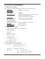
2. ELECTRICAL REQUIREMENTS
2.1 Standard Test Conditions
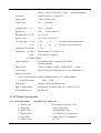
All tests shall be performed under the following conditions, unless otherwise specified.
Ambient light:
225 lux
Viewing distance :
50 cm in front of LCD panel
Warrn up time
All specifications:
30 minutes
Fully functional:
5 seconds
Measuring Equipment:
Chroma 2250 signal generator or equivalent, directly
Connected to the monitor under test.
Minolta CA100 photometer, or equivalent
Control settings
User brightness control:
Maximum (unless otherwise specified )
User contrast control:
Typical (unless otherwise specified )
User red/white balance,
Green/white balance and
Blue/white balance control:
In the center (unless otherwise specified )
Power input :
110Vac or 230Vac
20 ± 5 ˚C ( 68 ± 9 ˚ F)
Ambient temperature :
Analog input mode :
1280 x1024 /60 Hz
2.1.1 MEASUREMENT SYSTEMS
The units of measure stated in this document are listed below:
1 gamma = 1 nano tesla
1 tesla = 10,000 gauss
cm = in x 2.54
lb = kg x 2.2
degrees F = [°C x 1.8] + 32
degrees C = [°F - 32]/1.8
u' = 4x/(-2x + 12y + 3)
v' = 9y/(-2x + 12y + 3)
x = (27u'/4)/[(9u'/2) - 12v' + 9]
y = (3v')/[(9u'/2) - 12v' + 9]
nits = cd/(m2) = Ft-L x 3.426
lux = foot-candle x 10.76
2.2 LCD monitor General specification
Panel Type :
19 “ active matrix color TFT LCD
1). FUJITSU FLC48SXC8V
Display size :
Display mode :
376.32mm(H) x 301.056mm(V)
VGA
720 X 400 (70 Hz)
VGA
640 X 480 (60/66/70/72/75 Hz)
SVGA
800 X 600 (60/70/72/75 Hz)
4
XGA 1024 X 768 (60/70/75 Hz)
SXGA 1280 X 1024 (60/70/75 Hz)
Pixel pitch :
0.098x3mm(H) x 0.294mm(V)
Display Dot :
1280 x (RGB) x 1024
Pixel Clock :
25.2 – 135.0MHz
Contrast ratio: θ = 0˚
500 : 1 (typical)
Brightness:
250
Response time (Tr/Tf) :
15 /10 msec
Display color :
16777216 (8 bite color)
Viewing angle: L / R
U/D
cd/m2 (typical)
≧ 85
≧ 85
/ ≧ 85
( ≧ 170 degrees horizontal typical)
/ ≧ 85
( ≧ 170 degrees vertical typical)
Luminance Uniformity :
> 70 %
Pc interface: 1). Video :
RGB analog 0.7V peak to peak
Sync :
standard resolution
TTL positive or negative
2). Digital TMDS
Signal connector :
15 pin Mini D type, (standard VGA video)
DVI-D connector
Audio power :
1Wrms + 1Wrms ( 300Hz – 10kHz (S.P.L. – 10 dB))
Front control :
power on/off with LED select (up, down) adjustment (+,-)
Interface frequency
Horizontal Frequency 24KHz --80KHz(analog), 31.5– 80KHz(digital)
Vertical Frequency
56Hz ----75Hz
Plug & play :
Support VESA DDC2B functions
Power Input voltage :
Single phase, 50/60HZ, 100VAC to 240VAC ±10%
Total output power :
60 Watt max.
2.3 LCD Panel Specification
2.3.1 LCD Panel Model
•
•
•
•
•
•
(FUJITSU FLC48SXC8V)
Display Type
active matrix color TFT LCD
Resolution
1280 x 1024 pixels
Display Dot
1280 x (RGB) x 1024
Display Area
376.32mm(H) x 301.056mm(V)
Pixel Pitch
0.098x3mm(H) x 0.294mm(V)
Display Color
16777216
5
•
•
•
•
Lamp Voltage
700 Vrms typ.
Lamp Current
7mA rms.( typ). 4 Lamp
Weight
3200g .
Optical Specifications
The following items are measured under stable conditions. The optical characteristics
should be measured in a dark room or equivalent state with the methods shown in
Note(4).
Measuring equipment : TOPCON BM-5A, BM-7, PHOTO RESEARCH PR650
(Inverter Freq. : 54kHz) *Ta =25 ± 2°C, VDD=5V, fv=60 Hz, fDCLK=54 MHz, IL= 6.5mArms
Item
Symbol
Contrast Ratio
(Center of screen)
Rising
Response
Time
Falling
Luminance of White
(Center of screen)
Red
Color
Chromaticity
(CIE 1931)
Green
Blue
White
Viewing
Angle
Hor.
Ver.
Brightness Uniformity
(9 points)
Condition
Min.
Typ.
Max.
Unit
Note
(1)(2)(4)
BM-5A
CR
T.B.D
500
-
TR
TF
-
15
10
30
25
msec
(1)(3)
BM-7
200
250
-
cd/m2
(5)
BM-5A
YL
Rx
Ry
Gx
Gy
Bx
By
Wx
Wy
θL
θR
φH
φL
Normal
φ = 0˚
θ = 0˚
Viewing
Angle
CR≥10
BUNI
85
85
85
85
0.648
0.346
0.292
0.602
0.150
0.130
0.313
0.329
-
70
-
TYP.
-0.03
TYP.
+0.03
Note 1) Definition of Viewing Angle: Viewing angle range (10≤CR)
6
(1)(4)
PR650
-
Degrees
(1)(4)
BM-5A
-
%
(6)
BM-5A
Note 2) Definition of Contrast Ratio (CR): Ratio of gray max(Gmax),gray min(Gmin) at the
center point of panel.
CR=
Luminance with all pixels white (Gmax)
Luminance with all pixels black (Gmin)
Note 3) Definition of Response time: Sum of TR , TF
7
Note 4) After stabilizing and leaving the panel alone at a given temperature for 30 min, the
measurement should be executed .Measurement should be executed n a stable,
windless ,and dark room.30 min after lighting the back-light. This should be
measured in the center of screen. Dual lamp current :13.0mA(6.5mA x2)(Refer to
the note(1) in the page 14 for more information ).
Environment condition :Ta=25±2°C
Optical characteristics measurement setup
8
Notes 5) Definition of Luminance of White : measure the luminance of white at center point.
Notes 6)Definition of 9 points brightness uniformity (Measuring points: Refer to the Note 5)
Bmin
BUNI=100∗
∗
Bmax
Bmax: Maximum brightness
Bmin: Minimum brightness
Notes 7) Definition of Flicker level
F
Flicker Voltage pp
= x 100 %
LMD Voltage dc
♦ One maximum value of three estimated values.
♦ For this test ,an LMD(Light Measurement Device)is needed with adequate response time
to track any visible rate flicker component and with a voltage level output proportional
To luminance intensity.
♦ Test Pattern: For dot inversion Driving(Gray levels of foreground dots on the test panel
Are G22,G32,and G45)
♦ Test Point :Center point of the display area
9
Note 8) Definition of Crosstalk (Refer to the VESA STD)
The calculation for shadowing is made from the 2 luminance measurements Gbkg and Lsh,
as follows:
Lmax -Lmin
CT
= x100 %
Lmin
Where Lmax is the larger value of Gbkg or Lsh , and Lmin is the smaller of the two.
♦ To determine background and foreground levels (colors),first set the background to any
gray scale or color level suitable for shadowing determination.(Note that it may take
several iterations of adjusting background level and box levels to determine the proper
value for the background .Next display the box levels to determine the proper value for the
background level. Look for shadowing in any direction from box E. Independently vary the
gray level (or color) of the background and box E until the worst case shadowing is
observed. This defines the background (Gbkg) and foreground (Gfg) levels to be
maintained for the remainder of the test.
♦ One point only (the target) will be measured. To determine that point proceed as follows
Using the background and foreground gray levels of step1 (Gbkg and Gfg). Turn on each
box at a time. Look for the case with the worst shadowing. The box causing the worst case
is the shadowing source, or Bsrc. Use Bsrc and the box opposite from it that lies directly in
the shadow path. That is the target box, or Btgt. Note that box Eight be either Bsrc or Btgt,
depending on the shadowing conditions, but typically Bsrc and Btgt will be a pair of
opposite boxes, A&C or B&D. Btgt will only be displayed for aligning the LMD. It will be
turned off for the actual measurement.
♦ The target box point (Btgt) will be measured with the source box (Bsrc) turned on then off.
(Btgt is for alignment purpose only) Display the background only at level Gbkg. Display
Btgt determined in step 2 above. Using the correct distance, angle, and measurement
aperture, align the LMD to the center of the Btgt. Turn off Btgt. With Gbkg set to its proper
level, measure the luminance (or color). Next,turn on the source box Bsrc. Again measure at
the center point of Btgt (without Btgt present.). In this case the LMD will be measuring the
shadowing level, Lsh.
10
2.4 Input Signals
2.4.1 Video input
•
•
•
•
•
Type
Analog R, G, B., Digital TMDS
Input Impedance
75 ohm +/- 2%
Polarity
Positive
Amplitude
0 - 0.7 +/- 0.05 Vp
Display Color
same as LCD panel
2.4.2 Sync input
• Signal
separate horizontal and vertical sync, or composite sync
which are TTL compatible
• Polarity
positive and negative.
2.4.3 Interface frequency
The following frequency range is generalized by supported timing. If the entered
mode does not match the supported timing the display optimization will not be
assured.
• Horizontal Frequency 24KHz --80KHz(analog), 31.5– 80KHz(digital)
• Vertical Frequency
56Hz ---------75Hz
DISPLAY MODES
MONITOR
MODE NO.
SCREEN
RESOLUTION
1
2
3
4
5
6
7
8
9
10
11
12
13
14
15
16
17
18
19
20
21
640x350
640X400
640X400
640X400
640X480
640X480
640X480
640X480
720X400
832X624
800X600
800X600
800X600
800X600
1024X768
1024X768
1024X768
1024X768
1024x768
1280X1024
1280X1024
HORIZONTAL
SYNC RATE
(kHz)
31.5 +
24.83 31.531.531.5 35.037.8637.531.5 49.7235.16+
37.8 +
48.07 +
46.87+
48.4 53.96 +
56.47 60.0 +
60.2464.0 +
80.0 +
11
VERTICAL
SYNC RATE
(Hz)
70.0 56.4 70.0+
70.160.0 66.6772.8075.070.0 +
74.55 56.25+
60.0 +
72.18 +
75.0+
60.0 66.13 +
70.07 75.0 +
75.0260.0 +
75.0 +
VIDEO CLK
(MHz)
STANDARD
25.0
21.05
25.0
25.19
25.0
30.24
31.5
31.5
28.0
57.28
36.0
40.0
50.0
49.5
65.0
71.66
75.0
78.75
80.0
108.5
135.0
VGA
NEC
VGA
NEC
Defacto
MAC
VESA
VESA
Text Defacto
MAC
SVGA
VESA
VESA
VESA
VESA
XGA
VESA
VESA
MAC-768
SXGA
Defacto
Supported Timing
FH(KHZ)
SYNC
TOTAL
ACTIVE
SYNC
FRONT
BACK
PIXEL
FV(HZ)
POLARITY
(DOT/LINE)
(DOT/LINE)
31.469
70.087
24.83
56.42
31.469
70.087
31.5
70.15
31.469
59.94
35.00
66.67
+
–
–
–
–
+
–
–
–
–
–
–
800
449
848
440
800
449
800
449
800
525
864
525
640
350
640
400
640
400
640
400
640
480
640
480
96
2
64
8
96
2
64
2
96
2
64
3
16
37
64
7
16
12
16
13
16
10
64
3
48
60
80
25
48
35
80
34
48
33
96
39
37.861
72.809
37.5
75
31.469
70.087
49.725
74.55
–
–
–
–
–
+
–
–
832
520
840
500
900
449
1152
667
640
480
640
480
720
400
832
624
40
3
64
3
108
2
64
3
16
1
16
1
18
12
32
1
120
20
120
16
54
35
224
39
35.156
56.25
37.879
60.317
48.077
72.188
46.875
75
48.363
60.004
53.964
66.132
56.476
70.069
60.023
75.029
60.24
75.02
+
+
+
+
+
+
+
+
–
–
+
+
–
–
+
+
–
–
1024
625
1056
628
1040
666
1056
625
1344
806
1328
816
1328
806
1312
800
1328
803
800
600
800
600
800
600
800
600
1024
768
1024
768
1024
768
1024
768
1024
768
72
2
128
4
120
6
80
3
136
6
176
4
136
6
96
3
96
3
24
1
40
1
56
37
16
1
24
3
16
8
24
3
16
1
32
3
128
22
88
23
64
23
160
21
160
29
112
36
144
29
176
28
176
29
64
60
+
+
1688
1066
1280
1024
112
3
48
1
248
38
108
80
75
+
+
1688
1066
1280
1024
144
3
16
1
248
38
135
TIMING
640x350
VGA-350
640x400
NEC PC9801
640x400
VGA-GRAPH
640x400
NEC PC9821
640x480
VGA-480
640x480
APPLE MAC480
640x480
VESA-480-72Hz
640x480
VESA-480-75Hz
720x400
VGA-400-TEXT
832x624
APPLE MAC800
800x600
SVGA
800x600
VESA-600-60Hz
800x600
VESA-600-72Hz
800x600
VESA-600-75Hz
1024x768
XGA
1024x768
COMPAQ-XGA
1024x768
VESA-768-70Hz
1024x768
VESA-768-75Hz
1024x768
APPLE MAC768
1280x1024
VESA-102460Hz
1280x1024
VESA-102475Hz
WIDTH
(DOT/LINE)
PORCH
(DOT/LINE)
PORCH
FOREQ.(MHZ)
(DOT/LINE)
25.175
21.05
25.175
25.197
25.175
30.24
31.5
31.5
28.322
57.2832
36
40
50
49.5
65
71.664
75
78.75
80
If the input timing is not a supported timing listed above but within the supported frequency
range (Horizontal: 80KHz,Vertical: 75Hz), this monitor will select a closest mode instead. But
the display quality may not be optimized.
If the input timing over the supported frequency range, a message “Input Signal Out of Range”
will be shown.
12
2.4.4 85Hz refresh rate Support
Monitor should display 85Hz refresh rate mode as emergency mode.
Monitor should display “Out of Range” warning menu at this mode.
2.4.5 Video input Connector
Analog Video input Connector: 15pins mini D-Sub
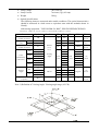
Table 2.4.5. Pin assignment for D-sub connector
Separate Sync
PIN
NO.
1
RED VIDEO
2
GREEN VIDEO
3
BLUE VIDEO
4
GROUND
5
GROUND
6
RED GROUND
7
GREEN GROUND
8
BLUE GROUND
9
PC5V (+5V DDC)
10
CABLE DETECTION
11
GROUND
12
SDA
13
H.SYNC
14
V.SYNC
15
SCL
Color of plastic parts: Blue
5
1
10
6
15
11
D-sub connector
13
Digital Video input Connector: DVI-D (T.B.D)
Table 4-3-3. Pin assignment for DVI-D (24pin) connector
1
2
3
4
5
6
7
8
Pin – Assignment of DVI –D connector :
TX29
TX1TX2+
10
TX1+
Shield (TX2 / TX4)
11
Shield (TX1 / TX3)
NC
12
NC
NC
13
NC
DDC-Serial Clock
14
+5V power *)
DDC-Serial Data
15
Ground (+5V)
No Connect
16
Hot plug detect
17
18
19
20
21
22
23
24
TX0TX0+
Shield (TX0 / TX5)
NC
NC
Shield (TXC)
TXC+
TXC-
*) In case, the power of the PC unit is switched off and the power of the monitor is switched on,
no voltage may occur at pin 14.
14
2.5 CONTROLS
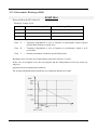
2.5.1 Control panel (monitor front panel)
1. Power LED, will be green when monitor is on; be amber when in power saving mode.
2. Adjust decrease.
3. Adjust increase.
4. Function select counter-clockwise.
5. Function select clockwise.
6. Power ON/OFF switch, push to ON and push to OFF. (toggle switch)
7. Ear phone jack.
8. Volume Control.
Note: When OSD Menu is off, press button 2 can activate “Auto Adjustment” immediately.
2.5.2 OSD Functions
•
•
•
•
•
OSD Format:
Refer to following figure.
OSD Border:
Cyan color
OSD Tunable Item:
The 16 icons that around the border.
Selected Item:
Yellow background
Comment:
Magenta foreground, Blue background
page format :
15
Description:
• Brightness:
Brightness adjustment, the range from 0 to 100.
• Contrast:
Contrast adjustment, the range from 0 to 100.
• H. Position:
Horizontal position adjustment.
• V. Position:
Vertical position adjustment.
• Phase:
Focus adjustment, the range from 0 to 31,32 steps.
• OSD position:
OSD position adjustment.
• Auto Adjustment:
This feature will automatically adjust size, position, clock and phase.
It takes 3-5 seconds to finish. When auto start, it shows “Auto
Adjusting….” message.
• Clock:
Frequency tracking adjustment. The max range from -48 to +48, but
some modes the range will be limited.
• Graph Text:
640x400(GRAPH) or 720x400(TEXT) mode select.
• Language:
5 kinds of language for description, including (English, German,
French, Spanish, Italian)
• Recall:
Recall the default value.
• Color Temp:
Color temperature for standard 9300,6500, 7500 or user defined.
User:
User R:
Red signal gain by user defined.
User G:
Green signal gain by user defined.
User B:
Blue signal gain by user defined.
7500:
6500:
9300:
• Exit:
Set CIE coordinate at 7500°K color temperature.
Set CIE coordinate at 6500°K color temperature.
Set CIE coordinate at 9300°K color temperature.
Exit OSD menu function.
Sharpness : Adjust the scale-up effect(smoother or sharper.)
OSD Transparency: Adjust the transparency level of OSD. The range is from 0 to 100 scales.
Comment:
• 1280x1024:
Current mode resolution.
• 60 HZ:
Current mode vertical frequency±1Hz.
• VER 1.00:
Firmware revision.
16
Other features:
Intellectual-Auto AL922(AM999) can start the Auto-Adjustment automatically when input
a new display mode at first time. After the adjustment, AL922(AM999) will remember this
mode and switch to optimized condition automatically for this mode whenever encounter
this mode again. Total 21 recent used modes are recorded into AL922(AM999)
VESA DPMS Functionality When signaled by the host CPU, AL922(AM999) show a
black screen about 3 seconds. If no further signal, then it shows “No Signal” and enter
power saving mode.
2.6 White Color Temperature
White color temperature is 4 preset as 9300, 7500,6500 and User,
Default value of user color should be user which is maximum setting for panel.
Target of color setting
Color
Temp.
9300K
7500K
6500K
User
Color Coordinate
x
y
0.283
0.297
0.299
0.315
0.313
0.329
*) TCO’0X A.2.6.1 requirement
Tolerance
+0.03
+0.03
+0.03
Color Coordinate
u’
0.189
0.194
0.198
-
v’
0.446
0.459
0.469
-
Tolerance
u’v’ < 0.01*
u’v’ < 0.01*
u’v’ < 0.01*
-
User should follow “Microsoft Windows Color Quality Specification for Liquid Crystal Display OEM’s”.
(http://www.microsoft.com/hwdev/tech/color/ColorTest.asp)
17
2.7 POWER SUPPLY
2.7.1 input Voltage Range
The monitor shall operate within specification over the range of 90 to 265 VAC power supply.
2.7.2 Input Frequency Range
Input power frequency range shall be from 47.5 to 63 Hz over the specified input voltage range.
2.7.3 Quick specification review
• Input current
1.5A (max) at 90VAC input and full load ,
0.75A (max) at 264 VAC input and full load.
• Inrush current @ cold start
30A(0-peak)@ 110Vac ,50A(0-peak) @ 220Vac
(measured when switched off for at least 10 mins.)
• Output
Tolerance
•
•
•
•
Output Current
Output Volt
-
MIN
MAX
+12Vdc
±5%
0A
5A
Total output power:
Withstanding voltage :
Leakage current :
Efficiency :
Volt Tolerance
11.4~12.6Vdc
60 Watt max.
1.5Kvac or 2.2KVdc for 1 minute.
< 0.25mA/100Vac , <3.5mA/230Vac
80% min. @115V/230VAC, maximum load.
2.7.4 Power Management
2.7.4.1 Meet VESA DPMS proposal
The monitor must comply with the Microsoft On Now specification, with a minimum of three power
management states, as defined by the VESA DPMS document. The front panel of the monitor must
appropriately display the DPMS state, For example:
DPMS ON :
DPMS OFF :
The power LED is Green
The power LED is Amber
2.7.5 Power Consumption
On mode
Off mode
DC power off
56 Wmax
4 Wmax
4 Wmax
disconnection
4 Wmax
Green
Amber
Dark
Dark (DC power off)
Amber (DC power on)
Power saving states are measured with speakers attached but not worked.
The recovery time from off mode to on mode is 3 seconds maximun.
2.7.6 Power Connector
All units shall have an IEC/CEE-22 type male power receptacle.
2.8 Plug & Play(EDID)
The monitor will be capable of sending a VESA standardized EDID file through the DDC (pins 12,
15 of the VGA connector).
18
2.9 Audio Technical specification
2.9.1 General Description:
Output power
: 1W + 1W maximum
Total harmonic distortion
: Less than 1 % (except speakers distortion)
Input signal sensitivity
: 0.5 Vrms for full output
Input impedance
: 47 Kohm +/- 5 %
Frequency response range
: 20Hz – 20kHz (except speakers response)
Difference of L and R output
:
Less than 2 dB
2.9.2 Electrical characteristics (Tamb=25°)
Audio amplifier(USE Panasonic VP-7723A Audio Analyzor. )
Item
Audio Input
Freq.
Min.
Input Voltage(V)
Input Current(m A)
Audio Voltage Gain
Frequency Response
Signal to Noise ratio
Total harmonic distortion
Cross talk
Output Watt.
Volume Control
500m Vrms 1KHz
500m Vrms 300Hz-20KHz -10dB
500m Vrms 1KHz
500m Vrms 1KHz
500m Vrms 1KHz
500m Vrms 1KHz
-
Spec.
Typ. Max.
5
500
-
800
6dB
+10d B
-40dB
1%
-30dB
1W
-
2.9.3 Speakers
Maximum power
: 2 W per speaker(max)
Impedance
: 4 ohm +/- 15 % @ 1kHz 1.0Hz
Frequency response range
: 350 Hz – 15 kHz (S.P.L. – 10 dB)
Total harmonic distortion
: Less than 5 % @ 0.125 W 1kHz
2.9.4 Headphone output
Output power
: 1.6 mW for 32 ohms Headphone
19
Comment
Volume Max.,load 4 Ω
Volume Max.,load 4 Ω
Volume Max.,load 4 Ω
except speakers distortion
Volume Max.,load 4 Ω
Volume Max.,load 4 Ω
Analog
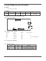
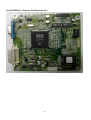
3. VL-901 DISPLAY CONTROL BOARD
3.1 Description
The VL-901 display control board is design to directly convert the analog RGB signals from
standard VGA display card to optimum LCD timing signals so as to construct a high display
quality LCD monitor.
3.2 Features
• On board embedded micro-processor to detect display timings and control user
functions.
• Using Genesis gm5120 design to generate optimum LCD timings.
2
• Using E PROM to memorize every adjusted parameter.
• support up to 22 display modes from VGA to SXGA.
• Offer full screen expansion function on non-SXGA mode (automatic).
• flexible color temperature selection function including 9300,6500,7500 and user
mode.
• Support OSD functions.
• Support VESA DPMS function.
• Support DDC2B functions.
• Support 5 languages for OSD description.
• The longest time for mode change is 3 seconds.
20
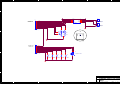
3.3 BLOCK DIAGRAM
21
3.4 Connector Locations
3.5 Connector Type
Location
CN1
CN2
CN4
J1
J2
Type
74320-4004
1211-15
6905-40
4300-10
4500-07
Maker
MOLEX
E&T
E&T
E&T
E&T
3.6 Connector pin assignment
3.6.1 CN2
Pin NO.
1
2
3
4
5
6
7
8
9
10
11
12
13
14
15
Signal
Comment
R-Video
G-Video
B-Video
N. C.
Ground
Ground
Ground
Ground
5VCC
PCDETECT
NC
SDA
HS
VS
SCL
Red Video Input.
Green Video Input.
Blue Video Input.
Ground.
Ground.
Ground.
Ground
DDC Power Input.
PCDETECT Input.
NC
DDC 2B
Horizontal Sync Input.
Vertical Sync Input.
DDC 2B
22
Number of pins
24
15
40
10
07
3.6.2 CN4
Terminal No.
Symbol
36,37,38
VDD
Function
1
TXE0-
2
TXE0+
LVDS EVEN OUTPUT DATA PAIRS
4
TXE1-
LVDS EVEN OUTPUT DATA PAIRS
5
TXE1+
LVDS EVEN OUTPUT DATA PAIRS
7
TXE2-
LVDS EVEN OUTPUT DATA PAIRS
8
TXE2+
LVDS EVEN OUTPUT DATA PAIRS
10
TXECLK-
LVDS EVEN OUTPUT DATA PAIRS
11
TXECLK+
LVDS EVEN OUTPUT DATA PAIRS
13
TXE3-
LVDS EVEN OUTPUT DATA PAIRS
14
TXE3+
LVDS EVEN OUTPUT DATA PAIRS
16
TXO0-
LVDS ODD OUTPUT DATA PAIRS
17
TXO0+
LVDS ODD OUTPUT DATA PAIRS
5V POWER SUPPLY
LVDS EVEN OUTPUT DATA PAIRS
19
TXO1-
LVDS ODD OUTPUT DATA PAIRS
20
TXO1+
LVDS ODD OUTPUT DATA PAIRS
22
TXO2-
LVDS ODD OUTPUT DATA PAIRS
23
TXO2+
LVDS ODD OUTPUT DATA PAIRS
25
TXOCLK-
LVDS ODD OUTPUT DATA PAIRS
26
TXOCLK+
LVDS ODD OUTPUT DATA PAIRS
28
TXO3-
LVDS ODD OUTPUT DATA PAIRS
29
TXO3+
LVDS ODD OUTPUT DATA PAIRS
03,06,09, 12
GND
Ground
15, 18, 21, 24
GND
Ground
27, 30, 34, 35
GND
Ground
39,40
GND
Ground
3.6.3 J2
Pin NO.
Signal
Comment
1,2
5 VCC
5V Power Input
3,4,5
GND
GND
6
BLON
Bright Light ON/OFF.
7
BRIGHT
Brightness Adjustment.
23
3.6.4 J1
Pin NO.
Signal
Comment
1
NC
NC
2
LED-Y
Power saving mode
3
LED-G
Monitor is ON
4
GND
GND
5
KEY-POWER
Power ON/OFF key
6
KEY-DOWN
Function select counter-clockwise key
7
KEY-R
Adjust up key
8
KEY-L
Adjust down key
9
KEY-UP
Function select counter-clockwise key
10
GND
GND
3.6.5 CN1 Digital Video input Connector: DVI-D
Pin-Assignment of DVI-D(24 pin) connector
1
TX2-
2 TX2+
9
TX1-
17 TX0-
10 TX1+
18 TX0+
3
Shield (TX2 / TX4) 11 Shield (TX1 / TX3) 19 Shield (TX0 / TX5)
4
NC
12 NC
20 NC
5
NC
13 NC
21 NC
6 DDC-Serial Clock 14 -5V Power *)
22 Shield (TXC)
7
DDC-Serial Data
15 Ground (+5V)
23 TXC-
8
No Connect
16 Hot plug detect
24 TXC+
*)In case, the power of the PC unit is switched off and the power the monitor is switched
on, no voltage may occur at pin 14.
24
4. VK901 Control Panel Board
4.1 Description
The VT-901 is designed to offer a user interfaced control panel which passes and receives
signals to and from VL-901 display control board.
4.2 Connector and Switch Locations
4.3 Connector type
Location
Type
Maker
Number of pins
J1
4500-10
E&T
10
J6
4500-11
E&T
11
J3
87502-0200
ACER
2
J4
87502-0200
ACER
2
J2
SCJ-0348-C
SC
9
4.4 Connector pin Assignment
4.4.1 J1
Pin NO.
1
2
3
4
5
6
7
8
9
10
4.4.2 J6
Pin NO.
1
2
3
4
5
Signal
Comment
NC
LED-Y
LED-G
GND
KEY-POWER
KEY-DOWN
KEY-R
KEY-L
KEY-UP
GND
NC
Power saving mode
Monitor is ON
GND
Power ON/OFF key
Function select counter-clockwise key
Adjust up key
Adjust down key
Function select counter-clockwise key
GND
Signal
Comment
VOL
GND
LIN1
RIN1
RIN2
Volume ON/OFF Control
GND
Audio Volume Adjust Line INL
Audio Volume Adjust Line INR
Audio Volume Adjust Line OUTR
25
6
7
8
9
10
11
LIN2
GND
R-EAR
L-EAR
ROUT
LOUT
Audio Volume Adjust Line OUTL
EAR Phone Out R
EAR Phone Out L
Speaker Out R
Speaker Out L
4.5 Switch definition
Location
S5
S1
S4
S3
S2
Definition
Power ON/OFF
Function select by clockwise direction
Function select by counter-clockwise direction
Adjust up
Adjust down
4.6 LED definition
Location
D1
Definition
Green for ON mode; Yellow for OFF mode; yellow for Power Saving
mode; Dark for DC power OFF mode.
26
5. INVERTER BOARD
5.1 Description
The Inverter board is designed for lighting up the back-lights of LCD module.
5.2 Electrical characteristics
5.2.1 FOR Fujitsu PANEL FLC48SXC8V
MIN.
TYP.
MAX.
COMMENT
INPUT VOLTAGE
11.4V
12.0V
12.6V
12V±5%
INPUT CURRENT
--------
2A
_
Vin=12V,
Vbrite=3.3V
Normal BACKLIGHT
VOLTAGE
--------
700V rms.
--------
--------.
7mA rms
8mA rms
DRIVING
FREQUENCY
40KHz
50KHZ
60KHz
EFFICIENCY
--------
80%
--------
Vin ON/OFF sequence
--------
1S
--------
OLP TIME
--------
3S
_
10%
--------
100%
0V
_
3.3V
_
220cd/m
Strike voltage at 0°C
1600 Vrms
_
_
Operating life time
20,000 hrs
_
_
LAMP CURRENT
BRIGHTNESS
RANGE
Brightness control
Brightness
2
Vin = 12V,max
brightness
Open lamp
protection time
3.3V, brightness
Max.
_
(note)
Note:
Life time (hr) can be defined as the time in which it continues to operate under the condition:
Ta=25±2°C, IL =7 mArms until one of the following event occurs:
1.
When the brightness becomes 50 %
2.
When the startup voltage (Vs) at 0°C becomes higher than the maximal value of Vs specified above.
27
5.3 Connector locations
5.3.1 Connector type
J2
J1
J5
J3
J4
CM999-E04
Location
Type
Maker
Number of pins
JN2, JN3,
SM02 (8.0)B-BHS
ST
2
85205-1200
E&T
12
JN4, JN5
JN1
5.3.2 Connector pin assignment
5.3.2.1 J2,J3,J4,J5
Pin NO.
Signal
Comment
1
HV
High voltage for lamp
3
LV
Low voltage (common)
Signal
Comment
1, 2, 3,4
BP+
+12V
7
BLT_ON
Back-light ON/OFF control, high active (3.3V)
5.3.2.2 JN1
Pin NO.
5, 6, 10, 11, 12 GND
8
+5VS
+5VS
9
BRITE
BRITE Brightness (0-3.3V) control from I/F
3.3 V for max. brightness (for Fujitsu model)
28
6. DC/DC POWER and Audio CKT VM-902
6.1 Input:
+12V/5A from AC adapter
6.2 Output:
ITEM
Output Voltage Max Load.
VCC
+5V
2.1A
Min Load
Tolerance
Ripple & Noise(max)
0.1A
±5 %
200mVpp
6.3 Efficiency: 80 % min at Maximum Load.
6.4 Connector Locations
6.4.1 Connector type for VM-902
Location
Type
Maker
J801
DC-IN
SC
J802
4500-12
E&T
J803
4500-07
E&T
J2
4500-11
E&T
Number of pins
2
12
7 (for LCM999 only)
11
6.4.2 Connector pin Assignment
6.4.3 J801 DC 12V Input
Pin No
Signal
Comment
Pin 1
+12V
From adapter output cable
Pin 2
GND
From adapter output cable
29
6.4.3.1 J802 FOR I/F CKT
Pin No
Pin 1,2,3,4
Pin
5,6,10,11,12
Signal
+12V
GND
Comment
From adapter +12V power
GND
Pin 8
+5V
Supply for I/F CKT
Pin 7
ON/OFF
ON/OFF Control ON>3.0V OFF <2.0V
Pin 9
BRIGHT
Lamp Current Control (0V to 3.3V) ,
3.3V for max brightness
6.4.3.2 J803 FOR M/B CKT
Pin No
Signal
Comment
Pin 1,2
+5V
For M/B +5V power
Pin 3,4,5
GND
GND
Pin 6
BLON
Bright Light On/ Off
Pin 7
BRIGHT
Brightness Adjustment
6.4.3.3 J3 FOR Audio input(for AM999 only)
Pin No
Pin 1
Pin 2
Pin 3
Signal
Comment
GND
Audio IN (1)
Audio IN (2)
GND
From Audio output (1)
From Audio output (2)
6.4.3.4 J2 TO Speaker CKT(for AM999 only)
Pin No
Signal
Pin 1
VOL
Pin 2
GND
Pin 3
LIN1
Pin 4
RIN1
Pin 5
RIN2
Pin 6
LIN2
Pin 11
GND
Pin 7
R-EAR
Pin 8
L-EAR
Pin 9
ROUT
Pin 10
LOUT
Comment
Volume ON/OFF control
GND
Audio volume adjust line INL
Audio volume adjust line INR
Audio volume adjust line OUTR
Audio volume adjust line OUTL
EAR phone out R
EAR phone out L
Speaker out R
Speaker out L
30
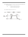
7. TROUBLESHOOTING
7.1 Main Procedure
31
7.1.1 Power Circuit Troubleshooting
32
7.1.2 Backlights Troubleshooting
33
7.1.3 Performance Troubleshooting
34
7.1.4 Function Troubleshooting
35
8. MECHANICAL REQUIREMENTS
8.1 Vibration and Shock
All testing shall be done in each of three mutually perpendicular axes, referenced to the
position of the system as it is in front of the user (i.e., front-to back, side-to-side, and top-tobottom).
8.1.1 Non-Operating
The unit should suffer minimal visible cosmetic damage or damage that presents a safety
hazard, or impairs the setup and operation of the system after testing.
Sinusoidal Vibration: 0.75 G zero-to-peak, 10 to 500Hz, 0.5 octave / minute sweep rate.
This requires one sweep, 10 to 500 to 10Hz, along each of the three axes.
Random Vibration: 0.008 G2/Hz, 10 to 500 Hz, nominal 2 GRMS. The test shall be for
one hour for each of the three axes.
Half Sine Wave Shock: 120 G peak, half sine pulse, 2 ms pulse duration. Testing shall
consist of one shock in each direction in each axis, for a total of 6 shock inputs.
Square Wave Shock: 40 G peak acceleration, 160 inches / second velocity change. There
shall be one shock in each direction in each axis, for a total of 6 shock inputs.
8.2 Package Drop Specification
Listed below are standards of drop heights for monitor product
Product Weight
height Specs
<9.1 kg
0.76 m
9.2~18.2 kg
0.66 m
18.3~27.2 Kg
0.61 m
27.3~45.4 Kg
0.46 m
8.2.1 Drop Test Sequence
Drop Order
Drop point
Drop Times
1
Right Front Bottom Corner
1
2
Right Bottom Edge
1
3
Right Front Edge
1
4
Front Bottom Edge
1
5
Bottom Side
1
6
Top Side
1
7
Front Side
1
8
Back Side
1
9
Left Side
1
10
Right Side
1
36
8.3 Dimension Size and Weight
Dimension size
433 (W) x 447 (H) x 235 (D)
Net Weight
6.5Kg
Gross Weight
9 Kg
8.4 Gap Spec.
8.4.1 The step between front bezel and back cover shall be within specification.
Back Cover & Bezel Gap
0.8 mm ≤ A ≤ 1.2 mm
Back Cover & Bezel Alignment
0 mm ≤ D ≤ 0.8 mm
Back Cover & Cable Cover Gap
0.8 mm ≤ B ≤ 1.2 mm
37
Back Cover & Cable Cover Gap
0.8 mm ≤ B ≤ 1.2 mm
Base Cover & Neck Cover Gap
0.8 mm ≤ C ≤ 1.2 mm
38
8.4.2 LCD Horizontally
The angle between front bezel and LCD unit in bottom side should not large than 1.0mm.
The distance of the LCD display unit from left side to right should not large than
∣E - F∣<=4.0mm.
8.5 Tilt Base Rotation
Tilt up 25 ± 1°/ down 5 ±1°
8.6 Swivel Base Rotation
Swivel Right 45 ±1° / Left 45 ±1°
39
8.7 Plastic Material
Front Bezel ABS 94HB, 94V-0
Back Cover ABS 94HB, 94V-0
The Others ABS 94HB
TCO’ 99(Optional)
Front Bezel
PC + ABS 94 - V0
BACK COVER
PC + ABS 94 – V0
The others
ABS 94 HB
8.8 GAP Spec.
Gap between panel with bezel is 0 mm < gap < 1.5 mm
9. Power Line Transient Test (IEC 61000-4-4 Fast
Transients/Burst)
TEST CONDITIONS & PROCEDURE: (Follow IEC 61000-4-4)
Test Condition :
The condition is base on operating with 50Ω load.
9.1 Peak Voltage:
2 KV (applies the Level 3 typical Industrial Environment” of IEC
61000-4-4)
9.2 Polarity
: +/-
9.3 Repetition Frequency of the impulse : 5 KHz.
40
9.4 Rise-Time : 5ns ± 30%
9.5 Impulse Duration: 50 nS ± 30%
9.6 Relation to Power Supply: Asynchronous
9.7 Burst Duration: 15 ms ± 20%
9.8 Burst Period: 300 ms ± 20%
9.9 Climatic Conditions:
- Ambient Temperature: 15°C to 35°C
- Relative Humidity: 45% to 75%
- Atmospheric Pressure: 86 kPa to 106 kPa
9.10 Test Procedure:
The monitor Display set high-resolution mode, AC input use AC 240V.
Note :
9.10.1
IEC 61000-4-4 defines that power supply, I/O line, and control line all shall be performed
the transient test, but the I/O line and control line is applied with only half of peak voltage
(1 KV).
9.10.2
For the comparison of wave-shape generated by different generator, so the test must uses
a scope with at least 400 MHz bandwidth, and coupled to 50 Ω to monitor the rise-time,
impulse, duration, and repetition rate of the impulses within one burst.
41
WAVESHAPE
42
10. Power Line Surge Test (IEC 61000-4-5 Surge)
10.1 Climatic Condition
The climatic conditions shall be within the following ranges:
10.1.1 Ambient Temperature: 15°C to 35°C
10.1.2 Relative Humidity: 10% to 75%
10.1.3 Atmospheric Pressure 86kPa(860 mbar)to 106kPa (1060mbar)
Note: The temperature and relative humidity should be recorded in the test report.
10.2 Test Conditions:
10.2.1 Wave-shape of the current surge: (refer to IEC 61000-4-5)
Open circuit voltage:
(1.2 / 50 µs)
Short circuit current:
10.2.2 Polarity:
(8 / 20 µs)
positive / negative
10.2.3 Phase shifting:in a range between 0º to 270º versus the AC line phase angle
10.2.4 Repetition rate:at least 1 per minute
10.2.5 Number of tests: at least 5 positive and 5 negative at the selected points.
10.3
The surge will be applied between lines and between lines and ground.
10.4
If not otherwise specified, the surge to power supply circuits shall be applied synchronized
to the voltage phase at the zero crossing and the peak value of the AC voltage wave.
(Positive and negative)
10.5
The surge voltage for test is from 1 KV and increases 1 kV for each step.
10.6
The recommended severity levels for the surge voltage test is 2.0 KV, and without any
degradation or loss of function that is not recoverable due to damage of component or
software allowed.
10.7 Display set high-resolution mode, AC input use AC 240V.
43
11. ENVIROMENT REQUIREMENT
11.1 Operating
Temperature
5°C ~ 40°C
Relative Humidity
20% to 80%
Altitude
Sea level to 8000ft
11.2 Storage or Shipment
Temperature
-20°C ~ +60°C
Relative Humidity
5% to 85%
Altitude
Sea level to 40,000ft
11.2.1 TEST PROCEDURE:
• Put in temperature chamber under 60°C
Time:24 hours
• Back to room temperature
Time: 4 hours
• Put in temperature chamber under -20°C
Time:24 hours
• Back to room temperature
Time:4 hours
• The process repeat 2 times.
44
12. REGULATION COMPLIANCE
12.1 This product comply to the most current revisions of following regulations:
UL/CUL
{UL 1950/ CSA C22.2 NO950}
Standard for Safety of Information Technology Equipment including
Electrical Business Equipment
EN 60950/CB Scheme
Safety of Information Technology Equipment including Electrical
Business Equipment
MPR 1990:8
Test methods for visual display units.
MPR 1990:10
User handbook for evaluation visual display units.
ISO 9241-3:
Ergonomic requirements for office work with visual display terminals
(VDTs)-Visual display requirements.
ISO 9241-7:
Ergonomic requirements for office work with visual display terminals
(VDTs)-Requirements for display with reflections.
ISO 9241-8:
Ergonomic requirements for office work with visual display terminals
(VDTs)-Requirements for displayed colours.
NUTEK/EPA
Requirements of power saving according to NUTEK Spec.
803299/94/96, EPA Energy star.
TCO 1999 (option)
Requirements for Environmental Labeling of Personal Computers.
Test methods for Ergonomic, Emission, Energy Efficiency, safety.
TUV/GS
Safety regulation for displays work places in the office sector.
FCC 47 CFR, Chapter 1,
Subchapter A, Part 15, Subpart B
A digital device that is marketed for use in a residential environment
not withstanding use in commercial, business and industrial
environments.
CISPR 22
Limits and methods of measurements of radio interference
characteristics of information technology equipment.
CE LVD Directive (73/23/EEC)
Safety: EN60950
CE EMC Directive (89/336/EEC)
EMI: EN55022 class B
Harmonics: EN61000-3-2
Voltage Fluctuation/Flicker: EN61000-3-3
Immunity: EN55024
IEC 61000-4
IEC 61000-4-2
IEC 61000-4-3
IEC 61000-4-4
IEC 61000-4-5
IEC 61000-4-6
VCCI (option)
Specification for limits and methods of measurement of radio
interference characteristics of information technology equipment.
Class B conformity verification report from the VCCI
BSMI (option)
CNS 13438, Class B
Electrostatic Discharge
Radiated Electromagnetic Field
Fast Transients/Burst
Surge
Conducted Disturbance, Induced by Radio
Frequency Fields
IEC 61000-4-8 Power Frequency Magnetic Field
IEC 61000-4-11 Voltage DIP/Interruption
45
12.2 Electrostatics Discharge (ESD)
E.S.D Test
This test follow the IEC 61000-4-2
Discharge Voltage Level :
Criteria
Contact Discharge (KV)
Air Discharge(KV)
Class C
±4
±4
Class B
±6
±8
Class A
±8
±15
Class A : Temporary degradation or loss of function or performance which requires
operator Intervention or system reset.
Class
B :
Class
C
Temporary degradation or loss of function or performance which is selfrecoverable
: Normal performance within the specification limits
Discharge times: 20 times for each discharge point, time interval 1 second.
In the case of acceptance tests, the test program and the interpretation of the test results are
subject to
agreement between manufacturer and user.
The test documentation shall include the test conditions and the test results.
46
Ambient temperature : 15°C to 35°C
Relative humidity
: 30% to 60%
13. QUALITY AND RELIABILITY
13.1 Quality Assurance
Unless otherwise specified in this specification or the applicable purchase order, the supplier shall
be responsible for maintaining a statistical process program or performing inspections that are
sufficient to assure that the parts supplied meet the requirements specified herein.
13.2 Reliability
The product shall have a designed MTBF of greater than 20,000 hours during its useful life.
47
APPENDIX A: PARTS LISTS
48
A. FRU Board
A-1 PCBA Inverter board
A-2 454A7830001 –PCBA Key Board (VT-901)
A-3 455A7830001 –PCBA Audio& D/D Board (VM-902)
49
A-4 461A7830011–Firmware Ctrl Board (VL-901)
50
A. FRU BOM LIST
Product Line: Monitor System
Product Family:
System Model:ABO_AL922(ET.92202.00X),X=1,4,5,9.
LEVEL Acer F/G P/N
ACER
PART
NO.
Compal PART
NO.
Common/
Unique
TAT
2 months
Rolling
Forecast
COMMENT
SUGGEST
FOR
MINIMAL
LOCAL
REFERNCE/MB Unit Price Action
ORDER DEFECT PARTS RETURN/SCRAP/ BUY
INDIVIDUAL
LOCATION
(US)
Code
Q'TY
VENDOR S/N COLLECT
(YES/NO) PACK(YES/NO)
Compal F/G P/N
CATEGORY
PARTNAME
DESCRIPTION
INVERTER/POWER
BOARD
PCBA INVERTER&POWER
PK07V000100
U
4WKS
REQUIRED
SYSTEM
16.56
30
LOCAL SCRAP
NO
NO
PCBA KEY
454A7930001
U
4WKS
REQUIRED
SYSTEM
3.02
30
LOCAL SCRAP
NO
NO
FIRMWARE CTRL (M/B)
461A7830011
U
4WKS
REQUIRED
SYSTEM
25.78
30
LOCAL REPAIR/LOCAL SCRAP
NO
NO
SYSTEM
18.36
30
LOCAL SCRAP
NO
NO
1
ET.92202.001/004/005/009
LAM999F1002/1004/1005/1009
BOARDS
1
ET.92202.001/004/005/009
LAM999F1002/1004/1005/1009
BOARDS
1
ET.92202.001/004/005/009
LAM999F1002/1004/1005/1009
BOARDS
KEY BOARD
FIRMWARE CONTROL
BOARD(M/B)
1
ET.92202.001/004/005/009
LAM999F1002/1004/1005/1009
BOARDS
PCBA AUDIO BOARD
PCBA AUDIO
455A7830021
U
4WKS
REQUIRED
1
ET.92202.001/004/005/009
LAM999F1002/1004/1005/1009
CABLE
LCD NET WIR SET
NET WIR SET
NA200800200
U
4WKS
REQUIRED
0.08
50
LOCAL SCRAP
NO
NO
ET.92202.001/004/005/009
LAM999F1002/1004/1005/1009
CABLE
KEY BOARD CABLE
H-CON SET
DC020200450
U
4WKS
REQUIRED
1.04
50
LOCAL SCRAP
NO
NO
1
ET.92202.001/004/005/009
LAM999F1002/1004/1005/1009
CABLE
CABLE
CB ASY
DC190013720
U
4WKS
REQUIRED
0.76
50
LOCAL SCRAP
NO
NO
1
ET.92202.001/004/005/009
LAM999F1002/1004/1005/1009
CABLE
SINGLE CABLE
CB ASY
DC190019270
U
4WKS
REQUIRED
8.08
50
LOCAL SCRAP
NO
NO
1
ET.92202.001/004/005/009
LAM999F1002/1004/1005/1009
CABLE
SINGLE CABLE
CB ASY
DC190020440
U
4WKS
REQUIRED
4.35
50
LOCAL SCRAP
NO
NO
1
ET.92202.001/1009
LAM999F1002/1009
CABLE
POWER CORD
POWER CORD( EU)
GA020000100
U
4WKS
REQUIRED
1.60
50
LOCAL SCRAP
NO
NO
1
ET.92202.1005
LAM999F1005
CABLE
POWER CORD
POWER CORD( AU)
GA060000510
U
4WKS
REQUIRED
2.28
50
LOCAL SCRAP
NO
NO
1
ET.92202.1005
LAM999F1009
CABLE
POWER CORD
POWER CORD (EU)
GA040080300
U
4WKS
REQUIRED
3.53
50
LOCAL SCRAP
NO
NO
1
ET.92202.1009
LAM999F1009
CABLE
POWER CORD
POWER CORD (EU)
GA070030300
U
4WKS
REQUIRED
3.06
50
LOCAL SCRAP
NO
NO
1
ET.92202.001/004/005/009
LAM999F1002/1004/1005/1009
FACM991B200
U
4WKS
REQUIRED
4.56
50
LOCAL SCRAP
NO
NO
ET.92202.001/004/005/009
LAM999F1002/1004/1005/1009
LCD COVER ASSY
LCD BEZEL A'SSY
(ACER)
LCD COVER
1
LCD BEZEL A'SSY (ACER)
FAAM991A200
U
4WKS
REQUIRED
8.53
50
LOCAL SCRAP
NO
NO
1
ET.92202.001/004/005/009
LAM999F1002/1004/1005/1009
CHASSIS
CHASSIS
ECCM9915100
U
4WKS
REQUIRED
8.35
50
LOCAL SCRAP
NO
NO
1
ET.92202.001/004/005/009
LAM999F1002/1004/1005/1009
EMI COVER
EMI COVER
EECM9916100
U
4WKS
REQUIRED
1.86
50
LOCAL SCRAP
NO
NO
1
ET.92202.001/004/005/009
LAM999F1002/1004/1005/1009
STAND NECK(BASE)
STAND NECK(BASE)
ECCM9924000
U
4WKS
REQUIRED
2.91
50
LOCAL SCRAP
NO
NO
1
ET.92202.001/004/005/009
LAM999F1002/1004/1005/1009
CASE/COVER/BRACKET
ASSEMBLY
CASE/COVER/BRACKET
ASSEMBLY
CASE/COVER/BRACKET
ASSEMBLY
CASE/COVER/BRACKET
ASSEMBLY
CASE/COVER/BRACKET
ASSEMBLY
CASE/COVER/BRACKET
ASSEMBLY
HINGE
HINGE
ECCM9933000
U
4WKS
REQUIRED
4.61
50
LOCAL SCRAP
NO
NO
1
ET.92202.001/004/005/009
LAM999F1002/1004/1005/1009
LCD
FLC48SXC8V 19" FUJ
FLC48SXC8V 19" FUJ
AC600022700
C
4WKS
REQUIRED
558.60
20
RETURN
NO
NO
3
ET.92202.001/004/005/009
LAM999F1002/1004/1005/1009
PCB COMPONENT
CRTSTAL
14.31818MHZ HC-49/
BD114P3M020
C
2WKS
0.44
20
LOCAL SCRAP
NO
NO
8.85
20
LOCAL SCRAP
NO
NO
1.04
50
LOCAL SCRAP
NO
NO
0.25
20
LOCAL SCRAP
NO
NO
2.10
50
LOCAL SCRAP
NO
NO
0.45
20
LOCAL SCRAP
NO
NO
0.45
50
LOCAL SCRAP
NO
NO
2.45
50
LOCAL SCRAP
NO
NO
3
ET.92202.001/004/005/009
LAM999F1002/1004/1005/1009
PCB COMPONENT
FPC
CM999 VS-901 REV1
DA3M999V010
C
2WKS
3
ET.92202.001/004/005/009
LAM999F1002/1004/1005/1009
PCB COMPONENT
SM IC
EE 128X8 SOP-8 24L
SA024210300
C
2WKS
3
ET.92202.001/004/005/009
LAM999F1002/1004/1005/1009
PCB COMPONENT
LED
LYG2093 YEL/GRN 3D
BC5G2093000
C
2WKS
3
ET.92202.001/004/005/009
LAM999F1002/1004/1005/1009
PCB COMPONENT
IC
SI-8051S LF1102
AB080510100
C
2WKS
3
ET.92202.001/004/005/009
LAM999F1002/1004/1005/1009
PCB COMPONENT
VR RES
3/100W RK10F12U013
CF150021300
C
2WKS
3
ET.92202.001/004/005/009
LAM999F1002/1004/1005/1009
PCB COMPONENT
SM IC
SN74LVC14 SOP-14 I
SA074140400
C
2WKS
3
ET.92202.001/004/005/009
LAM999F1002/1004/1005/1009
PCB COMPONENT
S IC
EEPROM PLCC-32 SST
SA390100000
51
C
2WKS
X1
FPC
U1
LED
U801
VR
U3
U6
3
ET.92202.001/004/005/009
LAM999F1002/1004/1005/1009
PCB COMPONENT
S IC
GM5120 PQFP-208
SA051200100
C
2WKS
3
ET.92202.001/004/005/009
LAM999F1002/1004/1005/1009
PCB COMPONENT
SM IC
EE 16K SO-8 C
SA024160008
C
2WKS
3
ET.92202.001/004/005/009
LAM999F1002/1004/1005/1009
PCB COMPONENT
SM TRANSISTOR
SI9435 (SO-8)
SBX94350109
C
2WKS
3
ET.92202.001/004/005/009
LAM999F1002/1004/1005/1009
PCB COMPONENT
S IC
THC63LVDM83A TSSOP
SA063830000
C
2WKS
3
ET.92202.001/004/005/009
LAM999F1002/1004/1005/1009
PCB COMPONENT
S IC
APL1085-33CE TO252
SA010850500
C
2WKS
3
ET.92202.001/004/005/009
LAM999F1002/1004/1005/1009
PCB COMPONENT
S IC
APL1117-25 SOT-223
SA011170200
C
2WKS
3
ET.92202.001/004/005/009
LAM999F1002/1004/1005/1009
PCB COMPONENT
SM TRANSISTOR
MMBT3906 (SOT-23)
SB7390601T6
C
2WKS
3
ET.92202.001/004/005/009
LAM999F1002/1004/1005/1009
PCB COMPONENT
S IC
MCP809-2.93 SIT-23
SA008090600
C
2WKS
3
ET.92202.001/004/005/009
LAM999F1002/1004/1005/1009
PCB COMPONENT
WAFER CONN.
E&T 96113-1013 10P
DC03E000500
C
2WKS
3
ET.92202.001/004/005/009
LAM999F1002/1004/1005/1009
PCB COMPONENT
ZENER DIODE
HZ6B-2
BC40HZ6B2T7
C
2WKS
3
ET.92202.001/004/005/009
LAM999F1002/1004/1005/1009
PCB COMPONENT
WAFER CONN.
E&T 96113-1113 11P
DC03E001000
C
2WKS
3
ET.92202.001/004/005/009
LAM999F1002/1004/1005/1009
PCB COMPONENT
IC
TDA1517 SIL-9 AUDI
AB015170002
C
2WKS
Spare Parts Level 1: Stands for FRU( Field Replaceable Unit) and CRU( Customer Replaceable Unit) which are used for first tier system service use and in LOW
stock level and RTV items.
Spare Parts Level 2: Stands for subassemblies of FRU and consumed parts which should be in HIGH stock level and scrap items.
Spare parts Level 3: Mainboard Components
Option items: "MFG" is responsible for 1st year support after product phase-out. CSD only provides FRU(plain package) instead of whole option item(marketing
package) accordingly.
* RETURN/SCRAP" : the choice made for high dollar valued item to be returned for repair and low dollar valued item to be scrapped locally.
* VENDOR S/N COLLECT : which the item may not be returned local but with vendor S/N collect for pass-through warranty claim. The details please do follow
AIH/RTV process procedures.
52
U4
U5
U8
U9
U11
U12
Q1
U7
J6
ZD801
J1
U1
13.05
20
LOCAL SCRAP
NO
NO
0.68
50
LOCAL SCRAP
NO
NO
0.94
50
LOCAL SCRAP
NO
NO
3.75
50
LOCAL SCRAP
NO
NO
0.84
20
LOCAL SCRAP
NO
NO
0.56
50
LOCAL SCRAP
NO
NO
0.07
20
LOCAL SCRAP
NO
NO
0.60
20
LOCAL SCRAP
NO
NO
0.48
20
LOCAL SCRAP
NO
NO
0.05
20
LOCAL SCRAP
NO
NO
1.60
20
LOCAL SCRAP
NO
NO
1.96
50
LOCAL SCRAP
NO
NO
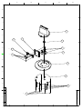
APPENDIX B: DISPLAY UNIT ASSEMBLY
53
8
7
6
303
6
014
E
7
201
202
D
C
B
A
8
For Standaard
013
004
003
001
006
302
301
002
008
5
5
304
305
4
4
007
3
3
2
2
SIZE
A3
2
DRAWING NO.
1
LAM999
FOR REV RECORD SEE SHEET 1
SHEET
1
0A
REV
E
D
C
B
A
\\M-id\ART1\
MANUAL\service\AB
====================================================================================================================================
QUANTITY REQUIRED
C NO.
PART NO.
DESCRIPTION
SPECIFICATION
DWG.NO. LAM999
REV. 0A
------------------ --------------------------------------
F1
001
REMARKS
- ---- ----------- ------------------------ ------------------------------ --- --- --- --- --- ----- ----- ----- ----- ----- ----# LAM999F1001 LAM999F ABO-USA
1 DC190020440 CB ASY
UR+TCO99 110V MSV16 19"FUJITSU
CM999 SIG/2CORE 1.8M BLK90DSUB
2 GA050000400 POWER CORD SET
3 PK10V000000 AC ADAP
LAE LAD6019AB5 12V/5A BLK
4 DC190019270 CB ASY
CM999 20276/CORE 1.8M BLK90DVI
5 DC190013720 CABLE ASSY
6 58290330001 DIS ABO
1
-
-
-
1
-
-
-
SP305X1.8MXIS14 SVT BLK
1
CM35H AUDIO IN 3P BLK-GRN
-
LAM999F UR+TCO99 MSV16
8 X66AI830001 MEC PACKING ABO
LAM999F TCO99
-
- 302
- 303
1
-
-
-
- 304
1
-
-
-
- 305
LAM999F TCO99 19"FUJ 1280X1024
7 68006530001 PACKING ABO-USA
-
- 301
1
1
-
-
-
- 351
1
-
-
-
- 352
-
-
-
- 353
End of Report
====================================================================================================================================
QUANTITY REQUIRED
C NO.
PART NO.
DESCRIPTION
SPECIFICATION
DWG.NO. 680065
REV. 0A
------------------ --------------------------------------
30
001
REMARKS
- ---- ----------- ------------------------ ------------------------------ --- --- --- --- --- ----- ----- ----- ----- ----- ----# 68006530001 PACKING ABO-USA
LAM999F UR+TCO99 MSV16
1 EJ4AM999000 RATING NP
2 HB4AM999000 CARTON
N-AM999-ABO UFGC 99 W/W
C-AM999-ABO W/W CHN
3 HDABOAM9900 USER'S MANUAL
FOR TCO99
5 HGTCO990000 TCO99 LABEL
TCO99 FOR BEZEL/MANUAL
6 HGTCO990100 TCO99 LABEL
TCO99 FOR CARTON
8 HF6VS558110 WARRANTY CARD
9 EJ1AM999000 FRONT PLATE
-
U-AM999-ABO EFGSIDPJC/CS 99
4 HF6TCO99000 TCO99 (NOTICE SHEET)
7 HK3CM870100 PE BAG
1
1
CM870-K001 FOR MAC LCDMONITOR
1
N-AM999-ABO FOR BEZEL
- 001
- 002
1
-
-
-
-
-
- 004
-
1
F-VS558-ABO USA LCD/CRT R1
-
1
1
-
-
1
1
End of Report
55
-
-
-
- 006
- 007
-
-
- 003
- 008
-
-
- 013
- 014
====================================================================================================================================
QUANTITY REQUIRED
C NO.
PART NO.
DESCRIPTION
SPECIFICATION
DWG.NO. X66AI8
REV. 0A
------------------ --------------------------------------
30
001
REMARKS
- ---- ----------- ------------------------ ------------------------------ --- --- --- --- --- ----- ----- ----- ----- ----- ----# X66AI830001 MEC PACKING ABO
LAM999F TCO99
1 FJCM9917000 EPS FOAM-L
CM9917
1
-
-
-
- 201
2 FJCM9918000 EPS FOAM-R
CM9918
1
-
-
-
- 202
End of Report
56
8
7
6
5
4
3
2
1
FOR REV RECORD SEE SHEET 1
011
2PCS
019
E
013
4PCS
E
2PCS
016
006
5PCS
2PCS
014
018
019
2PCS
D
D
VM-902
010
352
VL-901
303
353
305
C
014
4PCS
018
2PCS
C
001
F
301
304
G
B
2PCS
015
2PCS
020
B
F
302
306
2PCS
022
G
A
015
020
022
309
A
2PCS
2PCS
2PCS
351
VT-901
310
SIZE
009
8
7
6
A3
5
4
3
2
SHEET
2
DRAWING NO.
REV
582903
1
0A
E
D
8
7
6
6
5
3PCS
013
5
4
4
3
3
2
2
SIZE
A3
3
DRAWING NO.
6PCS
012
1
1
582903
FOR REV RECORD SEE SHEET 1
SHEET
017
5PCS
C
7
013
5PCS
018
2PCS
002
004
B
A
8
007
021
005
008
003
0A
REV
E
D
C
B
A
\\M-id\ART1\
\\M-id\ART1\
MANUAL\service\ABMANUAL\service\AB
====================================================================================================================================
QUANTITY REQUIRED
C NO.
PART NO.
DESCRIPTION
SPECIFICATION
DWG.NO. 582903
REV. 0A
------------------ --------------------------------------
30
001
REMARKS
- ---- ----------- ------------------------ ------------------------------ --- --- --- --- --- ----- ----- ----- ----- ----- ----# 58290330001 DIS ABO
1 AC600022700 LCD MODU
2 DA3M999V010 FPC
LAM999F TCO99 19"FUJ 1280X1024
FLC48SXC8V 19" FUJITSU
CM999 VS-901 REV1
1
-
-
-
-
-
-
- 302
1
3 DC020200420 H-CON SET
CM999 CTRL-DC 7P
1
-
-
-
4 DC020200430 H-CON SET
CM999 DC-INV 12P
1
-
-
-
5 DC020200440 H-CON SET
AM999 KEY-AMP 11P SHE1LD
6 DC020200450 H-CON SET
AM999 KEY-CTRL 10P
7 454A7930001 PCBA KEY/B
VT-901 LAM999F
8 455A7830021 PCBA AUDIO&D/D BD.
9 461A7830011 FIRMWARE CTRL/B
10 X66AI930001 MEC PARTS ABO
VM-902 LAM999F
VL-901 LAM999F ABO
LAM999F TCO99 MSV16/MBK17
1
1
1
-
-
- 303
- 304
-
- 301
-
-
-
- 351
1
-
-
-
1
-
-
-
1
End of Report
59
-
- 305
- 306
-
- 352
- 353
-
- 354
====================================================================================================================================
QUANTITY REQUIRED
C NO.
PART NO.
DESCRIPTION
SPECIFICATION
DWG.NO. X66AI9
REV. 0A
------------------ --------------------------------------
30
001
REMARKS
- ---- ----------- ------------------------ ------------------------------ --- --- --- --- --- ----- ----- ----- ----- ----- ----# X66AI930001 MEC PARTS ABO
1 ECCM9915100 CHASSIS
2 ECCM9922000 NECK BRACKET
3 ECCM9924000 BASE BRACKET
4 ECCM9933000 HINGE ASSY
5 ECCM9934000 SWIVEL HINGE
LAM999F TCO99 MSV16/MBK17
CM9915 (FOR POWER SW)
CM9922
1
CM9924
1
CM9933
-
-
-
-
-
-
- 002
-
1
CM9934
1
-
-
1
-
-
- 004
-
7 FACM9913200 NECK COVER
CM9913 ABS94HB MBK17
1
-
-
-
8 FACM9914400 BASE COVER
CM9914 ABS94HB MSV15
1
-
-
-
9 FAAM991A200 BEZEL ASSY
AM991A ABS94HB MSV15 ACER
12 FHST3545100 RUBBER FOOT
13 MAA70002204 SCREW
-
- 005
CM9916
11 FBCM9921200 CABLE COVER
-
- 003
-
6 EECM9916100 EMI COVER
10 FACM991B200 BACK COVER ASSY
1
-
-
- 001
-
1
ST3545
1
6
M4X0.7+10P-NI DIM 8.0
M3X0.5+4C-NI (NL)
-
- 009
1
-
-
-
-
-
-
- 011
-
-
-
- 012
10
-
-
-
9
-
16 MAAA0019300 SCREW SPECIAL
M3X0.5+10P-NI & WASHER DIM 6
17 MAB10003400 SCREW
TPP-4+10F-MC
5
18 MAB20009200 SCREW
TPB-4+12P-NI
6
19 MAB20076200 TAPING SCREW
4
4#-40UNCX12.7 WASHER D=5.0
-
TPP-4.0+16P-NI
20 MAB80007400 SCREW
TPP2X3+12B-MC
21 DC150V00000 CORE
KC K5B T 36X6X23-G
22 MAB7T002419 SCREW
TPB-4+10C-MC
4
013
-
012
013
012
013
014
014
014
014
-
-
- 015
-
015
-
-
-
- 017
017
017
017
017
018
018
018
018
-
- 018
-
-
-
-
-
End of Report
60
-
- 019
- 020
-
013
014
016
015
-
-
- 016
015
4
-
012
013
014
-
-
012
013
013
-
012
- 014
014
-
- 010
- 013
4
1
4
013
-
014
15 MAA70007209 SCREW
- 008
-
013
14 MAA70003100 SCREW
- 007
-
CM9991B ABS94HB MBK17(AUDIO)
CM9921 ABS94HB MBK17
- 006
019
016
019
019
020
020
020
022
022
022
- 021
- 022
016
018
APPENDIX C: P.C.B.A ASSEMBLY
61
A
B
C
D
E
4
4
J2
4
2
7
3
J1
11
10
9
8
7
6
5
4
3
2
1
LOUT
ROUT
L_EAR
R_EAR
LIN_2
RIN_2
RIN_1
LIN_1
LO
NC
RO
GND
5
6
8
1
1
2
ACES_87502_0200
STRAIGHT/2.5
SCJ-0348-C
J4
1
2
ACES_87502_0200
STRAIGHT/2.5
MUTE
3'
E&T_96113_1113
3
3
AudioBoard
connector
J3
LI1
LI2
RI1
RI2
3
VR
2
VR1
1,1'
2'
50K
3
3' 2' 2
1
1'
J5
2
MUTE
LED_Y
LED_G
GND
KEY_UP
KEY_DOWN
KEY_R
KEY_L
KEY_PWR
GND
3
1
2
3
4
5
6
7
8
9
10
1
MainBoard
connector
2
D1
LYG2093 YEL/GRN
E&T_96113_1013
S2
S3
S4
S5
2
S1
PT-002-B2
PT-002-B2
PT-002-B2
PT-002-B2
PT-002-B2
1
1
Title
SCHEMATIC, KEY/B VT-901 LAM999
Size
A3
Date:
A
B
C
D
Document Number
Rev
1A
404A79
Thursday, July 18, 2002
Sheet
E
2
of
2
\\M-id\ART1\
MANUAL\service\AB
====================================================================================================================================
QUANTITY REQUIRED
C NO.
PART NO.
DESCRIPTION
SPECIFICATION
DWG.NO. 454A79
REV. 1A
------------------ --------------------------------------
30
001
REMARKS
- ---- ----------- ------------------------ ------------------------------ --- --- --- --- --- ----- ----- ----- ----- ----- ----# 454A7930001 PCBA KEY/B
1 BC5G2093000 LED
2 CF150021100 VR RES
3 DA1M999V110 PCB
VT-901 LAM999F
1A
LYG2093 YEL/GRN 3D 3P
1
-
1/100W 50KB EVUTV6B28C54
CM999 VT-901 REV1
1
-
-
- D1
1
-
-
-
-
-
-
- ZZZ
- VR1
4 DC030040000 WAFER CONN
ACES 87502-0200 2P P2.25
2
-
-
-
- J3
5 DC03E000500 WAFER CONN.
E&T 96113-1013 10P P1.25
1
-
-
-
- J6
-
-
- J1
6 DC03E001000 WAFER CONN.
7 DC230201307 CONNECTOR
8 DE611000607 SWITCH
E&T 96113-1113 11P P1.25
1
SC SCJ-0348-C 3.65D
PT-002-B2
1
5
-
-
-
-
-
-
- J2
- S1
9 XX0900T2119 JUMPER WIRE
D=0.6MM P5.0
1
-
-
-
- W3
10 XX0900T2135 JUMPER WIRE
D=0.6MM P10
2
-
-
-
- W1
End of Report
63
J4
S2
W2
S3
S4
S5
5
4
3
2
1
LVDS_IF
ER[0..7]
EG[0..7]
EB[0..7]
OR[0..7]
OG[0..7]
OB[0..7]
LVDS_EN
LVDS_EN
D
D
DVS
DHS
DEN
DCLK
LCDON
6. LVDS_IF
Sheet 3
gm5115
RED+
REDGREEN+
GREENBLUE+
BLUEC
RXC+
RXCRX2+
RX2RX1+
RX1RX0+
RX0HS
VS
DDC_SCL
DDC_SDA
HCLK
HFSn
SCL
SDA
RED+
REDGREEN+
GREENBLUE+
BLUERXC+
RXCRX2+
RX2RX1+
RX1RX0+
RX0HS
VS
DDC_SCL
DDC_SDA
HCLK
HFSn
SCL
SDA
LVDS_EN
Display
RED+
REDGREEN+
GREENBLUE+
BLUE-
ER[0..7]
EG[0..7]
EB[0..7]
OR[0..7]
OG[0..7]
OB[0..7]
DVS
DHS
DEN
DCLK
RXC+
RXCRX2+
RX2RX1+
RX1RX0+
RX0-
ER[0..7]
EG[0..7]
EB[0..7]
ER[0..7]
EG[0..7]
EB[0..7]
OR[0..7]
OG[0..7]
OB[0..7]
OR[0..7]
OG[0..7]
OB[0..7]
DVS
DHS
DEN
DCLK
C
DVS
DHS
DEN
DCLK
HSYNC
VSYNC
DDC_SCL
DDC_SDA
HCLK
HFSn
SCL
SDA
AUDIO_ON
LED_Y
LED_G
KEY DOWN
KEY RIGHT
KEY UP
KEY LEFT
KEY ONOFF
B
PCDETECTA
PCDETECTA
PCDETECTD
PCDETECTD
AUDIO_ON
GPIO8/IRQINn
GPIO21/IRQn
GPIO7
GPIO6
GPIO3/TIMER1
GPIO2/PWM2
GPIO1/PWM1
LED_Y
LED_G
KEY DOWN
KEY RIGHT
KEY UP
KEY LEFT
KEY ONOFF
B
Power
PBIAS
PPWR
PBIAS
BRI_ADJ
3. Input Connectors
LCDON
BLKON
PPWR
BRI_ADJ
GPIO0/PWM0
7. Power
5. Display
4. gm5115
A
A
Title
CTRL/B VL-901,VGA INPUT
Size
B
Document Number
Date: Thursday, July 04, 2002
5
4
3
2
Rev
1B
401A78
Sheet
1
2
of
7
5
4
3
2
1
CN1
Shell
1
2
3
4
5
6
7
8
RX2RX2+
GND
RX4RX4+
SCL
SDA
VS
D
L8
SHT-4
SHT-4
D
PCDETECTD
R1 10K
HOT_PLUG
C1
C2
C3
C4
C5
RED
GRN
BLU
HS
GND
RX1RX1+
STC222BDVI_5V
STS2125
17
18
19
20
21
22
23
24
RX0RX0+
GND
RX5RX5+
GND
RXC+
RXC-
SHT-4
SHT-4
SCL_IN
SDA_IN
9
10
11
12
13
14
15
16
RX1RX1+
GND
RX3RX3+
5V
GND
HP
RX2RX2+
RX0RX0+
SHT-4
SHT-4
RXC+
RXC-
SHT-4
SHT-4
DDC_5V
Shell
C1
DVI-D
R2
R3
47K
47K
R4
0.1uF
GND
47K
GND
100
100
DDC_SCL SHT-4
DDC_SDA SHT-4
3
DDC_5V
DVI_5V
D3
2
EC10QS04
1
C
3
R5
R6
U1
D1
D2
5.6V
5.6V
1
2
3
4
EC10QS04
1
D5
2
EC10QS04
1
1
D4
2
1
VGA_5V
NC
VCC
NC VCLK
NC
SCL
GND SDA
8
7
6
5
C
24LC21A
+5V
GND
HCLK
HFSn
DDC_5V
GND
SHT-4
SHT-4
VGA_5V
C101
C2
0.1uF
R8
R9
0.1uF
B
47K
CN2
47K
47K
S1
R7
11
1
6
2
7
3
8
4
9
5
10
GND
VGA_SDA
R12
100
13
U2
14
VGA_SCL
24LC21A
R15
100
15
VGA
D6
D7
5.6V
5.6V
VGA_BLU
20 1%
C3
0.01uF
R11
56.2 1% C4
0.01uF
R13
20 1%
C5
0.01uF
R14
56.2 1% C6
0.01uF
R16
20 1%
C7
0.01uF
R17
56.2 1% C8
0.01uF
R18
R19
R20
75
75
75
RED+
SHT-4
RED-
SHT-4
GREEN+
SHT-4
GREEN-
SHT-4
BLUE+
SHT-4
BLUE-
SHT-4
VS
SHT-4
HS
SHT-4
B
PCDETECTA
PCDETECTA
3.3V_DVDD
Pins 6/7/8 are R/G/B
return lines resp.
1
1
GND
R10
VGA_GRN
S2
8
7
6
5
3
GND
VCC
NC
NC VCLK
SCL
NC
GND SDA
3
1
2
3
4
12
GND
VGA_RED
GND
GND
C120
SN74LVC14APWR
U3F
12
14
0.1uF
R21
Vsync
100
13
7
R22
100
3
D8
C9
D9
C10
510
5.6V
220pF
5.6V
220pF
2
5
PCDETECTA 3
4
1
VGA_BLU
NC/ZD1 DALC208SC6
1
6 VGA_GRN
SN74LVC14APWR
U3E
10
7
14
3
SN74LVC14APWR
U3B
IN
4
7
A
1
GND
A
SN74LVC14APWR
U3A
2
1
R23
11
7
14
3
Hsync
3.3V_DVDD
14
GND
VGA_RED
GND
Title
CTRL/B VL-901,VGA INPUT
Size
C
Date:
5
4
3
2
Document Number
Rev
1B
401A78
Thursday, July 04, 2002
Sheet
1
3
of
7
5
4
3
2
1
3.3V_DVDD
C19
C20
C21
C22
0.1uF
0.1uF
0.1uF
0.1uF
0.1uF
0.1uF
0.1uF
0.1uF
0.1uF
0.1uF
0.1uF
0.1uF
3.3V_AVDD
GND
+3.3V
3.3V_AVDD
L1
C24
C25
C26
C27
C28
C29
C30
C31
C32
C33
C34
C35
C36
22uF
6.3V
0.1uF
0.1uF
0.1uF
0.1uF
0.1uF
0.1uF
0.1uF
0.1uF
0.1uF
0.1uF
0.1uF
0.1uF
GND
C41
C42
C43
C44
C45
3.3V_DVDD
0.1uF
0.1uF
0.1uF
0.1uF
0.1uF
0.1uF
0.1uF
0.1uF
0.1uF
GND
+2.5V
R66
R67
10K
10K
2.5V_AVDD
L3
3.3V_AVDD
C46
C47
C48
22uF
6.3V
0.1uF
100pF
3.3V_AVDD
C49
C50
X1
22pF
SHT-5
SHT-7
22pF
GND
LCDON
BLKON
PPWR
PBIAS
TCLK
XTAL
TCLK
GND
113
114
152
151
14.318MHz
XTAL
SHT-3 PCDETECTA
A17
A16
SHT-3 PCDETECTD
SHT-3
HFSn
SHT-3
HCLK
C
206
207
208
1
205
204
6
7
SHT-3 DDC_SCL
SHT-3 DDC_SDA
/RESET
3.3V_DVDD
C51
R24
R25
10K
10K
U5
1
2
3
4
A0
A1
A2
GND
VCC
WP
SCL
SDA
8
7
6
5
R26
SCL
SDA
0R
AT24C16-10SC-1.8
GND
/WR
GND
RED+
REDGREEN+
GREENBLUE+
BLUEHSYNC
VSYNC
171
170
167
166
163
162
137
136
159
SHT-3
SHT-3
SHT-3
SHT-3
SHT-3
SHT-3
SHT-3
SHT-3
RXC+
RXCRX2+
RX2RX1+
RX1RX0+
RX0-
194
195
179
180
185
186
191
192
3.3V_DVDD
R27
RMADDR[0..15]
RMADDR15
RMADDR14
RMADDR13
RMADDR12
RMADDR11
RMADDR10
RMADDR9
RMADDR8
+5V
3.3V_DVDD
31
A17
A16
B
RMADDR15
RMADDR14
RMADDR13
RMADDR12
RMADDR11
RMADDR10
RMADDR9
RMADDR8
RMADDR7
RMADDR6
RMADDR5
RMADDR4
RMADDR3
RMADDR2
RMADDR1
RMADDR0
R30
R31
R32
R33
R34
R35
R36
R37
R40
R41
R42
R43
R44
R45
R46
R47
NC/10K
10K
NC/10K
NC/10K
NC/10K
NC/10K
10K
10K
NC/10K
NC/10K
NC/10K
NC/10K
NC/10K
NC/10K
NC/10K
NC/10K
U6
R28
RM-15
RM-14
OSC-SEL
RM-A12
RM-A11
RM-A10
OCM-START
H-PORT-EN
H-PROTO
SCLPOL
RM-A5
RM-A4
RM-A3
RM-A2
RM-A1
RM-A0
R29
NC/0
+5V
R38
R39
10K
10K
+5V
R48
30
2
3
29
28
4
25
23
26
27
5
6
7
8
9
10
11
12
RMADDR15
RMADDR14
RMADDR13
RMADDR12
RMADDR11
RMADDR10
RMADDR9
RMADDR8
RMADDR7
RMADDR6
RMADDR5
RMADDR4
RMADDR3
RMADDR2
RMADDR1
RMADDR0
10K
FLASH_OEn
GND
24
22
AT49HF/F010-45JC
WE
NC/A17
A16
A15
A14
A13
A12
A11
A10
A9
A8
A7
A6
A5
A4
A3
A2
A1
A0
OE
CE
DQ7
DQ6
DQ5
DQ4
DQ3
DQ2
DQ1
DQ0
21
20
19
18
17
15
14
13
RMDATA7
RMDATA6
RMDATA5
RMDATA4
RMDATA3
RMDATA2
RMDATA1
RMDATA0
RMDATA[0..7]
10K
5
50
SHT-3
SHT-3
SHT-3
SHT-3
SHT-3
SHT-3
SHT-3
SHT-3
+5V
NC
VCC
GND
1
32
16
32-Pin PLCC Socket
1K 174
1%
8
9
10
11
12
13
14
15
RMADDR7
RMADDR6
RMADDR5
RMADDR4
RMADDR3
RMADDR2
RMADDR1
RMADDR0
16
17
18
19
22
23
24
25
RMDATA7
RMDATA6
RMDATA5
RMDATA4
RMDATA3
RMDATA2
RMDATA1
RMDATA0
28
29
30
31
32
33
34
35
ROM_OEn
36
GND
AGND_IMB
AGND_RX2
AGND_RX1
AGND_RX0
AGND_RXC
AGND_RXPLL
AGND
SGND_ADC
AGND_ADC
AGND_BLUE
AGND_GREEN
AGND_RED
AVSS_RPLL
AVSS_SDDS
AVSS_DDDS
PD31/OR7
PD30/OR6
PD29/OR5
PD28/OR4
PD27/OR3
PD26/OR2
PD25/OR1
PD24/OR0
PPWR
PBIAS
TCLK
XTAL
PD23/EB7
PD22/EB6
PD21/EB5
PD20/EB4
PD19/EB3
PD18/EB2
PD17/EB1
PD16/EB0
GPIO20
GPIO19
GPIO18
GPIO17
GPIO16/HFSn
GPIO22/HCLK
DDC_SCL
DDC_SDA
PD15/EG7
PD14/EG6
PD13/EG5
PD12/EG4
PD11/EG3
PD10/EG2
PD9/EG1
PD8/EG0
RESETn
GPIO11/ROM_WEn
RED+
REDGREEN+
GREENBLUE+
BLUEHSYNC
VSYNC
ADC_TEST
PD7/ER7
PD6/ER6
PD5/ER5
PD4/ER4
PD3/ER3
PD2/ER2
PD1/ER1
PD0/ER0
RXC+
RXCRX2+
RX2RX1+
RX1RX0+
RX0-
TCON_OSP
TCON_OPOL
TCON_OINV
TCON_ESP
TCON_EPOL
TCON_EINV
TCON_RSP2
TCON_RSP3
TCON_RCLK
GPIO10/TCON_ROE3
GPIO9/TCON_ROE2
TCON_ROE
REXT
ROM_ADDR15
ROM_ADDR14
ROM_ADDR13
ROM_ADDR12
ROM_ADDR11
ROM_ADDR10
ROM_ADDR9
ROM_ADDR8
GPIO4/UART_D1
GPIO5/UART_D0
GPIO13/NVRAM_SCL
GPIO12/NVRAM_SDA
GPIO21/IRQINn
GPIO21/IRQn
GPIO7/TCON_TDIV
GPIO6/TCON_SHC
GPIO3/TIMER1
GPIO2/PWM2
GPIO1/PWM1
GPIO0/PWM0
ROM_ADDR7
ROM_ADDR6
ROM_ADDR5
ROM_ADDR4
ROM_ADDR3
ROM_ADDR2
ROM_ADDR1
ROM_ADDR0
ROM_DATA7
ROM_DATA6
ROM_DATA5
ROM_DATA4
ROM_DATA3
ROM_DATA2
ROM_DATA1
ROM_DATA0
ROM_OEn
gm5115 Family
+5V
PD39/OG7
PD38/OG6
PD37/OG5
PD36/OG4
PD35/OG3
PD34/OG2
PD33/OG1
PD32/OG0
Int_Test CLKOUT
147 VSS_DPLL
143 VSS_SDDS
138 VSS_DDDS
C40
GND1_ADC
GND2_ADC
GND_RX2
GND_RX1
GND_RX0
C39
VDD_RXPLL_2.5
156
154
177
183
189
C38
175
178
184
190
197
198
157
158
161
165
169
149
145
140
CVSS
CVSS
CVSS
CVSS
CVSS
C37
0.1uF
PD47/OB7
PD46/OB6
PD45/OB5
PD44/OB4
PD43/OB3
PD42/OB2
PD41/OB1
PD40/OB0
27
89
133
135
202
199
2.5V_VDD
BLM21P300S
DCLK
DEN
DVS
DHS
2.5V_AVDD
RVSS
RVSS
RVSS
RVSS
RVSS
RVSS
RVSS
RVSS
RVSS
BLM21P300S
AVDD_DDDS
AVDD_SDDS
AVDD_RPLL
AVDD_IMB
AVDD_RX2
AVDD_RX1
AVDD_RX0
AVDD_RXC
3.3V_A
AVDD_BLUE
AVDD_GREEN
AVDD_RED
AVDD_ADC
3
21
38
54
68
82
98
112
130
D
U4
141
146
150
173
181
187
193
196
164
168
172
160
3.3V_DVDD
2
20
37
53
67
81
97
111
129
C18
RVDD
RVDD
RVDD
RVDD
RVDD
RVDD
RVDD
RVDD
RVDD
C17
148
144
139
C16
VDD_DPLL_3.3
VDD_SDDS_3.3
VDD_DDDS_3.3
C15
203
26
88
134
C14
CVDD_2.5
CVDD_2.5
CVDD_2.5
CVDD_2.5
C13
VDD2_ADC_2.5
VDD1_ADC_2.5
VDD_RX2_2.5
VDD_RX1_2.5
VDD_RX0_2.5
C12
153
155
176
182
188
2.5V_VDD
C11
N/C
N/C
Reserved
Reserved
BLM21P300S
L2
R63
0
R65
0
R64
0
118
115
117
116
DCLK
DEN
DVS
DHS
OB[0..7]
SHT-5,6
SHT-5,6
SHT-5,6
SHT-5,6
SHT-5,6
110
109
108
107
106
105
104
103
OB7
OB6
OB5
OB4
OB3
OB2
OB1
OB0
102
101
100
99
96
95
94
93
OG7
OG6
OG5
OG4
OG3
OG2
OG1
OG0
OG[0..7]
SHT-5,6
92
91
90
87
86
85
84
83
OR7
OR6
OR5
OR4
OR3
OR2
OR1
OR0
OR[0..7]
SHT-5,6
80
79
78
77
76
75
74
73
EB7
EB6
EB5
EB4
EB3
EB2
EB1
EB0
EB[0..7]
SHT-5,6
72
71
70
69
66
65
64
63
EG7
EG6
EG5
EG4
EG3
EG2
EG1
EG0
EG[0..7]
SHT-5,6
62
61
60
59
58
57
56
55
ER7
ER6
ER5
ER4
ER3
ER2
ER1
ER0
ER[0..7]
SHT-5,6
119
120
121
122
123
124
125
126
127
49
48
128
D
C
LVDS_EN
44
45
RXD
TXD
52
51
39
4
47
46
43
42
41
40
GPIO13/NVRAM_SCL
GPIO12/NVRAM_SDA
GPIO8/IRQINn
GPIO21/IRQn
GPIO7
GPIO6
GPIO3/TIMER1
GPIO2/PWM2
GPIO1/PWM1
GPIO0/PWM0
SHT-5
LVDS_EN
AUDIO_ON
SHT-5
B
SCL
SDA
LED_Y
LED_G
KEY DOWN
KEY RIGHT
KEY ONOFF
KEY LEFT
KEY UP
BRI_ADJ
SHT-3
SHT-3
SHT-5
SHT-5
SHT-5
SHT-5
SHT-5
SHT-5
SHT-5
SHT-5
201
200
142
132
131
GND
PQFP208
SW1
C52
GND
0.1uF
SW PUSHBUTTON
NC/CN3
E&T 96113-0512
GND
4
3
2
1
GND
3.3V_DVDD
A
A
+3.3V
U7
Reset
Circuit
VCC
Reset
GND
3
2
1
/RESET
MCP809-300
BAV99L SIZE
TXD
GND
Title
RXD
CTRL/B VL-901,VGA INPUT
Size
C
Date:
5
4
3
2
Document Number
Rev
1B
401A78
Thursday, July 04, 2002
Sheet
1
4
of
7
5
4
3
2
1
3.3V_DVDD
D
D
R50
R51
R52
R53
R54
470
470
470
470
470
KEY UP
SHT-4
SHT-4
SHT-4
SHT-4
KEY LEFT
KEY ONOFF
KEY RIGHT
KEY DOWN
R72
R73
R71
100
100
100
R74
R75
100
100
C53
C54
C55
C56
C57
0.1uF
0.1uF
0.1uF
0.1uF
0.1uF
GND
C
C
+5V
3.3V_DVDD
R55
SHT-4
SHT-4
R56
LED_Y
B
47K / 4.7K
E
Q1
C
2N3906 / NC
C58
75 / 100
3.3V_DVDD
GND
C63
R59
47K / 4.7K
PANEL_VDD
NC/0.1uF
B
E
Q2
C
2N3906 / NC
GND
C64
470pF
LED_G
C59
NC/4.7uF/10V 0805
C60
J1
R58
SHT-4
NC/820
AUDIO_ON
470pF
GND
1
2
3
4
5
6
7
8
9
10
KEY ONOFF
KEY DOWN
KEY RIGHT
KEY LEFT
KEY UP
GND
R57
U8
L4
+
680uF/16V DIP
10K
1
2
3
4
S1
S2
S3
G
D4
D3
D2
D1
GND
8
7
6
5
BLM21P300S
PANEL_VDD
C61
C62
+
47uF
18pF
SI9435_SO8
Keyboard Connector
Molex_53261-1090
R60
SHT-4 PPWR
10K
GND
LCDON
Q3
2SC2411K
C65
B
+
B
NC/47uF
GND
GND
R61
75 / 100
GND
A
A
Title
CTRL/B VL-901,VGA INPUT
Size
C
Date:
5
4
3
2
Document Number
Rev
1B
401A78
Thursday, July 04, 2002
Sheet
1
5
of
7
5
4
3
2
1
LCDON
SHT-4 LCDON
U9
DS90CF383MTD
DCLK
C67
C68
C69
0.1uF
0.1uF
0.1uF
0.1uF
GND
V
V
V
V
SHT-4 DCLK
C66
1
9
17
26
DHS
DVS
DEN
SHT-4 DHS
SHT-4 DVS
SHT-4 DEN
ER[0..7]
ER0
ER1
ER2
ER3
ER4
ER5
ER6
ER7
D
SHT-4 EB[0..7]
SHT-4 EG[0..7]
EB[0..7]
EB0
EB1
EB2
EB3
EB4
EB5
EB6
EB7
EG[0..7]
EG0
EG1
EG2
EG3
EG4
EG5
EG6
EG7
RP1
8
7
6
5
8
7
6
5
RP2
RP5
8
7
6
5
8
7
6
5
RP6
RP3
8
7
6
5
8
7
6
5
RP4
22
1
2
3
4
1
2
3
4
22
22
1
2
3
4
1
2
3
4
22
22
1
2
3
4
1
2
3
4
22
DARED0
DARED1
DARED2
DARED3
DARED4
DARED5
DARED6
DARED7
DABLU0
DABLU1
DABLU2
DABLU3
DABLU4
DABLU5
DABLU6
DABLU7
DAGRN0
DAGRN1
DAGRN2
DAGRN3
DAGRN4
DAGRN5
DAGRN6
DAGRN7
DCLK
OR[0..7]
OR0
OR1
OR2
OR3
OR4
OR5
OR6
OR7
C
SHT-4 OB[0..7]
SHT-4 OG[0..7]
OB[0..7]
OB0
OB1
OB2
OB3
OB4
OB5
OB6
OB7
OG[0..7]
OG0
OG1
OG2
OG3
OG4
OG5
OG6
OG7
RP7
8
7
6
5
8
7
6
5
RP8
RP11
8
7
6
5
8
7
6
5
RP12
RP9
22
1
2
3
4
1
2
3
4
22
22
1
2
3
4
1
2
3
4
22
8
7
6
5
8
7
6 22
5
RP10
1
2
3
4
1
2
3
4
22
50
2
51
52
54
55
56
3
DAGRN0
DAGRN1
DAGRN2
DAGRN3
DAGRN4
DAGRN5
DAGRN6
DAGRN7
8
10
4
6
7
11
12
14
DABLU0
DABLU1
DABLU2
DABLU3
DABLU4
DABLU5
DABLU6
DABLU7
16
18
15
19
20
22
23
24
DHS
DVS
DEN
25
27
28
30
DISP_CLK
31
TXIN27
TXIN5
TXIN0
TXIN1
TXIN2
TXIN3
TXIN4
TXIN6
PWRDWN
TXOUT0TXOUT0+
TXOUT1TXOUT1+
TXOUT2TXOUT2+
TXOUT3TXOUT3+
ODD
TXIN10
TXIN11
TXIN7
TXIN8
TXIN9
TXIN12
TXIN13
TXIN14
TXCLKOUTTXCLKOUT+
LVDSVCC
TXIN16
TXIN17
TXIN15
TXIN18
TXIN19
TXIN20
TXIN21
TXIN22
LVDSGND
LVDSGND
LVDSGND
PLLVCC
PLLGND
PLLGND
TXIN23
TXIN24
TXIN25
TXIN26
GND
GND
GND
GND
GND
TXCLKIN
32
48
47
46
45
42
41
38
37
TXO0TXO0+
TXO1TXO1+
TXO2TXO2+
TXO3TXO3+
40
39
TXOCLKTXOCLK+
CN4
PANEL SIGNAL OUTPUT
TXE0TXE0+
1
2
3
4
5
6
7
8
9
10
11
12
13
14
15
16
17
18
19
20
21
22
23
24
25
26
27
28
29
30
31
32
33
34
35
36
37
38
39
40
TXE1TXE1+
TXE2TXE2+
TXECLKTXECLK+
TXE3TXE3+
44
49
43
36
C70
C71
0.1uF
0.01uF
C72
C73
0.1uF
0.01uF
TXO0TXO0+
TXO1TXO1+
34
35
33
TXO2TXO2+
TXOCLKTXOCLK+
53
29
21
13
5
LVDS_GND
TXO3TXO3+
SHT-4 LVDS_EN
10pF
DBRED0
DBRED1
DBRED2
DBRED3
DBRED4
DBRED5
DBRED6
DBRED7
GND
C74
GND
PANEL_VDD
R62
100
U10
DS90CF383MTD
TSSOP56
DBBLU0
DBBLU1
DBBLU2
DBBLU3
DBBLU4
DBBLU5
DBBLU6
DBBLU7
C75
C76
C77
C78
0.1uF
0.1uF
0.1uF
0.1uF
PANEL_VDD
D
RXO0RXO0+
GND
RXO1RXO1+
GND
RXO2RXO2+
GND
RXOCRXOC+
GND
RXO3RXO3+
GND
RXE0RXE0+
GND
RXE1RXE1+
GND
RXE2RXE2+
GND
RXECRXEC+
GND
RXE3RXE3+
GND
NC
PD
NC
GND
GND
VDD
VDD
VDD
GND
GND
C
GND
V
V
V
V
SHT-4 OR[0..7]
DARED0
DARED1
DARED2
DARED3
DARED4
DARED5
DARED6
DARED7
1
9
17
26
SHT-4 ER[0..7]
LVDS_GND
DBGRN0
DBGRN1
DBGRN2
DBGRN3
DBGRN4
DBGRN5
DBGRN6
DBGRN7
B
DBRED0
DBRED1
DBRED2
DBRED3
DBRED4
DBRED5
DBRED6
DBRED7
50
2
51
52
54
55
56
3
DBGRN0
DBGRN1
DBGRN2
DBGRN3
DBGRN4
DBGRN5
DBGRN6
DBGRN7
8
10
4
6
7
11
12
14
DBBLU0
DBBLU1
DBBLU2
DBBLU3
DBBLU4
DBBLU5
DBBLU6
DBBLU7
16
18
15
19
20
22
23
24
DHS
DVS
DEN
25
27
28
30
DISP_CLK
31
TXIN27
TXIN5
TXIN0
TXIN1
TXIN2
TXIN3
TXIN4
TXIN6
PWRDWN
EVEN
TXIN10
TXIN11
TXIN7
TXIN8
TXIN9
TXIN12
TXIN13
TXIN14
TXOUT0TXOUT0+
TXOUT1TXOUT1+
TXOUT2TXOUT2+
TXOUT3TXOUT3+
TXCLKOUTTXCLKOUT+
LVDSVCC
TXIN16
TXIN17
TXIN15
TXIN18
TXIN19
TXIN20
TXIN21
TXIN22
LVDSGND
LVDSGND
LVDSGND
PLLVCC
PLLGND
PLLGND
TXIN23
TXIN24
TXIN25
TXIN26
GND
GND
GND
GND
GND
TXCLKIN
GND
E&T_6701-40p-0.50m
32
48
47
46
45
42
41
38
37
TXE0TXE0+
TXE1TXE1+
TXE2TXE2+
TXE3TXE3+
40
39
TXECLKTXECLK+
44
49
43
36
C79
C80
0.1uF
0.01uF
C81
C82
0.1uF
0.01uF
34
35
33
53
29
21
13
5
GND
LVDS_GND
Connect LVDS grounds to GND
at one single point only.
LVDS_GND
B
GND
LVDS_3.3V
A
A
Title
CTRL/B VL-901,VGA INPUT
Size
C
Date:
5
4
3
2
Document Number
Rev
1B
401A78
Thursday, July 04, 2002
Sheet
1
6
of
7
A
B
C
D
E
+5V
U11
APL1085-3.3CE
3
1
C83
J2
4
3.3V_DVDD
BLM21P300S
2
OUT
GND
C86
C84
+
100uF
1
2
3
4
5
6
7
+3.3V
L5
IN
C87
C88
0.1uF
0.01uF
+
C85
0.1uF
0.1uF
C89
+
100uF
100uF
GND
GND
GND
GND
GND
GND
4
+5V
+2.5V
CON7
L6
U12
APL1117-25uC
5VCC
BLM21P300S
3
VI
VO
ADJ
C90
C91
+
C92
0.01uF
VO
L7
BLM21P300S
2
4
C95
C93
+
C94
+
0.1uF
0.1uF
1
100uF
2.5V_VDD
100uF
C96
+
100uF
100uF
GND
GND
GND
GND
GND
GND
BLKON
R70
1K
GND
PBIAS
BRI_ADJ
4
SHT-4
Vout
APL1117
SOT-223
C102 +
47uF
+5V
LVDS_3.3V
U13
APL1117-3.3V
3
IN
3
C97
4
+
Vout
C98
VI
VO
ADJ
2
OUT
VO
2
4
C99
C100
+
0.1uF
100uF
0.1uF
1
1
ADJ/GND
GND
100uF
3
3
APL1085
-33CE
GND
GND
SOT-252
1
ADJ/GND
2
OUT
GND
GND
GND
3
IN
2
2
1
1
Title
CTRL/B VL-901,POWER
Size
C
Date:
A
B
C
D
Document Number
Rev
1B
401A78
Thursday, July 04, 2002
Sheet
E
7
of
7
\\M-id\ART1\
MANUAL\service\AB
====================================================================================================================================
QUANTITY REQUIRED
C NO.
PART NO.
DESCRIPTION
SPECIFICATION
DWG.NO. 461A78
REV. 0C
------------------ --------------------------------------
30 30 88
001 011 002
REMARKS
- ---- ----------- ------------------------ ------------------------------ --- --- --- --- --- ----- ----- ----- ----- ----- ----# 461A7830001 FIRMWARE CTRL/B
VL-901 LCM999F COMPAL
# 461A7830011 FIRMWARE CTRL/B
VL-901 LAM999F ABO
# 461A7888002 FIRMWARE CTRL/B
VL-901 LCM999F J88
1 451A7830001
PCBA CTRL/B
VL-901 LCM999F
1
-
1
-
- ZZZ
2 451A7830011
PCBA CTRL/B
VL-901 LAM999F
-
1
-
-
- ZZZ
3 31A394
SYSTEM EDID,LCM999(C-E) DIGITAL
REF -
-
-
REF
-
- U1
REV:1.3
CHECKSUM:00
4 31A425
SYSTEM EDID,LCM999(C-E) ANALOG
-
-
- U2
-
- REF -
- U2
-
- REF -
- U1
REV:1.3
CHECKSUM:00
5 31A436
SYSTEM EDID,LCM999(J88) ANALOG
REV:1.3
CHECKSUM:00
6 31A437
SYSTEM EDID,LCM999(J88) DIGITAL
REV:1.3
CHECKSUM:00
*7 31A441
SYSTEM EDID (DIGITAL), LAM999 (ABO)
-
REF -
-
- U1
REV:1.3
CHECKSUM:00
*8 31A442
SYSTEM EDID (ANALOG), LAM999 (ABO)
-
REF -
-
- U2
REV:1.3
CHECKSUM:00
====================================================================================================================================
QUANTITY REQUIRED
C NO.
PART NO.
DESCRIPTION
SPECIFICATION
DWG.NO. 451A78
REV. 1D
------------------ --------------------------------------
30 30
001 011
REMARKS
- ---- ----------- ------------------------ ------------------------------ --- --- --- --- --- ----- ----- ----- ----- ----- ----# 451A7830001 PCBA CTRL/B
VL-901 LCM999F
# 451A7830011 PCBA CTRL/B
VL-901 LAM999F
1 431A7830001 SMT CTRL/B
VL-901 LCM999F
1
-
-
-
2 431A7830011 SMT CTRL/B
VL-901 LAM999F
-
1
-
-
3 BD114318014 CRYSTAL
4 CB68003M010 CAPACITOR
5 DC03E000200 WAFER CONN.
1D
- ZZZ
- ZZZ
14.31818MHZ (2 PIN) (S)
1
1
-
-
680U 16V M B P5 L10.5
1
1
-
-
E&T 96113-1003 10P P1.25
6 DC03E002600 WAFER
E&T 4500-07 7P P2.0
7 DC060014010 CONN.
30P FEMALE 74320-4004
8 DC060015000 D-CONN
15P FEMALE 1211-15
9 SA390100000 S IC
1C
EEPROM PLCC-32 SST39SF010-90
1
- C60
1
1
-
-
1
-
-
- J2
1
1
- X1
1
1
1
70
1
-
- J1
- CN1
- CN2
-
- U6
====================================================================================================================================
QUANTITY REQUIRED
C NO.
PART NO.
DESCRIPTION
SPECIFICATION
DWG.NO. 451A78
REV. 1D
------------------ --------------------------------------
30 30
001 011
REMARKS
- ---- ----------- ------------------------ ------------------------------ --- --- --- --- --- ----- ----- ----- ----- ----- ----# 431A7830001 SMT CTRL/B
VL-901 LCM999F
# 431A7830011 SMT CTRL/B
VL-901 LAM999F
1 DA4M999V010 PCB
CM999 VL-901 REV1
1
-
-
2 SA008090600 S IC
MCP809-2.93 SIT-23 RST 2.9V
1
1
-
-
- U7
3 SA010850500 S IC
APL1085-33CE TO252-3 REG.3A
1
1
-
-
- U11
4 SA011170200 S IC
APL1117-25 SOT-223 2.5V
5 SA011170300 S IC
APL1117-33VC-TR SOT-223 3.3V
6 SA024160008 SM IC
EE 16K SO-8 C
7 SA024210300 SM IC
EE 128X8 SOP-8 24LC21A
8 SA051200100 S IC
GM5120 PQFP-208
9 SA063830000 S IC
THC63LVDM83A TSSOP-56 LVDS
10 SA074140400 SM IC
1
1
1
1
1
-
1
-
1
- U12
-
-
-
-
- U5
2
2
-
-
1
-
-
2
1
-
1
- U1
-
-
- U10
-
2SC2411K (SOT-23)
1
1
-
-
MMBT3906 (SOT-23)
2
2
-
-
13 SBX94350109 SM TRANSISTOR
SI9435 (SO-8)
16 SD0130000T4 CHIP RES.
EC10QS04
3
- Q1
1
-
-
3
-
-
- D3
6
1/16W 0 +5% 0603
- Q3
1
RLZ5.6B (LL-34)
4
6
-
4
17 SD0131001T6 CHIP RES.
1/16W 1K +-5% 0603
S9
18 SD0131002T3 CHIP RES.
1/16W 10K +-5% 0603
S9 14 14
2
2
-
R37
D4
D5
- D1
D2
D6
D7
- R26
R63
R64
R65
-
-
- R27
-
R38
R66
Q2
- U8
-
-
U9
- U3
12 SB7390601T6 SM TRANSISTOR
15 SC4LZ56B0T5 SM ZENER DIODE
U2
- U4
11 SB3241100T8 SM TRANSISTOR
14 SC10QS041T4 SM DIODE
- U13
1
2
SN74LVC14 SOP-14 INV.
- ZZZ
R48
R24
R25
R57
R60
1/16W 470 +-5% 0603
S9
5
5
-
-
- R50
R51
20 SD0134702T5 CHIP RES.
1/16W 47K +-5% 0603
S9
8
8
-
-
- R2
R3
R4
R19
R20
R8
1/16W 510 +-5% 0603
S9
1
1
-
-
- R23
22 SD013750AT3 CHIP RES.
1/16W 75 +-5% 0603
S9
5
5
-
-
- R18
23 SD013820000 CHIP RES.
1/16W 820 +-5% 0603
-
1
-
-
- R55
24 SD014100009 CHIP RES.
1/16W 100 +-1% 0603
S9 12 12
R62
1/16W 20 +-1% 0603
1/16W 56.2 +-1% 0603
27 SD302220A00 CHIP NETWORK RES.
1/16W 22 +-5% 8P-4R
3
R31
R36
R52
R53
R54
R56
R59
R7
R9
21 SD013510009 CHIP RES.
26 SD014562A00 CHIP RES.
R28
R67
19 SD0134700T1 CHIP RES.
25 SD014200A00 CHIP RES.
D9
R70
- R1
R39
D8
3
3
-
-
R71
-
3
- R12
R72
-
R73
- R10
-
- R11
SA 12 12
-
-
RP4
RP5
RP6
RP7
10P 50V +-1PF NPO 0603
S8
1
1
-
-
29 SE024101JT8 CHIP CERAMIC CAP.
100P 50V +-5% NPO 0603
S8
1
1
-
-
30 SE024180Z01 CHIP CERAMIC CAP.
18P 50V Z NPO 0603
31 SE024221JT3 CHIP CERAMIC CAP.
220P 50V +-5% NPO 0603
S8
32 SE025103KT4 CHIP CERAMIC CAP.
.01U 50V +-10% X7R 0603
S8 12 12
3
2
C73
2
C8
33 SE025471KT3 CHIP CERAMIC CAP.
470P 50V +-10% X7R 0603
S8
34 SE027104NT0 CHIP CERAMIC CAP.
.1U 16V -20+80% Y5V 0603
S8 64 64
C14
71
2
2
C15
-
R75
R6
R17
RP10 RP11 RP12 RP2
RP8
RP3
RP9
C50
- C10
-
C4
C88
- C63
C5
C6
C7
C71
C91
C64
- C1
C17
C62
C9
- C3
C82
C16
R5
- C48
C80
-
R22
R16
R14
- C49
-
R61
- C74
-
-
R21
R74
- RP1
28 SE024100FT1 CHIP CERAMIC CAP.
3
R15
R13
-
R58
C18
C101 C11
C19
C12
C120 C13
====================================================================================================================================
QUANTITY REQUIRED
C NO.
PART NO.
DESCRIPTION
SPECIFICATION
DWG.NO. 451A78
REV. 1D
------------------ --------------------------------------
30 30
001 011
REMARKS
- ---- ----------- ------------------------ ------------------------------ --- --- --- --- --- ----- ----- ----- ----- ----- -----
35 SE053475Z05 CHIP CERAMIC CAP.
C2
C20
C21
C22
C25
C26
C27
C28
C29
C30
C31
C32
C33
C34
C35
C36
C37
C38
C39
C40
C41
C42
C43
C44
C45
C47
C51
C52
C53
C54
C55
C56
C57
C66
C67
C68
C69
C70
C72
C75
C76
C77
C78
C79
C81
C84
C86
C87
C93
C95
C98
C99
4.7U 10V Z Y5V 0805
-
36 SF02202M000 CHIP ELE. CAP.
22U 10V M A (4X5.4)
37 SF04704M000 CHIP ELE. CAP.
47U 25V M B (6.3X5.4) CV-GS7
38 SF1000340T2 CHIP ELE. CAP.
100U 16V M 85C (6.3X5.4)
1
2
-
- C24
2
2
-
-
9
9
-
C96
MURATA BLM21P300S (0805)
- C58
-
C94
39 SM010006300 CHIP EMI SUPPRESSOR
-
2
7
-
- C100 C83
NWE STC222B
1
7
1
-
-
- L1
-
-
- L8
41 SP02E002100 S W-CONN
E&T 98210-4011 40P
1
1
-
-
- CN4
42 SP070001600 S SOCKET
ACES 85218-3200 PLCC-32 H=3.83
1
1
-
-
End of Report
72
C85
C89
C90
C92
L3
L4
L5
L6
C97
L7
40 SM060000500 CHIP EMI SUPPRESSOR
C46
- C102 C61
- &U6
L2
5
4
R1
J3
2
RIN
5
1
LIN
2
1
22K
RIN_1
R2
D
3
22K
LIN_1
SCJ-0345-1-X-S
C1
470P
D
C2
470P
+12V
(To DC-DC)
D1
EC10QS04
C4
2
C3
+
0.1uF
VR use 50K ohm
1000uF/16V
5
If have not mark, Res. and Cap. use 0805.
1
J2
C5
+
PH1
BOTTOM VIEW
INV1
9
INV2
+
1
C8
OUT1
4
OUT2
6
4.7uF/16V
10uF/16V
C10
+
(To DC-DC)
R10
R5
5.1K
5.1K
C13
470uF/16V
0.1uF
3 Q1
R7
R8
51K
1
EMITTER
51K
+
PGND
C12
470uF/16V
R11
R12
9.1K
9.1K
C18
C14
0.1uF
0.1uF
5
+
+
MUTE
SGND
C17
SVRR
8
2
R6
3.3K
3
100UF/16V
2
BASE
MUTE_1
C
E&T_96113_1103
3
COLLECTOR
B
100
10uF/16V
C11
2SC2411K
SOT-23B
R4
+
LIN_2
100
11
10
9
8
7
6
5
4
3
2
1
LOUT
ROUT
L_EAR
R_EAR
LIN_2
RIN_2
RIN_1
LIN_1
4.7uF/16V
C9
+12V
R3
+
7
U1
C7
RIN_2
TDA1517
SOT110B
VP
C
470uF/16V
R13
1 1206
2
Q2
3
MUTE_1
B
1
945
R14
1 1206
2
C15
0.047uF
1
945
C16
0.047uF
1
2
L1
NC/1mH
C6
0.01uF
A
A
Title
SCHEMATIC, AUDIO&D/D BD. VM-902
FOR AM999 ONLY
Size
B
Date:
5
4
3
2
Document Number
Rev
0B
405A78
Friday, July 19, 2002
Sheet
1
2
of
3
A
B
C
D
E
Q805
+12V
ZD802
6.2C
R815
Q805
SCR
JST B4B-XH-A
K
D806
R816
4.7k 0805
1
4
J802
A
47 0805 G
1
2
3
4
2
(To Audio AMP)
4
PAD
KAG
F801
SMD250(CM870 ONLY)
R811
150 1206
R812
150 1206
C806
474 1206
2
R806
5.6k 0603 5%
D802
1N4148
SI4800
Q801
1
7
ND2 NS2
2
6
ND3 NS3
3
5
ND4
4
2
ND1 NS1
3
W803 P5
NG
1
R801
0.1 2512
J801
DC-JACK
1
2
1
2
3
C801
104 16V
4
+
C802
104 16V
C804
104 16V
8
BST
SC
1
7
IS
SE
2
6
VCC
TC
3
5
FB
GND
4
R802
33
+
R807
3.09K 1%
D804
EC10QS04
C807
472K
R803
1K
1
C812
104
+
R809
220
2
D801
1N4148
2
L801
STC 471D
L803
BLM21P300S
ZD801
6.2C
D803
EC10QS04
1
C809
10U 50V 4X5.4mm
*
R813
L802
100UH
8
2
1
+
1
1N4148
D805
Q804
DTC124EK
C810
1000U/10V M B P5 L15
Q802
2SA1036K
3
C811
470U/10V M A P3.5 L15
R808
1K 1%
3
R804
470K
C808
821K
U801
AIC1563
R805
470K
C805
821K
C803
470U/16V LOW-ESR
2
2
1
1
Title
SCHEMATIC, AUDIO&D/D BD. VM-902
Size
A3
Date:
A
B
C
D
Document Number
Rev
0B
405A78
Friday, July 19, 2002
Sheet
E
3
of
3
\\M-id\ART1\
MANUAL\service\AB
====================================================================================================================================
QUANTITY REQUIRED
C NO.
PART NO.
DESCRIPTION
SPECIFICATION
DWG.NO. 455A78
REV. 0C
------------------ --------------------------------------
30 30
001 021
REMARKS
- ---- ----------- ------------------------ ------------------------------ --- --- --- --- --- ----- ----- ----- ----- ----- ----# 455A7830001 PCBA AUDIO&D/D BD.
VM-902 LCM999F
# 455A7830021 PCBA AUDIO&D/D BD.
VM-902 LAM999F
1 445A7830001 AIS AUDIO&D/D BD.
VM-902 LCM999F
1
-
-
-
2 445A7830021 AIS AUDIO&D/D BD.
VM-902 LAM999F
-
1
-
-
3 AB015170002 IC
TDA1517 SIL-9 AUDIO AMP.
4 AB080510100 IC
SI-8051S LF1102
5 CB10012M100 CAPACITOR
6 CB10013M310 ELE CAP
*
- ZZZ
- ZZZ
-
1
-
-
1
-
-
- U801
1000U 10V M B P5 L10.5 (L-ESR)
1
1
-
-
1
-
-
- C3
1
1000U 16V M B P5 L10.5
-
- U1
- C810
470U 16V M A P3.5
-
3
-
-
- C11
8 CB47003M300 CAPACITOR
470U 16V M B P5 L10.5 (L-ESR)
1
1
-
-
9 CL310012100 CHOK COIL
CM999 56uH K 10X8X5 35.5TS
1
AM999 J804-SW
-
1
1
-
-
-
-
- L802
- &J804
JST B2P3S-VH 3.96 90D W/O PIN2
-
1
-
-
12 DC03E002600 WAFER
E&T 4500-07 7P P2.0
1
1
-
-
- J803
13 DC03E002640 WAFER
E&T 4500-12 12P P2.0
1
1
-
-
- J802
14 DC03E002650 WAFER
E&T 4500-11 11P P2.0
-
1
-
-
- J2
15 DC150001204 BEAD
BL02RN2-R62 (MURATA)
1
1
-
-
- L801
16 DC230201200 CONNECTOR
SC SCJ-0345-1-X-S 3.6D
17 DC231100300 CONNECTOR
SC SCD-014-1 PIN2.0 6.3D JACK
19 EECM9923000 INVERT SHIELD
20 MAA70007209 SCREW
21 MD2T0001109 NUT
22 PK07V000100 INVERTER
-
1
-
1
-
1
C13
- C803
11 DC030000110 WAFER
18 ECCM9943000 DC-DC HEAT SINK
*
0C
7 CB47003M205 CAPACITOR
10 DC020200460 H-CON SET
*
0C
- J804
- J3
-
-
- J801
CM9943
1
1
-
-
- H801
CM9923
1
1
-
-
- ZZZ
M3X0.5+10P-NI & WASHER DIM 6
1
1
-
-
- &H801
ITT 701453-101 M3XB5.5XH1.8-NI
1
1
-
-
- &H801
CM999 19" T51I058.00 AMBIT
1
75
1
-
-
- ZZZ
C5
====================================================================================================================================
QUANTITY REQUIRED
C NO.
PART NO.
DESCRIPTION
SPECIFICATION
DWG.NO. 455A78
REV. 0C
------------------ --------------------------------------
30 30
001 021
REMARKS
- ---- ----------- ------------------------ ------------------------------ --- --- --- --- --- ----- ----- ----- ----- ----- ----# 445A7830001 AIS AUDIO&D/D BD.
VM-902 LCM999F
# 445A7830021 AIS AUDIO&D/D BD.
VM-902 LAM999F
1 BB30945P1T5 TRANSISTOR
2SC945-P
2 BC1SB1401T0 DIO
SB140 DO-41 PANJIT
3 BC1SB2400T0 DIO
SB240 DO-15 PANJIT
-
HZ6B-2
5 CA001A601T8 CERAMIC CAP.
.1U 50V Z Y5V P5
4
-
6 CA001B631T8 CERAMIC CAP.
.01U 50V -20 +80% Z5V P5
7 CA047C6Z0T0 CERAMIC CAP.
.047U 50V Z Y5V P5
8 CA047D601T2 CERAMIC CAP.
470P 50V +-5% Z5P P5
4.7U 25V +-20% 85C P5
100U 16V M B P5
12 CC0010211T0 RESISTOR
1/8W 1 +-5%
13 CC1000211T8 RESISTOR
1/8W 100 +-5%
-
4
-
-
1
2
-
-
- C7
2
-
-
-
C2
2
2
S2
C16
- C1
-
-
2
1
-
-
R14
- R3
R4
-
- R1
1/8W 5.1K +-5%
S1
-
2
-
-
- R10
1/8W 51K +-5%
S1
-
2
-
-
- R7
1/8W 9.1K +-5%
S1
-
CM988 VM-902 REV0E
1
20 DC1510009T0 BEAD
NWE W5 3.5X6X1.0+T
1
2
1
1
4
-
-
4
-
-
-
-
- W10
W6
-
2
-
-
- W3
W9
End of Report
76
- R11
R5
R8
R12
- L803
-
2
R2
- R6
- ZZZ
-
C8
- R13
17 CC5102211T7 RESISTOR
19 DA1M988P001 PCB
-
C9
- C10
16 CC5101211T2 RESISTOR
1BX*10000PCS 52MM
C4
- C12
1/8W 3.3K +-5%
21 XX0900T1180 JUMP WIRE
C18
- C6
15 CC3301211T4 RESISTOR
18 CC9101211T0 RESISTOR
C17
- C15
-
2
-
-
2
1
-
S1
-
-
S1
- C14
- C801 C802 C804 C805
-
1/8W 22K +-1%
- D803 D804
- ZD801
-
S1
-
-
11 CB1000341T3 CAPACITOR
14 CC2202225T0 RESISTOR (M.F.)
-
Q2
- D1
-
-
10U 16V M B P5
- Q1
-
1
-
10 CB047A442T1 CAPACITOR
-
-
2
1
4
-
1
2
4 BC40HZ6B2T7 ZENER DIODE
9 CB0100341T4 CAPACITOR
2
-
- W1
W2
W4
W5